WO2022219455A1 - Display device, display module, and electronic apparatus - Google Patents
Display device, display module, and electronic apparatus Download PDFInfo
- Publication number
- WO2022219455A1 WO2022219455A1 PCT/IB2022/053133 IB2022053133W WO2022219455A1 WO 2022219455 A1 WO2022219455 A1 WO 2022219455A1 IB 2022053133 W IB2022053133 W IB 2022053133W WO 2022219455 A1 WO2022219455 A1 WO 2022219455A1
- Authority
- WO
- WIPO (PCT)
- Prior art keywords
- pixel
- light
- sub
- layer
- wiring
- Prior art date
Links
- 230000005525 hole transport Effects 0.000 claims abstract description 37
- 238000002347 injection Methods 0.000 abstract description 60
- 239000007924 injection Substances 0.000 abstract description 60
- 239000010410 layer Substances 0.000 description 1766
- 239000010408 film Substances 0.000 description 358
- 230000006870 function Effects 0.000 description 268
- 238000005401 electroluminescence Methods 0.000 description 262
- 238000000034 method Methods 0.000 description 180
- 239000000758 substrate Substances 0.000 description 162
- 239000000463 material Substances 0.000 description 158
- 238000010586 diagram Methods 0.000 description 157
- 239000004065 semiconductor Substances 0.000 description 133
- 239000000126 substance Substances 0.000 description 101
- 229920005989 resin Polymers 0.000 description 72
- 239000011347 resin Substances 0.000 description 72
- 229910052751 metal Inorganic materials 0.000 description 44
- 239000002184 metal Substances 0.000 description 43
- 238000012545 processing Methods 0.000 description 43
- 230000002441 reversible effect Effects 0.000 description 42
- 239000011241 protective layer Substances 0.000 description 41
- 239000011701 zinc Substances 0.000 description 41
- 230000015572 biosynthetic process Effects 0.000 description 38
- 238000005755 formation reaction Methods 0.000 description 38
- QVGXLLKOCUKJST-UHFFFAOYSA-N atomic oxygen Chemical group [O] QVGXLLKOCUKJST-UHFFFAOYSA-N 0.000 description 37
- 238000004519 manufacturing process Methods 0.000 description 37
- 239000001301 oxygen Substances 0.000 description 37
- 229910052760 oxygen Inorganic materials 0.000 description 37
- 239000003990 capacitor Substances 0.000 description 33
- 230000003287 optical effect Effects 0.000 description 32
- 238000005530 etching Methods 0.000 description 29
- 150000004767 nitrides Chemical class 0.000 description 27
- XUIMIQQOPSSXEZ-UHFFFAOYSA-N Silicon Chemical compound [Si] XUIMIQQOPSSXEZ-UHFFFAOYSA-N 0.000 description 24
- -1 etc.) Substances 0.000 description 24
- 229910052710 silicon Inorganic materials 0.000 description 24
- 239000010703 silicon Substances 0.000 description 24
- 239000007789 gas Substances 0.000 description 22
- 239000000203 mixture Substances 0.000 description 22
- 238000002834 transmittance Methods 0.000 description 22
- PXHVJJICTQNCMI-UHFFFAOYSA-N Nickel Chemical group [Ni] PXHVJJICTQNCMI-UHFFFAOYSA-N 0.000 description 21
- 229910052782 aluminium Inorganic materials 0.000 description 21
- XLYOFNOQVPJJNP-UHFFFAOYSA-N water Substances O XLYOFNOQVPJJNP-UHFFFAOYSA-N 0.000 description 21
- XAGFODPZIPBFFR-UHFFFAOYSA-N aluminium Chemical group [Al] XAGFODPZIPBFFR-UHFFFAOYSA-N 0.000 description 20
- TWNQGVIAIRXVLR-UHFFFAOYSA-N oxo(oxoalumanyloxy)alumane Chemical compound O=[Al]O[Al]=O TWNQGVIAIRXVLR-UHFFFAOYSA-N 0.000 description 20
- XLOMVQKBTHCTTD-UHFFFAOYSA-N Zinc monoxide Chemical compound [Zn]=O XLOMVQKBTHCTTD-UHFFFAOYSA-N 0.000 description 19
- 238000001514 detection method Methods 0.000 description 19
- GYHNNYVSQQEPJS-UHFFFAOYSA-N Gallium Chemical group [Ga] GYHNNYVSQQEPJS-UHFFFAOYSA-N 0.000 description 18
- 229910052733 gallium Inorganic materials 0.000 description 18
- 101100109982 Arabidopsis thaliana ARR4 gene Proteins 0.000 description 17
- 102100026440 Arrestin-C Human genes 0.000 description 17
- 101000785755 Homo sapiens Arrestin-C Proteins 0.000 description 17
- 101100175403 Saccharomyces cerevisiae (strain ATCC 204508 / S288c) GET3 gene Proteins 0.000 description 17
- 229910052581 Si3N4 Inorganic materials 0.000 description 17
- 238000000231 atomic layer deposition Methods 0.000 description 17
- HQVNEWCFYHHQES-UHFFFAOYSA-N silicon nitride Chemical compound N12[Si]34N5[Si]62N3[Si]51N64 HQVNEWCFYHHQES-UHFFFAOYSA-N 0.000 description 17
- 239000000853 adhesive Substances 0.000 description 16
- 230000001070 adhesive effect Effects 0.000 description 16
- 239000010949 copper Chemical group 0.000 description 16
- 230000006378 damage Effects 0.000 description 16
- 239000012535 impurity Substances 0.000 description 16
- 230000008569 process Effects 0.000 description 16
- 102100029648 Beta-arrestin-2 Human genes 0.000 description 15
- 101000728661 Homo sapiens Beta-arrestin-2 Proteins 0.000 description 15
- 239000000956 alloy Substances 0.000 description 15
- VYPSYNLAJGMNEJ-UHFFFAOYSA-N silicon dioxide Inorganic materials O=[Si]=O VYPSYNLAJGMNEJ-UHFFFAOYSA-N 0.000 description 15
- 238000001312 dry etching Methods 0.000 description 14
- 238000003384 imaging method Methods 0.000 description 14
- 238000007740 vapor deposition Methods 0.000 description 14
- XEEYBQQBJWHFJM-UHFFFAOYSA-N Iron Chemical group [Fe] XEEYBQQBJWHFJM-UHFFFAOYSA-N 0.000 description 13
- 239000003086 colorant Substances 0.000 description 13
- 229910052738 indium Inorganic materials 0.000 description 13
- APFVFJFRJDLVQX-UHFFFAOYSA-N indium atom Chemical compound [In] APFVFJFRJDLVQX-UHFFFAOYSA-N 0.000 description 13
- 238000004544 sputter deposition Methods 0.000 description 13
- 230000032258 transport Effects 0.000 description 13
- IJGRMHOSHXDMSA-UHFFFAOYSA-N Atomic nitrogen Chemical compound N#N IJGRMHOSHXDMSA-UHFFFAOYSA-N 0.000 description 12
- RYGMFSIKBFXOCR-UHFFFAOYSA-N Copper Chemical group [Cu] RYGMFSIKBFXOCR-UHFFFAOYSA-N 0.000 description 12
- RTAQQCXQSZGOHL-UHFFFAOYSA-N Titanium Chemical compound [Ti] RTAQQCXQSZGOHL-UHFFFAOYSA-N 0.000 description 12
- 150000001875 compounds Chemical class 0.000 description 12
- 229910052802 copper Inorganic materials 0.000 description 12
- 229910044991 metal oxide Inorganic materials 0.000 description 12
- 150000004706 metal oxides Chemical class 0.000 description 12
- 229910052814 silicon oxide Inorganic materials 0.000 description 12
- 239000010936 titanium Chemical group 0.000 description 12
- 230000001052 transient effect Effects 0.000 description 12
- 229910052721 tungsten Inorganic materials 0.000 description 12
- 238000001039 wet etching Methods 0.000 description 12
- 102100029649 Beta-arrestin-1 Human genes 0.000 description 11
- 101000728629 Homo sapiens Beta-arrestin-1 Proteins 0.000 description 11
- KDLHZDBZIXYQEI-UHFFFAOYSA-N Palladium Chemical compound [Pd] KDLHZDBZIXYQEI-UHFFFAOYSA-N 0.000 description 11
- 238000004768 lowest unoccupied molecular orbital Methods 0.000 description 11
- 239000011159 matrix material Substances 0.000 description 11
- 239000007769 metal material Substances 0.000 description 11
- 239000010937 tungsten Substances 0.000 description 11
- 229910052727 yttrium Inorganic materials 0.000 description 11
- 229920000178 Acrylic resin Polymers 0.000 description 10
- 239000004925 Acrylic resin Substances 0.000 description 10
- 238000010521 absorption reaction Methods 0.000 description 10
- 229910045601 alloy Inorganic materials 0.000 description 10
- 230000004888 barrier function Effects 0.000 description 10
- 238000005229 chemical vapour deposition Methods 0.000 description 10
- 238000000295 emission spectrum Methods 0.000 description 10
- 239000003822 epoxy resin Substances 0.000 description 10
- 239000011521 glass Substances 0.000 description 10
- 229910052750 molybdenum Inorganic materials 0.000 description 10
- 229910052759 nickel Inorganic materials 0.000 description 10
- 229920006122 polyamide resin Polymers 0.000 description 10
- 229920000647 polyepoxide Polymers 0.000 description 10
- 239000010409 thin film Substances 0.000 description 10
- 229910052719 titanium Inorganic materials 0.000 description 10
- 238000012546 transfer Methods 0.000 description 10
- WFKWXMTUELFFGS-UHFFFAOYSA-N tungsten Chemical compound [W] WFKWXMTUELFFGS-UHFFFAOYSA-N 0.000 description 10
- 238000001771 vacuum deposition Methods 0.000 description 10
- VWQVUPCCIRVNHF-UHFFFAOYSA-N yttrium atom Chemical group [Y] VWQVUPCCIRVNHF-UHFFFAOYSA-N 0.000 description 10
- ZOKXTWBITQBERF-UHFFFAOYSA-N Molybdenum Chemical group [Mo] ZOKXTWBITQBERF-UHFFFAOYSA-N 0.000 description 9
- 230000008859 change Effects 0.000 description 9
- 238000006243 chemical reaction Methods 0.000 description 9
- 238000000576 coating method Methods 0.000 description 9
- 238000004770 highest occupied molecular orbital Methods 0.000 description 9
- 239000011733 molybdenum Chemical group 0.000 description 9
- 239000011368 organic material Substances 0.000 description 9
- BASFCYQUMIYNBI-UHFFFAOYSA-N platinum Chemical compound [Pt] BASFCYQUMIYNBI-UHFFFAOYSA-N 0.000 description 9
- 239000011787 zinc oxide Substances 0.000 description 9
- XMWRBQBLMFGWIX-UHFFFAOYSA-N C60 fullerene Chemical class C12=C3C(C4=C56)=C7C8=C5C5=C9C%10=C6C6=C4C1=C1C4=C6C6=C%10C%10=C9C9=C%11C5=C8C5=C8C7=C3C3=C7C2=C1C1=C2C4=C6C4=C%10C6=C9C9=C%11C5=C5C8=C3C3=C7C1=C1C2=C4C6=C2C9=C5C3=C12 XMWRBQBLMFGWIX-UHFFFAOYSA-N 0.000 description 8
- 108010054147 Hemoglobins Proteins 0.000 description 8
- 102000001554 Hemoglobins Human genes 0.000 description 8
- 239000004372 Polyvinyl alcohol Substances 0.000 description 8
- ATJFFYVFTNAWJD-UHFFFAOYSA-N Tin Chemical group [Sn] ATJFFYVFTNAWJD-UHFFFAOYSA-N 0.000 description 8
- 210000001367 artery Anatomy 0.000 description 8
- 239000011651 chromium Substances 0.000 description 8
- 239000004020 conductor Substances 0.000 description 8
- AMGQUBHHOARCQH-UHFFFAOYSA-N indium;oxotin Chemical compound [In].[Sn]=O AMGQUBHHOARCQH-UHFFFAOYSA-N 0.000 description 8
- 239000011810 insulating material Substances 0.000 description 8
- MRELNEQAGSRDBK-UHFFFAOYSA-N lanthanum(3+);oxygen(2-) Chemical compound [O-2].[O-2].[O-2].[La+3].[La+3] MRELNEQAGSRDBK-UHFFFAOYSA-N 0.000 description 8
- PLDDOISOJJCEMH-UHFFFAOYSA-N neodymium(3+);oxygen(2-) Chemical compound [O-2].[O-2].[O-2].[Nd+3].[Nd+3] PLDDOISOJJCEMH-UHFFFAOYSA-N 0.000 description 8
- 150000002894 organic compounds Chemical class 0.000 description 8
- 238000005424 photoluminescence Methods 0.000 description 8
- 229920002037 poly(vinyl butyral) polymer Polymers 0.000 description 8
- 229920001721 polyimide Polymers 0.000 description 8
- 239000009719 polyimide resin Substances 0.000 description 8
- 229920002451 polyvinyl alcohol Polymers 0.000 description 8
- 229910052715 tantalum Inorganic materials 0.000 description 8
- 229910052718 tin Inorganic materials 0.000 description 8
- 101100109983 Arabidopsis thaliana ARR5 gene Proteins 0.000 description 7
- BQCADISMDOOEFD-UHFFFAOYSA-N Silver Chemical compound [Ag] BQCADISMDOOEFD-UHFFFAOYSA-N 0.000 description 7
- 229910052804 chromium Inorganic materials 0.000 description 7
- 238000004891 communication Methods 0.000 description 7
- PMHQVHHXPFUNSP-UHFFFAOYSA-M copper(1+);methylsulfanylmethane;bromide Chemical compound Br[Cu].CSC PMHQVHHXPFUNSP-UHFFFAOYSA-M 0.000 description 7
- 238000009792 diffusion process Methods 0.000 description 7
- 229910000449 hafnium oxide Inorganic materials 0.000 description 7
- WIHZLLGSGQNAGK-UHFFFAOYSA-N hafnium(4+);oxygen(2-) Chemical compound [O-2].[O-2].[Hf+4] WIHZLLGSGQNAGK-UHFFFAOYSA-N 0.000 description 7
- 229910010272 inorganic material Inorganic materials 0.000 description 7
- 238000007639 printing Methods 0.000 description 7
- 229910052709 silver Inorganic materials 0.000 description 7
- 239000004332 silver Substances 0.000 description 7
- GUVRBAGPIYLISA-UHFFFAOYSA-N tantalum atom Chemical compound [Ta] GUVRBAGPIYLISA-UHFFFAOYSA-N 0.000 description 7
- 101100109984 Arabidopsis thaliana ARR6 gene Proteins 0.000 description 6
- VYZAMTAEIAYCRO-UHFFFAOYSA-N Chromium Chemical compound [Cr] VYZAMTAEIAYCRO-UHFFFAOYSA-N 0.000 description 6
- UFHFLCQGNIYNRP-UHFFFAOYSA-N Hydrogen Chemical compound [H][H] UFHFLCQGNIYNRP-UHFFFAOYSA-N 0.000 description 6
- KFZMGEQAYNKOFK-UHFFFAOYSA-N Isopropanol Chemical compound CC(C)O KFZMGEQAYNKOFK-UHFFFAOYSA-N 0.000 description 6
- FYYHWMGAXLPEAU-UHFFFAOYSA-N Magnesium Chemical compound [Mg] FYYHWMGAXLPEAU-UHFFFAOYSA-N 0.000 description 6
- HCHKCACWOHOZIP-UHFFFAOYSA-N Zinc Chemical compound [Zn] HCHKCACWOHOZIP-UHFFFAOYSA-N 0.000 description 6
- QCWXUUIWCKQGHC-UHFFFAOYSA-N Zirconium Chemical group [Zr] QCWXUUIWCKQGHC-UHFFFAOYSA-N 0.000 description 6
- 239000012790 adhesive layer Substances 0.000 description 6
- 229920002678 cellulose Polymers 0.000 description 6
- 239000001913 cellulose Substances 0.000 description 6
- 230000006866 deterioration Effects 0.000 description 6
- 230000000694 effects Effects 0.000 description 6
- LNEPOXFFQSENCJ-UHFFFAOYSA-N haloperidol Chemical compound C1CC(O)(C=2C=CC(Cl)=CC=2)CCN1CCCC(=O)C1=CC=C(F)C=C1 LNEPOXFFQSENCJ-UHFFFAOYSA-N 0.000 description 6
- 239000001257 hydrogen Substances 0.000 description 6
- 229910052739 hydrogen Inorganic materials 0.000 description 6
- 229910052742 iron Inorganic materials 0.000 description 6
- 239000002346 layers by function Substances 0.000 description 6
- 239000007788 liquid Substances 0.000 description 6
- 229910052749 magnesium Inorganic materials 0.000 description 6
- 239000011777 magnesium Substances 0.000 description 6
- 150000002739 metals Chemical class 0.000 description 6
- 229910052757 nitrogen Inorganic materials 0.000 description 6
- 239000005011 phenolic resin Substances 0.000 description 6
- 239000004800 polyvinyl chloride Substances 0.000 description 6
- 229920000915 polyvinyl chloride Polymers 0.000 description 6
- 230000035945 sensitivity Effects 0.000 description 6
- 239000002356 single layer Substances 0.000 description 6
- 230000003595 spectral effect Effects 0.000 description 6
- 229910052725 zinc Inorganic materials 0.000 description 6
- 229910052726 zirconium Inorganic materials 0.000 description 6
- LFQSCWFLJHTTHZ-UHFFFAOYSA-N Ethanol Chemical compound CCO LFQSCWFLJHTTHZ-UHFFFAOYSA-N 0.000 description 5
- 241001422033 Thestylus Species 0.000 description 5
- 239000012298 atmosphere Substances 0.000 description 5
- 229910052796 boron Inorganic materials 0.000 description 5
- 235000019441 ethanol Nutrition 0.000 description 5
- 229910003472 fullerene Inorganic materials 0.000 description 5
- 239000010931 gold Substances 0.000 description 5
- 150000002484 inorganic compounds Chemical class 0.000 description 5
- 229910021420 polycrystalline silicon Inorganic materials 0.000 description 5
- 238000007789 sealing Methods 0.000 description 5
- 239000002904 solvent Substances 0.000 description 5
- YVTHLONGBIQYBO-UHFFFAOYSA-N zinc indium(3+) oxygen(2-) Chemical compound [O--].[Zn++].[In+3] YVTHLONGBIQYBO-UHFFFAOYSA-N 0.000 description 5
- ZOXJGFHDIHLPTG-UHFFFAOYSA-N Boron Chemical group [B] ZOXJGFHDIHLPTG-UHFFFAOYSA-N 0.000 description 4
- 229920002284 Cellulose triacetate Polymers 0.000 description 4
- 229920000089 Cyclic olefin copolymer Polymers 0.000 description 4
- WHXSMMKQMYFTQS-UHFFFAOYSA-N Lithium Chemical compound [Li] WHXSMMKQMYFTQS-UHFFFAOYSA-N 0.000 description 4
- 229910052779 Neodymium Inorganic materials 0.000 description 4
- NBIIXXVUZAFLBC-UHFFFAOYSA-N Phosphoric acid Chemical compound OP(O)(O)=O NBIIXXVUZAFLBC-UHFFFAOYSA-N 0.000 description 4
- 239000002202 Polyethylene glycol Substances 0.000 description 4
- 239000004373 Pullulan Substances 0.000 description 4
- 229920001218 Pullulan Polymers 0.000 description 4
- NNLVGZFZQQXQNW-ADJNRHBOSA-N [(2r,3r,4s,5r,6s)-4,5-diacetyloxy-3-[(2s,3r,4s,5r,6r)-3,4,5-triacetyloxy-6-(acetyloxymethyl)oxan-2-yl]oxy-6-[(2r,3r,4s,5r,6s)-4,5,6-triacetyloxy-2-(acetyloxymethyl)oxan-3-yl]oxyoxan-2-yl]methyl acetate Chemical compound O([C@@H]1O[C@@H]([C@H]([C@H](OC(C)=O)[C@H]1OC(C)=O)O[C@H]1[C@@H]([C@@H](OC(C)=O)[C@H](OC(C)=O)[C@@H](COC(C)=O)O1)OC(C)=O)COC(=O)C)[C@@H]1[C@@H](COC(C)=O)O[C@@H](OC(C)=O)[C@H](OC(C)=O)[C@H]1OC(C)=O NNLVGZFZQQXQNW-ADJNRHBOSA-N 0.000 description 4
- WZJYKHNJTSNBHV-UHFFFAOYSA-N benzo[h]quinoline Chemical class C1=CN=C2C3=CC=CC=C3C=CC2=C1 WZJYKHNJTSNBHV-UHFFFAOYSA-N 0.000 description 4
- UMIVXZPTRXBADB-UHFFFAOYSA-N benzocyclobutene Chemical compound C1=CC=C2CCC2=C1 UMIVXZPTRXBADB-UHFFFAOYSA-N 0.000 description 4
- DQXBYHZEEUGOBF-UHFFFAOYSA-N but-3-enoic acid;ethene Chemical compound C=C.OC(=O)CC=C DQXBYHZEEUGOBF-UHFFFAOYSA-N 0.000 description 4
- XJHCXCQVJFPJIK-UHFFFAOYSA-M caesium fluoride Chemical compound [F-].[Cs+] XJHCXCQVJFPJIK-UHFFFAOYSA-M 0.000 description 4
- 239000011248 coating agent Substances 0.000 description 4
- 229910017052 cobalt Inorganic materials 0.000 description 4
- 239000010941 cobalt Substances 0.000 description 4
- GUTLYIVDDKVIGB-UHFFFAOYSA-N cobalt atom Chemical compound [Co] GUTLYIVDDKVIGB-UHFFFAOYSA-N 0.000 description 4
- 230000000295 complement effect Effects 0.000 description 4
- 230000003111 delayed effect Effects 0.000 description 4
- 238000011161 development Methods 0.000 description 4
- 230000018109 developmental process Effects 0.000 description 4
- AJNVQOSZGJRYEI-UHFFFAOYSA-N digallium;oxygen(2-) Chemical compound [O-2].[O-2].[O-2].[Ga+3].[Ga+3] AJNVQOSZGJRYEI-UHFFFAOYSA-N 0.000 description 4
- KPUWHANPEXNPJT-UHFFFAOYSA-N disiloxane Chemical class [SiH3]O[SiH3] KPUWHANPEXNPJT-UHFFFAOYSA-N 0.000 description 4
- 239000005038 ethylene vinyl acetate Substances 0.000 description 4
- 230000005669 field effect Effects 0.000 description 4
- 229910001195 gallium oxide Inorganic materials 0.000 description 4
- PCHJSUWPFVWCPO-UHFFFAOYSA-N gold Chemical compound [Au] PCHJSUWPFVWCPO-UHFFFAOYSA-N 0.000 description 4
- 229910052737 gold Inorganic materials 0.000 description 4
- 238000010438 heat treatment Methods 0.000 description 4
- 150000003949 imides Chemical class 0.000 description 4
- 229910003437 indium oxide Inorganic materials 0.000 description 4
- PJXISJQVUVHSOJ-UHFFFAOYSA-N indium(iii) oxide Chemical compound [O-2].[O-2].[O-2].[In+3].[In+3] PJXISJQVUVHSOJ-UHFFFAOYSA-N 0.000 description 4
- 229910052746 lanthanum Inorganic materials 0.000 description 4
- FZLIPJUXYLNCLC-UHFFFAOYSA-N lanthanum atom Chemical group [La] FZLIPJUXYLNCLC-UHFFFAOYSA-N 0.000 description 4
- 229910052744 lithium Inorganic materials 0.000 description 4
- QEFYFXOXNSNQGX-UHFFFAOYSA-N neodymium atom Chemical compound [Nd] QEFYFXOXNSNQGX-UHFFFAOYSA-N 0.000 description 4
- 229910052756 noble gas Inorganic materials 0.000 description 4
- SIWVEOZUMHYXCS-UHFFFAOYSA-N oxo(oxoyttriooxy)yttrium Chemical compound O=[Y]O[Y]=O SIWVEOZUMHYXCS-UHFFFAOYSA-N 0.000 description 4
- BPUBBGLMJRNUCC-UHFFFAOYSA-N oxygen(2-);tantalum(5+) Chemical compound [O-2].[O-2].[O-2].[O-2].[O-2].[Ta+5].[Ta+5] BPUBBGLMJRNUCC-UHFFFAOYSA-N 0.000 description 4
- RVTZCBVAJQQJTK-UHFFFAOYSA-N oxygen(2-);zirconium(4+) Chemical compound [O-2].[O-2].[Zr+4] RVTZCBVAJQQJTK-UHFFFAOYSA-N 0.000 description 4
- 229910052763 palladium Inorganic materials 0.000 description 4
- 238000000206 photolithography Methods 0.000 description 4
- 229920002120 photoresistant polymer Polymers 0.000 description 4
- 229910052697 platinum Inorganic materials 0.000 description 4
- 229920001200 poly(ethylene-vinyl acetate) Polymers 0.000 description 4
- 229920001223 polyethylene glycol Polymers 0.000 description 4
- 229920000139 polyethylene terephthalate Polymers 0.000 description 4
- 239000005020 polyethylene terephthalate Substances 0.000 description 4
- 229920001343 polytetrafluoroethylene Polymers 0.000 description 4
- 239000004810 polytetrafluoroethylene Substances 0.000 description 4
- 229920000036 polyvinylpyrrolidone Polymers 0.000 description 4
- 239000001267 polyvinylpyrrolidone Substances 0.000 description 4
- 235000013855 polyvinylpyrrolidone Nutrition 0.000 description 4
- 239000002243 precursor Substances 0.000 description 4
- 230000001681 protective effect Effects 0.000 description 4
- 235000019423 pullulan Nutrition 0.000 description 4
- 238000004549 pulsed laser deposition Methods 0.000 description 4
- 229920002050 silicone resin Polymers 0.000 description 4
- 238000004528 spin coating Methods 0.000 description 4
- 229910001936 tantalum oxide Inorganic materials 0.000 description 4
- JBQYATWDVHIOAR-UHFFFAOYSA-N tellanylidenegermanium Chemical compound [Te]=[Ge] JBQYATWDVHIOAR-UHFFFAOYSA-N 0.000 description 4
- WGTYBPLFGIVFAS-UHFFFAOYSA-M tetramethylammonium hydroxide Chemical compound [OH-].C[N+](C)(C)C WGTYBPLFGIVFAS-UHFFFAOYSA-M 0.000 description 4
- 210000003462 vein Anatomy 0.000 description 4
- 229910001928 zirconium oxide Inorganic materials 0.000 description 4
- XESMNQMWRSEIET-UHFFFAOYSA-N 2,9-dinaphthalen-2-yl-4,7-diphenyl-1,10-phenanthroline Chemical compound C1=CC=CC=C1C1=CC(C=2C=C3C=CC=CC3=CC=2)=NC2=C1C=CC1=C(C=3C=CC=CC=3)C=C(C=3C=C4C=CC=CC4=CC=3)N=C21 XESMNQMWRSEIET-UHFFFAOYSA-N 0.000 description 3
- DHDHJYNTEFLIHY-UHFFFAOYSA-N 4,7-diphenyl-1,10-phenanthroline Chemical compound C1=CC=CC=C1C1=CC=NC2=C1C=CC1=C(C=3C=CC=CC=3)C=CN=C21 DHDHJYNTEFLIHY-UHFFFAOYSA-N 0.000 description 3
- QTBSBXVTEAMEQO-UHFFFAOYSA-N Acetic acid Chemical compound CC(O)=O QTBSBXVTEAMEQO-UHFFFAOYSA-N 0.000 description 3
- UHOVQNZJYSORNB-UHFFFAOYSA-N Benzene Chemical compound C1=CC=CC=C1 UHOVQNZJYSORNB-UHFFFAOYSA-N 0.000 description 3
- OKTJSMMVPCPJKN-UHFFFAOYSA-N Carbon Chemical compound [C] OKTJSMMVPCPJKN-UHFFFAOYSA-N 0.000 description 3
- 229910052684 Cerium Inorganic materials 0.000 description 3
- OKKJLVBELUTLKV-UHFFFAOYSA-N Methanol Chemical compound OC OKKJLVBELUTLKV-UHFFFAOYSA-N 0.000 description 3
- MUBZPKHOEPUJKR-UHFFFAOYSA-N Oxalic acid Chemical compound OC(=O)C(O)=O MUBZPKHOEPUJKR-UHFFFAOYSA-N 0.000 description 3
- NRTOMJZYCJJWKI-UHFFFAOYSA-N Titanium nitride Chemical compound [Ti]#N NRTOMJZYCJJWKI-UHFFFAOYSA-N 0.000 description 3
- 229910052769 Ytterbium Inorganic materials 0.000 description 3
- 230000009471 action Effects 0.000 description 3
- 150000001454 anthracenes Chemical class 0.000 description 3
- 150000004982 aromatic amines Chemical class 0.000 description 3
- 229910052790 beryllium Inorganic materials 0.000 description 3
- ATBAMAFKBVZNFJ-UHFFFAOYSA-N beryllium atom Chemical group [Be] ATBAMAFKBVZNFJ-UHFFFAOYSA-N 0.000 description 3
- 230000000903 blocking effect Effects 0.000 description 3
- 210000004204 blood vessel Anatomy 0.000 description 3
- 150000001716 carbazoles Chemical class 0.000 description 3
- 239000000919 ceramic Substances 0.000 description 3
- ZMIGMASIKSOYAM-UHFFFAOYSA-N cerium Chemical group [Ce][Ce][Ce][Ce][Ce][Ce][Ce][Ce][Ce][Ce][Ce][Ce][Ce][Ce][Ce][Ce][Ce][Ce][Ce][Ce][Ce][Ce][Ce][Ce][Ce][Ce][Ce][Ce][Ce][Ce][Ce][Ce][Ce][Ce][Ce][Ce][Ce][Ce] ZMIGMASIKSOYAM-UHFFFAOYSA-N 0.000 description 3
- 239000002131 composite material Substances 0.000 description 3
- 238000012937 correction Methods 0.000 description 3
- 239000013078 crystal Substances 0.000 description 3
- 238000002484 cyclic voltammetry Methods 0.000 description 3
- 238000013461 design Methods 0.000 description 3
- 239000000428 dust Substances 0.000 description 3
- 238000010894 electron beam technology Methods 0.000 description 3
- 238000001704 evaporation Methods 0.000 description 3
- 229910052732 germanium Inorganic materials 0.000 description 3
- GNPVGFCGXDBREM-UHFFFAOYSA-N germanium atom Chemical group [Ge] GNPVGFCGXDBREM-UHFFFAOYSA-N 0.000 description 3
- YBMRDBCBODYGJE-UHFFFAOYSA-N germanium oxide Inorganic materials O=[Ge]=O YBMRDBCBODYGJE-UHFFFAOYSA-N 0.000 description 3
- 238000005247 gettering Methods 0.000 description 3
- 229910021389 graphene Inorganic materials 0.000 description 3
- 229910052735 hafnium Inorganic materials 0.000 description 3
- VBJZVLUMGGDVMO-UHFFFAOYSA-N hafnium atom Chemical compound [Hf] VBJZVLUMGGDVMO-UHFFFAOYSA-N 0.000 description 3
- 230000031700 light absorption Effects 0.000 description 3
- PQXKHYXIUOZZFA-UHFFFAOYSA-M lithium fluoride Chemical compound [Li+].[F-] PQXKHYXIUOZZFA-UHFFFAOYSA-M 0.000 description 3
- 239000000395 magnesium oxide Substances 0.000 description 3
- CPLXHLVBOLITMK-UHFFFAOYSA-N magnesium oxide Inorganic materials [Mg]=O CPLXHLVBOLITMK-UHFFFAOYSA-N 0.000 description 3
- AXZKOIWUVFPNLO-UHFFFAOYSA-N magnesium;oxygen(2-) Chemical compound [O-2].[Mg+2] AXZKOIWUVFPNLO-UHFFFAOYSA-N 0.000 description 3
- 230000014759 maintenance of location Effects 0.000 description 3
- 238000002156 mixing Methods 0.000 description 3
- 229910021421 monocrystalline silicon Inorganic materials 0.000 description 3
- 150000002790 naphthalenes Chemical class 0.000 description 3
- PVADDRMAFCOOPC-UHFFFAOYSA-N oxogermanium Chemical compound [Ge]=O PVADDRMAFCOOPC-UHFFFAOYSA-N 0.000 description 3
- 230000035699 permeability Effects 0.000 description 3
- 229920001568 phenolic resin Polymers 0.000 description 3
- IEQIEDJGQAUEQZ-UHFFFAOYSA-N phthalocyanine Chemical compound N1C(N=C2C3=CC=CC=C3C(N=C3C4=CC=CC=C4C(=N4)N3)=N2)=C(C=CC=C2)C2=C1N=C1C2=CC=CC=C2C4=N1 IEQIEDJGQAUEQZ-UHFFFAOYSA-N 0.000 description 3
- 229920000642 polymer Polymers 0.000 description 3
- 238000003672 processing method Methods 0.000 description 3
- 150000003222 pyridines Chemical class 0.000 description 3
- 229940083082 pyrimidine derivative acting on arteriolar smooth muscle Drugs 0.000 description 3
- 150000003230 pyrimidines Chemical class 0.000 description 3
- 239000002096 quantum dot Substances 0.000 description 3
- 239000010453 quartz Substances 0.000 description 3
- 150000003252 quinoxalines Chemical class 0.000 description 3
- 230000004044 response Effects 0.000 description 3
- 239000010980 sapphire Substances 0.000 description 3
- 229910052594 sapphire Inorganic materials 0.000 description 3
- 238000010345 tape casting Methods 0.000 description 3
- 229910052720 vanadium Inorganic materials 0.000 description 3
- GPPXJZIENCGNKB-UHFFFAOYSA-N vanadium Chemical group [V]#[V] GPPXJZIENCGNKB-UHFFFAOYSA-N 0.000 description 3
- NAWDYIZEMPQZHO-UHFFFAOYSA-N ytterbium Chemical compound [Yb] NAWDYIZEMPQZHO-UHFFFAOYSA-N 0.000 description 3
- XKRFYHLGVUSROY-UHFFFAOYSA-N Argon Chemical compound [Ar] XKRFYHLGVUSROY-UHFFFAOYSA-N 0.000 description 2
- ROFVEXUMMXZLPA-UHFFFAOYSA-N Bipyridyl Chemical class N1=CC=CC=C1C1=CC=CC=N1 ROFVEXUMMXZLPA-UHFFFAOYSA-N 0.000 description 2
- 229910001111 Fine metal Inorganic materials 0.000 description 2
- KRHYYFGTRYWZRS-UHFFFAOYSA-N Fluorane Chemical compound F KRHYYFGTRYWZRS-UHFFFAOYSA-N 0.000 description 2
- PEDCQBHIVMGVHV-UHFFFAOYSA-N Glycerine Chemical compound OCC(O)CO PEDCQBHIVMGVHV-UHFFFAOYSA-N 0.000 description 2
- 229910000861 Mg alloy Inorganic materials 0.000 description 2
- 239000004677 Nylon Substances 0.000 description 2
- 229920001609 Poly(3,4-ethylenedioxythiophene) Polymers 0.000 description 2
- 239000004962 Polyamide-imide Substances 0.000 description 2
- 239000004743 Polypropylene Substances 0.000 description 2
- 229920001328 Polyvinylidene chloride Polymers 0.000 description 2
- JUJWROOIHBZHMG-UHFFFAOYSA-N Pyridine Chemical group C1=CC=NC=C1 JUJWROOIHBZHMG-UHFFFAOYSA-N 0.000 description 2
- NRCMAYZCPIVABH-UHFFFAOYSA-N Quinacridone Chemical compound N1C2=CC=CC=C2C(=O)C2=C1C=C1C(=O)C3=CC=CC=C3NC1=C2 NRCMAYZCPIVABH-UHFFFAOYSA-N 0.000 description 2
- SMWDFEZZVXVKRB-UHFFFAOYSA-N Quinoline Chemical compound N1=CC=CC2=CC=CC=C21 SMWDFEZZVXVKRB-UHFFFAOYSA-N 0.000 description 2
- FZWLAAWBMGSTSO-UHFFFAOYSA-N Thiazole Chemical group C1=CSC=N1 FZWLAAWBMGSTSO-UHFFFAOYSA-N 0.000 description 2
- 206010047571 Visual impairment Diseases 0.000 description 2
- 230000001133 acceleration Effects 0.000 description 2
- 239000002253 acid Substances 0.000 description 2
- NIXOWILDQLNWCW-UHFFFAOYSA-N acrylic acid group Chemical group C(C=C)(=O)O NIXOWILDQLNWCW-UHFFFAOYSA-N 0.000 description 2
- 229920000122 acrylonitrile butadiene styrene Polymers 0.000 description 2
- 239000008186 active pharmaceutical agent Substances 0.000 description 2
- 229910052783 alkali metal Inorganic materials 0.000 description 2
- 150000001340 alkali metals Chemical class 0.000 description 2
- 229910052784 alkaline earth metal Inorganic materials 0.000 description 2
- 150000001342 alkaline earth metals Chemical class 0.000 description 2
- 229910000147 aluminium phosphate Inorganic materials 0.000 description 2
- 229910021417 amorphous silicon Inorganic materials 0.000 description 2
- 229940027991 antiseptic and disinfectant quinoline derivative Drugs 0.000 description 2
- 239000004760 aramid Substances 0.000 description 2
- 229910052786 argon Inorganic materials 0.000 description 2
- 229920003235 aromatic polyamide Polymers 0.000 description 2
- 238000004380 ashing Methods 0.000 description 2
- QHIWVLPBUQWDMQ-UHFFFAOYSA-N butyl prop-2-enoate;methyl 2-methylprop-2-enoate;prop-2-enoic acid Chemical compound OC(=O)C=C.COC(=O)C(C)=C.CCCCOC(=O)C=C QHIWVLPBUQWDMQ-UHFFFAOYSA-N 0.000 description 2
- 229910052792 caesium Inorganic materials 0.000 description 2
- TVFDJXOCXUVLDH-UHFFFAOYSA-N caesium atom Chemical compound [Cs] TVFDJXOCXUVLDH-UHFFFAOYSA-N 0.000 description 2
- 239000011575 calcium Substances 0.000 description 2
- 229920001577 copolymer Polymers 0.000 description 2
- XCJYREBRNVKWGJ-UHFFFAOYSA-N copper(II) phthalocyanine Chemical compound [Cu+2].C12=CC=CC=C2C(N=C2[N-]C(C3=CC=CC=C32)=N2)=NC1=NC([C]1C=CC=CC1=1)=NC=1N=C1[C]3C=CC=CC3=C2[N-]1 XCJYREBRNVKWGJ-UHFFFAOYSA-N 0.000 description 2
- 238000007766 curtain coating Methods 0.000 description 2
- 150000001925 cycloalkenes Chemical class 0.000 description 2
- 230000007423 decrease Effects 0.000 description 2
- 230000002950 deficient Effects 0.000 description 2
- 238000000151 deposition Methods 0.000 description 2
- 150000004826 dibenzofurans Chemical class 0.000 description 2
- IYYZUPMFVPLQIF-ALWQSETLSA-N dibenzothiophene Chemical class C1=CC=CC=2[34S]C3=C(C=21)C=CC=C3 IYYZUPMFVPLQIF-ALWQSETLSA-N 0.000 description 2
- 238000003618 dip coating Methods 0.000 description 2
- 238000006073 displacement reaction Methods 0.000 description 2
- 238000001035 drying Methods 0.000 description 2
- 230000005684 electric field Effects 0.000 description 2
- 238000005516 engineering process Methods 0.000 description 2
- 230000005281 excited state Effects 0.000 description 2
- 230000001747 exhibiting effect Effects 0.000 description 2
- 150000002220 fluorenes Chemical class 0.000 description 2
- 150000002240 furans Chemical class 0.000 description 2
- 150000002390 heteroarenes Chemical class 0.000 description 2
- 150000002460 imidazoles Chemical class 0.000 description 2
- 239000011261 inert gas Substances 0.000 description 2
- 239000011147 inorganic material Substances 0.000 description 2
- 229940079865 intestinal antiinfectives imidazole derivative Drugs 0.000 description 2
- 229910052741 iridium Inorganic materials 0.000 description 2
- GKOZUEZYRPOHIO-UHFFFAOYSA-N iridium atom Chemical class [Ir] GKOZUEZYRPOHIO-UHFFFAOYSA-N 0.000 description 2
- 150000002605 large molecules Chemical class 0.000 description 2
- 239000003446 ligand Substances 0.000 description 2
- SJCKRGFTWFGHGZ-UHFFFAOYSA-N magnesium silver Chemical compound [Mg].[Ag] SJCKRGFTWFGHGZ-UHFFFAOYSA-N 0.000 description 2
- 230000005389 magnetism Effects 0.000 description 2
- 239000011572 manganese Substances 0.000 description 2
- 150000004702 methyl esters Chemical class 0.000 description 2
- 230000004048 modification Effects 0.000 description 2
- 238000012986 modification Methods 0.000 description 2
- 239000002121 nanofiber Substances 0.000 description 2
- 150000002835 noble gases Chemical class 0.000 description 2
- 229920001778 nylon Polymers 0.000 description 2
- 238000007645 offset printing Methods 0.000 description 2
- 125000002524 organometallic group Chemical group 0.000 description 2
- 150000004866 oxadiazoles Chemical class 0.000 description 2
- 150000007978 oxazole derivatives Chemical class 0.000 description 2
- 125000002971 oxazolyl group Chemical class 0.000 description 2
- 230000002093 peripheral effect Effects 0.000 description 2
- 150000005041 phenanthrolines Chemical class 0.000 description 2
- 238000005240 physical vapour deposition Methods 0.000 description 2
- 238000000623 plasma-assisted chemical vapour deposition Methods 0.000 description 2
- 229920003229 poly(methyl methacrylate) Polymers 0.000 description 2
- 229920006350 polyacrylonitrile resin Polymers 0.000 description 2
- 229920002312 polyamide-imide Polymers 0.000 description 2
- 239000004417 polycarbonate Substances 0.000 description 2
- 229920000515 polycarbonate Polymers 0.000 description 2
- 229920001225 polyester resin Polymers 0.000 description 2
- 239000004645 polyester resin Substances 0.000 description 2
- 239000011112 polyethylene naphthalate Substances 0.000 description 2
- 239000004926 polymethyl methacrylate Substances 0.000 description 2
- 229920001155 polypropylene Polymers 0.000 description 2
- 229920005591 polysilicon Polymers 0.000 description 2
- 229920001296 polysiloxane Polymers 0.000 description 2
- 229920005990 polystyrene resin Polymers 0.000 description 2
- 229920005749 polyurethane resin Polymers 0.000 description 2
- 239000005033 polyvinylidene chloride Substances 0.000 description 2
- 125000003373 pyrazinyl group Chemical group 0.000 description 2
- 150000003220 pyrenes Chemical class 0.000 description 2
- 125000000714 pyrimidinyl group Chemical group 0.000 description 2
- 150000003248 quinolines Chemical class 0.000 description 2
- 125000002943 quinolinyl group Chemical class N1=C(C=CC2=CC=CC=C12)* 0.000 description 2
- 230000005855 radiation Effects 0.000 description 2
- 229910052761 rare earth metal Inorganic materials 0.000 description 2
- 150000002910 rare earth metals Chemical class 0.000 description 2
- 239000005871 repellent Substances 0.000 description 2
- 238000007650 screen-printing Methods 0.000 description 2
- 230000035939 shock Effects 0.000 description 2
- 150000003384 small molecules Chemical class 0.000 description 2
- 239000007787 solid Substances 0.000 description 2
- 239000000243 solution Substances 0.000 description 2
- 239000007921 spray Substances 0.000 description 2
- 238000005507 spraying Methods 0.000 description 2
- 229940042055 systemic antimycotics triazole derivative Drugs 0.000 description 2
- 238000002230 thermal chemical vapour deposition Methods 0.000 description 2
- 229920001187 thermosetting polymer Polymers 0.000 description 2
- 150000007979 thiazole derivatives Chemical class 0.000 description 2
- 150000003577 thiophenes Chemical class 0.000 description 2
- 125000005580 triphenylene group Chemical group 0.000 description 2
- 230000037303 wrinkles Effects 0.000 description 2
- JYEUMXHLPRZUAT-UHFFFAOYSA-N 1,2,3-triazine Chemical group C1=CN=NN=C1 JYEUMXHLPRZUAT-UHFFFAOYSA-N 0.000 description 1
- FCEHBMOGCRZNNI-UHFFFAOYSA-N 1-benzothiophene Chemical class C1=CC=C2SC=CC2=C1 FCEHBMOGCRZNNI-UHFFFAOYSA-N 0.000 description 1
- QWENRTYMTSOGBR-UHFFFAOYSA-N 1H-1,2,3-Triazole Chemical group C=1C=NNN=1 QWENRTYMTSOGBR-UHFFFAOYSA-N 0.000 description 1
- VEPOHXYIFQMVHW-XOZOLZJESA-N 2,3-dihydroxybutanedioic acid (2S,3S)-3,4-dimethyl-2-phenylmorpholine Chemical compound OC(C(O)C(O)=O)C(O)=O.C[C@H]1[C@@H](OCCN1C)c1ccccc1 VEPOHXYIFQMVHW-XOZOLZJESA-N 0.000 description 1
- INGWEZCOABYORO-UHFFFAOYSA-N 2-(furan-2-yl)-7-methyl-1h-1,8-naphthyridin-4-one Chemical compound N=1C2=NC(C)=CC=C2C(O)=CC=1C1=CC=CO1 INGWEZCOABYORO-UHFFFAOYSA-N 0.000 description 1
- KXGFMDJXCMQABM-UHFFFAOYSA-N 2-methoxy-6-methylphenol Chemical compound [CH]OC1=CC=CC([CH])=C1O KXGFMDJXCMQABM-UHFFFAOYSA-N 0.000 description 1
- AEJARLYXNFRVLK-UHFFFAOYSA-N 4H-1,2,3-triazole Chemical group C1C=NN=N1 AEJARLYXNFRVLK-UHFFFAOYSA-N 0.000 description 1
- 229910001316 Ag alloy Inorganic materials 0.000 description 1
- 229910000838 Al alloy Inorganic materials 0.000 description 1
- 229910018137 Al-Zn Inorganic materials 0.000 description 1
- 229910018573 Al—Zn Inorganic materials 0.000 description 1
- OYPRJOBELJOOCE-UHFFFAOYSA-N Calcium Chemical compound [Ca] OYPRJOBELJOOCE-UHFFFAOYSA-N 0.000 description 1
- 229910000881 Cu alloy Inorganic materials 0.000 description 1
- MYMOFIZGZYHOMD-UHFFFAOYSA-N Dioxygen Chemical compound O=O MYMOFIZGZYHOMD-UHFFFAOYSA-N 0.000 description 1
- 101100190227 Drosophila melanogaster PGRP-SA gene Proteins 0.000 description 1
- 229910052693 Europium Inorganic materials 0.000 description 1
- 229910012294 LiPP Inorganic materials 0.000 description 1
- PWHULOQIROXLJO-UHFFFAOYSA-N Manganese Chemical compound [Mn] PWHULOQIROXLJO-UHFFFAOYSA-N 0.000 description 1
- 241001465754 Metazoa Species 0.000 description 1
- GRYLNZFGIOXLOG-UHFFFAOYSA-N Nitric acid Chemical compound O[N+]([O-])=O GRYLNZFGIOXLOG-UHFFFAOYSA-N 0.000 description 1
- 229910001252 Pd alloy Inorganic materials 0.000 description 1
- 229910002668 Pd-Cu Inorganic materials 0.000 description 1
- PCNDJXKNXGMECE-UHFFFAOYSA-N Phenazine Natural products C1=CC=CC2=NC3=CC=CC=C3N=C21 PCNDJXKNXGMECE-UHFFFAOYSA-N 0.000 description 1
- OAICVXFJPJFONN-UHFFFAOYSA-N Phosphorus Chemical compound [P] OAICVXFJPJFONN-UHFFFAOYSA-N 0.000 description 1
- 229920012266 Poly(ether sulfone) PES Polymers 0.000 description 1
- 239000004695 Polyether sulfone Substances 0.000 description 1
- 239000004698 Polyethylene Substances 0.000 description 1
- 229920000265 Polyparaphenylene Polymers 0.000 description 1
- 239000004721 Polyphenylene oxide Substances 0.000 description 1
- 229910008355 Si-Sn Inorganic materials 0.000 description 1
- 229910000577 Silicon-germanium Inorganic materials 0.000 description 1
- 229910006453 Si—Sn Inorganic materials 0.000 description 1
- 229910020994 Sn-Zn Inorganic materials 0.000 description 1
- 229910009069 Sn—Zn Inorganic materials 0.000 description 1
- 239000007983 Tris buffer Substances 0.000 description 1
- 241000700605 Viruses Species 0.000 description 1
- LEVVHYCKPQWKOP-UHFFFAOYSA-N [Si].[Ge] Chemical compound [Si].[Ge] LEVVHYCKPQWKOP-UHFFFAOYSA-N 0.000 description 1
- 238000004847 absorption spectroscopy Methods 0.000 description 1
- 150000001298 alcohols Chemical class 0.000 description 1
- 229940054051 antipsychotic indole derivative Drugs 0.000 description 1
- 239000007864 aqueous solution Substances 0.000 description 1
- 229910052785 arsenic Inorganic materials 0.000 description 1
- RQNWIZPPADIBDY-UHFFFAOYSA-N arsenic atom Chemical compound [As] RQNWIZPPADIBDY-UHFFFAOYSA-N 0.000 description 1
- GPBUGPUPKAGMDK-UHFFFAOYSA-N azanylidynemolybdenum Chemical compound [Mo]#N GPBUGPUPKAGMDK-UHFFFAOYSA-N 0.000 description 1
- 239000002585 base Substances 0.000 description 1
- 238000005452 bending Methods 0.000 description 1
- 230000008901 benefit Effects 0.000 description 1
- 125000005605 benzo group Chemical group 0.000 description 1
- 125000006268 biphenyl-3-yl group Chemical group [H]C1=C([H])C([H])=C(C([H])=C1[H])C1=C([H])C(*)=C([H])C([H])=C1[H] 0.000 description 1
- 239000008280 blood Substances 0.000 description 1
- 210000004369 blood Anatomy 0.000 description 1
- 239000000872 buffer Substances 0.000 description 1
- FJDQFPXHSGXQBY-UHFFFAOYSA-L caesium carbonate Chemical compound [Cs+].[Cs+].[O-]C([O-])=O FJDQFPXHSGXQBY-UHFFFAOYSA-L 0.000 description 1
- 229910000024 caesium carbonate Inorganic materials 0.000 description 1
- 229910052791 calcium Inorganic materials 0.000 description 1
- WUKWITHWXAAZEY-UHFFFAOYSA-L calcium difluoride Chemical compound [F-].[F-].[Ca+2] WUKWITHWXAAZEY-UHFFFAOYSA-L 0.000 description 1
- 229910001634 calcium fluoride Inorganic materials 0.000 description 1
- 239000000969 carrier Substances 0.000 description 1
- 229910000420 cerium oxide Inorganic materials 0.000 description 1
- 239000007795 chemical reaction product Substances 0.000 description 1
- 230000021615 conjugation Effects 0.000 description 1
- 239000000470 constituent Substances 0.000 description 1
- LSXDOTMGLUJQCM-UHFFFAOYSA-M copper(i) iodide Chemical compound I[Cu] LSXDOTMGLUJQCM-UHFFFAOYSA-M 0.000 description 1
- 150000001893 coumarin derivatives Chemical class 0.000 description 1
- 150000001907 coumarones Chemical class 0.000 description 1
- 229910021419 crystalline silicon Inorganic materials 0.000 description 1
- 108010002255 deoxyhemoglobin Proteins 0.000 description 1
- 230000008021 deposition Effects 0.000 description 1
- 229910003460 diamond Inorganic materials 0.000 description 1
- 239000010432 diamond Substances 0.000 description 1
- 125000005331 diazinyl group Chemical group N1=NC(=CC=C1)* 0.000 description 1
- 229910001882 dioxygen Inorganic materials 0.000 description 1
- 238000007598 dipping method Methods 0.000 description 1
- 230000009977 dual effect Effects 0.000 description 1
- 230000005674 electromagnetic induction Effects 0.000 description 1
- 125000006575 electron-withdrawing group Chemical group 0.000 description 1
- OGPBJKLSAFTDLK-UHFFFAOYSA-N europium atom Chemical compound [Eu] OGPBJKLSAFTDLK-UHFFFAOYSA-N 0.000 description 1
- 230000005284 excitation Effects 0.000 description 1
- 238000007687 exposure technique Methods 0.000 description 1
- 239000000284 extract Substances 0.000 description 1
- 230000002349 favourable effect Effects 0.000 description 1
- 238000007667 floating Methods 0.000 description 1
- 230000007274 generation of a signal involved in cell-cell signaling Effects 0.000 description 1
- 230000009477 glass transition Effects 0.000 description 1
- 235000011187 glycerol Nutrition 0.000 description 1
- 230000012447 hatching Effects 0.000 description 1
- 125000001072 heteroaryl group Chemical group 0.000 description 1
- 125000002883 imidazolyl group Chemical group 0.000 description 1
- 238000007654 immersion Methods 0.000 description 1
- BDVZHDCXCXJPSO-UHFFFAOYSA-N indium(3+) oxygen(2-) titanium(4+) Chemical compound [O-2].[Ti+4].[In+3] BDVZHDCXCXJPSO-UHFFFAOYSA-N 0.000 description 1
- 150000002475 indoles Chemical class 0.000 description 1
- VVVPGLRKXQSQSZ-UHFFFAOYSA-N indolo[3,2-c]carbazole Chemical class C1=CC=CC2=NC3=C4C5=CC=CC=C5N=C4C=CC3=C21 VVVPGLRKXQSQSZ-UHFFFAOYSA-N 0.000 description 1
- 238000012905 input function Methods 0.000 description 1
- 238000009413 insulation Methods 0.000 description 1
- 239000011229 interlayer Substances 0.000 description 1
- 238000002361 inverse photoelectron spectroscopy Methods 0.000 description 1
- 238000007733 ion plating Methods 0.000 description 1
- 238000010884 ion-beam technique Methods 0.000 description 1
- 238000002955 isolation Methods 0.000 description 1
- 238000010030 laminating Methods 0.000 description 1
- 238000007644 letterpress printing Methods 0.000 description 1
- FUJCRWPEOMXPAD-UHFFFAOYSA-N lithium oxide Chemical compound [Li+].[Li+].[O-2] FUJCRWPEOMXPAD-UHFFFAOYSA-N 0.000 description 1
- 229910001947 lithium oxide Inorganic materials 0.000 description 1
- 229910052748 manganese Inorganic materials 0.000 description 1
- 238000005259 measurement Methods 0.000 description 1
- 238000002844 melting Methods 0.000 description 1
- 230000008018 melting Effects 0.000 description 1
- 238000004776 molecular orbital Methods 0.000 description 1
- 229910000476 molybdenum oxide Inorganic materials 0.000 description 1
- 201000003152 motion sickness Diseases 0.000 description 1
- LKKPNUDVOYAOBB-UHFFFAOYSA-N naphthalocyanine Chemical class N1C(N=C2C3=CC4=CC=CC=C4C=C3C(N=C3C4=CC5=CC=CC=C5C=C4C(=N4)N3)=N2)=C(C=C2C(C=CC=C2)=C2)C2=C1N=C1C2=CC3=CC=CC=C3C=C2C4=N1 LKKPNUDVOYAOBB-UHFFFAOYSA-N 0.000 description 1
- 229910017604 nitric acid Inorganic materials 0.000 description 1
- 230000001151 other effect Effects 0.000 description 1
- 235000006408 oxalic acid Nutrition 0.000 description 1
- 230000003647 oxidation Effects 0.000 description 1
- 238000007254 oxidation reaction Methods 0.000 description 1
- BMMGVYCKOGBVEV-UHFFFAOYSA-N oxo(oxoceriooxy)cerium Chemical compound [Ce]=O.O=[Ce]=O BMMGVYCKOGBVEV-UHFFFAOYSA-N 0.000 description 1
- PQQKPALAQIIWST-UHFFFAOYSA-N oxomolybdenum Chemical compound [Mo]=O PQQKPALAQIIWST-UHFFFAOYSA-N 0.000 description 1
- 230000003071 parasitic effect Effects 0.000 description 1
- 230000000149 penetrating effect Effects 0.000 description 1
- 230000000737 periodic effect Effects 0.000 description 1
- 150000002987 phenanthrenes Chemical class 0.000 description 1
- 150000005359 phenylpyridines Chemical class 0.000 description 1
- 229910052698 phosphorus Inorganic materials 0.000 description 1
- 239000011574 phosphorus Substances 0.000 description 1
- 238000001420 photoelectron spectroscopy Methods 0.000 description 1
- 150000003057 platinum Chemical class 0.000 description 1
- 229920003227 poly(N-vinyl carbazole) Polymers 0.000 description 1
- 229920000553 poly(phenylenevinylene) Chemical class 0.000 description 1
- 229920000172 poly(styrenesulfonic acid) Polymers 0.000 description 1
- 229920000570 polyether Polymers 0.000 description 1
- 229920006393 polyether sulfone Polymers 0.000 description 1
- 229920002098 polyfluorene Polymers 0.000 description 1
- 229920000123 polythiophene Polymers 0.000 description 1
- 150000004033 porphyrin derivatives Chemical class 0.000 description 1
- PBMFSQRYOILNGV-UHFFFAOYSA-N pyridazine Chemical group C1=CC=NN=C1 PBMFSQRYOILNGV-UHFFFAOYSA-N 0.000 description 1
- 150000003233 pyrroles Chemical class 0.000 description 1
- 150000004059 quinone derivatives Chemical class 0.000 description 1
- 230000006798 recombination Effects 0.000 description 1
- 238000005215 recombination Methods 0.000 description 1
- 230000009467 reduction Effects 0.000 description 1
- PYWVYCXTNDRMGF-UHFFFAOYSA-N rhodamine B Chemical class [Cl-].C=12C=CC(=[N+](CC)CC)C=C2OC2=CC(N(CC)CC)=CC=C2C=1C1=CC=CC=C1C(O)=O PYWVYCXTNDRMGF-UHFFFAOYSA-N 0.000 description 1
- 238000005488 sandblasting Methods 0.000 description 1
- 238000006748 scratching Methods 0.000 description 1
- 230000002393 scratching effect Effects 0.000 description 1
- 238000000926 separation method Methods 0.000 description 1
- 238000001228 spectrum Methods 0.000 description 1
- 238000010186 staining Methods 0.000 description 1
- 238000003860 storage Methods 0.000 description 1
- 229910052712 strontium Inorganic materials 0.000 description 1
- CIOAGBVUUVVLOB-UHFFFAOYSA-N strontium atom Chemical compound [Sr] CIOAGBVUUVVLOB-UHFFFAOYSA-N 0.000 description 1
- 150000003457 sulfones Chemical class 0.000 description 1
- 230000003685 thermal hair damage Effects 0.000 description 1
- 150000003918 triazines Chemical class 0.000 description 1
- TYHJXGDMRRJCRY-UHFFFAOYSA-N zinc indium(3+) oxygen(2-) tin(4+) Chemical compound [O-2].[Zn+2].[Sn+4].[In+3] TYHJXGDMRRJCRY-UHFFFAOYSA-N 0.000 description 1
- OPCPDIFRZGJVCE-UHFFFAOYSA-N zinc indium(3+) oxygen(2-) titanium(4+) Chemical compound [O-2].[Zn+2].[In+3].[Ti+4] OPCPDIFRZGJVCE-UHFFFAOYSA-N 0.000 description 1
- BNEMLSQAJOPTGK-UHFFFAOYSA-N zinc;dioxido(oxo)tin Chemical compound [Zn+2].[O-][Sn]([O-])=O BNEMLSQAJOPTGK-UHFFFAOYSA-N 0.000 description 1
Images


Classifications
-
- G—PHYSICS
- G09—EDUCATION; CRYPTOGRAPHY; DISPLAY; ADVERTISING; SEALS
- G09F—DISPLAYING; ADVERTISING; SIGNS; LABELS OR NAME-PLATES; SEALS
- G09F9/00—Indicating arrangements for variable information in which the information is built-up on a support by selection or combination of individual elements
- G09F9/30—Indicating arrangements for variable information in which the information is built-up on a support by selection or combination of individual elements in which the desired character or characters are formed by combining individual elements
-
- H—ELECTRICITY
- H05—ELECTRIC TECHNIQUES NOT OTHERWISE PROVIDED FOR
- H05B—ELECTRIC HEATING; ELECTRIC LIGHT SOURCES NOT OTHERWISE PROVIDED FOR; CIRCUIT ARRANGEMENTS FOR ELECTRIC LIGHT SOURCES, IN GENERAL
- H05B33/00—Electroluminescent light sources
- H05B33/02—Details
-
- H—ELECTRICITY
- H10—SEMICONDUCTOR DEVICES; ELECTRIC SOLID-STATE DEVICES NOT OTHERWISE PROVIDED FOR
- H10K—ORGANIC ELECTRIC SOLID-STATE DEVICES
- H10K50/00—Organic light-emitting devices
-
- H—ELECTRICITY
- H10—SEMICONDUCTOR DEVICES; ELECTRIC SOLID-STATE DEVICES NOT OTHERWISE PROVIDED FOR
- H10K—ORGANIC ELECTRIC SOLID-STATE DEVICES
- H10K59/00—Integrated devices, or assemblies of multiple devices, comprising at least one organic light-emitting element covered by group H10K50/00
Definitions
- One embodiment of the present invention relates to semiconductor devices, display devices, display modules, and electronic devices.
- One embodiment of the present invention relates to a method for manufacturing a display device.
- one aspect of the present invention is not limited to the above technical field.
- Technical fields of one embodiment of the present invention include semiconductor devices, display devices, light-emitting devices, power storage devices, memory devices, electronic devices, lighting devices, input devices (eg, touch sensors), and input/output devices (eg, touch panels). , their driving method or their manufacturing method can be mentioned as an example.
- information terminal devices such as mobile phones such as smartphones, tablet information terminals, and notebook PCs (personal computers) have become widespread.
- Such information terminal equipment often contains personal information and the like, and various authentication techniques have been developed to prevent unauthorized use.
- information terminal equipment having various functions such as an image display function, a touch sensor function, and a fingerprint imaging function for authentication.
- Patent Literature 1 discloses an electronic device including a fingerprint sensor provided over a display section.
- a light-emitting device having a light-emitting device has been developed.
- a light-emitting device also referred to as an EL device or EL element
- EL the phenomenon of electroluminescence
- EL is a DC constant-voltage power supply that can easily be made thin and light, can respond quickly to an input signal, and It is applied to a display device.
- An object of one embodiment of the present invention is to provide a display device or the like having a display portion with a novel structure.
- An object of one embodiment of the present invention is to provide a display device or the like including a high-definition display portion.
- An object of one embodiment of the present invention is to provide a display device or the like including a high-resolution display portion.
- An object of one embodiment of the present invention is to provide a display device or the like having a high-definition display portion with a photodetection function.
- An object of one embodiment of the present invention is to provide a display device or the like having a light detection function and a high-resolution display portion.
- One embodiment of the present invention includes a power supply line, a first transistor, a second transistor, a light-emitting device, and a light-receiving device.
- the light-receiving device includes a third electrode, an active layer, and a first hole-transporting layer.
- an electron injection layer, and a second electrode are stacked in this order, the first electrode is electrically connected to one of the source or the drain of the first transistor, and the second electrode is the second electrode.
- the power supply line is electrically connected to the other of the source or the drain of the first transistor and the other of the source or the drain of the second transistor. is.
- One embodiment of the present invention includes a power supply line, a first transistor, a second transistor, a light-emitting device, and a light-receiving device.
- the light-receiving device includes a third electrode, an active layer, and a first hole-transporting layer.
- an electron injection layer, and a second electrode are stacked in this order, the first electrode is electrically connected to one of the source or the drain of the first transistor, and the second electrode is the second electrode.
- a power supply line is electrically connected to the other of the source or drain of the first transistor and the other of the source or drain of the second transistor, and the power supply line The potential is higher than the potential of the second electrode, the display device.
- a display device in which the first electrode and the third electrode are provided on the same plane is preferable.
- the light emitting device is preferably a display device having a second hole transport layer between the first electrode and the light emitting layer.
- the light receiving device is preferably a display device having a second electron transport layer between the third electrode and the active layer.
- the light-emitting device has a function of emitting visible light
- the light-receiving device has a function of detecting visible light
- the light-emitting device has a function of emitting infrared light
- the light-receiving device has a function of detecting infrared light
- One aspect of the present invention is a display module including the display device described above and at least one of a connector and an integrated circuit.
- An aspect of the present invention is an electronic device including the display module and at least one of a housing, a battery, a camera, a speaker, and a microphone.
- One embodiment of the present invention can provide a display device or the like having a display portion with a novel configuration.
- One embodiment of the present invention can provide a display device or the like having a high-definition display portion.
- One embodiment of the present invention can provide a display device or the like having a high-resolution display portion.
- One embodiment of the present invention can provide a display device or the like having a high-definition display portion with a photodetection function.
- One embodiment of the present invention can provide a display device or the like which has a light detection function and a high-resolution display portion.
- 1A to 1C are diagrams showing configuration examples of a display device.
- 2A to 2C are diagrams showing configuration examples of the display device.
- 3A to 3D are diagrams showing configuration examples of the display device.
- 4A and 4B are diagrams illustrating configuration examples of a display device.
- 5A and 5B are diagrams showing configuration examples of the display device.
- 6A and 6B are diagrams showing configuration examples of the display device.
- 7A and 7B are diagrams showing configuration examples of a display device.
- 8A and 8B are diagrams showing configuration examples of a display device.
- 9A and 9B are diagrams showing configuration examples of the display device.
- 10A and 10B are diagrams illustrating configuration examples of a display device.
- 11A and 11B are diagrams showing configuration examples of a display device.
- FIG. 12 is a diagram illustrating a configuration example of a display device.
- 13A and 13B are diagrams illustrating configuration examples of a display device.
- 14A and 14B are diagrams showing configuration examples of a display device.
- 15A and 15B are diagrams illustrating configuration examples of display devices.
- 16A and 16B are diagrams illustrating configuration examples of display devices.
- 17A and 17B are diagrams illustrating configuration examples of a display device.
- 18A and 18B are diagrams showing configuration examples of a display device.
- 19A and 19B are diagrams illustrating configuration examples of a display device.
- 20A and 20B are diagrams showing configuration examples of a display device.
- 21A and 21B are diagrams showing configuration examples of a display device.
- 22A and 22B are diagrams illustrating configuration examples of a display device.
- 23A and 23B are diagrams showing configuration examples of a display device.
- 24A and 24B are diagrams illustrating configuration examples of a display device.
- 25A and 25B are diagrams showing configuration examples of a display device.
- 26A and 26B are diagrams showing configuration examples of a display device.
- 27A and 27B are diagrams illustrating configuration examples of a display device.
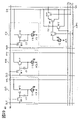
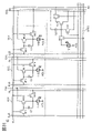
- 28A and 28B are diagrams showing configuration examples of a display device.
- FIG. 29 is a diagram illustrating a configuration example of a display device.
- FIG. 30 is a diagram illustrating a configuration example of a display device.
- FIG. 31 is a diagram illustrating a configuration example of a display device.
- FIG. 32 is a diagram illustrating a configuration example of a display device.
- FIG. 34 is a diagram illustrating a configuration example of a display device.
- 35A and 35B are diagrams showing configuration examples of a display device.
- 36A and 36B are diagrams illustrating configuration examples of display devices.
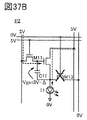
- 37A to 37C are diagrams showing configuration examples of display devices.
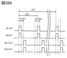
- 38A and 38B are block diagrams and timing charts of a display device.
- FIG. 39 is a diagram showing a timing chart of the display device.
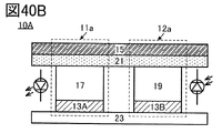
- 40A to 40D are diagrams showing configuration examples of display devices.
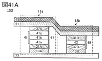
- 41A to 41C are diagrams showing configuration examples of display devices.
- FIG. 42 is a diagram illustrating a configuration example of a display device.
- 43A and 43B are diagrams showing configuration examples of a display device.
- 44A and 44B are diagrams showing configuration examples of a display device.
- 45A and 45B are diagrams showing configuration examples of a display device.
- 46A and 46B are diagrams showing configuration examples of a display device.
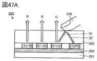
- 47A, 47B, and 47D are cross-sectional views showing examples of display devices.
- 47C and 47E are diagrams showing examples of images captured by the display device.
- FIG. 48 is a cross-sectional view showing an example of a display device.
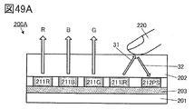
- 49A to 49C are cross-sectional views showing examples of display devices.
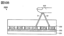
- 50A to 50C are cross-sectional views showing examples of display devices.
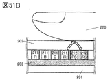
- 51A to 51C are diagrams showing an example of a display device.
- 52A to 52C are diagrams illustrating examples of electronic devices.
- FIG. 53A is a top view showing an example of a display device.
- FIG. 53B is a cross-sectional view showing an example of a display device;
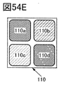
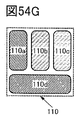
- 54A to 54I are top views showing examples of pixels.
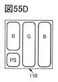
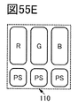
- 55A to 55E are top views showing examples of pixels.
- 56A and 56B are top views showing examples of pixels.
- 57A and 57B are top views showing examples of pixels.
- 58A and 58B are top views showing examples of pixels.
- 59A and 59B are top views showing examples of pixels.
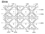
- 60A and 60B are top views showing examples of pixels.
- FIG. 61A is a top view showing an example of a display device.
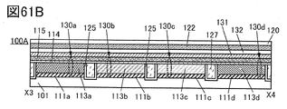
- FIG. 61B is a cross-sectional view showing an example of a display device.
- 62A to 62F are top views illustrating an example of a method for manufacturing a display device.
- 63A to 63C are cross-sectional views illustrating an example of a method for manufacturing a display device.
- 64A to 64C are cross-sectional views illustrating an example of a method for manufacturing a display device.
- 65A to 65C are cross-sectional views illustrating an example of a method for manufacturing a display device.
- 66A and 66B are cross-sectional views illustrating an example of a method for manufacturing a display device.
- 67A to 67C are cross-sectional views illustrating an example of a method for manufacturing a display device.
- 68A to 68C are cross-sectional views illustrating an example of a method for manufacturing a display device.
- FIG. 69A and 69B are cross-sectional views illustrating an example of a method for manufacturing a display device.
- 70A to 70E are cross-sectional views illustrating an example of a method for manufacturing a display device.
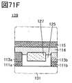
- 71A to 71F are cross-sectional views illustrating an example of a method for manufacturing a display device.
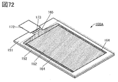
- FIG. 72 is a perspective view showing an example of a display device.
- FIG. 74 is a cross-sectional view showing an example of a display device.
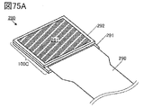
- 75A and 75B are perspective views showing an example of a display module.
- FIG. 76 is a cross-sectional view showing an example of a display device.
- FIG. 77 is a cross-sectional view showing an example of a display device.
- FIG. 78 is a cross-sectional view showing an example of a display device.
- FIG. 79 is a cross-sectional view showing an example of a display device.
- FIG. 80 is a cross-sectional view showing an example of a display device.
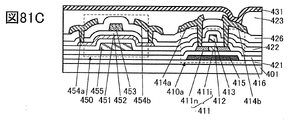
- 81A to 81D are diagrams illustrating examples of transistors.
- 82A and 82B are diagrams illustrating examples of electronic devices.
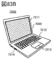
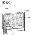
- 83A to 83D are diagrams showing examples of electronic devices.
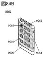
- 84A to 84F are diagrams illustrating examples of electronic devices.
- FIG. 85 is a diagram showing an example of a vehicle.
- film and “layer” can be interchanged depending on the case or situation.
- conductive layer can be changed to the term “conductive film.”
- insulating film can be changed to the term “insulating layer”.
- a display device of one embodiment of the present invention includes a display portion, and the display portion includes a plurality of pixels arranged in a matrix.
- a pixel includes a light-emitting device (also referred to as a light-emitting element) and a light-receiving device (also referred to as a light-receiving element).
- a light-emitting device functions as a display device (also called a display element).
- a display device of one embodiment of the present invention light-emitting devices are arranged in a matrix in a display portion, and an image can be displayed on the display portion. Further, the display device of one embodiment of the present invention has a function of detecting light using a light receiving device.
- an EL device such as an OLED (Organic Light Emitting Diode) or a QLED (Quantum-dot Light Emitting Diode) as the light emitting device.
- OLED Organic Light Emitting Diode
- QLED Quadantum-dot Light Emitting Diode
- light-emitting substances in EL devices include substances that emit fluorescence (fluorescent materials), substances that emit phosphorescence (phosphorescent materials), inorganic compounds (quantum dot materials, etc.), and substances that exhibit heat-activated delayed fluorescence (heat-activated delayed fluorescence ( Thermally Activated Delayed Fluorescence (TADF) material) and the like.
- LEDs such as micro LED (Light Emitting Diode), can also be used as a light emitting device.
- the TADF material a material in which the singlet excited state and the triplet excited state are in thermal equilibrium may be used. Since such a TADF material has a short emission lifetime (excitation lifetime), it is possible to suppress a decrease in efficiency in a high-luminance region of a light-emitting device.
- light-receiving devices are arranged in a matrix, and the display portion has one or both of an imaging function and a sensing function in addition to an image display function.
- the display part can be used for an image sensor or a touch sensor. That is, by detecting light on the display portion, an image can be captured, or proximity or contact of an object (a finger, hand, pen, or the like) can be detected.
- the display device of one embodiment of the present invention can use a light-emitting device as a light source of a sensor. Therefore, it is not necessary to provide a light receiving portion and a light source separately from the display device, and the number of parts of the electronic device can be reduced.
- the display device can capture an image using the light receiving device.
- the display device of this embodiment can be used as a scanner.
- an image sensor can be used to acquire data related to biometric information such as fingerprints and palm prints. That is, the biometric authentication sensor can be incorporated in the display device.
- the biometric authentication sensor can be incorporated into the display device.
- the display device can detect proximity or contact of an object using the light receiving device.
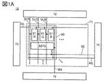
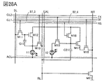
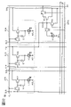
- FIG. 1A A block diagram of the display device 10 is shown in FIG. 1A.
- the display device 10 includes a display section 71, a drive circuit section 72, a drive circuit section 73, a drive circuit section 74, a circuit section 75, and the like.
- the display unit 71 has a plurality of pixels 80 arranged in a matrix.
- Pixel 80 has sub-pixel 81R, sub-pixel 81G, sub-pixel 81B, and sub-pixel 82PS.
- the sub-pixel 81R, sub-pixel 81G, and sub-pixel 81B each have a light-emitting device functioning as a display device.
- the sub-pixel 82PS has a light receiving device that functions as a photoelectric conversion element.
- sub-pixel the minimum unit in which one "pixel” performs an independent operation is defined as a "sub-pixel” for the sake of convenience.
- sub-pixel may be replaced with “pixel”.
- the pixel 80 is electrically connected to the wiring GL, the wiring SLR, the wiring SLG, the wiring SLB, the wiring SE, the wiring RS, the wiring WX, and the like.
- the wiring SLR, the wiring SLG, and the wiring SLB are electrically connected to the driver circuit portion 72 .
- the wiring GL is electrically connected to the drive circuit section 73 .
- the drive circuit section 72 functions as a source line drive circuit (also referred to as a source driver).
- the drive circuit section 73 functions as a gate line drive circuit (also called a gate driver).
- the pixel 80 has a sub-pixel 81R, a sub-pixel 81G, and a sub-pixel 81B as sub-pixels having light-emitting devices.
- the sub-pixel 81R is a red sub-pixel
- the sub-pixel 81G is a green sub-pixel
- the sub-pixel 81B is a blue sub-pixel. Accordingly, the display device 100 can perform full-color display.
- the pixel 80 has sub-pixels of three colors is shown here, it may have sub-pixels of four or more colors.
- the sub-pixel 81R has a light-emitting device that emits red light.
- Sub-pixel 81G has a light-emitting device that emits green light.
- Sub-pixel 81B has a light-emitting device that emits blue light.
- pixel 80 may have sub-pixels with light-emitting devices that exhibit other colors of light.
- the pixel 80 may have, in addition to the three sub-pixels described above, a sub-pixel having a light-emitting device that emits white light, a sub-pixel that has a light-emitting device that emits yellow light, or the like.
- the wiring GL is electrically connected to the sub-pixels 81R, 81G, and 81B arranged in the row direction (the extending direction of the wiring GL).
- the wiring SLR, the wiring SLG, and the wiring SLB are electrically connected to the sub-pixels 81R, 81G, and 81B arranged in the column direction (the extending direction of the wiring SLR and the like), respectively.
- a sub-pixel 82PS included in the pixel 80 is electrically connected to the wiring SE, the wiring RS, and the wiring WX.
- the wiring SE and the wiring RS are electrically connected to the drive circuit section 74 respectively, and the wiring WX is electrically connected to the circuit section 75 .
- the drive circuit section 74 has a function of generating a signal for driving the sub-pixel 82PS and outputting it to the sub-pixel 82PS via the wiring SE and the wiring RS.
- the circuit section 75 has a function of receiving a signal output from the sub-pixel 82PS via the wiring WX and outputting it to the outside as image data.
- the circuit section 75 functions as a readout circuit.
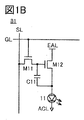
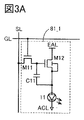
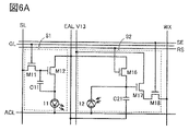
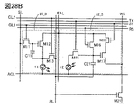
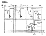
- FIG. 1B An example of a circuit diagram of a pixel 81 that can be applied to sub-pixel 81R, sub-pixel 81G, and sub-pixel 81B is shown in FIG. 1B.
- the pixel 81 has a transistor M11, a transistor M12, a capacitor C11, and a light emitting device 11.
- FIG. A wiring GL and a wiring SL are electrically connected to the pixel 81 .
- the wiring SL corresponds to one of the wiring SLR, the wiring SLG, and the wiring SLB illustrated in FIG. 1A.
- the transistor M11 has a gate electrically connected to the wiring GL, one of its source and drain electrically connected to the wiring SL, and the other electrically connected to one electrode of the capacitor C11 and the gate of the transistor M12. be.
- the transistor M12 has one of its source and drain electrically connected to the wiring EAL, and the other of its source and drain electrically connected to one electrode of the light emitting device 11 and the other electrode of the capacitor C11.
- the other electrode of the light emitting device 11 is electrically connected to the wiring ACL.
- the transistor M11 functions as a switch.
- the transistor M12 functions as a transistor for controlling current flowing through the light emitting device 11 .
- a transistor including silicon in a channel formation region (hereinafter referred to as a Si transistor) as the transistor M11 and the transistor M12.
- a transistor including a metal oxide (also referred to as an oxide semiconductor) in a channel formation region (hereinafter referred to as an OS transistor) is preferably used as the transistor M11, and a Si transistor is preferably used as the transistor M12.
- Si transistors have high field effect mobility and good frequency characteristics.
- a transistor including low temperature poly silicon (LTPS) in a channel formation region hereinafter referred to as an LTPS transistor can be used.
- LTPS low temperature poly silicon
- circuits that need to be driven at high frequencies can be built on the same substrate as the display section. This makes it possible to simplify the external circuit mounted on the display device and reduce the component cost and the mounting cost.
- Oxide semiconductors include, for example, indium and metal M (M is gallium, aluminum, silicon, boron, yttrium, tin, copper, vanadium, beryllium, titanium, iron, nickel, germanium, zirconium, molybdenum, lanthanum, cerium, one or more selected from neodymium, hafnium, tantalum, tungsten, and magnesium) and zinc.
- M is preferably one or more selected from aluminum, gallium, yttrium, and tin.
- an oxide containing indium, gallium, and zinc (also referred to as IGZO) is preferably used for the semiconductor layer of the OS transistor.
- an oxide containing indium, tin, and zinc is preferably used.
- oxides containing indium, gallium, tin, and zinc are preferably used.
- An OS transistor using an oxide semiconductor which has a wider bandgap and a lower carrier density than silicon, can achieve extremely low off-current. Therefore, with the small off-state current, charge accumulated in the capacitor connected in series with the OS transistor can be held for a long time. Therefore, it is preferable to use an OS transistor, particularly for the transistor M11 connected in series with the capacitor C11.
- an OS transistor as the transistor M11, the charge held in the capacitor C11 can be prevented from leaking through the transistor M11.
- the charge held in the capacitor C11 can be held for a long time, a still image can be displayed for a long time without rewriting the data of the pixel 81 .
- the off current value of the OS transistor per 1 ⁇ m of channel width at room temperature is 1 aA (1 ⁇ 10 ⁇ 18 A) or less, 1 zA (1 ⁇ 10 ⁇ 21 A) or less, or 1 yA (1 ⁇ 10 ⁇ 24 A) or less.
- the off current value of the Si transistor per 1 ⁇ m channel width at room temperature is 1 fA (1 ⁇ 10 ⁇ 15 A) or more and 1 pA (1 ⁇ 10 ⁇ 12 A) or less. Therefore, it can be said that the off-state current of the OS transistor is about ten digits lower than the off-state current of the Si transistor.
- a data potential is applied to the wiring SL.
- a selection signal is applied to the wiring GL.
- the selection signal includes a potential that makes the transistor conductive and a potential that makes the transistor non-conductive.
- a first potential is applied to the wiring EAL.
- a second potential is applied to the wiring ACL.
- the wiring EAL is electrically connected to the anode of the light emitting device 11 and functions to supply a first potential to the anode of the light emitting device 11 .
- the wiring ACL is electrically connected to the cathode of the light emitting device 11 and has a function of supplying the cathode of the light emitting device 11 with a second potential.
- the second potential is lower than the first potential.
- the first potential can be called the anode potential
- the second potential can be called the cathode potential.
- the wiring EAL may be called a power supply line.
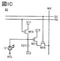
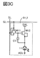
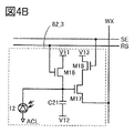
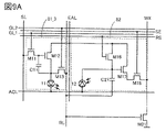
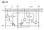
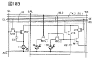
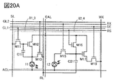
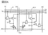
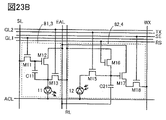
- Pixel 82 has transistor M16, transistor M17, transistor M18, capacitor C21, and light receiving device 12 .
- the light receiving device 12 has a cathode electrically connected to one of the source and drain of the transistor M16, the first electrode of the capacitor C21, and the gate of the transistor M17.
- the transistor M16 has a gate electrically connected to the wiring RS and the other of the source and the drain electrically connected to the wiring V11.
- One of the source and the drain of the transistor M17 is electrically connected to the wiring V13, and the other of the source and the drain is electrically connected to one of the source and the drain of the transistor M18.
- the transistor M18 has a gate electrically connected to the wiring SE and the other of the source and the drain electrically connected to the wiring WX.
- the light receiving device 12 has an anode electrically connected to the wiring ACL.
- a second electrode of the capacitor C21 is electrically connected to the wiring V12.
- the transistor M16 and the transistor M18 function as switches.
- the transistor M17 functions as an amplifying element (amplifier).
- Si transistors it is preferable to apply Si transistors to all of the transistors M16 to M18.
- an OS transistor is preferably used as the transistor M16, and a Si transistor is preferably used as the transistor M17.
- an OS transistor or a Si transistor may be applied to the transistor M18.
- a Si transistor is preferably applied to the transistor M17.
- Si transistors can achieve higher field-effect mobility than OS transistors, and are superior in drive capability and current capability. Therefore, the transistor M17 can operate at a higher speed than the transistor M16.
- an output operation corresponding to a minute potential based on the amount of light received by the light receiving device 12 can be quickly performed for the transistor M18.
- transistors are shown as n-channel transistors in FIGS. 1B and 1C, p-channel transistors can also be used.
- the transistors included in the pixels 81 and 82 are preferably formed side by side on the same substrate.
- the wiring ACL electrically connected to the anode of the light receiving device 12 in the pixel 82 can be shared with the wiring ACL of the pixel 81 and is supplied with the second potential.
- the wiring ACL has a function of applying the second potential to the anode of the light receiving device 12 .
- the wiring V11 electrically connected to the cathode of the light receiving device 12 can be shared with the wiring EAL of the pixel 81, and is supplied with the first potential.
- the first potential is higher than the second potential. Thereby, a reverse bias voltage can be applied to the light receiving device 12 .
- FIG. 2A illustrates an example in which the wiring V11, the wiring V13, the wiring V12, and the wiring EAL are shared. That is, in the circuit diagram shown in FIG. 2A , in a configuration in which a forward bias voltage is applied to the light emitting device 11 and a reverse bias voltage is applied to the light receiving device 12, a plurality of wirings included in the pixels 81 and 82 are shared. can be done. Therefore, the number of wirings electrically connected to the pixels 80 and the number of potentials applied to the pixels 80 can be reduced.
- the layout area of the pixel 80 can be reduced, so that the display device can have a high-definition display portion while having a photodetection function. Further, the display device can have a high-resolution display portion while having a light detection function.
- a light-emitting device and a light-receiving device that can be applied to the display device of one embodiment of the present invention are described.
- a schematic cross-sectional view of the light-emitting device 11 and the light-receiving device 12 included in the display device 10 of one embodiment of the present invention is shown in FIG. 2B.
- the light-emitting device 11 has a function of emitting light (hereinafter also referred to as a light-emitting function).
- Light emitting device 11 has electrode 13A, EL layer 17 and electrode 15 .
- the light emitting device 11 is preferably an organic EL device (organic electroluminescence device).
- the EL layer 17 sandwiched between the electrodes 13A and 15 has at least a light-emitting layer.
- the light-emitting layer has a light-emitting material that emits light. Light is emitted from the EL layer 17 by applying a voltage between the electrodes 13A and 15 .
- the EL layer 17 can further have various layers such as a hole injection layer, a hole transport layer, an electron transport layer, an electron injection layer, a carrier blocking layer, an exciton blocking layer, a charge generation layer, and the like.
- the light receiving device 12 has a function of detecting light (hereinafter also referred to as a light receiving function).
- a light receiving function for the light receiving device 12, for example, a pn-type or pin-type photodiode can be used.
- the light receiving device 12 has an electrode 13 B, a light receiving layer 19 and an electrode 15 .
- the light-receiving layer 19 sandwiched between the electrodes 13B and 15 has at least an active layer.
- the light-receiving device 12 functions as a photoelectric conversion device, generates electric charge by light incident on the light-receiving layer 19, and can be taken out as a current. At this time, a voltage may be applied between the electrode 13B and the electrode 15.
- FIG. The amount of charge generated is determined based on the amount of light incident on the light-receiving layer 19 .
- the light receiving device 12 has a function of detecting visible light.
- the light receiving device 12 is sensitive to visible light. More preferably, the light receiving device 12 has a function of detecting visible light and infrared light.
- the light receiving device 12 is preferably sensitive to visible light and/or infrared light.
- the wavelength region of blue (B) is 400 nm or more and less than 490 nm, and blue (B) light has at least one emission spectrum peak in this wavelength region.
- the wavelength region of green (G) is 490 nm or more and less than 580 nm, and green (G) light has at least one emission spectrum peak in this wavelength region.
- the wavelength region of red (R) is 580 nm or more and less than 700 nm, and red (R) light has at least one emission spectrum peak in this wavelength region.
- the wavelength region of visible light is from 400 nm to less than 700 nm, and visible light has at least one emission spectrum peak in this wavelength region.
- the infrared (IR) wavelength range is from 700 nm to less than 900 nm, and the infrared (IR) light has at least one emission spectrum peak in this wavelength range.
- the active layer contains a semiconductor.
- the semiconductor include inorganic semiconductors such as silicon and organic semiconductors including organic compounds.
- organic photodiode having a layer containing an organic semiconductor as the light receiving device 12 .
- Organic photodiodes can be easily made thinner, lighter, and larger, and have a high degree of freedom in shape and design, so that they can be applied to various display devices.
- the EL layer of the light emitting device 11 and the light receiving layer of the light receiving device 12 can be formed by the same method (eg, vacuum deposition method), and a common manufacturing apparatus can be used. It is preferable because it can be done.
- the display device of one embodiment of the present invention can suitably use an organic EL device as the light-emitting device 11 and an organic photodiode as the light-receiving device 12 .
- An organic EL device and an organic photodiode can be formed on the same substrate. Therefore, an organic photodiode can be incorporated in a display device using an organic EL device.
- a display device which is one embodiment of the present invention has one or both of an imaging function and a sensing function in addition to a function of displaying an image.
- the electrodes 13A and 13B are provided on the same plane.
- FIG. 2B shows a configuration in which the electrodes 13A and 13B are provided on the substrate 23.
- FIG. The electrodes 13A and 13B can be formed, for example, by processing a conductive film formed on the substrate 23 into an island shape. That is, the electrodes 13A and 13B can be formed through the same process.
- a substrate having heat resistance that can withstand the formation of the light emitting device 11 and the light receiving device 12 can be used.
- a glass substrate, a quartz substrate, a sapphire substrate, a ceramic substrate, an organic resin substrate, or the like can be used.
- a semiconductor substrate such as a single crystal semiconductor substrate, a polycrystalline semiconductor substrate, a compound semiconductor substrate made of silicon germanium or the like, or an SOI substrate can be used.
- the substrate 23 it is preferable to use the above-described insulating substrate or semiconductor substrate on which a semiconductor circuit including semiconductor elements such as transistors is formed.
- the semiconductor circuit preferably constitutes, for example, a pixel circuit, a gate line driver circuit (gate driver), a source line driver circuit (source driver), and the like.
- gate driver gate line driver
- source driver source driver
- an arithmetic circuit, a memory circuit, and the like may be configured.
- the electrodes 13A and 13B can be called pixel electrodes.
- the electrode 15 is a layer common to the light emitting device 11 and the light receiving device 12, and can be called a common electrode.
- a conductive film that transmits visible light and infrared light is used for the electrode on the side from which light is emitted or from which light is incident, of the pixel electrode and the common electrode.
- a conductive film that reflects visible light and infrared light is preferably used for the electrode on the side from which light is not emitted or incident.
- the display device which is one aspect of the present invention, is configured so that the electrode 15 functioning as a common electrode functions as either an anode or a cathode in the light emitting device 11 and functions as the other of the anode or cathode in the light receiving device 12 .
- FIG. 2C in the light-emitting device 11, the electrode 13A functions as an anode and the electrode 15 functions as a cathode, and in the light-receiving device 12, the electrode 13B functions as a cathode and the electrode 15 functions as an anode.
- FIG. 2C a schematic diagram with circuit symbols and the like added is shown in FIG.
- the circuit symbol of a light-emitting diode is shown on the left side of the light-emitting device 11, and the circuit symbol of a photodiode is shown on the right side of the light-receiving device 12, in order to make the orientation of the anode and cathode easier to understand. Arrows schematically indicate the directions in which electrons and holes flow.
- FIG. 2C the electrodes 15 in FIG. 2B are illustrated as wiring ACL.
- FIG. 2C also illustrates how the wiring EAL provided on the substrate 23 and the transistor M12 and the transistor M16 connected to the wiring EAL are connected to the electrodes 13A and 13B, respectively.
- the electrode 13A functions as an anode and is connected to the wiring EAL for supplying the first potential via the transistor M12.
- the wiring ACL functions as a cathode that supplies a second potential. The second potential is lower than the first potential.
- the electrode 13B functions as a cathode and is connected to the wiring EAL for supplying the first potential via the transistor M16.
- the wiring ACL functions as an anode that supplies the second potential.
- a reverse bias voltage is applied.
- the electrode 13A functions as an anode
- the electrode 15 functions as a cathode
- the electrode 13B functions as a cathode
- the electrode 15 functions as an anode.
- the potential difference between the electrodes 13B can be reduced, and leakage (hereinafter also referred to as side leakage) between the electrodes 13A and 13B can be suppressed. Therefore, a light-receiving device having a high SN ratio (Signal to Noise Ratio) can be obtained.
- the distance between the light emitting device 11 and the light receiving device 12 can be narrowed. That is, the proportion of the light emitting device 11 and the light receiving device 12 in the pixel (hereinafter also referred to as aperture ratio) can be increased.
- the pixel size can be reduced, and the definition of the display device can be improved. Therefore, a display device having a photodetection function and a high aperture ratio can be realized. Further, a high-definition display device having a photodetection function can be realized.
- the resolution of the light receiving device 12 is 100 ppi or more, preferably 200 ppi or more, more preferably 300 ppi or more, more preferably 400 ppi or more, still more preferably 500 ppi or more, and 2000 ppi or less, 1000 ppi or less, or 600 ppi or less.
- the resolution is 500 ppi or more, it is preferable because it can conform to standards such as the US National Institute of Standards and Technology (NIST).
- the size of one pixel is 50.8 ⁇ m, which is sufficient resolution to capture the width of a fingerprint (typically, 300 ⁇ m or more and 500 ⁇ m or less). I understand.
- the electrode 13A functions as a cathode and the electrode 15 functions as an anode in the light-emitting device 11, and the electrode 13B functions as an anode in the light-receiving device 12, and the electrode 15 may function as a cathode.
- a transistor having a pair of gates that overlap with each other with a semiconductor layer interposed therebetween can be used as the transistor included in the pixel 81 and the pixel 82 .
- Specific examples of the LTPS transistor and the OS transistor each having a pair of gates are described in detail below.
- a configuration in which the pair of gates are electrically connected to each other and supplied with the same potential has the advantage of increasing the on current of the transistor and improving saturation characteristics.
- a potential for controlling the threshold voltage of the transistor may be applied to one of the pair of gates.
- the stability of the electrical characteristics of the transistor can be improved.
- one gate of the transistor may be electrically connected to a wiring to which a constant potential is applied, or may be electrically connected to its own source or drain.
- a pixel 81_1 shown in FIG. 3A is an example in which a transistor having a pair of gates is applied to the transistor M12 of the pixel 81.
- FIG. The transistor M12 has the other of the pair of gates electrically connected to its source or drain.
- a pixel 82_1 shown in FIG. 3B is an example in which a transistor having a pair of gates is applied to the transistor M17 of the pixel 82 .
- the transistor M17 has the other of the pair of gates electrically connected to its source or drain.
- a pixel 81_2 shown in FIG. 3C is an example in which a transistor having a pair of gates is applied to the transistor M11 of the pixel 81_1.
- the transistor M12 has the other of the pair of gates electrically connected to its source or drain.
- a pixel 82_2 shown in FIG. 3D is an example in which transistors having a pair of gates are applied to the transistors M16 and M18 of the pixel 82_1.
- the transistor M17 has the other of the pair of gates electrically connected to its source or drain.
- a pixel 81_3 shown in FIG. 4A is an example in which a transistor M13 is added to the pixel 81 and wirings GL1 and GL2 are provided for separately controlling the transistors M11 and M13.
- a gate of the transistor M11 is electrically connected to the wiring GL1.
- a gate of the transistor M13 is electrically connected to the wiring GL2.
- the transistor M13 functions as a switch, like the transistor M11.
- One of the source and the drain of the transistor M13 is electrically connected to one electrode of the light emitting device 11, and the other of the source and the drain is electrically connected to the wiring RL.
- a reset potential is applied to the wiring RL.
- the reset potential applied to the wiring RL can be a potential such that the potential difference between the reset potential and the cathode potential of the light emitting device 11 is smaller than the threshold voltage of the light emitting device 11 .
- the reset potential can be a potential higher than the cathode potential, the same potential as the cathode potential, or a potential lower than the cathode potential.
- a pixel 82_3 shown in FIG. 4B is an example in which the position of the transistor M18 in the pixel 82 is changed between the transistor M17 and the wiring V13.
- FIG. 5A shows an example of a circuit diagram of the pixel 80 when the pixel 81 is applied to the sub-pixel 81R, sub-pixel 81G, or sub-pixel 81B, and the pixel 82_3 is applied to the sub-pixel 82PS.
- FIG. 5A illustrates an example in which the wiring V11, the wiring V13, the wiring V12, and the wiring EAL are shared. That is, in the circuit diagram shown in FIG. 5A , in a configuration in which a forward bias voltage is applied to the light emitting device 11 and a reverse bias voltage is applied to the light receiving device 12, a plurality of wirings included in the pixels 81 and 82 are shared. can be done. Therefore, in a pixel having the sub-pixel 81R, the sub-pixel 81G, the sub-pixel 81B, and the sub-pixel 82PS, the number of wiring lines and the number of applied potentials can be reduced.
- FIG. 5B shows an example of a circuit diagram of the pixel 80 when the pixel 81_3 is applied to the sub-pixel 81R, sub-pixel 81G, or sub-pixel 81B, and the pixel 82_3 is applied to the sub-pixel 82PS.
- FIG. 5B illustrates an example in which the wiring V11, the wiring V13, and the wiring EAL are shared, and the wiring RL and the wiring V12 are shared. That is, in the circuit diagram shown in FIG. 5B , in a configuration in which a forward bias voltage is applied to the light emitting device 11 and a reverse bias voltage is applied to the light receiving device 12, a plurality of wirings included in the pixels 81 and 82 are shared. can be done. Therefore, in a pixel having the sub-pixel 81R, the sub-pixel 81G, the sub-pixel 81B, and the sub-pixel 82PS, the number of wiring lines and the number of applied potentials can be reduced.
- FIG. 6A shows an example of a circuit diagram of the pixel 80 when the pixel 81 is applied to the sub-pixel 81R, sub-pixel 81G, or sub-pixel 81B, and the pixel 82 is applied to the sub-pixel 82PS.
- FIG. 6A illustrates an example in which the wiring V11, the wiring V12, and the wiring EAL are shared, and the wiring V13 is another wiring. That is, in the circuit diagram shown in FIG. 6A, in the configuration in which a forward bias voltage is applied to the light-emitting device 11 and a reverse bias voltage is applied to the light-receiving device 12, a plurality of wirings included in the pixels 81 and 82 are shared. can be done. Therefore, in a pixel having the sub-pixel 81R, the sub-pixel 81G, the sub-pixel 81B, and the sub-pixel 82PS, the number of wiring lines and the number of applied potentials can be reduced.
- FIG. 6B shows an example of a circuit diagram of the pixel 80 when the pixel 81_3 is applied to the sub-pixel 81R, sub-pixel 81G, or sub-pixel 81B, and the pixel 82 is applied to the sub-pixel 82PS.
- FIG. 6B illustrates an example in which the wiring V11, the wiring V12, and the wiring EAL are shared, and the wiring RL and the wiring V13 are shared. That is, in the circuit diagram shown in FIG. 6B, in a configuration in which a forward bias voltage is applied to the light emitting device 11 and a reverse bias voltage is applied to the light receiving device 12, a plurality of wirings included in the pixel 81_3 and the pixel 82 are shared. can be done. Therefore, in a pixel having the sub-pixel 81R, the sub-pixel 81G, the sub-pixel 81B, and the sub-pixel 82PS, the number of wiring lines and the number of applied potentials can be reduced.
- FIG. 7A shows an example of a circuit diagram of the pixel 80 when the pixel 81 is applied to the sub-pixel 81R, sub-pixel 81G, or sub-pixel 81B, and the pixel 82 is applied to the sub-pixel 82PS.
- FIG. 7A illustrates an example in which the wiring V13 and the wiring EAL are made common, and the wiring V11 and the wiring V12 are made common. That is, in the circuit diagram shown in FIG. 7A , in a configuration in which a forward bias voltage is applied to the light emitting device 11 and a reverse bias voltage is applied to the light receiving device 12, a plurality of wirings included in the pixels 81 and 82 are shared. can be done. Therefore, in a pixel having the sub-pixel 81R, the sub-pixel 81G, the sub-pixel 81B, and the sub-pixel 82PS, the number of wiring lines and the number of applied potentials can be reduced.
- FIG. 7B shows an example of a circuit diagram of the pixel 80 when the pixel 81_3 is applied to the sub-pixel 81R, sub-pixel 81G, or sub-pixel 81B, and the pixel 82 is applied to the sub-pixel 82PS.
- FIG. 7B illustrates an example in which the wiring V13 and the wiring EAL are shared, and the wiring RL, the wiring V11 and the wiring V12 are shared. That is, in the circuit diagram shown in FIG. 7B , in a configuration in which a forward bias voltage is applied to the light emitting device 11 and a reverse bias voltage is applied to the light receiving device 12, a plurality of wirings included in the pixel 81_3 and the pixel 82 are shared. can be done. Therefore, in a pixel having the sub-pixel 81R, the sub-pixel 81G, the sub-pixel 81B, and the sub-pixel 82PS, the number of wiring lines and the number of applied potentials can be reduced.
- FIG. 8A shows an example of a circuit diagram of the pixel 80 when the pixel 81 is applied to the sub-pixel 81R, sub-pixel 81G, or sub-pixel 81B, and the pixel 82 is applied to the sub-pixel 82PS.
- FIG. 8A illustrates an example in which the wiring V13 and the wiring V12 are made common, and the wiring V11 and the wiring EAL are made common. That is, in the circuit diagram shown in FIG. 8A , in a configuration in which a forward bias voltage is applied to the light emitting device 11 and a reverse bias voltage is applied to the light receiving device 12, a plurality of wirings included in the pixels 81 and 82 are shared. can be done. Therefore, in a pixel having the sub-pixel 81R, the sub-pixel 81G, the sub-pixel 81B, and the sub-pixel 82PS, the number of wiring lines and the number of applied potentials can be reduced.
- FIG. 8B shows an example of a circuit diagram of the pixel 80 when the pixel 81_3 is applied to the sub-pixel 81R, sub-pixel 81G, or sub-pixel 81B, and the pixel 82 is applied to the sub-pixel 82PS.
- FIG. 8B illustrates an example in which the wiring V11 and the wiring EAL are shared, and the wiring RL, the wiring V12 and the wiring V13 are shared. That is, in the circuit diagram shown in FIG. 8B, in a configuration in which a forward bias voltage is applied to the light emitting device 11 and a reverse bias voltage is applied to the light receiving device 12, a plurality of wirings included in the pixel 81_3 and the pixel 82 are shared. can be done. Therefore, in a pixel having the sub-pixel 81R, the sub-pixel 81G, the sub-pixel 81B, and the sub-pixel 82PS, the number of wiring lines and the number of applied potentials can be reduced.
- FIGS. 5A to 8B illustrate examples in which the pixel 82 (or the pixel 82_3) is applied to the sub-pixel 82PS, the pixels 82_1 to 82_3 may be applied.
- 5A to 8B illustrate diagrams in which the pixel 81 or 81_3 is applied to the sub-pixel 81R, the sub-pixel 81G, or the sub-pixel 81B, the pixel 81_1 or 82_2 may be applied.
- 5A to 8B illustrate the configuration in which the wirings connected to the transistors included in the pixel 80 are shared, but other configurations may be used.
- FIG. 9A shows a circuit diagram of the pixel 80 in which the pixel 81_3 is applied to the sub-pixel 81R, the sub-pixel 81G, or the sub-pixel 81B, and the pixel 82 is applied to the sub-pixel 82PS.
- An example in which the gate of the transistor M21 and the wiring RL are shared is shown. By applying the reset potential applied to the wiring RL to the gate of the transistor M21, the transistor M21 can function as a constant current source. Further, FIG.
- FIGS. 9A and 9B show a circuit diagram of the pixel 80 in which the pixel 81_3 is applied to the sub-pixel 81R, the sub-pixel 81G, or the sub-pixel 81B, and the pixel 82_3 is applied to the sub-pixel 82PS.
- An example is shown in which the gate of the connected transistor M21 and the wiring RL are shared.
- the transistor M21 can function as a constant current source. That is, in the circuit diagrams shown in FIGS. 9A and 9B, the pixel 81_3 and the pixel 82 (or the pixel 82_3) have A plurality of wirings and other wirings (wirings to which a potential is applied) can be shared. Therefore, in a pixel having the sub-pixel 81R, the sub-pixel 81G, the sub-pixel 81B, and the sub-pixel 82PS, the number of wiring lines and the number of applied potentials can be reduced.
- FIG. 10A A configuration different from the block diagram of the display device 10 shown in FIG. 1A will be described with reference to FIG. 10A. 10A only describes points different from FIG. 1A, and the configurations denoted by common reference numerals are the same as those in FIG. 1A.
- the pixel 80 is electrically connected to the wiring GL, the wiring SLR, the wiring SLG, the wiring SLB, the wiring TX, the wiring SE, the wiring RS, the wiring WX, and the like.
- the sub-pixel 82PS included in the pixel 80 is electrically connected to the wiring TX, the wiring SE, the wiring RS, and the wiring WX.
- the wiring TX, the wiring SE, and the wiring RS are electrically connected to the drive circuit section 74
- the wiring WX is electrically connected to the circuit section 75 .
- the drive circuit section 74 has a function of generating a signal for driving the sub-pixel 82PS and outputting it to the sub-pixel 82PS via the wiring SE, the wiring TX, and the wiring RS.
- Pixel 82_4 has transistor M15, transistor M16, transistor M17, transistor M18, capacitor C21, and light receiving device 12 .
- the light receiving device 12 the light receiving device described above can be used.
- the transistor M15 has a gate electrically connected to the wiring TX, one of its source and drain electrically connected to the cathode of the light receiving device 12, and the other of the source and drain being one of the source and drain of the transistor M16. It is electrically connected to the first electrode of the capacitor C21 and the gate of the transistor M17.
- the transistor M15 functions as a switch.
- a Si transistor or an OS transistor is preferably applied to the transistor M15.
- OS transistors as the transistors M15 and M16, the potential held at the gate of the transistor M17 can be prevented from leaking through the transistor M15 or the transistor M16 based on the charge generated in the light receiving device 12. can.
- the period (charge retention period) from the end of the charge transfer operation to the start of the readout operation differs depending on the pixel.
- an output signal having the same potential value is ideally obtained in all pixels.
- the length of the charge retention period differs from row to row
- the potential of the output signal of the pixel will differ from row to row if the charge accumulated in the node of the pixels in each row leaks over time.
- image data in which the number of gradations changes for each row is obtained. Therefore, by using OS transistors as the transistors M15 and M16, the potential change of the node of the pixel can be extremely reduced. That is, even if the image is captured using the global shutter method, the change in gradation of the image data due to the difference in the charge retention period can be suppressed to be small, and the quality of the captured image can be improved.
- Si transistors can achieve higher field-effect mobility than OS transistors, and are superior in drive capability and current capability. Therefore, the transistor M17 can operate faster than the transistors M15 and M16.
- Si transistors By using a Si transistor for the transistor M17, an output operation corresponding to a minute potential based on the amount of light received by the light receiving device 12 can be quickly performed for the transistor M18.
- the transistors M15 and M16 have low leakage current and the transistor M17 has high driving capability, the light is received by the light receiving device 12 and transferred via the transistor M15 is not leaked. It can be held and can be read out at high speed.
- transistors are shown as n-channel transistors in FIG. 10B, p-channel transistors can also be used.
- a pixel 82_5 shown in FIG. 11A is an example in which the transistor M16 in the pixel 82_4 is changed to a position where it is connected to one of the source and drain of the transistor M15 and the cathode of the light receiving device 12.
- FIG. 11A A pixel 82_5 shown in FIG. 11A is an example in which the transistor M16 in the pixel 82_4 is changed to a position where it is connected to one of the source and drain of the transistor M15 and the cathode of the light receiving device 12.
- a pixel 82_6 shown in FIG. 11B is an example in which the position of the transistor M18 in the pixel 82_5 is changed between the transistor M17 and the wiring V13.
- a pixel 82_7 shown in FIG. 12 is an example in which the transistor M16 in the pixel 82_6 is changed to a position connected to one of the source and drain of the transistor M15 and the cathode of the light receiving device 12.
- FIG. 12 A pixel 82_7 shown in FIG. 12 is an example in which the transistor M16 in the pixel 82_6 is changed to a position connected to one of the source and drain of the transistor M15 and the cathode of the light receiving device 12.
- a pixel 82_8 shown in FIG. 13A is an example of a configuration in which a plurality of pairs of the transistor M15 and the light receiving device PD are provided in the pixel 82_4.
- the transistor M15_1 has a gate electrically connected to the wiring TX_1, one of its source and drain electrically connected to the cathode of the light receiving device PD1, and the other of the source and drain being one of the source and drain of the transistor M16. It is electrically connected to the first electrode of the capacitor C21 and the gate of the transistor M17.
- the transistor M15_2 has a gate electrically connected to the wiring TX_2, one of its source and drain electrically connected to the cathode of the light receiving device PD2, and the other of the source and drain being one of the source and drain of the transistor M16. It is electrically connected to the first electrode of the capacitor C21 and the gate of the transistor M17.
- the anode of the light receiving device PD1 and the anode of the light receiving device PD2 are electrically connected to the wiring ACL.
- a pixel 82_9 shown in FIG. 13B is an example in which the position of the transistor M18 in the pixel 82_8 is changed between the transistor M17 and the wiring V13.
- FIG. 14A shows an example of a circuit diagram of the pixel 80 when the pixel 81 is applied to the sub-pixel 81R, sub-pixel 81G, or sub-pixel 81B, and the pixel 82_4 is applied to the sub-pixel 82PS.
- FIG. 14A illustrates an example in which the wiring V11, the wiring V13, the wiring V12, and the wiring EAL are shared. That is, in the circuit diagram shown in FIG. 14A , in a configuration in which a forward bias voltage is applied to the light emitting device 11 and a reverse bias voltage is applied to the light receiving device 12, a plurality of wirings included in the pixel 81 and the pixel 82_4 are shared. can be done. Therefore, in a pixel having the sub-pixel 81R, the sub-pixel 81G, the sub-pixel 81B, and the sub-pixel 82PS, the number of wiring lines and the number of applied potentials can be reduced.
- FIG. 14B shows an example of a circuit diagram of the pixel 80 when the pixel 81 is applied to the sub-pixel 81R, sub-pixel 81G, or sub-pixel 81B, and the pixel 82_5 is applied to the sub-pixel 82PS.
- FIG. 14B illustrates an example in which the wiring V11, the wiring V13, the wiring V12, and the wiring EAL are shared. That is, in the circuit diagram shown in FIG. 14B , in a configuration in which a forward bias voltage is applied to the light emitting device 11 and a reverse bias voltage is applied to the light receiving device 12, a plurality of wirings included in the pixel 81 and the pixel 82_5 are shared. can be done. Therefore, in a pixel having the sub-pixel 81R, the sub-pixel 81G, the sub-pixel 81B, and the sub-pixel 82PS, the number of wiring lines and the number of applied potentials can be reduced.
- FIG. 15A shows an example of a circuit diagram of the pixel 80 when the pixel 81 is applied to the sub-pixel 81R, sub-pixel 81G, or sub-pixel 81B, and the pixel 82_4 is applied to the sub-pixel 82PS.
- FIG. 15A illustrates an example in which the wiring V11, the wiring V13, and the wiring EAL are shared, and the wiring V12 is another wiring. That is, in the circuit diagram shown in FIG. 15A , in a configuration in which a forward bias voltage is applied to the light emitting device 11 and a reverse bias voltage is applied to the light receiving device 12, a plurality of wirings included in the pixel 81 and the pixel 82_4 are shared. can be done. Therefore, in a pixel having the sub-pixel 81R, the sub-pixel 81G, the sub-pixel 81B, and the sub-pixel 82PS, the number of wiring lines and the number of applied potentials can be reduced.
- the capacitance C21 of the pixel 82_4 can be omitted as shown in FIG. 15B by increasing the parasitic capacitance of the gate of the transistor M17.
- FIG. 16A shows an example of a circuit diagram of the pixel 80 when the pixel 81 is applied to the sub-pixel 81R, sub-pixel 81G, or sub-pixel 81B, and the pixel 82_6 is applied to the sub-pixel 82PS.
- FIG. 16A illustrates an example in which the wiring V11, the wiring V13, the wiring V12, and the wiring EAL are shared. That is, in the circuit diagram shown in FIG. 16A , in a configuration in which a forward bias voltage is applied to the light emitting device 11 and a reverse bias voltage is applied to the light receiving device 12, a plurality of wirings included in the pixel 81 and the pixel 82_6 are shared. can be done. Therefore, in a pixel having the sub-pixel 81R, the sub-pixel 81G, the sub-pixel 81B, and the sub-pixel 82PS, the number of wiring lines and the number of applied potentials can be reduced.
- FIG. 16B shows an example of a circuit diagram of the pixel 80 when the pixel 81 is applied to the sub-pixel 81R, sub-pixel 81G, or sub-pixel 81B, and the pixel 82_7 is applied to the sub-pixel 82PS.
- FIG. 16B illustrates an example in which the wiring V11, the wiring V13, the wiring V12, and the wiring EAL are shared. That is, in the circuit diagram shown in FIG. 16B , in a configuration in which a forward bias voltage is applied to the light emitting device 11 and a reverse bias voltage is applied to the light receiving device 12, a plurality of wirings included in the pixel 81 and the pixel 82_7 are shared. can be done. Therefore, in a pixel having the sub-pixel 81R, the sub-pixel 81G, the sub-pixel 81B, and the sub-pixel 82PS, the number of wiring lines and the number of applied potentials can be reduced.
- FIG. 17A shows an example of a circuit diagram of the pixel 80 when the pixel 81 is applied to the sub-pixel 81R, sub-pixel 81G, or sub-pixel 81B, and the pixel 82_8 is applied to the sub-pixel 82PS.
- FIG. 17A illustrates an example in which the wiring V11, the wiring V13, the wiring V12, and the wiring EAL are shared. That is, in the circuit diagram shown in FIG. 17A , in a configuration in which a forward bias voltage is applied to the light emitting device 11 and a reverse bias voltage is applied to the light receiving device 12, a plurality of wirings included in the pixel 81 and the pixel 82_8 are shared. can be done. Therefore, in a pixel having the sub-pixel 81R, the sub-pixel 81G, the sub-pixel 81B, and the sub-pixel 82PS, the number of wiring lines and the number of applied potentials can be reduced.
- FIG. 17B shows an example of a circuit diagram of the pixel 80 when the pixel 81 is applied to the sub-pixel 81R, sub-pixel 81G, or sub-pixel 81B, and the pixel 82_9 is applied to the sub-pixel 82PS.
- FIG. 17B illustrates an example in which the wiring V11, the wiring V13, the wiring V12, and the wiring EAL are shared. That is, in the circuit diagram shown in FIG. 17B , in a configuration in which a forward bias voltage is applied to the light emitting device 11 and a reverse bias voltage is applied to the light receiving device 12, a plurality of wirings included in the pixel 81 and the pixel 82_9 are shared. can be done. Therefore, in a pixel having the sub-pixel 81R, the sub-pixel 81G, the sub-pixel 81B, and the sub-pixel 82PS, the number of wiring lines and the number of applied potentials can be reduced.
- the light receiving devices may have different spectral sensitivity characteristics.
- the light receiving device 12IR having spectral sensitivity characteristics in the wavelength region of infrared light and the light receiving device 12 having spectral sensitivity characteristics in the wavelength region of visible light may be arranged.
- FIG. 18A shows, in the configuration of the circuit diagram shown in FIG. 17A, a light receiving device 12IR having spectral sensitivity characteristics in the wavelength region of infrared light and a light receiving device 12 having spectral sensitivity characteristics in the wavelength region of visible light.
- 4 is an example of a circuit diagram of a pixel 80.
- FIG. 18B shows, in the configuration of the circuit diagram shown in FIG. It is an example of a circuit diagram of a pixel 80 provided.
- FIG. 19A shows an example of a circuit diagram of the pixel 80 when the pixel 81_3 is applied to the sub-pixel 81R, sub-pixel 81G, or sub-pixel 81B, and the pixel 82_4 is applied to the sub-pixel 82PS.
- FIG. 19A illustrates an example in which the wiring V11, the wiring V12, the wiring V13, and the wiring EAL are shared. That is, in the circuit diagram shown in FIG. 19A , in a configuration in which a forward bias voltage is applied to the light emitting device 11 and a reverse bias voltage is applied to the light receiving device 12, a plurality of wirings included in the pixel 81_3 and the pixel 82_4 are shared. can be done. Therefore, in a pixel having the sub-pixel 81R, the sub-pixel 81G, the sub-pixel 81B, and the sub-pixel 82PS, the number of wiring lines and the number of applied potentials can be reduced.
- FIG. 19B shows an example of a circuit diagram of the pixel 80 when the pixel 81_3 is applied to the sub-pixel 81R, sub-pixel 81G, or sub-pixel 81B, and the pixel 82_5 is applied to the sub-pixel 82PS.
- FIG. 19B illustrates an example in which the wiring V11, the wiring V12, the wiring V13, and the wiring EAL are shared. That is, in the circuit diagram shown in FIG. 19B, in a configuration in which a forward bias voltage is applied to the light emitting device 11 and a reverse bias voltage is applied to the light receiving device 12, a plurality of wirings included in the pixel 81_3 and the pixel 82_5 are shared. can be done. Therefore, in a pixel having the sub-pixel 81R, the sub-pixel 81G, the sub-pixel 81B, and the sub-pixel 82PS, the number of wiring lines and the number of applied potentials can be reduced.
- FIG. 20A shows an example of a circuit diagram of the pixel 80 when the pixel 81_3 is applied to the sub-pixel 81R, sub-pixel 81G, or sub-pixel 81B, and the pixel 82_4 is applied to the sub-pixel 82PS.
- FIG. 20A illustrates an example in which the wiring V11, the wiring V13, and the wiring EAL are shared, and the wiring RL and the wiring V12 are shared. That is, in the circuit diagram shown in FIG. 20A , in a configuration in which a forward bias voltage is applied to the light emitting device 11 and a reverse bias voltage is applied to the light receiving device 12, a plurality of wirings included in the pixels 81_3 and 82_4 are shared. can be done. Therefore, in a pixel having the sub-pixel 81R, the sub-pixel 81G, the sub-pixel 81B, and the sub-pixel 82PS, the number of wiring lines and the number of applied potentials can be reduced.
- FIG. 20B shows an example of a circuit diagram of the pixel 80 when the pixel 81_3 is applied to the sub-pixel 81R, sub-pixel 81G, or sub-pixel 81B, and the pixel 82_4 is applied to the sub-pixel 82PS.
- FIG. 20B illustrates an example in which the wiring V11, the wiring V13, and the wiring EAL are shared, and the wiring V12 is omitted. That is, in the circuit diagram shown in FIG. 20B , in a configuration in which a forward bias voltage is applied to the light emitting device 11 and a reverse bias voltage is applied to the light receiving device 12, a plurality of wirings included in the pixel 81_3 and the pixel 82_4 are shared. can be done. Therefore, in a pixel having the sub-pixel 81R, the sub-pixel 81G, the sub-pixel 81B, and the sub-pixel 82PS, the number of wiring lines and the number of applied potentials can be reduced.
- FIG. 21A shows an example of a circuit diagram of the pixel 80 when the pixel 81_3 is applied to the sub-pixel 81R, sub-pixel 81G, or sub-pixel 81B, and the pixel 82_6 is applied to the sub-pixel 82PS.
- FIG. 21A illustrates an example in which the wiring V11, the wiring V12, the wiring V13, and the wiring EAL are shared. That is, in the circuit diagram shown in FIG. 21A , in a configuration in which a forward bias voltage is applied to the light emitting device 11 and a reverse bias voltage is applied to the light receiving device 12, a plurality of wirings included in the pixels 81_3 and 82_6 are shared. can be done. Therefore, in a pixel having the sub-pixel 81R, the sub-pixel 81G, the sub-pixel 81B, and the sub-pixel 82PS, the number of wiring lines and the number of applied potentials can be reduced.
- FIG. 21B shows an example of a circuit diagram of the pixel 80 when the pixel 81_3 is applied to the sub-pixel 81R, sub-pixel 81G, or sub-pixel 81B, and the pixel 82_7 is applied to the sub-pixel 82PS.
- FIG. 21B illustrates an example in which the wiring V11, the wiring V12, the wiring V13, and the wiring EAL are shared. That is, in the circuit diagram shown in FIG. 21B , in a configuration in which a forward bias voltage is applied to the light emitting device 11 and a reverse bias voltage is applied to the light receiving device 12, a plurality of wirings included in the pixel 81_3 and the pixel 82_7 are shared. can be done. Therefore, in a pixel having the sub-pixel 81R, the sub-pixel 81G, the sub-pixel 81B, and the sub-pixel 82PS, the number of wiring lines and the number of applied potentials can be reduced.
- FIG. 22A shows an example of a circuit diagram of the pixel 80 when the pixel 81 is applied to the sub-pixel 81R, sub-pixel 81G, or sub-pixel 81B, and the pixel 82_4 is applied to the sub-pixel 82PS.
- FIG. 22A illustrates an example in which the wiring V11, the wiring V12, and the wiring EAL are shared, and the wiring V13 is another wiring. That is, in the circuit diagram shown in FIG. 22A , in a configuration in which a forward bias voltage is applied to the light emitting device 11 and a reverse bias voltage is applied to the light receiving device 12, a plurality of wirings included in the pixel 81 and the pixel 82_4 are shared. can be done. Therefore, in a pixel having the sub-pixel 81R, the sub-pixel 81G, the sub-pixel 81B, and the sub-pixel 82PS, the number of wiring lines and the number of applied potentials can be reduced.
- FIG. 22B shows an example of a circuit diagram of the pixel 80 when the pixel 81 is applied to the sub-pixel 81R, sub-pixel 81G, or sub-pixel 81B, and the pixel 82_4 is applied to the sub-pixel 82PS.
- FIG. 22B illustrates an example in which the wiring V12, the wiring V13, and the wiring EAL are shared, and the wiring V11 is another wiring. That is, in the circuit diagram shown in FIG. 22B , in a configuration in which a forward bias voltage is applied to the light emitting device 11 and a reverse bias voltage is applied to the light receiving device 12, a plurality of wirings included in the pixel 81 and the pixel 82_4 are shared. can be done. Therefore, in a pixel having the sub-pixel 81R, the sub-pixel 81G, the sub-pixel 81B, and the sub-pixel 82PS, the number of wiring lines and the number of applied potentials can be reduced.
- FIG. 23A shows an example of a circuit diagram of the pixel 80 when the pixel 81_3 is applied to the sub-pixel 81R, sub-pixel 81G, or sub-pixel 81B, and the pixel 82_4 is applied to the sub-pixel 82PS.
- FIG. 23A illustrates an example in which the wiring V11, the wiring V12, and the wiring EAL are shared, and the wiring RL and the wiring V13 are shared. That is, in the circuit diagram shown in FIG. 23A, in a configuration in which a forward bias voltage is applied to the light emitting device 11 and a reverse bias voltage is applied to the light receiving device 12, a plurality of wirings included in the pixel 81_3 and the pixel 82_4 are shared. can be done. Therefore, in a pixel having the sub-pixel 81R, the sub-pixel 81G, the sub-pixel 81B, and the sub-pixel 82PS, the number of wiring lines and the number of applied potentials can be reduced.
- FIG. 23B shows an example of a circuit diagram of the pixel 80 when the pixel 81_3 is applied to the sub-pixel 81R, sub-pixel 81G, or sub-pixel 81B, and the pixel 82_4 is applied to the sub-pixel 82PS.
- FIG. 23B illustrates an example in which the wiring V12, the wiring V13, and the wiring EAL are shared, and the wiring RL and the wiring V11 are shared. That is, in the circuit diagram shown in FIG. 23B , in a configuration in which a forward bias voltage is applied to the light emitting device 11 and a reverse bias voltage is applied to the light receiving device 12, a plurality of wirings included in the pixels 81_3 and 82_4 are shared. can be done. Therefore, in a pixel having the sub-pixel 81R, the sub-pixel 81G, the sub-pixel 81B, and the sub-pixel 82PS, the number of wiring lines and the number of applied potentials can be reduced.
- FIG. 24A shows an example of a circuit diagram of the pixel 80 when the pixel 81 is applied to the sub-pixel 81R, sub-pixel 81G, or sub-pixel 81B, and the pixel 82_6 is applied to the sub-pixel 82PS.
- FIG. 24A illustrates an example in which the wiring V11, the wiring V12, and the wiring EAL are shared, and the wiring V13 is another wiring. That is, in the circuit diagram shown in FIG. 24A , in a configuration in which a forward bias voltage is applied to the light emitting device 11 and a reverse bias voltage is applied to the light receiving device 12, a plurality of wirings included in the pixel 81 and the pixel 82_6 are shared. can be done. Therefore, in a pixel having the sub-pixel 81R, the sub-pixel 81G, the sub-pixel 81B, and the sub-pixel 82PS, the number of wiring lines and the number of applied potentials can be reduced.
- FIG. 24B shows an example of a circuit diagram of the pixel 80 when the pixel 81 is applied to the sub-pixel 81R, sub-pixel 81G, or sub-pixel 81B, and the pixel 82_7 is applied to the sub-pixel 82PS.
- FIG. 24B illustrates an example in which the wiring V12, the wiring V13, and the wiring EAL are shared, and the wiring V11 is another wiring. That is, in the circuit diagram shown in FIG. 24B , in a configuration in which a forward bias voltage is applied to the light emitting device 11 and a reverse bias voltage is applied to the light receiving device 12, a plurality of wirings included in the pixel 81 and the pixel 82_7 are shared. can be done. Therefore, in a pixel having the sub-pixel 81R, the sub-pixel 81G, the sub-pixel 81B, and the sub-pixel 82PS, the number of wiring lines and the number of applied potentials can be reduced.
- FIG. 25A shows an example of a circuit diagram of the pixel 80 when the pixel 81_3 is applied to the sub-pixel 81R, sub-pixel 81G, or sub-pixel 81B, and the pixel 82_6 is applied to the sub-pixel 82PS.
- FIG. 25A illustrates an example in which the wiring V11, the wiring V12, and the wiring EAL are shared, and the wiring RL and the wiring V13 are shared. That is, in the circuit diagram shown in FIG. 25A, in a configuration in which a forward bias voltage is applied to the light emitting device 11 and a reverse bias voltage is applied to the light receiving device 12, a plurality of wirings included in the pixel 81_3 and the pixel 82_6 are shared. can be done. Therefore, in a pixel having the sub-pixel 81R, the sub-pixel 81G, the sub-pixel 81B, and the sub-pixel 82PS, the number of wiring lines and the number of applied potentials can be reduced.
- FIG. 25B shows an example of a circuit diagram of the pixel 80 when the pixel 81_3 is applied to the sub-pixel 81R, sub-pixel 81G, or sub-pixel 81B, and the pixel 82_7 is applied to the sub-pixel 82PS.
- FIG. 25B illustrates an example in which the wiring V12, the wiring V13, and the wiring EAL are shared, and the wiring RL and the wiring V11 are shared. That is, in the circuit diagram shown in FIG. 25B , in a configuration in which a forward bias voltage is applied to the light emitting device 11 and a reverse bias voltage is applied to the light receiving device 12, a plurality of wirings included in the pixel 81_3 and the pixel 82_7 are shared. can be done. Therefore, in a pixel having the sub-pixel 81R, the sub-pixel 81G, the sub-pixel 81B, and the sub-pixel 82PS, the number of wiring lines and the number of applied potentials can be reduced.
- FIG. 26A shows an example of a circuit diagram of the pixel 80 when the pixel 81 is applied to the sub-pixel 81R, sub-pixel 81G, or sub-pixel 81B, and the pixel 82_6 is applied to the sub-pixel 82PS.
- FIG. 26A illustrates an example in which the wiring V11 and the wiring EAL are shared, and the wiring V12 and the wiring V13 are shared. That is, in the circuit diagram shown in FIG. 26A, in a configuration in which a forward bias voltage is applied to the light emitting device 11 and a reverse bias voltage is applied to the light receiving device 12, a plurality of wirings included in the pixel 81 and the pixel 82_6 are shared. can be done. Therefore, in a pixel having the sub-pixel 81R, the sub-pixel 81G, the sub-pixel 81B, and the sub-pixel 82PS, the number of wiring lines and the number of applied potentials can be reduced.
- FIG. 26B shows an example of a circuit diagram of the pixel 80 when the pixel 81 is applied to the sub-pixel 81R, sub-pixel 81G, or sub-pixel 81B, and the pixel 82_7 is applied to the sub-pixel 82PS.
- FIG. 26B illustrates an example in which the wiring V11 and the wiring EAL are shared, and the wiring V12 and the wiring V13 are shared. That is, in the circuit diagram shown in FIG. 26B , in a configuration in which a forward bias voltage is applied to the light emitting device 11 and a reverse bias voltage is applied to the light receiving device 12, a plurality of wirings included in the pixel 81 and the pixel 82_7 are shared. can be done. Therefore, in a pixel having the sub-pixel 81R, the sub-pixel 81G, the sub-pixel 81B, and the sub-pixel 82PS, the number of wiring lines and the number of applied potentials can be reduced.
- FIG. 27A shows an example of a circuit diagram of the pixel 80 when the pixel 81_3 is applied to the sub-pixel 81R, sub-pixel 81G, or sub-pixel 81B, and the pixel 82_6 is applied to the sub-pixel 82PS.
- FIG. 27A illustrates an example in which the wiring V11 and the wiring EAL are shared, and the wiring RL, the wiring V12, and the wiring V13 are shared. That is, in the circuit diagram shown in FIG. 27A, in a configuration in which a forward bias voltage is applied to the light emitting device 11 and a reverse bias voltage is applied to the light receiving device 12, a plurality of wirings included in the pixel 81_3 and the pixel 82_6 are shared. can be done. Therefore, in a pixel having the sub-pixel 81R, the sub-pixel 81G, the sub-pixel 81B, and the sub-pixel 82PS, the number of wiring lines and the number of applied potentials can be reduced.
- FIG. 27B shows an example of a circuit diagram of the pixel 80 when the pixel 81_3 is applied to the sub-pixel 81R, sub-pixel 81G, or sub-pixel 81B, and the pixel 82_7 is applied to the sub-pixel 82PS.
- FIG. 27B illustrates an example in which the wiring V11 and the wiring EAL are shared, and the wiring RL, the wiring V12 and the wiring V13 are shared. That is, in the circuit diagram shown in FIG. 27B, in a configuration in which a forward bias voltage is applied to the light emitting device 11 and a reverse bias voltage is applied to the light receiving device 12, a plurality of wirings included in the pixel 81_3 and the pixel 82_7 are shared. can be done. Therefore, in a pixel having the sub-pixel 81R, the sub-pixel 81G, the sub-pixel 81B, and the sub-pixel 82PS, the number of wiring lines and the number of applied potentials can be reduced.
- FIGS. 19A to 27B describe the configuration in which the wirings connected to the transistors included in the pixel 80 are shared, other configurations may be used.
- FIG. 28A shows a circuit diagram of the pixel 80 in which the pixel 81_3 is applied to the sub-pixel 81R, the sub-pixel 81G, or the sub-pixel 81B, and the pixel 82_4 is applied to the sub-pixel 82PS.
- An example in which the gate of the transistor M21 and the wiring RL are shared is shown.
- the transistor M21 can function as a current source that flows current in accordance with the reset potential applied to the wiring RL.
- FIG. 28B shows a circuit diagram of the pixel 80 in which the pixel 81_3 is applied to the sub-pixel 81R, the sub-pixel 81G, or the sub-pixel 81B, and the pixel 82_5 is applied to the sub-pixel 82PS.
- the transistor M21 can function as a current source that flows current in accordance with the reset potential applied to the wiring RL. That is, in the circuit diagrams shown in FIGS. 28A and 28B, the pixel 81_3 and the pixel 82_4 (or the pixel 82_5) have A plurality of wirings and other wirings (wirings to which a potential is applied) can be shared. Therefore, in a pixel having the sub-pixel 81R, the sub-pixel 81G, the sub-pixel 81B, and the sub-pixel 82PS, the number of wiring lines and the number of applied potentials can be reduced.
- FIG. 29 is a circuit diagram when the pixel 81 is applied to the sub-pixel 81R, sub-pixel 81G, or sub-pixel 81B, and the pixel 82_4 is applied to the sub-pixel 82PS.
- the wirings V11 to V13 can be shared with the wiring EAL of the sub-pixel 81B.
- a forward bias voltage is applied to the light-emitting devices 11R, 11G, and 11B and a reverse bias voltage is applied to the light-receiving device 12
- a plurality of wirings of the sub-pixel 81B and the pixel 82PS are shared.
- the display device can have a high-definition display portion while having a photodetection function. Further, the display device can have a high-resolution display portion while having a light detection function.
- the configuration of the sub-pixel 81R, sub-pixel 81G, sub-pixel 81B, and sub-pixel 82PS is not limited to the configuration shown in FIG.
- An example of a circuit diagram of the pixel 80 different from that in FIG. 29 is shown in FIG.
- FIG. 30 is a circuit diagram when the pixel 81_3 is applied to the sub-pixel 81R, the sub-pixel 81G, or the sub-pixel 81B, and the pixel 82_4 is applied to the sub-pixel 82PS.
- the wirings V11 to V13 can be shared with the wiring EAL of the sub-pixel 81B.
- a forward bias voltage is applied to the light-emitting devices 11R, 11G, and 11B and a reverse bias voltage is applied to the light-receiving device 12
- a plurality of wirings of the sub-pixel 81B and the sub-pixel 82PS are connected. can be made common.
- a sub-pixel 81R or a sub-pixel 81G may be used instead of the sub-pixel 81B. As shown in FIG.
- the display device in a pixel having subpixels 81R, 81G, 81B, and 82PS, the number of wires and the number of applied potentials can be reduced.
- the display device can have a high-definition display portion while having a photodetection function. Further, the display device can have a high-resolution display portion while having a light detection function.
- the configuration of the sub-pixel 81R, sub-pixel 81G, sub-pixel 81B, and sub-pixel 82PS shown in FIG. 30 may share another wiring as shown in FIG.
- the wiring GL1 and the wiring GL2 may be shared.
- FIG. 31 in a pixel having a sub-pixel 81R, a sub-pixel 81G, a sub-pixel 81B, and a sub-pixel 82PS, it is possible to reduce the number of wiring lines and the number of applied potentials.
- the display device can have a high-definition display portion while having a photodetection function. Further, the display device can have a high-resolution display portion while having a light detection function.
- the configuration of the sub-pixel 81G, sub-pixel 81B, and sub-pixel 82PS shown in FIG. 29 may share another wiring as shown in FIG.
- the wiring connected to the sub-pixel 82PS may be divided into the wiring EAL connected to the sub-pixel 81G and the wiring EAL connected to the sub-pixel 81B.
- the number of wiring lines and the number of applied potentials can be reduced.
- the display device can have a high-definition display portion while having a photodetection function. Further, the display device can have a high-resolution display portion while having a light detection function.
- a light-receiving device may be provided between the wiring EAL to be connected.
- the light receiving device 12_1 connected to the transistor M15_1 and the light receiving device 12_2 connected to the transistor M15_2 are placed between the wiring EAL connected to the subpixel 81G and the wiring EAL connected to the subpixel 81B.
- the state that is provided in is illustrated.
- the display device in a pixel having subpixels 81R, 81G, 81B, and 82PS, the number of wires and the number of applied potentials can be reduced.
- the display device can have a high-definition display portion while having a photodetection function. Further, the display device can have a high-resolution display portion while having a light detection function.
- the light receiving device 12_1 connected to the transistor M15_1 and the light receiving device 12_2 connected to the transistor M15_2 are connected to the subpixel 81G, and the wiring EAL and the subpixel 81R. , and the wiring EAL connected to .
- the display device in a pixel having subpixels 81R, 81G, 81B, and 82PS, the number of wiring lines and the number of applied potentials can be reduced.
- the display device can have a high-definition display portion while having a photodetection function. Further, the display device can have a high-resolution display portion while having a light detection function.
- a light receiving device 12_1 connected to the transistor M15_1 and a light receiving device 12_2 connected to the transistor M15_2 are provided over different pixel regions. is illustrated.
- the light-receiving device 12_2 connected to the transistor M15_2 included in the sub-pixel 82PS_N is connected to the N-th row.
- the display device can have a high-definition display portion while having a photodetection function. Further, the display device can have a high-resolution display portion while having a light detection function.
- FIG. 35A shows an example of a layout diagram of pixels corresponding to the circuit diagram shown in FIG. Reference numerals shown in FIG. 35A correspond to the configuration shown in FIG.
- FIG. 35A shows a layout diagram up to electrodes connected to the light emitting device and the light receiving device, and omits illustration of each configuration such as an insulating layer and wiring ACL.
- the shapes and sizes of the transistors are shown to be the same size for easy understanding, but the channel widths and channel lengths may be different.
- FIG. 35B is a schematic cross-sectional view taken along the dashed line X1-X2 shown in FIG. 35A.
- the layout diagram shown in FIG. 35A shows a transistor MT having a semiconductor layer SEML, a conductive layer SDM, and a conductive layer GE shown in FIG. 35B, and a conductive layer PE connected to the transistor MT.
- a schematic cross-sectional view of the transistor MT can be applied to the transistors M11, M12, and the transistors M15 to M18.
- the wiring EAL connected to the sub-pixel 81B provided with the light emitting element 11B can be used as the wiring connected to the transistors M15 to M18. The number of applied potentials can be reduced.
- the display device can have a high-definition display portion while having a photodetection function. Further, the display device can have a high-resolution display portion while having a light detection function.
- Example of driving method> an example of a method for driving the above-described pixels will be described. As an example, a method for driving the pixel 81_3 illustrated in FIG. 36A will be described.
- FIG. 36B is a timing chart for explaining the operation of FIG. 36A.
- the pixel 81_3 illustrated in FIG. 36A can correct variations in luminance due to variations in transistor characteristics of each pixel by using different signals supplied to the wirings GL1 and GL2 as illustrated in FIG. 36B.
- the operation of the pixel 81_3 in periods P1 to P3 shown in FIG. 36B is described with reference to FIGS. 37A to 37C.
- FIG. 37A is a diagram for explaining the operation during the period P1 in which the signals applied to the wiring GL1 and the wiring GL2 are both at H level.
- the H level of the signal applied to the wiring GL1 and the wiring GL2 is set to 5V for easy understanding.
- the data potential applied to the pixel 81_3 applied to the wiring SL is 3V
- the potential applied to the wiring EAL is 5V
- the potential applied to the wiring ACL is 0V
- the potential applied to the wiring RL is 0V.
- both the transistor M11 and the transistor M13 are turned on.
- the action of the potential of each wiring to the pixel 81_3 is illustrated by dotted arrows.
- Vgs voltage between gate and source: Vgs
- FIG. 36B the signals applied to the wiring GL1 and the wiring GL2 are shown to be at the H level at the same time, but they do not have to be at the same time.
- FIG. 37B is a diagram illustrating operation in a period P2 in which a signal applied to the wiring GL1 is at H level and a signal applied to the wiring GL2 is at L level.
- the L level of the signal applied to the wiring GL2 is set to 0V for easy understanding.
- the transistor M11 becomes conductive and the transistor M13 becomes non-conductive.
- Non-conducting transistors are crossed out in FIG. 37B.
- FIG. 37B the action of the potential of each wiring to the pixel 81_3 is illustrated by dotted arrows. A current flows through the transistor M12 according to Vgs.
- the potential on the source side of the transistor M12 rises, and the voltage held across the capacitor C11 changes from 3 V by ⁇ .
- the magnitude of the voltage variation ⁇ varies from pixel to pixel depending on the field effect mobility of the transistor M12 and the like. That is, the operation of FIG. 37B holds Vgs according to the variation in the characteristics of the transistor M12. If the length of the period P2 is too long, the voltage fluctuation ⁇ increases and the voltage across the capacitor C11 decreases, so it is preferable that the period P2 is shorter than the period P1.
- FIG. 37C is a diagram for explaining the operation during the period P3 in which the signals applied to the wiring GL1 and the wiring GL2 are both at L level.
- the L level of the signal applied to the wiring GL1 and the wiring GL2 is set to 0 V for easy understanding.
- the transistor M11 and the transistor M13 are turned off. Non-conducting transistors are crossed out in FIG. 37C.
- the action of the potential of each wiring to the pixel 81_3 is illustrated by dotted arrows.
- the transistor M13 can pass a current to the light-emitting device 11 according to the voltage (3V- ⁇ ) obtained by changing the voltage held across the capacitor C11 by ⁇ from 3V.
- a voltage (3V ⁇ ) that becomes Vgs allows a current in which variations in the characteristics of the transistor M12 are corrected to flow through the light emitting device 11 .
- FIGS. 38A and 38B describe an example of a driving method for driving the pixels 81_3 shown in FIG. 36A provided in different rows.
- FIG. 38A shows a block diagram when the pixel 81_3 is applied to the sub-pixels 81R, 81G, and 81B in the display device 10.
- the display device 10 includes a display section 71, a drive circuit section 72, a drive circuit section 73, and the like.
- the display portion 71 includes a plurality of pixels 80_N and pixels 80_N+1 arranged in matrix.
- FIG. 38A illustrates pixel 80_N and pixel 80_N+1 as pixels in different rows.
- wirings GL1_N and GL2_N are illustrated as the wirings GL1 and GL2 in a row of pixels 80_N.
- wirings GL1_N+1 and GL2_N+1 are illustrated as the wirings GL1 and GL2 in the row where the pixel 80_N+1 is present.
- FIG. 38B is a timing chart for explaining signals supplied to the wirings GL1_N and GL2_N and the wirings GL1_N+1 and GL2_N+1 shown in FIG. 38A.
- period P_F is one frame period
- period P_E is the light emission period of the light emitting device 11 .
- Periods P_GS1 and P_GS2 are periods in which a signal for selecting a pixel is supplied to each wiring. Note that FIG. 38B shows that the signals of the wirings GL1_N and GL2_N and the wirings GL1_N+1 and GL2_N+1 change at the same timing, but the signals may change at different timings as shown in FIG. 36B. .
- a signal for causing the light emitting device 11 to emit light to display an image is applied to the wiring SL.
- a signal for turning off the light emitting device 11 to display black is applied to the wiring SL.
- the ratio of the lighting period to one horizontal period can be called the duty ratio.
- the duty ratio can be freely set, and can be appropriately adjusted within a range of, for example, higher than 0% and 100% or less.
- FIG. 39 shows signals input to the wiring TX, the wiring SE, the wiring RS, and the wiring WX.
- a low-level potential is applied to the wiring TX, the wiring SE, and the wiring RS before time T21. Further, the wiring WX is in a state in which data is not output, and is shown as a low-level potential here. Note that a predetermined potential may be applied to the wiring WX.
- the wiring TX and the wiring RS are supplied with a potential (here, a high-level potential) that makes the transistor conductive.
- a potential (here, a low-level potential) that makes the transistor non-conductive is applied to the wiring SE.
- the transistor M15 and the transistor M16 become conductive, so that the anode of the light receiving device 12 is supplied with a potential lower than the potential of the cathode from the wiring V11 via the transistor M16 and the transistor M15. That is, a state in which a reverse bias voltage is applied to the light receiving device 12 is reached.
- the potential of the wiring V11 is also supplied to the first electrode of the capacitor C21, and the capacitor C21 is charged.
- the period T21-T22 can also be called a reset (initialization) period.
- the light receiving device 12 Since the transistor M15 is in a non-conducting state, the light receiving device 12 is kept in a state in which a reverse bias voltage is applied. Here, the light incident on the light-receiving device 12 causes photoelectric conversion, and charges are accumulated in the light-receiving device 12 .
- the period T22-T23 can also be called an exposure period.
- the exposure period may be set according to the sensitivity of the light-receiving device 12, the amount of incident light, etc., but it is preferable to set a sufficiently long period at least as compared with the reset period.
- the transistor M15 and the transistor M16 are turned off, so that the potential of the first electrode of the capacitor C21 is kept at the potential supplied from the wiring V11.
- a high-level potential is applied to the wiring TX.
- the transistor M15 becomes conductive, and the charge accumulated in the light receiving device 12 is transferred to the first electrode of the capacitor C21 via the transistor M15.
- the potential of the node to which the first electrode of the capacitor C21 is connected rises according to the amount of charge accumulated in the light receiving device 12.
- FIG. As a result, the gate of the transistor M17 is in a state where a potential corresponding to the amount of exposure of the light receiving device 12 is applied.
- a low-level potential is applied to the wiring TX.
- the transistor M15 becomes non-conductive, and the node connected to the gate of the transistor M17 becomes floating. Since the light-receiving device 12 is always exposed to light, the potential of the node connected to the gate of the transistor M17 is changed by turning off the transistor M15 after the transfer operation in the period T23-T24 is completed. can be prevented.
- the period T25-T26 can also be called a reading period.
- the transistor M17 and the transistor included in the circuit section 75 constitute a source follower circuit, and data can be read out.
- the data potential DS output to the wiring WX is determined according to the gate potential of the transistor M17. Specifically, a potential obtained by subtracting the threshold voltage of the transistor M17 from the gate potential of the transistor M17 is output to the wiring WX as the data potential DS, and the readout circuit included in the circuit portion 75 reads the potential.
- the transistor M17 and the transistor included in the circuit portion 75 can form a source-grounded circuit, and data can be read by a readout circuit included in the circuit portion 75 .
- a low-level potential is applied to the wiring SE. This renders the transistor M18 non-conductive. This completes the readout of the data of the pixel 82 .
- the data read operation for the next row and subsequent rows is sequentially performed.
- the exposure period and the readout period can be set separately. Therefore, all the pixels 82 provided in the display portion 71 are exposed at the same time, and then the data are sequentially read. can be done. As a result, so-called global shutter driving can be realized.
- transistors that function as switches in the pixel 82 are transistors that use an oxide semiconductor and that have extremely low leakage current in a non-conducting state. is preferred.
- the display device of one embodiment of the present invention in a pixel including a subpixel which applies a forward bias voltage to a light-emitting device and a reverse bias voltage to a light-receiving device, functions of a wiring different from the wiring EAL are provided. can be made common. Therefore, the number of wirings electrically connected to the pixel can be reduced, and the number of potentials applied to the pixel can be reduced. As a result, the layout area of the pixels can be reduced, so that the display device can have a high-definition display portion while having a photodetection function. Further, the display device can have a high-resolution display portion while having a light detection function.
- Embodiment 2 In this embodiment, a display device of one embodiment of the present invention will be described. In particular, in this embodiment, structural examples of a light-receiving device and a light-emitting device included in a display device will be described.
- FIG. 40A An example different from the display device 10 described in Embodiment 1 is shown in FIG. 40A.
- a display device 10A shown in FIG. 40A has a light emitting device 11a and a light receiving device 12a.
- the light-emitting device 11a has the layer 21 between the EL layer 17 and the electrode 15, and the light-receiving device 12a has the layer 21 between the light-receiving layer 19 and the electrode 15.
- the layer 21 is a layer common to the light emitting device 11a and the light receiving device 12a, and can be called a common layer.
- at least one of the hole injection layer, the hole transport layer, the electron transport layer, and the electron injection layer is preferably a layer common to the light receiving device and the light emitting device.
- the electrode 13A functions as an anode and the electrode 15 functions as a cathode
- the electrode 13B functions as a cathode and the electrode 15 functions as an anode
- the layer 21 has, for example, a layer (electron injection layer) containing a highly electron-injecting substance. Layer 21 can function as an electron injection layer for injecting electrons from electrode 15 functioning as a cathode into EL layer 17 in light emitting device 11a.
- the layer 21 including a layer containing a substance with high electron injection properties does not have a specific function in the light receiving device 12a.
- layer 21 may be configured to function as an electron injection layer in light emitting device 11a.
- a layer common to the light receiving device and the light emitting device may have different functions in the light emitting device and the light receiving device. Components are sometimes referred to herein based on their function in the light emitting device.
- a hole-injecting layer functions as a hole-injecting layer in light-emitting devices and as a hole-transporting layer in light-receiving devices.
- an electron-injecting layer functions as an electron-injecting layer in light-emitting devices and as an electron-transporting layer in light-receiving devices.
- a layer shared by the light-receiving device and the light-emitting device may have the same function in the light-emitting device as in the light-receiving device.
- a hole-transporting layer functions as a hole-transporting layer in both a light-emitting device and a light-receiving device
- an electron-transporting layer functions as an electron-transporting layer in both a light-emitting device and a light-receiving device.
- the electrode 13A functions as a cathode and the electrode 15 functions as an anode
- the electrode 13B functions as an anode and the electrode 15 functions as a cathode
- the layer 21 has, for example, a layer containing a substance with a high hole-injection property (hole-injection layer).
- Layer 21 can function as a hole-injecting layer for injecting holes from electrode 15, which functions as an anode, into EL layer 17 in light-emitting device 11a.
- the layer 21 including a layer containing a substance with high hole injection properties does not have a specific function in the light receiving device 12a.
- layer 21 may be configured to function as a hole injection layer in light emitting device 11a.
- a display device of one embodiment of the present invention is shown in FIG. 40C.
- a display device 10B shown in FIG. 40C has a light emitting device 11b and a light receiving device 12b.
- the EL layer 17 of the light-emitting device 11b has a layered structure in which a layer 31A, a light-emitting layer 41, and a layer 37A are layered in this order.
- the light-receiving layer 19 of the light-receiving device 12b has a layered structure in which a layer 37B, an active layer 43, and a layer 31B are layered in this order.
- the electrode 13A functions as an anode and the electrode 15 functions as a cathode.
- the electrode 13B functions as a cathode and the electrode 15 functions as an anode.
- the layer 21 has, for example, a layer (electron injection layer) containing a substance with high electron injection properties.
- the layers 31A and 31B have, for example, a layer (hole transport layer) containing a highly hole-transporting substance. Furthermore, the layers 31A and 31B may have a layer (hole injection layer) containing a substance with high hole injection properties. Note that when the layers 31A and 31B each contain a substance with a high hole-transport property, even if the substance with a high hole-transport property included in the layer 31A and the substance with a high hole-transport property included in the layer 31B are the same, Well, it can be different.
- the layers 31A and 31B each contain a substance with a high hole-injection property
- the substance with a high hole-injection property included in the layer 31A and the substance with a high hole-injection property included in the layer 31B may be the same. may be different.
- the layers 31A and 31B may each have a laminated structure.
- the layers 37A and 37B have, for example, a layer (electron transport layer) containing a highly electron transporting substance. Furthermore, the layers 37A and 37B may have a layer (electron injection layer) containing a substance with high electron injection properties. Note that when the layers 37A and 37B each contain a substance with a high electron-transport property, the substance with a high electron-transport property included in the layer 37A and the substance with a high electron-transport property included in the layer 37B may be the same or different. may Similarly, when the layers 37A and 37B each contain a highly electron-injecting substance, the highly electron-injecting substance of the layer 37A and the highly electron-injecting substance of the layer 37B may be the same, can be different. Also, the layers 37A and 37B may each have a laminated structure.
- the active layer 43 contains a semiconductor. Active layer 43 preferably contains an organic semiconductor.
- the light-emitting layer 41 has a light-emitting substance that emits light.
- the structure having the layer 31A, the light-emitting layer 41, and the layer 37A provided between a pair of electrodes (electrode 13A and electrode 15) can function as a single light-emitting unit, and is described herein. etc., the structure of the light emitting device 11b may be called a single structure.
- the light-emitting device 11b includes, in order from the electrode 13A side, a layer 31A having a layer containing a highly hole-transporting substance (hole-transporting layer), a light-emitting layer 41, and a layer containing a highly electron-transporting substance (electron-transporting layer). has a layer 37A having
- the light receiving device 12b includes, in order from the electrode 13B side, a layer 37B having a layer containing a highly electron-transporting substance (electron transporting layer), an active layer 43, and a layer containing a highly hole-transporting substance (hole transporting layer).
- a layer containing a substance with a high electron-transport property (electron-transport layer) and a layer containing a substance with a high hole-transport property (a hole-transport layer) sandwiching a light-emitting layer and an active layer are provided.
- the stacking order is reversed between the light emitting device and the light receiving device. With such a configuration, side leakage between the light emitting device and the light receiving device can be suppressed.
- FIG. 40D shows the configuration of a display device that is different from the display device 10B described above.
- a display device 10C shown in FIG. 40D has a light emitting device 11c and a light receiving device 12c.
- the light-emitting device 11c differs from the above-described light-emitting device 11b mainly in that the stacking order of the layers constituting the EL layer 17 is reversed.
- the light-receiving device 12c mainly differs from the above-described light-receiving device 12b in that the layers constituting the light-receiving layer 19 are stacked in the opposite order.
- the EL layer 17 of the light-emitting device 11c has a laminated structure in which a layer 37A, a light-emitting layer 41, and a layer 31A are laminated in this order.
- the light-receiving layer 19 of the light-receiving device 12c has a layered structure in which a layer 31B, an active layer 43, and a layer 37B are layered in this order.
- the electrode 13A functions as a cathode and the electrode 15 functions as an anode.
- the electrode 13B functions as an anode and the electrode 15 functions as a cathode.
- the layer 21 has, for example, a layer (hole injection layer) containing a highly hole-injecting substance.
- the electrode 13A functions as an anode and the electrode 15 functions as a cathode in the light-emitting device
- the electrode 13B functions as a cathode and the electrode 15 functions as an anode in the light-receiving device.
- FIG. 41A A display device of one embodiment of the present invention is shown in FIG. 41A.
- a display device 10D shown in FIG. 41A has a light emitting device 11d and a light receiving device 12b.
- the light-emitting layer 41 of the light-emitting device 11d has a laminated structure in which a light-emitting layer 41a, a light-emitting layer 41b, and a light-emitting layer 41c are laminated in this order.
- a configuration in which a plurality of light-emitting layers eg, light-emitting layer 41a, light-emitting layer 41b, and light-emitting layer 41c
- a single structure e.g, light-emitting layer 41a, light-emitting layer 41b, and light-emitting layer 41c
- FIG. 41B A display device of one embodiment of the present invention is shown in FIG. 41B.
- a display device 10E shown in FIG. 41B has a light emitting device 11e and a light receiving device 12e.
- the light-emitting device 11e differs from the above-described light-emitting device 11b mainly in that the layer 31A has a laminated structure of a layer 33A and a layer 35A on the layer 33A.
- Light receiving device 12e differs from light receiving device 12b described above mainly in that layer 31B has a laminated structure of layer 35B and layer 33B on layer 35B.
- the layers 33A and 33B have, for example, layers (hole injection layers) containing substances with high hole injection properties.
- the substance with high hole injection property included in the layer 33A and the substance with high hole injection property included in the layer 33B may be the same or different.
- the layers 35A and 35B have, for example, a layer (hole transport layer) containing a highly hole-transporting substance.
- the substance with a high hole-transport property included in the layer 35A and the substance with a high hole-transport property included in the layer 35B may be the same or different.
- the light-emitting device 11 e can efficiently inject carriers into the light-emitting layer 41 and increase the efficiency of carrier recombination in the light-emitting layer 41 .
- the layer 33B functions as a hole transport layer.
- FIG. 41C A display device of one embodiment of the present invention is shown in FIG. 41C.
- a display device 10F shown in FIG. 41C has a light emitting device 11f and a light receiving device 12f.
- the light-emitting device 11f differs from the above-described light-emitting device 11e mainly in that it has an optical adjustment layer 39A between the electrode 13A and the EL layer 17.
- the light-receiving device 12f mainly differs from the above-described light-receiving device 12e in that it has an optical adjustment layer 39B between the electrode 13B and the light-receiving layer 19. FIG.
- the optical adjustment layer 39A and the optical adjustment layer 39B it is preferable to use a conductive material with high transparency to visible light. It is more preferable that the optical adjustment layer 39A and the optical adjustment layer 39B use a conductive material with high transparency to visible light and infrared light.
- the optical adjustment layer 39A and the optical adjustment layer 39B are made of, for example, indium oxide, indium tin oxide, indium zinc oxide, zinc oxide, zinc oxide containing gallium, indium tin oxide containing silicon, or indium zinc oxide containing silicon. Conductive oxides such as metals can be used.
- the electrodes 13A and 13B are made of a conductive film that reflects visible light
- the electrode 15 is made of a conductive film that is reflective and transparent to visible light.
- a so-called microcavity structure (microresonator structure) is realized in the light emitting device 11f and the light receiving device 12f.
- the light emitting device 11f can be a light emitting device with high color purity in which light of a specific wavelength is enhanced.
- the light-receiving device 12f can be a highly sensitive light-receiving device in which light of a specific wavelength to be detected is enhanced.
- each optical adjustment layer may use a conductive film having a different thickness, or may have a different structure between a single-layer structure and a multi-layer structure.
- FIG. A display device of one embodiment of the present invention is shown in FIG.
- a display device 10G shown in FIG. 42 has a light emitting device 11g and a light receiving device 12b.
- the light-emitting device 11g has a laminated structure in which an EL layer 47, an intermediate layer 50 and an EL layer 17 are laminated in this order between the electrodes 13A and 15.
- the EL layer 47 has a laminated structure in which a layer 51A, a light emitting layer 61 and a layer 57A are laminated in this order.
- the layer 51A, the light emitting layer 61, and the layer 57A may each have a laminated structure.
- the description of the layer 31A can be referred to, so detailed description thereof is omitted.
- the description of the light emitting layer 41 can be referred to for the light emitting layer 61, detailed description thereof is omitted.
- the description of the layer 37A can be referred to, so detailed description thereof is omitted.
- tandem a structure in which a plurality of light-emitting units (EL layer 17 and EL layer 47) are connected in series via an intermediate layer 50 (also referred to as a charge-generating layer), as in the light-emitting device 11g, is referred to as tandem. It is sometimes called structure. Note that the tandem structure may also be called a stack structure. By adopting a tandem structure, a light-emitting device capable of emitting light with high luminance can be obtained.
- the emission color of the light-emitting device can be red, green, blue, cyan, magenta, yellow, white, or the like, depending on the material forming the EL layer 17 . Further, the color purity can be further enhanced by providing the light-emitting device with a microcavity structure.
- a light-emitting device that emits white light preferably has a structure in which the light-emitting layer 41 contains two or more types of light-emitting substances.
- light-emitting substances may be selected so that each emission has a complementary color relationship. For example, by making the emission color of the first light-emitting layer and the emission color of the second light-emitting layer have a complementary color relationship, it is possible to obtain a light-emitting device that emits white light as a whole.
- a structure in which white light is emitted can be obtained by mixing respective emission colors.
- the light-emitting device 11d shown in FIG. 41A can realize a single-structure white light-emitting device by mixing the light-emitting colors of the light-emitting layers 41a, 41b, and 41c.
- the light-emitting layer preferably contains two or more light-emitting substances that emit light such as R (red), G (green), B (blue), Y (yellow), and O (orange).
- R red
- G green
- B blue
- Y yellow
- O orange
- the combination of the light emitting device and the light receiving device is not particularly limited.
- the display device may include any one or more of the light emitting devices described above and one or more of the light receiving devices described above.
- the display device may have a light emitting device 11e and a light receiving device 12c.
- FIG. 43A is a schematic cross-sectional view of a pixel having RGB three-color sub-pixels in the pixel 80 .
- a schematic cross-sectional view of the pixel 80 shows a light emitting device 11R, a light emitting device 11G, a light emitting device 11B, and a light receiving device 12PS.
- the configuration of the light emitting device 11e shown in FIG. 41B is applied to the light emitting device 11R, the light emitting device 11G, and the light emitting device 11B, and the configuration of the light receiving device 12e shown in FIG. 41B is applied to the light receiving device 12PS. shows an example.
- the light emitting device 11R can be applied to the light emitting device of the sub-pixel 81R and has a function of emitting red light.
- the light-emitting device 11R has a laminated structure in which an electrode 13a, an EL layer 17R, a layer 21, and an electrode 15 are laminated on a substrate 23 in this order.
- the EL layer 17R has a laminated structure in which a layer 33a, a layer 35a, a light-emitting layer 41R, and a layer 37a are laminated in this order.
- the layer 33a has a layer (hole injection layer) containing a highly hole-injecting substance.
- the layer 35a has a layer containing a substance with a high hole-transport property (hole-transport layer).
- the light-emitting layer 41R has a light-emitting substance that emits red light.
- the layer 37a has a layer containing a highly electron-transporting substance (electron-transporting layer).
- the layer 21 has a layer (electron injection layer) containing a substance with high electron injection properties.
- the electrode 13a functions as an anode and the electrode 15 functions as a cathode. That is, the potential supplied to the electrode 13a is set to be higher than the potential supplied to the electrode 15a.
- the light-emitting device 11G can be applied to the light-emitting device ELG included in the sub-pixel 81G, and has the function of emitting green light.
- the light-emitting device 11G has a laminated structure in which an electrode 13b, an EL layer 17G, a layer 21, and an electrode 15 are laminated on a substrate 23 in this order.
- the EL layer 17G has a laminated structure in which a layer 33b, a layer 35b, a light-emitting layer 41G, and a layer 37b are laminated in this order.
- the layer 33b has a layer (hole injection layer) containing a highly hole-injecting substance.
- the layer 35b has a layer containing a substance with a high hole-transport property (hole-transport layer).
- the light-emitting layer 41G has a light-emitting substance that emits green light.
- the layer 37b has a layer containing a highly electron-transporting substance (electron-transporting layer).
- the electrode 13b functions as an anode and the electrode 15 functions as a cathode.
- the potential supplied to the electrode 13b is higher than the potential supplied to the electrode 15b.
- the light-emitting device 11B can be applied to the light-emitting device ELB of the sub-pixel 81B, and has a function of emitting blue light.
- the light-emitting device 11B has a laminated structure in which an electrode 13c, an EL layer 17B, a layer 21, and an electrode 15 are laminated on a substrate 23 in this order.
- the EL layer 17B has a laminated structure in which a layer 33c, a layer 35c, a light-emitting layer 41B, and a layer 37c are laminated in this order.
- the layer 33c has a layer (hole injection layer) containing a highly hole-injecting substance.
- the layer 35c has a layer containing a substance with a high hole-transport property (hole-transport layer).
- the light-emitting layer 41B has a light-emitting substance that emits blue light.
- the layer 37c has a layer containing a highly electron-transporting substance (electron-transporting layer).
- the electrode 13c functions as an anode and the electrode 15 functions as a cathode. That is, the potential supplied to the electrode 13c is set to be higher than the potential supplied to the electrode 15c.
- the light receiving device 12PS can be applied to the light receiving device 12 included in the sub-pixel 82PS, and has a function of detecting visible light and infrared light.
- the light receiving device 12PS has a laminated structure in which an electrode 13d, a light receiving layer 19PS, a layer 21, and an electrode 15 are laminated on a substrate 23 in this order.
- the light receiving layer 19PS has a laminated structure in which a layer 37d, an active layer 43, a layer 35d, and a layer 33d are laminated in this order.
- the layer 37d has a layer (electron transport layer) containing a highly electron-transporting substance.
- the active layer 43PS contains a semiconductor.
- the active layer 43PS preferably contains an organic semiconductor.
- the layer 35d has a layer containing a substance with a high hole-transport property (hole-transport layer).
- the layer 33d has a layer (hole injection layer) containing a substance with high hole injection properties. In addition, in the light receiving device 12PS, the layer 33d functions as a hole transport layer.
- the electrode 13d functions as a cathode and the electrode 15 functions as an anode.
- the potential supplied to the electrode 13 d is set to be higher than the potential supplied to the electrode 15 .
- a reverse bias is applied between the electrode 13d and the electrode 15 of the light receiving device 12PS.
- the electrodes 13 a , 13 b , 13 c and 13 d are provided on the substrate 23 .
- the electrodes 13a, 13b, 13c, and 13d can be formed, for example, by processing a conductive film formed on the substrate 23 into an island shape.
- Each of the electrodes 13a, 13b, 13c, and 13d functions as a pixel electrode.
- the description of the electrodes 13A and 13B can be referred to, so detailed description thereof is omitted.
- Electrode 15 functions as a common electrode. As for the electrode 15, the above description can be referred to, so a detailed description thereof will be omitted.
- the description of the layers 33A and 33B can be referred to, so detailed description thereof will be omitted.
- the description of the layers 35A and 35B can be referred to, so detailed description thereof is omitted.
- the description of the layers 37A and 37B can be referred to, so detailed description thereof is omitted.
- the layer 21, which is a common layer the above description can be referred to, so a detailed description thereof is omitted.
- FIG. 43B shows red (R) light emitted from the light emitting device 11R, green (G) light emitted from the light emitting device 11G, blue (B) light emitted from the light emitting device 11B, and the light receiving device 12PS. , respectively, are schematically indicated by arrows.
- FIG. 44A A configuration example different from the pixel 80 described above is shown in FIG. 44A.
- a pixel 80A shown in FIG. 44A has a light emitting device 11R, a light emitting device 11G, a light emitting device 11B, a light emitting device 11IR, and a light receiving device 12PS.
- FIG. 44A is a schematic cross-sectional view showing configurations of the light emitting device 11R, the light emitting device 11G, the light emitting device 11B, the light emitting device 11IR, and the light receiving device 12PS.
- the pixel 80A mainly differs from the pixel 80 shown in FIG. 43A etc. in that it has a light emitting device 11IR.
- the light emitting device 11IR has a function of emitting infrared light.
- the light-emitting device 11IR has a laminated structure in which an electrode 13e, an EL layer 17IR, a layer 21, and an electrode 15 are laminated on a substrate 23 in this order.
- the EL layer 17IR has a laminated structure in which a layer 33e, a layer 35e, a light-emitting layer 41IR, and a layer 37e are laminated in this order.
- the layer 33e has a layer (hole injection layer) containing a highly hole-injecting substance.
- the layer 35e has a layer containing a substance with a high hole-transport property (hole-transport layer).
- the light-emitting layer 41IR has a light-emitting substance that emits light in the infrared wavelength region.
- the layer 37e has a layer containing a highly electron-transporting substance (electron-transporting layer).
- the electrode 13e functions as an anode and the electrode 15 functions as a cathode. In other words, the potential supplied to the electrode 13e is higher than the potential supplied to the electrode 15.
- the electrode 13 e is provided on the substrate 23 .
- the electrode 13e can be formed in the same process as the electrodes 13a, 13b, 13c, and 13d.
- the electrode 13e functions as a pixel electrode.
- the description of the electrode 13A and the electrode 13B can be referred to, so a detailed description thereof will be omitted.
- the description of the layer 33A and the layer 33B can be referred to, so detailed description thereof will be omitted.
- the layer 35e the description of the layer 35A and the layer 35B can be referred to, so detailed description thereof is omitted.
- the layer 37e the description of the layer 37A and the layer 37B can be referred to, so detailed description thereof is omitted.
- FIG. 44B shows red (R) light emitted from the light emitting device 11R, green (G) light emitted from the light emitting device 11G, blue (B) light emitted from the light emitting device 11B, and light emitted from the light emitting device 11IR.
- Emitted infrared (IR) light and light incident on the light receiving device 12PS are schematically indicated by arrows, respectively.
- FIG. 45A A configuration example different from the pixel 80 described above is shown in FIG. 45A.
- a pixel 80B shown in FIG. 45A has a light emitting device 11R, a light emitting device 11G, a light emitting device 11B, a light receiving device 12PS, and a light receiving device 12IRS.
- FIG. 45A is a schematic cross-sectional view showing configurations of the light emitting device 11R, the light emitting device 11G, the light emitting device 11B, the light receiving device 12PS, and the light receiving device 12IRS.
- the pixel 80B mainly differs from the pixel 80 shown in FIG. 43A etc. in that the configuration of the light receiving device is different.
- the light receiving device 12PS included in the pixel 80 has a function of receiving visible light, and the light receiving device 12IRS has a function of receiving infrared light.
- the light receiving device 12IRS has a laminated structure in which an electrode 13f, a light receiving layer 19IRS, a layer 21, and an electrode 15 are laminated on a substrate 23 in this order.
- the absorption layer 19IRS has a laminated structure in which a layer 37f, an active layer 43IRS, a layer 35f, and a layer 33f are laminated in this order.
- the layer 37f has a layer (electron transport layer) containing a highly electron-transporting substance.
- Active layer 43IRS includes a semiconductor.
- the active layer 43IRS preferably contains an organic semiconductor.
- the layer 35f has a layer containing a substance with a high hole-transport property (hole-transport layer).
- the layer 33f has a layer (hole injection layer) containing a substance with a high hole injection property.
- the layer 33f functions as a hole transport layer.
- the electrode 13f functions as a cathode and the electrode 15 functions as an anode. That is, the potential supplied to the electrode 13f is configured to be higher than the potential supplied to the electrode 15.
- the electrode 13f is provided on the substrate 23.
- the electrode 13f can be formed in the same process as the electrodes 13a, 13b, 13c, 13d, and 13e.
- the electrode 13e functions as a pixel electrode.
- the description of the electrodes 13A and 13B can be referred to, so detailed description thereof is omitted.
- the description of the layer 33A and the layer 33B can be referred to, so detailed description thereof is omitted.
- the layer 35f the description of the layer 35A and the layer 35B can be referred to, so detailed description thereof is omitted.
- the layer 37f the description of the layer 37A and the layer 37B can be referred to, so detailed description thereof is omitted.
- FIG. 45B shows red (R) light emitted from the light emitting device 11R, green (G) light emitted from the light emitting device 11G, blue (B) light emitted from the light emitting device 11B, and light receiving device 12PS.
- the incident light and the light incident on the light receiving device 12IRS are schematically indicated by arrows, respectively.
- FIG. 46A A configuration example different from the pixel 80B described above is shown in FIG. 46A.
- a pixel 80C shown in FIG. 46A has a light emitting device 11R, a light emitting device 11G, a light emitting device 11B, a light emitting device 11IR, a light receiving device 12PS, and a light receiving device 12IRS.
- FIG. 46A is a schematic cross-sectional view showing configurations of the light emitting device 11R, the light emitting device 11G, the light emitting device 11B, the light emitting device 11IR, the light receiving device 12PS, and the light receiving device 12IRS.
- the pixel 80C mainly differs from the pixel 80B shown in FIG. 45A and the like in that it has a light emitting device 11IR.
- FIG. 46B shows red (R) light emitted from the light emitting device 11R, green (G) light emitted from the light emitting device 11G, blue (B) light emitted from the light emitting device 11B, and light emitted from the light emitting device 11IR.
- Emitted infrared (IR) light, light incident on the light receiving device 12PS, and light incident on the light receiving device 12IRS are each schematically indicated by arrows.
- FIG. 47A A schematic diagram of a display device of one embodiment of the present invention is shown in FIG. 47A.
- a display device 200 shown in FIG. 47A includes a substrate 201, a substrate 202, a light emitting device 211R, a light emitting device 211G, a light emitting device 211B, a light receiving device 212PS, a functional layer 203, and the like.
- the light emitting device 211R, the light emitting device 211G, the light emitting device 211B, and the light receiving device 212PS are provided between the substrates 201 and 202.
- the light emitting device 211R, the light emitting device 211G, and the light emitting device 211B emit red (R), green (G), or blue (B) light, respectively.
- the light emitting device 211R, the light emitting device 211G, and the light emitting device 211B can use the light emitting device described above.
- the light receiving device 212PS can use the light receiving device described above.
- the light emitting device 211R, the light emitting device 211G, and the light emitting device 211B may be referred to as the light emitting device 211 when they are not distinguished from each other.
- FIG. 47A shows how a finger 220 touches the surface of the substrate 202.
- FIG. Part of the light emitted by the light emitting device (for example, light emitting device 211G) is reflected at the contact portion between substrate 202 and finger 220 . Part of the reflected light is incident on the light receiving device 212PS, so that contact of the finger 220 with the substrate 202 can be detected. That is, the display device 200 can function as a touch panel.
- the light emitting device for example, light emitting device 211G
- the functional layer 203 has a circuit for driving the light emitting device 211R, the light emitting device 211G, and the light emitting device 211B, and a circuit for driving the light receiving device 212PS.
- a switch, a transistor, a capacitor, a wiring, and the like are provided in the functional layer 203 .
- the light-emitting device 211R, the light-emitting device 211G, the light-emitting device 211B, and the light-receiving device 212PS are driven by a passive matrix method, a configuration without switches and transistors may be used.
- the display device 200 can detect the fingerprint of the finger 220, for example.
- FIG. 47B schematically shows an enlarged view of the contact portion between substrate 202 and finger 220 .
- FIG. 47B also shows light-emitting devices 211 and light-receiving devices 212 arranged alternately.
- a fingerprint is formed on the finger 220 by concave portions and convex portions. Therefore, as shown in FIG. 47B, the raised portion of the fingerprint is in contact with the substrate 202 .
- Light reflected from a surface or interface includes specular reflection and diffuse reflection.
- Specularly reflected light is highly directional light whose incident angle and reflected angle are the same, and diffusely reflected light is light with low angle dependence of intensity and low directivity.
- the light reflected from the surface of the finger 220 is dominated by the diffuse reflection component of the specular reflection and the diffuse reflection.
- the light reflected from the interface between the substrate 202 and the atmosphere is predominantly a specular reflection component.
- the intensity of the light reflected by the contact surface or non-contact surface between the finger 220 and the substrate 202 and incident on the light receiving device 212 positioned directly below them is the sum of the specular reflection light and the diffuse reflection light. .
- the specularly reflected light (indicated by solid line arrows) is dominant. indicated by dashed arrows) becomes dominant. Therefore, the intensity of the light received by the light receiving device 212 located directly below the concave portion is higher than that of the light receiving device 212 located directly below the convex portion. Thereby, the fingerprint of the finger 220 can be imaged.
- a clear fingerprint image can be obtained by setting the array interval of the light-receiving devices 212 to be smaller than the distance between two protrusions of the fingerprint, preferably the distance between adjacent recesses and protrusions. Since the distance between concave and convex portions of a human fingerprint is approximately 200 ⁇ m, for example, the array interval of the light receiving devices 212 is 400 ⁇ m or less, preferably 200 ⁇ m or less, more preferably 150 ⁇ m or less, even more preferably 100 ⁇ m or less, and even more preferably 100 ⁇ m or less. The thickness is 50 ⁇ m or less, and 1 ⁇ m or more, preferably 10 ⁇ m or more, and more preferably 20 ⁇ m or more.
- FIG. 47C An example of a fingerprint image captured by the display device 200 is shown in FIG. 47C.
- FIG. 47C shows the contour of the finger 220 with a dashed line and the contour of the contact portion 224 with a dashed line within the imaging range 227 .
- a high-contrast fingerprint 222 can be imaged due to the difference in the amount of light incident on the light-receiving device 212 within the contact portion 224 .
- the display device 200 can also function as a touch panel or a pen tablet.
- FIG. 47D shows a state in which the tip of the stylus 229 is in contact with the substrate 202 and slid in the direction of the dashed arrow.
- the diffusely reflected light diffused by the contact surface of the substrate 202 and the tip of the stylus 229 is incident on the light receiving device 212 located in the portion overlapping with the contact surface, thereby causing the tip of the stylus 229 to A position can be detected with high accuracy.
- FIG. 47E shows an example of the trajectory 226 of the stylus 229 detected by the display device 200.
- the display device 200 can detect the position of the object to be detected such as the stylus 229 with high positional accuracy, it is possible to perform high-definition drawing in a drawing application or the like.
- an electromagnetic induction touch pen, or the like it is possible to detect the position of an object to be detected with high insulation.
- Various writing utensils for example, brushes, glass pens, quill pens
- the light receiving device 212PS can be used as a touch sensor (also referred to as a direct touch sensor) or a near touch sensor (also referred to as a hover sensor, hover touch sensor, non-contact sensor, or touchless sensor).
- FIG. 48 shows how light 31 emitted from a light emitting device (for example, light emitting device 211G) is reflected by an object (for example, finger 220) and the reflected light 32 enters light receiving device 212PS. .
- a light emitting device for example, light emitting device 211G
- an object for example, finger 220
- the object can be detected using the light receiving device 212PS.
- the light receiving device 212PS may appropriately determine the wavelength of light to be detected according to the application.
- a touch sensor or near-touch sensor can detect the proximity or contact of an object (finger, hand, pen, etc.).
- a touch sensor can detect an object by direct contact between the display device and the object.
- the near-touch sensor can detect the object even if the object does not touch the display device.
- the display device can detect the object when the distance between the display device and the object is 0.1 mm or more and 300 mm or less, preferably 3 mm or more and 50 mm or less.
- the display device can be operated without direct contact with the object, in other words, the display device can be operated without contact.
- a display device of one embodiment of the present invention can have a variable refresh rate. For example, it is possible to reduce power consumption by adjusting the refresh rate (for example, in the range of 1 Hz to 240 Hz) according to the content displayed on the display device. Further, the drive frequency of the touch sensor or the near-touch sensor may be changed according to the refresh rate. For example, when the refresh rate of the display device is 120 Hz, the driving frequency of the touch sensor or the near-touch sensor can be higher than 120 Hz (typically 240 Hz). With this structure, low power consumption can be achieved and the response speed of the touch sensor or the near touch sensor can be increased.
- the light-receiving device 212PS is preferably provided in all pixels of the display device. A touch can be detected with high accuracy by providing the light receiving device 212PS in all the pixels. Note that a configuration in which the light receiving device 212PS is provided in some pixels may be employed. For example, a display device having a pixel provided with a light-emitting device and a light-receiving device and a pixel provided with a light-receiving device (without only the light-emitting device) may be used.
- a display device 200A shown in FIG. 49A includes a substrate 201, a substrate 202, a light emitting device 211R, a light emitting device 211G, a light emitting device 211B, a light emitting device 211IR, a light receiving device 212PS, a functional layer 203, and the like.
- the display device 200A mainly differs from the aforementioned display device 200 in that it has a light emitting device 211IR.
- the light emitting device 211R, the light emitting device 211G, the light emitting device 211B, and the light receiving device 212PS are provided between the substrates 201 and 202.
- Light emitting device 211IR emits infrared light.
- the light emitting device 211IR can use the light emitting device described above.
- FIG. 49A shows how the finger 220 touches the surface of the substrate 202.
- the light emitting device eg, light emitting device 211 IR
- Part of the reflected light is incident on the light receiving device 212PS, so that contact of the finger 220 with the substrate 202 can be detected.
- touch detection is possible even in a dark place.
- the display device 200A can display an image on the display section using the light emitting device 211R, the light emitting device 211G, and the light emitting device 211B, and perform touch detection on the display section using the light emitting device 211IR and the light receiving device 212PS.
- the display device 200A can display an image on the display unit and can perform imaging on the display unit.
- FIG. 49B shows how the light 31 emitted from the light emitting device 211G is reflected by the target (for example, the finger 220) and the reflected light 32 enters the light receiving device 212PS.
- FIG. 49C shows how the light 31 emitted from the light emitting device 211IR is reflected by an object (for example, finger 220) and the reflected light 32 enters the light receiving device 212PS.
- the object is not in contact with the display device 200A, the object can be detected using the light receiving device 212PS.
- FIG. 50A shows a configuration example different from the display device 200A described above.
- a display device 200B shown in FIG. 50A includes a substrate 201, a substrate 202, a light emitting device 211R, a light emitting device 211G, a light emitting device 211B, a light emitting device 211IR, a light receiving device 212PS, a light receiving device 212IRS, a functional layer 203, and the like.
- the display device 200B mainly differs from the above-described display device 200A in that the configuration of the light receiving device is different.
- the light emitting device 211R, the light emitting device 211G, the light emitting device 211B, the light receiving device 212PS, and the light receiving device 212IRS are provided between the substrates 201 and 202.
- the light receiving device 212PS receives visible light.
- the light receiving device 212IRS receives infrared light.
- the light receiving device 212PS and the light receiving device 212IRS can use the light receiving device described above.
- FIG. 50A shows how a finger 220 touches the surface of the substrate 202.
- FIG. Some of the light emitted by the light emitting device eg, light emitting device 211 IR
- the light emitting device eg, light emitting device 211 IR
- Part of the reflected light is incident on the light receiving device 212IRS, so that contact of the finger 220 with the substrate 202 can be detected.
- FIG. 50B shows how the light 31 emitted from the light emitting device 211IR is reflected by the object (for example, the finger 220) and the reflected light 32 enters the light receiving device 212IRS.
- FIG. 50C shows how the light 31 emitted from the light emitting device 211G is reflected by an object (for example, the finger 220) and the reflected light 32 enters the light receiving device 212PS.
- the object is not in contact with the display device 200B, the object can be detected using the light receiving device 212PS or the light receiving device 212IRS.
- the area of the light receiving region of the light receiving device 212PS (hereinafter also referred to as light receiving area) is preferably smaller than the light receiving area of the light receiving device 212IRS.
- the light-receiving device 212PS can perform higher-definition imaging than the light-receiving device 212IRS.
- the light receiving device 212PS can be used for imaging for personal authentication using a fingerprint, palm print, iris, pulse shape (including vein shape and artery shape), face, or the like. Note that the light receiving device 212PS may appropriately determine the wavelength of light to be detected according to the application.
- a target detection method may be selected according to the function from the difference in detection accuracy between the light receiving device 212PS and the light receiving device 212IRS.
- the scrolling function of the display screen is realized by the near touch sensor function using the light receiving device 212IRS
- the input function with the keyboard displayed on the screen is realized by the high-definition touch sensor function using the light receiving device 212PS.
- the light receiving device 212PS is provided in all the pixels of the display device.
- the light-receiving device 212IRS used as a touch sensor or a near-touch sensor does not require high accuracy compared to the detection using the light-receiving device 212PS, so it may be provided in some pixels of the display device.
- the display device of this embodiment can be a multifunctional display device by mounting a light-emitting device and a light-receiving device in one pixel.
- a display device having a high-definition imaging function and a sensing function such as a touch sensor or a near-touch sensor can be realized.
- a display device of one embodiment of the present invention may emit light of a specific color and receive reflected light reflected by an object.
- FIG. 51A schematically shows, with arrows, red light emitted from the display device and red light incident on the display device after being reflected by an object (finger 220 in this case).
- FIG. 51B schematically shows, with arrows, infrared light emitted from the display device and infrared light incident on the display device after being reflected by an object (finger 220 in this case).
- the transmittance of the object for red light can be measured.
- the transmittance of the object to infrared light can be measured by emitting infrared light while the object is in contact with or in close proximity to the display device and causing the reflected light from the object to enter the display device.
- FIG. 51C shows an enlarged view of the region P indicated by the dashed-dotted line in FIG. 51A.
- the light 31 emitted from the light emitting device 211R is scattered by the surface of the finger 220 and the living tissue inside, and part of the scattered light travels from inside the living body toward the light receiving device 212PS. This scattered light passes through the blood vessel 91, and the transmitted light 32 enters the light receiving device 212PS.
- the infrared light emitted from the light emitting device 211IR is scattered by the surface and internal biological tissue of the finger 220, and a part of the scattered infrared light travels from inside the living body toward the light receiving device 212IRS.
- This scattered infrared light passes through the blood vessel 91, and the transmitted infrared light enters the light receiving device 212IRS.
- the light 32 is light that has passed through a living tissue 93 and blood vessels 91 (arteries and veins). Since arterial blood pulsates with heartbeat, the absorption of light by arteries varies with heartbeat. On the other hand, since the body tissue 93 and the veins are not affected by the heartbeat, the light absorption by the body tissue 93 and the light absorption by the veins are constant. Therefore, by excluding a component that is constant over time from the light 32 incident on the display device, it is possible to calculate the light transmittance of the artery. Further, the transmittance of red light is lower for hemoglobin not bound to oxygen (also called reduced hemoglobin) than for hemoglobin bound to oxygen (also called oxygenated hemoglobin).
- hemoglobin not bound to oxygen also called reduced hemoglobin
- oxygenated hemoglobin also called oxygenated hemoglobin
- Oxygenated hemoglobin and reduced hemoglobin have the same transmittance of infrared light.
- the ratio of oxygenated hemoglobin to the sum of oxygenated hemoglobin and deoxyhemoglobin, or oxygen saturation can be calculated.
- the display device of one embodiment of the present invention can function as a reflective pulse oximeter.
- the position information of the area touched by the finger is acquired.
- red light is emitted from the region where the finger is in contact and the pixels in the vicinity thereof, and the transmittance of the artery to the red light is measured.
- Oxygen saturation can then be calculated by emitting infrared light and measuring the transmittance of the artery to infrared light.
- the order of measuring the transmittance for red light and the transmittance for infrared light is not particularly limited. After measuring the transmittance for infrared light, the transmittance for red light may be measured. Further, although an example of calculating the oxygen saturation using a finger is shown here, one embodiment of the present invention is not limited to this.
- Oxygen saturation can also be calculated at sites other than fingers.
- the oxygen saturation can be calculated by measuring the transmittance of the artery to red light and the transmittance of the artery to infrared light while the palm is in contact with the display unit of the display device.
- FIG. 52A An example of an electronic device to which the display device of one embodiment of the present invention is applied is shown in FIG. 52A.
- a mobile information terminal 400 shown in FIG. 52A can be used as, for example, a smart phone.
- the mobile information terminal 400 has a housing 402 and a display section 404 .
- the display device described above can be applied to the display portion 404 .
- the display unit 404 for example, the aforementioned display device 200B can be preferably used.
- FIG. 52A shows how a finger 406 is in contact with the display unit 404 of the mobile information terminal 400.
- FIG. FIG. 52A shows a region where a touch is detected and a region 408 in the vicinity thereof by a dashed line.
- the mobile information terminal 400 emits red light from the pixels in the area 408 and detects the red light incident on the display section 404 .
- the oxygen saturation of the finger 406 can be measured by emitting infrared light from pixels in the region 408 and detecting the infrared light incident on the display portion 404 .
- FIG. 52B shows how the pixels in region 408 are illuminated.
- FIG. 52B shows the finger 406 transparently, only the outline is shown in dashed lines, and the area 408 is hatched. As shown in FIG. 52B, illuminated area 408 is hidden by finger 406 and is less visible to the user. Therefore, the oxygen saturation can be measured without making the user feel stressed.
- portable information terminal 400 can measure oxygen saturation at any position within display unit 404 .
- the obtained oxygen saturation may be displayed on the display unit 404 .
- FIG. 52C shows how an image 409 indicating oxygen saturation is displayed in the region 407 .
- FIG. 52C shows characters “SpO 2 97%” as an example of image 409 .
- the image 409 may be an image, and may include an image and characters.
- the region 407 may be provided at any position on the display portion 404 .
- an island-shaped light-emitting layer and an active layer can be formed by a vacuum deposition method using a metal mask (also called a shadow mask).
- a metal mask also called a shadow mask
- island-like formations occur due to various influences such as precision of the metal mask, misalignment between the metal mask and the substrate, bending of the metal mask, and broadening of the contour of the deposited film due to vapor scattering. Since the shapes and positions of the light-emitting layer and the active layer deviate from the design, it is difficult to increase the definition and aperture ratio of the display device.
- an island-shaped pixel electrode (which can also be called a lower electrode) is formed, a first layer serving as an EL layer is formed over one surface, and then a first layer is formed over the first layer. 1 sacrificial layer is formed. Then, a first resist mask is formed over the first sacrificial layer, and the first layer and the first sacrificial layer are processed using the first resist mask, so that an island-shaped EL layer is formed. do. Similarly, a second layer to be a light-receiving layer is formed into an island-shaped light-receiving layer using a second sacrificial layer and a second resist mask.
- the island-shaped EL layer is not formed by a pattern of a metal mask, but is processed after a layer to be an EL layer is formed over one surface.
- the island-shaped light-receiving layer is not formed by a pattern of a metal mask, but is formed by forming a layer to be the light-receiving layer over the entire surface and then processing the layer. Therefore, it is possible to realize a high-definition display device or a display device with a high aperture ratio, which has hitherto been difficult to achieve.
- the EL layer can be separately formed for each color, a display device with extremely vivid, high-contrast, and high-quality display can be realized.
- a light-receiving device can be provided in a pixel, and a display device having a high-definition imaging function and a sensing function such as a touch sensor or a near-touch sensor can be realized.
- a sacrificial layer over the EL layer and the light-receiving layer, damage to the EL layer and the light-receiving layer during the manufacturing process of the display device can be reduced, and the reliability of the light-emitting device and the light-receiving device can be improved.
- the gap can be narrowed to 500 nm or less, 200 nm or less, 100 nm or less, or even 50 nm or less.
- the area of the light-emitting region hereinafter also referred to as the light-emitting area
- the light-receiving area occupied by the pixel can be increased, and the aperture ratio can be brought close to 100%.
- the aperture ratio can be 50% or more, 60% or more, 70% or more, 80% or more, or even 90% or more, and less than 100%.
- the patterns of the EL layer and the light-receiving layer themselves can also be made much smaller than when a metal mask is used.
- a metal mask is used to separate the EL layer and the light-receiving layer
- the thickness varies between the center and the edge of the pattern. area becomes smaller.
- the pattern is formed by processing a film formed to have a uniform thickness, the thickness can be made uniform within the pattern, and even if the pattern is fine, almost the entire area of the pattern can emit light. It can be used as a region or light receiving region. Therefore, a display device having both high definition and high aperture ratio can be manufactured.
- FIGS. 53A and 53B A display device of one embodiment of the present invention is shown in FIGS. 53A and 53B.
- FIG. 53A is a top view of the display device 100.
- the display device 100 has a display section in which a plurality of pixels 110 are arranged in a matrix, and a connection section 140 outside the display section.
- a stripe arrangement is applied to the pixels 110 shown in FIG. 53A.
- the pixel 110 shown in FIG. 53A is composed of four sub-pixels, sub-pixel 110a, sub-pixel 110b, sub-pixel 110c, and sub-pixel 110d.
- Sub-pixel 110a, sub-pixel 110b, and sub-pixel 110c have light-emitting devices that emit light in different wavelength ranges.
- the light emitting device the light emitting device described above can be used.
- Sub-pixels 110a, 110b, and 110c include three sub-pixels of red (R), green (G), and blue (B), yellow (Y), cyan (C), and magenta (M). ), and the like.
- Sub-pixel 110d has a light receiving device. The light receiving device described above can be used as the light receiving device.
- FIG. 53A shows an example in which sub-pixels are arranged side by side in the X direction, and sub-pixels of the same type are arranged side by side in the Y direction. Note that sub-pixels of different types may be arranged side by side in the Y direction, and sub-pixels of the same type may be arranged side by side in the X direction.
- FIG. 53A shows an example in which the connecting portion 140 is positioned below the display portion when viewed from above
- the connecting portion 140 may be provided at least one of the upper side, the right side, the left side, and the lower side of the display portion when viewed from above, and may be provided so as to surround the four sides of the display portion.
- the number of connection parts 140 may be singular or plural.
- FIG. 53B shows a cross-sectional view between dashed-dotted line X1-X2 in FIG. 53A.
- the display device 100 includes a light-emitting device 130a, a light-emitting device 130b, a light-emitting device 130c, and a light-receiving device 130d on a layer 101 including transistors. Furthermore, a protective layer 131 and a protective layer 132 are provided to cover these light emitting device and light receiving device. A substrate 120 is bonded onto the protective layer 132 with a resin layer 122 . Also, an insulating layer 125 and an insulating layer 127 on the insulating layer 125 are provided in a region between the adjacent light emitting device and light receiving device.
- a display device of one embodiment of the present invention is a top emission type in which light is emitted in a direction opposite to a substrate over which a light-emitting device is formed, and light is emitted toward a substrate over which a light-emitting device is formed.
- a bottom emission type bottom emission type
- a double emission type dual emission type in which light is emitted from both sides may be used.
- the layer 101 including transistors for example, a stacked structure in which a plurality of transistors are provided on a substrate and an insulating layer is provided to cover these transistors can be applied.
- the layer 101 containing transistors may have recesses between adjacent light emitting devices.
- recesses may be provided in the insulating layer located on the outermost surface of the layer 101 including the transistor.
- the light emitting device 130a, the light emitting device 130b, and the light emitting device 130c each emit light in different wavelength ranges.
- Light-emitting device 130a, light-emitting device 130b, and light-emitting device 130c are preferably a combination that emits three colors of red (R), green (G), and blue (B), for example.
- the light-emitting device 130a includes a pixel electrode 111a on the layer 101 including a transistor, an island-shaped EL layer 113a on the pixel electrode 111a, a layer 114 on the island-shaped EL layer 113a, and a common electrode 115 on the layer 114. , have
- the light-emitting device 130b includes a pixel electrode 111b on the layer 101 including a transistor, an island-shaped EL layer 113b on the pixel electrode 111b, a layer 114 on the island-shaped EL layer 113b, and a common electrode 115 on the layer 114. , have
- the light-emitting device 130c includes a pixel electrode 111c on the layer 101 including a transistor, an island-shaped EL layer 113c on the pixel electrode 111c, a layer 114 on the island-shaped EL layer 113c, and a common electrode 115 on the layer 114. , have
- the light-receiving device 130d includes a pixel electrode 111d on the layer 101 including a transistor, an island-shaped light-receiving layer 113d on the pixel electrode 111d, a layer 114 on the island-shaped light-receiving layer 113d, and a common electrode 115 on the layer 114. , has
- the light-emitting device and light-receiving device of each color share the same film as a common electrode.
- the common electrode is electrically connected to the conductive layer provided on the connecting portion 140 . As a result, the same potential is supplied to the common electrodes of the light-emitting devices and light-receiving devices of each color.
- a metal, an alloy, an electrically conductive compound, a mixture thereof, or the like can be appropriately used as the pair of electrodes (pixel electrode and common electrode) of the light emitting device and the light receiving device.
- indium tin oxide also referred to as In—Sn oxide, ITO
- In—Si—Sn oxide also referred to as ITSO
- indium zinc oxide In—Zn oxide
- In—W— Zn oxides aluminum-containing alloys (aluminum alloys) such as alloys of aluminum, nickel, and lanthanum (Al-Ni-La)
- Al-Ni-La aluminum-containing alloys
- Al-Ni-La alloys of silver, palladium and copper
- APC alloys of silver, palladium and copper
- elements belonging to Group 1 or Group 2 of the periodic table of elements not exemplified above e.g., lithium (Li), cesium (Cs), calcium (Ca), strontium (Sr)), europium (Eu), ytterbium
- Yb rare earth metal
- an alloy containing an appropriate combination thereof, graphene, or the like can be used.
- a micro optical resonator (microcavity) structure is preferably applied to the light emitting device. Therefore, one of the pair of electrodes of the light-emitting device preferably has an electrode (semi-transmissive/semi-reflective electrode) that is transparent and reflective to visible light, and the other is an electrode that is reflective to visible light ( reflective electrode). Since the light-emitting device has a microcavity structure, the light emitted from the light-emitting layer can be resonated between both electrodes, and the light emitted from the light-emitting device can be enhanced.
- the semi-transmissive/semi-reflective electrode can have a laminated structure of an electrode that reflects visible light and an electrode that transmits visible light (also referred to as a transparent electrode).
- the light transmittance of the transparent electrode is set to 40% or more.
- an electrode having a visible light transmittance of 40% or more is preferably used for the light-emitting element.
- the visible light reflectance of the semi-transmissive/semi-reflective electrode is 10% or more and 95% or less, preferably 30% or more and 80% or less.
- the visible light reflectance of the reflective electrode is 40% or more and 100% or less, preferably 70% or more and 100% or less.
- the resistivity of these electrodes is preferably 1 ⁇ 10 ⁇ 2 ⁇ cm or less.
- the EL layer 113a, the EL layer 113b, the EL layer 113c, and the light-receiving layer 113d are each provided in an island shape.
- Each of the EL layer 113a, the EL layer 113b, and the EL layer 113c has a light-emitting layer.
- Each of the EL layer 113a, the EL layer 113b, and the EL layer 113c preferably has a light-emitting layer that emits light in different wavelength regions.
- the light receiving layer 113d has an active layer.
- a light-emitting layer is a layer containing a light-emitting substance.
- the emissive layer can have one or more emissive materials.
- As the light-emitting substance a substance exhibiting emission colors such as blue, purple, violet, green, yellow-green, yellow, orange, and red is used as appropriate.
- a substance that emits infrared light can also be used as the light-emitting substance.
- Examples of light-emitting substances include fluorescent materials, phosphorescent materials, TADF materials, and quantum dot materials.
- fluorescent materials include pyrene derivatives, anthracene derivatives, triphenylene derivatives, fluorene derivatives, carbazole derivatives, dibenzothiophene derivatives, dibenzofuran derivatives, dibenzoquinoxaline derivatives, quinoxaline derivatives, pyridine derivatives, pyrimidine derivatives, phenanthrene derivatives, and naphthalene derivatives. be done.
- Examples of phosphorescent materials include organometallic complexes (especially iridium complexes) having a 4H-triazole skeleton, 1H-triazole skeleton, imidazole skeleton, pyrimidine skeleton, pyrazine skeleton, or pyridine skeleton, and phenylpyridine derivatives having an electron-withdrawing group.
- organometallic complexes especially iridium complexes
- platinum complexes, rare earth metal complexes, etc. which are used as ligands, can be mentioned.
- the light-emitting layer may contain one or more organic compounds (host material, assist material, etc.) in addition to the light-emitting substance (guest material).
- One or both of a hole-transporting material and an electron-transporting material can be used as the one or more organic compounds.
- Bipolar materials or TADF materials may also be used as one or more organic compounds.
- the light-emitting layer preferably includes, for example, a phosphorescent material and a combination of a hole-transporting material and an electron-transporting material that easily form an exciplex.
- ExTET Exciplex-Triplet Energy Transfer
- a combination that forms an exciplex that emits light that overlaps with the wavelength of the absorption band on the lowest energy side of the light-emitting substance energy transfer becomes smooth and light emission can be efficiently obtained. With this configuration, high efficiency, low-voltage driving, and long life of the light-emitting device can be realized at the same time.
- the HOMO level (highest occupied orbital level) of the hole-transporting material is higher than the HOMO level of the electron-transporting material.
- the LUMO level (lowest unoccupied molecular orbital level) of the hole-transporting material is equal to or higher than the LUMO level of the electron-transporting material.
- the LUMO and HOMO levels of a material can be derived from the material's electrochemical properties (reduction and oxidation potentials) measured by cyclic voltammetry (CV) measurements.
- Formation of the exciplex is performed by comparing, for example, the emission spectrum of the hole-transporting material, the emission spectrum of the electron-transporting material, and the emission spectrum of a mixed film in which these materials are mixed, and the emission spectrum of the mixed film is the emission spectrum of each material. It can be confirmed by observing a phenomenon that the spectrum shifts to a longer wavelength (or has a new peak on the longer wavelength side).
- the transient photoluminescence (PL) of the hole-transporting material, the transient PL of the electron-transporting material, and the transient PL of the mixed film in which these materials are mixed are compared, and the transient PL lifetime of the mixed film is the transient PL of each material.
- the transient PL described above may be read as transient electroluminescence (EL). That is, by comparing the transient EL of a hole-transporting material, the transient EL of a material having an electron-transporting property, and the transient EL of a mixed film thereof, and observing the difference in transient response, the formation of an exciplex can also be confirmed. can do.
- EL transient electroluminescence
- the EL layer 113a, the EL layer 113b, and the EL layer 113c include a substance with a high hole-injection property, a substance with a high hole-transport property (also referred to as a hole-transport material), and a hole-blocking layer as layers other than the light-emitting layer. materials, highly electron-transporting substances (also referred to as electron-transporting materials), highly electron-injecting substances, electron-blocking materials, or bipolar substances (both highly electron- and hole-transporting substances and bipolar materials) described) and the like.
- Both low-molecular-weight compounds and high-molecular-weight compounds can be used in the light-emitting device, and inorganic compounds may be included.
- Each of the layers constituting the light-emitting device can be formed by a vapor deposition method (including a vacuum vapor deposition method), a transfer method, a printing method, an inkjet method, a coating method, or the like.
- each of the EL layer 113a, the EL layer 113b, and the EL layer 113c is one of a hole-injection layer, a hole-transport layer, a hole-blocking layer, an electron-blocking layer, an electron-transporting layer, and an electron-injecting layer. You may have more than
- a hole-injection layer a hole-transport layer, a hole-blocking layer, an electron-blocking layer, an electron-transporting layer, and an electron-injecting layer are used as the layer formed in common for each color.
- layer 114 may be a carrier injection layer (hole injection layer or electron injection layer). Note that all layers of the EL layer may be formed separately for each color. In other words, the EL layer does not have to have a layer that is commonly formed for each color.
- Each of the EL layer 113a, the EL layer 113b, and the EL layer 113c preferably has a light emitting layer and a carrier transport layer on the light emitting layer. As a result, exposure of the light-emitting layer to the outermost surface can be suppressed during the manufacturing process of the display device 100, and damage to the light-emitting layer can be reduced. This can improve the reliability of the light emitting device.
- the hole-injecting layer is a layer that injects holes from the anode to the hole-transporting layer, and contains a substance with high hole-injecting properties.
- Substances with high hole-injection properties include aromatic amine compounds and composite materials containing a hole-transporting material and an acceptor material (electron-accepting material).
- the hole-transporting layer is a layer that transports holes injected from the anode to the light-emitting layer by means of the hole-injecting layer.
- a hole-transporting layer is a layer containing a hole-transporting material.
- a substance having a hole mobility of 10 ⁇ 6 cm 2 /Vs or more is preferable as the hole-transporting material. Note that substances other than these can be used as long as they have a higher hole-transport property than electron-transport property.
- hole-transporting materials include ⁇ -electron-rich heteroaromatic compounds (e.g., carbazole derivatives, thiophene derivatives, furan derivatives, etc.), aromatic amines (compounds having an aromatic amine skeleton), and other substances with high hole-transporting properties. is preferred.
- ⁇ -electron-rich heteroaromatic compounds e.g., carbazole derivatives, thiophene derivatives, furan derivatives, etc.
- aromatic amines compounds having an aromatic amine skeleton
- other substances with high hole-transporting properties is preferred.
- the electron-transporting layer is a layer that transports electrons injected from the cathode to the light-emitting layer by the electron-injecting layer.
- the electron-transporting layer is a layer containing an electron-transporting material.
- an electron-transporting material a substance having an electron mobility of 1 ⁇ 10 ⁇ 6 cm 2 /Vs or more is preferable. Note that substances other than these substances can be used as long as they have a higher electron-transport property than hole-transport property.
- electron-transporting materials include metal complexes having a quinoline skeleton, metal complexes having a benzoquinoline skeleton, metal complexes having an oxazole skeleton, metal complexes having a thiazole skeleton, oxadiazole derivatives, triazole derivatives, imidazole derivatives, ⁇ electron deficient including oxazole derivatives, thiazole derivatives, phenanthroline derivatives, quinoline derivatives with quinoline ligands, benzoquinoline derivatives, quinoxaline derivatives, dibenzoquinoxaline derivatives, pyridine derivatives, bipyridine derivatives, pyrimidine derivatives, and other nitrogen-containing heteroaromatic compounds
- a substance having a high electron transport property such as a type heteroaromatic compound can be used.
- the electron injection layer is a layer that injects electrons from the cathode to the electron transport layer, and is a layer that contains a substance with high electron injection properties.
- Alkali metals, alkaline earth metals, or compounds thereof can be used as the substance with a high electron-injecting property.
- a composite material containing an electron-transporting material and a donor material (electron-donating material) can also be used as the substance with high electron-injecting properties.
- the electron injection layer examples include lithium, cesium, ytterbium, lithium fluoride (LiF), cesium fluoride (CsF), calcium fluoride (CaF x , X is an arbitrary number), and 8-(quinolinolato)lithium (abbreviation: Liq), 2-(2-pyridyl)phenoratritium (abbreviation: LiPP), 2-(2-pyridyl)-3-pyridinolatritium (abbreviation: LiPPy), 4-phenyl-2-(2-pyridyl)pheno Alkali metals such as latolithium (abbreviation: LiPPP), lithium oxide (LiO x ), cesium carbonate, alkaline earth metals, or compounds thereof can be used.
- the electron injection layer may have a laminated structure of two or more layers. As the laminated structure, for example, lithium fluoride can be used for the first layer and ytterbium can be used for the second layer.
- an electron-transporting material may be used as the electron injection layer.
- a compound having a lone pair of electrons and an electron-deficient heteroaromatic ring can be used as the electron-transporting material.
- a compound having at least one of a pyridine ring, diazine ring (pyrimidine ring, pyrazine ring, pyridazine ring), and triazine ring can be used.
- the lowest unoccupied molecular orbital (LUMO) of the organic compound having an unshared electron pair is preferably -3.6 eV or more and -2.3 eV or less.
- CV cyclic voltammetry
- photoelectron spectroscopy optical absorption spectroscopy
- inverse photoelectron spectroscopy etc. are used to determine the highest occupied molecular orbital (HOMO: Highest Occupied Molecular Orbital) level and LUMO level of an organic compound. can be estimated.
- BPhen 4,7-diphenyl-1,10-phenanthroline
- NBPhen 2,9-bis(naphthalen-2-yl)-4,7-diphenyl-1,10-phenanthroline
- HATNA diquinoxalino ⁇ 2,3-a:2′,3′-c>phenazine
- TmPPPyTz 5-triazine
- NBPhen has a higher glass transition temperature (Tg) than BPhen and has excellent heat resistance.
- an intermediate layer is provided between the two light emitting units.
- the intermediate layer has a function of injecting electrons into one of the two light-emitting units and holes into the other when a voltage is applied between the pair of electrodes.
- a material that can be applied to an electron injection layer such as lithium
- a material applicable to the hole injection layer can be preferably used.
- a layer containing a hole-transporting material and an acceptor material can be used for the intermediate layer.
- a layer containing an electron-transporting material and a donor material can be used for the intermediate layer.
- the active layer contains a semiconductor.
- the semiconductor include inorganic semiconductors such as silicon and organic semiconductors including organic compounds.
- an organic semiconductor is used as the semiconductor included in the active layer.
- the light-emitting layer and the active layer can be formed by the same method (for example, a vacuum deposition method), and a manufacturing apparatus can be shared, which is preferable.
- Electron-accepting organic semiconductor materials such as fullerenes (eg, C 60 , C 70 , etc.) and fullerene derivatives can be used as n-type semiconductor materials for the active layer.
- Fullerenes have a soccer ball-like shape, which is energetically stable.
- Fullerene has both deep (low) HOMO and LUMO levels. Since fullerene has a deep LUMO level, it has an extremely high electron-accepting property (acceptor property). Normally, as in benzene, if the ⁇ -electron conjugation (resonance) spreads in the plane, the electron-donating property (donor property) increases. and the electron acceptability becomes higher.
- a high electron-accepting property is useful as a light-receiving element because charge separation occurs quickly and efficiently.
- Both C 60 and C 70 have broad absorption bands in the visible light region, and C 70 is particularly preferable because it has a larger ⁇ -electron conjugated system than C 60 and has a wide absorption band in the long wavelength region.
- [6,6]-Phenyl-C71-butylic acid methyl ester (abbreviation: PC70BM), [6,6]-Phenyl-C61-butylic acid methyl ester (abbreviation: PC60BM), 1′, 1′′,4′,4′′-Tetrahydro-di[1,4]methanonaphthaleno[1,2:2′,3′,56,60:2′′,3′′][5,6]fullerene- C60 (abbreviation: ICBA) etc. are mentioned.
- n-type semiconductor materials include metal complexes having a quinoline skeleton, metal complexes having a benzoquinoline skeleton, metal complexes having an oxazole skeleton, metal complexes having a thiazole skeleton, oxadiazole derivatives, triazole derivatives, imidazole derivatives, oxazole derivatives, Thiazole derivatives, phenanthroline derivatives, quinoline derivatives, benzoquinoline derivatives, quinoxaline derivatives, dibenzoquinoxaline derivatives, pyridine derivatives, bipyridine derivatives, pyrimidine derivatives, naphthalene derivatives, anthracene derivatives, coumarin derivatives, rhodamine derivatives, triazine derivatives, quinone derivatives, etc. .
- Materials for the p-type semiconductor of the active layer include copper (II) phthalocyanine (CuPc), tetraphenyldibenzoperiflanthene (DBP), zinc phthalocyanine (ZnPc), and tin phthalocyanine.
- electron-donating organic semiconductor materials such as (SnPc) and quinacridone;
- Examples of p-type semiconductor materials include carbazole derivatives, thiophene derivatives, furan derivatives, and compounds having an aromatic amine skeleton.
- materials for p-type semiconductors include naphthalene derivatives, anthracene derivatives, pyrene derivatives, triphenylene derivatives, fluorene derivatives, pyrrole derivatives, benzofuran derivatives, benzothiophene derivatives, indole derivatives, dibenzofuran derivatives, dibenzothiophene derivatives, indolocarbazole derivatives, porphyrin derivatives, phthalocyanine derivatives, naphthalocyanine derivatives, quinacridone derivatives, polyphenylenevinylene derivatives, polyparaphenylene derivatives, polyfluorene derivatives, polyvinylcarbazole derivatives, polythiophene derivatives and the like.
- the HOMO level of the electron-donating organic semiconductor material is preferably shallower (higher) than the HOMO level of the electron-accepting organic semiconductor material.
- the LUMO level of the electron-donating organic semiconductor material is preferably shallower (higher) than the LUMO level of the electron-accepting organic semiconductor material.
- a spherical fullerene as the electron-accepting organic semiconductor material, and use an organic semiconductor material with a shape close to a plane as the electron-donating organic semiconductor material. Molecules with similar shapes tend to gather together, and when molecules of the same type aggregate, the energy levels of the molecular orbitals are close to each other, so the carrier transportability can be enhanced.
- the active layer is preferably formed by co-depositing an n-type semiconductor and a p-type semiconductor.
- the active layer may be formed by laminating an n-type semiconductor and a p-type semiconductor.
- Both low-molecular-weight compounds and high-molecular-weight compounds can be used for the light-emitting element and the light-receiving element, and inorganic compounds may be included.
- the layers constituting the light-emitting element and the light-receiving element can each be formed by a vapor deposition method (including a vacuum vapor deposition method), a transfer method, a printing method, an inkjet method, a coating method, or the like.
- hole-transporting materials include polymer compounds such as poly(3,4-ethylenedioxythiophene)/poly(styrenesulfonic acid) (PEDOT/PSS), molybdenum oxide, and copper iodide (CuI).
- Inorganic compounds such as can be used.
- an inorganic compound such as zinc oxide (ZnO) can be used as the electron-transporting material.
- PBDB-T polymer compound such as a PBDB-T derivative
- a method of dispersing an acceptor material in PBDB-T or a PBDB-T derivative can be used.
- a third material may be mixed in addition to the n-type semiconductor material and the p-type semiconductor material.
- the third material may be a low-molecular compound or a high-molecular compound.
- the layer 114 (or the common electrode 115) is formed on any side surface of the pixel electrode 111a, the pixel electrode 111b, the pixel electrode 111c, the pixel electrode 111d, the EL layer 113a, the EL layer 113b, the EL layer 113c, and the light-receiving layer 113d. contact with the light-emitting device and the light-receiving device can be suppressed.
- the insulating layer 125 preferably covers at least side surfaces of the pixel electrodes 111a, 111b, 111c, and 111d. Furthermore, the insulating layer 125 preferably covers side surfaces of the EL layer 113a, the EL layer 113b, the EL layer 113c, and the light-receiving layer 113d. The insulating layer 125 can be in contact with side surfaces of the pixel electrode 111a, the pixel electrode 111b, the pixel electrode 111c, the pixel electrode 111d, the EL layer 113a, the EL layer 113b, the EL layer 113c, and the light-receiving layer 113d.
- the insulating layer 127 is provided on the insulating layer 125 so as to fill the recesses formed in the insulating layer 125 .
- the insulating layer 127 overlaps side surfaces of the pixel electrode 111a, the pixel electrode 111b, the pixel electrode 111c, the pixel electrode 111d, the EL layer 113a, the EL layer 113b, the EL layer 113c, and the light-receiving layer 113d with the insulating layer 125 interposed therebetween. can be configured.
- one of the insulating layer 125 and the insulating layer 127 may not be provided.
- the insulating layer 127 can be in contact with side surfaces of the EL layer 113a, the EL layer 113b, the EL layer 113c, and the light-receiving layer 113d.
- the insulating layer 127 can be provided over the layer 101 so as to fill a gap between the EL layer of the light-emitting device and the light-receiving layer of the light-receiving device.
- the layer 114 and the common electrode 115 are provided over the EL layer 113a, the EL layer 113b, the EL layer 113c, the light receiving layer 113d, the insulating layer 125, and the insulating layer 127.
- a step is generated between the region where the pixel electrode is provided and the region where the pixel electrode is not provided (the region between the light emitting device and the light receiving device). Since the display device of one embodiment of the present invention includes the insulating layer 125 and the insulating layer 127 , the step can be flattened, and coverage with the layer 114 and the common electrode 115 can be improved. Therefore, it is possible to suppress a connection failure due to step disconnection of the common electrode 115 . Alternatively, it is possible to prevent the common electrode 115 from being locally thinned due to the steps and increasing the electrical resistance.
- the top surfaces of the insulating layer 125 and the insulating layer 127 are set to the heights of the EL layer 113a, the EL layer 113b, the EL layer 113c, and the light-receiving layer, respectively. It preferably matches or approximately matches the height of at least one top surface of 113d.
- the upper surface of the insulating layer 127 preferably has a flat shape, and may have a convex portion or a concave portion.
- the insulating layer 125 has regions in contact with side surfaces of the EL layer 113a, the EL layer 113b, the EL layer 113c, and the light-receiving layer 113d, and functions as a protective insulating layer for the EL layer 113a, the EL layer 113b, the EL layer 113c, and the light-receiving layer 113d. do.
- impurities oxygen, moisture, or the like
- the EL layer 113a, the EL layer 113b, the EL layer 113c, and the light-receiving layer 113d in a cross-sectional view When the width (thickness) of the insulating layer 125 in the region in contact with the side surface of the EL layer 113a, the EL layer 113b, the EL layer 113c, and the light-receiving layer 113d in a cross-sectional view is large, the EL layer 113a, the EL layer 113b, the EL layer 113c, and the light-receiving layer 113d are large. The gap between the layers 113d may become large, resulting in a low aperture ratio.
- the width (thickness) of the insulating layer 125 is small, the effect of suppressing the entry of impurities into the interior from the side surfaces of the EL layers 113a, 113b, 113c, and the light-receiving layer 113d is reduced.
- the width (thickness) of the insulating layer 125 in the region in contact with the side surface of the EL layer 113a, the EL layer 113b, the EL layer 113c, and the light-receiving layer 113d is preferably 3 nm or more and 200 nm or less, more preferably 3 nm or more and 150 nm or less. It is preferably 5 nm or more and 150 nm or less, more preferably 5 nm or more and 100 nm or less, further preferably 10 nm or more and 100 nm or less, further preferably 10 nm or more and 50 nm or less.
- the insulating layer 125 can have an inorganic material.
- an inorganic insulating film such as an oxide insulating film, a nitride insulating film, an oxynitride insulating film, or a nitride oxide insulating film can be used, for example.
- the insulating layer 125 may have a single-layer structure or a laminated structure.
- the insulating layer 125 may be formed by a sputtering method, a chemical vapor deposition (CVD) method, a pulsed laser deposition (PLD) method, an atomic layer deposition (ALD) method, or the like. can be done.
- the insulating layer 125 is preferably formed by an ALD method with good coverage.
- the ALD method can be preferably used because it causes less film formation damage on the formation surface.
- oxide insulating film a silicon oxide film, an aluminum oxide film, a magnesium oxide film, an indium gallium zinc oxide film, a gallium oxide film, a germanium oxide film, an yttrium oxide film, a zirconium oxide film, a lanthanum oxide film, a neodymium oxide film, and a hafnium oxide. films, tantalum oxide films, and the like.
- the nitride insulating film include a silicon nitride film and an aluminum nitride film.
- oxynitride insulating film a silicon oxynitride film, an aluminum oxynitride film, or the like can be given.
- nitride oxide insulating film a silicon nitride oxide film, an aluminum nitride oxide film, or the like can be given.
- aluminum oxide is preferable because it has a high etching selectivity with respect to the EL layer and has a function of protecting the EL layer during formation of the insulating layer 127 described later.
- an inorganic insulating film such as an aluminum oxide film, a hafnium oxide film, or a silicon oxide film formed by an ALD method to the insulating layer 125, the insulating layer 125 with few pinholes and an excellent function of protecting the EL layer can be obtained. can be formed.
- oxynitride refers to a material whose composition contains more oxygen than nitrogen
- nitride oxide refers to a material whose composition contains more nitrogen than oxygen. point to the material.
- silicon oxynitride refers to a material whose composition contains more oxygen than nitrogen
- silicon nitride oxide refers to a material whose composition contains more nitrogen than oxygen. indicates
- the insulating layer 127 provided on the insulating layer 125 has the function of flattening the recesses of the insulating layer 125 formed between adjacent light emitting devices. In other words, the presence of the insulating layer 127 has the effect of improving the flatness of the surface on which the common electrode 115 is formed.
- an insulating layer containing an organic material can be preferably used.
- acrylic resin, polyimide resin, epoxy resin, imide resin, polyamide resin, polyimideamide resin, silicone resin, siloxane resin, benzocyclobutene-based resin, phenolic resin, and precursors of these resins are applied. can do.
- an organic material such as polyvinyl alcohol (PVA), polyvinyl butyral, polyvinylpyrrolidone, polyethylene glycol, polyglycerin, pullulan, water-soluble cellulose, or alcohol-soluble polyamide resin may be used for the insulating layer 127 .
- a photosensitive resin can be used as the insulating layer 127 .
- a photoresist may be used as the photosensitive resin.
- a positive material or a negative material can be used for the photosensitive resin.
- the difference between the height of the upper surface of the insulating layer 127 and the height of the upper surface of any one of the EL layer 113a, the EL layer 113b, the EL layer 113c, and the light-receiving layer 113d is, for example, 0.5 times or less the thickness of the insulating layer 127. is preferable, and 0.3 times or less is more preferable. Further, for example, the insulating layer 127 may be provided so that the top surface of any one of the EL layer 113a, the EL layer 113b, the EL layer 113c, and the light-receiving layer 113d is higher than the top surface of the insulating layer 127.
- the upper surface of the insulating layer 127 is higher than the upper surface of the light-emitting layers of the EL layers 113a, 113b, and 113c and higher than the upper surface of the active layer of the light-receiving layer 113d.
- An insulating layer 127 may be provided.
- a protective layer 131 and a protective layer 132 on the light emitting device 130a, the light emitting device 130b, the light emitting device 130c, and the light receiving device 130d.
- the conductivity of the protective layers 131 and 132 does not matter. At least one of an insulating film, a semiconductor film, and a conductive film can be used for the protective layers 131 and 132 .
- the common electrode 115 is prevented from being oxidized. It is possible to suppress the deterioration of the light-emitting device and the light-receiving device, such as suppressing entrapment, and improve the reliability of the display device.
- inorganic insulating films such as oxide insulating films, nitride insulating films, oxynitride insulating films, and oxynitride insulating films can be used.
- oxide insulating film include a silicon oxide film, an aluminum oxide film, a gallium oxide film, a germanium oxide film, an yttrium oxide film, a zirconium oxide film, a lanthanum oxide film, a neodymium oxide film, a hafnium oxide film, a tantalum oxide film, and the like.
- the nitride insulating film include a silicon nitride film and an aluminum nitride film.
- a silicon oxynitride film, an aluminum oxynitride film, or the like can be given.
- nitride oxide insulating film a silicon nitride oxide film, an aluminum nitride oxide film, or the like can be given.
- Each of the protective layers 131 and 132 preferably has a nitride insulating film or a nitride oxide insulating film, and more preferably has a nitride insulating film.
- In—Sn oxide also referred to as ITO
- In—Zn oxide Ga—Zn oxide, Al—Zn oxide, or indium gallium zinc oxide (In—Ga -Zn oxide, also referred to as IGZO) or the like
- the inorganic film preferably has a high resistance, and specifically, preferably has a higher resistance than the common electrode 115 .
- the inorganic film may further contain nitrogen.
- the protective layers 131 and 132 are likely to have high visible light transmittance.
- the protective layers 131 and 132 are likely to have high visible light transmittance.
- ITO, IGZO, and aluminum oxide are preferable because they are inorganic materials with high transparency to visible light.
- the protective layers 131 and 132 have, for example, a stacked structure of an aluminum oxide film and a silicon nitride film over the aluminum oxide film, or a stacked structure of an aluminum oxide film and an IGZO film over the aluminum oxide film.
- a structure or the like can be used. By using the stacked structure, impurities (such as water and oxygen) entering the EL layer can be suppressed.
- the protective layer 131 and the protective layer 132 may have an organic film.
- the protective layer 132 may have both organic and inorganic films.
- the protective layer 131 and the protective layer 132 may be formed using different film formation methods.
- the protective layer 131 may be formed using an ALD method
- the protective layer 132 may be formed using a sputtering method.
- each of the pixel electrode 111a, the pixel electrode 111b, the pixel electrode 111c, and the pixel electrode 111d is not covered with an insulating layer. Therefore, the distance between adjacent light-emitting devices and light-receiving devices can be made very narrow. Therefore, a high-definition or high-resolution display device can be obtained.
- a device manufactured using a metal mask or FMM may be referred to as a device with an MM (metal mask) structure.
- a device manufactured without using a metal mask or FMM may be referred to as a device with an MML (metal maskless) structure.
- SBS Side By Side
- the material and structure can be optimized for each light-emitting device, so the degree of freedom in selecting the material and structure increases, and it becomes easy to improve luminance and reliability.
- a light emitting device capable of emitting white light is sometimes called a white light emitting device.
- a white light emitting device can be combined with a colored layer (for example, a color filter) to realize a full-color display device.
- light-emitting devices can be broadly classified into single structures and tandem structures.
- a single-structure device preferably has one light-emitting unit between a pair of electrodes, and the light-emitting unit preferably includes one or more light-emitting layers.
- the light-emitting unit preferably includes one or more light-emitting layers.
- the luminescent color of the first luminescent layer and the luminescent color of the second luminescent layer have a complementary color relationship, it is possible to obtain a configuration in which the entire light emitting device emits white light.
- a light-emitting device having three or more light-emitting layers it is possible to adopt a configuration in which white light is emitted by mixing the light-emitting colors of the respective light-emitting layers.
- a tandem structure device preferably has two or more light-emitting units between a pair of electrodes, and each light-emitting unit preferably includes one or more light-emitting layers.
- each light-emitting unit preferably includes one or more light-emitting layers.
- a structure in which white light emission is obtained by combining light from the light emitting layers of a plurality of light emitting units may be employed. Note that the structure for obtaining white light emission is the same as the structure of the single structure.
- the light emitting device with the SBS structure can consume less power than the white light emitting device. If it is desired to keep power consumption low, it is preferable to use a light-emitting device with an SBS structure.
- the white light emitting device is preferable because the manufacturing process is simpler than that of the SBS structure light emitting device, so that the manufacturing cost can be lowered or the manufacturing yield can be increased.
- the display device of this embodiment can reduce the distance between the light emitting devices.
- the distance between light-emitting devices, the distance between EL layers, or the distance between pixel electrodes is less than 10 ⁇ m, 5 ⁇ m or less, 3 ⁇ m or less, 2 ⁇ m or less, 1 ⁇ m or less, 500 nm or less, 200 nm or less, 100 nm or less, or 90 nm or less. , 70 nm or less, 50 nm or less, 30 nm or less, 20 nm or less, 15 nm or less, or 10 nm or less.
- the distance between the side surface of the EL layer 113a and the side surface of the EL layer 113b or the distance between the side surface of the EL layer 113b and the side surface of the EL layer 113c is 1 ⁇ m or less, preferably 0.5 ⁇ m (500 nm). ), more preferably 100 nm or less.
- the display device of the present embodiment can reduce the distance between the light receiving devices.
- the distance between light receiving devices, the distance between light receiving layers, or the distance between pixel electrodes is less than 10 ⁇ m, 5 ⁇ m or less, 3 ⁇ m or less, 2 ⁇ m or less, 1 ⁇ m or less, 500 nm or less, 200 nm or less, 100 nm or less, or 90 nm or less. , 70 nm or less, 50 nm or less, 30 nm or less, 20 nm or less, 15 nm or less, or 10 nm or less.
- the distance between the side surface of the light-receiving layer and the side surface of the adjacent light-receiving layer has a region of 1 ⁇ m or less, preferably 0.5 ⁇ m (500 nm) or less, more preferably 100 nm or less. have.
- the display device of this embodiment can reduce the distance between the light-emitting device and the light-receiving device. Specifically, the distance between the light-emitting device and the light-receiving device, the distance between the EL layer and the light-receiving layer, or the distance between the pixel electrodes is less than 20 ⁇ m, 10 ⁇ m or less, 5 ⁇ m or less, 3 ⁇ m or less, 2 ⁇ m or less, or 1 ⁇ m or less.
- 500 nm or less 200 nm or less, 100 nm or less, 90 nm or less, 70 nm or less, 50 nm or less, 30 nm or less, 20 nm or less, 15 nm or less, or 10 nm or less.
- the distance between the side surface of the EL layer 113a and the side surface of the light-receiving layer 113d, the distance between the side surface of the EL layer 113b and the side surface of the light-receiving layer 113d, or the distance between the side surface of the EL layer 113c and the side surface of the light-receiving layer 113d is It has a region of 1 ⁇ m or less, preferably 0.5 ⁇ m (500 nm) or less, more preferably 100 nm or less.
- a light shielding layer may be provided on the surface of the substrate 120 on the resin layer 122 side.
- various optical members can be arranged outside the substrate 120 .
- optical members include polarizing plates, retardation plates, light diffusion layers (diffusion films, etc.), antireflection layers, light collecting films, and the like.
- an antistatic film that suppresses adhesion of dust, a water-repellent film that prevents adhesion of dirt, a hard coat film that suppresses the occurrence of scratches due to use, a shock absorption layer, etc. are arranged on the outside of the substrate 120.
- an antistatic film that suppresses adhesion of dust
- a water-repellent film that prevents adhesion of dirt
- a hard coat film that suppresses the occurrence of scratches due to use
- a shock absorption layer, etc. are arranged.
- Glass, quartz, ceramic, sapphire, resin, metal, alloy, semiconductor, etc. can be used for the substrate 120 .
- a material that transmits the light is used for the substrate on the side from which the light from the light-emitting device is extracted.
- Using a flexible material for the substrate 120 can increase the flexibility of the display device.
- a polarizing plate may be used as the substrate 120 .
- polyester resins such as polyethylene terephthalate (PET) and polyethylene naphthalate (PEN), polyacrylonitrile resins, acrylic resins, polyimide resins, polymethyl methacrylate resins, polycarbonate (PC) resins, polyethersulfone (PES) resins, respectively.
- resin polyamide resin (nylon, aramid, etc.), polysiloxane resin, cycloolefin resin, polystyrene resin, polyamideimide resin, polyurethane resin, polyvinyl chloride resin, polyvinylidene chloride resin, polypropylene resin, polytetrafluoroethylene (PTFE) Resin, ABS resin, cellulose nanofiber, etc.
- glass having a thickness that is flexible may be used.
- a substrate having high optical isotropy has small birefringence (it can be said that the amount of birefringence is small).
- the absolute value of the retardation (retardation) value of the substrate with high optical isotropy is preferably 30 nm or less, more preferably 20 nm or less, and even more preferably 10 nm or less.
- Films with high optical isotropy include triacetyl cellulose (TAC, also called cellulose triacetate) films, cycloolefin polymer (COP) films, cycloolefin copolymer (COC) films, and acrylic films.
- TAC triacetyl cellulose
- COP cycloolefin polymer
- COC cycloolefin copolymer
- the film When a film is used as a substrate, the film may absorb water, which may cause the display panel to wrinkle and change its shape. Therefore, it is preferable to use a film having a low water absorption rate as the substrate. For example, it is preferable to use a film with a water absorption of 1% or less, more preferably 0.1% or less, and even more preferably 0.01% or less.
- various curable adhesives such as photocurable adhesives such as ultraviolet curable adhesives, reaction curable adhesives, thermosetting adhesives, and anaerobic adhesives can be used.
- These adhesives include epoxy resins, acrylic resins, silicone resins, phenol resins, polyimide resins, imide resins, PVC (polyvinyl chloride) resins, PVB (polyvinyl butyral) resins, EVA (ethylene vinyl acetate) resins, and the like.
- a material with low moisture permeability such as epoxy resin is preferable.
- a two-liquid mixed type resin may be used.
- an adhesive sheet or the like may be used.
- materials that can be used for conductive layers such as various wirings and electrodes constituting display devices include aluminum, titanium, chromium, nickel, copper, yttrium, zirconium, molybdenum, silver, Examples include metals such as tantalum and tungsten, and alloys containing these metals as main components. A film containing these materials can be used as a single layer or as a laminated structure.
- Conductive oxides such as indium oxide, indium tin oxide, indium zinc oxide, zinc oxide, gallium-containing zinc oxide, or graphene can be used as the conductive material having translucency.
- metal materials such as gold, silver, platinum, magnesium, nickel, tungsten, chromium, molybdenum, iron, cobalt, copper, palladium, and titanium, or alloy materials containing such metal materials can be used.
- a nitride of the metal material eg, titanium nitride
- it is preferably thin enough to have translucency.
- a stacked film of any of the above materials can be used as the conductive layer.
- a laminated film of a silver-magnesium alloy and indium tin oxide because the conductivity can be increased.
- conductive layers such as various wirings and electrodes that constitute a display device, and conductive layers (conductive layers functioning as pixel electrodes or common electrodes) of light-emitting devices.
- Examples of insulating materials that can be used for each insulating layer include resins such as acrylic resins and epoxy resins, and inorganic insulating materials such as silicon oxide, silicon oxynitride, silicon nitride oxide, silicon nitride, and aluminum oxide.
- the display device of one embodiment of the present invention can have an OS transistor and a light-emitting element with an MML (metal maskless) structure.
- MML metal maskless
- leakage current that can flow through the transistor and leakage current that can flow between adjacent light-emitting elements also referred to as lateral leakage current, side leakage current, or the like
- an observer can observe any one or more of image sharpness, image sharpness, and high contrast ratio.
- a structure in which leakage current that can flow in a transistor and lateral leakage current between light-emitting elements are extremely low enables display with extremely little light leakage that can occur during black display (also referred to as pure black display). .
- the arrangement of sub-pixels includes, for example, a stripe arrangement, an S-stripe arrangement, a matrix arrangement, a delta arrangement, a Bayer arrangement, and a pentile arrangement.
- top surface shapes of sub-pixels include triangles, quadrilaterals (including rectangles and squares), polygons such as pentagons, shapes with rounded corners of these polygons, ellipses, and circles.
- the top surface shape of the sub-pixel corresponds to the top surface shape of the light emitting region of the light emitting device or the light receiving region of the light receiving device.
- a stripe arrangement is applied to the pixels 110 shown in FIGS. 54A to 54C.
- a display portion of a display device of one embodiment of the present invention includes a plurality of pixels arranged in a matrix in row and column directions.
- a display portion to which the pixel layouts shown in FIGS. 54A to 54C are applied has a first array in which sub-pixels 110a, 110b, 110c, and 110d are repeatedly arranged in this order in the row direction. Furthermore, the first array is repeatedly arranged in the column direction.
- the display portion includes a second array in which sub-pixels 110a are repeatedly arranged in the column direction, a third array in which sub-pixels 110b are repeatedly arranged in the column direction, and a sub-pixel 110c is repeatedly arranged in the column direction. It has a fourth array and a fifth array in which the sub-pixels 110d are repeatedly arranged in the column direction. Furthermore, the second array, the third array, the fourth array, and the fifth array are repeatedly arranged in this order in the row direction.
- the horizontal direction of the drawing is the row direction and the vertical direction is the column direction in order to explain the layout of pixels in an easy-to-understand manner; however, the row direction and the column direction can be interchanged. . Therefore, in this specification and the like, one of the row direction and the column direction may be referred to as the first direction, and the other of the row direction and the column direction may be referred to as the second direction.
- the second direction is orthogonal to the first direction. Note that when the top surface shape of the display section is rectangular, the first direction and the second direction may not be parallel to the straight line portion of the outline of the display section.
- the shape of the upper surface of the display portion is not limited to a rectangle, and may be a polygon or a curved shape (circle, ellipse, etc.). can be the direction of
- the order of sub-pixels is shown from the left of the drawing in order to explain the layout of pixels in an easy-to-understand manner, but the order is not limited to this, and can be changed to the order from the right.
- the order of sub-pixels is shown from the top of the drawing, it is not limited to this, and can be switched to the order from the bottom.
- “repeatedly arranged” means that the minimum unit of order of sub-pixels is arranged twice or more.
- FIG. 54A is an example in which each sub-pixel has a rectangular top surface shape
- FIG. 54B is an example in which each sub-pixel has a top surface shape connecting two semicircles and a rectangle
- FIG. This is an example where the sub-pixel has an elliptical top surface shape.
- the top surface shape of the sub-pixel may be a polygonal shape with rounded corners, an elliptical shape, a circular shape, or the like.
- the EL layer or the light-receiving layer is processed into an island shape using a resist mask.
- the resist film formed on the EL layer or light-receiving layer needs to be cured at a temperature lower than the heat-resistant temperature of the EL layer or light-receiving layer. Therefore, curing of the resist film may be insufficient depending on the heat resistance temperature of the material of the EL layer, the heat resistance temperature of the light receiving layer material, and the curing temperature of the resist material.
- a resist film that is insufficiently hardened may take a shape away from the desired shape during processing.
- the top surface shape of the EL layer and light-receiving layer may be a polygonal shape with rounded corners, an elliptical shape, a circular shape, or the like.
- a resist mask having a square top surface is formed, a resist mask having a circular top surface may be formed, and the top surfaces of the EL layer and the light-receiving layer may be circular.
- a technique (Optical Proximity Correction) of correcting the mask pattern in advance so that the design pattern and the transfer pattern match. technology) may be used.
- OPC Optical Proximity Correction
- a pattern for correction is added to a corner portion of a figure on a mask pattern.
- a matrix arrangement is applied to the pixels 110 shown in FIGS. 54D to 54F.
- the display portion of the display device to which the pixel layouts shown in FIGS. and a second array in which the sub-pixels 110d are alternately and repeatedly arranged. Further, the first array and the second array are repeatedly arranged in this order in the column direction.
- the display portion includes a third array in which the sub-pixels 110a and 110c are alternately and repeatedly arranged in the column direction, and a fourth array in which the sub-pixels 110b and 110d are alternately and repeatedly arranged in the column direction. , have Furthermore, the third array and the fourth array are alternately and repeatedly arranged in the row direction.
- FIG. 54D is an example in which each sub-pixel has a square top surface shape
- FIG. 54E is an example in which each sub-pixel has a substantially square top surface shape with rounded corners
- FIG. which have a circular top shape.
- FIG. 54G shows an example in which one pixel 110 is composed of 2 rows and 3 columns.
- the pixel 110 has three sub-pixels (sub-pixels 110a, 110b, 110c) in the upper row (first row) and one sub-pixel (sub-pixel 110d) in the lower row (second row).
- sub-pixel 110a in the left column (first column), sub-pixel 110b in the middle column (second column), and sub-pixel 110b in the right column (third column). It has pixels 110c and sub-pixels 110d over these three columns.
- FIG. 54G shows a configuration in which sub-pixel 110d is larger than sub-pixels 110a-110c.
- FIG. 54H shows a configuration in which sub-pixel 110b and sub-pixel 110c are larger than sub-pixel 110a, and sub-pixel 110a is larger than sub-pixel 110d.
- Pixel 110 shown in FIG. 54H has two sub-pixels (sub-pixels 110a and 110d) in the left column (first column), has sub-pixel 110b in the center column (second column), and has sub-pixel 110b in the center column (second column). (third column) has a sub-pixel 110c.
- a display unit of a display device to which the pixel layout shown in FIG. 54G is applied has a first array in which sub-pixels 110a, 110b, and 110c are repeatedly arranged in the row direction, and sub-pixels 110d in the row direction. and a second array in which is repeatedly arranged. Further, the first array and the second array are alternately and repeatedly arranged in the column direction.
- the display portion includes a third array in which the sub-pixels 110a and 110d are alternately and repeatedly arranged in the column direction, and a fourth array in which the sub-pixels 110b and 110d are alternately and repeatedly arranged in the column direction. , and a fifth array in which the sub-pixels 110c and 110d are alternately and repeatedly arranged in the column direction. Further, the third array, the fourth array, and the fifth array are repeatedly arranged in this order in the row direction.
- a display unit of a display device to which the pixel layout shown in FIG. 54H is applied has a first array in which sub-pixels 110a, 110b, and 110c are repeatedly arranged in the row direction, and sub-pixels 110d in the row direction. , and a second array in which the sub-pixels 110b and 110c are repeatedly arranged in this order. Further, the first array and the second array are alternately and repeatedly arranged in the column direction.
- the display portion includes a third array in which the sub-pixels 110a and 110d are alternately and repeatedly arranged in the column direction, a fourth array in which the sub-pixels 110b are repeatedly arranged in the column direction, and a third array in which the sub-pixels 110b are repeatedly arranged in the column direction. and a fifth array in which 110c is repeatedly arranged. Further, the third array, the fourth array, and the fifth array are repeatedly arranged in this order in the row direction.
- FIG. 54I shows an example in which one pixel 110 is composed of 2 rows and 3 columns.
- Pixel 110 has sub-pixel 110a, sub-pixel 110b, sub-pixel 110c, and three sub-pixels 110d.
- the pixel 110 has three sub-pixels (sub-pixels 110a, 110b, 110c) in the upper row (first row) and three sub-pixels (three sub-pixels 110d).
- the pixel 110 has two sub-pixels (sub-pixels 110a and 110d) in the left column (first column) and two sub-pixels (sub-pixels 110b and 110b) in the center column (second column). 110d) and two sub-pixels (sub-pixels 110c, 110d) in the right column (third column).
- a display unit of a display device to which the pixel layout shown in FIG. 54I is applied has a first array in which sub-pixels 110a, 110b, and 110c are repeatedly arranged in the row direction, and sub-pixels 110d in the row direction. and a second array in which is repeatedly arranged. Furthermore, the first array and the second array are alternately and repeatedly arranged in the column direction.
- the display portion includes a third array in which the sub-pixels 110a and 110d are alternately and repeatedly arranged in the column direction, and a fourth array in which the sub-pixels 110b and 110d are alternately and repeatedly arranged in the column direction. , and a fifth array in which the sub-pixels 110c and 110d are alternately and repeatedly arranged in the column direction. Furthermore, the third array, the fourth array, and the fifth array are repeatedly arranged in this order in the row direction.
- a pixel 110 shown in FIGS. 54A to 54I is composed of four sub-pixels 110a, 110b, 110c and 110d.
- the sub-pixels 110a, 110b, 110c, and 110d have light-emitting devices or light-receiving devices that emit light in different wavelength ranges.
- the sub-pixel 110a is a sub-pixel (R) having a function of emitting red light
- the sub-pixel 110b is a sub-pixel (G) having a function of emitting green light
- the sub-pixel 110c can be a sub-pixel (B) having a function of emitting blue light
- the sub-pixel 110d can be a sub-pixel (PS) having a light receiving function.
- the sub-pixel (R), the sub-pixel (G), the sub-pixel (B), and the sub-pixel (PS) are repeatedly arranged in this order in the row direction.
- the display section includes a second array in which sub-pixels (R) are repeatedly arranged in the column direction, a third array in which sub-pixels (G) are repeatedly arranged in the column direction, and a sub-pixel (B) array in the column direction. ) are repeatedly arranged, and a fifth array is arranged in which the sub-pixels (PS) are repeatedly arranged in the column direction. Furthermore, the second array, the third array, the fourth array, and the fifth array are repeatedly arranged in this order in the row direction.
- a display unit of a display device to which the pixel layout shown in FIG. 55B is applied includes a first array in which sub-pixels (R) and sub-pixels (G) are alternately and repeatedly arranged in the row direction, and sub-pixels ( B) and a second array in which the sub-pixels (PS) are alternately and repeatedly arranged. Further, the first array and the second array are repeatedly arranged in this order in the column direction.
- the display portion includes a third array in which subpixels (R) and subpixels (B) are alternately and repeatedly arranged in the column direction, and a subpixel (G) and subpixel (PS) are alternately and repeatedly arranged in the column direction. and a fourth array arranged. Furthermore, the third array and the fourth array are alternately and repeatedly arranged in the row direction.
- a display unit of a display device to which the pixel layout shown in FIG. and a second array in which the sub-pixels (PS) are repeatedly arranged in the row direction. Further, the first array and the second array are alternately and repeatedly arranged in the column direction.
- the display portion includes a third array in which subpixels (R) and subpixels (PS) are alternately and repeatedly arranged in the column direction, and a third array in which subpixels (G) and subpixels (PS) are alternately and repeatedly arranged in the column direction. and a fifth array in which sub-pixels (B) and sub-pixels (PS) are alternately and repeatedly arranged in the column direction. Further, the third array, the fourth array, and the fifth array are repeatedly arranged in this order in the row direction.
- a display unit of a display device to which the pixel layout shown in FIG. and a second array in which sub-pixels (PS), sub-pixels (G), and sub-pixels (B) are repeatedly arranged in this order in the row direction. Further, the first array and the second array are alternately and repeatedly arranged in the column direction.
- PS sub-pixels
- G sub-pixels
- B sub-pixels
- the display section includes a third array in which the sub-pixels (R) and the sub-pixels (PS) are alternately and repeatedly arranged in the column direction, and a fourth array in which the sub-pixels (G) are repeatedly arranged in the column direction. , and a fifth array in which the sub-pixels (B) are repeatedly arranged in the column direction. Further, the third array, the fourth array, and the fifth array are repeatedly arranged in this order in the row direction.
- a display unit of a display device to which the pixel layout shown in FIG. and a second array in which the sub-pixels (PS) are repeatedly arranged in the row direction. Furthermore, the first array and the second array are alternately and repeatedly arranged in the column direction.
- the display portion includes a third array in which subpixels (R) and subpixels (PS) are alternately and repeatedly arranged in the column direction, and a third array in which subpixels (G) and subpixels (PS) are alternately and repeatedly arranged in the column direction. and a fifth array in which sub-pixels (B) and sub-pixels (PS) are alternately and repeatedly arranged in the column direction. Furthermore, the third array, the fourth array, and the fifth array are repeatedly arranged in this order in the row direction.
- the light emitting areas of the sub-pixels (R), sub-pixels (G) and sub-pixels (B) having light emitting devices may be the same or different.
- the light-emitting area of a sub-pixel having a light-emitting device can be determined according to the lifetime of the light-emitting device. It is preferred that the light-emitting area of a sub-pixel of a short-lived light-emitting device is larger than the light-emitting area of other sub-pixels.
- FIG. 55D shows an example in which the light emitting areas of the sub-pixel (G) and the sub-pixel (B) are larger than the light emitting area of the sub-pixel (R).
- This configuration can be suitably used when the life of the light emitting device that emits green light and the light emitting device that emits blue light is shorter than the life of the light emitting device that emits red light.
- the current density applied to the light-emitting device that emits green light and the light-emitting device that emits blue light included in each sub-pixel is low. life can be extended. In other words, the display device can have high reliability.
- FIGS. 56A and 56B Examples of pixel layouts different from FIGS. 54A to 54I and FIGS. 55A to 55E are shown in FIGS. 56A and 56B.
- FIG. 56A shows four pixels, and shows a configuration in which two adjacent pixels 110A and 110B have different sub-pixels.
- Pixel 110A has three sub-pixels, sub-pixel 110a, sub-pixel 110b, and sub-pixel 110d, and pixel 110B adjacent to pixel 110A has sub-pixel 110b, sub-pixel 110c, and sub-pixel 110d. That is, pixels 110A including sub-pixels 110a and pixels 110B not including sub-pixels 110a are alternately and repeatedly arranged in the column direction and the row direction. Similarly, pixels 110A that do not include sub-pixels 110c and pixels 110B that include sub-pixels 110c are alternately and repeatedly arranged in the column direction and the row direction.
- the pixel 110A is composed of two rows and two columns, has two sub-pixels (sub-pixels 110b and 110d) in the left column (first column), and has one sub-pixel in the right column (second column). It has a pixel (sub-pixel 110a).
- the pixel 110A has two sub-pixels (sub-pixels 110a, 110b) in the upper row (first row) and two sub-pixels (sub-pixels 110a, 110b) in the lower row (second row). 110d), and sub-pixels 110a are provided over these two rows.
- the pixel 110B is composed of two rows and two columns, has two sub-pixels (sub-pixels 110b and 110d) in the left column (first column), and has one sub-pixel in the right column (second column). It has a pixel (sub-pixel 110c).
- the pixel 110A has two sub-pixels (sub-pixels 110b and 110c) in the upper row (first row) and two sub-pixels (sub-pixels 110c and 110c) in the lower row (second row). 110d), and sub-pixels 110c are provided over these two rows.
- the pixel shown in FIG. 56A is composed of two pixels, a pixel 110A and a pixel 110B, and has four types of sub-pixels, a sub-pixel 110a, a sub-pixel 110b, a sub-pixel 110c, and a sub-pixel 110d.
- Two pixels, pixel 110A and pixel 110B have one sub-pixel 110a, two sub-pixels 110b, one sub-pixel 110c, and two sub-pixels 110d.
- a display unit of a display device to which the pixel layout shown in FIG. and a second array ARR2 in which sub-pixels 110d, 110a, 110d and 110c are repeatedly arranged in this order. Further, the first array ARR1 and the second array ARR2 are alternately and repeatedly arranged in the column direction.
- the display portion includes a third array ARR3 in which the sub-pixels 110b and 110d are alternately and repeatedly arranged in the column direction, and a fourth array in which the sub-pixels 110a and 110c are alternately and repeatedly arranged in the column direction. and ARR4. Furthermore, the third array ARR3 and the fourth array ARR4 are alternately and repeatedly arranged in the row direction.
- sub-pixel 110a preferably has a larger area than both sub-pixels 110b and 110d
- sub-pixel 110c preferably has a larger area than both sub-pixels 110b and 110d.
- the sub-pixel having the largest area in the pixel 110A is different from the sub-pixel having the largest area in the pixel 110B (here, the sub-pixel 110c).
- the light-emitting area of a sub-pixel having a light-emitting device is sometimes referred to as the area of the sub-pixel.
- the light-receiving area of a sub-pixel having a light-receiving device may be referred to as the area of the sub-pixel.
- FIG. 56A shows the sub-pixel 110a and the sub-pixel 110c with the same area and the sub-pixel 110b and the sub-pixel 110d with the same area
- the sub-pixels 110a and 110c may have different areas.
- the sub-pixel 110b and the sub-pixel 110d may have different areas.
- FIG. 56B shows an example where the area of sub-pixel 110b is larger than the area of sub-pixel 110d.
- the pixel 110A and the pixel 110B may have different areas of the sub-pixel 110b and may have different areas of the sub-pixel 110d.
- the sub-pixels 110a, 110b, and 110c preferably have light-emitting devices that emit light in different wavelength regions, and the sub-pixel 110d preferably has a light-receiving device.
- the sub-pixel 110a is a sub-pixel (R) having a function of emitting red light
- the sub-pixel 110b is a sub-pixel (G) having a function of emitting green light
- the sub-pixel 110c can be a sub-pixel (B) having a function of emitting blue light
- the sub-pixel 110d can be a sub-pixel (PS) having a light receiving function.
- the pixel 110A has a sub-pixel (R) that has a function of emitting red light, a sub-pixel (G) that has a function of emitting green light, and a sub-pixel (PS) that has a function of receiving light.
- the pixel 110B includes a subpixel (B) having a function of emitting blue light, a subpixel (G) having a function of emitting green light, and a subpixel (PS) having a light receiving function.
- 1 shows a configuration with
- sub-pixels (G), sub-pixels (R), sub-pixels (G) and sub-pixels (B) are repeated in this order in the row direction.
- the display unit includes a third array ARR3 in which sub-pixels (G) and sub-pixels (PS) are alternately and repeatedly arranged in the column direction, and sub-pixels (R) and sub-pixels (B) are alternately arranged in the column direction. and a fourth sequence ARR4 arranged repeatedly. Furthermore, the third array ARR3 and the fourth array ARR4 are alternately and repeatedly arranged in the row direction.
- FIGS. 57A and 57B show an example in which both the pixel 110A and the pixel 110B are provided with a sub-pixel (PS) including a light-receiving device; however, one embodiment of the present invention is not limited to this. If the light-receiving function does not require high accuracy, pixels that do not include sub-pixels (PS) may be provided. That is, a configuration may be adopted in which pixels including sub-pixels (PS) and pixels not including sub-pixels (PS) are provided.
- PS sub-pixel
- PS sub-pixels
- the area of the sub-pixel (G) having the function of emitting green light is the area of the sub-pixel (R) having the function of emitting red light and the area of the sub-pixel (R) having the function of emitting blue light. is preferably smaller than the area of any of the sub-pixels (B) having . Human luminosity to green is higher than that to red and blue.
- the display device can have excellent balance between (G) and blue (B) and can have high visibility.
- FIGS. 57A and 57B show structures in which the area of the subpixel (G) is smaller than the areas of the subpixel (R) and the subpixel (B), one embodiment of the present invention is not limited to this.
- the area of the sub-pixel (R) may be smaller than the areas of the sub-pixel (G) and the sub-pixel (B).
- the area of the sub-pixel having the light emitting device may be determined according to the lifetime of the light emitting device of each color.
- FIGS. 58A and 58B A modification of FIG. 56A is shown in FIGS. 58A and 58B.
- the display unit includes a third array ARR3 in which subpixels 110b, 110d, and 110a are repeatedly arranged in this order in the column direction, and a third array ARR3 in which subpixels 110b, 110d, and 110c are arranged in this order in the column direction. and a fourth sequence ARR4 arranged repeatedly. Furthermore, the third array ARR3, the third array ARR3, the fourth array ARR4, and the fourth array ARR4 are repeatedly arranged in this order in the row direction.
- a display unit of a display device to which the pixel layout shown in FIG. A second array ARR2 in which sub-pixels 110d, 110a, 110b, and 110c are repeatedly arranged in the direction, and sub-pixels 110b, 110c, 110d, and 110c are arranged in the row direction. It has a third array ARR3 repeatedly arranged in this order, and a fourth array ARR4 repeatedly arranged in the row direction with sub-pixels 110d, 110c, 110b, and 110a in this order. Furthermore, the first array ARR1, the second array ARR2, the third array ARR3, and the fourth array ARR4 are repeatedly arranged in this order in the column direction.
- the display portion includes a fifth array ARR5 in which the sub-pixels 110b and 110d are alternately and repeatedly arranged in the column direction, and a sixth array in which the sub-pixels 110a and 110c are alternately and repeatedly arranged in the column direction. and ARR6. Furthermore, the fifth array ARR5 and the sixth array ARR6 are alternately and repeatedly arranged in the row direction.
- 59A and 59B show a configuration example in which a sub-pixel (B) having a function of emitting light and a sub-pixel (PS) having a light-receiving function are applied to the sub-pixel 110d.
- sub-pixels (G), sub-pixels (R), sub-pixels (G), and sub-pixels (B) are repeatedly arranged in this order in the row direction. It has a first array ARR1 and a second array ARR2 in which subpixels (PS), subpixels (R), subpixels (PS), and subpixels (B) are repeatedly arranged in this order in the row direction. Further, the first array ARR1 and the second array ARR2 are alternately and repeatedly arranged in the column direction.
- the display unit includes a third array ARR3 in which subpixels (G), subpixels (PS), and subpixels (R) are repeatedly arranged in this order in the column direction; (PS) and a fourth array ARR4 in which sub-pixels (B) are repeatedly arranged in this order. Furthermore, the third array ARR3, the third array ARR3, the fourth array ARR4, and the fourth array ARR4 are repeatedly arranged in this order in the row direction.
- sub-pixels (G), sub-pixels (R), sub-pixels (PS), and sub-pixels (R) are repeatedly arranged in this order in the row direction.
- the display unit includes a fifth array ARR5 in which sub-pixels (G) and sub-pixels (PS) are alternately and repeatedly arranged in the column direction, and sub-pixels (R) and sub-pixels (B) are alternately arranged in the column direction. and a sixth array ARR6 arranged repeatedly. Furthermore, the fifth array ARR5 and the sixth array ARR6 are alternately and repeatedly arranged in the row direction.
- FIG. 60A A modification of FIG. 59A is shown in FIG. 60A.
- a display unit of a display device to which the pixel layout shown in FIG. and a second array ARR2 in which sub-pixels 110d, 110a, 110d and 110c are repeatedly arranged in this order. Further, the first array ARR1 and the second array ARR2 are alternately and repeatedly arranged in the column direction. Furthermore, the display section may have a third array ARR3 in which the sub-pixels 110a and the sub-pixels 110c are alternately and repeatedly arranged in the row direction. Note that the pixel layout shown in FIG. 60A may be called a diamond layout.
- the display portion includes a fourth array ARR4 in which the sub-pixels 110b and 110d are alternately and repeatedly arranged in the column direction, and a fifth array in which the sub-pixels 110a and 110c are alternately and repeatedly arranged in the column direction. and ARR5. Further, the fourth array ARR4 and the fifth array ARR5 are alternately and repeatedly arranged in the row direction. Further, the display unit has a sixth array ARR6 in which sub-pixels 110b, 110a, 110d, 110b, 110c, and 110d are repeatedly arranged in the column direction in this order. good too.
- FIG. 60A shows a configuration in which the top surface shape of the sub-pixels 110a and 110c is a rectangle with rounded corners, and the top surface shape of the sub-pixels 110b and 110d is a triangle with rounded corners.
- the top surface shape of the sub-pixel is not particularly limited.
- the top surface shape of the sub-pixel 110b and the sub-pixel 110d may be a rectangle with rounded corners or a circle.
- FIG. 60A shows a configuration example in which a sub-pixel (B) having a function of emitting light and a sub-pixel (PS) having a light-receiving function are applied to the sub-pixel 110d.
- sub-pixels (G), sub-pixels (R), sub-pixels (G), and sub-pixels (B) are repeatedly arranged in this order in the row direction. It has a first array ARR1 and a second array ARR2 in which subpixels (PS), subpixels (R), subpixels (PS), and subpixels (B) are repeatedly arranged in this order in the row direction.
- the display section may have a third array ARR3 in which sub-pixels (R) and sub-pixels (B) are alternately and repeatedly arranged in the row direction.
- sub-pixels (G), sub-pixels (R), sub-pixels (PS), sub-pixels (G), sub-pixels (B), and sub-pixels (PS) are repeatedly arranged in this order in the column direction.
- the display unit may have a fifth array ARR5 in which sub-pixels (R) and sub-pixels (B) are alternately and repeatedly arranged in the column direction, and sub-pixels (G) and sub-pixels (B) are arranged in the column direction.
- PS may have a sixth array ARR6 arranged alternately and repeatedly.
- FIGS. 61A and 61B A configuration example different from the display device 100 described above is shown in FIGS. 61A and 61B.
- FIG. 61A is a top view of the display device 100A.
- FIG. 61B shows a cross-sectional view along dashed-dotted line X3-X4 in FIG. 61A.
- the display device 100A is an example to which the arrangement of the pixels 110 shown in FIG. 54I is applied.
- FIGS. 62A to 62F are top views showing a method for manufacturing the display device 100 shown in FIGS. 53A and 53B.
- 63A to 63C show side by side a cross-sectional view along the dashed line X1-X2 in FIG. 53A and a cross-sectional view along the line Y1-Y2.
- 64 to 69 and 70A are similar to FIG. 70B to 70D show cross-sectional views along the dashed-dotted line X1-X2 in FIG. 53A.
- FIG. 70E shows a cross-sectional view along the dashed-dotted line Y1-Y2 in FIG. 53A.
- 71A to 71F are enlarged views showing the cross-sectional structure of the insulating layer 127 and its periphery.
- the thin films (insulating films, semiconductor films, conductive films, etc.) that make up the display device are formed by sputtering, chemical vapor deposition (CVD), vacuum deposition, pulsed laser deposition (PLD). ) method, ALD method, or the like.
- CVD methods include a plasma enhanced CVD (PECVD) method, a thermal CVD method, and the like. Also, one of the thermal CVD methods is the metal organic CVD (MOCVD) method.
- Thin films (insulating films, semiconductor films, conductive films, etc.) that make up the display device are spin-coated, dipped, spray-coated, inkjet, dispense, screen-printed, offset-printed, doctor-knife, slit-coated, roll-coated, curtain-coated. , knife coating, or the like.
- vacuum processes such as vapor deposition and solution processes such as spin coating and inkjet can be used to fabricate light-emitting devices.
- vapor deposition methods include physical vapor deposition (PVD) such as sputtering, ion plating, ion beam vapor deposition, molecular beam vapor deposition, and vacuum vapor deposition, and chemical vapor deposition (CVD).
- PVD physical vapor deposition
- CVD chemical vapor deposition
- the functional layers (hole injection layer, hole transport layer, light emitting layer, electron transport layer, electron injection layer, etc.) included in the EL layer may be formed by a vapor deposition method (vacuum vapor deposition method, etc.), a coating method (dip coating method, die coat method, bar coat method, spin coat method, spray coat method, etc.), printing method (inkjet method, screen (stencil printing) method, offset (lithographic printing) method, flexographic (letterpress printing) method, gravure method, or micro contact method, etc.).
- a vapor deposition method vacuum vapor deposition method, etc.
- a coating method dip coating method, die coat method, bar coat method, spin coat method, spray coat method, etc.
- printing method inkjet method, screen (stencil printing) method, offset (lithographic printing) method, flexographic (letterpress printing) method, gravure method, or micro contact method, etc.
- the thin film that constitutes the display device When processing the thin film that constitutes the display device, it can be processed using a photolithography method or the like. Alternatively, the thin film may be processed by a nanoimprint method, a sandblast method, a lift-off method, or the like. Alternatively, an island-shaped thin film may be directly formed by a film formation method using a shielding mask such as a metal mask.
- a photolithography method there are typically the following two methods.
- One is a method of forming a resist mask on a thin film to be processed, processing the thin film by etching or the like, and removing the resist mask.
- the other is a method of forming a photosensitive thin film, then performing exposure and development to process the thin film into a desired shape.
- the light used for exposure can be, for example, i-line (wavelength 365 nm), g-line (wavelength 436 nm), h-line (wavelength 405 nm), or a mixture of these.
- ultraviolet rays, KrF laser light, ArF laser light, or the like can also be used.
- extreme ultraviolet light (EUV: Extreme Ultra-violet) or X-rays may be used.
- An electron beam can also be used instead of the light used for exposure. The use of extreme ultraviolet light, X-rays, or electron beams is preferable because extremely fine processing is possible.
- a photomask is not necessary when exposure is performed by scanning a beam such as an electron beam.
- a dry etching method, a wet etching method, a sandblasting method, or the like can be used to etch the thin film.
- a conductive film 111 is formed over a layer 101 including transistors.
- a first layer 113A is formed on the conductive film 111, a first sacrificial layer 118A is formed on the first layer 113A, and a second sacrificial layer 119A is formed on the first sacrificial layer 118A. do.
- the end of the first layer 113A on the side of the connecting portion 140 is located inside the end of the first sacrificial layer 118A.
- a mask for defining a film formation area also referred to as an area mask or a rough metal mask to distinguish it from a fine metal mask
- the first layer 113A, the first sacrificial layer 118A, and the first layer 118A can be formed. 2 of the sacrificial layer 119A can be changed.
- a light-emitting device is formed using a resist mask. By combining with an area mask as described above, a light-emitting device can be manufactured through a relatively simple process.
- the conductive film 111 is a layer that becomes the pixel electrodes 111a, 111b, 111c and the conductive layer 123 by being processed later. Therefore, the above structure applicable to the pixel electrode can be applied to the conductive film 111 .
- a sputtering method or a vacuum evaporation method can be used to form the conductive film 111, for example.
- the first layer 113A is a layer that later becomes the EL layer 113a. Therefore, the above structure applicable to the EL layer 113a can be applied.
- the first layer 113A can be formed by a vapor deposition method (including a vacuum vapor deposition method), a transfer method, a printing method, an inkjet method, a coating method, or the like.
- the first layer 113A is preferably formed using an evaporation method.
- a premixed material may be used in deposition using a vapor deposition method. In this specification and the like, a premix material is a composite material in which a plurality of materials are blended or mixed in advance.
- the first layer 113A and the second layer 113B and the third layer 113C formed in later steps are films having high resistance to processing conditions. Specifically, a film having a high etching selectivity with respect to various EL layers is used.
- first sacrificial layer 118A and the second sacrificial layer 119A for example, a sputtering method, an ALD method (thermal ALD method, PEALD method), a CVD method, or a vacuum deposition method can be used.
- the first sacrificial layer 118A formed on and in contact with the EL layer is preferably formed using a formation method that causes less damage to the EL layer than the second sacrificial layer 119A.
- first sacrificial layer 118A and the second sacrificial layer 119A are formed at a temperature lower than the heat-resistant temperature of the EL layer (typically, 200° C. or lower, preferably 100° C. or lower, more preferably 80° C. or lower). Form.
- a film that can be removed by a wet etching method is preferably used for the first sacrificial layer 118A and the second sacrificial layer 119A.
- damage to the first layer 113A during processing of the first sacrificial layer 118A and the second sacrificial layer 119A can be reduced as compared with the case of using the dry etching method.
- a film having a high etching selectivity with respect to the second sacrificial layer 119A is preferably used for the first sacrificial layer 118A.
- each layer constituting the EL layer (a hole injection layer, a hole transport layer, a light emitting layer, an electron transport layer, etc.) is difficult to process.
- various sacrificial layers are difficult to process in the process of processing each layer constituting the EL layer. It is desirable to select the material of the sacrificial layer, the processing method, and the processing method of the EL layer in consideration of these factors.
- the sacrificial layer is formed to have a two-layer structure of the first sacrificial layer and the second sacrificial layer is shown; It may have a laminated structure.
- inorganic films such as metal films, alloy films, metal oxide films, semiconductor films, and inorganic insulating films can be used.
- first sacrificial layer 118A and the second sacrificial layer 119A for example, gold, silver, platinum, magnesium, nickel, tungsten, chromium, molybdenum, iron, cobalt, copper, palladium, titanium, aluminum, yttrium, zirconium, and A metallic material such as tantalum or an alloy material containing the metallic material can be used. In particular, it is preferable to use a low melting point material such as aluminum or silver.
- a metal material capable of blocking ultraviolet light for one or both of the first sacrificial layer 118A and the second sacrificial layer 119A, irradiation of the EL layer with ultraviolet light can be suppressed. It is preferable because it can suppress the deterioration of
- a metal oxide such as In--Ga--Zn oxide can be used for the first sacrificial layer 118A and the second sacrificial layer 119A.
- an In--Ga--Zn oxide film can be formed using a sputtering method.
- indium oxide, In-Zn oxide, In-Sn oxide, indium titanium oxide (In-Ti oxide), indium tin zinc oxide (In-Sn-Zn oxide), indium titanium zinc oxide ( In--Ti--Zn oxide), indium gallium tin-zinc oxide (In--Ga--Sn--Zn oxide), or the like can be used.
- indium tin oxide containing silicon or the like can be used.
- element M is aluminum, silicon, boron, yttrium, copper, vanadium, beryllium, titanium, iron, nickel, germanium, zirconium, molybdenum, lanthanum, cerium, neodymium, hafnium, tantalum, tungsten , or one or more selected from magnesium
- M is preferably one or more selected from gallium, aluminum, and yttrium.
- Various inorganic insulating films that can be used for the protective layers 131 and 132 can be used as the first sacrificial layer 118A and the second sacrificial layer 119A.
- an oxide insulating film is preferable because it has higher adhesion to the EL layer than a nitride insulating film.
- an inorganic insulating material such as aluminum oxide, hafnium oxide, or silicon oxide can be used for the first sacrificial layer 118A and the second sacrificial layer 119A.
- an aluminum oxide film can be formed using the ALD method. Use of the ALD method is preferable because damage to the base (especially the EL layer or the like) can be reduced.
- an inorganic insulating film e.g., aluminum oxide film
- an In--Ga--Zn film formed using a sputtering method is used as the first sacrificial layer 118A.
- An oxide film can be used as the first sacrificial layer 118A.
- a material that can be dissolved in a chemically stable solvent may be used for at least the film positioned on the top of the first layer 113A.
- a material that dissolves in water or alcohol can be suitably used for the first sacrificial layer 118A or the second sacrificial layer 119A.
- the first sacrificial layer 118A and the second sacrificial layer 119A are formed by a wet method such as spin coating, dip coating, spray coating, inkjet, dispensing, screen printing, offset printing, doctor knife method, slit coating, roll coating, curtain coating, and knife coating. may be formed using the film forming method of .
- Polyvinyl alcohol PVA
- polyvinyl butyral polyvinylpyrrolidone
- polyethylene glycol polyglycerin
- pullulan polyethylene glycol
- polyglycerin polyglycerin
- pullulan polyethylene glycol
- water-soluble cellulose polyglycerin
- pullulan polyethylene glycol
- water-soluble cellulose polyglycerin
- pullulan polyethylene glycol
- water-soluble cellulose water-soluble cellulose
- alcohol-soluble polyamide resin or the like.
- Organic materials may also be used.
- a resist mask 190a is formed on the second sacrificial layer 119A.
- a resist mask can be formed by applying a photosensitive resin (photoresist), followed by exposure and development.
- the resist mask may be made using either a positive resist material or a negative resist material.
- the resist mask 190a is provided at a position that overlaps with the region that will later become the sub-pixel 110a.
- one island pattern is preferably provided for one sub-pixel 110a.
- one belt-like pattern may be formed for a plurality of sub-pixels 110a arranged in a row (in the Y direction in FIG. 62A).
- the resist mask 190a is also provided at a position that overlaps with the region that will later become the connecting portion 140. Accordingly, a region of the conductive film 111 that will later become the conductive layer 123 can be prevented from being damaged during the manufacturing process of the display device.
- a resist mask 190a is used to partially remove the second sacrificial layer 119A to form a second sacrificial layer 119a.
- the second sacrificial layer 119a remains in the region that will become the sub-pixel 110a later and the region that will become the connection portion 140 later.
- etching the second sacrificial layer 119A it is preferable to use etching conditions with a high selectivity so that the first sacrificial layer 118A is not removed by the etching.
- the EL layer is not exposed in the processing of the second sacrificial layer 119A, there is a wider selection of processing methods than in the processing of the first sacrificial layer 118A. Specifically, deterioration of the EL layer can be further suppressed even when a gas containing oxygen is used as an etching gas in processing the second sacrificial layer 119A.
- the resist mask 190a is removed.
- the resist mask 190a can be removed by ashing using oxygen plasma.
- the resist mask 190a may be removed by wet etching.
- the first sacrificial layer 118A is located on the outermost surface and the first layer 113A is not exposed, it is possible to suppress damage to the first layer 113A in the step of removing the resist mask 190a. can be done.
- the second sacrificial layer 119a is used as a hard mask to partially remove the first sacrificial layer 118A to form the first sacrificial layer 118a.
- the first sacrificial layer 118A and the second sacrificial layer 119A can be processed by wet etching or dry etching, respectively.
- the first sacrificial layer 118A and the second sacrificial layer 119A are preferably processed by anisotropic etching.
- a wet etching method By using the wet etching method, damage to the first layer 113A during processing of the first sacrificial layer 118A and the second sacrificial layer 119A can be reduced compared to the case of using the dry etching method.
- a wet etching method for example, a developer, a tetramethylammonium hydroxide aqueous solution (TMAH), dilute hydrofluoric acid, oxalic acid, phosphoric acid, acetic acid, nitric acid, or a chemical solution using a mixed liquid thereof can be used. preferable.
- deterioration of the first layer 113A can be suppressed by not using an oxygen-containing gas as an etching gas.
- a gas containing a noble gas such as CF 4 , C 4 F 8 , SF 6 , CHF 3 , Cl 2 , H 2 O, BCl 3 , or He is used for etching. Gases are preferred.
- the first sacrificial layer 118A when an aluminum oxide film formed by ALD is used as the first sacrificial layer 118A, the first sacrificial layer 118A can be processed by dry etching using CHF 3 and He.
- the second sacrificial layer 119A is processed by a wet etching method using diluted phosphoric acid. can be done.
- part of the first layer 113A is removed to form the EL layer 113a.
- a laminated structure of the EL layer 113a, the first sacrificial layer 118a, and the second sacrificial layer 119a remains on the conductive film 111 in the region corresponding to the sub-pixel 110a.
- a layered structure of the first sacrificial layer 118a and the second sacrificial layer 119a remains over the conductive film 111.
- regions of the first layer 113A, the first sacrificial layer 118A, and the second sacrificial layer 119A that do not overlap with the resist mask 190a can be removed.
- part of the first layer 113A may be removed using the resist mask 190a. After that, the resist mask 190a may be removed.
- the next step may be performed without removing the resist mask 190a.
- the resist mask can be used as a mask when the conductive film 111 is processed in a later step.
- processing of the conductive film 111 may be easier than in the case where only the sacrificial layer is used as a hard mask.
- the processing conditions of the conductive film 111, the material of the sacrificial layer, the material of the conductive film, and the like can be widened.
- the processing of the first layer 113A is preferably performed by anisotropic etching.
- Anisotropic dry etching is particularly preferred.
- wet etching may be used.
- deterioration of the first layer 113A can be suppressed by not using an oxygen-containing gas as the etching gas.
- a gas containing oxygen may be used as the etching gas.
- the etching gas contains oxygen, the etching rate can be increased. Therefore, etching can be performed under low power conditions while maintaining a sufficiently high etching rate. Therefore, damage to the first layer 113A can be suppressed. Furthermore, problems such as adhesion of reaction products that occur during etching can be suppressed.
- a dry etching method for example, H 2 , CF 4 , C 4 F 8 , SF 6 , CHF 3 , Cl 2 , H 2 O, BCl 3 , or noble gases such as He and Ar (also referred to as noble gases) It is preferable to use a gas containing one or more of these as the etching gas.
- a gas containing one or more of these and oxygen is preferably used as an etching gas.
- oxygen gas may be used as the etching gas.
- a gas containing H 2 and Ar or a gas containing CF 4 and He can be used as the etching gas.
- a gas containing CF 4 , He, and oxygen can be used as the etching gas.
- a second layer 113B is formed over the second sacrificial layer 119a and the conductive film 111, and a first sacrificial layer 118B is formed over the second layer 113B.
- a second sacrificial layer 119B is formed on the first sacrificial layer 118B.
- the end of the second layer 113B on the side of the connecting portion 140 is located inside the end of the first sacrificial layer 118B.
- the second layer 113B is a layer that later becomes the EL layer 113b.
- the EL layer 113b emits light in a wavelength region different from that of the EL layer 113a.
- the structure, materials, and the like that can be applied to the EL layer 113b are the same as those of the EL layer 113a.
- the second layer 113B can be deposited using a method similar to that of the first layer 113A.
- the first sacrificial layer 118B can be formed using a material applicable to the first sacrificial layer 118A.
- the second sacrificial layer 119B can be formed using a material applicable to the second sacrificial layer 119A.
- a resist mask 190b is formed on the second sacrificial layer 119B.
- the resist mask 190b is provided at a position that overlaps with the region that will later become the sub-pixel 110b.
- one island pattern is preferably provided for one sub-pixel 110b.
- one belt-like pattern may be formed for a plurality of sub-pixels 110b arranged in a line.
- the resist mask 190b may also be provided at a position that overlaps with the region that will later become the connecting portion 140.
- part of the second sacrificial layer 119B is removed to form a second sacrificial layer 119b.
- the second sacrificial layer 119b remains in regions that will later become the sub-pixels 110b.
- the resist mask 190b is removed. Then, using the second sacrificial layer 119b as a hard mask, part of the first sacrificial layer 118B is removed to form the first sacrificial layer 118b.
- part of the second layer 113B is removed to form the EL layer 113b.
- a laminated structure of the EL layer 113b, the first sacrificial layer 118b, and the second sacrificial layer 119b remains on the conductive film 111 in the region corresponding to the sub-pixel 110b.
- a layered structure of the first sacrificial layer 118a and the second sacrificial layer 119a remains over the conductive film 111.
- regions of the second layer 113B, the first sacrificial layer 118B, and the second sacrificial layer 119B that do not overlap with the resist mask 190b can be removed.
- a method applicable to processing the second layer 113B, the first sacrificial layer 118A, and the second sacrificial layer 119A can be used.
- a third layer 113C is formed on the second sacrificial layer 119a, the second sacrificial layer 119b, and the conductive film 111, and a first layer 113C is formed on the third layer 113C.
- a sacrificial layer 118C is formed, and a second sacrificial layer 119C is formed on the first sacrificial layer 118C.
- the end of the third layer 113C on the side of the connecting portion 140 is located inside the end of the first sacrificial layer 118C.
- the third layer 113C is a layer that will later become the EL layer 113c.
- the EL layer 113c emits light in a wavelength region different from that of the EL layers 113a and 113b.
- the structure, materials, and the like that can be applied to the EL layer 113c are the same as those of the EL layer 113a.
- the third layer 113C can be deposited using a method similar to that of the first layer 113A.
- the first sacrificial layer 118C can be formed using a material applicable to the first sacrificial layer 118A.
- the second sacrificial layer 119C can be formed using a material applicable to the second sacrificial layer 119A.
- a resist mask 190c is formed on the second sacrificial layer 119C.
- the resist mask 190c is provided at a position that overlaps with the region that will later become the sub-pixel 110c.
- one island pattern is preferably provided for one sub-pixel 110c.
- one belt-like pattern may be formed for a plurality of sub-pixels 110c arranged in a line.
- the resist mask 190c may also be provided at a position that overlaps with the region that will later become the connecting portion 140.
- part of the second sacrificial layer 119C is removed to form the second sacrificial layer 119c.
- the second sacrificial layer 119c remains in a region that will later become the sub-pixel 110c.
- the resist mask 190c is removed. Then, using the second sacrificial layer 119c as a hard mask, part of the first sacrificial layer 118C is removed to form the first sacrificial layer 118c.
- the second sacrificial layer 119c and the first sacrificial layer 118c are used as a hard mask to partially remove the third layer 113C to form the EL layer 113c.
- the laminated structure of the EL layer 113c, the first sacrificial layer 118c, and the second sacrificial layer 119c remains on the conductive film 111.
- a layered structure of the first sacrificial layer 118a and the second sacrificial layer 119a remains over the conductive film 111.
- regions of the third layer 113C, the first sacrificial layer 118C, and the second sacrificial layer 119C that do not overlap with the resist mask 190c can be removed.
- a method applicable to processing the first layer 113A, the first sacrificial layer 118A, and the second sacrificial layer 119A can be used.
- a fourth layer 113D is formed on the second sacrificial layer 119a, the second sacrificial layer 119b, the second sacrificial layer 119c, and the conductive film 111.
- a first sacrificial layer 118D is formed on the layer 113D, and a second sacrificial layer 119D is formed on the first sacrificial layer 118D.
- the end of the fourth layer 113D on the connecting part 140 side is located inside the end of the first sacrificial layer 118D.
- the fourth layer 113D is a layer that will later become the light-receiving layer 113d.
- the light receiving layer 113d has an active layer.
- the fourth layer 113D can be deposited using a method similar to that of the first layer 113A.
- the first sacrificial layer 118D can be formed using a material applicable to the first sacrificial layer 118A.
- the second sacrificial layer 119D can be formed using a material applicable to the second sacrificial layer 119A.
- a resist mask 190d is formed on the second sacrificial layer 119D.
- the resist mask 190d is provided at a position that overlaps with the region that will later become the sub-pixel 110d.
- one island pattern is preferably provided for one sub-pixel 110d.
- one belt-like pattern may be formed for a plurality of sub-pixels 110d arranged in a row.
- the resist mask 190d may also be provided at a position that overlaps with a region that will later become the connecting portion 140.
- a resist mask 190d is used to partially remove the second sacrificial layer 119D to form a second sacrificial layer 119d.
- the second sacrificial layer 119d remains in a region that will later become the sub-pixel 110d.
- the resist mask 190d is removed. Then, using the second sacrificial layer 119d as a hard mask, part of the first sacrificial layer 118D is removed to form the first sacrificial layer 118d.
- the second sacrificial layer 119d and the first sacrificial layer 118d are used as a hard mask to partially remove the fourth layer 113D to form the light receiving layer 113d.
- the laminated structure of the light receiving layer 113d, the first sacrificial layer 118d, and the second sacrificial layer 119d remains on the conductive film 111.
- a layered structure of the first sacrificial layer 118a and the second sacrificial layer 119a remains over the conductive film 111.
- regions of the fourth layer 113D, the first sacrificial layer 118D, and the second sacrificial layer 119D that do not overlap with the resist mask 190d can be removed.
- a method applicable to processing the first layer 113A, the first sacrificial layer 118A, and the second sacrificial layer 119A can be used.
- the side surfaces of the EL layer 113a, the EL layer 113b, the EL layer 113c, and the light-receiving layer 113d are preferably perpendicular or substantially perpendicular to the formation surface.
- the angle formed by the surface to be formed and these side surfaces be 60 degrees or more and 90 degrees or less.
- a first sacrificial layer 118a, a first sacrificial layer 118b, a first sacrificial layer 118c, a first sacrificial layer 118d, a second sacrificial layer 119a, and a second sacrificial layer are formed.
- 119b, the second sacrificial layer 119c, and the second sacrificial layer 119d are used as a hard mask
- the conductive film 111 is processed, and the pixel electrode 111a, the pixel electrode 111b, the pixel electrode 111c, the pixel electrode 111d, and the conductive layer 123 are formed.
- part of the layer 101 including the transistor may be processed to form a recess.
- the recess is provided in the layer 101 including the transistor will be described as an example, but the recess may not be provided.
- the conductive layer 123 in order to form the conductive layer 123, one of the first sacrificial layer 118a, the first sacrificial layer 118b, the first sacrificial layer 118c, and the first sacrificial layer 118d and the second sacrificial layer 118d are used. Any one of the sacrificial layer 119 a , the second sacrificial layer 119 b , the second sacrificial layer 119 c , and the second sacrificial layer 119 d is preferably provided in the connection portion 140 .
- the sacrificial layer in the connection portion 140 By providing the sacrificial layer in the connection portion 140, a region of the conductive film 111 which is to be the conductive layer 123 can be prevented from being damaged during the manufacturing process of the display device. Therefore, it is preferable to form the first sacrificial layer 118a and the second sacrificial layer 119a in the connection portion 140, which are manufactured by the fastest process.
- the conductive film 111 can be processed by a wet etching method or a dry etching method.
- the conductive film 111 is preferably processed by anisotropic etching.
- An insulating film 125A is formed as follows.
- an inorganic insulating film such as an oxide insulating film, a nitride insulating film, an oxynitride insulating film, and a nitride oxide insulating film can be used.
- oxide insulating films include silicon oxide films, aluminum oxide films, magnesium oxide films, gallium oxide films, germanium oxide films, yttrium oxide films, zirconium oxide films, lanthanum oxide films, neodymium oxide films, hafnium oxide films, and tantalum oxide films.
- the nitride insulating film include a silicon nitride film and an aluminum nitride film.
- a silicon oxynitride film, an aluminum oxynitride film, or the like can be given.
- nitride oxide insulating film a silicon nitride oxide film, an aluminum nitride oxide film, or the like can be given.
- a metal oxide film such as an indium gallium zinc oxide film may be used.
- the insulating film 125A preferably functions as a barrier insulating film against at least one of water and oxygen.
- the insulating film 125A preferably has a function of suppressing diffusion of at least one of water and oxygen.
- the insulating film 125A preferably has a function of capturing or fixing at least one of water and oxygen (also referred to as gettering).
- a barrier insulating film indicates an insulating film having barrier properties.
- barrier property refers to a function of suppressing diffusion of a corresponding substance (also referred to as low permeability).
- the corresponding substance has a function of capturing or fixing (also called gettering).
- the insulating film 125A has the barrier insulating film function or the gettering function described above, so that it is possible to suppress the intrusion of impurities (typically, water or oxygen) that can diffuse into each light-emitting device from the outside. configuration. With such a structure, a highly reliable display device can be provided.
- impurities typically, water or oxygen
- an insulating film 127A is formed on the insulating film 125A.
- the insulating film 127A is preferably formed so as to have an opening at a position overlapping with the conductive layer 123 (connecting portion 140).
- the insulating film 127A can be patterned by, for example, applying a photosensitive resin and performing exposure and development.
- the insulating film 127A may be formed so as to have openings also at positions overlapping with the pixel electrodes 111a, 111b, 111c, and 111d.
- An organic material can be used for the insulating film 127A.
- organic materials include acrylic resins, polyimide resins, epoxy resins, imide resins, polyamide resins, polyimideamide resins, silicone resins, siloxane resins, benzocyclobutene resins, phenolic resins, and precursors of these resins. be done.
- an organic material such as polyvinyl alcohol (PVA), polyvinyl butyral, polyvinylpyrrolidone, polyethylene glycol, polyglycerin, pullulan, water-soluble cellulose, or alcohol-soluble polyamide resin may be used.
- a photosensitive resin can be used for the insulating film 127A.
- a photoresist may be used as the photosensitive resin.
- a positive material or a negative material can be used for the photosensitive resin.
- the method for forming the insulating film 127A is not particularly limited, and examples thereof include wet methods such as spin coating, dipping, spray coating, inkjet, dispensing, screen printing, offset printing, doctor knife method, slit coating, roll coating, curtain coating, and knife coating. It can be formed using a film formation method. In particular, it is preferable to form the insulating film 127A by spin coating.
- the insulating film 125A and the insulating film 127A are preferably formed by a formation method that causes less damage to the EL layer.
- the insulating film 125A is formed in contact with the side surface of the EL layer, it is preferably formed by a formation method that causes less damage to the EL layer than the insulating film 127A.
- the insulating film 125A and the insulating film 127A are each formed at a temperature lower than the heat resistance temperature of the EL layer (typically, 200° C. or lower, preferably 100° C. or lower, more preferably 80° C. or lower).
- the insulating film 125A an aluminum oxide film can be formed using the ALD method.
- the use of the ALD method is preferable because film formation damage can be reduced and a film with high coverage can be formed.
- the insulating layer 125 and the insulating layer 127 are formed by processing the insulating film 125A and the insulating film 127A.
- the insulating layer 127 is formed in contact with the side surface of the insulating layer 125 and the upper surface of the recess.
- the insulating layer 125 (furthermore, the insulating layer 127) is provided so as to cover side surfaces of the pixel electrode 111a, the pixel electrode 111b, the pixel electrode 111c, and the pixel electrode 111d.
- a film to be formed later (a film forming an EL layer, a film forming a light-receiving layer, or a common electrode) is in contact with the pixel electrode 111a, the pixel electrode 111b, the pixel electrode 111c, or the pixel electrode 111d.
- Short-circuiting of the light-emitting device can be suppressed.
- the insulating layers 125 and 127 are preferably provided so as to cover side surfaces of the EL layer 113a, the EL layer 113b, the EL layer 113c, and the light-receiving layer 113d.
- films formed later can be prevented from coming into contact with the side surfaces of these layers, and short-circuiting of the light-emitting device can be prevented.
- damage to the EL layer 113a, the EL layer 113b, the EL layer 113c, and the light-receiving layer 113d in a later step can be suppressed.
- the side surfaces of the pixel electrode 111a, the pixel electrode 111b, the pixel electrode 111c, and the pixel electrode 111d are formed. It is possible to cover the whole with the insulating layer 125 and the insulating layer 127, which is preferable.
- the insulating film 125A is preferably processed by dry etching.
- the insulating film 125A is preferably processed by anisotropic etching.
- the insulating film 125A can be processed using an etching gas that can be used for processing the first sacrificial layer 118A and the second sacrificial layer 119A.
- the insulating film 127A is preferably processed by, for example, ashing using oxygen plasma.
- a first sacrificial layer 118a, a first sacrificial layer 118b, a first sacrificial layer 118c, a first sacrificial layer 118d, a second sacrificial layer 119a, and a second sacrificial layer are formed.
- 119b, the second sacrificial layer 119c, and the second sacrificial layer 119d are removed.
- the EL layer 113a is exposed on the pixel electrode 111a
- the EL layer 113b is exposed on the pixel electrode 111b
- the EL layer 113c is exposed on the pixel electrode 111c
- the light receiving layer 113d is exposed on the pixel electrode 111d.
- the conductive layer 123 is exposed at the connecting portion 140 .
- first sacrificial layer 118a, the first sacrificial layer 118b, the first sacrificial layer 118c, the first sacrificial layer 118d, the second sacrificial layer 119a, the second sacrificial layer 119b, and the second sacrificial layer 119c , or part of the second sacrificial layer 119d may remain.
- a region of the sacrificial layer that overlaps with the insulating layer 125 may remain in the connecting portion 140 or the like (see FIG. 68B).
- the height of the upper surface of the insulating layer 125 and the upper surface of the insulating layer 127 match or substantially match the height of the upper surface of at least one of the EL layer 113a, the EL layer 113b, the EL layer 113c, and the light-receiving layer 113d.
- the upper surface of the insulating layer 127 preferably has a flat shape, and may have a convex portion or a concave portion.
- the same method as the sacrificial layer processing process can be used.
- the EL layers 113a, 113b, 113c, and the EL layers 113a, 113b, 113c, and 113c are removed more easily than when the dry etching method is used. Damage applied to the light receiving layer 113d can be reduced.
- the first sacrificial layer and the second sacrificial layer may be removed in separate steps or may be removed in the same step.
- Either one or both of the first sacrificial layer and the second sacrificial layer may be removed by dissolving in a solvent such as water or alcohol.
- a solvent such as water or alcohol.
- Alcohols include ethyl alcohol, methyl alcohol, isopropyl alcohol (IPA), glycerin, and the like.
- a drying treatment may be performed in order to remove water contained in the EL layer and water adsorbed to the surface of the EL layer.
- heat treatment can be performed in an inert gas atmosphere or a reduced pressure atmosphere.
- the heat treatment can be performed at a substrate temperature of 50° C. to 200° C., preferably 60° C. to 150° C., more preferably 70° C. to 120° C.
- a reduced-pressure atmosphere is preferable because drying can be performed at a lower temperature.
- a layer 114 is formed to cover the insulating layers 125 and 127, the EL layer 113a, the EL layer 113b, the EL layer 113c, and the light-receiving layer 113d.
- the end of the layer 114 on the side of the connecting portion 140 is located inside the connecting portion 140, and the conductive layer 123 remains exposed.
- the layer 114 may be provided in the connection portion 140 depending on the level of conductivity of the layer 114 .
- the materials that can be used for layer 114 are as described above.
- the layer 114 can be formed by an evaporation method (including a vacuum evaporation method), a transfer method, a printing method, an inkjet method, a coating method, or the like. Layer 114 may also be formed using premixed materials.
- the layer 114 may come into contact with any of the pixel electrodes 111a, 111b, 111c, and 111d. Contact of these layers may short the light emitting or light receiving device, such as when layer 114 is highly conductive.
- the insulating layer 125 and the insulating layer 127 include the EL layer 113a, the EL layer 113b, the EL layer 113c, the light-receiving layer 113d, the pixel electrode 111a, the pixel electrode 111b, the pixel electrode 111c, and the side surface of the pixel electrode 111d, the highly conductive layer 114 can be prevented from being in contact with these layers, and short-circuiting of the light-emitting device can be prevented. This can improve the reliability of the light emitting device.
- a common electrode 115 is formed on the layer 114 and the conductive layer 123, as shown in FIG. 68C.
- the materials that can be used as the common electrode 115 are as described above.
- a sputtering method or a vacuum deposition method can be used.
- a film formed by an evaporation method and a film formed by a sputtering method may be stacked.
- a protective layer 131 is formed on the common electrode 115 and a protective layer 132 is formed on the protective layer 131 . Furthermore, by bonding the substrate 120 onto the protective layer 132 using the resin layer 122, the display device 100 shown in FIG. 53B can be manufactured.
- the materials and film formation methods that can be used for the protective layers 131 and 132 are as described above.
- Methods for forming the protective layers 131 and 132 include a vacuum deposition method, a sputtering method, a CVD method, an ALD method, and the like.
- the protective layer 131 and the protective layer 132 may be films formed using different film formation methods.
- each of the protective layers 131 and 132 may have a single-layer structure or a laminated structure.
- a mask also referred to as an area mask, a rough metal mask, etc.
- a resist mask 190e is formed on the common electrode 115 as shown in FIGS. 69A and 62F. There is a portion where the resist mask 190e is not provided at the end on the Y2 side in FIG. 69A. As shown in FIG. 62F, the resist mask 190e is provided in a region overlapping each sub-pixel and the connection portion 140. As shown in FIG. In other words, the region where the resist mask 190e is not provided is located outside the connecting portion 140. FIG.
- a portion of the common electrode 115 is removed using a resist mask 190e. As described above, the common electrode 115 can be processed.
- resist mask 190e when the resist mask 190e is used, processing steps of the resist mask 190a, the resist mask 190b, the resist mask 190c, the resist mask 190d, the resist mask 190e, and the insulating film 127A are performed. , six photomasks are used.
- the resist mask 190e is not used, the resist mask 190a, the resist mask 190b, the resist mask 190c, the resist mask 190d, and the insulating film 127A are processed.
- a mask for defining the film formation area is used for film formation of the common electrode 115 .
- a method for manufacturing a display device of one embodiment of the present invention includes a metal mask with a high-definition pattern for forming an island-shaped EL layer, a mask for forming an island-shaped pixel electrode, and an end portion of the pixel electrode. Since it is not necessary to use a mask for forming an insulating layer covering the , the number of masks and the cost can be reduced.
- the common electrode 115 may be formed so as to cover the insulating layers 125 and 127, the EL layer 113a, the EL layer 113b, the EL layer 113c, and the light-receiving layer 113d without providing the layer 114.
- all the layers constituting the EL layer may be made separately.
- the EL layers of each light-emitting device are all formed in an island shape.
- the insulating layers 125 and 127 include the EL layer 113a, the EL layer 113b, the EL layer 113c, the light-receiving layer 113d, the pixel electrode 111a, the pixel electrode 111b, the pixel electrode 111c, and the pixel electrode.
- the common electrode 115 can be prevented from coming into contact with these layers, and short-circuiting of the light-emitting device or the light-receiving device can be prevented. Thereby, the reliability of the light-emitting device and the light-receiving device can be improved.
- the layer 101 including the transistor when a part of the layer 101 including the transistor (specifically, the insulating layer located on the outermost surface) is not processed when the conductive film 111 is processed, the layer 101 including the transistor is not processed. A recess may not be provided.
- the insulating layer 125 may not be provided as shown in FIG. 70D.
- an organic material that causes little damage to the EL layer 113a, the EL layer 113b, the EL layer 113c, and the light-receiving layer 113d is preferably used.
- the insulating layer 127 is preferably made of an organic material such as polyvinyl alcohol (PVA), polyvinyl butyral, polyvinylpyrrolidone, polyethylene glycol, polyglycerin, pullulan, water-soluble cellulose, or alcohol-soluble polyamide resin.
- the conductive layer 123 and the common electrode 115 are electrically connected through the layer 114 as shown in FIG. 70E.
- 71A to 71F show the cross-sectional structure of the region 139 including the insulating layer 127 and its periphery.
- FIG. 71A shows an example in which the EL layers 113a and 113b have different thicknesses.
- the height of the top surface of the insulating layer 125 matches or substantially matches the height of the top surface of the EL layer 113a on the side of the EL layer 113a, and matches or substantially matches the height of the top surface of the EL layer 113b on the side of the EL layer 113b.
- the upper surface of the insulating layer 127 has a gentle slope with a higher surface on the side of the EL layer 113a and a lower surface on the side of the EL layer 113b.
- the insulating layers 125 and 127 have the same height as the top surface of the adjacent EL layer.
- the top surface may have a flat portion that is aligned with the top surface of any adjacent EL layer.
- the top surface of the insulating layer 127 has a region higher than the top surfaces of the EL layers 113a and 113b.
- the upper surface of the insulating layer 127 has a gently bulging convex shape toward the center.
- the insulating layer 127 has a region higher than the upper surfaces of the EL layers 113a and 113b.
- the display device 100 includes at least one of the first sacrificial layer 118a and the second sacrificial layer 119a, the insulating layer 127 is higher than the top surfaces of the EL layers 113a and 113b, and It has a first region positioned outside the insulating layer 125, and the first region is positioned on at least one of the first sacrificial layer 118a and the second sacrificial layer 119a.
- the display device 100 includes at least one of the first sacrificial layer 118b and the second sacrificial layer 119b, the insulating layer 127 is higher than the top surfaces of the EL layers 113a and 113b, and It has a second region positioned outside the insulating layer 125, and the second region is positioned on at least one of the first sacrificial layer 118b and the second sacrificial layer 119b.
- the top surface of the insulating layer 127 may have a shape corresponding to the surface on which the insulating layer 127 is formed (eg, top surfaces of the insulating layer 125, the second sacrificial layer 119a, and the second sacrificial layer 119b). good.
- FIG. 71C shows an example in which the upper surface of insulating layer 127 has a recessed shape in the region overlapping with the concave portion of insulating layer 125 .
- the top surface of the insulating layer 127 has a region lower than the top surfaces of the EL layers 113a and 113b.
- the upper surface of the insulating layer 127 has a shape that is gently recessed toward the center.
- the top surface of the insulating layer 125 has a region higher than the top surfaces of the EL layers 113a and 113b. That is, the insulating layer 125 protrudes from the formation surface of the layer 114 to form a convex portion.
- the insulating layer 125 may be formed in a protruding shape as shown in FIG. 71E. be.
- the top surface of the insulating layer 125 has a region lower than the top surfaces of the EL layers 113a and 113b. That is, the insulating layer 125 forms a recess on the surface where the layer 114 is formed.
- the island-shaped EL layer is not formed by the pattern of the metal mask, but is formed by forming the EL layer over one surface and then processing the EL layer. Therefore, the island-shaped EL layer can be formed with a uniform thickness. Then, a high-definition display device or a display device with a high aperture ratio can be realized.
- each EL layer can be manufactured with a configuration (material, film thickness, etc.) suitable for each color light-emitting device. Thereby, a light-emitting device with good characteristics can be produced.
- a display device of one embodiment of the present invention includes an insulating layer that covers side surfaces of the pixel electrode, the light-emitting layer, and the carrier-transport layer.
- the EL layer is processed while the light-emitting layer and the carrier-transporting layer are stacked; therefore, the display device has a structure in which damage to the light-emitting layer is reduced.
- the insulating layer suppresses contact between the pixel electrode and the carrier injection layer or the common electrode, thereby suppressing short-circuiting of the light-emitting device.
- the order of forming the light emitting device 130a, the light emitting device 130b, the light emitting device 130c, and the light receiving device 130d is not particularly limited.
- the display device of this embodiment can be a high-resolution display device or a large-sized display device. Therefore, the display device of the present embodiment includes a relatively large screen such as a television device, a desktop or notebook personal computer, a computer monitor, a digital signage, a large game machine such as a pachinko machine, or the like. In addition to electronic devices, it can be used for display portions of digital cameras, digital video cameras, digital photo frames, mobile phones, portable game machines, personal digital assistants, and sound reproducing devices.
- a display panel which is one aspect of a display device, has a function of displaying (outputting) an image or the like on a display surface. Therefore, the display panel is one aspect of the output device.
- the display device has a connector such as a flexible printed circuit board (FPC: Flexible Printed Circuit) or TCP (Tape Carrier Package) attached, or a COG (Chip On Glass) method or a COF (Chip On Glass) method.
- FPC Flexible Printed Circuit
- TCP Transmission Carrier Package
- COG Chip On Glass
- COF Chip On Glass
- a device on which an integrated circuit (IC) is mounted by the Film method or the like is sometimes called a display panel module, a display module, or simply a display panel.
- FIG. 72 shows a perspective view of the display device 100A
- FIG. 73A shows a cross-sectional view of the display device 100A.
- the display device 100A has a configuration in which a substrate 152 and a substrate 151 are bonded together.
- the substrate 152 is clearly indicated by dashed lines.
- the display device 100A has a display section 162, a circuit 164, wiring 165, and the like.
- FIG. 72 shows an example in which an IC 173 and an FPC 172 are mounted on the display device 100A. Therefore, the configuration shown in FIG. 72 can also be said to be a display module including the display device 100A, an IC (integrated circuit), and an FPC.
- a scanning line driving circuit for example, can be used as the circuit 164 .
- the wiring 165 has a function of supplying signals and power to the display section 162 and the circuit 164 .
- the signal and power are input to the wiring 165 from the outside through the FPC 172 or from the IC 173 .
- FIG. 72 shows an example in which an IC 173 is provided on the substrate 151 by a COG (Chip On Glass) method or a COF (Chip On Film) method.
- a COG Chip On Glass
- COF Chip On Film
- the IC 173 for example, an IC having a scanning line driver circuit or a signal line driver circuit can be applied.
- the display device 100A and the display module may be configured without an IC.
- the IC may be mounted on the FPC by the COF method or the like.
- FIG. 73A shows an example of a cross-section of the display device 100A when part of the region including the FPC 172, part of the circuit 164, part of the display section 162, and part of the region including the end are cut. show.
- the display device 100A has a light-emitting device, a light-receiving device, a transistor 207, a transistor 205, etc. between the substrate 151 and the substrate 152.
- FIG. 73A shows a light-emitting device 130a that emits red light, a light-emitting device 130b that emits green light, and a light-receiving device 130d as light-emitting devices and light-receiving devices.
- the three sub-pixels are R, G, and B sub-pixels, and yellow (Y). , cyan (C), and magenta (M).
- the four sub-pixels include R, G, B, and white (W) sub-pixels, and R, G, B, and Y four-color sub-pixels. be done.
- the light-emitting device 130a and the light-emitting device 130b have an optical adjustment layer between the pixel electrode and the EL layer, and the light-receiving device 130d has an optical adjustment layer between the pixel electrode and the light-receiving layer.
- the light emitting device 130a has a conductive layer 126a
- the light emitting device 130b has a conductive layer 126b
- the light receiving device 130d has a conductive layer 126d.
- Embodiment 1 can be referred to for details of the light-emitting device and the light-receiving device.
- a layer 114 is provided over the EL layer 113 a , the EL layer 113 b , the light-receiving layer 113 d , and the insulating layers 125 and 127 , and the common electrode 115 is provided over the layer 114 .
- a protective layer 131 is provided on each of the light emitting device 130a, the light emitting device 130b, and the light receiving device 130d.
- a protective layer 132 is provided on the protective layer 131 .
- the protective layer 132 and the substrate 152 are adhered via the adhesive layer 142 .
- a solid sealing structure, a hollow sealing structure, or the like can be applied to sealing the light-emitting device.
- the space between substrates 152 and 151 is filled with an adhesive layer 142 to apply a solid sealing structure.
- the space may be filled with an inert gas (such as nitrogen or argon) to apply a hollow sealing structure.
- the adhesive layer 142 may be provided so as not to overlap the light emitting device.
- the space may be filled with a resin different from the adhesive layer 142 provided in a frame shape.
- the pixel electrode 111a, the pixel electrode 111b, and the pixel electrode 111d are connected to the conductive layer 222b of the transistor 205 through openings provided in the insulating layer 214, respectively.
- a concave portion is formed in the pixel electrode 111a, the pixel electrode 111b, and the pixel electrode 111d so as to cover the opening provided in the insulating layer 214 .
- a layer 128 is preferably embedded in the recess. It is preferable to form a conductive layer 126a over the pixel electrode 111a and the layer 128, form a conductive layer 126b over the pixel electrode 111b and the layer 128, and form a conductive layer 126d over the pixel electrode 111d and the layer 128.
- the conductive layers 126a, 126b, and 126d can also be called pixel electrodes.
- the layer 128 has a function of planarizing the concave portions of the pixel electrodes 111a, 111b, and 111d.
- unevenness of the surface on which the EL layer and the light-receiving layer are formed can be reduced, and coverage can be improved.
- conductive layers 126a, 126b, and 126d electrically connected to the pixel electrodes 111a, 111b, and 111d are provided over the pixel electrodes 111a, 111b, 111d, and the layer 128. Therefore, in some cases, the regions overlapping the concave portions of the pixel electrodes 111a, 111b, and 111d can also be used as light emitting regions. Thereby, the aperture ratio of the pixel can be increased.
- the layer 128 may be an insulating layer or a conductive layer.
- Various inorganic insulating materials, organic insulating materials, and conductive materials can be used as appropriate for layer 128 .
- layer 128 is preferably formed using an insulating material.
- An insulating layer containing an organic material can be suitably used as the layer 128 .
- an acrylic resin, a polyimide resin, an epoxy resin, a polyamide resin, a polyimideamide resin, a siloxane resin, a benzocyclobutene resin, a phenol resin, precursors of these resins, or the like can be applied.
- a photosensitive resin can be used as the layer 128 .
- a positive material or a negative material can be used for the photosensitive resin.
- the layer 128 can be formed only through exposure and development steps, and dry etching, wet etching, or the like does not affect the surfaces of the pixel electrodes 111a, 111b, and 111d. can be reduced. Further, when the layer 128 is formed using a negative photosensitive resin, the layer 128 can be formed using the same photomask (exposure mask) used for forming the opening of the insulating layer 214 in some cases. be.
- the conductive layer 126 a is provided on the pixel electrode 111 a and the layer 128 .
- the conductive layer 126 a has a first region in contact with the top surface of the pixel electrode 111 a and a second region in contact with the top surface of the layer 128 . It is preferable that the height of the top surface of the pixel electrode 111a in contact with the first region and the height of the top surface of the layer 128 in contact with the second region match or substantially match.
- the conductive layer 126b is provided on the pixel electrode 111b and the layer 128.
- the conductive layer 126 b has a first region in contact with the top surface of the pixel electrode 111 b and a second region in contact with the top surface of the layer 128 .
- the height of the top surface of the pixel electrode 111b in contact with the first region and the height of the top surface of the layer 128 in contact with the second region are preferably the same or substantially the same.
- a conductive layer 126 d is provided on the pixel electrode 111 d and the layer 128 .
- the conductive layer 126d has a first region in contact with the top surface of the pixel electrode 111d and a second region in contact with the top surface of the layer 128 . It is preferable that the height of the top surface of the pixel electrode 111d in contact with the first region and the height of the top surface of the layer 128 in contact with the second region match or substantially match.
- the pixel electrode contains a material that reflects visible light
- the counter electrode contains a material that transmits visible light
- the display device 100A is of the top emission type. Light emitted by the light emitting device is emitted to the substrate 152 side. It is preferable that the substrate 152 be made of a material that is highly transparent to visible light. More preferably, the substrate 152 is made of a material having high visible light and infrared light transmittance. Light enters the light receiving device through the substrate 152 .
- a stacked structure from the substrate 151 to the insulating layer 214 corresponds to the substrate 23 described in Embodiment 1 or the layer 101 including the transistor described in Embodiment 2 or the like.
- Both the transistor 207 and the transistor 205 are formed over the substrate 151 . These transistors can be made with the same material and the same process.
- An insulating layer 217, an insulating layer 213, an insulating layer 215, and an insulating layer 214 are provided on the substrate 151 in this order.
- Part of the insulating layer 217 functions as a gate insulating layer of each transistor.
- Part of the insulating layer 213 functions as a gate insulating layer of each transistor.
- An insulating layer 215 is provided over the transistor.
- An insulating layer 214 is provided over the transistor and functions as a planarization layer. Note that the number of gate insulating layers and the number of insulating layers covering a transistor are not limited, and each may have a single layer or two or more layers.
- a material in which impurities such as water and hydrogen are difficult to diffuse for at least one insulating layer covering the transistor.
- Inorganic insulating films are preferably used for the insulating layer 217, the insulating layer 213, and the insulating layer 215, respectively.
- As the inorganic insulating film for example, a silicon nitride film, a silicon oxynitride film, a silicon oxide film, a silicon oxynitride film, an aluminum oxide film, an aluminum nitride film, or the like can be used.
- a hafnium oxide film, an yttrium oxide film, a zirconium oxide film, a gallium oxide film, a tantalum oxide film, a magnesium oxide film, a lanthanum oxide film, a cerium oxide film, a neodymium oxide film, or the like may be used.
- two or more of the insulating films described above may be laminated and used.
- the organic insulating film preferably has openings near the ends of the display device 100A. As a result, it is possible to prevent impurities from entering through the organic insulating film from the end portion of the display device 100A.
- the organic insulating film may be formed so that the edges of the organic insulating film are located inside the edges of the display device 100A so that the organic insulating film is not exposed at the edges of the display device 100A.
- An organic insulating film is suitable for the insulating layer 214 that functions as a planarizing layer.
- materials that can be used for the organic insulating film include acrylic resins, polyimide resins, epoxy resins, polyamide resins, polyimideamide resins, siloxane resins, benzocyclobutene-based resins, phenolic resins, precursors of these resins, and the like.
- the insulating layer 214 may have a laminated structure of an organic insulating film and an inorganic insulating film. The outermost layer of the insulating layer 214 preferably functions as an etching protection film.
- the insulating layer 214 may be provided with recesses during processing of the pixel electrode 111a, the conductive layer 126a, or the like.
- An opening is formed in the insulating layer 214 in a region 228 shown in FIG. 73A. As a result, even when an organic insulating film is used for the insulating layer 214 , it is possible to prevent impurities from entering the display section 162 from the outside through the insulating layer 214 . Therefore, the reliability of the display device 100A can be improved.
- the transistors 207 and 205 include a conductive layer 221 functioning as a gate, an insulating layer 217 functioning as a gate insulating layer, conductive layers 222a and 222b functioning as a source and a drain, a semiconductor layer 231, and an insulating layer functioning as a gate insulating layer. It has a layer 213 and a conductive layer 223 that functions as a gate. Here, the same hatching pattern is applied to a plurality of layers obtained by processing the same conductive film.
- the insulating layer 217 is located between the conductive layer 221 and the semiconductor layer 231 .
- the insulating layer 213 is located between the conductive layer 223 and the semiconductor layer 231 .
- the structure of the transistor included in the display device of this embodiment There is no particular limitation on the structure of the transistor included in the display device of this embodiment.
- a planar transistor, a staggered transistor, an inverted staggered transistor, or the like can be used.
- the transistor structure may be either top-gate type or bottom-gate type.
- gates may be provided above and below a semiconductor layer in which a channel is formed.
- a structure in which a semiconductor layer in which a channel is formed is sandwiched between two gates is applied to the transistors 207 and 205 .
- a transistor may be driven by connecting two gates and applying the same signal to them.
- the threshold voltage of the transistor may be controlled by applying a potential for controlling the threshold voltage to one of the two gates and applying a potential for driving to the other.
- Crystallinity of a semiconductor material used for a transistor is not particularly limited, either an amorphous semiconductor or a semiconductor having crystallinity (a microcrystalline semiconductor, a polycrystalline semiconductor, a single crystal semiconductor, or a semiconductor partially including a crystal region). may be used. It is preferable to use a crystalline semiconductor because deterioration of transistor characteristics can be suppressed.
- a semiconductor layer of a transistor preferably includes a metal oxide (also referred to as an oxide semiconductor).
- the display device of this embodiment preferably uses a transistor including a metal oxide for a channel formation region (hereinafter referred to as an OS transistor).
- the semiconductor layer of the transistor may comprise silicon. Examples of silicon include amorphous silicon and crystalline silicon (low-temperature polysilicon, monocrystalline silicon, etc.).
- the semiconductor layer includes, for example, indium and M (M is gallium, aluminum, silicon, boron, yttrium, tin, copper, vanadium, beryllium, titanium, iron, nickel, germanium, zirconium, molybdenum, lanthanum, cerium, neodymium, one or more selected from hafnium, tantalum, tungsten, and magnesium) and zinc.
- M is preferably one or more selected from aluminum, gallium, yttrium, and tin.
- an oxide also referred to as IGZO
- IGZO oxide containing indium (In), gallium (Ga), and zinc (Zn)
- IAZO oxide containing indium (In), aluminum (Al), and zinc (Zn)
- IAGZO oxide containing indium (In), aluminum (Al), gallium (Ga), and zinc (Zn) may be used for the semiconductor layer.
- the atomic ratio of In in the In-M-Zn oxide is preferably equal to or higher than the atomic ratio of M.
- the transistor included in the circuit 164 and the transistor included in the display portion 162 may have the same structure or different structures.
- the plurality of transistors included in the circuit 164 may all have the same structure, or may have two or more types.
- the structures of the plurality of transistors included in the display portion 162 may all be the same, or may be of two or more types.
- 73B and 73C show other configuration examples of the transistor.
- the transistors 209 and 210 each include a conductive layer 221 functioning as a gate, an insulating layer 217 functioning as a gate insulating layer, a semiconductor layer 231 having a channel formation region 231i and a pair of low-resistance regions 231n, and one of the pair of low-resistance regions 231n.
- a conductive layer 222a connected to a pair of low-resistance regions 231n, a conductive layer 222b connected to the other of a pair of low-resistance regions 231n, an insulating layer 225 functioning as a gate insulating layer, a conductive layer 223 functioning as a gate, and an insulating layer 215 covering the conductive layer 223 have
- the insulating layer 217 is located between the conductive layer 221 and the channel formation region 231i.
- the insulating layer 225 is located at least between the conductive layer 223 and the channel formation region 231i.
- an insulating layer 218 may be provided to cover the transistor.
- the transistor 209 shown in FIG. 73B shows an example in which the insulating layer 225 covers the top surface and side surfaces of the semiconductor layer 231 .
- the conductive layers 222a and 222b are connected to the low-resistance region 231n through openings provided in the insulating layers 225 and 215, respectively.
- One of the conductive layers 222a and 222b functions as a source and the other functions as a drain.
- the insulating layer 225 overlaps the channel formation region 231i of the semiconductor layer 231 and does not overlap the low resistance region 231n.
- the insulating layer 215 is provided to cover the insulating layer 225 and the conductive layer 223, and the conductive layers 222a and 222b are connected to the low-resistance regions 231n through openings in the insulating layer 215, respectively.
- a connecting portion 204 is provided in a region of the substrate 151 where the substrate 152 does not overlap.
- the wiring 165 is electrically connected to the FPC 172 via the conductive layer 166 and the connecting layer 242 .
- the conductive layer 166 is obtained by processing the same conductive film as the pixel electrodes 111a, 111b, and 111d and the same conductive film as the conductive layers 126a, 126b, and 126d. An example of a laminated structure of the obtained conductive film is shown.
- the conductive layer 166 is exposed on the upper surface of the connecting portion 204 . Thereby, the connecting portion 204 and the FPC 172 can be electrically connected via the connecting layer 242 .
- a light shielding layer 117 is preferably provided on the surface of the substrate 152 on the substrate 151 side.
- various optical members can be arranged outside the substrate 152 .
- optical members include polarizing plates, retardation plates, light diffusion layers (diffusion films, etc.), antireflection layers, light collecting films, and the like.
- an antistatic film that suppresses adhesion of dust, a water-repellent film that prevents adhesion of dirt, a hard coat film that suppresses the occurrence of scratches due to use, a shock absorption layer, etc. are arranged on the outside of the substrate 152.
- an antistatic film that suppresses adhesion of dust
- a water-repellent film that prevents adhesion of dirt
- a hard coat film that suppresses the occurrence of scratches due to use
- a shock absorption layer, etc. are arranged.
- the protective layers 131 and 132 that cover the light-emitting device By providing the protective layers 131 and 132 that cover the light-emitting device, it is possible to prevent impurities such as water from entering the light-emitting device and improve the reliability of the light-emitting device.
- the insulating layer 215 and the protective layer 131 or 132 are in contact with each other through the opening of the insulating layer 214 in the region 228 near the edge of the display device 100A.
- the inorganic insulating films are in contact with each other. This can prevent impurities from entering the display section 162 from the outside through the organic insulating film. Therefore, the reliability of the display device 100A can be improved.
- the substrates 151 and 152 glass, quartz, ceramics, sapphire, resins, metals, alloys, semiconductors, etc. can be used, respectively.
- a material that transmits the light is used for the substrate on the side from which the light from the light-emitting device is extracted.
- the flexibility of the display device can be increased.
- a polarizing plate may be used as the substrate 151 or the substrate 152 .
- polyester resins such as polyethylene terephthalate (PET) and polyethylene naphthalate (PEN), polyacrylonitrile resins, acrylic resins, polyimide resins, polymethyl methacrylate resins, polycarbonate (PC) resins, and polyether resins are used, respectively.
- PES resin Sulfone (PES) resin, polyamide resin (nylon, aramid, etc.), polysiloxane resin, cycloolefin resin, polystyrene resin, polyamideimide resin, polyurethane resin, polyvinyl chloride resin, polyvinylidene chloride resin, polypropylene resin, polytetrafluoroethylene (PTFE) resin, ABS resin, cellulose nanofiber, or the like can be used.
- PES polyamide resin
- aramid polysiloxane resin
- polystyrene resin polyamideimide resin
- polyurethane resin polyvinyl chloride resin
- polyvinylidene chloride resin polypropylene resin
- PTFE resin polytetrafluoroethylene
- ABS resin cellulose nanofiber, or the like
- One or both of the substrates 151 and 152 may be made of glass having a thickness sufficient to be flexible.
- a substrate having high optical isotropy has small birefringence (it can be said that the amount of birefringence is small).
- the absolute value of the retardation (retardation) value of the substrate with high optical isotropy is preferably 30 nm or less, more preferably 20 nm or less, and even more preferably 10 nm or less.
- Films with high optical isotropy include triacetyl cellulose (TAC, also called cellulose triacetate) films, cycloolefin polymer (COP) films, cycloolefin copolymer (COC) films, and acrylic films.
- TAC triacetyl cellulose
- COP cycloolefin polymer
- COC cycloolefin copolymer
- the film When a film is used as a substrate, the film may absorb water, which may cause the display panel to wrinkle and change its shape. Therefore, it is preferable to use a film having a low water absorption rate as the substrate. For example, it is preferable to use a film with a water absorption of 1% or less, more preferably 0.1% or less, and even more preferably 0.01% or less.
- various curable adhesives such as photocurable adhesives such as ultraviolet curable adhesives, reaction curable adhesives, thermosetting adhesives, and anaerobic adhesives can be used.
- These adhesives include epoxy resins, acrylic resins, silicone resins, phenol resins, polyimide resins, imide resins, PVC (polyvinyl chloride) resins, PVB (polyvinyl butyral) resins, EVA (ethylene vinyl acetate) resins, and the like.
- a material with low moisture permeability such as epoxy resin is preferable.
- a two-liquid mixed type resin may be used.
- an adhesive sheet or the like may be used.
- connection layer 242 an anisotropic conductive film (ACF: Anisotropic Conductive Film), an anisotropic conductive paste (ACP: Anisotropic Conductive Paste), or the like can be used.
- ACF Anisotropic Conductive Film
- ACP Anisotropic Conductive Paste
- materials that can be used for conductive layers such as various wirings and electrodes constituting display devices include aluminum, titanium, chromium, nickel, copper, yttrium, zirconium, molybdenum, silver, Examples include metals such as tantalum and tungsten, and alloys containing these metals as main components. A film containing these materials can be used as a single layer or as a laminated structure.
- conductive oxides such as indium oxide, indium tin oxide, indium zinc oxide, zinc oxide, zinc oxide containing gallium, or graphene can be used.
- metal materials such as gold, silver, platinum, magnesium, nickel, tungsten, chromium, molybdenum, iron, cobalt, copper, palladium, and titanium, or alloy materials containing such metal materials can be used.
- a nitride of the metal material eg, titanium nitride
- it is preferably thin enough to have translucency.
- a stacked film of any of the above materials can be used as the conductive layer.
- a laminated film of a silver-magnesium alloy and indium tin oxide because the conductivity can be increased.
- conductive layers such as various wirings and electrodes that constitute a display device, and conductive layers (conductive layers functioning as pixel electrodes or common electrodes) of light-emitting devices.
- Examples of insulating materials that can be used for each insulating layer include resins such as acrylic resins and epoxy resins, and inorganic insulating materials such as silicon oxide, silicon oxynitride, silicon nitride oxide, silicon nitride, and aluminum oxide.
- a display device 100B shown in FIG. 74 is mainly different from the display device 100A in that it is of a bottom emission type. Note that the description of the same parts as those of the display device 100A will be omitted.
- the light emitted by the light emitting device is emitted to the substrate 151 side.
- the substrate 151 be made of a material that is highly transparent to visible light. More preferably, the substrate 151 is made of a material having high visible light and infrared light transmittance. On the other hand, the material used for the substrate 152 may or may not be translucent. Light enters the light receiving device through the substrate 151 .
- a light shielding layer 117 is preferably formed between the substrate 151 and the transistor 207 and between the substrate 151 and the transistor 205 .
- FIG. 74 shows an example in which the light shielding layer 117 is provided over the substrate 151 , the insulating layer 153 is provided over the light shielding layer 117 , and the transistors 207 and 205 are provided over the insulating layer 153 .
- the display device of this embodiment can be a high-definition display device. Therefore, the display device of the present embodiment includes, for example, information terminals (wearable devices) such as a wristwatch type and a bracelet type, devices for VR such as a head-mounted display, devices for AR such as glasses, and the like. It can be used for the display part of wearable equipment.
- information terminals wearable devices
- VR such as a head-mounted display
- AR such as glasses
- FIG. 75A A perspective view of the display module 280 is shown in FIG. 75A.
- the display module 280 has a display device 100C and an FPC 290 .
- the display device included in the display module 280 is not limited to the display device 100C, and may be a display device 100D or a display device 100E, which will be described later.
- the display module 280 has substrates 291 and 292 .
- the display module 280 has a display section 281 .
- the display unit 281 is an area for displaying an image in the display module 280, and is an area where light from each pixel provided in the pixel unit 284, which will be described later, can be visually recognized.
- FIG. 75B shows a perspective view schematically showing the configuration on the substrate 291 side.
- a circuit section 282 , a pixel circuit section 283 on the circuit section 282 , and a pixel section 284 on the pixel circuit section 283 are stacked on the substrate 291 .
- a terminal portion 285 for connecting to the FPC 290 is provided on a portion of the substrate 291 that does not overlap with the pixel portion 284 .
- the terminal portion 285 and the circuit portion 282 are electrically connected by a wiring portion 286 composed of a plurality of wirings.
- the pixel section 284 has a plurality of periodically arranged pixels 284a. An enlarged view of one pixel 284a is shown on the right side of FIG. 75B.
- the pixel 284a has a light-emitting device 130a, a light-emitting device 130b, a light-emitting device 130c, and a light-receiving device 130d that emit light of different colors.
- the light emitting devices and light receiving devices can be arranged in a stripe arrangement as shown in FIG. 75B.
- various light emitting device arrangement methods such as delta arrangement or pentile arrangement can be applied.
- the pixel circuit section 283 has a plurality of periodically arranged pixel circuits 283a.
- One pixel circuit 283a is a circuit that controls light emission from a light emitting device and light reception from a light receiving device included in one pixel 284a. For example, if one pixel 284a has three light-emitting devices and one light-receiving device, one pixel circuit 283a is a circuit that controls light emission from three light-emitting devices and light reception from one light-receiving device. One pixel circuit 283a may be provided with three circuits for controlling light emission of one light emitting device and one circuit for controlling light reception by one light receiving device. For example, the pixel circuit 283a can have at least one selection transistor, one current control transistor (driving transistor), and a capacitive element for each light emitting device.
- a gate signal is input to the gate of the selection transistor, and a source signal is input to either the source or the drain of the selection transistor.
- a gate signal is input to the gate of the selection transistor, and a source signal is input to either the source or the drain of the selection transistor.
- the circuit section 282 has a circuit that drives each pixel circuit 283 a of the pixel circuit section 283 .
- a circuit that drives each pixel circuit 283 a of the pixel circuit section 283 For example, it is preferable to have one or both of a gate line driver circuit and a source line driver circuit.
- at least one of an arithmetic circuit, a memory circuit, a power supply circuit, and the like may be provided.
- the FPC 290 functions as wiring for supplying a video signal, power supply potential, or the like to the circuit section 282 from the outside. Also, an IC may be mounted on the FPC 290 .
- the aperture ratio (effective display area ratio) of the display portion 281 is extremely high. can be higher.
- the aperture ratio of the display section 281 can be 40% or more and less than 100%, preferably 50% or more and 95% or less, more preferably 60% or more and 95% or less.
- the pixels 284a can be arranged at an extremely high density, and the definition of the display portion 281 can be extremely high.
- the pixels 284a are arranged with a high definition.
- a display module 280 Since such a display module 280 has extremely high definition, it can be suitably used for devices for VR such as head-mounted displays, or glasses-type devices for AR. For example, even in the case of a configuration in which the display portion of the display module 280 is viewed through a lens, the display module 280 has an extremely high-definition display portion 281, so pixels cannot be viewed even if the display portion is enlarged with the lens. , a highly immersive display can be performed. Moreover, the display module 280 is not limited to this, and can be suitably used for electronic equipment having a relatively small display unit. For example, it can be suitably used for a display part of a wearable electronic device such as a wristwatch.
- the substrate 301 corresponds to the substrate 291 in FIGS. 75A and 75B.
- a transistor 310 is a transistor having a channel formation region in the substrate 301 .
- the substrate 301 for example, a semiconductor substrate such as a single crystal silicon substrate can be used.
- Transistor 310 includes a portion of substrate 301 , conductive layer 311 , low resistance region 312 , insulating layer 313 and insulating layer 314 .
- the conductive layer 311 functions as a gate electrode.
- An insulating layer 313 is located between the substrate 301 and the conductive layer 311 and functions as a gate insulating layer.
- the low-resistance region 312 is a region in which the substrate 301 is doped with impurities and functions as either a source or a drain.
- the insulating layer 314 is provided to cover the side surface of the conductive layer 311 and functions as an insulating layer.
- a device isolation layer 315 is provided between two adjacent transistors 310 so as to be embedded in the substrate 301 .
- An insulating layer 261 is provided to cover the transistor 310 , and a capacitor 240 is provided over the insulating layer 261 .
- the capacitor 240 has a conductive layer 241, a conductive layer 245, and an insulating layer 243 positioned therebetween.
- the conductive layer 241 functions as one electrode of the capacitor 240
- the conductive layer 245 functions as the other electrode of the capacitor 240
- the insulating layer 243 functions as the dielectric of the capacitor 240 .
- the conductive layer 241 is provided on the insulating layer 261 and embedded in the insulating layer 254 .
- Conductive layer 241 is electrically connected to one of the source or drain of transistor 310 by plug 271 embedded in insulating layer 261 .
- An insulating layer 243 is provided over the conductive layer 241 .
- the conductive layer 245 is provided in a region overlapping with the conductive layer 241 with the insulating layer 243 provided therebetween.
- An insulating layer 255a is provided to cover the capacitor 240, an insulating layer 255b is provided on the insulating layer 255a, and a light emitting device 130a, a light emitting device 130b, a light emitting device 130c, a light receiving device 130d, etc. are provided on the insulating layer 255b.
- a light emitting device 130a, a light emitting device 130b, a light emitting device 130c, a light receiving device 130d, etc. are provided on the insulating layer 255b.
- Side surfaces of the pixel electrode 111a, the pixel electrode 111b, the pixel electrode 111c, the pixel electrode 111d, the EL layer 113a, the EL layer 113b, the EL layer 113c, and the light receiving layer 113d are covered with insulating layers 125 and 127, respectively.
- a layer 114 is provided over the EL layer 113 a , the EL layer 113 b , the EL layer 113 c , the light-receiving layer 113 d , the insulating layer 125 , and the insulating layer 127 , and the common electrode 115 is provided over the layer 114 .
- a protective layer 131 is provided on the light emitting device 130a, the light emitting device 130b, the light emitting device 130c, and the light receiving device 130d.
- a protective layer 132 is provided on the protective layer 131 , and a substrate 120 is bonded onto the protective layer 132 with a resin layer 122 . Details of the components from the light emitting device to the substrate 120 can be referred to the above description.
- various inorganic insulating films such as an oxide insulating film, a nitride insulating film, an oxynitride insulating film, and a nitride oxide insulating film can be preferably used.
- an oxide insulating film or an oxynitride insulating film such as a silicon oxide film, a silicon oxynitride film, or an aluminum oxide film is preferably used.
- a nitride insulating film or a nitride oxide insulating film such as a silicon nitride film or a silicon nitride oxide film is preferably used.
- a silicon oxide film as the insulating layer 255a and a silicon nitride film as the insulating layer 255b.
- the insulating layer 255b preferably functions as an etching protection film.
- a nitride insulating film or a nitride oxide insulating film may be used as the insulating layer 255a, and an oxide insulating film or an oxynitride insulating film may be used as the insulating layer 255b.
- an example in which the insulating layer 255b is provided with the recessed portion is shown; however, the insulating layer 255b may not be provided with the recessed portion.
- the pixel electrode of the light emitting device is connected to one of the source or drain of transistor 310 by plugs 256 embedded in insulating layers 255a, 255b, conductive layers 241 embedded in insulating layers 254, and plugs 271 embedded in insulating layers 261. is electrically connected to The height of the upper surface of the insulating layer 255b and the height of the upper surface of the plug 256 match or substantially match.
- Various conductive materials can be used for the plug.
- a display device 100D shown in FIG. 77 is mainly different from the display device 100C in that the transistor configuration is different. Note that the description of the same parts as those of the display device 100C may be omitted.
- the transistor 320 is a transistor (OS transistor) in which a metal oxide (also referred to as an oxide semiconductor) is applied to a semiconductor layer in which a channel is formed.
- OS transistor a transistor in which a metal oxide (also referred to as an oxide semiconductor) is applied to a semiconductor layer in which a channel is formed.
- the transistor 320 has a semiconductor layer 321 , an insulating layer 323 , a conductive layer 324 , a pair of conductive layers 325 , an insulating layer 326 , and a conductive layer 327 .
- the substrate 331 corresponds to the substrate 291 in FIGS. 75A and 75B.
- a stacked structure from the substrate 331 to the insulating layer 255b corresponds to the layer 101 including the transistor in Embodiment 1.
- An insulating layer 332 is provided on the substrate 331 .
- the insulating layer 332 functions as a barrier layer that prevents impurities such as water or hydrogen from diffusing from the substrate 331 into the transistor 320 and oxygen from the semiconductor layer 321 toward the insulating layer 332 side.
- a film into which hydrogen or oxygen is less likely to diffuse than a silicon oxide film such as an aluminum oxide film, a hafnium oxide film, or a silicon nitride film, can be used.
- a conductive layer 327 is provided over the insulating layer 332 , and an insulating layer 326 is provided to cover the conductive layer 327 .
- the conductive layer 327 functions as a first gate electrode of the transistor 320, and part of the insulating layer 326 functions as a first gate insulating layer.
- An oxide insulating film such as a silicon oxide film is preferably used for at least a portion of the insulating layer 326 that is in contact with the semiconductor layer 321 .
- the upper surface of the insulating layer 326 is preferably planarized.
- the semiconductor layer 321 is provided on the insulating layer 326 .
- the semiconductor layer 321 preferably includes a metal oxide (also referred to as an oxide semiconductor) film having semiconductor characteristics.
- a pair of conductive layers 325 are provided on and in contact with the semiconductor layer 321 and function as a source electrode and a drain electrode.
- An insulating layer 328 is provided covering the top and side surfaces of the pair of conductive layers 325 and the side surface of the semiconductor layer 321, and the insulating layer 264 is provided on the insulating layer 328.
- the insulating layer 328 functions as a barrier layer that prevents impurities such as water or hydrogen from diffusing into the semiconductor layer 321 from the insulating layer 264 or the like and oxygen from leaving the semiconductor layer 321 .
- an insulating film similar to the insulating layer 332 can be used as the insulating layer 328.
- An opening reaching the semiconductor layer 321 is provided in the insulating layer 328 and the insulating layer 264 .
- the insulating layer 323 and the conductive layer 324 are buried in contact with the side surfaces of the insulating layer 264 , the insulating layer 328 , and the conductive layer 325 and the top surface of the semiconductor layer 321 .
- the conductive layer 324 functions as a second gate electrode, and the insulating layer 323 functions as a second gate insulating layer.
- the top surface of the conductive layer 324, the top surface of the insulating layer 323, and the top surface of the insulating layer 264 are planarized so that their heights are the same or substantially the same, and the insulating layers 329 and 265 are provided to cover them. ing.
- the insulating layers 264 and 265 function as interlayer insulating layers.
- the insulating layer 329 functions as a barrier layer that prevents impurities such as water or hydrogen from diffusing into the transistor 320 from the insulating layer 265 or the like.
- an insulating film similar to the insulating layers 328 and 332 can be used.
- a plug 274 electrically connected to one of the pair of conductive layers 325 is provided so as to be embedded in the insulating layers 265 , 329 and 264 .
- the plug 274 includes a conductive layer 274a that covers the side surfaces of the openings of the insulating layers 265, the insulating layers 329, the insulating layers 264, and the insulating layer 328 and part of the top surface of the conductive layer 325, and the conductive layer 274a. It is preferable to have a conductive layer 274b in contact with the top surface. At this time, a conductive material into which hydrogen and oxygen are difficult to diffuse is preferably used for the conductive layer 274a.
- the configuration from the insulating layer 254 to the substrate 120 in the display device 100D is similar to that of the display device 100C.
- a display device 100E illustrated in FIG. 78 has a structure in which a transistor 310 in which a channel is formed over a substrate 301 and a transistor 320 including a metal oxide in a semiconductor layer in which the channel is formed are stacked. Note that descriptions of portions similar to those of the display devices 100C and 100D may be omitted.
- An insulating layer 261 is provided to cover the transistor 310 , and a conductive layer 251 is provided over the insulating layer 261 .
- An insulating layer 262 is provided to cover the conductive layer 251 , and the conductive layer 252 is provided over the insulating layer 262 .
- the conductive layers 251 and 252 each function as wirings.
- An insulating layer 263 and an insulating layer 332 are provided to cover the conductive layer 252 , and the transistor 320 is provided over the insulating layer 332 .
- An insulating layer 265 is provided to cover the transistor 320 and a capacitor 240 is provided over the insulating layer 265 . Capacitor 240 and transistor 320 are electrically connected by plug 274 .
- the transistor 320 can be used as a transistor forming a pixel circuit. Further, the transistor 310 can be used as a transistor forming a pixel circuit or a transistor forming a driver circuit (a gate line driver circuit or a source line driver circuit) for driving the pixel circuit. Further, the transistors 310 and 320 can be used as transistors included in various circuits such as an arithmetic circuit and a memory circuit.
- a display device 100F shown in FIG. 79 has a structure in which a transistor 310A and a transistor 310B each having a channel formed in a semiconductor substrate are stacked.
- the display device 100F has a configuration in which a substrate 301B provided with a transistor 310B, a capacitor 240 and each light emitting device and a substrate 301A provided with a transistor 310A are bonded together.
- a plug 343 penetrating through the substrate 301B is provided on the substrate 301B. Also, the plug 343 is electrically connected to a conductive layer 342 provided on the back surface of the substrate 301B (the surface opposite to the substrate 120 side). On the other hand, the conductive layer 341 is provided on the insulating layer 261 on the substrate 301A.
- the substrates 301A and 301B are electrically connected.
- the same conductive material is preferably used for the conductive layers 341 and 342 .
- a metal film containing an element selected from Al, Cr, Cu, Ta, Ti, Mo, and W, or a metal nitride film (titanium nitride film, molybdenum nitride film, tungsten nitride film) containing the above elements as components etc. can be used.
- copper is preferably used for the conductive layers 341 and 342 . This makes it possible to apply a Cu--Cu direct bonding technique (a technique for achieving electrical continuity by connecting Cu (copper) pads to each other).
- the conductive layer 341 and the conductive layer 342 may be bonded via a bump.
- a display device 100G illustrated in FIG. 80 has a structure in which a transistor 320A and a transistor 320B each including an oxide semiconductor as a semiconductor in which a channel is formed are stacked.
- the display device 100D described above can be used for the configuration of the transistor 320A, the transistor 320B, and their peripherals.
- transistors each including an oxide semiconductor are stacked here, the structure is not limited to this.
- a structure in which three or more transistors are stacked may be employed.
- FIG. 81A is a cross-sectional view including the transistor 410.
- FIG. 81A is a cross-sectional view including the transistor 410.
- a transistor 410 is a transistor provided on the substrate 401 and using polycrystalline silicon for a semiconductor layer.
- transistor 410 corresponds to transistor M12 of pixel 81 shown in FIG. 40B. That is, FIG. 81A is an example in which one of the source and drain of transistor 410 is electrically connected to conductive layer 431 of the light emitting device.
- a transistor 410 includes a semiconductor layer 411, an insulating layer 412, a conductive layer 413, and the like.
- the semiconductor layer 411 has a channel formation region 411i and a low resistance region 411n.
- Semiconductor layer 411 comprises silicon.
- Semiconductor layer 411 preferably comprises polycrystalline silicon.
- Part of the insulating layer 412 functions as a gate insulating layer.
- Part of the conductive layer 413 functions as a gate electrode.
- the semiconductor layer 411 can also have a structure containing a metal oxide (also referred to as an oxide semiconductor) exhibiting semiconductor characteristics.
- the transistor 410 can be called an OS transistor.
- the low resistance region 411n is a region containing an impurity element.
- the transistor 410 is an n-channel transistor, phosphorus, arsenic, or the like may be added to the low-resistance region 411n.
- boron, aluminum, or the like may be added to the low resistance region 411n.
- the impurity described above may be added to the channel formation region 411i.
- An insulating layer 421 is provided on the substrate 401 .
- the semiconductor layer 411 is provided over the insulating layer 421 .
- the insulating layer 412 is provided to cover the semiconductor layer 411 and the insulating layer 421 .
- the conductive layer 413 is provided over the insulating layer 412 so as to overlap with the semiconductor layer 411 .
- An insulating layer 422 is provided to cover the conductive layer 413 and the insulating layer 412 .
- a conductive layer 414 a and a conductive layer 414 b are provided over the insulating layer 422 .
- the conductive layers 414 a and 414 b are electrically connected to the low-resistance region 411 n through openings provided in the insulating layers 422 and 412 .
- Part of the conductive layer 414a functions as one of the source and drain electrodes, and part of the conductive layer 414b functions as the other of the source and drain electrodes.
- An insulating layer 423 is provided to cover the conductive layers 414 a , 414 b , and the insulating layer 422 .
- a conductive layer 431 functioning as a pixel electrode is provided on the insulating layer 423 .
- the conductive layer 431 is provided over the insulating layer 423 and is electrically connected to the conductive layer 414 b through an opening provided in the insulating layer 423 .
- an EL layer and a common electrode can be stacked over the conductive layer 431 .
- FIG. 81B shows a transistor 410a having a pair of gate electrodes.
- a transistor 410a illustrated in FIG. 81B is mainly different from FIG. 81A in that a conductive layer 415 and an insulating layer 416 are included.
- the conductive layer 415 is provided on the insulating layer 421 .
- An insulating layer 416 is provided to cover the conductive layer 415 and the insulating layer 421 .
- the semiconductor layer 411 is provided so that at least a channel formation region 411i overlaps with the conductive layer 415 with the insulating layer 416 interposed therebetween.
- part of the conductive layer 413 functions as a first gate electrode and part of the conductive layer 415 functions as a second gate electrode.
- part of the insulating layer 412 functions as a first gate insulating layer, and part of the insulating layer 416 functions as a second gate insulating layer.
- the conductive layer 413 and the conductive layer 413 are electrically conductive in a region (not shown) through openings provided in the insulating layers 412 and 416 .
- the layer 415 may be electrically connected.
- a conductive layer is formed through openings provided in the insulating layers 422, 412, and 416 in a region (not shown).
- the conductive layer 414a or the conductive layer 414b and the conductive layer 415 may be electrically connected.
- the transistor 410 illustrated in FIG. 81A or the transistor 410a illustrated in FIG. 81B can be applied.
- the transistor 410a may be used for all the transistors forming the pixel 81
- the transistor 410 may be used for all the transistors
- the transistor 410a and the transistor 410 may be used in combination. .
- FIG. 81C A cross-sectional schematic diagram including transistor 410a and transistor 450 is shown in FIG. 81C.
- Configuration Example 1 For the transistor 410a, Configuration Example 1 can be used. Note that although an example using the transistor 410a is shown here, a structure including the transistors 410 and 450 may be employed, or a structure including all of the transistors 410, 410a, and 450 may be employed.
- a transistor 450 is a transistor in which a metal oxide is applied to a semiconductor layer.
- the configuration shown in FIG. 81C is an example in which, for example, the transistor 450 corresponds to the transistor M11 of the pixel 81 and the transistor 410a corresponds to the transistor M12. That is, FIG. 81C shows an example in which one of the source and drain of the transistor 410a is electrically connected to the conductive layer 431.
- FIG. 81C shows an example in which the transistor 450 has a pair of gates.
- the transistor 450 includes a conductive layer 455, an insulating layer 422, a semiconductor layer 451, an insulating layer 452, a conductive layer 453, and the like.
- a portion of conductive layer 453 functions as a first gate of transistor 450 and a portion of conductive layer 455 functions as a second gate of transistor 450 .
- part of the insulating layer 452 functions as a first gate insulating layer of the transistor 450 and part of the insulating layer 422 functions as a second gate insulating layer of the transistor 450 .
- the conductive layer 455 is provided on the insulating layer 412 .
- An insulating layer 422 is provided to cover the conductive layer 455 .
- the semiconductor layer 451 is provided over the insulating layer 422 .
- the insulating layer 452 is provided to cover the semiconductor layer 451 and the insulating layer 422 .
- the conductive layer 453 is provided over the insulating layer 452 and has regions that overlap with the semiconductor layer 451 and the conductive layer 455 .
- An insulating layer 426 is provided covering the insulating layer 452 and the conductive layer 453 .
- a conductive layer 454 a and a conductive layer 454 b are provided over the insulating layer 426 .
- the conductive layers 454 a and 454 b are electrically connected to the semiconductor layer 451 through openings provided in the insulating layers 426 and 452 .
- Part of the conductive layer 454a functions as one of the source and drain electrodes, and part of the conductive layer 454b functions as the other of the source and drain electrodes.
- An insulating layer 423 is provided to cover the conductive layers 454 a , 454 b , and the insulating layer 426 .
- the conductive layers 414a and 414b electrically connected to the transistor 410a are preferably formed by processing the same conductive film as the conductive layers 454a and 454b.
- the conductive layer 414a, the conductive layer 414b, the conductive layer 454a, and the conductive layer 454b are formed over the same surface (that is, in contact with the upper surface of the insulating layer 426) and contain the same metal element. showing.
- the conductive layers 414 a and 414 b are electrically connected to the low-resistance region 411 n through the insulating layers 426 , 452 , 422 , and openings provided in the insulating layer 412 . This is preferable because the manufacturing process can be simplified.
- the conductive layer 413 functioning as the first gate electrode of the transistor 410a and the conductive layer 455 functioning as the second gate electrode of the transistor 450 are preferably formed by processing the same conductive film.
- FIG. 81C shows a configuration in which the conductive layer 413 and the conductive layer 455 are formed on the same surface (that is, in contact with the upper surface of the insulating layer 412) and contain the same metal element. This is preferable because the manufacturing process can be simplified.
- the insulating layer 452 functioning as a first gate insulating layer of the transistor 450 covers the edge of the semiconductor layer 451.
- the transistor 450a shown in FIG. It may be processed so that the top surface shape matches or substantially matches that of the layer 453 .
- the upper surface shapes roughly match means that at least a part of the contours overlaps between the laminated layers.
- the upper layer and the lower layer may be processed with the same mask pattern or partially with the same mask pattern. Strictly speaking, however, the contours do not overlap, and the upper layer may be located inside the lower layer, or the upper layer may be located outside the lower layer.
- the transistor 410a corresponds to the transistor M12 and is electrically connected to the pixel electrode
- the present invention is not limited to this.
- the transistor 450 or the transistor 450a may correspond to the transistor M12.
- transistor 410a corresponds to transistor M11, transistor M13, or some other transistor.
- An electronic device of this embodiment includes the display device of one embodiment of the present invention in a display portion.
- the display device of one embodiment of the present invention can easily have high definition and high resolution. Therefore, it can be used for display portions of various electronic devices.
- Electronic devices include, for example, televisions, desktop or notebook personal computers, monitors for computers, digital signage, electronic devices with relatively large screens such as large game machines such as pachinko machines, and digital cameras. , digital video cameras, digital photo frames, mobile phones, portable game machines, personal digital assistants, sound reproduction devices, and the like.
- the display device of one embodiment of the present invention can have high definition, it can be suitably used for an electronic device having a relatively small display portion.
- electronic devices include wristwatch-type and bracelet-type information terminals (wearable devices), VR devices such as head-mounted displays, glasses-type AR devices, and MR devices. wearable devices that can be attached to
- a display device of one embodiment of the present invention includes HD (1280 ⁇ 720 pixels), FHD (1920 ⁇ 1080 pixels), WQHD (2560 ⁇ 1440 pixels), WQXGA (2560 ⁇ 1600 pixels), 4K (2560 ⁇ 1600 pixels), 3840 ⁇ 2160) and 8K (7680 ⁇ 4320 pixels).
- the resolution it is preferable to set the resolution to 4K, 8K, or higher.
- the pixel density (definition) of the display device of one embodiment of the present invention is preferably 100 ppi or more, preferably 300 ppi or more, more preferably 500 ppi or more, more preferably 1000 ppi or more, more preferably 2000 ppi or more, and 3000 ppi or more.
- the display device can support various screen ratios such as 1:1 (square), 4:3, 16:9, 16:10.
- the electronic device of this embodiment includes sensors (force, displacement, position, velocity, acceleration, angular velocity, number of revolutions, distance, light, liquid, magnetism, temperature, chemical substance, sound, time, hardness, electric field, current, voltage , power, radiation, flow, humidity, gradient, vibration, odor or infrared).
- the electronic device of this embodiment can have various functions. For example, functions to display various information (still images, moving images, text images, etc.) on the display, touch panel functions, functions to display calendars, dates or times, functions to execute various software (programs), wireless communication function, a function of reading a program or data recorded on a recording medium, and the like.
- An electronic device 6500 shown in FIG. 82A is a mobile information terminal that can be used as a smartphone.
- the electronic device 6500 has a housing 6501, a display unit 6502, a power button 6503, a button 6504, a speaker 6505, a microphone 6506, a camera 6507, a light source 6508, and the like.
- a display portion 6502 has a touch panel function.
- the display device of one embodiment of the present invention can be applied to the display portion 6502 .
- FIG. 82B is a schematic cross-sectional view including the end of the housing 6501 on the microphone 6506 side.
- a light-transmitting protective member 6510 is provided on the display surface side of the housing 6501, and a display panel 6511, an optical member 6512, a touch sensor panel 6513, and a printer are placed in a space surrounded by the housing 6501 and the protective member 6510.
- a substrate 6517, a battery 6518, and the like are arranged.
- a display panel 6511, an optical member 6512, and a touch sensor panel 6513 are fixed to the protective member 6510 with an adhesive layer (not shown).
- a portion of the display panel 6511 is folded back in a region outside the display portion 6502, and the FPC 6515 is connected to the folded portion.
- An IC6516 is mounted on the FPC6515.
- the FPC 6515 is connected to terminals provided on the printed circuit board 6517 .
- the flexible display of one embodiment of the present invention can be applied to the display panel 6511 . Therefore, an extremely lightweight electronic device can be realized. In addition, since the display panel 6511 is extremely thin, the thickness of the electronic device can be reduced and the large-capacity battery 6518 can be mounted. In addition, by folding back part of the display panel 6511 and arranging a connection portion with the FPC 6515 on the back side of the pixel portion, an electronic device with a narrow frame can be realized.
- FIG. 83A An example of a television device is shown in FIG. 83A.
- a television set 7100 has a display portion 7000 incorporated in a housing 7101 .
- a configuration in which a housing 7101 is supported by a stand 7103 is shown.
- the display device of one embodiment of the present invention can be applied to the display portion 7000 .
- the operation of the television apparatus 7100 shown in FIG. 83A can be performed using operation switches provided on the housing 7101 and a separate remote control operation device 7111 .
- the display portion 7000 may be provided with a touch sensor, and the television device 7100 may be operated by touching the display portion 7000 with a finger or the like.
- the remote controller 7111 may have a display section for displaying information output from the remote controller 7111 .
- a channel and a volume can be operated with operation keys or a touch panel provided in the remote controller 7111 , and an image displayed on the display portion 7000 can be operated.
- the television device 7100 is configured to include a receiver, a modem, and the like.
- the receiver can receive general television broadcasts. Also, by connecting to a wired or wireless communication network via a modem, one-way (from the sender to the receiver) or two-way (between the sender and the receiver, or between the receivers, etc.) information communication is performed. is also possible.
- FIG. 83B shows an example of a notebook personal computer.
- a notebook personal computer 7200 has a housing 7211, a keyboard 7212, a pointing device 7213, an external connection port 7214, and the like.
- the display portion 7000 is incorporated in the housing 7211 .
- the display device of one embodiment of the present invention can be applied to the display portion 7000 .
- FIGS. 83C and 83D An example of digital signage is shown in FIGS. 83C and 83D.
- a digital signage 7300 shown in FIG. 83C includes a housing 7301, a display unit 7000, speakers 7303, and the like. Furthermore, it can have an LED lamp, an operation key (including a power switch or an operation switch), connection terminals, various sensors, a microphone, and the like.
- FIG. 83D shows a digital signage 7400 attached to a cylindrical post 7401.
- a digital signage 7400 has a display section 7000 provided along the curved surface of a pillar 7401 .
- the display device of one embodiment of the present invention can be applied to the display portion 7000 in FIGS. 83C and 83D.
- the wider the display unit 7000 the more information can be provided at once.
- the wider the display unit 7000 the more conspicuous it is, and the more effective the advertisement can be, for example.
- a touch panel By applying a touch panel to the display unit 7000, not only can images or moving images be displayed on the display unit 7000, but also the user can intuitively operate the display unit 7000, which is preferable. Further, when used for providing information such as route information or traffic information, usability can be enhanced by intuitive operation.
- the digital signage 7300 or digital signage 7400 is preferably capable of cooperating with an information terminal 7311 or information terminal 7411 such as a smartphone possessed by the user through wireless communication.
- advertisement information displayed on the display unit 7000 can be displayed on the screen of the information terminal 7311 or the information terminal 7411 .
- display on the display portion 7000 can be switched.
- the digital signage 7300 or 7400 can execute a game using the screen of the information terminal 7311 or 7411 as an operating means (controller). This allows an unspecified number of users to simultaneously participate in and enjoy the game.
- the electronic device shown in FIGS. 84A to 84F includes a housing 9000, a display unit 9001, a speaker 9003, operation keys 9005 (including a power switch or an operation switch), connection terminals 9006, sensors 9007 (force, displacement, position, speed). , acceleration, angular velocity, number of rotations, distance, light, liquid, magnetism, temperature, chemical substances, sound, time, hardness, electric field, current, voltage, power, radiation, flow rate, humidity, gradient, vibration, smell, or infrared rays function), a microphone 9008, and the like.
- the electronic devices shown in FIGS. 84A to 84F have various functions. For example, a function to display various information (still images, moving images, text images, etc.) on the display unit, a touch panel function, a calendar, a function to display the date or time, a function to control processing by various software (programs), It can have a wireless communication function, a function of reading and processing programs or data recorded on a recording medium, and the like. Note that the functions of the electronic device are not limited to these, and can have various functions.
- the electronic device may have a plurality of display units.
- the electronic device is equipped with a camera, etc., and has the function of capturing still images or moving images and storing them in a recording medium (external or built into the camera), or the function of displaying the captured image on the display unit, etc. good.
- FIGS. 84A to 84F Details of the electronic devices shown in FIGS. 84A to 84F will be described below.
- FIG. 84A is a perspective view showing a mobile information terminal 9101.
- the mobile information terminal 9101 can be used as a smart phone, for example.
- the portable information terminal 9101 may be provided with a speaker 9003, a connection terminal 9006, a sensor 9007, and the like.
- the mobile information terminal 9101 can display text and image information on its multiple surfaces.
- FIG. 84A shows an example in which three icons 9050 are displayed.
- Information 9051 indicated by a dashed rectangle can also be displayed on another surface of the display portion 9001 . Examples of the information 9051 include notification of incoming e-mail, SNS, phone call, title of e-mail or SNS, sender name, date and time, remaining battery power, radio wave intensity, and the like.
- an icon 9050 or the like may be displayed at the position where the information 9051 is displayed.
- FIG. 84B is a perspective view showing a mobile information terminal 9102.
- the portable information terminal 9102 has a function of displaying information on three or more sides of the display portion 9001 .
- information 9052, information 9053, and information 9054 are displayed on different surfaces.
- the user can confirm the information 9053 displayed at a position where the mobile information terminal 9102 can be viewed from above the mobile information terminal 9102 while the mobile information terminal 9102 is stored in the chest pocket of the clothes.
- the user can check the display without taking out the portable information terminal 9102 from the pocket, and can determine, for example, whether to receive a call.
- FIG. 84C is a perspective view showing a wristwatch-type mobile information terminal 9200.
- the mobile information terminal 9200 can be used as a smart watch (registered trademark), for example.
- the display portion 9001 has a curved display surface, and display can be performed along the curved display surface.
- the mobile information terminal 9200 can also make hands-free calls by mutual communication with a headset capable of wireless communication, for example.
- the portable information terminal 9200 can transmit data to and from another information terminal through the connection terminal 9006, and can be charged. Note that the charging operation may be performed by wireless power supply.
- FIG. 84D to 84F are perspective views showing a foldable personal digital assistant 9201.
- FIG. 84D is a state in which the portable information terminal 9201 is unfolded
- FIG. 84F is a state in which it is folded
- FIG. 84E is a perspective view in the middle of changing from one of FIGS. 84D and 84F to the other.
- the portable information terminal 9201 has excellent portability in the folded state, and has excellent display visibility due to a seamless wide display area in the unfolded state.
- a display portion 9001 included in the portable information terminal 9201 is supported by three housings 9000 connected by hinges 9055 .
- the display portion 9001 can be bent with a curvature radius of 0.1 mm or more and 150 mm or less.
- a display device and an electronic device that are one aspect of the present invention can be incorporated into the inner or outer wall of a house or building, or the interior or exterior of a vehicle.
- FIG. 85 An example in which the display device of one embodiment of the present invention is mounted on a vehicle is shown in FIG.
- the vehicle shown in FIG. 85 has a dashboard 5002 mounted with a display device 5000a, a display device 5000b, and a display device 5000c.
- a display device 5000d is mounted on the ceiling 5004 on the driver's seat side.
- FIG. 85 shows an example in which the display device 5000d is mounted on a right-hand drive vehicle, it is not particularly limited, and can be mounted on a left-hand drive vehicle. In this case, the left and right arrangement of the configuration shown in FIG. 85 is changed.
- FIG. 85 shows a steering wheel 5006, a windshield 5008, etc. arranged around the driver's seat and passenger's seat.
- any one or more of the display devices 5000a to 5000d preferably have a near touch sensor function.
- the user can operate the display device without staring at the display device.
- the driver can operate the display device without taking his or her line of sight from the front, which can improve safety while driving and stopping the vehicle.
- the diagonal length of the display portions of the display devices 5000a to 5000d is preferably 5 inches or more, preferably 10 inches or more.
- a display device having a display portion with a diagonal length of about 13 inches can be preferably used.
- the display devices 5000a to 5000d may have flexibility. Having flexibility makes it possible to incorporate along a curved surface, even if the object to be incorporated is a curved surface.
- the display device can be provided along a curved surface such as the dashboard 5002 or the ceiling 5004 .
- a plurality of cameras 5005 may be provided outside the vehicle. By providing the camera 5005, it is possible to photograph the surroundings of the vehicle, for example, the situation behind the vehicle.
- FIG. 85 shows an example of installing a camera 5005 instead of the side mirror, both the side mirror and the camera may be installed.
- a CCD camera, a CMOS camera, or the like can be used as the camera 5005 .
- an infrared camera may be used in combination. Since the output level of the infrared camera increases as the temperature of the subject increases, it is possible to detect or extract a living body such as a person or an animal.
- An image captured by the camera 5005 can be output to one or more of the display devices 5000a to 5000d.
- the display devices 5000a to 5000d are mainly used to assist driving of the vehicle.
- the camera 5005 captures the rear side situation with a wide angle of view, and displays the image on one or more of the display devices 5000a to 5000d, so that the driver's blind spot area can be visually recognized, and an accident can occur. can be prevented from occurring.
- a distance image sensor may be provided on the roof of a car or the like, and an image obtained by the distance image sensor may be displayed on any one or more of the display devices 5000a to 5000d.
- An image sensor, a lidar (LIDAR: Light Detection and Ranging), or the like can be used as the distance image sensor.
- Any one or more of the display devices 5000a to 5000d may have a function of displaying map information, traffic information, television images, DVD images, and the like.
- a display panel having an imaging function is preferably applied to at least one of the display devices 5000a to 5000d.
- the vehicle can perform biometric authentication such as fingerprint authentication and palm print authentication.
- biometric authentication such as fingerprint authentication and palm print authentication.
- the vehicle may have the ability to personalize the environment if the driver is authenticated by biometrics. For example, seat position adjustment, steering wheel position adjustment, camera 5005 orientation adjustment, brightness setting, air conditioner setting, wiper speed (frequency) setting, audio volume setting, audio playlist reading, etc. preferably performed after authentication.
- the car When the driver is authenticated by biometric authentication, the car can be put into a drivable state, for example, the engine is running, which is preferable because it eliminates the need for a key that was conventionally required.
- the content (may be part of the content) described in one embodiment may be another content (may be part of the content) described in the embodiment, and/or one or more
- the contents described in another embodiment (or part of the contents) can be applied, combined, or replaced.
- electrode and “wiring” in this specification and the like do not functionally limit these components.
- an “electrode” may be used as part of a “wiring” and vice versa.
- the terms “electrode” and “wiring” include the case where a plurality of “electrodes” and “wiring” are integrally formed.
- a voltage is a potential difference from a reference potential.
- the reference potential is a ground voltage
- the voltage can be translated into a potential.
- Ground potential does not necessarily mean 0V. Note that the potential is relative, and the potential applied to the wiring or the like may be changed depending on the reference potential.
- a switch is one that has the function of being in a conducting state (on state) or a non-conducting state (off state) and controlling whether or not to allow current to flow.
- a switch has a function of selecting and switching a path through which current flows.
- the channel length refers to, for example, a region in which a semiconductor (or a portion of the semiconductor in which current flows when the transistor is on) overlaps with a gate in a top view of a transistor, or a channel is formed.
- the channel width refers to, for example, a region where a semiconductor (or a portion of the semiconductor where current flows when the transistor is on) overlaps with a gate electrode, or a region where a channel is formed. is the length of the part where the drain and the drain face each other.
- connection relationships other than the connection relationships shown in the drawings or the text are not limited to the predetermined connection relationships, for example, the connection relationships shown in the drawings or the text.
- X and Y are electrically connected is an element that enables electrical connection between X and Y (for example, switch, transistor, capacitive element, inductor, resistive element, diode, display devices, light emitting devices, and loads) can be connected between X and Y one or more times.
- the switch has a function of being controlled to be turned on and off. In other words, the switch has the function of being in a conducting state (on state) or a non-conducting state (off state) and controlling whether or not to allow current to flow.
- both an element and a power supply line for example, VDD (high power supply potential), VSS (low power supply potential), GND (ground potential), or a wiring that gives a desired potential
- VDD high power supply potential
- VSS low power supply potential
- GND ground potential
- X and Y are electrically connected when they are connected.
- X and Y are directly connected.
- X and Y are electrically connected when the drain and source of the transistor are interposed between X and Y.
- a capacitive element when a capacitive element is arranged between X and Y, it may or may not be defined that X and Y are electrically connected.
- a capacitive element in the configuration of a digital circuit or logic circuit, if a capacitive element is arranged between X and Y, it may not be defined that X and Y are electrically connected.
- X and Y are sometimes defined as being electrically connected.
- a circuit that enables functional connection between X and Y eg, a logic circuit (inverter, NAND circuit, NOR circuit, etc.), a signal conversion Circuits (digital-to-analog conversion circuit, analog-to-digital conversion circuit, gamma correction circuit, etc.), potential level conversion circuit (power supply circuit (booster circuit, step-down circuit, etc.), level shifter circuit that changes the potential level of signals, etc.), voltage source, current source , switching circuit, amplifier circuit (circuit that can increase signal amplitude or current amount, operational amplifier, differential amplifier circuit, source follower circuit, buffer circuit, etc.), signal generation circuit, memory circuit, control circuit, etc.) It is possible to connect one or more between As an example, even if another circuit is interposed between X and Y, when a signal output from X is transmitted to Y, X and Y are considered to be functionally connected. do.
- X and Y and the source (in other words, for example, the first terminal) and the drain (in other words, for example, the second terminal) of the transistor are electrically connected to each other.
- X the source of the transistor, the drain of the transistor, and Y in this order.
- the source of the transistor is electrically connected to X
- the drain of the transistor is electrically connected to Y
- X the source of the transistor, the drain of the transistor, Y are electrically connected in that order.
- the expression "X is electrically connected to Y through the source and drain of the transistor, and X, the source of the transistor, the drain of the transistor, and Y are provided in this connection order.” can be done.
- X and Y are objects (for example, devices, elements, circuits, wiring, electrodes, terminals, conductive films, layers, etc.).
- ACL wiring, C11: capacitance, C21: capacitance, GL: wiring, M11: transistor, M12: transistor, M13: transistor, M15: transistor, M16: transistor, M17: transistor, M18: transistor, RL: wiring, RS: wiring, TX: wiring, V11: wiring, V12: wiring, V13: wiring, WX: wiring, 10: display device, 11: light emitting device, 12: light receiving device, 15: electrode, 17: EL layer, 19: light receiving layer , 23: substrate, 80: pixel, 81: pixel, 82: pixel
Abstract
Description
図2A乃至図2Cは、表示装置の構成例を示す図である。
図3A乃至図3Dは、表示装置の構成例を示す図である。
図4A及び図4Bは、表示装置の構成例を示す図である。
図5A及び図5Bは、表示装置の構成例を示す図である。
図6A及び図6Bは、表示装置の構成例を示す図である。
図7A及び図7Bは、表示装置の構成例を示す図である。
図8A及び図8Bは、表示装置の構成例を示す図である。
図9A及び図9Bは、表示装置の構成例を示す図である。
図10A及び図10Bは、表示装置の構成例を示す図である。
図11A及び図11Bは、表示装置の構成例を示す図である。
図12は、表示装置の構成例を示す図である。
図13A及び図13Bは、表示装置の構成例を示す図である。
図14A及び図14Bは、表示装置の構成例を示す図である。
図15A及び図15Bは、表示装置の構成例を示す図である。
図16A及び図16Bは、表示装置の構成例を示す図である。
図17A及び図17Bは、表示装置の構成例を示す図である。
図18A及び図18Bは、表示装置の構成例を示す図である。
図19A及び図19Bは、表示装置の構成例を示す図である。
図20A及び図20Bは、表示装置の構成例を示す図である。
図21A及び図21Bは、表示装置の構成例を示す図である。
図22A及び図22Bは、表示装置の構成例を示す図である。
図23A及び図23Bは、表示装置の構成例を示す図である。
図24A及び図24Bは、表示装置の構成例を示す図である。
図25A及び図25Bは、表示装置の構成例を示す図である。
図26A及び図26Bは、表示装置の構成例を示す図である。
図27A及び図27Bは、表示装置の構成例を示す図である。
図28A及び図28Bは、表示装置の構成例を示す図である。
図29は、表示装置の構成例を示す図である。
図30は、表示装置の構成例を示す図である。
図31は、表示装置の構成例を示す図である。
図32は、表示装置の構成例を示す図である。
図33A及び図33Bは、表示装置の構成例を示す図である。
図34は、表示装置の構成例を示す図である。
図35A及び図35Bは、表示装置の構成例を示す図である。
図36A及び図36Bは、表示装置の構成例を示す図である。
図37A乃至図37Cは、表示装置の構成例を示す図である。
図38A及び図38Bは、表示装置のブロック図およびタイミングチャートを示す図である。
図39は、表示装置のタイミングチャートを示す図である。
図40A乃至図40Dは、表示装置の構成例を示す図である。
図41A乃至図41Cは、表示装置の構成例を示す図である。
図42は、表示装置の構成例を示す図である。
図43A及び図43Bは、表示装置の構成例を示す図である。
図44A及び図44Bは、表示装置の構成例を示す図である。
図45A及び図45Bは、表示装置の構成例を示す図である。
図46A及び図46Bは、表示装置の構成例を示す図である。
図47A、図47B及び図47Dは、表示装置の一例を示す断面図である。図47C及び図47Eは、表示装置で撮像した画像の例を示す図である。
図48は、表示装置の一例を示す断面図である。
図49A乃至図49Cは、表示装置の一例を示す断面図である。
図50A乃至図50Cは、表示装置の一例を示す断面図である。
図51A乃至図51Cは、表示装置の一例を示す図である。
図52A乃至図52Cは、電子機器の一例を示す図である。
図53Aは、表示装置の一例を示す上面図である。図53Bは、表示装置の一例を示す断面図である。
図54A乃至図54Iは、画素の一例を示す上面図である。
図55A乃至図55Eは、画素の一例を示す上面図である。
図56A及び図56Bは、画素の一例を示す上面図である。
図57A及び図57Bは、画素の一例を示す上面図である。
図58A及び図58Bは、画素の一例を示す上面図である。
図59A及び図59Bは、画素の一例を示す上面図である。
図60A及び図60Bは、画素の一例を示す上面図である。
図61Aは、表示装置の一例を示す上面図である。図61Bは、表示装置の一例を示す断面図である。
図62A乃至図62Fは、表示装置の作製方法の一例を示す上面図である。
図63A乃至図63Cは、表示装置の作製方法の一例を示す断面図である。
図64A乃至図64Cは、表示装置の作製方法の一例を示す断面図である。
図65A乃至図65Cは、表示装置の作製方法の一例を示す断面図である。
図66A及び図66Bは、表示装置の作製方法の一例を示す断面図である。
図67A乃至図67Cは、表示装置の作製方法の一例を示す断面図である。
図68A乃至図68Cは、表示装置の作製方法の一例を示す断面図である。
図69A及び図69Bは、表示装置の作製方法の一例を示す断面図である。
図70A乃至図70Eは、表示装置の作製方法の一例を示す断面図である。
図71A乃至図71Fは、表示装置の作製方法の一例を示す断面図である。
図72は、表示装置の一例を示す斜視図である。
図73Aは、表示装置の一例を示す断面図である。図73B及び図73Cは、トランジスタの一例を示す断面図である。
図74は、表示装置の一例を示す断面図である。
図75A及び図75Bは、表示モジュールの一例を示す斜視図である。
図76は、表示装置の一例を示す断面図である。
図77は、表示装置の一例を示す断面図である。
図78は、表示装置の一例を示す断面図である。
図79は、表示装置の一例を示す断面図である。
図80は、表示装置の一例を示す断面図である。
図81A乃至図81Dは、トランジスタの一例を示す図である。
図82A及び図82Bは、電子機器の一例を示す図である。
図83A乃至図83Dは、電子機器の一例を示す図である。
図84A乃至図84Fは、電子機器の一例を示す図である。
図85は、車両の一例を示す図である。 1A to 1C are diagrams showing configuration examples of a display device.
2A to 2C are diagrams showing configuration examples of the display device.
3A to 3D are diagrams showing configuration examples of the display device.
4A and 4B are diagrams illustrating configuration examples of a display device.
5A and 5B are diagrams showing configuration examples of the display device.
6A and 6B are diagrams showing configuration examples of the display device.
7A and 7B are diagrams showing configuration examples of a display device.
8A and 8B are diagrams showing configuration examples of a display device.
9A and 9B are diagrams showing configuration examples of the display device.
10A and 10B are diagrams illustrating configuration examples of a display device.
11A and 11B are diagrams showing configuration examples of a display device.
FIG. 12 is a diagram illustrating a configuration example of a display device.
13A and 13B are diagrams illustrating configuration examples of a display device.
14A and 14B are diagrams showing configuration examples of a display device.
15A and 15B are diagrams illustrating configuration examples of display devices.
16A and 16B are diagrams illustrating configuration examples of display devices.
17A and 17B are diagrams illustrating configuration examples of a display device.
18A and 18B are diagrams showing configuration examples of a display device.
19A and 19B are diagrams illustrating configuration examples of a display device.
20A and 20B are diagrams showing configuration examples of a display device.
21A and 21B are diagrams showing configuration examples of a display device.
22A and 22B are diagrams illustrating configuration examples of a display device.
23A and 23B are diagrams showing configuration examples of a display device.
24A and 24B are diagrams illustrating configuration examples of a display device.
25A and 25B are diagrams showing configuration examples of a display device.
26A and 26B are diagrams showing configuration examples of a display device.
27A and 27B are diagrams illustrating configuration examples of a display device.
28A and 28B are diagrams showing configuration examples of a display device.
FIG. 29 is a diagram illustrating a configuration example of a display device.
FIG. 30 is a diagram illustrating a configuration example of a display device.
FIG. 31 is a diagram illustrating a configuration example of a display device.
FIG. 32 is a diagram illustrating a configuration example of a display device.
33A and 33B are diagrams showing configuration examples of a display device.
FIG. 34 is a diagram illustrating a configuration example of a display device.
35A and 35B are diagrams showing configuration examples of a display device.
36A and 36B are diagrams illustrating configuration examples of display devices.
37A to 37C are diagrams showing configuration examples of display devices.
38A and 38B are block diagrams and timing charts of a display device.
FIG. 39 is a diagram showing a timing chart of the display device.
40A to 40D are diagrams showing configuration examples of display devices.
41A to 41C are diagrams showing configuration examples of display devices.
FIG. 42 is a diagram illustrating a configuration example of a display device.
43A and 43B are diagrams showing configuration examples of a display device.
44A and 44B are diagrams showing configuration examples of a display device.
45A and 45B are diagrams showing configuration examples of a display device.
46A and 46B are diagrams showing configuration examples of a display device.
47A, 47B, and 47D are cross-sectional views showing examples of display devices. 47C and 47E are diagrams showing examples of images captured by the display device.
FIG. 48 is a cross-sectional view showing an example of a display device.
49A to 49C are cross-sectional views showing examples of display devices.
50A to 50C are cross-sectional views showing examples of display devices.
51A to 51C are diagrams showing an example of a display device.
52A to 52C are diagrams illustrating examples of electronic devices.
FIG. 53A is a top view showing an example of a display device. FIG. 53B is a cross-sectional view showing an example of a display device;
54A to 54I are top views showing examples of pixels.
55A to 55E are top views showing examples of pixels.
56A and 56B are top views showing examples of pixels.
57A and 57B are top views showing examples of pixels.
58A and 58B are top views showing examples of pixels.
59A and 59B are top views showing examples of pixels.
60A and 60B are top views showing examples of pixels.
FIG. 61A is a top view showing an example of a display device. FIG. 61B is a cross-sectional view showing an example of a display device.
62A to 62F are top views illustrating an example of a method for manufacturing a display device.
63A to 63C are cross-sectional views illustrating an example of a method for manufacturing a display device.
64A to 64C are cross-sectional views illustrating an example of a method for manufacturing a display device.
65A to 65C are cross-sectional views illustrating an example of a method for manufacturing a display device.
66A and 66B are cross-sectional views illustrating an example of a method for manufacturing a display device.
67A to 67C are cross-sectional views illustrating an example of a method for manufacturing a display device.
68A to 68C are cross-sectional views illustrating an example of a method for manufacturing a display device.
69A and 69B are cross-sectional views illustrating an example of a method for manufacturing a display device.
70A to 70E are cross-sectional views illustrating an example of a method for manufacturing a display device.
71A to 71F are cross-sectional views illustrating an example of a method for manufacturing a display device.
FIG. 72 is a perspective view showing an example of a display device.
FIG. 73A is a cross-sectional view showing an example of a display device; 73B and 73C are cross-sectional views showing examples of transistors.
FIG. 74 is a cross-sectional view showing an example of a display device.
75A and 75B are perspective views showing an example of a display module.
FIG. 76 is a cross-sectional view showing an example of a display device.
FIG. 77 is a cross-sectional view showing an example of a display device.
FIG. 78 is a cross-sectional view showing an example of a display device.
FIG. 79 is a cross-sectional view showing an example of a display device.
FIG. 80 is a cross-sectional view showing an example of a display device.
81A to 81D are diagrams illustrating examples of transistors.
82A and 82B are diagrams illustrating examples of electronic devices.
83A to 83D are diagrams showing examples of electronic devices.
84A to 84F are diagrams illustrating examples of electronic devices.
FIG. 85 is a diagram showing an example of a vehicle.
本実施の形態では、本発明の一態様の表示装置について説明する。本実施の形態では、特に表示装置の画素が有する回路構成について説明する。 (Embodiment 1)
In this embodiment, a display device of one embodiment of the present invention will be described. In this embodiment mode, a circuit structure of a pixel of a display device is particularly described.
表示装置10のブロック図を、図1Aに示す。表示装置10は、表示部71、駆動回路部72、駆動回路部73、駆動回路部74、及び回路部75等を有する。 <Block diagram of display device>
A block diagram of the
副画素81R、副画素81G、及び副画素81Bに適用することができる画素81の回路図の一例を、図1Bに示す。画素81は、トランジスタM11、トランジスタM12、容量C11、及び発光デバイス11を有する。画素81には、配線GL及び配線SLが電気的に接続される。配線SLは、図1Aに示した配線SLR、配線SLG、及び配線SLBのうちのいずれかに対応する。 <Configuration example of pixel circuit>
An example of a circuit diagram of a
本発明の一態様の表示装置に適用できる発光デバイス、及び受光デバイスについて、説明する。本発明の一態様の表示装置10が有する発光デバイス11、及び受光デバイス12の断面概略図を、図2Bに示す。 <Configuration example of light-emitting device and light-receiving device>
A light-emitting device and a light-receiving device that can be applied to the display device of one embodiment of the present invention are described. A schematic cross-sectional view of the light-emitting
以下では、画素81及び画素82について、上記とは異なる構成例について説明する。 <Modified example of pixel circuit>
Configuration examples of the
次いで上述した画素の駆動方法例について説明する。一例として、図36Aに示す画素81_3の駆動方法の一例について説明する。 <Example of driving method>
Next, an example of a method for driving the above-described pixels will be described. As an example, a method for driving the pixel 81_3 illustrated in FIG. 36A will be described.
本実施の形態では、本発明の一態様の表示装置について説明する。特に本実施の形態では、表示装置が有する受光デバイス及び発光デバイスの構成例について説明する。 (Embodiment 2)
In this embodiment, a display device of one embodiment of the present invention will be described. In particular, in this embodiment, structural examples of a light-receiving device and a light-emitting device included in a display device will be described.
本実施の形態では、上記実施の形態で説明した発光デバイス及び受光デバイスを有する表示装置の利用形態等について説明する。 (Embodiment 3)
In this embodiment mode, usage patterns and the like of the display device including the light-emitting device and the light-receiving device described in the above embodiment mode will be described.
本実施の形態では、本発明の一態様の表示装置とその作製方法について、図53乃至図71を用いて説明する。 (Embodiment 4)
In this embodiment, a display device of one embodiment of the present invention and a manufacturing method thereof will be described with reference to FIGS.
本発明の一態様の表示装置を、図53A及び図53Bに示す。 <Configuration Example 1 of Display Device>
A display device of one embodiment of the present invention is shown in FIGS. 53A and 53B.
画素のレイアウトについて、説明する。副画素の配列に特に限定はなく、様々な方法を適用することができる。副画素の配列としては、例えば、ストライプ配列、Sストライプ配列、マトリクス配列、デルタ配列、ベイヤー配列、ペンタイル配列などが挙げられる。 <Pixel layout>
A pixel layout will be described. There is no particular limitation on the arrangement of sub-pixels, and various methods can be applied. The arrangement of sub-pixels includes, for example, a stripe arrangement, an S-stripe arrangement, a matrix arrangement, a delta arrangement, a Bayer arrangement, and a pentile arrangement.
前述の表示装置100と異なる構成例を、図61A及び図61Bに示す。 <Configuration Example 2 of Display Device>
A configuration example different from the
次に、図62乃至図71を用いて表示装置の作製方法例を説明する。図62A乃至図62Fは、図53A及び図53Bに示した表示装置100の作製方法を示す上面図である。図63A乃至図63Cには、図53Aにおける一点鎖線X1−X2間の断面図と、Y1−Y2間の断面図と、を並べて示す。図64乃至図69及び図70Aについても、図63と同様である。図70B乃至図70Dには、図53Aにおける一点鎖線X1−X2間の断面図を示す。図70Eには、図53Aにおける一点鎖線Y1−Y2間の断面図を示す。図71A乃至図71Fには、絶縁層127とその周辺の断面構造を示す拡大図を示す。 <Example of manufacturing method of display device>
Next, an example of a method for manufacturing a display device is described with reference to FIGS. 62A to 62F are top views showing a method for manufacturing the
本実施の形態では、本発明の一態様の表示装置について図72乃至図74を用いて説明する。 (Embodiment 5)
In this embodiment, a display device of one embodiment of the present invention will be described with reference to FIGS.
図72に、表示装置100Aの斜視図を示し、図73Aに、表示装置100Aの断面図を示す。 <
FIG. 72 shows a perspective view of the
図74に示す表示装置100Bは、ボトムエミッション型である点で、表示装置100Aと主に相違する。なお、表示装置100Aと同様の部分については説明を省略する。 <
A
本実施の形態では、本発明の一態様の表示装置について図75乃至図81を用いて説明する。 (Embodiment 6)
In this embodiment, a display device of one embodiment of the present invention will be described with reference to FIGS.
図75Aに、表示モジュール280の斜視図を示す。表示モジュール280は、表示装置100Cと、FPC290と、を有する。なお、表示モジュール280が有する表示装置は表示装置100Cに限られず、後述する表示装置100Dまたは表示装置100Eであってもよい。 <Display module>
A perspective view of the
図76に示す表示装置100Cは、基板301、発光デバイス130a、発光デバイス130b、発光デバイス130c、受光デバイス130d、容量240、及び、トランジスタ310を有する。 <
A
図77に示す表示装置100Dは、トランジスタの構成が異なる点で、表示装置100Cと主に相違する。なお、表示装置100Cと同様の部分については説明を省略することがある。 <
A
図78に示す表示装置100Eは、基板301にチャネルが形成されるトランジスタ310と、チャネルが形成される半導体層に金属酸化物を含むトランジスタ320とが積層された構成を有する。なお、表示装置100C、100Dと同様の部分については説明を省略することがある。 <
A
図79に示す表示装置100Fは、それぞれ半導体基板にチャネルが形成されるトランジスタ310Aと、トランジスタ310Bとが積層された構成を有する。 <Display device 100F>
A display device 100F shown in FIG. 79 has a structure in which a
図80に示す表示装置100Gは、それぞれチャネルが形成される半導体に酸化物半導体を有するトランジスタ320Aと、トランジスタ320Bとが積層された構成を有する。 <
A
以下では、上記表示装置に適用することのできるトランジスタの断面構成例について説明する。 <Structure example of transistor>
An example of a cross-sectional structure of a transistor that can be applied to the display device will be described below.
本実施の形態では、本発明の一態様の電子機器について、図82乃至図85を用いて説明する。 (Embodiment 7)
In this embodiment, electronic devices of one embodiment of the present invention will be described with reference to FIGS.
以上の実施の形態、及び実施の形態における各構成の説明について、以下に付記する。 <Supplementary remarks regarding the description of this specification, etc.>
Description of the above embodiment and each configuration in the embodiment will be added below.
Claims (9)
- 電源線と、第1のトランジスタと、第2のトランジスタと、発光デバイスと、受光デバイスと、を有し、
前記発光デバイスは、第1の電極と、発光層と、第1の電子輸送層と、電子注入層と、第2の電極と、をこの順で積層して有し、
前記受光デバイスは、第3の電極と、活性層と、第1の正孔輸送層と、前記電子注入層と、前記第2の電極と、をこの順で積層され、
前記第1の電極は、前記第1のトランジスタのソースまたはドレインの一方に電気的に接続され、
前記第2の電極は、前記第2のトランジスタのソースまたはドレインの一方に電気的に接続され、
前記電源線は、前記第1のトランジスタのソースまたはドレインの他方及び前記第2のトランジスタのソースまたはドレインの他方に電気的に接続される、表示装置。 a power supply line, a first transistor, a second transistor, a light-emitting device, and a light-receiving device;
The light-emitting device has a first electrode, a light-emitting layer, a first electron-transporting layer, an electron-injecting layer, and a second electrode stacked in this order,
The light-receiving device comprises a third electrode, an active layer, a first hole-transporting layer, an electron-injecting layer, and a second electrode, which are laminated in this order,
the first electrode is electrically connected to one of a source or a drain of the first transistor;
the second electrode is electrically connected to one of the source or drain of the second transistor;
The display device, wherein the power line is electrically connected to the other of the source or the drain of the first transistor and the other of the source or the drain of the second transistor. - 電源線と、第1のトランジスタと、第2のトランジスタと、発光デバイスと、受光デバイスと、を有し、
前記発光デバイスは、第1の電極と、発光層と、第1の電子輸送層と、電子注入層と、第2の電極と、をこの順で積層して有し、
前記受光デバイスは、第3の電極と、活性層と、第1の正孔輸送層と、前記電子注入層と、前記第2の電極と、をこの順で積層され、
前記第1の電極は、前記第1のトランジスタのソースまたはドレインの一方に電気的に接続され、
前記第2の電極は、前記第2のトランジスタのソースまたはドレインの一方に電気的に接続され、
前記電源線は、前記第1のトランジスタのソースまたはドレインの他方及び前記第2のトランジスタのソースまたはドレインの他方に電気的に接続され、
前記電源線の電位は、前記第2の電極の電位より高い、表示装置。 a power supply line, a first transistor, a second transistor, a light-emitting device, and a light-receiving device;
The light-emitting device has a first electrode, a light-emitting layer, a first electron-transporting layer, an electron-injecting layer, and a second electrode stacked in this order,
The light-receiving device comprises a third electrode, an active layer, a first hole-transporting layer, an electron-injecting layer, and a second electrode, which are laminated in this order,
the first electrode is electrically connected to one of a source or a drain of the first transistor;
the second electrode is electrically connected to one of the source or drain of the second transistor;
the power supply line is electrically connected to the other of the source or the drain of the first transistor and the other of the source or the drain of the second transistor;
The display device, wherein the potential of the power supply line is higher than the potential of the second electrode. - 請求項1または請求項2において、
前記第1の電極及び前記第3の電極は、同一面上に設けられる表示装置。 In claim 1 or claim 2,
A display device in which the first electrode and the third electrode are provided on the same plane. - 請求項1乃至請求項3のいずれか一において、
前記発光デバイスは、前記第1の電極と前記発光層の間に、第2の正孔輸送層を有する表示装置。 In any one of claims 1 to 3,
The light emitting device is a display device having a second hole transport layer between the first electrode and the light emitting layer. - 請求項1乃至請求項4のいずれか一において、
前記受光デバイスは、前記第3の電極と前記活性層の間に、第2の電子輸送層を有する表示装置。 In any one of claims 1 to 4,
A display device in which the light-receiving device has a second electron-transporting layer between the third electrode and the active layer. - 請求項1乃至請求項5のいずれか一において、
前記発光デバイスは、可視光を射出する機能を有し、
前記受光デバイスは、可視光を検出する機能を有する表示装置。 In any one of claims 1 to 5,
The light emitting device has a function of emitting visible light,
The light receiving device is a display device having a function of detecting visible light. - 請求項1乃至請求項6のいずれか一において、
前記発光デバイスは、赤外光を射出する機能を有し、
前記受光デバイスは、赤外光を検出する機能を有する表示装置。 In any one of claims 1 to 6,
The light emitting device has a function of emitting infrared light,
The light receiving device is a display device having a function of detecting infrared light. - 請求項1乃至7のいずれか一に記載の表示装置と、コネクタ及び集積回路のうち少なくとも一方と、を有する、表示モジュール。 A display module comprising the display device according to any one of claims 1 to 7, and at least one of a connector and an integrated circuit.
- 請求項8に記載の表示モジュールと、筐体、バッテリ、カメラ、スピーカ、及びマイクのうち少なくとも一つと、を有する、電子機器。 An electronic device comprising the display module according to claim 8 and at least one of a housing, a battery, a camera, a speaker, and a microphone.
Priority Applications (1)
| Application Number | Priority Date | Filing Date | Title |
|---|---|---|---|
| JP2023514174A JPWO2022219455A1 (en) | 2021-04-16 | 2022-04-05 |
Applications Claiming Priority (2)
| Application Number | Priority Date | Filing Date | Title |
|---|---|---|---|
| JP2021-069423 | 2021-04-16 | ||
| JP2021069423 | 2021-04-16 |
Publications (1)
| Publication Number | Publication Date |
|---|---|
| WO2022219455A1 true WO2022219455A1 (en) | 2022-10-20 |
Family
ID=83639491
Family Applications (1)
| Application Number | Title | Priority Date | Filing Date |
|---|---|---|---|
| PCT/IB2022/053133 WO2022219455A1 (en) | 2021-04-16 | 2022-04-05 | Display device, display module, and electronic apparatus |
Country Status (2)
| Country | Link |
|---|---|
| JP (1) | JPWO2022219455A1 (en) |
| WO (1) | WO2022219455A1 (en) |
Citations (5)
| Publication number | Priority date | Publication date | Assignee | Title |
|---|---|---|---|---|
| US20150364527A1 (en) * | 2014-06-11 | 2015-12-17 | Samsung Display Co., Ltd. | Organic light emitting diode display including sensors |
| JP2019033071A (en) * | 2017-07-04 | 2019-02-28 | 三星電子株式会社Samsung Electronics Co.,Ltd. | Organic light emitting diode panel in which near infrared organic photosensor is incorporated and display device including the same |
| US20200083302A1 (en) * | 2018-09-12 | 2020-03-12 | Samsung Electronics Co., Ltd. | Organic light emitting diode panels and display devices including the same |
| WO2020053692A1 (en) * | 2018-09-14 | 2020-03-19 | 株式会社半導体エネルギー研究所 | Display device, display module, and electronic apparatus |
| JP2021039342A (en) * | 2019-08-29 | 2021-03-11 | 株式会社半導体エネルギー研究所 | Display device, display module, and electronic device |
-
2022
- 2022-04-05 WO PCT/IB2022/053133 patent/WO2022219455A1/en active Application Filing
- 2022-04-05 JP JP2023514174A patent/JPWO2022219455A1/ja active Pending
Patent Citations (5)
| Publication number | Priority date | Publication date | Assignee | Title |
|---|---|---|---|---|
| US20150364527A1 (en) * | 2014-06-11 | 2015-12-17 | Samsung Display Co., Ltd. | Organic light emitting diode display including sensors |
| JP2019033071A (en) * | 2017-07-04 | 2019-02-28 | 三星電子株式会社Samsung Electronics Co.,Ltd. | Organic light emitting diode panel in which near infrared organic photosensor is incorporated and display device including the same |
| US20200083302A1 (en) * | 2018-09-12 | 2020-03-12 | Samsung Electronics Co., Ltd. | Organic light emitting diode panels and display devices including the same |
| WO2020053692A1 (en) * | 2018-09-14 | 2020-03-19 | 株式会社半導体エネルギー研究所 | Display device, display module, and electronic apparatus |
| JP2021039342A (en) * | 2019-08-29 | 2021-03-11 | 株式会社半導体エネルギー研究所 | Display device, display module, and electronic device |
Also Published As
| Publication number | Publication date |
|---|---|
| JPWO2022219455A1 (en) | 2022-10-20 |
Similar Documents
| Publication | Publication Date | Title |
|---|---|---|
| WO2023026125A1 (en) | Method for correcting display device, and display device | |
| WO2022219455A1 (en) | Display device, display module, and electronic apparatus | |
| WO2022189881A1 (en) | Display device, display module, and electronic apparatus | |
| WO2023017349A1 (en) | Display device, display module, and electronic equipment | |
| WO2022180482A1 (en) | Display device, display module, electronic apparatus, and method for manufacturing display device | |
| WO2023047239A1 (en) | Display device | |
| WO2022180468A1 (en) | Display apparatus, display module, electronic instrument, and method for producing display apparatus | |
| WO2022224080A1 (en) | Display device, display module, electronic apparatus, and method for producing display device | |
| WO2022200915A1 (en) | Electronic equipment | |
| WO2022185150A1 (en) | Display apparatus, display module, electronic equipment, and method for manufacturing display apparatus | |
| WO2022189883A1 (en) | Display apparatus, display module, electronic instrument, and method for producing display apparatus | |
| WO2022180480A1 (en) | Semiconductor device and electronic apparatus | |
| WO2022185149A1 (en) | Display device, display module, electronic device, and method for fabricating display device | |
| WO2023052907A1 (en) | Display device | |
| WO2022175789A1 (en) | Display device | |
| WO2022162493A1 (en) | Display device, display module, electronic device, and method for manufacturing display device | |
| WO2022229779A1 (en) | Display device, display module, and electronic apparatus | |
| WO2022189882A1 (en) | Display apparatus, display module, electronic equipment, and method for producing display apparatus | |
| WO2022189878A1 (en) | Display apparatus, display module, electronic instrument, and method for producing display apparatus | |
| WO2022167892A1 (en) | Method for producing display device | |
| WO2022200914A1 (en) | Display device, display module, electronic appliance, and method for manufacturing display device | |
| WO2023012577A1 (en) | Display device | |
| US20240138223A1 (en) | Display apparatus, display module, electronic device, and method of manufacturing display apparatus | |
| WO2022259069A1 (en) | Display device and display system | |
| US20230309346A1 (en) | Imaging device, display apparatus, and method for manufacturing display apparatus |
Legal Events
| Date | Code | Title | Description |
|---|---|---|---|
| 121 | Ep: the epo has been informed by wipo that ep was designated in this application |
Ref document number: 22787712 Country of ref document: EP Kind code of ref document: A1 |
|
| WWE | Wipo information: entry into national phase |
Ref document number: 2023514174 Country of ref document: JP |
|
| WWE | Wipo information: entry into national phase |
Ref document number: 18285724 Country of ref document: US |
|
| NENP | Non-entry into the national phase |
Ref country code: DE |
|
| 122 | Ep: pct application non-entry in european phase |
Ref document number: 22787712 Country of ref document: EP Kind code of ref document: A1 |