WO2022229779A1 - Display device, display module, and electronic apparatus - Google Patents
Display device, display module, and electronic apparatus Download PDFInfo
- Publication number
- WO2022229779A1 WO2022229779A1 PCT/IB2022/053596 IB2022053596W WO2022229779A1 WO 2022229779 A1 WO2022229779 A1 WO 2022229779A1 IB 2022053596 W IB2022053596 W IB 2022053596W WO 2022229779 A1 WO2022229779 A1 WO 2022229779A1
- Authority
- WO
- WIPO (PCT)
- Prior art keywords
- light
- layer
- electrode
- transistor
- display device
- Prior art date
Links
- 239000000463 material Substances 0.000 claims description 85
- 238000001514 detection method Methods 0.000 abstract description 7
- 239000010410 layer Substances 0.000 description 522
- 230000006870 function Effects 0.000 description 99
- 239000010408 film Substances 0.000 description 95
- 239000000758 substrate Substances 0.000 description 94
- 238000000034 method Methods 0.000 description 87
- 239000004065 semiconductor Substances 0.000 description 72
- 239000002346 layers by function Substances 0.000 description 36
- 239000000126 substance Substances 0.000 description 36
- 238000004519 manufacturing process Methods 0.000 description 33
- 229920005989 resin Polymers 0.000 description 29
- 239000011347 resin Substances 0.000 description 29
- 239000011701 zinc Substances 0.000 description 27
- 229910052751 metal Inorganic materials 0.000 description 24
- 238000002347 injection Methods 0.000 description 23
- 239000007924 injection Substances 0.000 description 23
- 239000002184 metal Substances 0.000 description 23
- 239000012790 adhesive layer Substances 0.000 description 21
- 239000011241 protective layer Substances 0.000 description 20
- 238000005192 partition Methods 0.000 description 17
- 239000000203 mixture Substances 0.000 description 16
- -1 aromatic amine compounds Chemical class 0.000 description 15
- 230000015572 biosynthetic process Effects 0.000 description 15
- 238000005755 formation reaction Methods 0.000 description 15
- 108091006146 Channels Proteins 0.000 description 14
- 230000003287 optical effect Effects 0.000 description 14
- 150000002894 organic compounds Chemical class 0.000 description 14
- 238000007740 vapor deposition Methods 0.000 description 13
- XUIMIQQOPSSXEZ-UHFFFAOYSA-N Silicon Chemical compound [Si] XUIMIQQOPSSXEZ-UHFFFAOYSA-N 0.000 description 11
- 150000001875 compounds Chemical class 0.000 description 11
- 230000005525 hole transport Effects 0.000 description 11
- 238000012545 processing Methods 0.000 description 11
- 229910052710 silicon Inorganic materials 0.000 description 11
- 239000010703 silicon Substances 0.000 description 11
- 230000008569 process Effects 0.000 description 10
- 239000010409 thin film Substances 0.000 description 10
- 239000003990 capacitor Substances 0.000 description 9
- 125000006850 spacer group Chemical group 0.000 description 9
- 238000004544 sputter deposition Methods 0.000 description 9
- 230000032258 transport Effects 0.000 description 9
- XMWRBQBLMFGWIX-UHFFFAOYSA-N C60 fullerene Chemical class C12=C3C(C4=C56)=C7C8=C5C5=C9C%10=C6C6=C4C1=C1C4=C6C6=C%10C%10=C9C9=C%11C5=C8C5=C8C7=C3C3=C7C2=C1C1=C2C4=C6C4=C%10C6=C9C9=C%11C5=C5C8=C3C3=C7C1=C1C2=C4C6=C2C9=C5C3=C12 XMWRBQBLMFGWIX-UHFFFAOYSA-N 0.000 description 8
- 239000000853 adhesive Substances 0.000 description 8
- 230000001070 adhesive effect Effects 0.000 description 8
- 238000001771 vacuum deposition Methods 0.000 description 8
- XLOMVQKBTHCTTD-UHFFFAOYSA-N Zinc monoxide Chemical compound [Zn]=O XLOMVQKBTHCTTD-UHFFFAOYSA-N 0.000 description 7
- 238000000576 coating method Methods 0.000 description 7
- 239000003086 colorant Substances 0.000 description 7
- 238000004891 communication Methods 0.000 description 7
- 238000010586 diagram Methods 0.000 description 7
- 239000012535 impurity Substances 0.000 description 7
- 238000004768 lowest unoccupied molecular orbital Methods 0.000 description 7
- 239000011159 matrix material Substances 0.000 description 7
- 238000007639 printing Methods 0.000 description 7
- GYHNNYVSQQEPJS-UHFFFAOYSA-N Gallium Chemical group [Ga] GYHNNYVSQQEPJS-UHFFFAOYSA-N 0.000 description 6
- PXHVJJICTQNCMI-UHFFFAOYSA-N Nickel Chemical group [Ni] PXHVJJICTQNCMI-UHFFFAOYSA-N 0.000 description 6
- 230000000903 blocking effect Effects 0.000 description 6
- 238000005229 chemical vapour deposition Methods 0.000 description 6
- 229910052733 gallium Inorganic materials 0.000 description 6
- 238000004770 highest occupied molecular orbital Methods 0.000 description 6
- 238000003384 imaging method Methods 0.000 description 6
- 229910052738 indium Inorganic materials 0.000 description 6
- APFVFJFRJDLVQX-UHFFFAOYSA-N indium atom Chemical compound [In] APFVFJFRJDLVQX-UHFFFAOYSA-N 0.000 description 6
- 238000007789 sealing Methods 0.000 description 6
- 239000002356 single layer Substances 0.000 description 6
- 229920000178 Acrylic resin Polymers 0.000 description 5
- 239000004925 Acrylic resin Substances 0.000 description 5
- RYGMFSIKBFXOCR-UHFFFAOYSA-N Copper Chemical group [Cu] RYGMFSIKBFXOCR-UHFFFAOYSA-N 0.000 description 5
- 229910001111 Fine metal Inorganic materials 0.000 description 5
- 102100022778 POC1 centriolar protein homolog A Human genes 0.000 description 5
- 101710125073 POC1 centriolar protein homolog A Proteins 0.000 description 5
- ATJFFYVFTNAWJD-UHFFFAOYSA-N Tin Chemical group [Sn] ATJFFYVFTNAWJD-UHFFFAOYSA-N 0.000 description 5
- 229910052782 aluminium Inorganic materials 0.000 description 5
- XAGFODPZIPBFFR-UHFFFAOYSA-N aluminium Chemical group [Al] XAGFODPZIPBFFR-UHFFFAOYSA-N 0.000 description 5
- 238000006243 chemical reaction Methods 0.000 description 5
- 239000003822 epoxy resin Substances 0.000 description 5
- 229910003472 fullerene Inorganic materials 0.000 description 5
- 229910010272 inorganic material Inorganic materials 0.000 description 5
- 239000007769 metal material Substances 0.000 description 5
- 238000000206 photolithography Methods 0.000 description 5
- 229920000647 polyepoxide Polymers 0.000 description 5
- 229910052718 tin Inorganic materials 0.000 description 5
- 238000012546 transfer Methods 0.000 description 5
- 238000002834 transmittance Methods 0.000 description 5
- XEEYBQQBJWHFJM-UHFFFAOYSA-N Iron Chemical group [Fe] XEEYBQQBJWHFJM-UHFFFAOYSA-N 0.000 description 4
- 102100022769 POC1 centriolar protein homolog B Human genes 0.000 description 4
- 101710125069 POC1 centriolar protein homolog B Proteins 0.000 description 4
- HCHKCACWOHOZIP-UHFFFAOYSA-N Zinc Chemical compound [Zn] HCHKCACWOHOZIP-UHFFFAOYSA-N 0.000 description 4
- 238000010521 absorption reaction Methods 0.000 description 4
- WZJYKHNJTSNBHV-UHFFFAOYSA-N benzo[h]quinoline Chemical class C1=CN=C2C3=CC=CC=C3C=CC2=C1 WZJYKHNJTSNBHV-UHFFFAOYSA-N 0.000 description 4
- XJHCXCQVJFPJIK-UHFFFAOYSA-M caesium fluoride Chemical compound [F-].[Cs+] XJHCXCQVJFPJIK-UHFFFAOYSA-M 0.000 description 4
- 229910052802 copper Inorganic materials 0.000 description 4
- 239000010949 copper Chemical group 0.000 description 4
- 239000013078 crystal Substances 0.000 description 4
- 238000000151 deposition Methods 0.000 description 4
- 230000000694 effects Effects 0.000 description 4
- 239000011521 glass Substances 0.000 description 4
- LNEPOXFFQSENCJ-UHFFFAOYSA-N haloperidol Chemical compound C1CC(O)(C=2C=CC(Cl)=CC=2)CCN1CCCC(=O)C1=CC=C(F)C=C1 LNEPOXFFQSENCJ-UHFFFAOYSA-N 0.000 description 4
- 150000002484 inorganic compounds Chemical class 0.000 description 4
- 239000011810 insulating material Substances 0.000 description 4
- 239000007788 liquid Substances 0.000 description 4
- 229920001721 polyimide Polymers 0.000 description 4
- 239000009719 polyimide resin Substances 0.000 description 4
- 230000001681 protective effect Effects 0.000 description 4
- 230000035945 sensitivity Effects 0.000 description 4
- VYPSYNLAJGMNEJ-UHFFFAOYSA-N silicon dioxide Inorganic materials O=[Si]=O VYPSYNLAJGMNEJ-UHFFFAOYSA-N 0.000 description 4
- 229910052727 yttrium Inorganic materials 0.000 description 4
- 229910052725 zinc Inorganic materials 0.000 description 4
- XESMNQMWRSEIET-UHFFFAOYSA-N 2,9-dinaphthalen-2-yl-4,7-diphenyl-1,10-phenanthroline Chemical compound C1=CC=CC=C1C1=CC(C=2C=C3C=CC=CC3=CC=2)=NC2=C1C=CC1=C(C=3C=CC=CC=3)C=C(C=3C=C4C=CC=CC4=CC=3)N=C21 XESMNQMWRSEIET-UHFFFAOYSA-N 0.000 description 3
- DHDHJYNTEFLIHY-UHFFFAOYSA-N 4,7-diphenyl-1,10-phenanthroline Chemical compound C1=CC=CC=C1C1=CC=NC2=C1C=CC1=C(C=3C=CC=CC=3)C=CN=C21 DHDHJYNTEFLIHY-UHFFFAOYSA-N 0.000 description 3
- UHOVQNZJYSORNB-UHFFFAOYSA-N Benzene Chemical compound C1=CC=CC=C1 UHOVQNZJYSORNB-UHFFFAOYSA-N 0.000 description 3
- ZOKXTWBITQBERF-UHFFFAOYSA-N Molybdenum Chemical group [Mo] ZOKXTWBITQBERF-UHFFFAOYSA-N 0.000 description 3
- 229910052581 Si3N4 Inorganic materials 0.000 description 3
- RTAQQCXQSZGOHL-UHFFFAOYSA-N Titanium Chemical group [Ti] RTAQQCXQSZGOHL-UHFFFAOYSA-N 0.000 description 3
- 239000000956 alloy Substances 0.000 description 3
- 150000004982 aromatic amines Chemical class 0.000 description 3
- 230000008859 change Effects 0.000 description 3
- 239000011248 coating agent Substances 0.000 description 3
- 230000003111 delayed effect Effects 0.000 description 3
- 230000008021 deposition Effects 0.000 description 3
- 238000009792 diffusion process Methods 0.000 description 3
- 238000010894 electron beam technology Methods 0.000 description 3
- 238000005530 etching Methods 0.000 description 3
- 230000005669 field effect Effects 0.000 description 3
- PQXKHYXIUOZZFA-UHFFFAOYSA-M lithium fluoride Chemical compound [Li+].[F-] PQXKHYXIUOZZFA-UHFFFAOYSA-M 0.000 description 3
- 229910044991 metal oxide Inorganic materials 0.000 description 3
- 150000004706 metal oxides Chemical class 0.000 description 3
- 229910052750 molybdenum Inorganic materials 0.000 description 3
- 239000011733 molybdenum Chemical group 0.000 description 3
- 229910052759 nickel Inorganic materials 0.000 description 3
- 239000005011 phenolic resin Substances 0.000 description 3
- IEQIEDJGQAUEQZ-UHFFFAOYSA-N phthalocyanine Chemical compound N1C(N=C2C3=CC=CC=C3C(N=C3C4=CC=CC=C4C(=N4)N3)=N2)=C(C=CC=C2)C2=C1N=C1C2=CC=CC=C2C4=N1 IEQIEDJGQAUEQZ-UHFFFAOYSA-N 0.000 description 3
- 229920006122 polyamide resin Polymers 0.000 description 3
- 229910021420 polycrystalline silicon Inorganic materials 0.000 description 3
- 229920000642 polymer Polymers 0.000 description 3
- 239000004800 polyvinyl chloride Substances 0.000 description 3
- 229920000915 polyvinyl chloride Polymers 0.000 description 3
- HQVNEWCFYHHQES-UHFFFAOYSA-N silicon nitride Chemical compound N12[Si]34N5[Si]62N3[Si]51N64 HQVNEWCFYHHQES-UHFFFAOYSA-N 0.000 description 3
- 239000007787 solid Substances 0.000 description 3
- JBQYATWDVHIOAR-UHFFFAOYSA-N tellanylidenegermanium Chemical compound [Te]=[Ge] JBQYATWDVHIOAR-UHFFFAOYSA-N 0.000 description 3
- 229910052719 titanium Inorganic materials 0.000 description 3
- 239000010936 titanium Chemical group 0.000 description 3
- WFKWXMTUELFFGS-UHFFFAOYSA-N tungsten Chemical compound [W] WFKWXMTUELFFGS-UHFFFAOYSA-N 0.000 description 3
- 229910052721 tungsten Inorganic materials 0.000 description 3
- 239000010937 tungsten Substances 0.000 description 3
- XLYOFNOQVPJJNP-UHFFFAOYSA-N water Substances O XLYOFNOQVPJJNP-UHFFFAOYSA-N 0.000 description 3
- VWQVUPCCIRVNHF-UHFFFAOYSA-N yttrium atom Chemical group [Y] VWQVUPCCIRVNHF-UHFFFAOYSA-N 0.000 description 3
- 239000011787 zinc oxide Substances 0.000 description 3
- XKRFYHLGVUSROY-UHFFFAOYSA-N Argon Chemical compound [Ar] XKRFYHLGVUSROY-UHFFFAOYSA-N 0.000 description 2
- IJGRMHOSHXDMSA-UHFFFAOYSA-N Atomic nitrogen Chemical compound N#N IJGRMHOSHXDMSA-UHFFFAOYSA-N 0.000 description 2
- ROFVEXUMMXZLPA-UHFFFAOYSA-N Bipyridyl Chemical class N1=CC=CC=C1C1=CC=CC=N1 ROFVEXUMMXZLPA-UHFFFAOYSA-N 0.000 description 2
- 229920002284 Cellulose triacetate Polymers 0.000 description 2
- VYZAMTAEIAYCRO-UHFFFAOYSA-N Chromium Chemical compound [Cr] VYZAMTAEIAYCRO-UHFFFAOYSA-N 0.000 description 2
- 229920000089 Cyclic olefin copolymer Polymers 0.000 description 2
- WHXSMMKQMYFTQS-UHFFFAOYSA-N Lithium Chemical compound [Li] WHXSMMKQMYFTQS-UHFFFAOYSA-N 0.000 description 2
- FYYHWMGAXLPEAU-UHFFFAOYSA-N Magnesium Chemical compound [Mg] FYYHWMGAXLPEAU-UHFFFAOYSA-N 0.000 description 2
- KDLHZDBZIXYQEI-UHFFFAOYSA-N Palladium Chemical compound [Pd] KDLHZDBZIXYQEI-UHFFFAOYSA-N 0.000 description 2
- 229920001609 Poly(3,4-ethylenedioxythiophene) Polymers 0.000 description 2
- NRCMAYZCPIVABH-UHFFFAOYSA-N Quinacridone Chemical compound N1C2=CC=CC=C2C(=O)C2=C1C=C1C(=O)C3=CC=CC=C3NC1=C2 NRCMAYZCPIVABH-UHFFFAOYSA-N 0.000 description 2
- SMWDFEZZVXVKRB-UHFFFAOYSA-N Quinoline Chemical compound N1=CC=CC2=CC=CC=C21 SMWDFEZZVXVKRB-UHFFFAOYSA-N 0.000 description 2
- BQCADISMDOOEFD-UHFFFAOYSA-N Silver Chemical compound [Ag] BQCADISMDOOEFD-UHFFFAOYSA-N 0.000 description 2
- FZWLAAWBMGSTSO-UHFFFAOYSA-N Thiazole Chemical group C1=CSC=N1 FZWLAAWBMGSTSO-UHFFFAOYSA-N 0.000 description 2
- 229910052769 Ytterbium Inorganic materials 0.000 description 2
- QCWXUUIWCKQGHC-UHFFFAOYSA-N Zirconium Chemical group [Zr] QCWXUUIWCKQGHC-UHFFFAOYSA-N 0.000 description 2
- NNLVGZFZQQXQNW-ADJNRHBOSA-N [(2r,3r,4s,5r,6s)-4,5-diacetyloxy-3-[(2s,3r,4s,5r,6r)-3,4,5-triacetyloxy-6-(acetyloxymethyl)oxan-2-yl]oxy-6-[(2r,3r,4s,5r,6s)-4,5,6-triacetyloxy-2-(acetyloxymethyl)oxan-3-yl]oxyoxan-2-yl]methyl acetate Chemical compound O([C@@H]1O[C@@H]([C@H]([C@H](OC(C)=O)[C@H]1OC(C)=O)O[C@H]1[C@@H]([C@@H](OC(C)=O)[C@H](OC(C)=O)[C@@H](COC(C)=O)O1)OC(C)=O)COC(=O)C)[C@@H]1[C@@H](COC(C)=O)O[C@@H](OC(C)=O)[C@H](OC(C)=O)[C@H]1OC(C)=O NNLVGZFZQQXQNW-ADJNRHBOSA-N 0.000 description 2
- 230000001133 acceleration Effects 0.000 description 2
- 239000002253 acid Substances 0.000 description 2
- 229910052783 alkali metal Inorganic materials 0.000 description 2
- 150000001340 alkali metals Chemical class 0.000 description 2
- 229910052784 alkaline earth metal Inorganic materials 0.000 description 2
- 150000001342 alkaline earth metals Chemical class 0.000 description 2
- 229910021417 amorphous silicon Inorganic materials 0.000 description 2
- 150000001454 anthracenes Chemical class 0.000 description 2
- 229940027991 antiseptic and disinfectant quinoline derivative Drugs 0.000 description 2
- 230000004888 barrier function Effects 0.000 description 2
- UMIVXZPTRXBADB-UHFFFAOYSA-N benzocyclobutene Chemical compound C1=CC=C2CCC2=C1 UMIVXZPTRXBADB-UHFFFAOYSA-N 0.000 description 2
- 229910052796 boron Inorganic materials 0.000 description 2
- DQXBYHZEEUGOBF-UHFFFAOYSA-N but-3-enoic acid;ethene Chemical compound C=C.OC(=O)CC=C DQXBYHZEEUGOBF-UHFFFAOYSA-N 0.000 description 2
- 150000001716 carbazoles Chemical class 0.000 description 2
- 239000000919 ceramic Substances 0.000 description 2
- 229910052804 chromium Inorganic materials 0.000 description 2
- 239000011651 chromium Substances 0.000 description 2
- 239000002131 composite material Substances 0.000 description 2
- XCJYREBRNVKWGJ-UHFFFAOYSA-N copper(II) phthalocyanine Chemical compound [Cu+2].C12=CC=CC=C2C(N=C2[N-]C(C3=CC=CC=C32)=N2)=NC1=NC([C]1C=CC=CC1=1)=NC=1N=C1[C]3C=CC=CC3=C2[N-]1 XCJYREBRNVKWGJ-UHFFFAOYSA-N 0.000 description 2
- 238000012937 correction Methods 0.000 description 2
- 238000002484 cyclic voltammetry Methods 0.000 description 2
- 230000002950 deficient Effects 0.000 description 2
- 238000013461 design Methods 0.000 description 2
- 230000006866 deterioration Effects 0.000 description 2
- 238000011161 development Methods 0.000 description 2
- 230000018109 developmental process Effects 0.000 description 2
- KPUWHANPEXNPJT-UHFFFAOYSA-N disiloxane Chemical class [SiH3]O[SiH3] KPUWHANPEXNPJT-UHFFFAOYSA-N 0.000 description 2
- 238000006073 displacement reaction Methods 0.000 description 2
- 230000005684 electric field Effects 0.000 description 2
- 239000005038 ethylene vinyl acetate Substances 0.000 description 2
- 239000000284 extract Substances 0.000 description 2
- 210000000887 face Anatomy 0.000 description 2
- 150000002240 furans Chemical class 0.000 description 2
- 230000012447 hatching Effects 0.000 description 2
- 150000002390 heteroarenes Chemical class 0.000 description 2
- 150000002460 imidazoles Chemical class 0.000 description 2
- AMGQUBHHOARCQH-UHFFFAOYSA-N indium;oxotin Chemical compound [In].[Sn]=O AMGQUBHHOARCQH-UHFFFAOYSA-N 0.000 description 2
- 229940079865 intestinal antiinfectives imidazole derivative Drugs 0.000 description 2
- 210000000554 iris Anatomy 0.000 description 2
- 229910052742 iron Inorganic materials 0.000 description 2
- MRELNEQAGSRDBK-UHFFFAOYSA-N lanthanum(3+);oxygen(2-) Chemical compound [O-2].[O-2].[O-2].[La+3].[La+3] MRELNEQAGSRDBK-UHFFFAOYSA-N 0.000 description 2
- 150000002605 large molecules Chemical class 0.000 description 2
- 229910052744 lithium Inorganic materials 0.000 description 2
- 239000011777 magnesium Substances 0.000 description 2
- 229910052749 magnesium Inorganic materials 0.000 description 2
- 230000005389 magnetism Effects 0.000 description 2
- 150000002739 metals Chemical class 0.000 description 2
- 150000004702 methyl esters Chemical class 0.000 description 2
- 229910021421 monocrystalline silicon Inorganic materials 0.000 description 2
- 150000002790 naphthalenes Chemical class 0.000 description 2
- PLDDOISOJJCEMH-UHFFFAOYSA-N neodymium(3+);oxygen(2-) Chemical compound [O-2].[O-2].[O-2].[Nd+3].[Nd+3] PLDDOISOJJCEMH-UHFFFAOYSA-N 0.000 description 2
- 150000004767 nitrides Chemical class 0.000 description 2
- 150000004866 oxadiazoles Chemical class 0.000 description 2
- 150000007978 oxazole derivatives Chemical class 0.000 description 2
- 125000002971 oxazolyl group Chemical class 0.000 description 2
- TWNQGVIAIRXVLR-UHFFFAOYSA-N oxo(oxoalumanyloxy)alumane Chemical compound O=[Al]O[Al]=O TWNQGVIAIRXVLR-UHFFFAOYSA-N 0.000 description 2
- 150000005041 phenanthrolines Chemical class 0.000 description 2
- 229920001568 phenolic resin Polymers 0.000 description 2
- 238000005240 physical vapour deposition Methods 0.000 description 2
- 239000000049 pigment Substances 0.000 description 2
- 238000000623 plasma-assisted chemical vapour deposition Methods 0.000 description 2
- BASFCYQUMIYNBI-UHFFFAOYSA-N platinum Chemical compound [Pt] BASFCYQUMIYNBI-UHFFFAOYSA-N 0.000 description 2
- 229920001200 poly(ethylene-vinyl acetate) Polymers 0.000 description 2
- 229920002037 poly(vinyl butyral) polymer Polymers 0.000 description 2
- 229920000139 polyethylene terephthalate Polymers 0.000 description 2
- 239000005020 polyethylene terephthalate Substances 0.000 description 2
- 229920001343 polytetrafluoroethylene Polymers 0.000 description 2
- 239000004810 polytetrafluoroethylene Substances 0.000 description 2
- 239000002243 precursor Substances 0.000 description 2
- 238000004549 pulsed laser deposition Methods 0.000 description 2
- 150000003222 pyridines Chemical class 0.000 description 2
- 229940083082 pyrimidine derivative acting on arteriolar smooth muscle Drugs 0.000 description 2
- 150000003230 pyrimidines Chemical class 0.000 description 2
- 239000002096 quantum dot Substances 0.000 description 2
- 239000010453 quartz Substances 0.000 description 2
- 150000003248 quinolines Chemical class 0.000 description 2
- 125000002943 quinolinyl group Chemical class N1=C(C=CC2=CC=CC=C12)* 0.000 description 2
- 150000003252 quinoxalines Chemical class 0.000 description 2
- 230000005855 radiation Effects 0.000 description 2
- YYMBJDOZVAITBP-UHFFFAOYSA-N rubrene Chemical compound C1=CC=CC=C1C(C1=C(C=2C=CC=CC=2)C2=CC=CC=C2C(C=2C=CC=CC=2)=C11)=C(C=CC=C2)C2=C1C1=CC=CC=C1 YYMBJDOZVAITBP-UHFFFAOYSA-N 0.000 description 2
- 239000010980 sapphire Substances 0.000 description 2
- 229910052594 sapphire Inorganic materials 0.000 description 2
- 229910052814 silicon oxide Inorganic materials 0.000 description 2
- 229910052709 silver Inorganic materials 0.000 description 2
- 239000004332 silver Substances 0.000 description 2
- 150000003384 small molecules Chemical class 0.000 description 2
- 238000004528 spin coating Methods 0.000 description 2
- 229940042055 systemic antimycotics triazole derivative Drugs 0.000 description 2
- 229910052715 tantalum Inorganic materials 0.000 description 2
- GUVRBAGPIYLISA-UHFFFAOYSA-N tantalum atom Chemical compound [Ta] GUVRBAGPIYLISA-UHFFFAOYSA-N 0.000 description 2
- 238000002230 thermal chemical vapour deposition Methods 0.000 description 2
- 150000007979 thiazole derivatives Chemical class 0.000 description 2
- 150000003577 thiophenes Chemical class 0.000 description 2
- NAWDYIZEMPQZHO-UHFFFAOYSA-N ytterbium Chemical compound [Yb] NAWDYIZEMPQZHO-UHFFFAOYSA-N 0.000 description 2
- 229910052726 zirconium Inorganic materials 0.000 description 2
- JYEUMXHLPRZUAT-UHFFFAOYSA-N 1,2,3-triazine Chemical group C1=CN=NN=C1 JYEUMXHLPRZUAT-UHFFFAOYSA-N 0.000 description 1
- FCEHBMOGCRZNNI-UHFFFAOYSA-N 1-benzothiophene Chemical class C1=CC=C2SC=CC2=C1 FCEHBMOGCRZNNI-UHFFFAOYSA-N 0.000 description 1
- VEPOHXYIFQMVHW-XOZOLZJESA-N 2,3-dihydroxybutanedioic acid (2S,3S)-3,4-dimethyl-2-phenylmorpholine Chemical compound OC(C(O)C(O)=O)C(O)=O.C[C@H]1[C@@H](OCCN1C)c1ccccc1 VEPOHXYIFQMVHW-XOZOLZJESA-N 0.000 description 1
- RSRXYYMFVWHYBW-UHFFFAOYSA-N 9,10-bis(methylcarbamoyl)perylene-3,4-dicarboxylic acid Chemical compound C=12C3=CC=C(C(O)=O)C2=C(C(O)=O)C=CC=1C1=CC=C(C(=O)NC)C2=C1C3=CC=C2C(=O)NC RSRXYYMFVWHYBW-UHFFFAOYSA-N 0.000 description 1
- ZOXJGFHDIHLPTG-UHFFFAOYSA-N Boron Chemical group [B] ZOXJGFHDIHLPTG-UHFFFAOYSA-N 0.000 description 1
- OKTJSMMVPCPJKN-UHFFFAOYSA-N Carbon Chemical compound [C] OKTJSMMVPCPJKN-UHFFFAOYSA-N 0.000 description 1
- 229910052684 Cerium Inorganic materials 0.000 description 1
- 244000290594 Ficus sycomorus Species 0.000 description 1
- UFHFLCQGNIYNRP-UHFFFAOYSA-N Hydrogen Chemical compound [H][H] UFHFLCQGNIYNRP-UHFFFAOYSA-N 0.000 description 1
- 229910012294 LiPP Inorganic materials 0.000 description 1
- 229910000861 Mg alloy Inorganic materials 0.000 description 1
- 229910052779 Neodymium Inorganic materials 0.000 description 1
- 239000004677 Nylon Substances 0.000 description 1
- PCNDJXKNXGMECE-UHFFFAOYSA-N Phenazine Natural products C1=CC=CC2=NC3=CC=CC=C3N=C21 PCNDJXKNXGMECE-UHFFFAOYSA-N 0.000 description 1
- 239000004962 Polyamide-imide Substances 0.000 description 1
- 229920002873 Polyethylenimine Polymers 0.000 description 1
- 229920000265 Polyparaphenylene Polymers 0.000 description 1
- 239000004721 Polyphenylene oxide Substances 0.000 description 1
- 239000004743 Polypropylene Substances 0.000 description 1
- 229920001328 Polyvinylidene chloride Polymers 0.000 description 1
- JUJWROOIHBZHMG-UHFFFAOYSA-N Pyridine Chemical group C1=CC=NC=C1 JUJWROOIHBZHMG-UHFFFAOYSA-N 0.000 description 1
- 229910000577 Silicon-germanium Inorganic materials 0.000 description 1
- NRTOMJZYCJJWKI-UHFFFAOYSA-N Titanium nitride Chemical compound [Ti]#N NRTOMJZYCJJWKI-UHFFFAOYSA-N 0.000 description 1
- 235000005811 Viola adunca Nutrition 0.000 description 1
- 240000009038 Viola odorata Species 0.000 description 1
- 235000013487 Viola odorata Nutrition 0.000 description 1
- 235000002254 Viola papilionacea Nutrition 0.000 description 1
- 244000172533 Viola sororia Species 0.000 description 1
- LEVVHYCKPQWKOP-UHFFFAOYSA-N [Si].[Ge] Chemical compound [Si].[Ge] LEVVHYCKPQWKOP-UHFFFAOYSA-N 0.000 description 1
- 238000004847 absorption spectroscopy Methods 0.000 description 1
- NIXOWILDQLNWCW-UHFFFAOYSA-N acrylic acid group Chemical group C(C=C)(=O)O NIXOWILDQLNWCW-UHFFFAOYSA-N 0.000 description 1
- 229920000122 acrylonitrile butadiene styrene Polymers 0.000 description 1
- 229910045601 alloy Inorganic materials 0.000 description 1
- 229940054051 antipsychotic indole derivative Drugs 0.000 description 1
- 239000004760 aramid Substances 0.000 description 1
- 229910052786 argon Inorganic materials 0.000 description 1
- 229920003235 aromatic polyamide Polymers 0.000 description 1
- 210000001367 artery Anatomy 0.000 description 1
- 230000003190 augmentative effect Effects 0.000 description 1
- 125000005605 benzo group Chemical group 0.000 description 1
- 229910052790 beryllium Inorganic materials 0.000 description 1
- ATBAMAFKBVZNFJ-UHFFFAOYSA-N beryllium atom Chemical group [Be] ATBAMAFKBVZNFJ-UHFFFAOYSA-N 0.000 description 1
- QHIWVLPBUQWDMQ-UHFFFAOYSA-N butyl prop-2-enoate;methyl 2-methylprop-2-enoate;prop-2-enoic acid Chemical compound OC(=O)C=C.COC(=O)C(C)=C.CCCCOC(=O)C=C QHIWVLPBUQWDMQ-UHFFFAOYSA-N 0.000 description 1
- YVVVSJAMVJMZRF-UHFFFAOYSA-N c1cncc(c1)-c1cccc(c1)-c1cccc(c1)-c1nc(nc(n1)-c1cccc(c1)-c1cccc(c1)-c1cccnc1)-c1cccc(c1)-c1cccc(c1)-c1cccnc1 Chemical compound c1cncc(c1)-c1cccc(c1)-c1cccc(c1)-c1nc(nc(n1)-c1cccc(c1)-c1cccc(c1)-c1cccnc1)-c1cccc(c1)-c1cccc(c1)-c1cccnc1 YVVVSJAMVJMZRF-UHFFFAOYSA-N 0.000 description 1
- 229910052792 caesium Inorganic materials 0.000 description 1
- TVFDJXOCXUVLDH-UHFFFAOYSA-N caesium atom Chemical compound [Cs] TVFDJXOCXUVLDH-UHFFFAOYSA-N 0.000 description 1
- FJDQFPXHSGXQBY-UHFFFAOYSA-L caesium carbonate Chemical compound [Cs+].[Cs+].[O-]C([O-])=O FJDQFPXHSGXQBY-UHFFFAOYSA-L 0.000 description 1
- 229910000024 caesium carbonate Inorganic materials 0.000 description 1
- WUKWITHWXAAZEY-UHFFFAOYSA-L calcium difluoride Chemical compound [F-].[F-].[Ca+2] WUKWITHWXAAZEY-UHFFFAOYSA-L 0.000 description 1
- 229910001634 calcium fluoride Inorganic materials 0.000 description 1
- 239000006229 carbon black Substances 0.000 description 1
- 230000015556 catabolic process Effects 0.000 description 1
- 229920002678 cellulose Polymers 0.000 description 1
- 239000001913 cellulose Substances 0.000 description 1
- ZMIGMASIKSOYAM-UHFFFAOYSA-N cerium Chemical group [Ce][Ce][Ce][Ce][Ce][Ce][Ce][Ce][Ce][Ce][Ce][Ce][Ce][Ce][Ce][Ce][Ce][Ce][Ce][Ce][Ce][Ce][Ce][Ce][Ce][Ce][Ce][Ce][Ce][Ce][Ce][Ce][Ce][Ce][Ce][Ce][Ce][Ce] ZMIGMASIKSOYAM-UHFFFAOYSA-N 0.000 description 1
- 229910000420 cerium oxide Inorganic materials 0.000 description 1
- 229910017052 cobalt Inorganic materials 0.000 description 1
- 239000010941 cobalt Substances 0.000 description 1
- GUTLYIVDDKVIGB-UHFFFAOYSA-N cobalt atom Chemical compound [Co] GUTLYIVDDKVIGB-UHFFFAOYSA-N 0.000 description 1
- 239000004020 conductor Substances 0.000 description 1
- 230000021615 conjugation Effects 0.000 description 1
- 229920001577 copolymer Polymers 0.000 description 1
- PMHQVHHXPFUNSP-UHFFFAOYSA-M copper(1+);methylsulfanylmethane;bromide Chemical compound Br[Cu].CSC PMHQVHHXPFUNSP-UHFFFAOYSA-M 0.000 description 1
- 150000001893 coumarin derivatives Chemical class 0.000 description 1
- 150000001907 coumarones Chemical class 0.000 description 1
- 229910021419 crystalline silicon Inorganic materials 0.000 description 1
- 238000007766 curtain coating Methods 0.000 description 1
- 150000001925 cycloalkenes Chemical class 0.000 description 1
- 125000005331 diazinyl group Chemical group N1=NC(=CC=C1)* 0.000 description 1
- 150000004826 dibenzofurans Chemical class 0.000 description 1
- IYYZUPMFVPLQIF-ALWQSETLSA-N dibenzothiophene Chemical class C1=CC=CC=2[34S]C3=C(C=21)C=CC=C3 IYYZUPMFVPLQIF-ALWQSETLSA-N 0.000 description 1
- AJNVQOSZGJRYEI-UHFFFAOYSA-N digallium;oxygen(2-) Chemical compound [O-2].[O-2].[O-2].[Ga+3].[Ga+3] AJNVQOSZGJRYEI-UHFFFAOYSA-N 0.000 description 1
- 238000003618 dip coating Methods 0.000 description 1
- 238000007598 dipping method Methods 0.000 description 1
- 238000001312 dry etching Methods 0.000 description 1
- 239000000428 dust Substances 0.000 description 1
- 238000005401 electroluminescence Methods 0.000 description 1
- 238000005516 engineering process Methods 0.000 description 1
- 238000001704 evaporation Methods 0.000 description 1
- 230000001747 exhibiting effect Effects 0.000 description 1
- 238000007687 exposure technique Methods 0.000 description 1
- 238000000605 extraction Methods 0.000 description 1
- 230000004424 eye movement Effects 0.000 description 1
- 238000007667 floating Methods 0.000 description 1
- 150000002220 fluorenes Chemical class 0.000 description 1
- 229910001195 gallium oxide Inorganic materials 0.000 description 1
- 229910052732 germanium Inorganic materials 0.000 description 1
- GNPVGFCGXDBREM-UHFFFAOYSA-N germanium atom Chemical group [Ge] GNPVGFCGXDBREM-UHFFFAOYSA-N 0.000 description 1
- 230000009477 glass transition Effects 0.000 description 1
- PCHJSUWPFVWCPO-UHFFFAOYSA-N gold Chemical compound [Au] PCHJSUWPFVWCPO-UHFFFAOYSA-N 0.000 description 1
- 229910052737 gold Inorganic materials 0.000 description 1
- 239000010931 gold Substances 0.000 description 1
- 229910021389 graphene Inorganic materials 0.000 description 1
- 229910052735 hafnium Inorganic materials 0.000 description 1
- VBJZVLUMGGDVMO-UHFFFAOYSA-N hafnium atom Chemical compound [Hf] VBJZVLUMGGDVMO-UHFFFAOYSA-N 0.000 description 1
- 229910000449 hafnium oxide Inorganic materials 0.000 description 1
- WIHZLLGSGQNAGK-UHFFFAOYSA-N hafnium(4+);oxygen(2-) Chemical compound [O-2].[O-2].[Hf+4] WIHZLLGSGQNAGK-UHFFFAOYSA-N 0.000 description 1
- 238000010438 heat treatment Methods 0.000 description 1
- 125000001072 heteroaryl group Chemical group 0.000 description 1
- 239000001257 hydrogen Substances 0.000 description 1
- 229910052739 hydrogen Inorganic materials 0.000 description 1
- 150000003949 imides Chemical class 0.000 description 1
- 238000007654 immersion Methods 0.000 description 1
- 229910003437 indium oxide Inorganic materials 0.000 description 1
- PJXISJQVUVHSOJ-UHFFFAOYSA-N indium(iii) oxide Chemical compound [O-2].[O-2].[O-2].[In+3].[In+3] PJXISJQVUVHSOJ-UHFFFAOYSA-N 0.000 description 1
- 150000002475 indoles Chemical class 0.000 description 1
- VVVPGLRKXQSQSZ-UHFFFAOYSA-N indolo[3,2-c]carbazole Chemical class C1=CC=CC2=NC3=C4C5=CC=CC=C5N=C4C=CC3=C21 VVVPGLRKXQSQSZ-UHFFFAOYSA-N 0.000 description 1
- 239000011261 inert gas Substances 0.000 description 1
- 238000002361 inverse photoelectron spectroscopy Methods 0.000 description 1
- 238000007733 ion plating Methods 0.000 description 1
- 238000010884 ion-beam technique Methods 0.000 description 1
- 238000010030 laminating Methods 0.000 description 1
- 229910052746 lanthanum Inorganic materials 0.000 description 1
- FZLIPJUXYLNCLC-UHFFFAOYSA-N lanthanum atom Chemical group [La] FZLIPJUXYLNCLC-UHFFFAOYSA-N 0.000 description 1
- 238000007644 letterpress printing Methods 0.000 description 1
- 239000003446 ligand Substances 0.000 description 1
- FUJCRWPEOMXPAD-UHFFFAOYSA-N lithium oxide Chemical compound [Li+].[Li+].[O-2] FUJCRWPEOMXPAD-UHFFFAOYSA-N 0.000 description 1
- 229910001947 lithium oxide Inorganic materials 0.000 description 1
- 239000000395 magnesium oxide Substances 0.000 description 1
- CPLXHLVBOLITMK-UHFFFAOYSA-N magnesium oxide Inorganic materials [Mg]=O CPLXHLVBOLITMK-UHFFFAOYSA-N 0.000 description 1
- SJCKRGFTWFGHGZ-UHFFFAOYSA-N magnesium silver Chemical compound [Mg].[Ag] SJCKRGFTWFGHGZ-UHFFFAOYSA-N 0.000 description 1
- AXZKOIWUVFPNLO-UHFFFAOYSA-N magnesium;oxygen(2-) Chemical compound [O-2].[Mg+2] AXZKOIWUVFPNLO-UHFFFAOYSA-N 0.000 description 1
- 238000012986 modification Methods 0.000 description 1
- 230000004048 modification Effects 0.000 description 1
- 238000004776 molecular orbital Methods 0.000 description 1
- 229910000476 molybdenum oxide Inorganic materials 0.000 description 1
- 239000002121 nanofiber Substances 0.000 description 1
- LKKPNUDVOYAOBB-UHFFFAOYSA-N naphthalocyanine Chemical class N1C(N=C2C3=CC4=CC=CC=C4C=C3C(N=C3C4=CC5=CC=CC=C5C=C4C(=N4)N3)=N2)=C(C=C2C(C=CC=C2)=C2)C2=C1N=C1C2=CC3=CC=CC=C3C=C2C4=N1 LKKPNUDVOYAOBB-UHFFFAOYSA-N 0.000 description 1
- QEFYFXOXNSNQGX-UHFFFAOYSA-N neodymium atom Chemical group [Nd] QEFYFXOXNSNQGX-UHFFFAOYSA-N 0.000 description 1
- 229910052757 nitrogen Inorganic materials 0.000 description 1
- 229920001778 nylon Polymers 0.000 description 1
- 238000007645 offset printing Methods 0.000 description 1
- 239000012044 organic layer Substances 0.000 description 1
- 230000001151 other effect Effects 0.000 description 1
- BMMGVYCKOGBVEV-UHFFFAOYSA-N oxo(oxoceriooxy)cerium Chemical compound [Ce]=O.O=[Ce]=O BMMGVYCKOGBVEV-UHFFFAOYSA-N 0.000 description 1
- SIWVEOZUMHYXCS-UHFFFAOYSA-N oxo(oxoyttriooxy)yttrium Chemical compound O=[Y]O[Y]=O SIWVEOZUMHYXCS-UHFFFAOYSA-N 0.000 description 1
- PQQKPALAQIIWST-UHFFFAOYSA-N oxomolybdenum Chemical compound [Mo]=O PQQKPALAQIIWST-UHFFFAOYSA-N 0.000 description 1
- BPUBBGLMJRNUCC-UHFFFAOYSA-N oxygen(2-);tantalum(5+) Chemical compound [O-2].[O-2].[O-2].[O-2].[O-2].[Ta+5].[Ta+5] BPUBBGLMJRNUCC-UHFFFAOYSA-N 0.000 description 1
- RVTZCBVAJQQJTK-UHFFFAOYSA-N oxygen(2-);zirconium(4+) Chemical compound [O-2].[O-2].[Zr+4] RVTZCBVAJQQJTK-UHFFFAOYSA-N 0.000 description 1
- 238000012856 packing Methods 0.000 description 1
- 229910052763 palladium Inorganic materials 0.000 description 1
- 239000002245 particle Substances 0.000 description 1
- 230000035699 permeability Effects 0.000 description 1
- FVDOBFPYBSDRKH-UHFFFAOYSA-N perylene-3,4,9,10-tetracarboxylic acid Chemical class C=12C3=CC=C(C(O)=O)C2=C(C(O)=O)C=CC=1C1=CC=C(C(O)=O)C2=C1C3=CC=C2C(=O)O FVDOBFPYBSDRKH-UHFFFAOYSA-N 0.000 description 1
- 238000001420 photoelectron spectroscopy Methods 0.000 description 1
- 229910052697 platinum Inorganic materials 0.000 description 1
- 229920003227 poly(N-vinyl carbazole) Polymers 0.000 description 1
- 229920003229 poly(methyl methacrylate) Polymers 0.000 description 1
- 229920000553 poly(phenylenevinylene) Chemical class 0.000 description 1
- 229920000172 poly(styrenesulfonic acid) Polymers 0.000 description 1
- 229920006350 polyacrylonitrile resin Polymers 0.000 description 1
- 229920002312 polyamide-imide Polymers 0.000 description 1
- 239000004417 polycarbonate Substances 0.000 description 1
- 229920000515 polycarbonate Polymers 0.000 description 1
- 229920001225 polyester resin Polymers 0.000 description 1
- 239000004645 polyester resin Substances 0.000 description 1
- 229920000570 polyether Polymers 0.000 description 1
- 239000011112 polyethylene naphthalate Substances 0.000 description 1
- 229920002098 polyfluorene Polymers 0.000 description 1
- 239000004926 polymethyl methacrylate Substances 0.000 description 1
- 229920001155 polypropylene Polymers 0.000 description 1
- 229920005591 polysilicon Polymers 0.000 description 1
- 229920001296 polysiloxane Polymers 0.000 description 1
- 229920005990 polystyrene resin Polymers 0.000 description 1
- 229920000123 polythiophene Polymers 0.000 description 1
- 229920005749 polyurethane resin Polymers 0.000 description 1
- 239000005033 polyvinylidene chloride Substances 0.000 description 1
- 150000004033 porphyrin derivatives Chemical class 0.000 description 1
- 210000001747 pupil Anatomy 0.000 description 1
- 125000003373 pyrazinyl group Chemical group 0.000 description 1
- 150000003220 pyrenes Chemical class 0.000 description 1
- PBMFSQRYOILNGV-UHFFFAOYSA-N pyridazine Chemical group C1=CC=NN=C1 PBMFSQRYOILNGV-UHFFFAOYSA-N 0.000 description 1
- 125000000714 pyrimidinyl group Chemical group 0.000 description 1
- 150000003233 pyrroles Chemical class 0.000 description 1
- 150000004059 quinone derivatives Chemical class 0.000 description 1
- 239000005871 repellent Substances 0.000 description 1
- 230000004044 response Effects 0.000 description 1
- PYWVYCXTNDRMGF-UHFFFAOYSA-N rhodamine B Chemical class [Cl-].C=12C=CC(=[N+](CC)CC)C=C2OC2=CC(N(CC)CC)=CC=C2C=1C1=CC=CC=C1C(O)=O PYWVYCXTNDRMGF-UHFFFAOYSA-N 0.000 description 1
- 238000005488 sandblasting Methods 0.000 description 1
- 238000007650 screen-printing Methods 0.000 description 1
- 238000000926 separation method Methods 0.000 description 1
- 230000035939 shock Effects 0.000 description 1
- HBMJWWWQQXIZIP-UHFFFAOYSA-N silicon carbide Chemical compound [Si+]#[C-] HBMJWWWQQXIZIP-UHFFFAOYSA-N 0.000 description 1
- 229910010271 silicon carbide Inorganic materials 0.000 description 1
- 229920002050 silicone resin Polymers 0.000 description 1
- 239000000243 solution Substances 0.000 description 1
- 239000007921 spray Substances 0.000 description 1
- 238000005507 spraying Methods 0.000 description 1
- 238000003860 storage Methods 0.000 description 1
- 150000003457 sulfones Chemical class 0.000 description 1
- 229910001936 tantalum oxide Inorganic materials 0.000 description 1
- 238000010345 tape casting Methods 0.000 description 1
- 150000003518 tetracenes Chemical class 0.000 description 1
- 229920001187 thermosetting polymer Polymers 0.000 description 1
- 150000003918 triazines Chemical class 0.000 description 1
- 125000005580 triphenylene group Chemical class 0.000 description 1
- 229910052720 vanadium Inorganic materials 0.000 description 1
- GPPXJZIENCGNKB-UHFFFAOYSA-N vanadium Chemical group [V]#[V] GPPXJZIENCGNKB-UHFFFAOYSA-N 0.000 description 1
- 210000003462 vein Anatomy 0.000 description 1
- 238000001039 wet etching Methods 0.000 description 1
- YVTHLONGBIQYBO-UHFFFAOYSA-N zinc indium(3+) oxygen(2-) Chemical compound [O--].[Zn++].[In+3] YVTHLONGBIQYBO-UHFFFAOYSA-N 0.000 description 1
- 229910001928 zirconium oxide Inorganic materials 0.000 description 1
Images


Classifications
-
- H—ELECTRICITY
- H10—SEMICONDUCTOR DEVICES; ELECTRIC SOLID-STATE DEVICES NOT OTHERWISE PROVIDED FOR
- H10K—ORGANIC ELECTRIC SOLID-STATE DEVICES
- H10K59/00—Integrated devices, or assemblies of multiple devices, comprising at least one organic light-emitting element covered by group H10K50/00
- H10K59/771—Integrated devices comprising a common active layer
-
- G—PHYSICS
- G06—COMPUTING; CALCULATING OR COUNTING
- G06F—ELECTRIC DIGITAL DATA PROCESSING
- G06F3/00—Input arrangements for transferring data to be processed into a form capable of being handled by the computer; Output arrangements for transferring data from processing unit to output unit, e.g. interface arrangements
- G06F3/01—Input arrangements or combined input and output arrangements for interaction between user and computer
- G06F3/03—Arrangements for converting the position or the displacement of a member into a coded form
- G06F3/041—Digitisers, e.g. for touch screens or touch pads, characterised by the transducing means
- G06F3/042—Digitisers, e.g. for touch screens or touch pads, characterised by the transducing means by opto-electronic means
-
- G—PHYSICS
- G09—EDUCATION; CRYPTOGRAPHY; DISPLAY; ADVERTISING; SEALS
- G09F—DISPLAYING; ADVERTISING; SIGNS; LABELS OR NAME-PLATES; SEALS
- G09F9/00—Indicating arrangements for variable information in which the information is built-up on a support by selection or combination of individual elements
- G09F9/30—Indicating arrangements for variable information in which the information is built-up on a support by selection or combination of individual elements in which the desired character or characters are formed by combining individual elements
- G09F9/301—Indicating arrangements for variable information in which the information is built-up on a support by selection or combination of individual elements in which the desired character or characters are formed by combining individual elements flexible foldable or roll-able electronic displays, e.g. thin LCD, OLED
-
- H—ELECTRICITY
- H05—ELECTRIC TECHNIQUES NOT OTHERWISE PROVIDED FOR
- H05B—ELECTRIC HEATING; ELECTRIC LIGHT SOURCES NOT OTHERWISE PROVIDED FOR; CIRCUIT ARRANGEMENTS FOR ELECTRIC LIGHT SOURCES, IN GENERAL
- H05B33/00—Electroluminescent light sources
- H05B33/02—Details
-
- H—ELECTRICITY
- H05—ELECTRIC TECHNIQUES NOT OTHERWISE PROVIDED FOR
- H05B—ELECTRIC HEATING; ELECTRIC LIGHT SOURCES NOT OTHERWISE PROVIDED FOR; CIRCUIT ARRANGEMENTS FOR ELECTRIC LIGHT SOURCES, IN GENERAL
- H05B33/00—Electroluminescent light sources
- H05B33/12—Light sources with substantially two-dimensional radiating surfaces
-
- H—ELECTRICITY
- H10—SEMICONDUCTOR DEVICES; ELECTRIC SOLID-STATE DEVICES NOT OTHERWISE PROVIDED FOR
- H10K—ORGANIC ELECTRIC SOLID-STATE DEVICES
- H10K30/00—Organic devices sensitive to infrared radiation, light, electromagnetic radiation of shorter wavelength or corpuscular radiation
- H10K30/60—Organic devices sensitive to infrared radiation, light, electromagnetic radiation of shorter wavelength or corpuscular radiation in which radiation controls flow of current through the devices, e.g. photoresistors
-
- H—ELECTRICITY
- H10—SEMICONDUCTOR DEVICES; ELECTRIC SOLID-STATE DEVICES NOT OTHERWISE PROVIDED FOR
- H10K—ORGANIC ELECTRIC SOLID-STATE DEVICES
- H10K30/00—Organic devices sensitive to infrared radiation, light, electromagnetic radiation of shorter wavelength or corpuscular radiation
- H10K30/80—Constructional details
- H10K30/81—Electrodes
-
- H—ELECTRICITY
- H10—SEMICONDUCTOR DEVICES; ELECTRIC SOLID-STATE DEVICES NOT OTHERWISE PROVIDED FOR
- H10K—ORGANIC ELECTRIC SOLID-STATE DEVICES
- H10K39/00—Integrated devices, or assemblies of multiple devices, comprising at least one organic radiation-sensitive element covered by group H10K30/00
- H10K39/501—Integrated devices comprising a common active layer
-
- H—ELECTRICITY
- H10—SEMICONDUCTOR DEVICES; ELECTRIC SOLID-STATE DEVICES NOT OTHERWISE PROVIDED FOR
- H10K—ORGANIC ELECTRIC SOLID-STATE DEVICES
- H10K50/00—Organic light-emitting devices
-
- H—ELECTRICITY
- H10—SEMICONDUCTOR DEVICES; ELECTRIC SOLID-STATE DEVICES NOT OTHERWISE PROVIDED FOR
- H10K—ORGANIC ELECTRIC SOLID-STATE DEVICES
- H10K59/00—Integrated devices, or assemblies of multiple devices, comprising at least one organic light-emitting element covered by group H10K50/00
-
- H—ELECTRICITY
- H10—SEMICONDUCTOR DEVICES; ELECTRIC SOLID-STATE DEVICES NOT OTHERWISE PROVIDED FOR
- H10K—ORGANIC ELECTRIC SOLID-STATE DEVICES
- H10K59/00—Integrated devices, or assemblies of multiple devices, comprising at least one organic light-emitting element covered by group H10K50/00
- H10K59/80—Constructional details
- H10K59/805—Electrodes
- H10K59/8051—Anodes
-
- H—ELECTRICITY
- H10—SEMICONDUCTOR DEVICES; ELECTRIC SOLID-STATE DEVICES NOT OTHERWISE PROVIDED FOR
- H10K—ORGANIC ELECTRIC SOLID-STATE DEVICES
- H10K59/00—Integrated devices, or assemblies of multiple devices, comprising at least one organic light-emitting element covered by group H10K50/00
- H10K59/80—Constructional details
- H10K59/805—Electrodes
- H10K59/8052—Cathodes
-
- H—ELECTRICITY
- H10—SEMICONDUCTOR DEVICES; ELECTRIC SOLID-STATE DEVICES NOT OTHERWISE PROVIDED FOR
- H10K—ORGANIC ELECTRIC SOLID-STATE DEVICES
- H10K59/00—Integrated devices, or assemblies of multiple devices, comprising at least one organic light-emitting element covered by group H10K50/00
- H10K59/90—Assemblies of multiple devices comprising at least one organic light-emitting element
-
- H—ELECTRICITY
- H10—SEMICONDUCTOR DEVICES; ELECTRIC SOLID-STATE DEVICES NOT OTHERWISE PROVIDED FOR
- H10K—ORGANIC ELECTRIC SOLID-STATE DEVICES
- H10K65/00—Integrated devices, or assemblies of multiple devices, comprising at least one organic light-emitting element and at least one organic radiation-sensitive element, e.g. organic opto-couplers
-
- H—ELECTRICITY
- H10—SEMICONDUCTOR DEVICES; ELECTRIC SOLID-STATE DEVICES NOT OTHERWISE PROVIDED FOR
- H10K—ORGANIC ELECTRIC SOLID-STATE DEVICES
- H10K77/00—Constructional details of devices covered by this subclass and not covered by groups H10K10/80, H10K30/80, H10K50/80 or H10K59/80
- H10K77/10—Substrates, e.g. flexible substrates
- H10K77/111—Flexible substrates
Definitions
- One embodiment of the present invention relates to a display device, a display module, and an electronic device.
- One aspect of the present invention relates to a display device having a light receiving device and a light emitting device.
- one embodiment of the present invention is not limited to the above technical field.
- Technical fields of one embodiment of the present invention include semiconductor devices, display devices, light-emitting devices, power storage devices, memory devices, electronic devices, lighting devices, input devices (e.g., touch sensors), and input/output devices (e.g., touch panels). ), how they are driven, or how they are manufactured.
- display devices are expected to be applied to various uses.
- applications of large display devices include home television devices (also referred to as televisions or television receivers), digital signage (digital signage), PIDs (Public Information Displays), and the like.
- home television devices also referred to as televisions or television receivers
- digital signage digital signage
- PIDs Public Information Displays
- portable information terminals development of smart phones and tablet terminals equipped with touch panels is underway as portable information terminals.
- a light-emitting device having a light-emitting device As a display device, for example, a light-emitting device having a light-emitting device (also referred to as a light-emitting element) has been developed.
- a light-emitting device also referred to as an EL device or an EL element
- electroluminescence hereinafter referred to as EL
- Patent Document 1 discloses a flexible light-emitting device to which an organic EL element is applied.
- An object of one embodiment of the present invention is to provide a high-definition display device having a photodetection function.
- An object of one embodiment of the present invention is to provide a highly convenient display device.
- An object of one embodiment of the present invention is to provide a multifunctional display device.
- An object of one embodiment of the present invention is to provide a display device with high display quality.
- An object of one embodiment of the present invention is to provide a display device with high light detection sensitivity.
- An object of one embodiment of the present invention is to provide a novel display device.
- One embodiment of the present invention is a display device including a light-receiving device and a light-emitting device, wherein the light-receiving device includes a first electrode, an active layer over the first electrode, and a second electrode over the active layer. and the light-emitting device has a third electrode, a light-emitting layer on the third electrode, and a second electrode on the light-emitting layer, and is outside the first electrode when viewed from above And, outside the third electrode, the active layer and the light-emitting layer have overlapping portions.
- the light receiving device and the light emitting device have a common layer.
- the common layer preferably has a portion located between the first electrode and the second electrode and a portion located between the first electrode and the third electrode.
- the light-emitting layer preferably has a portion located on the active layer.
- One aspect of the present invention is a display device that includes a light-receiving device, a first light-emitting device, and a second light-emitting device, wherein the light-receiving device includes a first electrode and an active layer on the first electrode. and a second electrode on the active layer, the first light emitting device comprising a third electrode, a first light emitting layer on the third electrode, and a first light emitting layer on the first light emitting layer. and a second light emitting device having a fourth electrode, a second light emitting layer on the fourth electrode, and a second electrode on the second light emitting layer.
- the first light-emitting layer and the second light-emitting layer contain different light-emitting materials
- the active layer is a portion located between the first light-emitting layer and the second light-emitting layer in a cross-sectional view.
- the light receiving device, the first light emitting device and the second light emitting device have a common layer.
- the common layer includes a portion positioned between the first electrode and the second electrode, a portion positioned between the first electrode and the third electrode, and a portion positioned between the fourth electrode and the third electrode. and a portion located between.
- the display device having any one of the above structures preferably has flexibility.
- One aspect of the present invention is a display module having a display device having any of the above configurations, and a connector such as a flexible printed circuit (hereinafter referred to as FPC) or TCP (tape carrier package) attached.
- FPC flexible printed circuit
- TCP tape carrier package
- a display module such as a display module in which an integrated circuit (IC) is mounted by a COG (Chip On Glass) method, a COF (Chip On Film) method, or the like.
- One embodiment of the present invention is an electronic device including the display module described above and at least one of a housing, a battery, a camera, a speaker, and a microphone.
- a high-definition display device having a photodetection function can be provided.
- a highly convenient display device can be provided.
- An aspect of the present invention can provide a multifunctional display device.
- a display device with high display quality can be provided.
- a display device with high photodetection sensitivity can be provided.
- One embodiment of the present invention can provide a novel display device.
- FIG. 1A to 1D are cross-sectional views showing examples of display devices.
- FIG. 1E is a diagram showing an example of an image.
- 2A to 2I are diagrams showing examples of pixels of a display device.
- FIG. 3 is a top view showing an example of the display device.
- 4A to 4C are cross-sectional views showing examples of display devices.
- 5A to 5C are cross-sectional views illustrating an example of a method for manufacturing a display device.
- 6A and 6B are cross-sectional views illustrating an example of a method for manufacturing a display device.
- 7A and 7B are cross-sectional views illustrating an example of a method for manufacturing a display device.
- FIG. 8 is a perspective view showing an example of a display device.
- FIG. 9 is a cross-sectional view showing an example of a display device.
- FIG. 10 is a cross-sectional view showing an example of a display device.
- FIG. 11A is a cross-sectional view showing an example of a display device;
- FIG. 11B is a cross-sectional view showing an example of a transistor;
- 12A and 12B are circuit diagrams showing examples of pixel circuits.
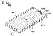
- 13A and 13B are diagrams illustrating examples of electronic devices.
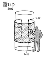
- 14A to 14D are diagrams illustrating examples of electronic devices.
- 15A to 15E are diagrams illustrating examples of electronic devices.
- 16A to 16G are diagrams illustrating examples of electronic devices.
- film and “layer” can be interchanged depending on the case or situation.
- conductive layer can be changed to the term “conductive film.”
- insulating film can be changed to the term “insulating layer”.
- a device manufactured using a metal mask or FMM may be referred to as an FMM structure device or an MM (metal mask) structure device.
- a device manufactured without using a metal mask or FMM may be referred to as a device with an MML (metal maskless) structure.
- the display device of this embodiment includes a light-receiving device and a light-emitting device in a display portion.
- light-emitting devices are arranged in matrix in the display portion, and an image can be displayed on the display portion.
- light receiving devices are arranged in a matrix in the display portion, and the display portion also functions as a light receiving portion.
- the light receiving section can be used for one or both of the image sensor and the touch sensor. That is, by detecting light with the light receiving portion, it is possible to capture an image and detect the proximity or contact of an object (a finger, a pen, or the like).
- the display device of this embodiment mode can use a light-emitting device as a light source of a sensor.
- a light-emitting device for example, in addition to displaying an image with all the sub-pixels of a display device, some sub-pixels exhibit light as a light source, some other pixels detect light, and the remaining sub-pixels Images can also be displayed. Therefore, it is not necessary to provide a light receiving portion and a light source separately from the display device, and the number of parts of the electronic device can be reduced. For example, there is no need to separately provide a fingerprint authentication device provided in the electronic device or a capacitive touch panel for scrolling or the like. Therefore, by using the display device of one embodiment of the present invention, an electronic device whose manufacturing cost is reduced can be provided.
- the light-receiving device when an object reflects (or scatters) light emitted by a light-emitting device included in the display portion, the light-receiving device can detect the reflected light (or scattered light).
- the reflected light or scattered light.
- imaging or touch detection is possible.
- the display device of this embodiment has a function of displaying an image using a light-emitting device.
- the light-emitting device functions as a display device (also referred to as a display element).
- the light emitting device for example, it is preferable to use an OLED (Organic Light Emitting Diode) or a QLED (Quantum-dot Light Emitting Diode).
- light-emitting substances also referred to as light-emitting materials
- examples of light-emitting substances included in the light-emitting device include substances that emit fluorescence (fluorescent materials), substances that emit phosphorescence (phosphorescent materials), and substances that exhibit thermally activated delayed fluorescence (thermally activated delayed Fluorescence (Thermally Activated Delayed Fluorescence: TADF) material).
- LEDs such as micro LED (Light Emitting Diode) can also be used as a light emitting device.
- An inorganic compound eg, quantum dot material
- the display device of this embodiment has a function of detecting light using a light receiving device.
- the display device of this embodiment can capture an image using the light-receiving device.
- the display device of this embodiment can be used as a scanner.
- image sensors can be used to acquire data such as fingerprints, palm prints, or irises.
- a biometric sensor can be built in the display device of this embodiment mode.
- An image sensor can also be used to acquire data such as a user's expression, eye movements, or changes in pupil diameter.
- data such as a user's expression, eye movements, or changes in pupil diameter.
- By analyzing the data it is possible to obtain information about the user's mind and body.
- By changing the output content of one or both of the display and audio based on the information for example, in a device for VR (Virtual Reality), a device for AR (Augmented Reality), or a device for MR (Mixed Reality), It is possible to ensure that the user can use the equipment safely.
- VR Virtual Reality
- AR Augmented Reality
- MR Mated Reality
- the display device of this embodiment can detect proximity or contact of an object using the light receiving device.
- a pn-type or pin-type photodiode can be used as the light receiving device.
- a light-receiving device functions as a photoelectric conversion device (also referred to as a photoelectric conversion element) that detects light incident on the light-receiving device and generates an electric charge. The amount of charge generated is determined based on the amount of incident light.
- organic photodiode having a layer containing an organic compound as the light receiving device.
- Organic photodiodes can be easily made thinner, lighter, and larger, and have a high degree of freedom in shape and design, so that they can be applied to various display devices.
- an organic EL device is used as the light-emitting device and an organic photodiode is used as the light-receiving device.
- An organic EL device and an organic photodiode can be formed on the same substrate. Therefore, an organic photodiode can be incorporated in a display device using an organic EL device.
- the number of film forming steps becomes very large. Since the organic photodiode has many layers that can have the same configuration as the organic EL device, the layers that can have the same configuration can be formed at once, thereby suppressing an increase in the number of film forming steps. In addition, even if the number of depositions is the same, by reducing the number of layers deposited only on some devices, it is possible to reduce the effects of deviations in the deposition pattern and to adhere to the deposition mask (metal mask, etc.). It is possible to reduce the influence of foreign matter (including small foreign matter called particles) that has been collected. Accordingly, the yield of manufacturing the display device can be increased.
- At least one of the hole injection layer, the hole transport layer, the electron transport layer, and the electron injection layer is preferably a common layer for the light receiving device and the light emitting device. Accordingly, the number of film formations and the number of masks can be reduced, and the number of manufacturing steps and manufacturing cost of the display device can be reduced.
- a layer shared by the light-receiving device and the light-emitting device may have different functions in the light-receiving device and in the light-emitting device. Components are referred to herein based on their function in the light emitting device.
- a hole-injecting layer functions as a hole-injecting layer in light-emitting devices and as a hole-transporting layer in light-receiving devices.
- an electron-injecting layer functions as an electron-injecting layer in light-emitting devices and as an electron-transporting layer in light-receiving devices.
- a layer shared by the light-receiving device and the light-emitting device may have the same function in the light-emitting device as in the light-receiving device.
- a hole-transporting layer functions as a hole-transporting layer in both a light-emitting device and a light-receiving device
- an electron-transporting layer functions as an electron-transporting layer in both a light-emitting device and a light-receiving device.
- the light-emitting layer of the light-emitting device and the active layer of the light-receiving device can each be formed in an island shape using a fine metal mask (also referred to as a metal mask or a shadow mask).
- a fine metal mask also referred to as a metal mask or a shadow mask.
- the end portion of the light-emitting layer and the end portion of the active layer may have overlapping portions.
- a high-definition display device of 300 ppi or more or 500 ppi or more and 1000 ppi or less or 800 ppi or less can be manufactured.
- the light-emitting layers in light-emitting devices that emit light of different colors overlap each other, side leakage may occur, resulting in deterioration of display quality.
- a phosphorescent light-emitting device is applied to both a light-emitting device that emits red light and a light-emitting device that emits green light
- the red light-emitting device uses a red light-emitting material
- the green light-emitting device uses a green light-emitting material.
- the red light-emitting layer and the green light-emitting layer are not in direct contact, or a structure in which the area in which the red light-emitting layer and the green light-emitting layer are in direct contact is reduced. Therefore, it is preferable to include a step of forming an active layer between the step of forming a red light-emitting layer and the step of forming a green light-emitting layer. As a result, a portion having an active layer is generated between the red light-emitting layer and the green light-emitting layer, and the area where the red light-emitting layer and the green light-emitting layer are in direct contact can be reduced. Therefore, it is possible to suppress side leakage that occurs between light emitting devices that emit light of different colors. Then, a display device with high display quality can be realized.
- FIGS. 1A to 1D are cross-sectional views of display devices of one embodiment of the present invention.
- a display device 50A shown in FIG. 1A has a layer 53 having light receiving devices and a layer 57 having light emitting devices between substrates 51 and 59 .
- the display device 50B shown in FIG. 1B has, between substrates 51 and 59, a layer 53 with light receiving devices, a layer 55 with transistors, and a layer 57 with light emitting devices.
- red (R), green (G), and blue (B) lights are emitted from the layer 57 having the light emitting device.
- a display device of one embodiment of the present invention includes a plurality of pixels arranged in a matrix.
- One pixel has one or more sub-pixels.
- One subpixel has one light emitting device.
- a pixel has three sub-pixels (three colors of R, G, and B, and three colors of yellow (Y), cyan (C), and magenta (M)), or a sub-pixel (4 colors of R, G, B, white (W), 4 colors of R, G, B, Y, and 4 types of R, G, B, infrared light (IR), etc.) can be applied.
- the pixel has a light receiving device.
- the light receiving device may be provided in all pixels or may be provided in some pixels.
- one pixel may have a plurality of light receiving devices.
- Layer 55 comprising transistors preferably comprises a first transistor and a second transistor.
- the first transistor is electrically connected with the light receiving device.
- a second transistor is electrically connected to the light emitting device.
- a display device of one embodiment of the present invention may have a function of detecting an object such as a finger in contact with the display device.
- the finger 52 touching the display device 50B reflects the light emitted by the light emitting device in the layer 57 having the light emitting device, so that the light receiving device in the layer 53 having the light receiving device reflects the light. Detect light. Thereby, it is possible to detect that the finger 52 touches the display device 50B.
- a display device of one embodiment of the present invention may have a function of detecting or imaging an object that is close to (that is, is not in contact with) the display device 50B, as shown in FIG. 1D.
- FIG. 1E shows an example of a fingerprint image captured by the display device of one embodiment of the present invention.
- the contour of the finger 220 is indicated by a dashed line and the contour of the contact portion 224 is indicated by a dashed line within the imaging range 226 .
- the fingerprint 222 with high contrast can be imaged due to the difference in the amount of light incident on the light receiving device.
- FIG. 1 A pixel layout of a display device of one embodiment of the present invention is described.
- the arrangement of sub-pixels includes, for example, a stripe arrangement, an S-stripe arrangement, a matrix arrangement, a delta arrangement, a Bayer arrangement, and a pentile arrangement.
- top surface shapes of sub-pixels include polygons such as triangles, quadrilaterals (including rectangles and squares), pentagons, and hexagons, and polygons with rounded corners, ellipses, and circles.
- the top surface shape of the sub-pixel corresponds to the top surface shape of the light emitting region of the light emitting device or the light receiving region of the light receiving device.
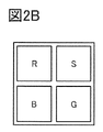
- the pixel shown in FIGS. 2A-2C has a sub-pixel G that emits green light, a sub-pixel B that emits blue light, a sub-pixel R that emits red light, and a sub-pixel S that has a light receiving device. Note that there is no particular limitation on the arrangement order of the sub-pixels. Note that when the sub-pixel S detects light of a specific color, it is preferable to arrange a sub-pixel that emits light of that color next to the sub-pixel S so that the detection accuracy can be improved. Also, sub-pixels with more reliable light-emitting devices can be made smaller.
- FIG. 2A shows an example in which the sub-pixel R is located between the sub-pixel B and the sub-pixel S, the sub-pixel R and the sub-pixel G may be adjacent to each other, for example.
- FIG. 2B shows an example in which sub-pixel R and sub-pixel S are located in the same row, and sub-pixel B and sub-pixel G are located in the same row. may be located on the same line.
- sub-pixel R and the sub-pixel B are positioned in the same column and the sub-pixel S and the sub-pixel G are positioned in the same column is shown. may be located in the same column.
- FIG. 2C shows an example having vertically elongated subpixel B and horizontally elongated subpixels R, G, and S.
- the vertically elongated subpixel is either subpixel R, subpixel G, or subpixel S.
- FIG. 2D shows an example in which pixels 109a and pixels 109b are alternately arranged.
- the pixel 109a has sub-pixel B, sub-pixel G, and sub-pixel S
- the pixel 109b has sub-pixel R, sub-pixel G, and sub-pixel S.
- FIG. 2D shows an example in which the sub-pixels included in both the pixel 109a and the pixel 109b are the sub-pixel G and the sub-pixel S, but the present invention is not particularly limited. It is preferable that both the pixel 109a and the pixel 109b have the sub-pixel S, so that the definition of a captured image can be increased. At this time, it is preferable that the sub-pixel S detects the light emitted by the sub-pixel (the sub-pixel G in FIG. 2D) included in both the pixel 109a and the pixel 109b.
- FIG. 2E is a modification in which the sub-pixels of the pixels 109a and 109b shown in FIG. 2D each have a substantially rectangular top surface shape with rounded corners.
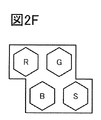
- FIG. 2F Two-dimensional hexagonal close-packing is applied to the pixel layout shown in FIG. 2F.
- a hexagonal close-packed layout is preferable because the aperture ratio of each sub-pixel can be increased.
- FIG. 2F shows an example in which each sub-pixel has a hexagonal top surface shape.
- FIG. 2G is a variation in which the pixel shown in FIG. 2F has a substantially hexagonal top shape with rounded corners.
- a technique for correcting the mask pattern in advance so that the design pattern and the transfer pattern match.
- OPC Optical Proximity Correction
- a pattern for correction is added to a corner portion of a figure on a mask pattern.
- the pixel shown in FIG. 2H is an example in which sub-pixels R, sub-pixels G, and sub-pixels B are arranged in one horizontal row, and sub-pixels S are arranged below them.
- the pixel shown in FIG. 2I is an example in which sub-pixels R, sub-pixels G, sub-pixels B, and sub-pixels X are arranged in one horizontal row, and sub-pixels S are arranged below them.
- the sub-pixel X for example, a sub-pixel that emits infrared light (IR) can be applied.
- the sub-pixel X can employ a configuration having a light-emitting device that emits infrared light (IR).
- the sub-pixel S preferably detects infrared light. For example, while an image is displayed using the sub-pixels R, G, and B, the sub-pixel S can detect the reflected light emitted by the sub-pixel X using the sub-pixel X as a light source.
- sub-pixel X for example, a sub-pixel that emits white (W) light or a sub-pixel that emits yellow (Y) light can be applied.
- W white
- Y yellow
- the sub-pixel X for example, a configuration having a light receiving device can be applied.
- the wavelength ranges of light detected by the sub-pixels S and X may be the same, different, or partly common.
- one of the sub-pixel S and the sub-pixel X may mainly detect visible light, and the other may mainly detect infrared light.
- the sub-pixels S can be used to capture images for personal authentication using, for example, fingerprints, palm prints, irises, pulse shapes (including vein shapes and artery shapes), or faces.
- the definition of the sub-pixel S is, for example, 100 ppi or more, preferably 200 ppi or more, more preferably 300 ppi or more, more preferably 400 ppi or more, still more preferably 500 ppi or more, and 2000 ppi or less, 1000 ppi or less, or 600 ppi or less. be able to.
- the resolution is 200 ppi or more and 600 ppi or less, preferably 300 ppi or more and 600 ppi or less, it can be suitably used for imaging a fingerprint.
- the resolution is 500 ppi or more, it is preferable because it can conform to standards such as the US National Institute of Standards and Technology (NIST). Assuming that the resolution of the light-receiving device is 500 ppi, the size of one pixel is 50.8 ⁇ m. I understand.
- a clear fingerprint image can be obtained by setting the array interval of the light receiving devices to be smaller than the distance between two protrusions of the fingerprint, preferably smaller than the distance between adjacent recesses and protrusions. It is said that the distance between the concave and convex portions of a human fingerprint is approximately 200 ⁇ m.
- the width of a human fingerprint is said to be 300 ⁇ m or more and 500 ⁇ m or less, or 460 ⁇ m ⁇ 150 ⁇ m.
- the arrangement interval of the light receiving devices is 400 ⁇ m or less, preferably 200 ⁇ m or less, more preferably 150 ⁇ m or less, still more preferably 100 ⁇ m or less, further preferably 50 ⁇ m or less, and 1 ⁇ m or more, preferably 10 ⁇ m or more, more preferably 20 ⁇ m or more.
- the light-receiving device included in the sub-pixel S preferably detects visible light, and preferably detects one or more of blue, purple, blue-violet, green, yellow-green, yellow, orange, and red light. . Also, the light receiving device included in the sub-pixel S may detect infrared light.
- the sub-pixel S can be used as a touch sensor (also called a direct touch sensor) or a non-contact sensor (also called a hover sensor, a hover touch sensor, a near-touch sensor, or a touchless sensor).
- the sub-pixel S can appropriately determine the wavelength of light to be detected according to the application. For example, if the sub-pixel S can detect infrared light, touch detection becomes possible even in a dark place.
- touch sensors or non-contact sensors can detect the proximity or contact of an object (such as a finger, hand, or pen).
- a touch sensor can detect an object when the electronic device mounted with the display device of one embodiment of the present invention is in direct contact with the object.
- the non-contact sensor can detect the target without the target being in contact with the electronic device.
- the display device can detect the object when the distance between the display device (or electronic device) and the object is 0.1 mm or more and 300 mm or less, preferably 3 mm or more and 50 mm or less.
- the electronic device can be operated without direct contact with the target object, in other words, the display device can be operated without contact (touchless). With the above configuration, it is possible to reduce the risk of the electronic device being dirty or scratched, or the electronic It becomes possible to operate the device.
- the display device of one embodiment of the present invention can have a variable refresh rate.
- the power consumption can be reduced by adjusting the refresh rate (for example, in the range of 1 Hz to 240 Hz) according to the content displayed on the display device.
- the drive frequency of the touch sensor or the non-contact sensor may be changed according to the refresh rate. For example, when the refresh rate of the display device is 120 Hz, the driving frequency of the touch sensor or the non-contact sensor can be higher than 120 Hz (typically 240 Hz). With this structure, low power consumption can be achieved and the response speed of the touch sensor or the non-contact sensor can be increased.
- a display device of one embodiment of the present invention includes a top emission type in which light is emitted in a direction opposite to a substrate over which a light emitting device is formed, a bottom emission type in which light is emitted toward a substrate over which a light emitting device is formed, and a double-sided display device. It may be of any dual-emission type that emits light to .
- a top emission display device will be described as an example.
- a display device having a light-emitting device that emits visible light and a light-receiving device that detects visible light is mainly described.
- the light receiving device may have a function of detecting infrared light, or a function of detecting both visible light and infrared light.
- FIG. 3 shows a top view of a display device of one embodiment of the present invention.
- a portion surrounded by a dotted line frame in FIG. 3 corresponds to one pixel.
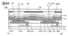
- One pixel has a light receiving device 110, a red light emitting device 190R, a green light emitting device 190G, and a blue light emitting device 190B.
- the top surface shape of the light receiving device 110 and the light emitting devices 190R, 190G, and 190B is not particularly limited.
- a hexagonal close-packed type is applied to the pixel layout shown in FIG.
- a hexagonal close-packed layout is preferable because the aperture ratios of the light receiving device 110 and the light emitting devices 190R, 190G, and 190B can be increased.
- the light-receiving region of the light-receiving device 110 is rectangular, and the light-emitting regions of the light-emitting devices 190R, 190G, and 190B are hexagonal.
- a spacer 219 is provided between the green light-emitting device 190G and the blue light-emitting device 190B when viewed from above (also referred to as a plan view).
- the positions at which the spacers 219 are provided, the number of the spacers 219, and the like can be determined as appropriate.
- FIG. 4A shows an example of a cross-sectional view along the dashed-dotted line A1-A2 in FIG. 3
- FIG. 4B shows an example of a cross-sectional view along the dashed-dotted line A3-A4 in FIG.
- the display device 10A has a light receiving device 110, a red light emitting device 190R, a green light emitting device 190G, and a blue light emitting device 190B.
- the light-emitting device 190R has a pixel electrode 111R, a common layer 112, a light-emitting layer 113R, a common layer 114, and a common electrode 115.
- FIG. The light emitting layer 113R has an organic compound that emits red light 21R.
- a case where the pixel electrode 111R functions as an anode and the common electrode 115 functions as a cathode will be described as an example.
- Light emitting device 190R has a function of emitting red light. Specifically, the light emitting device 190R is an electroluminescent device that emits light toward the substrate 152 by applying a voltage between the pixel electrode 111R and the common electrode 115 (see red light 21R).
- the light-emitting device 190G has a pixel electrode 111G, a common layer 112, a light-emitting layer 113G, a common layer 114, and a common electrode 115.
- the light emitting layer 113G has an organic compound that emits green light 21G.
- Light emitting device 190G has the function of emitting green light 21G.
- the light-emitting device 190B has a pixel electrode 111B, a common layer 112, a light-emitting layer 113B, a common layer 114, and a common electrode 115.
- the light emitting layer 113B has an organic compound that emits blue light 21B.
- the light emitting device 190B has a function of emitting blue light 21B.
- the light receiving device 110 has a pixel electrode 111 S, a common layer 112 , an active layer 113 S, a common layer 114 and a common electrode 115 .
- the active layer 113S has an organic compound.
- the light receiving device 110 has a function of detecting visible light.
- the pixel electrode 111S functions as an anode and the common electrode 115 functions as a cathode, as in the case of the light-emitting device.
- the display device 10A detects light incident on the light-receiving device 110, generates an electric charge, and extracts it as a current. be able to.
- the light receiving device 110 has a function of detecting light.
- the light receiving device 110 is a photoelectric conversion device that receives light 22 incident from outside the display device 10B and converts it into an electric signal.
- the light 22 can also be said to be the light emitted by the light emitting device and reflected by the object.
- the light 22 may also enter the light receiving device 110 through a lens.
- Each of the pixel electrodes 111S, 111R, 111G, and 111B, the common layer 112, the active layer 113S, the light-emitting layers 113R, 113G, and 113B, the common layer 114, and the common electrode 115 may have a single-layer structure or a laminated structure. There may be.
- Common layer 112 may include at least one of a hole injection layer, a hole transport layer, and an electron blocking layer.
- the common layer 112 may have different functions in the light emitting device than in the light receiving device 110 .
- the hole-injection layer functions as a hole-injection layer in light-emitting devices and as a hole-transport layer in light-receiving devices 110 .
- Common layer 114 may include at least one of an electron injection layer, an electron transport layer, and a hole blocking layer.
- the common layer 114 may have different functions in the light emitting device than in the light receiving device 110 .
- the electron-injection layer functions as an electron-injection layer in light-emitting devices and as an electron-transport layer in light-receiving devices 110 .
- an organic compound is used for the active layer 113S of the light receiving device 110 .
- the light receiving device 110 can share layers other than the active layer 113S with the light emitting device (EL device). Therefore, the light-receiving device 110 can be formed in parallel with the formation of the light-emitting device simply by adding the step of forming the active layer 113S to the manufacturing process of the light-emitting device. Also, the light emitting device and the light receiving device 110 can be formed on the same substrate. Therefore, the light-receiving device 110 can be incorporated in the display device without significantly increasing the number of manufacturing steps.
- the light receiving device 110 and the light emitting devices 190R, 190G, and 190B are separately manufactured, the light receiving device 110 and the light emitting devices 190R, 190G , 190B are common configurations.
- the configurations of the light receiving device 110 and the light emitting devices 190R, 190G, and 190B are not limited to this.
- the light-receiving device 110 and the light-emitting devices 190R, 190G, 190B may have separate layers in addition to the active layer 113S and the light-emitting layers (light-emitting layers 113R, 113G, 113B). It is preferable that the light receiving device 110 and the light emitting devices 190R, 190G, and 190B have at least one layer (common layer) used in common. Accordingly, the light-receiving device 110 can be incorporated in the display device without significantly increasing the number of manufacturing steps.
- the display device 10A includes a light receiving device 110, a light emitting device 190R, a light emitting device 190G, a light emitting device 190B, a transistor 42S, a transistor 42R, a transistor 42G, a transistor 42B, etc. between a pair of substrates (substrate 151 and substrate 152). .
- Pixel electrodes 111 S, 111 R, 111 G, and 111 B are located on insulating layer 214 .
- the pixel electrodes 111S, 111R, 111G, and 111B can be formed using the same material and the same process. Accordingly, the manufacturing cost of the display device can be reduced and the manufacturing process can be simplified.
- the ends of the pixel electrodes 111S, 111R, 111G, and 111B are covered with partition walls 216, respectively.
- the pixel electrodes 111S, 111R, 111G, and 111B are electrically insulated (also called electrically isolated) from each other by the partition wall 216 .
- An organic insulating film is suitable for the partition wall 216 .
- materials that can be used for the organic insulating film include acrylic resins, polyimide resins, epoxy resins, polyamide resins, polyimideamide resins, siloxane resins, benzocyclobutene-based resins, phenolic resins, precursors of these resins, and the like.
- the partition wall 216 may be a layer that transmits visible light or a layer that blocks visible light.
- a resin material containing a pigment or a dye, or a brown resist material may be used to form (colored) partition walls that block visible light.
- the pixel electrode 111S is electrically connected through an opening provided in the insulating layer 214 to the source or drain of the transistor 42S.
- the pixel electrode 111R is electrically connected through an opening provided in the insulating layer 214 to the source or drain of the transistor 42R.
- the pixel electrode 111G is electrically connected through an opening provided in the insulating layer 214 to the source or drain of the transistor 42G.
- the pixel electrode 111B is electrically connected through an opening provided in the insulating layer 214 to the source or drain of the transistor 42B.
- Transistors 42R, 42G, 42B and transistor 42S are on the same layer (substrate 151 in FIGS. 4A and 4B).
- At least part of the circuit electrically connected to the light receiving device 110 is preferably formed using the same material and the same process as the circuit electrically connected to the light emitting device. Accordingly, the thickness of the display device can be reduced and the manufacturing process can be simplified as compared with the case where two circuits are formed separately.
- the light receiving device 110 and the light emitting devices 190R, 190G, 190B are each preferably covered with a protective layer 116.
- a protective layer 116 is provided over and in contact with the common electrode 115 .
- impurities such as water can be prevented from entering the light receiving device 110 and the light emitting devices 190R, 190G, and 190B, and the reliability of the light receiving device 110 and the light emitting devices 190R, 190G, and 190B can be improved.
- the protective layer 116 and the substrate 152 are bonded together by the adhesive layer 142 .
- a light shielding layer 158 is provided on the substrate 151 side surface of the substrate 152 .
- the light shielding layer 158 has openings at positions overlapping with the light emitting devices 190R, 190G, and 190B and at positions overlapping with the light receiving device 110 .
- a position overlapping with a light-emitting device specifically refers to a position overlapping with a light-emitting region of the light-emitting device.
- the position overlapping the light receiving device 110 specifically refers to the position overlapping the light receiving region of the light receiving device 110 .
- Light emitted from the light-emitting device is extracted through the display surface of the display device of one embodiment of the present invention, and light emitted to the light-receiving device passes through the display surface.
- Light emitted from the light-emitting device is preferably extracted to the outside of the display device through the opening of the light-shielding layer 158 (or a region where the light-shielding layer is not provided). It is preferable that the light is irradiated through the region where the light shielding layer is not provided).
- the light receiving device 110 detects the light emitted by the light emitting device reflected by the object.
- the light emitted from the light-emitting device may be reflected within the display device and enter the light-receiving device 110 as stray light without passing through the object.
- Such stray light becomes noise at the time of light detection, and becomes a factor of lowering the S/N ratio (Signal-to-noise ratio).
- the influence of stray light can be suppressed. Thereby, noise can be reduced and the sensitivity of the sensor using the light receiving device 110 can be increased.
- the light shielding layer 158 a material that blocks light emitted from the light emitting device can be used.
- the light shielding layer 158 preferably absorbs visible light.
- a black matrix can be formed using a metal material, a resin material containing a pigment (such as carbon black) or a dye, or the like.
- the light shielding layer 158 may have a layered structure of red color filters, green color filters, and blue color filters.
- the spacer 219 is positioned on the partition wall 216 and positioned between the light emitting device 190G and the light emitting device 190B in top view.
- the display device 10A has a structure in which an active layer 113S and a light emitting layer 113R are laminated in this order on a partition wall 216.
- FIG. 4A shows a structure in which the light emitting layer 113R is provided on the active layer 113S
- the present invention is not limited to this.
- a structure in which the active layer 113S is provided on the light emitting layer 113R may be employed.
- the spacer 219 is in direct contact with a metal mask in a manufacturing process of a display device in some cases.
- the light emitting layer 113G and the light emitting layer 113B are not formed on the spacer 219, as shown in FIG. 4B.
- FIG. 4C shows an example of a cross-sectional view taken along the dashed-dotted line A1-A2 in FIG.
- the description of the same configuration as that of the display device described above may be omitted.
- the display device 10B has a light receiving device 110, a light emitting device 190R, a transistor 42S, a transistor 42R, etc. between a pair of substrates (substrate 151 and substrate 152).
- the light-emitting device 190R has a pixel electrode 111R, a functional layer 112R, a light-emitting layer 113R, a functional layer 114R, and a common electrode 115.
- the light emitting layer 113R has an organic compound that emits red light 21R.
- Light emitting device 190R has a function of emitting red light.
- the light receiving device 110 has a pixel electrode 111 S, a functional layer 112 S, an active layer 113 S, a functional layer 114 S, and a common electrode 115 .
- the active layer 113S has an organic compound.
- the light receiving device 110 has a function of detecting visible light.
- Each of the functional layers 112R, 112S, 114R, and 114S may have a single layer structure or a laminated structure.
- the functional layer 112S is located on the pixel electrode 111S.
- the active layer 113S overlaps the pixel electrode 111S via the functional layer 112S.
- the functional layer 114S is located on the active layer 113S.
- the active layer 113S overlaps the common electrode 115 via the functional layer 114S.
- the functional layer 112S can have a hole transport layer.
- the functional layer 114S can have an electron transport layer.
- the functional layer 112R is located on the pixel electrode 111R.
- the light emitting layer 113R overlaps the pixel electrode 111R via the functional layer 112R.
- the functional layer 114R is located on the light emitting layer 113R.
- the light-emitting layer 113R overlaps the common electrode 115 via the functional layer 114R.
- the functional layer 112R may have at least one of a hole injection layer, a hole transport layer, and an electron blocking layer.
- the functional layer 114R may have at least one of an electron injection layer, an electron transport layer, and a hole blocking layer.
- the common electrode 115 is a layer commonly used for the light receiving device 110 and the light emitting device 190R.
- the functional layer 112S, the active layer 113S, and the functional layer 114S located between the pixel electrode 111S and the common electrode 115 can also be called organic layers (layers containing organic compounds).
- the pixel electrode 111S preferably has a function of reflecting visible light.
- the common electrode 115 has a function of transmitting visible light.
- the common electrode 115 has a function of transmitting the infrared light.
- the pixel electrode 111S preferably has a function of reflecting infrared light.
- the functional layer 112R, the light-emitting layer 113R, and the functional layer 114R located between the pixel electrode 111R and the common electrode 115 can also be called EL layers.
- the pixel electrode 111R preferably has a function of reflecting visible light.
- the common electrode 115 has a function of transmitting visible light.
- a micro optical resonator (microcavity) structure is preferably applied to the light emitting device included in the display device of this embodiment mode. Therefore, one of the pair of electrodes of the light-emitting device preferably has an electrode (semi-transmissive/semi-reflective electrode) that is transparent and reflective to visible light, and the other is an electrode that is reflective to visible light ( reflective electrode). Since the light-emitting device has a microcavity structure, the light emitted from the light-emitting layer can be resonated between both electrodes, and the light emitted from the light-emitting device can be enhanced.
- the semi-transmissive/semi-reflective electrode can have a laminated structure of a reflective electrode and an electrode (also referred to as a transparent electrode) having transparency to visible light.
- the reflective electrode which functions as a part of the semi-transmissive/semi-reflective electrode, is sometimes referred to as a pixel electrode or a common electrode, and the transparent electrode is sometimes referred to as an optical adjustment layer. layer) can also be said to have a function as a pixel electrode or a common electrode.
- the light transmittance of the transparent electrode is set to 40% or more.
- the light-emitting device preferably uses an electrode having a transmittance of 40% or more for visible light (light with a wavelength of 400 nm or more and less than 750 nm).
- the visible light reflectance of the semi-transmissive/semi-reflective electrode is 10% or more and 95% or less, preferably 30% or more and 80% or less.
- the visible light reflectance of the reflective electrode is 40% or more and 100% or less, preferably 70% or more and 100% or less.
- the resistivity of these electrodes is preferably 1 ⁇ 10 ⁇ 2 ⁇ cm or less.
- the transmittance and reflectance of these electrodes for near-infrared light are preferably within the above numerical range. .
- At least one of the functional layers 112R, 112S, 114R, and 114S may function as an optical adjustment layer.
- the film thickness of the functional layer in each color light emitting device it is possible to intensify and extract light of a specific color in each light emitting device.
- the semi-transmissive/semi-reflective electrode has a laminated structure of a reflective electrode and a transparent electrode, the optical distance between a pair of electrodes means the optical distance between the pair of reflective electrodes.
- the display device 10B has a structure in which a functional layer 112S, an active layer 113S, a functional layer 114S, a functional layer 112R, a light-emitting layer 113R, and a functional layer 114R are laminated in this order on a partition wall 216.
- the functional layer 112S, the functional layer 112R, the active layer 113S, the light emitting layer 113R, the functional layer 114S, and the functional layer 114R may be laminated in this order.
- an active layer 113S may be provided on the light emitting layer 113R.
- Example of manufacturing method of display device Next, an example of a method for manufacturing a display device is described with reference to FIGS. 5A to 7B, mainly the method of manufacturing the structure including the light emitting devices 190R, 190G, 190B, the light receiving device 110, and the connecting portion between the common electrode 115 and the conductive layer will be described.
- the thin films (insulating films, semiconductor films, conductive films, etc.) that make up the display device are formed by sputtering, chemical vapor deposition (CVD), vacuum deposition, pulsed laser deposition (PLD). ) method, ALD method, or the like.
- CVD methods include a plasma enhanced CVD (PECVD) method, a thermal CVD method, and the like.
- PECVD plasma enhanced CVD
- thermal CVD metal organic chemical vapor deposition
- the thin films (insulating film, semiconductor film, conductive film, etc.) constituting the display device can be applied by spin coating, dipping, spray coating, inkjet, dispensing, screen printing, offset printing, doctor knife method, slit coating, and roll coating. , curtain coating, knife coating, or the like.
- a vacuum process such as a vapor deposition method and a solution process such as a spin coating method or an inkjet method can be used for manufacturing a light-emitting device.
- vapor deposition methods include sputtering, ion plating, ion beam vapor deposition, molecular beam vapor deposition, physical vapor deposition (PVD) such as vacuum vapor deposition, and CVD.
- the functional layers (hole injection layer, hole transport layer, light emitting layer, electron transport layer, electron injection layer, etc.) included in the EL layer may be formed by a vapor deposition method (vacuum vapor deposition method, etc.), a coating method (dip coating method, die coat method, bar coat method, spin coat method, spray coat method, etc.), printing method (inkjet method, screen (stencil printing) method, offset (lithographic printing) method, flexographic (letterpress printing) method, gravure method, or micro contact method, etc.).
- a vapor deposition method vacuum vapor deposition method, etc.
- a coating method dip coating method, die coat method, bar coat method, spin coat method, spray coat method, etc.
- printing method inkjet method, screen (stencil printing) method, offset (lithographic printing) method, flexographic (letterpress printing) method, gravure method, or micro contact method, etc.
- a photolithography method or the like can be used when processing a thin film forming a display device.
- the thin film may be processed by a nanoimprint method, a sandblast method, a lift-off method, or the like.
- an island-shaped thin film may be directly formed by a film formation method using a shielding mask such as a metal mask.
- the photolithography method there are typically the following two methods.
- One is a method of forming a resist mask on a thin film to be processed, processing the thin film by etching or the like, and removing the resist mask.
- the other is a method of forming a photosensitive thin film, then performing exposure and development to process the thin film into a desired shape.
- the light used for exposure can be, for example, i-line (wavelength 365 nm), g-line (wavelength 436 nm), h-line (wavelength 405 nm), or a mixture of these.
- ultraviolet rays, KrF laser light, ArF laser light, or the like can also be used.
- extreme ultraviolet (EUV: Extreme Ultra-violet) light or X-rays may be used.
- An electron beam can also be used instead of the light used for exposure. The use of extreme ultraviolet light, X-rays, or electron beams is preferable because extremely fine processing is possible.
- a photomask is not necessary when exposure is performed by scanning a beam such as an electron beam.
- a dry etching method, a wet etching method, a sandblasting method, or the like can be used for etching the thin film.
- a substrate having heat resistance that can withstand at least subsequent heat treatment can be used.
- a substrate having heat resistance that can withstand at least subsequent heat treatment can be used.
- a substrate having heat resistance that can withstand at least subsequent heat treatment can be used.
- a substrate having heat resistance that can withstand at least subsequent heat treatment can be used.
- a glass substrate, a quartz substrate, a sapphire substrate, a ceramic substrate, an organic resin substrate, or the like can be used.
- a semiconductor substrate such as a single crystal semiconductor substrate made of silicon, silicon carbide, or the like, a polycrystalline semiconductor substrate, a compound semiconductor substrate such as silicon germanium, or an SOI substrate can be used.
- the substrate it is preferable to use a substrate obtained by forming a semiconductor circuit including a semiconductor element such as a transistor on the above semiconductor substrate or insulating substrate.
- the semiconductor circuit preferably constitutes, for example, a pixel circuit, a gate line driver circuit (gate driver), a source line driver circuit (source driver), and the like.
- gate driver gate line driver
- source driver source driver
- an arithmetic circuit, a memory circuit, and the like may be configured.
- An insulating layer 105 is provided on top of the substrate.
- the insulating layer 105 is provided with a plurality of openings reaching transistors, wirings, electrodes, or the like provided over the substrate.
- the opening can be formed by photolithography.
- an inorganic insulating material or an organic insulating material can be used as the insulating layer 105.
- a conductive film is formed over the insulating layer 105 .
- a conductive film can be formed using, for example, a sputtering method or a vacuum deposition method.
- pixel electrodes 111R, 111G, 111B, and 111S and a conductive layer 111C are formed on the insulating layer 105 (FIG. 5A).
- a resist mask is formed over the conductive film by a photolithography method, and unnecessary portions of the conductive film are removed by etching. After that, by removing the resist mask, the pixel electrodes 111R, 111G, 111B, and 111S and the conductive layer 111C can be formed in the same step.
- partition walls 216 are formed to cover the ends of the pixel electrodes 111R, 111G, 111B, 111S and the conductive layer 111C (FIG. 5A).
- the partition 216 can have a single-layer structure or a laminated structure using one or both of an inorganic insulating film and an organic insulating film.
- a common layer 112 is formed on the pixel electrodes 111R, 111G, 111B, and 111S (FIG. 5B).
- the common layer 112 is preferably formed so as not to overlap the conductive layer 111C.
- the film formation range of the common layer 112 can be controlled by using a mask for defining the film formation area (also referred to as an area mask or a rough metal mask to distinguish it from a fine metal mask).
- the common layer 112 can be preferably formed by a vacuum deposition method.
- the film is not limited to this, and can be formed by a sputtering method, a transfer method, a printing method, a coating method, an inkjet method, or the like.
- an island-shaped light-emitting layer 113G is formed on the common layer 112 so as to include a region overlapping with the pixel electrode 111G.
- the light-emitting layer 113G is preferably formed by vacuum deposition through a fine metal mask (FMM). Note that the island-shaped light-emitting layer 113G may be formed by a sputtering method using FMM or an inkjet method.
- FMM fine metal mask
- FIG. 5C shows how the light-emitting layer 113G is deposited through the FMM 151G.
- FIG. 5C shows a state in which a film is formed by a so-called face-down method, in which the substrate is turned over so that the surface to be formed faces downward.
- the light-emitting layer 113G can be deposited over a wider range than the opening pattern of the FMM 151G.
- an island-shaped active layer 113S is formed on the common layer 112 so as to include a region overlapping with the pixel electrode 111S (FIG. 6A).
- a pattern extending outside the pixel electrode 111S is formed, similarly to the light-emitting layer 113G.
- an FMM 151R is used to form an island-shaped light-emitting layer 113R on the common layer 112 so as to include a region overlapping with the pixel electrode 111R (FIG. 6B).
- the light-emitting layer 113R As the light-emitting layer 113R, a pattern extending outside the pixel electrode 111R is formed, similarly to the light-emitting layer 113G. As a result, as shown in the region SR in FIG. 6B, a portion where the light emitting layer 113R overlaps with the active layer 113S is formed. Also, as shown in the region GR in FIG. 6B, a portion where the light emitting layer 113R overlaps with the light emitting layer 113G is formed.
- an island-shaped light-emitting layer 113B is formed on the common layer 112 so as to include a region overlapping with the pixel electrode 111B (FIG. 7A).
- the light-emitting layer 113B is formed with a pattern extending outward from the pixel electrode 111B. As a result, a portion where the light emitting layer 113B overlaps with the active layer 113S is formed as shown in the region SB in FIG. 7A. Further, as shown in the region GB in FIG. 7A, a portion where the light emitting layer 113B overlaps with the light emitting layer 113G is formed.
- the order in which the light-emitting layers 113R, 113G, 113B and the active layer 113S are formed is not particularly limited. If any two of the light-emitting layers 113R, 113G, and 113B are in direct contact with each other and side leakage may occur, the active layer 113S is formed after forming one of the two layers, and then the active layer 113S is formed. It is preferred to form the other of the two layers. As a result, the area where the two layers are in contact can be reduced, and the occurrence of side leakage can be suppressed.
- a common layer 114 is formed on the light emitting layers 113R, 113G, 113B and the active layer 113S (FIG. 7B).
- the common layer 114 is preferably formed so as not to overlap the conductive layer 111C.
- the film formation range of the common layer 114 can be controlled.
- Common layer 114 can preferably be formed by a vacuum deposition method.
- the film is not limited to this, and can be formed by a sputtering method, a transfer method, a printing method, a coating method, an inkjet method, or the like.
- a common electrode 115 is formed on the common layer 114 (FIG. 7B).
- a sputtering method or a vacuum deposition method can be used for forming the common electrode 115.
- a film formed by an evaporation method and a film formed by a sputtering method may be stacked.
- a mask for defining the film formation area may be used when forming the common electrode 115 .
- a protective layer 116 is formed on the common electrode 115 (FIG. 7B). Further, the display device of this embodiment mode can be manufactured by bonding the substrate 152 to the protective layer 116 using the adhesive layer 142 .
- Methods for forming the protective layer 116 include a vacuum deposition method, a sputtering method, a CVD method, an ALD method, and the like.
- the protective layer 116 may be formed by stacking films formed using different film formation methods.
- Display device configuration example 3 A more detailed structure of the display device of one embodiment of the present invention is described below with reference to FIGS. 8 to 11B.
- FIG. 8 shows a perspective view of the display device 100A
- FIG. 9 shows a cross-sectional view of the display device 100A.
- the display device 100A has a configuration in which a substrate 152 and a substrate 151 are bonded together.
- the substrate 152 is clearly indicated by dashed lines.
- the display device 100A includes a display portion 162, a circuit 164, wirings 165, and the like.
- FIG. 8 shows an example in which an IC (integrated circuit) 173 and an FPC 172 are mounted on the display device 100A. Therefore, the configuration shown in FIG. 8 can also be said to be a display module having the display device 100A, an IC, and an FPC.
- a scanning line driver circuit can be used.
- the wiring 165 has a function of supplying signals and power to the display portion 162 and the circuit 164 .
- the signal and power are input to the wiring 165 from the outside through the FPC 172 or input to the wiring 165 from the IC 173 .
- FIG. 8 shows an example in which an IC 173 is provided on a substrate 151 by the COG method, the COF method, or the like.
- the IC 173 for example, an IC having a scanning line driver circuit or a signal line driver circuit can be applied.
- the display device 100A and the display module may be configured without an IC.
- the IC may be mounted on the FPC by the COF method or the like.
- FIG. 9 shows an example of a cross-section of the display device 100A when part of the region including the FPC 172, part of the circuit 164, part of the display section 162, and part of the region including the end are cut. show.
- a display device 100A illustrated in FIG. 9 includes a transistor 201, a transistor 205, a transistor 206, a light-emitting device 190R, a light-receiving device 110, a protective layer 116, and the like between substrates 151 and 152.
- FIG. 9 A display device 100A illustrated in FIG. 9 includes a transistor 201, a transistor 205, a transistor 206, a light-emitting device 190R, a light-receiving device 110, a protective layer 116, and the like between substrates 151 and 152.
- the substrate 152 and the protective layer 116 are adhered by an adhesive layer 142a and an adhesive layer 142b.
- a solid sealing structure, a hollow sealing structure, or the like can be applied.
- the space surrounded by the substrate 152, the frame-shaped adhesive layer 142b, and the substrate 151 is filled with the adhesive layer 142a to apply a solid sealing structure.
- the substrate 152 and the protective layer 116 may be bonded together by one type of adhesive layer without providing the frame-shaped adhesive layer.
- the space may be filled with an inert gas (nitrogen, argon, or the like) to apply a hollow sealing structure.
- the light-emitting device 190R has a layered structure in which a pixel electrode 111R, a common layer 112, a light-emitting layer 113R emitting red light, a common layer 114, and a common electrode 115 are stacked in this order from the insulating layer 214 side.
- the pixel electrode 111R is connected to the conductive layer 222b included in the transistor 206 through an opening provided in the insulating layer 214.
- the edge of the pixel electrode 111R is covered with a partition wall 216. As shown in FIG.
- the pixel electrode 111R contains a material that reflects visible light, and the common electrode 115 contains a material that transmits visible light.
- the light receiving device 110 has a laminated structure in which a pixel electrode 111S, a common layer 112, an active layer 113S, a common layer 114, and a common electrode 115 are laminated in this order from the insulating layer 214 side.
- the pixel electrode 111S is electrically connected to the conductive layer 222b included in the transistor 205 through an opening provided in the insulating layer 214.
- FIG. The edge of the pixel electrode 111S is covered with a partition wall 216.
- the pixel electrode 111S contains a material that reflects visible light
- the common electrode 115 contains a material that transmits visible light.
- Light emitted by the light emitting device 190R is emitted to the substrate 152 side. Light enters the light receiving device 110 through the substrate 152 and the adhesive layer 142a. A material having high visible light transmittance is preferably used for the substrate 152 .
- the pixel electrode 111R and the pixel electrode 111S can be manufactured using the same material and the same process.
- Common layer 112, common layer 114, and common electrode 115 are used for both light receiving device 110 and light emitting device 190R.
- the light-receiving device 110 and the light-emitting device 190R can have the same configuration except for the configurations of the active layer 113S and the light-emitting layer 113R. Accordingly, the light-receiving device 110 can be incorporated in the display device 100A without significantly increasing the number of manufacturing steps.
- the partition wall 216 covers the edge of the pixel electrode 111S and the edge of the pixel electrode 111R. A region SR in which the light emitting layer 113R and the active layer 113S overlap each other is present on the partition wall 216 .
- the protective layer 116 that covers the light receiving device 110 and the light emitting device 190R By providing the protective layer 116 that covers the light receiving device 110 and the light emitting device 190R, impurities such as water can be prevented from entering the light receiving device 110 and the light emitting device 190R, and the reliability of the light receiving device 110 and the light emitting device 190R can be improved. can.
- the transistors 201 , 205 , and 206 are all formed over the substrate 151 . These transistors can be made with the same material and the same process.
- An insulating layer 211 , an insulating layer 213 , an insulating layer 215 , and an insulating layer 214 are provided in this order over the substrate 151 .
- Part of the insulating layer 211 functions as a gate insulating layer of each transistor.
- Part of the insulating layer 213 functions as a gate insulating layer of each transistor.
- An insulating layer 215 is provided over the transistor.
- An insulating layer 214 is provided over the transistor and functions as a planarization layer. Note that the number of gate insulating layers and the number of insulating layers covering a transistor are not limited, and each may have a single layer or two or more layers.
- a material into which impurities such as water and hydrogen are difficult to diffuse is preferably used for at least one insulating layer that covers the transistor. This allows the insulating layer to function as a barrier layer. With such a structure, diffusion of impurities from the outside into the transistor can be effectively suppressed, and the reliability of the display device can be improved.
- An inorganic insulating film is preferably used for each of the insulating layers 211 , 213 , and 215 .
- Examples of the inorganic insulating film include a silicon nitride film, a silicon oxynitride film, a silicon oxide film, a silicon oxynitride film, an aluminum oxide film, and an aluminum nitride film.
- Hafnium oxide film, yttrium oxide film, zirconium oxide film, gallium oxide film, tantalum oxide film, magnesium oxide film, lanthanum oxide film, cerium oxide film, neodymium oxide film, and the like can also be used. Further, two or more of the insulating films described above may be laminated and used.
- the organic insulating film preferably has openings near the ends of the display device 100A. As a result, it is possible to prevent impurities from entering through the organic insulating film from the end portion of the display device 100A.
- the organic insulating film may be formed so that the edges of the organic insulating film are located inside the edges of the display device 100A so that the organic insulating film is not exposed at the edges of the display device 100A.
- An organic insulating film is suitable for the insulating layer 214 that functions as a planarization layer.
- materials that can be used for the organic insulating film include acrylic resins, polyimide resins, epoxy resins, polyamide resins, polyimideamide resins, siloxane resins, benzocyclobutene-based resins, phenolic resins, precursors of these resins, and the like.
- An opening is formed in the insulating layer 214 in a region 228 shown in FIG. As a result, even when an organic insulating film is used for the insulating layer 214 , it is possible to prevent impurities from entering the display section 162 from the outside through the insulating layer 214 . Therefore, the reliability of the display device 100A can be improved.
- the insulating layer 215 and the protective layer 116 are in contact with each other through the opening of the insulating layer 214 in the region 228 near the edge of the display device 100A.
- the inorganic insulating film included in the insulating layer 215 and the inorganic insulating film included in the protective layer 116 are in contact with each other. This can prevent impurities from entering the display section 162 from the outside through the organic insulating film. Therefore, the reliability of the display device 100A can be improved.
- the protective layer 116 preferably has at least one inorganic insulating film.
- the protective layer 116 may have a single layer structure or a laminated structure of two or more layers.
- the protective layer 116 may have a three-layer structure in which a first inorganic insulating film, an organic insulating film, and a second inorganic insulating film are laminated in this order.
- the transistor 201, the transistor 205, and the transistor 206 include a conductive layer 221 functioning as a gate, an insulating layer 211 functioning as a gate insulating layer, conductive layers 222a and 222b functioning as sources and drains, a semiconductor layer 231, and a gate insulating layer. It has an insulating layer 213 functioning as a gate and a conductive layer 223 functioning as a gate.
- the same hatching pattern is applied to a plurality of layers obtained by processing the same conductive film.
- the insulating layer 211 is located between the conductive layer 221 and the semiconductor layer 231 .
- the insulating layer 213 is located between the conductive layer 223 and the semiconductor layer 231 .
- the structure of the transistor included in the display device of this embodiment there is no particular limitation on the structure of the transistor included in the display device of this embodiment.
- a planar transistor, a staggered transistor, an inverted staggered transistor, or the like can be used.
- the transistor structure may be either a top-gate type or a bottom-gate type.
- gates may be provided above and below a semiconductor layer in which a channel is formed.
- a structure in which a semiconductor layer in which a channel is formed is sandwiched between two gates is applied to the transistors 201 , 205 , and 206 .
- a transistor may be driven by connecting two gates and applying the same signal to them.
- the threshold voltage of the transistor may be controlled by applying a potential for controlling the threshold voltage to one of the two gates and applying a potential for driving to the other.
- the crystallinity of the semiconductor material used for the transistor is not particularly limited, either, and may be an amorphous semiconductor, a single crystal semiconductor, or a semiconductor having crystallinity other than a single crystal (a microcrystalline semiconductor, a polycrystalline semiconductor, or a semiconductor having a partially crystalline region). semiconductor) may be used.
- a single crystal semiconductor or a crystalline semiconductor is preferably used because deterioration in transistor characteristics can be suppressed.
- a semiconductor layer of a transistor preferably includes a metal oxide (also referred to as an oxide semiconductor).
- the display device of this embodiment preferably uses a transistor including a metal oxide for a channel formation region (hereinafter referred to as an OS transistor).
- crystalline oxide semiconductors examples include CAAC (c-axis-aligned crystalline)-OS, nc (nanocrystalline)-OS, and the like.
- a transistor using silicon for a channel formation region may be used.
- silicon examples include monocrystalline silicon, polycrystalline silicon, amorphous silicon, and the like.
- a transistor including low-temperature polysilicon (LTPS) in a semiconductor layer hereinafter also referred to as an LTPS transistor
- the LTPS transistor has high field effect mobility and good frequency characteristics.
- a Si transistor such as an LTPS transistor
- a circuit that needs to be driven at a high frequency for example, a source driver circuit
- OS transistors have much higher field-effect mobility than transistors using amorphous silicon.
- an OS transistor has extremely low source-drain leakage current (hereinafter also referred to as an off-state current) in an off state, and can retain charge accumulated in a capacitor connected in series with the transistor for a long time. is possible. Further, by using the OS transistor, power consumption of the display device can be reduced.
- the off current value of the OS transistor per 1 ⁇ m of channel width at room temperature is 1 aA (1 ⁇ 10 ⁇ 18 A) or less, 1 zA (1 ⁇ 10 ⁇ 21 A) or less, or 1 yA (1 ⁇ 10 ⁇ 24 A) or less.
- the off current value of the Si transistor per 1 ⁇ m channel width at room temperature is 1 fA (1 ⁇ 10 ⁇ 15 A) or more and 1 pA (1 ⁇ 10 ⁇ 12 A) or less. Therefore, it can be said that the off-state current of the OS transistor is about ten digits lower than the off-state current of the Si transistor.
- the amount of current flowing through the light emitting device it is necessary to increase the amount of current flowing through the light emitting device.
- the OS transistor when the transistor operates in the saturation region, the OS transistor can reduce the change in the source-drain current with respect to the change in the gate-source voltage as compared with the Si transistor. Therefore, by applying an OS transistor as a drive transistor included in a pixel circuit, the current flowing between the source and the drain can be finely determined according to the change in the voltage between the gate and the source. can be controlled. Therefore, the number of gradations in the pixel circuit can be increased.
- the OS transistor flows a more stable current (saturation current) than the Si transistor even when the source-drain voltage gradually increases. be able to. Therefore, by using the OS transistor as the driving transistor, a stable current can be supplied to the light-emitting device even when the current-voltage characteristics of the EL device vary, for example. That is, when the OS transistor operates in the saturation region, even if the source-drain voltage is increased, the source-drain current hardly changes, so that the light emission luminance of the light-emitting device can be stabilized.
- an OS transistor as a driving transistor included in a pixel circuit, it is possible to suppress black floating, increase emission luminance, provide multiple gradations, and suppress variations in light emitting devices. can be planned.
- the semiconductor layer includes, for example, indium and M (M is gallium, aluminum, silicon, boron, yttrium, tin, copper, vanadium, beryllium, titanium, iron, nickel, germanium, zirconium, molybdenum, lanthanum, cerium, neodymium, one or more selected from hafnium, tantalum, tungsten, and magnesium) and zinc.
- M is preferably one or more selected from aluminum, gallium, yttrium, and tin.
- an oxide containing indium (In), gallium (Ga), and zinc (Zn) (also referred to as IGZO) is preferably used for the semiconductor layer.
- an oxide containing indium, tin, and zinc is preferably used.
- oxides containing indium, gallium, tin, and zinc are preferably used.
- an oxide containing indium (In), aluminum (Al), and zinc (Zn) (also referred to as IAZO) is preferably used.
- an oxide containing indium (In), aluminum (Al), gallium (Ga), and zinc (Zn) (also referred to as IAGZO) is preferably used.
- the In atomic ratio in the In-M-Zn oxide is preferably equal to or higher than the M atomic ratio.
- the transistors included in the circuit 164 and the transistors included in the display portion 162 may have the same structure or different structures.
- the plurality of transistors included in the circuit 164 may all have the same structure, or may have two or more types.
- the structures of the plurality of transistors included in the display portion 162 may all be the same, or may be of two or more types.
- All of the transistors in the display portion 162 may be OS transistors, all of the transistors in the display portion 162 may be Si transistors, or some of the transistors in the display portion 162 may be OS transistors and the rest may be Si transistors. good.
- LTPS transistors and OS transistors in the display portion 162
- a display device with low power consumption and high driving capability can be realized.
- a structure in which an LTPS transistor and an OS transistor are combined is sometimes called an LTPO.
- an OS transistor as a transistor or the like that functions as a switch for controlling conduction/non-conduction between wirings, and use an LTPS transistor as a transistor or the like that controls current.
- one of the transistors included in the display portion 162 functions as a transistor for controlling current flowing through the light-emitting device and can also be called a driving transistor.
- One of the source and drain of the driving transistor is electrically connected to the pixel electrode of the light emitting device.
- An LTPS transistor is preferably used as the driving transistor. This makes it possible to increase the current flowing through the light emitting device in the pixel circuit.
- the other transistor included in the display portion 162 functions as a switch for controlling selection/non-selection of pixels and can also be called a selection transistor.
- the gate of the selection transistor is electrically connected to the gate line, and one of the source and the drain is electrically connected to the source line (signal line).
- An OS transistor is preferably used as the selection transistor.
- the display device of one embodiment of the present invention can have high aperture ratio, high definition, high display quality, and low power consumption.
- a connection portion 204 is provided in a region of the substrate 151 where the substrate 152 does not overlap.
- the wiring 165 is electrically connected to the FPC 172 via the conductive layer 166 and the connecting layer 242 .
- a conductive layer 166 obtained by processing the same conductive film as the pixel electrode 111S is exposed on the upper surface of the connection portion 204 . Thereby, the connecting portion 204 and the FPC 172 can be electrically connected via the connecting layer 242 .
- optical members can be arranged outside the substrate 152 .
- optical members include polarizing plates, retardation plates, light diffusion layers (diffusion films, etc.), antireflection layers, light collecting films, and the like.
- an antistatic film that suppresses adhesion of dust, a water-repellent film that prevents adhesion of dirt, a hard coat film that suppresses the occurrence of scratches due to use, a shock absorption layer, etc. are arranged on the outside of the substrate 152 .
- an antistatic film that suppresses adhesion of dust
- a water-repellent film that prevents adhesion of dirt
- a hard coat film that suppresses the occurrence of scratches due to use
- a shock absorption layer, etc. are arranged.
- Glass, quartz, ceramic, sapphire, resin, or the like can be used for the substrates 151 and 152, respectively.
- the flexibility of the display device can be increased and a flexible display can be realized.
- various curable adhesives such as photocurable adhesives such as ultraviolet curable adhesives, reaction curable adhesives, thermosetting adhesives, and anaerobic adhesives can be used.
- These adhesives include epoxy resins, acrylic resins, silicone resins, phenol resins, polyimide resins, imide resins, PVC (polyvinyl chloride) resins, PVB (polyvinyl butyral) resins, EVA (ethylene vinyl acetate) resins, and the like.
- a material with low moisture permeability such as epoxy resin is preferable.
- a two-liquid mixed type resin may be used.
- an adhesive sheet or the like may be used.
- connection layer 242 an anisotropic conductive film (ACF), an anisotropic conductive paste (ACP), or the like can be used.
- ACF anisotropic conductive film
- ACP anisotropic conductive paste
- any of a top-emission type, a bottom-emission type, and a dual-emission type may be applied to the light-emitting device included in the display device of this embodiment.
- a conductive film that transmits visible light is used for the electrode on the light extraction side.
- a conductive film that reflects visible light is preferably used for the electrode on the side from which light is not extracted.
- a light-emitting device has at least a light-emitting layer.
- a substance with high hole-injection property a substance with high hole-transport property (hole-transport material), a hole-blocking material, an electron-blocking material, and a substance with high electron-transport property (
- the common layer 112 preferably includes at least one of a hole injection layer, a hole transport layer, and an electron blocking layer.
- the common layer 114 preferably includes at least one of a hole blocking layer, an electron transport layer, and an electron injection layer.
- the hole-injecting layer is a layer that injects holes from the anode to the hole-transporting layer, and contains a substance having a high hole-injecting property.
- Substances with high hole-injection properties include aromatic amine compounds and composite materials containing a hole-transporting material and an acceptor material (electron-accepting material).
- the hole-transporting layer is a layer that transports the holes injected from the anode through the hole-injecting layer to the light-emitting layer.
- a hole-transporting layer is a layer containing a hole-transporting material.
- the hole-transporting material a substance having a hole mobility of 1 ⁇ 10 ⁇ 6 cm 2 /Vs or more is preferable. Note that substances other than these can be used as long as they have a higher hole-transport property than electron-transport property.
- hole-transporting materials include ⁇ -electron-rich heteroaromatic compounds (e.g., carbazole derivatives, thiophene derivatives, furan derivatives, etc.), aromatic amines (compounds having an aromatic amine skeleton), and other substances with high hole-transporting properties. is preferred.
- ⁇ -electron-rich heteroaromatic compounds e.g., carbazole derivatives, thiophene derivatives, furan derivatives, etc.
- aromatic amines compounds having an aromatic amine skeleton
- other substances with high hole-transporting properties is preferred.
- the electron-transporting layer is a layer that transports electrons injected from the cathode through the electron-injecting layer to the light-emitting layer.
- the electron-transporting layer is a layer containing an electron-transporting material.
- an electron-transporting material a substance having an electron mobility of 1 ⁇ 10 ⁇ 6 cm 2 /Vs or more is preferable. Note that substances other than these substances can be used as long as they have a higher electron-transport property than hole-transport property.
- electron-transporting materials include metal complexes having a quinoline skeleton, metal complexes having a benzoquinoline skeleton, metal complexes having an oxazole skeleton, metal complexes having a thiazole skeleton, oxadiazole derivatives, triazole derivatives, imidazole derivatives, ⁇ -electrons including oxazole derivatives, thiazole derivatives, phenanthroline derivatives, quinoline derivatives with quinoline ligands, benzoquinoline derivatives, quinoxaline derivatives, dibenzoquinoxaline derivatives, pyridine derivatives, bipyridine derivatives, pyrimidine derivatives, and other nitrogen-containing heteroaromatic compounds
- a substance having a high electron-transport property such as a deficient heteroaromatic compound can be used.
- the electron injection layer is a layer that injects electrons from the cathode to the electron transport layer, and is a layer that contains a substance with high electron injection properties.
- Alkali metals, alkaline earth metals, or compounds thereof can be used as the substance with a high electron-injecting property.
- a composite material containing an electron-transporting material and a donor material (electron-donating material) can also be used as the substance with high electron-injecting properties.
- the electron injection layer examples include lithium, cesium, ytterbium, lithium fluoride (LiF), cesium fluoride (CsF), calcium fluoride (CaF x , X is an arbitrary number), and 8-(quinolinolato)lithium (abbreviation: Liq), 2-(2-pyridyl)phenoratritium (abbreviation: LiPP), 2-(2-pyridyl)-3-pyridinolatritium (abbreviation: LiPPy), 4-phenyl-2-(2-pyridyl)pheno Alkali metals such as latolithium (abbreviation: LiPPP), lithium oxide (LiO x ), cesium carbonate, alkaline earth metals, or compounds thereof can be used.
- the electron injection layer may have a laminated structure of two or more layers. As the laminated structure, for example, lithium fluoride can be used for the first layer and ytterbium can be provided for the second layer.
- an electron-transporting material may be used as the electron injection layer.
- a compound having a lone pair of electrons and an electron-deficient heteroaromatic ring can be used as the electron-transporting material.
- a compound having at least one of a pyridine ring, diazine ring (pyrimidine ring, pyrazine ring, pyridazine ring), and triazine ring can be used.
- the lowest unoccupied molecular orbital (LUMO) of the organic compound having an unshared electron pair is preferably ⁇ 3.6 eV or more and ⁇ 2.3 eV or less.
- CV cyclic voltammetry
- photoelectron spectroscopy optical absorption spectroscopy
- inverse photoelectron spectroscopy etc. are used to determine the highest occupied molecular orbital (HOMO: Highest Occupied Molecular Orbital) level and LUMO level of an organic compound. can be estimated.
- BPhen 4,7-diphenyl-1,10-phenanthroline
- NBPhen 2,9-di(naphthalen-2-yl)-4,7-diphenyl-1,10-phenanthroline
- HATNA diquinoxalino [2,3-a:2′,3d′-c]phenazine
- TmPPPyTz 2,4,6-tris[3′-(pyridin-3-yl)biphenyl-3-yl]-1,3 , 5-triazine
- TmPPPyTz 2,4,6-tris[3′-(pyridin-3-yl)biphenyl-3-yl]-1,3 , 5-triazine
- Either a low-molecular-weight compound or a high-molecular-weight compound can be used for the common layer 112, the light-emitting layer, and the common layer 114, and an inorganic compound may be included.
- Layers constituting the common layer 112, the light-emitting layer, and the common layer 114 can be formed by vapor deposition (including vacuum vapor deposition), transfer, printing, inkjet, coating, or the like.
- a light-emitting layer is a layer containing a light-emitting substance.
- the emissive layer can have one or more emissive materials.
- a substance exhibiting emission colors such as blue, purple, violet, green, yellow-green, yellow, orange, and red is used as appropriate.
- a substance that emits near-infrared light can be used as the light-emitting substance.
- a light receiving device has an active layer that functions at least as a photoelectric conversion layer between a pair of electrodes.
- one of a pair of electrodes may be referred to as a pixel electrode and the other may be referred to as a common electrode.
- one electrode functions as an anode and the other electrode functions as a cathode.
- the light-receiving device can be driven by applying a reverse bias between the pixel electrode and the common electrode, thereby detecting light incident on the light-receiving device, generating electric charge, and extracting it as a current.
- the pixel electrode may function as a cathode and the common electrode may function as an anode.
- the active layer of the light receiving device contains a semiconductor.
- the semiconductor include inorganic semiconductors such as silicon and organic semiconductors including organic compounds.
- an organic semiconductor is used as the semiconductor included in the active layer.
- the light-emitting layer and the active layer can be formed by the same method (for example, a vacuum deposition method), and a manufacturing apparatus can be shared, which is preferable.
- Electron-accepting organic semiconductor materials such as fullerenes (eg, C 60 , C 70 , etc.) and fullerene derivatives can be used as the n-type semiconductor material of the active layer.
- Fullerenes have a soccer ball-like shape, which is energetically stable.
- Fullerene has both deep (low) HOMO and LUMO levels. Since fullerene has a deep LUMO level, it has an extremely high electron-accepting property (acceptor property). Normally, as in benzene, if the ⁇ -electron conjugation (resonance) spreads across the plane, the electron-donating property (donor property) increases. and the electron acceptability becomes higher.
- a high electron-accepting property is useful as a light-receiving device because charge separation occurs quickly and efficiently.
- Both C 60 and C 70 have broad absorption bands in the visible light region, and C 70 is particularly preferable because it has a larger ⁇ -electron conjugated system than C 60 and has a wide absorption band in the long wavelength region.
- [6,6]-Phenyl-C71-butylic acid methyl ester (abbreviation: PC70BM), [6,6]-Phenyl-C61-butylic acid methyl ester (abbreviation: PC60BM), 1′, 1′′,4′,4′′-Tetrahydro-di[1,4]methanonaphthaleno[1,2:2′,3′,56,60:2′′,3′′][5,6]fullerene- C60 (abbreviation: ICBA) etc. are mentioned.
- n-type semiconductor materials include perylenetetracarboxylic acid derivatives such as N,N'-dimethyl-3,4,9,10-perylenetetracarboxylic acid diimide (abbreviation: Me-PTCDI).
- n-type semiconductor materials include 2,2′-(5,5′-(thieno[3,2-b]thiophene-2,5-diyl)bis(thiophene-5,2-diyl) ) bis(methan-1-yl-1-ylidene)dimalononitrile (abbreviation: FT2TDMN).
- Materials for the n-type semiconductor include metal complexes having a quinoline skeleton, metal complexes having a benzoquinoline skeleton, metal complexes having an oxazole skeleton, metal complexes having a thiazole skeleton, oxadiazole derivatives, triazole derivatives, imidazole derivatives, Oxazole derivatives, thiazole derivatives, phenanthroline derivatives, quinoline derivatives, benzoquinoline derivatives, quinoxaline derivatives, dibenzoquinoxaline derivatives, pyridine derivatives, bipyridine derivatives, pyrimidine derivatives, naphthalene derivatives, anthracene derivatives, coumarin derivatives, rhodamine derivatives, triazine derivatives, quinone derivatives, etc. is mentioned.
- Materials for the p-type semiconductor of the active layer include copper (II) phthalocyanine (CuPc), tetraphenyldibenzoperiflanthene (DBP), zinc phthalocyanine (ZnPc), and tin phthalocyanine.
- electron-donating organic semiconductor materials such as (SnPc), quinacridone, and rubrene.
- Examples of p-type semiconductor materials include carbazole derivatives, thiophene derivatives, furan derivatives, and compounds having an aromatic amine skeleton.
- materials for p-type semiconductors include naphthalene derivatives, anthracene derivatives, pyrene derivatives, triphenylene derivatives, fluorene derivatives, pyrrole derivatives, benzofuran derivatives, benzothiophene derivatives, indole derivatives, dibenzofuran derivatives, dibenzothiophene derivatives, indolocarbazole derivatives, porphyrin derivatives, phthalocyanine derivatives, naphthalocyanine derivatives, quinacridone derivatives, rubrene derivatives, tetracene derivatives, polyphenylenevinylene derivatives, polyparaphenylene derivatives, polyfluorene derivatives, polyvinylcarbazole derivatives, polythiophene derivatives and the like.
- the HOMO level of the electron-donating organic semiconductor material is preferably shallower (higher) than the HOMO level of the electron-accepting organic semiconductor material.
- the LUMO level of the electron-donating organic semiconductor material is preferably shallower (higher) than the LUMO level of the electron-accepting organic semiconductor material.
- a spherical fullerene as the electron-accepting organic semiconductor material and an organic semiconductor material having a nearly planar shape as the electron-donating organic semiconductor material. Molecules with similar shapes tend to gather together, and when molecules of the same type aggregate, the energy levels of the molecular orbitals are close to each other, so the carrier transportability can be enhanced.
- the active layer is preferably formed by co-depositing an n-type semiconductor and a p-type semiconductor.
- the active layer may be formed by laminating an n-type semiconductor and a p-type semiconductor.
- the light-receiving device further includes, as layers other than the active layer, a layer containing a highly hole-transporting substance, a highly electron-transporting substance, a bipolar substance (substances having high electron-transporting and hole-transporting properties), or the like. may have.
- the layer is not limited to the above, and may further include a layer containing a highly hole-injecting substance, a hole-blocking material, a highly electron-injecting substance, an electron-blocking material, or the like.
- Either a low-molecular-weight compound or a high-molecular-weight compound can be used for the light-receiving device, and an inorganic compound may be included.
- the layers constituting the light-receiving device can be formed by methods such as a vapor deposition method (including a vacuum vapor deposition method), a transfer method, a printing method, an inkjet method, and a coating method.
- polymer compounds such as poly(3,4-ethylenedioxythiophene)/poly(styrenesulfonic acid) (PEDOT/PSS), molybdenum oxide, and iodide Inorganic compounds such as copper (CuI) can be used.
- Inorganic compounds such as zinc oxide (ZnO) and organic compounds such as polyethyleneimine ethoxylate (PEIE) can be used as the electron-transporting material or the hole-blocking material.
- the light receiving device may have, for example, a mixed film of PEIE and ZnO.
- 6-diyl]-2,5-thiophenediyl[5,7-bis(2-ethylhexyl)-4,8-dioxo-4H,8H-benzo[1,2-c:4,5-c′]dithiophene-1 ,3-diyl]]polymer (abbreviation: PBDB-T) or a polymer compound such as a PBDB-T derivative can be used.
- a method of dispersing an acceptor material in PBDB-T or a PBDB-T derivative can be used.
- three or more kinds of materials may be used for the active layer.
- a third material may be mixed in addition to the n-type semiconductor material and the p-type semiconductor material.
- the third material may be a low-molecular compound or a high-molecular compound.
- materials that can be used for conductive layers such as various wirings and electrodes constituting display devices include aluminum, titanium, chromium, nickel, copper, yttrium, zirconium, molybdenum, silver, Examples include metals such as tantalum and tungsten, and alloys containing these metals as main components. A film containing these materials can be used as a single layer or as a laminated structure.
- a conductive oxide such as indium oxide, indium tin oxide, indium zinc oxide, zinc oxide, zinc oxide containing gallium, or graphene can be used.
- metal materials such as gold, silver, platinum, magnesium, nickel, tungsten, chromium, molybdenum, iron, cobalt, copper, palladium, and titanium, and alloy materials containing the metal materials can be done.
- a nitride of the metal material eg, titanium nitride
- it is preferably thin enough to have translucency.
- a stacked film of any of the above materials can be used as the conductive layer.
- a laminated film of a silver-magnesium alloy and indium tin oxide because the conductivity can be increased.
- These can also be used for conductive layers such as various wirings and electrodes constituting display devices, and conductive layers (conductive layers functioning as pixel electrodes or common electrodes) of display devices.
- Examples of insulating materials that can be used for each insulating layer include resins such as acrylic resins and epoxy resins, and inorganic insulating materials such as silicon oxide, silicon oxynitride, silicon nitride oxide, silicon nitride, and aluminum oxide.
- FIG. 10 and 11A show cross-sectional views of the display device 100B.
- a perspective view of the display device 100B is the same as that of the display device 100A (FIG. 8).
- FIG. 10 shows an example of a cross section of the display device 100B when part of the region including the FPC 172, part of the circuit 164, and part of the display portion 162 are cut.
- FIG. 11A shows an example of a cross section of the display device 100B when part of the display section 162 is cut.
- FIG. 10 shows an example of a cross-section of the display section 162, particularly in a region including the light receiving device 110 and the light emitting device 190R that emits red light.
- FIG. 11A shows an example of a cross section of the display section 162, in particular, a region including a light emitting device 190G that emits green light and a light emitting device 190B that emits blue light.
- the display device 100B shown in FIGS. 10 and 11A includes a transistor 203, a transistor 207, a transistor 208, a transistor 209, a transistor 210, a light-emitting device 190R, a light-emitting device 190G, a light-emitting device 190B, and a light-receiving device 190B between the substrate 153 and the substrate 154. It has a device 110 and the like. In addition, a protective layer may be provided over light emitting device 190R, light emitting device 190G, light emitting device 190B, and light receiving device 110. FIG.
- the insulating layer 157 and the common electrode 115 are adhered via the adhesive layer 142, and a solid sealing structure is applied to the display device 100B.
- the substrate 153 and the insulating layer 212 are bonded together by an adhesive layer 155 .
- the substrate 154 and the insulating layer 157 are bonded together by an adhesive layer 156 .
- a method for manufacturing the display device 100B first, a first manufacturing substrate provided with an insulating layer 212, each transistor, a light receiving device 110, each light emitting device, and the like, and a second manufacturing substrate provided with an insulating layer 157 and the like are provided. and are bonded together by the adhesive layer 142 . Then, a substrate 153 is attached to the exposed surface after peeling the first manufacturing substrate, and a substrate 154 is attached to the exposed surface after peeling the second manufacturing substrate, whereby the first manufacturing substrate and the second manufacturing substrate are attached. Each component formed above is transferred to substrate 153 and substrate 154 . It is preferable that each of the substrates 153 and 154 has flexibility. Thereby, the flexibility of the display device 100B can be enhanced.
- polyester resins such as polyethylene terephthalate (PET) and polyethylene naphthalate (PEN), polyacrylonitrile resins, acrylic resins, polyimide resins, polymethyl methacrylate resins, polycarbonate (PC) resins, and polyether resins are used, respectively.
- PES resin Sulfone (PES) resin, polyamide resin (nylon, aramid, etc.), polysiloxane resin, cycloolefin resin, polystyrene resin, polyamideimide resin, polyurethane resin, polyvinyl chloride resin, polyvinylidene chloride resin, polypropylene resin, polytetrafluoroethylene (PTFE) resin, ABS resin, cellulose nanofiber, or the like can be used.
- PES polyamide resin
- aramid polysiloxane resin
- polystyrene resin polyamideimide resin
- polyurethane resin polyvinyl chloride resin
- polyvinylidene chloride resin polypropylene resin
- PTFE resin polytetrafluoroethylene
- ABS resin cellulose nanofiber, or the like
- One or both of the substrates 153 and 154 may be made of glass having a thickness sufficient to be flexible.
- a film with high optical isotropy may be used for the substrate included in the display device of this embodiment.
- Films with high optical isotropy include triacetylcellulose (TAC, also called cellulose triacetate) films, cycloolefin polymer (COP) films, cycloolefin copolymer (COC) films, and acrylic films.
- TAC triacetylcellulose
- COP cycloolefin polymer
- COC cycloolefin copolymer
- acrylic films acrylic films.
- the inorganic insulating films that can be used for the insulating layers 211, 213, and 215 can be used for the insulating layers 212 and 157, respectively.
- the light-emitting device 190R has a laminated structure in which the pixel electrode 111R, the common layer 112, the light-emitting layer 113R, the common layer 114, and the common electrode 115 are laminated in this order from the insulating layer 214b side.
- the pixel electrode 111R is connected to the conductive layer 169R through an opening provided in the insulating layer 214b.
- the conductive layer 169R is connected to the conductive layer 222b included in the transistor 208 through an opening provided in the insulating layer 214a.
- the conductive layer 222b is connected to the low resistance region 231n through an opening provided in the insulating layer 215 . That is, the pixel electrode 111R is electrically connected to the transistor 208.
- the transistor 208 has the function of controlling the driving of the light emitting device 190R.
- the light-emitting device 190G has a laminated structure in which the pixel electrode 111G, the common layer 112, the light-emitting layer 113G, the common layer 114, and the common electrode 115 are laminated in this order from the insulating layer 214b side.
- the pixel electrode 111G is electrically connected to the low resistance region 231n of the transistor 209 through the conductive layer 169G and the conductive layer 222b of the transistor 209. That is, the pixel electrode 111G is electrically connected to the transistor 209.
- the transistor 209 has a function of controlling driving of the light emitting device 190G.
- the light-emitting device 190B has a laminated structure in which the pixel electrode 111B, the common layer 112, the light-emitting layer 113B, the common layer 114, and the common electrode 115 are laminated in this order from the insulating layer 214b side.
- the pixel electrode 111B is electrically connected to the low resistance region 231n of the transistor 210 through the conductive layer 169B and the conductive layer 222b of the transistor 210.
- the transistor 210 has a function of controlling driving of the light emitting device 190B.
- the light receiving device 110 has a laminated structure in which a pixel electrode 111S, a common layer 112, an active layer 113S, a common layer 114, and a common electrode 115 are laminated in this order from the insulating layer 214b side.
- the pixel electrode 111S is electrically connected to the low-resistance region 231n of the transistor 207 through the conductive layer 168 and the conductive layer 222b of the transistor 207.
- Edges of the pixel electrodes 111S, 111R, 111G, and 111B are covered with partition walls 216 .
- the pixel electrodes 111S, 111R, 111G, and 111B contain a material that reflects visible light, and the common electrode 115 contains a material that transmits visible light.
- a region SR in which the light emitting layer 113R and the active layer 113S overlap each other is present on the partition wall 216 .
- spacers 219 are provided on partition walls 216 .
- the spacer 219 is in direct contact with a metal mask in a manufacturing process of a display device in some cases. In this case, the light emitting layer 113G and the light emitting layer 113B are not formed on the spacer 219, as shown in FIG. 11A.
- Light emitted by the light emitting devices 190R, 190G, and 190B is emitted to the substrate 154 side. Light enters the light receiving device 110 through the substrate 154 and the adhesive layer 142 .
- a material having high visible light transmittance is preferably used for the substrate 154 .
- the pixel electrodes 111S, 111R, 111G, and 111B can be manufactured using the same material and the same process.
- a common layer 112, a common layer 114, and a common electrode 115 are commonly used for the light receiving device 110 and the light emitting devices 190R, 190G, 190B.
- the light-receiving device 110 and the light-emitting device of each color can have the same configuration except for the configuration of the active layer 113S and the light-emitting layer. Accordingly, the light-receiving device 110 can be incorporated in the display device 100B without significantly increasing the number of manufacturing steps.
- a light shielding layer may be provided on the surface of the insulating layer 157 on the substrate 153 side. By providing the light shielding layer, the light detection range of the light receiving device 110 can be controlled. In addition, by having the light shielding layer 158, it is possible to prevent light from entering the light receiving device 110 from the light emitting devices 190R, 190G, and 190B without passing through the object. Therefore, a sensor with little noise and high sensitivity can be realized.
- connection portion 204 is provided in a region of the substrate 153 where the substrate 154 does not overlap.
- the wiring 165 is electrically connected to the FPC 172 through the conductive layers 167 , 166 and connection layer 242 .
- the conductive layer 167 can be obtained by processing the same conductive film as the conductive layer 168 .
- a conductive layer 166 obtained by processing the same conductive film as the pixel electrode 111S is exposed on the upper surface of the connection portion 204 . Thereby, the connecting portion 204 and the FPC 172 can be electrically connected via the connecting layer 242 .
- the transistor 207, the transistor 208, the transistor 209, and the transistor 210 each include a conductive layer 221 functioning as a gate, an insulating layer 211 functioning as a gate insulating layer, a channel formation region 231i, and a semiconductor layer having a pair of low-resistance regions 231n.
- the insulating layer 211 is located between the conductive layer 221 and the channel formation region 231i.
- the insulating layer 225 is located between the conductive layer 223 and the channel formation region 231i.
- the conductive layers 222a and 222b are connected to the low-resistance region 231n through openings provided in the insulating layer 215, respectively.
- One of the conductive layers 222a and 222b functions as a source and the other functions as a drain.
- the insulating layer 225 overlaps the channel forming region 231i of the semiconductor layer 231 and does not overlap the low resistance region 231n.
- the structure shown in FIG. 10 can be manufactured.
- the insulating layer 215 is provided to cover the insulating layer 225 and the conductive layer 223, and the conductive layers 222a and 222b are connected to the low-resistance region 231n through openings in the insulating layer 215, respectively.
- a protective layer 116 may be provided to cover the transistor.
- the transistor 202 illustrated in FIG. 11B illustrates an example in which the insulating layer 225 covers the top surface and side surfaces of the semiconductor layer.
- the conductive layers 222a and 222b are connected to the low-resistance region 231n through openings provided in the insulating layers 225 and 215, respectively.
- the display device of this embodiment mode includes a light receiving device and a light emitting device in the display portion, and the display portion has both a function of displaying an image and a function of detecting light. Accordingly, the size and weight of the electronic device can be reduced as compared with the case where the sensor is provided outside the display portion or the display device. Further, by combining with a sensor provided outside the display portion or outside the display device, an electronic device with more functions can be realized.
- the light-receiving device can share at least one of the layers provided between the pair of electrodes with the light-emitting device (EL device).
- the light-receiving device can share all layers other than the active layer with the light-emitting device (EL device). That is, the light-emitting device and the light-receiving device can be formed on the same substrate only by adding the step of forming the active layer to the manufacturing process of the light-emitting device. Further, the pixel electrode and the common electrode of the light receiving device and the light emitting device can be formed using the same material and the same process.
- the circuit electrically connected to the light receiving device and the circuit electrically connected to the light emitting device are manufactured using the same material and in the same process, whereby the manufacturing process of the display device can be simplified. . In this way, a highly convenient display device with a built-in light-receiving device can be manufactured without complicated steps.
- a display device of one embodiment of the present invention includes a first pixel circuit having a light-receiving device and a second pixel circuit having a light-emitting device.
- the first pixel circuits and the second pixel circuits are arranged in a matrix.
- FIG. 12A shows an example of a first pixel circuit with a light receiving device
- FIG. 12B shows an example of a second pixel circuit with a light emitting device.
- the pixel circuit PIX1 shown in FIG. 12A has a light receiving device PD, a transistor M1, a transistor M2, a transistor M3, a transistor M4, and a capacitor C1.
- a light receiving device PD a transistor M1, a transistor M2, a transistor M3, a transistor M4, and a capacitor C1.
- an example using a photodiode is shown as the light receiving device PD.
- the light receiving device PD has a cathode electrically connected to the wiring V1 and an anode electrically connected to one of the source and drain of the transistor M1.
- the transistor M1 has a gate electrically connected to the wiring TX, and the other of its source and drain is electrically connected to one electrode of the capacitor C1, one of the source and drain of the transistor M2, and the gate of the transistor M3.
- the transistor M2 has a gate electrically connected to the wiring RES and the other of the source and the drain electrically connected to the wiring V2.
- One of the source and the drain of the transistor M3 is electrically connected to the wiring V3, and the other of the source and the drain is electrically connected to one of the source and the drain of the transistor M4.
- the transistor M4 has a gate electrically connected to the wiring SE and the other of the source and the drain electrically connected to the wiring OUT1.
- a constant potential is supplied to each of the wiring V1, the wiring V2, and the wiring V3.
- the wiring V2 is supplied with a potential lower than that of the wiring V1.
- the transistor M2 is controlled by a signal supplied to the wiring RES, and has a function of resetting the potential of the node connected to the gate of the transistor M3 to the potential supplied to the wiring V2.
- the transistor M1 is controlled by a signal supplied to the wiring TX, and has a function of controlling the timing at which the potential of the node changes according to the current flowing through the light receiving device PD.
- the transistor M3 functions as an amplifying transistor that outputs according to the potential of the node.
- the transistor M4 is controlled by a signal supplied to the wiring SE, and functions as a selection transistor for reading an output corresponding to the potential of the node by an external circuit connected to the wiring OUT1.
- the pixel circuit PIX2 shown in FIG. 12B has a light emitting device EL, a transistor M5, a transistor M6, a transistor M7, and a capacitor C2.
- a light emitting device EL an example using a light-emitting diode is shown as the light-emitting device EL.
- an organic EL device it is preferable to use an organic EL device as the light emitting device EL.
- the transistor M5 has a gate electrically connected to the wiring VG, one of the source and the drain electrically connected to the wiring VS, and the other of the source and the drain connected to one electrode of the capacitor C2 and the gate of the transistor M6. Connect electrically.
- One of the source and drain of the transistor M6 is electrically connected to the wiring V4, and the other is electrically connected to the anode of the light emitting device EL and one of the source and drain of the transistor M7.
- the transistor M7 has a gate electrically connected to the wiring MS and the other of the source and the drain electrically connected to the wiring OUT2.
- a cathode of the light emitting device EL is electrically connected to the wiring V5.
- a constant potential is supplied to each of the wiring V4 and the wiring V5.
- the anode side of the light emitting device EL can be at a higher potential and the cathode side can be at a lower potential than the anode side.
- the transistor M5 is controlled by a signal supplied to the wiring VG and functions as a selection transistor for controlling the selection state of the pixel circuit PIX2.
- the transistor M6 functions as a drive transistor that controls the current flowing through the light emitting device EL according to the potential supplied to its gate.
- the transistor M5 is on, the potential supplied to the wiring VS is supplied to the gate of the transistor M6, and the light emission luminance of the light emitting device EL can be controlled according to the potential.
- the transistor M7 is controlled by a signal supplied to the wiring MS, and has a function of outputting the potential between the transistor M6 and the light emitting device EL to the outside through the wiring OUT2.
- transistor M1 transistor M2, transistor M3, and transistor M4 included in the pixel circuit PIX1 and the transistor M5, transistor M6, and transistor M7 included in the pixel circuit PIX2, metal is added to the semiconductor layers in which channels are formed.
- a transistor including an oxide (oxide semiconductor) is preferably used.
- a transistor using a metal oxide which has a wider bandgap and a lower carrier density than silicon, can achieve extremely low off-state current. Therefore, with the small off-state current, charge accumulated in the capacitor connected in series with the transistor can be held for a long time. Therefore, it is preferable to use a transistor including an oxide semiconductor, particularly for the transistor M1, the transistor M2, and the transistor M5 which are connected in series to the capacitor C1 or the capacitor C2. Further, by using a transistor including an oxide semiconductor for other transistors, the manufacturing cost can be reduced.
- a transistor in which silicon is used as a semiconductor in which a channel is formed can be used for the transistors M1 to M7.
- highly crystalline silicon such as single crystal silicon or polycrystalline silicon because high field-effect mobility can be achieved and high-speed operation is possible.
- At least one of the transistors M1 to M7 may be formed using an oxide semiconductor, and the rest may be formed using silicon.
- transistors are shown as n-channel transistors in FIGS. 12A and 12B, p-channel transistors can also be used.
- the transistors included in the pixel circuit PIX1 and the transistors included in the pixel circuit PIX2 are preferably formed side by side on the same substrate. In particular, it is preferable to mix the transistors of the pixel circuit PIX1 and the transistors of the pixel circuit PIX2 in one region and arrange them periodically.
- each pixel circuit can be provided at a position overlapping with the light receiving device PD or the light emitting device EL.
- the effective area occupied by each pixel circuit can be reduced, and a high-definition light receiving section or display section can be realized.
- An electronic device of this embodiment includes a display device of one embodiment of the present invention.
- the display device of one embodiment of the present invention can be applied to a display portion of an electronic device. Since the display device of one embodiment of the present invention has a function of detecting light, the display portion can perform biometric authentication or detect a touch operation (contact or proximity). Thereby, the functionality and convenience of the electronic device can be enhanced.
- Examples of electronic devices include televisions, desktop or notebook personal computers, monitors for computers, digital signage, large game machines such as pachinko machines, and other electronic devices with relatively large screens. Examples include cameras, digital video cameras, digital photo frames, mobile phones, mobile game machines, mobile information terminals, and sound reproducing devices.
- the electronic device of this embodiment includes sensors (force, displacement, position, velocity, acceleration, angular velocity, number of revolutions, distance, light, liquid, magnetism, temperature, chemical substance, sound, time, hardness, electric field, current, voltage , power, radiation, flow, humidity, gradient, vibration, odor or infrared).
- the electronic device of this embodiment can have various functions. For example, functions to display various information (still images, moving images, text images, etc.) on the display, touch panel functions, functions to display calendars, dates or times, functions to execute various software (programs), wireless communication function, a function of reading a program or data recorded on a recording medium, and the like.
- An electronic device 6500 illustrated in FIG. 13A is a personal digital assistant that can be used as a smart phone.
- An electronic device 6500 includes a housing 6501, a display portion 6502, a power button 6503, a button 6504, a speaker 6505, a microphone 6506, a camera 6507, a light source 6508, and the like.
- a display portion 6502 has a touch panel function.
- the display device of one embodiment of the present invention can be applied to the display portion 6502 .
- FIG. 13B is a schematic cross-sectional view including the end of the housing 6501 on the microphone 6506 side.
- a light-transmitting protective member 6510 is provided on the display surface side of the housing 6501, and a display panel 6511, an optical member 6512, a touch sensor panel 6513, and a printer are placed in a space surrounded by the housing 6501 and the protective member 6510.
- a substrate 6517, a battery 6518, and the like are arranged.
- a display panel 6511, an optical member 6512, and a touch sensor panel 6513 are fixed to the protective member 6510 with an adhesive layer (not shown).
- a portion of the display panel 6511 is folded back in a region outside the display portion 6502, and the FPC 6515 is connected to the folded portion.
- An IC6516 is mounted on the FPC6515.
- the FPC 6515 is connected to terminals provided on the printed circuit board 6517 .
- the flexible display of one embodiment of the present invention can be applied to the display panel 6511 . Therefore, an extremely lightweight electronic device can be realized. In addition, since the display panel 6511 is extremely thin, the thickness of the electronic device can be reduced and the large-capacity battery 6518 can be mounted. In addition, by folding back part of the display panel 6511 and arranging a connection portion with the FPC 6515 on the back side of the pixel portion, an electronic device with a narrow frame can be realized.
- FIG. 14A shows an example of a television device.
- a television set 7100 has a display portion 7000 incorporated in a housing 7101 .
- a configuration in which a housing 7101 is supported by a stand 7103 is shown.
- the display device of one embodiment of the present invention can be applied to the display portion 7000 .
- the television apparatus 7100 shown in FIG. 14A can be operated by operation switches provided in the housing 7101 and a separate remote controller 7111 .
- the display portion 7000 may be provided with a touch sensor, and the television device 7100 may be operated by touching the display portion 7000 with a finger or the like.
- the remote controller 7111 may have a display section for displaying information output from the remote controller 7111 .
- a channel and a volume can be operated with operation keys or a touch panel provided in the remote controller 7111 , and an image displayed on the display portion 7000 can be operated.
- the television device 7100 includes a receiver, a modem, and the like.
- the receiver can receive general television broadcasts. Also, by connecting to a wired or wireless communication network via a modem, one-way (from the sender to the receiver) or two-way (between the sender and the receiver, or between the receivers, etc.) information communication. is also possible.
- FIG. 14B shows an example of a notebook personal computer.
- a notebook personal computer 7200 has a housing 7211, a keyboard 7212, a pointing device 7213, an external connection port 7214, and the like.
- the display portion 7000 is incorporated in the housing 7211 .
- the display device of one embodiment of the present invention can be applied to the display portion 7000 .
- FIG. 14C An example of digital signage is shown in FIG. 14C and FIG. 14D.
- a digital signage 7300 illustrated in FIG. 14C includes a housing 7301, a display portion 7000, speakers 7303, and the like. Furthermore, it can have an LED lamp, an operation key (including a power switch or an operation switch), connection terminals, various sensors, a microphone, and the like.
- FIG. 14D is a digital signage 7400 mounted on a cylindrical post 7401.
- FIG. A digital signage 7400 has a display section 7000 provided along the curved surface of a pillar 7401 .
- the display device of one embodiment of the present invention can be applied to the display portion 7000 in FIGS. 14C and 14D.
- the display portion 7000 As the display portion 7000 is wider, the amount of information that can be provided at one time can be increased. In addition, the wider the display unit 7000, the more conspicuous it is, and the more effective the advertisement can be, for example.
- a touch panel By applying a touch panel to the display portion 7000, not only an image or a moving image can be displayed on the display portion 7000 but also the user can intuitively operate the display portion 7000, which is preferable. Further, when used for providing information such as route information or traffic information, usability can be enhanced by intuitive operation.
- the digital signage 7300 or the digital signage 7400 is preferably capable of cooperating with an information terminal 7311 or 7411 such as a smartphone possessed by the user through wireless communication.
- advertisement information displayed on the display unit 7000 can be displayed on the screen of the information terminal 7311 or the information terminal 7411 .
- display on the display portion 7000 can be switched.
- the digital signage 7300 or the digital signage 7400 can execute a game using the screen of the information terminal 7311 or 7411 as an operation means (controller). This allows an unspecified number of users to simultaneously participate in and enjoy the game.
- a personal computer 2800 illustrated in FIG. 15A includes a housing 2801, a housing 2802, a display portion 2803, a keyboard 2804, a pointing device 2805, and the like.
- a secondary battery 2807 is provided inside the housing 2801 and a secondary battery 2806 is provided inside the housing 2802 .
- a display device of one embodiment of the present invention is applied to the display portion 2803 and has a touch panel function.
- the personal computer 2800 can be used as a tablet terminal by removing the housings 2801 and 2802 and using the housing 2802 alone.
- a flexible display is applied to the display portion 2803 in the modified example of the personal computer shown in FIG. 15C.
- the secondary battery 2806 can be a bendable secondary battery by using a flexible film for an exterior body. Accordingly, as shown in FIG. 15C, the housing 2802, the display portion 2803, and the secondary battery 2806 can be folded for use. At this time, as shown in FIG. 15C, part of the display unit 2803 can also be used as a keyboard.
- housing 2802 can be folded so that the display portion 2803 is on the inside as shown in FIG. 15D, or the housing 2802 can be folded so that the display portion 2803 is on the outside as shown in FIG. 15E.
- the electronic device shown in FIGS. 16A to 16G includes a housing 9000, a display unit 9001, a speaker 9003, operation keys 9005 (including a power switch or an operation switch), connection terminals 9006, sensors 9007 (force, displacement, position, speed , acceleration, angular velocity, number of rotations, distance, light, liquid, magnetism, temperature, chemical substances, sound, time, hardness, electric field, current, voltage, power, radiation, flow rate, humidity, gradient, vibration, smell, or infrared rays function), a microphone 9008, and the like.
- the display device of one embodiment of the present invention can be applied to the display portion 9001 in FIGS. 16A to 16G.
- the electronic devices shown in FIGS. 16A to 16G have various functions. For example, a function to display various information (still images, moving images, text images, etc.) on the display unit, a touch panel function, a calendar, a function to display the date or time, a function to control processing by various software (programs), It can have a wireless communication function, a function of reading and processing programs or data recorded on a recording medium, and the like. Note that the functions of the electronic device are not limited to these, and can have various functions.
- the electronic device may have a plurality of display units.
- the electronic device is equipped with a camera, etc., and has the function of capturing still images or moving images and storing them in a recording medium (external or built into the camera), or the function of displaying the captured image on the display unit, etc. good.
- FIGS. 16A to 16G Details of the electronic device shown in FIGS. 16A to 16G are described below.
- FIG. 16A is a perspective view showing a mobile information terminal 9101.
- the mobile information terminal 9101 can be used as a smart phone, for example.
- the portable information terminal 9101 may be provided with a speaker 9003, a connection terminal 9006, a sensor 9007, and the like.
- the mobile information terminal 9101 can display text and image information on its multiple surfaces.
- FIG. 16A shows an example in which three icons 9050 are displayed.
- Information 9051 indicated by a dashed rectangle can also be displayed on another surface of the display portion 9001 . Examples of the information 9051 include notification of incoming e-mails, SNSs, telephone calls, titles of e-mails and SNSs, sender names, date and time, remaining battery power, radio wave intensity, and the like.
- an icon 9050 or the like may be displayed at the position where the information 9051 is displayed.
- FIG. 16B is a perspective view showing a mobile information terminal 9102.
- the portable information terminal 9102 has a function of displaying information on three or more sides of the display portion 9001 .
- information 9052, information 9053, and information 9054 are displayed on different surfaces.
- the user can check the information 9053 displayed at a position where the mobile information terminal 9102 can be viewed from above the mobile information terminal 9102 while the mobile information terminal 9102 is stored in the chest pocket of the clothes.
- the user can check the display without taking out the portable information terminal 9102 from the pocket, and can determine, for example, whether or not to receive a call.
- FIG. 16C is a perspective view showing the steering wheel of the vehicle;
- the handle 41 has a rim 42, a hub 43, spokes 44, a shaft 45 and the like.
- a display portion 20 is provided on the surface of the hub 43 .
- the lower spoke 44 has a light emitting/receiving portion 20b
- the left spoke 44 has a plurality of light emitting/receiving portions 20c
- the right spoke 44 has a plurality of light emitting/receiving portions 20d. , respectively.
- the navigation system, audio system, call system, etc. of the vehicle can be operated.
- various operations such as rearview mirror adjustment, side mirror adjustment, on/off operation and brightness adjustment of interior lighting, and window opening/closing operation are possible.
- FIG. 16D is a perspective view showing a wristwatch-type personal digital assistant 9200.
- the mobile information terminal 9200 can be used as a smart watch (registered trademark), for example.
- the display portion 9001 has a curved display surface, and display can be performed along the curved display surface.
- the mobile information terminal 9200 can also make hands-free calls by mutual communication with a headset capable of wireless communication, for example.
- the portable information terminal 9200 can transmit data to and from another information terminal through the connection terminal 9006, and can be charged. Note that the charging operation may be performed by wireless power supply.
- FIGS. 16E-16G are perspective views showing a foldable personal digital assistant 9201.
- FIG. 16E is a state in which the mobile information terminal 9201 is unfolded
- FIG. 16G is a state in which it is folded
- FIG. 16F is a perspective view in the middle of changing from one of FIGS. 16E and 16G to the other.
- the portable information terminal 9201 has excellent portability in the folded state, and has excellent display visibility due to a seamless wide display area in the unfolded state.
- a display portion 9001 included in the portable information terminal 9201 is supported by three housings 9000 connected by hinges 9055 .
- the display portion 9001 can be bent with a curvature radius of 0.1 mm or more and 150 mm or less.
- GB area, GR: area, MS: wiring, PD: light receiving device, RES: wiring, SB: area, SE: wiring, SR: area, TX: wiring, VG: wiring, VS: wiring, 10A: display device, 10B: display device, 20b: light emitting/receiving part, 20c: light emitting/receiving part, 20d: light emitting/receiving part, 20: display part, 21B: light, 21G: light, 21R: light, 22: light, 35: hand, 41: Handle, 42B: Transistor, 42G: Transistor, 42R: Transistor, 42S: Transistor, 42: Rim, 43: Hub, 44: Spoke, 45: Shaft, 50A: Display device, 50B: Display device, 51: Substrate, 52: finger, 53: layer, 55: layer, 57: layer, 59: substrate, 100A: display device, 100B: display device, 105: insulating layer, 109a: pixel, 109
Abstract
Description
図2A乃至図2Iは、表示装置の画素の一例を示す図である。
図3は、表示装置の一例を示す上面図である。
図4A乃至図4Cは、表示装置の一例を示す断面図である。
図5A乃至図5Cは、表示装置の作製方法の一例を示す断面図である。
図6A及び図6Bは、表示装置の作製方法の一例を示す断面図である。
図7A及び図7Bは、表示装置の作製方法の一例を示す断面図である。
図8は、表示装置の一例を示す斜視図である。
図9は、表示装置の一例を示す断面図である。
図10は、表示装置の一例を示す断面図である。
図11Aは、表示装置の一例を示す断面図である。図11Bは、トランジスタの一例を示す断面図である。
図12A及び図12Bは、画素回路の一例を示す回路図である。
図13A及び図13Bは、電子機器の一例を示す図である。
図14A乃至図14Dは、電子機器の一例を示す図である。
図15A乃至図15Eは、電子機器の一例を示す図である。
図16A乃至図16Gは、電子機器の一例を示す図である。 1A to 1D are cross-sectional views showing examples of display devices. FIG. 1E is a diagram showing an example of an image.
2A to 2I are diagrams showing examples of pixels of a display device.
FIG. 3 is a top view showing an example of the display device.
4A to 4C are cross-sectional views showing examples of display devices.
5A to 5C are cross-sectional views illustrating an example of a method for manufacturing a display device.
6A and 6B are cross-sectional views illustrating an example of a method for manufacturing a display device.
7A and 7B are cross-sectional views illustrating an example of a method for manufacturing a display device.
FIG. 8 is a perspective view showing an example of a display device.
FIG. 9 is a cross-sectional view showing an example of a display device.
FIG. 10 is a cross-sectional view showing an example of a display device.
FIG. 11A is a cross-sectional view showing an example of a display device; FIG. 11B is a cross-sectional view showing an example of a transistor;
12A and 12B are circuit diagrams showing examples of pixel circuits.
13A and 13B are diagrams illustrating examples of electronic devices.
14A to 14D are diagrams illustrating examples of electronic devices.
15A to 15E are diagrams illustrating examples of electronic devices.
16A to 16G are diagrams illustrating examples of electronic devices.
本実施の形態では、本発明の一態様の表示装置について図1A乃至図11Bを用いて説明する。 (Embodiment 1)
In this embodiment, a display device of one embodiment of the present invention will be described with reference to FIGS. 1A to 11B.
図1A乃至図1Dに、本発明の一態様の表示装置の断面図を示す。 [Configuration example 1 of display device]
1A to 1D are cross-sectional views of display devices of one embodiment of the present invention.
本発明の一態様の表示装置の画素のレイアウトについて説明する。画素が有する副画素の配列に特に限定はなく、様々な方法を適用することができる。副画素の配列としては、例えば、ストライプ配列、Sストライプ配列、マトリクス配列、デルタ配列、ベイヤー配列、ペンタイル配列などが挙げられる。 [Pixel layout]
A pixel layout of a display device of one embodiment of the present invention is described. There is no particular limitation on the arrangement of sub-pixels that a pixel has, and various methods can be applied. The arrangement of sub-pixels includes, for example, a stripe arrangement, an S-stripe arrangement, a matrix arrangement, a delta arrangement, a Bayer arrangement, and a pentile arrangement.
副画素Sを用いて、例えば、指紋、掌紋、虹彩、脈形状(静脈形状、動脈形状を含む)、または顔などを用いた個人認証のための撮像を行うことができる。 [Sub-pixel S]
The sub-pixels S can be used to capture images for personal authentication using, for example, fingerprints, palm prints, irises, pulse shapes (including vein shapes and artery shapes), or faces.
以下では、図3及び図4を用いて、本発明の一態様の表示装置が有する発光デバイス及び受光デバイスの、詳細な構成について説明する。 [Configuration example 2 of display device]
Detailed structures of a light-emitting device and a light-receiving device included in the display device of one embodiment of the present invention are described below with reference to FIGS.
図4Aに、図3における一点鎖線A1−A2間の断面図の一例を示し、図4Bに、図3における一点鎖線A3−A4間の断面図の一例を示す。 <
FIG. 4A shows an example of a cross-sectional view along the dashed-dotted line A1-A2 in FIG. 3, and FIG. 4B shows an example of a cross-sectional view along the dashed-dotted line A3-A4 in FIG.
図4Cに、図3における一点鎖線A1−A2間の断面図の一例を示す。なお、以降の表示装置の説明において、先に説明した表示装置と同様の構成については、説明を省略することがある。 <
FIG. 4C shows an example of a cross-sectional view taken along the dashed-dotted line A1-A2 in FIG. In addition, in the following description of the display device, the description of the same configuration as that of the display device described above may be omitted.
次に、図5乃至図7を用いて表示装置の作製方法例を説明する。図5A乃至図7Bでは、発光デバイス190R、190G、190B、受光デバイス110、及び、共通電極115と導電層との接続部を含む構造について、主に作製方法を説明する。 [Example of manufacturing method of display device]
Next, an example of a method for manufacturing a display device is described with reference to FIGS. 5A to 7B, mainly the method of manufacturing the structure including the
以下では、図8乃至図11Bを用いて、本発明の一態様の表示装置の、より詳細な構成について説明する。 [Display device configuration example 3]
A more detailed structure of the display device of one embodiment of the present invention is described below with reference to FIGS. 8 to 11B.
図8に、表示装置100Aの斜視図を示し、図9に、表示装置100Aの断面図を示す。 <
FIG. 8 shows a perspective view of the
図10及び図11Aに、表示装置100Bの断面図を示す。表示装置100Bの斜視図は表示装置100A(図8)と同様である。図10には、表示装置100Bの、FPC172を含む領域の一部、回路164の一部、及び、表示部162の一部をそれぞれ切断したときの断面の一例を示す。図11Aには、表示装置100Bの、表示部162の一部を切断したときの断面の一例を示す。図10では、表示部162のうち、特に、受光デバイス110と赤色の光を発する発光デバイス190Rを含む領域を切断したときの断面の一例を示す。図11Aでは、表示部162のうち、特に、緑色の光を発する発光デバイス190Gと青色の光を発する発光デバイス190Bを含む領域を切断したときの断面の一例を示す。 <
10 and 11A show cross-sectional views of the
本実施の形態では、本発明の一態様の表示装置について、図12Aおよび図12Bを用いて説明する。 (Embodiment 2)
In this embodiment, a display device of one embodiment of the present invention will be described with reference to FIGS. 12A and 12B.
本実施の形態では、本発明の一態様の電子機器について、図13A乃至図16Gを用いて説明する。 (Embodiment 3)
In this embodiment, an electronic device of one embodiment of the present invention will be described with reference to FIGS. 13A to 16G.
Claims (8)
- 受光デバイスと、発光デバイスと、を有し、
前記受光デバイスは、第1の電極と、前記第1の電極上の活性層と、前記活性層上の第2の電極と、を有し、
前記発光デバイスは、第3の電極と、前記第3の電極上の発光層と、前記発光層上の前記第2の電極と、を有し、
上面視で、前記第1の電極の外側、かつ、前記第3の電極の外側において、前記活性層と前記発光層とは、互いに重なる部分を有する、表示装置。 having a light receiving device and a light emitting device,
the light receiving device having a first electrode, an active layer on the first electrode, and a second electrode on the active layer;
The light-emitting device has a third electrode, a light-emitting layer on the third electrode, and the second electrode on the light-emitting layer;
The display device, wherein the active layer and the light-emitting layer have overlapping portions outside the first electrode and outside the third electrode when viewed from above. - 請求項1において、
前記受光デバイスと前記発光デバイスとは、共通層を有し、
前記共通層は、前記第1の電極と前記第2の電極との間に位置する部分と、前記第1の電極と前記第3の電極との間に位置する部分と、を有する、表示装置。 In claim 1,
the light receiving device and the light emitting device have a common layer;
The display device, wherein the common layer has a portion located between the first electrode and the second electrode and a portion located between the first electrode and the third electrode. . - 請求項1または2において、
前記発光層は、前記活性層上に位置する部分を有する、表示装置。 In claim 1 or 2,
The display device, wherein the light-emitting layer has a portion located on the active layer. - 受光デバイスと、第1の発光デバイスと、第2の発光デバイスと、を有し、
前記受光デバイスは、第1の電極と、前記第1の電極上の活性層と、前記活性層上の第2の電極と、を有し、
前記第1の発光デバイスは、第3の電極と、前記第3の電極上の第1の発光層と、前記第1の発光層上の前記第2の電極と、を有し、
前記第2の発光デバイスは、第4の電極と、前記第4の電極上の第2の発光層と、前記第2の発光層上の前記第2の電極と、を有し、
前記第1の発光層と前記第2の発光層とは、互いに異なる発光材料を有し、
断面視で、前記活性層は、前記第1の発光層と前記第2の発光層との間に位置する部分を有する、表示装置。 a light receiving device, a first light emitting device, and a second light emitting device;
the light receiving device having a first electrode, an active layer on the first electrode, and a second electrode on the active layer;
said first light emitting device having a third electrode, a first light emitting layer on said third electrode, and said second electrode on said first light emitting layer;
the second light-emitting device having a fourth electrode, a second light-emitting layer on the fourth electrode, and the second electrode on the second light-emitting layer;
the first light-emitting layer and the second light-emitting layer have different light-emitting materials;
The display device, wherein the active layer has a portion positioned between the first light-emitting layer and the second light-emitting layer in a cross-sectional view. - 請求項4において、
前記受光デバイスと前記第1の発光デバイスと前記第2の発光デバイスとは、共通層を有し、
前記共通層は、前記第1の電極と前記第2の電極との間に位置する部分と、前記第1の電極と前記第3の電極との間に位置する部分と、前記第4の電極と前記第3の電極との間に位置する部分と、を有する、表示装置。 In claim 4,
the light receiving device, the first light emitting device and the second light emitting device have a common layer;
The common layer includes a portion positioned between the first electrode and the second electrode, a portion positioned between the first electrode and the third electrode, and the fourth electrode. and a portion located between the third electrode. - 請求項1乃至5のいずれか一において、
可撓性を有する、表示装置。 In any one of claims 1 to 5,
A flexible display device. - 請求項1乃至6のいずれか一に記載の表示装置と、コネクタ及び集積回路のうち少なくとも一方と、を有する、表示モジュール。 A display module comprising the display device according to any one of claims 1 to 6, and at least one of a connector and an integrated circuit.
- 請求項7に記載の表示モジュールと、
筐体、バッテリ、カメラ、スピーカ、及びマイクのうち少なくとも一つと、を有する、電子機器。 a display module according to claim 7;
An electronic device comprising at least one of a housing, a battery, a camera, a speaker, and a microphone.
Priority Applications (3)
| Application Number | Priority Date | Filing Date | Title |
|---|---|---|---|
| CN202280031826.7A CN117280397A (en) | 2021-04-30 | 2022-04-18 | Display device, display module and electronic equipment |
| KR1020237039144A KR20240004516A (en) | 2021-04-30 | 2022-04-18 | Display devices, display modules, and electronic devices |
| JP2023516852A JPWO2022229779A1 (en) | 2021-04-30 | 2022-04-18 |
Applications Claiming Priority (2)
| Application Number | Priority Date | Filing Date | Title |
|---|---|---|---|
| JP2021077437 | 2021-04-30 | ||
| JP2021-077437 | 2021-04-30 |
Publications (1)
| Publication Number | Publication Date |
|---|---|
| WO2022229779A1 true WO2022229779A1 (en) | 2022-11-03 |
Family
ID=83847824
Family Applications (1)
| Application Number | Title | Priority Date | Filing Date |
|---|---|---|---|
| PCT/IB2022/053596 WO2022229779A1 (en) | 2021-04-30 | 2022-04-18 | Display device, display module, and electronic apparatus |
Country Status (4)
| Country | Link |
|---|---|
| JP (1) | JPWO2022229779A1 (en) |
| KR (1) | KR20240004516A (en) |
| CN (1) | CN117280397A (en) |
| WO (1) | WO2022229779A1 (en) |
Citations (5)
| Publication number | Priority date | Publication date | Assignee | Title |
|---|---|---|---|---|
| US20190278968A1 (en) * | 2018-03-06 | 2019-09-12 | Samsung Display Co., Ltd. | Fingerprint sensor package and display device including the same |
| WO2019243955A1 (en) * | 2018-06-22 | 2019-12-26 | 株式会社半導体エネルギー研究所 | Information processing method, image display method, information processing device, and image display device |
| WO2020148600A1 (en) * | 2019-01-18 | 2020-07-23 | 株式会社半導体エネルギー研究所 | Display device, display module, and electronic apparatus |
| JP2021012366A (en) * | 2019-07-05 | 2021-02-04 | 株式会社半導体エネルギー研究所 | Display, display module, and electronic apparatus |
| JP2021057039A (en) * | 2019-09-27 | 2021-04-08 | 株式会社半導体エネルギー研究所 | Display device, authentication method, and program |
Family Cites Families (1)
| Publication number | Priority date | Publication date | Assignee | Title |
|---|---|---|---|---|
| KR102079188B1 (en) | 2012-05-09 | 2020-02-19 | 가부시키가이샤 한도오따이 에네루기 켄큐쇼 | Light-emitting device and electronic device |
-
2022
- 2022-04-18 KR KR1020237039144A patent/KR20240004516A/en unknown
- 2022-04-18 JP JP2023516852A patent/JPWO2022229779A1/ja active Pending
- 2022-04-18 WO PCT/IB2022/053596 patent/WO2022229779A1/en active Application Filing
- 2022-04-18 CN CN202280031826.7A patent/CN117280397A/en active Pending
Patent Citations (5)
| Publication number | Priority date | Publication date | Assignee | Title |
|---|---|---|---|---|
| US20190278968A1 (en) * | 2018-03-06 | 2019-09-12 | Samsung Display Co., Ltd. | Fingerprint sensor package and display device including the same |
| WO2019243955A1 (en) * | 2018-06-22 | 2019-12-26 | 株式会社半導体エネルギー研究所 | Information processing method, image display method, information processing device, and image display device |
| WO2020148600A1 (en) * | 2019-01-18 | 2020-07-23 | 株式会社半導体エネルギー研究所 | Display device, display module, and electronic apparatus |
| JP2021012366A (en) * | 2019-07-05 | 2021-02-04 | 株式会社半導体エネルギー研究所 | Display, display module, and electronic apparatus |
| JP2021057039A (en) * | 2019-09-27 | 2021-04-08 | 株式会社半導体エネルギー研究所 | Display device, authentication method, and program |
Also Published As
| Publication number | Publication date |
|---|---|
| KR20240004516A (en) | 2024-01-11 |
| JPWO2022229779A1 (en) | 2022-11-03 |
| CN117280397A (en) | 2023-12-22 |
Similar Documents
| Publication | Publication Date | Title |
|---|---|---|
| JP7464604B2 (en) | Display device, display module, and electronic device | |
| WO2022229779A1 (en) | Display device, display module, and electronic apparatus | |
| US20230309346A1 (en) | Imaging device, display apparatus, and method for manufacturing display apparatus | |
| WO2023047239A1 (en) | Display device | |
| WO2022162493A1 (en) | Display device, display module, electronic device, and method for manufacturing display device | |
| US20230354643A1 (en) | Display device and electronic device | |
| WO2022219455A1 (en) | Display device, display module, and electronic apparatus | |
| US20240090291A1 (en) | Display apparatus, display module, and electronic device | |
| WO2023012577A1 (en) | Display device | |
| US20240138169A1 (en) | Semiconductor device and electronic device | |
| WO2022248971A1 (en) | Display device and method for producing display device | |
| WO2022224080A1 (en) | Display device, display module, electronic apparatus, and method for producing display device | |
| WO2023126742A1 (en) | Display apparatus and method for manufacturing display apparatus | |
| WO2023052907A1 (en) | Display device | |
| WO2022224107A1 (en) | Electronic apparatus and electronic apparatus authentication method | |
| WO2022185150A1 (en) | Display apparatus, display module, electronic equipment, and method for manufacturing display apparatus | |
| WO2023052913A1 (en) | Display device | |
| US20240155880A1 (en) | Display apparatus, display module, electronic device, and method of manufacturing display apparatus | |
| WO2022180468A1 (en) | Display apparatus, display module, electronic instrument, and method for producing display apparatus | |
| WO2022180480A1 (en) | Semiconductor device and electronic apparatus | |
| WO2023281347A1 (en) | Display device, display module, and electronic apparatus | |
| WO2022238806A1 (en) | Display device, display module, electronic device, and display device manufacturing method | |
| WO2022175789A1 (en) | Display device | |
| WO2022238803A1 (en) | Display device, display module, electronic device, and method for producing display device | |
| WO2022238808A1 (en) | Display device and method for manufacturing display device |
Legal Events
| Date | Code | Title | Description |
|---|---|---|---|
| 121 | Ep: the epo has been informed by wipo that ep was designated in this application |
Ref document number: 22795099 Country of ref document: EP Kind code of ref document: A1 |
|
| WWE | Wipo information: entry into national phase |
Ref document number: 18286840 Country of ref document: US |
|
| WWE | Wipo information: entry into national phase |
Ref document number: 2023516852 Country of ref document: JP |
|
| ENP | Entry into the national phase |
Ref document number: 20237039144 Country of ref document: KR Kind code of ref document: A |
|
| NENP | Non-entry into the national phase |
Ref country code: DE |