WO2023052913A1 - Display device - Google Patents
Display device Download PDFInfo
- Publication number
- WO2023052913A1 WO2023052913A1 PCT/IB2022/058946 IB2022058946W WO2023052913A1 WO 2023052913 A1 WO2023052913 A1 WO 2023052913A1 IB 2022058946 W IB2022058946 W IB 2022058946W WO 2023052913 A1 WO2023052913 A1 WO 2023052913A1
- Authority
- WO
- WIPO (PCT)
- Prior art keywords
- light
- layer
- display device
- light emitting
- emitting element
- Prior art date
Links
- 239000010410 layer Substances 0.000 claims abstract description 668
- 239000012044 organic layer Substances 0.000 claims abstract description 152
- 125000006850 spacer group Chemical group 0.000 claims abstract description 69
- 239000011241 protective layer Substances 0.000 claims abstract description 30
- 238000006243 chemical reaction Methods 0.000 claims abstract description 19
- 229920005989 resin Polymers 0.000 claims description 85
- 239000011347 resin Substances 0.000 claims description 85
- 238000003384 imaging method Methods 0.000 abstract description 53
- 239000010408 film Substances 0.000 description 144
- 239000000463 material Substances 0.000 description 136
- 230000006870 function Effects 0.000 description 123
- 239000000758 substrate Substances 0.000 description 77
- 239000004065 semiconductor Substances 0.000 description 62
- 238000005401 electroluminescence Methods 0.000 description 58
- 238000002347 injection Methods 0.000 description 43
- 239000007924 injection Substances 0.000 description 43
- 238000000034 method Methods 0.000 description 39
- 239000000126 substance Substances 0.000 description 37
- 230000005525 hole transport Effects 0.000 description 33
- 238000010586 diagram Methods 0.000 description 31
- 230000032258 transport Effects 0.000 description 26
- 238000004519 manufacturing process Methods 0.000 description 25
- 239000003086 colorant Substances 0.000 description 24
- 239000004793 Polystyrene Substances 0.000 description 19
- 150000002894 organic compounds Chemical class 0.000 description 18
- 229910052751 metal Inorganic materials 0.000 description 17
- 239000002184 metal Substances 0.000 description 17
- 239000012790 adhesive layer Substances 0.000 description 16
- -1 polyglycerin Polymers 0.000 description 16
- 230000015572 biosynthetic process Effects 0.000 description 15
- 238000005755 formation reaction Methods 0.000 description 15
- 239000011159 matrix material Substances 0.000 description 15
- XUIMIQQOPSSXEZ-UHFFFAOYSA-N Silicon Chemical compound [Si] XUIMIQQOPSSXEZ-UHFFFAOYSA-N 0.000 description 14
- 229910052710 silicon Inorganic materials 0.000 description 14
- 239000010703 silicon Substances 0.000 description 14
- 230000003287 optical effect Effects 0.000 description 13
- 230000001052 transient effect Effects 0.000 description 12
- XLOMVQKBTHCTTD-UHFFFAOYSA-N Zinc monoxide Chemical compound [Zn]=O XLOMVQKBTHCTTD-UHFFFAOYSA-N 0.000 description 11
- 229910052581 Si3N4 Inorganic materials 0.000 description 10
- 229910044991 metal oxide Inorganic materials 0.000 description 10
- 150000004706 metal oxides Chemical class 0.000 description 10
- 230000035945 sensitivity Effects 0.000 description 10
- HQVNEWCFYHHQES-UHFFFAOYSA-N silicon nitride Chemical compound N12[Si]34N5[Si]62N3[Si]51N64 HQVNEWCFYHHQES-UHFFFAOYSA-N 0.000 description 10
- 229910010272 inorganic material Inorganic materials 0.000 description 9
- 150000004767 nitrides Chemical class 0.000 description 9
- 238000012545 processing Methods 0.000 description 9
- 239000011701 zinc Substances 0.000 description 9
- IJGRMHOSHXDMSA-UHFFFAOYSA-N Atomic nitrogen Chemical compound N#N IJGRMHOSHXDMSA-UHFFFAOYSA-N 0.000 description 8
- XMWRBQBLMFGWIX-UHFFFAOYSA-N C60 fullerene Chemical class C12=C3C(C4=C56)=C7C8=C5C5=C9C%10=C6C6=C4C1=C1C4=C6C6=C%10C%10=C9C9=C%11C5=C8C5=C8C7=C3C3=C7C2=C1C1=C2C4=C6C4=C%10C6=C9C9=C%11C5=C5C8=C3C3=C7C1=C1C2=C4C6=C2C9=C5C3=C12 XMWRBQBLMFGWIX-UHFFFAOYSA-N 0.000 description 8
- VYPSYNLAJGMNEJ-UHFFFAOYSA-N Silicium dioxide Chemical compound O=[Si]=O VYPSYNLAJGMNEJ-UHFFFAOYSA-N 0.000 description 8
- 239000000853 adhesive Substances 0.000 description 8
- 230000001070 adhesive effect Effects 0.000 description 8
- 238000004891 communication Methods 0.000 description 8
- 238000004768 lowest unoccupied molecular orbital Methods 0.000 description 8
- 238000005424 photoluminescence Methods 0.000 description 8
- 230000008569 process Effects 0.000 description 8
- 229920000178 Acrylic resin Polymers 0.000 description 7
- 239000004925 Acrylic resin Substances 0.000 description 7
- 238000010521 absorption reaction Methods 0.000 description 7
- 238000000295 emission spectrum Methods 0.000 description 7
- 229910052738 indium Inorganic materials 0.000 description 7
- APFVFJFRJDLVQX-UHFFFAOYSA-N indium atom Chemical compound [In] APFVFJFRJDLVQX-UHFFFAOYSA-N 0.000 description 7
- TWNQGVIAIRXVLR-UHFFFAOYSA-N oxo(oxoalumanyloxy)alumane Chemical compound O=[Al]O[Al]=O TWNQGVIAIRXVLR-UHFFFAOYSA-N 0.000 description 7
- 229910052814 silicon oxide Inorganic materials 0.000 description 7
- GYHNNYVSQQEPJS-UHFFFAOYSA-N Gallium Chemical compound [Ga] GYHNNYVSQQEPJS-UHFFFAOYSA-N 0.000 description 6
- PXHVJJICTQNCMI-UHFFFAOYSA-N Nickel Chemical group [Ni] PXHVJJICTQNCMI-UHFFFAOYSA-N 0.000 description 6
- 229910052782 aluminium Inorganic materials 0.000 description 6
- XAGFODPZIPBFFR-UHFFFAOYSA-N aluminium Chemical compound [Al] XAGFODPZIPBFFR-UHFFFAOYSA-N 0.000 description 6
- 229910052796 boron Inorganic materials 0.000 description 6
- 239000003990 capacitor Substances 0.000 description 6
- 239000003822 epoxy resin Substances 0.000 description 6
- 229910052733 gallium Inorganic materials 0.000 description 6
- 239000011521 glass Substances 0.000 description 6
- 238000004770 highest occupied molecular orbital Methods 0.000 description 6
- 150000002484 inorganic compounds Chemical class 0.000 description 6
- MRELNEQAGSRDBK-UHFFFAOYSA-N lanthanum(3+);oxygen(2-) Chemical compound [O-2].[O-2].[O-2].[La+3].[La+3] MRELNEQAGSRDBK-UHFFFAOYSA-N 0.000 description 6
- 239000002346 layers by function Substances 0.000 description 6
- PLDDOISOJJCEMH-UHFFFAOYSA-N neodymium(3+);oxygen(2-) Chemical compound [O-2].[O-2].[O-2].[Nd+3].[Nd+3] PLDDOISOJJCEMH-UHFFFAOYSA-N 0.000 description 6
- 229920000647 polyepoxide Polymers 0.000 description 6
- XLYOFNOQVPJJNP-UHFFFAOYSA-N water Substances O XLYOFNOQVPJJNP-UHFFFAOYSA-N 0.000 description 6
- 229910052727 yttrium Inorganic materials 0.000 description 6
- RYGMFSIKBFXOCR-UHFFFAOYSA-N Copper Chemical group [Cu] RYGMFSIKBFXOCR-UHFFFAOYSA-N 0.000 description 5
- 102100022778 POC1 centriolar protein homolog A Human genes 0.000 description 5
- 101710125073 POC1 centriolar protein homolog A Proteins 0.000 description 5
- HCHKCACWOHOZIP-UHFFFAOYSA-N Zinc Chemical compound [Zn] HCHKCACWOHOZIP-UHFFFAOYSA-N 0.000 description 5
- 230000000903 blocking effect Effects 0.000 description 5
- 150000001875 compounds Chemical class 0.000 description 5
- 230000003111 delayed effect Effects 0.000 description 5
- 238000000605 extraction Methods 0.000 description 5
- 229910003472 fullerene Inorganic materials 0.000 description 5
- 229910000449 hafnium oxide Inorganic materials 0.000 description 5
- WIHZLLGSGQNAGK-UHFFFAOYSA-N hafnium(4+);oxygen(2-) Chemical compound [O-2].[O-2].[Hf+4] WIHZLLGSGQNAGK-UHFFFAOYSA-N 0.000 description 5
- 239000012535 impurity Substances 0.000 description 5
- 229920006122 polyamide resin Polymers 0.000 description 5
- 229920001721 polyimide Polymers 0.000 description 5
- 239000009719 polyimide resin Substances 0.000 description 5
- 238000012546 transfer Methods 0.000 description 5
- 238000002834 transmittance Methods 0.000 description 5
- 229910052725 zinc Inorganic materials 0.000 description 5
- 239000011787 zinc oxide Substances 0.000 description 5
- 229910001111 Fine metal Inorganic materials 0.000 description 4
- XEEYBQQBJWHFJM-UHFFFAOYSA-N Iron Chemical group [Fe] XEEYBQQBJWHFJM-UHFFFAOYSA-N 0.000 description 4
- NIPNSKYNPDTRPC-UHFFFAOYSA-N N-[2-oxo-2-(2,4,6,7-tetrahydrotriazolo[4,5-c]pyridin-5-yl)ethyl]-2-[[3-(trifluoromethoxy)phenyl]methylamino]pyrimidine-5-carboxamide Chemical compound O=C(CNC(=O)C=1C=NC(=NC=1)NCC1=CC(=CC=C1)OC(F)(F)F)N1CC2=C(CC1)NN=N2 NIPNSKYNPDTRPC-UHFFFAOYSA-N 0.000 description 4
- 102100022769 POC1 centriolar protein homolog B Human genes 0.000 description 4
- 101710125069 POC1 centriolar protein homolog B Proteins 0.000 description 4
- 241001422033 Thestylus Species 0.000 description 4
- 239000000956 alloy Substances 0.000 description 4
- QVGXLLKOCUKJST-UHFFFAOYSA-N atomic oxygen Chemical compound [O] QVGXLLKOCUKJST-UHFFFAOYSA-N 0.000 description 4
- WZJYKHNJTSNBHV-UHFFFAOYSA-N benzo[h]quinoline Chemical class C1=CN=C2C3=CC=CC=C3C=CC2=C1 WZJYKHNJTSNBHV-UHFFFAOYSA-N 0.000 description 4
- 229910052802 copper Inorganic materials 0.000 description 4
- 239000010949 copper Chemical group 0.000 description 4
- 238000013461 design Methods 0.000 description 4
- 238000001514 detection method Methods 0.000 description 4
- AJNVQOSZGJRYEI-UHFFFAOYSA-N digallium;oxygen(2-) Chemical compound [O-2].[O-2].[O-2].[Ga+3].[Ga+3] AJNVQOSZGJRYEI-UHFFFAOYSA-N 0.000 description 4
- 230000000694 effects Effects 0.000 description 4
- 230000001747 exhibiting effect Effects 0.000 description 4
- 229910001195 gallium oxide Inorganic materials 0.000 description 4
- LNEPOXFFQSENCJ-UHFFFAOYSA-N haloperidol Chemical compound C1CC(O)(C=2C=CC(Cl)=CC=2)CCN1CCCC(=O)C1=CC=C(F)C=C1 LNEPOXFFQSENCJ-UHFFFAOYSA-N 0.000 description 4
- 239000011810 insulating material Substances 0.000 description 4
- 238000005259 measurement Methods 0.000 description 4
- 239000007769 metal material Substances 0.000 description 4
- 239000000203 mixture Substances 0.000 description 4
- 229910052757 nitrogen Inorganic materials 0.000 description 4
- 229910052760 oxygen Inorganic materials 0.000 description 4
- 239000001301 oxygen Substances 0.000 description 4
- 238000005192 partition Methods 0.000 description 4
- 239000005011 phenolic resin Substances 0.000 description 4
- 238000000206 photolithography Methods 0.000 description 4
- 239000000049 pigment Substances 0.000 description 4
- 229910021420 polycrystalline silicon Inorganic materials 0.000 description 4
- 230000001681 protective effect Effects 0.000 description 4
- 239000002096 quantum dot Substances 0.000 description 4
- VZSRBBMJRBPUNF-UHFFFAOYSA-N 2-(2,3-dihydro-1H-inden-2-ylamino)-N-[3-oxo-3-(2,4,6,7-tetrahydrotriazolo[4,5-c]pyridin-5-yl)propyl]pyrimidine-5-carboxamide Chemical compound C1C(CC2=CC=CC=C12)NC1=NC=C(C=N1)C(=O)NCCC(N1CC2=C(CC1)NN=N2)=O VZSRBBMJRBPUNF-UHFFFAOYSA-N 0.000 description 3
- UHOVQNZJYSORNB-UHFFFAOYSA-N Benzene Chemical compound C1=CC=CC=C1 UHOVQNZJYSORNB-UHFFFAOYSA-N 0.000 description 3
- VYZAMTAEIAYCRO-UHFFFAOYSA-N Chromium Chemical compound [Cr] VYZAMTAEIAYCRO-UHFFFAOYSA-N 0.000 description 3
- ZOKXTWBITQBERF-UHFFFAOYSA-N Molybdenum Chemical group [Mo] ZOKXTWBITQBERF-UHFFFAOYSA-N 0.000 description 3
- AFCARXCZXQIEQB-UHFFFAOYSA-N N-[3-oxo-3-(2,4,6,7-tetrahydrotriazolo[4,5-c]pyridin-5-yl)propyl]-2-[[3-(trifluoromethoxy)phenyl]methylamino]pyrimidine-5-carboxamide Chemical compound O=C(CCNC(=O)C=1C=NC(=NC=1)NCC1=CC(=CC=C1)OC(F)(F)F)N1CC2=C(CC1)NN=N2 AFCARXCZXQIEQB-UHFFFAOYSA-N 0.000 description 3
- ATJFFYVFTNAWJD-UHFFFAOYSA-N Tin Chemical group [Sn] ATJFFYVFTNAWJD-UHFFFAOYSA-N 0.000 description 3
- RTAQQCXQSZGOHL-UHFFFAOYSA-N Titanium Chemical group [Ti] RTAQQCXQSZGOHL-UHFFFAOYSA-N 0.000 description 3
- 230000001133 acceleration Effects 0.000 description 3
- 150000001454 anthracenes Chemical class 0.000 description 3
- 150000004982 aromatic amines Chemical class 0.000 description 3
- 230000004888 barrier function Effects 0.000 description 3
- UMIVXZPTRXBADB-UHFFFAOYSA-N benzocyclobutene Chemical compound C1=CC=C2CCC2=C1 UMIVXZPTRXBADB-UHFFFAOYSA-N 0.000 description 3
- 150000001716 carbazoles Chemical class 0.000 description 3
- 230000008859 change Effects 0.000 description 3
- 229910052804 chromium Inorganic materials 0.000 description 3
- 239000011651 chromium Substances 0.000 description 3
- PMHQVHHXPFUNSP-UHFFFAOYSA-M copper(1+);methylsulfanylmethane;bromide Chemical compound Br[Cu].CSC PMHQVHHXPFUNSP-UHFFFAOYSA-M 0.000 description 3
- 238000009792 diffusion process Methods 0.000 description 3
- KPUWHANPEXNPJT-UHFFFAOYSA-N disiloxane Chemical class [SiH3]O[SiH3] KPUWHANPEXNPJT-UHFFFAOYSA-N 0.000 description 3
- AMGQUBHHOARCQH-UHFFFAOYSA-N indium;oxotin Chemical compound [In].[Sn]=O AMGQUBHHOARCQH-UHFFFAOYSA-N 0.000 description 3
- 239000007788 liquid Substances 0.000 description 3
- CPLXHLVBOLITMK-UHFFFAOYSA-N magnesium oxide Inorganic materials [Mg]=O CPLXHLVBOLITMK-UHFFFAOYSA-N 0.000 description 3
- 239000000395 magnesium oxide Substances 0.000 description 3
- AXZKOIWUVFPNLO-UHFFFAOYSA-N magnesium;oxygen(2-) Chemical compound [O-2].[Mg+2] AXZKOIWUVFPNLO-UHFFFAOYSA-N 0.000 description 3
- 150000002739 metals Chemical class 0.000 description 3
- 230000004048 modification Effects 0.000 description 3
- 238000012986 modification Methods 0.000 description 3
- 229910052750 molybdenum Inorganic materials 0.000 description 3
- 239000011733 molybdenum Chemical group 0.000 description 3
- 150000002790 naphthalenes Chemical class 0.000 description 3
- 229910052759 nickel Inorganic materials 0.000 description 3
- 239000011368 organic material Substances 0.000 description 3
- SIWVEOZUMHYXCS-UHFFFAOYSA-N oxo(oxoyttriooxy)yttrium Chemical compound O=[Y]O[Y]=O SIWVEOZUMHYXCS-UHFFFAOYSA-N 0.000 description 3
- BPUBBGLMJRNUCC-UHFFFAOYSA-N oxygen(2-);tantalum(5+) Chemical compound [O-2].[O-2].[O-2].[O-2].[O-2].[Ta+5].[Ta+5] BPUBBGLMJRNUCC-UHFFFAOYSA-N 0.000 description 3
- RVTZCBVAJQQJTK-UHFFFAOYSA-N oxygen(2-);zirconium(4+) Chemical compound [O-2].[O-2].[Zr+4] RVTZCBVAJQQJTK-UHFFFAOYSA-N 0.000 description 3
- 229920001568 phenolic resin Polymers 0.000 description 3
- IEQIEDJGQAUEQZ-UHFFFAOYSA-N phthalocyanine Chemical compound N1C(N=C2C3=CC=CC=C3C(N=C3C4=CC=CC=C4C(=N4)N3)=N2)=C(C=CC=C2)C2=C1N=C1C2=CC=CC=C2C4=N1 IEQIEDJGQAUEQZ-UHFFFAOYSA-N 0.000 description 3
- 229920002037 poly(vinyl butyral) polymer Polymers 0.000 description 3
- 229920000642 polymer Polymers 0.000 description 3
- 229920005591 polysilicon Polymers 0.000 description 3
- 239000004800 polyvinyl chloride Substances 0.000 description 3
- 229920000915 polyvinyl chloride Polymers 0.000 description 3
- 239000002243 precursor Substances 0.000 description 3
- 150000003222 pyridines Chemical class 0.000 description 3
- 229940083082 pyrimidine derivative acting on arteriolar smooth muscle Drugs 0.000 description 3
- 150000003230 pyrimidines Chemical class 0.000 description 3
- 150000003252 quinoxalines Chemical class 0.000 description 3
- 230000004044 response Effects 0.000 description 3
- 230000002441 reversible effect Effects 0.000 description 3
- 239000002356 single layer Substances 0.000 description 3
- 229910001936 tantalum oxide Inorganic materials 0.000 description 3
- 229910052718 tin Inorganic materials 0.000 description 3
- 229910052719 titanium Inorganic materials 0.000 description 3
- 239000010936 titanium Chemical group 0.000 description 3
- WFKWXMTUELFFGS-UHFFFAOYSA-N tungsten Chemical compound [W] WFKWXMTUELFFGS-UHFFFAOYSA-N 0.000 description 3
- 229910052721 tungsten Inorganic materials 0.000 description 3
- 239000010937 tungsten Substances 0.000 description 3
- 238000007740 vapor deposition Methods 0.000 description 3
- VWQVUPCCIRVNHF-UHFFFAOYSA-N yttrium atom Chemical group [Y] VWQVUPCCIRVNHF-UHFFFAOYSA-N 0.000 description 3
- 229910001928 zirconium oxide Inorganic materials 0.000 description 3
- ROFVEXUMMXZLPA-UHFFFAOYSA-N Bipyridyl Chemical class N1=CC=CC=C1C1=CC=CC=N1 ROFVEXUMMXZLPA-UHFFFAOYSA-N 0.000 description 2
- 229920002284 Cellulose triacetate Polymers 0.000 description 2
- 229920000089 Cyclic olefin copolymer Polymers 0.000 description 2
- FYYHWMGAXLPEAU-UHFFFAOYSA-N Magnesium Chemical compound [Mg] FYYHWMGAXLPEAU-UHFFFAOYSA-N 0.000 description 2
- KDLHZDBZIXYQEI-UHFFFAOYSA-N Palladium Chemical compound [Pd] KDLHZDBZIXYQEI-UHFFFAOYSA-N 0.000 description 2
- 229920001609 Poly(3,4-ethylenedioxythiophene) Polymers 0.000 description 2
- 239000004372 Polyvinyl alcohol Substances 0.000 description 2
- NRCMAYZCPIVABH-UHFFFAOYSA-N Quinacridone Chemical compound N1C2=CC=CC=C2C(=O)C2=C1C=C1C(=O)C3=CC=CC=C3NC1=C2 NRCMAYZCPIVABH-UHFFFAOYSA-N 0.000 description 2
- SMWDFEZZVXVKRB-UHFFFAOYSA-N Quinoline Chemical compound N1=CC=CC2=CC=CC=C21 SMWDFEZZVXVKRB-UHFFFAOYSA-N 0.000 description 2
- BQCADISMDOOEFD-UHFFFAOYSA-N Silver Chemical compound [Ag] BQCADISMDOOEFD-UHFFFAOYSA-N 0.000 description 2
- FZWLAAWBMGSTSO-UHFFFAOYSA-N Thiazole Chemical group C1=CSC=N1 FZWLAAWBMGSTSO-UHFFFAOYSA-N 0.000 description 2
- QCWXUUIWCKQGHC-UHFFFAOYSA-N Zirconium Chemical group [Zr] QCWXUUIWCKQGHC-UHFFFAOYSA-N 0.000 description 2
- NNLVGZFZQQXQNW-ADJNRHBOSA-N [(2r,3r,4s,5r,6s)-4,5-diacetyloxy-3-[(2s,3r,4s,5r,6r)-3,4,5-triacetyloxy-6-(acetyloxymethyl)oxan-2-yl]oxy-6-[(2r,3r,4s,5r,6s)-4,5,6-triacetyloxy-2-(acetyloxymethyl)oxan-3-yl]oxyoxan-2-yl]methyl acetate Chemical compound O([C@@H]1O[C@@H]([C@H]([C@H](OC(C)=O)[C@H]1OC(C)=O)O[C@H]1[C@@H]([C@@H](OC(C)=O)[C@H](OC(C)=O)[C@@H](COC(C)=O)O1)OC(C)=O)COC(=O)C)[C@@H]1[C@@H](COC(C)=O)O[C@@H](OC(C)=O)[C@H](OC(C)=O)[C@H]1OC(C)=O NNLVGZFZQQXQNW-ADJNRHBOSA-N 0.000 description 2
- 238000000862 absorption spectrum Methods 0.000 description 2
- 229910045601 alloy Inorganic materials 0.000 description 2
- 229940027991 antiseptic and disinfectant quinoline derivative Drugs 0.000 description 2
- 210000005252 bulbus oculi Anatomy 0.000 description 2
- DQXBYHZEEUGOBF-UHFFFAOYSA-N but-3-enoic acid;ethene Chemical compound C=C.OC(=O)CC=C DQXBYHZEEUGOBF-UHFFFAOYSA-N 0.000 description 2
- 239000006229 carbon black Substances 0.000 description 2
- 229920002678 cellulose Polymers 0.000 description 2
- 239000001913 cellulose Substances 0.000 description 2
- 229910000420 cerium oxide Inorganic materials 0.000 description 2
- 229910017052 cobalt Inorganic materials 0.000 description 2
- 239000010941 cobalt Substances 0.000 description 2
- GUTLYIVDDKVIGB-UHFFFAOYSA-N cobalt atom Chemical compound [Co] GUTLYIVDDKVIGB-UHFFFAOYSA-N 0.000 description 2
- 230000000295 complement effect Effects 0.000 description 2
- 239000002131 composite material Substances 0.000 description 2
- 239000004020 conductor Substances 0.000 description 2
- 239000000470 constituent Substances 0.000 description 2
- XCJYREBRNVKWGJ-UHFFFAOYSA-N copper(II) phthalocyanine Chemical compound [Cu+2].C12=CC=CC=C2C(N=C2[N-]C(C3=CC=CC=C32)=N2)=NC1=NC([C]1C=CC=CC1=1)=NC=1N=C1[C]3C=CC=CC3=C2[N-]1 XCJYREBRNVKWGJ-UHFFFAOYSA-N 0.000 description 2
- 229910021419 crystalline silicon Inorganic materials 0.000 description 2
- 230000006866 deterioration Effects 0.000 description 2
- 150000004826 dibenzofurans Chemical class 0.000 description 2
- IYYZUPMFVPLQIF-ALWQSETLSA-N dibenzothiophene Chemical class C1=CC=CC=2[34S]C3=C(C=21)C=CC=C3 IYYZUPMFVPLQIF-ALWQSETLSA-N 0.000 description 2
- 238000006073 displacement reaction Methods 0.000 description 2
- 239000000428 dust Substances 0.000 description 2
- 230000005684 electric field Effects 0.000 description 2
- 239000005038 ethylene vinyl acetate Substances 0.000 description 2
- 238000007667 floating Methods 0.000 description 2
- 150000002220 fluorenes Chemical class 0.000 description 2
- 150000002240 furans Chemical class 0.000 description 2
- 229910052735 hafnium Inorganic materials 0.000 description 2
- VBJZVLUMGGDVMO-UHFFFAOYSA-N hafnium atom Chemical compound [Hf] VBJZVLUMGGDVMO-UHFFFAOYSA-N 0.000 description 2
- 150000002390 heteroarenes Chemical class 0.000 description 2
- 150000002460 imidazoles Chemical class 0.000 description 2
- 150000003949 imides Chemical class 0.000 description 2
- 239000011147 inorganic material Substances 0.000 description 2
- 229940079865 intestinal antiinfectives imidazole derivative Drugs 0.000 description 2
- 229910052741 iridium Inorganic materials 0.000 description 2
- GKOZUEZYRPOHIO-UHFFFAOYSA-N iridium atom Chemical class [Ir] GKOZUEZYRPOHIO-UHFFFAOYSA-N 0.000 description 2
- 229910052742 iron Inorganic materials 0.000 description 2
- 239000010985 leather Substances 0.000 description 2
- 239000003446 ligand Substances 0.000 description 2
- 229910052749 magnesium Inorganic materials 0.000 description 2
- 239000011777 magnesium Substances 0.000 description 2
- 230000005389 magnetism Effects 0.000 description 2
- 230000007246 mechanism Effects 0.000 description 2
- 229910021421 monocrystalline silicon Inorganic materials 0.000 description 2
- 125000002524 organometallic group Chemical group 0.000 description 2
- 150000004866 oxadiazoles Chemical class 0.000 description 2
- 150000007978 oxazole derivatives Chemical class 0.000 description 2
- 125000002971 oxazolyl group Chemical class 0.000 description 2
- BMMGVYCKOGBVEV-UHFFFAOYSA-N oxo(oxoceriooxy)cerium Chemical compound [Ce]=O.O=[Ce]=O BMMGVYCKOGBVEV-UHFFFAOYSA-N 0.000 description 2
- 150000005041 phenanthrolines Chemical class 0.000 description 2
- BASFCYQUMIYNBI-UHFFFAOYSA-N platinum Chemical compound [Pt] BASFCYQUMIYNBI-UHFFFAOYSA-N 0.000 description 2
- 229920001200 poly(ethylene-vinyl acetate) Polymers 0.000 description 2
- 229920000139 polyethylene terephthalate Polymers 0.000 description 2
- 239000005020 polyethylene terephthalate Substances 0.000 description 2
- 229920001343 polytetrafluoroethylene Polymers 0.000 description 2
- 239000004810 polytetrafluoroethylene Substances 0.000 description 2
- 229920002451 polyvinyl alcohol Polymers 0.000 description 2
- 150000003220 pyrenes Chemical class 0.000 description 2
- 150000003248 quinolines Chemical class 0.000 description 2
- 125000002943 quinolinyl group Chemical class N1=C(C=CC2=CC=CC=C12)* 0.000 description 2
- 230000005855 radiation Effects 0.000 description 2
- YYMBJDOZVAITBP-UHFFFAOYSA-N rubrene Chemical compound C1=CC=CC=C1C(C1=C(C=2C=CC=CC=2)C2=CC=CC=C2C(C=2C=CC=CC=2)=C11)=C(C=CC=C2)C2=C1C1=CC=CC=C1 YYMBJDOZVAITBP-UHFFFAOYSA-N 0.000 description 2
- 229920002050 silicone resin Polymers 0.000 description 2
- 229910052709 silver Inorganic materials 0.000 description 2
- 239000004332 silver Substances 0.000 description 2
- 239000007787 solid Substances 0.000 description 2
- 229940042055 systemic antimycotics triazole derivative Drugs 0.000 description 2
- 229910052715 tantalum Inorganic materials 0.000 description 2
- GUVRBAGPIYLISA-UHFFFAOYSA-N tantalum atom Chemical compound [Ta] GUVRBAGPIYLISA-UHFFFAOYSA-N 0.000 description 2
- 150000007979 thiazole derivatives Chemical class 0.000 description 2
- 239000010409 thin film Substances 0.000 description 2
- 150000003577 thiophenes Chemical class 0.000 description 2
- 125000005580 triphenylene group Chemical group 0.000 description 2
- 210000003462 vein Anatomy 0.000 description 2
- 238000001039 wet etching Methods 0.000 description 2
- YVTHLONGBIQYBO-UHFFFAOYSA-N zinc indium(3+) oxygen(2-) Chemical compound [O--].[Zn++].[In+3] YVTHLONGBIQYBO-UHFFFAOYSA-N 0.000 description 2
- 229910052726 zirconium Inorganic materials 0.000 description 2
- FCEHBMOGCRZNNI-UHFFFAOYSA-N 1-benzothiophene Chemical class C1=CC=C2SC=CC2=C1 FCEHBMOGCRZNNI-UHFFFAOYSA-N 0.000 description 1
- QWENRTYMTSOGBR-UHFFFAOYSA-N 1H-1,2,3-Triazole Chemical group C=1C=NNN=1 QWENRTYMTSOGBR-UHFFFAOYSA-N 0.000 description 1
- KXGFMDJXCMQABM-UHFFFAOYSA-N 2-methoxy-6-methylphenol Chemical compound [CH]OC1=CC=CC([CH])=C1O KXGFMDJXCMQABM-UHFFFAOYSA-N 0.000 description 1
- YLZOPXRUQYQQID-UHFFFAOYSA-N 3-(2,4,6,7-tetrahydrotriazolo[4,5-c]pyridin-5-yl)-1-[4-[2-[[3-(trifluoromethoxy)phenyl]methylamino]pyrimidin-5-yl]piperazin-1-yl]propan-1-one Chemical compound N1N=NC=2CN(CCC=21)CCC(=O)N1CCN(CC1)C=1C=NC(=NC=1)NCC1=CC(=CC=C1)OC(F)(F)F YLZOPXRUQYQQID-UHFFFAOYSA-N 0.000 description 1
- AEJARLYXNFRVLK-UHFFFAOYSA-N 4H-1,2,3-triazole Chemical group C1C=NN=N1 AEJARLYXNFRVLK-UHFFFAOYSA-N 0.000 description 1
- RSRXYYMFVWHYBW-UHFFFAOYSA-N 9,10-bis(methylcarbamoyl)perylene-3,4-dicarboxylic acid Chemical compound C=12C3=CC=C(C(O)=O)C2=C(C(O)=O)C=CC=1C1=CC=C(C(=O)NC)C2=C1C3=CC=C2C(=O)NC RSRXYYMFVWHYBW-UHFFFAOYSA-N 0.000 description 1
- ZOXJGFHDIHLPTG-UHFFFAOYSA-N Boron Chemical group [B] ZOXJGFHDIHLPTG-UHFFFAOYSA-N 0.000 description 1
- AZSFNTBGCTUQFX-UHFFFAOYSA-N C12=C3C(C4=C5C=6C7=C8C9=C(C%10=6)C6=C%11C=%12C%13=C%14C%11=C9C9=C8C8=C%11C%15=C%16C=%17C(C=%18C%19=C4C7=C8C%15=%18)=C4C7=C8C%15=C%18C%20=C(C=%178)C%16=C8C%11=C9C%14=C8C%20=C%13C%18=C8C9=%12)=C%19C4=C2C7=C2C%15=C8C=4C2=C1C12C3=C5C%10=C3C6=C9C=4C32C1(CCCC(=O)OC)C1=CC=CC=C1 Chemical compound C12=C3C(C4=C5C=6C7=C8C9=C(C%10=6)C6=C%11C=%12C%13=C%14C%11=C9C9=C8C8=C%11C%15=C%16C=%17C(C=%18C%19=C4C7=C8C%15=%18)=C4C7=C8C%15=C%18C%20=C(C=%178)C%16=C8C%11=C9C%14=C8C%20=C%13C%18=C8C9=%12)=C%19C4=C2C7=C2C%15=C8C=4C2=C1C12C3=C5C%10=C3C6=C9C=4C32C1(CCCC(=O)OC)C1=CC=CC=C1 AZSFNTBGCTUQFX-UHFFFAOYSA-N 0.000 description 1
- OKTJSMMVPCPJKN-UHFFFAOYSA-N Carbon Chemical compound [C] OKTJSMMVPCPJKN-UHFFFAOYSA-N 0.000 description 1
- 229910052684 Cerium Inorganic materials 0.000 description 1
- JOYRKODLDBILNP-UHFFFAOYSA-N Ethyl urethane Chemical compound CCOC(N)=O JOYRKODLDBILNP-UHFFFAOYSA-N 0.000 description 1
- UFHFLCQGNIYNRP-UHFFFAOYSA-N Hydrogen Chemical compound [H][H] UFHFLCQGNIYNRP-UHFFFAOYSA-N 0.000 description 1
- 229910000861 Mg alloy Inorganic materials 0.000 description 1
- MKYBYDHXWVHEJW-UHFFFAOYSA-N N-[1-oxo-1-(2,4,6,7-tetrahydrotriazolo[4,5-c]pyridin-5-yl)propan-2-yl]-2-[[3-(trifluoromethoxy)phenyl]methylamino]pyrimidine-5-carboxamide Chemical compound O=C(C(C)NC(=O)C=1C=NC(=NC=1)NCC1=CC(=CC=C1)OC(F)(F)F)N1CC2=C(CC1)NN=N2 MKYBYDHXWVHEJW-UHFFFAOYSA-N 0.000 description 1
- 229910052779 Neodymium Inorganic materials 0.000 description 1
- 239000004677 Nylon Substances 0.000 description 1
- 239000004962 Polyamide-imide Substances 0.000 description 1
- 239000002202 Polyethylene glycol Substances 0.000 description 1
- 229920002873 Polyethylenimine Polymers 0.000 description 1
- 229920000265 Polyparaphenylene Polymers 0.000 description 1
- 239000004721 Polyphenylene oxide Substances 0.000 description 1
- 239000004743 Polypropylene Substances 0.000 description 1
- 229920001328 Polyvinylidene chloride Polymers 0.000 description 1
- 239000004373 Pullulan Substances 0.000 description 1
- 229920001218 Pullulan Polymers 0.000 description 1
- JUJWROOIHBZHMG-UHFFFAOYSA-N Pyridine Chemical group C1=CC=NC=C1 JUJWROOIHBZHMG-UHFFFAOYSA-N 0.000 description 1
- NRTOMJZYCJJWKI-UHFFFAOYSA-N Titanium nitride Chemical compound [Ti]#N NRTOMJZYCJJWKI-UHFFFAOYSA-N 0.000 description 1
- 235000005811 Viola adunca Nutrition 0.000 description 1
- 240000009038 Viola odorata Species 0.000 description 1
- 235000013487 Viola odorata Nutrition 0.000 description 1
- 235000002254 Viola papilionacea Nutrition 0.000 description 1
- 244000172533 Viola sororia Species 0.000 description 1
- 241000700605 Viruses Species 0.000 description 1
- MCEWYIDBDVPMES-UHFFFAOYSA-N [60]pcbm Chemical compound C123C(C4=C5C6=C7C8=C9C%10=C%11C%12=C%13C%14=C%15C%16=C%17C%18=C(C=%19C=%20C%18=C%18C%16=C%13C%13=C%11C9=C9C7=C(C=%20C9=C%13%18)C(C7=%19)=C96)C6=C%11C%17=C%15C%13=C%15C%14=C%12C%12=C%10C%10=C85)=C9C7=C6C2=C%11C%13=C2C%15=C%12C%10=C4C23C1(CCCC(=O)OC)C1=CC=CC=C1 MCEWYIDBDVPMES-UHFFFAOYSA-N 0.000 description 1
- NIXOWILDQLNWCW-UHFFFAOYSA-N acrylic acid group Chemical group C(C=C)(=O)O NIXOWILDQLNWCW-UHFFFAOYSA-N 0.000 description 1
- 229920000122 acrylonitrile butadiene styrene Polymers 0.000 description 1
- 230000009471 action Effects 0.000 description 1
- 229910052783 alkali metal Inorganic materials 0.000 description 1
- 150000001340 alkali metals Chemical class 0.000 description 1
- 229910052784 alkaline earth metal Inorganic materials 0.000 description 1
- 150000001342 alkaline earth metals Chemical class 0.000 description 1
- 229910021417 amorphous silicon Inorganic materials 0.000 description 1
- 229940054051 antipsychotic indole derivative Drugs 0.000 description 1
- 238000013459 approach Methods 0.000 description 1
- 239000004760 aramid Substances 0.000 description 1
- 229920003235 aromatic polyamide Polymers 0.000 description 1
- 210000001367 artery Anatomy 0.000 description 1
- 125000005605 benzo group Chemical group 0.000 description 1
- 229910052790 beryllium Inorganic materials 0.000 description 1
- ATBAMAFKBVZNFJ-UHFFFAOYSA-N beryllium atom Chemical group [Be] ATBAMAFKBVZNFJ-UHFFFAOYSA-N 0.000 description 1
- 230000005540 biological transmission Effects 0.000 description 1
- 210000000988 bone and bone Anatomy 0.000 description 1
- QHIWVLPBUQWDMQ-UHFFFAOYSA-N butyl prop-2-enoate;methyl 2-methylprop-2-enoate;prop-2-enoic acid Chemical compound OC(=O)C=C.COC(=O)C(C)=C.CCCCOC(=O)C=C QHIWVLPBUQWDMQ-UHFFFAOYSA-N 0.000 description 1
- 230000015556 catabolic process Effects 0.000 description 1
- 239000000919 ceramic Substances 0.000 description 1
- ZMIGMASIKSOYAM-UHFFFAOYSA-N cerium Chemical group [Ce][Ce][Ce][Ce][Ce][Ce][Ce][Ce][Ce][Ce][Ce][Ce][Ce][Ce][Ce][Ce][Ce][Ce][Ce][Ce][Ce][Ce][Ce][Ce][Ce][Ce][Ce][Ce][Ce][Ce][Ce][Ce][Ce][Ce][Ce][Ce][Ce][Ce] ZMIGMASIKSOYAM-UHFFFAOYSA-N 0.000 description 1
- 238000005229 chemical vapour deposition Methods 0.000 description 1
- 238000004140 cleaning Methods 0.000 description 1
- 238000000576 coating method Methods 0.000 description 1
- 230000021615 conjugation Effects 0.000 description 1
- 229920001577 copolymer Polymers 0.000 description 1
- 150000001893 coumarin derivatives Chemical class 0.000 description 1
- 150000001907 coumarones Chemical class 0.000 description 1
- 239000013078 crystal Substances 0.000 description 1
- 238000002484 cyclic voltammetry Methods 0.000 description 1
- 150000001925 cycloalkenes Chemical class 0.000 description 1
- 230000002950 deficient Effects 0.000 description 1
- 238000000151 deposition Methods 0.000 description 1
- 229910003460 diamond Inorganic materials 0.000 description 1
- 239000010432 diamond Substances 0.000 description 1
- 230000009977 dual effect Effects 0.000 description 1
- 229920001971 elastomer Polymers 0.000 description 1
- 230000005674 electromagnetic induction Effects 0.000 description 1
- 125000006575 electron-withdrawing group Chemical group 0.000 description 1
- 238000005530 etching Methods 0.000 description 1
- 230000005284 excitation Effects 0.000 description 1
- 210000001508 eye Anatomy 0.000 description 1
- 210000000744 eyelid Anatomy 0.000 description 1
- 239000004744 fabric Substances 0.000 description 1
- 230000005669 field effect Effects 0.000 description 1
- 210000001061 forehead Anatomy 0.000 description 1
- 229910052732 germanium Inorganic materials 0.000 description 1
- GNPVGFCGXDBREM-UHFFFAOYSA-N germanium atom Chemical group [Ge] GNPVGFCGXDBREM-UHFFFAOYSA-N 0.000 description 1
- YBMRDBCBODYGJE-UHFFFAOYSA-N germanium oxide Inorganic materials O=[Ge]=O YBMRDBCBODYGJE-UHFFFAOYSA-N 0.000 description 1
- PCHJSUWPFVWCPO-UHFFFAOYSA-N gold Chemical compound [Au] PCHJSUWPFVWCPO-UHFFFAOYSA-N 0.000 description 1
- 229910052737 gold Inorganic materials 0.000 description 1
- 239000010931 gold Substances 0.000 description 1
- 229910021389 graphene Inorganic materials 0.000 description 1
- 210000003128 head Anatomy 0.000 description 1
- 229910052739 hydrogen Inorganic materials 0.000 description 1
- 239000001257 hydrogen Substances 0.000 description 1
- 125000002883 imidazolyl group Chemical group 0.000 description 1
- 238000007654 immersion Methods 0.000 description 1
- 229910003437 indium oxide Inorganic materials 0.000 description 1
- PJXISJQVUVHSOJ-UHFFFAOYSA-N indium(iii) oxide Chemical compound [O-2].[O-2].[O-2].[In+3].[In+3] PJXISJQVUVHSOJ-UHFFFAOYSA-N 0.000 description 1
- 150000002475 indoles Chemical class 0.000 description 1
- VVVPGLRKXQSQSZ-UHFFFAOYSA-N indolo[3,2-c]carbazole Chemical class C1=CC=CC2=NC3=C4C5=CC=CC=C5N=C4C=CC3=C21 VVVPGLRKXQSQSZ-UHFFFAOYSA-N 0.000 description 1
- 238000009413 insulation Methods 0.000 description 1
- 238000010030 laminating Methods 0.000 description 1
- 229910052746 lanthanum Inorganic materials 0.000 description 1
- FZLIPJUXYLNCLC-UHFFFAOYSA-N lanthanum atom Chemical group [La] FZLIPJUXYLNCLC-UHFFFAOYSA-N 0.000 description 1
- 150000002605 large molecules Chemical class 0.000 description 1
- 239000002649 leather substitute Substances 0.000 description 1
- SJCKRGFTWFGHGZ-UHFFFAOYSA-N magnesium silver Chemical compound [Mg].[Ag] SJCKRGFTWFGHGZ-UHFFFAOYSA-N 0.000 description 1
- 238000004776 molecular orbital Methods 0.000 description 1
- 229910000476 molybdenum oxide Inorganic materials 0.000 description 1
- 238000012544 monitoring process Methods 0.000 description 1
- 239000002121 nanofiber Substances 0.000 description 1
- LKKPNUDVOYAOBB-UHFFFAOYSA-N naphthalocyanine Chemical class N1C(N=C2C3=CC4=CC=CC=C4C=C3C(N=C3C4=CC5=CC=CC=C5C=C4C(=N4)N3)=N2)=C(C=C2C(C=CC=C2)=C2)C2=C1N=C1C2=CC3=CC=CC=C3C=C2C4=N1 LKKPNUDVOYAOBB-UHFFFAOYSA-N 0.000 description 1
- QEFYFXOXNSNQGX-UHFFFAOYSA-N neodymium atom Chemical group [Nd] QEFYFXOXNSNQGX-UHFFFAOYSA-N 0.000 description 1
- 229920001778 nylon Polymers 0.000 description 1
- 239000003960 organic solvent Substances 0.000 description 1
- 230000001151 other effect Effects 0.000 description 1
- 230000003647 oxidation Effects 0.000 description 1
- 238000007254 oxidation reaction Methods 0.000 description 1
- PVADDRMAFCOOPC-UHFFFAOYSA-N oxogermanium Chemical compound [Ge]=O PVADDRMAFCOOPC-UHFFFAOYSA-N 0.000 description 1
- PQQKPALAQIIWST-UHFFFAOYSA-N oxomolybdenum Chemical compound [Mo]=O PQQKPALAQIIWST-UHFFFAOYSA-N 0.000 description 1
- 229910052763 palladium Inorganic materials 0.000 description 1
- 230000035699 permeability Effects 0.000 description 1
- FVDOBFPYBSDRKH-UHFFFAOYSA-N perylene-3,4,9,10-tetracarboxylic acid Chemical class C=12C3=CC=C(C(O)=O)C2=C(C(O)=O)C=CC=1C1=CC=C(C(O)=O)C2=C1C3=CC=C2C(=O)O FVDOBFPYBSDRKH-UHFFFAOYSA-N 0.000 description 1
- 150000002987 phenanthrenes Chemical class 0.000 description 1
- 150000005359 phenylpyridines Chemical class 0.000 description 1
- 238000000103 photoluminescence spectrum Methods 0.000 description 1
- 229920002120 photoresistant polymer Polymers 0.000 description 1
- 229910052697 platinum Inorganic materials 0.000 description 1
- 150000003057 platinum Chemical class 0.000 description 1
- 229920003227 poly(N-vinyl carbazole) Polymers 0.000 description 1
- 229920003229 poly(methyl methacrylate) Polymers 0.000 description 1
- 229920000553 poly(phenylenevinylene) Chemical class 0.000 description 1
- 229920000172 poly(styrenesulfonic acid) Polymers 0.000 description 1
- 229920006350 polyacrylonitrile resin Polymers 0.000 description 1
- 229920002312 polyamide-imide Polymers 0.000 description 1
- 239000004417 polycarbonate Substances 0.000 description 1
- 229920000515 polycarbonate Polymers 0.000 description 1
- 229920001225 polyester resin Polymers 0.000 description 1
- 239000004645 polyester resin Substances 0.000 description 1
- 229920000570 polyether Polymers 0.000 description 1
- 229920001223 polyethylene glycol Polymers 0.000 description 1
- 239000011112 polyethylene naphthalate Substances 0.000 description 1
- 229920002098 polyfluorene Polymers 0.000 description 1
- 239000004926 polymethyl methacrylate Substances 0.000 description 1
- 229920001155 polypropylene Polymers 0.000 description 1
- 229920001296 polysiloxane Polymers 0.000 description 1
- 229920005990 polystyrene resin Polymers 0.000 description 1
- 229920000123 polythiophene Polymers 0.000 description 1
- 229920005749 polyurethane resin Polymers 0.000 description 1
- 239000005033 polyvinylidene chloride Substances 0.000 description 1
- 229920000036 polyvinylpyrrolidone Polymers 0.000 description 1
- 239000001267 polyvinylpyrrolidone Substances 0.000 description 1
- 235000013855 polyvinylpyrrolidone Nutrition 0.000 description 1
- 150000004033 porphyrin derivatives Chemical class 0.000 description 1
- 238000003825 pressing Methods 0.000 description 1
- 238000007639 printing Methods 0.000 description 1
- 235000019423 pullulan Nutrition 0.000 description 1
- 125000003373 pyrazinyl group Chemical group 0.000 description 1
- 125000000714 pyrimidinyl group Chemical group 0.000 description 1
- 150000003233 pyrroles Chemical class 0.000 description 1
- 239000010453 quartz Substances 0.000 description 1
- 150000004059 quinone derivatives Chemical class 0.000 description 1
- 229910052761 rare earth metal Inorganic materials 0.000 description 1
- 150000002910 rare earth metals Chemical class 0.000 description 1
- 230000009467 reduction Effects 0.000 description 1
- 239000005871 repellent Substances 0.000 description 1
- PYWVYCXTNDRMGF-UHFFFAOYSA-N rhodamine B Chemical class [Cl-].C=12C=CC(=[N+](CC)CC)C=C2OC2=CC(N(CC)CC)=CC=C2C=1C1=CC=CC=C1C(O)=O PYWVYCXTNDRMGF-UHFFFAOYSA-N 0.000 description 1
- 239000010980 sapphire Substances 0.000 description 1
- 229910052594 sapphire Inorganic materials 0.000 description 1
- 238000006748 scratching Methods 0.000 description 1
- 230000002393 scratching effect Effects 0.000 description 1
- 238000007789 sealing Methods 0.000 description 1
- 238000000926 separation method Methods 0.000 description 1
- 230000035939 shock Effects 0.000 description 1
- 238000004904 shortening Methods 0.000 description 1
- 229920002379 silicone rubber Polymers 0.000 description 1
- 239000004945 silicone rubber Substances 0.000 description 1
- 150000003384 small molecules Chemical class 0.000 description 1
- 239000007779 soft material Substances 0.000 description 1
- 239000002904 solvent Substances 0.000 description 1
- 238000001228 spectrum Methods 0.000 description 1
- 238000004544 sputter deposition Methods 0.000 description 1
- 238000010186 staining Methods 0.000 description 1
- 238000003860 storage Methods 0.000 description 1
- 150000003457 sulfones Chemical class 0.000 description 1
- 229910052717 sulfur Inorganic materials 0.000 description 1
- 150000003518 tetracenes Chemical class 0.000 description 1
- 229920001187 thermosetting polymer Polymers 0.000 description 1
- 150000003918 triazines Chemical class 0.000 description 1
- 238000001771 vacuum deposition Methods 0.000 description 1
- 229910052720 vanadium Inorganic materials 0.000 description 1
- GPPXJZIENCGNKB-UHFFFAOYSA-N vanadium Chemical group [V]#[V] GPPXJZIENCGNKB-UHFFFAOYSA-N 0.000 description 1
- 230000004304 visual acuity Effects 0.000 description 1
- 230000037303 wrinkles Effects 0.000 description 1
Images


Classifications
-
- G—PHYSICS
- G09—EDUCATION; CRYPTOGRAPHY; DISPLAY; ADVERTISING; SEALS
- G09F—DISPLAYING; ADVERTISING; SIGNS; LABELS OR NAME-PLATES; SEALS
- G09F9/00—Indicating arrangements for variable information in which the information is built-up on a support by selection or combination of individual elements
- G09F9/30—Indicating arrangements for variable information in which the information is built-up on a support by selection or combination of individual elements in which the desired character or characters are formed by combining individual elements
-
- H—ELECTRICITY
- H05—ELECTRIC TECHNIQUES NOT OTHERWISE PROVIDED FOR
- H05B—ELECTRIC HEATING; ELECTRIC LIGHT SOURCES NOT OTHERWISE PROVIDED FOR; CIRCUIT ARRANGEMENTS FOR ELECTRIC LIGHT SOURCES, IN GENERAL
- H05B33/00—Electroluminescent light sources
- H05B33/02—Details
-
- H—ELECTRICITY
- H05—ELECTRIC TECHNIQUES NOT OTHERWISE PROVIDED FOR
- H05B—ELECTRIC HEATING; ELECTRIC LIGHT SOURCES NOT OTHERWISE PROVIDED FOR; CIRCUIT ARRANGEMENTS FOR ELECTRIC LIGHT SOURCES, IN GENERAL
- H05B33/00—Electroluminescent light sources
- H05B33/02—Details
- H05B33/04—Sealing arrangements, e.g. against humidity
-
- H—ELECTRICITY
- H05—ELECTRIC TECHNIQUES NOT OTHERWISE PROVIDED FOR
- H05B—ELECTRIC HEATING; ELECTRIC LIGHT SOURCES NOT OTHERWISE PROVIDED FOR; CIRCUIT ARRANGEMENTS FOR ELECTRIC LIGHT SOURCES, IN GENERAL
- H05B33/00—Electroluminescent light sources
- H05B33/12—Light sources with substantially two-dimensional radiating surfaces
- H05B33/22—Light sources with substantially two-dimensional radiating surfaces characterised by the chemical or physical composition or the arrangement of auxiliary dielectric or reflective layers
-
- H—ELECTRICITY
- H10—SEMICONDUCTOR DEVICES; ELECTRIC SOLID-STATE DEVICES NOT OTHERWISE PROVIDED FOR
- H10K—ORGANIC ELECTRIC SOLID-STATE DEVICES
- H10K50/00—Organic light-emitting devices
-
- H—ELECTRICITY
- H10—SEMICONDUCTOR DEVICES; ELECTRIC SOLID-STATE DEVICES NOT OTHERWISE PROVIDED FOR
- H10K—ORGANIC ELECTRIC SOLID-STATE DEVICES
- H10K59/00—Integrated devices, or assemblies of multiple devices, comprising at least one organic light-emitting element covered by group H10K50/00
Definitions
- One embodiment of the present invention relates to a display device.
- One aspect of the present invention relates to an imaging device.
- One embodiment of the present invention relates to a display device having an imaging function.
- one aspect of the present invention is not limited to the above technical field.
- Technical fields of one embodiment of the present invention disclosed in this specification and the like include semiconductor devices, display devices, light-emitting devices, power storage devices, memory devices, electronic devices, lighting devices, input devices, input/output devices, and driving methods thereof. , or methods for producing them, can be mentioned as an example.
- a semiconductor device refers to all devices that can function by utilizing semiconductor characteristics.
- display devices are required to have higher definition in order to display high-resolution images.
- information terminal devices such as smartphones, tablet terminals, and notebook PCs (personal computers)
- display devices are required to have low power consumption in addition to high definition.
- a display device that has various functions in addition to displaying an image, such as a function as a touch panel or a function of capturing an image of a fingerprint for authentication.
- a light-emitting element also referred to as an EL element
- EL the phenomenon of electroluminescence
- Patent Document 1 discloses a flexible light-emitting device to which an organic EL element is applied.
- An object of one embodiment of the present invention is to provide a display device having an imaging function. Another object is to provide a high-definition imaging device or display device. Another object is to reduce noise during imaging. Another object is to provide an imaging device or a display device that can perform imaging with high sensitivity. Another object is to provide a display device or an imaging device with a high aperture ratio. Another object is to provide a display device from which biometric information such as a fingerprint can be obtained. Another object is to provide a display device that functions as a touch panel.
- An object of one embodiment of the present invention is to provide a highly reliable display device, imaging device, or electronic device.
- An object of one embodiment of the present invention is to provide a display device, an imaging device, an electronic device, or the like having a novel structure.
- One aspect of the present invention aims at at least alleviating at least one of the problems of the prior art.
- One embodiment of the present invention is a display device including a first pixel electrode, a second pixel electrode, a first organic layer, a second organic layer, a common electrode, spacers, a protective layer, and a light shielding layer.
- a first organic layer is provided on the first pixel electrode.
- a second organic layer is provided on the second pixel electrode.
- the common electrode has a portion overlapping with the first pixel electrode via the first organic layer and a portion overlapping with the second pixel electrode via the second organic layer.
- a protective layer is provided over the common electrode.
- the spacer has a property of transmitting visible light and has a portion overlapping with the first pixel electrode with the protective layer, the common electrode, and the first organic layer interposed therebetween.
- the light shielding layer is provided on the spacer and has an opening that overlaps with the second pixel electrode.
- the first organic layer includes a photoelectric conversion layer
- the second organic layer includes a light-emitting layer.
- the spacer preferably has an island-like upper surface shape.
- the light shielding layer is provided so as to cover part of the upper surface and the side surface of the spacer.
- the opening of the light shielding layer is located inside the contour of the first pixel electrode and inside the contour of the first organic layer in plan view.
- the lens is preferably provided on the spacer and at a position overlapping with the first pixel electrode. Furthermore, the lens preferably overlaps the opening of the light shielding layer and the light shielding layer covers the edge of the lens.
- the spacer preferably has a function of transmitting light of the first color and absorbing light of the second color.
- the light shielding layer preferably has a function of absorbing light of the first color and transmitting light of the second color.
- the light shielding layer preferably has a portion overlapping with the second organic layer.
- the second organic layer preferably has a function of emitting light containing light of the second color.
- the second organic layer preferably has a function of emitting white light.
- first insulating layer is provided to cover the edge of the first pixel electrode and the edge of the second pixel electrode.
- first organic layer and the second organic layer each have a portion located on the first insulating layer.
- first side surface of the first organic layer and the second side surface of the second organic layer are preferably provided to face each other.
- the first organic layer preferably has a portion where the angle between the first side surface and the bottom surface is 45 degrees or more and 100 degrees or less.
- the second organic layer preferably has a portion where the angle between the second side surface and the bottom surface is 45 degrees or more and 100 degrees or less.
- the second insulating layer has a portion in contact with the first side surface and a portion in contact with the second side surface. Moreover, it is preferable that the second insulating layer includes an inorganic insulating film.
- the resin layer preferably has a portion overlapping with the first organic layer with the second insulating layer interposed therebetween and a portion overlapping with the second organic layer with the second insulating layer interposed therebetween.
- the common electrode preferably has a portion located on the resin layer.
- the spacer preferably has a portion located on the resin layer.
- a display device having an imaging function it is possible to provide a display device having an imaging function.
- a high-definition imaging device or display device can be provided.
- noise during imaging can be reduced.
- a display device or an imaging device with a high aperture ratio can be provided.
- an imaging device or a display device capable of imaging with high sensitivity can be provided.
- a display device capable of acquiring biometric information such as fingerprints can be provided.
- a display device functioning as a touch panel can be provided.
- a highly reliable display device, imaging device, or electronic device can be provided.
- a display device, an imaging device, an electronic device, or the like with a novel structure can be provided.
- at least one of the problems of the prior art can be alleviated.
- 1A and 1B are diagrams showing configuration examples of a display device.
- 2A and 2B are diagrams showing configuration examples of the display device.
- 3A and 3B are diagrams showing configuration examples of the display device.
- 4A and 4B are diagrams illustrating configuration examples of a display device.
- 5A and 5B are diagrams showing configuration examples of the display device.
- 6A and 6B are diagrams showing configuration examples of the display device.
- 7A and 7B are diagrams showing configuration examples of a display device.
- 8A to 8C are diagrams showing configuration examples of a display device.
- 9A to 9C are diagrams showing configuration examples of the display device.
- 10A and 10B are diagrams illustrating configuration examples of a display device.
- 11A to 11C are diagrams illustrating configuration examples of display devices.
- FIG. 12A and 12B are diagrams illustrating configuration examples of a display device.
- FIG. 13 is a diagram illustrating a configuration example of a display device.
- FIG. 14A is a diagram illustrating a configuration example of a display device.
- FIG. 14B is a diagram illustrating a configuration example of a transistor;
- 15A, 15B, and 15D are cross-sectional views showing examples of display devices.
- 15C and 15E are diagrams showing examples of images.
- 15F to 15H are top views showing examples of pixels.
- FIG. 16A is a cross-sectional view showing a configuration example of a display device.
- 16B to 16D are top views showing examples of pixels.
- FIG. 17A is a cross-sectional view showing a configuration example of a display device.
- 17B to 17I are top views showing examples of pixels.
- 18A and 18B are diagrams showing configuration examples of a display device.
- 19A to 19G are diagrams showing configuration examples of display devices.
- 20A to 20C are diagrams showing configuration examples of display devices.
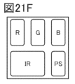
- 21A to 21F are diagrams showing examples of pixels.
- 21G and 21H are diagrams showing examples of pixel circuit diagrams.
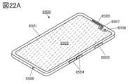
- 22A and 22B are diagrams illustrating examples of electronic devices.
- 23A to 23D are diagrams illustrating examples of electronic devices.
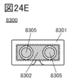
- 24A to 24F are diagrams illustrating examples of electronic devices.
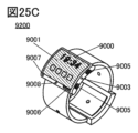
- 25A to 25F are diagrams illustrating examples of electronic devices.
- film and the term “layer” can be interchanged with each other.
- conductive layer or “insulating layer” may be interchangeable with the terms “conductive film” or “insulating film.”
- the top surface shape of a component refers to the contour shape of the component in plan view.
- Plan view means viewing from the normal direction of the surface on which the component is formed, or the surface of the support (for example, substrate) on which the component is formed.
- an EL layer refers to a layer provided between a pair of electrodes of a light-emitting element and containing at least a light-emitting substance (also referred to as a light-emitting layer) or a laminate including a light-emitting layer.
- a display panel which is one aspect of a display device, has a function of displaying (outputting) an image or the like on a display surface. Therefore, the display panel is one aspect of the output device.
- the substrate of the display panel is attached with a connector such as FPC (Flexible Printed Circuit) or TCP (Tape Carrier Package), or the substrate is mounted with a COG (Chip On Glass) method.
- a connector such as FPC (Flexible Printed Circuit) or TCP (Tape Carrier Package)
- COG Chip On Glass
- One embodiment of the present invention is a display device including a light-emitting element (also referred to as a light-emitting device) and a light-receiving element (also referred to as a light-receiving device).
- a light-emitting element has a pair of electrodes and an EL layer therebetween.
- the light receiving element has a pair of electrodes and an active layer therebetween.
- the light-emitting element is preferably an organic EL element (organic electroluminescence element).
- the light receiving element is preferably an organic photodiode (organic photoelectric conversion element).
- the display device preferably has two or more light-emitting elements with different emission colors.
- Light-emitting elements emitting light of different colors have EL layers containing different materials.
- a full-color display device can be realized by using three types of light-emitting elements that emit red (R), green (G), and blue (B) light.
- an image can be captured by a plurality of light receiving elements, and thus functions as an imaging device.
- the light emitting element can be used as a light source for imaging.
- one embodiment of the present invention can display an image with a plurality of light-emitting elements, and therefore functions as a display device. Therefore, one embodiment of the present invention can be referred to as a display device having an imaging function or an imaging device having a display function.
- the display section has a function of displaying an image and a function of a light receiving section. Since an image can be captured by a plurality of light receiving elements provided in the display portion, the display device can function as an image sensor, a touch panel, or the like. That is, it is possible to capture an image on the display unit, or detect the approach or contact of an object.
- the light-emitting element provided in the display unit can be used as a light source when receiving light, there is no need to provide a light source separate from the display device, and a highly functional display can be achieved without increasing the number of electronic components. device can be realized.
- the light-receiving element when an object reflects light emitted from a light-emitting element included in a display portion, the light-receiving element can detect the reflected light. It can be performed.
- the display device of one embodiment of the present invention can capture an image of a fingerprint or a palmprint when a finger, palm, or the like is brought into contact with the display portion. Therefore, an electronic device including the display device of one embodiment of the present invention can perform personal authentication using an image such as a captured fingerprint or palmprint. As a result, there is no need to separately provide an imaging device for fingerprint authentication or palmprint authentication, and the number of parts of the electronic device can be reduced.
- the light-receiving elements are arranged in a matrix in the display section, an image of a fingerprint or a palm print can be taken anywhere on the display section, and an electronic device with excellent convenience can be realized.
- biometric authentication method is face authentication.
- face authentication there is a possibility that the accuracy of authentication may differ depending on the situation, such as a marked decrease in the accuracy of authentication when a person is wearing a mask.
- authentication methods using fingerprints, palmprints, veins, or the like have almost no difference in authentication accuracy depending on the measurement environment, etc., and can be said to be authentication methods with higher accuracy.
- the light emitted from the light emitting element of the display can be used as a light source.
- the light emitting element it is preferable to cause the light emitting element to emit light momentarily (for example, 100 ⁇ s or more and 100 ms or less).
- the light emitting element By shortening the light emission time, deterioration of the light emitting element can be suppressed even when light is emitted with high luminance.
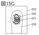
- an image with enhanced contrast (shadow) can be obtained by capturing an image using momentary and high-brightness light emission, it is possible to capture an uneven shape such as a fingerprint more clearly.
- a light-shielding layer on the light-receiving surface side of the light-receiving element that defines the range (imaging range) in which light enters the light-receiving element.
- a clearer image can be captured as the imaging range of the light receiving element is narrower. It functions as a pinhole to prevent light from obliquely entering the light-receiving element and to sharpen the image.
- a light-shielding thin film having an opening at a position overlapping the light-receiving element can be used as the light-shielding layer.
- a light-transmitting spacer (also referred to as a light-transmitting layer) is arranged between the light-receiving element and the light-shielding layer.
- the spacer is stacked on the light receiving element with a barrier layer interposed therebetween. The thicker the spacer, the greater the distance between the light-shielding layer and the light-receiving element, so that a clearer image can be captured.
- the spacer positioned on the light receiving element is formed in an island-like pattern, and the light shielding layer is provided so as to partially cover the upper surface and the side surface of the spacer.
- the light-shielding layer along the side surface of the spacer, the light-receiving surface of the light-receiving element can be surrounded by the light-shielding layer. Therefore, the path of stray light emitted from the light-emitting element and diffusing in the display device can be blocked by the light-shielding layer, and the stray light can be prevented from entering the light-receiving element. Since the stray light causes noise when the light-receiving element performs imaging, the imaging sensitivity (signal-to-noise ratio (S/N ratio)) can be increased by adopting a configuration that blocks the stray light. .
- a display device in which a light-emitting element that emits white light and a color filter are combined can also be used.
- light-emitting elements having the same structure can be applied to light-emitting elements provided in pixels (sub-pixels) that emit light of different colors. Since the EL layer can be formed in common for all the light-emitting elements in this manner, the manufacturing process can be simplified.
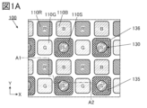
- FIG. 1A shows a schematic top view of display device 100 .
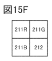
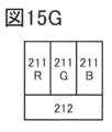
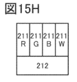
- the display device includes a plurality of red light emitting elements 110R, green light emitting elements 110G, blue light emitting elements 110B, and light receiving elements 110S.
- the light-emitting region of each light-emitting element or the light-receiving region of the light-receiving element is denoted by R, G, B or S.
- the light-emitting element 110R, the light-emitting element 110G, the light-emitting element 110B, and the light-receiving element 110S are arranged in a matrix.
- FIG. 1A shows a configuration in which two elements are alternately arranged in one direction.
- the arrangement method of the light-emitting elements and the light-receiving elements is not limited to this, and an arrangement method such as a stripe arrangement, an S-stripe arrangement, a delta arrangement, a Bayer arrangement, and a zigzag arrangement may be applied, as well as a pentile arrangement, a diamond arrangement, and the like. can also be used.
- FIG. 1A shows an example in which the light emitting elements and the light receiving elements are arranged at the same period. That is, FIG. 1A shows an example in which the definition (density) of light emitting elements and the definition (density) of light receiving elements are the same.
- the array period of the light-emitting elements may be different from the array period of the light-receiving elements. For example, the array period of the light emitting elements may be shorter than the array period of the light receiving elements, or conversely, the array period of the light emitting elements may be longer than the array period of the light receiving elements.
- EL elements such as OLEDs (Organic Light Emitting Diodes) or QLEDs (Quantum-dot Light Emitting Diodes) are preferably used as the light emitting elements 110R, 110G, and 110B.
- the light-emitting substance of the EL element include a substance that emits fluorescence (fluorescent material), a substance that emits phosphorescence (phosphorescent material), and a substance that exhibits thermally activated delayed fluorescence (thermally activated delayed fluorescence: TADF) material. ), inorganic compounds (such as quantum dot materials), and the like.
- a pn-type or pin-type photodiode can be used as the light receiving element 110S.
- the light receiving element 110S functions as a photoelectric conversion element that detects light incident on the light receiving element 110S and generates charges.
- the amount of charge generated by the photoelectric conversion element is determined according to the amount of incident light.
- Organic photodiodes can be easily made thinner, lighter, and larger, and have a high degree of freedom in shape and design, so they can be applied to various devices.
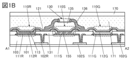
- FIG. 1B shows a schematic cross-sectional view corresponding to the dashed-dotted line A1-A2 in FIG. 1A.
- FIG. 1B shows a schematic cross-sectional view of the light emitting element 110R, the light receiving element 110S, and the light emitting element 110G.
- the light emitting element 110R, the light emitting element 110G, the light emitting element 110B (not shown), and the light receiving element 110S are provided on the substrate 101. It also has an adhesive layer 171 and a substrate 170 covering the light emitting element 110R, the light emitting element 110G, the light emitting element 110B, and the light receiving element 110S.
- the light emitting element 110R has a pixel electrode 111R, an organic layer 112R, and a common electrode 113.
- the light emitting element 110G has a pixel electrode 111G, an organic layer 112G, and a common electrode 113.
- the light receiving element 110S has a pixel electrode 111S, an organic layer 155, and a common electrode 113.
- the common electrode 113 is provided commonly to the light emitting element 110R, the light emitting element 110G, the light emitting element 110B (not shown), and the light receiving element 110S.
- the pixel electrode 111S of the light receiving element 110S can also be called a sensor electrode, a light receiving electrode, an imaging electrode, or the like.
- the organic layer 112R of the light-emitting element 110R has at least a light-emitting organic compound that emits red light.
- the organic layer 112G included in the light-emitting element 110G contains at least a light-emitting organic compound that emits green light.
- An organic layer 112B (not shown) included in the light-emitting element 110B contains at least a light-emitting organic compound that emits blue light.
- Layers containing a light-emitting organic compound included in the organic layer 112R, the organic layer 112G, and the organic layer 112B can also be called light-emitting layers.
- the organic layer 155 of the light-receiving element 110S has a photoelectric conversion material that is sensitive to the wavelength region of visible light or infrared light.
- the wavelength range to which the photoelectric conversion material of the organic layer 155 is sensitive includes the wavelength range of light emitted by the light emitting element 110R, the wavelength range of light emitted by the light emitting element 110G, and the wavelength range of light emitted by the light emitting element 110B.
- a photoelectric conversion material having sensitivity to infrared light having a longer wavelength than the wavelength range of light emitted by the light emitting element 110R may be used.
- a layer containing a photoelectric conversion material included in the organic layer 155 can also be called an active layer or a photoelectric conversion layer.
- the letters that distinguish them may be omitted and the light emitting elements 110 may be referred to.
- the symbols omitting the letters may be used. be.
- the organic layer 112 may have one or more of an electron injection layer, an electron transport layer, a hole injection layer, and a hole transport layer in addition to the light emitting layer.
- the organic layer 112 may have a layered structure of a hole injection layer, a hole transport layer, a light emitting layer, an electron transport layer, and an electron injection layer from the pixel electrode 111 side.
- one or more of the hole injection layer, the hole transport layer, the light emitting layer, the electron transport layer, and the electron injection layer may be a film containing only an inorganic compound or an inorganic substance without containing an organic compound.
- a pixel electrode 111R, a pixel electrode 111G, and a pixel electrode 111B are provided for each light emitting element 110, respectively.
- the common electrode 113 is provided as a continuous layer common to each light emitting element 110 and light receiving element 110S.
- a conductive film having a property of transmitting visible light is used for one of the pixel electrodes and the common electrode 113, and a conductive film having a reflective property is used for the other.
- a bottom emission type display device can be obtained.
- a top emission display device can be obtained.
- a dual-emission display device can be obtained.
- One embodiment of the present invention is preferably a top emission type or a dual emission type.
- the pixel electrode 111 can also have a laminated structure of a reflective conductive film and a translucent conductive film.
- the organic layer 112 is preferably provided over the reflective conductive film with a light-transmitting conductive film interposed therebetween. Further, at this time, the thickness of the light-transmitting conductive film may be different for each light-emitting element.
- a transistor 102R, a transistor 102S, a transistor 102G, and the like are provided on the substrate 101.
- An insulating layer 103 is provided to cover each transistor 102 , and a pixel electrode 111 is provided over the insulating layer 103 .
- the pixel electrode 111R is electrically connected to the transistor 102R through an opening provided in the insulating layer 103.
- FIG. Similarly, the pixel electrode 111S is electrically connected to the transistor 102S, the pixel electrode 111G is electrically connected to the transistor 102G, and the pixel electrode 111B (not shown) is electrically connected to the transistor 102B (not shown).
- An insulating layer 131 is provided to cover end portions of the pixel electrode 111R, the pixel electrode 111G, the pixel electrode 111B (not shown), and the pixel electrode 111S.
- the end of the insulating layer 131 is preferably tapered.
- the tapered shape refers to a shape in which at least a part of the side surface of the structure is inclined with respect to the substrate surface.
- the insulating layer 131 preferably contains an organic resin.
- an organic resin for the insulating layer 131, adhesion to the organic layers 112 and 155 can be improved, and manufacturing yield can be improved.
- the surface can be made into a gently curved surface. Therefore, coverage with a film formed over the insulating layer 131 can be improved.
- Examples of materials that can be used for the insulating layer 131 include acrylic resins, polyimide resins, epoxy resins, polyamide resins, polyimideamide resins, siloxane resins, benzocyclobutene-based resins, phenolic resins, precursors of these resins, and the like. be done.
- An inorganic insulating film can also be used for the insulating layer 131 .
- Using an inorganic insulating film for the insulating layer 131 is more suitable for microfabrication than using an organic resin, and is particularly suitable for manufacturing a high-definition display device.
- Examples of inorganic insulating materials that can be used for the insulating layer 131 include oxides or nitrides such as silicon oxide, silicon oxynitride, silicon nitride oxide, silicon nitride, aluminum oxide, aluminum oxynitride, or hafnium oxide. be able to. Alternatively, yttrium oxide, zirconium oxide, gallium oxide, tantalum oxide, magnesium oxide, lanthanum oxide, cerium oxide, neodymium oxide, or the like may be used. Alternatively, the insulating layer 131 may be formed by stacking a film containing the inorganic insulating material.
- the organic layer 112 and the organic layer 155 each have a region in contact with the upper surface of the pixel electrode and a region in contact with the surface of the insulating layer 131 . Also, the ends of the organic layer 112 and the organic layer 155 are located on the insulating layer 131 respectively.
- a protective layer 121 is provided on the common electrode 113 to cover the light emitting element 110R, the light emitting element 110G, the light receiving element 110S, and the light emitting element 110B (not shown).
- the protective layer 121 has a function of preventing impurities such as water from diffusing into each light emitting element 110 from above.
- the protective layer 121 can have, for example, a single layer structure or a laminated structure including at least an inorganic insulating film.
- inorganic insulating films include oxide films and nitride films such as silicon oxide films, silicon oxynitride films, silicon nitride oxide films, silicon nitride films, aluminum oxide films, aluminum oxynitride films, and hafnium oxide films.
- a semiconductor material or a conductive material such as indium gallium oxide, indium zinc oxide, indium tin oxide, or indium gallium zinc oxide may be used for the protective layer 121 .
- a spacer 135 is provided on the protective layer 121 .
- the spacer 135 is provided on a portion of the protective layer 121 overlapping with the light receiving element 110S.
- the spacer 1335 it is preferable to use a material that is translucent at least with respect to the light of the wavelength to which the light receiving element 110S is sensitive.
- the spacer 135 preferably has a property of transmitting visible light.
- An organic resin or an inorganic insulating film can be used for the spacer 135 .
- FIG. 1B shows an example in which the spacer 135 is processed into an island shape.
- the spacer 135 is provided so as to overlap with the pixel electrode 111S with the protective layer 121, the common electrode 113, and the organic layer 155 interposed therebetween. Further, an end portion of the spacer 135 is provided so as to overlap with the insulating layer 131 .
- the shape of the outer edge of spacer 135 is indicated by a dashed line.
- an island shape indicates a state in which two or more layers using the same material formed in the same process are physically separated.
- an island-shaped light-emitting layer means that the light-emitting layer is physically separated from an adjacent light-emitting layer.
- a light shielding layer 136 is provided on the spacer 135 . As shown in FIGS. 1A and 1B, the light blocking layer 136 has an opening 130 overlapping the light receiving element 110S. The opening 130 is located inside the outline of the pixel electrode 111S in plan view. Further, the opening 130 is located inside the outline of the organic layer 155 in plan view.
- the light shielding layer 136 is provided to cover not only the upper surface of the spacer 135 but also the side surface thereof. An end portion of the light shielding layer 136 opposite to the opening 130 is provided so as to overlap the insulating layer 131 with the protective layer 121 interposed therebetween.
- the light shielding layer 136 contains a material that absorbs at least part of visible light. For example, it includes a material that absorbs at least one of the lights emitted by the light emitting elements 110R, 110G, and 110B.
- the light shielding layer 136 itself may be made of a material that absorbs visible light (for example, a colored organic or inorganic material), or the light shielding layer 136 may contain a pigment that absorbs visible light.
- a resin containing carbon black as a pigment and functioning as a black matrix, or a black thin film of chromium or the like can be used.
- a resin or the like that can be used as a color filter that transmits red, blue, or green light and absorbs other light can be used.
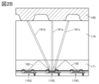
- FIGS. 2A and 2B show a light receiving element 110S in the center and light emitting elements 110G adjacent to both sides thereof.
- the object to be imaged 160 is in contact with the substrate 170 .
- the object 160 to be imaged has an uneven surface.
- the convex portion of the imaged object 160 is in contact with the substrate 170 and the concave portion is not in contact.
- the object to be imaged 160 is a fingertip, and the uneven shape on the surface thereof can be called a fingerprint.
- the reflected light 181a, the reflected light 181b, and the reflected light 181c are reflected lights that are reflected by the object to be imaged 160 or the like and directed toward the light receiving element 110S when the light emitting element 110G or the like is used as a light source.
- FIG. 2B is a schematic cross-sectional view when the spacer 135 and the light shielding layer 136 are not provided.
- the captured image may be blurred.
- the spacer 135 and the light shielding layer 136 by providing the spacer 135 and the light shielding layer 136, the reflected light 181b and the reflected light 181c reflected from the oblique direction toward the light receiving element 110S are blocked by the light shielding layer 136, and the light receiving element 110S Only the reflected light 181a directly above can reach the light receiving area of the light receiving element 110S.
- the object to be imaged in the vicinity of the surface of the substrate 170 can be photographed clearly.
- the light 182 guided through the adhesive layer 171 can also enter the light receiving element 110S.
- the light 182 includes, for example, light emitted from the light emitting element 110G and totally reflected at the interface between the adhesive layer 171 and the substrate 170, or the like.
- Such light can be called stray light.
- the stray light that diffuses inside the display device causes noise when an image is captured by the light receiving element 110S. That is, the imaging sensitivity (signal-noise ratio (S/N ratio)) is lowered.
- the imaging sensitivity can be enhanced.
- the spacer 135 by processing the spacer 135 into an island shape and covering the side surface of the spacer 135 with a light shielding layer 136, the light that passes through the spacer 135 from the adhesive layer 171 and reaches the light receiving element 110S and the spacer 135 itself can be effectively blocked to reach the light receiving element 110S.
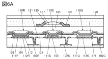
- the light shielding layer 136 may also be arranged on the light emitting element as shown in FIGS. 3A and 3B.
- the light shielding layer 136 is arranged between the light emitting element 110 and the light receiving element 110S and also between the adjacent light emitting elements 110.
- the light shielding layer 136 has an opening overlapping with the light emitting element 110 and an opening 130 overlapping with the light receiving element 110S.
- the diameter (or area) of the opening overlapping the light emitting element 110 is preferably larger than the opening overlapping the light receiving element 110S.
- FIG. 4A shows an example in which the spacer 135 is not processed into an island shape.
- the spacer 135 is provided covering not only the light receiving element 110S but also the light emitting elements 110R, 110G, and 110B (not shown).
- the process of forming the spacer 135 can be simplified, so that the manufacturing cost can be reduced.
- FIG. 4B is an example in which the light shielding layer 136 is also arranged in the vicinity of the light emitting element, as in FIG. 3B.
- FIG. 5A is an example when the lens 137 is applied.
- Lens 137 is a convex lens and is provided on spacer 135 . Also, the lens 137 is provided at a position overlapping the opening of the light shielding layer 136 . A portion of the light shielding layer 136 is provided to cover the end of the lens 137 .
- the lens 137 has a function of increasing the amount of light received by the light receiving element 110S by condensing the light transmitted through the opening 130 of the light shielding layer 136. Therefore, the imaging sensitivity can be improved.
- the diameter of the opening 130 of the light shielding layer 136 is larger than the diameter of the light receiving area of the light receiving element 110S, because the amount of light received by the light receiving element 110S can be effectively increased.
- the diameter (or width) of the light receiving region of the light receiving element 110S corresponds to the aperture diameter (or aperture width) of the insulating layer 131 on the pixel electrode 111S.
- the lens 137 has translucency with respect to at least the light of the wavelength received by the light receiving element 110S. Further, the lens 137 can be made of a material having a higher refractive index than the adhesive layer 171 with respect to the light of the wavelength received by the light receiving element 110S. Organic resin such as acrylic resin can be used as the lens 137 .
- FIG. 5B is an example in which the light shielding layer 136 is also arranged in the vicinity of the light emitting element, as in FIG. 3B.
- FIG. 6A is an example in which a lens 137 is applied to the configuration example 1-2.
- FIG. 6B is an example in which the light shielding layer 136 is also arranged in the vicinity of the light emitting element, as in FIG. 3B.
- FIG. 7A shows an example in which a lens 138 is provided not only on the light receiving element 110S but also on the light emitting element.
- a lens 138 is provided so as to overlap each light emitting element. By using the lens 138, the light extraction efficiency of the light emitting element can be increased and power consumption can be reduced.
- the lens 137 overlaps the light receiving element 110S via the spacer 135 and the protective layer 121, whereas the spacer 135 is not provided between the lens 138 and the protective layer 121. Therefore, the distance between the lens 138 and the light emitting element 110 is smaller by the thickness of the spacer 135 than the distance between the lens 137 and the light receiving element 110S.
- the lens 138 can also be formed by processing the same film as the lens 137.
- a convex lens may be used for the lens 138, or a concave lens may be used.
- a concave lens When a concave lens is used, a material having a lower refractive index than that of the adhesive layer 171 may be used for the lens 138 .
- FIG. 7B shows an example in which the spacer 135 is not processed into an island shape.
- Lens 138 is provided on spacer 135 in the same manner as lens 137 .
- FIG. 8A shows an example in which the spacer 135 and the light shielding layer 136 are formed using colored layers.
- the configuration shown in FIG. 8A has a colored layer 174G instead of the spacer 135 and a 174R instead of the light shielding layer 136.
- the colored layer 174G functions as a color filter that transmits green light and absorbs light of other colors.
- the colored layer 174R functions as a color filter that transmits red light and absorbs light of other colors.
- the colored layers used as spacers can be determined according to the wavelength of the light used as the light source during imaging, the sensitivity characteristics of the light receiving element 110S, and the like. Although an example using the colored layer 174G that is a green color filter is shown here, a colored layer 174R that is a red color filter or a colored layer that is a blue color filter may be used, and light other than visible light may be used. A color filter that transmits (infrared light or ultraviolet light) may be used.
- the colored layer used instead of the light shielding layer 136 can use a color filter with a color different from that of the colored layer used as the spacer.
- a color filter that transmits blue light and absorbs light of other colors may be used instead of the colored layer 174R.
- each colored layer so as to overlap the light emitting element 110 corresponding to each color.
- the colored layer 174R is provided on the light emitting element 110R
- the colored layer 174G is provided on the light emitting element 110G.
- FIGS. 8B and 8C are examples in which the colored layers are continuous without being separated between each light-emitting element and the light-receiving element 110S.
- the colored layer 174G used as a spacer is preferably divided between the light receiving element 110S and the light emitting element 110B. If the colored layer 174G is continuously provided on the light receiving element 110S and the light emitting element 110B, the light emitted by the light emitting element 110B may propagate through the colored layer 174G and reach the light receiving element 110S. On the other hand, the colored layer 174R is divided between the light emitting element 110R and the light receiving element 110S because even if the light emitted by the light emitting element 110R is guided through the colored layer 174R, it is absorbed by the colored layer 174G on the light receiving element 110S. You don't have to.
- FIG. 8C shows a cross section of a light emitting element 110B that emits blue light.
- the light emitting element 110B has a pixel electrode 111B, an organic layer 112B, and a common electrode 113.
- the pixel electrode 111B is electrically connected to the transistor 102B through an opening provided in the insulating layer 103.
- FIG. A colored layer 174B functioning as a blue color filter is overlaid on the light emitting element 110B.
- the colored layer 174R and the colored layer 174B may be provided facing each other with the opening 130 interposed therebetween.
- FIGS. 9A, 9B, and 9C are examples in which a light-emitting element emitting white light is applied to the configuration example 1-6.
- the light emitting element 110W has an organic layer 112W between the pixel electrode and the common electrode 113.
- the organic layer 112W exhibits white light.
- the organic layer 112 can have, for example, a structure including two or more kinds of light-emitting materials that have a complementary color relationship.
- a colored layer 174R, a colored layer 174G, or a colored layer 174B is provided in a region overlapping with the light emitting element 110W. This enables full-color display.
- the EL layer When part or all of the EL layer is separately formed between light emitting elements with different emission colors, it is formed by vapor deposition using a shadow mask such as a fine metal mask (hereinafter also referred to as FMM: Fine Metal Mask). It has been known. However, in this method, island-like organic films are formed due to various influences such as FMM accuracy, positional deviation between the FMM and the substrate, FMM deflection, and broadening of the contour of the formed film due to vapor scattering and the like. Since the shape and position deviate from the design, it is difficult to increase the definition and aperture ratio of the display device. Therefore, measures have been taken to artificially increase the definition (also called pixel density) by applying a special pixel arrangement method such as a pentile arrangement.
- a shadow mask such as a fine metal mask
- two adjacent island-shaped organic films can be partially overlapped in order to achieve higher definition and higher aperture ratio.
- the distance between the light emitting regions can be significantly shortened compared to the case where the two island-shaped organic films are not overlapped.
- current leakage occurs between the adjacent two light-emitting elements through the overlapped organic film, resulting in unintended light emission.
- the display quality is degraded due to a decrease in luminance, a decrease in contrast, and the like.
- power efficiency, power consumption, etc. deteriorate due to leakage current.
- the imaging sensitivity may decrease.
- part or all of the organic layer positioned between the pair of electrodes of the light-emitting element and part or all of the organic layer positioned between the pair of electrodes of the light-receiving element are formed by photolithography. processed by At this time, it is preferable to separate the organic layers between adjacent light emitting elements and between adjacent light emitting elements and light receiving elements so as not to contact each other. This makes it possible to cut current leak paths (leak paths) through the organic layer between the light-emitting elements and between the light-emitting element and the light-receiving element.
- leakage current also called side leakage or side leakage current
- highly accurate imaging with a high S/N ratio can be performed. Therefore, even with weak light, a clear image can be captured. Therefore, the luminance of a light-emitting element used as a light source can be lowered at the time of imaging, so that power consumption can be reduced.
- a current leak path (leak path) can be separated between two adjacent light emitting elements. Therefore, brightness can be increased, contrast can be increased, power efficiency can be increased, power consumption can be reduced, and the like.
- an insulating layer in order to protect the side surfaces of the organic laminated film exposed by etching. Thereby, the reliability of the display device can be improved.
- the resin layer is provided in contact with the EL layer, the EL layer may be dissolved by the solvent used when forming the resin layer. Therefore, it is preferable to provide an insulating layer for protecting the side surface of the EL layer between the EL layer and the resin layer. That is, it is preferable to provide an inorganic insulating layer in contact with the side surface and the upper surface of the EL layer at the end of the EL layer, and provide the resin layer over the inorganic insulating layer.
- the end portion of the pixel electrode is tapered so that the step coverage of the EL film formed over the pixel electrode is improved, and the step at the end portion of the pixel electrode is formed without using a partition wall. It is possible to prevent the EL layer from being divided. As a result, the aperture ratio can be made extremely high.
- a display device in which a light-emitting element that emits white light and a color filter are combined can also be used.
- light-emitting elements having the same structure can be applied to light-emitting elements provided in pixels (sub-pixels) that emit light of different colors, and all layers can be common layers. Further, part or all of each EL layer is divided by photolithography. As a result, leakage current through the common layer is suppressed, and a high-contrast display device can be realized.
- FIG. 10A shows a schematic cross-sectional view of a display device exemplified below.
- FIG. 10A shows a cross-sectional view including the light emitting element 110R, the light emitting element 110G, and the light receiving element 110S.
- the light emitting element 110R has a pixel electrode 111R, an organic layer 112R, a common layer 114, and a common electrode 113.
- the light emitting element 110G has a pixel electrode 111G, an organic layer 112G, a common layer 114, and a common electrode 113.
- the light receiving element 110S has a pixel electrode 111S, an organic layer 155, a common layer 114, and a common electrode 113.
- FIG. Common layer 114 and common electrode 113 are provided as a continuous layer common to light emitting element 110R, light emitting element 110G, light receiving element 110S, and light emitting element 110B (not shown).
- a conductive layer 161 is provided on the insulating layer 103, and the pixel electrode 111 of each light emitting element 110 or light receiving element 110S is provided on the conductive layer 161.
- the conductive layer 161 is electrically connected to each transistor 102 through openings provided in the insulating layer 103 .
- a recess is formed in the top surface of the conductive layer 161 in a connection portion between the conductive layer 161 and the transistor 102, and a planarization layer 163 is provided so as to fill the recess.
- the organic layer 112 and the common layer 114 may each independently have one or more of an electron injection layer, an electron transport layer, a hole injection layer, and a hole transport layer.
- the organic layer 112 may have a layered structure of a hole injection layer, a hole transport layer, a light emitting layer, and an electron transport layer from the pixel electrode 111 side, and the common layer 114 may have an electron injection layer.
- the common layer 114 can be a film containing only an inorganic compound or an inorganic substance without containing an organic compound.
- FIG. 10A shows an example in which the insulating layer 131 covering the edge of the pixel electrode 111 is not provided. Since the organic layer 112 or the organic layer 155 has a portion covering the edge of the pixel electrode 111, the edge of the pixel electrode 111 preferably has a tapered shape.
- the organic layer 112 and the organic layer 155 are processed into an island shape by photolithography. Therefore, the organic layer 112 and the organic layer 155 have a shape in which the angle formed by the top surface and the side surface is close to 90 degrees at the ends thereof.
- an organic film formed using FMM (Fine Metal Mask) or the like tends to gradually become thinner nearer the end. Since it is formed in a slope shape, it is difficult to distinguish between the top surface and the side surface.
- the angle between the side surface and the bottom surface is 10 degrees or more and 120 degrees or less, preferably 30 degrees or more and 110 degrees or less, more preferably 45 degrees or more and 100 degrees or less, further preferably It is preferably processed so as to have a region of 60 degrees or more and 95 degrees or less. As the taper angle is smaller, the length from the edge of the pixel electrode 111 to the edge of the organic layer 112 or the organic layer 155 can be reduced, so that a higher definition display device can be realized.
- FIG. 10B shows an enlarged view of part of the light emitting element 110R, part of the light receiving element 110S, and the area therebetween.
- the side surface of the organic layer 112 and the side surface of the organic layer 155 are provided to face each other with the resin layer 126 interposed therebetween.
- the resin layer 126 has a smooth upper surface, and a common layer 114 and a common electrode 113 are provided to cover the upper surface of the resin layer 126 .
- the resin layer 126 functions as a planarization film for alleviating the step at the end of the organic layer 112 or the organic layer 155 .
- the provision of the resin layer 126 causes a phenomenon in which the common electrode 113 is divided by a step of the organic layer 112 or the organic layer 155 (also referred to as step disconnection), and the common electrode over the organic layer 112 or the organic layer 155 is insulated. You can prevent it from getting lost.
- the resin layer 126 can also be called an LFP (Local Filling Planarization) layer.
- An insulating layer containing an organic material can be suitably used as the resin layer 126 .
- acrylic resin, polyimide resin, epoxy resin, imide resin, polyamide resin, polyimideamide resin, silicone resin, siloxane resin, benzocyclobutene-based resin, phenolic resin, and precursors of these resins are applied as the resin layer 126. can do.
- an organic material such as polyvinyl alcohol (PVA), polyvinyl butyral, polyvinylpyrrolidone, polyethylene glycol, polyglycerin, pullulan, water-soluble cellulose, or alcohol-soluble polyamide resin may be used.
- a photosensitive resin can be used as the resin layer 126 .
- a photoresist may be used as the photosensitive resin.
- a positive material or a negative material can be used for the photosensitive resin.
- the resin layer 126 may contain a material that absorbs visible light.
- the resin layer 126 itself may be made of a material that absorbs visible light, or the resin layer 126 may contain a pigment that absorbs visible light.
- a resin that transmits red, blue, or green light and can be used as a color filter that absorbs other light, or a resin that contains carbon black as a pigment and functions as a black matrix, or the like. can be used.
- the insulating layer 125 is provided in contact with the side surface of the organic layer 112 and the side surface of the organic layer 155 . Also, the insulating layer 125 is provided to cover the upper end portion of the organic layer 112 and the upper end portion of the organic layer 155 . A part of the insulating layer 125 is provided in contact with the upper surface of the insulating layer 103 .
- the insulating layer 125 is located between the organic layer 112 or the organic layer 155 and the resin layer 126 and functions as a protective layer to prevent the resin layer 126 from contacting the organic layer 112 or the organic layer 155 .
- the organic layer 112 or the organic layer 155 and the resin layer 126 are in contact with each other, the organic layer 112 or the organic layer 155 may be dissolved by the organic solvent or the like used when forming the resin layer 126 . Therefore, by providing such an insulating layer 125, it is possible to protect the side surface of the organic layer.
- the insulating layer 125 can prevent the side surfaces of the organic layer 112 or the organic layer 155 from being exposed to the air. Accordingly, a highly reliable light-emitting element and light-receiving element can be manufactured.
- the insulating layer 125 can be an insulating layer containing an inorganic material.
- an inorganic insulating film such as an oxide insulating film, a nitride insulating film, an oxynitride insulating film, or a nitride oxide insulating film can be used, for example.
- the insulating layer 125 may have a single-layer structure or a laminated structure.
- the oxide insulating film includes a silicon oxide film, an aluminum oxide film, a magnesium oxide film, an indium gallium zinc oxide film, a gallium oxide film, a germanium oxide film, an yttrium oxide film, a zirconium oxide film, a lanthanum oxide film, a neodymium oxide film, and an oxide film.
- Examples include a hafnium film and a tantalum oxide film.
- Examples of the nitride insulating film include a silicon nitride film and an aluminum nitride film.
- As the oxynitride insulating film a silicon oxynitride film, an aluminum oxynitride film, or the like can be given.
- nitride oxide insulating film a silicon nitride oxide film, an aluminum nitride oxide film, or the like can be given.
- a metal oxide film such as a hafnium oxide film, or an inorganic insulating film such as a silicon oxide film to the insulating layer 125, pinholes are reduced and the EL layer can be protected.
- a superior insulating layer 125 can be formed.
- oxynitride refers to a material whose composition contains more oxygen than nitrogen
- nitride oxide refers to a material whose composition contains more nitrogen than oxygen. point to the material.
- silicon oxynitride refers to a material whose composition contains more oxygen than nitrogen
- silicon nitride oxide refers to a material whose composition contains more nitrogen than oxygen. indicates
- a sputtering method, a CVD method, a PLD method, an ALD method, or the like can be used to form the insulating layer 125 .
- the insulating layer 125 is preferably formed by an ALD method with good coverage.
- the resin layer 126 is provided to cover the upper surface of the organic layer 112 or the organic layer 155.
- a layer 128 and an insulating layer 125 are laminated in this order between the upper surface of the organic layer 112 or the organic layer 155 and the resin layer 126 .
- Layer 128 is provided in contact with the top surface of organic layer 112 .
- the layer 128 is part of a protective layer (also referred to as a mask layer or a sacrificial layer) remaining for protecting the organic layer 112 or the organic layer 155 when the organic layer 112 or the organic layer 155 is etched.
- a protective layer also referred to as a mask layer or a sacrificial layer
- any of the materials that can be used for the insulating layer 125 can be used.
- an aluminum oxide film formed by an ALD method a metal oxide film such as a hafnium oxide film, or an inorganic insulating film such as a silicon oxide film has few pinholes.
- An insulating layer 125 having excellent resistance can be formed.
- the layer 128 is a film in contact with the top surface of the organic layer 112, the reliability of the light-emitting element 110 and the light-receiving element 110S is improved by using wet etching which causes less damage to the formation surface when processing the layer 128. be able to.
- a protective layer 121 is provided to cover the common electrode 113 , and a spacer 135 and a light shielding layer 136 are provided on the protective layer 121 .
- the description of Structural Example 1 can be referred to for the protective layer 121, the spacer 135, the light-blocking layer 136, and the like.
- FIG. 10A and 11B are examples of the case where the lens 137 is applied to the configuration illustrated in FIG. 10A.
- the lens 137 when the lens 137 is used, it is preferable to make the diameter of the opening 130 of the light shielding layer 136 larger than the diameter of the light receiving region of the light receiving element 110S.
- the diameter of the opening of the light receiving element 110S could be controlled by the diameter of the opening of the insulating layer 131.
- the light receiving region of the light receiving element 110S corresponds to the diameter of the pixel electrode 111S or the opening diameter of the resin layer 126, the insulating layer 125, or the layer 128.
- FIG. 11A is an example in which the light receiving area of the light receiving element 110S is made smaller than the light emitting area of the light emitting element 110.
- FIG. 11A the aperture ratio (ratio of effective light emitting area) of the light emitting element can be increased, and the reliability can be improved.
- FIG. 11B is an example in which the diameter of the light receiving region of the light receiving element 110S is narrowed and the width of the resin layer 126 is increased compared to FIG. 10A.
- the distance between the light receiving element 110S and the adjacent light emitting element can be increased, and the diameter of the lens 137 can be increased accordingly. Therefore, the amount of light received by the light receiving element 110S can be increased.
- FIG. 11C is an example in which a lens 138 is further provided on the light emitting element 110 in addition to the configuration shown in FIG. 11B.
- FIG. 12A shows an example in which the spacer 135 and the light shielding layer 136 are composed of a colored layer 174R, a colored layer 174G, and the like.
- FIG. 12B is an example in which a white light emitting element 110W is applied to the light emitting element of FIG. 12A.
- Forming the spacers 135 and the light shielding layer 136 with colored layers in this manner is preferable because it is possible to take measures against stray light on the light receiving element 110S and to improve imaging clarity without increasing the number of processes.
- This embodiment can be implemented by appropriately combining at least part of it with other embodiments described herein.
- Embodiment 2 In this embodiment, a structural example of a display device of one embodiment of the present invention will be described. Although a display device capable of displaying an image is described here, it can be used as an imaging device by using a light-emitting element as a light source.
- the display device of this embodiment can be a high-resolution display device or a large-sized display device. Therefore, the display device of the present embodiment includes a relatively large screen such as a television device, a desktop or notebook personal computer, a computer monitor, a digital signage, a large game machine such as a pachinko machine, or the like. In addition to electronic devices, it can also be used for display parts of digital cameras, digital video cameras, digital photo frames, mobile phones, portable game machines, smartphones, wristwatch terminals, tablet terminals, personal digital assistants, and sound reproducing devices.
- Display device 400 13 shows a perspective view of the display device 400, and FIG. 14A shows a cross-sectional view of the display device 400. As shown in FIG.
- the display device 400 has a configuration in which a substrate 452 and a substrate 451 are bonded together.
- the substrate 452 is clearly indicated by dashed lines.
- the display device 400 has a display section 462, a circuit 464, wiring 465, and the like.
- FIG. 13 shows an example in which an IC 473 and an FPC 472 are mounted on the display device 400 . Therefore, the configuration shown in FIG. 14 can also be called a display module including the display device 400, an IC (integrated circuit), and an FPC.
- a scanning line driving circuit for example, can be used as the circuit 464 .
- the wiring 465 has a function of supplying signals and power to the display section 462 and the circuit 464 .
- the signal and power are input to the wiring 465 from the outside through the FPC 472 or input to the wiring 465 from the IC 473 .
- FIG. 13 shows an example in which an IC 473 is provided on a substrate 451 by a COG (Chip On Glass) method, a COF (Chip on Film) method, or the like.
- IC 473 for example, an IC having a scanning line driver circuit, a signal line driver circuit, or the like can be applied.
- the display device 400 and the display module may be configured without an IC.
- the IC may be mounted on the FPC by the COF method or the like.
- FIG. 14A shows an example of a cross section of the display device 400 when part of the region including the FPC 472, part of the circuit 464, part of the display portion 462, and part of the region including the connection portion are cut. show.
- FIG. 14A shows an example of a cross section of the display section 462, in particular, a region including a light emitting element 430b that emits green light (G) and a light receiving element 440 that receives reflected light (L).
- a display device 400 shown in FIG. 14A includes a transistor 252, a transistor 260, a transistor 258, a light-emitting element 430b, a light-receiving element 440, and the like between substrates 451 and 452.
- the above-exemplified light emitting elements or light receiving elements can be applied.
- the three sub-pixels are red (R), green (G), and blue (B).
- Color sub-pixels such as yellow (Y), cyan (C), and magenta (M) sub-pixels.
- the four sub-pixels include R, G, B, and white (W) sub-pixels, and R, G, B, and Y four-color sub-pixels. be done.
- the sub-pixel may include a light-emitting element that emits infrared light.
- a photoelectric conversion element sensitive to light in the red, green, or blue wavelength range, or a photoelectric conversion element sensitive to light in the infrared wavelength range can be used.
- the substrate 452 and the protective layer 416 are adhered via the adhesive layer 442 .
- the adhesive layer 442 is provided so as to overlap each of the light emitting element 430b and the light receiving element 440, and the display device 400 has a solid sealing structure.
- the light-emitting element 430b and the light-receiving element 440 have conductive layers 411a, 411b, and 411c as pixel electrodes.
- the conductive layer 411b reflects visible light and functions as a reflective electrode.
- the conductive layer 411c is transparent to visible light and functions as an optical adjustment layer.
- a conductive layer 411 a included in the light emitting element 430 b is connected to the conductive layer 272 b included in the transistor 260 through an opening provided in the insulating layer 294 .
- the transistor 260 has a function of controlling driving of the light emitting element.
- the conductive layer 411 a included in the light receiving element 440 is electrically connected to the conductive layer 272 b included in the transistor 258 .
- the transistor 258 has a function of controlling the timing of exposure using the light receiving element 440 and the like.
- An organic layer 412G or an organic layer 412S is provided to cover the pixel electrodes.
- An insulating layer 421 is provided in contact with a side surface of the organic layer 412G and a side surface of the organic layer 412S, and a resin layer 422 is provided on the insulating layer 421.
- FIG. An organic layer 414, a common electrode 413, and a protective layer 416 are provided to cover the organic layers 412G and 412S.
- a spacer 418 is provided on the protective layer 416 so as to cover the light receiving element 440 , and a light shielding layer 417 having an opening is provided to cover the upper surface and side surfaces of the spacer 418 .
- the light G emitted by the light emitting element 430b is emitted to the substrate 452 side.
- the light receiving element 440 receives the light L incident through the substrate 452 and converts it into an electric signal.
- a material having high visible light transmittance is preferably used for the substrate 452 .
- the transistors 252 , 260 , and 258 are all formed over the substrate 451 . These transistors can be made with the same material and the same process.
- transistor 252, the transistor 260, and the transistor 258 may be separately manufactured so as to have different structures.
- transistors with or without back gates may be separately manufactured, or transistors with different materials or thicknesses or both of semiconductors, gate electrodes, gate insulating layers, source electrodes, and drain electrodes may be separately manufactured. .
- the substrate 451 and the insulating layer 262 are bonded together by an adhesive layer 455 .
- a manufacturing substrate provided with an insulating layer 262 , each transistor, each light-emitting element, a light-receiving element, and the like is attached to a substrate 452 provided with a light-shielding layer 417 with an adhesive layer 442 . match. Then, the formation substrate is peeled off and a substrate 451 is attached to the exposed surface, so that each component formed over the formation substrate is transferred to the substrate 451 .
- Each of the substrates 451 and 452 preferably has flexibility. Thereby, the flexibility of the display device 400 can be enhanced.
- a connecting portion 254 is provided in a region of the substrate 451 where the substrate 452 does not overlap.
- the wiring 465 is electrically connected to the FPC 472 through the conductive layer 466 and the connecting layer 292 .
- the conductive layer 466 can be obtained by processing the same conductive film as the pixel electrode. Thereby, the connection portion 254 and the FPC 472 can be electrically connected via the connection layer 292 .
- the transistors 252, 260, and 258 each include a conductive layer 271 functioning as a gate, an insulating layer 261 functioning as a gate insulating layer, a semiconductor layer 281 having a channel formation region 281i and a pair of low-resistance regions 281n, and a pair of low-resistance regions. 281n, a conductive layer 272b connected to the other of the pair of low-resistance regions 281n, an insulating layer 275 functioning as a gate insulating layer, a conductive layer 273 functioning as a gate, and covering the conductive layer 273 It has an insulating layer 265 .
- the insulating layer 261 is located between the conductive layer 271 and the channel formation region 281i.
- the insulating layer 275 is located between the conductive layer 273 and the channel formation region 281i.
- the conductive layers 272a and 272b are connected to the low-resistance region 281n through openings provided in the insulating layer 265, respectively.
- One of the conductive layers 272a and 272b functions as a source and the other functions as a drain.
- FIG. 14A shows an example in which an insulating layer 275 covers the upper and side surfaces of the semiconductor layer.
- the conductive layers 272a and 272b are connected to the low-resistance region 281n through openings provided in the insulating layers 275 and 265, respectively.
- the insulating layer 275 overlaps the channel formation region 281i of the semiconductor layer 281 and does not overlap the low resistance region 281n.
- the structure shown in FIG. 14B can be manufactured.
- an insulating layer 265 is provided to cover the insulating layer 275 and the conductive layer 273, and the conductive layers 272a and 272b are connected to the low resistance region 281n through openings in the insulating layer 265, respectively.
- an insulating layer 268 may be provided to cover the transistor.
- the structure of the transistor included in the display device of this embodiment there is no particular limitation on the structure of the transistor included in the display device of this embodiment.
- a planar transistor, a staggered transistor, an inverted staggered transistor, or the like can be used.
- the transistor structure may be either a top-gate type or a bottom-gate type.
- gates may be provided above and below a semiconductor layer in which a channel is formed.
- a structure in which a semiconductor layer in which a channel is formed is sandwiched between two gates is applied to the transistors 252 , 260 , and 258 .
- a transistor may be driven by connecting two gates and applying the same signal to them.
- the threshold voltage of the transistor may be controlled by applying a potential for controlling the threshold voltage to one of the two gates and applying a potential for driving to the other.
- the crystallinity of the semiconductor material used for the semiconductor layer of the transistor is not particularly limited, either.
- a semiconductor having a crystalline region in the semiconductor) may be used.
- a single crystal semiconductor or a crystalline semiconductor is preferably used because deterioration in transistor characteristics can be suppressed.
- a semiconductor layer of a transistor preferably includes a metal oxide (also referred to as an oxide semiconductor).
- the display device of this embodiment preferably uses a transistor including a metal oxide for a channel formation region (hereinafter referred to as an OS transistor).
- the bandgap of the metal oxide used for the semiconductor layer of the transistor is preferably 2 eV or more, more preferably 2.5 eV or more.
- the metal oxide preferably contains at least indium or zinc, and more preferably contains indium and zinc.
- metal oxides include indium and M (where M is gallium, aluminum, yttrium, tin, silicon, boron, copper, vanadium, beryllium, titanium, iron, nickel, germanium, zirconium, molybdenum, lanthanum, cerium, neodymium). , hafnium, tantalum, tungsten, magnesium, and cobalt) and zinc.
- M is preferably one or more selected from gallium, aluminum, yttrium and tin, more preferably gallium.
- a metal oxide containing indium, M, and zinc may be hereinafter referred to as an In-M-Zn oxide.
- In--Ga--Zn oxide In--Sn--Zn oxide, or In--Ga--Zn oxide containing Sn.
- the semiconductor layer of the transistor may contain silicon.
- silicon examples include amorphous silicon, crystalline silicon (low-temperature polysilicon (also referred to as LTPS), single-crystal silicon, and the like).
- low-temperature polysilicon has relatively high mobility and can be formed on a glass substrate, so it can be suitably used for display devices.
- a transistor whose semiconductor layer is made of low-temperature polysilicon (LTPS transistor) is used as the transistor 252 included in the driver circuit, and a transistor whose semiconductor layer is made of an oxide semiconductor is used as the transistor 260, the transistor 258, or the like provided in the pixel. (OS transistor) can be applied.
- LTPS transistor low-temperature polysilicon
- OS transistor oxide semiconductor
- a structure in which an LTPS transistor and an OS transistor are combined is sometimes called an LTPO.
- an OS transistor as a transistor or the like that functions as a switch for controlling conduction/non-conduction between wirings
- an LTPS transistor as a transistor or the like that controls current
- the display device shown in FIG. 14A has an OS transistor and has a structure in which organic layers are separated between light emitting elements.
- leakage current that can flow in a transistor leakage current that can flow between adjacent light-emitting elements
- leakage current that can flow between adjacent light-emitting elements and light-receiving elements also referred to as lateral leakage current, side leakage current, etc.
- lateral leakage current, side leakage current, etc. when an image is displayed on the display device, an observer can observe any one or more of sharpness of the image, sharpness of the image, high saturation, and high contrast ratio.
- the leakage current that can flow in the transistor and the horizontal leakage current between light-emitting elements are extremely low, so that light leakage that can occur during black display (so-called black floating) is extremely small (also called pure black display).
- the transistor included in the circuit 464 and the transistor included in the display portion 462 may have the same structure or different structures.
- the plurality of transistors included in the circuit 464 may all have the same structure, or may have two or more types.
- the plurality of transistors included in the display portion 462 may all have the same structure, or may have two or more types.
- the insulating layer can function as a barrier layer. With such a structure, diffusion of impurities from the outside into the transistor can be effectively suppressed, and the reliability of the display device can be improved.
- Inorganic insulating films are preferably used for the insulating layer 261, the insulating layer 262, the insulating layer 265, the insulating layer 268, and the insulating layer 275, respectively.
- the inorganic insulating film for example, a silicon nitride film, a silicon oxynitride film, a silicon oxide film, a silicon oxynitride film, an aluminum oxide film, an aluminum nitride film, or the like can be used.
- a hafnium oxide film, an yttrium oxide film, a zirconium oxide film, a gallium oxide film, a tantalum oxide film, a magnesium oxide film, a lanthanum oxide film, a cerium oxide film, a neodymium oxide film, or the like may be used.
- two or more of the inorganic insulating films described above may be laminated and used.
- the organic insulating film preferably has an opening near the edge of the display device 400 .
- the organic insulating film may be formed so that the edges of the organic insulating film are located inside the edges of the display device 400 so that the organic insulating film is not exposed at the edges of the display device 400 .
- An organic insulating film is suitable for the insulating layer 294 that functions as a planarizing layer.
- materials that can be used for the organic insulating film include acrylic resins, polyimide resins, epoxy resins, polyamide resins, polyimideamide resins, siloxane resins, benzocyclobutene-based resins, phenolic resins, precursors of these resins, and the like.
- a light shielding layer 417 is preferably provided on the surface of the substrate 452 on the substrate 451 side.
- various optical members can be arranged outside the substrate 452 .
- optical members include polarizing plates, retardation plates, light diffusion layers (diffusion films, etc.), antireflection layers, light collecting films, and the like.
- an antistatic film that suppresses adhesion of dust, a water-repellent film that prevents adhesion of dirt, a hard coat film that suppresses the occurrence of scratches due to use, a shock absorption layer, etc. are arranged on the outside of the substrate 452.
- an antistatic film that suppresses adhesion of dust, a water-repellent film that prevents adhesion of dirt, a hard coat film that suppresses the occurrence of scratches due to use, a shock absorption layer, etc. are arranged.
- the connecting part 278 is shown in FIG. 14A. At the connecting portion 278, the common electrode 413 and the wiring are electrically connected.
- FIG. 14A shows an example in which the wiring has the same laminated structure as that of the pixel electrode.
- the substrates 451 and 452 glass, quartz, ceramics, sapphire, resins, metals, alloys, semiconductors, etc. can be used, respectively.
- a material that transmits the light is used for the substrate on the side from which the light from the light-emitting element is extracted.
- the flexibility of the display device can be increased.
- a polarizing plate may be used as the substrate 451 or the substrate 452 .
- polyester resins such as polyethylene terephthalate (PET) and polyethylene naphthalate (PEN), polyacrylonitrile resins, acrylic resins, polyimide resins, polymethyl methacrylate resins, polycarbonate (PC) resins, and polyether resins are used, respectively.
- PES resin Sulfone (PES) resin, polyamide resin (nylon, aramid, etc.), polysiloxane resin, cycloolefin resin, polystyrene resin, polyamideimide resin, polyurethane resin, polyvinyl chloride resin, polyvinylidene chloride resin, polypropylene resin, polytetrafluoroethylene (PTFE) resin, ABS resin, cellulose nanofiber, or the like can be used.
- PES polytetyrene resin
- polyamideimide resin polyurethane resin
- polyvinyl chloride resin polyvinylidene chloride resin
- polypropylene resin polytetrafluoroethylene (PTFE) resin
- PTFE resin polytetrafluoroethylene
- ABS resin cellulose nanofiber, or the like
- One or both of the substrates 451 and 452 may be made of glass having a thickness sufficient to be flexible.
- a substrate having high optical isotropy has small birefringence (it can be said that the amount of birefringence is small).
- the absolute value of the retardation (retardation) value of the substrate with high optical isotropy is preferably 30 nm or less, more preferably 20 nm or less, and even more preferably 10 nm or less.
- Films with high optical isotropy include triacetyl cellulose (TAC, also called cellulose triacetate) films, cycloolefin polymer (COP) films, cycloolefin copolymer (COC) films, and acrylic films.
- TAC triacetyl cellulose
- COP cycloolefin polymer
- COC cycloolefin copolymer
- a film having a low water absorption rate as the substrate.
- various curable adhesives such as photocurable adhesives such as ultraviolet curable adhesives, reaction curable adhesives, thermosetting adhesives, and anaerobic adhesives can be used.
- These adhesives include epoxy resins, acrylic resins, silicone resins, phenol resins, polyimide resins, imide resins, PVC (polyvinyl chloride) resins, PVB (polyvinyl butyral) resins, EVA (ethylene vinyl acetate) resins, and the like.
- a material with low moisture permeability such as epoxy resin is preferable.
- a two-liquid mixed type resin may be used.
- an adhesive sheet or the like may be used.
- connection layer 292 an anisotropic conductive film (ACF), an anisotropic conductive paste (ACP), or the like can be used.
- ACF anisotropic conductive film
- ACP anisotropic conductive paste
- materials that can be used for conductive layers such as various wirings and electrodes constituting display devices include aluminum, titanium, chromium, nickel, copper, yttrium, zirconium, molybdenum, silver, Examples include metals such as tantalum and tungsten, and alloys containing these metals as main components. A film containing these materials can be used as a single layer or as a laminated structure.
- conductive oxides such as indium oxide, indium tin oxide, indium zinc oxide, zinc oxide, zinc oxide containing gallium, or graphene can be used.
- metal materials such as gold, silver, platinum, magnesium, nickel, tungsten, chromium, molybdenum, iron, cobalt, copper, palladium, and titanium, or alloy materials containing such metal materials can be used.
- a nitride of the metal material eg, titanium nitride
- it is preferably thin enough to have translucency.
- a stacked film of any of the above materials can be used as the conductive layer.
- a laminated film of a silver-magnesium alloy and indium tin oxide because the conductivity can be increased.
- conductive layers such as various wirings and electrodes that constitute a display device, and conductive layers (conductive layers functioning as pixel electrodes or common electrodes) of light-emitting elements.
- Examples of insulating materials that can be used for each insulating layer include resins such as acrylic resins and epoxy resins, and inorganic insulating materials such as silicon oxide, silicon oxynitride, silicon nitride oxide, silicon nitride, and aluminum oxide.
- This embodiment can be implemented by appropriately combining at least part of it with other embodiments described herein.
- a display device of one embodiment of the present invention includes a light-receiving element (also referred to as a light-receiving device) and a light-emitting element (also referred to as a light-emitting device).
- the display device of one embodiment of the present invention may have a structure including a light receiving/emitting element (also referred to as a light emitting/receiving device) and a light emitting element.
- a display device of one embodiment of the present invention includes a light receiving element and a light emitting element in a light emitting/receiving portion.
- light-emitting elements are arranged in a matrix in the light-receiving and light-emitting portion, and an image can be displayed by the light-receiving and light-emitting portion.
- the light receiving/emitting unit has light receiving elements arranged in a matrix, and the light emitting/receiving unit has one or both of an imaging function and a sensing function.
- the light receiving/emitting unit can be used for image sensors, touch sensors, and the like.
- the display device of one embodiment of the present invention can use the light-emitting element as a light source of the sensor. Therefore, it is not necessary to provide a light receiving portion and a light source separately from the display device, and the number of parts of the electronic device can be reduced.
- the light-receiving element when an object reflects (or scatters) light emitted by a light-emitting element included in the light-receiving/emitting portion, the light-receiving element can detect the reflected light (or scattered light), so that the display device is dark. It is possible to capture an image and detect a touch operation even at a place.
- a light-emitting element included in the display device of one embodiment of the present invention functions as a display element (also referred to as a display device).
- an EL element also referred to as an EL device
- examples of light-emitting substances included in EL elements include substances that emit fluorescence (fluorescent materials), substances that emit phosphorescence (phosphorescence materials), and substances that exhibit thermally activated delayed fluorescence (thermally activated delayed fluorescence (TADF) materials).
- TADF thermally activated delayed fluorescence
- a light-emitting substance included in an EL element not only an organic compound but also an inorganic compound (such as a quantum dot material) can be used.
- LEDs, such as micro LED can also be used as a light emitting element.
- a display device of one embodiment of the present invention has a function of detecting light using a light-receiving element.
- the display device can capture an image using the light receiving element.
- the display device can be used as a scanner.
- An electronic device to which the display device of one embodiment of the present invention is applied can acquire biometric data such as fingerprints and palmprints by using the function of an image sensor. That is, the biometric authentication sensor can be incorporated in the display device.
- the biometric authentication sensor By incorporating the biometric authentication sensor into the display device, compared to the case where the biometric authentication sensor is provided separately from the display device, the number of parts of the electronic device can be reduced, and the size and weight of the electronic device can be reduced. .
- the display device can detect the touch operation of the object using the light receiving element.
- a pn-type or pin-type photodiode can be used as the light receiving element.
- a light-receiving element functions as a photoelectric conversion element (also referred to as a photoelectric conversion device) that detects light incident on the light-receiving element and generates an electric charge. The amount of charge generated from the light receiving element is determined based on the amount of light incident on the light receiving element.
- organic photodiode having a layer containing an organic compound as the light receiving element.
- Organic photodiodes can be easily made thinner, lighter, and larger, and have a high degree of freedom in shape and design, so they can be applied to various devices.
- an organic EL element (also referred to as an organic EL device) is used as the light emitting element, and an organic photodiode is used as the light receiving element.
- An organic EL element and an organic photodiode can be formed on the same substrate. Therefore, an organic photodiode can be incorporated in a display device using an organic EL element.
- the number of film formation processes becomes enormous.
- the organic photodiode has many layers that can have the same structure as the organic EL element, the layers that can have the same structure can be formed at once, thereby suppressing an increase in the number of film forming processes.
- one of the pair of electrodes can be a layer common to the light receiving element and the light emitting element.
- at least one of the hole injection layer, the hole transport layer, the electron transport layer, and the electron injection layer may be a layer common to the light receiving element and the light emitting element. Since the light-receiving element and the light-emitting element have a common layer in this way, the number of film formations and the number of masks can be reduced, and the manufacturing steps and manufacturing cost of the display device can be reduced.
- a display device having a light-receiving element can be manufactured using an existing display device manufacturing apparatus and manufacturing method.
- subpixels exhibiting one color include light-receiving and emitting elements instead of light-emitting elements, and subpixels exhibiting other colors include light-emitting elements.
- the light receiving/emitting element has both a function of emitting light (light emitting function) and a function of receiving light (light receiving function). For example, if a pixel has three sub-pixels, a red sub-pixel, a green sub-pixel, and a blue sub-pixel, at least one sub-pixel has a light emitting/receiving element and the other sub-pixels have a light emitting element. Configuration. Therefore, the light receiving/emitting portion of the display device of one embodiment of the present invention has a function of displaying an image using both the light receiving/emitting element and the light emitting element.
- the pixel By having the light receiving and emitting element serve as both a light emitting element and a light receiving element, the pixel can be given a light receiving function without increasing the number of sub-pixels included in the pixel. As a result, one or both of an imaging function and a sensing function can be added to the light emitting/receiving portion of the display device while maintaining the aperture ratio of the pixel (the aperture ratio of each sub-pixel) and the definition of the display device. can. Therefore, in the display device of one embodiment of the present invention, the aperture ratio of the pixel can be increased and high definition can be easily achieved as compared with the case where the subpixel including the light-receiving element is provided separately from the subpixel including the light-emitting element. be.
- the light receiving/emitting element and the light emitting element are arranged in a matrix in the light emitting/receiving portion, and an image can be displayed by the light emitting/receiving portion.
- the light receiving/emitting unit can be used for an image sensor, a touch sensor, or the like.
- the display device of one embodiment of the present invention can use the light-emitting element as a light source of the sensor. Therefore, it is possible to capture images and detect touch operations even in dark places.
- the light receiving and emitting element can be produced by combining an organic EL element and an organic photodiode.
- a light emitting/receiving element can be produced by adding an active layer of an organic photodiode to the laminated structure of the organic EL element.
- an increase in the number of film forming processes can be suppressed by collectively forming layers that can have a common configuration with the organic EL element.
- one of the pair of electrodes can be a layer common to the light receiving and emitting element and the light emitting element.
- at least one of the hole injection layer, the hole transport layer, the electron transport layer, and the electron injection layer may be a common layer for the light receiving and emitting device and the light emitting device.
- the layer included in the light receiving and emitting element may have different functions depending on whether the light receiving or emitting element functions as a light receiving element or as a light emitting element.
- constituent elements are referred to based on their functions when the light emitting/receiving element functions as a light emitting element.
- the display device of this embodiment has a function of displaying an image using a light-emitting element and a light-receiving/light-receiving element.
- the light emitting element and the light emitting/receiving element function as a display element.
- the display device of this embodiment has a function of detecting light using light receiving and emitting elements.
- the light emitting/receiving element can detect light having a shorter wavelength than the light emitted by the light emitting/receiving element itself.
- the display device of this embodiment can capture an image using the light emitting/receiving element. Further, when the light emitting/receiving element is used as a touch sensor, the display device of this embodiment can detect a touch operation on an object using the light emitting/receiving element.
- the light receiving and emitting element functions as a photoelectric conversion element.
- the light emitting/receiving element can be manufactured by adding the active layer of the light receiving element to the structure of the light emitting element.
- the active layer of a pn-type or pin-type photodiode can be used for the light receiving and emitting element.
- organic photodiode having a layer containing an organic compound for the light emitting/receiving element.
- Organic photodiodes can be easily made thinner, lighter, and larger, and have a high degree of freedom in shape and design, so they can be applied to various devices.
- a display device that is an example of the display device of one embodiment of the present invention is described below in more detail with reference to the drawings.
- FIG. 15A shows a schematic diagram of the display panel 200.
- the display panel 200 has a substrate 201, a substrate 202, a light receiving element 212, a light emitting element 211R, a light emitting element 211G, a light emitting element 211B, a functional layer 203, and the like.
- the light emitting element 211R, the light emitting element 211G, the light emitting element 211B, and the light receiving element 212 are provided between the substrates 201 and 202.
- the light emitting element 211R, the light emitting element 211G, and the light emitting element 211B emit red (R), green (G), or blue (B) light, respectively.
- the light emitting element 211R, the light emitting element 211G, and the light emitting element 211B may be referred to as the light emitting element 211 when they are not distinguished from each other.
- the display panel 200 has a plurality of pixels arranged in a matrix.
- One pixel has one or more sub-pixels.
- One sub-pixel has one light-emitting element.
- a pixel has three sub-pixels (three colors of R, G, and B, or three colors of yellow (Y), cyan (C), and magenta (M)), or sub-pixels (4 colors of R, G, B, and white (W), or 4 colors of R, G, B, Y, etc.) can be applied.
- the pixel has a light receiving element 212 .
- the light receiving element 212 may be provided in all pixels or may be provided in some pixels. Also, one pixel may have a plurality of light receiving elements 212 .
- FIG. 15A shows how a finger 220 touches the surface of the substrate 202 .
- Part of the light emitted by the light emitting element 211G is reflected at the contact portion between the substrate 202 and the finger 220.
- FIG. A part of the reflected light is incident on the light receiving element 212, so that contact of the finger 220 with the substrate 202 can be detected. That is, the display panel 200 can function as a touch panel.
- the functional layer 203 has a circuit for driving the light emitting elements 211R, 211G, and 211B, and a circuit for driving the light receiving element 212.
- a switch, a transistor, a capacitor, a wiring, and the like are provided in the functional layer 203 . Note that when the light-emitting element 211R, the light-emitting element 211G, the light-emitting element 211B, and the light-receiving element 212 are driven by a passive matrix method, a configuration in which switches, transistors, and the like are not provided may be employed.
- the display panel 200 preferably has a function of detecting the fingerprint of the finger 220.
- FIG. 15B schematically shows an enlarged view of the contact portion when the finger 220 is in contact with the substrate 202 .
- FIG. 15B also shows the light emitting elements 211 and the light receiving elements 212 arranged alternately.
- a fingerprint is formed on the finger 220 by concave portions and convex portions. Therefore, the convex portion of the fingerprint touches the substrate 202 as shown in FIG. 15B.
- Light reflected from a certain surface, interface, etc. includes specular reflection and diffuse reflection.
- Specularly reflected light is highly directional light whose incident angle and reflected angle are the same, and diffusely reflected light is light with low angle dependence of intensity and low directivity.
- the light reflected from the surface of the finger 220 is dominated by the diffuse reflection component of the specular reflection and the diffuse reflection.
- the light reflected from the interface between the substrate 202 and the atmosphere is predominantly a specular reflection component.
- the intensity of the light reflected by the contact surface or non-contact surface between the finger 220 and the substrate 202 and incident on the light receiving element 212 positioned directly below them is the sum of the specular reflection light and the diffuse reflection light. .
- the specularly reflected light (indicated by solid line arrows) is dominant. indicated by dashed arrows) becomes dominant. Therefore, the intensity of the light received by the light receiving element 212 located directly below the concave portion is higher than that of the light receiving element 212 located directly below the convex portion. Thereby, the fingerprint of the finger 220 can be imaged.
- a clear fingerprint image can be obtained by setting the array interval of the light receiving elements 212 to be smaller than the distance between two convex portions of the fingerprint, preferably smaller than the distance between adjacent concave portions and convex portions. Since the distance between concave and convex portions of a human fingerprint is approximately 200 ⁇ m, for example, the array interval of the light receiving elements 212 is 400 ⁇ m or less, preferably 200 ⁇ m or less, more preferably 150 ⁇ m or less, even more preferably 100 ⁇ m or less, and even more preferably 100 ⁇ m or less. The thickness is 50 ⁇ m or less, and 1 ⁇ m or more, preferably 10 ⁇ m or more, and more preferably 20 ⁇ m or more.
- FIG. 15C An example of a fingerprint image captured by the display panel 200 is shown in FIG. 15C.
- the contour of the finger 220 is indicated by a dashed line and the contour of the contact portion 221 is indicated by a dashed line within the imaging range 223 .
- a fingerprint 222 with high contrast can be imaged due to the difference in the amount of light incident on the light receiving element 212 in the contact portion 221 .
- the display panel 200 can also function as a touch panel and a pen tablet.
- FIG. 15D shows a state in which the tip of the stylus 225 is in contact with the substrate 202 and is slid in the direction of the dashed arrow.
- the diffusely reflected light diffused by the contact surface of the substrate 202 and the tip of the stylus 225 is incident on the light receiving element 212 located in the portion overlapping with the contact surface.
- a position can be detected with high accuracy.
- FIG. 15E shows an example of the trajectory 226 of the stylus 225 detected by the display panel 200.
- the display panel 200 can detect the position of the object to be detected such as the stylus 225 with high positional accuracy, it is possible to perform high-definition drawing in a drawing application or the like.
- an electromagnetic induction touch pen, or the like it is possible to detect the position of even an object with high insulation.
- Various writing utensils for example, brushes, glass pens, quill pens, etc.
- FIGS. 15F to 15H examples of pixels applicable to the display panel 200 are shown in FIGS. 15F to 15H.
- the pixels shown in FIGS. 15F and 15G each have a red (R) light emitting element 211R, a green (G) light emitting element 211G, a blue (B) light emitting element 211B, and a light receiving element 212.
- the pixels have pixel circuits for driving the light-emitting element 211R, the light-emitting element 211G, the light-emitting element 211B, and the light-receiving element 212, respectively.
- FIG. 15F is an example in which three light-emitting elements and one light-receiving element are arranged in a 2 ⁇ 2 matrix.
- FIG. 15G shows an example in which three light-emitting elements are arranged in a row, and one horizontally long light-receiving element 212 is arranged below them.
- the pixel shown in FIG. 15H is an example having a white (W) light emitting element 211W.
- W white
- four light-emitting elements are arranged in a row, and a light-receiving element 212 is arranged below them.
- the pixel configuration is not limited to the above, and various arrangement methods can be adopted.
- a display panel 200A shown in FIG. 16A has light emitting elements 211IR in addition to the configuration illustrated in FIG. 15A.
- the light emitting element 211IR is a light emitting element that emits infrared light IR. Further, at this time, it is preferable to use an element capable of receiving at least the infrared light IR emitted by the light emitting element 211IR as the light receiving element 212 . Further, it is more preferable to use an element capable of receiving both visible light and infrared light as the light receiving element 212 .
- 16B to 16D show examples of pixels applicable to the display panel 200A.
- FIG. 16B is an example in which three light-emitting elements are arranged in a row, and a light-emitting element 211IR and a light-receiving element 212 are arranged side by side below them.
- FIG. 16C is an example in which four light emitting elements including the light emitting element 211IR are arranged in a row, and the light receiving element 212 is arranged below them.
- FIG. 16D is an example in which three light emitting elements and a light receiving element 212 are arranged in four directions around the light emitting element 211IR.
- the positions of the light emitting elements and the light emitting element and the light receiving element are interchangeable.
- a display panel 200B shown in FIG. 17A has a light emitting element 211B, a light emitting element 211G, and a light emitting/receiving element 213R.
- the light receiving/emitting element 213R has a function as a light emitting element that emits red (R) light and a function as a photoelectric conversion element that receives visible light.
- FIG. 17A shows an example in which the light receiving/emitting element 213R receives green (G) light emitted by the light emitting element 211G.
- the light receiving/emitting element 213R may receive blue (B) light emitted by the light emitting element 211B.
- the light emitting/receiving element 213R may receive both green light and blue light.
- the light receiving/emitting element 213R preferably receives light with a shorter wavelength than the light emitted by itself.
- the light receiving/emitting element 213R may be configured to receive light having a longer wavelength (for example, infrared light) than the light emitted by itself.
- the light emitting/receiving element 213R may be configured to receive light of the same wavelength as the light emitted by itself, but in that case, the light emitted by itself may also be received, resulting in a decrease in light emission efficiency. Therefore, the light emitting/receiving element 213R is preferably configured such that the peak of the emission spectrum and the peak of the absorption spectrum do not overlap as much as possible.
- the light emitted by the light receiving and emitting element is not limited to red light. Also, the light emitted by the light emitting element is not limited to the combination of green light and blue light.
- the light emitting/receiving element can be an element that emits green or blue light and receives light of a wavelength different from the light emitted by itself.
- the light emitting/receiving element 213R serves as both a light emitting element and a light receiving element, so that the number of elements arranged in one pixel can be reduced. Therefore, high definition, high aperture ratio, high resolution, etc. are facilitated.
- 17B to 17I show examples of pixels applicable to the display panel 200B.
- FIG. 17B is an example in which the light emitting/receiving element 213R, the light emitting element 211G, and the light emitting element 211B are arranged in a line.
- FIG. 17C shows an example in which light emitting elements 211G and light emitting elements 211B are arranged alternately in the vertical direction, and light emitting/receiving elements 213R are arranged horizontally.
- FIG. 17D is an example in which three light-emitting elements (light-emitting element 211G, light-emitting element 211B, and light-emitting element 211X and one light-receiving/emitting element are arranged in a 2 ⁇ 2 matrix.
- G, and B Lights other than R, G, and B include white (W), yellow (Y), cyan (C), magenta (M), and infrared light (IR). , ultraviolet light (UV), etc.
- the light emitting element 211X exhibits infrared light
- the light receiving and emitting element has a function of detecting infrared light, or detects both visible light and infrared light.
- the wavelength of light detected by the light receiving and emitting element can be determined according to the application of the sensor.
- FIG. 17E shows two pixels. A region including three elements surrounded by dotted lines corresponds to one pixel. Each pixel has a light emitting element 211G, a light emitting element 211B, and a light emitting/receiving element 213R. In the left pixel shown in FIG. 17E, the light emitting element 211G is arranged in the same row as the light emitting/receiving element 213R, and the light emitting element 211B is arranged in the same column as the light emitting/receiving element 213R. In the right pixel shown in FIG.
- the light emitting element 211G is arranged in the same row as the light emitting/receiving element 213R, and the light emitting element 211B is arranged in the same column as the light emitting element 211G.
- the light emitting/receiving element 213R, the light emitting element 211G, and the light emitting element 211B are repeatedly arranged in both odd and even rows, and in each column, Light-emitting elements or light-receiving and light-receiving elements of different colors are arranged.
- FIG. 17F shows four pixels to which the pentile arrangement is applied, and two adjacent pixels have light-emitting elements or light-receiving and light-receiving elements exhibiting different combinations of two colors of light. Note that FIG. 17F shows the top surface shape of the light emitting element or the light emitting/receiving element.
- the upper left pixel and lower right pixel shown in FIG. 17F have a light emitting/receiving element 213R and a light emitting element 211G.
- the upper right pixel and the lower left pixel have light emitting elements 211G and 211B. That is, in the example shown in FIG. 17F, each pixel is provided with a light emitting element 211G.
- the upper surface shape of the light emitting element and light receiving/emitting element is not particularly limited, and may be a circle, an ellipse, a polygon, a polygon with rounded corners, or the like.
- FIG. 17F and the like show an example in which the upper surface shape of the light emitting element and the light receiving/emitting element is a square (rhombus) inclined by approximately 45 degrees.
- the top surface shape of the light-emitting element and the light-receiving/emitting element for each color may be different from each other, or may be the same for some or all colors.
- the sizes of the light-emitting regions (or light-receiving and emitting regions) of the light-emitting elements and light-receiving and light-receiving elements of each color may be different from each other, or may be the same for some or all colors.
- the area of the light emitting region of the light emitting element 211G provided in each pixel may be made smaller than the light emitting region (or light receiving/emitting region) of the other elements.
- FIG. 17G is a modification of the pixel array shown in FIG. 17F. Specifically, the configuration of FIG. 17G is obtained by rotating the configuration of FIG. 17F by 45 degrees. In FIG. 17F, one pixel is described as having two elements, but as shown in FIG. 17G, one pixel can be considered to be composed of four elements.
- FIG. 17H is a modification of the pixel array shown in FIG. 17F.
- the upper left pixel and lower right pixel shown in FIG. 17H have a light emitting/receiving element 213R and a light emitting element 211G.
- the upper right pixel and the lower left pixel have a light emitting/receiving element 213R and a light emitting element 211B. That is, in the example shown in FIG. 17H, each pixel is provided with a light emitting/receiving element 213R. Since the light emitting/receiving element 213R is provided in each pixel, the configuration shown in FIG. 17H can perform imaging with higher definition than the configuration shown in FIG. 17F. Thereby, for example, the accuracy of biometric authentication can be improved.
- FIG. 17I is a modification of the pixel array shown in FIG. 17H, and is a configuration obtained by rotating the pixel array by 45 degrees.
- one pixel is composed of four elements (two light emitting elements and two light emitting/receiving elements).
- one pixel has a plurality of light receiving and emitting elements having a light receiving function, so that an image can be captured with high definition. Therefore, the accuracy of biometric authentication can be improved.
- the imaging resolution can be the root twice the display resolution.
- a display device to which the configuration shown in FIG. 17H or 17I is applied includes p (p is an integer of 2 or more) first light-emitting elements and q (q is an integer of 2 or more) second light-emitting elements. and r (r is an integer greater than p and greater than q) light receiving and emitting elements.
- One of the first light emitting element and the second light emitting element emits green light and the other emits blue light.
- the light receiving/emitting element emits red light and has a light receiving function.
- the light emitted from the light source is difficult for the user to visually recognize. Since blue light has lower visibility than green light, a light-emitting element that emits blue light is preferably used as a light source. Therefore, it is preferable that the light emitting/receiving element has a function of receiving blue light. It should be noted that the present invention is not limited to this, and a light-emitting element used as a light source can be appropriately selected according to the sensitivity of the light-receiving and emitting element.
- pixels with various arrangements can be applied to the display device of this embodiment.
- This embodiment can be implemented by appropriately combining at least part of it with other embodiments described herein.
- a device manufactured using a metal mask or FMM may be referred to as a device with an MM (metal mask) structure.
- a device manufactured without using a metal mask or FMM may be referred to as a device with an MML (metal maskless) structure.
- a structure in which a light-emitting layer is separately formed or a light-emitting layer is separately painted in each color light-emitting device is referred to as SBS (Side By Side) structure.
- SBS Side By Side
- a light-emitting device capable of emitting white light is sometimes referred to as a white light-emitting device.
- the white light-emitting device can be combined with a colored layer (for example, a color filter) to form a full-color display device.
- light-emitting devices can be broadly classified into single structures and tandem structures.
- a single-structure device preferably has one light-emitting unit between a pair of electrodes, and the light-emitting unit preferably includes one or more light-emitting layers.
- the light emitting layers should be selected so that the light emitted from each of the two or more light emitting layers can produce white light.
- the light-emitting device as a whole may emit white light by combining the light-emitting colors of the three or more light-emitting layers.
- a tandem structure device preferably has two or more light-emitting units between a pair of electrodes, and each light-emitting unit preferably includes one or more light-emitting layers.
- each light-emitting unit preferably includes one or more light-emitting layers.
- luminance per predetermined current can be increased, and a light-emitting device with higher reliability than a single structure can be obtained.
- the white light emitting device when comparing the white light emitting device (single structure or tandem structure) and the light emitting device having the SBS structure, the light emitting device having the SBS structure can consume less power than the white light emitting device. If it is desired to keep power consumption low, it is preferable to use a light-emitting device with an SBS structure. On the other hand, the white light emitting device is preferable because the manufacturing process is simpler than that of the SBS structure light emitting device, so that the manufacturing cost can be lowered or the manufacturing yield can be increased.
- a display device of one embodiment of the present invention includes a top-emission type in which light is emitted in a direction opposite to a substrate provided with a light-emitting element, a bottom-emission type in which light is emitted toward a substrate provided with a light-emitting element, and a double-sided display device. It may be of any dual-emission type that emits light to .
- a top emission type display device will be described as an example.
- a light-emitting layer 383 may be used when describing items common to the light-emitting layer 383R, the light-emitting layer 383G, and the like.
- the display device 380A shown in FIG. 18A includes a light receiving element 370PD, a light emitting element 370R that emits red (R) light, a light emitting element 370G that emits green (G) light, and a light emitting element 370B that emits blue (B) light.
- Each light emitting element has a pixel electrode 371, a hole injection layer 381, a hole transport layer 382, a light emitting layer, an electron transport layer 384, an electron injection layer 385, and a common electrode 375 which are stacked in this order.
- the light emitting element 370R has a light emitting layer 383R
- the light emitting element 370G has a light emitting layer 383G
- the light emitting element 370B has a light emitting layer 383B.
- the light-emitting layer 383R has a light-emitting material that emits red light
- the light-emitting layer 383G has a light-emitting material that emits green light
- the light-emitting layer 383B has a light-emitting material that emits blue light.
- the light-emitting element is an electroluminescence element that emits light toward the common electrode 375 by applying a voltage between the pixel electrode 371 and the common electrode 375 .
- the light receiving element 370PD has a pixel electrode 371, a hole injection layer 381, a hole transport layer 382, an active layer 373, an electron transport layer 384, an electron injection layer 385, and a common electrode 375 which are laminated in this order.
- the light receiving element 370PD is a photoelectric conversion element that receives light incident from the outside of the display device 380A and converts it into an electric signal.
- the pixel electrode 371 functions as an anode and the common electrode 375 functions as a cathode in both the light-emitting element and the light-receiving element.
- the light receiving element by driving the light receiving element with a reverse bias applied between the pixel electrode 371 and the common electrode 375, the light incident on the light receiving element can be detected, electric charge can be generated, and the electric charge can be extracted as a current.
- an organic compound is used for the active layer 373 of the light receiving element 370PD.
- the light-receiving element 370PD can share layers other than the active layer 373 with those of the light-emitting element. Therefore, the light-receiving element 370PD can be formed in parallel with the formation of the light-emitting element simply by adding the step of forming the active layer 373 to the manufacturing process of the light-emitting element. Also, the light emitting element and the light receiving element 370PD can be formed on the same substrate. Therefore, the light-receiving element 370PD can be incorporated in the display device without significantly increasing the number of manufacturing steps.
- the display device 380A shows an example in which the light receiving element 370PD and the light emitting element have a common configuration except that the active layer 373 of the light receiving element 370PD and the light emitting layer 383 of the light emitting element are separately formed.
- the configuration of the light receiving element 370PD and the light emitting element is not limited to this.
- the light receiving element 370PD and the light emitting element may have layers that are made separately from each other. It is preferable that the light-receiving element 370PD and the light-emitting element have at least one layer (common layer) used in common. As a result, the light-receiving element 370PD can be incorporated in the display device without significantly increasing the number of manufacturing steps.
- a conductive film that transmits visible light is used for the electrode on the light extraction side of the pixel electrode 371 and the common electrode 375 .
- a conductive film that reflects visible light is preferably used for the electrode on the side from which light is not extracted.
- a micro optical resonator (microcavity) structure is preferably applied to the light emitting element included in the display device of this embodiment. Therefore, one of the pair of electrodes of the light-emitting element preferably has an electrode (semi-transmissive/semi-reflective electrode) that is transparent and reflective to visible light, and the other is an electrode that is reflective to visible light ( reflective electrode). Since the light-emitting element has a microcavity structure, the light emitted from the light-emitting layer can be resonated between the two electrodes, and the light emitted from the light-emitting element can be enhanced.
- the semi-transmissive/semi-reflective electrode can have a laminated structure of a reflective electrode and an electrode having transparency to visible light (also referred to as a transparent electrode).
- the light transmittance of the transparent electrode is set to 40% or more.
- the visible light reflectance of the semi-transmissive/semi-reflective electrode is 10% or more and 95% or less, preferably 30% or more and 80% or less.
- the visible light reflectance of the reflective electrode is 40% or more and 100% or less, preferably 70% or more and 100% or less.
- the resistivity of these electrodes is preferably 1 ⁇ 10 ⁇ 2 ⁇ cm or less.
- the near-infrared light transmittance or reflectance of these electrodes is similar to the visible light transmittance or reflectance, It is preferable to satisfy the above numerical range.
- the light-emitting element has at least a light-emitting layer 383 .
- layers other than the light-emitting layer 383 include a substance with a high hole-injection property, a substance with a high hole-transport property, a hole-blocking material, a substance with a high electron-transport property, a substance with a high electron-injection property, and an electron-blocking material.
- a layer containing a bipolar substance a substance with high electron-transport properties and high hole-transport properties
- the light-emitting element and the light-receiving element may have one or more layers in common among the hole injection layer, the hole transport layer, the electron transport layer, and the electron injection layer.
- the light-emitting element and the light-receiving element can each have one or more of the hole injection layer, the hole transport layer, the electron transport layer, and the electron injection layer.
- the hole-injecting layer is a layer that injects holes from the anode into the hole-transporting layer, and contains a material with high hole-injecting properties.
- a material with high hole-injecting properties an aromatic amine compound or a composite material containing a hole-transporting material and an acceptor material (electron-accepting material) can be used.
- the hole-transporting layer is a layer that transports holes injected from the anode to the light-emitting layer by means of the hole-injecting layer.
- the hole-transporting layer is a layer that transports holes generated by incident light in the active layer to the anode.
- a hole-transporting layer is a layer containing a hole-transporting material.
- the hole-transporting material a substance having a hole mobility of 1 ⁇ 10 ⁇ 6 cm 2 /Vs or more is preferable. Note that substances other than these can be used as long as they have a higher hole-transport property than electron-transport property.
- hole-transporting materials include ⁇ -electron-rich heteroaromatic compounds (e.g., carbazole derivatives, thiophene derivatives, furan derivatives, etc.), aromatic amines (compounds having an aromatic amine skeleton), and other highly hole-transporting materials. is preferred.
- ⁇ -electron-rich heteroaromatic compounds e.g., carbazole derivatives, thiophene derivatives, furan derivatives, etc.
- aromatic amines compounds having an aromatic amine skeleton
- other highly hole-transporting materials is preferred.
- the electron transport layer is a layer that transports electrons injected from the cathode to the light-emitting layer by the electron injection layer.
- the electron transport layer is a layer that transports electrons generated by incident light in the active layer to the cathode.
- the electron-transporting layer is a layer containing an electron-transporting material.
- an electron-transporting material a substance having an electron mobility of 1 ⁇ 10 ⁇ 6 cm 2 /Vs or more is preferable. Note that substances other than these substances can be used as long as they have a higher electron-transport property than hole-transport property.
- electron-transporting materials include metal complexes having a quinoline skeleton, metal complexes having a benzoquinoline skeleton, metal complexes having an oxazole skeleton, metal complexes having a thiazole skeleton, oxadiazole derivatives, triazole derivatives, imidazole derivatives, ⁇ electron deficient including oxazole derivatives, thiazole derivatives, phenanthroline derivatives, quinoline derivatives with quinoline ligands, benzoquinoline derivatives, quinoxaline derivatives, dibenzoquinoxaline derivatives, pyridine derivatives, bipyridine derivatives, pyrimidine derivatives, and other nitrogen-containing heteroaromatic compounds
- a material having a high electron transport property such as a type heteroaromatic compound can be used.
- the electron injection layer is a layer that injects electrons from the cathode to the electron transport layer, and is a layer that contains a material with high electron injection properties.
- Alkali metals, alkaline earth metals, or compounds thereof can be used as materials with high electron injection properties.
- a composite material containing an electron-transporting material and a donor material (electron-donating material) can also be used as a material with high electron-injecting properties.
- the light-emitting layer 383 is a layer containing a light-emitting substance.
- Emissive layer 383 can have one or more luminescent materials.
- a substance exhibiting emission colors such as blue, purple, violet, green, yellow-green, yellow, orange, and red is used as appropriate.
- a substance that emits near-infrared light can be used as the light-emitting substance.
- Examples of light-emitting substances include fluorescent materials, phosphorescent materials, TADF materials, and quantum dot materials.
- fluorescent materials include pyrene derivatives, anthracene derivatives, triphenylene derivatives, fluorene derivatives, carbazole derivatives, dibenzothiophene derivatives, dibenzofuran derivatives, dibenzoquinoxaline derivatives, quinoxaline derivatives, pyridine derivatives, pyrimidine derivatives, phenanthrene derivatives, and naphthalene derivatives. be done.
- Examples of phosphorescent materials include organometallic complexes (especially iridium complexes) having a 4H-triazole skeleton, 1H-triazole skeleton, imidazole skeleton, pyrimidine skeleton, pyrazine skeleton, or pyridine skeleton, and phenylpyridine derivatives having an electron-withdrawing group.
- organometallic complexes especially iridium complexes
- platinum complexes, rare earth metal complexes, etc. which are used as ligands, can be mentioned.
- the light-emitting layer 383 may contain one or more organic compounds (host material, assist material, etc.) in addition to the light-emitting substance (guest material).
- One or both of a hole-transporting material and an electron-transporting material can be used as the one or more organic compounds.
- Bipolar materials or TADF materials may also be used as one or more organic compounds.
- the light-emitting layer 383 preferably includes, for example, a phosphorescent material and a combination of a hole-transporting material and an electron-transporting material that easily form an exciplex.
- ExTET Exciplex-Triplet Energy Transfer
- a combination that forms an exciplex that emits light that overlaps with the wavelength of the absorption band on the lowest energy side of the light-emitting substance energy transfer becomes smooth and light emission can be efficiently obtained. With this configuration, high efficiency, low-voltage driving, and long life of the light-emitting element can be realized at the same time.
- the HOMO level (highest occupied orbital level) of the hole-transporting material is higher than the HOMO level of the electron-transporting material.
- the LUMO level (lowest unoccupied molecular orbital level) of the hole-transporting material is equal to or higher than the LUMO level of the electron-transporting material.
- the LUMO and HOMO levels of a material can be derived from the material's electrochemical properties (reduction and oxidation potentials) measured by cyclic voltammetry (CV) measurements.
- Formation of the exciplex is performed by comparing, for example, the emission spectrum of the hole-transporting material, the emission spectrum of the electron-transporting material, and the emission spectrum of a mixed film in which these materials are mixed, and the emission spectrum of the mixed film is the emission spectrum of each material. It can be confirmed by observing a phenomenon that the spectrum shifts to a longer wavelength (or has a new peak on the longer wavelength side).
- the transient photoluminescence (PL) of the hole-transporting material, the transient PL of the electron-transporting material, and the transient PL of the mixed film in which these materials are mixed are compared, and the transient PL lifetime of the mixed film is the transient PL of each material.
- the transient PL described above may be read as transient electroluminescence (EL). That is, by comparing the transient EL of a hole-transporting material, the transient EL of a material having an electron-transporting property, and the transient EL of a mixed film thereof, and observing the difference in transient response, the formation of an exciplex can also be confirmed. can do.
- EL transient electroluminescence
- the active layer 373 contains a semiconductor.
- the semiconductor include inorganic semiconductors such as silicon and organic semiconductors including organic compounds.
- This embodiment mode shows an example in which an organic semiconductor is used as the semiconductor included in the active layer 373 .
- the light-emitting layer 383 and the active layer 373 can be formed by the same method (for example, a vacuum deposition method), and a manufacturing apparatus can be shared, which is preferable.
- Materials of the n-type semiconductor included in the active layer 373 include electron-accepting organic semiconductor materials such as fullerenes (eg, C 60 , C 70 , etc.) and fullerene derivatives.
- Fullerenes have a soccer ball-like shape, which is energetically stable.
- Fullerene has both deep (low) HOMO and LUMO levels. Since fullerene has a deep LUMO level, it has an extremely high electron-accepting property (acceptor property). Normally, as in benzene, if the ⁇ -electron conjugation (resonance) spreads in the plane, the electron-donating property (donor property) increases. and the electron acceptability becomes higher.
- a high electron-accepting property is useful as a light-receiving element because charge separation occurs quickly and efficiently.
- Both C 60 and C 70 have broad absorption bands in the visible light region, and C 70 is particularly preferable because it has a larger ⁇ -electron conjugated system than C 60 and has a wide absorption band in the long wavelength region.
- [6,6]-Phenyl- C71 -butyric acid methyl ester (abbreviation: PC70BM), [6,6]-Phenyl- C61 -butyric acid methyl ester (abbreviation: PC60BM), 1 ',1'',4',4''-Tetrahydro-di[1,4]methanonaphthaleno[1,2:2',3',56,60:2'',3''][5,6] fullerene-C 60 (abbreviation: ICBA) and the like.
- PC70BM [6,6]-Phenyl- C71 -butyric acid methyl ester
- PC60BM [6,6]-Phenyl- C61 -butyric acid methyl ester
- ICBA 1,6] fullerene-C 60
- n-type semiconductor materials include perylenetetracarboxylic acid derivatives such as N,N'-dimethyl-3,4,9,10-perylenetetracarboxylic acid diimide (abbreviation: Me-PTCDI).
- n-type semiconductor materials include 2,2′-(5,5′-(thieno[3,2-b]thiophene-2,5-diyl)bis(thiophene-5,2-diyl) ) bis(methan-1-yl-1-ylidene)dimalononitrile (abbreviation: FT2TDMN).
- Materials for the n-type semiconductor include metal complexes having a quinoline skeleton, metal complexes having a benzoquinoline skeleton, metal complexes having an oxazole skeleton, metal complexes having a thiazole skeleton, oxadiazole derivatives, triazole derivatives, imidazole derivatives, Oxazole derivatives, thiazole derivatives, phenanthroline derivatives, quinoline derivatives, benzoquinoline derivatives, quinoxaline derivatives, dibenzoquinoxaline derivatives, pyridine derivatives, bipyridine derivatives, pyrimidine derivatives, naphthalene derivatives, anthracene derivatives, coumarin derivatives, rhodamine derivatives, triazine derivatives, quinone derivatives, etc. is mentioned.
- Materials of the p-type semiconductor included in the active layer 373 include copper (II) phthalocyanine (CuPc), tetraphenyldibenzoperiflanthene (DBP), zinc phthalocyanine (ZnPc), tin Electron-donating organic semiconductor materials such as phthalocyanine (SnPc), quinacridone, and rubrene are included.
- CuPc copper
- DBP tetraphenyldibenzoperiflanthene
- ZnPc zinc phthalocyanine
- Electron-donating organic semiconductor materials such as phthalocyanine (SnPc), quinacridone, and rubrene are included.
- Examples of p-type semiconductor materials include carbazole derivatives, thiophene derivatives, furan derivatives, and compounds having an aromatic amine skeleton.
- materials for p-type semiconductors include naphthalene derivatives, anthracene derivatives, pyrene derivatives, triphenylene derivatives, fluorene derivatives, pyrrole derivatives, benzofuran derivatives, benzothiophene derivatives, indole derivatives, dibenzofuran derivatives, dibenzothiophene derivatives, indolocarbazole derivatives, porphyrin derivatives, phthalocyanine derivatives, naphthalocyanine derivatives, quinacridone derivatives, rubrene derivatives, tetracene derivatives, polyphenylenevinylene derivatives, polyparaphenylene derivatives, polyfluorene derivatives, polyvinylcarbazole derivatives, polythiophene derivatives and the like.
- the HOMO level of the electron-donating organic semiconductor material is preferably shallower (higher) than the HOMO level of the electron-accepting organic semiconductor material.
- the LUMO level of the electron-donating organic semiconductor material is preferably shallower (higher) than the LUMO level of the electron-accepting organic semiconductor material.
- a spherical fullerene as the electron-accepting organic semiconductor material, and use an organic semiconductor material with a shape close to a plane as the electron-donating organic semiconductor material. Molecules with similar shapes tend to gather together, and when molecules of the same type aggregate, the energy levels of the molecular orbitals are close to each other, so the carrier transportability can be enhanced.
- the active layer 373 is preferably formed by co-depositing an n-type semiconductor and a p-type semiconductor.
- the active layer 373 may be formed by laminating an n-type semiconductor and a p-type semiconductor.
- Both low-molecular-weight compounds and high-molecular-weight compounds can be used for the light-emitting element and the light-receiving element, and inorganic compounds may be included.
- the layers constituting the light-emitting element and the light-receiving element can each be formed by a vapor deposition method (including a vacuum vapor deposition method), a transfer method, a printing method, an inkjet method, a coating method, or the like.
- polymer compounds such as poly(3,4-ethylenedioxythiophene)/poly(styrenesulfonic acid) (PEDOT/PSS), molybdenum oxide, and iodide Inorganic compounds such as copper (CuI) can be used.
- Inorganic compounds such as zinc oxide (ZnO) and organic compounds such as polyethyleneimine ethoxylate (PEIE) can be used as the electron-transporting material or the hole-blocking material.
- the light receiving device may have, for example, a mixed film of PEIE and ZnO.
- Poly[[4,8-bis[5-(2-ethylhexyl)-2-thienyl]benzo[1,2-b:4,5-b']dithiophene-2 functioning as a donor is added to the active layer 373.
- Polymer compounds such as 1,3-diyl]]polymer (abbreviation: PBDB-T) or PBDB-T derivatives can be used.
- PBDB-T 1,3-diyl]]polymer
- PBDB-T derivatives a method of dispersing an acceptor material in PBDB-T or a PBDB-T derivative can be used.
- a display device 380B shown in FIG. 18B differs from the display device 380A in that the light receiving element 370PD and the light emitting element 370R have the same configuration.
- the light receiving element 370PD and the light emitting element 370R have the active layer 373 and the light emitting layer 383R in common.
- the light-receiving element 370PD has a common configuration with a light-emitting element that emits light with a longer wavelength than the light to be detected.
- the light receiving element 370PD configured to detect blue light can have the same configuration as one or both of the light emitting elements 370R and 370G.
- the light receiving element 370PD configured to detect green light can have the same configuration as the light emitting element 370R.
- the number of film forming processes and the number of masks are reduced compared to a configuration in which the light receiving element 370PD and the light emitting element 370R have layers that are separately formed. can be reduced. Therefore, manufacturing steps and manufacturing costs of the display device can be reduced.
- the margin for misalignment can be narrowed compared to a structure in which the light receiving element 370PD and the light emitting element 370R have separate layers. .
- the aperture ratio of the pixel can be increased, and the light extraction efficiency of the display device can be increased. This can extend the life of the light emitting element.
- the display device can express high luminance. Also, it is possible to increase the definition of the display device.
- the light-emitting layer 383R has a light-emitting material that emits red light.
- Active layer 373 comprises an organic compound that absorbs light of wavelengths shorter than red (eg, one or both of green light and blue light).
- the active layer 373 preferably contains an organic compound that hardly absorbs red light and absorbs light with a wavelength shorter than that of red light. As a result, red light is efficiently extracted from the light emitting element 370R, and the light receiving element 370PD can detect light with a shorter wavelength than red light with high accuracy.
- the display device 380B an example in which the light emitting element 370R and the light receiving element 370PD have the same configuration is shown, but the light emitting element 370R and the light receiving element 370PD may have optical adjustment layers with different thicknesses.
- a display device 380C shown in FIGS. 19A and 19B has a light receiving/emitting element 370SR, a light emitting element 370G, and a light emitting element 370B which emit red (R) light and have a light receiving function.
- the display device 380A and the like can be referred to.
- the light emitting/receiving element 370SR has a pixel electrode 371, a hole injection layer 381, a hole transport layer 382, an active layer 373, a light emitting layer 383R, an electron transport layer 384, an electron injection layer 385, and a common electrode 375 stacked in this order.
- the light emitting/receiving element 370SR has the same configuration as the light emitting element 370R and the light receiving element 370PD exemplified in the display device 380B.
- FIG. 19A shows a case where the light emitting/receiving element 370SR functions as a light emitting element.
- FIG. 19A shows an example in which the light emitting element 370B emits blue light, the light emitting element 370G emits green light, and the light receiving/emitting element 370SR emits red light.
- FIG. 19B shows the case where the light emitting/receiving element 370SR functions as a light receiving element.
- FIG. 19B shows an example in which the light emitting/receiving element 370SR receives blue light emitted by the light emitting element 370B and green light emitted by the light emitting element 370G.
- the light emitting element 370B, the light emitting element 370G, and the light emitting/receiving element 370SR each have a pixel electrode 371 and a common electrode 375.
- a case where the pixel electrode 371 functions as an anode and the common electrode 375 functions as a cathode will be described as an example.
- the light emitting/receiving element 370SR is driven by applying a reverse bias between the pixel electrode 371 and the common electrode 375, thereby detecting light incident on the light emitting/receiving element 370SR, generating electric charge, and extracting it as a current. .
- the light emitting/receiving element 370SR can be said to have a structure in which an active layer 373 is added to the light emitting element.
- the light emitting/receiving element 370SR can be formed in parallel with the formation of the light emitting element simply by adding the step of forming the active layer 373 to the manufacturing process of the light emitting element.
- the light emitting element and the light emitting/receiving element can be formed on the same substrate. Therefore, one or both of an imaging function and a sensing function can be imparted to the display portion without significantly increasing the number of manufacturing steps.
- the stacking order of the light emitting layer 383R and the active layer 373 is not limited.
- 19A and 19B show an example in which an active layer 373 is provided on the hole transport layer 382 and a light emitting layer 383R is provided on the active layer 373.
- FIG. The stacking order of the light emitting layer 383R and the active layer 373 may be changed.
- the light receiving and emitting element may not have at least one of the hole injection layer 381, the hole transport layer 382, the electron transport layer 384, and the electron injection layer 385.
- the light emitting/receiving element may have other functional layers such as a hole blocking layer and an electron blocking layer.
- a conductive film that transmits visible light is used for the electrode on the light extraction side.
- a conductive film that reflects visible light is preferably used for the electrode on the side from which light is not extracted.
- each layer constituting the light emitting/receiving element is the same as the functions and materials of the layers constituting the light emitting element and the light receiving element, so detailed description thereof will be omitted.
- 19C to 19G show examples of laminated structures of light receiving and emitting elements.
- the light emitting and receiving element shown in FIG. 19C includes a first electrode 377, a hole injection layer 381, a hole transport layer 382, a light emitting layer 383R, an active layer 373, an electron transport layer 384, an electron injection layer 385, and a second electrode. 378.
- FIG. 19C is an example in which a light emitting layer 383R is provided on the hole transport layer 382 and an active layer 373 is laminated on the light emitting layer 383R.
- the active layer 373 and the light emitting layer 383R may be in contact with each other.
- a buffer layer is preferably provided between the active layer 373 and the light emitting layer 383R.
- the buffer layer preferably has hole-transporting properties and electron-transporting properties.
- at least one of a hole injection layer, a hole transport layer, an electron transport layer, an electron injection layer, a hole block layer, an electron block layer, and the like can be used as the buffer layer.
- FIG. 19D shows an example of using a hole transport layer 382 as a buffer layer.
- a buffer layer between the active layer 373 and the light emitting layer 383R By providing a buffer layer between the active layer 373 and the light emitting layer 383R, it is possible to suppress the transfer of excitation energy from the light emitting layer 383R to the active layer 373.
- the buffer layer can also be used to adjust the optical path length (cavity length) of the microcavity structure. Therefore, a light emitting/receiving element having a buffer layer between the active layer 373 and the light emitting layer 383R can provide high light emitting efficiency.
- FIG. 19E is an example having a layered structure in which a hole transport layer 382-1, an active layer 373, a hole transport layer 382-2, and a light emitting layer 383R are layered on the hole injection layer 381 in this order.
- the hole transport layer 382-2 functions as a buffer layer.
- the hole transport layer 382-1 and the hole transport layer 381-2 may contain the same material or may contain different materials. Further, the above layer that can be used for the buffer layer may be used instead of the hole-transport layer 381-2. Also, the positions of the active layer 373 and the light emitting layer 383R may be exchanged.
- the light emitting/receiving element shown in FIG. 19F differs from the light emitting/receiving element shown in FIG. 19A in that it does not have a hole transport layer 382 .
- the light receiving and emitting device may not have at least one of the hole injection layer 381, the hole transport layer 382, the electron transport layer 384, and the electron injection layer 385.
- the light emitting/receiving element may have other functional layers such as a hole blocking layer and an electron blocking layer.
- the light emitting/receiving element shown in FIG. 19G differs from the light emitting/receiving element shown in FIG. 19A in that it does not have an active layer 373 and a light emitting layer 383R, but has a layer 389 that serves both as a light emitting layer and an active layer.
- Layers that serve as both a light-emitting layer and an active layer include, for example, an n-type semiconductor that can be used for the active layer 373, a p-type semiconductor that can be used for the active layer 373, and a light-emitting substance that can be used for the light-emitting layer 383R.
- a layer containing three materials can be used.
- the absorption band on the lowest energy side of the absorption spectrum of the mixed material of the n-type semiconductor and the p-type semiconductor and the maximum peak of the emission spectrum (PL spectrum) of the light-emitting substance do not overlap each other. More preferably away.
- a display device 380D shown in FIG. 20A is an example in which only a common electrode 375 is shared among the light receiving element 370PD, the light emitting element 370R, the light emitting element 370G, and the light emitting element 370B.
- the hole-injection layer 381, the hole-transport layer 382, the electron-transport layer 384, and the electron-injection layer 385 provided in the light-emitting elements 370R, 370G, and 370B are formed in different steps, respectively. Density and the like may be different for each light emitting element. may be the same.
- the light-receiving element 370PD has a structure in which a pixel electrode 371, a hole transport layer 382, an active layer 373, an electron transport layer 384, and a common electrode 375 are stacked. is simplified. Therefore, the driving voltage of the light receiving element 370PD can be reduced.
- a display device 380E shown in FIG. 20B is an example in which the light receiving element 370PD and the light emitting element 370R have the same layered structure, and the light emitting element 370G and the light emitting element 370B have different layered structures.
- a display device 380F shown in FIG. 20C is an example in which the light receiving/emitting element 370SR, the light emitting element 370G, and the light emitting element 370B have different laminated structures.
- the laminated structures of the light emitting element, the light receiving element, and the light receiving and emitting element can be made different. is easy to optimize.
- a common layer is not provided between the light-emitting element and the light-receiving element or between the light-emitting element and the light-receiving/light-receiving element, leakage current can be prevented from occurring through the common layer, so that the S/N ratio is improved. , it is possible to capture a clearer image.
- a pixel can have a structure in which a plurality of types of sub-pixels having light-emitting devices emitting different colors are provided.
- a pixel can be configured to have three types of sub-pixels.
- the three sub-pixels are red (R), green (G), and blue (B) sub-pixels, and yellow (Y), cyan (C), and magenta (M) sub-pixels. etc.
- the pixel can be configured to have four types of sub-pixels. Examples of the four sub-pixels include R, G, B, and white (W) sub-pixels, and R, G, B, and Y sub-pixels.
- the arrangement of sub-pixels includes, for example, a stripe arrangement, an S-stripe arrangement, a matrix arrangement, a delta arrangement, a Bayer arrangement, and a pentile arrangement.
- top surface shapes of sub-pixels include triangles, quadrilaterals (including rectangles and squares), polygons such as pentagons, shapes with rounded corners of these polygons, ellipses, and circles.
- the top surface shape of the sub-pixel here corresponds to the top surface shape of the light emitting region of the light emitting device.
- a display device having a light-emitting device and a light-receiving device in a pixel, since the pixel has a light-receiving function, it is possible to detect contact or proximity of an object while displaying an image. For example, not only can an image be displayed by all the sub-pixels of the display device, but also some sub-pixels can emit light as a light source and the remaining sub-pixels can be used to display an image.
- the pixels shown in FIGS. 21A, 21B, and 21C have sub-pixels G, sub-pixels B, sub-pixels R, and sub-pixels PS.
- a stripe arrangement is applied to the pixels shown in FIG. 21A.
- a matrix arrangement is applied to the pixels shown in FIG. 21B.
- the pixel arrangement shown in FIG. 21C has a configuration in which three sub-pixels (sub-pixel R, sub-pixel G, and sub-pixel S) are vertically arranged next to one sub-pixel (sub-pixel B).
- the pixels shown in FIGS. 21D, 21E, and 21F have sub-pixels G, sub-pixels B, sub-pixels R, sub-pixels IR, and sub-pixels PS.
- 21D, 21E, and 21F show examples in which one pixel is provided over two rows.
- Three sub-pixels (sub-pixel G, sub-pixel B, sub-pixel R) are provided in the upper row (first row), and two sub-pixels (one sub-pixel) are provided in the lower row (second row).
- a pixel PS and one sub-pixel IR) are provided.
- FIG. 21D has a configuration in which three vertically long sub-pixels G, B, and R are arranged horizontally, and a sub-pixel PS and a horizontally long sub-pixel IR are horizontally arranged below them.
- FIG. 21E two horizontally long sub-pixels G and R are arranged in the vertical direction, and vertically long sub-pixels B are arranged horizontally. Below them, horizontally long sub-pixels IR and vertically long sub-pixels PS are arranged side by side.
- FIG. 21F has a configuration in which three vertically long sub-pixels R, G, and B are arranged horizontally, and horizontally long sub-pixels IR and vertically long sub-pixels PS are horizontally arranged below them. 21E and 21F show the case where the area of the sub-pixel IR is the largest and the area of the sub-pixel PS is approximately the same as that of the sub-pixels.
- the sub-pixel R has a light-emitting device that emits red light.
- Sub-pixel G has a light-emitting device that emits green light.
- Sub-pixel B has a light-emitting device that emits blue light.
- Sub-pixel IR has a light-emitting device that emits infrared light.
- the sub-pixel PS has a light receiving device.
- the wavelength of light detected by the sub-pixel PS is not particularly limited, but the light-receiving device included in the sub-pixel PS is sensitive to the light emitted by the light-emitting device included in the sub-pixel R, sub-pixel G, sub-pixel B, or IR. It is preferable to have For example, it is preferable to detect one or more of light in wavelength ranges such as blue, purple, blue-violet, green, yellow-green, yellow, orange, and red, and light in an infrared wavelength range.
- the light receiving area of the sub-pixel PS is smaller than the light emitting area of the other sub-pixels.
- the sub-pixels PS can be used to capture images for personal authentication using a fingerprint, palm print, iris, pulse shape (including vein shape and artery shape), face, or the like.
- the sub-pixel PS can be used for a touch sensor (also called a direct touch sensor) or a near-touch sensor (also called a hover sensor, a hover touch sensor, a non-contact sensor, or a touchless sensor).
- a touch sensor also called a direct touch sensor
- a near-touch sensor also called a hover sensor, a hover touch sensor, a non-contact sensor, or a touchless sensor
- the sub-pixel PS preferably detects infrared light. This enables touch detection even in dark places.
- the touch sensor or near-touch sensor can detect the proximity or contact of an object (finger, hand, pen, etc.).
- a touch sensor can detect an object by direct contact between the display device and the object.
- the near-touch sensor can detect the object even if the object does not touch the display device.
- the display device can detect the object when the distance between the display device and the object is 0.1 mm or more and 300 mm or less, preferably 3 mm or more and 50 mm or less.
- the display device can be operated without direct contact with the object, in other words, the display device can be operated without contact.
- the risk of staining or scratching the display device can be reduced, or the object can be displayed without directly touching the stain (for example, dust or virus) attached to the display device. It becomes possible to operate the device.
- the sub-pixels PS are provided in all the pixels included in the display device.
- the sub-pixel PS is used for a touch sensor or a near-touch sensor, high precision is not required compared to the case of capturing an image of a fingerprint, and therefore, some pixels included in the display device are provided with the sub-pixel PS. All you have to do is By making the number of sub-pixels PS included in the display device smaller than the number of sub-pixels R and the like, the detection speed can be increased.
- FIG. 21G shows an example of a pixel circuit of a sub-pixel having a light receiving device
- FIG. 21H shows an example of a pixel circuit of a sub-pixel having a light emitting device.
- a pixel circuit PIX1 shown in FIG. 21G has a light receiving device PD, a transistor M11, a transistor M12, a transistor M13, a transistor M14, and a capacitive element C2.
- a light receiving device PD a transistor M11, a transistor M12, a transistor M13, a transistor M14, and a capacitive element C2.
- an example using a photodiode is shown as the light receiving device PD.
- the light receiving device PD has an anode electrically connected to the wiring V1 and a cathode electrically connected to one of the source or drain of the transistor M11.
- the transistor M11 has its gate electrically connected to the wiring TX, and the other of its source and drain electrically connected to one electrode of the capacitor C2, one of the source and drain of the transistor M12, and the gate of the transistor M13.
- the transistor M12 has a gate electrically connected to the wiring RES and the other of the source and the drain electrically connected to the wiring V2.
- One of the source and the drain of the transistor M13 is electrically connected to the wiring V3, and the other of the source and the drain is electrically connected to one of the source and the drain of the transistor M14.
- the transistor M14 has a gate electrically connected to the wiring SE and the other of the source and the drain electrically connected to the wiring OUT1.
- a constant potential is supplied to each of the wiring V1, the wiring V2, and the wiring V3.
- the wiring V2 is supplied with a potential higher than that of the wiring V1.
- the transistor M12 is controlled by a signal supplied to the wiring RES, and has a function of resetting the potential of the node connected to the gate of the transistor M13 to the potential supplied to the wiring V2.
- the transistor M11 is controlled by a signal supplied to the wiring TX, and has a function of controlling the timing at which the potential of the node changes according to the current flowing through the light receiving device PD.
- the transistor M13 functions as an amplifying transistor that outputs according to the potential of the node.
- the transistor M14 is controlled by a signal supplied to the wiring SE, and functions as a selection transistor for reading an output corresponding to the potential of the node by an external circuit connected to the wiring OUT1.
- a pixel circuit PIX2 shown in FIG. 21H has a light emitting device EL, a transistor M15, a transistor M16, a transistor M17, and a capacitive element C3.
- a light emitting device EL an example using a light-emitting diode is shown as the light-emitting device EL.
- an organic EL element it is preferable to use an organic EL element as the light emitting device EL.
- the transistor M15 has a gate electrically connected to the wiring VG, one of the source and the drain electrically connected to the wiring VS, and the other of the source and the drain being connected to one electrode of the capacitor C3 and the gate of the transistor M16.
- electrically connected to the One of the source and drain of the transistor M16 is electrically connected to the wiring V4, and the other is electrically connected to the anode of the light emitting device EL and one of the source and drain of the transistor M17.
- the transistor M17 has a gate electrically connected to the wiring MS and the other of the source and the drain electrically connected to the wiring OUT2.
- a cathode of the light emitting device EL is electrically connected to the wiring V5.
- a constant potential is supplied to each of the wiring V4 and the wiring V5.
- the anode side of the light emitting device EL can be at a higher potential and the cathode side can be at a lower potential than the anode side.
- the transistor M15 is controlled by a signal supplied to the wiring VG and functions as a selection transistor for controlling the selection state of the pixel circuit PIX2.
- the transistor M16 functions as a driving transistor that controls the current flowing through the light emitting device EL according to the potential supplied to its gate. When the transistor M15 is on, the potential supplied to the wiring VS is supplied to the gate of the transistor M16, and the luminance of the light emitting device EL can be controlled according to the potential.
- the transistor M17 is controlled by a signal supplied to the wiring MS, and has a function of outputting the potential between the transistor M16 and the light emitting device EL to the outside through the wiring OUT2.
- transistor M11 the transistor M12, the transistor M13, and the transistor M14 included in the pixel circuit PIX1
- metal is added to semiconductor layers in which channels are formed.
- a transistor including an oxide (oxide semiconductor) is preferably used.
- a transistor that uses metal oxide which has a wider bandgap than silicon and a lower carrier density, can achieve extremely low off-current. Therefore, the small off-state current can hold charge accumulated in the capacitor connected in series with the transistor for a long time. Therefore, transistors including an oxide semiconductor are preferably used particularly for the transistor M11, the transistor M12, and the transistor M15 which are connected in series to the capacitor C2 or the capacitor C3. Further, by using a transistor including an oxide semiconductor for other transistors, the manufacturing cost can be reduced.
- the off current value of the OS transistor per 1 ⁇ m channel width at room temperature is 1 aA (1 ⁇ 10 ⁇ 18 A) or less, 1 zA (1 ⁇ 10 ⁇ 21 A) or less, or 1 yA (1 ⁇ 10 ⁇ 24 A).
- the off current value of the Si transistor per 1 ⁇ m channel width at room temperature is 1 fA (1 ⁇ 10 ⁇ 15 A) or more and 1 pA (1 ⁇ 10 ⁇ 12 A) or less. Therefore, it can be said that the off-state current of the OS transistor is about ten digits lower than the off-state current of the Si transistor.
- transistors in which silicon is used as a semiconductor in which a channel is formed can be used for the transistors M11 to M17.
- highly crystalline silicon such as single crystal silicon or polycrystalline silicon because high field-effect mobility can be achieved and high-speed operation is possible.
- At least one of the transistors M11 to M17 may be formed using an oxide semiconductor, and the rest may be formed using silicon.
- transistors are shown as n-channel transistors in FIGS. 21G and 21H, p-channel transistors can also be used.
- the transistors included in the pixel circuit PIX1 and the transistors included in the pixel circuit PIX2 are preferably formed side by side on the same substrate. In particular, it is preferable that the transistors included in the pixel circuit PIX1 and the transistors included in the pixel circuit PIX2 are mixed in one region and periodically arranged.
- each pixel circuit it is preferable to provide one or a plurality of layers having one or both of a transistor and a capacitive element at positions overlapping with the light receiving device PD or the light emitting device EL.
- the effective area occupied by each pixel circuit can be reduced, and a high-definition light receiving section or display section can be realized.
- the amount of current flowing through the light emitting device EL included in the pixel circuit is necessary to increase the amount of current flowing through the light emitting device EL.
- the OS transistor when the transistor operates in the saturation region, the OS transistor can reduce the change in the current between the source and the drain with respect to the change in the voltage between the gate and the source compared to the Si transistor. Therefore, by applying an OS transistor as a drive transistor included in a pixel circuit, the current flowing between the source and the drain can be finely determined according to the change in the voltage between the gate and the source. can be controlled. Therefore, it is possible to increase the gradation in the pixel circuit.
- the OS transistor flows a more stable current (saturation current) than the Si transistor even when the source-drain voltage gradually increases. be able to. Therefore, by using the OS transistor as the driving transistor, a stable current can be supplied to the light-emitting device even if the current-voltage characteristics of the light-emitting device including the EL material are varied. That is, when the OS transistor operates in the saturation region, even if the source-drain voltage is increased, the source-drain current hardly changes, so that the light emission luminance of the light-emitting device can be stabilized.
- an OS transistor as a driving transistor included in a pixel circuit, it is possible to suppress black floating, increase emission luminance, provide multiple gradations, and suppress variations in light emitting devices. can be planned.
- the display device of one embodiment of the present invention can have a variable refresh rate.
- the power consumption can be reduced by adjusting the refresh rate (for example, in the range of 0.01 Hz to 240 Hz) according to the content displayed on the display device.
- driving that reduces the power consumption of the display device by driving with a reduced refresh rate may be referred to as idling stop (IDS) driving.
- IDS idling stop
- the drive frequency of the touch sensor or the near touch sensor may be changed according to the refresh rate. For example, when the refresh rate of the display device is 120 Hz, the driving frequency of the touch sensor or the near-touch sensor can be higher than 120 Hz (typically 240 Hz). With this structure, low power consumption can be achieved and the response speed of the touch sensor or the near touch sensor can be increased.
- This embodiment can be implemented by appropriately combining at least part of it with other embodiments described herein.
- An electronic device of this embodiment includes a display device of one embodiment of the present invention.
- the display device of one embodiment of the present invention can easily have high definition, high resolution, and large size. Therefore, the display device of one embodiment of the present invention can be used for display portions of various electronic devices.
- the display device of one embodiment of the present invention can be manufactured at low cost, the manufacturing cost of the electronic device can be reduced.
- Examples of electronic devices include televisions, desktop or notebook personal computers, monitors for computers, digital signage, large game machines such as pachinko machines, and other electronic devices with relatively large screens. Examples include cameras, digital video cameras, digital photo frames, mobile phones, mobile game machines, mobile information terminals, and sound reproducing devices.
- the display device of one embodiment of the present invention can have high definition, it can be suitably used for an electronic device having a relatively small display portion.
- electronic devices include wristwatch-type and bracelet-type information terminals (wearable devices), VR devices such as head-mounted displays, and glasses-type AR devices that can be worn on the head. equipment and the like.
- Wearable devices also include devices for SR (Substitutional Reality) and devices for MR (Mixed Reality).
- a display device of one embodiment of the present invention includes HD (1280 ⁇ 720 pixels), FHD (1920 ⁇ 1080 pixels), WQHD (2560 ⁇ 1440 pixels), WQXGA (2560 ⁇ 1600 pixels), 4K2K (2560 ⁇ 1600 pixels), 3840 ⁇ 2160) and 8K4K (7680 ⁇ 4320 pixels).
- the resolution it is preferable to set the resolution to 4K2K, 8K4K, or higher.
- the pixel density (definition) of the display device of one embodiment of the present invention is preferably 300 ppi or more, more preferably 500 ppi or more, 1000 ppi or more, more preferably 2000 ppi or more, more preferably 3000 ppi or more, and 5000 ppi or more. is more preferable, and 7000 ppi or more is even more preferable.
- the electronic device of this embodiment can be incorporated along the inner or outer wall of a house or building, or along the curved surface of the interior or exterior of an automobile.
- the electronic device of this embodiment may have an antenna.
- An image, information, or the like can be displayed on the display portion by receiving a signal with the antenna.
- the antenna may be used for contactless power transmission.
- the electronic device of this embodiment includes sensors (force, displacement, position, velocity, acceleration, angular velocity, number of revolutions, distance, light, liquid, magnetism, temperature, chemical substance, sound, time, hardness, electric field, current, voltage , power, radiation, flow, humidity, gradient, vibration, odor or infrared sensing, detection or measurement).
- the electronic device of this embodiment can have various functions. For example, functions to display various information (still images, moving images, text images, etc.) on the display, touch panel functions, functions to display calendars, dates or times, functions to execute various software (programs), wireless communication function, a function of reading a program or data recorded on a recording medium, and the like.
- An electronic device 6500 shown in FIG. 22A is a mobile information terminal that can be used as a smartphone.
- the electronic device 6500 has a housing 6501, a display unit 6502, a power button 6503, a button 6504, a speaker 6505, a microphone 6506, a camera 6507, a light source 6508, and the like.
- a display portion 6502 has a touch panel function.
- the display device of one embodiment of the present invention can be applied to the display portion 6502 .
- FIG. 22B is a schematic cross-sectional view including the end of the housing 6501 on the microphone 6506 side.
- a light-transmitting protective member 6510 is provided on the display surface side of the housing 6501, and a display panel 6511, an optical member 6512, a touch sensor panel 6513, and a printer are placed in a space surrounded by the housing 6501 and the protective member 6510.
- a substrate 6517, a battery 6518, and the like are arranged.
- a display panel 6511, an optical member 6512, and a touch sensor panel 6513 are fixed to the protective member 6510 with an adhesive layer (not shown).
- a portion of the display panel 6511 is folded back in a region outside the display portion 6502, and the FPC 6515 is connected to the folded portion.
- An IC6516 is mounted on the FPC6515.
- the FPC 6515 is connected to terminals provided on the printed circuit board 6517 .
- a flexible display (flexible display device) of one embodiment of the present invention can be applied to the display panel 6511 . Therefore, an extremely lightweight electronic device can be realized. In addition, since the display panel 6511 is extremely thin, the thickness of the electronic device can be reduced and the large-capacity battery 6518 can be mounted. In addition, by folding back part of the display panel 6511 and arranging a connection portion with the FPC 6515 on the back side of the pixel portion, an electronic device with a narrow frame can be realized.
- FIG. 23A An example of a television device is shown in FIG. 23A.
- a television set 7100 has a display portion 7000 incorporated in a housing 7101 .
- a configuration in which a housing 7101 is supported by a stand 7103 is shown.
- the display device of one embodiment of the present invention can be applied to the display portion 7000 .
- the operation of the television apparatus 7100 shown in FIG. 23A can be performed using operation switches provided in the housing 7101 and a separate remote controller 7111 .
- the display portion 7000 may be provided with a touch sensor, and the television device 7100 may be operated by touching the display portion 7000 with a finger or the like.
- the remote controller 7111 may have a display section for displaying information output from the remote controller 7111 .
- a channel and a volume can be operated with operation keys or a touch panel provided in the remote controller 7111 , and an image displayed on the display portion 7000 can be operated.
- the television device 7100 is configured to include a receiver, a modem, and the like.
- the receiver can receive general television broadcasts. Also, by connecting to a wired or wireless communication network via a modem, one-way (from the sender to the receiver) or two-way (between the sender and the receiver, or between the receivers, etc.) information communication. is also possible.
- FIG. 23B shows an example of a notebook personal computer.
- a notebook personal computer 7200 has a housing 7211, a keyboard 7212, a pointing device 7213, an external connection port 7214, and the like.
- the display portion 7000 is incorporated in the housing 7211 .
- the display device of one embodiment of the present invention can be applied to the display portion 7000 .
- FIGS. 23C and 23D An example of digital signage is shown in FIGS. 23C and 23D.
- a digital signage 7300 shown in FIG. 23C includes a housing 7301, a display unit 7000, speakers 7303, and the like. Furthermore, it can have an LED lamp, an operation key (including a power switch or an operation switch), connection terminals, various sensors, a microphone, and the like.
- FIG. 23D shows a digital signage 7400 attached to a cylindrical post 7401.
- a digital signage 7400 has a display section 7000 provided along the curved surface of a pillar 7401 .
- the display device of one embodiment of the present invention can be applied to the display portion 7000 in FIGS. 23C and 23D.
- the wider the display unit 7000 the more information can be provided at once.
- the wider the display unit 7000 the more conspicuous it is, and the more effective the advertisement can be, for example.
- a touch panel By applying a touch panel to the display unit 7000, not only can images or moving images be displayed on the display unit 7000, but also the user can intuitively operate the display unit 7000, which is preferable. Further, when used for providing information such as route information or traffic information, usability can be enhanced by intuitive operation.
- the digital signage 7300 or digital signage 7400 is preferably capable of cooperating with an information terminal 7311 or information terminal 7411 such as a smartphone possessed by the user through wireless communication.
- advertisement information displayed on the display unit 7000 can be displayed on the screen of the information terminal 7311 or the information terminal 7411 .
- display on the display portion 7000 can be switched.
- the digital signage 7300 or the digital signage 7400 can execute a game using the screen of the information terminal 7311 or 7411 as an operation means (controller). This allows an unspecified number of users to simultaneously participate in and enjoy the game.
- FIG. 24A is a diagram showing the appearance of the camera 8000 with the finder 8100 attached.
- a camera 8000 has a housing 8001, a display unit 8002, an operation button 8003, a shutter button 8004, and the like.
- a detachable lens 8006 is attached to the camera 8000 . Note that the camera 8000 may be integrated with the lens 8006 and the housing.
- the camera 8000 can capture an image by pressing the shutter button 8004 or by touching the display unit 8002 that functions as a touch panel.
- the housing 8001 has a mount with electrodes, and can be connected to the viewfinder 8100 as well as a strobe device or the like.
- the viewfinder 8100 has a housing 8101, a display section 8102, buttons 8103, and the like.
- the housing 8101 is attached to the camera 8000 by mounts that engage the mounts of the camera 8000 .
- a viewfinder 8100 can display an image or the like received from the camera 8000 on a display portion 8102 .
- the button 8103 has a function as a power button or the like.
- the display device of one embodiment of the present invention can be applied to the display portion 8002 of the camera 8000 and the display portion 8102 of the viewfinder 8100 .
- the camera 8000 having a built-in finder may also be used.
- FIG. 24B is a diagram showing the appearance of the head mounted display 8200.
- FIG. 24B is a diagram showing the appearance of the head mounted display 8200.
- a head-mounted display 8200 has a mounting section 8201, a lens 8202, a main body 8203, a display section 8204, a cable 8205, and the like.
- a battery 8206 is built in the mounting portion 8201 .
- a cable 8205 supplies power from a battery 8206 to the main body 8203 .
- a main body 8203 includes a wireless receiver or the like, and can display received video information on a display portion 8204 .
- the main body 8203 is equipped with a camera, and information on the movement of the user's eyeballs or eyelids can be used as input means.
- the mounting section 8201 may be provided with a plurality of electrodes capable of detecting a current flowing along with the movement of the user's eyeballs at a position where it touches the user, and may have a function of recognizing the line of sight. Moreover, it may have a function of monitoring the user's pulse based on the current flowing through the electrode.
- the mounting unit 8201 may have various sensors such as a temperature sensor, a pressure sensor, an acceleration sensor, etc., and has a function of displaying biological information of the user on the display unit 8204, In addition, a function of changing an image displayed on the display portion 8204 may be provided.
- the display device of one embodiment of the present invention can be applied to the display portion 8204 .
- FIG. 24C to 24E are diagrams showing the appearance of the head mounted display 8300.
- FIG. A head mounted display 8300 includes a housing 8301 , a display portion 8302 , a band-shaped fixture 8304 , and a pair of lenses 8305 .
- the user can visually recognize the display on the display unit 8302 through the lens 8305 .
- the display portion 8302 it is preferable to arrange the display portion 8302 in a curved manner because the user can feel a high presence.
- three-dimensional display or the like using parallax can be performed.
- the configuration is not limited to the configuration in which one display portion 8302 is provided, and two display portions 8302 may be provided and one display portion may be arranged for one eye of the user.
- the display device of one embodiment of the present invention can be applied to the display portion 8302 .
- the display device of one embodiment of the present invention can also achieve extremely high definition. For example, even when the display is magnified using the lens 8305 as shown in FIG. 24E and visually recognized, the pixels are difficult for the user to visually recognize. In other words, the display portion 8302 can be used to allow the user to view highly realistic images.
- FIG. 24F is a diagram showing the appearance of a goggle-type head-mounted display 8400.
- the head mounted display 8400 has a pair of housings 8401, a mounting section 8402, and a cushioning member 8403.
- a display portion 8404 and a lens 8405 are provided in the pair of housings 8401, respectively.
- the user can visually recognize the display unit 8404 through the lens 8405.
- the lens 8405 has a focus adjustment mechanism, and its position can be adjusted according to the user's visual acuity.
- the display portion 8404 is preferably square or horizontally long rectangular. This makes it possible to enhance the sense of presence.
- the mounting part 8402 preferably has plasticity and elasticity so that it can be adjusted according to the size of the user's face and does not slip off.
- a part of the mounting portion 8402 preferably has a vibrating mechanism that functions as a bone conduction earphone. As a result, you can enjoy video and audio without the need for separate audio equipment such as earphones and speakers.
- the housing 8401 may have a function of outputting audio data by wireless communication.
- the mounting part 8402 and the cushioning member 8403 are parts that come into contact with the user's face (forehead, cheeks, etc.). Since the cushioning member 8403 is in close contact with the user's face, it is possible to prevent light leakage and enhance the sense of immersion. It is preferable to use a soft material for the cushioning member 8403 so that the cushioning member 8403 comes into close contact with the user's face when the head mounted display 8400 is worn by the user. For example, materials such as rubber, silicone rubber, urethane, and sponge can be used.
- a member that touches the user's skin is preferably detachable for easy cleaning or replacement.
- the electronic device shown in FIGS. 25A to 25F includes a housing 9000, a display unit 9001, a speaker 9003, operation keys 9005 (including a power switch or an operation switch), connection terminals 9006, sensors 9007 (force, displacement, position, speed). , acceleration, angular velocity, number of rotations, distance, light, liquid, magnetism, temperature, chemical substances, sound, time, hardness, electric field, current, voltage, power, radiation, flow rate, humidity, gradient, vibration, smell, or infrared rays , detection or measurement), a microphone 9008, and the like.
- the electronic devices shown in FIGS. 25A to 25F have various functions. For example, a function to display various information (still images, moving images, text images, etc.) on the display unit, a touch panel function, a calendar, a function to display the date or time, a function to control processing by various software (programs), It can have a wireless communication function, a function of reading and processing programs or data recorded on a recording medium, and the like. Note that the functions of the electronic device are not limited to these, and can have various functions.
- the electronic device may have a plurality of display units.
- the electronic device is equipped with a camera, etc., and has the function of capturing still images or moving images and storing them in a recording medium (external or built into the camera), or the function of displaying the captured image on the display unit, etc. good.
- the display device of one embodiment of the present invention can be applied to the display portion 9001 .
- FIGS. 25A to 25F The details of the electronic devices shown in FIGS. 25A to 25F will be described below.
- FIG. 25A is a perspective view showing a mobile information terminal 9101.
- the mobile information terminal 9101 can be used as a smart phone, for example.
- the portable information terminal 9101 may be provided with a speaker 9003, a connection terminal 9006, a sensor 9007, and the like.
- the mobile information terminal 9101 can display text and image information on its multiple surfaces.
- FIG. 25A shows an example in which three icons 9050 are displayed.
- Information 9051 indicated by a dashed rectangle can also be displayed on another surface of the display portion 9001 . Examples of the information 9051 include notification of incoming e-mail, SNS, telephone, etc., title of e-mail, SNS, etc., sender name, date and time, remaining battery power, strength of antenna reception, and the like.
- an icon 9050 or the like may be displayed at the position where the information 9051 is displayed.
- FIG. 25B is a perspective view showing the mobile information terminal 9102.
- the portable information terminal 9102 has a function of displaying information on three or more sides of the display portion 9001 .
- information 9052, information 9053, and information 9054 are displayed on different surfaces.
- the user can confirm the information 9053 displayed at a position where the mobile information terminal 9102 can be viewed from above the mobile information terminal 9102 while the mobile information terminal 9102 is stored in the chest pocket of the clothes.
- the user can check the display without taking out the portable information terminal 9102 from the pocket, and can determine, for example, whether to receive a call.
- FIG. 25C is a perspective view showing a wristwatch-type mobile information terminal 9200.
- the mobile information terminal 9200 can be used as a smart watch (registered trademark), for example.
- the display portion 9001 has a curved display surface, and display can be performed along the curved display surface.
- Hands-free communication is also possible by allowing the mobile information terminal 9200 to communicate with, for example, a headset capable of wireless communication.
- the portable information terminal 9200 can transmit data to and from another information terminal through the connection terminal 9006, and can be charged. Note that the charging operation may be performed by wireless power supply.
- FIG. 25D to 25F are perspective views showing a foldable personal digital assistant 9201.
- FIG. 25D is a state in which the portable information terminal 9201 is unfolded
- FIG. 25F is a state in which it is folded
- FIG. 25E is a perspective view in the middle of changing from one of FIGS. 25D and 25F to the other.
- the portable information terminal 9201 has excellent portability in the folded state, and has excellent display visibility due to a seamless wide display area in the unfolded state.
- a display portion 9001 included in the portable information terminal 9201 is supported by three housings 9000 connected by hinges 9055 .
- the display portion 9001 can be bent with a curvature radius of 0.1 mm or more and 150 mm or less.
- This embodiment can be implemented by appropriately combining at least part of it with other embodiments described herein.
Abstract
Provided is a display device that has an imaging function. The present invention reduces noise during imaging. This display device has a first pixel electrode, a second pixel electrode, a first organic layer, a second organic layer, a common electrode, a spacer, a protective layer, and a light shielding layer. The first organic layer is provided above the first pixel electrode. The second organic layer is provided above the second pixel electrode. The common electrode has a portion overlapping the first pixel electrode with the first organic layer interposed therebetween, and a portion overlapping the second pixel electrode with the second organic layer interposed therebetween. The protective layer is provided so as to cover the common electrode. The spacer has a portion that is transparent with respect to visible light and overlaps the first pixel electrode, with the protective layer, the common electrode, and the first organic layer therebetween. The light shielding layer is provided above the spacer and has an opening that overlaps the second pixel electrode. The first organic layer includes a photoelectric conversion layer, and the second organic layer includes a light emitting layer.
Description
本発明の一態様は、表示装置に関する。本発明の一態様は、撮像装置に関する。本発明の一態様は、撮像機能を有する表示装置に関する。
One embodiment of the present invention relates to a display device. One aspect of the present invention relates to an imaging device. One embodiment of the present invention relates to a display device having an imaging function.
なお、本発明の一態様は、上記の技術分野に限定されない。本明細書等で開示する本発明の一態様の技術分野としては、半導体装置、表示装置、発光装置、蓄電装置、記憶装置、電子機器、照明装置、入力装置、入出力装置、それらの駆動方法、又はそれらの製造方法、を一例として挙げることができる。半導体装置は、半導体特性を利用することで機能しうる装置全般を指す。
It should be noted that one aspect of the present invention is not limited to the above technical field. Technical fields of one embodiment of the present invention disclosed in this specification and the like include semiconductor devices, display devices, light-emitting devices, power storage devices, memory devices, electronic devices, lighting devices, input devices, input/output devices, and driving methods thereof. , or methods for producing them, can be mentioned as an example. A semiconductor device refers to all devices that can function by utilizing semiconductor characteristics.
近年、表示装置は高解像度の画像を表示するために高精細化が求められている。また、スマートフォン、タブレット型端末、またはノート型PC(パーソナルコンピュータ)などの情報端末機器においては、表示装置は、高精細化に加えて、低消費電力化が求められている。さらに、タッチパネルとしての機能、または認証のために指紋を撮像する機能など、画像を表示するだけでなく、様々な機能が付加された表示装置が求められている。
In recent years, display devices are required to have higher definition in order to display high-resolution images. In information terminal devices such as smartphones, tablet terminals, and notebook PCs (personal computers), display devices are required to have low power consumption in addition to high definition. Furthermore, there is a demand for a display device that has various functions in addition to displaying an image, such as a function as a touch panel or a function of capturing an image of a fingerprint for authentication.
表示装置としては、例えば、発光素子を有する発光装置が開発されている。エレクトロルミネッセンス(Electroluminescence、以下ELと記す)現象を利用した発光素子(EL素子とも記す)は、薄型軽量化が容易である、入力信号に対し高速に応答可能である、直流定電圧電源を用いて駆動可能である等の特徴を有し、表示装置に応用されている。例えば、特許文献1に、有機EL素子が適用された、可撓性を有する発光装置が開示されている。
As a display device, for example, a light-emitting device having a light-emitting element has been developed. A light-emitting element (also referred to as an EL element) that utilizes the phenomenon of electroluminescence (hereinafter referred to as EL) can easily be made thin and light, can respond quickly to an input signal, and uses a DC constant voltage power supply. It has features such as being drivable, and is applied to display devices. For example, Patent Document 1 discloses a flexible light-emitting device to which an organic EL element is applied.
本発明の一態様は、撮像機能を有する表示装置を提供することを課題の一とする。または、高精細な撮像装置または表示装置を提供することを課題の一とする。または、撮像時のノイズを低減することを課題の一とする。または、高感度な撮像を行うことのできる撮像装置、または表示装置を提供することを課題の一とする。または、開口率の高い表示装置または撮像装置を提供することを課題の一とする。または、指紋などの生体情報を取得できる表示装置を提供することを課題の一とする。または、タッチパネルとして機能する表示装置を提供することを課題の一とする。
An object of one embodiment of the present invention is to provide a display device having an imaging function. Another object is to provide a high-definition imaging device or display device. Another object is to reduce noise during imaging. Another object is to provide an imaging device or a display device that can perform imaging with high sensitivity. Another object is to provide a display device or an imaging device with a high aperture ratio. Another object is to provide a display device from which biometric information such as a fingerprint can be obtained. Another object is to provide a display device that functions as a touch panel.
本発明の一態様は、信頼性の高い表示装置、撮像装置、または電子機器を提供することを課題の一とする。本発明の一態様は、新規な構成を有する表示装置、撮像装置、または電子機器等を提供することを課題の一とする。本発明の一態様は、先行技術の問題点の少なくとも一つを、少なくとも軽減することを課題の一とする。
An object of one embodiment of the present invention is to provide a highly reliable display device, imaging device, or electronic device. An object of one embodiment of the present invention is to provide a display device, an imaging device, an electronic device, or the like having a novel structure. One aspect of the present invention aims at at least alleviating at least one of the problems of the prior art.
なお、これらの課題の記載は、他の課題の存在を妨げるものではない。なお、本発明の一態様は、これらの課題の全てを解決する必要はないものとする。なお、これら以外の課題は、明細書、図面、請求項などの記載から抽出することが可能である。
The description of these issues does not prevent the existence of other issues. Note that one embodiment of the present invention does not necessarily solve all of these problems. Problems other than these can be extracted from descriptions in the specification, drawings, claims, and the like.
本発明の一態様は、第1の画素電極、第2の画素電極、第1の有機層、第2の有機層、共通電極、スペーサ、保護層、及び遮光層を有する表示装置である。第1の有機層は、第1の画素電極上に設けられる。第2の有機層は、第2の画素電極上に設けられる。共通電極は、第1の有機層を介して第1の画素電極と重なる部分と、第2の有機層を介して第2の画素電極と重なる部分と、を有する。保護層は、共通電極を覆って設けられる。スペーサは、可視光に対して透光性を有し、且つ、保護層、共通電極、及び第1の有機層を介して第1の画素電極と重なる部分を有する。遮光層は、スペーサ上に設けられ、且つ、第2の画素電極と重なる開口を有する。第1の有機層は、光電変換層を含み、第2の有機層は、発光層を含む。
One embodiment of the present invention is a display device including a first pixel electrode, a second pixel electrode, a first organic layer, a second organic layer, a common electrode, spacers, a protective layer, and a light shielding layer. A first organic layer is provided on the first pixel electrode. A second organic layer is provided on the second pixel electrode. The common electrode has a portion overlapping with the first pixel electrode via the first organic layer and a portion overlapping with the second pixel electrode via the second organic layer. A protective layer is provided over the common electrode. The spacer has a property of transmitting visible light and has a portion overlapping with the first pixel electrode with the protective layer, the common electrode, and the first organic layer interposed therebetween. The light shielding layer is provided on the spacer and has an opening that overlaps with the second pixel electrode. The first organic layer includes a photoelectric conversion layer, and the second organic layer includes a light-emitting layer.
また、上記において、スペーサは、島状の上面形状を有することが好ましい。また、遮光層は、スペーサの上面の一部、及び側面を覆って設けられることが好ましい。
In addition, in the above, the spacer preferably has an island-like upper surface shape. Moreover, it is preferable that the light shielding layer is provided so as to cover part of the upper surface and the side surface of the spacer.
また、上記いずれかにおいて、平面視において、遮光層の開口は、第1の画素電極の輪郭よりも内側に位置し、且つ、第1の有機層の輪郭よりも内側に位置することが好ましい。
In any of the above, it is preferable that the opening of the light shielding layer is located inside the contour of the first pixel electrode and inside the contour of the first organic layer in plan view.
また、上記いずれかにおいて、さらにレンズを有することが好ましい。レンズは、スペーサ上であって、第1の画素電極と重なる位置に設けられることが好ましい。さらに、レンズは、遮光層の開口と重なり、遮光層は、レンズの端部を覆うことが好ましい。
Also, in any of the above, it is preferable to further have a lens. The lens is preferably provided on the spacer and at a position overlapping with the first pixel electrode. Furthermore, the lens preferably overlaps the opening of the light shielding layer and the light shielding layer covers the edge of the lens.
また、上記いずれかにおいて、スペーサは、第1の色の光を透過し、且つ第2の色の光を吸収する機能を有することが好ましい。さらに、遮光層は、第1の色の光を吸収し、且つ第2の色の光を透過する機能を有することが好ましい。
In any of the above, the spacer preferably has a function of transmitting light of the first color and absorbing light of the second color. Furthermore, the light shielding layer preferably has a function of absorbing light of the first color and transmitting light of the second color.
また、上記において、遮光層は、第2の有機層と重なる部分を有することが好ましい。さらに、第2の有機層は、第2の色の光を含む光を発する機能を有することが好ましい。
Further, in the above, the light shielding layer preferably has a portion overlapping with the second organic layer. Furthermore, the second organic layer preferably has a function of emitting light containing light of the second color.
また、上記において、第2の有機層は、白色光を発する機能を有することが好ましい。
Also, in the above, the second organic layer preferably has a function of emitting white light.
また、上記いずれかにおいて、さらに第1の絶縁層を有することが好ましい。第1の絶縁層は、第1の画素電極の端部、及び第2の画素電極の端部を覆って設けられることが好ましい。さらに、第1の有機層及び第2の有機層は、それぞれ第1の絶縁層上に位置する部分を有することが好ましい。
Further, in any one of the above, it is preferable to further have a first insulating layer. It is preferable that the first insulating layer is provided to cover the edge of the first pixel electrode and the edge of the second pixel electrode. Furthermore, it is preferable that the first organic layer and the second organic layer each have a portion located on the first insulating layer.
また、上記いずれかにおいて、第1の有機層の第1の側面と、第2の有機層の第2の側面とは、対向して設けられることが好ましい。第1の有機層は、第1の側面と底面との成す角が45度以上100度以下である部分を有することが好ましい。第2の有機層は、第2の側面と底面との成す角が45度以上100度以下である部分を有することが好ましい。
In any of the above, the first side surface of the first organic layer and the second side surface of the second organic layer are preferably provided to face each other. The first organic layer preferably has a portion where the angle between the first side surface and the bottom surface is 45 degrees or more and 100 degrees or less. The second organic layer preferably has a portion where the angle between the second side surface and the bottom surface is 45 degrees or more and 100 degrees or less.
また、上記において、さらに第2の絶縁層を有することが好ましい。第2の絶縁層は、第1の側面に接する部分と、第2の側面に接する部分と、を有する。また、第2の絶縁層は、無機絶縁膜を含むことが好ましい。
Further, in the above, it is preferable to further have a second insulating layer. The second insulating layer has a portion in contact with the first side surface and a portion in contact with the second side surface. Moreover, it is preferable that the second insulating layer includes an inorganic insulating film.
また、上記において、さらに樹脂層を有することが好ましい。樹脂層は、第2の絶縁層を介して第1の有機層と重なる部分と、第2の絶縁層を介して第2の有機層と重なる部分と、を有することが好ましい。さらに、共通電極は、樹脂層上に位置する部分を有することが好ましい。またこのとき、スペーサは、樹脂層上に位置する部分を有することが好ましい。
In addition, in the above, it is preferable to further have a resin layer. The resin layer preferably has a portion overlapping with the first organic layer with the second insulating layer interposed therebetween and a portion overlapping with the second organic layer with the second insulating layer interposed therebetween. Furthermore, the common electrode preferably has a portion located on the resin layer. Moreover, at this time, the spacer preferably has a portion located on the resin layer.
本発明の一態様によれば、撮像機能を有する表示装置を提供することができる。または、高精細な撮像装置または表示装置を提供することができる。または、撮像時のノイズを低減できる。または、開口率の高い表示装置または撮像装置を提供することができる。または、高感度な撮像を行うことのできる撮像装置、または表示装置を提供することができる。または、指紋などの生体情報を取得できる表示装置を提供することができる。または、タッチパネルとして機能する表示装置を提供することができる。
According to one aspect of the present invention, it is possible to provide a display device having an imaging function. Alternatively, a high-definition imaging device or display device can be provided. Alternatively, noise during imaging can be reduced. Alternatively, a display device or an imaging device with a high aperture ratio can be provided. Alternatively, an imaging device or a display device capable of imaging with high sensitivity can be provided. Alternatively, a display device capable of acquiring biometric information such as fingerprints can be provided. Alternatively, a display device functioning as a touch panel can be provided.
本発明の一態様によれば、信頼性の高い表示装置、撮像装置、または電子機器を提供することができる。または、新規な構成を有する表示装置、撮像装置、または電子機器等を提供できる。または、先行技術の問題点の少なくとも一つを少なくとも軽減できる。
According to one embodiment of the present invention, a highly reliable display device, imaging device, or electronic device can be provided. Alternatively, a display device, an imaging device, an electronic device, or the like with a novel structure can be provided. Alternatively, at least one of the problems of the prior art can be alleviated.
なお、これらの効果の記載は、他の効果の存在を妨げるものではない。なお、本発明の一態様は、必ずしも、これらの効果の全てを有する必要はない。なお、これら以外の効果は、明細書、図面、請求項などの記載から抽出することが可能である。
The description of these effects does not prevent the existence of other effects. Note that one embodiment of the present invention does not necessarily have all of these effects. Effects other than these can be extracted from descriptions in the specification, drawings, claims, and the like.
図1A及び図1Bは、表示装置の構成例を示す図である。
図2A及び図2Bは、表示装置の構成例を示す図である。
図3A及び図3Bは、表示装置の構成例を示す図である。
図4A及び図4Bは、表示装置の構成例を示す図である。
図5A及び図5Bは、表示装置の構成例を示す図である。
図6A及び図6Bは、表示装置の構成例を示す図である。
図7A及び図7Bは、表示装置の構成例を示す図である。
図8A乃至図8Cは、表示装置の構成例を示す図である。
図9A乃至図9Cは、表示装置の構成例を示す図である。
図10A及び図10Bは、表示装置の構成例を示す図である。
図11A乃至図11Cは、表示装置の構成例を示す図である。
図12A及び図12Bは、表示装置の構成例を示す図である。
図13は、表示装置の構成例を示す図である。
図14Aは、表示装置の構成例を示す図である。図14Bは、トランジスタの構成例を示す図である。
図15A、図15B及び図15Dは、表示装置の例を示す断面図である。図15C、図15Eは、画像の例を示す図である。図15F乃至図15Hは、画素の例を示す上面図である。
図16Aは、表示装置の構成例を示す断面図である。図16B乃至図16Dは、画素の例を示す上面図である。
図17Aは、表示装置の構成例を示す断面図である。図17B乃至図17Iは、画素の一例を示す上面図である。
図18A及び図18Bは、表示装置の構成例を示す図である。
図19A乃至図19Gは、表示装置の構成例を示す図である。
図20A乃至図20Cは、表示装置の構成例を示す図である。
図21A乃至図21Fは、画素の例を示す図である。図21G及び図21Hは、画素の回路図の例を示す図である。
図22A及び図22Bは、電子機器の一例を示す図である。
図23A乃至図23Dは、電子機器の一例を示す図である。
図24A乃至図24Fは、電子機器の一例を示す図である。
図25A乃至図25Fは、電子機器の一例を示す図である。 1A and 1B are diagrams showing configuration examples of a display device.
2A and 2B are diagrams showing configuration examples of the display device.
3A and 3B are diagrams showing configuration examples of the display device.
4A and 4B are diagrams illustrating configuration examples of a display device.
5A and 5B are diagrams showing configuration examples of the display device.
6A and 6B are diagrams showing configuration examples of the display device.
7A and 7B are diagrams showing configuration examples of a display device.
8A to 8C are diagrams showing configuration examples of a display device.
9A to 9C are diagrams showing configuration examples of the display device.
10A and 10B are diagrams illustrating configuration examples of a display device.
11A to 11C are diagrams illustrating configuration examples of display devices.
12A and 12B are diagrams illustrating configuration examples of a display device.
FIG. 13 is a diagram illustrating a configuration example of a display device.
FIG. 14A is a diagram illustrating a configuration example of a display device. FIG. 14B is a diagram illustrating a configuration example of a transistor;
15A, 15B, and 15D are cross-sectional views showing examples of display devices. 15C and 15E are diagrams showing examples of images. 15F to 15H are top views showing examples of pixels.
FIG. 16A is a cross-sectional view showing a configuration example of a display device. 16B to 16D are top views showing examples of pixels.
FIG. 17A is a cross-sectional view showing a configuration example of a display device. 17B to 17I are top views showing examples of pixels.
18A and 18B are diagrams showing configuration examples of a display device.
19A to 19G are diagrams showing configuration examples of display devices.
20A to 20C are diagrams showing configuration examples of display devices.
21A to 21F are diagrams showing examples of pixels. 21G and 21H are diagrams showing examples of pixel circuit diagrams.
22A and 22B are diagrams illustrating examples of electronic devices.
23A to 23D are diagrams illustrating examples of electronic devices.
24A to 24F are diagrams illustrating examples of electronic devices.
25A to 25F are diagrams illustrating examples of electronic devices.
以下、実施の形態について図面を参照しながら説明する。ただし、実施の形態は多くの異なる態様で実施することが可能であり、趣旨及びその範囲から逸脱することなくその形態及び詳細を様々に変更し得ることは当業者であれば容易に理解される。従って、本発明は、以下の実施の形態の記載内容に限定して解釈されるものではない。
Hereinafter, embodiments will be described with reference to the drawings. Those skilled in the art will readily appreciate, however, that the embodiments can be embodied in many different forms and that various changes in form and detail can be made without departing from the spirit and scope thereof. . Therefore, the present invention should not be construed as being limited to the description of the following embodiments.
なお、以下に説明する発明の構成において、同一部分又は同様な機能を有する部分には同一の符号を異なる図面間で共通して用い、その繰り返しの説明は省略する。また、同様の機能を指す場合には、ハッチパターンを同じくし、特に符号を付さない場合がある。
In addition, in the configuration of the invention described below, the same reference numerals are used in common for the same parts or parts having similar functions in different drawings, and repeated description thereof will be omitted. Moreover, when referring to similar functions, the hatch patterns may be the same and no particular reference numerals may be attached.
なお、本明細書で説明する各図において、各構成要素の大きさ、層の厚さ、または領域は、明瞭化のために誇張されている場合がある。よって、必ずしもそのスケールに限定されない。
It should be noted that in each drawing described in this specification, the size of each component, the thickness of a layer, or a region may be exaggerated for clarity. Therefore, it is not necessarily limited to that scale.
なお、本明細書等における「第1」、「第2」等の序数詞は、構成要素の混同を避けるために付すものであり、数的に限定するものではない。
It should be noted that ordinal numbers such as "first" and "second" in this specification etc. are added to avoid confusion of constituent elements, and are not numerically limited.
また、本明細書等において、「膜」という用語と、「層」という用語とは、互いに入れ替えることが可能である。例えば、「導電層」または「絶縁層」という用語は、「導電膜」または「絶縁膜」という用語に相互に交換することが可能な場合がある。
Also, in this specification and the like, the term "film" and the term "layer" can be interchanged with each other. For example, the terms "conductive layer" or "insulating layer" may be interchangeable with the terms "conductive film" or "insulating film."
なお、本明細書等において、ある構成要素の上面形状とは、その平面視における当該構成要素の輪郭形状のことを言う。また平面視とは、当該構成要素の被形成面、または当該構成要素が形成される支持体(例えば基板)の表面の法線方向から見ることを言う。
In this specification and the like, the top surface shape of a component refers to the contour shape of the component in plan view. Plan view means viewing from the normal direction of the surface on which the component is formed, or the surface of the support (for example, substrate) on which the component is formed.
なお、本明細書において、EL層とは発光素子の一対の電極間に設けられ、少なくとも発光性の物質を含む層(発光層とも呼ぶ)、または発光層を含む積層体を示すものとする。
Note that in this specification, an EL layer refers to a layer provided between a pair of electrodes of a light-emitting element and containing at least a light-emitting substance (also referred to as a light-emitting layer) or a laminate including a light-emitting layer.
本明細書等において、表示装置の一態様である表示パネルは表示面に画像等を表示(出力)する機能を有するものである。したがって表示パネルは出力装置の一態様である。
In this specification and the like, a display panel, which is one aspect of a display device, has a function of displaying (outputting) an image or the like on a display surface. Therefore, the display panel is one aspect of the output device.
また、本明細書等では、表示パネルの基板に、例えばFPC(Flexible Printed Circuit)もしくはTCP(Tape Carrier Package)などのコネクターが取り付けられたもの、または基板にCOG(Chip On Glass)方式等によりICが実装されたものを、表示パネルモジュール、表示モジュール、または単に表示パネルなどと呼ぶ場合がある。
In this specification and the like, the substrate of the display panel is attached with a connector such as FPC (Flexible Printed Circuit) or TCP (Tape Carrier Package), or the substrate is mounted with a COG (Chip On Glass) method. is sometimes called a display panel module, a display module, or simply a display panel.
(実施の形態1)
本実施の形態では、本発明の一態様の表示装置の構成例、及び表示装置の作製方法例について説明する。 (Embodiment 1)
In this embodiment, a structure example of a display device of one embodiment of the present invention and an example of a method for manufacturing the display device will be described.
本実施の形態では、本発明の一態様の表示装置の構成例、及び表示装置の作製方法例について説明する。 (Embodiment 1)
In this embodiment, a structure example of a display device of one embodiment of the present invention and an example of a method for manufacturing the display device will be described.
本発明の一態様は、発光素子(発光デバイスともいう)と、受光素子(受光デバイスともいう)を有する表示装置である。発光素子は一対の電極と、その間にEL層を有する。受光素子は、一対の電極と、その間に活性層を有する。発光素子は、有機EL素子(有機電界発光素子)であることが好ましい。受光素子は、有機フォトダイオード(有機光電変換素子)であることが好ましい。
One embodiment of the present invention is a display device including a light-emitting element (also referred to as a light-emitting device) and a light-receiving element (also referred to as a light-receiving device). A light-emitting element has a pair of electrodes and an EL layer therebetween. The light receiving element has a pair of electrodes and an active layer therebetween. The light-emitting element is preferably an organic EL element (organic electroluminescence element). The light receiving element is preferably an organic photodiode (organic photoelectric conversion element).
また、表示装置は、発光色の異なる2つ以上の発光素子を有することが好ましい。発光色の異なる発光素子は、それぞれ異なる材料を含むEL層を有する。例えば、それぞれ赤色(R)、緑色(G)、または青色(B)の光を発する3種類の発光素子を有することで、フルカラーの表示装置を実現できる。
Also, the display device preferably has two or more light-emitting elements with different emission colors. Light-emitting elements emitting light of different colors have EL layers containing different materials. For example, a full-color display device can be realized by using three types of light-emitting elements that emit red (R), green (G), and blue (B) light.
本発明の一態様は、複数の受光素子によって撮像することができるため、撮像装置として機能する。このとき、発光素子は、撮像のための光源として用いることができる。また、本発明の一態様は、複数の発光素子によって画像を表示することが可能なため、表示装置として機能する。したがって、本発明の一態様は、撮像機能を有する表示装置、または表示機能を有する撮像装置ということができる。
According to one embodiment of the present invention, an image can be captured by a plurality of light receiving elements, and thus functions as an imaging device. At this time, the light emitting element can be used as a light source for imaging. Further, one embodiment of the present invention can display an image with a plurality of light-emitting elements, and therefore functions as a display device. Therefore, one embodiment of the present invention can be referred to as a display device having an imaging function or an imaging device having a display function.
例えば、本発明の一態様の表示装置は、表示部に発光素子がマトリクス状に配置され、さらに表示部には、受光素子がマトリクス状に配置される。そのため、表示部は、画像を表示する機能と、受光部としての機能を有する。表示部に設けられる複数の受光素子により画像を撮像することができるため、表示装置は、イメージセンサまたはタッチパネルなどとして機能することができる。すなわち、表示部で画像を撮像すること、または対象物が近づくことまたは接触することを検出することなどができる。さらに、表示部に設けられる発光素子は、受光の際の光源として利用することができるため、表示装置とは別に光源を設ける必要がなく、電子部品の部品点数を増やすことなく機能性の高い表示装置を実現できる。
For example, in the display device of one embodiment of the present invention, light-emitting elements are arranged in matrix in the display portion, and light-receiving elements are arranged in matrix in the display portion. Therefore, the display section has a function of displaying an image and a function of a light receiving section. Since an image can be captured by a plurality of light receiving elements provided in the display portion, the display device can function as an image sensor, a touch panel, or the like. That is, it is possible to capture an image on the display unit, or detect the approach or contact of an object. Furthermore, since the light-emitting element provided in the display unit can be used as a light source when receiving light, there is no need to provide a light source separate from the display device, and a highly functional display can be achieved without increasing the number of electronic components. device can be realized.
本発明の一態様は、表示部が有する発光素子の発光を対象物が反射した際に、受光素子がその反射光を検出できるため、暗い環境でも撮像またはタッチ(非接触を含む)の検出などを行うことができる。
According to one embodiment of the present invention, when an object reflects light emitted from a light-emitting element included in a display portion, the light-receiving element can detect the reflected light. It can be performed.
また、本発明の一態様の表示装置は、表示部に指、掌などを接触させた場合に、指紋または掌紋を撮像することができる。そのため、本発明の一態様の表示装置を備える電子機器は、撮像した指紋、または掌紋などの画像を用いて、個人認証を実行することができる。これにより、指紋認証または掌紋認証などのための撮像装置を別途設ける必要がなく、電子機器の部品点数を削減することができる。また、表示部にはマトリクス状に受光素子が配置されているため、表示部のどの場所であっても指紋または掌紋などの撮像を行うことができ、利便性に優れた電子機器を実現できる。
Further, the display device of one embodiment of the present invention can capture an image of a fingerprint or a palmprint when a finger, palm, or the like is brought into contact with the display portion. Therefore, an electronic device including the display device of one embodiment of the present invention can perform personal authentication using an image such as a captured fingerprint or palmprint. As a result, there is no need to separately provide an imaging device for fingerprint authentication or palmprint authentication, and the number of parts of the electronic device can be reduced. In addition, since the light-receiving elements are arranged in a matrix in the display section, an image of a fingerprint or a palm print can be taken anywhere on the display section, and an electronic device with excellent convenience can be realized.
他の生体認証方法として、顔認証がある。しかしながら顔認証では、マスクをした状態では認証精度が著しく低下するなど、状況に応じて認証の精度に差が生じる恐れがある。一方、指紋、掌紋、または静脈などを用いた認証方法は、測定環境などによる認証精度の差はほとんどないため、より精度の高い認証方法と言える。
Another biometric authentication method is face authentication. However, in face authentication, there is a possibility that the accuracy of authentication may differ depending on the situation, such as a marked decrease in the accuracy of authentication when a person is wearing a mask. On the other hand, authentication methods using fingerprints, palmprints, veins, or the like have almost no difference in authentication accuracy depending on the measurement environment, etc., and can be said to be authentication methods with higher accuracy.
受光素子によって指紋などの撮像を行う際、表示部が有する発光素子の発光を光源として用いることができる。このとき、発光素子を瞬間的(例えば100μs以上、100ms以下)に発光させることが好ましい。発光時間を短くすることで、高輝度で発光させたとしても発光素子の劣化を抑制することができる。また、瞬間的かつ高輝度な発光を用いて撮像することにより、コントラスト(陰影)が強調された像を得ることができるため、指紋などの凹凸形状をより鮮明に撮像することができる。
When taking an image of a fingerprint or the like with the light receiving element, the light emitted from the light emitting element of the display can be used as a light source. At this time, it is preferable to cause the light emitting element to emit light momentarily (for example, 100 μs or more and 100 ms or less). By shortening the light emission time, deterioration of the light emitting element can be suppressed even when light is emitted with high luminance. In addition, since an image with enhanced contrast (shadow) can be obtained by capturing an image using momentary and high-brightness light emission, it is possible to capture an uneven shape such as a fingerprint more clearly.
受光素子の受光面側には、受光素子に光が入射する範囲(撮像範囲)を規定する遮光層を設けることが好ましい。受光素子の撮像範囲が狭いほど、鮮明な像を撮像することができる。受光素子に斜め方向からの光が入射されることを防止し、像を鮮明化させるためのピンホールとしての機能を有する。例えば、遮光層には、受光素子と重なる位置に開口を有する遮光性の薄膜を用いることができる。
It is preferable to provide a light-shielding layer on the light-receiving surface side of the light-receiving element that defines the range (imaging range) in which light enters the light-receiving element. A clearer image can be captured as the imaging range of the light receiving element is narrower. It functions as a pinhole to prevent light from obliquely entering the light-receiving element and to sharpen the image. For example, a light-shielding thin film having an opening at a position overlapping the light-receiving element can be used as the light-shielding layer.
また、遮光層の開口径が同じ場合、受光素子の受光面と、遮光層との距離が大きいほど、撮像範囲を狭めることができ、鮮明な像を撮像することができる。そこで、受光素子と遮光層との間に、透光性のスペーサ(透光層ともいう)を配置する。スペーサは、受光素子上にバリア層を介して積層する。スペーサが厚いほど、遮光層と受光素子との距離を大きくでき、より鮮明な像を撮像することができる。
Further, when the aperture diameter of the light shielding layer is the same, the larger the distance between the light receiving surface of the light receiving element and the light shielding layer, the narrower the imaging range and the clearer image can be captured. Therefore, a light-transmitting spacer (also referred to as a light-transmitting layer) is arranged between the light-receiving element and the light-shielding layer. The spacer is stacked on the light receiving element with a barrier layer interposed therebetween. The thicker the spacer, the greater the distance between the light-shielding layer and the light-receiving element, so that a clearer image can be captured.
また、受光素子上に位置するスペーサを島状のパターンに形成し、さらに遮光層が、スペーサの上面の一部、及び側面を覆うように設けることが好ましい。スペーサの側面に沿って遮光層が設けられることにより、受光素子の受光面が周囲を遮光層で囲まれる構成とすることができる。そのため、発光素子から発せられ表示装置内部を拡散する(迷光ともいう)の経路を遮光層により遮断し、当該迷光が受光素子に入射することを抑制できる。当該迷光は、受光素子で撮像を行う際のノイズの要因となるため、当該迷光を遮断する構成とすることで、撮像の感度(シグナル−ノイズ比(S/N比))を高めることができる。
Further, it is preferable that the spacer positioned on the light receiving element is formed in an island-like pattern, and the light shielding layer is provided so as to partially cover the upper surface and the side surface of the spacer. By providing the light-shielding layer along the side surface of the spacer, the light-receiving surface of the light-receiving element can be surrounded by the light-shielding layer. Therefore, the path of stray light emitted from the light-emitting element and diffusing in the display device can be blocked by the light-shielding layer, and the stray light can be prevented from entering the light-receiving element. Since the stray light causes noise when the light-receiving element performs imaging, the imaging sensitivity (signal-to-noise ratio (S/N ratio)) can be increased by adopting a configuration that blocks the stray light. .
なお、白色発光の発光素子と、カラーフィルタとを組み合わせた表示装置とすることもできる。この場合、異なる色の光を呈する画素(副画素)に設けられる発光素子に、それぞれ同じ構成の発光素子を適用することができる。このように、全ての発光素子のEL層を共通に形成することができるため、作製工程を簡略化できる。
A display device in which a light-emitting element that emits white light and a color filter are combined can also be used. In this case, light-emitting elements having the same structure can be applied to light-emitting elements provided in pixels (sub-pixels) that emit light of different colors. Since the EL layer can be formed in common for all the light-emitting elements in this manner, the manufacturing process can be simplified.
以下では、より具体的な例について、図面を参照して説明する。
A more specific example will be described below with reference to the drawings.
[構成例1]
〔構成例1−1〕
図1Aに、表示装置100の上面概略図を示す。表示装置は、赤色を呈する発光素子110R、緑色を呈する発光素子110G、青色を呈する発光素子110B、及び受光素子110Sを、それぞれ複数有する。図1Aでは、各発光素子及び受光素子の区別を簡単にするため、各発光素子の発光領域内、または受光素子の受光領域内にR、G、BまたはSの符号を付している。 [Configuration example 1]
[Configuration example 1-1]
FIG. 1A shows a schematic top view ofdisplay device 100 . The display device includes a plurality of red light emitting elements 110R, green light emitting elements 110G, blue light emitting elements 110B, and light receiving elements 110S. In FIG. 1A, in order to easily distinguish each light-emitting element and light-receiving element, the light-emitting region of each light-emitting element or the light-receiving region of the light-receiving element is denoted by R, G, B or S.
〔構成例1−1〕
図1Aに、表示装置100の上面概略図を示す。表示装置は、赤色を呈する発光素子110R、緑色を呈する発光素子110G、青色を呈する発光素子110B、及び受光素子110Sを、それぞれ複数有する。図1Aでは、各発光素子及び受光素子の区別を簡単にするため、各発光素子の発光領域内、または受光素子の受光領域内にR、G、BまたはSの符号を付している。 [Configuration example 1]
[Configuration example 1-1]
FIG. 1A shows a schematic top view of
発光素子110R、発光素子110G、発光素子110B、及び受光素子110Sは、それぞれマトリクス状に配列している。図1Aは、一方向に2つの素子が交互に配列する構成を示している。なお、発光素子及び受光素子の配列方法はこれに限られず、ストライプ配列、Sストライプ配列、デルタ配列、ベイヤー配列、ジグザグ配列などの配列方法を適用してもよいし、ペンタイル配列、ダイヤモンド配列などを用いることもできる。
The light-emitting element 110R, the light-emitting element 110G, the light-emitting element 110B, and the light-receiving element 110S are arranged in a matrix. FIG. 1A shows a configuration in which two elements are alternately arranged in one direction. The arrangement method of the light-emitting elements and the light-receiving elements is not limited to this, and an arrangement method such as a stripe arrangement, an S-stripe arrangement, a delta arrangement, a Bayer arrangement, and a zigzag arrangement may be applied, as well as a pentile arrangement, a diamond arrangement, and the like. can also be used.
また、図1Aでは、発光素子と受光素子とが同じ周期で配列している例を示している。すなわち、図1Aは、発光素子の精細度(密度)と、受光素子の精細度(密度)とが同じ場合の例である。なお、発光素子の配列周期と、受光素子の配列周期を異ならせてもよい。例えば、発光素子の配列周期を受光素子の配列周期よりも短くしてもよいし、その逆に発光素子の配列周期を受光素子の配列周期よりも長くしてもよい。
Also, FIG. 1A shows an example in which the light emitting elements and the light receiving elements are arranged at the same period. That is, FIG. 1A shows an example in which the definition (density) of light emitting elements and the definition (density) of light receiving elements are the same. Note that the array period of the light-emitting elements may be different from the array period of the light-receiving elements. For example, the array period of the light emitting elements may be shorter than the array period of the light receiving elements, or conversely, the array period of the light emitting elements may be longer than the array period of the light receiving elements.
発光素子110R、発光素子110G、及び発光素子110Bとしては、OLED(Organic Light Emitting Diode)、またはQLED(Quantum−dot Light Emitting Diode)などのEL素子を用いることが好ましい。EL素子が有する発光物質としては、蛍光を発する物質(蛍光材料)、燐光を発する物質(燐光材料)、熱活性化遅延蛍光を示す物質(熱活性化遅延蛍光(Thermally activated delayed fluorescence:TADF)材料)、無機化合物(量子ドット材料など)などが挙げられる。
EL elements such as OLEDs (Organic Light Emitting Diodes) or QLEDs (Quantum-dot Light Emitting Diodes) are preferably used as the light emitting elements 110R, 110G, and 110B. Examples of the light-emitting substance of the EL element include a substance that emits fluorescence (fluorescent material), a substance that emits phosphorescence (phosphorescent material), and a substance that exhibits thermally activated delayed fluorescence (thermally activated delayed fluorescence: TADF) material. ), inorganic compounds (such as quantum dot materials), and the like.
受光素子110Sとしては、例えば、pn型またはpin型のフォトダイオードを用いることができる。受光素子110Sは、受光素子110Sに入射する光を検出し電荷を発生させる光電変換素子として機能する。光電変換素子は、入射する光量に応じて、発生する電荷量が決まる。特に、受光素子110Sとして、有機化合物を含む層を有する有機フォトダイオードを用いることが好ましい。有機フォトダイオードは、薄型化、軽量化、及び大面積化が容易であり、また、形状及びデザインの自由度が高いため、様々な装置に適用できる。
For example, a pn-type or pin-type photodiode can be used as the light receiving element 110S. The light receiving element 110S functions as a photoelectric conversion element that detects light incident on the light receiving element 110S and generates charges. The amount of charge generated by the photoelectric conversion element is determined according to the amount of incident light. In particular, it is preferable to use an organic photodiode having a layer containing an organic compound as the light receiving element 110S. Organic photodiodes can be easily made thinner, lighter, and larger, and have a high degree of freedom in shape and design, so they can be applied to various devices.
図1Bには、図1A中の一点鎖線A1−A2に対応する断面概略図を示している。図1Bには、発光素子110R、受光素子110S、及び発光素子110Gの断面概略図を示している。
FIG. 1B shows a schematic cross-sectional view corresponding to the dashed-dotted line A1-A2 in FIG. 1A. FIG. 1B shows a schematic cross-sectional view of the light emitting element 110R, the light receiving element 110S, and the light emitting element 110G.
発光素子110R、発光素子110G、発光素子110B(図示しない)、及び受光素子110Sは、基板101上に設けられている。また、発光素子110R、発光素子110G、発光素子110B、及び受光素子110Sを覆って接着層171及び基板170を有する。
The light emitting element 110R, the light emitting element 110G, the light emitting element 110B (not shown), and the light receiving element 110S are provided on the substrate 101. It also has an adhesive layer 171 and a substrate 170 covering the light emitting element 110R, the light emitting element 110G, the light emitting element 110B, and the light receiving element 110S.
発光素子110Rは、画素電極111R、有機層112R、及び共通電極113を有する。発光素子110Gは、画素電極111G、有機層112G、及び共通電極113を有する。受光素子110Sは、画素電極111S、有機層155、及び共通電極113を有する。共通電極113は、発光素子110R、発光素子110G、発光素子110B(図示しない)、及び受光素子110Sに共通に設けられる。ここで、受光素子110Sの画素電極111Sを、センサ電極、受光電極、撮像電極などともいうことができる。
The light emitting element 110R has a pixel electrode 111R, an organic layer 112R, and a common electrode 113. The light emitting element 110G has a pixel electrode 111G, an organic layer 112G, and a common electrode 113. As shown in FIG. The light receiving element 110S has a pixel electrode 111S, an organic layer 155, and a common electrode 113. As shown in FIG. The common electrode 113 is provided commonly to the light emitting element 110R, the light emitting element 110G, the light emitting element 110B (not shown), and the light receiving element 110S. Here, the pixel electrode 111S of the light receiving element 110S can also be called a sensor electrode, a light receiving electrode, an imaging electrode, or the like.
発光素子110Rが有する有機層112Rは、少なくとも赤色の光を発する発光性の有機化合物を有する。発光素子110Gが有する有機層112Gは、少なくとも緑色の光を発する発光性の有機化合物を有する。発光素子110Bが有する有機層112B(図示しない)は、少なくとも青色の光を発する発光性の有機化合物を有する。有機層112R、有機層112G、及び有機層112Bが有する、発光性の有機化合物を含む層は、それぞれ発光層とも呼ぶことができる。
The organic layer 112R of the light-emitting element 110R has at least a light-emitting organic compound that emits red light. The organic layer 112G included in the light-emitting element 110G contains at least a light-emitting organic compound that emits green light. An organic layer 112B (not shown) included in the light-emitting element 110B contains at least a light-emitting organic compound that emits blue light. Layers containing a light-emitting organic compound included in the organic layer 112R, the organic layer 112G, and the organic layer 112B can also be called light-emitting layers.
受光素子110Sが有する有機層155は、可視光または赤外光の波長域に感度を有する光電変換材料を有する。有機層155が有する光電変換材料が感度を有する波長域には、発光素子110Rが発する光の波長域、発光素子110Gが発する光の波長域、または発光素子110Bが発する光の波長域のうち、一以上が含まれることが好ましい。または、発光素子110Rが発する光の波長域よりも長波長の赤外光に感度を有する光電変換材料を用いてもよい。有機層155が有する、光電変換材料を含む層は、活性層、または光電変換層とも呼ぶことができる。
The organic layer 155 of the light-receiving element 110S has a photoelectric conversion material that is sensitive to the wavelength region of visible light or infrared light. The wavelength range to which the photoelectric conversion material of the organic layer 155 is sensitive includes the wavelength range of light emitted by the light emitting element 110R, the wavelength range of light emitted by the light emitting element 110G, and the wavelength range of light emitted by the light emitting element 110B. Preferably one or more are included. Alternatively, a photoelectric conversion material having sensitivity to infrared light having a longer wavelength than the wavelength range of light emitted by the light emitting element 110R may be used. A layer containing a photoelectric conversion material included in the organic layer 155 can also be called an active layer or a photoelectric conversion layer.
以下では、発光素子110R、発光素子110G、及び発光素子110Bに共通する事項を説明する場合には、これらを区別するアルファベットを省略し、発光素子110と呼称して説明する場合がある。同様に、有機層112R、有機層112G、及び有機層112Bなど、アルファベットで区別する構成要素についても、これらに共通する事項を説明する場合には、アルファベットを省略した符号を用いて説明する場合がある。
In the following, when describing matters common to the light emitting elements 110R, 110G, and 110B, the letters that distinguish them may be omitted and the light emitting elements 110 may be referred to. Similarly, when describing common items for structural elements such as the organic layer 112R, the organic layer 112G, and the organic layer 112B, which are distinguished by letters, the symbols omitting the letters may be used. be.
有機層112は、発光層のほかに電子注入層、電子輸送層、正孔注入層、及び正孔輸送層のうち、一以上を有することができる。例えば、有機層112が、画素電極111側から正孔注入層、正孔輸送層、発光層、電子輸送層、電子注入層の積層構造を有する構成とすることができる。また、正孔注入層、正孔輸送層、発光層、電子輸送層、電子注入層のうち一以上には、有機化合物を含まず、無機化合物または無機物のみを含む膜を用いることもできる。
The organic layer 112 may have one or more of an electron injection layer, an electron transport layer, a hole injection layer, and a hole transport layer in addition to the light emitting layer. For example, the organic layer 112 may have a layered structure of a hole injection layer, a hole transport layer, a light emitting layer, an electron transport layer, and an electron injection layer from the pixel electrode 111 side. In addition, one or more of the hole injection layer, the hole transport layer, the light emitting layer, the electron transport layer, and the electron injection layer may be a film containing only an inorganic compound or an inorganic substance without containing an organic compound.
画素電極111R、画素電極111G、画素電極111B(図示しない)は、それぞれ発光素子110毎に設けられている。また、共通電極113は、各発光素子110及び受光素子110Sに共通な一続きの層として設けられている。各画素電極と共通電極113のいずれか一方に可視光に対して透光性を有する導電膜を用い、他方に反射性を有する導電膜を用いる。例えば、各画素電極を透光性、共通電極113を反射性とすることで、下面射出型(ボトムエミッション型)の表示装置とすることができ、その反対に各画素電極を反射性、共通電極113を透光性とすることで、上面射出型(トップエミッション型)の表示装置とすることができる。なお、各画素電極と共通電極113の双方を透光性とすることで、両面射出型(デュアルエミッション型)の表示装置とすることもできる。本発明の一態様は、トップエミッション型、またはデュアルエミッション型とすることが好ましい。
A pixel electrode 111R, a pixel electrode 111G, and a pixel electrode 111B (not shown) are provided for each light emitting element 110, respectively. Further, the common electrode 113 is provided as a continuous layer common to each light emitting element 110 and light receiving element 110S. A conductive film having a property of transmitting visible light is used for one of the pixel electrodes and the common electrode 113, and a conductive film having a reflective property is used for the other. For example, by making each pixel electrode translucent and the common electrode 113 reflective, a bottom emission type display device can be obtained. By making 113 light-transmitting, a top emission display device can be obtained. Note that by making both the pixel electrodes and the common electrode 113 transparent, a dual-emission display device can be obtained. One embodiment of the present invention is preferably a top emission type or a dual emission type.
画素電極111は、反射性を有する導電膜と、透光性を有する導電膜の積層構造とすることもできる。このとき、反射性を有する導電膜上に、透光性を有する導電膜を介して有機層112を設けることが好ましい。さらにこのとき、透光性を有する導電膜の厚さを発光素子毎に異ならせてもよい。
The pixel electrode 111 can also have a laminated structure of a reflective conductive film and a translucent conductive film. At this time, the organic layer 112 is preferably provided over the reflective conductive film with a light-transmitting conductive film interposed therebetween. Further, at this time, the thickness of the light-transmitting conductive film may be different for each light-emitting element.
基板101上には、トランジスタ102R、トランジスタ102S、トランジスタ102G等が設けられている。各トランジスタ102を覆って絶縁層103が設けられ、絶縁層103上に画素電極111が設けられている。画素電極111Rは、絶縁層103に設けられた開口を介してトランジスタ102Rと電気的に接続されている。同様に画素電極111Sはトランジスタ102Sと、画素電極111Gはトランジスタ102Gと、画素電極111B(図示しない)はトランジスタ102B(図示しない)と、それぞれ電気的に接続されている。
A transistor 102R, a transistor 102S, a transistor 102G, and the like are provided on the substrate 101. An insulating layer 103 is provided to cover each transistor 102 , and a pixel electrode 111 is provided over the insulating layer 103 . The pixel electrode 111R is electrically connected to the transistor 102R through an opening provided in the insulating layer 103. FIG. Similarly, the pixel electrode 111S is electrically connected to the transistor 102S, the pixel electrode 111G is electrically connected to the transistor 102G, and the pixel electrode 111B (not shown) is electrically connected to the transistor 102B (not shown).
画素電極111R、画素電極111G、画素電極111B(図示しない)、及び画素電極111Sの端部を覆って、絶縁層131が設けられている。絶縁層131の端部はテーパ形状であることが好ましい。
An insulating layer 131 is provided to cover end portions of the pixel electrode 111R, the pixel electrode 111G, the pixel electrode 111B (not shown), and the pixel electrode 111S. The end of the insulating layer 131 is preferably tapered.
なお、本明細書等において、テーパ形状とは、構造の側面の少なくとも一部が、基板面に対して傾斜して設けられている形状のことを指す。例えば、傾斜した側面と被形成面とがなす角(テーパ角ともいう)が90°未満である領域を有すると好ましい。
In this specification and the like, the tapered shape refers to a shape in which at least a part of the side surface of the structure is inclined with respect to the substrate surface. For example, it is preferable to have a region in which the angle formed by the inclined side surface and the formation surface (also referred to as a taper angle) is less than 90°.
絶縁層131は、有機樹脂を含むことが好ましい。絶縁層131として有機樹脂を用いることで、有機層112、及び有機層155との密着性を高めることができ、作製歩留まりを向上させることができる。
The insulating layer 131 preferably contains an organic resin. By using an organic resin for the insulating layer 131, adhesion to the organic layers 112 and 155 can be improved, and manufacturing yield can be improved.
また、絶縁層131に有機樹脂を用いることで、その表面を緩やかな曲面とすることができる。そのため、絶縁層131の上に形成される膜の被覆性を高めることができる。
Also, by using an organic resin for the insulating layer 131, the surface can be made into a gently curved surface. Therefore, coverage with a film formed over the insulating layer 131 can be improved.
絶縁層131に用いることのできる材料としては、例えばアクリル樹脂、ポリイミド樹脂、エポキシ樹脂、ポリアミド樹脂、ポリイミドアミド樹脂、シロキサン樹脂、ベンゾシクロブテン系樹脂、フェノール樹脂、及びこれら樹脂の前駆体等が挙げられる。
Examples of materials that can be used for the insulating layer 131 include acrylic resins, polyimide resins, epoxy resins, polyamide resins, polyimideamide resins, siloxane resins, benzocyclobutene-based resins, phenolic resins, precursors of these resins, and the like. be done.
また、絶縁層131に無機絶縁膜を用いることもできる。絶縁層131に無機絶縁膜を用いることで、有機樹脂を用いた場合よりも微細加工に適しているため、特に高精細な表示装置を作製する場合に好適である。
An inorganic insulating film can also be used for the insulating layer 131 . Using an inorganic insulating film for the insulating layer 131 is more suitable for microfabrication than using an organic resin, and is particularly suitable for manufacturing a high-definition display device.
絶縁層131に用いることのできる無機絶縁材料としては、例えば、酸化シリコン、酸化窒化シリコン、窒化酸化シリコン、窒化シリコン、酸化アルミニウム、酸化窒化アルミニウム、または酸化ハフニウムなどの、酸化物または窒化物を用いることができる。また、酸化イットリウム、酸化ジルコニウム、酸化ガリウム、酸化タンタル、酸化マグネシウム、酸化ランタン、酸化セリウム、及び酸化ネオジム等を用いてもよい。また、絶縁層131は、上記無機絶縁材料を含む膜を積層してもよい。
Examples of inorganic insulating materials that can be used for the insulating layer 131 include oxides or nitrides such as silicon oxide, silicon oxynitride, silicon nitride oxide, silicon nitride, aluminum oxide, aluminum oxynitride, or hafnium oxide. be able to. Alternatively, yttrium oxide, zirconium oxide, gallium oxide, tantalum oxide, magnesium oxide, lanthanum oxide, cerium oxide, neodymium oxide, or the like may be used. Alternatively, the insulating layer 131 may be formed by stacking a film containing the inorganic insulating material.
有機層112、及び有機層155は、それぞれ画素電極の上面に接する領域と、絶縁層131の表面に接する領域と、を有する。また、有機層112及び有機層155の端部は、それぞれ絶縁層131上に位置する。
The organic layer 112 and the organic layer 155 each have a region in contact with the upper surface of the pixel electrode and a region in contact with the surface of the insulating layer 131 . Also, the ends of the organic layer 112 and the organic layer 155 are located on the insulating layer 131 respectively.
共通電極113上には、発光素子110R、発光素子110G、受光素子110S、及び発光素子110B(図示しない)を覆って、保護層121が設けられている。保護層121は、上方から各発光素子110に水などの不純物が拡散することを防ぐ機能を有する。
A protective layer 121 is provided on the common electrode 113 to cover the light emitting element 110R, the light emitting element 110G, the light receiving element 110S, and the light emitting element 110B (not shown). The protective layer 121 has a function of preventing impurities such as water from diffusing into each light emitting element 110 from above.
保護層121としては、例えば、少なくとも無機絶縁膜を含む単層構造または積層構造とすることができる。無機絶縁膜としては、例えば、酸化シリコン膜、酸化窒化シリコン膜、窒化酸化シリコン膜、窒化シリコン膜、酸化アルミニウム膜、酸化窒化アルミニウム膜、酸化ハフニウム膜などの酸化物膜または窒化物膜が挙げられる。または、保護層121としてインジウムガリウム酸化物、インジウム亜鉛酸化物、インジウムスズ酸化物、インジウムガリウム亜鉛酸化物などの半導体材料または導電性材料を用いてもよい。
The protective layer 121 can have, for example, a single layer structure or a laminated structure including at least an inorganic insulating film. Examples of inorganic insulating films include oxide films and nitride films such as silicon oxide films, silicon oxynitride films, silicon nitride oxide films, silicon nitride films, aluminum oxide films, aluminum oxynitride films, and hafnium oxide films. . Alternatively, a semiconductor material or a conductive material such as indium gallium oxide, indium zinc oxide, indium tin oxide, or indium gallium zinc oxide may be used for the protective layer 121 .
保護層121上に、スペーサ135が設けられている。スペーサ135は、保護層121上の、受光素子110Sと重なる部分に設けられている。
A spacer 135 is provided on the protective layer 121 . The spacer 135 is provided on a portion of the protective layer 121 overlapping with the light receiving element 110S.
スペーサ135は、少なくとも受光素子110Sが感度を有する波長の光に対して、透光性を有する材料を用いることが好ましい。スペーサ135は、可視光に対して透光性を有することが好ましい。スペーサ135は有機樹脂または無機絶縁膜を用いることができる。特に、スペーサ135に有機樹脂を用いると、厚さを厚くすることが容易となるため好ましい。
For the spacer 135, it is preferable to use a material that is translucent at least with respect to the light of the wavelength to which the light receiving element 110S is sensitive. The spacer 135 preferably has a property of transmitting visible light. An organic resin or an inorganic insulating film can be used for the spacer 135 . In particular, it is preferable to use an organic resin for the spacer 135 because the thickness thereof can be easily increased.
図1Bでは、スペーサ135が島状に加工されている例を示している。スペーサ135は、保護層121、共通電極113、及び有機層155を介して、画素電極111Sと重なるように設けられている。また、スペーサ135の端部は、絶縁層131と重なるように設けられている。図1Aには、スペーサ135の外縁の形状を破線で示している。
FIG. 1B shows an example in which the spacer 135 is processed into an island shape. The spacer 135 is provided so as to overlap with the pixel electrode 111S with the protective layer 121, the common electrode 113, and the organic layer 155 interposed therebetween. Further, an end portion of the spacer 135 is provided so as to overlap with the insulating layer 131 . In FIG. 1A, the shape of the outer edge of spacer 135 is indicated by a dashed line.
なお、本明細書等において、島状とは、同一工程で形成された同一材料を用いた2以上の層が物理的に分離されている状態であることを示す。例えば、島状の発光層とは、当該発光層と、隣接する発光層とが、物理的に分離されている状態であることを示す。
In this specification and the like, an island shape indicates a state in which two or more layers using the same material formed in the same process are physically separated. For example, an island-shaped light-emitting layer means that the light-emitting layer is physically separated from an adjacent light-emitting layer.
スペーサ135上には、遮光層136が設けられている。図1A及び図1Bに示すように、遮光層136は受光素子110Sと重なる開口130を有する。開口130は、平面視において画素電極111Sの輪郭よりも内側に位置する。また開口130は、平面視において有機層155の輪郭よりも内側に位置する。
A light shielding layer 136 is provided on the spacer 135 . As shown in FIGS. 1A and 1B, the light blocking layer 136 has an opening 130 overlapping the light receiving element 110S. The opening 130 is located inside the outline of the pixel electrode 111S in plan view. Further, the opening 130 is located inside the outline of the organic layer 155 in plan view.
また、遮光層136は、スペーサ135の上面だけでなく、側面も覆って設けられている。遮光層136の開口130とは反対側の端部は、保護層121を介して絶縁層131と重なるように設けられている。
Also, the light shielding layer 136 is provided to cover not only the upper surface of the spacer 135 but also the side surface thereof. An end portion of the light shielding layer 136 opposite to the opening 130 is provided so as to overlap the insulating layer 131 with the protective layer 121 interposed therebetween.
遮光層136は、少なくとも可視光の一部を吸収する材料を含む。例えば、発光素子110R、発光素子110G、及び発光素子110Bが発する光のうち、少なくとも一以上の光を吸収する材料を含む。例えば、遮光層136自体が可視光を吸収する材料(例えば有色の有機材料または無機材料)により構成されていてもよいし、遮光層136が、可視光を吸収する顔料を含んでいてもよい。遮光層136としては、例えば、カーボンブラックを顔料として含みブラックマトリクスとして機能する樹脂、またはクロムなどの黒色薄膜を用いることができる。または、赤色、青色、または緑色の光を透過し、他の光を吸収するカラーフィルタとして用いることのできる樹脂などを用いることができる。
The light shielding layer 136 contains a material that absorbs at least part of visible light. For example, it includes a material that absorbs at least one of the lights emitted by the light emitting elements 110R, 110G, and 110B. For example, the light shielding layer 136 itself may be made of a material that absorbs visible light (for example, a colored organic or inorganic material), or the light shielding layer 136 may contain a pigment that absorbs visible light. As the light shielding layer 136, for example, a resin containing carbon black as a pigment and functioning as a black matrix, or a black thin film of chromium or the like can be used. Alternatively, a resin or the like that can be used as a color filter that transmits red, blue, or green light and absorbs other light can be used.
ここで、図2A及び図2Bを用いて、スペーサ135及び遮光層136の機能について説明する。図2A、図2Bには、中央に受光素子110Sと、その両側に隣接する発光素子110Gを示している。また、基板170上には、被撮像体160が接している。被撮像体160は、表面に凹凸を有している。被撮像体160の凸部は基板170に接し、凹部は接していない。例えば被撮像体160は指先であり、その表面の凹凸形状は、指紋と言い換えることもできる。反射光181a、反射光181b、及び反射光181cは、発光素子110G等を光源としたときに、それぞれ被撮像体160などで反射し、受光素子110Sに向かう反射光である。
Here, functions of the spacer 135 and the light shielding layer 136 will be described with reference to FIGS. 2A and 2B. 2A and 2B show a light receiving element 110S in the center and light emitting elements 110G adjacent to both sides thereof. Also, the object to be imaged 160 is in contact with the substrate 170 . The object 160 to be imaged has an uneven surface. The convex portion of the imaged object 160 is in contact with the substrate 170 and the concave portion is not in contact. For example, the object to be imaged 160 is a fingertip, and the uneven shape on the surface thereof can be called a fingerprint. The reflected light 181a, the reflected light 181b, and the reflected light 181c are reflected lights that are reflected by the object to be imaged 160 or the like and directed toward the light receiving element 110S when the light emitting element 110G or the like is used as a light source.
図2Bは、スペーサ135及び遮光層136を設けない場合の断面模式図である。図2Bでは、受光素子110Sの直上における、被撮像体160による反射光181aだけでなく、異なる凸部に対応する部分からの反射光181b、及び被撮像体160の凹部に相当する部分からの反射光181cなども、受光素子110Sに入射される。そのため、撮像される像にボケが生じてしまう場合がある。
FIG. 2B is a schematic cross-sectional view when the spacer 135 and the light shielding layer 136 are not provided. In FIG. 2B, not only the reflected light 181a by the imaged object 160 directly above the light receiving element 110S, but also the reflected light 181b from a portion corresponding to a different convex portion, and the reflected light 181b from a portion corresponding to the concave portion of the imaged object 160 Light 181c and the like are also incident on the light receiving element 110S. Therefore, the captured image may be blurred.
一方、図2Aに示すように、スペーサ135及び遮光層136を設けることで、斜め方向から受光素子110Sに向かって反射する反射光181b及び反射光181cは、遮光層136により遮られ、受光素子110Sの直上からの反射光181aのみが受光素子110Sの受光領域に到達することができる。これにより、基板170の表面近傍の被撮像体を鮮明に撮影することができる。スペーサ135の厚さが厚いほど、また遮光層136の開口径が小さいほど、撮像範囲の立体角を狭めることができ、撮像される像の鮮明化を図ることができる。
On the other hand, as shown in FIG. 2A, by providing the spacer 135 and the light shielding layer 136, the reflected light 181b and the reflected light 181c reflected from the oblique direction toward the light receiving element 110S are blocked by the light shielding layer 136, and the light receiving element 110S Only the reflected light 181a directly above can reach the light receiving area of the light receiving element 110S. As a result, the object to be imaged in the vicinity of the surface of the substrate 170 can be photographed clearly. The thicker the spacer 135 and the smaller the opening diameter of the light shielding layer 136, the narrower the solid angle of the imaging range, and the clearer the image to be picked up.
また、接着層171を導波する光182なども、受光素子110Sに入射されうる。光182としては、例えば発光素子110Gから発せられ、接着層171と基板170との界面で全反射した光などがある。このような光を迷光と呼ぶことができる。このように、表示装置の内部を拡散する迷光は、受光素子110Sで撮像を行う際のノイズの要因となる。すなわち、撮像の感度(シグナル−ノイズ比(S/N比))が低下してしまう。
Also, the light 182 guided through the adhesive layer 171 can also enter the light receiving element 110S. The light 182 includes, for example, light emitted from the light emitting element 110G and totally reflected at the interface between the adhesive layer 171 and the substrate 170, or the like. Such light can be called stray light. In this way, the stray light that diffuses inside the display device causes noise when an image is captured by the light receiving element 110S. That is, the imaging sensitivity (signal-noise ratio (S/N ratio)) is lowered.
一方、図2Aに示すように、スペーサ135及び遮光層136を設けることで、接着層171を導波する光182は遮光層136により遮られ、受光素子110Sの受光領域には到達しない。そのため、撮像の感度を高めることができる。
On the other hand, as shown in FIG. 2A, by providing the spacer 135 and the light shielding layer 136, the light 182 guided through the adhesive layer 171 is blocked by the light shielding layer 136 and does not reach the light receiving region of the light receiving element 110S. Therefore, the imaging sensitivity can be enhanced.
また、図2Aに示すように、スペーサ135を島状に加工し、その側面を遮光層136で覆うことにより、接着層171からスペーサ135を透過して受光素子110Sに到達する光、及び、スペーサ135自体を導波して受光素子110Sに到達する光を効果的に遮断することができる。
Further, as shown in FIG. 2A, by processing the spacer 135 into an island shape and covering the side surface of the spacer 135 with a light shielding layer 136, the light that passes through the spacer 135 from the adhesive layer 171 and reaches the light receiving element 110S and the spacer 135 itself can be effectively blocked to reach the light receiving element 110S.
上記では、遮光層136を受光素子110Sにのみ配置する例を示したが、図3A、図3Bに示すように、遮光層136を発光素子上にも配置してもよい。
Although an example in which the light shielding layer 136 is arranged only on the light receiving element 110S has been described above, the light shielding layer 136 may also be arranged on the light emitting element as shown in FIGS. 3A and 3B.
図3A、図3Bにおいて、遮光層136は、発光素子110と受光素子110Sの間、及び、隣接する発光素子110間にも配置されている。言い換えると遮光層136は、発光素子110と重なる開口、及び受光素子110Sと重なる開口130を有する。このとき、発光素子110と重なる開口の径(または面積)は、受光素子110Sと重なる開口よりも大きくすることが好ましい。
3A and 3B, the light shielding layer 136 is arranged between the light emitting element 110 and the light receiving element 110S and also between the adjacent light emitting elements 110. In FIGS. In other words, the light shielding layer 136 has an opening overlapping with the light emitting element 110 and an opening 130 overlapping with the light receiving element 110S. At this time, the diameter (or area) of the opening overlapping the light emitting element 110 is preferably larger than the opening overlapping the light receiving element 110S.
以下では、上記とは一部の構成が異なる表示装置の構成例について説明する。なお以下では、上記構成例1−1と重複する部分については同一の符号を付して上記記載を参照し、繰り返しの説明は行わない場合がある。
A configuration example of a display device that is partially different from the above will be described below. In the following description, the same reference numerals are given to the parts that overlap with the configuration example 1-1, and the description may not be repeated.
〔構成例1−2〕
図4Aは、スペーサ135を島状に加工しない場合の例である。スペーサ135は、受光素子110Sだけでなく、発光素子110R、発光素子110G、及び発光素子110B(図示しない)を覆って設けられる。 [Configuration example 1-2]
FIG. 4A shows an example in which thespacer 135 is not processed into an island shape. The spacer 135 is provided covering not only the light receiving element 110S but also the light emitting elements 110R, 110G, and 110B (not shown).
図4Aは、スペーサ135を島状に加工しない場合の例である。スペーサ135は、受光素子110Sだけでなく、発光素子110R、発光素子110G、及び発光素子110B(図示しない)を覆って設けられる。 [Configuration example 1-2]
FIG. 4A shows an example in which the
このような構成とすることで、スペーサ135の形成工程を簡略化できるため、作製コストを削減できる。
By adopting such a configuration, the process of forming the spacer 135 can be simplified, so that the manufacturing cost can be reduced.
図4Bは、図3Bと同様に、遮光層136を発光素子の近傍にも配置した場合の例である。
FIG. 4B is an example in which the light shielding layer 136 is also arranged in the vicinity of the light emitting element, as in FIG. 3B.
〔構成例1−3〕
図5Aは、レンズ137を適用した場合の例である。レンズ137は、凸レンズであり、スペーサ135上に設けられる。また、レンズ137は、遮光層136の開口と重なる位置に設けられている。遮光層136の一部は、レンズ137の端部を覆って設けられている。 [Configuration Example 1-3]
FIG. 5A is an example when thelens 137 is applied. Lens 137 is a convex lens and is provided on spacer 135 . Also, the lens 137 is provided at a position overlapping the opening of the light shielding layer 136 . A portion of the light shielding layer 136 is provided to cover the end of the lens 137 .
図5Aは、レンズ137を適用した場合の例である。レンズ137は、凸レンズであり、スペーサ135上に設けられる。また、レンズ137は、遮光層136の開口と重なる位置に設けられている。遮光層136の一部は、レンズ137の端部を覆って設けられている。 [Configuration Example 1-3]
FIG. 5A is an example when the
レンズ137は、遮光層136の開口130を透過した光を集光することにより、受光素子110Sが受光する光の量を増大させる機能を有する。そのため、撮像の感度を向上させることができる。
The lens 137 has a function of increasing the amount of light received by the light receiving element 110S by condensing the light transmitted through the opening 130 of the light shielding layer 136. Therefore, the imaging sensitivity can be improved.
レンズ137を用いる場合には、遮光層136の開口130の径を、受光素子110Sの受光領域の径よりも大きくすると、効果的に受光素子110Sが受光する光量を増大できるため好ましい。図5Aにおいては、受光素子110Sの受光領域の径(または幅)は、画素電極111S上の絶縁層131の開口径(または開口幅)に相当する。
When the lens 137 is used, it is preferable to make the diameter of the opening 130 of the light shielding layer 136 larger than the diameter of the light receiving area of the light receiving element 110S, because the amount of light received by the light receiving element 110S can be effectively increased. In FIG. 5A, the diameter (or width) of the light receiving region of the light receiving element 110S corresponds to the aperture diameter (or aperture width) of the insulating layer 131 on the pixel electrode 111S.
レンズ137は、少なくとも受光素子110Sが受光する波長の光に対して透光性を有する。また、レンズ137は接着層171よりも、受光素子110Sが受光する波長の光に対して屈折率が高い材料を用いることができる。レンズ137としては、アクリル樹脂などの有機樹脂を用いることができる。
The lens 137 has translucency with respect to at least the light of the wavelength received by the light receiving element 110S. Further, the lens 137 can be made of a material having a higher refractive index than the adhesive layer 171 with respect to the light of the wavelength received by the light receiving element 110S. Organic resin such as acrylic resin can be used as the lens 137 .
図5Bは、図3Bと同様に、遮光層136を発光素子の近傍にも配置した場合の例である。
FIG. 5B is an example in which the light shielding layer 136 is also arranged in the vicinity of the light emitting element, as in FIG. 3B.
〔構成例1−4〕
図6Aは、上記構成例1−2に、レンズ137を適用した場合の例である。 [Configuration example 1-4]
FIG. 6A is an example in which alens 137 is applied to the configuration example 1-2.
図6Aは、上記構成例1−2に、レンズ137を適用した場合の例である。 [Configuration example 1-4]
FIG. 6A is an example in which a
また、図6Bは、図3Bと同様に、遮光層136を発光素子の近傍にも配置した場合の例である。
Also, FIG. 6B is an example in which the light shielding layer 136 is also arranged in the vicinity of the light emitting element, as in FIG. 3B.
〔構成例1−5〕
図7Aは、受光素子110Sだけでなく発光素子にもレンズ138を設けた場合の例である。 [Configuration Example 1-5]
FIG. 7A shows an example in which alens 138 is provided not only on the light receiving element 110S but also on the light emitting element.
図7Aは、受光素子110Sだけでなく発光素子にもレンズ138を設けた場合の例である。 [Configuration Example 1-5]
FIG. 7A shows an example in which a
レンズ138は、各発光素子と重ねて設けられる。レンズ138を用いることで、発光素子の光取り出し効率を高めることができ、消費電力を低減することができる。
A lens 138 is provided so as to overlap each light emitting element. By using the lens 138, the light extraction efficiency of the light emitting element can be increased and power consumption can be reduced.
レンズ137はスペーサ135及び保護層121を介して受光素子110Sと重なるのに対し、レンズ138と保護層121との間にはスペーサ135が設けられていない。そのため、レンズ138と発光素子110との距離は、レンズ137と受光素子110Sとの距離よりもスペーサ135の厚さ分小さくなる。
The lens 137 overlaps the light receiving element 110S via the spacer 135 and the protective layer 121, whereas the spacer 135 is not provided between the lens 138 and the protective layer 121. Therefore, the distance between the lens 138 and the light emitting element 110 is smaller by the thickness of the spacer 135 than the distance between the lens 137 and the light receiving element 110S.
レンズ138は、レンズ137と同一の膜を加工して形成することもできる。レンズ138には、凸レンズを用いてもよいし、凹レンズを用いてもよい。凹レンズとする場合には、レンズ138に、接着層171よりも屈折率の低い材料を用いればよい。
The lens 138 can also be formed by processing the same film as the lens 137. A convex lens may be used for the lens 138, or a concave lens may be used. When a concave lens is used, a material having a lower refractive index than that of the adhesive layer 171 may be used for the lens 138 .
図7Bは、図6Aと同様に、スペーサ135を島状に加工しない場合の例を示している。レンズ138は、レンズ137と同様に、スペーサ135上に設けられている。
FIG. 7B, like FIG. 6A, shows an example in which the spacer 135 is not processed into an island shape. Lens 138 is provided on spacer 135 in the same manner as lens 137 .
〔構成例1−6〕
図8Aは、スペーサ135と遮光層136を、着色層を用いて形成した場合の例である。 [Configuration Example 1-6]
FIG. 8A shows an example in which thespacer 135 and the light shielding layer 136 are formed using colored layers.
図8Aは、スペーサ135と遮光層136を、着色層を用いて形成した場合の例である。 [Configuration Example 1-6]
FIG. 8A shows an example in which the
図8Aに示す構成は、スペーサ135に代えて着色層174Gを、遮光層136に代えて174Rを有する。
The configuration shown in FIG. 8A has a colored layer 174G instead of the spacer 135 and a 174R instead of the light shielding layer 136.
着色層174Gは、緑色の光を透過し、他の色の光を吸収するカラーフィルタとしての機能を有する。また、着色層174Rは、赤色の光を透過し、他の色の光を吸収するカラーフィルタとしての機能を有する。
The colored layer 174G functions as a color filter that transmits green light and absorbs light of other colors. In addition, the colored layer 174R functions as a color filter that transmits red light and absorbs light of other colors.
受光素子110Sの受光面に対して垂直方向から入射する光は、着色層174Gを透過する際に緑色の光以外はほとんど吸収される。その結果、受光素子110Sには緑色の光が入射される。
Most of the light incident on the light-receiving surface of the light-receiving element 110S from the vertical direction is absorbed except the green light when passing through the colored layer 174G. As a result, green light is incident on the light receiving element 110S.
スペーサとして用いる着色層は、撮像の際の光源に用いる光の波長、及び受光素子110Sの感度特性などに応じて決定することができる。ここでは緑色のカラーフィルタである着色層174Gを用いる例を示したが、赤色のカラーフィルタである着色層174R、または青色のカラーフィルタである着色層を用いてもよいし、可視光以外の光(赤外光または紫外光)を透過するカラーフィルタを用いてもよい。
The colored layers used as spacers can be determined according to the wavelength of the light used as the light source during imaging, the sensitivity characteristics of the light receiving element 110S, and the like. Although an example using the colored layer 174G that is a green color filter is shown here, a colored layer 174R that is a red color filter or a colored layer that is a blue color filter may be used, and light other than visible light may be used. A color filter that transmits (infrared light or ultraviolet light) may be used.
また、受光素子110Sの受光面に対して斜め方向から入射する光は、着色層174Rを透過する際に、赤色の光以外はほとんど吸収され、残った赤色の光は着色層174Gで吸収される。このように、異なる色の着色層を組み合わせることにより、遮光層として機能させることができる。
Further, most of the light incident on the light receiving surface of the light receiving element 110S from an oblique direction is absorbed except the red light when passing through the colored layer 174R, and the remaining red light is absorbed by the colored layer 174G. . By combining colored layers of different colors in this way, it is possible to function as a light shielding layer.
遮光層136に代えて用いる着色層は、スペーサとして用いる着色層とは異なる色のカラーフィルタを用いることができる。例えば図8Aに示す例では、スペーサに着色層174Gを用いているため、着色層174Rの代わりに、青色の光を透過し、他の色の光を吸収するカラーフィルタを用いてもよい。
The colored layer used instead of the light shielding layer 136 can use a color filter with a color different from that of the colored layer used as the spacer. For example, in the example shown in FIG. 8A, since the colored layer 174G is used as the spacer, a color filter that transmits blue light and absorbs light of other colors may be used instead of the colored layer 174R.
また、図8Aに示すように、各着色層を、それぞれの色に対応した発光素子110に重ねて設けることが好ましい。着色層174Rは、発光素子110R上に設けられ、着色層174Gは、発光素子110G上に設けられている。発光素子に着色層を設けることにより、色純度をさらに高めることができるため、色再現性の高い表示装置を実現できる。また、着色層を用いることにより、外光反射を抑制できるため、反射防止のための円偏光板を用いない構成とすることもできる。そのため、光取り出し効率が高まり、輝度が向上するだけでなく、消費電力も低減できるため好ましい。
Also, as shown in FIG. 8A, it is preferable to provide each colored layer so as to overlap the light emitting element 110 corresponding to each color. The colored layer 174R is provided on the light emitting element 110R, and the colored layer 174G is provided on the light emitting element 110G. By providing the colored layer in the light-emitting element, the color purity can be further increased, so that a display device with high color reproducibility can be realized. In addition, since reflection of external light can be suppressed by using a colored layer, a configuration that does not use a circularly polarizing plate for antireflection can be employed. Therefore, the light extraction efficiency is increased, the luminance is improved, and power consumption can be reduced, which is preferable.
図8B及び図8Cは、各発光素子と受光素子110Sとの間で、着色層を分断することなく一続きにした場合の例である。
FIGS. 8B and 8C are examples in which the colored layers are continuous without being separated between each light-emitting element and the light-receiving element 110S.
図8Bに示すように、スペーサとして用いる着色層174Gは、受光素子110Sと、発光素子110Bとの間で分断することが好ましい。着色層174Gを、受光素子110Sと発光素子110Bとに一続きに設けた場合には、発光素子110Bが発した光が着色層174Gを導波して受光素子110Sに到達する恐れがある。一方、着色層174Rは、発光素子110Rが発する光が着色層174Rを導波しても、受光素子110S上の着色層174Gで吸収されるため、発光素子110Rと受光素子110Sとの間で分断しなくてもよい。
As shown in FIG. 8B, the colored layer 174G used as a spacer is preferably divided between the light receiving element 110S and the light emitting element 110B. If the colored layer 174G is continuously provided on the light receiving element 110S and the light emitting element 110B, the light emitted by the light emitting element 110B may propagate through the colored layer 174G and reach the light receiving element 110S. On the other hand, the colored layer 174R is divided between the light emitting element 110R and the light receiving element 110S because even if the light emitted by the light emitting element 110R is guided through the colored layer 174R, it is absorbed by the colored layer 174G on the light receiving element 110S. You don't have to.
図8Cには、青色の発光を呈する発光素子110Bの断面を示している。発光素子110Bは、画素電極111B、有機層112B、及び共通電極113を有する。また画素電極111Bは、絶縁層103に設けられた開口を介してトランジスタ102Bと電気的に接続されている。発光素子110B上には、青色のカラーフィルタとして機能する着色層174Bが重ねて配置されている。
FIG. 8C shows a cross section of a light emitting element 110B that emits blue light. The light emitting element 110B has a pixel electrode 111B, an organic layer 112B, and a common electrode 113. FIG. In addition, the pixel electrode 111B is electrically connected to the transistor 102B through an opening provided in the insulating layer 103. FIG. A colored layer 174B functioning as a blue color filter is overlaid on the light emitting element 110B.
図8Cに示すように、受光素子110S上において、着色層174G上には、着色層174Rと、着色層174Bとが開口130を挟んで対向して設けられていてもよい。
As shown in FIG. 8C, on the light receiving element 110S, on the colored layer 174G, the colored layer 174R and the colored layer 174B may be provided facing each other with the opening 130 interposed therebetween.
〔構成例1−7〕
図9A、図9B、図9Cは、白色発光の発光素子を上記構成例1−6に適用した場合の例である。 [Configuration example 1-7]
FIGS. 9A, 9B, and 9C are examples in which a light-emitting element emitting white light is applied to the configuration example 1-6.
図9A、図9B、図9Cは、白色発光の発光素子を上記構成例1−6に適用した場合の例である。 [Configuration example 1-7]
FIGS. 9A, 9B, and 9C are examples in which a light-emitting element emitting white light is applied to the configuration example 1-6.
発光素子110Wは、画素電極と共通電極113との間に、有機層112Wを有する。有機層112Wは、白色の光を呈する。有機層112は、例えば補色の関係となる2種類以上の発光材料を有する構成とすることができる。
The light emitting element 110W has an organic layer 112W between the pixel electrode and the common electrode 113. The organic layer 112W exhibits white light. The organic layer 112 can have, for example, a structure including two or more kinds of light-emitting materials that have a complementary color relationship.
発光素子110Wと重なる領域に、着色層174R、着色層174G、または着色層174Bを有する。これによりフルカラーの表示を行うことができる。
A colored layer 174R, a colored layer 174G, or a colored layer 174B is provided in a region overlapping with the light emitting element 110W. This enables full-color display.
[構成例2]
以下では、フォトリソグラフィ法により有機層を加工することにより得られる構成の例について説明する。 [Configuration example 2]
An example of a configuration obtained by processing an organic layer by photolithography will be described below.
以下では、フォトリソグラフィ法により有機層を加工することにより得られる構成の例について説明する。 [Configuration example 2]
An example of a configuration obtained by processing an organic layer by photolithography will be described below.
発光色の異なる発光素子間で、EL層の一部または全部を作り分ける場合、ファインメタルマスク(以下、FMM:Fine Metal Maskとも表記する。)などのシャドーマスクを用いた蒸着法により形成することが知られている。しかしながら、この方法では、FMMの精度、FMMと基板との位置ずれ、FMMのたわみ、及び蒸気の散乱などによる成膜される膜の輪郭の広がりなど、様々な影響により、島状の有機膜の形状及び位置に設計からのずれが生じるため、表示装置の高精細化、及び高開口率化が困難である。そのため、ペンタイル配列などの特殊な画素配列方式を適用することなどにより、疑似的に精細度(画素密度ともいう)を高める対策が取られていた。
When part or all of the EL layer is separately formed between light emitting elements with different emission colors, it is formed by vapor deposition using a shadow mask such as a fine metal mask (hereinafter also referred to as FMM: Fine Metal Mask). It has been known. However, in this method, island-like organic films are formed due to various influences such as FMM accuracy, positional deviation between the FMM and the substrate, FMM deflection, and broadening of the contour of the formed film due to vapor scattering and the like. Since the shape and position deviate from the design, it is difficult to increase the definition and aperture ratio of the display device. Therefore, measures have been taken to artificially increase the definition (also called pixel density) by applying a special pixel arrangement method such as a pentile arrangement.
FMMを用いた作製方法において、少しでも高精細化、高開口率化を達成するために、隣接する2つの島状の有機膜の一部が重なるように形成することができる。これにより、2つの島状の有機膜を重ねない場合に比べて、発光領域間の距離を格段に縮めることができる。しかしながら、隣接する2つの島状の有機膜を重ねて形成した場合に、隣接する2つの発光素子間において、重ねて形成した有機膜を介して電流のリークが生じ、意図しない発光が生じてしまう場合がある。これにより、輝度の低下、コントラストの低下などが生じることで、表示品位が低下してしまう。また、リーク電流によって電力効率、消費電力などが悪化してしまう。
In the manufacturing method using FMM, two adjacent island-shaped organic films can be partially overlapped in order to achieve higher definition and higher aperture ratio. As a result, the distance between the light emitting regions can be significantly shortened compared to the case where the two island-shaped organic films are not overlapped. However, when two adjacent island-shaped organic films are formed to overlap each other, current leakage occurs between the adjacent two light-emitting elements through the overlapped organic film, resulting in unintended light emission. Sometimes. As a result, the display quality is degraded due to a decrease in luminance, a decrease in contrast, and the like. In addition, power efficiency, power consumption, etc. deteriorate due to leakage current.
また、発光素子と受光素子との間に、同様のリーク電流が生じる場合には、当該リーク電流が、受光素子で撮像を行う際のノイズの要因となるため、撮像の感度(S/N比)が低下してしまう恐れがある。
In addition, when a similar leak current occurs between the light emitting element and the light receiving element, the leak current becomes a factor of noise when the light receiving element performs imaging, so the imaging sensitivity (S/N ratio ) may decrease.
そこで本発明の一態様では、発光素子の一対の電極間に位置する有機層の一部または全部、及び、受光素子の一対の電極間に位置する有機層の一部または全部を、フォトリソグラフィ法により加工する。このとき、隣接する発光素子間、及び隣接する発光素子と受光素子間において、有機層同士が分離し、接触しないように加工することが好ましい。これにより、発光素子間、及び発光素子と受光素子との間の、有機層を介した電流のリーク経路(リークパス)を分断することができる。
Therefore, in one embodiment of the present invention, part or all of the organic layer positioned between the pair of electrodes of the light-emitting element and part or all of the organic layer positioned between the pair of electrodes of the light-receiving element are formed by photolithography. processed by At this time, it is preferable to separate the organic layers between adjacent light emitting elements and between adjacent light emitting elements and light receiving elements so as not to contact each other. This makes it possible to cut current leak paths (leak paths) through the organic layer between the light-emitting elements and between the light-emitting element and the light-receiving element.
このように、発光素子と受光素子との間のリーク電流(サイドリーク、サイドリーク電流ともいう)が抑制され、S/N比の高い高精度な撮像を行うことができる。そのため、微弱な光であっても、鮮明な撮像を行うことができる。そのため、撮像時には光源として用いる発光素子の輝度を低くできるため、消費電力を低減することができる。
In this way, leakage current (also called side leakage or side leakage current) between the light emitting element and the light receiving element is suppressed, and highly accurate imaging with a high S/N ratio can be performed. Therefore, even with weak light, a clear image can be captured. Therefore, the luminance of a light-emitting element used as a light source can be lowered at the time of imaging, so that power consumption can be reduced.
さらに、隣接する2つの発光素子間で、電流のリーク経路(リークパス)を分断することができる。そのため、輝度を高めること、コントラストを高めること、電力効率を高めること、または消費電力を低減すること、などができる。
Furthermore, a current leak path (leak path) can be separated between two adjacent light emitting elements. Therefore, brightness can be increased, contrast can be increased, power efficiency can be increased, power consumption can be reduced, and the like.
さらに、エッチングにより露出した有機積層膜の側面を保護するために、絶縁層を形成することが好ましい。これにより、表示装置の信頼性を高めることができる。
Furthermore, it is preferable to form an insulating layer in order to protect the side surfaces of the organic laminated film exposed by etching. Thereby, the reliability of the display device can be improved.
隣接する2つの発光素子間及び隣接する発光素子と受光素子との間には、受光素子及び発光素子の有機層が設けられない領域(凹部)を有する。当該凹部を覆って共通電極、または共通電極及び共通層を形成する場合、共通電極がEL層の端部の段差により分断されてしまう現象(段切れともいう)が生じ、EL層上の共通電極が絶縁してしまう場合がある。そこで、隣接する2つの発光素子間に位置する局所的な段差を、平坦化膜として機能する樹脂層により埋める構成(LFP:Local Filling Planarizationともいう)とすることが好ましい。当該樹脂層は、平坦化膜としての機能を有する。これにより、共通層または共通電極の段切れを抑制し、信頼性の高い表示装置を実現できる。
Between two adjacent light-emitting elements and between an adjacent light-emitting element and light-receiving element, there is a region (recess) in which the organic layers of the light-receiving element and the light-emitting element are not provided. When the common electrode or the common electrode and the common layer are formed so as to cover the recess, a phenomenon occurs in which the common electrode is divided by a step at the end of the EL layer (also referred to as step disconnection). may insulate. Therefore, it is preferable to adopt a structure in which a local step located between two adjacent light emitting elements is filled with a resin layer functioning as a planarization film (also called LFP: Local Filling Planarization). The resin layer has a function as a planarizing film. As a result, disconnection of the common layer or the common electrode can be suppressed, and a highly reliable display device can be realized.
上記樹脂層は、EL層と接して設けると、樹脂層の形成時に用いる溶媒などで、EL層が溶解してしまう恐れがある。そこで、上記EL層の側面を保護する絶縁層を、EL層と樹脂層との間に設けることが好ましい。すなわち、EL層の端部において、EL層の側面及び上面に接して無機絶縁層を設け、当該無機絶縁層上に、樹脂層を設ける構成とすることが好ましい。
If the resin layer is provided in contact with the EL layer, the EL layer may be dissolved by the solvent used when forming the resin layer. Therefore, it is preferable to provide an insulating layer for protecting the side surface of the EL layer between the EL layer and the resin layer. That is, it is preferable to provide an inorganic insulating layer in contact with the side surface and the upper surface of the EL layer at the end of the EL layer, and provide the resin layer over the inorganic insulating layer.
ここで、画素電極の端部を覆う隔壁を設けないことが好ましい。このような隔壁を用いた場合、画素電極の、隔壁に覆われた領域は非発光領域となるため、その分、開口率が低下してしまう。本発明の一態様では、画素電極の端部をテーパ形状とすることで、画素電極上に成膜されるEL膜の段差被覆性を高め、隔壁を用いることなく画素電極の端部の段差によりEL層が分断されることを防ぐことができる。これにより、開口率を極めて高くすることができる。
Here, it is preferable not to provide a partition covering the edge of the pixel electrode. When such a partition is used, the area of the pixel electrode covered with the partition becomes a non-light-emitting area, so the aperture ratio is reduced accordingly. In one embodiment of the present invention, the end portion of the pixel electrode is tapered so that the step coverage of the EL film formed over the pixel electrode is improved, and the step at the end portion of the pixel electrode is formed without using a partition wall. It is possible to prevent the EL layer from being divided. As a result, the aperture ratio can be made extremely high.
なお、白色発光の発光素子と、カラーフィルタとを組み合わせた表示装置とすることもできる。この場合、異なる色の光を呈する画素(副画素)に設けられる発光素子に、それぞれ同じ構成の発光素子を適用することができ、全ての層を共通層とすることができる。さらに、それぞれのEL層の一部または全部を、フォトリソグラフィにより分断する。これにより、共通層を介したリーク電流が抑制され、コントラストの高い表示装置を実現できる。特に導電性の高い中間層を介して、複数の発光層を積層したタンデム構造を有する素子では、当該中間層を介したリーク電流を効果的に防ぐことができるため、高い輝度、高い精細度、及び高いコントラストを兼ね備えた表示装置を実現できる。
A display device in which a light-emitting element that emits white light and a color filter are combined can also be used. In this case, light-emitting elements having the same structure can be applied to light-emitting elements provided in pixels (sub-pixels) that emit light of different colors, and all layers can be common layers. Further, part or all of each EL layer is divided by photolithography. As a result, leakage current through the common layer is suppressed, and a high-contrast display device can be realized. In particular, in a device having a tandem structure in which a plurality of light emitting layers are stacked via a highly conductive intermediate layer, it is possible to effectively prevent leakage current through the intermediate layer, resulting in high brightness, high definition, It is possible to realize a display device having both high contrast and high contrast.
〔構成例2−1〕
図10Aに、以下で例示する表示装置の断面概略図を示す。図10Aには、発光素子110R、発光素子110G、及び受光素子110Sを含む断面図を示している。 [Configuration example 2-1]
FIG. 10A shows a schematic cross-sectional view of a display device exemplified below. FIG. 10A shows a cross-sectional view including thelight emitting element 110R, the light emitting element 110G, and the light receiving element 110S.
図10Aに、以下で例示する表示装置の断面概略図を示す。図10Aには、発光素子110R、発光素子110G、及び受光素子110Sを含む断面図を示している。 [Configuration example 2-1]
FIG. 10A shows a schematic cross-sectional view of a display device exemplified below. FIG. 10A shows a cross-sectional view including the
発光素子110Rは、画素電極111R、有機層112R、共通層114、及び共通電極113を有する。発光素子110Gは、画素電極111G、有機層112G、共通層114、及び共通電極113を有する。受光素子110Sは、画素電極111S、有機層155、共通層114、及び共通電極113を有する。共通層114と共通電極113は、発光素子110R、発光素子110G、受光素子110S、及び発光素子110B(図示しない)に共通な一続きの層として設けられている。
The light emitting element 110R has a pixel electrode 111R, an organic layer 112R, a common layer 114, and a common electrode 113. The light emitting element 110G has a pixel electrode 111G, an organic layer 112G, a common layer 114, and a common electrode 113. FIG. The light receiving element 110S has a pixel electrode 111S, an organic layer 155, a common layer 114, and a common electrode 113. FIG. Common layer 114 and common electrode 113 are provided as a continuous layer common to light emitting element 110R, light emitting element 110G, light receiving element 110S, and light emitting element 110B (not shown).
絶縁層103上には導電層161が設けられ、導電層161上に各発光素子110または受光素子110Sの画素電極111が設けられている。導電層161は、絶縁層103に設けられた開口を介して各トランジスタ102と電気的に接続されている。導電層161とトランジスタ102との接続部において、導電層161の上面に凹部が形成され、当該凹部を埋めるように、平坦化層163が設けられている。平坦化層163が設けられることで、画素電極111の、上記接続部と重なる部分も平坦にできるため、発光素子の発光領域、または受光素子の受光領域として用いることができる。
A conductive layer 161 is provided on the insulating layer 103, and the pixel electrode 111 of each light emitting element 110 or light receiving element 110S is provided on the conductive layer 161. The conductive layer 161 is electrically connected to each transistor 102 through openings provided in the insulating layer 103 . A recess is formed in the top surface of the conductive layer 161 in a connection portion between the conductive layer 161 and the transistor 102, and a planarization layer 163 is provided so as to fill the recess. By providing the planarization layer 163, the portion of the pixel electrode 111 which overlaps with the connection portion can be planarized.
有機層112、及び共通層114は、それぞれ独立に電子注入層、電子輸送層、正孔注入層、及び正孔輸送層のうち、一以上を有することができる。例えば、有機層112が、画素電極111側から正孔注入層、正孔輸送層、発光層、電子輸送層の積層構造を有し、共通層114が電子注入層を有する構成とすることができる。例えば、共通層114には有機化合物を含まず、無機化合物または無機物のみを含む膜を用いることもできる。
The organic layer 112 and the common layer 114 may each independently have one or more of an electron injection layer, an electron transport layer, a hole injection layer, and a hole transport layer. For example, the organic layer 112 may have a layered structure of a hole injection layer, a hole transport layer, a light emitting layer, and an electron transport layer from the pixel electrode 111 side, and the common layer 114 may have an electron injection layer. . For example, the common layer 114 can be a film containing only an inorganic compound or an inorganic substance without containing an organic compound.
図10Aでは、画素電極111の端部を覆う絶縁層131を設けない場合の例を示している。有機層112または有機層155は、画素電極111の端部を被覆する部分を有するため、画素電極111の端部はテーパ形状を有することが好ましい。
FIG. 10A shows an example in which the insulating layer 131 covering the edge of the pixel electrode 111 is not provided. Since the organic layer 112 or the organic layer 155 has a portion covering the edge of the pixel electrode 111, the edge of the pixel electrode 111 preferably has a tapered shape.
有機層112及び有機層155は、フォトリソグラフィ法により島状に加工されている。そのため、有機層112及び有機層155は、その端部において、上面と側面との成す角が90度に近い形状となる。一方、FMM(Fine Metal Mask)などを用いて形成された有機膜は、その厚さが端部に近いほど徐々に薄くなる傾向があり、例えば端部まで1μm以上10μm以下の範囲にわたって、上面がスロープ状に形成されるため、上面と側面の区別が困難な形状となる。有機層112及び有機層155は、側面と底面との成す角(テーパ角)が10度以上120度以下、好ましくは30度以上110度以下、より好ましくは45度以上100度以下、さらに好ましくは60度以上95度以下である領域を有するように、加工されていることが好ましい。テーパ角が小さいほど、画素電極111の端から有機層112または有機層155の端までの長さを小さくできるため、より高精細な表示装置を実現できる。
The organic layer 112 and the organic layer 155 are processed into an island shape by photolithography. Therefore, the organic layer 112 and the organic layer 155 have a shape in which the angle formed by the top surface and the side surface is close to 90 degrees at the ends thereof. On the other hand, an organic film formed using FMM (Fine Metal Mask) or the like tends to gradually become thinner nearer the end. Since it is formed in a slope shape, it is difficult to distinguish between the top surface and the side surface. In the organic layer 112 and the organic layer 155, the angle between the side surface and the bottom surface (taper angle) is 10 degrees or more and 120 degrees or less, preferably 30 degrees or more and 110 degrees or less, more preferably 45 degrees or more and 100 degrees or less, further preferably It is preferably processed so as to have a region of 60 degrees or more and 95 degrees or less. As the taper angle is smaller, the length from the edge of the pixel electrode 111 to the edge of the organic layer 112 or the organic layer 155 can be reduced, so that a higher definition display device can be realized.
隣接する発光素子110と受光素子110Sとの間には、絶縁層125、及び樹脂層126を有する。図10Bには、発光素子110Rの一部と、受光素子110Sの一部と、これらの間の領域の拡大図を示している。
An insulating layer 125 and a resin layer 126 are provided between the adjacent light emitting element 110 and light receiving element 110S. FIG. 10B shows an enlarged view of part of the light emitting element 110R, part of the light receiving element 110S, and the area therebetween.
隣接する発光素子110と受光素子110Sとの間において、有機層112の側面と有機層155の側面とが、樹脂層126を挟んで対向して設けられている。樹脂層126は、滑らかな上面形状を有しており、樹脂層126の上面を覆って、共通層114及び共通電極113が設けられている。
Between the adjacent light emitting element 110 and light receiving element 110S, the side surface of the organic layer 112 and the side surface of the organic layer 155 are provided to face each other with the resin layer 126 interposed therebetween. The resin layer 126 has a smooth upper surface, and a common layer 114 and a common electrode 113 are provided to cover the upper surface of the resin layer 126 .
樹脂層126は、有機層112または有機層155の端部の段差を緩和するための平坦化膜として機能する。樹脂層126を設けることにより、共通電極113が有機層112または有機層155の段差により分断されてしまう現象(段切れともいう)が生じ、有機層112または有機層155上の共通電極が絶縁してしまうことを防ぐことができる。樹脂層126は、LFP(Local Filling Planarization)層ともいうことができる。
The resin layer 126 functions as a planarization film for alleviating the step at the end of the organic layer 112 or the organic layer 155 . The provision of the resin layer 126 causes a phenomenon in which the common electrode 113 is divided by a step of the organic layer 112 or the organic layer 155 (also referred to as step disconnection), and the common electrode over the organic layer 112 or the organic layer 155 is insulated. You can prevent it from getting lost. The resin layer 126 can also be called an LFP (Local Filling Planarization) layer.
樹脂層126としては、有機材料を有する絶縁層を好適に用いることができる。例えば、樹脂層126として、アクリル樹脂、ポリイミド樹脂、エポキシ樹脂、イミド樹脂、ポリアミド樹脂、ポリイミドアミド樹脂、シリコーン樹脂、シロキサン樹脂、ベンゾシクロブテン系樹脂、フェノール樹脂、及びこれら樹脂の前駆体等を適用することができる。また、樹脂層126として、ポリビニルアルコール(PVA)、ポリビニルブチラール、ポリビニルピロリドン、ポリエチレングリコール、ポリグリセリン、プルラン、水溶性のセルロース、またはアルコール可溶性のポリアミド樹脂などの有機材料を用いてもよい。
An insulating layer containing an organic material can be suitably used as the resin layer 126 . For example, acrylic resin, polyimide resin, epoxy resin, imide resin, polyamide resin, polyimideamide resin, silicone resin, siloxane resin, benzocyclobutene-based resin, phenolic resin, and precursors of these resins are applied as the resin layer 126. can do. Also, as the resin layer 126, an organic material such as polyvinyl alcohol (PVA), polyvinyl butyral, polyvinylpyrrolidone, polyethylene glycol, polyglycerin, pullulan, water-soluble cellulose, or alcohol-soluble polyamide resin may be used.
また、樹脂層126として、感光性の樹脂を用いることができる。感光性の樹脂としてはフォトレジストを用いてもよい。感光性の樹脂は、ポジ型の材料、またはネガ型の材料を用いることができる。
Also, a photosensitive resin can be used as the resin layer 126 . A photoresist may be used as the photosensitive resin. A positive material or a negative material can be used for the photosensitive resin.
樹脂層126は、可視光を吸収する材料を含んでいてもよい。例えば、樹脂層126自体が可視光を吸収する材料により構成されていてもよいし、樹脂層126が、可視光を吸収する顔料を含んでいてもよい。樹脂層126としては、例えば、赤色、青色、または緑色の光を透過し、他の光を吸収するカラーフィルタとして用いることのできる樹脂、またはカーボンブラックを顔料として含み、ブラックマトリクスとして機能する樹脂などを用いることができる。
The resin layer 126 may contain a material that absorbs visible light. For example, the resin layer 126 itself may be made of a material that absorbs visible light, or the resin layer 126 may contain a pigment that absorbs visible light. As the resin layer 126, for example, a resin that transmits red, blue, or green light and can be used as a color filter that absorbs other light, or a resin that contains carbon black as a pigment and functions as a black matrix, or the like. can be used.
絶縁層125は、有機層112の側面及び有機層155の側面に接して設けられている。また、絶縁層125は、有機層112の上端部及び有機層155の上端部を覆って設けられている。また絶縁層125の一部は、絶縁層103上面に接して設けられている。
The insulating layer 125 is provided in contact with the side surface of the organic layer 112 and the side surface of the organic layer 155 . Also, the insulating layer 125 is provided to cover the upper end portion of the organic layer 112 and the upper end portion of the organic layer 155 . A part of the insulating layer 125 is provided in contact with the upper surface of the insulating layer 103 .
絶縁層125は、有機層112または有機層155と、樹脂層126との間に位置し、樹脂層126が有機層112または有機層155と接することを防ぐための保護層として機能する。有機層112または有機層155と樹脂層126とが接すると、樹脂層126の形成時に用いられる有機溶媒などにより有機層112または有機層155が溶解する可能性がある。そのため、このような絶縁層125を設けることで、有機層の側面を保護することが可能となる。また、絶縁層125により、有機層112または有機層155の側面が大気に曝されることを防ぐことができる。これにより、信頼性の高い発光素子及び受光素子を作製することができる。
The insulating layer 125 is located between the organic layer 112 or the organic layer 155 and the resin layer 126 and functions as a protective layer to prevent the resin layer 126 from contacting the organic layer 112 or the organic layer 155 . When the organic layer 112 or the organic layer 155 and the resin layer 126 are in contact with each other, the organic layer 112 or the organic layer 155 may be dissolved by the organic solvent or the like used when forming the resin layer 126 . Therefore, by providing such an insulating layer 125, it is possible to protect the side surface of the organic layer. In addition, the insulating layer 125 can prevent the side surfaces of the organic layer 112 or the organic layer 155 from being exposed to the air. Accordingly, a highly reliable light-emitting element and light-receiving element can be manufactured.
絶縁層125としては、無機材料を有する絶縁層とすることができる。絶縁層125には、例えば、酸化絶縁膜、窒化絶縁膜、酸化窒化絶縁膜、及び窒化酸化絶縁膜などの無機絶縁膜を用いることができる。絶縁層125は単層構造であってもよく積層構造であってもよい。酸化絶縁膜としては、酸化シリコン膜、酸化アルミニウム膜、酸化マグネシウム膜、インジウムガリウム亜鉛酸化物膜、酸化ガリウム膜、酸化ゲルマニウム膜、酸化イットリウム膜、酸化ジルコニウム膜、酸化ランタン膜、酸化ネオジム膜、酸化ハフニウム膜、及び酸化タンタル膜などが挙げられる。窒化絶縁膜としては、窒化シリコン膜及び窒化アルミニウム膜などが挙げられる。酸化窒化絶縁膜としては、酸化窒化シリコン膜、酸化窒化アルミニウム膜などが挙げられる。窒化酸化絶縁膜としては、窒化酸化シリコン膜、窒化酸化アルミニウム膜などが挙げられる。特にALD法により形成した酸化アルミニウム膜、酸化ハフニウム膜などの酸化金属膜、または酸化シリコン膜などの無機絶縁膜を絶縁層125に適用することで、ピンホールが少なく、EL層を保護する機能に優れた絶縁層125を形成することができる。
The insulating layer 125 can be an insulating layer containing an inorganic material. For the insulating layer 125, an inorganic insulating film such as an oxide insulating film, a nitride insulating film, an oxynitride insulating film, or a nitride oxide insulating film can be used, for example. The insulating layer 125 may have a single-layer structure or a laminated structure. The oxide insulating film includes a silicon oxide film, an aluminum oxide film, a magnesium oxide film, an indium gallium zinc oxide film, a gallium oxide film, a germanium oxide film, an yttrium oxide film, a zirconium oxide film, a lanthanum oxide film, a neodymium oxide film, and an oxide film. Examples include a hafnium film and a tantalum oxide film. Examples of the nitride insulating film include a silicon nitride film and an aluminum nitride film. As the oxynitride insulating film, a silicon oxynitride film, an aluminum oxynitride film, or the like can be given. As the nitride oxide insulating film, a silicon nitride oxide film, an aluminum nitride oxide film, or the like can be given. In particular, by applying an aluminum oxide film formed by an ALD method, a metal oxide film such as a hafnium oxide film, or an inorganic insulating film such as a silicon oxide film to the insulating layer 125, pinholes are reduced and the EL layer can be protected. A superior insulating layer 125 can be formed.
なお、本明細書などにおいて、酸化窒化物とは、その組成として、窒素よりも酸素の含有量が多い材料を指し、窒化酸化物とは、その組成として、酸素よりも窒素の含有量が多い材料を指す。例えば、酸化窒化シリコンと記載した場合は、その組成として窒素よりも酸素の含有量が多い材料を指し、窒化酸化シリコンと記載した場合は、その組成として、酸素よりも窒素の含有量が多い材料を示す。
In this specification and the like, oxynitride refers to a material whose composition contains more oxygen than nitrogen, and nitride oxide refers to a material whose composition contains more nitrogen than oxygen. point to the material. For example, silicon oxynitride refers to a material whose composition contains more oxygen than nitrogen, and silicon nitride oxide refers to a material whose composition contains more nitrogen than oxygen. indicates
絶縁層125の形成は、スパッタリング法、CVD法、PLD法、ALD法などを用いることができる。絶縁層125は、被覆性が良好なALD法を用いて形成することが好ましい。
A sputtering method, a CVD method, a PLD method, an ALD method, or the like can be used to form the insulating layer 125 . The insulating layer 125 is preferably formed by an ALD method with good coverage.
有機層112または有機層155の上端部において、樹脂層126は有機層112または有機層155の上面を覆って設けられている。また有機層112または有機層155の上面と、樹脂層126との間に、層128及び絶縁層125がこの順に積層されている。層128は、有機層112の上面に接して設けられている。
At the upper end of the organic layer 112 or the organic layer 155, the resin layer 126 is provided to cover the upper surface of the organic layer 112 or the organic layer 155. A layer 128 and an insulating layer 125 are laminated in this order between the upper surface of the organic layer 112 or the organic layer 155 and the resin layer 126 . Layer 128 is provided in contact with the top surface of organic layer 112 .
層128は、有機層112または有機層155のエッチング時に、有機層112または有機層155を保護するための保護層(マスク層、犠牲層ともいう)の一部が残存したものである。層128には、上記絶縁層125に用いることのできる材料を用いることができる。特に、層128と絶縁層125とに同じ材料を用いると、加工のための装置等を共通に用いることができるため、好ましい。
The layer 128 is part of a protective layer (also referred to as a mask layer or a sacrificial layer) remaining for protecting the organic layer 112 or the organic layer 155 when the organic layer 112 or the organic layer 155 is etched. For the layer 128, any of the materials that can be used for the insulating layer 125 can be used. In particular, it is preferable to use the same material for the layer 128 and the insulating layer 125 because an apparatus or the like for processing can be used in common.
特にALD法により形成した酸化アルミニウム膜、酸化ハフニウム膜などの酸化金属膜、または酸化シリコン膜などの無機絶縁膜はピンホールが少ないため、層128として、適用することで、EL層を保護する機能に優れた絶縁層125を形成することができる。
In particular, an aluminum oxide film formed by an ALD method, a metal oxide film such as a hafnium oxide film, or an inorganic insulating film such as a silicon oxide film has few pinholes. An insulating layer 125 having excellent resistance can be formed.
特に、層128には、ウェットエッチングにより加工することのできる絶縁膜を用いることが好ましい。層128は有機層112の上面に接する膜であるため、これを加工する際にはより被形成面に対するダメージの少ないウェットエッチングを用いることで、発光素子110及び受光素子110Sの信頼性を向上させることができる。
In particular, it is preferable to use an insulating film that can be processed by wet etching for the layer 128 . Since the layer 128 is a film in contact with the top surface of the organic layer 112, the reliability of the light-emitting element 110 and the light-receiving element 110S is improved by using wet etching which causes less damage to the formation surface when processing the layer 128. be able to.
共通電極113を覆って保護層121が設けられ、保護層121上にスペーサ135及び遮光層136が設けられている。保護層121、スペーサ135、及び遮光層136等については、構成例1の記載を参照できる。
A protective layer 121 is provided to cover the common electrode 113 , and a spacer 135 and a light shielding layer 136 are provided on the protective layer 121 . The description of Structural Example 1 can be referred to for the protective layer 121, the spacer 135, the light-blocking layer 136, and the like.
〔構成例2−2〕
図11A、及び図11Bは、図10Aで例示した構成に、レンズ137を適用した場合の例である。 [Configuration example 2-2]
11A and 11B are examples of the case where thelens 137 is applied to the configuration illustrated in FIG. 10A.
図11A、及び図11Bは、図10Aで例示した構成に、レンズ137を適用した場合の例である。 [Configuration example 2-2]
11A and 11B are examples of the case where the
構成例1−3で説明したように、レンズ137を用いる場合には、遮光層136の開口130の径を、受光素子110Sの受光領域の径よりも大きくすることが好ましい。構成例1−3においては、絶縁層131の開口の径により、受光素子110Sの開口の径を制御することができたが、本構成では絶縁層131を用いないため、受光素子110Sの受光領域は、画素電極111Sの径、または、樹脂層126、絶縁層125、もしくは層128の開口径に相当する。
As described in Configuration Example 1-3, when the lens 137 is used, it is preferable to make the diameter of the opening 130 of the light shielding layer 136 larger than the diameter of the light receiving region of the light receiving element 110S. In configuration example 1-3, the diameter of the opening of the light receiving element 110S could be controlled by the diameter of the opening of the insulating layer 131. However, since the insulating layer 131 is not used in this configuration, the light receiving region of the light receiving element 110S corresponds to the diameter of the pixel electrode 111S or the opening diameter of the resin layer 126, the insulating layer 125, or the layer 128.
図11Aは、発光素子110の発光領域よりも、受光素子110Sの受光領域を縮小した場合の例である。これにより、発光素子の開口率(有効発光面積比)を高めることができ、信頼性を向上させることができる。
11A is an example in which the light receiving area of the light receiving element 110S is made smaller than the light emitting area of the light emitting element 110. FIG. Thereby, the aperture ratio (ratio of effective light emitting area) of the light emitting element can be increased, and the reliability can be improved.
図11Bは、図10Aに対して、受光素子110Sの受光領域の径を狭めるとともに、樹脂層126の幅を大きくした場合の例である。これにより、受光素子110Sと隣接する発光素子との間の距離を広げることができるため、その分レンズ137の径を大きくできている。そのため、受光素子110Sの受光する光量をより大きくすることができる。
FIG. 11B is an example in which the diameter of the light receiving region of the light receiving element 110S is narrowed and the width of the resin layer 126 is increased compared to FIG. 10A. As a result, the distance between the light receiving element 110S and the adjacent light emitting element can be increased, and the diameter of the lens 137 can be increased accordingly. Therefore, the amount of light received by the light receiving element 110S can be increased.
図11Cは、図11Bに示す構成に、さらに発光素子110にもレンズ138を設けた場合の例である。
FIG. 11C is an example in which a lens 138 is further provided on the light emitting element 110 in addition to the configuration shown in FIG. 11B.
〔構成例2−3〕
図12Aは、スペーサ135と遮光層136を、着色層174R、着色層174G等で構成した場合の例である。 [Configuration example 2-3]
FIG. 12A shows an example in which thespacer 135 and the light shielding layer 136 are composed of a colored layer 174R, a colored layer 174G, and the like.
図12Aは、スペーサ135と遮光層136を、着色層174R、着色層174G等で構成した場合の例である。 [Configuration example 2-3]
FIG. 12A shows an example in which the
また、図12Bは、図12Aの発光素子に、白色の発光素子110Wを適用した場合の例である。
FIG. 12B is an example in which a white light emitting element 110W is applied to the light emitting element of FIG. 12A.
このように、スペーサ135及び遮光層136を着色層で形成することで、工程を増やすことなく受光素子110Sへの迷光の対策、及び撮像の鮮明化が図れるため好ましい。
Forming the spacers 135 and the light shielding layer 136 with colored layers in this manner is preferable because it is possible to take measures against stray light on the light receiving element 110S and to improve imaging clarity without increasing the number of processes.
以上が、構成例についての説明である。
This concludes the description of the configuration example.
本実施の形態で例示した構成例、及びそれらに対応する図面等は、少なくともその一部を他の構成例、または図面等と適宜組み合わせることができる。
At least part of the configuration examples illustrated in the present embodiment and the drawings corresponding thereto can be appropriately combined with other configuration examples, drawings, and the like.
本実施の形態は、少なくともその一部を本明細書中に記載する他の実施の形態と適宜組み合わせて実施することができる。
This embodiment can be implemented by appropriately combining at least part of it with other embodiments described herein.
(実施の形態2)
本実施の形態では、本発明の一態様の表示装置の構成例について説明する。ここでは画像を表示可能な表示装置として説明するが、発光素子を光源として用いることで、撮像装置として使用することができる。 (Embodiment 2)
In this embodiment, a structural example of a display device of one embodiment of the present invention will be described. Although a display device capable of displaying an image is described here, it can be used as an imaging device by using a light-emitting element as a light source.
また、本実施の形態の表示装置は、高解像度の表示装置または大型な表示装置とすることができる。したがって、本実施の形態の表示装置は、例えば、テレビジョン装置、デスクトップ型もしくはノート型のパーソナルコンピュータ、コンピュータ用などのモニタ、デジタルサイネージ、パチンコ機などの大型ゲーム機などの比較的大きな画面を備える電子機器の他、デジタルカメラ、デジタルビデオカメラ、デジタルフォトフレーム、携帯電話機、携帯型ゲーム機、スマートフォン、腕時計型端末、タブレット端末、携帯情報端末、音響再生装置の表示部に用いることもできる。
Further, the display device of this embodiment can be a high-resolution display device or a large-sized display device. Therefore, the display device of the present embodiment includes a relatively large screen such as a television device, a desktop or notebook personal computer, a computer monitor, a digital signage, a large game machine such as a pachinko machine, or the like. In addition to electronic devices, it can also be used for display parts of digital cameras, digital video cameras, digital photo frames, mobile phones, portable game machines, smartphones, wristwatch terminals, tablet terminals, personal digital assistants, and sound reproducing devices.
[表示装置400]
図13に、表示装置400の斜視図を示し、図14Aに、表示装置400の断面図を示す。 [Display device 400]
13 shows a perspective view of thedisplay device 400, and FIG. 14A shows a cross-sectional view of the display device 400. As shown in FIG.
図13に、表示装置400の斜視図を示し、図14Aに、表示装置400の断面図を示す。 [Display device 400]
13 shows a perspective view of the
表示装置400は、基板452と基板451とが貼り合わされた構成を有する。図13では、基板452を破線で明示している。
The display device 400 has a configuration in which a substrate 452 and a substrate 451 are bonded together. In FIG. 13, the substrate 452 is clearly indicated by dashed lines.
表示装置400は、表示部462、回路464、配線465等を有する。図13では表示装置400にIC473及びFPC472が実装されている例を示している。そのため、図14に示す構成は、表示装置400、IC(集積回路)、及びFPCを有する表示モジュールということもできる。
The display device 400 has a display section 462, a circuit 464, wiring 465, and the like. FIG. 13 shows an example in which an IC 473 and an FPC 472 are mounted on the display device 400 . Therefore, the configuration shown in FIG. 14 can also be called a display module including the display device 400, an IC (integrated circuit), and an FPC.
回路464としては、例えば走査線駆動回路を用いることができる。
A scanning line driving circuit, for example, can be used as the circuit 464 .
配線465は、表示部462及び回路464に信号及び電力を供給する機能を有する。当該信号及び電力は、FPC472を介して外部から配線465に入力されるか、またはIC473から配線465に入力される。
The wiring 465 has a function of supplying signals and power to the display section 462 and the circuit 464 . The signal and power are input to the wiring 465 from the outside through the FPC 472 or input to the wiring 465 from the IC 473 .
図13では、COG(Chip On Glass)方式またはCOF(Chip on Film)方式等により、基板451にIC473が設けられている例を示す。IC473は、例えば走査線駆動回路または信号線駆動回路などを有するICを適用できる。なお、表示装置400及び表示モジュールは、ICを設けない構成としてもよい。また、ICを、COF方式等により、FPCに実装してもよい。
FIG. 13 shows an example in which an IC 473 is provided on a substrate 451 by a COG (Chip On Glass) method, a COF (Chip on Film) method, or the like. For the IC 473, for example, an IC having a scanning line driver circuit, a signal line driver circuit, or the like can be applied. Note that the display device 400 and the display module may be configured without an IC. Also, the IC may be mounted on the FPC by the COF method or the like.
図14Aに、表示装置400の、FPC472を含む領域の一部、回路464の一部、表示部462の一部、及び、接続部を含む領域の一部をそれぞれ切断したときの断面の一例を示す。図14Aでは、表示部462のうち、特に、緑色の光(G)を発する発光素子430bと、反射光(L)を受光する受光素子440を含む領域を切断したときの断面の一例を示す。
FIG. 14A shows an example of a cross section of the display device 400 when part of the region including the FPC 472, part of the circuit 464, part of the display portion 462, and part of the region including the connection portion are cut. show. FIG. 14A shows an example of a cross section of the display section 462, in particular, a region including a light emitting element 430b that emits green light (G) and a light receiving element 440 that receives reflected light (L).
図14Aに示す表示装置400は、基板451と基板452の間に、トランジスタ252、トランジスタ260、トランジスタ258、発光素子430b、及び受光素子440等を有する。
A display device 400 shown in FIG. 14A includes a transistor 252, a transistor 260, a transistor 258, a light-emitting element 430b, a light-receiving element 440, and the like between substrates 451 and 452.
発光素子430b、及び受光素子440には、上記で例示した発光素子または受光素子を適用することができる。
For the light emitting element 430b and the light receiving element 440, the above-exemplified light emitting elements or light receiving elements can be applied.
ここで、表示装置の画素が、互いに発光色の異なる発光素子を有する副画素を3種類有する場合、当該3つの副画素としては、赤色(R)、緑色(G)、青色(B)の3色の副画素、黄色(Y)、シアン(C)、及びマゼンタ(M)の3色の副画素などが挙げられる。当該副画素を4つ有する場合、当該4つの副画素としては、R、G、B、白色(W)の4色の副画素、R、G、B、Yの4色の副画素などが挙げられる。または、副画素が赤外光を発する発光素子を備えていてもよい。
Here, when a pixel of a display device has three types of sub-pixels having light-emitting elements with different emission colors, the three sub-pixels are red (R), green (G), and blue (B). Color sub-pixels, such as yellow (Y), cyan (C), and magenta (M) sub-pixels. When the four sub-pixels are provided, the four sub-pixels include R, G, B, and white (W) sub-pixels, and R, G, B, and Y four-color sub-pixels. be done. Alternatively, the sub-pixel may include a light-emitting element that emits infrared light.
また、受光素子440としては、赤色、緑色、または青色の波長域の光に感度を有する光電変換素子、または、赤外の波長域の光に感度を有する光電変換素子を用いることができる。
Further, as the light receiving element 440, a photoelectric conversion element sensitive to light in the red, green, or blue wavelength range, or a photoelectric conversion element sensitive to light in the infrared wavelength range can be used.
基板452と保護層416とは接着層442を介して接着されている。接着層442は、発光素子430b及び受光素子440それぞれと重ねて設けられており、表示装置400には、固体封止構造が適用されている。
The substrate 452 and the protective layer 416 are adhered via the adhesive layer 442 . The adhesive layer 442 is provided so as to overlap each of the light emitting element 430b and the light receiving element 440, and the display device 400 has a solid sealing structure.
発光素子430b、受光素子440は、画素電極として、導電層411a、導電層411b、及び導電層411cを有する。導電層411bは、可視光に対して反射性を有し、反射電極として機能する。導電層411cは、可視光に対して透過性を有し、光学調整層として機能する。
The light-emitting element 430b and the light-receiving element 440 have conductive layers 411a, 411b, and 411c as pixel electrodes. The conductive layer 411b reflects visible light and functions as a reflective electrode. The conductive layer 411c is transparent to visible light and functions as an optical adjustment layer.
発光素子430bが有する導電層411aは、絶縁層294に設けられた開口を介して、トランジスタ260が有する導電層272bと接続されている。トランジスタ260は、発光素子の駆動を制御する機能を有する。一方、受光素子440が有する導電層411aは、トランジスタ258が有する導電層272bと電気的に接続されている。トランジスタ258は、受光素子440を用いた露光のタイミングなどを制御する機能を有する。
A conductive layer 411 a included in the light emitting element 430 b is connected to the conductive layer 272 b included in the transistor 260 through an opening provided in the insulating layer 294 . The transistor 260 has a function of controlling driving of the light emitting element. On the other hand, the conductive layer 411 a included in the light receiving element 440 is electrically connected to the conductive layer 272 b included in the transistor 258 . The transistor 258 has a function of controlling the timing of exposure using the light receiving element 440 and the like.
画素電極を覆って、有機層412Gまたは有機層412Sが設けられている。有機層412Gの側面、及び有機層412Sの側面に接して、それぞれ絶縁層421が設けられ、絶縁層421上に、樹脂層422が設けられている。有機層412G及び有機層412Sを覆って、有機層414、共通電極413、及び保護層416が設けられている。発光素子を覆う保護層416を設けることで、発光素子に水などの不純物が入り込むことを抑制し、発光素子の信頼性を高めることができる。保護層416上には、受光素子440を覆うようにスペーサ418が設けられ、スペーサ418の上面及び側面を覆って、開口を有する遮光層417が設けられている。
An organic layer 412G or an organic layer 412S is provided to cover the pixel electrodes. An insulating layer 421 is provided in contact with a side surface of the organic layer 412G and a side surface of the organic layer 412S, and a resin layer 422 is provided on the insulating layer 421. FIG. An organic layer 414, a common electrode 413, and a protective layer 416 are provided to cover the organic layers 412G and 412S. By providing the protective layer 416 that covers the light-emitting element, entry of impurities such as water into the light-emitting element can be suppressed, and the reliability of the light-emitting element can be improved. A spacer 418 is provided on the protective layer 416 so as to cover the light receiving element 440 , and a light shielding layer 417 having an opening is provided to cover the upper surface and side surfaces of the spacer 418 .
発光素子430bが発する光Gは、基板452側に射出される。受光素子440は、基板452を介して入射した光Lを受光し、電気信号に変換する。基板452には、可視光に対する透過性が高い材料を用いることが好ましい。
The light G emitted by the light emitting element 430b is emitted to the substrate 452 side. The light receiving element 440 receives the light L incident through the substrate 452 and converts it into an electric signal. A material having high visible light transmittance is preferably used for the substrate 452 .
トランジスタ252、トランジスタ260、及びトランジスタ258は、いずれも基板451上に形成されている。これらのトランジスタは、同一の材料及び同一の工程により作製することができる。
The transistors 252 , 260 , and 258 are all formed over the substrate 451 . These transistors can be made with the same material and the same process.
なお、トランジスタ252、トランジスタ260、及びトランジスタ258は、異なる構成を有するように、作り分けられていてもよい。例えば、バックゲートの有無が異なるトランジスタを作り分けてもよいし、半導体、ゲート電極、ゲート絶縁層、ソース電極及びドレイン電極について、材料または厚さの一方又は双方が異なるトランジスタを作り分けてもよい。
Note that the transistor 252, the transistor 260, and the transistor 258 may be separately manufactured so as to have different structures. For example, transistors with or without back gates may be separately manufactured, or transistors with different materials or thicknesses or both of semiconductors, gate electrodes, gate insulating layers, source electrodes, and drain electrodes may be separately manufactured. .
基板451と絶縁層262とは接着層455によって貼り合わされている。
The substrate 451 and the insulating layer 262 are bonded together by an adhesive layer 455 .
表示装置400の作製方法としては、まず、絶縁層262、各トランジスタ、各発光素子、受光素子等が設けられた作製基板と、遮光層417が設けられた基板452と、を接着層442によって貼り合わせる。そして、作製基板を剥離し露出した面に基板451を貼ることで、作製基板上に形成した各構成要素を、基板451に転置する。基板451及び基板452は、それぞれ、可撓性を有することが好ましい。これにより、表示装置400の可撓性を高めることができる。
As a method for manufacturing the display device 400 , first, a manufacturing substrate provided with an insulating layer 262 , each transistor, each light-emitting element, a light-receiving element, and the like is attached to a substrate 452 provided with a light-shielding layer 417 with an adhesive layer 442 . match. Then, the formation substrate is peeled off and a substrate 451 is attached to the exposed surface, so that each component formed over the formation substrate is transferred to the substrate 451 . Each of the substrates 451 and 452 preferably has flexibility. Thereby, the flexibility of the display device 400 can be enhanced.
基板451の、基板452が重ならない領域には、接続部254が設けられている。接続部254では、配線465が導電層466及び接続層292を介してFPC472と電気的に接続されている。導電層466は、画素電極と同一の導電膜を加工して得ることができる。これにより、接続部254とFPC472とを接続層292を介して電気的に接続することができる。
A connecting portion 254 is provided in a region of the substrate 451 where the substrate 452 does not overlap. At the connecting portion 254 , the wiring 465 is electrically connected to the FPC 472 through the conductive layer 466 and the connecting layer 292 . The conductive layer 466 can be obtained by processing the same conductive film as the pixel electrode. Thereby, the connection portion 254 and the FPC 472 can be electrically connected via the connection layer 292 .
トランジスタ252、トランジスタ260及びトランジスタ258は、ゲートとして機能する導電層271、ゲート絶縁層として機能する絶縁層261、チャネル形成領域281i及び一対の低抵抗領域281nを有する半導体層281、一対の低抵抗領域281nの一方と接続する導電層272a、一対の低抵抗領域281nの他方と接続する導電層272b、ゲート絶縁層として機能する絶縁層275、ゲートとして機能する導電層273、並びに、導電層273を覆う絶縁層265を有する。絶縁層261は、導電層271とチャネル形成領域281iとの間に位置する。絶縁層275は、導電層273とチャネル形成領域281iとの間に位置する。
The transistors 252, 260, and 258 each include a conductive layer 271 functioning as a gate, an insulating layer 261 functioning as a gate insulating layer, a semiconductor layer 281 having a channel formation region 281i and a pair of low-resistance regions 281n, and a pair of low-resistance regions. 281n, a conductive layer 272b connected to the other of the pair of low-resistance regions 281n, an insulating layer 275 functioning as a gate insulating layer, a conductive layer 273 functioning as a gate, and covering the conductive layer 273 It has an insulating layer 265 . The insulating layer 261 is located between the conductive layer 271 and the channel formation region 281i. The insulating layer 275 is located between the conductive layer 273 and the channel formation region 281i.
導電層272a及び導電層272bは、それぞれ、絶縁層265に設けられた開口を介して低抵抗領域281nと接続される。導電層272a及び導電層272bのうち、一方はソースとして機能し、他方はドレインとして機能する。
The conductive layers 272a and 272b are connected to the low-resistance region 281n through openings provided in the insulating layer 265, respectively. One of the conductive layers 272a and 272b functions as a source and the other functions as a drain.
図14Aでは、絶縁層275が半導体層の上面及び側面を覆う例を示す。導電層272a及び導電層272bは、それぞれ、絶縁層275及び絶縁層265に設けられた開口を介して低抵抗領域281nと接続される。
FIG. 14A shows an example in which an insulating layer 275 covers the upper and side surfaces of the semiconductor layer. The conductive layers 272a and 272b are connected to the low-resistance region 281n through openings provided in the insulating layers 275 and 265, respectively.
一方、図14Bに示すトランジスタ259では、絶縁層275は、半導体層281のチャネル形成領域281iと重なり、低抵抗領域281nとは重ならない。例えば、導電層273をマスクとして絶縁層275を加工することで、図14Bに示す構造を作製できる。図14Bでは、絶縁層275及び導電層273を覆って絶縁層265が設けられ、絶縁層265の開口を介して、導電層272a及び導電層272bがそれぞれ低抵抗領域281nと接続されている。さらに、トランジスタを覆う絶縁層268を設けてもよい。
On the other hand, in the transistor 259 shown in FIG. 14B, the insulating layer 275 overlaps the channel formation region 281i of the semiconductor layer 281 and does not overlap the low resistance region 281n. For example, by processing the insulating layer 275 using the conductive layer 273 as a mask, the structure shown in FIG. 14B can be manufactured. In FIG. 14B, an insulating layer 265 is provided to cover the insulating layer 275 and the conductive layer 273, and the conductive layers 272a and 272b are connected to the low resistance region 281n through openings in the insulating layer 265, respectively. Furthermore, an insulating layer 268 may be provided to cover the transistor.
本実施の形態の表示装置が有するトランジスタの構造は特に限定されない。例えば、プレーナ型のトランジスタ、スタガ型のトランジスタ、逆スタガ型のトランジスタ等を用いることができる。また、トップゲート型またはボトムゲート型のいずれのトランジスタ構造としてもよい。または、チャネルが形成される半導体層の上下にゲートが設けられていてもよい。
There is no particular limitation on the structure of the transistor included in the display device of this embodiment. For example, a planar transistor, a staggered transistor, an inverted staggered transistor, or the like can be used. Further, the transistor structure may be either a top-gate type or a bottom-gate type. Alternatively, gates may be provided above and below a semiconductor layer in which a channel is formed.
トランジスタ252、トランジスタ260、及びトランジスタ258には、チャネルが形成される半導体層を2つのゲートで挟持する構成が適用されている。2つのゲートを接続し、これらに同一の信号を供給することによりトランジスタを駆動してもよい。または、2つのゲートのうち、一方に閾値電圧を制御するための電位を与え、他方に駆動のための電位を与えることで、トランジスタの閾値電圧を制御してもよい。
A structure in which a semiconductor layer in which a channel is formed is sandwiched between two gates is applied to the transistors 252 , 260 , and 258 . A transistor may be driven by connecting two gates and applying the same signal to them. Alternatively, the threshold voltage of the transistor may be controlled by applying a potential for controlling the threshold voltage to one of the two gates and applying a potential for driving to the other.
トランジスタの半導体層に用いる半導体材料の結晶性についても特に限定されず、非晶質半導体、単結晶半導体、または単結晶以外の結晶性を有する半導体、(微結晶半導体、多結晶半導体、または一部に結晶領域を有する半導体)のいずれを用いてもよい。単結晶半導体または結晶性を有する半導体を用いると、トランジスタ特性の劣化を抑制できるため好ましい。
The crystallinity of the semiconductor material used for the semiconductor layer of the transistor is not particularly limited, either. A semiconductor having a crystalline region in the semiconductor) may be used. A single crystal semiconductor or a crystalline semiconductor is preferably used because deterioration in transistor characteristics can be suppressed.
トランジスタの半導体層は、金属酸化物(酸化物半導体ともいう)を有することが好ましい。つまり、本実施の形態の表示装置は、金属酸化物をチャネル形成領域に用いたトランジスタ(以下、OSトランジスタ)を用いることが好ましい。
A semiconductor layer of a transistor preferably includes a metal oxide (also referred to as an oxide semiconductor). In other words, the display device of this embodiment preferably uses a transistor including a metal oxide for a channel formation region (hereinafter referred to as an OS transistor).
トランジスタの半導体層に用いる金属酸化物のバンドギャップは、2eV以上が好ましく、2.5eV以上がより好ましい。バンドギャップの大きい金属酸化物を用いることで、OSトランジスタのオフ電流を低減することができる。
The bandgap of the metal oxide used for the semiconductor layer of the transistor is preferably 2 eV or more, more preferably 2.5 eV or more. By using a metal oxide with a large bandgap, the off-state current of the OS transistor can be reduced.
金属酸化物は、少なくともインジウムまたは亜鉛を有することが好ましく、インジウム及び亜鉛を有することがより好ましい。例えば、金属酸化物は、インジウムと、M(Mは、ガリウム、アルミニウム、イットリウム、スズ、シリコン、ホウ素、銅、バナジウム、ベリリウム、チタン、鉄、ニッケル、ゲルマニウム、ジルコニウム、モリブデン、ランタン、セリウム、ネオジム、ハフニウム、タンタル、タングステン、マグネシウム、及びコバルトから選ばれた一種または複数種)と、亜鉛と、を有することが好ましい。特に、Mは、ガリウム、アルミニウム、イットリウム、及びスズから選ばれた一種または複数種であることが好ましく、ガリウムがより好ましい。なお、インジウムと、Mと、亜鉛とを有する金属酸化物を、以降ではIn−M−Zn酸化物と呼ぶ場合がある。
The metal oxide preferably contains at least indium or zinc, and more preferably contains indium and zinc. For example, metal oxides include indium and M (where M is gallium, aluminum, yttrium, tin, silicon, boron, copper, vanadium, beryllium, titanium, iron, nickel, germanium, zirconium, molybdenum, lanthanum, cerium, neodymium). , hafnium, tantalum, tungsten, magnesium, and cobalt) and zinc. In particular, M is preferably one or more selected from gallium, aluminum, yttrium and tin, more preferably gallium. Note that a metal oxide containing indium, M, and zinc may be hereinafter referred to as an In-M-Zn oxide.
例えば、In−Ga−Zn酸化物、In−Sn−Zn酸化物、またはSnを含むIn−Ga−Zn酸化物などを用いることが好ましい。
For example, it is preferable to use In--Ga--Zn oxide, In--Sn--Zn oxide, or In--Ga--Zn oxide containing Sn.
または、トランジスタの半導体層は、シリコンを有していてもよい。シリコンとしては、アモルファスシリコン、結晶性のシリコン(低温ポリシリコン(LTPSともいう)、単結晶シリコンなど)などが挙げられる。
Alternatively, the semiconductor layer of the transistor may contain silicon. Examples of silicon include amorphous silicon, crystalline silicon (low-temperature polysilicon (also referred to as LTPS), single-crystal silicon, and the like).
特に低温ポリシリコンは比較的移動度が高く、ガラス基板上に形成可能であるため、表示装置に好適に用いることができる。例えば、駆動回路が有するトランジスタ252などに低温ポリシリコンを半導体層に用いたトランジスタ(LTPSトランジスタ)を適用し、画素に設けられるトランジスタ260、トランジスタ258などに、酸化物半導体を半導体層に用いたトランジスタ(OSトランジスタ)を適用することができる。LTPSトランジスタとOSトランジスタとの双方を用いることで、消費電力が低く、駆動能力の高い表示装置を実現することができる。また、LTPSトランジスタと、OSトランジスタとを、組み合わせる構成をLTPOと呼称する場合がある。なお、より好適な例としては、配線間の導通、非導通を制御するためのスイッチとして機能するトランジスタ等にOSトランジスタを適用し、電流を制御するトランジスタ等にLTPSトランジスタを適用することが好ましい。
In particular, low-temperature polysilicon has relatively high mobility and can be formed on a glass substrate, so it can be suitably used for display devices. For example, a transistor whose semiconductor layer is made of low-temperature polysilicon (LTPS transistor) is used as the transistor 252 included in the driver circuit, and a transistor whose semiconductor layer is made of an oxide semiconductor is used as the transistor 260, the transistor 258, or the like provided in the pixel. (OS transistor) can be applied. By using both the LTPS transistor and the OS transistor, a display device with low power consumption and high driving capability can be realized. A structure in which an LTPS transistor and an OS transistor are combined is sometimes called an LTPO. Note that as a more preferable example, it is preferable to use an OS transistor as a transistor or the like that functions as a switch for controlling conduction/non-conduction between wirings, and use an LTPS transistor as a transistor or the like that controls current.
なお、図14Aに示す表示装置は、OSトランジスタを有し、且つ発光素子間の有機層が分離された構成である。当該構成とすることで、トランジスタに流れうるリーク電流、隣接する発光素子間に流れうるリーク電流、及び隣接する発光素子と受光素子間に流れるリーク電流(横リーク電流、サイドリーク電流などともいう)を、極めて低くすることができる。また、上記構成とすることで、表示装置に画像を表示した場合に、観察者が画像のきれ、画像のするどさ、高い彩度及び高いコントラスト比のいずれか一または複数を観測できる。なお、トランジスタに流れうるリーク電流、及び発光素子間の横リーク電流が極めて低い構成とすることで、黒表示時に生じうる光漏れ(いわゆる黒浮き)などが限りなく少ない表示(真黒表示ともいう)とすることができる。
Note that the display device shown in FIG. 14A has an OS transistor and has a structure in which organic layers are separated between light emitting elements. With such a structure, leakage current that can flow in a transistor, leakage current that can flow between adjacent light-emitting elements, and leakage current that can flow between adjacent light-emitting elements and light-receiving elements (also referred to as lateral leakage current, side leakage current, etc.). can be very low. Further, with the above structure, when an image is displayed on the display device, an observer can observe any one or more of sharpness of the image, sharpness of the image, high saturation, and high contrast ratio. Note that the leakage current that can flow in the transistor and the horizontal leakage current between light-emitting elements are extremely low, so that light leakage that can occur during black display (so-called black floating) is extremely small (also called pure black display). can be
回路464が有するトランジスタと、表示部462が有するトランジスタは、同じ構造であってもよく、異なる構造であってもよい。回路464が有する複数のトランジスタの構造は、全て同じであってもよく、2種類以上あってもよい。同様に、表示部462が有する複数のトランジスタの構造は、全て同じであってもよく、2種類以上あってもよい。
The transistor included in the circuit 464 and the transistor included in the display portion 462 may have the same structure or different structures. The plurality of transistors included in the circuit 464 may all have the same structure, or may have two or more types. Similarly, the plurality of transistors included in the display portion 462 may all have the same structure, or may have two or more types.
トランジスタを覆う絶縁層の少なくとも一層に、水及び水素などの不純物が拡散しにくい材料を用いることが好ましい。これにより、当該絶縁層をバリア層として機能させることができる。このような構成とすることで、トランジスタに外部から不純物が拡散することを効果的に抑制でき、表示装置の信頼性を高めることができる。
It is preferable to use a material in which impurities such as water and hydrogen are difficult to diffuse for at least one insulating layer covering the transistor. Accordingly, the insulating layer can function as a barrier layer. With such a structure, diffusion of impurities from the outside into the transistor can be effectively suppressed, and the reliability of the display device can be improved.
絶縁層261、絶縁層262、絶縁層265、絶縁層268、及び絶縁層275としては、それぞれ、無機絶縁膜を用いることが好ましい。無機絶縁膜としては、例えば、窒化シリコン膜、酸化窒化シリコン膜、酸化シリコン膜、窒化酸化シリコン膜、酸化アルミニウム膜、窒化アルミニウム膜などを用いることができる。また、酸化ハフニウム膜、酸化イットリウム膜、酸化ジルコニウム膜、酸化ガリウム膜、酸化タンタル膜、酸化マグネシウム膜、酸化ランタン膜、酸化セリウム膜、及び酸化ネオジム膜等を用いてもよい。また、上述の無機絶縁膜を2以上積層して用いてもよい。
Inorganic insulating films are preferably used for the insulating layer 261, the insulating layer 262, the insulating layer 265, the insulating layer 268, and the insulating layer 275, respectively. As the inorganic insulating film, for example, a silicon nitride film, a silicon oxynitride film, a silicon oxide film, a silicon oxynitride film, an aluminum oxide film, an aluminum nitride film, or the like can be used. Alternatively, a hafnium oxide film, an yttrium oxide film, a zirconium oxide film, a gallium oxide film, a tantalum oxide film, a magnesium oxide film, a lanthanum oxide film, a cerium oxide film, a neodymium oxide film, or the like may be used. Further, two or more of the inorganic insulating films described above may be laminated and used.
ここで、有機絶縁膜は、無機絶縁膜に比べてバリア性が低いことが多い。そのため、有機絶縁膜は、表示装置400の端部近傍に開口を有することが好ましい。これにより、表示装置400の端部から有機絶縁膜を介して不純物が入り込むことを抑制することができる。または、有機絶縁膜の端部が表示装置400の端部よりも内側にくるように有機絶縁膜を形成し、表示装置400の端部に有機絶縁膜が露出しないようにしてもよい。
Here, organic insulating films often have lower barrier properties than inorganic insulating films. Therefore, the organic insulating film preferably has an opening near the edge of the display device 400 . As a result, it is possible to prevent impurities from entering through the organic insulating film from the end portion of the display device 400 . Alternatively, the organic insulating film may be formed so that the edges of the organic insulating film are located inside the edges of the display device 400 so that the organic insulating film is not exposed at the edges of the display device 400 .
平坦化層として機能する絶縁層294には、有機絶縁膜が好適である。有機絶縁膜に用いることができる材料としては、アクリル樹脂、ポリイミド樹脂、エポキシ樹脂、ポリアミド樹脂、ポリイミドアミド樹脂、シロキサン樹脂、ベンゾシクロブテン系樹脂、フェノール樹脂、及びこれら樹脂の前駆体等が挙げられる。
An organic insulating film is suitable for the insulating layer 294 that functions as a planarizing layer. Examples of materials that can be used for the organic insulating film include acrylic resins, polyimide resins, epoxy resins, polyamide resins, polyimideamide resins, siloxane resins, benzocyclobutene-based resins, phenolic resins, precursors of these resins, and the like. .
基板452の基板451側の面には、遮光層417を設けることが好ましい。また、基板452の外側には各種光学部材を配置することができる。光学部材としては、偏光板、位相差板、光拡散層(拡散フィルムなど)、反射防止層、及び集光フィルム等が挙げられる。また、基板452の外側には、ゴミの付着を抑制する帯電防止膜、汚れを付着しにくくする撥水性の膜、使用に伴う傷の発生を抑制するハードコート膜、衝撃吸収層等を配置してもよい。
A light shielding layer 417 is preferably provided on the surface of the substrate 452 on the substrate 451 side. Also, various optical members can be arranged outside the substrate 452 . Examples of optical members include polarizing plates, retardation plates, light diffusion layers (diffusion films, etc.), antireflection layers, light collecting films, and the like. In addition, on the outside of the substrate 452, an antistatic film that suppresses adhesion of dust, a water-repellent film that prevents adhesion of dirt, a hard coat film that suppresses the occurrence of scratches due to use, a shock absorption layer, etc. are arranged. may
図14Aには、接続部278を示している。接続部278において、共通電極413と配線とが電気的に接続する。図14Aでは、当該配線として、画素電極と同一の積層構造を適用した場合の例を示している。
The connecting part 278 is shown in FIG. 14A. At the connecting portion 278, the common electrode 413 and the wiring are electrically connected. FIG. 14A shows an example in which the wiring has the same laminated structure as that of the pixel electrode.
基板451及び基板452には、それぞれ、ガラス、石英、セラミックス、サファイア、樹脂、金属、合金、半導体などを用いることができる。発光素子からの光を取り出す側の基板には、該光を透過する材料を用いる。基板451及び基板452に可撓性を有する材料を用いると、表示装置の可撓性を高めることができる。また、基板451または基板452として偏光板を用いてもよい。
For the substrates 451 and 452, glass, quartz, ceramics, sapphire, resins, metals, alloys, semiconductors, etc. can be used, respectively. A material that transmits the light is used for the substrate on the side from which the light from the light-emitting element is extracted. By using flexible materials for the substrates 451 and 452, the flexibility of the display device can be increased. Alternatively, a polarizing plate may be used as the substrate 451 or the substrate 452 .
基板451及び基板452としては、それぞれ、ポリエチレンテレフタレート(PET)、ポリエチレンナフタレート(PEN)等のポリエステル樹脂、ポリアクリロニトリル樹脂、アクリル樹脂、ポリイミド樹脂、ポリメチルメタクリレート樹脂、ポリカーボネート(PC)樹脂、ポリエーテルスルホン(PES)樹脂、ポリアミド樹脂(ナイロン、アラミド等)、ポリシロキサン樹脂、シクロオレフィン樹脂、ポリスチレン樹脂、ポリアミドイミド樹脂、ポリウレタン樹脂、ポリ塩化ビニル樹脂、ポリ塩化ビニリデン樹脂、ポリプロピレン樹脂、ポリテトラフルオロエチレン(PTFE)樹脂、ABS樹脂、セルロースナノファイバー等を用いることができる。基板451及び基板452の一方または双方に、可撓性を有する程度の厚さのガラスを用いてもよい。
As the substrates 451 and 452, polyester resins such as polyethylene terephthalate (PET) and polyethylene naphthalate (PEN), polyacrylonitrile resins, acrylic resins, polyimide resins, polymethyl methacrylate resins, polycarbonate (PC) resins, and polyether resins are used, respectively. Sulfone (PES) resin, polyamide resin (nylon, aramid, etc.), polysiloxane resin, cycloolefin resin, polystyrene resin, polyamideimide resin, polyurethane resin, polyvinyl chloride resin, polyvinylidene chloride resin, polypropylene resin, polytetrafluoroethylene (PTFE) resin, ABS resin, cellulose nanofiber, or the like can be used. One or both of the substrates 451 and 452 may be made of glass having a thickness sufficient to be flexible.
なお、表示装置に円偏光板を重ねる場合、表示装置が有する基板には、光学等方性の高い基板を用いることが好ましい。光学等方性が高い基板は、複屈折が小さい(複屈折量が小さい、ともいえる)。
When a circularly polarizing plate is superimposed on a display device, it is preferable to use a substrate having high optical isotropy as the substrate of the display device. A substrate with high optical isotropy has small birefringence (it can be said that the amount of birefringence is small).
光学等方性が高い基板のリタデーション(位相差)値の絶対値は、30nm以下が好ましく、20nm以下がより好ましく、10nm以下がさらに好ましい。
The absolute value of the retardation (retardation) value of the substrate with high optical isotropy is preferably 30 nm or less, more preferably 20 nm or less, and even more preferably 10 nm or less.
光学等方性が高いフィルムとしては、トリアセチルセルロース(TAC、セルローストリアセテートともいう)フィルム、シクロオレフィンポリマー(COP)フィルム、シクロオレフィンコポリマー(COC)フィルム、及びアクリルフィルム等が挙げられる。
Films with high optical isotropy include triacetyl cellulose (TAC, also called cellulose triacetate) films, cycloolefin polymer (COP) films, cycloolefin copolymer (COC) films, and acrylic films.
また、基板としてフィルムを用いる場合、フィルムが吸水することで、表示パネルにしわが発生するなどの形状変化が生じる恐れがある。そのため、基板には、吸水率の低いフィルムを用いることが好ましい。例えば、吸水率が1%以下のフィルムを用いることが好ましく、0.1%以下のフィルムを用いることがより好ましく、0.01%以下のフィルムを用いることがさらに好ましい。
Also, when a film is used as a substrate, there is a risk that the film will absorb water, causing shape changes such as wrinkles in the display panel. Therefore, it is preferable to use a film having a low water absorption rate as the substrate. For example, it is preferable to use a film with a water absorption of 1% or less, more preferably 0.1% or less, and even more preferably 0.01% or less.
接着層としては、紫外線硬化型等の光硬化型接着剤、反応硬化型接着剤、熱硬化型接着剤、嫌気型接着剤などの各種硬化型接着剤を用いることができる。これら接着剤としてはエポキシ樹脂、アクリル樹脂、シリコーン樹脂、フェノール樹脂、ポリイミド樹脂、イミド樹脂、PVC(ポリビニルクロライド)樹脂、PVB(ポリビニルブチラール)樹脂、EVA(エチレンビニルアセテート)樹脂等が挙げられる。特に、エポキシ樹脂等の透湿性が低い材料が好ましい。また、二液混合型の樹脂を用いてもよい。また、接着シート等を用いてもよい。
As the adhesive layer, various curable adhesives such as photocurable adhesives such as ultraviolet curable adhesives, reaction curable adhesives, thermosetting adhesives, and anaerobic adhesives can be used. These adhesives include epoxy resins, acrylic resins, silicone resins, phenol resins, polyimide resins, imide resins, PVC (polyvinyl chloride) resins, PVB (polyvinyl butyral) resins, EVA (ethylene vinyl acetate) resins, and the like. In particular, a material with low moisture permeability such as epoxy resin is preferable. Also, a two-liquid mixed type resin may be used. Alternatively, an adhesive sheet or the like may be used.
接続層292としては、異方性導電フィルム(ACF:Anisotropic Conductive Film)、異方性導電ペースト(ACP:Anisotropic Conductive Paste)などを用いることができる。
As the connection layer 292, an anisotropic conductive film (ACF), an anisotropic conductive paste (ACP), or the like can be used.
トランジスタのゲート、ソース及びドレインのほか、表示装置を構成する各種配線及び電極などの導電層に用いることのできる材料としては、アルミニウム、チタン、クロム、ニッケル、銅、イットリウム、ジルコニウム、モリブデン、銀、タンタル、及びタングステンなどの金属、並びに、当該金属を主成分とする合金などが挙げられる。これらの材料を含む膜を単層で、または積層構造として用いることができる。
In addition to the gate, source and drain of transistors, materials that can be used for conductive layers such as various wirings and electrodes constituting display devices include aluminum, titanium, chromium, nickel, copper, yttrium, zirconium, molybdenum, silver, Examples include metals such as tantalum and tungsten, and alloys containing these metals as main components. A film containing these materials can be used as a single layer or as a laminated structure.
また、透光性を有する導電材料としては、酸化インジウム、インジウム錫酸化物、インジウム亜鉛酸化物、酸化亜鉛、ガリウムを含む酸化亜鉛などの導電性酸化物またはグラフェンを用いることができる。または、金、銀、白金、マグネシウム、ニッケル、タングステン、クロム、モリブデン、鉄、コバルト、銅、パラジウム、及びチタンなどの金属材料、または、該金属材料を含む合金材料を用いることができる。または、該金属材料の窒化物(例えば、窒化チタン)などを用いてもよい。なお、金属材料、または、合金材料(またはそれらの窒化物)を用いる場合には、透光性を有する程度に薄くすることが好ましい。また、上記材料の積層膜を導電層として用いることができる。例えば、銀とマグネシウムの合金とインジウムスズ酸化物の積層膜などを用いると、導電性を高めることができるため好ましい。これらは、表示装置を構成する各種配線及び電極などの導電層、及び、発光素子が有する導電層(画素電極または共通電極として機能する導電層)にも用いることができる。
In addition, as the conductive material having translucency, conductive oxides such as indium oxide, indium tin oxide, indium zinc oxide, zinc oxide, zinc oxide containing gallium, or graphene can be used. Alternatively, metal materials such as gold, silver, platinum, magnesium, nickel, tungsten, chromium, molybdenum, iron, cobalt, copper, palladium, and titanium, or alloy materials containing such metal materials can be used. Alternatively, a nitride of the metal material (eg, titanium nitride) or the like may be used. Note that when a metal material or an alloy material (or a nitride thereof) is used, it is preferably thin enough to have translucency. Alternatively, a stacked film of any of the above materials can be used as the conductive layer. For example, it is preferable to use a laminated film of a silver-magnesium alloy and indium tin oxide, because the conductivity can be increased. These can also be used for conductive layers such as various wirings and electrodes that constitute a display device, and conductive layers (conductive layers functioning as pixel electrodes or common electrodes) of light-emitting elements.
各絶縁層に用いることのできる絶縁材料としては、例えば、アクリル樹脂、エポキシ樹脂などの樹脂、酸化シリコン、酸化窒化シリコン、窒化酸化シリコン、窒化シリコン、酸化アルミニウムなどの無機絶縁材料が挙げられる。
Examples of insulating materials that can be used for each insulating layer include resins such as acrylic resins and epoxy resins, and inorganic insulating materials such as silicon oxide, silicon oxynitride, silicon nitride oxide, silicon nitride, and aluminum oxide.
本実施の形態で例示した構成例、及びそれらに対応する図面等は、少なくともその一部を他の構成例、または図面等と適宜組み合わせることができる。
At least part of the configuration examples illustrated in the present embodiment and the drawings corresponding thereto can be appropriately combined with other configuration examples, drawings, and the like.
本実施の形態は、少なくともその一部を本明細書中に記載する他の実施の形態と適宜組み合わせて実施することができる。
This embodiment can be implemented by appropriately combining at least part of it with other embodiments described herein.
(実施の形態3)
本実施の形態では、本発明の一態様の表示装置について説明する。 (Embodiment 3)
In this embodiment, a display device of one embodiment of the present invention will be described.
本実施の形態では、本発明の一態様の表示装置について説明する。 (Embodiment 3)
In this embodiment, a display device of one embodiment of the present invention will be described.
本発明の一態様の表示装置は、受光素子(受光デバイスともいう)と発光素子(発光デバイスともいう)を有する。または、本発明の一態様の表示装置は、受発光素子(受発光デバイスともいう)と発光素子とを有する構成としてもよい。
A display device of one embodiment of the present invention includes a light-receiving element (also referred to as a light-receiving device) and a light-emitting element (also referred to as a light-emitting device). Alternatively, the display device of one embodiment of the present invention may have a structure including a light receiving/emitting element (also referred to as a light emitting/receiving device) and a light emitting element.
まず、受光素子と発光素子とを有する表示装置について説明する。
First, a display device having a light receiving element and a light emitting element will be described.
本発明の一態様の表示装置は、受発光部に、受光素子と発光素子とを有する。本発明の一態様の表示装置は、受発光部に、発光素子がマトリクス状に配置されており、当該受発光部で画像を表示することができる。また、当該受発光部には、受光素子がマトリクス状に配置されており、受発光部は、撮像機能及びセンシング機能の一方または双方も有する。受発光部は、イメージセンサ、タッチセンサなどに用いることができる。つまり、受発光部で光を検出することで、画像を撮像すること、対象物(指、ペンなど)のタッチ操作を検出することができる。さらに、本発明の一態様の表示装置は、発光素子をセンサの光源として利用することができる。したがって、表示装置と別に受光部及び光源を設けなくてよく、電子機器の部品点数を削減することができる。
A display device of one embodiment of the present invention includes a light receiving element and a light emitting element in a light emitting/receiving portion. In the display device of one embodiment of the present invention, light-emitting elements are arranged in a matrix in the light-receiving and light-emitting portion, and an image can be displayed by the light-receiving and light-emitting portion. Further, the light receiving/emitting unit has light receiving elements arranged in a matrix, and the light emitting/receiving unit has one or both of an imaging function and a sensing function. The light receiving/emitting unit can be used for image sensors, touch sensors, and the like. That is, by detecting light with the light emitting/receiving unit, it is possible to pick up an image and detect a touch operation of an object (finger, pen, etc.). Further, the display device of one embodiment of the present invention can use the light-emitting element as a light source of the sensor. Therefore, it is not necessary to provide a light receiving portion and a light source separately from the display device, and the number of parts of the electronic device can be reduced.
本発明の一態様の表示装置では、受発光部が有する発光素子が発した光を対象物が反射(または散乱)した際、受光素子がその反射光(または散乱光)を検出できるため、暗い場所でも、撮像、タッチ操作の検出などが可能である。
In the display device of one embodiment of the present invention, when an object reflects (or scatters) light emitted by a light-emitting element included in the light-receiving/emitting portion, the light-receiving element can detect the reflected light (or scattered light), so that the display device is dark. It is possible to capture an image and detect a touch operation even at a place.
本発明の一態様の表示装置が有する発光素子は、表示素子(表示デバイスともいう)として機能する。
A light-emitting element included in the display device of one embodiment of the present invention functions as a display element (also referred to as a display device).
発光素子としては、OLED、QLEDなどのEL素子(ELデバイスともいう)を用いることが好ましい。EL素子が有する発光物質としては、蛍光を発する物質(蛍光材料)、燐光を発する物質(燐光材料)、熱活性化遅延蛍光を示す物質(熱活性化遅延蛍光(TADF)材料)などが挙げられる。EL素子が有する発光物質としては、有機化合物だけでなく、無機化合物(量子ドット材料など)を用いることができる。また、発光素子として、マイクロLEDなどのLEDを用いることもできる。
As the light-emitting element, it is preferable to use an EL element (also referred to as an EL device) such as OLED and QLED. Examples of light-emitting substances included in EL elements include substances that emit fluorescence (fluorescent materials), substances that emit phosphorescence (phosphorescence materials), and substances that exhibit thermally activated delayed fluorescence (thermally activated delayed fluorescence (TADF) materials). . As a light-emitting substance included in an EL element, not only an organic compound but also an inorganic compound (such as a quantum dot material) can be used. Moreover, LEDs, such as micro LED, can also be used as a light emitting element.
本発明の一態様の表示装置は、受光素子を用いて、光を検出する機能を有する。
A display device of one embodiment of the present invention has a function of detecting light using a light-receiving element.
受光素子をイメージセンサに用いる場合、表示装置は、受光素子を用いて、画像を撮像することができる。例えば、表示装置は、スキャナとして用いることができる。
When the light receiving element is used as an image sensor, the display device can capture an image using the light receiving element. For example, the display device can be used as a scanner.
本発明の一態様の表示装置が適用された電子機器は、イメージセンサとしての機能を用いて、指紋、掌紋などの生体情報に係るデータを取得することができる。つまり、表示装置に、生体認証用センサを内蔵させることができる。表示装置が生体認証用センサを内蔵することで、表示装置とは別に生体認証用センサを設ける場合に比べて、電子機器の部品点数を少なくでき、電子機器の小型化及び軽量化が可能である。
An electronic device to which the display device of one embodiment of the present invention is applied can acquire biometric data such as fingerprints and palmprints by using the function of an image sensor. That is, the biometric authentication sensor can be incorporated in the display device. By incorporating the biometric authentication sensor into the display device, compared to the case where the biometric authentication sensor is provided separately from the display device, the number of parts of the electronic device can be reduced, and the size and weight of the electronic device can be reduced. .
また、受光素子をタッチセンサに用いる場合、表示装置は、受光素子を用いて、対象物のタッチ操作を検出することができる。
Also, when the light receiving element is used as the touch sensor, the display device can detect the touch operation of the object using the light receiving element.
受光素子としては、例えば、pn型またはpin型のフォトダイオードを用いることができる。受光素子は、受光素子に入射する光を検出し電荷を発生させる光電変換素子(光電変換デバイスともいう)として機能する。受光素子に入射する光量に基づき、受光素子から発生する電荷量が決まる。
For example, a pn-type or pin-type photodiode can be used as the light receiving element. A light-receiving element functions as a photoelectric conversion element (also referred to as a photoelectric conversion device) that detects light incident on the light-receiving element and generates an electric charge. The amount of charge generated from the light receiving element is determined based on the amount of light incident on the light receiving element.
特に、受光素子として、有機化合物を含む層を有する有機フォトダイオードを用いることが好ましい。有機フォトダイオードは、薄型化、軽量化、及び大面積化が容易であり、また、形状及びデザインの自由度が高いため、様々な装置に適用できる。
In particular, it is preferable to use an organic photodiode having a layer containing an organic compound as the light receiving element. Organic photodiodes can be easily made thinner, lighter, and larger, and have a high degree of freedom in shape and design, so they can be applied to various devices.
本発明の一態様では、発光素子として有機EL素子(有機ELデバイスともいう)を用い、受光素子として有機フォトダイオードを用いる。有機EL素子及び有機フォトダイオードは、同一基板上に形成することができる。したがって、有機EL素子を用いた表示装置に有機フォトダイオードを内蔵することができる。
In one aspect of the present invention, an organic EL element (also referred to as an organic EL device) is used as the light emitting element, and an organic photodiode is used as the light receiving element. An organic EL element and an organic photodiode can be formed on the same substrate. Therefore, an organic photodiode can be incorporated in a display device using an organic EL element.
有機EL素子及び有機フォトダイオードを構成する全ての層を作り分ける場合、成膜工程数が膨大になってしまう。しかしながら有機フォトダイオードは、有機EL素子と共通の構成にできる層が多いため、共通の構成にできる層は一括で成膜することで、成膜工程の増加を抑制することができる。
If all the layers that make up the organic EL element and the organic photodiode are made separately, the number of film formation processes becomes enormous. However, since the organic photodiode has many layers that can have the same structure as the organic EL element, the layers that can have the same structure can be formed at once, thereby suppressing an increase in the number of film forming processes.
例えば、一対の電極のうち一方(共通電極)を、受光素子及び発光素子で共通の層とすることができる。また、例えば、正孔注入層、正孔輸送層、電子輸送層、及び電子注入層の少なくとも1つを、受光素子及び発光素子で共通の層としてもよい。このように、受光素子及び発光素子が共通の層を有することで、成膜回数及びマスクの数を減らすことができ、表示装置の作製工程及び作製コストを削減することができる。また、表示装置の既存の製造装置及び製造方法を用いて、受光素子を有する表示装置を作製することができる。
For example, one of the pair of electrodes (common electrode) can be a layer common to the light receiving element and the light emitting element. Further, for example, at least one of the hole injection layer, the hole transport layer, the electron transport layer, and the electron injection layer may be a layer common to the light receiving element and the light emitting element. Since the light-receiving element and the light-emitting element have a common layer in this way, the number of film formations and the number of masks can be reduced, and the manufacturing steps and manufacturing cost of the display device can be reduced. In addition, a display device having a light-receiving element can be manufactured using an existing display device manufacturing apparatus and manufacturing method.
次に、受発光素子と発光素子を有する表示装置について説明する。なお、上記と同様の機能、作用、効果等については、説明を省略することがある。
Next, a display device having light receiving/emitting elements and light emitting elements will be described. Note that descriptions of functions, actions, effects, etc. similar to those described above may be omitted.
本発明の一態様の表示装置において、いずれかの色を呈する副画素は、発光素子の代わりに受発光素子を有し、その他の色を呈する副画素は、発光素子を有する。受発光素子は、光を発する機能(発光機能)と、受光する機能(受光機能)と、の双方を有する。例えば、画素が、赤色の副画素、緑色の副画素、青色の副画素の3つの副画素を有する場合、少なくとも1つの副画素が受発光素子を有し、他の副画素は発光素子を有する構成とする。したがって、本発明の一態様の表示装置の受発光部は、受発光素子と発光素子との双方を用いて画像を表示する機能を有する。
In the display device of one embodiment of the present invention, subpixels exhibiting one color include light-receiving and emitting elements instead of light-emitting elements, and subpixels exhibiting other colors include light-emitting elements. The light receiving/emitting element has both a function of emitting light (light emitting function) and a function of receiving light (light receiving function). For example, if a pixel has three sub-pixels, a red sub-pixel, a green sub-pixel, and a blue sub-pixel, at least one sub-pixel has a light emitting/receiving element and the other sub-pixels have a light emitting element. Configuration. Therefore, the light receiving/emitting portion of the display device of one embodiment of the present invention has a function of displaying an image using both the light receiving/emitting element and the light emitting element.
受発光素子が、発光素子と受光素子を兼ねることで、画素に含まれる副画素の数を増やさずに、画素に受光機能を付与することができる。これにより、画素の開口率(各副画素の開口率)、及び、表示装置の精細度を維持したまま、表示装置の受発光部に、撮像機能及びセンシング機能の一方または双方を付加することができる。したがって、本発明の一態様の表示装置は、発光素子を有する副画素とは別に、受光素子を有する副画素を設ける場合に比べ、画素の開口率を高くでき、また、高精細化が容易である。
By having the light receiving and emitting element serve as both a light emitting element and a light receiving element, the pixel can be given a light receiving function without increasing the number of sub-pixels included in the pixel. As a result, one or both of an imaging function and a sensing function can be added to the light emitting/receiving portion of the display device while maintaining the aperture ratio of the pixel (the aperture ratio of each sub-pixel) and the definition of the display device. can. Therefore, in the display device of one embodiment of the present invention, the aperture ratio of the pixel can be increased and high definition can be easily achieved as compared with the case where the subpixel including the light-receiving element is provided separately from the subpixel including the light-emitting element. be.
本発明の一態様の表示装置は、受発光部に、受発光素子と発光素子がマトリクス状に配置されており、当該受発光部で画像を表示することができる。また、受発光部は、イメージセンサ、タッチセンサなどに用いることができる。本発明の一態様の表示装置は、発光素子をセンサの光源として利用することができる。そのため暗い場所でも、撮像、タッチ操作の検出などが可能である。
In the display device of one embodiment of the present invention, the light receiving/emitting element and the light emitting element are arranged in a matrix in the light emitting/receiving portion, and an image can be displayed by the light emitting/receiving portion. Also, the light receiving/emitting unit can be used for an image sensor, a touch sensor, or the like. The display device of one embodiment of the present invention can use the light-emitting element as a light source of the sensor. Therefore, it is possible to capture images and detect touch operations even in dark places.
受発光素子は、有機EL素子と有機フォトダイオードを組み合わせて作製することができる。例えば、有機EL素子の積層構造に、有機フォトダイオードの活性層を追加することで、受発光素子を作製することができる。さらに、有機EL素子と有機フォトダイオードを組み合わせて作製する受発光素子は、有機EL素子と共通の構成にできる層を一括で成膜することで、成膜工程の増加を抑制することができる。
The light receiving and emitting element can be produced by combining an organic EL element and an organic photodiode. For example, a light emitting/receiving element can be produced by adding an active layer of an organic photodiode to the laminated structure of the organic EL element. Furthermore, in the light emitting/receiving element manufactured by combining the organic EL element and the organic photodiode, an increase in the number of film forming processes can be suppressed by collectively forming layers that can have a common configuration with the organic EL element.
例えば、一対の電極のうち一方(共通電極)を、受発光素子及び発光素子で共通の層とすることができる。また、例えば、正孔注入層、正孔輸送層、電子輸送層、及び電子注入層の少なくとも1つを、受発光素子及び発光素子で共通の層としてもよい。
For example, one of the pair of electrodes (common electrode) can be a layer common to the light receiving and emitting element and the light emitting element. Further, for example, at least one of the hole injection layer, the hole transport layer, the electron transport layer, and the electron injection layer may be a common layer for the light receiving and emitting device and the light emitting device.
なお、受発光素子が有する層は、受発光素子が、受光素子として機能する場合と、発光素子として機能する場合と、で、機能が異なることがある。本明細書中では、受発光素子が発光素子として機能する場合における機能に基づいて構成要素を呼称する。
Note that the layer included in the light receiving and emitting element may have different functions depending on whether the light receiving or emitting element functions as a light receiving element or as a light emitting element. In this specification, constituent elements are referred to based on their functions when the light emitting/receiving element functions as a light emitting element.
本実施の形態の表示装置は、発光素子及び受発光素子を用いて、画像を表示する機能を有する。つまり、発光素子及び受発光素子は、表示素子として機能する。
The display device of this embodiment has a function of displaying an image using a light-emitting element and a light-receiving/light-receiving element. In other words, the light emitting element and the light emitting/receiving element function as a display element.
本実施の形態の表示装置は、受発光素子を用いて、光を検出する機能を有する。受発光素子は、受発光素子自身が発する光よりも短波長の光を検出することができる。
The display device of this embodiment has a function of detecting light using light receiving and emitting elements. The light emitting/receiving element can detect light having a shorter wavelength than the light emitted by the light emitting/receiving element itself.
受発光素子をイメージセンサに用いる場合、本実施の形態の表示装置は、受発光素子を用いて、画像を撮像することができる。また、受発光素子をタッチセンサに用いる場合、本実施の形態の表示装置は、受発光素子を用いて、対象物のタッチ操作を検出することができる。
When the light emitting/receiving element is used for the image sensor, the display device of this embodiment can capture an image using the light emitting/receiving element. Further, when the light emitting/receiving element is used as a touch sensor, the display device of this embodiment can detect a touch operation on an object using the light emitting/receiving element.
受発光素子は、光電変換素子として機能する。受発光素子は、上記発光素子の構成に、受光素子の活性層を追加することで作製することができる。受発光素子には、例えば、pn型またはpin型のフォトダイオードの活性層を用いることができる。
The light receiving and emitting element functions as a photoelectric conversion element. The light emitting/receiving element can be manufactured by adding the active layer of the light receiving element to the structure of the light emitting element. For example, the active layer of a pn-type or pin-type photodiode can be used for the light receiving and emitting element.
特に、受発光素子には、有機化合物を含む層を有する有機フォトダイオードの活性層を用いることが好ましい。有機フォトダイオードは、薄型化、軽量化、及び大面積化が容易であり、また、形状及びデザインの自由度が高いため、様々な装置に適用できる。
In particular, it is preferable to use an active layer of an organic photodiode having a layer containing an organic compound for the light emitting/receiving element. Organic photodiodes can be easily made thinner, lighter, and larger, and have a high degree of freedom in shape and design, so they can be applied to various devices.
以下では、本発明の一態様の表示装置の一例である表示装置について、図面を用いてより具体的に説明する。
A display device that is an example of the display device of one embodiment of the present invention is described below in more detail with reference to the drawings.
[表示装置の構成例1]
〔構成例1−1〕
図15Aに、表示パネル200の模式図を示す。表示パネル200は、基板201、基板202、受光素子212、発光素子211R、発光素子211G、発光素子211B、機能層203等を有する。 [Configuration example 1 of display device]
[Configuration example 1-1]
FIG. 15A shows a schematic diagram of thedisplay panel 200. As shown in FIG. The display panel 200 has a substrate 201, a substrate 202, a light receiving element 212, a light emitting element 211R, a light emitting element 211G, a light emitting element 211B, a functional layer 203, and the like.
〔構成例1−1〕
図15Aに、表示パネル200の模式図を示す。表示パネル200は、基板201、基板202、受光素子212、発光素子211R、発光素子211G、発光素子211B、機能層203等を有する。 [Configuration example 1 of display device]
[Configuration example 1-1]
FIG. 15A shows a schematic diagram of the
発光素子211R、発光素子211G、発光素子211B、及び受光素子212は、基板201と基板202の間に設けられている。発光素子211R、発光素子211G、発光素子211Bは、それぞれ赤色(R)、緑色(G)、または青色(B)の光を発する。なお以下では、発光素子211R、発光素子211G及び発光素子211Bを区別しない場合に、発光素子211と表記する場合がある。
The light emitting element 211R, the light emitting element 211G, the light emitting element 211B, and the light receiving element 212 are provided between the substrates 201 and 202. The light emitting element 211R, the light emitting element 211G, and the light emitting element 211B emit red (R), green (G), or blue (B) light, respectively. Note that hereinafter, the light emitting element 211R, the light emitting element 211G, and the light emitting element 211B may be referred to as the light emitting element 211 when they are not distinguished from each other.
表示パネル200は、マトリクス状に配置された複数の画素を有する。1つの画素は、1つ以上の副画素を有する。1つの副画素は、1つの発光素子を有する。例えば、画素には、副画素を3つ有する構成(R、G、Bの3色、または、黄色(Y)、シアン(C)、及びマゼンタ(M)の3色など)、または、副画素を4つ有する構成(R、G、B、白色(W)の4色、または、R、G、B、Yの4色など)を適用できる。さらに、画素は、受光素子212を有する。受光素子212は、全ての画素に設けられていてもよく、一部の画素に設けられていてもよい。また、1つの画素が複数の受光素子212を有していてもよい。
The display panel 200 has a plurality of pixels arranged in a matrix. One pixel has one or more sub-pixels. One sub-pixel has one light-emitting element. For example, a pixel has three sub-pixels (three colors of R, G, and B, or three colors of yellow (Y), cyan (C), and magenta (M)), or sub-pixels (4 colors of R, G, B, and white (W), or 4 colors of R, G, B, Y, etc.) can be applied. Furthermore, the pixel has a light receiving element 212 . The light receiving element 212 may be provided in all pixels or may be provided in some pixels. Also, one pixel may have a plurality of light receiving elements 212 .
図15Aには、基板202の表面に指220が触れる様子を示している。発光素子211Gが発する光の一部は、基板202と指220との接触部で反射される。そして、反射光の一部が、受光素子212に入射されることにより、指220が基板202に接触したことを検出することができる。すなわち、表示パネル200はタッチパネルとして機能することができる。
FIG. 15A shows how a finger 220 touches the surface of the substrate 202 . Part of the light emitted by the light emitting element 211G is reflected at the contact portion between the substrate 202 and the finger 220. FIG. A part of the reflected light is incident on the light receiving element 212, so that contact of the finger 220 with the substrate 202 can be detected. That is, the display panel 200 can function as a touch panel.
機能層203は、発光素子211R、発光素子211G、発光素子211Bを駆動する回路、及び、受光素子212を駆動する回路を有する。機能層203には、スイッチ、トランジスタ、容量、配線などが設けられる。なお、発光素子211R、発光素子211G、発光素子211B、及び受光素子212をパッシブマトリクス方式で駆動させる場合には、スイッチ、トランジスタなどを設けない構成としてもよい。
The functional layer 203 has a circuit for driving the light emitting elements 211R, 211G, and 211B, and a circuit for driving the light receiving element 212. A switch, a transistor, a capacitor, a wiring, and the like are provided in the functional layer 203 . Note that when the light-emitting element 211R, the light-emitting element 211G, the light-emitting element 211B, and the light-receiving element 212 are driven by a passive matrix method, a configuration in which switches, transistors, and the like are not provided may be employed.
表示パネル200は、指220の指紋を検出する機能を有することが好ましい。図15Bには、基板202に指220が触れている状態における接触部の拡大図を模式的に示している。また、図15Bには、交互に配列した発光素子211と受光素子212を示している。
The display panel 200 preferably has a function of detecting the fingerprint of the finger 220. FIG. 15B schematically shows an enlarged view of the contact portion when the finger 220 is in contact with the substrate 202 . FIG. 15B also shows the light emitting elements 211 and the light receiving elements 212 arranged alternately.
指220は凹部及び凸部により指紋が形成されている。そのため、図15Bに示すように指紋の凸部が基板202に触れている。
A fingerprint is formed on the finger 220 by concave portions and convex portions. Therefore, the convex portion of the fingerprint touches the substrate 202 as shown in FIG. 15B.
ある表面、界面などから反射される光には、正反射と拡散反射とがある。正反射光は入射角と反射角が一致する、指向性の高い光であり、拡散反射光は、強度の角度依存性が低い、指向性の低い光である。指220の表面から反射される光は、正反射と拡散反射のうち拡散反射の成分が支配的となる。一方、基板202と大気との界面から反射される光は、正反射の成分が支配的となる。
Light reflected from a certain surface, interface, etc. includes specular reflection and diffuse reflection. Specularly reflected light is highly directional light whose incident angle and reflected angle are the same, and diffusely reflected light is light with low angle dependence of intensity and low directivity. The light reflected from the surface of the finger 220 is dominated by the diffuse reflection component of the specular reflection and the diffuse reflection. On the other hand, the light reflected from the interface between the substrate 202 and the atmosphere is predominantly a specular reflection component.
指220と基板202との接触面または非接触面で反射され、これらの直下に位置する受光素子212に入射される光の強度は、正反射光と拡散反射光とを足し合わせたものとなる。上述のように指220の凹部では基板202と指220が接触しないため、正反射光(実線矢印で示す)が支配的となり、凸部ではこれらが接触するため、指220からの拡散反射光(破線矢印で示す)が支配的となる。したがって、凹部の直下に位置する受光素子212で受光する光の強度は、凸部の直下に位置する受光素子212よりも高くなる。これにより、指220の指紋を撮像することができる。
The intensity of the light reflected by the contact surface or non-contact surface between the finger 220 and the substrate 202 and incident on the light receiving element 212 positioned directly below them is the sum of the specular reflection light and the diffuse reflection light. . As described above, since the substrate 202 and the finger 220 do not come into contact with each other in the concave portion of the finger 220, the specularly reflected light (indicated by solid line arrows) is dominant. indicated by dashed arrows) becomes dominant. Therefore, the intensity of the light received by the light receiving element 212 located directly below the concave portion is higher than that of the light receiving element 212 located directly below the convex portion. Thereby, the fingerprint of the finger 220 can be imaged.
受光素子212の配列間隔は、指紋の2つの凸部間の距離、好ましくは隣接する凹部と凸部間の距離よりも小さい間隔とすることで、鮮明な指紋の画像を取得することができる。人の指紋の凹部と凸部の間隔は概ね200μmであることから、例えば受光素子212の配列間隔は、400μm以下、好ましくは200μm以下、より好ましくは150μm以下、さらに好ましくは100μm以下、さらに好ましくは50μm以下であって、1μm以上、好ましくは10μm以上、より好ましくは20μm以上とする。
A clear fingerprint image can be obtained by setting the array interval of the light receiving elements 212 to be smaller than the distance between two convex portions of the fingerprint, preferably smaller than the distance between adjacent concave portions and convex portions. Since the distance between concave and convex portions of a human fingerprint is approximately 200 μm, for example, the array interval of the light receiving elements 212 is 400 μm or less, preferably 200 μm or less, more preferably 150 μm or less, even more preferably 100 μm or less, and even more preferably 100 μm or less. The thickness is 50 μm or less, and 1 μm or more, preferably 10 μm or more, and more preferably 20 μm or more.
表示パネル200で撮像した指紋の画像の例を図15Cに示す。図15Cには、撮像範囲223内に、指220の輪郭を破線で、接触部221の輪郭を一点鎖線で示している。接触部221内において、受光素子212に入射する光量の違いによって、コントラストの高い指紋222を撮像することができる。
An example of a fingerprint image captured by the display panel 200 is shown in FIG. 15C. In FIG. 15C , the contour of the finger 220 is indicated by a dashed line and the contour of the contact portion 221 is indicated by a dashed line within the imaging range 223 . A fingerprint 222 with high contrast can be imaged due to the difference in the amount of light incident on the light receiving element 212 in the contact portion 221 .
表示パネル200は、タッチパネル、ペンタブレットとしても機能させることができる。図15Dには、スタイラス225の先端を基板202に接触させた状態で、破線矢印の方向に滑らせている様子を示している。
The display panel 200 can also function as a touch panel and a pen tablet. FIG. 15D shows a state in which the tip of the stylus 225 is in contact with the substrate 202 and is slid in the direction of the dashed arrow.
図15Dに示すように、スタイラス225の先端と、基板202の接触面で拡散される拡散反射光が、当該接触面と重なる部分に位置する受光素子212に入射することで、スタイラス225の先端の位置を高精度に検出することができる。
As shown in FIG. 15D, the diffusely reflected light diffused by the contact surface of the substrate 202 and the tip of the stylus 225 is incident on the light receiving element 212 located in the portion overlapping with the contact surface. A position can be detected with high accuracy.
図15Eには、表示パネル200で検出したスタイラス225の軌跡226の例を示している。表示パネル200は、高い位置精度でスタイラス225等の被検出体の位置検出が可能であるため、描画アプリケーション等において、高精細な描画を行うことも可能である。また、静電容量式のタッチセンサ、電磁誘導型のタッチペン等を用いた場合とは異なり、絶縁性の高い被検出体であっても位置検出が可能であるため、スタイラス225の先端部の材料は問われず、様々な筆記用具(例えば筆、ガラスペン、羽ペンなど)を用いることもできる。
FIG. 15E shows an example of the trajectory 226 of the stylus 225 detected by the display panel 200. FIG. Since the display panel 200 can detect the position of the object to be detected such as the stylus 225 with high positional accuracy, it is possible to perform high-definition drawing in a drawing application or the like. In addition, unlike the case of using a capacitive touch sensor, an electromagnetic induction touch pen, or the like, it is possible to detect the position of even an object with high insulation. Various writing utensils (for example, brushes, glass pens, quill pens, etc.) can also be used.
ここで、図15F乃至図15Hに、表示パネル200に適用可能な画素の一例を示す。
Here, examples of pixels applicable to the display panel 200 are shown in FIGS. 15F to 15H.
図15F、及び図15Gに示す画素は、それぞれ赤色(R)の発光素子211R、緑色(G)の発光素子211G、青色(B)の発光素子211Bと、受光素子212を有する。画素は、それぞれ発光素子211R、発光素子211G、発光素子211B、及び受光素子212を駆動するための画素回路を有する。
The pixels shown in FIGS. 15F and 15G each have a red (R) light emitting element 211R, a green (G) light emitting element 211G, a blue (B) light emitting element 211B, and a light receiving element 212. The pixels have pixel circuits for driving the light-emitting element 211R, the light-emitting element 211G, the light-emitting element 211B, and the light-receiving element 212, respectively.
図15Fは、2×2のマトリクス状に、3つの発光素子と1つの受光素子が配置されている例である。図15Gは、3つの発光素子が一列に配列し、その下側に、横長の1つの受光素子212が配置されている例である。
FIG. 15F is an example in which three light-emitting elements and one light-receiving element are arranged in a 2×2 matrix. FIG. 15G shows an example in which three light-emitting elements are arranged in a row, and one horizontally long light-receiving element 212 is arranged below them.
図15Hに示す画素は、白色(W)の発光素子211Wを有する例である。ここでは、4つの発光素子が一列に配置され、その下側に受光素子212が配置されている。
The pixel shown in FIG. 15H is an example having a white (W) light emitting element 211W. Here, four light-emitting elements are arranged in a row, and a light-receiving element 212 is arranged below them.
なお、画素の構成は上記に限られず、様々な配置方法を採用することができる。
Note that the pixel configuration is not limited to the above, and various arrangement methods can be adopted.
〔構成例1−2〕
以下では、可視光を呈する発光素子と、赤外光を呈する発光素子と、受光素子と、を備える構成の例について説明する。 [Configuration example 1-2]
An example of a configuration including a light-emitting element emitting visible light, a light-emitting element emitting infrared light, and a light-receiving element will be described below.
以下では、可視光を呈する発光素子と、赤外光を呈する発光素子と、受光素子と、を備える構成の例について説明する。 [Configuration example 1-2]
An example of a configuration including a light-emitting element emitting visible light, a light-emitting element emitting infrared light, and a light-receiving element will be described below.
図16Aに示す表示パネル200Aは、図15Aで例示した構成に加えて、発光素子211IRを有する。発光素子211IRは、赤外光IRを発する発光素子である。またこのとき、受光素子212には、少なくとも発光素子211IRが発する赤外光IRを受光することのできる素子を用いることが好ましい。また、受光素子212として、可視光と赤外光の両方を受光することのできる素子を用いることがより好ましい。
A display panel 200A shown in FIG. 16A has light emitting elements 211IR in addition to the configuration illustrated in FIG. 15A. The light emitting element 211IR is a light emitting element that emits infrared light IR. Further, at this time, it is preferable to use an element capable of receiving at least the infrared light IR emitted by the light emitting element 211IR as the light receiving element 212 . Further, it is more preferable to use an element capable of receiving both visible light and infrared light as the light receiving element 212 .
図16Aに示すように、基板202に指220が触れると、発光素子211IRから発せられた赤外光IRが指220により反射され、当該反射光の一部が受光素子212に入射されることにより、指220の位置情報を取得することができる。
As shown in FIG. 16A, when a finger 220 touches the substrate 202, infrared light IR emitted from the light emitting element 211IR is reflected by the finger 220, and part of the reflected light enters the light receiving element 212. , the position information of the finger 220 can be obtained.
図16B乃至図16Dに、表示パネル200Aに適用可能な画素の一例を示す。
16B to 16D show examples of pixels applicable to the display panel 200A.
図16Bは、3つの発光素子が一列に配列し、その下側に、発光素子211IRと、受光素子212とが横に並んで配置されている例である。また、図16Cは、発光素子211IRを含む4つの発光素子が一列に配列し、その下側に、受光素子212が配置されている例である。
FIG. 16B is an example in which three light-emitting elements are arranged in a row, and a light-emitting element 211IR and a light-receiving element 212 are arranged side by side below them. Further, FIG. 16C is an example in which four light emitting elements including the light emitting element 211IR are arranged in a row, and the light receiving element 212 is arranged below them.
また、図16Dは、発光素子211IRを中心にして、四方に3つの発光素子と、受光素子212が配置されている例である。
FIG. 16D is an example in which three light emitting elements and a light receiving element 212 are arranged in four directions around the light emitting element 211IR.
なお、図16B乃至図16Dに示す画素において、発光素子同士、及び発光素子と受光素子とは、それぞれの位置を交換可能である。
In addition, in the pixels shown in FIGS. 16B to 16D, the positions of the light emitting elements and the light emitting element and the light receiving element are interchangeable.
〔構成例1−3〕
以下では、可視光を呈する発光素子と、可視光を呈し、且つ可視光を受光する受発光素子と、を備える構成の例について説明する。 [Configuration Example 1-3]
An example of a configuration including a light-emitting element that emits visible light and a light-receiving and emitting element that emits visible light and receives visible light will be described below.
以下では、可視光を呈する発光素子と、可視光を呈し、且つ可視光を受光する受発光素子と、を備える構成の例について説明する。 [Configuration Example 1-3]
An example of a configuration including a light-emitting element that emits visible light and a light-receiving and emitting element that emits visible light and receives visible light will be described below.
図17Aに示す表示パネル200Bは、発光素子211B、発光素子211G、及び受発光素子213Rを有する。受発光素子213Rは、赤色(R)の光を発する発光素子としての機能と、可視光を受光する光電変換素子としての機能と、を有する。図17Aでは、受発光素子213Rが、発光素子211Gが発する緑色(G)の光を受光する例を示している。なお、受発光素子213Rは、発光素子211Bが発する青色(B)の光を受光してもよい。また、受発光素子213Rは、緑色の光と青色の光の両方を受光してもよい。
A display panel 200B shown in FIG. 17A has a light emitting element 211B, a light emitting element 211G, and a light emitting/receiving element 213R. The light receiving/emitting element 213R has a function as a light emitting element that emits red (R) light and a function as a photoelectric conversion element that receives visible light. FIG. 17A shows an example in which the light receiving/emitting element 213R receives green (G) light emitted by the light emitting element 211G. Note that the light receiving/emitting element 213R may receive blue (B) light emitted by the light emitting element 211B. Also, the light emitting/receiving element 213R may receive both green light and blue light.
例えば、受発光素子213Rは、自身が発する光よりも短波長の光を受光することが好ましい。または、受発光素子213Rは、自身が発する光よりも長波長の光(例えば赤外光)を受光する構成としてもよい。受発光素子213Rは、自身が発する光と同程度の波長を受光する構成としてもよいが、その場合は自身が発する光をも受光してしまい、発光効率が低下してしまう恐れがある。そのため、受発光素子213Rは、発光スペクトルのピークと、吸収スペクトルのピークとができるだけ重ならないように構成されることが好ましい。
For example, the light receiving/emitting element 213R preferably receives light with a shorter wavelength than the light emitted by itself. Alternatively, the light receiving/emitting element 213R may be configured to receive light having a longer wavelength (for example, infrared light) than the light emitted by itself. The light emitting/receiving element 213R may be configured to receive light of the same wavelength as the light emitted by itself, but in that case, the light emitted by itself may also be received, resulting in a decrease in light emission efficiency. Therefore, the light emitting/receiving element 213R is preferably configured such that the peak of the emission spectrum and the peak of the absorption spectrum do not overlap as much as possible.
また、ここでは受発光素子が発する光は、赤色の光に限られない。また、発光素子が発する光も、緑色の光と青色の光の組み合わせに限定されない。例えば受発光素子として、緑色または青色の光を発し、且つ、自身が発する光とは異なる波長の光を受光する素子とすることができる。
Also, here, the light emitted by the light receiving and emitting element is not limited to red light. Also, the light emitted by the light emitting element is not limited to the combination of green light and blue light. For example, the light emitting/receiving element can be an element that emits green or blue light and receives light of a wavelength different from the light emitted by itself.
このように、受発光素子213Rが、発光素子と受光素子とを兼ねることにより、一画素に配置する素子の数を減らすことができる。そのため、高精細化、高開口率化、高解像度化などが容易となる。
In this way, the light emitting/receiving element 213R serves as both a light emitting element and a light receiving element, so that the number of elements arranged in one pixel can be reduced. Therefore, high definition, high aperture ratio, high resolution, etc. are facilitated.
図17B乃至図17Iに、表示パネル200Bに適用可能な画素の一例を示す。
17B to 17I show examples of pixels applicable to the display panel 200B.
図17Bは、受発光素子213R、発光素子211G、及び発光素子211Bが一列に配列されている例である。図17Cは、発光素子211Gと発光素子211Bが縦方向に交互に配列し、これらの横に受発光素子213Rが配置されている例である。
FIG. 17B is an example in which the light emitting/receiving element 213R, the light emitting element 211G, and the light emitting element 211B are arranged in a line. FIG. 17C shows an example in which light emitting elements 211G and light emitting elements 211B are arranged alternately in the vertical direction, and light emitting/receiving elements 213R are arranged horizontally.
図17Dは、2×2のマトリクス状に、3つの発光素子(発光素子211G、発光素子211B、及び発光素子211Xと一つの受発光素子が配置されている例である。発光素子211Xは、R、G、B以外の光を呈する素子である。R、G、B以外の光としては、白色(W)、黄色(Y)、シアン(C)、マゼンタ(M)、赤外光(IR)、紫外光(UV)等の光が挙げられる。発光素子211Xが赤外光を呈する場合、受発光素子は、赤外光を検出する機能、または、可視光及び赤外光の双方を検出する機能を有することが好ましい。センサの用途に応じて、受発光素子が検出する光の波長を決定することができる。
FIG. 17D is an example in which three light-emitting elements (light-emitting element 211G, light-emitting element 211B, and light-emitting element 211X and one light-receiving/emitting element are arranged in a 2×2 matrix. , G, and B. Lights other than R, G, and B include white (W), yellow (Y), cyan (C), magenta (M), and infrared light (IR). , ultraviolet light (UV), etc. When the light emitting element 211X exhibits infrared light, the light receiving and emitting element has a function of detecting infrared light, or detects both visible light and infrared light. The wavelength of light detected by the light receiving and emitting element can be determined according to the application of the sensor.
図17Eには、2つ分の画素を示している。点線で囲まれた3つの素子を含む領域が1つの画素に相当する。画素はそれぞれ発光素子211G、発光素子211B、及び受発光素子213Rを有する。図17Eに示す左の画素では、受発光素子213Rと同じ行に発光素子211Gが配置され、受発光素子213Rと同じ列に発光素子211Bが配置されている。図17Eに示す右の画素では、受発光素子213Rと同じ行に発光素子211Gが配置され、発光素子211Gと同じ列に発光素子211Bが配置されている。図17Eに示す画素レイアウトでは、奇数行と偶数行のいずれにおいても、受発光素子213R、発光素子211G、及び発光素子211Bが繰り返し配置されており、かつ、各列において、奇数行と偶数行では互いに異なる色の発光素子または受発光素子が配置される。
FIG. 17E shows two pixels. A region including three elements surrounded by dotted lines corresponds to one pixel. Each pixel has a light emitting element 211G, a light emitting element 211B, and a light emitting/receiving element 213R. In the left pixel shown in FIG. 17E, the light emitting element 211G is arranged in the same row as the light emitting/receiving element 213R, and the light emitting element 211B is arranged in the same column as the light emitting/receiving element 213R. In the right pixel shown in FIG. 17E, the light emitting element 211G is arranged in the same row as the light emitting/receiving element 213R, and the light emitting element 211B is arranged in the same column as the light emitting element 211G. In the pixel layout shown in FIG. 17E, the light emitting/receiving element 213R, the light emitting element 211G, and the light emitting element 211B are repeatedly arranged in both odd and even rows, and in each column, Light-emitting elements or light-receiving and light-receiving elements of different colors are arranged.
図17Fには、ペンタイル配列が適用された4つの画素を示しており、隣接する2つの画素は組み合わせの異なる2色の光を呈する発光素子または受発光素子を有する。なお、図17Fでは、発光素子または受発光素子の上面形状を示している。
FIG. 17F shows four pixels to which the pentile arrangement is applied, and two adjacent pixels have light-emitting elements or light-receiving and light-receiving elements exhibiting different combinations of two colors of light. Note that FIG. 17F shows the top surface shape of the light emitting element or the light emitting/receiving element.
図17Fに示す左上の画素と右下の画素は、受発光素子213Rと発光素子211Gを有する。また右上の画素と左下の画素は、発光素子211Gと発光素子211Bを有する。すなわち、図17Fに示す例では、各画素に発光素子211Gが設けられている。
The upper left pixel and lower right pixel shown in FIG. 17F have a light emitting/receiving element 213R and a light emitting element 211G. The upper right pixel and the lower left pixel have light emitting elements 211G and 211B. That is, in the example shown in FIG. 17F, each pixel is provided with a light emitting element 211G.
発光素子及び受発光素子の上面形状は特に限定されず、円、楕円、多角形、角の丸い多角形等とすることができる。図17F等では、発光素子及び受発光素子の上面形状として、略45度傾いた正方形(ひし形)である例を示している。なお、各色の発光素子及び受発光素子の上面形状は、互いに異なっていてもよく、一部または全ての色で同じであってもよい。
The upper surface shape of the light emitting element and light receiving/emitting element is not particularly limited, and may be a circle, an ellipse, a polygon, a polygon with rounded corners, or the like. FIG. 17F and the like show an example in which the upper surface shape of the light emitting element and the light receiving/emitting element is a square (rhombus) inclined by approximately 45 degrees. The top surface shape of the light-emitting element and the light-receiving/emitting element for each color may be different from each other, or may be the same for some or all colors.
また、各色の発光素子及び受発光素子の発光領域(または受発光領域)のサイズは、互いに異なっていてもよく、一部または全ての色で同じであってもよい。例えば図17Fにおいて、各画素に設けられる発光素子211Gの発光領域の面積を他の素子の発光領域(または受発光領域)よりも小さくしてもよい。
In addition, the sizes of the light-emitting regions (or light-receiving and emitting regions) of the light-emitting elements and light-receiving and light-receiving elements of each color may be different from each other, or may be the same for some or all colors. For example, in FIG. 17F, the area of the light emitting region of the light emitting element 211G provided in each pixel may be made smaller than the light emitting region (or light receiving/emitting region) of the other elements.
図17Gは、図17Fに示す画素配列の変形例である。具体的には、図17Gの構成は、図17Fの構成を45度回転させることで得られる。図17Fでは、1つの画素に2つの素子を有するとして説明したが、図17Gに示すように、4つの素子により1つの画素が構成されていると捉えることもできる。
FIG. 17G is a modification of the pixel array shown in FIG. 17F. Specifically, the configuration of FIG. 17G is obtained by rotating the configuration of FIG. 17F by 45 degrees. In FIG. 17F, one pixel is described as having two elements, but as shown in FIG. 17G, one pixel can be considered to be composed of four elements.
図17Hは、図17Fに示す画素配列の変形例である。図17Hに示す左上の画素と右下の画素は、受発光素子213Rと発光素子211Gを有する。また右上の画素と左下の画素は、受発光素子213Rと発光素子211Bを有する。すなわち、図17Hに示す例では、各画素に受発光素子213Rが設けられている。各画素に受発光素子213Rが設けられているため、図17Hに示す構成は、図17Fに示す構成に比べて、高い精細度で撮像を行うことができる。これにより、例えば、生体認証の精度を高めることができる。
FIG. 17H is a modification of the pixel array shown in FIG. 17F. The upper left pixel and lower right pixel shown in FIG. 17H have a light emitting/receiving element 213R and a light emitting element 211G. Also, the upper right pixel and the lower left pixel have a light emitting/receiving element 213R and a light emitting element 211B. That is, in the example shown in FIG. 17H, each pixel is provided with a light emitting/receiving element 213R. Since the light emitting/receiving element 213R is provided in each pixel, the configuration shown in FIG. 17H can perform imaging with higher definition than the configuration shown in FIG. 17F. Thereby, for example, the accuracy of biometric authentication can be improved.
図17Iは、図17Hで示す画素配列の変形例であり、当該画素配列を45度回転させることで得られる構成である。
FIG. 17I is a modification of the pixel array shown in FIG. 17H, and is a configuration obtained by rotating the pixel array by 45 degrees.
図17Iでは、4つの素子(2つの発光素子と2つの受発光素子)により1つの画素が構成されることとして説明を行う。このように、1つの画素が、受光機能を有する受発光素子を複数有することで、高い精細度で撮像を行うことができる。したがって、生体認証の精度を高めることができる。例えば、撮像の精細度を、表示の精細度のルート2倍とすることができる。
In FIG. 17I, description will be given assuming that one pixel is composed of four elements (two light emitting elements and two light emitting/receiving elements). In this manner, one pixel has a plurality of light receiving and emitting elements having a light receiving function, so that an image can be captured with high definition. Therefore, the accuracy of biometric authentication can be improved. For example, the imaging resolution can be the root twice the display resolution.
図17Hまたは図17Iに示す構成が適用された表示装置は、p個(pは2以上の整数)の第1の発光素子と、q個(qは2以上の整数)の第2の発光素子と、r個(rはpより大きく、qより大きい整数)の受発光素子と、を有する。pとrはr=2pを満たす。また、p、q、rはr=p+qを満たす。第1の発光素子と第2の発光素子のうち一方が緑色の光を発し、他方が青色の光を発する。受発光素子は、赤色の光を発し、かつ、受光機能を有する。
A display device to which the configuration shown in FIG. 17H or 17I is applied includes p (p is an integer of 2 or more) first light-emitting elements and q (q is an integer of 2 or more) second light-emitting elements. and r (r is an integer greater than p and greater than q) light receiving and emitting elements. p and r satisfy r=2p. Moreover, p, q, and r satisfy r=p+q. One of the first light emitting element and the second light emitting element emits green light and the other emits blue light. The light receiving/emitting element emits red light and has a light receiving function.
例えば、受発光素子を用いて、タッチ操作の検出を行う場合、光源からの発光がユーザーに視認されにくいことが好ましい。青色の光は、緑色の光よりも視認性が低いため、青色の光を発する発光素子を光源とすることが好ましい。したがって、受発光素子は、青色の光を受光する機能を有することが好ましい。なお、これに限られず、受発光素子の感度に応じて、光源とする発光素子を適宜選択することができる。
For example, when detecting a touch operation using a light emitting/receiving element, it is preferable that the light emitted from the light source is difficult for the user to visually recognize. Since blue light has lower visibility than green light, a light-emitting element that emits blue light is preferably used as a light source. Therefore, it is preferable that the light emitting/receiving element has a function of receiving blue light. It should be noted that the present invention is not limited to this, and a light-emitting element used as a light source can be appropriately selected according to the sensitivity of the light-receiving and emitting element.
以上のように、本実施の形態の表示装置には、様々な配列の画素を適用することができる。
As described above, pixels with various arrangements can be applied to the display device of this embodiment.
本実施の形態は、少なくともその一部を本明細書中に記載する他の実施の形態と適宜組み合わせて実施することができる。
This embodiment can be implemented by appropriately combining at least part of it with other embodiments described herein.
(実施の形態4)
本実施の形態では、本発明の一態様である受発光装置に用いることができる発光素子(発光デバイスともいう)、及び受光素子(受光デバイスともいう)について説明する。 (Embodiment 4)
In this embodiment, a light-emitting element (also referred to as a light-emitting device) and a light-receiving element (also referred to as a light-receiving device) that can be used in a light receiving and emitting device that is one embodiment of the present invention will be described.
本明細書等において、メタルマスク、またはFMM(ファインメタルマスク、高精細なメタルマスク)を用いて作製されるデバイスをMM(メタルマスク)構造のデバイスと呼称する場合がある。また、本明細書等において、メタルマスク、またはFMMを用いることなく作製されるデバイスをMML(メタルマスクレス)構造のデバイスと呼称する場合がある。
In this specification and the like, a device manufactured using a metal mask or FMM (fine metal mask, high-definition metal mask) may be referred to as a device with an MM (metal mask) structure. In this specification and the like, a device manufactured without using a metal mask or FMM may be referred to as a device with an MML (metal maskless) structure.
なお、本明細書等において、各色の発光デバイス(ここでは青(B)、緑(G)、及び赤(R))で、発光層を作り分ける、または発光層を塗り分ける構造をSBS(Side By Side)構造と呼ぶ場合がある。また、本明細書等において、白色光を発することのできる発光デバイスを白色発光デバイスと呼ぶ場合がある。なお、白色発光デバイスは、着色層(たとえば、カラーフィルタ)と組み合わせることで、フルカラー表示の表示装置とすることができる。
In this specification and the like, a structure in which a light-emitting layer is separately formed or a light-emitting layer is separately painted in each color light-emitting device (here, blue (B), green (G), and red (R)) is referred to as SBS (Side By Side) structure. In this specification and the like, a light-emitting device capable of emitting white light is sometimes referred to as a white light-emitting device. Note that the white light-emitting device can be combined with a colored layer (for example, a color filter) to form a full-color display device.
また、発光デバイスは、シングル構造と、タンデム構造とに大別することができる。シングル構造のデバイスは、一対の電極間に1つの発光ユニットを有し、当該発光ユニットは、1以上の発光層を含む構成とすることが好ましい。シングル構造で白色発光を得るには、2以上の発光層の各々の発光により白色を作ることのできるような発光層を選択すればよい。例えば2色の場合、第1の発光層の発光色と第2の発光層の発光色を補色の関係になるようにすることで、発光デバイス全体として白色発光する構成を得ることができる。また、3以上の発光層を用いて白色発光を得る場合、3以上の発光層のそれぞれの発光色が合わさることで、発光デバイス全体として白色発光することができる構成とすればよい。
In addition, light-emitting devices can be broadly classified into single structures and tandem structures. A single-structure device preferably has one light-emitting unit between a pair of electrodes, and the light-emitting unit preferably includes one or more light-emitting layers. In order to obtain white light emission with a single structure, the light emitting layers should be selected so that the light emitted from each of the two or more light emitting layers can produce white light. For example, in the case of two colors, by making the emission color of the first emission layer and the emission color of the second emission layer have a complementary color relationship, it is possible to obtain a configuration in which the entire light emitting device emits white light. When three or more light-emitting layers are used to emit white light, the light-emitting device as a whole may emit white light by combining the light-emitting colors of the three or more light-emitting layers.
タンデム構造のデバイスは、一対の電極間に2以上の複数の発光ユニットを有し、各発光ユニットは、1以上の発光層を含む構成とすることが好ましい。各発光ユニットにおいて、同じ色の光を発する発光層を用いることで、所定の電流当たりの輝度が高められ、且つ、シングル構造と比較して信頼性の高い発光デバイスとすることができる。タンデム構造で白色発光を得るには、複数の発光ユニットの発光層からの光を合わせて白色発光が得られる構成とすればよい。なお、白色発光が得られる発光色の組み合わせについては、シングル構造の構成と同様である。なお、タンデム構造のデバイスにおいて、複数の発光ユニットの間には、電荷発生層などの中間層を設けると好適である。
A tandem structure device preferably has two or more light-emitting units between a pair of electrodes, and each light-emitting unit preferably includes one or more light-emitting layers. By using light-emitting layers that emit light of the same color in each light-emitting unit, luminance per predetermined current can be increased, and a light-emitting device with higher reliability than a single structure can be obtained. In order to obtain white light emission with a tandem structure, it is sufficient to adopt a structure in which white light emission is obtained by combining light from the light emitting layers of a plurality of light emitting units. Note that the combination of emission colors for obtaining white light emission is the same as in the configuration of the single structure. In the tandem structure device, it is preferable to provide an intermediate layer such as a charge generation layer between the plurality of light emitting units.
また、上述の白色発光デバイス(シングル構造またはタンデム構造)と、SBS構造の発光デバイスと、を比較した場合、SBS構造の発光デバイスは、白色発光デバイスよりも消費電力を低くすることができる。消費電力を低く抑えたい場合は、SBS構造の発光デバイスを用いると好適である。一方で、白色発光デバイスは、製造プロセスがSBS構造の発光デバイスよりも簡単であるため、製造コストを低くすることができる、又は製造歩留まりを高くすることができるため、好適である。
In addition, when comparing the white light emitting device (single structure or tandem structure) and the light emitting device having the SBS structure, the light emitting device having the SBS structure can consume less power than the white light emitting device. If it is desired to keep power consumption low, it is preferable to use a light-emitting device with an SBS structure. On the other hand, the white light emitting device is preferable because the manufacturing process is simpler than that of the SBS structure light emitting device, so that the manufacturing cost can be lowered or the manufacturing yield can be increased.
[デバイス構造]
次に、本発明の一態様の表示装置に用いることができる、発光素子、受光素子、及び受発光素子の詳細な構成について説明する。 [Device structure]
Next, detailed structures of a light-emitting element, a light-receiving element, and a light-receiving/light-receiving element that can be used in the display device of one embodiment of the present invention are described.
本発明の一態様の表示装置は、発光素子が形成されている基板とは反対方向に光を射出するトップエミッション型、発光素子が形成されている基板側に光を射出するボトムエミッション型、両面に光を射出するデュアルエミッション型のいずれであってもよい。
A display device of one embodiment of the present invention includes a top-emission type in which light is emitted in a direction opposite to a substrate provided with a light-emitting element, a bottom-emission type in which light is emitted toward a substrate provided with a light-emitting element, and a double-sided display device. It may be of any dual-emission type that emits light to .
本実施の形態では、トップエミッション型の表示装置を例に挙げて説明する。
In this embodiment, a top emission type display device will be described as an example.
なお、本明細書等において、特に説明のない限り、要素(発光素子、発光層など)を複数有する構成を説明する場合であっても、各々の要素に共通する事項を説明する場合には、アルファベットを省略して説明する。例えば、発光層383R及び発光層383G等に共通する事項を説明する場合に、発光層383と記す場合がある。
In this specification and the like, unless otherwise specified, even when describing a configuration having a plurality of elements (light-emitting elements, light-emitting layers, etc.), when describing matters common to each element, Alphabets are omitted for explanation. For example, a light-emitting layer 383 may be used when describing items common to the light-emitting layer 383R, the light-emitting layer 383G, and the like.
図18Aに示す表示装置380Aは、受光素子370PD、赤色(R)の光を発する発光素子370R、緑色(G)の光を発する発光素子370G、及び、青色(B)の光を発する発光素子370Bを有する。
The display device 380A shown in FIG. 18A includes a light receiving element 370PD, a light emitting element 370R that emits red (R) light, a light emitting element 370G that emits green (G) light, and a light emitting element 370B that emits blue (B) light. have
各発光素子は、画素電極371、正孔注入層381、正孔輸送層382、発光層、電子輸送層384、電子注入層385、及び共通電極375をこの順で積層して有する。発光素子370Rは、発光層383Rを有し、発光素子370Gは、発光層383Gを有し、発光素子370Bは、発光層383Bを有する。発光層383Rは、赤色の光を発する発光物質を有し、発光層383Gは、緑色の光を発する発光物質を有し、発光層383Bは、青色の光を発する発光物質を有する。
Each light emitting element has a pixel electrode 371, a hole injection layer 381, a hole transport layer 382, a light emitting layer, an electron transport layer 384, an electron injection layer 385, and a common electrode 375 which are stacked in this order. The light emitting element 370R has a light emitting layer 383R, the light emitting element 370G has a light emitting layer 383G, and the light emitting element 370B has a light emitting layer 383B. The light-emitting layer 383R has a light-emitting material that emits red light, the light-emitting layer 383G has a light-emitting material that emits green light, and the light-emitting layer 383B has a light-emitting material that emits blue light.
発光素子は、画素電極371と共通電極375との間に電圧を印加することで、共通電極375側に光を射出する電界発光素子である。
The light-emitting element is an electroluminescence element that emits light toward the common electrode 375 by applying a voltage between the pixel electrode 371 and the common electrode 375 .
受光素子370PDは、画素電極371、正孔注入層381、正孔輸送層382、活性層373、電子輸送層384、電子注入層385、及び共通電極375をこの順で積層して有する。
The light receiving element 370PD has a pixel electrode 371, a hole injection layer 381, a hole transport layer 382, an active layer 373, an electron transport layer 384, an electron injection layer 385, and a common electrode 375 which are laminated in this order.
受光素子370PDは、表示装置380Aの外部から入射される光を受光し、電気信号に変換する、光電変換素子である。
The light receiving element 370PD is a photoelectric conversion element that receives light incident from the outside of the display device 380A and converts it into an electric signal.
本実施の形態では、発光素子及び受光素子のいずれにおいても、画素電極371が陽極として機能し、共通電極375が陰極として機能するものとして説明する。つまり、受光素子は、画素電極371と共通電極375との間に逆バイアスをかけて駆動することで、受光素子に入射する光を検出し、電荷を発生させ、電流として取り出すことができる。
In this embodiment, the pixel electrode 371 functions as an anode and the common electrode 375 functions as a cathode in both the light-emitting element and the light-receiving element. In other words, by driving the light receiving element with a reverse bias applied between the pixel electrode 371 and the common electrode 375, the light incident on the light receiving element can be detected, electric charge can be generated, and the electric charge can be extracted as a current.
本実施の形態の表示装置では、受光素子370PDの活性層373に有機化合物を用いる。受光素子370PDは、活性層373以外の層を、発光素子と共通の構成にすることができる。そのため、発光素子の作製工程に、活性層373を成膜する工程を追加するのみで、発光素子の形成と並行して受光素子370PDを形成することができる。また、発光素子と受光素子370PDとを同一基板上に形成することができる。したがって、作製工程を大幅に増やすことなく、表示装置に受光素子370PDを内蔵することができる。
In the display device of this embodiment, an organic compound is used for the active layer 373 of the light receiving element 370PD. The light-receiving element 370PD can share layers other than the active layer 373 with those of the light-emitting element. Therefore, the light-receiving element 370PD can be formed in parallel with the formation of the light-emitting element simply by adding the step of forming the active layer 373 to the manufacturing process of the light-emitting element. Also, the light emitting element and the light receiving element 370PD can be formed on the same substrate. Therefore, the light-receiving element 370PD can be incorporated in the display device without significantly increasing the number of manufacturing steps.
表示装置380Aでは、受光素子370PDの活性層373と、発光素子の発光層383と、を作り分ける以外は、受光素子370PDと発光素子が共通の構成である例を示す。ただし、受光素子370PDと発光素子の構成はこれに限定されない。受光素子370PDと発光素子は、活性層373と発光層383のほかにも、互いに作り分ける層を有していてもよい。受光素子370PDと発光素子は、共通で用いられる層(共通層)を1層以上有することが好ましい。これにより、作製工程を大幅に増やすことなく、表示装置に受光素子370PDを内蔵することができる。
The display device 380A shows an example in which the light receiving element 370PD and the light emitting element have a common configuration except that the active layer 373 of the light receiving element 370PD and the light emitting layer 383 of the light emitting element are separately formed. However, the configuration of the light receiving element 370PD and the light emitting element is not limited to this. In addition to the active layer 373 and the light emitting layer 383, the light receiving element 370PD and the light emitting element may have layers that are made separately from each other. It is preferable that the light-receiving element 370PD and the light-emitting element have at least one layer (common layer) used in common. As a result, the light-receiving element 370PD can be incorporated in the display device without significantly increasing the number of manufacturing steps.
画素電極371と共通電極375のうち、光を取り出す側の電極には、可視光を透過する導電膜を用いる。また、光を取り出さない側の電極には、可視光を反射する導電膜を用いることが好ましい。
A conductive film that transmits visible light is used for the electrode on the light extraction side of the pixel electrode 371 and the common electrode 375 . A conductive film that reflects visible light is preferably used for the electrode on the side from which light is not extracted.
本実施の形態の表示装置が有する発光素子には、微小光共振器(マイクロキャビティ)構造が適用されていることが好ましい。したがって、発光素子が有する一対の電極の一方は、可視光に対する透過性及び反射性を有する電極(半透過・半反射電極)を有することが好ましく、他方は、可視光に対する反射性を有する電極(反射電極)を有することが好ましい。発光素子がマイクロキャビティ構造を有することで、発光層から得られる発光を両電極間で共振させ、発光素子から射出される光を強めることができる。
A micro optical resonator (microcavity) structure is preferably applied to the light emitting element included in the display device of this embodiment. Therefore, one of the pair of electrodes of the light-emitting element preferably has an electrode (semi-transmissive/semi-reflective electrode) that is transparent and reflective to visible light, and the other is an electrode that is reflective to visible light ( reflective electrode). Since the light-emitting element has a microcavity structure, the light emitted from the light-emitting layer can be resonated between the two electrodes, and the light emitted from the light-emitting element can be enhanced.
なお、半透過・半反射電極は、反射電極と可視光に対する透過性を有する電極(透明電極ともいう)との積層構造とすることができる。
Note that the semi-transmissive/semi-reflective electrode can have a laminated structure of a reflective electrode and an electrode having transparency to visible light (also referred to as a transparent electrode).
透明電極の光の透過率は、40%以上とする。例えば、発光素子には、可視光(波長400nm以上750nm未満の光)の透過率が40%以上である電極を用いることが好ましい。半透過・半反射電極の可視光の反射率は、10%以上95%以下、好ましくは30%以上80%以下とする。反射電極の可視光の反射率は、40%以上100%以下、好ましくは70%以上100%以下とする。また、これらの電極の抵抗率は、1×10⁻²Ωcm以下が好ましい。なお、発光素子が近赤外光(波長750nm以上1300nm以下の光)を発する場合、これらの電極の近赤外光の透過率または反射率は、可視光の透過率または反射率と同様に、上記の数値範囲を満たすことが好ましい。
The light transmittance of the transparent electrode is set to 40% or more. For example, it is preferable to use an electrode having a transmittance of 40% or more for visible light (light with a wavelength of 400 nm or more and less than 750 nm) for the light-emitting element. The visible light reflectance of the semi-transmissive/semi-reflective electrode is 10% or more and 95% or less, preferably 30% or more and 80% or less. The visible light reflectance of the reflective electrode is 40% or more and 100% or less, preferably 70% or more and 100% or less. Moreover, the resistivity of these electrodes is preferably 1×10 −2 Ωcm or less. When the light-emitting element emits near-infrared light (light with a wavelength of 750 nm or more and 1300 nm or less), the near-infrared light transmittance or reflectance of these electrodes is similar to the visible light transmittance or reflectance, It is preferable to satisfy the above numerical range.
発光素子は少なくとも発光層383を有する。発光素子は、発光層383以外の層として、正孔注入性の高い物質、正孔輸送性の高い物質、正孔ブロック材料、電子輸送性の高い物質、電子注入性の高い物質、電子ブロック材料、またはバイポーラ性の物質(電子輸送性及び正孔輸送性が高い物質)等を含む層をさらに有していてもよい。
The light-emitting element has at least a light-emitting layer 383 . In the light-emitting element, layers other than the light-emitting layer 383 include a substance with a high hole-injection property, a substance with a high hole-transport property, a hole-blocking material, a substance with a high electron-transport property, a substance with a high electron-injection property, and an electron-blocking material. , a layer containing a bipolar substance (a substance with high electron-transport properties and high hole-transport properties), or the like.
例えば、発光素子及び受光素子は、正孔注入層、正孔輸送層、電子輸送層、及び電子注入層のうち1層以上を共通の構成とすることができる。また、発光素子及び受光素子は、正孔注入層、正孔輸送層、電子輸送層、及び電子注入層のうち1層以上を互いに作り分けることができる。
For example, the light-emitting element and the light-receiving element may have one or more layers in common among the hole injection layer, the hole transport layer, the electron transport layer, and the electron injection layer. In addition, the light-emitting element and the light-receiving element can each have one or more of the hole injection layer, the hole transport layer, the electron transport layer, and the electron injection layer.
正孔注入層は、陽極から正孔輸送層に正孔を注入する層であり、正孔注入性の高い材料を含む層である。正孔注入性の高い材料としては、芳香族アミン化合物、または正孔輸送性材料とアクセプター性材料(電子受容性材料)とを含む複合材料を用いることができる。
The hole-injecting layer is a layer that injects holes from the anode into the hole-transporting layer, and contains a material with high hole-injecting properties. As a material with high hole-injecting properties, an aromatic amine compound or a composite material containing a hole-transporting material and an acceptor material (electron-accepting material) can be used.
発光素子において、正孔輸送層は、正孔注入層によって、陽極から注入された正孔を発光層に輸送する層である。受光素子において、正孔輸送層は、活性層において入射した光に基づき発生した正孔を陽極に輸送する層である。正孔輸送層は、正孔輸送性材料を含む層である。正孔輸送性材料としては、1×10⁻⁶cm2/Vs以上の正孔移動度を有する物質が好ましい。なお、電子よりも正孔の輸送性の高い物質であれば、これら以外のものも用いることができる。正孔輸送性材料としては、π電子過剰型複素芳香族化合物(例えばカルバゾール誘導体、チオフェン誘導体、フラン誘導体など)、芳香族アミン(芳香族アミン骨格を有する化合物)等の正孔輸送性の高い材料が好ましい。
In the light-emitting device, the hole-transporting layer is a layer that transports holes injected from the anode to the light-emitting layer by means of the hole-injecting layer. In the light-receiving element, the hole-transporting layer is a layer that transports holes generated by incident light in the active layer to the anode. A hole-transporting layer is a layer containing a hole-transporting material. As the hole-transporting material, a substance having a hole mobility of 1×10 −6 cm 2 /Vs or more is preferable. Note that substances other than these can be used as long as they have a higher hole-transport property than electron-transport property. Examples of hole-transporting materials include π-electron-rich heteroaromatic compounds (e.g., carbazole derivatives, thiophene derivatives, furan derivatives, etc.), aromatic amines (compounds having an aromatic amine skeleton), and other highly hole-transporting materials. is preferred.
発光素子において、電子輸送層は、電子注入層によって、陰極から注入された電子を発光層に輸送する層である。受光素子において、電子輸送層は、活性層において入射した光に基づき発生した電子を陰極に輸送する層である。電子輸送層は、電子輸送性材料を含む層である。電子輸送性材料としては、1×10⁻⁶cm2/Vs以上の電子移動度を有する物質が好ましい。なお、正孔よりも電子の輸送性の高い物質であれば、これら以外のものも用いることができる。電子輸送性材料としては、キノリン骨格を有する金属錯体、ベンゾキノリン骨格を有する金属錯体、オキサゾール骨格を有する金属錯体、チアゾール骨格を有する金属錯体等の他、オキサジアゾール誘導体、トリアゾール誘導体、イミダゾール誘導体、オキサゾール誘導体、チアゾール誘導体、フェナントロリン誘導体、キノリン配位子を有するキノリン誘導体、ベンゾキノリン誘導体、キノキサリン誘導体、ジベンゾキノキサリン誘導体、ピリジン誘導体、ビピリジン誘導体、ピリミジン誘導体、その他含窒素複素芳香族化合物を含むπ電子不足型複素芳香族化合物等の電子輸送性の高い材料を用いることができる。
In the light-emitting device, the electron transport layer is a layer that transports electrons injected from the cathode to the light-emitting layer by the electron injection layer. In the light-receiving element, the electron transport layer is a layer that transports electrons generated by incident light in the active layer to the cathode. The electron-transporting layer is a layer containing an electron-transporting material. As an electron-transporting material, a substance having an electron mobility of 1×10 −6 cm 2 /Vs or more is preferable. Note that substances other than these substances can be used as long as they have a higher electron-transport property than hole-transport property. Examples of electron-transporting materials include metal complexes having a quinoline skeleton, metal complexes having a benzoquinoline skeleton, metal complexes having an oxazole skeleton, metal complexes having a thiazole skeleton, oxadiazole derivatives, triazole derivatives, imidazole derivatives, π electron deficient including oxazole derivatives, thiazole derivatives, phenanthroline derivatives, quinoline derivatives with quinoline ligands, benzoquinoline derivatives, quinoxaline derivatives, dibenzoquinoxaline derivatives, pyridine derivatives, bipyridine derivatives, pyrimidine derivatives, and other nitrogen-containing heteroaromatic compounds A material having a high electron transport property such as a type heteroaromatic compound can be used.
電子注入層は、陰極から電子輸送層に電子を注入する層であり、電子注入性の高い材料を含む層である。電子注入性の高い材料としては、アルカリ金属、アルカリ土類金属、またはそれらの化合物を用いることができる。電子注入性の高い材料としては、電子輸送性材料とドナー性材料(電子供与性材料)とを含む複合材料を用いることもできる。
The electron injection layer is a layer that injects electrons from the cathode to the electron transport layer, and is a layer that contains a material with high electron injection properties. Alkali metals, alkaline earth metals, or compounds thereof can be used as materials with high electron injection properties. A composite material containing an electron-transporting material and a donor material (electron-donating material) can also be used as a material with high electron-injecting properties.
発光層383は、発光物質を含む層である。発光層383は、1種または複数種の発光物質を有することができる。発光物質としては、青色、紫色、青紫色、緑色、黄緑色、黄色、橙色、赤色などの発光色を呈する物質を適宜用いる。また、発光物質として、近赤外光を発する物質を用いることもできる。
The light-emitting layer 383 is a layer containing a light-emitting substance. Emissive layer 383 can have one or more luminescent materials. As the light-emitting substance, a substance exhibiting emission colors such as blue, purple, violet, green, yellow-green, yellow, orange, and red is used as appropriate. Alternatively, a substance that emits near-infrared light can be used as the light-emitting substance.
発光物質としては、蛍光材料、燐光材料、TADF材料、量子ドット材料などが挙げられる。
Examples of light-emitting substances include fluorescent materials, phosphorescent materials, TADF materials, and quantum dot materials.
蛍光材料としては、例えば、ピレン誘導体、アントラセン誘導体、トリフェニレン誘導体、フルオレン誘導体、カルバゾール誘導体、ジベンゾチオフェン誘導体、ジベンゾフラン誘導体、ジベンゾキノキサリン誘導体、キノキサリン誘導体、ピリジン誘導体、ピリミジン誘導体、フェナントレン誘導体、ナフタレン誘導体などが挙げられる。
Examples of fluorescent materials include pyrene derivatives, anthracene derivatives, triphenylene derivatives, fluorene derivatives, carbazole derivatives, dibenzothiophene derivatives, dibenzofuran derivatives, dibenzoquinoxaline derivatives, quinoxaline derivatives, pyridine derivatives, pyrimidine derivatives, phenanthrene derivatives, and naphthalene derivatives. be done.
燐光材料としては、例えば、4H−トリアゾール骨格、1H−トリアゾール骨格、イミダゾール骨格、ピリミジン骨格、ピラジン骨格、またはピリジン骨格を有する有機金属錯体(特にイリジウム錯体)、電子吸引基を有するフェニルピリジン誘導体を配位子とする有機金属錯体(特にイリジウム錯体)、白金錯体、希土類金属錯体等が挙げられる。
Examples of phosphorescent materials include organometallic complexes (especially iridium complexes) having a 4H-triazole skeleton, 1H-triazole skeleton, imidazole skeleton, pyrimidine skeleton, pyrazine skeleton, or pyridine skeleton, and phenylpyridine derivatives having an electron-withdrawing group. Organometallic complexes (especially iridium complexes), platinum complexes, rare earth metal complexes, etc., which are used as ligands, can be mentioned.
発光層383は、発光物質(ゲスト材料)に加えて、1種または複数種の有機化合物(ホスト材料、アシスト材料等)を有していてもよい。1種または複数種の有機化合物としては、正孔輸送性材料及び電子輸送性材料の一方または双方を用いることができる。また、1種または複数種の有機化合物として、バイポーラ性材料、またはTADF材料を用いてもよい。
The light-emitting layer 383 may contain one or more organic compounds (host material, assist material, etc.) in addition to the light-emitting substance (guest material). One or both of a hole-transporting material and an electron-transporting material can be used as the one or more organic compounds. Bipolar materials or TADF materials may also be used as one or more organic compounds.
発光層383は、例えば、燐光材料と、励起錯体を形成しやすい組み合わせである正孔輸送性材料及び電子輸送性材料と、を有することが好ましい。このような構成とすることにより、励起錯体から発光物質(燐光材料)へのエネルギー移動であるExTET(Exciplex−Triplet Energy Transfer)を用いた発光を効率よく得ることができる。発光物質の最も低エネルギー側の吸収帯の波長と重なるような発光を呈する励起錯体を形成するような組み合わせを選択することで、エネルギー移動がスムーズとなり、効率よく発光を得ることができる。この構成により、発光素子の高効率、低電圧駆動、長寿命を同時に実現できる。
The light-emitting layer 383 preferably includes, for example, a phosphorescent material and a combination of a hole-transporting material and an electron-transporting material that easily form an exciplex. With such a structure, light emission using ExTET (Exciplex-Triplet Energy Transfer), which is energy transfer from an exciplex to a light-emitting substance (phosphorescent material), can be efficiently obtained. By selecting a combination that forms an exciplex that emits light that overlaps with the wavelength of the absorption band on the lowest energy side of the light-emitting substance, energy transfer becomes smooth and light emission can be efficiently obtained. With this configuration, high efficiency, low-voltage driving, and long life of the light-emitting element can be realized at the same time.
励起錯体を形成する材料の組み合わせとしては、正孔輸送性材料のHOMO準位(最高被占有軌道準位)が電子輸送性材料のHOMO準位以上の値であると好ましい。正孔輸送性材料のLUMO準位(最低空軌道準位)が電子輸送性材料のLUMO準位以上の値であると好ましい。材料のLUMO準位及びHOMO準位は、サイクリックボルタンメトリ(CV)測定によって測定される材料の電気化学特性(還元電位及び酸化電位)から導出することができる。
As for the combination of materials that form an exciplex, it is preferable that the HOMO level (highest occupied orbital level) of the hole-transporting material is higher than the HOMO level of the electron-transporting material. It is preferable that the LUMO level (lowest unoccupied molecular orbital level) of the hole-transporting material is equal to or higher than the LUMO level of the electron-transporting material. The LUMO and HOMO levels of a material can be derived from the material's electrochemical properties (reduction and oxidation potentials) measured by cyclic voltammetry (CV) measurements.
励起錯体の形成は、例えば正孔輸送性材料の発光スペクトル、電子輸送性材料の発光スペクトル、及びこれら材料を混合した混合膜の発光スペクトルを比較し、混合膜の発光スペクトルが、各材料の発光スペクトルよりも長波長シフトする(または長波長側に新たなピークを持つ)現象を観測することにより確認することができる。または、正孔輸送性材料の過渡フォトルミネッセンス(PL)、電子輸送性材料の過渡PL、及びこれら材料を混合した混合膜の過渡PLを比較し、混合膜の過渡PL寿命が、各材料の過渡PL寿命よりも長寿命成分を有する、または遅延成分の割合が大きくなるなどの過渡応答の違いを観測することにより、確認することができる。また、上述の過渡PLは過渡エレクトロルミネッセンス(EL)と読み替えても構わない。すなわち、正孔輸送性材料の過渡EL、電子輸送性を有する材料の過渡EL、及びこれらの混合膜の過渡ELを比較し、過渡応答の違いを観測することによっても、励起錯体の形成を確認することができる。
Formation of the exciplex is performed by comparing, for example, the emission spectrum of the hole-transporting material, the emission spectrum of the electron-transporting material, and the emission spectrum of a mixed film in which these materials are mixed, and the emission spectrum of the mixed film is the emission spectrum of each material. It can be confirmed by observing a phenomenon that the spectrum shifts to a longer wavelength (or has a new peak on the longer wavelength side). Alternatively, the transient photoluminescence (PL) of the hole-transporting material, the transient PL of the electron-transporting material, and the transient PL of the mixed film in which these materials are mixed are compared, and the transient PL lifetime of the mixed film is the transient PL of each material. This can be confirmed by observing the difference in transient response, such as having a component with a lifetime longer than the PL lifetime or having a large proportion of the delayed component. Also, the transient PL described above may be read as transient electroluminescence (EL). That is, by comparing the transient EL of a hole-transporting material, the transient EL of a material having an electron-transporting property, and the transient EL of a mixed film thereof, and observing the difference in transient response, the formation of an exciplex can also be confirmed. can do.
活性層373は、半導体を含む。当該半導体としては、シリコンなどの無機半導体、及び、有機化合物を含む有機半導体が挙げられる。本実施の形態では、活性層373が有する半導体として、有機半導体を用いる例を示す。有機半導体を用いることで、発光層383と、活性層373と、を同じ方法(例えば、真空蒸着法)で形成することができ、製造装置を共通化できるため好ましい。
The active layer 373 contains a semiconductor. Examples of the semiconductor include inorganic semiconductors such as silicon and organic semiconductors including organic compounds. This embodiment mode shows an example in which an organic semiconductor is used as the semiconductor included in the active layer 373 . By using an organic semiconductor, the light-emitting layer 383 and the active layer 373 can be formed by the same method (for example, a vacuum deposition method), and a manufacturing apparatus can be shared, which is preferable.
活性層373が有するn型半導体の材料としては、フラーレン(例えばC60、C70等)、フラーレン誘導体等の電子受容性の有機半導体材料が挙げられる。フラーレンは、サッカーボールのような形状を有し、当該形状はエネルギー的に安定である。フラーレンは、HOMO準位及びLUMO準位の双方が深い(低い)。フラーレンは、LUMO準位が深いため、電子受容性(アクセプター性)が極めて高い。通常、ベンゼンのように、平面にπ電子共役(共鳴)が広がると、電子供与性(ドナー性)が高くなるが、フラーレンは球体形状であるため、π電子共役が大きく広がっているにも関わらず、電子受容性が高くなる。電子受容性が高いと、電荷分離を高速に効率よく起こすため、受光素子として有益である。C60、C70ともに可視光領域に広い吸収帯を有しており、特にC70はC60に比べてπ電子共役系が大きく、長波長領域にも広い吸収帯を有するため好ましい。そのほか、フラーレン誘導体としては、[6,6]−Phenyl−C71−butyric acid methyl ester(略称:PC70BM)、[6,6]−Phenyl−C61−butyric acid methyl ester(略称:PC60BM)、1’,1’’,4’,4’’−Tetrahydro−di[1,4]methanonaphthaleno[1,2:2’,3’,56,60:2’’,3’’][5,6]fullerene−C60(略称:ICBA)などが挙げられる。
Materials of the n-type semiconductor included in the active layer 373 include electron-accepting organic semiconductor materials such as fullerenes (eg, C 60 , C 70 , etc.) and fullerene derivatives. Fullerenes have a soccer ball-like shape, which is energetically stable. Fullerene has both deep (low) HOMO and LUMO levels. Since fullerene has a deep LUMO level, it has an extremely high electron-accepting property (acceptor property). Normally, as in benzene, if the π-electron conjugation (resonance) spreads in the plane, the electron-donating property (donor property) increases. and the electron acceptability becomes higher. A high electron-accepting property is useful as a light-receiving element because charge separation occurs quickly and efficiently. Both C 60 and C 70 have broad absorption bands in the visible light region, and C 70 is particularly preferable because it has a larger π-electron conjugated system than C 60 and has a wide absorption band in the long wavelength region. In addition, as fullerene derivatives, [6,6]-Phenyl- C71 -butyric acid methyl ester (abbreviation: PC70BM), [6,6]-Phenyl- C61 -butyric acid methyl ester (abbreviation: PC60BM), 1 ',1'',4',4''-Tetrahydro-di[1,4]methanonaphthaleno[1,2:2',3',56,60:2'',3''][5,6] fullerene-C 60 (abbreviation: ICBA) and the like.
また、n型半導体の材料としては、例えば、N,N’−ジメチル−3,4,9,10−ペリレンテトラカルボン酸ジイミド(略称:Me−PTCDI)などのペリレンテトラカルボン酸誘導体が挙げられる。
Further, examples of n-type semiconductor materials include perylenetetracarboxylic acid derivatives such as N,N'-dimethyl-3,4,9,10-perylenetetracarboxylic acid diimide (abbreviation: Me-PTCDI).
また、n型半導体の材料としては、例えば、2,2’−(5,5’−(チエノ[3,2−b]チオフェン−2,5−ジイル)ビス(チオフェン−5,2−ジイル))ビス(メタン−1−イル−1−イリデン)ジマロノニトリル(略称:FT2TDMN)が挙げられる。
Examples of n-type semiconductor materials include 2,2′-(5,5′-(thieno[3,2-b]thiophene-2,5-diyl)bis(thiophene-5,2-diyl) ) bis(methan-1-yl-1-ylidene)dimalononitrile (abbreviation: FT2TDMN).
また、n型半導体の材料としては、キノリン骨格を有する金属錯体、ベンゾキノリン骨格を有する金属錯体、オキサゾール骨格を有する金属錯体、チアゾール骨格を有する金属錯体、オキサジアゾール誘導体、トリアゾール誘導体、イミダゾール誘導体、オキサゾール誘導体、チアゾール誘導体、フェナントロリン誘導体、キノリン誘導体、ベンゾキノリン誘導体、キノキサリン誘導体、ジベンゾキノキサリン誘導体、ピリジン誘導体、ビピリジン誘導体、ピリミジン誘導体、ナフタレン誘導体、アントラセン誘導体、クマリン誘導体、ローダミン誘導体、トリアジン誘導体、キノン誘導体等が挙げられる。
Materials for the n-type semiconductor include metal complexes having a quinoline skeleton, metal complexes having a benzoquinoline skeleton, metal complexes having an oxazole skeleton, metal complexes having a thiazole skeleton, oxadiazole derivatives, triazole derivatives, imidazole derivatives, Oxazole derivatives, thiazole derivatives, phenanthroline derivatives, quinoline derivatives, benzoquinoline derivatives, quinoxaline derivatives, dibenzoquinoxaline derivatives, pyridine derivatives, bipyridine derivatives, pyrimidine derivatives, naphthalene derivatives, anthracene derivatives, coumarin derivatives, rhodamine derivatives, triazine derivatives, quinone derivatives, etc. is mentioned.
活性層373が有するp型半導体の材料としては、銅(II)フタロシアニン(Copper(II) phthalocyanine;CuPc)、テトラフェニルジベンゾペリフランテン(Tetraphenyldibenzoperiflanthene;DBP)、亜鉛フタロシアニン(Zinc Phthalocyanine;ZnPc)、スズフタロシアニン(SnPc)、キナクリドン、ルブレン等の電子供与性の有機半導体材料が挙げられる。
Materials of the p-type semiconductor included in the active layer 373 include copper (II) phthalocyanine (CuPc), tetraphenyldibenzoperiflanthene (DBP), zinc phthalocyanine (ZnPc), tin Electron-donating organic semiconductor materials such as phthalocyanine (SnPc), quinacridone, and rubrene are included.
また、p型半導体の材料としては、カルバゾール誘導体、チオフェン誘導体、フラン誘導体、芳香族アミン骨格を有する化合物等が挙げられる。さらに、p型半導体の材料としては、ナフタレン誘導体、アントラセン誘導体、ピレン誘導体、トリフェニレン誘導体、フルオレン誘導体、ピロール誘導体、ベンゾフラン誘導体、ベンゾチオフェン誘導体、インドール誘導体、ジベンゾフラン誘導体、ジベンゾチオフェン誘導体、インドロカルバゾール誘導体、ポルフィリン誘導体、フタロシアニン誘導体、ナフタロシアニン誘導体、キナクリドン誘導体、ルブレン誘導体、テトラセン誘導体、ポリフェニレンビニレン誘導体、ポリパラフェニレン誘導体、ポリフルオレン誘導体、ポリビニルカルバゾール誘導体、ポリチオフェン誘導体等が挙げられる。
Examples of p-type semiconductor materials include carbazole derivatives, thiophene derivatives, furan derivatives, and compounds having an aromatic amine skeleton. Furthermore, materials for p-type semiconductors include naphthalene derivatives, anthracene derivatives, pyrene derivatives, triphenylene derivatives, fluorene derivatives, pyrrole derivatives, benzofuran derivatives, benzothiophene derivatives, indole derivatives, dibenzofuran derivatives, dibenzothiophene derivatives, indolocarbazole derivatives, porphyrin derivatives, phthalocyanine derivatives, naphthalocyanine derivatives, quinacridone derivatives, rubrene derivatives, tetracene derivatives, polyphenylenevinylene derivatives, polyparaphenylene derivatives, polyfluorene derivatives, polyvinylcarbazole derivatives, polythiophene derivatives and the like.
電子供与性の有機半導体材料のHOMO準位は、電子受容性の有機半導体材料のHOMO準位よりも浅い(高い)ことが好ましい。電子供与性の有機半導体材料のLUMO準位は、電子受容性の有機半導体材料のLUMO準位よりも浅い(高い)ことが好ましい。
The HOMO level of the electron-donating organic semiconductor material is preferably shallower (higher) than the HOMO level of the electron-accepting organic semiconductor material. The LUMO level of the electron-donating organic semiconductor material is preferably shallower (higher) than the LUMO level of the electron-accepting organic semiconductor material.
電子受容性の有機半導体材料として、球状のフラーレンを用い、電子供与性の有機半導体材料として、平面に近い形状の有機半導体材料を用いることが好ましい。似た形状の分子同士は集まりやすい傾向にあり、同種の分子が凝集すると、分子軌道のエネルギー準位が近いため、キャリア輸送性を高めることができる。
It is preferable to use a spherical fullerene as the electron-accepting organic semiconductor material, and use an organic semiconductor material with a shape close to a plane as the electron-donating organic semiconductor material. Molecules with similar shapes tend to gather together, and when molecules of the same type aggregate, the energy levels of the molecular orbitals are close to each other, so the carrier transportability can be enhanced.
例えば、活性層373は、n型半導体とp型半導体と共蒸着して形成することが好ましい。または、活性層373は、n型半導体とp型半導体とを積層して形成してもよい。
For example, the active layer 373 is preferably formed by co-depositing an n-type semiconductor and a p-type semiconductor. Alternatively, the active layer 373 may be formed by laminating an n-type semiconductor and a p-type semiconductor.
発光素子及び受光素子には低分子系化合物及び高分子系化合物のいずれを用いることもでき、無機化合物を含んでいてもよい。発光素子及び受光素子を構成する層は、それぞれ、蒸着法(真空蒸着法を含む)、転写法、印刷法、インクジェット法、塗布法等の方法で形成することができる。
Both low-molecular-weight compounds and high-molecular-weight compounds can be used for the light-emitting element and the light-receiving element, and inorganic compounds may be included. The layers constituting the light-emitting element and the light-receiving element can each be formed by a vapor deposition method (including a vacuum vapor deposition method), a transfer method, a printing method, an inkjet method, a coating method, or the like.
例えば、正孔輸送性材料または電子ブロック材料として、ポリ(3,4−エチレンジオキシチオフェン)/ポリ(スチレンスルホン酸)(PEDOT/PSS)などの高分子化合物、及び、モリブデン酸化物、ヨウ化銅(CuI)などの無機化合物を用いることができる。また、電子輸送性材料または正孔ブロック材料として、酸化亜鉛(ZnO)などの無機化合物、ポリエチレンイミンエトキシレート(PEIE)などの有機化合物を用いることができる。受光デバイスは、例えば、PEIEとZnOとの混合膜を有していてもよい。
For example, as hole-transporting materials or electron-blocking materials, polymer compounds such as poly(3,4-ethylenedioxythiophene)/poly(styrenesulfonic acid) (PEDOT/PSS), molybdenum oxide, and iodide Inorganic compounds such as copper (CuI) can be used. Inorganic compounds such as zinc oxide (ZnO) and organic compounds such as polyethyleneimine ethoxylate (PEIE) can be used as the electron-transporting material or the hole-blocking material. The light receiving device may have, for example, a mixed film of PEIE and ZnO.
また、活性層373に、ドナーとして機能するPoly[[4,8−bis[5−(2−ethylhexyl)−2−thienyl]benzo[1,2−b:4,5−b’]dithiophene−2,6−diyl]−2,5−thiophenediyl[5,7−bis(2−ethylhexyl)−4,8−dioxo−4H,8H−benzo[1,2−c:4,5−c’]dithiophene−1,3−diyl]]polymer(略称:PBDB−T)、または、PBDB−T誘導体などの高分子化合物を用いることができる。例えば、PBDB−TまたはPBDB−T誘導体にアクセプター材料を分散させる方法などが使用できる。
Poly[[4,8-bis[5-(2-ethylhexyl)-2-thienyl]benzo[1,2-b:4,5-b']dithiophene-2 functioning as a donor is added to the active layer 373. ,6-diyl]-2,5-thiophenediyl[5,7-bis(2-ethylhexyl)-4,8-dioxo-4H,8H-benzo[1,2-c:4,5-c′]dithiophene- Polymer compounds such as 1,3-diyl]]polymer (abbreviation: PBDB-T) or PBDB-T derivatives can be used. For example, a method of dispersing an acceptor material in PBDB-T or a PBDB-T derivative can be used.
図18Bに示す表示装置380Bは、受光素子370PDと発光素子370Rが同一の構成である点で、表示装置380Aと異なる。
A display device 380B shown in FIG. 18B differs from the display device 380A in that the light receiving element 370PD and the light emitting element 370R have the same configuration.
受光素子370PDと発光素子370Rは、活性層373と発光層383Rを共通して有する。
The light receiving element 370PD and the light emitting element 370R have the active layer 373 and the light emitting layer 383R in common.
ここで、受光素子370PDは、検出したい光よりも長波長の光を発する発光素子と共通の構成にすることが好ましい。例えば、青色の光を検出する構成の受光素子370PDは、発光素子370R及び発光素子370Gの一方または双方と同様の構成にすることができる。例えば、緑色の光を検出する構成の受光素子370PDは、発光素子370Rと同様の構成にすることができる。
Here, it is preferable that the light-receiving element 370PD has a common configuration with a light-emitting element that emits light with a longer wavelength than the light to be detected. For example, the light receiving element 370PD configured to detect blue light can have the same configuration as one or both of the light emitting elements 370R and 370G. For example, the light receiving element 370PD configured to detect green light can have the same configuration as the light emitting element 370R.
受光素子370PDと、発光素子370Rと、を共通の構成にすることで、受光素子370PDと、発光素子370Rと、が互いに作り分ける層を有する構成に比べて、成膜工程の数及びマスクの数を削減することができる。したがって、表示装置の作製工程及び作製コストを削減することができる。
By making the light receiving element 370PD and the light emitting element 370R have a common configuration, the number of film forming processes and the number of masks are reduced compared to a configuration in which the light receiving element 370PD and the light emitting element 370R have layers that are separately formed. can be reduced. Therefore, manufacturing steps and manufacturing costs of the display device can be reduced.
また、受光素子370PDと、発光素子370Rと、を共通の構成にすることで、受光素子370PDと、発光素子370Rと、が互いに作り分ける層を有する構成に比べて、位置ずれに対するマージンを狭くできる。これにより、画素の開口率を高めることができ、表示装置の光取り出し効率を高めることができる。これにより、発光素子の寿命を延ばすことができる。また、表示装置は、高い輝度を表現することができる。また、表示装置の高精細度化も可能である。
Further, by using a common structure for the light receiving element 370PD and the light emitting element 370R, the margin for misalignment can be narrowed compared to a structure in which the light receiving element 370PD and the light emitting element 370R have separate layers. . Thereby, the aperture ratio of the pixel can be increased, and the light extraction efficiency of the display device can be increased. This can extend the life of the light emitting element. In addition, the display device can express high luminance. Also, it is possible to increase the definition of the display device.
発光層383Rは、赤色の光を発する発光材料を有する。活性層373は、赤色よりも短波長の光(例えば、緑色の光及び青色の光の一方または双方)を吸収する有機化合物を有する。活性層373は、赤色の光を吸収しにくく、かつ、赤色よりも短波長の光を吸収する有機化合物を有することが好ましい。これにより、発光素子370Rからは赤色の光が効率よく取り出され、受光素子370PDは、高い精度で赤色よりも短波長の光を検出することができる。
The light-emitting layer 383R has a light-emitting material that emits red light. Active layer 373 comprises an organic compound that absorbs light of wavelengths shorter than red (eg, one or both of green light and blue light). The active layer 373 preferably contains an organic compound that hardly absorbs red light and absorbs light with a wavelength shorter than that of red light. As a result, red light is efficiently extracted from the light emitting element 370R, and the light receiving element 370PD can detect light with a shorter wavelength than red light with high accuracy.
また、表示装置380Bでは、発光素子370R及び受光素子370PDが同一の構成である例を示すが、発光素子370R及び受光素子370PDは、それぞれ異なる厚さの光学調整層を有していてもよい。
Also, in the display device 380B, an example in which the light emitting element 370R and the light receiving element 370PD have the same configuration is shown, but the light emitting element 370R and the light receiving element 370PD may have optical adjustment layers with different thicknesses.
図19A及び図19Bに示す表示装置380Cは、赤色(R)の光を発し、かつ、受光機能を有する受発光素子370SR、発光素子370G、及び、発光素子370Bを有する。発光素子370Gと発光素子370Bの構成は、上記表示装置380A等を参照できる。
A display device 380C shown in FIGS. 19A and 19B has a light receiving/emitting element 370SR, a light emitting element 370G, and a light emitting element 370B which emit red (R) light and have a light receiving function. For the configuration of the light emitting element 370G and the light emitting element 370B, the display device 380A and the like can be referred to.
受発光素子370SRは、画素電極371、正孔注入層381、正孔輸送層382、活性層373、発光層383R、電子輸送層384、電子注入層385、及び共通電極375をこの順で積層して有する。受発光素子370SRは、上記表示装置380Bで例示した発光素子370R及び受光素子370PDと同一の構成である。
The light emitting/receiving element 370SR has a pixel electrode 371, a hole injection layer 381, a hole transport layer 382, an active layer 373, a light emitting layer 383R, an electron transport layer 384, an electron injection layer 385, and a common electrode 375 stacked in this order. have The light emitting/receiving element 370SR has the same configuration as the light emitting element 370R and the light receiving element 370PD exemplified in the display device 380B.
図19Aでは、受発光素子370SRが発光素子として機能する場合を示す。図19Aでは、発光素子370Bが青色の光を発し、発光素子370Gが緑色の光を発し、受発光素子370SRが赤色の光を発している例を示す。
FIG. 19A shows a case where the light emitting/receiving element 370SR functions as a light emitting element. FIG. 19A shows an example in which the light emitting element 370B emits blue light, the light emitting element 370G emits green light, and the light receiving/emitting element 370SR emits red light.
図19Bでは、受発光素子370SRが受光素子として機能する場合を示す。図19Bでは、受発光素子370SRが、発光素子370Bが発する青色の光と、発光素子370Gが発する緑色の光を受光している例を示す。
FIG. 19B shows the case where the light emitting/receiving element 370SR functions as a light receiving element. FIG. 19B shows an example in which the light emitting/receiving element 370SR receives blue light emitted by the light emitting element 370B and green light emitted by the light emitting element 370G.
発光素子370B、発光素子370G、及び受発光素子370SRは、それぞれ、画素電極371及び共通電極375を有する。本実施の形態では、画素電極371が陽極として機能し、共通電極375が陰極として機能する場合を例に挙げて説明する。受発光素子370SRは、画素電極371と共通電極375との間に逆バイアスをかけて駆動することで、受発光素子370SRに入射する光を検出し、電荷を発生させ、電流として取り出すことができる。
The light emitting element 370B, the light emitting element 370G, and the light emitting/receiving element 370SR each have a pixel electrode 371 and a common electrode 375. In this embodiment mode, a case where the pixel electrode 371 functions as an anode and the common electrode 375 functions as a cathode will be described as an example. The light emitting/receiving element 370SR is driven by applying a reverse bias between the pixel electrode 371 and the common electrode 375, thereby detecting light incident on the light emitting/receiving element 370SR, generating electric charge, and extracting it as a current. .
受発光素子370SRは、発光素子に、活性層373を追加した構成ということができる。つまり、発光素子の作製工程に、活性層373を成膜する工程を追加するのみで、発光素子の形成と並行して受発光素子370SRを形成することができる。また、発光素子と受発光素子とを同一基板上に形成することができる。したがって、作製工程を大幅に増やすことなく、表示部に撮像機能及びセンシング機能の一方または双方を付与することができる。
The light emitting/receiving element 370SR can be said to have a structure in which an active layer 373 is added to the light emitting element. In other words, the light emitting/receiving element 370SR can be formed in parallel with the formation of the light emitting element simply by adding the step of forming the active layer 373 to the manufacturing process of the light emitting element. In addition, the light emitting element and the light emitting/receiving element can be formed on the same substrate. Therefore, one or both of an imaging function and a sensing function can be imparted to the display portion without significantly increasing the number of manufacturing steps.
発光層383Rと活性層373との積層順は限定されない。図19A及び図19Bでは、正孔輸送層382上に活性層373が設けられ、活性層373上に発光層383Rが設けられている例を示す。発光層383Rと活性層373の積層順を入れ替えてもよい。
The stacking order of the light emitting layer 383R and the active layer 373 is not limited. 19A and 19B show an example in which an active layer 373 is provided on the hole transport layer 382 and a light emitting layer 383R is provided on the active layer 373. FIG. The stacking order of the light emitting layer 383R and the active layer 373 may be changed.
また、受発光素子は、正孔注入層381、正孔輸送層382、電子輸送層384、及び電子注入層385のうち少なくとも1層を有していなくてもよい。また、受発光素子は、正孔ブロック層、電子ブロック層など、他の機能層を有していてもよい。
Also, the light receiving and emitting element may not have at least one of the hole injection layer 381, the hole transport layer 382, the electron transport layer 384, and the electron injection layer 385. In addition, the light emitting/receiving element may have other functional layers such as a hole blocking layer and an electron blocking layer.
受発光素子において、光を取り出す側の電極には、可視光を透過する導電膜を用いる。また、光を取り出さない側の電極には、可視光を反射する導電膜を用いることが好ましい。
In the light receiving and emitting element, a conductive film that transmits visible light is used for the electrode on the light extraction side. A conductive film that reflects visible light is preferably used for the electrode on the side from which light is not extracted.
受発光素子を構成する各層の機能及び材料は、発光素子及び受光素子を構成する各層の機能及び材料と同様であるため、詳細な説明は省略する。
The functions and materials of each layer constituting the light emitting/receiving element are the same as the functions and materials of the layers constituting the light emitting element and the light receiving element, so detailed description thereof will be omitted.
図19C乃至図19Gに、受発光素子の積層構造の例を示す。
19C to 19G show examples of laminated structures of light receiving and emitting elements.
図19Cに示す受発光素子は、第1の電極377、正孔注入層381、正孔輸送層382、発光層383R、活性層373、電子輸送層384、電子注入層385、及び第2の電極378を有する。
The light emitting and receiving element shown in FIG. 19C includes a first electrode 377, a hole injection layer 381, a hole transport layer 382, a light emitting layer 383R, an active layer 373, an electron transport layer 384, an electron injection layer 385, and a second electrode. 378.
図19Cは、正孔輸送層382上に発光層383Rが設けられ、発光層383R上に活性層373が積層された例である。
FIG. 19C is an example in which a light emitting layer 383R is provided on the hole transport layer 382 and an active layer 373 is laminated on the light emitting layer 383R.
図19A乃至図19Cに示すように、活性層373と発光層383Rとは、互いに接していてもよい。
As shown in FIGS. 19A to 19C, the active layer 373 and the light emitting layer 383R may be in contact with each other.
また、活性層373と発光層383Rとの間には、バッファ層が設けられることが好ましい。このとき、バッファ層は、正孔輸送性及び電子輸送性を有することが好ましい。例えば、バッファ層には、バイポーラ性の物質を用いることが好ましい。または、バッファ層として、正孔注入層、正孔輸送層、電子輸送層、電子注入層、正孔ブロック層、及び電子ブロック層等のうち少なくとも1層を用いることができる。図19Dには、バッファ層として正孔輸送層382を用いる例を示す。
A buffer layer is preferably provided between the active layer 373 and the light emitting layer 383R. At this time, the buffer layer preferably has hole-transporting properties and electron-transporting properties. For example, it is preferable to use a bipolar substance for the buffer layer. Alternatively, at least one of a hole injection layer, a hole transport layer, an electron transport layer, an electron injection layer, a hole block layer, an electron block layer, and the like can be used as the buffer layer. FIG. 19D shows an example of using a hole transport layer 382 as a buffer layer.
活性層373と発光層383Rとの間にバッファ層を設けることで、発光層383Rから活性層373に励起エネルギーが移動することを抑制できる。また、バッファ層を用いて、マイクロキャビティ構造の光路長(キャビティ長)を調整することもできる。したがって、活性層373と発光層383Rとの間にバッファ層を有する受発光素子からは、高い発光効率を得ることができる。
By providing a buffer layer between the active layer 373 and the light emitting layer 383R, it is possible to suppress the transfer of excitation energy from the light emitting layer 383R to the active layer 373. The buffer layer can also be used to adjust the optical path length (cavity length) of the microcavity structure. Therefore, a light emitting/receiving element having a buffer layer between the active layer 373 and the light emitting layer 383R can provide high light emitting efficiency.
図19Eは、正孔注入層381上に正孔輸送層382−1、活性層373、正孔輸送層382−2、発光層383Rの順で積層された積層構造を有する例である。正孔輸送層382−2は、バッファ層として機能する。正孔輸送層382−1と正孔輸送層381−2とは、同じ材料を含んでいてもよいし、異なる材料を含んでいてもよい。また、正孔輸送層381−2の代わりに、上述したバッファ層に用いることのできる層を用いてもよい。また、活性層373と、発光層383Rの位置を入れ替えてもよい。
FIG. 19E is an example having a layered structure in which a hole transport layer 382-1, an active layer 373, a hole transport layer 382-2, and a light emitting layer 383R are layered on the hole injection layer 381 in this order. The hole transport layer 382-2 functions as a buffer layer. The hole transport layer 382-1 and the hole transport layer 381-2 may contain the same material or may contain different materials. Further, the above layer that can be used for the buffer layer may be used instead of the hole-transport layer 381-2. Also, the positions of the active layer 373 and the light emitting layer 383R may be exchanged.
図19Fに示す受発光素子は、正孔輸送層382を有さない点で、図19Aに示す受発光素子と異なる。このように、受発光素子は、正孔注入層381、正孔輸送層382、電子輸送層384、及び電子注入層385のうち少なくとも1層を有していなくてもよい。また、受発光素子は、正孔ブロック層、電子ブロック層など、他の機能層を有していてもよい。
The light emitting/receiving element shown in FIG. 19F differs from the light emitting/receiving element shown in FIG. 19A in that it does not have a hole transport layer 382 . Thus, the light receiving and emitting device may not have at least one of the hole injection layer 381, the hole transport layer 382, the electron transport layer 384, and the electron injection layer 385. In addition, the light emitting/receiving element may have other functional layers such as a hole blocking layer and an electron blocking layer.
図19Gに示す受発光素子は、活性層373及び発光層383Rを有さず、発光層と活性層を兼ねる層389を有する点で、図19Aに示す受発光素子と異なる。
The light emitting/receiving element shown in FIG. 19G differs from the light emitting/receiving element shown in FIG. 19A in that it does not have an active layer 373 and a light emitting layer 383R, but has a layer 389 that serves both as a light emitting layer and an active layer.
発光層と活性層を兼ねる層としては、例えば、活性層373に用いることができるn型半導体と、活性層373に用いることができるp型半導体と、発光層383Rに用いることができる発光物質と、の3つの材料を含む層を用いることができる。
Layers that serve as both a light-emitting layer and an active layer include, for example, an n-type semiconductor that can be used for the active layer 373, a p-type semiconductor that can be used for the active layer 373, and a light-emitting substance that can be used for the light-emitting layer 383R. A layer containing three materials can be used.
なお、n型半導体とp型半導体との混合材料の吸収スペクトルの最も低エネルギー側の吸収帯と、発光物質の発光スペクトル(PLスペクトル)の最大ピークと、は互いに重ならないことが好ましく、十分に離れていることがより好ましい。
In addition, it is preferable that the absorption band on the lowest energy side of the absorption spectrum of the mixed material of the n-type semiconductor and the p-type semiconductor and the maximum peak of the emission spectrum (PL spectrum) of the light-emitting substance do not overlap each other. More preferably away.
上記では、発光素子と受光素子の間、または発光素子と受発光素子の間で、共通層を設ける場合の例を示したが、以下では、共通層を設けない場合の例を示す。
In the above, an example in which a common layer is provided between the light emitting element and the light receiving element or between the light emitting element and the light receiving and emitting element is shown, but an example in which the common layer is not provided is shown below.
図20Aに示す表示装置380Dは、受光素子370PD、発光素子370R、発光素子370G、及び発光素子370B間で、共通電極375のみ共通とした場合の例である。
A display device 380D shown in FIG. 20A is an example in which only a common electrode 375 is shared among the light receiving element 370PD, the light emitting element 370R, the light emitting element 370G, and the light emitting element 370B.
発光素子370R、発光素子370G、及び発光素子370Bに設けられる正孔注入層381、正孔輸送層382、電子輸送層384、電子注入層385は、それぞれ異なる工程で形成され、厚さ、材料、密度などは発光素子毎に異なっていてもよいし。同じであってもよい。
The hole-injection layer 381, the hole-transport layer 382, the electron-transport layer 384, and the electron-injection layer 385 provided in the light-emitting elements 370R, 370G, and 370B are formed in different steps, respectively. Density and the like may be different for each light emitting element. may be the same.
受光素子370PDは、画素電極371、正孔輸送層382、活性層373、電子輸送層384、及び共通電極375が積層された構成を有し、上記表示装置380Aの場合と比較して、積層構造が簡略化されている。そのため、受光素子370PDの駆動電圧を低減することができる。
The light-receiving element 370PD has a structure in which a pixel electrode 371, a hole transport layer 382, an active layer 373, an electron transport layer 384, and a common electrode 375 are stacked. is simplified. Therefore, the driving voltage of the light receiving element 370PD can be reduced.
図20Bに示す表示装置380Eは、受光素子370PDと発光素子370Rを同じ積層構造とし、発光素子370G、発光素子370Bをそれぞれ異なる積層構造とした場合の例である。
A display device 380E shown in FIG. 20B is an example in which the light receiving element 370PD and the light emitting element 370R have the same layered structure, and the light emitting element 370G and the light emitting element 370B have different layered structures.
また、図20Cに示す表示装置380Fは、受発光素子370SRと、発光素子370Gと、発光素子370Bとを、それぞれ異なる積層構造とした場合の例である。
A display device 380F shown in FIG. 20C is an example in which the light receiving/emitting element 370SR, the light emitting element 370G, and the light emitting element 370B have different laminated structures.
このように、共通層を用いない構成とすることで、発光素子、受光素子、及び受発光素子の積層構造をそれぞれ異ならせることができるため、それぞれ個別に、各層の材料、厚さ、密度などを最適化することが容易となる。また、発光素子と受光素子、または発光素子と受発光素子の間で共通層を設けないことにより、共通層を介してリーク電流が生じることを防ぐことができるため、S/N比が向上し、より鮮明な画像を撮像することが可能となる。
By adopting a structure that does not use a common layer in this way, the laminated structures of the light emitting element, the light receiving element, and the light receiving and emitting element can be made different. is easy to optimize. In addition, since a common layer is not provided between the light-emitting element and the light-receiving element or between the light-emitting element and the light-receiving/light-receiving element, leakage current can be prevented from occurring through the common layer, so that the S/N ratio is improved. , it is possible to capture a clearer image.
(実施の形態5)
本実施の形態では、本発明の一態様の受光デバイス等を有する表示装置の例について説明する。 (Embodiment 5)
In this embodiment, an example of a display device including a light-receiving device or the like of one embodiment of the present invention will be described.
本実施の形態では、本発明の一態様の受光デバイス等を有する表示装置の例について説明する。 (Embodiment 5)
In this embodiment, an example of a display device including a light-receiving device or the like of one embodiment of the present invention will be described.
本実施の形態の表示装置において、画素は、異なる色を発する発光デバイスを有する副画素を、複数種有する構成とすることができる。例えば、画素は、副画素を3種類有する構成とすることができる。当該3つの副画素としては、赤色(R)、緑色(G)、青色(B)の3色の副画素、黄色(Y)、シアン(C)、及びマゼンタ(M)の3色の副画素などが挙げられる。または、画素は副画素を4種類有する構成とすることができる。当該4つの副画素としては、R、G、B、白色(W)の4色の副画素、R、G、B、Yの4色の副画素などが挙げられる。
In the display device of this embodiment mode, a pixel can have a structure in which a plurality of types of sub-pixels having light-emitting devices emitting different colors are provided. For example, a pixel can be configured to have three types of sub-pixels. The three sub-pixels are red (R), green (G), and blue (B) sub-pixels, and yellow (Y), cyan (C), and magenta (M) sub-pixels. etc. Alternatively, the pixel can be configured to have four types of sub-pixels. Examples of the four sub-pixels include R, G, B, and white (W) sub-pixels, and R, G, B, and Y sub-pixels.
副画素の配列に特に限定はなく、様々な方法を適用することができる。副画素の配列としては、例えば、ストライプ配列、Sストライプ配列、マトリクス配列、デルタ配列、ベイヤー配列、ペンタイル配列などが挙げられる。
There are no particular restrictions on the arrangement of sub-pixels, and various methods can be applied. The arrangement of sub-pixels includes, for example, a stripe arrangement, an S-stripe arrangement, a matrix arrangement, a delta arrangement, a Bayer arrangement, and a pentile arrangement.
また、副画素の上面形状としては、例えば、三角形、四角形(長方形、正方形を含む)、五角形などの多角形、これら多角形の角が丸い形状、楕円形、または円形などが挙げられる。ここでいう副画素の上面形状は、発光デバイスの発光領域の上面形状に相当する。
In addition, examples of top surface shapes of sub-pixels include triangles, quadrilaterals (including rectangles and squares), polygons such as pentagons, shapes with rounded corners of these polygons, ellipses, and circles. The top surface shape of the sub-pixel here corresponds to the top surface shape of the light emitting region of the light emitting device.
画素に、発光デバイス及び受光デバイスを有する表示装置では、画素が受光機能を有するため、画像を表示しながら、対象物の接触または近接を検出することができる。例えば、表示装置が有する副画素全てで画像を表示するだけでなく、一部の副画素は、光源としての光を呈し、残りの副画素で画像を表示することもできる。
In a display device having a light-emitting device and a light-receiving device in a pixel, since the pixel has a light-receiving function, it is possible to detect contact or proximity of an object while displaying an image. For example, not only can an image be displayed by all the sub-pixels of the display device, but also some sub-pixels can emit light as a light source and the remaining sub-pixels can be used to display an image.
図21A、図21B、図21Cに示す画素は、副画素G、副画素B、副画素R、及び、副画素PSを有する。
The pixels shown in FIGS. 21A, 21B, and 21C have sub-pixels G, sub-pixels B, sub-pixels R, and sub-pixels PS.
図21Aに示す画素には、ストライプ配列が適用されている。図21Bに示す画素には、マトリクス配列が適用されている。
A stripe arrangement is applied to the pixels shown in FIG. 21A. A matrix arrangement is applied to the pixels shown in FIG. 21B.
図21Cに示す画素の配列は、1つの副画素(副画素B)の隣に、3つの副画素(副画素R、副画素G、副画素S)が縦に3つ並んだ構成を有する。
The pixel arrangement shown in FIG. 21C has a configuration in which three sub-pixels (sub-pixel R, sub-pixel G, and sub-pixel S) are vertically arranged next to one sub-pixel (sub-pixel B).
図21D、図21E、図21Fに示す画素は、副画素G、副画素B、副画素R、副画素IR、及び副画素PSを有する。
The pixels shown in FIGS. 21D, 21E, and 21F have sub-pixels G, sub-pixels B, sub-pixels R, sub-pixels IR, and sub-pixels PS.
図21D、図21E、図21Fでは、1つの画素が、2行にわたって設けられている例を示す。上の行(1行目)には、3つの副画素(副画素G、副画素B、副画素R)が設けられ、下の行(2行目)には2つの副画素(1つの副画素PSと、1つの副画素IR)が設けられている。
21D, 21E, and 21F show examples in which one pixel is provided over two rows. Three sub-pixels (sub-pixel G, sub-pixel B, sub-pixel R) are provided in the upper row (first row), and two sub-pixels (one sub-pixel) are provided in the lower row (second row). A pixel PS and one sub-pixel IR) are provided.
図21Dでは、縦長の副画素G、副画素B、副画素Rが横に3つ並び、その下側に副画素PSと、横長の副画素IRと、が横に並んだ構成を有する。図21Eでは、横長の副画素G及び副画素Rが縦方向に2つ並び、その横に縦長の副画素Bが並び、それらの下側に、横長の副画素IRと、縦長の副画素PSが横に並んだ構成を有する。図21Fでは、縦長の副画素R、副画素G、副画素Bが横に3つ並び、それらの下側に横長の副画素IRと縦長の副画素PSが横に並んだ構成を有する。図21E及び図21Fでは、副画素IRの面積が最も大きく、副画素PSの面積が副画素等と同程度である場合を示している。
FIG. 21D has a configuration in which three vertically long sub-pixels G, B, and R are arranged horizontally, and a sub-pixel PS and a horizontally long sub-pixel IR are horizontally arranged below them. In FIG. 21E , two horizontally long sub-pixels G and R are arranged in the vertical direction, and vertically long sub-pixels B are arranged horizontally. Below them, horizontally long sub-pixels IR and vertically long sub-pixels PS are arranged side by side. FIG. 21F has a configuration in which three vertically long sub-pixels R, G, and B are arranged horizontally, and horizontally long sub-pixels IR and vertically long sub-pixels PS are horizontally arranged below them. 21E and 21F show the case where the area of the sub-pixel IR is the largest and the area of the sub-pixel PS is approximately the same as that of the sub-pixels.
なお、副画素のレイアウトは図21A乃至図21Fの構成に限られない。
Note that the layout of sub-pixels is not limited to the configurations shown in FIGS. 21A to 21F.
副画素Rは、赤色の光を発する発光デバイスを有する。副画素Gは、緑色の光を発する発光デバイスを有する。副画素Bは、青色の光を発する発光デバイスを有する。副画素IRは、赤外光を発する発光デバイスを有する。副画素PSは、受光デバイスを有する。副画素PSが検出する光の波長は特に限定されないが、副画素PSが有する受光デバイスは、副画素R、副画素G、副画素B、または副画素IRが有する発光デバイスが発する光に感度を有することが好ましい。例えば、青色、紫色、青紫色、緑色、黄緑色、黄色、橙色、赤色などの波長域の光、及び、赤外の波長域の光のうち、一つまたは複数を検出することが好ましい。
The sub-pixel R has a light-emitting device that emits red light. Sub-pixel G has a light-emitting device that emits green light. Sub-pixel B has a light-emitting device that emits blue light. Sub-pixel IR has a light-emitting device that emits infrared light. The sub-pixel PS has a light receiving device. The wavelength of light detected by the sub-pixel PS is not particularly limited, but the light-receiving device included in the sub-pixel PS is sensitive to the light emitted by the light-emitting device included in the sub-pixel R, sub-pixel G, sub-pixel B, or IR. It is preferable to have For example, it is preferable to detect one or more of light in wavelength ranges such as blue, purple, blue-violet, green, yellow-green, yellow, orange, and red, and light in an infrared wavelength range.
副画素PSの受光面積は、他の副画素の発光面積よりも小さい。受光面積が小さいほど、撮像範囲が狭くなり、撮像結果のボケの抑制、及び、解像度の向上が可能となる。そのため、副画素PSを用いることで、高精細または高解像度の撮像を行うことができる。例えば、副画素PSを用いて、指紋、掌紋、虹彩、脈形状(静脈形状、動脈形状を含む)、または顔などを用いた個人認証のための撮像を行うことができる。
The light receiving area of the sub-pixel PS is smaller than the light emitting area of the other sub-pixels. The smaller the light-receiving area, the narrower the imaging range, which makes it possible to suppress the blurring of the imaging result and improve the resolution. Therefore, high-definition or high-resolution imaging can be performed by using the sub-pixel PS. For example, the sub-pixels PS can be used to capture images for personal authentication using a fingerprint, palm print, iris, pulse shape (including vein shape and artery shape), face, or the like.
また、副画素PSは、タッチセンサ(ダイレクトタッチセンサともいう)またはニアタッチセンサ(ホバーセンサ、ホバータッチセンサ、非接触センサ、タッチレスセンサともいう)などに用いることができる。例えば、副画素PSは、赤外光を検出することが好ましい。これにより、暗い場所でも、タッチ検出が可能となる。
Also, the sub-pixel PS can be used for a touch sensor (also called a direct touch sensor) or a near-touch sensor (also called a hover sensor, a hover touch sensor, a non-contact sensor, or a touchless sensor). For example, the sub-pixel PS preferably detects infrared light. This enables touch detection even in dark places.
ここで、タッチセンサまたはニアタッチセンサは、対象物(指、手、またはペンなど)の近接もしくは接触を検出することができる。タッチセンサは、表示装置と、対象物とが、直接接することで、対象物を検出できる。また、ニアタッチセンサは、対象物が表示装置に接触しなくても、当該対象物を検出することができる。例えば、表示装置と、対象物との間の距離が0.1mm以上300mm以下、好ましくは3mm以上50mm以下の範囲で表示装置が当該対象物を検出できる構成であると好ましい。当該構成とすることで、表示装置に対象物が直接触れずに操作することが可能となる、別言すると非接触(タッチレス)で表示装置を操作することが可能となる。上記構成とすることで、表示装置に汚れ、または傷がつくリスクを低減することができる、または対象物が表示装置に付着した汚れ(例えば、ゴミ、またはウィルスなど)に直接触れずに、表示装置を操作することが可能となる。
Here, the touch sensor or near-touch sensor can detect the proximity or contact of an object (finger, hand, pen, etc.). A touch sensor can detect an object by direct contact between the display device and the object. Also, the near-touch sensor can detect the object even if the object does not touch the display device. For example, it is preferable that the display device can detect the object when the distance between the display device and the object is 0.1 mm or more and 300 mm or less, preferably 3 mm or more and 50 mm or less. With this structure, the display device can be operated without direct contact with the object, in other words, the display device can be operated without contact. With the above configuration, the risk of staining or scratching the display device can be reduced, or the object can be displayed without directly touching the stain (for example, dust or virus) attached to the display device. It becomes possible to operate the device.
なお、高精細な撮像を行うため、副画素PSは、表示装置が有する全ての画素に設けられていることが好ましい。一方で、副画素PSは、タッチセンサまたはニアタッチセンサなどに用いる場合は、指紋などを撮像する場合と比較して高い精度が求められないため、表示装置が有する一部の画素に設けられていればよい。表示装置が有する副画素PSの数を、副画素R等の数よりも少なくすることで、検出速度を高めることができる。
It should be noted that, in order to perform high-definition imaging, it is preferable that the sub-pixels PS are provided in all the pixels included in the display device. On the other hand, when the sub-pixel PS is used for a touch sensor or a near-touch sensor, high precision is not required compared to the case of capturing an image of a fingerprint, and therefore, some pixels included in the display device are provided with the sub-pixel PS. All you have to do is By making the number of sub-pixels PS included in the display device smaller than the number of sub-pixels R and the like, the detection speed can be increased.
図21Gに、受光デバイスを有する副画素の画素回路の一例を示し、図21Hに、発光デバイスを有する副画素の画素回路の一例を示す。
FIG. 21G shows an example of a pixel circuit of a sub-pixel having a light receiving device, and FIG. 21H shows an example of a pixel circuit of a sub-pixel having a light emitting device.
図21Gに示す画素回路PIX1は、受光デバイスPD、トランジスタM11、トランジスタM12、トランジスタM13、トランジスタM14、及び容量素子C2を有する。ここでは、受光デバイスPDとして、フォトダイオードを用いた例を示している。
A pixel circuit PIX1 shown in FIG. 21G has a light receiving device PD, a transistor M11, a transistor M12, a transistor M13, a transistor M14, and a capacitive element C2. Here, an example using a photodiode is shown as the light receiving device PD.
受光デバイスPDは、アノードが配線V1と電気的に接続し、カソードがトランジスタM11のソースまたはドレインの一方と電気的に接続する。トランジスタM11は、ゲートが配線TXと電気的に接続し、ソースまたはドレインの他方が容量素子C2の一方の電極、トランジスタM12のソースまたはドレインの一方、及びトランジスタM13のゲートと電気的に接続する。トランジスタM12は、ゲートが配線RESと電気的に接続し、ソースまたはドレインの他方が配線V2と電気的に接続する。トランジスタM13は、ソースまたはドレインの一方が配線V3と電気的に接続し、ソースまたはドレインの他方がトランジスタM14のソースまたはドレインの一方と電気的に接続する。トランジスタM14は、ゲートが配線SEと電気的に接続し、ソースまたはドレインの他方が配線OUT1と電気的に接続する。
The light receiving device PD has an anode electrically connected to the wiring V1 and a cathode electrically connected to one of the source or drain of the transistor M11. The transistor M11 has its gate electrically connected to the wiring TX, and the other of its source and drain electrically connected to one electrode of the capacitor C2, one of the source and drain of the transistor M12, and the gate of the transistor M13. The transistor M12 has a gate electrically connected to the wiring RES and the other of the source and the drain electrically connected to the wiring V2. One of the source and the drain of the transistor M13 is electrically connected to the wiring V3, and the other of the source and the drain is electrically connected to one of the source and the drain of the transistor M14. The transistor M14 has a gate electrically connected to the wiring SE and the other of the source and the drain electrically connected to the wiring OUT1.
配線V1、配線V2、及び配線V3には、それぞれ定電位が供給される。受光デバイスPDを逆バイアスで駆動させる場合には、配線V2に、配線V1の電位よりも高い電位を供給する。トランジスタM12は、配線RESに供給される信号により制御され、トランジスタM13のゲートに接続するノードの電位を、配線V2に供給される電位にリセットする機能を有する。トランジスタM11は、配線TXに供給される信号により制御され、受光デバイスPDに流れる電流に応じて上記ノードの電位が変化するタイミングを制御する機能を有する。トランジスタM13は、上記ノードの電位に応じた出力を行う増幅トランジスタとして機能する。トランジスタM14は、配線SEに供給される信号により制御され、上記ノードの電位に応じた出力を配線OUT1に接続する外部回路で読み出すための選択トランジスタとして機能する。
A constant potential is supplied to each of the wiring V1, the wiring V2, and the wiring V3. When the light-receiving device PD is driven with a reverse bias, the wiring V2 is supplied with a potential higher than that of the wiring V1. The transistor M12 is controlled by a signal supplied to the wiring RES, and has a function of resetting the potential of the node connected to the gate of the transistor M13 to the potential supplied to the wiring V2. The transistor M11 is controlled by a signal supplied to the wiring TX, and has a function of controlling the timing at which the potential of the node changes according to the current flowing through the light receiving device PD. The transistor M13 functions as an amplifying transistor that outputs according to the potential of the node. The transistor M14 is controlled by a signal supplied to the wiring SE, and functions as a selection transistor for reading an output corresponding to the potential of the node by an external circuit connected to the wiring OUT1.
図21Hに示す画素回路PIX2は、発光デバイスEL、トランジスタM15、トランジスタM16、トランジスタM17、及び容量素子C3を有する。ここでは、発光デバイスELとして、発光ダイオードを用いた例を示している。特に、発光デバイスELとして、有機EL素子を用いることが好ましい。
A pixel circuit PIX2 shown in FIG. 21H has a light emitting device EL, a transistor M15, a transistor M16, a transistor M17, and a capacitive element C3. Here, an example using a light-emitting diode is shown as the light-emitting device EL. In particular, it is preferable to use an organic EL element as the light emitting device EL.
トランジスタM15は、ゲートが配線VGと電気的に接続し、ソースまたはドレインの一方が配線VSと電気的に接続し、ソースまたはドレインの他方が、容量素子C3の一方の電極、及びトランジスタM16のゲートと電気的に接続する。トランジスタM16のソースまたはドレインの一方は配線V4と電気的に接続し、他方は、発光デバイスELのアノード、及びトランジスタM17のソースまたはドレインの一方と電気的に接続する。トランジスタM17は、ゲートが配線MSと電気的に接続し、ソースまたはドレインの他方が配線OUT2と電気的に接続する。発光デバイスELのカソードは、配線V5と電気的に接続する。
The transistor M15 has a gate electrically connected to the wiring VG, one of the source and the drain electrically connected to the wiring VS, and the other of the source and the drain being connected to one electrode of the capacitor C3 and the gate of the transistor M16. electrically connected to the One of the source and drain of the transistor M16 is electrically connected to the wiring V4, and the other is electrically connected to the anode of the light emitting device EL and one of the source and drain of the transistor M17. The transistor M17 has a gate electrically connected to the wiring MS and the other of the source and the drain electrically connected to the wiring OUT2. A cathode of the light emitting device EL is electrically connected to the wiring V5.
配線V4及び配線V5には、それぞれ定電位が供給される。発光デバイスELのアノード側を高電位に、カソード側をアノード側よりも低電位にすることができる。トランジスタM15は、配線VGに供給される信号により制御され、画素回路PIX2の選択状態を制御するための選択トランジスタとして機能する。また、トランジスタM16は、ゲートに供給される電位に応じて発光デバイスELに流れる電流を制御する駆動トランジスタとして機能する。トランジスタM15が導通状態のとき、配線VSに供給される電位がトランジスタM16のゲートに供給され、その電位に応じて発光デバイスELの発光輝度を制御することができる。トランジスタM17は配線MSに供給される信号により制御され、トランジスタM16と発光デバイスELとの間の電位を、配線OUT2を介して外部に出力する機能を有する。
A constant potential is supplied to each of the wiring V4 and the wiring V5. The anode side of the light emitting device EL can be at a higher potential and the cathode side can be at a lower potential than the anode side. The transistor M15 is controlled by a signal supplied to the wiring VG and functions as a selection transistor for controlling the selection state of the pixel circuit PIX2. In addition, the transistor M16 functions as a driving transistor that controls the current flowing through the light emitting device EL according to the potential supplied to its gate. When the transistor M15 is on, the potential supplied to the wiring VS is supplied to the gate of the transistor M16, and the luminance of the light emitting device EL can be controlled according to the potential. The transistor M17 is controlled by a signal supplied to the wiring MS, and has a function of outputting the potential between the transistor M16 and the light emitting device EL to the outside through the wiring OUT2.
ここで、画素回路PIX1が有するトランジスタM11、トランジスタM12、トランジスタM13、及びトランジスタM14、並びに、画素回路PIX2が有するトランジスタM15、トランジスタM16、及びトランジスタM17には、それぞれチャネルが形成される半導体層に金属酸化物(酸化物半導体)を用いたトランジスタを適用することが好ましい。
Here, in the transistor M11, the transistor M12, the transistor M13, and the transistor M14 included in the pixel circuit PIX1, and the transistor M15, the transistor M16, and the transistor M17 included in the pixel circuit PIX2, metal is added to semiconductor layers in which channels are formed. A transistor including an oxide (oxide semiconductor) is preferably used.
シリコンよりもバンドギャップが広く、かつキャリア密度の小さい金属酸化物を用いたトランジスタは、極めて小さいオフ電流を実現することができる。そのため、その小さいオフ電流により、トランジスタと直列に接続された容量素子に蓄積した電荷を長期間に亘って保持することが可能である。そのため、特に容量素子C2または容量素子C3に直列に接続されるトランジスタM11、トランジスタM12、及びトランジスタM15には、酸化物半導体が適用されたトランジスタを用いることが好ましい。また、これ以外のトランジスタも同様に酸化物半導体を適用したトランジスタを用いることで、作製コストを低減することができる。
A transistor that uses metal oxide, which has a wider bandgap than silicon and a lower carrier density, can achieve extremely low off-current. Therefore, the small off-state current can hold charge accumulated in the capacitor connected in series with the transistor for a long time. Therefore, transistors including an oxide semiconductor are preferably used particularly for the transistor M11, the transistor M12, and the transistor M15 which are connected in series to the capacitor C2 or the capacitor C3. Further, by using a transistor including an oxide semiconductor for other transistors, the manufacturing cost can be reduced.
例えば、室温下における、チャネル幅1μmあたりのOSトランジスタのオフ電流値は、1aA(1×10⁻¹⁸A)以下、1zA(1×10⁻²¹A)以下、または1yA(1×10⁻²⁴A)以下とすることができる。なお、室温下における、チャネル幅1μmあたりのSiトランジスタのオフ電流値は、1fA(1×10⁻¹⁵A)以上1pA(1×10⁻¹²A)以下である。したがって、OSトランジスタのオフ電流は、Siトランジスタのオフ電流よりも10桁程度低いともいえる。
For example, the off current value of the OS transistor per 1 μm channel width at room temperature is 1 aA (1×10 −18 A) or less, 1 zA (1×10 −21 A) or less, or 1 yA (1×10 −24 A). ) can be: Note that the off current value of the Si transistor per 1 μm channel width at room temperature is 1 fA (1×10 −15 A) or more and 1 pA (1×10 −12 A) or less. Therefore, it can be said that the off-state current of the OS transistor is about ten digits lower than the off-state current of the Si transistor.
また、トランジスタM11乃至トランジスタM17に、チャネルが形成される半導体にシリコンを適用したトランジスタを用いることもできる。特に単結晶シリコンまたは多結晶シリコンなどの結晶性の高いシリコンを用いることで、高い電界効果移動度を実現することができ、より高速な動作が可能となるため好ましい。
Alternatively, transistors in which silicon is used as a semiconductor in which a channel is formed can be used for the transistors M11 to M17. In particular, it is preferable to use highly crystalline silicon such as single crystal silicon or polycrystalline silicon because high field-effect mobility can be achieved and high-speed operation is possible.
また、トランジスタM11乃至トランジスタM17のうち、一以上に酸化物半導体を適用したトランジスタを用い、それ以外にシリコンを適用したトランジスタを用いる構成としてもよい。
Alternatively, at least one of the transistors M11 to M17 may be formed using an oxide semiconductor, and the rest may be formed using silicon.
なお、図21G、図21Hにおいて、トランジスタをnチャネル型のトランジスタとして表記しているが、pチャネル型のトランジスタを用いることもできる。
Although the transistors are shown as n-channel transistors in FIGS. 21G and 21H, p-channel transistors can also be used.
画素回路PIX1が有するトランジスタと画素回路PIX2が有するトランジスタは、同一基板上に並べて形成されることが好ましい。特に、画素回路PIX1が有するトランジスタと画素回路PIX2が有するトランジスタとを1つの領域内に混在させて周期的に配列する構成とすることが好ましい。
The transistors included in the pixel circuit PIX1 and the transistors included in the pixel circuit PIX2 are preferably formed side by side on the same substrate. In particular, it is preferable that the transistors included in the pixel circuit PIX1 and the transistors included in the pixel circuit PIX2 are mixed in one region and periodically arranged.
また、受光デバイスPDまたは発光デバイスELと重なる位置に、トランジスタ及び容量素子の一方又は双方を有する層を1つまたは複数設けることが好ましい。これにより、各画素回路の実効的な占有面積を小さくでき、高精細な受光部または表示部を実現できる。
In addition, it is preferable to provide one or a plurality of layers having one or both of a transistor and a capacitive element at positions overlapping with the light receiving device PD or the light emitting device EL. As a result, the effective area occupied by each pixel circuit can be reduced, and a high-definition light receiving section or display section can be realized.
画素回路に含まれる発光デバイスELの発光輝度を高くする場合、発光デバイスELに流す電流量を大きくする必要がある。そのためには、画素回路に含まれている駆動トランジスタのソース−ドレイン間電圧を高くする必要がある。OSトランジスタは、Siトランジスタと比較して、ソース−ドレイン間において耐圧が高いため、OSトランジスタのソース−ドレイン間には高い電圧を印加することができる。これにより、画素回路に含まれる駆動トランジスタをOSトランジスタとすることで、発光デバイスに流れる電流量を大きくし、発光デバイスの発光輝度を高くすることができる。
When increasing the luminance of the light emitting device EL included in the pixel circuit, it is necessary to increase the amount of current flowing through the light emitting device EL. For this purpose, it is necessary to increase the source-drain voltage of the drive transistor included in the pixel circuit. Since the OS transistor has a higher breakdown voltage between the source and the drain than the Si transistor, a high voltage can be applied between the source and the drain of the OS transistor. Accordingly, by using an OS transistor as a drive transistor included in the pixel circuit, the amount of current flowing through the light emitting device can be increased, and the light emission luminance of the light emitting device can be increased.
また、トランジスタが飽和領域で動作する場合において、OSトランジスタは、Siトランジスタよりも、ゲート−ソース間電圧の変化に対して、ソース−ドレイン間電流の変化を小さくすることができる。このため、画素回路に含まれる駆動トランジスタとしてOSトランジスタを適用することによって、ゲート−ソース間電圧の変化によって、ソース−ドレイン間に流れる電流を細かく定めることができるため、発光デバイスに流れる電流量を制御することができる。このため、画素回路における階調を大きくすることができる。
In addition, when the transistor operates in the saturation region, the OS transistor can reduce the change in the current between the source and the drain with respect to the change in the voltage between the gate and the source compared to the Si transistor. Therefore, by applying an OS transistor as a drive transistor included in a pixel circuit, the current flowing between the source and the drain can be finely determined according to the change in the voltage between the gate and the source. can be controlled. Therefore, it is possible to increase the gradation in the pixel circuit.
また、トランジスタが飽和領域で動作するときに流れる電流の飽和特性において、OSトランジスタは、ソース−ドレイン間電圧が徐々に高くなった場合においても、Siトランジスタよりも安定した電流(飽和電流)を流すことができる。そのため、OSトランジスタを駆動トランジスタとして用いることで、例えば、EL材料が含まれる発光デバイスの電流−電圧特性にばらつきが生じた場合においても、発光デバイスに安定した電流を流すことができる。つまり、OSトランジスタは、飽和領域で動作する場合において、ソース−ドレイン間電圧を高くしても、ソース−ドレイン間電流がほぼ変化しないため、発光デバイスの発光輝度を安定させることができる。
In addition, regarding the saturation characteristics of the current that flows when the transistor operates in the saturation region, the OS transistor flows a more stable current (saturation current) than the Si transistor even when the source-drain voltage gradually increases. be able to. Therefore, by using the OS transistor as the driving transistor, a stable current can be supplied to the light-emitting device even if the current-voltage characteristics of the light-emitting device including the EL material are varied. That is, when the OS transistor operates in the saturation region, even if the source-drain voltage is increased, the source-drain current hardly changes, so that the light emission luminance of the light-emitting device can be stabilized.
上記のとおり、画素回路に含まれる駆動トランジスタにOSトランジスタを用いることで、「黒浮きの抑制」、「発光輝度の上昇」、「多階調化」、「発光デバイスのばらつきの抑制」などを図ることができる。
As described above, by using an OS transistor as a driving transistor included in a pixel circuit, it is possible to suppress black floating, increase emission luminance, provide multiple gradations, and suppress variations in light emitting devices. can be planned.
また、本発明の一態様の表示装置は、リフレッシュレートを可変にすることができる。例えば、表示装置に表示されるコンテンツに応じてリフレッシュレートを調整(例えば、0.01Hz以上240Hz以下の範囲で調整)して消費電力を低減させることができる。また、リフレッシュレートを低下させた駆動により、表示装置の消費電力を低減する駆動をアイドリングストップ(IDS)駆動と呼称してもよい。
Further, the display device of one embodiment of the present invention can have a variable refresh rate. For example, the power consumption can be reduced by adjusting the refresh rate (for example, in the range of 0.01 Hz to 240 Hz) according to the content displayed on the display device. Further, driving that reduces the power consumption of the display device by driving with a reduced refresh rate may be referred to as idling stop (IDS) driving.
また、上記のリフレッシュレートに応じて、タッチセンサ、またはニアタッチセンサの駆動周波数を変化させてもよい。例えば、表示装置のリフレッシュレートが120Hzの場合、タッチセンサ、またはニアタッチセンサの駆動周波数を120Hzよりも高い周波数(代表的には240Hz)とする構成とすることができる。当該構成とすることで、低消費電力が実現でき、且つタッチセンサ、またはニアタッチセンサの応答速度を高めることが可能となる。
Also, the drive frequency of the touch sensor or the near touch sensor may be changed according to the refresh rate. For example, when the refresh rate of the display device is 120 Hz, the driving frequency of the touch sensor or the near-touch sensor can be higher than 120 Hz (typically 240 Hz). With this structure, low power consumption can be achieved and the response speed of the touch sensor or the near touch sensor can be increased.
本実施の形態は、少なくともその一部を本明細書中に記載する他の実施の形態と適宜組み合わせて実施することができる。
This embodiment can be implemented by appropriately combining at least part of it with other embodiments described herein.
(実施の形態6)
本実施の形態では、本発明の一態様の電子機器について図22乃至図25を用いて説明する。 (Embodiment 6)
In this embodiment, electronic devices of one embodiment of the present invention will be described with reference to FIGS.
本実施の形態では、本発明の一態様の電子機器について図22乃至図25を用いて説明する。 (Embodiment 6)
In this embodiment, electronic devices of one embodiment of the present invention will be described with reference to FIGS.
本実施の形態の電子機器は、本発明の一態様の表示装置を有する。本発明の一態様の表示装置は、高精細化、高解像度化、大型化のそれぞれが容易である。したがって、本発明の一態様の表示装置は、様々な電子機器の表示部に用いることができる。
An electronic device of this embodiment includes a display device of one embodiment of the present invention. The display device of one embodiment of the present invention can easily have high definition, high resolution, and large size. Therefore, the display device of one embodiment of the present invention can be used for display portions of various electronic devices.
また、本発明の一態様の表示装置は、低いコストで作製できるため、電子機器の製造コストを低減することができる。
Further, since the display device of one embodiment of the present invention can be manufactured at low cost, the manufacturing cost of the electronic device can be reduced.
電子機器としては、例えば、テレビジョン装置、デスクトップ型もしくはノート型のパーソナルコンピュータ、コンピュータ用などのモニタ、デジタルサイネージ、パチンコ機などの大型ゲーム機などの比較的大きな画面を備える電子機器の他、デジタルカメラ、デジタルビデオカメラ、デジタルフォトフレーム、携帯電話機、携帯型ゲーム機、携帯情報端末、音響再生装置、などが挙げられる。
Examples of electronic devices include televisions, desktop or notebook personal computers, monitors for computers, digital signage, large game machines such as pachinko machines, and other electronic devices with relatively large screens. Examples include cameras, digital video cameras, digital photo frames, mobile phones, mobile game machines, mobile information terminals, and sound reproducing devices.
特に、本発明の一態様の表示装置は、精細度を高めることが可能なため、比較的小さな表示部を有する電子機器に好適に用いることができる。このような電子機器としては、例えば腕時計型、ブレスレット型などの情報端末機(ウェアラブル機器)、並びに、ヘッドマウントディスプレイなどのVR向け機器、メガネ型のAR向け機器など、頭部に装着可能なウェアラブル機器等が挙げられる。また、ウェアラブル機器としては、SR(Substitutional Reality)向け機器、及び、MR(Mixed Reality)向け機器も挙げられる。
In particular, since the display device of one embodiment of the present invention can have high definition, it can be suitably used for an electronic device having a relatively small display portion. Examples of such electronic devices include wristwatch-type and bracelet-type information terminals (wearable devices), VR devices such as head-mounted displays, and glasses-type AR devices that can be worn on the head. equipment and the like. Wearable devices also include devices for SR (Substitutional Reality) and devices for MR (Mixed Reality).
本発明の一態様の表示装置は、HD(画素数1280×720)、FHD(画素数1920×1080)、WQHD(画素数2560×1440)、WQXGA(画素数2560×1600)、4K2K(画素数3840×2160)、8K4K(画素数7680×4320)といった極めて高い解像度を有していることが好ましい。特に4K2K、8K4K、又はそれ以上の解像度とすることが好ましい。また、本発明の一態様の表示装置における画素密度(精細度)は、300ppi以上が好ましく、500ppi以上がより好ましく、1000ppi以上がより好ましく、2000ppi以上がより好ましく、3000ppi以上がより好ましく、5000ppi以上がより好ましく、7000ppi以上がさらに好ましい。このように高い解像度または高い精細度を有する表示装置を用いることで、臨場感及び奥行き感などをより高めることが可能となる。
A display device of one embodiment of the present invention includes HD (1280×720 pixels), FHD (1920×1080 pixels), WQHD (2560×1440 pixels), WQXGA (2560×1600 pixels), 4K2K (2560×1600 pixels), 3840×2160) and 8K4K (7680×4320 pixels). In particular, it is preferable to set the resolution to 4K2K, 8K4K, or higher. Further, the pixel density (definition) of the display device of one embodiment of the present invention is preferably 300 ppi or more, more preferably 500 ppi or more, 1000 ppi or more, more preferably 2000 ppi or more, more preferably 3000 ppi or more, and 5000 ppi or more. is more preferable, and 7000 ppi or more is even more preferable. By using such a display device with high resolution or high definition, it is possible to further enhance the sense of realism and depth.
本実施の形態の電子機器は、家屋もしくはビルの内壁もしくは外壁、または、自動車の内装もしくは外装の曲面に沿って組み込むことができる。
The electronic device of this embodiment can be incorporated along the inner or outer wall of a house or building, or along the curved surface of the interior or exterior of an automobile.
本実施の形態の電子機器は、アンテナを有していてもよい。アンテナで信号を受信することで、表示部で映像及び情報等の表示を行うことができる。また、電子機器がアンテナ及び二次電池を有する場合、アンテナを、非接触電力伝送に用いてもよい。
The electronic device of this embodiment may have an antenna. An image, information, or the like can be displayed on the display portion by receiving a signal with the antenna. Moreover, when an electronic device has an antenna and a secondary battery, the antenna may be used for contactless power transmission.
本実施の形態の電子機器は、センサ(力、変位、位置、速度、加速度、角速度、回転数、距離、光、液、磁気、温度、化学物質、音声、時間、硬度、電場、電流、電圧、電力、放射線、流量、湿度、傾度、振動、においまたは赤外線を検知、検出、または測定する機能を含むもの)を有していてもよい。
The electronic device of this embodiment includes sensors (force, displacement, position, velocity, acceleration, angular velocity, number of revolutions, distance, light, liquid, magnetism, temperature, chemical substance, sound, time, hardness, electric field, current, voltage , power, radiation, flow, humidity, gradient, vibration, odor or infrared sensing, detection or measurement).
本実施の形態の電子機器は、様々な機能を有することができる。例えば、様々な情報(静止画、動画、テキスト画像など)を表示部に表示する機能、タッチパネル機能、カレンダー、日付または時刻などを表示する機能、様々なソフトウェア(プログラム)を実行する機能、無線通信機能、記録媒体に記録されているプログラムまたはデータを読み出す機能等を有することができる。
The electronic device of this embodiment can have various functions. For example, functions to display various information (still images, moving images, text images, etc.) on the display, touch panel functions, functions to display calendars, dates or times, functions to execute various software (programs), wireless communication function, a function of reading a program or data recorded on a recording medium, and the like.
図22Aに示す電子機器6500は、スマートフォンとして用いることのできる携帯情報端末機である。
An electronic device 6500 shown in FIG. 22A is a mobile information terminal that can be used as a smartphone.
電子機器6500は、筐体6501、表示部6502、電源ボタン6503、ボタン6504、スピーカ6505、マイク6506、カメラ6507、及び光源6508等を有する。表示部6502はタッチパネル機能を備える。
The electronic device 6500 has a housing 6501, a display unit 6502, a power button 6503, a button 6504, a speaker 6505, a microphone 6506, a camera 6507, a light source 6508, and the like. A display portion 6502 has a touch panel function.
表示部6502に、本発明の一態様の表示装置を適用することができる。
The display device of one embodiment of the present invention can be applied to the display portion 6502 .
図22Bは、筐体6501のマイク6506側の端部を含む断面概略図である。
FIG. 22B is a schematic cross-sectional view including the end of the housing 6501 on the microphone 6506 side.
筐体6501の表示面側には透光性を有する保護部材6510が設けられ、筐体6501と保護部材6510に囲まれた空間内に、表示パネル6511、光学部材6512、タッチセンサパネル6513、プリント基板6517、バッテリ6518等が配置されている。
A light-transmitting protective member 6510 is provided on the display surface side of the housing 6501, and a display panel 6511, an optical member 6512, a touch sensor panel 6513, and a printer are placed in a space surrounded by the housing 6501 and the protective member 6510. A substrate 6517, a battery 6518, and the like are arranged.
保護部材6510には、表示パネル6511、光学部材6512、及びタッチセンサパネル6513が接着層(図示しない)により固定されている。
A display panel 6511, an optical member 6512, and a touch sensor panel 6513 are fixed to the protective member 6510 with an adhesive layer (not shown).
表示部6502よりも外側の領域において、表示パネル6511の一部が折り返されており、当該折り返された部分にFPC6515が接続されている。FPC6515には、IC6516が実装されている。FPC6515は、プリント基板6517に設けられた端子に接続されている。
A portion of the display panel 6511 is folded back in a region outside the display portion 6502, and the FPC 6515 is connected to the folded portion. An IC6516 is mounted on the FPC6515. The FPC 6515 is connected to terminals provided on the printed circuit board 6517 .
表示パネル6511には本発明の一態様のフレキシブルディスプレイ(可撓性を有する表示装置)を適用することができる。そのため、極めて軽量な電子機器を実現できる。また、表示パネル6511が極めて薄いため、電子機器の厚さを抑えつつ、大容量のバッテリ6518を搭載することもできる。また、表示パネル6511の一部を折り返して、画素部の裏側にFPC6515との接続部を配置することにより、狭額縁の電子機器を実現できる。
A flexible display (flexible display device) of one embodiment of the present invention can be applied to the display panel 6511 . Therefore, an extremely lightweight electronic device can be realized. In addition, since the display panel 6511 is extremely thin, the thickness of the electronic device can be reduced and the large-capacity battery 6518 can be mounted. In addition, by folding back part of the display panel 6511 and arranging a connection portion with the FPC 6515 on the back side of the pixel portion, an electronic device with a narrow frame can be realized.
図23Aにテレビジョン装置の一例を示す。テレビジョン装置7100は、筐体7101に表示部7000が組み込まれている。ここでは、スタンド7103により筐体7101を支持した構成を示している。
An example of a television device is shown in FIG. 23A. A television set 7100 has a display portion 7000 incorporated in a housing 7101 . Here, a configuration in which a housing 7101 is supported by a stand 7103 is shown.
表示部7000に、本発明の一態様の表示装置を適用することができる。
The display device of one embodiment of the present invention can be applied to the display portion 7000 .
図23Aに示すテレビジョン装置7100の操作は、筐体7101が備える操作スイッチ、及び、別体のリモコン操作機7111により行うことができる。または、表示部7000にタッチセンサを備えていてもよく、指等で表示部7000に触れることでテレビジョン装置7100を操作してもよい。リモコン操作機7111は、当該リモコン操作機7111から出力する情報を表示する表示部を有していてもよい。リモコン操作機7111が備える操作キーまたはタッチパネルにより、チャンネル及び音量の操作を行うことができ、表示部7000に表示される映像を操作することができる。
The operation of the television apparatus 7100 shown in FIG. 23A can be performed using operation switches provided in the housing 7101 and a separate remote controller 7111 . Alternatively, the display portion 7000 may be provided with a touch sensor, and the television device 7100 may be operated by touching the display portion 7000 with a finger or the like. The remote controller 7111 may have a display section for displaying information output from the remote controller 7111 . A channel and a volume can be operated with operation keys or a touch panel provided in the remote controller 7111 , and an image displayed on the display portion 7000 can be operated.
なお、テレビジョン装置7100は、受信機及びモデムなどを備えた構成とする。受信機により一般のテレビ放送の受信を行うことができる。また、モデムを介して有線または無線による通信ネットワークに接続することにより、一方向(送信者から受信者)または双方向(送信者と受信者間、あるいは受信者間など)の情報通信を行うことも可能である。
Note that the television device 7100 is configured to include a receiver, a modem, and the like. The receiver can receive general television broadcasts. Also, by connecting to a wired or wireless communication network via a modem, one-way (from the sender to the receiver) or two-way (between the sender and the receiver, or between the receivers, etc.) information communication. is also possible.
図23Bに、ノート型パーソナルコンピュータの一例を示す。ノート型パーソナルコンピュータ7200は、筐体7211、キーボード7212、ポインティングデバイス7213、外部接続ポート7214等を有する。筐体7211に、表示部7000が組み込まれている。
FIG. 23B shows an example of a notebook personal computer. A notebook personal computer 7200 has a housing 7211, a keyboard 7212, a pointing device 7213, an external connection port 7214, and the like. The display portion 7000 is incorporated in the housing 7211 .
表示部7000に、本発明の一態様の表示装置を適用することができる。
The display device of one embodiment of the present invention can be applied to the display portion 7000 .
図23C及び図23Dに、デジタルサイネージの一例を示す。
An example of digital signage is shown in FIGS. 23C and 23D.
図23Cに示すデジタルサイネージ7300は、筐体7301、表示部7000、及びスピーカ7303等を有する。さらに、LEDランプ、操作キー(電源スイッチ、または操作スイッチを含む)、接続端子、各種センサ、マイクロフォン等を有することができる。
A digital signage 7300 shown in FIG. 23C includes a housing 7301, a display unit 7000, speakers 7303, and the like. Furthermore, it can have an LED lamp, an operation key (including a power switch or an operation switch), connection terminals, various sensors, a microphone, and the like.
図23Dは円柱状の柱7401に取り付けられたデジタルサイネージ7400である。デジタルサイネージ7400は、柱7401の曲面に沿って設けられた表示部7000を有する。
FIG. 23D shows a digital signage 7400 attached to a cylindrical post 7401. A digital signage 7400 has a display section 7000 provided along the curved surface of a pillar 7401 .
図23C及び図23Dにおいて、表示部7000に、本発明の一態様の表示装置を適用することができる。
The display device of one embodiment of the present invention can be applied to the display portion 7000 in FIGS. 23C and 23D.
表示部7000が広いほど、一度に提供できる情報量を増やすことができる。また、表示部7000が広いほど、人の目につきやすく、例えば、広告の宣伝効果を高めることができる。
The wider the display unit 7000, the more information can be provided at once. In addition, the wider the display unit 7000, the more conspicuous it is, and the more effective the advertisement can be, for example.
表示部7000にタッチパネルを適用することで、表示部7000に画像または動画を表示するだけでなく、使用者が直感的に操作することができ、好ましい。また、路線情報もしくは交通情報などの情報を提供するための用途に用いる場合には、直感的な操作によりユーザビリティを高めることができる。
By applying a touch panel to the display unit 7000, not only can images or moving images be displayed on the display unit 7000, but also the user can intuitively operate the display unit 7000, which is preferable. Further, when used for providing information such as route information or traffic information, usability can be enhanced by intuitive operation.
また、図23C及び図23Dに示すように、デジタルサイネージ7300またはデジタルサイネージ7400は、ユーザが所持するスマートフォン等の情報端末機7311または情報端末機7411と無線通信により連携可能であることが好ましい。例えば、表示部7000に表示される広告の情報を、情報端末機7311または情報端末機7411の画面に表示させることができる。また、情報端末機7311または情報端末機7411を操作することで、表示部7000の表示を切り替えることができる。
Also, as shown in FIGS. 23C and 23D, the digital signage 7300 or digital signage 7400 is preferably capable of cooperating with an information terminal 7311 or information terminal 7411 such as a smartphone possessed by the user through wireless communication. For example, advertisement information displayed on the display unit 7000 can be displayed on the screen of the information terminal 7311 or the information terminal 7411 . By operating the information terminal 7311 or the information terminal 7411, display on the display portion 7000 can be switched.
また、デジタルサイネージ7300またはデジタルサイネージ7400に、情報端末機7311または情報端末機7411の画面を操作手段(コントローラ)としたゲームを実行させることもできる。これにより、不特定多数のユーザが同時にゲームに参加し、楽しむことができる。
Also, the digital signage 7300 or the digital signage 7400 can execute a game using the screen of the information terminal 7311 or 7411 as an operation means (controller). This allows an unspecified number of users to simultaneously participate in and enjoy the game.
図24Aは、ファインダー8100を取り付けた状態のカメラ8000の外観を示す図である。
FIG. 24A is a diagram showing the appearance of the camera 8000 with the finder 8100 attached.
カメラ8000は、筐体8001、表示部8002、操作ボタン8003、シャッターボタン8004等を有する。またカメラ8000には、着脱可能なレンズ8006が取り付けられている。なお、カメラ8000は、レンズ8006と筐体とが一体となっていてもよい。
A camera 8000 has a housing 8001, a display unit 8002, an operation button 8003, a shutter button 8004, and the like. A detachable lens 8006 is attached to the camera 8000 . Note that the camera 8000 may be integrated with the lens 8006 and the housing.
カメラ8000は、シャッターボタン8004を押す、またはタッチパネルとして機能する表示部8002をタッチすることにより撮像することができる。
The camera 8000 can capture an image by pressing the shutter button 8004 or by touching the display unit 8002 that functions as a touch panel.
筐体8001は、電極を有するマウントを有し、ファインダー8100のほか、ストロボ装置等を接続することができる。
The housing 8001 has a mount with electrodes, and can be connected to the viewfinder 8100 as well as a strobe device or the like.
ファインダー8100は、筐体8101、表示部8102、ボタン8103等を有する。
The viewfinder 8100 has a housing 8101, a display section 8102, buttons 8103, and the like.
筐体8101は、カメラ8000のマウントと係合するマウントにより、カメラ8000に取り付けられている。ファインダー8100はカメラ8000から受信した映像等を表示部8102に表示させることができる。
The housing 8101 is attached to the camera 8000 by mounts that engage the mounts of the camera 8000 . A viewfinder 8100 can display an image or the like received from the camera 8000 on a display portion 8102 .
ボタン8103は、電源ボタン等としての機能を有する。
The button 8103 has a function as a power button or the like.
カメラ8000の表示部8002、及びファインダー8100の表示部8102に、本発明の一態様の表示装置を適用することができる。なお、ファインダーが内蔵されたカメラ8000であってもよい。
The display device of one embodiment of the present invention can be applied to the display portion 8002 of the camera 8000 and the display portion 8102 of the viewfinder 8100 . Note that the camera 8000 having a built-in finder may also be used.
図24Bは、ヘッドマウントディスプレイ8200の外観を示す図である。
FIG. 24B is a diagram showing the appearance of the head mounted display 8200. FIG.
ヘッドマウントディスプレイ8200は、装着部8201、レンズ8202、本体8203、表示部8204、ケーブル8205等を有している。また装着部8201には、バッテリ8206が内蔵されている。
A head-mounted display 8200 has a mounting section 8201, a lens 8202, a main body 8203, a display section 8204, a cable 8205, and the like. A battery 8206 is built in the mounting portion 8201 .
ケーブル8205は、バッテリ8206から本体8203に電力を供給する。本体8203は無線受信機等を備え、受信した映像情報を表示部8204に表示させることができる。また、本体8203はカメラを備え、使用者の眼球またはまぶたの動きの情報を入力手段として用いることができる。
A cable 8205 supplies power from a battery 8206 to the main body 8203 . A main body 8203 includes a wireless receiver or the like, and can display received video information on a display portion 8204 . In addition, the main body 8203 is equipped with a camera, and information on the movement of the user's eyeballs or eyelids can be used as input means.
また、装着部8201には、使用者に触れる位置に、使用者の眼球の動きに伴って流れる電流を検知可能な複数の電極が設けられ、視線を認識する機能を有していてもよい。また、当該電極に流れる電流により、使用者の脈拍をモニタする機能を有していてもよい。また、装着部8201には、温度センサ、圧力センサ、加速度センサ等の各種センサを有していてもよく、使用者の生体情報を表示部8204に表示する機能、使用者の頭部の動きに合わせて表示部8204に表示する映像を変化させる機能などを有していてもよい。
In addition, the mounting section 8201 may be provided with a plurality of electrodes capable of detecting a current flowing along with the movement of the user's eyeballs at a position where it touches the user, and may have a function of recognizing the line of sight. Moreover, it may have a function of monitoring the user's pulse based on the current flowing through the electrode. In addition, the mounting unit 8201 may have various sensors such as a temperature sensor, a pressure sensor, an acceleration sensor, etc., and has a function of displaying biological information of the user on the display unit 8204, In addition, a function of changing an image displayed on the display portion 8204 may be provided.
表示部8204に、本発明の一態様の表示装置を適用することができる。
The display device of one embodiment of the present invention can be applied to the display portion 8204 .
図24C乃至図24Eは、ヘッドマウントディスプレイ8300の外観を示す図である。ヘッドマウントディスプレイ8300は、筐体8301と、表示部8302と、バンド状の固定具8304と、一対のレンズ8305と、を有する。
24C to 24E are diagrams showing the appearance of the head mounted display 8300. FIG. A head mounted display 8300 includes a housing 8301 , a display portion 8302 , a band-shaped fixture 8304 , and a pair of lenses 8305 .
使用者は、レンズ8305を通して、表示部8302の表示を視認することができる。なお、表示部8302を湾曲して配置させると、使用者が高い臨場感を感じることができるため好ましい。また、表示部8302の異なる領域に表示された別の画像を、レンズ8305を通して視認することで、視差を用いた3次元表示等を行うこともできる。なお、表示部8302を1つ設ける構成に限られず、表示部8302を2つ設け、使用者の片方の目につき1つの表示部を配置してもよい。
The user can visually recognize the display on the display unit 8302 through the lens 8305 . Note that it is preferable to arrange the display portion 8302 in a curved manner because the user can feel a high presence. By viewing another image displayed in a different region of the display portion 8302 through the lens 8305, three-dimensional display or the like using parallax can be performed. Note that the configuration is not limited to the configuration in which one display portion 8302 is provided, and two display portions 8302 may be provided and one display portion may be arranged for one eye of the user.
表示部8302に、本発明の一態様の表示装置を適用することができる。本発明の一態様の表示装置は、極めて高い精細度を実現することも可能である。例えば、図24Eのようにレンズ8305を用いて表示を拡大して視認される場合でも、使用者に画素が視認されにくい。つまり、表示部8302を用いて、使用者に現実感の高い映像を視認させることができる。
The display device of one embodiment of the present invention can be applied to the display portion 8302 . The display device of one embodiment of the present invention can also achieve extremely high definition. For example, even when the display is magnified using the lens 8305 as shown in FIG. 24E and visually recognized, the pixels are difficult for the user to visually recognize. In other words, the display portion 8302 can be used to allow the user to view highly realistic images.
図24Fは、ゴーグル型のヘッドマウントディスプレイ8400の外観を示す図である。ヘッドマウントディスプレイ8400は、一対の筐体8401と、装着部8402と、緩衝部材8403と、を有する。一対の筐体8401内には、それぞれ、表示部8404及びレンズ8405が設けられる。一対の表示部8404に互いに異なる画像を表示させることで、視差を用いた3次元表示を行うことができる。
FIG. 24F is a diagram showing the appearance of a goggle-type head-mounted display 8400. FIG. The head mounted display 8400 has a pair of housings 8401, a mounting section 8402, and a cushioning member 8403. A display portion 8404 and a lens 8405 are provided in the pair of housings 8401, respectively. By displaying different images on the pair of display portions 8404, three-dimensional display using parallax can be performed.
使用者は、レンズ8405を通して表示部8404を視認することができる。レンズ8405はピント調整機構を有し、使用者の視力に応じて位置を調整することができる。表示部8404は、正方形または横長の長方形であることが好ましい。これにより、臨場感を高めることができる。
The user can visually recognize the display unit 8404 through the lens 8405. The lens 8405 has a focus adjustment mechanism, and its position can be adjusted according to the user's visual acuity. The display portion 8404 is preferably square or horizontally long rectangular. This makes it possible to enhance the sense of presence.
装着部8402は、使用者の顔のサイズに応じて調整でき、かつ、ずれ落ちることのないよう、可塑性及び弾性を有することが好ましい。また、装着部8402の一部は、骨伝導イヤフォンとして機能する振動機構を有していることが好ましい。これにより、別途イヤフォン、スピーカなどの音響機器を必要とせず、装着しただけで映像と音声を楽しむことができる。なお、筐体8401内に、無線通信により音声データを出力する機能を有していてもよい。
The mounting part 8402 preferably has plasticity and elasticity so that it can be adjusted according to the size of the user's face and does not slip off. A part of the mounting portion 8402 preferably has a vibrating mechanism that functions as a bone conduction earphone. As a result, you can enjoy video and audio without the need for separate audio equipment such as earphones and speakers. Note that the housing 8401 may have a function of outputting audio data by wireless communication.
装着部8402と緩衝部材8403は、使用者の顔(額、頬など)に接触する部分である。緩衝部材8403が使用者の顔と密着することにより、光漏れを防ぐことができ、より没入感を高めることができる。緩衝部材8403は、使用者がヘッドマウントディスプレイ8400を装着した際に使用者の顔に密着するよう、柔らかな素材を用いることが好ましい。例えばゴム、シリコーンゴム、ウレタン、スポンジなどの素材を用いることができる。また、スポンジ等の表面を布、革(天然皮革または合成皮革)、などで覆ったものを用いると、使用者の顔と緩衝部材8403との間に隙間が生じにくく光漏れを好適に防ぐことができる。また、このような素材を用いると、肌触りが良いことに加え、寒い季節などに装着した際に、使用者に冷たさを感じさせないため好ましい。緩衝部材8403または装着部8402などの、使用者の肌に触れる部材は、取り外し可能な構成とすると、クリーニングまたは交換が容易となるため好ましい。
The mounting part 8402 and the cushioning member 8403 are parts that come into contact with the user's face (forehead, cheeks, etc.). Since the cushioning member 8403 is in close contact with the user's face, it is possible to prevent light leakage and enhance the sense of immersion. It is preferable to use a soft material for the cushioning member 8403 so that the cushioning member 8403 comes into close contact with the user's face when the head mounted display 8400 is worn by the user. For example, materials such as rubber, silicone rubber, urethane, and sponge can be used. If a sponge or the like whose surface is covered with cloth, leather (natural leather or synthetic leather) is used, it is difficult to create a gap between the user's face and the cushioning member 8403, thereby suitably preventing light leakage. can be done. Moreover, it is preferable to use such a material because it is pleasant to the touch and does not make the user feel cold when worn in the cold season. A member that touches the user's skin, such as the cushioning member 8403 or the mounting portion 8402, is preferably detachable for easy cleaning or replacement.
図25A乃至図25Fに示す電子機器は、筐体9000、表示部9001、スピーカ9003、操作キー9005(電源スイッチ、または操作スイッチを含む)、接続端子9006、センサ9007(力、変位、位置、速度、加速度、角速度、回転数、距離、光、液、磁気、温度、化学物質、音声、時間、硬度、電場、電流、電圧、電力、放射線、流量、湿度、傾度、振動、においまたは赤外線を検知、検出、または測定する機能を含むもの)、マイクロフォン9008、等を有する。
The electronic device shown in FIGS. 25A to 25F includes a housing 9000, a display unit 9001, a speaker 9003, operation keys 9005 (including a power switch or an operation switch), connection terminals 9006, sensors 9007 (force, displacement, position, speed). , acceleration, angular velocity, number of rotations, distance, light, liquid, magnetism, temperature, chemical substances, sound, time, hardness, electric field, current, voltage, power, radiation, flow rate, humidity, gradient, vibration, smell, or infrared rays , detection or measurement), a microphone 9008, and the like.
図25A乃至図25Fに示す電子機器は、様々な機能を有する。例えば、様々な情報(静止画、動画、テキスト画像など)を表示部に表示する機能、タッチパネル機能、カレンダー、日付または時刻などを表示する機能、様々なソフトウェア(プログラム)によって処理を制御する機能、無線通信機能、記録媒体に記録されているプログラムまたはデータを読み出して処理する機能、等を有することができる。なお、電子機器の機能はこれらに限られず、様々な機能を有することができる。電子機器は、複数の表示部を有していてもよい。また、電子機器にカメラ等を設け、静止画または動画を撮影し、記録媒体(外部またはカメラに内蔵)に保存する機能、撮影した画像を表示部に表示する機能、等を有していてもよい。
The electronic devices shown in FIGS. 25A to 25F have various functions. For example, a function to display various information (still images, moving images, text images, etc.) on the display unit, a touch panel function, a calendar, a function to display the date or time, a function to control processing by various software (programs), It can have a wireless communication function, a function of reading and processing programs or data recorded on a recording medium, and the like. Note that the functions of the electronic device are not limited to these, and can have various functions. The electronic device may have a plurality of display units. In addition, even if the electronic device is equipped with a camera, etc., and has the function of capturing still images or moving images and storing them in a recording medium (external or built into the camera), or the function of displaying the captured image on the display unit, etc. good.
表示部9001に、本発明の一態様の表示装置を適用することができる。
The display device of one embodiment of the present invention can be applied to the display portion 9001 .
図25A乃至図25Fに示す電子機器の詳細について、以下説明を行う。
The details of the electronic devices shown in FIGS. 25A to 25F will be described below.
図25Aは、携帯情報端末9101を示す斜視図である。携帯情報端末9101は、例えばスマートフォンとして用いることができる。なお、携帯情報端末9101は、スピーカ9003、接続端子9006、センサ9007等を設けてもよい。また、携帯情報端末9101は、文字及び画像情報をその複数の面に表示することができる。図25Aでは3つのアイコン9050を表示した例を示している。また、破線の矩形で示す情報9051を表示部9001の他の面に表示することもできる。情報9051の一例としては、電子メール、SNS、電話などの着信の通知、電子メール、SNSなどの題名、送信者名、日時、時刻、バッテリの残量、アンテナ受信の強度などがある。または、情報9051が表示されている位置にはアイコン9050などを表示してもよい。
25A is a perspective view showing a mobile information terminal 9101. FIG. The mobile information terminal 9101 can be used as a smart phone, for example. Note that the portable information terminal 9101 may be provided with a speaker 9003, a connection terminal 9006, a sensor 9007, and the like. Also, the mobile information terminal 9101 can display text and image information on its multiple surfaces. FIG. 25A shows an example in which three icons 9050 are displayed. Information 9051 indicated by a dashed rectangle can also be displayed on another surface of the display portion 9001 . Examples of the information 9051 include notification of incoming e-mail, SNS, telephone, etc., title of e-mail, SNS, etc., sender name, date and time, remaining battery power, strength of antenna reception, and the like. Alternatively, an icon 9050 or the like may be displayed at the position where the information 9051 is displayed.
図25Bは、携帯情報端末9102を示す斜視図である。携帯情報端末9102は、表示部9001の3面以上に情報を表示する機能を有する。ここでは、情報9052、情報9053、情報9054がそれぞれ異なる面に表示されている例を示す。例えば使用者は、洋服の胸ポケットに携帯情報端末9102を収納した状態で、携帯情報端末9102の上方から観察できる位置に表示された情報9053を確認することもできる。使用者は、携帯情報端末9102をポケットから取り出すことなく表示を確認し、例えば電話を受けるか否かを判断できる。
25B is a perspective view showing the mobile information terminal 9102. FIG. The portable information terminal 9102 has a function of displaying information on three or more sides of the display portion 9001 . Here, an example is shown in which information 9052, information 9053, and information 9054 are displayed on different surfaces. For example, the user can confirm the information 9053 displayed at a position where the mobile information terminal 9102 can be viewed from above the mobile information terminal 9102 while the mobile information terminal 9102 is stored in the chest pocket of the clothes. The user can check the display without taking out the portable information terminal 9102 from the pocket, and can determine, for example, whether to receive a call.
図25Cは、腕時計型の携帯情報端末9200を示す斜視図である。携帯情報端末9200は、例えばスマートウォッチ(登録商標)として用いることができる。また、表示部9001はその表示面が湾曲して設けられ、湾曲した表示面に沿って表示を行うことができる。また、携帯情報端末9200を、例えば無線通信可能なヘッドセットと相互通信させることによって、ハンズフリーで通話することもできる。また、携帯情報端末9200は、接続端子9006により、他の情報端末と相互にデータ伝送を行うこと、及び、充電を行うこともできる。なお、充電動作は無線給電により行ってもよい。
FIG. 25C is a perspective view showing a wristwatch-type mobile information terminal 9200. FIG. The mobile information terminal 9200 can be used as a smart watch (registered trademark), for example. Further, the display portion 9001 has a curved display surface, and display can be performed along the curved display surface. Hands-free communication is also possible by allowing the mobile information terminal 9200 to communicate with, for example, a headset capable of wireless communication. In addition, the portable information terminal 9200 can transmit data to and from another information terminal through the connection terminal 9006, and can be charged. Note that the charging operation may be performed by wireless power supply.
図25D乃至図25Fは、折り畳み可能な携帯情報端末9201を示す斜視図である。また、図25Dは携帯情報端末9201を展開した状態、図25Fは折り畳んだ状態、図25Eは図25Dと図25Fの一方から他方に変化する途中の状態の斜視図である。携帯情報端末9201は、折り畳んだ状態では可搬性に優れ、展開した状態では継ぎ目のない広い表示領域により表示の一覧性に優れる。携帯情報端末9201が有する表示部9001は、ヒンジ9055によって連結された3つの筐体9000に支持されている。例えば、表示部9001は、曲率半径0.1mm以上150mm以下で曲げることができる。
25D to 25F are perspective views showing a foldable personal digital assistant 9201. FIG. 25D is a state in which the portable information terminal 9201 is unfolded, FIG. 25F is a state in which it is folded, and FIG. 25E is a perspective view in the middle of changing from one of FIGS. 25D and 25F to the other. The portable information terminal 9201 has excellent portability in the folded state, and has excellent display visibility due to a seamless wide display area in the unfolded state. A display portion 9001 included in the portable information terminal 9201 is supported by three housings 9000 connected by hinges 9055 . For example, the display portion 9001 can be bent with a curvature radius of 0.1 mm or more and 150 mm or less.
本実施の形態で例示した構成例、及びそれらに対応する図面等は、少なくともその一部を他の構成例、または図面等と適宜組み合わせることができる。
At least part of the configuration examples illustrated in the present embodiment and the drawings corresponding thereto can be appropriately combined with other configuration examples, drawings, and the like.
本実施の形態は、少なくともその一部を本明細書中に記載する他の実施の形態と適宜組み合わせて実施することができる。
This embodiment can be implemented by appropriately combining at least part of it with other embodiments described herein.
100:表示装置、101:基板、102G:トランジスタ、102R:トランジスタ、102S:トランジスタ、102:トランジスタ、103:絶縁層、110B:発光素子、110G:発光素子、110R:発光素子、110S:受光素子、110W:発光素子、110:発光素子、111B:画素電極、111G:画素電極、111R:画素電極、111S:画素電極、111:画素電極、112B:有機層、112G:有機層、112R:有機層、112W:有機層、112:有機層、113:共通電極、114:共通層、121:保護層、125:絶縁層、126:樹脂層、128:層、130:開口、131:絶縁層、135:スペーサ、136:遮光層、137:レンズ、138:レンズ、155:有機層、160:被撮像体、161:導電層、163:平坦化層、170:基板、171:接着層、174B:着色層、174G:着色層、174R:着色層、181a:反射光、181b:反射光、181c:反射光、182:光、200A:表示パネル、200B:表示パネル、200:表示パネル、201:基板、202:基板、203:機能層、211B:発光素子、211G:発光素子、211IR:発光素子、211R:発光素子、211W:発光素子、211X:発光素子、211:発光素子、212:受光素子、213R:受発光素子、220:指、221:接触部、222:指紋、223:撮像範囲、225:スタイラス、226:軌跡、252:トランジスタ、254:接続部、258:トランジスタ、259:トランジスタ、260:トランジスタ、261:絶縁層、262:絶縁層、265:絶縁層、268:絶縁層、271:導電層、272a:導電層、272b:導電層、273:導電層、275:絶縁層、278:接続部、281i:チャネル形成領域、281n:低抵抗領域、281:半導体層、292:接続層、294:絶縁層、370B:発光素子、370G:発光素子、370PD:受光素子、370R:発光素子、370SR:受発光素子、371:画素電極、373:活性層、375:共通電極、377:第1の電極、378:第2の電極、380A:表示装置、380B:表示装置、380C:表示装置、380D:表示装置、380E:表示装置、380F:表示装置、381:正孔注入層、382:正孔輸送層、383B:発光層、383G:発光層、383R:発光層、383:発光層、384:電子輸送層、385:電子注入層、389:層、400:表示装置、411a:導電層、411b:導電層、411c:導電層、412G:有機層、412S:有機層、413:共通電極、414:有機層、416:保護層、417:遮光層、418:スペーサ、421:絶縁層、422:樹脂層、430b:発光素子、440:受光素子、442:接着層、451:基板、452:基板、455:接着層、462:表示部、464:回路、465:配線、466:導電層、472:FPC、473:IC、6500:電子機器、6501:筐体、6502:表示部、6503:電源ボタン、6504:ボタン、6505:スピーカ、6506:マイク、6507:カメラ、6508:光源、6510:保護部材、6511:表示パネル、6512:光学部材、6513:タッチセンサパネル、6515:FPC、6516:IC、6517:プリント基板、6518:バッテリ、7000:表示部、7100:テレビジョン装置、7101:筐体、7103:スタンド、7111:リモコン操作機、7200:ノート型パーソナルコンピュータ、7211:筐体、7212:キーボード、7213:ポインティングデバイス、7214:外部接続ポート、7300:デジタルサイネージ、7301:筐体、7303:スピーカ、7311:情報端末機、7400:デジタルサイネージ、7401:柱、7411:情報端末機、8000:カメラ、8001:筐体、8002:表示部、8003:操作ボタン、8004:シャッターボタン、8006:レンズ、8100:ファインダー、8101:筐体、8102:表示部、8103:ボタン、8200:ヘッドマウントディスプレイ、8201:装着部、8202:レンズ、8203:本体、8204:表示部、8205:ケーブル、8206:バッテリ、8300:ヘッドマウントディスプレイ、8301:筐体、8302:表示部、8304:固定具、8305:レンズ、8400:ヘッドマウントディスプレイ、8401:筐体、8402:装着部、8403:緩衝部材、8404:表示部、8405:レンズ、9000:筐体、9001:表示部、9003:スピーカ、9005:操作キー、9006:接続端子、9007:センサ、9008:マイクロフォン、9050:アイコン、9051:情報、9052:情報、9053:情報、9054:情報、9055:ヒンジ、9101:携帯情報端末、9102:携帯情報端末、9200:携帯情報端末、9201:携帯情報端末
100: display device, 101: substrate, 102G: transistor, 102R: transistor, 102S: transistor, 102: transistor, 103: insulating layer, 110B: light emitting element, 110G: light emitting element, 110R: light emitting element, 110S: light receiving element, 110W: light emitting element, 110: light emitting element, 111B: pixel electrode, 111G: pixel electrode, 111R: pixel electrode, 111S: pixel electrode, 111: pixel electrode, 112B: organic layer, 112G: organic layer, 112R: organic layer, 112W: organic layer, 112: organic layer, 113: common electrode, 114: common layer, 121: protective layer, 125: insulating layer, 126: resin layer, 128: layer, 130: opening, 131: insulating layer, 135: Spacer, 136: Light shielding layer, 137: Lens, 138: Lens, 155: Organic layer, 160: Object to be imaged, 161: Conductive layer, 163: Flattening layer, 170: Substrate, 171: Adhesive layer, 174B: Colored layer , 174G: colored layer, 174R: colored layer, 181a: reflected light, 181b: reflected light, 181c: reflected light, 182: light, 200A: display panel, 200B: display panel, 200: display panel, 201: substrate, 202 : substrate, 203: functional layer, 211B: light emitting element, 211G: light emitting element, 211IR: light emitting element, 211R: light emitting element, 211W: light emitting element, 211X: light emitting element, 211: light emitting element, 212: light receiving element, 213R: Light emitting/receiving element 220: finger 221: contact portion 222: fingerprint 223: imaging range 225: stylus 226: trajectory 252: transistor 254: connection portion 258: transistor 259: transistor 260: transistor , 261: insulating layer, 262: insulating layer, 265: insulating layer, 268: insulating layer, 271: conductive layer, 272a: conductive layer, 272b: conductive layer, 273: conductive layer, 275: insulating layer, 278: connection portion , 281i: channel forming region, 281n: low resistance region, 281: semiconductor layer, 292: connection layer, 294: insulating layer, 370B: light emitting element, 370G: light emitting element, 370PD: light receiving element, 370R: light emitting element, 370SR: 371: Pixel electrode 373: Active layer 375: Common electrode 377: First electrode 378: Second electrode 380A: Display device 380B: Display device 380C: Display device 380D: display device, 380E: display device, 380F: display device, 381: hole injection layer, 382: hole transport layer, 383B: light emitting layer, 383G: light emitting layer, 383R: light emitting layer, 383: light emitting layer, 384: electron transport layer, 385: electron injection layer, 389: layer, 400: display device, 411a: conductive layer, 411b: conductive layer, 411c: conductive layer, 412G: organic layer, 412S: organic layer, 413: common electrode, 414: Organic layer, 416: protective layer, 417: light shielding layer, 418: spacer, 421: insulating layer, 422: resin layer, 430b: light emitting element, 440: light receiving element, 442: adhesive layer, 451: substrate, 452: substrate, 455: Adhesive layer, 462: Display unit, 464: Circuit, 465: Wiring, 466: Conductive layer, 472: FPC, 473: IC, 6500: Electronic device, 6501: Housing, 6502: Display unit, 6503: Power button , 6504: button, 6505: speaker, 6506: microphone, 6507: camera, 6508: light source, 6510: protective member, 6511: display panel, 6512: optical member, 6513: touch sensor panel, 6515: FPC, 6516: IC, 6517: Printed circuit board, 6518: Battery, 7000: Display unit, 7100: Television device, 7101: Housing, 7103: Stand, 7111: Remote controller, 7200: Notebook personal computer, 7211: Housing, 7212: Keyboard , 7213: pointing device, 7214: external connection port, 7300: digital signage, 7301: housing, 7303: speaker, 7311: information terminal, 7400: digital signage, 7401: pillar, 7411: information terminal, 8000: camera , 8001: housing, 8002: display unit, 8003: operation button, 8004: shutter button, 8006: lens, 8100: viewfinder, 8101: housing, 8102: display unit, 8103: button, 8200: head mounted display, 8201 : Mounting unit 8202: Lens 8203: Main body 8204: Display unit 8205: Cable 8206: Battery 8300: Head mounted display 8301: Housing 8302: Display unit 8304: Fixture 8305: Lens 8400: head mounted display, 8401: housing, 8402: mounting unit, 8403: cushioning member, 8404: display unit, 8405: lens, 9000: housing, 9001: display unit, 9003: speaker, 9005: operation keys, 9006 : connection terminal 9007: sensor 9008: microphone 9050: icon 9051: information 9052: information 9053: information 9054: information 9055: hinge 9101: mobile information terminal 9102: mobile information terminal 9200: mobile information terminal, 9201: mobile information terminal
Claims (12)
- 第1の画素電極、第2の画素電極、第1の有機層、第2の有機層、共通電極、スペーサ、保護層、及び遮光層を有し、
前記第1の有機層は、前記第1の画素電極上に設けられ、
前記第2の有機層は、前記第2の画素電極上に設けられ、
前記共通電極は、前記第1の有機層を介して前記第1の画素電極と重なる部分と、前記第2の有機層を介して前記第2の画素電極と重なる部分と、を有し、
前記保護層は、前記共通電極を覆って設けられ、
前記スペーサは、可視光に対して透光性を有し、且つ、前記保護層、前記共通電極、及び前記第1の有機層を介して前記第1の画素電極と重なる部分を有し、
前記遮光層は、前記スペーサ上に設けられ、且つ、前記第1の画素電極と重なる開口を有し、
前記第1の有機層は、光電変換層を含み、
前記第2の有機層は、発光層を含む、
表示装置。 having a first pixel electrode, a second pixel electrode, a first organic layer, a second organic layer, a common electrode, a spacer, a protective layer, and a light shielding layer;
The first organic layer is provided on the first pixel electrode,
The second organic layer is provided on the second pixel electrode,
the common electrode has a portion overlapping with the first pixel electrode through the first organic layer and a portion overlapping with the second pixel electrode through the second organic layer;
The protective layer is provided to cover the common electrode,
the spacer is transparent to visible light and has a portion overlapping with the first pixel electrode through the protective layer, the common electrode, and the first organic layer;
the light shielding layer is provided on the spacer and has an opening that overlaps with the first pixel electrode;
The first organic layer includes a photoelectric conversion layer,
wherein the second organic layer comprises a light-emitting layer;
display device. - 請求項1において、
前記スペーサは、島状の上面形状を有し、
前記遮光層は、前記スペーサの上面の一部、及び側面を覆って設けられる、
表示装置。 In claim 1,
The spacer has an island-shaped top surface,
The light shielding layer is provided covering a part of the upper surface and the side surface of the spacer,
display device. - 請求項1において、
平面視において、前記遮光層の前記開口は、前記第1の画素電極の輪郭よりも内側に位置し、且つ、前記第1の有機層の輪郭よりも内側に位置する、
表示装置。 In claim 1,
In plan view, the opening of the light shielding layer is located inside the outline of the first pixel electrode and inside the outline of the first organic layer,
display device. - 請求項1において、
レンズを有し、
前記レンズは、前記スペーサ上であって、前記第1の画素電極と重なる位置に設けられ、
前記レンズは、前記遮光層の開口と重なり、
前記遮光層は、前記レンズの端部を覆う、
表示装置。 In claim 1,
having a lens,
the lens is provided on the spacer and at a position overlapping the first pixel electrode;
the lens overlaps the aperture of the light shielding layer,
The light shielding layer covers the edge of the lens,
display device. - 請求項1において、
前記スペーサは、第1の色の光を透過し、且つ第2の色の光を吸収する機能を有し、
前記遮光層は、前記第1の色の光を吸収し、且つ前記第2の色の光を透過する機能を有する、
表示装置。 In claim 1,
the spacer has a function of transmitting light of a first color and absorbing light of a second color;
The light shielding layer has a function of absorbing the light of the first color and transmitting the light of the second color.
display device. - 請求項5において、
前記遮光層は、前記第2の有機層と重なる部分を有し、
前記第2の有機層は、前記第2の色の光を含む光を発する機能を有する、
表示装置。 In claim 5,
The light shielding layer has a portion overlapping with the second organic layer,
The second organic layer has a function of emitting light containing light of the second color,
display device. - 請求項6において、
前記第2の有機層は、白色光を発する機能を有する、
表示装置。 In claim 6,
The second organic layer has a function of emitting white light,
display device. - 請求項1乃至請求項7のいずれか一において、
第1の絶縁層を有し、
前記第1の絶縁層は、前記第1の画素電極の端部、及び前記第2の画素電極の端部を覆って設けられ、
前記第1の有機層及び前記第2の有機層は、それぞれ前記第1の絶縁層上に位置する部分を有する、
表示装置。 In any one of claims 1 to 7,
having a first insulating layer;
the first insulating layer is provided to cover an end portion of the first pixel electrode and an end portion of the second pixel electrode;
The first organic layer and the second organic layer each have a portion located on the first insulating layer,
display device. - 請求項1乃至請求項7のいずれか一において、
前記第1の有機層の第1の側面と、前記第2の有機層の第2の側面とは、対向して設けられ、
前記第1の有機層は、前記第1の側面と底面との成す角が45度以上100度以下である部分を有し、
前記第2の有機層は、前記第2の側面と底面との成す角が45度以上100度以下である部分を有する、
表示装置。 In any one of claims 1 to 7,
The first side surface of the first organic layer and the second side surface of the second organic layer are provided to face each other,
the first organic layer has a portion where the angle between the first side surface and the bottom surface is 45 degrees or more and 100 degrees or less,
The second organic layer has a portion where the angle formed by the second side surface and the bottom surface is 45 degrees or more and 100 degrees or less,
display device. - 請求項9において、
第2の絶縁層を有し、
前記第2の絶縁層は、前記第1の側面に接する部分と、前記第2の側面に接する部分と、を有し、
前記第2の絶縁層は、無機絶縁膜を含む、
表示装置。 In claim 9,
having a second insulating layer;
the second insulating layer has a portion in contact with the first side surface and a portion in contact with the second side surface;
the second insulating layer includes an inorganic insulating film,
display device. - 請求項10において、
樹脂層を有し、
前記樹脂層は、前記第2の絶縁層を介して前記第1の有機層と重なる部分と、前記第2の絶縁層を介して前記第2の有機層と重なる部分と、を有し、
前記共通電極は、前記樹脂層上に位置する部分を有する、
表示装置。 In claim 10,
having a resin layer,
the resin layer has a portion overlapping with the first organic layer through the second insulating layer and a portion overlapping with the second organic layer through the second insulating layer;
The common electrode has a portion located on the resin layer,
display device. - 請求項11において、
前記スペーサは、前記樹脂層上に位置する部分を有する、
表示装置。 In claim 11,
The spacer has a portion located on the resin layer,
display device.
Applications Claiming Priority (2)
| Application Number | Priority Date | Filing Date | Title |
|---|---|---|---|
| JP2021161385 | 2021-09-30 | ||
| JP2021-161385 | 2021-09-30 |
Publications (1)
| Publication Number | Publication Date |
|---|---|
| WO2023052913A1 true WO2023052913A1 (en) | 2023-04-06 |
Family
ID=85780472
Family Applications (1)
| Application Number | Title | Priority Date | Filing Date |
|---|---|---|---|
| PCT/IB2022/058946 WO2023052913A1 (en) | 2021-09-30 | 2022-09-22 | Display device |
Country Status (1)
| Country | Link |
|---|---|
| WO (1) | WO2023052913A1 (en) |
Citations (8)
| Publication number | Priority date | Publication date | Assignee | Title |
|---|---|---|---|---|
| JP2009139597A (en) * | 2007-12-05 | 2009-06-25 | Sony Corp | Display apparatus |
| JP2011039125A (en) * | 2009-08-07 | 2011-02-24 | Hitachi Displays Ltd | Display device |
| US20200083302A1 (en) * | 2018-09-12 | 2020-03-12 | Samsung Electronics Co., Ltd. | Organic light emitting diode panels and display devices including the same |
| WO2020053692A1 (en) * | 2018-09-14 | 2020-03-19 | 株式会社半導体エネルギー研究所 | Display device, display module, and electronic apparatus |
| US20200135959A1 (en) * | 2018-10-30 | 2020-04-30 | Innolux Corporation | Electronic device |
| JP2020122968A (en) * | 2013-05-20 | 2020-08-13 | 株式会社半導体エネルギー研究所 | Electronic apparatus |
| CN112366217A (en) * | 2020-10-27 | 2021-02-12 | 京东方科技集团股份有限公司 | Display panel, manufacturing method thereof and display device |
| JP2021057039A (en) * | 2019-09-27 | 2021-04-08 | 株式会社半導体エネルギー研究所 | Display device, authentication method, and program |
-
2022
- 2022-09-22 WO PCT/IB2022/058946 patent/WO2023052913A1/en active Application Filing
Patent Citations (8)
| Publication number | Priority date | Publication date | Assignee | Title |
|---|---|---|---|---|
| JP2009139597A (en) * | 2007-12-05 | 2009-06-25 | Sony Corp | Display apparatus |
| JP2011039125A (en) * | 2009-08-07 | 2011-02-24 | Hitachi Displays Ltd | Display device |
| JP2020122968A (en) * | 2013-05-20 | 2020-08-13 | 株式会社半導体エネルギー研究所 | Electronic apparatus |
| US20200083302A1 (en) * | 2018-09-12 | 2020-03-12 | Samsung Electronics Co., Ltd. | Organic light emitting diode panels and display devices including the same |
| WO2020053692A1 (en) * | 2018-09-14 | 2020-03-19 | 株式会社半導体エネルギー研究所 | Display device, display module, and electronic apparatus |
| US20200135959A1 (en) * | 2018-10-30 | 2020-04-30 | Innolux Corporation | Electronic device |
| JP2021057039A (en) * | 2019-09-27 | 2021-04-08 | 株式会社半導体エネルギー研究所 | Display device, authentication method, and program |
| CN112366217A (en) * | 2020-10-27 | 2021-02-12 | 京东方科技集团股份有限公司 | Display panel, manufacturing method thereof and display device |
Similar Documents
| Publication | Publication Date | Title |
|---|---|---|
| JP7381508B2 (en) | display device | |
| KR20220069031A (en) | Electronics | |
| WO2022248984A1 (en) | Display device | |
| WO2023052913A1 (en) | Display device | |
| WO2023012577A1 (en) | Display device | |
| WO2023047239A1 (en) | Display device | |
| KR20220079560A (en) | Display device, display module, and electronic device | |
| KR20220025073A (en) | Display device, display module, and electronic device | |
| WO2022224070A1 (en) | Display device and method for producing display device | |
| WO2022248971A1 (en) | Display device and method for producing display device | |
| WO2022238808A1 (en) | Display device and method for manufacturing display device | |
| WO2022175789A1 (en) | Display device | |
| WO2022248973A1 (en) | Display device | |
| CN117957598A (en) | Display device | |
| WO2023052892A1 (en) | Display apparatus and electronic equipment | |
| US20220384536A1 (en) | Display apparatus, method for manufacturing display apparatus, display module, and electronic device | |
| WO2023031718A1 (en) | Display device and electronic equipment | |
| US20230309346A1 (en) | Imaging device, display apparatus, and method for manufacturing display apparatus | |
| WO2022224107A1 (en) | Electronic apparatus and electronic apparatus authentication method | |
| WO2023017349A1 (en) | Display device, display module, and electronic equipment | |
| WO2022229779A1 (en) | Display device, display module, and electronic apparatus | |
| WO2022180482A1 (en) | Display device, display module, electronic apparatus, and method for manufacturing display device | |
| WO2022219455A1 (en) | Display device, display module, and electronic apparatus | |
| WO2022224080A1 (en) | Display device, display module, electronic apparatus, and method for producing display device | |
| WO2022180468A1 (en) | Display apparatus, display module, electronic instrument, and method for producing display apparatus |
Legal Events
| Date | Code | Title | Description |
|---|---|---|---|
| 121 | Ep: the epo has been informed by wipo that ep was designated in this application |
Ref document number: 22875274 Country of ref document: EP Kind code of ref document: A1 |
|
| WWE | Wipo information: entry into national phase |
Ref document number: 2023550742 Country of ref document: JP |