WO2023031718A1 - Display device and electronic equipment - Google Patents
Display device and electronic equipment Download PDFInfo
- Publication number
- WO2023031718A1 WO2023031718A1 PCT/IB2022/057727 IB2022057727W WO2023031718A1 WO 2023031718 A1 WO2023031718 A1 WO 2023031718A1 IB 2022057727 W IB2022057727 W IB 2022057727W WO 2023031718 A1 WO2023031718 A1 WO 2023031718A1
- Authority
- WO
- WIPO (PCT)
- Prior art keywords
- light
- layer
- lens
- pixel
- emitting
- Prior art date
Links
- 230000003287 optical effect Effects 0.000 claims abstract description 25
- 238000003384 imaging method Methods 0.000 abstract description 20
- 239000010410 layer Substances 0.000 description 1127
- 239000000463 material Substances 0.000 description 182
- 230000006870 function Effects 0.000 description 126
- 239000000758 substrate Substances 0.000 description 100
- 239000004065 semiconductor Substances 0.000 description 79
- 229920005989 resin Polymers 0.000 description 64
- 239000011347 resin Substances 0.000 description 64
- 238000002347 injection Methods 0.000 description 55
- 239000007924 injection Substances 0.000 description 55
- 238000000034 method Methods 0.000 description 53
- 239000000126 substance Substances 0.000 description 43
- 230000000903 blocking effect Effects 0.000 description 35
- 239000011701 zinc Substances 0.000 description 33
- 230000032258 transport Effects 0.000 description 32
- 239000011241 protective layer Substances 0.000 description 30
- 229910052751 metal Inorganic materials 0.000 description 28
- 239000002184 metal Substances 0.000 description 27
- 230000005525 hole transport Effects 0.000 description 22
- 238000004519 manufacturing process Methods 0.000 description 20
- 239000000203 mixture Substances 0.000 description 20
- -1 polyglycerin Polymers 0.000 description 19
- 238000004891 communication Methods 0.000 description 18
- 239000003086 colorant Substances 0.000 description 17
- 239000001301 oxygen Substances 0.000 description 17
- 229910052760 oxygen Inorganic materials 0.000 description 17
- QVGXLLKOCUKJST-UHFFFAOYSA-N atomic oxygen Chemical compound [O] QVGXLLKOCUKJST-UHFFFAOYSA-N 0.000 description 16
- 230000015572 biosynthetic process Effects 0.000 description 16
- 239000002346 layers by function Substances 0.000 description 15
- 230000008569 process Effects 0.000 description 15
- 239000012790 adhesive layer Substances 0.000 description 14
- 150000004767 nitrides Chemical class 0.000 description 14
- 238000012545 processing Methods 0.000 description 14
- TWNQGVIAIRXVLR-UHFFFAOYSA-N oxo(oxoalumanyloxy)alumane Chemical compound O=[Al]O[Al]=O TWNQGVIAIRXVLR-UHFFFAOYSA-N 0.000 description 13
- IJGRMHOSHXDMSA-UHFFFAOYSA-N Atomic nitrogen Chemical compound N#N IJGRMHOSHXDMSA-UHFFFAOYSA-N 0.000 description 12
- 238000006243 chemical reaction Methods 0.000 description 12
- XLYOFNOQVPJJNP-UHFFFAOYSA-N water Substances O XLYOFNOQVPJJNP-UHFFFAOYSA-N 0.000 description 12
- 239000002585 base Substances 0.000 description 11
- 150000001875 compounds Chemical class 0.000 description 11
- 238000010586 diagram Methods 0.000 description 11
- 238000000605 extraction Methods 0.000 description 11
- 229910052581 Si3N4 Inorganic materials 0.000 description 10
- VYPSYNLAJGMNEJ-UHFFFAOYSA-N Silicium dioxide Chemical compound O=[Si]=O VYPSYNLAJGMNEJ-UHFFFAOYSA-N 0.000 description 10
- 230000004888 barrier function Effects 0.000 description 10
- 239000000872 buffer Substances 0.000 description 10
- 239000003990 capacitor Substances 0.000 description 10
- 230000000694 effects Effects 0.000 description 10
- HQVNEWCFYHHQES-UHFFFAOYSA-N silicon nitride Chemical compound N12[Si]34N5[Si]62N3[Si]51N64 HQVNEWCFYHHQES-UHFFFAOYSA-N 0.000 description 10
- 206010034972 Photosensitivity reaction Diseases 0.000 description 9
- XUIMIQQOPSSXEZ-UHFFFAOYSA-N Silicon Chemical compound [Si] XUIMIQQOPSSXEZ-UHFFFAOYSA-N 0.000 description 9
- 239000012535 impurity Substances 0.000 description 9
- 229910052738 indium Inorganic materials 0.000 description 9
- APFVFJFRJDLVQX-UHFFFAOYSA-N indium atom Chemical compound [In] APFVFJFRJDLVQX-UHFFFAOYSA-N 0.000 description 9
- 229910010272 inorganic material Inorganic materials 0.000 description 9
- 150000002894 organic compounds Chemical class 0.000 description 9
- 230000036211 photosensitivity Effects 0.000 description 9
- 229910052710 silicon Inorganic materials 0.000 description 9
- 239000010703 silicon Substances 0.000 description 9
- GYHNNYVSQQEPJS-UHFFFAOYSA-N Gallium Chemical compound [Ga] GYHNNYVSQQEPJS-UHFFFAOYSA-N 0.000 description 8
- 239000000853 adhesive Substances 0.000 description 8
- 230000001070 adhesive effect Effects 0.000 description 8
- 229910052782 aluminium Inorganic materials 0.000 description 8
- XAGFODPZIPBFFR-UHFFFAOYSA-N aluminium Chemical compound [Al] XAGFODPZIPBFFR-UHFFFAOYSA-N 0.000 description 8
- 229910052733 gallium Inorganic materials 0.000 description 8
- 238000004088 simulation Methods 0.000 description 8
- XLOMVQKBTHCTTD-UHFFFAOYSA-N Zinc monoxide Chemical compound [Zn]=O XLOMVQKBTHCTTD-UHFFFAOYSA-N 0.000 description 7
- 230000007246 mechanism Effects 0.000 description 7
- 229910052814 silicon oxide Inorganic materials 0.000 description 7
- 229920000178 Acrylic resin Polymers 0.000 description 6
- 239000004925 Acrylic resin Substances 0.000 description 6
- UFHFLCQGNIYNRP-UHFFFAOYSA-N Hydrogen Chemical compound [H][H] UFHFLCQGNIYNRP-UHFFFAOYSA-N 0.000 description 6
- PXHVJJICTQNCMI-UHFFFAOYSA-N Nickel Chemical group [Ni] PXHVJJICTQNCMI-UHFFFAOYSA-N 0.000 description 6
- ATJFFYVFTNAWJD-UHFFFAOYSA-N Tin Chemical group [Sn] ATJFFYVFTNAWJD-UHFFFAOYSA-N 0.000 description 6
- 229910045601 alloy Inorganic materials 0.000 description 6
- 239000000956 alloy Substances 0.000 description 6
- 229910052796 boron Inorganic materials 0.000 description 6
- 238000001514 detection method Methods 0.000 description 6
- 238000005530 etching Methods 0.000 description 6
- 239000001257 hydrogen Substances 0.000 description 6
- 229910052739 hydrogen Inorganic materials 0.000 description 6
- 150000002484 inorganic compounds Chemical class 0.000 description 6
- 239000011810 insulating material Substances 0.000 description 6
- 238000004768 lowest unoccupied molecular orbital Methods 0.000 description 6
- 229910052757 nitrogen Inorganic materials 0.000 description 6
- 230000035945 sensitivity Effects 0.000 description 6
- 229910052718 tin Inorganic materials 0.000 description 6
- 238000002834 transmittance Methods 0.000 description 6
- XMWRBQBLMFGWIX-UHFFFAOYSA-N C60 fullerene Chemical class C12=C3C(C4=C56)=C7C8=C5C5=C9C%10=C6C6=C4C1=C1C4=C6C6=C%10C%10=C9C9=C%11C5=C8C5=C8C7=C3C3=C7C2=C1C1=C2C4=C6C4=C%10C6=C9C9=C%11C5=C5C8=C3C3=C7C1=C1C2=C4C6=C2C9=C5C3=C12 XMWRBQBLMFGWIX-UHFFFAOYSA-N 0.000 description 5
- RYGMFSIKBFXOCR-UHFFFAOYSA-N Copper Chemical group [Cu] RYGMFSIKBFXOCR-UHFFFAOYSA-N 0.000 description 5
- HCHKCACWOHOZIP-UHFFFAOYSA-N Zinc Chemical compound [Zn] HCHKCACWOHOZIP-UHFFFAOYSA-N 0.000 description 5
- 238000000231 atomic layer deposition Methods 0.000 description 5
- 230000008859 change Effects 0.000 description 5
- 238000009792 diffusion process Methods 0.000 description 5
- 239000011521 glass Substances 0.000 description 5
- 239000011159 matrix material Substances 0.000 description 5
- 229910044991 metal oxide Inorganic materials 0.000 description 5
- 150000004706 metal oxides Chemical class 0.000 description 5
- 229920001721 polyimide Polymers 0.000 description 5
- 238000007789 sealing Methods 0.000 description 5
- 238000012546 transfer Methods 0.000 description 5
- 229910052727 yttrium Inorganic materials 0.000 description 5
- 229910052725 zinc Inorganic materials 0.000 description 5
- XEEYBQQBJWHFJM-UHFFFAOYSA-N Iron Chemical group [Fe] XEEYBQQBJWHFJM-UHFFFAOYSA-N 0.000 description 4
- WHXSMMKQMYFTQS-UHFFFAOYSA-N Lithium Chemical compound [Li] WHXSMMKQMYFTQS-UHFFFAOYSA-N 0.000 description 4
- KDLHZDBZIXYQEI-UHFFFAOYSA-N Palladium Chemical compound [Pd] KDLHZDBZIXYQEI-UHFFFAOYSA-N 0.000 description 4
- 238000010521 absorption reaction Methods 0.000 description 4
- 229910052783 alkali metal Inorganic materials 0.000 description 4
- 150000001340 alkali metals Chemical class 0.000 description 4
- 229910052784 alkaline earth metal Inorganic materials 0.000 description 4
- 150000001342 alkaline earth metals Chemical class 0.000 description 4
- WZJYKHNJTSNBHV-UHFFFAOYSA-N benzo[h]quinoline Chemical class C1=CN=C2C3=CC=CC=C3C=CC2=C1 WZJYKHNJTSNBHV-UHFFFAOYSA-N 0.000 description 4
- XJHCXCQVJFPJIK-UHFFFAOYSA-M caesium fluoride Chemical compound [F-].[Cs+] XJHCXCQVJFPJIK-UHFFFAOYSA-M 0.000 description 4
- 239000010949 copper Chemical group 0.000 description 4
- XCJYREBRNVKWGJ-UHFFFAOYSA-N copper(II) phthalocyanine Chemical compound [Cu+2].C12=CC=CC=C2C(N=C2[N-]C(C3=CC=CC=C32)=N2)=NC1=NC([C]1C=CC=CC1=1)=NC=1N=C1[C]3C=CC=CC3=C2[N-]1 XCJYREBRNVKWGJ-UHFFFAOYSA-N 0.000 description 4
- 239000003822 epoxy resin Substances 0.000 description 4
- 210000003128 head Anatomy 0.000 description 4
- 238000004770 highest occupied molecular orbital Methods 0.000 description 4
- MRELNEQAGSRDBK-UHFFFAOYSA-N lanthanum(3+);oxygen(2-) Chemical compound [O-2].[O-2].[O-2].[La+3].[La+3] MRELNEQAGSRDBK-UHFFFAOYSA-N 0.000 description 4
- 229910052744 lithium Inorganic materials 0.000 description 4
- 229910000476 molybdenum oxide Inorganic materials 0.000 description 4
- PLDDOISOJJCEMH-UHFFFAOYSA-N neodymium(3+);oxygen(2-) Chemical compound [O-2].[O-2].[O-2].[Nd+3].[Nd+3] PLDDOISOJJCEMH-UHFFFAOYSA-N 0.000 description 4
- 239000011368 organic material Substances 0.000 description 4
- PQQKPALAQIIWST-UHFFFAOYSA-N oxomolybdenum Chemical compound [Mo]=O PQQKPALAQIIWST-UHFFFAOYSA-N 0.000 description 4
- IEQIEDJGQAUEQZ-UHFFFAOYSA-N phthalocyanine Chemical compound N1C(N=C2C3=CC=CC=C3C(N=C3C4=CC=CC=C4C(=N4)N3)=N2)=C(C=CC=C2)C2=C1N=C1C2=CC=CC=C2C4=N1 IEQIEDJGQAUEQZ-UHFFFAOYSA-N 0.000 description 4
- 229920006122 polyamide resin Polymers 0.000 description 4
- 229920000647 polyepoxide Polymers 0.000 description 4
- 239000009719 polyimide resin Substances 0.000 description 4
- 239000002356 single layer Substances 0.000 description 4
- 238000007740 vapor deposition Methods 0.000 description 4
- XESMNQMWRSEIET-UHFFFAOYSA-N 2,9-dinaphthalen-2-yl-4,7-diphenyl-1,10-phenanthroline Chemical compound C1=CC=CC=C1C1=CC(C=2C=C3C=CC=CC3=CC=2)=NC2=C1C=CC1=C(C=3C=CC=CC=3)C=C(C=3C=C4C=CC=CC4=CC=3)N=C21 XESMNQMWRSEIET-UHFFFAOYSA-N 0.000 description 3
- DHDHJYNTEFLIHY-UHFFFAOYSA-N 4,7-diphenyl-1,10-phenanthroline Chemical compound C1=CC=CC=C1C1=CC=NC2=C1C=CC1=C(C=3C=CC=CC=3)C=CN=C21 DHDHJYNTEFLIHY-UHFFFAOYSA-N 0.000 description 3
- 229910052769 Ytterbium Inorganic materials 0.000 description 3
- 230000001133 acceleration Effects 0.000 description 3
- 150000001454 anthracenes Chemical class 0.000 description 3
- 150000004982 aromatic amines Chemical class 0.000 description 3
- 150000001716 carbazoles Chemical class 0.000 description 3
- 239000004020 conductor Substances 0.000 description 3
- 229910052802 copper Inorganic materials 0.000 description 3
- PMHQVHHXPFUNSP-UHFFFAOYSA-M copper(1+);methylsulfanylmethane;bromide Chemical compound Br[Cu].CSC PMHQVHHXPFUNSP-UHFFFAOYSA-M 0.000 description 3
- 238000013461 design Methods 0.000 description 3
- 239000000428 dust Substances 0.000 description 3
- 238000005247 gettering Methods 0.000 description 3
- 229910000449 hafnium oxide Inorganic materials 0.000 description 3
- WIHZLLGSGQNAGK-UHFFFAOYSA-N hafnium(4+);oxygen(2-) Chemical compound [O-2].[O-2].[Hf+4] WIHZLLGSGQNAGK-UHFFFAOYSA-N 0.000 description 3
- 239000003446 ligand Substances 0.000 description 3
- 239000007788 liquid Substances 0.000 description 3
- PQXKHYXIUOZZFA-UHFFFAOYSA-M lithium fluoride Chemical compound [Li+].[F-] PQXKHYXIUOZZFA-UHFFFAOYSA-M 0.000 description 3
- 150000002739 metals Chemical class 0.000 description 3
- 150000002790 naphthalenes Chemical class 0.000 description 3
- 229910052759 nickel Inorganic materials 0.000 description 3
- BPUBBGLMJRNUCC-UHFFFAOYSA-N oxygen(2-);tantalum(5+) Chemical compound [O-2].[O-2].[O-2].[O-2].[O-2].[Ta+5].[Ta+5] BPUBBGLMJRNUCC-UHFFFAOYSA-N 0.000 description 3
- 230000000737 periodic effect Effects 0.000 description 3
- 239000005011 phenolic resin Substances 0.000 description 3
- 229920002037 poly(vinyl butyral) polymer Polymers 0.000 description 3
- 229920000642 polymer Polymers 0.000 description 3
- 239000004800 polyvinyl chloride Substances 0.000 description 3
- 229920000915 polyvinyl chloride Polymers 0.000 description 3
- 230000001681 protective effect Effects 0.000 description 3
- 150000003222 pyridines Chemical class 0.000 description 3
- 229940083082 pyrimidine derivative acting on arteriolar smooth muscle Drugs 0.000 description 3
- 150000003230 pyrimidines Chemical class 0.000 description 3
- 239000002096 quantum dot Substances 0.000 description 3
- 150000003252 quinoxalines Chemical class 0.000 description 3
- 230000005855 radiation Effects 0.000 description 3
- 238000004544 sputter deposition Methods 0.000 description 3
- 238000003860 storage Methods 0.000 description 3
- 229910001936 tantalum oxide Inorganic materials 0.000 description 3
- JBQYATWDVHIOAR-UHFFFAOYSA-N tellanylidenegermanium Chemical compound [Te]=[Ge] JBQYATWDVHIOAR-UHFFFAOYSA-N 0.000 description 3
- NAWDYIZEMPQZHO-UHFFFAOYSA-N ytterbium Chemical compound [Yb] NAWDYIZEMPQZHO-UHFFFAOYSA-N 0.000 description 3
- VWQVUPCCIRVNHF-UHFFFAOYSA-N yttrium atom Chemical group [Y] VWQVUPCCIRVNHF-UHFFFAOYSA-N 0.000 description 3
- 239000011787 zinc oxide Substances 0.000 description 3
- XKRFYHLGVUSROY-UHFFFAOYSA-N Argon Chemical compound [Ar] XKRFYHLGVUSROY-UHFFFAOYSA-N 0.000 description 2
- ROFVEXUMMXZLPA-UHFFFAOYSA-N Bipyridyl Chemical class N1=CC=CC=C1C1=CC=CC=N1 ROFVEXUMMXZLPA-UHFFFAOYSA-N 0.000 description 2
- OKTJSMMVPCPJKN-UHFFFAOYSA-N Carbon Chemical compound [C] OKTJSMMVPCPJKN-UHFFFAOYSA-N 0.000 description 2
- 229920002284 Cellulose triacetate Polymers 0.000 description 2
- 229920000089 Cyclic olefin copolymer Polymers 0.000 description 2
- 229910001111 Fine metal Inorganic materials 0.000 description 2
- ZOKXTWBITQBERF-UHFFFAOYSA-N Molybdenum Chemical group [Mo] ZOKXTWBITQBERF-UHFFFAOYSA-N 0.000 description 2
- 229910052779 Neodymium Inorganic materials 0.000 description 2
- 229920001609 Poly(3,4-ethylenedioxythiophene) Polymers 0.000 description 2
- 239000004372 Polyvinyl alcohol Substances 0.000 description 2
- JUJWROOIHBZHMG-UHFFFAOYSA-N Pyridine Chemical group C1=CC=NC=C1 JUJWROOIHBZHMG-UHFFFAOYSA-N 0.000 description 2
- SMWDFEZZVXVKRB-UHFFFAOYSA-N Quinoline Chemical compound N1=CC=CC2=CC=CC=C21 SMWDFEZZVXVKRB-UHFFFAOYSA-N 0.000 description 2
- FZWLAAWBMGSTSO-UHFFFAOYSA-N Thiazole Chemical group C1=CSC=N1 FZWLAAWBMGSTSO-UHFFFAOYSA-N 0.000 description 2
- RTAQQCXQSZGOHL-UHFFFAOYSA-N Titanium Chemical group [Ti] RTAQQCXQSZGOHL-UHFFFAOYSA-N 0.000 description 2
- NNLVGZFZQQXQNW-ADJNRHBOSA-N [(2r,3r,4s,5r,6s)-4,5-diacetyloxy-3-[(2s,3r,4s,5r,6r)-3,4,5-triacetyloxy-6-(acetyloxymethyl)oxan-2-yl]oxy-6-[(2r,3r,4s,5r,6s)-4,5,6-triacetyloxy-2-(acetyloxymethyl)oxan-3-yl]oxyoxan-2-yl]methyl acetate Chemical compound O([C@@H]1O[C@@H]([C@H]([C@H](OC(C)=O)[C@H]1OC(C)=O)O[C@H]1[C@@H]([C@@H](OC(C)=O)[C@H](OC(C)=O)[C@@H](COC(C)=O)O1)OC(C)=O)COC(=O)C)[C@@H]1[C@@H](COC(C)=O)O[C@@H](OC(C)=O)[C@H](OC(C)=O)[C@H]1OC(C)=O NNLVGZFZQQXQNW-ADJNRHBOSA-N 0.000 description 2
- 229910021417 amorphous silicon Inorganic materials 0.000 description 2
- 229940027991 antiseptic and disinfectant quinoline derivative Drugs 0.000 description 2
- UMIVXZPTRXBADB-UHFFFAOYSA-N benzocyclobutene Chemical compound C1=CC=C2CCC2=C1 UMIVXZPTRXBADB-UHFFFAOYSA-N 0.000 description 2
- DQXBYHZEEUGOBF-UHFFFAOYSA-N but-3-enoic acid;ethene Chemical compound C=C.OC(=O)CC=C DQXBYHZEEUGOBF-UHFFFAOYSA-N 0.000 description 2
- 229910052792 caesium Inorganic materials 0.000 description 2
- TVFDJXOCXUVLDH-UHFFFAOYSA-N caesium atom Chemical compound [Cs] TVFDJXOCXUVLDH-UHFFFAOYSA-N 0.000 description 2
- 239000001913 cellulose Substances 0.000 description 2
- 229920002678 cellulose Polymers 0.000 description 2
- 238000000576 coating method Methods 0.000 description 2
- 230000000052 comparative effect Effects 0.000 description 2
- 239000002131 composite material Substances 0.000 description 2
- 239000013078 crystal Substances 0.000 description 2
- 238000002484 cyclic voltammetry Methods 0.000 description 2
- 230000002950 deficient Effects 0.000 description 2
- 230000003111 delayed effect Effects 0.000 description 2
- 230000006866 deterioration Effects 0.000 description 2
- 150000004826 dibenzofurans Chemical class 0.000 description 2
- IYYZUPMFVPLQIF-ALWQSETLSA-N dibenzothiophene Chemical class C1=CC=CC=2[34S]C3=C(C=21)C=CC=C3 IYYZUPMFVPLQIF-ALWQSETLSA-N 0.000 description 2
- AJNVQOSZGJRYEI-UHFFFAOYSA-N digallium;oxygen(2-) Chemical compound [O-2].[O-2].[O-2].[Ga+3].[Ga+3] AJNVQOSZGJRYEI-UHFFFAOYSA-N 0.000 description 2
- KPUWHANPEXNPJT-UHFFFAOYSA-N disiloxane Chemical class [SiH3]O[SiH3] KPUWHANPEXNPJT-UHFFFAOYSA-N 0.000 description 2
- 238000006073 displacement reaction Methods 0.000 description 2
- 230000005684 electric field Effects 0.000 description 2
- 239000005038 ethylene vinyl acetate Substances 0.000 description 2
- 230000004424 eye movement Effects 0.000 description 2
- 210000000744 eyelid Anatomy 0.000 description 2
- 230000005669 field effect Effects 0.000 description 2
- 238000007667 floating Methods 0.000 description 2
- 150000002220 fluorenes Chemical class 0.000 description 2
- 229910003472 fullerene Inorganic materials 0.000 description 2
- 150000002240 furans Chemical class 0.000 description 2
- 229910001195 gallium oxide Inorganic materials 0.000 description 2
- 229910052735 hafnium Inorganic materials 0.000 description 2
- VBJZVLUMGGDVMO-UHFFFAOYSA-N hafnium atom Chemical compound [Hf] VBJZVLUMGGDVMO-UHFFFAOYSA-N 0.000 description 2
- LNEPOXFFQSENCJ-UHFFFAOYSA-N haloperidol Chemical compound C1CC(O)(C=2C=CC(Cl)=CC=2)CCN1CCCC(=O)C1=CC=C(F)C=C1 LNEPOXFFQSENCJ-UHFFFAOYSA-N 0.000 description 2
- 150000002390 heteroarenes Chemical class 0.000 description 2
- AMWRITDGCCNYAT-UHFFFAOYSA-L hydroxy(oxo)manganese;manganese Chemical compound [Mn].O[Mn]=O.O[Mn]=O AMWRITDGCCNYAT-UHFFFAOYSA-L 0.000 description 2
- 150000002460 imidazoles Chemical class 0.000 description 2
- 150000003949 imides Chemical class 0.000 description 2
- 238000007654 immersion Methods 0.000 description 2
- 239000011147 inorganic material Substances 0.000 description 2
- 229940079865 intestinal antiinfectives imidazole derivative Drugs 0.000 description 2
- 229910052741 iridium Inorganic materials 0.000 description 2
- GKOZUEZYRPOHIO-UHFFFAOYSA-N iridium atom Chemical class [Ir] GKOZUEZYRPOHIO-UHFFFAOYSA-N 0.000 description 2
- 229910052742 iron Inorganic materials 0.000 description 2
- 238000002955 isolation Methods 0.000 description 2
- 238000010030 laminating Methods 0.000 description 2
- 229910052746 lanthanum Inorganic materials 0.000 description 2
- FZLIPJUXYLNCLC-UHFFFAOYSA-N lanthanum atom Chemical group [La] FZLIPJUXYLNCLC-UHFFFAOYSA-N 0.000 description 2
- 150000002605 large molecules Chemical class 0.000 description 2
- 238000001459 lithography Methods 0.000 description 2
- 239000000395 magnesium oxide Substances 0.000 description 2
- CPLXHLVBOLITMK-UHFFFAOYSA-N magnesium oxide Inorganic materials [Mg]=O CPLXHLVBOLITMK-UHFFFAOYSA-N 0.000 description 2
- AXZKOIWUVFPNLO-UHFFFAOYSA-N magnesium;oxygen(2-) Chemical compound [O-2].[Mg+2] AXZKOIWUVFPNLO-UHFFFAOYSA-N 0.000 description 2
- 230000005389 magnetism Effects 0.000 description 2
- 238000002156 mixing Methods 0.000 description 2
- 230000004048 modification Effects 0.000 description 2
- 238000012986 modification Methods 0.000 description 2
- 229910052750 molybdenum Inorganic materials 0.000 description 2
- 239000011733 molybdenum Chemical group 0.000 description 2
- 229910021421 monocrystalline silicon Inorganic materials 0.000 description 2
- QEFYFXOXNSNQGX-UHFFFAOYSA-N neodymium atom Chemical group [Nd] QEFYFXOXNSNQGX-UHFFFAOYSA-N 0.000 description 2
- 125000002524 organometallic group Chemical group 0.000 description 2
- 150000004866 oxadiazoles Chemical class 0.000 description 2
- 150000007978 oxazole derivatives Chemical class 0.000 description 2
- 125000002971 oxazolyl group Chemical class 0.000 description 2
- SIWVEOZUMHYXCS-UHFFFAOYSA-N oxo(oxoyttriooxy)yttrium Chemical compound O=[Y]O[Y]=O SIWVEOZUMHYXCS-UHFFFAOYSA-N 0.000 description 2
- RVTZCBVAJQQJTK-UHFFFAOYSA-N oxygen(2-);zirconium(4+) Chemical compound [O-2].[O-2].[Zr+4] RVTZCBVAJQQJTK-UHFFFAOYSA-N 0.000 description 2
- 230000035699 permeability Effects 0.000 description 2
- 150000005041 phenanthrolines Chemical class 0.000 description 2
- 229920001568 phenolic resin Polymers 0.000 description 2
- BASFCYQUMIYNBI-UHFFFAOYSA-N platinum Chemical compound [Pt] BASFCYQUMIYNBI-UHFFFAOYSA-N 0.000 description 2
- 229920001200 poly(ethylene-vinyl acetate) Polymers 0.000 description 2
- 239000004417 polycarbonate Substances 0.000 description 2
- 229920000515 polycarbonate Polymers 0.000 description 2
- 229910021420 polycrystalline silicon Inorganic materials 0.000 description 2
- 229920000139 polyethylene terephthalate Polymers 0.000 description 2
- 239000005020 polyethylene terephthalate Substances 0.000 description 2
- 229920001343 polytetrafluoroethylene Polymers 0.000 description 2
- 239000004810 polytetrafluoroethylene Substances 0.000 description 2
- 229920002451 polyvinyl alcohol Polymers 0.000 description 2
- 239000002243 precursor Substances 0.000 description 2
- 238000007639 printing Methods 0.000 description 2
- 125000003373 pyrazinyl group Chemical group 0.000 description 2
- 150000003220 pyrenes Chemical class 0.000 description 2
- 125000000714 pyrimidinyl group Chemical group 0.000 description 2
- 150000003248 quinolines Chemical class 0.000 description 2
- 125000002943 quinolinyl group Chemical class N1=C(C=CC2=CC=CC=C12)* 0.000 description 2
- 229910052761 rare earth metal Inorganic materials 0.000 description 2
- 150000002910 rare earth metals Chemical class 0.000 description 2
- 239000011342 resin composition Substances 0.000 description 2
- YYMBJDOZVAITBP-UHFFFAOYSA-N rubrene Chemical compound C1=CC=CC=C1C(C1=C(C=2C=CC=CC=2)C2=CC=CC=C2C(C=2C=CC=CC=2)=C11)=C(C=CC=C2)C2=C1C1=CC=CC=C1 YYMBJDOZVAITBP-UHFFFAOYSA-N 0.000 description 2
- 238000006748 scratching Methods 0.000 description 2
- 230000002393 scratching effect Effects 0.000 description 2
- 229920002050 silicone resin Polymers 0.000 description 2
- 150000003384 small molecules Chemical class 0.000 description 2
- 239000007787 solid Substances 0.000 description 2
- 229940042055 systemic antimycotics triazole derivative Drugs 0.000 description 2
- 229910052715 tantalum Inorganic materials 0.000 description 2
- GUVRBAGPIYLISA-UHFFFAOYSA-N tantalum atom Chemical compound [Ta] GUVRBAGPIYLISA-UHFFFAOYSA-N 0.000 description 2
- 150000007979 thiazole derivatives Chemical class 0.000 description 2
- 150000003577 thiophenes Chemical class 0.000 description 2
- 229910052719 titanium Inorganic materials 0.000 description 2
- 239000010936 titanium Chemical group 0.000 description 2
- 125000005580 triphenylene group Chemical group 0.000 description 2
- WFKWXMTUELFFGS-UHFFFAOYSA-N tungsten Chemical compound [W] WFKWXMTUELFFGS-UHFFFAOYSA-N 0.000 description 2
- 229910052721 tungsten Inorganic materials 0.000 description 2
- 239000010937 tungsten Substances 0.000 description 2
- 238000001771 vacuum deposition Methods 0.000 description 2
- 229910001928 zirconium oxide Inorganic materials 0.000 description 2
- JYEUMXHLPRZUAT-UHFFFAOYSA-N 1,2,3-triazine Chemical group C1=CN=NN=C1 JYEUMXHLPRZUAT-UHFFFAOYSA-N 0.000 description 1
- FCEHBMOGCRZNNI-UHFFFAOYSA-N 1-benzothiophene Chemical class C1=CC=C2SC=CC2=C1 FCEHBMOGCRZNNI-UHFFFAOYSA-N 0.000 description 1
- QWENRTYMTSOGBR-UHFFFAOYSA-N 1H-1,2,3-Triazole Chemical group C=1C=NNN=1 QWENRTYMTSOGBR-UHFFFAOYSA-N 0.000 description 1
- KXGFMDJXCMQABM-UHFFFAOYSA-N 2-methoxy-6-methylphenol Chemical compound [CH]OC1=CC=CC([CH])=C1O KXGFMDJXCMQABM-UHFFFAOYSA-N 0.000 description 1
- DMEVMYSQZPJFOK-UHFFFAOYSA-N 3,4,5,6,9,10-hexazatetracyclo[12.4.0.02,7.08,13]octadeca-1(18),2(7),3,5,8(13),9,11,14,16-nonaene Chemical group N1=NN=C2C3=CC=CC=C3C3=CC=NN=C3C2=N1 DMEVMYSQZPJFOK-UHFFFAOYSA-N 0.000 description 1
- AEJARLYXNFRVLK-UHFFFAOYSA-N 4H-1,2,3-triazole Chemical group C1C=NN=N1 AEJARLYXNFRVLK-UHFFFAOYSA-N 0.000 description 1
- JWBHNEZMQMERHA-UHFFFAOYSA-N 5,6,11,12,17,18-hexaazatrinaphthylene Chemical compound C1=CC=C2N=C3C4=NC5=CC=CC=C5N=C4C4=NC5=CC=CC=C5N=C4C3=NC2=C1 JWBHNEZMQMERHA-UHFFFAOYSA-N 0.000 description 1
- RSRXYYMFVWHYBW-UHFFFAOYSA-N 9,10-bis(methylcarbamoyl)perylene-3,4-dicarboxylic acid Chemical compound C=12C3=CC=C(C(O)=O)C2=C(C(O)=O)C=CC=1C1=CC=C(C(=O)NC)C2=C1C3=CC=C2C(=O)NC RSRXYYMFVWHYBW-UHFFFAOYSA-N 0.000 description 1
- 229910001316 Ag alloy Inorganic materials 0.000 description 1
- 229910000838 Al alloy Inorganic materials 0.000 description 1
- 229910018137 Al-Zn Inorganic materials 0.000 description 1
- 229910018573 Al—Zn Inorganic materials 0.000 description 1
- ZOXJGFHDIHLPTG-UHFFFAOYSA-N Boron Chemical group [B] ZOXJGFHDIHLPTG-UHFFFAOYSA-N 0.000 description 1
- AZSFNTBGCTUQFX-UHFFFAOYSA-N C12=C3C(C4=C5C=6C7=C8C9=C(C%10=6)C6=C%11C=%12C%13=C%14C%11=C9C9=C8C8=C%11C%15=C%16C=%17C(C=%18C%19=C4C7=C8C%15=%18)=C4C7=C8C%15=C%18C%20=C(C=%178)C%16=C8C%11=C9C%14=C8C%20=C%13C%18=C8C9=%12)=C%19C4=C2C7=C2C%15=C8C=4C2=C1C12C3=C5C%10=C3C6=C9C=4C32C1(CCCC(=O)OC)C1=CC=CC=C1 Chemical compound C12=C3C(C4=C5C=6C7=C8C9=C(C%10=6)C6=C%11C=%12C%13=C%14C%11=C9C9=C8C8=C%11C%15=C%16C=%17C(C=%18C%19=C4C7=C8C%15=%18)=C4C7=C8C%15=C%18C%20=C(C=%178)C%16=C8C%11=C9C%14=C8C%20=C%13C%18=C8C9=%12)=C%19C4=C2C7=C2C%15=C8C=4C2=C1C12C3=C5C%10=C3C6=C9C=4C32C1(CCCC(=O)OC)C1=CC=CC=C1 AZSFNTBGCTUQFX-UHFFFAOYSA-N 0.000 description 1
- OYPRJOBELJOOCE-UHFFFAOYSA-N Calcium Chemical compound [Ca] OYPRJOBELJOOCE-UHFFFAOYSA-N 0.000 description 1
- 229910052684 Cerium Inorganic materials 0.000 description 1
- VYZAMTAEIAYCRO-UHFFFAOYSA-N Chromium Chemical compound [Cr] VYZAMTAEIAYCRO-UHFFFAOYSA-N 0.000 description 1
- 229910000881 Cu alloy Inorganic materials 0.000 description 1
- 235000002673 Dioscorea communis Nutrition 0.000 description 1
- 241000544230 Dioscorea communis Species 0.000 description 1
- 229910052693 Europium Inorganic materials 0.000 description 1
- PXGOKWXKJXAPGV-UHFFFAOYSA-N Fluorine Chemical compound FF PXGOKWXKJXAPGV-UHFFFAOYSA-N 0.000 description 1
- 229910018068 Li 2 O Inorganic materials 0.000 description 1
- 229910012294 LiPP Inorganic materials 0.000 description 1
- FYYHWMGAXLPEAU-UHFFFAOYSA-N Magnesium Chemical compound [Mg] FYYHWMGAXLPEAU-UHFFFAOYSA-N 0.000 description 1
- 239000004677 Nylon Substances 0.000 description 1
- 229910001252 Pd alloy Inorganic materials 0.000 description 1
- 229910002668 Pd-Cu Inorganic materials 0.000 description 1
- 208000035753 Periorbital contusion Diseases 0.000 description 1
- 229920012266 Poly(ether sulfone) PES Polymers 0.000 description 1
- 239000004962 Polyamide-imide Substances 0.000 description 1
- 239000002202 Polyethylene glycol Substances 0.000 description 1
- 229920002873 Polyethylenimine Polymers 0.000 description 1
- 239000004642 Polyimide Substances 0.000 description 1
- 229920000265 Polyparaphenylene Polymers 0.000 description 1
- 239000004743 Polypropylene Substances 0.000 description 1
- 229920001328 Polyvinylidene chloride Polymers 0.000 description 1
- 239000004373 Pullulan Substances 0.000 description 1
- 229920001218 Pullulan Polymers 0.000 description 1
- NRCMAYZCPIVABH-UHFFFAOYSA-N Quinacridone Chemical class N1C2=CC=CC=C2C(=O)C2=C1C=C1C(=O)C3=CC=CC=C3NC1=C2 NRCMAYZCPIVABH-UHFFFAOYSA-N 0.000 description 1
- 229910008355 Si-Sn Inorganic materials 0.000 description 1
- BQCADISMDOOEFD-UHFFFAOYSA-N Silver Chemical compound [Ag] BQCADISMDOOEFD-UHFFFAOYSA-N 0.000 description 1
- 229910006453 Si—Sn Inorganic materials 0.000 description 1
- WGLPBDUCMAPZCE-UHFFFAOYSA-N Trioxochromium Chemical compound O=[Cr](=O)=O WGLPBDUCMAPZCE-UHFFFAOYSA-N 0.000 description 1
- 235000005811 Viola adunca Nutrition 0.000 description 1
- 240000009038 Viola odorata Species 0.000 description 1
- 235000013487 Viola odorata Nutrition 0.000 description 1
- 235000002254 Viola papilionacea Nutrition 0.000 description 1
- 241000700605 Viruses Species 0.000 description 1
- QCWXUUIWCKQGHC-UHFFFAOYSA-N Zirconium Chemical group [Zr] QCWXUUIWCKQGHC-UHFFFAOYSA-N 0.000 description 1
- MCEWYIDBDVPMES-UHFFFAOYSA-N [60]pcbm Chemical compound C123C(C4=C5C6=C7C8=C9C%10=C%11C%12=C%13C%14=C%15C%16=C%17C%18=C(C=%19C=%20C%18=C%18C%16=C%13C%13=C%11C9=C9C7=C(C=%20C9=C%13%18)C(C7=%19)=C96)C6=C%11C%17=C%15C%13=C%15C%14=C%12C%12=C%10C%10=C85)=C9C7=C6C2=C%11C%13=C2C%15=C%12C%10=C4C23C1(CCCC(=O)OC)C1=CC=CC=C1 MCEWYIDBDVPMES-UHFFFAOYSA-N 0.000 description 1
- XHCLAFWTIXFWPH-UHFFFAOYSA-N [O-2].[O-2].[O-2].[O-2].[O-2].[V+5].[V+5] Chemical compound [O-2].[O-2].[O-2].[O-2].[O-2].[V+5].[V+5] XHCLAFWTIXFWPH-UHFFFAOYSA-N 0.000 description 1
- 238000004847 absorption spectroscopy Methods 0.000 description 1
- NIXOWILDQLNWCW-UHFFFAOYSA-N acrylic acid group Chemical group C(C=C)(=O)O NIXOWILDQLNWCW-UHFFFAOYSA-N 0.000 description 1
- 229920000122 acrylonitrile butadiene styrene Polymers 0.000 description 1
- 150000001339 alkali metal compounds Chemical class 0.000 description 1
- 150000001341 alkaline earth metal compounds Chemical class 0.000 description 1
- 229940054051 antipsychotic indole derivative Drugs 0.000 description 1
- 239000004760 aramid Substances 0.000 description 1
- 229910052786 argon Inorganic materials 0.000 description 1
- 229920003235 aromatic polyamide Polymers 0.000 description 1
- 210000001367 artery Anatomy 0.000 description 1
- 125000003118 aryl group Chemical group 0.000 description 1
- 230000003190 augmentative effect Effects 0.000 description 1
- 238000005452 bending Methods 0.000 description 1
- 125000005605 benzo group Chemical group 0.000 description 1
- 229910052790 beryllium Inorganic materials 0.000 description 1
- ATBAMAFKBVZNFJ-UHFFFAOYSA-N beryllium atom Chemical group [Be] ATBAMAFKBVZNFJ-UHFFFAOYSA-N 0.000 description 1
- 230000005540 biological transmission Effects 0.000 description 1
- 210000000988 bone and bone Anatomy 0.000 description 1
- QHIWVLPBUQWDMQ-UHFFFAOYSA-N butyl prop-2-enoate;methyl 2-methylprop-2-enoate;prop-2-enoic acid Chemical compound OC(=O)C=C.COC(=O)C(C)=C.CCCCOC(=O)C=C QHIWVLPBUQWDMQ-UHFFFAOYSA-N 0.000 description 1
- YVVVSJAMVJMZRF-UHFFFAOYSA-N c1cncc(c1)-c1cccc(c1)-c1cccc(c1)-c1nc(nc(n1)-c1cccc(c1)-c1cccc(c1)-c1cccnc1)-c1cccc(c1)-c1cccc(c1)-c1cccnc1 Chemical compound c1cncc(c1)-c1cccc(c1)-c1cccc(c1)-c1nc(nc(n1)-c1cccc(c1)-c1cccc(c1)-c1cccnc1)-c1cccc(c1)-c1cccc(c1)-c1cccnc1 YVVVSJAMVJMZRF-UHFFFAOYSA-N 0.000 description 1
- FJDQFPXHSGXQBY-UHFFFAOYSA-L caesium carbonate Chemical compound [Cs+].[Cs+].[O-]C([O-])=O FJDQFPXHSGXQBY-UHFFFAOYSA-L 0.000 description 1
- 229910000024 caesium carbonate Inorganic materials 0.000 description 1
- 229910052791 calcium Inorganic materials 0.000 description 1
- 239000011575 calcium Substances 0.000 description 1
- WUKWITHWXAAZEY-UHFFFAOYSA-L calcium difluoride Chemical compound [F-].[F-].[Ca+2] WUKWITHWXAAZEY-UHFFFAOYSA-L 0.000 description 1
- 229910001634 calcium fluoride Inorganic materials 0.000 description 1
- 229910052799 carbon Inorganic materials 0.000 description 1
- 239000000969 carrier Substances 0.000 description 1
- 230000015556 catabolic process Effects 0.000 description 1
- 239000000919 ceramic Substances 0.000 description 1
- ZMIGMASIKSOYAM-UHFFFAOYSA-N cerium Chemical group [Ce][Ce][Ce][Ce][Ce][Ce][Ce][Ce][Ce][Ce][Ce][Ce][Ce][Ce][Ce][Ce][Ce][Ce][Ce][Ce][Ce][Ce][Ce][Ce][Ce][Ce][Ce][Ce][Ce][Ce][Ce][Ce][Ce][Ce][Ce][Ce][Ce][Ce] ZMIGMASIKSOYAM-UHFFFAOYSA-N 0.000 description 1
- 229910000420 cerium oxide Inorganic materials 0.000 description 1
- 229910052804 chromium Inorganic materials 0.000 description 1
- 239000011651 chromium Substances 0.000 description 1
- 229910000423 chromium oxide Inorganic materials 0.000 description 1
- 229910017052 cobalt Inorganic materials 0.000 description 1
- 239000010941 cobalt Substances 0.000 description 1
- GUTLYIVDDKVIGB-UHFFFAOYSA-N cobalt atom Chemical compound [Co] GUTLYIVDDKVIGB-UHFFFAOYSA-N 0.000 description 1
- 239000000470 constituent Substances 0.000 description 1
- 238000011109 contamination Methods 0.000 description 1
- 150000004696 coordination complex Chemical class 0.000 description 1
- 229920001577 copolymer Polymers 0.000 description 1
- 150000001893 coumarin derivatives Chemical class 0.000 description 1
- 150000001907 coumarones Chemical class 0.000 description 1
- 150000001925 cycloalkenes Chemical class 0.000 description 1
- 238000000151 deposition Methods 0.000 description 1
- 230000000994 depressogenic effect Effects 0.000 description 1
- 238000011161 development Methods 0.000 description 1
- 230000018109 developmental process Effects 0.000 description 1
- 125000005331 diazinyl group Chemical group N1=NC(=CC=C1)* 0.000 description 1
- 239000000975 dye Substances 0.000 description 1
- 238000005401 electroluminescence Methods 0.000 description 1
- 230000005674 electromagnetic induction Effects 0.000 description 1
- 125000006575 electron-withdrawing group Chemical group 0.000 description 1
- 150000002148 esters Chemical class 0.000 description 1
- OGPBJKLSAFTDLK-UHFFFAOYSA-N europium atom Chemical compound [Eu] OGPBJKLSAFTDLK-UHFFFAOYSA-N 0.000 description 1
- 239000000284 extract Substances 0.000 description 1
- 210000000887 face Anatomy 0.000 description 1
- 239000011737 fluorine Substances 0.000 description 1
- 229910052731 fluorine Inorganic materials 0.000 description 1
- 229910052732 germanium Inorganic materials 0.000 description 1
- GNPVGFCGXDBREM-UHFFFAOYSA-N germanium atom Chemical group [Ge] GNPVGFCGXDBREM-UHFFFAOYSA-N 0.000 description 1
- YBMRDBCBODYGJE-UHFFFAOYSA-N germanium oxide Inorganic materials O=[Ge]=O YBMRDBCBODYGJE-UHFFFAOYSA-N 0.000 description 1
- 230000009477 glass transition Effects 0.000 description 1
- PCHJSUWPFVWCPO-UHFFFAOYSA-N gold Chemical compound [Au] PCHJSUWPFVWCPO-UHFFFAOYSA-N 0.000 description 1
- 229910052737 gold Inorganic materials 0.000 description 1
- 239000010931 gold Substances 0.000 description 1
- 229910021389 graphene Inorganic materials 0.000 description 1
- 230000012447 hatching Effects 0.000 description 1
- 125000001072 heteroaryl group Chemical group 0.000 description 1
- 125000002883 imidazolyl group Chemical group 0.000 description 1
- 230000006872 improvement Effects 0.000 description 1
- AMGQUBHHOARCQH-UHFFFAOYSA-N indium;oxotin Chemical compound [In].[Sn]=O AMGQUBHHOARCQH-UHFFFAOYSA-N 0.000 description 1
- 150000002475 indoles Chemical class 0.000 description 1
- VVVPGLRKXQSQSZ-UHFFFAOYSA-N indolo[3,2-c]carbazole Chemical class C1=CC=CC2=NC3=C4C5=CC=CC=C5N=C4C=CC3=C21 VVVPGLRKXQSQSZ-UHFFFAOYSA-N 0.000 description 1
- 239000011261 inert gas Substances 0.000 description 1
- 230000003993 interaction Effects 0.000 description 1
- 239000011229 interlayer Substances 0.000 description 1
- 238000002361 inverse photoelectron spectroscopy Methods 0.000 description 1
- FUJCRWPEOMXPAD-UHFFFAOYSA-N lithium oxide Chemical compound [Li+].[Li+].[O-2] FUJCRWPEOMXPAD-UHFFFAOYSA-N 0.000 description 1
- 229910001947 lithium oxide Inorganic materials 0.000 description 1
- 229910052749 magnesium Inorganic materials 0.000 description 1
- 239000011777 magnesium Substances 0.000 description 1
- WPBNNNQJVZRUHP-UHFFFAOYSA-L manganese(2+);methyl n-[[2-(methoxycarbonylcarbamothioylamino)phenyl]carbamothioyl]carbamate;n-[2-(sulfidocarbothioylamino)ethyl]carbamodithioate Chemical compound [Mn+2].[S-]C(=S)NCCNC([S-])=S.COC(=O)NC(=S)NC1=CC=CC=C1NC(=S)NC(=O)OC WPBNNNQJVZRUHP-UHFFFAOYSA-L 0.000 description 1
- 239000007769 metal material Substances 0.000 description 1
- 125000005395 methacrylic acid group Chemical group 0.000 description 1
- 238000004776 molecular orbital Methods 0.000 description 1
- 239000002121 nanofiber Substances 0.000 description 1
- LKKPNUDVOYAOBB-UHFFFAOYSA-N naphthalocyanine Chemical class N1C(N=C2C3=CC4=CC=CC=C4C=C3C(N=C3C4=CC5=CC=CC=C5C=C4C(=N4)N3)=N2)=C(C=C2C(C=CC=C2)=C2)C2=C1N=C1C2=CC3=CC=CC=C3C=C2C4=N1 LKKPNUDVOYAOBB-UHFFFAOYSA-N 0.000 description 1
- 229910000484 niobium oxide Inorganic materials 0.000 description 1
- URLJKFSTXLNXLG-UHFFFAOYSA-N niobium(5+);oxygen(2-) Chemical compound [O-2].[O-2].[O-2].[O-2].[O-2].[Nb+5].[Nb+5] URLJKFSTXLNXLG-UHFFFAOYSA-N 0.000 description 1
- QGLKJKCYBOYXKC-UHFFFAOYSA-N nonaoxidotritungsten Chemical compound O=[W]1(=O)O[W](=O)(=O)O[W](=O)(=O)O1 QGLKJKCYBOYXKC-UHFFFAOYSA-N 0.000 description 1
- 229920001778 nylon Polymers 0.000 description 1
- 238000013041 optical simulation Methods 0.000 description 1
- 239000012044 organic layer Substances 0.000 description 1
- 230000001151 other effect Effects 0.000 description 1
- 230000003647 oxidation Effects 0.000 description 1
- 238000007254 oxidation reaction Methods 0.000 description 1
- BMMGVYCKOGBVEV-UHFFFAOYSA-N oxo(oxoceriooxy)cerium Chemical compound [Ce]=O.O=[Ce]=O BMMGVYCKOGBVEV-UHFFFAOYSA-N 0.000 description 1
- PVADDRMAFCOOPC-UHFFFAOYSA-N oxogermanium Chemical compound [Ge]=O PVADDRMAFCOOPC-UHFFFAOYSA-N 0.000 description 1
- DYIZHKNUQPHNJY-UHFFFAOYSA-N oxorhenium Chemical compound [Re]=O DYIZHKNUQPHNJY-UHFFFAOYSA-N 0.000 description 1
- NRNFFDZCBYOZJY-UHFFFAOYSA-N p-quinodimethane Chemical class C=C1C=CC(=C)C=C1 NRNFFDZCBYOZJY-UHFFFAOYSA-N 0.000 description 1
- 229910052763 palladium Inorganic materials 0.000 description 1
- 230000002093 peripheral effect Effects 0.000 description 1
- FVDOBFPYBSDRKH-UHFFFAOYSA-N perylene-3,4,9,10-tetracarboxylic acid Chemical class C=12C3=CC=C(C(O)=O)C2=C(C(O)=O)C=CC=1C1=CC=C(C(O)=O)C2=C1C3=CC=C2C(=O)O FVDOBFPYBSDRKH-UHFFFAOYSA-N 0.000 description 1
- 150000002987 phenanthrenes Chemical class 0.000 description 1
- 150000005359 phenylpyridines Chemical class 0.000 description 1
- 238000001420 photoelectron spectroscopy Methods 0.000 description 1
- 238000000206 photolithography Methods 0.000 description 1
- 229920002120 photoresistant polymer Polymers 0.000 description 1
- 239000000049 pigment Substances 0.000 description 1
- 229910052697 platinum Inorganic materials 0.000 description 1
- 150000003057 platinum Chemical class 0.000 description 1
- 229920003227 poly(N-vinyl carbazole) Polymers 0.000 description 1
- 229920003229 poly(methyl methacrylate) Polymers 0.000 description 1
- 229920000553 poly(phenylenevinylene) Chemical class 0.000 description 1
- 229920000172 poly(styrenesulfonic acid) Polymers 0.000 description 1
- 229920000058 polyacrylate Polymers 0.000 description 1
- 229920006350 polyacrylonitrile resin Polymers 0.000 description 1
- 229920002312 polyamide-imide Polymers 0.000 description 1
- 229920000728 polyester Polymers 0.000 description 1
- 229920001225 polyester resin Polymers 0.000 description 1
- 239000004645 polyester resin Substances 0.000 description 1
- 229920001223 polyethylene glycol Polymers 0.000 description 1
- 239000011112 polyethylene naphthalate Substances 0.000 description 1
- 229920002098 polyfluorene Polymers 0.000 description 1
- 229920000193 polymethacrylate Polymers 0.000 description 1
- 239000004926 polymethyl methacrylate Substances 0.000 description 1
- 229920001155 polypropylene Polymers 0.000 description 1
- 229920005591 polysilicon Polymers 0.000 description 1
- 229920001296 polysiloxane Polymers 0.000 description 1
- 229920005990 polystyrene resin Polymers 0.000 description 1
- 229920000123 polythiophene Polymers 0.000 description 1
- 229920005749 polyurethane resin Polymers 0.000 description 1
- 239000005033 polyvinylidene chloride Substances 0.000 description 1
- 229920000036 polyvinylpyrrolidone Polymers 0.000 description 1
- 239000001267 polyvinylpyrrolidone Substances 0.000 description 1
- 235000013855 polyvinylpyrrolidone Nutrition 0.000 description 1
- 150000004033 porphyrin derivatives Chemical class 0.000 description 1
- 230000009993 protective function Effects 0.000 description 1
- 235000019423 pullulan Nutrition 0.000 description 1
- 210000001747 pupil Anatomy 0.000 description 1
- PBMFSQRYOILNGV-UHFFFAOYSA-N pyridazine Chemical group C1=CC=NN=C1 PBMFSQRYOILNGV-UHFFFAOYSA-N 0.000 description 1
- 150000003233 pyrroles Chemical class 0.000 description 1
- 239000010453 quartz Substances 0.000 description 1
- 150000004053 quinones Chemical class 0.000 description 1
- 239000005871 repellent Substances 0.000 description 1
- 230000004044 response Effects 0.000 description 1
- 230000002441 reversible effect Effects 0.000 description 1
- 229910003449 rhenium oxide Inorganic materials 0.000 description 1
- PYWVYCXTNDRMGF-UHFFFAOYSA-N rhodamine B Chemical class [Cl-].C=12C=CC(=[N+](CC)CC)C=C2OC2=CC(N(CC)CC)=CC=C2C=1C1=CC=CC=C1C(O)=O PYWVYCXTNDRMGF-UHFFFAOYSA-N 0.000 description 1
- 239000010980 sapphire Substances 0.000 description 1
- 229910052594 sapphire Inorganic materials 0.000 description 1
- 230000035939 shock Effects 0.000 description 1
- 239000000377 silicon dioxide Substances 0.000 description 1
- LIVNPJMFVYWSIS-UHFFFAOYSA-N silicon monoxide Chemical compound [Si-]#[O+] LIVNPJMFVYWSIS-UHFFFAOYSA-N 0.000 description 1
- 229910052709 silver Inorganic materials 0.000 description 1
- 239000004332 silver Substances 0.000 description 1
- 238000010186 staining Methods 0.000 description 1
- 229910052712 strontium Inorganic materials 0.000 description 1
- CIOAGBVUUVVLOB-UHFFFAOYSA-N strontium atom Chemical compound [Sr] CIOAGBVUUVVLOB-UHFFFAOYSA-N 0.000 description 1
- 229910052717 sulfur Inorganic materials 0.000 description 1
- 238000010897 surface acoustic wave method Methods 0.000 description 1
- 150000003518 tetracenes Chemical class 0.000 description 1
- UGNWTBMOAKPKBL-UHFFFAOYSA-N tetrachloro-1,4-benzoquinone Chemical class ClC1=C(Cl)C(=O)C(Cl)=C(Cl)C1=O UGNWTBMOAKPKBL-UHFFFAOYSA-N 0.000 description 1
- 229920001187 thermosetting polymer Polymers 0.000 description 1
- 150000003918 triazines Chemical class 0.000 description 1
- 229910001930 tungsten oxide Inorganic materials 0.000 description 1
- 229910052720 vanadium Inorganic materials 0.000 description 1
- GPPXJZIENCGNKB-UHFFFAOYSA-N vanadium Chemical group [V]#[V] GPPXJZIENCGNKB-UHFFFAOYSA-N 0.000 description 1
- 229910001935 vanadium oxide Inorganic materials 0.000 description 1
- 210000003462 vein Anatomy 0.000 description 1
- 230000037303 wrinkles Effects 0.000 description 1
- YVTHLONGBIQYBO-UHFFFAOYSA-N zinc indium(3+) oxygen(2-) Chemical compound [O--].[Zn++].[In+3] YVTHLONGBIQYBO-UHFFFAOYSA-N 0.000 description 1
- 229910052726 zirconium Inorganic materials 0.000 description 1
Images


Classifications
-
- G—PHYSICS
- G09—EDUCATION; CRYPTOGRAPHY; DISPLAY; ADVERTISING; SEALS
- G09F—DISPLAYING; ADVERTISING; SIGNS; LABELS OR NAME-PLATES; SEALS
- G09F9/00—Indicating arrangements for variable information in which the information is built-up on a support by selection or combination of individual elements
- G09F9/30—Indicating arrangements for variable information in which the information is built-up on a support by selection or combination of individual elements in which the desired character or characters are formed by combining individual elements
-
- H—ELECTRICITY
- H01—ELECTRIC ELEMENTS
- H01L—SEMICONDUCTOR DEVICES NOT COVERED BY CLASS H10
- H01L27/00—Devices consisting of a plurality of semiconductor or other solid-state components formed in or on a common substrate
- H01L27/14—Devices consisting of a plurality of semiconductor or other solid-state components formed in or on a common substrate including semiconductor components sensitive to infrared radiation, light, electromagnetic radiation of shorter wavelength or corpuscular radiation and specially adapted either for the conversion of the energy of such radiation into electrical energy or for the control of electrical energy by such radiation
- H01L27/144—Devices controlled by radiation
- H01L27/146—Imager structures
-
- H—ELECTRICITY
- H01—ELECTRIC ELEMENTS
- H01L—SEMICONDUCTOR DEVICES NOT COVERED BY CLASS H10
- H01L31/00—Semiconductor devices sensitive to infrared radiation, light, electromagnetic radiation of shorter wavelength or corpuscular radiation and specially adapted either for the conversion of the energy of such radiation into electrical energy or for the control of electrical energy by such radiation; Processes or apparatus specially adapted for the manufacture or treatment thereof or of parts thereof; Details thereof
- H01L31/02—Details
- H01L31/0232—Optical elements or arrangements associated with the device
-
- H—ELECTRICITY
- H01—ELECTRIC ELEMENTS
- H01L—SEMICONDUCTOR DEVICES NOT COVERED BY CLASS H10
- H01L31/00—Semiconductor devices sensitive to infrared radiation, light, electromagnetic radiation of shorter wavelength or corpuscular radiation and specially adapted either for the conversion of the energy of such radiation into electrical energy or for the control of electrical energy by such radiation; Processes or apparatus specially adapted for the manufacture or treatment thereof or of parts thereof; Details thereof
- H01L31/08—Semiconductor devices sensitive to infrared radiation, light, electromagnetic radiation of shorter wavelength or corpuscular radiation and specially adapted either for the conversion of the energy of such radiation into electrical energy or for the control of electrical energy by such radiation; Processes or apparatus specially adapted for the manufacture or treatment thereof or of parts thereof; Details thereof in which radiation controls flow of current through the device, e.g. photoresistors
- H01L31/10—Semiconductor devices sensitive to infrared radiation, light, electromagnetic radiation of shorter wavelength or corpuscular radiation and specially adapted either for the conversion of the energy of such radiation into electrical energy or for the control of electrical energy by such radiation; Processes or apparatus specially adapted for the manufacture or treatment thereof or of parts thereof; Details thereof in which radiation controls flow of current through the device, e.g. photoresistors characterised by at least one potential-jump barrier or surface barrier, e.g. phototransistors
-
- H—ELECTRICITY
- H05—ELECTRIC TECHNIQUES NOT OTHERWISE PROVIDED FOR
- H05B—ELECTRIC HEATING; ELECTRIC LIGHT SOURCES NOT OTHERWISE PROVIDED FOR; CIRCUIT ARRANGEMENTS FOR ELECTRIC LIGHT SOURCES, IN GENERAL
- H05B33/00—Electroluminescent light sources
- H05B33/02—Details
-
- H—ELECTRICITY
- H05—ELECTRIC TECHNIQUES NOT OTHERWISE PROVIDED FOR
- H05B—ELECTRIC HEATING; ELECTRIC LIGHT SOURCES NOT OTHERWISE PROVIDED FOR; CIRCUIT ARRANGEMENTS FOR ELECTRIC LIGHT SOURCES, IN GENERAL
- H05B33/00—Electroluminescent light sources
- H05B33/12—Light sources with substantially two-dimensional radiating surfaces
- H05B33/22—Light sources with substantially two-dimensional radiating surfaces characterised by the chemical or physical composition or the arrangement of auxiliary dielectric or reflective layers
Definitions
- One embodiment of the present invention relates to a display device.
- one embodiment of the present invention is not limited to the above technical field.
- Technical fields of one embodiment of the present invention include semiconductor devices, display devices, light-emitting devices, power storage devices, storage devices, electronic devices, lighting devices, input devices (e.g., touch sensors), input/output devices (e.g., touch panels), Their driving method or their manufacturing method can be mentioned as an example.
- Display devices have been applied to various uses. Applications of large display devices include home television devices, digital signage (digital signage), PIDs (Public Information Displays), and the like. Display devices are also widely used in smartphones, tablet terminals, and the like that have touch panels.
- High-definition display devices are required for, for example, virtual reality (VR), augmented reality (AR), alternative reality (SR), and mixed reality (MR).
- VR virtual reality
- AR augmented reality
- SR alternative reality
- MR mixed reality
- a light-emitting device including a light-emitting device (also referred to as a light-emitting element) has been developed.
- a light-emitting device also referred to as an EL device or EL element
- EL the phenomenon of electroluminescence
- EL is a DC constant-voltage power supply that can easily be made thin and light, can respond quickly to an input signal, and It has a feature that it can be driven using
- Patent Document 1 discloses a display device for VR using an organic EL device (also referred to as an organic EL element).
- Patent Document 2 discloses a method of forming a microlens using a radiation-sensitive resin composition.
- the display device can have an imaging function.
- an image such as a fingerprint or a palm print can be obtained by touching the panel surface with a finger or palm and taking an image. Images such as fingerprints and palm prints can be used for personal authentication.
- the distance between the panel surface and the light-receiving device is short, it is difficult to provide a lens that collects light rays and forms an image. Therefore, it is preferable to form a pinhole on the light-receiving device to reduce the light beam and form an image.
- an object of one embodiment of the present invention is to provide a display device having an imaging function.
- An object is to provide a display device having a structure for increasing the sensitivity of a light receiving device.
- Another object is to provide a display device having an authentication function.
- Another object is to provide a high-definition display device.
- Another object is to provide a high-resolution display device.
- Another object is to provide a high-luminance display device.
- Another object is to provide a highly reliable display device.
- One embodiment of the present invention includes a first pixel and a second pixel, the first pixel including a light-emitting device and the second pixel including a light-receiving device and a lens.
- the light-emitting device and the light-receiving device have common electrodes;
- the lens and the light-receiving device have overlapping regions;
- the width of the lens is greater than the width of the light-receiving part of the light-receiving device;
- the cross-sectional shape in the direction of the thickness including the and the second pixel are adjacent display devices.
- a light shielding layer is preferably formed around the lens.
- the surface including the upper base of the trapezoid can have a convex surface.
- the lens and the light receiving device are spaced apart so that their centers overlap each other.
- Another aspect of the invention has a first pixel and a second pixel, the first pixel having a light emitting device and a first lens, the second pixel having , a light receiving device, and a second lens, the light emitting device and the light receiving device having common electrodes, the first lens and the light emitting device having overlapping regions, the second lens and the light receiving device
- the device has overlapping regions, the width of the first lens is greater than the width of the light emitting portion of the light emitting device, the width of the second lens is greater than the width of the light receiving portion of the light receiving device, and the first lens has a width greater than the width of the light receiving portion of the light receiving device.
- a surface including the substantially trapezoidal legs is a convex curved surface, and includes the substantially trapezoidal upper base of the first lens
- the surface and the light-emitting portion are provided to face each other, the surface including the upper base of the substantially trapezoidal shape of the second lens and the light-receiving portion are provided to face each other, and the first pixel and the second pixel are adjacent to each other. It is a display device provided as a
- a light shielding layer can be formed around the first lens and the second lens.
- the light shielding layer can be formed only around the second lens.
- the surface including the upper base of the approximately trapezoid can have a convex curved surface.
- the first lens and the light-emitting device are spaced apart so as to overlap each other's centers, and the second lens and the light-receiving device are spaced apart so as to overlap each other's centers.
- the light emitting device may be tandem.
- a tandem-type light-emitting device preferably has a plurality of light-emitting units, and the plurality of light-emitting units emit light of the same color.
- Another embodiment of the present invention is an electronic device that includes the above display device, obtains a fingerprint image with a light receiving device, and performs fingerprint authentication.
- a display device having an imaging function can be provided. It is possible to provide a display device having a configuration that enhances the sensitivity of the light receiving device.
- a display device having an authentication function can be provided.
- a high-definition display device can be provided.
- a high-resolution display device can be provided.
- a high-luminance display device can be provided.
- a highly reliable display device can be provided.
- FIG. 1A is a top view illustrating an example of a display device.
- FIG. 1B is a cross-sectional view illustrating an example of a display device;
- FIG. 1C is a diagram illustrating the laminated structure of the light emitting unit.
- 2A and 2B are cross-sectional views illustrating elements of the display device.
- 3A and 3B are cross-sectional views illustrating elements of the display device.
- 4A and 4B are cross-sectional views illustrating elements of the display device.
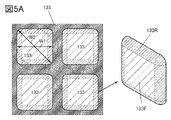
- FIG. 5A is a top view and a perspective view illustrating elements of the display device.
- FIG. 5B is a top view illustrating the elements of the display device.
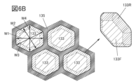
- 6A and 6B are top and perspective views illustrating elements of the display device.
- FIG. 7A and 7B are cross-sectional views illustrating elements of the display device.
- 8A to 8E are diagrams explaining the simulation model.
- FIG. 9 is a diagram for explaining simulation results.
- 10A and 10B are cross-sectional views illustrating elements of the display device.
- 11A and 11B are cross-sectional views illustrating elements of the display device.
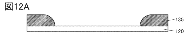
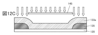
- 12A to 12F are cross-sectional views illustrating an example of a method for manufacturing a lens.
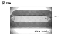
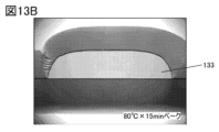
- 13A to 13C are cross-sectional SEM photographs illustrating the lens.
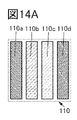
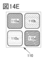
- 14A to 14K are diagrams illustrating examples of pixels.
- 15A and 15B are perspective views illustrating an example of a display device.
- FIG. 16 is a cross-sectional view illustrating an example of a display device.
- FIG. 17 is a cross-sectional view illustrating an example of a display device
- FIG. 18 is a cross-sectional view illustrating an example of a display device.
- FIG. 19 is a cross-sectional view illustrating an example of a display device;
- FIG. 20 is a perspective view illustrating an example of a display device;
- FIG. 21A is a cross-sectional view illustrating an example of a display device;
- 21B and 21C are cross-sectional views illustrating examples of transistors.
- 22A and 22B are cross-sectional views illustrating an example of a display device.
- 23A and 23B are cross-sectional views illustrating an example of a display device.
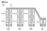
- 24A and 24B are cross-sectional views illustrating an example of a display device.
- 25A and 25B are cross-sectional views illustrating an example of a display device.
- 26A to 26C are diagrams illustrating configuration examples of display devices.
- 27A to 27D are diagrams illustrating examples of electronic devices.
- 28A to 28F are diagrams illustrating examples of electronic devices.
- 29A to 29G are diagrams illustrating examples of electronic devices.
- film and “layer” can be interchanged depending on the case or situation.
- conductive layer can be changed to the term “conductive film.”
- insulating film can be changed to the term “insulating layer”.
- a device manufactured using a metal mask or FMM may be referred to as a device with an MM (metal mask) structure.
- a device manufactured without using a metal mask or FMM may be referred to as a device with an MML (metal maskless) structure.
- holes or electrons are sometimes referred to as “carriers”.
- the hole injection layer or electron injection layer is referred to as a "carrier injection layer”
- the hole transport layer or electron transport layer is referred to as a “carrier transport layer”
- the hole blocking layer or electron blocking layer is referred to as a "carrier It is sometimes called a block layer.
- the carrier injection layer, the carrier transport layer, and the carrier block layer described above may not be clearly distinguished from each other due to their cross-sectional shape, characteristics, or the like.
- one layer may function as two or three of the carrier injection layer, the carrier transport layer, and the carrier block layer.
- a light-emitting device (also referred to as a light-emitting element) includes an EL layer between a pair of electrodes.
- the EL layer has at least a light-emitting layer.
- the layers (also referred to as functional layers) included in the EL layer include a light-emitting layer, a carrier-injection layer (a hole-injection layer and an electron-injection layer), a carrier-transport layer (a hole-transport layer and an electron-transport layer), and a carrier layer.
- a light-receiving device also referred to as a light-receiving element
- one of a pair of electrodes may be referred to as a common electrode and the other may be referred to as a pixel electrode.
- a tapered shape refers to a shape in which at least a part of the side surface of the structure is inclined with respect to the substrate surface. For example, it is preferable to have a region where the angle between the inclined side surface and the substrate surface (also referred to as a taper angle) is less than 90°. Note that the side surfaces of the structure and the substrate surface are not necessarily completely flat, and may be substantially planar with a fine curvature or substantially planar with fine unevenness.
- a mask layer is positioned above at least a light-emitting layer (more specifically, a layer processed into an island shape among layers constituting an EL layer) or an active layer. It has a function of protecting the light-emitting layer or the active layer during the process.
- the mask layer may be removed during the fabrication process, or at least a portion of the mask layer may remain.
- One embodiment of the present invention is a display device that has a light-emitting device and a light-receiving device that are separately manufactured for each emission color and is capable of full-color display and imaging operation.
- the light emitting device may be of a tandem type. By using a tandem light-emitting device, a highly reliable display device capable of high-luminance display can be obtained.
- each color light-emitting device for example, blue (B), green (G), and red (R)
- a structure in which at least light-emitting layers are separately formed or separately painted is referred to as SBS (side-by-side). Side) structure.
- SBS side-by-side
- Side Side structure.
- the SBS structure can optimize the materials and configuration for each light-emitting device, thus improving the brightness and reliability of the display device.
- island-shaped light-emitting layers with different emission colors are formed. Also in a light-receiving device, an active layer (a layer having a photoelectric conversion function) is formed in an island shape.
- an island shape indicates a state in which two or more layers using the same material formed in the same step are physically separated.
- an island-shaped light-emitting layer means that the light-emitting layer is physically separated from an adjacent light-emitting layer.
- the island-shaped light-emitting layer and active layer can be formed by a vacuum deposition method using a metal mask.
- the shape and formation position of the island-shaped light emitting layer may deviate from the design due to the effects of misalignment between the metal mask and the substrate, bending of the metal mask, and wraparound of the deposited material. . Therefore, the formation method using a metal mask is not suitable for achieving high definition and high aperture ratio of display devices.
- the manufacturing yield will be low due to low dimensional accuracy of the metal mask and deformation due to heat or the like.
- a light-emitting layer and an active layer are processed into fine patterns by a lithography step and an etching step. Specifically, after forming a pixel electrode for each sub-pixel, a film to be a light-emitting layer or an active layer is formed on the plurality of pixel electrodes. After that, the film is processed using a lithography process and an etching process to form one island-shaped light-emitting layer or active layer for one pixel electrode. Thereby, an island-shaped light-emitting layer or active layer can be formed for each sub-pixel. Note that in this specification and the like, a sub-pixel is sometimes simply referred to as a pixel.
- a functional layer is preferably provided between the light-emitting layer or active layer and the pixel electrode. Moreover, the functional layer is preferably processed into an island shape in the same pattern as that of the light-emitting layer or the active layer.
- the functional layer means, for example, a carrier injection layer, a carrier transport layer, or a carrier block layer, more specifically a hole injection layer, a hole transport layer, an electron block layer, or the like.
- the functional layer When the functional layer is used as a common layer between adjacent sub-pixels, lateral leak current may occur due to the functional layer.
- the functional layer is processed into an island shape in the same pattern as the light-emitting layer; Leakage current can be made extremely small.
- a light-emitting device and a light-receiving device that emit light of different colors
- some layers can be deposited in the same process.
- part of the EL layers included in the light-emitting device is formed in an island shape for each emission color.
- the active layer of the light-receiving device is formed in an island shape.
- the remaining layers (sometimes referred to as common layers) constituting the light-emitting device and the light-receiving device, and a common electrode (also referred to as an upper electrode) shared by the light-emitting device and the light-receiving device are formed.
- the common layer is a layer with relatively high conductivity. Therefore, when the common layer comes into contact with the side surface of a part of the EL layer formed like an island, the side surface of the active layer, or the side surface of the pixel electrode, there is a risk that the upper and lower layers in the light emitting device and the light receiving device will be short-circuited. There is Note that even when the common layer is provided in an island shape and the common electrode is formed in common for each color, the common electrode may cause a short circuit.
- the display device of one embodiment of the present invention includes an insulating layer covering at least side surfaces of the island-shaped light-emitting layer and the active layer.
- the insulating layer preferably covers part of the upper surface of each of the island-shaped light-emitting layer and the active layer.
- the end portion of the insulating layer preferably has a tapered shape with a taper angle of less than 90° in a cross-sectional view. This can prevent disconnection of the common layer and the common electrode provided on the insulating layer. Therefore, it is possible to suppress poor connection due to disconnection. In addition, it is possible to suppress an increase in electrical resistance due to local thinning of the common electrode due to a step.
- discontinuity refers to a phenomenon in which a layer, film, or electrode is divided due to the shape of a formation surface (for example, a step).
- the island-shaped light-emitting layer and active layer manufactured by the method for manufacturing a display device of one embodiment of the present invention are formed by processing a film that is formed over one surface. Therefore, it is possible to realize a high-definition display device or a display device with a high aperture ratio, which has hitherto been difficult to achieve. Furthermore, since the light-emitting layer of the light-emitting device can be separately formed for each color, a display device with extremely vivid, high contrast and luminance, and high display quality can be realized. Moreover, the light receiving device can capture a high-definition image.
- the display device of one embodiment of the present invention has convex lens structures over the light receiving device and the light emitting device.
- the structure on the light-receiving device and the light-emitting device By providing the structure on the light-receiving device and the light-emitting device, the light-receiving sensitivity of the light-receiving device and the efficiency of extracting light emitted from the light-emitting device to the outside can be enhanced.
- the width of the structure provided on the light-receiving device By making the width of the structure provided on the light-receiving device larger than the width of the light-receiving part, the light condensing ability can be enhanced, and the photosensitivity of the light-receiving device can be improved.
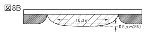
- the convex lens-shaped structure preferably has a substantially trapezoidal cross section.
- the width and thickness of the lens are proportional to each other, so it may not be arranged depending on the pixel size.
- part of the light reflected inside the structure tends to have a large incident angle. Therefore, the light is likely to be totally reflected and may not enter the light receiving device efficiently.
- a structure having a substantially trapezoidal cross section has a lens shape near the ends and a flat plate shape near the center. Therefore, the light entering near the edge of the opening can be refracted to enter the light receiving device. In addition, since the light reflected inside the structure has a relatively small incident angle, it is difficult to undergo total reflection and can effectively enter the light receiving device. Therefore, the photosensitivity of the light receiving device can be improved.
- part of the light emitted by the light emitting device may be blocked near the edge of the opening and not extracted to the outside.
- the light can be refracted and extracted to the outside. Therefore, the light extraction efficiency can be improved.
- the convex lens-like structure can be provided on both the light receiving device and the light emitting device, but may be provided on either the light receiving device or the light emitting device.
- the convex lens-shaped structure having a substantially trapezoidal cross section may be simply referred to as a lens, a trapezoidal lens, or a microlens.
- a microlens array MLA
- FIG. 1A shows a top view of a display device 100 with light-emitting and light-receiving devices.
- the display device 100 has a display section in which a plurality of pixels 110 are arranged.
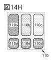
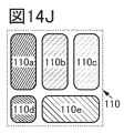
- FIG. 1A shows some sub-pixels, and shows an example in which a pixel 110 is composed of a plurality of equally-spaced sub-pixels (sub-pixels 110a, 110b, 110c, and 110d).
- the row direction is sometimes called the X direction
- the column direction is sometimes called the Y direction.
- the X and Y directions intersect and intersect perpendicularly or nearly perpendicularly (see FIG. 1A).
- the top surface shape of the sub-pixel shown in FIG. 1A corresponds to the top surface shape of the light emitting region or the light receiving region.
- the top surface shape of the sub-pixel may be a triangle, a quadrangle (including a rectangle and a square), a polygon such as a pentagon, a polygon with rounded corners, an ellipse, or a circle.
- the layout of the circuits included in the sub-pixels is not limited to the range of the sub-pixels shown in FIG. 1A, and may be arranged outside the sub-pixels.
- the transistors included in sub-pixel 110a may be located within sub-pixel 110b, or some or all may be located outside sub-pixel 110a.
- the aperture ratios of the sub-pixels 110a, 110b, 110c, and 110d can be determined as appropriate.
- the aperture ratios of the sub-pixels 110a, 110b, 110c, and 110d may be different, and two or more may be equal or substantially equal.
- a display device of one embodiment of the present invention includes a light-receiving device in a pixel.
- a light-receiving device in a pixel.
- three may have light-emitting devices and one may have a light-receiving device.
- the three sub-pixels can each have light emitting devices that emit different colors of light. For example, red (R), green (G), and blue (B) sub-pixels, and yellow (Y), cyan (C), and magenta (M) sub-pixels can be used.
- the sub-pixels 110a, 110b, and 110c each have a light-emitting device and the sub-pixel 110d has a light-receiving device 150 will be described.
- the light emitting device 130c included in the sub-pixel 110c will be described as an element constituting the light emitting device, common elements can also be applied to the light emitting devices included in the sub-pixels 110a and 110b.
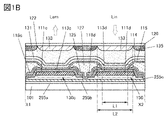
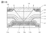
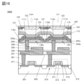
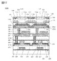
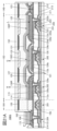
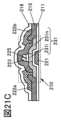
- FIG. 1B shows a cross-sectional view along the dashed-dotted line X1-X2 in FIG. 1A.
- an insulating layer is provided on the layer 101 containing the transistor, and a light emitting device 130c and a light receiving device 150 are provided on the insulating layer.
- a protective layer 131 is provided to cover the light emitting device 130 c and the light receiving device 150 .
- a lens 133 provided on a substrate 120 and a light shielding layer 135 are bonded onto the protective layer 131 via an adhesive layer 122 .
- the lens 133 is provided for each sub-pixel and has a region that overlaps with the light emitting device 130 c or the light receiving device 150 .
- a light shielding layer 135 is provided between adjacent lenses 133 .
- FIG. 1B shows an example in which the light Lem emitted by the light emitting device 130c is emitted to the substrate 120 side via the lens 133, and the light Lin entering from the substrate 120 side is incident on the light receiving device 150 via the lens 133.
- FIG. 1B shows an example in which the light Lem emitted by the light emitting device 130c is emitted to the substrate 120 side via the lens 133, and the light Lin entering from the substrate 120 side is incident on the light receiving device 150 via the lens 133.
- An insulating layer 125 and an insulating layer 127 on the insulating layer 125 are provided in a region between the adjacent light emitting device and the light receiving device 150 .
- insulating layers 125 and 127 are also provided in regions between adjacent light emitting devices.
- a display device of one embodiment of the present invention is a top emission type in which light is emitted in a direction opposite to a substrate over which a light-emitting device is formed.
- a layered structure including a plurality of transistors provided over a substrate and an insulating layer covering the transistors can be applied to the layer 101 including transistors.
- the insulating layer over the transistor may have a single-layer structure or a stacked-layer structure.
- FIG. 1B shows an insulating layer 255a, an insulating layer 255b over the insulating layer 255a, and an insulating layer 255c over the insulating layer 255b.
- various inorganic insulating films such as an oxide insulating film, a nitride insulating film, an oxynitride insulating film, and a nitride oxide insulating film can be preferably used.
- an oxide insulating film or an oxynitride insulating film such as a silicon oxide film, a silicon oxynitride film, or an aluminum oxide film is preferably used.
- a nitride insulating film or a nitride oxide insulating film such as a silicon nitride film or a silicon nitride oxide film is preferably used. More specifically, a silicon oxide film is preferably used for the insulating layers 255a and 255c, and a silicon nitride film is preferably used for the insulating layer 255b.
- the insulating layer 255b preferably functions as an etching protection film.
- oxynitride refers to a material whose composition contains more oxygen than nitrogen
- nitride oxide refers to a material whose composition contains more nitrogen than oxygen. point to the material.
- silicon oxynitride refers to a material whose composition contains more oxygen than nitrogen
- silicon nitride oxide refers to a material whose composition contains more nitrogen than oxygen. indicates
- the emission color of the light emitting device can be infrared, red, green, blue, cyan, magenta, yellow, white, or the like.
- color purity can be enhanced by providing a light-emitting device with a microcavity structure.
- the light-emitting device 130c can emit light of one of three colors, red (R), green (G), and blue (B), for example.
- the light emitting device it is preferable to use an OLED (Organic Light Emitting Diode) or a QLED (Quantum-dot Light Emitting Diode).
- OLED Organic Light Emitting Diode
- QLED Quadantum-dot Light Emitting Diode
- the light-emitting substance included in the light-emitting device include a substance that emits fluorescence (fluorescent material), a substance that emits phosphorescence (phosphorescent material), and a substance that exhibits thermally activated delayed fluorescence (thermally activated delayed fluorescence: TADF) material. ) and inorganic compounds (such as quantum dot materials).
- one electrode functions as a cathode and the other electrode functions as an anode.
- the case where the pixel electrode functions as an anode and the common electrode functions as a cathode may be taken as an example.
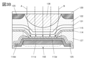
- the light emitting device 130c has a pixel electrode 111c on the insulating layer 255c, an island-shaped layer 113c on the pixel electrode 111c, a common layer 114 on the layer 113c, and a common electrode 115 on the common layer 114c.
- layer 113c and common layer 114 can be collectively referred to as EL layers.
- a single structure (structure having only one light emitting unit) or a tandem structure (structure having a plurality of light emitting units) may be applied to the light emitting device of this embodiment.
- the light-emitting unit has at least one light-emitting layer.
- layer 113c can have a light-emitting layer that emits red, green, or blue light.
- the layer 113c can have a plurality of light-emitting units that emit red, green, or blue light. Moreover, in order to emit white light, a tandem structure in which light emitting units emitting different colors are combined can be employed.
- Layer 113c may have one or more of a hole injection layer, a hole transport layer, a hole blocking layer, a charge generation layer, an electron blocking layer, an electron transport layer, and an electron injection layer.
- Layer 113c can have, for example, a hole-injection layer, a hole-transport layer, a light-emitting layer, and an electron-transport layer, in that order. Moreover, you may have an electron block layer between a hole transport layer and a light emitting layer. Further, a hole blocking layer may be provided between the electron transport layer and the light emitting layer. Moreover, you may have an electron injection layer on the electron transport layer.
- layer 113c can have an electron injection layer, an electron transport layer, an emissive layer, and a hole transport layer, in that order.
- a hole blocking layer may be provided between the electron transport layer and the light emitting layer.
- you may have an electron block layer between a hole transport layer and a light emitting layer.
- a hole injection layer may be provided on the hole transport layer.
- a light-emitting device with a tandem structure may have two or more light-emitting units in the layer 113c, and each light-emitting unit may include one or more light-emitting layers. Each light emitting unit may also have one or more of a hole injection layer, a hole transport layer, a hole blocking layer, an electron blocking layer, an electron transport layer, and an electron injection layer.
- a charge-generating layer (also referred to as an intermediate layer) is preferably provided between each light-emitting unit. The charge generation layer has at least a charge generation region.
- layer 113c can have a stacked structure of light-emitting unit 113_1, charge-generating layer 113_3, and light-emitting unit 113_2 (see the enlarged view of layer 113c in FIG. 1C). Note that in the drawings used in this embodiment mode, the charge generation layer may be indicated by a dashed line.
- the layer 113c can have a plurality of light-emitting units that emit light of the same color.
- both the light emitting unit 113_1 and the light emitting unit 113_2 can use the same type of light emitting unit that emits red, green, or blue light.
- a tandem structure in which light emitting units emitting different colors are combined can be employed.
- the light emitted from a plurality of light emitting units may be combined to obtain white light emission.
- one of the light emitting unit 113_1 and the light emitting unit 113_2 may be a blue light emitting unit, and the other may be a yellow light emitting unit.
- a light emitting unit emitting red light and a light emitting unit emitting cyan light may be combined.
- a light emitting unit emitting green light and a light emitting unit emitting magenta light may be combined.
- a configuration in which three light emitting units are combined may be employed.
- a configuration may be employed in which three light emitting units, a light emitting unit emitting blue light, a light emitting unit emitting yellow or yellowish green light, and a light emitting unit emitting blue light, are combined.
- a configuration may be employed in which three light emitting units, that is, a light emitting unit emitting blue light, a light emitting unit emitting yellow, yellow-green or green and red light, and a light emitting unit emitting blue light, are combined.
- the number of layers of light emitting units and the order of color from the anode side, a two-stage structure of B and Y, a two-stage structure of B and light-emitting unit X, a three-stage structure of B, Y, and B, and B, X, and B.
- the order of the number of layers of the light-emitting layers and the colors in the light-emitting unit X is, from the anode side, a two-layer structure of R and Y, a two-layer structure of R and G, and a two-layer structure of G and R. structure, a three-layer structure of G, R, and G, or a three-layer structure of R, G, and R, or the like.
- another layer may be provided between the two light-emitting layers.
- a tandem-type light-emitting device in which light is emitted from multiple light-emitting units, requires a relatively high voltage for light emission, but requires a smaller current value to obtain the same light-emitting intensity as a single-type light-emitting device (structure with one light-emitting unit). . Therefore, in the tandem structure, the current stress per light emitting unit can be reduced, and the device life can be extended. That is, by using a tandem light-emitting device, a highly reliable display device can be formed.
- the light-emitting unit 113_2 preferably has a light-emitting layer and a carrier-transporting layer (electron-transporting layer or hole-transporting layer) over the light-emitting layer.
- the light emitting unit 113_2 preferably has a light emitting layer and a carrier blocking layer (a hole blocking layer or an electron blocking layer) on the light emitting layer.
- the light emitting unit 113_2 preferably has a light emitting layer, a carrier blocking layer over the light emitting layer, and a carrier transport layer over the carrier blocking layer.
- the light-emitting unit 113_2 Since the surface of the light-emitting unit 113_2 is exposed during the manufacturing process of the display device, one or both of the carrier-transporting layer and the carrier-blocking layer are provided over the light-emitting layer to prevent the light-emitting layer from being exposed on the outermost surface. , the damage to the light-emitting layer can be reduced. This can improve the reliability of the light emitting device.
- the light-emitting unit provided in the uppermost layer preferably has a light-emitting layer and one or both of a carrier transport layer and a carrier block layer over the light-emitting layer.
- tandem light emitting device The configuration and materials of the tandem light emitting device are detailed in other embodiments.
- the common layer 114 can have an electron injection layer or a hole injection layer. Alternatively, the common layer 114 may have a laminate of an electron transport layer and an electron injection layer, or may have a laminate of a hole transport layer and a hole injection layer. A common layer 114 and a common electrode 115 are shared by the light emitting device of each sub-pixel.
- layer 113c is formed to cover the edge of pixel electrode 111c.
- a mask layer 118c is located on the layer 113c included in the light emitting device 130c. The mask layer 118c is part of the remaining mask layer provided in contact with the upper surface of the layer 113c when the layer 113c is processed.
- one edge of mask layer 118c is aligned or nearly aligned with an edge of layer 113c, and the other edge of mask layer 118c is located on layer 113c.
- the other end of the mask layer 118c preferably overlaps the layer 113c and the pixel electrode 111c.
- the sides of layer 113c are covered with insulating layer 125 .
- the insulating layer 127 overlaps with the side surface of the layer 113c with the insulating layer 125 interposed therebetween.
- a portion of the upper surface of layer 113c is also covered with mask layer 118c. Insulating layer 125 and insulating layer 127 partially overlap with the upper surface of layer 113c via mask layer 118c. Note that the upper surface of the layer 113c is not limited to the upper surface of the flat portion overlapping the upper surface of the pixel electrode, and can include the upper surface of the inclined portion and the flat portion located outside the upper surface of the pixel electrode.
- a portion of the top surface and side surfaces of layer 113c are covered with at least one of insulating layer 125, insulating layer 127, and mask layer 118c, so that common layer 114 (or common electrode 115) is formed from pixel electrodes 111c, 111c, and 118c. and contact with the side surface of the layer 113c. Therefore, short circuits between upper and lower layers of the light emitting device can be suppressed.
- the insulating layer 127 is provided on the insulating layer 125 so as to fill the recess in which the insulating layer 125 is formed.
- the insulating layer 127 can overlap with part of the top surface and side surfaces of the layer 113c with the insulating layer 125 provided therebetween.
- the insulating layer 127 preferably covers at least part of the side surfaces of the insulating layer 125 .
- the space between the adjacent island-shaped layers can be filled; can reduce the extreme unevenness of the surface and make it more flat. Therefore, coverage of the carrier injection layer, the common electrode, and the like can be improved.
- Common layer 114 and common electrode 115 are provided on layer 113 c , mask layer 118 c , insulating layer 125 and insulating layer 127 . Before the insulating layer 125 and the insulating layer 127 are provided, a region where the pixel electrode and the island-shaped EL layer are provided, a region where the pixel electrode and the island-shaped EL layer are not provided (region between the light emitting devices), There is a step due to
- the step can be planarized, and coverage with the common layer 114 and the common electrode 115 can be improved. Therefore, it is possible to suppress poor connection due to disconnection. In addition, it is possible to prevent the common electrode 115 from being locally thinned due to the steps and increasing the electrical resistance.
- the top surface of the insulating layer 127 preferably has a highly flat shape, but may have a convex portion, a convex curved surface, a concave curved surface, or a concave portion.
- FIG. 1B shows an example in which the upper surface of the insulating layer 127 has a flat portion, but as shown in FIG. 2A, the entire upper surface of the insulating layer 127 may have a convex curved surface. Alternatively, as shown in FIG. 2B, the upper surface of the insulating layer 127 may have a concave surface.
- the upper surface of insulating layer 127 has a shape that gently bulges from the ends toward the center, that is, a convex surface, and has a shape that is depressed at and near the center, that is, a concave surface. Also, in FIG.
- the convex curved surface portion of the upper surface of the insulating layer 127 has a shape that is smoothly connected to the tapered portion at the end portion. Even if the insulating layer 127 has such a shape, the common layer 114 and the common electrode 115 can be formed on the entire insulating layer 127 with good coverage.
- the stress of the insulating layer 127 can be relieved by providing the insulating layer 127 with a concave curved surface in the central portion. More specifically, the insulating layer 127 has a concave curved surface at its central portion, thereby relieving local stress generated at the end portion of the insulating layer 127 and reducing the stress between the layer 113c and the mask layer 118c. Any one or more of film peeling, film peeling between the mask layer 118c and the insulating layer 125, and film peeling between the insulating layer 125 and the insulating layer 127 can be suppressed.
- the common layer 114 and the common electrode 115 can be formed with high coverage. In addition, it is possible to prevent the formation of portions divided by the common layer 114 and the common electrode 115 and portions where the film thickness is locally thin.
- the display quality of the display device according to one embodiment of the present invention can be improved.
- Insulating layer 125 can be an insulating layer comprising an inorganic material.
- an inorganic insulating film such as an oxide insulating film, a nitride insulating film, an oxynitride insulating film, or a nitride oxide insulating film can be used.
- the insulating layer 125 may have a single-layer structure or a laminated structure.
- the oxide insulating film includes a silicon oxide film, an aluminum oxide film, a magnesium oxide film, an indium gallium zinc oxide film, a gallium oxide film, a germanium oxide film, an yttrium oxide film, a zirconium oxide film, a lanthanum oxide film, a neodymium oxide film, and an oxide film.
- a hafnium film, a tantalum oxide film, and the like are included.
- the nitride insulating film include a silicon nitride film and an aluminum nitride film.
- Examples of the oxynitride insulating film include a silicon oxynitride film, an aluminum oxynitride film, and the like.
- nitride oxide insulating film examples include a silicon nitride oxide film, an aluminum nitride oxide film, and the like.
- aluminum oxide is preferable because it has a high etching selectivity with respect to the EL layer and has a function of protecting the EL layer during formation of the insulating layer 127 described later.
- an inorganic insulating film such as an aluminum oxide film, a hafnium oxide film, or a silicon oxide film formed by an atomic layer deposition (ALD) method to the insulating layer 125
- ALD atomic layer deposition
- An insulating layer 125 having an excellent protective function can be formed.
- the insulating layer 125 may have a layered structure of a film formed by an ALD method and a film formed by a sputtering method.
- the insulating layer 125 may have a laminated structure of, for example, an aluminum oxide film formed by ALD and a silicon nitride film formed by sputtering.
- the insulating layer 125 preferably functions as a barrier insulating layer against at least one of water and oxygen. Insulating layer 125 preferably has a function of suppressing diffusion of at least one of water and oxygen. Further, the insulating layer 125 preferably has a function of capturing or fixing at least one of water and oxygen (also referred to as gettering).
- a barrier insulating layer means an insulating layer having a barrier property.
- barrier property refers to a function of suppressing diffusion of a corresponding substance (also referred to as low permeability).
- the corresponding substance has a function of capturing or fixing (also called gettering).
- the insulating layer 125 has a function as a barrier insulating layer or a gettering function, thereby suppressing entry of impurities (typically, at least one of water and oxygen) that can diffuse into each light-emitting device from the outside. is possible. With such a structure, a highly reliable light-emitting device and a highly reliable display device can be provided.
- impurities typically, at least one of water and oxygen
- the same material can be used for the insulating layer 125 and the mask layer 118c.
- the boundary between the mask layer 118c and the insulating layer 125 becomes unclear, and the mask layer 118c and the insulating layer 125 may be recognized as one layer.
- the insulating layer 127 provided on the insulating layer 125 has a function of planarizing extreme irregularities of the insulating layer 125 formed between adjacent light emitting devices.
- an insulating layer containing an organic material can be preferably used.
- the organic material it is preferable to use a photosensitive organic resin, and for example, a photosensitive resin composition containing an acrylic resin is used.
- acrylic resin does not only refer to polymethacrylate esters or methacrylic resins, but may refer to all acrylic polymers in a broad sense.
- an acrylic resin, a polyimide resin, an epoxy resin, an imide resin, a polyamide resin, a polyimideamide resin, a silicone resin, a siloxane resin, a benzocyclobutene-based resin, a phenolic resin, precursors of these resins, or the like is used.
- an organic material such as polyvinyl alcohol (PVA), polyvinyl butyral, polyvinylpyrrolidone, polyethylene glycol, polyglycerin, pullulan, water-soluble cellulose, or alcohol-soluble polyamide resin may be used as the insulating layer 127 .
- a photoresist may be used as the photosensitive resin.
- the photosensitive organic resin either a positive material or a negative material may be used.
- a material that absorbs visible light may be used for the insulating layer 127 . Since the insulating layer 127 absorbs light emitted from the light emitting device, leakage of light (stray light) from the light emitting device to the adjacent light emitting device or light receiving device via the insulating layer 127 can be suppressed. Thereby, the display quality and imaging performance of the display device can be improved. In addition, since the display quality can be improved without using a polarizing plate for the display device, the weight and thickness of the display device can be reduced.
- Materials that absorb visible light include materials containing pigments such as black, materials containing dyes, light-absorbing resin materials (e.g., polyimide), and resin materials that can be used for color filters (color filter materials). is mentioned.
- resin material obtained by laminating or mixing color filter materials of two colors or three or more colors, because the effect of shielding visible light can be enhanced.
- color filter materials it is possible to obtain a black or nearly black resin layer.
- the light receiving device 150 will be described. Description of elements common to the light emitting device 130c and elements having a common purpose will be omitted.
- a pn-type or pin-type photodiode can be used as the light receiving device.
- a light-receiving device functions as a photoelectric conversion device (also referred to as a photoelectric conversion element) that detects light incident on the light-receiving device and generates an electric charge. The amount of charge generated from the light receiving device is determined based on the amount of light incident on the light receiving device.
- the light receiving device can detect one or both of visible light and infrared light. When infrared light is detected, it is possible to detect objects even in dark places.
- an organic photodiode having a layer containing an organic compound is preferably used.
- Organic photodiodes can be easily made thinner, lighter, and larger, and have a high degree of freedom in shape and design, so they can be applied to various display devices.
- an organic EL device is used as the light-emitting device and an organic photodiode is used as the light-receiving device.
- An organic EL device and an organic photodiode can be formed on the same substrate. Therefore, an organic photodiode can be incorporated in a display device using an organic EL device.
- the light-receiving device can be driven by applying a reverse bias between the pixel electrode and the common electrode, thereby detecting light incident on the light-receiving device, generating electric charge, and extracting it as a current.
- a manufacturing method similar to that for the light-emitting device can also be applied to the light-receiving device.
- the island-shaped active layer (also called photoelectric conversion layer) of the light receiving device is not formed using a fine metal mask, but is formed by forming a film that will become the active layer over the surface and then processing it. Therefore, the island-shaped active layer can be formed with a uniform thickness. Further, by providing the mask layer over the active layer, the damage to the active layer during the manufacturing process of the display device can be reduced, and the reliability of the light-receiving device can be improved.
- the light receiving device 150 has a pixel electrode 111d on the insulating layer 255c, a layer 113d on the pixel electrode 111d, a common layer 114 on the layer 113d, and a common electrode 115 on the common layer 114.
- layer 113d includes at least an active layer and preferably has a plurality of functional layers.
- functional layers include carrier transport layers (hole transport layer and electron transport layer) and carrier block layers (hole block layer and electron block layer).
- the layer 113d is a layer provided in the light receiving device 150 and not provided in the light emitting device 130c.
- the functional layers other than the active layer contained in layer 113d may have the same material as the functional layers other than the light-emitting layer contained in layer 113c.
- Common layer 114 is a sequence of layers shared by light receiving device 150 and light emitting device 130c.
- a layer shared by the light-receiving device and the light-emitting device may have different functions in the light-emitting device and in the light-receiving device. Components are sometimes referred to herein based on their function in the light emitting device.
- a hole-injecting layer functions as a hole-injecting layer in light-emitting devices and as a hole-transporting layer in light-receiving devices.
- an electron-injecting layer functions as an electron-injecting layer in light-emitting devices and as an electron-transporting layer in light-receiving devices.
- a layer shared by the light-receiving device and the light-emitting device may have the same function in the light-emitting device as in the light-receiving device.
- a hole-transporting layer functions as a hole-transporting layer in both light-emitting and light-receiving devices
- an electron-transporting layer functions as an electron-transporting layer in both light-emitting and light-receiving devices.
- mask layer 118c Between layer 113c and insulating layer 125 is mask layer 118c, and between layer 113d and insulating layer 125 is mask layer 118d.
- the mask layer 118c is part of the mask layer provided on the layer 113c when the layer 113c is processed.
- the mask layer 118d is part of the remaining mask layer provided in contact with the upper surface of the layer 113d when the layer 113d including the active layer is processed.
- Mask layer 118c and mask layer 118d may have the same material or may have different materials.
- the sub-pixel 110d may have a higher aperture ratio than at least one of the sub-pixels 110a, 110b, and 110c.
- a wide light receiving area of the sub-pixel 110d may make it easier to detect an object.
- the aperture ratio of the sub-pixel 110d may be higher than the aperture ratios of the other sub-pixels depending on the definition of the display device, the circuit configuration of the sub-pixels, and the like.
- the sub-pixel 110d may have a lower aperture ratio than at least one of the sub-pixels 110a, 110b, and 110c. By lowering the aperture ratio of the sub-pixel 110d, the pinhole effect can be enhanced and a clearer image can be obtained.
- the sub-pixel 110d preferably changes the detection wavelength, definition, and aperture ratio depending on the application.
- the protective layer 131 provided on the light-emitting device 130c and the light-receiving device 150 may have a single-layer structure or a laminated structure of two or more layers. By providing the protective layer 131, the reliability of the light emitting device 130c and the light receiving device 150 can be improved.
- the conductivity of the protective layer 131 does not matter. At least one of an insulating film, a semiconductor film, and a conductive film can be used as the protective layer 131 .
- the protective layer 131 has an inorganic film, deterioration of the light-emitting device and the light-receiving device can be prevented by preventing oxidation of the common electrode 115, suppressing impurities (such as moisture and oxygen) from entering the light-emitting device and the light-receiving device, and the like. can be suppressed, and the reliability of the display device can be improved.
- an inorganic insulating film such as an oxide insulating film, a nitride insulating film, an oxynitride insulating film, or a nitride oxide insulating film can be used. Specific examples of these inorganic insulating films are as described for the insulating layer 125 .
- the protective layer 131 preferably includes a nitride insulating film or a nitride oxide insulating film, and more preferably includes a nitride insulating film.
- the protective layer 131 includes In—Sn oxide (also referred to as ITO), In—Zn oxide, Ga—Zn oxide, Al—Zn oxide, or indium gallium zinc oxide (In—Ga—Zn oxide).
- ITO In—Sn oxide
- In—Zn oxide Ga—Zn oxide
- Al—Zn oxide Al—Zn oxide
- indium gallium zinc oxide In—Ga—Zn oxide
- An inorganic film containing a material such as IGZO can also be used.
- the inorganic film preferably has a high resistance, and specifically, preferably has a higher resistance than the common electrode 115 .
- the inorganic film may further contain nitrogen.
- the protective layer 131 preferably has high transparency to visible light.
- ITO, IGZO, and aluminum oxide are each preferred because they are inorganic materials that are highly transparent to visible light.
- the protective layer 131 for example, a stacked structure of an aluminum oxide film and a silicon nitride film over the aluminum oxide film, or a stacked structure of an aluminum oxide film and an IGZO film over the aluminum oxide film, or the like can be used. can be done. By using the stacked-layer structure, impurities (such as water and oxygen) entering the EL layer can be suppressed.
- the protective layer 131 may have an organic film.
- the protective layer 131 may have both an organic film and an inorganic film.
- an organic material that can be used for the protective layer 131 an organic insulating material that can be used for the insulating layer 127, or the like can be given.
- the protective layer 131 may have a two-layer structure formed using different film formation methods. Specifically, the first layer of the protective layer 131 may be formed using the ALD method, and the second layer of the protective layer 131 may be formed using the sputtering method.
- a lens 133 provided on a substrate 120 and a light shielding layer 135 are bonded onto the protective layer 131 via an adhesive layer 122 .
- the lens 133 is provided for each sub-pixel, and the light emitting device 130 c and the light receiving device 150 each have a region overlapping the lens 133 .
- a light shielding layer 135 is provided between adjacent lenses 133 .
- the light shielding layer 135 has a region overlapping with the insulating layer 127 .
- Lens 133 can be made of the same material as insulating layer 127 .
- the light blocking layer 135 can be formed of a metal material, a resin material containing a material that absorbs visible light, or the like.
- the width (L2) of the lens 133 provided on the light receiving device 150 is larger than the width (L1) of the light receiving portion of the light receiving device 150 .
- the light receiving portion is a region where the layer 113d and the common layer 114 are in contact with each other. When the common layer 114 is not provided, the region where the layer 113d and the common electrode 115 are in contact is used.
- the width of the lens and the light-receiving part refers to the diameter of the inscribed circle, the diameter of the circumscribed circle, the diameter of the circumscribed circle, the length of the opposite sides, or the length of the diagonal (the corners are rounded).
- the definition of the width is the same for pinholes (openings), which will be described later.
- a specific example of the width of the lens will be described later with reference to FIGS. 5A, 6A, and 6B.
- the lens provided on the light receiving device 150 will be described with reference to cross-sectional views of FIGS. 3A to 5B. Note that the lens and the light receiving device 150 are spaced apart so that their centers overlap each other.
- a lens is generally considered as the element, but it is difficult to secure a sufficient area for providing the lens between the surface of the substrate 120 and the light receiving device. Therefore, it is difficult to provide a lens for concentrating light rays and forming an image.
- the pinhole is formed by providing an opening in the light shielding layer 135 .
- the pinhole is for reducing the amount of light, but it causes a decrease in photosensitivity due to insufficient light.
- FIG. 3A is a comparative example in which no lens is provided, and is a diagram simply showing light rays incident on the light receiving device. Note that minute reflections at boundaries between layers are not shown.
- the light shielding layer 135 Most of the light that obliquely irradiates the substrate 120 is blocked by the light shielding layer 135 . Therefore, most of the light incident on the light-receiving device 150 is light that travels straight or nearly straight. However, if the width of the pinhole (aperture) is larger than the width of the light receiving section, part of the light may not enter the light receiving section as indicated by the rays A and B in FIG. 3A.
- a lens 136 in the pinhole (aperture) it is preferable to provide a lens 136 in the pinhole (aperture) to refract the light rays A and B so as to enter the light receiving section.
- a hemispherical or nearly hemispherical lens (hereinafter abbreviated as a hemispherical lens) requires a height approximately half the width of the subpixel, there is a limit to the size of the subpixel that can be applied.
- the distance between the protective layer 131 and the substrate 120 is about several ⁇ m regardless of the size of the display device. Therefore, the width of a sub-pixel that can reasonably use a hemispherical lens is about twice the thickness of the adhesive layer 122 (10 and several ⁇ m or less) at maximum. That is, it becomes difficult to apply a hemispherical lens to a display device having larger sub-pixels.
- the lens can be formed by applying a photosensitive resin or the like, it is also difficult to apply the photosensitive resin to a thickness of ten and several ⁇ m or more. For example, in a display device that is larger than a smartphone, the width of a sub-pixel may be ten and several ⁇ m or more even if the display device has high definition, which makes it difficult to use a hemispherical lens.
- the substantially trapezoidal lens is a lens having a substantially trapezoidal cross-sectional shape in the thickness direction including the center of the lens or a substantially trapezoidal cross-sectional shape including the central axis (optical axis) of the lens.
- the surface including the portions corresponding to the legs of the trapezoid has a convex curved surface, or the surface including the portions corresponding to the legs and the surface including the portion corresponding to the upper base have a convex curved surface.
- a surface including a portion corresponding to the upper base of the trapezoid and a surface including a portion corresponding to the lower base of the trapezoid each have a flat surface. It may also have a shape in which these two faces are parallel.
- the substantially trapezoidal lens has a substantially frustum shape and has an upper base surface, a lower base surface, and a cone surface, and the cone surface has a convex curved surface, or the convex surface extends from the cone surface to the upper base surface. It can also be said that the lens has
- the area near the end of the lens 133 acts as a convex lens, refracts the light that is incident on the area in a straight line, and can change the direction of travel.
- the light that enters the other area (flat portion) of the lens 133 in a straight line travels straight without changing its traveling direction.
- the lens 133 can also refract the light rays A and B to enter the light receiving section.
- the light that is incident on the center of the lens 133 and its vicinity can be incident on the light receiving portion by traveling straight.
- the substantially trapezoidal lens 133 can also be said to be a kind of plano-convex lens.
- FIG. 5A illustrates a plan view and a perspective view of lens 133 .
- FIG. 5A shows a lens shape corresponding to the pixel array shown in FIG. 1A, which is substantially rectangular when viewed from above.
- the width of the lens can be defined as the diameter W1 of the inscribed circle or the diameter W2 of the circumscribed circle shown in FIG. 5A.
- the lens 133 has a convex surface region 133R near the ends and a planar region 133F at and near the center. As described above, the convex curved region 133R acts as a lens.
- FIG. 6A is a plan view and a perspective view showing an example of a lens that is circular in top view.
- the diameter W1 of the circle can be defined as the width of the lens.
- FIG. 6B is a plan view and a perspective view showing an example of a lens that can be applied to the delta arrangement and has a substantially hexagonal top view.
- the lengths (W1, W2) between opposite sides or the lengths (W3, W4) corresponding to the diagonals can be defined as the width of the lens.
- FIG. 5A shows an example in which the light shielding layer 135 is provided around the lenses provided for all sub-pixels, but the light shielding layer 135 may be provided around only some of the sub-pixels.
- a light shielding layer 135 can be provided only around a sub-pixel having a light receiving device (corresponding to the sub-pixel 110d in FIG. 1).
- the configuration shown in FIG. 5B can also be applied to FIGS. 6A and 6B.
- the region corresponding to the upper base of the trapezoid is shown as a flat surface, but it may have a slightly convex curved surface.
- FIG. 4A shows an example in which the upper side of the lens 133 is formed to face the light receiving device, but as shown in FIG. 4B, the lower side of the lens 133 is formed to face the light receiving device. good too.
- a planarization film 137 is formed on the protective layer 131 and a lens 133 is formed on the planarization film 137 .
- the substrate 120 with the light shielding layer 135 formed thereon may be bonded with the adhesive layer 122 interposed therebetween.
- FIG. 4A shows a configuration in which the light shielding layer 135 and the lens 133 do not overlap. good too.
- a configuration may be employed in which a region in which the light shielding layer 135 overlaps the end portion of the lens 133 is provided.
- FIG. 8A shows a typical configuration of the light receiving device and peripheral elements used in the simulation.
- the protective layer 131 is omitted in the model of this simulation.
- the common electrode is made up of two layers of the translucent conductive film 115a and the semi-reflective electrode 115b.
- the thickness T of the lens is 2 ⁇ m
- the distance from the translucent conductive film 115a to the substrate 120) was set to 10 ⁇ m.
- the light source was installed on the upper surface of the substrate 120 (thickness: 300 ⁇ m). Table 1 shows the material, refractive index, reflectance, and absorptance of other elements used in the simulation.
- the models used in the simulations were a configuration with a planar area in the lens 133 shown in FIG. 8A, a configuration without the lens shown in FIG. 3A, and a configuration with a hemispherical lens 136 shown in FIG.
- the configuration shown in FIG. In FIGS. 8B to 8E the heights of the convex surfaces added to the plane regions of the lens 133 are 0.5 ⁇ m, 1 ⁇ m, 2 ⁇ m, and 3 ⁇ m, respectively.
- the ratios of the width of the reference plane region to the height of the convex curved surface (hereinafter referred to as aspect ratio) are 5%, 10%, 20% and 30%, respectively.
- FIG. 9 shows the simulation result of the amount of light received in the light receiving section using these models, and shows the amount of light received as a relative value with 1 for no lens.
- Lighting SimulatorCAD manufactured by Best Media was used as simulation software.
- the amount of light received by the light emitting device using the substantially trapezoidal lens 133 is the largest. It should be noted that the amount of light received by a substantially trapezoidal lens having a planar portion (FIG. 5A) and a configuration with an aspect ratio of 5% to 20% (FIGS. 8B to 8D) are almost the same. , the amount of received light tends to decrease when the aspect ratio exceeds 30%.
- the interface between the lens 136 and the adhesive layer 122 is mostly flat. Therefore, most of the light incident on the lens 133 does not increase the incident angle ⁇ 2 with respect to the interface. Therefore, the light travels toward the light receiving section without undergoing total reflection.
- lenses having aspect ratios of 5% to 20% are also considered to be less likely to increase the incident angle ⁇ 2.
- the amount of light received by the light receiving portion is greater when the substantially trapezoidal lens 133 is used than when the hemispherical lens 136 is used. Also, it can be said that it is effective to use a substantially trapezoidal lens regardless of the size of the sub-pixel. In addition, even lenses with an aspect ratio of up to 20% can receive an excellent amount of light. It can be said that there is an excellent effect.
- the substantially trapezoidal lens 133 is provided on the light-emitting device 130c, which also has the effect of increasing the light extraction efficiency. Note that the lens 133 and the light emitting device 130c are spaced apart so that their centers overlap each other.
- the width of the lens 133 provided on the light emitting device 130c is larger than the width of the light emitting portion of the light emitting device 130c.
- the light emitting portion is a region where the layer 113c and the common layer 114 are in contact with each other. When the common layer 114 is not provided, the region where the layer 113c and the common electrode 115 are in contact is used.
- the width of the lens is the same as the width of the lens shown in FIGS. 5A, 6A, and 6B.
- FIG. 11A and 11B are diagrams illustrating part of the light beam emitted by the light emitting device 130c.
- FIG. 11A is a comparative example without a lens
- FIG. 11B is an example with a lens 133 .
- the substantially trapezoidal lens 133 provided on the light emitting device 130c can have the same configuration as the substantially trapezoidal lens 133 provided on the light receiving device 150 described above.
- the light shielding layer 135 When the light shielding layer 135 is provided, part of the light emitted obliquely from the light emitting device 130c is blocked by the light shielding layer 135 and cannot be emitted to the outside.
- the lens 133 when the lens 133 is provided, even light that is blocked in FIG. Therefore, by providing the substantially trapezoidal lens 133, the light extraction efficiency can be enhanced. That is, a high-luminance display device can be formed.
- optical members can be arranged outside the substrate 120 .
- optical members include polarizing plates, retardation plates, light diffusion layers (diffusion films, etc.), antireflection layers, and light-condensing films.
- an antistatic film that suppresses adhesion of dust a water-repellent film that prevents adhesion of dirt, a hard coat film that suppresses the occurrence of scratches due to use, a shock absorption layer, etc. Layers may be arranged.
- the surface protective layer By providing a glass layer or a silica layer (SiO x layer) as the surface protective layer, surface contamination and scratching can be suppressed, which is preferable.
- the surface protective layer DLC (diamond-like carbon), aluminum oxide (AlO x ), polyester-based material, polycarbonate-based material, or the like may be used.
- a material having a high visible light transmittance is preferably used for the surface protective layer.
- Glass, quartz, ceramics, sapphire, resin, metal, alloy, semiconductor, or the like can be used for the substrate 120 .
- a material that transmits the light is used for the substrate on the side from which the light from the light-emitting device is extracted.
- Using a flexible material for the substrate 120 can increase the flexibility of the display device.
- a polarizing plate may be used as the substrate 120 .
- polyester resins such as polyethylene terephthalate (PET) and polyethylene naphthalate (PEN), polyacrylonitrile resins, acrylic resins, polyimide resins, polymethyl methacrylate resins, polycarbonate (PC) resins, and polyethersulfone (PES) resins.
- polyamide resin nylon, aramid, etc.
- polysiloxane resin cycloolefin resin
- polystyrene resin polyamideimide resin
- polyurethane resin polyvinyl chloride resin
- polyvinylidene chloride resin polypropylene resin
- PTFE polytetrafluoroethylene
- ABS resin cellulose nanofiber, etc.
- glass having a thickness that is flexible may be used.
- a substrate having high optical isotropy is preferably used as the substrate of the display device.
- a substrate with high optical isotropy has small birefringence (it can be said that the amount of birefringence is small).
- the absolute value of the retardation (retardation) value of the substrate with high optical isotropy is preferably 30 nm or less, more preferably 20 nm or less, and even more preferably 10 nm or less.
- Films with high optical isotropy include triacetyl cellulose (TAC, also called cellulose triacetate) films, cycloolefin polymer (COP) films, cycloolefin copolymer (COC) films, acrylic films, and the like.
- TAC triacetyl cellulose
- COP cycloolefin polymer
- COC cycloolefin copolymer
- the film when a film is used as the substrate, the film may absorb water, which may cause shape change such as wrinkles in the display device. Therefore, it is preferable to use a film having a low water absorption rate as the substrate. For example, it is preferable to use a film with a water absorption of 1% or less, more preferably 0.1% or less, and even more preferably 0.01% or less.
- various curable adhesives such as photocurable adhesives such as ultraviolet curable adhesives, reaction curable adhesives, thermosetting adhesives, and anaerobic adhesives can be used.
- These adhesives include epoxy resins, acrylic resins, silicone resins, phenol resins, polyimide resins, imide resins, PVC (polyvinyl chloride) resins, PVB (polyvinyl butyral) resins, EVA (ethylene vinyl acetate) resins, and the like.
- a material with low moisture permeability such as epoxy resin is preferable.
- a two-liquid mixed type resin may be used.
- an adhesive sheet or the like may be used.
- an island-shaped EL layer is provided for each light-emitting device, so that leakage current between subpixels can be suppressed. Thereby, crosstalk due to unintended light emission can be prevented, and a display device with extremely high contrast can be realized.
- an insulating layer having a tapered end portion between adjacent island-shaped EL layers it is possible to suppress the occurrence of discontinuity during formation of the common electrode. As a result, it is possible to suppress connection failure caused by the divided portions in the common layer and the common electrode. Therefore, the display device of one embodiment of the present invention can achieve both high definition and high display quality.
- a substantially trapezoidal lens is provided over the light-receiving device and the light-emitting device included in the display device of one embodiment of the present invention.
- the light-receiving device can efficiently receive the light incident on the pinhole (opening) at the light-receiving part, and the light-receiving sensitivity can be improved.
- the light emitted toward the end of the light-shielding layer can be refracted by the lens and emitted to the outside, and the light extraction efficiency can be improved.
- Embodiment 2 In this embodiment, a method for manufacturing a lens included in a display device of one embodiment of the present invention will be described. Note that Embodiment 1 can be referred to for the description of the constituent materials of each element.
- FIG. 12A to 12F are diagrams for explaining the manufacturing process of the lens 133 formed over the substrate 120.
- the light shielding layer 135 is formed on the substrate 120 (see FIG. 12A).
- a light-shielding metal film having a thickness is formed over the substrate 120, and a resist mask is formed over the metal film by a photolithography process.
- the light shielding layer 135 having a desired shape can be formed.
- the light shielding layer 135 may be formed by applying a photosensitive resin, partially exposing the photosensitive resin, and performing a developing process.
- a resin layer 133a is formed by applying a photosensitive resin onto the substrate 120 and the light shielding layer 135 and performing prebaking (see FIG. 12B).
- a photosensitive resin for example, the material for forming the insulating layer 127 described in Embodiment 1 can be used.
- a negative photosensitive resin may be used.
- a photomask 145 is used to shield the region where the lens 133 is to be formed, and the resin layer 133a is exposed (see FIG. 12C).
- a photomask is used for shielding the region where the lens 133 is not formed.
- a developing process is performed to remove unnecessary regions of the resin layer 133a to form a resin layer 133b (see FIG. 12D).
- the resin layer 133b since the resin layer 133b has not been exposed to light, unreacted components remain and may be colored. Since the lens 133 to be formed preferably has a high transmittance to visible light, the resin layer 133b is exposed to light to accelerate the reaction when the lens is colored.
- a resin layer 133c with improved transmittance can be formed (see FIG. 12E). Further, by performing such exposure after the developing process, the post-baking temperature of the resin layer 133c in the subsequent process may be lowered. In addition, when the resin layer 133b is not colored, the exposure after the development process may be unnecessary.
- post-baking is performed to reflow and harden the resin layer 133c to form the lens 133 (FIG. 12F).
- the degree of deformation of the resin layer 133c can be varied depending on the post-baking temperature.
- 13A to 13C are SEM photographs showing the cross-sectional shape of the lens 133 completed by changing the post-baking temperature.
- the resin layer 133c cannot be sufficiently reflowed, and the vicinity of the end of the resin layer 133c is not deformed to have a curved surface and does not form a lens.
- the post-baking temperature is appropriate (80° C. ⁇ 15 minutes, see FIG. 13B)
- the resin layer 133c is deformed such that the central portion of the resin layer 133c is substantially flat and the vicinity of the end portion thereof has a curved surface.
- a shaped lens 133 is obtained.
- the post-baking temperature is high (100° C. ⁇ 15 minutes, see FIG. 13C)
- the deformation of the resin layer 133c becomes excessive, resulting in a hemispherical shape instead of a trapezoidal shape. Therefore, it is preferable to post-bake at an appropriate temperature.
- the arrangement of sub-pixels includes, for example, a stripe arrangement, an S-stripe arrangement, a matrix arrangement, a delta arrangement, a Bayer arrangement, and a pentile arrangement.
- the top surface shape of the sub-pixel shown in the drawings in this embodiment mode corresponds to the top surface shape of the light emitting region or the light receiving region.
- top surface shapes of sub-pixels include triangles, quadrilaterals (including rectangles and squares), polygons such as pentagons, polygons with rounded corners, ellipses, and circles.
- circuit layout forming the sub-pixels is not limited to the range of the sub-pixels shown in the drawing, and may be arranged outside the sub-pixels.
- a stripe arrangement is applied to the pixels 110 shown in FIGS. 14A to 14C.
- FIG. 14A is an example in which each sub-pixel has a rectangular top surface shape
- FIG. 14B is an example in which each sub-pixel has a top surface shape connecting two semicircles and a rectangle
- FIG. This is an example where the sub-pixel has an elliptical top surface shape.
- a matrix arrangement is applied to the pixels 110 shown in FIGS. 14D to 14F.
- FIG. 14D is an example in which each sub-pixel has a square top surface shape
- FIG. 14E is an example in which each sub-pixel has a substantially square top surface shape with rounded corners
- FIG. which have a circular top shape.
- FIGS. 14G and 14H show an example in which one pixel 110 is composed of 2 rows and 3 columns.
- the pixel 110 shown in FIG. 14G has three sub-pixels (sub-pixels 110a, 110b, 110c) in the upper row (first row) and one sub-pixel ( sub-pixel 110d).
- pixel 110 has sub-pixel 110a in the left column (first column), sub-pixel 110b in the middle column (second column), and sub-pixel 110b in the right column (third column). It has pixels 110c and sub-pixels 110d over these three columns.
- the pixel 110 shown in FIG. 14H has three sub-pixels (sub-pixels 110a, 110b, 110c) in the upper row (first row) and three sub-pixels 110d in the lower row (second row). have In other words, pixel 110 has sub-pixels 110a and 110d in the left column (first column), sub-pixels 110b and 110d in the center column (second column), and sub-pixels 110b and 110d in the middle column (second column).
- a column (third column) has a sub-pixel 110c and a sub-pixel 110d.
- FIG. 14I shows an example in which one pixel 110 is composed of 3 rows and 2 columns.
- the pixel 110 shown in FIG. 14I has sub-pixels 110a in the upper row (first row) and sub-pixels 110b in the middle row (second row). It has a sub-pixel 110c and one sub-pixel (sub-pixel 110d) in the lower row (third row).
- the pixel 110 has sub-pixels 110a and 110b in the left column (first column), sub-pixel 110c in the right column (second column), and sub-pixels 110c and 110c in the right column (second column). It has a pixel 110d.
- the pixel 110 shown in FIGS. 14A-14I is composed of four sub-pixels, sub-pixels 110a, 110b, 110c and 110d.
- one of the sub-pixels 110a to 110d can be provided with a light-receiving device, and the other three can be provided with light-emitting devices.
- the sub-pixel 110a is a sub-pixel R that emits red light
- the sub-pixel 110b is a sub-pixel G that emits green light
- the sub-pixel 110c is a sub-pixel that emits blue light.
- the sub-pixel B is the sub-pixel B
- the sub-pixel 110d is the sub-pixel S having the light-receiving device.
- the pixel 110 shown in FIGS. 14G and 14H has a stripe arrangement of R, G, and B, so that the display quality can be improved.
- the layout of R, G, and B is a so-called S-stripe arrangement, so the display quality can be improved.
- the wavelength of light detected by the sub-pixel S having a light receiving device is not particularly limited.
- the sub-pixels S can be configured to detect one or both of visible light and infrared light.
- the sub-pixels 110a, 110b, 110c, and 110d may be sub-pixels of four colors of R, G, B, and white (W), and They can be sub-pixels, or R, G, B, infrared (IR) sub-pixels, and the like.
- the pixel may have five types of sub-pixels.
- FIG. 14J shows an example in which one pixel 110 is composed of 2 rows and 3 columns.
- the pixel 110 shown in FIG. 14J has three sub-pixels (sub-pixels 110a, 110b, 110c) in the upper row (first row) and two sub-pixels ( sub-pixels 110d and 110e).
- pixel 110 has sub-pixels 110a and 110d in the left column (first column), sub-pixel 110b in the center column (second column), and right column (third column). has sub-pixels 110c in the second and third columns, and sub-pixels 110e in the second and third columns.
- FIG. 14K shows an example in which one pixel 110 is composed of 3 rows and 2 columns.
- the pixel 110 shown in FIG. 14K has sub-pixels 110a in the upper row (first row) and sub-pixels 110b in the middle row (second row). It has a sub-pixel 110c and two sub-pixels (sub-pixels 110d and 110e) in the lower row (third row). In other words, pixel 110 has sub-pixels 110a, 110b, and 110d in the left column (first column) and sub-pixels 110c and 110e in the right column (second column).
- the sub-pixel 110a is a sub-pixel R that emits red light
- the sub-pixel 110b is a sub-pixel G that emits green light
- the sub-pixel 110c is a sub-pixel that emits blue light.
- the pixel 110 shown in FIG. 14J has a stripe arrangement of R, G, and B, so that the display quality can be improved.
- the layout of R, G, and B is a so-called S-stripe arrangement, so the display quality can be improved.
- each pixel 110 shown in FIGS. 14J and 14K it is preferable to apply a sub-pixel S having a light receiving device to at least one of the sub-pixel 110d and the sub-pixel 110e.
- the configurations of the light receiving devices may be different from each other.
- at least a part of the wavelength regions of the light to be detected may be different.
- one of the sub-pixel 110d and the sub-pixel 110e may have a light receiving device that mainly detects visible light, and the other may have a light receiving device that mainly detects infrared light.
- one of the sub-pixel 110d and the sub-pixel 110e can be applied with a sub-pixel S having a light receiving device, and the other can be used as a light source. It is preferable to apply sub-pixels with light-emitting devices.
- one of the sub-pixel 110d and the sub-pixel 110e is a sub-pixel IR that emits infrared light, and the other is a sub-pixel S that has a light receiving device that detects infrared light.
- a pixel having sub-pixels R, G, B, IR, and S an image is displayed using the sub-pixels R, G, and B, and the sub-pixel IR is used as a light source at the sub-pixel S. Reflected infrared light can be detected.
- various layouts can be applied to pixels each including a subpixel including a light-emitting device. Further, a structure in which a pixel includes both a light-emitting device and a light-receiving device can be applied to the display device of one embodiment of the present invention. Also in this case, various layouts can be applied.
- the display device of this embodiment can be a high-definition display device. Therefore, the display device of the present embodiment includes, for example, the display units of information terminals (wearable devices) such as wristwatch-type and bracelet-type devices, VR devices such as head-mounted displays (HMD), and eyeglass-type devices. It can be used for a display unit of a wearable device that can be worn on the head, such as an AR device.
- wearable devices such as wristwatch-type and bracelet-type devices
- VR devices such as head-mounted displays (HMD)
- eyeglass-type devices eyeglass-type devices. It can be used for a display unit of a wearable device that can be worn on the head, such as an AR device.
- the display device of this embodiment can be a high-resolution display device or a large-sized display device. Therefore, the display device of the present embodiment can be used to display relatively large screens such as televisions, desktop or notebook personal computers, computer monitors, digital signage, and large game machines such as pachinko machines. It can be used for display portions of digital cameras, digital video cameras, digital photo frames, mobile phones, portable game machines, personal digital assistants, and sound reproducing devices, in addition to electronic devices.
- Display module A perspective view of the display module 280 is shown in FIG. 15A.
- the display module 280 has a display device 100A and an FPC 290 .
- Display module 280 has a substrate 291 and a substrate 292 .
- the display module 280 has a display section 281 .
- the display unit 281 is an area for displaying an image in the display module 280, and is an area where light from each pixel provided in the pixel unit 284, which will be described later, can be visually recognized.
- FIG. 15B shows a perspective view schematically showing the configuration on the substrate 291 side.
- a circuit section 282 , a pixel circuit section 283 on the circuit section 282 , and a pixel section 284 on the pixel circuit section 283 are stacked on the substrate 291 .
- a terminal portion 285 for connecting to the FPC 290 is provided on a portion of the substrate 291 that does not overlap with the pixel portion 284 .
- the terminal portion 285 and the circuit portion 282 are electrically connected by a wiring portion 286 composed of a plurality of wirings.
- the pixel section 284 has a plurality of periodically arranged pixels 284a.
- An enlarged view of one pixel 284a is shown on the right side of FIG. 15B.
- the pixel described in the above embodiment can be applied to the pixel 284a.
- FIG. 15B shows, as an example, the case of having the same configuration as the pixel 110 shown in FIG. 1A.
- the pixel circuit section 283 has a plurality of pixel circuits 283a arranged periodically.
- One pixel circuit 283a is a circuit that controls driving of a plurality of elements included in one pixel 284a.
- One pixel circuit 283a can be configured to have a circuit that controls the light emission of one light emitting device or the imaging operation of one light receiving device.
- the circuit section 282 has a circuit that drives each pixel circuit 283 a of the pixel circuit section 283 .
- a circuit that drives each pixel circuit 283 a of the pixel circuit section 283 For example, it is preferable to have one or both of a gate line driver circuit and a source line driver circuit.
- at least one of an arithmetic circuit, a memory circuit, a power supply circuit, and the like may be provided.
- the FPC 290 functions as wiring for supplying a video signal, power supply potential, or the like to the circuit section 282 from the outside. Also, an IC may be mounted on the FPC 290 .
- the aperture ratio (effective display area ratio) of the display portion 281 is can be very high.
- the aperture ratio of the display section 281 can be 40% or more and less than 100%, preferably 50% or more and 95% or less, more preferably 60% or more and 95% or less.
- the wiring length between the circuit section 282 and the pixel circuit section 283 can be shortened, the effects of wiring resistance and wiring capacitance can be reduced, enabling high-speed operation with low power consumption.
- a display module 280 has extremely high definition, it can be suitably used for a VR device such as an HMD or a glasses-type AR device. For example, even in the case of a configuration in which the display portion of the display module 280 is viewed through a lens, the display module 280 has an extremely high-definition display portion 281, so pixels cannot be viewed even if the display portion is enlarged with the lens. , a highly immersive display can be performed.
- the display module 280 is not limited to this, and can be suitably used for electronic equipment having a relatively small display unit. For example, it can be suitably used for a display portion of a smart phone or a wristwatch type electronic device.
- Display device 100A A display device 100A shown in FIG.
- the substrate 301 corresponds to the substrate 291 in FIGS. 15A and 15B.
- a stacked structure from the substrate 301 to the insulating layer 255a and below corresponds to the layer 101 including the transistor in Embodiment 1.
- FIG. 1 A stacked structure from the substrate 301 to the insulating layer 255a and below corresponds to the layer 101 including the transistor in Embodiment 1.
- a transistor 310 has a channel formation region in the substrate 301 .
- the substrate 301 for example, a semiconductor substrate such as a single crystal silicon substrate can be used.
- Transistor 310 has a portion of substrate 301 , conductive layer 311 , low resistance region 312 , insulating layer 313 and insulating layer 314 .
- the conductive layer 311 functions as a gate electrode.
- An insulating layer 313 is located between the substrate 301 and the conductive layer 311 and functions as a gate insulating layer.
- the low-resistance region 312 is a region in which the substrate 301 is doped with impurities and functions as either a source or a drain.
- the insulating layer 314 is provided to cover the side surface of the conductive layer 311 .
- a device isolation layer 315 is provided between two adjacent transistors 310 so as to be embedded in the substrate 301 .
- An insulating layer 261 is provided to cover the transistor 310 and a capacitor 240 is provided over the insulating layer 261 .
- the capacitor 240 has a conductive layer 241, a conductive layer 245, and an insulating layer 243 positioned therebetween.
- the conductive layer 241 functions as one electrode of the capacitor 240
- the conductive layer 245 functions as the other electrode of the capacitor 240
- the insulating layer 243 functions as the dielectric of the capacitor 240 .
- An insulating layer 255a is provided to cover the capacitor 240, an insulating layer 255b is provided over the insulating layer 255a, and an insulating layer 255c is provided over the insulating layer 255b.
- a light emitting device 130c and a light receiving device 150 are provided on the insulating layer 255c.
- FIG. 16 shows an example in which the light emitting device 130c and the light receiving device 150 have the laminated structure shown in FIG. 1B.
- the pixel electrode 111c and the pixel electrode 111d are embedded in the insulating layer 243, the insulating layer 255a, the insulating layer 255b, the plug 256 embedded in the insulating layer 255c, the conductive layer 241 embedded in the insulating layer 254, and the insulating layer 261. It is electrically connected to one of the source or drain of transistor 310 by a plug 271 .
- the pixel electrode can have, for example, a two-layer structure of a reflective electrode and a transparent electrode on the reflective electrode.
- the height of the upper surface of the insulating layer 255c and the height of the upper surface of the plug 256 match or substantially match.
- Various conductive materials can be used for the plug.
- Embodiment 1 can be referred to for details of the components from the light emitting device to the substrate 120 .
- Substrate 120 corresponds to substrate 292 in FIG. 15A.
- Display device 100D A display device 100D shown in FIG. 17 is mainly different from the display device 100A in that the configuration of transistors is different. In the following description of the display device, the description of the same parts as those of the previously described display device may be omitted.
- the transistor 320 is a transistor (OS transistor) in which a metal oxide (also referred to as an oxide semiconductor) is applied to a semiconductor layer in which a channel is formed.
- OS transistor a transistor in which a metal oxide (also referred to as an oxide semiconductor) is applied to a semiconductor layer in which a channel is formed.
- the transistor 320 has a semiconductor layer 321 , an insulating layer 323 , a conductive layer 324 , a pair of conductive layers 325 , an insulating layer 326 , and a conductive layer 327 .
- the substrate 331 corresponds to the substrate 291 in FIGS. 15A and 15B.
- a stacked structure from the substrate 331 to the insulating layer 255a and below corresponds to the layer 101 including the transistor in Embodiment 1.
- An insulating layer 332 is provided over the substrate 331 .
- the insulating layer 332 functions as a barrier layer that prevents impurities such as water or hydrogen from diffusing from the substrate 331 into the transistor 320 and oxygen from the semiconductor layer 321 toward the insulating layer 332 side.
- a film into which hydrogen or oxygen is less likely to diffuse than a silicon oxide film such as an aluminum oxide film, a hafnium oxide film, or a silicon nitride film, can be used.
- a conductive layer 327 is provided over the insulating layer 332 and an insulating layer 326 is provided to cover the conductive layer 327 .
- the conductive layer 327 functions as a first gate electrode of the transistor 320, and part of the insulating layer 326 functions as a first gate insulating layer.
- An oxide insulating film such as a silicon oxide film is preferably used for at least a portion of the insulating layer 326 that is in contact with the semiconductor layer 321 .
- the upper surface of the insulating layer 326 is preferably planarized.
- the semiconductor layer 321 is provided over the insulating layer 326 .
- the semiconductor layer 321 preferably includes a metal oxide (also referred to as an oxide semiconductor) film having semiconductor characteristics.
- a pair of conductive layers 325 is provided on and in contact with the semiconductor layer 321 and functions as a source electrode and a drain electrode.
- An insulating layer 328 is provided to cover the top and side surfaces of the pair of conductive layers 325 , the side surface of the semiconductor layer 321 , and the like, and the insulating layer 264 is provided over the insulating layer 328 .
- the insulating layer 328 functions as a barrier layer that prevents impurities such as water or hydrogen from diffusing into the semiconductor layer 321 from the insulating layer 264 or the like and oxygen from leaving the semiconductor layer 321 .
- an insulating film similar to the insulating layer 332 can be used as the insulating layer 328.
- An opening reaching the semiconductor layer 321 is provided in the insulating layer 328 and the insulating layer 264 .
- the insulating layer 323 and the conductive layer 324 are buried in contact with the side surfaces of the insulating layer 264 , the insulating layer 328 , and the conductive layer 325 and the top surface of the semiconductor layer 321 .
- the conductive layer 324 functions as a second gate electrode, and the insulating layer 323 functions as a second gate insulating layer.
- the top surface of the conductive layer 324, the top surface of the insulating layer 323, and the top surface of the insulating layer 264 are planarized so that their heights are the same or substantially the same, and an insulating layer 329 and an insulating layer 265 are provided to cover them. ing.
- the insulating layers 264 and 265 function as interlayer insulating layers.
- the insulating layer 329 functions as a barrier layer that prevents impurities such as water or hydrogen from diffusing into the transistor 320 from the insulating layer 265 or the like.
- an insulating film similar to the insulating layers 328 and 332 can be used.
- a plug 274 electrically connected to one of the pair of conductive layers 325 is provided so as to be embedded in the insulating layers 265 , 329 and 264 .
- the plug 274 includes a conductive layer 274a covering the side surfaces of the openings of the insulating layers 265, the insulating layers 329, the insulating layers 264, and the insulating layers 328 and part of the upper surface of the conductive layer 325, and the conductive layer 274a. It is preferable to have a conductive layer 274b in contact with the top surface. At this time, a conductive material into which hydrogen and oxygen are difficult to diffuse is preferably used for the conductive layer 274a.
- a display device 100E illustrated in FIG. 18 has a structure in which a transistor 320A and a transistor 320B each including an oxide semiconductor as a semiconductor in which a channel is formed are stacked.
- the structure of the transistor 320A, the transistor 320B, and the periphery thereof can be referred to the display device 100D.
- transistors each including an oxide semiconductor are stacked here, the structure is not limited to this.
- a structure in which three or more transistors are stacked may be employed.
- a display device 100F illustrated in FIG. 19 has a structure in which a transistor 310 in which a channel is formed over a substrate 301 and a transistor 320 including a metal oxide in a semiconductor layer in which the channel is formed are stacked.
- An insulating layer 261 is provided to cover the transistor 310 , and a conductive layer 251 is provided over the insulating layer 261 .
- An insulating layer 262 is provided to cover the conductive layer 251 , and the conductive layer 252 is provided over the insulating layer 262 .
- the conductive layers 251 and 252 each function as wiring.
- An insulating layer 263 and an insulating layer 332 are provided to cover the conductive layer 252 , and the transistor 320 is provided over the insulating layer 332 .
- An insulating layer 265 is provided to cover the transistor 320 and a capacitor 240 is provided over the insulating layer 265 . Capacitor 240 and transistor 320 are electrically connected by plug 274 .
- the transistor 320 can be used as a transistor forming a pixel circuit. Further, the transistor 310 can be used as a transistor forming a pixel circuit or a transistor forming a driver circuit (a gate line driver circuit or a source line driver circuit) for driving the pixel circuit. Further, the transistors 310 and 320 can be used as transistors included in various circuits such as an arithmetic circuit and a memory circuit.
- FIG. 20 shows a perspective view of the display device 100G
- FIG. 21A shows a cross-sectional view of the display device 100G.
- the display device 100G has a configuration in which a substrate 152 and a substrate 151 are bonded together.
- the substrate 152 is indicated by dashed lines.
- the display device 100G includes a display portion 162, a connection portion 140, a circuit 164, wirings 165, and the like.
- FIG. 20 shows an example in which an IC 173 and an FPC 172 are mounted on the display device 100G. Therefore, the configuration shown in FIG. 20 can also be said to be a display module including the display device 100G, an IC (integrated circuit), and an FPC.
- the connecting portion 140 is provided outside the display portion 162 .
- the connection portion 140 can be provided along one side or a plurality of sides of the display portion 162 .
- the number of connection parts 140 may be singular or plural.
- FIG. 20 shows an example in which connection portions 140 are provided so as to surround the four sides of the display portion.
- the connection part 140 the common electrode of the light emitting device and the conductive layer are electrically connected, and a potential can be supplied to the common electrode.
- a scanning line driver circuit can be used.
- the wiring 165 has a function of supplying signals and power to the display portion 162 and the circuit 164 .
- the signal and power are input to wiring 165 from the outside via FPC 172 or from IC 173 .
- FIG. 20 shows an example in which the IC 173 is provided on the substrate 151 by a COG (Chip On Glass) method, a COF (Chip on Film) method, or the like.
- a COG Chip On Glass
- COF Chip on Film
- the IC 173 for example, an IC having a scanning line driver circuit or a signal line driver circuit can be applied.
- the display device 100G and the display module may be configured without an IC.
- the IC may be mounted on the FPC by the COF method or the like.
- part of the area including the FPC 172, part of the circuit 164, part of the display part 162, part of the connection part 140, and part of the area including the end of the display device 100G are cut off.
- An example of a cross section is shown.
- a display device 100G illustrated in FIG. 21A includes a transistor 201 and a transistor 205, a light emitting device 130R emitting red light, a light emitting device 130G emitting green light, a light receiving device 150, and the like, between substrates 151 and 152.
- FIG. 21A includes a transistor 201 and a transistor 205, a light emitting device 130R emitting red light, a light emitting device 130G emitting green light, a light receiving device 150, and the like, between substrates 151 and 152.
- the light-emitting devices 130R, 130G and the light-receiving device 150P have the same layered structure as the light-emitting device and the light-receiving device shown in FIG. 1B, respectively, except that the configuration of the pixel electrodes is different.
- the light emitting device 130R has a conductive layer 112a, a conductive layer 126a on the conductive layer 112a, and a conductive layer 129a on the conductive layer 126a. All of the conductive layers 112a, 126a, and 129a can be called pixel electrodes, and some of them can be called pixel electrodes.
- Light emitting device 130G has conductive layer 112b, conductive layer 126b on conductive layer 112b, and conductive layer 129b on conductive layer 126b.
- the light receiving device 150P has a conductive layer 112d, a conductive layer 126d on the conductive layer 112d, and a conductive layer 129d on the conductive layer 126d.
- the conductive layer 112 a is connected to the conductive layer 222 b included in the transistor 205 through an opening provided in the insulating layer 214 .
- the end of the conductive layer 126a is located outside the end of the conductive layer 112a.
- the end of the conductive layer 126a and the end of the conductive layer 129a are aligned or substantially aligned.
- a conductive layer functioning as a reflective electrode can be used for the conductive layers 112a and 126a
- a conductive layer functioning as a transparent electrode can be used for the conductive layer 129a.
- the conductive layers 112b, 126b, and 129b in the light emitting device 130G and the conductive layers 112d, 126d, and 129d in the light receiving device 150P are the same as the conductive layers 112a, 126a, and 129a in the light emitting device 130R, so detailed description thereof will be omitted.
- Concave portions are formed in the conductive layers 112 a , 112 b , and 112 d so as to cover the openings provided in the insulating layer 214 .
- a layer 128 is embedded in the recess.
- Layer 128 has the function of planarizing recesses in conductive layers 112a, 112b, 112d.
- Conductive layers 126a, 126b, and 126d electrically connected to the conductive layers 112a, 112b, and 112d are provided over the conductive layers 112a, 112b, and 112d and the layer 128, respectively. Therefore, the regions overlapping the concave portions of the conductive layers 112a, 112b, and 112d can also be used as light emitting regions or light receiving regions, and the aperture ratio of pixels can be increased.
- Layer 128 may be an insulating layer or a conductive layer.
- Various inorganic insulating materials, organic insulating materials, and conductive materials can be used for layer 128 as appropriate.
- layer 128 is preferably formed using an insulating material, and particularly preferably formed using an organic insulating material.
- an organic insulating material that can be used for the insulating layer 127 described above can be applied.
- a lens 133 and a protective layer 131 are provided on the light emitting devices 130R, 130G and the light receiving device 150P.
- the protective layer 131 and the substrate 152 are adhered via the adhesive layer 122 .
- a light shielding layer 135 is provided on the substrate 152 .
- a solid sealing structure, a hollow sealing structure, or the like can be applied to sealing the light-emitting device.
- the space between substrates 152 and 151 is filled with an adhesive layer 122 to apply a solid sealing structure.
- the space may be filled with an inert gas (such as nitrogen or argon) to apply a hollow sealing structure.
- the adhesive layer 122 may be provided so as not to overlap the light emitting device.
- the space may be filled with a resin different from the adhesive layer 122 provided in a frame shape.
- a conductive layer 123 is provided over the insulating layer 214 in the connection portion 140 .
- the conductive layer 123 includes a conductive film obtained by processing the same conductive film as the conductive layers 112a, 112b, and 112d and a conductive film obtained by processing the same conductive film as the conductive layers 126a, 126b, and 126d. , and a conductive film obtained by processing the same conductive film as the conductive layers 129a, 129b, and 129d.
- a common layer 114 is provided over the conductive layer 123 , and a common electrode 115 is provided over the common layer 114 .
- the conductive layer 123 and the common electrode 115 are electrically connected through the common layer 114 .
- the common layer 114 may not be formed in the connecting portion 140 . In this case, the conductive layer 123 and the common electrode 115 are directly contacted and electrically connected.
- the display device 100G is of a top emission type. Light emitted by the light emitting device is emitted to the substrate 152 side. A material having high visible light transmittance is preferably used for the substrate 152 .
- the pixel electrode contains a material that reflects visible light, and the counter electrode (common electrode 115) contains a material that transmits visible light.
- the layered structure from the substrate 151 to the insulating layer 214 corresponds to the layer 101 including the transistor in Embodiment 1.
- Both the transistor 201 and the transistor 205 are formed over the substrate 151 . These transistors can be made with the same material and the same process.
- An insulating layer 211 , an insulating layer 213 , an insulating layer 215 , and an insulating layer 214 are provided in this order over the substrate 151 .
- Part of the insulating layer 211 functions as a gate insulating layer of each transistor.
- Part of the insulating layer 213 functions as a gate insulating layer of each transistor.
- An insulating layer 215 is provided over the transistor.
- An insulating layer 214 is provided over the transistor and functions as a planarization layer. Note that the number of gate insulating layers and the number of insulating layers covering a transistor are not limited, and each may be a single layer or two or more layers.
- a material into which impurities such as water and hydrogen are difficult to diffuse is preferably used for at least one insulating layer covering the transistor. This allows the insulating layer to function as a barrier layer. With such a structure, diffusion of impurities from the outside into the transistor can be effectively suppressed, and the reliability of the display device can be improved.
- Inorganic insulating films are preferably used for the insulating layers 211, 213, and 215, respectively.
- the inorganic insulating film for example, a silicon nitride film, a silicon oxynitride film, a silicon oxide film, a silicon oxynitride film, an aluminum oxide film, an aluminum nitride film, or the like can be used.
- a hafnium oxide film, an yttrium oxide film, a zirconium oxide film, a gallium oxide film, a tantalum oxide film, a magnesium oxide film, a lanthanum oxide film, a cerium oxide film, a neodymium oxide film, or the like may be used.
- two or more of the insulating films described above may be laminated and used.
- An organic insulating layer is suitable for the insulating layer 214 that functions as a planarization layer.
- Materials that can be used for the organic insulating layer include acrylic resins, polyimide resins, epoxy resins, polyamide resins, polyimideamide resins, siloxane resins, benzocyclobutene-based resins, phenolic resins, precursors of these resins, and the like.
- the insulating layer 214 may have a laminated structure of an organic insulating layer and an inorganic insulating layer. The outermost layer of the insulating layer 214 preferably functions as an etching protective layer.
- a recess in the insulating layer 214 can be suppressed when the conductive layer 112a, the conductive layer 126a, or the conductive layer 129a is processed.
- recesses may be provided in the insulating layer 214 when the conductive layers 112a, 126a, 129a, or the like are processed.
- the transistor 201 and the transistor 205 include a conductive layer 221 functioning as a gate, an insulating layer 211 functioning as a gate insulating layer, conductive layers 222a and 222b functioning as a source and a drain, a semiconductor layer 231, and an insulating layer functioning as a gate insulating layer. It has a layer 213 and a conductive layer 223 that functions as a gate. Here, the same hatching pattern is applied to a plurality of layers obtained by processing the same conductive film.
- the insulating layer 211 is located between the conductive layer 221 and the semiconductor layer 231 .
- the insulating layer 213 is located between the conductive layer 223 and the semiconductor layer 231 .
- the structure of the transistor included in the display device of this embodiment there is no particular limitation on the structure of the transistor included in the display device of this embodiment.
- a planar transistor, a staggered transistor, an inverted staggered transistor, or the like can be used.
- the transistor structure may be either a top-gate type or a bottom-gate type.
- gates may be provided above and below a semiconductor layer in which a channel is formed.
- a structure in which a semiconductor layer in which a channel is formed is sandwiched between two gates is applied to the transistors 201 and 205 .
- a transistor may be driven by connecting two gates and applying the same signal to them.
- the threshold voltage of the transistor may be controlled by applying a potential for controlling the threshold voltage to one of the two gates and applying a potential for driving to the other.
- Crystallinity of a semiconductor material used for a transistor is not particularly limited, either an amorphous semiconductor or a semiconductor having crystallinity (a microcrystalline semiconductor, a polycrystalline semiconductor, a single crystal semiconductor, or a semiconductor partially including a crystal region). may be used. It is preferable to use a crystalline semiconductor because deterioration of transistor characteristics can be suppressed.
- a semiconductor layer of a transistor preferably includes a metal oxide (also referred to as an oxide semiconductor).
- the display device of this embodiment preferably uses a transistor including a metal oxide for a channel formation region (hereinafter referred to as an OS transistor).
- crystalline oxide semiconductors examples include CAAC (c-axis-aligned crystalline)-OS, nc (nanocrystalline)-OS, and the like.
- a transistor using silicon for a channel formation region may be used.
- silicon examples include monocrystalline silicon, polycrystalline silicon, amorphous silicon, and the like.
- a transistor including low-temperature polysilicon (LTPS) in a semiconductor layer hereinafter also referred to as an LTPS transistor
- the LTPS transistor has high field effect mobility and good frequency characteristics.
- a circuit that needs to be driven at a high frequency (for example, a source driver circuit) can be formed on the same substrate as the display portion. This makes it possible to simplify the external circuit mounted on the display device and reduce the component cost and the mounting cost.
- OS transistors have much higher field-effect mobility than transistors using amorphous silicon.
- an OS transistor has extremely low source-drain leakage current (hereinafter also referred to as an off-state current) in an off state, and can retain charge accumulated in a capacitor connected in series with the transistor for a long time. is possible. Further, by using the OS transistor, power consumption of the display device can be reduced.
- the amount of current flowing through the light emitting device it is necessary to increase the amount of current flowing through the light emitting device.
- the OS transistor when the transistor operates in the saturation region, the OS transistor can reduce the change in the source-drain current with respect to the change in the gate-source voltage as compared with the Si transistor. Therefore, by applying an OS transistor as a drive transistor included in a pixel circuit, the current flowing between the source and the drain can be finely determined according to the change in the voltage between the gate and the source. can be controlled. Therefore, it is possible to increase the gradation in the pixel circuit.
- the OS transistor flows a more stable current (saturation current) than the Si transistor even when the source-drain voltage gradually increases. be able to. Therefore, by using the OS transistor as the driving transistor, a stable current can be supplied to the light-emitting device even when the current-voltage characteristics of the EL device vary, for example. That is, when the OS transistor operates in the saturation region, even if the source-drain voltage is increased, the source-drain current hardly changes, so that the light emission luminance of the light-emitting device can be stabilized.
- an OS transistor as a driving transistor included in a pixel circuit, it is possible to suppress black floating, increase emission luminance, provide multiple gradations, and suppress variations in light emitting devices. can be planned.
- the semiconductor layer includes, for example, indium and M (M is gallium, aluminum, silicon, boron, yttrium, tin, copper, vanadium, beryllium, titanium, iron, nickel, germanium, zirconium, molybdenum, lanthanum, cerium, neodymium, one or more selected from hafnium, tantalum, tungsten, and magnesium) and zinc.
- M is preferably one or more selected from aluminum, gallium, yttrium, and tin.
- an oxide containing indium (In), gallium (Ga), and zinc (Zn) (also referred to as IGZO) is preferably used for the semiconductor layer.
- an oxide containing indium, tin, and zinc is preferably used.
- oxides containing indium, gallium, tin, and zinc are preferably used.
- an oxide containing indium (In), aluminum (Al), and zinc (Zn) (also referred to as IAZO) is preferably used.
- an oxide containing indium (In), aluminum (Al), gallium (Ga), and zinc (Zn) (also referred to as IAGZO) is preferably used.
- the In atomic ratio in the In-M-Zn oxide is preferably equal to or higher than the M atomic ratio.
- the transistors included in the circuit 164 and the transistors included in the display portion 162 may have the same structure or different structures.
- the plurality of transistors included in the circuit 164 may all have the same structure, or may have two or more types.
- the structures of the plurality of transistors included in the display portion 162 may all be the same, or may be of two or more types.
- All of the transistors in the display portion 162 may be OS transistors, all of the transistors in the display portion 162 may be Si transistors, or some of the transistors in the display portion 162 may be OS transistors and the rest may be Si transistors. good.
- LTPS transistors and OS transistors in the display portion 162
- a display device with low power consumption and high driving capability can be realized.
- a structure in which an LTPS transistor and an OS transistor are combined is sometimes called an LTPO.
- an OS transistor as a transistor or the like that functions as a switch for controlling conduction/non-conduction between wirings, and use an LTPS transistor as a transistor or the like that controls current.
- one of the transistors included in the display portion 162 functions as a transistor for controlling current flowing through the light-emitting device and can also be called a driving transistor.
- One of the source and drain of the drive transistor is electrically connected to the pixel electrode of the light emitting device.
- An LTPS transistor is preferably used as the driving transistor. This makes it possible to increase the current flowing through the light emitting device in the pixel circuit.
- the other transistor included in the display portion 162 functions as a switch for controlling selection/non-selection of pixels and can also be called a selection transistor.
- the gate of the select transistor is electrically connected to the gate line, and one of the source and the drain is electrically connected to the source line (signal line).
- An OS transistor is preferably used as the selection transistor.
- the display device of one embodiment of the present invention can have high aperture ratio, high definition, high display quality, and low power consumption.
- the display device of one embodiment of the present invention includes an OS transistor and a light-emitting device with an MML (metal maskless) structure.
- MML metal maskless
- leakage current that can flow through the transistor and leakage current that can flow between adjacent light-emitting devices also referred to as lateral leakage current, side leakage current, or the like
- an observer can observe any one or more of sharpness of the image, sharpness of the image, high saturation, and high contrast ratio.
- a layer provided between light-emitting devices (for example, an organic layer commonly used between light-emitting devices, also referred to as a common layer) is Due to the divided structure, side leaks can be eliminated or extremely reduced.
- 21B and 21C show other configuration examples of the transistor.
- the transistor 209 and the transistor 210 each include a conductive layer 221 functioning as a gate, an insulating layer 211 functioning as a gate insulating layer, a semiconductor layer 231 having a channel formation region 231i and a pair of low-resistance regions 231n, and one of the pair of low-resistance regions 231n.
- a conductive layer 222a connected to a pair of low-resistance regions 231n, a conductive layer 222b connected to the other of a pair of low-resistance regions 231n, an insulating layer 225 functioning as a gate insulating layer, a conductive layer 223 functioning as a gate, and an insulating layer 215 covering the conductive layer 223 have
- the insulating layer 211 is located between the conductive layer 221 and the channel formation region 231i.
- the insulating layer 225 is located at least between the conductive layer 223 and the channel formation region 231i.
- an insulating layer 218 may be provided to cover the transistor.
- the transistor 209 shown in FIG. 21B shows an example in which the insulating layer 225 covers the top and side surfaces of the semiconductor layer 231 .
- Conductive layers 222a and 222b are connected to low resistance region 231n through openings provided in insulating layers 225 and 215, respectively.
- One of the conductive layers 222a and 222b functions as a source and the other functions as a drain.
- the insulating layer 225 overlaps with the channel formation region 231i of the semiconductor layer 231 and does not overlap with the low resistance region 231n.
- the structure shown in FIG. 21C can be manufactured by processing the insulating layer 225 using the conductive layer 223 as a mask.
- insulating layer 215 is provided to cover insulating layer 225 and conductive layer 223, and conductive layer 222a and conductive layer 222b are connected to low resistance region 231n through openings in insulating layer 215, respectively.
- a connection portion 204 is provided in a region of the substrate 151 where the substrate 152 does not overlap.
- the wiring 165 is electrically connected to the FPC 172 via the conductive layer 166 and the connecting layer 242 .
- the conductive layer 166 includes a conductive film obtained by processing the same conductive film as the conductive layers 112a, 112b, and 112d and a conductive film obtained by processing the same conductive film as the conductive layers 126a, 126b, and 126d. , and a conductive film obtained by processing the same conductive film as the conductive layers 129a, 129b, and 129d.
- the conductive layer 166 is exposed on the upper surface of the connecting portion 204 . Thereby, the connecting portion 204 and the FPC 172 can be electrically connected via the connecting layer 242 .
- a light shielding layer 135 is preferably provided on the surface of the substrate 152 on the substrate 151 side.
- the light shielding layer 135 can be provided between adjacent light emitting devices, on the connection part 140, on the circuit 164, and the like. Also, various optical members can be arranged outside the substrate 152 .
- Materials that can be used for the substrate 120 can be used for the substrates 151 and 152, respectively.
- connection layer 242 an anisotropic conductive film (ACF), an anisotropic conductive paste (ACP), or the like can be used.
- ACF anisotropic conductive film
- ACP anisotropic conductive paste
- 22A, 22B, 23A, and 23B show modifications of the display device 100G. Note that illustration of the vicinity of the transistor is omitted.
- FIG. 22A is an example in which a color filter is provided on the light emitting device instead of the lens.
- a red color filter 138R is provided on the light emitting device 130R that emits red light
- a green color filter 138G is provided on the light emitting device 130G that emits green light.
- a blue color filter is provided on the light emitting device that emits blue light.
- a light-emitting device that emits white light may be used as shown in FIG. 22B.
- a pixel that emits red light is provided with a light emitting device 130RW that emits white light and a red color filter 138R.
- a pixel that emits green light is provided with a white light emitting device 130GW and a green color filter 138G.
- a pixel that emits blue light is provided with a light-emitting device that emits white light and a blue color filter.
- the lens and the color filter may be provided so as to overlap each other on the light emitting device.
- the light shielding layer 135 and the lens 133 are formed on the substrate 152 and the planarizing film 139 is formed on the light shielding layer 135 and the lens 133 .
- Color filters 138R and 138G can be formed on the planarization film 139 at positions overlapping with the lenses 133, respectively. Note that a blue color filter can also be formed in the same manner.
- the lens 133 overlapping the light shielding layer 135, the color filters 138R and 138G and the light receiving device 150P is formed on the substrate 152, and the lens overlapping the light shielding layer 135, the color filters 138R and 138G and the light receiving device 150P.
- a planarization film 139 is formed on 133 . Then, on the planarization film 139, the lenses 133 can be formed at respective positions overlapping with the color filters 138R and 138G.
- a lens 133 can be similarly formed at a position overlapping the blue color filter.
- FIGS. 23A and 23B illustrate examples using light-emitting devices that emit red light and green light, respectively, light-emitting devices that emit white light may be used.
- FIG. 24A shows a schematic cross-sectional view of the display device 500 .
- the display device 500 has a light-emitting device 550R that emits red light, a light-emitting device 550G that emits green light, a light-emitting device 550B that emits blue light, and a light-receiving device 560.
- FIG. 550R that emits red light
- a light-emitting device 550G that emits green light
- a light-emitting device 550B that emits blue light
- a light-receiving device 560 a light-receiving device 560.
- the light-emitting device 550R has a structure in which two light-emitting units (light-emitting unit 512R_1 and light-emitting unit 512R_2) are stacked with a charge generation layer 531 interposed between a pair of electrodes (electrode 501 and electrode 502).
- the light-emitting device 550G has a light-emitting unit 512G_1, a charge generation layer 531, and a light-emitting unit 512G_2 between a pair of electrodes
- the light-emitting device 550B has a light-emitting unit 512B_1 and a charge generation layer between a pair of electrodes. It has a layer 531 and a light emitting unit 512B_2.
- the light receiving device 560 has one light receiving unit 542 between a pair of electrodes (electrodes 501 and 502).
- the electrode 501 functions as a pixel electrode and is provided for each light emitting device and each light receiving device.
- the electrode 502 functions as a common electrode and is commonly provided for multiple light-emitting devices and multiple light-receiving devices.
- the light emitting unit 512R_1 has layers 521, 522, 523R and 524.
- the light-emitting unit 512R_2 has a layer 522, a light-emitting layer 523R, and a layer 524.
- FIG. The light-emitting device 550R also has a layer 525 between the light-emitting unit 512R_2 and the electrode 502. FIG. Note that the layer 525 can also be considered part of the light emitting unit 512R_2.
- the layer 521 has, for example, a layer containing a highly hole-injecting substance (hole-injecting layer).
- the layer 522 includes, for example, one or both of a layer containing a substance with high hole-transport properties (hole-transport layer) and a layer containing a substance with high electron-blocking properties (electron-blocking layer).
- the layer 524 includes, for example, one or both of a layer containing a substance with high electron-transport properties (electron-transport layer) and a layer containing a substance with high hole-blocking properties (hole-blocking layer).
- the layer 525 has, for example, a layer containing a substance with high electron-injection property (electron-injection layer).
- layer 521 comprises an electron injection layer and layer 522 comprises an electron transport layer and/or a hole blocking layer.
- Layer 524 has one or both of a hole-transporting layer and an electron-blocking layer, and layer 525 has a hole-injecting layer.
- the layer 522, the light-emitting layer 523R, and the layer 524 may have the same configuration (material, film thickness, etc.) between the light-emitting unit 512R_1 and the light-emitting unit 512R_2, or may have different configurations.
- the present invention is not limited to this.
- the layer 521 has a function of both a hole-injection layer and a hole-transport layer, or when the layer 521 has a function of both an electron-injection layer and an electron-transport layer , the layer 522 may be omitted.
- the charge generation layer 531 has at least a charge generation region.
- the charge-generating layer 531 has a function of injecting electrons into one of the light-emitting units 512R_1 and 512R_2 and holes into the other when a voltage is applied between the electrodes 501 and 502 .
- the light-emitting layer 523R included in the light-emitting device 550R includes a light-emitting substance (also referred to as a light-emitting material) that emits red light
- the light-emitting layer 523G included in the light-emitting device 550G includes a light-emitting substance that emits green light
- the light-emitting device 550B includes a light-emitting layer 523G that emits green light.
- the light-emitting layer 523B in has a light-emitting substance that emits blue light.
- the light-emitting device 550G and the light-emitting device 550B each have a configuration in which the light-emitting layer 523R of the light-emitting device 550R is replaced with the light-emitting layer 523G or the light-emitting layer 523B, and other configurations are the same as those of the light-emitting device 550R. .
- the layers 521, 522, 524, and 525 may each have the same configuration (material, film thickness, etc.) in light-emitting devices of two or more colors or all colors. There may be different configurations in the light emitting device.
- a structure in which a plurality of light-emitting units are connected in series via the charge generation layer 531, such as the light-emitting device 550R, the light-emitting device 550G, and the light-emitting device 550B, is referred to herein as a tandem structure.
- a structure having one light-emitting unit between a pair of electrodes is called a single structure.
- the tandem structure may also be called a stack structure.
- a structure in which at least a light emitting layer is separately prepared for each light emitting device may be called an SBS (Side By Side) structure.
- SBS Standard By Side
- the material and structure can be optimized for each light-emitting device, which increases the degree of freedom in selecting the material and structure, and facilitates improvement in luminance and reliability.
- the light-emitting device in the display device 500 shown in FIG. 24A has a structure in which light-emitting units are formed in series in two stages, and thus may be called a two-stage tandem structure.
- the structure is such that the second light-emitting unit having the red light-emitting layer is stacked on the first light-emitting unit having the red light-emitting layer. .
- the device 550B has a structure in which a second light-emitting unit having a blue light-emitting layer is stacked on a first light-emitting unit having a blue light-emitting layer.
- the light receiving unit 542 included in the light receiving device 560 has a layer 522, an active layer 543 and a layer 524. As shown in FIG. 12A, the light receiving unit 542 included in the light receiving device 560 has a layer 522, an active layer 543 and a layer 524. As shown in FIG. 12A, the light receiving unit 542 included in the light receiving device 560 has a layer 522, an active layer 543 and a layer 524. As shown in FIG.
- the active layer 543 functions as a photoelectric conversion layer.
- layer 522 comprises a hole-transporting layer and layer 524 comprises an electron-transporting layer.
- electrode 501 is the cathode and electrode 502 is the anode, layers 522 and 524 are reversed to each other.
- the layers 522 and 524 included in the light-receiving device may each have the same configuration (material, film thickness, etc.) as that of the light-emitting devices of one or more colors or all colors, and may be different from those of the light-emitting devices of all colors. It may be a configuration.
- FIG. 24B is a modification of the display device 500 shown in FIG. 24A.
- a display device 500 shown in FIG. 24B is an example in which a layer 525 is shared by a plurality of light-emitting devices and a plurality of light-receiving devices like the electrodes 502 .
- layer 525 can be referred to as a common layer.
- Layer 525 can be, for example, a layer that functions as an electron injection layer in a light emitting device and as an electron transport layer in a light receiving device 560 .
- a display device 500 shown in FIG. 25A is an example in which three light emitting units are stacked in a light emitting device.
- a light-emitting device 550R has a light-emitting unit 512R_3 stacked on a light-emitting unit 512R_2 with a charge generation layer 531 interposed therebetween.
- the light emitting unit 512R_3 has the same configuration as the light emitting unit 512R_2.
- the light-emitting device has a plurality of charge-generation layers 531, two or more or all of the plurality of charge-generation layers 531 may have the same structure (material, film thickness, etc.), or they may all have different structures. may
- FIG. 25B shows an example of stacking n light-emitting units (n is an integer of 2 or more).
- the luminance obtained from the light-emitting device with the same amount of current can be increased according to the number of stacked layers.
- the current required to obtain the same luminance can be reduced, so the power consumption of the light-emitting device can be reduced according to the number of stacked layers.
- a conductive film that transmits visible light is used for the electrode on the side from which light from the light-emitting device is extracted, between the electrodes 501 and 502 .
- a conductive film that reflects visible light is preferably used for the electrode on the side from which the light is not extracted.
- the display device has a light-emitting device that emits infrared light
- a conductive film that transmits visible light and infrared light is used for the electrode on the side from which light is extracted
- a conductive film is used for the electrode on the side that does not extract light. It is preferable to use a conductive film that reflects visible light and infrared light.
- a conductive film that transmits visible light may also be used for the electrode on the side from which light is not extracted.
- the electrode is preferably arranged between the reflective layer and the light-emitting unit closest to the reflective layer. That is, the light emitted from the light emitting device may be reflected by the reflective layer and extracted from the display.
- Metals, alloys, electrically conductive compounds, mixtures thereof, and the like can be appropriately used as materials for forming the pair of electrodes of the light-emitting device and the light-receiving device.
- Specific examples of such materials include aluminum, titanium, chromium, manganese, iron, cobalt, nickel, copper, gallium, zinc, indium, tin, molybdenum, tantalum, tungsten, palladium, gold, platinum, silver, yttrium, Metals such as neodymium, and alloys containing appropriate combinations of these are included.
- Examples of such materials include indium tin oxide (In—Sn oxide, also referred to as ITO), In—Si—Sn oxide (also referred to as ITSO), indium zinc oxide (In—Zn oxide), and In -W-Zn oxide and the like can be mentioned.
- Examples of such materials include aluminum-containing alloys (aluminum alloys) such as alloys of aluminum, nickel, and lanthanum (Al-Ni-La), and alloys of silver, palladium and copper (Ag-Pd-Cu, APC Also referred to as).
- elements belonging to Group 1 or Group 2 of the periodic table of elements not exemplified above e.g., lithium, cesium, calcium, strontium
- europium e.g., europium
- rare earth metals such as ytterbium
- appropriate combinations of these alloy containing, graphene, and the like e.g., graphene, graphene, and the like.
- the light-emitting device preferably employs a micro-optical resonator (microcavity) structure. Therefore, one of the pair of electrodes of the light-emitting device preferably has an electrode (semi-transmissive/semi-reflective electrode) that is transparent and reflective to visible light, and the other is an electrode that is reflective to visible light ( reflective electrode). Since the light-emitting device has a microcavity structure, the light emitted from the light-emitting layer can be resonated between both electrodes, and the light emitted from the light-emitting device can be enhanced. A microcavity structure may also be applied to the light receiving device.
- the semi-transmissive/semi-reflective electrode has a laminated structure of a conductive layer that can be used as a reflective electrode and a conductive layer that can be used as an electrode that transmits visible light (also referred to as a transparent electrode). can be done.
- the light transmittance of the transparent electrode is set to 40% or more.
- an electrode having a transmittance of 40% or more for visible light (light having a wavelength of 400 nm or more and less than 750 nm) as the transparent electrode of the light emitting device.
- the visible light reflectance of the semi-transmissive/semi-reflective electrode is 10% or more and 95% or less, preferably 30% or more and 80% or less.
- the visible light reflectance of the reflective electrode is 40% or more and 100% or less, preferably 70% or more and 100% or less.
- the resistivity of these electrodes is preferably 1 ⁇ 10 ⁇ 2 ⁇ cm or less.
- a light-emitting device has at least a light-emitting layer. Further, in the light-emitting device, layers other than the light-emitting layer include a substance with high hole-injection property, a substance with high hole-transport property, a hole-blocking material, a substance with high electron-transport property, an electron-blocking material, and a layer with high electron-injection property. A layer containing a substance, a bipolar substance (a substance with high electron-transport properties and high hole-transport properties), or the like may be further included.
- the light-emitting device has, in addition to the light-emitting layer, one or more of a hole injection layer, a hole transport layer, a hole blocking layer, a charge generation layer, an electron blocking layer, an electron transport layer, and an electron injection layer. can be configured.
- Either a low-molecular-weight compound or a high-molecular-weight compound can be used in the light-emitting device, and an inorganic compound may be included.
- Each of the layers constituting the light-emitting device can be formed by a vapor deposition method (including a vacuum vapor deposition method), a transfer method, a printing method, an inkjet method, a coating method, or the like.
- the emissive layer has one or more emissive materials.
- a substance that emits light such as blue, purple, blue-violet, green, yellow-green, yellow, orange, or red is used as appropriate.
- a substance that emits near-infrared light can be used as the light-emitting substance.
- Examples of light-emitting substances include fluorescent materials, phosphorescent materials, TADF materials, and quantum dot materials.
- fluorescent materials include pyrene derivatives, anthracene derivatives, triphenylene derivatives, fluorene derivatives, carbazole derivatives, dibenzothiophene derivatives, dibenzofuran derivatives, dibenzoquinoxaline derivatives, quinoxaline derivatives, pyridine derivatives, pyrimidine derivatives, phenanthrene derivatives, and naphthalene derivatives. are mentioned.
- Examples of phosphorescent materials include organometallic complexes (especially iridium complexes) having a 4H-triazole skeleton, 1H-triazole skeleton, imidazole skeleton, pyrimidine skeleton, pyrazine skeleton, or pyridine skeleton, and phenylpyridine derivatives having an electron-withdrawing group.
- organometallic complexes especially iridium complexes
- platinum complexes, rare earth metal complexes, and the like, which serve as ligands, can be mentioned.
- the light-emitting layer may contain one or more organic compounds (host material, assist material, etc.) in addition to the light-emitting substance (guest material).
- One or both of a highly hole-transporting substance (hole-transporting material) and a highly electron-transporting substance (electron-transporting material) can be used as the one or more organic compounds.
- a highly hole-transporting substance hole-transporting material
- a highly electron-transporting substance electron-transporting material
- electron-transporting material a material having a high electron-transporting property that can be used for the electron-transporting layer, which will be described later, can be used.
- Bipolar materials or TADF materials may also be used as one or more organic compounds.
- the light-emitting layer preferably includes, for example, a phosphorescent material and a combination of a hole-transporting material and an electron-transporting material that easily form an exciplex.
- ExTET Exciplex-Triplet Energy Transfer
- a combination that forms an exciplex that emits light that overlaps with the wavelength of the absorption band on the lowest energy side of the light-emitting substance energy transfer becomes smooth and light emission can be efficiently obtained. With this configuration, high efficiency, low-voltage driving, and long life of the light-emitting device can be realized at the same time.
- the hole-injecting layer is a layer that injects holes from the anode to the hole-transporting layer, and contains a material with high hole-injecting properties.
- highly hole-injecting materials include aromatic amine compounds and composite materials containing a hole-transporting material and an acceptor material (electron-accepting material).
- hole-transporting material a material having a high hole-transporting property that can be used for the hole-transporting layer, which will be described later, can be used.
- oxides of metals belonging to groups 4 to 8 in the periodic table can be used.
- Specific examples include molybdenum oxide, vanadium oxide, niobium oxide, tantalum oxide, chromium oxide, tungsten oxide, manganese oxide, and rhenium oxide.
- molybdenum oxide is particularly preferred because it is stable even in the atmosphere, has low hygroscopicity, and is easy to handle.
- An organic acceptor material containing fluorine can also be used.
- Organic acceptor materials such as quinodimethane derivatives, chloranil derivatives, and hexaazatriphenylene derivatives can also be used.
- a material with a high hole-injection property a material containing a hole-transporting material and an oxide of a metal belonging to Groups 4 to 8 in the above-described periodic table (typically molybdenum oxide) is used. may be used.
- the hole-transporting layer is a layer that transports holes injected from the anode to the light-emitting layer by means of the hole-injecting layer.
- a hole-transporting layer is a layer containing a hole-transporting material.
- the hole-transporting material a substance having a hole mobility of 1 ⁇ 10 ⁇ 6 cm 2 /Vs or more is preferable. Note that substances other than these can be used as long as they have a higher hole-transport property than electron-transport property.
- hole-transporting materials include ⁇ -electron-rich heteroaromatic compounds (e.g., carbazole derivatives, thiophene derivatives, furan derivatives, etc.), aromatic amines (compounds having an aromatic amine skeleton), and other highly hole-transporting materials. is preferred.
- ⁇ -electron-rich heteroaromatic compounds e.g., carbazole derivatives, thiophene derivatives, furan derivatives, etc.
- aromatic amines compounds having an aromatic amine skeleton
- other highly hole-transporting materials is preferred.
- the electron blocking layer is provided in contact with the light emitting layer.
- the electron blocking layer is a layer containing a material capable of transporting holes and blocking electrons.
- a material having an electron blocking property can be used among the above hole-transporting materials.
- the electron blocking layer has hole-transporting properties, it can also be called a hole-transporting layer. Moreover, the layer which has electron blocking property can also be called an electron blocking layer among hole transport layers.
- the electron-transporting layer is a layer that transports electrons injected from the cathode to the light-emitting layer by the electron-injecting layer.
- the electron-transporting layer is a layer containing an electron-transporting material.
- an electron-transporting material a substance having an electron mobility of 1 ⁇ 10 ⁇ 6 cm 2 /Vs or more is preferable. Note that substances other than these substances can be used as long as they have a higher electron-transport property than hole-transport property.
- electron-transporting materials include metal complexes having a quinoline skeleton, metal complexes having a benzoquinoline skeleton, metal complexes having an oxazole skeleton, metal complexes having a thiazole skeleton, oxadiazole derivatives, triazole derivatives, imidazole derivatives, ⁇ electron deficient including oxazole derivatives, thiazole derivatives, phenanthroline derivatives, quinoline derivatives with quinoline ligands, benzoquinoline derivatives, quinoxaline derivatives, dibenzoquinoxaline derivatives, pyridine derivatives, bipyridine derivatives, pyrimidine derivatives, and other nitrogen-containing heteroaromatic compounds
- a material having a high electron transport property such as a type heteroaromatic compound can be used.
- the hole blocking layer is provided in contact with the light emitting layer.
- the hole-blocking layer is a layer containing a material that has electron-transport properties and can block holes.
- a material having a hole-blocking property can be used among the above-described electron-transporting materials.
- the hole blocking layer has electron transport properties, it can also be called an electron transport layer. Moreover, among the electron transport layers, a layer having hole blocking properties can also be referred to as a hole blocking layer.
- the electron injection layer is a layer that injects electrons from the cathode into the electron transport layer, and is a layer containing a material with high electron injection properties.
- Alkali metals, alkaline earth metals, or compounds thereof can be used as materials with high electron injection properties.
- a composite material containing an electron-transporting material and a donor material (electron-donating material) can also be used as a material with high electron-injecting properties.
- the LUMO level of the material with high electron injection properties has a small difference (specifically, 0.5 eV or less) from the value of the work function of the material used for the cathode.
- the electron injection layer includes, for example, lithium, cesium, ytterbium, lithium fluoride (LiF), cesium fluoride (CsF), calcium fluoride (CaF x , X is an arbitrary number), 8-(quinolinolato)lithium (abbreviation: Liq), 2-(2-pyridyl)phenoratritium (abbreviation: LiPP), 2-(2-pyridyl)-3-pyridinolatritium (abbreviation: LiPPy), 4-phenyl-2-(2-pyridyl)pheno Alkali metals such as latolithium (abbreviation: LiPPP), lithium oxide (LiO x ), cesium carbonate, alkaline earth metals, or compounds thereof can be used.
- the electron injection layer may have a laminated structure of two or more layers. Examples of the laminated structure include a structure in which lithium fluoride is used for the first layer and ytterbium is provided for the second layer.
- the electron injection layer may have an electron-transporting material.
- a compound having a lone pair of electrons and an electron-deficient heteroaromatic ring can be used as the electron-transporting material.
- a compound having at least one of a pyridine ring, diazine ring (pyrimidine ring, pyrazine ring, pyridazine ring), and triazine ring can be used.
- the lowest unoccupied molecular orbital (LUMO) level of an organic compound having an unshared electron pair is preferably ⁇ 3.6 eV or more and ⁇ 2.3 eV or less.
- CV cyclic voltammetry
- photoelectron spectroscopy optical absorption spectroscopy
- inverse photoemission spectroscopy etc. are used to determine the highest occupied molecular orbital (HOMO) level and LUMO level of an organic compound. can be estimated.
- BPhen 4,7-diphenyl-1,10-phenanthroline
- NBPhen diquinoxalino [ 2,3-a: 2′,3′-c]phenazine
- TmPPPyTz 2,4,6-tris[3′-(pyridin-3-yl)biphenyl-3-yl]-1,3, 5-triazine
- the charge generation layer has at least a charge generation layer as described above.
- the charge generation region preferably contains an acceptor material.
- the charge generation layer preferably has a layer containing a material with high electron injection properties.
- This layer can also be called an electron injection buffer layer.
- the electron injection buffer layer is preferably provided between the charge generation region and the electron transport layer. Since the injection barrier between the charge generation region and the electron transport layer can be relaxed by providing the electron injection buffer layer, electrons generated in the charge generation region can be easily injected into the electron transport layer.
- the electron injection buffer layer preferably contains an alkali metal or an alkaline earth metal, and can be configured to contain, for example, an alkali metal compound or an alkaline earth metal compound.
- the electron injection buffer layer preferably has an inorganic compound containing an alkali metal and oxygen, or an inorganic compound containing an alkaline earth metal and oxygen. Lithium (Li 2 O), etc.) is more preferred.
- the above materials applicable to the electron injection layer can be preferably used.
- the charge generation layer preferably has a layer containing a material with high electron transport properties. Such layers may also be referred to as electron relay layers.
- the electron relay layer is preferably provided between the charge generation region and the electron injection buffer layer. If the charge generation region does not have an electron injection buffer layer, the electron relay layer is preferably provided between the charge generation region and the electron transport layer.
- the electron relay layer has a function of smoothly transferring electrons by preventing interaction between the charge generation region and the electron injection buffer layer (or electron transport layer).
- a phthalocyanine-based material such as copper (II) phthalocyanine (abbreviation: CuPc), or a metal complex having a metal-oxygen bond and an aromatic ligand.
- charge generation region electron injection buffer layer, and electron relay layer may not be clearly distinguished depending on their cross-sectional shape, characteristics, or the like.
- the charge generation layer may contain a donor material instead of the acceptor material.
- the charge-generating layer may have a layer containing an electron-transporting material and a donor material, which are applicable to the electron-injecting layer described above.
- the light-emitting material of the light-emitting layer is not particularly limited.
- light-emitting device 550R has two light-emitting layers 523R each having a phosphorescent material
- light-emitting device 550G has two light-emitting layers 523G each having a fluorescent material
- light-emitting device 550B has Each of the two light-emitting layers 523B can have a structure including a fluorescent material.
- light-emitting device 550R has two light-emitting layers 523R each having a phosphorescent material
- light-emitting device 550G has two light-emitting layers 523G each having a phosphorescent material
- light-emitting device 550B has Each of the two light-emitting layers 523B can have a structure including a fluorescent material.
- the display device of one embodiment of the present invention has a structure in which all the light-emitting layers of the light-emitting devices 550R, 550G, and 550B are made of a fluorescent material, or all the light-emitting layers of the light-emitting devices 550R, 550G, and 550B are made of phosphorescent material. A configuration using materials may be applied.
- a phosphorescent material is used for the light-emitting layer 523R of the light-emitting unit 512R_1 and a fluorescent material is used for the light-emitting layer 523R of the light-emitting unit 512R_2, or a fluorescent material is used for the light-emitting layer 523R of the light-emitting unit 512R_1.
- a structure in which a phosphorescent material is used for the light-emitting layer 523R included in the light-emitting unit 512R_2, that is, a structure in which different light-emitting materials are used for the light-emitting layer in the first stage and the light-emitting layer in the second stage may be applied.
- the description here is made for the light-emitting unit 512R_1 and the light-emitting unit 512R_2, the same configuration can be applied to the light-emitting unit 512G_1 and the light-emitting unit 512G_2 as well as the light-emitting unit 512B_1 and the light-emitting unit 512B_2. can.
- Either a low-molecular-weight compound or a high-molecular-weight compound can be used for the light-receiving device, and an inorganic compound may be included.
- the layers constituting the light-receiving device can be formed by methods such as a vapor deposition method (including a vacuum vapor deposition method), a transfer method, a printing method, an inkjet method, and a coating method.
- the active layer of the light receiving device contains a semiconductor.
- the semiconductor include inorganic semiconductors such as silicon and organic semiconductors including organic compounds.
- an organic semiconductor is used as the semiconductor included in the active layer.
- the light-emitting layer and the active layer can be formed by the same method (for example, a vacuum deposition method), and a manufacturing apparatus can be shared, which is preferable.
- Electron-accepting organic semiconductor materials such as fullerenes (eg, C 60 , C 70 , etc.) and fullerene derivatives can be used as n-type semiconductor materials for the active layer.
- fullerene derivatives include [6,6]-Phenyl- C71 -butyric acid methyl ester (abbreviation: PC70BM), [6,6]-Phenyl- C61 -butyric acid methyl ester (abbreviation: PC60BM), 1 ',1'',4',4''-Tetrahydro-di[1,4]methanonaphthaleno[1,2:2',3',56,60:2'',3''][5,6] fullerene-C 60 (abbreviation: ICBA) and the like.
- PC70BM [6,6]-Phenyl- C71 -butyric acid methyl ester
- PC60BM [6,6]-Phenyl- C61 -buty
- n-type semiconductor materials include perylenetetracarboxylic acid derivatives such as N,N′-dimethyl-3,4,9,10-perylenetetracarboxylic acid diimide (abbreviation: Me-PTCDI), and 2 ,2′-(5,5′-(thieno[3,2-b]thiophene-2,5-diyl)bis(thiophene-5,2-diyl))bis(methan-1-yl-1-ylidene) Dimalononitrile (abbreviation: FT2TDMN) can be mentioned.
- Me-PTCDI N,N′-dimethyl-3,4,9,10-perylenetetracarboxylic acid diimide
- FT2TDMN 2 ,2′-(5,5′-(thieno[3,2-b]thiophene-2,5-diyl)bis(thiophene-5,2-diyl))bis(methan-1-yl-1-ylid
- Materials for the n-type semiconductor include metal complexes having a quinoline skeleton, metal complexes having a benzoquinoline skeleton, metal complexes having an oxazole skeleton, metal complexes having a thiazole skeleton, oxadiazole derivatives, triazole derivatives, imidazole derivatives, Oxazole derivatives, thiazole derivatives, phenanthroline derivatives, quinoline derivatives, benzoquinoline derivatives, quinoxaline derivatives, dibenzoquinoxaline derivatives, pyridine derivatives, bipyridine derivatives, pyrimidine derivatives, naphthalene derivatives, anthracene derivatives, coumarin derivatives, rhodamine derivatives, triazine derivatives, and quinones derivatives and the like.
- Materials for the p-type semiconductor of the active layer include copper (II) phthalocyanine (CuPc), tetraphenyldibenzoperiflanthene (DBP), zinc phthalocyanine (ZnPc), and tin phthalocyanine. (SnPc), quinacridones, and electron-donating organic semiconductor materials such as rubrene.
- Examples of p-type semiconductor materials include carbazole derivatives, thiophene derivatives, furan derivatives, and compounds having an aromatic amine skeleton.
- materials for p-type semiconductors include naphthalene derivatives, anthracene derivatives, pyrene derivatives, triphenylene derivatives, fluorene derivatives, pyrrole derivatives, benzofuran derivatives, benzothiophene derivatives, indole derivatives, dibenzofuran derivatives, dibenzothiophene derivatives, indolocarbazole derivatives, porphyrin derivatives, phthalocyanine derivatives, naphthalocyanine derivatives, quinacridone derivatives, rubrene derivatives, tetracene derivatives, polyphenylenevinylene derivatives, polyparaphenylene derivatives, polyfluorene derivatives, polyvinylcarbazole derivatives, and polythiophene derivatives.
- the HOMO level of the electron-donating organic semiconductor material is preferably shallower (higher) than the HOMO level of the electron-accepting organic semiconductor material.
- the LUMO level of the electron-donating organic semiconductor material is preferably shallower (higher) than the LUMO level of the electron-accepting organic semiconductor material.
- a spherical fullerene as the electron-accepting organic semiconductor material and an organic semiconductor material having a nearly planar shape as the electron-donating organic semiconductor material. Molecules with similar shapes tend to gather together, and when molecules of the same type aggregate, the energy levels of the molecular orbitals are close to each other, so the carrier transportability can be enhanced.
- 6-diyl]-2,5-thiophenediyl[5,7-bis(2-ethylhexyl)-4,8-dioxo-4H,8H-benzo[1,2-c:4,5-c′]dithiophene-1 ,3-diyl]]polymer (abbreviation: PBDB-T) or a polymer compound such as a PBDB-T derivative can be used.
- a method of dispersing an acceptor material in PBDB-T or a PBDB-T derivative can be used.
- the active layer is preferably formed by co-depositing an n-type semiconductor and a p-type semiconductor.
- the active layer may be formed by laminating an n-type semiconductor and a p-type semiconductor.
- three or more kinds of materials may be mixed in the active layer.
- a third material may be mixed in addition to the n-type semiconductor material and the p-type semiconductor material.
- the third material may be a low-molecular compound or a high-molecular compound.
- the light-receiving device further includes, as layers other than the active layer, a layer containing a highly hole-transporting substance, a highly electron-transporting substance, a bipolar substance (substances with high electron-transporting and hole-transporting properties), or the like. may have.
- the light-receiving device can be configured to have one or both of a hole-transporting layer and an electron-transporting layer in addition to the active layer.
- the layer is not limited to the above, and may further include a layer containing a highly hole-injecting substance, a hole-blocking material, a highly electron-injecting material, an electron-blocking material, or the like.
- materials that can be used in the above-described light-emitting device can be used.
- polymer compounds such as poly(3,4-ethylenedioxythiophene)/poly(styrenesulfonic acid) (PEDOT/PSS), molybdenum oxide, iodide Inorganic compounds such as copper (CuI) can be used.
- Inorganic compounds such as zinc oxide (ZnO) and organic compounds such as polyethyleneimine ethoxylate (PEIE) can be used as the electron-transporting material or the hole-blocking material.
- the light receiving device may have, for example, a mixed film of PEIE and ZnO.
- light-emitting devices are arranged in matrix in the display portion, and an image can be displayed on the display portion.
- light receiving devices are arranged in a matrix in the display section, and the display section has one or both of an imaging function and a sensing function in addition to an image display function.
- the display part can be used for an image sensor or a touch sensor. That is, by detecting light on the display portion, an image can be captured, or proximity or contact of an object (a finger, hand, pen, or the like) can be detected.
- the display device of one embodiment of the present invention can use a light-emitting device as a light source of a sensor.
- the light-receiving device can detect the reflected light (or scattered light).
- imaging or touch detection is possible.
- a display device of one embodiment of the present invention includes a light-emitting device and a light-receiving device in a pixel.
- a display device of one embodiment of the present invention uses an organic EL device as a light-emitting device and an organic photodiode as a light-receiving device.
- An organic EL device and an organic photodiode can be formed on the same substrate. Therefore, an organic photodiode can be incorporated in a display device using an organic EL device.
- a display device having a light-emitting device and a light-receiving device in a pixel
- contact or proximity of an object can be detected while displaying an image.
- an image can be displayed by all the sub-pixels of the display device, but also some sub-pixels can emit light as a light source and the remaining sub-pixels can be used to display an image.
- the display device can capture an image using the light receiving device.
- the display device of this embodiment can be used as a scanner.
- an image sensor can be used to capture an image for personal authentication using a fingerprint, palm print, iris, pulse shape (including vein shape and artery shape), face, or the like.
- an image sensor can be used to capture images around the eye, on the surface of the eye, or inside the eye (such as the fundus) of the user of the wearable device. Therefore, the wearable device can have a function of detecting any one or more selected from the user's blink, black eye movement, and eyelid movement.
- the light receiving device can be used as a touch sensor (also referred to as a direct touch sensor) or a near touch sensor (also referred to as a hover sensor, hover touch sensor, non-contact sensor, or touchless sensor).
- a touch sensor also referred to as a direct touch sensor
- a near touch sensor also referred to as a hover sensor, hover touch sensor, non-contact sensor, or touchless sensor.
- a touch sensor or near-touch sensor can detect the proximity or contact of an object (such as a finger, hand, or pen).
- a touch sensor can detect an object by direct contact between the display device and the object. Also, the near-touch sensor can detect the object even if the object does not touch the display device. For example, it is preferable that the display device can detect the object when the distance between the display device and the object is 0.1 mm or more and 300 mm or less, preferably 3 mm or more and 50 mm or less. With this structure, the display device can be operated without direct contact with the object, in other words, the display device can be operated without contact. With the above configuration, the risk of staining or scratching the display device can be reduced, or the object can be displayed without directly touching the stain (for example, dust or virus) attached to the display device. It becomes possible to operate the device.
- the stain for example, dust or virus
- the display device of one embodiment of the present invention can have a variable refresh rate.
- the power consumption can be reduced by adjusting the refresh rate (for example, in the range of 1 Hz to 240 Hz) according to the content displayed on the display device.
- the drive frequency of the touch sensor or the near-touch sensor may be changed according to the refresh rate. For example, when the refresh rate of the display device is 120 Hz, the driving frequency of the touch sensor or the near-touch sensor can be higher than 120 Hz (typically 240 Hz). With this structure, low power consumption can be achieved and the response speed of the touch sensor or the near touch sensor can be increased.
- a lens can be provided over the light receiving device.
- the display device 100 shown in FIGS. 26A to 26C has a layer 353 having light receiving devices, a functional layer 355 and a layer 357 having light emitting devices between substrates 351 and 359 .
- Functional layer 355 has circuitry to drive the light receiving device and circuitry to drive the light emitting device.
- One or more of switches, transistors, capacitors, resistors, wirings, terminals, and the like can be provided in the functional layer 355 . Note that when the light-emitting device and the light-receiving device are driven by a passive matrix method, the configuration may be such that the switch and the transistor are not provided.
- a finger 352 touching the display device 100 reflects light emitted by a light-emitting device in a layer 357 having a light-emitting device, so that a light-receiving device in a layer 353 having a light-receiving device reflects the light. Detect light. Thereby, it is possible to detect that the finger 352 touches the display device 100 .
- FIGS. 26B and 26C it may have a function of detecting or imaging an object that is close to (not in contact with) the display device.
- FIG. 26B shows an example of detecting a finger of a person
- FIG. 26C shows an example of detecting information around, on the surface of, or inside the human eye (number of blinks, eye movement, eyelid movement, etc.).
- the electronic devices of this embodiment each include the display device of one embodiment of the present invention in a display portion.
- the display device of one embodiment of the present invention can easily have high definition and high resolution. Therefore, it can be used for display portions of various electronic devices.
- Examples of electronic devices include televisions, desktop or notebook personal computers, monitors for computers, digital signage, large game machines such as pachinko machines, and other electronic devices with relatively large screens. Examples include cameras, digital video cameras, digital photo frames, mobile phones, mobile game machines, mobile information terminals, and sound reproducing devices.
- the display device of one embodiment of the present invention can have high definition, it can be suitably used for an electronic device having a relatively small display portion.
- electronic devices include wristwatch-type and bracelet-type information terminals (wearable devices), VR devices such as head-mounted displays, glasses-type AR devices, and MR devices.
- wearable devices include wristwatch-type and bracelet-type information terminals (wearable devices), VR devices such as head-mounted displays, glasses-type AR devices, and MR devices.
- a wearable device that can be attached to a part is exemplified.
- a display device of one embodiment of the present invention includes HD (1280 ⁇ 720 pixels), FHD (1920 ⁇ 1080 pixels), WQHD (2560 ⁇ 1440 pixels), WQXGA (2560 ⁇ 1600 pixels), 4K (2560 ⁇ 1600 pixels), 3840 ⁇ 2160) and 8K (7680 ⁇ 4320 pixels).
- the resolution it is preferable to set the resolution to 4K, 8K, or higher.
- the pixel density (definition) of the display device of one embodiment of the present invention is preferably 100 ppi or more, preferably 300 ppi or more, more preferably 500 ppi or more, more preferably 1000 ppi or more, more preferably 2000 ppi or more, and 3000 ppi or more.
- the display device can support various screen ratios such as 1:1 (square), 4:3, 16:9, 16:10.
- the electronic device of this embodiment includes sensors (force, displacement, position, velocity, acceleration, angular velocity, number of revolutions, distance, light, liquid, magnetism, temperature, chemical substance, sound, time, hardness, electric field, current, voltage , power, radiation, flow, humidity, gradient, vibration, odor or infrared).
- the electronic device of this embodiment can have various functions. For example, functions to display various information (still images, moving images, text images, etc.) on the display, touch panel functions, functions to display calendars, dates or times, functions to execute various software (programs), wireless communication function, a function of reading a program or data recorded on a recording medium, and the like.
- FIGS. 27A to 27D An example of a wearable device that can be worn on the head will be described with reference to FIGS. 27A to 27D.
- These wearable devices have at least one of a function of displaying AR content, a function of displaying VR content, a function of displaying SR content, and a function of displaying MR content. If the electronic device has a function of displaying at least one content such as AR, VR, SR, and MR, it is possible to enhance the user's sense of immersion.
- Electronic device 700A shown in FIG. 27A and electronic device 700B shown in FIG. It has a control section (not shown), an imaging section (not shown), a pair of optical members 753 , a frame 757 and a pair of nose pads 758 .
- the display device of one embodiment of the present invention can be applied to the display panel 751 . Therefore, the electronic device can display images with extremely high definition.
- the display device of one embodiment of the present invention since light emitted from the light-emitting portion is extracted through the lens, light extraction efficiency is high, and an extremely bright image can be displayed. Therefore, when used as an electronic device capable of AR display, an image with good visibility can be displayed even when external light is strong.
- the display device when the display device has a light receiving device, the light receiving device can capture an image of the pupil and perform iris authentication.
- line-of-sight tracking can also be performed by the light receiving device. By performing line-of-sight tracking, it is possible to specify the object and position that the user is looking at, so it is possible to select functions provided in the electronic device, execute software, and the like.
- Each of electronic device 700A and electronic device 700B can project an image displayed on display panel 751 onto display area 756 of optical member 753 . Since the optical member 753 has translucency, the user can see the image displayed in the display area superimposed on the transmitted image visually recognized through the optical member 753 . Therefore, electronic device 700A and electronic device 700B are electronic devices capable of AR display.
- Electronic device 700A and electronic device 700B may be provided with a camera capable of capturing an image of the front as an imaging unit.
- Electronic device 700A and electronic device 700B each include an acceleration sensor such as a gyro sensor to detect the orientation of the user's head and display an image corresponding to the orientation in display area 756. can also
- the communication unit has a wireless communication device, and can supply a video signal or the like by the wireless communication device.
- a connector capable of connecting a cable to which the video signal and the power supply potential are supplied may be provided.
- the electronic device 700A and the electronic device 700B are provided with batteries, and can be charged wirelessly and/or wiredly.
- the housing 721 may be provided with a touch sensor module.
- the touch sensor module has a function of detecting that the outer surface of the housing 721 is touched.
- the touch sensor module can detect a user's tap operation or slide operation and execute various processes. For example, it is possible to perform processing such as pausing or resuming a moving image by a tap operation, and fast-forward or fast-reverse processing can be performed by a slide operation. Further, by providing a touch sensor module for each of the two housings 721, the range of operations can be expanded.
- Various touch sensors can be applied as the touch sensor module.
- various methods such as a capacitance method, a resistive film method, an infrared method, an electromagnetic induction method, a surface acoustic wave method, and an optical method can be adopted.
- a photoelectric conversion device (also referred to as a photoelectric conversion element) can be used as the light receiving device.
- a photoelectric conversion device also referred to as a photoelectric conversion element
- One or both of an inorganic semiconductor and an organic semiconductor can be used for the active layer of the photoelectric conversion device.
- the display device of one embodiment of the present invention can be applied to the display portion 820 . Therefore, the electronic device can display images with extremely high definition. This allows the user to feel a high sense of immersion.
- the display unit 820 is provided inside the housing 821 at a position where it can be viewed through the lens 832 . By displaying different images on the pair of display portions 820, three-dimensional display using parallax can be performed.
- Each of the electronic device 800A and the electronic device 800B can be said to be an electronic device for VR.
- a user wearing electronic device 800 ⁇ /b>A or electronic device 800 ⁇ /b>B can view an image displayed on display unit 820 through lens 832 .
- Electronic device 800A and electronic device 800B each have a mechanism for adjusting the left and right positions of lens 832 and display unit 820 so that they are optimally positioned according to the position of the user's eyes. preferably. Further, it is preferable to have a mechanism for adjusting focus by changing the distance between the lens 832 and the display portion 820 .
- Mounting portion 823 allows the user to mount electronic device 800A or electronic device 800B on the head.
- the shape is illustrated as a temple of spectacles (also referred to as a temple), but the shape is not limited to this.
- the mounting portion 823 may be worn by the user, and may be, for example, a helmet-type or band-type shape.
- the imaging unit 825 has a function of acquiring external information. Data acquired by the imaging unit 825 can be output to the display unit 820 . An image sensor can be used for the imaging unit 825 . Also, a plurality of cameras may be provided so as to be able to deal with a plurality of angles of view such as telephoto and wide angle.
- a distance measuring sensor capable of measuring the distance to an object
- the imaging unit 825 is one aspect of the detection unit.
- the detection unit for example, an image sensor or a distance image sensor such as LIDAR (Light Detection and Ranging) can be used.
- LIDAR Light Detection and Ranging
- the electronic device 800A may have a vibration mechanism that functions as bone conduction earphones.
- a vibration mechanism that functions as bone conduction earphones.
- one or more of the display portion 820, the housing 821, and the mounting portion 823 can have the vibration mechanism.
- the user can enjoy video and audio simply by wearing the electronic device 800A without the need for separate audio equipment such as headphones, earphones, or speakers.
- Electronic device 800A and electronic device 800B may each have an input terminal.
- the input terminal can be connected to a cable for supplying a video signal from a video output device or the like and power for charging a battery provided in the electronic device.
- An electronic device of one embodiment of the present invention may have a function of wirelessly communicating with the earphone 750 .
- Earphone 750 has a communication unit (not shown) and has a wireless communication function.
- the earphone 750 can receive information (eg, audio data) from the electronic device by wireless communication function.
- information eg, audio data
- electronic device 700A shown in FIG. 27A has a function of transmitting information to earphone 750 by a wireless communication function.
- electronic device 800A shown in FIG. 27C has a function of transmitting information to earphone 750 by a wireless communication function.
- the electronic device may have an earphone section.
- Electronic device 700B shown in FIG. 27B has earphone section 727 .
- the earphone section 727 and the control section can be configured to be wired to each other.
- a part of the wiring connecting the earphone section 727 and the control section may be arranged inside the housing 721 or the mounting section 723 .
- electronic device 800B shown in FIG. 27D has earphone section 827.
- the earphone unit 827 and the control unit 824 can be configured to be wired to each other.
- a part of the wiring connecting the earphone section 827 and the control section 824 may be arranged inside the housing 821 or the mounting section 823 .
- the earphone section 827 and the mounting section 823 may have magnets. Accordingly, the earphone section 827 can be fixed to the mounting section 823 by magnetic force, which is preferable because it facilitates storage.
- the electronic device may have an audio output terminal to which earphones, headphones, or the like can be connected. Also, the electronic device may have one or both of an audio input terminal and an audio input mechanism.
- the voice input mechanism for example, a sound collecting device such as a microphone can be used.
- the electronic device may function as a so-called headset.
- the electronic device of one embodiment of the present invention includes both glasses type (electronic device 700A, electronic device 700B, etc.) and goggle type (electronic device 800A, electronic device 800B, etc.). preferred.
- the electronic device of one embodiment of the present invention can transmit information to the earphone by wire or wirelessly.
- An electronic device 6500 illustrated in FIG. 28A is a personal digital assistant that can be used as a smart phone.
- An electronic device 6500 includes a housing 6501, a display portion 6502, a power button 6503, a button 6504, a speaker 6505, a microphone 6506, a camera 6507, a light source 6508, and the like.
- a display portion 6502 has a touch panel function.
- the display device of one embodiment of the present invention can be applied to the display portion 6502 .
- light emitted from the light-emitting portion is extracted through the lens, so that light extraction efficiency is high and an extremely bright image can be displayed.
- FIG. 28B is a schematic cross-sectional view including the end of housing 6501 on the microphone 6506 side.
- a light-transmitting protective member 6510 is provided on the display surface side of the housing 6501, and a display panel 6511, an optical member 6512, a touch sensor panel 6513, and a printer are placed in a space surrounded by the housing 6501 and the protective member 6510.
- a substrate 6517, a battery 6518, and the like are arranged.
- a display panel 6511, an optical member 6512, and a touch sensor panel 6513 are fixed to the protective member 6510 with an adhesive layer (not shown).
- a light-receiving device included in the display device of one embodiment of the present invention can also function as the touch-sensor panel.
- a light-receiving device included in the display device of one embodiment of the present invention detects light through a lens, has high photosensitivity, and is excellent in detecting a touch position. Also, the light receiving device can acquire an image for fingerprint authentication.
- a portion of the display panel 6511 is folded back in a region outside the display portion 6502, and the FPC 6515 is connected to the folded portion.
- An IC6516 is mounted on the FPC6515.
- the FPC 6515 is connected to terminals provided on the printed circuit board 6517 .
- the flexible display of one embodiment of the present invention can be applied to the display panel 6511 . Therefore, an extremely lightweight electronic device can be realized. In addition, since the display panel 6511 is extremely thin, the thickness of the electronic device can be reduced and the large-capacity battery 6518 can be mounted. In addition, by folding back part of the display panel 6511 and arranging a connection portion with the FPC 6515 on the back side of the pixel portion, an electronic device with a narrow frame can be realized.
- FIG. 28C shows an example of a television device.
- a television set 7100 has a display portion 7000 incorporated in a housing 7101 .
- a configuration in which a housing 7101 is supported by a stand 7103 is shown.
- the display device of one embodiment of the present invention can be applied to the display portion 7000 .
- light emitted from the light-emitting portion is extracted through the lens, so that light extraction efficiency is high and an extremely bright image can be displayed.
- the operation of the television apparatus 7100 shown in FIG. 28C can be performed using operation switches provided in the housing 7101 and a separate remote controller 7111 .
- the display portion 7000 may be provided with a touch sensor, and the television device 7100 may be operated by touching the display portion 7000 with a finger or the like.
- the remote controller 7111 may have a display section for displaying information output from the remote controller 7111 .
- a channel and a volume can be operated with operation keys or a touch panel included in the remote controller 7111 , and an image displayed on the display portion 7000 can be operated.
- television apparatus 7100 is configured to include a receiver, a modem, and the like.
- the receiver can receive general television broadcasts. Also, by connecting to a wired or wireless communication network via a modem, one-way (from the sender to the receiver) or two-way (between the sender and the receiver, or between the receivers, etc.) information communication. is also possible.
- FIG. 28D shows an example of a notebook personal computer.
- a notebook personal computer 7200 has a housing 7211, a keyboard 7212, a pointing device 7213, an external connection port 7214, and the like.
- the display portion 7000 is incorporated in the housing 7211 .
- the display device of one embodiment of the present invention can be applied to the display portion 7000 .
- light emitted from the light-emitting portion is extracted through the lens, so that light extraction efficiency is high and an extremely bright image can be displayed.
- FIGS. 28E and 28F An example of digital signage is shown in FIGS. 28E and 28F.
- a digital signage 7300 illustrated in FIG. 28E includes a housing 7301, a display portion 7000, speakers 7303, and the like. Furthermore, it can have an LED lamp, an operation key (including a power switch or an operation switch), connection terminals, various sensors, a microphone, and the like.
- FIG. 28F is a digital signage 7400 mounted on a cylindrical post 7401.
- FIG. A digital signage 7400 has a display section 7000 provided along the curved surface of a pillar 7401 .
- the display device of one embodiment of the present invention can be applied to the display portion 7000 in FIGS. 28E and 28F.
- light emitted from the light-emitting portion is extracted through the lens, so that light extraction efficiency is high and an extremely bright image can be displayed.
- the display portion 7000 As the display portion 7000 is wider, the amount of information that can be provided at one time can be increased. In addition, the wider the display unit 7000, the more conspicuous it is, and the more effective the advertisement can be, for example.
- the touch panel can be formed using a light-receiving device included in the display device of one embodiment of the present invention.
- a light-receiving device included in the display device of one embodiment of the present invention detects light through a lens and has high photosensitivity. Therefore, a touch panel having high sensitivity and excellent ability to detect a touch position can be provided.
- the digital signage 7300 or digital signage 7400 is preferably capable of cooperating with an information terminal 7311 or 7411 such as a smartphone possessed by the user through wireless communication.
- advertisement information displayed on the display unit 7000 can be displayed on the screen of the information terminal 7311 or the information terminal 7411 .
- display on the display portion 7000 can be switched.
- the digital signage 7300 or the digital signage 7400 can execute a game using the screen of the information terminal 7311 or 7411 as an operation means (controller). This allows an unspecified number of users to simultaneously participate in and enjoy the game.
- the electronic device shown in FIGS. 29A to 29G includes a housing 9000, a display unit 9001, a speaker 9003, operation keys 9005 (including a power switch or an operation switch), connection terminals 9006, sensors 9007 (force, displacement, position, speed , acceleration, angular velocity, number of rotations, distance, light, liquid, magnetism, temperature, chemical substances, sound, time, hardness, electric field, current, voltage, power, radiation, flow rate, humidity, gradient, vibration, smell, or infrared rays function), a microphone 9008, and the like.
- the electronic devices shown in FIGS. 29A to 29G have various functions. For example, a function to display various information (still images, moving images, text images, etc.) on the display unit, a touch panel function, a calendar, a function to display the date or time, a function to control processing by various software (programs), It can have a wireless communication function, a function of reading and processing programs or data recorded on a recording medium, and the like. Note that the functions of the electronic device are not limited to these, and can have various functions.
- the electronic device may have a plurality of display units.
- the electronic device is equipped with a camera, etc., and has the function of capturing still images or moving images and storing them in a recording medium (external or built into the camera), or the function of displaying the captured image on the display unit, etc. good.
- the display device of one embodiment of the present invention can be applied to these electronic devices.
- light emitted from the light-emitting portion is extracted through the lens, so that light extraction efficiency is high and an extremely bright image can be displayed.
- These electronic devices can also have the functionality of touch sensor panels.
- a light-receiving device included in the display device of one embodiment of the present invention can also function as the touch-sensor panel.
- a light-receiving device included in the display device of one embodiment of the present invention detects light through a lens, has high photosensitivity, and is excellent in detecting a touch position. Also, the light receiving device can acquire an image for fingerprint authentication.
- FIG. 29A is a perspective view showing a mobile information terminal 9101.
- the mobile information terminal 9101 can be used as, for example, a smart phone.
- the portable information terminal 9101 may be provided with a speaker 9003, a connection terminal 9006, a sensor 9007, and the like.
- the mobile information terminal 9101 can display text and image information on its multiple surfaces.
- FIG. 28A shows an example in which three icons 9050 are displayed.
- Information 9051 indicated by a dashed rectangle can also be displayed on another surface of the display portion 9001 . Examples of the information 9051 include notification of incoming e-mail, SNS, telephone call, title of e-mail or SNS, sender name, date and time, remaining battery power, radio wave intensity, and the like.
- an icon 9050 or the like may be displayed at the position where the information 9051 is displayed.
- FIG. 29B is a perspective view showing a mobile information terminal 9102.
- the portable information terminal 9102 has a function of displaying information on three or more sides of the display portion 9001 .
- information 9052, information 9053, and information 9054 are displayed on different surfaces.
- the user can also check the information 9053 displayed at a position where the mobile information terminal 9102 can be observed from above the mobile information terminal 9102 while the mobile information terminal 9102 is stored in the chest pocket of the clothes.
- the user can check the display without taking out the portable information terminal 9102 from the pocket and determine whether or not to receive the call.
- FIG. 29C is a perspective view showing the tablet terminal 9103.
- the tablet terminal 9103 can execute various applications such as mobile phone, e-mail, reading and creating text, playing music, Internet communication, and computer games.
- the tablet terminal 9103 has a display portion 9001, a camera 9002, a microphone 9008, and a speaker 9003 on the front of the housing 9000, operation keys 9005 as operation buttons on the left side of the housing 9000, and connection terminals on the bottom. 9006.
- FIG. 29D is a perspective view showing a wristwatch-type personal digital assistant 9200.
- the mobile information terminal 9200 can be used as a smart watch (registered trademark), for example.
- the display portion 9001 has a curved display surface, and display can be performed along the curved display surface.
- the mobile information terminal 9200 can make hands-free calls by mutual communication with a headset capable of wireless communication.
- the portable information terminal 9200 can perform mutual data transmission and charging with another information terminal through the connection terminal 9006 . Note that the charging operation may be performed by wireless power supply.
- FIGS. 29E-29G are perspective views showing a foldable personal digital assistant 9201.
- FIG. 29E is a state in which the portable information terminal 9201 is unfolded
- FIG. 29G is a state in which it is folded
- FIG. 29F is a perspective view in the middle of changing from one of FIGS. 29E and 29G to the other.
- the portable information terminal 9201 has excellent portability in the folded state, and has excellent display visibility due to a seamless wide display area in the unfolded state.
- a display portion 9001 included in the portable information terminal 9201 is supported by three housings 9000 connected by hinges 9055 .
- the display portion 9001 can be bent with a curvature radius of 0.1 mm or more and 150 mm or less.
Abstract
The present invention provides a display device having an imaging function. The display device includes a first pixel and a second pixel, wherein: the first pixel includes a light-emitting device; the second pixel includes a light-receiving device and a lens; the light-emitting device and the light-receiving device include an electrode used in common; the lens and the light-receiving device include areas overlapping with each other; the width of the lens is greater than the width of a light-receiving portion of the light-receiving device; the cross-section of the lens in a thickness direction including an optical axis is of a substantially trapezoidal shape; a surface of the lens including the legs of the substantially trapezoidal shape is a convex surface; a surface of the lens including the upper base of the substantially trapezoidal shape and the light-receiving portion are provided so as to face each other; and the first pixel and the second pixel are provided adjacent to each other.
Description
本発明の一態様は、表示装置に関する。
One embodiment of the present invention relates to a display device.
なお、本発明の一態様は、上記の技術分野に限定されない。本発明の一態様の技術分野としては、半導体装置、表示装置、発光装置、蓄電装置、記憶装置、電子機器、照明装置、入力装置(例えば、タッチセンサ)、入出力装置(例えば、タッチパネル)、それらの駆動方法、またはそれらの製造方法を一例として挙げることができる。
Note that one embodiment of the present invention is not limited to the above technical field. Technical fields of one embodiment of the present invention include semiconductor devices, display devices, light-emitting devices, power storage devices, storage devices, electronic devices, lighting devices, input devices (e.g., touch sensors), input/output devices (e.g., touch panels), Their driving method or their manufacturing method can be mentioned as an example.
近年、表示装置は様々な用途に応用されている。大型の表示装置の用途としては、家庭用のテレビジョン装置、デジタルサイネージ(Digital Signage:電子看板)、およびPID(Public Information Display)等が挙げられる。また、表示装置は、タッチパネルを備えるスマートフォンおよびタブレット端末などにも多く用いられている。
In recent years, display devices have been applied to various uses. Applications of large display devices include home television devices, digital signage (digital signage), PIDs (Public Information Displays), and the like. Display devices are also widely used in smartphones, tablet terminals, and the like that have touch panels.
また、表示装置の高精細化が求められている。高精細な表示装置は、例えば、仮想現実(VR:Virtual Reality)、拡張現実(AR:Augmented Reality)、代替現実(SR:Substitutional Reality)、および複合現実(MR:Mixed Reality)向けに求められている。
In addition, there is a demand for higher definition of display devices. High-definition display devices are required for, for example, virtual reality (VR), augmented reality (AR), alternative reality (SR), and mixed reality (MR). there is
表示装置としては、発光デバイス(発光素子ともいう)を有する発光装置が開発されている。エレクトロルミネッセンス(Electroluminescence、以下ELと記す)現象を利用した発光デバイス(ELデバイス、EL素子ともいう)は、薄型軽量化が容易である、入力信号に対し高速に応答可能である、直流定電圧電源を用いて駆動可能である等の特徴を有する。
As a display device, a light-emitting device including a light-emitting device (also referred to as a light-emitting element) has been developed. A light-emitting device (also referred to as an EL device or EL element) that utilizes the phenomenon of electroluminescence (hereinafter referred to as EL) is a DC constant-voltage power supply that can easily be made thin and light, can respond quickly to an input signal, and It has a feature that it can be driven using
特許文献1には、有機ELデバイス(有機EL素子ともいう)を用いた、VR向けの表示装置が開示されている。
Patent Document 1 discloses a display device for VR using an organic EL device (also referred to as an organic EL element).
また、表示装置では、光取り出し効率を向上させるために、発光デバイスによる発光を、マイクロレンズを介して取り出す構造も採用されている。特許文献2には、感放射線性樹脂組成物を用いたマイクロレンズの形成方法が開示されている。
Further, in order to improve the light extraction efficiency, the display device employs a structure in which light emitted from the light emitting device is extracted through a microlens. Patent Document 2 discloses a method of forming a microlens using a radiation-sensitive resin composition.
画素に受光デバイスを形成することで、表示装置に撮像機能を付与させることができる。例えば、パネル表面に指または掌を接触させて撮像することで、指紋または掌紋などの画像を得ることができる。指紋および掌紋などの画像は、個人認証に用いることができる。
By forming a light-receiving device in a pixel, the display device can have an imaging function. For example, an image such as a fingerprint or a palm print can be obtained by touching the panel surface with a finger or palm and taking an image. Images such as fingerprints and palm prints can be used for personal authentication.
ここで、パネル表面と受光デバイスとの間は距離が短いため、光線を集めて結像するレンズを設けることは困難である。したがって、受光デバイス上にピンホールを形成し、光線を削減して結像させる構成とすることが好ましい。当該構成を用いる場合、受光感度向上のため、ピンホールを通過する光を有効に受光するための工夫が望まれる。
Here, since the distance between the panel surface and the light-receiving device is short, it is difficult to provide a lens that collects light rays and forms an image. Therefore, it is preferable to form a pinhole on the light-receiving device to reduce the light beam and form an image. When using such a configuration, it is desirable to devise ways to effectively receive light passing through the pinhole in order to improve light receiving sensitivity.
したがって、発明の一態様は、撮像機能を有する表示装置を提供することを課題の一つとする。受光デバイスの感度を高める構成を有する表示装置を提供することを課題の一つとする。または、認証機能を有する表示装置を提供することを課題の一つとする。または、高精細な表示装置を提供することを課題の一つとする。または、高解像度の表示装置を提供することを課題の一つとする。または、高輝度の表示装置を提供することを課題の一つとする。または、信頼性の高い表示装置を提供することを課題の一つとする。
Therefore, an object of one embodiment of the present invention is to provide a display device having an imaging function. An object is to provide a display device having a structure for increasing the sensitivity of a light receiving device. Another object is to provide a display device having an authentication function. Another object is to provide a high-definition display device. Another object is to provide a high-resolution display device. Another object is to provide a high-luminance display device. Another object is to provide a highly reliable display device.
なお、これらの課題の記載は、他の課題の存在を妨げるものではない。本発明の一態様は、必ずしも、これらの課題の全てを解決する必要はないものとする。明細書、図面、請求項の記載から、これら以外の課題を抽出することが可能である。
The description of these problems does not preclude the existence of other problems. One aspect of the present invention does not necessarily have to solve all of these problems. Problems other than these can be extracted from the descriptions of the specification, drawings, and claims.
本発明の一態様は、第1の画素と、第2の画素と、を有し、第1の画素は、発光デバイスを有し、第2の画素は、受光デバイスと、レンズと、を有し、発光デバイスおよび受光デバイスは共用する電極を有し、レンズおよび受光デバイスは、互いに重なる領域を有し、レンズの幅は、受光デバイスの受光部の幅よりも大きく、レンズは、光軸を含む厚さ方向の断面形状が略台形であり、略台形の脚を含む面は凸曲面であり、略台形の上底を含む面と受光部とは互いに向き合うように設けられ、第1の画素と第2の画素は、隣接して設けられている表示装置である。
One embodiment of the present invention includes a first pixel and a second pixel, the first pixel including a light-emitting device and the second pixel including a light-receiving device and a lens. the light-emitting device and the light-receiving device have common electrodes; the lens and the light-receiving device have overlapping regions; the width of the lens is greater than the width of the light-receiving part of the light-receiving device; The cross-sectional shape in the direction of the thickness including the and the second pixel are adjacent display devices.
上記レンズの周囲には遮光層が形成されていることが好ましい。
A light shielding layer is preferably formed around the lens.
上記レンズにおいて、略台形の上底を含む面は凸曲面を有することができる。
In the lens, the surface including the upper base of the trapezoid can have a convex surface.
レンズおよび受光デバイスは、互いの中心が重なるように離隔して設けられていることが好ましい。
Preferably, the lens and the light receiving device are spaced apart so that their centers overlap each other.
本発明の他の一態様は、第1の画素と、第2の画素と、を有し、第1の画素は、発光デバイスと、第1のレンズと、を有し、第2の画素は、受光デバイスと、第2のレンズと、を有し、発光デバイスおよび受光デバイスは共用する電極を有し、第1のレンズおよび発光デバイスは、互いに重なる領域を有し、第2のレンズおよび受光デバイスは、互いに重なる領域を有し、第1のレンズの幅は、発光デバイスの発光部の幅よりも大きく、第2のレンズの幅は、受光デバイスの受光部の幅よりも大きく、第1のレンズおよび第2のレンズは、光軸を含む厚さ方向の断面形状が略台形であり、略台形の脚を含む面は凸曲面であり、第1のレンズの略台形の上底を含む面と発光部とは互いに向き合うように設けられ、第2のレンズの略台形の上底を含む面と受光部とは互いに向き合うように設けられ、第1の画素と第2の画素は、隣接して設けられている表示装置である。
Another aspect of the invention has a first pixel and a second pixel, the first pixel having a light emitting device and a first lens, the second pixel having , a light receiving device, and a second lens, the light emitting device and the light receiving device having common electrodes, the first lens and the light emitting device having overlapping regions, the second lens and the light receiving device The device has overlapping regions, the width of the first lens is greater than the width of the light emitting portion of the light emitting device, the width of the second lens is greater than the width of the light receiving portion of the light receiving device, and the first lens has a width greater than the width of the light receiving portion of the light receiving device. and the second lens have a substantially trapezoidal cross-sectional shape in the thickness direction including the optical axis, a surface including the substantially trapezoidal legs is a convex curved surface, and includes the substantially trapezoidal upper base of the first lens The surface and the light-emitting portion are provided to face each other, the surface including the upper base of the substantially trapezoidal shape of the second lens and the light-receiving portion are provided to face each other, and the first pixel and the second pixel are adjacent to each other. It is a display device provided as a
第1のレンズおよび第2のレンズの周囲には、遮光層を形成することができる。または、第2のレンズの周囲のみに遮光層を形成することができる。
A light shielding layer can be formed around the first lens and the second lens. Alternatively, the light shielding layer can be formed only around the second lens.
第1のレンズおよび第2のレンズにおいて、略台形の上底を含む面は凸曲面を有することができる。
In the first lens and the second lens, the surface including the upper base of the approximately trapezoid can have a convex curved surface.
第1のレンズおよび発光デバイスは、互いの中心が重なるように離隔して設けられ、第2のレンズおよび受光デバイスは、互いの中心が重なるように離隔して設けられていることが好ましい。
Preferably, the first lens and the light-emitting device are spaced apart so as to overlap each other's centers, and the second lens and the light-receiving device are spaced apart so as to overlap each other's centers.
発光デバイスはタンデム型であってもよい。タンデム型の発光デバイスは、複数の発光ユニットを有し、複数の発光ユニットは、同色の光を発することが好ましい。
The light emitting device may be tandem. A tandem-type light-emitting device preferably has a plurality of light-emitting units, and the plurality of light-emitting units emit light of the same color.
また、本発明の他の一態様は、上記表示装置を有し、受光デバイスで指紋の画像を取得し、指紋認証を行う電子機器である。
Another embodiment of the present invention is an electronic device that includes the above display device, obtains a fingerprint image with a light receiving device, and performs fingerprint authentication.
本発明の一態様により、撮像機能を有する表示装置を提供することができる。受光デバイスの感度を高める構成を有する表示装置を提供することができる。または、認証機能を有する表示装置を提供することができる。または、高精細な表示装置を提供することができる。または、高解像度の表示装置を提供することができる。または、高輝度の表示装置を提供することができる。または、信頼性の高い表示装置を提供することができる。
According to one embodiment of the present invention, a display device having an imaging function can be provided. It is possible to provide a display device having a configuration that enhances the sensitivity of the light receiving device. Alternatively, a display device having an authentication function can be provided. Alternatively, a high-definition display device can be provided. Alternatively, a high-resolution display device can be provided. Alternatively, a high-luminance display device can be provided. Alternatively, a highly reliable display device can be provided.
なお、これらの効果の記載は、他の効果の存在を妨げるものではない。本発明の一態様は、必ずしも、これらの効果の全てを有する必要はない。明細書、図面、請求項の記載から、これら以外の効果を抽出することが可能である。
Note that the description of these effects does not preclude the existence of other effects. One aspect of the present invention does not necessarily have all of these effects. Effects other than these can be extracted from the descriptions of the specification, drawings, and claims.
図1Aは、表示装置の一例を説明する上面図である。図1Bは、表示装置の一例を説明する断面図である。図1Cは、発光ユニットの積層構造を説明する図である。
図2Aおよび図2Bは、表示装置の要素を説明する断面図である。
図3Aおよび図3Bは、表示装置の要素を説明する断面図である。
図4Aおよび図4Bは、表示装置の要素を説明する断面図である。
図5Aは、表示装置の要素を説明する上面図および斜視図である。図5Bは、表示装置の要素を説明する上面図である。
図6Aおよび図6Bは、表示装置の要素を説明する上面図および斜視図である。
図7Aおよび図7Bは、表示装置の要素を説明する断面図である。
図8A乃至図8Eは、シミュレーションモデルを説明する図である。
図9は、シミュレーション結果を説明する図である。
図10Aおよび図10Bは、表示装置の要素を説明する断面図である。
図11Aおよび図11Bは、表示装置の要素を説明する断面図である。
図12A乃至図12Fは、レンズの作製方法の一例を説明する断面図である。
図13A乃至図13Cは、レンズを説明する断面SEM写真である。
図14A乃至図14Kは、画素の一例を説明する図である。
図15Aおよび図15Bは、表示装置の一例を説明する斜視図である。
図16は、表示装置の一例を説明する断面図である。
図17は、表示装置の一例を説明する断面図である。
図18は、表示装置の一例を説明する断面図である。
図19は、表示装置の一例を説明する断面図である。
図20は、表示装置の一例を説明する斜視図である。
図21Aは、表示装置の一例を説明する断面図である。図21Bおよび図21Cは、トランジスタの一例を説明する断面図である。
図22Aおよび図22Bは、表示装置の一例を説明する断面図である。
図23Aおよび図23Bは、表示装置の一例を説明する断面図である。
図24Aおよび図24Bは、表示装置の一例を説明する断面図である。
図25Aおよび図25Bは、表示装置の一例を説明する断面図である。
図26A乃至図26Cは、表示装置の構成例を説明する図である。
図27A乃至図27Dは、電子機器の一例を説明する図である。
図28A乃至図28Fは、電子機器の一例を説明する図である。
図29A乃至図29Gは、電子機器の一例を説明する図である。 FIG. 1A is a top view illustrating an example of a display device. FIG. 1B is a cross-sectional view illustrating an example of a display device; FIG. 1C is a diagram illustrating the laminated structure of the light emitting unit.
2A and 2B are cross-sectional views illustrating elements of the display device.
3A and 3B are cross-sectional views illustrating elements of the display device.
4A and 4B are cross-sectional views illustrating elements of the display device.
FIG. 5A is a top view and a perspective view illustrating elements of the display device. FIG. 5B is a top view illustrating the elements of the display device.
6A and 6B are top and perspective views illustrating elements of the display device.
7A and 7B are cross-sectional views illustrating elements of the display device.
8A to 8E are diagrams explaining the simulation model.
FIG. 9 is a diagram for explaining simulation results.
10A and 10B are cross-sectional views illustrating elements of the display device.
11A and 11B are cross-sectional views illustrating elements of the display device.
12A to 12F are cross-sectional views illustrating an example of a method for manufacturing a lens.
13A to 13C are cross-sectional SEM photographs illustrating the lens.
14A to 14K are diagrams illustrating examples of pixels.
15A and 15B are perspective views illustrating an example of a display device.
FIG. 16 is a cross-sectional view illustrating an example of a display device.
FIG. 17 is a cross-sectional view illustrating an example of a display device;
FIG. 18 is a cross-sectional view illustrating an example of a display device.
FIG. 19 is a cross-sectional view illustrating an example of a display device;
FIG. 20 is a perspective view illustrating an example of a display device;
FIG. 21A is a cross-sectional view illustrating an example of a display device; 21B and 21C are cross-sectional views illustrating examples of transistors.
22A and 22B are cross-sectional views illustrating an example of a display device.
23A and 23B are cross-sectional views illustrating an example of a display device.
24A and 24B are cross-sectional views illustrating an example of a display device.
25A and 25B are cross-sectional views illustrating an example of a display device.
26A to 26C are diagrams illustrating configuration examples of display devices.
27A to 27D are diagrams illustrating examples of electronic devices.
28A to 28F are diagrams illustrating examples of electronic devices.
29A to 29G are diagrams illustrating examples of electronic devices.
実施の形態について、図面を用いて詳細に説明する。但し、本発明は以下の説明に限定されず、本発明の趣旨およびその範囲から逸脱することなくその形態および詳細を様々に変更し得ることは当業者であれば容易に理解される。したがって、本発明は以下に示す実施の形態の記載内容に限定して解釈されるものではない。
Embodiments will be described in detail with reference to the drawings. However, the present invention is not limited to the following description, and those skilled in the art will readily understand that various changes can be made in form and detail without departing from the spirit and scope of the present invention. Therefore, the present invention should not be construed as being limited to the descriptions of the embodiments shown below.
なお、以下に説明する発明の構成において、同一部分または同様な機能を有する部分には同一の符号を異なる図面間で共通して用い、その繰り返しの説明は省略する。また、同様の機能を指す場合には、ハッチパターンを同じくし、特に符号を付さない場合がある。
In the configuration of the invention described below, the same reference numerals are used in common for the same parts or parts having similar functions in different drawings, and repeated description thereof will be omitted. Moreover, when referring to similar functions, the hatch patterns may be the same and no particular reference numerals may be attached.
また、図面において示す各構成の、位置、大きさ、および範囲などは、理解の簡単のため、実際の位置、大きさ、および範囲などを表していない場合がある。このため、開示する発明は、必ずしも、図面に開示された位置、大きさ、および範囲などに限定されない。
Also, the position, size, range, etc. of each configuration shown in the drawings may not represent the actual position, size, range, etc., for the sake of easy understanding. Therefore, the disclosed invention is not necessarily limited to the position, size, range, etc. disclosed in the drawings.
なお、「膜」という言葉と、「層」という言葉とは、場合によっては、または、状況に応じて、互いに入れ替えることが可能である。例えば、「導電層」という用語を、「導電膜」という用語に変更することが可能である。または、例えば、「絶縁膜」という用語を、「絶縁層」という用語に変更することが可能である。
It should be noted that the terms "film" and "layer" can be interchanged depending on the case or situation. For example, the term "conductive layer" can be changed to the term "conductive film." Alternatively, for example, the term “insulating film” can be changed to the term “insulating layer”.
本明細書等において、メタルマスク、またはFMM(ファインメタルマスク、高精細なメタルマスク)を用いて作製されるデバイスをMM(メタルマスク)構造のデバイスと呼称する場合がある。また、本明細書等において、メタルマスク、またはFMMを用いることなく作製されるデバイスをMML(メタルマスクレス)構造のデバイスと呼称する場合がある。
In this specification and the like, a device manufactured using a metal mask or FMM (fine metal mask, high-definition metal mask) may be referred to as a device with an MM (metal mask) structure. In this specification and the like, a device manufactured without using a metal mask or FMM may be referred to as a device with an MML (metal maskless) structure.
本明細書等において、正孔または電子を、「キャリア」といって示す場合がある。具体的には、正孔注入層または電子注入層を「キャリア注入層」といい、正孔輸送層または電子輸送層を「キャリア輸送層」といい、正孔ブロック層または電子ブロック層を「キャリアブロック層」という場合がある。なお、上述のキャリア注入層、キャリア輸送層、およびキャリアブロック層は、それぞれ、断面形状、または特性などによって明確に区別できない場合がある。また、1つの層が、キャリア注入層、キャリア輸送層、およびキャリアブロック層のうち2つまたは3つの機能を兼ねる場合がある。
In this specification and the like, holes or electrons are sometimes referred to as “carriers”. Specifically, the hole injection layer or electron injection layer is referred to as a "carrier injection layer", the hole transport layer or electron transport layer is referred to as a "carrier transport layer", and the hole blocking layer or electron blocking layer is referred to as a "carrier It is sometimes called a block layer. Note that the carrier injection layer, the carrier transport layer, and the carrier block layer described above may not be clearly distinguished from each other due to their cross-sectional shape, characteristics, or the like. Also, one layer may function as two or three of the carrier injection layer, the carrier transport layer, and the carrier block layer.
本明細書等において、発光デバイス(発光素子ともいう)は、一対の電極間にEL層を有する。EL層は、少なくとも発光層を有する。ここで、EL層が有する層(機能層ともいう)としては、発光層、キャリア注入層(正孔注入層および電子注入層)、キャリア輸送層(正孔輸送層および電子輸送層)、およびキャリアブロック層(正孔ブロック層および電子ブロック層)などが挙げられる。本明細書等において、受光デバイス(受光素子ともいう)は、一対の電極間に少なくとも光電変換層として機能する活性層を有する。本明細書等では、一対の電極の一方を共通電極と記し、他方を画素電極と記すことがある。
In this specification and the like, a light-emitting device (also referred to as a light-emitting element) includes an EL layer between a pair of electrodes. The EL layer has at least a light-emitting layer. Here, the layers (also referred to as functional layers) included in the EL layer include a light-emitting layer, a carrier-injection layer (a hole-injection layer and an electron-injection layer), a carrier-transport layer (a hole-transport layer and an electron-transport layer), and a carrier layer. blocking layers (hole blocking layers and electron blocking layers); In this specification and the like, a light-receiving device (also referred to as a light-receiving element) has at least an active layer functioning as a photoelectric conversion layer between a pair of electrodes. In this specification and the like, one of a pair of electrodes may be referred to as a common electrode and the other may be referred to as a pixel electrode.
なお、本明細書等において、テーパ形状とは、構造の側面の少なくとも一部が、基板面に対して傾斜して設けられている形状のことを指す。例えば、傾斜した側面と基板面とがなす角(テーパ角ともいう)が90°未満である領域を有すると好ましい。なお、構造の側面および基板面は、必ずしも完全に平坦である必要はなく、微細な曲率を有する略平面状、または微細な凹凸を有する略平面状であってもよい。
Note that in this specification and the like, a tapered shape refers to a shape in which at least a part of the side surface of the structure is inclined with respect to the substrate surface. For example, it is preferable to have a region where the angle between the inclined side surface and the substrate surface (also referred to as a taper angle) is less than 90°. Note that the side surfaces of the structure and the substrate surface are not necessarily completely flat, and may be substantially planar with a fine curvature or substantially planar with fine unevenness.
なお、本明細書等において、マスク層とは、少なくとも発光層(より具体的には、EL層を構成する層のうち、島状に加工される層)または活性層の上方に位置し、作製工程中において、当該発光層または当該活性層を保護する機能を有する。マスク層は、作製工程中に除去されてもよいし、マスク層の少なくとも一部が残存してもよい。
In this specification and the like, a mask layer is positioned above at least a light-emitting layer (more specifically, a layer processed into an island shape among layers constituting an EL layer) or an active layer. It has a function of protecting the light-emitting layer or the active layer during the process. The mask layer may be removed during the fabrication process, or at least a portion of the mask layer may remain.
(実施の形態1)
本実施の形態では、本発明の一態様の表示装置について図面を用いて説明する。 (Embodiment 1)
In this embodiment, a display device of one embodiment of the present invention will be described with reference to drawings.
本実施の形態では、本発明の一態様の表示装置について図面を用いて説明する。 (Embodiment 1)
In this embodiment, a display device of one embodiment of the present invention will be described with reference to drawings.
本発明の一態様は、発光色ごとに作り分けられた発光デバイスおよび受光デバイスを有し、フルカラー表示、および撮像動作が可能な表示装置である。なお、発光デバイスはタンデム型であってもよい。タンデム型の発光デバイスを用いることで、高輝度表示が可能、かつ高信頼性の表示装置とすることができる。
One embodiment of the present invention is a display device that has a light-emitting device and a light-receiving device that are separately manufactured for each emission color and is capable of full-color display and imaging operation. Note that the light emitting device may be of a tandem type. By using a tandem light-emitting device, a highly reliable display device capable of high-luminance display can be obtained.
本明細書等では、各色の発光デバイス(例えば、青(B)、緑(G)、および赤(R))で、少なくとも発光層を作り分ける、または発光層を塗り分ける構造をSBS(Side By Side)構造と呼ぶ場合がある。SBS構造は、発光デバイスごとに材料および構成を最適化することができるため、表示装置の輝度および信頼性を向上させることができる。
In this specification and the like, in each color light-emitting device (for example, blue (B), green (G), and red (R)), a structure in which at least light-emitting layers are separately formed or separately painted is referred to as SBS (side-by-side). Side) structure. The SBS structure can optimize the materials and configuration for each light-emitting device, thus improving the brightness and reliability of the display device.
発光色がそれぞれ異なる複数の発光デバイスを有する表示装置を作製する場合、発光色が異なる発光層をそれぞれ島状に形成する。また、受光デバイスにおいても、活性層(光電変換機能を有する層)を島状に形成する。
When a display device having a plurality of light-emitting devices with different emission colors is manufactured, island-shaped light-emitting layers with different emission colors are formed. Also in a light-receiving device, an active layer (a layer having a photoelectric conversion function) is formed in an island shape.
なお、本明細書等において、島状とは、同一工程で形成された同一材料を用いた2以上の層が、物理的に分離されている状態であることを示す。例えば、島状の発光層とは、当該発光層と、隣接する発光層とが、物理的に分離されている状態であることを示す。
Note that, in this specification and the like, an island shape indicates a state in which two or more layers using the same material formed in the same step are physically separated. For example, an island-shaped light-emitting layer means that the light-emitting layer is physically separated from an adjacent light-emitting layer.
島状の発光層および活性層は、メタルマスクを用いた真空蒸着法により形成することができる。しかし、この方法では、メタルマスクと基板との位置ずれ、メタルマスクの撓み、および蒸着物の回り込みなどの影響により、島状の発光層の形状および形成位置に設計からのずれが生じることがある。そのため、メタルマスクを用いた形成法は、表示装置の高精細化および高開口率化には不向きである。また、大型かつ高精細な表示装置を作製する場合は、メタルマスクの寸法精度の低さ、および熱等による変形により、製造歩留まりが低くなる懸念がある。
The island-shaped light-emitting layer and active layer can be formed by a vacuum deposition method using a metal mask. However, in this method, the shape and formation position of the island-shaped light emitting layer may deviate from the design due to the effects of misalignment between the metal mask and the substrate, bending of the metal mask, and wraparound of the deposited material. . Therefore, the formation method using a metal mask is not suitable for achieving high definition and high aperture ratio of display devices. Moreover, when manufacturing a large-sized, high-definition display device, there is a concern that the manufacturing yield will be low due to low dimensional accuracy of the metal mask and deformation due to heat or the like.
そこで、本発明の一態様の表示装置を作製する際には、発光層および活性層をリソグラフィ工程およびエッチング工程を用いて微細なパターンに加工する。具体的には、副画素ごとに画素電極を形成した後、当該複数の画素電極上に発光層または活性層となる膜を成膜する。その後、当該膜をリソグラフィ工程およびエッチング工程を用いて加工し、1つの画素電極に対して1つの島状の発光層または活性層を形成する。これにより、副画素ごとに島状の発光層または活性層を形成することができる。なお、本明細書等において、副画素を単に画素と記す場合がある。
Therefore, in manufacturing a display device of one embodiment of the present invention, a light-emitting layer and an active layer are processed into fine patterns by a lithography step and an etching step. Specifically, after forming a pixel electrode for each sub-pixel, a film to be a light-emitting layer or an active layer is formed on the plurality of pixel electrodes. After that, the film is processed using a lithography process and an etching process to form one island-shaped light-emitting layer or active layer for one pixel electrode. Thereby, an island-shaped light-emitting layer or active layer can be formed for each sub-pixel. Note that in this specification and the like, a sub-pixel is sometimes simply referred to as a pixel.
また、発光層または活性層と画素電極との間には、機能層を設けることが好ましい。また、当該機能層は、発光層または活性層と同じパターンで島状に加工することが好ましい。ここで、機能層とは、例えば、キャリア注入層、キャリア輸送層、または、キャリアブロック層、より具体的には正孔注入層、正孔輸送層、電子ブロック層などのことをいう。
A functional layer is preferably provided between the light-emitting layer or active layer and the pixel electrode. Moreover, the functional layer is preferably processed into an island shape in the same pattern as that of the light-emitting layer or the active layer. Here, the functional layer means, for example, a carrier injection layer, a carrier transport layer, or a carrier block layer, more specifically a hole injection layer, a hole transport layer, an electron block layer, or the like.
隣接する副画素間で上記機能層を共通の層として用いる場合、機能層に起因した横リーク電流が発生することがある。一方で、本発明の一態様の表示装置においては、発光層と同じパターンで機能層を島状に加工するため、隣接する副画素間での横リーク電流は、実質的に発生しない、または横リーク電流を極めて小さくすることができる。
When the functional layer is used as a common layer between adjacent sub-pixels, lateral leak current may occur due to the functional layer. On the other hand, in the display device of one embodiment of the present invention, the functional layer is processed into an island shape in the same pattern as the light-emitting layer; Leakage current can be made extremely small.
それぞれ異なる色の光を発する発光デバイス、および受光デバイスにおいて、一部の層は、同一工程で成膜することができる。本発明の一態様の表示装置の作製方法では、発光デバイスが有するEL層を構成する一部の層を発光色ごとに島状に形成する。また、受光デバイスが有する活性層を島状に形成する。その後、発光デバイスおよび受光デバイスを構成する残りの層(共通層と呼ぶ場合がある)と、発光デバイスおよび受光デバイスで共用する共通電極(上部電極ともいえる)を形成する。
In a light-emitting device and a light-receiving device that emit light of different colors, some layers can be deposited in the same process. In the method for manufacturing a display device of one embodiment of the present invention, part of the EL layers included in the light-emitting device is formed in an island shape for each emission color. Also, the active layer of the light-receiving device is formed in an island shape. After that, the remaining layers (sometimes referred to as common layers) constituting the light-emitting device and the light-receiving device, and a common electrode (also referred to as an upper electrode) shared by the light-emitting device and the light-receiving device are formed.
ここで、共通層は、比較的導電性が高い層である。そのため、共通層が、島状に形成されたEL層の一部の層の側面、活性層の側面、または画素電極の側面に接することで、発光デバイスおよび受光デバイスにおける上下の層がショートする恐れがある。なお、共通層を島状に設け、共通電極を各色に共通して形成する場合であっても、共通電極がショートの要因となる恐れがある。
Here, the common layer is a layer with relatively high conductivity. Therefore, when the common layer comes into contact with the side surface of a part of the EL layer formed like an island, the side surface of the active layer, or the side surface of the pixel electrode, there is a risk that the upper and lower layers in the light emitting device and the light receiving device will be short-circuited. There is Note that even when the common layer is provided in an island shape and the common electrode is formed in common for each color, the common electrode may cause a short circuit.
そこで、本発明の一態様の表示装置は、少なくとも島状の発光層および活性層の側面を覆う絶縁層を有する。また、当該絶縁層は、島状の発光層および活性層のそれぞれの上面の一部を覆うことが好ましい。
Therefore, the display device of one embodiment of the present invention includes an insulating layer covering at least side surfaces of the island-shaped light-emitting layer and the active layer. In addition, the insulating layer preferably covers part of the upper surface of each of the island-shaped light-emitting layer and the active layer.
これにより、島状に形成されたEL層の一部の層、活性層および画素電極が、共通層または共通電極と接することを抑制することができる。したがって、発光デバイスおよび受光デバイスにおける上下の層のショートを抑制し、発光デバイスおよび受光デバイスの歩留まりを高めることができる。
As a result, it is possible to prevent some of the island-shaped EL layers, the active layer, and the pixel electrode from coming into contact with the common layer or the common electrode. Therefore, it is possible to suppress the short circuit between the upper and lower layers in the light emitting device and the light receiving device, and increase the yield of the light emitting device and the light receiving device.
当該絶縁層の端部は、断面視においてテーパ角90°未満のテーパ形状を有することが好ましい。これにより、絶縁層上に設けられる共通層および共通電極の段切れを防止することができる。したがって、段切れによる接続不良を抑制することができる。また、段差によって共通電極が局所的に薄膜化して電気抵抗が上昇することを抑制することができる。
The end portion of the insulating layer preferably has a tapered shape with a taper angle of less than 90° in a cross-sectional view. This can prevent disconnection of the common layer and the common electrode provided on the insulating layer. Therefore, it is possible to suppress poor connection due to disconnection. In addition, it is possible to suppress an increase in electrical resistance due to local thinning of the common electrode due to a step.
なお、本明細書等において、段切れとは、層、膜、または電極が、被形成面の形状(例えば段差など)に起因して分断されてしまう現象を示す。
Note that in this specification and the like, discontinuity refers to a phenomenon in which a layer, film, or electrode is divided due to the shape of a formation surface (for example, a step).
このように、本発明の一態様の表示装置の作製方法で作製される島状の発光層および活性層は、一面に成膜した膜を加工することで形成される。したがって、これまで実現が困難であった高精細な表示装置または高開口率の表示装置を実現することができる。さらに、発光デバイスの発光層を各色で作り分けることができるため、極めて鮮やかでコントラストおよび輝度が高く、表示品位の高い表示装置を実現できる。また、受光デバイスでは、高精細な画像を撮像することができる。
In this manner, the island-shaped light-emitting layer and active layer manufactured by the method for manufacturing a display device of one embodiment of the present invention are formed by processing a film that is formed over one surface. Therefore, it is possible to realize a high-definition display device or a display device with a high aperture ratio, which has hitherto been difficult to achieve. Furthermore, since the light-emitting layer of the light-emitting device can be separately formed for each color, a display device with extremely vivid, high contrast and luminance, and high display quality can be realized. Moreover, the light receiving device can capture a high-definition image.
さらに、本発明の一態様の表示装置は、受光デバイス上および発光デバイス上に凸レンズ状の構造物を有する。受光デバイス上および発光デバイス上に当該構造物を設けることで、受光デバイスの受光感度および発光デバイスが発する光の外部への取り出し効率を高めることができる。
Further, the display device of one embodiment of the present invention has convex lens structures over the light receiving device and the light emitting device. By providing the structure on the light-receiving device and the light-emitting device, the light-receiving sensitivity of the light-receiving device and the efficiency of extracting light emitted from the light-emitting device to the outside can be enhanced.
受光デバイス上に設ける当該構造物の幅を受光部の幅よりも大きくすることで、光の集光能力を高めることができ、受光デバイスの光感度を向上させることができる。
By making the width of the structure provided on the light-receiving device larger than the width of the light-receiving part, the light condensing ability can be enhanced, and the photosensitivity of the light-receiving device can be improved.
凸レンズ状の構造物は、その断面が略台形型となっていることが好ましい。断面が半球型のレンズ状構造物の場合、レンズの幅と厚みが比例することから、画素サイズによっては配置できない場合がある。また、構造物内を反射する光の一部は入射角が大きくなりやすい。そのため、当該光は全反射しやすく、効率よく受光デバイスに入射できない場合がある。
The convex lens-shaped structure preferably has a substantially trapezoidal cross section. In the case of a lens-shaped structure having a hemispherical cross section, the width and thickness of the lens are proportional to each other, so it may not be arranged depending on the pixel size. In addition, part of the light reflected inside the structure tends to have a large incident angle. Therefore, the light is likely to be totally reflected and may not enter the light receiving device efficiently.
断面が略台形型である構造物の場合は、端部近傍はレンズ形状を有し、中央付近は平板形状である。したがって、開口部の端部近傍に入る光を屈折して受光デバイスに入射することができる。また、構造物内を反射する光は入射角が比較的小さいため、全反射しにくく、受光デバイスに有効に入射することができる。したがって、受光デバイスの光感度を向上させることができる。
A structure having a substantially trapezoidal cross section has a lens shape near the ends and a flat plate shape near the center. Therefore, the light entering near the edge of the opening can be refracted to enter the light receiving device. In addition, since the light reflected inside the structure has a relatively small incident angle, it is difficult to undergo total reflection and can effectively enter the light receiving device. Therefore, the photosensitivity of the light receiving device can be improved.
また、発光デバイスが発する光の一部は、開口部端近傍で遮られ、外部に取り出されない場合がある。当該光の光路に凸レンズ状の構造物を設けることで、当該光を屈折させ、外部に取り出すことができる。したがって、光の取り出し効率を向上させることができる。
In addition, part of the light emitted by the light emitting device may be blocked near the edge of the opening and not extracted to the outside. By providing a convex lens-like structure in the optical path of the light, the light can be refracted and extracted to the outside. Therefore, the light extraction efficiency can be improved.
なお、凸レンズ状の構造物は、受光デバイス上および発光デバイス上の双方に設けることができるが、受光デバイス上または発光デバイス上の一方に設ける構成としてもよい。
The convex lens-like structure can be provided on both the light receiving device and the light emitting device, but may be provided on either the light receiving device or the light emitting device.
なお、本明細書において、上記断面が略台形型の凸レンズ状の構造物を単にレンズ、台形レンズ、またはマイクロレンズと呼称することがある。また、当該レンズを規則的に配置したものをマイクロレンズアレイ(MLA)と呼称することがある。
In this specification, the convex lens-shaped structure having a substantially trapezoidal cross section may be simply referred to as a lens, a trapezoidal lens, or a microlens. Moreover, what arrange|positions the said lens regularly may be called a microlens array (MLA).
本実施の形態では、本発明の一態様の表示装置の断面構造について主に説明する。
In this embodiment, a cross-sectional structure of a display device of one embodiment of the present invention is mainly described.
図1Aに、発光デバイスおよび受光デバイスを有する表示装置100の上面図を示す。表示装置100は、複数の画素110が配置された表示部を有する。図1Aでは、一部の副画素を示しており、等間隔に配置された複数の副画素(副画素110a、110b、110c、110d)で画素110が構成される例を示している。
FIG. 1A shows a top view of a display device 100 with light-emitting and light-receiving devices. The display device 100 has a display section in which a plurality of pixels 110 are arranged. FIG. 1A shows some sub-pixels, and shows an example in which a pixel 110 is composed of a plurality of equally-spaced sub-pixels (sub-pixels 110a, 110b, 110c, and 110d).
なお、本明細書等において、行方向をX方向、列方向をY方向という場合がある。X方向とY方向は交差し、垂直または略垂直に交差する(図1A参照)。
In this specification and the like, the row direction is sometimes called the X direction, and the column direction is sometimes called the Y direction. The X and Y directions intersect and intersect perpendicularly or nearly perpendicularly (see FIG. 1A).
図1Aに示す副画素の上面形状は、発光領域または受光領域の上面形状に相当する。なお、副画素の上面形状は、三角形、四角形(長方形、正方形を含む)、五角形などの多角形、これら多角形の角が丸い形状、楕円形、または円形などであってもよい。
The top surface shape of the sub-pixel shown in FIG. 1A corresponds to the top surface shape of the light emitting region or the light receiving region. The top surface shape of the sub-pixel may be a triangle, a quadrangle (including a rectangle and a square), a polygon such as a pentagon, a polygon with rounded corners, an ellipse, or a circle.
また、副画素が有する回路のレイアウトは、図1Aに示す副画素の範囲に限定されず、その外側に配置されていてもよい。例えば、副画素110aが有するトランジスタは、副画素110bの範囲内に位置してもよく、一部または全てが副画素110aの範囲外に位置してもよい。
Also, the layout of the circuits included in the sub-pixels is not limited to the range of the sub-pixels shown in FIG. 1A, and may be arranged outside the sub-pixels. For example, the transistors included in sub-pixel 110a may be located within sub-pixel 110b, or some or all may be located outside sub-pixel 110a.
副画素110a、110b、110c、110dの開口率は、それぞれ適宜決定することができる。副画素110a、110b、110c、110dの開口率は、それぞれ、異なっていてもよく、2つ以上が等しいまたは概略等しくてもよい。
The aperture ratios of the sub-pixels 110a, 110b, 110c, and 110d can be determined as appropriate. The aperture ratios of the sub-pixels 110a, 110b, 110c, and 110d may be different, and two or more may be equal or substantially equal.
本発明の一態様の表示装置は、画素に受光デバイスを有する。例えば、図1Aに示す画素110が有する4つの副画素のうち、3つが発光デバイスを有する構成とし、1つが受光デバイスを有する構成とすることができる。
A display device of one embodiment of the present invention includes a light-receiving device in a pixel. For example, of the four sub-pixels included in the pixel 110 shown in FIG. 1A, three may have light-emitting devices and one may have a light-receiving device.
3つの副画素は、それぞれ異なる色の光を発する発光デバイスを有することができる。例えば、赤色(R)、緑色(G)、青色(B)の3色の副画素、黄色(Y)、シアン(C)、およびマゼンタ(M)の3色の副画素などが挙げられる。
The three sub-pixels can each have light emitting devices that emit different colors of light. For example, red (R), green (G), and blue (B) sub-pixels, and yellow (Y), cyan (C), and magenta (M) sub-pixels can be used.
なお、以下の説明では、副画素110a、110b、110cがそれぞれ発光デバイスを有し、副画素110dが受光デバイス150を有する例として説明する。また、発光デバイスを構成する要素としては、副画素110cが有する発光デバイス130cについて説明するが、共通する要素は副画素110a、110bがそれぞれ有する発光デバイスにも適用できる。
In the following description, an example in which the sub-pixels 110a, 110b, and 110c each have a light-emitting device and the sub-pixel 110d has a light-receiving device 150 will be described. In addition, although the light emitting device 130c included in the sub-pixel 110c will be described as an element constituting the light emitting device, common elements can also be applied to the light emitting devices included in the sub-pixels 110a and 110b.
図1Bに、図1Aにおける一点鎖線X1−X2間の断面図を示す。図1Bに示すように、トランジスタを含む層101上には絶縁層が設けられ、絶縁層上に発光デバイス130cおよび受光デバイス150が設けられる。また、発光デバイス130cおよび受光デバイス150を覆うように保護層131が設けられている。
FIG. 1B shows a cross-sectional view along the dashed-dotted line X1-X2 in FIG. 1A. As shown in FIG. 1B, an insulating layer is provided on the layer 101 containing the transistor, and a light emitting device 130c and a light receiving device 150 are provided on the insulating layer. A protective layer 131 is provided to cover the light emitting device 130 c and the light receiving device 150 .
保護層131上には、基板120に設けられたレンズ133および遮光層135が接着層122を介して貼り合わされている。ここで、レンズ133は副画素ごとに設けられ、発光デバイス130cまたは受光デバイス150と重なる領域を有する。隣り合うレンズ133との間には、遮光層135が設けられている。
A lens 133 provided on a substrate 120 and a light shielding layer 135 are bonded onto the protective layer 131 via an adhesive layer 122 . Here, the lens 133 is provided for each sub-pixel and has a region that overlaps with the light emitting device 130 c or the light receiving device 150 . A light shielding layer 135 is provided between adjacent lenses 133 .
図1Bでは、発光デバイス130cが発する光Lemがレンズ133を介して基板120側に射出され、基板120側から入る光Linがレンズ133を介して受光デバイス150に入射する例を示している。
FIG. 1B shows an example in which the light Lem emitted by the light emitting device 130c is emitted to the substrate 120 side via the lens 133, and the light Lin entering from the substrate 120 side is incident on the light receiving device 150 via the lens 133. FIG.
また、隣り合う発光デバイスと受光デバイス150の間の領域には、絶縁層125と、絶縁層125上の絶縁層127と、が設けられている。なお、図1Bには図示されていないが、隣り合う発光デバイス同士の間の領域にも絶縁層125および絶縁層127が設けられる。
An insulating layer 125 and an insulating layer 127 on the insulating layer 125 are provided in a region between the adjacent light emitting device and the light receiving device 150 . Although not shown in FIG. 1B, insulating layers 125 and 127 are also provided in regions between adjacent light emitting devices.
まず、発光デバイスについて説明する。本発明の一態様の表示装置は、発光デバイスが形成されている基板とは反対方向に光を射出する上面射出型(トップエミッション型)である。
First, the light emitting device will be explained. A display device of one embodiment of the present invention is a top emission type in which light is emitted in a direction opposite to a substrate over which a light-emitting device is formed.
トランジスタを含む層101には、基板上に設けられた複数のトランジスタと、これらのトランジスタを覆う絶縁層を有する積層構造を適用することができる。トランジスタ上の絶縁層は単層構造であってもよく、積層構造であってもよい。図1Bでは、トランジスタ上の絶縁層のうち、絶縁層255a、絶縁層255a上の絶縁層255b、および絶縁層255b上の絶縁層255cを示している。
A layered structure including a plurality of transistors provided over a substrate and an insulating layer covering the transistors can be applied to the layer 101 including transistors. The insulating layer over the transistor may have a single-layer structure or a stacked-layer structure. Of the insulating layers over the transistor, FIG. 1B shows an insulating layer 255a, an insulating layer 255b over the insulating layer 255a, and an insulating layer 255c over the insulating layer 255b.
絶縁層255a、絶縁層255b、および絶縁層255cとしては、それぞれ、酸化絶縁膜、窒化絶縁膜、酸化窒化絶縁膜、および窒化酸化絶縁膜などの各種無機絶縁膜を好適に用いることができる。絶縁層255aおよび絶縁層255cとしては、それぞれ、酸化シリコン膜、酸化窒化シリコン膜、酸化アルミニウム膜などの酸化絶縁膜または酸化窒化絶縁膜を用いることが好ましい。絶縁層255bとしては、窒化シリコン膜、窒化酸化シリコン膜などの窒化絶縁膜または窒化酸化絶縁膜を用いることが好ましい。より具体的には、絶縁層255aおよび絶縁層255cとして酸化シリコン膜を用い、絶縁層255bとして窒化シリコン膜を用いることが好ましい。絶縁層255bは、エッチング保護膜としての機能を有することが好ましい。
As the insulating layer 255a, the insulating layer 255b, and the insulating layer 255c, various inorganic insulating films such as an oxide insulating film, a nitride insulating film, an oxynitride insulating film, and a nitride oxide insulating film can be preferably used. As the insulating layers 255a and 255c, an oxide insulating film or an oxynitride insulating film such as a silicon oxide film, a silicon oxynitride film, or an aluminum oxide film is preferably used. As the insulating layer 255b, a nitride insulating film or a nitride oxide insulating film such as a silicon nitride film or a silicon nitride oxide film is preferably used. More specifically, a silicon oxide film is preferably used for the insulating layers 255a and 255c, and a silicon nitride film is preferably used for the insulating layer 255b. The insulating layer 255b preferably functions as an etching protection film.
なお、本明細書等において、酸化窒化物とは、その組成として、窒素よりも酸素の含有量が多い材料を指し、窒化酸化物とは、その組成として、酸素よりも窒素の含有量が多い材料を指す。例えば、酸化窒化シリコンと記載した場合は、その組成として窒素よりも酸素の含有量が多い材料を指し、窒化酸化シリコンと記載した場合は、その組成として、酸素よりも窒素の含有量が多い材料を示す。
In this specification and the like, oxynitride refers to a material whose composition contains more oxygen than nitrogen, and nitride oxide refers to a material whose composition contains more nitrogen than oxygen. point to the material. For example, silicon oxynitride refers to a material whose composition contains more oxygen than nitrogen, and silicon nitride oxide refers to a material whose composition contains more nitrogen than oxygen. indicates
発光デバイスの発光色は、赤外、赤、緑、青、シアン、マゼンタ、黄、または白などとすることができる。また、発光デバイスにマイクロキャビティ構造を付与することにより色純度を高めることができる。発光デバイス130cは、例えば、赤色(R)、緑色(G)、青色(B)の3色のうち、いずれか1色の光を発することができる。
The emission color of the light emitting device can be infrared, red, green, blue, cyan, magenta, yellow, white, or the like. In addition, color purity can be enhanced by providing a light-emitting device with a microcavity structure. The light-emitting device 130c can emit light of one of three colors, red (R), green (G), and blue (B), for example.
発光デバイスとしては、OLED(Organic Light Emitting Diode)、またはQLED(Quantum−dot Light Emitting Diode)を用いることが好ましい。発光デバイスが有する発光物質としては、蛍光を発する物質(蛍光材料)、燐光を発する物質(燐光材料)、熱活性化遅延蛍光を示す物質(熱活性化遅延蛍光(Thermally activated delayed fluorescence:TADF)材料)および無機化合物(量子ドット材料等)が挙げられる。
As the light emitting device, it is preferable to use an OLED (Organic Light Emitting Diode) or a QLED (Quantum-dot Light Emitting Diode). Examples of the light-emitting substance included in the light-emitting device include a substance that emits fluorescence (fluorescent material), a substance that emits phosphorescence (phosphorescent material), and a substance that exhibits thermally activated delayed fluorescence (thermally activated delayed fluorescence: TADF) material. ) and inorganic compounds (such as quantum dot materials).
発光デバイスが有する一対の電極のうち、一方の電極は陰極として機能し、他方の電極は陽極として機能する。以下では、画素電極が陽極として機能し、共通電極が陰極として機能する場合を例に挙げて説明する場合がある。
Of the pair of electrodes that the light-emitting device has, one electrode functions as a cathode and the other electrode functions as an anode. In the following description, the case where the pixel electrode functions as an anode and the common electrode functions as a cathode may be taken as an example.
発光デバイス130cは、絶縁層255c上の画素電極111cと、画素電極111c上の島状の層113cと、層113c上の共通層114と、共通層114上の共通電極115と、を有する。発光デバイス130cにおいて、層113c、および共通層114をまとめてEL層と呼ぶことができる。
The light emitting device 130c has a pixel electrode 111c on the insulating layer 255c, an island-shaped layer 113c on the pixel electrode 111c, a common layer 114 on the layer 113c, and a common electrode 115 on the common layer 114c. In light emitting device 130c, layer 113c and common layer 114 can be collectively referred to as EL layers.
EL層を発光デバイスごとに島状に設けることで、隣接する発光デバイス間のリーク電流を抑制することができる。これにより、意図しない発光に起因したクロストークを防ぐことができ、コントラストの極めて高い表示装置を実現できる。特に、低輝度における電流効率の高い表示装置を実現できる。
By providing an island-shaped EL layer for each light-emitting device, leakage current between adjacent light-emitting devices can be suppressed. Thereby, crosstalk due to unintended light emission can be prevented, and a display device with extremely high contrast can be realized. In particular, a display device with high current efficiency at low luminance can be realized.
本実施の形態の発光デバイスには、シングル構造(発光ユニットを1つだけ有する構造)を適用してもよく、タンデム構造(発光ユニットを複数有する構造)を適用してもよい。発光ユニットは、少なくとも1層の発光層を有する。
A single structure (structure having only one light emitting unit) or a tandem structure (structure having a plurality of light emitting units) may be applied to the light emitting device of this embodiment. The light-emitting unit has at least one light-emitting layer.
シングル構造の発光デバイスを用いる場合、層113cは、赤色、緑色または青色の光を発する発光層を有することができる。
When using a single-structure light-emitting device, layer 113c can have a light-emitting layer that emits red, green, or blue light.
タンデム構造の発光デバイスを用いる場合、層113cは、赤色、緑色または青色の光を発する発光ユニットを複数有することができる。また、白色発光を行うために、異なる色を発する発光ユニットを組み合わせたタンデム構造とすることもできる。
When using a tandem structure light-emitting device, the layer 113c can have a plurality of light-emitting units that emit red, green, or blue light. Moreover, in order to emit white light, a tandem structure in which light emitting units emitting different colors are combined can be employed.
層113cは、正孔注入層、正孔輸送層、正孔ブロック層、電荷発生層、電子ブロック層、電子輸送層、および電子注入層のうち1つ以上を有してもよい。
Layer 113c may have one or more of a hole injection layer, a hole transport layer, a hole blocking layer, a charge generation layer, an electron blocking layer, an electron transport layer, and an electron injection layer.
層113cは、例えば、正孔注入層、正孔輸送層、発光層、および電子輸送層をこの順で有することができる。また、正孔輸送層と発光層の間に電子ブロック層を有していてもよい。また、電子輸送層と発光層との間に正孔ブロック層を有していてもよい。また、電子輸送層上に電子注入層を有していてもよい。
Layer 113c can have, for example, a hole-injection layer, a hole-transport layer, a light-emitting layer, and an electron-transport layer, in that order. Moreover, you may have an electron block layer between a hole transport layer and a light emitting layer. Further, a hole blocking layer may be provided between the electron transport layer and the light emitting layer. Moreover, you may have an electron injection layer on the electron transport layer.
または、層113cは、電子注入層、電子輸送層、発光層、および正孔輸送層をこの順で有することができる。また、電子輸送層と発光層との間に正孔ブロック層を有していてもよい。また、正孔輸送層と発光層との間に電子ブロック層を有していてもよい。また、正孔輸送層上に正孔注入層を有していてもよい。
Alternatively, layer 113c can have an electron injection layer, an electron transport layer, an emissive layer, and a hole transport layer, in that order. Further, a hole blocking layer may be provided between the electron transport layer and the light emitting layer. Moreover, you may have an electron block layer between a hole transport layer and a light emitting layer. Also, a hole injection layer may be provided on the hole transport layer.
タンデム構造の発光デバイスは、層113cに2以上の複数の発光ユニットを有し、各発光ユニットは、1以上の発光層を含む構成とすることができる。また、各発光ユニットは、正孔注入層、正孔輸送層、正孔ブロック層、電子ブロック層、電子輸送層、および電子注入層のうち1つ以上を有してもよい。各発光ユニットの間には、電荷発生層(中間層ともいう)を設けることが好ましい。電荷発生層は、少なくとも電荷発生領域を有する。
A light-emitting device with a tandem structure may have two or more light-emitting units in the layer 113c, and each light-emitting unit may include one or more light-emitting layers. Each light emitting unit may also have one or more of a hole injection layer, a hole transport layer, a hole blocking layer, an electron blocking layer, an electron transport layer, and an electron injection layer. A charge-generating layer (also referred to as an intermediate layer) is preferably provided between each light-emitting unit. The charge generation layer has at least a charge generation region.
例えば、層113cは、発光ユニット113_1と、電荷発生層113_3と、発光ユニット113_2との積層構造とすることができる(図1Cの層113cの拡大図参照)。なお、本実施の形態で用いる図面では、電荷発生層を破線で示している場合がある。
For example, layer 113c can have a stacked structure of light-emitting unit 113_1, charge-generating layer 113_3, and light-emitting unit 113_2 (see the enlarged view of layer 113c in FIG. 1C). Note that in the drawings used in this embodiment mode, the charge generation layer may be indicated by a dashed line.
タンデム構造の発光デバイスを用いる場合、層113cは、同色の光を発する発光ユニットを複数有することができる。例えば、図1Cに示す構成では、発光ユニット113_1および発光ユニット113_2の双方に赤色、緑色または青色の光を発する同じ種類の発光ユニットを用いることができる。
When a tandem structure light-emitting device is used, the layer 113c can have a plurality of light-emitting units that emit light of the same color. For example, in the configuration shown in FIG. 1C, both the light emitting unit 113_1 and the light emitting unit 113_2 can use the same type of light emitting unit that emits red, green, or blue light.
また、白色発光を行うために、異なる色を発する発光ユニットを組み合わせたタンデム構造とすることもできる。白色発光を得るには、複数の発光ユニットが発する光を合わせて白色発光が得られる構成とすればよい。例えば、図1Cに示す構成では、発光ユニット113_1および発光ユニット113_2の一方を青色発光の発光ユニットとし、他方を黄色発光の発光ユニットとすればよい。または、赤色発光の発光ユニットとシアン発光の発光ユニットを組み合わせてもよい。または、緑色発光の発光ユニットとマゼンタ発光の発光ユニットを組み合わせてもよい。
Moreover, in order to emit white light, a tandem structure in which light emitting units emitting different colors are combined can be employed. In order to obtain white light emission, the light emitted from a plurality of light emitting units may be combined to obtain white light emission. For example, in the configuration shown in FIG. 1C, one of the light emitting unit 113_1 and the light emitting unit 113_2 may be a blue light emitting unit, and the other may be a yellow light emitting unit. Alternatively, a light emitting unit emitting red light and a light emitting unit emitting cyan light may be combined. Alternatively, a light emitting unit emitting green light and a light emitting unit emitting magenta light may be combined.
または、3つ発光ユニットを組み合わせた構成としてもよい。例えば、赤色発光の発光ユニット、緑色発光の発光ユニットおよび青色発光の発光ユニットの3つ発光ユニットを組み合わせた構成とすることができる。または、青色発光の発光ユニット、黄色または黄緑色発光の発光ユニットおよび青色発光の発光ユニットの3つ発光ユニットを組み合わせた構成としてもよい。または、青色発光の発光ユニットと、黄色、黄緑色または緑色および赤色の発光の発光ユニットと、青色発光の発光ユニットとの3つ発光ユニットを組み合わせた構成としてもよい。
Alternatively, a configuration in which three light emitting units are combined may be employed. For example, it is possible to adopt a configuration in which three light emitting units, a red light emitting unit, a green light emitting unit and a blue light emitting unit, are combined. Alternatively, a configuration may be employed in which three light emitting units, a light emitting unit emitting blue light, a light emitting unit emitting yellow or yellowish green light, and a light emitting unit emitting blue light, are combined. Alternatively, a configuration may be employed in which three light emitting units, that is, a light emitting unit emitting blue light, a light emitting unit emitting yellow, yellow-green or green and red light, and a light emitting unit emitting blue light, are combined.
発光ユニットの積層数と色の順番としては、陽極側から、B、Yの2段構造、Bと発光ユニットXとの2段構造、B、Y、Bの3段構造、B、X、Bの3段構造が挙げられ、発光ユニットXにおける発光層の積層数と色の順番としては、陽極側から、R、Yの2層構造、R、Gの2層構造、G、Rの2層構造、G、R、Gの3層構造、または、R、G、Rの3層構造などとすることができる。また、2つの発光層の間に他の層が設けられていてもよい。
As for the number of layers of light emitting units and the order of color, from the anode side, a two-stage structure of B and Y, a two-stage structure of B and light-emitting unit X, a three-stage structure of B, Y, and B, and B, X, and B. The order of the number of layers of the light-emitting layers and the colors in the light-emitting unit X is, from the anode side, a two-layer structure of R and Y, a two-layer structure of R and G, and a two-layer structure of G and R. structure, a three-layer structure of G, R, and G, or a three-layer structure of R, G, and R, or the like. Also, another layer may be provided between the two light-emitting layers.
複数の発光ユニットから発光が得られるタンデム型発光デバイスは、発光に比較的高い電圧を要するが、シングル型発光デバイス(発光ユニットが一つの構成)と同じ発光強度を得るための電流値は小さくなる。したがって、タンデム構造では、発光ユニットあたりの電流ストレスを少なくすることができ、素子寿命を延ばすことができる。すなわち、タンデム型発光デバイスを用いることで、信頼性の高い表示装置を形成することができる。
A tandem-type light-emitting device, in which light is emitted from multiple light-emitting units, requires a relatively high voltage for light emission, but requires a smaller current value to obtain the same light-emitting intensity as a single-type light-emitting device (structure with one light-emitting unit). . Therefore, in the tandem structure, the current stress per light emitting unit can be reduced, and the device life can be extended. That is, by using a tandem light-emitting device, a highly reliable display device can be formed.
図1Cに示す構成において、発光ユニット113_2は、発光層と、発光層上のキャリア輸送層(電子輸送層または正孔輸送層)と、を有することが好ましい。または、発光ユニット113_2は、発光層と、発光層上のキャリアブロック層(正孔ブロック層または電子ブロック層)と、を有することが好ましい。または、発光ユニット113_2は、発光層と、発光層上のキャリアブロック層と、キャリアブロック層上のキャリア輸送層と、を有することが好ましい。発光ユニット113_2の表面は、表示装置の作製工程中に露出するため、キャリア輸送層およびキャリアブロック層の一方または双方を発光層上に設けることで、発光層が最表面に露出することを抑制し、発光層が受けるダメージを低減することができる。これにより、発光デバイスの信頼性を高めることができる。なお、発光ユニットを3つ以上有する場合は、最も上層に設けられる発光ユニットにおいて、発光層と、発光層上のキャリア輸送層およびキャリアブロック層の一方または双方と、を有することが好ましい。
In the structure shown in FIG. 1C, the light-emitting unit 113_2 preferably has a light-emitting layer and a carrier-transporting layer (electron-transporting layer or hole-transporting layer) over the light-emitting layer. Alternatively, the light emitting unit 113_2 preferably has a light emitting layer and a carrier blocking layer (a hole blocking layer or an electron blocking layer) on the light emitting layer. Alternatively, the light emitting unit 113_2 preferably has a light emitting layer, a carrier blocking layer over the light emitting layer, and a carrier transport layer over the carrier blocking layer. Since the surface of the light-emitting unit 113_2 is exposed during the manufacturing process of the display device, one or both of the carrier-transporting layer and the carrier-blocking layer are provided over the light-emitting layer to prevent the light-emitting layer from being exposed on the outermost surface. , the damage to the light-emitting layer can be reduced. This can improve the reliability of the light emitting device. Note that when three or more light-emitting units are provided, the light-emitting unit provided in the uppermost layer preferably has a light-emitting layer and one or both of a carrier transport layer and a carrier block layer over the light-emitting layer.
タンデム型発光デバイスの構成および材料については、他の実施の形態で詳述する。
The configuration and materials of the tandem light emitting device are detailed in other embodiments.
共通層114は、電子注入層、または正孔注入層を有することができる。または、共通層114は、電子輸送層と電子注入層とを積層して有していてもよく、正孔輸送層と正孔注入層とを積層して有していてもよい。共通層114および共通電極115は、各副画素が有する発光デバイスで共有されている。
The common layer 114 can have an electron injection layer or a hole injection layer. Alternatively, the common layer 114 may have a laminate of an electron transport layer and an electron injection layer, or may have a laminate of a hole transport layer and a hole injection layer. A common layer 114 and a common electrode 115 are shared by the light emitting device of each sub-pixel.
図1Bにおいて、層113cは、画素電極111cの端部を覆うように形成されている。また、発光デバイス130cが有する層113c上には、マスク層118cが位置する。マスク層118cは、層113cを加工する際に層113cの上面に接して設けたマスク層の一部が残存しているものである。
In FIG. 1B, layer 113c is formed to cover the edge of pixel electrode 111c. A mask layer 118c is located on the layer 113c included in the light emitting device 130c. The mask layer 118c is part of the remaining mask layer provided in contact with the upper surface of the layer 113c when the layer 113c is processed.
図1Bにおいて、マスク層118cの一方の端部は、層113cの端部と揃っている、または概略揃っており、マスク層118cの他方の端部は、層113c上に位置する。ここで、マスク層118cの他方の端部は、層113cおよび画素電極111cと重なることが好ましい。
In FIG. 1B, one edge of mask layer 118c is aligned or nearly aligned with an edge of layer 113c, and the other edge of mask layer 118c is located on layer 113c. Here, the other end of the mask layer 118c preferably overlaps the layer 113c and the pixel electrode 111c.
層113cの側面は、絶縁層125によって覆われている。絶縁層127は、絶縁層125を介して、層113cの側面と重なる。
The sides of layer 113c are covered with insulating layer 125 . The insulating layer 127 overlaps with the side surface of the layer 113c with the insulating layer 125 interposed therebetween.
また、層113cの上面の一部は、マスク層118cによって覆われている。絶縁層125および絶縁層127は、マスク層118cを介して、層113cの上面の一部と重なる。なお、層113cの上面としては、画素電極の上面と重なる平坦部の上面のみに限られず、画素電極の上面の外側に位置する傾斜部および平坦部の上面を含むことができる。
A portion of the upper surface of layer 113c is also covered with mask layer 118c. Insulating layer 125 and insulating layer 127 partially overlap with the upper surface of layer 113c via mask layer 118c. Note that the upper surface of the layer 113c is not limited to the upper surface of the flat portion overlapping the upper surface of the pixel electrode, and can include the upper surface of the inclined portion and the flat portion located outside the upper surface of the pixel electrode.
層113cの上面の一部および側面が、絶縁層125、絶縁層127、およびマスク層118cの少なくとも一つによって覆われていることで、共通層114(または共通電極115)が、画素電極111c、および層113cの側面と接することを抑制できる。したがって、発光デバイスが有する上下の層のショートを抑制することができる。
A portion of the top surface and side surfaces of layer 113c are covered with at least one of insulating layer 125, insulating layer 127, and mask layer 118c, so that common layer 114 (or common electrode 115) is formed from pixel electrodes 111c, 111c, and 118c. and contact with the side surface of the layer 113c. Therefore, short circuits between upper and lower layers of the light emitting device can be suppressed.
絶縁層127は、絶縁層125が形成された凹部を充填するように、絶縁層125上に設けられる。絶縁層127は、絶縁層125を介して、層113cの上面の一部および側面と重なる構成とすることができる。絶縁層127は、絶縁層125の側面の少なくとも一部を覆うことが好ましい。
The insulating layer 127 is provided on the insulating layer 125 so as to fill the recess in which the insulating layer 125 is formed. The insulating layer 127 can overlap with part of the top surface and side surfaces of the layer 113c with the insulating layer 125 provided therebetween. The insulating layer 127 preferably covers at least part of the side surfaces of the insulating layer 125 .
絶縁層125および絶縁層127を設けることで、隣り合う島状の層の間を埋めることができるため、島状の層上に設ける層(例えばキャリア注入層、および共通電極など)の被形成面の極端な凹凸を低減し、より平坦にすることができる。したがって、キャリア注入層および共通電極などの被覆性を高めることができる。
By providing the insulating layer 125 and the insulating layer 127, the space between the adjacent island-shaped layers can be filled; can reduce the extreme unevenness of the surface and make it more flat. Therefore, coverage of the carrier injection layer, the common electrode, and the like can be improved.
共通層114および共通電極115は、層113c、マスク層118c、絶縁層125、および絶縁層127上に設けられる。絶縁層125および絶縁層127を設ける前の段階では、画素電極および島状のEL層が設けられる領域と、画素電極および島状のEL層が設けられない領域(発光デバイス間の領域)と、に起因する段差が生じている。
Common layer 114 and common electrode 115 are provided on layer 113 c , mask layer 118 c , insulating layer 125 and insulating layer 127 . Before the insulating layer 125 and the insulating layer 127 are provided, a region where the pixel electrode and the island-shaped EL layer are provided, a region where the pixel electrode and the island-shaped EL layer are not provided (region between the light emitting devices), There is a step due to
本発明の一態様の表示装置は、絶縁層125および絶縁層127を有することで当該段差を平坦化させることができ、共通層114および共通電極115の被覆性を向上させることができる。したがって、段切れによる接続不良を抑制することができる。また、段差によって共通電極115が局所的に薄膜化して電気抵抗が上昇することを抑制することができる。
Since the display device of one embodiment of the present invention includes the insulating layer 125 and the insulating layer 127 , the step can be planarized, and coverage with the common layer 114 and the common electrode 115 can be improved. Therefore, it is possible to suppress poor connection due to disconnection. In addition, it is possible to prevent the common electrode 115 from being locally thinned due to the steps and increasing the electrical resistance.
絶縁層127の上面は平坦性の高い形状を有することが好ましいが、凸部、凸曲面、凹曲面、または凹部を有していてもよい。
The top surface of the insulating layer 127 preferably has a highly flat shape, but may have a convex portion, a convex curved surface, a concave curved surface, or a concave portion.
図1Bでは、絶縁層127の上面が平坦部を有する例を示しているが、図2Aに示すように、絶縁層127の上面全体が凸曲面を有する形状としてもよい。または、図2Bに示すように、絶縁層127の上面が凹曲面を有する形状としてもよい。図2Bにおいて、絶縁層127の上面は、端部から中心に向かってなだらかに膨らんだ形状、つまり凸曲面を有し、かつ、中央およびその近傍が窪んだ形状、つまり、凹曲面を有する。また、図2Bにおいて、絶縁層127上面の凸曲面部は、端部のテーパ部に滑らかに接続される形状である。絶縁層127がこのような形状であっても、絶縁層127上全体で、共通層114および共通電極115を被覆性良く成膜することができる。
FIG. 1B shows an example in which the upper surface of the insulating layer 127 has a flat portion, but as shown in FIG. 2A, the entire upper surface of the insulating layer 127 may have a convex curved surface. Alternatively, as shown in FIG. 2B, the upper surface of the insulating layer 127 may have a concave surface. In FIG. 2B, the upper surface of insulating layer 127 has a shape that gently bulges from the ends toward the center, that is, a convex surface, and has a shape that is depressed at and near the center, that is, a concave surface. Also, in FIG. 2B, the convex curved surface portion of the upper surface of the insulating layer 127 has a shape that is smoothly connected to the tapered portion at the end portion. Even if the insulating layer 127 has such a shape, the common layer 114 and the common electrode 115 can be formed on the entire insulating layer 127 with good coverage.
また、図2Bに示すように絶縁層127の中央部に凹曲面を有する構成とすることで、絶縁層127の応力を緩和することができる。より具体的には、絶縁層127の中央部に凹曲面を有する構成とすることで、絶縁層127の端部に生じる局所的な応力を緩和し、層113cと、マスク層118cとの間の膜剥がれ、マスク層118cと、絶縁層125との間の膜剥がれ、および絶縁層125と、絶縁層127との間の膜剥がれのいずれか一つまたは複数を抑制することができる。
Moreover, as shown in FIG. 2B, the stress of the insulating layer 127 can be relieved by providing the insulating layer 127 with a concave curved surface in the central portion. More specifically, the insulating layer 127 has a concave curved surface at its central portion, thereby relieving local stress generated at the end portion of the insulating layer 127 and reducing the stress between the layer 113c and the mask layer 118c. Any one or more of film peeling, film peeling between the mask layer 118c and the insulating layer 125, and film peeling between the insulating layer 125 and the insulating layer 127 can be suppressed.
図1B乃至図2Bに示すように、マスク層118c、絶縁層125および絶縁層127を設けることにより、共通層114および共通電極115を被覆性高く形成することができる。そして、共通層114および共通電極115に分断された箇所、および局所的に膜厚が薄い箇所が形成されることを防ぐことができる。
By providing the mask layer 118c, the insulating layer 125, and the insulating layer 127 as shown in FIGS. 1B to 2B, the common layer 114 and the common electrode 115 can be formed with high coverage. In addition, it is possible to prevent the formation of portions divided by the common layer 114 and the common electrode 115 and portions where the film thickness is locally thin.
よって、各発光デバイス間において、共通層114および共通電極115に、分断された箇所に起因する接続不良、および局所的に膜厚が薄い箇所に起因する電気抵抗の上昇が発生することを抑制できる。これにより、本発明の一態様に係る表示装置は、表示品位を向上させることができる。
Therefore, between the light emitting devices, it is possible to suppress the occurrence of a connection failure due to the divided portion in the common layer 114 and the common electrode 115 and an increase in electrical resistance due to a portion where the film thickness is locally thin. . Accordingly, the display quality of the display device according to one embodiment of the present invention can be improved.
次に、絶縁層125および絶縁層127の材料の例について説明する。
Next, examples of materials for the insulating layers 125 and 127 are described.
絶縁層125は、無機材料を有する絶縁層とすることができる。絶縁層125には、例えば、酸化絶縁膜、窒化絶縁膜、酸化窒化絶縁膜、および窒化酸化絶縁膜等の無機絶縁膜を用いることができる。絶縁層125は単層構造であってもよく積層構造であってもよい。酸化絶縁膜としては、酸化シリコン膜、酸化アルミニウム膜、酸化マグネシウム膜、インジウムガリウム亜鉛酸化物膜、酸化ガリウム膜、酸化ゲルマニウム膜、酸化イットリウム膜、酸化ジルコニウム膜、酸化ランタン膜、酸化ネオジム膜、酸化ハフニウム膜、および酸化タンタル膜等が挙げられる。窒化絶縁膜としては、窒化シリコン膜および窒化アルミニウム膜等が挙げられる。酸化窒化絶縁膜としては、酸化窒化シリコン膜、および酸化窒化アルミニウム膜等が挙げられる。窒化酸化絶縁膜としては、窒化酸化シリコン膜、および窒化酸化アルミニウム膜等が挙げられる。特に、酸化アルミニウムは、エッチングにおいて、EL層との選択比が高く、後述する絶縁層127の形成において、EL層を保護する機能を有するため、好ましい。
Insulating layer 125 can be an insulating layer comprising an inorganic material. For the insulating layer 125, for example, an inorganic insulating film such as an oxide insulating film, a nitride insulating film, an oxynitride insulating film, or a nitride oxide insulating film can be used. The insulating layer 125 may have a single-layer structure or a laminated structure. The oxide insulating film includes a silicon oxide film, an aluminum oxide film, a magnesium oxide film, an indium gallium zinc oxide film, a gallium oxide film, a germanium oxide film, an yttrium oxide film, a zirconium oxide film, a lanthanum oxide film, a neodymium oxide film, and an oxide film. A hafnium film, a tantalum oxide film, and the like are included. Examples of the nitride insulating film include a silicon nitride film and an aluminum nitride film. Examples of the oxynitride insulating film include a silicon oxynitride film, an aluminum oxynitride film, and the like. Examples of the nitride oxide insulating film include a silicon nitride oxide film, an aluminum nitride oxide film, and the like. In particular, aluminum oxide is preferable because it has a high etching selectivity with respect to the EL layer and has a function of protecting the EL layer during formation of the insulating layer 127 described later.
特に原子層堆積(ALD:Atomic Layer Deposition)法により形成した酸化アルミニウム膜、酸化ハフニウム膜、または酸化シリコン膜等の無機絶縁膜を絶縁層125に適用することで、ピンホールが少なく、EL層を保護する機能に優れた絶縁層125を形成することができる。また、絶縁層125は、ALD法により形成した膜と、スパッタリング法により形成した膜と、の積層構造としてもよい。絶縁層125は、例えば、ALD法によって形成された酸化アルミニウム膜と、スパッタリング法によって形成された窒化シリコン膜と、の積層構造であってもよい。
In particular, by applying an inorganic insulating film such as an aluminum oxide film, a hafnium oxide film, or a silicon oxide film formed by an atomic layer deposition (ALD) method to the insulating layer 125, there are few pinholes and the EL layer can be used. An insulating layer 125 having an excellent protective function can be formed. Alternatively, the insulating layer 125 may have a layered structure of a film formed by an ALD method and a film formed by a sputtering method. The insulating layer 125 may have a laminated structure of, for example, an aluminum oxide film formed by ALD and a silicon nitride film formed by sputtering.
絶縁層125は、水および酸素の少なくとも一方に対するバリア絶縁層としての機能を有することが好ましい。また、絶縁層125は、水および酸素の少なくとも一方の拡散を抑制する機能を有することが好ましい。また、絶縁層125は、水および酸素の少なくとも一方を捕獲、または固着する(ゲッタリングともいう)機能を有することが好ましい。
The insulating layer 125 preferably functions as a barrier insulating layer against at least one of water and oxygen. Insulating layer 125 preferably has a function of suppressing diffusion of at least one of water and oxygen. Further, the insulating layer 125 preferably has a function of capturing or fixing at least one of water and oxygen (also referred to as gettering).
なお、本明細書等において、バリア絶縁層とは、バリア性を有する絶縁層のことを示す。また、本明細書等において、バリア性とは、対応する物質の拡散を抑制する機能(透過性が低いともいう)とする。または、対応する物質を、捕獲、または固着する(ゲッタリングともいう)機能とする。
Note that in this specification and the like, a barrier insulating layer means an insulating layer having a barrier property. In this specification and the like, the term "barrier property" refers to a function of suppressing diffusion of a corresponding substance (also referred to as low permeability). Alternatively, the corresponding substance has a function of capturing or fixing (also called gettering).
絶縁層125が、バリア絶縁層としての機能、またはゲッタリング機能を有することで、外部から各発光デバイスに拡散しうる不純物(代表的には、水および酸素の少なくとも一方)の侵入を抑制することが可能な構成となる。当該構成とすることで、信頼性の高い発光デバイス、さらには、信頼性の高い表示装置を提供することができる。
The insulating layer 125 has a function as a barrier insulating layer or a gettering function, thereby suppressing entry of impurities (typically, at least one of water and oxygen) that can diffuse into each light-emitting device from the outside. is possible. With such a structure, a highly reliable light-emitting device and a highly reliable display device can be provided.
なお、絶縁層125とマスク層118cには同じ材料を用いることができる。この場合、マスク層118cと絶縁層125との境界が不明瞭となり、マスク層118cと絶縁層125とが、1つの層として確認される場合がある。
Note that the same material can be used for the insulating layer 125 and the mask layer 118c. In this case, the boundary between the mask layer 118c and the insulating layer 125 becomes unclear, and the mask layer 118c and the insulating layer 125 may be recognized as one layer.
絶縁層125上に設けられる絶縁層127は、隣接する発光デバイス間に形成された絶縁層125の極端な凹凸を平坦化する機能を有する。
The insulating layer 127 provided on the insulating layer 125 has a function of planarizing extreme irregularities of the insulating layer 125 formed between adjacent light emitting devices.
絶縁層127としては、有機材料を有する絶縁層を好適に用いることができる。有機材料としては、感光性の有機樹脂を用いることが好ましく、例えば、アクリル樹脂を含む感光性の樹脂組成物を用いる。なお、本明細書などにおいて、アクリル樹脂とは、ポリメタクリル酸エステル、またはメタクリル樹脂だけを指すものではなく、広義のアクリル系ポリマー全体を指す場合がある。
As the insulating layer 127, an insulating layer containing an organic material can be preferably used. As the organic material, it is preferable to use a photosensitive organic resin, and for example, a photosensitive resin composition containing an acrylic resin is used. In this specification and the like, acrylic resin does not only refer to polymethacrylate esters or methacrylic resins, but may refer to all acrylic polymers in a broad sense.
また、絶縁層127として、アクリル樹脂、ポリイミド樹脂、エポキシ樹脂、イミド樹脂、ポリアミド樹脂、ポリイミドアミド樹脂、シリコーン樹脂、シロキサン樹脂、ベンゾシクロブテン系樹脂、フェノール樹脂、およびこれら樹脂の前駆体等を用いてもよい。また、絶縁層127として、ポリビニルアルコール(PVA)、ポリビニルブチラル、ポリビニルピロリドン、ポリエチレングリコール、ポリグリセリン、プルラン、水溶性のセルロース、またはアルコール可溶性のポリアミド樹脂等の有機材料を用いてもよい。また、感光性の樹脂としてはフォトレジストを用いてもよい。感光性の有機樹脂として、ポジ型の材料およびネガ型の材料のどちらを用いてもよい。
For the insulating layer 127, an acrylic resin, a polyimide resin, an epoxy resin, an imide resin, a polyamide resin, a polyimideamide resin, a silicone resin, a siloxane resin, a benzocyclobutene-based resin, a phenolic resin, precursors of these resins, or the like is used. may Alternatively, an organic material such as polyvinyl alcohol (PVA), polyvinyl butyral, polyvinylpyrrolidone, polyethylene glycol, polyglycerin, pullulan, water-soluble cellulose, or alcohol-soluble polyamide resin may be used as the insulating layer 127 . A photoresist may be used as the photosensitive resin. As the photosensitive organic resin, either a positive material or a negative material may be used.
絶縁層127には可視光を吸収する材料を用いてもよい。絶縁層127が発光デバイスからの発光を吸収することで、発光デバイスから絶縁層127を介して隣接する発光デバイスまたは受光デバイスに光が漏れること(迷光)を抑制することができる。これにより、表示装置の表示品位および撮像性能を高めることができる。また、表示装置に偏光板を用いなくても、表示品位を高めることができるため、表示装置の軽量化および薄型化を図ることができる。
A material that absorbs visible light may be used for the insulating layer 127 . Since the insulating layer 127 absorbs light emitted from the light emitting device, leakage of light (stray light) from the light emitting device to the adjacent light emitting device or light receiving device via the insulating layer 127 can be suppressed. Thereby, the display quality and imaging performance of the display device can be improved. In addition, since the display quality can be improved without using a polarizing plate for the display device, the weight and thickness of the display device can be reduced.
可視光を吸収する材料としては、黒色などの顔料を含む材料、染料を含む材料、光吸収性を有する樹脂材料(例えばポリイミドなど)、およびカラーフィルタに用いることのできる樹脂材料(カラーフィルタ材料)が挙げられる。特に、2色、または3色以上のカラーフィルタ材料を積層または混合した樹脂材料を用いると、可視光の遮蔽効果を高めることができるため好ましい。特に3色以上のカラーフィルタ材料を混合させることで、黒色または黒色近傍の樹脂層とすることが可能となる。
Materials that absorb visible light include materials containing pigments such as black, materials containing dyes, light-absorbing resin materials (e.g., polyimide), and resin materials that can be used for color filters (color filter materials). is mentioned. In particular, it is preferable to use a resin material obtained by laminating or mixing color filter materials of two colors or three or more colors, because the effect of shielding visible light can be enhanced. In particular, by mixing color filter materials of three or more colors, it is possible to obtain a black or nearly black resin layer.
次に、受光デバイス150について説明する。なお、発光デバイス130cと共通の要素、および目的が共通する要素の説明は省略する。
Next, the light receiving device 150 will be described. Description of elements common to the light emitting device 130c and elements having a common purpose will be omitted.
受光デバイスとしては、pn型またはpin型のフォトダイオードを用いることができる。受光デバイスは、受光デバイスに入射する光を検出し電荷を発生させる光電変換デバイス(光電変換素子ともいう)として機能する。受光デバイスに入射する光量に基づき、受光デバイスから発生する電荷量が決まる。
A pn-type or pin-type photodiode can be used as the light receiving device. A light-receiving device functions as a photoelectric conversion device (also referred to as a photoelectric conversion element) that detects light incident on the light-receiving device and generates an electric charge. The amount of charge generated from the light receiving device is determined based on the amount of light incident on the light receiving device.
受光デバイスは、可視光および赤外光の一方または双方を検出することができる。赤外光を検出する場合、暗い場所でも対象物の検出が可能となる。
The light receiving device can detect one or both of visible light and infrared light. When infrared light is detected, it is possible to detect objects even in dark places.
受光デバイスとしては、有機化合物を含む層を有する有機フォトダイオードを用いることが好ましい。有機フォトダイオードは、薄型化、軽量化、および大面積化が容易であり、また、形状およびデザインの自由度が高いため、様々な表示装置に適用できる。
As the light receiving device, an organic photodiode having a layer containing an organic compound is preferably used. Organic photodiodes can be easily made thinner, lighter, and larger, and have a high degree of freedom in shape and design, so they can be applied to various display devices.
本発明の一態様では、発光デバイスとして有機ELデバイスを用い、受光デバイスとして有機フォトダイオードを用いる。有機ELデバイスおよび有機フォトダイオードは、同一基板上に形成することができる。したがって、有機ELデバイスを用いた表示装置に有機フォトダイオードを内蔵することができる。
In one embodiment of the present invention, an organic EL device is used as the light-emitting device and an organic photodiode is used as the light-receiving device. An organic EL device and an organic photodiode can be formed on the same substrate. Therefore, an organic photodiode can be incorporated in a display device using an organic EL device.
受光デバイスは、画素電極と共通電極との間に逆バイアスをかけて駆動することで、受光デバイスに入射する光を検出し、電荷を発生させ、電流として取り出すことができる。
The light-receiving device can be driven by applying a reverse bias between the pixel electrode and the common electrode, thereby detecting light incident on the light-receiving device, generating electric charge, and extracting it as a current.
受光デバイスについても、発光デバイスと同様の作製方法を適用することができる。受光デバイスが有する島状の活性層(光電変換層ともいう)は、ファインメタルマスクを用いて形成されるのではなく、活性層となる膜を一面に成膜した後に加工することで形成されるため、島状の活性層を均一の厚さで形成することができる。また、活性層上にマスク層を設けることで、表示装置の作製工程中に活性層が受けるダメージを低減し、受光デバイスの信頼性を高めることができる。
A manufacturing method similar to that for the light-emitting device can also be applied to the light-receiving device. The island-shaped active layer (also called photoelectric conversion layer) of the light receiving device is not formed using a fine metal mask, but is formed by forming a film that will become the active layer over the surface and then processing it. Therefore, the island-shaped active layer can be formed with a uniform thickness. Further, by providing the mask layer over the active layer, the damage to the active layer during the manufacturing process of the display device can be reduced, and the reliability of the light-receiving device can be improved.
受光デバイス150は、絶縁層255c上の画素電極111dと、画素電極111d上の層113dと、層113d上の共通層114と、共通層114上の共通電極115と、を有する。
The light receiving device 150 has a pixel electrode 111d on the insulating layer 255c, a layer 113d on the pixel electrode 111d, a common layer 114 on the layer 113d, and a common electrode 115 on the common layer 114.
ここで、層113dは、少なくとも活性層を含み、好ましくは複数の機能層を有する。例えば、機能層として、キャリア輸送層(正孔輸送層および電子輸送層)、および、キャリアブロック層(正孔ブロック層および電子ブロック層)などが挙げられる。また、活性層上に1層以上の層を有することが好ましい。活性層とマスク層との間に他の層を有することで、表示装置の作製工程中に活性層が最表面に露出することを抑制し、活性層が受けるダメージを低減することができる。これにより、受光デバイス150の信頼性を高めることができる。したがって、層113dは、活性層と、活性層上のキャリアブロック層(正孔ブロック層または電子ブロック層)、もしくはキャリア輸送層(電子輸送層または正孔輸送層)と、を有することが好ましい。
Here, layer 113d includes at least an active layer and preferably has a plurality of functional layers. Examples of functional layers include carrier transport layers (hole transport layer and electron transport layer) and carrier block layers (hole block layer and electron block layer). Also, it is preferable to have one or more layers on the active layer. By providing another layer between the active layer and the mask layer, it is possible to prevent the active layer from being exposed to the outermost surface during the manufacturing process of the display device, thereby reducing damage to the active layer. Thereby, the reliability of the light receiving device 150 can be improved. Therefore, layer 113d preferably has an active layer and a carrier blocking layer (hole blocking layer or electron blocking layer) or a carrier transporting layer (electron transporting layer or hole transporting layer) on the active layer.
層113dは、受光デバイス150に設けられ、発光デバイス130cには設けられない層である。ただし、層113dに含まれる活性層以外の機能層は、層113cに含まれる発光層以外の機能層と同じ材料を有する場合がある。一方、共通層114は、受光デバイス150と発光デバイス130cが共有する一続きの層である。
The layer 113d is a layer provided in the light receiving device 150 and not provided in the light emitting device 130c. However, the functional layers other than the active layer contained in layer 113d may have the same material as the functional layers other than the light-emitting layer contained in layer 113c. Common layer 114, on the other hand, is a sequence of layers shared by light receiving device 150 and light emitting device 130c.
ここで、受光デバイスと発光デバイスが共通で有する層は、発光デバイスにおける機能と受光デバイスにおける機能とが異なる場合がある。本明細書中では、発光デバイスにおける機能に基づいて構成要素を呼称することがある。例えば、正孔注入層は、発光デバイスにおいて正孔注入層として機能し、受光デバイスにおいて正孔輸送層として機能する。同様に、電子注入層は、発光デバイスにおいて電子注入層として機能し、受光デバイスにおいて電子輸送層として機能する。また、受光デバイスと発光デバイスが共通で有する層は、発光デバイスにおける機能と受光デバイスにおける機能とが同一である場合もある。例えば、正孔輸送層は、発光デバイスおよび受光デバイスのいずれにおいても、正孔輸送層として機能し、電子輸送層は、発光デバイスおよび受光デバイスのいずれにおいても、電子輸送層として機能する。
Here, a layer shared by the light-receiving device and the light-emitting device may have different functions in the light-emitting device and in the light-receiving device. Components are sometimes referred to herein based on their function in the light emitting device. For example, a hole-injecting layer functions as a hole-injecting layer in light-emitting devices and as a hole-transporting layer in light-receiving devices. Similarly, an electron-injecting layer functions as an electron-injecting layer in light-emitting devices and as an electron-transporting layer in light-receiving devices. Further, a layer shared by the light-receiving device and the light-emitting device may have the same function in the light-emitting device as in the light-receiving device. For example, a hole-transporting layer functions as a hole-transporting layer in both light-emitting and light-receiving devices, and an electron-transporting layer functions as an electron-transporting layer in both light-emitting and light-receiving devices.
受光デバイスの構成および材料については、他の実施の形態で詳述する。
The configuration and materials of the light receiving device will be detailed in other embodiments.
層113cと絶縁層125との間にはマスク層118cが位置し、層113dと絶縁層125との間にはマスク層118dが位置する。マスク層118cは、層113cを加工する際に層113c上に設けたマスク層の一部が残存しているものである。また、マスク層118dは、活性層を含む層である層113dを加工する際に層113dの上面に接して設けたマスク層の一部が残存しているものである。マスク層118cとマスク層118dは同じ材料を有していてもよく、異なる材料を有していてもよい。
Between layer 113c and insulating layer 125 is mask layer 118c, and between layer 113d and insulating layer 125 is mask layer 118d. The mask layer 118c is part of the mask layer provided on the layer 113c when the layer 113c is processed. The mask layer 118d is part of the remaining mask layer provided in contact with the upper surface of the layer 113d when the layer 113d including the active layer is processed. Mask layer 118c and mask layer 118d may have the same material or may have different materials.
副画素110dは、副画素110a、110b、110cの少なくとも一つよりも開口率が高くてもよい。副画素110dの受光面積が広いことで、対象物の検出をより容易にできる場合がある。例えば、表示装置の精細度、および副画素の回路構成等によっては、副画素110dの開口率が、他の副画素の開口率に比べて高くなる場合がある。
The sub-pixel 110d may have a higher aperture ratio than at least one of the sub-pixels 110a, 110b, and 110c. A wide light receiving area of the sub-pixel 110d may make it easier to detect an object. For example, the aperture ratio of the sub-pixel 110d may be higher than the aperture ratios of the other sub-pixels depending on the definition of the display device, the circuit configuration of the sub-pixels, and the like.
また、副画素110dは、副画素110a、110b、110cの少なくとも一つよりも開口率が低くてもよい。副画素110dの開口率を低くすることで、ピンホール効果を高めることができ、より鮮明な画像を得ることができる。
Also, the sub-pixel 110d may have a lower aperture ratio than at least one of the sub-pixels 110a, 110b, and 110c. By lowering the aperture ratio of the sub-pixel 110d, the pinhole effect can be enhanced and a clearer image can be obtained.
このように、副画素110dは、用途に応じて検出波長、精細度、および開口率を変化させることが好ましい。
Thus, the sub-pixel 110d preferably changes the detection wavelength, definition, and aperture ratio depending on the application.
発光デバイス130c上および受光デバイス150上に設ける保護層131は単層構造でもよく、2層以上の積層構造であってもよい。保護層131を設けることで、発光デバイス130cおよび受光デバイス150の信頼性を高めることができる。
The protective layer 131 provided on the light-emitting device 130c and the light-receiving device 150 may have a single-layer structure or a laminated structure of two or more layers. By providing the protective layer 131, the reliability of the light emitting device 130c and the light receiving device 150 can be improved.
保護層131の導電性は問わない。保護層131としては、絶縁膜、半導体膜、および導電膜の少なくとも一種を用いることができる。
The conductivity of the protective layer 131 does not matter. At least one of an insulating film, a semiconductor film, and a conductive film can be used as the protective layer 131 .
保護層131が無機膜を有することで、共通電極115の酸化を防止する、発光デバイスおよび受光デバイスに不純物(水分および酸素等)が入り込むことを抑制する、等、発光デバイスおよび受光デバイスの劣化を抑制し、表示装置の信頼性を高めることができる。
Since the protective layer 131 has an inorganic film, deterioration of the light-emitting device and the light-receiving device can be prevented by preventing oxidation of the common electrode 115, suppressing impurities (such as moisture and oxygen) from entering the light-emitting device and the light-receiving device, and the like. can be suppressed, and the reliability of the display device can be improved.
保護層131には、例えば、酸化絶縁膜、窒化絶縁膜、酸化窒化絶縁膜、および窒化酸化絶縁膜等の無機絶縁膜を用いることができる。これらの無機絶縁膜の具体例は、絶縁層125の説明で挙げた通りである。特に、保護層131は、窒化絶縁膜または窒化酸化絶縁膜を有することが好ましく、窒化絶縁膜を有することがより好ましい。
For the protective layer 131, for example, an inorganic insulating film such as an oxide insulating film, a nitride insulating film, an oxynitride insulating film, or a nitride oxide insulating film can be used. Specific examples of these inorganic insulating films are as described for the insulating layer 125 . In particular, the protective layer 131 preferably includes a nitride insulating film or a nitride oxide insulating film, and more preferably includes a nitride insulating film.
また、保護層131には、In−Sn酸化物(ITOともいう)、In−Zn酸化物、Ga−Zn酸化物、Al−Zn酸化物、またはインジウムガリウム亜鉛酸化物(In−Ga−Zn酸化物、IGZOともいう)等を含む無機膜を用いることもできる。当該無機膜は、高抵抗であることが好ましく、具体的には、共通電極115よりも高抵抗であることが好ましい。当該無機膜は、さらに窒素を含んでいてもよい。
In addition, the protective layer 131 includes In—Sn oxide (also referred to as ITO), In—Zn oxide, Ga—Zn oxide, Al—Zn oxide, or indium gallium zinc oxide (In—Ga—Zn oxide). An inorganic film containing a material such as IGZO can also be used. The inorganic film preferably has a high resistance, and specifically, preferably has a higher resistance than the common electrode 115 . The inorganic film may further contain nitrogen.
保護層131は、可視光に対する透過性が高いことが好ましい。ITO、IGZO、および酸化アルミニウムは、それぞれ、可視光に対する透過性が高い無機材料であるため、好ましい。
The protective layer 131 preferably has high transparency to visible light. ITO, IGZO, and aluminum oxide are each preferred because they are inorganic materials that are highly transparent to visible light.
保護層131としては、例えば、酸化アルミニウム膜と、酸化アルミニウム膜上の窒化シリコン膜と、の積層構造、または、酸化アルミニウム膜と、酸化アルミニウム膜上のIGZO膜と、の積層構造等を用いることができる。当該積層構造を用いることで、EL層側に入り込む不純物(水および酸素等)を抑制することができる。
As the protective layer 131, for example, a stacked structure of an aluminum oxide film and a silicon nitride film over the aluminum oxide film, or a stacked structure of an aluminum oxide film and an IGZO film over the aluminum oxide film, or the like can be used. can be done. By using the stacked-layer structure, impurities (such as water and oxygen) entering the EL layer can be suppressed.
さらに、保護層131は、有機膜を有していてもよい。保護層131は、有機膜と無機膜の双方を有していてもよい。保護層131に用いることができる有機材料としては、絶縁層127に用いることができる有機絶縁材料などが挙げられる。
Furthermore, the protective layer 131 may have an organic film. The protective layer 131 may have both an organic film and an inorganic film. As an organic material that can be used for the protective layer 131, an organic insulating material that can be used for the insulating layer 127, or the like can be given.
保護層131は、異なる成膜方法を用いて形成された2層構造であってもよい。具体的には、ALD法を用いて保護層131の第1層目を形成し、スパッタリング法を用いて保護層131の第2層目を形成してもよい。
The protective layer 131 may have a two-layer structure formed using different film formation methods. Specifically, the first layer of the protective layer 131 may be formed using the ALD method, and the second layer of the protective layer 131 may be formed using the sputtering method.
保護層131上には、基板120に設けられたレンズ133および遮光層135が接着層122を介して貼り合わされている。ここで、レンズ133は副画素ごとに設けられ、発光デバイス130cおよび受光デバイス150は、それぞれレンズ133と重なる領域を有する。隣り合うレンズ133との間には、遮光層135が設けられている。遮光層135は、絶縁層127と重なる領域を有する。
A lens 133 provided on a substrate 120 and a light shielding layer 135 are bonded onto the protective layer 131 via an adhesive layer 122 . Here, the lens 133 is provided for each sub-pixel, and the light emitting device 130 c and the light receiving device 150 each have a region overlapping the lens 133 . A light shielding layer 135 is provided between adjacent lenses 133 . The light shielding layer 135 has a region overlapping with the insulating layer 127 .
レンズ133は、絶縁層127と同様の材料で形成することができる。また、遮光層135は、金属材料または可視光を吸収する材料を含む樹脂材料などで形成することができる。
Lens 133 can be made of the same material as insulating layer 127 . Also, the light blocking layer 135 can be formed of a metal material, a resin material containing a material that absorbs visible light, or the like.
受光デバイス150上に設けられるレンズ133の幅(L2)は、受光デバイス150の受光部の幅(L1)より大きい構成とすることが好ましい。当該構成とすることで、受光部より広い領域(開口部)に入射された光を集光して受光部に入射することができ、光感度を高めることができる。なお、受光部とは、層113dと共通層114が接する領域とする。また、共通層114が設けられない場合は、層113dと共通電極115が接する領域とする。
It is preferable that the width (L2) of the lens 133 provided on the light receiving device 150 is larger than the width (L1) of the light receiving portion of the light receiving device 150 . With this configuration, light incident on a region (opening) wider than the light receiving section can be condensed and made incident on the light receiving section, and photosensitivity can be enhanced. Note that the light receiving portion is a region where the layer 113d and the common layer 114 are in contact with each other. When the common layer 114 is not provided, the region where the layer 113d and the common electrode 115 are in contact is used.
ここで、レンズおよび受光部の幅とは、それぞれの上面視における形状に対する内接円の径、外接円の径、直径、対辺間の長さ、または対角間の長さ(角が丸みを帯びた形状では、対角間に相当する長さ)のいずれかに相当する。なお、当該幅の定義は、後述するピンホール(開口部)についても同様である。レンズの幅の具体例については、図5A、図6A、図6Bを用いて後述する。
Here, the width of the lens and the light-receiving part refers to the diameter of the inscribed circle, the diameter of the circumscribed circle, the diameter of the circumscribed circle, the length of the opposite sides, or the length of the diagonal (the corners are rounded). In the case of the shape shown in FIG. The definition of the width is the same for pinholes (openings), which will be described later. A specific example of the width of the lens will be described later with reference to FIGS. 5A, 6A, and 6B.
次に、図3A乃至図5Bの断面図を用いて、受光デバイス150上に設けられるレンズについて説明する。なお、レンズおよび受光デバイス150は、互いの中心が重なるように離隔して設けられている。
Next, the lens provided on the light receiving device 150 will be described with reference to cross-sectional views of FIGS. 3A to 5B. Note that the lens and the light receiving device 150 are spaced apart so that their centers overlap each other.
基板120表面に接触した被写体を撮像する場合、当該被写体を受光デバイスに結像させるための要素を設けることが好ましい。当該要素としては、一般にはレンズが考えられるが、基板120表面と受光デバイスとの間にレンズを設けるための十分な領域を確保することは難しい。そのため、光線を集めて結像するためのレンズを設けることは困難となる。
When imaging a subject in contact with the substrate 120 surface, it is preferable to provide an element for imaging the subject on the light receiving device. A lens is generally considered as the element, but it is difficult to secure a sufficient area for providing the lens between the surface of the substrate 120 and the light receiving device. Therefore, it is difficult to provide a lens for concentrating light rays and forming an image.
したがって、受光デバイス上にピンホールを形成し、光線を削減して結像させる構成とすることが好ましい。本発明に一態様において、当該ピンホールは遮光層135に開口部を設けることで形成する。
Therefore, it is preferable to form a pinhole on the light-receiving device to reduce the light beam and form an image. In one embodiment of the present invention, the pinhole is formed by providing an opening in the light shielding layer 135 .
ピンホールは光線を削減するためにあるが、光量不足による光感度低下の要因となる。光感度を向上させるには、ピンホールは設計の範囲でできるだけ大きくし、当該ピンホールに入る光を効率よく受光部に入射させることが好ましい。
The pinhole is for reducing the amount of light, but it causes a decrease in photosensitivity due to insufficient light. In order to improve the photosensitivity, it is preferable to make the pinhole as large as possible within the range of design so that the light entering the pinhole is efficiently incident on the light receiving portion.
図3Aは、レンズを設けない場合の比較例であり、受光デバイスに入射する光線を簡易的に示した図である。なお、各層の境における微小な反射などは図示していない。
FIG. 3A is a comparative example in which no lens is provided, and is a diagram simply showing light rays incident on the light receiving device. Note that minute reflections at boundaries between layers are not shown.
基板120に対して斜め方向から照射される光の多くは、遮光層135によって遮られる。そのため、受光デバイス150に入射される光の多くは直進する光線または直進に近い光線である。しかしながら、ピンホール(開口部)の幅が受光部の幅よりも大きい場合は、図3Aにおいて光線A、Bが示すように、一部の光が受光部に入射されないことがある。
Most of the light that obliquely irradiates the substrate 120 is blocked by the light shielding layer 135 . Therefore, most of the light incident on the light-receiving device 150 is light that travels straight or nearly straight. However, if the width of the pinhole (aperture) is larger than the width of the light receiving section, part of the light may not enter the light receiving section as indicated by the rays A and B in FIG. 3A.
したがって、図3Bに示すように、ピンホール(開口部)にレンズ136を設け、光線A、Bを屈折させて受光部に入射させることが好ましい。しかしながら、半球型または半球型に近いレンズ(以下、半球型のレンズと略す)では、副画素の幅の約半分の高さを要するため、適用できる副画素のサイズに制約がある。
Therefore, as shown in FIG. 3B, it is preferable to provide a lens 136 in the pinhole (aperture) to refract the light rays A and B so as to enter the light receiving section. However, since a hemispherical or nearly hemispherical lens (hereinafter abbreviated as a hemispherical lens) requires a height approximately half the width of the subpixel, there is a limit to the size of the subpixel that can be applied.
保護層131と基板120との間の距離(接着層122の厚み)は、表示装置のサイズによらず数μmほどである。そのため、半球型のレンズを無理なく用いることができる副画素の幅は、最大で接着層122の厚みの2倍程度(10数μm以下)となる。すなわち、それより大きい副画素を有する表示装置に半球型のレンズを適用することが厳しくなる。また、レンズは、感光性樹脂等を塗布して形成することができるが、10数μm以上の厚さに当該感光性樹脂を塗布することも難しい。例えば、スマートフォンよりも大きいサイズの表示装置は、高精細であっても副画素の幅が10数μm以上となることがあり、半球型のレンズを用いることが困難となる。
The distance between the protective layer 131 and the substrate 120 (thickness of the adhesive layer 122) is about several μm regardless of the size of the display device. Therefore, the width of a sub-pixel that can reasonably use a hemispherical lens is about twice the thickness of the adhesive layer 122 (10 and several μm or less) at maximum. That is, it becomes difficult to apply a hemispherical lens to a display device having larger sub-pixels. In addition, although the lens can be formed by applying a photosensitive resin or the like, it is also difficult to apply the photosensitive resin to a thickness of ten and several μm or more. For example, in a display device that is larger than a smartphone, the width of a sub-pixel may be ten and several μm or more even if the display device has high definition, which makes it difficult to use a hemispherical lens.
したがって、本発明の一態様では、図4Aに示す略台形型のレンズ133を用いる。ここで、略台形型のレンズとは、レンズの中心を含む厚さ方向の断面形状が概略台形、またはレンズの中心軸(光軸)を含む断面形状が概略台形であるレンズである。また、略台形型のレンズは、当該台形の脚に相当する部分を含む面が凸曲面を有する、または脚に相当する部分を含む面から上底に相当する部分を含む面にかけて凸曲面を有する。さらに、略台形型のレンズは、当該台形の上底に相当する部分を含む面および当該台形の下底に相当する部分を含む面が、それぞれ平面を有する。また、これら2つの面が平行である形状を有していてもよい。
Accordingly, one aspect of the present invention employs a substantially trapezoidal lens 133 as shown in FIG. 4A. Here, the substantially trapezoidal lens is a lens having a substantially trapezoidal cross-sectional shape in the thickness direction including the center of the lens or a substantially trapezoidal cross-sectional shape including the central axis (optical axis) of the lens. Also, in the substantially trapezoidal lens, the surface including the portions corresponding to the legs of the trapezoid has a convex curved surface, or the surface including the portions corresponding to the legs and the surface including the portion corresponding to the upper base have a convex curved surface. . Further, in the substantially trapezoidal lens, a surface including a portion corresponding to the upper base of the trapezoid and a surface including a portion corresponding to the lower base of the trapezoid each have a flat surface. It may also have a shape in which these two faces are parallel.
または、略台形型のレンズは、略錐台状であって、上底面と、下底面と、錐体面とを有し、錐体面が凸曲面を有する、または錐体面から上底面にかけて凸曲面を有するレンズということもできる。
Alternatively, the substantially trapezoidal lens has a substantially frustum shape and has an upper base surface, a lower base surface, and a cone surface, and the cone surface has a convex curved surface, or the convex surface extends from the cone surface to the upper base surface. It can also be said that the lens has
すなわち、レンズ133の端部近傍領域では凸レンズとして作用し、当該領域に直進して入射する光を屈折させ、進行方向を変化させることができる。また、レンズ133の他の領域(平面部)に直進して入射する光は、進行方向を変化させずに直進する。
In other words, the area near the end of the lens 133 acts as a convex lens, refracts the light that is incident on the area in a straight line, and can change the direction of travel. In addition, the light that enters the other area (flat portion) of the lens 133 in a straight line travels straight without changing its traveling direction.
したがって、図3Bに示した半球型のレンズ136と同様に、レンズ133でも光線A、Bを屈折させて受光部に入射させることができる。また、レンズ133の中央およびその近傍に直進して入射される光は、直進して受光部に入射することができる。
Therefore, similarly to the hemispherical lens 136 shown in FIG. 3B, the lens 133 can also refract the light rays A and B to enter the light receiving section. In addition, the light that is incident on the center of the lens 133 and its vicinity can be incident on the light receiving portion by traveling straight.
したがって、略台形型のレンズ133でも半球型のレンズ136と同様の効果を得ることができる。略台形型のレンズは、高さが低く薄型にできるため、半球型のレンズの適用が困難な幅が10数μm以上の副画素にも適用することができる。なお、略台形型のレンズ133は、平凸レンズの一種ということもできる。
Therefore, even with the substantially trapezoidal lens 133, the same effect as with the hemispherical lens 136 can be obtained. Since the substantially trapezoidal lens is low in height and can be made thin, it can be applied to a sub-pixel having a width of ten and several μm or more, which is difficult to apply a hemispherical lens. The substantially trapezoidal lens 133 can also be said to be a kind of plano-convex lens.
図5Aにレンズ133の平面図および斜視図を例示する。図5Aは、図1Aに示す画素配列に対応するレンズ形状であり、上面視では略四角形となっている。ここで、当該レンズの幅とは、図5Aに示す内接円の径W1、または外接円の径W2と定義することができる。また、レンズ133は、端部近傍の凸曲面領域133R、および中央およびその近傍の平面領域133Fを有する。前述したように、凸曲面領域133Rがレンズとして作用する。
FIG. 5A illustrates a plan view and a perspective view of lens 133 . FIG. 5A shows a lens shape corresponding to the pixel array shown in FIG. 1A, which is substantially rectangular when viewed from above. Here, the width of the lens can be defined as the diameter W1 of the inscribed circle or the diameter W2 of the circumscribed circle shown in FIG. 5A. In addition, the lens 133 has a convex surface region 133R near the ends and a planar region 133F at and near the center. As described above, the convex curved region 133R acts as a lens.
また、図6Aは、上面視が円形のレンズの例を示す平面図および斜視図である。上面視が円形のレンズでは、円の直径W1をレンズの幅と定義することができる。
Moreover, FIG. 6A is a plan view and a perspective view showing an example of a lens that is circular in top view. For a lens that is circular in top view, the diameter W1 of the circle can be defined as the width of the lens.
また、図6Bは、デルタ配列に適用することができ、上面視が略六角形のレンズの例を示す平面図および斜視図である。上面視が略六角形のレンズでは、対辺間の長さ(W1、W2)または対角間に相当する長さ(W3、W4)をレンズの幅と定義することができる。
Also, FIG. 6B is a plan view and a perspective view showing an example of a lens that can be applied to the delta arrangement and has a substantially hexagonal top view. In a lens that is substantially hexagonal when viewed from above, the lengths (W1, W2) between opposite sides or the lengths (W3, W4) corresponding to the diagonals can be defined as the width of the lens.
なお、図5Aでは、全ての副画素に設けられるレンズの周囲に遮光層135が設けられる例を示しているが、一部の副画素の周囲のみに遮光層135を設ける構成としてもよい。例えば、図5Bに示すように、受光デバイスを有する副画素(図1の副画素110dに相当)の周囲のみに遮光層135を設ける構成とすることができる。なお、図5Bに示す構成は、図6A、図6Bにも適用することができる。
Note that FIG. 5A shows an example in which the light shielding layer 135 is provided around the lenses provided for all sub-pixels, but the light shielding layer 135 may be provided around only some of the sub-pixels. For example, as shown in FIG. 5B, a light shielding layer 135 can be provided only around a sub-pixel having a light receiving device (corresponding to the sub-pixel 110d in FIG. 1). The configuration shown in FIG. 5B can also be applied to FIGS. 6A and 6B.
また、図4Aでは、台形の上底に相当する領域を平面として図示してあるが、僅かな凸曲面を有していてもよい。
Also, in FIG. 4A, the region corresponding to the upper base of the trapezoid is shown as a flat surface, but it may have a slightly convex curved surface.
また、図4Aでは、レンズ133の上底側が受光デバイスと向き合うように形成された例を示しているが、図4Bに示すように、レンズ133の下底側が受光デバイスと向き合うように形成してもよい。この場合、保護層131上に平坦化膜137を形成し、平坦化膜137上にレンズ133を形成する。そして、遮光層135を形成した基板120を接着層122を介して貼り合わせればよい。
FIG. 4A shows an example in which the upper side of the lens 133 is formed to face the light receiving device, but as shown in FIG. 4B, the lower side of the lens 133 is formed to face the light receiving device. good too. In this case, a planarization film 137 is formed on the protective layer 131 and a lens 133 is formed on the planarization film 137 . Then, the substrate 120 with the light shielding layer 135 formed thereon may be bonded with the adhesive layer 122 interposed therebetween.
また、図4Aでは、遮光層135とレンズ133が重ならない形態を示しているが、図7Aの破線円内に示すように、遮光層の端部の上にレンズ133が重なる領域を有する形態としてもよい。または、図7Bの破線円内に示すように、レンズ133の端部の上に遮光層135が重なる領域を有する形態としてもよい。
FIG. 4A shows a configuration in which the light shielding layer 135 and the lens 133 do not overlap. good too. Alternatively, as shown in the dashed circle in FIG. 7B, a configuration may be employed in which a region in which the light shielding layer 135 overlaps the end portion of the lens 133 is provided.
受光部における受光量は、半球型のレンズ136を用いるよりも略台形型のレンズ133を用いるほうが優れていることが光学シミュレーションにより見出されている。
It has been found by optical simulation that the amount of light received by the light receiving portion is superior when the substantially trapezoidal lens 133 is used rather than when the hemispherical lens 136 is used.
図8Aにシミュレーションに用いた受光デバイスおよび周辺要素の代表的な構成を示す。なお、本シミュレーションのモデルにおいて、保護層131は省略した。また、共通電極は、透光性導電膜115aと半反射電極115bの2層とした。レンズの厚さTは2μm、レンズ中央近傍図5Aの平面領域133F)の幅Wは10μm、レンズ端部近傍(図5Aの凸曲面領域133Rに相当)の曲率半径Rは4μm、セルギャップG(透光性導電膜115aから基板120までの距離)は10μmとした。また、光源は、基板120(厚さ300μm)上面に設置した。シミュレーションに用いたその他の要素の材質、屈折率、反射率、および吸収率を表1に示す。
FIG. 8A shows a typical configuration of the light receiving device and peripheral elements used in the simulation. Note that the protective layer 131 is omitted in the model of this simulation. Further, the common electrode is made up of two layers of the translucent conductive film 115a and the semi-reflective electrode 115b. The thickness T of the lens is 2 μm, the width W of the flat region 133F in FIG. The distance from the translucent conductive film 115a to the substrate 120) was set to 10 μm. Also, the light source was installed on the upper surface of the substrate 120 (thickness: 300 μm). Table 1 shows the material, refractive index, reflectance, and absorptance of other elements used in the simulation.

シミュレーションに用いたモデルは、図8Aに示すレンズ133に平面領域を有する構成、図3Aに示すレンズなしの構成、および図3Bに示す半球型のレンズ136を有する構成、ならびに図8B乃至図8Eに示す、レンズ133の平面領域に凸曲面を付加した構成とした。図8B乃至図8Eにおいて、レンズ133の平面領域に付加される凸曲面の高さは、それぞれ、0.5μm、1μm、2μm、及び3μmとした。また、基準となる平面領域の幅と凸曲面の高さの比率(以下、縦横比)は、それぞれ、5%、10%、20%、及び30%である。
The models used in the simulations were a configuration with a planar area in the lens 133 shown in FIG. 8A, a configuration without the lens shown in FIG. 3A, and a configuration with a hemispherical lens 136 shown in FIG. The configuration shown in FIG. In FIGS. 8B to 8E, the heights of the convex surfaces added to the plane regions of the lens 133 are 0.5 μm, 1 μm, 2 μm, and 3 μm, respectively. Also, the ratios of the width of the reference plane region to the height of the convex curved surface (hereinafter referred to as aspect ratio) are 5%, 10%, 20% and 30%, respectively.
図9は、これらのモデルを用いた受光部における受光量のシミュレーション結果であり、レンズなしを1とした相対値でそれぞれの受光量を示している。なお、シミュレーションソフトには、ベストメディア製の照明SimulatorCADを用いた。
FIG. 9 shows the simulation result of the amount of light received in the light receiving section using these models, and shows the amount of light received as a relative value with 1 for no lens. Lighting SimulatorCAD manufactured by Best Media was used as simulation software.
シミュレーションの結果、略台形型のレンズ133を用いた発光デバイスの受光量が最も多くなることがわかった。なお、略台形型のレンズであって、平面部を有する構成(図5A)、および縦横比が5%乃至20%までの構成(図8B乃至図8D)の受光量は、ほぼ同等の結果となり、縦横比が30%を超えると受光量が低下し始める傾向がみられた。
As a result of the simulation, it was found that the amount of light received by the light emitting device using the substantially trapezoidal lens 133 is the largest. It should be noted that the amount of light received by a substantially trapezoidal lens having a planar portion (FIG. 5A) and a configuration with an aspect ratio of 5% to 20% (FIGS. 8B to 8D) are almost the same. , the amount of received light tends to decrease when the aspect ratio exceeds 30%.
これは、図10Aに示すように、半球型のレンズ136では、レンズと接着層122との界面が球面であるため、レンズ136に入射する光のうち、一部の光の当該界面に対する入射角θ1が比較的大きくなることに起因する。当該界面に対して入射角が大きい光は全反射を繰り返し、受光部とは異なる方向に進行してしまう。例えば図8Eに示すような、縦横比が30%のレンズの場合も同様の現象が起きやすくなっていると考えられる。
This is because, as shown in FIG. 10A, in the hemispherical lens 136, the interface between the lens and the adhesive layer 122 is spherical. This is because θ1 becomes relatively large. Light with a large incident angle with respect to the interface repeats total reflection and travels in a direction different from that of the light receiving section. For example, it is considered that a similar phenomenon is likely to occur in the case of a lens having an aspect ratio of 30% as shown in FIG. 8E.
一方、図10Bに示すように、台形型のレンズ133では、レンズ136と接着層122との界面が平面である部分が多い。そのため、レンズ133に入射する光のほとんどは、当該界面に対する入射角θ2が大きくならない。したがって、光は全反射することなく、受光部に向かって進行する。例えば図8B乃至図8Dに示すような、縦横比が5%乃至20%までの構成のレンズも場合も同様に入射角θ2が大きくなりにくくなっていると考えられる。
On the other hand, as shown in FIG. 10B, in the trapezoidal lens 133, the interface between the lens 136 and the adhesive layer 122 is mostly flat. Therefore, most of the light incident on the lens 133 does not increase the incident angle θ2 with respect to the interface. Therefore, the light travels toward the light receiving section without undergoing total reflection. For example, lenses having aspect ratios of 5% to 20%, as shown in FIGS. 8B to 8D, are also considered to be less likely to increase the incident angle θ2.
よって、受光部における受光量は、半球型のレンズ136よりも略台形型のレンズ133を用いるほうが多くなる。また、副画素のサイズによらず、略台形型のレンズを用いることは有効といえる。また、縦横比が20%程度までのレンズでも受光量が優れていることから、平面部の形成が不完全で僅かに凸曲面を有するようになった場合でも、略台形レンズは受光量向上に優れた効果があるといえる。
Therefore, the amount of light received by the light receiving portion is greater when the substantially trapezoidal lens 133 is used than when the hemispherical lens 136 is used. Also, it can be said that it is effective to use a substantially trapezoidal lens regardless of the size of the sub-pixel. In addition, even lenses with an aspect ratio of up to 20% can receive an excellent amount of light. It can be said that there is an excellent effect.
また、略台形型のレンズ133は、発光デバイス130c上に設けることで、光の取り出し効率を高める効果も有する。なお、レンズ133および発光デバイス130cは、互いの中心が重なるように離隔して設けられている。
In addition, the substantially trapezoidal lens 133 is provided on the light-emitting device 130c, which also has the effect of increasing the light extraction efficiency. Note that the lens 133 and the light emitting device 130c are spaced apart so that their centers overlap each other.
発光デバイス130c上に設けられるレンズ133の幅は、発光デバイス130cの発光部の幅より大きい構成とすることが好ましい。なお、発光部とは、層113cと共通層114が接する領域とする。また、共通層114が設けられない場合は、層113cと共通電極115が接する領域とする。
It is preferable that the width of the lens 133 provided on the light emitting device 130c is larger than the width of the light emitting portion of the light emitting device 130c. Note that the light emitting portion is a region where the layer 113c and the common layer 114 are in contact with each other. When the common layer 114 is not provided, the region where the layer 113c and the common electrode 115 are in contact is used.
ここで、レンズの幅とは、図5Aおよび図6A、図6Bに示したレンズの幅と同様である。
Here, the width of the lens is the same as the width of the lens shown in FIGS. 5A, 6A, and 6B.
図11A、図11Bは、発光デバイス130cが発する光線の一部を説明する図である。図11Aは、レンズを設けない比較例であり、図11Bは、レンズ133が設けられている例である。なお、発光デバイス130c上に設ける略台形型のレンズ133については、上述の受光デバイス150上に設ける略台形型のレンズ133と同様の構成とすることができる。
11A and 11B are diagrams illustrating part of the light beam emitted by the light emitting device 130c. FIG. 11A is a comparative example without a lens, and FIG. 11B is an example with a lens 133 . The substantially trapezoidal lens 133 provided on the light emitting device 130c can have the same configuration as the substantially trapezoidal lens 133 provided on the light receiving device 150 described above.
遮光層135が設けられている場合、発光デバイス130cから斜め方向に射出される光の一部は、遮光層135で遮断され、外部に射出することができない。一方、レンズ133を設けた場合は、図11Aで遮断される光でもレンズ133端部の屈折により外部に射出することができる。したがって、略台形型のレンズ133を設けることで、光の取り出し効率を高めることができる。すなわち、高輝度の表示装置を形成することができる。
When the light shielding layer 135 is provided, part of the light emitted obliquely from the light emitting device 130c is blocked by the light shielding layer 135 and cannot be emitted to the outside. On the other hand, when the lens 133 is provided, even light that is blocked in FIG. Therefore, by providing the substantially trapezoidal lens 133, the light extraction efficiency can be enhanced. That is, a high-luminance display device can be formed.
基板120の外側には各種光学部材を配置することができる。光学部材としては、偏光板、位相差板、光拡散層(拡散フィルムなど)、反射防止層、および集光フィルム等が挙げられる。また、基板120の外側には、ゴミの付着を抑制する帯電防止膜、汚れを付着しにくくする撥水性の膜、使用に伴う傷の発生を抑制するハードコート膜、衝撃吸収層等の表面保護層を配置してもよい。
Various optical members can be arranged outside the substrate 120 . Examples of optical members include polarizing plates, retardation plates, light diffusion layers (diffusion films, etc.), antireflection layers, and light-condensing films. In addition, on the outside of the substrate 120, an antistatic film that suppresses adhesion of dust, a water-repellent film that prevents adhesion of dirt, a hard coat film that suppresses the occurrence of scratches due to use, a shock absorption layer, etc. Layers may be arranged.
表面保護層として、ガラス層またはシリカ層(SiOx層)を設けることで、表面汚染および傷の発生を抑制することができ、好ましい。また、表面保護層としては、DLC(ダイヤモンドライクカーボン)、酸化アルミニウム(AlOx)、ポリエステル系材料、またはポリカーボネート系材料などを用いてもよい。なお、表面保護層には、可視光に対する透過率が高い材料を用いることが好ましい。また、表面保護層には、硬度が高い材料を用いることが好ましい。
By providing a glass layer or a silica layer (SiO x layer) as the surface protective layer, surface contamination and scratching can be suppressed, which is preferable. As the surface protective layer, DLC (diamond-like carbon), aluminum oxide (AlO x ), polyester-based material, polycarbonate-based material, or the like may be used. A material having a high visible light transmittance is preferably used for the surface protective layer. Moreover, it is preferable to use a material having high hardness for the surface protective layer.
基板120には、ガラス、石英、セラミックス、サファイア、樹脂、金属、合金、半導体などを用いることができる。発光デバイスからの光を取り出す側の基板には、当該光を透過する材料を用いる。基板120に可撓性を有する材料を用いると、表示装置の可撓性を高めることができる。また、基板120として偏光板を用いてもよい。
Glass, quartz, ceramics, sapphire, resin, metal, alloy, semiconductor, or the like can be used for the substrate 120 . A material that transmits the light is used for the substrate on the side from which the light from the light-emitting device is extracted. Using a flexible material for the substrate 120 can increase the flexibility of the display device. Alternatively, a polarizing plate may be used as the substrate 120 .
基板120としては、ポリエチレンテレフタレート(PET)、ポリエチレンナフタレート(PEN)等のポリエステル樹脂、ポリアクリロニトリル樹脂、アクリル樹脂、ポリイミド樹脂、ポリメチルメタクリレート樹脂、ポリカーボネート(PC)樹脂、ポリエーテルスルホン(PES)樹脂、ポリアミド樹脂(ナイロン、アラミド等)、ポリシロキサン樹脂、シクロオレフィン樹脂、ポリスチレン樹脂、ポリアミドイミド樹脂、ポリウレタン樹脂、ポリ塩化ビニル樹脂、ポリ塩化ビニリデン樹脂、ポリプロピレン樹脂、ポリテトラフルオロエチレン(PTFE)樹脂、ABS樹脂、セルロースナノファイバー等を用いることができる。基板120に、可撓性を有する程度の厚さのガラスを用いてもよい。
As the substrate 120, polyester resins such as polyethylene terephthalate (PET) and polyethylene naphthalate (PEN), polyacrylonitrile resins, acrylic resins, polyimide resins, polymethyl methacrylate resins, polycarbonate (PC) resins, and polyethersulfone (PES) resins. , polyamide resin (nylon, aramid, etc.), polysiloxane resin, cycloolefin resin, polystyrene resin, polyamideimide resin, polyurethane resin, polyvinyl chloride resin, polyvinylidene chloride resin, polypropylene resin, polytetrafluoroethylene (PTFE) resin, ABS resin, cellulose nanofiber, etc. can be used. For the substrate 120, glass having a thickness that is flexible may be used.
なお、表示装置に円偏光板を重ねる場合、表示装置が有する基板には、光学等方性の高い基板を用いることが好ましい。光学等方性が高い基板は、複屈折が小さい(複屈折量が小さい、ともいえる)。
Note that when a circularly polarizing plate is stacked on a display device, a substrate having high optical isotropy is preferably used as the substrate of the display device. A substrate with high optical isotropy has small birefringence (it can be said that the amount of birefringence is small).
光学等方性が高い基板のリタデーション(位相差)値の絶対値は、30nm以下が好ましく、20nm以下がより好ましく、10nm以下がさらに好ましい。
The absolute value of the retardation (retardation) value of the substrate with high optical isotropy is preferably 30 nm or less, more preferably 20 nm or less, and even more preferably 10 nm or less.
光学等方性が高いフィルムとしては、トリアセチルセルロース(TAC、セルローストリアセテートともいう)フィルム、シクロオレフィンポリマー(COP)フィルム、シクロオレフィンコポリマー(COC)フィルム、およびアクリルフィルム等が挙げられる。
Films with high optical isotropy include triacetyl cellulose (TAC, also called cellulose triacetate) films, cycloolefin polymer (COP) films, cycloolefin copolymer (COC) films, acrylic films, and the like.
また、基板としてフィルムを用いる場合、フィルムが吸水することで、表示装置にしわが発生するなどの形状変化が生じる恐れがある。そのため、基板には、吸水率の低いフィルムを用いることが好ましい。例えば、吸水率が1%以下のフィルムを用いることが好ましく、0.1%以下のフィルムを用いることがより好ましく、0.01%以下のフィルムを用いることがさらに好ましい。
Moreover, when a film is used as the substrate, the film may absorb water, which may cause shape change such as wrinkles in the display device. Therefore, it is preferable to use a film having a low water absorption rate as the substrate. For example, it is preferable to use a film with a water absorption of 1% or less, more preferably 0.1% or less, and even more preferably 0.01% or less.
接着層122としては、紫外線硬化型等の光硬化型接着剤、反応硬化型接着剤、熱硬化型接着剤、嫌気型接着剤などの各種硬化型接着剤を用いることができる。これら接着剤としてはエポキシ樹脂、アクリル樹脂、シリコーン樹脂、フェノール樹脂、ポリイミド樹脂、イミド樹脂、PVC(ポリビニルクロライド)樹脂、PVB(ポリビニルブチラル)樹脂、EVA(エチレンビニルアセテート)樹脂等が挙げられる。特に、エポキシ樹脂等の透湿性が低い材料が好ましい。また、二液混合型の樹脂を用いてもよい。また、接着シート等を用いてもよい。
As the adhesive layer 122, various curable adhesives such as photocurable adhesives such as ultraviolet curable adhesives, reaction curable adhesives, thermosetting adhesives, and anaerobic adhesives can be used. These adhesives include epoxy resins, acrylic resins, silicone resins, phenol resins, polyimide resins, imide resins, PVC (polyvinyl chloride) resins, PVB (polyvinyl butyral) resins, EVA (ethylene vinyl acetate) resins, and the like. In particular, a material with low moisture permeability such as epoxy resin is preferable. Also, a two-liquid mixed type resin may be used. Alternatively, an adhesive sheet or the like may be used.
本発明の一態様の表示装置は、発光デバイスごとにEL層が島状に設けられていることで、副画素間にリーク電流が発生することを抑制することができる。これにより、意図しない発光に起因したクロストークを防ぐことができ、コントラストの極めて高い表示装置を実現できる。また、隣り合う島状のEL層の間に、端部にテーパ形状を有する絶縁層を設けることで、共通電極の形成時に段切れが生じることを抑制することができる。これにより、共通層および共通電極において、分断された箇所に起因する接続不良を抑制できる。したがって、本発明の一態様の表示装置は、高精細化と高い表示品位の両立が可能となる。
In the display device of one embodiment of the present invention, an island-shaped EL layer is provided for each light-emitting device, so that leakage current between subpixels can be suppressed. Thereby, crosstalk due to unintended light emission can be prevented, and a display device with extremely high contrast can be realized. In addition, by providing an insulating layer having a tapered end portion between adjacent island-shaped EL layers, it is possible to suppress the occurrence of discontinuity during formation of the common electrode. As a result, it is possible to suppress connection failure caused by the divided portions in the common layer and the common electrode. Therefore, the display device of one embodiment of the present invention can achieve both high definition and high display quality.
また、本発明の一態様の表示装置が有する受光デバイスおよび発光デバイス上には、略台形型のレンズが設けられる。略台形型のレンズを設けることで、受光デバイスではピンホール(開口部)に入射された光を効率よく受光部で受光することができ、受光感度を向上させることができる。また、発光デバイスでは、遮光層端に向けて発せられた光をレンズで屈折させて外部に射出させることができ、光の取り出し効率を向上させることができる。
A substantially trapezoidal lens is provided over the light-receiving device and the light-emitting device included in the display device of one embodiment of the present invention. By providing the substantially trapezoidal lens, the light-receiving device can efficiently receive the light incident on the pinhole (opening) at the light-receiving part, and the light-receiving sensitivity can be improved. Further, in the light-emitting device, the light emitted toward the end of the light-shielding layer can be refracted by the lens and emitted to the outside, and the light extraction efficiency can be improved.
本実施の形態は、他の実施の形態と適宜組み合わせることができる。また、本明細書において、1つの実施の形態の中に、複数の構成例が示される場合は、構成例を適宜組み合わせることが可能である。
This embodiment can be appropriately combined with other embodiments. Further, in this specification, when a plurality of configuration examples are shown in one embodiment, the configuration examples can be combined as appropriate.
(実施の形態2)
本実施の形態では、本発明の一態様の表示装置が有するレンズの作製方法について説明する。なお、各要素の構成材料についての説明は、実施の形態1を参照することができる。 (Embodiment 2)
In this embodiment, a method for manufacturing a lens included in a display device of one embodiment of the present invention will be described. Note thatEmbodiment 1 can be referred to for the description of the constituent materials of each element.
本実施の形態では、本発明の一態様の表示装置が有するレンズの作製方法について説明する。なお、各要素の構成材料についての説明は、実施の形態1を参照することができる。 (Embodiment 2)
In this embodiment, a method for manufacturing a lens included in a display device of one embodiment of the present invention will be described. Note that
図12A乃至図12Fは、基板120上に形成するレンズ133の作製工程を説明する図である。なお、本実施の形態においては、遮光層135を形成した後にレンズ133を形成する工程を説明するが、レンズ133を形成した後に遮光層135を形成してもよい。
12A to 12F are diagrams for explaining the manufacturing process of the lens 133 formed over the substrate 120. FIG. In this embodiment, the process of forming the lens 133 after forming the light shielding layer 135 will be described, but the light shielding layer 135 may be formed after the lens 133 is formed.
まず、基板120上に遮光層135を形成する(図12A参照)。例えば、基板120上に遮光性を有する厚さの金属膜を形成し、当該金属膜上にフォトリソグラフィ工程でレジストマスクを形成する。そして、当該金属膜のエッチングを行うことで所望の形状の遮光層135を形成することができる。または、感光性樹脂を塗布し、当該感光性樹脂を部分的に露光し、現像工程を行うことで遮光層135を形成してもよい。
First, the light shielding layer 135 is formed on the substrate 120 (see FIG. 12A). For example, a light-shielding metal film having a thickness is formed over the substrate 120, and a resist mask is formed over the metal film by a photolithography process. By etching the metal film, the light shielding layer 135 having a desired shape can be formed. Alternatively, the light shielding layer 135 may be formed by applying a photosensitive resin, partially exposing the photosensitive resin, and performing a developing process.
次に、基板120および遮光層135上に感光性樹脂を塗布し、プリベークを行うことで、樹脂層133aを形成する(図12B参照)。感光性樹脂としては、例えば、実施の形態1に示した絶縁層127を形成するための材料を用いることができる。また、ここでは、ポジ型の感光性樹脂を用いる例を説明するが、ネガ型の感光性樹脂を用いてもよい。
Next, a resin layer 133a is formed by applying a photosensitive resin onto the substrate 120 and the light shielding layer 135 and performing prebaking (see FIG. 12B). As the photosensitive resin, for example, the material for forming the insulating layer 127 described in Embodiment 1 can be used. Moreover, although an example using a positive photosensitive resin is described here, a negative photosensitive resin may be used.
次に、フォトマスク145を用い、レンズ133を形成する領域を遮光して樹脂層133aの露光を行う(図12C参照)。ネガ型の感光性樹脂を用いる場合は、レンズ133を形成しない領域を遮光するフォトマスクを用いる。
Next, a photomask 145 is used to shield the region where the lens 133 is to be formed, and the resin layer 133a is exposed (see FIG. 12C). When a negative photosensitive resin is used, a photomask is used for shielding the region where the lens 133 is not formed.
次に、現像工程を行って樹脂層133aの不要な領域を取り除き、樹脂層133bを形成しる(図12D参照)。ここで、樹脂層133bは未露光であるため、未反応成分が残存しており、着色していることがある。形成目的のレンズ133は、可視光に対する透過率が高いことが好ましいことから、着色している場合は樹脂層133bを露光して反応を促進させる。
Next, a developing process is performed to remove unnecessary regions of the resin layer 133a to form a resin layer 133b (see FIG. 12D). Here, since the resin layer 133b has not been exposed to light, unreacted components remain and may be colored. Since the lens 133 to be formed preferably has a high transmittance to visible light, the resin layer 133b is exposed to light to accelerate the reaction when the lens is colored.
反応を促進させることで、透過率を向上させた樹脂層133cを形成することができる(図12E参照)。また、現像工程後にこのような露光を行うことで、後の工程における、樹脂層133cのポストベーク温度を低下させることができる場合がある。なお、樹脂層133bが着色していない場合は、現像工程後の露光を不要としてもよい。
By accelerating the reaction, a resin layer 133c with improved transmittance can be formed (see FIG. 12E). Further, by performing such exposure after the developing process, the post-baking temperature of the resin layer 133c in the subsequent process may be lowered. In addition, when the resin layer 133b is not colored, the exposure after the development process may be unnecessary.
そして、ポストベークを行うことで樹脂層133cのリフローおよび硬化を行い、レンズ133を形成する(図12F)。
Then, post-baking is performed to reflow and harden the resin layer 133c to form the lens 133 (FIG. 12F).
ここで、樹脂層133cは、ポストベークの温度によって、変形の度合いを異ならせることができる。図13A乃至図13Cは、ポストベークの温度を振って完成させたレンズ133の断面形状を示すSEM写真である。
Here, the degree of deformation of the resin layer 133c can be varied depending on the post-baking temperature. 13A to 13C are SEM photographs showing the cross-sectional shape of the lens 133 completed by changing the post-baking temperature.
ポストベークの温度が低い場合(60℃×15分、図13A参照)は、十分にリフローできないため、樹脂層133cの端部近傍が曲面を有するように変形せず、レンズの形態とならない。ポストベークの温度が適切な場合(80℃×15分、図13B参照)は、樹脂層133cの中央部が略平坦で、端部近傍が曲面を有するように樹脂層133cは変形し、所望の形状のレンズ133が得られる。ポストベークの温度が高い場合(100℃×15分、図13C参照)は、樹脂層133cの変形が過剰になり、台形型ではなく、半球型に変形してしまう。したがって、適切な温度でポストベークを行うことが好ましい。
When the post-baking temperature is low (60° C.×15 minutes, see FIG. 13A), the resin layer 133c cannot be sufficiently reflowed, and the vicinity of the end of the resin layer 133c is not deformed to have a curved surface and does not form a lens. When the post-baking temperature is appropriate (80° C.×15 minutes, see FIG. 13B), the resin layer 133c is deformed such that the central portion of the resin layer 133c is substantially flat and the vicinity of the end portion thereof has a curved surface. A shaped lens 133 is obtained. When the post-baking temperature is high (100° C.×15 minutes, see FIG. 13C), the deformation of the resin layer 133c becomes excessive, resulting in a hemispherical shape instead of a trapezoidal shape. Therefore, it is preferable to post-bake at an appropriate temperature.
なお、使用する感光性樹脂によっては、ポストベーク時にリフローする特性を有さず、図12Dの工程時にレンズ133の形状が完成している場合もある。その場合は、次工程でポストベークを行って、レンズ133を完成させればよい。
Depending on the photosensitive resin to be used, there is a case where the shape of the lens 133 is completed at the time of the process shown in FIG. In that case, post-baking is performed in the next step to complete the lens 133 .
本実施の形態は、他の実施の形態と適宜組み合わせることができる。
This embodiment can be appropriately combined with other embodiments.
(実施の形態3)
本実施の形態では、本発明の一態様の表示装置に適用できる画素レイアウトついて説明する。 (Embodiment 3)
In this embodiment, a pixel layout that can be applied to a display device of one embodiment of the present invention will be described.
本実施の形態では、本発明の一態様の表示装置に適用できる画素レイアウトついて説明する。 (Embodiment 3)
In this embodiment, a pixel layout that can be applied to a display device of one embodiment of the present invention will be described.
[画素のレイアウト]
副画素の配列に特に限定はなく、様々な方法を適用することができる。副画素の配列としては、例えば、ストライプ配列、Sストライプ配列、マトリクス配列、デルタ配列、ベイヤー配列、ペンタイル配列などが挙げられる。 [Pixel layout]
There is no particular limitation on the arrangement of sub-pixels, and various methods can be applied. The arrangement of sub-pixels includes, for example, a stripe arrangement, an S-stripe arrangement, a matrix arrangement, a delta arrangement, a Bayer arrangement, and a pentile arrangement.
本実施の形態で図に示す副画素の上面形状は、発光領域または受光領域の上面形状に相当する。
The top surface shape of the sub-pixel shown in the drawings in this embodiment mode corresponds to the top surface shape of the light emitting region or the light receiving region.
なお、副画素の上面形状としては、例えば、三角形、四角形(長方形、正方形を含む)、五角形などの多角形、これら多角形の角が丸い形状、楕円形、または円形などが挙げられる。
Examples of top surface shapes of sub-pixels include triangles, quadrilaterals (including rectangles and squares), polygons such as pentagons, polygons with rounded corners, ellipses, and circles.
また、副画素を構成する回路レイアウトは、図に示す副画素の範囲に限定されず、その外側に配置されていてもよい。
Also, the circuit layout forming the sub-pixels is not limited to the range of the sub-pixels shown in the drawing, and may be arranged outside the sub-pixels.
図14A乃至図14Cに示す画素110は、ストライプ配列が適用されている。
A stripe arrangement is applied to the pixels 110 shown in FIGS. 14A to 14C.
図14Aは、各副画素が、長方形の上面形状を有する例であり、図14Bは、各副画素が、2つの半円と長方形をつなげた上面形状を有する例であり、図14Cは、各副画素が、楕円形の上面形状を有する例である。
14A is an example in which each sub-pixel has a rectangular top surface shape, FIG. 14B is an example in which each sub-pixel has a top surface shape connecting two semicircles and a rectangle, and FIG. This is an example where the sub-pixel has an elliptical top surface shape.
図14D乃至図14Fに示す画素110は、マトリクス配列が適用されている。
A matrix arrangement is applied to the pixels 110 shown in FIGS. 14D to 14F.
図14Dは、各副画素が、正方形の上面形状を有する例であり、図14Eは、各副画素が、角が丸い略正方形の上面形状を有する例であり、図14Fは、各副画素が、円形の上面形状を有する例である。
FIG. 14D is an example in which each sub-pixel has a square top surface shape, FIG. 14E is an example in which each sub-pixel has a substantially square top surface shape with rounded corners, and FIG. , which have a circular top shape.
図14G、図14Hでは、1つの画素110が、2行3列で構成されている例を示す。
FIGS. 14G and 14H show an example in which one pixel 110 is composed of 2 rows and 3 columns.
図14Gに示す画素110は、上の行(1行目)に、3つの副画素(副画素110a、110b、110c)を有し、下の行(2行目)に、1つの副画素(副画素110d)を有する。言い換えると、画素110は、左の列(1列目)に、副画素110aを有し、中央の列(2列目)に副画素110bを有し、右の列(3列目)に副画素110cを有し、さらに、この3列にわたって、副画素110dを有する。
The pixel 110 shown in FIG. 14G has three sub-pixels (sub-pixels 110a, 110b, 110c) in the upper row (first row) and one sub-pixel ( sub-pixel 110d). In other words, pixel 110 has sub-pixel 110a in the left column (first column), sub-pixel 110b in the middle column (second column), and sub-pixel 110b in the right column (third column). It has pixels 110c and sub-pixels 110d over these three columns.
図14Hに示す画素110は、上の行(1行目)に、3つの副画素(副画素110a、110b、110c)を有し、下の行(2行目)に、3つの副画素110dを有する。言い換えると、画素110は、左の列(1列目)に、副画素110aおよび副画素110dを有し、中央の列(2列目)に副画素110bおよび副画素110dを有し、右の列(3列目)に副画素110cおよび副画素110dを有する。図14Hに示すように、上の行と下の行との副画素の配置を揃える構成とすることで、製造プロセスで生じうるゴミなどを効率よく除去することが可能となる。したがって、表示品位の高い表示装置を提供することができる。
The pixel 110 shown in FIG. 14H has three sub-pixels (sub-pixels 110a, 110b, 110c) in the upper row (first row) and three sub-pixels 110d in the lower row (second row). have In other words, pixel 110 has sub-pixels 110a and 110d in the left column (first column), sub-pixels 110b and 110d in the center column (second column), and sub-pixels 110b and 110d in the middle column (second column). A column (third column) has a sub-pixel 110c and a sub-pixel 110d. As shown in FIG. 14H, by aligning the arrangement of the sub-pixels in the upper row and the lower row, it is possible to efficiently remove dust that may be generated in the manufacturing process. Therefore, a display device with high display quality can be provided.
図14Iでは、1つの画素110が、3行2列で構成されている例を示す。
FIG. 14I shows an example in which one pixel 110 is composed of 3 rows and 2 columns.
図14Iに示す画素110は、上の行(1行目)に、副画素110aを有し、中央の行(2行目)に、副画素110bを有し、1行目から2行目にわたって副画素110cを有し、下の行(3行目)に、1つの副画素(副画素110d)を有する。言い換えると、画素110は、左の列(1列目)に、副画素110a、110bを有し、右の列(2列目)に副画素110cを有し、さらに、この2列にわたって、副画素110dを有する。
The pixel 110 shown in FIG. 14I has sub-pixels 110a in the upper row (first row) and sub-pixels 110b in the middle row (second row). It has a sub-pixel 110c and one sub-pixel (sub-pixel 110d) in the lower row (third row). In other words, the pixel 110 has sub-pixels 110a and 110b in the left column (first column), sub-pixel 110c in the right column (second column), and sub-pixels 110c and 110c in the right column (second column). It has a pixel 110d.
図14A乃至図14Iに示す画素110は、副画素110a、110b、110c、110dの、4つの副画素から構成される。例えば、副画素110a乃至副画素110dのいずれか一つに受光デバイスを設け、他の3つに発光デバイスを設けることができる。
The pixel 110 shown in FIGS. 14A-14I is composed of four sub-pixels, sub-pixels 110a, 110b, 110c and 110d. For example, one of the sub-pixels 110a to 110d can be provided with a light-receiving device, and the other three can be provided with light-emitting devices.
図14A乃至図14Iに示す各画素110において、例えば、副画素110aを赤色の光を呈する副画素Rとし、副画素110bを緑色の光を呈する副画素Gとし、副画素110cを青色の光を呈する副画素Bとし、副画素110dを、受光デバイスを有する副画素Sとすることが好ましい。このような構成とする場合、図14G、図14Hに示す画素110では、R、G、Bのレイアウトがストライプ配列となるため、表示品位を高めることができる。また、図14Iに示す画素110では、R、G、BのレイアウトがいわゆるSストライプ配列となるため、表示品位を高めることができる。
In each pixel 110 shown in FIGS. 14A to 14I, for example, the sub-pixel 110a is a sub-pixel R that emits red light, the sub-pixel 110b is a sub-pixel G that emits green light, and the sub-pixel 110c is a sub-pixel that emits blue light. It is preferred that the sub-pixel B is the sub-pixel B and the sub-pixel 110d is the sub-pixel S having the light-receiving device. With such a configuration, the pixel 110 shown in FIGS. 14G and 14H has a stripe arrangement of R, G, and B, so that the display quality can be improved. In addition, in the pixel 110 shown in FIG. 14I, the layout of R, G, and B is a so-called S-stripe arrangement, so the display quality can be improved.
受光デバイスを有する副画素Sが検出する光の波長は特に限定されない。副画素Sは、可視光および赤外光の一方または双方を検出する構成とすることができる。
The wavelength of light detected by the sub-pixel S having a light receiving device is not particularly limited. The sub-pixels S can be configured to detect one or both of visible light and infrared light.
なお、発光デバイスが設けられない場合は、副画素110a、110b、110c、110dとして、R、G、B、白色(W)の4色の副画素、R、G、B、Yの4色の副画素、または、R、G、B、赤外光(IR)の副画素などとすることができる。
If no light-emitting device is provided, the sub-pixels 110a, 110b, 110c, and 110d may be sub-pixels of four colors of R, G, B, and white (W), and They can be sub-pixels, or R, G, B, infrared (IR) sub-pixels, and the like.
図14J、図14Kに示すように、画素は副画素を5種類有する構成とすることができる。
As shown in FIGS. 14J and 14K, the pixel may have five types of sub-pixels.
図14Jでは、1つの画素110が、2行3列で構成されている例を示す。
FIG. 14J shows an example in which one pixel 110 is composed of 2 rows and 3 columns.
図14Jに示す画素110は、上の行(1行目)に、3つの副画素(副画素110a、110b、110c)を有し、下の行(2行目)に、2つの副画素(副画素110d、110e)を有する。言い換えると、画素110は、左の列(1列目)に、副画素110a、110dを有し、中央の列(2列目)に副画素110bを有し、右の列(3列目)に副画素110cを有し、さらに、2列目から3列目にわたって、副画素110eを有する。
The pixel 110 shown in FIG. 14J has three sub-pixels (sub-pixels 110a, 110b, 110c) in the upper row (first row) and two sub-pixels ( sub-pixels 110d and 110e). In other words, pixel 110 has sub-pixels 110a and 110d in the left column (first column), sub-pixel 110b in the center column (second column), and right column (third column). has sub-pixels 110c in the second and third columns, and sub-pixels 110e in the second and third columns.
図14Kでは、1つの画素110が、3行2列で構成されている例を示す。
FIG. 14K shows an example in which one pixel 110 is composed of 3 rows and 2 columns.
図14Kに示す画素110は、上の行(1行目)に、副画素110aを有し、中央の行(2行目)に、副画素110bを有し、1行目から2行目にわたって副画素110cを有し、下の行(3行目)に、2つの副画素(副画素110d、110e)を有する。言い換えると、画素110は、左の列(1列目)に、副画素110a、110b、110dを有し、右の列(2列目)に副画素110c、110eを有する。
The pixel 110 shown in FIG. 14K has sub-pixels 110a in the upper row (first row) and sub-pixels 110b in the middle row (second row). It has a sub-pixel 110c and two sub-pixels (sub-pixels 110d and 110e) in the lower row (third row). In other words, pixel 110 has sub-pixels 110a, 110b, and 110d in the left column (first column) and sub-pixels 110c and 110e in the right column (second column).
図14J、図14Kに示す各画素110において、例えば、副画素110aを赤色の光を呈する副画素Rとし、副画素110bを緑色の光を呈する副画素Gとし、副画素110cを青色の光を呈する副画素Bとすることが好ましい。このような構成とする場合、図14Jに示す画素110では、R、G、Bのレイアウトがストライプ配列となるため、表示品位を高めることができる。また、図14Kに示す画素110では、R、G、BのレイアウトがいわゆるSストライプ配列となるため、表示品位を高めることができる。
In each pixel 110 shown in FIGS. 14J and 14K, for example, the sub-pixel 110a is a sub-pixel R that emits red light, the sub-pixel 110b is a sub-pixel G that emits green light, and the sub-pixel 110c is a sub-pixel that emits blue light. It is preferable to use the sub-pixel B that exhibits With such a configuration, the pixel 110 shown in FIG. 14J has a stripe arrangement of R, G, and B, so that the display quality can be improved. In addition, in the pixel 110 shown in FIG. 14K, the layout of R, G, and B is a so-called S-stripe arrangement, so the display quality can be improved.
また、図14J、図14Kに示す各画素110において、例えば、副画素110dと副画素110eのうち、少なくとも一方に、受光デバイスを有する副画素Sを適用することが好ましい。副画素110dと副画素110eの両方に受光デバイスを用いる場合、受光デバイスの構成が互いに異なっていてもよい。例えば、互いに検出する光の波長域が少なくとも一部が異なっていてもよい。具体的には、副画素110dと副画素110eのうち、一方は主に可視光を検出する受光デバイスを有し、他方は主に赤外光を検出する受光デバイスを有していてもよい。
In each pixel 110 shown in FIGS. 14J and 14K, for example, it is preferable to apply a sub-pixel S having a light receiving device to at least one of the sub-pixel 110d and the sub-pixel 110e. When light receiving devices are used for both the sub-pixel 110d and the sub-pixel 110e, the configurations of the light receiving devices may be different from each other. For example, at least a part of the wavelength regions of the light to be detected may be different. Specifically, one of the sub-pixel 110d and the sub-pixel 110e may have a light receiving device that mainly detects visible light, and the other may have a light receiving device that mainly detects infrared light.
また、図14J、図14Kに示す各画素110において、例えば、副画素110dと副画素110eのうち、一方に、受光デバイスを有する副画素Sを適用し、他方に、光源として用いることが可能な発光デバイスを有する副画素を適用することが好ましい。例えば、副画素110dと副画素110eのうち、一方は赤外光を呈する副画素IRとし、他方は赤外光を検出する受光デバイスを有する副画素Sとすることが好ましい。
Further, in each pixel 110 shown in FIGS. 14J and 14K, for example, one of the sub-pixel 110d and the sub-pixel 110e can be applied with a sub-pixel S having a light receiving device, and the other can be used as a light source. It is preferable to apply sub-pixels with light-emitting devices. For example, it is preferable that one of the sub-pixel 110d and the sub-pixel 110e is a sub-pixel IR that emits infrared light, and the other is a sub-pixel S that has a light receiving device that detects infrared light.
副画素R、G、B、IR、Sを有する画素では、副画素R、G、Bを用いて画像を表示しながら、副画素IRを光源として用いて、副画素Sにて副画素IRが発する赤外光の反射光を検出することができる。
In a pixel having sub-pixels R, G, B, IR, and S, an image is displayed using the sub-pixels R, G, and B, and the sub-pixel IR is used as a light source at the sub-pixel S. Reflected infrared light can be detected.
以上のように、本発明の一態様の表示装置は、発光デバイスを有する副画素からなる構成の画素について、様々なレイアウトを適用することができる。また、本発明の一態様の表示装置は、画素に発光デバイスと受光デバイスとの双方を有する構成を適用することができる。この場合においても、様々なレイアウトを適用することができる。
As described above, in the display device of one embodiment of the present invention, various layouts can be applied to pixels each including a subpixel including a light-emitting device. Further, a structure in which a pixel includes both a light-emitting device and a light-receiving device can be applied to the display device of one embodiment of the present invention. Also in this case, various layouts can be applied.
本実施の形態は、他の実施の形態と適宜組み合わせることができる。
This embodiment can be appropriately combined with other embodiments.
(実施の形態4)
本実施の形態では、本発明の一態様の表示装置について説明する。 (Embodiment 4)
In this embodiment, a display device of one embodiment of the present invention will be described.
本実施の形態では、本発明の一態様の表示装置について説明する。 (Embodiment 4)
In this embodiment, a display device of one embodiment of the present invention will be described.
本実施の形態の表示装置は、高精細な表示装置とすることができる。したがって、本実施の形態の表示装置は、例えば、腕時計型、およびブレスレット型などの情報端末機(ウェアラブル機器)の表示部、並びに、ヘッドマウントディスプレイ(HMD)などのVR向け機器、およびメガネ型のAR向け機器などの頭部に装着可能なウェアラブル機器の表示部に用いることができる。
The display device of this embodiment can be a high-definition display device. Therefore, the display device of the present embodiment includes, for example, the display units of information terminals (wearable devices) such as wristwatch-type and bracelet-type devices, VR devices such as head-mounted displays (HMD), and eyeglass-type devices. It can be used for a display unit of a wearable device that can be worn on the head, such as an AR device.
また、本実施の形態の表示装置は、高解像度の表示装置または大型な表示装置とすることができる。したがって、本実施の形態の表示装置は、例えば、テレビジョン装置、デスクトップ型もしくはノート型のパーソナルコンピュータ、コンピュータ用などのモニタ、デジタルサイネージ、およびパチンコ機などの大型ゲーム機などの比較的大きな画面を備える電子機器の他、デジタルカメラ、デジタルビデオカメラ、デジタルフォトフレーム、携帯電話機、携帯型ゲーム機、携帯情報端末、および音響再生装置の表示部に用いることができる。
Further, the display device of this embodiment can be a high-resolution display device or a large-sized display device. Therefore, the display device of the present embodiment can be used to display relatively large screens such as televisions, desktop or notebook personal computers, computer monitors, digital signage, and large game machines such as pachinko machines. It can be used for display portions of digital cameras, digital video cameras, digital photo frames, mobile phones, portable game machines, personal digital assistants, and sound reproducing devices, in addition to electronic devices.
[表示モジュール]
図15Aに、表示モジュール280の斜視図を示す。表示モジュール280は、表示装置100Aと、FPC290と、を有する。 [Display module]
A perspective view of thedisplay module 280 is shown in FIG. 15A. The display module 280 has a display device 100A and an FPC 290 .
図15Aに、表示モジュール280の斜視図を示す。表示モジュール280は、表示装置100Aと、FPC290と、を有する。 [Display module]
A perspective view of the
表示モジュール280は、基板291および基板292を有する。表示モジュール280は、表示部281を有する。表示部281は、表示モジュール280における画像を表示する領域であり、後述する画素部284に設けられる各画素からの光を視認できる領域である。
Display module 280 has a substrate 291 and a substrate 292 . The display module 280 has a display section 281 . The display unit 281 is an area for displaying an image in the display module 280, and is an area where light from each pixel provided in the pixel unit 284, which will be described later, can be visually recognized.
図15Bに、基板291側の構成を模式的に示した斜視図を示している。基板291上には、回路部282と、回路部282上の画素回路部283と、画素回路部283上の画素部284と、が積層されている。また、基板291上の画素部284と重ならない部分に、FPC290と接続するための端子部285が設けられている。端子部285と回路部282とは、複数の配線により構成される配線部286により電気的に接続されている。
FIG. 15B shows a perspective view schematically showing the configuration on the substrate 291 side. A circuit section 282 , a pixel circuit section 283 on the circuit section 282 , and a pixel section 284 on the pixel circuit section 283 are stacked on the substrate 291 . A terminal portion 285 for connecting to the FPC 290 is provided on a portion of the substrate 291 that does not overlap with the pixel portion 284 . The terminal portion 285 and the circuit portion 282 are electrically connected by a wiring portion 286 composed of a plurality of wirings.
画素部284は、周期的に配列した複数の画素284aを有する。図15Bの右側に、1つの画素284aの拡大図を示している。画素284aには、先の実施の形態で説明した画素を適用することができる。図15Bでは、図1Aに示す画素110と同様の構成を有する場合を例に示す。
The pixel section 284 has a plurality of periodically arranged pixels 284a. An enlarged view of one pixel 284a is shown on the right side of FIG. 15B. The pixel described in the above embodiment can be applied to the pixel 284a. FIG. 15B shows, as an example, the case of having the same configuration as the pixel 110 shown in FIG. 1A.
画素回路部283は、周期的に配列した複数の画素回路283aを有する。
The pixel circuit section 283 has a plurality of pixel circuits 283a arranged periodically.
1つの画素回路283aは、1つの画素284aが有する複数の素子の駆動を制御する回路である。1つの画素回路283aは、1つの発光デバイスの発光または1つの受光デバイスの撮像動作を制御する回路を有する構成とすることができる。
One pixel circuit 283a is a circuit that controls driving of a plurality of elements included in one pixel 284a. One pixel circuit 283a can be configured to have a circuit that controls the light emission of one light emitting device or the imaging operation of one light receiving device.
回路部282は、画素回路部283の各画素回路283aを駆動する回路を有する。例えば、ゲート線駆動回路、およびソース線駆動回路の一方または双方を有することが好ましい。このほか、演算回路、メモリ回路、および電源回路等の少なくとも一つを有していてもよい。
The circuit section 282 has a circuit that drives each pixel circuit 283 a of the pixel circuit section 283 . For example, it is preferable to have one or both of a gate line driver circuit and a source line driver circuit. In addition, at least one of an arithmetic circuit, a memory circuit, a power supply circuit, and the like may be provided.
FPC290は、外部から回路部282にビデオ信号または電源電位等を供給するための配線として機能する。また、FPC290上にICが実装されていてもよい。
The FPC 290 functions as wiring for supplying a video signal, power supply potential, or the like to the circuit section 282 from the outside. Also, an IC may be mounted on the FPC 290 .
表示モジュール280は、画素部284の下側に画素回路部283および回路部282の一方または双方が重ねて設けられた構成とすることができるため、表示部281の開口率(有効表示面積比)を極めて高くすることができる。例えば、表示部281の開口率は、40%以上100%未満、好ましくは50%以上95%以下、より好ましくは60%以上95%以下とすることができる。また、回路部282と画素回路部283との配線長を短くすることができるため、配線抵抗および配線容量の影響を小さくすることができ、高速かつ低消費電力での動作が可能となる。
Since the display module 280 can have a configuration in which one or both of the pixel circuit portion 283 and the circuit portion 282 are stacked under the pixel portion 284, the aperture ratio (effective display area ratio) of the display portion 281 is can be very high. For example, the aperture ratio of the display section 281 can be 40% or more and less than 100%, preferably 50% or more and 95% or less, more preferably 60% or more and 95% or less. In addition, since the wiring length between the circuit section 282 and the pixel circuit section 283 can be shortened, the effects of wiring resistance and wiring capacitance can be reduced, enabling high-speed operation with low power consumption.
このような表示モジュール280は、極めて高精細であることから、HMDなどのVR向け機器またはメガネ型のAR向け機器に好適に用いることができる。例えば、レンズを通して表示モジュール280の表示部を視認する構成の場合であっても、表示モジュール280は極めて高精細な表示部281を有するためにレンズで表示部を拡大しても画素が視認されず、没入感の高い表示を行うことができる。また、表示モジュール280はこれに限られず、比較的小型の表示部を有する電子機器に好適に用いることができる。例えばスマートフォンまたは腕時計型の電子機器の表示部に好適に用いることができる。
Since such a display module 280 has extremely high definition, it can be suitably used for a VR device such as an HMD or a glasses-type AR device. For example, even in the case of a configuration in which the display portion of the display module 280 is viewed through a lens, the display module 280 has an extremely high-definition display portion 281, so pixels cannot be viewed even if the display portion is enlarged with the lens. , a highly immersive display can be performed. Moreover, the display module 280 is not limited to this, and can be suitably used for electronic equipment having a relatively small display unit. For example, it can be suitably used for a display portion of a smart phone or a wristwatch type electronic device.
[表示装置100A]
図16に示す表示装置100Aは、基板301、発光デバイス130c、受光デバイス150、容量240、およびトランジスタ310を有する。 [Display device 100A]
Adisplay device 100A shown in FIG.
図16に示す表示装置100Aは、基板301、発光デバイス130c、受光デバイス150、容量240、およびトランジスタ310を有する。 [
A
基板301は、図15A、図15Bにおける基板291に相当する。基板301から絶縁層255aより下までの積層構造が、実施の形態1におけるトランジスタを含む層101に相当する。
The substrate 301 corresponds to the substrate 291 in FIGS. 15A and 15B. A stacked structure from the substrate 301 to the insulating layer 255a and below corresponds to the layer 101 including the transistor in Embodiment 1. FIG.
トランジスタ310は、基板301にチャネル形成領域を有するトランジスタである。基板301としては、例えば、単結晶シリコン基板などの半導体基板を用いることができる。トランジスタ310は、基板301の一部、導電層311、低抵抗領域312、絶縁層313、および絶縁層314を有する。導電層311は、ゲート電極として機能する。絶縁層313は、基板301と導電層311の間に位置し、ゲート絶縁層として機能する。低抵抗領域312は、基板301に不純物がドープされた領域であり、ソースまたはドレインの一方として機能する。絶縁層314は、導電層311の側面を覆って設けられる。
A transistor 310 has a channel formation region in the substrate 301 . As the substrate 301, for example, a semiconductor substrate such as a single crystal silicon substrate can be used. Transistor 310 has a portion of substrate 301 , conductive layer 311 , low resistance region 312 , insulating layer 313 and insulating layer 314 . The conductive layer 311 functions as a gate electrode. An insulating layer 313 is located between the substrate 301 and the conductive layer 311 and functions as a gate insulating layer. The low-resistance region 312 is a region in which the substrate 301 is doped with impurities and functions as either a source or a drain. The insulating layer 314 is provided to cover the side surface of the conductive layer 311 .
また、基板301に埋め込まれるように、隣接する2つのトランジスタ310の間に素子分離層315が設けられている。
A device isolation layer 315 is provided between two adjacent transistors 310 so as to be embedded in the substrate 301 .
また、トランジスタ310を覆って絶縁層261が設けられ、絶縁層261上に容量240が設けられている。
An insulating layer 261 is provided to cover the transistor 310 and a capacitor 240 is provided over the insulating layer 261 .
容量240は、導電層241と、導電層245と、これらの間に位置する絶縁層243を有する。導電層241は、容量240の一方の電極として機能し、導電層245は、容量240の他方の電極として機能し、絶縁層243は、容量240の誘電体として機能する。
The capacitor 240 has a conductive layer 241, a conductive layer 245, and an insulating layer 243 positioned therebetween. The conductive layer 241 functions as one electrode of the capacitor 240 , the conductive layer 245 functions as the other electrode of the capacitor 240 , and the insulating layer 243 functions as the dielectric of the capacitor 240 .
導電層241は絶縁層261上に設けられ、絶縁層254に埋め込まれている。導電層241は、絶縁層261に埋め込まれたプラグ271によってトランジスタ310のソースまたはドレインの一方と電気的に接続されている。絶縁層243は導電層241を覆って設けられる。導電層245は、絶縁層243を介して導電層241と重なる領域に設けられている。
The conductive layer 241 is provided over the insulating layer 261 and embedded in the insulating layer 254 . Conductive layer 241 is electrically connected to one of the source or drain of transistor 310 by plug 271 embedded in insulating layer 261 . An insulating layer 243 is provided over the conductive layer 241 . The conductive layer 245 is provided in a region overlapping with the conductive layer 241 with the insulating layer 243 provided therebetween.
容量240を覆って、絶縁層255aが設けられ、絶縁層255a上に絶縁層255bが設けられ、絶縁層255b上に絶縁層255cが設けられている。絶縁層255c上に発光デバイス130c、および受光デバイス150が設けられている。図16では、発光デバイス130cおよび受光デバイス150が図1Bに示す積層構造を有する例を示す。
An insulating layer 255a is provided to cover the capacitor 240, an insulating layer 255b is provided over the insulating layer 255a, and an insulating layer 255c is provided over the insulating layer 255b. A light emitting device 130c and a light receiving device 150 are provided on the insulating layer 255c. FIG. 16 shows an example in which the light emitting device 130c and the light receiving device 150 have the laminated structure shown in FIG. 1B.
画素電極111cおよび画素電極111dは、絶縁層243、絶縁層255a、絶縁層255b、および絶縁層255cに埋め込まれたプラグ256、絶縁層254に埋め込まれた導電層241、および絶縁層261に埋め込まれたプラグ271によってトランジスタ310のソースまたはドレインの一方と電気的に接続されている。画素電極は、例えば、反射電極と、反射電極上の透明電極と、の2層構造とすることができる。絶縁層255cの上面の高さと、プラグ256の上面の高さは、一致または概略一致している。プラグには各種導電材料を用いることができる。
The pixel electrode 111c and the pixel electrode 111d are embedded in the insulating layer 243, the insulating layer 255a, the insulating layer 255b, the plug 256 embedded in the insulating layer 255c, the conductive layer 241 embedded in the insulating layer 254, and the insulating layer 261. It is electrically connected to one of the source or drain of transistor 310 by a plug 271 . The pixel electrode can have, for example, a two-layer structure of a reflective electrode and a transparent electrode on the reflective electrode. The height of the upper surface of the insulating layer 255c and the height of the upper surface of the plug 256 match or substantially match. Various conductive materials can be used for the plug.
発光デバイスから基板120までの構成要素についての詳細は、実施の形態1を参照することができる。基板120は、図15Aにおける基板292に相当する。
Embodiment 1 can be referred to for details of the components from the light emitting device to the substrate 120 . Substrate 120 corresponds to substrate 292 in FIG. 15A.
[表示装置100D]
図17に示す表示装置100Dは、トランジスタの構成が異なる点で、表示装置100Aと主に相違する。なお、以降の表示装置の説明では、先に説明した表示装置と同様の部分については説明を省略することがある。 [Display device 100D]
Adisplay device 100D shown in FIG. 17 is mainly different from the display device 100A in that the configuration of transistors is different. In the following description of the display device, the description of the same parts as those of the previously described display device may be omitted.
図17に示す表示装置100Dは、トランジスタの構成が異なる点で、表示装置100Aと主に相違する。なお、以降の表示装置の説明では、先に説明した表示装置と同様の部分については説明を省略することがある。 [
A
トランジスタ320は、チャネルが形成される半導体層に、金属酸化物(酸化物半導体ともいう)が適用されたトランジスタ(OSトランジスタ)である。
The transistor 320 is a transistor (OS transistor) in which a metal oxide (also referred to as an oxide semiconductor) is applied to a semiconductor layer in which a channel is formed.
トランジスタ320は、半導体層321、絶縁層323、導電層324、一対の導電層325、絶縁層326、および、導電層327を有する。
The transistor 320 has a semiconductor layer 321 , an insulating layer 323 , a conductive layer 324 , a pair of conductive layers 325 , an insulating layer 326 , and a conductive layer 327 .
基板331は、図15A、図15Bにおける基板291に相当する。基板331から絶縁層255aより下までの積層構造が、実施の形態1におけるトランジスタを含む層101に相当する。基板331としては、絶縁性基板または半導体基板を用いることができる。
The substrate 331 corresponds to the substrate 291 in FIGS. 15A and 15B. A stacked structure from the substrate 331 to the insulating layer 255a and below corresponds to the layer 101 including the transistor in Embodiment 1. FIG. As the substrate 331, an insulating substrate or a semiconductor substrate can be used.
基板331上に、絶縁層332が設けられている。絶縁層332は、基板331から水または水素などの不純物がトランジスタ320に拡散すること、および半導体層321から絶縁層332側に酸素が脱離することを防ぐバリア層として機能する。絶縁層332としては、例えば、酸化アルミニウム膜、酸化ハフニウム膜、窒化シリコン膜などの、酸化シリコン膜よりも水素または酸素が拡散しにくい膜を用いることができる。
An insulating layer 332 is provided over the substrate 331 . The insulating layer 332 functions as a barrier layer that prevents impurities such as water or hydrogen from diffusing from the substrate 331 into the transistor 320 and oxygen from the semiconductor layer 321 toward the insulating layer 332 side. As the insulating layer 332, for example, a film into which hydrogen or oxygen is less likely to diffuse than a silicon oxide film, such as an aluminum oxide film, a hafnium oxide film, or a silicon nitride film, can be used.
絶縁層332上に導電層327が設けられ、導電層327を覆って絶縁層326が設けられている。導電層327は、トランジスタ320の第1のゲート電極として機能し、絶縁層326の一部は、第1のゲート絶縁層として機能する。絶縁層326の少なくとも半導体層321と接する部分には、酸化シリコン膜等の酸化物絶縁膜を用いることが好ましい。絶縁層326の上面は、平坦化されていることが好ましい。
A conductive layer 327 is provided over the insulating layer 332 and an insulating layer 326 is provided to cover the conductive layer 327 . The conductive layer 327 functions as a first gate electrode of the transistor 320, and part of the insulating layer 326 functions as a first gate insulating layer. An oxide insulating film such as a silicon oxide film is preferably used for at least a portion of the insulating layer 326 that is in contact with the semiconductor layer 321 . The upper surface of the insulating layer 326 is preferably planarized.
半導体層321は、絶縁層326上に設けられる。半導体層321は、半導体特性を有する金属酸化物(酸化物半導体ともいう)膜を有することが好ましい。一対の導電層325は、半導体層321上に接して設けられ、ソース電極およびドレイン電極として機能する。
The semiconductor layer 321 is provided over the insulating layer 326 . The semiconductor layer 321 preferably includes a metal oxide (also referred to as an oxide semiconductor) film having semiconductor characteristics. A pair of conductive layers 325 is provided on and in contact with the semiconductor layer 321 and functions as a source electrode and a drain electrode.
一対の導電層325の上面および側面、並びに半導体層321の側面等を覆って絶縁層328が設けられ、絶縁層328上に絶縁層264が設けられている。絶縁層328は、半導体層321に絶縁層264等から水または水素などの不純物が拡散すること、および半導体層321から酸素が脱離することを防ぐバリア層として機能する。絶縁層328としては、上記絶縁層332と同様の絶縁膜を用いることができる。
An insulating layer 328 is provided to cover the top and side surfaces of the pair of conductive layers 325 , the side surface of the semiconductor layer 321 , and the like, and the insulating layer 264 is provided over the insulating layer 328 . The insulating layer 328 functions as a barrier layer that prevents impurities such as water or hydrogen from diffusing into the semiconductor layer 321 from the insulating layer 264 or the like and oxygen from leaving the semiconductor layer 321 . As the insulating layer 328, an insulating film similar to the insulating layer 332 can be used.
絶縁層328および絶縁層264に、半導体層321に達する開口が設けられている。当該開口の内部において、絶縁層264、絶縁層328、および導電層325の側面、並びに半導体層321の上面に接する絶縁層323と、導電層324とが埋め込まれている。導電層324は、第2のゲート電極として機能し、絶縁層323は第2のゲート絶縁層として機能する。
An opening reaching the semiconductor layer 321 is provided in the insulating layer 328 and the insulating layer 264 . Inside the opening, the insulating layer 323 and the conductive layer 324 are buried in contact with the side surfaces of the insulating layer 264 , the insulating layer 328 , and the conductive layer 325 and the top surface of the semiconductor layer 321 . The conductive layer 324 functions as a second gate electrode, and the insulating layer 323 functions as a second gate insulating layer.
導電層324の上面、絶縁層323の上面、および絶縁層264の上面は、それぞれ高さが一致または概略一致するように平坦化処理され、これらを覆って絶縁層329および絶縁層265が設けられている。
The top surface of the conductive layer 324, the top surface of the insulating layer 323, and the top surface of the insulating layer 264 are planarized so that their heights are the same or substantially the same, and an insulating layer 329 and an insulating layer 265 are provided to cover them. ing.
絶縁層264および絶縁層265は、層間絶縁層として機能する。絶縁層329は、トランジスタ320に絶縁層265等から水または水素などの不純物が拡散することを防ぐバリア層として機能する。絶縁層329としては、上記絶縁層328および絶縁層332と同様の絶縁膜を用いることができる。
The insulating layers 264 and 265 function as interlayer insulating layers. The insulating layer 329 functions as a barrier layer that prevents impurities such as water or hydrogen from diffusing into the transistor 320 from the insulating layer 265 or the like. As the insulating layer 329, an insulating film similar to the insulating layers 328 and 332 can be used.
一対の導電層325の一方と電気的に接続するプラグ274は、絶縁層265、絶縁層329、および絶縁層264に埋め込まれるように設けられている。ここで、プラグ274は、絶縁層265、絶縁層329、絶縁層264、および絶縁層328のそれぞれの開口の側面、および導電層325の上面の一部を覆う導電層274aと、導電層274aの上面に接する導電層274bとを有することが好ましい。このとき、導電層274aとして、水素および酸素が拡散しにくい導電材料を用いることが好ましい。
A plug 274 electrically connected to one of the pair of conductive layers 325 is provided so as to be embedded in the insulating layers 265 , 329 and 264 . Here, the plug 274 includes a conductive layer 274a covering the side surfaces of the openings of the insulating layers 265, the insulating layers 329, the insulating layers 264, and the insulating layers 328 and part of the upper surface of the conductive layer 325, and the conductive layer 274a. It is preferable to have a conductive layer 274b in contact with the top surface. At this time, a conductive material into which hydrogen and oxygen are difficult to diffuse is preferably used for the conductive layer 274a.
[表示装置100E]
図18に示す表示装置100Eは、それぞれチャネルが形成される半導体に酸化物半導体を有するトランジスタ320Aと、トランジスタ320Bとが積層された構成を有する。 [Display device 100E]
Adisplay device 100E illustrated in FIG. 18 has a structure in which a transistor 320A and a transistor 320B each including an oxide semiconductor as a semiconductor in which a channel is formed are stacked.
図18に示す表示装置100Eは、それぞれチャネルが形成される半導体に酸化物半導体を有するトランジスタ320Aと、トランジスタ320Bとが積層された構成を有する。 [
A
トランジスタ320A、トランジスタ320B、およびその周辺の構成については、上記表示装置100Dを参照することができる。
The structure of the transistor 320A, the transistor 320B, and the periphery thereof can be referred to the display device 100D.
なお、ここでは、酸化物半導体を有するトランジスタを2つ積層する構成としたが、これに限られない。例えば、3つ以上のトランジスタを積層する構成としてもよい。
Note that although two transistors each including an oxide semiconductor are stacked here, the structure is not limited to this. For example, a structure in which three or more transistors are stacked may be employed.
[表示装置100F]
図19に示す表示装置100Fは、基板301にチャネルが形成されるトランジスタ310と、チャネルが形成される半導体層に金属酸化物を含むトランジスタ320とが積層された構成を有する。 [Display device 100F]
Adisplay device 100F illustrated in FIG. 19 has a structure in which a transistor 310 in which a channel is formed over a substrate 301 and a transistor 320 including a metal oxide in a semiconductor layer in which the channel is formed are stacked.
図19に示す表示装置100Fは、基板301にチャネルが形成されるトランジスタ310と、チャネルが形成される半導体層に金属酸化物を含むトランジスタ320とが積層された構成を有する。 [
A
トランジスタ310を覆って絶縁層261が設けられ、絶縁層261上に導電層251が設けられている。また導電層251を覆って絶縁層262が設けられ、絶縁層262上に導電層252が設けられている。導電層251および導電層252は、それぞれ配線として機能する。また、導電層252を覆って絶縁層263および絶縁層332が設けられ、絶縁層332上にトランジスタ320が設けられている。また、トランジスタ320を覆って絶縁層265が設けられ、絶縁層265上に容量240が設けられている。容量240とトランジスタ320とは、プラグ274により電気的に接続されている。
An insulating layer 261 is provided to cover the transistor 310 , and a conductive layer 251 is provided over the insulating layer 261 . An insulating layer 262 is provided to cover the conductive layer 251 , and the conductive layer 252 is provided over the insulating layer 262 . The conductive layers 251 and 252 each function as wiring. An insulating layer 263 and an insulating layer 332 are provided to cover the conductive layer 252 , and the transistor 320 is provided over the insulating layer 332 . An insulating layer 265 is provided to cover the transistor 320 and a capacitor 240 is provided over the insulating layer 265 . Capacitor 240 and transistor 320 are electrically connected by plug 274 .
トランジスタ320は、画素回路を構成するトランジスタとして用いることができる。また、トランジスタ310は、画素回路を構成するトランジスタ、または当該画素回路を駆動するための駆動回路(ゲート線駆動回路、ソース線駆動回路)を構成するトランジスタとして用いることができる。また、トランジスタ310およびトランジスタ320は、演算回路または記憶回路などの各種回路を構成するトランジスタとして用いることができる。
The transistor 320 can be used as a transistor forming a pixel circuit. Further, the transistor 310 can be used as a transistor forming a pixel circuit or a transistor forming a driver circuit (a gate line driver circuit or a source line driver circuit) for driving the pixel circuit. Further, the transistors 310 and 320 can be used as transistors included in various circuits such as an arithmetic circuit and a memory circuit.
このような構成とすることで、発光デバイスの直下に画素回路だけでなく駆動回路等を形成することができるため、表示領域の周辺に駆動回路を設ける場合に比べて、表示装置を小型化することが可能となる。
With such a structure, not only the pixel circuit but also the driver circuit and the like can be formed directly under the light-emitting device, so that the size of the display device can be reduced compared to the case where the driver circuit is provided around the display region. becomes possible.
[表示装置100G]
図20に、表示装置100Gの斜視図を示し、図21Aに、表示装置100Gの断面図を示す。 [Display device 100G]
FIG. 20 shows a perspective view of thedisplay device 100G, and FIG. 21A shows a cross-sectional view of the display device 100G.
図20に、表示装置100Gの斜視図を示し、図21Aに、表示装置100Gの断面図を示す。 [
FIG. 20 shows a perspective view of the
表示装置100Gは、基板152と基板151とが貼り合わされた構成を有する。図20では、基板152を破線で示している。
The display device 100G has a configuration in which a substrate 152 and a substrate 151 are bonded together. In FIG. 20, the substrate 152 is indicated by dashed lines.
表示装置100Gは、表示部162、接続部140、回路164、配線165等を有する。図20では表示装置100GにIC173およびFPC172が実装されている例を示している。そのため、図20に示す構成は、表示装置100Gと、IC(集積回路)と、FPCと、を有する表示モジュールということもできる。
The display device 100G includes a display portion 162, a connection portion 140, a circuit 164, wirings 165, and the like. FIG. 20 shows an example in which an IC 173 and an FPC 172 are mounted on the display device 100G. Therefore, the configuration shown in FIG. 20 can also be said to be a display module including the display device 100G, an IC (integrated circuit), and an FPC.
接続部140は、表示部162の外側に設けられる。接続部140は、表示部162の一辺または複数の辺に沿って設けることができる。接続部140は、単数であっても複数であってもよい。図20では、表示部の四辺を囲むように接続部140が設けられている例を示す。接続部140では、発光デバイスの共通電極と、導電層とが電気的に接続されており、共通電極に電位を供給することができる。
The connecting portion 140 is provided outside the display portion 162 . The connection portion 140 can be provided along one side or a plurality of sides of the display portion 162 . The number of connection parts 140 may be singular or plural. FIG. 20 shows an example in which connection portions 140 are provided so as to surround the four sides of the display portion. In the connection part 140, the common electrode of the light emitting device and the conductive layer are electrically connected, and a potential can be supplied to the common electrode.
回路164としては、例えば、走査線駆動回路を用いることができる。
As the circuit 164, for example, a scanning line driver circuit can be used.
配線165は、表示部162および回路164に信号および電力を供給する機能を有する。当該信号および電力は、FPC172を介して外部から、またはIC173から配線165に入力される。
The wiring 165 has a function of supplying signals and power to the display portion 162 and the circuit 164 . The signal and power are input to wiring 165 from the outside via FPC 172 or from IC 173 .
図20では、COG(Chip On Glass)方式またはCOF(Chip on Film)方式等により、基板151にIC173が設けられている例を示す。IC173は、例えば、走査線駆動回路または信号線駆動回路などを有するICを適用できる。なお、表示装置100Gおよび表示モジュールは、ICを設けない構成としてもよい。また、ICを、COF方式等により、FPCに実装してもよい。
FIG. 20 shows an example in which the IC 173 is provided on the substrate 151 by a COG (Chip On Glass) method, a COF (Chip on Film) method, or the like. For the IC 173, for example, an IC having a scanning line driver circuit or a signal line driver circuit can be applied. Note that the display device 100G and the display module may be configured without an IC. Also, the IC may be mounted on the FPC by the COF method or the like.
図21Aに、表示装置100Gの、FPC172を含む領域の一部、回路164の一部、表示部162の一部、接続部140の一部、および、端部を含む領域の一部をそれぞれ切断したときの断面の一例を示す。
In FIG. 21A, part of the area including the FPC 172, part of the circuit 164, part of the display part 162, part of the connection part 140, and part of the area including the end of the display device 100G are cut off. An example of a cross section is shown.
図21Aに示す表示装置100Gは、基板151と基板152の間に、トランジスタ201、トランジスタ205、赤色の光を発する発光デバイス130R、緑色の光を発する発光デバイス130G、および受光デバイス150等を有する。
A display device 100G illustrated in FIG. 21A includes a transistor 201 and a transistor 205, a light emitting device 130R emitting red light, a light emitting device 130G emitting green light, a light receiving device 150, and the like, between substrates 151 and 152. FIG.
発光デバイス130R、130G、および受光デバイス150Pは、画素電極の構成が異なる点以外は、それぞれ、図1Bに示す発光デバイスおよび受光デバイスと同様の積層構造を有する。
The light-emitting devices 130R, 130G and the light-receiving device 150P have the same layered structure as the light-emitting device and the light-receiving device shown in FIG. 1B, respectively, except that the configuration of the pixel electrodes is different.
発光デバイス130Rは、導電層112aと、導電層112a上の導電層126aと、導電層126a上の導電層129aと、を有する。導電層112a、126a、129aの全てを画素電極と呼ぶこともでき、一部を画素電極と呼ぶこともできる。
The light emitting device 130R has a conductive layer 112a, a conductive layer 126a on the conductive layer 112a, and a conductive layer 129a on the conductive layer 126a. All of the conductive layers 112a, 126a, and 129a can be called pixel electrodes, and some of them can be called pixel electrodes.
発光デバイス130Gは、導電層112bと、導電層112b上の導電層126bと、導電層126b上の導電層129bと、を有する。
Light emitting device 130G has conductive layer 112b, conductive layer 126b on conductive layer 112b, and conductive layer 129b on conductive layer 126b.
受光デバイス150Pは、導電層112dと、導電層112d上の導電層126dと、導電層126d上の導電層129dと、を有する。
The light receiving device 150P has a conductive layer 112d, a conductive layer 126d on the conductive layer 112d, and a conductive layer 129d on the conductive layer 126d.
導電層112aは、絶縁層214に設けられた開口を介して、トランジスタ205が有する導電層222bと接続されている。導電層112aの端部よりも外側に導電層126aの端部が位置している。導電層126aの端部と導電層129aの端部は、揃っている、または概略揃っている。例えば、導電層112aおよび導電層126aに反射電極として機能する導電層を用い、導電層129aに、透明電極として機能する導電層を用いることができる。
The conductive layer 112 a is connected to the conductive layer 222 b included in the transistor 205 through an opening provided in the insulating layer 214 . The end of the conductive layer 126a is located outside the end of the conductive layer 112a. The end of the conductive layer 126a and the end of the conductive layer 129a are aligned or substantially aligned. For example, a conductive layer functioning as a reflective electrode can be used for the conductive layers 112a and 126a, and a conductive layer functioning as a transparent electrode can be used for the conductive layer 129a.
発光デバイス130Gにおける導電層112b、126b、129b、および受光デバイス150Pにおける導電層112d、126d、129dについては、発光デバイス130Rにおける導電層112a、126a、129aと同様であるため詳細な説明は省略する。
The conductive layers 112b, 126b, and 129b in the light emitting device 130G and the conductive layers 112d, 126d, and 129d in the light receiving device 150P are the same as the conductive layers 112a, 126a, and 129a in the light emitting device 130R, so detailed description thereof will be omitted.
導電層112a、112b、112dには、絶縁層214に設けられた開口を覆うように凹部が形成される。当該凹部には、層128が埋め込まれている。
Concave portions are formed in the conductive layers 112 a , 112 b , and 112 d so as to cover the openings provided in the insulating layer 214 . A layer 128 is embedded in the recess.
層128は、導電層112a、112b、112dの凹部を平坦化する機能を有する。導電層112a、112b、112dおよび層128上には、導電層112a、112b、112dと電気的に接続される導電層126a、126b、126dが設けられている。したがって、導電層112a、112b、112dの凹部と重なる領域も発光領域または受光領域として使用でき、画素の開口率を高めることができる。
Layer 128 has the function of planarizing recesses in conductive layers 112a, 112b, 112d. Conductive layers 126a, 126b, and 126d electrically connected to the conductive layers 112a, 112b, and 112d are provided over the conductive layers 112a, 112b, and 112d and the layer 128, respectively. Therefore, the regions overlapping the concave portions of the conductive layers 112a, 112b, and 112d can also be used as light emitting regions or light receiving regions, and the aperture ratio of pixels can be increased.
層128は、絶縁層であってもよく、導電層であってもよい。層128には、各種無機絶縁材料、有機絶縁材料、および導電材料を適宜用いることができる。特に、層128は、絶縁材料を用いて形成されることが好ましく、有機絶縁材料を用いて形成されることが特に好ましい。層128には、例えば、前述の絶縁層127に用いることができる有機絶縁材料を適用することができる。
Layer 128 may be an insulating layer or a conductive layer. Various inorganic insulating materials, organic insulating materials, and conductive materials can be used for layer 128 as appropriate. In particular, layer 128 is preferably formed using an insulating material, and particularly preferably formed using an organic insulating material. For the layer 128, for example, an organic insulating material that can be used for the insulating layer 127 described above can be applied.
また、発光デバイス130R、130G、および受光デバイス150P上にはレンズ133および保護層131が設けられている。保護層131と基板152は接着層122を介して接着されている。基板152には、遮光層135が設けられている。発光デバイスの封止には、固体封止構造または中空封止構造などが適用できる。図21Aでは、基板152と基板151との間の空間が、接着層122で充填されており、固体封止構造が適用されている。または、当該空間を不活性ガス(窒素またはアルゴンなど)で充填し、中空封止構造を適用してもよい。このとき、接着層122は、発光デバイスと重ならないように設けられていてもよい。また、当該空間を、枠状に設けられた接着層122とは異なる樹脂で充填してもよい。
A lens 133 and a protective layer 131 are provided on the light emitting devices 130R, 130G and the light receiving device 150P. The protective layer 131 and the substrate 152 are adhered via the adhesive layer 122 . A light shielding layer 135 is provided on the substrate 152 . A solid sealing structure, a hollow sealing structure, or the like can be applied to sealing the light-emitting device. In FIG. 21A, the space between substrates 152 and 151 is filled with an adhesive layer 122 to apply a solid sealing structure. Alternatively, the space may be filled with an inert gas (such as nitrogen or argon) to apply a hollow sealing structure. At this time, the adhesive layer 122 may be provided so as not to overlap the light emitting device. Further, the space may be filled with a resin different from the adhesive layer 122 provided in a frame shape.
接続部140においては、絶縁層214上に導電層123が設けられている。導電層123は、導電層112a、112b、112dと同一の導電膜を加工して得られた導電膜と、導電層126a、126b、126dと同一の導電膜を加工して得られた導電膜と、導電層129a、129b、129dと同一の導電膜を加工して得られた導電膜と、の積層構造である例を示す。導電層123上には共通層114が設けられ、共通層114上には共通電極115が設けられている。導電層123と共通電極115は共通層114を介して電気的に接続される。なお、接続部140には、共通層114が形成されていなくてもよい。この場合、導電層123と共通電極115とが直接接して電気的に接続される。
A conductive layer 123 is provided over the insulating layer 214 in the connection portion 140 . The conductive layer 123 includes a conductive film obtained by processing the same conductive film as the conductive layers 112a, 112b, and 112d and a conductive film obtained by processing the same conductive film as the conductive layers 126a, 126b, and 126d. , and a conductive film obtained by processing the same conductive film as the conductive layers 129a, 129b, and 129d. A common layer 114 is provided over the conductive layer 123 , and a common electrode 115 is provided over the common layer 114 . The conductive layer 123 and the common electrode 115 are electrically connected through the common layer 114 . Note that the common layer 114 may not be formed in the connecting portion 140 . In this case, the conductive layer 123 and the common electrode 115 are directly contacted and electrically connected.
表示装置100Gは、トップエミッション型である。発光デバイスが発する光は、基板152側に射出される。基板152には、可視光に対する透過性が高い材料を用いることが好ましい。画素電極は可視光を反射する材料を含み、対向電極(共通電極115)は可視光を透過する材料を含む。
The display device 100G is of a top emission type. Light emitted by the light emitting device is emitted to the substrate 152 side. A material having high visible light transmittance is preferably used for the substrate 152 . The pixel electrode contains a material that reflects visible light, and the counter electrode (common electrode 115) contains a material that transmits visible light.
例えば、基板151から絶縁層214までの積層構造が、実施の形態1におけるトランジスタを含む層101に相当する。
For example, the layered structure from the substrate 151 to the insulating layer 214 corresponds to the layer 101 including the transistor in Embodiment 1.
トランジスタ201およびトランジスタ205は、いずれも基板151上に形成されている。これらのトランジスタは、同一の材料および同一の工程により作製することができる。
Both the transistor 201 and the transistor 205 are formed over the substrate 151 . These transistors can be made with the same material and the same process.
基板151上には、絶縁層211、絶縁層213、絶縁層215、および絶縁層214がこの順で設けられている。絶縁層211は、その一部が各トランジスタのゲート絶縁層として機能する。絶縁層213は、その一部が各トランジスタのゲート絶縁層として機能する。絶縁層215は、トランジスタを覆って設けられる。絶縁層214は、トランジスタを覆って設けられ、平坦化層としての機能を有する。なお、ゲート絶縁層の数およびトランジスタを覆う絶縁層の数は限定されず、それぞれ単層であっても2層以上であってもよい。
An insulating layer 211 , an insulating layer 213 , an insulating layer 215 , and an insulating layer 214 are provided in this order over the substrate 151 . Part of the insulating layer 211 functions as a gate insulating layer of each transistor. Part of the insulating layer 213 functions as a gate insulating layer of each transistor. An insulating layer 215 is provided over the transistor. An insulating layer 214 is provided over the transistor and functions as a planarization layer. Note that the number of gate insulating layers and the number of insulating layers covering a transistor are not limited, and each may be a single layer or two or more layers.
トランジスタを覆う絶縁層の少なくとも一層に、水および水素などの不純物が拡散しにくい材料を用いることが好ましい。これにより、絶縁層をバリア層として機能させることができる。このような構成とすることで、トランジスタに外部から不純物が拡散することを効果的に抑制でき、表示装置の信頼性を高めることができる。
A material into which impurities such as water and hydrogen are difficult to diffuse is preferably used for at least one insulating layer covering the transistor. This allows the insulating layer to function as a barrier layer. With such a structure, diffusion of impurities from the outside into the transistor can be effectively suppressed, and the reliability of the display device can be improved.
絶縁層211、絶縁層213、および絶縁層215としては、それぞれ、無機絶縁膜を用いることが好ましい。無機絶縁膜としては、例えば、窒化シリコン膜、酸化窒化シリコン膜、酸化シリコン膜、窒化酸化シリコン膜、酸化アルミニウム膜、窒化アルミニウム膜などを用いることができる。また、酸化ハフニウム膜、酸化イットリウム膜、酸化ジルコニウム膜、酸化ガリウム膜、酸化タンタル膜、酸化マグネシウム膜、酸化ランタン膜、酸化セリウム膜、および酸化ネオジム膜等を用いてもよい。また、上述の絶縁膜を2以上積層して用いてもよい。
Inorganic insulating films are preferably used for the insulating layers 211, 213, and 215, respectively. As the inorganic insulating film, for example, a silicon nitride film, a silicon oxynitride film, a silicon oxide film, a silicon oxynitride film, an aluminum oxide film, an aluminum nitride film, or the like can be used. Alternatively, a hafnium oxide film, an yttrium oxide film, a zirconium oxide film, a gallium oxide film, a tantalum oxide film, a magnesium oxide film, a lanthanum oxide film, a cerium oxide film, a neodymium oxide film, or the like may be used. Further, two or more of the insulating films described above may be laminated and used.
平坦化層として機能する絶縁層214には、有機絶縁層が好適である。有機絶縁層に用いることができる材料としては、アクリル樹脂、ポリイミド樹脂、エポキシ樹脂、ポリアミド樹脂、ポリイミドアミド樹脂、シロキサン樹脂、ベンゾシクロブテン系樹脂、フェノール樹脂、およびこれら樹脂の前駆体等が挙げられる。また、絶縁層214を、有機絶縁層と、無機絶縁層との積層構造にしてもよい。絶縁層214の最表層は、エッチング保護層としての機能を有することが好ましい。これにより、導電層112a、導電層126a、または導電層129aなどの加工時に、絶縁層214に凹部が形成されることを抑制することができる。または、絶縁層214には、導電層112a、導電層126a、または導電層129aなどの加工時に、凹部が設けられてもよい。
An organic insulating layer is suitable for the insulating layer 214 that functions as a planarization layer. Materials that can be used for the organic insulating layer include acrylic resins, polyimide resins, epoxy resins, polyamide resins, polyimideamide resins, siloxane resins, benzocyclobutene-based resins, phenolic resins, precursors of these resins, and the like. . Alternatively, the insulating layer 214 may have a laminated structure of an organic insulating layer and an inorganic insulating layer. The outermost layer of the insulating layer 214 preferably functions as an etching protective layer. Accordingly, formation of a recess in the insulating layer 214 can be suppressed when the conductive layer 112a, the conductive layer 126a, or the conductive layer 129a is processed. Alternatively, recesses may be provided in the insulating layer 214 when the conductive layers 112a, 126a, 129a, or the like are processed.
トランジスタ201およびトランジスタ205は、ゲートとして機能する導電層221、ゲート絶縁層として機能する絶縁層211、ソースおよびドレインとして機能する導電層222aおよび導電層222b、半導体層231、ゲート絶縁層として機能する絶縁層213、並びに、ゲートとして機能する導電層223を有する。ここでは、同一の導電膜を加工して得られる複数の層に、同じハッチングパターンを付している。絶縁層211は、導電層221と半導体層231との間に位置する。絶縁層213は、導電層223と半導体層231との間に位置する。
The transistor 201 and the transistor 205 include a conductive layer 221 functioning as a gate, an insulating layer 211 functioning as a gate insulating layer, conductive layers 222a and 222b functioning as a source and a drain, a semiconductor layer 231, and an insulating layer functioning as a gate insulating layer. It has a layer 213 and a conductive layer 223 that functions as a gate. Here, the same hatching pattern is applied to a plurality of layers obtained by processing the same conductive film. The insulating layer 211 is located between the conductive layer 221 and the semiconductor layer 231 . The insulating layer 213 is located between the conductive layer 223 and the semiconductor layer 231 .
本実施の形態の表示装置が有するトランジスタの構造は特に限定されない。例えば、プレーナ型のトランジスタ、スタガ型のトランジスタ、逆スタガ型のトランジスタ等を用いることができる。また、トップゲート型またはボトムゲート型のいずれのトランジスタ構造としてもよい。または、チャネルが形成される半導体層の上下にゲートが設けられていてもよい。
There is no particular limitation on the structure of the transistor included in the display device of this embodiment. For example, a planar transistor, a staggered transistor, an inverted staggered transistor, or the like can be used. Further, the transistor structure may be either a top-gate type or a bottom-gate type. Alternatively, gates may be provided above and below a semiconductor layer in which a channel is formed.
トランジスタ201およびトランジスタ205には、チャネルが形成される半導体層を2つのゲートで挟持する構成が適用されている。2つのゲートを接続し、これらに同一の信号を供給することによりトランジスタを駆動してもよい。または、2つのゲートのうち、一方に閾値電圧を制御するための電位を与え、他方に駆動のための電位を与えることで、トランジスタの閾値電圧を制御してもよい。
A structure in which a semiconductor layer in which a channel is formed is sandwiched between two gates is applied to the transistors 201 and 205 . A transistor may be driven by connecting two gates and applying the same signal to them. Alternatively, the threshold voltage of the transistor may be controlled by applying a potential for controlling the threshold voltage to one of the two gates and applying a potential for driving to the other.
トランジスタに用いる半導体材料の結晶性についても特に限定されず、非晶質半導体、結晶性を有する半導体(微結晶半導体、多結晶半導体、単結晶半導体、または一部に結晶領域を有する半導体)のいずれを用いてもよい。結晶性を有する半導体を用いると、トランジスタ特性の劣化を抑制できるため好ましい。
Crystallinity of a semiconductor material used for a transistor is not particularly limited, either an amorphous semiconductor or a semiconductor having crystallinity (a microcrystalline semiconductor, a polycrystalline semiconductor, a single crystal semiconductor, or a semiconductor partially including a crystal region). may be used. It is preferable to use a crystalline semiconductor because deterioration of transistor characteristics can be suppressed.
トランジスタの半導体層は、金属酸化物(酸化物半導体ともいう)を有することが好ましい。つまり、本実施の形態の表示装置は、金属酸化物をチャネル形成領域に用いたトランジスタ(以下、OSトランジスタ)を用いることが好ましい。
A semiconductor layer of a transistor preferably includes a metal oxide (also referred to as an oxide semiconductor). In other words, the display device of this embodiment preferably uses a transistor including a metal oxide for a channel formation region (hereinafter referred to as an OS transistor).
結晶性を有する酸化物半導体としては、CAAC(c−axis−aligned crystalline)−OS、nc(nanocrystalline)−OS等が挙げられる。
Examples of crystalline oxide semiconductors include CAAC (c-axis-aligned crystalline)-OS, nc (nanocrystalline)-OS, and the like.
または、シリコンをチャネル形成領域に用いたトランジスタ(Siトランジスタ)を用いてもよい。シリコンとしては、単結晶シリコン、多結晶シリコン、非晶質シリコン等が挙げられる。特に、半導体層に低温ポリシリコン(LTPS(Low Temperature Poly Silicon))を有するトランジスタ(以下、LTPSトランジスタともいう)を用いることができる。LTPSトランジスタは、電界効果移動度が高く、周波数特性が良好である。
Alternatively, a transistor using silicon for a channel formation region (Si transistor) may be used. Examples of silicon include monocrystalline silicon, polycrystalline silicon, amorphous silicon, and the like. In particular, a transistor including low-temperature polysilicon (LTPS) in a semiconductor layer (hereinafter also referred to as an LTPS transistor) can be used. The LTPS transistor has high field effect mobility and good frequency characteristics.
LTPSトランジスタ等のSiトランジスタを適用することで、高周波数で駆動する必要のある回路(例えば、ソースドライバ回路)を表示部と同一基板上に作り込むことができる。これにより、表示装置に実装される外部回路を簡略化でき、部品コストおよび実装コストを削減することができる。
By using a Si transistor such as an LTPS transistor, a circuit that needs to be driven at a high frequency (for example, a source driver circuit) can be formed on the same substrate as the display portion. This makes it possible to simplify the external circuit mounted on the display device and reduce the component cost and the mounting cost.
OSトランジスタは、非晶質シリコンを用いたトランジスタと比較して電界効果移動度が極めて高い。また、OSトランジスタは、オフ状態におけるソース−ドレイン間のリーク電流(以下、オフ電流ともいう)が著しく小さく、当該トランジスタと直列に接続された容量に蓄積した電荷を長期間に亘って保持することが可能である。また、OSトランジスタを適用することで、表示装置の消費電力を低減することができる。
OS transistors have much higher field-effect mobility than transistors using amorphous silicon. In addition, an OS transistor has extremely low source-drain leakage current (hereinafter also referred to as an off-state current) in an off state, and can retain charge accumulated in a capacitor connected in series with the transistor for a long time. is possible. Further, by using the OS transistor, power consumption of the display device can be reduced.
また、画素回路に含まれる発光デバイスの発光輝度を高くする場合、発光デバイスに流す電流量を大きくする必要がある。そのためには、画素回路に含まれている駆動トランジスタのソース−ドレイン間電圧を高くする必要がある。OSトランジスタは、Siトランジスタと比較して、ソース−ドレイン間において耐圧が高いため、OSトランジスタのソース−ドレイン間には高い電圧を印加することができる。したがって、画素回路に含まれる駆動トランジスタをOSトランジスタとすることで、発光デバイスに流れる電流量を大きくし、発光デバイスの発光輝度を高くすることができる。
Further, in order to increase the light emission luminance of the light emitting device included in the pixel circuit, it is necessary to increase the amount of current flowing through the light emitting device. For this purpose, it is necessary to increase the source-drain voltage of the drive transistor included in the pixel circuit. Since the OS transistor has a higher breakdown voltage between the source and the drain than the Si transistor, a high voltage can be applied between the source and the drain of the OS transistor. Therefore, by using an OS transistor as the drive transistor included in the pixel circuit, the amount of current flowing through the light emitting device can be increased, and the light emission luminance of the light emitting device can be increased.
また、トランジスタが飽和領域で動作する場合において、OSトランジスタは、Siトランジスタよりも、ゲート−ソース間電圧の変化に対して、ソース−ドレイン間電流の変化を小さくすることができる。このため、画素回路に含まれる駆動トランジスタとしてOSトランジスタを適用することによって、ゲート−ソース間電圧の変化によって、ソース−ドレイン間に流れる電流を細かく定めることができるため、発光デバイスに流れる電流量を制御することができる。このため、画素回路における階調を大きくすることができる。
Further, when the transistor operates in the saturation region, the OS transistor can reduce the change in the source-drain current with respect to the change in the gate-source voltage as compared with the Si transistor. Therefore, by applying an OS transistor as a drive transistor included in a pixel circuit, the current flowing between the source and the drain can be finely determined according to the change in the voltage between the gate and the source. can be controlled. Therefore, it is possible to increase the gradation in the pixel circuit.
また、トランジスタが飽和領域で動作するときに流れる電流の飽和特性において、OSトランジスタは、ソース−ドレイン間電圧が徐々に高くなった場合においても、Siトランジスタよりも安定した電流(飽和電流)を流すことができる。そのため、OSトランジスタを駆動トランジスタとして用いることで、例えば、ELデバイスの電流−電圧特性にばらつきが生じた場合においても、発光デバイスに安定した電流を流すことができる。つまり、OSトランジスタは、飽和領域で動作する場合において、ソース−ドレイン間電圧を高くしても、ソース−ドレイン間電流がほぼ変化しないため、発光デバイスの発光輝度を安定させることができる。
In addition, regarding the saturation characteristics of the current that flows when the transistor operates in the saturation region, the OS transistor flows a more stable current (saturation current) than the Si transistor even when the source-drain voltage gradually increases. be able to. Therefore, by using the OS transistor as the driving transistor, a stable current can be supplied to the light-emitting device even when the current-voltage characteristics of the EL device vary, for example. That is, when the OS transistor operates in the saturation region, even if the source-drain voltage is increased, the source-drain current hardly changes, so that the light emission luminance of the light-emitting device can be stabilized.
上記のとおり、画素回路に含まれる駆動トランジスタにOSトランジスタを用いることで、「黒浮きの抑制」、「発光輝度の上昇」、「多階調化」、「発光デバイスのばらつきの抑制」などを図ることができる。
As described above, by using an OS transistor as a driving transistor included in a pixel circuit, it is possible to suppress black floating, increase emission luminance, provide multiple gradations, and suppress variations in light emitting devices. can be planned.
半導体層は、例えば、インジウムと、M(Mは、ガリウム、アルミニウム、シリコン、ホウ素、イットリウム、スズ、銅、バナジウム、ベリリウム、チタン、鉄、ニッケル、ゲルマニウム、ジルコニウム、モリブデン、ランタン、セリウム、ネオジム、ハフニウム、タンタル、タングステン、およびマグネシウムから選ばれた一種または複数種)と、亜鉛と、を有することが好ましい。特に、Mは、アルミニウム、ガリウム、イットリウム、およびスズから選ばれた一種または複数種であることが好ましい。
The semiconductor layer includes, for example, indium and M (M is gallium, aluminum, silicon, boron, yttrium, tin, copper, vanadium, beryllium, titanium, iron, nickel, germanium, zirconium, molybdenum, lanthanum, cerium, neodymium, one or more selected from hafnium, tantalum, tungsten, and magnesium) and zinc. In particular, M is preferably one or more selected from aluminum, gallium, yttrium, and tin.
特に、半導体層として、インジウム(In)、ガリウム(Ga)、および亜鉛(Zn)を含む酸化物(IGZOとも記す)を用いることが好ましい。または、インジウム、スズ、および亜鉛を含む酸化物を用いることが好ましい。または、インジウム、ガリウム、スズ、および亜鉛を含む酸化物を用いることが好ましい。または、インジウム(In)、アルミニウム(Al)、および亜鉛(Zn)を含む酸化物(IAZOとも記す)を用いることが好ましい。または、インジウム(In)、アルミニウム(Al)、ガリウム(Ga)、および亜鉛(Zn)を含む酸化物(IAGZOとも記す)を用いることが好ましい。
In particular, an oxide containing indium (In), gallium (Ga), and zinc (Zn) (also referred to as IGZO) is preferably used for the semiconductor layer. Alternatively, an oxide containing indium, tin, and zinc is preferably used. Alternatively, oxides containing indium, gallium, tin, and zinc are preferably used. Alternatively, an oxide containing indium (In), aluminum (Al), and zinc (Zn) (also referred to as IAZO) is preferably used. Alternatively, an oxide containing indium (In), aluminum (Al), gallium (Ga), and zinc (Zn) (also referred to as IAGZO) is preferably used.
半導体層がIn−M−Zn酸化物の場合、当該In−M−Zn酸化物におけるInの原子数比はMの原子数比以上であることが好ましい。このようなIn−M−Zn酸化物の金属元素の原子数比として、In:M:Zn=1:1:1またはその近傍の組成、In:M:Zn=1:1:1.2またはその近傍の組成、In:M:Zn=1:3:2またはその近傍の組成、In:M:Zn=1:3:4またはその近傍の組成、In:M:Zn=2:1:3またはその近傍の組成、In:M:Zn=3:1:2またはその近傍の組成、In:M:Zn=4:2:3またはその近傍の組成、In:M:Zn=4:2:4.1またはその近傍の組成、In:M:Zn=5:1:3またはその近傍の組成、In:M:Zn=5:1:6またはその近傍の組成、In:M:Zn=5:1:7またはその近傍の組成、In:M:Zn=5:1:8またはその近傍の組成、In:M:Zn=6:1:6またはその近傍の組成、In:M:Zn=5:2:5またはその近傍の組成、等が挙げられる。なお、近傍の組成とは、所望の原子数比の±30%の範囲を含む。
When the semiconductor layer is an In-M-Zn oxide, the In atomic ratio in the In-M-Zn oxide is preferably equal to or higher than the M atomic ratio. As the atomic number ratio of the metal elements of such In-M-Zn oxide, In:M:Zn=1:1:1 or a composition in the vicinity thereof, In:M:Zn=1:1:1.2 or In:M:Zn=1:3:2 or its neighboring composition In:M:Zn=1:3:4 or its neighboring composition In:M:Zn=2:1:3 or a composition in the vicinity thereof, In:M:Zn=3:1:2 or a composition in the vicinity thereof, In:M:Zn=4:2:3 or a composition in the vicinity thereof, In:M:Zn=4:2: 4.1 or a composition in the vicinity of In:M:Zn=5:1:3 or in the vicinity of In:M:Zn=5:1:6 or in the vicinity of In:M:Zn=5 : 1:7 or a composition in the vicinity thereof, In:M:Zn=5:1:8 or a composition in the vicinity thereof, In:M:Zn=6:1:6 or a composition in the vicinity thereof, In:M:Zn= 5:2:5 or a composition in the vicinity thereof, and the like. It should be noted that the neighboring composition includes a range of ±30% of the desired atomic number ratio.
例えば、原子数比がIn:Ga:Zn=4:2:3またはその近傍の組成と記載する場合、Inを4としたとき、Gaが1以上3以下であり、Znが2以上4以下である場合を含む。また、原子数比がIn:Ga:Zn=5:1:6またはその近傍の組成と記載する場合、Inを5としたときに、Gaが0.1より大きく2以下であり、Znが5以上7以下である場合を含む。また、原子数比がIn:Ga:Zn=1:1:1またはその近傍の組成と記載する場合、Inを1としたときに、Gaが0.1より大きく2以下であり、Znが0.1より大きく2以下である場合を含む。
For example, when the atomic number ratio is described as In:Ga:Zn=4:2:3 or a composition in the vicinity thereof, when In is 4, Ga is 1 or more and 3 or less, and Zn is 2 or more and 4 or less. Including if there is. In addition, when the atomic number ratio is described as In:Ga:Zn=5:1:6 or a composition in the vicinity thereof, when In is 5, Ga is greater than 0.1 and 2 or less, and Zn is 5 Including cases where the number is 7 or less. In addition, when the atomic number ratio is described as In:Ga:Zn=1:1:1 or a composition in the vicinity thereof, when In is 1, Ga is greater than 0.1 and 2 or less, and Zn is 0. .Including cases where it is greater than 1 and less than or equal to 2.
回路164が有するトランジスタと、表示部162が有するトランジスタは、同じ構造であってもよく、異なる構造であってもよい。回路164が有する複数のトランジスタの構造は、全て同じであってもよく、2種類以上あってもよい。同様に、表示部162が有する複数のトランジスタの構造は、全て同じであってもよく、2種類以上あってもよい。
The transistors included in the circuit 164 and the transistors included in the display portion 162 may have the same structure or different structures. The plurality of transistors included in the circuit 164 may all have the same structure, or may have two or more types. Similarly, the structures of the plurality of transistors included in the display portion 162 may all be the same, or may be of two or more types.
表示部162が有するトランジスタの全てをOSトランジスタとしてもよく、表示部162が有するトランジスタの全てをSiトランジスタとしてもよく、表示部162が有するトランジスタの一部をOSトランジスタとし、残りをSiトランジスタとしてもよい。
All of the transistors in the display portion 162 may be OS transistors, all of the transistors in the display portion 162 may be Si transistors, or some of the transistors in the display portion 162 may be OS transistors and the rest may be Si transistors. good.
例えば、表示部162にLTPSトランジスタとOSトランジスタとの双方を用いることで、消費電力が低く、駆動能力の高い表示装置を実現することができる。また、LTPSトランジスタと、OSトランジスタとを、組み合わせる構成をLTPOと呼称する場合がある。なお、より好適な例としては、配線間の導通、非導通を制御するためのスイッチとして機能するトランジスタ等にOSトランジスタを適用し、電流を制御するトランジスタ等にLTPSトランジスタを適用することが好ましい。
For example, by using both LTPS transistors and OS transistors in the display portion 162, a display device with low power consumption and high driving capability can be realized. A structure in which an LTPS transistor and an OS transistor are combined is sometimes called an LTPO. Note that as a more preferable example, it is preferable to use an OS transistor as a transistor or the like that functions as a switch for controlling conduction/non-conduction between wirings, and use an LTPS transistor as a transistor or the like that controls current.
例えば、表示部162が有するトランジスタの一は、発光デバイスに流れる電流を制御するためのトランジスタとして機能し、駆動トランジスタもと呼ぶことができる。駆動トランジスタのソースおよびドレインの一方は、発光デバイスの画素電極と電気的に接続される。当該駆動トランジスタには、LTPSトランジスタを用いることが好ましい。これにより、画素回路において発光デバイスに流れる電流を大きくできる。
For example, one of the transistors included in the display portion 162 functions as a transistor for controlling current flowing through the light-emitting device and can also be called a driving transistor. One of the source and drain of the drive transistor is electrically connected to the pixel electrode of the light emitting device. An LTPS transistor is preferably used as the driving transistor. This makes it possible to increase the current flowing through the light emitting device in the pixel circuit.
一方、表示部162が有するトランジスタの他の一は、画素の選択、非選択を制御するためのスイッチとして機能し、選択トランジスタとも呼ぶことができる。選択トランジスタのゲートはゲート線と電気的に接続され、ソースおよびドレインの一方は、ソース線(信号線)と電気的に接続される。選択トランジスタには、OSトランジスタを適用することが好ましい。これにより、フレーム周波数を著しく小さく(例えば1fps以下)しても、画素の階調を維持することができるため、静止画を表示する際にドライバを停止することで、消費電力を低減することができる。
On the other hand, the other transistor included in the display portion 162 functions as a switch for controlling selection/non-selection of pixels and can also be called a selection transistor. The gate of the select transistor is electrically connected to the gate line, and one of the source and the drain is electrically connected to the source line (signal line). An OS transistor is preferably used as the selection transistor. As a result, even if the frame frequency is significantly reduced (for example, 1 fps or less), the gradation of pixels can be maintained, so power consumption can be reduced by stopping the driver when displaying a still image. can.
このように本発明の一態様の表示装置は、高い開口率と、高い精細度と、高い表示品位と、低い消費電力と、を兼ね備えることができる。
Thus, the display device of one embodiment of the present invention can have high aperture ratio, high definition, high display quality, and low power consumption.
なお、本発明の一態様の表示装置は、OSトランジスタを有し、且つMML(メタルマスクレス)構造の発光デバイスを有する構成である。当該構成とすることで、トランジスタに流れうるリーク電流、および隣接する発光デバイス間に流れうるリーク電流(横リーク電流、サイドリーク電流などともいう)を、極めて低くすることができる。また、上記構成とすることで、表示装置に画像を表示した場合に、観察者が画像のきれ、画像のするどさ、高い彩度、および高いコントラスト比のいずれか一または複数を観測できる。なお、トランジスタに流れうるリーク電流、および発光デバイス間の横リーク電流が極めて低い構成とすることで、黒表示時に生じうる光漏れ(いわゆる黒浮き)などが限りなく少ない表示とすることができる。
Note that the display device of one embodiment of the present invention includes an OS transistor and a light-emitting device with an MML (metal maskless) structure. With this structure, leakage current that can flow through the transistor and leakage current that can flow between adjacent light-emitting devices (also referred to as lateral leakage current, side leakage current, or the like) can be extremely reduced. In addition, with the above configuration, when an image is displayed on the display device, an observer can observe any one or more of sharpness of the image, sharpness of the image, high saturation, and high contrast ratio. By adopting a configuration in which the leakage current that can flow through the transistor and the horizontal leakage current between the light emitting devices are extremely low, light leakage that can occur during black display (so-called black floating) can be minimized.
特に、MML構造の発光デバイスの中でも、先に示すSBS構造を適用することで、発光デバイスの間に設けられる層(例えば、発光デバイスの間で共通して用いる有機層、共通層ともいう)が分断された構成となるため、サイドリークをなくす、またはサイドリークを極めて少なくすることができる。
In particular, among light-emitting devices having an MML structure, by applying the above-described SBS structure, a layer provided between light-emitting devices (for example, an organic layer commonly used between light-emitting devices, also referred to as a common layer) is Due to the divided structure, side leaks can be eliminated or extremely reduced.
図21Bおよび図21Cに、トランジスタの他の構成例を示す。
21B and 21C show other configuration examples of the transistor.
トランジスタ209およびトランジスタ210は、ゲートとして機能する導電層221、ゲート絶縁層として機能する絶縁層211、チャネル形成領域231iおよび一対の低抵抗領域231nを有する半導体層231、一対の低抵抗領域231nの一方と接続する導電層222a、一対の低抵抗領域231nの他方と接続する導電層222b、ゲート絶縁層として機能する絶縁層225、ゲートとして機能する導電層223、並びに、導電層223を覆う絶縁層215を有する。絶縁層211は、導電層221とチャネル形成領域231iとの間に位置する。絶縁層225は、少なくとも導電層223とチャネル形成領域231iとの間に位置する。さらに、トランジスタを覆う絶縁層218を設けてもよい。
The transistor 209 and the transistor 210 each include a conductive layer 221 functioning as a gate, an insulating layer 211 functioning as a gate insulating layer, a semiconductor layer 231 having a channel formation region 231i and a pair of low-resistance regions 231n, and one of the pair of low-resistance regions 231n. a conductive layer 222a connected to a pair of low-resistance regions 231n, a conductive layer 222b connected to the other of a pair of low-resistance regions 231n, an insulating layer 225 functioning as a gate insulating layer, a conductive layer 223 functioning as a gate, and an insulating layer 215 covering the conductive layer 223 have The insulating layer 211 is located between the conductive layer 221 and the channel formation region 231i. The insulating layer 225 is located at least between the conductive layer 223 and the channel formation region 231i. Furthermore, an insulating layer 218 may be provided to cover the transistor.
図21Bに示すトランジスタ209では、絶縁層225が半導体層231の上面および側面を覆う例を示す。導電層222aおよび導電層222bは、それぞれ、絶縁層225および絶縁層215に設けられた開口を介して低抵抗領域231nと接続される。導電層222aおよび導電層222bのうち、一方はソースとして機能し、他方はドレインとして機能する。
The transistor 209 shown in FIG. 21B shows an example in which the insulating layer 225 covers the top and side surfaces of the semiconductor layer 231 . Conductive layers 222a and 222b are connected to low resistance region 231n through openings provided in insulating layers 225 and 215, respectively. One of the conductive layers 222a and 222b functions as a source and the other functions as a drain.
一方、図21Cに示すトランジスタ210では、絶縁層225は、半導体層231のチャネル形成領域231iと重なり、低抵抗領域231nとは重ならない。例えば、導電層223をマスクとして絶縁層225を加工することで、図21Cに示す構造を作製できる。図21Cでは、絶縁層225および導電層223を覆って絶縁層215が設けられ、絶縁層215の開口を介して、導電層222aおよび導電層222bがそれぞれ低抵抗領域231nと接続されている。
On the other hand, in the transistor 210 shown in FIG. 21C, the insulating layer 225 overlaps with the channel formation region 231i of the semiconductor layer 231 and does not overlap with the low resistance region 231n. For example, the structure shown in FIG. 21C can be manufactured by processing the insulating layer 225 using the conductive layer 223 as a mask. 21C, insulating layer 215 is provided to cover insulating layer 225 and conductive layer 223, and conductive layer 222a and conductive layer 222b are connected to low resistance region 231n through openings in insulating layer 215, respectively.
基板151の、基板152が重ならない領域には、接続部204が設けられている。接続部204では、配線165が導電層166および接続層242を介してFPC172と電気的に接続されている。導電層166は、導電層112a、112b、112dと同一の導電膜を加工して得られた導電膜と、導電層126a、126b、126dと同一の導電膜を加工して得られた導電膜と、導電層129a、129b、129dと同一の導電膜を加工して得られた導電膜と、の積層構造である例を示す。接続部204の上面では、導電層166が露出している。これにより、接続部204とFPC172とを接続層242を介して電気的に接続することができる。
A connection portion 204 is provided in a region of the substrate 151 where the substrate 152 does not overlap. At the connecting portion 204 , the wiring 165 is electrically connected to the FPC 172 via the conductive layer 166 and the connecting layer 242 . The conductive layer 166 includes a conductive film obtained by processing the same conductive film as the conductive layers 112a, 112b, and 112d and a conductive film obtained by processing the same conductive film as the conductive layers 126a, 126b, and 126d. , and a conductive film obtained by processing the same conductive film as the conductive layers 129a, 129b, and 129d. The conductive layer 166 is exposed on the upper surface of the connecting portion 204 . Thereby, the connecting portion 204 and the FPC 172 can be electrically connected via the connecting layer 242 .
基板152の基板151側の面には、遮光層135を設けることが好ましい。遮光層135は、隣り合う発光デバイスの間、接続部140、および、回路164などに設けることができる。また、基板152の外側には各種光学部材を配置することができる。
A light shielding layer 135 is preferably provided on the surface of the substrate 152 on the substrate 151 side. The light shielding layer 135 can be provided between adjacent light emitting devices, on the connection part 140, on the circuit 164, and the like. Also, various optical members can be arranged outside the substrate 152 .
基板151および基板152としては、それぞれ、基板120に用いることができる材料を適用することができる。
Materials that can be used for the substrate 120 can be used for the substrates 151 and 152, respectively.
接続層242としては、異方性導電フィルム(ACF:Anisotropic Conductive Film)、異方性導電ペースト(ACP:Anisotropic Conductive Paste)などを用いることができる。
As the connection layer 242, an anisotropic conductive film (ACF), an anisotropic conductive paste (ACP), or the like can be used.
また、図22A、図22Bおよび図23A、図23Bに表示装置100Gの変形例を示す。なお、トランジスタ近傍の図示は省略している。
22A, 22B, 23A, and 23B show modifications of the display device 100G. Note that illustration of the vicinity of the transistor is omitted.
図22Aは、発光デバイス上にレンズではなくカラーフィルタを設けた例である。赤色光を発する発光デバイス130R上に赤色のカラーフィルタ138Rが設けられ、緑色光を発する発光デバイス130G上に緑色のカラーフィルタ138Gが設けられる。なお、図示はしていないが、青色光を発する発光デバイス上に青色のカラーフィルタが設けられる。このような構成とすることで、発光デバイスから基板120の外に発せられる光の色純度を高めることができる。また、カラーフィルタを設けることで、表示面の反射を抑制することができ、反射防止用の偏光板を不要とすることができる。
FIG. 22A is an example in which a color filter is provided on the light emitting device instead of the lens. A red color filter 138R is provided on the light emitting device 130R that emits red light, and a green color filter 138G is provided on the light emitting device 130G that emits green light. Although not shown, a blue color filter is provided on the light emitting device that emits blue light. With such a configuration, the color purity of light emitted from the light emitting device to the outside of the substrate 120 can be increased. Further, by providing a color filter, reflection on the display surface can be suppressed, and a polarizing plate for antireflection can be eliminated.
なお、カラーフィルタを用いる場合、図22Bに示すように、白色発光の発光デバイスを用いてもよい。赤色光を発する画素には、白色発光の発光デバイス130RWおよび赤色のカラーフィルタ138Rが設けられる。また、緑色光を発する画素には、白色発光の発光デバイス130GWおよび緑色のカラーフィルタ138Gが設けられる。なお、図示はしていないが、青色光を発する画素には、白色発光の発光デバイスおよび青色のカラーフィルタが設けられる。
Note that when using a color filter, a light-emitting device that emits white light may be used as shown in FIG. 22B. A pixel that emits red light is provided with a light emitting device 130RW that emits white light and a red color filter 138R. A pixel that emits green light is provided with a white light emitting device 130GW and a green color filter 138G. Although not shown, a pixel that emits blue light is provided with a light-emitting device that emits white light and a blue color filter.
また、図23Aに示すように、発光デバイス上において、レンズとカラーフィルタが重なるように設けてもよい。例えば、基板152上に遮光層135およびレンズ133を形成し、遮光層135およびレンズ133上に平坦化膜139を形成する。そして、平坦化膜139上において、それぞれレンズ133と重なる位置にカラーフィルタ138R、138Gを形成することができる。なお、青色のカラーフィルタも同様に形成することができる。
Moreover, as shown in FIG. 23A, the lens and the color filter may be provided so as to overlap each other on the light emitting device. For example, the light shielding layer 135 and the lens 133 are formed on the substrate 152 and the planarizing film 139 is formed on the light shielding layer 135 and the lens 133 . Color filters 138R and 138G can be formed on the planarization film 139 at positions overlapping with the lenses 133, respectively. Note that a blue color filter can also be formed in the same manner.
または、図23Bに示すように、基板152上に遮光層135、カラーフィルタ138R、138Gおよび受光デバイス150Pと重なるレンズ133を形成し、遮光層135、カラーフィルタ138R、138Gおよび受光デバイス150Pと重なるレンズ133上に平坦化膜139を形成する。そして、平坦化膜139上において、カラーフィルタ138R、138Gと重なるそれぞれの位置にレンズ133を形成することができる。なお、青色のカラーフィルタとかさなる位置にも同様にレンズ133を形成することができる。
Alternatively, as shown in FIG. 23B, the lens 133 overlapping the light shielding layer 135, the color filters 138R and 138G and the light receiving device 150P is formed on the substrate 152, and the lens overlapping the light shielding layer 135, the color filters 138R and 138G and the light receiving device 150P. A planarization film 139 is formed on 133 . Then, on the planarization film 139, the lenses 133 can be formed at respective positions overlapping with the color filters 138R and 138G. A lens 133 can be similarly formed at a position overlapping the blue color filter.
なお、図23A、図23Bでは、赤色光、緑色光をそれぞれ発する発光デバイスを用いた例を図示しているが、白色光を発する発光デバイスを用いてもよい。
Note that although FIGS. 23A and 23B illustrate examples using light-emitting devices that emit red light and green light, respectively, light-emitting devices that emit white light may be used.
本実施の形態は、他の実施の形態と適宜組み合わせることができる。
This embodiment can be appropriately combined with other embodiments.
(実施の形態5)
本実施の形態では、本発明の一態様の表示装置に用いることができる発光デバイスおよび受光デバイスの構成例について説明する。 (Embodiment 5)
In this embodiment, structural examples of a light-emitting device and a light-receiving device that can be used for the display device of one embodiment of the present invention will be described.
本実施の形態では、本発明の一態様の表示装置に用いることができる発光デバイスおよび受光デバイスの構成例について説明する。 (Embodiment 5)
In this embodiment, structural examples of a light-emitting device and a light-receiving device that can be used for the display device of one embodiment of the present invention will be described.
図24Aに、表示装置500の断面概略図を示す。表示装置500は、赤色の光を発する発光デバイス550R、緑色の光を発する発光デバイス550G、青色の光を発する発光デバイス550B、および、受光デバイス560を有する。
FIG. 24A shows a schematic cross-sectional view of the display device 500 . The display device 500 has a light-emitting device 550R that emits red light, a light-emitting device 550G that emits green light, a light-emitting device 550B that emits blue light, and a light-receiving device 560. FIG.
発光デバイス550Rは、一対の電極(電極501および電極502)の間に、電荷発生層531を介して2つの発光ユニット(発光ユニット512R_1および発光ユニット512R_2)が積層された構成を有する。同様に、発光デバイス550Gは、一対の電極の間に、発光ユニット512G_1、電荷発生層531、および発光ユニット512G_2を有し、発光デバイス550Bは、一対の電極の間に、発光ユニット512B_1、電荷発生層531、および発光ユニット512B_2を有する。
The light-emitting device 550R has a structure in which two light-emitting units (light-emitting unit 512R_1 and light-emitting unit 512R_2) are stacked with a charge generation layer 531 interposed between a pair of electrodes (electrode 501 and electrode 502). Similarly, the light-emitting device 550G has a light-emitting unit 512G_1, a charge generation layer 531, and a light-emitting unit 512G_2 between a pair of electrodes, and the light-emitting device 550B has a light-emitting unit 512B_1 and a charge generation layer between a pair of electrodes. It has a layer 531 and a light emitting unit 512B_2.
受光デバイス560は、一対の電極(電極501および電極502)の間に、1つの受光ユニット542を有する。
The light receiving device 560 has one light receiving unit 542 between a pair of electrodes (electrodes 501 and 502).
電極501は、画素電極として機能し、発光デバイス毎および受光デバイス毎に設けられる。電極502は、共通電極として機能し、複数の発光デバイスおよび複数の受光デバイスに共通に設けられる。
The electrode 501 functions as a pixel electrode and is provided for each light emitting device and each light receiving device. The electrode 502 functions as a common electrode and is commonly provided for multiple light-emitting devices and multiple light-receiving devices.
図24Aに示すように、発光ユニット512R_1は、層521、層522、発光層523R、および層524を有する。発光ユニット512R_2は、層522、発光層523R、および層524を有する。また、発光デバイス550Rは、発光ユニット512R_2と、電極502と、の間に、層525を有する。なお、層525を発光ユニット512R_2の一部とみなすこともできる。
As shown in FIG. 24A, the light emitting unit 512R_1 has layers 521, 522, 523R and 524. The light-emitting unit 512R_2 has a layer 522, a light-emitting layer 523R, and a layer 524. FIG. The light-emitting device 550R also has a layer 525 between the light-emitting unit 512R_2 and the electrode 502. FIG. Note that the layer 525 can also be considered part of the light emitting unit 512R_2.
発光デバイスにおいて、電極501が陽極として機能し、電極502が陰極として機能する場合、層521は、例えば、正孔注入性の高い物質を含む層(正孔注入層)を有する。また、層522は、例えば、正孔輸送性の高い物質を含む層(正孔輸送層)および電子ブロック性の高い物質を含む層(電子ブロック層)のうち一方または双方を有する。また、層524は、例えば、電子輸送性の高い物質を含む層(電子輸送層)および正孔ブロック性の高い物質を含む層(正孔ブロック層)のうち一方または双方を有する。また、層525は、例えば、電子注入性の高い物質を含む層(電子注入層)を有する。
In a light-emitting device, when the electrode 501 functions as an anode and the electrode 502 functions as a cathode, the layer 521 has, for example, a layer containing a highly hole-injecting substance (hole-injecting layer). In addition, the layer 522 includes, for example, one or both of a layer containing a substance with high hole-transport properties (hole-transport layer) and a layer containing a substance with high electron-blocking properties (electron-blocking layer). In addition, the layer 524 includes, for example, one or both of a layer containing a substance with high electron-transport properties (electron-transport layer) and a layer containing a substance with high hole-blocking properties (hole-blocking layer). In addition, the layer 525 has, for example, a layer containing a substance with high electron-injection property (electron-injection layer).
発光デバイスにおいて、電極501が陰極として機能し、電極502が陽極として機能する場合、例えば、層521は電子注入層を有し、層522は電子輸送層および正孔ブロック層のうち一方または双方を有し、層524は正孔輸送層および電子ブロック層のうち一方または双方を有し、層525は正孔注入層を有する。
In a light emitting device, where electrode 501 functions as a cathode and electrode 502 functions as an anode, for example, layer 521 comprises an electron injection layer and layer 522 comprises an electron transport layer and/or a hole blocking layer. Layer 524 has one or both of a hole-transporting layer and an electron-blocking layer, and layer 525 has a hole-injecting layer.
なお、層522、発光層523R、および、層524は、それぞれ、発光ユニット512R_1と発光ユニット512R_2とで同一の構成(材料、膜厚など)であってもよく、異なる構成であってもよい。
Note that the layer 522, the light-emitting layer 523R, and the layer 524 may have the same configuration (material, film thickness, etc.) between the light-emitting unit 512R_1 and the light-emitting unit 512R_2, or may have different configurations.
なお、図24Aにおいては、層521と、層522と、を分けて明示したがこれに限定されない。例えば、層521が正孔注入層と、正孔輸送層との双方の機能を有する構成とする場合、あるいは層521が電子注入層と、電子輸送層との双方の機能を有する構成とする場合においては、層522を省略してもよい。
Although the layer 521 and the layer 522 are shown separately in FIG. 24A, the present invention is not limited to this. For example, when the layer 521 has a function of both a hole-injection layer and a hole-transport layer, or when the layer 521 has a function of both an electron-injection layer and an electron-transport layer , the layer 522 may be omitted.
タンデム構造の発光デバイスを作製する場合、2つの発光ユニットは、電荷発生層531を介して積層される。電荷発生層531は、少なくとも電荷発生領域を有する。電荷発生層531は、電極501と電極502との間に電圧を印加したときに、発光ユニット512R_1および発光ユニット512R_2のうち、一方に電子を注入し、他方に正孔を注入する機能を有する。
When manufacturing a tandem structure light-emitting device, two light-emitting units are stacked with the charge generation layer 531 interposed therebetween. The charge generation layer 531 has at least a charge generation region. The charge-generating layer 531 has a function of injecting electrons into one of the light-emitting units 512R_1 and 512R_2 and holes into the other when a voltage is applied between the electrodes 501 and 502 .
発光デバイス550Rが有する発光層523Rは、赤色の発光を示す発光物質(発光材料ともいう)を有し、発光デバイス550Gが有する発光層523Gは緑色の発光を示す発光物質を有し、発光デバイス550Bが有する発光層523Bは、青色の発光を示す発光物質を有する。なお、発光デバイス550Gおよび発光デバイス550Bは、それぞれ、発光デバイス550Rが有する発光層523Rを、発光層523Gまたは発光層523Bに置き換えた構成を有し、そのほかの構成は、発光デバイス550Rと同様である。
The light-emitting layer 523R included in the light-emitting device 550R includes a light-emitting substance (also referred to as a light-emitting material) that emits red light, the light-emitting layer 523G included in the light-emitting device 550G includes a light-emitting substance that emits green light, and the light-emitting device 550B includes a light-emitting layer 523G that emits green light. The light-emitting layer 523B in has a light-emitting substance that emits blue light. The light-emitting device 550G and the light-emitting device 550B each have a configuration in which the light-emitting layer 523R of the light-emitting device 550R is replaced with the light-emitting layer 523G or the light-emitting layer 523B, and other configurations are the same as those of the light-emitting device 550R. .
なお、層521、層522、層524、および、層525は、それぞれ、2色以上または全ての色の発光デバイスで同一の構成(材料、膜厚など)であってもよく、全ての色の発光デバイスで異なる構成であってもよい。
Note that the layers 521, 522, 524, and 525 may each have the same configuration (material, film thickness, etc.) in light-emitting devices of two or more colors or all colors. There may be different configurations in the light emitting device.
発光デバイス550R、発光デバイス550G、および発光デバイス550Bのように、複数の発光ユニットが電荷発生層531を介して直列に接続された構成を本明細書ではタンデム構造と呼ぶ。一方、一対の電極間に一つの発光ユニットを有する構成を、シングル構造と呼ぶ。なお、タンデム構造をスタック構造と呼んでもよい。タンデム構造とすることで、高輝度発光が可能な発光デバイスとすることができる。また、タンデム構造は、シングル構造と比べて、同じ輝度を得るために必要な電流を低減できるため、発光デバイスの信頼性を高めることができる。
A structure in which a plurality of light-emitting units are connected in series via the charge generation layer 531, such as the light-emitting device 550R, the light-emitting device 550G, and the light-emitting device 550B, is referred to herein as a tandem structure. On the other hand, a structure having one light-emitting unit between a pair of electrodes is called a single structure. Note that the tandem structure may also be called a stack structure. By adopting a tandem structure, a light-emitting device capable of emitting light with high luminance can be obtained. In addition, the tandem structure can reduce the current required to obtain the same luminance as compared with the single structure, so that the reliability of the light emitting device can be improved.
また、発光デバイス550R、発光デバイス550G、および発光デバイス550Bのように、発光デバイスごとに少なくとも発光層を作り分ける構造をSBS(Side By Side)構造と呼ぶ場合がある。SBS構造は、発光デバイスごとに材料および構成を最適化することができるため、材料および構成の選択の自由度が高まり、輝度の向上、信頼性の向上を図ることが容易となる。
Also, like the light emitting device 550R, the light emitting device 550G, and the light emitting device 550B, a structure in which at least a light emitting layer is separately prepared for each light emitting device may be called an SBS (Side By Side) structure. In the SBS structure, the material and structure can be optimized for each light-emitting device, which increases the degree of freedom in selecting the material and structure, and facilitates improvement in luminance and reliability.
本発明の一態様の表示装置500にタンデム構造の発光デバイスを適用し、かつ、SBS構造とした場合は、タンデム構造のメリットと、SBS構造のメリットの両方を併せ持つことができる。なお、図24Aに示す表示装置500における発光デバイスは、発光ユニットが直列に2段形成された構造であるため、2段タンデム構造と呼称してもよい。また、図24Aに示す2段タンデム構造の発光デバイス550Rにおいては、赤色の発光層を有する第1の発光ユニットの上に、赤色の発光層を有する第2の発光ユニットが積層された構造となる。同様に、図24Aに示す2段タンデム構造の発光デバイス550Gにおいては緑色の発光層を有する第1の発光ユニットの上に緑色の発光層を有する第2の発光ユニットが積層された構造となり、発光デバイス550Bにおいては、青色の発光層を有する第1の発光ユニットの上に青色の発光層を有する第2の発光ユニットが積層された構造となる。
When a light-emitting device with a tandem structure is applied to the display device 500 of one embodiment of the present invention and has an SBS structure, both the merits of the tandem structure and the merits of the SBS structure can be obtained. Note that the light-emitting device in the display device 500 shown in FIG. 24A has a structure in which light-emitting units are formed in series in two stages, and thus may be called a two-stage tandem structure. In addition, in the light-emitting device 550R having the two-stage tandem structure shown in FIG. 24A, the structure is such that the second light-emitting unit having the red light-emitting layer is stacked on the first light-emitting unit having the red light-emitting layer. . Similarly, in a light-emitting device 550G having a two-stage tandem structure shown in FIG. The device 550B has a structure in which a second light-emitting unit having a blue light-emitting layer is stacked on a first light-emitting unit having a blue light-emitting layer.
図12Aに示すように、受光デバイス560が有する受光ユニット542は、層522、活性層543、および層524を有する。
As shown in FIG. 12A, the light receiving unit 542 included in the light receiving device 560 has a layer 522, an active layer 543 and a layer 524. As shown in FIG.
活性層543は、光電変換層として機能する。受光デバイスにおいて、電極501が陽極として機能し、電極502が陰極として機能する場合、例えば、層522は正孔輸送層を有し、層524は電子輸送層を有する。電極501が陰極であり、電極502が陽極である場合、層522と層524は互いに上記と逆の構成になる。
The active layer 543 functions as a photoelectric conversion layer. In a light-receiving device, where electrode 501 functions as an anode and electrode 502 functions as a cathode, for example, layer 522 comprises a hole-transporting layer and layer 524 comprises an electron-transporting layer. When electrode 501 is the cathode and electrode 502 is the anode, layers 522 and 524 are reversed to each other.
なお、受光デバイスが有する層522および層524は、それぞれ、1色以上または全ての色の発光デバイスと同一の構成(材料、膜厚など)であってもよく、全ての色の発光デバイスと異なる構成であってもよい。
Note that the layers 522 and 524 included in the light-receiving device may each have the same configuration (material, film thickness, etc.) as that of the light-emitting devices of one or more colors or all colors, and may be different from those of the light-emitting devices of all colors. It may be a configuration.
図24Bは、図24Aに示す表示装置500の変形例である。図24Bに示す表示装置500は、層525を、電極502と同様に、複数の発光デバイスおよび複数の受光デバイスが共有して有する例である。このとき、層525を共通層と呼ぶことができる。このように、複数の発光デバイスおよび複数の受光デバイスの間に1以上の共通層を設けることで、作製工程を簡略化できるため、製造コストを低減することができる。
FIG. 24B is a modification of the display device 500 shown in FIG. 24A. A display device 500 shown in FIG. 24B is an example in which a layer 525 is shared by a plurality of light-emitting devices and a plurality of light-receiving devices like the electrodes 502 . At this time, layer 525 can be referred to as a common layer. By providing one or more common layers between a plurality of light-emitting devices and a plurality of light-receiving devices in this manner, manufacturing steps can be simplified, and manufacturing costs can be reduced.
層525は、例えば、発光デバイスにおいては、電子注入層として機能し、受光デバイス560においては、電子輸送層として機能する層とすることができる。
Layer 525 can be, for example, a layer that functions as an electron injection layer in a light emitting device and as an electron transport layer in a light receiving device 560 .
図25Aに示す表示装置500は、発光デバイスにおいて3つの発光ユニットを積層した場合の例である。図25Aにおいて、発光デバイス550Rは、発光ユニット512R_2上にさらに電荷発生層531を介して発光ユニット512R_3が積層されている。発光ユニット512R_3は、発光ユニット512R_2と同様の構成を有する。また、発光デバイス550Gが有する発光ユニット512G_3、および、発光デバイス550Bが有する発光ユニット512B_3も同様である。なお、発光デバイスが複数の電荷発生層531を有する場合、複数の電荷発生層531の2つ以上または全てが同一の構成(材料、膜厚など)であってもよく、全てが異なる構成であってもよい。
A display device 500 shown in FIG. 25A is an example in which three light emitting units are stacked in a light emitting device. In FIG. 25A, a light-emitting device 550R has a light-emitting unit 512R_3 stacked on a light-emitting unit 512R_2 with a charge generation layer 531 interposed therebetween. The light emitting unit 512R_3 has the same configuration as the light emitting unit 512R_2. The same applies to the light emitting unit 512G_3 of the light emitting device 550G and the light emitting unit 512B_3 of the light emitting device 550B. Note that when the light-emitting device has a plurality of charge-generation layers 531, two or more or all of the plurality of charge-generation layers 531 may have the same structure (material, film thickness, etc.), or they may all have different structures. may
図25Bでは、n個の発光ユニット(nは2以上の整数)を積層した場合の例を示している。
FIG. 25B shows an example of stacking n light-emitting units (n is an integer of 2 or more).
このように、発光ユニットの積層数を増やすことにより、同じ電流量で発光デバイスから得られる輝度を、積層数に応じて高めることができる。また、発光ユニットの積層数を増やすことにより、同じ輝度を得るために必要な電流を低減できるため、発光デバイスの消費電力を、積層数に応じて低減することができる。
Thus, by increasing the number of stacked light-emitting units, the luminance obtained from the light-emitting device with the same amount of current can be increased according to the number of stacked layers. Further, by increasing the number of stacked light-emitting units, the current required to obtain the same luminance can be reduced, so the power consumption of the light-emitting device can be reduced according to the number of stacked layers.
次に、発光デバイスおよび受光デバイスに用いることができる材料について説明する。
Next, materials that can be used for light-emitting devices and light-receiving devices are described.
電極501と電極502のうち、発光デバイスからの光を取り出す側の電極には、可視光を透過する導電膜を用いる。また、当該光を取り出さない側の電極には、可視光を反射する導電膜を用いることが好ましい。また、表示装置が赤外光を発する発光デバイスを有する場合には、光を取り出す側の電極には、可視光および赤外光を透過する導電膜を用い、光を取り出さない側の電極には、可視光および赤外光を反射する導電膜を用いることが好ましい。
A conductive film that transmits visible light is used for the electrode on the side from which light from the light-emitting device is extracted, between the electrodes 501 and 502 . A conductive film that reflects visible light is preferably used for the electrode on the side from which the light is not extracted. When the display device has a light-emitting device that emits infrared light, a conductive film that transmits visible light and infrared light is used for the electrode on the side from which light is extracted, and a conductive film is used for the electrode on the side that does not extract light. It is preferable to use a conductive film that reflects visible light and infrared light.
また、光を取り出さない側の電極にも可視光を透過する導電膜を用いてもよい。この場合、反射層と当該反射層と最も近い発光ユニットとの間に当該電極を配置することが好ましい。つまり、発光デバイスの発光は、当該反射層によって反射されて、表示装置から取り出されてもよい。
A conductive film that transmits visible light may also be used for the electrode on the side from which light is not extracted. In this case, the electrode is preferably arranged between the reflective layer and the light-emitting unit closest to the reflective layer. That is, the light emitted from the light emitting device may be reflected by the reflective layer and extracted from the display.
発光デバイスおよび受光デバイスの一対の電極を形成する材料としては、金属、合金、電気伝導性化合物、およびこれらの混合物などを適宜用いることができる。当該材料としては、具体的には、アルミニウム、チタン、クロム、マンガン、鉄、コバルト、ニッケル、銅、ガリウム、亜鉛、インジウム、スズ、モリブデン、タンタル、タングステン、パラジウム、金、白金、銀、イットリウム、ネオジムなどの金属、およびこれらを適宜組み合わせて含む合金が挙げられる。また、当該材料としては、インジウムスズ酸化物(In−Sn酸化物、ITOともいう)、In−Si−Sn酸化物(ITSOともいう)、インジウム亜鉛酸化物(In−Zn酸化物)、およびIn−W−Zn酸化物などを挙げることができる。また、当該材料としては、アルミニウム、ニッケル、およびランタンの合金(Al−Ni−La)等のアルミニウムを含む合金(アルミニウム合金)、および、銀とパラジウムと銅の合金(Ag−Pd−Cu、APCとも記す)が挙げられる。その他、当該材料としては、上記例示のない元素周期表の第1族または第2族に属する元素(例えば、リチウム、セシウム、カルシウム、ストロンチウム)、ユウロピウム、イッテルビウムなどの希土類金属およびこれらを適宜組み合わせて含む合金、グラフェン等が挙げられる。
Metals, alloys, electrically conductive compounds, mixtures thereof, and the like can be appropriately used as materials for forming the pair of electrodes of the light-emitting device and the light-receiving device. Specific examples of such materials include aluminum, titanium, chromium, manganese, iron, cobalt, nickel, copper, gallium, zinc, indium, tin, molybdenum, tantalum, tungsten, palladium, gold, platinum, silver, yttrium, Metals such as neodymium, and alloys containing appropriate combinations of these are included. Examples of such materials include indium tin oxide (In—Sn oxide, also referred to as ITO), In—Si—Sn oxide (also referred to as ITSO), indium zinc oxide (In—Zn oxide), and In -W-Zn oxide and the like can be mentioned. Examples of such materials include aluminum-containing alloys (aluminum alloys) such as alloys of aluminum, nickel, and lanthanum (Al-Ni-La), and alloys of silver, palladium and copper (Ag-Pd-Cu, APC Also referred to as). In addition, as the material, elements belonging to Group 1 or Group 2 of the periodic table of elements not exemplified above (e.g., lithium, cesium, calcium, strontium), europium, rare earth metals such as ytterbium, and appropriate combinations of these alloy containing, graphene, and the like.
発光デバイスには、微小光共振器(マイクロキャビティ)構造が適用されていることが好ましい。したがって、発光デバイスが有する一対の電極の一方は、可視光に対する透過性および反射性を有する電極(半透過・半反射電極)を有することが好ましく、他方は、可視光に対する反射性を有する電極(反射電極)を有することが好ましい。発光デバイスがマイクロキャビティ構造を有することで、発光層から得られる発光を両電極間で共振させ、発光デバイスから射出される光を強めることができる。また、受光デバイスにおいても、マイクロキャビティ構造を適用してもよい。
The light-emitting device preferably employs a micro-optical resonator (microcavity) structure. Therefore, one of the pair of electrodes of the light-emitting device preferably has an electrode (semi-transmissive/semi-reflective electrode) that is transparent and reflective to visible light, and the other is an electrode that is reflective to visible light ( reflective electrode). Since the light-emitting device has a microcavity structure, the light emitted from the light-emitting layer can be resonated between both electrodes, and the light emitted from the light-emitting device can be enhanced. A microcavity structure may also be applied to the light receiving device.
なお、半透過・半反射電極は、反射電極として用いることができる導電層と、可視光に対する透過性を有する電極(透明電極ともいう)として用いることができる導電層と、の積層構造とすることができる。
Note that the semi-transmissive/semi-reflective electrode has a laminated structure of a conductive layer that can be used as a reflective electrode and a conductive layer that can be used as an electrode that transmits visible light (also referred to as a transparent electrode). can be done.
透明電極の光の透過率は、40%以上とする。例えば、発光デバイスの透明電極には、可視光(波長400nm以上750nm未満の光)の透過率が40%以上である電極を用いることが好ましい。半透過・半反射電極の可視光の反射率は、10%以上95%以下、好ましくは30%以上80%以下とする。反射電極の可視光の反射率は、40%以上100%以下、好ましくは70%以上100%以下とする。また、これらの電極の抵抗率は、1×10⁻²Ωcm以下が好ましい。
The light transmittance of the transparent electrode is set to 40% or more. For example, it is preferable to use an electrode having a transmittance of 40% or more for visible light (light having a wavelength of 400 nm or more and less than 750 nm) as the transparent electrode of the light emitting device. The visible light reflectance of the semi-transmissive/semi-reflective electrode is 10% or more and 95% or less, preferably 30% or more and 80% or less. The visible light reflectance of the reflective electrode is 40% or more and 100% or less, preferably 70% or more and 100% or less. Moreover, the resistivity of these electrodes is preferably 1×10 −2 Ωcm or less.
発光デバイスは少なくとも発光層を有する。また、発光デバイスは、発光層以外の層として、正孔注入性の高い物質、正孔輸送性の高い物質、正孔ブロック材料、電子輸送性の高い物質、電子ブロック材料、電子注入性の高い物質、またはバイポーラ性の物質(電子輸送性および正孔輸送性が高い物質)等を含む層をさらに有していてもよい。例えば、発光デバイスは、発光層の他に、正孔注入層、正孔輸送層、正孔ブロック層、電荷発生層、電子ブロック層、電子輸送層、および電子注入層のうち1層以上を有する構成とすることができる。
A light-emitting device has at least a light-emitting layer. Further, in the light-emitting device, layers other than the light-emitting layer include a substance with high hole-injection property, a substance with high hole-transport property, a hole-blocking material, a substance with high electron-transport property, an electron-blocking material, and a layer with high electron-injection property. A layer containing a substance, a bipolar substance (a substance with high electron-transport properties and high hole-transport properties), or the like may be further included. For example, the light-emitting device has, in addition to the light-emitting layer, one or more of a hole injection layer, a hole transport layer, a hole blocking layer, a charge generation layer, an electron blocking layer, an electron transport layer, and an electron injection layer. can be configured.
発光デバイスには低分子化合物および高分子化合物のいずれを用いることもでき、無機化合物を含んでいてもよい。発光デバイスを構成する層は、それぞれ、蒸着法(真空蒸着法を含む)、転写法、印刷法、インクジェット法、塗布法等の方法で形成することができる。
Either a low-molecular-weight compound or a high-molecular-weight compound can be used in the light-emitting device, and an inorganic compound may be included. Each of the layers constituting the light-emitting device can be formed by a vapor deposition method (including a vacuum vapor deposition method), a transfer method, a printing method, an inkjet method, a coating method, or the like.
発光層は、1種または複数種の発光物質を有する。発光物質としては、青色、紫色、青紫色、緑色、黄緑色、黄色、橙色、または、赤色などの発光色を呈する物質を適宜用いる。また、発光物質として、近赤外光を発する物質を用いることもできる。
The emissive layer has one or more emissive materials. As the light-emitting substance, a substance that emits light such as blue, purple, blue-violet, green, yellow-green, yellow, orange, or red is used as appropriate. Alternatively, a substance that emits near-infrared light can be used as the light-emitting substance.
発光物質としては、蛍光材料、燐光材料、TADF材料、および、量子ドット材料などが挙げられる。
Examples of light-emitting substances include fluorescent materials, phosphorescent materials, TADF materials, and quantum dot materials.
蛍光材料としては、例えば、ピレン誘導体、アントラセン誘導体、トリフェニレン誘導体、フルオレン誘導体、カルバゾール誘導体、ジベンゾチオフェン誘導体、ジベンゾフラン誘導体、ジベンゾキノキサリン誘導体、キノキサリン誘導体、ピリジン誘導体、ピリミジン誘導体、フェナントレン誘導体、および、ナフタレン誘導体などが挙げられる。
Examples of fluorescent materials include pyrene derivatives, anthracene derivatives, triphenylene derivatives, fluorene derivatives, carbazole derivatives, dibenzothiophene derivatives, dibenzofuran derivatives, dibenzoquinoxaline derivatives, quinoxaline derivatives, pyridine derivatives, pyrimidine derivatives, phenanthrene derivatives, and naphthalene derivatives. are mentioned.
燐光材料としては、例えば、4H−トリアゾール骨格、1H−トリアゾール骨格、イミダゾール骨格、ピリミジン骨格、ピラジン骨格、またはピリジン骨格を有する有機金属錯体(特にイリジウム錯体)、電子吸引基を有するフェニルピリジン誘導体を配位子とする有機金属錯体(特にイリジウム錯体)、白金錯体、および、希土類金属錯体等が挙げられる。
Examples of phosphorescent materials include organometallic complexes (especially iridium complexes) having a 4H-triazole skeleton, 1H-triazole skeleton, imidazole skeleton, pyrimidine skeleton, pyrazine skeleton, or pyridine skeleton, and phenylpyridine derivatives having an electron-withdrawing group. Organometallic complexes (particularly iridium complexes), platinum complexes, rare earth metal complexes, and the like, which serve as ligands, can be mentioned.
発光層は、発光物質(ゲスト材料)に加えて、1種または複数種の有機化合物(ホスト材料、アシスト材料等)を有していてもよい。1種または複数種の有機化合物としては、正孔輸送性の高い物質(正孔輸送性材料)および電子輸送性の高い物質(電子輸送性材料)の一方または双方を用いることができる。正孔輸送性材料としては、後述の、正孔輸送層に用いることができる正孔輸送性の高い材料を用いることができる。電子輸送性材料としては、後述の、電子輸送層に用いることができる電子輸送性の高い材料を用いることができる。また、1種または複数種の有機化合物として、バイポーラ性材料、またはTADF材料を用いてもよい。
The light-emitting layer may contain one or more organic compounds (host material, assist material, etc.) in addition to the light-emitting substance (guest material). One or both of a highly hole-transporting substance (hole-transporting material) and a highly electron-transporting substance (electron-transporting material) can be used as the one or more organic compounds. As the hole-transporting material, a material having a high hole-transporting property that can be used for the hole-transporting layer, which will be described later, can be used. As the electron-transporting material, a material having a high electron-transporting property that can be used for the electron-transporting layer, which will be described later, can be used. Bipolar materials or TADF materials may also be used as one or more organic compounds.
発光層は、例えば、燐光材料と、励起錯体を形成しやすい組み合わせである正孔輸送性材料および電子輸送性材料と、を有することが好ましい。このような構成とすることにより、励起錯体から発光物質(燐光材料)へのエネルギー移動であるExTET(Exciplex−Triplet Energy Transfer)を用いた発光を効率よく得ることができる。発光物質の最も低エネルギー側の吸収帯の波長と重なるような発光を呈する励起錯体を形成するような組み合わせを選択することで、エネルギー移動がスムーズとなり、効率よく発光を得ることができる。この構成により、発光デバイスの高効率、低電圧駆動、長寿命を同時に実現できる。
The light-emitting layer preferably includes, for example, a phosphorescent material and a combination of a hole-transporting material and an electron-transporting material that easily form an exciplex. With such a structure, light emission using ExTET (Exciplex-Triplet Energy Transfer), which is energy transfer from an exciplex to a light-emitting substance (phosphorescent material), can be efficiently obtained. By selecting a combination that forms an exciplex that emits light that overlaps with the wavelength of the absorption band on the lowest energy side of the light-emitting substance, energy transfer becomes smooth and light emission can be efficiently obtained. With this configuration, high efficiency, low-voltage driving, and long life of the light-emitting device can be realized at the same time.
正孔注入層は、陽極から正孔輸送層に正孔を注入する層であり、正孔注入性の高い材料を含む層である。正孔注入性の高い材料としては、芳香族アミン化合物、および、正孔輸送性材料とアクセプター性材料(電子受容性材料)とを含む複合材料などが挙げられる。
The hole-injecting layer is a layer that injects holes from the anode to the hole-transporting layer, and contains a material with high hole-injecting properties. Examples of highly hole-injecting materials include aromatic amine compounds and composite materials containing a hole-transporting material and an acceptor material (electron-accepting material).
正孔輸送性材料としては、後述の、正孔輸送層に用いることができる正孔輸送性の高い材料を用いることができる。
As the hole-transporting material, a material having a high hole-transporting property that can be used for the hole-transporting layer, which will be described later, can be used.
アクセプター性材料としては、例えば、元素周期表における第4族乃至第8族に属する金属の酸化物を用いることができる。具体的には、酸化モリブデン、酸化バナジウム、酸化ニオブ、酸化タンタル、酸化クロム、酸化タングステン、酸化マンガン、および、酸化レニウムが挙げられる。中でも特に、酸化モリブデンは大気中でも安定であり、吸湿性が低く、扱いやすいため好ましい。また、フッ素を含む有機アクセプター性材料を用いることもできる。また、キノジメタン誘導体、クロラニル誘導体、および、ヘキサアザトリフェニレン誘導体などの有機アクセプター性材料を用いることもできる。
As the acceptor material, for example, oxides of metals belonging to groups 4 to 8 in the periodic table can be used. Specific examples include molybdenum oxide, vanadium oxide, niobium oxide, tantalum oxide, chromium oxide, tungsten oxide, manganese oxide, and rhenium oxide. Among them, molybdenum oxide is particularly preferred because it is stable even in the atmosphere, has low hygroscopicity, and is easy to handle. An organic acceptor material containing fluorine can also be used. Organic acceptor materials such as quinodimethane derivatives, chloranil derivatives, and hexaazatriphenylene derivatives can also be used.
例えば、正孔注入性の高い材料として、正孔輸送性材料と、上述の元素周期表における第4族乃至第8族に属する金属の酸化物(代表的には酸化モリブデン)とを含む材料を用いてもよい。
For example, as a material with a high hole-injection property, a material containing a hole-transporting material and an oxide of a metal belonging to Groups 4 to 8 in the above-described periodic table (typically molybdenum oxide) is used. may be used.
正孔輸送層は、正孔注入層によって、陽極から注入された正孔を発光層に輸送する層である。正孔輸送層は、正孔輸送性材料を含む層である。正孔輸送性材料としては、1×10⁻⁶cm2/Vs以上の正孔移動度を有する物質が好ましい。なお、電子よりも正孔の輸送性の高い物質であれば、これら以外のものも用いることができる。正孔輸送性材料としては、π電子過剰型複素芳香族化合物(例えばカルバゾール誘導体、チオフェン誘導体、フラン誘導体など)、芳香族アミン(芳香族アミン骨格を有する化合物)等の正孔輸送性の高い材料が好ましい。
The hole-transporting layer is a layer that transports holes injected from the anode to the light-emitting layer by means of the hole-injecting layer. A hole-transporting layer is a layer containing a hole-transporting material. As the hole-transporting material, a substance having a hole mobility of 1×10 −6 cm 2 /Vs or more is preferable. Note that substances other than these can be used as long as they have a higher hole-transport property than electron-transport property. Examples of hole-transporting materials include π-electron-rich heteroaromatic compounds (e.g., carbazole derivatives, thiophene derivatives, furan derivatives, etc.), aromatic amines (compounds having an aromatic amine skeleton), and other highly hole-transporting materials. is preferred.
電子ブロック層は、発光層に接して設けられる。電子ブロック層は、正孔輸送性を有し、かつ、電子をブロックすることが可能な材料を含む層である。電子ブロック層には、上記正孔輸送性材料のうち、電子ブロック性を有する材料を用いることができる。
The electron blocking layer is provided in contact with the light emitting layer. The electron blocking layer is a layer containing a material capable of transporting holes and blocking electrons. For the electron blocking layer, a material having an electron blocking property can be used among the above hole-transporting materials.
電子ブロック層は、正孔輸送性を有するため、正孔輸送層と呼ぶこともできる。また、正孔輸送層のうち、電子ブロック性を有する層を、電子ブロック層と呼ぶこともできる。
Since the electron blocking layer has hole-transporting properties, it can also be called a hole-transporting layer. Moreover, the layer which has electron blocking property can also be called an electron blocking layer among hole transport layers.
電子輸送層は、電子注入層によって、陰極から注入された電子を発光層に輸送する層である。電子輸送層は、電子輸送性材料を含む層である。電子輸送性材料としては、1×10⁻⁶cm2/Vs以上の電子移動度を有する物質が好ましい。なお、正孔よりも電子の輸送性の高い物質であれば、これら以外のものも用いることができる。電子輸送性材料としては、キノリン骨格を有する金属錯体、ベンゾキノリン骨格を有する金属錯体、オキサゾール骨格を有する金属錯体、チアゾール骨格を有する金属錯体等の他、オキサジアゾール誘導体、トリアゾール誘導体、イミダゾール誘導体、オキサゾール誘導体、チアゾール誘導体、フェナントロリン誘導体、キノリン配位子を有するキノリン誘導体、ベンゾキノリン誘導体、キノキサリン誘導体、ジベンゾキノキサリン誘導体、ピリジン誘導体、ビピリジン誘導体、ピリミジン誘導体、その他含窒素複素芳香族化合物を含むπ電子不足型複素芳香族化合物等の電子輸送性の高い材料を用いることができる。
The electron-transporting layer is a layer that transports electrons injected from the cathode to the light-emitting layer by the electron-injecting layer. The electron-transporting layer is a layer containing an electron-transporting material. As an electron-transporting material, a substance having an electron mobility of 1×10 −6 cm 2 /Vs or more is preferable. Note that substances other than these substances can be used as long as they have a higher electron-transport property than hole-transport property. Examples of electron-transporting materials include metal complexes having a quinoline skeleton, metal complexes having a benzoquinoline skeleton, metal complexes having an oxazole skeleton, metal complexes having a thiazole skeleton, oxadiazole derivatives, triazole derivatives, imidazole derivatives, π electron deficient including oxazole derivatives, thiazole derivatives, phenanthroline derivatives, quinoline derivatives with quinoline ligands, benzoquinoline derivatives, quinoxaline derivatives, dibenzoquinoxaline derivatives, pyridine derivatives, bipyridine derivatives, pyrimidine derivatives, and other nitrogen-containing heteroaromatic compounds A material having a high electron transport property such as a type heteroaromatic compound can be used.
正孔ブロック層は、発光層に接して設けられる。正孔ブロック層は、電子輸送性を有し、かつ、正孔をブロックすることが可能な材料を含む層である。正孔ブロック層には、上記電子輸送性材料のうち、正孔ブロック性を有する材料を用いることができる。
The hole blocking layer is provided in contact with the light emitting layer. The hole-blocking layer is a layer containing a material that has electron-transport properties and can block holes. For the hole-blocking layer, a material having a hole-blocking property can be used among the above-described electron-transporting materials.
正孔ブロック層は、電子輸送性を有するため、電子輸送層と呼ぶこともできる。また、電子輸送層のうち、正孔ブロック性を有する層を、正孔ブロック層と呼ぶこともできる。
Since the hole blocking layer has electron transport properties, it can also be called an electron transport layer. Moreover, among the electron transport layers, a layer having hole blocking properties can also be referred to as a hole blocking layer.
電子注入層は、陰極から電子輸送層に電子を注入する層であり、電子注入性の高い材料を含む層である。電子注入性の高い材料としては、アルカリ金属、アルカリ土類金属、またはそれらの化合物を用いることができる。電子注入性の高い材料としては、電子輸送性材料とドナー性材料(電子供与性材料)とを含む複合材料を用いることもできる。
The electron injection layer is a layer that injects electrons from the cathode into the electron transport layer, and is a layer containing a material with high electron injection properties. Alkali metals, alkaline earth metals, or compounds thereof can be used as materials with high electron injection properties. A composite material containing an electron-transporting material and a donor material (electron-donating material) can also be used as a material with high electron-injecting properties.
また、電子注入性の高い材料のLUMO準位は、陰極に用いる材料の仕事関数の値との差が小さい(具体的には0.5eV以下)であることが好ましい。
In addition, it is preferable that the LUMO level of the material with high electron injection properties has a small difference (specifically, 0.5 eV or less) from the value of the work function of the material used for the cathode.
電子注入層には、例えば、リチウム、セシウム、イッテルビウム、フッ化リチウム(LiF)、フッ化セシウム(CsF)、フッ化カルシウム(CaFx、Xは任意数)、8−(キノリノラト)リチウム(略称:Liq)、2−(2−ピリジル)フェノラトリチウム(略称:LiPP)、2−(2−ピリジル)−3−ピリジノラトリチウム(略称:LiPPy)、4−フェニル−2−(2−ピリジル)フェノラトリチウム(略称:LiPPP)、リチウム酸化物(LiOx)、炭酸セシウム等のようなアルカリ金属、アルカリ土類金属、またはこれらの化合物を用いることができる。また、電子注入層は、2以上の積層構造としてもよい。当該積層構造としては、例えば、1層目にフッ化リチウムを用い、2層目にイッテルビウムを設ける構成が挙げられる。
The electron injection layer includes, for example, lithium, cesium, ytterbium, lithium fluoride (LiF), cesium fluoride (CsF), calcium fluoride (CaF x , X is an arbitrary number), 8-(quinolinolato)lithium (abbreviation: Liq), 2-(2-pyridyl)phenoratritium (abbreviation: LiPP), 2-(2-pyridyl)-3-pyridinolatritium (abbreviation: LiPPy), 4-phenyl-2-(2-pyridyl)pheno Alkali metals such as latolithium (abbreviation: LiPPP), lithium oxide (LiO x ), cesium carbonate, alkaline earth metals, or compounds thereof can be used. Also, the electron injection layer may have a laminated structure of two or more layers. Examples of the laminated structure include a structure in which lithium fluoride is used for the first layer and ytterbium is provided for the second layer.
電子注入層は、電子輸送性材料を有していてもよい。例えば、非共有電子対を備え、電子不足型複素芳香環を有する化合物を、電子輸送性材料に用いることができる。具体的には、ピリジン環、ジアジン環(ピリミジン環、ピラジン環、ピリダジン環)、トリアジン環の少なくとも1つを有する化合物を用いることができる。
The electron injection layer may have an electron-transporting material. For example, a compound having a lone pair of electrons and an electron-deficient heteroaromatic ring can be used as the electron-transporting material. Specifically, a compound having at least one of a pyridine ring, diazine ring (pyrimidine ring, pyrazine ring, pyridazine ring), and triazine ring can be used.
なお、非共有電子対を備える有機化合物の最低空軌道(LUMO:Lowest Unoccupied Molecular Orbital)準位は、−3.6eV以上−2.3eV以下であると好ましい。また、一般にCV(サイクリックボルタンメトリ)、光電子分光法、光吸収分光法、逆光電子分光法等により、有機化合物の最高被占有軌道(HOMO:highest occupied Molecular Orbital)準位およびLUMO準位を見積もることができる。
Note that the lowest unoccupied molecular orbital (LUMO) level of an organic compound having an unshared electron pair is preferably −3.6 eV or more and −2.3 eV or less. In general, CV (cyclic voltammetry), photoelectron spectroscopy, optical absorption spectroscopy, inverse photoemission spectroscopy, etc. are used to determine the highest occupied molecular orbital (HOMO) level and LUMO level of an organic compound. can be estimated.
例えば、4,7−ジフェニル−1,10−フェナントロリン(略称:BPhen)、2,9−ジ(ナフタレン−2−イル)−4,7−ジフェニル−1,10−フェナントロリン(略称:NBPhen、ジキノキサリノ[2,3−a:2’,3’−c]フェナジン(略称:HATNA)、2,4,6−トリス[3’−(ピリジン−3−イル)ビフェニル−3−イル]−1,3,5−トリアジン(略称:TmPPPyTz)等を、非共有電子対を備える有機化合物に用いることができる。なお、NBPhenはBPhenと比較して、高いガラス転移点(Tg)を備え、耐熱性に優れる。
For example, 4,7-diphenyl-1,10-phenanthroline (abbreviation: BPhen), 2,9-di(naphthalen-2-yl)-4,7-diphenyl-1,10-phenanthroline (abbreviation: NBPhen, diquinoxalino [ 2,3-a: 2′,3′-c]phenazine (abbreviation: HATNA), 2,4,6-tris[3′-(pyridin-3-yl)biphenyl-3-yl]-1,3, 5-triazine (abbreviation: TmPPPyTz), etc. can be used for an organic compound having a lone pair of electrons, etc. Note that NBPhen has a higher glass transition point (Tg) and superior heat resistance than BPhen.
電荷発生層は、上述の通り、少なくとも電荷発生層を有する。電荷発生領域は、アクセプター性材料を含むことが好ましく、例えば、上述の正孔注入層に適用可能な、正孔輸送性材料とアクセプター性材料とを含む層を用いることが好ましい。
The charge generation layer has at least a charge generation layer as described above. The charge generation region preferably contains an acceptor material. For example, it is preferable to use a layer containing a hole transport material and an acceptor material that can be applied to the hole injection layer described above.
また、電荷発生層は、電子注入性の高い材料を含む層を有することが好ましい。当該層は、電子注入バッファ層と呼ぶこともできる。電子注入バッファ層は、電荷発生領域と電子輸送層との間に設けられることが好ましい。電子注入バッファ層を設けることで、電荷発生領域と電子輸送層との間の注入障壁を緩和することができるため、電荷発生領域で生じた電子を電子輸送層に容易に注入することができる。
Also, the charge generation layer preferably has a layer containing a material with high electron injection properties. This layer can also be called an electron injection buffer layer. The electron injection buffer layer is preferably provided between the charge generation region and the electron transport layer. Since the injection barrier between the charge generation region and the electron transport layer can be relaxed by providing the electron injection buffer layer, electrons generated in the charge generation region can be easily injected into the electron transport layer.
電子注入バッファ層は、アルカリ金属またはアルカリ土類金属を含むことが好ましく、例えば、アルカリ金属の化合物またはアルカリ土類金属の化合物を含む構成とすることができる。具体的には、電子注入バッファ層は、アルカリ金属と酸素とを含む無機化合物、または、アルカリ土類金属と酸素とを含む無機化合物を有することが好ましく、リチウムと酸素とを含む無機化合物(酸化リチウム(Li2O)など)を有することがより好ましい。その他、電子注入バッファ層には、上述の電子注入層に適用可能な材料を好適に用いることができる。
The electron injection buffer layer preferably contains an alkali metal or an alkaline earth metal, and can be configured to contain, for example, an alkali metal compound or an alkaline earth metal compound. Specifically, the electron injection buffer layer preferably has an inorganic compound containing an alkali metal and oxygen, or an inorganic compound containing an alkaline earth metal and oxygen. Lithium (Li 2 O), etc.) is more preferred. In addition, for the electron injection buffer layer, the above materials applicable to the electron injection layer can be preferably used.
電荷発生層は、電子輸送性の高い材料を含む層を有することが好ましい。当該層は、電子リレー層と呼ぶこともできる。電子リレー層は、電荷発生領域と電子注入バッファ層との間に設けられることが好ましい。電荷発生領域が電子注入バッファ層を有さない場合、電子リレー層は、電荷発生領域と電子輸送層との間に設けられることが好ましい。電子リレー層は、電荷発生領域と電子注入バッファ層(または電子輸送層)との相互作用を防いで、電子をスムーズに受け渡す機能を有する。
The charge generation layer preferably has a layer containing a material with high electron transport properties. Such layers may also be referred to as electron relay layers. The electron relay layer is preferably provided between the charge generation region and the electron injection buffer layer. If the charge generation region does not have an electron injection buffer layer, the electron relay layer is preferably provided between the charge generation region and the electron transport layer. The electron relay layer has a function of smoothly transferring electrons by preventing interaction between the charge generation region and the electron injection buffer layer (or electron transport layer).
電子リレー層としては、銅(II)フタロシアニン(略称:CuPc)などのフタロシアニン系の材料、または、金属−酸素結合と芳香族配位子を有する金属錯体を用いることが好ましい。
As the electron relay layer, it is preferable to use a phthalocyanine-based material such as copper (II) phthalocyanine (abbreviation: CuPc), or a metal complex having a metal-oxygen bond and an aromatic ligand.
なお、上述の電荷発生領域、電子注入バッファ層、及び電子リレー層は、断面形状、または特性などによって明確に区別できない場合がある。
Note that the above-described charge generation region, electron injection buffer layer, and electron relay layer may not be clearly distinguished depending on their cross-sectional shape, characteristics, or the like.
なお、電荷発生層は、アクセプター性材料の代わりに、ドナー性材料を有していてもよい。例えば、電荷発生層としては、上述の電子注入層に適用可能な、電子輸送性材料とドナー性材料とを含む層を有していてもよい。
The charge generation layer may contain a donor material instead of the acceptor material. For example, the charge-generating layer may have a layer containing an electron-transporting material and a donor material, which are applicable to the electron-injecting layer described above.
発光ユニットを積層する際、2つの発光ユニットの間に電荷発生層を設けることで、駆動電圧の上昇を抑制することができる。
When stacking light-emitting units, an increase in driving voltage can be suppressed by providing a charge generation layer between two light-emitting units.
なお、図24Aに示す表示装置500において、発光層の発光材料は特に限定されない。例えば、図24Aにおいて、発光デバイス550Rが有する2つの発光層523Rは、それぞれ、燐光材料を有し、発光デバイス550Gが有する2つの発光層523Gは、それぞれ、蛍光材料を有し、発光デバイス550Bが有する2つの発光層523Bは、それぞれ、蛍光材料を有する構成とすることができる。
In addition, in the display device 500 shown in FIG. 24A, the light-emitting material of the light-emitting layer is not particularly limited. For example, in FIG. 24A, light-emitting device 550R has two light-emitting layers 523R each having a phosphorescent material, light-emitting device 550G has two light-emitting layers 523G each having a fluorescent material, and light-emitting device 550B has Each of the two light-emitting layers 523B can have a structure including a fluorescent material.
または、図24Aにおいて、発光デバイス550Rが有する2つの発光層523Rは、それぞれ、燐光材料を有し、発光デバイス550Gが有する2つの発光層523Gは、それぞれ、燐光材料を有し、発光デバイス550Bが有する2つの発光層523Bは、それぞれ、蛍光材料を有する構成とすることができる。
Alternatively, in FIG. 24A, light-emitting device 550R has two light-emitting layers 523R each having a phosphorescent material, light-emitting device 550G has two light-emitting layers 523G each having a phosphorescent material, and light-emitting device 550B has Each of the two light-emitting layers 523B can have a structure including a fluorescent material.
また、本発明の一態様の表示装置には、発光デバイス550R、550G、550Bが有する全ての発光層に蛍光材料を用いる構成、または、発光デバイス550R、550G、550Bが有する全ての発光層に燐光材料を用いる構成を適用してもよい。
Further, the display device of one embodiment of the present invention has a structure in which all the light-emitting layers of the light-emitting devices 550R, 550G, and 550B are made of a fluorescent material, or all the light-emitting layers of the light-emitting devices 550R, 550G, and 550B are made of phosphorescent material. A configuration using materials may be applied.
また、図24Aにおいて、発光ユニット512R_1が有する発光層523Rに燐光材料を用い、発光ユニット512R_2が有する発光層523Rに蛍光材料を用いる構成、または、発光ユニット512R_1が有する発光層523Rに蛍光材料を用い、発光ユニット512R_2が有する発光層523Rに燐光材料を用いる構成、すなわち、1段目の発光層と2段目の発光層とで、異なる発光材料を用いる構成を適用してもよい。なお、ここでの記載については、発光ユニット512R_1、および発光ユニット512R_2について明示したが、発光ユニット512G_1、および発光ユニット512G_2、並びに発光ユニット512B_1、および発光ユニット512B_2についても同様の構成を適用することができる。
In FIG. 24A, a phosphorescent material is used for the light-emitting layer 523R of the light-emitting unit 512R_1 and a fluorescent material is used for the light-emitting layer 523R of the light-emitting unit 512R_2, or a fluorescent material is used for the light-emitting layer 523R of the light-emitting unit 512R_1. A structure in which a phosphorescent material is used for the light-emitting layer 523R included in the light-emitting unit 512R_2, that is, a structure in which different light-emitting materials are used for the light-emitting layer in the first stage and the light-emitting layer in the second stage may be applied. Note that although the description here is made for the light-emitting unit 512R_1 and the light-emitting unit 512R_2, the same configuration can be applied to the light-emitting unit 512G_1 and the light-emitting unit 512G_2 as well as the light-emitting unit 512B_1 and the light-emitting unit 512B_2. can.
受光デバイスには低分子化合物および高分子化合物のいずれを用いることもでき、無機化合物を含んでいてもよい。受光デバイスを構成する層は、それぞれ、蒸着法(真空蒸着法を含む)、転写法、印刷法、インクジェット法、塗布法等の方法で形成することができる。
Either a low-molecular-weight compound or a high-molecular-weight compound can be used for the light-receiving device, and an inorganic compound may be included. The layers constituting the light-receiving device can be formed by methods such as a vapor deposition method (including a vacuum vapor deposition method), a transfer method, a printing method, an inkjet method, and a coating method.
受光デバイスが有する活性層は、半導体を含む。当該半導体としては、シリコンなどの無機半導体、および、有機化合物を含む有機半導体が挙げられる。本実施の形態では、活性層が有する半導体として、有機半導体を用いる例を示す。有機半導体を用いることで、発光層と、活性層と、を同じ方法(例えば、真空蒸着法)で形成することができ、製造装置を共通化できるため好ましい。
The active layer of the light receiving device contains a semiconductor. Examples of the semiconductor include inorganic semiconductors such as silicon and organic semiconductors including organic compounds. In this embodiment mode, an example in which an organic semiconductor is used as the semiconductor included in the active layer is shown. By using an organic semiconductor, the light-emitting layer and the active layer can be formed by the same method (for example, a vacuum deposition method), and a manufacturing apparatus can be shared, which is preferable.
活性層が有するn型半導体の材料としては、フラーレン(例えばC60、C70等)、フラーレン誘導体等の電子受容性の有機半導体材料が挙げられる。フラーレン誘導体としては、例えば、[6,6]−Phenyl−C71−butyric acid methyl ester(略称:PC70BM)、[6,6]−Phenyl−C61−butyric acid methyl ester(略称:PC60BM)、1’,1’’,4’,4’’−Tetrahydro−di[1,4]methanonaphthaleno[1,2:2’,3’,56,60:2’’,3’’][5,6]fullerene−C60(略称:ICBA)などが挙げられる。
Electron-accepting organic semiconductor materials such as fullerenes (eg, C 60 , C 70 , etc.) and fullerene derivatives can be used as n-type semiconductor materials for the active layer. Examples of fullerene derivatives include [6,6]-Phenyl- C71 -butyric acid methyl ester (abbreviation: PC70BM), [6,6]-Phenyl- C61 -butyric acid methyl ester (abbreviation: PC60BM), 1 ',1'',4',4''-Tetrahydro-di[1,4]methanonaphthaleno[1,2:2',3',56,60:2'',3''][5,6] fullerene-C 60 (abbreviation: ICBA) and the like.
また、n型半導体の材料としては、例えば、N,N’−ジメチル−3,4,9,10−ペリレンテトラカルボン酸ジイミド(略称:Me−PTCDI)などのペリレンテトラカルボン酸誘導体、および、2,2’−(5,5’−(チエノ[3,2−b]チオフェン−2,5−ジイル)ビス(チオフェン−5,2−ジイル))ビス(メタン−1−イル−1−イリデン)ジマロノニトリル(略称:FT2TDMN)が挙げられる。
Examples of n-type semiconductor materials include perylenetetracarboxylic acid derivatives such as N,N′-dimethyl-3,4,9,10-perylenetetracarboxylic acid diimide (abbreviation: Me-PTCDI), and 2 ,2′-(5,5′-(thieno[3,2-b]thiophene-2,5-diyl)bis(thiophene-5,2-diyl))bis(methan-1-yl-1-ylidene) Dimalononitrile (abbreviation: FT2TDMN) can be mentioned.
また、n型半導体の材料としては、キノリン骨格を有する金属錯体、ベンゾキノリン骨格を有する金属錯体、オキサゾール骨格を有する金属錯体、チアゾール骨格を有する金属錯体、オキサジアゾール誘導体、トリアゾール誘導体、イミダゾール誘導体、オキサゾール誘導体、チアゾール誘導体、フェナントロリン誘導体、キノリン誘導体、ベンゾキノリン誘導体、キノキサリン誘導体、ジベンゾキノキサリン誘導体、ピリジン誘導体、ビピリジン誘導体、ピリミジン誘導体、ナフタレン誘導体、アントラセン誘導体、クマリン誘導体、ローダミン誘導体、トリアジン誘導体、および、キノン誘導体等が挙げられる。
Materials for the n-type semiconductor include metal complexes having a quinoline skeleton, metal complexes having a benzoquinoline skeleton, metal complexes having an oxazole skeleton, metal complexes having a thiazole skeleton, oxadiazole derivatives, triazole derivatives, imidazole derivatives, Oxazole derivatives, thiazole derivatives, phenanthroline derivatives, quinoline derivatives, benzoquinoline derivatives, quinoxaline derivatives, dibenzoquinoxaline derivatives, pyridine derivatives, bipyridine derivatives, pyrimidine derivatives, naphthalene derivatives, anthracene derivatives, coumarin derivatives, rhodamine derivatives, triazine derivatives, and quinones derivatives and the like.
活性層が有するp型半導体の材料としては、銅(II)フタロシアニン(Copper(II)phthalocyanine;CuPc)、テトラフェニルジベンゾペリフランテン(Tetraphenyldibenzoperiflanthene;DBP)、亜鉛フタロシアニン(Zinc Phthalocyanine;ZnPc)、スズフタロシアニン(SnPc)、キナクリドン、および、ルブレン等の電子供与性の有機半導体材料が挙げられる。
Materials for the p-type semiconductor of the active layer include copper (II) phthalocyanine (CuPc), tetraphenyldibenzoperiflanthene (DBP), zinc phthalocyanine (ZnPc), and tin phthalocyanine. (SnPc), quinacridones, and electron-donating organic semiconductor materials such as rubrene.
また、p型半導体の材料としては、カルバゾール誘導体、チオフェン誘導体、フラン誘導体、芳香族アミン骨格を有する化合物等が挙げられる。さらに、p型半導体の材料としては、ナフタレン誘導体、アントラセン誘導体、ピレン誘導体、トリフェニレン誘導体、フルオレン誘導体、ピロール誘導体、ベンゾフラン誘導体、ベンゾチオフェン誘導体、インドール誘導体、ジベンゾフラン誘導体、ジベンゾチオフェン誘導体、インドロカルバゾール誘導体、ポルフィリン誘導体、フタロシアニン誘導体、ナフタロシアニン誘導体、キナクリドン誘導体、ルブレン誘導体、テトラセン誘導体、ポリフェニレンビニレン誘導体、ポリパラフェニレン誘導体、ポリフルオレン誘導体、ポリビニルカルバゾール誘導体、および、ポリチオフェン誘導体等が挙げられる。
Examples of p-type semiconductor materials include carbazole derivatives, thiophene derivatives, furan derivatives, and compounds having an aromatic amine skeleton. Furthermore, materials for p-type semiconductors include naphthalene derivatives, anthracene derivatives, pyrene derivatives, triphenylene derivatives, fluorene derivatives, pyrrole derivatives, benzofuran derivatives, benzothiophene derivatives, indole derivatives, dibenzofuran derivatives, dibenzothiophene derivatives, indolocarbazole derivatives, porphyrin derivatives, phthalocyanine derivatives, naphthalocyanine derivatives, quinacridone derivatives, rubrene derivatives, tetracene derivatives, polyphenylenevinylene derivatives, polyparaphenylene derivatives, polyfluorene derivatives, polyvinylcarbazole derivatives, and polythiophene derivatives.
電子供与性の有機半導体材料のHOMO準位は、電子受容性の有機半導体材料のHOMO準位よりも浅い(高い)ことが好ましい。電子供与性の有機半導体材料のLUMO準位は、電子受容性の有機半導体材料のLUMO準位よりも浅い(高い)ことが好ましい。
The HOMO level of the electron-donating organic semiconductor material is preferably shallower (higher) than the HOMO level of the electron-accepting organic semiconductor material. The LUMO level of the electron-donating organic semiconductor material is preferably shallower (higher) than the LUMO level of the electron-accepting organic semiconductor material.
電子受容性の有機半導体材料として、球状のフラーレンを用い、電子供与性の有機半導体材料として、平面に近い形状の有機半導体材料を用いることが好ましい。似た形状の分子同士は集まりやすい傾向にあり、同種の分子が凝集すると、分子軌道のエネルギー準位が近いため、キャリア輸送性を高めることができる。
It is preferable to use a spherical fullerene as the electron-accepting organic semiconductor material and an organic semiconductor material having a nearly planar shape as the electron-donating organic semiconductor material. Molecules with similar shapes tend to gather together, and when molecules of the same type aggregate, the energy levels of the molecular orbitals are close to each other, so the carrier transportability can be enhanced.
また、活性層に、ドナーとして機能するPoly[[4,8−bis[5−(2−ethylhexyl)−2−thienyl]benzo[1,2−b:4,5−b’]dithiophene−2,6−diyl]−2,5−thiophenediyl[5,7−bis(2−ethylhexyl)−4,8−dioxo−4H,8H−benzo[1,2−c:4,5−c’]dithiophene−1,3−diyl]]polymer(略称:PBDB−T)、または、PBDB−T誘導体などの高分子化合物を用いることができる。例えば、PBDB−TまたはPBDB−T誘導体にアクセプター材料を分散させる方法などが使用できる。
Poly[[4,8-bis[5-(2-ethylhexyl)-2-thienyl]benzo[1,2-b:4,5-b']dithiophene-2, which functions as a donor, is added to the active layer. 6-diyl]-2,5-thiophenediyl[5,7-bis(2-ethylhexyl)-4,8-dioxo-4H,8H-benzo[1,2-c:4,5-c′]dithiophene-1 ,3-diyl]]polymer (abbreviation: PBDB-T) or a polymer compound such as a PBDB-T derivative can be used. For example, a method of dispersing an acceptor material in PBDB-T or a PBDB-T derivative can be used.
例えば、活性層は、n型半導体とp型半導体とを共蒸着して形成することが好ましい。または、活性層は、n型半導体とp型半導体とを積層して形成してもよい。
For example, the active layer is preferably formed by co-depositing an n-type semiconductor and a p-type semiconductor. Alternatively, the active layer may be formed by laminating an n-type semiconductor and a p-type semiconductor.
また、活性層には3種類以上の材料を混合させてもよい。例えば、波長域を拡大する目的で、n型半導体の材料と、p型半導体の材料と、に加えて、第3の材料を混合してもよい。このとき、第3の材料は、低分子化合物でも高分子化合物でもよい。
Moreover, three or more kinds of materials may be mixed in the active layer. For example, in order to expand the wavelength range, a third material may be mixed in addition to the n-type semiconductor material and the p-type semiconductor material. At this time, the third material may be a low-molecular compound or a high-molecular compound.
受光デバイスは、活性層以外の層として、正孔輸送性の高い物質、電子輸送性の高い物質、またはバイポーラ性の物質(電子輸送性および正孔輸送性が高い物質)等を含む層をさらに有していてもよい。例えば、受光デバイスは、活性層の他に、正孔輸送層および電子輸送層の一方または双方を有する構成とすることができる。また、上記に限られず、正孔注入性の高い物質、正孔ブロック材料、電子注入性の高い材料、または電子ブロック材料などを含む層をさらに有していてもよい。受光デバイスが有する活性層以外の層には、例えば、上述の発光デバイスに用いることができる材料を用いることができる。
The light-receiving device further includes, as layers other than the active layer, a layer containing a highly hole-transporting substance, a highly electron-transporting substance, a bipolar substance (substances with high electron-transporting and hole-transporting properties), or the like. may have. For example, the light-receiving device can be configured to have one or both of a hole-transporting layer and an electron-transporting layer in addition to the active layer. In addition, the layer is not limited to the above, and may further include a layer containing a highly hole-injecting substance, a hole-blocking material, a highly electron-injecting material, an electron-blocking material, or the like. For the layers other than the active layer of the light-receiving device, for example, materials that can be used in the above-described light-emitting device can be used.
例えば、正孔輸送性材料または電子ブロック材料として、ポリ(3,4−エチレンジオキシチオフェン)/ポリ(スチレンスルホン酸)(PEDOT/PSS)などの高分子化合物、および、モリブデン酸化物、ヨウ化銅(CuI)などの無機化合物を用いることができる。また、電子輸送性材料または正孔ブロック材料として、酸化亜鉛(ZnO)などの無機化合物、ポリエチレンイミンエトキシレート(PEIE)などの有機化合物を用いることができる。受光デバイスは、例えば、PEIEとZnOとの混合膜を有していてもよい。
For example, as hole-transporting materials or electron-blocking materials, polymer compounds such as poly(3,4-ethylenedioxythiophene)/poly(styrenesulfonic acid) (PEDOT/PSS), molybdenum oxide, iodide Inorganic compounds such as copper (CuI) can be used. Inorganic compounds such as zinc oxide (ZnO) and organic compounds such as polyethyleneimine ethoxylate (PEIE) can be used as the electron-transporting material or the hole-blocking material. The light receiving device may have, for example, a mixed film of PEIE and ZnO.
本実施の形態は、他の実施の形態と適宜組み合わせることができる。
This embodiment can be appropriately combined with other embodiments.
(実施の形態6)
本実施の形態では、本発明の一態様の光検出機能を有する表示装置について説明する。 (Embodiment 6)
In this embodiment, a display device having a photodetection function of one embodiment of the present invention will be described.
本実施の形態では、本発明の一態様の光検出機能を有する表示装置について説明する。 (Embodiment 6)
In this embodiment, a display device having a photodetection function of one embodiment of the present invention will be described.
本発明の一態様の表示装置は、表示部に、発光デバイスがマトリクス状に配置されており、当該表示部で画像を表示することができる。また、当該表示部には、受光デバイスがマトリクス状に配置されており、表示部は、画像表示機能に加えて、撮像機能およびセンシング機能の一方または双方を有する。表示部は、イメージセンサまたはタッチセンサに用いることができる。つまり、表示部で光を検出することで、画像を撮像すること、または、対象物(指、手、またはペンなど)の近接もしくは接触を検出することができる。
In the display device of one embodiment of the present invention, light-emitting devices are arranged in matrix in the display portion, and an image can be displayed on the display portion. Further, light receiving devices are arranged in a matrix in the display section, and the display section has one or both of an imaging function and a sensing function in addition to an image display function. The display part can be used for an image sensor or a touch sensor. That is, by detecting light on the display portion, an image can be captured, or proximity or contact of an object (a finger, hand, pen, or the like) can be detected.
さらに、本発明の一態様の表示装置は、発光デバイスをセンサの光源として利用することができる。本発明の一態様の表示装置では、表示部が有する発光デバイスが発した光を対象物が反射(または散乱)した際、受光デバイスがその反射光(または散乱光)を検出できるため、暗い場所でも、撮像またはタッチ検出が可能である。
Furthermore, the display device of one embodiment of the present invention can use a light-emitting device as a light source of a sensor. In the display device of one embodiment of the present invention, when an object reflects (or scatters) light emitted by a light-emitting device included in the display portion, the light-receiving device can detect the reflected light (or scattered light). However, imaging or touch detection is possible.
したがって、表示装置と別に受光部および光源を設けなくてもよく、電子機器の部品点数を削減することができる。例えば、電子機器に設けられる生体認証装置、またはスクロールなどを行うための静電容量方式のタッチパネルなどを別途設ける必要がない。したがって、本発明の一態様の表示装置を用いることで、製造コストが低減された電子機器を提供することができる。
Therefore, it is not necessary to provide a light receiving portion and a light source separately from the display device, and the number of parts of the electronic device can be reduced. For example, there is no need to separately provide a biometric authentication device provided in the electronic device or a capacitive touch panel for scrolling or the like. Therefore, by using the display device of one embodiment of the present invention, an electronic device whose manufacturing cost is reduced can be provided.
具体的には、本発明の一態様の表示装置は、画素に、発光デバイスと受光デバイスを有する。本発明の一態様の表示装置では、発光デバイスとして有機ELデバイスを用い、受光デバイスとして有機フォトダイオードを用いる。有機ELデバイスおよび有機フォトダイオードは、同一基板上に形成することができる。したがって、有機ELデバイスを用いた表示装置に有機フォトダイオードを内蔵することができる。
Specifically, a display device of one embodiment of the present invention includes a light-emitting device and a light-receiving device in a pixel. A display device of one embodiment of the present invention uses an organic EL device as a light-emitting device and an organic photodiode as a light-receiving device. An organic EL device and an organic photodiode can be formed on the same substrate. Therefore, an organic photodiode can be incorporated in a display device using an organic EL device.
画素に、発光デバイスおよび受光デバイスを有する表示装置では、画素が受光機能を有するため、画像を表示しながら、対象物の接触または近接を検出することができる。例えば、表示装置が有する副画素全てで画像を表示するだけでなく、一部の副画素は、光源としての光を呈し、残りの副画素で画像を表示することもできる。
In a display device having a light-emitting device and a light-receiving device in a pixel, since the pixel has a light-receiving function, contact or proximity of an object can be detected while displaying an image. For example, not only can an image be displayed by all the sub-pixels of the display device, but also some sub-pixels can emit light as a light source and the remaining sub-pixels can be used to display an image.
受光デバイスをイメージセンサに用いる場合、表示装置は、受光デバイスを用いて、画像を撮像することができる。例えば、本実施の形態の表示装置は、スキャナとして用いることができる。
When a light receiving device is used as an image sensor, the display device can capture an image using the light receiving device. For example, the display device of this embodiment can be used as a scanner.
例えば、イメージセンサを用いて、指紋、掌紋、虹彩、脈形状(静脈形状、動脈形状を含む)、または顔などを用いた個人認証のための撮像を行うことができる。
For example, an image sensor can be used to capture an image for personal authentication using a fingerprint, palm print, iris, pulse shape (including vein shape and artery shape), face, or the like.
例えば、イメージセンサを用いて、ウェアラブル機器の使用者の、目の周辺、目の表面、または目の内部(眼底など)の撮像を行うことができる。したがって、ウェアラブル機器は、使用者の瞬き、黒目の動き、および瞼の動きの中から選ばれるいずれか一または複数を検出する機能を備えることができる。
For example, an image sensor can be used to capture images around the eye, on the surface of the eye, or inside the eye (such as the fundus) of the user of the wearable device. Therefore, the wearable device can have a function of detecting any one or more selected from the user's blink, black eye movement, and eyelid movement.
また、受光デバイスは、タッチセンサ(ダイレクトタッチセンサともいう)またはニアタッチセンサ(ホバーセンサ、ホバータッチセンサ、非接触センサ、タッチレスセンサともいう)などに用いることができる。
In addition, the light receiving device can be used as a touch sensor (also referred to as a direct touch sensor) or a near touch sensor (also referred to as a hover sensor, hover touch sensor, non-contact sensor, or touchless sensor).
ここで、タッチセンサまたはニアタッチセンサは、対象物(指、手、またはペンなど)の近接もしくは接触を検出することができる。
Here, a touch sensor or near-touch sensor can detect the proximity or contact of an object (such as a finger, hand, or pen).
タッチセンサは、表示装置と、対象物とが、直接接することで、対象物を検出できる。また、ニアタッチセンサは、対象物が表示装置に接触しなくても、当該対象物を検出することができる。例えば、表示装置と、対象物との間の距離が0.1mm以上300mm以下、好ましくは3mm以上50mm以下の範囲で表示装置が当該対象物を検出できる構成であると好ましい。当該構成とすることで、表示装置に対象物が直接触れずに操作することが可能となる、別言すると非接触(タッチレス)で表示装置を操作することが可能となる。上記構成とすることで、表示装置に汚れ、または傷がつくリスクを低減することができる、または対象物が表示装置に付着した汚れ(例えば、ゴミ、またはウィルスなど)に直接触れずに、表示装置を操作することが可能となる。
A touch sensor can detect an object by direct contact between the display device and the object. Also, the near-touch sensor can detect the object even if the object does not touch the display device. For example, it is preferable that the display device can detect the object when the distance between the display device and the object is 0.1 mm or more and 300 mm or less, preferably 3 mm or more and 50 mm or less. With this structure, the display device can be operated without direct contact with the object, in other words, the display device can be operated without contact. With the above configuration, the risk of staining or scratching the display device can be reduced, or the object can be displayed without directly touching the stain (for example, dust or virus) attached to the display device. It becomes possible to operate the device.
また、本発明の一態様の表示装置は、リフレッシュレートを可変にすることができる。例えば、表示装置に表示されるコンテンツに応じてリフレッシュレートを調整(例えば、1Hz以上240Hz以下の範囲で調整)して消費電力を低減させることができる。また、当該リフレッシュレートに応じて、タッチセンサ、またはニアタッチセンサの駆動周波数を変化させてもよい。例えば、表示装置のリフレッシュレートが120Hzの場合、タッチセンサ、またはニアタッチセンサの駆動周波数を120Hzよりも高い周波数(代表的には240Hz)とする構成とすることができる。当該構成とすることで、低消費電力が実現でき、かつタッチセンサ、またはニアタッチセンサの応答速度を高めることが可能となる。
Further, the display device of one embodiment of the present invention can have a variable refresh rate. For example, the power consumption can be reduced by adjusting the refresh rate (for example, in the range of 1 Hz to 240 Hz) according to the content displayed on the display device. Further, the drive frequency of the touch sensor or the near-touch sensor may be changed according to the refresh rate. For example, when the refresh rate of the display device is 120 Hz, the driving frequency of the touch sensor or the near-touch sensor can be higher than 120 Hz (typically 240 Hz). With this structure, low power consumption can be achieved and the response speed of the touch sensor or the near touch sensor can be increased.
また、本発明の一態様の表示装置では、受光デバイス上にレンズを設けることができる。当該レンズの幅を受光部の幅よりも大きくすることで、光の集光能力を高めることができ、受光デバイスの光感度を向上させることができる。
Further, in the display device of one embodiment of the present invention, a lens can be provided over the light receiving device. By making the width of the lens larger than the width of the light-receiving part, it is possible to enhance the light-condensing ability and improve the photosensitivity of the light-receiving device.
図26A乃至図26Cに示す表示装置100は、基板351と基板359との間に、受光デバイスを有する層353、機能層355、および発光デバイスを有する層357を有する。
The display device 100 shown in FIGS. 26A to 26C has a layer 353 having light receiving devices, a functional layer 355 and a layer 357 having light emitting devices between substrates 351 and 359 .
機能層355は、受光デバイスを駆動する回路、および発光デバイスを駆動する回路を有する。機能層355には、スイッチ、トランジスタ、容量、抵抗、配線、および端子などのうち一つまたは複数を設けることができる。なお、発光デバイスおよび受光デバイスをパッシブマトリクス方式で駆動させる場合には、スイッチおよびトランジスタを設けない構成としてもよい。
Functional layer 355 has circuitry to drive the light receiving device and circuitry to drive the light emitting device. One or more of switches, transistors, capacitors, resistors, wirings, terminals, and the like can be provided in the functional layer 355 . Note that when the light-emitting device and the light-receiving device are driven by a passive matrix method, the configuration may be such that the switch and the transistor are not provided.
例えば、図26Aに示すように、発光デバイスを有する層357において発光デバイスが発した光を、表示装置100に接触した指352が反射することで、受光デバイスを有する層353における受光デバイスがその反射光を検出する。これにより、表示装置100に指352が接触したことを検出することができる。
For example, as shown in FIG. 26A, a finger 352 touching the display device 100 reflects light emitted by a light-emitting device in a layer 357 having a light-emitting device, so that a light-receiving device in a layer 353 having a light-receiving device reflects the light. Detect light. Thereby, it is possible to detect that the finger 352 touches the display device 100 .
また、図26Bおよび図26Cに示すように、表示装置に近接している(接触していない)対象物を検出または撮像する機能を有していてもよい。図26Bでは、人の指を検出する例を示し、図26Cでは人の目の周辺、表面、または内部の情報(瞬きの回数、眼球の動き、瞼の動きなど)を検出する例を示す。
In addition, as shown in FIGS. 26B and 26C, it may have a function of detecting or imaging an object that is close to (not in contact with) the display device. FIG. 26B shows an example of detecting a finger of a person, and FIG. 26C shows an example of detecting information around, on the surface of, or inside the human eye (number of blinks, eye movement, eyelid movement, etc.).
本実施の形態は、他の実施の形態と適宜組み合わせることができる。
This embodiment can be appropriately combined with other embodiments.
(実施の形態7)
本実施の形態では、本発明の一態様の電子機器について、図27乃至図29を用いて説明する。 (Embodiment 7)
In this embodiment, electronic devices of one embodiment of the present invention will be described with reference to FIGS.
本実施の形態では、本発明の一態様の電子機器について、図27乃至図29を用いて説明する。 (Embodiment 7)
In this embodiment, electronic devices of one embodiment of the present invention will be described with reference to FIGS.
本実施の形態の電子機器は、表示部に本発明の一態様の表示装置を有する。本発明の一態様の表示装置は、高精細化および高解像度化が容易である。したがって、様々な電子機器の表示部に用いることができる。
The electronic devices of this embodiment each include the display device of one embodiment of the present invention in a display portion. The display device of one embodiment of the present invention can easily have high definition and high resolution. Therefore, it can be used for display portions of various electronic devices.
電子機器としては、例えば、テレビジョン装置、デスクトップ型もしくはノート型のパーソナルコンピュータ、コンピュータ用などのモニタ、デジタルサイネージ、パチンコ機などの大型ゲーム機などの比較的大きな画面を備える電子機器の他、デジタルカメラ、デジタルビデオカメラ、デジタルフォトフレーム、携帯電話機、携帯型ゲーム機、携帯情報端末、音響再生装置、などが挙げられる。
Examples of electronic devices include televisions, desktop or notebook personal computers, monitors for computers, digital signage, large game machines such as pachinko machines, and other electronic devices with relatively large screens. Examples include cameras, digital video cameras, digital photo frames, mobile phones, mobile game machines, mobile information terminals, and sound reproducing devices.
特に、本発明の一態様の表示装置は、精細度を高めることが可能なため、比較的小さな表示部を有する電子機器に好適に用いることができる。このような電子機器としては、例えば、腕時計型およびブレスレット型の情報端末機(ウェアラブル機器)、並びに、ヘッドマウントディスプレイなどのVR向け機器、メガネ型のAR向け機器、および、MR向け機器など、頭部に装着可能なウェアラブル機器等が挙げられる。
In particular, since the display device of one embodiment of the present invention can have high definition, it can be suitably used for an electronic device having a relatively small display portion. Examples of such electronic devices include wristwatch-type and bracelet-type information terminals (wearable devices), VR devices such as head-mounted displays, glasses-type AR devices, and MR devices. A wearable device that can be attached to a part is exemplified.
本発明の一態様の表示装置は、HD(画素数1280×720)、FHD(画素数1920×1080)、WQHD(画素数2560×1440)、WQXGA(画素数2560×1600)、4K(画素数3840×2160)、8K(画素数7680×4320)といった極めて高い解像度を有していることが好ましい。特に4K、8K、またはそれ以上の解像度とすることが好ましい。また、本発明の一態様の表示装置における画素密度(精細度)は、100ppi以上が好ましく、300ppi以上が好ましく、500ppi以上がより好ましく、1000ppi以上がより好ましく、2000ppi以上がより好ましく、3000ppi以上がより好ましく、5000ppi以上がより好ましく、7000ppi以上がさらに好ましい。このように高い解像度および高い精細度の一方または双方を有する表示装置を用いることで、臨場感および奥行き感などをより高めることが可能となる。また、本発明の一態様の表示装置の画面比率(アスペクト比)については、特に限定はない。例えば、表示装置は、1:1(正方形)、4:3、16:9、16:10など様々な画面比率に対応することができる。
A display device of one embodiment of the present invention includes HD (1280×720 pixels), FHD (1920×1080 pixels), WQHD (2560×1440 pixels), WQXGA (2560×1600 pixels), 4K (2560×1600 pixels), 3840×2160) and 8K (7680×4320 pixels). In particular, it is preferable to set the resolution to 4K, 8K, or higher. Further, the pixel density (definition) of the display device of one embodiment of the present invention is preferably 100 ppi or more, preferably 300 ppi or more, more preferably 500 ppi or more, more preferably 1000 ppi or more, more preferably 2000 ppi or more, and 3000 ppi or more. More preferably, it is 5000 ppi or more, and even more preferably 7000 ppi or more. By using a display device having one or both of high resolution and high definition in this way, it is possible to further enhance the sense of realism and depth. Further, there is no particular limitation on the screen ratio (aspect ratio) of the display device of one embodiment of the present invention. For example, the display device can support various screen ratios such as 1:1 (square), 4:3, 16:9, 16:10.
本実施の形態の電子機器は、センサ(力、変位、位置、速度、加速度、角速度、回転数、距離、光、液、磁気、温度、化学物質、音声、時間、硬度、電場、電流、電圧、電力、放射線、流量、湿度、傾度、振動、においまたは赤外線を測定する機能を含むもの)を有していてもよい。
The electronic device of this embodiment includes sensors (force, displacement, position, velocity, acceleration, angular velocity, number of revolutions, distance, light, liquid, magnetism, temperature, chemical substance, sound, time, hardness, electric field, current, voltage , power, radiation, flow, humidity, gradient, vibration, odor or infrared).
本実施の形態の電子機器は、様々な機能を有することができる。例えば、様々な情報(静止画、動画、テキスト画像など)を表示部に表示する機能、タッチパネル機能、カレンダー、日付または時刻などを表示する機能、様々なソフトウェア(プログラム)を実行する機能、無線通信機能、記録媒体に記録されているプログラムまたはデータを読み出す機能等を有することができる。
The electronic device of this embodiment can have various functions. For example, functions to display various information (still images, moving images, text images, etc.) on the display, touch panel functions, functions to display calendars, dates or times, functions to execute various software (programs), wireless communication function, a function of reading a program or data recorded on a recording medium, and the like.
図27A乃至図27Dを用いて、頭部に装着可能なウェアラブル機器の一例を説明する。これらウェアラブル機器は、ARのコンテンツを表示する機能、VRのコンテンツを表示する機能、SRのコンテンツを表示する機能、MRのコンテンツを表示する機能のうち少なくとも一つを有する。電子機器が、AR、VR、SR、およびMRなどの少なくとも一つのコンテンツを表示する機能を有することで、使用者の没入感を高めることが可能となる。
An example of a wearable device that can be worn on the head will be described with reference to FIGS. 27A to 27D. These wearable devices have at least one of a function of displaying AR content, a function of displaying VR content, a function of displaying SR content, and a function of displaying MR content. If the electronic device has a function of displaying at least one content such as AR, VR, SR, and MR, it is possible to enhance the user's sense of immersion.
図27Aに示す電子機器700A、および、図27Bに示す電子機器700Bは、それぞれ、一対の表示パネル751と、一対の筐体721と、通信部(図示しない)と、一対の装着部723と、制御部(図示しない)と、撮像部(図示しない)と、一対の光学部材753と、フレーム757と、一対の鼻パッド758と、を有する。
Electronic device 700A shown in FIG. 27A and electronic device 700B shown in FIG. It has a control section (not shown), an imaging section (not shown), a pair of optical members 753 , a frame 757 and a pair of nose pads 758 .
表示パネル751には、本発明の一態様の表示装置を適用することができる。したがって極めて精細度の高い表示が可能な電子機器とすることができる。また、本発明の一態様の表示装置は、発光部が発する光がレンズを介して取り出されることから、光の取り出し効率が高く、極めて明るい画像を表示することができる。したがって、AR表示が可能な電子機器として用いる場合において、外光が強い場合であっても視認性の良い画像を表示することができる。
The display device of one embodiment of the present invention can be applied to the display panel 751 . Therefore, the electronic device can display images with extremely high definition. In the display device of one embodiment of the present invention, since light emitted from the light-emitting portion is extracted through the lens, light extraction efficiency is high, and an extremely bright image can be displayed. Therefore, when used as an electronic device capable of AR display, an image with good visibility can be displayed even when external light is strong.
また、表示装置が受光デバイスを有する場合は、当該受光デバイスにより瞳を撮像し、虹彩認証を行うことができる。また、当該受光デバイスにより視線追尾を行うこともできる。視線追尾を行うことにより、使用者の見ている物、位置を特定できるため、電子機器が備える機能の選択、ソフトウェアの実行動作などを行うことができる。
Also, when the display device has a light receiving device, the light receiving device can capture an image of the pupil and perform iris authentication. In addition, line-of-sight tracking can also be performed by the light receiving device. By performing line-of-sight tracking, it is possible to specify the object and position that the user is looking at, so it is possible to select functions provided in the electronic device, execute software, and the like.
電子機器700A、および電子機器700Bは、それぞれ、光学部材753の表示領域756に、表示パネル751で表示した画像を投影することができる。光学部材753は透光性を有するため、使用者は光学部材753を通して視認される透過像に重ねて、表示領域に表示された画像を見ることができる。したがって、電子機器700A、および電子機器700Bは、それぞれ、AR表示が可能な電子機器である。
Each of electronic device 700A and electronic device 700B can project an image displayed on display panel 751 onto display area 756 of optical member 753 . Since the optical member 753 has translucency, the user can see the image displayed in the display area superimposed on the transmitted image visually recognized through the optical member 753 . Therefore, electronic device 700A and electronic device 700B are electronic devices capable of AR display.
電子機器700A、および電子機器700Bには、撮像部として、前方を撮像することのできるカメラが設けられていてもよい。また、電子機器700A、および電子機器700Bは、それぞれ、ジャイロセンサなどの加速度センサを備えることで、使用者の頭部の向きを検知して、その向きに応じた画像を表示領域756に表示することもできる。
Electronic device 700A and electronic device 700B may be provided with a camera capable of capturing an image of the front as an imaging unit. Electronic device 700A and electronic device 700B each include an acceleration sensor such as a gyro sensor to detect the orientation of the user's head and display an image corresponding to the orientation in display area 756. can also
通信部は無線通信機を有し、当該無線通信機により映像信号等を供給することができる。なお、無線通信機に代えて、または無線通信機に加えて、映像信号および電源電位が供給されるケーブルを接続可能なコネクタを備えていてもよい。
The communication unit has a wireless communication device, and can supply a video signal or the like by the wireless communication device. Instead of or in addition to the wireless communication device, a connector capable of connecting a cable to which the video signal and the power supply potential are supplied may be provided.
また、電子機器700A、および電子機器700Bには、バッテリが設けられており、無線および有線の一方または双方によって充電することができる。
In addition, the electronic device 700A and the electronic device 700B are provided with batteries, and can be charged wirelessly and/or wiredly.
筐体721には、タッチセンサモジュールが設けられていてもよい。タッチセンサモジュールは、筐体721の外側の面がタッチされることを検出する機能を有する。タッチセンサモジュールにより、使用者のタップ操作またはスライド操作などを検出し、様々な処理を実行することができる。例えば、タップ操作によって動画の一時停止または再開などの処理を実行することが可能となり、スライド操作により、早送りまたは早戻しの処理を実行することなどが可能となる。また、2つの筐体721のそれぞれにタッチセンサモジュールを設けることで、操作の幅を広げることができる。
The housing 721 may be provided with a touch sensor module. The touch sensor module has a function of detecting that the outer surface of the housing 721 is touched. The touch sensor module can detect a user's tap operation or slide operation and execute various processes. For example, it is possible to perform processing such as pausing or resuming a moving image by a tap operation, and fast-forward or fast-reverse processing can be performed by a slide operation. Further, by providing a touch sensor module for each of the two housings 721, the range of operations can be expanded.
タッチセンサモジュールとしては、様々なタッチセンサを適用することができる。例えば、静電容量方式、抵抗膜方式、赤外線方式、電磁誘導方式、表面弾性波方式、光学方式等、種々の方式を採用することができる。特に、静電容量方式または光学方式のセンサを、タッチセンサモジュールに適用することが好ましい。
Various touch sensors can be applied as the touch sensor module. For example, various methods such as a capacitance method, a resistive film method, an infrared method, an electromagnetic induction method, a surface acoustic wave method, and an optical method can be adopted. In particular, it is preferable to apply a capacitive or optical sensor to the touch sensor module.
光学方式のタッチセンサを用いる場合には、受光デバイスとして、光電変換デバイス(光電変換素子ともいう)を用いることができる。光電変換デバイスの活性層には、無機半導体および有機半導体の一方または双方を用いることができる。
In the case of using an optical touch sensor, a photoelectric conversion device (also referred to as a photoelectric conversion element) can be used as the light receiving device. One or both of an inorganic semiconductor and an organic semiconductor can be used for the active layer of the photoelectric conversion device.
図27Cに示す電子機器800A、および図27Dに示す電子機器800Bは、それぞれ、一対の表示部820と、筐体821と、通信部822と、一対の装着部823と、制御部824と、一対の撮像部825と、一対のレンズ832と、を有する。
Electronic device 800A shown in FIG. 27C and electronic device 800B shown in FIG. and a pair of lenses 832 .
表示部820には、本発明の一態様の表示装置を適用することができる。したがって極めて精細度の高い表示が可能な電子機器とすることができる。これにより、使用者に高い没入感を感じさせることができる。
The display device of one embodiment of the present invention can be applied to the display portion 820 . Therefore, the electronic device can display images with extremely high definition. This allows the user to feel a high sense of immersion.
表示部820は、筐体821の内部の、レンズ832を通して視認できる位置に設けられる。また、一対の表示部820に異なる画像を表示させることで、視差を用いた3次元表示を行うこともできる。
The display unit 820 is provided inside the housing 821 at a position where it can be viewed through the lens 832 . By displaying different images on the pair of display portions 820, three-dimensional display using parallax can be performed.
電子機器800A、および電子機器800Bは、それぞれ、VR向けの電子機器ということができる。電子機器800Aまたは電子機器800Bを装着した使用者は、レンズ832を通して、表示部820に表示される画像を視認することができる。
Each of the electronic device 800A and the electronic device 800B can be said to be an electronic device for VR. A user wearing electronic device 800</b>A or electronic device 800</b>B can view an image displayed on display unit 820 through lens 832 .
電子機器800A、および電子機器800Bは、それぞれ、レンズ832および表示部820が、使用者の目の位置に応じて最適な位置となるように、これらの左右の位置を調整可能な機構を有していることが好ましい。また、レンズ832と表示部820との距離を変えることで、ピントを調整する機構を有していることが好ましい。
Electronic device 800A and electronic device 800B each have a mechanism for adjusting the left and right positions of lens 832 and display unit 820 so that they are optimally positioned according to the position of the user's eyes. preferably. Further, it is preferable to have a mechanism for adjusting focus by changing the distance between the lens 832 and the display portion 820 .
装着部823により、使用者は電子機器800Aまたは電子機器800Bを頭部に装着することができる。なお、図27Cなどにおいては、メガネのつる(テンプルなどともいう)のような形状として例示しているがこれに限定されない。装着部823は、使用者が装着できればよく、例えば、ヘルメット型またはバンド型の形状としてもよい。
Mounting portion 823 allows the user to mount electronic device 800A or electronic device 800B on the head. In addition, in FIG. 27C and the like, the shape is illustrated as a temple of spectacles (also referred to as a temple), but the shape is not limited to this. The mounting portion 823 may be worn by the user, and may be, for example, a helmet-type or band-type shape.
撮像部825は、外部の情報を取得する機能を有する。撮像部825が取得したデータは、表示部820に出力することができる。撮像部825には、イメージセンサを用いることができる。また、望遠、広角などの複数の画角に対応可能なように複数のカメラを設けてもよい。
The imaging unit 825 has a function of acquiring external information. Data acquired by the imaging unit 825 can be output to the display unit 820 . An image sensor can be used for the imaging unit 825 . Also, a plurality of cameras may be provided so as to be able to deal with a plurality of angles of view such as telephoto and wide angle.
なお、ここでは撮像部825を有する例を示したが、対象物の距離を測定することのできる測距センサ(以下、検知部ともよぶ)を設ければよい。すなわち、撮像部825は、検知部の一態様である。検知部としては、例えばイメージセンサ、または、ライダー(LIDAR:Light Detection and Ranging)などの距離画像センサを用いることができる。カメラによって得られた画像と、距離画像センサによって得られた画像とを用いることにより、より多くの情報を取得し、より高精度なジェスチャー操作を可能とすることができる。
Note that although an example including the imaging unit 825 is shown here, a distance measuring sensor (hereinafter also referred to as a detection unit) capable of measuring the distance to an object may be provided. That is, the imaging unit 825 is one aspect of the detection unit. As the detection unit, for example, an image sensor or a distance image sensor such as LIDAR (Light Detection and Ranging) can be used. By using the image obtained by the camera and the image obtained by the range image sensor, it is possible to acquire more information and perform gesture operations with higher accuracy.
電子機器800Aは、骨伝導イヤフォンとして機能する振動機構を有していてもよい。例えば、表示部820、筐体821、および装着部823のいずれか一または複数に、当該振動機構を有する構成を適用することができる。これにより、別途、ヘッドフォン、イヤフォン、またはスピーカなどの音響機器を必要とせず、電子機器800Aを装着しただけで映像と音声を楽しむことができる。
The electronic device 800A may have a vibration mechanism that functions as bone conduction earphones. For example, one or more of the display portion 820, the housing 821, and the mounting portion 823 can have the vibration mechanism. As a result, the user can enjoy video and audio simply by wearing the electronic device 800A without the need for separate audio equipment such as headphones, earphones, or speakers.
電子機器800A、および電子機器800Bは、それぞれ、入力端子を有していてもよい。入力端子には映像出力機器等からの映像信号、および、電子機器内に設けられるバッテリを充電するための電力等を供給するケーブルを接続することができる。
Electronic device 800A and electronic device 800B may each have an input terminal. The input terminal can be connected to a cable for supplying a video signal from a video output device or the like and power for charging a battery provided in the electronic device.
本発明の一態様の電子機器は、イヤフォン750と無線通信を行う機能を有していてもよい。イヤフォン750は、通信部(図示しない)を有し、無線通信機能を有する。イヤフォン750は、無線通信機能により、電子機器から情報(例えば音声データ)を受信することができる。例えば、図27Aに示す電子機器700Aは、無線通信機能によって、イヤフォン750に情報を送信する機能を有する。また、例えば、図27Cに示す電子機器800Aは、無線通信機能によって、イヤフォン750に情報を送信する機能を有する。
An electronic device of one embodiment of the present invention may have a function of wirelessly communicating with the earphone 750 . Earphone 750 has a communication unit (not shown) and has a wireless communication function. The earphone 750 can receive information (eg, audio data) from the electronic device by wireless communication function. For example, electronic device 700A shown in FIG. 27A has a function of transmitting information to earphone 750 by a wireless communication function. Further, for example, electronic device 800A shown in FIG. 27C has a function of transmitting information to earphone 750 by a wireless communication function.
また、電子機器がイヤフォン部を有していてもよい。図27Bに示す電子機器700Bは、イヤフォン部727を有する。例えば、イヤフォン部727と制御部とは、互いに有線接続されている構成とすることができる。イヤフォン部727と制御部とをつなぐ配線の一部は、筐体721または装着部723の内部に配置されていてもよい。
Also, the electronic device may have an earphone section. Electronic device 700B shown in FIG. 27B has earphone section 727 . For example, the earphone section 727 and the control section can be configured to be wired to each other. A part of the wiring connecting the earphone section 727 and the control section may be arranged inside the housing 721 or the mounting section 723 .
同様に、図27Dに示す電子機器800Bは、イヤフォン部827を有する。例えば、イヤフォン部827と制御部824とは、互いに有線接続されている構成とすることができる。イヤフォン部827と制御部824とをつなぐ配線の一部は、筐体821または装着部823の内部に配置されていてもよい。また、イヤフォン部827と装着部823とがマグネットを有していてもよい。これにより、イヤフォン部827を装着部823に磁力によって固定することができ、収納が容易となり好ましい。
Similarly, electronic device 800B shown in FIG. 27D has earphone section 827. FIG. For example, the earphone unit 827 and the control unit 824 can be configured to be wired to each other. A part of the wiring connecting the earphone section 827 and the control section 824 may be arranged inside the housing 821 or the mounting section 823 . Also, the earphone section 827 and the mounting section 823 may have magnets. Accordingly, the earphone section 827 can be fixed to the mounting section 823 by magnetic force, which is preferable because it facilitates storage.
なお、電子機器は、イヤフォンまたはヘッドフォンなどを接続することができる音声出力端子を有していてもよい。また、電子機器は、音声入力端子および音声入力機構の一方または双方を有していてもよい。音声入力機構としては、例えば、マイクなどの集音装置を用いることができる。電子機器が音声入力機構を有することで、電子機器に、いわゆるヘッドセットとしての機能を付与してもよい。
Note that the electronic device may have an audio output terminal to which earphones, headphones, or the like can be connected. Also, the electronic device may have one or both of an audio input terminal and an audio input mechanism. As the voice input mechanism, for example, a sound collecting device such as a microphone can be used. By providing the electronic device with a voice input mechanism, the electronic device may function as a so-called headset.
このように、本発明の一態様の電子機器としては、メガネ型(電子機器700A、および、電子機器700Bなど)と、ゴーグル型(電子機器800A、および、電子機器800Bなど)と、のどちらも好適である。
As described above, the electronic device of one embodiment of the present invention includes both glasses type (electronic device 700A, electronic device 700B, etc.) and goggle type (electronic device 800A, electronic device 800B, etc.). preferred.
また、本発明の一態様の電子機器は、有線または無線によって、イヤフォンに情報を送信することができる。
Further, the electronic device of one embodiment of the present invention can transmit information to the earphone by wire or wirelessly.
図28Aに示す電子機器6500は、スマートフォンとして用いることのできる携帯情報端末機である。
An electronic device 6500 illustrated in FIG. 28A is a personal digital assistant that can be used as a smart phone.
電子機器6500は、筐体6501、表示部6502、電源ボタン6503、ボタン6504、スピーカ6505、マイク6506、カメラ6507、および光源6508等を有する。表示部6502はタッチパネル機能を備える。
An electronic device 6500 includes a housing 6501, a display portion 6502, a power button 6503, a button 6504, a speaker 6505, a microphone 6506, a camera 6507, a light source 6508, and the like. A display portion 6502 has a touch panel function.
表示部6502に、本発明の一態様の表示装置を適用することができる。本発明の一態様の表示装置は、発光部が発する光がレンズを介して取り出されることから、光の取り出し効率が高く、極めて明るい画像を表示することができる。
The display device of one embodiment of the present invention can be applied to the display portion 6502 . In the display device of one embodiment of the present invention, light emitted from the light-emitting portion is extracted through the lens, so that light extraction efficiency is high and an extremely bright image can be displayed.
図28Bは、筐体6501のマイク6506側の端部を含む断面概略図である。
FIG. 28B is a schematic cross-sectional view including the end of housing 6501 on the microphone 6506 side.
筐体6501の表示面側には透光性を有する保護部材6510が設けられ、筐体6501と保護部材6510に囲まれた空間内に、表示パネル6511、光学部材6512、タッチセンサパネル6513、プリント基板6517、バッテリ6518等が配置されている。
A light-transmitting protective member 6510 is provided on the display surface side of the housing 6501, and a display panel 6511, an optical member 6512, a touch sensor panel 6513, and a printer are placed in a space surrounded by the housing 6501 and the protective member 6510. A substrate 6517, a battery 6518, and the like are arranged.
保護部材6510には、表示パネル6511、光学部材6512、およびタッチセンサパネル6513が接着層(図示しない)により固定されている。当該タッチセンサパネルの機能は、本発明の一態様の表示装置が有する受光デバイスで担うこともできる。本発明の一態様の表示装置が有する受光デバイスは、レンズを介して光を検出する構成であり、光感度が高い特徴を有し、タッチ位置の検出能力に優れている。また、受光デバイスで指紋認証用の画像を取得することもできる。
A display panel 6511, an optical member 6512, and a touch sensor panel 6513 are fixed to the protective member 6510 with an adhesive layer (not shown). A light-receiving device included in the display device of one embodiment of the present invention can also function as the touch-sensor panel. A light-receiving device included in the display device of one embodiment of the present invention detects light through a lens, has high photosensitivity, and is excellent in detecting a touch position. Also, the light receiving device can acquire an image for fingerprint authentication.
表示部6502よりも外側の領域において、表示パネル6511の一部が折り返されており、当該折り返された部分にFPC6515が接続されている。FPC6515には、IC6516が実装されている。FPC6515は、プリント基板6517に設けられた端子に接続されている。
A portion of the display panel 6511 is folded back in a region outside the display portion 6502, and the FPC 6515 is connected to the folded portion. An IC6516 is mounted on the FPC6515. The FPC 6515 is connected to terminals provided on the printed circuit board 6517 .
表示パネル6511には本発明の一態様のフレキシブルディスプレイを適用することができる。そのため、極めて軽量な電子機器を実現できる。また、表示パネル6511が極めて薄いため、電子機器の厚さを抑えつつ、大容量のバッテリ6518を搭載することもできる。また、表示パネル6511の一部を折り返して、画素部の裏側にFPC6515との接続部を配置することにより、狭額縁の電子機器を実現できる。
The flexible display of one embodiment of the present invention can be applied to the display panel 6511 . Therefore, an extremely lightweight electronic device can be realized. In addition, since the display panel 6511 is extremely thin, the thickness of the electronic device can be reduced and the large-capacity battery 6518 can be mounted. In addition, by folding back part of the display panel 6511 and arranging a connection portion with the FPC 6515 on the back side of the pixel portion, an electronic device with a narrow frame can be realized.
図28Cにテレビジョン装置の一例を示す。テレビジョン装置7100は、筐体7101に表示部7000が組み込まれている。ここでは、スタンド7103により筐体7101を支持した構成を示している。
FIG. 28C shows an example of a television device. A television set 7100 has a display portion 7000 incorporated in a housing 7101 . Here, a configuration in which a housing 7101 is supported by a stand 7103 is shown.
表示部7000に、本発明の一態様の表示装置を適用することができる。本発明の一態様の表示装置は、発光部が発する光がレンズを介して取り出されることから、光の取り出し効率が高く、極めて明るい画像を表示することができる。
The display device of one embodiment of the present invention can be applied to the display portion 7000 . In the display device of one embodiment of the present invention, light emitted from the light-emitting portion is extracted through the lens, so that light extraction efficiency is high and an extremely bright image can be displayed.
図28Cに示すテレビジョン装置7100の操作は、筐体7101が備える操作スイッチ、および、別体のリモコン操作機7111により行うことができる。または、表示部7000にタッチセンサを備えていてもよく、指等で表示部7000に触れることでテレビジョン装置7100を操作してもよい。リモコン操作機7111は、当該リモコン操作機7111から出力する情報を表示する表示部を有していてもよい。リモコン操作機7111が備える操作キーまたはタッチパネルにより、チャンネルおよび音量の操作を行うことができ、表示部7000に表示される映像を操作することができる。
The operation of the television apparatus 7100 shown in FIG. 28C can be performed using operation switches provided in the housing 7101 and a separate remote controller 7111 . Alternatively, the display portion 7000 may be provided with a touch sensor, and the television device 7100 may be operated by touching the display portion 7000 with a finger or the like. The remote controller 7111 may have a display section for displaying information output from the remote controller 7111 . A channel and a volume can be operated with operation keys or a touch panel included in the remote controller 7111 , and an image displayed on the display portion 7000 can be operated.
なお、テレビジョン装置7100は、受信機およびモデムなどを備えた構成とする。受信機により一般のテレビ放送の受信を行うことができる。また、モデムを介して有線または無線による通信ネットワークに接続することにより、一方向(送信者から受信者)または双方向(送信者と受信者間、あるいは受信者間など)の情報通信を行うことも可能である。
Note that television apparatus 7100 is configured to include a receiver, a modem, and the like. The receiver can receive general television broadcasts. Also, by connecting to a wired or wireless communication network via a modem, one-way (from the sender to the receiver) or two-way (between the sender and the receiver, or between the receivers, etc.) information communication. is also possible.
図28Dに、ノート型パーソナルコンピュータの一例を示す。ノート型パーソナルコンピュータ7200は、筐体7211、キーボード7212、ポインティングデバイス7213、外部接続ポート7214等を有する。筐体7211に、表示部7000が組み込まれている。
FIG. 28D shows an example of a notebook personal computer. A notebook personal computer 7200 has a housing 7211, a keyboard 7212, a pointing device 7213, an external connection port 7214, and the like. The display portion 7000 is incorporated in the housing 7211 .
表示部7000に、本発明の一態様の表示装置を適用することができる。本発明の一態様の表示装置は、発光部が発する光がレンズを介して取り出されることから、光の取り出し効率が高く、極めて明るい画像を表示することができる。
The display device of one embodiment of the present invention can be applied to the display portion 7000 . In the display device of one embodiment of the present invention, light emitted from the light-emitting portion is extracted through the lens, so that light extraction efficiency is high and an extremely bright image can be displayed.
図28Eおよび図28Fに、デジタルサイネージの一例を示す。
An example of digital signage is shown in FIGS. 28E and 28F.
図28Eに示すデジタルサイネージ7300は、筐体7301、表示部7000、およびスピーカ7303等を有する。さらに、LEDランプ、操作キー(電源スイッチ、または操作スイッチを含む)、接続端子、各種センサ、マイクロフォン等を有することができる。
A digital signage 7300 illustrated in FIG. 28E includes a housing 7301, a display portion 7000, speakers 7303, and the like. Furthermore, it can have an LED lamp, an operation key (including a power switch or an operation switch), connection terminals, various sensors, a microphone, and the like.
図28Fは円柱状の柱7401に取り付けられたデジタルサイネージ7400である。デジタルサイネージ7400は、柱7401の曲面に沿って設けられた表示部7000を有する。
FIG. 28F is a digital signage 7400 mounted on a cylindrical post 7401. FIG. A digital signage 7400 has a display section 7000 provided along the curved surface of a pillar 7401 .
図28Eおよび図28Fにおいて、表示部7000に、本発明の一態様の表示装置を適用することができる。本発明の一態様の表示装置は、発光部が発する光がレンズを介して取り出されることから、光の取り出し効率が高く、極めて明るい画像を表示することができる。
The display device of one embodiment of the present invention can be applied to the display portion 7000 in FIGS. 28E and 28F. In the display device of one embodiment of the present invention, light emitted from the light-emitting portion is extracted through the lens, so that light extraction efficiency is high and an extremely bright image can be displayed.
表示部7000が広いほど、一度に提供できる情報量を増やすことができる。また、表示部7000が広いほど、人の目につきやすく、例えば、広告の宣伝効果を高めることができる。
As the display portion 7000 is wider, the amount of information that can be provided at one time can be increased. In addition, the wider the display unit 7000, the more conspicuous it is, and the more effective the advertisement can be, for example.
表示部7000にタッチパネルを適用することで、表示部7000に画像または動画を表示するだけでなく、使用者が直感的に操作することができ、好ましい。また、路線情報もしくは交通情報などの情報を提供するための用途に用いる場合には、直感的な操作によりユーザビリティを高めることができる。当該タッチパネルは、本発明の一態様の表示装置が有する受光デバイスで構成することもできる。本発明の一態様の表示装置が有する受光デバイスは、レンズを介して光を検出する構成であり、光感度が高い。したがって、感度が高く、タッチ位置の検出能力に優れたタッチパネルとすることができる。
By applying a touch panel to the display portion 7000, not only an image or a moving image can be displayed on the display portion 7000 but also the user can intuitively operate the display portion 7000, which is preferable. Further, when used for providing information such as route information or traffic information, usability can be enhanced by intuitive operation. The touch panel can be formed using a light-receiving device included in the display device of one embodiment of the present invention. A light-receiving device included in the display device of one embodiment of the present invention detects light through a lens and has high photosensitivity. Therefore, a touch panel having high sensitivity and excellent ability to detect a touch position can be provided.
また、図28Eおよび図28Fに示すように、デジタルサイネージ7300またはデジタルサイネージ7400は、使用者が所持するスマートフォン等の情報端末機7311または情報端末機7411と無線通信により連携可能であることが好ましい。例えば、表示部7000に表示される広告の情報を、情報端末機7311または情報端末機7411の画面に表示させることができる。また、情報端末機7311または情報端末機7411を操作することで、表示部7000の表示を切り替えることができる。
Also, as shown in FIGS. 28E and 28F, the digital signage 7300 or digital signage 7400 is preferably capable of cooperating with an information terminal 7311 or 7411 such as a smartphone possessed by the user through wireless communication. For example, advertisement information displayed on the display unit 7000 can be displayed on the screen of the information terminal 7311 or the information terminal 7411 . By operating the information terminal 7311 or the information terminal 7411, display on the display portion 7000 can be switched.
また、デジタルサイネージ7300またはデジタルサイネージ7400に、情報端末機7311または情報端末機7411の画面を操作手段(コントローラ)としたゲームを実行させることもできる。これにより、不特定多数の使用者が同時にゲームに参加し、楽しむことができる。
Also, the digital signage 7300 or the digital signage 7400 can execute a game using the screen of the information terminal 7311 or 7411 as an operation means (controller). This allows an unspecified number of users to simultaneously participate in and enjoy the game.
図29A乃至図29Gに示す電子機器は、筐体9000、表示部9001、スピーカ9003、操作キー9005(電源スイッチ、または操作スイッチを含む)、接続端子9006、センサ9007(力、変位、位置、速度、加速度、角速度、回転数、距離、光、液、磁気、温度、化学物質、音声、時間、硬度、電場、電流、電圧、電力、放射線、流量、湿度、傾度、振動、においまたは赤外線を測定する機能を含むもの)、マイクロフォン9008、等を有する。
The electronic device shown in FIGS. 29A to 29G includes a housing 9000, a display unit 9001, a speaker 9003, operation keys 9005 (including a power switch or an operation switch), connection terminals 9006, sensors 9007 (force, displacement, position, speed , acceleration, angular velocity, number of rotations, distance, light, liquid, magnetism, temperature, chemical substances, sound, time, hardness, electric field, current, voltage, power, radiation, flow rate, humidity, gradient, vibration, smell, or infrared rays function), a microphone 9008, and the like.
図29A乃至図29Gに示す電子機器は、様々な機能を有する。例えば、様々な情報(静止画、動画、テキスト画像など)を表示部に表示する機能、タッチパネル機能、カレンダー、日付または時刻などを表示する機能、様々なソフトウェア(プログラム)によって処理を制御する機能、無線通信機能、記録媒体に記録されているプログラムまたはデータを読み出して処理する機能、等を有することができる。なお、電子機器の機能はこれらに限られず、様々な機能を有することができる。電子機器は、複数の表示部を有していてもよい。また、電子機器にカメラ等を設け、静止画または動画を撮影し、記録媒体(外部またはカメラに内蔵)に保存する機能、撮影した画像を表示部に表示する機能、等を有していてもよい。
The electronic devices shown in FIGS. 29A to 29G have various functions. For example, a function to display various information (still images, moving images, text images, etc.) on the display unit, a touch panel function, a calendar, a function to display the date or time, a function to control processing by various software (programs), It can have a wireless communication function, a function of reading and processing programs or data recorded on a recording medium, and the like. Note that the functions of the electronic device are not limited to these, and can have various functions. The electronic device may have a plurality of display units. In addition, even if the electronic device is equipped with a camera, etc., and has the function of capturing still images or moving images and storing them in a recording medium (external or built into the camera), or the function of displaying the captured image on the display unit, etc. good.
図29A乃至図29Gに示す電子機器の詳細について、以下説明を行う。なお、これらの電子機器に、本発明の一態様の表示装置を適用することができる。本発明の一態様の表示装置は、発光部が発する光がレンズを介して取り出されることから、光の取り出し効率が高く、極めて明るい画像を表示することができる。また、これらの電子機器は、タッチセンサパネルの機能を有することができる。当該タッチセンサパネルの機能は、本発明の一態様の表示装置が有する受光デバイスで担うこともできる。本発明の一態様の表示装置が有する受光デバイスは、レンズを介して光を検出する構成であり、光感度が高い特徴を有し、タッチ位置の検出能力に優れている。また、受光デバイスで指紋認証用の画像を取得することもできる。
Details of the electronic device shown in FIGS. 29A to 29G are described below. Note that the display device of one embodiment of the present invention can be applied to these electronic devices. In the display device of one embodiment of the present invention, light emitted from the light-emitting portion is extracted through the lens, so that light extraction efficiency is high and an extremely bright image can be displayed. These electronic devices can also have the functionality of touch sensor panels. A light-receiving device included in the display device of one embodiment of the present invention can also function as the touch-sensor panel. A light-receiving device included in the display device of one embodiment of the present invention detects light through a lens, has high photosensitivity, and is excellent in detecting a touch position. Also, the light receiving device can acquire an image for fingerprint authentication.
図29Aは、携帯情報端末9101を示す斜視図である。携帯情報端末9101は、例えば、スマートフォンとして用いることができる。なお、携帯情報端末9101は、スピーカ9003、接続端子9006、センサ9007等を設けてもよい。また、携帯情報端末9101は、文字および画像情報をその複数の面に表示することができる。図28Aでは3つのアイコン9050を表示した例を示している。また、破線の矩形で示す情報9051を表示部9001の他の面に表示することもできる。情報9051の一例としては、電子メール、SNS、電話などの着信の通知、電子メールまたはSNSなどの題名、送信者名、日時、時刻、バッテリの残量、電波強度などがある。または、情報9051が表示されている位置にはアイコン9050などを表示してもよい。
29A is a perspective view showing a mobile information terminal 9101. FIG. The mobile information terminal 9101 can be used as, for example, a smart phone. Note that the portable information terminal 9101 may be provided with a speaker 9003, a connection terminal 9006, a sensor 9007, and the like. Also, the mobile information terminal 9101 can display text and image information on its multiple surfaces. FIG. 28A shows an example in which three icons 9050 are displayed. Information 9051 indicated by a dashed rectangle can also be displayed on another surface of the display portion 9001 . Examples of the information 9051 include notification of incoming e-mail, SNS, telephone call, title of e-mail or SNS, sender name, date and time, remaining battery power, radio wave intensity, and the like. Alternatively, an icon 9050 or the like may be displayed at the position where the information 9051 is displayed.
図29Bは、携帯情報端末9102を示す斜視図である。携帯情報端末9102は、表示部9001の3面以上に情報を表示する機能を有する。ここでは、情報9052、情報9053、情報9054がそれぞれ異なる面に表示されている例を示す。使用者は、洋服の胸ポケットに携帯情報端末9102を収納した状態で、携帯情報端末9102の上方から観察できる位置に表示された情報9053を確認することもできる。使用者は、携帯情報端末9102をポケットから取り出すことなく表示を確認し、電話を受けるか否かを判断できる。
29B is a perspective view showing a mobile information terminal 9102. FIG. The portable information terminal 9102 has a function of displaying information on three or more sides of the display portion 9001 . Here, an example is shown in which information 9052, information 9053, and information 9054 are displayed on different surfaces. The user can also check the information 9053 displayed at a position where the mobile information terminal 9102 can be observed from above the mobile information terminal 9102 while the mobile information terminal 9102 is stored in the chest pocket of the clothes. The user can check the display without taking out the portable information terminal 9102 from the pocket and determine whether or not to receive the call.
図29Cは、タブレット端末9103を示す斜視図である。タブレット端末9103は、一例として、移動電話、電子メール、文章閲覧および作成、音楽再生、インターネット通信、コンピュータゲーム等の種々のアプリケーションの実行が可能である。タブレット端末9103は、筐体9000の正面に表示部9001、カメラ9002、マイクロフォン9008、スピーカ9003を有し、筐体9000の左側面には操作用のボタンとしての操作キー9005、底面には接続端子9006を有する。
29C is a perspective view showing the tablet terminal 9103. FIG. For example, the tablet terminal 9103 can execute various applications such as mobile phone, e-mail, reading and creating text, playing music, Internet communication, and computer games. The tablet terminal 9103 has a display portion 9001, a camera 9002, a microphone 9008, and a speaker 9003 on the front of the housing 9000, operation keys 9005 as operation buttons on the left side of the housing 9000, and connection terminals on the bottom. 9006.
図29Dは、腕時計型の携帯情報端末9200を示す斜視図である。携帯情報端末9200は、例えば、スマートウォッチ(登録商標)として用いることができる。また、表示部9001はその表示面が湾曲して設けられ、湾曲した表示面に沿って表示を行うことができる。また、携帯情報端末9200は、無線通信可能なヘッドセットと相互通信することによって、ハンズフリーで通話することもできる。また、携帯情報端末9200は、接続端子9006により、他の情報端末と相互にデータ伝送を行うこと、および充電を行うこともできる。なお、充電動作は無線給電により行ってもよい。
FIG. 29D is a perspective view showing a wristwatch-type personal digital assistant 9200. FIG. The mobile information terminal 9200 can be used as a smart watch (registered trademark), for example. Further, the display portion 9001 has a curved display surface, and display can be performed along the curved display surface. In addition, the mobile information terminal 9200 can make hands-free calls by mutual communication with a headset capable of wireless communication. In addition, the portable information terminal 9200 can perform mutual data transmission and charging with another information terminal through the connection terminal 9006 . Note that the charging operation may be performed by wireless power supply.
図29E乃至図29Gは、折り畳み可能な携帯情報端末9201を示す斜視図である。また、図29Eは携帯情報端末9201を展開した状態、図29Gは折り畳んだ状態、図29Fは図29Eと図29Gの一方から他方に変化する途中の状態の斜視図である。携帯情報端末9201は、折り畳んだ状態では可搬性に優れ、展開した状態では継ぎ目のない広い表示領域により表示の一覧性に優れる。携帯情報端末9201が有する表示部9001は、ヒンジ9055によって連結された3つの筐体9000に支持されている。例えば、表示部9001は、曲率半径0.1mm以上150mm以下で曲げることができる。
29E-29G are perspective views showing a foldable personal digital assistant 9201. FIG. 29E is a state in which the portable information terminal 9201 is unfolded, FIG. 29G is a state in which it is folded, and FIG. 29F is a perspective view in the middle of changing from one of FIGS. 29E and 29G to the other. The portable information terminal 9201 has excellent portability in the folded state, and has excellent display visibility due to a seamless wide display area in the unfolded state. A display portion 9001 included in the portable information terminal 9201 is supported by three housings 9000 connected by hinges 9055 . For example, the display portion 9001 can be bent with a curvature radius of 0.1 mm or more and 150 mm or less.
本実施の形態は、他の実施の形態と適宜組み合わせることができる。
This embodiment can be appropriately combined with other embodiments.
100A:表示装置、100D:表示装置、100E:表示装置、100F:表示装置、100G:表示装置、100:表示装置、101:層、110a:副画素、110b:副画素、110c:副画素、110d:副画素、110e:副画素、110:画素、111c:画素電極、111d:画素電極、112a:導電層、112b:導電層、112d:導電層、113_1:発光ユニット、113_2:発光ユニット、113_3:電荷発生層、113c:層、113d:層、114:共通層、115a:透光性導電膜、115b:半反射電極、115:共通電極、118c:マスク層、118d:マスク層、120:基板、122:接着層、123:導電層、125:絶縁層、126a:導電層、126b:導電層、126d:導電層、127:絶縁層、128:層、129a:導電層、129b:導電層、129d:導電層、130c:発光デバイス、130G:発光デバイス、130GW:発光デバイス、130R:発光デバイス、130RW:発光デバイス、131:保護層、133a:樹脂層、133b:樹脂層、133c:樹脂層、133F:平面領域、133R:凸曲面領域、133:レンズ、135:遮光層、136:レンズ、137:平坦化膜、138G:カラーフィルタ、138R:カラーフィルタ、139:平坦化膜、140:接続部、145:フォトマスク、150P:受光デバイス、150:受光デバイス、151:基板、152:基板、162:表示部、164:回路、165:配線、166:導電層、172:FPC、173:IC、201:トランジスタ、204:接続部、205:トランジスタ、209:トランジスタ、210:トランジスタ、211:絶縁層、213:絶縁層、214:絶縁層、215:絶縁層、218:絶縁層、221:導電層、222a:導電層、222b:導電層、223:導電層、225:絶縁層、231i:チャネル形成領域、231n:低抵抗領域、231:半導体層、240:容量、241:導電層、242:接続層、243:絶縁層、245:導電層、251:導電層、252:導電層、254:絶縁層、255a:絶縁層、255b:絶縁層、255c:絶縁層、256:プラグ、261:絶縁層、262:絶縁層、263:絶縁層、264:絶縁層、265:絶縁層、271:プラグ、274a:導電層、274b:導電層、274:プラグ、280:表示モジュール、281:表示部、282:回路部、283a:画素回路、283:画素回路部、284a:画素、284:画素部、285:端子部、286:配線部、290:FPC、291:基板、292:基板、301:基板、310:トランジスタ、311:導電層、312:低抵抗領域、313:絶縁層、314:絶縁層、315:素子分離層、320A:トランジスタ、320B:トランジスタ、320:トランジスタ、321:半導体層、323:絶縁層、324:導電層、325:導電層、326:絶縁層、327:導電層、328:絶縁層、329:絶縁層、331:基板、332:絶縁層、351:基板、352:指、353:層、355:機能層、357:層、359:基板、500:表示装置、501:電極、502:電極、512B_1:発光ユニット、512B_2:発光ユニット、512B_3:発光ユニット、512G_1:発光ユニット、512G_2:発光ユニット、512G_3:発光ユニット、512R_1:発光ユニット、512R_2:発光ユニット、512R_3:発光ユニット、521:層、522:層、523B:発光層、523G:発光層、523R:発光層、524:層、525:層、531:電荷発生層、542:受光ユニット、543:活性層、550B:発光デバイス、550G:発光デバイス、550R:発光デバイス、560:受光デバイス、700A:電子機器、700B:電子機器、721:筐体、723:装着部、727:イヤフォン部、750:イヤフォン、751:表示パネル、753:光学部材、756:表示領域、757:フレーム、758:鼻パッド、800A:電子機器、800B:電子機器、820:表示部、821:筐体、822:通信部、823:装着部、824:制御部、825:撮像部、827:イヤフォン部、832:レンズ、6500:電子機器、6501:筐体、6502:表示部、6503:電源ボタン、6504:ボタン、6505:スピーカ、6506:マイク、6507:カメラ、6508:光源、6510:保護部材、6511:表示パネル、6512:光学部材、6513:タッチセンサパネル、6515:FPC、6516:IC、6517:プリント基板、6518:バッテリ、7000:表示部、7100:テレビジョン装置、7101:筐体、7103:スタンド、7111:リモコン操作機、7200:ノート型パーソナルコンピュータ、7211:筐体、7212:キーボード、7213:ポインティングデバイス、7214:外部接続ポート、7300:デジタルサイネージ、7301:筐体、7303:スピーカ、7311:情報端末機、7400:デジタルサイネージ、7401:柱、7411:情報端末機、9000:筐体、9001:表示部、9002:カメラ、9003:スピーカ、9005:操作キー、9006:接続端子、9007:センサ、9008:マイクロフォン、9050:アイコン、9051:情報、9052:情報、9053:情報、9054:情報、9055:ヒンジ、9101:携帯情報端末、9102:携帯情報端末、9103:タブレット端末、9200:携帯情報端末、9201:携帯情報端末
100A: display device, 100D: display device, 100E: display device, 100F: display device, 100G: display device, 100: display device, 101: layer, 110a: subpixel, 110b: subpixel, 110c: subpixel, 110d : subpixel, 110e: subpixel, 110: pixel, 111c: pixel electrode, 111d: pixel electrode, 112a: conductive layer, 112b: conductive layer, 112d: conductive layer, 113_1: light emitting unit, 113_2: light emitting unit, 113_3: charge generation layer, 113c: layer, 113d: layer, 114: common layer, 115a: translucent conductive film, 115b: semi-reflective electrode, 115: common electrode, 118c: mask layer, 118d: mask layer, 120: substrate, 122: adhesive layer, 123: conductive layer, 125: insulating layer, 126a: conductive layer, 126b: conductive layer, 126d: conductive layer, 127: insulating layer, 128: layer, 129a: conductive layer, 129b: conductive layer, 129d : conductive layer, 130c: light emitting device, 130G: light emitting device, 130GW: light emitting device, 130R: light emitting device, 130RW: light emitting device, 131: protective layer, 133a: resin layer, 133b: resin layer, 133c: resin layer, 133F : planar region, 133R: convex surface region, 133: lens, 135: light shielding layer, 136: lens, 137: planarizing film, 138G: color filter, 138R: color filter, 139: planarizing film, 140: connection portion, 145: Photomask, 150P: Light receiving device, 150: Light receiving device, 151: Substrate, 152: Substrate, 162: Display unit, 164: Circuit, 165: Wiring, 166: Conductive layer, 172: FPC, 173: IC, 201 : transistor, 204: connection part, 205: transistor, 209: transistor, 210: transistor, 211: insulating layer, 213: insulating layer, 214: insulating layer, 215: insulating layer, 218: insulating layer, 221: conductive layer, 222a: Conductive layer, 222b: Conductive layer, 223: Conductive layer, 225: Insulating layer, 231i: Channel formation region, 231n: Low resistance region, 231: Semiconductor layer, 240: Capacitance, 241: Conductive layer, 242: Connection layer , 243: insulating layer, 245: conductive layer, 251: conductive layer, 252: conductive layer, 254: insulating layer, 255a: insulating layer, 255b: insulating layer, 255c: insulating layer, 256: plug, 261: insulating layer, 262: insulating layer, 263: insulating layer, 264: insulating layer, 265: insulating layer, 271: plug, 274a: conductive layer, 274b: conductive layer, 274: plug 280: display module 281: display section 282: circuit section 283a: pixel circuit 283: pixel circuit section 284a: pixel 284: pixel section 285: terminal section 286: wiring section 290: FPC , 291: substrate, 292: substrate, 301: substrate, 310: transistor, 311: conductive layer, 312: low resistance region, 313: insulating layer, 314: insulating layer, 315: element isolation layer, 320A: transistor, 320B: transistor, 320: transistor, 321: semiconductor layer, 323: insulating layer, 324: conductive layer, 325: conductive layer, 326: insulating layer, 327: conductive layer, 328: insulating layer, 329: insulating layer, 331: substrate, 332: insulating layer, 351: substrate, 352: finger, 353: layer, 355: functional layer, 357: layer, 359: substrate, 500: display device, 501: electrode, 502: electrode, 512B_1: light emitting unit, 512B_2: Light-emitting unit 512B_3: Light-emitting unit 512G_1: Light-emitting unit 512G_2: Light-emitting unit 512G_3: Light-emitting unit 512R_1: Light-emitting unit 512R_2: Light-emitting unit 512R_3: Light-emitting unit 521: Layer 522: Layer 523B: Light-emitting layer , 523G: light-emitting layer, 523R: light-emitting layer, 524: layer, 525: layer, 531: charge generation layer, 542: light-receiving unit, 543: active layer, 550B: light-emitting device, 550G: light-emitting device, 550R: light-emitting device, 560: Light receiving device, 700A: Electronic device, 700B: Electronic device, 721: Housing, 723: Mounting unit, 727: Earphone unit, 750: Earphone, 751: Display panel, 753: Optical member, 756: Display area, 757 : frame, 758: nose pad, 800A: electronic device, 800B: electronic device, 820: display unit, 821: housing, 822: communication unit, 823: mounting unit, 824: control unit, 825: imaging unit, 827: Earphone part, 832: Lens, 6500: Electronic device, 6501: Housing, 6502: Display part, 6503: Power button, 6504: Button, 6505: Speaker, 6506: Microphone, 6507: Camera, 6508: Light source, 6510: Protection Member, 6511: Display panel, 6512: Optical member, 6513: Touch sensor panel, 6515: FPC, 6516: IC, 6517: Printed circuit board, 6518: Battery, 7000: Display unit, 7100: Television device, 7101: Housing , 7103: Stand, 7111: Li Remote controller, 7200: notebook personal computer, 7211: housing, 7212: keyboard, 7213: pointing device, 7214: external connection port, 7300: digital signage, 7301: housing, 7303: speaker, 7311: information terminal , 7400: digital signage, 7401: pillar, 7411: information terminal, 9000: housing, 9001: display unit, 9002: camera, 9003: speaker, 9005: operation key, 9006: connection terminal, 9007: sensor, 9008: Microphone, 9050: Icon, 9051: Information, 9052: Information, 9053: Information, 9054: Information, 9055: Hinge, 9101: Personal digital assistant, 9102: Personal digital assistant, 9103: Tablet terminal, 9200: Personal digital assistant, 9201 : Portable information terminal
Claims (12)
- 第1の画素と、第2の画素と、を有し、
前記第1の画素は、発光デバイスを有し、
前記第2の画素は、受光デバイスと、レンズと、を有し、
前記発光デバイスおよび前記受光デバイスは共用する電極を有し、
前記レンズおよび前記受光デバイスは、互いに重なる領域を有し、
前記レンズの幅は、前記受光デバイスの受光部の幅よりも大きく、
前記レンズは、光軸を含む厚さ方向の断面形状が略台形であり、
前記略台形の脚を含む面は凸曲面であり、
前記略台形の上底を含む面と前記受光部とは互いに向き合うように設けられ、
前記第1の画素と前記第2の画素は、隣接して設けられている表示装置。 having a first pixel and a second pixel;
the first pixel comprises a light emitting device;
the second pixel has a light receiving device and a lens;
the light-emitting device and the light-receiving device have common electrodes;
the lens and the light receiving device have overlapping regions;
The width of the lens is larger than the width of the light receiving portion of the light receiving device,
the lens has a substantially trapezoidal cross-sectional shape in the thickness direction including the optical axis;
a surface including the legs of the substantially trapezoid is a convex curved surface,
The surface including the upper base of the substantially trapezoidal shape and the light receiving unit are provided so as to face each other,
A display device in which the first pixel and the second pixel are provided adjacent to each other. - 請求項1において、
前記レンズの周囲には遮光層が形成されている表示装置。 In claim 1,
A display device in which a light shielding layer is formed around the lens. - 請求項1または2において、
前記略台形の上底を含む面が凸曲面を有する表示装置。 In claim 1 or 2,
A display device in which a surface including the upper base of the substantially trapezoid has a convex curved surface. - 請求項1乃至3のいずれか一項において、
前記レンズおよび前記受光デバイスは、互いの中心が重なるように離隔して設けられている表示装置。 In any one of claims 1 to 3,
The display device, wherein the lens and the light receiving device are spaced apart so that their centers overlap each other. - 第1の画素と、第2の画素と、を有し、
前記第1の画素は、発光デバイスと、第1のレンズと、を有し、
前記第2の画素は、受光デバイスと、第2のレンズと、を有し、
前記発光デバイスおよび前記受光デバイスは共用する電極を有し、
前記第1のレンズおよび前記発光デバイスは、互いに重なる領域を有し、
前記第2のレンズおよび前記受光デバイスは、互いに重なる領域を有し、
前記第1のレンズの幅は、前記発光デバイスの発光部の幅よりも大きく、
前記第2のレンズの幅は、前記受光デバイスの受光部の幅よりも大きく、
前記第1のレンズおよび前記第2のレンズは、光軸を含む厚さ方向の断面形状が略台形であり、
前記略台形の脚を含む面は凸曲面であり、
前記第1のレンズの前記略台形の上底を含む面と前記発光部とは互いに向き合うように設けられ、
前記第2のレンズの前記略台形の上底を含む面と前記受光部とは互いに向き合うように設けられ、
前記第1の画素と前記第2の画素は、隣接して設けられている表示装置。 having a first pixel and a second pixel;
the first pixel has a light emitting device and a first lens;
the second pixel has a light receiving device and a second lens;
the light-emitting device and the light-receiving device have common electrodes;
the first lens and the light emitting device have overlapping regions;
the second lens and the light receiving device have overlapping regions;
The width of the first lens is larger than the width of the light emitting portion of the light emitting device,
The width of the second lens is larger than the width of the light receiving portion of the light receiving device,
the first lens and the second lens each have a substantially trapezoidal cross-sectional shape in a thickness direction including the optical axis;
a surface including the legs of the substantially trapezoid is a convex curved surface,
a surface including the upper base of the substantially trapezoidal shape of the first lens and the light emitting portion are provided so as to face each other;
a surface including the upper base of the substantially trapezoidal shape of the second lens and the light receiving section are provided so as to face each other;
A display device in which the first pixel and the second pixel are provided adjacent to each other. - 請求項5において、
前記第1のレンズおよび前記第2のレンズの周囲には、遮光層が形成されている表示装置。 In claim 5,
A display device, wherein a light shielding layer is formed around the first lens and the second lens. - 請求項5において、
前記第2のレンズの周囲には、遮光層が形成されている表示装置。 In claim 5,
A display device in which a light shielding layer is formed around the second lens. - 請求項5乃至7のいずれか一項において、
前記第1のレンズおよび前記第2のレンズにおいて、前記略台形の上底を含む面が凸曲面を有する表示装置。 In any one of claims 5 to 7,
A display device in which, in the first lens and the second lens, a surface including an upper base of the substantially trapezoid is a convex curved surface. - 請求項5乃至8のいずれか一項において、
前記第1のレンズおよび前記発光デバイスは、互いの中心が重なるように離隔して設けられ、前記第2のレンズおよび前記受光デバイスは、互いの中心が重なるように離隔して設けられている表示装置。 In any one of claims 5 to 8,
The first lens and the light emitting device are spaced apart so that their centers overlap each other, and the second lens and the light receiving device are spaced apart so that their centers overlap each other. Device. - 請求項1乃至9のいずれか一項において、
前記発光デバイスは、タンデム型である表示装置。 In any one of claims 1 to 9,
The display device, wherein the light emitting device is a tandem type. - 請求項10において、
前記タンデム型の発光デバイスは、複数の発光ユニットを有し、
前記複数の発光ユニットは、同色の光を発する表示装置。 In claim 10,
The tandem light emitting device has a plurality of light emitting units,
The display device, wherein the plurality of light emitting units emit light of the same color. - 請求項1乃至11のいずれか一項に記載の表示装置を有し、
前記受光デバイスで指紋の画像を取得し、指紋認証を行う電子機器。 Having the display device according to any one of claims 1 to 11,
An electronic device that acquires a fingerprint image with the light-receiving device and performs fingerprint authentication.
Priority Applications (1)
| Application Number | Priority Date | Filing Date | Title |
|---|---|---|---|
| CN202280056219.6A CN117836835A (en) | 2021-08-31 | 2022-08-18 | Display device and electronic apparatus |
Applications Claiming Priority (4)
| Application Number | Priority Date | Filing Date | Title |
|---|---|---|---|
| JP2021-140634 | 2021-08-31 | ||
| JP2021140634 | 2021-08-31 | ||
| JP2021-155023 | 2021-09-24 | ||
| JP2021155023 | 2021-09-24 |
Publications (1)
| Publication Number | Publication Date |
|---|---|
| WO2023031718A1 true WO2023031718A1 (en) | 2023-03-09 |
Family
ID=85412021
Family Applications (1)
| Application Number | Title | Priority Date | Filing Date |
|---|---|---|---|
| PCT/IB2022/057727 WO2023031718A1 (en) | 2021-08-31 | 2022-08-18 | Display device and electronic equipment |
Country Status (1)
| Country | Link |
|---|---|
| WO (1) | WO2023031718A1 (en) |
Citations (9)
| Publication number | Priority date | Publication date | Assignee | Title |
|---|---|---|---|---|
| JP2010080224A (en) * | 2008-09-25 | 2010-04-08 | Sony Corp | Method of manufacturing optical component, and optical component, as well as method of manufacturing display device, and display device |
| JP2013003588A (en) * | 2011-06-15 | 2013-01-07 | Samsung Display Co Ltd | Liquid crystal lens and display |
| JP2016024414A (en) * | 2014-07-24 | 2016-02-08 | セイコーエプソン株式会社 | Micro lens array substrate, electro-optic device, and electronic apparatus |
| US20180190193A1 (en) * | 2016-12-30 | 2018-07-05 | Lg Display Co., Ltd. | Organic light-emitting device and organic light-emitting display device using the same |
| JP2019208027A (en) * | 2018-05-29 | 2019-12-05 | エルジー ディスプレイ カンパニー リミテッド | Display |
| WO2021002791A1 (en) * | 2019-07-03 | 2021-01-07 | Fingerprint Cards Ab | Sensor displacement compensation in an optical biometric imaging arrangment under a display |
| JP2021012366A (en) * | 2019-07-05 | 2021-02-04 | 株式会社半導体エネルギー研究所 | Display, display module, and electronic apparatus |
| JP2021039342A (en) * | 2019-08-29 | 2021-03-11 | 株式会社半導体エネルギー研究所 | Display device, display module, and electronic device |
| WO2021074738A1 (en) * | 2019-10-17 | 2021-04-22 | 株式会社半導体エネルギー研究所 | Display device, display module, and electronic equipment |
-
2022
- 2022-08-18 WO PCT/IB2022/057727 patent/WO2023031718A1/en active Application Filing
Patent Citations (9)
| Publication number | Priority date | Publication date | Assignee | Title |
|---|---|---|---|---|
| JP2010080224A (en) * | 2008-09-25 | 2010-04-08 | Sony Corp | Method of manufacturing optical component, and optical component, as well as method of manufacturing display device, and display device |
| JP2013003588A (en) * | 2011-06-15 | 2013-01-07 | Samsung Display Co Ltd | Liquid crystal lens and display |
| JP2016024414A (en) * | 2014-07-24 | 2016-02-08 | セイコーエプソン株式会社 | Micro lens array substrate, electro-optic device, and electronic apparatus |
| US20180190193A1 (en) * | 2016-12-30 | 2018-07-05 | Lg Display Co., Ltd. | Organic light-emitting device and organic light-emitting display device using the same |
| JP2019208027A (en) * | 2018-05-29 | 2019-12-05 | エルジー ディスプレイ カンパニー リミテッド | Display |
| WO2021002791A1 (en) * | 2019-07-03 | 2021-01-07 | Fingerprint Cards Ab | Sensor displacement compensation in an optical biometric imaging arrangment under a display |
| JP2021012366A (en) * | 2019-07-05 | 2021-02-04 | 株式会社半導体エネルギー研究所 | Display, display module, and electronic apparatus |
| JP2021039342A (en) * | 2019-08-29 | 2021-03-11 | 株式会社半導体エネルギー研究所 | Display device, display module, and electronic device |
| WO2021074738A1 (en) * | 2019-10-17 | 2021-04-22 | 株式会社半導体エネルギー研究所 | Display device, display module, and electronic equipment |
Similar Documents
| Publication | Publication Date | Title |
|---|---|---|
| WO2023031718A1 (en) | Display device and electronic equipment | |
| WO2023052892A1 (en) | Display apparatus and electronic equipment | |
| WO2023126742A1 (en) | Display apparatus and method for manufacturing display apparatus | |
| WO2023281347A1 (en) | Display device, display module, and electronic apparatus | |
| WO2023021360A1 (en) | Display apparatus and electronic equipment | |
| WO2023275654A1 (en) | Display device, display module, and electronic apparatus | |
| WO2023285907A1 (en) | Display device, display module, electronic apparatus, and method for manufacturing display device | |
| WO2023119050A1 (en) | Display device | |
| WO2023012578A1 (en) | Display apparatus and electronic equipment | |
| WO2023073489A1 (en) | Display device, display module, and electronic apparatus | |
| WO2023144643A1 (en) | Display apparatus and method for manufacturing display apparatus | |
| WO2023285906A1 (en) | Display device, display module, electronic device, and method for producing display device | |
| WO2023057855A1 (en) | Display device, display module, and electronic apparatus | |
| WO2023111754A1 (en) | Display device and method for manufacturing display device | |
| WO2022224080A1 (en) | Display device, display module, electronic apparatus, and method for producing display device | |
| WO2023002279A1 (en) | Display device, display module, electronic device, and method for producing display device | |
| WO2023089439A1 (en) | Method for producing display device | |
| WO2023021365A1 (en) | Method for manufacturing display device, display device, display module, and electronic apparatus | |
| WO2023047235A1 (en) | Method for producing display device | |
| WO2023100022A1 (en) | Display device and method for producing display device | |
| WO2023012564A1 (en) | Display device, display module, electronic apparatus, and method for manufacturing display device | |
| WO2023094943A1 (en) | Display device and method for manufacturing display device | |
| WO2022259069A1 (en) | Display device and display system | |
| WO2022180482A1 (en) | Display device, display module, electronic apparatus, and method for manufacturing display device | |
| WO2023139448A1 (en) | Display device and method for producing display device |
Legal Events
| Date | Code | Title | Description |
|---|---|---|---|
| 121 | Ep: the epo has been informed by wipo that ep was designated in this application |
Ref document number: 22863723 Country of ref document: EP Kind code of ref document: A1 |
|
| WWE | Wipo information: entry into national phase |
Ref document number: 2023544791 Country of ref document: JP |