WO2023100022A1 - Display device and method for producing display device - Google Patents
Display device and method for producing display device Download PDFInfo
- Publication number
- WO2023100022A1 WO2023100022A1 PCT/IB2022/061194 IB2022061194W WO2023100022A1 WO 2023100022 A1 WO2023100022 A1 WO 2023100022A1 IB 2022061194 W IB2022061194 W IB 2022061194W WO 2023100022 A1 WO2023100022 A1 WO 2023100022A1
- Authority
- WO
- WIPO (PCT)
- Prior art keywords
- layer
- light
- insulating layer
- region
- pixel electrode
- Prior art date
Links
- 238000004519 manufacturing process Methods 0.000 title claims description 38
- 239000010410 layer Substances 0.000 claims abstract description 1811
- 239000012044 organic layer Substances 0.000 claims abstract description 333
- 239000004065 semiconductor Substances 0.000 claims description 168
- 238000000034 method Methods 0.000 claims description 162
- 229920005989 resin Polymers 0.000 claims description 155
- 239000011347 resin Substances 0.000 claims description 155
- 238000006243 chemical reaction Methods 0.000 claims description 43
- 229910052782 aluminium Inorganic materials 0.000 claims description 40
- XAGFODPZIPBFFR-UHFFFAOYSA-N aluminium Chemical compound [Al] XAGFODPZIPBFFR-UHFFFAOYSA-N 0.000 claims description 39
- 150000001875 compounds Chemical class 0.000 claims description 34
- 229910052760 oxygen Inorganic materials 0.000 claims description 29
- 239000001301 oxygen Substances 0.000 claims description 29
- QVGXLLKOCUKJST-UHFFFAOYSA-N atomic oxygen Chemical compound [O] QVGXLLKOCUKJST-UHFFFAOYSA-N 0.000 claims description 28
- 239000010408 film Substances 0.000 description 378
- 239000000463 material Substances 0.000 description 196
- 239000000758 substrate Substances 0.000 description 167
- 230000006870 function Effects 0.000 description 123
- 239000004793 Polystyrene Substances 0.000 description 101
- 239000000126 substance Substances 0.000 description 82
- 238000002347 injection Methods 0.000 description 73
- 239000007924 injection Substances 0.000 description 73
- 239000011701 zinc Substances 0.000 description 59
- 238000005401 electroluminescence Methods 0.000 description 53
- 229910052751 metal Inorganic materials 0.000 description 42
- 239000002184 metal Substances 0.000 description 35
- IJGRMHOSHXDMSA-UHFFFAOYSA-N Atomic nitrogen Chemical compound N#N IJGRMHOSHXDMSA-UHFFFAOYSA-N 0.000 description 32
- 238000010586 diagram Methods 0.000 description 32
- XUIMIQQOPSSXEZ-UHFFFAOYSA-N Silicon Chemical compound [Si] XUIMIQQOPSSXEZ-UHFFFAOYSA-N 0.000 description 31
- 229910052710 silicon Inorganic materials 0.000 description 31
- 239000010703 silicon Substances 0.000 description 31
- 230000032258 transport Effects 0.000 description 31
- 239000003086 colorant Substances 0.000 description 30
- 230000005525 hole transport Effects 0.000 description 29
- 229910044991 metal oxide Inorganic materials 0.000 description 27
- 150000004706 metal oxides Chemical class 0.000 description 27
- 238000012545 processing Methods 0.000 description 27
- 230000015572 biosynthetic process Effects 0.000 description 26
- 239000010949 copper Substances 0.000 description 26
- 239000000203 mixture Substances 0.000 description 26
- 230000003287 optical effect Effects 0.000 description 26
- PXHVJJICTQNCMI-UHFFFAOYSA-N Nickel Chemical compound [Ni] PXHVJJICTQNCMI-UHFFFAOYSA-N 0.000 description 25
- 108091006146 Channels Proteins 0.000 description 24
- -1 polyglycerin Polymers 0.000 description 24
- 239000011241 protective layer Substances 0.000 description 24
- RYGMFSIKBFXOCR-UHFFFAOYSA-N Copper Chemical compound [Cu] RYGMFSIKBFXOCR-UHFFFAOYSA-N 0.000 description 23
- 230000000903 blocking effect Effects 0.000 description 23
- TWNQGVIAIRXVLR-UHFFFAOYSA-N oxo(oxoalumanyloxy)alumane Chemical compound O=[Al]O[Al]=O TWNQGVIAIRXVLR-UHFFFAOYSA-N 0.000 description 23
- 229910052802 copper Inorganic materials 0.000 description 22
- 239000000956 alloy Substances 0.000 description 21
- XLYOFNOQVPJJNP-UHFFFAOYSA-N water Substances O XLYOFNOQVPJJNP-UHFFFAOYSA-N 0.000 description 21
- 238000010438 heat treatment Methods 0.000 description 20
- 229920000178 Acrylic resin Polymers 0.000 description 19
- 239000004925 Acrylic resin Substances 0.000 description 19
- 229910052738 indium Inorganic materials 0.000 description 19
- APFVFJFRJDLVQX-UHFFFAOYSA-N indium atom Chemical compound [In] APFVFJFRJDLVQX-UHFFFAOYSA-N 0.000 description 19
- 239000010409 thin film Substances 0.000 description 19
- 238000000231 atomic layer deposition Methods 0.000 description 18
- 239000003990 capacitor Substances 0.000 description 18
- 239000011521 glass Substances 0.000 description 18
- 230000008569 process Effects 0.000 description 18
- GYHNNYVSQQEPJS-UHFFFAOYSA-N Gallium Chemical compound [Ga] GYHNNYVSQQEPJS-UHFFFAOYSA-N 0.000 description 17
- KDLHZDBZIXYQEI-UHFFFAOYSA-N Palladium Chemical compound [Pd] KDLHZDBZIXYQEI-UHFFFAOYSA-N 0.000 description 17
- 229910052581 Si3N4 Inorganic materials 0.000 description 17
- 229910045601 alloy Inorganic materials 0.000 description 17
- 238000004891 communication Methods 0.000 description 17
- 238000005530 etching Methods 0.000 description 17
- 229910052733 gallium Inorganic materials 0.000 description 17
- 150000002894 organic compounds Chemical class 0.000 description 17
- HQVNEWCFYHHQES-UHFFFAOYSA-N silicon nitride Chemical compound N12[Si]34N5[Si]62N3[Si]51N64 HQVNEWCFYHHQES-UHFFFAOYSA-N 0.000 description 17
- 239000010936 titanium Substances 0.000 description 17
- 238000001039 wet etching Methods 0.000 description 17
- XEEYBQQBJWHFJM-UHFFFAOYSA-N Iron Chemical compound [Fe] XEEYBQQBJWHFJM-UHFFFAOYSA-N 0.000 description 16
- 238000001312 dry etching Methods 0.000 description 16
- 238000003384 imaging method Methods 0.000 description 16
- 239000007769 metal material Substances 0.000 description 16
- 238000004544 sputter deposition Methods 0.000 description 16
- 229910052719 titanium Inorganic materials 0.000 description 16
- VYPSYNLAJGMNEJ-UHFFFAOYSA-N Silicium dioxide Chemical compound O=[Si]=O VYPSYNLAJGMNEJ-UHFFFAOYSA-N 0.000 description 15
- RTAQQCXQSZGOHL-UHFFFAOYSA-N Titanium Chemical compound [Ti] RTAQQCXQSZGOHL-UHFFFAOYSA-N 0.000 description 15
- 238000004380 ashing Methods 0.000 description 15
- 239000007789 gas Substances 0.000 description 15
- 229910052757 nitrogen Inorganic materials 0.000 description 15
- 229910052727 yttrium Inorganic materials 0.000 description 15
- 239000012790 adhesive layer Substances 0.000 description 14
- 239000012535 impurity Substances 0.000 description 14
- 229910052721 tungsten Inorganic materials 0.000 description 14
- BQCADISMDOOEFD-UHFFFAOYSA-N Silver Chemical compound [Ag] BQCADISMDOOEFD-UHFFFAOYSA-N 0.000 description 13
- XLOMVQKBTHCTTD-UHFFFAOYSA-N Zinc monoxide Chemical compound [Zn]=O XLOMVQKBTHCTTD-UHFFFAOYSA-N 0.000 description 13
- 229910052814 silicon oxide Inorganic materials 0.000 description 13
- 229910052709 silver Inorganic materials 0.000 description 13
- 239000004332 silver Substances 0.000 description 13
- 239000010937 tungsten Substances 0.000 description 13
- ATJFFYVFTNAWJD-UHFFFAOYSA-N Tin Chemical compound [Sn] ATJFFYVFTNAWJD-UHFFFAOYSA-N 0.000 description 12
- 239000000872 buffer Substances 0.000 description 12
- 229910010272 inorganic material Inorganic materials 0.000 description 12
- 229910052750 molybdenum Inorganic materials 0.000 description 12
- 229910052759 nickel Inorganic materials 0.000 description 12
- 239000002096 quantum dot Substances 0.000 description 12
- 238000007789 sealing Methods 0.000 description 12
- 229910052718 tin Inorganic materials 0.000 description 12
- WFKWXMTUELFFGS-UHFFFAOYSA-N tungsten Chemical compound [W] WFKWXMTUELFFGS-UHFFFAOYSA-N 0.000 description 12
- 238000007740 vapor deposition Methods 0.000 description 12
- ZOKXTWBITQBERF-UHFFFAOYSA-N Molybdenum Chemical compound [Mo] ZOKXTWBITQBERF-UHFFFAOYSA-N 0.000 description 11
- HCHKCACWOHOZIP-UHFFFAOYSA-N Zinc Chemical compound [Zn] HCHKCACWOHOZIP-UHFFFAOYSA-N 0.000 description 11
- 239000011733 molybdenum Substances 0.000 description 11
- 150000004767 nitrides Chemical class 0.000 description 11
- 229910052725 zinc Inorganic materials 0.000 description 11
- XKRFYHLGVUSROY-UHFFFAOYSA-N Argon Chemical compound [Ar] XKRFYHLGVUSROY-UHFFFAOYSA-N 0.000 description 10
- 239000013078 crystal Substances 0.000 description 10
- BASFCYQUMIYNBI-UHFFFAOYSA-N platinum Chemical compound [Pt] BASFCYQUMIYNBI-UHFFFAOYSA-N 0.000 description 10
- 238000012546 transfer Methods 0.000 description 10
- 238000001771 vacuum deposition Methods 0.000 description 10
- VWQVUPCCIRVNHF-UHFFFAOYSA-N yttrium atom Chemical compound [Y] VWQVUPCCIRVNHF-UHFFFAOYSA-N 0.000 description 10
- XMWRBQBLMFGWIX-UHFFFAOYSA-N C60 fullerene Chemical class C12=C3C(C4=C56)=C7C8=C5C5=C9C%10=C6C6=C4C1=C1C4=C6C6=C%10C%10=C9C9=C%11C5=C8C5=C8C7=C3C3=C7C2=C1C1=C2C4=C6C4=C%10C6=C9C9=C%11C5=C5C8=C3C3=C7C1=C1C2=C4C6=C2C9=C5C3=C12 XMWRBQBLMFGWIX-UHFFFAOYSA-N 0.000 description 9
- 229910052796 boron Inorganic materials 0.000 description 9
- 238000005229 chemical vapour deposition Methods 0.000 description 9
- 150000002484 inorganic compounds Chemical class 0.000 description 9
- 239000011159 matrix material Substances 0.000 description 9
- 239000002356 single layer Substances 0.000 description 9
- FYYHWMGAXLPEAU-UHFFFAOYSA-N Magnesium Chemical compound [Mg] FYYHWMGAXLPEAU-UHFFFAOYSA-N 0.000 description 8
- 239000002253 acid Substances 0.000 description 8
- 239000000853 adhesive Substances 0.000 description 8
- 230000001070 adhesive effect Effects 0.000 description 8
- 239000012298 atmosphere Substances 0.000 description 8
- 238000000576 coating method Methods 0.000 description 8
- 230000000295 complement effect Effects 0.000 description 8
- 229910052742 iron Inorganic materials 0.000 description 8
- 238000004768 lowest unoccupied molecular orbital Methods 0.000 description 8
- 239000011777 magnesium Substances 0.000 description 8
- 229910052779 Neodymium Inorganic materials 0.000 description 7
- 229910052804 chromium Inorganic materials 0.000 description 7
- 239000011651 chromium Substances 0.000 description 7
- 238000001514 detection method Methods 0.000 description 7
- 230000000694 effects Effects 0.000 description 7
- 239000010931 gold Substances 0.000 description 7
- AMGQUBHHOARCQH-UHFFFAOYSA-N indium;oxotin Chemical compound [In].[Sn]=O AMGQUBHHOARCQH-UHFFFAOYSA-N 0.000 description 7
- 229910052749 magnesium Inorganic materials 0.000 description 7
- 230000007246 mechanism Effects 0.000 description 7
- QEFYFXOXNSNQGX-UHFFFAOYSA-N neodymium atom Chemical compound [Nd] QEFYFXOXNSNQGX-UHFFFAOYSA-N 0.000 description 7
- 229910052763 palladium Inorganic materials 0.000 description 7
- 229920000642 polymer Polymers 0.000 description 7
- 238000007639 printing Methods 0.000 description 7
- 229910052715 tantalum Inorganic materials 0.000 description 7
- 238000012360 testing method Methods 0.000 description 7
- XESMNQMWRSEIET-UHFFFAOYSA-N 2,9-dinaphthalen-2-yl-4,7-diphenyl-1,10-phenanthroline Chemical compound C1=CC=CC=C1C1=CC(C=2C=C3C=CC=CC3=CC=2)=NC2=C1C=CC1=C(C=3C=CC=CC=3)C=C(C=3C=C4C=CC=CC4=CC=3)N=C21 XESMNQMWRSEIET-UHFFFAOYSA-N 0.000 description 6
- VYZAMTAEIAYCRO-UHFFFAOYSA-N Chromium Chemical compound [Cr] VYZAMTAEIAYCRO-UHFFFAOYSA-N 0.000 description 6
- UFHFLCQGNIYNRP-UHFFFAOYSA-N Hydrogen Chemical compound [H][H] UFHFLCQGNIYNRP-UHFFFAOYSA-N 0.000 description 6
- QCWXUUIWCKQGHC-UHFFFAOYSA-N Zirconium Chemical compound [Zr] QCWXUUIWCKQGHC-UHFFFAOYSA-N 0.000 description 6
- 229910052783 alkali metal Inorganic materials 0.000 description 6
- 150000001340 alkali metals Chemical class 0.000 description 6
- 229910052784 alkaline earth metal Inorganic materials 0.000 description 6
- 150000001342 alkaline earth metals Chemical class 0.000 description 6
- 230000004888 barrier function Effects 0.000 description 6
- 230000008859 change Effects 0.000 description 6
- 239000004020 conductor Substances 0.000 description 6
- 239000003822 epoxy resin Substances 0.000 description 6
- 229910003472 fullerene Inorganic materials 0.000 description 6
- PCHJSUWPFVWCPO-UHFFFAOYSA-N gold Chemical compound [Au] PCHJSUWPFVWCPO-UHFFFAOYSA-N 0.000 description 6
- 229910052737 gold Inorganic materials 0.000 description 6
- 238000004770 highest occupied molecular orbital Methods 0.000 description 6
- 239000001257 hydrogen Substances 0.000 description 6
- 229910052739 hydrogen Inorganic materials 0.000 description 6
- 239000011810 insulating material Substances 0.000 description 6
- 229910052746 lanthanum Inorganic materials 0.000 description 6
- FZLIPJUXYLNCLC-UHFFFAOYSA-N lanthanum atom Chemical compound [La] FZLIPJUXYLNCLC-UHFFFAOYSA-N 0.000 description 6
- 239000007788 liquid Substances 0.000 description 6
- 238000005498 polishing Methods 0.000 description 6
- 229920006122 polyamide resin Polymers 0.000 description 6
- 229920000647 polyepoxide Polymers 0.000 description 6
- GUVRBAGPIYLISA-UHFFFAOYSA-N tantalum atom Chemical compound [Ta] GUVRBAGPIYLISA-UHFFFAOYSA-N 0.000 description 6
- WGTYBPLFGIVFAS-UHFFFAOYSA-M tetramethylammonium hydroxide Chemical compound [OH-].C[N+](C)(C)C WGTYBPLFGIVFAS-UHFFFAOYSA-M 0.000 description 6
- 239000011787 zinc oxide Substances 0.000 description 6
- 229910052726 zirconium Inorganic materials 0.000 description 6
- NRTOMJZYCJJWKI-UHFFFAOYSA-N Titanium nitride Chemical compound [Ti]#N NRTOMJZYCJJWKI-UHFFFAOYSA-N 0.000 description 5
- 238000010521 absorption reaction Methods 0.000 description 5
- 229910052786 argon Inorganic materials 0.000 description 5
- 229910017052 cobalt Inorganic materials 0.000 description 5
- 239000010941 cobalt Substances 0.000 description 5
- GUTLYIVDDKVIGB-UHFFFAOYSA-N cobalt atom Chemical compound [Co] GUTLYIVDDKVIGB-UHFFFAOYSA-N 0.000 description 5
- 230000006866 deterioration Effects 0.000 description 5
- 238000000295 emission spectrum Methods 0.000 description 5
- 230000001747 exhibiting effect Effects 0.000 description 5
- 229910052732 germanium Inorganic materials 0.000 description 5
- GNPVGFCGXDBREM-UHFFFAOYSA-N germanium atom Chemical compound [Ge] GNPVGFCGXDBREM-UHFFFAOYSA-N 0.000 description 5
- 229910052735 hafnium Inorganic materials 0.000 description 5
- VBJZVLUMGGDVMO-UHFFFAOYSA-N hafnium atom Chemical compound [Hf] VBJZVLUMGGDVMO-UHFFFAOYSA-N 0.000 description 5
- 229910000449 hafnium oxide Inorganic materials 0.000 description 5
- WIHZLLGSGQNAGK-UHFFFAOYSA-N hafnium(4+);oxygen(2-) Chemical compound [O-2].[O-2].[Hf+4] WIHZLLGSGQNAGK-UHFFFAOYSA-N 0.000 description 5
- 239000011368 organic material Substances 0.000 description 5
- 230000035699 permeability Effects 0.000 description 5
- 238000000206 photolithography Methods 0.000 description 5
- 238000009832 plasma treatment Methods 0.000 description 5
- 238000000623 plasma-assisted chemical vapour deposition Methods 0.000 description 5
- 229910052697 platinum Inorganic materials 0.000 description 5
- 229910021420 polycrystalline silicon Inorganic materials 0.000 description 5
- 229920001721 polyimide Polymers 0.000 description 5
- 239000009719 polyimide resin Substances 0.000 description 5
- 230000001681 protective effect Effects 0.000 description 5
- 238000004549 pulsed laser deposition Methods 0.000 description 5
- 229910000838 Al alloy Inorganic materials 0.000 description 4
- OKTJSMMVPCPJKN-UHFFFAOYSA-N Carbon Chemical compound [C] OKTJSMMVPCPJKN-UHFFFAOYSA-N 0.000 description 4
- 229910052684 Cerium Inorganic materials 0.000 description 4
- KRHYYFGTRYWZRS-UHFFFAOYSA-N Fluorane Chemical compound F KRHYYFGTRYWZRS-UHFFFAOYSA-N 0.000 description 4
- WHXSMMKQMYFTQS-UHFFFAOYSA-N Lithium Chemical compound [Li] WHXSMMKQMYFTQS-UHFFFAOYSA-N 0.000 description 4
- GQPLMRYTRLFLPF-UHFFFAOYSA-N Nitrous Oxide Chemical compound [O-][N+]#N GQPLMRYTRLFLPF-UHFFFAOYSA-N 0.000 description 4
- NBIIXXVUZAFLBC-UHFFFAOYSA-N Phosphoric acid Chemical compound OP(O)(O)=O NBIIXXVUZAFLBC-UHFFFAOYSA-N 0.000 description 4
- 239000004372 Polyvinyl alcohol Substances 0.000 description 4
- 230000001133 acceleration Effects 0.000 description 4
- 229910021417 amorphous silicon Inorganic materials 0.000 description 4
- WZJYKHNJTSNBHV-UHFFFAOYSA-N benzo[h]quinoline Chemical class C1=CN=C2C3=CC=CC=C3C=CC2=C1 WZJYKHNJTSNBHV-UHFFFAOYSA-N 0.000 description 4
- 230000005540 biological transmission Effects 0.000 description 4
- XJHCXCQVJFPJIK-UHFFFAOYSA-M caesium fluoride Chemical compound [F-].[Cs+] XJHCXCQVJFPJIK-UHFFFAOYSA-M 0.000 description 4
- 239000000969 carrier Substances 0.000 description 4
- ZMIGMASIKSOYAM-UHFFFAOYSA-N cerium Chemical group [Ce][Ce][Ce][Ce][Ce][Ce][Ce][Ce][Ce][Ce][Ce][Ce][Ce][Ce][Ce][Ce][Ce][Ce][Ce][Ce][Ce][Ce][Ce][Ce][Ce][Ce][Ce][Ce][Ce][Ce][Ce][Ce][Ce][Ce][Ce][Ce][Ce][Ce] ZMIGMASIKSOYAM-UHFFFAOYSA-N 0.000 description 4
- PMHQVHHXPFUNSP-UHFFFAOYSA-M copper(1+);methylsulfanylmethane;bromide Chemical compound Br[Cu].CSC PMHQVHHXPFUNSP-UHFFFAOYSA-M 0.000 description 4
- XCJYREBRNVKWGJ-UHFFFAOYSA-N copper(II) phthalocyanine Chemical compound [Cu+2].C12=CC=CC=C2C(N=C2[N-]C(C3=CC=CC=C32)=N2)=NC1=NC([C]1C=CC=CC1=1)=NC=1N=C1[C]3C=CC=CC3=C2[N-]1 XCJYREBRNVKWGJ-UHFFFAOYSA-N 0.000 description 4
- 238000011161 development Methods 0.000 description 4
- 230000018109 developmental process Effects 0.000 description 4
- 238000009792 diffusion process Methods 0.000 description 4
- 230000005669 field effect Effects 0.000 description 4
- 210000003128 head Anatomy 0.000 description 4
- 238000007654 immersion Methods 0.000 description 4
- MRELNEQAGSRDBK-UHFFFAOYSA-N lanthanum(3+);oxygen(2-) Chemical compound [O-2].[O-2].[O-2].[La+3].[La+3] MRELNEQAGSRDBK-UHFFFAOYSA-N 0.000 description 4
- 150000002605 large molecules Chemical class 0.000 description 4
- 229910052744 lithium Inorganic materials 0.000 description 4
- 238000005259 measurement Methods 0.000 description 4
- 150000002739 metals Chemical class 0.000 description 4
- 229910000476 molybdenum oxide Inorganic materials 0.000 description 4
- 229910021421 monocrystalline silicon Inorganic materials 0.000 description 4
- PLDDOISOJJCEMH-UHFFFAOYSA-N neodymium(3+);oxygen(2-) Chemical compound [O-2].[O-2].[O-2].[Nd+3].[Nd+3] PLDDOISOJJCEMH-UHFFFAOYSA-N 0.000 description 4
- PQQKPALAQIIWST-UHFFFAOYSA-N oxomolybdenum Chemical compound [Mo]=O PQQKPALAQIIWST-UHFFFAOYSA-N 0.000 description 4
- 239000005011 phenolic resin Substances 0.000 description 4
- IEQIEDJGQAUEQZ-UHFFFAOYSA-N phthalocyanine Chemical compound N1C(N=C2C3=CC=CC=C3C(N=C3C4=CC=CC=C4C(=N4)N3)=N2)=C(C=CC=C2)C2=C1N=C1C2=CC=CC=C2C4=N1 IEQIEDJGQAUEQZ-UHFFFAOYSA-N 0.000 description 4
- 229920002037 poly(vinyl butyral) polymer Polymers 0.000 description 4
- 229920002451 polyvinyl alcohol Polymers 0.000 description 4
- 239000002243 precursor Substances 0.000 description 4
- 239000011342 resin composition Substances 0.000 description 4
- 230000002441 reversible effect Effects 0.000 description 4
- 150000003384 small molecules Chemical class 0.000 description 4
- DHDHJYNTEFLIHY-UHFFFAOYSA-N 4,7-diphenyl-1,10-phenanthroline Chemical compound C1=CC=CC=C1C1=CC=NC2=C1C=CC1=C(C=3C=CC=CC=3)C=CN=C21 DHDHJYNTEFLIHY-UHFFFAOYSA-N 0.000 description 3
- QTBSBXVTEAMEQO-UHFFFAOYSA-N Acetic acid Chemical compound CC(O)=O QTBSBXVTEAMEQO-UHFFFAOYSA-N 0.000 description 3
- UHOVQNZJYSORNB-UHFFFAOYSA-N Benzene Chemical compound C1=CC=CC=C1 UHOVQNZJYSORNB-UHFFFAOYSA-N 0.000 description 3
- ZOXJGFHDIHLPTG-UHFFFAOYSA-N Boron Chemical group [B] ZOXJGFHDIHLPTG-UHFFFAOYSA-N 0.000 description 3
- MUBZPKHOEPUJKR-UHFFFAOYSA-N Oxalic acid Chemical compound OC(=O)C(O)=O MUBZPKHOEPUJKR-UHFFFAOYSA-N 0.000 description 3
- BLRPTPMANUNPDV-UHFFFAOYSA-N Silane Chemical compound [SiH4] BLRPTPMANUNPDV-UHFFFAOYSA-N 0.000 description 3
- 229910052769 Ytterbium Inorganic materials 0.000 description 3
- 150000001454 anthracenes Chemical class 0.000 description 3
- 238000013459 approach Methods 0.000 description 3
- 150000004982 aromatic amines Chemical class 0.000 description 3
- GPBUGPUPKAGMDK-UHFFFAOYSA-N azanylidynemolybdenum Chemical compound [Mo]#N GPBUGPUPKAGMDK-UHFFFAOYSA-N 0.000 description 3
- UMIVXZPTRXBADB-UHFFFAOYSA-N benzocyclobutene Chemical compound C1=CC=C2CCC2=C1 UMIVXZPTRXBADB-UHFFFAOYSA-N 0.000 description 3
- 229910052790 beryllium Inorganic materials 0.000 description 3
- ATBAMAFKBVZNFJ-UHFFFAOYSA-N beryllium atom Chemical group [Be] ATBAMAFKBVZNFJ-UHFFFAOYSA-N 0.000 description 3
- 150000001716 carbazoles Chemical class 0.000 description 3
- 229920002678 cellulose Polymers 0.000 description 3
- 239000001913 cellulose Substances 0.000 description 3
- 239000002131 composite material Substances 0.000 description 3
- 239000000470 constituent Substances 0.000 description 3
- 230000007547 defect Effects 0.000 description 3
- AJNVQOSZGJRYEI-UHFFFAOYSA-N digallium;oxygen(2-) Chemical compound [O-2].[O-2].[O-2].[Ga+3].[Ga+3] AJNVQOSZGJRYEI-UHFFFAOYSA-N 0.000 description 3
- KPUWHANPEXNPJT-UHFFFAOYSA-N disiloxane Chemical class [SiH3]O[SiH3] KPUWHANPEXNPJT-UHFFFAOYSA-N 0.000 description 3
- 238000010894 electron beam technology Methods 0.000 description 3
- 238000001704 evaporation Methods 0.000 description 3
- 229910001195 gallium oxide Inorganic materials 0.000 description 3
- 150000003949 imides Chemical class 0.000 description 3
- 229910003437 indium oxide Inorganic materials 0.000 description 3
- PJXISJQVUVHSOJ-UHFFFAOYSA-N indium(iii) oxide Chemical compound [O-2].[O-2].[O-2].[In+3].[In+3] PJXISJQVUVHSOJ-UHFFFAOYSA-N 0.000 description 3
- 239000003446 ligand Substances 0.000 description 3
- PQXKHYXIUOZZFA-UHFFFAOYSA-M lithium fluoride Chemical compound [Li+].[F-] PQXKHYXIUOZZFA-UHFFFAOYSA-M 0.000 description 3
- 150000002790 naphthalenes Chemical class 0.000 description 3
- 230000003647 oxidation Effects 0.000 description 3
- 238000007254 oxidation reaction Methods 0.000 description 3
- BPUBBGLMJRNUCC-UHFFFAOYSA-N oxygen(2-);tantalum(5+) Chemical compound [O-2].[O-2].[O-2].[O-2].[O-2].[Ta+5].[Ta+5] BPUBBGLMJRNUCC-UHFFFAOYSA-N 0.000 description 3
- 230000000737 periodic effect Effects 0.000 description 3
- 239000004800 polyvinyl chloride Substances 0.000 description 3
- 229920000915 polyvinyl chloride Polymers 0.000 description 3
- 150000003222 pyridines Chemical class 0.000 description 3
- 229940083082 pyrimidine derivative acting on arteriolar smooth muscle Drugs 0.000 description 3
- 150000003230 pyrimidines Chemical class 0.000 description 3
- 150000003252 quinoxalines Chemical class 0.000 description 3
- 238000002310 reflectometry Methods 0.000 description 3
- 238000001004 secondary ion mass spectrometry Methods 0.000 description 3
- 229910000077 silane Inorganic materials 0.000 description 3
- 229920002050 silicone resin Polymers 0.000 description 3
- 239000002904 solvent Substances 0.000 description 3
- 238000005477 sputtering target Methods 0.000 description 3
- 229910001936 tantalum oxide Inorganic materials 0.000 description 3
- JBQYATWDVHIOAR-UHFFFAOYSA-N tellanylidenegermanium Chemical compound [Te]=[Ge] JBQYATWDVHIOAR-UHFFFAOYSA-N 0.000 description 3
- 238000002834 transmittance Methods 0.000 description 3
- 229910052720 vanadium Inorganic materials 0.000 description 3
- GPPXJZIENCGNKB-UHFFFAOYSA-N vanadium Chemical group [V]#[V] GPPXJZIENCGNKB-UHFFFAOYSA-N 0.000 description 3
- NAWDYIZEMPQZHO-UHFFFAOYSA-N ytterbium Chemical compound [Yb] NAWDYIZEMPQZHO-UHFFFAOYSA-N 0.000 description 3
- YVTHLONGBIQYBO-UHFFFAOYSA-N zinc indium(3+) oxygen(2-) Chemical compound [O--].[Zn++].[In+3] YVTHLONGBIQYBO-UHFFFAOYSA-N 0.000 description 3
- 229910001316 Ag alloy Inorganic materials 0.000 description 2
- ROFVEXUMMXZLPA-UHFFFAOYSA-N Bipyridyl Chemical class N1=CC=CC=C1C1=CC=CC=N1 ROFVEXUMMXZLPA-UHFFFAOYSA-N 0.000 description 2
- 229920002284 Cellulose triacetate Polymers 0.000 description 2
- 229920000089 Cyclic olefin copolymer Polymers 0.000 description 2
- 229910000861 Mg alloy Inorganic materials 0.000 description 2
- GRYLNZFGIOXLOG-UHFFFAOYSA-N Nitric acid Chemical compound O[N+]([O-])=O GRYLNZFGIOXLOG-UHFFFAOYSA-N 0.000 description 2
- 229920001609 Poly(3,4-ethylenedioxythiophene) Polymers 0.000 description 2
- 239000002202 Polyethylene glycol Substances 0.000 description 2
- 239000004373 Pullulan Substances 0.000 description 2
- 229920001218 Pullulan Polymers 0.000 description 2
- JUJWROOIHBZHMG-UHFFFAOYSA-N Pyridine Chemical group C1=CC=NC=C1 JUJWROOIHBZHMG-UHFFFAOYSA-N 0.000 description 2
- NRCMAYZCPIVABH-UHFFFAOYSA-N Quinacridone Chemical compound N1C2=CC=CC=C2C(=O)C2=C1C=C1C(=O)C3=CC=CC=C3NC1=C2 NRCMAYZCPIVABH-UHFFFAOYSA-N 0.000 description 2
- SMWDFEZZVXVKRB-UHFFFAOYSA-N Quinoline Chemical compound N1=CC=CC2=CC=CC=C21 SMWDFEZZVXVKRB-UHFFFAOYSA-N 0.000 description 2
- 229910000577 Silicon-germanium Inorganic materials 0.000 description 2
- FZWLAAWBMGSTSO-UHFFFAOYSA-N Thiazole Chemical group C1=CSC=N1 FZWLAAWBMGSTSO-UHFFFAOYSA-N 0.000 description 2
- 239000007983 Tris buffer Substances 0.000 description 2
- NNLVGZFZQQXQNW-ADJNRHBOSA-N [(2r,3r,4s,5r,6s)-4,5-diacetyloxy-3-[(2s,3r,4s,5r,6r)-3,4,5-triacetyloxy-6-(acetyloxymethyl)oxan-2-yl]oxy-6-[(2r,3r,4s,5r,6s)-4,5,6-triacetyloxy-2-(acetyloxymethyl)oxan-3-yl]oxyoxan-2-yl]methyl acetate Chemical compound O([C@@H]1O[C@@H]([C@H]([C@H](OC(C)=O)[C@H]1OC(C)=O)O[C@H]1[C@@H]([C@@H](OC(C)=O)[C@H](OC(C)=O)[C@@H](COC(C)=O)O1)OC(C)=O)COC(=O)C)[C@@H]1[C@@H](COC(C)=O)O[C@@H](OC(C)=O)[C@H](OC(C)=O)[C@H]1OC(C)=O NNLVGZFZQQXQNW-ADJNRHBOSA-N 0.000 description 2
- LEVVHYCKPQWKOP-UHFFFAOYSA-N [Si].[Ge] Chemical compound [Si].[Ge] LEVVHYCKPQWKOP-UHFFFAOYSA-N 0.000 description 2
- 239000012670 alkaline solution Substances 0.000 description 2
- 229910000147 aluminium phosphate Inorganic materials 0.000 description 2
- 238000004873 anchoring Methods 0.000 description 2
- 229940027991 antiseptic and disinfectant quinoline derivative Drugs 0.000 description 2
- DQXBYHZEEUGOBF-UHFFFAOYSA-N but-3-enoic acid;ethene Chemical compound C=C.OC(=O)CC=C DQXBYHZEEUGOBF-UHFFFAOYSA-N 0.000 description 2
- 229910052792 caesium Inorganic materials 0.000 description 2
- TVFDJXOCXUVLDH-UHFFFAOYSA-N caesium atom Chemical compound [Cs] TVFDJXOCXUVLDH-UHFFFAOYSA-N 0.000 description 2
- 229910052799 carbon Inorganic materials 0.000 description 2
- 239000000919 ceramic Substances 0.000 description 2
- 239000011248 coating agent Substances 0.000 description 2
- 230000021615 conjugation Effects 0.000 description 2
- 238000012937 correction Methods 0.000 description 2
- 238000002484 cyclic voltammetry Methods 0.000 description 2
- 230000002950 deficient Effects 0.000 description 2
- 230000003111 delayed effect Effects 0.000 description 2
- 238000013461 design Methods 0.000 description 2
- 150000004826 dibenzofurans Chemical class 0.000 description 2
- IYYZUPMFVPLQIF-ALWQSETLSA-N dibenzothiophene Chemical class C1=CC=CC=2[34S]C3=C(C=21)C=CC=C3 IYYZUPMFVPLQIF-ALWQSETLSA-N 0.000 description 2
- 229910001873 dinitrogen Inorganic materials 0.000 description 2
- 238000006073 displacement reaction Methods 0.000 description 2
- 239000000428 dust Substances 0.000 description 2
- 230000005684 electric field Effects 0.000 description 2
- 230000005674 electromagnetic induction Effects 0.000 description 2
- 239000005038 ethylene vinyl acetate Substances 0.000 description 2
- 238000000605 extraction Methods 0.000 description 2
- 150000002220 fluorenes Chemical class 0.000 description 2
- 150000002240 furans Chemical class 0.000 description 2
- 229910021389 graphene Inorganic materials 0.000 description 2
- LNEPOXFFQSENCJ-UHFFFAOYSA-N haloperidol Chemical compound C1CC(O)(C=2C=CC(Cl)=CC=2)CCN1CCCC(=O)C1=CC=C(F)C=C1 LNEPOXFFQSENCJ-UHFFFAOYSA-N 0.000 description 2
- 150000002390 heteroarenes Chemical class 0.000 description 2
- AMWRITDGCCNYAT-UHFFFAOYSA-L hydroxy(oxo)manganese;manganese Chemical compound [Mn].O[Mn]=O.O[Mn]=O AMWRITDGCCNYAT-UHFFFAOYSA-L 0.000 description 2
- 150000002460 imidazoles Chemical class 0.000 description 2
- 239000011261 inert gas Substances 0.000 description 2
- 239000011147 inorganic material Substances 0.000 description 2
- 229940079865 intestinal antiinfectives imidazole derivative Drugs 0.000 description 2
- 229910052741 iridium Inorganic materials 0.000 description 2
- GKOZUEZYRPOHIO-UHFFFAOYSA-N iridium atom Chemical class [Ir] GKOZUEZYRPOHIO-UHFFFAOYSA-N 0.000 description 2
- 238000002955 isolation Methods 0.000 description 2
- 239000002346 layers by function Substances 0.000 description 2
- 239000004973 liquid crystal related substance Substances 0.000 description 2
- 238000004020 luminiscence type Methods 0.000 description 2
- 239000000395 magnesium oxide Substances 0.000 description 2
- CPLXHLVBOLITMK-UHFFFAOYSA-N magnesium oxide Inorganic materials [Mg]=O CPLXHLVBOLITMK-UHFFFAOYSA-N 0.000 description 2
- AXZKOIWUVFPNLO-UHFFFAOYSA-N magnesium;oxygen(2-) Chemical compound [O-2].[Mg+2] AXZKOIWUVFPNLO-UHFFFAOYSA-N 0.000 description 2
- 230000005389 magnetism Effects 0.000 description 2
- 150000004702 methyl esters Chemical class 0.000 description 2
- 229910017604 nitric acid Inorganic materials 0.000 description 2
- 239000001272 nitrous oxide Substances 0.000 description 2
- 125000002524 organometallic group Chemical group 0.000 description 2
- 150000004866 oxadiazoles Chemical class 0.000 description 2
- 150000007978 oxazole derivatives Chemical class 0.000 description 2
- 125000002971 oxazolyl group Chemical class 0.000 description 2
- SIWVEOZUMHYXCS-UHFFFAOYSA-N oxo(oxoyttriooxy)yttrium Chemical compound O=[Y]O[Y]=O SIWVEOZUMHYXCS-UHFFFAOYSA-N 0.000 description 2
- RVTZCBVAJQQJTK-UHFFFAOYSA-N oxygen(2-);zirconium(4+) Chemical compound [O-2].[O-2].[Zr+4] RVTZCBVAJQQJTK-UHFFFAOYSA-N 0.000 description 2
- 150000005041 phenanthrolines Chemical class 0.000 description 2
- 239000000049 pigment Substances 0.000 description 2
- 238000007517 polishing process Methods 0.000 description 2
- 229920001200 poly(ethylene-vinyl acetate) Polymers 0.000 description 2
- 229920001223 polyethylene glycol Polymers 0.000 description 2
- 229920000139 polyethylene terephthalate Polymers 0.000 description 2
- 239000005020 polyethylene terephthalate Substances 0.000 description 2
- 229920005591 polysilicon Polymers 0.000 description 2
- 229920001296 polysiloxane Polymers 0.000 description 2
- 229920001343 polytetrafluoroethylene Polymers 0.000 description 2
- 239000004810 polytetrafluoroethylene Substances 0.000 description 2
- 229920000036 polyvinylpyrrolidone Polymers 0.000 description 2
- 239000001267 polyvinylpyrrolidone Substances 0.000 description 2
- 235000013855 polyvinylpyrrolidone Nutrition 0.000 description 2
- 239000011148 porous material Substances 0.000 description 2
- 238000003672 processing method Methods 0.000 description 2
- 235000019423 pullulan Nutrition 0.000 description 2
- 125000003373 pyrazinyl group Chemical group 0.000 description 2
- 150000003220 pyrenes Chemical class 0.000 description 2
- 125000000714 pyrimidinyl group Chemical group 0.000 description 2
- 239000010453 quartz Substances 0.000 description 2
- 150000003248 quinolines Chemical class 0.000 description 2
- 125000002943 quinolinyl group Chemical class N1=C(C=CC2=CC=CC=C12)* 0.000 description 2
- 230000005855 radiation Effects 0.000 description 2
- 229910052761 rare earth metal Inorganic materials 0.000 description 2
- 150000002910 rare earth metals Chemical class 0.000 description 2
- YYMBJDOZVAITBP-UHFFFAOYSA-N rubrene Chemical compound C1=CC=CC=C1C(C1=C(C=2C=CC=CC=2)C2=CC=CC=C2C(C=2C=CC=CC=2)=C11)=C(C=CC=C2)C2=C1C1=CC=CC=C1 YYMBJDOZVAITBP-UHFFFAOYSA-N 0.000 description 2
- 238000005488 sandblasting Methods 0.000 description 2
- 239000010980 sapphire Substances 0.000 description 2
- 229910052594 sapphire Inorganic materials 0.000 description 2
- 238000007650 screen-printing Methods 0.000 description 2
- 230000035945 sensitivity Effects 0.000 description 2
- 239000007787 solid Substances 0.000 description 2
- 230000003595 spectral effect Effects 0.000 description 2
- 238000004528 spin coating Methods 0.000 description 2
- 238000003860 storage Methods 0.000 description 2
- 238000010897 surface acoustic wave method Methods 0.000 description 2
- 229940042055 systemic antimycotics triazole derivative Drugs 0.000 description 2
- 238000002230 thermal chemical vapour deposition Methods 0.000 description 2
- 150000007979 thiazole derivatives Chemical class 0.000 description 2
- 150000003577 thiophenes Chemical class 0.000 description 2
- 125000005580 triphenylene group Chemical group 0.000 description 2
- 229910001928 zirconium oxide Inorganic materials 0.000 description 2
- JYEUMXHLPRZUAT-UHFFFAOYSA-N 1,2,3-triazine Chemical group C1=CN=NN=C1 JYEUMXHLPRZUAT-UHFFFAOYSA-N 0.000 description 1
- FCEHBMOGCRZNNI-UHFFFAOYSA-N 1-benzothiophene Chemical class C1=CC=C2SC=CC2=C1 FCEHBMOGCRZNNI-UHFFFAOYSA-N 0.000 description 1
- QWENRTYMTSOGBR-UHFFFAOYSA-N 1H-1,2,3-Triazole Chemical group C=1C=NNN=1 QWENRTYMTSOGBR-UHFFFAOYSA-N 0.000 description 1
- VZSRBBMJRBPUNF-UHFFFAOYSA-N 2-(2,3-dihydro-1H-inden-2-ylamino)-N-[3-oxo-3-(2,4,6,7-tetrahydrotriazolo[4,5-c]pyridin-5-yl)propyl]pyrimidine-5-carboxamide Chemical compound C1C(CC2=CC=CC=C12)NC1=NC=C(C=N1)C(=O)NCCC(N1CC2=C(CC1)NN=N2)=O VZSRBBMJRBPUNF-UHFFFAOYSA-N 0.000 description 1
- KXGFMDJXCMQABM-UHFFFAOYSA-N 2-methoxy-6-methylphenol Chemical compound [CH]OC1=CC=CC([CH])=C1O KXGFMDJXCMQABM-UHFFFAOYSA-N 0.000 description 1
- DMEVMYSQZPJFOK-UHFFFAOYSA-N 3,4,5,6,9,10-hexazatetracyclo[12.4.0.02,7.08,13]octadeca-1(18),2(7),3,5,8(13),9,11,14,16-nonaene Chemical group N1=NN=C2C3=CC=CC=C3C3=CC=NN=C3C2=N1 DMEVMYSQZPJFOK-UHFFFAOYSA-N 0.000 description 1
- XZHTVOLZMMZGQX-UHFFFAOYSA-N 3-[3-[4-(9-phenylcarbazol-3-yl)phenyl]phenyl]phenanthro[9,10-b]pyrazine Chemical compound C1=CC=C(C=C1)N2C3=C(C=C(C=C3)C4=CC=C(C=C4)C5=CC(=CC=C5)C6=CN=C7C8=CC=CC=C8C9=CC=CC=C9C7=N6)C1=CC=CC=C12 XZHTVOLZMMZGQX-UHFFFAOYSA-N 0.000 description 1
- AEJARLYXNFRVLK-UHFFFAOYSA-N 4H-1,2,3-triazole Chemical group C1C=NN=N1 AEJARLYXNFRVLK-UHFFFAOYSA-N 0.000 description 1
- JWBHNEZMQMERHA-UHFFFAOYSA-N 5,6,11,12,17,18-hexaazatrinaphthylene Chemical compound C1=CC=C2N=C3C4=NC5=CC=CC=C5N=C4C4=NC5=CC=CC=C5N=C4C3=NC2=C1 JWBHNEZMQMERHA-UHFFFAOYSA-N 0.000 description 1
- RSRXYYMFVWHYBW-UHFFFAOYSA-N 9,10-bis(methylcarbamoyl)perylene-3,4-dicarboxylic acid Chemical compound C=12C3=CC=C(C(O)=O)C2=C(C(O)=O)C=CC=1C1=CC=C(C(=O)NC)C2=C1C3=CC=C2C(=O)NC RSRXYYMFVWHYBW-UHFFFAOYSA-N 0.000 description 1
- OYPRJOBELJOOCE-UHFFFAOYSA-N Calcium Chemical compound [Ca] OYPRJOBELJOOCE-UHFFFAOYSA-N 0.000 description 1
- 229910000881 Cu alloy Inorganic materials 0.000 description 1
- MYMOFIZGZYHOMD-UHFFFAOYSA-N Dioxygen Chemical compound O=O MYMOFIZGZYHOMD-UHFFFAOYSA-N 0.000 description 1
- 229910052693 Europium Inorganic materials 0.000 description 1
- 229910001111 Fine metal Inorganic materials 0.000 description 1
- PXGOKWXKJXAPGV-UHFFFAOYSA-N Fluorine Chemical compound FF PXGOKWXKJXAPGV-UHFFFAOYSA-N 0.000 description 1
- 229910018068 Li 2 O Inorganic materials 0.000 description 1
- 229910012294 LiPP Inorganic materials 0.000 description 1
- PWHULOQIROXLJO-UHFFFAOYSA-N Manganese Chemical compound [Mn] PWHULOQIROXLJO-UHFFFAOYSA-N 0.000 description 1
- 239000004677 Nylon Substances 0.000 description 1
- 229910001252 Pd alloy Inorganic materials 0.000 description 1
- 229910002668 Pd-Cu Inorganic materials 0.000 description 1
- OAICVXFJPJFONN-UHFFFAOYSA-N Phosphorus Chemical compound [P] OAICVXFJPJFONN-UHFFFAOYSA-N 0.000 description 1
- 206010034960 Photophobia Diseases 0.000 description 1
- 229920012266 Poly(ether sulfone) PES Polymers 0.000 description 1
- 239000004962 Polyamide-imide Substances 0.000 description 1
- 229920002873 Polyethylenimine Polymers 0.000 description 1
- 229920000265 Polyparaphenylene Polymers 0.000 description 1
- 239000004743 Polypropylene Substances 0.000 description 1
- 229920001328 Polyvinylidene chloride Polymers 0.000 description 1
- 229910018503 SF6 Inorganic materials 0.000 description 1
- BUGBHKTXTAQXES-UHFFFAOYSA-N Selenium Chemical compound [Se] BUGBHKTXTAQXES-UHFFFAOYSA-N 0.000 description 1
- 229910008355 Si-Sn Inorganic materials 0.000 description 1
- 229910006453 Si—Sn Inorganic materials 0.000 description 1
- 229910020994 Sn-Zn Inorganic materials 0.000 description 1
- 229910009069 Sn—Zn Inorganic materials 0.000 description 1
- NINIDFKCEFEMDL-UHFFFAOYSA-N Sulfur Chemical compound [S] NINIDFKCEFEMDL-UHFFFAOYSA-N 0.000 description 1
- GWEVSGVZZGPLCZ-UHFFFAOYSA-N Titan oxide Chemical compound O=[Ti]=O GWEVSGVZZGPLCZ-UHFFFAOYSA-N 0.000 description 1
- WGLPBDUCMAPZCE-UHFFFAOYSA-N Trioxochromium Chemical compound O=[Cr](=O)=O WGLPBDUCMAPZCE-UHFFFAOYSA-N 0.000 description 1
- 235000005811 Viola adunca Nutrition 0.000 description 1
- 240000009038 Viola odorata Species 0.000 description 1
- 235000013487 Viola odorata Nutrition 0.000 description 1
- 235000002254 Viola papilionacea Nutrition 0.000 description 1
- 244000172533 Viola sororia Species 0.000 description 1
- 241000700605 Viruses Species 0.000 description 1
- XHCLAFWTIXFWPH-UHFFFAOYSA-N [O-2].[O-2].[O-2].[O-2].[O-2].[V+5].[V+5] Chemical compound [O-2].[O-2].[O-2].[O-2].[O-2].[V+5].[V+5] XHCLAFWTIXFWPH-UHFFFAOYSA-N 0.000 description 1
- 238000004847 absorption spectroscopy Methods 0.000 description 1
- 239000003929 acidic solution Substances 0.000 description 1
- 230000002378 acidificating effect Effects 0.000 description 1
- NIXOWILDQLNWCW-UHFFFAOYSA-N acrylic acid group Chemical group C(C=C)(=O)O NIXOWILDQLNWCW-UHFFFAOYSA-N 0.000 description 1
- 229920000122 acrylonitrile butadiene styrene Polymers 0.000 description 1
- 150000001339 alkali metal compounds Chemical class 0.000 description 1
- 150000001341 alkaline earth metal compounds Chemical class 0.000 description 1
- 239000003963 antioxidant agent Substances 0.000 description 1
- 229940054051 antipsychotic indole derivative Drugs 0.000 description 1
- 239000007864 aqueous solution Substances 0.000 description 1
- 239000004760 aramid Substances 0.000 description 1
- 229920003235 aromatic polyamide Polymers 0.000 description 1
- 229910052785 arsenic Inorganic materials 0.000 description 1
- RQNWIZPPADIBDY-UHFFFAOYSA-N arsenic atom Chemical compound [As] RQNWIZPPADIBDY-UHFFFAOYSA-N 0.000 description 1
- 125000003118 aryl group Chemical group 0.000 description 1
- 230000003190 augmentative effect Effects 0.000 description 1
- 239000002585 base Substances 0.000 description 1
- 125000005605 benzo group Chemical group 0.000 description 1
- 210000000988 bone and bone Anatomy 0.000 description 1
- YVVVSJAMVJMZRF-UHFFFAOYSA-N c1cncc(c1)-c1cccc(c1)-c1cccc(c1)-c1nc(nc(n1)-c1cccc(c1)-c1cccc(c1)-c1cccnc1)-c1cccc(c1)-c1cccc(c1)-c1cccnc1 Chemical compound c1cncc(c1)-c1cccc(c1)-c1cccc(c1)-c1nc(nc(n1)-c1cccc(c1)-c1cccc(c1)-c1cccnc1)-c1cccc(c1)-c1cccc(c1)-c1cccnc1 YVVVSJAMVJMZRF-UHFFFAOYSA-N 0.000 description 1
- 229910052793 cadmium Inorganic materials 0.000 description 1
- BDOSMKKIYDKNTQ-UHFFFAOYSA-N cadmium atom Chemical compound [Cd] BDOSMKKIYDKNTQ-UHFFFAOYSA-N 0.000 description 1
- FJDQFPXHSGXQBY-UHFFFAOYSA-L caesium carbonate Chemical compound [Cs+].[Cs+].[O-]C([O-])=O FJDQFPXHSGXQBY-UHFFFAOYSA-L 0.000 description 1
- 229910000024 caesium carbonate Inorganic materials 0.000 description 1
- 229910052791 calcium Inorganic materials 0.000 description 1
- 239000011575 calcium Substances 0.000 description 1
- WUKWITHWXAAZEY-UHFFFAOYSA-L calcium difluoride Chemical compound [F-].[F-].[Ca+2] WUKWITHWXAAZEY-UHFFFAOYSA-L 0.000 description 1
- 229910001634 calcium fluoride Inorganic materials 0.000 description 1
- 239000006229 carbon black Substances 0.000 description 1
- 229910052800 carbon group element Inorganic materials 0.000 description 1
- 230000015556 catabolic process Effects 0.000 description 1
- 239000003054 catalyst Substances 0.000 description 1
- 229910000420 cerium oxide Inorganic materials 0.000 description 1
- 229910000423 chromium oxide Inorganic materials 0.000 description 1
- 229920001940 conductive polymer Polymers 0.000 description 1
- 150000004696 coordination complex Chemical class 0.000 description 1
- 229920001577 copolymer Polymers 0.000 description 1
- 239000011258 core-shell material Substances 0.000 description 1
- 230000007797 corrosion Effects 0.000 description 1
- 238000005260 corrosion Methods 0.000 description 1
- 150000001893 coumarin derivatives Chemical class 0.000 description 1
- 150000001907 coumarones Chemical class 0.000 description 1
- 229910021419 crystalline silicon Inorganic materials 0.000 description 1
- 238000007766 curtain coating Methods 0.000 description 1
- 238000005520 cutting process Methods 0.000 description 1
- 150000001925 cycloalkenes Chemical class 0.000 description 1
- 230000018044 dehydration Effects 0.000 description 1
- 238000006297 dehydration reaction Methods 0.000 description 1
- 239000000412 dendrimer Substances 0.000 description 1
- 229920000736 dendritic polymer Polymers 0.000 description 1
- 125000005331 diazinyl group Chemical group N1=NC(=CC=C1)* 0.000 description 1
- ALKZAGKDWUSJED-UHFFFAOYSA-N dinuclear copper ion Chemical compound [Cu].[Cu] ALKZAGKDWUSJED-UHFFFAOYSA-N 0.000 description 1
- 229910001882 dioxygen Inorganic materials 0.000 description 1
- 238000007598 dipping method Methods 0.000 description 1
- 230000009977 dual effect Effects 0.000 description 1
- 125000006575 electron-withdrawing group Chemical group 0.000 description 1
- OGPBJKLSAFTDLK-UHFFFAOYSA-N europium atom Chemical compound [Eu] OGPBJKLSAFTDLK-UHFFFAOYSA-N 0.000 description 1
- 238000007687 exposure technique Methods 0.000 description 1
- 239000000284 extract Substances 0.000 description 1
- 238000011049 filling Methods 0.000 description 1
- 238000007667 floating Methods 0.000 description 1
- 239000011737 fluorine Substances 0.000 description 1
- 229910052731 fluorine Inorganic materials 0.000 description 1
- YBMRDBCBODYGJE-UHFFFAOYSA-N germanium oxide Inorganic materials O=[Ge]=O YBMRDBCBODYGJE-UHFFFAOYSA-N 0.000 description 1
- 230000009477 glass transition Effects 0.000 description 1
- 230000012447 hatching Effects 0.000 description 1
- 125000001072 heteroaryl group Chemical group 0.000 description 1
- 125000002883 imidazolyl group Chemical group 0.000 description 1
- BDVZHDCXCXJPSO-UHFFFAOYSA-N indium(3+) oxygen(2-) titanium(4+) Chemical compound [O-2].[Ti+4].[In+3] BDVZHDCXCXJPSO-UHFFFAOYSA-N 0.000 description 1
- 150000002475 indoles Chemical class 0.000 description 1
- VVVPGLRKXQSQSZ-UHFFFAOYSA-N indolo[3,2-c]carbazole Chemical class C1=CC=CC2=NC3=C4C5=CC=CC=C5N=C4C=CC3=C21 VVVPGLRKXQSQSZ-UHFFFAOYSA-N 0.000 description 1
- 239000012212 insulator Substances 0.000 description 1
- 230000003993 interaction Effects 0.000 description 1
- 239000011229 interlayer Substances 0.000 description 1
- 238000002361 inverse photoelectron spectroscopy Methods 0.000 description 1
- 230000001678 irradiating effect Effects 0.000 description 1
- 238000005499 laser crystallization Methods 0.000 description 1
- 208000013469 light sensitivity Diseases 0.000 description 1
- FUJCRWPEOMXPAD-UHFFFAOYSA-N lithium oxide Chemical compound [Li+].[Li+].[O-2] FUJCRWPEOMXPAD-UHFFFAOYSA-N 0.000 description 1
- 229910001947 lithium oxide Inorganic materials 0.000 description 1
- SJCKRGFTWFGHGZ-UHFFFAOYSA-N magnesium silver Chemical compound [Mg].[Ag] SJCKRGFTWFGHGZ-UHFFFAOYSA-N 0.000 description 1
- 229910052748 manganese Inorganic materials 0.000 description 1
- 239000011572 manganese Substances 0.000 description 1
- WPBNNNQJVZRUHP-UHFFFAOYSA-L manganese(2+);methyl n-[[2-(methoxycarbonylcarbamothioylamino)phenyl]carbamothioyl]carbamate;n-[2-(sulfidocarbothioylamino)ethyl]carbamodithioate Chemical compound [Mn+2].[S-]C(=S)NCCNC([S-])=S.COC(=O)NC(=S)NC1=CC=CC=C1NC(=S)NC(=O)OC WPBNNNQJVZRUHP-UHFFFAOYSA-L 0.000 description 1
- 238000002844 melting Methods 0.000 description 1
- 230000008018 melting Effects 0.000 description 1
- 239000012528 membrane Substances 0.000 description 1
- 229910021424 microcrystalline silicon Inorganic materials 0.000 description 1
- 238000012986 modification Methods 0.000 description 1
- 230000004048 modification Effects 0.000 description 1
- 238000004776 molecular orbital Methods 0.000 description 1
- 238000012544 monitoring process Methods 0.000 description 1
- 239000000178 monomer Substances 0.000 description 1
- 239000002121 nanofiber Substances 0.000 description 1
- LKKPNUDVOYAOBB-UHFFFAOYSA-N naphthalocyanine Chemical class N1C(N=C2C3=CC4=CC=CC=C4C=C3C(N=C3C4=CC5=CC=CC=C5C=C4C(=N4)N3)=N2)=C(C=C2C(C=CC=C2)=C2)C2=C1N=C1C2=CC3=CC=CC=C3C=C2C4=N1 LKKPNUDVOYAOBB-UHFFFAOYSA-N 0.000 description 1
- 229910000484 niobium oxide Inorganic materials 0.000 description 1
- URLJKFSTXLNXLG-UHFFFAOYSA-N niobium(5+);oxygen(2-) Chemical compound [O-2].[O-2].[O-2].[O-2].[O-2].[Nb+5].[Nb+5] URLJKFSTXLNXLG-UHFFFAOYSA-N 0.000 description 1
- 239000012299 nitrogen atmosphere Substances 0.000 description 1
- QGLKJKCYBOYXKC-UHFFFAOYSA-N nonaoxidotritungsten Chemical compound O=[W]1(=O)O[W](=O)(=O)O[W](=O)(=O)O1 QGLKJKCYBOYXKC-UHFFFAOYSA-N 0.000 description 1
- 229920001778 nylon Polymers 0.000 description 1
- 238000007645 offset printing Methods 0.000 description 1
- 239000003960 organic solvent Substances 0.000 description 1
- 230000001151 other effect Effects 0.000 description 1
- 235000006408 oxalic acid Nutrition 0.000 description 1
- 239000007800 oxidant agent Substances 0.000 description 1
- BMMGVYCKOGBVEV-UHFFFAOYSA-N oxo(oxoceriooxy)cerium Chemical compound [Ce]=O.O=[Ce]=O BMMGVYCKOGBVEV-UHFFFAOYSA-N 0.000 description 1
- PVADDRMAFCOOPC-UHFFFAOYSA-N oxogermanium Chemical compound [Ge]=O PVADDRMAFCOOPC-UHFFFAOYSA-N 0.000 description 1
- DYIZHKNUQPHNJY-UHFFFAOYSA-N oxorhenium Chemical compound [Re]=O DYIZHKNUQPHNJY-UHFFFAOYSA-N 0.000 description 1
- NRNFFDZCBYOZJY-UHFFFAOYSA-N p-quinodimethane Chemical class C=C1C=CC(=C)C=C1 NRNFFDZCBYOZJY-UHFFFAOYSA-N 0.000 description 1
- 238000010422 painting Methods 0.000 description 1
- 230000000149 penetrating effect Effects 0.000 description 1
- 230000002093 peripheral effect Effects 0.000 description 1
- FVDOBFPYBSDRKH-UHFFFAOYSA-N perylene-3,4,9,10-tetracarboxylic acid Chemical class C=12C3=CC=C(C(O)=O)C2=C(C(O)=O)C=CC=1C1=CC=C(C(O)=O)C2=C1C3=CC=C2C(=O)O FVDOBFPYBSDRKH-UHFFFAOYSA-N 0.000 description 1
- 150000002987 phenanthrenes Chemical class 0.000 description 1
- 229920001568 phenolic resin Polymers 0.000 description 1
- 125000001997 phenyl group Chemical group [H]C1=C([H])C([H])=C(*)C([H])=C1[H] 0.000 description 1
- 150000005359 phenylpyridines Chemical class 0.000 description 1
- 229910052698 phosphorus Inorganic materials 0.000 description 1
- 239000011574 phosphorus Substances 0.000 description 1
- 238000001420 photoelectron spectroscopy Methods 0.000 description 1
- 229920002120 photoresistant polymer Polymers 0.000 description 1
- 239000003504 photosensitizing agent Substances 0.000 description 1
- 238000000053 physical method Methods 0.000 description 1
- 238000007747 plating Methods 0.000 description 1
- 150000003057 platinum Chemical class 0.000 description 1
- 229920003227 poly(N-vinyl carbazole) Polymers 0.000 description 1
- 229920003229 poly(methyl methacrylate) Polymers 0.000 description 1
- 229920000553 poly(phenylenevinylene) Chemical class 0.000 description 1
- 229920000172 poly(styrenesulfonic acid) Polymers 0.000 description 1
- 229920006350 polyacrylonitrile resin Polymers 0.000 description 1
- 229920002312 polyamide-imide Polymers 0.000 description 1
- 239000004417 polycarbonate Substances 0.000 description 1
- 229920000515 polycarbonate Polymers 0.000 description 1
- 229920001225 polyester resin Polymers 0.000 description 1
- 239000004645 polyester resin Substances 0.000 description 1
- 239000011112 polyethylene naphthalate Substances 0.000 description 1
- 229920002098 polyfluorene Polymers 0.000 description 1
- 239000004926 polymethyl methacrylate Substances 0.000 description 1
- 229920001155 polypropylene Polymers 0.000 description 1
- 229920005990 polystyrene resin Polymers 0.000 description 1
- 229920000123 polythiophene Polymers 0.000 description 1
- 229920005749 polyurethane resin Polymers 0.000 description 1
- 239000005033 polyvinylidene chloride Substances 0.000 description 1
- 150000004033 porphyrin derivatives Chemical class 0.000 description 1
- 238000002360 preparation method Methods 0.000 description 1
- PBMFSQRYOILNGV-UHFFFAOYSA-N pyridazine Chemical group C1=CC=NN=C1 PBMFSQRYOILNGV-UHFFFAOYSA-N 0.000 description 1
- 150000003233 pyrroles Chemical class 0.000 description 1
- 150000004059 quinone derivatives Chemical class 0.000 description 1
- 230000006798 recombination Effects 0.000 description 1
- 238000005215 recombination Methods 0.000 description 1
- 229910003449 rhenium oxide Inorganic materials 0.000 description 1
- PYWVYCXTNDRMGF-UHFFFAOYSA-N rhodamine B Chemical class [Cl-].C=12C=CC(=[N+](CC)CC)C=C2OC2=CC(N(CC)CC)=CC=C2C=1C1=CC=CC=C1C(O)=O PYWVYCXTNDRMGF-UHFFFAOYSA-N 0.000 description 1
- 238000006748 scratching Methods 0.000 description 1
- 230000002393 scratching effect Effects 0.000 description 1
- 229910052711 selenium Inorganic materials 0.000 description 1
- 239000011669 selenium Substances 0.000 description 1
- 238000000926 separation method Methods 0.000 description 1
- 229910000679 solder Inorganic materials 0.000 description 1
- 239000000243 solution Substances 0.000 description 1
- 238000001228 spectrum Methods 0.000 description 1
- 238000005507 spraying Methods 0.000 description 1
- 238000010186 staining Methods 0.000 description 1
- 229910052712 strontium Inorganic materials 0.000 description 1
- CIOAGBVUUVVLOB-UHFFFAOYSA-N strontium atom Chemical compound [Sr] CIOAGBVUUVVLOB-UHFFFAOYSA-N 0.000 description 1
- 229910052717 sulfur Inorganic materials 0.000 description 1
- 239000011593 sulfur Substances 0.000 description 1
- SFZCNBIFKDRMGX-UHFFFAOYSA-N sulfur hexafluoride Chemical compound FS(F)(F)(F)(F)F SFZCNBIFKDRMGX-UHFFFAOYSA-N 0.000 description 1
- 229960000909 sulfur hexafluoride Drugs 0.000 description 1
- 239000004094 surface-active agent Substances 0.000 description 1
- 238000010408 sweeping Methods 0.000 description 1
- 238000010345 tape casting Methods 0.000 description 1
- 229910052714 tellurium Inorganic materials 0.000 description 1
- PORWMNRCUJJQNO-UHFFFAOYSA-N tellurium atom Chemical compound [Te] PORWMNRCUJJQNO-UHFFFAOYSA-N 0.000 description 1
- 150000003518 tetracenes Chemical class 0.000 description 1
- UGNWTBMOAKPKBL-UHFFFAOYSA-N tetrachloro-1,4-benzoquinone Chemical class ClC1=C(Cl)C(=O)C(Cl)=C(Cl)C1=O UGNWTBMOAKPKBL-UHFFFAOYSA-N 0.000 description 1
- 229920001187 thermosetting polymer Polymers 0.000 description 1
- XOLBLPGZBRYERU-UHFFFAOYSA-N tin dioxide Chemical compound O=[Sn]=O XOLBLPGZBRYERU-UHFFFAOYSA-N 0.000 description 1
- 229910001887 tin oxide Inorganic materials 0.000 description 1
- OGIDPMRJRNCKJF-UHFFFAOYSA-N titanium oxide Inorganic materials [Ti]=O OGIDPMRJRNCKJF-UHFFFAOYSA-N 0.000 description 1
- 150000003918 triazines Chemical class 0.000 description 1
- MCULRUJILOGHCJ-UHFFFAOYSA-N triisobutylaluminium Chemical compound CC(C)C[Al](CC(C)C)CC(C)C MCULRUJILOGHCJ-UHFFFAOYSA-N 0.000 description 1
- JLTRXTDYQLMHGR-UHFFFAOYSA-N trimethylaluminium Chemical compound C[Al](C)C JLTRXTDYQLMHGR-UHFFFAOYSA-N 0.000 description 1
- 229910001930 tungsten oxide Inorganic materials 0.000 description 1
- 229910001935 vanadium oxide Inorganic materials 0.000 description 1
- 230000008016 vaporization Effects 0.000 description 1
- 230000037303 wrinkles Effects 0.000 description 1
- TYHJXGDMRRJCRY-UHFFFAOYSA-N zinc indium(3+) oxygen(2-) tin(4+) Chemical compound [O-2].[Zn+2].[Sn+4].[In+3] TYHJXGDMRRJCRY-UHFFFAOYSA-N 0.000 description 1
- OPCPDIFRZGJVCE-UHFFFAOYSA-N zinc indium(3+) oxygen(2-) titanium(4+) Chemical compound [O-2].[Zn+2].[In+3].[Ti+4] OPCPDIFRZGJVCE-UHFFFAOYSA-N 0.000 description 1
- BNEMLSQAJOPTGK-UHFFFAOYSA-N zinc;dioxido(oxo)tin Chemical compound [Zn+2].[O-][Sn]([O-])=O BNEMLSQAJOPTGK-UHFFFAOYSA-N 0.000 description 1
Images


Classifications
-
- G—PHYSICS
- G09—EDUCATION; CRYPTOGRAPHY; DISPLAY; ADVERTISING; SEALS
- G09F—DISPLAYING; ADVERTISING; SIGNS; LABELS OR NAME-PLATES; SEALS
- G09F9/00—Indicating arrangements for variable information in which the information is built-up on a support by selection or combination of individual elements
- G09F9/30—Indicating arrangements for variable information in which the information is built-up on a support by selection or combination of individual elements in which the desired character or characters are formed by combining individual elements
-
- H—ELECTRICITY
- H01—ELECTRIC ELEMENTS
- H01L—SEMICONDUCTOR DEVICES NOT COVERED BY CLASS H10
- H01L31/00—Semiconductor devices sensitive to infrared radiation, light, electromagnetic radiation of shorter wavelength or corpuscular radiation and specially adapted either for the conversion of the energy of such radiation into electrical energy or for the control of electrical energy by such radiation; Processes or apparatus specially adapted for the manufacture or treatment thereof or of parts thereof; Details thereof
- H01L31/08—Semiconductor devices sensitive to infrared radiation, light, electromagnetic radiation of shorter wavelength or corpuscular radiation and specially adapted either for the conversion of the energy of such radiation into electrical energy or for the control of electrical energy by such radiation; Processes or apparatus specially adapted for the manufacture or treatment thereof or of parts thereof; Details thereof in which radiation controls flow of current through the device, e.g. photoresistors
- H01L31/10—Semiconductor devices sensitive to infrared radiation, light, electromagnetic radiation of shorter wavelength or corpuscular radiation and specially adapted either for the conversion of the energy of such radiation into electrical energy or for the control of electrical energy by such radiation; Processes or apparatus specially adapted for the manufacture or treatment thereof or of parts thereof; Details thereof in which radiation controls flow of current through the device, e.g. photoresistors characterised by at least one potential-jump barrier or surface barrier, e.g. phototransistors
-
- H—ELECTRICITY
- H01—ELECTRIC ELEMENTS
- H01L—SEMICONDUCTOR DEVICES NOT COVERED BY CLASS H10
- H01L31/00—Semiconductor devices sensitive to infrared radiation, light, electromagnetic radiation of shorter wavelength or corpuscular radiation and specially adapted either for the conversion of the energy of such radiation into electrical energy or for the control of electrical energy by such radiation; Processes or apparatus specially adapted for the manufacture or treatment thereof or of parts thereof; Details thereof
- H01L31/12—Semiconductor devices sensitive to infrared radiation, light, electromagnetic radiation of shorter wavelength or corpuscular radiation and specially adapted either for the conversion of the energy of such radiation into electrical energy or for the control of electrical energy by such radiation; Processes or apparatus specially adapted for the manufacture or treatment thereof or of parts thereof; Details thereof structurally associated with, e.g. formed in or on a common substrate with, one or more electric light sources, e.g. electroluminescent light sources, and electrically or optically coupled thereto
-
- H—ELECTRICITY
- H05—ELECTRIC TECHNIQUES NOT OTHERWISE PROVIDED FOR
- H05B—ELECTRIC HEATING; ELECTRIC LIGHT SOURCES NOT OTHERWISE PROVIDED FOR; CIRCUIT ARRANGEMENTS FOR ELECTRIC LIGHT SOURCES, IN GENERAL
- H05B33/00—Electroluminescent light sources
- H05B33/02—Details
-
- H—ELECTRICITY
- H05—ELECTRIC TECHNIQUES NOT OTHERWISE PROVIDED FOR
- H05B—ELECTRIC HEATING; ELECTRIC LIGHT SOURCES NOT OTHERWISE PROVIDED FOR; CIRCUIT ARRANGEMENTS FOR ELECTRIC LIGHT SOURCES, IN GENERAL
- H05B33/00—Electroluminescent light sources
- H05B33/10—Apparatus or processes specially adapted to the manufacture of electroluminescent light sources
-
- H—ELECTRICITY
- H05—ELECTRIC TECHNIQUES NOT OTHERWISE PROVIDED FOR
- H05B—ELECTRIC HEATING; ELECTRIC LIGHT SOURCES NOT OTHERWISE PROVIDED FOR; CIRCUIT ARRANGEMENTS FOR ELECTRIC LIGHT SOURCES, IN GENERAL
- H05B33/00—Electroluminescent light sources
- H05B33/12—Light sources with substantially two-dimensional radiating surfaces
- H05B33/14—Light sources with substantially two-dimensional radiating surfaces characterised by the chemical or physical composition or the arrangement of the electroluminescent material, or by the simultaneous addition of the electroluminescent material in or onto the light source
-
- H—ELECTRICITY
- H05—ELECTRIC TECHNIQUES NOT OTHERWISE PROVIDED FOR
- H05B—ELECTRIC HEATING; ELECTRIC LIGHT SOURCES NOT OTHERWISE PROVIDED FOR; CIRCUIT ARRANGEMENTS FOR ELECTRIC LIGHT SOURCES, IN GENERAL
- H05B33/00—Electroluminescent light sources
- H05B33/12—Light sources with substantially two-dimensional radiating surfaces
- H05B33/22—Light sources with substantially two-dimensional radiating surfaces characterised by the chemical or physical composition or the arrangement of auxiliary dielectric or reflective layers
-
- H—ELECTRICITY
- H10—SEMICONDUCTOR DEVICES; ELECTRIC SOLID-STATE DEVICES NOT OTHERWISE PROVIDED FOR
- H10K—ORGANIC ELECTRIC SOLID-STATE DEVICES
- H10K30/00—Organic devices sensitive to infrared radiation, light, electromagnetic radiation of shorter wavelength or corpuscular radiation
- H10K30/60—Organic devices sensitive to infrared radiation, light, electromagnetic radiation of shorter wavelength or corpuscular radiation in which radiation controls flow of current through the devices, e.g. photoresistors
-
- H—ELECTRICITY
- H10—SEMICONDUCTOR DEVICES; ELECTRIC SOLID-STATE DEVICES NOT OTHERWISE PROVIDED FOR
- H10K—ORGANIC ELECTRIC SOLID-STATE DEVICES
- H10K50/00—Organic light-emitting devices
-
- H—ELECTRICITY
- H10—SEMICONDUCTOR DEVICES; ELECTRIC SOLID-STATE DEVICES NOT OTHERWISE PROVIDED FOR
- H10K—ORGANIC ELECTRIC SOLID-STATE DEVICES
- H10K59/00—Integrated devices, or assemblies of multiple devices, comprising at least one organic light-emitting element covered by group H10K50/00
Definitions
- One embodiment of the present invention relates to a display device.
- One embodiment of the present invention relates to a method for manufacturing a display device.
- one embodiment of the present invention is not limited to the above technical field.
- Technical fields of one embodiment of the present invention disclosed in this specification and the like include semiconductor devices, display devices, light-emitting devices, power storage devices, memory devices, electronic devices, lighting devices, input devices, input/output devices, and driving methods thereof. , or methods for producing them, can be mentioned as an example.
- a semiconductor device refers to all devices that can function by utilizing semiconductor characteristics.
- Display devices that can be applied to display panels typically include liquid crystal display devices, organic EL (Electro Luminescence) elements, light-emitting devices equipped with light-emitting elements such as light-emitting diodes (LEDs), and electrophoretic display devices.
- Examples include electronic paper that performs display by, for example.
- the basic structure of an organic EL device is to sandwich a layer containing a light-emitting organic compound between a pair of electrodes. By applying a voltage to this device, light can be obtained from the light-emitting organic compound.
- a display device to which such an organic EL element is applied does not require a backlight, which is required in a liquid crystal display device or the like.
- Patent Document 1 describes an example of a display device using an organic EL element.
- the wearable devices for VR, AR, SR, or MR described above require a focusing lens between the eye and the display panel. Since a part of the screen is magnified by the lens, there is a problem that if the definition of the display panel is low, the sense of reality and the sense of immersion are lost.
- display panels are required to have high color reproducibility.
- VR, AR, SR, or MR equipment by using a display panel with high color reproducibility, it is possible to display colors close to the actual colors of objects, and to enhance the sense of reality and immersion. can.
- An object of one embodiment of the present invention is to provide an extremely high-definition display device.
- An object of one embodiment of the present invention is to provide a display device with high color reproducibility.
- An object of one embodiment of the present invention is to provide a high-luminance display device.
- An object of one embodiment of the present invention is to provide a highly reliable display device.
- One embodiment of the present invention includes a first insulating layer, a light-emitting element and a light-receiving element over the first insulating layer, a second insulating layer, a third insulating layer, and a resin layer;
- the light-emitting element includes a first pixel electrode, a first organic layer, and a common electrode; and the light-receiving element includes a second pixel electrode and a second organic layer.
- the first organic layer includes a light-emitting layer
- the second organic layer includes a photoelectric conversion layer
- the first insulating layer includes a recess
- the recess comprises
- the second insulating layer has a region that overlaps with the first pixel electrode, a region that overlaps with the second pixel electrode, and a region that does not overlap with the first pixel electrode and the second pixel electrode.
- the third insulating layer has a region in contact with the upper surface of the organic layer of the second organic layer, a region in contact with the side surface of the first organic layer, and a region located below the first pixel electrode.
- the resin layer has a region in contact with the upper surface, a region in contact with the side surface of the second organic layer, and a region located below the second pixel electrode, the resin layer has a region located in the recess, and the common electrode , the display device provided to cover the upper surface of the resin layer.
- the second insulating layer has a region below the first pixel electrode that is in contact with the first insulating layer
- the third insulating layer has a region below the second pixel electrode that is in contact with the first insulating layer. It is preferred to have a region in contact with the layer.
- the shortest distance between the edge of the first pixel electrode and the edge of the second pixel electrode is preferably larger than twice the film thickness of the first organic layer.
- the concave portion has an arcuate shape that protrudes downward in a cross-sectional view.
- each of the second insulating layer and the third insulating layer preferably contains aluminum and oxygen.
- one embodiment of the present invention includes a first insulating layer, a second insulating layer and a third insulating layer over the first insulating layer, a light-emitting element over the second insulating layer, and a third insulating layer.
- the second insulating layer and the third insulating layer are inorganic insulating layers, the light emitting element has a first pixel electrode, a first organic layer, and a common electrode, and the light receiving element has a second a pixel electrode, a second organic layer, and a common electrode, the first organic layer including a light-emitting layer, the second organic layer including a photoelectric conversion layer, and a first insulating layer has a recess, the recess has a region that overlaps with the first pixel electrode, a region that overlaps with the second pixel electrode, and a region that does not overlap with the first pixel electrode and the second pixel electrode;
- the fourth insulating layer has a region in contact with the upper surface of the first organic layer, a region in contact with the side surface of
- the fifth insulating layer has a region in contact with the upper surface of the second organic layer, a region in contact with the side surface of the second organic layer, and a region below the second pixel electrode in contact with the third insulating layer.
- the resin layer has a region located within the recess, and the common electrode is provided to cover the upper surface of the resin layer.
- one embodiment of the present invention is a method for manufacturing a display device, in which a first pixel electrode and a second pixel electrode are formed over a first insulating layer, and part of the first insulating layer is etched. forming a concave portion having a region overlapping with the first pixel electrode, a region overlapping with the second pixel electrode, and a region not overlapping with the first pixel electrode and the second pixel electrode; By forming a first organic film over the electrode, the second pixel electrode, and the first insulating layer, the first organic layer is formed over the first pixel electrode, and the first organic layer is formed over the first pixel electrode.
- a second organic layer is formed over the two pixel electrodes, a second insulating layer is formed over the first organic layer, the second organic layer is removed, and a second organic layer is formed over the first organic layer.
- a second organic film By forming a second organic film on the pixel electrode and the first insulating layer, a third organic layer is formed on the second pixel electrode and a third organic layer is formed on the first organic layer.
- Four organic layers are formed, a third insulating layer is formed over the third organic layer, the fourth organic layer is removed, and a second insulating layer is formed over the first insulating layer, the second insulating layer, and the third insulating layer.
- a resin layer is formed on the insulating layer, and a part of the resin layer, a part of the second insulating layer, and a part of the third insulating layer are removed, so that the resin layer and the second insulating layer have a third insulating layer.
- forming a first opening reaching the first organic layer forming a second opening reaching the third organic layer in the resin layer and the third insulating layer;
- a common electrode is formed so as to overlap with the first organic layer through the second opening and overlap with the third organic layer through the second opening.
- the first organic film contains a light-emitting compound that emits light having an intensity in a red wavelength region, a green wavelength region, or a blue wavelength region
- the second organic film contains a red wavelength region. It preferably contains a light-emitting compound that emits light having intensity in a wavelength range of a color different from that of the first organic film among the wavelength range, the green wavelength range, and the blue wavelength range.
- the first organic film contains a light-emitting compound and the second organic film contains an organic semiconductor.
- One embodiment of the present invention includes a first insulating layer, a first light-emitting element and a second light-emitting element over the first insulating layer, a second insulating layer, a third insulating layer, and the first insulating layer.
- a resin layer on the insulating layer, the first light emitting element has a first pixel electrode, a first organic layer, and a common electrode
- the second light emitting element has a second two pixel electrodes, a second organic layer, and a common electrode, the first organic layer and the second organic layer each including a light-emitting layer, and the first insulating layer in plan view
- a groove-shaped region is provided along the side of the first pixel electrode.
- the groove-shaped region includes a first region that overlaps with the first pixel electrode and a second region that overlaps with the second pixel electrode. a region, wherein the width of the first region is 20 nm or more and 500 nm or less, the width of the second region is 20 nm or more and 500 nm or less, and the second insulating layer is the first organic layer;
- the third insulating layer has a region in contact with the top surface, a region in contact with the side surface of the first organic layer, and a region located below the first pixel electrode, and the third insulating layer has a region in contact with the top surface of the second organic layer.
- the resin layer has a region located within the groove-shaped region
- the common electrode includes: The display device has a region covering the upper surface of the resin layer.
- the depth of the groove-shaped region is preferably 50 nm or more and 3000 nm or less.
- the second insulating layer has a region below the first pixel electrode that is in contact with the first insulating layer
- the third insulating layer has a region below the second pixel electrode that is in contact with the first insulating layer. It preferably has a region in contact with the insulating layer.
- the shortest distance between the edge of the first pixel electrode and the edge of the second pixel electrode is preferably larger than twice the film thickness of the first organic layer.
- the concave portion has an arcuate shape that protrudes downward in a cross-sectional view.
- each of the second insulating layer and the third insulating layer preferably contains aluminum and oxygen.
- one embodiment of the present invention includes a first insulating layer, a second insulating layer and a third insulating layer over the first insulating layer, a first light-emitting element over the second insulating layer, and a first insulating layer.
- a second light emitting element on three insulating layers, a fourth insulating layer, a fifth insulating layer, and a resin layer on the first insulating layer;
- the insulating layer, the second insulating layer and the third insulating layer are inorganic insulating layers, and the first light emitting element includes a first pixel electrode, a first organic layer, and a common electrode.
- the first insulating layer has a groove-shaped region provided along a side of the first pixel electrode in plan view, and the groove-shaped region overlaps with the first pixel electrode; a second region overlapping with the second pixel electrode, wherein the first region has a width of 20 nm or more and 500 nm or less; the second region has a width of 20 nm or more and 500 nm or less;
- the insulating layer has a region in contact with the upper surface of the first organic layer, a region in contact with the side surface of the first organic layer, and a region below the first pixel electrode in contact with the second insulating layer.
- the insulating layer has a region in contact with the upper surface of the second organic layer, a region in contact with the side surface of the second organic layer, and a region below the second pixel electrode in contact with the third insulating layer.
- the layer has a region located within the grooved region, and the common electrode has a region covering the upper surface of the resin layer.
- the depth of the grooved region is preferably 50 nm or more and 3000 nm or less.
- an extremely high-definition display device can be provided.
- a display device with high color reproducibility can be provided.
- a display device with high luminance can be provided.
- a highly reliable display device can be provided.
- a display device with low manufacturing cost can be provided.
- a method for manufacturing the display device described above can be provided.
- FIG. 1 is a diagram showing a configuration example of a display device.
- 2A and 2B are diagrams showing configuration examples of the display device.
- FIG. 3 is a diagram illustrating a configuration example of a display device.
- 4A to 4E are diagrams illustrating an example of a method for manufacturing a display device.
- 5A to 5D are diagrams illustrating an example of a method for manufacturing a display device.
- 6A to 6C are diagrams showing configuration examples of the display device.
- 7A to 7C are diagrams illustrating configuration examples of a display device.
- 8A to 8G are diagrams showing examples of pixels.
- 9A to 9I are diagrams showing examples of pixels.
- 10A and 10B are diagrams illustrating configuration examples of a display device.
- FIG. 1 is a diagram showing a configuration example of a display device.
- 2A and 2B are diagrams showing configuration examples of the display device.
- FIG. 3 is a diagram illustrating a configuration example of a display device.
- FIG. 11 is a diagram illustrating a configuration example of a display device.
- FIG. 12 is a diagram illustrating a configuration example of a display device.
- FIG. 13 is a diagram illustrating a configuration example of a display device.
- FIG. 14 is a diagram illustrating a configuration example of a display device.
- FIG. 15 is a diagram illustrating a configuration example of a display device.
- FIG. 16 is a diagram illustrating a configuration example of a display device.
- FIG. 17 is a diagram illustrating a configuration example of a display device.
- FIG. 18 is a diagram illustrating a configuration example of a display device.
- 19A to 19C are diagrams showing configuration examples of display devices.
- FIG. 20A is a circuit diagram showing a configuration example of a display device.
- 20B to 20D are circuit diagrams showing examples of pixel circuits.
- 21A to 21F are diagrams showing configuration examples of light-emitting elements.
- 22A to 22C are diagrams showing configuration examples of light-emitting elements.
- 23A to 23C are cross-sectional views showing examples of display devices.
- FIG. 23D is a diagram showing an example of an image.
- 24A to 24E are cross-sectional views showing configuration examples of light receiving elements.
- 25A to 25D are diagrams illustrating examples of electronic devices.
- 26A to 26F are diagrams illustrating examples of electronic devices.
- 27A to 27G are diagrams illustrating examples of electronic devices.
- FIG. 28 is a diagram showing the measurement results of the peel force.
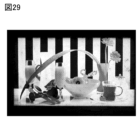
- FIG. 29 is a photograph of the display panel.
- FIG. 30 is a cross-sectional view illustrating an example of a display device; 31A and 31B are the results of cross-sectional observation. 32A and 32B are the results of cross-sectional observation. 33A and 33B are the results of cross-sectional observation. Figures 34A and 34B are the results of the peel test. FIG. 35 shows the results of the peel test.
- holes or electrons are sometimes referred to as “carriers”.
- the hole injection layer or electron injection layer is referred to as a "carrier injection layer”
- the hole transport layer or electron transport layer is referred to as a “carrier transport layer”
- the hole blocking layer or electron blocking layer is referred to as a "carrier It is sometimes called a block layer.
- the carrier injection layer, the carrier transport layer, and the carrier block layer described above may not be clearly distinguished from each other due to their cross-sectional shape, characteristics, or the like.
- one layer may serve as two or three functions of the carrier injection layer, the carrier transport layer, and the carrier block layer.
- a light-emitting element (also referred to as a light-emitting device) has an EL layer between a pair of electrodes, for example.
- the EL layer has at least a light-emitting layer.
- the layers (also referred to as functional layers) included in the EL layer include a light-emitting layer, a carrier-injection layer (hole-injection layer and electron-injection layer), a carrier-transport layer (hole-transport layer and electron-transport layer), and A carrier block layer (a hole block layer and an electron block layer) and the like are included.
- a light-receiving element (also referred to as a light-receiving device) includes, for example, a layer including a photoelectric conversion layer between a pair of electrodes.
- a layer shared by the light-receiving element and the light-emitting element may exist.
- Such layers may have different functions in the light emitting device than in the light receiving device.
- constituent elements may be referred to based on their functions in the light-emitting element.
- One embodiment of the present invention is a display device having a display portion capable of full-color display.
- the display unit has first sub-pixels and second sub-pixels exhibiting light of different colors, and a third pixel detecting light.
- the first sub-pixel has a first light-emitting element that emits blue light
- the second sub-pixel has a second light-emitting element that emits light of a different color than the first light-emitting element.
- the third pixel has a light receiving element that detects light.
- the first light emitting element and the second light emitting element have at least one different material, for example, different light emitting materials.
- the display device of one embodiment of the present invention uses light-emitting elements that are separately manufactured for each emission color.
- the light receiving element has a photoelectric conversion material.
- an image can be captured using a plurality of light-receiving elements, so that the image sensor functions as an imaging device.
- the light emitting element can be used as a light source for imaging.
- one embodiment of the present invention can display an image with a plurality of light-emitting elements, and therefore functions as a display device. Therefore, one embodiment of the present invention can be referred to as a display device having an imaging function or an imaging device having a display function.
- the display section has a function of displaying an image and a function of a light receiving section. Since an image can be captured by a plurality of light receiving elements provided in the display portion, the display device can function as an image sensor or the like. That is, it is possible to capture an image on the display unit, or detect the approach or contact of an object. Furthermore, since the light-emitting element provided in the display unit can be used as a light source when receiving light, there is no need to provide a light source separate from the display device. device can be realized.
- the light-receiving element when an object reflects light emitted from a light-emitting element included in a display portion, the light-receiving element can detect the reflected light. It can be performed.
- the display device of one embodiment of the present invention can capture an image of a fingerprint or a palmprint when a finger, palm, or the like is brought into contact with the display portion. Therefore, an electronic device including the display device of one embodiment of the present invention can perform personal authentication using an image such as a captured fingerprint or palmprint. As a result, there is no need to separately provide an imaging device for fingerprint authentication or palmprint authentication, and the number of parts of the electronic device can be reduced.
- the light-receiving elements are arranged in a matrix in the display section, an image of a fingerprint or a palm print can be taken anywhere on the display section, and an electronic device with excellent convenience can be realized.
- light-emitting elements with different emission wavelengths for example, blue (B), green (G), and red (R)
- B blue
- G green
- R red
- SBS side-by-side
- the material and structure can be optimized for each light-emitting element, so the degree of freedom in selecting the material and structure increases, and it becomes easy to improve luminance and reliability.
- an island shape indicates a state in which two or more layers using the same material formed in the same step are physically separated.
- an island-shaped light-emitting layer means that the light-emitting layer is physically separated from an adjacent light-emitting layer.
- the display device of one embodiment of the present invention includes a touch sensor that acquires position information of an object that touches or approaches the display surface.
- a touch sensor various systems such as a resistive film system, a capacitance system, an infrared system, an electromagnetic induction system, and a surface acoustic wave system can be adopted.
- a capacitive touch sensor it is preferable to use as the touch sensor.
- the capacitance method includes a surface capacitance method, a projected capacitance method, and the like. Also, the projective capacitance method includes a self-capacitance method, a mutual capacitance method, and the like. It is preferable to use the mutual capacitance method because it enables simultaneous multi-point detection.
- a mutual-capacitance touch sensor can have a plurality of electrodes to which a pulse potential is applied and a plurality of electrodes to which detection circuits are connected.
- a touch sensor can perform detection using a change in capacitance between electrodes when a finger or the like approaches. It is preferable that the electrodes constituting the touch sensor be arranged closer to the display surface than the light-emitting elements (light-receiving elements).
- At least part of the electrode of the touch sensor overlaps with a region sandwiched between two adjacent light-emitting elements (light-receiving elements) or a region sandwiched between two adjacent EL layers (PS layers). Furthermore, it is preferable that at least part of the electrode of the touch sensor has a region overlapping with an organic resin film provided between two adjacent EL layers (PS layers). With such a structure, the touch sensor can be provided above the display device without reducing the light emitting area of the light emitting element (light receiving element). Therefore, a display device having both a high aperture ratio and high definition can be provided.
- a metal or alloy material as the conductive layer that functions as the electrode of the touch sensor.
- a non-light-transmitting metal or alloy material can be used for the electrodes of the touch sensor without reducing the aperture ratio of the display device. Touch sensing with high sensitivity can be achieved by using a metal or alloy material with low resistance for the electrodes of the touch sensor.
- a light-transmitting electrode that transmits light emitted from the light-emitting element can be used as the electrode of the touch sensor. At this time, the light-transmitting electrode can be provided so as to overlap with the light-emitting element (light-receiving element).
- a light-emitting element can be provided between a pair of substrates.
- a rigid substrate such as a glass substrate may be used, or a flexible film may be used.
- the electrodes of the touch sensor can be formed on the substrate positioned on the display surface side. Alternatively, the electrodes of the touch sensor may be formed on another substrate and attached to the display surface side.
- the electrodes of the touch sensor between the pair of substrates.
- a protective layer may be provided to cover the light-emitting element (light-receiving element), and electrodes of the touch sensor may be provided over the protective layer.
- a tapered shape refers to a shape in which at least a part of the side surface of the structure is inclined with respect to the substrate surface. For example, it is preferable to have a region where the angle between the inclined side surface and the substrate surface (also referred to as a taper angle) is less than 90°. Note that the side surfaces of the structure and the substrate surface are not necessarily completely flat, and may be substantially planar with a small curvature or substantially planar with fine unevenness.
- a reverse tapered shape refers to a case where an angle in the structure formed by at least part of the side surface of the structure and the bottom surface is greater than 90°.
- the reverse tapered shape is a shape having a side portion or an upper portion protruding in a direction parallel to the substrate from the bottom portion.
- a display device of one embodiment of the present invention includes light-emitting elements that emit light of different colors.
- a light-emitting element includes a lower electrode, an upper electrode, and a layer containing a light-emitting compound (also referred to as a light-emitting layer) therebetween.
- Electroluminescence elements such as organic EL elements and inorganic EL elements are preferably used as the light emitting elements. Alternatively, a light emitting diode (LED) may be used.
- a display device of one embodiment of the present invention includes a light receiving element.
- the light receiving element can detect one or both of visible light and infrared light.
- a light receiving element includes, for example, a lower electrode, an upper electrode, and a photoelectric conversion layer therebetween.
- the light emitting element for example, it is preferable to use an OLED (Organic Light Emitting Diode) or a QLED (Quantum-dot Light Emitting Diode).
- the light-emitting substance included in the light-emitting element include a substance that emits fluorescence (fluorescent material), a substance that emits phosphorescence (phosphorescent material), and a substance that exhibits thermally activated delayed fluorescence (thermally activated delayed fluorescence: TADF ) materials), and inorganic compounds (quantum dot materials, etc.).
- LEDs such as micro LED (Light Emitting Diode), can also be used as a light emitting element.
- the emission color of the light emitting element can be red, green, blue, cyan, magenta, yellow, white, or the like. Further, the color purity can be enhanced by providing the light-emitting element with a microcavity structure.
- Embodiment 3 can be referred to for the structure and material of the light-emitting element.
- the light-emitting layer may contain one or more compounds (host material, assist material) in addition to the light-emitting substance (guest material).
- the host material and the assist material one or a plurality of substances having an energy gap larger than that of the light-emitting substance (guest material) can be selected and used.
- the host material and the assist material it is preferable to use a combination of compounds that form an exciplex. In order to efficiently form an exciplex, it is particularly preferable to combine a compound that easily accepts holes (hole-transporting material) and a compound that easily accepts electrons (electron-transporting material).
- Either a low-molecular-weight compound or a high-molecular-weight compound can be used for the light-emitting element, and an inorganic compound (quantum dot material, etc.) may be included.
- pixels having one or more light emitting elements are arranged at a resolution of 2000 ppi or more, preferably 3000 ppi or more, more preferably 5000 ppi or more, and even more preferably 6000 ppi or more, and 20000 ppi or less, or 30000 ppi or less.
- a very high-definition display device is preferable.
- FIG. 1 is a schematic top view of the display device 100A
- FIGS. 2A and 2B are schematic cross-sectional views of the display device 100A
- FIG. 2A is a cross-sectional view of the portion indicated by the dashed-dotted line A1-A2 in FIG. 1
- FIG. 2B is a cross-sectional view of the portion indicated by the dashed-dotted line B1-B2 in FIG. Note that some elements are omitted in the top view of FIG. 1 for clarity of illustration.
- the display device 100A includes a substrate 101 including a semiconductor circuit, an insulating layer 105, a light emitting element 110R, a light emitting element 110G, and a light emitting element 110B. Moreover, the display device 100A preferably has a light receiving element 110S. 2A and 2B, the light emitting element 110R, the light emitting element 110G, the light emitting element 110B, and the light receiving element 110S are provided on the insulating layer 105.
- the display device 100A has a gap between the insulating layer 105 and the light emitting element 110R, between the insulating layer 105 and the light emitting element 110G, between the insulating layer 105 and the light emitting element 110B, and between the insulating layer 105 and the light receiving element 110S.
- Each has an insulating layer 106 between them.
- the insulating layer 105 is preferably an organic insulating film (organic insulating layer), and the insulating layer 106 is preferably an inorganic insulating film (inorganic insulating layer).
- the insulating layer 105 may be an inorganic insulating film and the insulating layer 106 may be an organic insulating film.
- the organic layer 112 preferably has a region in contact with the upper surface of the pixel electrode 111, a region in contact with the side surface of the pixel electrode 111, and a region in contact with the insulating layer 105, respectively. Also, the organic layer 112 preferably has a region in contact with the side surface of the insulating layer 106 . Also, the organic layer 112 preferably has a region in contact with the lower surface of the insulating layer 106 . With the structure shown in FIG. 2A, the organic layer 112 can be sealed with the insulating layer 106 and the insulating layer 118 .
- Sealing the organic layer 112 with the insulating layer 106 and the insulating layer 118 can prevent the insulating layer 118 from peeling off from the organic layer 112, for example. In addition, diffusion of impurities such as water into the organic layer 112 can be suppressed.
- the PS layer 155S preferably has a region in contact with the upper surface of the pixel electrode 111, a region in contact with the side surface of the pixel electrode 111, and a region in contact with the insulating layer 105, respectively. Also, the PS layer 155S preferably has a region in contact with the side surface of the insulating layer 106 . Also, the PS layer 155S preferably has a region in contact with the bottom surface of the insulating layer 106 . With the configuration shown in FIG. 2B, the PS layer 155S can be sealed with the insulating layer 106 and the insulating layer 118d.
- Sealing the PS layer 155S with the insulating layer 106 and the insulating layer 118 can prevent the insulating layer 118 from peeling off from the organic layer 112, for example. In addition, diffusion of impurities such as water into the organic layer 112 can be suppressed.
- the display device 100A may be configured without the insulating layer 106 .
- 3 differs from FIG. 2A in that the display device 100A does not have the insulating layer 106.
- the organic layer 112 preferably has a region in contact with the upper surface of the pixel electrode 111, a region in contact with the side surface of the pixel electrode 111, and a region in contact with the insulating layer 105, respectively. Also, the organic layer 112 preferably has a region in contact with the lower surface of the pixel electrode 111 .
- the insulating layer 105 a single layer or a laminated structure of two or more layers can be selected as appropriate.
- the insulating layer 105 may have a laminated structure of an inorganic insulating film and an organic insulating film.
- the light emitting element 110R is a red light emitting element
- the light emitting element 110G is a green light emitting element
- the light emitting element 110B is a blue light emitting element.
- the light emitting element 110R and the light emitting element 110G emit light of different colors.
- the light-emitting element 110G and the light-emitting element 110B emit light of different colors.
- the light emitting element 110B and the light emitting element 110R emit light of different colors.
- a structure in which each light-emitting element is separately colored here, red (R), green (G), and blue (B)
- SBS side-by-side
- SBS Side-By-Side
- the material and structure can be optimized for each light-emitting element, so the degree of freedom in selecting the material and structure increases, and it becomes easy to improve luminance and reliability.
- the light emitting element 110R has a pixel electrode 111R, an organic layer 112R, a common layer 114, and a common electrode 113.
- the light emitting element 110G has a pixel electrode 111G, an organic layer 112G, a common layer 114, and a common electrode 113.
- the light emitting element 110B has a pixel electrode 111B, an organic layer 112B, a common layer 114, and a common electrode 113.
- the common layer 114 and the common electrode 113 are commonly provided for the light emitting elements 110R, 110G, and 110B.
- the organic layer 112R contains a light-emitting organic compound that emits light having an intensity in at least the red wavelength range.
- the organic layer 112G contains a light-emitting organic compound that emits light having an intensity in at least the green wavelength range.
- the organic layer 112B contains a light-emitting organic compound that emits light having an intensity in at least the blue wavelength range.
- the organic layer 112R, the organic layer 112G, and the organic layer 112B have at least a layer (light-emitting layer) containing a light-emitting organic compound.
- the symbols added to the reference numerals may be omitted and the light emitting elements 110 may be used for description.
- the organic layer 112R, the organic layer 112G, and the organic layer 112B may also be described as the organic layer 112 in some cases.
- the pixel electrode 111R, the pixel electrode 111G, the pixel electrode 111B, and the pixel electrode 111S may also be described as the pixel electrode 111 in some cases.
- the EL layer may refer to, for example, a structure in which the organic layer 112 and the common layer 114 are combined.
- a pixel electrode 111R, a pixel electrode 111G, and a pixel electrode 111B are provided for each light emitting element. Further, the common layer 114 and the common electrode 113 are provided as a continuous layer common to each light emitting element.
- a conductive film having a property of transmitting visible light is used for one of the pixel electrodes and the common electrode 113, and a conductive film having a reflective property is used for the other.
- a protective layer 121 is provided on the common electrode 113 to cover the light emitting elements 110R, 110G, and 110B.
- the protective layer 121 has a function of preventing impurities such as water from diffusing into each light emitting element from above.
- the light receiving element 110S can detect one or both of visible light and infrared light.
- visible light for example, one or more of colors such as blue, purple, violet, green, yellow-green, yellow, orange, and red can be detected.
- infrared light it is possible to detect an object even in a dark place, which is preferable.
- the light receiving element 110S for example, a pn-type or pin-type photodiode can be used.
- the light receiving element 110S functions as a photoelectric conversion element (also referred to as a photoelectric conversion device) that detects light incident on the light receiving element 110S and generates electric charges. The amount of charge generated by the photoelectric conversion element is determined according to the amount of incident light.
- organic photodiode having a layer containing an organic compound as the light receiving element 110S.
- Organic photodiodes can be easily made thinner, lighter, and larger, and have a high degree of freedom in shape and design, so they can be applied to various devices.
- a layer shared by the light-receiving element and the light-emitting element may exist.
- Such layers may have different functions in the light emitting device than in the light receiving device.
- constituent elements may be referred to based on their functions in the light-emitting element.
- the hole-injection layer functions as a hole-injection layer in the light-emitting device and as a hole-transport layer in the light-receiving device.
- the electron injection layer functions as an electron injection layer in the light emitting device and as an electron transport layer in the light receiving device.
- a layer shared by the light receiving element and the light emitting element may have the same function in the light emitting element and the light receiving element.
- the hole-transporting layer functions as a hole-transporting layer in both the light-emitting device and the light-receiving device
- the electron-transporting layer functions as an electron-transporting layer in both the light-emitting device and the light-receiving device.
- an organic EL element is used as the light-emitting element and an organic photodiode is used as the light-receiving element.
- An organic EL element and an organic photodiode can be formed on the same substrate. Therefore, an organic photodiode can be incorporated in a display device using an organic EL element.
- the light-receiving element is driven by applying a reverse bias between the pixel electrode and the common electrode, thereby detecting light incident on the light-receiving element, generating an electric charge, and extracting it as a current.
- the light receiving element 110S has a pixel electrode 111S, a PS layer 155S, and a common electrode 113. As shown in FIG. 2B and the like, the light receiving element 110S has a common layer 114 between the PS layer 155S and the common electrode 113. As shown in FIG. 2B and the like, the light receiving element 110S has a common layer 114 between the PS layer 155S and the common electrode 113. As shown in FIG.
- the PS layer 155S has at least a photoelectric conversion layer (sometimes called an active layer).
- the layers (also referred to as functional layers) included in the PS layer 155S include a photoelectric conversion layer, a carrier injection layer (hole injection layer and electron injection layer), a carrier transport layer (hole transport layer and electron transport layer), and a carrier block layer (a hole block layer and an electron block layer).
- the photoelectric conversion layer contains a semiconductor.
- the semiconductor include inorganic semiconductors such as silicon and organic semiconductors including organic compounds.
- an organic semiconductor can be used as the semiconductor included in the photoelectric conversion layer.
- the light-emitting layer and the photoelectric conversion layer can be formed by the same method (for example, a vacuum deposition method), and a manufacturing apparatus can be shared, which is preferable.
- a pn-type or pin-type photodiode can be used as the photoelectric conversion layer.
- the material and structure shown for the pixel electrode 111R, the pixel electrode 111G, the pixel electrode 111B, and the like can be used.
- the combination of colors of light emitted by the light emitting element 110 is not limited to the above, and for example, colors such as cyan, magenta, and yellow may also be used. In the above, three colors of red (R), green (G), and blue (B) are exemplified. or four or more colors.
- the pixel electrode 111 functions as a lower electrode, and the common electrode 113 functions as an upper electrode.
- the common electrode 113 is transmissive and reflective to visible light.
- Organic layer 112 includes a light-emitting compound.
- the light-emitting element 110 an electroluminescence element having a function of emitting light by current flowing through the organic layer 112 by applying a potential difference between the pixel electrode 111 and the common electrode 113 can be used.
- an organic EL element using a light-emitting organic compound for the organic layer 112 .
- the light-emitting element 110 is preferably an element that emits monochromatic light whose emission spectrum has one peak in the visible light region.
- the light emitting element 110 may be an element that emits white light whose emission spectrum has two or more peaks in the visible light region.
- a pixel electrode 111 provided for each light emitting element 110 is independently applied with a potential for controlling the amount of light emitted by the light emitting element 110 .
- Organic layer 112 and common layer 114 may each independently include one or more of an electron injection layer, an electron transport layer, a hole injection layer, and a hole transport layer.
- the organic layer 112 may have a stacked structure of a hole-injection layer, a hole-transport layer, a light-emitting layer, and an electron-transport layer from the pixel electrode 111 side
- the common layer 114 may have an electron-injection layer. can.
- the common electrode 113 is formed to be transmissive and reflective to visible light.
- a metal film or an alloy film thin enough to transmit visible light can be used.
- a light-transmitting conductive film eg, a metal oxide film
- stacked over such a film may be used.
- the edge of the organic layer 112 is positioned outside the edge of the pixel electrode 111 .
- the edge of the organic layer 112 covers the edge of the pixel electrode 111 .
- the edge of the PS layer 155S is located outside the edge of the pixel electrode 111. As shown in FIG. Edges of the PS layer 155S cover edges of the pixel electrode 111 . By locating the end of the PS layer 155S outside the end of the pixel electrode 111, short-circuiting between the pixel electrode 111 and the common electrode 113 can be suppressed.
- the insulating layer 105 has recesses 175 .
- the recess 175 is provided in the insulating layer 105 in a region located between two pixel electrodes 111 adjacent in the A1-A2 direction shown in FIG.
- the recess 175 is also provided in the insulating layer 105 in a region located between two pixel electrodes 111 adjacent in the B1-B2 direction.
- the recess 175 can also be expressed as a collection of multiple recesses.
- the concave portion 175 can be expressed as, for example, a collection of a plurality of grooves, and one groove is provided, for example, between adjacent pixel electrodes 111 .
- the recess 175 has a groove-like region.
- the concave portion 175 has, for example, a groove-like region provided along the side of the pixel electrode 111 when viewed from above.
- the recess 175 has a region overlapping with the pixel electrode 111 inside the side of the pixel electrode 111 when viewed from above.
- the organic layer 112 can be discontinued in the area below the pixel electrode 111 and inside the side of the pixel electrode 111 by having the area where the concave portion 175 overlaps the inside of the pixel electrode. .
- a recess 175 is provided in a region of the insulating layer 105 located between the light emitting elements 110R and 110G so that the insulating layer 105 is located between the light emitting elements 110G and 110B.
- a recess 175 is provided in a region located between them, and a recess 175 is provided in a region of the insulating layer 105 located between the light emitting element 110B and the light emitting element 110R.
- a recess 175 is provided in a region of the insulating layer 105 located between the light emitting element 110G and the light receiving element 110S.
- the direction in which the light emitting elements 110R, 110G, and 110B are arranged in order is defined as the x direction
- the direction perpendicular to the x direction is defined as the y direction.
- the concave portion 175 can also be expressed as a set of linear grooves extending in the x-direction and lower linear grooves extending in the y-direction.
- a portion of the recess 175 is preferably positioned below the pixel electrode 111 .
- the recess 175 preferably has a region located below the pixel electrode 111 .
- the recess 175 has a first region overlapping with the first pixel electrode and a second region overlapping with the second pixel electrode. , and a third region that does not overlap with the first pixel electrode and the second pixel electrode.
- the third region is located between the first region and the second region.
- the first region is positioned below the first pixel electrode.
- the second region is positioned below the second pixel electrode.
- the light-emitting element having the first pixel electrode and the light-emitting element having the second pixel electrode emit light of different colors.
- the first pixel electrode is included in the light emitting element and the second pixel electrode is included in the light receiving element.
- the concave portion 175 has a downward convex shape in a cross-sectional view of the display device 100A.
- the concave portion 175 has, for example, an arcuate shape that protrudes downward.
- the recess 175 may have, for example, a downwardly convex arc-shaped region and a flat-shaped region.
- the side wall of the recess 175 may have an arcuate shape that protrudes downward, and the bottom may have a flat shape.
- the shape of the recess 175 is not particularly limited as long as part of the recess 175 is positioned below the pixel electrode 111 .
- the concave portion 175 may have an arcuate shape that is convex downward, or may have an arcuate shape with a flat bottom and downwardly convex sidewalls. good.
- the shape of the recess 175 is not limited to the above.
- the recess 175 does not have to have a region located below the pixel electrode 111 .
- the concave portion 175 may have a cross-shaped shape, a T-shaped shape, or an inverted T-shaped shape in a cross-sectional view of the display device.
- the downwardly convex circular arc shape can also be said to be a concave curved surface shape.
- the downwardly convex circular arc shape includes a downwardly convex semicircular shape.
- the organic layer 112 of the light emitting element 110 can be cut between the adjacent light emitting element 110 or between the adjacent light receiving element 110S. Further, by providing the concave portion 175, the PS layer 155S of the light receiving element 110S can be cut between the adjacent light emitting elements 110 or between the adjacent light receiving elements 110S.
- the film that will become the organic layer 112 is cut in the region of the concave portion 175 that overlaps the pixel electrode 111 .
- the film to be the organic layer 112 can be processed into an island shape without using a shadow mask such as a metal mask, etching, or the like.
- the film to be the PS layer 155S is cut in the region of the concave portion 175 overlapping the pixel electrode 111.
- FIG. the film to be the organic layer 112 can be processed into an island shape without using a shadow mask such as a metal mask, etching, or the like.
- the film remaining in the recess 175 among the film to be the organic layer 112 and the film to be the PS layer 155S is etched. It is preferable to remove by, for example.
- the organic layer 112 is divided between adjacent light emitting elements, between adjacent light emitting elements and light receiving elements, or between adjacent light receiving elements. Accordingly, current (also referred to as leakage current) flowing through the organic layer 112 can be prevented between adjacent elements. Therefore, light emission caused by the leakage current can be suppressed, and high-contrast display can be realized. Furthermore, even when the definition is increased, a material with high conductivity can be used for the organic layer 112, so that the range of selection of materials can be widened, and efficiency can be improved, power consumption can be reduced, and reliability can be improved. It becomes easier to improve.
- the organic layer 112 and the PS layer 155S may form an island pattern by film formation using a shadow mask such as a metal mask, but it is particularly preferable to use a processing method that does not use a metal mask. As a result, it is possible to form an extremely fine pattern, so that the definition and the aperture ratio can be improved as compared with the formation method using a metal mask.
- a processing method typically, a photolithography method can be used.
- formation methods such as nanoimprinting and sandblasting can also be used.
- a device manufactured using a metal mask or FMM may be referred to as a device with an MM (metal mask) structure.
- a device manufactured without using a metal mask or FMM may be referred to as a device with an MML (metal maskless) structure.
- the display device 100A includes an insulating layer 118a on the organic layer 112R, an insulating layer 118b on the organic layer 112G, an insulating layer 118c on the organic layer 112B, an insulating layer 118d on the PS layer 155S, an insulating layer 125, and a resin layer 126 .
- the insulating layer 118 is provided so as to cover at least part of the upper surface of the organic layer 112 or the PS layer 155S. Moreover, the insulating layer 118 is provided so as to overlap with at least part of the recess 175 . As shown in FIG. 2A, the insulating layer 118a on the organic layer 112R is provided so as to overlap at least part of the recess 175, and the insulating layer 118b on the organic layer 112G is provided so as to overlap at least part of the recess 175. The insulating layer 118 c on the organic layer 112 B is provided so as to overlap with at least part of the recess 175 . Also, as shown in FIG. 2B, the insulating layer 118d on the PS layer 155S is provided so as to overlap at least a portion of the recess 175. As shown in FIG.
- the insulating layer 118 also has a region in contact with at least part of the top surface of the organic layer 112 (PS layer 155S) and a region in contact with the side surface of the organic layer 112 (PS layer 155S). Further, the insulating layer 118 has a region in contact with the insulating layer 105 below the light emitting element 110 (light receiving element 110S), specifically, the pixel electrode 111 . Insulating layer 118 also has a region in contact with the lower surface of insulating layer 106 .
- the insulating layer 118 can be peeled off from the organic layer 112 (PS layer 155S) and the organic layer 112 (PS layer 155S) can be separated from the pixel electrode. Peeling off from 111 can be suppressed.
- the insulating layer 105 and the insulating layer 118 are configured to have high adhesiveness, the insulating layer 118 can be peeled off from the organic layer 112 (PS layer 155S), and the organic layer 112 (PS layer 155S) can be separated from the pixel electrode 111. It is possible to suppress peeling from. By suppressing the peeling of the film, the yield in the manufacturing process of the display device can be improved. Moreover, the display quality of the display device can be improved.
- the adhesion between the insulating layer 105 and the insulating layer 118 is preferably higher than the adhesion between the insulating layer 118 and the organic layer 112 . Also, the adhesion between the insulating layer 105 and the insulating layer 118 is preferably higher than the adhesion between the insulating layer 118 and the PS layer 155S.
- acrylic resin, polyimide resin, epoxy resin, imide resin, polyamide resin, polyimideamide resin, silicone resin, siloxane resin, benzocyclobutene-based resin, phenol resin, and the like can be used.
- a resin precursor or the like can be applied.
- an organic material such as polyvinyl alcohol (PVA), polyvinyl butyral, polyvinylpyrrolidone, polyethylene glycol, polyglycerin, pullulan, water-soluble cellulose, or alcohol-soluble polyamide resin may be used.
- baking is preferably performed after the resin is applied. Baking is preferably performed in a reducing atmosphere, for example, and can be performed in a nitrogen atmosphere, for example.
- the baking temperature is preferably 125° C. or higher, more preferably 150° C. or higher, and even more preferably 200° C. or higher. By performing baking at such a temperature, adhesion between the insulating layer 105 and the insulating layer 118 may increase.
- the baking temperature in manufacturing the resin layer 126 described later may be lower than the baking temperature in manufacturing the insulating layer 105 .
- the baking temperature for producing the resin layer 126 is, for example, preferably 200° C. or lower, more preferably 150° C. or lower, and even more preferably 125° C. or lower.
- the insulating layer 118a has a region in contact with at least a portion of the upper surface of the organic layer 112R, a region in contact with the side surface of the organic layer 112R, and a region in contact with the insulating layer 105 below the pixel electrode 111R. Insulating layer 118 a also has a region in contact with the lower surface of insulating layer 106 .
- the insulating layer 118b has a region in contact with at least part of the upper surface of the organic layer 112G, a region in contact with the side surface of the organic layer 112G, and a region in contact with the insulating layer 105 below the pixel electrode 111G.
- Insulating layer 118 b also has a region in contact with the lower surface of insulating layer 106 .
- the insulating layer 118c has a region in contact with at least part of the upper surface of the organic layer 112B, a region in contact with the side surface of the organic layer 112B, and a region in contact with the insulating layer 105 below the pixel electrode 111B.
- Insulating layer 118 c also has a region in contact with the lower surface of insulating layer 106 .
- the insulating layer 118d has a region in contact with at least a portion of the upper surface of the PS layer 155S, a region in contact with the side surfaces of the PS layer 155S, and a region in contact with the insulating layer 105 below the pixel electrode 111S.
- the insulating layer 118 has an opening reaching the organic layer 112 (PS layer 155S).
- the organic layer 112 (PS layer 155S) is in contact with the common layer 114 in the opening.
- the common electrode 113 has a region overlapping with the organic layer 112 (PS layer 155S) through the opening.
- the insulating layer 118 has a region located between the resin layer 126 and the organic layer 112 (PS layer 155S), and serves as a protective film to prevent the resin layer 126 from contacting the organic layer 112 (PS layer 155S). Function.
- the organic layer 112 (PS layer 155S) and the resin layer 126 are in contact with each other, the organic layer 112 (PS layer 155S) may be dissolved by the organic solvent or the like used when forming the resin layer 126 . Therefore, as shown in this embodiment, the insulating layer 118 is provided between the organic layer 112 (PS layer 155S) and the resin layer 126 to protect the side surface of the organic layer 112 (PS layer 155S). It becomes possible to
- the insulating layer 118 can be an insulating layer containing an inorganic material.
- an inorganic insulating film such as an oxide insulating film, a nitride insulating film, an oxynitride insulating film, or a nitride oxide insulating film can be used, for example.
- the insulating layer 118 may have a single-layer structure or a laminated structure.
- the oxide insulating film includes a silicon oxide film, an aluminum oxide film, a magnesium oxide film, an indium gallium zinc oxide film, a gallium oxide film, a germanium oxide film, an yttrium oxide film, a zirconium oxide film, a lanthanum oxide film, a neodymium oxide film, and an oxide film.
- Examples include a hafnium film and a tantalum oxide film.
- Examples of the nitride insulating film include a silicon nitride film, an aluminum nitride film, and the like.
- Examples of the oxynitride insulating film include a silicon oxynitride film, an aluminum oxynitride film, and the like.
- nitride oxide insulating film a silicon nitride oxide film, an aluminum nitride oxide film, or the like can be given.
- a metal oxide film such as an aluminum oxide film or a hafnium oxide film formed by an ALD method, or an inorganic insulating film such as a silicon oxide film to the insulating layer 118, there are few pinholes and the function of protecting the organic layer 112.
- An insulating layer 118 having excellent resistance can be formed.
- oxynitride refers to a material whose composition contains more oxygen than nitrogen
- nitride oxide refers to a material whose composition contains more nitrogen than oxygen. point to the material.
- silicon oxynitride refers to a material whose composition contains more oxygen than nitrogen
- silicon nitride oxide refers to a material whose composition contains more nitrogen than oxygen. indicates
- the insulating layer 118 may also function as a protective layer that prevents impurities such as water from diffusing into the organic layer 112 and the PS layer 155S.
- An inorganic insulating film with low moisture permeability such as a silicon oxide film, a silicon nitride film, or an aluminum oxide film is preferably used for the insulating layer 118 .
- the insulating layer 118 is an insulating layer containing aluminum and oxygen.
- the insulating layer 118 can be formed by a sputtering method, a CVD method, a PLD method, an ALD method, or the like.
- the insulating layer 118 is preferably formed by an ALD method with good coverage.
- the thickness of the insulating layer 118 is preferably 3 nm or more, 5 nm or more, or 10 nm or more and 200 nm or less, 150 nm or less, 100 nm or less, or 50 nm or less.
- the side surfaces of the organic layers 112 are provided facing each other with the resin layer 126 interposed therebetween.
- the resin layer 126 is positioned between the adjacent light-emitting elements of different colors, and is provided so as to fill the end portions of the respective organic layers 112 and the area between the two organic layers 112 .
- the side surface of the organic layer 112 of the light emitting element and the side surface of the PS layer 155S of the light receiving element are provided to face each other with the resin layer 126 interposed therebetween.
- the resin layer 126 is located between the adjacent light-emitting element and light-receiving element, and fills the area between the edge of the organic layer 112 and the edge of the PS layer 155S and the area between the organic layer 112 and the PS layer 155S. is provided as follows.
- the side surfaces of the PS layers 155S are provided to face each other with the resin layer 126 interposed between the adjacent light receiving elements. ing.
- the resin layer 126 is positioned between the adjacent light receiving elements, and is provided so as to fill the ends of each PS layer 155S and the area between the two PS layers 155S.
- the resin layer 126 has a smooth convex upper surface, and a common layer 114 and a common electrode 113 are provided to cover the upper surface of the resin layer 126 .
- the resin layer 126 has regions in contact with the insulating layer 105 between adjacent light emitting elements, between adjacent light emitting elements and light receiving elements, and the like.
- the resin layer 126 has a region in contact with the insulating layer 105 in a portion located between the organic layers 112R and 112G.
- the resin layer 126 has a region in contact with the insulating layer 105 in a portion located between the organic layers 112G and 112B.
- the resin layer 126 has a region in contact with the insulating layer 105 in a portion located between the organic layers 112B and 112R.
- the resin layer 126 has a region in contact with the insulating layer 105 in a portion located between the PS layer 155S and the organic layer 112 .
- the resin layer 126 functions as a planarization film that fills in steps between adjacent light-emitting elements, steps between adjacent light-emitting elements and light-receiving elements, and the like.
- a phenomenon in which the common electrode 113 is divided by a step at the end of the organic layer 112 and a step at the end of the PS layer 155S (also referred to as discontinuity) can be suppressed. It is possible to prevent the common electrode 113 on the layer 112 from being insulated.
- the resin layer 126 can also be called LFP (Local Filling Planarization).
- an insulating layer containing an organic material can be preferably used.
- acrylic resin, polyimide resin, epoxy resin, imide resin, polyamide resin, polyimideamide resin, silicone resin, siloxane resin, benzocyclobutene-based resin, phenolic resin, and precursors of these resins are applied as the resin layer 126. can do.
- an organic material such as polyvinyl alcohol (PVA), polyvinyl butyral, polyvinylpyrrolidone, polyethylene glycol, polyglycerin, pullulan, water-soluble cellulose, or alcohol-soluble polyamide resin may be used.
- a photosensitive resin can be used as the resin layer 126 .
- a photoresist may be used as the photosensitive resin.
- a positive material or a negative material can be used for the photosensitive resin.
- the resin layer 126 may contain a material that absorbs visible light.
- the resin layer 126 itself may be made of a material that absorbs visible light, or the resin layer 126 may contain a pigment that absorbs visible light.
- a resin that transmits red, blue, or green light and can be used as a color filter that absorbs other light, or a resin that contains carbon black as a pigment and functions as a black matrix, or the like. can be used.
- Insulating layers 125 are provided between the resin layer 126 and the insulating layer 118a, between the resin layer 126 and the insulating layer 118b, and between the resin layer 126 and the insulating layer 118c.
- the insulating layer 125 is provided with an opening reaching the organic layer 112 (PS layer 155S). Note that the display device 100A may have a structure in which the insulating layer 125 is not provided.
- a protective layer 121 is provided to cover the common electrode 113 .
- the protective layer 121 can have, for example, a single-layer structure or a laminated structure including at least an inorganic insulating film.
- inorganic insulating films include oxide films and nitride films such as silicon oxide films, silicon oxynitride films, silicon nitride oxide films, silicon nitride films, aluminum oxide films, aluminum oxynitride films, and hafnium oxide films.
- a semiconductor material or a conductive material such as indium gallium oxide, indium zinc oxide, indium tin oxide, or indium gallium zinc oxide may be used for the protective layer 121 .
- a laminated film of an inorganic insulating film and an organic insulating film can also be used as the protective layer 121 .
- a structure in which an organic insulating film is sandwiched between a pair of inorganic insulating films is preferable.
- the organic insulating film functions as a planarizing film.
- the upper surface of the organic insulating film can be flattened, so that the coverage of the inorganic insulating film thereon can be improved, and the barrier property can be enhanced.
- the upper surface of the protective layer 121 is flat, when a structure (for example, a color filter, an electrode of a touch sensor, or a lens array) is provided above the protective layer 121, an uneven shape due to the structure below may be formed. This is preferable because it can reduce the impact.
- a structure for example, a color filter, an electrode of a touch sensor, or a lens array
- the common electrode 113 extends outside the end of the recess 175 .
- an EL layer included in the light-emitting element 110 is separately formed for each light-emitting element of a different color, so that color display with high color reproducibility and low power consumption can be performed.
- a circuit board having transistors, wiring, or the like can be used as the substrate 101 .
- an insulating substrate such as a glass substrate can be used as the substrate 101 when a passive matrix method or a segment method can be applied.
- the substrate 101 is a substrate provided with a circuit for driving each light-emitting element (also referred to as a pixel circuit) or a semiconductor circuit functioning as a driver circuit for driving the pixel circuit. A more specific configuration example of the substrate 101 will be described later.
- the substrate 101 and the pixel electrode 111 of the light emitting element 110 are electrically connected via a conductive layer.
- a width W1 shown in FIG. 2A is the width of the concave portion 175 in the region that does not overlap the pixel electrode 111 in the A1-A2 direction.
- the width W1 can be rephrased as the shortest distance between the ends of the pixel electrodes 111 facing each other.
- a width W2 shown in FIG. 2A is the width of the recess 175 in the region overlapping the pixel electrode 111 in the A1-A2 direction.
- FIG. 30 shows an enlarged view of a region including width W1 and width W2 in FIG. 2A.
- 30 also shows the depth W5 of the recess 175.
- the depth W5 is, for example, the height difference between the bottom of the recess 175 and the top surface of the insulating layer 105 .
- the width W1, the width W2, the height of the bottom portion, and the height of the upper surface of the insulating layer 105 of the concave portion 175 can be measured by, for example, a cross-sectional observation image of the display device 100A.
- the cross-sectional observation image can be observed using, for example, a TEM (Transmission Electron Microscope), a STEM (Scanning Transmission Electron Microscope), or the like.
- the cross-sectional observation image can be processed to expose the cross section and measured using the height in the observation range.
- the average height in the observation range may be calculated.
- the height of the bottom of recess 175 may be measured at the deepest point of recess 175 in the observed area.
- the average height in the observation range may be calculated.
- the height of the upper surface of the insulating layer 105 may be measured at the point where the upper surface of the insulating layer 105 is highest in the observed region.
- the width W1, width W2, depth W5, etc. of the recesses may be their average value, maximum value, minimum value, median value, or the like. And it is sufficient.
- the width W1 is preferably larger than twice the film thickness of the organic layer 112 (PS layer 155S).
- the width W1 is 200 nm or more and 1200 nm or less, preferably 200 nm or more and 1000 nm or less, more preferably 200 nm or more and 900 nm or less.
- the organic layer 112 (PS layer 155S) is broken by the recess 175, and the organic layer 112 (PS layer 155S) can be formed on the pixel electrode 111.
- FIG. At this time, as shown in FIG.
- the organic layer 112 (PS layer 155S) is arranged so as to cover the side surfaces and the upper surface of the pixel electrode 111 .
- a layer covering a structure means a state in which the layer covers part of an end surface of the structure, or a state in which the layer completely covers the end surface of the structure. It refers to the state where Here, the layer is an insulating layer, an insulating film, a conductive layer, or the like.
- the structure is a conductive layer, an organic layer, a laminate, a light-emitting element, or the like.
- the width W1 may be appropriately adjusted according to the processing accuracy when forming the concave portion 175, the film forming conditions of the organic layer 112 (PS layer 155S), and the like.
- the organic layer 112 (PS layer 155S) is formed by, for example, a vacuum deposition method, even if the width W1 is smaller than twice the film thickness of the organic layer 112 (PS layer 155S), the organic layer 112 (PS layer 155S) ) may be interrupted.
- the width W1 may be 100 nm or more and 1200 nm or less, 1000 nm or less, or 900 nm or less.
- the width W2 may be any width that causes a discontinuity in the organic layer 112 (PS layer 155S).
- the width W2 is preferably 2 nm or more, 5 nm or more, 10 nm or more, 20 nm or more, 30 nm or more, 40 nm or more, or 50 nm or more.
- a discontinuity can be generated in the organic layer 112 .
- the width W2 is preferably 500 nm or less, 300 nm or less, 200 nm or less, 150 nm or less, or 100 nm or less.
- the width W2 is preferably 20 nm or more and 500 nm or less, more preferably 30 nm or more and 300 nm or less, still more preferably 40 nm or more and 200 nm or less, still more preferably 50 nm or more and 150 nm or less, for example about 90 nm.
- the organic layer 112 can be discontinued while maintaining a high aperture ratio even in a high-definition display. It can be configured to be in contact with the lower surface and the side surface of the insulating layer 105, and the insulating layer 118 can be preferably prevented from peeling off from the organic layer 112 (PS layer 155S). Further, the anchoring effect of the organic layer 112 can improve adhesion.
- the width W1, the width W2 and the depth W5 can be measured using, for example, a cross-sectional image of the display device observed with an electron microscope or the like.
- the cross section to be observed is preferably substantially perpendicular to the sides of the pixel electrode 111 when viewed from above. At this time, in the region where the sides are substantially straight lines, the cross section may be processed substantially vertically and the cross section may be observed.
- the width W1 and the width W2 may be measured in the width direction of the groove.
- the depth W5 is, for example, 20 nm or more, or 50 nm or more and 3000 nm or less, or 100 nm or more and 2000 nm or less, or 200 nm or more and 1000 nm or less.
- the organic layer 112 when the width W2 is set to the above width, the organic layer 112 can be suitably discontinued. Further, by setting the width W2 to the width described above, even when one or more of the insulating layer 106 and the pixel electrode 111 have a tapered shape, the organic layer 112 can be suitably cut off.
- part of the insulating layer 118 is in contact with the bottom surface of the insulating layer 106 and the side surface of the insulating layer 105, whereby the pixel electrode 111, the insulating layer 118, and the insulating layer 106 are formed. , and the insulating layer 105 can seal the organic layer 112 .
- the above sealing is performed in a region around the pixel electrode 111 . Therefore, when the perimeter of the pixel electrode 111 is sufficiently large with respect to the area of the pixel electrode 111 in a plan view, sealing can be performed more satisfactorily. Therefore, a display device with a smaller area of the pixel electrode 111 and a higher definition can be sealed more satisfactorily. For example, better sealing may be achieved at a resolution of 400 ppi or more, more preferably 600 ppi or more.
- pixels having one or more light emitting elements are arranged at a resolution of 2000 ppi or more, preferably 3000 ppi or more, more preferably 5000 ppi or more, and still more preferably 6000 ppi or more, and 20000 ppi or less, or 30000 ppi or less. , a very high-definition display device can be realized.
- a microcavity structure (microresonator structure) is provided, and a high-brightness display device can be realized.
- the light emitting elements 110 it becomes possible to arrange the light emitting elements 110 at an extremely high density. For example, a display device with a definition exceeding 2000 ppi can be realized.
- the thickness of the EL layer of the light emitting element 110 may be adjusted according to the peak wavelength of the emission spectrum.
- the light emitting element 110R that emits light with the longest wavelength has the thickest organic layer 112R
- the light emitting element 110B that emits light with the shortest wavelength has the thinnest organic layer 112B.
- the thickness of each organic layer can be adjusted in consideration of the wavelength of light emitted by each light emitting element, the optical characteristics of the layers constituting the light emitting element, the electrical characteristics of the light emitting element, and the like. .
- the width W1 is preferably larger than twice the thickness of the thinnest organic layer 112 (PS layer 155S), and is larger than twice the thickness of the thickest organic layer 112 (PS layer 155S). is more preferred.
- the organic layer 112 (PS layer 155S) is broken by the recess 175, and the organic layer 112 (PS layer 155S) can be formed on the pixel electrode 111.
- FIG. Furthermore, microcavity structures can be realized.
- a width W3 shown in FIG. 2B is the width of the concave portion 175 in the region that does not overlap the pixel electrode 111 in the B1-B2 direction.
- the width W3 can be rephrased as the shortest distance between the ends of the pixel electrodes 111 facing each other.
- a width W4 shown in FIG. 2B is the width of the concave portion 175 in the region overlapping the pixel electrode 111 in the B1-B2 direction.
- width W3 the description of the width W1 can be referred to.
- width W4 the description of the width W2 can be referred to.
- a light emitting element that can be used for the light emitting element 110, an element that can emit light by itself can be used, and an element whose luminance is controlled by current or voltage is included in its category.
- an LED, an organic EL element, an inorganic EL element, or the like can be used.
- Light-emitting elements include top emission type, bottom emission type, dual emission type, and the like.
- a conductive film that transmits visible light is used for the electrode on the light extraction side.
- a conductive film that reflects visible light is used for the electrode on the side from which light is not extracted.
- a top-emission or dual-emission light-emitting element that emits light to the side opposite to the formation surface can be preferably used.
- the organic layer 112 has at least a light-emitting layer.
- the organic layer 112 includes, as layers other than the light-emitting layer, a substance with a high hole-injection property, a substance with a high hole-transport property, a hole-blocking material, a substance with a high electron-transport property, a substance with a high electron-injection property, and an electron-blocking material. , a layer containing a bipolar substance (a substance with high electron-transport properties and high hole-transport properties), or the like.
- Either a low-molecular-weight compound or a high-molecular-weight compound can be used for the organic layer 112, and an inorganic compound may be included.
- the layers constituting the organic layer 112 can be formed by a method such as a vapor deposition method (including a vacuum vapor deposition method), a transfer method, a printing method, an inkjet method, or a coating method.
- the organic layer 112 preferably contains two or more kinds of light-emitting substances.
- white light emission can be obtained by selecting luminescent substances such that the luminescence of each of two or more luminescent substances has a complementary color relationship.
- luminescent substances exhibiting luminescence such as R (red), G (green), B (blue), Y (yellow), and O (orange), respectively, or spectral components of two or more colors of R, G, and B It is preferable that two or more of the light-emitting substances exhibiting light emission containing are included.
- the spectrum of light emitted from the light-emitting element has two or more peaks within the range of wavelengths in the visible light region (eg, 350 nm to 750 nm).
- the emission spectrum of the material having a peak in the yellow wavelength region is preferably a material having spectral components in the green and red wavelength regions as well.
- the organic layer 112 preferably has a structure in which a light-emitting layer containing a light-emitting material that emits light of one color and a light-emitting layer containing a light-emitting material that emits light of another color are stacked.
- the plurality of light-emitting layers in the organic layer 112 may be laminated in contact with each other, or may be laminated via a region that does not contain any light-emitting material.
- a configuration in which a region is provided between a fluorescent-emitting layer and a phosphorescent-emitting layer and contains the same material as the fluorescent-emitting layer or the phosphorescent-emitting layer (e.g., host material, assist material) and does not contain any of the emitting materials. good too. This facilitates fabrication of the light-emitting element and reduces the driving voltage.
- the light emitting element 110 may be a single element having one EL layer, or may be a tandem element in which a plurality of EL layers are stacked with a charge generation layer interposed therebetween.
- a single-structure device preferably has one light-emitting unit between a pair of electrodes, and the light-emitting unit preferably includes one or more light-emitting layers.
- the light-emitting layers may be selected such that the respective light-emitting colors of the two light-emitting layers are in a complementary color relationship. For example, by setting the emission color of the first light-emitting layer and the emission color of the second light-emitting layer to have a complementary color relationship, it is possible to obtain a configuration in which the entire light-emitting element emits white light.
- the light-emitting element as a whole may emit white light by combining the light-emitting colors of the three or more light-emitting layers.
- a tandem structure device preferably has two or more light-emitting units between a pair of electrodes, and each light-emitting unit includes one or more light-emitting layers.
- each light-emitting unit includes one or more light-emitting layers.
- a structure in which white light emission is obtained by combining light from the light emitting layers of a plurality of light emitting units may be employed. Note that the structure for obtaining white light emission is the same as the structure of the single structure.
- a conductive film which transmits visible light and which can be used for the pixel electrode 111 or the like can be formed using, for example, indium oxide, indium tin oxide, indium zinc oxide, zinc oxide, gallium-added zinc oxide, or the like. can be done.
- metal materials such as gold, silver, platinum, magnesium, nickel, tungsten, chromium, molybdenum, iron, cobalt, copper, palladium, or titanium, alloys containing these metal materials, or nitrides of these metal materials (for example, Titanium nitride) or the like can also be used by forming it thin enough to have translucency.
- a stacked film of any of the above materials can be used as the conductive layer.
- graphene or the like may be used.
- the pixel electrode 111 uses a conductive film that reflects the visible light in a portion located on the organic layer 112 side.
- a conductive film metal materials such as aluminum, gold, platinum, silver, nickel, tungsten, chromium, molybdenum, iron, cobalt, copper, or palladium, or alloys containing these metal materials can be used.
- Silver has a high reflectance of visible light and is preferred.
- aluminum is preferable because it is easy to process because the electrode can be easily etched, and has high reflectance for visible light and near-infrared light.
- lanthanum, neodymium, germanium, or the like may be added to the metal material or alloy.
- an alloy containing titanium, nickel, or neodymium and aluminum may be used.
- An alloy containing copper, palladium, magnesium, and silver may also be used.
- An alloy containing silver and copper is preferred because of its high heat resistance.
- the pixel electrode 111 may have a structure in which a conductive metal oxide film is stacked over a conductive film that reflects visible light.
- a conductive metal oxide film is stacked over a conductive film that reflects visible light.
- oxidation, corrosion, or the like of the conductive film that reflects visible light can be suppressed.
- materials for such metal films and metal oxide films include titanium and titanium oxide.
- a conductive film that transmits visible light and a film made of a metal material may be stacked.
- a laminated film of silver and indium tin oxide, a laminated film of an alloy of silver and magnesium and indium tin oxide, or the like can be used.
- the thickness is preferably 40 nm or more, more preferably 70 nm or more, so that the reflectance of visible light can be sufficiently increased.
- the thickness is preferably 70 nm or more, more preferably 100 nm or more, so that the reflectance of visible light can be sufficiently increased.
- a conductive film that reflects visible light and is thin enough to transmit visible light can be used. Further, with the stacked structure of the conductive film and the conductive film that transmits visible light, conductivity, mechanical strength, or the like can be increased.
- the translucent and reflective conductive film has a reflectance for visible light (for example, a reflectance for light with a predetermined wavelength in the range of 400 nm to 700 nm) of 20% to 80%, preferably 40% to 70%. % or less. Further, the reflectance of the conductive film having reflectivity to visible light is preferably 40% or more and 100% or less, preferably 70% or more and 100% or less. In addition, the reflectance of the light-transmitting conductive film to visible light is preferably 0% to 40%, preferably 0% to 30%.
- metal materials such as gold, silver, platinum, magnesium, nickel, tungsten, chromium, molybdenum, iron, cobalt, copper, palladium, or titanium, alloys containing these metal materials, or Nitrides (for example, titanium nitride) of these metal materials can be used.
- Electrodes forming a light-emitting element may be formed by an evaporation method, a sputtering method, or the like. In addition, it can be formed using an ejection method such as an inkjet method, a printing method such as a screen printing method, or a plating method.
- the layer containing the above-described light-emitting layer a substance with high hole-injection property, a substance with high hole-transport property, a substance with high electron-transport property, a substance with high electron-injection property, a bipolar substance, etc.
- Each may have inorganic compounds such as quantum dots, or polymeric compounds (oligomers, dendrimers, polymers, etc.).
- quantum dots in the light-emitting layer, it can function as a light-emitting material.
- quantum dot material a colloidal quantum dot material, an alloy quantum dot material, a core-shell quantum dot material, a core quantum dot material, or the like can be used. Also, materials containing element groups of Groups 12 and 16, Groups 13 and 15, or Groups 14 and 16 may be used. Alternatively, quantum dot materials containing elements such as cadmium, selenium, zinc, sulfur, phosphorus, indium, tellurium, lead, gallium, arsenic, and aluminum may be used.
- the optical distance between the surface of the reflective layer that reflects visible light and the common electrode 113 that is transparent and reflective to visible light is the wavelength ⁇ of the light whose intensity is to be increased.
- it is preferably adjusted to be m ⁇ /2 (m is an integer equal to or greater than 1) or its vicinity.
- the optical distance described above is the physical distance between the reflective surface of the reflective layer and the reflective surface of the common electrode 113 having translucency and reflectivity, and the refractive index of the layer provided therebetween. It is difficult to adjust exactly because the product with the rate is involved. Therefore, it is preferable to adjust the optical distance by assuming that the surface of the reflective layer and the surface of the common electrode 113 having translucency and reflectivity are respectively reflective surfaces.
- the thin films (insulating film, semiconductor film, conductive film, etc.) that make up the display device can be formed by sputtering, chemical vapor deposition (CVD), vacuum deposition, pulsed laser deposition (PLD). ) method, Atomic Layer Deposition (ALD) method, or the like.
- the CVD method includes a plasma enhanced CVD (PECVD) method, a thermal CVD method, and the like. Also, one of the thermal CVD methods is the metal organic CVD (MOCVD) method.
- the thin films (insulating films, semiconductor films, conductive films, etc.) that make up the display device can be applied by spin coating, dipping, spray coating, inkjet, dispensing, screen printing, offset printing, doctor knife, slit coating, roll coating, curtain coating. , or by a wet film formation method such as knife coating.
- the processing can be performed using a photolithography method or the like.
- the thin film may be processed by a nanoimprint method, a sandblast method, a lift-off method, or the like.
- an island-shaped thin film may be directly formed by a film formation method using a shielding mask such as a metal mask.
- the photolithography method there are typically the following two methods.
- One is a method of forming a resist mask on a thin film to be processed, processing the thin film by etching or the like, and removing the resist mask.
- the other is a method of forming a photosensitive thin film, then performing exposure and development to process the thin film into a desired shape.
- the light used for exposure can be, for example, i-line (wavelength 365 nm), g-line (wavelength 436 nm), h-line (wavelength 405 nm), or a mixture thereof.
- ultraviolet rays, KrF laser light, ArF laser light, or the like can also be used.
- extreme ultraviolet (EUV: Extreme Ultra-violet) light or X-rays may be used.
- An electron beam can also be used instead of the light used for exposure. The use of extreme ultraviolet light, X-rays, or electron beams is preferable because extremely fine processing is possible.
- a photomask is not necessary when exposure is performed by scanning a beam such as an electron beam.
- a dry etching method, a wet etching method, a sandblasting method, or the like can be used for processing the thin film.
- the resist mask can be removed by dry etching treatment such as ashing, wet etching treatment, wet etching treatment after dry etching treatment, or dry etching treatment after wet etching treatment.
- a polishing treatment method such as a chemical mechanical polishing (CMP) method can be suitably used.
- CMP chemical mechanical polishing
- dry etching treatment or plasma treatment may be used.
- the polishing treatment, the dry etching treatment, and the plasma treatment may be performed multiple times, or may be performed in combination.
- the order of processes is not particularly limited, and may be appropriately set according to the unevenness of the surface to be processed.
- a CMP method for example, is used to accurately process the thin film to a desired thickness.
- the thin film is polished at a constant processing rate until part of the upper surface of the thin film is exposed. After that, polishing is performed until the thin film reaches a desired thickness under conditions with a slower processing speed than this, thereby enabling highly accurate processing.
- a method for detecting the polishing end point there is an optical method of irradiating the surface to be processed with light and detecting changes in the reflected light, or by detecting changes in the polishing resistance received by the processing apparatus from the surface to be processed.
- the thickness of the thin film is reduced by performing a polishing process at a slow processing speed while monitoring the thickness of the thin film by an optical method using a laser interferometer or the like. It can be controlled with high precision. In addition, if necessary, the polishing process may be performed multiple times until the thin film has a desired thickness.
- a substrate having heat resistance enough to withstand at least heat treatment performed later can be used.
- an insulating substrate may be used as the substrate 101, it may be a glass substrate, a quartz substrate, a sapphire substrate, a ceramic substrate, or the like.
- a semiconductor substrate such as a single crystal semiconductor substrate, a polycrystalline semiconductor substrate, a compound semiconductor substrate made of silicon germanium or the like, or an SOI substrate can be used.
- the substrate 101 it is preferable to use the above semiconductor substrate or a substrate obtained by forming a semiconductor circuit including a semiconductor element such as a transistor over the insulating substrate.
- the semiconductor circuit preferably constitutes, for example, a pixel circuit, a gate line driver circuit (gate driver), a source line driver circuit (source driver), and the like.
- gate driver gate line driver
- source driver source driver
- an arithmetic circuit, a memory circuit, and the like may be configured.
- a substrate including at least a pixel circuit is used as the substrate 101 .
- recesses 175 are formed in the insulating layer 105 (FIG. 4A).
- An isotropic etching method can be used to form the recess 175 .
- an isotropic plasma etch process or a wet etch process can be used.
- isotropic dry etching treatment, plasma treatment, or the like is preferably used.
- the plasma treatment for example, RF plasma treatment using oxygen as gas can be performed.
- wet etching treatment is preferably used. Thereby, a recess 175 partly located below the pixel electrode 111 can be formed.
- the insulating layer 106 when the insulating layer 106 is provided on the insulating layer 105 and the pixel electrode 111 is formed on the insulating layer 106, for example, an organic insulating film is used as the insulating layer 105, and the insulating layer 106 is formed of an organic insulating film. It is preferable to use an inorganic insulating film as the insulating film. With such a structure, by using an isotropic dry etching process and using etching conditions in which the etching rate of the organic insulating film is higher than that of the inorganic insulating film, a part of the insulating layer 106 is formed under the insulating layer 106 . A located recess 175 may be formed in the insulating layer 105 .
- FIG. 4B shows an enlarged view of the area enclosed by the dashed line in FIG. 4A.
- FIG. 4C shows an example of the pixel electrode 111 having a shape different from that of FIG. 4B.
- the pixel electrode 111 may be a single layer or a laminated film.
- FIG. 4C shows an example of a configuration in which a laminated film is used as a pixel electrode.
- the pixel electrode 111 illustrated in FIG. 4C has a stacked structure of a conductive layer 111_1, a conductive layer 111_2 over the conductive layer 111_1, and a conductive layer 111_3 over the conductive layer 111_2.
- the end of the conductive layer 111_2 is positioned inside the ends of the conductive layers 111_1 and 111_3. Further, the side surface of the conductive layer 111_2 is covered with the conductive layer 111_3. Accordingly, a configuration in which the conductive layer 111_2 and the organic layer 112 or the conductive layer 111_2 and the PS layer 155S are not in contact can be obtained.
- oxidation of the conductive layer 111_2 in subsequent steps can be suppressed.
- etching of the conductive layer 111_3 even when the selectivity with respect to the conductive layer 111_2 is low, receding of the conductive layer 111_2 can be suppressed, and excellent display quality can be achieved in the display device.
- a transparent conductive layer can be used as the conductive layer 111_3
- a reflective conductive layer can be used as the conductive layer 111_2.
- a film containing a first light-emitting compound is formed over the pixel electrode 111R, the pixel electrode 111G, the pixel electrode 111B, and the insulating layer 105 (FIG. 4D).
- the film containing the first light-emitting compound can be formed, for example, by a vapor deposition method, specifically a vacuum vapor deposition method. Moreover, the film may be formed by a transfer method, a printing method, an inkjet method, a coating method, or the like.
- FIG. 4D the film is cut off at the protruding portion of the insulating layer 106 .
- an organic layer 112Rf is formed on the pixel electrode 111R, the pixel electrode 111G, the pixel electrode 111B, and the insulating layer 105. As shown in FIG.
- an insulating film 118A is formed on the organic layer 112Rf and the insulating layer 105.
- the insulating film 118A can be formed by a sputtering method, a CVD method, an MBE method, a PLD method, an ALD method, or the like as appropriate.
- the insulating film 118A is formed to cover the side surfaces of the organic layer 112R, the pixel electrode 111R, and the insulating layer 106. As shown in FIG. Further, the insulating film 118A is formed within the recess 175 so as to cover the lower surface of the insulating layer 106 . Further, the insulating film 118A is formed in the concave portion 175 so as to cover the insulating layer 105 below the pixel electrode.
- the insulating film 118A for example, metal materials such as gold, silver, platinum, magnesium, nickel, tungsten, chromium, molybdenum, iron, cobalt, copper, palladium, titanium, aluminum, yttrium, zirconium, and tantalum, or the metal materials are used.
- An alloy material containing it is preferable to use a low melting point material such as aluminum or silver. It is preferable to use a metal material capable of shielding ultraviolet light for the insulating film 118A because irradiation of the EL layer with ultraviolet light can be suppressed and deterioration of the EL layer can be suppressed.
- a metal oxide such as an In--Ga--Zn oxide can be used for the insulating film 118A.
- an In--Ga--Zn oxide film can be formed using a sputtering method.
- indium oxide, In-Zn oxide, In-Sn oxide, indium titanium oxide (In-Ti oxide), indium tin zinc oxide (In-Sn-Zn oxide), indium titanium zinc oxide ( In--Ti--Zn oxide), indium gallium tin-zinc oxide (In--Ga--Sn--Zn oxide), or the like can be used.
- indium tin oxide containing silicon or the like can be used.
- element M is aluminum, silicon, boron, yttrium, copper, vanadium, beryllium, titanium, iron, nickel, germanium, zirconium, molybdenum, lanthanum, cerium, neodymium, hafnium, tantalum, tungsten , or one or more selected from magnesium
- M is preferably one or more selected from gallium, aluminum, and yttrium.
- Various inorganic insulating films that can be used for the protective layer 121 can be used as the insulating film 118A.
- Various inorganic insulating films that can be used for the insulating layer 125 can be used as the insulating film 118A.
- an oxide insulating film is preferable because it has higher adhesion to the EL layer than a nitride insulating film.
- an inorganic insulating material such as aluminum oxide, hafnium oxide, or silicon oxide can be used for the insulating film 118A.
- an aluminum oxide film can be formed using the ALD method. Use of the ALD method is preferable because damage to the base (especially the EL layer or the like) can be reduced.
- an aluminum oxide film is formed as the insulating film 118A by an ALD method.
- the insulating film 118A needs to be deposited on the bottom and side surfaces of the recess 175 provided in the insulating layer 105 with good coverage.
- the film formation by the ALD method can deposit atomic layers one by one on the bottom and side surfaces of the recess 175, so that the insulating film 118A can be formed with good coverage over the recess 175.
- film formation damage can be reduced.
- a material gas obtained by vaporizing a solvent and a liquid containing an aluminum precursor compound (trimethylaluminum (TMA, Al(CH 3 ) 3 ), etc.) and an oxidizing agent
- TMA trimethylaluminum
- Al(CH 3 ) 3 a liquid containing an aluminum precursor compound
- H2O Two gases, H2O , are used.
- Other materials include tris(dimethylamido)aluminum, triisobutylaluminum, and aluminum tris(2,2,6,6-tetramethyl-3,5-heptanedionate).
- the insulating film 118A may be formed using a sputtering method, a CVD method, or a PECVD method, which has a higher film formation rate than the ALD method. Accordingly, a highly reliable display device can be manufactured with high productivity.
- the insulating film 118A may have a laminated structure of two or more layers.
- an inorganic insulating film e.g., aluminum oxide film
- an inorganic film e.g., In--Ga--Zn oxide film, aluminum film, or a tungsten film.
- a resist mask 181 is formed on the insulating film 118A (FIG. 4E). At this time, the resist mask 181 is formed in a portion overlapping with the organic layer 112R and a portion of the recess 175. Next, as shown in FIG.
- the end of resist mask 181 has a shape perpendicular to the surface of substrate 101, but the shape of the end of resist mask 181 is not limited to this.
- the end portion of the resist mask 181 may have a tapered shape or an inverse tapered shape.
- the insulating layer 118a can be formed.
- a dry etching method or a wet etching method can be used to partially remove the insulating film 118A.
- the resist mask 181 is removed.
- the portion of the organic layer 112Rf that does not overlap the resist mask 181 is removed.
- the organic layer 112Rf in the relevant portion is separated from the organic layer 112R, the organic layer 112Rf in the relevant portion may remain. Further, the organic layer 112Rf formed on the concave portion 175 in contact with the insulating layer 105 may remain.
- the insulating layer 106 and the insulating layer 118a can seal the organic layer 112R and the pixel electrode 111R.
- a film containing a second light-emitting compound is formed over the pixel electrode 111G, the pixel electrode 111B, the insulating layer 105, and the insulating layer 118a.
- the film containing the second light-emitting compound can be formed, for example, by a vapor deposition method, specifically a vacuum vapor deposition method. Moreover, the film may be formed by a transfer method, a printing method, an inkjet method, a coating method, or the like.
- an organic layer 112Gf is formed on the pixel electrode 111G, the pixel electrode 111B, the insulating layer 105 and the insulating layer 118a.
- an insulating film 118B is formed on the organic layer 112Gf and the insulating layer 105 (FIG. 5B).
- the insulating film 118B can be formed by a sputtering method, a CVD method, an MBE method, a PLD method, an ALD method, or the like as appropriate.
- the description of the insulating film 118A can be referred to for the insulating film 118B.
- a resist mask 182 is formed on the insulating film 118B (FIG. 5C).
- the insulating layer 118b can be formed.
- a dry etching method or a wet etching method can be used to partially remove the insulating film 118B.
- the resist mask 182 is removed.
- the organic layer 112G and the pixel electrode 111G can be sealed with the insulating layer 106 and the insulating layer 118b.
- ⁇ Formation of organic layer 112B, insulating layer 118c, PS layer 155S, and insulating layer 118d ⁇ Referring to the steps of forming the organic layers 112R and 112G, a layered structure of the organic layer 112B and the insulating layer 118c is formed on the pixel electrode 111B (FIG. 6A). Also, although not shown, a laminated structure of a PS layer 155S and an insulating layer 118d is formed on the pixel electrode 111S.
- the insulating layer 106 and the insulating layer 118c can seal the organic layer 112B and the pixel electrode 111B. Moreover, the PS layer 155S and the pixel electrode 111S can be sealed by the insulating layer 106 and the insulating layer 118d.
- FIG. 6B shows an enlarged view of the area enclosed by the dashed line in FIG. 6A. Also, FIG. 6C shows an example of a configuration different from that of FIG. 6B.
- the thickness of the organic layer 112 is thinner in the region contacting the side surface of the pixel electrode 111 and the region contacting the side surface of the recess 175 than in the region contacting the upper surface of the pixel electrode 111 .
- the region in contact with the side surface of the pixel electrode 111 and the region in contact with the side surface of the recess 175 may be thinner than the thickness of the region in contact with the upper surface of the pixel electrode 111.
- a step may be formed in the insulating layer 105 in the process of forming the organic layer 112G or the like. Specifically, for example, as shown in FIG. 6C, a step is formed near the edge of the insulating layer 118a.
- an insulating film 125A is formed on the insulating layer 105, the insulating layers 118a, 118b, and 118c, and a resin film 126A is formed on the insulating film 125A (FIG. 7A).
- the insulating film 125A is a film that becomes the insulating layer 125
- the resin film 126A is a film that becomes the resin layer 126.
- a film that can be used for the insulating film 118A or the like can be used as the insulating film 125A. Also, the insulating film 125A may not be provided.
- the resin film 126A is formed at a temperature lower than the heat resistance temperature of the organic layer 112R, the organic layer 112G, the organic layer 112B, and the PS layer 155S.
- the substrate temperature when forming the insulating film is 60° C. or higher, 80° C. or higher, 100° C. or higher, or 120° C. or higher and 200° C. or lower, 180° C. or lower, 160° C. or lower, 150° C. or lower, or 140° C. or higher. °C or less.
- the resin film 126A is preferably formed using the wet film forming method described above.
- the insulating film is preferably formed, for example, by spin coating using a photosensitive material, and more specifically, is preferably formed using a photosensitive resin composition containing an acrylic resin.
- the resin film 126A is preferably formed using, for example, a resin composition containing a polymer, an acid generator, and a solvent.
- a polymer is formed using one or more types of monomers and has a structure in which one or more types of structural units (also referred to as structural units) are regularly or irregularly repeated.
- the acid generator one or both of a compound that generates an acid upon exposure to light and a compound that generates an acid upon heating can be used.
- the resin composition may further comprise one or more of photosensitizers, sensitizers, catalysts, adhesion aids, surfactants, and antioxidants.
- Heat treatment (also referred to as pre-baking) is preferably performed after the resin film 126A is formed.
- the heat treatment is performed at a temperature lower than the heat-resistant temperatures of the organic layers 112R, 112G, and 112B.
- the substrate temperature during the heat treatment is preferably 50° C. or higher and 200° C. or lower, more preferably 60° C. or higher and 150° C. or lower, and even more preferably 70° C. or higher and 120° C. or lower. Thereby, the solvent contained in the resin film 126A can be removed.
- the resin film 126A is exposed to visible light or ultraviolet light.
- a positive photosensitive resin composition containing an acrylic resin is used for the insulating film, a region where the resin layer 126 is not formed in a later step is irradiated with visible light or ultraviolet light.
- the resin layer 126 is formed in a region sandwiched between any two of the pixel electrodes 111R, 111G, and 111B. Therefore, the pixel electrode 111 is irradiated with visible light or ultraviolet light.
- the region where the resin layer 126 is formed is irradiated with visible light or ultraviolet light.
- the width of the resin layer 126 to be formed later can be controlled by the exposed area of the resin film 126A.
- the resin layer 126 is processed so as to have a region overlapping with the upper surface of the pixel electrode 111 .
- Light used for exposure preferably includes i-line (wavelength: 365 nm). Moreover, the light used for exposure may include at least one of g-line (wavelength: 436 nm) and h-line (wavelength: 405 nm).
- the resin layer 126 is formed in a region sandwiched between any two of the pixel electrodes 111R, 111G, and 111B.
- an acrylic resin is used for the insulating film
- it is preferable to use an alkaline solution as a developer for example, a tetramethylammonium hydroxide (TMAH) aqueous solution can be used.
- TMAH tetramethylammonium hydroxide
- residues during development may be removed.
- the residue can be removed by ashing using oxygen plasma.
- Etching may be performed to adjust the height of the surface of the resin layer 126 .
- the resin layer 126 may be processed, for example, by ashing using oxygen plasma. Further, even when a non-photosensitive material is used for the resin film that becomes the resin layer 126, the height of the surface of the insulating film can be adjusted by the ashing, for example.
- etching is performed using the resin layer 126 as a mask to remove a portion of the insulating film 125A, a portion of the insulating layer 118a, a portion of the insulating layer 118b, and a portion of the insulating layer 118c.
- openings are formed in the insulating film 125A and the insulating layer 118a, and the upper surface of the organic layer 112R is exposed.
- An opening is formed in the insulating film 125A and the insulating layer 118b to expose the upper surface of the organic layer 112G.
- an opening is formed in the insulating film 125A and the insulating layer 118c to expose the upper surface of the organic layer 112B (FIG. 7B).
- an opening is formed in the insulating film 125A and the insulating layer 118d to expose the upper surface of the PS layer 155S.
- openings reaching the organic layer 112R are provided in the resin layer 126, the insulating layer 125, and the insulating layer 118a.
- an opening reaching the organic layer 112G is provided in the resin layer 126, the insulating layer 125 and the insulating layer 118b.
- An opening reaching the organic layer 112B is provided in the resin layer 126, the insulating layer 125 and the insulating layer 118c.
- An opening reaching the PS layer 155S is provided in the resin layer 126, the insulating layer 125 and the insulating layer 118d.
- the etching process is performed by wet etching.
- a chemical used for the wet etching process may be alkaline or acidic.
- wet etching using an alkaline solution such as TMAH can be performed.
- wet etching using an acidic solution such as dilute hydrofluoric acid, oxalic acid, phosphoric acid, acetic acid, nitric acid, or a mixed liquid thereof may be used.
- a mixed acid-based chemical containing water, phosphoric acid, dilute hydrofluoric acid, and nitric acid may be used.
- heat treatment may be performed after part of the organic layer 112R, the organic layer 112G, the organic layer 112B, and the PS layer 155S are exposed.
- the heat treatment can remove water contained in the organic layer 112 and the PS layer 155S, water adsorbed on the surface of the organic layer 112 and the surface of the PS layer 155S, and the like.
- heat treatment can be performed in an inert gas atmosphere or a reduced pressure atmosphere.
- the heat treatment can be performed at a substrate temperature of 50° C. to 200° C., preferably 60° C. to 150° C., more preferably 70° C. to 120° C.
- a reduced-pressure atmosphere is preferable because dehydration can be performed at a lower temperature.
- the temperature range of the above heat treatment in consideration of the heat resistance temperature of the organic layer 112 and the PS layer 155S.
- a temperature of 70° C. or more and 120° C. or less is particularly suitable in the above temperature range.
- the common layer 114 is formed on the organic layer 112R, the organic layer 112G, the organic layer 112B, the PS layer 155S and the resin layer 126.
- the common layer 114 can be formed by a vapor deposition method (including a vacuum vapor deposition method), a transfer method, a printing method, an inkjet method, a coating method, or the like.
- a common electrode 113 is formed on the common layer 114 .
- the common electrode 113 can be formed using a sputtering method, a vacuum evaporation method, or the like.
- the common electrode 113 may be formed by stacking a film formed by an evaporation method and a film formed by a sputtering method.
- the common electrode 113 is formed so as to overlap the organic layer 112R through an opening formed in the resin layer 126 and the insulating layer 118a. In addition, the common electrode 113 is formed so as to overlap the organic layer 112G through openings formed in the resin layer 126 and the insulating layer 118b. In addition, the common electrode 113 is formed so as to overlap the organic layer 112B through openings formed in the resin layer 126 and the insulating layer 118c. Also, the common electrode 113 is formed so as to overlap the PS layer 155S through an opening formed in the resin layer 126 and the insulating layer 118d.
- the light emitting element 110R, the light emitting element 110G, the light emitting element 110B, and the light receiving element 110S can be formed.
- the protective layer 121 is formed by a method such as a vacuum deposition method, a sputtering method, a CVD method, or an ALD method.
- the display device 100A having the configuration shown in FIG. 2A and the like can be manufactured.
- the organic layer 112 and the PS layer 155S are sealed with the insulating layer 106 and the insulating layer 118, or with the insulating layer 105 and the insulating layer 118, so that the resist mask can be removed. Do not expose to chemicals, etc. Therefore, the light emitting element 110 can be formed without using a metal mask for forming the organic layer 112 and the PS layer 155S.
- the wet etching method can be used for all of the etching processes performed after the formation of the pixel electrode 111, so that the manufacturing cost of the display device 100A can be suppressed.
- the difference in optical distance between the pixel electrode 111 and the common electrode 113 can be precisely controlled by the thickness of the organic layer 112, so that the chromaticity deviation in each light emitting element can be reduced.
- a display device with excellent color reproducibility and extremely high display quality can be easily manufactured.
- the display device of one embodiment of the present invention can achieve high definition, high display quality, and high light sensitivity.
- the display device can support various screen ratios such as 1:1 (square), 3:4, 16:9, and 16:10.
- the arrangement of sub-pixels includes, for example, a stripe arrangement, an S-stripe arrangement, a matrix arrangement, a delta arrangement, a Bayer arrangement, and a pentile arrangement.
- the top surface shape of the sub-pixel shown in FIGS. 8 and 9 corresponds to the top surface shape of the light emitting region.
- top surface shapes of sub-pixels include triangles, quadrilaterals (including rectangles and squares), polygons such as pentagons, polygons with rounded corners, ellipses, and circles.
- circuit layout forming the sub-pixels is not limited to the range of the sub-pixels shown in the drawing, and may be arranged outside the sub-pixels.
- a pixel 150 shown in FIG. 8A is composed of three sub-pixels, sub-pixel 130a, sub-pixel 130b, and sub-pixel 130c.
- Sub-pixel 130a can be, for example, a sub-pixel having light emitting element 110R.
- the sub-pixel 130b can be a sub-pixel having the light emitting element 110G, for example.
- the sub-pixel 130c can be, for example, a sub-pixel having the light emitting element 110B.
- the pixel 150 shown in FIG. 8B includes a subpixel 130a having a substantially trapezoidal top surface shape with rounded corners, a subpixel 130b having a substantially triangular top surface shape with rounded corners, and a substantially square or substantially hexagonal top surface shape with rounded corners. and a sub-pixel 130c having Also, the sub-pixel 130a has a larger light-emitting area than the sub-pixel 130b.
- the shape and size of each sub-pixel can be determined independently. For example, sub-pixels having more reliable light-emitting elements can be made smaller.
- FIG. 8C shows an example in which pixels 124a having sub-pixels 130a and 130b and pixels 124b having sub-pixels 130b and 130c are alternately arranged.
- Pixel 124a has two sub-pixels (sub-pixel 130a, sub-pixel 130b) in the upper row (first row) and one sub-pixel (sub-pixel 130c) in the lower row (second row). have.
- Pixel 124b has one subpixel (subpixel 130c) in the upper row (first row) and two subpixels (subpixel 130a and subpixel 130b) in the lower row (second row). have.
- FIG. 8D is an example in which each sub-pixel has a substantially square top surface shape with rounded corners
- FIG. 8E is an example in which each sub-pixel has a circular top surface shape
- FIG. 8F is an example in which each sub-pixel has a , which has a substantially hexagonal top shape with rounded corners.
- each sub-pixel is located inside a close-packed hexagonal region.
- Each sub-pixel is arranged so as to be surrounded by six sub-pixels when focusing on one sub-pixel.
- sub-pixels that emit light of the same color are provided so as not to be adjacent to each other.
- the sub-pixels are provided such that three sub-pixels 130b and three sub-pixels 130c are alternately arranged so as to surround the sub-pixel 130a.
- FIG. 8G is an example in which sub-pixels of each color are arranged in a zigzag pattern. Specifically, when viewed from above, the positions of the upper sides of two sub-pixels (for example, the sub-pixel 130a and the sub-pixel 130b or the sub-pixel 130b and the sub-pixel 130c) aligned in the column direction are shifted.
- the sub-pixel 130a is a sub-pixel that emits red light
- the sub-pixel 130b is a sub-pixel that emits green light
- the sub-pixel 130c is a sub-pixel that emits blue light. It is preferable to Note that the configuration of the sub-pixels is not limited to this, and the colors exhibited by the sub-pixels and the order in which the sub-pixels are arranged can be determined as appropriate.
- the sub-pixel 130b may be a sub-pixel that emits red light
- the sub-pixel 130a may be a sub-pixel that emits green light.
- the top surface shape of the sub-pixel may be a polygonal shape with rounded corners, an elliptical shape, a circular shape, or the like.
- the EL layer is processed into an island shape using a resist mask.
- the resist film formed on the EL layer needs to be cured at a temperature lower than the heat resistance temperature of the EL layer. Therefore, curing of the resist film may be insufficient depending on the heat resistance temperature of the EL layer material and the curing temperature of the resist material.
- a resist film that is insufficiently hardened may take a shape away from the desired shape during processing.
- the top surface shape of the EL layer may be a polygon with rounded corners, an ellipse, or a circle. For example, when a resist mask having a square top surface is formed, a resist mask having a circular top surface is formed, and the EL layer may have a circular top surface.
- a technique for correcting the mask pattern in advance so that the design pattern and the transfer pattern match.
- OPC Optical Proximity Correction
- a pattern for correction is added to a corner portion of a figure on a mask pattern.
- a pixel can have four types of sub-pixels.
- a pixel is composed of four sub-pixels, for example, sub-pixel 130a, sub-pixel 130b, sub-pixel 130c, and sub-pixel 130d.
- Sub-pixel 130a can be, for example, a sub-pixel having light emitting element 110R.
- the sub-pixel 130b can be a sub-pixel having the light emitting element 110G, for example.
- the sub-pixel 130c can be, for example, a sub-pixel having the light emitting element 110B.
- the sub-pixel 130d can be a sub-pixel having the light receiving element 110S, for example.
- a stripe arrangement is applied to the pixels 150 shown in FIGS. 9A to 9C.
- FIG. 9A is an example in which each sub-pixel has a rectangular top surface shape
- FIG. 9B is an example in which each sub-pixel has a top surface shape connecting two semicircles and a rectangle
- FIG. This is an example where the sub-pixel has an elliptical top surface shape.
- a matrix arrangement is applied to the pixels 150 shown in FIGS. 9D to 9F.
- FIG. 9D is an example in which each subpixel has a square top surface shape
- FIG. 9E is an example in which each subpixel has a substantially square top surface shape with rounded corners
- FIG. 9F is an example in which each subpixel has a square top surface shape. , which have a circular top shape.
- 9G and 9H show an example in which one pixel 150 is composed of 2 rows and 3 columns.
- the pixel 150 shown in FIG. 9G has three sub-pixels (sub-pixel 130a, sub-pixel 130b, and sub-pixel 130c) in the upper row (first row) and 1 sub-pixel in the lower row (second row). has two sub-pixels (sub-pixel 130d).
- pixel 150 has subpixel 130a in the left column (first column), subpixel 130b in the center column (second column), and subpixel 130b in the right column (third column). It has pixels 130c and sub-pixels 130d over these three columns.
- the pixel 150 shown in FIG. 9H has three sub-pixels (sub-pixel 130a, sub-pixel 130b, sub-pixel 130c) in the upper row (first row) and three It has two sub-pixels 130d.
- pixel 150 has sub-pixels 130a and 130d in the left column (first column), sub-pixels 130b and 130d in the center column (second column), and sub-pixels 130b and 130d in the middle column (second column).
- a column (third column) has a sub-pixel 130c and a sub-pixel 130d.
- FIG. 9I shows an example in which one pixel 150 is composed of 3 rows and 2 columns.
- the pixel 150 shown in FIG. 9I has sub-pixels 130a in the top row (first row) and sub-pixels 130b in the middle row (second row). It has a sub-pixel 130c and one sub-pixel (sub-pixel 130d) in the lower row (third row). In other words, the pixel 150 has the sub-pixels 130a and 130b in the left column (first column), the sub-pixel 130c in the right column (second column), and the two columns. , sub-pixel 130d.
- the pixel 150 shown in FIGS. 9A-9I is composed of four sub-pixels: sub-pixel 130a, sub-pixel 130b, sub-pixel 130c, and sub-pixel 130d.
- the sub-pixel 130a, the sub-pixel 130b, and the sub-pixel 130c may each have a light-emitting element that emits light of a different color, and the sub-pixel 130d may have a light-receiving element.
- the sub-pixel 130a is a sub-pixel that emits red light
- the sub-pixel 130b is a sub-pixel that emits green light
- the sub-pixel 130c is a sub-pixel that emits blue light.
- the sub-pixel 130d be a sub-pixel having a function of detecting one or both of visible light and infrared light.
- the layout of the R, G, and B sub-pixels is a stripe arrangement, so that the display quality can be improved.
- the layout of the R, G, and B sub-pixels is a so-called S-stripe arrangement, so that the display quality can be improved.
- the sub-pixel 130a, the sub-pixel 130b, the sub-pixel 130c, and the sub-pixel 130d may each have a light-emitting element that emits light of a different color.
- the sub-pixel 130a, the sub-pixel 130b, the sub-pixel 130c, and the sub-pixel 130d are light emitting elements that emit light of different colors
- the four sub-pixels of R, G, B, and white (W) are used.
- the sub-pixel 130a is a sub-pixel that emits red light
- the sub-pixel 130b is a sub-pixel that emits green light
- the sub-pixel 130c is a sub-pixel that emits blue light
- the sub-pixel 130d is a sub-pixel that emits white light, a sub-pixel that emits yellow light, or a sub-pixel that emits near-infrared light.
- the layout of the R, G, and B sub-pixels is a stripe arrangement, so that the display quality can be improved.
- the layout of the R, G, and B sub-pixels is a so-called S-stripe arrangement, so that the display quality can be improved.
- various layouts can be applied to pixels each including a subpixel including a light-emitting element.
- a display device (display panel) exemplified below can be applied to the display device 100A or the like of the first embodiment.
- a display device (display panel) exemplified below includes a transistor.
- the display device of this embodiment can be a high-definition display device.
- the display device of one embodiment of the present invention is a display unit of an information terminal (wearable device) such as a wristwatch type and a bracelet type, a device for VR such as a head-mounted display, and a glasses type for AR. It can be used for a display unit of a wearable device that can be worn on the head of the device.
- Display module A perspective view of the display module 280 is shown in FIG. 10A.
- the display module 280 has a display device 200A and an FPC 290 .
- the display panel included in the display module 280 is not limited to the display device 200A, and may be any one of the display devices 200B to 200F described later.
- the display module 280 has substrates 291 and 292 .
- the display module 280 has a display section 281 .
- the display unit 281 is an area for displaying images.
- FIG. 10B shows a perspective view schematically showing the configuration on the substrate 291 side.
- a circuit section 282 , a pixel circuit section 283 on the circuit section 282 , and a pixel section 284 on the pixel circuit section 283 are stacked on the substrate 291 .
- a terminal portion 285 for connecting to the FPC 290 is provided on a portion of the substrate 291 that does not overlap with the pixel portion 284 .
- the terminal portion 285 and the circuit portion 282 are electrically connected by a wiring portion 286 composed of a plurality of wirings.
- the pixel section 284 has a plurality of periodically arranged pixels 284a. An enlarged view of one pixel 284a is shown on the right side of FIG. 10B.
- the pixel 284a has a light emitting element 110R that emits red light, a light emitting element 110G that emits green light, a light emitting element 110B that emits blue light, and a light receiving element 110S.
- the pixel circuit section 283 has a plurality of pixel circuits 283a arranged periodically.
- One pixel circuit 283a is a circuit that controls light emission of a light-emitting element and a light-receiving element included in one pixel 284a.
- One pixel circuit 283a may be provided with four circuits for controlling light emission of one light-emitting element (light-receiving element).
- the pixel circuit 283a can have at least one selection transistor, one current control transistor (driving transistor), and a capacitive element for each light emitting element. At this time, a gate signal is inputted to the gate of the selection transistor, and a source signal is inputted to the source thereof. This realizes an active matrix display panel.
- the circuit section 282 has a circuit that drives each pixel circuit 283 a of the pixel circuit section 283 .
- a circuit that drives each pixel circuit 283 a of the pixel circuit section 283 For example, it is preferable to have one or both of a gate line driver circuit and a source line driver circuit.
- at least one of an arithmetic circuit, a memory circuit, a power supply circuit, and the like may be provided.
- the transistor provided in the circuit portion 282 may form part of the pixel circuit 283a. That is, the pixel circuit 283a may be configured with the transistor included in the pixel circuit portion 283 and the transistor included in the circuit portion 282.
- the FPC 290 functions as wiring for supplying a video signal, a power supply potential, and the like from the outside to the circuit section 282 . Also, an IC may be mounted on the FPC 290 .
- the aperture ratio (effective display area ratio) of the display portion 281 can be significantly increased. can be higher.
- the aperture ratio of the display section 281 can be 40% or more and less than 100%, preferably 50% or more and 95% or less, more preferably 60% or more and 95% or less.
- the pixels 284a can be arranged at an extremely high density, and the definition of the display portion 281 can be extremely high.
- the pixels 284a may be arranged with a resolution of 2000 ppi or more, preferably 3000 ppi or more, more preferably 5000 ppi or more, and still more preferably 6000 ppi or more, and 20000 ppi or less, or 30000 ppi or less. preferable.
- a display module 280 Since such a display module 280 has extremely high definition, it can be suitably used for equipment for VR such as a head-mounted display, or equipment for glasses-type AR. For example, even in the case of a configuration in which the display portion of the display module 280 is viewed through a lens, the display module 280 has an extremely high-definition display portion 281, so pixels cannot be viewed even if the display portion is enlarged with the lens. , a highly immersive display can be performed. Moreover, the display module 280 is not limited to this, and can be suitably used for electronic equipment having a relatively small display unit. For example, it can be suitably used for a display part of a wearable electronic device such as a wristwatch.
- Display device 200A A display device 200A shown in FIG.
- the substrate 301 corresponds to the substrate 291 in FIGS. 10A and 10B.
- a transistor 310 has a channel formation region in the substrate 301 .
- the substrate 301 for example, a semiconductor substrate such as a single crystal silicon substrate can be used.
- Transistor 310 includes a portion of substrate 301 , conductive layer 311 , low resistance region 312 , insulating layer 313 and insulating layer 314 .
- the conductive layer 311 functions as a gate electrode.
- An insulating layer 313 is located between the substrate 301 and the conductive layer 311 and functions as a gate insulating layer.
- the low-resistance region 312 is a region in which the substrate 301 is doped with impurities and functions as either a source or a drain.
- the insulating layer 314 is provided to cover the side surface of the conductive layer 311 .
- a device isolation layer 315 is provided between two adjacent transistors 310 so as to be embedded in the substrate 301 .
- An insulating layer 261 is provided to cover the transistor 310 and a capacitor 240 is provided over the insulating layer 261 .
- the capacitor 240 has a conductive layer 241, a conductive layer 245, and an insulating layer 243 positioned therebetween.
- the conductive layer 241 functions as one electrode of the capacitor 240
- the conductive layer 245 functions as the other electrode of the capacitor 240
- the insulating layer 243 functions as the dielectric of the capacitor 240 .
- the conductive layer 241 is provided over the insulating layer 261 and embedded in the insulating layer 254 .
- Conductive layer 241 is electrically connected to one of the source or drain of transistor 310 by plug 271 embedded in insulating layer 261 .
- An insulating layer 243 is provided over the conductive layer 241 .
- the conductive layer 245 is provided in a region overlapping with the conductive layer 241 with the insulating layer 243 provided therebetween.
- An insulating layer 255 is provided to cover the capacitor 240 .
- An inorganic insulating film can be suitably used for the insulating layer 255 .
- a silicon oxide film, a silicon nitride film, or the like can be used as the insulating layer 255 .
- This embodiment mode shows an example in which part of the insulating layer 255 is etched to form a recess.
- the insulating layer 255 has a three-layer structure of a first insulating layer, a second insulating layer over the first insulating layer, and a third insulating layer over the second insulating layer.
- An inorganic insulating film can be preferably used for each of the first insulating layer, the second insulating layer, and the third insulating layer.
- the insulating layer 255 corresponds to the insulating layer 105 in FIG. 2A and the like. Further, when the insulating layer 255 has a laminated structure, part of the plurality of layers included in the insulating layer 255 corresponds to the insulating layer 105 in FIG. 2A and the like.
- a light-emitting element 110R, a light-emitting element 110G, and a light-receiving element 110S are provided on the insulating layer 255.
- FIG. Embodiment 1 can be used for the configurations of the light emitting element 110R, the light emitting element 110G, and the light receiving element 110S.
- the light emitting element 110R is a light emitting element that emits red light R, for example.
- the light emitting element 110G is a light emitting element that emits green light G, for example.
- the light receiving element 110S is a light emitting element having a function of detecting light L, for example.
- the light-emitting elements are separately manufactured for each emission color, so that the change in chromaticity between low-luminance light emission and high-luminance light emission is small. Further, since the organic layer 112R, the organic layer 112G, and the organic layer 112B are separated from each other, it is possible to suppress the occurrence of crosstalk between adjacent sub-pixels even in a high-definition display panel. Therefore, a display panel with high definition and high display quality can be realized.
- An insulating layer 118 and a resin layer 126 are provided in a region between adjacent light emitting elements.
- the pixel electrode 111R, the pixel electrode 111G, and the pixel electrode 111S of the light emitting element are formed by a plug 256 embedded in the insulating layer 255, a conductive layer 241 embedded in the insulating layer 254, and a plug 271 embedded in the insulating layer 261. is electrically connected to one of the source or drain of transistor 310 by .
- the height of the top surface of the insulating layer 255 and the height of the top surface of the plug 256 match or substantially match.
- Various conductive materials can be used for the plug.
- a protective layer 121 is provided on the light emitting element 110R, the light emitting element 110G, and the light receiving element 110S.
- a substrate 170 is bonded onto the protective layer 121 with an adhesive layer 171 .
- a resin layer can be used as the adhesive layer 171 .
- the resin layer that can be used for the adhesive layer 171 and the like include various curable adhesives such as photocurable adhesives such as ultraviolet curable adhesives, reaction curable adhesives, thermosetting adhesives, and anaerobic adhesives. be done.
- These adhesives include epoxy resins, acrylic resins, silicone resins, phenol resins, polyimide resins, imide resins, PVC (polyvinyl chloride) resins, PVB (polyvinyl butyral) resins, EVA (ethylene vinyl acetate) resins, and the like.
- a material with low moisture permeability such as epoxy resin is preferable.
- a two-liquid mixed type resin may be used.
- an adhesive sheet or the like may be used.
- No insulating layer is provided between two adjacent pixel electrodes 111 to cover the edge of the upper surface of the pixel electrode 111 . Therefore, the interval between adjacent light emitting elements can be extremely narrowed. Therefore, a high-definition or high-resolution display device can be obtained.
- a display device 200B shown in FIG. 12 has a structure in which a transistor 310A and a transistor 310B each having a channel formed in a semiconductor substrate are stacked.
- the description of the same parts as those of the previously described display panel may be omitted.
- the display device 200B has a structure in which a substrate 301B provided with a transistor 310B, a capacitor 240, and a light-emitting element and a substrate 301A provided with a transistor 310A are bonded together.
- an insulating layer 345 is provided on the lower surface of the substrate 301B, and an insulating layer 346 is provided on the insulating layer 261 provided on the substrate 301A.
- the insulating layers 345 and 346 are insulating layers functioning as protective layers, and can suppress diffusion of impurities into the substrates 301B and 301A.
- an inorganic insulating film that can be used for the protective layer 121 or the insulating layer 332 can be used.
- the substrate 301B is provided with a plug 343 penetrating through the substrate 301B and the insulating layer 345 .
- an insulating layer 344 functioning as a protective layer to cover the side surface of the plug 343 .
- the substrate 301B is provided with a conductive layer 342 under the insulating layer 345 .
- the conductive layer 342 is embedded in the insulating layer 335, and the lower surfaces of the conductive layer 342 and the insulating layer 335 are planarized. Also, the conductive layer 342 is electrically connected to the plug 343 .
- the conductive layer 341 is provided on the insulating layer 346 on the substrate 301A.
- the conductive layer 341 is embedded in the insulating layer 336, and the top surfaces of the conductive layer 341 and the insulating layer 336 are planarized.
- the same conductive material is preferably used for the conductive layers 341 and 342 .
- a metal film containing an element selected from Al, Cr, Cu, Ta, Ti, Mo, and W, or a metal nitride film (titanium nitride film, molybdenum nitride film, tungsten nitride film) containing the above elements as components etc. can be used.
- copper is preferably used for the conductive layers 341 and 342 .
- a Cu—Cu (copper-copper) direct bonding technique (a technique for achieving electrical continuity by connecting Cu (copper) pads) can be applied.
- a display device 200 ⁇ /b>C shown in FIG. 13 has a configuration in which a conductive layer 341 and a conductive layer 342 are bonded via bumps 347 .
- the conductive layers 341 and 342 can be electrically connected.
- the bumps 347 can be formed using a conductive material containing, for example, gold (Au), nickel (Ni), indium (In), tin (Sn), or the like. Also, for example, solder may be used as the bumps 347 . Further, an adhesive layer 348 may be provided between the insulating layer 345 and the insulating layer 346 . Further, when the bump 347 is provided, the insulating layer 345 and the insulating layer 346 may not be provided.
- Display device 200D A display device 200D shown in FIG. 14 is mainly different from the display device 200A in that the transistor configuration is different.
- the transistor 320 is a transistor (OS transistor) in which a metal oxide (also referred to as an oxide semiconductor) is applied to a semiconductor layer in which a channel is formed.
- OS transistor a transistor in which a metal oxide (also referred to as an oxide semiconductor) is applied to a semiconductor layer in which a channel is formed.
- the transistor 320 has a semiconductor layer 321 , an insulating layer 323 , a conductive layer 324 , a pair of conductive layers 325 , an insulating layer 326 , and a conductive layer 327 .
- the substrate 331 corresponds to the substrate 291 in FIGS. 10A and 10B.
- An insulating layer 332 is provided over the substrate 331 .
- the insulating layer 332 functions as a barrier layer that prevents impurities such as water or hydrogen from diffusing from the substrate 331 into the transistor 320 and oxygen from the semiconductor layer 321 toward the insulating layer 332 side.
- a film into which hydrogen or oxygen is less likely to diffuse than a silicon oxide film such as an aluminum oxide film, a hafnium oxide film, or a silicon nitride film, can be used.
- a conductive layer 327 is provided over the insulating layer 332 and an insulating layer 326 is provided to cover the conductive layer 327 .
- the conductive layer 327 functions as a first gate electrode of the transistor 320, and part of the insulating layer 326 functions as a first gate insulating layer.
- An oxide insulating film such as a silicon oxide film is preferably used for at least a portion of the insulating layer 326 that is in contact with the semiconductor layer 321 .
- the upper surface of the insulating layer 326 is preferably planarized.
- the semiconductor layer 321 is provided over the insulating layer 326 .
- the semiconductor layer 321 preferably includes a metal oxide (also referred to as an oxide semiconductor) film exhibiting semiconductor characteristics.
- a pair of conductive layers 325 is provided on and in contact with the semiconductor layer 321 and functions as a source electrode and a drain electrode.
- An insulating layer 328 is provided to cover the top and side surfaces of the pair of conductive layers 325 , the side surface of the semiconductor layer 321 , and the like, and the insulating layer 264 is provided over the insulating layer 328 .
- the insulating layer 328 functions as a barrier layer that prevents impurities such as water or hydrogen from diffusing into the semiconductor layer 321 from the insulating layer 264 or the like and oxygen from leaving the semiconductor layer 321 .
- an insulating film similar to the insulating layer 332 can be used as the insulating layer 328.
- An opening reaching the semiconductor layer 321 is provided in the insulating layer 328 and the insulating layer 264 .
- An insulating layer 323 in contact with the upper surface of the semiconductor layer 321 and a conductive layer 324 are embedded in the opening.
- the conductive layer 324 functions as a second gate electrode, and the insulating layer 323 functions as a second gate insulating layer.
- the top surface of the conductive layer 324, the top surface of the insulating layer 323, and the top surface of the insulating layer 264 are planarized so that their heights are the same or substantially the same, and the insulating layers 329 and 265 are provided to cover them. ing.
- the insulating layers 264 and 265 function as interlayer insulating layers.
- the insulating layer 329 functions as a barrier layer that prevents impurities such as water or hydrogen from diffusing into the transistor 320 from the insulating layer 265 or the like.
- an insulating film similar to the insulating layers 328 and 332 can be used.
- a plug 274 electrically connected to one of the pair of conductive layers 325 is provided so as to be embedded in the insulating layers 265 , 329 , and 264 .
- the plug 274 includes a conductive layer 274a that covers the side surfaces of the openings of the insulating layers 265, the insulating layers 329, the insulating layers 264, and the insulating layer 328 and part of the top surface of the conductive layer 325, and the conductive layer 274a. It is preferable to have a conductive layer 274b in contact with the top surface. At this time, a conductive material into which hydrogen and oxygen are difficult to diffuse is preferably used for the conductive layer 274a.
- a display device 200E illustrated in FIG. 15 has a structure in which a transistor 320A and a transistor 320B each including an oxide semiconductor as a semiconductor in which a channel is formed are stacked.
- the display device 200D can be used for the configuration of the transistor 320A, the transistor 320B, and their peripherals.
- transistors each including an oxide semiconductor are stacked here, the structure is not limited to this.
- a structure in which three or more transistors are stacked may be employed.
- a display device 200F illustrated in FIG. 16 has a structure in which a transistor 310 in which a channel is formed over a substrate 301 and a transistor 320 including a metal oxide in a semiconductor layer in which the channel is formed are stacked.
- An insulating layer 261 is provided to cover the transistor 310 , and a conductive layer 251 is provided over the insulating layer 261 .
- An insulating layer 262 is provided to cover the conductive layer 251 , and the conductive layer 252 is provided over the insulating layer 262 .
- the conductive layers 251 and 252 each function as wirings.
- An insulating layer 263 and an insulating layer 332 are provided to cover the conductive layer 252 , and the transistor 320 is provided over the insulating layer 332 .
- An insulating layer 265 is provided to cover the transistor 320 and a capacitor 240 is provided over the insulating layer 265 . Capacitor 240 and transistor 320 are electrically connected by plug 274 .
- the transistor 320 can be used as a transistor forming a pixel circuit. Further, the transistor 310 can be used as a transistor forming a pixel circuit or a transistor forming a driver circuit (a gate line driver circuit or a source line driver circuit) for driving the pixel circuit. Further, the transistors 310 and 320 can be used as transistors included in various circuits such as an arithmetic circuit and a memory circuit.
- a pixel circuit not only a pixel circuit but also a driver circuit and the like can be formed directly under the light-emitting element, so that the size of the display panel can be reduced compared to the case where the driver circuit is provided around the display region. becomes possible.
- a display device 200G illustrated in FIG. 17 has a structure in which a transistor 310 in which a channel is formed over a substrate 301, a transistor 320A including a metal oxide in a semiconductor layer in which the channel is formed, and a transistor 320B are stacked.
- the transistor 320A can be used as a transistor forming a pixel circuit.
- the transistor 310 can be used as a transistor that forms a pixel circuit or a transistor that forms a driver circuit (a gate line driver circuit or a source line driver circuit) for driving the pixel circuit.
- the transistor 320B may be used as a transistor forming a pixel circuit, or may be used as a transistor forming the driver circuit. Further, the transistor 310, the transistor 320A, and the transistor 320B can be used as transistors included in various circuits such as an arithmetic circuit and a memory circuit.
- Components such as a transistor that can be applied to a display device are described below.
- a transistor includes a conductive layer functioning as a gate electrode, a semiconductor layer, a conductive layer functioning as a source electrode, a conductive layer functioning as a drain electrode, and an insulating layer functioning as a gate insulating layer.
- the structure of the transistor included in the display device of one embodiment of the present invention there is no particular limitation on the structure of the transistor included in the display device of one embodiment of the present invention.
- a planar transistor, a staggered transistor, or an inverted staggered transistor may be used.
- the transistor structure may be either a top-gate type or a bottom-gate type.
- gate electrodes may be provided above and below the channel.
- Crystallinity of a semiconductor material used for a transistor is not particularly limited, either an amorphous semiconductor or a semiconductor having crystallinity (a microcrystalline semiconductor, a polycrystalline semiconductor, a single crystal semiconductor, or a semiconductor partially including a crystal region). may be used. It is preferable to use a crystalline semiconductor because deterioration of transistor characteristics can be suppressed.
- a transistor using a metal oxide film as a semiconductor layer in which a channel is formed will be described below.
- a metal oxide with an energy gap of 2 eV or more, preferably 2.5 eV or more, more preferably 3 eV or more can be used.
- a typical example is a metal oxide containing indium, and for example, CAC-OS, which will be described later, can be used.
- a transistor using a metal oxide that has a wider bandgap and a lower carrier concentration than silicon retains charge accumulated in a capacitor connected in series with the transistor for a long period of time due to its low off-state current. Is possible.
- the semiconductor layer is denoted by an In-M-Zn oxide containing, for example, indium, zinc and M, where M is a metal such as aluminum, titanium, gallium, germanium, yttrium, zirconium, lanthanum, cerium, tin, neodymium or hafnium. It can be a membrane that
- the atomic ratio of the metal elements in the sputtering target used for forming the In-M-Zn oxide is In ⁇ M, Zn ⁇ It is preferable to satisfy M.
- the atomic ratio of the semiconductor layers to be deposited includes a variation of plus or minus 40% of the atomic ratio of the metal element contained in the sputtering target.
- a metal oxide film with a low carrier concentration is used as the semiconductor layer.
- the semiconductor layer has a carrier concentration of 1 ⁇ 10 17 cm ⁇ 3 or less, preferably 1 ⁇ 10 15 cm ⁇ 3 or less, more preferably 1 ⁇ 10 13 cm ⁇ 3 or less, more preferably 1 ⁇ 10 11 cm ⁇ 3 or less .
- a metal oxide having a carrier concentration of 3 or less, more preferably less than 1 ⁇ 10 10 cm ⁇ 3 and 1 ⁇ 10 ⁇ 9 cm ⁇ 3 or more can be used.
- Such metal oxides are referred to as highly pure or substantially highly pure intrinsic metal oxides.
- the oxide semiconductor can be said to be a metal oxide with a low defect state density and stable characteristics.
- the oxide semiconductor is not limited to these materials, and an oxide semiconductor having an appropriate composition may be used according to required semiconductor characteristics and electrical characteristics (field-effect mobility, threshold voltage, and the like) of the transistor.
- the semiconductor layer has appropriate carrier concentration, impurity concentration, defect density, atomic ratio of metal elements and oxygen, interatomic distance, density, and the like. .
- the concentration of silicon or carbon in the semiconductor layer is set to 2 ⁇ 10 18 atoms/cm 3 or less, preferably 2 ⁇ 10 17 atoms/cm 3 or less.
- the concentration of alkali metals or alkaline earth metals obtained by secondary ion mass spectrometry in the semiconductor layer is set to 1 ⁇ 10 18 atoms/cm 3 or less, preferably 2 ⁇ 10 16 atoms/cm 3 or less.
- the nitrogen concentration in the semiconductor layer obtained by secondary ion mass spectrometry is preferably 5 ⁇ 10 18 atoms/cm 3 or less.
- Oxide semiconductors are classified into single-crystal oxide semiconductors and non-single-crystal oxide semiconductors.
- non-single-crystal oxide semiconductors include CAAC-OS (c-axis-aligned crystalline oxide semiconductor), polycrystalline oxide semiconductors, nc-OS (nanocrystalline oxide semiconductors), and pseudo-amorphous oxide semiconductors (a-like OS). : amorphous-like oxide semiconductor), amorphous oxide semiconductors, and the like.
- a CAC-OS (cloud-aligned composite oxide semiconductor) may be used for the semiconductor layer of the transistor disclosed in one embodiment of the present invention.
- non-single-crystal oxide semiconductor can be preferably used for a semiconductor layer of the transistor disclosed in one embodiment of the present invention.
- a non-single-crystal oxide semiconductor an nc-OS, a CAAC-OS, or a CAC-OS can be preferably used.
- the semiconductor layer includes a CAAC-OS region, a polycrystalline oxide semiconductor region, an nc-OS region, a CAC-OS region, a pseudo-amorphous oxide semiconductor region, and an amorphous oxide semiconductor region.
- a mixed film containing two or more of these may be used.
- the mixed film may have, for example, a single-layer structure or a laminated structure containing two or more of the above-described regions.
- a transistor having a metal oxide film as a semiconductor layer does not require a laser crystallization step, unlike a transistor using low-temperature polysilicon. Therefore, the manufacturing cost can be reduced even for a display device using a large-sized substrate.
- semiconductors are used in high-resolution and large display devices such as ultra high-definition (“4K resolution”, “4K2K”, “4K”) and super high-definition (“8K resolution”, “8K4K”, “8K”).
- silicon may be used for a semiconductor in which a channel of a transistor is formed.
- amorphous silicon may be used as silicon, it is particularly preferable to use crystalline silicon.
- microcrystalline silicon, polycrystalline silicon, single crystal silicon, or the like is preferably used.
- polycrystalline silicon can be formed at a lower temperature than monocrystalline silicon, and has higher field effect mobility and higher reliability than amorphous silicon.
- Conductive layer In addition to the gate, source and drain of transistors, materials that can be used for conductive layers such as various wirings and electrodes constituting display devices include aluminum, titanium, chromium, nickel, copper, yttrium, zirconium, molybdenum, silver, A metal such as tantalum or tungsten, or an alloy containing this as a main component can be used. Also, a film containing these materials can be used as a single layer or as a laminated structure.
- a single-layer structure of an aluminum film containing silicon a two-layer structure in which an aluminum film is stacked over a titanium film, a two-layer structure in which an aluminum film is stacked over a tungsten film, and a copper film over a copper-magnesium-aluminum alloy film.
- insulating materials that can be used for each insulating layer include resins such as acrylic resins and epoxy resins, resins having a siloxane bond such as silicone, silicon oxide, silicon oxynitride, silicon nitride oxide, silicon nitride, and oxide. Inorganic insulating materials such as aluminum can also be used.
- an oxynitride refers to a material whose composition contains more oxygen than nitrogen
- a nitride oxide refers to a material whose composition contains more nitrogen than oxygen.
- silicon oxynitride refers to a material whose composition contains more oxygen than nitrogen
- silicon nitride oxide refers to a material whose composition contains more nitrogen than oxygen.
- the light-emitting element is preferably provided between a pair of insulating films with low water permeability. As a result, it is possible to prevent impurities such as water from entering the light-emitting element, and to prevent deterioration of the reliability of the device.
- a film containing nitrogen and silicon such as a silicon nitride film or a silicon nitride oxide film, a film containing nitrogen and aluminum such as an aluminum nitride film, or the like can be given.
- a silicon oxide film, a silicon oxynitride film, an aluminum oxide film, or the like may be used.
- the water vapor permeation amount of an insulating film with low water permeability is 1 ⁇ 10 ⁇ 5 [g/(m 2 ⁇ day)] or less, preferably 1 ⁇ 10 ⁇ 6 [g/(m 2 ⁇ day)] or less, It is more preferably 1 ⁇ 10 ⁇ 7 [g/(m 2 ⁇ day)] or less, still more preferably 1 ⁇ 10 ⁇ 8 [g/(m 2 ⁇ day)] or less.
- This embodiment can be implemented by appropriately combining at least part of it with other embodiments described herein.
- FIG. 18 shows a perspective view of the display device 200H
- FIG. 19A shows a cross-sectional view of the display device 200H.
- the display device 200H has a configuration in which a substrate 170 and a substrate 151 are bonded together.
- the substrate 170 is clearly indicated by dashed lines.
- the display device 200H includes a display portion 167, a connection portion 140, a circuit 164, wirings 165, and the like.
- FIG. 18 shows an example in which an IC 173 and an FPC 172 are mounted on the display device 200H. Therefore, the configuration shown in FIG. 18 can also be said to be a display module including the display device 200H, an IC (integrated circuit), and an FPC.
- the connecting portion 140 is provided outside the display portion 167 .
- the connection portion 140 can be provided along one side or a plurality of sides of the display portion 167 .
- the number of connection parts 140 may be singular or plural.
- FIG. 18 shows an example in which connecting portions 140 are provided so as to surround the four sides of the display portion.
- the connection portion 140 the common electrode of the light emitting element and the conductive layer are electrically connected, and a potential can be supplied to the common electrode.
- FIG. 19A shows an example in which the recess 175 is not provided in the insulating layer 105 in the region where the circuit 164 is provided, but the recess 175 may be provided in the insulating layer 105 in the region where the circuit 164 is provided.
- the transistor included in the circuit 164 may overlap with the recessed portion 175 .
- the insulating layer 105 is positioned over the transistor included in the circuit 164, and the surface of the insulating layer 105 is an insulator provided using the same film as the insulating layers 118a, 118b, 118d, and the like. covered by a layer.
- the wiring 165 has a function of supplying signals and power to the display portion 167 and the circuit 164 .
- the signal and power are input to the wiring 165 from the outside through the FPC 172 or input to the wiring 165 from the IC 173 .
- FIG. 18 shows an example in which an IC 173 is provided on a substrate 151 by a COG (Chip On Glass) method, a COF (Chip On Film) method, or the like.
- a COG Chip On Glass
- COF Chip On Film
- the IC 173 for example, an IC having a scanning line driver circuit or a signal line driver circuit can be applied.
- the display device 200H and the display module may be configured without an IC.
- the IC may be mounted on the FPC by the COF method or the like.
- part of the area including the FPC 172, part of the circuit 164, part of the display part 167, part of the connection part 140, and part of the area including the end of the display device 200H are cut off.
- An example of a cross section is shown.
- a display device 200H illustrated in FIG. 19A includes a transistor 201, a transistor 205, a light-emitting element 110b, a light-emitting element 110a, a light-receiving element 110d, and the like between a substrate 151 and a substrate 170.
- the light emitting element 110a is a light emitting element that emits red light R, for example.
- the light emitting element 110b is a light emitting element that emits green light G, for example.
- the light receiving element 110d is a light emitting element having a function of detecting light L, for example.
- the light-emitting elements 110a and 110b have the same structures as the light-emitting elements 110R and 110G shown in FIG. 2A and the like, respectively, except that the configuration of the pixel electrode is different.
- Embodiment 1 can be referred to for details of the light-emitting element and the light-receiving element.
- the light receiving element 110d has the same structure as the light receiving element 110S shown in FIG. 2B and the like, except that the configuration of the pixel electrode is different.
- the light emitting element 110 a , the light emitting element 110 b , and the light receiving element 110 d are provided on the insulating layer 105 .
- the display device 200H has a light-emitting element 110c (not shown) on the insulating layer 105 between the substrate 151 and the substrate 170, and the light-emitting element 110c has a different configuration of the pixel electrode. , has the same structure as the light emitting element 110B shown in FIG. 2A and the like.
- the organic layer 112R, the organic layer 112G, and the PS layer 155S are separated and separated from each other. Therefore, crosstalk occurs between adjacent sub-pixels even in a high-definition display device. can be suppressed. Therefore, a display device with high definition and high display quality can be realized.
- the light-emitting element 110a includes a conductive layer 115a, a conductive layer 127a over the conductive layer 115a, and a conductive layer 129a over the conductive layer 127a. All of the conductive layer 115a, the conductive layer 127a, and the conductive layer 129a can be called pixel electrodes, or part of them can be called a pixel electrode.
- the light-emitting element 110b has a conductive layer 115b, a conductive layer 127b over the conductive layer 115b, and a conductive layer 129b over the conductive layer 127b. All of the conductive layer 115b, the conductive layer 127b, and the conductive layer 129b can be called pixel electrodes, and some of them can also be called pixel electrodes.
- the light receiving element 110d has a conductive layer 115d, a conductive layer 127d over the conductive layer 115d, and a conductive layer 129d over the conductive layer 127d. All of the conductive layer 115d, the conductive layer 127d, and the conductive layer 129d can be called pixel electrodes, and some of them can also be called pixel electrodes.
- the conductive layer 115 a is connected to the conductive layer 222 b included in the transistor 205 through openings provided in the insulating layers 105 and 106 . Edges of the conductive layer 115a and the conductive layer 127a are aligned. The end of the conductive layer 129a is positioned outside the end of the conductive layer 127a.
- a reflective conductive layer can be used for the conductive layer 127a, and a light-transmitting conductive layer can be used for the conductive layer 129a.
- the conductive layer 115 b is connected to the conductive layer 222 b included in the transistor 205 through openings provided in the insulating layers 105 and 106 . Edges of the conductive layer 115b and the conductive layer 127b are aligned. The end of the conductive layer 129b is positioned outside the end of the conductive layer 127b.
- a reflective conductive layer can be used for the conductive layer 127b, and a light-transmitting conductive layer can be used for the conductive layer 129b.
- the conductive layer 115 d is connected to the conductive layer 222 b included in the transistor 205 through openings provided in the insulating layers 105 and 106 .
- the ends of the conductive layer 115d and the conductive layer 127d are aligned.
- the end of the conductive layer 129d is located outside the end of the conductive layer 127d.
- a reflective conductive layer can be used for the conductive layer 127d
- a light-transmitting conductive layer can be used for the conductive layer 129d.
- Concave portions are formed in the conductive layers 115 a , 115 b , and 115 d so as to cover the openings provided in the insulating layers 105 and 106 .
- a layer 128 is embedded in the recess.
- the layer 128 has a function of planarizing concave portions of the conductive layers 115a, 115b, and 115d.
- Conductive layers 127a, 127b, and 127d electrically connected to the conductive layers 115a, 115b, and 115d are provided over the conductive layers 115a, 115b, 115d, and 128, respectively. Therefore, regions of the conductive layers 115a, 115b, and 115d, which overlap with the recesses, can also be used as light-emitting regions, and the aperture ratio of the pixel can be increased.
- Layer 128 may be an insulating layer or a conductive layer.
- Various inorganic insulating materials, organic insulating materials, and conductive materials can be used as appropriate for layer 128 .
- layer 128 is preferably formed using an insulating material.
- an insulating layer containing an organic material can be preferably used.
- an acrylic resin, a polyimide resin, an epoxy resin, a polyamide resin, a polyimideamide resin, a siloxane resin, a benzocyclobutene resin, a phenol resin, precursors of these resins, or the like can be applied.
- a photosensitive resin can be used as the layer 128 .
- a positive material or a negative material can be used for the photosensitive resin.
- the layer 128 can be formed only through the steps of exposure and development, and the influence of dry etching, wet etching, or the like on the surfaces of the conductive layers 115a, 115b, and 115d is eliminated. can be reduced. Further, by forming the layer 128 using a negative photosensitive resin, the layer 128 can be formed using the same photomask (exposure mask) used for forming the openings in the insulating layers 105 and 106 . can be formed.
- the top and side surfaces of the conductive layer 129a are covered with the organic layer 112R.
- the top and side surfaces of conductive layer 129b are covered with organic layer 112G.
- the upper and side surfaces of the conductive layer 129d are covered with a PS layer 155S. Therefore, the entire region where the conductive layer 127a, the conductive layer 127b, and the conductive layer 127d are provided can be used as the light emitting region or the light receiving region of the light emitting element 110a, the light emitting element 110b, and the light receiving element 110d. can increase
- a protective layer 121 is provided on each of the light emitting element 110a, the light emitting element 110b, and the light receiving element 110d. By providing the protective layer 121 that covers the light-emitting element, entry of impurities such as water into the light-emitting element can be suppressed, and the reliability of the light-emitting element can be improved.
- the protective layer 121 and the substrate 170 are adhered via the adhesive layer 142 .
- a solid sealing structure, a hollow sealing structure, or the like can be applied to the sealing of the light emitting element.
- the space between substrate 170 and substrate 151 is filled with an adhesive layer 142 to apply a solid sealing structure.
- the space may be filled with an inert gas (such as nitrogen or argon) to apply a hollow sealing structure.
- the adhesive layer 142 may be provided so as not to overlap with the light emitting element.
- the space may be filled with a resin different from the adhesive layer 142 provided in a frame shape.
- the description of the adhesive layer 171 can be referred to for the adhesive layer 142 .
- a conductive layer 123 is provided over the insulating layer 105 and the insulating layer 106 in the connection portion 140 .
- the conductive layer 123 is obtained by processing the same conductive film as the conductive layers 115a, 115b, and 115d, and the same conductive film as the conductive layers 127a, 127b, and 127d.
- An example of a stacked-layer structure of a conductive film obtained by processing and a conductive film obtained by processing the same conductive film as the conductive layers 129a, 129b, and 129d is shown.
- the ends of the conductive layer 123 are covered with the insulating layer 118a, the insulating layer 125, and the resin layer 126.
- a common layer 114 is provided over the conductive layer 123 , and a common electrode 113 is provided over the common layer 114 .
- the conductive layer 123 and the common electrode 113 are electrically connected through the common layer 114 .
- the common layer 114 may not be formed in the connecting portion 140 .
- the conductive layer 123 and the common electrode 113 are in direct contact and electrically connected.
- the insulating layer 105 is provided with a recess 175 having a region overlapping with the conductive layer 123 .
- An insulating layer 118g is provided so as to cover the side and top surfaces of the conductive layer 123 .
- the insulating layer 118g can be formed by processing the same insulating film as the insulating layers 118a, 118b, 118c (not shown), 118d, and the like. By providing the insulating layer 118g so as to cover the side surface and the top surface of the conductive layer 123 in the connection portion 140, adhesion between the insulating layer 106 and the conductive layer 123 is improved in some cases.
- the display device 200H is of top emission type. Light emitted by the light emitting element is emitted to the substrate 170 side. A material having high visible light transmittance is preferably used for the substrate 170 .
- the pixel electrode contains a material that reflects visible light, and the counter electrode (common electrode 113) contains a material that transmits visible light.
- a stacked structure from the substrate 151 to the insulating layer 215 corresponds to the substrate 101 including the transistor in Embodiment 1.
- FIG. 1 A stacked structure from the substrate 151 to the insulating layer 215 corresponds to the substrate 101 including the transistor in Embodiment 1.
- Both the transistor 201 and the transistor 205 are formed over the substrate 151 . These transistors can be made with the same material and the same process.
- An insulating layer 211 , an insulating layer 213 , an insulating layer 215 , an insulating layer 105 , and an insulating layer 106 are provided in this order over the substrate 151 .
- Embodiment 1 can be referred to for the insulating layer 105 and the insulating layer 106 .
- Part of the insulating layer 211 functions as a gate insulating layer of each transistor.
- Part of the insulating layer 213 functions as a gate insulating layer of each transistor.
- An insulating layer 215 is provided over the transistor.
- An insulating layer 105 is provided over the transistor and functions as a planarization layer. Note that the number of gate insulating layers and the number of insulating layers covering a transistor are not limited, and each may have a single layer or two or more layers.
- a material into which impurities such as water and hydrogen are difficult to diffuse is preferably used for at least one insulating layer covering the transistor. This allows the insulating layer to function as a barrier layer. With such a structure, diffusion of impurities from the outside into the transistor can be effectively suppressed, and the reliability of the display device can be improved.
- An inorganic insulating film is preferably used for each of the insulating layers 211 , 213 , and 215 .
- the inorganic insulating film for example, a silicon nitride film, a silicon oxynitride film, a silicon oxide film, a silicon oxynitride film, an aluminum oxide film, an aluminum nitride film, or the like can be used.
- a hafnium oxide film, an yttrium oxide film, a zirconium oxide film, a gallium oxide film, a tantalum oxide film, a magnesium oxide film, a lanthanum oxide film, a cerium oxide film, a neodymium oxide film, or the like may be used.
- two or more of the insulating films described above may be laminated and used.
- the transistors 201 and 205 include a conductive layer 221 functioning as a gate, an insulating layer 211 functioning as a gate insulating layer, conductive layers 222a and 222b functioning as sources and drains, a semiconductor layer 231, and an insulating layer functioning as a gate insulating layer. It has a layer 213 and a conductive layer 223 that functions as a gate. Here, the same hatching pattern is applied to a plurality of layers obtained by processing the same conductive film.
- the insulating layer 211 is located between the conductive layer 221 and the semiconductor layer 231 .
- the insulating layer 213 is located between the conductive layer 223 and the semiconductor layer 231 .
- the structure of the transistor included in the display device of this embodiment there is no particular limitation on the structure of the transistor included in the display device of this embodiment.
- a planar transistor, a staggered transistor, an inverted staggered transistor, or the like can be used.
- the transistor structure may be either a top-gate type or a bottom-gate type.
- gates may be provided above and below a semiconductor layer in which a channel is formed.
- a structure in which a semiconductor layer in which a channel is formed is sandwiched between two gates is applied to the transistors 201 and 205 .
- a transistor may be driven by connecting two gates and applying the same signal to them.
- the threshold voltage of the transistor may be controlled by applying a potential for controlling the threshold voltage to one of the two gates and applying a potential for driving to the other.
- the crystallinity of the semiconductor material used for the transistor is not particularly limited, either. (semiconductors having A single crystal semiconductor or a crystalline semiconductor is preferably used because deterioration in transistor characteristics can be suppressed.
- a semiconductor layer of a transistor preferably includes a metal oxide (also referred to as an oxide semiconductor).
- the display device of this embodiment preferably uses a transistor including a metal oxide for a channel formation region (hereinafter referred to as an OS transistor).
- crystalline oxide semiconductors examples include CAAC (c-axis-aligned crystalline)-OS, nc (nanocrystalline)-OS, and the like.
- a transistor using silicon for a channel formation region may be used.
- silicon examples include monocrystalline silicon, polycrystalline silicon, amorphous silicon, and the like.
- a transistor including low-temperature polysilicon (LTPS) in a semiconductor layer hereinafter also referred to as an LTPS transistor
- the LTPS transistor has high field effect mobility and good frequency characteristics.
- a Si transistor such as an LTPS transistor
- a circuit that needs to be driven at a high frequency for example, a source driver circuit
- OS transistors have much higher field-effect mobility than transistors using amorphous silicon.
- an OS transistor has extremely low source-drain leakage current (hereinafter also referred to as an off-state current) in an off state, and can retain charge accumulated in a capacitor connected in series with the transistor for a long time. is possible. Further, by using the OS transistor, power consumption of the display device can be reduced.
- the off current value of the OS transistor per 1 ⁇ m of channel width at room temperature is 1 aA (1 ⁇ 10 ⁇ 18 A) or less, 1 zA (1 ⁇ 10 ⁇ 21 A) or less, or 1 yA (1 ⁇ 10 ⁇ 24 A) or less.
- the off current value of the Si transistor per 1 ⁇ m channel width at room temperature is 1 fA (1 ⁇ 10 ⁇ 15 A) or more and 1 pA (1 ⁇ 10 ⁇ 12 A) or less. Therefore, it can be said that the off-state current of the OS transistor is about ten digits lower than the off-state current of the Si transistor.
- the amount of current flowing through the light emitting element is necessary to increase the amount of current flowing through the light emitting element.
- the OS transistor when the transistor operates in the saturation region, the OS transistor can reduce the change in the source-drain current with respect to the change in the gate-source voltage as compared with the Si transistor. Therefore, by applying an OS transistor as a driving transistor included in a pixel circuit, the current flowing between the source and the drain can be finely determined according to the change in the voltage between the gate and the source. can be controlled. Therefore, it is possible to increase the gradation in the pixel circuit.
- the OS transistor flows a more stable current (saturation current) than the Si transistor even when the source-drain voltage gradually increases. be able to. Therefore, by using the OS transistor as the driving transistor, a stable current can be supplied to the light-emitting element even when the current-voltage characteristics of the EL device vary. That is, when the OS transistor operates in the saturation region, even if the source-drain voltage is increased, the source-drain current hardly changes, so that the light emission luminance of the light-emitting element can be stabilized.
- an OS transistor as a drive transistor included in a pixel circuit, it is possible to suppress black floating, increase luminance of emitted light, increase multiple gradations, and suppress variations in light emitting elements. can be planned.
- the semiconductor layer includes, for example, indium and M (M is gallium, aluminum, silicon, boron, yttrium, tin, copper, vanadium, beryllium, titanium, iron, nickel, germanium, zirconium, molybdenum, lanthanum, cerium, neodymium, one or more selected from hafnium, tantalum, tungsten, and magnesium) and zinc.
- M is preferably one or more selected from aluminum, gallium, yttrium, and tin.
- an oxide containing indium (In), gallium (Ga), and zinc (Zn) (also referred to as IGZO) is preferably used for the semiconductor layer.
- an oxide containing indium, tin, and zinc is preferably used.
- oxides containing indium, gallium, tin, and zinc are preferably used.
- an oxide containing indium (In), aluminum (Al), and zinc (Zn) (also referred to as IAZO) is preferably used.
- an oxide containing indium (In), aluminum (Al), gallium (Ga), and zinc (Zn) (also referred to as IAGZO) is preferably used.
- the In atomic ratio in the In-M-Zn oxide is preferably equal to or higher than the M atomic ratio.
- the transistor included in the circuit 164 and the transistor included in the display portion 167 may have the same structure or different structures.
- the plurality of transistors included in the circuit 164 may all have the same structure, or may have two or more types.
- the plurality of transistors included in the display portion 167 may all have the same structure, or may have two or more types.
- All the transistors included in the display portion 167 may be OS transistors, all the transistors included in the display portion 167 may be Si transistors, or some of the transistors included in the display portion 167 may be OS transistors and the rest may be Si transistors. good.
- LTPS transistors and OS transistors in the display portion 167, a display device with low power consumption and high driving capability can be realized.
- a structure in which an LTPS transistor and an OS transistor are combined is sometimes called an LTPO.
- an OS transistor as a transistor or the like that functions as a switch for controlling conduction/non-conduction between wirings, and use an LTPS transistor as a transistor or the like that controls current.
- one of the transistors included in the display portion 167 functions as a transistor for controlling current flowing through the light-emitting element and can also be called a driving transistor.
- One of the source and drain of the driving transistor is electrically connected to the pixel electrode of the light emitting element.
- An LTPS transistor is preferably used as the driving transistor. This makes it possible to increase the current flowing through the light emitting element in the pixel circuit.
- the other transistor included in the display portion 167 functions as a switch for controlling selection/non-selection of pixels and can also be called a selection transistor.
- the gate of the selection transistor is electrically connected to the gate line, and one of the source and the drain is electrically connected to the source line (signal line).
- An OS transistor is preferably used as the selection transistor.
- the display device of one embodiment of the present invention can have high aperture ratio, high definition, high display quality, and low power consumption.
- the display device of one embodiment of the present invention includes an OS transistor and a light-emitting element with an MML (metal maskless) structure.
- MML metal maskless
- leakage current that can flow through the transistor and leakage current that can flow between adjacent light-emitting elements also referred to as lateral leakage current, side leakage current, or the like
- an observer can observe any one or more of sharpness of the image, sharpness of the image, high saturation, and high contrast ratio.
- the leakage current that can flow in the transistor and the lateral leakage current between light-emitting elements are extremely low, so that light leakage that can occur during black display can be minimized.
- 19B and 19C show other configuration examples of the transistor.
- the transistor 209 and the transistor 210 each include a conductive layer 221 functioning as a gate, an insulating layer 211 functioning as a gate insulating layer, a semiconductor layer 231 having a channel formation region 231i and a pair of low-resistance regions 231n, and one of the pair of low-resistance regions 231n.
- a conductive layer 222a connected to a pair of low-resistance regions 231n, a conductive layer 222b connected to the other of a pair of low-resistance regions 231n, an insulating layer 225 functioning as a gate insulating layer, a conductive layer 223 functioning as a gate, and an insulating layer 215 covering the conductive layer 223 have
- the insulating layer 211 is located between the conductive layer 221 and the channel formation region 231i.
- the insulating layer 225 is located at least between the conductive layer 223 and the channel formation region 231i.
- an insulating layer 218 may be provided to cover the transistor.
- the transistor 209 illustrated in FIG. 19B illustrates an example in which the insulating layer 225 covers the top and side surfaces of the semiconductor layer 231 .
- the conductive layers 222a and 222b are connected to the low-resistance region 231n through openings provided in the insulating layers 225 and 215, respectively.
- One of the conductive layers 222a and 222b functions as a source and the other functions as a drain.
- the insulating layer 225 overlaps with the channel formation region 231i of the semiconductor layer 231 and does not overlap with the low resistance region 231n.
- the structure shown in FIG. 19C can be manufactured by processing the insulating layer 225 using the conductive layer 223 as a mask.
- the insulating layer 215 is provided to cover the insulating layer 225 and the conductive layer 223, and the conductive layers 222a and 222b are connected to the low-resistance regions 231n through openings in the insulating layer 215, respectively.
- a connection portion 204 is provided in a region of the substrate 151 where the substrate 170 does not overlap.
- the wiring 165 is electrically connected to the FPC 172 via the conductive layer 166 and the connecting layer 242 .
- the conductive layer 166 is obtained by processing the same conductive film as the conductive layers 115a, 115b, and 115d, and the same conductive film as the conductive layers 127a, 127b, and 127d.
- An example of a stacked-layer structure of a conductive film obtained by processing and a conductive film obtained by processing the same conductive film as the conductive layers 129a, 129b, and 129d is shown.
- the conductive layer 166 is exposed on the upper surface of the connecting portion 204 .
- FIG. 19A shows an example in which the recess 175 is not provided around the region where the connection layer 242 is provided, but a configuration in which the recess 175 is provided around the region where the connection layer 242 is provided may be employed. In such a configuration, for example, a concave portion 175 is provided so as to surround the connection layer 242 when viewed from above.
- a light shielding layer 117 is preferably provided on the surface of the substrate 170 on the substrate 151 side.
- the light-blocking layer 117 can be provided between adjacent light-emitting elements, the connection portion 140, the circuit 164, and the like. Also, various optical members can be arranged outside the substrate 170 .
- Examples of the substrate 151 and the substrate 170 include glass substrates, quartz substrates, sapphire substrates, ceramics substrates, metals, alloys, and semiconductors, respectively.
- a semiconductor substrate such as a single crystal semiconductor substrate, a polycrystalline semiconductor substrate, a compound semiconductor substrate made of silicon germanium or the like, or an SOI substrate can be used.
- a polarizing plate may also be used as the substrate.
- polyester resin such as polyethylene terephthalate (PET) and polyethylene naphthalate (PEN), polyacrylonitrile resin, acrylic resin, polyimide resin, polymethyl methacrylate resin, polycarbonate (PC) resin, polyethersulfone (PES) resin, polyamide Resin (nylon, aramid, etc.), polysiloxane resin, cycloolefin resin, polystyrene resin, polyamideimide resin, polyurethane resin, polyvinyl chloride resin, polyvinylidene chloride resin, polypropylene resin, polytetrafluoroethylene (PTFE) resin, ABS resin , cellulose nanofibers, and the like can be used.
- PET polyethylene terephthalate
- PEN polyethylene naphthalate
- polyacrylonitrile resin acrylic resin
- polyimide resin polymethyl methacrylate resin
- PC polycarbonate
- PES polyethersulfone
- polyamide Resin nylon, aramid, etc.
- a substrate having high optical isotropy is preferably used as the substrate of the display device.
- a substrate with high optical isotropy has small birefringence (it can be said that the amount of birefringence is small).
- the absolute value of the retardation (retardation) value of the substrate with high optical isotropy is preferably 30 nm or less, more preferably 20 nm or less, and even more preferably 10 nm or less.
- Films with high optical isotropy include triacetyl cellulose (TAC, also called cellulose triacetate) films, cycloolefin polymer (COP) films, cycloolefin copolymer (COC) films, and acrylic films.
- TAC triacetyl cellulose
- COP cycloolefin polymer
- COC cycloolefin copolymer
- the film when a film is used as the substrate, the film may absorb water, which may cause shape change such as wrinkles in the display device. Therefore, it is preferable to use a film having a low water absorption rate as the substrate. For example, it is preferable to use a film with a water absorption of 1% or less, more preferably 0.1% or less, and even more preferably 0.01% or less.
- connection layer 242 an anisotropic conductive film (ACF), an anisotropic conductive paste (ACP), or the like can be used.
- ACF anisotropic conductive film
- ACP anisotropic conductive paste
- FIG. 20A shows a block diagram of the display device 400.
- the display device 400 includes a display portion 404, a driver circuit portion 402, a driver circuit portion 403, and the like.
- the display portion 404 has a plurality of pixels 430 arranged in matrix.
- Pixel 430 has sub-pixel 405R, sub-pixel 405G, and sub-pixel 405B.
- the sub-pixel 405R, sub-pixel 405G, and sub-pixel 405B each have a light-emitting element functioning as a display device.
- the pixel 430 is electrically connected to the wiring GL, the wiring SLR, the wiring SLG, and the wiring SLB.
- the wiring SLR, the wiring SLG, and the wiring SLB are each electrically connected to the driver circuit portion 402 .
- the wiring GL is electrically connected to the driver circuit portion 403 .
- the driver circuit portion 402 functions as a source line driver circuit (also referred to as a source driver), and the driver circuit portion 403 functions as a gate line driver circuit (also referred to as a gate driver).
- the wiring GL functions as a gate line
- the wiring SLR, the wiring SLG, and the wiring SLB each function as a source line.
- the sub-pixel 405R has a light-emitting element that emits red light.
- the sub-pixel 405G has a light-emitting element that emits green light.
- the sub-pixel 405B has a light-emitting element that emits blue light. Accordingly, the display device 400 can perform full-color display.
- the pixel 430 may have sub-pixels having light-emitting elements that emit light of other colors. For example, in addition to the above three sub-pixels, the pixel 430 may have a sub-pixel having a light-emitting element that emits white light, a sub-pixel that has a light-emitting element that emits yellow light, or the like.
- the wiring GL is electrically connected to the subpixels 405R, 405G, and 405B arranged in the row direction (the direction in which the wiring GL extends).
- the wiring SLR, the wiring SLG, and the wiring SLB are electrically connected to the sub-pixels 405R, 405G, or 405B (not shown) arranged in the column direction (the direction in which the wiring SLR and the like extend). .
- FIG. 20B shows an example of a circuit diagram of a pixel 405 that can be applied to the sub-pixel 405R, sub-pixel 405G, and sub-pixel 405B.
- the pixel 405 has a transistor M1, a transistor M2, a transistor M3, a capacitor C1, and a light emitting element EL.
- a wiring GL and a wiring SL are electrically connected to the pixel 405 .
- the wiring SL corresponds to one of the wiring SLR, the wiring SLG, and the wiring SLB shown in FIG. 20A.
- the transistor M1 has a gate electrically connected to the wiring GL, one of its source and drain electrically connected to the wiring SL, and the other electrically connected to one electrode of the capacitor C1 and the gate of the transistor M2. be.
- One of the source and the drain of the transistor M2 is electrically connected to the wiring AL, and the other of the source and the drain is connected to one electrode of the light emitting element EL, the other electrode of the capacitor C1, and one of the source and the drain of the transistor M3. electrically connected.
- the transistor M3 has a gate electrically connected to the wiring GL and the other of its source and drain electrically connected to the wiring RL.
- the other electrode of the light emitting element EL is electrically connected to the wiring CL.
- a data potential is applied to the wiring SL.
- a selection signal is supplied to the wiring GL.
- the selection signal includes a potential that makes the transistor conductive and a potential that makes the transistor non-conductive.
- a reset potential is applied to the wiring RL.
- An anode potential is applied to the wiring AL.
- a cathode potential is applied to the wiring CL.
- the anode potential is higher than the cathode potential.
- the reset potential applied to the wiring RL can be a potential such that the potential difference between the reset potential and the cathode potential is smaller than the threshold voltage of the light emitting element EL.
- the reset potential can be a potential higher than the cathode potential, the same potential as the cathode potential, or a potential lower than the cathode potential.
- Transistor M1 and transistor M3 function as switches.
- the transistor M2 functions as a transistor for controlling the current flowing through the light emitting element EL.
- the transistor M1 functions as a selection transistor and the transistor M2 functions as a driving transistor.
- LTPS transistors are preferably used for all of the transistors M1 to M3.
- OS transistor for the transistors M1 and M3
- LTPS transistor for the transistor M2.
- all of the transistors M1 to M3 may be OS transistors.
- one or more of the plurality of transistors included in the driver circuit portion 402 and the plurality of transistors included in the driver circuit portion 403 can be an LTPS transistor, and the other transistors can be OS transistors.
- the transistors provided in the display portion 404 can be OS transistors
- the transistors provided in the driver circuit portions 402 and 403 can be LTPS transistors.
- the OS transistor a transistor including an oxide semiconductor for a semiconductor layer in which a channel is formed can be used.
- the semiconductor layer includes, for example, indium and M (M is gallium, aluminum, silicon, boron, yttrium, tin, copper, vanadium, beryllium, titanium, iron, nickel, germanium, zirconium, molybdenum, lanthanum, cerium, neodymium, one or more selected from hafnium, tantalum, tungsten, and magnesium) and zinc.
- M is preferably one or more selected from aluminum, gallium, yttrium, and tin.
- an oxide containing indium, gallium, and zinc (also referred to as IGZO) is preferably used for the semiconductor layer of the OS transistor.
- an oxide containing indium, tin, and zinc is preferably used.
- oxides containing indium, gallium, tin, and zinc are preferably used.
- a transistor including an oxide semiconductor which has a wider bandgap and a lower carrier density than silicon, can achieve extremely low off-state current. Therefore, with the small off-state current, charge accumulated in the capacitor connected in series with the transistor can be held for a long time. Therefore, it is preferable to use a transistor including an oxide semiconductor, particularly for the transistor M1 and the transistor M3 which are connected in series to the capacitor C1.
- a transistor including an oxide semiconductor as the transistor M1 and the transistor M3
- the charge held in the capacitor C1 can be prevented from leaking through the transistor M1 or the transistor M3.
- the charge held in the capacitor C1 can be held for a long time, a still image can be displayed for a long time without rewriting the data of the pixel 405 .
- transistors are shown as n-channel transistors in FIG. 20B, p-channel transistors can also be used.
- each transistor included in the pixel 405 is preferably formed side by side over the same substrate.
- a transistor having a pair of gates that overlap with each other with a semiconductor layer provided therebetween can be used.
- a structure in which the pair of gates are electrically connected to each other and supplied with the same potential is advantageous in that the on-state current of the transistor is increased and the saturation characteristics are improved.
- a potential for controlling the threshold voltage of the transistor may be applied to one of the pair of gates.
- the stability of the electrical characteristics of the transistor can be improved.
- one gate of the transistor may be electrically connected to a wiring to which a constant potential is applied, or may be electrically connected to its own source or drain.
- a pixel 405 illustrated in FIG. 20C is an example in which a transistor having a pair of gates is applied to the transistor M1 and the transistor M3. A pair of gates of the transistor M1 and the transistor M3 are electrically connected to each other. With such a structure, the period for writing data to the pixel 405 can be shortened.
- a pixel 405 shown in FIG. 20D is an example in which a transistor having a pair of gates is applied to the transistor M2 in addition to the transistors M1 and M3. A pair of gates of the transistor M2 are electrically connected.
- the saturation characteristic is improved, so that it becomes easy to control the light emission luminance of the light emitting element EL, and the display quality can be improved.
- the light emitting device has an EL layer 763 between a pair of electrodes (lower electrode 761 and upper electrode 762).
- EL layer 763 can be composed of multiple layers, such as layer 780 , light-emitting layer 771 , and layer 790 .
- the light-emitting layer 771 includes at least a light-emitting substance (also referred to as a light-emitting material).
- the layer 780 includes a layer containing a substance with high hole injection property (hole injection layer), a layer containing a substance with high hole transport property (positive hole-transporting layer) and a layer containing a highly electron-blocking substance (electron-blocking layer).
- the layer 790 includes a layer containing a substance with high electron injection properties (electron injection layer), a layer containing a substance with high electron transport properties (electron transport layer), and a layer containing a substance with high hole blocking properties (positive layer). pore blocking layer).
- a structure having layer 780, light-emitting layer 771, and layer 790 provided between a pair of electrodes can function as a single light-emitting unit, and the structure of FIG. 21A is referred to herein as a single structure.
- FIG. 21B shows a modification of the EL layer 763 included in the light emitting element shown in FIG. 21A. Specifically, the light-emitting element shown in FIG. It has a top layer 792 and a top electrode 762 on layer 792 .
- layer 781 is a hole injection layer
- layer 782 is a hole transport layer
- layer 791 is an electron transport layer
- layer 792 is an electron injection layer.
- the layer 781 is an electron injection layer
- the layer 782 is an electron transport layer
- the layer 791 is a hole transport layer
- the layer 792 is a hole injection layer.
- FIGS. 21C and 21D a configuration in which a plurality of light-emitting layers (light-emitting layers 771, 772, and 773) are provided between layers 780 and 790 is also a variation of the single structure.
- FIGS. 21C and 21D show an example having three light-emitting layers, the number of light-emitting layers in a single-structure light-emitting element may be two or four or more.
- the single-structure light-emitting element may have a buffer layer between the two light-emitting layers.
- FIGS. 21E and 21F a structure in which a plurality of light-emitting units (light-emitting unit 763a and light-emitting unit 763b) are connected in series via a charge generation layer 785 (also referred to as an intermediate layer) is described in this specification.
- a tandem structure a structure in which a plurality of light-emitting units (light-emitting unit 763a and light-emitting unit 763b) are connected in series via a charge generation layer 785 (also referred to as an intermediate layer) is described in this specification.
- This is called a tandem structure.
- the tandem structure may also be called a stack structure.
- a tandem structure a light-emitting element capable of emitting light with high luminance can be obtained.
- the tandem structure can reduce the current required to obtain the same luminance as compared with the single structure, so reliability can be improved.
- FIGS. 21D and 21F are examples in which the display device includes a layer 764 overlapping with the light emitting element.
- FIG. 21D is an example in which layer 764 overlaps the light emitting element shown in FIG. 21C
- FIG. 21F is an example in which layer 764 overlaps the light emitting element shown in FIG. 21E. 21D and 21F
- a conductive film that transmits visible light is used for the upper electrode 762 in order to extract light to the upper electrode 762 side.
- the layer 764 one or both of a color conversion layer and a color filter (colored layer) can be used.
- a light-emitting element with a single structure has three light-emitting layers, a light-emitting layer containing a light-emitting substance that emits red (R) light, a light-emitting layer containing a light-emitting substance that emits green (G) light, and a light-emitting layer that emits blue light. It is preferable to have a light-emitting layer having a light-emitting substance (B) that emits light.
- the stacking order of the light-emitting layers can be R, G, B from the anode side, or R, B, G, etc. from the anode side.
- a buffer layer may be provided between R and G or B.
- a light-emitting element with a single structure has two light-emitting layers
- a light-emitting layer containing a light-emitting substance that emits blue (B) light and a light-emitting layer containing a light-emitting substance that emits yellow (Y) light. is preferred.
- This structure is sometimes called a BY single structure.
- a light-emitting element that emits white light preferably contains two or more kinds of light-emitting substances.
- two or more light-emitting substances may be selected so that the light emission of each light-emitting substance has a complementary color relationship.
- a light-emitting element that emits white light as a whole can be obtained.
- the layer 780 and the layer 790 may each independently have a laminated structure consisting of two or more layers.
- the light-emitting element having the structure shown in FIG. 21E or 21F is used for the sub-pixel that emits light of each color
- different light-emitting substances may be used depending on the sub-pixel.
- a light-emitting substance that emits red light may be used for each of the light-emitting layers 771 and 772 .
- the light-emitting layers 771 and 772 may each use a light-emitting substance that emits green light.
- a light-emitting substance that emits blue light may be used for each of the light-emitting layers 771 and 772 . It can be said that the display device having such a configuration employs a tandem-structured light-emitting element and has an SBS structure. Therefore, it is possible to have both the merit of the tandem structure and the merit of the SBS structure. Accordingly, a highly reliable light-emitting element capable of emitting light with high brightness can be realized.
- 21E and 21F show an example in which the light-emitting unit 763a has one light-emitting layer 771 and the light-emitting unit 763b has one light-emitting layer 772, but the present invention is not limited to this.
- Each of the light-emitting unit 763a and the light-emitting unit 763b may have two or more light-emitting layers.
- the light-emitting element having two light-emitting units was illustrated, but the present invention is not limited to this.
- the light-emitting element may have three or more light-emitting units.
- a structure having two light-emitting units may be called a two-stage tandem structure, and a structure having three light-emitting units may be called a three-stage tandem structure.
- light-emitting unit 763a has layer 780a, light-emitting layer 771 and layer 790a, and light-emitting unit 763b has layer 780b, light-emitting layer 772 and layer 790b.
- layers 780a and 780b each comprise one or more of a hole injection layer, a hole transport layer, and an electron blocking layer.
- layers 790a and 790b each include one or more of an electron injection layer, an electron transport layer, and a hole blocking layer. If the bottom electrode 761 is the cathode and the top electrode 762 is the anode, then layers 780a and 790a would have the opposite arrangement, and layers 780b and 790b would also have the opposite arrangement.
- layer 780a has a hole-injection layer and a hole-transport layer over the hole-injection layer, and further includes a hole-transport layer. It may have an electron blocking layer on the layer.
- Layer 790a also has an electron-transporting layer and may also have a hole-blocking layer between the light-emitting layer 771 and the electron-transporting layer.
- Layer 780b also has a hole transport layer and may also have an electron blocking layer on the hole transport layer.
- Layer 790b also has an electron-transporting layer, an electron-injecting layer on the electron-transporting layer, and may also have a hole-blocking layer between the light-emitting layer 772 and the electron-transporting layer. If the bottom electrode 761 is the cathode and the top electrode 762 is the anode, for example, layer 780a has an electron injection layer, an electron transport layer on the electron injection layer, and a positive electrode on the electron transport layer. It may have a pore blocking layer. Layer 790a also has a hole-transporting layer and may also have an electron-blocking layer between the light-emitting layer 771 and the hole-transporting layer.
- Layer 780b also has an electron-transporting layer and may also have a hole-blocking layer on the electron-transporting layer.
- Layer 790b also has a hole-transporting layer, a hole-injecting layer on the hole-transporting layer, and an electron-blocking layer between the light-emitting layer 772 and the hole-transporting layer. good too.
- charge generation layer 785 has at least a charge generation region.
- the charge-generating layer 785 has a function of injecting electrons into one of the two light-emitting units and holes into the other when a voltage is applied between the pair of electrodes.
- FIGS. 22A to 22C structures shown in FIGS. 22A to 22C are given.
- FIG. 22A shows a configuration having three light emitting units.
- a plurality of light-emitting units (light-emitting unit 763a, light-emitting unit 763b, and light-emitting unit 763c) are connected in series via charge generation layers 785, respectively.
- Light-emitting unit 763a includes layer 780a, light-emitting layer 771, and layer 790a
- light-emitting unit 763b includes layer 780b, light-emitting layer 772, and layer 790b
- light-emitting unit 763c includes , a layer 780c, a light-emitting layer 773, and a layer 790c.
- a structure applicable to the layers 780a and 780b can be used for the layer 780c
- a structure applicable to the layers 790a and 790b can be used for the layer 790c.
- light-emitting layer 771, light-emitting layer 772, and light-emitting layer 773 preferably have light-emitting materials that emit light of the same color.
- the light-emitting layer 771, the light-emitting layer 772, and the light-emitting layer 773 each include a red (R) light-emitting substance (so-called three-stage tandem structure of R ⁇ R ⁇ R), the light-emitting layer 771, and the light-emitting layer 772 and 773 each include a green (G) light-emitting substance (so-called G ⁇ G ⁇ G three-stage tandem structure), or the light-emitting layers 771, 772, and 773 each include a blue light-emitting layer.
- R red
- G green
- a structure (B) including a light-emitting substance (a so-called three-stage tandem structure of B ⁇ B ⁇ B) can be employed.
- a ⁇ b means that a light-emitting unit having a light-emitting substance that emits light b is provided over a light-emitting unit that has a light-emitting substance that emits light a through a charge generation layer.
- a, b denote colors.
- a light-emitting substance that emits light of a different color may be used for part or all of the light-emitting layers 771, 772, and 773.
- FIG. The combination of the emission colors of the light-emitting layer 771, the light-emitting layer 772, and the light-emitting layer 773 is, for example, a configuration in which any two are blue (B) and the remaining one is yellow (Y), and any one is red (R ), the other one is green (G), and the remaining one is blue (B).
- FIG. 22B shows a configuration in which two light-emitting units (light-emitting unit 763a and light-emitting unit 763b) are connected in series via the charge generation layer 785.
- the light-emitting unit 763a includes a layer 780a, a light-emitting layer 771a, a light-emitting layer 771b, a light-emitting layer 771c, and a layer 790a. and a light-emitting layer 772c and a layer 790b.
- the configuration shown in FIG. 22B is a two-stage tandem structure of W ⁇ W. Note that there is no particular limitation on the stacking order of the light-emitting substances that are complementary colors. A practitioner can appropriately select the optimum stacking order. Although not shown, a three-stage tandem structure of W ⁇ W ⁇ W or a tandem structure of four or more stages may be employed.
- a two-stage tandem structure of B ⁇ Y or Y ⁇ B having a light-emitting unit that emits yellow (Y) light and a light-emitting unit that emits blue (B) light.
- Two-stage tandem structure of R ⁇ G ⁇ B or B ⁇ R ⁇ G having a light-emitting unit that emits (R) and green (G) light and a light-emitting unit that emits blue (B) light, blue (B)
- a three-stage tandem structure of B ⁇ Y ⁇ B having, in this order, a light-emitting unit that emits light of yellow (Y), and a light-emitting unit that emits light of blue (B).
- a light-emitting unit that emits yellow-green (YG) light, and a light-emitting unit that emits blue (B) light in this order, a three-stage tandem structure of B ⁇ YG ⁇ B, blue A three-stage tandem structure of B ⁇ G ⁇ B having, in this order, a light-emitting unit that emits (B) light, a light-emitting unit that emits green (G) light, and a light-emitting unit that emits blue (B) light, etc. is mentioned.
- a ⁇ b means that one light-emitting unit includes a light-emitting substance that emits light a and a light-emitting substance that emits light b.
- a light-emitting unit having one light-emitting layer and a light-emitting unit having a plurality of light-emitting layers may be combined.
- a plurality of light-emitting units (light-emitting unit 763a, light-emitting unit 763b, and light-emitting unit 763c) are connected in series with the charge generation layer 785 interposed therebetween.
- Light-emitting unit 763a includes layer 780a, light-emitting layer 771, and layer 790a
- light-emitting unit 763b includes layer 780b, light-emitting layer 772a, light-emitting layer 772b, light-emitting layer 772c, and layer 790b.
- the light-emitting unit 763c includes a layer 780c, a light-emitting layer 773, and a layer 790c.
- the light-emitting unit 763a is a light-emitting unit that emits blue (B) light
- the light-emitting unit 763b emits red (R), green (G), and yellow-green (YG) light.
- a three-stage tandem structure of B ⁇ R, G, and YG ⁇ B, in which the light-emitting unit 763c is a light-emitting unit that emits blue (B) light, or the like can be applied.
- the order of the number of stacked light-emitting units and the colors is as follows: from the anode side, a two-stage structure of B and Y; a two-stage structure of B and light-emitting unit X; a three-stage structure of B, Y, and B; , B, and the order of the number of layers of light-emitting layers and the colors in the light-emitting unit X is, from the anode side, a two-layer structure of R and Y, a two-layer structure of R and G, and a two-layer structure of G and R.
- a two-layer structure, a three-layer structure of G, R, and G, or a three-layer structure of R, G, and R can be used.
- another layer may be provided between the two light-emitting layers.
- a conductive film that transmits visible light is used for the electrode on the light extraction side of the lower electrode 761 and the upper electrode 762 .
- a conductive film that reflects visible light is preferably used for the electrode on the side from which light is not extracted.
- a conductive film that transmits visible light and infrared light is used for the electrode on the side from which light is extracted, and a conductive film is used for the electrode on the side that does not extract light.
- a conductive film that reflects visible light and infrared light is preferably used.
- a conductive film that transmits visible light may also be used for the electrode on the side from which light is not extracted.
- the electrode is preferably placed between the reflective layer and the EL layer 763 . That is, the light emitted from the EL layer 763 may be reflected by the reflective layer and extracted from the display device.
- metals, alloys, electrically conductive compounds, mixtures thereof, and the like can be used as appropriate.
- specific examples of such materials include aluminum, titanium, chromium, manganese, iron, cobalt, nickel, copper, gallium, zinc, indium, tin, molybdenum, tantalum, tungsten, palladium, gold, platinum, silver, yttrium, Metals such as neodymium, and alloys containing appropriate combinations thereof can be mentioned.
- Examples of such materials include indium tin oxide (also referred to as In—Sn oxide, ITO), In—Si—Sn oxide (also referred to as ITSO), indium zinc oxide (In—Zn oxide), and In -W-Zn oxide and the like can be mentioned.
- Examples of the material include aluminum-containing alloys (aluminum alloys) such as alloys of aluminum, nickel, and lanthanum (Al-Ni-La), and alloys of silver, palladium and copper (Ag-Pd-Cu, APC Also referred to as).
- elements belonging to Group 1 or Group 2 of the periodic table of elements not exemplified above e.g., lithium, cesium, calcium, strontium
- europium e.g., europium
- rare earth metals such as ytterbium
- appropriate combinations of these alloy containing, graphene, and the like e.g., graphene, graphene, and the like.
- a micro optical resonator (microcavity) structure is preferably applied to the light emitting device. Therefore, one of the pair of electrodes of the light-emitting element is preferably an electrode (semi-transmissive/semi-reflective electrode) having visible light-transmitting and reflecting properties, and the other is an electrode having visible light-reflecting properties ( reflective electrode). Since the light-emitting element has a microcavity structure, the light emitted from the light-emitting layer can be resonated between the two electrodes, and the light emitted from the light-emitting element can be enhanced.
- the semi-transmissive/semi-reflective electrode has a laminated structure of a conductive layer that can be used as a reflective electrode and a conductive layer that can be used as an electrode that transmits visible light (also referred to as a transparent electrode). can be done.
- the light transmittance of the transparent electrode is set to 40% or more.
- an electrode having a transmittance of 40% or more for visible light (light having a wavelength of 400 nm or more and less than 750 nm) as the transparent electrode of the light emitting element.
- the visible light reflectance of the semi-transmissive/semi-reflective electrode is 10% or more and 95% or less, preferably 30% or more and 80% or less.
- the visible light reflectance of the reflective electrode is 40% or more and 100% or less, preferably 70% or more and 100% or less.
- the resistivity of these electrodes is preferably 1 ⁇ 10 ⁇ 2 ⁇ cm or less.
- a light-emitting element has at least a light-emitting layer. Further, in the light-emitting element, layers other than the light-emitting layer include a substance with a high hole-injection property, a substance with a high hole-transport property, a hole-blocking material, a substance with a high electron-transport property, an electron-blocking material, and a substance with a high electron-injection property.
- a layer containing a substance, a bipolar substance (a substance with high electron-transport properties and high hole-transport properties), or the like may be further included.
- the light-emitting device has one or more layers selected from a hole injection layer, a hole transport layer, a hole blocking layer, a charge generation layer, an electron blocking layer, an electron transport layer, and an electron injection layer. can be configured.
- Either a low-molecular-weight compound or a high-molecular-weight compound can be used for the light-emitting element, and an inorganic compound may be included.
- Each of the layers constituting the light-emitting element can be formed by a vapor deposition method (including a vacuum vapor deposition method), a transfer method, a printing method, an inkjet method, a coating method, or the like.
- the emissive layer has one or more emissive materials.
- a substance emitting light of blue, purple, blue-violet, green, yellow-green, yellow, orange, red, or the like is used as appropriate.
- a substance that emits near-infrared light can be used as the light-emitting substance.
- Luminescent materials include fluorescent materials, phosphorescent materials, TADF materials, quantum dot materials, and the like.
- fluorescent materials include pyrene derivatives, anthracene derivatives, triphenylene derivatives, fluorene derivatives, carbazole derivatives, dibenzothiophene derivatives, dibenzofuran derivatives, dibenzoquinoxaline derivatives, quinoxaline derivatives, pyridine derivatives, pyrimidine derivatives, phenanthrene derivatives, and naphthalene derivatives. mentioned.
- Examples of phosphorescent materials include organometallic complexes (especially iridium complexes) having a 4H-triazole skeleton, 1H-triazole skeleton, imidazole skeleton, pyrimidine skeleton, pyrazine skeleton, or pyridine skeleton, and phenylpyridine derivatives having an electron-withdrawing group.
- organometallic complexes especially iridium complexes
- platinum complexes, rare earth metal complexes, and the like, which serve as ligands, can be mentioned.
- the light-emitting layer may contain one or more organic compounds (host material, assist material, etc.) in addition to the light-emitting substance (guest material).
- One or both of a highly hole-transporting substance (hole-transporting material) and a highly electron-transporting substance (electron-transporting material) can be used as the one or more organic compounds.
- a highly hole-transporting substance hole-transporting material
- a highly electron-transporting substance electron-transporting material
- electron-transporting material a material having a high electron-transporting property that can be used for the electron-transporting layer, which will be described later, can be used.
- Bipolar materials or TADF materials may also be used as one or more organic compounds.
- the light-emitting layer preferably includes, for example, a phosphorescent material and a combination of a hole-transporting material and an electron-transporting material that easily form an exciplex.
- ExTET Exciplex-Triplet Energy Transfer
- a combination that forms an exciplex exhibiting light emission at a wavelength that overlaps with the wavelength of the absorption band on the lowest energy side of the light-emitting substance energy transfer becomes smooth and light emission can be efficiently obtained. With this configuration, high efficiency, low-voltage driving, and long life of the light-emitting element can be realized at the same time.
- the hole-injecting layer is a layer that injects holes from the anode to the hole-transporting layer, and contains a material with high hole-injecting properties.
- highly hole-injecting materials include aromatic amine compounds and composite materials containing a hole-transporting material and an acceptor material (electron-accepting material).
- hole-transporting material a material having a high hole-transporting property that can be used for the hole-transporting layer, which will be described later, can be used.
- oxides of metals belonging to groups 4 to 8 in the periodic table can be used.
- Specific examples include molybdenum oxide, vanadium oxide, niobium oxide, tantalum oxide, chromium oxide, tungsten oxide, manganese oxide, and rhenium oxide.
- molybdenum oxide is particularly preferred because it is stable even in the atmosphere, has low hygroscopicity, and is easy to handle.
- An organic acceptor material containing fluorine can also be used.
- Organic acceptor materials such as quinodimethane derivatives, chloranil derivatives, and hexaazatriphenylene derivatives can also be used.
- a material with a high hole-injection property a material containing a hole-transporting material and an oxide of a metal belonging to Groups 4 to 8 in the above-described periodic table (typically molybdenum oxide) is used. may be used.
- the hole-transporting layer is a layer that transports the holes injected from the anode through the hole-injecting layer to the light-emitting layer.
- a hole-transporting layer is a layer containing a hole-transporting material.
- the hole-transporting material a substance having a hole mobility of 1 ⁇ 10 ⁇ 6 cm 2 /Vs or more is preferable. Note that substances other than these can be used as long as they have a higher hole-transport property than electron-transport property.
- hole-transporting materials include ⁇ -electron-rich heteroaromatic compounds (e.g., carbazole derivatives, thiophene derivatives, furan derivatives, etc.), aromatic amines (compounds having an aromatic amine skeleton), and other highly hole-transporting materials. is preferred.
- ⁇ -electron-rich heteroaromatic compounds e.g., carbazole derivatives, thiophene derivatives, furan derivatives, etc.
- aromatic amines compounds having an aromatic amine skeleton
- other highly hole-transporting materials is preferred.
- the electron blocking layer is provided in contact with the light emitting layer.
- the electron blocking layer is a layer containing a material capable of transporting holes and blocking electrons.
- a material having an electron blocking property can be used among the above hole-transporting materials.
- the electron blocking layer has hole-transporting properties, it can also be called a hole-transporting layer. Moreover, the layer which has electron blocking property can also be called an electron blocking layer among hole transport layers.
- the electron-transporting layer is a layer that transports electrons injected from the cathode to the light-emitting layer by the electron-injecting layer.
- the electron-transporting layer is a layer containing an electron-transporting material.
- an electron-transporting material a substance having an electron mobility of 1 ⁇ 10 ⁇ 6 cm 2 /Vs or more is preferable. Note that substances other than these substances can be used as long as they have a higher electron-transport property than hole-transport property.
- electron-transporting materials include metal complexes having a quinoline skeleton, metal complexes having a benzoquinoline skeleton, metal complexes having an oxazole skeleton, metal complexes having a thiazole skeleton, oxadiazole derivatives, triazole derivatives, imidazole derivatives, ⁇ electron deficient including oxazole derivatives, thiazole derivatives, phenanthroline derivatives, quinoline derivatives with quinoline ligands, benzoquinoline derivatives, quinoxaline derivatives, dibenzoquinoxaline derivatives, pyridine derivatives, bipyridine derivatives, pyrimidine derivatives, and other nitrogen-containing heteroaromatic compounds
- a material having a high electron transport property such as a type heteroaromatic compound can be used.
- the hole blocking layer is provided in contact with the light emitting layer.
- the hole-blocking layer is a layer containing a material that has electron-transport properties and can block holes. Among the above electron-transporting materials, materials having hole-blocking properties can be used for the hole-blocking layer.
- the hole blocking layer has electron transport properties, it can also be called an electron transport layer. Moreover, among the electron transport layers, a layer having hole blocking properties can also be referred to as a hole blocking layer.
- the electron injection layer is a layer that injects electrons from the cathode into the electron transport layer, and is a layer containing a material with high electron injection properties.
- Alkali metals, alkaline earth metals, or compounds thereof can be used as materials with high electron injection properties.
- a composite material containing an electron-transporting material and a donor material (electron-donating material) can also be used as a material with high electron-injecting properties.
- the lowest unoccupied molecular orbital (LUMO) level of a material with high electron injection properties has a small difference (specifically, 0.5 eV or less) from the value of the work function of the material used for the cathode. preferable.
- the electron injection layer includes, for example, lithium, cesium, ytterbium, lithium fluoride (LiF), cesium fluoride (CsF), calcium fluoride (CaF x , X is an arbitrary number), 8-(quinolinolato)lithium (abbreviation: Liq), 2-(2-pyridyl)phenoratritium (abbreviation: LiPP), 2-(2-pyridyl)-3-pyridinolatritium (abbreviation: LiPPy), 4-phenyl-2-(2-pyridyl)pheno Alkali metals such as latolithium (abbreviation: LiPPP), lithium oxide (LiO x ), cesium carbonate, alkaline earth metals, or compounds thereof can be used.
- the electron injection layer may have a laminated structure of two or more layers. Examples of the laminated structure include a structure in which lithium fluoride is used for the first layer and ytterbium is provided for the second layer.
- the electron injection layer may have an electron-transporting material.
- a compound having a lone pair of electrons and an electron-deficient heteroaromatic ring can be used as the electron-transporting material.
- a compound having at least one of a pyridine ring, diazine ring (pyrimidine ring, pyrazine ring, pyridazine ring), and triazine ring can be used.
- the LUMO level of the organic compound having a lone pair of electrons is preferably ⁇ 3.6 eV or more and ⁇ 2.3 eV or less.
- CV cyclic voltammetry
- photoelectron spectroscopy optical absorption spectroscopy
- inverse photoelectron spectroscopy etc. are used to determine the highest occupied molecular orbital (HOMO: Highest Occupied Molecular Orbital) level and LUMO level of an organic compound. can be estimated.
- BPhen 4,7-diphenyl-1,10-phenanthroline
- NBPhen 2,9-di(naphthalen-2-yl)-4,7-diphenyl-1,10-phenanthroline
- mPPhen2P 2,2-(1,3-phenylene)bis[9-phenyl-1,10-phenanthroline]
- HATNA diquinoxalino[2,3-a:2′,3′-c]phenazine
- TmPPPyTz 2,4,6-tris[3′-(pyridin-3-yl)biphenyl-3-yl]-1,3,5-triazine
- TmPPPyTz 2,4,6-tris[3′-(pyridin-3-yl)biphenyl-3-yl]-1,3,5-triazine
- TmPPPyTz 2,4,6-tris[3′-(pyridin-3-yl)biphenyl-3-yl]-1,3,5-
- the charge generation layer has at least a charge generation region, as described above.
- the charge generation region preferably contains an acceptor material, for example, preferably contains a hole transport material and an acceptor material applicable to the hole injection layer described above.
- the charge generation layer preferably has a layer containing a material with high electron injection properties.
- This layer can also be called an electron injection buffer layer.
- the electron injection buffer layer is preferably provided between the charge generation region and the electron transport layer. Since the injection barrier between the charge generation region and the electron transport layer can be relaxed by providing the electron injection buffer layer, electrons generated in the charge generation region can be easily injected into the electron transport layer.
- the electron injection buffer layer preferably contains an alkali metal or an alkaline earth metal, and can be configured to contain, for example, an alkali metal compound or an alkaline earth metal compound.
- the electron injection buffer layer preferably has an inorganic compound containing an alkali metal and oxygen, or an inorganic compound containing an alkaline earth metal and oxygen. Lithium (Li 2 O), etc.) is more preferred.
- the above materials applicable to the electron injection layer can be preferably used.
- the charge generation layer preferably has a layer containing a material with high electron transport properties. Such layers may also be referred to as electron relay layers.
- the electron relay layer is preferably provided between the charge generation region and the electron injection buffer layer. If the charge generation layer does not have an electron injection buffer layer, the electron relay layer is preferably provided between the charge generation region and the electron transport layer.
- the electron relay layer has a function of smoothly transferring electrons by preventing interaction between the charge generation region and the electron injection buffer layer (or electron transport layer).
- a phthalocyanine-based material such as copper (II) phthalocyanine (abbreviation: CuPc), or a metal complex having a metal-oxygen bond and an aromatic ligand.
- charge generation region electron injection buffer layer, and electron relay layer may not be clearly distinguished depending on their cross-sectional shape, characteristics, or the like.
- the charge generation layer may contain a donor material instead of the acceptor material.
- the charge-generating layer may have a layer containing an electron-transporting material and a donor material, which are applicable to the electron-injecting layer described above.
- the function of the display device 100 having the light emitting element 110R, the light emitting element 110G, the light emitting element 110B, and the light receiving element 110S will be described using the schematic diagram shown in FIG. 23A.
- the light emission of the light emitting element 110R is red (R)
- the light emission of the light emitting element 110G is green (G)
- the light emission of the light emitting element 110B is blue (B).
- the light emitting element 110R can correspond to the light emitting element 110G
- the light emitting element 110B can correspond to any one of the light emitting elements 110a, 110b, and 110c shown in FIG. 19A and the like, respectively.
- FIG. 23A shows how a finger 190 touches the surface of the substrate 102 .
- the substrate 102 the substrate 170 or the like described in Embodiment 2 can be referred to.
- Part of the light emitted by light emitting element 110 (for example, the light emitted by light emitting element 110G) is reflected at the contact portion between substrate 102 and finger 190 .
- Part of the reflected light is incident on the light receiving element 110S, so that it is possible to sense that the finger 190 has touched the substrate 102.
- the display device 100 can detect the fingerprint of the finger 190 and perform personal authentication.
- FIG. 23C schematically shows an enlarged view of the contact portion when the finger 190 is in contact with the substrate 102. As shown in FIG. Also, FIG. 23C shows the light emitting elements 110 and the light receiving elements 110S arranged alternately.
- Finger 190 has a fingerprint formed of concave and convex portions. Therefore, the convex portion of the fingerprint touches the substrate 102 as shown in FIG. 23C.
- Light reflected from a certain surface, interface, or the like includes specular reflection and diffuse reflection.
- Specularly reflected light is highly directional light whose incident angle and reflected angle are the same, and diffusely reflected light is light with low angle dependence of intensity and low directivity.
- the light reflected from the surface of the finger 190 is dominated by the diffuse reflection component of the specular reflection and the diffuse reflection.
- light reflected from the interface between the substrate 102 and the atmosphere is predominantly specular.
- the intensity of the light reflected by the contact surface or non-contact surface between the finger 190 and the substrate 102 and incident on the light receiving element 110S positioned directly below them is the sum of the regular reflection light and the diffuse reflection light. .
- the specularly reflected light (indicated by solid line arrows) is dominant, and in the convex portion they come into contact with each other, so the diffusely reflected light from the finger 190 ( indicated by dashed arrows) becomes dominant. Therefore, the intensity of light received by the light receiving element 110S positioned directly below the concave portion is higher than that of the light receiving element 110S positioned directly below the convex portion. Thereby, the fingerprint of the finger 190 can be imaged.
- a clear fingerprint image can be obtained by setting the array interval of the light receiving elements 110S to be smaller than the distance between two protrusions of the fingerprint, preferably the distance between adjacent recesses and protrusions. Since the distance between concave and convex portions of a human fingerprint is approximately 200 ⁇ m, for example, the array interval of the light receiving elements 110S is 400 ⁇ m or less, preferably 200 ⁇ m or less, more preferably 150 ⁇ m or less, even more preferably 100 ⁇ m or less, and even more preferably 100 ⁇ m or less. The thickness is 50 ⁇ m or less, and 1 ⁇ m or more, preferably 10 ⁇ m or more, and more preferably 20 ⁇ m or more.
- FIG. 23D shows an example of a fingerprint image captured by display device 100 .
- the contour of the finger 190 is indicated by a dashed line and the contour of the contact portion 191 is indicated by a dashed line within the imaging range 193 .
- a fingerprint 192 with high contrast can be imaged due to the difference in the amount of light incident on the light receiving element 110S.
- FIG. 23A shows an example in which finger 190 contacts substrate 102 , but finger 190 does not necessarily need to contact substrate 102 .
- sensing may be possible with the finger 190 and the substrate 102 separated.
- the distance between the finger 190 and the substrate 102 is relatively short, and this state is sometimes called near touch or hover touch.
- near-touch or hover-touch refers to a state in which an object (finger 190) can be detected without the object (finger 190) touching the display device, for example.
- the display device can detect the object (finger 190) when the distance between the display device and the object (finger 190) is 0.1 mm or more and 300 mm or less, preferably 3 mm or more and 50 mm or less.
- the display device can be operated without direct contact with the object (finger 190), in other words, the display device can be operated without contact.
- the risk of staining or scratching the display device can be reduced, or the object (finger 190) directly touches dirt (for example, dust or virus) that may adhere to the display device. It is possible to operate the display device without any need.
- FIGS. 24A to 24E show structural examples of light-receiving elements that can be applied to display devices. Components shown in FIGS. 24A to 24E that are the same as those shown in FIG. 21 are denoted by the same reference numerals.
- the light receiving element shown in FIG. 24A has a PS layer 787 between a pair of electrodes (lower electrode 761, upper electrode 762).
- the lower electrode 761 functions as a pixel electrode and is provided for each light receiving element.
- the upper electrode 762 functions as a common electrode and is commonly provided for a plurality of light emitting elements and light receiving elements.
- the PS layers 787 shown in FIG. 24A can each be formed as island-shaped layers. That is, the PS layer 787 shown in FIG. 24A corresponds to the PS layer 155S shown in FIG. 2B and the like. Note that the light receiving element corresponds to the light receiving element 110S. Also, the lower electrode 761 corresponds to the pixel electrode 111S. Also, the upper electrode 762 corresponds to the common electrode 113 .
- the PS layer 787 includes a layer 781, a layer 782, a photoelectric conversion layer 783, a layer 791, a layer 792, and the like.
- Layers 781, 782, 791, 792, and the like are the same as those used in the above light-emitting element.
- the layer 792 and the upper electrode 762 can be provided in common for the light-emitting element and the light-receiving element.
- the photoelectric conversion layer 783 contains a semiconductor.
- the semiconductor include inorganic semiconductors such as silicon and organic semiconductors including organic compounds.
- an organic semiconductor is used as the semiconductor included in the photoelectric conversion layer 783 is shown.
- the use of an organic semiconductor is preferable because the light-emitting layer and the photoelectric conversion layer 783 can be formed by the same method (eg, vacuum evaporation method) and a manufacturing apparatus can be shared.
- a pn-type or pin-type photodiode can be used as the photoelectric conversion layer 783.
- An n-type semiconductor material and a p-type semiconductor material that can be used for the photoelectric conversion layer 783 are shown below.
- the n-type semiconductor material and the p-type semiconductor material may be layered and used, respectively, or may be mixed and used as one layer.
- n-type semiconductor materials included in the photoelectric conversion layer 783 include electron-accepting organic semiconductor materials such as fullerenes (eg, C 60 , C 70 , etc.) and fullerene derivatives.
- Fullerenes have a soccer ball-like shape, which is energetically stable.
- Fullerene has both deep (low) HOMO and LUMO levels. Since fullerene has a deep LUMO level, it has an extremely high electron-accepting property (acceptor property).
- [6,6]-Phenyl- C71 -butylic acid methyl ester (abbreviation: PC70BM), [6,6]-Phenyl- C61 -butylic acid methyl ester (abbreviation: PC60BM), 1 ',1'',4',4''-Tetrahydro-di[1,4]methanonaphthaleno[1,2:2',3',56,60:2'',3''][5,6] fullerene-C 60 (abbreviation: ICBA) and the like.
- PC70BM [6,6]-Phenyl- C71 -butylic acid methyl ester
- PC60BM [6,6]-Phenyl- C61 -butylic acid methyl ester
- ICBA 1,6] fullerene-C 60
- n-type semiconductor materials include perylenetetracarboxylic acid derivatives such as N,N'-dimethyl-3,4,9,10-perylenetetracarboxylic acid diimide (abbreviation: Me-PTCDI).
- n-type semiconductor materials include 2,2′-(5,5′-(thieno[3,2-b]thiophene-2,5-diyl)bis(thiophene-5,2-diyl) ) bis(methan-1-yl-1-ylidene)dimalononitrile (abbreviation: FT2TDMN).
- Materials for the n-type semiconductor include metal complexes having a quinoline skeleton, metal complexes having a benzoquinoline skeleton, metal complexes having an oxazole skeleton, metal complexes having a thiazole skeleton, oxadiazole derivatives, triazole derivatives, imidazole derivatives, Oxazole derivatives, thiazole derivatives, phenanthroline derivatives, quinoline derivatives, benzoquinoline derivatives, quinoxaline derivatives, dibenzoquinoxaline derivatives, pyridine derivatives, bipyridine derivatives, pyrimidine derivatives, naphthalene derivatives, anthracene derivatives, coumarin derivatives, rhodamine derivatives, triazine derivatives, quinone derivatives, etc. is mentioned.
- Materials of the p-type semiconductor included in the photoelectric conversion layer 783 include copper (II) phthalocyanine (CuPc), tetraphenyldibenzoperiflanthene (DBP), zinc phthalocyanine (ZnPc), Electron-donating organic semiconductor materials such as tin phthalocyanine (SnPc), quinacridone, and rubrene are included.
- CuPc copper
- DBP tetraphenyldibenzoperiflanthene
- ZnPc zinc phthalocyanine
- Electron-donating organic semiconductor materials such as tin phthalocyanine (SnPc), quinacridone, and rubrene are included.
- Examples of p-type semiconductor materials include carbazole derivatives, thiophene derivatives, furan derivatives, and compounds having an aromatic amine skeleton.
- materials for p-type semiconductors include naphthalene derivatives, anthracene derivatives, pyrene derivatives, triphenylene derivatives, fluorene derivatives, pyrrole derivatives, benzofuran derivatives, benzothiophene derivatives, indole derivatives, dibenzofuran derivatives, dibenzothiophene derivatives, indolocarbazole derivatives, porphyrin derivatives, phthalocyanine derivatives, naphthalocyanine derivatives, quinacridone derivatives, rubrene derivatives, tetracene derivatives, polyphenylenevinylene derivatives, polyparaphenylene derivatives, polyfluorene derivatives, polyvinylcarbazole derivatives, polythiophene derivatives and the like.
- the HOMO level of the electron-donating organic semiconductor material is preferably shallower (higher) than the HOMO level of the electron-accepting organic semiconductor material.
- the LUMO level of the electron-donating organic semiconductor material is preferably shallower (higher) than the LUMO level of the electron-accepting organic semiconductor material.
- a spherical fullerene as the electron-accepting organic semiconductor material and an organic semiconductor material having a nearly planar shape as the electron-donating organic semiconductor material. Molecules with similar shapes tend to gather together, and when molecules of the same type aggregate, the energy levels of the molecular orbitals are close to each other, so the carrier transportability can be enhanced.
- the photoelectric conversion layer 783 is preferably formed by co-evaporating an n-type semiconductor and a p-type semiconductor.
- the photoelectric conversion layer 783 may be formed by stacking an n-type semiconductor and a p-type semiconductor.
- Either a low-molecular-weight compound or a high-molecular-weight compound can be used for the light-emitting element and the light-receiving element, and an inorganic compound may be included.
- the layers constituting the light-emitting element and the light-receiving element can each be formed by a vapor deposition method (including a vacuum vapor deposition method), a transfer method, a printing method, an inkjet method, a coating method, or the like.
- polymer compounds such as poly(3,4-ethylenedioxythiophene)/poly(styrenesulfonic acid) (PEDOT/PSS), molybdenum oxide, and iodide Inorganic compounds such as copper (CuI) can be used.
- Inorganic compounds such as zinc oxide (ZnO) and organic compounds such as polyethyleneimine ethoxylate (PEIE) can be used as the electron-transporting material or the hole-blocking material.
- the light receiving element may have, for example, a mixed film of PEIE and ZnO.
- Poly[[4,8-bis[5-(2-ethylhexyl)-2-thienyl]benzo[1,2-b:4,5-b′]dithiophene- which functions as a donor is added to the photoelectric conversion layer 783 .
- 2,6-diyl]-2,5-thiophenediyl[5,7-bis(2-ethylhexyl)-4,8-dioxo-4H,8H-benzo[1,2-c:4,5-c′]dithiophene -1,3-diyl]]polymer (abbreviation: PBDB-T) or a polymer compound such as a PBDB-T derivative can be used.
- a method of dispersing an acceptor material in PBDB-T or a PBDB-T derivative can be used.
- the photoelectric conversion layer 783 may be mixed with three or more kinds of materials.
- a third material may be mixed in addition to the n-type semiconductor material and the p-type semiconductor material.
- the third material may be a low-molecular compound or a high-molecular compound.
- the PS layer 787 includes layer 781 (hole injection layer), layer 782 (hole transport layer), photoelectric conversion layer 783, layer 791 (electron transport layer), layer 792 (electron injection layer), as shown in FIG. 24A. can be stacked in the order of This is the same stacking order as the EL layer 763 shown in FIG. 21B.
- the lower electrode 761 can function as an anode and the upper electrode 762 can function as a cathode in both the light emitting element and the light receiving element.
- the light incident on the light receiving element can be detected, electric charge can be generated, and the electric charge can be extracted as a current.
- layer 781 may have an electron-injection layer
- layer 782 may have an electron-transport layer
- layer 791 may have a hole-transport layer
- layer 792 may have a hole-injection layer.
- the lower electrode 761 can function as a cathode and the upper electrode 762 can function as an anode.
- the light-emitting element and the light-receiving element can be individually formed. Therefore, even if the configurations of the light-emitting element and the light-receiving element are significantly different, they can be manufactured relatively easily.
- a layer 782 having a hole-injection layer may be in contact with the lower electrode 761 without providing the layer 781 having a hole-injection layer.
- at least one of a layer 782 having a hole-transporting layer and a layer 791 having an electron-transporting layer is preferably provided in contact with the photoelectric conversion layer 783 as shown in FIGS. 24A and 24B.
- a structure in which either the layer 782 or the layer 791 is not provided can be employed.
- a structure in which a photoelectric conversion layer 783 is in contact with a layer 792 without providing a layer 791 having an electron-transporting layer may be employed.
- the PS layer 787 can be composed only of the photoelectric conversion layer 783 .
- a structure in which a photoelectric conversion layer 783 is in contact with a lower electrode 761 without providing a layer 782 having a hole transport layer may be employed.
- the layer 792 may not be provided for the light-receiving element.
- the photoelectric conversion layer 783 may be in contact with the upper electrode 762 without providing the layer 792 having an electron injection layer.
- the electronic devices of this embodiment each include the display device of one embodiment of the present invention in a display portion.
- the display device of one embodiment of the present invention can easily have high definition and high resolution. Therefore, it can be used for display portions of various electronic devices.
- Examples of electronic devices include television devices, desktop or notebook personal computers, computer monitors, digital signage, and electronic devices with relatively large screens such as large game machines such as pachinko machines. Examples include cameras, digital video cameras, digital photo frames, mobile phones, portable game machines, personal digital assistants, and sound reproduction devices.
- the display device of one embodiment of the present invention can have high definition, it can be suitably used for an electronic device having a relatively small display portion.
- electronic devices include wristwatch-type and bracelet-type information terminals (wearable devices), VR devices such as head-mounted displays, glasses-type AR devices, and MR devices. wearable devices that can be worn on
- a display device of one embodiment of the present invention includes HD (1280 ⁇ 720 pixels), FHD (1920 ⁇ 1080 pixels), WQHD (2560 ⁇ 1440 pixels), WQXGA (2560 ⁇ 1600 pixels), 4K (2560 ⁇ 1600 pixels), 3840 ⁇ 2160) and 8K (7680 ⁇ 4320 pixels).
- the resolution it is preferable to set the resolution to 4K, 8K, or higher.
- the pixel density (definition) of the display device of one embodiment of the present invention is preferably 100 ppi or more, preferably 300 ppi or more, more preferably 500 ppi or more, more preferably 1000 ppi or more, more preferably 2000 ppi or more, and 3000 ppi or more.
- the display device More preferably, it is 5000 ppi or more, and even more preferably 7000 ppi or more.
- a display device having one or both of high resolution and high definition in this way, it is possible to further enhance the sense of realism and depth in electronic devices for personal use such as portable or home use.
- the screen ratio aspect ratio
- the display can accommodate various screen ratios such as 1:1 (square), 4:3, 16:9, and 16:10.
- the electronic device of this embodiment includes sensors (force, displacement, position, velocity, acceleration, angular velocity, number of revolutions, distance, light, liquid, magnetism, temperature, chemical substance, sound, time, hardness, electric field, current, voltage , power, radiation, flow, humidity, gradient, vibration, odor, or infrared).
- the electronic device of this embodiment can have various functions. For example, a function to display various information (still images, moving images, text images, etc.) on the display unit, a touch panel function, a function to display a calendar, date, or time, etc., a function to execute various software (programs), It can have a wireless communication function, a function of reading a program or data recorded on a recording medium, or the like.
- FIGS. 25A to 25D An example of a wearable device that can be worn on the head will be described with reference to FIGS. 25A to 25D.
- These wearable devices have at least one of a function of displaying AR content, a function of displaying VR content, a function of displaying SR content, and a function of displaying MR content. If the electronic device has a function of displaying at least one of AR, VR, SR, MR, and the like, it is possible to enhance the user's sense of immersion.
- Electronic device 700A shown in FIG. 25A and electronic device 700B shown in FIG. It has a portion (not shown), an imaging portion (not shown), a pair of optical members 753 , a frame 757 and a pair of nose pads 758 .
- the display device of one embodiment of the present invention can be applied to the display panel 751 . Therefore, an extremely high-definition electronic device can be obtained.
- Each of the electronic devices 700A and 700B can project an image displayed on the display panel 751 onto the display area 756 of the optical member 753 . Since the optical member 753 has translucency, the user can see the image displayed in the display area superimposed on the transmitted image visually recognized through the optical member 753 . Therefore, the electronic device 700A and the electronic device 700B are electronic devices capable of AR display.
- the electronic device 700A and the electronic device 700B may be provided with a camera capable of capturing an image of the front as an imaging unit. Further, each of the electronic devices 700A and 700B includes an acceleration sensor such as a gyro sensor to detect the orientation of the user's head and display an image corresponding to the orientation in the display area 756. can also be provided with a camera capable of capturing an image of the front as an imaging unit. Further, each of the electronic devices 700A and 700B includes an acceleration sensor such as a gyro sensor to detect the orientation of the user's head and display an image corresponding to the orientation in the display area 756. can also
- the communication unit has a radio communicator, by means of which a video signal, for example, can be supplied.
- a connector capable of connecting a cable to which the video signal and the power supply potential are supplied may be provided.
- the electronic device 700A and the electronic device 700B are provided with batteries, and can be charged by one or both of wireless and wired methods.
- the housing 721 may be provided with a touch sensor module.
- the touch sensor module has a function of detecting that the outer surface of the housing 721 is touched.
- the touch sensor module can detect a user's tap operation, slide operation, or the like, and execute various processes. For example, it is possible to perform processing such as pausing or resuming a moving image by a tap operation, and it is possible to perform fast-forward or fast-reverse processing by a slide operation. Further, by providing a touch sensor module for each of the two housings 721, the range of operations can be expanded.
- touch sensors can be applied as the touch sensor module.
- various methods such as a capacitance method, a resistive film method, an infrared method, an electromagnetic induction method, a surface acoustic wave method, or an optical method can be adopted.
- a photoelectric conversion element (also referred to as a photoelectric conversion device) can be used as the light receiving element.
- a photoelectric conversion element also referred to as a photoelectric conversion device
- One or both of an inorganic semiconductor and an organic semiconductor can be used for the active layer of the photoelectric conversion element.
- the display device of one embodiment of the present invention can be applied to the display portion 820 . Therefore, an extremely high-definition electronic device can be obtained.
- the display unit 820 is provided inside the housing 821 at a position where it can be viewed through the lens 832 . By displaying different images on the pair of display portions 820, three-dimensional display using parallax can be performed.
- the electronic device 800A and the electronic device 800B can each be said to be an electronic device for VR.
- a user wearing electronic device 800A or electronic device 800B can visually recognize an image displayed on display unit 820 through lens 832 .
- the electronic device 800A and the electronic device 800B each have a mechanism for adjusting the left and right positions of the lens 832 and the display unit 820 so that they are optimally positioned according to the position of the user's eyes. preferably. In addition, it is preferable to have a mechanism for adjusting focus by changing the distance between the lens 832 and the display portion 820 .
- the wearing portion 823 allows the user to wear the electronic device 800A or the electronic device 800B on the head.
- the shape is illustrated as a temple of eyeglasses (also referred to as a temple or the like), but the shape is not limited to this.
- the mounting portion 823 may be worn by the user, and may have, for example, a helmet-type or band-type shape.
- the imaging unit 825 has a function of acquiring external information. Data acquired by the imaging unit 825 can be output to the display unit 820 . An image sensor can be used for the imaging unit 825 . Also, a plurality of cameras may be provided so as to be able to deal with a plurality of angles of view such as telephoto and wide angle.
- a distance measuring sensor also referred to as a detection portion
- the imaging unit 825 is one aspect of the detection unit.
- the detection unit for example, an image sensor or a distance image sensor such as LIDAR (Light Detection and Ranging) can be used.
- LIDAR Light Detection and Ranging
- Electronic device 800A may have a vibration mechanism that functions as a bone conduction earphone.
- the vibration mechanism can be applied to one or more of the display portion 820 , the housing 821 , and the mounting portion 823 .
- the vibration mechanism can be applied to one or more of the display portion 820 , the housing 821 , and the mounting portion 823 .
- Each of the electronic device 800A and the electronic device 800B may have an input terminal.
- a cable for supplying a video signal from a video output device or the like and electric power for charging a battery provided in the electronic device can be connected to the input terminal.
- An electronic device of one embodiment of the present invention may have a function of wirelessly communicating with earphone 750 .
- Earphone 750 has a communication unit (not shown) and has a wireless communication function.
- Earphone 750 can receive information (eg, audio data) from an electronic device through its wireless communication function.
- electronic device 700A shown in FIG. 25A has a function of transmitting information to earphone 750 by a wireless communication function.
- electronic device 800A shown in FIG. 25C has a function of transmitting information to earphone 750 by a wireless communication function.
- the electronic device may have an earphone section.
- Electronic device 700B shown in FIG. 25B has earphone section 727 .
- the earphone unit 727 and the control unit can be configured to be wired to each other.
- a part of the wiring connecting the earphone section 727 and the control section may be arranged inside the housing 721 or the mounting section 723 .
- electronic device 800B shown in FIG. 25D has earphone section 827.
- the earphone unit 827 and the control unit 824 can be configured to be wired to each other.
- a part of the wiring connecting the earphone section 827 and the control section 824 may be arranged inside the housing 821 or the mounting section 823 .
- the earphone section 827 and the mounting section 823 may have magnets. As a result, the earphone section 827 can be fixed to the mounting section 823 by magnetic force, and storage is facilitated, which is preferable.
- the electronic device may have an audio output terminal to which earphones, headphones, or the like can be connected. Also, the electronic device may have one or both of the audio input terminal and the audio input mechanism.
- the voice input mechanism for example, a sound collecting device such as a microphone can be used. By providing the electronic device with a voice input mechanism, the electronic device may function as a so-called headset.
- both a glasses type (electronic device 700A, electronic device 700B, etc.) and a goggle type (electronic device 800A, electronic device 800B, etc.) are preferable. be.
- the electronic device of one embodiment of the present invention can transmit information to the earphone by wire or wirelessly.
- An electronic device 6500 illustrated in FIG. 26A is a personal digital assistant that can be used as a smart phone.
- An electronic device 6500 includes a housing 6501, a display portion 6502, a power button 6503, a button 6504, a speaker 6505, a microphone 6506, a camera 6507, a light source 6508, and the like.
- a display portion 6502 has a touch panel function.
- the display device of one embodiment of the present invention can be applied to the display portion 6502 . Therefore, an extremely high-definition electronic device can be obtained.
- FIG. 26B is a schematic cross-sectional view including the end of housing 6501 on the microphone 6506 side.
- a light-transmitting protective member 6510 is provided on the display surface side of the housing 6501, and a display panel 6511, an optical member 6512, a touch sensor panel 6513, and a printer are placed in a space surrounded by the housing 6501 and the protective member 6510.
- a substrate 6517, a battery 6518, and the like are arranged.
- a display panel 6511, an optical member 6512, and a touch sensor panel 6513 are fixed to the protective member 6510 with an adhesive layer (not shown).
- a portion of the display panel 6511 is folded back in a region outside the display portion 6502, and the FPC 6515 is connected to the folded region.
- An IC6516 is mounted on the FPC6515.
- the FPC 6515 is connected to terminals provided on the printed circuit board 6517 .
- the flexible display of one embodiment of the present invention can be applied to the display panel 6511 . Therefore, an extremely lightweight electronic device can be realized. In addition, since the display panel 6511 is extremely thin, the thickness of the electronic device can be reduced and the large-capacity battery 6518 can be mounted. In addition, by folding back part of the display panel 6511 and arranging a connection portion with the FPC 6515 on the back side of the pixel portion, an electronic device with a narrow frame can be realized.
- FIG. 26C shows an example of a television device.
- a television set 7100 has a display portion 7000 incorporated in a housing 7101 .
- a configuration in which a housing 7101 is supported by a stand 7103 is shown.
- the display device of one embodiment of the present invention can be applied to the display portion 7000 . Therefore, an extremely high-definition electronic device can be obtained.
- the operation of the television apparatus 7100 shown in FIG. 26C can be performed by operation switches provided in the housing 7101 and a separate remote controller 7111 .
- the display portion 7000 may be provided with a touch sensor, and the television device 7100 may be operated by touching the display portion 7000 with a finger or the like.
- the remote controller 7111 may have a display unit that displays information output from the remote controller 7111 .
- a channel and a volume can be operated with operation keys or a touch panel provided in the remote controller 7111 , and an image displayed on the display portion 7000 can be operated.
- the television device 7100 is configured to include a receiver, a modem, and the like.
- the receiver can receive general television broadcasts. Also, by connecting to a wired or wireless communication network via a modem, one-way (from the sender to the receiver) or two-way (between the sender and the receiver, or between the receivers, etc.) information communication. is also possible.
- FIG. 26D shows an example of a notebook personal computer.
- a notebook personal computer 7200 has a housing 7211, a keyboard 7212, a pointing device 7213, an external connection port 7214, and the like.
- the display portion 7000 is incorporated in the housing 7211 .
- the display device of one embodiment of the present invention can be applied to the display portion 7000 . Therefore, an extremely high-definition electronic device can be obtained.
- FIGS. 26E and 26F An example of digital signage is shown in FIGS. 26E and 26F.
- a digital signage 7300 illustrated in FIG. 26E includes a housing 7301, a display portion 7000, speakers 7303, and the like. Furthermore, it can have an LED lamp, an operation key (including a power switch or an operation switch), connection terminals, various sensors, a microphone, and the like.
- FIG. 26F is a digital signage 7400 mounted on a cylindrical post 7401.
- FIG. A digital signage 7400 has a display section 7000 provided along the curved surface of a pillar 7401 .
- the display device of one embodiment of the present invention can be applied to the display portion 7000 in FIGS. 26E and 26F. Therefore, an extremely high-definition electronic device can be obtained.
- the display portion 7000 As the display portion 7000 is wider, the amount of information that can be provided at one time can be increased. In addition, the wider the display unit 7000, the more conspicuous it is, and the more effective the advertisement can be, for example.
- a touch panel By applying a touch panel to the display portion 7000, not only an image or a moving image can be displayed on the display portion 7000 but also the user can intuitively operate the display portion 7000, which is preferable. Further, when used for providing information such as route information or traffic information, the usability can be enhanced by intuitive operation.
- the digital signage 7300 or digital signage 7400 is preferably capable of cooperating with an information terminal 7311 or 7411 such as a smartphone possessed by the user through wireless communication.
- advertisement information displayed on the display portion 7000 can be displayed on the screen of the information terminal 7311 or the information terminal 7411 .
- display on the display portion 7000 can be switched.
- the digital signage 7300 or the digital signage 7400 can execute a game using the screen of the information terminal 7311 or 7411 as an operating means (controller). This allows an unspecified number of users to simultaneously participate in and enjoy the game.
- the electronic device shown in FIGS. 27A to 27G includes a housing 9000, a display unit 9001, a speaker 9003, operation keys 9005 (including a power switch or an operation switch), connection terminals 9006, sensors 9007 (force, displacement, position, speed , acceleration, angular velocity, number of rotations, distance, light, liquid, magnetism, temperature, chemical substances, sound, time, hardness, electric field, current, voltage, power, radiation, flow rate, humidity, gradient, vibration, smell, or infrared rays measuring function), and a microphone 9008 and the like.
- the electronic devices shown in FIGS. 27A to 27G have various functions. For example, a function to display various information (still images, moving images, text images, etc.) on the display unit, a touch panel function, a calendar, a function to display the date or time, etc., a function to control processing by various software (programs) , a wireless communication function, or a function of reading and processing programs or data recorded on a recording medium.
- a function to display various information (still images, moving images, text images, etc.) on the display unit a touch panel function, a calendar, a function to display the date or time, etc.
- a function to control processing by various software (programs) a wireless communication function
- a wireless communication function or a function of reading and processing programs or data recorded on a recording medium.
- the electronic device may have a plurality of display units.
- the electronic device may be provided with a camera or the like, and may have a function of capturing a still image or moving image and storing it in a recording medium (external or built into the camera), and a function of displaying the captured image on the display unit. .
- FIG. 27A is a perspective view showing a mobile information terminal 9101.
- the mobile information terminal 9101 can be used as a smart phone, for example.
- the portable information terminal 9101 may be provided with a speaker 9003, a connection terminal 9006, a sensor 9007, or the like.
- the mobile information terminal 9101 can display text and image information on its multiple surfaces.
- FIG. 27A shows an example in which three icons 9050 are displayed.
- Information 9051 indicated by a dashed rectangle can also be displayed on another surface of the display portion 9001 . Examples of the information 9051 include notification of incoming e-mails, SNSs, telephone calls, titles of e-mails or SNSs, sender names, date and time, remaining battery power, radio wave intensity, and the like.
- an icon 9050 may be displayed at the position where the information 9051 is displayed.
- FIG. 27B is a perspective view showing the mobile information terminal 9102.
- the portable information terminal 9102 has a function of displaying information on three or more sides of the display portion 9001 .
- information 9052, information 9053, and information 9054 are displayed on different surfaces.
- the user can confirm the information 9053 displayed at a position where the mobile information terminal 9102 can be viewed from above the mobile information terminal 9102 while the mobile information terminal 9102 is stored in the chest pocket of the clothes.
- the user can check the display without taking out the portable information terminal 9102 from the pocket, and can determine, for example, whether to receive a call.
- FIG. 27C is a perspective view showing the tablet terminal 9103.
- the tablet terminal 9103 is capable of executing various applications such as mobile phone, e-mail, reading and creating text, playing music, Internet communication, and computer games, for example.
- the tablet terminal 9103 has a display portion 9001, a camera 9002, a microphone 9008, and a speaker 9003 on the front of the housing 9000, operation keys 9005 as operation buttons on the left side of the housing 9000, and connection on the bottom. It has a terminal 9006 .
- FIG. 27D is a perspective view showing a wristwatch-type personal digital assistant 9200.
- the mobile information terminal 9200 can be used as a smart watch (registered trademark), for example.
- the display portion 9001 has a curved display surface, and display can be performed along the curved display surface.
- the mobile information terminal 9200 can also make hands-free calls by mutual communication with a headset capable of wireless communication, for example.
- the portable information terminal 9200 can perform mutual data transmission and charging with another information terminal through the connection terminal 9006 . Note that the charging operation may be performed by wireless power supply.
- FIGS. 27E-27G are perspective views showing a foldable personal digital assistant 9201.
- FIG. 27E is a state in which the portable information terminal 9201 is unfolded
- FIG. 27G is a state in which it is folded
- FIG. 27F is a perspective view in the middle of changing from one of FIGS. 27E and 27G to the other.
- the portable information terminal 9201 has excellent portability in the folded state, and has excellent display visibility due to a seamless wide display area in the unfolded state.
- a display portion 9001 included in the portable information terminal 9201 is supported by three housings 9000 connected by hinges 9055 .
- the display portion 9001 can be bent with a curvature radius of 0.1 mm or more and 150 mm or less.
- Example 1 In this example, an example of an insulating layer that can be applied to a display device of one embodiment of the present invention will be described. Moreover, the result of the peel test of this insulating layer is shown.
- a structure was prepared in which two types of films for the peel test were formed in order on a glass substrate.
- the size of the sample viewed from above was 126 mm long and 25 mm wide.
- a tape was affixed to the upper surface, tensile strength was applied to the tape, and the strength at which the upper surface film was peeled off from the lower surface film of the two types of films formed was measured and used as the peeling force.
- the sample was placed on a flat platform and the tape was subjected to tensile strength in the direction perpendicular to the platform.
- the peel force was taken as the median value in the range of the tape sweep distance of 20 mm or more and 50 mm or less after peeling occurred.
- a structure was prepared in which an In--Si--Sn oxide layer was formed on a glass substrate, and a first organic layer was formed on the In--Si--Sn oxide layer.
- sample S5 a structure in which a silicon oxynitride layer was formed over a glass substrate and an aluminum oxide layer was formed over the silicon oxynitride layer was prepared.
- PCBBiF 9-Dimethyl-9H-fluorene-2-amine
- the In--Si--Sn oxide layers used for the samples S1 and S4 were formed by a sputtering method.
- An In--Si--Sn oxide was used as the target, and a mixed gas of argon and oxygen was used as the gas.
- the aluminum oxide layers used for the samples S3 to S6 were formed to have a thickness of 30 nm at a substrate heating temperature of 80° C. by ALD.
- the silicon oxynitride layer used for the samples S2 and S4 was formed by a PECVD method to have a thickness of 100 nm. Silane and nitrous oxide were used as gases, and the substrate heating temperature was set to 200.degree.
- the acrylic resin layer used for sample S6 was formed by applying an acrylic resin and then performing a heat treatment at 250° C. for 1 hour in a nitrogen gas atmosphere.
- the acrylic resin layer was formed so as to have a thickness of 2 ⁇ m after heat treatment.
- Table 1 shows the structures of samples S1 to S6.
- the adhesion between the pixel electrode 111 and the organic layer 112 in the display device described in Embodiment 1 or the like can be estimated. More specifically, for example, the adhesion between the pixel electrode 111 and the hole injection layer of the organic layer 112 can be inferred. Alternatively, for example, the adhesion between the pixel electrode 111 and the hole transport layer of the organic layer 112 can be inferred.
- the adhesion between the insulating layer 106 and the organic layer 112 in the display device described in Embodiment 1 or the like can be estimated. More specifically, for example, the adhesion between the insulating layer 106 and the hole injection layer of the organic layer 112 can be inferred. Alternatively, for example, the adhesion between the insulating layer 106 and the hole transport layer of the organic layer 112 can be inferred.
- the adhesion between the organic layer 112 and the insulating layer 118 in the display device described in Embodiment Mode 1 or the like can be estimated. More specifically, for example, the adhesion between the electron transport layer of the organic layer 112 and the insulating layer 118 can be inferred.
- the adhesion between the pixel electrode 111 and the insulating layer 118 in the display device described in Embodiment 1 or the like can be estimated.
- the adhesion between the insulating layer 106 and the insulating layer 118 in the display device described in Embodiment 1 or the like can be estimated.
- the adhesion between the insulating layer 105 and the insulating layer 118 in the display device described in Embodiment 1 or the like can be estimated.
- FIG. 28 shows the peel forces of samples S1 to S6.
- Sample S3 had a peel force of 0.1 [N], which was lower than the other samples. In other samples, a high peel force of 3.0 [N] or more was obtained. In these samples, the actual peel force may exceed the upper limit of the measurement system, and the actual peel force may be even higher.
- the pixel electrode 111 and the organic layer 112 are separated from each other by the insulating layer 106 and the insulating layer 118. It has been suggested that sealing with a combination of two films having a high V has an effect of suppressing peeling of the insulating layer 118 from the organic layer 112 (PS layer 155S).
- a display panel of one embodiment of the present invention was manufactured.
- the display panel was manufactured based on the manufacturing method exemplified in the first embodiment. Specifically, a substrate was prepared in which a pixel circuit including a transistor, a wiring, and the like was formed on a glass substrate. Subsequently, after forming the insulating layer 105 , the insulating layer 106 and the pixel electrode 111 in this order, the concave portion 175 was formed in the insulating layer 105 .
- the resin layer 126 is formed. was provided, and openings were provided in the insulating layer 118 and the resin layer 126 on each of the organic layers 112 and the PS layer 155S. A layer having an organic photoelectric conversion layer was used as the PS layer 155S. Subsequently, an electron injection layer, a common electrode, and a protective layer were sequentially formed on each EL layer. After that, the glass substrates were bonded together using a sealing resin.
- the insulating layer 118 had a stacked-layer structure of an aluminum oxide layer and an In--Ga--Zn oxide layer over the aluminum oxide layer.
- the aluminum oxide layer was formed by the ALD method.
- the In--Ga--Zn oxide layer was formed by a sputtering method.
- the display panel has a diagonal size of 5.72 inches, an effective pixel count of 1440 ⁇ 2560, and a resolution of 513 ppi.
- FIG. 29 shows the display panel in the display state.
- a high-definition, full-color image display can be realized by the separate painting method.
- the display panel shown in FIG. 29 could be used to receive light incident on the panel and capture an image.
- Example 1 In this example, a structure having a recessed portion of one embodiment of the present invention was manufactured and cross-sectional observation was performed.
- a substrate in which a pixel circuit including transistors, wiring, and the like was formed on a glass substrate was prepared.
- an acrylic resin layer was formed as the insulating layer 105 . Specifically, acrylic resin was applied, and then heat treatment was performed at 250° C. for 1 hour in a nitrogen gas atmosphere to form an acrylic resin layer. The acrylic resin layer was formed so as to have a thickness of 2 ⁇ m after heat treatment.
- a stacked structure of a silicon nitride layer and a silicon oxynitride layer was formed by PECVD. Specifically, first, a substrate heating temperature was set to 200° C., and a mixed gas of silane and nitrogen was used as a gas to form a silicon nitride layer with a thickness of 10 nm. Subsequently, the substrate heating temperature was set to 200° C., and silane and nitrous oxide were used as gases to form a silicon oxynitride layer with a thickness of 200 nm.
- a layered structure of an In--Si--Sn oxide layer, an APC layer, and an In--Si--Sn oxide layer was formed. Specifically, first, as a first conductive layer of the pixel electrode 111, an In--Si--Sn oxide layer with a thickness of 10 nm was formed by a sputtering method. An In--Si--Sn oxide was used as the target, and a mixed gas of argon and oxygen was used as the gas.
- an APC layer with a thickness of 100 nm was formed by a sputtering method.
- An alloy containing silver (Ag), palladium (Pd) and copper (Cu) was used as a target, and argon was used as a gas. After that, wet etching was used to process the second conductive layer.
- an In--Si--Sn oxide layer with a thickness of 100 nm was formed by a sputtering method.
- the film formation conditions were the same as those for the first conductive layer.
- wet etching was used to process the first conductive layer and the third conductive layer.
- a recess 175 partly located below the insulating layer 106 was formed in the insulating layer 105 .
- a resist mask was formed. Subsequently, dry etching was performed.
- the insulating layer 106 and the insulating layer 105 are processed by dry etching. Specific dry etching conditions were as follows: sulfur hexafluoride was used as an etching gas at a flow rate of 100 sccm, the pressure was 0.67 Pa, the ICP power was 6000 W, and the bias power was 500 W.
- the etching processing time was set to 180 seconds.
- the insulating layer 105 is mainly processed by ashing.
- oxygen gas was used at a flow rate of 1800 sccm, the pressure was 40 Pa, and the bias power was 700 W.
- the treatment time was varied under three conditions of 30 seconds, 90 seconds, and 150 seconds. After ashing, the resist was removed.
- the organic layer 112Rf PCBBiF was formed by vacuum deposition so as to have a thickness of 100 nm.
- the organic layer 112Rf is expressed as the organic layer 112Rf, a single-layer structure of PCBBiF is used as the organic layer for confirming the shape by simplifying the formation process. Therefore, although the organic layer 112Rf formed in this example does not actually include a layer having strength in the red wavelength region, the thickness of the organic layer 112Rf is the same as that of the organic layer used in the display device.
- insulating film 118A Next, a two-layer laminated structure was formed as the insulating film 118A.
- An aluminum oxide film was formed as the insulating film 118A(1), and a laminated structure of In—Ga—Zn oxide films was formed as the insulating film 118A(2).
- the aluminum oxide film was formed to have a thickness of 30 nm using the ALD method.
- the substrate heating temperature was 80°C.
- the In--Ga--Zn oxide film was formed to have a thickness of 50 nm by a sputtering method using an In--Si--Sn oxide as a target and a mixed gas of argon and oxygen as a gas.
- FIG. 31A is the observation result of the sample produced using the condition of 30 seconds for the ashing treatment time
- FIG. 32A is the sample produced using the condition of 90 seconds
- FIG. 33A is the observation result of the sample produced using the condition of 150 seconds. be.
- FIG. 31B shows an example in which an auxiliary line is added to FIG. 31A to clarify the organic layer 112Rf and the like
- FIG. 32B shows an example in which an auxiliary line is added to FIG. 32A to clarify the organic layer 112Rf and the like
- An example is shown
- FIG. 33B shows an example in which auxiliary lines are added to FIG. 33A to clarify the organic layer 112Rf and the like.
- FIGS. 32A and 33A it was seen that the organic layer 112Rf was discontinued at the protruded portion of the insulating layer 106.
- FIG. It has also been suggested that the insulating film 118A(1) is in contact with the lower surface of the insulating layer 106 and the side surface of the insulating layer 105.
- the width W2 of the concave portion 175 was about 90 nm, and the depth W5 was about 400 nm.
- the width W2 of the concave portion 175 can be estimated to be approximately 10 nm, and the depth W5 can be estimated to be approximately 180 nm. Also, in FIG. 31A, no discontinuity in the organic layer 112Rf was clearly observed.
- the recessed portion 175 was formed in the insulating layer 105 .
- the width W2 of the recess 175 could be suitably adjusted by the ashing process using oxygen.
- a structure in which part of the insulating film 118A is in contact with the bottom surface of the insulating layer 106 and the side surface of the insulating layer 105 can be manufactured by using the manufacturing method of one embodiment of the present invention.
- the size of the sample viewed from the top was cut so that the length was 126 mm and the width was 25 mm.
- a tape was affixed to the upper surface, tensile strength was applied to the tape, and the strength at which the upper surface film was peeled off from the lower surface film of the two types of films formed was measured and used as the peeling force.
- the sample was placed on a flat platform and the tape was subjected to tensile strength in the direction perpendicular to the platform.
- FIG. 34A shows the peel forces measured in the range of 13 mm or more and 27 mm or less in the tape sweeping distance (measured length on the horizontal axis of the figure) after the peeling occurred.
- FIG. 34A shows the measurement results of the sample produced using the condition of 30 seconds
- FIG. 34B the sample produced using the condition of ashing for 90 seconds
- FIG. 35 the result of the sample produced using the condition of ashing of 150 seconds.
- the peel force had a minimum value of 0.04N and a maximum value of 0.06N.
- FIG. 34B the minimum peel force was 0.03N and the maximum peel force was 0.57N.
- FIG. 34A shows the peel forces measured in the range of 13 mm or more and 27 mm or less in the tape sweeping distance (measured length on the horizontal axis of the figure) after the peeling occurred.
- FIG. 34A shows the measurement results of the sample produced using the condition of 30 seconds
- FIG. 34B the sample produced using the condition of ashing for 90 seconds
- the peel force had a minimum value of 1.95N and a maximum value of 2.15N. It can be seen that the larger the width W2 of the concave portion 175, the higher the peeling force.
- W2 was 60 nm (sample with ashing time of 90 seconds), the peeling force exceeded 0.2 N at many measurement points. Excellent results were obtained. Further, when W2 was 90 nm (sample with ashing time of 150 seconds), even higher and excellent peeling force was obtained.
Abstract
The present invention provides a high-definition display device. Provided is a display device having exceptional display quality. A display device having a first light-emitting element and a second light-emitting element on a first insulating layer, as well as having a second insulating layer and a third insulating layer. The first light-emitting element has a first pixel electrode and a first organic layer. The second light-emitting element has a second pixel electrode and a second organic layer. The first insulating layer has a grooved region provided along a side of the first pixel electrode in a plan view. The grooved region has a first region that overlaps the first pixel electrode and a second region that overlaps the second pixel electrode. The width of the first and second regions is 20-500 nm inclusive. The second insulating layer has a region that is in contact with the upper surface of the first organic layer, a region that is in contact with a side surface of the first organic layer, and a region that is positioned below the first pixel electrode. The third insulating layer has a region that is in contact with the upper surface of the second organic layer, a region that is in contact with a side surface of the second organic layer, and a region that is positioned below the second pixel electrode.
Description
本発明の一態様は、表示装置に関する。本発明の一様態は、表示装置の作製方法に関する。
One embodiment of the present invention relates to a display device. One embodiment of the present invention relates to a method for manufacturing a display device.
なお、本発明の一態様は、上記の技術分野に限定されない。本明細書等で開示する本発明の一態様の技術分野としては、半導体装置、表示装置、発光装置、蓄電装置、記憶装置、電子機器、照明装置、入力装置、入出力装置、それらの駆動方法、又はそれらの製造方法、を一例として挙げることができる。なお、本明細書等において、半導体装置は、半導体特性を利用することで機能しうる装置全般を指すものとする。
Note that one embodiment of the present invention is not limited to the above technical field. Technical fields of one embodiment of the present invention disclosed in this specification and the like include semiconductor devices, display devices, light-emitting devices, power storage devices, memory devices, electronic devices, lighting devices, input devices, input/output devices, and driving methods thereof. , or methods for producing them, can be mentioned as an example. Note that in this specification and the like, a semiconductor device refers to all devices that can function by utilizing semiconductor characteristics.
近年、ディスプレイパネルの高精細化が求められている。高精細なディスプレイパネルが要求される機器として、例えば、仮想現実(VR:Virtual Reality)、拡張現実(AR:Augmented Reality)、代替現実(SR:Substitutional Reality)、または複合現実(MR:Mixed Reality)向けの機器が、近年盛んに開発されている。
In recent years, there has been a demand for higher definition display panels. Devices that require a high-definition display panel include, for example, virtual reality (VR), augmented reality (AR), alternative reality (SR), or mixed reality (MR) In recent years, equipment for
また、ディスプレイパネルに適用可能な表示装置としては、代表的には液晶表示装置、有機EL(Electro Luminescence)素子、発光ダイオード(LED:Light Emitting Diode)等の発光素子を備える発光装置、電気泳動方式などにより表示を行う電子ペーパなどが挙げられる。
Display devices that can be applied to display panels typically include liquid crystal display devices, organic EL (Electro Luminescence) elements, light-emitting devices equipped with light-emitting elements such as light-emitting diodes (LEDs), and electrophoretic display devices. Examples include electronic paper that performs display by, for example.
例えば、有機EL素子の基本的な構成は、一対の電極間に発光性の有機化合物を含む層を挟持したものである。この素子に電圧を印加することにより、発光性の有機化合物から発光を得ることができる。このような有機EL素子が適用された表示装置は、液晶表示装置等で必要であったバックライトが不要なため、薄型、軽量、高コントラストで且つ低消費電力な表示装置を実現できる。例えば、有機EL素子を用いた表示装置の一例が、特許文献1に記載されている。
For example, the basic structure of an organic EL device is to sandwich a layer containing a light-emitting organic compound between a pair of electrodes. By applying a voltage to this device, light can be obtained from the light-emitting organic compound. A display device to which such an organic EL element is applied does not require a backlight, which is required in a liquid crystal display device or the like. For example, Patent Document 1 describes an example of a display device using an organic EL element.
例えば、上述したVR、AR、SR、またはMR向けの装着型の機器では、目とディスプレイパネルとの間に焦点調整用のレンズを設ける必要がある。当該レンズにより画面の一部が拡大されるため、ディスプレイパネルの精細度が低いと、現実感及び没入感が薄れてしまうといった問題がある。
For example, the wearable devices for VR, AR, SR, or MR described above require a focusing lens between the eye and the display panel. Since a part of the screen is magnified by the lens, there is a problem that if the definition of the display panel is low, the sense of reality and the sense of immersion are lost.
また、ディスプレイパネルには、高い色再現性が求められる。特に上述したVR、AR、SR、またはMR向けの機器において、色再現性の高いディスプレイパネルを用いることによって、現実の物体色に近い表示を行うことができ、現実感及び没入感を高めることができる。
In addition, display panels are required to have high color reproducibility. Especially in the above-mentioned VR, AR, SR, or MR equipment, by using a display panel with high color reproducibility, it is possible to display colors close to the actual colors of objects, and to enhance the sense of reality and immersion. can.
本発明の一態様は、極めて高精細な表示装置を提供することを課題の一とする。本発明の一態様は、高い色再現性が実現された表示装置を提供することを課題の一とする。本発明の一態様は、高輝度な表示装置を提供することを課題の一とする。本発明の一態様は、信頼性の高い表示装置を提供することを課題の一とする。本発明の一態様は、製造コストが低い表示装置を提供することを課題の一とする。また、本発明の一態様は、上述した表示装置を製造する方法を提供することを課題の一とする。
An object of one embodiment of the present invention is to provide an extremely high-definition display device. An object of one embodiment of the present invention is to provide a display device with high color reproducibility. An object of one embodiment of the present invention is to provide a high-luminance display device. An object of one embodiment of the present invention is to provide a highly reliable display device. An object of one embodiment of the present invention is to provide a display device whose manufacturing cost is low. Another object of one embodiment of the present invention is to provide a method for manufacturing the above display device.
なお、これらの課題の記載は、他の課題の存在を妨げるものではない。なお、本発明の一態様は、これらの課題の全てを解決する必要はないものとする。なお、これら以外の課題は、明細書、図面、請求項などの記載から抽出することが可能である。
The description of these problems does not preclude the existence of other problems. Note that one embodiment of the present invention does not necessarily solve all of these problems. Problems other than these can be extracted from descriptions in the specification, drawings, claims, and the like.
本発明の一態様は、第1の絶縁層と、第1の絶縁層上の、発光素子及び受光素子と、第2の絶縁層と、第3の絶縁層と、第1の絶縁層上の樹脂層と、を有し、発光素子は、第1の画素電極と、第1の有機層と、共通電極と、を有し、受光素子は、第2の画素電極と、第2の有機層と、共通電極と、を有し、第1の有機層は、発光層を含み、第2の有機層は、光電変換層を含み、第1の絶縁層は、凹部を有し、凹部は、第1の画素電極と重なる領域と、第2の画素電極と重なる領域と、第1の画素電極及び第2の画素電極と重ならない領域と、を有し、第2の絶縁層は、第1の有機層の上面と接する領域、第1の有機層の側面と接する領域、及び、第1の画素電極の下方に位置する領域を有し、第3の絶縁層は、第2の有機層の上面と接する領域、第2の有機層の側面と接する領域、及び、第2の画素電極の下方に位置する領域を有し、樹脂層は、凹部内に位置する領域を有し、共通電極は、樹脂層の上面を覆って設けられる、表示装置である。
One embodiment of the present invention includes a first insulating layer, a light-emitting element and a light-receiving element over the first insulating layer, a second insulating layer, a third insulating layer, and a resin layer; the light-emitting element includes a first pixel electrode, a first organic layer, and a common electrode; and the light-receiving element includes a second pixel electrode and a second organic layer. and a common electrode, wherein the first organic layer includes a light-emitting layer, the second organic layer includes a photoelectric conversion layer, the first insulating layer includes a recess, the recess comprises The second insulating layer has a region that overlaps with the first pixel electrode, a region that overlaps with the second pixel electrode, and a region that does not overlap with the first pixel electrode and the second pixel electrode. The third insulating layer has a region in contact with the upper surface of the organic layer of the second organic layer, a region in contact with the side surface of the first organic layer, and a region located below the first pixel electrode. The resin layer has a region in contact with the upper surface, a region in contact with the side surface of the second organic layer, and a region located below the second pixel electrode, the resin layer has a region located in the recess, and the common electrode , the display device provided to cover the upper surface of the resin layer.
また上記構成において、2の絶縁層は、第1の画素電極の下方において第1の絶縁層と接する領域を有し、第3の絶縁層は、第2の画素電極の下方において第1の絶縁層と接する領域を有することが好ましい。
In the above structure, the second insulating layer has a region below the first pixel electrode that is in contact with the first insulating layer, and the third insulating layer has a region below the second pixel electrode that is in contact with the first insulating layer. It is preferred to have a region in contact with the layer.
また上記構成において、第1の画素電極の端部と第2の画素電極の端部との最短距離は、第1の有機層の膜厚の2倍よりも大きいことが好ましい。
Further, in the above structure, the shortest distance between the edge of the first pixel electrode and the edge of the second pixel electrode is preferably larger than twice the film thickness of the first organic layer.
また上記構成において、凹部は、断面視において、下に凸の円弧状の形状を有することが好ましい。
Moreover, in the above configuration, it is preferable that the concave portion has an arcuate shape that protrudes downward in a cross-sectional view.
また上記構成において、第2の絶縁層、及び第3の絶縁層のそれぞれは、アルミニウムと、酸素と、を有することが好ましい。
In the above structure, each of the second insulating layer and the third insulating layer preferably contains aluminum and oxygen.
または本発明の一態様は、第1の絶縁層と、第1の絶縁層上の第2の絶縁層及び第3の絶縁層と、第2の絶縁層上の発光素子と、第3の絶縁層上の受光素子と、第4の絶縁層と、第5の絶縁層と、第1の絶縁層上の樹脂層と、を有し、第1の絶縁層は、有機絶縁層であり、第2の絶縁層及び第3の絶縁層は、無機絶縁層であり、発光素子は、第1の画素電極と、第1の有機層と、共通電極と、を有し、受光素子は、第2の画素電極と、第2の有機層と、共通電極と、を有し、第1の有機層は、発光層を含み、第2の有機層は、光電変換層を含み、第1の絶縁層は凹部を有し、凹部は、第1の画素電極と重なる領域と、第2の画素電極と重なる領域と、第1の画素電極及び第2の画素電極と重ならない領域と、を有し、第4の絶縁層は、第1の有機層の上面と接する領域、第1の有機層の側面と接する領域、及び、第1の画素電極の下方において第2の絶縁層に接する領域を有し、第5の絶縁層は、第2の有機層の上面と接する領域、第2の有機層の側面と接する領域、及び、第2の画素電極の下方において第3の絶縁層に接する領域を有し、樹脂層は、凹部内に位置する領域を有し、共通電極は、樹脂層の上面を覆って設けられる、表示装置である。
Alternatively, one embodiment of the present invention includes a first insulating layer, a second insulating layer and a third insulating layer over the first insulating layer, a light-emitting element over the second insulating layer, and a third insulating layer. a light-receiving element on the layer, a fourth insulating layer, a fifth insulating layer, and a resin layer on the first insulating layer, the first insulating layer being an organic insulating layer; The second insulating layer and the third insulating layer are inorganic insulating layers, the light emitting element has a first pixel electrode, a first organic layer, and a common electrode, and the light receiving element has a second a pixel electrode, a second organic layer, and a common electrode, the first organic layer including a light-emitting layer, the second organic layer including a photoelectric conversion layer, and a first insulating layer has a recess, the recess has a region that overlaps with the first pixel electrode, a region that overlaps with the second pixel electrode, and a region that does not overlap with the first pixel electrode and the second pixel electrode; The fourth insulating layer has a region in contact with the upper surface of the first organic layer, a region in contact with the side surface of the first organic layer, and a region below the first pixel electrode in contact with the second insulating layer. , the fifth insulating layer has a region in contact with the upper surface of the second organic layer, a region in contact with the side surface of the second organic layer, and a region below the second pixel electrode in contact with the third insulating layer. The resin layer has a region located within the recess, and the common electrode is provided to cover the upper surface of the resin layer.
または、本発明の一態様は、表示装置の作製方法であり、第1の絶縁層上に、第1の画素電極及び第2の画素電極を形成し、第1の絶縁層の一部をエッチングし、第1の画素電極と重なる領域と、第2の画素電極と重なる領域と、第1の画素電極及び第2の画素電極と重ならない領域と、を有する凹部を形成し、第1の画素電極上、第2の画素電極上、及び第1の絶縁層上に、第1の有機膜を成膜することで、第1の画素電極上に第1の有機層が形成され、かつ、第2の画素電極上に第2の有機層が形成され、第1の有機層上に第2の絶縁層を形成し、第2の有機層を除去し、第1の有機層上、第2の画素電極上、及び第1の絶縁層上に第2の有機膜を成膜することで、第2の画素電極上に第3の有機層が形成され、かつ、第1の有機層上に第4の有機層が形成され、第3の有機層上に第3の絶縁層を形成し、第4の有機層を除去し、第1の絶縁層上、第2の絶縁層上及び第3の絶縁層上に樹脂層を形成し、樹脂層の一部、第2の絶縁層の一部及び第3の絶縁層の一部を除去することで、樹脂層及び第2の絶縁層に、第1の有機層に達する第1の開口部を形成し、かつ、樹脂層及び第3の絶縁層に、第3の有機層に達する第2の開口部を形成し、第1の開口部を介して第1の有機層と重畳し、かつ、第2の開口部を介して第3の有機層と重畳するように、共通電極を形成する、表示装置の作製方法である。
Alternatively, one embodiment of the present invention is a method for manufacturing a display device, in which a first pixel electrode and a second pixel electrode are formed over a first insulating layer, and part of the first insulating layer is etched. forming a concave portion having a region overlapping with the first pixel electrode, a region overlapping with the second pixel electrode, and a region not overlapping with the first pixel electrode and the second pixel electrode; By forming a first organic film over the electrode, the second pixel electrode, and the first insulating layer, the first organic layer is formed over the first pixel electrode, and the first organic layer is formed over the first pixel electrode. A second organic layer is formed over the two pixel electrodes, a second insulating layer is formed over the first organic layer, the second organic layer is removed, and a second organic layer is formed over the first organic layer. By forming a second organic film on the pixel electrode and the first insulating layer, a third organic layer is formed on the second pixel electrode and a third organic layer is formed on the first organic layer. Four organic layers are formed, a third insulating layer is formed over the third organic layer, the fourth organic layer is removed, and a second insulating layer is formed over the first insulating layer, the second insulating layer, and the third insulating layer. A resin layer is formed on the insulating layer, and a part of the resin layer, a part of the second insulating layer, and a part of the third insulating layer are removed, so that the resin layer and the second insulating layer have a third insulating layer. forming a first opening reaching the first organic layer; forming a second opening reaching the third organic layer in the resin layer and the third insulating layer; In the method for manufacturing a display device, a common electrode is formed so as to overlap with the first organic layer through the second opening and overlap with the third organic layer through the second opening.
また上記構成において、第1の有機膜は、赤色の波長域、緑色の波長域、または青色の波長域に強度を有する光を発する発光性の化合物を含み、第2の有機膜は、赤色の波長域、緑色の波長域、及び青色の波長域のうち、第1の有機膜とは異なる色の波長域に強度を有する光を発する発光性の化合物を含むことが好ましい。
Further, in the above structure, the first organic film contains a light-emitting compound that emits light having an intensity in a red wavelength region, a green wavelength region, or a blue wavelength region, and the second organic film contains a red wavelength region. It preferably contains a light-emitting compound that emits light having intensity in a wavelength range of a color different from that of the first organic film among the wavelength range, the green wavelength range, and the blue wavelength range.
また上記構成において、第1の有機膜は、発光性の化合物を含み、第2の有機膜は、有機半導体を含むことが好ましい。
Further, in the above structure, it is preferable that the first organic film contains a light-emitting compound and the second organic film contains an organic semiconductor.
本発明の一態様は、第1の絶縁層と、第1の絶縁層上の第1の発光素子及び第2の発光素子と、第2の絶縁層と、第3の絶縁層と、第1の絶縁層上の樹脂層と、を有し、第1の発光素子は、第1の画素電極と、第1の有機層と、共通電極と、を有し、第2の発光素子は、第2の画素電極と、第2の有機層と、共通電極と、を有し、第1の有機層及び第2の有機層はそれぞれ、発光層を含み、第1の絶縁層は、平面視において第1の画素電極の辺に沿って設けられる、溝状の領域を有し、溝状の領域は、第1の画素電極と重なる第1の領域と、第2の画素電極と重なる第2の領域と、を有し、第1の領域の幅は、20nm以上500nm以下であり、第2の領域の幅は、20nm以上500nm以下であり、第2の絶縁層は、第1の有機層の上面と接する領域、第1の有機層の側面と接する領域、及び、第1の画素電極の下方に位置する領域を有し、第3の絶縁層は、第2の有機層の上面と接する領域、第2の有機層の側面と接する領域、及び、第2の画素電極の下方に位置する領域を有し、樹脂層は、溝状の領域内に位置する領域を有し、共通電極は、樹脂層の上面を覆う領域を有する表示装置である。
One embodiment of the present invention includes a first insulating layer, a first light-emitting element and a second light-emitting element over the first insulating layer, a second insulating layer, a third insulating layer, and the first insulating layer. a resin layer on the insulating layer, the first light emitting element has a first pixel electrode, a first organic layer, and a common electrode, and the second light emitting element has a second two pixel electrodes, a second organic layer, and a common electrode, the first organic layer and the second organic layer each including a light-emitting layer, and the first insulating layer in plan view A groove-shaped region is provided along the side of the first pixel electrode. The groove-shaped region includes a first region that overlaps with the first pixel electrode and a second region that overlaps with the second pixel electrode. a region, wherein the width of the first region is 20 nm or more and 500 nm or less, the width of the second region is 20 nm or more and 500 nm or less, and the second insulating layer is the first organic layer; The third insulating layer has a region in contact with the top surface, a region in contact with the side surface of the first organic layer, and a region located below the first pixel electrode, and the third insulating layer has a region in contact with the top surface of the second organic layer. , a region in contact with the side surface of the second organic layer, and a region located below the second pixel electrode, the resin layer has a region located within the groove-shaped region, and the common electrode includes: The display device has a region covering the upper surface of the resin layer.
また上記構成において、溝状の領域の深さは50nm以上3000nm以下である、ことが好ましい。
Further, in the above structure, the depth of the groove-shaped region is preferably 50 nm or more and 3000 nm or less.
また上記構成において、第2の絶縁層は、第1の画素電極の下方において第1の絶縁層と接する領域を有し、第3の絶縁層は、第2の画素電極の下方において第1の絶縁層と接する領域を有することが好ましい。
In the above structure, the second insulating layer has a region below the first pixel electrode that is in contact with the first insulating layer, and the third insulating layer has a region below the second pixel electrode that is in contact with the first insulating layer. It preferably has a region in contact with the insulating layer.
また上記構成において、第1の画素電極の端部と第2の画素電極の端部との最短距離は、第1の有機層の膜厚の2倍よりも大きいことが好ましい。
Further, in the above structure, the shortest distance between the edge of the first pixel electrode and the edge of the second pixel electrode is preferably larger than twice the film thickness of the first organic layer.
また上記構成において、凹部は、断面視において、下に凸の円弧状の形状を有することが好ましい。
Moreover, in the above configuration, it is preferable that the concave portion has an arcuate shape that protrudes downward in a cross-sectional view.
また上記構成において、第2の絶縁層、及び第3の絶縁層のそれぞれは、アルミニウムと、酸素と、を有することが好ましい。
In the above structure, each of the second insulating layer and the third insulating layer preferably contains aluminum and oxygen.
または本発明の一態様は、第1の絶縁層と、第1の絶縁層上の第2の絶縁層及び第3の絶縁層と、第2の絶縁層上の第1の発光素子と、第3の絶縁層上の第2の発光素子と、第4の絶縁層と、第5の絶縁層と、第1の絶縁層上の樹脂層と、を有し、第1の絶縁層は、有機絶縁層であり、第2の絶縁層及び第3の絶縁層は、無機絶縁層であり、第1の発光素子は、第1の画素電極と、第1の有機層と、共通電極と、を有し、第2の素子は、第2の画素電極と、第2の有機層と、共通電極と、を有し、第1の有機層及び第2の有機層はそれぞれ、発光層を含み、第1の絶縁層は、平面視において第1の画素電極の辺に沿って設けられる、溝状の領域を有し、溝状の領域は、第1の画素電極と重なる第1の領域と、第2の画素電極と重なる第2の領域と、を有し、第1の領域の幅は、20nm以上500nm以下であり、第2の領域の幅は、20nm以上500nm以下であり、第4の絶縁層は、第1の有機層の上面と接する領域、第1の有機層の側面と接する領域、及び、第1の画素電極の下方において第2の絶縁層に接する領域を有し、第5の絶縁層は、第2の有機層の上面と接する領域、第2の有機層の側面と接する領域、及び、第2の画素電極の下方において第3の絶縁層に接する領域を有し、樹脂層は、溝状の領域内に位置する領域を有し、共通電極は、樹脂層の上面を覆う領域を有する表示装置である。
Alternatively, one embodiment of the present invention includes a first insulating layer, a second insulating layer and a third insulating layer over the first insulating layer, a first light-emitting element over the second insulating layer, and a first insulating layer. a second light emitting element on three insulating layers, a fourth insulating layer, a fifth insulating layer, and a resin layer on the first insulating layer; The insulating layer, the second insulating layer and the third insulating layer are inorganic insulating layers, and the first light emitting element includes a first pixel electrode, a first organic layer, and a common electrode. a second element having a second pixel electrode, a second organic layer, and a common electrode, the first organic layer and the second organic layer each comprising a light-emitting layer; The first insulating layer has a groove-shaped region provided along a side of the first pixel electrode in plan view, and the groove-shaped region overlaps with the first pixel electrode; a second region overlapping with the second pixel electrode, wherein the first region has a width of 20 nm or more and 500 nm or less; the second region has a width of 20 nm or more and 500 nm or less; The insulating layer has a region in contact with the upper surface of the first organic layer, a region in contact with the side surface of the first organic layer, and a region below the first pixel electrode in contact with the second insulating layer. The insulating layer has a region in contact with the upper surface of the second organic layer, a region in contact with the side surface of the second organic layer, and a region below the second pixel electrode in contact with the third insulating layer. The layer has a region located within the grooved region, and the common electrode has a region covering the upper surface of the resin layer.
また上記構成において、溝状の領域の深さは50nm以上3000nm以下であることが好ましい。
Further, in the above structure, the depth of the grooved region is preferably 50 nm or more and 3000 nm or less.
本発明の一態様によれば、極めて高精細な表示装置を提供できる。または、高い色再現性が実現された表示装置を提供できる。または、高輝度な表示装置を提供できる。または、信頼性の高い表示装置を提供できる。または、製造コストが低い表示装置を提供できる。または、上述した表示装置を製造する方法を提供できる。
According to one embodiment of the present invention, an extremely high-definition display device can be provided. Alternatively, a display device with high color reproducibility can be provided. Alternatively, a display device with high luminance can be provided. Alternatively, a highly reliable display device can be provided. Alternatively, a display device with low manufacturing cost can be provided. Alternatively, a method for manufacturing the display device described above can be provided.
なお、これらの効果の記載は、他の効果の存在を妨げるものではない。なお、本発明の一態様は、必ずしも、これらの効果の全てを有する必要はない。なお、これら以外の効果は、明細書、図面、請求項などの記載から抽出することが可能である。
Note that the description of these effects does not preclude the existence of other effects. Note that one embodiment of the present invention does not necessarily have all of these effects. Effects other than these can be extracted from descriptions in the specification, drawings, claims, and the like.
図1は、表示装置の構成例を示す図である。
図2A及び図2Bは、表示装置の構成例を示す図である。
図3は、表示装置の構成例を示す図である。
図4A乃至図4Eは、表示装置の作製方法例を示す図である。
図5A乃至図5Dは、表示装置の作製方法例を示す図である。
図6A乃至図6Cは、表示装置の構成例を示す図である。
図7A乃至図7Cは、表示装置の構成例を説明する図である。
図8A乃至図8Gは、画素の一例を示す図である。
図9A乃至図9Iは、画素の一例を示す図である。
図10A及び図10Bは、表示装置の構成例を示す図である。
図11は、表示装置の構成例を示す図である。
図12は、表示装置の構成例を示す図である。
図13は、表示装置の構成例を示す図である。
図14は、表示装置の構成例を示す図である。
図15は、表示装置の構成例を示す図である。
図16は、表示装置の構成例を示す図である。
図17は、表示装置の構成例を示す図である。
図18は、表示装置の構成例を示す図である。
図19A乃至図19Cは、表示装置の構成例を示す図である。
図20Aは、表示装置の構成例を示す回路図である。図20B乃至図20Dは、画素回路の一例を示す回路図である。
図21A乃至図21Fは、発光素子の構成例を示す図である。
図22A乃至図22Cは、発光素子の構成例を示す図である。
図23A乃至図23Cは、表示装置の一例を示す断面図である。図23Dは、画像の例を示す図である。
図24A乃至図24Eは、受光素子の構成例を示す断面図である。
図25A乃至図25Dは、電子機器の一例を示す図である。
図26A乃至図26Fは、電子機器の一例を示す図である。
図27A乃至図27Gは、電子機器の一例を示す図である。
図28は、剥離力の測定結果を示す図である。
図29は、表示パネルの写真である。
図30は、表示装置の一例を説明する断面図である。
図31A及び図31Bは、断面観察の結果である。
図32A及び図32Bは、断面観察の結果である。
図33A及び図33Bは、断面観察の結果である。
図34A及び図34Bは、剥離試験の結果である。
図35は、剥離試験の結果である。 FIG. 1 is a diagram showing a configuration example of a display device.
2A and 2B are diagrams showing configuration examples of the display device.
FIG. 3 is a diagram illustrating a configuration example of a display device.
4A to 4E are diagrams illustrating an example of a method for manufacturing a display device.
5A to 5D are diagrams illustrating an example of a method for manufacturing a display device.
6A to 6C are diagrams showing configuration examples of the display device.
7A to 7C are diagrams illustrating configuration examples of a display device.
8A to 8G are diagrams showing examples of pixels.
9A to 9I are diagrams showing examples of pixels.
10A and 10B are diagrams illustrating configuration examples of a display device.
FIG. 11 is a diagram illustrating a configuration example of a display device.
FIG. 12 is a diagram illustrating a configuration example of a display device.
FIG. 13 is a diagram illustrating a configuration example of a display device.
FIG. 14 is a diagram illustrating a configuration example of a display device.
FIG. 15 is a diagram illustrating a configuration example of a display device.
FIG. 16 is a diagram illustrating a configuration example of a display device.
FIG. 17 is a diagram illustrating a configuration example of a display device.
FIG. 18 is a diagram illustrating a configuration example of a display device.
19A to 19C are diagrams showing configuration examples of display devices.
FIG. 20A is a circuit diagram showing a configuration example of a display device. 20B to 20D are circuit diagrams showing examples of pixel circuits.
21A to 21F are diagrams showing configuration examples of light-emitting elements.
22A to 22C are diagrams showing configuration examples of light-emitting elements.
23A to 23C are cross-sectional views showing examples of display devices. FIG. 23D is a diagram showing an example of an image.
24A to 24E are cross-sectional views showing configuration examples of light receiving elements.
25A to 25D are diagrams illustrating examples of electronic devices.
26A to 26F are diagrams illustrating examples of electronic devices.
27A to 27G are diagrams illustrating examples of electronic devices.
FIG. 28 is a diagram showing the measurement results of the peel force.
FIG. 29 is a photograph of the display panel.
FIG. 30 is a cross-sectional view illustrating an example of a display device;
31A and 31B are the results of cross-sectional observation.
32A and 32B are the results of cross-sectional observation.
33A and 33B are the results of cross-sectional observation.
Figures 34A and 34B are the results of the peel test.
FIG. 35 shows the results of the peel test.
以下、実施の形態について図面を参照しながら説明する。ただし、実施の形態は多くの異なる態様で実施することが可能であり、趣旨及びその範囲から逸脱することなくその形態及び詳細を様々に変更し得ることは当業者であれば容易に理解される。従って、本発明は、以下の実施の形態の記載内容に限定して解釈されるものではない。
Hereinafter, embodiments will be described with reference to the drawings. Those skilled in the art will readily appreciate, however, that the embodiments can be embodied in many different forms and that various changes in form and detail can be made therein without departing from the spirit and scope thereof. . Therefore, the present invention should not be construed as being limited to the description of the following embodiments.
なお、以下に説明する発明の構成において、同一部分又は同様な機能を有する部分には同一の符号を異なる図面間で共通して用い、その繰り返しの説明は省略する。また、同様の機能を指す場合には、ハッチパターンを同じくし、特に符号を付さない場合がある。
In the configuration of the invention to be described below, the same reference numerals are used in common for the same parts or parts having similar functions in different drawings, and repeated description thereof will be omitted. Moreover, when referring to similar functions, the hatch patterns may be the same and no particular reference numerals may be attached.
なお、本明細書で説明する各図において、各構成要素の大きさ、層の厚さ、または領域は、明瞭化のために誇張されている場合がある。よって、必ずしもそのスケールに限定されない。
In each drawing described in this specification, the size of each component, the thickness of layers, or regions may be exaggerated for clarity. Therefore, it is not necessarily limited to that scale.
なお、本明細書等における「第1」、「第2」等の序数詞は、構成要素の混同を避けるために付すものであり、数的に限定するものではない。
Note that ordinal numbers such as “first” and “second” in this specification and the like are used to avoid confusion of constituent elements, and are not numerically limited.
本明細書等において、正孔または電子を、「キャリア」といって示す場合がある。具体的には、正孔注入層または電子注入層を「キャリア注入層」といい、正孔輸送層または電子輸送層を「キャリア輸送層」といい、正孔ブロック層または電子ブロック層を「キャリアブロック層」という場合がある。なお、上述のキャリア注入層、キャリア輸送層、及びキャリアブロック層は、それぞれ、断面形状、または特性などによって明確に区別できない場合がある。また、1つの層が、キャリア注入層、キャリア輸送層、及びキャリアブロック層のうち2つまたは3つの機能を兼ねる場合がある。
In this specification and the like, holes or electrons are sometimes referred to as “carriers”. Specifically, the hole injection layer or electron injection layer is referred to as a "carrier injection layer", the hole transport layer or electron transport layer is referred to as a "carrier transport layer", and the hole blocking layer or electron blocking layer is referred to as a "carrier It is sometimes called a block layer. Note that the carrier injection layer, the carrier transport layer, and the carrier block layer described above may not be clearly distinguished from each other due to their cross-sectional shape, characteristics, or the like. Also, one layer may serve as two or three functions of the carrier injection layer, the carrier transport layer, and the carrier block layer.
本明細書等において、発光素子(発光デバイスともいう)は例えば、一対の電極間にEL層を有する。EL層は、少なくとも発光層を有する。ここで、EL層が有する層(機能層ともいう)としては、発光層、キャリア注入層(正孔注入層及び電子注入層)、キャリア輸送層(正孔輸送層及び電子輸送層)、及び、キャリアブロック層(正孔ブロック層及び電子ブロック層)などが挙げられる。
In this specification and the like, a light-emitting element (also referred to as a light-emitting device) has an EL layer between a pair of electrodes, for example. The EL layer has at least a light-emitting layer. Here, the layers (also referred to as functional layers) included in the EL layer include a light-emitting layer, a carrier-injection layer (hole-injection layer and electron-injection layer), a carrier-transport layer (hole-transport layer and electron-transport layer), and A carrier block layer (a hole block layer and an electron block layer) and the like are included.
また本明細書等において、受光素子(受光デバイスともいう)は例えば、一対の電極間に、光電変換層を含む層を有する。
In this specification and the like, a light-receiving element (also referred to as a light-receiving device) includes, for example, a layer including a photoelectric conversion layer between a pair of electrodes.
ここで、本発明の一態様の表示装置では、受光素子と発光素子とが共通で有する層(受光素子と発光素子とが共有する一続きの層、ともいえる)が存在する場合がある。このような層は、発光素子における機能と受光素子における機能とが異なる場合がある。また、本明細書中では、発光素子における機能に基づいて構成要素を呼称することがある。
Here, in the display device of one embodiment of the present invention, a layer shared by the light-receiving element and the light-emitting element (also referred to as a continuous layer shared by the light-receiving element and the light-emitting element) may exist. Such layers may have different functions in the light emitting device than in the light receiving device. Also, in this specification, constituent elements may be referred to based on their functions in the light-emitting element.
本発明の一態様は、フルカラー表示が可能な表示部を有する表示装置である。表示部は、互いに異なる色の光を呈する第1の副画素と第2の副画素と、光を検出する第3の画素と、を有する。第1の副画素は、青色の光を発する第1の発光素子を有し、第2の副画素は、第1の発光素子とは異なる色の光を発する第2の発光素子を有する。また、第3の画素は、光を検出する受光素子を有する。第1の発光素子と第2の発光素子とは互いに異なる材料を少なくとも一つ有し、例えば、互いに異なる発光材料を有する。つまり、本発明の一態様の表示装置では、発光色ごとに作り分けられた発光素子を用いる。また、受光素子は、光電変換材料を有する。
One embodiment of the present invention is a display device having a display portion capable of full-color display. The display unit has first sub-pixels and second sub-pixels exhibiting light of different colors, and a third pixel detecting light. The first sub-pixel has a first light-emitting element that emits blue light, and the second sub-pixel has a second light-emitting element that emits light of a different color than the first light-emitting element. Also, the third pixel has a light receiving element that detects light. The first light emitting element and the second light emitting element have at least one different material, for example, different light emitting materials. In other words, the display device of one embodiment of the present invention uses light-emitting elements that are separately manufactured for each emission color. Moreover, the light receiving element has a photoelectric conversion material.
また、本発明の一態様は、複数の受光素子によって撮像することができるため、撮像装置として機能する。このとき、発光素子は、撮像のための光源として用いることができる。また、本発明の一態様は、複数の発光素子によって画像を表示することが可能なため、表示装置として機能する。したがって、本発明の一態様は、撮像機能を有する表示装置、または表示機能を有する撮像装置ということができる。
Further, according to one embodiment of the present invention, an image can be captured using a plurality of light-receiving elements, so that the image sensor functions as an imaging device. At this time, the light emitting element can be used as a light source for imaging. Further, one embodiment of the present invention can display an image with a plurality of light-emitting elements, and therefore functions as a display device. Therefore, one embodiment of the present invention can be referred to as a display device having an imaging function or an imaging device having a display function.
例えば、本発明の一態様の表示装置は、表示部に発光素子がマトリクス状に配置され、さらに表示部には、受光素子がマトリクス状に配置される。そのため、表示部は、画像を表示する機能と、受光部としての機能を有する。表示部に設けられる複数の受光素子により画像を撮像することができるため、表示装置は、イメージセンサなどとして機能することができる。すなわち、表示部で画像を撮像すること、または対象物が近づくことまたは接触することを検出することなどができる。さらに、表示部に設けられる発光素子は、受光の際の光源として利用することができるため、表示装置とは別に光源を設ける必要がなく、電子部品の部品点数を増やすことなく機能性の高い表示装置を実現できる。
For example, in the display device of one embodiment of the present invention, light-emitting elements are arranged in matrix in the display portion, and light-receiving elements are arranged in matrix in the display portion. Therefore, the display section has a function of displaying an image and a function of a light receiving section. Since an image can be captured by a plurality of light receiving elements provided in the display portion, the display device can function as an image sensor or the like. That is, it is possible to capture an image on the display unit, or detect the approach or contact of an object. Furthermore, since the light-emitting element provided in the display unit can be used as a light source when receiving light, there is no need to provide a light source separate from the display device. device can be realized.
本発明の一態様は、表示部が有する発光素子の発光を対象物が反射した際に、受光素子がその反射光を検出できるため、暗い環境でも撮像またはタッチ(非接触を含む)の検出などを行うことができる。
According to one embodiment of the present invention, when an object reflects light emitted from a light-emitting element included in a display portion, the light-receiving element can detect the reflected light. It can be performed.
また、本発明の一態様の表示装置は、表示部に指、掌などを接触させた場合に、指紋または掌紋を撮像することができる。そのため、本発明の一態様の表示装置を備える電子機器は、撮像した指紋、または掌紋などの画像を用いて、個人認証を実行することができる。これにより、指紋認証または掌紋認証などのための撮像装置を別途設ける必要がなく、電子機器の部品点数を削減することができる。また、表示部にはマトリクス状に受光素子が配置されているため、表示部のどの場所であっても指紋または掌紋などの撮像を行うことができ、利便性に優れた電子機器を実現できる。
Further, the display device of one embodiment of the present invention can capture an image of a fingerprint or a palmprint when a finger, palm, or the like is brought into contact with the display portion. Therefore, an electronic device including the display device of one embodiment of the present invention can perform personal authentication using an image such as a captured fingerprint or palmprint. As a result, there is no need to separately provide an imaging device for fingerprint authentication or palmprint authentication, and the number of parts of the electronic device can be reduced. In addition, since the light-receiving elements are arranged in a matrix in the display section, an image of a fingerprint or a palm print can be taken anywhere on the display section, and an electronic device with excellent convenience can be realized.
また、発光波長が異なる発光素子(例えば、青(B)、緑(G)、及び赤(R))で、発光層を作り分ける、または発光層を塗り分ける構造をSBS(Side By Side)構造と呼ぶ場合がある。SBS構造は、発光素子ごとに材料及び構成を最適化することができるため、材料及び構成の選択の自由度が高まり、輝度の向上及び信頼性の向上を図ることが容易となる。
In addition, light-emitting elements with different emission wavelengths (for example, blue (B), green (G), and red (R)) are used to form separate light-emitting layers, or separate light-emitting layers are painted in an SBS (side-by-side) structure. is sometimes called. In the SBS structure, the material and structure can be optimized for each light-emitting element, so the degree of freedom in selecting the material and structure increases, and it becomes easy to improve luminance and reliability.
発光色がそれぞれ異なる複数の発光素子を有する表示装置を作製する場合、発光色が異なる発光層をそれぞれ島状に形成する必要がある。また、受光素子においても、光電変換層が島状に形成される。なお、本明細書等において、島状とは、同一工程で形成された同一材料を用いた2以上の層が、物理的に分離されている状態であることを示す。例えば、島状の発光層とは、当該発光層と、隣接する発光層とが、物理的に分離されている状態であることを示す。
In the case of manufacturing a display device having a plurality of light-emitting elements with different emission colors, it is necessary to form island-shaped light-emitting layers with different emission colors. Also in the light receiving element, the photoelectric conversion layer is formed in an island shape. Note that, in this specification and the like, an island shape indicates a state in which two or more layers using the same material formed in the same step are physically separated. For example, an island-shaped light-emitting layer means that the light-emitting layer is physically separated from an adjacent light-emitting layer.
また、本発明の一態様の表示装置は、表示面に触れる、または近接する物体の位置情報を取得するタッチセンサを備える。タッチセンサとしては、抵抗膜方式、静電容量方式、赤外線方式、電磁誘導方式、表面弾性波方式等、種々の方式を採用することができる。特にタッチセンサとして、静電容量方式のタッチセンサを用いることが好ましい。
Further, the display device of one embodiment of the present invention includes a touch sensor that acquires position information of an object that touches or approaches the display surface. As a touch sensor, various systems such as a resistive film system, a capacitance system, an infrared system, an electromagnetic induction system, and a surface acoustic wave system can be adopted. In particular, it is preferable to use a capacitive touch sensor as the touch sensor.
静電容量方式としては、表面型静電容量方式、投影型静電容量方式等がある。また、投影型静電容量方式としては、自己容量方式、相互容量方式等がある。相互容量方式を用いると、同時多点検知が可能となるため好ましい。
The capacitance method includes a surface capacitance method, a projected capacitance method, and the like. Also, the projective capacitance method includes a self-capacitance method, a mutual capacitance method, and the like. It is preferable to use the mutual capacitance method because it enables simultaneous multi-point detection.
相互容量方式のタッチセンサは、パルス電位が与えられる電極と、検知回路が接続される電極と、をそれぞれ複数有する構成とすることができる。タッチセンサは、指などが接近した際に、電極間の容量が変化することを利用して、検知することができる。タッチセンサを構成する電極は、発光素子(受光素子)よりも表示面側に配置することが好ましい。
A mutual-capacitance touch sensor can have a plurality of electrodes to which a pulse potential is applied and a plurality of electrodes to which detection circuits are connected. A touch sensor can perform detection using a change in capacitance between electrodes when a finger or the like approaches. It is preferable that the electrodes constituting the touch sensor be arranged closer to the display surface than the light-emitting elements (light-receiving elements).
タッチセンサの電極の少なくとも一部が、隣接する2つの発光素子(受光素子)に挟まれた領域、または隣接する2つのEL層(PS層)に挟まれた領域と重畳する構成にする。さらに、タッチセンサの電極の少なくとも一部が、隣接する2つのEL層(PS層)の間に設けられた有機樹脂膜と重畳する領域を有することが好ましい。このような構成にすることで、発光素子(受光素子)の発光面積を低減することなく、表示装置の上部にタッチセンサを設けることができる。よって、高い開口率と、高い精細度を兼ね備えた表示装置を提供することができる。
At least part of the electrode of the touch sensor overlaps with a region sandwiched between two adjacent light-emitting elements (light-receiving elements) or a region sandwiched between two adjacent EL layers (PS layers). Furthermore, it is preferable that at least part of the electrode of the touch sensor has a region overlapping with an organic resin film provided between two adjacent EL layers (PS layers). With such a structure, the touch sensor can be provided above the display device without reducing the light emitting area of the light emitting element (light receiving element). Therefore, a display device having both a high aperture ratio and high definition can be provided.
ここで、タッチセンサの電極として機能する導電層として、金属または合金材料を用いることが好ましい。タッチセンサの電極を上記のように配置することで、表示装置の開口率を低減させることなく、透光性を有さない、金属または合金材料を、タッチセンサの電極に用いることができる。タッチセンサの電極に抵抗の低い金属または合金材料を用いることで、感度の高いタッチセンシングを実現することができる。
Here, it is preferable to use a metal or alloy material as the conductive layer that functions as the electrode of the touch sensor. By arranging the electrodes of the touch sensor as described above, a non-light-transmitting metal or alloy material can be used for the electrodes of the touch sensor without reducing the aperture ratio of the display device. Touch sensing with high sensitivity can be achieved by using a metal or alloy material with low resistance for the electrodes of the touch sensor.
なお、タッチセンサの電極として、発光素子が発する光を透過する、透光性の電極を用いることができる。このとき、透光性の電極が、発光素子(受光素子)と重なるように設けることができる。
Note that a light-transmitting electrode that transmits light emitted from the light-emitting element can be used as the electrode of the touch sensor. At this time, the light-transmitting electrode can be provided so as to overlap with the light-emitting element (light-receiving element).
発光素子(受光素子)は、一対の基板の間に設けることができる。基板としては、ガラス基板等の剛性を有する基板を用いてもよいし、可撓性のフィルムを用いてもよい。このとき、タッチセンサの電極は、表示面側に位置する基板に形成することができる。または、タッチセンサの電極を他の基板上に形成し、表示面側に貼り合わせる構成としてもよい。
A light-emitting element (light-receiving element) can be provided between a pair of substrates. As the substrate, a rigid substrate such as a glass substrate may be used, or a flexible film may be used. At this time, the electrodes of the touch sensor can be formed on the substrate positioned on the display surface side. Alternatively, the electrodes of the touch sensor may be formed on another substrate and attached to the display surface side.
また、タッチセンサの電極を、上記一対の基板の間に配置することが好ましい。このとき、発光素子(受光素子)を覆う保護層を設け、保護層上に、タッチセンサの電極が設けられる構成とすることができる。これにより、部品点数が削減でき、作製工程が簡略化できる。また、表示装置の厚さを薄くできるため、特に基板に可撓性のフィルムを用いたフレキシブルディスプレイとして表示装置を用いる場合に適している。
Further, it is preferable to arrange the electrodes of the touch sensor between the pair of substrates. At this time, a protective layer may be provided to cover the light-emitting element (light-receiving element), and electrodes of the touch sensor may be provided over the protective layer. As a result, the number of parts can be reduced, and the manufacturing process can be simplified. Moreover, since the thickness of the display device can be reduced, the display device is particularly suitable for use as a flexible display using a flexible film as a substrate.
なお、本明細書等において、テーパ形状とは、構造の側面の少なくとも一部が、基板面に対して傾斜して設けられている形状のことを指す。例えば、傾斜した側面と基板面とがなす角(テーパ角ともいう)が90°未満である領域を有すると好ましい。なお、構造の側面及び基板面は、必ずしも完全に平坦である必要はなく、小さな曲率を有する略平面状、または微細な凹凸を有する略平面状であってもよい。
Note that in this specification and the like, a tapered shape refers to a shape in which at least a part of the side surface of the structure is inclined with respect to the substrate surface. For example, it is preferable to have a region where the angle between the inclined side surface and the substrate surface (also referred to as a taper angle) is less than 90°. Note that the side surfaces of the structure and the substrate surface are not necessarily completely flat, and may be substantially planar with a small curvature or substantially planar with fine unevenness.
なお、本明細書等において、逆テーパ形状とは、構造の側面の少なくとも一部と底面がなす当該構造内の角度が90°より大きい場合を指す。または、逆テーパ形状とは、底部よりも基板に平行な方向にせり出した側部、または上部を有した形状である。
In this specification and the like, a reverse tapered shape refers to a case where an angle in the structure formed by at least part of the side surface of the structure and the bottom surface is greater than 90°. Alternatively, the reverse tapered shape is a shape having a side portion or an upper portion protruding in a direction parallel to the substrate from the bottom portion.
また、本明細書において、上限と下限の数値が規定されている場合は、上限の数値と下限の数値を自由に組み合わせる構成も開示されているものとする。
Further, in this specification, when upper and lower numerical values are defined, a configuration in which the upper and lower numerical values are freely combined is also disclosed.
(実施の形態1)
本実施の形態では、本発明の一態様の表示装置、及び表示装置の作製方法について説明する。 (Embodiment 1)
In this embodiment, a display device of one embodiment of the present invention and a method for manufacturing the display device will be described.
本実施の形態では、本発明の一態様の表示装置、及び表示装置の作製方法について説明する。 (Embodiment 1)
In this embodiment, a display device of one embodiment of the present invention and a method for manufacturing the display device will be described.
本発明の一態様の表示装置は、異なる色の光を呈する発光素子を備える。発光素子は、下部電極と、上部電極と、これらの間の発光性の化合物を含む層(発光層ともいう)と、を備える。発光素子としては、有機EL素子、無機EL素子などの電界発光素子を用いることが好ましい。その他、発光ダイオード(LED)を用いてもよい。
A display device of one embodiment of the present invention includes light-emitting elements that emit light of different colors. A light-emitting element includes a lower electrode, an upper electrode, and a layer containing a light-emitting compound (also referred to as a light-emitting layer) therebetween. Electroluminescence elements such as organic EL elements and inorganic EL elements are preferably used as the light emitting elements. Alternatively, a light emitting diode (LED) may be used.
また本発明の一態様の表示装置は、受光素子を備える。受光素子は、可視光及び赤外光の一方または双方を検出することができる。受光素子は例えば、下部電極と、上部電極と、これらの間の光電変換層と、を備える。
A display device of one embodiment of the present invention includes a light receiving element. The light receiving element can detect one or both of visible light and infrared light. A light receiving element includes, for example, a lower electrode, an upper electrode, and a photoelectric conversion layer therebetween.
発光素子としては、例えば、OLED(Organic Light Emitting Diode)、またはQLED(Quantum−dot Light Emitting Diode)を用いることが好ましい。発光素子が有する発光物質としては、例えば、蛍光を発する物質(蛍光材料)、燐光を発する物質(燐光材料)、熱活性化遅延蛍光を示す物質(熱活性化遅延蛍光(Thermally activated delayed fluorescence:TADF)材料)、及び、無機化合物(量子ドット材料等)が挙げられる。また、発光素子として、マイクロLED(Light Emitting Diode)などのLEDを用いることもできる。
As the light emitting element, for example, it is preferable to use an OLED (Organic Light Emitting Diode) or a QLED (Quantum-dot Light Emitting Diode). Examples of the light-emitting substance included in the light-emitting element include a substance that emits fluorescence (fluorescent material), a substance that emits phosphorescence (phosphorescent material), and a substance that exhibits thermally activated delayed fluorescence (thermally activated delayed fluorescence: TADF ) materials), and inorganic compounds (quantum dot materials, etc.). Moreover, LEDs, such as micro LED (Light Emitting Diode), can also be used as a light emitting element.
発光素子の発光色は、赤、緑、青、シアン、マゼンタ、黄、または白などとすることができる。また、発光素子にマイクロキャビティ構造を付与することにより色純度を高めることができる。
The emission color of the light emitting element can be red, green, blue, cyan, magenta, yellow, white, or the like. Further, the color purity can be enhanced by providing the light-emitting element with a microcavity structure.
発光素子の構成及び材料については、実施の形態3を参照することができる。
Embodiment 3 can be referred to for the structure and material of the light-emitting element.
発光層は、発光物質(ゲスト材料)に加えて、1種または複数種の化合物(ホスト材料、アシスト材料)を有していてもよい。ホスト材料、アシスト材料としては、発光物質(ゲスト材料)のエネルギーギャップより大きなエネルギーギャップを有する物質を、一種もしくは複数種選択して用いることができる。ホスト材料、アシスト材料としては、励起錯体を形成する化合物を組み合わせて用いることが好ましい。効率よく励起錯体を形成するためには、正孔を受け取りやすい化合物(正孔輸送性材料)と、電子を受け取りやすい化合物(電子輸送性材料)とを組み合わせることが特に好ましい。
The light-emitting layer may contain one or more compounds (host material, assist material) in addition to the light-emitting substance (guest material). As the host material and the assist material, one or a plurality of substances having an energy gap larger than that of the light-emitting substance (guest material) can be selected and used. As the host material and the assist material, it is preferable to use a combination of compounds that form an exciplex. In order to efficiently form an exciplex, it is particularly preferable to combine a compound that easily accepts holes (hole-transporting material) and a compound that easily accepts electrons (electron-transporting material).
発光素子には低分子系化合物及び高分子系化合物のいずれを用いることもでき、無機化合物(量子ドット材料等)を含んでいてもよい。
Either a low-molecular-weight compound or a high-molecular-weight compound can be used for the light-emitting element, and an inorganic compound (quantum dot material, etc.) may be included.
本発明の一態様の表示装置は、極めて高精度に異なる色の発光素子を作り分けることができる。そのため、従来の表示装置よりも高い精細度の表示装置を実現することができる。例えば、一つ以上の発光素子を有する画素が、2000ppi以上、好ましくは3000ppi以上、より好ましくは5000ppi以上、さらに好ましくは6000ppi以上であって、20000ppi以下、または30000ppi以下の精細度で配置される、極めて高精細な表示装置であることが好ましい。
In the display device of one embodiment of the present invention, light-emitting elements of different colors can be produced with extremely high accuracy. Therefore, a display device with higher definition than the conventional display device can be realized. For example, pixels having one or more light emitting elements are arranged at a resolution of 2000 ppi or more, preferably 3000 ppi or more, more preferably 5000 ppi or more, and even more preferably 6000 ppi or more, and 20000 ppi or less, or 30000 ppi or less. A very high-definition display device is preferable.
以下では、表示装置のより具体的な構成例及び作製方法例について、図面を参照して説明する。
More specific structural examples and manufacturing method examples of the display device are described below with reference to drawings.
[構成例1]
〔構成例1−1〕
図1、図2A及び図2Bは、本発明の一態様の表示装置を説明する図である。図1は、表示装置100Aの上面概略図であり、図2A及び図2Bはそれぞれ、表示装置100Aの断面概略図である。ここで図2Aは、図1にA1−A2の一点鎖線で示す部位の断面図であり、図2Bは、図1にB1−B2の一点鎖線で示す部位の断面図である。なお、図1の上面図では、図の明瞭化のために一部の要素を省いている。 [Configuration example 1]
[Configuration example 1-1]
1, 2A, and 2B are diagrams illustrating a display device of one embodiment of the present invention. FIG. 1 is a schematic top view of thedisplay device 100A, and FIGS. 2A and 2B are schematic cross-sectional views of the display device 100A. Here, FIG. 2A is a cross-sectional view of the portion indicated by the dashed-dotted line A1-A2 in FIG. 1, and FIG. 2B is a cross-sectional view of the portion indicated by the dashed-dotted line B1-B2 in FIG. Note that some elements are omitted in the top view of FIG. 1 for clarity of illustration.
〔構成例1−1〕
図1、図2A及び図2Bは、本発明の一態様の表示装置を説明する図である。図1は、表示装置100Aの上面概略図であり、図2A及び図2Bはそれぞれ、表示装置100Aの断面概略図である。ここで図2Aは、図1にA1−A2の一点鎖線で示す部位の断面図であり、図2Bは、図1にB1−B2の一点鎖線で示す部位の断面図である。なお、図1の上面図では、図の明瞭化のために一部の要素を省いている。 [Configuration example 1]
[Configuration example 1-1]
1, 2A, and 2B are diagrams illustrating a display device of one embodiment of the present invention. FIG. 1 is a schematic top view of the
表示装置100Aは、半導体回路を備える基板101、絶縁層105、発光素子110R、発光素子110G、及び発光素子110Bを有する。また、表示装置100Aは、受光素子110Sを有することが好ましい。図2A及び図2Bにおいて、発光素子110R、発光素子110G、発光素子110B、及び受光素子110Sは絶縁層105上に設けられる。
The display device 100A includes a substrate 101 including a semiconductor circuit, an insulating layer 105, a light emitting element 110R, a light emitting element 110G, and a light emitting element 110B. Moreover, the display device 100A preferably has a light receiving element 110S. 2A and 2B, the light emitting element 110R, the light emitting element 110G, the light emitting element 110B, and the light receiving element 110S are provided on the insulating layer 105. FIG.
また図2A及び図2Bにおいて表示装置100Aは、絶縁層105と発光素子110Rの間、絶縁層105と発光素子110Gの間、絶縁層105と発光素子110Bの間、及び絶縁層105と受光素子110Sの間にそれぞれ、絶縁層106を有する。
In FIGS. 2A and 2B, the display device 100A has a gap between the insulating layer 105 and the light emitting element 110R, between the insulating layer 105 and the light emitting element 110G, between the insulating layer 105 and the light emitting element 110B, and between the insulating layer 105 and the light receiving element 110S. Each has an insulating layer 106 between them.
絶縁層105は好ましくは有機絶縁膜(有機絶縁層)であり、絶縁層106は好ましくは無機絶縁膜(無機絶縁層)である。あるいは、絶縁層105は無機絶縁膜であってもよく、絶縁層106は有機絶縁膜であってもよい。
The insulating layer 105 is preferably an organic insulating film (organic insulating layer), and the insulating layer 106 is preferably an inorganic insulating film (inorganic insulating layer). Alternatively, the insulating layer 105 may be an inorganic insulating film and the insulating layer 106 may be an organic insulating film.
図2Aに示す表示装置100Aにおいて、有機層112は画素電極111の上面と接する領域、画素電極111の側面と接する領域、及び絶縁層105と接する領域をそれぞれ有することが好ましい。また有機層112は絶縁層106の側面と接する領域を有することが好ましい。また有機層112は絶縁層106の下面と接する領域を有することが好ましい。図2Aに示す構成とすることで、絶縁層106及び絶縁層118によって、有機層112を封止することができる。絶縁層106及び絶縁層118によって有機層112を封止することにより例えば、絶縁層118が有機層112から剥がれることを抑制することができる。また、水などの不純物が有機層112に拡散することを抑制することができる。
In the display device 100A shown in FIG. 2A, the organic layer 112 preferably has a region in contact with the upper surface of the pixel electrode 111, a region in contact with the side surface of the pixel electrode 111, and a region in contact with the insulating layer 105, respectively. Also, the organic layer 112 preferably has a region in contact with the side surface of the insulating layer 106 . Also, the organic layer 112 preferably has a region in contact with the lower surface of the insulating layer 106 . With the structure shown in FIG. 2A, the organic layer 112 can be sealed with the insulating layer 106 and the insulating layer 118 . Sealing the organic layer 112 with the insulating layer 106 and the insulating layer 118 can prevent the insulating layer 118 from peeling off from the organic layer 112, for example. In addition, diffusion of impurities such as water into the organic layer 112 can be suppressed.
図2Bに示す表示装置100Aにおいて、PS層155Sは画素電極111の上面と接する領域、画素電極111の側面と接する領域、及び絶縁層105と接する領域をそれぞれ有することが好ましい。またPS層155Sは絶縁層106の側面と接する領域を有することが好ましい。またPS層155Sは絶縁層106の下面と接する領域を有することが好ましい。図2Bに示す構成とすることで、絶縁層106及び絶縁層118dによって、PS層155Sを封止することができる。絶縁層106及び絶縁層118によってPS層155Sを封止することにより例えば、絶縁層118が有機層112から剥がれることを抑制することができる。また、水などの不純物が有機層112に拡散することを抑制することができる。
In the display device 100A shown in FIG. 2B, the PS layer 155S preferably has a region in contact with the upper surface of the pixel electrode 111, a region in contact with the side surface of the pixel electrode 111, and a region in contact with the insulating layer 105, respectively. Also, the PS layer 155S preferably has a region in contact with the side surface of the insulating layer 106 . Also, the PS layer 155S preferably has a region in contact with the bottom surface of the insulating layer 106 . With the configuration shown in FIG. 2B, the PS layer 155S can be sealed with the insulating layer 106 and the insulating layer 118d. Sealing the PS layer 155S with the insulating layer 106 and the insulating layer 118 can prevent the insulating layer 118 from peeling off from the organic layer 112, for example. In addition, diffusion of impurities such as water into the organic layer 112 can be suppressed.
また表示装置100Aが絶縁層106を有さない構成であってもよい。図3は、図2Aと比較して、表示装置100Aが絶縁層106を有さない点が異なる。
Alternatively, the display device 100A may be configured without the insulating layer 106 . 3 differs from FIG. 2A in that the display device 100A does not have the insulating layer 106. FIG.
図3に示す表示装置100Aにおいて、有機層112は画素電極111の上面と接する領域、画素電極111の側面と接する領域、及び絶縁層105と接する領域をそれぞれ有することが好ましい。また有機層112は画素電極111の下面と接する領域を有することが好ましい。
In the display device 100A shown in FIG. 3, the organic layer 112 preferably has a region in contact with the upper surface of the pixel electrode 111, a region in contact with the side surface of the pixel electrode 111, and a region in contact with the insulating layer 105, respectively. Also, the organic layer 112 preferably has a region in contact with the lower surface of the pixel electrode 111 .
また、絶縁層105の構成は、単層、または2層以上の積層構造を適宜選択することができる。例えば絶縁層105は、無機絶縁膜と有機絶縁膜との積層構造であってもよい。
Further, as the structure of the insulating layer 105, a single layer or a laminated structure of two or more layers can be selected as appropriate. For example, the insulating layer 105 may have a laminated structure of an inorganic insulating film and an organic insulating film.
発光素子110Rは赤色を呈する発光素子であり、発光素子110Gは緑色を呈する発光素子であり、発光素子110Bは青色を呈する発光素子である。別言すると、発光素子110Rと、発光素子110Gとは、異なる色の光を呈する。また、発光素子110Gと、発光素子110Bとは、異なる色の光を呈する。また、発光素子110Bと、発光素子110Rとは、異なる色の光を呈する。このように、発光素子ごとに、発光色(ここでは赤(R)、緑(G)、および青(B))を塗り分けする構造をSBS(Side By Side)構造と呼ぶ場合がある。
The light emitting element 110R is a red light emitting element, the light emitting element 110G is a green light emitting element, and the light emitting element 110B is a blue light emitting element. In other words, the light emitting element 110R and the light emitting element 110G emit light of different colors. In addition, the light-emitting element 110G and the light-emitting element 110B emit light of different colors. In addition, the light emitting element 110B and the light emitting element 110R emit light of different colors. In this way, a structure in which each light-emitting element is separately colored (here, red (R), green (G), and blue (B)) is sometimes called a side-by-side (SBS) structure.
本明細書等では、発光波長が異なる発光素子で少なくとも発光層を作り分ける構造をSBS(Side By Side)構造と呼ぶ場合がある。SBS構造は、発光素子ごとに材料及び構成を最適化することができるため、材料及び構成の選択の自由度が高まり、輝度の向上及び信頼性の向上を図ることが容易となる。
In this specification and the like, a structure in which at least light-emitting layers are separately formed by light-emitting elements having different emission wavelengths is sometimes referred to as an SBS (Side-By-Side) structure. In the SBS structure, the material and structure can be optimized for each light-emitting element, so the degree of freedom in selecting the material and structure increases, and it becomes easy to improve luminance and reliability.
発光素子110Rは、画素電極111R、有機層112R、共通層114、及び共通電極113を有する。発光素子110Gは、画素電極111G、有機層112G、共通層114、及び共通電極113を有する。発光素子110Bは、画素電極111B、有機層112B、共通層114、及び共通電極113を有する。共通層114及び共通電極113は、発光素子110R、発光素子110G、及び発光素子110Bに共通に設けられる。
The light emitting element 110R has a pixel electrode 111R, an organic layer 112R, a common layer 114, and a common electrode 113. FIG. The light emitting element 110G has a pixel electrode 111G, an organic layer 112G, a common layer 114, and a common electrode 113. FIG. The light emitting element 110B has a pixel electrode 111B, an organic layer 112B, a common layer 114, and a common electrode 113. FIG. The common layer 114 and the common electrode 113 are commonly provided for the light emitting elements 110R, 110G, and 110B.
有機層112Rは、少なくとも赤色の波長域に強度を有する光を発する発光性の有機化合物を有する。有機層112Gは、少なくとも緑色の波長域に強度を有する光を発する発光性の有機化合物を有する。有機層112Bは、少なくとも青色の波長域に強度を有する光を発する発光性の有機化合物を有する。有機層112R、有機層112G、及び有機層112Bは、少なくとも発光性の有機化合物を含む層(発光層)を有する。
The organic layer 112R contains a light-emitting organic compound that emits light having an intensity in at least the red wavelength range. The organic layer 112G contains a light-emitting organic compound that emits light having an intensity in at least the green wavelength range. The organic layer 112B contains a light-emitting organic compound that emits light having an intensity in at least the blue wavelength range. The organic layer 112R, the organic layer 112G, and the organic layer 112B have at least a layer (light-emitting layer) containing a light-emitting organic compound.
なお以下では、発光素子110R、発光素子110G、及び発光素子110Bに共通の事項を説明する場合には、符号に付加する記号を省略し、発光素子110と表記して説明する場合がある。また有機層112R、有機層112G、及び有機層112Bも同様に、有機層112と表記して説明する場合がある。また、画素電極111R、画素電極111G、画素電極111B、及び画素電極111Sも同様に、画素電極111と表記して説明する場合がある。
In the following, when describing items common to the light emitting elements 110R, 110G, and 110B, the symbols added to the reference numerals may be omitted and the light emitting elements 110 may be used for description. Similarly, the organic layer 112R, the organic layer 112G, and the organic layer 112B may also be described as the organic layer 112 in some cases. Similarly, the pixel electrode 111R, the pixel electrode 111G, the pixel electrode 111B, and the pixel electrode 111S may also be described as the pixel electrode 111 in some cases.
発光素子110において、EL層は例えば、有機層112と共通層114とを合わせた構成を指す場合がある。
In the light-emitting element 110, the EL layer may refer to, for example, a structure in which the organic layer 112 and the common layer 114 are combined.
画素電極111R、画素電極111G、及び画素電極111Bは、それぞれ発光素子毎に設けられている。また、共通層114及び共通電極113は、各発光素子に共通な一続きの層として設けられている。各画素電極と共通電極113のいずれか一方に可視光に対して透光性を有する導電膜を用い、他方に反射性を有する導電膜を用いる。各画素電極を透光性、共通電極113を反射性とすることで、下面射出型(ボトムエミッション型)の表示装置とすることができ、反対に各画素電極を反射性、共通電極113を透光性とすることで、上面射出型(トップエミッション型)の表示装置とすることができる。なお、各画素電極と共通電極113の双方を透光性とすることで、両面射出型(デュアルエミッション型)の表示装置とすることもできる。
A pixel electrode 111R, a pixel electrode 111G, and a pixel electrode 111B are provided for each light emitting element. Further, the common layer 114 and the common electrode 113 are provided as a continuous layer common to each light emitting element. A conductive film having a property of transmitting visible light is used for one of the pixel electrodes and the common electrode 113, and a conductive film having a reflective property is used for the other. By making each pixel electrode translucent and the common electrode 113 reflective, a bottom emission type display device can be obtained. By making the display device light, a top emission display device can be obtained. Note that by making both the pixel electrodes and the common electrode 113 transparent, a dual-emission display device can be obtained.
共通電極113上には、発光素子110R、発光素子110G、及び発光素子110Bを覆って、保護層121が設けられている。保護層121は、上方から各発光素子に水などの不純物が拡散することを防ぐ機能を有する。
A protective layer 121 is provided on the common electrode 113 to cover the light emitting elements 110R, 110G, and 110B. The protective layer 121 has a function of preventing impurities such as water from diffusing into each light emitting element from above.
受光素子110Sは、可視光及び赤外光の一方または双方を検出することができる。可視光を検出する場合、例えば、青色、紫色、青紫色、緑色、黄緑色、黄色、橙色、赤色などの色のうち一つまたは複数を検出することができる。赤外光を検出する場合、暗い場所でも対象物の検出が可能となり、好ましい。
The light receiving element 110S can detect one or both of visible light and infrared light. When detecting visible light, for example, one or more of colors such as blue, purple, violet, green, yellow-green, yellow, orange, and red can be detected. When detecting infrared light, it is possible to detect an object even in a dark place, which is preferable.
受光素子110Sとしては、例えば、pn型またはpin型のフォトダイオードを用いることができる。受光素子110Sは、受光素子110Sに入射する光を検出し電荷を発生させる光電変換素子(光電変換デバイスともいう)として機能する。光電変換素子は、入射する光量に応じて、発生する電荷量が決まる。
As the light receiving element 110S, for example, a pn-type or pin-type photodiode can be used. The light receiving element 110S functions as a photoelectric conversion element (also referred to as a photoelectric conversion device) that detects light incident on the light receiving element 110S and generates electric charges. The amount of charge generated by the photoelectric conversion element is determined according to the amount of incident light.
特に、受光素子110Sとして、有機化合物を含む層を有する有機フォトダイオードを用いることが好ましい。有機フォトダイオードは、薄型化、軽量化、及び大面積化が容易であり、また、形状及びデザインの自由度が高いため、様々な装置に適用できる。
In particular, it is preferable to use an organic photodiode having a layer containing an organic compound as the light receiving element 110S. Organic photodiodes can be easily made thinner, lighter, and larger, and have a high degree of freedom in shape and design, so they can be applied to various devices.
ここで、本発明の一態様の表示装置では、受光素子と発光素子とが共通で有する層(受光素子と発光素子とが共有する一続きの層、ともいえる)が存在する場合がある。このような層は、発光素子における機能と受光素子における機能とが異なる場合がある。本明細書中では、発光素子における機能に基づいて構成要素を呼称することがある。例えば、正孔注入層は、発光素子において正孔注入層として機能し、受光素子において正孔輸送層として機能する。同様に、電子注入層は、発光素子において電子注入層として機能し、受光素子において電子輸送層として機能する。また、受光素子と発光素子が共通で有する層は、発光素子における機能と受光素子における機能とが同一である場合もある。正孔輸送層は、発光素子及び受光素子のいずれにおいても、正孔輸送層として機能し、電子輸送層は、発光素子及び受光素子のいずれにおいても、電子輸送層として機能する。
Here, in the display device of one embodiment of the present invention, a layer shared by the light-receiving element and the light-emitting element (also referred to as a continuous layer shared by the light-receiving element and the light-emitting element) may exist. Such layers may have different functions in the light emitting device than in the light receiving device. In this specification, constituent elements may be referred to based on their functions in the light-emitting element. For example, the hole-injection layer functions as a hole-injection layer in the light-emitting device and as a hole-transport layer in the light-receiving device. Similarly, the electron injection layer functions as an electron injection layer in the light emitting device and as an electron transport layer in the light receiving device. Further, a layer shared by the light receiving element and the light emitting element may have the same function in the light emitting element and the light receiving element. The hole-transporting layer functions as a hole-transporting layer in both the light-emitting device and the light-receiving device, and the electron-transporting layer functions as an electron-transporting layer in both the light-emitting device and the light-receiving device.
本発明の一態様では、発光素子として有機EL素子を用い、受光素子として有機フォトダイオードを用いる。有機EL素子及び有機フォトダイオードは、同一基板上に形成することができる。したがって、有機EL素子を用いた表示装置に有機フォトダイオードを内蔵することができる。
In one embodiment of the present invention, an organic EL element is used as the light-emitting element and an organic photodiode is used as the light-receiving element. An organic EL element and an organic photodiode can be formed on the same substrate. Therefore, an organic photodiode can be incorporated in a display device using an organic EL element.
受光素子は、画素電極と共通電極との間に逆バイアスをかけて駆動することで、受光素子に入射する光を検出し、電荷を発生させ、電流として取り出すことができる。
The light-receiving element is driven by applying a reverse bias between the pixel electrode and the common electrode, thereby detecting light incident on the light-receiving element, generating an electric charge, and extracting it as a current.
受光素子110Sは、画素電極111S、PS層155S、及び共通電極113を有する。また図2B等に示す構成において受光素子110Sは、PS層155Sと共通電極113との間に共通層114を有する。
The light receiving element 110S has a pixel electrode 111S, a PS layer 155S, and a common electrode 113. As shown in FIG. 2B and the like, the light receiving element 110S has a common layer 114 between the PS layer 155S and the common electrode 113. As shown in FIG.
PS層155Sは、少なくとも光電変換層(活性層と呼ぶ場合もある)を有する。ここで、PS層155Sが有する層(機能層ともいう)としては、光電変換層、キャリア注入層(正孔注入層及び電子注入層)、キャリア輸送層(正孔輸送層及び電子輸送層)、及び、キャリアブロック層(正孔ブロック層及び電子ブロック層)などが挙げられる。
The PS layer 155S has at least a photoelectric conversion layer (sometimes called an active layer). Here, the layers (also referred to as functional layers) included in the PS layer 155S include a photoelectric conversion layer, a carrier injection layer (hole injection layer and electron injection layer), a carrier transport layer (hole transport layer and electron transport layer), and a carrier block layer (a hole block layer and an electron block layer).
光電変換層は、半導体を含む。当該半導体としては、シリコンなどの無機半導体、及び、有機化合物を含む有機半導体が挙げられる。光電変換層が有する半導体として例えば、有機半導体を用いることができる。有機半導体を用いることで、発光層と、光電変換層と、を同じ方法(例えば、真空蒸着法)で形成することができ、製造装置を共通化できるため好ましい。光電変換層として例えば、pn型またはpin型のフォトダイオードを用いることができる。
The photoelectric conversion layer contains a semiconductor. Examples of the semiconductor include inorganic semiconductors such as silicon and organic semiconductors including organic compounds. For example, an organic semiconductor can be used as the semiconductor included in the photoelectric conversion layer. By using an organic semiconductor, the light-emitting layer and the photoelectric conversion layer can be formed by the same method (for example, a vacuum deposition method), and a manufacturing apparatus can be shared, which is preferable. For example, a pn-type or pin-type photodiode can be used as the photoelectric conversion layer.
画素電極111Sとして、画素電極111R、画素電極111G、画素電極111Bなどに示す材料及び構成を用いることができる。
As the pixel electrode 111S, the material and structure shown for the pixel electrode 111R, the pixel electrode 111G, the pixel electrode 111B, and the like can be used.
発光素子110が発する光の色の組み合わせは、上記に限定されず、例えば、シアン、マゼンタ、黄などの色も用いてもよい。また、上記では、赤(R)、緑(G)、および青(B)の3色の例を示したが、表示装置100Aに含まれる発光素子110が発する光の色の数は、2色としてもよいし、4色以上としてもよい。
The combination of colors of light emitted by the light emitting element 110 is not limited to the above, and for example, colors such as cyan, magenta, and yellow may also be used. In the above, three colors of red (R), green (G), and blue (B) are exemplified. or four or more colors.
画素電極111は下部電極として機能し、共通電極113は上部電極として機能する。共通電極113は、可視光に対して透過性及び反射性を有する。有機層112は、発光性の化合物を含む。
The pixel electrode 111 functions as a lower electrode, and the common electrode 113 functions as an upper electrode. The common electrode 113 is transmissive and reflective to visible light. Organic layer 112 includes a light-emitting compound.
発光素子110は、画素電極111と共通電極113の間に電位差を与えることで有機層112に流れる電流により発光する機能を有する電界発光素子を用いることができる。特に有機層112に発光性の有機化合物を用いた有機EL素子を適用することが好ましい。また、発光素子110は、発光スペクトルが可視光領域に1つのピークを有する単色の光を発する素子であることが好ましい。なお、発光素子110は、発光スペクトルが可視光領域に2つ以上のピークを有する白色光を発する素子であってもよい。
As the light-emitting element 110, an electroluminescence element having a function of emitting light by current flowing through the organic layer 112 by applying a potential difference between the pixel electrode 111 and the common electrode 113 can be used. In particular, it is preferable to use an organic EL element using a light-emitting organic compound for the organic layer 112 . Further, the light-emitting element 110 is preferably an element that emits monochromatic light whose emission spectrum has one peak in the visible light region. Note that the light emitting element 110 may be an element that emits white light whose emission spectrum has two or more peaks in the visible light region.
各発光素子110に設けられる画素電極111には、発光素子110の発光の光量を制御する電位が独立に与えられる。
A pixel electrode 111 provided for each light emitting element 110 is independently applied with a potential for controlling the amount of light emitted by the light emitting element 110 .
有機層112、及び共通層114は、それぞれ独立に電子注入層、電子輸送層、正孔注入層、及び正孔輸送層のうち、一以上を有することができる。例えば、有機層112が、画素電極111側から正孔注入層、正孔輸送層、発光層、および電子輸送層の積層構造を有し、共通層114が電子注入層を有する構成とすることができる。
Organic layer 112 and common layer 114 may each independently include one or more of an electron injection layer, an electron transport layer, a hole injection layer, and a hole transport layer. For example, the organic layer 112 may have a stacked structure of a hole-injection layer, a hole-transport layer, a light-emitting layer, and an electron-transport layer from the pixel electrode 111 side, and the common layer 114 may have an electron-injection layer. can.
共通電極113は、可視光に対して透過性及び反射性を有するように形成する。例えば、可視光を透過する程度に薄い金属膜、または合金膜を用いることができる。またはこのような膜に透光性を有する導電膜(例えば金属酸化物膜)を積層してもよい。
The common electrode 113 is formed to be transmissive and reflective to visible light. For example, a metal film or an alloy film thin enough to transmit visible light can be used. Alternatively, a light-transmitting conductive film (eg, a metal oxide film) may be stacked over such a film.
図2Aの断面図において、有機層112の端部は、画素電極111の端部よりも外側に位置する。有機層112の端部は、画素電極111の端部を覆う。有機層112の端部が画素電極111の端部より外側に位置することにより、画素電極111と共通電極113のショートを抑制することができる。
In the cross-sectional view of FIG. 2A, the edge of the organic layer 112 is positioned outside the edge of the pixel electrode 111 . The edge of the organic layer 112 covers the edge of the pixel electrode 111 . By locating the edge of the organic layer 112 outside the edge of the pixel electrode 111, short-circuiting between the pixel electrode 111 and the common electrode 113 can be suppressed.
図2Bの断面図において、PS層155Sの端部は、画素電極111の端部よりも外側に位置する。PS層155Sの端部は、画素電極111の端部を覆う。PS層155Sの端部が画素電極111の端部より外側に位置することにより、画素電極111と共通電極113のショートを抑制することができる。
In the cross-sectional view of FIG. 2B, the edge of the PS layer 155S is located outside the edge of the pixel electrode 111. As shown in FIG. Edges of the PS layer 155S cover edges of the pixel electrode 111 . By locating the end of the PS layer 155S outside the end of the pixel electrode 111, short-circuiting between the pixel electrode 111 and the common electrode 113 can be suppressed.
絶縁層105は凹部175を有する。凹部175は、図1に示すA1−A2方向に隣接する2つの画素電極111の間に位置する領域の絶縁層105に設けられる。また凹部175は、B1−B2方向に隣接する2つの画素電極111の間に位置する領域の絶縁層105にも設けられる。凹部175は、複数の凹部の集まりと表現することもできる。また凹部175は例えば、複数の溝の集まりと表現することもでき、ひとつの溝は例えば、隣接する画素電極111の間に設けられる。
The insulating layer 105 has recesses 175 . The recess 175 is provided in the insulating layer 105 in a region located between two pixel electrodes 111 adjacent in the A1-A2 direction shown in FIG. The recess 175 is also provided in the insulating layer 105 in a region located between two pixel electrodes 111 adjacent in the B1-B2 direction. The recess 175 can also be expressed as a collection of multiple recesses. Also, the concave portion 175 can be expressed as, for example, a collection of a plurality of grooves, and one groove is provided, for example, between adjacent pixel electrodes 111 .
凹部175は溝状の領域を有する。凹部175は例えば、上面視において画素電極111の辺に沿って設けられる、溝状の領域を有する。溝状の該領域において凹部175は、上面視において、画素電極111の該辺の内側において、画素電極111と重畳する領域を有する。凹部175が画素電極の内側において重畳する領域を有することにより例えば、有機層112の成膜時に、画素電極111の下方の、該辺の内側の領域において、有機層112を段切れさせることができる。
The recess 175 has a groove-like region. The concave portion 175 has, for example, a groove-like region provided along the side of the pixel electrode 111 when viewed from above. In the groove-shaped region, the recess 175 has a region overlapping with the pixel electrode 111 inside the side of the pixel electrode 111 when viewed from above. For example, when the organic layer 112 is formed, the organic layer 112 can be discontinued in the area below the pixel electrode 111 and inside the side of the pixel electrode 111 by having the area where the concave portion 175 overlaps the inside of the pixel electrode. .
図1及び図2Aに示すように、絶縁層105の、発光素子110Rと発光素子110Gとの間に位置する領域に凹部175が設けられ、絶縁層105の、発光素子110Gと発光素子110Bとの間に位置する領域に凹部175が設けられ、絶縁層105の、発光素子110Bと発光素子110Rとの間に位置する領域に凹部175が設けられる。また、図1及び図2Bに示すように、絶縁層105の、発光素子110Gと受光素子110Sとの間に位置する領域に凹部175が設けられる。
As shown in FIGS. 1 and 2A, a recess 175 is provided in a region of the insulating layer 105 located between the light emitting elements 110R and 110G so that the insulating layer 105 is located between the light emitting elements 110G and 110B. A recess 175 is provided in a region located between them, and a recess 175 is provided in a region of the insulating layer 105 located between the light emitting element 110B and the light emitting element 110R. Further, as shown in FIGS. 1 and 2B, a recess 175 is provided in a region of the insulating layer 105 located between the light emitting element 110G and the light receiving element 110S.
また、図1に示すように、表示装置100Aの上面視において、発光素子110R、発光素子110G、発光素子110Bが順に配列する方向をx方向とし、x方向と垂直な方向をy方向とする。凹部175は、x方向に延在した直線形状の溝と、y方向に延在下直線形状の溝と、の集まりである、と表現することもできる。
As shown in FIG. 1, in the top view of the display device 100A, the direction in which the light emitting elements 110R, 110G, and 110B are arranged in order is defined as the x direction, and the direction perpendicular to the x direction is defined as the y direction. The concave portion 175 can also be expressed as a set of linear grooves extending in the x-direction and lower linear grooves extending in the y-direction.
凹部175の一部は、画素電極111の下方に位置することが好ましい。別言すると、凹部175は、画素電極111の下方に位置する領域を有することが好ましい。
A portion of the recess 175 is preferably positioned below the pixel electrode 111 . In other words, the recess 175 preferably has a region located below the pixel electrode 111 .
例えば、第1の画素電極と第2の画素電極の間に位置する凹部175において、凹部175は第1の画素電極と重なる第1の領域と、第2の画素電極と重なる第2の領域と、第1の画素電極および第2の画素電極と重ならない第3の領域と、を有することが好ましい。第3の領域は、第1の領域と第2の領域との間に位置する。また、第1の領域は、第1の画素電極の下方に位置すると言える。また、第2の領域は第2の画素電極の下方に位置すると言える。なお、第1の画素電極を有する発光素子と、第2の画素電極を有する発光素子とは、異なる色の光を呈する。あるいは、第1の画素電極が発光素子に含まれ、第2の画素電極が受光素子に含まれる。
For example, in the recess 175 positioned between the first pixel electrode and the second pixel electrode, the recess 175 has a first region overlapping with the first pixel electrode and a second region overlapping with the second pixel electrode. , and a third region that does not overlap with the first pixel electrode and the second pixel electrode. The third region is located between the first region and the second region. Also, it can be said that the first region is positioned below the first pixel electrode. Also, it can be said that the second region is positioned below the second pixel electrode. Note that the light-emitting element having the first pixel electrode and the light-emitting element having the second pixel electrode emit light of different colors. Alternatively, the first pixel electrode is included in the light emitting element and the second pixel electrode is included in the light receiving element.
凹部175は、表示装置100Aの断面視において、下に凸の形状を有する。凹部175は例えば、下に凸の円弧状の形状を有する。あるいは凹部175は例えば、下に凸の円弧状の形状の領域と、平坦な形状の領域と、を有してもよい。例えば凹部175の側壁が下に凸の円弧状の形状を有し、底面が平坦な形状を有してもよい。
The concave portion 175 has a downward convex shape in a cross-sectional view of the display device 100A. The concave portion 175 has, for example, an arcuate shape that protrudes downward. Alternatively, the recess 175 may have, for example, a downwardly convex arc-shaped region and a flat-shaped region. For example, the side wall of the recess 175 may have an arcuate shape that protrudes downward, and the bottom may have a flat shape.
凹部175の形状は、凹部175の一部が画素電極111の下方に位置するのであれば、特に限定されない。例えば、凹部175は、表示装置の断面視において、下に凸の円弧状の形状を有してもよいし、底面が平坦、かつ、側壁が下に凸の円弧状の形状を有してもよい。
The shape of the recess 175 is not particularly limited as long as part of the recess 175 is positioned below the pixel electrode 111 . For example, in a cross-sectional view of the display device, the concave portion 175 may have an arcuate shape that is convex downward, or may have an arcuate shape with a flat bottom and downwardly convex sidewalls. good.
また凹部175の形状は上記に限られない。例えば、凹部175が画素電極111の下方に位置する領域を有しなくてもよい場合がある。例えば、凹部175は、表示装置の断面視において、十字状の形状、T字状の形状、または逆T字状の形状を有してもよい。
Also, the shape of the recess 175 is not limited to the above. For example, there are cases where the recess 175 does not have to have a region located below the pixel electrode 111 . For example, the concave portion 175 may have a cross-shaped shape, a T-shaped shape, or an inverted T-shaped shape in a cross-sectional view of the display device.
なお、下に凸の円弧状の形状は、凹状の曲面形状とも言える。また、下に凸の円弧状には、下に凸の半円状が含まれる。
The downwardly convex circular arc shape can also be said to be a concave curved surface shape. In addition, the downwardly convex circular arc shape includes a downwardly convex semicircular shape.
凹部175を設けることにより、発光素子110が有する有機層112を、隣接する発光素子110との間、あるいは隣接する受光素子110Sとの間で切断することができる。また、凹部175を設けることにより、受光素子110Sが有するPS層155Sを、隣接する発光素子110との間、あるいは隣接する受光素子110Sとの間で切断することができる。
By providing the concave portion 175, the organic layer 112 of the light emitting element 110 can be cut between the adjacent light emitting element 110 or between the adjacent light receiving element 110S. Further, by providing the concave portion 175, the PS layer 155S of the light receiving element 110S can be cut between the adjacent light emitting elements 110 or between the adjacent light receiving elements 110S.
有機層112となる膜を画素電極上、及び凹部175に成膜することにより例えば、凹部175のうち、画素電極111と重なる領域において、有機層112となる膜が切断される。これにより例えば、メタルマスクなどのシャドーマスク、及びエッチング等を用いずに有機層112となる膜を島状に加工することができる。
By forming the film that will become the organic layer 112 on the pixel electrode and in the concave portion 175 , for example, the film that will become the organic layer 112 is cut in the region of the concave portion 175 that overlaps the pixel electrode 111 . As a result, for example, the film to be the organic layer 112 can be processed into an island shape without using a shadow mask such as a metal mask, etching, or the like.
また、PS層155Sとなる膜を画素電極上、及び凹部175に成膜することにより例えば、凹部175のうち、画素電極111と重なる領域において、PS層155Sとなる膜が切断される。これにより例えば、メタルマスクなどのシャドーマスク、及びエッチング等を用いずに有機層112となる膜を島状に加工することができる。
Further, by forming a film to be the PS layer 155S on the pixel electrode and in the concave portion 175, for example, the film to be the PS layer 155S is cut in the region of the concave portion 175 overlapping the pixel electrode 111. FIG. As a result, for example, the film to be the organic layer 112 can be processed into an island shape without using a shadow mask such as a metal mask, etching, or the like.
なお、有機層112となる膜、及びPS層155Sとなる膜を凹部175において切断した後、有機層112となる膜、及びPS層155Sとなる膜のうち凹部175内に残存した膜を、エッチング等により除去することが好ましい。
After cutting the film to be the organic layer 112 and the film to be the PS layer 155S in the recess 175, the film remaining in the recess 175 among the film to be the organic layer 112 and the film to be the PS layer 155S is etched. It is preferable to remove by, for example.
表示装置100Aは、隣接する発光素子間、または隣接する発光素子と受光素子、または隣接する受光素子間で、有機層112が分断される。これにより、隣接する素子間で、有機層112を介して流れる電流(リーク電流ともいう)を防ぐことができる。したがって、当該リーク電流により生じる発光を抑制することができ、コントラストの高い表示を実現することができる。さらに、精細度を高めた場合でも、有機層112に導電性の高い材料を用いることができるため、材料の選択の幅を広げることができ、効率の向上、消費電力の低減、及び信頼性の向上を図ることが容易となる。
In the display device 100A, the organic layer 112 is divided between adjacent light emitting elements, between adjacent light emitting elements and light receiving elements, or between adjacent light receiving elements. Accordingly, current (also referred to as leakage current) flowing through the organic layer 112 can be prevented between adjacent elements. Therefore, light emission caused by the leakage current can be suppressed, and high-contrast display can be realized. Furthermore, even when the definition is increased, a material with high conductivity can be used for the organic layer 112, so that the range of selection of materials can be widened, and efficiency can be improved, power consumption can be reduced, and reliability can be improved. It becomes easier to improve.
有機層112及びPS層155Sは、メタルマスクなどのシャドーマスクを用いた成膜により、島状のパターンを形成してもよいが、特にメタルマスクを用いない加工方法を用いることが好ましい。これにより、極めて微細なパターンを形成することが可能となるため、メタルマスクを用いた形成法と比較して、精細度、及び開口率を向上させることができる。このような加工方法としては、代表的には、フォトリソグラフィ法を用いることができる。そのほか、ナノインプリント法、サンドブラスト法などの形成法を用いることもできる。
The organic layer 112 and the PS layer 155S may form an island pattern by film formation using a shadow mask such as a metal mask, but it is particularly preferable to use a processing method that does not use a metal mask. As a result, it is possible to form an extremely fine pattern, so that the definition and the aperture ratio can be improved as compared with the formation method using a metal mask. As such a processing method, typically, a photolithography method can be used. In addition, formation methods such as nanoimprinting and sandblasting can also be used.
本明細書等において、メタルマスク、またはFMM(ファインメタルマスク、高精細なメタルマスク)を用いて作製されるデバイスをMM(メタルマスク)構造のデバイスと呼称する場合がある。また、本明細書等において、メタルマスク、またはFMMを用いることなく作製されるデバイスをMML(メタルマスクレス)構造のデバイスと呼称する場合がある。
In this specification and the like, a device manufactured using a metal mask or FMM (fine metal mask, high-definition metal mask) may be referred to as a device with an MM (metal mask) structure. In this specification and the like, a device manufactured without using a metal mask or FMM may be referred to as a device with an MML (metal maskless) structure.
表示装置100Aは、有機層112R上の絶縁層118aと、有機層112G上の絶縁層118bと、有機層112B上の絶縁層118cと、PS層155S上の絶縁層118dと、絶縁層125と、樹脂層126と、を有する。
The display device 100A includes an insulating layer 118a on the organic layer 112R, an insulating layer 118b on the organic layer 112G, an insulating layer 118c on the organic layer 112B, an insulating layer 118d on the PS layer 155S, an insulating layer 125, and a resin layer 126 .
なお以下では、絶縁層118a、絶縁層118b、絶縁層118c、及び絶縁層118dに共通の事項を説明する場合には、符号に付加する記号を省略し、絶縁層118と表記して説明する場合がある。
In the following description, when items common to the insulating layer 118a, the insulating layer 118b, the insulating layer 118c, and the insulating layer 118d are described, the symbols added to the reference numerals are omitted and the insulating layer 118 is used for description. There is
絶縁層118は、有機層112またはPS層155Sの上面の少なくとも一部を覆うように設けられている。また、絶縁層118は、凹部175の少なくとも一部と重なるように設けられている。図2Aに示すように、有機層112R上の絶縁層118aは、凹部175の少なくとも一部と重なるように設けられ、有機層112G上の絶縁層118bは、凹部175の少なくとも一部と重なるように設けられ、有機層112B上の絶縁層118cは、凹部175の少なくとも一部と重なるように設けられている。また、図2Bに示すように、PS層155S上の絶縁層118dは、凹部175の少なくとも一部と重なるように設けられる。
The insulating layer 118 is provided so as to cover at least part of the upper surface of the organic layer 112 or the PS layer 155S. Moreover, the insulating layer 118 is provided so as to overlap with at least part of the recess 175 . As shown in FIG. 2A, the insulating layer 118a on the organic layer 112R is provided so as to overlap at least part of the recess 175, and the insulating layer 118b on the organic layer 112G is provided so as to overlap at least part of the recess 175. The insulating layer 118 c on the organic layer 112 B is provided so as to overlap with at least part of the recess 175 . Also, as shown in FIG. 2B, the insulating layer 118d on the PS layer 155S is provided so as to overlap at least a portion of the recess 175. As shown in FIG.
また、絶縁層118は、有機層112(PS層155S)の上面の少なくとも一部と接する領域、および有機層112(PS層155S)の側面と接する領域を有する。また、絶縁層118は、発光素子110(受光素子110S)、具体的には画素電極111の下方において、絶縁層105と接する領域を有する。また、絶縁層118は、絶縁層106の下面と接する領域を有する。ここで、絶縁層106と絶縁層118との密着性が高い構成とすることにより、絶縁層118が有機層112(PS層155S)から剥がれること、及び有機層112(PS層155S)が画素電極111から剥がれることを抑制することができる。また、絶縁層105と絶縁層118との密着性が高い構成とすることにより、絶縁層118が有機層112(PS層155S)から剥がれること、及び有機層112(PS層155S)が画素電極111から剥がれることを抑制することができる。膜の剥がれを抑制することにより、表示装置の作製工程における歩留まりを向上することができる。また表示装置の表示品位を高めることができる。
The insulating layer 118 also has a region in contact with at least part of the top surface of the organic layer 112 (PS layer 155S) and a region in contact with the side surface of the organic layer 112 (PS layer 155S). Further, the insulating layer 118 has a region in contact with the insulating layer 105 below the light emitting element 110 (light receiving element 110S), specifically, the pixel electrode 111 . Insulating layer 118 also has a region in contact with the lower surface of insulating layer 106 . Here, by adopting a structure in which the insulating layer 106 and the insulating layer 118 have high adhesiveness, the insulating layer 118 can be peeled off from the organic layer 112 (PS layer 155S) and the organic layer 112 (PS layer 155S) can be separated from the pixel electrode. Peeling off from 111 can be suppressed. In addition, since the insulating layer 105 and the insulating layer 118 are configured to have high adhesiveness, the insulating layer 118 can be peeled off from the organic layer 112 (PS layer 155S), and the organic layer 112 (PS layer 155S) can be separated from the pixel electrode 111. It is possible to suppress peeling from. By suppressing the peeling of the film, the yield in the manufacturing process of the display device can be improved. Moreover, the display quality of the display device can be improved.
絶縁層105と絶縁層118との密着性は、絶縁層118と有機層112の密着性より高いことが好ましい。また、絶縁層105と絶縁層118との密着性は、絶縁層118とPS層155Sの密着性より高いことが好ましい。
The adhesion between the insulating layer 105 and the insulating layer 118 is preferably higher than the adhesion between the insulating layer 118 and the organic layer 112 . Also, the adhesion between the insulating layer 105 and the insulating layer 118 is preferably higher than the adhesion between the insulating layer 118 and the PS layer 155S.
絶縁層105としては有機絶縁膜を用いる場合には、アクリル樹脂、ポリイミド樹脂、エポキシ樹脂、イミド樹脂、ポリアミド樹脂、ポリイミドアミド樹脂、シリコーン樹脂、シロキサン樹脂、ベンゾシクロブテン系樹脂、フェノール樹脂、及びこれら樹脂の前駆体等を適用することができる。また絶縁層105として、ポリビニルアルコール(PVA)、ポリビニルブチラール、ポリビニルピロリドン、ポリエチレングリコール、ポリグリセリン、プルラン、水溶性のセルロース、またはアルコール可溶性のポリアミド樹脂などの有機材料を用いてもよい。
When an organic insulating film is used as the insulating layer 105, acrylic resin, polyimide resin, epoxy resin, imide resin, polyamide resin, polyimideamide resin, silicone resin, siloxane resin, benzocyclobutene-based resin, phenol resin, and the like can be used. A resin precursor or the like can be applied. As the insulating layer 105, an organic material such as polyvinyl alcohol (PVA), polyvinyl butyral, polyvinylpyrrolidone, polyethylene glycol, polyglycerin, pullulan, water-soluble cellulose, or alcohol-soluble polyamide resin may be used.
ここで、絶縁層105の作製において、樹脂を塗布後にベーク(加熱処理)を行うことが好ましい。ベークは例えば、還元雰囲気下で行うことが好ましく、例えば窒素雰囲気において行うことができる。
Here, in manufacturing the insulating layer 105, baking (heat treatment) is preferably performed after the resin is applied. Baking is preferably performed in a reducing atmosphere, for example, and can be performed in a nitrogen atmosphere, for example.
絶縁層105としてアクリル樹脂を用いる場合には例えば、ベーク温度は125℃以上であることが好ましく、150℃以上であることがより好ましく、200℃以上であることがさらに好ましい。このような温度でベークを行うことにより、絶縁層105と絶縁層118の密着性が高まる場合がある。
When acrylic resin is used as the insulating layer 105, for example, the baking temperature is preferably 125° C. or higher, more preferably 150° C. or higher, and even more preferably 200° C. or higher. By performing baking at such a temperature, adhesion between the insulating layer 105 and the insulating layer 118 may increase.
なお、絶縁層105の作製におけるベークの温度に比べて、後述する樹脂層126の作製におけるベークの温度が低い場合がある。樹脂層126の作製におけるベーク温度は例えば200℃以下であることが好ましく、150℃以下であることがより好ましく、125℃以下であることがさらに好ましい。
Note that the baking temperature in manufacturing the resin layer 126 described later may be lower than the baking temperature in manufacturing the insulating layer 105 . The baking temperature for producing the resin layer 126 is, for example, preferably 200° C. or lower, more preferably 150° C. or lower, and even more preferably 125° C. or lower.
図2Aに示すように、絶縁層118aは、有機層112Rの上面の少なくとも一部と接する領域、有機層112Rの側面と接する領域、及び画素電極111Rの下方において絶縁層105と接する領域を有する。また絶縁層118aは、絶縁層106の下面と接する領域を有する。絶縁層118bは、有機層112Gの上面の少なくとも一部と接する領域、有機層112Gの側面と接する領域、及び画素電極111Gの下方において絶縁層105と接する領域を有する。また絶縁層118bは、絶縁層106の下面と接する領域を有する。絶縁層118cは、有機層112Bの上面の少なくとも一部と接する領域、有機層112Bの側面と接する領域、及び画素電極111Bの下方において絶縁層105と接する領域を有する。また絶縁層118cは、絶縁層106の下面と接する領域を有する。
As shown in FIG. 2A, the insulating layer 118a has a region in contact with at least a portion of the upper surface of the organic layer 112R, a region in contact with the side surface of the organic layer 112R, and a region in contact with the insulating layer 105 below the pixel electrode 111R. Insulating layer 118 a also has a region in contact with the lower surface of insulating layer 106 . The insulating layer 118b has a region in contact with at least part of the upper surface of the organic layer 112G, a region in contact with the side surface of the organic layer 112G, and a region in contact with the insulating layer 105 below the pixel electrode 111G. Insulating layer 118 b also has a region in contact with the lower surface of insulating layer 106 . The insulating layer 118c has a region in contact with at least part of the upper surface of the organic layer 112B, a region in contact with the side surface of the organic layer 112B, and a region in contact with the insulating layer 105 below the pixel electrode 111B. Insulating layer 118 c also has a region in contact with the lower surface of insulating layer 106 .
図2Bに示すように、絶縁層118dは、PS層155Sの上面の少なくとも一部と接する領域、PS層155Sの側面と接する領域、及び画素電極111Sの下方において絶縁層105と接する領域を有する。
As shown in FIG. 2B, the insulating layer 118d has a region in contact with at least a portion of the upper surface of the PS layer 155S, a region in contact with the side surfaces of the PS layer 155S, and a region in contact with the insulating layer 105 below the pixel electrode 111S.
絶縁層118には、有機層112(PS層155S)に達する開口部を有する。当該開口部において、有機層112(PS層155S)は、共通層114と接する。また、共通電極113は、当該開口部を介して、有機層112(PS層155S)と重畳する領域を有する。
The insulating layer 118 has an opening reaching the organic layer 112 (PS layer 155S). The organic layer 112 (PS layer 155S) is in contact with the common layer 114 in the opening. Also, the common electrode 113 has a region overlapping with the organic layer 112 (PS layer 155S) through the opening.
絶縁層118は、樹脂層126と有機層112(PS層155S)との間に位置する領域を有し、樹脂層126が有機層112(PS層155S)に接することを防ぐための保護膜として機能する。有機層112(PS層155S)と樹脂層126とが接すると、樹脂層126の形成時に用いられる有機溶媒などにより有機層112(PS層155S)が溶解する可能性がある。そのため、本実施の形態に示すように、有機層112(PS層155S)と樹脂層126との間に絶縁層118を設ける構成とすることで、有機層112(PS層155S)の側面を保護することが可能となる。
The insulating layer 118 has a region located between the resin layer 126 and the organic layer 112 (PS layer 155S), and serves as a protective film to prevent the resin layer 126 from contacting the organic layer 112 (PS layer 155S). Function. When the organic layer 112 (PS layer 155S) and the resin layer 126 are in contact with each other, the organic layer 112 (PS layer 155S) may be dissolved by the organic solvent or the like used when forming the resin layer 126 . Therefore, as shown in this embodiment, the insulating layer 118 is provided between the organic layer 112 (PS layer 155S) and the resin layer 126 to protect the side surface of the organic layer 112 (PS layer 155S). It becomes possible to
絶縁層118としては、無機材料を有する絶縁層とすることができる。絶縁層118には、例えば、酸化絶縁膜、窒化絶縁膜、酸化窒化絶縁膜、及び窒化酸化絶縁膜などの無機絶縁膜を用いることができる。絶縁層118は単層構造であってもよく積層構造であってもよい。酸化絶縁膜としては、酸化シリコン膜、酸化アルミニウム膜、酸化マグネシウム膜、インジウムガリウム亜鉛酸化物膜、酸化ガリウム膜、酸化ゲルマニウム膜、酸化イットリウム膜、酸化ジルコニウム膜、酸化ランタン膜、酸化ネオジム膜、酸化ハフニウム膜、及び酸化タンタル膜などが挙げられる。窒化絶縁膜としては、窒化シリコン膜、及び窒化アルミニウム膜などが挙げられる。酸化窒化絶縁膜としては、酸化窒化シリコン膜、及び酸化窒化アルミニウム膜などが挙げられる。窒化酸化絶縁膜としては、窒化酸化シリコン膜、及び窒化酸化アルミニウム膜などが挙げられる。特にALD法により形成した酸化アルミニウム膜、酸化ハフニウム膜などの酸化金属膜、または酸化シリコン膜などの無機絶縁膜を絶縁層118に適用することで、ピンホールが少なく、有機層112を保護する機能に優れた絶縁層118を形成することができる。
The insulating layer 118 can be an insulating layer containing an inorganic material. For the insulating layer 118, an inorganic insulating film such as an oxide insulating film, a nitride insulating film, an oxynitride insulating film, or a nitride oxide insulating film can be used, for example. The insulating layer 118 may have a single-layer structure or a laminated structure. The oxide insulating film includes a silicon oxide film, an aluminum oxide film, a magnesium oxide film, an indium gallium zinc oxide film, a gallium oxide film, a germanium oxide film, an yttrium oxide film, a zirconium oxide film, a lanthanum oxide film, a neodymium oxide film, and an oxide film. Examples include a hafnium film and a tantalum oxide film. Examples of the nitride insulating film include a silicon nitride film, an aluminum nitride film, and the like. Examples of the oxynitride insulating film include a silicon oxynitride film, an aluminum oxynitride film, and the like. As the nitride oxide insulating film, a silicon nitride oxide film, an aluminum nitride oxide film, or the like can be given. In particular, by applying a metal oxide film such as an aluminum oxide film or a hafnium oxide film formed by an ALD method, or an inorganic insulating film such as a silicon oxide film to the insulating layer 118, there are few pinholes and the function of protecting the organic layer 112. An insulating layer 118 having excellent resistance can be formed.
なお、本明細書などにおいて、酸化窒化物とは、その組成として、窒素よりも酸素の含有量が多い材料を指し、窒化酸化物とは、その組成として、酸素よりも窒素の含有量が多い材料を指す。例えば、酸化窒化シリコンと記載した場合は、その組成として窒素よりも酸素の含有量が多い材料を指し、窒化酸化シリコンと記載した場合は、その組成として、酸素よりも窒素の含有量が多い材料を示す。
In this specification and the like, oxynitride refers to a material whose composition contains more oxygen than nitrogen, and nitride oxide refers to a material whose composition contains more nitrogen than oxygen. point to the material. For example, silicon oxynitride refers to a material whose composition contains more oxygen than nitrogen, and silicon nitride oxide refers to a material whose composition contains more nitrogen than oxygen. indicates
また、絶縁層118は、有機層112及びPS層155Sに水などの不純物が拡散することを防ぐ保護層として機能してもよい。絶縁層118には酸化シリコン膜、窒化シリコン膜、または酸化アルミニウム膜などの、透湿性の低い無機絶縁膜を用いることが好ましい。絶縁層118に酸化アルミニウムを用いる場合、絶縁層118は、アルミニウムと、酸素と、を有する絶縁層となる。
The insulating layer 118 may also function as a protective layer that prevents impurities such as water from diffusing into the organic layer 112 and the PS layer 155S. An inorganic insulating film with low moisture permeability such as a silicon oxide film, a silicon nitride film, or an aluminum oxide film is preferably used for the insulating layer 118 . When aluminum oxide is used for the insulating layer 118, the insulating layer 118 is an insulating layer containing aluminum and oxygen.
絶縁層118の形成は、スパッタリング法、CVD法、PLD法、またはALD法などを用いることができる。絶縁層118は、被覆性が良好なALD法を用いて形成することが好ましい。
The insulating layer 118 can be formed by a sputtering method, a CVD method, a PLD method, an ALD method, or the like. The insulating layer 118 is preferably formed by an ALD method with good coverage.
絶縁層118の膜厚は、3nm以上、5nm以上、又は10nm以上、且つ、200nm以下、150nm以下、100nm以下、又は50nm以下であることが好ましい。
The thickness of the insulating layer 118 is preferably 3 nm or more, 5 nm or more, or 10 nm or more and 200 nm or less, 150 nm or less, 100 nm or less, or 50 nm or less.
隣接する異なる色の発光素子間において、互いの有機層112の側面が、樹脂層126を挟んで対向して設けられている。樹脂層126は、隣接する異なる色の発光素子の間に位置し、それぞれの有機層112の端部、及び2つの有機層112の間の領域を埋めるように設けられている。
Between the adjacent light emitting elements of different colors, the side surfaces of the organic layers 112 are provided facing each other with the resin layer 126 interposed therebetween. The resin layer 126 is positioned between the adjacent light-emitting elements of different colors, and is provided so as to fill the end portions of the respective organic layers 112 and the area between the two organic layers 112 .
また、隣接する発光素子と受光素子において、発光素子が有する有機層112の側面と、受光素子が有するPS層155Sの側面が、樹脂層126を挟んで対向して設けられている。樹脂層126は、隣接する発光素子と受光素子の間に位置し、有機層112の端部とPS層155Sの端部の間の領域、及び有機層112とPS層155Sの間の領域を埋めるように設けられている。
Further, in the adjacent light emitting element and light receiving element, the side surface of the organic layer 112 of the light emitting element and the side surface of the PS layer 155S of the light receiving element are provided to face each other with the resin layer 126 interposed therebetween. The resin layer 126 is located between the adjacent light-emitting element and light-receiving element, and fills the area between the edge of the organic layer 112 and the edge of the PS layer 155S and the area between the organic layer 112 and the PS layer 155S. is provided as follows.
また本発明の一態様の表示装置が、受光素子が隣接する構成を有する場合には、隣接する受光素子間において、互いのPS層155Sの側面が、樹脂層126を挟んで対向して設けられている。樹脂層126は、隣接する受光素子の間に位置し、それぞれのPS層155Sの端部、及び2つのPS層155Sの間の領域を埋めるように設けられている。
In the case where the display device of one embodiment of the present invention has a structure in which light receiving elements are adjacent to each other, the side surfaces of the PS layers 155S are provided to face each other with the resin layer 126 interposed between the adjacent light receiving elements. ing. The resin layer 126 is positioned between the adjacent light receiving elements, and is provided so as to fill the ends of each PS layer 155S and the area between the two PS layers 155S.
樹脂層126は、滑らかな凸状の上面形状を有しており、樹脂層126の上面を覆って、共通層114及び共通電極113が設けられている。
The resin layer 126 has a smooth convex upper surface, and a common layer 114 and a common electrode 113 are provided to cover the upper surface of the resin layer 126 .
隣接する発光素子間、及び隣接する発光素子と受光素子の間などにおいて、樹脂層126は絶縁層105と接する領域を有する。例えば、樹脂層126は、有機層112Rと有機層112Gとの間に位置する部分において、絶縁層105と接する領域を有する。また、樹脂層126は、有機層112Gと有機層112Bとの間に位置する部分において、絶縁層105と接する領域を有する。また、樹脂層126は、有機層112Bと有機層112Rとの間に位置する部分において、絶縁層105と接する領域を有する。また、樹脂層126は、PS層155Sと有機層112との間に位置する部分において、絶縁層105と接する領域を有する。
The resin layer 126 has regions in contact with the insulating layer 105 between adjacent light emitting elements, between adjacent light emitting elements and light receiving elements, and the like. For example, the resin layer 126 has a region in contact with the insulating layer 105 in a portion located between the organic layers 112R and 112G. Moreover, the resin layer 126 has a region in contact with the insulating layer 105 in a portion located between the organic layers 112G and 112B. Moreover, the resin layer 126 has a region in contact with the insulating layer 105 in a portion located between the organic layers 112B and 112R. Also, the resin layer 126 has a region in contact with the insulating layer 105 in a portion located between the PS layer 155S and the organic layer 112 .
樹脂層126は、隣接する発光素子間に位置する段差、及び隣接する発光素子と受光素子の間に位置する段差、等を埋める平坦化膜として機能する。樹脂層126を設けることにより、共通電極113が有機層112の端部の段差、及びPS層155Sの端部の段差により分断されてしまう現象(段切れともいう)を抑制することができ、有機層112上の共通電極113が絶縁してしまうことを防ぐことができる。樹脂層126は、LFP(Local Filling Planarization)ともいうことができる。
The resin layer 126 functions as a planarization film that fills in steps between adjacent light-emitting elements, steps between adjacent light-emitting elements and light-receiving elements, and the like. By providing the resin layer 126, a phenomenon in which the common electrode 113 is divided by a step at the end of the organic layer 112 and a step at the end of the PS layer 155S (also referred to as discontinuity) can be suppressed. It is possible to prevent the common electrode 113 on the layer 112 from being insulated. The resin layer 126 can also be called LFP (Local Filling Planarization).
樹脂層126としては、有機材料を有する絶縁層を好適に用いることができる。例えば、樹脂層126として、アクリル樹脂、ポリイミド樹脂、エポキシ樹脂、イミド樹脂、ポリアミド樹脂、ポリイミドアミド樹脂、シリコーン樹脂、シロキサン樹脂、ベンゾシクロブテン系樹脂、フェノール樹脂、及びこれら樹脂の前駆体等を適用することができる。また、樹脂層126として、ポリビニルアルコール(PVA)、ポリビニルブチラール、ポリビニルピロリドン、ポリエチレングリコール、ポリグリセリン、プルラン、水溶性のセルロース、またはアルコール可溶性のポリアミド樹脂などの有機材料を用いてもよい。
As the resin layer 126, an insulating layer containing an organic material can be preferably used. For example, acrylic resin, polyimide resin, epoxy resin, imide resin, polyamide resin, polyimideamide resin, silicone resin, siloxane resin, benzocyclobutene-based resin, phenolic resin, and precursors of these resins are applied as the resin layer 126. can do. Also, as the resin layer 126, an organic material such as polyvinyl alcohol (PVA), polyvinyl butyral, polyvinylpyrrolidone, polyethylene glycol, polyglycerin, pullulan, water-soluble cellulose, or alcohol-soluble polyamide resin may be used.
また、樹脂層126として、感光性の樹脂を用いることができる。感光性の樹脂としてはフォトレジストを用いてもよい。感光性の樹脂は、ポジ型の材料、またはネガ型の材料を用いることができる。
Also, a photosensitive resin can be used as the resin layer 126 . A photoresist may be used as the photosensitive resin. A positive material or a negative material can be used for the photosensitive resin.
樹脂層126は、可視光を吸収する材料を含んでいてもよい。例えば、樹脂層126自体が可視光を吸収する材料により構成されていてもよいし、樹脂層126が、可視光を吸収する顔料を含んでいてもよい。樹脂層126としては、例えば、赤色、青色、または緑色の光を透過し、他の光を吸収するカラーフィルタとして用いることのできる樹脂、またはカーボンブラックを顔料として含み、ブラックマトリクスとして機能する樹脂などを用いることができる。
The resin layer 126 may contain a material that absorbs visible light. For example, the resin layer 126 itself may be made of a material that absorbs visible light, or the resin layer 126 may contain a pigment that absorbs visible light. As the resin layer 126, for example, a resin that transmits red, blue, or green light and can be used as a color filter that absorbs other light, or a resin that contains carbon black as a pigment and functions as a black matrix, or the like. can be used.
また、樹脂層126と絶縁層118aの間、樹脂層126と絶縁層118bの間、及び樹脂層126と絶縁層118cの間にはそれぞれ、絶縁層125が設けられている。絶縁層125は、有機層112(PS層155S)達する開口部が設けられる。なお、表示装置100Aにおいて、絶縁層125を設けない構成としてもよい。
Insulating layers 125 are provided between the resin layer 126 and the insulating layer 118a, between the resin layer 126 and the insulating layer 118b, and between the resin layer 126 and the insulating layer 118c. The insulating layer 125 is provided with an opening reaching the organic layer 112 (PS layer 155S). Note that the display device 100A may have a structure in which the insulating layer 125 is not provided.
共通電極113を覆って保護層121が設けられている。
A protective layer 121 is provided to cover the common electrode 113 .
保護層121としては、例えば、少なくとも無機絶縁膜を含む単層構造または積層構造とすることができる。無機絶縁膜としては、例えば、酸化シリコン膜、酸化窒化シリコン膜、窒化酸化シリコン膜、窒化シリコン膜、酸化アルミニウム膜、酸化窒化アルミニウム膜、酸化ハフニウム膜などの酸化物膜または窒化物膜が挙げられる。または、保護層121としてインジウムガリウム酸化物、インジウム亜鉛酸化物、インジウムスズ酸化物、インジウムガリウム亜鉛酸化物などの半導体材料または導電性材料を用いてもよい。
The protective layer 121 can have, for example, a single-layer structure or a laminated structure including at least an inorganic insulating film. Examples of inorganic insulating films include oxide films and nitride films such as silicon oxide films, silicon oxynitride films, silicon nitride oxide films, silicon nitride films, aluminum oxide films, aluminum oxynitride films, and hafnium oxide films. . Alternatively, a semiconductor material or a conductive material such as indium gallium oxide, indium zinc oxide, indium tin oxide, or indium gallium zinc oxide may be used for the protective layer 121 .
保護層121としては、無機絶縁膜と、有機絶縁膜の積層膜を用いることもできる。例えば、一対の無機絶縁膜の間に、有機絶縁膜を挟んだ構成とすることが好ましい。さらに有機絶縁膜が平坦化膜として機能することが好ましい。これにより、有機絶縁膜の上面を平坦なものとすることができるため、その上の無機絶縁膜の被覆性が向上し、バリア性を高めることができる。また、保護層121の上面が平坦となるため、保護層121の上方に構造物(例えばカラーフィルタ、タッチセンサの電極、またはレンズアレイなど)を設ける場合に、下方の構造に起因する凹凸形状の影響を軽減できるため好ましい。
A laminated film of an inorganic insulating film and an organic insulating film can also be used as the protective layer 121 . For example, a structure in which an organic insulating film is sandwiched between a pair of inorganic insulating films is preferable. Furthermore, it is preferable that the organic insulating film functions as a planarizing film. As a result, the upper surface of the organic insulating film can be flattened, so that the coverage of the inorganic insulating film thereon can be improved, and the barrier property can be enhanced. In addition, since the upper surface of the protective layer 121 is flat, when a structure (for example, a color filter, an electrode of a touch sensor, or a lens array) is provided above the protective layer 121, an uneven shape due to the structure below may be formed. This is preferable because it can reduce the impact.
図2Bには図示していないが、共通電極113は、凹部175の端部よりも外側の領域に延在していることが好ましい。
Although not shown in FIG. 2B, it is preferable that the common electrode 113 extends outside the end of the recess 175 .
このような構成とすることで、異なる色の発光素子毎に、発光素子110が有するEL層を作り分けて、色再現性が高く、低消費電力のカラー表示を行うことができる。
With such a structure, an EL layer included in the light-emitting element 110 is separately formed for each light-emitting element of a different color, so that color display with high color reproducibility and low power consumption can be performed.
基板101は、トランジスタまたは配線などを有する回路基板を用いることができる。なお、パッシブマトリクス方式またはセグメント方式が適用できる場合には、基板101としてガラス基板などの絶縁性基板を用いることができる。また、基板101は、各発光素子を駆動するための回路(画素回路ともいう)、または当該画素回路を駆動するための駆動回路として機能する半導体回路が設けられた基板である。基板101のより具体的な構成例については後述する。
A circuit board having transistors, wiring, or the like can be used as the substrate 101 . Note that an insulating substrate such as a glass substrate can be used as the substrate 101 when a passive matrix method or a segment method can be applied. Further, the substrate 101 is a substrate provided with a circuit for driving each light-emitting element (also referred to as a pixel circuit) or a semiconductor circuit functioning as a driver circuit for driving the pixel circuit. A more specific configuration example of the substrate 101 will be described later.
基板101と、発光素子110の画素電極111とは、導電層を介して電気的に接続されている。
The substrate 101 and the pixel electrode 111 of the light emitting element 110 are electrically connected via a conductive layer.
図2Aに示す幅W1は、A1−A2方向における、画素電極111と重ならない領域の凹部175の幅である。なお、図2Aに示す表示装置100Aにおいては、幅W1は、互いに向かい合う、画素電極111の端部の最短距離と言い換えることができる。また、図2Aに示す幅W2は、A1−A2方向における、画素電極111と重なる領域の凹部175の幅である。
A width W1 shown in FIG. 2A is the width of the concave portion 175 in the region that does not overlap the pixel electrode 111 in the A1-A2 direction. In addition, in the display device 100A shown in FIG. 2A, the width W1 can be rephrased as the shortest distance between the ends of the pixel electrodes 111 facing each other. A width W2 shown in FIG. 2A is the width of the recess 175 in the region overlapping the pixel electrode 111 in the A1-A2 direction.
図30には、図2Aにおいて、幅W1、幅W2を含む領域の拡大図を示す。また、図30には、凹部175の深さW5を示す。深さW5は例えば、凹部175の底部の高さと、絶縁層105の上面との高さの差である。なお、凹部175の幅W1、幅W2、底部の高さ及び絶縁層105の上面の高さはそれぞれ例えば、表示装置100Aの断面観察像によって計測することができる。断面観察像は例えば、TEM(Transmission Electron Microscope、透過電子顕微鏡)、STEM(Scanning Transmission Electron Microscope、走査透過電子顕微鏡)、等を用いて観察することができる。断面観察像は、加工を行って断面を露出させ、観察範囲における高さを用いて計測することができる。凹部175の底部の高さは例えば、観察範囲における高さの平均を算出すればよい。あるいは凹部175の底部の高さは、観察される領域において凹部175が最も深くなる点を測定すればよい。絶縁層105の上面の高さは例えば、観察範囲における高さの平均を算出すればよい。あるいは絶縁層105の上面の高さは、観察される領域において絶縁層105の上面が最も高くなる点を測定すればよい。
FIG. 30 shows an enlarged view of a region including width W1 and width W2 in FIG. 2A. 30 also shows the depth W5 of the recess 175. As shown in FIG. The depth W5 is, for example, the height difference between the bottom of the recess 175 and the top surface of the insulating layer 105 . Note that the width W1, the width W2, the height of the bottom portion, and the height of the upper surface of the insulating layer 105 of the concave portion 175 can be measured by, for example, a cross-sectional observation image of the display device 100A. The cross-sectional observation image can be observed using, for example, a TEM (Transmission Electron Microscope), a STEM (Scanning Transmission Electron Microscope), or the like. The cross-sectional observation image can be processed to expose the cross section and measured using the height in the observation range. For the height of the bottom of the concave portion 175, for example, the average height in the observation range may be calculated. Alternatively, the height of the bottom of recess 175 may be measured at the deepest point of recess 175 in the observed area. For the height of the upper surface of the insulating layer 105, for example, the average height in the observation range may be calculated. Alternatively, the height of the upper surface of the insulating layer 105 may be measured at the point where the upper surface of the insulating layer 105 is highest in the observed region.
また、観察範囲内において、複数の凹部175が観察される場合には、凹部の幅W1、幅W2、深さW5等は、それらの平均値、あるいは最大値、あるいは最小値、中央値、等とすればよい。
In addition, when a plurality of recesses 175 are observed within the observation range, the width W1, width W2, depth W5, etc. of the recesses may be their average value, maximum value, minimum value, median value, or the like. And it is sufficient.
幅W1は、有機層112(PS層155S)の膜厚の2倍よりも大きいことが好ましい。例えば有機層112(PS層155S)の膜厚が100nmである場合、幅W1は、200nm以上1200nm以下、好ましくは200nm以上1000nm以下、より好ましくは200nm以上900nm以下とする。これにより、凹部175によって有機層112(PS層155S)に段切れが発生し、画素電極111上に有機層112(PS層155S)を形成することができる。このとき、図2Aに示すように、有機層112(PS層155S)は、画素電極111の側面および上面を覆うように配置される。なお、本明細書等において、層が構造体を覆うとは、当該層が当該構造体の端面の一部を覆っている状態、または、当該層が当該構造体の端面を包むように完全に覆っている状態を指す。ここで、層は、絶縁層、絶縁膜、または導電層などである。また、構造体は、導電層、有機層、積層体、または発光素子などである。
The width W1 is preferably larger than twice the film thickness of the organic layer 112 (PS layer 155S). For example, when the thickness of the organic layer 112 (PS layer 155S) is 100 nm, the width W1 is 200 nm or more and 1200 nm or less, preferably 200 nm or more and 1000 nm or less, more preferably 200 nm or more and 900 nm or less. As a result, the organic layer 112 (PS layer 155S) is broken by the recess 175, and the organic layer 112 (PS layer 155S) can be formed on the pixel electrode 111. FIG. At this time, as shown in FIG. 2A, the organic layer 112 (PS layer 155S) is arranged so as to cover the side surfaces and the upper surface of the pixel electrode 111 . In this specification and the like, a layer covering a structure means a state in which the layer covers part of an end surface of the structure, or a state in which the layer completely covers the end surface of the structure. It refers to the state where Here, the layer is an insulating layer, an insulating film, a conductive layer, or the like. Moreover, the structure is a conductive layer, an organic layer, a laminate, a light-emitting element, or the like.
なお、幅W1は、凹部175を形成する場合の加工精度、有機層112(PS層155S)の成膜条件等に合わせて適宜調整するとよい。有機層112(PS層155S)を例えば真空蒸着法を用いて成膜する場合、幅W1が有機層112(PS層155S)の膜厚の2倍より小さくても、有機層112(PS層155S)に段切れが生じる場合がある。例えば有機層112(PS層155S)の膜厚が100nmである場合、幅W1は、100nm以上、かつ、1200nm以下、1000nm以下、又は900nm以下であってもよい。
It should be noted that the width W1 may be appropriately adjusted according to the processing accuracy when forming the concave portion 175, the film forming conditions of the organic layer 112 (PS layer 155S), and the like. When the organic layer 112 (PS layer 155S) is formed by, for example, a vacuum deposition method, even if the width W1 is smaller than twice the film thickness of the organic layer 112 (PS layer 155S), the organic layer 112 (PS layer 155S) ) may be interrupted. For example, when the thickness of the organic layer 112 (PS layer 155S) is 100 nm, the width W1 may be 100 nm or more and 1200 nm or less, 1000 nm or less, or 900 nm or less.
また、幅W2は、有機層112(PS層155S)に段切れが発生する幅であればよい。幅W2は、2nm以上、5nm以上、10nm以上、20nm以上、30nm以上、40nm以上、50nm以上であることが好ましい。幅W2を大きくすることにより、有機層112に段切れを発生させることができる。また幅W2を大きくすることにより、有機層112のアンカリング効果により、密着性を高めることができる。また、幅W2の値が大きすぎる場合には、表示装置の開口率が減少する懸念がある。よって幅W2は500nm以下、300nm以下、200nm以下、150nm以下、または100nm以下であることが好ましい。
Moreover, the width W2 may be any width that causes a discontinuity in the organic layer 112 (PS layer 155S). The width W2 is preferably 2 nm or more, 5 nm or more, 10 nm or more, 20 nm or more, 30 nm or more, 40 nm or more, or 50 nm or more. By increasing the width W2, a discontinuity can be generated in the organic layer 112 . Further, by increasing the width W2, the anchoring effect of the organic layer 112 can improve adhesion. Also, if the value of the width W2 is too large, there is a concern that the aperture ratio of the display device will decrease. Therefore, the width W2 is preferably 500 nm or less, 300 nm or less, 200 nm or less, 150 nm or less, or 100 nm or less.
さらに、幅W2は、好ましくは20nm以上500nm以下、さらに好ましくは30nm以上300nm以下、さらに好ましくは40nm以上200nm以下、さらに好ましくは50nm以上150nm以下であり、例えば90nm程度とすることが好ましい。幅W2を好適な範囲の値とすることにより、高精細なディスプレイにおいても開口率を高い値に保ちつつ、有機層112を段切れさせることができ、絶縁層118の一部を絶縁層106の下面、及び絶縁層105の側面と接する構成とすることができ、絶縁層118が有機層112(PS層155S)から剥がれることを好適に抑制することができる。また有機層112のアンカリング効果により、密着性を高めることができる。
Furthermore, the width W2 is preferably 20 nm or more and 500 nm or less, more preferably 30 nm or more and 300 nm or less, still more preferably 40 nm or more and 200 nm or less, still more preferably 50 nm or more and 150 nm or less, for example about 90 nm. By setting the width W2 to a value within a suitable range, the organic layer 112 can be discontinued while maintaining a high aperture ratio even in a high-definition display. It can be configured to be in contact with the lower surface and the side surface of the insulating layer 105, and the insulating layer 118 can be preferably prevented from peeling off from the organic layer 112 (PS layer 155S). Further, the anchoring effect of the organic layer 112 can improve adhesion.
なお、幅W1、幅W2及び深さW5は例えば、電子顕微鏡等により観察した表示装置の断面像を用いて測定することができる。観察を行う断面は、上面視において、画素電極111の辺に対して概略垂直となることが好ましい。このとき、辺が概略直線となる領域において、断面を概略垂直に加工し、断面の観察を行えばよい。
The width W1, the width W2 and the depth W5 can be measured using, for example, a cross-sectional image of the display device observed with an electron microscope or the like. The cross section to be observed is preferably substantially perpendicular to the sides of the pixel electrode 111 when viewed from above. At this time, in the region where the sides are substantially straight lines, the cross section may be processed substantially vertically and the cross section may be observed.
また、凹部175が溝状に設けられる領域においては、溝の幅方向において、幅W1及び幅W2を測定すればよい。
Moreover, in the region where the concave portion 175 is provided in a groove shape, the width W1 and the width W2 may be measured in the width direction of the groove.
また、深さW5は例えば20nm以上、あるいは50nm以上3000nm以下、あるいは100nm以上2000nm以下、あるいは200nm以上1000nm以下である。
Also, the depth W5 is, for example, 20 nm or more, or 50 nm or more and 3000 nm or less, or 100 nm or more and 2000 nm or less, or 200 nm or more and 1000 nm or less.
本発明の一態様の表示装置において、幅W2を上記の幅とすることにより、有機層112を好適に段切れさせることができる。また、幅W2を上記の幅とすることにより、絶縁層106及び画素電極111の一以上がテーパ形状を有する場合においても、有機層112を好適に断切れさせることができる。
In the display device of one embodiment of the present invention, when the width W2 is set to the above width, the organic layer 112 can be suitably discontinued. Further, by setting the width W2 to the width described above, even when one or more of the insulating layer 106 and the pixel electrode 111 have a tapered shape, the organic layer 112 can be suitably cut off.
また、本発明の一態様の表示装置において、絶縁層118の一部を絶縁層106の下面、及び絶縁層105の側面と接する構成とすることにより、画素電極111、絶縁層118、絶縁層106、及び絶縁層105によって、有機層112を封止する構成とすることができる。なお、上記封止は、画素電極111の周辺の領域において行われる。よって、平面視における画素電極111の面積に対して、画素電極の周長が充分に大きい場合には、より良好に封止を行うことができる。よって、画素電極111の面積がより小さい、より精細度の高い表示装置において、より良好に封止を行うことができる。例えば、400ppi以上、より好ましくは600ppi以上の精細度において、より良好に封止できる場合がある。
In the display device of one embodiment of the present invention, part of the insulating layer 118 is in contact with the bottom surface of the insulating layer 106 and the side surface of the insulating layer 105, whereby the pixel electrode 111, the insulating layer 118, and the insulating layer 106 are formed. , and the insulating layer 105 can seal the organic layer 112 . Note that the above sealing is performed in a region around the pixel electrode 111 . Therefore, when the perimeter of the pixel electrode 111 is sufficiently large with respect to the area of the pixel electrode 111 in a plan view, sealing can be performed more satisfactorily. Therefore, a display device with a smaller area of the pixel electrode 111 and a higher definition can be sealed more satisfactorily. For example, better sealing may be achieved at a resolution of 400 ppi or more, more preferably 600 ppi or more.
以上より、一つ以上の発光素子を有する画素が、2000ppi以上、好ましくは3000ppi以上、より好ましくは5000ppi以上、さらに好ましくは6000ppi以上であって、20000ppi以下、または30000ppi以下の精細度で配置される、極めて高精細な表示装置を実現することができる。
From the above, pixels having one or more light emitting elements are arranged at a resolution of 2000 ppi or more, preferably 3000 ppi or more, more preferably 5000 ppi or more, and still more preferably 6000 ppi or more, and 20000 ppi or less, or 30000 ppi or less. , a very high-definition display device can be realized.
また、発光素子110が有するEL層の膜厚を発光スペクトルのピーク波長に合わせて調整することで、マイクロキャビティ構造(微小共振器構造)を付与し、高輝度な表示装置を実現することができる。また、発光素子110を極めて高密度に配置することが可能となる。例えば、精細度が2000ppiを超える表示装置を実現することができる。
Further, by adjusting the film thickness of the EL layer included in the light-emitting element 110 according to the peak wavelength of the emission spectrum, a microcavity structure (microresonator structure) is provided, and a high-brightness display device can be realized. . In addition, it becomes possible to arrange the light emitting elements 110 at an extremely high density. For example, a display device with a definition exceeding 2000 ppi can be realized.
マイクロキャビティ構造を実現するために、発光素子110が有するEL層の膜厚を発光スペクトルのピーク波長に合わせて調整することがある。例えば、最も波長の長い光を発する発光素子110Rが有する有機層112Rが最も厚く、最も波長の短い光を発する発光素子110Bが有する有機層112Bが最も薄い。なお、これに限られず、各発光素子が発する光の波長、発光素子を構成する層の光学特性、及び発光素子の電気特性などを考慮して、各有機層の厚さを調整することができる。
In order to realize the microcavity structure, the thickness of the EL layer of the light emitting element 110 may be adjusted according to the peak wavelength of the emission spectrum. For example, the light emitting element 110R that emits light with the longest wavelength has the thickest organic layer 112R, and the light emitting element 110B that emits light with the shortest wavelength has the thinnest organic layer 112B. Note that the thickness of each organic layer can be adjusted in consideration of the wavelength of light emitted by each light emitting element, the optical characteristics of the layers constituting the light emitting element, the electrical characteristics of the light emitting element, and the like. .
上記において、幅W1は、最も薄い有機層112(PS層155S)の膜厚の2倍よりも大きいことが好ましく、最も厚い有機層112(PS層155S)の膜厚の2倍よりも大きいことがより好ましい。これにより、凹部175によって有機層112(PS層155S)に段切れが発生し、画素電極111上に有機層112(PS層155S)を形成することができる。さらに、マイクロキャビティ構造を実現することができる。
In the above, the width W1 is preferably larger than twice the thickness of the thinnest organic layer 112 (PS layer 155S), and is larger than twice the thickness of the thickest organic layer 112 (PS layer 155S). is more preferred. As a result, the organic layer 112 (PS layer 155S) is broken by the recess 175, and the organic layer 112 (PS layer 155S) can be formed on the pixel electrode 111. FIG. Furthermore, microcavity structures can be realized.
図2Bに示す幅W3は、B1−B2方向における、画素電極111と重ならない領域の凹部175の幅である。なお、図2Bに示す表示装置100Aにおいては、幅W3は、互いに向かい合う、画素電極111の端部の最短距離と言い換えることができる。また、図2Bに示す幅W4は、B1−B2方向における、画素電極111と重なる領域の凹部175の幅である。
A width W3 shown in FIG. 2B is the width of the concave portion 175 in the region that does not overlap the pixel electrode 111 in the B1-B2 direction. In addition, in the display device 100A shown in FIG. 2B, the width W3 can be rephrased as the shortest distance between the ends of the pixel electrodes 111 facing each other. A width W4 shown in FIG. 2B is the width of the concave portion 175 in the region overlapping the pixel electrode 111 in the B1-B2 direction.
幅W3については、幅W1の記載を参照することができる。また幅W4については、幅W2の記載を参照することができる。
For the width W3, the description of the width W1 can be referred to. For the width W4, the description of the width W2 can be referred to.
[構成要素について]
〔発光素子〕
発光素子110に用いることのできる発光素子としては、自発光が可能な素子を用いることができ、電流または電圧によって輝度が制御される素子をその範疇に含んでいる。例えば、LED、有機EL素子、無機EL素子等を用いることができる。特に、有機EL素子を用いることが好ましい。 [About the components]
[Light emitting element]
As a light emitting element that can be used for the light emitting element 110, an element that can emit light by itself can be used, and an element whose luminance is controlled by current or voltage is included in its category. For example, an LED, an organic EL element, an inorganic EL element, or the like can be used. In particular, it is preferable to use an organic EL device.
発光素子は、トップエミッション型、ボトムエミッション型、デュアルエミッション型などがある。光を取り出す側の電極には、可視光を透過する導電膜を用いる。また、光を取り出さない側の電極には、可視光を反射する導電膜を用いる。
Light-emitting elements include top emission type, bottom emission type, dual emission type, and the like. A conductive film that transmits visible light is used for the electrode on the light extraction side. A conductive film that reflects visible light is used for the electrode on the side from which light is not extracted.
本発明の一態様では、特に被形成面側とは反対側に光を射出する、トップエミッション型またはデュアルエミッション型の発光素子を好適に用いることができる。
In one embodiment of the present invention, a top-emission or dual-emission light-emitting element that emits light to the side opposite to the formation surface can be preferably used.
有機層112は少なくとも発光層を有する。有機層112は、発光層以外の層として、正孔注入性の高い物質、正孔輸送性の高い物質、正孔ブロック材料、電子輸送性の高い物質、電子注入性の高い物質、電子ブロック材料、またはバイポーラ性の物質(電子輸送性及び正孔輸送性が高い物質)等を含む層をさらに有していてもよい。
The organic layer 112 has at least a light-emitting layer. The organic layer 112 includes, as layers other than the light-emitting layer, a substance with a high hole-injection property, a substance with a high hole-transport property, a hole-blocking material, a substance with a high electron-transport property, a substance with a high electron-injection property, and an electron-blocking material. , a layer containing a bipolar substance (a substance with high electron-transport properties and high hole-transport properties), or the like.
有機層112には低分子系化合物及び高分子系化合物のいずれを用いることもでき、無機化合物を含んでいてもよい。有機層112を構成する層は、それぞれ、蒸着法(真空蒸着法を含む)、転写法、印刷法、インクジェット法、塗布法等の方法で形成することができる。
Either a low-molecular-weight compound or a high-molecular-weight compound can be used for the organic layer 112, and an inorganic compound may be included. The layers constituting the organic layer 112 can be formed by a method such as a vapor deposition method (including a vacuum vapor deposition method), a transfer method, a printing method, an inkjet method, or a coating method.
陰極と陽極の間に、発光素子110の閾値電圧より高い電圧を印加すると、有機層112に陽極側から正孔が注入され、陰極側から電子が注入される。注入された電子と正孔は有機層112において再結合し、有機層112に含まれる発光物質が発光する。
When a voltage higher than the threshold voltage of the light emitting element 110 is applied between the cathode and the anode, holes are injected into the organic layer 112 from the anode side and electrons are injected from the cathode side. The injected electrons and holes recombine in the organic layer 112, and the light-emitting substance contained in the organic layer 112 emits light.
発光素子110として、白色発光の発光素子を適用する場合には、有機層112に2種類以上の発光物質を含む構成とすることが好ましい。例えば2つ以上の発光物質の各々の発光が補色の関係となるように、発光物質を選択することにより白色発光を得ることができる。例えば、それぞれR(赤)、G(緑)、B(青)、Y(黄)、O(橙)等の発光を示す発光物質、またはR、G、Bのうち2以上の色のスペクトル成分を含む発光を示す発光物質のうち、2以上を含むことが好ましい。また、発光素子からの発光のスペクトルが、可視光領域の波長(例えば350nm乃至750nm)の範囲内に2つ以上のピークを有する発光素子を適用することが好ましい。また、黄色の波長領域にピークを有する材料の発光スペクトルは、緑色及び赤色の波長領域にもスペクトル成分を有する材料であることが好ましい。
When a light-emitting element emitting white light is used as the light-emitting element 110, the organic layer 112 preferably contains two or more kinds of light-emitting substances. For example, white light emission can be obtained by selecting luminescent substances such that the luminescence of each of two or more luminescent substances has a complementary color relationship. For example, luminescent substances exhibiting luminescence such as R (red), G (green), B (blue), Y (yellow), and O (orange), respectively, or spectral components of two or more colors of R, G, and B It is preferable that two or more of the light-emitting substances exhibiting light emission containing are included. Further, it is preferable to use a light-emitting element in which the spectrum of light emitted from the light-emitting element has two or more peaks within the range of wavelengths in the visible light region (eg, 350 nm to 750 nm). Moreover, the emission spectrum of the material having a peak in the yellow wavelength region is preferably a material having spectral components in the green and red wavelength regions as well.
有機層112は、一つの色を発光する発光材料を含む発光層と、他の色を発光する発光材料を含む発光層とが積層された構成とすることが好ましい。例えば、有機層112における複数の発光層は、互いに接して積層されていてもよいし、いずれの発光材料も含まない領域を介して積層されていてもよい。例えば、蛍光発光層と燐光発光層との間に、当該蛍光発光層または燐光発光層と同一の材料(例えばホスト材料、アシスト材料)を含み、且ついずれの発光材料も含まない領域を設ける構成としてもよい。これにより、発光素子の作製が容易になり、また、駆動電圧が低減される。
The organic layer 112 preferably has a structure in which a light-emitting layer containing a light-emitting material that emits light of one color and a light-emitting layer containing a light-emitting material that emits light of another color are stacked. For example, the plurality of light-emitting layers in the organic layer 112 may be laminated in contact with each other, or may be laminated via a region that does not contain any light-emitting material. For example, a configuration in which a region is provided between a fluorescent-emitting layer and a phosphorescent-emitting layer and contains the same material as the fluorescent-emitting layer or the phosphorescent-emitting layer (e.g., host material, assist material) and does not contain any of the emitting materials. good too. This facilitates fabrication of the light-emitting element and reduces the driving voltage.
また、発光素子110は、EL層を1つ有するシングル素子であってもよいし、複数のEL層が電荷発生層を介して積層されたタンデム素子であってもよい。
Further, the light emitting element 110 may be a single element having one EL layer, or may be a tandem element in which a plurality of EL layers are stacked with a charge generation layer interposed therebetween.
シングル構造のデバイスは、一対の電極間に1つの発光ユニットを有し、当該発光ユニットは、1以上の発光層を含む構成とすることが好ましい。2の発光層を用いて白色発光を得る場合、2の発光層の各々の発光色が補色の関係となるような発光層を選択すればよい。例えば、第1の発光層の発光色と第2の発光層の発光色を補色の関係になるようにすることで、発光素子全体として白色発光する構成を得ることができる。また、3以上の発光層を用いて白色発光を得る場合、3以上の発光層のそれぞれの発光色が合わさることで、発光素子全体として白色発光することができる構成とすればよい。
A single-structure device preferably has one light-emitting unit between a pair of electrodes, and the light-emitting unit preferably includes one or more light-emitting layers. When white light emission is obtained using two light-emitting layers, the light-emitting layers may be selected such that the respective light-emitting colors of the two light-emitting layers are in a complementary color relationship. For example, by setting the emission color of the first light-emitting layer and the emission color of the second light-emitting layer to have a complementary color relationship, it is possible to obtain a configuration in which the entire light-emitting element emits white light. When three or more light-emitting layers are used to emit white light, the light-emitting element as a whole may emit white light by combining the light-emitting colors of the three or more light-emitting layers.
タンデム構造のデバイスは、一対の電極間に2以上の複数の発光ユニットを有し、各発光ユニットは、1以上の発光層を含む構成とすることが好ましい。白色発光を得るには、複数の発光ユニットの発光層からの光を合わせて白色発光が得られる構成とすればよい。なお、白色発光が得られる構成については、シングル構造の構成と同様である。なお、タンデム構造のデバイスにおいて、複数の発光ユニットの間には、電荷発生層などの中間層を設けると好適である。
A tandem structure device preferably has two or more light-emitting units between a pair of electrodes, and each light-emitting unit includes one or more light-emitting layers. In order to obtain white light emission, a structure in which white light emission is obtained by combining light from the light emitting layers of a plurality of light emitting units may be employed. Note that the structure for obtaining white light emission is the same as the structure of the single structure. In the tandem structure device, it is preferable to provide an intermediate layer such as a charge generation layer between the plurality of light emitting units.
画素電極111等に用いることのできる、可視光を透過する導電膜は、例えば、酸化インジウム、インジウム錫酸化物、インジウム亜鉛酸化物、酸化亜鉛、ガリウムを添加した酸化亜鉛などを用いて形成することができる。また、金、銀、白金、マグネシウム、ニッケル、タングステン、クロム、モリブデン、鉄、コバルト、銅、パラジウム、もしくはチタン等の金属材料、これら金属材料を含む合金、またはこれら金属材料の窒化物(例えば、窒化チタン)等も、透光性を有する程度に薄く形成することで用いることができる。また、上記材料の積層膜を導電層として用いることができる。例えば、銀とマグネシウムの合金とインジウム錫酸化物の積層膜などを用いると、導電性を高めることができるため好ましい。また、グラフェン等を用いてもよい。
A conductive film which transmits visible light and which can be used for the pixel electrode 111 or the like can be formed using, for example, indium oxide, indium tin oxide, indium zinc oxide, zinc oxide, gallium-added zinc oxide, or the like. can be done. In addition, metal materials such as gold, silver, platinum, magnesium, nickel, tungsten, chromium, molybdenum, iron, cobalt, copper, palladium, or titanium, alloys containing these metal materials, or nitrides of these metal materials (for example, Titanium nitride) or the like can also be used by forming it thin enough to have translucency. Alternatively, a stacked film of any of the above materials can be used as the conductive layer. For example, it is preferable to use a laminated film of a silver-magnesium alloy and indium tin oxide, because the conductivity can be increased. Alternatively, graphene or the like may be used.
画素電極111は、有機層112側に位置する部分に、上記可視光を反射する導電膜を用いることが好ましい。当該導電膜として例えば、アルミニウム、金、白金、銀、ニッケル、タングステン、クロム、モリブデン、鉄、コバルト、銅、もしくはパラジウム等の金属材料、またはこれら金属材料を含む合金を用いることができる。銀は可視光の反射率が高く、好ましい。また、アルミニウムは電極のエッチングが容易であるため加工しやすく、かつ、可視光および近赤外光の反射率が高く、好ましい。また、上記金属材料または合金に、ランタン、ネオジム、またはゲルマニウム等が添加されていてもよい。また、チタン、ニッケル、またはネオジムと、アルミニウムを含む合金(アルミニウム合金)を用いてもよい。また銅、パラジウム、マグネシウムと、銀を含む合金を用いてもよい。銀と銅を含む合金は、耐熱性が高いため好ましい。
It is preferable that the pixel electrode 111 uses a conductive film that reflects the visible light in a portion located on the organic layer 112 side. As the conductive film, metal materials such as aluminum, gold, platinum, silver, nickel, tungsten, chromium, molybdenum, iron, cobalt, copper, or palladium, or alloys containing these metal materials can be used. Silver has a high reflectance of visible light and is preferred. In addition, aluminum is preferable because it is easy to process because the electrode can be easily etched, and has high reflectance for visible light and near-infrared light. Moreover, lanthanum, neodymium, germanium, or the like may be added to the metal material or alloy. Alternatively, an alloy containing titanium, nickel, or neodymium and aluminum (aluminum alloy) may be used. An alloy containing copper, palladium, magnesium, and silver may also be used. An alloy containing silver and copper is preferred because of its high heat resistance.
また画素電極111を、可視光を反射する導電膜上に導電性金属酸化物膜を積層する構成としてもよい。このような構成とすることで、可視光を反射する導電膜の酸化または腐食などを抑制できる。例えば、アルミニウム膜またはアルミニウム合金膜に接して金属膜または金属酸化物膜を積層することで、酸化を抑制することができる。このような金属膜、金属酸化物膜の材料としては、チタンまたは酸化チタンなどが挙げられる。また、上記可視光を透過する導電膜と金属材料からなる膜とを積層してもよい。例えば、銀とインジウム錫酸化物の積層膜、銀とマグネシウムの合金とインジウム錫酸化物の積層膜などを用いることができる。
Alternatively, the pixel electrode 111 may have a structure in which a conductive metal oxide film is stacked over a conductive film that reflects visible light. With such a structure, oxidation, corrosion, or the like of the conductive film that reflects visible light can be suppressed. For example, by stacking a metal film or a metal oxide film in contact with an aluminum film or an aluminum alloy film, oxidation can be suppressed. Examples of materials for such metal films and metal oxide films include titanium and titanium oxide. Alternatively, a conductive film that transmits visible light and a film made of a metal material may be stacked. For example, a laminated film of silver and indium tin oxide, a laminated film of an alloy of silver and magnesium and indium tin oxide, or the like can be used.
画素電極111としてアルミニウムを用いる場合には、好ましくは40nm以上、より好ましくは70nm以上の厚さとすることにより、可視光などの反射率を充分に高くすることができる。また、画素電極111として銀を用いる場合には、好ましくは70nm以上、より好ましくは100nm以上とすることにより、可視光などの反射率を充分に高くすることができる。
When aluminum is used for the pixel electrode 111, the thickness is preferably 40 nm or more, more preferably 70 nm or more, so that the reflectance of visible light can be sufficiently increased. When silver is used for the pixel electrode 111, the thickness is preferably 70 nm or more, more preferably 100 nm or more, so that the reflectance of visible light can be sufficiently increased.
共通電極113に用いることのできる、透光性及び反射性を有する導電膜としては、上記可視光を反射する導電膜を、可視光が透過する程度に薄く形成した膜を用いることができる。また、当該導電膜と上記可視光を透過する導電膜との積層構造とすることで、導電性または機械的な強度などを高めることができる。
As the light-transmitting and reflective conductive film that can be used for the common electrode 113, a conductive film that reflects visible light and is thin enough to transmit visible light can be used. Further, with the stacked structure of the conductive film and the conductive film that transmits visible light, conductivity, mechanical strength, or the like can be increased.
透光性及び反射性を有する導電膜は、可視光に対する反射率(例えば400nm乃至700nmの範囲内の所定の波長の光に対する反射率)が、20%以上80%以下、好ましくは40%以上70%以下とすることが好ましい。また、反射性を有する導電膜の可視光に対する反射率は、40%以上100%以下、好ましくは70%以上100%以下とすることが好ましい。また、透光性を有する導電膜の可視光に対する反射率は、0%以上40%以下、好ましくは0%以上30%以下とすることが好ましい。
The translucent and reflective conductive film has a reflectance for visible light (for example, a reflectance for light with a predetermined wavelength in the range of 400 nm to 700 nm) of 20% to 80%, preferably 40% to 70%. % or less. Further, the reflectance of the conductive film having reflectivity to visible light is preferably 40% or more and 100% or less, preferably 70% or more and 100% or less. In addition, the reflectance of the light-transmitting conductive film to visible light is preferably 0% to 40%, preferably 0% to 30%.
下部電極として機能する画素電極111としては、金、銀、白金、マグネシウム、ニッケル、タングステン、クロム、モリブデン、鉄、コバルト、銅、パラジウム、もしくはチタン等の金属材料、これら金属材料を含む合金、またはこれら金属材料の窒化物(例えば、窒化チタン)等を用いることができる。
For the pixel electrode 111 functioning as a lower electrode, metal materials such as gold, silver, platinum, magnesium, nickel, tungsten, chromium, molybdenum, iron, cobalt, copper, palladium, or titanium, alloys containing these metal materials, or Nitrides (for example, titanium nitride) of these metal materials can be used.
発光素子を構成する電極は、それぞれ、蒸着法またはスパッタリング法などを用いて形成すればよい。そのほか、インクジェット法などの吐出法、スクリーン印刷法などの印刷法、またはメッキ法を用いて形成することができる。
Electrodes forming a light-emitting element may be formed by an evaporation method, a sputtering method, or the like. In addition, it can be formed using an ejection method such as an inkjet method, a printing method such as a screen printing method, or a plating method.
なお、上述した、発光層、ならびに正孔注入性の高い物質、正孔輸送性の高い物質、電子輸送性の高い物質、及び電子注入性の高い物質、バイポーラ性の物質等を含む層は、それぞれ量子ドットなどの無機化合物、または高分子化合物(オリゴマー、デンドリマー、ポリマー等)を有していてもよい。例えば、量子ドットを発光層に用いることで、発光材料として機能させることもできる。
In addition, the layer containing the above-described light-emitting layer, a substance with high hole-injection property, a substance with high hole-transport property, a substance with high electron-transport property, a substance with high electron-injection property, a bipolar substance, etc. Each may have inorganic compounds such as quantum dots, or polymeric compounds (oligomers, dendrimers, polymers, etc.). For example, by using quantum dots in the light-emitting layer, it can function as a light-emitting material.
なお、量子ドット材料としては、コロイド状量子ドット材料、合金型量子ドット材料、コア・シェル型量子ドット材料、コア型量子ドット材料などを用いることができる。また、第12族と第16族、第13族と第15族、または第14族と第16族の元素グループを含む材料を用いてもよい。または、カドミウム、セレン、亜鉛、硫黄、リン、インジウム、テルル、鉛、ガリウム、ヒ素、アルミニウム等の元素を含む量子ドット材料を用いてもよい。
As the quantum dot material, a colloidal quantum dot material, an alloy quantum dot material, a core-shell quantum dot material, a core quantum dot material, or the like can be used. Also, materials containing element groups of Groups 12 and 16, Groups 13 and 15, or Groups 14 and 16 may be used. Alternatively, quantum dot materials containing elements such as cadmium, selenium, zinc, sulfur, phosphorus, indium, tellurium, lead, gallium, arsenic, and aluminum may be used.
各発光素子は、その可視光を反射する反射層の表面と、可視光に対して透過性及び反射性を有する共通電極113との間の光学距離が、その強度を強めたい光の波長λに対して、m×λ/2(mは1以上の整数)、またはその近傍となるように調整されていることが好ましい。
In each light-emitting element, the optical distance between the surface of the reflective layer that reflects visible light and the common electrode 113 that is transparent and reflective to visible light is the wavelength λ of the light whose intensity is to be increased. On the other hand, it is preferably adjusted to be m×λ/2 (m is an integer equal to or greater than 1) or its vicinity.
なお、上述した光学距離は、厳密には反射層の反射面と透光性及び反射性を有する共通電極113の反射面との間の物理的な距離と、これらの間に設けられる層の屈折率との積が関係するため、厳密に調整することは困難である。そのため、反射層の表面、及び透光性及び反射性を有する共通電極113の表面を、それぞれ反射面と仮定して、光学距離を調整することが好ましい。
Strictly speaking, the optical distance described above is the physical distance between the reflective surface of the reflective layer and the reflective surface of the common electrode 113 having translucency and reflectivity, and the refractive index of the layer provided therebetween. It is difficult to adjust exactly because the product with the rate is involved. Therefore, it is preferable to adjust the optical distance by assuming that the surface of the reflective layer and the surface of the common electrode 113 having translucency and reflectivity are respectively reflective surfaces.
[作製方法例]
本発明の一態様の表示装置の作製方法の一例について、図面を参照して説明する。 [Example of manufacturing method]
An example of a method for manufacturing a display device of one embodiment of the present invention will be described with reference to drawings.
本発明の一態様の表示装置の作製方法の一例について、図面を参照して説明する。 [Example of manufacturing method]
An example of a method for manufacturing a display device of one embodiment of the present invention will be described with reference to drawings.
なお、表示装置を構成する薄膜(絶縁膜、半導体膜、導電膜等)は、スパッタリング法、化学気相堆積(CVD:Chemical Vapor Deposition)法、真空蒸着法、パルスレーザー堆積(PLD:Pulsed Laser Deposition)法、原子層堆積(ALD:Atomic Layer Deposition)法等を用いて形成することができる。CVD法としては、プラズマ化学気相堆積(PECVD:Plasma Enhanced CVD)法、及び熱CVD法などがある。また、熱CVD法のひとつに、有機金属化学気相堆積(MOCVD:Metal Organic CVD)法がある。
The thin films (insulating film, semiconductor film, conductive film, etc.) that make up the display device can be formed by sputtering, chemical vapor deposition (CVD), vacuum deposition, pulsed laser deposition (PLD). ) method, Atomic Layer Deposition (ALD) method, or the like. The CVD method includes a plasma enhanced CVD (PECVD) method, a thermal CVD method, and the like. Also, one of the thermal CVD methods is the metal organic CVD (MOCVD) method.
また、表示装置を構成する薄膜(絶縁膜、半導体膜、導電膜等)は、スピンコート、ディップ、スプレー塗布、インクジェット、ディスペンス、スクリーン印刷、オフセット印刷、ドクターナイフ、スリットコート、ロールコート、カーテンコート、又はナイフコート等の湿式の成膜方法により形成することができる。
In addition, the thin films (insulating films, semiconductor films, conductive films, etc.) that make up the display device can be applied by spin coating, dipping, spray coating, inkjet, dispensing, screen printing, offset printing, doctor knife, slit coating, roll coating, curtain coating. , or by a wet film formation method such as knife coating.
また、表示装置を構成する薄膜を加工する際には、フォトリソグラフィ法等を用いて加工することができる。それ以外に、ナノインプリント法、サンドブラスト法、リフトオフ法などにより薄膜を加工してもよい。また、メタルマスクなどの遮蔽マスクを用いた成膜方法により、島状の薄膜を直接形成してもよい。
In addition, when processing the thin film that constitutes the display device, the processing can be performed using a photolithography method or the like. Alternatively, the thin film may be processed by a nanoimprint method, a sandblast method, a lift-off method, or the like. Alternatively, an island-shaped thin film may be directly formed by a film formation method using a shielding mask such as a metal mask.
フォトリソグラフィ法としては、代表的には以下の2つの方法がある。一つは、加工したい薄膜上にレジストマスクを形成して、エッチング等により当該薄膜を加工し、レジストマスクを除去する方法である。もう一つは、感光性を有する薄膜を成膜した後に、露光、現像を行って、当該薄膜を所望の形状に加工する方法である。
As the photolithography method, there are typically the following two methods. One is a method of forming a resist mask on a thin film to be processed, processing the thin film by etching or the like, and removing the resist mask. The other is a method of forming a photosensitive thin film, then performing exposure and development to process the thin film into a desired shape.
フォトリソグラフィ法において、露光に用いる光は、例えばi線(波長365nm)、g線(波長436nm)、h線(波長405nm)、またはこれらを混合させた光を用いることができる。そのほか、紫外線、KrFレーザ光、またはArFレーザ光等を用いることもできる。また、液浸露光技術により露光を行ってもよい。また、露光に用いる光として、極端紫外(EUV:Extreme Ultra−violet)光、またはX線を用いてもよい。また、露光に用いる光に換えて、電子ビームを用いることもできる。極端紫外光、X線または電子ビームを用いると、極めて微細な加工が可能となるため好ましい。なお、電子ビームなどのビームを走査することにより露光を行う場合には、フォトマスクは不要である。
In the photolithography method, the light used for exposure can be, for example, i-line (wavelength 365 nm), g-line (wavelength 436 nm), h-line (wavelength 405 nm), or a mixture thereof. In addition, ultraviolet rays, KrF laser light, ArF laser light, or the like can also be used. Moreover, you may expose by a liquid immersion exposure technique. As the light used for exposure, extreme ultraviolet (EUV: Extreme Ultra-violet) light or X-rays may be used. An electron beam can also be used instead of the light used for exposure. The use of extreme ultraviolet light, X-rays, or electron beams is preferable because extremely fine processing is possible. A photomask is not necessary when exposure is performed by scanning a beam such as an electron beam.
薄膜の加工には、ドライエッチング法、ウェットエッチング法、サンドブラスト法などを用いることができる。また、レジストマスクの除去は、アッシングなどのドライエッチング処理、ウェットエッチング処理、ドライエッチング処理後のウェットエッチング処理、またはウェットエッチング処理後のドライエッチング処理で行うことができる。
A dry etching method, a wet etching method, a sandblasting method, or the like can be used for processing the thin film. The resist mask can be removed by dry etching treatment such as ashing, wet etching treatment, wet etching treatment after dry etching treatment, or dry etching treatment after wet etching treatment.
薄膜の平坦化処理としては、代表的には化学的機械研磨(Chemical Mechanical Polishing:CMP)法等の研磨処理法を好適に用いることができる。その他、ドライエッチング処理、プラズマ処理を用いてもよい。なお、研磨処理、ドライエッチング処理、プラズマ処理は複数回行ってもよく、それらを組み合わせて行ってもよい。また、組み合わせて行う場合、工程順も特に限定されず、被処理面の凹凸状態に合わせて適宜設定すればよい。
As the flattening treatment of the thin film, typically, a polishing treatment method such as a chemical mechanical polishing (CMP) method can be suitably used. Alternatively, dry etching treatment or plasma treatment may be used. Note that the polishing treatment, the dry etching treatment, and the plasma treatment may be performed multiple times, or may be performed in combination. In addition, when the processes are performed in combination, the order of processes is not particularly limited, and may be appropriately set according to the unevenness of the surface to be processed.
薄膜の厚みを所望の厚さになるように精度よく加工するには、例えば、CMP法を用いる。その場合、まず当該薄膜の上面の一部が露出するまで一定の加工速度で研磨する。その後、これよりも加工速度の遅い条件で当該薄膜が所望の厚さになるまで研磨を行うことで、高精度に加工することが可能となる。
A CMP method, for example, is used to accurately process the thin film to a desired thickness. In that case, first, the thin film is polished at a constant processing rate until part of the upper surface of the thin film is exposed. After that, polishing is performed until the thin film reaches a desired thickness under conditions with a slower processing speed than this, thereby enabling highly accurate processing.
研磨の終了点を検出する方法としては、被処理面の表面に光を照射し、その反射光の変化を検出する光学的な方法、または加工装置が被処理面から受ける研磨抵抗の変化を検出する物理的な方法、被処理面に磁力線を当て、発生する渦電流による磁力線の変化を用いる方法などがある。
As a method for detecting the polishing end point, there is an optical method of irradiating the surface to be processed with light and detecting changes in the reflected light, or by detecting changes in the polishing resistance received by the processing apparatus from the surface to be processed. There is a physical method that applies magnetic lines of force to the surface to be processed, and a method that uses changes in the magnetic lines of force due to eddy currents that are generated.
当該薄膜の上面が露出した後、レーザ干渉計などを用いた光学的な方法により当該薄膜の厚さを監視しながら、遅い加工速度の条件で研磨処理を行なうことで、当該薄膜の厚さを高精度に制御することができる。なお、必要に応じて、当該薄膜が所望の厚さになるまで研磨処理を複数回行ってもよい。
After the upper surface of the thin film is exposed, the thickness of the thin film is reduced by performing a polishing process at a slow processing speed while monitoring the thickness of the thin film by an optical method using a laser interferometer or the like. It can be controlled with high precision. In addition, if necessary, the polishing process may be performed multiple times until the thin film has a desired thickness.
{基板101の準備}
基板101としては、少なくとも後の熱処理に耐えうる程度の耐熱性を有する基板を用いることができる。基板101として、絶縁性基板を用いる場合には、ガラス基板、石英基板、サファイア基板、セラミックス基板などが挙げられる。また、シリコンまたは炭化シリコンなどを材料とした単結晶半導体基板、多結晶半導体基板、シリコンゲルマニウム等の化合物半導体基板、SOI基板などの半導体基板を用いることができる。 {Preparation of substrate 101}
As thesubstrate 101, a substrate having heat resistance enough to withstand at least heat treatment performed later can be used. When an insulating substrate is used as the substrate 101, it may be a glass substrate, a quartz substrate, a sapphire substrate, a ceramic substrate, or the like. Alternatively, a semiconductor substrate such as a single crystal semiconductor substrate, a polycrystalline semiconductor substrate, a compound semiconductor substrate made of silicon germanium or the like, or an SOI substrate can be used.
基板101としては、少なくとも後の熱処理に耐えうる程度の耐熱性を有する基板を用いることができる。基板101として、絶縁性基板を用いる場合には、ガラス基板、石英基板、サファイア基板、セラミックス基板などが挙げられる。また、シリコンまたは炭化シリコンなどを材料とした単結晶半導体基板、多結晶半導体基板、シリコンゲルマニウム等の化合物半導体基板、SOI基板などの半導体基板を用いることができる。 {Preparation of substrate 101}
As the
特に、基板101として、上記半導体基板または上記絶縁性基板上に、トランジスタなどの半導体素子を含む半導体回路が形成された基板を用いることが好ましい。当該半導体回路は、例えば画素回路、ゲート線駆動回路(ゲートドライバ)、ソース線駆動回路(ソースドライバ)などを構成していることが好ましい。また、上記に加えて演算回路、記憶回路などが構成されていてもよい。
In particular, as the substrate 101, it is preferable to use the above semiconductor substrate or a substrate obtained by forming a semiconductor circuit including a semiconductor element such as a transistor over the insulating substrate. The semiconductor circuit preferably constitutes, for example, a pixel circuit, a gate line driver circuit (gate driver), a source line driver circuit (source driver), and the like. Further, in addition to the above, an arithmetic circuit, a memory circuit, and the like may be configured.
本実施の形態では、少なくとも画素回路が構成された基板を、基板101として用いる。
In this embodiment mode, a substrate including at least a pixel circuit is used as the substrate 101 .
{絶縁層105、プラグ131、画素電極111の形成}
基板101上に絶縁層105となる絶縁膜を成膜する。 {Formation of insulatinglayer 105, plug 131, and pixel electrode 111}
An insulating film to be the insulatinglayer 105 is formed over the substrate 101 .
基板101上に絶縁層105となる絶縁膜を成膜する。 {Formation of insulating
An insulating film to be the insulating
{凹部175の形成}
続いて、絶縁層105に凹部175を形成する(図4A)。凹部175の形成には、等方性のエッチング法を用いることができる。例えば、等方性のプラズマエッチング処理、またはウェットエッチング処理を用いることができる。特に、絶縁層105として有機材料を有する絶縁層を用いる場合、等方性のドライエッチング処理、プラズマ処理、等を用いることが好ましい。プラズマ処理として例えば、ガスとして酸素を用いたRFプラズマ処理を行うことができる。また、絶縁層105として無機材料を有する絶縁層を用いる場合、ウェットエッチング処理を用いることが好ましい。これにより、一部が画素電極111の下方に位置する凹部175を形成することができる。 {Formation of concave portion 175}
Subsequently, recesses 175 are formed in the insulating layer 105 (FIG. 4A). An isotropic etching method can be used to form therecess 175 . For example, an isotropic plasma etch process or a wet etch process can be used. In particular, when an insulating layer containing an organic material is used as the insulating layer 105, isotropic dry etching treatment, plasma treatment, or the like is preferably used. As the plasma treatment, for example, RF plasma treatment using oxygen as gas can be performed. In the case where an insulating layer containing an inorganic material is used as the insulating layer 105, wet etching treatment is preferably used. Thereby, a recess 175 partly located below the pixel electrode 111 can be formed.
続いて、絶縁層105に凹部175を形成する(図4A)。凹部175の形成には、等方性のエッチング法を用いることができる。例えば、等方性のプラズマエッチング処理、またはウェットエッチング処理を用いることができる。特に、絶縁層105として有機材料を有する絶縁層を用いる場合、等方性のドライエッチング処理、プラズマ処理、等を用いることが好ましい。プラズマ処理として例えば、ガスとして酸素を用いたRFプラズマ処理を行うことができる。また、絶縁層105として無機材料を有する絶縁層を用いる場合、ウェットエッチング処理を用いることが好ましい。これにより、一部が画素電極111の下方に位置する凹部175を形成することができる。 {Formation of concave portion 175}
Subsequently, recesses 175 are formed in the insulating layer 105 (FIG. 4A). An isotropic etching method can be used to form the
また、図4Aに示すように、絶縁層105上に絶縁層106を有し、絶縁層106上に画素電極111を形成する場合には例えば、絶縁層105として有機絶縁膜を用い、絶縁層106として無機絶縁膜を用いる構成とすることが好ましい。このような構成とすることで、等方性のドライエッチング処理を用い、かつ、無機絶縁膜よりも有機絶縁膜のエッチング速度が速いエッチング条件を用いることにより、一部が絶縁層106の下方に位置する凹部175を、絶縁層105に形成することができる。
Further, as shown in FIG. 4A, when the insulating layer 106 is provided on the insulating layer 105 and the pixel electrode 111 is formed on the insulating layer 106, for example, an organic insulating film is used as the insulating layer 105, and the insulating layer 106 is formed of an organic insulating film. It is preferable to use an inorganic insulating film as the insulating film. With such a structure, by using an isotropic dry etching process and using etching conditions in which the etching rate of the organic insulating film is higher than that of the inorganic insulating film, a part of the insulating layer 106 is formed under the insulating layer 106 . A located recess 175 may be formed in the insulating layer 105 .
図4Bには、図4Aにおいて破線で囲む領域の拡大図を示す。また、図4Cには、図4Bとは異なる形状を有する画素電極111の例を示す。
FIG. 4B shows an enlarged view of the area enclosed by the dashed line in FIG. 4A. Also, FIG. 4C shows an example of the pixel electrode 111 having a shape different from that of FIG. 4B.
画素電極111は、単層であってもよく、積層膜を用いてもよい。図4Cには、画素電極として積層膜を用いる場合の構成の一例を示す。図4Cに示す画素電極111は、導電層111_1と、導電層111_1上の導電層111_2と、導電層111_2上の導電層111_3と、の積層構造を有する。導電層111_2の端部は、導電層111_1および導電層111_3の端部よりも内側に位置する。また、導電層111_2の側面は、導電層111_3により覆われている。これにより、導電層111_2と有機層112、あるいは導電層111_2とPS層155Sが接しない構成とすることができる。
The pixel electrode 111 may be a single layer or a laminated film. FIG. 4C shows an example of a configuration in which a laminated film is used as a pixel electrode. The pixel electrode 111 illustrated in FIG. 4C has a stacked structure of a conductive layer 111_1, a conductive layer 111_2 over the conductive layer 111_1, and a conductive layer 111_3 over the conductive layer 111_2. The end of the conductive layer 111_2 is positioned inside the ends of the conductive layers 111_1 and 111_3. Further, the side surface of the conductive layer 111_2 is covered with the conductive layer 111_3. Accordingly, a configuration in which the conductive layer 111_2 and the organic layer 112 or the conductive layer 111_2 and the PS layer 155S are not in contact can be obtained.
また、図4Cに示す構成とすることにより、以後の工程における導電層111_2の酸化などを抑制することができる。また、導電層111_3のエッチングにおいて、導電層111_2との選択比が低い場合でも、導電層111_2の後退を抑制し、表示装置において、優れた表示品位を実現することができる。
Further, with the structure shown in FIG. 4C, oxidation of the conductive layer 111_2 in subsequent steps can be suppressed. In etching of the conductive layer 111_3, even when the selectivity with respect to the conductive layer 111_2 is low, receding of the conductive layer 111_2 can be suppressed, and excellent display quality can be achieved in the display device.
ここで導電層111_3として例えば、透明導電層を用い、導電層111_2として反射性を有する導電層を用いることができる。
Here, for example, a transparent conductive layer can be used as the conductive layer 111_3, and a reflective conductive layer can be used as the conductive layer 111_2.
{有機層112R、絶縁層118aの形成}
画素電極111R上、画素電極111G上、画素電極111B上、及び絶縁層105上に、第1の発光性の化合物を含む膜を成膜する(図4D)。 {Formation oforganic layer 112R and insulating layer 118a}
A film containing a first light-emitting compound is formed over thepixel electrode 111R, the pixel electrode 111G, the pixel electrode 111B, and the insulating layer 105 (FIG. 4D).
画素電極111R上、画素電極111G上、画素電極111B上、及び絶縁層105上に、第1の発光性の化合物を含む膜を成膜する(図4D)。 {Formation of
A film containing a first light-emitting compound is formed over the
上記第1の発光性の化合物を含む膜は、例えば、蒸着法、具体的には真空蒸着法により形成できる。また、上記膜は、転写法、印刷法、インクジェット法、又は塗布法等の方法で形成してもよい。
The film containing the first light-emitting compound can be formed, for example, by a vapor deposition method, specifically a vacuum vapor deposition method. Moreover, the film may be formed by a transfer method, a printing method, an inkjet method, a coating method, or the like.
このとき、凹部175内において、上記第1の発光性の化合物を含む膜に段切れが発生する。図4Dでは、絶縁層106の突出した部分において当該膜に段切れが発生する。この結果、画素電極111R上、画素電極111G上及び画素電極111B上及び絶縁層105上に有機層112Rfが形成される。
At this time, a discontinuity occurs in the film containing the first light-emitting compound in the recess 175 . In FIG. 4D, the film is cut off at the protruding portion of the insulating layer 106 . As a result, an organic layer 112Rf is formed on the pixel electrode 111R, the pixel electrode 111G, the pixel electrode 111B, and the insulating layer 105. As shown in FIG.
続いて、有機層112Rf上、及び絶縁層105上に、絶縁膜118Aを成膜する。絶縁膜118Aは、スパッタリング法、CVD法、MBE法、PLD法、またはALD法などを適宜用いて成膜することができる。
Subsequently, an insulating film 118A is formed on the organic layer 112Rf and the insulating layer 105. Next, as shown in FIG. The insulating film 118A can be formed by a sputtering method, a CVD method, an MBE method, a PLD method, an ALD method, or the like as appropriate.
絶縁膜118Aは、有機層112Rの側面、画素電極111Rの側面、及び絶縁層106の側面を覆うように形成される。また絶縁膜118Aは凹部175内において、絶縁層106の下面を覆うように形成される。また絶縁膜118Aは凹部175内において、画素電極の下方にて絶縁層105を覆うように形成される。
The insulating film 118A is formed to cover the side surfaces of the organic layer 112R, the pixel electrode 111R, and the insulating layer 106. As shown in FIG. Further, the insulating film 118A is formed within the recess 175 so as to cover the lower surface of the insulating layer 106 . Further, the insulating film 118A is formed in the concave portion 175 so as to cover the insulating layer 105 below the pixel electrode.
絶縁膜118Aとして例えば、金、銀、白金、マグネシウム、ニッケル、タングステン、クロム、モリブデン、鉄、コバルト、銅、パラジウム、チタン、アルミニウム、イットリウム、ジルコニウム、及びタンタルなどの金属材料、または該金属材料を含む合金材料を用いることができる。特に、アルミニウムまたは銀などの低融点材料を用いることが好ましい。絶縁膜118Aに紫外光を遮蔽することが可能な金属材料を用いることで、EL層に紫外光が照射されることを抑制でき、EL層の劣化を抑制できるため、好ましい。
As the insulating film 118A, for example, metal materials such as gold, silver, platinum, magnesium, nickel, tungsten, chromium, molybdenum, iron, cobalt, copper, palladium, titanium, aluminum, yttrium, zirconium, and tantalum, or the metal materials are used. An alloy material containing In particular, it is preferable to use a low melting point material such as aluminum or silver. It is preferable to use a metal material capable of shielding ultraviolet light for the insulating film 118A because irradiation of the EL layer with ultraviolet light can be suppressed and deterioration of the EL layer can be suppressed.
また、絶縁膜118Aには、In−Ga−Zn酸化物などの金属酸化物を用いることができる。絶縁膜118Aとして、例えば、スパッタリング法を用いて、In−Ga−Zn酸化物膜を形成することができる。さらに、酸化インジウム、In−Zn酸化物、In−Sn酸化物、インジウムチタン酸化物(In−Ti酸化物)、インジウムスズ亜鉛酸化物(In−Sn−Zn酸化物)、インジウムチタン亜鉛酸化物(In−Ti−Zn酸化物)、インジウムガリウムスズ亜鉛酸化物(In−Ga−Sn−Zn酸化物)などを用いることができる。またはシリコンを含むインジウムスズ酸化物などを用いることもできる。
A metal oxide such as an In--Ga--Zn oxide can be used for the insulating film 118A. As the insulating film 118A, for example, an In--Ga--Zn oxide film can be formed using a sputtering method. Furthermore, indium oxide, In-Zn oxide, In-Sn oxide, indium titanium oxide (In-Ti oxide), indium tin zinc oxide (In-Sn-Zn oxide), indium titanium zinc oxide ( In--Ti--Zn oxide), indium gallium tin-zinc oxide (In--Ga--Sn--Zn oxide), or the like can be used. Alternatively, indium tin oxide containing silicon or the like can be used.
なお、上記ガリウムに代えて元素M(Mは、アルミニウム、シリコン、ホウ素、イットリウム、銅、バナジウム、ベリリウム、チタン、鉄、ニッケル、ゲルマニウム、ジルコニウム、モリブデン、ランタン、セリウム、ネオジム、ハフニウム、タンタル、タングステン、またはマグネシウムから選ばれた一種または複数種)を用いてもよい。特に、Mは、ガリウム、アルミニウム、またはイットリウムから選ばれた一種または複数種とすることが好ましい。
In place of gallium, element M (M is aluminum, silicon, boron, yttrium, copper, vanadium, beryllium, titanium, iron, nickel, germanium, zirconium, molybdenum, lanthanum, cerium, neodymium, hafnium, tantalum, tungsten , or one or more selected from magnesium) may be used. In particular, M is preferably one or more selected from gallium, aluminum, and yttrium.
また、絶縁膜118Aとして、保護層121に用いることができる各種無機絶縁膜を用いることができる。また、絶縁膜118Aとして、絶縁層125に用いることができる各種無機絶縁膜を用いることができる。特に、酸化絶縁膜は、窒化絶縁膜に比べてEL層との密着性が高く好ましい。例えば、絶縁膜118Aには、酸化アルミニウム、酸化ハフニウム、酸化シリコンなどの無機絶縁材料を用いることができる。絶縁膜118Aとして、例えば、ALD法を用いて、酸化アルミニウム膜を形成することができる。ALD法を用いることで、下地(特にEL層など)へのダメージを低減できるため好ましい。
Various inorganic insulating films that can be used for the protective layer 121 can be used as the insulating film 118A. Various inorganic insulating films that can be used for the insulating layer 125 can be used as the insulating film 118A. In particular, an oxide insulating film is preferable because it has higher adhesion to the EL layer than a nitride insulating film. For example, an inorganic insulating material such as aluminum oxide, hafnium oxide, or silicon oxide can be used for the insulating film 118A. As the insulating film 118A, for example, an aluminum oxide film can be formed using the ALD method. Use of the ALD method is preferable because damage to the base (especially the EL layer or the like) can be reduced.
本実施の形態では、絶縁膜118Aとして、ALD法によって、酸化アルミニウムを成膜する。絶縁膜118Aは、絶縁層105に設けられる凹部175の底面および側面に被覆性良く成膜される必要がある。ALD法による成膜は、凹部175の底面および側面において、原子の層を一層ずつ堆積させることができるため、絶縁膜118Aを凹部175に対して良好な被覆性で成膜することができる。また、成膜ダメージを小さくすることができる。
In this embodiment mode, an aluminum oxide film is formed as the insulating film 118A by an ALD method. The insulating film 118A needs to be deposited on the bottom and side surfaces of the recess 175 provided in the insulating layer 105 with good coverage. The film formation by the ALD method can deposit atomic layers one by one on the bottom and side surfaces of the recess 175, so that the insulating film 118A can be formed with good coverage over the recess 175. FIG. In addition, film formation damage can be reduced.
例えば、ALD法によって酸化アルミニウムを成膜する場合には、溶媒とアルミニウム前駆体化合物を含む液体(トリメチルアルミニウム(TMA、Al(CH3)3)など)を気化させた原料ガスと、酸化剤としてH2Oの2種類のガスを用いる。また、他の材料としては、トリス(ジメチルアミド)アルミニウム、トリイソブチルアルミニウム、アルミニウムトリス(2,2,6,6−テトラメチル−3,5−ヘプタンジオナート)などがある。
For example, when forming an aluminum oxide film by the ALD method, a material gas obtained by vaporizing a solvent and a liquid containing an aluminum precursor compound (trimethylaluminum (TMA, Al(CH 3 ) 3 ), etc.) and an oxidizing agent Two gases, H2O , are used. Other materials include tris(dimethylamido)aluminum, triisobutylaluminum, and aluminum tris(2,2,6,6-tetramethyl-3,5-heptanedionate).
なお、絶縁膜118Aは、ALD法よりも成膜速度が速いスパッタリング法、CVD法、又はPECVD法を用いて成膜してもよい。これにより、信頼性が高い表示装置を生産性高く作製できる。
Note that the insulating film 118A may be formed using a sputtering method, a CVD method, or a PECVD method, which has a higher film formation rate than the ALD method. Accordingly, a highly reliable display device can be manufactured with high productivity.
また、絶縁膜118Aを2層以上の積層構造としてもよい。
Further, the insulating film 118A may have a laminated structure of two or more layers.
例えば、下層にALD法を用いて形成した無機絶縁膜(例えば、酸化アルミニウム膜)を用い、上層にスパッタリング法を用いて形成した無機膜(例えば、In−Ga−Zn酸化物膜、アルミニウム膜、またはタングステン膜)を用いた2層構成とすることができる。
For example, an inorganic insulating film (e.g., aluminum oxide film) formed using an ALD method is used as the lower layer, and an inorganic film (e.g., In--Ga--Zn oxide film, aluminum film, or a tungsten film).
続いて、絶縁膜118A上に、レジストマスク181を形成する(図4E)。このとき、レジストマスク181は、有機層112Rおよび凹部175の一部と重なる部分に形成される。
Subsequently, a resist mask 181 is formed on the insulating film 118A (FIG. 4E). At this time, the resist mask 181 is formed in a portion overlapping with the organic layer 112R and a portion of the recess 175. Next, as shown in FIG.
図4Eでは、レジストマスク181の端部は基板101の表面に対して垂直な形状を有しているが、レジストマスク181の端部の形状はこれに限られない。レジストマスク181の端部はテーパ形状を有してもよいし、逆テーパ形状を有してもよい。
In FIG. 4E, the end of resist mask 181 has a shape perpendicular to the surface of substrate 101, but the shape of the end of resist mask 181 is not limited to this. The end portion of the resist mask 181 may have a tapered shape or an inverse tapered shape.
続いて、レジストマスク181に覆われない絶縁膜118Aを除去することで、絶縁層118aを形成することができる。絶縁膜118Aの一部の除去には、ドライエッチング法またはウェットエッチング法を用いることができる。
Subsequently, by removing the insulating film 118A that is not covered with the resist mask 181, the insulating layer 118a can be formed. A dry etching method or a wet etching method can be used to partially remove the insulating film 118A.
その後、レジストマスク181を除去する。
After that, the resist mask 181 is removed.
次に、絶縁層118aをハードマスクとして用いたエッチング処理により、有機層112Rfの一部を除去し、有機層112Rを形成する(図5A)。これにより、画素電極111R上に、有機層112R及び絶縁層118aの積層構造が残存する。
Next, by etching using the insulating layer 118a as a hard mask, part of the organic layer 112Rf is removed to form the organic layer 112R (FIG. 5A). As a result, a layered structure of the organic layer 112R and the insulating layer 118a remains on the pixel electrode 111R.
図5Aでは、レジストマスク181と重ならない部分の有機層112Rfが除去されている。なお、当該部分の有機層112Rfは有機層112Rと分断されているため、当該部分の有機層112Rfは残存しても構わない。また、絶縁層105に接し、凹部175上に形成される有機層112Rfは残存しても構わない。
In FIG. 5A, the portion of the organic layer 112Rf that does not overlap the resist mask 181 is removed. In addition, since the organic layer 112Rf in the relevant portion is separated from the organic layer 112R, the organic layer 112Rf in the relevant portion may remain. Further, the organic layer 112Rf formed on the concave portion 175 in contact with the insulating layer 105 may remain.
以上より、絶縁層106及び絶縁層118aによって、有機層112Rおよび画素電極111Rを封止することができる。
As described above, the insulating layer 106 and the insulating layer 118a can seal the organic layer 112R and the pixel electrode 111R.
{有機層112G、絶縁層118bの形成}
画素電極111G上、画素電極111B上、絶縁層105上、及び絶縁層118a上に、第2の発光性の化合物を含む膜を成膜する。 {Formation oforganic layer 112G and insulating layer 118b}
A film containing a second light-emitting compound is formed over thepixel electrode 111G, the pixel electrode 111B, the insulating layer 105, and the insulating layer 118a.
画素電極111G上、画素電極111B上、絶縁層105上、及び絶縁層118a上に、第2の発光性の化合物を含む膜を成膜する。 {Formation of
A film containing a second light-emitting compound is formed over the
上記第2の発光性の化合物を含む膜は、例えば、蒸着法、具体的には真空蒸着法により形成できる。また、上記膜は、転写法、印刷法、インクジェット法、又は塗布法等の方法で形成してもよい。
The film containing the second light-emitting compound can be formed, for example, by a vapor deposition method, specifically a vacuum vapor deposition method. Moreover, the film may be formed by a transfer method, a printing method, an inkjet method, a coating method, or the like.
このとき、凹部175内において、上記第2の発光性の化合物を含む膜に段切れが発生する。この結果、画素電極111G上、画素電極111B上、絶縁層105上及び絶縁層118a上に有機層112Gfが形成される。
At this time, a discontinuity occurs in the film containing the second light-emitting compound in the concave portion 175 . As a result, an organic layer 112Gf is formed on the pixel electrode 111G, the pixel electrode 111B, the insulating layer 105 and the insulating layer 118a.
続いて、有機層112Gf上、及び絶縁層105上に、絶縁膜118Bを成膜する(図5B)。絶縁膜118Bは、スパッタリング法、CVD法、MBE法、PLD法、またはALD法などを適宜用いて成膜することができる。絶縁膜118Bは、絶縁膜118Aの記載を参照することができる。
Subsequently, an insulating film 118B is formed on the organic layer 112Gf and the insulating layer 105 (FIG. 5B). The insulating film 118B can be formed by a sputtering method, a CVD method, an MBE method, a PLD method, an ALD method, or the like as appropriate. The description of the insulating film 118A can be referred to for the insulating film 118B.
続いて、絶縁膜118B上に、レジストマスク182を形成する(図5C)。
Subsequently, a resist mask 182 is formed on the insulating film 118B (FIG. 5C).
続いて、レジストマスク182に覆われない絶縁膜118Bを除去することで、絶縁層118bを形成することができる。絶縁膜118Bの一部の除去には、ドライエッチング法またはウェットエッチング法を用いることができる。
Subsequently, by removing the insulating film 118B that is not covered with the resist mask 182, the insulating layer 118b can be formed. A dry etching method or a wet etching method can be used to partially remove the insulating film 118B.
その後、レジストマスク182を除去する。
After that, the resist mask 182 is removed.
次に、絶縁層118bをハードマスクとして用いたエッチング処理により、有機層112Gfの一部を除去し、有機層112Gを形成する(図5D)。これにより、画素電極111G上に、有機層112G及び絶縁層118bの積層構造が残存する。
Next, by etching using the insulating layer 118b as a hard mask, part of the organic layer 112Gf is removed to form the organic layer 112G (FIG. 5D). As a result, a layered structure of the organic layer 112G and the insulating layer 118b remains on the pixel electrode 111G.
以上より、絶縁層106及び絶縁層118bによって、有機層112Gおよび画素電極111Gを封止することができる。
As described above, the organic layer 112G and the pixel electrode 111G can be sealed with the insulating layer 106 and the insulating layer 118b.
{有機層112B、絶縁層118c、PS層155S、絶縁層118dの形成}
有機層112R及び有機層112Gの形成工程を参照し、画素電極111B上に、有機層112Bと絶縁層118cの積層構造を形成する(図6A)。また、図示しないが、画素電極111S上に、PS層155Sと絶縁層118dの積層構造を形成する。 {Formation oforganic layer 112B, insulating layer 118c, PS layer 155S, and insulating layer 118d}
Referring to the steps of forming the organic layers 112R and 112G, a layered structure of the organic layer 112B and the insulating layer 118c is formed on the pixel electrode 111B (FIG. 6A). Also, although not shown, a laminated structure of a PS layer 155S and an insulating layer 118d is formed on the pixel electrode 111S.
有機層112R及び有機層112Gの形成工程を参照し、画素電極111B上に、有機層112Bと絶縁層118cの積層構造を形成する(図6A)。また、図示しないが、画素電極111S上に、PS層155Sと絶縁層118dの積層構造を形成する。 {Formation of
Referring to the steps of forming the
絶縁層106及び絶縁層118cによって、有機層112Bおよび画素電極111Bを封止することができる。また、絶縁層106及び絶縁層118dによって、PS層155Sおよび画素電極111Sを封止することができる。
The insulating layer 106 and the insulating layer 118c can seal the organic layer 112B and the pixel electrode 111B. Moreover, the PS layer 155S and the pixel electrode 111S can be sealed by the insulating layer 106 and the insulating layer 118d.
図6Bは、図6Aにおいて破線で囲んだ領域の拡大図を示す。また、図6Cは、図6Bとは異なる構成の一例を示す。
FIG. 6B shows an enlarged view of the area enclosed by the dashed line in FIG. 6A. Also, FIG. 6C shows an example of a configuration different from that of FIG. 6B.
図6Cに示すように、有機層112は画素電極111の上面に接する領域の厚さに比べて、画素電極111の側面に接する領域、及び凹部175の側面に接する領域において、厚さが薄くなる場合がある。同様に、PS層155Sにおいても、画素電極111の上面に接する領域の厚さに比べて、画素電極111の側面に接する領域、及び凹部175の側面に接する領域において、厚さが薄くなる場合がある。また、絶縁層105には、有機層112Gの形成工程等において、段差が形成される場合がある。具体的には例えば図6Cに示すように、絶縁層118aの端部近傍において、段差が形成される。
As shown in FIG. 6C , the thickness of the organic layer 112 is thinner in the region contacting the side surface of the pixel electrode 111 and the region contacting the side surface of the recess 175 than in the region contacting the upper surface of the pixel electrode 111 . Sometimes. Similarly, in the PS layer 155S, the region in contact with the side surface of the pixel electrode 111 and the region in contact with the side surface of the recess 175 may be thinner than the thickness of the region in contact with the upper surface of the pixel electrode 111. be. In addition, a step may be formed in the insulating layer 105 in the process of forming the organic layer 112G or the like. Specifically, for example, as shown in FIG. 6C, a step is formed near the edge of the insulating layer 118a.
{絶縁層125、樹脂層126、共通層114、共通電極113の形成}
続いて、絶縁層105上、絶縁層118a、絶縁層118b、および絶縁層118c上に、絶縁膜125Aを形成し、絶縁膜125A上に樹脂膜126Aを形成する(図7A)。絶縁膜125Aは、絶縁層125となる膜であり、樹脂膜126Aは、樹脂層126となる膜である。なお、絶縁層118として2層積層構造を用いる場合には、絶縁膜125A及び樹脂膜126Aの形成を行う前に上層を除去してもよい。 {Formation of insulatinglayer 125, resin layer 126, common layer 114, and common electrode 113}
Subsequently, an insulatingfilm 125A is formed on the insulating layer 105, the insulating layers 118a, 118b, and 118c, and a resin film 126A is formed on the insulating film 125A (FIG. 7A). The insulating film 125A is a film that becomes the insulating layer 125, and the resin film 126A is a film that becomes the resin layer 126. FIG. Note that when a two-layer laminated structure is used as the insulating layer 118, the upper layer may be removed before forming the insulating film 125A and the resin film 126A.
続いて、絶縁層105上、絶縁層118a、絶縁層118b、および絶縁層118c上に、絶縁膜125Aを形成し、絶縁膜125A上に樹脂膜126Aを形成する(図7A)。絶縁膜125Aは、絶縁層125となる膜であり、樹脂膜126Aは、樹脂層126となる膜である。なお、絶縁層118として2層積層構造を用いる場合には、絶縁膜125A及び樹脂膜126Aの形成を行う前に上層を除去してもよい。 {Formation of insulating
Subsequently, an insulating
絶縁膜118A等に用いることができる膜を、絶縁膜125Aとして用いることができる。また、絶縁膜125Aを設けなくてもよい。
A film that can be used for the insulating film 118A or the like can be used as the insulating film 125A. Also, the insulating film 125A may not be provided.
樹脂膜126Aは、有機層112R、有機層112G、有機層112B、及びPS層155Sの耐熱温度よりも低い温度で形成する。当該絶縁膜を形成する際の基板温度としては、60℃以上、80℃以上、100℃以上、又は120℃以上、且つ、200℃以下、180℃以下、160℃以下、150℃以下、又は140℃以下であることが好ましい。
The resin film 126A is formed at a temperature lower than the heat resistance temperature of the organic layer 112R, the organic layer 112G, the organic layer 112B, and the PS layer 155S. The substrate temperature when forming the insulating film is 60° C. or higher, 80° C. or higher, 100° C. or higher, or 120° C. or higher and 200° C. or lower, 180° C. or lower, 160° C. or lower, 150° C. or lower, or 140° C. or higher. °C or less.
また、樹脂膜126Aは、前述の湿式の成膜方法を用いて形成することが好ましい。当該絶縁膜は、例えば、スピンコートにより、感光性材料を用いて形成することが好ましく、より具体的には、アクリル樹脂を含む感光性の樹脂組成物を用いて形成することが好ましい。
Also, the resin film 126A is preferably formed using the wet film forming method described above. The insulating film is preferably formed, for example, by spin coating using a photosensitive material, and more specifically, is preferably formed using a photosensitive resin composition containing an acrylic resin.
樹脂膜126Aは、例えば、重合体、酸発生剤、及び溶媒を有する樹脂組成物を用いて形成することが好ましい。重合体は、1種又は複数種の単量体を用いて形成され、1種又は複数種の構造単位(構成単位ともいう)が規則的又は不規則に繰り返された構造を有する。酸発生剤としては、光の照射により酸を発生する化合物、及び加熱により酸を発生する化合物の一方又は双方を用いることができる。樹脂組成物は、さらに、感光剤、増感剤、触媒、接着助剤、界面活性剤、及び酸化防止剤のうち一つ又は複数を有してもよい。
The resin film 126A is preferably formed using, for example, a resin composition containing a polymer, an acid generator, and a solvent. A polymer is formed using one or more types of monomers and has a structure in which one or more types of structural units (also referred to as structural units) are regularly or irregularly repeated. As the acid generator, one or both of a compound that generates an acid upon exposure to light and a compound that generates an acid upon heating can be used. The resin composition may further comprise one or more of photosensitizers, sensitizers, catalysts, adhesion aids, surfactants, and antioxidants.
また、樹脂膜126Aの形成後に加熱処理(プリベークともいう)を行うことが好ましい。当該加熱処理は、有機層112R、有機層112G、及び有機層112Bの耐熱温度よりも低い温度で行う。加熱処理の際の基板温度としては、50℃以上200℃以下が好ましく、60℃以上150℃以下がより好ましく、70℃以上120℃以下がさらに好ましい。これにより、樹脂膜126A中に含まれる溶媒を除去できる。
Heat treatment (also referred to as pre-baking) is preferably performed after the resin film 126A is formed. The heat treatment is performed at a temperature lower than the heat-resistant temperatures of the organic layers 112R, 112G, and 112B. The substrate temperature during the heat treatment is preferably 50° C. or higher and 200° C. or lower, more preferably 60° C. or higher and 150° C. or lower, and even more preferably 70° C. or higher and 120° C. or lower. Thereby, the solvent contained in the resin film 126A can be removed.
続いて、露光を行って、樹脂膜126Aの一部に、可視光線又は紫外線を感光させる。ここで、当該絶縁膜にアクリル樹脂を含むポジ型の感光性の樹脂組成物を用いる場合、後の工程で樹脂層126を形成しない領域に可視光線又は紫外線を照射する。樹脂層126は、画素電極111R、画素電極111G、及び画素電極111Bのいずれか2つに挟まれる領域に形成される。このため、画素電極111上に、可視光線又は紫外線を照射する。なお、上記樹脂膜にネガ型の感光性材料を用いる場合、樹脂層126が形成される領域に可視光線又は紫外線を照射する。
Subsequently, exposure is performed to expose a part of the resin film 126A to visible light or ultraviolet light. Here, when a positive photosensitive resin composition containing an acrylic resin is used for the insulating film, a region where the resin layer 126 is not formed in a later step is irradiated with visible light or ultraviolet light. The resin layer 126 is formed in a region sandwiched between any two of the pixel electrodes 111R, 111G, and 111B. Therefore, the pixel electrode 111 is irradiated with visible light or ultraviolet light. Note that when a negative photosensitive material is used for the resin film, the region where the resin layer 126 is formed is irradiated with visible light or ultraviolet light.
樹脂膜126Aへの露光領域によって、後に形成する樹脂層126の幅を制御できる。本実施の形態では、樹脂層126が画素電極111の上面と重なる領域を有するように加工する。
The width of the resin layer 126 to be formed later can be controlled by the exposed area of the resin film 126A. In this embodiment mode, the resin layer 126 is processed so as to have a region overlapping with the upper surface of the pixel electrode 111 .
露光に用いる光は、i線(波長365nm)を含むことが好ましい。また、露光に用いる光は、g線(波長436nm)、及びh線(波長405nm)の少なくとも一方を含んでいてもよい。
Light used for exposure preferably includes i-line (wavelength: 365 nm). Moreover, the light used for exposure may include at least one of g-line (wavelength: 436 nm) and h-line (wavelength: 405 nm).
続いて、現像を行って、樹脂膜126Aの露光させた領域を除去し、樹脂層126を形成する。樹脂層126は、画素電極111R、画素電極111G、及び画素電極111Bのいずれか2つに挟まれる領域に形成される。ここで、上記絶縁膜にアクリル樹脂を用いる場合、現像液として、アルカリ性の溶液を用いることが好ましく、例えば、水酸化テトラメチルアンモニウム(TMAH)水溶液を用いることができる。
Subsequently, development is performed to remove the exposed region of the resin film 126A, and the resin layer 126 is formed. The resin layer 126 is formed in a region sandwiched between any two of the pixel electrodes 111R, 111G, and 111B. Here, when an acrylic resin is used for the insulating film, it is preferable to use an alkaline solution as a developer, for example, a tetramethylammonium hydroxide (TMAH) aqueous solution can be used.
続いて、現像時の残渣(いわゆるスカム)を除去してもよい。例えば、酸素プラズマを用いたアッシングを行うことで、残渣を除去できる。
Subsequently, residues (so-called scum) during development may be removed. For example, the residue can be removed by ashing using oxygen plasma.
なお、樹脂層126の表面の高さを調整するために、エッチングを行ってもよい。樹脂層126は、例えば、酸素プラズマを用いたアッシングにより加工してもよい。また、樹脂層126となる樹脂膜として非感光性の材料を用いる場合においても、例えば当該アッシングにより、当該絶縁膜の表面の高さを調整できる。
Etching may be performed to adjust the height of the surface of the resin layer 126 . The resin layer 126 may be processed, for example, by ashing using oxygen plasma. Further, even when a non-photosensitive material is used for the resin film that becomes the resin layer 126, the height of the surface of the insulating film can be adjusted by the ashing, for example.
続いて、樹脂層126をマスクとしてエッチング処理を行って、絶縁膜125Aの一部、絶縁層118aの一部、絶縁層118bの一部、および絶縁層118cの一部を除去する。これにより、絶縁膜125A及び絶縁層118aに開口部が形成され、有機層112Rの上面が露出する。また、絶縁膜125A及び絶縁層118bに開口部が形成され、有機層112Gの上面が露出する。また、絶縁膜125A及び絶縁層118cに開口部が形成され、有機層112Bの上面が露出する(図7B)。また図示しないが、絶縁膜125A及び絶縁層118dに開口部が形成され、PS層155Sの上面が露出する。別言すると、樹脂層126、絶縁層125および絶縁層118aに、有機層112Rに達する開口部が設けられる。また、樹脂層126、絶縁層125および絶縁層118bに、有機層112Gに達する開口部が設けられる。また、樹脂層126、絶縁層125および絶縁層118cに、有機層112Bに達する開口部が設けられる。また、樹脂層126、絶縁層125および絶縁層118dに、PS層155Sに達する開口部が設けられる。
Subsequently, etching is performed using the resin layer 126 as a mask to remove a portion of the insulating film 125A, a portion of the insulating layer 118a, a portion of the insulating layer 118b, and a portion of the insulating layer 118c. As a result, openings are formed in the insulating film 125A and the insulating layer 118a, and the upper surface of the organic layer 112R is exposed. An opening is formed in the insulating film 125A and the insulating layer 118b to expose the upper surface of the organic layer 112G. Also, an opening is formed in the insulating film 125A and the insulating layer 118c to expose the upper surface of the organic layer 112B (FIG. 7B). Although not shown, an opening is formed in the insulating film 125A and the insulating layer 118d to expose the upper surface of the PS layer 155S. In other words, openings reaching the organic layer 112R are provided in the resin layer 126, the insulating layer 125, and the insulating layer 118a. Further, an opening reaching the organic layer 112G is provided in the resin layer 126, the insulating layer 125 and the insulating layer 118b. An opening reaching the organic layer 112B is provided in the resin layer 126, the insulating layer 125 and the insulating layer 118c. An opening reaching the PS layer 155S is provided in the resin layer 126, the insulating layer 125 and the insulating layer 118d.
上記エッチング処理はウェットエッチングで行う。ウェットエッチング法を用いることで、ドライエッチング法を用いる場合に比べて、有機層112R、有機層112G、及び有機層112Bに加わるダメージを低減することができる。ウェットエッチング処理に用いる薬液は、アルカリ性であってもよく、酸性であってもよい。例えばTMAH等のアルカリ性溶液を用いたウェットエッチングを行うことができる。または、希フッ酸、シュウ酸、リン酸、酢酸、硝酸、またはこれらの混合液体などの酸性溶液を用いたウェットエッチングを用いてもよい。また、酸性溶液を用いたウェットエッチングの場合、水、リン酸、希フッ酸、及び硝酸を含む混酸系薬液を用いてもよい。
The etching process is performed by wet etching. By using the wet etching method, damage to the organic layers 112R, 112G, and 112B can be reduced as compared with the case of using the dry etching method. A chemical used for the wet etching process may be alkaline or acidic. For example, wet etching using an alkaline solution such as TMAH can be performed. Alternatively, wet etching using an acidic solution such as dilute hydrofluoric acid, oxalic acid, phosphoric acid, acetic acid, nitric acid, or a mixed liquid thereof may be used. In the case of wet etching using an acid solution, a mixed acid-based chemical containing water, phosphoric acid, dilute hydrofluoric acid, and nitric acid may be used.
また、有機層112R、有機層112G、有機層112B、及びPS層155Sの一部を露出した後、さらに加熱処理を行ってもよい。当該加熱処理により、有機層112及びPS層155Sに含まれる水、並びに有機層112表面及びPS層155S表面に吸着する水等を除去できる。例えば、不活性ガス雰囲気又は減圧雰囲気下における加熱処理を行うことができる。加熱処理は、基板温度として50℃以上200℃以下、好ましくは60℃以上150℃以下、さらに好ましくは70℃以上120℃以下の温度で行うことができる。減圧雰囲気とすることで、より低温で脱水が可能であるため好ましい。ただし、上記の加熱処理は、有機層112及びPS層155Sの耐熱温度も考慮して温度範囲を適宜設定することが好ましい。なお、有機層112及びPS層155Sの耐熱温度を考慮した場合、上記温度範囲のなかでも特に70℃以上120℃以下の温度が好適である。
Further, heat treatment may be performed after part of the organic layer 112R, the organic layer 112G, the organic layer 112B, and the PS layer 155S are exposed. The heat treatment can remove water contained in the organic layer 112 and the PS layer 155S, water adsorbed on the surface of the organic layer 112 and the surface of the PS layer 155S, and the like. For example, heat treatment can be performed in an inert gas atmosphere or a reduced pressure atmosphere. The heat treatment can be performed at a substrate temperature of 50° C. to 200° C., preferably 60° C. to 150° C., more preferably 70° C. to 120° C. A reduced-pressure atmosphere is preferable because dehydration can be performed at a lower temperature. However, it is preferable to appropriately set the temperature range of the above heat treatment in consideration of the heat resistance temperature of the organic layer 112 and the PS layer 155S. In consideration of the heat resistance temperature of the organic layer 112 and the PS layer 155S, a temperature of 70° C. or more and 120° C. or less is particularly suitable in the above temperature range.
続いて、有機層112R上、有機層112G上、有機層112B上、及びPS層155S上及び樹脂層126上に共通層114を形成する。共通層114は、蒸着法(真空蒸着法を含む)、転写法、印刷法、インクジェット法、又は塗布法等の方法で形成することができる。
Subsequently, the common layer 114 is formed on the organic layer 112R, the organic layer 112G, the organic layer 112B, the PS layer 155S and the resin layer 126. FIG. The common layer 114 can be formed by a vapor deposition method (including a vacuum vapor deposition method), a transfer method, a printing method, an inkjet method, a coating method, or the like.
続いて、共通層114上に共通電極113を形成する。共通電極113は、スパッタリング法、又は真空蒸着法などを用いて形成することができる。又は、蒸着法で形成した膜と、スパッタリング法で形成した膜を積層させて、共通電極113を形成してもよい。
Subsequently, a common electrode 113 is formed on the common layer 114 . The common electrode 113 can be formed using a sputtering method, a vacuum evaporation method, or the like. Alternatively, the common electrode 113 may be formed by stacking a film formed by an evaporation method and a film formed by a sputtering method.
共通電極113は、樹脂層126および絶縁層118aに形成された開口部を介して、有機層112Rと重畳するように形成される。また、共通電極113は、樹脂層126および絶縁層118bに形成された開口部を介して、有機層112Gと重畳するように形成される。また、共通電極113は、樹脂層126および絶縁層118cに形成された開口部を介して、有機層112Bと重畳するように形成される。また、共通電極113は、樹脂層126および絶縁層118dに形成された開口部を介して、PS層155Sと重畳するように形成される。
The common electrode 113 is formed so as to overlap the organic layer 112R through an opening formed in the resin layer 126 and the insulating layer 118a. In addition, the common electrode 113 is formed so as to overlap the organic layer 112G through openings formed in the resin layer 126 and the insulating layer 118b. In addition, the common electrode 113 is formed so as to overlap the organic layer 112B through openings formed in the resin layer 126 and the insulating layer 118c. Also, the common electrode 113 is formed so as to overlap the PS layer 155S through an opening formed in the resin layer 126 and the insulating layer 118d.
以上により、発光素子110R、発光素子110G、発光素子110B、及び受光素子110Sを形成することができる。
As described above, the light emitting element 110R, the light emitting element 110G, the light emitting element 110B, and the light receiving element 110S can be formed.
続いて、共通電極113上に保護層121を形成する(図7C)。保護層121は、真空蒸着法、スパッタリング法、CVD法、又はALD法等の方法で形成できる。
Subsequently, a protective layer 121 is formed on the common electrode 113 (FIG. 7C). The protective layer 121 can be formed by a method such as a vacuum deposition method, a sputtering method, a CVD method, or an ALD method.
以上により、図2A等に示す構成を有する表示装置100Aを作製することができる。
As described above, the display device 100A having the configuration shown in FIG. 2A and the like can be manufactured.
上記作製方法例によれば、有機層112及びPS層155Sは、絶縁層106と絶縁層118、あるいは絶縁層105と絶縁層118とで封止されることで、レジストマスクを除去する際に使用する薬液等に曝されない。よって、有機層112及びPS層155Sの成膜にメタルマスクを用いることなく、発光素子110を形成することができる。
According to the above manufacturing method example, the organic layer 112 and the PS layer 155S are sealed with the insulating layer 106 and the insulating layer 118, or with the insulating layer 105 and the insulating layer 118, so that the resist mask can be removed. Do not expose to chemicals, etc. Therefore, the light emitting element 110 can be formed without using a metal mask for forming the organic layer 112 and the PS layer 155S.
上記作製方法例によれば、画素電極111を形成した後の工程で行われるエッチング処理の全てにウェットエッチング法を用いることができるため、表示装置100Aの製造コストを抑制することが可能となる。
According to the manufacturing method example described above, the wet etching method can be used for all of the etching processes performed after the formation of the pixel electrode 111, so that the manufacturing cost of the display device 100A can be suppressed.
上記作製方法例によれば、有機層112の厚さによって、画素電極111と共通電極113との間の光学距離の差を精密に制御することができるため、各々の発光素子における色度のずれなどが生じにくく、色再現性に優れ、極めて表示品位の高い表示装置を簡便に作製することができる。
According to the manufacturing method example described above, the difference in optical distance between the pixel electrode 111 and the common electrode 113 can be precisely controlled by the thickness of the organic layer 112, so that the chromaticity deviation in each light emitting element can be reduced. A display device with excellent color reproducibility and extremely high display quality can be easily manufactured.
また、隣り合う島状の有機層112、隣り合う有機層112とPS層155S、などの間に、端部にテーパ形状を有する樹脂層126を設けることで、共通電極113の形成時に段切れが生じることを抑制し、また、共通電極113に局所的に膜厚が薄い箇所が形成されることを抑制することができる。これにより、共通層114及び共通電極113において、分断された箇所に起因する接続不良、及び局所的に膜厚が薄い箇所に起因する電気抵抗の上昇が発生することを抑制できる。したがって、本発明の一態様の表示装置は、高精細化、高い表示品位、及び高い受光感度の実現が可能となる。
Further, by providing the resin layer 126 having a tapered shape at the end between the adjacent island-shaped organic layer 112, the adjacent organic layer 112 and the PS layer 155S, and the like, there is no discontinuity when the common electrode 113 is formed. In addition, it is possible to suppress the formation of a local thin portion of the common electrode 113 . As a result, in the common layer 114 and the common electrode 113, it is possible to suppress the occurrence of poor connection due to the divided portions and an increase in electrical resistance due to the portions where the film thickness is locally thin. Therefore, the display device of one embodiment of the present invention can achieve high definition, high display quality, and high light sensitivity.
なお、本発明の一態様の表示装置、又は表示装置の作製方法において、表示装置の表示部の画面率(アスペクト比)については、特に限定されない。例えば、表示装置としては、1:1(正方形)、3:4、16:9、16:10など様々な画面比率に対応することができる。
Note that in the display device or the manufacturing method of the display device of one embodiment of the present invention, there is no particular limitation on the screen ratio (aspect ratio) of the display portion of the display device. For example, the display device can support various screen ratios such as 1:1 (square), 3:4, 16:9, and 16:10.
[画素のレイアウト]
以下では、主に、図1とは異なる画素レイアウトについて説明する。副画素の配列に特に限定はなく、様々な方法を適用することができる。副画素の配列としては、例えば、ストライプ配列、Sストライプ配列、マトリクス配列、デルタ配列、ベイヤー配列、ペンタイル配列などが挙げられる。 [Pixel layout]
A pixel layout different from that in FIG. 1 will be mainly described below. There is no particular limitation on the arrangement of sub-pixels, and various methods can be applied. The arrangement of sub-pixels includes, for example, a stripe arrangement, an S-stripe arrangement, a matrix arrangement, a delta arrangement, a Bayer arrangement, and a pentile arrangement.
図8及び図9に示す副画素の上面形状は、発光領域の上面形状に相当する。
The top surface shape of the sub-pixel shown in FIGS. 8 and 9 corresponds to the top surface shape of the light emitting region.
なお、副画素の上面形状としては、例えば、三角形、四角形(長方形、正方形を含む)、五角形などの多角形、これら多角形の角が丸い形状、楕円形、または円形などが挙げられる。
Examples of top surface shapes of sub-pixels include triangles, quadrilaterals (including rectangles and squares), polygons such as pentagons, polygons with rounded corners, ellipses, and circles.
また、副画素を構成する回路レイアウトは、図に示す副画素の範囲に限定されず、その外側に配置されていてもよい。
Also, the circuit layout forming the sub-pixels is not limited to the range of the sub-pixels shown in the drawing, and may be arranged outside the sub-pixels.
図8Aに示す画素150には、Sストライプ配列が適用されている。図8Aに示す画素150は、副画素130a、副画素130b、副画素130cの、3つの副画素から構成される。副画素130aは例えば、発光素子110Rを有する副画素とすることができる。また、副画素130bは例えば、発光素子110Gを有する副画素とすることができる。また、副画素130cは例えば、発光素子110Bを有する副画素とすることができる。
The S-stripe arrangement is applied to the pixel 150 shown in FIG. 8A. A pixel 150 shown in FIG. 8A is composed of three sub-pixels, sub-pixel 130a, sub-pixel 130b, and sub-pixel 130c. Sub-pixel 130a can be, for example, a sub-pixel having light emitting element 110R. Also, the sub-pixel 130b can be a sub-pixel having the light emitting element 110G, for example. Also, the sub-pixel 130c can be, for example, a sub-pixel having the light emitting element 110B.
図8Bに示す画素150は、角が丸い略台形の上面形状を有する副画素130aと、角が丸い略三角形の上面形状を有する副画素130bと、角が丸い略四角形または略六角形の上面形状を有する副画素130cと、を有する。また、副画素130aは、副画素130bよりも発光面積が広い。このように、各副画素の形状及びサイズはそれぞれ独立に決定することができる。例えば、信頼性の高い発光素子を有する副画素ほど、サイズを小さくすることができる。
The pixel 150 shown in FIG. 8B includes a subpixel 130a having a substantially trapezoidal top surface shape with rounded corners, a subpixel 130b having a substantially triangular top surface shape with rounded corners, and a substantially square or substantially hexagonal top surface shape with rounded corners. and a sub-pixel 130c having Also, the sub-pixel 130a has a larger light-emitting area than the sub-pixel 130b. Thus, the shape and size of each sub-pixel can be determined independently. For example, sub-pixels having more reliable light-emitting elements can be made smaller.
図8Cに示す画素124a、画素124bには、ペンタイル配列が適用されている。図8Cでは、副画素130a及び副画素130bを有する画素124aと、副画素130b及び副画素130cを有する画素124bと、が交互に配置されている例を示す。
A pentile arrangement is applied to the pixels 124a and 124b shown in FIG. 8C. FIG. 8C shows an example in which pixels 124a having sub-pixels 130a and 130b and pixels 124b having sub-pixels 130b and 130c are alternately arranged.
図8D乃至図8Fに示す画素124a、画素124bは、デルタ配列が適用されている。画素124aは上の行(1行目)に、2つの副画素(副画素130a、副画素130b)を有し、下の行(2行目)に、1つの副画素(副画素130c)を有する。画素124bは上の行(1行目)に、1つの副画素(副画素130c)を有し、下の行(2行目)に、2つの副画素(副画素130a、副画素130b)を有する。
A delta arrangement is applied to the pixels 124a and 124b shown in FIGS. 8D to 8F. Pixel 124a has two sub-pixels (sub-pixel 130a, sub-pixel 130b) in the upper row (first row) and one sub-pixel (sub-pixel 130c) in the lower row (second row). have. Pixel 124b has one subpixel (subpixel 130c) in the upper row (first row) and two subpixels (subpixel 130a and subpixel 130b) in the lower row (second row). have.
図8Dは、各副画素が、角が丸い略四角形の上面形状を有する例であり、図8Eは、各副画素が、円形の上面形状を有する例であり、図8Fは、各副画素が、角が丸い略六角形の上面形状を有する例である。
FIG. 8D is an example in which each sub-pixel has a substantially square top surface shape with rounded corners, FIG. 8E is an example in which each sub-pixel has a circular top surface shape, and FIG. 8F is an example in which each sub-pixel has a , which has a substantially hexagonal top shape with rounded corners.
図8Fでは、各副画素が、最密に配列した六角形の領域の内側に配置されている。各副画素は、その1つの副画素に着目したとき、6つの副画素に囲まれるように、配置されている。また、同じ色の光を呈する副画素が隣り合わないように設けられている。例えば、副画素130aに着目したとき、これを囲むように3つの副画素130bと3つの副画素130cが、交互に配置されるように、それぞれの副画素が設けられている。
In FIG. 8F, each sub-pixel is located inside a close-packed hexagonal region. Each sub-pixel is arranged so as to be surrounded by six sub-pixels when focusing on one sub-pixel. In addition, sub-pixels that emit light of the same color are provided so as not to be adjacent to each other. For example, when focusing on the sub-pixel 130a, the sub-pixels are provided such that three sub-pixels 130b and three sub-pixels 130c are alternately arranged so as to surround the sub-pixel 130a.
図8Gは、各色の副画素がジグザグに配置されている例である。具体的には、上面視において、列方向に並ぶ2つの副画素(例えば、副画素130aと副画素130b、または、副画素130bと副画素130c)の上辺の位置がずれている。
FIG. 8G is an example in which sub-pixels of each color are arranged in a zigzag pattern. Specifically, when viewed from above, the positions of the upper sides of two sub-pixels (for example, the sub-pixel 130a and the sub-pixel 130b or the sub-pixel 130b and the sub-pixel 130c) aligned in the column direction are shifted.
図8A乃至図8Gに示す各画素において、例えば、副画素130aを赤色の光を呈する副画素とし、副画素130bを緑色の光を呈する副画素とし、副画素130cを青色の光を呈する副画素とすることが好ましい。なお、副画素の構成はこれに限定されず、副画素が呈する色とその並び順は適宜決定することができる。例えば、副画素130bを赤色の光を呈する副画素とし、副画素130aを緑色の光を呈する副画素としてもよい。
In each pixel shown in FIGS. 8A to 8G, for example, the sub-pixel 130a is a sub-pixel that emits red light, the sub-pixel 130b is a sub-pixel that emits green light, and the sub-pixel 130c is a sub-pixel that emits blue light. It is preferable to Note that the configuration of the sub-pixels is not limited to this, and the colors exhibited by the sub-pixels and the order in which the sub-pixels are arranged can be determined as appropriate. For example, the sub-pixel 130b may be a sub-pixel that emits red light, and the sub-pixel 130a may be a sub-pixel that emits green light.
フォトリソグラフィ法では、加工するパターンが微細になるほど、光の回折の影響を無視できなくなるため、露光によりフォトマスクのパターンを転写する際に忠実性が損なわれ、レジストマスクを所望の形状に加工することが困難になる。そのため、フォトマスクのパターンが矩形であっても、角が丸まったパターンが形成されやすい。したがって、副画素の上面形状が、多角形の角が丸い形状、楕円形、または円形などになることがある。
In photolithography, the finer the pattern to be processed, the more difficult it is to ignore the effects of light diffraction. becomes difficult. Therefore, even if the photomask pattern is rectangular, a pattern with rounded corners is likely to be formed. Therefore, the top surface shape of the sub-pixel may be a polygonal shape with rounded corners, an elliptical shape, a circular shape, or the like.
さらに、本発明の一態様の表示装置の作製方法では、レジストマスクを用いてEL層を島状に加工する。EL層上に形成したレジスト膜は、EL層の耐熱温度よりも低い温度で硬化する必要がある。そのため、EL層の材料の耐熱温度及びレジスト材料の硬化温度によっては、レジスト膜の硬化が不十分になる場合がある。硬化が不十分なレジスト膜は、加工時に所望の形状から離れた形状をとることがある。その結果、EL層の上面形状が、多角形の角が丸い形状、楕円形、または円形などになることがある。例えば、上面形状が正方形のレジストマスクを形成しようとした場合に、円形の上面形状のレジストマスクが形成され、EL層の上面形状が円形になることがある。
Further, in the method for manufacturing a display device of one embodiment of the present invention, the EL layer is processed into an island shape using a resist mask. The resist film formed on the EL layer needs to be cured at a temperature lower than the heat resistance temperature of the EL layer. Therefore, curing of the resist film may be insufficient depending on the heat resistance temperature of the EL layer material and the curing temperature of the resist material. A resist film that is insufficiently hardened may take a shape away from the desired shape during processing. As a result, the top surface shape of the EL layer may be a polygon with rounded corners, an ellipse, or a circle. For example, when a resist mask having a square top surface is formed, a resist mask having a circular top surface is formed, and the EL layer may have a circular top surface.
なお、EL層の上面形状を所望の形状とするために、設計パターンと、転写パターンとが、一致するように、あらかじめマスクパターンを補正する技術(OPC(Optical Proximity Correction:光近接効果補正)技術)を用いてもよい。具体的には、OPC技術では、マスクパターン上の図形コーナー部などに補正用のパターンを追加する。
In order to obtain the desired shape of the upper surface of the EL layer, a technique (OPC (Optical Proximity Correction) technique) for correcting the mask pattern in advance so that the design pattern and the transfer pattern match. ) may be used. Specifically, in the OPC technique, a pattern for correction is added to a corner portion of a figure on a mask pattern.
図9A乃至図9Iに示すように、画素は副画素を4種類有する構成とすることができる。画素は例えば、副画素130a、副画素130b、副画素130c、副画素130dの、4つの副画素から構成される。副画素130aは例えば、発光素子110Rを有する副画素とすることができる。また、副画素130bは例えば、発光素子110Gを有する副画素とすることができる。また、副画素130cは例えば、発光素子110Bを有する副画素とすることができる。また、副画素130dは例えば、受光素子110Sを有する副画素とすることができる。
As shown in FIGS. 9A to 9I, a pixel can have four types of sub-pixels. A pixel is composed of four sub-pixels, for example, sub-pixel 130a, sub-pixel 130b, sub-pixel 130c, and sub-pixel 130d. Sub-pixel 130a can be, for example, a sub-pixel having light emitting element 110R. Also, the sub-pixel 130b can be a sub-pixel having the light emitting element 110G, for example. Also, the sub-pixel 130c can be, for example, a sub-pixel having the light emitting element 110B. Also, the sub-pixel 130d can be a sub-pixel having the light receiving element 110S, for example.
図9A乃至図9Cに示す画素150は、ストライプ配列が適用されている。
A stripe arrangement is applied to the pixels 150 shown in FIGS. 9A to 9C.
図9Aは、各副画素が、長方形の上面形状を有する例であり、図9Bは、各副画素が、2つの半円と長方形をつなげた上面形状を有する例であり、図9Cは、各副画素が、楕円形の上面形状を有する例である。
9A is an example in which each sub-pixel has a rectangular top surface shape, FIG. 9B is an example in which each sub-pixel has a top surface shape connecting two semicircles and a rectangle, and FIG. This is an example where the sub-pixel has an elliptical top surface shape.
図9D乃至図9Fに示す画素150は、マトリクス配列が適用されている。
A matrix arrangement is applied to the pixels 150 shown in FIGS. 9D to 9F.
図9Dは、各副画素が、正方形の上面形状を有する例であり、図9Eは、各副画素が、角が丸い略正方形の上面形状を有する例であり、図9Fは、各副画素が、円形の上面形状を有する例である。
9D is an example in which each subpixel has a square top surface shape, FIG. 9E is an example in which each subpixel has a substantially square top surface shape with rounded corners, and FIG. 9F is an example in which each subpixel has a square top surface shape. , which have a circular top shape.
図9G及び図9Hでは、1つの画素150が、2行3列で構成されている例を示す。
9G and 9H show an example in which one pixel 150 is composed of 2 rows and 3 columns.
図9Gに示す画素150は、上の行(1行目)に、3つの副画素(副画素130a、副画素130b、副画素130c)を有し、下の行(2行目)に、1つの副画素(副画素130d)を有する。言い換えると、画素150は、左の列(1列目)に、副画素130aを有し、中央の列(2列目)に副画素130bを有し、右の列(3列目)に副画素130cを有し、さらに、この3列にわたって、副画素130dを有する。
The pixel 150 shown in FIG. 9G has three sub-pixels (sub-pixel 130a, sub-pixel 130b, and sub-pixel 130c) in the upper row (first row) and 1 sub-pixel in the lower row (second row). has two sub-pixels (sub-pixel 130d). In other words, pixel 150 has subpixel 130a in the left column (first column), subpixel 130b in the center column (second column), and subpixel 130b in the right column (third column). It has pixels 130c and sub-pixels 130d over these three columns.
図9Hに示す画素150は、上の行(1行目)に、3つの副画素(副画素130a、副画素130b、副画素130c)を有し、下の行(2行目)に、3つの副画素130dを有する。言い換えると、画素150は、左の列(1列目)に、副画素130a及び副画素130dを有し、中央の列(2列目)に副画素130b及び副画素130dを有し、右の列(3列目)に副画素130c及び副画素130dを有する。図9Hに示すように、上の行と下の行との副画素の配置を揃える構成とすることで、製造プロセスで生じうるゴミなどを効率よく除去することが可能となる。したがって、表示品位の高い表示装置を提供することができる。
The pixel 150 shown in FIG. 9H has three sub-pixels (sub-pixel 130a, sub-pixel 130b, sub-pixel 130c) in the upper row (first row) and three It has two sub-pixels 130d. In other words, pixel 150 has sub-pixels 130a and 130d in the left column (first column), sub-pixels 130b and 130d in the center column (second column), and sub-pixels 130b and 130d in the middle column (second column). A column (third column) has a sub-pixel 130c and a sub-pixel 130d. As shown in FIG. 9H, by aligning the arrangement of the sub-pixels in the upper row and the lower row, it is possible to efficiently remove dust that may be generated in the manufacturing process. Therefore, a display device with high display quality can be provided.
図9Iでは、1つの画素150が、3行2列で構成されている例を示す。
FIG. 9I shows an example in which one pixel 150 is composed of 3 rows and 2 columns.
図9Iに示す画素150は、上の行(1行目)に、副画素130aを有し、中央の行(2行目)に、副画素130bを有し、1行目から2行目にわたって副画素130cを有し、下の行(3行目)に、1つの副画素(副画素130d)を有する。言い換えると、画素150は、左の列(1列目)に、副画素130a、副画素130bを有し、右の列(2列目)に副画素130cを有し、さらに、この2列にわたって、副画素130dを有する。
The pixel 150 shown in FIG. 9I has sub-pixels 130a in the top row (first row) and sub-pixels 130b in the middle row (second row). It has a sub-pixel 130c and one sub-pixel (sub-pixel 130d) in the lower row (third row). In other words, the pixel 150 has the sub-pixels 130a and 130b in the left column (first column), the sub-pixel 130c in the right column (second column), and the two columns. , sub-pixel 130d.
図9A乃至図9Iに示す画素150は、副画素130a、副画素130b、副画素130c、副画素130dの、4つの副画素から構成される。
The pixel 150 shown in FIGS. 9A-9I is composed of four sub-pixels: sub-pixel 130a, sub-pixel 130b, sub-pixel 130c, and sub-pixel 130d.
副画素130a、副画素130b、副画素130c、をそれぞれ、異なる色の光を発する発光素子を有する構成とし、副画素130dを、受光素子を有する構成とすることができる。
The sub-pixel 130a, the sub-pixel 130b, and the sub-pixel 130c may each have a light-emitting element that emits light of a different color, and the sub-pixel 130d may have a light-receiving element.
図9A乃至図9Iに示す各画素150において、例えば、副画素130aを赤色の光を呈する副画素とし、副画素130bを緑色の光を呈する副画素とし、副画素130cを青色の光を呈する副画素とし、副画素130dを、可視光及び赤外光の一方または双方を検出する機能を有する副画素とすることが好ましい。このような構成とする場合、図9G及び図9Hに示す画素150では、R、G、Bの副画素のレイアウトがストライプ配列となるため、表示品位を高めることができる。また、図9Iに示す画素150では、R、G、Bの副画素のレイアウトがいわゆるSストライプ配列となるため、表示品位を高めることができる。
In each pixel 150 shown in FIGS. 9A to 9I, for example, the sub-pixel 130a is a sub-pixel that emits red light, the sub-pixel 130b is a sub-pixel that emits green light, and the sub-pixel 130c is a sub-pixel that emits blue light. It is preferable that the sub-pixel 130d be a sub-pixel having a function of detecting one or both of visible light and infrared light. With such a configuration, in the pixel 150 shown in FIGS. 9G and 9H, the layout of the R, G, and B sub-pixels is a stripe arrangement, so that the display quality can be improved. Further, in the pixel 150 shown in FIG. 9I, the layout of the R, G, and B sub-pixels is a so-called S-stripe arrangement, so that the display quality can be improved.
または、副画素130a、副画素130b、副画素130c、副画素130dをそれぞれ、異なる色の光を発する発光素子を有する構成としてもよい。例えば、副画素130a、副画素130b、副画素130c、副画素130dをそれぞれ、異なる色の光を発する発光素子とする場合には、R、G、B、白色(W)の4色の副画素、R、G、B、Yの4色の副画素、または、R、G、B、赤外光(IR)の副画素などが挙げられる。
Alternatively, the sub-pixel 130a, the sub-pixel 130b, the sub-pixel 130c, and the sub-pixel 130d may each have a light-emitting element that emits light of a different color. For example, when the sub-pixel 130a, the sub-pixel 130b, the sub-pixel 130c, and the sub-pixel 130d are light emitting elements that emit light of different colors, the four sub-pixels of R, G, B, and white (W) are used. , R, G, B, and Y sub-pixels, or R, G, B, and infrared light (IR) sub-pixels.
図9A乃至図9Iに示す各画素150において、例えば、副画素130aを赤色の光を呈する副画素とし、副画素130bを緑色の光を呈する副画素とし、副画素130cを青色の光を呈する副画素とし、副画素130dを白色の光を呈する副画素、黄色の光を呈する副画素、または近赤外光を呈する副画素のいずれかとすることが好ましい。このような構成とする場合、図9G及び図9Hに示す画素150では、R、G、Bの副画素のレイアウトがストライプ配列となるため、表示品位を高めることができる。また、図9Iに示す画素150では、R、G、Bの副画素のレイアウトがいわゆるSストライプ配列となるため、表示品位を高めることができる。
In each pixel 150 shown in FIGS. 9A to 9I, for example, the sub-pixel 130a is a sub-pixel that emits red light, the sub-pixel 130b is a sub-pixel that emits green light, and the sub-pixel 130c is a sub-pixel that emits blue light. Preferably, the sub-pixel 130d is a sub-pixel that emits white light, a sub-pixel that emits yellow light, or a sub-pixel that emits near-infrared light. With such a configuration, in the pixel 150 shown in FIGS. 9G and 9H, the layout of the R, G, and B sub-pixels is a stripe arrangement, so that the display quality can be improved. Further, in the pixel 150 shown in FIG. 9I, the layout of the R, G, and B sub-pixels is a so-called S-stripe arrangement, so that the display quality can be improved.
以上のように、本発明の一態様の表示装置は、発光素子を有する副画素からなる構成の画素について、様々なレイアウトを適用することができる。
As described above, in the display device of one embodiment of the present invention, various layouts can be applied to pixels each including a subpixel including a light-emitting element.
本実施の形態は、他の実施の形態と適宜組み合わせることができる。
This embodiment can be appropriately combined with other embodiments.
(実施の形態2)
本実施の形態では、先の実施の形態で説明した表示装置(表示パネル)の他の構成例について説明する。以下で例示する表示装置(表示パネル)は、上記実施の形態1の表示装置100A等に適用することができる。以下で例示する表示装置(表示パネル)は、トランジスタを有する。 (Embodiment 2)
In this embodiment, another structural example of the display device (display panel) described in the above embodiment will be described. A display device (display panel) exemplified below can be applied to thedisplay device 100A or the like of the first embodiment. A display device (display panel) exemplified below includes a transistor.
本実施の形態では、先の実施の形態で説明した表示装置(表示パネル)の他の構成例について説明する。以下で例示する表示装置(表示パネル)は、上記実施の形態1の表示装置100A等に適用することができる。以下で例示する表示装置(表示パネル)は、トランジスタを有する。 (Embodiment 2)
In this embodiment, another structural example of the display device (display panel) described in the above embodiment will be described. A display device (display panel) exemplified below can be applied to the
本実施の形態の表示装置は、高精細な表示装置とすることができる。例えば、本発明の一態様の表示装置は、腕時計型、及び、ブレスレット型などの情報端末機(ウェアラブル機器)の表示部、並びに、ヘッドマウントディスプレイなどのVR向け機器、及び、メガネ型のAR向け機器などの頭部に装着可能なウェアラブル機器の表示部に用いることができる。
The display device of this embodiment can be a high-definition display device. For example, the display device of one embodiment of the present invention is a display unit of an information terminal (wearable device) such as a wristwatch type and a bracelet type, a device for VR such as a head-mounted display, and a glasses type for AR. It can be used for a display unit of a wearable device that can be worn on the head of the device.
[表示モジュール]
図10Aに、表示モジュール280の斜視図を示す。表示モジュール280は、表示装置200Aと、FPC290と、を有する。なお、表示モジュール280が有する表示パネルは表示装置200Aに限られず、後述する表示装置200B乃至表示装置200Fのいずれかであってもよい。 [Display module]
A perspective view of thedisplay module 280 is shown in FIG. 10A. The display module 280 has a display device 200A and an FPC 290 . The display panel included in the display module 280 is not limited to the display device 200A, and may be any one of the display devices 200B to 200F described later.
図10Aに、表示モジュール280の斜視図を示す。表示モジュール280は、表示装置200Aと、FPC290と、を有する。なお、表示モジュール280が有する表示パネルは表示装置200Aに限られず、後述する表示装置200B乃至表示装置200Fのいずれかであってもよい。 [Display module]
A perspective view of the
表示モジュール280は、基板291及び基板292を有する。表示モジュール280は、表示部281を有する。表示部281は、画像を表示する領域である。
The display module 280 has substrates 291 and 292 . The display module 280 has a display section 281 . The display unit 281 is an area for displaying images.
図10Bに、基板291側の構成を模式的に示した斜視図を示している。基板291上には、回路部282と、回路部282上の画素回路部283と、画素回路部283上の画素部284と、が積層されている。また、基板291上の画素部284と重ならない部分に、FPC290と接続するための端子部285が設けられている。端子部285と回路部282とは、複数の配線により構成される配線部286により電気的に接続されている。
FIG. 10B shows a perspective view schematically showing the configuration on the substrate 291 side. A circuit section 282 , a pixel circuit section 283 on the circuit section 282 , and a pixel section 284 on the pixel circuit section 283 are stacked on the substrate 291 . A terminal portion 285 for connecting to the FPC 290 is provided on a portion of the substrate 291 that does not overlap with the pixel portion 284 . The terminal portion 285 and the circuit portion 282 are electrically connected by a wiring portion 286 composed of a plurality of wirings.
画素部284は、周期的に配列した複数の画素284aを有する。図10Bの右側に、1つの画素284aの拡大図を示している。画素284aは、赤色の光を発する発光素子110R、緑色の光を発する発光素子110G、青色の光を発する発光素子110B、及び受光素子110Sを有する。
The pixel section 284 has a plurality of periodically arranged pixels 284a. An enlarged view of one pixel 284a is shown on the right side of FIG. 10B. The pixel 284a has a light emitting element 110R that emits red light, a light emitting element 110G that emits green light, a light emitting element 110B that emits blue light, and a light receiving element 110S.
画素回路部283は、周期的に配列した複数の画素回路283aを有する。1つの画素回路283aは、1つの画素284aが有する発光素子及び受光素子の発光を制御する回路である。1つの画素回路283aには、1つの発光素子(受光素子)の発光を制御する回路が4つ設けられる構成としてもよい。例えば、画素回路283aは、1つの発光素子につき、1つの選択トランジスタと、1つの電流制御用トランジスタ(駆動トランジスタ)と、容量素子と、を少なくとも有する構成とすることができる。このとき、選択トランジスタのゲートにはゲート信号が、ソースにはソース信号が、それぞれ入力される。これにより、アクティブマトリクス型の表示パネルが実現されている。
The pixel circuit section 283 has a plurality of pixel circuits 283a arranged periodically. One pixel circuit 283a is a circuit that controls light emission of a light-emitting element and a light-receiving element included in one pixel 284a. One pixel circuit 283a may be provided with four circuits for controlling light emission of one light-emitting element (light-receiving element). For example, the pixel circuit 283a can have at least one selection transistor, one current control transistor (driving transistor), and a capacitive element for each light emitting element. At this time, a gate signal is inputted to the gate of the selection transistor, and a source signal is inputted to the source thereof. This realizes an active matrix display panel.
回路部282は、画素回路部283の各画素回路283aを駆動する回路を有する。例えば、ゲート線駆動回路、及び、ソース線駆動回路の一方または双方を有することが好ましい。このほか、演算回路、メモリ回路、及び電源回路等の少なくとも一つを有していてもよい。また、回路部282に設けられるトランジスタが画素回路283aの一部を構成してもよい。すなわち、画素回路283aが、画素回路部283が有するトランジスタと、回路部282が有するトランジスタと、により構成されていてもよい。
The circuit section 282 has a circuit that drives each pixel circuit 283 a of the pixel circuit section 283 . For example, it is preferable to have one or both of a gate line driver circuit and a source line driver circuit. In addition, at least one of an arithmetic circuit, a memory circuit, a power supply circuit, and the like may be provided. Further, the transistor provided in the circuit portion 282 may form part of the pixel circuit 283a. That is, the pixel circuit 283a may be configured with the transistor included in the pixel circuit portion 283 and the transistor included in the circuit portion 282. FIG.
FPC290は、外部から回路部282にビデオ信号及び電源電位等を供給するための配線として機能する。また、FPC290上にICが実装されていてもよい。
The FPC 290 functions as wiring for supplying a video signal, a power supply potential, and the like from the outside to the circuit section 282 . Also, an IC may be mounted on the FPC 290 .
表示モジュール280は、画素部284の下側に画素回路部283及び回路部282の一方または双方が積層された構成とすることができるため、表示部281の開口率(有効表示面積比)を極めて高くすることができる。例えば表示部281の開口率は、40%以上100%未満、好ましくは50%以上95%以下、より好ましくは60%以上95%以下とすることができる。また、画素284aを極めて高密度に配置することが可能で、表示部281の精細度を極めて高くすることができる。例えば、表示部281には、2000ppi以上、好ましくは3000ppi以上、より好ましくは5000ppi以上、さらに好ましくは6000ppi以上であって、20000ppi以下、または30000ppi以下の精細度で、画素284aが配置されることが好ましい。
Since the display module 280 can have a structure in which one or both of the pixel circuit portion 283 and the circuit portion 282 are stacked under the pixel portion 284, the aperture ratio (effective display area ratio) of the display portion 281 can be significantly increased. can be higher. For example, the aperture ratio of the display section 281 can be 40% or more and less than 100%, preferably 50% or more and 95% or less, more preferably 60% or more and 95% or less. In addition, the pixels 284a can be arranged at an extremely high density, and the definition of the display portion 281 can be extremely high. For example, in the display unit 281, the pixels 284a may be arranged with a resolution of 2000 ppi or more, preferably 3000 ppi or more, more preferably 5000 ppi or more, and still more preferably 6000 ppi or more, and 20000 ppi or less, or 30000 ppi or less. preferable.
このような表示モジュール280は、極めて高精細であることから、ヘッドマウントディスプレイなどのVR向け機器、またはメガネ型のAR向け機器に好適に用いることができる。例えば、レンズを通して表示モジュール280の表示部を視認する構成の場合であっても、表示モジュール280は極めて高精細な表示部281を有するためにレンズで表示部を拡大しても画素が視認されず、没入感の高い表示を行うことができる。また、表示モジュール280はこれに限られず、比較的小型の表示部を有する電子機器に好適に用いることができる。例えば腕時計などの装着型の電子機器の表示部に好適に用いることができる。
Since such a display module 280 has extremely high definition, it can be suitably used for equipment for VR such as a head-mounted display, or equipment for glasses-type AR. For example, even in the case of a configuration in which the display portion of the display module 280 is viewed through a lens, the display module 280 has an extremely high-definition display portion 281, so pixels cannot be viewed even if the display portion is enlarged with the lens. , a highly immersive display can be performed. Moreover, the display module 280 is not limited to this, and can be suitably used for electronic equipment having a relatively small display unit. For example, it can be suitably used for a display part of a wearable electronic device such as a wristwatch.
[表示装置200A]
図11に示す表示装置200Aは、基板301、発光素子110R、発光素子110G、発光素子110B(図示しない)、受光素子110S、容量240、及び、トランジスタ310を有する。 [Display device 200A]
Adisplay device 200A shown in FIG.
図11に示す表示装置200Aは、基板301、発光素子110R、発光素子110G、発光素子110B(図示しない)、受光素子110S、容量240、及び、トランジスタ310を有する。 [
A
基板301は、図10A及び図10Bにおける基板291に相当する。
The substrate 301 corresponds to the substrate 291 in FIGS. 10A and 10B.
トランジスタ310は、基板301にチャネル形成領域を有するトランジスタである。基板301としては、例えば単結晶シリコン基板などの半導体基板を用いることができる。トランジスタ310は、基板301の一部、導電層311、低抵抗領域312、絶縁層313、及び、絶縁層314を有する。導電層311は、ゲート電極として機能する。絶縁層313は、基板301と導電層311の間に位置し、ゲート絶縁層として機能する。低抵抗領域312は、基板301に不純物がドープされた領域であり、ソースまたはドレインの一方として機能する。絶縁層314は、導電層311の側面を覆って設けられる。
A transistor 310 has a channel formation region in the substrate 301 . As the substrate 301, for example, a semiconductor substrate such as a single crystal silicon substrate can be used. Transistor 310 includes a portion of substrate 301 , conductive layer 311 , low resistance region 312 , insulating layer 313 and insulating layer 314 . The conductive layer 311 functions as a gate electrode. An insulating layer 313 is located between the substrate 301 and the conductive layer 311 and functions as a gate insulating layer. The low-resistance region 312 is a region in which the substrate 301 is doped with impurities and functions as either a source or a drain. The insulating layer 314 is provided to cover the side surface of the conductive layer 311 .
また、基板301に埋め込まれるように、隣接する2つのトランジスタ310の間に素子分離層315が設けられている。
A device isolation layer 315 is provided between two adjacent transistors 310 so as to be embedded in the substrate 301 .
また、トランジスタ310を覆って絶縁層261が設けられ、絶縁層261上に容量240が設けられている。
An insulating layer 261 is provided to cover the transistor 310 and a capacitor 240 is provided over the insulating layer 261 .
容量240は、導電層241と、導電層245と、これらの間に位置する絶縁層243を有する。導電層241は、容量240の一方の電極として機能し、導電層245は、容量240の他方の電極として機能し、絶縁層243は、容量240の誘電体として機能する。
The capacitor 240 has a conductive layer 241, a conductive layer 245, and an insulating layer 243 positioned therebetween. The conductive layer 241 functions as one electrode of the capacitor 240 , the conductive layer 245 functions as the other electrode of the capacitor 240 , and the insulating layer 243 functions as the dielectric of the capacitor 240 .
導電層241は絶縁層261上に設けられ、絶縁層254に埋め込まれている。導電層241は、絶縁層261に埋め込まれたプラグ271によってトランジスタ310のソースまたはドレインの一方と電気的に接続されている。絶縁層243は導電層241を覆って設けられる。導電層245は、絶縁層243を介して導電層241と重なる領域に設けられている。
The conductive layer 241 is provided over the insulating layer 261 and embedded in the insulating layer 254 . Conductive layer 241 is electrically connected to one of the source or drain of transistor 310 by plug 271 embedded in insulating layer 261 . An insulating layer 243 is provided over the conductive layer 241 . The conductive layer 245 is provided in a region overlapping with the conductive layer 241 with the insulating layer 243 provided therebetween.
容量240を覆って、絶縁層255が設けられている。
An insulating layer 255 is provided to cover the capacitor 240 .
絶縁層255には、無機絶縁膜を好適に用いることができる。例えば、絶縁層255として、酸化シリコン膜、または窒化シリコン膜などを用いることができる。本実施の形態では、絶縁層255の一部がエッチングされ、凹部が形成されている例を示す。
An inorganic insulating film can be suitably used for the insulating layer 255 . For example, a silicon oxide film, a silicon nitride film, or the like can be used as the insulating layer 255 . This embodiment mode shows an example in which part of the insulating layer 255 is etched to form a recess.
なお、絶縁層255は、第1の絶縁層と、第1の絶縁層上の第2の絶縁層と、第2の絶縁層上の第3の絶縁層の、3層の積層構造を有してもよい。第1の絶縁層、第2の絶縁層、及び第3の絶縁層には、それぞれ無機絶縁膜を好適に用いることができる。例えば、第1の絶縁層及び第3の絶縁層に酸化シリコン膜を用い、第2の絶縁層に窒化シリコン膜を用いることが好ましい。これにより、第2の絶縁層は、エッチング保護膜として機能させることができる。
Note that the insulating layer 255 has a three-layer structure of a first insulating layer, a second insulating layer over the first insulating layer, and a third insulating layer over the second insulating layer. may An inorganic insulating film can be preferably used for each of the first insulating layer, the second insulating layer, and the third insulating layer. For example, it is preferable to use a silicon oxide film for the first insulating layer and the third insulating layer, and use a silicon nitride film for the second insulating layer. This allows the second insulating layer to function as an etching protection film.
絶縁層255は、図2A等における絶縁層105に相当する。また、絶縁層255が積層構造を有する場合、絶縁層255が有する複数の層の一部は、図2A等における絶縁層105に相当する。
The insulating layer 255 corresponds to the insulating layer 105 in FIG. 2A and the like. Further, when the insulating layer 255 has a laminated structure, part of the plurality of layers included in the insulating layer 255 corresponds to the insulating layer 105 in FIG. 2A and the like.
絶縁層255上に発光素子110R、発光素子110G、及び、受光素子110Sが設けられている。発光素子110R、発光素子110G、及び、受光素子110Sの構成は、実施の形態1を援用できる。発光素子110Rは例えば、赤色の光Rを発する発光素子である。また、発光素子110Gは例えば、緑色の光Gを発する発光素子である。受光素子110Sは例えば、光Lを検出する機能を有する発光素子である。
A light-emitting element 110R, a light-emitting element 110G, and a light-receiving element 110S are provided on the insulating layer 255. FIG. Embodiment 1 can be used for the configurations of the light emitting element 110R, the light emitting element 110G, and the light receiving element 110S. The light emitting element 110R is a light emitting element that emits red light R, for example. Further, the light emitting element 110G is a light emitting element that emits green light G, for example. The light receiving element 110S is a light emitting element having a function of detecting light L, for example.
表示装置200Aは、発光色ごとに、発光素子を作り分けているため、低輝度での発光と高輝度での発光で色度の変化が小さい。また、有機層112R、有機層112G、有機層112Bがそれぞれ離隔しているため、高精細な表示パネルであっても、隣接する副画素間におけるクロストークの発生を抑制することができる。したがって、高精細であり、かつ、表示品位の高い表示パネルを実現することができる。
In the display device 200A, the light-emitting elements are separately manufactured for each emission color, so that the change in chromaticity between low-luminance light emission and high-luminance light emission is small. Further, since the organic layer 112R, the organic layer 112G, and the organic layer 112B are separated from each other, it is possible to suppress the occurrence of crosstalk between adjacent sub-pixels even in a high-definition display panel. Therefore, a display panel with high definition and high display quality can be realized.
隣り合う発光素子の間の領域には、絶縁層118、及び樹脂層126が設けられる。
An insulating layer 118 and a resin layer 126 are provided in a region between adjacent light emitting elements.
発光素子の画素電極111R、画素電極111G、及び、画素電極111Sは、絶縁層255に埋め込まれたプラグ256、絶縁層254に埋め込まれた導電層241、及び、絶縁層261に埋め込まれたプラグ271によってトランジスタ310のソースまたはドレインの一方と電気的に接続されている。絶縁層255の上面の高さと、プラグ256の上面の高さは、一致または概略一致している。プラグには各種導電材料を用いることができる。
The pixel electrode 111R, the pixel electrode 111G, and the pixel electrode 111S of the light emitting element are formed by a plug 256 embedded in the insulating layer 255, a conductive layer 241 embedded in the insulating layer 254, and a plug 271 embedded in the insulating layer 261. is electrically connected to one of the source or drain of transistor 310 by . The height of the top surface of the insulating layer 255 and the height of the top surface of the plug 256 match or substantially match. Various conductive materials can be used for the plug.
また、発光素子110R、発光素子110G、及び受光素子110S上には保護層121が設けられている。保護層121上には、接着層171によって基板170が貼り合わされている。接着層171として例えば、樹脂層を用いることができる。接着層171等に用いることができる樹脂層として例えば、紫外線硬化型等の光硬化型接着剤、反応硬化型接着剤、熱硬化型接着剤、嫌気型接着剤などの各種硬化型接着剤が挙げられる。これら接着剤としてはエポキシ樹脂、アクリル樹脂、シリコーン樹脂、フェノール樹脂、ポリイミド樹脂、イミド樹脂、PVC(ポリビニルクロライド)樹脂、PVB(ポリビニルブチラール)樹脂、EVA(エチレンビニルアセテート)樹脂等が挙げられる。特に、エポキシ樹脂等の透湿性が低い材料が好ましい。また、二液混合型の樹脂を用いてもよい。また、接着シート等を用いてもよい。
A protective layer 121 is provided on the light emitting element 110R, the light emitting element 110G, and the light receiving element 110S. A substrate 170 is bonded onto the protective layer 121 with an adhesive layer 171 . For example, a resin layer can be used as the adhesive layer 171 . Examples of the resin layer that can be used for the adhesive layer 171 and the like include various curable adhesives such as photocurable adhesives such as ultraviolet curable adhesives, reaction curable adhesives, thermosetting adhesives, and anaerobic adhesives. be done. These adhesives include epoxy resins, acrylic resins, silicone resins, phenol resins, polyimide resins, imide resins, PVC (polyvinyl chloride) resins, PVB (polyvinyl butyral) resins, EVA (ethylene vinyl acetate) resins, and the like. In particular, a material with low moisture permeability such as epoxy resin is preferable. Also, a two-liquid mixed type resin may be used. Alternatively, an adhesive sheet or the like may be used.
隣接する2つの画素電極111間には、画素電極111の上面端部を覆う絶縁層が設けられていない。そのため、隣り合う発光素子の間隔を極めて狭くすることができる。したがって、高精細、または、高解像度の表示装置とすることができる。
No insulating layer is provided between two adjacent pixel electrodes 111 to cover the edge of the upper surface of the pixel electrode 111 . Therefore, the interval between adjacent light emitting elements can be extremely narrowed. Therefore, a high-definition or high-resolution display device can be obtained.
[表示装置200B]
図12に示す表示装置200Bは、それぞれ半導体基板にチャネルが形成されるトランジスタ310Aと、トランジスタ310Bとが積層された構成を有する。なお、以降の表示パネルの説明では、先に説明した表示パネルと同様の部分については説明を省略することがある。 [Display device 200B]
Adisplay device 200B shown in FIG. 12 has a structure in which a transistor 310A and a transistor 310B each having a channel formed in a semiconductor substrate are stacked. In the following description of the display panel, the description of the same parts as those of the previously described display panel may be omitted.
図12に示す表示装置200Bは、それぞれ半導体基板にチャネルが形成されるトランジスタ310Aと、トランジスタ310Bとが積層された構成を有する。なお、以降の表示パネルの説明では、先に説明した表示パネルと同様の部分については説明を省略することがある。 [
A
表示装置200Bは、トランジスタ310B、容量240、発光素子が設けられた基板301Bと、トランジスタ310Aが設けられた基板301Aとが、貼り合された構成を有する。
The display device 200B has a structure in which a substrate 301B provided with a transistor 310B, a capacitor 240, and a light-emitting element and a substrate 301A provided with a transistor 310A are bonded together.
ここで、基板301Bの下面に絶縁層345が設けられ、基板301A上に設けられた絶縁層261の上には絶縁層346を設けられている。絶縁層345、及び絶縁層346は、保護層として機能する絶縁層であり、基板301B及び基板301Aに不純物が拡散することを抑制することができる。絶縁層345、及び絶縁層346としては、保護層121または絶縁層332に用いることができる無機絶縁膜を用いることができる。
Here, an insulating layer 345 is provided on the lower surface of the substrate 301B, and an insulating layer 346 is provided on the insulating layer 261 provided on the substrate 301A. The insulating layers 345 and 346 are insulating layers functioning as protective layers, and can suppress diffusion of impurities into the substrates 301B and 301A. As the insulating layers 345 and 346, an inorganic insulating film that can be used for the protective layer 121 or the insulating layer 332 can be used.
基板301Bには、基板301B及び絶縁層345を貫通するプラグ343が設けられる。ここで、プラグ343の側面を覆って、保護層として機能する絶縁層344を設けることが好ましい。
The substrate 301B is provided with a plug 343 penetrating through the substrate 301B and the insulating layer 345 . Here, it is preferable to provide an insulating layer 344 functioning as a protective layer to cover the side surface of the plug 343 .
また、基板301Bは、絶縁層345の下側に、導電層342が設けられる。導電層342は、絶縁層335に埋め込まれており、導電層342と絶縁層335の下面は平坦化されている。また、導電層342はプラグ343と電気的に接続されている。
Also, the substrate 301B is provided with a conductive layer 342 under the insulating layer 345 . The conductive layer 342 is embedded in the insulating layer 335, and the lower surfaces of the conductive layer 342 and the insulating layer 335 are planarized. Also, the conductive layer 342 is electrically connected to the plug 343 .
一方、基板301Aには、絶縁層346上に導電層341が設けられている。導電層341は、絶縁層336に埋め込まれており、導電層341と絶縁層336の上面は平坦化されている。
On the other hand, the conductive layer 341 is provided on the insulating layer 346 on the substrate 301A. The conductive layer 341 is embedded in the insulating layer 336, and the top surfaces of the conductive layer 341 and the insulating layer 336 are planarized.
導電層341及び導電層342としては、同じ導電材料を用いることが好ましい。例えば、Al、Cr、Cu、Ta、Ti、Mo、Wから選ばれた元素を含む金属膜、又は上述した元素を成分とする金属窒化物膜(窒化チタン膜、窒化モリブデン膜、窒化タングステン膜)等を用いることができる。特に、導電層341及び導電層342に、銅を用いることが好ましい。これにより、Cu−Cu(カッパー・カッパー)直接接合技術(Cu(銅)のパッド同士を接続することで電気的導通を図る技術)を適用することができる。
The same conductive material is preferably used for the conductive layers 341 and 342 . For example, a metal film containing an element selected from Al, Cr, Cu, Ta, Ti, Mo, and W, or a metal nitride film (titanium nitride film, molybdenum nitride film, tungsten nitride film) containing the above elements as components etc. can be used. In particular, copper is preferably used for the conductive layers 341 and 342 . As a result, a Cu—Cu (copper-copper) direct bonding technique (a technique for achieving electrical continuity by connecting Cu (copper) pads) can be applied.
[表示装置200C]
図13に示す表示装置200Cは、導電層341と導電層342を、バンプ347を介して接合する構成を有する。 [Display device 200C]
A display device 200</b>C shown in FIG. 13 has a configuration in which aconductive layer 341 and a conductive layer 342 are bonded via bumps 347 .
図13に示す表示装置200Cは、導電層341と導電層342を、バンプ347を介して接合する構成を有する。 [Display device 200C]
A display device 200</b>C shown in FIG. 13 has a configuration in which a
図13に示すように、導電層341と導電層342の間にバンプ347を設けることで、導電層341と導電層342を電気的に接続することができる。バンプ347は、例えば、金(Au)、ニッケル(Ni)、インジウム(In)、錫(Sn)などを含む導電材料を用いて形成することができる。また例えば、バンプ347として半田を用いる場合がある。また、絶縁層345と絶縁層346の間に、接着層348を設けてもよい。また、バンプ347を設ける場合、絶縁層345及び絶縁層346を設けない構成にしてもよい。
As shown in FIG. 13, by providing bumps 347 between the conductive layers 341 and 342, the conductive layers 341 and 342 can be electrically connected. The bumps 347 can be formed using a conductive material containing, for example, gold (Au), nickel (Ni), indium (In), tin (Sn), or the like. Also, for example, solder may be used as the bumps 347 . Further, an adhesive layer 348 may be provided between the insulating layer 345 and the insulating layer 346 . Further, when the bump 347 is provided, the insulating layer 345 and the insulating layer 346 may not be provided.
[表示装置200D]
図14に示す表示装置200Dは、トランジスタの構成が異なる点で、表示装置200Aと主に相違する。 [Display device 200D]
Adisplay device 200D shown in FIG. 14 is mainly different from the display device 200A in that the transistor configuration is different.
図14に示す表示装置200Dは、トランジスタの構成が異なる点で、表示装置200Aと主に相違する。 [
A
トランジスタ320は、チャネルが形成される半導体層に、金属酸化物(酸化物半導体ともいう)が適用されたトランジスタ(OSトランジスタ)である。
The transistor 320 is a transistor (OS transistor) in which a metal oxide (also referred to as an oxide semiconductor) is applied to a semiconductor layer in which a channel is formed.
トランジスタ320は、半導体層321、絶縁層323、導電層324、一対の導電層325、絶縁層326、及び、導電層327を有する。
The transistor 320 has a semiconductor layer 321 , an insulating layer 323 , a conductive layer 324 , a pair of conductive layers 325 , an insulating layer 326 , and a conductive layer 327 .
基板331は、図10A及び図10Bにおける基板291に相当する。
The substrate 331 corresponds to the substrate 291 in FIGS. 10A and 10B.
基板331上に、絶縁層332が設けられている。絶縁層332は、基板331から水または水素などの不純物がトランジスタ320に拡散すること、及び半導体層321から絶縁層332側に酸素が脱離することを防ぐバリア層として機能する。絶縁層332としては、例えば酸化アルミニウム膜、酸化ハフニウム膜、窒化シリコン膜などの、酸化シリコン膜よりも水素または酸素が拡散しにくい膜を用いることができる。
An insulating layer 332 is provided over the substrate 331 . The insulating layer 332 functions as a barrier layer that prevents impurities such as water or hydrogen from diffusing from the substrate 331 into the transistor 320 and oxygen from the semiconductor layer 321 toward the insulating layer 332 side. As the insulating layer 332, a film into which hydrogen or oxygen is less likely to diffuse than a silicon oxide film, such as an aluminum oxide film, a hafnium oxide film, or a silicon nitride film, can be used.
絶縁層332上に導電層327が設けられ、導電層327を覆って絶縁層326が設けられている。導電層327は、トランジスタ320の第1のゲート電極として機能し、絶縁層326の一部は、第1のゲート絶縁層として機能する。絶縁層326の少なくとも半導体層321と接する部分には、酸化シリコン膜等の酸化物絶縁膜を用いることが好ましい。絶縁層326の上面は、平坦化されていることが好ましい。
A conductive layer 327 is provided over the insulating layer 332 and an insulating layer 326 is provided to cover the conductive layer 327 . The conductive layer 327 functions as a first gate electrode of the transistor 320, and part of the insulating layer 326 functions as a first gate insulating layer. An oxide insulating film such as a silicon oxide film is preferably used for at least a portion of the insulating layer 326 that is in contact with the semiconductor layer 321 . The upper surface of the insulating layer 326 is preferably planarized.
半導体層321は、絶縁層326上に設けられる。半導体層321は、半導体特性を示す金属酸化物(酸化物半導体ともいう)膜を有することが好ましい。一対の導電層325は、半導体層321上に接して設けられ、ソース電極及びドレイン電極として機能する。
The semiconductor layer 321 is provided over the insulating layer 326 . The semiconductor layer 321 preferably includes a metal oxide (also referred to as an oxide semiconductor) film exhibiting semiconductor characteristics. A pair of conductive layers 325 is provided on and in contact with the semiconductor layer 321 and functions as a source electrode and a drain electrode.
一対の導電層325の上面及び側面、並びに半導体層321の側面等を覆って絶縁層328が設けられ、絶縁層328上に絶縁層264が設けられている。絶縁層328は、半導体層321に絶縁層264等から水または水素などの不純物が拡散すること、及び半導体層321から酸素が脱離することを防ぐバリア層として機能する。絶縁層328としては、上記絶縁層332と同様の絶縁膜を用いることができる。
An insulating layer 328 is provided to cover the top and side surfaces of the pair of conductive layers 325 , the side surface of the semiconductor layer 321 , and the like, and the insulating layer 264 is provided over the insulating layer 328 . The insulating layer 328 functions as a barrier layer that prevents impurities such as water or hydrogen from diffusing into the semiconductor layer 321 from the insulating layer 264 or the like and oxygen from leaving the semiconductor layer 321 . As the insulating layer 328, an insulating film similar to the insulating layer 332 can be used.
絶縁層328及び絶縁層264に、半導体層321に達する開口が設けられている。当該開口の内部に、半導体層321の上面に接する絶縁層323と、導電層324とが埋め込まれている。導電層324は、第2のゲート電極として機能し、絶縁層323は第2のゲート絶縁層として機能する。
An opening reaching the semiconductor layer 321 is provided in the insulating layer 328 and the insulating layer 264 . An insulating layer 323 in contact with the upper surface of the semiconductor layer 321 and a conductive layer 324 are embedded in the opening. The conductive layer 324 functions as a second gate electrode, and the insulating layer 323 functions as a second gate insulating layer.
導電層324の上面、絶縁層323の上面、及び絶縁層264の上面は、それぞれ高さが一致または概略一致するように平坦化処理され、これらを覆って絶縁層329及び絶縁層265が設けられている。
The top surface of the conductive layer 324, the top surface of the insulating layer 323, and the top surface of the insulating layer 264 are planarized so that their heights are the same or substantially the same, and the insulating layers 329 and 265 are provided to cover them. ing.
絶縁層264及び絶縁層265は、層間絶縁層として機能する。絶縁層329は、トランジスタ320に絶縁層265等から水または水素などの不純物が拡散することを防ぐバリア層として機能する。絶縁層329としては、上記絶縁層328及び絶縁層332と同様の絶縁膜を用いることができる。
The insulating layers 264 and 265 function as interlayer insulating layers. The insulating layer 329 functions as a barrier layer that prevents impurities such as water or hydrogen from diffusing into the transistor 320 from the insulating layer 265 or the like. As the insulating layer 329, an insulating film similar to the insulating layers 328 and 332 can be used.
一対の導電層325の一方と電気的に接続するプラグ274は、絶縁層265、絶縁層329、及び絶縁層264に埋め込まれるように設けられている。ここで、プラグ274は、絶縁層265、絶縁層329、絶縁層264、及び絶縁層328のそれぞれの開口の側面、及び導電層325の上面の一部を覆う導電層274aと、導電層274aの上面に接する導電層274bとを有することが好ましい。このとき、導電層274aとして、水素及び酸素が拡散しにくい導電材料を用いることが好ましい。
A plug 274 electrically connected to one of the pair of conductive layers 325 is provided so as to be embedded in the insulating layers 265 , 329 , and 264 . Here, the plug 274 includes a conductive layer 274a that covers the side surfaces of the openings of the insulating layers 265, the insulating layers 329, the insulating layers 264, and the insulating layer 328 and part of the top surface of the conductive layer 325, and the conductive layer 274a. It is preferable to have a conductive layer 274b in contact with the top surface. At this time, a conductive material into which hydrogen and oxygen are difficult to diffuse is preferably used for the conductive layer 274a.
[表示装置200E]
図15に示す表示装置200Eは、それぞれチャネルが形成される半導体に酸化物半導体を有するトランジスタ320Aと、トランジスタ320Bとが積層された構成を有する。 [Display device 200E]
Adisplay device 200E illustrated in FIG. 15 has a structure in which a transistor 320A and a transistor 320B each including an oxide semiconductor as a semiconductor in which a channel is formed are stacked.
図15に示す表示装置200Eは、それぞれチャネルが形成される半導体に酸化物半導体を有するトランジスタ320Aと、トランジスタ320Bとが積層された構成を有する。 [
A
トランジスタ320A、トランジスタ320B、及びその周辺の構成については、上記表示装置200Dを援用することができる。
The display device 200D can be used for the configuration of the transistor 320A, the transistor 320B, and their peripherals.
なお、ここでは、酸化物半導体を有するトランジスタを2つ積層する構成としたが、これに限られない。例えば3つ以上のトランジスタを積層する構成としてもよい。
Note that although two transistors each including an oxide semiconductor are stacked here, the structure is not limited to this. For example, a structure in which three or more transistors are stacked may be employed.
[表示装置200F]
図16に示す表示装置200Fは、基板301にチャネルが形成されるトランジスタ310と、チャネルが形成される半導体層に金属酸化物を含むトランジスタ320とが積層された構成を有する。 [Display device 200F]
Adisplay device 200F illustrated in FIG. 16 has a structure in which a transistor 310 in which a channel is formed over a substrate 301 and a transistor 320 including a metal oxide in a semiconductor layer in which the channel is formed are stacked.
図16に示す表示装置200Fは、基板301にチャネルが形成されるトランジスタ310と、チャネルが形成される半導体層に金属酸化物を含むトランジスタ320とが積層された構成を有する。 [
A
トランジスタ310を覆って絶縁層261が設けられ、絶縁層261上に導電層251が設けられている。また導電層251を覆って絶縁層262が設けられ、絶縁層262上に導電層252が設けられている。導電層251及び導電層252は、それぞれ配線として機能する。また、導電層252を覆って絶縁層263及び絶縁層332が設けられ、絶縁層332上にトランジスタ320が設けられている。また、トランジスタ320を覆って絶縁層265が設けられ、絶縁層265上に容量240が設けられている。容量240とトランジスタ320とは、プラグ274により電気的に接続されている。
An insulating layer 261 is provided to cover the transistor 310 , and a conductive layer 251 is provided over the insulating layer 261 . An insulating layer 262 is provided to cover the conductive layer 251 , and the conductive layer 252 is provided over the insulating layer 262 . The conductive layers 251 and 252 each function as wirings. An insulating layer 263 and an insulating layer 332 are provided to cover the conductive layer 252 , and the transistor 320 is provided over the insulating layer 332 . An insulating layer 265 is provided to cover the transistor 320 and a capacitor 240 is provided over the insulating layer 265 . Capacitor 240 and transistor 320 are electrically connected by plug 274 .
トランジスタ320は、画素回路を構成するトランジスタとして用いることができる。また、トランジスタ310は、画素回路を構成するトランジスタ、または当該画素回路を駆動するための駆動回路(ゲート線駆動回路、ソース線駆動回路)を構成するトランジスタとして用いることができる。また、トランジスタ310及びトランジスタ320は、演算回路または記憶回路などの各種回路を構成するトランジスタとして用いることができる。
The transistor 320 can be used as a transistor forming a pixel circuit. Further, the transistor 310 can be used as a transistor forming a pixel circuit or a transistor forming a driver circuit (a gate line driver circuit or a source line driver circuit) for driving the pixel circuit. Further, the transistors 310 and 320 can be used as transistors included in various circuits such as an arithmetic circuit and a memory circuit.
このような構成とすることで、発光素子の直下に画素回路だけでなく駆動回路等を形成することができるため、表示領域の周辺に駆動回路を設ける場合に比べて、表示パネルを小型化することが可能となる。
With such a structure, not only a pixel circuit but also a driver circuit and the like can be formed directly under the light-emitting element, so that the size of the display panel can be reduced compared to the case where the driver circuit is provided around the display region. becomes possible.
[表示装置200G]
図17に示す表示装置200Gは、基板301にチャネルが形成されるトランジスタ310と、チャネルが形成される半導体層に金属酸化物を含むトランジスタ320Aと、トランジスタ320Bとが積層された構成を有する。 [Display device 200G]
Adisplay device 200G illustrated in FIG. 17 has a structure in which a transistor 310 in which a channel is formed over a substrate 301, a transistor 320A including a metal oxide in a semiconductor layer in which the channel is formed, and a transistor 320B are stacked.
図17に示す表示装置200Gは、基板301にチャネルが形成されるトランジスタ310と、チャネルが形成される半導体層に金属酸化物を含むトランジスタ320Aと、トランジスタ320Bとが積層された構成を有する。 [
A
トランジスタ320Aは、画素回路を構成するトランジスタとして用いることができる。トランジスタ310は、画素回路を構成するトランジスタ、または当該画素回路を駆動するための駆動回路(ゲート線駆動回路、ソース線駆動回路)を構成するトランジスタとして用いることができる。トランジスタ320Bは、画素回路を構成するトランジスタとして用いてもよいし、上記駆動回路を構成するトランジスタとして用いてもよい。また、トランジスタ310、トランジスタ320A、及びトランジスタ320Bは、演算回路または記憶回路などの各種回路を構成するトランジスタとして用いることができる。
The transistor 320A can be used as a transistor forming a pixel circuit. The transistor 310 can be used as a transistor that forms a pixel circuit or a transistor that forms a driver circuit (a gate line driver circuit or a source line driver circuit) for driving the pixel circuit. The transistor 320B may be used as a transistor forming a pixel circuit, or may be used as a transistor forming the driver circuit. Further, the transistor 310, the transistor 320A, and the transistor 320B can be used as transistors included in various circuits such as an arithmetic circuit and a memory circuit.
以下では、表示装置に適用可能なトランジスタ等の構成要素について説明する。
Components such as a transistor that can be applied to a display device are described below.
〔トランジスタ〕
トランジスタは、ゲート電極として機能する導電層と、半導体層と、ソース電極として機能する導電層と、ドレイン電極として機能する導電層と、ゲート絶縁層として機能する絶縁層と、を有する。 [transistor]
A transistor includes a conductive layer functioning as a gate electrode, a semiconductor layer, a conductive layer functioning as a source electrode, a conductive layer functioning as a drain electrode, and an insulating layer functioning as a gate insulating layer.
なお、本発明の一態様の表示装置が有するトランジスタの構造は特に限定されない。例えば、プレーナ型のトランジスタとしてもよいし、スタガ型のトランジスタとしてもよいし、逆スタガ型のトランジスタとしてもよい。また、トップゲート型またはボトムゲート型のいずれのトランジスタ構造としてもよい。または、チャネルの上下にゲート電極が設けられていてもよい。
Note that there is no particular limitation on the structure of the transistor included in the display device of one embodiment of the present invention. For example, a planar transistor, a staggered transistor, or an inverted staggered transistor may be used. Further, the transistor structure may be either a top-gate type or a bottom-gate type. Alternatively, gate electrodes may be provided above and below the channel.
トランジスタに用いる半導体材料の結晶性についても特に限定されず、非晶質半導体、結晶性を有する半導体(微結晶半導体、多結晶半導体、単結晶半導体、または一部に結晶領域を有する半導体)のいずれを用いてもよい。結晶性を有する半導体を用いると、トランジスタ特性の劣化を抑制できるため好ましい。
Crystallinity of a semiconductor material used for a transistor is not particularly limited, either an amorphous semiconductor or a semiconductor having crystallinity (a microcrystalline semiconductor, a polycrystalline semiconductor, a single crystal semiconductor, or a semiconductor partially including a crystal region). may be used. It is preferable to use a crystalline semiconductor because deterioration of transistor characteristics can be suppressed.
以下では、特に金属酸化物膜をチャネルが形成される半導体層に用いるトランジスタについて説明する。
A transistor using a metal oxide film as a semiconductor layer in which a channel is formed will be described below.
トランジスタに用いる半導体材料としては、エネルギーギャップが2eV以上、好ましくは2.5eV以上、より好ましくは3eV以上である金属酸化物を用いることができる。代表的には、インジウムを含む金属酸化物などであり、例えば、後述するCAC−OSなどを用いることができる。
As a semiconductor material used for a transistor, a metal oxide with an energy gap of 2 eV or more, preferably 2.5 eV or more, more preferably 3 eV or more can be used. A typical example is a metal oxide containing indium, and for example, CAC-OS, which will be described later, can be used.
シリコンよりもバンドギャップが広く、且つキャリア濃度の小さい金属酸化物が用いられたトランジスタは、その小さいオフ電流により、トランジスタと直列に接続された容量素子に蓄積した電荷を長期間に亘って保持することが可能である。
A transistor using a metal oxide that has a wider bandgap and a lower carrier concentration than silicon retains charge accumulated in a capacitor connected in series with the transistor for a long period of time due to its low off-state current. Is possible.
半導体層は、例えばインジウム、亜鉛及びM(Mはアルミニウム、チタン、ガリウム、ゲルマニウム、イットリウム、ジルコニウム、ランタン、セリウム、スズ、ネオジムまたはハフニウム等の金属)を含むIn−M−Zn酸化物で表記される膜とすることができる。
The semiconductor layer is denoted by an In-M-Zn oxide containing, for example, indium, zinc and M, where M is a metal such as aluminum, titanium, gallium, germanium, yttrium, zirconium, lanthanum, cerium, tin, neodymium or hafnium. It can be a membrane that
半導体層を構成する金属酸化物がIn−M−Zn酸化物の場合、In−M−Zn酸化物を成膜するために用いるスパッタリングターゲットの金属元素の原子数比は、In≧M、Zn≧Mを満たすことが好ましい。このようなスパッタリングターゲットの金属元素の原子数比として、In:M:Zn=1:1:1、In:M:Zn=1:1:1.2、In:M:Zn=1:1:2、In:M:Zn=3:1:2、In:M:Zn=4:2:3、In:M:Zn=4:2:4.1、In:M:Zn=5:1:6、In:M:Zn=5:1:7、In:M:Zn=5:1:8等が好ましい。なお、成膜される半導体層の原子数比はそれぞれ、上記のスパッタリングターゲットに含まれる金属元素の原子数比のプラスマイナス40%の変動を含む。
When the metal oxide forming the semiconductor layer is an In-M-Zn oxide, the atomic ratio of the metal elements in the sputtering target used for forming the In-M-Zn oxide is In≧M, Zn≧ It is preferable to satisfy M. The atomic ratios of the metal elements in such a sputtering target are In:M:Zn=1:1:1, In:M:Zn=1:1:1.2, In:M:Zn=1:1: 2, In:M:Zn=3:1:2, In:M:Zn=4:2:3, In:M:Zn=4:2:4.1, In:M:Zn=5:1: 6, In:M:Zn=5:1:7, In:M:Zn=5:1:8, etc. are preferable. It should be noted that the atomic ratio of the semiconductor layers to be deposited includes a variation of plus or minus 40% of the atomic ratio of the metal element contained in the sputtering target.
半導体層としては、キャリア濃度の低い金属酸化物膜を用いる。例えば、半導体層は、キャリア濃度が1×1017cm−3以下、好ましくは1×1015cm−3以下、さらに好ましくは1×1013cm−3以下、より好ましくは1×1011cm−3以下、さらに好ましくは1×1010cm−3未満であり、1×10⁻⁹cm−3以上のキャリア濃度の金属酸化物を用いることができる。そのような金属酸化物を、高純度真性または実質的に高純度真性な金属酸化物と呼ぶ。当該酸化物半導体は、欠陥準位密度が低く、安定な特性を有する金属酸化物であるといえる。
A metal oxide film with a low carrier concentration is used as the semiconductor layer. For example, the semiconductor layer has a carrier concentration of 1×10 17 cm −3 or less, preferably 1×10 15 cm −3 or less, more preferably 1×10 13 cm −3 or less, more preferably 1×10 11 cm −3 or less . A metal oxide having a carrier concentration of 3 or less, more preferably less than 1×10 10 cm −3 and 1×10 −9 cm −3 or more can be used. Such metal oxides are referred to as highly pure or substantially highly pure intrinsic metal oxides. The oxide semiconductor can be said to be a metal oxide with a low defect state density and stable characteristics.
なお、これらに限らず、必要とするトランジスタの半導体特性及び電気特性(電界効果移動度、しきい値電圧等)に応じて適切な組成の酸化物半導体を用いればよい。また、必要とするトランジスタの半導体特性を得るために、半導体層のキャリア濃度、不純物濃度、欠陥密度、金属元素と酸素の原子数比、原子間距離、密度等を適切なものとすることが好ましい。
Note that the oxide semiconductor is not limited to these materials, and an oxide semiconductor having an appropriate composition may be used according to required semiconductor characteristics and electrical characteristics (field-effect mobility, threshold voltage, and the like) of the transistor. In addition, in order to obtain the required semiconductor characteristics of the transistor, it is preferable that the semiconductor layer has appropriate carrier concentration, impurity concentration, defect density, atomic ratio of metal elements and oxygen, interatomic distance, density, and the like. .
半導体層を構成する金属酸化物において、第14族元素であるシリコンまたは炭素が含まれると、半導体層において酸素欠損が増加し、n型化してしまう。このため、半導体層におけるシリコンまたは炭素の濃度(二次イオン質量分析法により得られる濃度)を、2×10¹⁸atoms/cm3以下、好ましくは2×1017atoms/cm3以下とする。
If silicon or carbon, which is a group 14 element, is contained in the metal oxide forming the semiconductor layer, oxygen vacancies increase in the semiconductor layer, and the semiconductor layer becomes n-type. Therefore, the concentration of silicon or carbon in the semiconductor layer (concentration obtained by secondary ion mass spectrometry) is set to 2×10 18 atoms/cm 3 or less, preferably 2×10 17 atoms/cm 3 or less.
また、アルカリ金属及びアルカリ土類金属は、金属酸化物と結合するとキャリアを生成する場合があり、トランジスタのオフ電流が増大してしまうことがある。このため半導体層における二次イオン質量分析法により得られるアルカリ金属またはアルカリ土類金属の濃度を、1×10¹⁸atoms/cm3以下、好ましくは2×1016atoms/cm3以下にする。
Further, alkali metals and alkaline earth metals might generate carriers when bonded to metal oxides, which might increase the off-state current of the transistor. Therefore, the concentration of alkali metals or alkaline earth metals obtained by secondary ion mass spectrometry in the semiconductor layer is set to 1×10 18 atoms/cm 3 or less, preferably 2×10 16 atoms/cm 3 or less.
また、半導体層を構成する金属酸化物に窒素が含まれていると、キャリアである電子が生じ、キャリア濃度が増加し、n型化しやすい。この結果、窒素が含まれている金属酸化物を用いたトランジスタはノーマリーオン特性となりやすい。このため半導体層における二次イオン質量分析法により得られる窒素濃度は、5×10¹⁸atoms/cm3以下にすることが好ましい。
Further, when the metal oxide forming the semiconductor layer contains nitrogen, electrons as carriers are generated, the carrier concentration increases, and the semiconductor layer tends to become n-type. As a result, a transistor using a metal oxide containing nitrogen tends to have normally-on characteristics. Therefore, the nitrogen concentration in the semiconductor layer obtained by secondary ion mass spectrometry is preferably 5×10 18 atoms/cm 3 or less.
酸化物半導体は、単結晶酸化物半導体と、非単結晶酸化物半導体と、に分けられる。非単結晶酸化物半導体としては、CAAC−OS(c−axis−aligned crystalline oxide semiconductor)、多結晶酸化物半導体、nc−OS(nanocrystalline oxide semiconductor)、擬似非晶質酸化物半導体(a−like OS:amorphous−like oxide semiconductor)、及び非晶質酸化物半導体などがある。
Oxide semiconductors are classified into single-crystal oxide semiconductors and non-single-crystal oxide semiconductors. Examples of non-single-crystal oxide semiconductors include CAAC-OS (c-axis-aligned crystalline oxide semiconductor), polycrystalline oxide semiconductors, nc-OS (nanocrystalline oxide semiconductors), and pseudo-amorphous oxide semiconductors (a-like OS). : amorphous-like oxide semiconductor), amorphous oxide semiconductors, and the like.
また、本発明の一態様で開示されるトランジスタの半導体層には、CAC−OS(cloud−aligned composite oxide semiconductor)を用いてもよい。
A CAC-OS (cloud-aligned composite oxide semiconductor) may be used for the semiconductor layer of the transistor disclosed in one embodiment of the present invention.
なお、本発明の一態様で開示されるトランジスタの半導体層は、上述した非単結晶酸化物半導体を好適に用いることができる。また、非単結晶酸化物半導体としては、nc−OS、CAAC−OS、またはCAC−OSを好適に用いることができる。
Note that the above non-single-crystal oxide semiconductor can be preferably used for a semiconductor layer of the transistor disclosed in one embodiment of the present invention. As a non-single-crystal oxide semiconductor, an nc-OS, a CAAC-OS, or a CAC-OS can be preferably used.
なお、半導体層がCAAC−OSの領域、多結晶酸化物半導体の領域、nc−OSの領域、CAC−OSの領域、擬似非晶質酸化物半導体の領域、及び非晶質酸化物半導体の領域のうち、二種以上を有する混合膜であってもよい。混合膜は、例えば上述した領域のうち、いずれか二種以上の領域を含む単層構造、または積層構造を有する場合がある。
Note that the semiconductor layer includes a CAAC-OS region, a polycrystalline oxide semiconductor region, an nc-OS region, a CAC-OS region, a pseudo-amorphous oxide semiconductor region, and an amorphous oxide semiconductor region. A mixed film containing two or more of these may be used. The mixed film may have, for example, a single-layer structure or a laminated structure containing two or more of the above-described regions.
また、半導体層に金属酸化物膜を有するトランジスタは低温ポリシリコンを用いたトランジスタとは異なり、レーザ結晶化工程が不要である。これのため、大面積基板を用いた表示装置であっても、製造コストを低減することが可能である。さらに、ウルトラハイビジョン(「4K解像度」、「4K2K」、「4K」)、スーパーハイビジョン(「8K解像度」、「8K4K」、「8K」)のよう高解像度であり、且つ大型の表示装置において、半導体層にCAC−OSを有するトランジスタを駆動回路及び表示部に用いることで、短時間での書き込みが可能であり、表示不良を低減することが可能であり好ましい。
In addition, a transistor having a metal oxide film as a semiconductor layer does not require a laser crystallization step, unlike a transistor using low-temperature polysilicon. Therefore, the manufacturing cost can be reduced even for a display device using a large-sized substrate. In addition, semiconductors are used in high-resolution and large display devices such as ultra high-definition (“4K resolution”, “4K2K”, “4K”) and super high-definition (“8K resolution”, “8K4K”, “8K”). By using a transistor including a CAC-OS in a layer for a driver circuit and a display portion, writing can be performed in a short time and display defects can be reduced, which is preferable.
または、トランジスタのチャネルが形成される半導体にシリコンを用いてもよい。シリコンとしてアモルファスシリコンを用いてもよいが、特に結晶性を有するシリコンを用いることが好ましい。例えば、微結晶シリコン、多結晶シリコン、単結晶シリコンなどを用いることが好ましい。特に、多結晶シリコンは、単結晶シリコンに比べて低温で形成でき、且つアモルファスシリコンに比べて高い電界効果移動度と高い信頼性を備える。
Alternatively, silicon may be used for a semiconductor in which a channel of a transistor is formed. Although amorphous silicon may be used as silicon, it is particularly preferable to use crystalline silicon. For example, microcrystalline silicon, polycrystalline silicon, single crystal silicon, or the like is preferably used. In particular, polycrystalline silicon can be formed at a lower temperature than monocrystalline silicon, and has higher field effect mobility and higher reliability than amorphous silicon.
〔導電層〕
トランジスタのゲート、ソース及びドレインのほか、表示装置を構成する各種配線及び電極などの導電層に用いることのできる材料としては、アルミニウム、チタン、クロム、ニッケル、銅、イットリウム、ジルコニウム、モリブデン、銀、タンタル、またはタングステンなどの金属、またはこれを主成分とする合金などが挙げられる。またこれらの材料を含む膜を単層で、または積層構造として用いることができる。例えば、シリコンを含むアルミニウム膜の単層構造、チタン膜上にアルミニウム膜を積層する二層構造、タングステン膜上にアルミニウム膜を積層する二層構造、銅−マグネシウム−アルミニウム合金膜上に銅膜を積層する二層構造、チタン膜上に銅膜を積層する二層構造、タングステン膜上に銅膜を積層する二層構造、チタン膜または窒化チタン膜と、その上に重ねてアルミニウム膜または銅膜を積層し、さらにその上にチタン膜または窒化チタン膜を形成する三層構造、モリブデン膜または窒化モリブデン膜と、その上に重ねてアルミニウム膜または銅膜を積層し、さらにその上にモリブデン膜または窒化モリブデン膜を形成する三層構造等がある。なお、酸化インジウム、酸化錫または酸化亜鉛等の酸化物を用いてもよい。また、マンガンを含む銅を用いると、エッチングによる形状の制御性が高まるため好ましい。 [Conductive layer]
In addition to the gate, source and drain of transistors, materials that can be used for conductive layers such as various wirings and electrodes constituting display devices include aluminum, titanium, chromium, nickel, copper, yttrium, zirconium, molybdenum, silver, A metal such as tantalum or tungsten, or an alloy containing this as a main component can be used. Also, a film containing these materials can be used as a single layer or as a laminated structure. For example, a single-layer structure of an aluminum film containing silicon, a two-layer structure in which an aluminum film is stacked over a titanium film, a two-layer structure in which an aluminum film is stacked over a tungsten film, and a copper film over a copper-magnesium-aluminum alloy film. A two-layer structure, a two-layer structure in which a copper film is laminated on a titanium film, a two-layer structure in which a copper film is laminated on a tungsten film, a titanium film or a titanium nitride film, and an aluminum film or a copper film overlaid thereon and further a titanium film or a titanium nitride film is formed thereon, a molybdenum film or a molybdenum nitride film is laminated thereon, an aluminum film or a copper film is laminated thereon, and a molybdenum film or a There is a three-layer structure that forms a molybdenum nitride film, and the like. Note that an oxide such as indium oxide, tin oxide, or zinc oxide may be used. Further, it is preferable to use copper containing manganese because the controllability of the shape by etching is increased.
〔絶縁層〕
各絶縁層に用いることのできる絶縁材料としては、例えば、アクリル樹脂、エポキシ樹脂などの樹脂、シリコーンなどのシロキサン結合を有する樹脂の他、酸化シリコン、酸化窒化シリコン、窒化酸化シリコン、窒化シリコン、酸化アルミニウムなどの無機絶縁材料を用いることもできる。 [Insulating layer]
Examples of insulating materials that can be used for each insulating layer include resins such as acrylic resins and epoxy resins, resins having a siloxane bond such as silicone, silicon oxide, silicon oxynitride, silicon nitride oxide, silicon nitride, and oxide. Inorganic insulating materials such as aluminum can also be used.
なお、本明細書中において、酸化窒化物とは、その組成として窒素よりも酸素の含有量が多い材料を指し、窒化酸化物とは、その組成として酸素よりも窒素の含有量が多い材料を指す。例えば、酸化窒化シリコンと記載した場合は、その組成として窒素よりも酸素の含有量が多い材料を指し、窒化酸化シリコンと記載した場合は、その組成として、酸素よりも窒素の含有量が多い材料を示す。
In this specification, an oxynitride refers to a material whose composition contains more oxygen than nitrogen, and a nitride oxide refers to a material whose composition contains more nitrogen than oxygen. Point. For example, silicon oxynitride refers to a material whose composition contains more oxygen than nitrogen, and silicon nitride oxide refers to a material whose composition contains more nitrogen than oxygen. indicates
また、発光素子は、一対の透水性の低い絶縁膜の間に設けられていることが好ましい。これにより、発光素子に水等の不純物が侵入することを抑制でき、装置の信頼性の低下を抑制できる。
Further, the light-emitting element is preferably provided between a pair of insulating films with low water permeability. As a result, it is possible to prevent impurities such as water from entering the light-emitting element, and to prevent deterioration of the reliability of the device.
透水性の低い絶縁膜としては、窒化シリコン膜、窒化酸化シリコン膜等の窒素と珪素を含む膜、または窒化アルミニウム膜等の窒素とアルミニウムを含む膜等が挙げられる。また、酸化シリコン膜、酸化窒化シリコン膜、酸化アルミニウム膜等を用いてもよい。
As the insulating film with low water permeability, a film containing nitrogen and silicon such as a silicon nitride film or a silicon nitride oxide film, a film containing nitrogen and aluminum such as an aluminum nitride film, or the like can be given. Alternatively, a silicon oxide film, a silicon oxynitride film, an aluminum oxide film, or the like may be used.
例えば、透水性の低い絶縁膜の水蒸気透過量は、1×10⁻⁵[g/(m2・day)]以下、好ましくは1×10−6[g/(m2・day)]以下、より好ましくは1×10−7[g/(m2・day)]以下、さらに好ましくは1×10−8[g/(m2・day)]以下とする。
For example, the water vapor permeation amount of an insulating film with low water permeability is 1×10 −5 [g/(m 2 ·day)] or less, preferably 1×10 −6 [g/(m 2 ·day)] or less, It is more preferably 1×10 −7 [g/(m 2 ·day)] or less, still more preferably 1×10 −8 [g/(m 2 ·day)] or less.
本実施の形態は、少なくともその一部を本明細書中に記載する他の実施の形態と適宜組み合わせて実施することができる。
This embodiment can be implemented by appropriately combining at least part of it with other embodiments described herein.
[表示装置200H]
図18に、表示装置200Hの斜視図を示し、図19Aに、表示装置200Hの断面図を示す。 [Display device 200H]
FIG. 18 shows a perspective view of thedisplay device 200H, and FIG. 19A shows a cross-sectional view of the display device 200H.
図18に、表示装置200Hの斜視図を示し、図19Aに、表示装置200Hの断面図を示す。 [
FIG. 18 shows a perspective view of the
表示装置200Hは、基板170と基板151とが貼り合わされた構成を有する。図18では、基板170を破線で明示している。
The display device 200H has a configuration in which a substrate 170 and a substrate 151 are bonded together. In FIG. 18, the substrate 170 is clearly indicated by dashed lines.
表示装置200Hは、表示部167、接続部140、回路164、配線165等を有する。図18では表示装置200HにIC173及びFPC172が実装されている例を示している。そのため、図18に示す構成は、表示装置200Hと、IC(集積回路)と、FPCと、を有する表示モジュールということもできる。
The display device 200H includes a display portion 167, a connection portion 140, a circuit 164, wirings 165, and the like. FIG. 18 shows an example in which an IC 173 and an FPC 172 are mounted on the display device 200H. Therefore, the configuration shown in FIG. 18 can also be said to be a display module including the display device 200H, an IC (integrated circuit), and an FPC.
接続部140は、表示部167の外側に設けられる。接続部140は、表示部167の一辺または複数の辺に沿って設けることができる。接続部140は、単数であっても複数であってもよい。図18では、表示部の四辺を囲むように接続部140が設けられている例を示す。接続部140では、発光素子の共通電極と、導電層とが電気的に接続されており、共通電極に電位を供給することができる。
The connecting portion 140 is provided outside the display portion 167 . The connection portion 140 can be provided along one side or a plurality of sides of the display portion 167 . The number of connection parts 140 may be singular or plural. FIG. 18 shows an example in which connecting portions 140 are provided so as to surround the four sides of the display portion. In the connection portion 140, the common electrode of the light emitting element and the conductive layer are electrically connected, and a potential can be supplied to the common electrode.
回路164としては、例えば走査線駆動回路を用いることができる。なお、図19Aには、回路164が設けられる領域の絶縁層105には凹部175が設けられない例を示すが、回路164が設けられる領域の絶縁層105に、凹部175を設けてもよい。例えば、回路164が有するトランジスタと、凹部175が重畳する構成としてもよい。このような構成においては例えば、回路164が有するトランジスタ上に絶縁層105が位置し、絶縁層105の表面が、絶縁層118a、絶縁層118b、絶縁層118d等と同じ膜を用いて設けられる絶縁層により覆われる。
As the circuit 164, for example, a scanning line driver circuit can be used. Note that FIG. 19A shows an example in which the recess 175 is not provided in the insulating layer 105 in the region where the circuit 164 is provided, but the recess 175 may be provided in the insulating layer 105 in the region where the circuit 164 is provided. For example, the transistor included in the circuit 164 may overlap with the recessed portion 175 . In such a structure, for example, the insulating layer 105 is positioned over the transistor included in the circuit 164, and the surface of the insulating layer 105 is an insulator provided using the same film as the insulating layers 118a, 118b, 118d, and the like. covered by a layer.
配線165は、表示部167及び回路164に信号及び電力を供給する機能を有する。当該信号及び電力は、FPC172を介して外部から配線165に入力される、またはIC173から配線165に入力される。
The wiring 165 has a function of supplying signals and power to the display portion 167 and the circuit 164 . The signal and power are input to the wiring 165 from the outside through the FPC 172 or input to the wiring 165 from the IC 173 .
図18では、COG(Chip On Glass)方式またはCOF(Chip On Film)方式等により、基板151にIC173が設けられている例を示す。IC173は、例えば走査線駆動回路または信号線駆動回路などを有するICを適用できる。なお、表示装置200H及び表示モジュールは、ICを設けない構成としてもよい。また、ICを、COF方式等により、FPCに実装してもよい。
FIG. 18 shows an example in which an IC 173 is provided on a substrate 151 by a COG (Chip On Glass) method, a COF (Chip On Film) method, or the like. For the IC 173, for example, an IC having a scanning line driver circuit or a signal line driver circuit can be applied. Note that the display device 200H and the display module may be configured without an IC. Also, the IC may be mounted on the FPC by the COF method or the like.
図19Aに、表示装置200Hの、FPC172を含む領域の一部、回路164の一部、表示部167の一部、接続部140の一部、及び、端部を含む領域の一部をそれぞれ切断したときの断面の一例を示す。
In FIG. 19A, part of the area including the FPC 172, part of the circuit 164, part of the display part 167, part of the connection part 140, and part of the area including the end of the display device 200H are cut off. An example of a cross section is shown.
図19Aに示す表示装置200Hは、基板151と基板170の間に、トランジスタ201、トランジスタ205、発光素子110b、発光素子110a、及び、受光素子110d、等を有する。発光素子110aは例えば、赤色の光Rを発する発光素子である。また、発光素子110bは例えば、緑色の光Gを発する発光素子である。受光素子110dは例えば、光Lを検出する機能を有する発光素子である。
A display device 200H illustrated in FIG. 19A includes a transistor 201, a transistor 205, a light-emitting element 110b, a light-emitting element 110a, a light-receiving element 110d, and the like between a substrate 151 and a substrate 170. FIG. The light emitting element 110a is a light emitting element that emits red light R, for example. Also, the light emitting element 110b is a light emitting element that emits green light G, for example. The light receiving element 110d is a light emitting element having a function of detecting light L, for example.
発光素子110a及び発光素子110bは、画素電極の構成が異なる点以外は、それぞれ、図2A等に示す発光素子110R及び発光素子110Gと同様の構造を有する。発光素子及び受光素子の詳細は実施の形態1を参照できる。また、受光素子110dは、画素電極の構成が異なる点以外は、図2B等に示す受光素子110Sと同様の構造を有する。発光素子110a、発光素子110b、及び受光素子110dは、絶縁層105上に設けられる。また、図示しないが、表示装置200Hは、基板151と基板170の間に、絶縁層105上の発光素子110c(図示しない)を有し、発光素子110cは、画素電極の構成が異なる点以外は、図2A等に示す発光素子110Bと同様の構造を有する。
The light-emitting elements 110a and 110b have the same structures as the light-emitting elements 110R and 110G shown in FIG. 2A and the like, respectively, except that the configuration of the pixel electrode is different. Embodiment 1 can be referred to for details of the light-emitting element and the light-receiving element. Moreover, the light receiving element 110d has the same structure as the light receiving element 110S shown in FIG. 2B and the like, except that the configuration of the pixel electrode is different. The light emitting element 110 a , the light emitting element 110 b , and the light receiving element 110 d are provided on the insulating layer 105 . Although not shown, the display device 200H has a light-emitting element 110c (not shown) on the insulating layer 105 between the substrate 151 and the substrate 170, and the light-emitting element 110c has a different configuration of the pixel electrode. , has the same structure as the light emitting element 110B shown in FIG. 2A and the like.
表示装置200Hは、有機層112R、有機層112G、及びPS層155Sが分離されており、それぞれ離隔しているため、高精細な表示装置であっても、隣接する副画素間におけるクロストークの発生を抑制することができる。したがって、高精細であり、かつ、表示品位の高い表示装置を実現することができる。
In the display device 200H, the organic layer 112R, the organic layer 112G, and the PS layer 155S are separated and separated from each other. Therefore, crosstalk occurs between adjacent sub-pixels even in a high-definition display device. can be suppressed. Therefore, a display device with high definition and high display quality can be realized.
発光素子110aは、導電層115aと、導電層115a上の導電層127aと、導電層127a上の導電層129aと、を有する。導電層115a、導電層127a、導電層129aの全てを画素電極と呼ぶこともでき、一部を画素電極と呼ぶこともできる。
The light-emitting element 110a includes a conductive layer 115a, a conductive layer 127a over the conductive layer 115a, and a conductive layer 129a over the conductive layer 127a. All of the conductive layer 115a, the conductive layer 127a, and the conductive layer 129a can be called pixel electrodes, or part of them can be called a pixel electrode.
発光素子110bは、導電層115bと、導電層115b上の導電層127bと、導電層127b上の導電層129bと、を有する。導電層115b、導電層127b、導電層129bの全てを画素電極と呼ぶこともでき、一部を画素電極と呼ぶこともできる。
The light-emitting element 110b has a conductive layer 115b, a conductive layer 127b over the conductive layer 115b, and a conductive layer 129b over the conductive layer 127b. All of the conductive layer 115b, the conductive layer 127b, and the conductive layer 129b can be called pixel electrodes, and some of them can also be called pixel electrodes.
受光素子110dは、導電層115dと、導電層115d上の導電層127dと、導電層127d上の導電層129dと、を有する。導電層115d、導電層127d、導電層129dの全てを画素電極と呼ぶこともでき、一部を画素電極と呼ぶこともできる。
The light receiving element 110d has a conductive layer 115d, a conductive layer 127d over the conductive layer 115d, and a conductive layer 129d over the conductive layer 127d. All of the conductive layer 115d, the conductive layer 127d, and the conductive layer 129d can be called pixel electrodes, and some of them can also be called pixel electrodes.
導電層115aは、絶縁層105及び絶縁層106に設けられた開口を介して、トランジスタ205が有する導電層222bと接続されている。導電層115a及び導電層127aの端部は揃っている。導電層127aの端部よりも外側に導電層129aの端部が位置している。例えば、導電層127aに反射性を有する導電層を用い、導電層129aに、透光性を有する導電層を用いることができる。
The conductive layer 115 a is connected to the conductive layer 222 b included in the transistor 205 through openings provided in the insulating layers 105 and 106 . Edges of the conductive layer 115a and the conductive layer 127a are aligned. The end of the conductive layer 129a is positioned outside the end of the conductive layer 127a. For example, a reflective conductive layer can be used for the conductive layer 127a, and a light-transmitting conductive layer can be used for the conductive layer 129a.
導電層115bは、絶縁層105及び絶縁層106に設けられた開口を介して、トランジスタ205が有する導電層222bと接続されている。導電層115b及び導電層127bの端部は揃っている。導電層127bの端部よりも外側に導電層129bの端部が位置している。例えば、導電層127bに反射性を有する導電層を用い、導電層129bに、透光性を有する導電層を用いることができる。
The conductive layer 115 b is connected to the conductive layer 222 b included in the transistor 205 through openings provided in the insulating layers 105 and 106 . Edges of the conductive layer 115b and the conductive layer 127b are aligned. The end of the conductive layer 129b is positioned outside the end of the conductive layer 127b. For example, a reflective conductive layer can be used for the conductive layer 127b, and a light-transmitting conductive layer can be used for the conductive layer 129b.
導電層115dは、絶縁層105及び絶縁層106に設けられた開口を介して、トランジスタ205が有する導電層222bと接続されている。導電層115d及び導電層127dの端部は揃っている。導電層127dの端部よりも外側に導電層129dの端部が位置している。例えば、導電層127dに反射性を有する導電層を用い、導電層129dに、透光性を有する導電層を用いることができる。
The conductive layer 115 d is connected to the conductive layer 222 b included in the transistor 205 through openings provided in the insulating layers 105 and 106 . The ends of the conductive layer 115d and the conductive layer 127d are aligned. The end of the conductive layer 129d is located outside the end of the conductive layer 127d. For example, a reflective conductive layer can be used for the conductive layer 127d, and a light-transmitting conductive layer can be used for the conductive layer 129d.
導電層115a、115b、115dには、絶縁層105及び絶縁層106に設けられた開口を覆うように凹部が形成される。当該凹部には、層128が埋め込まれている。
Concave portions are formed in the conductive layers 115 a , 115 b , and 115 d so as to cover the openings provided in the insulating layers 105 and 106 . A layer 128 is embedded in the recess.
層128は、導電層115a、導電層115b、導電層115dの凹部を平坦化する機能を有する。導電層115a、導電層115b、導電層115d及び層128上には、導電層115a、115b、115dと電気的に接続される導電層127a、導電層127b、導電層127dが設けられている。したがって、導電層115a、導電層115b、導電層115dの凹部と重なる領域も発光領域として使用でき、画素の開口率を高めることができる。
The layer 128 has a function of planarizing concave portions of the conductive layers 115a, 115b, and 115d. Conductive layers 127a, 127b, and 127d electrically connected to the conductive layers 115a, 115b, and 115d are provided over the conductive layers 115a, 115b, 115d, and 128, respectively. Therefore, regions of the conductive layers 115a, 115b, and 115d, which overlap with the recesses, can also be used as light-emitting regions, and the aperture ratio of the pixel can be increased.
層128は、絶縁層であってもよく、導電層であってもよい。層128には、各種無機絶縁材料、有機絶縁材料、及び導電材料を適宜用いることができる。特に、層128は、絶縁材料を用いて形成されることが好ましい。
Layer 128 may be an insulating layer or a conductive layer. Various inorganic insulating materials, organic insulating materials, and conductive materials can be used as appropriate for layer 128 . In particular, layer 128 is preferably formed using an insulating material.
層128としては、有機材料を有する絶縁層を好適に用いることができる。例えば、層128として、アクリル樹脂、ポリイミド樹脂、エポキシ樹脂、ポリアミド樹脂、ポリイミドアミド樹脂、シロキサン樹脂、ベンゾシクロブテン系樹脂、フェノール樹脂、及びこれら樹脂の前駆体等を適用することができる。また、層128として、感光性の樹脂を用いることができる。感光性の樹脂は、ポジ型の材料、またはネガ型の材料を用いることができる。
As the layer 128, an insulating layer containing an organic material can be preferably used. For example, as the layer 128, an acrylic resin, a polyimide resin, an epoxy resin, a polyamide resin, a polyimideamide resin, a siloxane resin, a benzocyclobutene resin, a phenol resin, precursors of these resins, or the like can be applied. Alternatively, a photosensitive resin can be used as the layer 128 . A positive material or a negative material can be used for the photosensitive resin.
感光性の樹脂を用いることにより、露光及び現像の工程のみで層128を作製することができ、ドライエッチング、あるいはウェットエッチング等による導電層115a、導電層115b、導電層115dの表面への影響を低減することができる。また、ネガ型の感光性樹脂を用いて層128を形成することにより、絶縁層105及び絶縁層106の開口の形成に用いるフォトマスク(露光マスク)と同一のフォトマスクを用いて、層128を形成できる場合がある。
By using a photosensitive resin, the layer 128 can be formed only through the steps of exposure and development, and the influence of dry etching, wet etching, or the like on the surfaces of the conductive layers 115a, 115b, and 115d is eliminated. can be reduced. Further, by forming the layer 128 using a negative photosensitive resin, the layer 128 can be formed using the same photomask (exposure mask) used for forming the openings in the insulating layers 105 and 106 . can be formed.
導電層129aの上面及び側面は、有機層112Rによって覆われている。同様に、導電層129bの上面及び側面は、有機層112Gによって覆われている。また、導電層129dの上面及び側面は、PS層155Sによって覆われている。したがって、導電層127a、導電層127b、導電層127dが設けられている領域全体を、発光素子110a、発光素子110b、受光素子110dの発光領域または受光領域として用いることができるため、画素の開口率を高めることができる。
The top and side surfaces of the conductive layer 129a are covered with the organic layer 112R. Similarly, the top and side surfaces of conductive layer 129b are covered with organic layer 112G. Also, the upper and side surfaces of the conductive layer 129d are covered with a PS layer 155S. Therefore, the entire region where the conductive layer 127a, the conductive layer 127b, and the conductive layer 127d are provided can be used as the light emitting region or the light receiving region of the light emitting element 110a, the light emitting element 110b, and the light receiving element 110d. can increase
また、発光素子110a、発光素子110b、及び、受光素子110d上にはそれぞれ、保護層121が設けられている。発光素子を覆う保護層121を設けることで、発光素子に水などの不純物が入り込むことを抑制し、発光素子の信頼性を高めることができる。
A protective layer 121 is provided on each of the light emitting element 110a, the light emitting element 110b, and the light receiving element 110d. By providing the protective layer 121 that covers the light-emitting element, entry of impurities such as water into the light-emitting element can be suppressed, and the reliability of the light-emitting element can be improved.
保護層121と基板170は接着層142を介して接着されている。発光素子の封止には、固体封止構造または中空封止構造などが適用できる。図19Aでは、基板170と基板151との間の空間が、接着層142で充填されており、固体封止構造が適用されている。または、当該空間を不活性ガス(窒素またはアルゴンなど)で充填し、中空封止構造を適用してもよい。このとき、接着層142は、発光素子と重ならないように設けられていてもよい。また、当該空間を、枠状に設けられた接着層142とは異なる樹脂で充填してもよい。接着層142として、接着層171の記載を参照することができる。
The protective layer 121 and the substrate 170 are adhered via the adhesive layer 142 . A solid sealing structure, a hollow sealing structure, or the like can be applied to the sealing of the light emitting element. In FIG. 19A, the space between substrate 170 and substrate 151 is filled with an adhesive layer 142 to apply a solid sealing structure. Alternatively, the space may be filled with an inert gas (such as nitrogen or argon) to apply a hollow sealing structure. At this time, the adhesive layer 142 may be provided so as not to overlap with the light emitting element. Further, the space may be filled with a resin different from the adhesive layer 142 provided in a frame shape. The description of the adhesive layer 171 can be referred to for the adhesive layer 142 .
接続部140においては、絶縁層105及び絶縁層106上に導電層123が設けられている。導電層123は、導電層115a、導電層115b、導電層115dと同一の導電膜を加工して得られた導電膜と、導電層127a、導電層127b、導電層127dと同一の導電膜を加工して得られた導電膜と、導電層129a、導電層129b、導電層129dと同一の導電膜を加工して得られた導電膜と、の積層構造である例を示す。導電層123の端部は、絶縁層118a、絶縁層125、及び、樹脂層126によって覆われている。また、導電層123上には共通層114が設けられ、共通層114上には共通電極113が設けられている。導電層123と共通電極113は共通層114を介して電気的に接続される。なお、接続部140には、共通層114が形成されていなくてもよい。この場合、導電層123と共通電極113とが直接接して電気的に接続される。絶縁層105には、導電層123と重なる領域を有する凹部175が設けられている。また、導電層123の側面及び上面を覆うように絶縁層118gが設けられている。絶縁層118gは、絶縁層118a、絶縁層118b、絶縁層118c(図示せず)、絶縁層118d等と同一の絶縁膜を加工して形成することができる。接続部140において、導電層123の側面及び上面を覆うように絶縁層118gが設けられることにより、導電層123において、絶縁層106と導電層123の密着性が向上する場合がある。
A conductive layer 123 is provided over the insulating layer 105 and the insulating layer 106 in the connection portion 140 . The conductive layer 123 is obtained by processing the same conductive film as the conductive layers 115a, 115b, and 115d, and the same conductive film as the conductive layers 127a, 127b, and 127d. An example of a stacked-layer structure of a conductive film obtained by processing and a conductive film obtained by processing the same conductive film as the conductive layers 129a, 129b, and 129d is shown. The ends of the conductive layer 123 are covered with the insulating layer 118a, the insulating layer 125, and the resin layer 126. FIG. A common layer 114 is provided over the conductive layer 123 , and a common electrode 113 is provided over the common layer 114 . The conductive layer 123 and the common electrode 113 are electrically connected through the common layer 114 . Note that the common layer 114 may not be formed in the connecting portion 140 . In this case, the conductive layer 123 and the common electrode 113 are in direct contact and electrically connected. The insulating layer 105 is provided with a recess 175 having a region overlapping with the conductive layer 123 . An insulating layer 118g is provided so as to cover the side and top surfaces of the conductive layer 123 . The insulating layer 118g can be formed by processing the same insulating film as the insulating layers 118a, 118b, 118c (not shown), 118d, and the like. By providing the insulating layer 118g so as to cover the side surface and the top surface of the conductive layer 123 in the connection portion 140, adhesion between the insulating layer 106 and the conductive layer 123 is improved in some cases.
表示装置200Hは、トップエミッション型である。発光素子が発する光は、基板170側に射出される。基板170には、可視光に対する透過性が高い材料を用いることが好ましい。画素電極は可視光を反射する材料を含み、対向電極(共通電極113)は可視光を透過する材料を含む。
The display device 200H is of top emission type. Light emitted by the light emitting element is emitted to the substrate 170 side. A material having high visible light transmittance is preferably used for the substrate 170 . The pixel electrode contains a material that reflects visible light, and the counter electrode (common electrode 113) contains a material that transmits visible light.
基板151から絶縁層215までの積層構造が、実施の形態1におけるトランジスタを含む基板101に相当する。
A stacked structure from the substrate 151 to the insulating layer 215 corresponds to the substrate 101 including the transistor in Embodiment 1. FIG.
トランジスタ201及びトランジスタ205は、いずれも基板151上に形成されている。これらのトランジスタは、同一の材料及び同一の工程により作製することができる。
Both the transistor 201 and the transistor 205 are formed over the substrate 151 . These transistors can be made with the same material and the same process.
基板151上には、絶縁層211、絶縁層213、絶縁層215、絶縁層105、及び絶縁層106がこの順で設けられている。
An insulating layer 211 , an insulating layer 213 , an insulating layer 215 , an insulating layer 105 , and an insulating layer 106 are provided in this order over the substrate 151 .
絶縁層105及び絶縁層106については、実施の形態1の記載を参照することができる。
The description in Embodiment 1 can be referred to for the insulating layer 105 and the insulating layer 106 .
絶縁層211は、その一部が各トランジスタのゲート絶縁層として機能する。絶縁層213は、その一部が各トランジスタのゲート絶縁層として機能する。絶縁層215は、トランジスタを覆って設けられる。絶縁層105は、トランジスタを覆って設けられ、平坦化層としての機能を有する。なお、ゲート絶縁層の数及びトランジスタを覆う絶縁層の数は限定されず、それぞれ単層であっても2層以上であってもよい。
Part of the insulating layer 211 functions as a gate insulating layer of each transistor. Part of the insulating layer 213 functions as a gate insulating layer of each transistor. An insulating layer 215 is provided over the transistor. An insulating layer 105 is provided over the transistor and functions as a planarization layer. Note that the number of gate insulating layers and the number of insulating layers covering a transistor are not limited, and each may have a single layer or two or more layers.
トランジスタを覆う絶縁層の少なくとも一層に、水及び水素などの不純物が拡散しにくい材料を用いることが好ましい。これにより、絶縁層をバリア層として機能させることができる。このような構成とすることで、トランジスタに外部から不純物が拡散することを効果的に抑制でき、表示装置の信頼性を高めることができる。
A material into which impurities such as water and hydrogen are difficult to diffuse is preferably used for at least one insulating layer covering the transistor. This allows the insulating layer to function as a barrier layer. With such a structure, diffusion of impurities from the outside into the transistor can be effectively suppressed, and the reliability of the display device can be improved.
絶縁層211、絶縁層213、及び絶縁層215としては、それぞれ、無機絶縁膜を用いることが好ましい。無機絶縁膜としては、例えば、窒化シリコン膜、酸化窒化シリコン膜、酸化シリコン膜、窒化酸化シリコン膜、酸化アルミニウム膜、窒化アルミニウム膜などを用いることができる。また、酸化ハフニウム膜、酸化イットリウム膜、酸化ジルコニウム膜、酸化ガリウム膜、酸化タンタル膜、酸化マグネシウム膜、酸化ランタン膜、酸化セリウム膜、及び酸化ネオジム膜等を用いてもよい。また、上述の絶縁膜を2以上積層して用いてもよい。
An inorganic insulating film is preferably used for each of the insulating layers 211 , 213 , and 215 . As the inorganic insulating film, for example, a silicon nitride film, a silicon oxynitride film, a silicon oxide film, a silicon oxynitride film, an aluminum oxide film, an aluminum nitride film, or the like can be used. Alternatively, a hafnium oxide film, an yttrium oxide film, a zirconium oxide film, a gallium oxide film, a tantalum oxide film, a magnesium oxide film, a lanthanum oxide film, a cerium oxide film, a neodymium oxide film, or the like may be used. Further, two or more of the insulating films described above may be laminated and used.
トランジスタ201及びトランジスタ205は、ゲートとして機能する導電層221、ゲート絶縁層として機能する絶縁層211、ソース及びドレインとして機能する導電層222a及び導電層222b、半導体層231、ゲート絶縁層として機能する絶縁層213、並びに、ゲートとして機能する導電層223を有する。ここでは、同一の導電膜を加工して得られる複数の層に、同じハッチングパターンを付している。絶縁層211は、導電層221と半導体層231との間に位置する。絶縁層213は、導電層223と半導体層231との間に位置する。
The transistors 201 and 205 include a conductive layer 221 functioning as a gate, an insulating layer 211 functioning as a gate insulating layer, conductive layers 222a and 222b functioning as sources and drains, a semiconductor layer 231, and an insulating layer functioning as a gate insulating layer. It has a layer 213 and a conductive layer 223 that functions as a gate. Here, the same hatching pattern is applied to a plurality of layers obtained by processing the same conductive film. The insulating layer 211 is located between the conductive layer 221 and the semiconductor layer 231 . The insulating layer 213 is located between the conductive layer 223 and the semiconductor layer 231 .
本実施の形態の表示装置が有するトランジスタの構造は特に限定されない。例えば、プレーナ型のトランジスタ、スタガ型のトランジスタ、逆スタガ型のトランジスタ等を用いることができる。また、トップゲート型またはボトムゲート型のいずれのトランジスタ構造としてもよい。または、チャネルが形成される半導体層の上下にゲートが設けられていてもよい。
There is no particular limitation on the structure of the transistor included in the display device of this embodiment. For example, a planar transistor, a staggered transistor, an inverted staggered transistor, or the like can be used. Further, the transistor structure may be either a top-gate type or a bottom-gate type. Alternatively, gates may be provided above and below a semiconductor layer in which a channel is formed.
トランジスタ201及びトランジスタ205には、チャネルが形成される半導体層を2つのゲートで挟持する構成が適用されている。2つのゲートを接続し、これらに同一の信号を供給することによりトランジスタを駆動してもよい。または、2つのゲートのうち、一方に閾値電圧を制御するための電位を与え、他方に駆動のための電位を与えることで、トランジスタの閾値電圧を制御してもよい。
A structure in which a semiconductor layer in which a channel is formed is sandwiched between two gates is applied to the transistors 201 and 205 . A transistor may be driven by connecting two gates and applying the same signal to them. Alternatively, the threshold voltage of the transistor may be controlled by applying a potential for controlling the threshold voltage to one of the two gates and applying a potential for driving to the other.
トランジスタに用いる半導体材料の結晶性についても特に限定されず、非晶質半導体、単結晶半導体、または、単結晶以外の結晶性を有する半導体(微結晶半導体、多結晶半導体、または一部に結晶領域を有する半導体)のいずれを用いてもよい。単結晶半導体または結晶性を有する半導体を用いると、トランジスタ特性の劣化を抑制できるため好ましい。
The crystallinity of the semiconductor material used for the transistor is not particularly limited, either. (semiconductors having A single crystal semiconductor or a crystalline semiconductor is preferably used because deterioration in transistor characteristics can be suppressed.
トランジスタの半導体層は、金属酸化物(酸化物半導体ともいう)を有することが好ましい。つまり、本実施の形態の表示装置は、金属酸化物をチャネル形成領域に用いたトランジスタ(以下、OSトランジスタ)を用いることが好ましい。
A semiconductor layer of a transistor preferably includes a metal oxide (also referred to as an oxide semiconductor). In other words, the display device of this embodiment preferably uses a transistor including a metal oxide for a channel formation region (hereinafter referred to as an OS transistor).
結晶性を有する酸化物半導体としては、CAAC(c−axis−aligned crystalline)−OS、nc(nanocrystalline)−OS等が挙げられる。
Examples of crystalline oxide semiconductors include CAAC (c-axis-aligned crystalline)-OS, nc (nanocrystalline)-OS, and the like.
または、シリコンをチャネル形成領域に用いたトランジスタ(Siトランジスタ)を用いてもよい。シリコンとしては、単結晶シリコン、多結晶シリコン、非晶質シリコン等が挙げられる。特に、半導体層に低温ポリシリコン(LTPS(Low Temperature Poly Silicon))を有するトランジスタ(以下、LTPSトランジスタともいう)を用いることができる。LTPSトランジスタは、電界効果移動度が高く、周波数特性が良好である。
Alternatively, a transistor using silicon for a channel formation region (Si transistor) may be used. Examples of silicon include monocrystalline silicon, polycrystalline silicon, amorphous silicon, and the like. In particular, a transistor including low-temperature polysilicon (LTPS) in a semiconductor layer (hereinafter also referred to as an LTPS transistor) can be used. The LTPS transistor has high field effect mobility and good frequency characteristics.
LTPSトランジスタ等のSiトランジスタを適用することで、高周波数で駆動する必要のある回路(例えばソースドライバ回路)を表示部と同一基板上に作り込むことができる。これにより、表示装置に実装される外部回路を簡略化でき、部品コスト及び実装コストを削減することができる。
By applying a Si transistor such as an LTPS transistor, a circuit that needs to be driven at a high frequency (for example, a source driver circuit) can be formed on the same substrate as the display portion. This makes it possible to simplify the external circuit mounted on the display device and reduce the component cost and the mounting cost.
OSトランジスタは、非晶質シリコンを用いたトランジスタと比較して電界効果移動度が極めて高い。また、OSトランジスタは、オフ状態におけるソース−ドレイン間のリーク電流(以下、オフ電流ともいう)が著しく小さく、当該トランジスタと直列に接続された容量に蓄積した電荷を長期間に亘って保持することが可能である。また、OSトランジスタを適用することで、表示装置の消費電力を低減することができる。
OS transistors have much higher field-effect mobility than transistors using amorphous silicon. In addition, an OS transistor has extremely low source-drain leakage current (hereinafter also referred to as an off-state current) in an off state, and can retain charge accumulated in a capacitor connected in series with the transistor for a long time. is possible. Further, by using the OS transistor, power consumption of the display device can be reduced.
また、室温下における、チャネル幅1μmあたりのOSトランジスタのオフ電流値は、1aA(1×10⁻¹⁸A)以下、1zA(1×10⁻²¹A)以下、または1yA(1×10⁻²⁴A)以下とすることができる。なお、室温下における、チャネル幅1μmあたりのSiトランジスタのオフ電流値は、1fA(1×10⁻¹⁵A)以上1pA(1×10⁻¹²A)以下である。したがって、OSトランジスタのオフ電流は、Siトランジスタのオフ電流よりも10桁程度低いともいえる。
Further, the off current value of the OS transistor per 1 μm of channel width at room temperature is 1 aA (1×10 −18 A) or less, 1 zA (1×10 −21 A) or less, or 1 yA (1×10 −24 A) or less. ) can be: Note that the off current value of the Si transistor per 1 μm channel width at room temperature is 1 fA (1×10 −15 A) or more and 1 pA (1×10 −12 A) or less. Therefore, it can be said that the off-state current of the OS transistor is about ten digits lower than the off-state current of the Si transistor.
また、画素回路に含まれる発光素子の発光輝度を高くする場合、発光素子に流す電流量を大きくする必要がある。そのためには、画素回路に含まれている駆動トランジスタのソース−ドレイン間電圧を高くする必要がある。OSトランジスタは、Siトランジスタと比較して、ソース−ドレイン間において耐圧が高いため、OSトランジスタのソース−ドレイン間には高い電圧を印加することができる。したがって、画素回路に含まれる駆動トランジスタをOSトランジスタとすることで、発光素子に流れる電流量を大きくし、発光素子の発光輝度を高くすることができる。
Further, in order to increase the light emission luminance of a light emitting element included in a pixel circuit, it is necessary to increase the amount of current flowing through the light emitting element. For this purpose, it is necessary to increase the source-drain voltage of the drive transistor included in the pixel circuit. Since the OS transistor has a higher breakdown voltage between the source and the drain than the Si transistor, a high voltage can be applied between the source and the drain of the OS transistor. Therefore, by using an OS transistor as the driving transistor included in the pixel circuit, the amount of current flowing through the light emitting element can be increased, and the light emission luminance of the light emitting element can be increased.
また、トランジスタが飽和領域で動作する場合において、OSトランジスタは、Siトランジスタよりも、ゲート−ソース間電圧の変化に対して、ソース−ドレイン間電流の変化を小さくすることができる。このため、画素回路に含まれる駆動トランジスタとしてOSトランジスタを適用することによって、ゲート−ソース間電圧の変化によって、ソース−ドレイン間に流れる電流を細かく定めることができるため、発光素子に流れる電流量を制御することができる。このため、画素回路における階調を大きくすることができる。
Further, when the transistor operates in the saturation region, the OS transistor can reduce the change in the source-drain current with respect to the change in the gate-source voltage as compared with the Si transistor. Therefore, by applying an OS transistor as a driving transistor included in a pixel circuit, the current flowing between the source and the drain can be finely determined according to the change in the voltage between the gate and the source. can be controlled. Therefore, it is possible to increase the gradation in the pixel circuit.
また、トランジスタが飽和領域で動作するときに流れる電流の飽和特性において、OSトランジスタは、ソース−ドレイン間電圧が徐々に高くなった場合においても、Siトランジスタよりも安定した電流(飽和電流)を流すことができる。そのため、OSトランジスタを駆動トランジスタとして用いることで、例えば、ELデバイスの電流−電圧特性にばらつきが生じた場合においても、発光素子に安定した電流を流すことができる。つまり、OSトランジスタは、飽和領域で動作する場合において、ソース−ドレイン間電圧を高くしても、ソース−ドレイン間電流がほぼ変化しないため、発光素子の発光輝度を安定させることができる。
In addition, regarding the saturation characteristics of the current that flows when the transistor operates in the saturation region, the OS transistor flows a more stable current (saturation current) than the Si transistor even when the source-drain voltage gradually increases. be able to. Therefore, by using the OS transistor as the driving transistor, a stable current can be supplied to the light-emitting element even when the current-voltage characteristics of the EL device vary. That is, when the OS transistor operates in the saturation region, even if the source-drain voltage is increased, the source-drain current hardly changes, so that the light emission luminance of the light-emitting element can be stabilized.
上記のとおり、画素回路に含まれる駆動トランジスタにOSトランジスタを用いることで、「黒浮きの抑制」、「発光輝度の上昇」、「多階調化」、「発光素子のばらつきの抑制」などを図ることができる。
As described above, by using an OS transistor as a drive transistor included in a pixel circuit, it is possible to suppress black floating, increase luminance of emitted light, increase multiple gradations, and suppress variations in light emitting elements. can be planned.
半導体層は、例えば、インジウムと、M(Mは、ガリウム、アルミニウム、シリコン、ホウ素、イットリウム、スズ、銅、バナジウム、ベリリウム、チタン、鉄、ニッケル、ゲルマニウム、ジルコニウム、モリブデン、ランタン、セリウム、ネオジム、ハフニウム、タンタル、タングステン、及びマグネシウムから選ばれた一種または複数種)と、亜鉛と、を有することが好ましい。特に、Mは、アルミニウム、ガリウム、イットリウム、及びスズから選ばれた一種または複数種であることが好ましい。
The semiconductor layer includes, for example, indium and M (M is gallium, aluminum, silicon, boron, yttrium, tin, copper, vanadium, beryllium, titanium, iron, nickel, germanium, zirconium, molybdenum, lanthanum, cerium, neodymium, one or more selected from hafnium, tantalum, tungsten, and magnesium) and zinc. In particular, M is preferably one or more selected from aluminum, gallium, yttrium, and tin.
特に、半導体層として、インジウム(In)、ガリウム(Ga)、及び亜鉛(Zn)を含む酸化物(IGZOとも記す)を用いることが好ましい。または、インジウム、スズ、及び亜鉛を含む酸化物を用いることが好ましい。または、インジウム、ガリウム、スズ、及び亜鉛を含む酸化物を用いることが好ましい。または、インジウム(In)、アルミニウム(Al)、及び亜鉛(Zn)を含む酸化物(IAZOとも記す)を用いることが好ましい。または、インジウム(In)、アルミニウム(Al)、ガリウム(Ga)、及び亜鉛(Zn)を含む酸化物(IAGZOとも記す)を用いることが好ましい。
In particular, an oxide containing indium (In), gallium (Ga), and zinc (Zn) (also referred to as IGZO) is preferably used for the semiconductor layer. Alternatively, an oxide containing indium, tin, and zinc is preferably used. Alternatively, oxides containing indium, gallium, tin, and zinc are preferably used. Alternatively, an oxide containing indium (In), aluminum (Al), and zinc (Zn) (also referred to as IAZO) is preferably used. Alternatively, an oxide containing indium (In), aluminum (Al), gallium (Ga), and zinc (Zn) (also referred to as IAGZO) is preferably used.
半導体層がIn−M−Zn酸化物の場合、当該In−M−Zn酸化物におけるInの原子数比はMの原子数比以上であることが好ましい。このようなIn−M−Zn酸化物の金属元素の原子数比として、In:M:Zn=1:1:1またはその近傍の組成、In:M:Zn=1:1:1.2またはその近傍の組成、In:M:Zn=1:3:2またはその近傍の組成、In:M:Zn=1:3:4またはその近傍の組成、In:M:Zn=2:1:3またはその近傍の組成、In:M:Zn=3:1:2またはその近傍の組成、In:M:Zn=4:2:3またはその近傍の組成、In:M:Zn=4:2:4.1またはその近傍の組成、In:M:Zn=5:1:3またはその近傍の組成、In:M:Zn=5:1:6またはその近傍の組成、In:M:Zn=5:1:7またはその近傍の組成、In:M:Zn=5:1:8またはその近傍の組成、In:M:Zn=6:1:6またはその近傍の組成、In:M:Zn=5:2:5またはその近傍の組成、等が挙げられる。なお、近傍の組成とは、所望の原子数比の±30%の範囲を含む。
When the semiconductor layer is an In-M-Zn oxide, the In atomic ratio in the In-M-Zn oxide is preferably equal to or higher than the M atomic ratio. The atomic number ratio of the metal elements of such In-M-Zn oxide is In:M:Zn=1:1:1 or a composition in the vicinity thereof, In:M:Zn=1:1:1.2 or In:M:Zn=1:3:2 or its neighboring composition In:M:Zn=1:3:4 or its neighboring composition In:M:Zn=2:1:3 or a composition in the vicinity thereof, In:M:Zn=3:1:2 or a composition in the vicinity thereof, In:M:Zn=4:2:3 or a composition in the vicinity thereof, In:M:Zn=4:2: 4.1 or a composition in the vicinity of In:M:Zn=5:1:3 or in the vicinity of In:M:Zn=5:1:6 or in the vicinity of In:M:Zn=5 : 1:7 or a composition in the vicinity thereof, In:M:Zn=5:1:8 or a composition in the vicinity thereof, In:M:Zn=6:1:6 or a composition in the vicinity thereof, In:M:Zn= 5:2:5 or a composition in the vicinity thereof, and the like. It should be noted that the neighboring composition includes a range of ±30% of the desired atomic number ratio.
例えば、原子数比がIn:Ga:Zn=4:2:3またはその近傍の組成と記載する場合、Inを4としたとき、Gaが1以上3以下であり、Znが2以上4以下である場合を含む。また、原子数比がIn:Ga:Zn=5:1:6またはその近傍の組成と記載する場合、Inを5としたときに、Gaが0.1より大きく2以下であり、Znが5以上7以下である場合を含む。また、原子数比がIn:Ga:Zn=1:1:1またはその近傍の組成と記載する場合、Inを1としたときに、Gaが0.1より大きく2以下であり、Znが0.1より大きく2以下である場合を含む。
For example, when the atomic number ratio is described as In:Ga:Zn=4:2:3 or a composition in the vicinity thereof, when In is 4, Ga is 1 or more and 3 or less, and Zn is 2 or more and 4 or less. Including if there is. In addition, when the atomic number ratio is described as In:Ga:Zn=5:1:6 or a composition in the vicinity thereof, when In is 5, Ga is greater than 0.1 and 2 or less, and Zn is 5 Including cases where the number is 7 or less. In addition, when the atomic number ratio is described as In:Ga:Zn=1:1:1 or a composition in the vicinity thereof, when In is 1, Ga is greater than 0.1 and 2 or less, and Zn is 0. .Including cases where it is greater than 1 and less than or equal to 2.
回路164が有するトランジスタと、表示部167が有するトランジスタは、同じ構造であってもよく、異なる構造であってもよい。回路164が有する複数のトランジスタの構造は、全て同じであってもよく、2種類以上あってもよい。同様に、表示部167が有する複数のトランジスタの構造は、全て同じであってもよく、2種類以上あってもよい。
The transistor included in the circuit 164 and the transistor included in the display portion 167 may have the same structure or different structures. The plurality of transistors included in the circuit 164 may all have the same structure, or may have two or more types. Similarly, the plurality of transistors included in the display portion 167 may all have the same structure, or may have two or more types.
表示部167が有するトランジスタの全てをOSトランジスタとしてもよく、表示部167が有するトランジスタの全てをSiトランジスタとしてもよく、表示部167が有するトランジスタの一部をOSトランジスタとし、残りをSiトランジスタとしてもよい。
All the transistors included in the display portion 167 may be OS transistors, all the transistors included in the display portion 167 may be Si transistors, or some of the transistors included in the display portion 167 may be OS transistors and the rest may be Si transistors. good.
例えば、表示部167にLTPSトランジスタとOSトランジスタとの双方を用いることで、消費電力が低く、駆動能力の高い表示装置を実現することができる。また、LTPSトランジスタと、OSトランジスタとを、組み合わせる構成をLTPOと呼称する場合がある。なお、より好適な例としては、配線間の導通、非導通を制御するためのスイッチとして機能するトランジスタ等にOSトランジスタを適用し、電流を制御するトランジスタ等にLTPSトランジスタを適用することが好ましい。
For example, by using both LTPS transistors and OS transistors in the display portion 167, a display device with low power consumption and high driving capability can be realized. A structure in which an LTPS transistor and an OS transistor are combined is sometimes called an LTPO. Note that as a more preferable example, it is preferable to use an OS transistor as a transistor or the like that functions as a switch for controlling conduction/non-conduction between wirings, and use an LTPS transistor as a transistor or the like that controls current.
例えば、表示部167が有するトランジスタの一は、発光素子に流れる電流を制御するためのトランジスタとして機能し、駆動トランジスタとも呼ぶことができる。駆動トランジスタのソース及びドレインの一方は、発光素子の画素電極と電気的に接続される。当該駆動トランジスタには、LTPSトランジスタを用いることが好ましい。これにより、画素回路において発光素子に流れる電流を大きくできる。
For example, one of the transistors included in the display portion 167 functions as a transistor for controlling current flowing through the light-emitting element and can also be called a driving transistor. One of the source and drain of the driving transistor is electrically connected to the pixel electrode of the light emitting element. An LTPS transistor is preferably used as the driving transistor. This makes it possible to increase the current flowing through the light emitting element in the pixel circuit.
一方、表示部167が有するトランジスタの他の一は、画素の選択、非選択を制御するためのスイッチとして機能し、選択トランジスタとも呼ぶことができる。選択トランジスタのゲートはゲート線と電気的に接続され、ソース及びドレインの一方は、ソース線(信号線)と電気的に接続される。選択トランジスタには、OSトランジスタを適用することが好ましい。これにより、フレーム周波数を著しく小さく(例えば1fps以下)しても、画素の階調を維持することができるため、静止画を表示する際にドライバを停止することで、消費電力を低減することができる。
On the other hand, the other transistor included in the display portion 167 functions as a switch for controlling selection/non-selection of pixels and can also be called a selection transistor. The gate of the selection transistor is electrically connected to the gate line, and one of the source and the drain is electrically connected to the source line (signal line). An OS transistor is preferably used as the selection transistor. As a result, even if the frame frequency is significantly reduced (for example, 1 fps or less), the gradation of pixels can be maintained, so power consumption can be reduced by stopping the driver when displaying a still image. can.
このように本発明の一態様の表示装置は、高い開口率と、高い精細度と、高い表示品位と、低い消費電力と、を兼ね備えることができる。
Thus, the display device of one embodiment of the present invention can have high aperture ratio, high definition, high display quality, and low power consumption.
なお、本発明の一態様の表示装置は、OSトランジスタを有し、且つMML(メタルマスクレス)構造の発光素子を有する構成である。当該構成とすることで、トランジスタに流れうるリーク電流、及び隣接する発光素子間に流れうるリーク電流(横リーク電流、サイドリーク電流などともいう)を、極めて低くすることができる。また、上記構成とすることで、表示装置に画像を表示した場合に、観察者が画像のきれ、画像のするどさ、高い彩度、及び高いコントラスト比のいずれか一または複数を観測できる。なお、トランジスタに流れうるリーク電流、及び発光素子間の横リーク電流が極めて低い構成とすることで、黒表示時に生じうる光漏れなどが限りなく少ない表示とすることができる。
Note that the display device of one embodiment of the present invention includes an OS transistor and a light-emitting element with an MML (metal maskless) structure. With this structure, leakage current that can flow through the transistor and leakage current that can flow between adjacent light-emitting elements (also referred to as lateral leakage current, side leakage current, or the like) can be extremely reduced. Further, with the above structure, when an image is displayed on the display device, an observer can observe any one or more of sharpness of the image, sharpness of the image, high saturation, and high contrast ratio. Note that the leakage current that can flow in the transistor and the lateral leakage current between light-emitting elements are extremely low, so that light leakage that can occur during black display can be minimized.
図19B及び図19Cに、トランジスタの他の構成例を示す。
19B and 19C show other configuration examples of the transistor.
トランジスタ209及びトランジスタ210は、ゲートとして機能する導電層221、ゲート絶縁層として機能する絶縁層211、チャネル形成領域231i及び一対の低抵抗領域231nを有する半導体層231、一対の低抵抗領域231nの一方と接続する導電層222a、一対の低抵抗領域231nの他方と接続する導電層222b、ゲート絶縁層として機能する絶縁層225、ゲートとして機能する導電層223、並びに、導電層223を覆う絶縁層215を有する。絶縁層211は、導電層221とチャネル形成領域231iとの間に位置する。絶縁層225は、少なくとも導電層223とチャネル形成領域231iとの間に位置する。さらに、トランジスタを覆う絶縁層218を設けてもよい。
The transistor 209 and the transistor 210 each include a conductive layer 221 functioning as a gate, an insulating layer 211 functioning as a gate insulating layer, a semiconductor layer 231 having a channel formation region 231i and a pair of low-resistance regions 231n, and one of the pair of low-resistance regions 231n. a conductive layer 222a connected to a pair of low-resistance regions 231n, a conductive layer 222b connected to the other of a pair of low-resistance regions 231n, an insulating layer 225 functioning as a gate insulating layer, a conductive layer 223 functioning as a gate, and an insulating layer 215 covering the conductive layer 223 have The insulating layer 211 is located between the conductive layer 221 and the channel formation region 231i. The insulating layer 225 is located at least between the conductive layer 223 and the channel formation region 231i. Furthermore, an insulating layer 218 may be provided to cover the transistor.
図19Bに示すトランジスタ209では、絶縁層225が半導体層231の上面及び側面を覆う例を示す。導電層222a及び導電層222bは、それぞれ、絶縁層225及び絶縁層215に設けられた開口を介して低抵抗領域231nと接続される。導電層222a及び導電層222bのうち、一方はソースとして機能し、他方はドレインとして機能する。
The transistor 209 illustrated in FIG. 19B illustrates an example in which the insulating layer 225 covers the top and side surfaces of the semiconductor layer 231 . The conductive layers 222a and 222b are connected to the low-resistance region 231n through openings provided in the insulating layers 225 and 215, respectively. One of the conductive layers 222a and 222b functions as a source and the other functions as a drain.
一方、図19Cに示すトランジスタ210では、絶縁層225は、半導体層231のチャネル形成領域231iと重なり、低抵抗領域231nとは重ならない。例えば、導電層223をマスクとして絶縁層225を加工することで、図19Cに示す構造を作製できる。図19Cでは、絶縁層225及び導電層223を覆って絶縁層215が設けられ、絶縁層215の開口を介して、導電層222a及び導電層222bがそれぞれ低抵抗領域231nと接続されている。
On the other hand, in the transistor 210 shown in FIG. 19C, the insulating layer 225 overlaps with the channel formation region 231i of the semiconductor layer 231 and does not overlap with the low resistance region 231n. For example, the structure shown in FIG. 19C can be manufactured by processing the insulating layer 225 using the conductive layer 223 as a mask. In FIG. 19C, the insulating layer 215 is provided to cover the insulating layer 225 and the conductive layer 223, and the conductive layers 222a and 222b are connected to the low-resistance regions 231n through openings in the insulating layer 215, respectively.
基板151の、基板170が重ならない領域には、接続部204が設けられている。接続部204では、配線165が導電層166及び接続層242を介してFPC172と電気的に接続されている。導電層166は、導電層115a、導電層115b、導電層115dと同一の導電膜を加工して得られた導電膜と、導電層127a、導電層127b、導電層127dと同一の導電膜を加工して得られた導電膜と、導電層129a、導電層129b、導電層129dと同一の導電膜を加工して得られた導電膜と、の積層構造である例を示す。接続部204の上面では、導電層166が露出している。これにより、接続部204とFPC172とを接続層242を介して電気的に接続することができる。また図19Aには、接続層242が設けられる領域の周辺には凹部175が設けられない例を示すが、接続層242が設けられる領域の周辺に凹部175が設けられる構成としてもよい。このような構成においては、上面視において例えば、接続層242を囲むように凹部175が設けられる。
A connection portion 204 is provided in a region of the substrate 151 where the substrate 170 does not overlap. At the connecting portion 204 , the wiring 165 is electrically connected to the FPC 172 via the conductive layer 166 and the connecting layer 242 . The conductive layer 166 is obtained by processing the same conductive film as the conductive layers 115a, 115b, and 115d, and the same conductive film as the conductive layers 127a, 127b, and 127d. An example of a stacked-layer structure of a conductive film obtained by processing and a conductive film obtained by processing the same conductive film as the conductive layers 129a, 129b, and 129d is shown. The conductive layer 166 is exposed on the upper surface of the connecting portion 204 . Thereby, the connecting portion 204 and the FPC 172 can be electrically connected via the connecting layer 242 . Also, FIG. 19A shows an example in which the recess 175 is not provided around the region where the connection layer 242 is provided, but a configuration in which the recess 175 is provided around the region where the connection layer 242 is provided may be employed. In such a configuration, for example, a concave portion 175 is provided so as to surround the connection layer 242 when viewed from above.
基板170の基板151側の面には、遮光層117を設けることが好ましい。遮光層117は、隣り合う発光素子の間、接続部140、及び、回路164などに設けることができる。また、基板170の外側には各種光学部材を配置することができる。
A light shielding layer 117 is preferably provided on the surface of the substrate 170 on the substrate 151 side. The light-blocking layer 117 can be provided between adjacent light-emitting elements, the connection portion 140, the circuit 164, and the like. Also, various optical members can be arranged outside the substrate 170 .
基板151及び基板170としては、それぞれ、ガラス基板、石英基板、サファイア基板、セラミックス基板、金属、合金、半導体などが挙げられる。また、シリコンまたは炭化シリコンなどを材料とした単結晶半導体基板、多結晶半導体基板、シリコンゲルマニウム等の化合物半導体基板、SOI基板などの半導体基板を用いることができる。基板として可撓性を有する材料を用いると、表示装置の可撓性を高めることができる。また、基板として偏光板を用いてもよい。
Examples of the substrate 151 and the substrate 170 include glass substrates, quartz substrates, sapphire substrates, ceramics substrates, metals, alloys, and semiconductors, respectively. Alternatively, a semiconductor substrate such as a single crystal semiconductor substrate, a polycrystalline semiconductor substrate, a compound semiconductor substrate made of silicon germanium or the like, or an SOI substrate can be used. When a flexible material is used for the substrate, the flexibility of the display device can be increased. A polarizing plate may also be used as the substrate.
基板として、ポリエチレンテレフタレート(PET)、ポリエチレンナフタレート(PEN)等のポリエステル樹脂、ポリアクリロニトリル樹脂、アクリル樹脂、ポリイミド樹脂、ポリメチルメタクリレート樹脂、ポリカーボネート(PC)樹脂、ポリエーテルスルホン(PES)樹脂、ポリアミド樹脂(ナイロン、アラミド等)、ポリシロキサン樹脂、シクロオレフィン樹脂、ポリスチレン樹脂、ポリアミドイミド樹脂、ポリウレタン樹脂、ポリ塩化ビニル樹脂、ポリ塩化ビニリデン樹脂、ポリプロピレン樹脂、ポリテトラフルオロエチレン(PTFE)樹脂、ABS樹脂、セルロースナノファイバー等を用いることができる。基板として、可撓性を有する程度の厚さのガラスを用いてもよい。
As a substrate, polyester resin such as polyethylene terephthalate (PET) and polyethylene naphthalate (PEN), polyacrylonitrile resin, acrylic resin, polyimide resin, polymethyl methacrylate resin, polycarbonate (PC) resin, polyethersulfone (PES) resin, polyamide Resin (nylon, aramid, etc.), polysiloxane resin, cycloolefin resin, polystyrene resin, polyamideimide resin, polyurethane resin, polyvinyl chloride resin, polyvinylidene chloride resin, polypropylene resin, polytetrafluoroethylene (PTFE) resin, ABS resin , cellulose nanofibers, and the like can be used. As the substrate, a glass having a thickness that is flexible may be used.
なお、表示装置に円偏光板を重ねる場合、表示装置が有する基板には、光学等方性の高い基板を用いることが好ましい。光学等方性が高い基板は、複屈折が小さい(複屈折量が小さい、ともいえる)。
Note that when a circularly polarizing plate is stacked on a display device, a substrate having high optical isotropy is preferably used as the substrate of the display device. A substrate with high optical isotropy has small birefringence (it can be said that the amount of birefringence is small).
光学等方性が高い基板のリタデーション(位相差)値の絶対値は、30nm以下が好ましく、20nm以下がより好ましく、10nm以下がさらに好ましい。
The absolute value of the retardation (retardation) value of the substrate with high optical isotropy is preferably 30 nm or less, more preferably 20 nm or less, and even more preferably 10 nm or less.
光学等方性が高いフィルムとしては、トリアセチルセルロース(TAC、セルローストリアセテートともいう)フィルム、シクロオレフィンポリマー(COP)フィルム、シクロオレフィンコポリマー(COC)フィルム、及びアクリルフィルム等が挙げられる。
Films with high optical isotropy include triacetyl cellulose (TAC, also called cellulose triacetate) films, cycloolefin polymer (COP) films, cycloolefin copolymer (COC) films, and acrylic films.
また、基板としてフィルムを用いる場合、フィルムが吸水することで、表示装置にしわが発生するなどの形状変化が生じる恐れがある。そのため、基板には、吸水率の低いフィルムを用いることが好ましい。例えば、吸水率が1%以下のフィルムを用いることが好ましく、0.1%以下のフィルムを用いることがより好ましく、0.01%以下のフィルムを用いることがさらに好ましい。
Moreover, when a film is used as the substrate, the film may absorb water, which may cause shape change such as wrinkles in the display device. Therefore, it is preferable to use a film having a low water absorption rate as the substrate. For example, it is preferable to use a film with a water absorption of 1% or less, more preferably 0.1% or less, and even more preferably 0.01% or less.
接続層242としては、異方性導電フィルム(ACF:Anisotropic Conductive Film)、異方性導電ペースト(ACP:Anisotropic Conductive Paste)などを用いることができる。
As the connection layer 242, an anisotropic conductive film (ACF), an anisotropic conductive paste (ACP), or the like can be used.
[表示装置の構成例]
図20Aに、表示装置400のブロック図を示す。表示装置400は、表示部404、駆動回路部402、駆動回路部403などを有する。 [Configuration example of display device]
FIG. 20A shows a block diagram of thedisplay device 400. As shown in FIG. The display device 400 includes a display portion 404, a driver circuit portion 402, a driver circuit portion 403, and the like.
図20Aに、表示装置400のブロック図を示す。表示装置400は、表示部404、駆動回路部402、駆動回路部403などを有する。 [Configuration example of display device]
FIG. 20A shows a block diagram of the
表示部404は、マトリクス状に配置された複数の画素430を有する。画素430は、副画素405R、副画素405G、及び副画素405Bを有する。副画素405R、副画素405G、及び副画素405Bは、それぞれ表示デバイスとして機能する発光素子を有する。
The display portion 404 has a plurality of pixels 430 arranged in matrix. Pixel 430 has sub-pixel 405R, sub-pixel 405G, and sub-pixel 405B. The sub-pixel 405R, sub-pixel 405G, and sub-pixel 405B each have a light-emitting element functioning as a display device.
画素430は、配線GL、配線SLR、配線SLG、及び配線SLBと電気的に接続されている。配線SLR、配線SLG、及び配線SLBは、それぞれ駆動回路部402と電気的に接続されている。配線GLは、駆動回路部403と電気的に接続されている。駆動回路部402は、ソース線駆動回路(ソースドライバともいう)として機能し、駆動回路部403は、ゲート線駆動回路(ゲートドライバともいう)として機能する。配線GLは、ゲート線として機能し、配線SLR、配線SLG、及び配線SLBは、それぞれソース線として機能する。
The pixel 430 is electrically connected to the wiring GL, the wiring SLR, the wiring SLG, and the wiring SLB. The wiring SLR, the wiring SLG, and the wiring SLB are each electrically connected to the driver circuit portion 402 . The wiring GL is electrically connected to the driver circuit portion 403 . The driver circuit portion 402 functions as a source line driver circuit (also referred to as a source driver), and the driver circuit portion 403 functions as a gate line driver circuit (also referred to as a gate driver). The wiring GL functions as a gate line, and the wiring SLR, the wiring SLG, and the wiring SLB each function as a source line.
副画素405Rは、赤色の光を呈する発光素子を有する。副画素405Gは、緑色の光を呈する発光素子を有する。副画素405Bは、青色の光を呈する発光素子を有する。これにより、表示装置400はフルカラーの表示を行うことができる。なお、画素430は、他の色の光を呈する発光素子を有する副画素を有していてもよい。例えば画素430は、上記3つの副画素に加えて、白色の光を呈する発光素子を有する副画素、または黄色の光を呈する発光素子を有する副画素などを有していてもよい。
The sub-pixel 405R has a light-emitting element that emits red light. The sub-pixel 405G has a light-emitting element that emits green light. The sub-pixel 405B has a light-emitting element that emits blue light. Accordingly, the display device 400 can perform full-color display. Note that the pixel 430 may have sub-pixels having light-emitting elements that emit light of other colors. For example, in addition to the above three sub-pixels, the pixel 430 may have a sub-pixel having a light-emitting element that emits white light, a sub-pixel that has a light-emitting element that emits yellow light, or the like.
配線GLは、行方向(配線GLの延伸方向)に配列する副画素405R、副画素405G、及び副画素405Bと電気的に接続されている。配線SLR、配線SLG、及び配線SLBは、それぞれ、列方向(配線SLR等の延伸方向)に配列する副画素405R、副画素405G、または副画素405B(図示しない)と電気的に接続されている。
The wiring GL is electrically connected to the subpixels 405R, 405G, and 405B arranged in the row direction (the direction in which the wiring GL extends). The wiring SLR, the wiring SLG, and the wiring SLB are electrically connected to the sub-pixels 405R, 405G, or 405B (not shown) arranged in the column direction (the direction in which the wiring SLR and the like extend). .
〔画素回路の構成例〕
図20Bに、上記副画素405R、副画素405G、及び副画素405Bに適用することのできる画素405の回路図の一例を示す。画素405は、トランジスタM1、トランジスタM2、トランジスタM3、容量C1、及び発光素子ELを有する。また、画素405には、配線GL及び配線SLが電気的に接続される。配線SLは、図20Aで示した配線SLR、配線SLG、及び配線SLBのうちのいずれかに対応する。 [Configuration example of pixel circuit]
FIG. 20B shows an example of a circuit diagram of apixel 405 that can be applied to the sub-pixel 405R, sub-pixel 405G, and sub-pixel 405B. The pixel 405 has a transistor M1, a transistor M2, a transistor M3, a capacitor C1, and a light emitting element EL. A wiring GL and a wiring SL are electrically connected to the pixel 405 . The wiring SL corresponds to one of the wiring SLR, the wiring SLG, and the wiring SLB shown in FIG. 20A.
図20Bに、上記副画素405R、副画素405G、及び副画素405Bに適用することのできる画素405の回路図の一例を示す。画素405は、トランジスタM1、トランジスタM2、トランジスタM3、容量C1、及び発光素子ELを有する。また、画素405には、配線GL及び配線SLが電気的に接続される。配線SLは、図20Aで示した配線SLR、配線SLG、及び配線SLBのうちのいずれかに対応する。 [Configuration example of pixel circuit]
FIG. 20B shows an example of a circuit diagram of a
トランジスタM1は、ゲートが配線GLと電気的に接続され、ソース及びドレインの一方が配線SLと電気的に接続され、他方が容量C1の一方の電極、及びトランジスタM2のゲートと電気的に接続される。トランジスタM2は、ソース及びドレインの一方が配線ALと電気的に接続され、ソース及びドレインの他方が発光素子ELの一方の電極、容量C1の他方の電極、及びトランジスタM3のソース及びドレインの一方と電気的に接続される。トランジスタM3は、ゲートが配線GLと電気的に接続され、ソース及びドレインの他方が配線RLと電気的に接続される。発光素子ELは、他方の電極が配線CLと電気的に接続される。
The transistor M1 has a gate electrically connected to the wiring GL, one of its source and drain electrically connected to the wiring SL, and the other electrically connected to one electrode of the capacitor C1 and the gate of the transistor M2. be. One of the source and the drain of the transistor M2 is electrically connected to the wiring AL, and the other of the source and the drain is connected to one electrode of the light emitting element EL, the other electrode of the capacitor C1, and one of the source and the drain of the transistor M3. electrically connected. The transistor M3 has a gate electrically connected to the wiring GL and the other of its source and drain electrically connected to the wiring RL. The other electrode of the light emitting element EL is electrically connected to the wiring CL.
配線SLには、データ電位が与えられる。配線GLには、選択信号が与えられる。当該選択信号には、トランジスタを導通状態とする電位と、非導通状態とする電位が含まれる。
A data potential is applied to the wiring SL. A selection signal is supplied to the wiring GL. The selection signal includes a potential that makes the transistor conductive and a potential that makes the transistor non-conductive.
配線RLには、リセット電位が与えられる。配線ALには、アノード電位が与えられる。配線CLには、カソード電位が与えられる。画素405において、アノード電位はカソード電位よりも高い電位とする。また、配線RLに与えられるリセット電位は、リセット電位とカソード電位との電位差が、発光素子ELのしきい値電圧よりも小さくなるような電位とすることができる。リセット電位は、カソード電位よりも高い電位、カソード電位と同じ電位、または、カソード電位よりも低い電位とすることができる。
A reset potential is applied to the wiring RL. An anode potential is applied to the wiring AL. A cathode potential is applied to the wiring CL. In the pixel 405, the anode potential is higher than the cathode potential. Further, the reset potential applied to the wiring RL can be a potential such that the potential difference between the reset potential and the cathode potential is smaller than the threshold voltage of the light emitting element EL. The reset potential can be a potential higher than the cathode potential, the same potential as the cathode potential, or a potential lower than the cathode potential.
トランジスタM1及びトランジスタM3は、スイッチとして機能する。トランジスタM2は、発光素子ELに流れる電流を制御するためのトランジスタとして機能する。例えば、トランジスタM1は選択トランジスタとして機能し、トランジスタM2は、駆動トランジスタとして機能するともいえる。
Transistor M1 and transistor M3 function as switches. The transistor M2 functions as a transistor for controlling the current flowing through the light emitting element EL. For example, it can be said that the transistor M1 functions as a selection transistor and the transistor M2 functions as a driving transistor.
ここで、トランジスタM1乃至トランジスタM3の全てに、LTPSトランジスタを適用することが好ましい。または、トランジスタM1及びトランジスタM3にOSトランジスタを適用し、トランジスタM2にLTPSトランジスタを適用することが好ましい。
Here, LTPS transistors are preferably used for all of the transistors M1 to M3. Alternatively, it is preferable to use an OS transistor for the transistors M1 and M3 and an LTPS transistor for the transistor M2.
または、トランジスタM1乃至トランジスタM3のすべてに、OSトランジスタを適用してもよい。このとき、駆動回路部402が有する複数のトランジスタ、及び駆動回路部403が有する複数のトランジスタのうち、一以上にLTPSトランジスタを適用し、他のトランジスタにOSトランジスタを適用する構成とすることができる。例えば、表示部404に設けられるトランジスタにはOSトランジスタを適用し、駆動回路部402及び駆動回路部403に設けられるトランジスタにはLTPSトランジスタを適用することもできる。
Alternatively, all of the transistors M1 to M3 may be OS transistors. At this time, one or more of the plurality of transistors included in the driver circuit portion 402 and the plurality of transistors included in the driver circuit portion 403 can be an LTPS transistor, and the other transistors can be OS transistors. . For example, the transistors provided in the display portion 404 can be OS transistors, and the transistors provided in the driver circuit portions 402 and 403 can be LTPS transistors.
OSトランジスタとしては、チャネルが形成される半導体層に酸化物半導体を用いたトランジスタを用いることができる。半導体層は、例えば、インジウムと、M(Mは、ガリウム、アルミニウム、シリコン、ホウ素、イットリウム、スズ、銅、バナジウム、ベリリウム、チタン、鉄、ニッケル、ゲルマニウム、ジルコニウム、モリブデン、ランタン、セリウム、ネオジム、ハフニウム、タンタル、タングステン、及びマグネシウムから選ばれた一種または複数種)と、亜鉛と、を有することが好ましい。特に、Mは、アルミニウム、ガリウム、イットリウム、及びスズから選ばれた一種または複数種であることが好ましい。特に、OSトランジスタの半導体層として、インジウム、ガリウム、及び亜鉛を含む酸化物(IGZOとも記す)を用いることが好ましい。または、インジウム、スズ、及び亜鉛を含む酸化物を用いることが好ましい。または、インジウム、ガリウム、スズ、及び亜鉛を含む酸化物を用いることが好ましい。
As the OS transistor, a transistor including an oxide semiconductor for a semiconductor layer in which a channel is formed can be used. The semiconductor layer includes, for example, indium and M (M is gallium, aluminum, silicon, boron, yttrium, tin, copper, vanadium, beryllium, titanium, iron, nickel, germanium, zirconium, molybdenum, lanthanum, cerium, neodymium, one or more selected from hafnium, tantalum, tungsten, and magnesium) and zinc. In particular, M is preferably one or more selected from aluminum, gallium, yttrium, and tin. In particular, an oxide containing indium, gallium, and zinc (also referred to as IGZO) is preferably used for the semiconductor layer of the OS transistor. Alternatively, an oxide containing indium, tin, and zinc is preferably used. Alternatively, oxides containing indium, gallium, tin, and zinc are preferably used.
シリコンよりもバンドギャップが広く、かつキャリア密度の小さい酸化物半導体を用いたトランジスタは、極めて小さいオフ電流を実現することができる。そのため、その小さいオフ電流により、トランジスタと直列に接続された容量に蓄積した電荷を長期間に亘って保持することが可能である。そのため、特に容量C1に直列に接続されるトランジスタM1及びトランジスタM3には、それぞれ、酸化物半導体が適用されたトランジスタを用いることが好ましい。トランジスタM1及びトランジスタM3として酸化物半導体を有するトランジスタを適用することで、容量C1に保持される電荷が、トランジスタM1またはトランジスタM3を介してリークされることを防ぐことができる。また、容量C1に保持される電荷を長時間に亘って保持できるため、画素405のデータを書き換えることなく、静止画を長期間に亘って表示することが可能となる。
A transistor including an oxide semiconductor, which has a wider bandgap and a lower carrier density than silicon, can achieve extremely low off-state current. Therefore, with the small off-state current, charge accumulated in the capacitor connected in series with the transistor can be held for a long time. Therefore, it is preferable to use a transistor including an oxide semiconductor, particularly for the transistor M1 and the transistor M3 which are connected in series to the capacitor C1. By using a transistor including an oxide semiconductor as the transistor M1 and the transistor M3, the charge held in the capacitor C1 can be prevented from leaking through the transistor M1 or the transistor M3. In addition, since the charge held in the capacitor C1 can be held for a long time, a still image can be displayed for a long time without rewriting the data of the pixel 405 .
なお、図20Bにおいて、トランジスタをnチャネル型のトランジスタとして表記しているが、pチャネル型のトランジスタを用いることもできる。
Note that although the transistors are shown as n-channel transistors in FIG. 20B, p-channel transistors can also be used.
また、画素405が有する各トランジスタは、同一基板上に並べて形成されることが好ましい。
Further, each transistor included in the pixel 405 is preferably formed side by side over the same substrate.
画素405が有するトランジスタとして、半導体層を介して重なる一対のゲートを有するトランジスタを適用することができる。
As the transistor included in the pixel 405, a transistor having a pair of gates that overlap with each other with a semiconductor layer provided therebetween can be used.
一対のゲートを有するトランジスタにおいて、一対のゲートが互いに電気的に接続され、同じ電位が与えられる構成とすることで、トランジスタのオン電流が高まること、及び飽和特性が向上するといった利点がある。また、一対のゲートの一方に、トランジスタのしきい値電圧を制御する電位を与えてもよい。また、一対のゲートの一方に、定電位を与えることで、トランジスタの電気特性の安定性を向上させることができる。例えば、トランジスタの一方のゲートを、定電位が与えられる配線と電気的に接続する構成としてもよいし、自身のソースまたはドレインと電気的に接続する構成としてもよい。
In a transistor having a pair of gates, a structure in which the pair of gates are electrically connected to each other and supplied with the same potential is advantageous in that the on-state current of the transistor is increased and the saturation characteristics are improved. Alternatively, a potential for controlling the threshold voltage of the transistor may be applied to one of the pair of gates. Further, by applying a constant potential to one of the pair of gates, the stability of the electrical characteristics of the transistor can be improved. For example, one gate of the transistor may be electrically connected to a wiring to which a constant potential is applied, or may be electrically connected to its own source or drain.
図20Cに示す画素405は、トランジスタM1及びトランジスタM3に、一対のゲートを有するトランジスタを適用した場合の例である。トランジスタM1及びトランジスタM3は、それぞれ一対のゲートが電気的に接続されている。このような構成とすることで、画素405へのデータの書き込み期間を短縮することができる。
A pixel 405 illustrated in FIG. 20C is an example in which a transistor having a pair of gates is applied to the transistor M1 and the transistor M3. A pair of gates of the transistor M1 and the transistor M3 are electrically connected to each other. With such a structure, the period for writing data to the pixel 405 can be shortened.
図20Dに示す画素405は、トランジスタM1及びトランジスタM3に加えて、トランジスタM2にも、一対のゲートを有するトランジスタを適用した例である。トランジスタM2は、一対のゲートが電気的に接続されている。トランジスタM2に、このようなトランジスタを適用することで、飽和特性が向上するため、発光素子ELの発光輝度の制御が容易となり、表示品位を高めることができる。
A pixel 405 shown in FIG. 20D is an example in which a transistor having a pair of gates is applied to the transistor M2 in addition to the transistors M1 and M3. A pair of gates of the transistor M2 are electrically connected. By using such a transistor as the transistor M2, the saturation characteristic is improved, so that it becomes easy to control the light emission luminance of the light emitting element EL, and the display quality can be improved.
(実施の形態3)
本実施の形態では、本発明の一態様の表示装置に用いることができる発光素子について説明する。 (Embodiment 3)
In this embodiment, a light-emitting element that can be used for the display device of one embodiment of the present invention will be described.
本実施の形態では、本発明の一態様の表示装置に用いることができる発光素子について説明する。 (Embodiment 3)
In this embodiment, a light-emitting element that can be used for the display device of one embodiment of the present invention will be described.
図21Aに示すように、発光素子は、一対の電極(下部電極761及び上部電極762)の間に、EL層763を有する。EL層763は、層780、発光層771、及び、層790などの複数の層で構成することができる。
As shown in FIG. 21A, the light emitting device has an EL layer 763 between a pair of electrodes (lower electrode 761 and upper electrode 762). EL layer 763 can be composed of multiple layers, such as layer 780 , light-emitting layer 771 , and layer 790 .
発光層771は、少なくとも発光物質(発光材料ともいう)を有する。
The light-emitting layer 771 includes at least a light-emitting substance (also referred to as a light-emitting material).
下部電極761が陽極であり、上部電極762が陰極である場合、層780は、正孔注入性の高い物質を含む層(正孔注入層)、正孔輸送性の高い物質を含む層(正孔輸送層)、及び、電子ブロック性の高い物質を含む層(電子ブロック層)のうち一つまたは複数を有する。また、層790は、電子注入性の高い物質を含む層(電子注入層)、電子輸送性の高い物質を含む層(電子輸送層)、及び、正孔ブロック性の高い物質を含む層(正孔ブロック層)のうち一つまたは複数を有する。下部電極761が陰極であり、上部電極762が陽極である場合、層780と層790は互いに上記と逆の構成になる。
When the lower electrode 761 is an anode and the upper electrode 762 is a cathode, the layer 780 includes a layer containing a substance with high hole injection property (hole injection layer), a layer containing a substance with high hole transport property (positive hole-transporting layer) and a layer containing a highly electron-blocking substance (electron-blocking layer). The layer 790 includes a layer containing a substance with high electron injection properties (electron injection layer), a layer containing a substance with high electron transport properties (electron transport layer), and a layer containing a substance with high hole blocking properties (positive layer). pore blocking layer). When the bottom electrode 761 is the cathode and the top electrode 762 is the anode, layers 780 and 790 are reversed to each other.
一対の電極間に設けられた層780、発光層771、及び層790を有する構成は単一の発光ユニットとして機能することができ、本明細書では図21Aの構成をシングル構造と呼ぶ。
A structure having layer 780, light-emitting layer 771, and layer 790 provided between a pair of electrodes can function as a single light-emitting unit, and the structure of FIG. 21A is referred to herein as a single structure.
また、図21Bは、図21Aに示す発光素子が有するEL層763の変形例である。具体的には、図21Bに示す発光素子は、下部電極761上の層781と、層781上の層782と、層782上の発光層771と、発光層771上の層791と、層791上の層792と、層792上の上部電極762と、を有する。
FIG. 21B shows a modification of the EL layer 763 included in the light emitting element shown in FIG. 21A. Specifically, the light-emitting element shown in FIG. It has a top layer 792 and a top electrode 762 on layer 792 .
下部電極761が陽極であり、上部電極762が陰極である場合、例えば、層781を正孔注入層、層782を正孔輸送層、層791を電子輸送層、層792を電子注入層とすることができる。また、下部電極761が陰極であり、上部電極762が陽極である場合、層781を電子注入層、層782を電子輸送層、層791を正孔輸送層、層792を正孔注入層とすることができる。このような層構造とすることで、発光層771に効率よくキャリアを注入し、発光層771内におけるキャリアの再結合の効率を高めることができる。
When the lower electrode 761 is the anode and the upper electrode 762 is the cathode, for example, layer 781 is a hole injection layer, layer 782 is a hole transport layer, layer 791 is an electron transport layer, and layer 792 is an electron injection layer. be able to. When the lower electrode 761 is a cathode and the upper electrode 762 is an anode, the layer 781 is an electron injection layer, the layer 782 is an electron transport layer, the layer 791 is a hole transport layer, and the layer 792 is a hole injection layer. be able to. With such a layer structure, carriers can be efficiently injected into the light-emitting layer 771, and the efficiency of carrier recombination in the light-emitting layer 771 can be increased.
なお、図21C及び図21Dに示すように、層780と層790との間に複数の発光層(発光層771、発光層772、発光層773)が設けられる構成もシングル構造のバリエーションである。なお、図21C及び図21Dでは、発光層を3層有する例を示すが、シングル構造の発光素子における発光層は、2層であってもよく、4層以上であってもよい。また、シングル構造の発光素子は、2つの発光層の間に、バッファ層を有していてもよい。
As shown in FIGS. 21C and 21D, a configuration in which a plurality of light-emitting layers (light-emitting layers 771, 772, and 773) are provided between layers 780 and 790 is also a variation of the single structure. Although FIGS. 21C and 21D show an example having three light-emitting layers, the number of light-emitting layers in a single-structure light-emitting element may be two or four or more. In addition, the single-structure light-emitting element may have a buffer layer between the two light-emitting layers.
また、図21E及び図21Fに示すように、複数の発光ユニット(発光ユニット763a及び発光ユニット763b)が電荷発生層785(中間層ともいう)を介して直列に接続された構成を本明細書ではタンデム構造と呼ぶ。なお、タンデム構造をスタック構造と呼んでもよい。タンデム構造とすることで、高輝度発光が可能な発光素子とすることができる。また、タンデム構造は、シングル構造と比べて、同じ輝度を得るために必要な電流を低減できるため、信頼性を高めることができる。
Further, as shown in FIGS. 21E and 21F, a structure in which a plurality of light-emitting units (light-emitting unit 763a and light-emitting unit 763b) are connected in series via a charge generation layer 785 (also referred to as an intermediate layer) is described in this specification. This is called a tandem structure. Note that the tandem structure may also be called a stack structure. By adopting a tandem structure, a light-emitting element capable of emitting light with high luminance can be obtained. In addition, the tandem structure can reduce the current required to obtain the same luminance as compared with the single structure, so reliability can be improved.
なお、図21D及び図21Fは、表示装置が、発光素子と重なる層764を有する例である。図21Dは、層764が、図21Cに示す発光素子と重なる例であり、図21Fは、層764が、図21Eに示す発光素子と重なる例である。図21D及び図21Fでは、上部電極762側に光を取り出すため、上部電極762には、可視光を透過する導電膜を用いる。
Note that FIGS. 21D and 21F are examples in which the display device includes a layer 764 overlapping with the light emitting element. FIG. 21D is an example in which layer 764 overlaps the light emitting element shown in FIG. 21C, and FIG. 21F is an example in which layer 764 overlaps the light emitting element shown in FIG. 21E. 21D and 21F, a conductive film that transmits visible light is used for the upper electrode 762 in order to extract light to the upper electrode 762 side.
層764としては、色変換層及びカラーフィルタ(着色層)の一方または双方を用いることができる。
As the layer 764, one or both of a color conversion layer and a color filter (colored layer) can be used.
例えば、シングル構造の発光素子が3層の発光層を有する場合、赤色(R)の光を発する発光物質を有する発光層、緑色(G)の光を発する発光物質を有する発光層、及び、青色(B)の光を発する発光物質を有する発光層を有することが好ましい。発光層の積層順としては、陽極側から、R、G、B、または、陽極側からR、B、Gなどとすることができる。このとき、RとGまたはBとの間にバッファ層が設けられていてもよい。
For example, when a light-emitting element with a single structure has three light-emitting layers, a light-emitting layer containing a light-emitting substance that emits red (R) light, a light-emitting layer containing a light-emitting substance that emits green (G) light, and a light-emitting layer that emits blue light. It is preferable to have a light-emitting layer having a light-emitting substance (B) that emits light. The stacking order of the light-emitting layers can be R, G, B from the anode side, or R, B, G, etc. from the anode side. At this time, a buffer layer may be provided between R and G or B.
また、例えば、シングル構造の発光素子が2層の発光層を有する場合、青色(B)の光を発する発光物質を有する発光層、及び、黄色(Y)の光を発する発光物質を有する発光層を有する構成が好ましい。当該構成をBYシングル構造と呼称する場合がある。
Further, for example, when a light-emitting element with a single structure has two light-emitting layers, a light-emitting layer containing a light-emitting substance that emits blue (B) light and a light-emitting layer containing a light-emitting substance that emits yellow (Y) light. is preferred. This structure is sometimes called a BY single structure.
白色の光を発する発光素子は、2種類以上の発光物質を含むことが好ましい。白色発光を得るには、2以上の発光物質の各々の発光が補色の関係となるような発光物質を選択すればよい。例えば、第1の発光層の発光色と第2の発光層の発光色を補色の関係になるようにすることで、発光素子全体として白色発光する発光素子を得ることができる。また、発光層を3つ以上有する発光素子の場合も同様である。
A light-emitting element that emits white light preferably contains two or more kinds of light-emitting substances. In order to obtain white light emission, two or more light-emitting substances may be selected so that the light emission of each light-emitting substance has a complementary color relationship. For example, by setting the emission color of the first light-emitting layer and the emission color of the second light-emitting layer to have a complementary color relationship, a light-emitting element that emits white light as a whole can be obtained. The same applies to a light-emitting element having three or more light-emitting layers.
なお、図21C、図21Dにおいても、図21Bに示すように、層780と、層790とを、それぞれ独立に、2層以上の層からなる積層構造としてもよい。
21C and 21D, as shown in FIG. 21B, the layer 780 and the layer 790 may each independently have a laminated structure consisting of two or more layers.
また、各色の光を呈する副画素に、図21Eまたは図21Fに示す構成の発光素子を用いる場合、副画素によって、異なる発光物質を用いてもよい。具体的には、赤色の光を呈する副画素が有する発光素子において、発光層771と、発光層772に、それぞれ赤色の光を発する発光物質を用いてもよい。同様に、緑色の光を呈する副画素が有する発光素子において、発光層771と、発光層772に、それぞれ緑色の光を発する発光物質を用いてもよい。青色の光を呈する副画素が有する発光素子において、発光層771と、発光層772に、それぞれ青色の光を発する発光物質を用いてもよい。このような構成の表示装置は、タンデム構造の発光素子が適用されており、かつ、SBS構造であるといえる。そのため、タンデム構造のメリットと、SBS構造のメリットの両方を併せ持つことができる。これにより、高輝度発光が可能であり、信頼性の高い発光素子を実現することができる。
In addition, when the light-emitting element having the structure shown in FIG. 21E or 21F is used for the sub-pixel that emits light of each color, different light-emitting substances may be used depending on the sub-pixel. Specifically, in a light-emitting element included in a subpixel that emits red light, a light-emitting substance that emits red light may be used for each of the light-emitting layers 771 and 772 . Similarly, in the light-emitting element included in the subpixel that emits green light, the light-emitting layers 771 and 772 may each use a light-emitting substance that emits green light. In the light-emitting element included in the subpixel that emits blue light, a light-emitting substance that emits blue light may be used for each of the light-emitting layers 771 and 772 . It can be said that the display device having such a configuration employs a tandem-structured light-emitting element and has an SBS structure. Therefore, it is possible to have both the merit of the tandem structure and the merit of the SBS structure. Accordingly, a highly reliable light-emitting element capable of emitting light with high brightness can be realized.
なお、図21E及び図21Fにおいて、発光ユニット763aが1層の発光層771を有し、発光ユニット763bが1層の発光層772を有する例を示すが、これに限られない。発光ユニット763a及び発光ユニット763bは、それぞれ、2層以上の発光層を有していてもよい。
21E and 21F show an example in which the light-emitting unit 763a has one light-emitting layer 771 and the light-emitting unit 763b has one light-emitting layer 772, but the present invention is not limited to this. Each of the light-emitting unit 763a and the light-emitting unit 763b may have two or more light-emitting layers.
また、図21E及び図21Fでは、発光ユニットを2つ有する発光素子を例示したが、これに限られない。発光素子は、発光ユニットを3つ以上有していてもよい。なお、発光ユニットを2つ有する構成を2段タンデム構造と、発光ユニットを3つ有する構成を3段タンデム構造と、それぞれ呼称してもよい。
Moreover, in FIGS. 21E and 21F, the light-emitting element having two light-emitting units was illustrated, but the present invention is not limited to this. The light-emitting element may have three or more light-emitting units. A structure having two light-emitting units may be called a two-stage tandem structure, and a structure having three light-emitting units may be called a three-stage tandem structure.
また、図21E及び図21Fにおいて、発光ユニット763aは、層780a、発光層771、及び、層790aを有し、発光ユニット763bは、層780b、発光層772、及び、層790bを有する。
21E and 21F, light-emitting unit 763a has layer 780a, light-emitting layer 771 and layer 790a, and light-emitting unit 763b has layer 780b, light-emitting layer 772 and layer 790b.
下部電極761が陽極であり、上部電極762が陰極である場合、層780a及び層780bは、それぞれ、正孔注入層、正孔輸送層、及び、電子ブロック層のうち一つまたは複数を有する。また、層790a及び層790bは、それぞれ、電子注入層、電子輸送層、及び、正孔ブロック層のうち一つまたは複数を有する。下部電極761が陰極であり、上部電極762が陽極である場合、層780aと層790aは互いに上記と逆の構成になり、層780bと層790bも互いに上記と逆の構成になる。
When bottom electrode 761 is the anode and top electrode 762 is the cathode, layers 780a and 780b each comprise one or more of a hole injection layer, a hole transport layer, and an electron blocking layer. Also, layers 790a and 790b each include one or more of an electron injection layer, an electron transport layer, and a hole blocking layer. If the bottom electrode 761 is the cathode and the top electrode 762 is the anode, then layers 780a and 790a would have the opposite arrangement, and layers 780b and 790b would also have the opposite arrangement.
下部電極761が陽極であり、上部電極762が陰極である場合、例えば、層780aは、正孔注入層と、正孔注入層上の正孔輸送層と、を有し、さらに、正孔輸送層上の電子ブロック層を有していてもよい。また、層790aは、電子輸送層を有し、さらに、発光層771と電子輸送層との間の正孔ブロック層を有していてもよい。また、層780bは、正孔輸送層を有し、さらに、正孔輸送層上の電子ブロック層を有していてもよい。また、層790bは、電子輸送層と、電子輸送層上の電子注入層と、を有し、さらに、発光層772と電子輸送層との間の正孔ブロック層を有していてもよい。下部電極761が陰極であり、上部電極762が陽極である場合、例えば、層780aは、電子注入層と、電子注入層上の電子輸送層と、を有し、さらに、電子輸送層上の正孔ブロック層を有していてもよい。また、層790aは、正孔輸送層を有し、さらに、発光層771と正孔輸送層との間の電子ブロック層を有していてもよい。また、層780bは、電子輸送層を有し、さらに、電子輸送層上の正孔ブロック層を有していてもよい。また、層790bは、正孔輸送層と、正孔輸送層上の正孔注入層と、を有し、さらに、発光層772と正孔輸送層との間の電子ブロック層を有していてもよい。
If bottom electrode 761 is the anode and top electrode 762 is the cathode, for example, layer 780a has a hole-injection layer and a hole-transport layer over the hole-injection layer, and further includes a hole-transport layer. It may have an electron blocking layer on the layer. Layer 790a also has an electron-transporting layer and may also have a hole-blocking layer between the light-emitting layer 771 and the electron-transporting layer. Layer 780b also has a hole transport layer and may also have an electron blocking layer on the hole transport layer. Layer 790b also has an electron-transporting layer, an electron-injecting layer on the electron-transporting layer, and may also have a hole-blocking layer between the light-emitting layer 772 and the electron-transporting layer. If the bottom electrode 761 is the cathode and the top electrode 762 is the anode, for example, layer 780a has an electron injection layer, an electron transport layer on the electron injection layer, and a positive electrode on the electron transport layer. It may have a pore blocking layer. Layer 790a also has a hole-transporting layer and may also have an electron-blocking layer between the light-emitting layer 771 and the hole-transporting layer. Layer 780b also has an electron-transporting layer and may also have a hole-blocking layer on the electron-transporting layer. Layer 790b also has a hole-transporting layer, a hole-injecting layer on the hole-transporting layer, and an electron-blocking layer between the light-emitting layer 772 and the hole-transporting layer. good too.
また、タンデム構造の発光素子を作製する場合、2つの発光ユニットは、電荷発生層785を介して積層される。電荷発生層785は、少なくとも電荷発生領域を有する。電荷発生層785は、一対の電極間に電圧を印加したときに、2つの発光ユニットの一方に電子を注入し、他方に正孔を注入する機能を有する。
In addition, in the case of manufacturing a light-emitting element with a tandem structure, two light-emitting units are stacked with the charge generation layer 785 interposed therebetween. Charge generation layer 785 has at least a charge generation region. The charge-generating layer 785 has a function of injecting electrons into one of the two light-emitting units and holes into the other when a voltage is applied between the pair of electrodes.
また、タンデム構造の発光素子の一例として、図22A乃至図22Cに示す構成が挙げられる。
In addition, as an example of a tandem structure light-emitting element, structures shown in FIGS. 22A to 22C are given.
図22Aは、発光ユニットを3つ有する構成である。図22Aでは、複数の発光ユニット(発光ユニット763a、発光ユニット763b、及び発光ユニット763c)がそれぞれ電荷発生層785を介して、直列に接続されている。また、発光ユニット763aは、層780aと、発光層771と、層790aと、を有し、発光ユニット763bは、層780bと、発光層772と、層790bと、を有し、発光ユニット763cは、層780cと、発光層773と、層790cと、を有する。なお、層780cは、層780a及び層780bに適用可能な構成を用いることができ、層790cは、層790a及び層790bに適用可能な構成を用いることができる。
FIG. 22A shows a configuration having three light emitting units. In FIG. 22A, a plurality of light-emitting units (light-emitting unit 763a, light-emitting unit 763b, and light-emitting unit 763c) are connected in series via charge generation layers 785, respectively. Light-emitting unit 763a includes layer 780a, light-emitting layer 771, and layer 790a, light-emitting unit 763b includes layer 780b, light-emitting layer 772, and layer 790b, and light-emitting unit 763c includes , a layer 780c, a light-emitting layer 773, and a layer 790c. Note that a structure applicable to the layers 780a and 780b can be used for the layer 780c, and a structure applicable to the layers 790a and 790b can be used for the layer 790c.
図22Aにおいて、発光層771、発光層772、及び発光層773は、同じ色の光を発する発光物質を有すると好ましい。具体的には、発光層771、発光層772、及び発光層773が、それぞれ赤色(R)の発光物質を有する構成(いわゆるR\R\Rの3段タンデム構造)、発光層771、発光層772、及び発光層773が、それぞれ緑色(G)の発光物質を有する構成(いわゆるG\G\Gの3段タンデム構造)、または発光層771、発光層772、及び発光層773が、それぞれ青色(B)の発光物質を有する構成(いわゆるB\B\Bの3段タンデム構造)とすることができる。なお、「a\b」は、aの光を発する発光物質を有する発光ユニット上に、電荷発生層を介して、bの光を発する発光物質を有する発光ユニットが設けられていることを意味し、a、bは、色を意味する。
In FIG. 22A, light-emitting layer 771, light-emitting layer 772, and light-emitting layer 773 preferably have light-emitting materials that emit light of the same color. Specifically, the light-emitting layer 771, the light-emitting layer 772, and the light-emitting layer 773 each include a red (R) light-emitting substance (so-called three-stage tandem structure of R\R\R), the light-emitting layer 771, and the light-emitting layer 772 and 773 each include a green (G) light-emitting substance (so-called G\G\G three-stage tandem structure), or the light-emitting layers 771, 772, and 773 each include a blue light-emitting layer. A structure (B) including a light-emitting substance (a so-called three-stage tandem structure of B\B\B) can be employed. Note that “a\b” means that a light-emitting unit having a light-emitting substance that emits light b is provided over a light-emitting unit that has a light-emitting substance that emits light a through a charge generation layer. , a, b denote colors.
また、図22Aにおいて、発光層771、発光層772、及び発光層773のうち、一部または全てに異なる色の光を発する発光物質を用いてもよい。発光層771、発光層772、及び発光層773の発光色の組み合わせは、例えば、いずれか2つが青色(B)、残りの一つが黄色(Y)の構成、並びに、いずれか一つが赤色(R)、他の一つが緑色(G)、残りの一つが青色(B)の構成が挙げられる。
Further, in FIG. 22A, a light-emitting substance that emits light of a different color may be used for part or all of the light-emitting layers 771, 772, and 773. FIG. The combination of the emission colors of the light-emitting layer 771, the light-emitting layer 772, and the light-emitting layer 773 is, for example, a configuration in which any two are blue (B) and the remaining one is yellow (Y), and any one is red (R ), the other one is green (G), and the remaining one is blue (B).
なお、それぞれ同じ色の光を発する発光物質としては、上記の構成に限定されない。例えば、図22Bに示すように、複数の発光層を有する発光ユニットを積層したタンデム型の発光素子としてもよい。図22Bは、2つの発光ユニット(発光ユニット763a、及び発光ユニット763b)が電荷発生層785を介して直列に接続された構成である。また、発光ユニット763aは、層780aと、発光層771a、発光層771b、及び発光層771cと、層790aと、を有し、発光ユニット763bは、層780bと、発光層772a、発光層772b、及び発光層772cと、層790bと、を有する。
Note that the light-emitting substances that emit light of the same color are not limited to the above structures. For example, as shown in FIG. 22B, a tandem light-emitting element in which light-emitting units having a plurality of light-emitting layers are stacked may be used. FIG. 22B shows a configuration in which two light-emitting units (light-emitting unit 763a and light-emitting unit 763b) are connected in series via the charge generation layer 785. FIG. The light-emitting unit 763a includes a layer 780a, a light-emitting layer 771a, a light-emitting layer 771b, a light-emitting layer 771c, and a layer 790a. and a light-emitting layer 772c and a layer 790b.
図22Bにおいては、発光層771a、発光層771b、及び発光層771cについて、補色の関係となる発光物質を選択し、発光ユニット763aを白色発光(W)が可能な構成とする。また、発光層772a、発光層772b、及び発光層772cについても、補色の関係となる発光物質を選択し、発光ユニット763bを白色発光(W)が可能な構成とする。すなわち、図22Bに示す構成は、W\Wの2段タンデム構造である。なお、補色の関係となる発光物質の積層順については、特に限定はない。実施者が適宜最適な積層順を選択することができる。また、図示しないが、W\W\Wの3段タンデム構造、または4段以上のタンデム構造としてもよい。
In FIG. 22B, light-emitting substances having a complementary color relationship are selected for the light-emitting layers 771a, 771b, and 771c, and the light-emitting unit 763a is configured to emit white light (W). Further, for the light-emitting layer 772a, the light-emitting layer 772b, and the light-emitting layer 772c, light-emitting substances having complementary colors are selected, and the light-emitting unit 763b is configured to emit white light (W). That is, the configuration shown in FIG. 22B is a two-stage tandem structure of W\W. Note that there is no particular limitation on the stacking order of the light-emitting substances that are complementary colors. A practitioner can appropriately select the optimum stacking order. Although not shown, a three-stage tandem structure of W\W\W or a tandem structure of four or more stages may be employed.
また、タンデム構造の発光素子を用いる場合、黄色(Y)の光を発する発光ユニットと、青色(B)の光を発する発光ユニットとを有するB\YまたはY\Bの2段タンデム構造、赤色(R)と緑色(G)の光を発する発光ユニットと、青色(B)の光を発する発光ユニットとを有するR・G\BまたはB\R・Gの2段タンデム構造、青色(B)の光を発する発光ユニットと、黄色(Y)の光を発する発光ユニットと、青色(B)の光を発する発光ユニットとをこの順で有するB\Y\Bの3段タンデム構造、青色(B)の光を発する発光ユニットと、黄緑色(YG)の光を発する発光ユニットと、青色(B)の光を発する発光ユニットとをこの順で有するB\YG\Bの3段タンデム構造、青色(B)の光を発する発光ユニットと、緑色(G)の光を発する発光ユニットと、青色(B)の光を発する発光ユニットとをこの順で有するB\G\Bの3段タンデム構造などが挙げられる。なお、「a・b」は、1つの発光ユニットにaの光を発する発光物質とbの光を発する発光物質とを有することを意味する。
In the case of using a light-emitting element with a tandem structure, a two-stage tandem structure of B\Y or Y\B having a light-emitting unit that emits yellow (Y) light and a light-emitting unit that emits blue (B) light. Two-stage tandem structure of R·G\B or B\R·G having a light-emitting unit that emits (R) and green (G) light and a light-emitting unit that emits blue (B) light, blue (B) A three-stage tandem structure of B\Y\B having, in this order, a light-emitting unit that emits light of yellow (Y), and a light-emitting unit that emits light of blue (B). ), a light-emitting unit that emits yellow-green (YG) light, and a light-emitting unit that emits blue (B) light, in this order, a three-stage tandem structure of B\YG\B, blue A three-stage tandem structure of B\G\B having, in this order, a light-emitting unit that emits (B) light, a light-emitting unit that emits green (G) light, and a light-emitting unit that emits blue (B) light, etc. is mentioned. Note that “a·b” means that one light-emitting unit includes a light-emitting substance that emits light a and a light-emitting substance that emits light b.
また、図22Cに示すように、1つの発光層を有する発光ユニットと、複数の発光層を有する発光ユニットと、を組み合わせてもよい。
Further, as shown in FIG. 22C, a light-emitting unit having one light-emitting layer and a light-emitting unit having a plurality of light-emitting layers may be combined.
具体的には、図22Cに示す構成においては、複数の発光ユニット(発光ユニット763a、発光ユニット763b、及び発光ユニット763c)がそれぞれ電荷発生層785を介して直列に接続された構成である。また、発光ユニット763aは、層780aと、発光層771と、層790aと、を有し、発光ユニット763bは、層780bと、発光層772a、発光層772b、及び発光層772cと、層790bと、を有し、発光ユニット763cは、層780cと、発光層773と、層790cと、を有する。
Specifically, in the structure shown in FIG. 22C, a plurality of light-emitting units (light-emitting unit 763a, light-emitting unit 763b, and light-emitting unit 763c) are connected in series with the charge generation layer 785 interposed therebetween. Light-emitting unit 763a includes layer 780a, light-emitting layer 771, and layer 790a, and light-emitting unit 763b includes layer 780b, light-emitting layer 772a, light-emitting layer 772b, light-emitting layer 772c, and layer 790b. , and the light-emitting unit 763c includes a layer 780c, a light-emitting layer 773, and a layer 790c.
例えば、図22Cに示す構成において、発光ユニット763aが青色(B)の光を発する発光ユニットであり、発光ユニット763bが赤色(R)、緑色(G)、及び黄緑色(YG)の光を発する発光ユニットであり、発光ユニット763cが青色(B)の光を発する発光ユニットである、B\R・G・YG\Bの3段タンデム構造などを適用することができる。
For example, in the configuration shown in FIG. 22C, the light-emitting unit 763a is a light-emitting unit that emits blue (B) light, and the light-emitting unit 763b emits red (R), green (G), and yellow-green (YG) light. A three-stage tandem structure of B\R, G, and YG\B, in which the light-emitting unit 763c is a light-emitting unit that emits blue (B) light, or the like can be applied.
例えば、発光ユニットの積層数と色の順番としては、陽極側から、B、Yの2段構造、Bと発光ユニットXとの2段構造、B、Y、Bの3段構造、B、X、Bの3段構造が挙げられ、発光ユニットXにおける発光層の積層数と色の順番としては、陽極側から、R、Yの2層構造、R、Gの2層構造、G、Rの2層構造、G、R、Gの3層構造、または、R、G、Rの3層構造などとすることができる。また、2つの発光層の間に他の層が設けられていてもよい。
For example, the order of the number of stacked light-emitting units and the colors is as follows: from the anode side, a two-stage structure of B and Y; a two-stage structure of B and light-emitting unit X; a three-stage structure of B, Y, and B; , B, and the order of the number of layers of light-emitting layers and the colors in the light-emitting unit X is, from the anode side, a two-layer structure of R and Y, a two-layer structure of R and G, and a two-layer structure of G and R. A two-layer structure, a three-layer structure of G, R, and G, or a three-layer structure of R, G, and R can be used. Also, another layer may be provided between the two light-emitting layers.
次に、発光素子に用いることができる材料について説明する。
Next, materials that can be used for the light-emitting element are described.
下部電極761と上部電極762のうち、光を取り出す側の電極には、可視光を透過する導電膜を用いる。また、光を取り出さない側の電極には、可視光を反射する導電膜を用いることが好ましい。また、表示装置が赤外光を発する発光素子を有する場合には、光を取り出す側の電極には、可視光及び赤外光を透過する導電膜を用い、光を取り出さない側の電極には、可視光及び赤外光を反射する導電膜を用いることが好ましい。
A conductive film that transmits visible light is used for the electrode on the light extraction side of the lower electrode 761 and the upper electrode 762 . A conductive film that reflects visible light is preferably used for the electrode on the side from which light is not extracted. In the case where the display device has a light-emitting element that emits infrared light, a conductive film that transmits visible light and infrared light is used for the electrode on the side from which light is extracted, and a conductive film is used for the electrode on the side that does not extract light. A conductive film that reflects visible light and infrared light is preferably used.
また、光を取り出さない側の電極にも可視光を透過する導電膜を用いてもよい。この場合、反射層と、EL層763との間に当該電極を配置することが好ましい。つまり、EL層763の発光は、当該反射層によって反射されて、表示装置から取り出されてもよい。
A conductive film that transmits visible light may also be used for the electrode on the side from which light is not extracted. In this case, the electrode is preferably placed between the reflective layer and the EL layer 763 . That is, the light emitted from the EL layer 763 may be reflected by the reflective layer and extracted from the display device.
発光素子の一対の電極を形成する材料としては、金属、合金、電気伝導性化合物、及びこれらの混合物などを適宜用いることができる。当該材料としては、具体的には、アルミニウム、チタン、クロム、マンガン、鉄、コバルト、ニッケル、銅、ガリウム、亜鉛、インジウム、スズ、モリブデン、タンタル、タングステン、パラジウム、金、白金、銀、イットリウム、ネオジムなどの金属、及びこれらを適宜組み合わせて含む合金が挙げられる。また、当該材料としては、インジウムスズ酸化物(In−Sn酸化物、ITOともいう)、In−Si−Sn酸化物(ITSOともいう)、インジウム亜鉛酸化物(In−Zn酸化物)、及びIn−W−Zn酸化物などを挙げることができる。また、当該材料としては、アルミニウム、ニッケル、及びランタンの合金(Al−Ni−La)等のアルミニウムを含む合金(アルミニウム合金)、及び、銀とパラジウムと銅の合金(Ag−Pd−Cu、APCとも記す)が挙げられる。その他、当該材料としては、上記例示のない元素周期表の第1族または第2族に属する元素(例えば、リチウム、セシウム、カルシウム、ストロンチウム)、ユウロピウム、イッテルビウムなどの希土類金属及びこれらを適宜組み合わせて含む合金、グラフェン等が挙げられる。
As materials for forming the pair of electrodes of the light-emitting element, metals, alloys, electrically conductive compounds, mixtures thereof, and the like can be used as appropriate. Specific examples of such materials include aluminum, titanium, chromium, manganese, iron, cobalt, nickel, copper, gallium, zinc, indium, tin, molybdenum, tantalum, tungsten, palladium, gold, platinum, silver, yttrium, Metals such as neodymium, and alloys containing appropriate combinations thereof can be mentioned. Examples of such materials include indium tin oxide (also referred to as In—Sn oxide, ITO), In—Si—Sn oxide (also referred to as ITSO), indium zinc oxide (In—Zn oxide), and In -W-Zn oxide and the like can be mentioned. Examples of the material include aluminum-containing alloys (aluminum alloys) such as alloys of aluminum, nickel, and lanthanum (Al-Ni-La), and alloys of silver, palladium and copper (Ag-Pd-Cu, APC Also referred to as). In addition, as the material, elements belonging to Group 1 or Group 2 of the periodic table of elements not exemplified above (e.g., lithium, cesium, calcium, strontium), europium, rare earth metals such as ytterbium, and appropriate combinations of these alloy containing, graphene, and the like.
発光素子には、微小光共振器(マイクロキャビティ)構造が適用されていることが好ましい。したがって、発光素子が有する一対の電極の一方は、可視光に対する透過性及び反射性を有する電極(半透過・半反射電極)であることが好ましく、他方は、可視光に対する反射性を有する電極(反射電極)であることが好ましい。発光素子がマイクロキャビティ構造を有することで、発光層から得られる発光を両電極間で共振させ、発光素子から射出される光を強めることができる。
A micro optical resonator (microcavity) structure is preferably applied to the light emitting device. Therefore, one of the pair of electrodes of the light-emitting element is preferably an electrode (semi-transmissive/semi-reflective electrode) having visible light-transmitting and reflecting properties, and the other is an electrode having visible light-reflecting properties ( reflective electrode). Since the light-emitting element has a microcavity structure, the light emitted from the light-emitting layer can be resonated between the two electrodes, and the light emitted from the light-emitting element can be enhanced.
なお、半透過・半反射電極は、反射電極として用いることができる導電層と、可視光に対する透過性を有する電極(透明電極ともいう)として用いることができる導電層と、の積層構造とすることができる。
Note that the semi-transmissive/semi-reflective electrode has a laminated structure of a conductive layer that can be used as a reflective electrode and a conductive layer that can be used as an electrode that transmits visible light (also referred to as a transparent electrode). can be done.
透明電極の光の透過率は、40%以上とする。例えば、発光素子の透明電極には、可視光(波長400nm以上750nm未満の光)の透過率が40%以上である電極を用いることが好ましい。半透過・半反射電極の可視光の反射率は、10%以上95%以下、好ましくは30%以上80%以下とする。反射電極の可視光の反射率は、40%以上100%以下、好ましくは70%以上100%以下とする。また、これらの電極の抵抗率は、1×10⁻²Ωcm以下が好ましい。
The light transmittance of the transparent electrode is set to 40% or more. For example, it is preferable to use an electrode having a transmittance of 40% or more for visible light (light having a wavelength of 400 nm or more and less than 750 nm) as the transparent electrode of the light emitting element. The visible light reflectance of the semi-transmissive/semi-reflective electrode is 10% or more and 95% or less, preferably 30% or more and 80% or less. The visible light reflectance of the reflective electrode is 40% or more and 100% or less, preferably 70% or more and 100% or less. Moreover, the resistivity of these electrodes is preferably 1×10 −2 Ωcm or less.
発光素子は少なくとも発光層を有する。また、発光素子は、発光層以外の層として、正孔注入性の高い物質、正孔輸送性の高い物質、正孔ブロック材料、電子輸送性の高い物質、電子ブロック材料、電子注入性の高い物質、またはバイポーラ性の物質(電子輸送性及び正孔輸送性が高い物質)等を含む層をさらに有していてもよい。例えば、発光素子は、発光層の他に、正孔注入層、正孔輸送層、正孔ブロック層、電荷発生層、電子ブロック層、電子輸送層、及び電子注入層のうち1層以上を有する構成とすることができる。
A light-emitting element has at least a light-emitting layer. Further, in the light-emitting element, layers other than the light-emitting layer include a substance with a high hole-injection property, a substance with a high hole-transport property, a hole-blocking material, a substance with a high electron-transport property, an electron-blocking material, and a substance with a high electron-injection property. A layer containing a substance, a bipolar substance (a substance with high electron-transport properties and high hole-transport properties), or the like may be further included. For example, in addition to the light-emitting layer, the light-emitting device has one or more layers selected from a hole injection layer, a hole transport layer, a hole blocking layer, a charge generation layer, an electron blocking layer, an electron transport layer, and an electron injection layer. can be configured.
発光素子には低分子化合物及び高分子化合物のいずれを用いることもでき、無機化合物を含んでいてもよい。発光素子を構成する層は、それぞれ、蒸着法(真空蒸着法を含む)、転写法、印刷法、インクジェット法、塗布法等の方法で形成することができる。
Either a low-molecular-weight compound or a high-molecular-weight compound can be used for the light-emitting element, and an inorganic compound may be included. Each of the layers constituting the light-emitting element can be formed by a vapor deposition method (including a vacuum vapor deposition method), a transfer method, a printing method, an inkjet method, a coating method, or the like.
発光層は、1種または複数種の発光物質を有する。発光物質としては、青色、紫色、青紫色、緑色、黄緑色、黄色、橙色、または赤色などの発光色を呈する物質を適宜用いる。また、発光物質として、近赤外光を発する物質を用いることもできる。
The emissive layer has one or more emissive materials. As the light-emitting substance, a substance emitting light of blue, purple, blue-violet, green, yellow-green, yellow, orange, red, or the like is used as appropriate. Alternatively, a substance that emits near-infrared light can be used as the light-emitting substance.
発光物質としては、蛍光材料、燐光材料、TADF材料、及び量子ドット材料などが挙げられる。
Luminescent materials include fluorescent materials, phosphorescent materials, TADF materials, quantum dot materials, and the like.
蛍光材料としては、例えば、ピレン誘導体、アントラセン誘導体、トリフェニレン誘導体、フルオレン誘導体、カルバゾール誘導体、ジベンゾチオフェン誘導体、ジベンゾフラン誘導体、ジベンゾキノキサリン誘導体、キノキサリン誘導体、ピリジン誘導体、ピリミジン誘導体、フェナントレン誘導体、及びナフタレン誘導体などが挙げられる。
Examples of fluorescent materials include pyrene derivatives, anthracene derivatives, triphenylene derivatives, fluorene derivatives, carbazole derivatives, dibenzothiophene derivatives, dibenzofuran derivatives, dibenzoquinoxaline derivatives, quinoxaline derivatives, pyridine derivatives, pyrimidine derivatives, phenanthrene derivatives, and naphthalene derivatives. mentioned.
燐光材料としては、例えば、4H−トリアゾール骨格、1H−トリアゾール骨格、イミダゾール骨格、ピリミジン骨格、ピラジン骨格、またはピリジン骨格を有する有機金属錯体(特にイリジウム錯体)、電子吸引基を有するフェニルピリジン誘導体を配位子とする有機金属錯体(特にイリジウム錯体)、白金錯体、及び希土類金属錯体等が挙げられる。
Examples of phosphorescent materials include organometallic complexes (especially iridium complexes) having a 4H-triazole skeleton, 1H-triazole skeleton, imidazole skeleton, pyrimidine skeleton, pyrazine skeleton, or pyridine skeleton, and phenylpyridine derivatives having an electron-withdrawing group. Organometallic complexes (particularly iridium complexes), platinum complexes, rare earth metal complexes, and the like, which serve as ligands, can be mentioned.
発光層は、発光物質(ゲスト材料)に加えて、1種または複数種の有機化合物(ホスト材料、アシスト材料等)を有していてもよい。1種または複数種の有機化合物としては、正孔輸送性の高い物質(正孔輸送性材料)及び電子輸送性の高い物質(電子輸送性材料)の一方または双方を用いることができる。正孔輸送性材料としては、後述の、正孔輸送層に用いることができる正孔輸送性の高い材料を用いることができる。電子輸送性材料としては、後述の、電子輸送層に用いることができる電子輸送性の高い材料を用いることができる。また、1種または複数種の有機化合物として、バイポーラ性材料、またはTADF材料を用いてもよい。
The light-emitting layer may contain one or more organic compounds (host material, assist material, etc.) in addition to the light-emitting substance (guest material). One or both of a highly hole-transporting substance (hole-transporting material) and a highly electron-transporting substance (electron-transporting material) can be used as the one or more organic compounds. As the hole-transporting material, a material having a high hole-transporting property that can be used for the hole-transporting layer, which will be described later, can be used. As the electron-transporting material, a material having a high electron-transporting property that can be used for the electron-transporting layer, which will be described later, can be used. Bipolar materials or TADF materials may also be used as one or more organic compounds.
発光層は、例えば、燐光材料と、励起錯体を形成しやすい組み合わせである正孔輸送性材料及び電子輸送性材料と、を有することが好ましい。このような構成とすることにより、励起錯体から発光物質(燐光材料)へのエネルギー移動であるExTET(Exciplex−Triplet Energy Transfer)を用いた発光を効率よく得ることができる。発光物質の最も低エネルギー側の吸収帯の波長と重なるような波長の発光を呈する励起錯体を形成するような組み合わせを選択することで、エネルギー移動がスムーズとなり、効率よく発光を得ることができる。この構成により、発光素子の高効率、低電圧駆動、長寿命を同時に実現できる。
The light-emitting layer preferably includes, for example, a phosphorescent material and a combination of a hole-transporting material and an electron-transporting material that easily form an exciplex. With such a structure, light emission using ExTET (Exciplex-Triplet Energy Transfer), which is energy transfer from an exciplex to a light-emitting substance (phosphorescent material), can be efficiently obtained. By selecting a combination that forms an exciplex exhibiting light emission at a wavelength that overlaps with the wavelength of the absorption band on the lowest energy side of the light-emitting substance, energy transfer becomes smooth and light emission can be efficiently obtained. With this configuration, high efficiency, low-voltage driving, and long life of the light-emitting element can be realized at the same time.
正孔注入層は、陽極から正孔輸送層に正孔を注入する層であり、正孔注入性の高い材料を含む層である。正孔注入性の高い材料としては、芳香族アミン化合物、及び、正孔輸送性材料とアクセプター性材料(電子受容性材料)とを含む複合材料などが挙げられる。
The hole-injecting layer is a layer that injects holes from the anode to the hole-transporting layer, and contains a material with high hole-injecting properties. Examples of highly hole-injecting materials include aromatic amine compounds and composite materials containing a hole-transporting material and an acceptor material (electron-accepting material).
正孔輸送性材料としては、後述の、正孔輸送層に用いることができる正孔輸送性の高い材料を用いることができる。
As the hole-transporting material, a material having a high hole-transporting property that can be used for the hole-transporting layer, which will be described later, can be used.
アクセプター性材料としては、例えば、元素周期表における第4族乃至第8族に属する金属の酸化物を用いることができる。具体的には、酸化モリブデン、酸化バナジウム、酸化ニオブ、酸化タンタル、酸化クロム、酸化タングステン、酸化マンガン、及び、酸化レニウムが挙げられる。中でも特に、酸化モリブデンは大気中でも安定であり、吸湿性が低く、扱いやすいため好ましい。また、フッ素を含む有機アクセプター性材料を用いることもできる。また、キノジメタン誘導体、クロラニル誘導体、及び、ヘキサアザトリフェニレン誘導体などの有機アクセプター性材料を用いることもできる。
As the acceptor material, for example, oxides of metals belonging to groups 4 to 8 in the periodic table can be used. Specific examples include molybdenum oxide, vanadium oxide, niobium oxide, tantalum oxide, chromium oxide, tungsten oxide, manganese oxide, and rhenium oxide. Among them, molybdenum oxide is particularly preferred because it is stable even in the atmosphere, has low hygroscopicity, and is easy to handle. An organic acceptor material containing fluorine can also be used. Organic acceptor materials such as quinodimethane derivatives, chloranil derivatives, and hexaazatriphenylene derivatives can also be used.
例えば、正孔注入性の高い材料として、正孔輸送性材料と、上述の元素周期表における第4族乃至第8族に属する金属の酸化物(代表的には酸化モリブデン)とを含む材料を用いてもよい。
For example, as a material with a high hole-injection property, a material containing a hole-transporting material and an oxide of a metal belonging to Groups 4 to 8 in the above-described periodic table (typically molybdenum oxide) is used. may be used.
正孔輸送層は、正孔注入層によって陽極から注入された正孔を、発光層に輸送する層である。正孔輸送層は、正孔輸送性材料を含む層である。正孔輸送性材料としては、1×10⁻⁶cm2/Vs以上の正孔移動度を有する物質が好ましい。なお、電子よりも正孔の輸送性の高い物質であれば、これら以外のものも用いることができる。正孔輸送性材料としては、π電子過剰型複素芳香族化合物(例えばカルバゾール誘導体、チオフェン誘導体、フラン誘導体など)、芳香族アミン(芳香族アミン骨格を有する化合物)等の正孔輸送性の高い材料が好ましい。
The hole-transporting layer is a layer that transports the holes injected from the anode through the hole-injecting layer to the light-emitting layer. A hole-transporting layer is a layer containing a hole-transporting material. As the hole-transporting material, a substance having a hole mobility of 1×10 −6 cm 2 /Vs or more is preferable. Note that substances other than these can be used as long as they have a higher hole-transport property than electron-transport property. Examples of hole-transporting materials include π-electron-rich heteroaromatic compounds (e.g., carbazole derivatives, thiophene derivatives, furan derivatives, etc.), aromatic amines (compounds having an aromatic amine skeleton), and other highly hole-transporting materials. is preferred.
電子ブロック層は、発光層に接して設けられる。電子ブロック層は、正孔輸送性を有し、かつ、電子をブロックすることが可能な材料を含む層である。電子ブロック層には、上記正孔輸送性材料のうち、電子ブロック性を有する材料を用いることができる。
The electron blocking layer is provided in contact with the light emitting layer. The electron blocking layer is a layer containing a material capable of transporting holes and blocking electrons. For the electron blocking layer, a material having an electron blocking property can be used among the above hole-transporting materials.
電子ブロック層は、正孔輸送性を有するため、正孔輸送層と呼ぶこともできる。また、正孔輸送層のうち、電子ブロック性を有する層を、電子ブロック層と呼ぶこともできる。
Since the electron blocking layer has hole-transporting properties, it can also be called a hole-transporting layer. Moreover, the layer which has electron blocking property can also be called an electron blocking layer among hole transport layers.
電子輸送層は、電子注入層によって、陰極から注入された電子を発光層に輸送する層である。電子輸送層は、電子輸送性材料を含む層である。電子輸送性材料としては、1×10⁻⁶cm2/Vs以上の電子移動度を有する物質が好ましい。なお、正孔よりも電子の輸送性の高い物質であれば、これら以外のものも用いることができる。電子輸送性材料としては、キノリン骨格を有する金属錯体、ベンゾキノリン骨格を有する金属錯体、オキサゾール骨格を有する金属錯体、チアゾール骨格を有する金属錯体等の他、オキサジアゾール誘導体、トリアゾール誘導体、イミダゾール誘導体、オキサゾール誘導体、チアゾール誘導体、フェナントロリン誘導体、キノリン配位子を有するキノリン誘導体、ベンゾキノリン誘導体、キノキサリン誘導体、ジベンゾキノキサリン誘導体、ピリジン誘導体、ビピリジン誘導体、ピリミジン誘導体、その他含窒素複素芳香族化合物を含むπ電子不足型複素芳香族化合物等の電子輸送性の高い材料を用いることができる。
The electron-transporting layer is a layer that transports electrons injected from the cathode to the light-emitting layer by the electron-injecting layer. The electron-transporting layer is a layer containing an electron-transporting material. As an electron-transporting material, a substance having an electron mobility of 1×10 −6 cm 2 /Vs or more is preferable. Note that substances other than these substances can be used as long as they have a higher electron-transport property than hole-transport property. Examples of electron-transporting materials include metal complexes having a quinoline skeleton, metal complexes having a benzoquinoline skeleton, metal complexes having an oxazole skeleton, metal complexes having a thiazole skeleton, oxadiazole derivatives, triazole derivatives, imidazole derivatives, π electron deficient including oxazole derivatives, thiazole derivatives, phenanthroline derivatives, quinoline derivatives with quinoline ligands, benzoquinoline derivatives, quinoxaline derivatives, dibenzoquinoxaline derivatives, pyridine derivatives, bipyridine derivatives, pyrimidine derivatives, and other nitrogen-containing heteroaromatic compounds A material having a high electron transport property such as a type heteroaromatic compound can be used.
正孔ブロック層は、発光層に接して設けられる。正孔ブロック層は、電子輸送性を有し、かつ、正孔をブロックすることが可能な材料を含む層である。正孔ブロック層には、上記電子輸送性材料のうち、正孔ブロック性を有する材料を用いることができる。
The hole blocking layer is provided in contact with the light emitting layer. The hole-blocking layer is a layer containing a material that has electron-transport properties and can block holes. Among the above electron-transporting materials, materials having hole-blocking properties can be used for the hole-blocking layer.
正孔ブロック層は、電子輸送性を有するため、電子輸送層と呼ぶこともできる。また、電子輸送層のうち、正孔ブロック性を有する層を、正孔ブロック層と呼ぶこともできる。
Since the hole blocking layer has electron transport properties, it can also be called an electron transport layer. Moreover, among the electron transport layers, a layer having hole blocking properties can also be referred to as a hole blocking layer.
電子注入層は、陰極から電子輸送層に電子を注入する層であり、電子注入性の高い材料を含む層である。電子注入性の高い材料としては、アルカリ金属、アルカリ土類金属、またはそれらの化合物を用いることができる。電子注入性の高い材料としては、電子輸送性材料とドナー性材料(電子供与性材料)とを含む複合材料を用いることもできる。
The electron injection layer is a layer that injects electrons from the cathode into the electron transport layer, and is a layer containing a material with high electron injection properties. Alkali metals, alkaline earth metals, or compounds thereof can be used as materials with high electron injection properties. A composite material containing an electron-transporting material and a donor material (electron-donating material) can also be used as a material with high electron-injecting properties.
また、電子注入性の高い材料の最低空軌道(LUMO:Lowest Unoccupied Molecular Orbital)準位は、陰極に用いる材料の仕事関数の値との差が小さい(具体的には0.5eV以下)ことが好ましい。
In addition, the lowest unoccupied molecular orbital (LUMO) level of a material with high electron injection properties has a small difference (specifically, 0.5 eV or less) from the value of the work function of the material used for the cathode. preferable.
電子注入層には、例えば、リチウム、セシウム、イッテルビウム、フッ化リチウム(LiF)、フッ化セシウム(CsF)、フッ化カルシウム(CaFx、Xは任意数)、8−(キノリノラト)リチウム(略称:Liq)、2−(2−ピリジル)フェノラトリチウム(略称:LiPP)、2−(2−ピリジル)−3−ピリジノラトリチウム(略称:LiPPy)、4−フェニル−2−(2−ピリジル)フェノラトリチウム(略称:LiPPP)、リチウム酸化物(LiOx)、炭酸セシウム等のようなアルカリ金属、アルカリ土類金属、またはこれらの化合物を用いることができる。また、電子注入層は、2以上の積層構造としてもよい。当該積層構造としては、例えば、1層目にフッ化リチウムを用い、2層目にイッテルビウムを設ける構成が挙げられる。
The electron injection layer includes, for example, lithium, cesium, ytterbium, lithium fluoride (LiF), cesium fluoride (CsF), calcium fluoride (CaF x , X is an arbitrary number), 8-(quinolinolato)lithium (abbreviation: Liq), 2-(2-pyridyl)phenoratritium (abbreviation: LiPP), 2-(2-pyridyl)-3-pyridinolatritium (abbreviation: LiPPy), 4-phenyl-2-(2-pyridyl)pheno Alkali metals such as latolithium (abbreviation: LiPPP), lithium oxide (LiO x ), cesium carbonate, alkaline earth metals, or compounds thereof can be used. Also, the electron injection layer may have a laminated structure of two or more layers. Examples of the laminated structure include a structure in which lithium fluoride is used for the first layer and ytterbium is provided for the second layer.
電子注入層は、電子輸送性材料を有していてもよい。例えば、非共有電子対を備え、電子不足型複素芳香環を有する化合物を、電子輸送性材料に用いることができる。具体的には、ピリジン環、ジアジン環(ピリミジン環、ピラジン環、ピリダジン環)、トリアジン環の少なくとも1つを有する化合物を用いることができる。
The electron injection layer may have an electron-transporting material. For example, a compound having a lone pair of electrons and an electron-deficient heteroaromatic ring can be used as the electron-transporting material. Specifically, a compound having at least one of a pyridine ring, diazine ring (pyrimidine ring, pyrazine ring, pyridazine ring), and triazine ring can be used.
なお、非共有電子対を備える有機化合物のLUMO準位は、−3.6eV以上−2.3eV以下であると好ましい。また、一般にCV(サイクリックボルタンメトリ)、光電子分光法、光吸収分光法、逆光電子分光法等により、有機化合物の最高被占有軌道(HOMO:Highest Occupied Molecular Orbital)準位及びLUMO準位を見積もることができる。
Note that the LUMO level of the organic compound having a lone pair of electrons is preferably −3.6 eV or more and −2.3 eV or less. Generally, CV (cyclic voltammetry), photoelectron spectroscopy, optical absorption spectroscopy, inverse photoelectron spectroscopy, etc. are used to determine the highest occupied molecular orbital (HOMO: Highest Occupied Molecular Orbital) level and LUMO level of an organic compound. can be estimated.
例えば、4,7−ジフェニル−1,10−フェナントロリン(略称:BPhen)、2,9−ジ(ナフタレン−2−イル)−4,7−ジフェニル−1,10−フェナントロリン(略称:NBPhen)、2,2−(1,3−フェニレン)ビス[9−フェニル−1,10−フェナントロリン](略称:mPPhen2P)、ジキノキサリノ[2,3−a:2’,3’−c]フェナジン(略称:HATNA)、2,4,6−トリス[3’−(ピリジン−3−イル)ビフェニル−3−イル]−1,3,5−トリアジン(略称:TmPPPyTz)等を、非共有電子対を備える有機化合物に用いることができる。なお、NBPhenはBPhenと比較して、高いガラス転移温度(Tg)を備え、耐熱性に優れる。
For example, 4,7-diphenyl-1,10-phenanthroline (abbreviation: BPhen), 2,9-di(naphthalen-2-yl)-4,7-diphenyl-1,10-phenanthroline (abbreviation: NBPhen), 2 ,2-(1,3-phenylene)bis[9-phenyl-1,10-phenanthroline] (abbreviation: mPPhen2P), diquinoxalino[2,3-a:2′,3′-c]phenazine (abbreviation: HATNA) , 2,4,6-tris[3′-(pyridin-3-yl)biphenyl-3-yl]-1,3,5-triazine (abbreviation: TmPPPyTz), etc., to an organic compound having a lone pair of electrons. can be used. Note that NBPhen has a higher glass transition temperature (Tg) than BPhen and has excellent heat resistance.
電荷発生層は、上述の通り、少なくとも電荷発生領域を有する。電荷発生領域は、アクセプター性材料を含むことが好ましく、例えば、上述の正孔注入層に適用可能な、正孔輸送性材料とアクセプター性材料とを含むことが好ましい。
The charge generation layer has at least a charge generation region, as described above. The charge generation region preferably contains an acceptor material, for example, preferably contains a hole transport material and an acceptor material applicable to the hole injection layer described above.
また、電荷発生層は、電子注入性の高い材料を含む層を有することが好ましい。当該層は、電子注入バッファ層と呼ぶこともできる。電子注入バッファ層は、電荷発生領域と電子輸送層との間に設けられることが好ましい。電子注入バッファ層を設けることで、電荷発生領域と電子輸送層との間の注入障壁を緩和することができるため、電荷発生領域で生じた電子を電子輸送層に容易に注入することができる。
Also, the charge generation layer preferably has a layer containing a material with high electron injection properties. This layer can also be called an electron injection buffer layer. The electron injection buffer layer is preferably provided between the charge generation region and the electron transport layer. Since the injection barrier between the charge generation region and the electron transport layer can be relaxed by providing the electron injection buffer layer, electrons generated in the charge generation region can be easily injected into the electron transport layer.
電子注入バッファ層は、アルカリ金属またはアルカリ土類金属を含むことが好ましく、例えば、アルカリ金属の化合物またはアルカリ土類金属の化合物を含む構成とすることができる。具体的には、電子注入バッファ層は、アルカリ金属と酸素とを含む無機化合物、または、アルカリ土類金属と酸素とを含む無機化合物を有することが好ましく、リチウムと酸素とを含む無機化合物(酸化リチウム(Li2O)など)を有することがより好ましい。その他、電子注入バッファ層には、上述の電子注入層に適用可能な材料を好適に用いることができる。
The electron injection buffer layer preferably contains an alkali metal or an alkaline earth metal, and can be configured to contain, for example, an alkali metal compound or an alkaline earth metal compound. Specifically, the electron injection buffer layer preferably has an inorganic compound containing an alkali metal and oxygen, or an inorganic compound containing an alkaline earth metal and oxygen. Lithium (Li 2 O), etc.) is more preferred. In addition, for the electron injection buffer layer, the above materials applicable to the electron injection layer can be preferably used.
電荷発生層は、電子輸送性の高い材料を含む層を有することが好ましい。当該層は、電子リレー層と呼ぶこともできる。電子リレー層は、電荷発生領域と電子注入バッファ層との間に設けられることが好ましい。電荷発生層が電子注入バッファ層を有さない場合、電子リレー層は、電荷発生領域と電子輸送層との間に設けられることが好ましい。電子リレー層は、電荷発生領域と電子注入バッファ層(または電子輸送層)との相互作用を防いで、電子をスムーズに受け渡す機能を有する。
The charge generation layer preferably has a layer containing a material with high electron transport properties. Such layers may also be referred to as electron relay layers. The electron relay layer is preferably provided between the charge generation region and the electron injection buffer layer. If the charge generation layer does not have an electron injection buffer layer, the electron relay layer is preferably provided between the charge generation region and the electron transport layer. The electron relay layer has a function of smoothly transferring electrons by preventing interaction between the charge generation region and the electron injection buffer layer (or electron transport layer).
電子リレー層としては、銅(II)フタロシアニン(略称:CuPc)などのフタロシアニン系の材料、または、金属−酸素結合と芳香族配位子を有する金属錯体を用いることが好ましい。
As the electron relay layer, it is preferable to use a phthalocyanine-based material such as copper (II) phthalocyanine (abbreviation: CuPc), or a metal complex having a metal-oxygen bond and an aromatic ligand.
なお、上述の電荷発生領域、電子注入バッファ層、及び電子リレー層は、断面形状、または特性などによって明確に区別できない場合がある。
Note that the above-described charge generation region, electron injection buffer layer, and electron relay layer may not be clearly distinguished depending on their cross-sectional shape, characteristics, or the like.
なお、電荷発生層は、アクセプター性材料の代わりに、ドナー性材料を有していてもよい。例えば、電荷発生層としては、上述の電子注入層に適用可能な、電子輸送性材料とドナー性材料とを含む層を有していてもよい。
The charge generation layer may contain a donor material instead of the acceptor material. For example, the charge-generating layer may have a layer containing an electron-transporting material and a donor material, which are applicable to the electron-injecting layer described above.
発光ユニットを積層する際、2つの発光ユニットの間に電荷発生層を設けることで、駆動電圧の上昇を抑制することができる。
When stacking light-emitting units, an increase in driving voltage can be suppressed by providing a charge generation layer between two light-emitting units.
次に、図23Aに示す模式図を用いて、発光素子110R、発光素子110G、発光素子110B、及び受光素子110Sを有する表示装置100の機能について説明する。ここで、発光素子110Rの発光は赤色(R)となり、発光素子110Gの発光は緑色(G)となり、発光素子110Bの発光は青色(B)となる。また、発光素子110Rは、発光素子110G、及び発光素子110Bは、それぞれ、図19A等に示す発光素子110a、発光素子110b、及び発光素子110cのいずれかに対応させることもできる。
Next, the function of the display device 100 having the light emitting element 110R, the light emitting element 110G, the light emitting element 110B, and the light receiving element 110S will be described using the schematic diagram shown in FIG. 23A. Here, the light emission of the light emitting element 110R is red (R), the light emission of the light emitting element 110G is green (G), and the light emission of the light emitting element 110B is blue (B). Also, the light emitting element 110R can correspond to the light emitting element 110G, and the light emitting element 110B can correspond to any one of the light emitting elements 110a, 110b, and 110c shown in FIG. 19A and the like, respectively.
図23Aには、基板102の表面に指190が触れる様子を示している。基板102として実施の形態2に示す基板170等を参照することができる。発光素子110が発する光の一部(例えば、発光素子110Gが発する光)は、基板102と指190との接触部で反射される。そして、反射光の一部が、受光素子110Sに入射されることにより、指190が基板102に接触したことをセンシングすることができる。このようにして、表示装置100は、指190の指紋を検出し、個人認証を行うことができる。
FIG. 23A shows how a finger 190 touches the surface of the substrate 102 . As the substrate 102, the substrate 170 or the like described in Embodiment 2 can be referred to. Part of the light emitted by light emitting element 110 (for example, the light emitted by light emitting element 110G) is reflected at the contact portion between substrate 102 and finger 190 . Part of the reflected light is incident on the light receiving element 110S, so that it is possible to sense that the finger 190 has touched the substrate 102. FIG. Thus, the display device 100 can detect the fingerprint of the finger 190 and perform personal authentication.
ここで、図23Cに、基板102に指190が触れている状態における接触部の拡大図を模式的に示す。また、図23Cには、交互に配列した発光素子110と受光素子110Sを示している。
Here, FIG. 23C schematically shows an enlarged view of the contact portion when the finger 190 is in contact with the substrate 102. As shown in FIG. Also, FIG. 23C shows the light emitting elements 110 and the light receiving elements 110S arranged alternately.
指190は凹部及び凸部により指紋が形成されている。そのため、図23Cに示すように指紋の凸部が基板102に触れている。
Finger 190 has a fingerprint formed of concave and convex portions. Therefore, the convex portion of the fingerprint touches the substrate 102 as shown in FIG. 23C.
ある表面、界面などから反射される光には、正反射と拡散反射とがある。正反射光は入射角と反射角が一致する、指向性の高い光であり、拡散反射光は、強度の角度依存性が低い、指向性の低い光である。指190の表面から反射される光は、正反射と拡散反射のうち拡散反射の成分が支配的となる。一方、基板102と大気との界面から反射される光は、正反射の成分が支配的となる。
Light reflected from a certain surface, interface, or the like includes specular reflection and diffuse reflection. Specularly reflected light is highly directional light whose incident angle and reflected angle are the same, and diffusely reflected light is light with low angle dependence of intensity and low directivity. The light reflected from the surface of the finger 190 is dominated by the diffuse reflection component of the specular reflection and the diffuse reflection. On the other hand, light reflected from the interface between the substrate 102 and the atmosphere is predominantly specular.
指190と基板102との接触面または非接触面で反射され、これらの直下に位置する受光素子110Sに入射される光の強度は、正反射光と拡散反射光とを足し合わせたものとなる。上述のように指190の凹部では基板102と指190が接触しないため、正反射光(実線矢印で示す)が支配的となり、凸部ではこれらが接触するため、指190からの拡散反射光(破線矢印で示す)が支配的となる。したがって、凹部の直下に位置する受光素子110Sで受光する光の強度は、凸部の直下に位置する受光素子110Sよりも高くなる。これにより、指190の指紋を撮像することができる。
The intensity of the light reflected by the contact surface or non-contact surface between the finger 190 and the substrate 102 and incident on the light receiving element 110S positioned directly below them is the sum of the regular reflection light and the diffuse reflection light. . As described above, since the substrate 102 and the finger 190 do not come into contact with each other in the concave portion of the finger 190, the specularly reflected light (indicated by solid line arrows) is dominant, and in the convex portion they come into contact with each other, so the diffusely reflected light from the finger 190 ( indicated by dashed arrows) becomes dominant. Therefore, the intensity of light received by the light receiving element 110S positioned directly below the concave portion is higher than that of the light receiving element 110S positioned directly below the convex portion. Thereby, the fingerprint of the finger 190 can be imaged.
受光素子110Sの配列間隔は、指紋の2つの凸部間の距離、好ましくは隣接する凹部と凸部間の距離よりも小さい間隔とすることで、鮮明な指紋の画像を取得することができる。人の指紋の凹部と凸部の間隔は概ね200μmであることから、例えば受光素子110Sの配列間隔は、400μm以下、好ましくは200μm以下、より好ましくは150μm以下、さらに好ましくは100μm以下、さらに好ましくは50μm以下であって、1μm以上、好ましくは10μm以上、より好ましくは20μm以上とする。
A clear fingerprint image can be obtained by setting the array interval of the light receiving elements 110S to be smaller than the distance between two protrusions of the fingerprint, preferably the distance between adjacent recesses and protrusions. Since the distance between concave and convex portions of a human fingerprint is approximately 200 μm, for example, the array interval of the light receiving elements 110S is 400 μm or less, preferably 200 μm or less, more preferably 150 μm or less, even more preferably 100 μm or less, and even more preferably 100 μm or less. The thickness is 50 μm or less, and 1 μm or more, preferably 10 μm or more, and more preferably 20 μm or more.
表示装置100で撮像した指紋の画像の例を図23Dに示す。図23Dには、撮像範囲193内に、指190の輪郭を破線で、接触部191の輪郭を一点鎖線で示している。接触部191内において、受光素子110Sに入射する光量の違いによって、コントラストの高い指紋192を撮像することができる。
FIG. 23D shows an example of a fingerprint image captured by display device 100 . In FIG. 23D, the contour of the finger 190 is indicated by a dashed line and the contour of the contact portion 191 is indicated by a dashed line within the imaging range 193 . In the contact portion 191, a fingerprint 192 with high contrast can be imaged due to the difference in the amount of light incident on the light receiving element 110S.
なお、図23Aでは、指190が基板102に接する例について示したが、必ずしも指190が基板102に接する必要はない。例えば、図23Bに示すように、指190と基板102が離れている状態でセンシングが可能な場合もある。ただし、このとき指190と基板102の距離が比較的近いことが好ましく、この状態をニアタッチまたはホバータッチと呼ぶ場合がある。
Note that FIG. 23A shows an example in which finger 190 contacts substrate 102 , but finger 190 does not necessarily need to contact substrate 102 . For example, as shown in FIG. 23B, sensing may be possible with the finger 190 and the substrate 102 separated. However, at this time, it is preferable that the distance between the finger 190 and the substrate 102 is relatively short, and this state is sometimes called near touch or hover touch.
本明細書等において、ニアタッチまたはホバータッチとは、例えば、表示装置に対象(指190)が接触せずに、対象(指190)を検出できる状態を指す。例えば、表示装置と、対象(指190)との間の距離が0.1mm以上300mm以下、好ましくは3mm以上50mm以下の範囲で表示装置が対象(指190)を検出できる構成であると好ましい。当該構成とすることで、表示装置に対象(指190)が直接触れずに操作することが可能となる、別言すると非接触(タッチレス)で表示装置を操作することが可能となる。上記構成とすることで、表示装置に汚れ、または傷がつくリスクを低減することができる、または対象(指190)が表示装置に付着しうる汚れ(例えば、ゴミ、またはウィルスなど)に直接触れずに、表示装置を操作することが可能となる。
In this specification and the like, near-touch or hover-touch refers to a state in which an object (finger 190) can be detected without the object (finger 190) touching the display device, for example. For example, it is preferable that the display device can detect the object (finger 190) when the distance between the display device and the object (finger 190) is 0.1 mm or more and 300 mm or less, preferably 3 mm or more and 50 mm or less. With this structure, the display device can be operated without direct contact with the object (finger 190), in other words, the display device can be operated without contact. With the above structure, the risk of staining or scratching the display device can be reduced, or the object (finger 190) directly touches dirt (for example, dust or virus) that may adhere to the display device. It is possible to operate the display device without any need.
図24A乃至図24Eに表示装置に適用することができる受光素子の構成例を示す。図24A乃至図24Eに示す構成要素で、図21に示す構成要素と同様のものについては、同符号を付して示す。
24A to 24E show structural examples of light-receiving elements that can be applied to display devices. Components shown in FIGS. 24A to 24E that are the same as those shown in FIG. 21 are denoted by the same reference numerals.
図24Aに示す受光素子は、一対の電極(下部電極761、上部電極762)の間に、PS層787を有する。下部電極761は、画素電極として機能し、受光素子ごとに設けられる。上部電極762は、共通電極として機能し、複数の発光素子と受光素子に共通に設けられる。
The light receiving element shown in FIG. 24A has a PS layer 787 between a pair of electrodes (lower electrode 761, upper electrode 762). The lower electrode 761 functions as a pixel electrode and is provided for each light receiving element. The upper electrode 762 functions as a common electrode and is commonly provided for a plurality of light emitting elements and light receiving elements.
図24Aに示す、PS層787は、それぞれ島状の層として形成することができる。つまり、図24Aに示すPS層787は、図2B等に示すPS層155Sに相当する。なお、受光素子は、受光素子110Sに相当する。また、下部電極761は画素電極111Sに相当する。また、上部電極762は共通電極113に相当する。
The PS layers 787 shown in FIG. 24A can each be formed as island-shaped layers. That is, the PS layer 787 shown in FIG. 24A corresponds to the PS layer 155S shown in FIG. 2B and the like. Note that the light receiving element corresponds to the light receiving element 110S. Also, the lower electrode 761 corresponds to the pixel electrode 111S. Also, the upper electrode 762 corresponds to the common electrode 113 .
PS層787は、層781、層782、光電変換層783、層791、層792等を有する。層781、層782、層791、及び層792等は、上記発光素子に用いたものと同様である。ここで、層792、及び上部電極762は、発光素子、及び受光素子に共通で設けることができる。
The PS layer 787 includes a layer 781, a layer 782, a photoelectric conversion layer 783, a layer 791, a layer 792, and the like. Layers 781, 782, 791, 792, and the like are the same as those used in the above light-emitting element. Here, the layer 792 and the upper electrode 762 can be provided in common for the light-emitting element and the light-receiving element.
光電変換層783は、半導体を含む。当該半導体としては、シリコンなどの無機半導体、及び、有機化合物を含む有機半導体が挙げられる。本実施の形態では、光電変換層783が有する半導体として、有機半導体を用いる例を示す。有機半導体を用いることで、発光層と、光電変換層783と、を同じ方法(例えば、真空蒸着法)で形成することができ、製造装置を共通化できるため好ましい。
The photoelectric conversion layer 783 contains a semiconductor. Examples of the semiconductor include inorganic semiconductors such as silicon and organic semiconductors including organic compounds. In this embodiment, an example in which an organic semiconductor is used as the semiconductor included in the photoelectric conversion layer 783 is shown. The use of an organic semiconductor is preferable because the light-emitting layer and the photoelectric conversion layer 783 can be formed by the same method (eg, vacuum evaporation method) and a manufacturing apparatus can be shared.
光電変換層783としては、例えば、pn型またはpin型のフォトダイオードを用いることができる。以下に光電変換層783として用いることができる、n型半導体材料、及びp型半導体材料を示す。n型半導体材料、及びp型半導体材料は、それぞれを層状にして積層して用いてもよいし、混合して一つの層にして用いてもよい。
As the photoelectric conversion layer 783, for example, a pn-type or pin-type photodiode can be used. An n-type semiconductor material and a p-type semiconductor material that can be used for the photoelectric conversion layer 783 are shown below. The n-type semiconductor material and the p-type semiconductor material may be layered and used, respectively, or may be mixed and used as one layer.
光電変換層783が有するn型半導体の材料としては、フラーレン(例えばC60、C70等)、フラーレン誘導体等の電子受容性の有機半導体材料が挙げられる。フラーレンは、サッカーボールのような形状を有し、当該形状はエネルギー的に安定である。フラーレンは、HOMO準位及びLUMO準位の双方が深い(低い)。フラーレンは、LUMO準位が深いため、電子受容性(アクセプター性)が極めて高い。通常、ベンゼンのように、平面にπ電子共役(共鳴)が広がると、電子供与性(ドナー性)が高くなるが、フラーレンは球体形状であるため、π電子共役が大きく広がっているにも関わらず、電子受容性が高くなる。電子受容性が高いと、電荷分離を高速に効率よく起こすため、受光素子として有益である。C60、C70ともに可視光領域に広い吸収帯を有しており、特にC70はC60に比べてπ電子共役系が大きく、長波長領域にも広い吸収帯を有するため好ましい。そのほか、フラーレン誘導体としては、[6,6]−Phenyl−C71−butyric acid methyl ester(略称:PC70BM)、[6,6]−Phenyl−C61−butyric acid methyl ester(略称:PC60BM)、1’,1’’,4’,4’’−Tetrahydro−di[1,4]methanonaphthaleno[1,2:2’,3’,56,60:2’’,3’’][5,6]fullerene−C60(略称:ICBA)などが挙げられる。
Examples of n-type semiconductor materials included in the photoelectric conversion layer 783 include electron-accepting organic semiconductor materials such as fullerenes (eg, C 60 , C 70 , etc.) and fullerene derivatives. Fullerenes have a soccer ball-like shape, which is energetically stable. Fullerene has both deep (low) HOMO and LUMO levels. Since fullerene has a deep LUMO level, it has an extremely high electron-accepting property (acceptor property). Normally, as in benzene, if the π-electron conjugation (resonance) spreads in the plane, the electron-donating property (donor property) increases, but since fullerene is spherical, the π-electron conjugation spreads widely. and the electron acceptability becomes higher. A high electron-accepting property is useful as a light-receiving element because charge separation occurs quickly and efficiently. Both C 60 and C 70 have broad absorption bands in the visible light region, and C 70 is particularly preferable because it has a larger π-electron conjugated system than C 60 and has a wide absorption band in the long wavelength region. In addition, as fullerene derivatives, [6,6]-Phenyl- C71 -butylic acid methyl ester (abbreviation: PC70BM), [6,6]-Phenyl- C61 -butylic acid methyl ester (abbreviation: PC60BM), 1 ',1'',4',4''-Tetrahydro-di[1,4]methanonaphthaleno[1,2:2',3',56,60:2'',3''][5,6] fullerene-C 60 (abbreviation: ICBA) and the like.
また、n型半導体の材料としては、例えば、N,N’−ジメチル−3,4,9,10−ペリレンテトラカルボン酸ジイミド(略称:Me−PTCDI)などのペリレンテトラカルボン酸誘導体が挙げられる。
Examples of n-type semiconductor materials include perylenetetracarboxylic acid derivatives such as N,N'-dimethyl-3,4,9,10-perylenetetracarboxylic acid diimide (abbreviation: Me-PTCDI).
また、n型半導体の材料としては、例えば、2,2’−(5,5’−(チエノ[3,2−b]チオフェン−2,5−ジイル)ビス(チオフェン−5,2−ジイル))ビス(メタン−1−イル−1−イリデン)ジマロノニトリル(略称:FT2TDMN)が挙げられる。
Examples of n-type semiconductor materials include 2,2′-(5,5′-(thieno[3,2-b]thiophene-2,5-diyl)bis(thiophene-5,2-diyl) ) bis(methan-1-yl-1-ylidene)dimalononitrile (abbreviation: FT2TDMN).
また、n型半導体の材料としては、キノリン骨格を有する金属錯体、ベンゾキノリン骨格を有する金属錯体、オキサゾール骨格を有する金属錯体、チアゾール骨格を有する金属錯体、オキサジアゾール誘導体、トリアゾール誘導体、イミダゾール誘導体、オキサゾール誘導体、チアゾール誘導体、フェナントロリン誘導体、キノリン誘導体、ベンゾキノリン誘導体、キノキサリン誘導体、ジベンゾキノキサリン誘導体、ピリジン誘導体、ビピリジン誘導体、ピリミジン誘導体、ナフタレン誘導体、アントラセン誘導体、クマリン誘導体、ローダミン誘導体、トリアジン誘導体、キノン誘導体等が挙げられる。
Materials for the n-type semiconductor include metal complexes having a quinoline skeleton, metal complexes having a benzoquinoline skeleton, metal complexes having an oxazole skeleton, metal complexes having a thiazole skeleton, oxadiazole derivatives, triazole derivatives, imidazole derivatives, Oxazole derivatives, thiazole derivatives, phenanthroline derivatives, quinoline derivatives, benzoquinoline derivatives, quinoxaline derivatives, dibenzoquinoxaline derivatives, pyridine derivatives, bipyridine derivatives, pyrimidine derivatives, naphthalene derivatives, anthracene derivatives, coumarin derivatives, rhodamine derivatives, triazine derivatives, quinone derivatives, etc. is mentioned.
光電変換層783が有するp型半導体の材料としては、銅(II)フタロシアニン(Copper(II)phthalocyanine;CuPc)、テトラフェニルジベンゾペリフランテン(Tetraphenyldibenzoperiflanthene;DBP)、亜鉛フタロシアニン(Zinc Phthalocyanine;ZnPc)、スズフタロシアニン(SnPc)、キナクリドン、ルブレン等の電子供与性の有機半導体材料が挙げられる。
Materials of the p-type semiconductor included in the photoelectric conversion layer 783 include copper (II) phthalocyanine (CuPc), tetraphenyldibenzoperiflanthene (DBP), zinc phthalocyanine (ZnPc), Electron-donating organic semiconductor materials such as tin phthalocyanine (SnPc), quinacridone, and rubrene are included.
また、p型半導体の材料としては、カルバゾール誘導体、チオフェン誘導体、フラン誘導体、芳香族アミン骨格を有する化合物等が挙げられる。さらに、p型半導体の材料としては、ナフタレン誘導体、アントラセン誘導体、ピレン誘導体、トリフェニレン誘導体、フルオレン誘導体、ピロール誘導体、ベンゾフラン誘導体、ベンゾチオフェン誘導体、インドール誘導体、ジベンゾフラン誘導体、ジベンゾチオフェン誘導体、インドロカルバゾール誘導体、ポルフィリン誘導体、フタロシアニン誘導体、ナフタロシアニン誘導体、キナクリドン誘導体、ルブレン誘導体、テトラセン誘導体、ポリフェニレンビニレン誘導体、ポリパラフェニレン誘導体、ポリフルオレン誘導体、ポリビニルカルバゾール誘導体、ポリチオフェン誘導体等が挙げられる。
Examples of p-type semiconductor materials include carbazole derivatives, thiophene derivatives, furan derivatives, and compounds having an aromatic amine skeleton. Furthermore, materials for p-type semiconductors include naphthalene derivatives, anthracene derivatives, pyrene derivatives, triphenylene derivatives, fluorene derivatives, pyrrole derivatives, benzofuran derivatives, benzothiophene derivatives, indole derivatives, dibenzofuran derivatives, dibenzothiophene derivatives, indolocarbazole derivatives, porphyrin derivatives, phthalocyanine derivatives, naphthalocyanine derivatives, quinacridone derivatives, rubrene derivatives, tetracene derivatives, polyphenylenevinylene derivatives, polyparaphenylene derivatives, polyfluorene derivatives, polyvinylcarbazole derivatives, polythiophene derivatives and the like.
電子供与性の有機半導体材料のHOMO準位は、電子受容性の有機半導体材料のHOMO準位よりも浅い(高い)ことが好ましい。電子供与性の有機半導体材料のLUMO準位は、電子受容性の有機半導体材料のLUMO準位よりも浅い(高い)ことが好ましい。
The HOMO level of the electron-donating organic semiconductor material is preferably shallower (higher) than the HOMO level of the electron-accepting organic semiconductor material. The LUMO level of the electron-donating organic semiconductor material is preferably shallower (higher) than the LUMO level of the electron-accepting organic semiconductor material.
電子受容性の有機半導体材料として、球状のフラーレンを用い、電子供与性の有機半導体材料として、平面に近い形状の有機半導体材料を用いることが好ましい。似た形状の分子同士は集まりやすい傾向にあり、同種の分子が凝集すると、分子軌道のエネルギー準位が近いため、キャリア輸送性を高めることができる。
It is preferable to use a spherical fullerene as the electron-accepting organic semiconductor material and an organic semiconductor material having a nearly planar shape as the electron-donating organic semiconductor material. Molecules with similar shapes tend to gather together, and when molecules of the same type aggregate, the energy levels of the molecular orbitals are close to each other, so the carrier transportability can be enhanced.
例えば、光電変換層783は、n型半導体とp型半導体と共蒸着して形成することが好ましい。または、光電変換層783は、n型半導体とp型半導体とを積層して形成してもよい。
For example, the photoelectric conversion layer 783 is preferably formed by co-evaporating an n-type semiconductor and a p-type semiconductor. Alternatively, the photoelectric conversion layer 783 may be formed by stacking an n-type semiconductor and a p-type semiconductor.
発光素子及び受光素子には低分子系化合物及び高分子系化合物のいずれを用いることもでき、無機化合物を含んでいてもよい。発光素子及び受光素子を構成する層は、それぞれ、蒸着法(真空蒸着法を含む)、転写法、印刷法、インクジェット法、塗布法等の方法で形成することができる。
Either a low-molecular-weight compound or a high-molecular-weight compound can be used for the light-emitting element and the light-receiving element, and an inorganic compound may be included. The layers constituting the light-emitting element and the light-receiving element can each be formed by a vapor deposition method (including a vacuum vapor deposition method), a transfer method, a printing method, an inkjet method, a coating method, or the like.
例えば、正孔輸送性材料または電子ブロック材料として、ポリ(3,4−エチレンジオキシチオフェン)/ポリ(スチレンスルホン酸)(PEDOT/PSS)などの高分子化合物、及び、モリブデン酸化物、ヨウ化銅(CuI)などの無機化合物を用いることができる。また、電子輸送性材料または正孔ブロック材料として、酸化亜鉛(ZnO)などの無機化合物、ポリエチレンイミンエトキシレート(PEIE)などの有機化合物を用いることができる。受光素子は、例えば、PEIEとZnOとの混合膜を有していてもよい。
For example, as hole-transporting materials or electron-blocking materials, polymer compounds such as poly(3,4-ethylenedioxythiophene)/poly(styrenesulfonic acid) (PEDOT/PSS), molybdenum oxide, and iodide Inorganic compounds such as copper (CuI) can be used. Inorganic compounds such as zinc oxide (ZnO) and organic compounds such as polyethyleneimine ethoxylate (PEIE) can be used as the electron-transporting material or the hole-blocking material. The light receiving element may have, for example, a mixed film of PEIE and ZnO.
また、光電変換層783に、ドナーとして機能するPoly[[4,8−bis[5−(2−ethylhexyl)−2−thienyl]benzo[1,2−b:4,5−b’]dithiophene−2,6−diyl]−2,5−thiophenediyl[5,7−bis(2−ethylhexyl)−4,8−dioxo−4H,8H−benzo[1,2−c:4,5−c’]dithiophene−1,3−diyl]]polymer(略称:PBDB−T)、または、PBDB−T誘導体などの高分子化合物を用いることができる。例えば、PBDB−TまたはPBDB−T誘導体にアクセプター材料を分散させる方法などが使用できる。
Poly[[4,8-bis[5-(2-ethylhexyl)-2-thienyl]benzo[1,2-b:4,5-b′]dithiophene- which functions as a donor is added to the photoelectric conversion layer 783 . 2,6-diyl]-2,5-thiophenediyl[5,7-bis(2-ethylhexyl)-4,8-dioxo-4H,8H-benzo[1,2-c:4,5-c′]dithiophene -1,3-diyl]]polymer (abbreviation: PBDB-T) or a polymer compound such as a PBDB-T derivative can be used. For example, a method of dispersing an acceptor material in PBDB-T or a PBDB-T derivative can be used.
また、光電変換層783には3種類以上の材料を混合させてもよい。例えば、波長域を拡大する目的で、n型半導体の材料と、p型半導体の材料と、に加えて、第3の材料を混合してもよい。このとき、第3の材料は、低分子化合物でも高分子化合物でもよい。
Further, the photoelectric conversion layer 783 may be mixed with three or more kinds of materials. For example, in order to expand the wavelength range, a third material may be mixed in addition to the n-type semiconductor material and the p-type semiconductor material. At this time, the third material may be a low-molecular compound or a high-molecular compound.
PS層787は、図24Aに示すように、層781(正孔注入層)、層782(正孔輸送層)、光電変換層783、層791(電子輸送層)、層792(電子注入層)の順に積層することができる。これは、図21Bに示すEL層763と同じ積層順である。この場合、発光素子及び受光素子のいずれにおいても、下部電極761を陽極として機能させ、上部電極762を陰極として機能させることができる。つまり、受光素子は、下部電極761と上部電極762との間に逆バイアスをかけて駆動することで、受光素子に入射する光を検出し、電荷を発生させ、電流として取り出すことができる。
The PS layer 787 includes layer 781 (hole injection layer), layer 782 (hole transport layer), photoelectric conversion layer 783, layer 791 (electron transport layer), layer 792 (electron injection layer), as shown in FIG. 24A. can be stacked in the order of This is the same stacking order as the EL layer 763 shown in FIG. 21B. In this case, the lower electrode 761 can function as an anode and the upper electrode 762 can function as a cathode in both the light emitting element and the light receiving element. In other words, by driving the light receiving element with a reverse bias applied between the lower electrode 761 and the upper electrode 762, the light incident on the light receiving element can be detected, electric charge can be generated, and the electric charge can be extracted as a current.
ただし、本発明はこれに限られるものではない。例えば、層781が電子注入層を有し、層782が電子輸送層を有し、層791が正孔輸送層を有し、層792が正孔注入層を有する構成としてもよい。この場合、受光素子においては、下部電極761を陰極として機能させ、上部電極762を陽極として機能させることができる。先の実施の形態に示す通り、本発明では、発光素子と、受光素子をそれぞれ個別に形成することができる。このため、発光素子と受光素子の構成が大きく異なる場合でも、比較的容易に作製することができる。
However, the present invention is not limited to this. For example, layer 781 may have an electron-injection layer, layer 782 may have an electron-transport layer, layer 791 may have a hole-transport layer, and layer 792 may have a hole-injection layer. In this case, in the light receiving element, the lower electrode 761 can function as a cathode and the upper electrode 762 can function as an anode. As shown in the previous embodiment, in the present invention, the light-emitting element and the light-receiving element can be individually formed. Therefore, even if the configurations of the light-emitting element and the light-receiving element are significantly different, they can be manufactured relatively easily.
また、図24Aに示す、層781、層782、層791、及び層792は、必ずしも全てを設ける必要はない。例えば、図24Bに示すように、正孔注入層を有する層781を設けずに、正孔注入層を有する層782が下部電極761に接する構成にしてもよい。なお、図24A及び図24Bに示すように、光電変換層783に接して、正孔輸送層を有する層782、及び電子輸送層を有する層791の少なくとも一方を設けることが好ましい。これにより、受光素子において、下部電極761と上部電極762の間にリーク電流が生じ、撮像の感度が下がるのを抑制することができる。
In addition, all of the layers 781, 782, 791, and 792 shown in FIG. 24A are not necessarily provided. For example, as shown in FIG. 24B, a layer 782 having a hole-injection layer may be in contact with the lower electrode 761 without providing the layer 781 having a hole-injection layer. Note that at least one of a layer 782 having a hole-transporting layer and a layer 791 having an electron-transporting layer is preferably provided in contact with the photoelectric conversion layer 783 as shown in FIGS. 24A and 24B. As a result, it is possible to prevent a leakage current from occurring between the lower electrode 761 and the upper electrode 762 in the light receiving element, thereby suppressing deterioration in imaging sensitivity.
さらに、層782または層791のいずれか一方を設けない構成にすることもできる。例えば、図24Cに示すように、電子輸送層を有する層791を設けずに、光電変換層783が層792に接する構成にしてもよい。
Furthermore, a structure in which either the layer 782 or the layer 791 is not provided can be employed. For example, as shown in FIG. 24C, a structure in which a photoelectric conversion layer 783 is in contact with a layer 792 without providing a layer 791 having an electron-transporting layer may be employed.
さらに、PS層787を光電変換層783のみの構成にすることもできる。例えば、図24Dに示すように、正孔輸送層を有する層782を設けずに、光電変換層783が下部電極761に接する構成にしてもよい。
Furthermore, the PS layer 787 can be composed only of the photoelectric conversion layer 783 . For example, as shown in FIG. 24D, a structure in which a photoelectric conversion layer 783 is in contact with a lower electrode 761 without providing a layer 782 having a hole transport layer may be employed.
さらに、層792を共通層とせず、発光素子ごとに設ける場合、受光素子に層792を設けない構成にすることもできる。例えば、図24Eに示すように、電子注入層を有する層792を設けずに、光電変換層783が上部電極762に接する構成にしてもよい。
Furthermore, in the case where the layer 792 is not provided as a common layer but provided for each light-emitting element, the layer 792 may not be provided for the light-receiving element. For example, as shown in FIG. 24E, the photoelectric conversion layer 783 may be in contact with the upper electrode 762 without providing the layer 792 having an electron injection layer.
本実施の形態は、他の実施の形態と適宜組み合わせることができる。
This embodiment can be appropriately combined with other embodiments.
(実施の形態4)
本実施の形態では、本発明の一態様の電子機器について説明する。 (Embodiment 4)
In this embodiment, an electronic device of one embodiment of the present invention will be described.
本実施の形態では、本発明の一態様の電子機器について説明する。 (Embodiment 4)
In this embodiment, an electronic device of one embodiment of the present invention will be described.
本実施の形態の電子機器は、表示部に本発明の一態様の表示装置を有する。本発明の一態様の表示装置は高精細化及び高解像度化が容易である。したがって、様々な電子機器の表示部に用いることができる。
The electronic devices of this embodiment each include the display device of one embodiment of the present invention in a display portion. The display device of one embodiment of the present invention can easily have high definition and high resolution. Therefore, it can be used for display portions of various electronic devices.
電子機器としては、例えば、テレビジョン装置、デスクトップ型若しくはノート型のパーソナルコンピュータ、コンピュータ用のモニタ、デジタルサイネージ、及びパチンコ機等の大型ゲーム機等の比較的大きな画面を備える電子機器の他、デジタルカメラ、デジタルビデオカメラ、デジタルフォトフレーム、携帯電話機、携帯型ゲーム機、携帯情報端末、及び音響再生装置等が挙げられる。
Examples of electronic devices include television devices, desktop or notebook personal computers, computer monitors, digital signage, and electronic devices with relatively large screens such as large game machines such as pachinko machines. Examples include cameras, digital video cameras, digital photo frames, mobile phones, portable game machines, personal digital assistants, and sound reproduction devices.
特に、本発明の一態様の表示装置は、精細度を高めることが可能なため、比較的小さな表示部を有する電子機器に好適に用いることができる。このような電子機器としては、例えば、腕時計型及びブレスレット型の情報端末機(ウェアラブル機器)、並びに、ヘッドマウントディスプレイ等のVR向け機器、メガネ型のAR向け機器、及びMR向け機器等、頭部に装着可能なウェアラブル機器が挙げられる。
In particular, since the display device of one embodiment of the present invention can have high definition, it can be suitably used for an electronic device having a relatively small display portion. Examples of such electronic devices include wristwatch-type and bracelet-type information terminals (wearable devices), VR devices such as head-mounted displays, glasses-type AR devices, and MR devices. wearable devices that can be worn on
本発明の一態様の表示装置は、HD(画素数1280×720)、FHD(画素数1920×1080)、WQHD(画素数2560×1440)、WQXGA(画素数2560×1600)、4K(画素数3840×2160)、8K(画素数7680×4320)といった極めて高い解像度を有していることが好ましい。特に4K、8K、又はそれ以上の解像度とすることが好ましい。また、本発明の一態様の表示装置における画素密度(精細度)は、100ppi以上が好ましく、300ppi以上が好ましく、500ppi以上がより好ましく、1000ppi以上がより好ましく、2000ppi以上がより好ましく、3000ppi以上がより好ましく、5000ppi以上がより好ましく、7000ppi以上がさらに好ましい。このように高い解像度及び高い精細度の一方又は双方を有する表示装置を用いることで、携帯型又は家庭用途等のパーソナルユースの電子機器において、臨場感及び奥行き感等をより高めることが可能となる。また、本発明の一態様の表示装置の画面比率(アスペクト比)については、特に限定はない。例えば、表示装置は、1:1(正方形)、4:3、16:9、及び16:10等様々な画面比率に対応できる。
A display device of one embodiment of the present invention includes HD (1280×720 pixels), FHD (1920×1080 pixels), WQHD (2560×1440 pixels), WQXGA (2560×1600 pixels), 4K (2560×1600 pixels), 3840×2160) and 8K (7680×4320 pixels). In particular, it is preferable to set the resolution to 4K, 8K, or higher. Further, the pixel density (definition) of the display device of one embodiment of the present invention is preferably 100 ppi or more, preferably 300 ppi or more, more preferably 500 ppi or more, more preferably 1000 ppi or more, more preferably 2000 ppi or more, and 3000 ppi or more. More preferably, it is 5000 ppi or more, and even more preferably 7000 ppi or more. By using a display device having one or both of high resolution and high definition in this way, it is possible to further enhance the sense of realism and depth in electronic devices for personal use such as portable or home use. . Further, there is no particular limitation on the screen ratio (aspect ratio) of the display device of one embodiment of the present invention. For example, the display can accommodate various screen ratios such as 1:1 (square), 4:3, 16:9, and 16:10.
本実施の形態の電子機器は、センサ(力、変位、位置、速度、加速度、角速度、回転数、距離、光、液、磁気、温度、化学物質、音声、時間、硬度、電場、電流、電圧、電力、放射線、流量、湿度、傾度、振動、におい、又は赤外線を測定する機能を含むもの)を有してもよい。
The electronic device of this embodiment includes sensors (force, displacement, position, velocity, acceleration, angular velocity, number of revolutions, distance, light, liquid, magnetism, temperature, chemical substance, sound, time, hardness, electric field, current, voltage , power, radiation, flow, humidity, gradient, vibration, odor, or infrared).
本実施の形態の電子機器は、様々な機能を有することができる。例えば、様々な情報(静止画、動画、又はテキスト画像等)を表示部に表示する機能、タッチパネル機能、カレンダー、日付、若しくは時刻等を表示する機能、様々なソフトウェア(プログラム)を実行する機能、無線通信機能、又は記録媒体に記録されているプログラム若しくはデータを読み出す機能等を有することができる。
The electronic device of this embodiment can have various functions. For example, a function to display various information (still images, moving images, text images, etc.) on the display unit, a touch panel function, a function to display a calendar, date, or time, etc., a function to execute various software (programs), It can have a wireless communication function, a function of reading a program or data recorded on a recording medium, or the like.
図25A乃至図25Dを用いて、頭部に装着可能なウェアラブル機器の一例を説明する。これらウェアラブル機器は、ARのコンテンツを表示する機能、VRのコンテンツを表示する機能、SRのコンテンツを表示する機能、MRのコンテンツを表示する機能のうち少なくとも一つを有する。電子機器が、AR、VR、SR、及びMR等のうち少なくとも一つのコンテンツを表示する機能を有することで、使用者の没入感を高めることが可能となる。
An example of a wearable device that can be worn on the head will be described with reference to FIGS. 25A to 25D. These wearable devices have at least one of a function of displaying AR content, a function of displaying VR content, a function of displaying SR content, and a function of displaying MR content. If the electronic device has a function of displaying at least one of AR, VR, SR, MR, and the like, it is possible to enhance the user's sense of immersion.
図25Aに示す電子機器700A、及び図25Bに示す電子機器700Bは、それぞれ、一対の表示パネル751と、一対の筐体721と、通信部(図示しない)と、一対の装着部723と、制御部(図示しない)と、撮像部(図示しない)と、一対の光学部材753と、フレーム757と、一対の鼻パッド758と、を有する。
Electronic device 700A shown in FIG. 25A and electronic device 700B shown in FIG. It has a portion (not shown), an imaging portion (not shown), a pair of optical members 753 , a frame 757 and a pair of nose pads 758 .
表示パネル751には、本発明の一態様の表示装置を適用できる。したがって、極めて高精細な電子機器とすることができる。
The display device of one embodiment of the present invention can be applied to the display panel 751 . Therefore, an extremely high-definition electronic device can be obtained.
電子機器700A、及び電子機器700Bは、それぞれ、光学部材753の表示領域756に、表示パネル751で表示した画像を投影できる。光学部材753は透光性を有するため、使用者は光学部材753を通して視認される透過像に重ねて、表示領域に表示された画像を見ることができる。したがって、電子機器700A、及び電子機器700Bは、それぞれAR表示が可能な電子機器である。
Each of the electronic devices 700A and 700B can project an image displayed on the display panel 751 onto the display area 756 of the optical member 753 . Since the optical member 753 has translucency, the user can see the image displayed in the display area superimposed on the transmitted image visually recognized through the optical member 753 . Therefore, the electronic device 700A and the electronic device 700B are electronic devices capable of AR display.
電子機器700A、及び電子機器700Bには、撮像部として、前方を撮像することのできるカメラが設けられていてもよい。また、電子機器700A、及び電子機器700Bは、それぞれ、ジャイロセンサ等の加速度センサを備えることで、使用者の頭部の向きを検知して、その向きに応じた画像を表示領域756に表示することもできる。
The electronic device 700A and the electronic device 700B may be provided with a camera capable of capturing an image of the front as an imaging unit. Further, each of the electronic devices 700A and 700B includes an acceleration sensor such as a gyro sensor to detect the orientation of the user's head and display an image corresponding to the orientation in the display area 756. can also
通信部は無線通信機を有し、当該無線通信機により例えば映像信号を供給できる。なお、無線通信機に代えて、又は無線通信機に加えて、映像信号及び電源電位が供給されるケーブルを接続可能なコネクタを備えていてもよい。
The communication unit has a radio communicator, by means of which a video signal, for example, can be supplied. Instead of the wireless communication device or in addition to the wireless communication device, a connector capable of connecting a cable to which the video signal and the power supply potential are supplied may be provided.
また、電子機器700A、及び電子機器700Bには、バッテリが設けられており、無線及び有線の一方又は双方によって充電できる。
In addition, the electronic device 700A and the electronic device 700B are provided with batteries, and can be charged by one or both of wireless and wired methods.
筐体721には、タッチセンサモジュールが設けられていてもよい。タッチセンサモジュールは、筐体721の外側の面がタッチされることを検出する機能を有する。タッチセンサモジュールにより、使用者のタップ操作又はスライド操作等を検出し、様々な処理を実行できる。例えば、タップ操作によって動画の一時停止又は再開等の処理を実行することが可能となり、スライド操作により、早送り又は早戻しの処理を実行すること等が可能となる。また、2つの筐体721のそれぞれにタッチセンサモジュールを設けることで、操作の幅を広げることができる。
The housing 721 may be provided with a touch sensor module. The touch sensor module has a function of detecting that the outer surface of the housing 721 is touched. The touch sensor module can detect a user's tap operation, slide operation, or the like, and execute various processes. For example, it is possible to perform processing such as pausing or resuming a moving image by a tap operation, and it is possible to perform fast-forward or fast-reverse processing by a slide operation. Further, by providing a touch sensor module for each of the two housings 721, the range of operations can be expanded.
タッチセンサモジュールとしては、様々なタッチセンサを適用できる。例えば、静電容量方式、抵抗膜方式、赤外線方式、電磁誘導方式、表面弾性波方式、又は光学方式等、種々の方式を採用できる。特に、静電容量方式又は光学方式のセンサを、タッチセンサモジュールに適用することが好ましい。
Various touch sensors can be applied as the touch sensor module. For example, various methods such as a capacitance method, a resistive film method, an infrared method, an electromagnetic induction method, a surface acoustic wave method, or an optical method can be adopted. In particular, it is preferable to apply a capacitive or optical sensor to the touch sensor module.
光学方式のタッチセンサを用いる場合には、受光素子として、光電変換素子(光電変換デバイスともいう)を用いることができる。光電変換素子の活性層には、無機半導体及び有機半導体の一方又は双方を用いることができる。
In the case of using an optical touch sensor, a photoelectric conversion element (also referred to as a photoelectric conversion device) can be used as the light receiving element. One or both of an inorganic semiconductor and an organic semiconductor can be used for the active layer of the photoelectric conversion element.
図25Cに示す電子機器800A、及び図25Dに示す電子機器800Bは、それぞれ、一対の表示部820と、筐体821と、通信部822と、一対の装着部823と、制御部824と、一対の撮像部825と、一対のレンズ832と、を有する。
Electronic device 800A shown in FIG. 25C and electronic device 800B shown in FIG. and a pair of lenses 832 .
表示部820には、本発明の一態様の表示装置を適用できる。したがって、極めて高精細な電子機器とすることができる。
The display device of one embodiment of the present invention can be applied to the display portion 820 . Therefore, an extremely high-definition electronic device can be obtained.
表示部820は、筐体821の内部の、レンズ832を通して視認できる位置に設けられる。また、一対の表示部820に異なる画像を表示させることで、視差を用いた3次元表示を行うこともできる。
The display unit 820 is provided inside the housing 821 at a position where it can be viewed through the lens 832 . By displaying different images on the pair of display portions 820, three-dimensional display using parallax can be performed.
電子機器800A、及び電子機器800Bは、それぞれ、VR向けの電子機器ということができる。電子機器800A又は電子機器800Bを装着した使用者は、レンズ832を通して、表示部820に表示される画像を視認できる。
The electronic device 800A and the electronic device 800B can each be said to be an electronic device for VR. A user wearing electronic device 800A or electronic device 800B can visually recognize an image displayed on display unit 820 through lens 832 .
電子機器800A、及び電子機器800Bは、それぞれ、レンズ832及び表示部820が、使用者の目の位置に応じて最適な位置となるように、これらの左右の位置を調整可能な機構を有していることが好ましい。また、レンズ832と表示部820との距離を変えることで、ピントを調整する機構を有していることが好ましい。
The electronic device 800A and the electronic device 800B each have a mechanism for adjusting the left and right positions of the lens 832 and the display unit 820 so that they are optimally positioned according to the position of the user's eyes. preferably. In addition, it is preferable to have a mechanism for adjusting focus by changing the distance between the lens 832 and the display portion 820 .
装着部823により、使用者は電子機器800A又は電子機器800Bを頭部に装着できる。なお、例えば図25Cにおいては、メガネのつる(テンプル等ともいう)のような形状として例示しているがこれに限定されない。装着部823は、使用者が装着できればよく、例えば、ヘルメット型又はバンド型の形状としてもよい。
The wearing portion 823 allows the user to wear the electronic device 800A or the electronic device 800B on the head. For example, in FIG. 25C, the shape is illustrated as a temple of eyeglasses (also referred to as a temple or the like), but the shape is not limited to this. The mounting portion 823 may be worn by the user, and may have, for example, a helmet-type or band-type shape.
撮像部825は、外部の情報を取得する機能を有する。撮像部825が取得したデータは、表示部820に出力できる。撮像部825には、イメージセンサを用いることができる。また、望遠、及び広角等の複数の画角に対応可能なように複数のカメラを設けてもよい。
The imaging unit 825 has a function of acquiring external information. Data acquired by the imaging unit 825 can be output to the display unit 820 . An image sensor can be used for the imaging unit 825 . Also, a plurality of cameras may be provided so as to be able to deal with a plurality of angles of view such as telephoto and wide angle.
なお、ここでは撮像部825を有する例を示したが、対象物の距離を測定することのできる測距センサ(検知部ともいう)を設ければよい。すなわち、撮像部825は、検知部の一態様である。検知部としては、例えばイメージセンサ、又はライダー(LIDAR:Light Detection and Ranging)等の距離画像センサを用いることができる。カメラによって得られた画像と、距離画像センサによって得られた画像とを用いることにより、より多くの情報を取得し、より高精度なジェスチャー操作を可能とすることができる。
Note that although an example including the imaging portion 825 is shown here, a distance measuring sensor (also referred to as a detection portion) capable of measuring the distance to an object may be provided. That is, the imaging unit 825 is one aspect of the detection unit. As the detection unit, for example, an image sensor or a distance image sensor such as LIDAR (Light Detection and Ranging) can be used. By using the image obtained by the camera and the image obtained by the range image sensor, it is possible to acquire more information and perform gesture operations with higher accuracy.
電子機器800Aは、骨伝導イヤフォンとして機能する振動機構を有してもよい。例えば、表示部820、筐体821、及び装着部823のいずれか一又は複数に、当該振動機構を有する構成を適用できる。これにより、別途、ヘッドフォン、イヤフォン、又はスピーカ等の音響機器を必要とせず、電子機器800Aを装着しただけで映像と音声を楽しむことができる。
Electronic device 800A may have a vibration mechanism that functions as a bone conduction earphone. For example, the vibration mechanism can be applied to one or more of the display portion 820 , the housing 821 , and the mounting portion 823 . As a result, it is possible to enjoy video and audio simply by wearing the electronic device 800A without the need for separate audio equipment such as headphones, earphones, or speakers.
電子機器800A、及び電子機器800Bは、それぞれ、入力端子を有してもよい。入力端子には映像出力機器等からの映像信号、及び電子機器内に設けられるバッテリを充電するための電力等を供給するケーブルを接続できる。
Each of the electronic device 800A and the electronic device 800B may have an input terminal. A cable for supplying a video signal from a video output device or the like and electric power for charging a battery provided in the electronic device can be connected to the input terminal.
本発明の一態様の電子機器は、イヤフォン750と無線通信を行う機能を有してもよい。イヤフォン750は、通信部(図示しない)を有し、無線通信機能を有する。イヤフォン750は、無線通信機能により、電子機器から情報(例えば音声データ)を受信できる。例えば、図25Aに示す電子機器700Aは、無線通信機能によって、イヤフォン750に情報を送信する機能を有する。また、例えば、図25Cに示す電子機器800Aは、無線通信機能によって、イヤフォン750に情報を送信する機能を有する。
An electronic device of one embodiment of the present invention may have a function of wirelessly communicating with earphone 750 . Earphone 750 has a communication unit (not shown) and has a wireless communication function. Earphone 750 can receive information (eg, audio data) from an electronic device through its wireless communication function. For example, electronic device 700A shown in FIG. 25A has a function of transmitting information to earphone 750 by a wireless communication function. Further, for example, electronic device 800A shown in FIG. 25C has a function of transmitting information to earphone 750 by a wireless communication function.
また、電子機器がイヤフォン部を有してもよい。図25Bに示す電子機器700Bは、イヤフォン部727を有する。例えば、イヤフォン部727と制御部とは、互いに有線接続される構成とすることができる。イヤフォン部727と制御部とをつなぐ配線の一部は、筐体721又は装着部723の内部に配置されていてもよい。
Also, the electronic device may have an earphone section. Electronic device 700B shown in FIG. 25B has earphone section 727 . For example, the earphone unit 727 and the control unit can be configured to be wired to each other. A part of the wiring connecting the earphone section 727 and the control section may be arranged inside the housing 721 or the mounting section 723 .
同様に、図25Dに示す電子機器800Bは、イヤフォン部827を有する。例えば、イヤフォン部827と制御部824とは、互いに有線接続される構成とすることができる。イヤフォン部827と制御部824とをつなぐ配線の一部は、筐体821又は装着部823の内部に配置されていてもよい。また、イヤフォン部827と装着部823とがマグネットを有してもよい。これにより、イヤフォン部827を装着部823に磁力によって固定でき、収納が容易となり好ましい。
Similarly, electronic device 800B shown in FIG. 25D has earphone section 827. FIG. For example, the earphone unit 827 and the control unit 824 can be configured to be wired to each other. A part of the wiring connecting the earphone section 827 and the control section 824 may be arranged inside the housing 821 or the mounting section 823 . Also, the earphone section 827 and the mounting section 823 may have magnets. As a result, the earphone section 827 can be fixed to the mounting section 823 by magnetic force, and storage is facilitated, which is preferable.
なお、電子機器は、イヤフォン又はヘッドフォン等を接続できる音声出力端子を有してもよい。また、電子機器は、音声入力端子及び音声入力機構の一方又は双方を有してもよい。音声入力機構としては、例えば、マイク等の集音装置を用いることができる。電子機器が音声入力機構を有することで、電子機器に、いわゆるヘッドセットとしての機能を付与してもよい。
Note that the electronic device may have an audio output terminal to which earphones, headphones, or the like can be connected. Also, the electronic device may have one or both of the audio input terminal and the audio input mechanism. As the voice input mechanism, for example, a sound collecting device such as a microphone can be used. By providing the electronic device with a voice input mechanism, the electronic device may function as a so-called headset.
このように、本発明の一態様の電子機器としては、メガネ型(電子機器700A、及び電子機器700B等)と、ゴーグル型(電子機器800A、及び電子機器800B等)と、のどちらも好適である。
As described above, as the electronic device of one embodiment of the present invention, both a glasses type (electronic device 700A, electronic device 700B, etc.) and a goggle type (electronic device 800A, electronic device 800B, etc.) are preferable. be.
また、本発明の一態様の電子機器は、有線又は無線によって、イヤフォンに情報を送信できる。
Further, the electronic device of one embodiment of the present invention can transmit information to the earphone by wire or wirelessly.
図26Aに示す電子機器6500は、スマートフォンとして用いることのできる携帯情報端末機である。
An electronic device 6500 illustrated in FIG. 26A is a personal digital assistant that can be used as a smart phone.
電子機器6500は、筐体6501、表示部6502、電源ボタン6503、ボタン6504、スピーカ6505、マイク6506、カメラ6507、及び光源6508等を有する。表示部6502はタッチパネル機能を備える。
An electronic device 6500 includes a housing 6501, a display portion 6502, a power button 6503, a button 6504, a speaker 6505, a microphone 6506, a camera 6507, a light source 6508, and the like. A display portion 6502 has a touch panel function.
表示部6502に、本発明の一態様の表示装置を適用できる。したがって、極めて高精細な電子機器とすることができる。
The display device of one embodiment of the present invention can be applied to the display portion 6502 . Therefore, an extremely high-definition electronic device can be obtained.
図26Bは、筐体6501のマイク6506側の端部を含む断面概略図である。
FIG. 26B is a schematic cross-sectional view including the end of housing 6501 on the microphone 6506 side.
筐体6501の表示面側には透光性を有する保護部材6510が設けられ、筐体6501と保護部材6510に囲まれた空間内に、表示パネル6511、光学部材6512、タッチセンサパネル6513、プリント基板6517、及びバッテリ6518等が配置されている。
A light-transmitting protective member 6510 is provided on the display surface side of the housing 6501, and a display panel 6511, an optical member 6512, a touch sensor panel 6513, and a printer are placed in a space surrounded by the housing 6501 and the protective member 6510. A substrate 6517, a battery 6518, and the like are arranged.
保護部材6510には、表示パネル6511、光学部材6512、及びタッチセンサパネル6513が接着層(図示しない)により固定されている。
A display panel 6511, an optical member 6512, and a touch sensor panel 6513 are fixed to the protective member 6510 with an adhesive layer (not shown).
表示部6502よりも外側の領域において、表示パネル6511の一部が折り返されており、当該折り返された領域にFPC6515が接続される。FPC6515には、IC6516が実装されている。FPC6515は、プリント基板6517に設けられた端子に接続される。
A portion of the display panel 6511 is folded back in a region outside the display portion 6502, and the FPC 6515 is connected to the folded region. An IC6516 is mounted on the FPC6515. The FPC 6515 is connected to terminals provided on the printed circuit board 6517 .
表示パネル6511には本発明の一態様のフレキシブルディスプレイを適用できる。このため、極めて軽量な電子機器を実現できる。また、表示パネル6511が極めて薄いため、電子機器の厚さを抑えつつ、大容量のバッテリ6518を搭載することもできる。また、表示パネル6511の一部を折り返して、画素部の裏側にFPC6515との接続部を配置することにより、狭額縁の電子機器を実現できる。
The flexible display of one embodiment of the present invention can be applied to the display panel 6511 . Therefore, an extremely lightweight electronic device can be realized. In addition, since the display panel 6511 is extremely thin, the thickness of the electronic device can be reduced and the large-capacity battery 6518 can be mounted. In addition, by folding back part of the display panel 6511 and arranging a connection portion with the FPC 6515 on the back side of the pixel portion, an electronic device with a narrow frame can be realized.
図26Cにテレビジョン装置の一例を示す。テレビジョン装置7100は、筐体7101に表示部7000が組み込まれている。ここでは、スタンド7103により筐体7101を支持した構成を示している。
FIG. 26C shows an example of a television device. A television set 7100 has a display portion 7000 incorporated in a housing 7101 . Here, a configuration in which a housing 7101 is supported by a stand 7103 is shown.
表示部7000に、本発明の一態様の表示装置を適用できる。したがって、極めて高精細な電子機器とすることができる。
The display device of one embodiment of the present invention can be applied to the display portion 7000 . Therefore, an extremely high-definition electronic device can be obtained.
図26Cに示すテレビジョン装置7100の操作は、筐体7101が備える操作スイッチ、及び別体のリモコン操作機7111により行うことができる。又は、表示部7000にタッチセンサを備えていてもよく、指等で表示部7000に触れることでテレビジョン装置7100を操作してもよい。リモコン操作機7111は、当該リモコン操作機7111から出力する情報を表示する表示部を有してもよい。リモコン操作機7111が備える操作キー又はタッチパネルにより、チャンネル及び音量の操作を行うことができ、表示部7000に表示される映像を操作できる。
The operation of the television apparatus 7100 shown in FIG. 26C can be performed by operation switches provided in the housing 7101 and a separate remote controller 7111 . Alternatively, the display portion 7000 may be provided with a touch sensor, and the television device 7100 may be operated by touching the display portion 7000 with a finger or the like. The remote controller 7111 may have a display unit that displays information output from the remote controller 7111 . A channel and a volume can be operated with operation keys or a touch panel provided in the remote controller 7111 , and an image displayed on the display portion 7000 can be operated.
なお、テレビジョン装置7100は、受信機及びモデム等を備えた構成とする。受信機により一般のテレビ放送の受信を行うことができる。また、モデムを介して有線又は無線による通信ネットワークに接続することにより、一方向(送信者から受信者)又は双方向(送信者と受信者間、或いは受信者間等)の情報通信を行うことも可能である。
Note that the television device 7100 is configured to include a receiver, a modem, and the like. The receiver can receive general television broadcasts. Also, by connecting to a wired or wireless communication network via a modem, one-way (from the sender to the receiver) or two-way (between the sender and the receiver, or between the receivers, etc.) information communication. is also possible.
図26Dに、ノート型パーソナルコンピュータの一例を示す。ノート型パーソナルコンピュータ7200は、筐体7211、キーボード7212、ポインティングデバイス7213、及び外部接続ポート7214等を有する。筐体7211に、表示部7000が組み込まれている。
FIG. 26D shows an example of a notebook personal computer. A notebook personal computer 7200 has a housing 7211, a keyboard 7212, a pointing device 7213, an external connection port 7214, and the like. The display portion 7000 is incorporated in the housing 7211 .
表示部7000に、本発明の一態様の表示装置を適用できる。したがって、極めて高精細な電子機器とすることができる。
The display device of one embodiment of the present invention can be applied to the display portion 7000 . Therefore, an extremely high-definition electronic device can be obtained.
図26E及び図26Fに、デジタルサイネージの一例を示す。
An example of digital signage is shown in FIGS. 26E and 26F.
図26Eに示すデジタルサイネージ7300は、筐体7301、表示部7000、及びスピーカ7303等を有する。さらに、LEDランプ、操作キー(電源スイッチ、又は操作スイッチを含む)、接続端子、各種センサ、及びマイクロフォン等を有することができる。
A digital signage 7300 illustrated in FIG. 26E includes a housing 7301, a display portion 7000, speakers 7303, and the like. Furthermore, it can have an LED lamp, an operation key (including a power switch or an operation switch), connection terminals, various sensors, a microphone, and the like.
図26Fは円柱状の柱7401に取り付けられたデジタルサイネージ7400である。デジタルサイネージ7400は、柱7401の曲面に沿って設けられた表示部7000を有する。
FIG. 26F is a digital signage 7400 mounted on a cylindrical post 7401. FIG. A digital signage 7400 has a display section 7000 provided along the curved surface of a pillar 7401 .
図26E及び図26Fにおいて、表示部7000に、本発明の一態様の表示装置を適用できる。したがって、極めて高精細な電子機器とすることができる。
The display device of one embodiment of the present invention can be applied to the display portion 7000 in FIGS. 26E and 26F. Therefore, an extremely high-definition electronic device can be obtained.
表示部7000が広いほど、一度に提供できる情報量を増やすことができる。また、表示部7000が広いほど、人の目につきやすく、例えば、広告の宣伝効果を高めることができる。
As the display portion 7000 is wider, the amount of information that can be provided at one time can be increased. In addition, the wider the display unit 7000, the more conspicuous it is, and the more effective the advertisement can be, for example.
表示部7000にタッチパネルを適用することで、表示部7000に画像又は動画を表示するだけでなく、使用者が直感的に操作でき、好ましい。また、路線情報若しくは交通情報等の情報を提供するための用途に用いる場合には、直感的な操作によりユーザビリティを高めることができる。
By applying a touch panel to the display portion 7000, not only an image or a moving image can be displayed on the display portion 7000 but also the user can intuitively operate the display portion 7000, which is preferable. Further, when used for providing information such as route information or traffic information, the usability can be enhanced by intuitive operation.
また、図26E及び図26Fに示すように、デジタルサイネージ7300又はデジタルサイネージ7400は、使用者が所持するスマートフォン等の情報端末機7311又は情報端末機7411と無線通信により連携可能であることが好ましい。例えば、表示部7000に表示される広告の情報を、情報端末機7311又は情報端末機7411の画面に表示させることができる。また、情報端末機7311又は情報端末機7411を操作することで、表示部7000の表示を切り替えることができる。
Also, as shown in FIGS. 26E and 26F, the digital signage 7300 or digital signage 7400 is preferably capable of cooperating with an information terminal 7311 or 7411 such as a smartphone possessed by the user through wireless communication. For example, advertisement information displayed on the display portion 7000 can be displayed on the screen of the information terminal 7311 or the information terminal 7411 . By operating the information terminal 7311 or the information terminal 7411, display on the display portion 7000 can be switched.
また、デジタルサイネージ7300又はデジタルサイネージ7400に、情報端末機7311又は情報端末機7411の画面を操作手段(コントローラ)としたゲームを実行させることもできる。これにより、不特定多数の使用者が同時にゲームに参加し、楽しむことができる。
Also, the digital signage 7300 or the digital signage 7400 can execute a game using the screen of the information terminal 7311 or 7411 as an operating means (controller). This allows an unspecified number of users to simultaneously participate in and enjoy the game.
図27A乃至図27Gに示す電子機器は、筐体9000、表示部9001、スピーカ9003、操作キー9005(電源スイッチ、又は操作スイッチを含む)、接続端子9006、センサ9007(力、変位、位置、速度、加速度、角速度、回転数、距離、光、液、磁気、温度、化学物質、音声、時間、硬度、電場、電流、電圧、電力、放射線、流量、湿度、傾度、振動、におい、又は赤外線を測定する機能を含むもの)、及びマイクロフォン9008等を有する。
The electronic device shown in FIGS. 27A to 27G includes a housing 9000, a display unit 9001, a speaker 9003, operation keys 9005 (including a power switch or an operation switch), connection terminals 9006, sensors 9007 (force, displacement, position, speed , acceleration, angular velocity, number of rotations, distance, light, liquid, magnetism, temperature, chemical substances, sound, time, hardness, electric field, current, voltage, power, radiation, flow rate, humidity, gradient, vibration, smell, or infrared rays measuring function), and a microphone 9008 and the like.
図27A乃至図27Gに示す電子機器は、様々な機能を有する。例えば、様々な情報(静止画、動画、又はテキスト画像等)を表示部に表示する機能、タッチパネル機能、カレンダー、日付若しくは時刻等を表示する機能、様々なソフトウェア(プログラム)によって処理を制御する機能、無線通信機能、又は記録媒体に記録されているプログラム若しくはデータを読み出して処理する機能等を有することができる。なお、電子機器の機能はこれらに限られず、様々な機能を有することができる。電子機器は、複数の表示部を有してもよい。また、電子機器にカメラ等を設け、静止画又は動画を撮影し、記録媒体(外部又はカメラに内蔵)に保存する機能、及び撮影した画像を表示部に表示する機能等を有してもよい。
The electronic devices shown in FIGS. 27A to 27G have various functions. For example, a function to display various information (still images, moving images, text images, etc.) on the display unit, a touch panel function, a calendar, a function to display the date or time, etc., a function to control processing by various software (programs) , a wireless communication function, or a function of reading and processing programs or data recorded on a recording medium. Note that the functions of the electronic device are not limited to these, and can have various functions. The electronic device may have a plurality of display units. In addition, the electronic device may be provided with a camera or the like, and may have a function of capturing a still image or moving image and storing it in a recording medium (external or built into the camera), and a function of displaying the captured image on the display unit. .
図27A乃至図27Gに示す電子機器の詳細について、以下説明を行う。
Details of the electronic device shown in FIGS. 27A to 27G are described below.
図27Aは、携帯情報端末9101を示す斜視図である。携帯情報端末9101は、例えばスマートフォンとして用いることができる。なお、携帯情報端末9101は、スピーカ9003、接続端子9006、又はセンサ9007等を設けてもよい。また、携帯情報端末9101は、文字及び画像情報をその複数の面に表示できる。図27Aでは3つのアイコン9050を表示した例を示している。また、破線の矩形で示す情報9051を表示部9001の他の面に表示することもできる。情報9051の一例としては、電子メール、SNS、電話等の着信の通知、電子メール又はSNS等の題名、送信者名、日時、時刻、バッテリの残量、及び電波強度等がある。又は、情報9051が表示されている位置には例えばアイコン9050を表示してもよい。
27A is a perspective view showing a mobile information terminal 9101. FIG. The mobile information terminal 9101 can be used as a smart phone, for example. Note that the portable information terminal 9101 may be provided with a speaker 9003, a connection terminal 9006, a sensor 9007, or the like. Also, the mobile information terminal 9101 can display text and image information on its multiple surfaces. FIG. 27A shows an example in which three icons 9050 are displayed. Information 9051 indicated by a dashed rectangle can also be displayed on another surface of the display portion 9001 . Examples of the information 9051 include notification of incoming e-mails, SNSs, telephone calls, titles of e-mails or SNSs, sender names, date and time, remaining battery power, radio wave intensity, and the like. Alternatively, for example, an icon 9050 may be displayed at the position where the information 9051 is displayed.
図27Bは、携帯情報端末9102を示す斜視図である。携帯情報端末9102は、表示部9001の3面以上に情報を表示する機能を有する。ここでは、情報9052、情報9053、及び情報9054がそれぞれ異なる面に表示されている例を示す。例えば使用者は、洋服の胸ポケットに携帯情報端末9102を収納した状態で、携帯情報端末9102の上方から観察できる位置に表示された情報9053を確認することもできる。使用者は、携帯情報端末9102をポケットから取り出すことなく表示を確認し、例えば電話を受けるか否かを判断できる。
27B is a perspective view showing the mobile information terminal 9102. FIG. The portable information terminal 9102 has a function of displaying information on three or more sides of the display portion 9001 . Here, an example in which information 9052, information 9053, and information 9054 are displayed on different surfaces is shown. For example, the user can confirm the information 9053 displayed at a position where the mobile information terminal 9102 can be viewed from above the mobile information terminal 9102 while the mobile information terminal 9102 is stored in the chest pocket of the clothes. The user can check the display without taking out the portable information terminal 9102 from the pocket, and can determine, for example, whether to receive a call.
図27Cは、タブレット端末9103を示す斜視図である。タブレット端末9103は、一例として、移動電話、電子メール、文章閲覧及び作成、音楽再生、インターネット通信、及びコンピュータゲーム等の種々のアプリケーションの実行が可能である。タブレット端末9103は、筐体9000の正面に表示部9001、カメラ9002、マイクロフォン9008、及びスピーカ9003を有し、筐体9000の左側面には操作用のボタンとしての操作キー9005、底面には接続端子9006を有する。
27C is a perspective view showing the tablet terminal 9103. FIG. The tablet terminal 9103 is capable of executing various applications such as mobile phone, e-mail, reading and creating text, playing music, Internet communication, and computer games, for example. The tablet terminal 9103 has a display portion 9001, a camera 9002, a microphone 9008, and a speaker 9003 on the front of the housing 9000, operation keys 9005 as operation buttons on the left side of the housing 9000, and connection on the bottom. It has a terminal 9006 .
図27Dは、腕時計型の携帯情報端末9200を示す斜視図である。携帯情報端末9200は、例えばスマートウォッチ(登録商標)として用いることができる。また、表示部9001はその表示面が湾曲して設けられ、湾曲した表示面に沿って表示を行うことができる。また、携帯情報端末9200は、例えば無線通信可能なヘッドセットと相互通信することによって、ハンズフリーで通話することもできる。また、携帯情報端末9200は、接続端子9006により、他の情報端末と相互にデータ伝送を行うこと、及び充電を行うこともできる。なお、充電動作は無線給電により行ってもよい。
FIG. 27D is a perspective view showing a wristwatch-type personal digital assistant 9200. FIG. The mobile information terminal 9200 can be used as a smart watch (registered trademark), for example. Further, the display portion 9001 has a curved display surface, and display can be performed along the curved display surface. The mobile information terminal 9200 can also make hands-free calls by mutual communication with a headset capable of wireless communication, for example. In addition, the portable information terminal 9200 can perform mutual data transmission and charging with another information terminal through the connection terminal 9006 . Note that the charging operation may be performed by wireless power supply.
図27E乃至図27Gは、折り畳み可能な携帯情報端末9201を示す斜視図である。また、図27Eは携帯情報端末9201を展開した状態、図27Gは折り畳んだ状態、図27Fは図27Eと図27Gの一方から他方に変化する途中の状態の斜視図である。携帯情報端末9201は、折り畳んだ状態では可搬性に優れ、展開した状態では継ぎ目のない広い表示領域により表示の一覧性に優れる。携帯情報端末9201が有する表示部9001は、ヒンジ9055によって連結された3つの筐体9000に支持されている。例えば、表示部9001は、曲率半径0.1mm以上150mm以下で曲げることができる。
27E-27G are perspective views showing a foldable personal digital assistant 9201. FIG. 27E is a state in which the portable information terminal 9201 is unfolded, FIG. 27G is a state in which it is folded, and FIG. 27F is a perspective view in the middle of changing from one of FIGS. 27E and 27G to the other. The portable information terminal 9201 has excellent portability in the folded state, and has excellent display visibility due to a seamless wide display area in the unfolded state. A display portion 9001 included in the portable information terminal 9201 is supported by three housings 9000 connected by hinges 9055 . For example, the display portion 9001 can be bent with a curvature radius of 0.1 mm or more and 150 mm or less.
本実施の形態は、他の実施の形態と適宜組み合わせることができる。また、本明細書において、1つの実施の形態の中に、複数の構成例が示される場合は、構成例を適宜組み合わせることが可能である。
This embodiment can be appropriately combined with other embodiments. Further, in this specification, when a plurality of configuration examples are shown in one embodiment, the configuration examples can be combined as appropriate.
本実施例では、本発明の一態様の表示装置に適用可能な絶縁層の一例を示す。また、該絶縁層の剥離試験の結果を示す。
Example 1 In this example, an example of an insulating layer that can be applied to a display device of one embodiment of the present invention will be described. Moreover, the result of the peel test of this insulating layer is shown.
剥離試験を行うサンプルとして、ガラス基板上に、剥離試験を行う2種の膜を順に成膜した構造を準備した。サンプルの上面からみた大きさを、長さが126mm、幅が25mmとした。上面にテープを貼り、テープに引っ張り強度を加え、形成された2種の膜のうち、上面の膜が下面の膜から剥離する際の強度を測定し、剥離力とした。サンプルは平らな台の上に設置され、テープには、台に垂直な方向に引っ張り強度を加えた。
As a sample for the peel test, a structure was prepared in which two types of films for the peel test were formed in order on a glass substrate. The size of the sample viewed from above was 126 mm long and 25 mm wide. A tape was affixed to the upper surface, tensile strength was applied to the tape, and the strength at which the upper surface film was peeled off from the lower surface film of the two types of films formed was measured and used as the peeling force. The sample was placed on a flat platform and the tape was subjected to tensile strength in the direction perpendicular to the platform.
剥離力は、剥離が起きてから、テープの掃引距離が20mm以上50mm以下の範囲における中央値とした。
The peel force was taken as the median value in the range of the tape sweep distance of 20 mm or more and 50 mm or less after peeling occurred.
サンプルS1として、ガラス基板上にIn−Si−Sn酸化物層を成膜し、In−Si−Sn酸化物層上に第1有機層を成膜した構造を準備した。
As a sample S1, a structure was prepared in which an In--Si--Sn oxide layer was formed on a glass substrate, and a first organic layer was formed on the In--Si--Sn oxide layer.
サンプルS2として、ガラス基板上に酸化窒化シリコン層を成膜し、酸化窒化シリコン層上に第1有機層を成膜した構造を準備した。
As a sample S2, a structure in which a silicon oxynitride layer was formed over a glass substrate and a first organic layer was formed over the silicon oxynitride layer was prepared.
サンプルS3として、ガラス基板上に第2有機層を成膜し、第2有機層上に酸化アルミニウム層を成膜した構造を準備した。
As sample S3, a structure in which a second organic layer was formed on a glass substrate and an aluminum oxide layer was formed on the second organic layer was prepared.
サンプルS4として、ガラス基板上にIn−Si−Sn酸化物層を成膜し、In−Si−Sn酸化物層上に酸化アルミニウム層を成膜した構造を準備した。
As a sample S4, a structure in which an In--Si--Sn oxide layer was formed on a glass substrate and an aluminum oxide layer was formed on the In--Si--Sn oxide layer was prepared.
サンプルS5として、ガラス基板上に酸化窒化シリコン層を成膜し、酸化窒化シリコン層上に酸化アルミニウム層を成膜した構造を準備した。
As sample S5, a structure in which a silicon oxynitride layer was formed over a glass substrate and an aluminum oxide layer was formed over the silicon oxynitride layer was prepared.
サンプルS6として、ガラス基板上にアクリル樹脂層を成膜し、アクリル樹脂層上に酸化アルミニウム層を成膜した構造を準備した。
As a sample S6, a structure in which an acrylic resin layer was formed on a glass substrate and an aluminum oxide layer was formed on the acrylic resin layer was prepared.
サンプルS1及びサンプルS2の第1有機層として、N−(1,1’−ビフェニル−4−イル)−N−[4−(9−フェニル−9H−カルバゾール−3−イル)フェニル]−9,9−ジメチル−9H−フルオレン−2−アミン(略称:PCBBiF)を真空蒸着法により60nm形成した。
N-(1,1′-biphenyl-4-yl)-N-[4-(9-phenyl-9H-carbazol-3-yl)phenyl]-9, as the first organic layer of sample S1 and sample S2, 9-Dimethyl-9H-fluorene-2-amine (abbreviation: PCBBiF) was formed to a thickness of 60 nm by vacuum deposition.
また、サンプルS3の第2有機層として、2−[4’−(9−フェニル−9H−カルバゾール−3−イル)−3,1’−ビフェニル−1−イル]ジベンゾ[f,h]キノキサリン(略称:2mpPCBPDBq)と2,9−ジ(ナフタレン−2−イル)−4,7−ジフェニル−1,10−フェナントロリン(略称:NBPhen)の積層構造を用いた。2mpPCBPDBqを真空蒸着法により30nmし、その上にNBPhenを真空蒸着法により10nm積層した。
2-[4′-(9-phenyl-9H-carbazol-3-yl)-3,1′-biphenyl-1-yl]dibenzo[f,h]quinoxaline ( A laminated structure of 2mpPCBPDBq) and 2,9-di(naphthalen-2-yl)-4,7-diphenyl-1,10-phenanthroline (abbreviation: NBPhen) was used. 2mp PCBPDBq was deposited to a thickness of 30 nm by vacuum deposition, and NBPhen was layered thereon to a thickness of 10 nm by vacuum deposition.
サンプルS1及びサンプルS4に用いたIn−Si−Sn酸化物層は、スパッタリング法により形成した。ターゲットとしてIn−Si−Sn酸化物を用い、ガスとしてアルゴンと酸素の混合ガスを用いた。
The In--Si--Sn oxide layers used for the samples S1 and S4 were formed by a sputtering method. An In--Si--Sn oxide was used as the target, and a mixed gas of argon and oxygen was used as the gas.
サンプルS3乃至サンプルS6に用いた酸化アルミニウム層は、ALD法を用いて、基板加熱温度80℃の条件で30nmの厚さとなるように形成した。
The aluminum oxide layers used for the samples S3 to S6 were formed to have a thickness of 30 nm at a substrate heating temperature of 80° C. by ALD.
サンプルS2及びサンプルS4に用いた酸化窒化シリコン層は、PECVD法を用いて、100nmの厚さとなるように形成した。ガスとしてシラン及び亜酸化窒素を用い、基板加熱温度を200℃とした。
The silicon oxynitride layer used for the samples S2 and S4 was formed by a PECVD method to have a thickness of 100 nm. Silane and nitrous oxide were used as gases, and the substrate heating temperature was set to 200.degree.
サンプルS6に用いたアクリル樹脂層は、アクリル樹脂を塗布後、窒素ガス雰囲気下、250℃にて1時間の加熱処理を行い、形成した。なお、アクリル樹脂層は加熱処理後に厚さが2μmとなるように形成した。
The acrylic resin layer used for sample S6 was formed by applying an acrylic resin and then performing a heat treatment at 250° C. for 1 hour in a nitrogen gas atmosphere. The acrylic resin layer was formed so as to have a thickness of 2 μm after heat treatment.
表1に、サンプルS1乃至サンプルS6の構造を示す。
Table 1 shows the structures of samples S1 to S6.

サンプルS1の評価を行うことにより例えば、実施の形態1等に示す表示装置において、画素電極111と有機層112の密着性を推察することができる。より具体的には例えば、画素電極111と、有機層112が有するホール注入層の密着性を推察することができる。あるいは例えば、画素電極111と、有機層112が有するホール輸送層の密着性を推察することができる。
By evaluating the sample S1, for example, the adhesion between the pixel electrode 111 and the organic layer 112 in the display device described in Embodiment 1 or the like can be estimated. More specifically, for example, the adhesion between the pixel electrode 111 and the hole injection layer of the organic layer 112 can be inferred. Alternatively, for example, the adhesion between the pixel electrode 111 and the hole transport layer of the organic layer 112 can be inferred.
サンプルS2の評価を行うことにより例えば、実施の形態1等に示す表示装置において、絶縁層106と有機層112の密着性を推察することができる。より具体的には例えば、絶縁層106と、有機層112が有するホール注入層の密着性を推察することができる。あるいは例えば、絶縁層106と、有機層112が有するホール輸送層の密着性を推察することができる。
By evaluating the sample S2, for example, the adhesion between the insulating layer 106 and the organic layer 112 in the display device described in Embodiment 1 or the like can be estimated. More specifically, for example, the adhesion between the insulating layer 106 and the hole injection layer of the organic layer 112 can be inferred. Alternatively, for example, the adhesion between the insulating layer 106 and the hole transport layer of the organic layer 112 can be inferred.
サンプルS3の評価を行うことにより例えば、実施の形態1等に示す表示装置において、有機層112と絶縁層118の密着性を推察することができる。より具体的には例えば、有機層112の電子輸送層と、絶縁層118の密着性を推察することができる。
By evaluating the sample S3, for example, the adhesion between the organic layer 112 and the insulating layer 118 in the display device described in Embodiment Mode 1 or the like can be estimated. More specifically, for example, the adhesion between the electron transport layer of the organic layer 112 and the insulating layer 118 can be inferred.
サンプルS4の評価を行うことにより例えば、実施の形態1等に示す表示装置において、画素電極111と絶縁層118の密着性を推察することができる。
By evaluating the sample S4, for example, the adhesion between the pixel electrode 111 and the insulating layer 118 in the display device described in Embodiment 1 or the like can be estimated.
サンプルS5の評価を行うことにより例えば、実施の形態1等に示す表示装置において、絶縁層106と絶縁層118の密着性を推察することができる。
By evaluating the sample S5, for example, the adhesion between the insulating layer 106 and the insulating layer 118 in the display device described in Embodiment 1 or the like can be estimated.
サンプルS6の評価を行うことにより例えば、実施の形態1等に示す表示装置において、絶縁層105と絶縁層118の密着性を推察することができる。
By evaluating the sample S6, for example, the adhesion between the insulating layer 105 and the insulating layer 118 in the display device described in Embodiment 1 or the like can be estimated.
図28に、サンプルS1乃至サンプルS6の剥離力を示す。サンプルS3では剥離力が0.1[N]であり、他のサンプルと比較して低い値となった。なお、他のサンプルにおいては、剥離力は3.0[N]以上と高い値が得られた。これらのサンプルにおいては実際の剥離力が測定系の上限を超えている可能性があり、実際の剥離力はさらに高い値である可能性がある。
FIG. 28 shows the peel forces of samples S1 to S6. Sample S3 had a peel force of 0.1 [N], which was lower than the other samples. In other samples, a high peel force of 3.0 [N] or more was obtained. In these samples, the actual peel force may exceed the upper limit of the measurement system, and the actual peel force may be even higher.
図28より、本発明の一態様の表示装置においては、先の実施の形態に述べた通り、画素電極111及び有機層112(PS層155S)を、絶縁層106及び絶縁層118など、剥離力が高い2つの膜の組み合わせにより封止することにより、有機層112(PS層155S)から絶縁層118が剥がれることを抑制する効果を有することが示唆された。
28, in the display device of one embodiment of the present invention, as described in the above embodiment, the pixel electrode 111 and the organic layer 112 (PS layer 155S) are separated from each other by the insulating layer 106 and the insulating layer 118. It has been suggested that sealing with a combination of two films having a high V has an effect of suppressing peeling of the insulating layer 118 from the organic layer 112 (PS layer 155S).
本実施例では、本発明の一態様の表示パネルを作製した。
In this example, a display panel of one embodiment of the present invention was manufactured.
表示パネルの作製は、実施の形態1で例示した作製方法に基づいて行った。具体的には、ガラス基板上にトランジスタ及び配線等を備える画素回路が形成された基板を準備した。続いて、絶縁層105、絶縁層106、画素電極111の順に形成した後、絶縁層105に凹部175を形成した。次に、赤色の発光層を有する有機層112R、緑色の発光層を有する有機層112G、青色の発光層を有する有機層112B、光電変換層を有するPS層155Sを順に形成した後に、樹脂層126を設け、各有機層112及びPS層155S上の絶縁層118及び樹脂層126に開口部を設けた。PS層155Sとして、有機光電変換層を有する層を用いた。続いて、各EL層上に電子注入層、共通電極、及び保護層を順に形成した。その後、封止樹脂を用いてガラス基板を貼り合わせた。
The display panel was manufactured based on the manufacturing method exemplified in the first embodiment. Specifically, a substrate was prepared in which a pixel circuit including a transistor, a wiring, and the like was formed on a glass substrate. Subsequently, after forming the insulating layer 105 , the insulating layer 106 and the pixel electrode 111 in this order, the concave portion 175 was formed in the insulating layer 105 . Next, after sequentially forming an organic layer 112R having a red light-emitting layer, an organic layer 112G having a green light-emitting layer, an organic layer 112B having a blue light-emitting layer, and a PS layer 155S having a photoelectric conversion layer, the resin layer 126 is formed. was provided, and openings were provided in the insulating layer 118 and the resin layer 126 on each of the organic layers 112 and the PS layer 155S. A layer having an organic photoelectric conversion layer was used as the PS layer 155S. Subsequently, an electron injection layer, a common electrode, and a protective layer were sequentially formed on each EL layer. After that, the glass substrates were bonded together using a sealing resin.
絶縁層118には、酸化アルミニウム層と、酸化アルミニウム層上のIn−Ga−Zn酸化物層と、の積層構造を用いた。酸化アルミニウム層は、ALD法により形成した。In−Ga−Zn酸化物層はスパッタリング法により形成した。
The insulating layer 118 had a stacked-layer structure of an aluminum oxide layer and an In--Ga--Zn oxide layer over the aluminum oxide layer. The aluminum oxide layer was formed by the ALD method. The In--Ga--Zn oxide layer was formed by a sputtering method.
表示パネルは、表示部のサイズが対角5.72inch、有効画素数が1440×2560、精細度が513ppiである。
The display panel has a diagonal size of 5.72 inches, an effective pixel count of 1440×2560, and a resolution of 513 ppi.
図29に、表示状態における表示パネルを示す。塗分け方式によって、高い精細度で、且つフルカラーの画像の表示を、実現することができた。また、図29に示す表示パネルを用いてパネルに入射する光を受光し、撮像を行うことができた。
FIG. 29 shows the display panel in the display state. A high-definition, full-color image display can be realized by the separate painting method. In addition, the display panel shown in FIG. 29 could be used to receive light incident on the panel and capture an image.
本実施例では、本発明の一態様の凹部を有する構成を作製し、断面観察を行った。
Example 1 In this example, a structure having a recessed portion of one embodiment of the present invention was manufactured and cross-sectional observation was performed.
ガラス基板上にトランジスタ及び配線等を備える画素回路が形成された基板を準備した。
A substrate in which a pixel circuit including transistors, wiring, and the like was formed on a glass substrate was prepared.
次に、絶縁層105としてアクリル樹脂層を形成した。具体的には、アクリル樹脂の塗布を行い、その後、窒素ガス雰囲気下、250℃にて1時間の加熱処理を行い、アクリル樹脂層を形成した。なお、アクリル樹脂層は加熱処理後に厚さが2μmとなるように形成した。
Next, an acrylic resin layer was formed as the insulating layer 105 . Specifically, acrylic resin was applied, and then heat treatment was performed at 250° C. for 1 hour in a nitrogen gas atmosphere to form an acrylic resin layer. The acrylic resin layer was formed so as to have a thickness of 2 μm after heat treatment.
次に、絶縁層106として、PECVD法を用いて、窒化シリコン層と酸化窒化シリコン層の積層構造を形成した。具体的にはまず、基板加熱温度を200℃とし、ガスとしてシランと窒素の混合ガスを用いて、10nmの厚さの窒化シリコン層を形成した。続いて、基板加熱温度を200℃とし、ガスとしてシラン及び亜酸化窒素を用いて、200nmの厚さの酸化窒化シリコン層を形成した。
Next, as the insulating layer 106, a stacked structure of a silicon nitride layer and a silicon oxynitride layer was formed by PECVD. Specifically, first, a substrate heating temperature was set to 200° C., and a mixed gas of silane and nitrogen was used as a gas to form a silicon nitride layer with a thickness of 10 nm. Subsequently, the substrate heating temperature was set to 200° C., and silane and nitrous oxide were used as gases to form a silicon oxynitride layer with a thickness of 200 nm.
次に、画素電極111として、In−Si−Sn酸化物層、APC層、In−Si−Sn酸化物層の積層構造を形成した。具体的にはまず画素電極111の第1の導電層として、スパッタリング法により厚さ10nmのIn−Si−Sn酸化物層を形成した。ターゲットとしてIn−Si−Sn酸化物を用い、ガスとしてアルゴンと酸素の混合ガスを用いた。
Next, as the pixel electrode 111, a layered structure of an In--Si--Sn oxide layer, an APC layer, and an In--Si--Sn oxide layer was formed. Specifically, first, as a first conductive layer of the pixel electrode 111, an In--Si--Sn oxide layer with a thickness of 10 nm was formed by a sputtering method. An In--Si--Sn oxide was used as the target, and a mixed gas of argon and oxygen was used as the gas.
次に、画素電極111の第2の導電層として、スパッタリング法により厚さ100nmのAPC層を形成した。ターゲットとして銀(Ag)、パラジウム(Pd)及び銅(Cu)を含む合金を用い、ガスとしてアルゴンを用いた。その後、ウェットエッチングを用いて第2の導電層の加工を行った。
Next, as a second conductive layer of the pixel electrode 111, an APC layer with a thickness of 100 nm was formed by a sputtering method. An alloy containing silver (Ag), palladium (Pd) and copper (Cu) was used as a target, and argon was used as a gas. After that, wet etching was used to process the second conductive layer.
次に、画素電極111の第3の導電層として、スパッタリング法により厚さ100nmのIn−Si−Sn酸化物層を形成した。成膜条件は第1の導電層と同じ条件を用いた。その後、ウェットエッチングを用いて第1の導電層及び第3の導電層の加工を行った。
Next, as a third conductive layer of the pixel electrode 111, an In--Si--Sn oxide layer with a thickness of 100 nm was formed by a sputtering method. The film formation conditions were the same as those for the first conductive layer. After that, wet etching was used to process the first conductive layer and the third conductive layer.
次に、ドライエッチング及びアッシングを用いて絶縁層106及び絶縁層105の加工を行うことにより、一部が絶縁層106の下方に位置する凹部175を、絶縁層105に形成した。
Next, by processing the insulating layer 106 and the insulating layer 105 using dry etching and ashing, a recess 175 partly located below the insulating layer 106 was formed in the insulating layer 105 .
まずレジストマスクを形成した。続いてドライエッチングを行った。ドライエッチングにより絶縁層106及び絶縁層105が加工される。具体的なドライエッチングの条件としては、エッチングガスとして六フッ化硫黄を100sccmの流量で用い、圧力を0.67Paとし、ICP電力を6000Wとし、バイアス電力を500Wとした。エッチング処理時間は180秒とした。
First, a resist mask was formed. Subsequently, dry etching was performed. The insulating layer 106 and the insulating layer 105 are processed by dry etching. Specific dry etching conditions were as follows: sulfur hexafluoride was used as an etching gas at a flow rate of 100 sccm, the pressure was 0.67 Pa, the ICP power was 6000 W, and the bias power was 500 W. The etching processing time was set to 180 seconds.
次に、アッシングを行った。アッシングにより主に、絶縁層105が加工される。具体的なアッシングの条件としては、ガスとして酸素を1800sccmの流量で用い、圧力を40Paとし、バイアス電力を700Wとした。処理時間は、30秒、90秒、または150秒の3条件で条件振りを行った。次いで、アッシング後にレジスト剥離を行った。
Next, ashing was performed. The insulating layer 105 is mainly processed by ashing. As specific ashing conditions, oxygen gas was used at a flow rate of 1800 sccm, the pressure was 40 Pa, and the bias power was 700 W. The treatment time was varied under three conditions of 30 seconds, 90 seconds, and 150 seconds. After ashing, the resist was removed.
次に、有機層112Rfとして、PCBBiFを真空蒸着により厚さが100nmとなるように形成した。なお、有機層112Rfと表現したが、ここでは形状確認のための有機層として、形成工程を簡略化し、PCBBiFの単層構造を用いた。そのため、本実施例で形成した有機層112Rfには、実際には赤色の波長領域に強度を有する層は含まれていないが、表示装置において用いる有機層と同等の厚さとした。
Next, as the organic layer 112Rf, PCBBiF was formed by vacuum deposition so as to have a thickness of 100 nm. Although the organic layer 112Rf is expressed as the organic layer 112Rf, a single-layer structure of PCBBiF is used as the organic layer for confirming the shape by simplifying the formation process. Therefore, although the organic layer 112Rf formed in this example does not actually include a layer having strength in the red wavelength region, the thickness of the organic layer 112Rf is the same as that of the organic layer used in the display device.
次に絶縁膜118Aとして、2層積層構造を形成した(以下、下層を絶縁膜118A(1)、上層を絶縁膜118A(2)とそれぞれ示す)。絶縁膜118A(1)として、酸化アルミニウム膜を形成し、絶縁膜118A(2)として、In−Ga−Zn酸化物膜の積層構造を形成した。
Next, a two-layer laminated structure was formed as the insulating film 118A. An aluminum oxide film was formed as the insulating film 118A(1), and a laminated structure of In—Ga—Zn oxide films was formed as the insulating film 118A(2).
酸化アルミニウム膜は、ALD法を用いて、30nmの厚さとなるように形成した。基板加熱温度は80℃とした。
The aluminum oxide film was formed to have a thickness of 30 nm using the ALD method. The substrate heating temperature was 80°C.
In−Ga−Zn酸化物膜は、スパッタリング法を用いて、ターゲットとしてIn−Si−Sn酸化物を用い、ガスとしてアルゴンと酸素の混合ガスを用いて、50nmの厚さとなるように形成した。
The In--Ga--Zn oxide film was formed to have a thickness of 50 nm by a sputtering method using an In--Si--Sn oxide as a target and a mixed gas of argon and oxygen as a gas.
<断面観察>
作製したサンプルをFIBを用いて加工して断面を露出させ、STEMにより断面観察を行った。STEMは、日立ハイテク製のHD−2300を用いた。図31A、図32A、及び図33Aには、加速電圧を200kVとして撮影した透過像を示す。図31Aはアッシングの処理時間が30秒の条件を用いて作製したサンプル、図32Aは90秒の条件を用いて作製したサンプル、図33Aは150秒の条件を用いて作製したサンプルの観察結果である。 <Cross-section observation>
The fabricated sample was processed using FIB to expose the cross section, and the cross section was observed by STEM. HD-2300 manufactured by Hitachi High-Tech was used as the STEM. 31A, 32A, and 33A show transmission images taken at an acceleration voltage of 200 kV. FIG. 31A is the observation result of the sample produced using the condition of 30 seconds for the ashing treatment time, FIG. 32A is the sample produced using the condition of 90 seconds, and FIG. 33A is the observation result of the sample produced using the condition of 150 seconds. be.
また、図31Bには、図31Aに補助線を追記し、有機層112Rf等を明瞭化した例を示し、図32Bには、図32Aに補助線を追記し、有機層112Rf等を明瞭化した例を示し、図33Bには、図33Aに補助線を追記し、有機層112Rf等を明瞭化した例を示す。
Further, FIG. 31B shows an example in which an auxiliary line is added to FIG. 31A to clarify the organic layer 112Rf and the like, and FIG. 32B shows an example in which an auxiliary line is added to FIG. 32A to clarify the organic layer 112Rf and the like. An example is shown, and FIG. 33B shows an example in which auxiliary lines are added to FIG. 33A to clarify the organic layer 112Rf and the like.
図32A及び図33Aでは、有機層112Rfが絶縁層106の突出した部分において段切れする様子が見られた。また、絶縁膜118A(1)が絶縁層106の下面、及び絶縁層105の側面と接することが示唆された。
In FIGS. 32A and 33A, it was seen that the organic layer 112Rf was discontinued at the protruded portion of the insulating layer 106. FIG. It has also been suggested that the insulating film 118A(1) is in contact with the lower surface of the insulating layer 106 and the side surface of the insulating layer 105. FIG.
図32Aでは、凹部175において、幅W2はおよそ60nm程度、深さW5はおよそ280nm程度と見積もることができた。
In FIG. 32A, it was possible to estimate that the width W2 of the concave portion 175 was about 60 nm and the depth W5 was about 280 nm.
また図33Aでは、凹部175において、幅W2はおよそ90nm程度、深さW5はおよそ400nm程度と見積もることができた。
Further, in FIG. 33A, it was possible to estimate that the width W2 of the concave portion 175 was about 90 nm, and the depth W5 was about 400 nm.
なお図31Aにおいては、凹部175において、幅W2はおよそ10nm程度、深さW5はおよそ180nm程度と見積もることができた。また、図31Aにおいては、有機層112Rfの段切れが明確には観測されなかった。
In FIG. 31A, the width W2 of the concave portion 175 can be estimated to be approximately 10 nm, and the depth W5 can be estimated to be approximately 180 nm. Also, in FIG. 31A, no discontinuity in the organic layer 112Rf was clearly observed.
本発明の一態様の作製方法を用いることにより、絶縁層105に凹部175を形成することができた。また、酸素を用いたアッシング工程により、凹部175における幅W2を好適に調整することができた。また、本発明の一態様の作製方法を用いることにより、また、絶縁膜118Aの一部が絶縁層106の下面、及び絶縁層105の側面と接する構成を作製できることが示唆された。
By using the manufacturing method of one embodiment of the present invention, the recessed portion 175 was formed in the insulating layer 105 . In addition, the width W2 of the recess 175 could be suitably adjusted by the ashing process using oxygen. Further, it was suggested that a structure in which part of the insulating film 118A is in contact with the bottom surface of the insulating layer 106 and the side surface of the insulating layer 105 can be manufactured by using the manufacturing method of one embodiment of the present invention.
<剥離試験>
次に、作製した各サンプルを用いて、剥離試験を行った。 <Peeling test>
Next, a peeling test was conducted using each of the prepared samples.
次に、作製した各サンプルを用いて、剥離試験を行った。 <Peeling test>
Next, a peeling test was conducted using each of the prepared samples.
上面からみたサンプルの大きさを、長さが126mm、幅が25mmとなるように切断した。上面にテープを貼り、テープに引っ張り強度を加え、形成された2種の膜のうち、上面の膜が下面の膜から剥離する際の強度を測定し、剥離力とした。サンプルは平らな台の上に設置され、テープには、台に垂直な方向に引っ張り強度を加えた。
The size of the sample viewed from the top was cut so that the length was 126 mm and the width was 25 mm. A tape was affixed to the upper surface, tensile strength was applied to the tape, and the strength at which the upper surface film was peeled off from the lower surface film of the two types of films formed was measured and used as the peeling force. The sample was placed on a flat platform and the tape was subjected to tensile strength in the direction perpendicular to the platform.
剥離が起きてから、テープの掃引距離(図の横軸において、測定長さと示す)が13mm以上27mm以下の範囲において測定した剥離力を図34A、図34B、及び図35にそれぞれ示す。図34Aは30秒の条件を用いて作製したサンプル、図34Bはアッシングが90秒の条件を用いて作製したサンプル、図35はアッシングが150秒の条件を用いて作製したサンプルの測定結果である。図34Aでは剥離力の最小値は0.04N、最大値は0.06Nであった。図34Bでは、剥離力の最小値は0.03N、剥離力の最大値は0.57Nであった。図35では剥離力の最小値は1.95N、最大値は2.15Nであった。凹部175の幅W2が大きくなるほど剥離力が高くなる様子が見られ、W2が60nmの条件(アッシングが90秒のサンプル)では剥離力が0.2N以上を超える測定点が多くみられ、剥離力に優れる結果となった。また、W2が90nmの条件(アッシングが150秒のサンプル)ではさらに高い、優れた剥離力が得られた。
Figures 34A, 34B, and 35 show the peel forces measured in the range of 13 mm or more and 27 mm or less in the tape sweeping distance (measured length on the horizontal axis of the figure) after the peeling occurred. FIG. 34A shows the measurement results of the sample produced using the condition of 30 seconds, FIG. 34B the sample produced using the condition of ashing for 90 seconds, and FIG. 35 the result of the sample produced using the condition of ashing of 150 seconds. . In FIG. 34A, the peel force had a minimum value of 0.04N and a maximum value of 0.06N. In FIG. 34B, the minimum peel force was 0.03N and the maximum peel force was 0.57N. In FIG. 35, the peel force had a minimum value of 1.95N and a maximum value of 2.15N. It can be seen that the larger the width W2 of the concave portion 175, the higher the peeling force. When W2 was 60 nm (sample with ashing time of 90 seconds), the peeling force exceeded 0.2 N at many measurement points. Excellent results were obtained. Further, when W2 was 90 nm (sample with ashing time of 150 seconds), even higher and excellent peeling force was obtained.
100A:表示装置、100:表示装置、101:基板、102:基板、105:絶縁層、106:絶縁層、110a:発光素子、110B:発光素子、110b:発光素子、110c:発光素子、110d:受光素子、110G:発光素子、110R:発光素子、110S:受光素子、110:発光素子、111_1:導電層、111_2:導電層、111_3:導電層、111B:画素電極、111G:画素電極、111R:画素電極、111S:画素電極、111:画素電極、112B:有機層、112G:有機層、112Gf:有機層、112R:有機層、112Rf:有機層、112:有機層、113:共通電極、114:共通層、115a:導電層、115b:導電層、115d:導電層、117:遮光層、118a:絶縁層、118A:絶縁膜、118b:絶縁層、118B:絶縁膜、118c:絶縁層、118d:絶縁層、118g:絶縁層、118:絶縁層、121:保護層、123:導電層、124a:画素、124b:画素、125A:絶縁膜、125:絶縁層、126A:樹脂膜、126:樹脂層、127a:導電層、127b:導電層、127d:導電層、128:層、129a:導電層、129b:導電層、129d:導電層、130a:副画素、130b:副画素、130c:副画素、130d:副画素、140:接続部、142:接着層、150:画素、151:基板、152:基板、155S:PS層、164:回路、165:配線、166:導電層、167:表示部、170:基板、171:接着層、172:FPC、173:IC、175:凹部、181:レジストマスク、182:レジストマスク、190:指、191:接触部、192:指紋、193:撮像範囲、200A:表示装置、200B:表示装置、200C:表示装置、200D:表示装置、200E:表示装置、200F:表示装置、200G:表示装置、200H:表示装置、201:トランジスタ、204:接続部、205:トランジスタ、209:トランジスタ、210:トランジスタ、211:絶縁層、213:絶縁層、215:絶縁層、218:絶縁層、221:導電層、222a:導電層、222b:導電層、223:導電層、225:絶縁層、231i:チャネル形成領域、231n:低抵抗領域、231:半導体層、240:容量、241:導電層、242:接続層、243:絶縁層、245:導電層、251:導電層、252:導電層、254:絶縁層、255:絶縁層、256:プラグ、261:絶縁層、262:絶縁層、263:絶縁層、264:絶縁層、265:絶縁層、271:プラグ、274a:導電層、274b:導電層、274:プラグ、280:表示モジュール、281:表示部、282:回路部、283a:画素回路、283:画素回路部、284a:画素、284:画素部、285:端子部、286:配線部、290:FPC、291:基板、292:基板、301A:基板、301B:基板、301:基板、310A:トランジスタ、310B:トランジスタ、310:トランジスタ、311:導電層、312:低抵抗領域、313:絶縁層、314:絶縁層、315:素子分離層、320A:トランジスタ、320B:トランジスタ、320:トランジスタ、321:半導体層、323:絶縁層、324:導電層、325:導電層、326:絶縁層、327:導電層、328:絶縁層、329:絶縁層、331:基板、332:絶縁層、335:絶縁層、336:絶縁層、341:導電層、342:導電層、343:プラグ、344:絶縁層、345:絶縁層、346:絶縁層、347:バンプ、348:接着層、400:表示装置、402:駆動回路部、403:駆動回路部、404:表示部、405B:副画素、405G:副画素、405R:副画素、405:画素、430:画素、700A:電子機器、700B:電子機器、721:筐体、723:装着部、727:イヤフォン部、750:イヤフォン、751:表示パネル、753:光学部材、756:表示領域、757:フレーム、758:鼻パッド、761:下部電極、762:上部電極、763a:発光ユニット、763b:発光ユニット、763c:発光ユニット、763:EL層、764:層、771a:発光層、771b:発光層、771c:発光層、771:発光層、772a:発光層、772b:発光層、772c:発光層、772:発光層、773:発光層、780a:層、780b:層、780c:層、780:層、781:層、782:層、783:光電変換層、785:電荷発生層、787:PS層、790a:層、790b:層、790c:層、790:層、791:層、792:層、800A:電子機器、800B:電子機器、820:表示部、821:筐体、822:通信部、823:装着部、824:制御部、825:撮像部、827:イヤフォン部、832:レンズ、6500:電子機器、6501:筐体、6502:表示部、6503:電源ボタン、6504:ボタン、6505:スピーカ、6506:マイク、6507:カメラ、6508:光源、6510:保護部材、6511:表示パネル、6512:光学部材、6513:タッチセンサパネル、6515:FPC、6516:IC、6517:プリント基板、6518:バッテリ、7000:表示部、7100:テレビジョン装置、7101:筐体、7103:スタンド、7111:リモコン操作機、7200:ノート型パーソナルコンピュータ、7211:筐体、7212:キーボード、7213:ポインティングデバイス、7214:外部接続ポート、7300:デジタルサイネージ、7301:筐体、7303:スピーカ、7311:情報端末機、7400:デジタルサイネージ、7401:柱、7411:情報端末機、9000:筐体、9001:表示部、9002:カメラ、9003:スピーカ、9005:操作キー、9006:接続端子、9007:センサ、9008:マイクロフォン、9050:アイコン、9051:情報、9052:情報、9053:情報、9054:情報、9055:ヒンジ、9101:携帯情報端末、9102:携帯情報端末、9103:タブレット端末、9200:携帯情報端末、9201:携帯情報端末
100A: display device, 100: display device, 101: substrate, 102: substrate, 105: insulating layer, 106: insulating layer, 110a: light emitting element, 110B: light emitting element, 110b: light emitting element, 110c: light emitting element, 110d: Light receiving element, 110G: light emitting element, 110R: light emitting element, 110S: light receiving element, 110: light emitting element, 111_1: conductive layer, 111_2: conductive layer, 111_3: conductive layer, 111B: pixel electrode, 111G: pixel electrode, 111R: pixel electrode, 111S: pixel electrode, 111: pixel electrode, 112B: organic layer, 112G: organic layer, 112Gf: organic layer, 112R: organic layer, 112Rf: organic layer, 112: organic layer, 113: common electrode, 114: Common layer 115a: Conductive layer 115b: Conductive layer 115d: Conductive layer 117: Light shielding layer 118a: Insulating layer 118A: Insulating film 118b: Insulating layer 118B: Insulating film 118c: Insulating layer 118d: Insulating layer, 118g: insulating layer, 118: insulating layer, 121: protective layer, 123: conductive layer, 124a: pixel, 124b: pixel, 125A: insulating film, 125: insulating layer, 126A: resin film, 126: resin layer , 127a: conductive layer, 127b: conductive layer, 127d: conductive layer, 128: layer, 129a: conductive layer, 129b: conductive layer, 129d: conductive layer, 130a: sub-pixel, 130b: sub-pixel, 130c: sub-pixel, 130d: sub-pixel, 140: connection portion, 142: adhesive layer, 150: pixel, 151: substrate, 152: substrate, 155S: PS layer, 164: circuit, 165: wiring, 166: conductive layer, 167: display portion, 170: substrate, 171: adhesive layer, 172: FPC, 173: IC, 175: concave portion, 181: resist mask, 182: resist mask, 190: finger, 191: contact portion, 192: fingerprint, 193: imaging range, 200A : display device, 200B: display device, 200C: display device, 200D: display device, 200E: display device, 200F: display device, 200G: display device, 200H: display device, 201: transistor, 204: connection part, 205: Transistor, 209: Transistor, 210: Transistor, 211: Insulating layer, 213: Insulating layer, 215: Insulating layer, 218: Insulating layer, 221: Conductive layer, 222a: Conductive layer, 222b: Conductive layer, 223: Conductive layer, 225: insulating layer, 231i: channel forming region, 231n: low resistance region, 231: semiconductor layer, 240: capacitance, 241: conductive layer, 242: connection layer, 243: insulating layer, 245: conductive layer, 251: conductive layer , 252: Conductive layer, 254: Insulating layer, 255: Insulating layer, 256: Plug, 261: Insulating layer, 262: Insulating layer, 263: Insulating layer, 264: Insulating layer, 265: Insulating layer, 271: Plug, 274a : conductive layer 274b: conductive layer 274: plug 280: display module 281: display section 282: circuit section 283a: pixel circuit 283: pixel circuit section 284a: pixel 284: pixel section 285: terminal portion, 286: wiring portion, 290: FPC, 291: substrate, 292: substrate, 301A: substrate, 301B: substrate, 301: substrate, 310A: transistor, 310B: transistor, 310: transistor, 311: conductive layer, 312 : low resistance region, 313: insulating layer, 314: insulating layer, 315: element isolation layer, 320A: transistor, 320B: transistor, 320: transistor, 321: semiconductor layer, 323: insulating layer, 324: conductive layer, 325: Conductive layer, 326: insulating layer, 327: conductive layer, 328: insulating layer, 329: insulating layer, 331: substrate, 332: insulating layer, 335: insulating layer, 336: insulating layer, 341: conductive layer, 342: conductive Layer 343: Plug 344: Insulating layer 345: Insulating layer 346: Insulating layer 347: Bump 348: Adhesive layer 400: Display device 402: Drive circuit part 403: Drive circuit part 404: Display section, 405B: sub-pixel, 405G: sub-pixel, 405R: sub-pixel, 405: pixel, 430: pixel, 700A: electronic device, 700B: electronic device, 721: housing, 723: mounting section, 727: earphone section, 750: earphone, 751: display panel, 753: optical member, 756: display area, 757: frame, 758: nose pad, 761: lower electrode, 762: upper electrode, 763a: light emitting unit, 763b: light emitting unit, 763c: Light-emitting unit 763: EL layer 764: Layer 771a: Light-emitting layer 771b: Light-emitting layer 771c: Light-emitting layer 771: Light-emitting layer 772a: Light-emitting layer 772b: Light-emitting layer 772c: Light-emitting layer 772: Light-emitting Layer, 773: Light emitting layer, 780a: Layer, 780b: Layer, 780c: Layer, 780: Layer, 781: Layer, 782: Layer, 783: Photoelectric conversion layer, 785: Charge generating layer, 787: PS layer, 790a: Layer 790b: Layer 790c: Layer 790: Layer 791: Layer 792: Layer 800A: Electronic device 800B: Electronic device 820: Display unit 821: Housing 822: Communication unit 823: Mounting Unit 824: Control unit 825: Imaging unit 827: Earphone unit 832: Lens 6500: Electronic device 6501: Housing 6502: Display unit 6503: Power button 6504: Button 6505: Speaker 6506 : microphone, 6507: camera, 6508: light source, 6510: protective member, 6511: display panel, 6512: optical member, 6513: touch sensor panel, 6515: FPC, 6516: IC, 6517: printed circuit board, 6518: battery, 7000 : display unit 7100: television device 7101: housing 7103: stand 7111: remote controller 7200: notebook personal computer 7211: housing 7212: keyboard 7213: pointing device 7214: external connection Port 7300: Digital signage 7301: Case 7303: Speaker 7311: Information terminal 7400: Digital signage 7401: Column 7411: Information terminal 9000: Case 9001: Display unit 9002: Camera , 9003: speaker, 9005: operation key, 9006: connection terminal, 9007: sensor, 9008: microphone, 9050: icon, 9051: information, 9052: information, 9053: information, 9054: information, 9055: hinge, 9101: mobile phone Information terminal 9102: Personal digital assistant 9103: Tablet terminal 9200: Personal digital assistant 9201: Personal digital assistant
Claims (17)
- 第1の絶縁層と、
前記第1の絶縁層上の、発光素子及び受光素子と、
第2の絶縁層と、
第3の絶縁層と、
前記第1の絶縁層上の樹脂層と、
を有し、
前記発光素子は、第1の画素電極と、第1の有機層と、共通電極と、を有し、
前記受光素子は、第2の画素電極と、第2の有機層と、前記共通電極と、を有し、
前記第1の有機層は、発光層を含み、
前記第2の有機層は、光電変換層を含み、
前記第1の絶縁層は、凹部を有し、
前記凹部は、前記第1の画素電極と重なる領域と、前記第2の画素電極と重なる領域と、前記第1の画素電極及び前記第2の画素電極と重ならない領域と、を有し、
前記第2の絶縁層は、前記第1の有機層の上面と接する領域、前記第1の有機層の側面と接する領域、及び、前記第1の画素電極の下方に位置する領域を有し、
前記第3の絶縁層は、前記第2の有機層の上面と接する領域、前記第2の有機層の側面と接する領域、及び、前記第2の画素電極の下方に位置する領域を有し、
前記樹脂層は、前記凹部内に位置する領域を有し、
前記共通電極は、前記樹脂層の上面を覆って設けられる、
表示装置。 a first insulating layer;
a light-emitting element and a light-receiving element on the first insulating layer;
a second insulating layer;
a third insulating layer;
a resin layer on the first insulating layer;
has
The light emitting element has a first pixel electrode, a first organic layer, and a common electrode,
The light receiving element has a second pixel electrode, a second organic layer, and the common electrode,
the first organic layer includes a light-emitting layer;
The second organic layer includes a photoelectric conversion layer,
The first insulating layer has a recess,
the recess has a region that overlaps with the first pixel electrode, a region that overlaps with the second pixel electrode, and a region that does not overlap with the first pixel electrode and the second pixel electrode;
The second insulating layer has a region in contact with the upper surface of the first organic layer, a region in contact with the side surface of the first organic layer, and a region located below the first pixel electrode,
the third insulating layer has a region in contact with the upper surface of the second organic layer, a region in contact with the side surface of the second organic layer, and a region located below the second pixel electrode;
The resin layer has a region located within the recess,
wherein the common electrode is provided to cover the upper surface of the resin layer;
display device. - 請求項1において、
前記第2の絶縁層は、前記第1の画素電極の下方において前記第1の絶縁層と接する領域を有し、
前記第3の絶縁層は、前記第2の画素電極の下方において前記第1の絶縁層と接する領域を有する表示装置。 In claim 1,
the second insulating layer has a region below the first pixel electrode and in contact with the first insulating layer;
The display device, wherein the third insulating layer has a region below the second pixel electrode and in contact with the first insulating layer. - 請求項1または請求項2において、
前記第1の画素電極の端部と前記第2の画素電極の端部との最短距離は、前記第1の有機層の膜厚の2倍よりも大きい、
表示装置。 In claim 1 or claim 2,
the shortest distance between the edge of the first pixel electrode and the edge of the second pixel electrode is greater than twice the film thickness of the first organic layer;
display device. - 請求項1または請求項2において、
前記凹部は、断面視において、下に凸の円弧状の形状を有する、
表示装置。 In claim 1 or claim 2,
The recess has an arcuate shape that is convex downward in a cross-sectional view,
display device. - 請求項1または請求項2において、
前記第2の絶縁層、及び前記第3の絶縁層のそれぞれは、アルミニウムと、酸素と、を有する、
表示装置。 In claim 1 or claim 2,
each of the second insulating layer and the third insulating layer comprises aluminum and oxygen;
display device. - 第1の絶縁層と、
前記第1の絶縁層上の第2の絶縁層及び第3の絶縁層と、
前記第2の絶縁層上の発光素子と、
前記第3の絶縁層上の受光素子と、
第4の絶縁層と、
第5の絶縁層と、
前記第1の絶縁層上の樹脂層と、
を有し、
前記第1の絶縁層は、有機絶縁層であり、
前記第2の絶縁層及び前記第3の絶縁層は、無機絶縁層であり、
前記発光素子は、第1の画素電極と、第1の有機層と、共通電極と、を有し、
前記受光素子は、第2の画素電極と、第2の有機層と、前記共通電極と、を有し、
前記第1の有機層は、発光層を含み、
前記第2の有機層は、光電変換層を含み、
前記第1の絶縁層は凹部を有し、
前記凹部は、前記第1の画素電極と重なる領域と、前記第2の画素電極と重なる領域と、前記第1の画素電極及び前記第2の画素電極と重ならない領域と、を有し、
前記第4の絶縁層は、前記第1の有機層の上面と接する領域、前記第1の有機層の側面と接する領域、及び、前記第1の画素電極の下方において前記第2の絶縁層に接する領域を有し、
前記第5の絶縁層は、前記第2の有機層の上面と接する領域、前記第2の有機層の側面と接する領域、及び、前記第2の画素電極の下方において前記第3の絶縁層に接する領域を有し、
前記樹脂層は、前記凹部内に位置する領域を有し、
前記共通電極は、前記樹脂層の上面を覆って設けられる、
表示装置。 a first insulating layer;
a second insulating layer and a third insulating layer on the first insulating layer;
a light emitting element on the second insulating layer;
a light receiving element on the third insulating layer;
a fourth insulating layer;
a fifth insulating layer;
a resin layer on the first insulating layer;
has
The first insulating layer is an organic insulating layer,
the second insulating layer and the third insulating layer are inorganic insulating layers;
The light emitting element has a first pixel electrode, a first organic layer, and a common electrode,
The light receiving element has a second pixel electrode, a second organic layer, and the common electrode,
the first organic layer includes a light-emitting layer;
The second organic layer includes a photoelectric conversion layer,
the first insulating layer has a recess,
the recess has a region that overlaps with the first pixel electrode, a region that overlaps with the second pixel electrode, and a region that does not overlap with the first pixel electrode and the second pixel electrode;
The fourth insulating layer has a region in contact with the upper surface of the first organic layer, a region in contact with the side surface of the first organic layer, and a region below the first pixel electrode in the second insulating layer. having a tangent region,
The fifth insulating layer has a region in contact with the upper surface of the second organic layer, a region in contact with the side surface of the second organic layer, and a region below the second pixel electrode in the third insulating layer. having a tangent region,
The resin layer has a region located within the recess,
wherein the common electrode is provided to cover the upper surface of the resin layer;
display device. - 第1の絶縁層上に、第1の画素電極及び第2の画素電極を形成し、
前記第1の絶縁層の一部をエッチングし、前記第1の画素電極と重なる領域と、前記第2の画素電極と重なる領域と、前記第1の画素電極及び前記第2の画素電極と重ならない領域と、を有する凹部を形成し、
前記第1の画素電極上、前記第2の画素電極上、及び前記第1の絶縁層上に、第1の有機膜を成膜することで、前記第1の画素電極上に第1の有機層が形成され、かつ、前記第2の画素電極上に第2の有機層が形成され、
前記第1の有機層上に第2の絶縁層を形成し、
前記第2の有機層を除去し、
前記第1の有機層上、前記第2の画素電極上、及び前記第1の絶縁層上に第2の有機膜を成膜することで、前記第2の画素電極上に第3の有機層が形成され、かつ、前記第1の有機層上に第4の有機層が形成され、
前記第3の有機層上に第3の絶縁層を形成し、
前記第4の有機層を除去し、
前記第1の絶縁層上、前記第2の絶縁層上及び前記第3の絶縁層上に樹脂層を形成し、
前記樹脂層の一部、前記第2の絶縁層の一部及び前記第3の絶縁層の一部を除去することで、前記樹脂層及び前記第2の絶縁層に、前記第1の有機層に達する第1の開口部を形成し、かつ、前記樹脂層及び前記第3の絶縁層に、前記第3の有機層に達する第2の開口部を形成し、
前記第1の開口部を介して前記第1の有機層と重畳し、かつ、前記第2の開口部を介して前記第3の有機層と重畳するように、共通電極を形成する、表示装置の作製方法。 forming a first pixel electrode and a second pixel electrode on the first insulating layer;
A portion of the first insulating layer is etched to form a region overlapping with the first pixel electrode, a region overlapping with the second pixel electrode, and a region overlapping with the first pixel electrode and the second pixel electrode. forming a recess having a region that does not
By forming a first organic film on the first pixel electrode, the second pixel electrode, and the first insulating layer, a first organic film is formed on the first pixel electrode. forming a layer, and forming a second organic layer on the second pixel electrode;
forming a second insulating layer on the first organic layer;
removing the second organic layer;
A third organic layer is formed on the second pixel electrode by forming a second organic film on the first organic layer, the second pixel electrode, and the first insulating layer. is formed, and a fourth organic layer is formed on the first organic layer,
forming a third insulating layer on the third organic layer;
removing the fourth organic layer;
forming a resin layer on the first insulating layer, the second insulating layer, and the third insulating layer;
By removing a part of the resin layer, a part of the second insulating layer, and a part of the third insulating layer, the first organic layer is formed on the resin layer and the second insulating layer. forming a first opening reaching the third organic layer, and forming a second opening reaching the third organic layer in the resin layer and the third insulating layer;
A display device, wherein a common electrode is formed so as to overlap with the first organic layer through the first opening and overlap with the third organic layer through the second opening. method of making. - 請求項7において、
前記第1の有機膜は、赤色の波長域、緑色の波長域、または青色の波長域に強度を有する光を発する発光性の化合物を含み、
前記第2の有機膜は、赤色の波長域、緑色の波長域、及び青色の波長域のうち、前記第1の有機膜とは異なる色の波長域に強度を有する光を発する発光性の化合物を含む、表示装置の作製方法。 In claim 7,
The first organic film contains a light-emitting compound that emits light having an intensity in a red wavelength range, a green wavelength range, or a blue wavelength range,
The second organic film is a light-emitting compound that emits light having intensity in a wavelength region of a color different from that of the first organic film among the wavelength regions of red, green, and blue. A method for manufacturing a display device, comprising: - 請求項7において、
前記第1の有機膜は、発光性の化合物を含み、
前記第2の有機膜は、有機半導体を含む、表示装置の作製方法。 In claim 7,
The first organic film contains a light-emitting compound,
The method for manufacturing a display device, wherein the second organic film includes an organic semiconductor. - 第1の絶縁層と、
前記第1の絶縁層上の第1の発光素子、第2の発光素子及び樹脂層と、
第2の絶縁層と、
第3の絶縁層と、
を有し、
前記第1の発光素子は、第1の画素電極と、第1の有機層と、共通電極と、を有し、
前記第2の発光素子は、第2の画素電極と、第2の有機層と、前記共通電極と、を有し、
前記第1の有機層及び前記第2の有機層はそれぞれ、発光層を含み、
前記第1の絶縁層は、凹部を有し、
前記凹部は、平面視において前記第1の画素電極の辺に沿って設けられる、溝状の領域を有し、
前記溝状の領域は、前記第1の画素電極と重なる第1の領域と、前記第2の画素電極と重なる第2の領域と、を有し、
前記第1の領域の幅は、20nm以上500nm以下であり、
前記第2の領域の幅は、20nm以上500nm以下であり、
前記第2の絶縁層は、前記第1の有機層の上面と接する領域、前記第1の有機層の側面と接する領域、及び、前記第1の画素電極の下方に位置する領域を有し、
前記第3の絶縁層は、前記第2の有機層の上面と接する領域、前記第2の有機層の側面と接する領域、及び、前記第2の画素電極の下方に位置する領域を有し、
前記樹脂層は、前記凹部内に位置する領域を有し、
前記共通電極は、前記樹脂層の上面を覆う領域を有する、
表示装置。 a first insulating layer;
a first light emitting element, a second light emitting element and a resin layer on the first insulating layer;
a second insulating layer;
a third insulating layer;
has
the first light emitting element has a first pixel electrode, a first organic layer, and a common electrode;
the second light emitting element has a second pixel electrode, a second organic layer, and the common electrode;
the first organic layer and the second organic layer each comprise a light-emitting layer;
The first insulating layer has a recess,
the recess has a groove-like region provided along the side of the first pixel electrode in plan view,
the groove-shaped region has a first region that overlaps with the first pixel electrode and a second region that overlaps with the second pixel electrode;
The width of the first region is 20 nm or more and 500 nm or less,
The width of the second region is 20 nm or more and 500 nm or less,
The second insulating layer has a region in contact with the upper surface of the first organic layer, a region in contact with the side surface of the first organic layer, and a region located below the first pixel electrode,
the third insulating layer has a region in contact with the upper surface of the second organic layer, a region in contact with the side surface of the second organic layer, and a region located below the second pixel electrode;
The resin layer has a region located within the recess,
The common electrode has a region covering the upper surface of the resin layer,
display device. - 請求項10において、
前記溝状の領域の深さは50nm以上3000nm以下である、
表示装置。 In claim 10,
The groove-shaped region has a depth of 50 nm or more and 3000 nm or less.
display device. - 請求項10または請求項11において、
前記第2の絶縁層は、前記第1の画素電極の下方において前記第1の絶縁層と接する領域を有し、
前記第3の絶縁層は、前記第2の画素電極の下方において前記第1の絶縁層と接する領域を有する表示装置。 In claim 10 or claim 11,
the second insulating layer has a region below the first pixel electrode and in contact with the first insulating layer;
The display device, wherein the third insulating layer has a region below the second pixel electrode and in contact with the first insulating layer. - 請求項10または請求項11において、
前記第1の画素電極の端部と前記第2の画素電極の端部との最短距離は、前記第1の有機層の膜厚の2倍よりも大きい、
表示装置。 In claim 10 or claim 11,
the shortest distance between the edge of the first pixel electrode and the edge of the second pixel electrode is greater than twice the film thickness of the first organic layer;
display device. - 請求項10または請求項11において、
前記凹部は、断面視において、下に凸の円弧状の形状を有する、
表示装置。 In claim 10 or claim 11,
The recess has an arcuate shape that is convex downward in a cross-sectional view,
display device. - 請求項10または請求項11において、
前記第2の絶縁層、及び前記第3の絶縁層のそれぞれは、アルミニウムと、酸素と、を有する、
表示装置。 In claim 10 or claim 11,
each of the second insulating layer and the third insulating layer comprises aluminum and oxygen;
display device. - 第1の絶縁層と、
前記第1の絶縁層上の第2の絶縁層、第3の絶縁層、及び樹脂層と、
前記第2の絶縁層上の第1の発光素子と、
前記第3の絶縁層上の第2の発光素子と、
第4の絶縁層と、
第5の絶縁層と、
を有し、
前記第1の絶縁層は、有機絶縁層であり、
前記第2の絶縁層及び前記第3の絶縁層は、無機絶縁層であり、
前記第1の発光素子は、第1の画素電極と、第1の有機層と、共通電極と、を有し、
前記第2の発光素子は、第2の画素電極と、第2の有機層と、前記共通電極と、を有し、
前記第1の有機層及び前記第2の有機層はそれぞれ、発光層を含み、
前記第1の絶縁層は、凹部を有し、
前記凹部は、平面視において前記第1の画素電極の辺に沿って設けられる、溝状の領域を有し、
前記溝状の領域は、前記第1の画素電極と重なる第1の領域と、前記第2の画素電極と重なる第2の領域と、を有し、
前記第1の領域の幅は、20nm以上500nm以下であり、
前記第2の領域の幅は、20nm以上500nm以下であり、
前記第4の絶縁層は、前記第1の有機層の上面と接する領域、前記第1の有機層の側面と接する領域、及び、前記第1の画素電極の下方において前記第2の絶縁層に接する領域を有し、
前記第5の絶縁層は、前記第2の有機層の上面と接する領域、前記第2の有機層の側面と接する領域、及び、前記第2の画素電極の下方において前記第3の絶縁層に接する領域を有し、
前記樹脂層は、前記凹部内に位置する領域を有し、
前記共通電極は、前記樹脂層の上面を覆う領域を有する、
表示装置。 a first insulating layer;
a second insulating layer, a third insulating layer, and a resin layer on the first insulating layer;
a first light emitting element on the second insulating layer;
a second light emitting element on the third insulating layer;
a fourth insulating layer;
a fifth insulating layer;
has
The first insulating layer is an organic insulating layer,
the second insulating layer and the third insulating layer are inorganic insulating layers;
the first light emitting element has a first pixel electrode, a first organic layer, and a common electrode;
the second light emitting element has a second pixel electrode, a second organic layer, and the common electrode;
the first organic layer and the second organic layer each comprise a light-emitting layer;
The first insulating layer has a recess,
the recess has a groove-like region provided along the side of the first pixel electrode in plan view,
the groove-shaped region has a first region that overlaps with the first pixel electrode and a second region that overlaps with the second pixel electrode;
The width of the first region is 20 nm or more and 500 nm or less,
The width of the second region is 20 nm or more and 500 nm or less,
The fourth insulating layer has a region in contact with the upper surface of the first organic layer, a region in contact with the side surface of the first organic layer, and a region below the first pixel electrode in the second insulating layer. having a tangent region,
The fifth insulating layer has a region in contact with the upper surface of the second organic layer, a region in contact with the side surface of the second organic layer, and a region below the second pixel electrode in the third insulating layer. having a tangent region,
The resin layer has a region located within the recess,
The common electrode has a region covering the upper surface of the resin layer,
display device. - 請求項16において、
前記溝状の領域の深さは50nm以上3000nm以下である、
表示装置。 In claim 16,
The groove-shaped region has a depth of 50 nm or more and 3000 nm or less.
display device.
Applications Claiming Priority (6)
| Application Number | Priority Date | Filing Date | Title |
|---|---|---|---|
| JP2021-193948 | 2021-11-30 | ||
| JP2021193948 | 2021-11-30 | ||
| JP2021215363 | 2021-12-29 | ||
| JP2021-215363 | 2021-12-29 | ||
| JP2022-147625 | 2022-09-16 | ||
| JP2022147625 | 2022-09-16 |
Publications (1)
| Publication Number | Publication Date |
|---|---|
| WO2023100022A1 true WO2023100022A1 (en) | 2023-06-08 |
Family
ID=86611620
Family Applications (1)
| Application Number | Title | Priority Date | Filing Date |
|---|---|---|---|
| PCT/IB2022/061194 WO2023100022A1 (en) | 2021-11-30 | 2022-11-21 | Display device and method for producing display device |
Country Status (1)
| Country | Link |
|---|---|
| WO (1) | WO2023100022A1 (en) |
Citations (7)
| Publication number | Priority date | Publication date | Assignee | Title |
|---|---|---|---|---|
| JP2004362792A (en) * | 2003-06-02 | 2004-12-24 | Mitsubishi Electric Corp | Organic electroluminescent display device and its manufacturing method |
| JP2006260954A (en) * | 2005-03-17 | 2006-09-28 | Casio Comput Co Ltd | Cabling, its patterning method, display and its manufacturing method |
| US20080197342A1 (en) * | 2007-02-15 | 2008-08-21 | Chi Mei El Corp. | Display device and method of manufacturing the same |
| JP2011054946A (en) * | 2009-08-07 | 2011-03-17 | Semiconductor Energy Lab Co Ltd | Semiconductor device, and method for manufacturing semiconductor device |
| JP2015169937A (en) * | 2014-03-11 | 2015-09-28 | セイコーエプソン株式会社 | Electro-optic device, method for manufacturing electro-optic device, and electronic equipment |
| JP2019067525A (en) * | 2017-09-28 | 2019-04-25 | キヤノン株式会社 | Display device, electronic device, and method of manufacturing display device |
| US20200328269A1 (en) * | 2019-04-09 | 2020-10-15 | Samsung Display Co., Ltd. | Display apparatus |
-
2022
- 2022-11-21 WO PCT/IB2022/061194 patent/WO2023100022A1/en unknown
Patent Citations (7)
| Publication number | Priority date | Publication date | Assignee | Title |
|---|---|---|---|---|
| JP2004362792A (en) * | 2003-06-02 | 2004-12-24 | Mitsubishi Electric Corp | Organic electroluminescent display device and its manufacturing method |
| JP2006260954A (en) * | 2005-03-17 | 2006-09-28 | Casio Comput Co Ltd | Cabling, its patterning method, display and its manufacturing method |
| US20080197342A1 (en) * | 2007-02-15 | 2008-08-21 | Chi Mei El Corp. | Display device and method of manufacturing the same |
| JP2011054946A (en) * | 2009-08-07 | 2011-03-17 | Semiconductor Energy Lab Co Ltd | Semiconductor device, and method for manufacturing semiconductor device |
| JP2015169937A (en) * | 2014-03-11 | 2015-09-28 | セイコーエプソン株式会社 | Electro-optic device, method for manufacturing electro-optic device, and electronic equipment |
| JP2019067525A (en) * | 2017-09-28 | 2019-04-25 | キヤノン株式会社 | Display device, electronic device, and method of manufacturing display device |
| US20200328269A1 (en) * | 2019-04-09 | 2020-10-15 | Samsung Display Co., Ltd. | Display apparatus |
Similar Documents
| Publication | Publication Date | Title |
|---|---|---|
| WO2023100022A1 (en) | Display device and method for producing display device | |
| WO2022200914A1 (en) | Display device, display module, electronic appliance, and method for manufacturing display device | |
| WO2022189882A1 (en) | Display apparatus, display module, electronic equipment, and method for producing display apparatus | |
| WO2022189878A1 (en) | Display apparatus, display module, electronic instrument, and method for producing display apparatus | |
| WO2023073489A1 (en) | Display device, display module, and electronic apparatus | |
| WO2022180482A1 (en) | Display device, display module, electronic apparatus, and method for manufacturing display device | |
| WO2022189883A1 (en) | Display apparatus, display module, electronic instrument, and method for producing display apparatus | |
| WO2023144643A1 (en) | Display apparatus and method for manufacturing display apparatus | |
| WO2022180468A1 (en) | Display apparatus, display module, electronic instrument, and method for producing display apparatus | |
| WO2022185149A1 (en) | Display device, display module, electronic device, and method for fabricating display device | |
| WO2023021360A1 (en) | Display apparatus and electronic equipment | |
| WO2022185150A1 (en) | Display apparatus, display module, electronic equipment, and method for manufacturing display apparatus | |
| WO2023073473A1 (en) | Display device and method for manufacturing display device | |
| US20240138204A1 (en) | Display apparatus, display module, electronic device, and method of manufacturing display apparatus | |
| US20240155880A1 (en) | Display apparatus, display module, electronic device, and method of manufacturing display apparatus | |
| WO2023111754A1 (en) | Display device and method for manufacturing display device | |
| US20240138223A1 (en) | Display apparatus, display module, electronic device, and method of manufacturing display apparatus | |
| US20230116067A1 (en) | Display apparatus, display module, and electronic device | |
| WO2023002297A1 (en) | Display device and method for producing display device | |
| WO2023002279A1 (en) | Display device, display module, electronic device, and method for producing display device | |
| WO2023089439A1 (en) | Method for producing display device | |
| WO2023021365A1 (en) | Method for manufacturing display device, display device, display module, and electronic apparatus | |
| WO2022224080A1 (en) | Display device, display module, electronic apparatus, and method for producing display device | |
| WO2023285907A1 (en) | Display device, display module, electronic apparatus, and method for manufacturing display device | |
| WO2023126749A1 (en) | Display device, display module, and electronic apparatus |
Legal Events
| Date | Code | Title | Description |
|---|---|---|---|
| 121 | Ep: the epo has been informed by wipo that ep was designated in this application |
Ref document number: 22900756 Country of ref document: EP Kind code of ref document: A1 |