WO2023100022A1 - Dispositif d'affichage et procédé de production de dispositif d'affichage - Google Patents
Dispositif d'affichage et procédé de production de dispositif d'affichage Download PDFInfo
- Publication number
- WO2023100022A1 WO2023100022A1 PCT/IB2022/061194 IB2022061194W WO2023100022A1 WO 2023100022 A1 WO2023100022 A1 WO 2023100022A1 IB 2022061194 W IB2022061194 W IB 2022061194W WO 2023100022 A1 WO2023100022 A1 WO 2023100022A1
- Authority
- WO
- WIPO (PCT)
- Prior art keywords
- layer
- light
- insulating layer
- region
- pixel electrode
- Prior art date
Links
- 238000004519 manufacturing process Methods 0.000 title claims description 38
- 239000010410 layer Substances 0.000 claims abstract description 1811
- 239000012044 organic layer Substances 0.000 claims abstract description 333
- 239000004065 semiconductor Substances 0.000 claims description 168
- 238000000034 method Methods 0.000 claims description 162
- 229920005989 resin Polymers 0.000 claims description 155
- 239000011347 resin Substances 0.000 claims description 155
- 238000006243 chemical reaction Methods 0.000 claims description 43
- 229910052782 aluminium Inorganic materials 0.000 claims description 40
- XAGFODPZIPBFFR-UHFFFAOYSA-N aluminium Chemical compound [Al] XAGFODPZIPBFFR-UHFFFAOYSA-N 0.000 claims description 39
- 150000001875 compounds Chemical class 0.000 claims description 34
- 229910052760 oxygen Inorganic materials 0.000 claims description 29
- 239000001301 oxygen Substances 0.000 claims description 29
- QVGXLLKOCUKJST-UHFFFAOYSA-N atomic oxygen Chemical compound [O] QVGXLLKOCUKJST-UHFFFAOYSA-N 0.000 claims description 28
- 239000010408 film Substances 0.000 description 378
- 239000000463 material Substances 0.000 description 196
- 239000000758 substrate Substances 0.000 description 167
- 230000006870 function Effects 0.000 description 123
- 239000004793 Polystyrene Substances 0.000 description 101
- 239000000126 substance Substances 0.000 description 82
- 238000002347 injection Methods 0.000 description 73
- 239000007924 injection Substances 0.000 description 73
- 239000011701 zinc Substances 0.000 description 59
- 238000005401 electroluminescence Methods 0.000 description 53
- 229910052751 metal Inorganic materials 0.000 description 42
- 239000002184 metal Substances 0.000 description 35
- IJGRMHOSHXDMSA-UHFFFAOYSA-N Atomic nitrogen Chemical compound N#N IJGRMHOSHXDMSA-UHFFFAOYSA-N 0.000 description 32
- 238000010586 diagram Methods 0.000 description 32
- XUIMIQQOPSSXEZ-UHFFFAOYSA-N Silicon Chemical compound [Si] XUIMIQQOPSSXEZ-UHFFFAOYSA-N 0.000 description 31
- 229910052710 silicon Inorganic materials 0.000 description 31
- 239000010703 silicon Substances 0.000 description 31
- 230000032258 transport Effects 0.000 description 31
- 239000003086 colorant Substances 0.000 description 30
- 230000005525 hole transport Effects 0.000 description 29
- 229910044991 metal oxide Inorganic materials 0.000 description 27
- 150000004706 metal oxides Chemical class 0.000 description 27
- 238000012545 processing Methods 0.000 description 27
- 230000015572 biosynthetic process Effects 0.000 description 26
- 239000010949 copper Substances 0.000 description 26
- 239000000203 mixture Substances 0.000 description 26
- 230000003287 optical effect Effects 0.000 description 26
- PXHVJJICTQNCMI-UHFFFAOYSA-N Nickel Chemical compound [Ni] PXHVJJICTQNCMI-UHFFFAOYSA-N 0.000 description 25
- 108091006146 Channels Proteins 0.000 description 24
- -1 polyglycerin Polymers 0.000 description 24
- 239000011241 protective layer Substances 0.000 description 24
- RYGMFSIKBFXOCR-UHFFFAOYSA-N Copper Chemical compound [Cu] RYGMFSIKBFXOCR-UHFFFAOYSA-N 0.000 description 23
- 230000000903 blocking effect Effects 0.000 description 23
- TWNQGVIAIRXVLR-UHFFFAOYSA-N oxo(oxoalumanyloxy)alumane Chemical compound O=[Al]O[Al]=O TWNQGVIAIRXVLR-UHFFFAOYSA-N 0.000 description 23
- 229910052802 copper Inorganic materials 0.000 description 22
- 239000000956 alloy Substances 0.000 description 21
- XLYOFNOQVPJJNP-UHFFFAOYSA-N water Substances O XLYOFNOQVPJJNP-UHFFFAOYSA-N 0.000 description 21
- 238000010438 heat treatment Methods 0.000 description 20
- 229920000178 Acrylic resin Polymers 0.000 description 19
- 239000004925 Acrylic resin Substances 0.000 description 19
- 229910052738 indium Inorganic materials 0.000 description 19
- APFVFJFRJDLVQX-UHFFFAOYSA-N indium atom Chemical compound [In] APFVFJFRJDLVQX-UHFFFAOYSA-N 0.000 description 19
- 239000010409 thin film Substances 0.000 description 19
- 238000000231 atomic layer deposition Methods 0.000 description 18
- 239000003990 capacitor Substances 0.000 description 18
- 239000011521 glass Substances 0.000 description 18
- 230000008569 process Effects 0.000 description 18
- GYHNNYVSQQEPJS-UHFFFAOYSA-N Gallium Chemical compound [Ga] GYHNNYVSQQEPJS-UHFFFAOYSA-N 0.000 description 17
- KDLHZDBZIXYQEI-UHFFFAOYSA-N Palladium Chemical compound [Pd] KDLHZDBZIXYQEI-UHFFFAOYSA-N 0.000 description 17
- 229910052581 Si3N4 Inorganic materials 0.000 description 17
- 229910045601 alloy Inorganic materials 0.000 description 17
- 238000004891 communication Methods 0.000 description 17
- 238000005530 etching Methods 0.000 description 17
- 229910052733 gallium Inorganic materials 0.000 description 17
- 150000002894 organic compounds Chemical class 0.000 description 17
- HQVNEWCFYHHQES-UHFFFAOYSA-N silicon nitride Chemical compound N12[Si]34N5[Si]62N3[Si]51N64 HQVNEWCFYHHQES-UHFFFAOYSA-N 0.000 description 17
- 239000010936 titanium Substances 0.000 description 17
- 238000001039 wet etching Methods 0.000 description 17
- XEEYBQQBJWHFJM-UHFFFAOYSA-N Iron Chemical compound [Fe] XEEYBQQBJWHFJM-UHFFFAOYSA-N 0.000 description 16
- 238000001312 dry etching Methods 0.000 description 16
- 238000003384 imaging method Methods 0.000 description 16
- 239000007769 metal material Substances 0.000 description 16
- 238000004544 sputter deposition Methods 0.000 description 16
- 229910052719 titanium Inorganic materials 0.000 description 16
- VYPSYNLAJGMNEJ-UHFFFAOYSA-N Silicium dioxide Chemical compound O=[Si]=O VYPSYNLAJGMNEJ-UHFFFAOYSA-N 0.000 description 15
- RTAQQCXQSZGOHL-UHFFFAOYSA-N Titanium Chemical compound [Ti] RTAQQCXQSZGOHL-UHFFFAOYSA-N 0.000 description 15
- 238000004380 ashing Methods 0.000 description 15
- 239000007789 gas Substances 0.000 description 15
- 229910052757 nitrogen Inorganic materials 0.000 description 15
- 229910052727 yttrium Inorganic materials 0.000 description 15
- 239000012790 adhesive layer Substances 0.000 description 14
- 239000012535 impurity Substances 0.000 description 14
- 229910052721 tungsten Inorganic materials 0.000 description 14
- BQCADISMDOOEFD-UHFFFAOYSA-N Silver Chemical compound [Ag] BQCADISMDOOEFD-UHFFFAOYSA-N 0.000 description 13
- XLOMVQKBTHCTTD-UHFFFAOYSA-N Zinc monoxide Chemical compound [Zn]=O XLOMVQKBTHCTTD-UHFFFAOYSA-N 0.000 description 13
- 229910052814 silicon oxide Inorganic materials 0.000 description 13
- 229910052709 silver Inorganic materials 0.000 description 13
- 239000004332 silver Substances 0.000 description 13
- 239000010937 tungsten Substances 0.000 description 13
- ATJFFYVFTNAWJD-UHFFFAOYSA-N Tin Chemical compound [Sn] ATJFFYVFTNAWJD-UHFFFAOYSA-N 0.000 description 12
- 239000000872 buffer Substances 0.000 description 12
- 229910010272 inorganic material Inorganic materials 0.000 description 12
- 229910052750 molybdenum Inorganic materials 0.000 description 12
- 229910052759 nickel Inorganic materials 0.000 description 12
- 239000002096 quantum dot Substances 0.000 description 12
- 238000007789 sealing Methods 0.000 description 12
- 229910052718 tin Inorganic materials 0.000 description 12
- WFKWXMTUELFFGS-UHFFFAOYSA-N tungsten Chemical compound [W] WFKWXMTUELFFGS-UHFFFAOYSA-N 0.000 description 12
- 238000007740 vapor deposition Methods 0.000 description 12
- ZOKXTWBITQBERF-UHFFFAOYSA-N Molybdenum Chemical compound [Mo] ZOKXTWBITQBERF-UHFFFAOYSA-N 0.000 description 11
- HCHKCACWOHOZIP-UHFFFAOYSA-N Zinc Chemical compound [Zn] HCHKCACWOHOZIP-UHFFFAOYSA-N 0.000 description 11
- 239000011733 molybdenum Substances 0.000 description 11
- 150000004767 nitrides Chemical class 0.000 description 11
- 229910052725 zinc Inorganic materials 0.000 description 11
- XKRFYHLGVUSROY-UHFFFAOYSA-N Argon Chemical compound [Ar] XKRFYHLGVUSROY-UHFFFAOYSA-N 0.000 description 10
- 239000013078 crystal Substances 0.000 description 10
- BASFCYQUMIYNBI-UHFFFAOYSA-N platinum Chemical compound [Pt] BASFCYQUMIYNBI-UHFFFAOYSA-N 0.000 description 10
- 238000012546 transfer Methods 0.000 description 10
- 238000001771 vacuum deposition Methods 0.000 description 10
- VWQVUPCCIRVNHF-UHFFFAOYSA-N yttrium atom Chemical compound [Y] VWQVUPCCIRVNHF-UHFFFAOYSA-N 0.000 description 10
- XMWRBQBLMFGWIX-UHFFFAOYSA-N C60 fullerene Chemical class C12=C3C(C4=C56)=C7C8=C5C5=C9C%10=C6C6=C4C1=C1C4=C6C6=C%10C%10=C9C9=C%11C5=C8C5=C8C7=C3C3=C7C2=C1C1=C2C4=C6C4=C%10C6=C9C9=C%11C5=C5C8=C3C3=C7C1=C1C2=C4C6=C2C9=C5C3=C12 XMWRBQBLMFGWIX-UHFFFAOYSA-N 0.000 description 9
- 229910052796 boron Inorganic materials 0.000 description 9
- 238000005229 chemical vapour deposition Methods 0.000 description 9
- 150000002484 inorganic compounds Chemical class 0.000 description 9
- 239000011159 matrix material Substances 0.000 description 9
- 239000002356 single layer Substances 0.000 description 9
- FYYHWMGAXLPEAU-UHFFFAOYSA-N Magnesium Chemical compound [Mg] FYYHWMGAXLPEAU-UHFFFAOYSA-N 0.000 description 8
- 239000002253 acid Substances 0.000 description 8
- 239000000853 adhesive Substances 0.000 description 8
- 230000001070 adhesive effect Effects 0.000 description 8
- 239000012298 atmosphere Substances 0.000 description 8
- 238000000576 coating method Methods 0.000 description 8
- 230000000295 complement effect Effects 0.000 description 8
- 229910052742 iron Inorganic materials 0.000 description 8
- 238000004768 lowest unoccupied molecular orbital Methods 0.000 description 8
- 239000011777 magnesium Substances 0.000 description 8
- 229910052779 Neodymium Inorganic materials 0.000 description 7
- 229910052804 chromium Inorganic materials 0.000 description 7
- 239000011651 chromium Substances 0.000 description 7
- 238000001514 detection method Methods 0.000 description 7
- 230000000694 effects Effects 0.000 description 7
- 239000010931 gold Substances 0.000 description 7
- AMGQUBHHOARCQH-UHFFFAOYSA-N indium;oxotin Chemical compound [In].[Sn]=O AMGQUBHHOARCQH-UHFFFAOYSA-N 0.000 description 7
- 229910052749 magnesium Inorganic materials 0.000 description 7
- 230000007246 mechanism Effects 0.000 description 7
- QEFYFXOXNSNQGX-UHFFFAOYSA-N neodymium atom Chemical compound [Nd] QEFYFXOXNSNQGX-UHFFFAOYSA-N 0.000 description 7
- 229910052763 palladium Inorganic materials 0.000 description 7
- 229920000642 polymer Polymers 0.000 description 7
- 238000007639 printing Methods 0.000 description 7
- 229910052715 tantalum Inorganic materials 0.000 description 7
- 238000012360 testing method Methods 0.000 description 7
- XESMNQMWRSEIET-UHFFFAOYSA-N 2,9-dinaphthalen-2-yl-4,7-diphenyl-1,10-phenanthroline Chemical compound C1=CC=CC=C1C1=CC(C=2C=C3C=CC=CC3=CC=2)=NC2=C1C=CC1=C(C=3C=CC=CC=3)C=C(C=3C=C4C=CC=CC4=CC=3)N=C21 XESMNQMWRSEIET-UHFFFAOYSA-N 0.000 description 6
- VYZAMTAEIAYCRO-UHFFFAOYSA-N Chromium Chemical compound [Cr] VYZAMTAEIAYCRO-UHFFFAOYSA-N 0.000 description 6
- UFHFLCQGNIYNRP-UHFFFAOYSA-N Hydrogen Chemical compound [H][H] UFHFLCQGNIYNRP-UHFFFAOYSA-N 0.000 description 6
- QCWXUUIWCKQGHC-UHFFFAOYSA-N Zirconium Chemical compound [Zr] QCWXUUIWCKQGHC-UHFFFAOYSA-N 0.000 description 6
- 229910052783 alkali metal Inorganic materials 0.000 description 6
- 150000001340 alkali metals Chemical class 0.000 description 6
- 229910052784 alkaline earth metal Inorganic materials 0.000 description 6
- 150000001342 alkaline earth metals Chemical class 0.000 description 6
- 230000004888 barrier function Effects 0.000 description 6
- 230000008859 change Effects 0.000 description 6
- 239000004020 conductor Substances 0.000 description 6
- 239000003822 epoxy resin Substances 0.000 description 6
- 229910003472 fullerene Inorganic materials 0.000 description 6
- PCHJSUWPFVWCPO-UHFFFAOYSA-N gold Chemical compound [Au] PCHJSUWPFVWCPO-UHFFFAOYSA-N 0.000 description 6
- 229910052737 gold Inorganic materials 0.000 description 6
- 238000004770 highest occupied molecular orbital Methods 0.000 description 6
- 239000001257 hydrogen Substances 0.000 description 6
- 229910052739 hydrogen Inorganic materials 0.000 description 6
- 239000011810 insulating material Substances 0.000 description 6
- 229910052746 lanthanum Inorganic materials 0.000 description 6
- FZLIPJUXYLNCLC-UHFFFAOYSA-N lanthanum atom Chemical compound [La] FZLIPJUXYLNCLC-UHFFFAOYSA-N 0.000 description 6
- 239000007788 liquid Substances 0.000 description 6
- 238000005498 polishing Methods 0.000 description 6
- 229920006122 polyamide resin Polymers 0.000 description 6
- 229920000647 polyepoxide Polymers 0.000 description 6
- GUVRBAGPIYLISA-UHFFFAOYSA-N tantalum atom Chemical compound [Ta] GUVRBAGPIYLISA-UHFFFAOYSA-N 0.000 description 6
- WGTYBPLFGIVFAS-UHFFFAOYSA-M tetramethylammonium hydroxide Chemical compound [OH-].C[N+](C)(C)C WGTYBPLFGIVFAS-UHFFFAOYSA-M 0.000 description 6
- 239000011787 zinc oxide Substances 0.000 description 6
- 229910052726 zirconium Inorganic materials 0.000 description 6
- NRTOMJZYCJJWKI-UHFFFAOYSA-N Titanium nitride Chemical compound [Ti]#N NRTOMJZYCJJWKI-UHFFFAOYSA-N 0.000 description 5
- 238000010521 absorption reaction Methods 0.000 description 5
- 229910052786 argon Inorganic materials 0.000 description 5
- 229910017052 cobalt Inorganic materials 0.000 description 5
- 239000010941 cobalt Substances 0.000 description 5
- GUTLYIVDDKVIGB-UHFFFAOYSA-N cobalt atom Chemical compound [Co] GUTLYIVDDKVIGB-UHFFFAOYSA-N 0.000 description 5
- 230000006866 deterioration Effects 0.000 description 5
- 238000000295 emission spectrum Methods 0.000 description 5
- 230000001747 exhibiting effect Effects 0.000 description 5
- 229910052732 germanium Inorganic materials 0.000 description 5
- GNPVGFCGXDBREM-UHFFFAOYSA-N germanium atom Chemical compound [Ge] GNPVGFCGXDBREM-UHFFFAOYSA-N 0.000 description 5
- 229910052735 hafnium Inorganic materials 0.000 description 5
- VBJZVLUMGGDVMO-UHFFFAOYSA-N hafnium atom Chemical compound [Hf] VBJZVLUMGGDVMO-UHFFFAOYSA-N 0.000 description 5
- 229910000449 hafnium oxide Inorganic materials 0.000 description 5
- WIHZLLGSGQNAGK-UHFFFAOYSA-N hafnium(4+);oxygen(2-) Chemical compound [O-2].[O-2].[Hf+4] WIHZLLGSGQNAGK-UHFFFAOYSA-N 0.000 description 5
- 239000011368 organic material Substances 0.000 description 5
- 230000035699 permeability Effects 0.000 description 5
- 238000000206 photolithography Methods 0.000 description 5
- 238000009832 plasma treatment Methods 0.000 description 5
- 238000000623 plasma-assisted chemical vapour deposition Methods 0.000 description 5
- 229910052697 platinum Inorganic materials 0.000 description 5
- 229910021420 polycrystalline silicon Inorganic materials 0.000 description 5
- 229920001721 polyimide Polymers 0.000 description 5
- 239000009719 polyimide resin Substances 0.000 description 5
- 230000001681 protective effect Effects 0.000 description 5
- 238000004549 pulsed laser deposition Methods 0.000 description 5
- 229910000838 Al alloy Inorganic materials 0.000 description 4
- OKTJSMMVPCPJKN-UHFFFAOYSA-N Carbon Chemical compound [C] OKTJSMMVPCPJKN-UHFFFAOYSA-N 0.000 description 4
- 229910052684 Cerium Inorganic materials 0.000 description 4
- KRHYYFGTRYWZRS-UHFFFAOYSA-N Fluorane Chemical compound F KRHYYFGTRYWZRS-UHFFFAOYSA-N 0.000 description 4
- WHXSMMKQMYFTQS-UHFFFAOYSA-N Lithium Chemical compound [Li] WHXSMMKQMYFTQS-UHFFFAOYSA-N 0.000 description 4
- GQPLMRYTRLFLPF-UHFFFAOYSA-N Nitrous Oxide Chemical compound [O-][N+]#N GQPLMRYTRLFLPF-UHFFFAOYSA-N 0.000 description 4
- NBIIXXVUZAFLBC-UHFFFAOYSA-N Phosphoric acid Chemical compound OP(O)(O)=O NBIIXXVUZAFLBC-UHFFFAOYSA-N 0.000 description 4
- 239000004372 Polyvinyl alcohol Substances 0.000 description 4
- 230000001133 acceleration Effects 0.000 description 4
- 229910021417 amorphous silicon Inorganic materials 0.000 description 4
- WZJYKHNJTSNBHV-UHFFFAOYSA-N benzo[h]quinoline Chemical class C1=CN=C2C3=CC=CC=C3C=CC2=C1 WZJYKHNJTSNBHV-UHFFFAOYSA-N 0.000 description 4
- 230000005540 biological transmission Effects 0.000 description 4
- XJHCXCQVJFPJIK-UHFFFAOYSA-M caesium fluoride Chemical compound [F-].[Cs+] XJHCXCQVJFPJIK-UHFFFAOYSA-M 0.000 description 4
- 239000000969 carrier Substances 0.000 description 4
- ZMIGMASIKSOYAM-UHFFFAOYSA-N cerium Chemical group [Ce][Ce][Ce][Ce][Ce][Ce][Ce][Ce][Ce][Ce][Ce][Ce][Ce][Ce][Ce][Ce][Ce][Ce][Ce][Ce][Ce][Ce][Ce][Ce][Ce][Ce][Ce][Ce][Ce][Ce][Ce][Ce][Ce][Ce][Ce][Ce][Ce][Ce] ZMIGMASIKSOYAM-UHFFFAOYSA-N 0.000 description 4
- PMHQVHHXPFUNSP-UHFFFAOYSA-M copper(1+);methylsulfanylmethane;bromide Chemical compound Br[Cu].CSC PMHQVHHXPFUNSP-UHFFFAOYSA-M 0.000 description 4
- XCJYREBRNVKWGJ-UHFFFAOYSA-N copper(II) phthalocyanine Chemical compound [Cu+2].C12=CC=CC=C2C(N=C2[N-]C(C3=CC=CC=C32)=N2)=NC1=NC([C]1C=CC=CC1=1)=NC=1N=C1[C]3C=CC=CC3=C2[N-]1 XCJYREBRNVKWGJ-UHFFFAOYSA-N 0.000 description 4
- 238000011161 development Methods 0.000 description 4
- 230000018109 developmental process Effects 0.000 description 4
- 238000009792 diffusion process Methods 0.000 description 4
- 230000005669 field effect Effects 0.000 description 4
- 210000003128 head Anatomy 0.000 description 4
- 238000007654 immersion Methods 0.000 description 4
- MRELNEQAGSRDBK-UHFFFAOYSA-N lanthanum(3+);oxygen(2-) Chemical compound [O-2].[O-2].[O-2].[La+3].[La+3] MRELNEQAGSRDBK-UHFFFAOYSA-N 0.000 description 4
- 150000002605 large molecules Chemical class 0.000 description 4
- 229910052744 lithium Inorganic materials 0.000 description 4
- 238000005259 measurement Methods 0.000 description 4
- 150000002739 metals Chemical class 0.000 description 4
- 229910000476 molybdenum oxide Inorganic materials 0.000 description 4
- 229910021421 monocrystalline silicon Inorganic materials 0.000 description 4
- PLDDOISOJJCEMH-UHFFFAOYSA-N neodymium(3+);oxygen(2-) Chemical compound [O-2].[O-2].[O-2].[Nd+3].[Nd+3] PLDDOISOJJCEMH-UHFFFAOYSA-N 0.000 description 4
- PQQKPALAQIIWST-UHFFFAOYSA-N oxomolybdenum Chemical compound [Mo]=O PQQKPALAQIIWST-UHFFFAOYSA-N 0.000 description 4
- 239000005011 phenolic resin Substances 0.000 description 4
- IEQIEDJGQAUEQZ-UHFFFAOYSA-N phthalocyanine Chemical compound N1C(N=C2C3=CC=CC=C3C(N=C3C4=CC=CC=C4C(=N4)N3)=N2)=C(C=CC=C2)C2=C1N=C1C2=CC=CC=C2C4=N1 IEQIEDJGQAUEQZ-UHFFFAOYSA-N 0.000 description 4
- 229920002037 poly(vinyl butyral) polymer Polymers 0.000 description 4
- 229920002451 polyvinyl alcohol Polymers 0.000 description 4
- 239000002243 precursor Substances 0.000 description 4
- 239000011342 resin composition Substances 0.000 description 4
- 230000002441 reversible effect Effects 0.000 description 4
- 150000003384 small molecules Chemical class 0.000 description 4
- DHDHJYNTEFLIHY-UHFFFAOYSA-N 4,7-diphenyl-1,10-phenanthroline Chemical compound C1=CC=CC=C1C1=CC=NC2=C1C=CC1=C(C=3C=CC=CC=3)C=CN=C21 DHDHJYNTEFLIHY-UHFFFAOYSA-N 0.000 description 3
- QTBSBXVTEAMEQO-UHFFFAOYSA-N Acetic acid Chemical compound CC(O)=O QTBSBXVTEAMEQO-UHFFFAOYSA-N 0.000 description 3
- UHOVQNZJYSORNB-UHFFFAOYSA-N Benzene Chemical compound C1=CC=CC=C1 UHOVQNZJYSORNB-UHFFFAOYSA-N 0.000 description 3
- ZOXJGFHDIHLPTG-UHFFFAOYSA-N Boron Chemical group [B] ZOXJGFHDIHLPTG-UHFFFAOYSA-N 0.000 description 3
- MUBZPKHOEPUJKR-UHFFFAOYSA-N Oxalic acid Chemical compound OC(=O)C(O)=O MUBZPKHOEPUJKR-UHFFFAOYSA-N 0.000 description 3
- BLRPTPMANUNPDV-UHFFFAOYSA-N Silane Chemical compound [SiH4] BLRPTPMANUNPDV-UHFFFAOYSA-N 0.000 description 3
- 229910052769 Ytterbium Inorganic materials 0.000 description 3
- 150000001454 anthracenes Chemical class 0.000 description 3
- 238000013459 approach Methods 0.000 description 3
- 150000004982 aromatic amines Chemical class 0.000 description 3
- GPBUGPUPKAGMDK-UHFFFAOYSA-N azanylidynemolybdenum Chemical compound [Mo]#N GPBUGPUPKAGMDK-UHFFFAOYSA-N 0.000 description 3
- UMIVXZPTRXBADB-UHFFFAOYSA-N benzocyclobutene Chemical compound C1=CC=C2CCC2=C1 UMIVXZPTRXBADB-UHFFFAOYSA-N 0.000 description 3
- 229910052790 beryllium Inorganic materials 0.000 description 3
- ATBAMAFKBVZNFJ-UHFFFAOYSA-N beryllium atom Chemical group [Be] ATBAMAFKBVZNFJ-UHFFFAOYSA-N 0.000 description 3
- 150000001716 carbazoles Chemical class 0.000 description 3
- 229920002678 cellulose Polymers 0.000 description 3
- 239000001913 cellulose Substances 0.000 description 3
- 239000002131 composite material Substances 0.000 description 3
- 239000000470 constituent Substances 0.000 description 3
- 230000007547 defect Effects 0.000 description 3
- AJNVQOSZGJRYEI-UHFFFAOYSA-N digallium;oxygen(2-) Chemical compound [O-2].[O-2].[O-2].[Ga+3].[Ga+3] AJNVQOSZGJRYEI-UHFFFAOYSA-N 0.000 description 3
- KPUWHANPEXNPJT-UHFFFAOYSA-N disiloxane Chemical class [SiH3]O[SiH3] KPUWHANPEXNPJT-UHFFFAOYSA-N 0.000 description 3
- 238000010894 electron beam technology Methods 0.000 description 3
- 238000001704 evaporation Methods 0.000 description 3
- 229910001195 gallium oxide Inorganic materials 0.000 description 3
- 150000003949 imides Chemical class 0.000 description 3
- 229910003437 indium oxide Inorganic materials 0.000 description 3
- PJXISJQVUVHSOJ-UHFFFAOYSA-N indium(iii) oxide Chemical compound [O-2].[O-2].[O-2].[In+3].[In+3] PJXISJQVUVHSOJ-UHFFFAOYSA-N 0.000 description 3
- 239000003446 ligand Substances 0.000 description 3
- PQXKHYXIUOZZFA-UHFFFAOYSA-M lithium fluoride Chemical compound [Li+].[F-] PQXKHYXIUOZZFA-UHFFFAOYSA-M 0.000 description 3
- 150000002790 naphthalenes Chemical class 0.000 description 3
- 230000003647 oxidation Effects 0.000 description 3
- 238000007254 oxidation reaction Methods 0.000 description 3
- BPUBBGLMJRNUCC-UHFFFAOYSA-N oxygen(2-);tantalum(5+) Chemical compound [O-2].[O-2].[O-2].[O-2].[O-2].[Ta+5].[Ta+5] BPUBBGLMJRNUCC-UHFFFAOYSA-N 0.000 description 3
- 230000000737 periodic effect Effects 0.000 description 3
- 239000004800 polyvinyl chloride Substances 0.000 description 3
- 229920000915 polyvinyl chloride Polymers 0.000 description 3
- 150000003222 pyridines Chemical class 0.000 description 3
- 229940083082 pyrimidine derivative acting on arteriolar smooth muscle Drugs 0.000 description 3
- 150000003230 pyrimidines Chemical class 0.000 description 3
- 150000003252 quinoxalines Chemical class 0.000 description 3
- 238000002310 reflectometry Methods 0.000 description 3
- 238000001004 secondary ion mass spectrometry Methods 0.000 description 3
- 229910000077 silane Inorganic materials 0.000 description 3
- 229920002050 silicone resin Polymers 0.000 description 3
- 239000002904 solvent Substances 0.000 description 3
- 238000005477 sputtering target Methods 0.000 description 3
- 229910001936 tantalum oxide Inorganic materials 0.000 description 3
- JBQYATWDVHIOAR-UHFFFAOYSA-N tellanylidenegermanium Chemical compound [Te]=[Ge] JBQYATWDVHIOAR-UHFFFAOYSA-N 0.000 description 3
- 238000002834 transmittance Methods 0.000 description 3
- 229910052720 vanadium Inorganic materials 0.000 description 3
- GPPXJZIENCGNKB-UHFFFAOYSA-N vanadium Chemical group [V]#[V] GPPXJZIENCGNKB-UHFFFAOYSA-N 0.000 description 3
- NAWDYIZEMPQZHO-UHFFFAOYSA-N ytterbium Chemical compound [Yb] NAWDYIZEMPQZHO-UHFFFAOYSA-N 0.000 description 3
- YVTHLONGBIQYBO-UHFFFAOYSA-N zinc indium(3+) oxygen(2-) Chemical compound [O--].[Zn++].[In+3] YVTHLONGBIQYBO-UHFFFAOYSA-N 0.000 description 3
- 229910001316 Ag alloy Inorganic materials 0.000 description 2
- ROFVEXUMMXZLPA-UHFFFAOYSA-N Bipyridyl Chemical class N1=CC=CC=C1C1=CC=CC=N1 ROFVEXUMMXZLPA-UHFFFAOYSA-N 0.000 description 2
- 229920002284 Cellulose triacetate Polymers 0.000 description 2
- 229920000089 Cyclic olefin copolymer Polymers 0.000 description 2
- 229910000861 Mg alloy Inorganic materials 0.000 description 2
- GRYLNZFGIOXLOG-UHFFFAOYSA-N Nitric acid Chemical compound O[N+]([O-])=O GRYLNZFGIOXLOG-UHFFFAOYSA-N 0.000 description 2
- 229920001609 Poly(3,4-ethylenedioxythiophene) Polymers 0.000 description 2
- 239000002202 Polyethylene glycol Substances 0.000 description 2
- 239000004373 Pullulan Substances 0.000 description 2
- 229920001218 Pullulan Polymers 0.000 description 2
- JUJWROOIHBZHMG-UHFFFAOYSA-N Pyridine Chemical group C1=CC=NC=C1 JUJWROOIHBZHMG-UHFFFAOYSA-N 0.000 description 2
- NRCMAYZCPIVABH-UHFFFAOYSA-N Quinacridone Chemical compound N1C2=CC=CC=C2C(=O)C2=C1C=C1C(=O)C3=CC=CC=C3NC1=C2 NRCMAYZCPIVABH-UHFFFAOYSA-N 0.000 description 2
- SMWDFEZZVXVKRB-UHFFFAOYSA-N Quinoline Chemical compound N1=CC=CC2=CC=CC=C21 SMWDFEZZVXVKRB-UHFFFAOYSA-N 0.000 description 2
- 229910000577 Silicon-germanium Inorganic materials 0.000 description 2
- FZWLAAWBMGSTSO-UHFFFAOYSA-N Thiazole Chemical group C1=CSC=N1 FZWLAAWBMGSTSO-UHFFFAOYSA-N 0.000 description 2
- 239000007983 Tris buffer Substances 0.000 description 2
- NNLVGZFZQQXQNW-ADJNRHBOSA-N [(2r,3r,4s,5r,6s)-4,5-diacetyloxy-3-[(2s,3r,4s,5r,6r)-3,4,5-triacetyloxy-6-(acetyloxymethyl)oxan-2-yl]oxy-6-[(2r,3r,4s,5r,6s)-4,5,6-triacetyloxy-2-(acetyloxymethyl)oxan-3-yl]oxyoxan-2-yl]methyl acetate Chemical compound O([C@@H]1O[C@@H]([C@H]([C@H](OC(C)=O)[C@H]1OC(C)=O)O[C@H]1[C@@H]([C@@H](OC(C)=O)[C@H](OC(C)=O)[C@@H](COC(C)=O)O1)OC(C)=O)COC(=O)C)[C@@H]1[C@@H](COC(C)=O)O[C@@H](OC(C)=O)[C@H](OC(C)=O)[C@H]1OC(C)=O NNLVGZFZQQXQNW-ADJNRHBOSA-N 0.000 description 2
- LEVVHYCKPQWKOP-UHFFFAOYSA-N [Si].[Ge] Chemical compound [Si].[Ge] LEVVHYCKPQWKOP-UHFFFAOYSA-N 0.000 description 2
- 239000012670 alkaline solution Substances 0.000 description 2
- 229910000147 aluminium phosphate Inorganic materials 0.000 description 2
- 238000004873 anchoring Methods 0.000 description 2
- 229940027991 antiseptic and disinfectant quinoline derivative Drugs 0.000 description 2
- DQXBYHZEEUGOBF-UHFFFAOYSA-N but-3-enoic acid;ethene Chemical compound C=C.OC(=O)CC=C DQXBYHZEEUGOBF-UHFFFAOYSA-N 0.000 description 2
- 229910052792 caesium Inorganic materials 0.000 description 2
- TVFDJXOCXUVLDH-UHFFFAOYSA-N caesium atom Chemical compound [Cs] TVFDJXOCXUVLDH-UHFFFAOYSA-N 0.000 description 2
- 229910052799 carbon Inorganic materials 0.000 description 2
- 239000000919 ceramic Substances 0.000 description 2
- 239000011248 coating agent Substances 0.000 description 2
- 230000021615 conjugation Effects 0.000 description 2
- 238000012937 correction Methods 0.000 description 2
- 238000002484 cyclic voltammetry Methods 0.000 description 2
- 230000002950 deficient Effects 0.000 description 2
- 230000003111 delayed effect Effects 0.000 description 2
- 238000013461 design Methods 0.000 description 2
- 150000004826 dibenzofurans Chemical class 0.000 description 2
- IYYZUPMFVPLQIF-ALWQSETLSA-N dibenzothiophene Chemical class C1=CC=CC=2[34S]C3=C(C=21)C=CC=C3 IYYZUPMFVPLQIF-ALWQSETLSA-N 0.000 description 2
- 229910001873 dinitrogen Inorganic materials 0.000 description 2
- 238000006073 displacement reaction Methods 0.000 description 2
- 239000000428 dust Substances 0.000 description 2
- 230000005684 electric field Effects 0.000 description 2
- 230000005674 electromagnetic induction Effects 0.000 description 2
- 239000005038 ethylene vinyl acetate Substances 0.000 description 2
- 238000000605 extraction Methods 0.000 description 2
- 150000002220 fluorenes Chemical class 0.000 description 2
- 150000002240 furans Chemical class 0.000 description 2
- 229910021389 graphene Inorganic materials 0.000 description 2
- LNEPOXFFQSENCJ-UHFFFAOYSA-N haloperidol Chemical compound C1CC(O)(C=2C=CC(Cl)=CC=2)CCN1CCCC(=O)C1=CC=C(F)C=C1 LNEPOXFFQSENCJ-UHFFFAOYSA-N 0.000 description 2
- 150000002390 heteroarenes Chemical class 0.000 description 2
- AMWRITDGCCNYAT-UHFFFAOYSA-L hydroxy(oxo)manganese;manganese Chemical compound [Mn].O[Mn]=O.O[Mn]=O AMWRITDGCCNYAT-UHFFFAOYSA-L 0.000 description 2
- 150000002460 imidazoles Chemical class 0.000 description 2
- 239000011261 inert gas Substances 0.000 description 2
- 239000011147 inorganic material Substances 0.000 description 2
- 229940079865 intestinal antiinfectives imidazole derivative Drugs 0.000 description 2
- 229910052741 iridium Inorganic materials 0.000 description 2
- GKOZUEZYRPOHIO-UHFFFAOYSA-N iridium atom Chemical class [Ir] GKOZUEZYRPOHIO-UHFFFAOYSA-N 0.000 description 2
- 238000002955 isolation Methods 0.000 description 2
- 239000002346 layers by function Substances 0.000 description 2
- 239000004973 liquid crystal related substance Substances 0.000 description 2
- 238000004020 luminiscence type Methods 0.000 description 2
- 239000000395 magnesium oxide Substances 0.000 description 2
- CPLXHLVBOLITMK-UHFFFAOYSA-N magnesium oxide Inorganic materials [Mg]=O CPLXHLVBOLITMK-UHFFFAOYSA-N 0.000 description 2
- AXZKOIWUVFPNLO-UHFFFAOYSA-N magnesium;oxygen(2-) Chemical compound [O-2].[Mg+2] AXZKOIWUVFPNLO-UHFFFAOYSA-N 0.000 description 2
- 230000005389 magnetism Effects 0.000 description 2
- 150000004702 methyl esters Chemical class 0.000 description 2
- 229910017604 nitric acid Inorganic materials 0.000 description 2
- 239000001272 nitrous oxide Substances 0.000 description 2
- 125000002524 organometallic group Chemical group 0.000 description 2
- 150000004866 oxadiazoles Chemical class 0.000 description 2
- 150000007978 oxazole derivatives Chemical class 0.000 description 2
- 125000002971 oxazolyl group Chemical class 0.000 description 2
- SIWVEOZUMHYXCS-UHFFFAOYSA-N oxo(oxoyttriooxy)yttrium Chemical compound O=[Y]O[Y]=O SIWVEOZUMHYXCS-UHFFFAOYSA-N 0.000 description 2
- RVTZCBVAJQQJTK-UHFFFAOYSA-N oxygen(2-);zirconium(4+) Chemical compound [O-2].[O-2].[Zr+4] RVTZCBVAJQQJTK-UHFFFAOYSA-N 0.000 description 2
- 150000005041 phenanthrolines Chemical class 0.000 description 2
- 239000000049 pigment Substances 0.000 description 2
- 238000007517 polishing process Methods 0.000 description 2
- 229920001200 poly(ethylene-vinyl acetate) Polymers 0.000 description 2
- 229920001223 polyethylene glycol Polymers 0.000 description 2
- 229920000139 polyethylene terephthalate Polymers 0.000 description 2
- 239000005020 polyethylene terephthalate Substances 0.000 description 2
- 229920005591 polysilicon Polymers 0.000 description 2
- 229920001296 polysiloxane Polymers 0.000 description 2
- 229920001343 polytetrafluoroethylene Polymers 0.000 description 2
- 239000004810 polytetrafluoroethylene Substances 0.000 description 2
- 229920000036 polyvinylpyrrolidone Polymers 0.000 description 2
- 239000001267 polyvinylpyrrolidone Substances 0.000 description 2
- 235000013855 polyvinylpyrrolidone Nutrition 0.000 description 2
- 239000011148 porous material Substances 0.000 description 2
- 238000003672 processing method Methods 0.000 description 2
- 235000019423 pullulan Nutrition 0.000 description 2
- 125000003373 pyrazinyl group Chemical group 0.000 description 2
- 150000003220 pyrenes Chemical class 0.000 description 2
- 125000000714 pyrimidinyl group Chemical group 0.000 description 2
- 239000010453 quartz Substances 0.000 description 2
- 150000003248 quinolines Chemical class 0.000 description 2
- 125000002943 quinolinyl group Chemical class N1=C(C=CC2=CC=CC=C12)* 0.000 description 2
- 230000005855 radiation Effects 0.000 description 2
- 229910052761 rare earth metal Inorganic materials 0.000 description 2
- 150000002910 rare earth metals Chemical class 0.000 description 2
- YYMBJDOZVAITBP-UHFFFAOYSA-N rubrene Chemical compound C1=CC=CC=C1C(C1=C(C=2C=CC=CC=2)C2=CC=CC=C2C(C=2C=CC=CC=2)=C11)=C(C=CC=C2)C2=C1C1=CC=CC=C1 YYMBJDOZVAITBP-UHFFFAOYSA-N 0.000 description 2
- 238000005488 sandblasting Methods 0.000 description 2
- 239000010980 sapphire Substances 0.000 description 2
- 229910052594 sapphire Inorganic materials 0.000 description 2
- 238000007650 screen-printing Methods 0.000 description 2
- 230000035945 sensitivity Effects 0.000 description 2
- 239000007787 solid Substances 0.000 description 2
- 230000003595 spectral effect Effects 0.000 description 2
- 238000004528 spin coating Methods 0.000 description 2
- 238000003860 storage Methods 0.000 description 2
- 238000010897 surface acoustic wave method Methods 0.000 description 2
- 229940042055 systemic antimycotics triazole derivative Drugs 0.000 description 2
- 238000002230 thermal chemical vapour deposition Methods 0.000 description 2
- 150000007979 thiazole derivatives Chemical class 0.000 description 2
- 150000003577 thiophenes Chemical class 0.000 description 2
- 125000005580 triphenylene group Chemical group 0.000 description 2
- 229910001928 zirconium oxide Inorganic materials 0.000 description 2
- JYEUMXHLPRZUAT-UHFFFAOYSA-N 1,2,3-triazine Chemical group C1=CN=NN=C1 JYEUMXHLPRZUAT-UHFFFAOYSA-N 0.000 description 1
- FCEHBMOGCRZNNI-UHFFFAOYSA-N 1-benzothiophene Chemical class C1=CC=C2SC=CC2=C1 FCEHBMOGCRZNNI-UHFFFAOYSA-N 0.000 description 1
- QWENRTYMTSOGBR-UHFFFAOYSA-N 1H-1,2,3-Triazole Chemical group C=1C=NNN=1 QWENRTYMTSOGBR-UHFFFAOYSA-N 0.000 description 1
- VZSRBBMJRBPUNF-UHFFFAOYSA-N 2-(2,3-dihydro-1H-inden-2-ylamino)-N-[3-oxo-3-(2,4,6,7-tetrahydrotriazolo[4,5-c]pyridin-5-yl)propyl]pyrimidine-5-carboxamide Chemical compound C1C(CC2=CC=CC=C12)NC1=NC=C(C=N1)C(=O)NCCC(N1CC2=C(CC1)NN=N2)=O VZSRBBMJRBPUNF-UHFFFAOYSA-N 0.000 description 1
- KXGFMDJXCMQABM-UHFFFAOYSA-N 2-methoxy-6-methylphenol Chemical compound [CH]OC1=CC=CC([CH])=C1O KXGFMDJXCMQABM-UHFFFAOYSA-N 0.000 description 1
- DMEVMYSQZPJFOK-UHFFFAOYSA-N 3,4,5,6,9,10-hexazatetracyclo[12.4.0.02,7.08,13]octadeca-1(18),2(7),3,5,8(13),9,11,14,16-nonaene Chemical group N1=NN=C2C3=CC=CC=C3C3=CC=NN=C3C2=N1 DMEVMYSQZPJFOK-UHFFFAOYSA-N 0.000 description 1
- XZHTVOLZMMZGQX-UHFFFAOYSA-N 3-[3-[4-(9-phenylcarbazol-3-yl)phenyl]phenyl]phenanthro[9,10-b]pyrazine Chemical compound C1=CC=C(C=C1)N2C3=C(C=C(C=C3)C4=CC=C(C=C4)C5=CC(=CC=C5)C6=CN=C7C8=CC=CC=C8C9=CC=CC=C9C7=N6)C1=CC=CC=C12 XZHTVOLZMMZGQX-UHFFFAOYSA-N 0.000 description 1
- AEJARLYXNFRVLK-UHFFFAOYSA-N 4H-1,2,3-triazole Chemical group C1C=NN=N1 AEJARLYXNFRVLK-UHFFFAOYSA-N 0.000 description 1
- JWBHNEZMQMERHA-UHFFFAOYSA-N 5,6,11,12,17,18-hexaazatrinaphthylene Chemical compound C1=CC=C2N=C3C4=NC5=CC=CC=C5N=C4C4=NC5=CC=CC=C5N=C4C3=NC2=C1 JWBHNEZMQMERHA-UHFFFAOYSA-N 0.000 description 1
- RSRXYYMFVWHYBW-UHFFFAOYSA-N 9,10-bis(methylcarbamoyl)perylene-3,4-dicarboxylic acid Chemical compound C=12C3=CC=C(C(O)=O)C2=C(C(O)=O)C=CC=1C1=CC=C(C(=O)NC)C2=C1C3=CC=C2C(=O)NC RSRXYYMFVWHYBW-UHFFFAOYSA-N 0.000 description 1
- OYPRJOBELJOOCE-UHFFFAOYSA-N Calcium Chemical compound [Ca] OYPRJOBELJOOCE-UHFFFAOYSA-N 0.000 description 1
- 229910000881 Cu alloy Inorganic materials 0.000 description 1
- MYMOFIZGZYHOMD-UHFFFAOYSA-N Dioxygen Chemical compound O=O MYMOFIZGZYHOMD-UHFFFAOYSA-N 0.000 description 1
- 229910052693 Europium Inorganic materials 0.000 description 1
- 229910001111 Fine metal Inorganic materials 0.000 description 1
- PXGOKWXKJXAPGV-UHFFFAOYSA-N Fluorine Chemical compound FF PXGOKWXKJXAPGV-UHFFFAOYSA-N 0.000 description 1
- 229910018068 Li 2 O Inorganic materials 0.000 description 1
- 229910012294 LiPP Inorganic materials 0.000 description 1
- PWHULOQIROXLJO-UHFFFAOYSA-N Manganese Chemical compound [Mn] PWHULOQIROXLJO-UHFFFAOYSA-N 0.000 description 1
- 239000004677 Nylon Substances 0.000 description 1
- 229910001252 Pd alloy Inorganic materials 0.000 description 1
- 229910002668 Pd-Cu Inorganic materials 0.000 description 1
- OAICVXFJPJFONN-UHFFFAOYSA-N Phosphorus Chemical compound [P] OAICVXFJPJFONN-UHFFFAOYSA-N 0.000 description 1
- 206010034960 Photophobia Diseases 0.000 description 1
- 229920012266 Poly(ether sulfone) PES Polymers 0.000 description 1
- 239000004962 Polyamide-imide Substances 0.000 description 1
- 229920002873 Polyethylenimine Polymers 0.000 description 1
- 229920000265 Polyparaphenylene Polymers 0.000 description 1
- 239000004743 Polypropylene Substances 0.000 description 1
- 229920001328 Polyvinylidene chloride Polymers 0.000 description 1
- 229910018503 SF6 Inorganic materials 0.000 description 1
- BUGBHKTXTAQXES-UHFFFAOYSA-N Selenium Chemical compound [Se] BUGBHKTXTAQXES-UHFFFAOYSA-N 0.000 description 1
- 229910008355 Si-Sn Inorganic materials 0.000 description 1
- 229910006453 Si—Sn Inorganic materials 0.000 description 1
- 229910020994 Sn-Zn Inorganic materials 0.000 description 1
- 229910009069 Sn—Zn Inorganic materials 0.000 description 1
- NINIDFKCEFEMDL-UHFFFAOYSA-N Sulfur Chemical compound [S] NINIDFKCEFEMDL-UHFFFAOYSA-N 0.000 description 1
- GWEVSGVZZGPLCZ-UHFFFAOYSA-N Titan oxide Chemical compound O=[Ti]=O GWEVSGVZZGPLCZ-UHFFFAOYSA-N 0.000 description 1
- WGLPBDUCMAPZCE-UHFFFAOYSA-N Trioxochromium Chemical compound O=[Cr](=O)=O WGLPBDUCMAPZCE-UHFFFAOYSA-N 0.000 description 1
- 235000005811 Viola adunca Nutrition 0.000 description 1
- 240000009038 Viola odorata Species 0.000 description 1
- 235000013487 Viola odorata Nutrition 0.000 description 1
- 235000002254 Viola papilionacea Nutrition 0.000 description 1
- 244000172533 Viola sororia Species 0.000 description 1
- 241000700605 Viruses Species 0.000 description 1
- XHCLAFWTIXFWPH-UHFFFAOYSA-N [O-2].[O-2].[O-2].[O-2].[O-2].[V+5].[V+5] Chemical compound [O-2].[O-2].[O-2].[O-2].[O-2].[V+5].[V+5] XHCLAFWTIXFWPH-UHFFFAOYSA-N 0.000 description 1
- 238000004847 absorption spectroscopy Methods 0.000 description 1
- 239000003929 acidic solution Substances 0.000 description 1
- 230000002378 acidificating effect Effects 0.000 description 1
- NIXOWILDQLNWCW-UHFFFAOYSA-N acrylic acid group Chemical group C(C=C)(=O)O NIXOWILDQLNWCW-UHFFFAOYSA-N 0.000 description 1
- 229920000122 acrylonitrile butadiene styrene Polymers 0.000 description 1
- 150000001339 alkali metal compounds Chemical class 0.000 description 1
- 150000001341 alkaline earth metal compounds Chemical class 0.000 description 1
- 239000003963 antioxidant agent Substances 0.000 description 1
- 229940054051 antipsychotic indole derivative Drugs 0.000 description 1
- 239000007864 aqueous solution Substances 0.000 description 1
- 239000004760 aramid Substances 0.000 description 1
- 229920003235 aromatic polyamide Polymers 0.000 description 1
- 229910052785 arsenic Inorganic materials 0.000 description 1
- RQNWIZPPADIBDY-UHFFFAOYSA-N arsenic atom Chemical compound [As] RQNWIZPPADIBDY-UHFFFAOYSA-N 0.000 description 1
- 125000003118 aryl group Chemical group 0.000 description 1
- 230000003190 augmentative effect Effects 0.000 description 1
- 239000002585 base Substances 0.000 description 1
- 125000005605 benzo group Chemical group 0.000 description 1
- 210000000988 bone and bone Anatomy 0.000 description 1
- YVVVSJAMVJMZRF-UHFFFAOYSA-N c1cncc(c1)-c1cccc(c1)-c1cccc(c1)-c1nc(nc(n1)-c1cccc(c1)-c1cccc(c1)-c1cccnc1)-c1cccc(c1)-c1cccc(c1)-c1cccnc1 Chemical compound c1cncc(c1)-c1cccc(c1)-c1cccc(c1)-c1nc(nc(n1)-c1cccc(c1)-c1cccc(c1)-c1cccnc1)-c1cccc(c1)-c1cccc(c1)-c1cccnc1 YVVVSJAMVJMZRF-UHFFFAOYSA-N 0.000 description 1
- 229910052793 cadmium Inorganic materials 0.000 description 1
- BDOSMKKIYDKNTQ-UHFFFAOYSA-N cadmium atom Chemical compound [Cd] BDOSMKKIYDKNTQ-UHFFFAOYSA-N 0.000 description 1
- FJDQFPXHSGXQBY-UHFFFAOYSA-L caesium carbonate Chemical compound [Cs+].[Cs+].[O-]C([O-])=O FJDQFPXHSGXQBY-UHFFFAOYSA-L 0.000 description 1
- 229910000024 caesium carbonate Inorganic materials 0.000 description 1
- 229910052791 calcium Inorganic materials 0.000 description 1
- 239000011575 calcium Substances 0.000 description 1
- WUKWITHWXAAZEY-UHFFFAOYSA-L calcium difluoride Chemical compound [F-].[F-].[Ca+2] WUKWITHWXAAZEY-UHFFFAOYSA-L 0.000 description 1
- 229910001634 calcium fluoride Inorganic materials 0.000 description 1
- 239000006229 carbon black Substances 0.000 description 1
- 229910052800 carbon group element Inorganic materials 0.000 description 1
- 230000015556 catabolic process Effects 0.000 description 1
- 239000003054 catalyst Substances 0.000 description 1
- 229910000420 cerium oxide Inorganic materials 0.000 description 1
- 229910000423 chromium oxide Inorganic materials 0.000 description 1
- 229920001940 conductive polymer Polymers 0.000 description 1
- 150000004696 coordination complex Chemical class 0.000 description 1
- 229920001577 copolymer Polymers 0.000 description 1
- 239000011258 core-shell material Substances 0.000 description 1
- 230000007797 corrosion Effects 0.000 description 1
- 238000005260 corrosion Methods 0.000 description 1
- 150000001893 coumarin derivatives Chemical class 0.000 description 1
- 150000001907 coumarones Chemical class 0.000 description 1
- 229910021419 crystalline silicon Inorganic materials 0.000 description 1
- 238000007766 curtain coating Methods 0.000 description 1
- 238000005520 cutting process Methods 0.000 description 1
- 150000001925 cycloalkenes Chemical class 0.000 description 1
- 230000018044 dehydration Effects 0.000 description 1
- 238000006297 dehydration reaction Methods 0.000 description 1
- 239000000412 dendrimer Substances 0.000 description 1
- 229920000736 dendritic polymer Polymers 0.000 description 1
- 125000005331 diazinyl group Chemical group N1=NC(=CC=C1)* 0.000 description 1
- ALKZAGKDWUSJED-UHFFFAOYSA-N dinuclear copper ion Chemical compound [Cu].[Cu] ALKZAGKDWUSJED-UHFFFAOYSA-N 0.000 description 1
- 229910001882 dioxygen Inorganic materials 0.000 description 1
- 238000007598 dipping method Methods 0.000 description 1
- 230000009977 dual effect Effects 0.000 description 1
- 125000006575 electron-withdrawing group Chemical group 0.000 description 1
- OGPBJKLSAFTDLK-UHFFFAOYSA-N europium atom Chemical compound [Eu] OGPBJKLSAFTDLK-UHFFFAOYSA-N 0.000 description 1
- 238000007687 exposure technique Methods 0.000 description 1
- 239000000284 extract Substances 0.000 description 1
- 238000011049 filling Methods 0.000 description 1
- 238000007667 floating Methods 0.000 description 1
- 239000011737 fluorine Substances 0.000 description 1
- 229910052731 fluorine Inorganic materials 0.000 description 1
- YBMRDBCBODYGJE-UHFFFAOYSA-N germanium oxide Inorganic materials O=[Ge]=O YBMRDBCBODYGJE-UHFFFAOYSA-N 0.000 description 1
- 230000009477 glass transition Effects 0.000 description 1
- 230000012447 hatching Effects 0.000 description 1
- 125000001072 heteroaryl group Chemical group 0.000 description 1
- 125000002883 imidazolyl group Chemical group 0.000 description 1
- BDVZHDCXCXJPSO-UHFFFAOYSA-N indium(3+) oxygen(2-) titanium(4+) Chemical compound [O-2].[Ti+4].[In+3] BDVZHDCXCXJPSO-UHFFFAOYSA-N 0.000 description 1
- 150000002475 indoles Chemical class 0.000 description 1
- VVVPGLRKXQSQSZ-UHFFFAOYSA-N indolo[3,2-c]carbazole Chemical class C1=CC=CC2=NC3=C4C5=CC=CC=C5N=C4C=CC3=C21 VVVPGLRKXQSQSZ-UHFFFAOYSA-N 0.000 description 1
- 239000012212 insulator Substances 0.000 description 1
- 230000003993 interaction Effects 0.000 description 1
- 239000011229 interlayer Substances 0.000 description 1
- 238000002361 inverse photoelectron spectroscopy Methods 0.000 description 1
- 230000001678 irradiating effect Effects 0.000 description 1
- 238000005499 laser crystallization Methods 0.000 description 1
- 208000013469 light sensitivity Diseases 0.000 description 1
- FUJCRWPEOMXPAD-UHFFFAOYSA-N lithium oxide Chemical compound [Li+].[Li+].[O-2] FUJCRWPEOMXPAD-UHFFFAOYSA-N 0.000 description 1
- 229910001947 lithium oxide Inorganic materials 0.000 description 1
- SJCKRGFTWFGHGZ-UHFFFAOYSA-N magnesium silver Chemical compound [Mg].[Ag] SJCKRGFTWFGHGZ-UHFFFAOYSA-N 0.000 description 1
- 229910052748 manganese Inorganic materials 0.000 description 1
- 239000011572 manganese Substances 0.000 description 1
- WPBNNNQJVZRUHP-UHFFFAOYSA-L manganese(2+);methyl n-[[2-(methoxycarbonylcarbamothioylamino)phenyl]carbamothioyl]carbamate;n-[2-(sulfidocarbothioylamino)ethyl]carbamodithioate Chemical compound [Mn+2].[S-]C(=S)NCCNC([S-])=S.COC(=O)NC(=S)NC1=CC=CC=C1NC(=S)NC(=O)OC WPBNNNQJVZRUHP-UHFFFAOYSA-L 0.000 description 1
- 238000002844 melting Methods 0.000 description 1
- 230000008018 melting Effects 0.000 description 1
- 239000012528 membrane Substances 0.000 description 1
- 229910021424 microcrystalline silicon Inorganic materials 0.000 description 1
- 238000012986 modification Methods 0.000 description 1
- 230000004048 modification Effects 0.000 description 1
- 238000004776 molecular orbital Methods 0.000 description 1
- 238000012544 monitoring process Methods 0.000 description 1
- 239000000178 monomer Substances 0.000 description 1
- 239000002121 nanofiber Substances 0.000 description 1
- LKKPNUDVOYAOBB-UHFFFAOYSA-N naphthalocyanine Chemical class N1C(N=C2C3=CC4=CC=CC=C4C=C3C(N=C3C4=CC5=CC=CC=C5C=C4C(=N4)N3)=N2)=C(C=C2C(C=CC=C2)=C2)C2=C1N=C1C2=CC3=CC=CC=C3C=C2C4=N1 LKKPNUDVOYAOBB-UHFFFAOYSA-N 0.000 description 1
- 229910000484 niobium oxide Inorganic materials 0.000 description 1
- URLJKFSTXLNXLG-UHFFFAOYSA-N niobium(5+);oxygen(2-) Chemical compound [O-2].[O-2].[O-2].[O-2].[O-2].[Nb+5].[Nb+5] URLJKFSTXLNXLG-UHFFFAOYSA-N 0.000 description 1
- 239000012299 nitrogen atmosphere Substances 0.000 description 1
- QGLKJKCYBOYXKC-UHFFFAOYSA-N nonaoxidotritungsten Chemical compound O=[W]1(=O)O[W](=O)(=O)O[W](=O)(=O)O1 QGLKJKCYBOYXKC-UHFFFAOYSA-N 0.000 description 1
- 229920001778 nylon Polymers 0.000 description 1
- 238000007645 offset printing Methods 0.000 description 1
- 239000003960 organic solvent Substances 0.000 description 1
- 230000001151 other effect Effects 0.000 description 1
- 235000006408 oxalic acid Nutrition 0.000 description 1
- 239000007800 oxidant agent Substances 0.000 description 1
- BMMGVYCKOGBVEV-UHFFFAOYSA-N oxo(oxoceriooxy)cerium Chemical compound [Ce]=O.O=[Ce]=O BMMGVYCKOGBVEV-UHFFFAOYSA-N 0.000 description 1
- PVADDRMAFCOOPC-UHFFFAOYSA-N oxogermanium Chemical compound [Ge]=O PVADDRMAFCOOPC-UHFFFAOYSA-N 0.000 description 1
- DYIZHKNUQPHNJY-UHFFFAOYSA-N oxorhenium Chemical compound [Re]=O DYIZHKNUQPHNJY-UHFFFAOYSA-N 0.000 description 1
- NRNFFDZCBYOZJY-UHFFFAOYSA-N p-quinodimethane Chemical class C=C1C=CC(=C)C=C1 NRNFFDZCBYOZJY-UHFFFAOYSA-N 0.000 description 1
- 238000010422 painting Methods 0.000 description 1
- 230000000149 penetrating effect Effects 0.000 description 1
- 230000002093 peripheral effect Effects 0.000 description 1
- FVDOBFPYBSDRKH-UHFFFAOYSA-N perylene-3,4,9,10-tetracarboxylic acid Chemical class C=12C3=CC=C(C(O)=O)C2=C(C(O)=O)C=CC=1C1=CC=C(C(O)=O)C2=C1C3=CC=C2C(=O)O FVDOBFPYBSDRKH-UHFFFAOYSA-N 0.000 description 1
- 150000002987 phenanthrenes Chemical class 0.000 description 1
- 229920001568 phenolic resin Polymers 0.000 description 1
- 125000001997 phenyl group Chemical group [H]C1=C([H])C([H])=C(*)C([H])=C1[H] 0.000 description 1
- 150000005359 phenylpyridines Chemical class 0.000 description 1
- 229910052698 phosphorus Inorganic materials 0.000 description 1
- 239000011574 phosphorus Substances 0.000 description 1
- 238000001420 photoelectron spectroscopy Methods 0.000 description 1
- 229920002120 photoresistant polymer Polymers 0.000 description 1
- 239000003504 photosensitizing agent Substances 0.000 description 1
- 238000000053 physical method Methods 0.000 description 1
- 238000007747 plating Methods 0.000 description 1
- 150000003057 platinum Chemical class 0.000 description 1
- 229920003227 poly(N-vinyl carbazole) Polymers 0.000 description 1
- 229920003229 poly(methyl methacrylate) Polymers 0.000 description 1
- 229920000553 poly(phenylenevinylene) Chemical class 0.000 description 1
- 229920000172 poly(styrenesulfonic acid) Polymers 0.000 description 1
- 229920006350 polyacrylonitrile resin Polymers 0.000 description 1
- 229920002312 polyamide-imide Polymers 0.000 description 1
- 239000004417 polycarbonate Substances 0.000 description 1
- 229920000515 polycarbonate Polymers 0.000 description 1
- 229920001225 polyester resin Polymers 0.000 description 1
- 239000004645 polyester resin Substances 0.000 description 1
- 239000011112 polyethylene naphthalate Substances 0.000 description 1
- 229920002098 polyfluorene Polymers 0.000 description 1
- 239000004926 polymethyl methacrylate Substances 0.000 description 1
- 229920001155 polypropylene Polymers 0.000 description 1
- 229920005990 polystyrene resin Polymers 0.000 description 1
- 229920000123 polythiophene Polymers 0.000 description 1
- 229920005749 polyurethane resin Polymers 0.000 description 1
- 239000005033 polyvinylidene chloride Substances 0.000 description 1
- 150000004033 porphyrin derivatives Chemical class 0.000 description 1
- 238000002360 preparation method Methods 0.000 description 1
- PBMFSQRYOILNGV-UHFFFAOYSA-N pyridazine Chemical group C1=CC=NN=C1 PBMFSQRYOILNGV-UHFFFAOYSA-N 0.000 description 1
- 150000003233 pyrroles Chemical class 0.000 description 1
- 150000004059 quinone derivatives Chemical class 0.000 description 1
- 230000006798 recombination Effects 0.000 description 1
- 238000005215 recombination Methods 0.000 description 1
- 229910003449 rhenium oxide Inorganic materials 0.000 description 1
- PYWVYCXTNDRMGF-UHFFFAOYSA-N rhodamine B Chemical class [Cl-].C=12C=CC(=[N+](CC)CC)C=C2OC2=CC(N(CC)CC)=CC=C2C=1C1=CC=CC=C1C(O)=O PYWVYCXTNDRMGF-UHFFFAOYSA-N 0.000 description 1
- 238000006748 scratching Methods 0.000 description 1
- 230000002393 scratching effect Effects 0.000 description 1
- 229910052711 selenium Inorganic materials 0.000 description 1
- 239000011669 selenium Substances 0.000 description 1
- 238000000926 separation method Methods 0.000 description 1
- 229910000679 solder Inorganic materials 0.000 description 1
- 239000000243 solution Substances 0.000 description 1
- 238000001228 spectrum Methods 0.000 description 1
- 238000005507 spraying Methods 0.000 description 1
- 238000010186 staining Methods 0.000 description 1
- 229910052712 strontium Inorganic materials 0.000 description 1
- CIOAGBVUUVVLOB-UHFFFAOYSA-N strontium atom Chemical compound [Sr] CIOAGBVUUVVLOB-UHFFFAOYSA-N 0.000 description 1
- 229910052717 sulfur Inorganic materials 0.000 description 1
- 239000011593 sulfur Substances 0.000 description 1
- SFZCNBIFKDRMGX-UHFFFAOYSA-N sulfur hexafluoride Chemical compound FS(F)(F)(F)(F)F SFZCNBIFKDRMGX-UHFFFAOYSA-N 0.000 description 1
- 229960000909 sulfur hexafluoride Drugs 0.000 description 1
- 239000004094 surface-active agent Substances 0.000 description 1
- 238000010408 sweeping Methods 0.000 description 1
- 238000010345 tape casting Methods 0.000 description 1
- 229910052714 tellurium Inorganic materials 0.000 description 1
- PORWMNRCUJJQNO-UHFFFAOYSA-N tellurium atom Chemical compound [Te] PORWMNRCUJJQNO-UHFFFAOYSA-N 0.000 description 1
- 150000003518 tetracenes Chemical class 0.000 description 1
- UGNWTBMOAKPKBL-UHFFFAOYSA-N tetrachloro-1,4-benzoquinone Chemical class ClC1=C(Cl)C(=O)C(Cl)=C(Cl)C1=O UGNWTBMOAKPKBL-UHFFFAOYSA-N 0.000 description 1
- 229920001187 thermosetting polymer Polymers 0.000 description 1
- XOLBLPGZBRYERU-UHFFFAOYSA-N tin dioxide Chemical compound O=[Sn]=O XOLBLPGZBRYERU-UHFFFAOYSA-N 0.000 description 1
- 229910001887 tin oxide Inorganic materials 0.000 description 1
- OGIDPMRJRNCKJF-UHFFFAOYSA-N titanium oxide Inorganic materials [Ti]=O OGIDPMRJRNCKJF-UHFFFAOYSA-N 0.000 description 1
- 150000003918 triazines Chemical class 0.000 description 1
- MCULRUJILOGHCJ-UHFFFAOYSA-N triisobutylaluminium Chemical compound CC(C)C[Al](CC(C)C)CC(C)C MCULRUJILOGHCJ-UHFFFAOYSA-N 0.000 description 1
- JLTRXTDYQLMHGR-UHFFFAOYSA-N trimethylaluminium Chemical compound C[Al](C)C JLTRXTDYQLMHGR-UHFFFAOYSA-N 0.000 description 1
- 229910001930 tungsten oxide Inorganic materials 0.000 description 1
- 229910001935 vanadium oxide Inorganic materials 0.000 description 1
- 230000008016 vaporization Effects 0.000 description 1
- 230000037303 wrinkles Effects 0.000 description 1
- TYHJXGDMRRJCRY-UHFFFAOYSA-N zinc indium(3+) oxygen(2-) tin(4+) Chemical compound [O-2].[Zn+2].[Sn+4].[In+3] TYHJXGDMRRJCRY-UHFFFAOYSA-N 0.000 description 1
- OPCPDIFRZGJVCE-UHFFFAOYSA-N zinc indium(3+) oxygen(2-) titanium(4+) Chemical compound [O-2].[Zn+2].[In+3].[Ti+4] OPCPDIFRZGJVCE-UHFFFAOYSA-N 0.000 description 1
- BNEMLSQAJOPTGK-UHFFFAOYSA-N zinc;dioxido(oxo)tin Chemical compound [Zn+2].[O-][Sn]([O-])=O BNEMLSQAJOPTGK-UHFFFAOYSA-N 0.000 description 1
Images


Classifications
-
- G—PHYSICS
- G09—EDUCATION; CRYPTOGRAPHY; DISPLAY; ADVERTISING; SEALS
- G09F—DISPLAYING; ADVERTISING; SIGNS; LABELS OR NAME-PLATES; SEALS
- G09F9/00—Indicating arrangements for variable information in which the information is built-up on a support by selection or combination of individual elements
- G09F9/30—Indicating arrangements for variable information in which the information is built-up on a support by selection or combination of individual elements in which the desired character or characters are formed by combining individual elements
-
- H—ELECTRICITY
- H01—ELECTRIC ELEMENTS
- H01L—SEMICONDUCTOR DEVICES NOT COVERED BY CLASS H10
- H01L31/00—Semiconductor devices sensitive to infrared radiation, light, electromagnetic radiation of shorter wavelength or corpuscular radiation and specially adapted either for the conversion of the energy of such radiation into electrical energy or for the control of electrical energy by such radiation; Processes or apparatus specially adapted for the manufacture or treatment thereof or of parts thereof; Details thereof
- H01L31/08—Semiconductor devices sensitive to infrared radiation, light, electromagnetic radiation of shorter wavelength or corpuscular radiation and specially adapted either for the conversion of the energy of such radiation into electrical energy or for the control of electrical energy by such radiation; Processes or apparatus specially adapted for the manufacture or treatment thereof or of parts thereof; Details thereof in which radiation controls flow of current through the device, e.g. photoresistors
- H01L31/10—Semiconductor devices sensitive to infrared radiation, light, electromagnetic radiation of shorter wavelength or corpuscular radiation and specially adapted either for the conversion of the energy of such radiation into electrical energy or for the control of electrical energy by such radiation; Processes or apparatus specially adapted for the manufacture or treatment thereof or of parts thereof; Details thereof in which radiation controls flow of current through the device, e.g. photoresistors characterised by potential barriers, e.g. phototransistors
-
- H—ELECTRICITY
- H01—ELECTRIC ELEMENTS
- H01L—SEMICONDUCTOR DEVICES NOT COVERED BY CLASS H10
- H01L31/00—Semiconductor devices sensitive to infrared radiation, light, electromagnetic radiation of shorter wavelength or corpuscular radiation and specially adapted either for the conversion of the energy of such radiation into electrical energy or for the control of electrical energy by such radiation; Processes or apparatus specially adapted for the manufacture or treatment thereof or of parts thereof; Details thereof
- H01L31/12—Semiconductor devices sensitive to infrared radiation, light, electromagnetic radiation of shorter wavelength or corpuscular radiation and specially adapted either for the conversion of the energy of such radiation into electrical energy or for the control of electrical energy by such radiation; Processes or apparatus specially adapted for the manufacture or treatment thereof or of parts thereof; Details thereof structurally associated with, e.g. formed in or on a common substrate with, one or more electric light sources, e.g. electroluminescent light sources, and electrically or optically coupled thereto
-
- H—ELECTRICITY
- H05—ELECTRIC TECHNIQUES NOT OTHERWISE PROVIDED FOR
- H05B—ELECTRIC HEATING; ELECTRIC LIGHT SOURCES NOT OTHERWISE PROVIDED FOR; CIRCUIT ARRANGEMENTS FOR ELECTRIC LIGHT SOURCES, IN GENERAL
- H05B33/00—Electroluminescent light sources
- H05B33/02—Details
-
- H—ELECTRICITY
- H05—ELECTRIC TECHNIQUES NOT OTHERWISE PROVIDED FOR
- H05B—ELECTRIC HEATING; ELECTRIC LIGHT SOURCES NOT OTHERWISE PROVIDED FOR; CIRCUIT ARRANGEMENTS FOR ELECTRIC LIGHT SOURCES, IN GENERAL
- H05B33/00—Electroluminescent light sources
- H05B33/10—Apparatus or processes specially adapted to the manufacture of electroluminescent light sources
-
- H—ELECTRICITY
- H05—ELECTRIC TECHNIQUES NOT OTHERWISE PROVIDED FOR
- H05B—ELECTRIC HEATING; ELECTRIC LIGHT SOURCES NOT OTHERWISE PROVIDED FOR; CIRCUIT ARRANGEMENTS FOR ELECTRIC LIGHT SOURCES, IN GENERAL
- H05B33/00—Electroluminescent light sources
- H05B33/12—Light sources with substantially two-dimensional radiating surfaces
- H05B33/14—Light sources with substantially two-dimensional radiating surfaces characterised by the chemical or physical composition or the arrangement of the electroluminescent material, or by the simultaneous addition of the electroluminescent material in or onto the light source
-
- H—ELECTRICITY
- H05—ELECTRIC TECHNIQUES NOT OTHERWISE PROVIDED FOR
- H05B—ELECTRIC HEATING; ELECTRIC LIGHT SOURCES NOT OTHERWISE PROVIDED FOR; CIRCUIT ARRANGEMENTS FOR ELECTRIC LIGHT SOURCES, IN GENERAL
- H05B33/00—Electroluminescent light sources
- H05B33/12—Light sources with substantially two-dimensional radiating surfaces
- H05B33/22—Light sources with substantially two-dimensional radiating surfaces characterised by the chemical or physical composition or the arrangement of auxiliary dielectric or reflective layers
-
- H—ELECTRICITY
- H10—SEMICONDUCTOR DEVICES; ELECTRIC SOLID-STATE DEVICES NOT OTHERWISE PROVIDED FOR
- H10K—ORGANIC ELECTRIC SOLID-STATE DEVICES
- H10K30/00—Organic devices sensitive to infrared radiation, light, electromagnetic radiation of shorter wavelength or corpuscular radiation
- H10K30/60—Organic devices sensitive to infrared radiation, light, electromagnetic radiation of shorter wavelength or corpuscular radiation in which radiation controls flow of current through the devices, e.g. photoresistors
-
- H—ELECTRICITY
- H10—SEMICONDUCTOR DEVICES; ELECTRIC SOLID-STATE DEVICES NOT OTHERWISE PROVIDED FOR
- H10K—ORGANIC ELECTRIC SOLID-STATE DEVICES
- H10K50/00—Organic light-emitting devices
-
- H—ELECTRICITY
- H10—SEMICONDUCTOR DEVICES; ELECTRIC SOLID-STATE DEVICES NOT OTHERWISE PROVIDED FOR
- H10K—ORGANIC ELECTRIC SOLID-STATE DEVICES
- H10K59/00—Integrated devices, or assemblies of multiple devices, comprising at least one organic light-emitting element covered by group H10K50/00
Definitions
- One embodiment of the present invention relates to a display device.
- One embodiment of the present invention relates to a method for manufacturing a display device.
- one embodiment of the present invention is not limited to the above technical field.
- Technical fields of one embodiment of the present invention disclosed in this specification and the like include semiconductor devices, display devices, light-emitting devices, power storage devices, memory devices, electronic devices, lighting devices, input devices, input/output devices, and driving methods thereof. , or methods for producing them, can be mentioned as an example.
- a semiconductor device refers to all devices that can function by utilizing semiconductor characteristics.
- Display devices that can be applied to display panels typically include liquid crystal display devices, organic EL (Electro Luminescence) elements, light-emitting devices equipped with light-emitting elements such as light-emitting diodes (LEDs), and electrophoretic display devices.
- Examples include electronic paper that performs display by, for example.
- the basic structure of an organic EL device is to sandwich a layer containing a light-emitting organic compound between a pair of electrodes. By applying a voltage to this device, light can be obtained from the light-emitting organic compound.
- a display device to which such an organic EL element is applied does not require a backlight, which is required in a liquid crystal display device or the like.
- Patent Document 1 describes an example of a display device using an organic EL element.
- the wearable devices for VR, AR, SR, or MR described above require a focusing lens between the eye and the display panel. Since a part of the screen is magnified by the lens, there is a problem that if the definition of the display panel is low, the sense of reality and the sense of immersion are lost.
- display panels are required to have high color reproducibility.
- VR, AR, SR, or MR equipment by using a display panel with high color reproducibility, it is possible to display colors close to the actual colors of objects, and to enhance the sense of reality and immersion. can.
- An object of one embodiment of the present invention is to provide an extremely high-definition display device.
- An object of one embodiment of the present invention is to provide a display device with high color reproducibility.
- An object of one embodiment of the present invention is to provide a high-luminance display device.
- An object of one embodiment of the present invention is to provide a highly reliable display device.
- One embodiment of the present invention includes a first insulating layer, a light-emitting element and a light-receiving element over the first insulating layer, a second insulating layer, a third insulating layer, and a resin layer;
- the light-emitting element includes a first pixel electrode, a first organic layer, and a common electrode; and the light-receiving element includes a second pixel electrode and a second organic layer.
- the first organic layer includes a light-emitting layer
- the second organic layer includes a photoelectric conversion layer
- the first insulating layer includes a recess
- the recess comprises
- the second insulating layer has a region that overlaps with the first pixel electrode, a region that overlaps with the second pixel electrode, and a region that does not overlap with the first pixel electrode and the second pixel electrode.
- the third insulating layer has a region in contact with the upper surface of the organic layer of the second organic layer, a region in contact with the side surface of the first organic layer, and a region located below the first pixel electrode.
- the resin layer has a region in contact with the upper surface, a region in contact with the side surface of the second organic layer, and a region located below the second pixel electrode, the resin layer has a region located in the recess, and the common electrode , the display device provided to cover the upper surface of the resin layer.
- the second insulating layer has a region below the first pixel electrode that is in contact with the first insulating layer
- the third insulating layer has a region below the second pixel electrode that is in contact with the first insulating layer. It is preferred to have a region in contact with the layer.
- the shortest distance between the edge of the first pixel electrode and the edge of the second pixel electrode is preferably larger than twice the film thickness of the first organic layer.
- the concave portion has an arcuate shape that protrudes downward in a cross-sectional view.
- each of the second insulating layer and the third insulating layer preferably contains aluminum and oxygen.
- one embodiment of the present invention includes a first insulating layer, a second insulating layer and a third insulating layer over the first insulating layer, a light-emitting element over the second insulating layer, and a third insulating layer.
- the second insulating layer and the third insulating layer are inorganic insulating layers, the light emitting element has a first pixel electrode, a first organic layer, and a common electrode, and the light receiving element has a second a pixel electrode, a second organic layer, and a common electrode, the first organic layer including a light-emitting layer, the second organic layer including a photoelectric conversion layer, and a first insulating layer has a recess, the recess has a region that overlaps with the first pixel electrode, a region that overlaps with the second pixel electrode, and a region that does not overlap with the first pixel electrode and the second pixel electrode;
- the fourth insulating layer has a region in contact with the upper surface of the first organic layer, a region in contact with the side surface of
- the fifth insulating layer has a region in contact with the upper surface of the second organic layer, a region in contact with the side surface of the second organic layer, and a region below the second pixel electrode in contact with the third insulating layer.
- the resin layer has a region located within the recess, and the common electrode is provided to cover the upper surface of the resin layer.
- one embodiment of the present invention is a method for manufacturing a display device, in which a first pixel electrode and a second pixel electrode are formed over a first insulating layer, and part of the first insulating layer is etched. forming a concave portion having a region overlapping with the first pixel electrode, a region overlapping with the second pixel electrode, and a region not overlapping with the first pixel electrode and the second pixel electrode; By forming a first organic film over the electrode, the second pixel electrode, and the first insulating layer, the first organic layer is formed over the first pixel electrode, and the first organic layer is formed over the first pixel electrode.
- a second organic layer is formed over the two pixel electrodes, a second insulating layer is formed over the first organic layer, the second organic layer is removed, and a second organic layer is formed over the first organic layer.
- a second organic film By forming a second organic film on the pixel electrode and the first insulating layer, a third organic layer is formed on the second pixel electrode and a third organic layer is formed on the first organic layer.
- Four organic layers are formed, a third insulating layer is formed over the third organic layer, the fourth organic layer is removed, and a second insulating layer is formed over the first insulating layer, the second insulating layer, and the third insulating layer.
- a resin layer is formed on the insulating layer, and a part of the resin layer, a part of the second insulating layer, and a part of the third insulating layer are removed, so that the resin layer and the second insulating layer have a third insulating layer.
- forming a first opening reaching the first organic layer forming a second opening reaching the third organic layer in the resin layer and the third insulating layer;
- a common electrode is formed so as to overlap with the first organic layer through the second opening and overlap with the third organic layer through the second opening.
- the first organic film contains a light-emitting compound that emits light having an intensity in a red wavelength region, a green wavelength region, or a blue wavelength region
- the second organic film contains a red wavelength region. It preferably contains a light-emitting compound that emits light having intensity in a wavelength range of a color different from that of the first organic film among the wavelength range, the green wavelength range, and the blue wavelength range.
- the first organic film contains a light-emitting compound and the second organic film contains an organic semiconductor.
- One embodiment of the present invention includes a first insulating layer, a first light-emitting element and a second light-emitting element over the first insulating layer, a second insulating layer, a third insulating layer, and the first insulating layer.
- a resin layer on the insulating layer, the first light emitting element has a first pixel electrode, a first organic layer, and a common electrode
- the second light emitting element has a second two pixel electrodes, a second organic layer, and a common electrode, the first organic layer and the second organic layer each including a light-emitting layer, and the first insulating layer in plan view
- a groove-shaped region is provided along the side of the first pixel electrode.
- the groove-shaped region includes a first region that overlaps with the first pixel electrode and a second region that overlaps with the second pixel electrode. a region, wherein the width of the first region is 20 nm or more and 500 nm or less, the width of the second region is 20 nm or more and 500 nm or less, and the second insulating layer is the first organic layer;
- the third insulating layer has a region in contact with the top surface, a region in contact with the side surface of the first organic layer, and a region located below the first pixel electrode, and the third insulating layer has a region in contact with the top surface of the second organic layer.
- the resin layer has a region located within the groove-shaped region
- the common electrode includes: The display device has a region covering the upper surface of the resin layer.
- the depth of the groove-shaped region is preferably 50 nm or more and 3000 nm or less.
- the second insulating layer has a region below the first pixel electrode that is in contact with the first insulating layer
- the third insulating layer has a region below the second pixel electrode that is in contact with the first insulating layer. It preferably has a region in contact with the insulating layer.
- the shortest distance between the edge of the first pixel electrode and the edge of the second pixel electrode is preferably larger than twice the film thickness of the first organic layer.
- the concave portion has an arcuate shape that protrudes downward in a cross-sectional view.
- each of the second insulating layer and the third insulating layer preferably contains aluminum and oxygen.
- one embodiment of the present invention includes a first insulating layer, a second insulating layer and a third insulating layer over the first insulating layer, a first light-emitting element over the second insulating layer, and a first insulating layer.
- a second light emitting element on three insulating layers, a fourth insulating layer, a fifth insulating layer, and a resin layer on the first insulating layer;
- the insulating layer, the second insulating layer and the third insulating layer are inorganic insulating layers, and the first light emitting element includes a first pixel electrode, a first organic layer, and a common electrode.
- the first insulating layer has a groove-shaped region provided along a side of the first pixel electrode in plan view, and the groove-shaped region overlaps with the first pixel electrode; a second region overlapping with the second pixel electrode, wherein the first region has a width of 20 nm or more and 500 nm or less; the second region has a width of 20 nm or more and 500 nm or less;
- the insulating layer has a region in contact with the upper surface of the first organic layer, a region in contact with the side surface of the first organic layer, and a region below the first pixel electrode in contact with the second insulating layer.
- the insulating layer has a region in contact with the upper surface of the second organic layer, a region in contact with the side surface of the second organic layer, and a region below the second pixel electrode in contact with the third insulating layer.
- the layer has a region located within the grooved region, and the common electrode has a region covering the upper surface of the resin layer.
- the depth of the grooved region is preferably 50 nm or more and 3000 nm or less.
- an extremely high-definition display device can be provided.
- a display device with high color reproducibility can be provided.
- a display device with high luminance can be provided.
- a highly reliable display device can be provided.
- a display device with low manufacturing cost can be provided.
- a method for manufacturing the display device described above can be provided.
- FIG. 1 is a diagram showing a configuration example of a display device.
- 2A and 2B are diagrams showing configuration examples of the display device.
- FIG. 3 is a diagram illustrating a configuration example of a display device.
- 4A to 4E are diagrams illustrating an example of a method for manufacturing a display device.
- 5A to 5D are diagrams illustrating an example of a method for manufacturing a display device.
- 6A to 6C are diagrams showing configuration examples of the display device.
- 7A to 7C are diagrams illustrating configuration examples of a display device.
- 8A to 8G are diagrams showing examples of pixels.
- 9A to 9I are diagrams showing examples of pixels.
- 10A and 10B are diagrams illustrating configuration examples of a display device.
- FIG. 1 is a diagram showing a configuration example of a display device.
- 2A and 2B are diagrams showing configuration examples of the display device.
- FIG. 3 is a diagram illustrating a configuration example of a display device.
- FIG. 11 is a diagram illustrating a configuration example of a display device.
- FIG. 12 is a diagram illustrating a configuration example of a display device.
- FIG. 13 is a diagram illustrating a configuration example of a display device.
- FIG. 14 is a diagram illustrating a configuration example of a display device.
- FIG. 15 is a diagram illustrating a configuration example of a display device.
- FIG. 16 is a diagram illustrating a configuration example of a display device.
- FIG. 17 is a diagram illustrating a configuration example of a display device.
- FIG. 18 is a diagram illustrating a configuration example of a display device.
- 19A to 19C are diagrams showing configuration examples of display devices.
- FIG. 20A is a circuit diagram showing a configuration example of a display device.
- 20B to 20D are circuit diagrams showing examples of pixel circuits.
- 21A to 21F are diagrams showing configuration examples of light-emitting elements.
- 22A to 22C are diagrams showing configuration examples of light-emitting elements.
- 23A to 23C are cross-sectional views showing examples of display devices.
- FIG. 23D is a diagram showing an example of an image.
- 24A to 24E are cross-sectional views showing configuration examples of light receiving elements.
- 25A to 25D are diagrams illustrating examples of electronic devices.
- 26A to 26F are diagrams illustrating examples of electronic devices.
- 27A to 27G are diagrams illustrating examples of electronic devices.
- FIG. 28 is a diagram showing the measurement results of the peel force.
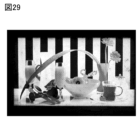
- FIG. 29 is a photograph of the display panel.
- FIG. 30 is a cross-sectional view illustrating an example of a display device; 31A and 31B are the results of cross-sectional observation. 32A and 32B are the results of cross-sectional observation. 33A and 33B are the results of cross-sectional observation. Figures 34A and 34B are the results of the peel test. FIG. 35 shows the results of the peel test.
- holes or electrons are sometimes referred to as “carriers”.
- the hole injection layer or electron injection layer is referred to as a "carrier injection layer”
- the hole transport layer or electron transport layer is referred to as a “carrier transport layer”
- the hole blocking layer or electron blocking layer is referred to as a "carrier It is sometimes called a block layer.
- the carrier injection layer, the carrier transport layer, and the carrier block layer described above may not be clearly distinguished from each other due to their cross-sectional shape, characteristics, or the like.
- one layer may serve as two or three functions of the carrier injection layer, the carrier transport layer, and the carrier block layer.
- a light-emitting element (also referred to as a light-emitting device) has an EL layer between a pair of electrodes, for example.
- the EL layer has at least a light-emitting layer.
- the layers (also referred to as functional layers) included in the EL layer include a light-emitting layer, a carrier-injection layer (hole-injection layer and electron-injection layer), a carrier-transport layer (hole-transport layer and electron-transport layer), and A carrier block layer (a hole block layer and an electron block layer) and the like are included.
- a light-receiving element (also referred to as a light-receiving device) includes, for example, a layer including a photoelectric conversion layer between a pair of electrodes.
- a layer shared by the light-receiving element and the light-emitting element may exist.
- Such layers may have different functions in the light emitting device than in the light receiving device.
- constituent elements may be referred to based on their functions in the light-emitting element.
- One embodiment of the present invention is a display device having a display portion capable of full-color display.
- the display unit has first sub-pixels and second sub-pixels exhibiting light of different colors, and a third pixel detecting light.
- the first sub-pixel has a first light-emitting element that emits blue light
- the second sub-pixel has a second light-emitting element that emits light of a different color than the first light-emitting element.
- the third pixel has a light receiving element that detects light.
- the first light emitting element and the second light emitting element have at least one different material, for example, different light emitting materials.
- the display device of one embodiment of the present invention uses light-emitting elements that are separately manufactured for each emission color.
- the light receiving element has a photoelectric conversion material.
- an image can be captured using a plurality of light-receiving elements, so that the image sensor functions as an imaging device.
- the light emitting element can be used as a light source for imaging.
- one embodiment of the present invention can display an image with a plurality of light-emitting elements, and therefore functions as a display device. Therefore, one embodiment of the present invention can be referred to as a display device having an imaging function or an imaging device having a display function.
- the display section has a function of displaying an image and a function of a light receiving section. Since an image can be captured by a plurality of light receiving elements provided in the display portion, the display device can function as an image sensor or the like. That is, it is possible to capture an image on the display unit, or detect the approach or contact of an object. Furthermore, since the light-emitting element provided in the display unit can be used as a light source when receiving light, there is no need to provide a light source separate from the display device. device can be realized.
- the light-receiving element when an object reflects light emitted from a light-emitting element included in a display portion, the light-receiving element can detect the reflected light. It can be performed.
- the display device of one embodiment of the present invention can capture an image of a fingerprint or a palmprint when a finger, palm, or the like is brought into contact with the display portion. Therefore, an electronic device including the display device of one embodiment of the present invention can perform personal authentication using an image such as a captured fingerprint or palmprint. As a result, there is no need to separately provide an imaging device for fingerprint authentication or palmprint authentication, and the number of parts of the electronic device can be reduced.
- the light-receiving elements are arranged in a matrix in the display section, an image of a fingerprint or a palm print can be taken anywhere on the display section, and an electronic device with excellent convenience can be realized.
- light-emitting elements with different emission wavelengths for example, blue (B), green (G), and red (R)
- B blue
- G green
- R red
- SBS side-by-side
- the material and structure can be optimized for each light-emitting element, so the degree of freedom in selecting the material and structure increases, and it becomes easy to improve luminance and reliability.
- an island shape indicates a state in which two or more layers using the same material formed in the same step are physically separated.
- an island-shaped light-emitting layer means that the light-emitting layer is physically separated from an adjacent light-emitting layer.
- the display device of one embodiment of the present invention includes a touch sensor that acquires position information of an object that touches or approaches the display surface.
- a touch sensor various systems such as a resistive film system, a capacitance system, an infrared system, an electromagnetic induction system, and a surface acoustic wave system can be adopted.
- a capacitive touch sensor it is preferable to use as the touch sensor.
- the capacitance method includes a surface capacitance method, a projected capacitance method, and the like. Also, the projective capacitance method includes a self-capacitance method, a mutual capacitance method, and the like. It is preferable to use the mutual capacitance method because it enables simultaneous multi-point detection.
- a mutual-capacitance touch sensor can have a plurality of electrodes to which a pulse potential is applied and a plurality of electrodes to which detection circuits are connected.
- a touch sensor can perform detection using a change in capacitance between electrodes when a finger or the like approaches. It is preferable that the electrodes constituting the touch sensor be arranged closer to the display surface than the light-emitting elements (light-receiving elements).
- At least part of the electrode of the touch sensor overlaps with a region sandwiched between two adjacent light-emitting elements (light-receiving elements) or a region sandwiched between two adjacent EL layers (PS layers). Furthermore, it is preferable that at least part of the electrode of the touch sensor has a region overlapping with an organic resin film provided between two adjacent EL layers (PS layers). With such a structure, the touch sensor can be provided above the display device without reducing the light emitting area of the light emitting element (light receiving element). Therefore, a display device having both a high aperture ratio and high definition can be provided.
- a metal or alloy material as the conductive layer that functions as the electrode of the touch sensor.
- a non-light-transmitting metal or alloy material can be used for the electrodes of the touch sensor without reducing the aperture ratio of the display device. Touch sensing with high sensitivity can be achieved by using a metal or alloy material with low resistance for the electrodes of the touch sensor.
- a light-transmitting electrode that transmits light emitted from the light-emitting element can be used as the electrode of the touch sensor. At this time, the light-transmitting electrode can be provided so as to overlap with the light-emitting element (light-receiving element).
- a light-emitting element can be provided between a pair of substrates.
- a rigid substrate such as a glass substrate may be used, or a flexible film may be used.
- the electrodes of the touch sensor can be formed on the substrate positioned on the display surface side. Alternatively, the electrodes of the touch sensor may be formed on another substrate and attached to the display surface side.
- the electrodes of the touch sensor between the pair of substrates.
- a protective layer may be provided to cover the light-emitting element (light-receiving element), and electrodes of the touch sensor may be provided over the protective layer.
- a tapered shape refers to a shape in which at least a part of the side surface of the structure is inclined with respect to the substrate surface. For example, it is preferable to have a region where the angle between the inclined side surface and the substrate surface (also referred to as a taper angle) is less than 90°. Note that the side surfaces of the structure and the substrate surface are not necessarily completely flat, and may be substantially planar with a small curvature or substantially planar with fine unevenness.
- a reverse tapered shape refers to a case where an angle in the structure formed by at least part of the side surface of the structure and the bottom surface is greater than 90°.
- the reverse tapered shape is a shape having a side portion or an upper portion protruding in a direction parallel to the substrate from the bottom portion.
- a display device of one embodiment of the present invention includes light-emitting elements that emit light of different colors.
- a light-emitting element includes a lower electrode, an upper electrode, and a layer containing a light-emitting compound (also referred to as a light-emitting layer) therebetween.
- Electroluminescence elements such as organic EL elements and inorganic EL elements are preferably used as the light emitting elements. Alternatively, a light emitting diode (LED) may be used.
- a display device of one embodiment of the present invention includes a light receiving element.
- the light receiving element can detect one or both of visible light and infrared light.
- a light receiving element includes, for example, a lower electrode, an upper electrode, and a photoelectric conversion layer therebetween.
- the light emitting element for example, it is preferable to use an OLED (Organic Light Emitting Diode) or a QLED (Quantum-dot Light Emitting Diode).
- the light-emitting substance included in the light-emitting element include a substance that emits fluorescence (fluorescent material), a substance that emits phosphorescence (phosphorescent material), and a substance that exhibits thermally activated delayed fluorescence (thermally activated delayed fluorescence: TADF ) materials), and inorganic compounds (quantum dot materials, etc.).
- LEDs such as micro LED (Light Emitting Diode), can also be used as a light emitting element.
- the emission color of the light emitting element can be red, green, blue, cyan, magenta, yellow, white, or the like. Further, the color purity can be enhanced by providing the light-emitting element with a microcavity structure.
- Embodiment 3 can be referred to for the structure and material of the light-emitting element.
- the light-emitting layer may contain one or more compounds (host material, assist material) in addition to the light-emitting substance (guest material).
- the host material and the assist material one or a plurality of substances having an energy gap larger than that of the light-emitting substance (guest material) can be selected and used.
- the host material and the assist material it is preferable to use a combination of compounds that form an exciplex. In order to efficiently form an exciplex, it is particularly preferable to combine a compound that easily accepts holes (hole-transporting material) and a compound that easily accepts electrons (electron-transporting material).
- Either a low-molecular-weight compound or a high-molecular-weight compound can be used for the light-emitting element, and an inorganic compound (quantum dot material, etc.) may be included.
- pixels having one or more light emitting elements are arranged at a resolution of 2000 ppi or more, preferably 3000 ppi or more, more preferably 5000 ppi or more, and even more preferably 6000 ppi or more, and 20000 ppi or less, or 30000 ppi or less.
- a very high-definition display device is preferable.
- FIG. 1 is a schematic top view of the display device 100A
- FIGS. 2A and 2B are schematic cross-sectional views of the display device 100A
- FIG. 2A is a cross-sectional view of the portion indicated by the dashed-dotted line A1-A2 in FIG. 1
- FIG. 2B is a cross-sectional view of the portion indicated by the dashed-dotted line B1-B2 in FIG. Note that some elements are omitted in the top view of FIG. 1 for clarity of illustration.
- the display device 100A includes a substrate 101 including a semiconductor circuit, an insulating layer 105, a light emitting element 110R, a light emitting element 110G, and a light emitting element 110B. Moreover, the display device 100A preferably has a light receiving element 110S. 2A and 2B, the light emitting element 110R, the light emitting element 110G, the light emitting element 110B, and the light receiving element 110S are provided on the insulating layer 105.
- the display device 100A has a gap between the insulating layer 105 and the light emitting element 110R, between the insulating layer 105 and the light emitting element 110G, between the insulating layer 105 and the light emitting element 110B, and between the insulating layer 105 and the light receiving element 110S.
- Each has an insulating layer 106 between them.
- the insulating layer 105 is preferably an organic insulating film (organic insulating layer), and the insulating layer 106 is preferably an inorganic insulating film (inorganic insulating layer).
- the insulating layer 105 may be an inorganic insulating film and the insulating layer 106 may be an organic insulating film.
- the organic layer 112 preferably has a region in contact with the upper surface of the pixel electrode 111, a region in contact with the side surface of the pixel electrode 111, and a region in contact with the insulating layer 105, respectively. Also, the organic layer 112 preferably has a region in contact with the side surface of the insulating layer 106 . Also, the organic layer 112 preferably has a region in contact with the lower surface of the insulating layer 106 . With the structure shown in FIG. 2A, the organic layer 112 can be sealed with the insulating layer 106 and the insulating layer 118 .
- Sealing the organic layer 112 with the insulating layer 106 and the insulating layer 118 can prevent the insulating layer 118 from peeling off from the organic layer 112, for example. In addition, diffusion of impurities such as water into the organic layer 112 can be suppressed.
- the PS layer 155S preferably has a region in contact with the upper surface of the pixel electrode 111, a region in contact with the side surface of the pixel electrode 111, and a region in contact with the insulating layer 105, respectively. Also, the PS layer 155S preferably has a region in contact with the side surface of the insulating layer 106 . Also, the PS layer 155S preferably has a region in contact with the bottom surface of the insulating layer 106 . With the configuration shown in FIG. 2B, the PS layer 155S can be sealed with the insulating layer 106 and the insulating layer 118d.
- Sealing the PS layer 155S with the insulating layer 106 and the insulating layer 118 can prevent the insulating layer 118 from peeling off from the organic layer 112, for example. In addition, diffusion of impurities such as water into the organic layer 112 can be suppressed.
- the display device 100A may be configured without the insulating layer 106 .
- 3 differs from FIG. 2A in that the display device 100A does not have the insulating layer 106.
- the organic layer 112 preferably has a region in contact with the upper surface of the pixel electrode 111, a region in contact with the side surface of the pixel electrode 111, and a region in contact with the insulating layer 105, respectively. Also, the organic layer 112 preferably has a region in contact with the lower surface of the pixel electrode 111 .
- the insulating layer 105 a single layer or a laminated structure of two or more layers can be selected as appropriate.
- the insulating layer 105 may have a laminated structure of an inorganic insulating film and an organic insulating film.
- the light emitting element 110R is a red light emitting element
- the light emitting element 110G is a green light emitting element
- the light emitting element 110B is a blue light emitting element.
- the light emitting element 110R and the light emitting element 110G emit light of different colors.
- the light-emitting element 110G and the light-emitting element 110B emit light of different colors.
- the light emitting element 110B and the light emitting element 110R emit light of different colors.
- a structure in which each light-emitting element is separately colored here, red (R), green (G), and blue (B)
- SBS side-by-side
- SBS Side-By-Side
- the material and structure can be optimized for each light-emitting element, so the degree of freedom in selecting the material and structure increases, and it becomes easy to improve luminance and reliability.
- the light emitting element 110R has a pixel electrode 111R, an organic layer 112R, a common layer 114, and a common electrode 113.
- the light emitting element 110G has a pixel electrode 111G, an organic layer 112G, a common layer 114, and a common electrode 113.
- the light emitting element 110B has a pixel electrode 111B, an organic layer 112B, a common layer 114, and a common electrode 113.
- the common layer 114 and the common electrode 113 are commonly provided for the light emitting elements 110R, 110G, and 110B.
- the organic layer 112R contains a light-emitting organic compound that emits light having an intensity in at least the red wavelength range.
- the organic layer 112G contains a light-emitting organic compound that emits light having an intensity in at least the green wavelength range.
- the organic layer 112B contains a light-emitting organic compound that emits light having an intensity in at least the blue wavelength range.
- the organic layer 112R, the organic layer 112G, and the organic layer 112B have at least a layer (light-emitting layer) containing a light-emitting organic compound.
- the symbols added to the reference numerals may be omitted and the light emitting elements 110 may be used for description.
- the organic layer 112R, the organic layer 112G, and the organic layer 112B may also be described as the organic layer 112 in some cases.
- the pixel electrode 111R, the pixel electrode 111G, the pixel electrode 111B, and the pixel electrode 111S may also be described as the pixel electrode 111 in some cases.
- the EL layer may refer to, for example, a structure in which the organic layer 112 and the common layer 114 are combined.
- a pixel electrode 111R, a pixel electrode 111G, and a pixel electrode 111B are provided for each light emitting element. Further, the common layer 114 and the common electrode 113 are provided as a continuous layer common to each light emitting element.
- a conductive film having a property of transmitting visible light is used for one of the pixel electrodes and the common electrode 113, and a conductive film having a reflective property is used for the other.
- a protective layer 121 is provided on the common electrode 113 to cover the light emitting elements 110R, 110G, and 110B.
- the protective layer 121 has a function of preventing impurities such as water from diffusing into each light emitting element from above.
- the light receiving element 110S can detect one or both of visible light and infrared light.
- visible light for example, one or more of colors such as blue, purple, violet, green, yellow-green, yellow, orange, and red can be detected.
- infrared light it is possible to detect an object even in a dark place, which is preferable.
- the light receiving element 110S for example, a pn-type or pin-type photodiode can be used.
- the light receiving element 110S functions as a photoelectric conversion element (also referred to as a photoelectric conversion device) that detects light incident on the light receiving element 110S and generates electric charges. The amount of charge generated by the photoelectric conversion element is determined according to the amount of incident light.
- organic photodiode having a layer containing an organic compound as the light receiving element 110S.
- Organic photodiodes can be easily made thinner, lighter, and larger, and have a high degree of freedom in shape and design, so they can be applied to various devices.
- a layer shared by the light-receiving element and the light-emitting element may exist.
- Such layers may have different functions in the light emitting device than in the light receiving device.
- constituent elements may be referred to based on their functions in the light-emitting element.
- the hole-injection layer functions as a hole-injection layer in the light-emitting device and as a hole-transport layer in the light-receiving device.
- the electron injection layer functions as an electron injection layer in the light emitting device and as an electron transport layer in the light receiving device.
- a layer shared by the light receiving element and the light emitting element may have the same function in the light emitting element and the light receiving element.
- the hole-transporting layer functions as a hole-transporting layer in both the light-emitting device and the light-receiving device
- the electron-transporting layer functions as an electron-transporting layer in both the light-emitting device and the light-receiving device.
- an organic EL element is used as the light-emitting element and an organic photodiode is used as the light-receiving element.
- An organic EL element and an organic photodiode can be formed on the same substrate. Therefore, an organic photodiode can be incorporated in a display device using an organic EL element.
- the light-receiving element is driven by applying a reverse bias between the pixel electrode and the common electrode, thereby detecting light incident on the light-receiving element, generating an electric charge, and extracting it as a current.
- the light receiving element 110S has a pixel electrode 111S, a PS layer 155S, and a common electrode 113. As shown in FIG. 2B and the like, the light receiving element 110S has a common layer 114 between the PS layer 155S and the common electrode 113. As shown in FIG. 2B and the like, the light receiving element 110S has a common layer 114 between the PS layer 155S and the common electrode 113. As shown in FIG.
- the PS layer 155S has at least a photoelectric conversion layer (sometimes called an active layer).
- the layers (also referred to as functional layers) included in the PS layer 155S include a photoelectric conversion layer, a carrier injection layer (hole injection layer and electron injection layer), a carrier transport layer (hole transport layer and electron transport layer), and a carrier block layer (a hole block layer and an electron block layer).
- the photoelectric conversion layer contains a semiconductor.
- the semiconductor include inorganic semiconductors such as silicon and organic semiconductors including organic compounds.
- an organic semiconductor can be used as the semiconductor included in the photoelectric conversion layer.
- the light-emitting layer and the photoelectric conversion layer can be formed by the same method (for example, a vacuum deposition method), and a manufacturing apparatus can be shared, which is preferable.
- a pn-type or pin-type photodiode can be used as the photoelectric conversion layer.
- the material and structure shown for the pixel electrode 111R, the pixel electrode 111G, the pixel electrode 111B, and the like can be used.
- the combination of colors of light emitted by the light emitting element 110 is not limited to the above, and for example, colors such as cyan, magenta, and yellow may also be used. In the above, three colors of red (R), green (G), and blue (B) are exemplified. or four or more colors.
- the pixel electrode 111 functions as a lower electrode, and the common electrode 113 functions as an upper electrode.
- the common electrode 113 is transmissive and reflective to visible light.
- Organic layer 112 includes a light-emitting compound.
- the light-emitting element 110 an electroluminescence element having a function of emitting light by current flowing through the organic layer 112 by applying a potential difference between the pixel electrode 111 and the common electrode 113 can be used.
- an organic EL element using a light-emitting organic compound for the organic layer 112 .
- the light-emitting element 110 is preferably an element that emits monochromatic light whose emission spectrum has one peak in the visible light region.
- the light emitting element 110 may be an element that emits white light whose emission spectrum has two or more peaks in the visible light region.
- a pixel electrode 111 provided for each light emitting element 110 is independently applied with a potential for controlling the amount of light emitted by the light emitting element 110 .
- Organic layer 112 and common layer 114 may each independently include one or more of an electron injection layer, an electron transport layer, a hole injection layer, and a hole transport layer.
- the organic layer 112 may have a stacked structure of a hole-injection layer, a hole-transport layer, a light-emitting layer, and an electron-transport layer from the pixel electrode 111 side
- the common layer 114 may have an electron-injection layer. can.
- the common electrode 113 is formed to be transmissive and reflective to visible light.
- a metal film or an alloy film thin enough to transmit visible light can be used.
- a light-transmitting conductive film eg, a metal oxide film
- stacked over such a film may be used.
- the edge of the organic layer 112 is positioned outside the edge of the pixel electrode 111 .
- the edge of the organic layer 112 covers the edge of the pixel electrode 111 .
- the edge of the PS layer 155S is located outside the edge of the pixel electrode 111. As shown in FIG. Edges of the PS layer 155S cover edges of the pixel electrode 111 . By locating the end of the PS layer 155S outside the end of the pixel electrode 111, short-circuiting between the pixel electrode 111 and the common electrode 113 can be suppressed.
- the insulating layer 105 has recesses 175 .
- the recess 175 is provided in the insulating layer 105 in a region located between two pixel electrodes 111 adjacent in the A1-A2 direction shown in FIG.
- the recess 175 is also provided in the insulating layer 105 in a region located between two pixel electrodes 111 adjacent in the B1-B2 direction.
- the recess 175 can also be expressed as a collection of multiple recesses.
- the concave portion 175 can be expressed as, for example, a collection of a plurality of grooves, and one groove is provided, for example, between adjacent pixel electrodes 111 .
- the recess 175 has a groove-like region.
- the concave portion 175 has, for example, a groove-like region provided along the side of the pixel electrode 111 when viewed from above.
- the recess 175 has a region overlapping with the pixel electrode 111 inside the side of the pixel electrode 111 when viewed from above.
- the organic layer 112 can be discontinued in the area below the pixel electrode 111 and inside the side of the pixel electrode 111 by having the area where the concave portion 175 overlaps the inside of the pixel electrode. .
- a recess 175 is provided in a region of the insulating layer 105 located between the light emitting elements 110R and 110G so that the insulating layer 105 is located between the light emitting elements 110G and 110B.
- a recess 175 is provided in a region located between them, and a recess 175 is provided in a region of the insulating layer 105 located between the light emitting element 110B and the light emitting element 110R.
- a recess 175 is provided in a region of the insulating layer 105 located between the light emitting element 110G and the light receiving element 110S.
- the direction in which the light emitting elements 110R, 110G, and 110B are arranged in order is defined as the x direction
- the direction perpendicular to the x direction is defined as the y direction.
- the concave portion 175 can also be expressed as a set of linear grooves extending in the x-direction and lower linear grooves extending in the y-direction.
- a portion of the recess 175 is preferably positioned below the pixel electrode 111 .
- the recess 175 preferably has a region located below the pixel electrode 111 .
- the recess 175 has a first region overlapping with the first pixel electrode and a second region overlapping with the second pixel electrode. , and a third region that does not overlap with the first pixel electrode and the second pixel electrode.
- the third region is located between the first region and the second region.
- the first region is positioned below the first pixel electrode.
- the second region is positioned below the second pixel electrode.
- the light-emitting element having the first pixel electrode and the light-emitting element having the second pixel electrode emit light of different colors.
- the first pixel electrode is included in the light emitting element and the second pixel electrode is included in the light receiving element.
- the concave portion 175 has a downward convex shape in a cross-sectional view of the display device 100A.
- the concave portion 175 has, for example, an arcuate shape that protrudes downward.
- the recess 175 may have, for example, a downwardly convex arc-shaped region and a flat-shaped region.
- the side wall of the recess 175 may have an arcuate shape that protrudes downward, and the bottom may have a flat shape.
- the shape of the recess 175 is not particularly limited as long as part of the recess 175 is positioned below the pixel electrode 111 .
- the concave portion 175 may have an arcuate shape that is convex downward, or may have an arcuate shape with a flat bottom and downwardly convex sidewalls. good.
- the shape of the recess 175 is not limited to the above.
- the recess 175 does not have to have a region located below the pixel electrode 111 .
- the concave portion 175 may have a cross-shaped shape, a T-shaped shape, or an inverted T-shaped shape in a cross-sectional view of the display device.
- the downwardly convex circular arc shape can also be said to be a concave curved surface shape.
- the downwardly convex circular arc shape includes a downwardly convex semicircular shape.
- the organic layer 112 of the light emitting element 110 can be cut between the adjacent light emitting element 110 or between the adjacent light receiving element 110S. Further, by providing the concave portion 175, the PS layer 155S of the light receiving element 110S can be cut between the adjacent light emitting elements 110 or between the adjacent light receiving elements 110S.
- the film that will become the organic layer 112 is cut in the region of the concave portion 175 that overlaps the pixel electrode 111 .
- the film to be the organic layer 112 can be processed into an island shape without using a shadow mask such as a metal mask, etching, or the like.
- the film to be the PS layer 155S is cut in the region of the concave portion 175 overlapping the pixel electrode 111.
- FIG. the film to be the organic layer 112 can be processed into an island shape without using a shadow mask such as a metal mask, etching, or the like.
- the film remaining in the recess 175 among the film to be the organic layer 112 and the film to be the PS layer 155S is etched. It is preferable to remove by, for example.
- the organic layer 112 is divided between adjacent light emitting elements, between adjacent light emitting elements and light receiving elements, or between adjacent light receiving elements. Accordingly, current (also referred to as leakage current) flowing through the organic layer 112 can be prevented between adjacent elements. Therefore, light emission caused by the leakage current can be suppressed, and high-contrast display can be realized. Furthermore, even when the definition is increased, a material with high conductivity can be used for the organic layer 112, so that the range of selection of materials can be widened, and efficiency can be improved, power consumption can be reduced, and reliability can be improved. It becomes easier to improve.
- the organic layer 112 and the PS layer 155S may form an island pattern by film formation using a shadow mask such as a metal mask, but it is particularly preferable to use a processing method that does not use a metal mask. As a result, it is possible to form an extremely fine pattern, so that the definition and the aperture ratio can be improved as compared with the formation method using a metal mask.
- a processing method typically, a photolithography method can be used.
- formation methods such as nanoimprinting and sandblasting can also be used.
- a device manufactured using a metal mask or FMM may be referred to as a device with an MM (metal mask) structure.
- a device manufactured without using a metal mask or FMM may be referred to as a device with an MML (metal maskless) structure.
- the display device 100A includes an insulating layer 118a on the organic layer 112R, an insulating layer 118b on the organic layer 112G, an insulating layer 118c on the organic layer 112B, an insulating layer 118d on the PS layer 155S, an insulating layer 125, and a resin layer 126 .
- the insulating layer 118 is provided so as to cover at least part of the upper surface of the organic layer 112 or the PS layer 155S. Moreover, the insulating layer 118 is provided so as to overlap with at least part of the recess 175 . As shown in FIG. 2A, the insulating layer 118a on the organic layer 112R is provided so as to overlap at least part of the recess 175, and the insulating layer 118b on the organic layer 112G is provided so as to overlap at least part of the recess 175. The insulating layer 118 c on the organic layer 112 B is provided so as to overlap with at least part of the recess 175 . Also, as shown in FIG. 2B, the insulating layer 118d on the PS layer 155S is provided so as to overlap at least a portion of the recess 175. As shown in FIG.
- the insulating layer 118 also has a region in contact with at least part of the top surface of the organic layer 112 (PS layer 155S) and a region in contact with the side surface of the organic layer 112 (PS layer 155S). Further, the insulating layer 118 has a region in contact with the insulating layer 105 below the light emitting element 110 (light receiving element 110S), specifically, the pixel electrode 111 . Insulating layer 118 also has a region in contact with the lower surface of insulating layer 106 .
- the insulating layer 118 can be peeled off from the organic layer 112 (PS layer 155S) and the organic layer 112 (PS layer 155S) can be separated from the pixel electrode. Peeling off from 111 can be suppressed.
- the insulating layer 105 and the insulating layer 118 are configured to have high adhesiveness, the insulating layer 118 can be peeled off from the organic layer 112 (PS layer 155S), and the organic layer 112 (PS layer 155S) can be separated from the pixel electrode 111. It is possible to suppress peeling from. By suppressing the peeling of the film, the yield in the manufacturing process of the display device can be improved. Moreover, the display quality of the display device can be improved.
- the adhesion between the insulating layer 105 and the insulating layer 118 is preferably higher than the adhesion between the insulating layer 118 and the organic layer 112 . Also, the adhesion between the insulating layer 105 and the insulating layer 118 is preferably higher than the adhesion between the insulating layer 118 and the PS layer 155S.
- acrylic resin, polyimide resin, epoxy resin, imide resin, polyamide resin, polyimideamide resin, silicone resin, siloxane resin, benzocyclobutene-based resin, phenol resin, and the like can be used.
- a resin precursor or the like can be applied.
- an organic material such as polyvinyl alcohol (PVA), polyvinyl butyral, polyvinylpyrrolidone, polyethylene glycol, polyglycerin, pullulan, water-soluble cellulose, or alcohol-soluble polyamide resin may be used.
- baking is preferably performed after the resin is applied. Baking is preferably performed in a reducing atmosphere, for example, and can be performed in a nitrogen atmosphere, for example.
- the baking temperature is preferably 125° C. or higher, more preferably 150° C. or higher, and even more preferably 200° C. or higher. By performing baking at such a temperature, adhesion between the insulating layer 105 and the insulating layer 118 may increase.
- the baking temperature in manufacturing the resin layer 126 described later may be lower than the baking temperature in manufacturing the insulating layer 105 .
- the baking temperature for producing the resin layer 126 is, for example, preferably 200° C. or lower, more preferably 150° C. or lower, and even more preferably 125° C. or lower.
- the insulating layer 118a has a region in contact with at least a portion of the upper surface of the organic layer 112R, a region in contact with the side surface of the organic layer 112R, and a region in contact with the insulating layer 105 below the pixel electrode 111R. Insulating layer 118 a also has a region in contact with the lower surface of insulating layer 106 .
- the insulating layer 118b has a region in contact with at least part of the upper surface of the organic layer 112G, a region in contact with the side surface of the organic layer 112G, and a region in contact with the insulating layer 105 below the pixel electrode 111G.
- Insulating layer 118 b also has a region in contact with the lower surface of insulating layer 106 .
- the insulating layer 118c has a region in contact with at least part of the upper surface of the organic layer 112B, a region in contact with the side surface of the organic layer 112B, and a region in contact with the insulating layer 105 below the pixel electrode 111B.
- Insulating layer 118 c also has a region in contact with the lower surface of insulating layer 106 .
- the insulating layer 118d has a region in contact with at least a portion of the upper surface of the PS layer 155S, a region in contact with the side surfaces of the PS layer 155S, and a region in contact with the insulating layer 105 below the pixel electrode 111S.
- the insulating layer 118 has an opening reaching the organic layer 112 (PS layer 155S).
- the organic layer 112 (PS layer 155S) is in contact with the common layer 114 in the opening.
- the common electrode 113 has a region overlapping with the organic layer 112 (PS layer 155S) through the opening.
- the insulating layer 118 has a region located between the resin layer 126 and the organic layer 112 (PS layer 155S), and serves as a protective film to prevent the resin layer 126 from contacting the organic layer 112 (PS layer 155S). Function.
- the organic layer 112 (PS layer 155S) and the resin layer 126 are in contact with each other, the organic layer 112 (PS layer 155S) may be dissolved by the organic solvent or the like used when forming the resin layer 126 . Therefore, as shown in this embodiment, the insulating layer 118 is provided between the organic layer 112 (PS layer 155S) and the resin layer 126 to protect the side surface of the organic layer 112 (PS layer 155S). It becomes possible to
- the insulating layer 118 can be an insulating layer containing an inorganic material.
- an inorganic insulating film such as an oxide insulating film, a nitride insulating film, an oxynitride insulating film, or a nitride oxide insulating film can be used, for example.
- the insulating layer 118 may have a single-layer structure or a laminated structure.
- the oxide insulating film includes a silicon oxide film, an aluminum oxide film, a magnesium oxide film, an indium gallium zinc oxide film, a gallium oxide film, a germanium oxide film, an yttrium oxide film, a zirconium oxide film, a lanthanum oxide film, a neodymium oxide film, and an oxide film.
- Examples include a hafnium film and a tantalum oxide film.
- Examples of the nitride insulating film include a silicon nitride film, an aluminum nitride film, and the like.
- Examples of the oxynitride insulating film include a silicon oxynitride film, an aluminum oxynitride film, and the like.
- nitride oxide insulating film a silicon nitride oxide film, an aluminum nitride oxide film, or the like can be given.
- a metal oxide film such as an aluminum oxide film or a hafnium oxide film formed by an ALD method, or an inorganic insulating film such as a silicon oxide film to the insulating layer 118, there are few pinholes and the function of protecting the organic layer 112.
- An insulating layer 118 having excellent resistance can be formed.
- oxynitride refers to a material whose composition contains more oxygen than nitrogen
- nitride oxide refers to a material whose composition contains more nitrogen than oxygen. point to the material.
- silicon oxynitride refers to a material whose composition contains more oxygen than nitrogen
- silicon nitride oxide refers to a material whose composition contains more nitrogen than oxygen. indicates
- the insulating layer 118 may also function as a protective layer that prevents impurities such as water from diffusing into the organic layer 112 and the PS layer 155S.
- An inorganic insulating film with low moisture permeability such as a silicon oxide film, a silicon nitride film, or an aluminum oxide film is preferably used for the insulating layer 118 .
- the insulating layer 118 is an insulating layer containing aluminum and oxygen.
- the insulating layer 118 can be formed by a sputtering method, a CVD method, a PLD method, an ALD method, or the like.
- the insulating layer 118 is preferably formed by an ALD method with good coverage.
- the thickness of the insulating layer 118 is preferably 3 nm or more, 5 nm or more, or 10 nm or more and 200 nm or less, 150 nm or less, 100 nm or less, or 50 nm or less.
- the side surfaces of the organic layers 112 are provided facing each other with the resin layer 126 interposed therebetween.
- the resin layer 126 is positioned between the adjacent light-emitting elements of different colors, and is provided so as to fill the end portions of the respective organic layers 112 and the area between the two organic layers 112 .
- the side surface of the organic layer 112 of the light emitting element and the side surface of the PS layer 155S of the light receiving element are provided to face each other with the resin layer 126 interposed therebetween.
- the resin layer 126 is located between the adjacent light-emitting element and light-receiving element, and fills the area between the edge of the organic layer 112 and the edge of the PS layer 155S and the area between the organic layer 112 and the PS layer 155S. is provided as follows.
- the side surfaces of the PS layers 155S are provided to face each other with the resin layer 126 interposed between the adjacent light receiving elements. ing.
- the resin layer 126 is positioned between the adjacent light receiving elements, and is provided so as to fill the ends of each PS layer 155S and the area between the two PS layers 155S.
- the resin layer 126 has a smooth convex upper surface, and a common layer 114 and a common electrode 113 are provided to cover the upper surface of the resin layer 126 .
- the resin layer 126 has regions in contact with the insulating layer 105 between adjacent light emitting elements, between adjacent light emitting elements and light receiving elements, and the like.
- the resin layer 126 has a region in contact with the insulating layer 105 in a portion located between the organic layers 112R and 112G.
- the resin layer 126 has a region in contact with the insulating layer 105 in a portion located between the organic layers 112G and 112B.
- the resin layer 126 has a region in contact with the insulating layer 105 in a portion located between the organic layers 112B and 112R.
- the resin layer 126 has a region in contact with the insulating layer 105 in a portion located between the PS layer 155S and the organic layer 112 .
- the resin layer 126 functions as a planarization film that fills in steps between adjacent light-emitting elements, steps between adjacent light-emitting elements and light-receiving elements, and the like.
- a phenomenon in which the common electrode 113 is divided by a step at the end of the organic layer 112 and a step at the end of the PS layer 155S (also referred to as discontinuity) can be suppressed. It is possible to prevent the common electrode 113 on the layer 112 from being insulated.
- the resin layer 126 can also be called LFP (Local Filling Planarization).
- an insulating layer containing an organic material can be preferably used.
- acrylic resin, polyimide resin, epoxy resin, imide resin, polyamide resin, polyimideamide resin, silicone resin, siloxane resin, benzocyclobutene-based resin, phenolic resin, and precursors of these resins are applied as the resin layer 126. can do.
- an organic material such as polyvinyl alcohol (PVA), polyvinyl butyral, polyvinylpyrrolidone, polyethylene glycol, polyglycerin, pullulan, water-soluble cellulose, or alcohol-soluble polyamide resin may be used.
- a photosensitive resin can be used as the resin layer 126 .
- a photoresist may be used as the photosensitive resin.
- a positive material or a negative material can be used for the photosensitive resin.
- the resin layer 126 may contain a material that absorbs visible light.
- the resin layer 126 itself may be made of a material that absorbs visible light, or the resin layer 126 may contain a pigment that absorbs visible light.
- a resin that transmits red, blue, or green light and can be used as a color filter that absorbs other light, or a resin that contains carbon black as a pigment and functions as a black matrix, or the like. can be used.
- Insulating layers 125 are provided between the resin layer 126 and the insulating layer 118a, between the resin layer 126 and the insulating layer 118b, and between the resin layer 126 and the insulating layer 118c.
- the insulating layer 125 is provided with an opening reaching the organic layer 112 (PS layer 155S). Note that the display device 100A may have a structure in which the insulating layer 125 is not provided.
- a protective layer 121 is provided to cover the common electrode 113 .
- the protective layer 121 can have, for example, a single-layer structure or a laminated structure including at least an inorganic insulating film.
- inorganic insulating films include oxide films and nitride films such as silicon oxide films, silicon oxynitride films, silicon nitride oxide films, silicon nitride films, aluminum oxide films, aluminum oxynitride films, and hafnium oxide films.
- a semiconductor material or a conductive material such as indium gallium oxide, indium zinc oxide, indium tin oxide, or indium gallium zinc oxide may be used for the protective layer 121 .
- a laminated film of an inorganic insulating film and an organic insulating film can also be used as the protective layer 121 .
- a structure in which an organic insulating film is sandwiched between a pair of inorganic insulating films is preferable.
- the organic insulating film functions as a planarizing film.
- the upper surface of the organic insulating film can be flattened, so that the coverage of the inorganic insulating film thereon can be improved, and the barrier property can be enhanced.
- the upper surface of the protective layer 121 is flat, when a structure (for example, a color filter, an electrode of a touch sensor, or a lens array) is provided above the protective layer 121, an uneven shape due to the structure below may be formed. This is preferable because it can reduce the impact.
- a structure for example, a color filter, an electrode of a touch sensor, or a lens array
- the common electrode 113 extends outside the end of the recess 175 .
- an EL layer included in the light-emitting element 110 is separately formed for each light-emitting element of a different color, so that color display with high color reproducibility and low power consumption can be performed.
- a circuit board having transistors, wiring, or the like can be used as the substrate 101 .
- an insulating substrate such as a glass substrate can be used as the substrate 101 when a passive matrix method or a segment method can be applied.
- the substrate 101 is a substrate provided with a circuit for driving each light-emitting element (also referred to as a pixel circuit) or a semiconductor circuit functioning as a driver circuit for driving the pixel circuit. A more specific configuration example of the substrate 101 will be described later.
- the substrate 101 and the pixel electrode 111 of the light emitting element 110 are electrically connected via a conductive layer.
- a width W1 shown in FIG. 2A is the width of the concave portion 175 in the region that does not overlap the pixel electrode 111 in the A1-A2 direction.
- the width W1 can be rephrased as the shortest distance between the ends of the pixel electrodes 111 facing each other.
- a width W2 shown in FIG. 2A is the width of the recess 175 in the region overlapping the pixel electrode 111 in the A1-A2 direction.
- FIG. 30 shows an enlarged view of a region including width W1 and width W2 in FIG. 2A.
- 30 also shows the depth W5 of the recess 175.
- the depth W5 is, for example, the height difference between the bottom of the recess 175 and the top surface of the insulating layer 105 .
- the width W1, the width W2, the height of the bottom portion, and the height of the upper surface of the insulating layer 105 of the concave portion 175 can be measured by, for example, a cross-sectional observation image of the display device 100A.
- the cross-sectional observation image can be observed using, for example, a TEM (Transmission Electron Microscope), a STEM (Scanning Transmission Electron Microscope), or the like.
- the cross-sectional observation image can be processed to expose the cross section and measured using the height in the observation range.
- the average height in the observation range may be calculated.
- the height of the bottom of recess 175 may be measured at the deepest point of recess 175 in the observed area.
- the average height in the observation range may be calculated.
- the height of the upper surface of the insulating layer 105 may be measured at the point where the upper surface of the insulating layer 105 is highest in the observed region.
- the width W1, width W2, depth W5, etc. of the recesses may be their average value, maximum value, minimum value, median value, or the like. And it is sufficient.
- the width W1 is preferably larger than twice the film thickness of the organic layer 112 (PS layer 155S).
- the width W1 is 200 nm or more and 1200 nm or less, preferably 200 nm or more and 1000 nm or less, more preferably 200 nm or more and 900 nm or less.
- the organic layer 112 (PS layer 155S) is broken by the recess 175, and the organic layer 112 (PS layer 155S) can be formed on the pixel electrode 111.
- FIG. At this time, as shown in FIG.
- the organic layer 112 (PS layer 155S) is arranged so as to cover the side surfaces and the upper surface of the pixel electrode 111 .
- a layer covering a structure means a state in which the layer covers part of an end surface of the structure, or a state in which the layer completely covers the end surface of the structure. It refers to the state where Here, the layer is an insulating layer, an insulating film, a conductive layer, or the like.
- the structure is a conductive layer, an organic layer, a laminate, a light-emitting element, or the like.
- the width W1 may be appropriately adjusted according to the processing accuracy when forming the concave portion 175, the film forming conditions of the organic layer 112 (PS layer 155S), and the like.
- the organic layer 112 (PS layer 155S) is formed by, for example, a vacuum deposition method, even if the width W1 is smaller than twice the film thickness of the organic layer 112 (PS layer 155S), the organic layer 112 (PS layer 155S) ) may be interrupted.
- the width W1 may be 100 nm or more and 1200 nm or less, 1000 nm or less, or 900 nm or less.
- the width W2 may be any width that causes a discontinuity in the organic layer 112 (PS layer 155S).
- the width W2 is preferably 2 nm or more, 5 nm or more, 10 nm or more, 20 nm or more, 30 nm or more, 40 nm or more, or 50 nm or more.
- a discontinuity can be generated in the organic layer 112 .
- the width W2 is preferably 500 nm or less, 300 nm or less, 200 nm or less, 150 nm or less, or 100 nm or less.
- the width W2 is preferably 20 nm or more and 500 nm or less, more preferably 30 nm or more and 300 nm or less, still more preferably 40 nm or more and 200 nm or less, still more preferably 50 nm or more and 150 nm or less, for example about 90 nm.
- the organic layer 112 can be discontinued while maintaining a high aperture ratio even in a high-definition display. It can be configured to be in contact with the lower surface and the side surface of the insulating layer 105, and the insulating layer 118 can be preferably prevented from peeling off from the organic layer 112 (PS layer 155S). Further, the anchoring effect of the organic layer 112 can improve adhesion.
- the width W1, the width W2 and the depth W5 can be measured using, for example, a cross-sectional image of the display device observed with an electron microscope or the like.
- the cross section to be observed is preferably substantially perpendicular to the sides of the pixel electrode 111 when viewed from above. At this time, in the region where the sides are substantially straight lines, the cross section may be processed substantially vertically and the cross section may be observed.
- the width W1 and the width W2 may be measured in the width direction of the groove.
- the depth W5 is, for example, 20 nm or more, or 50 nm or more and 3000 nm or less, or 100 nm or more and 2000 nm or less, or 200 nm or more and 1000 nm or less.
- the organic layer 112 when the width W2 is set to the above width, the organic layer 112 can be suitably discontinued. Further, by setting the width W2 to the width described above, even when one or more of the insulating layer 106 and the pixel electrode 111 have a tapered shape, the organic layer 112 can be suitably cut off.
- part of the insulating layer 118 is in contact with the bottom surface of the insulating layer 106 and the side surface of the insulating layer 105, whereby the pixel electrode 111, the insulating layer 118, and the insulating layer 106 are formed. , and the insulating layer 105 can seal the organic layer 112 .
- the above sealing is performed in a region around the pixel electrode 111 . Therefore, when the perimeter of the pixel electrode 111 is sufficiently large with respect to the area of the pixel electrode 111 in a plan view, sealing can be performed more satisfactorily. Therefore, a display device with a smaller area of the pixel electrode 111 and a higher definition can be sealed more satisfactorily. For example, better sealing may be achieved at a resolution of 400 ppi or more, more preferably 600 ppi or more.
- pixels having one or more light emitting elements are arranged at a resolution of 2000 ppi or more, preferably 3000 ppi or more, more preferably 5000 ppi or more, and still more preferably 6000 ppi or more, and 20000 ppi or less, or 30000 ppi or less. , a very high-definition display device can be realized.
- a microcavity structure (microresonator structure) is provided, and a high-brightness display device can be realized.
- the light emitting elements 110 it becomes possible to arrange the light emitting elements 110 at an extremely high density. For example, a display device with a definition exceeding 2000 ppi can be realized.
- the thickness of the EL layer of the light emitting element 110 may be adjusted according to the peak wavelength of the emission spectrum.
- the light emitting element 110R that emits light with the longest wavelength has the thickest organic layer 112R
- the light emitting element 110B that emits light with the shortest wavelength has the thinnest organic layer 112B.
- the thickness of each organic layer can be adjusted in consideration of the wavelength of light emitted by each light emitting element, the optical characteristics of the layers constituting the light emitting element, the electrical characteristics of the light emitting element, and the like. .
- the width W1 is preferably larger than twice the thickness of the thinnest organic layer 112 (PS layer 155S), and is larger than twice the thickness of the thickest organic layer 112 (PS layer 155S). is more preferred.
- the organic layer 112 (PS layer 155S) is broken by the recess 175, and the organic layer 112 (PS layer 155S) can be formed on the pixel electrode 111.
- FIG. Furthermore, microcavity structures can be realized.
- a width W3 shown in FIG. 2B is the width of the concave portion 175 in the region that does not overlap the pixel electrode 111 in the B1-B2 direction.
- the width W3 can be rephrased as the shortest distance between the ends of the pixel electrodes 111 facing each other.
- a width W4 shown in FIG. 2B is the width of the concave portion 175 in the region overlapping the pixel electrode 111 in the B1-B2 direction.
- width W3 the description of the width W1 can be referred to.
- width W4 the description of the width W2 can be referred to.
- a light emitting element that can be used for the light emitting element 110, an element that can emit light by itself can be used, and an element whose luminance is controlled by current or voltage is included in its category.
- an LED, an organic EL element, an inorganic EL element, or the like can be used.
- Light-emitting elements include top emission type, bottom emission type, dual emission type, and the like.
- a conductive film that transmits visible light is used for the electrode on the light extraction side.
- a conductive film that reflects visible light is used for the electrode on the side from which light is not extracted.
- a top-emission or dual-emission light-emitting element that emits light to the side opposite to the formation surface can be preferably used.
- the organic layer 112 has at least a light-emitting layer.
- the organic layer 112 includes, as layers other than the light-emitting layer, a substance with a high hole-injection property, a substance with a high hole-transport property, a hole-blocking material, a substance with a high electron-transport property, a substance with a high electron-injection property, and an electron-blocking material. , a layer containing a bipolar substance (a substance with high electron-transport properties and high hole-transport properties), or the like.
- Either a low-molecular-weight compound or a high-molecular-weight compound can be used for the organic layer 112, and an inorganic compound may be included.
- the layers constituting the organic layer 112 can be formed by a method such as a vapor deposition method (including a vacuum vapor deposition method), a transfer method, a printing method, an inkjet method, or a coating method.
- the organic layer 112 preferably contains two or more kinds of light-emitting substances.
- white light emission can be obtained by selecting luminescent substances such that the luminescence of each of two or more luminescent substances has a complementary color relationship.
- luminescent substances exhibiting luminescence such as R (red), G (green), B (blue), Y (yellow), and O (orange), respectively, or spectral components of two or more colors of R, G, and B It is preferable that two or more of the light-emitting substances exhibiting light emission containing are included.
- the spectrum of light emitted from the light-emitting element has two or more peaks within the range of wavelengths in the visible light region (eg, 350 nm to 750 nm).
- the emission spectrum of the material having a peak in the yellow wavelength region is preferably a material having spectral components in the green and red wavelength regions as well.
- the organic layer 112 preferably has a structure in which a light-emitting layer containing a light-emitting material that emits light of one color and a light-emitting layer containing a light-emitting material that emits light of another color are stacked.
- the plurality of light-emitting layers in the organic layer 112 may be laminated in contact with each other, or may be laminated via a region that does not contain any light-emitting material.
- a configuration in which a region is provided between a fluorescent-emitting layer and a phosphorescent-emitting layer and contains the same material as the fluorescent-emitting layer or the phosphorescent-emitting layer (e.g., host material, assist material) and does not contain any of the emitting materials. good too. This facilitates fabrication of the light-emitting element and reduces the driving voltage.
- the light emitting element 110 may be a single element having one EL layer, or may be a tandem element in which a plurality of EL layers are stacked with a charge generation layer interposed therebetween.
- a single-structure device preferably has one light-emitting unit between a pair of electrodes, and the light-emitting unit preferably includes one or more light-emitting layers.
- the light-emitting layers may be selected such that the respective light-emitting colors of the two light-emitting layers are in a complementary color relationship. For example, by setting the emission color of the first light-emitting layer and the emission color of the second light-emitting layer to have a complementary color relationship, it is possible to obtain a configuration in which the entire light-emitting element emits white light.
- the light-emitting element as a whole may emit white light by combining the light-emitting colors of the three or more light-emitting layers.
- a tandem structure device preferably has two or more light-emitting units between a pair of electrodes, and each light-emitting unit includes one or more light-emitting layers.
- each light-emitting unit includes one or more light-emitting layers.
- a structure in which white light emission is obtained by combining light from the light emitting layers of a plurality of light emitting units may be employed. Note that the structure for obtaining white light emission is the same as the structure of the single structure.
- a conductive film which transmits visible light and which can be used for the pixel electrode 111 or the like can be formed using, for example, indium oxide, indium tin oxide, indium zinc oxide, zinc oxide, gallium-added zinc oxide, or the like. can be done.
- metal materials such as gold, silver, platinum, magnesium, nickel, tungsten, chromium, molybdenum, iron, cobalt, copper, palladium, or titanium, alloys containing these metal materials, or nitrides of these metal materials (for example, Titanium nitride) or the like can also be used by forming it thin enough to have translucency.
- a stacked film of any of the above materials can be used as the conductive layer.
- graphene or the like may be used.
- the pixel electrode 111 uses a conductive film that reflects the visible light in a portion located on the organic layer 112 side.
- a conductive film metal materials such as aluminum, gold, platinum, silver, nickel, tungsten, chromium, molybdenum, iron, cobalt, copper, or palladium, or alloys containing these metal materials can be used.
- Silver has a high reflectance of visible light and is preferred.
- aluminum is preferable because it is easy to process because the electrode can be easily etched, and has high reflectance for visible light and near-infrared light.
- lanthanum, neodymium, germanium, or the like may be added to the metal material or alloy.
- an alloy containing titanium, nickel, or neodymium and aluminum may be used.
- An alloy containing copper, palladium, magnesium, and silver may also be used.
- An alloy containing silver and copper is preferred because of its high heat resistance.
- the pixel electrode 111 may have a structure in which a conductive metal oxide film is stacked over a conductive film that reflects visible light.
- a conductive metal oxide film is stacked over a conductive film that reflects visible light.
- oxidation, corrosion, or the like of the conductive film that reflects visible light can be suppressed.
- materials for such metal films and metal oxide films include titanium and titanium oxide.
- a conductive film that transmits visible light and a film made of a metal material may be stacked.
- a laminated film of silver and indium tin oxide, a laminated film of an alloy of silver and magnesium and indium tin oxide, or the like can be used.
- the thickness is preferably 40 nm or more, more preferably 70 nm or more, so that the reflectance of visible light can be sufficiently increased.
- the thickness is preferably 70 nm or more, more preferably 100 nm or more, so that the reflectance of visible light can be sufficiently increased.
- a conductive film that reflects visible light and is thin enough to transmit visible light can be used. Further, with the stacked structure of the conductive film and the conductive film that transmits visible light, conductivity, mechanical strength, or the like can be increased.
- the translucent and reflective conductive film has a reflectance for visible light (for example, a reflectance for light with a predetermined wavelength in the range of 400 nm to 700 nm) of 20% to 80%, preferably 40% to 70%. % or less. Further, the reflectance of the conductive film having reflectivity to visible light is preferably 40% or more and 100% or less, preferably 70% or more and 100% or less. In addition, the reflectance of the light-transmitting conductive film to visible light is preferably 0% to 40%, preferably 0% to 30%.
- metal materials such as gold, silver, platinum, magnesium, nickel, tungsten, chromium, molybdenum, iron, cobalt, copper, palladium, or titanium, alloys containing these metal materials, or Nitrides (for example, titanium nitride) of these metal materials can be used.
- Electrodes forming a light-emitting element may be formed by an evaporation method, a sputtering method, or the like. In addition, it can be formed using an ejection method such as an inkjet method, a printing method such as a screen printing method, or a plating method.
- the layer containing the above-described light-emitting layer a substance with high hole-injection property, a substance with high hole-transport property, a substance with high electron-transport property, a substance with high electron-injection property, a bipolar substance, etc.
- Each may have inorganic compounds such as quantum dots, or polymeric compounds (oligomers, dendrimers, polymers, etc.).
- quantum dots in the light-emitting layer, it can function as a light-emitting material.
- quantum dot material a colloidal quantum dot material, an alloy quantum dot material, a core-shell quantum dot material, a core quantum dot material, or the like can be used. Also, materials containing element groups of Groups 12 and 16, Groups 13 and 15, or Groups 14 and 16 may be used. Alternatively, quantum dot materials containing elements such as cadmium, selenium, zinc, sulfur, phosphorus, indium, tellurium, lead, gallium, arsenic, and aluminum may be used.
- the optical distance between the surface of the reflective layer that reflects visible light and the common electrode 113 that is transparent and reflective to visible light is the wavelength ⁇ of the light whose intensity is to be increased.
- it is preferably adjusted to be m ⁇ /2 (m is an integer equal to or greater than 1) or its vicinity.
- the optical distance described above is the physical distance between the reflective surface of the reflective layer and the reflective surface of the common electrode 113 having translucency and reflectivity, and the refractive index of the layer provided therebetween. It is difficult to adjust exactly because the product with the rate is involved. Therefore, it is preferable to adjust the optical distance by assuming that the surface of the reflective layer and the surface of the common electrode 113 having translucency and reflectivity are respectively reflective surfaces.
- the thin films (insulating film, semiconductor film, conductive film, etc.) that make up the display device can be formed by sputtering, chemical vapor deposition (CVD), vacuum deposition, pulsed laser deposition (PLD). ) method, Atomic Layer Deposition (ALD) method, or the like.
- the CVD method includes a plasma enhanced CVD (PECVD) method, a thermal CVD method, and the like. Also, one of the thermal CVD methods is the metal organic CVD (MOCVD) method.
- the thin films (insulating films, semiconductor films, conductive films, etc.) that make up the display device can be applied by spin coating, dipping, spray coating, inkjet, dispensing, screen printing, offset printing, doctor knife, slit coating, roll coating, curtain coating. , or by a wet film formation method such as knife coating.
- the processing can be performed using a photolithography method or the like.
- the thin film may be processed by a nanoimprint method, a sandblast method, a lift-off method, or the like.
- an island-shaped thin film may be directly formed by a film formation method using a shielding mask such as a metal mask.
- the photolithography method there are typically the following two methods.
- One is a method of forming a resist mask on a thin film to be processed, processing the thin film by etching or the like, and removing the resist mask.
- the other is a method of forming a photosensitive thin film, then performing exposure and development to process the thin film into a desired shape.
- the light used for exposure can be, for example, i-line (wavelength 365 nm), g-line (wavelength 436 nm), h-line (wavelength 405 nm), or a mixture thereof.
- ultraviolet rays, KrF laser light, ArF laser light, or the like can also be used.
- extreme ultraviolet (EUV: Extreme Ultra-violet) light or X-rays may be used.
- An electron beam can also be used instead of the light used for exposure. The use of extreme ultraviolet light, X-rays, or electron beams is preferable because extremely fine processing is possible.
- a photomask is not necessary when exposure is performed by scanning a beam such as an electron beam.
- a dry etching method, a wet etching method, a sandblasting method, or the like can be used for processing the thin film.
- the resist mask can be removed by dry etching treatment such as ashing, wet etching treatment, wet etching treatment after dry etching treatment, or dry etching treatment after wet etching treatment.
- a polishing treatment method such as a chemical mechanical polishing (CMP) method can be suitably used.
- CMP chemical mechanical polishing
- dry etching treatment or plasma treatment may be used.
- the polishing treatment, the dry etching treatment, and the plasma treatment may be performed multiple times, or may be performed in combination.
- the order of processes is not particularly limited, and may be appropriately set according to the unevenness of the surface to be processed.
- a CMP method for example, is used to accurately process the thin film to a desired thickness.
- the thin film is polished at a constant processing rate until part of the upper surface of the thin film is exposed. After that, polishing is performed until the thin film reaches a desired thickness under conditions with a slower processing speed than this, thereby enabling highly accurate processing.
- a method for detecting the polishing end point there is an optical method of irradiating the surface to be processed with light and detecting changes in the reflected light, or by detecting changes in the polishing resistance received by the processing apparatus from the surface to be processed.
- the thickness of the thin film is reduced by performing a polishing process at a slow processing speed while monitoring the thickness of the thin film by an optical method using a laser interferometer or the like. It can be controlled with high precision. In addition, if necessary, the polishing process may be performed multiple times until the thin film has a desired thickness.
- a substrate having heat resistance enough to withstand at least heat treatment performed later can be used.
- an insulating substrate may be used as the substrate 101, it may be a glass substrate, a quartz substrate, a sapphire substrate, a ceramic substrate, or the like.
- a semiconductor substrate such as a single crystal semiconductor substrate, a polycrystalline semiconductor substrate, a compound semiconductor substrate made of silicon germanium or the like, or an SOI substrate can be used.
- the substrate 101 it is preferable to use the above semiconductor substrate or a substrate obtained by forming a semiconductor circuit including a semiconductor element such as a transistor over the insulating substrate.
- the semiconductor circuit preferably constitutes, for example, a pixel circuit, a gate line driver circuit (gate driver), a source line driver circuit (source driver), and the like.
- gate driver gate line driver
- source driver source driver
- an arithmetic circuit, a memory circuit, and the like may be configured.
- a substrate including at least a pixel circuit is used as the substrate 101 .
- recesses 175 are formed in the insulating layer 105 (FIG. 4A).
- An isotropic etching method can be used to form the recess 175 .
- an isotropic plasma etch process or a wet etch process can be used.
- isotropic dry etching treatment, plasma treatment, or the like is preferably used.
- the plasma treatment for example, RF plasma treatment using oxygen as gas can be performed.
- wet etching treatment is preferably used. Thereby, a recess 175 partly located below the pixel electrode 111 can be formed.
- the insulating layer 106 when the insulating layer 106 is provided on the insulating layer 105 and the pixel electrode 111 is formed on the insulating layer 106, for example, an organic insulating film is used as the insulating layer 105, and the insulating layer 106 is formed of an organic insulating film. It is preferable to use an inorganic insulating film as the insulating film. With such a structure, by using an isotropic dry etching process and using etching conditions in which the etching rate of the organic insulating film is higher than that of the inorganic insulating film, a part of the insulating layer 106 is formed under the insulating layer 106 . A located recess 175 may be formed in the insulating layer 105 .
- FIG. 4B shows an enlarged view of the area enclosed by the dashed line in FIG. 4A.
- FIG. 4C shows an example of the pixel electrode 111 having a shape different from that of FIG. 4B.
- the pixel electrode 111 may be a single layer or a laminated film.
- FIG. 4C shows an example of a configuration in which a laminated film is used as a pixel electrode.
- the pixel electrode 111 illustrated in FIG. 4C has a stacked structure of a conductive layer 111_1, a conductive layer 111_2 over the conductive layer 111_1, and a conductive layer 111_3 over the conductive layer 111_2.
- the end of the conductive layer 111_2 is positioned inside the ends of the conductive layers 111_1 and 111_3. Further, the side surface of the conductive layer 111_2 is covered with the conductive layer 111_3. Accordingly, a configuration in which the conductive layer 111_2 and the organic layer 112 or the conductive layer 111_2 and the PS layer 155S are not in contact can be obtained.
- oxidation of the conductive layer 111_2 in subsequent steps can be suppressed.
- etching of the conductive layer 111_3 even when the selectivity with respect to the conductive layer 111_2 is low, receding of the conductive layer 111_2 can be suppressed, and excellent display quality can be achieved in the display device.
- a transparent conductive layer can be used as the conductive layer 111_3
- a reflective conductive layer can be used as the conductive layer 111_2.
- a film containing a first light-emitting compound is formed over the pixel electrode 111R, the pixel electrode 111G, the pixel electrode 111B, and the insulating layer 105 (FIG. 4D).
- the film containing the first light-emitting compound can be formed, for example, by a vapor deposition method, specifically a vacuum vapor deposition method. Moreover, the film may be formed by a transfer method, a printing method, an inkjet method, a coating method, or the like.
- FIG. 4D the film is cut off at the protruding portion of the insulating layer 106 .
- an organic layer 112Rf is formed on the pixel electrode 111R, the pixel electrode 111G, the pixel electrode 111B, and the insulating layer 105. As shown in FIG.
- an insulating film 118A is formed on the organic layer 112Rf and the insulating layer 105.
- the insulating film 118A can be formed by a sputtering method, a CVD method, an MBE method, a PLD method, an ALD method, or the like as appropriate.
- the insulating film 118A is formed to cover the side surfaces of the organic layer 112R, the pixel electrode 111R, and the insulating layer 106. As shown in FIG. Further, the insulating film 118A is formed within the recess 175 so as to cover the lower surface of the insulating layer 106 . Further, the insulating film 118A is formed in the concave portion 175 so as to cover the insulating layer 105 below the pixel electrode.
- the insulating film 118A for example, metal materials such as gold, silver, platinum, magnesium, nickel, tungsten, chromium, molybdenum, iron, cobalt, copper, palladium, titanium, aluminum, yttrium, zirconium, and tantalum, or the metal materials are used.
- An alloy material containing it is preferable to use a low melting point material such as aluminum or silver. It is preferable to use a metal material capable of shielding ultraviolet light for the insulating film 118A because irradiation of the EL layer with ultraviolet light can be suppressed and deterioration of the EL layer can be suppressed.
- a metal oxide such as an In--Ga--Zn oxide can be used for the insulating film 118A.
- an In--Ga--Zn oxide film can be formed using a sputtering method.
- indium oxide, In-Zn oxide, In-Sn oxide, indium titanium oxide (In-Ti oxide), indium tin zinc oxide (In-Sn-Zn oxide), indium titanium zinc oxide ( In--Ti--Zn oxide), indium gallium tin-zinc oxide (In--Ga--Sn--Zn oxide), or the like can be used.
- indium tin oxide containing silicon or the like can be used.
- element M is aluminum, silicon, boron, yttrium, copper, vanadium, beryllium, titanium, iron, nickel, germanium, zirconium, molybdenum, lanthanum, cerium, neodymium, hafnium, tantalum, tungsten , or one or more selected from magnesium
- M is preferably one or more selected from gallium, aluminum, and yttrium.
- Various inorganic insulating films that can be used for the protective layer 121 can be used as the insulating film 118A.
- Various inorganic insulating films that can be used for the insulating layer 125 can be used as the insulating film 118A.
- an oxide insulating film is preferable because it has higher adhesion to the EL layer than a nitride insulating film.
- an inorganic insulating material such as aluminum oxide, hafnium oxide, or silicon oxide can be used for the insulating film 118A.
- an aluminum oxide film can be formed using the ALD method. Use of the ALD method is preferable because damage to the base (especially the EL layer or the like) can be reduced.
- an aluminum oxide film is formed as the insulating film 118A by an ALD method.
- the insulating film 118A needs to be deposited on the bottom and side surfaces of the recess 175 provided in the insulating layer 105 with good coverage.
- the film formation by the ALD method can deposit atomic layers one by one on the bottom and side surfaces of the recess 175, so that the insulating film 118A can be formed with good coverage over the recess 175.
- film formation damage can be reduced.
- a material gas obtained by vaporizing a solvent and a liquid containing an aluminum precursor compound (trimethylaluminum (TMA, Al(CH 3 ) 3 ), etc.) and an oxidizing agent
- TMA trimethylaluminum
- Al(CH 3 ) 3 a liquid containing an aluminum precursor compound
- H2O Two gases, H2O , are used.
- Other materials include tris(dimethylamido)aluminum, triisobutylaluminum, and aluminum tris(2,2,6,6-tetramethyl-3,5-heptanedionate).
- the insulating film 118A may be formed using a sputtering method, a CVD method, or a PECVD method, which has a higher film formation rate than the ALD method. Accordingly, a highly reliable display device can be manufactured with high productivity.
- the insulating film 118A may have a laminated structure of two or more layers.
- an inorganic insulating film e.g., aluminum oxide film
- an inorganic film e.g., In--Ga--Zn oxide film, aluminum film, or a tungsten film.
- a resist mask 181 is formed on the insulating film 118A (FIG. 4E). At this time, the resist mask 181 is formed in a portion overlapping with the organic layer 112R and a portion of the recess 175. Next, as shown in FIG.
- the end of resist mask 181 has a shape perpendicular to the surface of substrate 101, but the shape of the end of resist mask 181 is not limited to this.
- the end portion of the resist mask 181 may have a tapered shape or an inverse tapered shape.
- the insulating layer 118a can be formed.
- a dry etching method or a wet etching method can be used to partially remove the insulating film 118A.
- the resist mask 181 is removed.
- the portion of the organic layer 112Rf that does not overlap the resist mask 181 is removed.
- the organic layer 112Rf in the relevant portion is separated from the organic layer 112R, the organic layer 112Rf in the relevant portion may remain. Further, the organic layer 112Rf formed on the concave portion 175 in contact with the insulating layer 105 may remain.
- the insulating layer 106 and the insulating layer 118a can seal the organic layer 112R and the pixel electrode 111R.
- a film containing a second light-emitting compound is formed over the pixel electrode 111G, the pixel electrode 111B, the insulating layer 105, and the insulating layer 118a.
- the film containing the second light-emitting compound can be formed, for example, by a vapor deposition method, specifically a vacuum vapor deposition method. Moreover, the film may be formed by a transfer method, a printing method, an inkjet method, a coating method, or the like.
- an organic layer 112Gf is formed on the pixel electrode 111G, the pixel electrode 111B, the insulating layer 105 and the insulating layer 118a.
- an insulating film 118B is formed on the organic layer 112Gf and the insulating layer 105 (FIG. 5B).
- the insulating film 118B can be formed by a sputtering method, a CVD method, an MBE method, a PLD method, an ALD method, or the like as appropriate.
- the description of the insulating film 118A can be referred to for the insulating film 118B.
- a resist mask 182 is formed on the insulating film 118B (FIG. 5C).
- the insulating layer 118b can be formed.
- a dry etching method or a wet etching method can be used to partially remove the insulating film 118B.
- the resist mask 182 is removed.
- the organic layer 112G and the pixel electrode 111G can be sealed with the insulating layer 106 and the insulating layer 118b.
- ⁇ Formation of organic layer 112B, insulating layer 118c, PS layer 155S, and insulating layer 118d ⁇ Referring to the steps of forming the organic layers 112R and 112G, a layered structure of the organic layer 112B and the insulating layer 118c is formed on the pixel electrode 111B (FIG. 6A). Also, although not shown, a laminated structure of a PS layer 155S and an insulating layer 118d is formed on the pixel electrode 111S.
- the insulating layer 106 and the insulating layer 118c can seal the organic layer 112B and the pixel electrode 111B. Moreover, the PS layer 155S and the pixel electrode 111S can be sealed by the insulating layer 106 and the insulating layer 118d.
- FIG. 6B shows an enlarged view of the area enclosed by the dashed line in FIG. 6A. Also, FIG. 6C shows an example of a configuration different from that of FIG. 6B.
- the thickness of the organic layer 112 is thinner in the region contacting the side surface of the pixel electrode 111 and the region contacting the side surface of the recess 175 than in the region contacting the upper surface of the pixel electrode 111 .
- the region in contact with the side surface of the pixel electrode 111 and the region in contact with the side surface of the recess 175 may be thinner than the thickness of the region in contact with the upper surface of the pixel electrode 111.
- a step may be formed in the insulating layer 105 in the process of forming the organic layer 112G or the like. Specifically, for example, as shown in FIG. 6C, a step is formed near the edge of the insulating layer 118a.
- an insulating film 125A is formed on the insulating layer 105, the insulating layers 118a, 118b, and 118c, and a resin film 126A is formed on the insulating film 125A (FIG. 7A).
- the insulating film 125A is a film that becomes the insulating layer 125
- the resin film 126A is a film that becomes the resin layer 126.
- a film that can be used for the insulating film 118A or the like can be used as the insulating film 125A. Also, the insulating film 125A may not be provided.
- the resin film 126A is formed at a temperature lower than the heat resistance temperature of the organic layer 112R, the organic layer 112G, the organic layer 112B, and the PS layer 155S.
- the substrate temperature when forming the insulating film is 60° C. or higher, 80° C. or higher, 100° C. or higher, or 120° C. or higher and 200° C. or lower, 180° C. or lower, 160° C. or lower, 150° C. or lower, or 140° C. or higher. °C or less.
- the resin film 126A is preferably formed using the wet film forming method described above.
- the insulating film is preferably formed, for example, by spin coating using a photosensitive material, and more specifically, is preferably formed using a photosensitive resin composition containing an acrylic resin.
- the resin film 126A is preferably formed using, for example, a resin composition containing a polymer, an acid generator, and a solvent.
- a polymer is formed using one or more types of monomers and has a structure in which one or more types of structural units (also referred to as structural units) are regularly or irregularly repeated.
- the acid generator one or both of a compound that generates an acid upon exposure to light and a compound that generates an acid upon heating can be used.
- the resin composition may further comprise one or more of photosensitizers, sensitizers, catalysts, adhesion aids, surfactants, and antioxidants.
- Heat treatment (also referred to as pre-baking) is preferably performed after the resin film 126A is formed.
- the heat treatment is performed at a temperature lower than the heat-resistant temperatures of the organic layers 112R, 112G, and 112B.
- the substrate temperature during the heat treatment is preferably 50° C. or higher and 200° C. or lower, more preferably 60° C. or higher and 150° C. or lower, and even more preferably 70° C. or higher and 120° C. or lower. Thereby, the solvent contained in the resin film 126A can be removed.
- the resin film 126A is exposed to visible light or ultraviolet light.
- a positive photosensitive resin composition containing an acrylic resin is used for the insulating film, a region where the resin layer 126 is not formed in a later step is irradiated with visible light or ultraviolet light.
- the resin layer 126 is formed in a region sandwiched between any two of the pixel electrodes 111R, 111G, and 111B. Therefore, the pixel electrode 111 is irradiated with visible light or ultraviolet light.
- the region where the resin layer 126 is formed is irradiated with visible light or ultraviolet light.
- the width of the resin layer 126 to be formed later can be controlled by the exposed area of the resin film 126A.
- the resin layer 126 is processed so as to have a region overlapping with the upper surface of the pixel electrode 111 .
- Light used for exposure preferably includes i-line (wavelength: 365 nm). Moreover, the light used for exposure may include at least one of g-line (wavelength: 436 nm) and h-line (wavelength: 405 nm).
- the resin layer 126 is formed in a region sandwiched between any two of the pixel electrodes 111R, 111G, and 111B.
- an acrylic resin is used for the insulating film
- it is preferable to use an alkaline solution as a developer for example, a tetramethylammonium hydroxide (TMAH) aqueous solution can be used.
- TMAH tetramethylammonium hydroxide
- residues during development may be removed.
- the residue can be removed by ashing using oxygen plasma.
- Etching may be performed to adjust the height of the surface of the resin layer 126 .
- the resin layer 126 may be processed, for example, by ashing using oxygen plasma. Further, even when a non-photosensitive material is used for the resin film that becomes the resin layer 126, the height of the surface of the insulating film can be adjusted by the ashing, for example.
- etching is performed using the resin layer 126 as a mask to remove a portion of the insulating film 125A, a portion of the insulating layer 118a, a portion of the insulating layer 118b, and a portion of the insulating layer 118c.
- openings are formed in the insulating film 125A and the insulating layer 118a, and the upper surface of the organic layer 112R is exposed.
- An opening is formed in the insulating film 125A and the insulating layer 118b to expose the upper surface of the organic layer 112G.
- an opening is formed in the insulating film 125A and the insulating layer 118c to expose the upper surface of the organic layer 112B (FIG. 7B).
- an opening is formed in the insulating film 125A and the insulating layer 118d to expose the upper surface of the PS layer 155S.
- openings reaching the organic layer 112R are provided in the resin layer 126, the insulating layer 125, and the insulating layer 118a.
- an opening reaching the organic layer 112G is provided in the resin layer 126, the insulating layer 125 and the insulating layer 118b.
- An opening reaching the organic layer 112B is provided in the resin layer 126, the insulating layer 125 and the insulating layer 118c.
- An opening reaching the PS layer 155S is provided in the resin layer 126, the insulating layer 125 and the insulating layer 118d.
- the etching process is performed by wet etching.
- a chemical used for the wet etching process may be alkaline or acidic.
- wet etching using an alkaline solution such as TMAH can be performed.
- wet etching using an acidic solution such as dilute hydrofluoric acid, oxalic acid, phosphoric acid, acetic acid, nitric acid, or a mixed liquid thereof may be used.
- a mixed acid-based chemical containing water, phosphoric acid, dilute hydrofluoric acid, and nitric acid may be used.
- heat treatment may be performed after part of the organic layer 112R, the organic layer 112G, the organic layer 112B, and the PS layer 155S are exposed.
- the heat treatment can remove water contained in the organic layer 112 and the PS layer 155S, water adsorbed on the surface of the organic layer 112 and the surface of the PS layer 155S, and the like.
- heat treatment can be performed in an inert gas atmosphere or a reduced pressure atmosphere.
- the heat treatment can be performed at a substrate temperature of 50° C. to 200° C., preferably 60° C. to 150° C., more preferably 70° C. to 120° C.
- a reduced-pressure atmosphere is preferable because dehydration can be performed at a lower temperature.
- the temperature range of the above heat treatment in consideration of the heat resistance temperature of the organic layer 112 and the PS layer 155S.
- a temperature of 70° C. or more and 120° C. or less is particularly suitable in the above temperature range.
- the common layer 114 is formed on the organic layer 112R, the organic layer 112G, the organic layer 112B, the PS layer 155S and the resin layer 126.
- the common layer 114 can be formed by a vapor deposition method (including a vacuum vapor deposition method), a transfer method, a printing method, an inkjet method, a coating method, or the like.
- a common electrode 113 is formed on the common layer 114 .
- the common electrode 113 can be formed using a sputtering method, a vacuum evaporation method, or the like.
- the common electrode 113 may be formed by stacking a film formed by an evaporation method and a film formed by a sputtering method.
- the common electrode 113 is formed so as to overlap the organic layer 112R through an opening formed in the resin layer 126 and the insulating layer 118a. In addition, the common electrode 113 is formed so as to overlap the organic layer 112G through openings formed in the resin layer 126 and the insulating layer 118b. In addition, the common electrode 113 is formed so as to overlap the organic layer 112B through openings formed in the resin layer 126 and the insulating layer 118c. Also, the common electrode 113 is formed so as to overlap the PS layer 155S through an opening formed in the resin layer 126 and the insulating layer 118d.
- the light emitting element 110R, the light emitting element 110G, the light emitting element 110B, and the light receiving element 110S can be formed.
- the protective layer 121 is formed by a method such as a vacuum deposition method, a sputtering method, a CVD method, or an ALD method.
- the display device 100A having the configuration shown in FIG. 2A and the like can be manufactured.
- the organic layer 112 and the PS layer 155S are sealed with the insulating layer 106 and the insulating layer 118, or with the insulating layer 105 and the insulating layer 118, so that the resist mask can be removed. Do not expose to chemicals, etc. Therefore, the light emitting element 110 can be formed without using a metal mask for forming the organic layer 112 and the PS layer 155S.
- the wet etching method can be used for all of the etching processes performed after the formation of the pixel electrode 111, so that the manufacturing cost of the display device 100A can be suppressed.
- the difference in optical distance between the pixel electrode 111 and the common electrode 113 can be precisely controlled by the thickness of the organic layer 112, so that the chromaticity deviation in each light emitting element can be reduced.
- a display device with excellent color reproducibility and extremely high display quality can be easily manufactured.
- the display device of one embodiment of the present invention can achieve high definition, high display quality, and high light sensitivity.
- the display device can support various screen ratios such as 1:1 (square), 3:4, 16:9, and 16:10.
- the arrangement of sub-pixels includes, for example, a stripe arrangement, an S-stripe arrangement, a matrix arrangement, a delta arrangement, a Bayer arrangement, and a pentile arrangement.
- the top surface shape of the sub-pixel shown in FIGS. 8 and 9 corresponds to the top surface shape of the light emitting region.
- top surface shapes of sub-pixels include triangles, quadrilaterals (including rectangles and squares), polygons such as pentagons, polygons with rounded corners, ellipses, and circles.
- circuit layout forming the sub-pixels is not limited to the range of the sub-pixels shown in the drawing, and may be arranged outside the sub-pixels.
- a pixel 150 shown in FIG. 8A is composed of three sub-pixels, sub-pixel 130a, sub-pixel 130b, and sub-pixel 130c.
- Sub-pixel 130a can be, for example, a sub-pixel having light emitting element 110R.
- the sub-pixel 130b can be a sub-pixel having the light emitting element 110G, for example.
- the sub-pixel 130c can be, for example, a sub-pixel having the light emitting element 110B.
- the pixel 150 shown in FIG. 8B includes a subpixel 130a having a substantially trapezoidal top surface shape with rounded corners, a subpixel 130b having a substantially triangular top surface shape with rounded corners, and a substantially square or substantially hexagonal top surface shape with rounded corners. and a sub-pixel 130c having Also, the sub-pixel 130a has a larger light-emitting area than the sub-pixel 130b.
- the shape and size of each sub-pixel can be determined independently. For example, sub-pixels having more reliable light-emitting elements can be made smaller.
- FIG. 8C shows an example in which pixels 124a having sub-pixels 130a and 130b and pixels 124b having sub-pixels 130b and 130c are alternately arranged.
- Pixel 124a has two sub-pixels (sub-pixel 130a, sub-pixel 130b) in the upper row (first row) and one sub-pixel (sub-pixel 130c) in the lower row (second row). have.
- Pixel 124b has one subpixel (subpixel 130c) in the upper row (first row) and two subpixels (subpixel 130a and subpixel 130b) in the lower row (second row). have.
- FIG. 8D is an example in which each sub-pixel has a substantially square top surface shape with rounded corners
- FIG. 8E is an example in which each sub-pixel has a circular top surface shape
- FIG. 8F is an example in which each sub-pixel has a , which has a substantially hexagonal top shape with rounded corners.
- each sub-pixel is located inside a close-packed hexagonal region.
- Each sub-pixel is arranged so as to be surrounded by six sub-pixels when focusing on one sub-pixel.
- sub-pixels that emit light of the same color are provided so as not to be adjacent to each other.
- the sub-pixels are provided such that three sub-pixels 130b and three sub-pixels 130c are alternately arranged so as to surround the sub-pixel 130a.
- FIG. 8G is an example in which sub-pixels of each color are arranged in a zigzag pattern. Specifically, when viewed from above, the positions of the upper sides of two sub-pixels (for example, the sub-pixel 130a and the sub-pixel 130b or the sub-pixel 130b and the sub-pixel 130c) aligned in the column direction are shifted.
- the sub-pixel 130a is a sub-pixel that emits red light
- the sub-pixel 130b is a sub-pixel that emits green light
- the sub-pixel 130c is a sub-pixel that emits blue light. It is preferable to Note that the configuration of the sub-pixels is not limited to this, and the colors exhibited by the sub-pixels and the order in which the sub-pixels are arranged can be determined as appropriate.
- the sub-pixel 130b may be a sub-pixel that emits red light
- the sub-pixel 130a may be a sub-pixel that emits green light.
- the top surface shape of the sub-pixel may be a polygonal shape with rounded corners, an elliptical shape, a circular shape, or the like.
- the EL layer is processed into an island shape using a resist mask.
- the resist film formed on the EL layer needs to be cured at a temperature lower than the heat resistance temperature of the EL layer. Therefore, curing of the resist film may be insufficient depending on the heat resistance temperature of the EL layer material and the curing temperature of the resist material.
- a resist film that is insufficiently hardened may take a shape away from the desired shape during processing.
- the top surface shape of the EL layer may be a polygon with rounded corners, an ellipse, or a circle. For example, when a resist mask having a square top surface is formed, a resist mask having a circular top surface is formed, and the EL layer may have a circular top surface.
- a technique for correcting the mask pattern in advance so that the design pattern and the transfer pattern match.
- OPC Optical Proximity Correction
- a pattern for correction is added to a corner portion of a figure on a mask pattern.
- a pixel can have four types of sub-pixels.
- a pixel is composed of four sub-pixels, for example, sub-pixel 130a, sub-pixel 130b, sub-pixel 130c, and sub-pixel 130d.
- Sub-pixel 130a can be, for example, a sub-pixel having light emitting element 110R.
- the sub-pixel 130b can be a sub-pixel having the light emitting element 110G, for example.
- the sub-pixel 130c can be, for example, a sub-pixel having the light emitting element 110B.
- the sub-pixel 130d can be a sub-pixel having the light receiving element 110S, for example.
- a stripe arrangement is applied to the pixels 150 shown in FIGS. 9A to 9C.
- FIG. 9A is an example in which each sub-pixel has a rectangular top surface shape
- FIG. 9B is an example in which each sub-pixel has a top surface shape connecting two semicircles and a rectangle
- FIG. This is an example where the sub-pixel has an elliptical top surface shape.
- a matrix arrangement is applied to the pixels 150 shown in FIGS. 9D to 9F.
- FIG. 9D is an example in which each subpixel has a square top surface shape
- FIG. 9E is an example in which each subpixel has a substantially square top surface shape with rounded corners
- FIG. 9F is an example in which each subpixel has a square top surface shape. , which have a circular top shape.
- 9G and 9H show an example in which one pixel 150 is composed of 2 rows and 3 columns.
- the pixel 150 shown in FIG. 9G has three sub-pixels (sub-pixel 130a, sub-pixel 130b, and sub-pixel 130c) in the upper row (first row) and 1 sub-pixel in the lower row (second row). has two sub-pixels (sub-pixel 130d).
- pixel 150 has subpixel 130a in the left column (first column), subpixel 130b in the center column (second column), and subpixel 130b in the right column (third column). It has pixels 130c and sub-pixels 130d over these three columns.
- the pixel 150 shown in FIG. 9H has three sub-pixels (sub-pixel 130a, sub-pixel 130b, sub-pixel 130c) in the upper row (first row) and three It has two sub-pixels 130d.
- pixel 150 has sub-pixels 130a and 130d in the left column (first column), sub-pixels 130b and 130d in the center column (second column), and sub-pixels 130b and 130d in the middle column (second column).
- a column (third column) has a sub-pixel 130c and a sub-pixel 130d.
- FIG. 9I shows an example in which one pixel 150 is composed of 3 rows and 2 columns.
- the pixel 150 shown in FIG. 9I has sub-pixels 130a in the top row (first row) and sub-pixels 130b in the middle row (second row). It has a sub-pixel 130c and one sub-pixel (sub-pixel 130d) in the lower row (third row). In other words, the pixel 150 has the sub-pixels 130a and 130b in the left column (first column), the sub-pixel 130c in the right column (second column), and the two columns. , sub-pixel 130d.
- the pixel 150 shown in FIGS. 9A-9I is composed of four sub-pixels: sub-pixel 130a, sub-pixel 130b, sub-pixel 130c, and sub-pixel 130d.
- the sub-pixel 130a, the sub-pixel 130b, and the sub-pixel 130c may each have a light-emitting element that emits light of a different color, and the sub-pixel 130d may have a light-receiving element.
- the sub-pixel 130a is a sub-pixel that emits red light
- the sub-pixel 130b is a sub-pixel that emits green light
- the sub-pixel 130c is a sub-pixel that emits blue light.
- the sub-pixel 130d be a sub-pixel having a function of detecting one or both of visible light and infrared light.
- the layout of the R, G, and B sub-pixels is a stripe arrangement, so that the display quality can be improved.
- the layout of the R, G, and B sub-pixels is a so-called S-stripe arrangement, so that the display quality can be improved.
- the sub-pixel 130a, the sub-pixel 130b, the sub-pixel 130c, and the sub-pixel 130d may each have a light-emitting element that emits light of a different color.
- the sub-pixel 130a, the sub-pixel 130b, the sub-pixel 130c, and the sub-pixel 130d are light emitting elements that emit light of different colors
- the four sub-pixels of R, G, B, and white (W) are used.
- the sub-pixel 130a is a sub-pixel that emits red light
- the sub-pixel 130b is a sub-pixel that emits green light
- the sub-pixel 130c is a sub-pixel that emits blue light
- the sub-pixel 130d is a sub-pixel that emits white light, a sub-pixel that emits yellow light, or a sub-pixel that emits near-infrared light.
- the layout of the R, G, and B sub-pixels is a stripe arrangement, so that the display quality can be improved.
- the layout of the R, G, and B sub-pixels is a so-called S-stripe arrangement, so that the display quality can be improved.
- various layouts can be applied to pixels each including a subpixel including a light-emitting element.
- a display device (display panel) exemplified below can be applied to the display device 100A or the like of the first embodiment.
- a display device (display panel) exemplified below includes a transistor.
- the display device of this embodiment can be a high-definition display device.
- the display device of one embodiment of the present invention is a display unit of an information terminal (wearable device) such as a wristwatch type and a bracelet type, a device for VR such as a head-mounted display, and a glasses type for AR. It can be used for a display unit of a wearable device that can be worn on the head of the device.
- Display module A perspective view of the display module 280 is shown in FIG. 10A.
- the display module 280 has a display device 200A and an FPC 290 .
- the display panel included in the display module 280 is not limited to the display device 200A, and may be any one of the display devices 200B to 200F described later.
- the display module 280 has substrates 291 and 292 .
- the display module 280 has a display section 281 .
- the display unit 281 is an area for displaying images.
- FIG. 10B shows a perspective view schematically showing the configuration on the substrate 291 side.
- a circuit section 282 , a pixel circuit section 283 on the circuit section 282 , and a pixel section 284 on the pixel circuit section 283 are stacked on the substrate 291 .
- a terminal portion 285 for connecting to the FPC 290 is provided on a portion of the substrate 291 that does not overlap with the pixel portion 284 .
- the terminal portion 285 and the circuit portion 282 are electrically connected by a wiring portion 286 composed of a plurality of wirings.
- the pixel section 284 has a plurality of periodically arranged pixels 284a. An enlarged view of one pixel 284a is shown on the right side of FIG. 10B.
- the pixel 284a has a light emitting element 110R that emits red light, a light emitting element 110G that emits green light, a light emitting element 110B that emits blue light, and a light receiving element 110S.
- the pixel circuit section 283 has a plurality of pixel circuits 283a arranged periodically.
- One pixel circuit 283a is a circuit that controls light emission of a light-emitting element and a light-receiving element included in one pixel 284a.
- One pixel circuit 283a may be provided with four circuits for controlling light emission of one light-emitting element (light-receiving element).
- the pixel circuit 283a can have at least one selection transistor, one current control transistor (driving transistor), and a capacitive element for each light emitting element. At this time, a gate signal is inputted to the gate of the selection transistor, and a source signal is inputted to the source thereof. This realizes an active matrix display panel.
- the circuit section 282 has a circuit that drives each pixel circuit 283 a of the pixel circuit section 283 .
- a circuit that drives each pixel circuit 283 a of the pixel circuit section 283 For example, it is preferable to have one or both of a gate line driver circuit and a source line driver circuit.
- at least one of an arithmetic circuit, a memory circuit, a power supply circuit, and the like may be provided.
- the transistor provided in the circuit portion 282 may form part of the pixel circuit 283a. That is, the pixel circuit 283a may be configured with the transistor included in the pixel circuit portion 283 and the transistor included in the circuit portion 282.
- the FPC 290 functions as wiring for supplying a video signal, a power supply potential, and the like from the outside to the circuit section 282 . Also, an IC may be mounted on the FPC 290 .
- the aperture ratio (effective display area ratio) of the display portion 281 can be significantly increased. can be higher.
- the aperture ratio of the display section 281 can be 40% or more and less than 100%, preferably 50% or more and 95% or less, more preferably 60% or more and 95% or less.
- the pixels 284a can be arranged at an extremely high density, and the definition of the display portion 281 can be extremely high.
- the pixels 284a may be arranged with a resolution of 2000 ppi or more, preferably 3000 ppi or more, more preferably 5000 ppi or more, and still more preferably 6000 ppi or more, and 20000 ppi or less, or 30000 ppi or less. preferable.
- a display module 280 Since such a display module 280 has extremely high definition, it can be suitably used for equipment for VR such as a head-mounted display, or equipment for glasses-type AR. For example, even in the case of a configuration in which the display portion of the display module 280 is viewed through a lens, the display module 280 has an extremely high-definition display portion 281, so pixels cannot be viewed even if the display portion is enlarged with the lens. , a highly immersive display can be performed. Moreover, the display module 280 is not limited to this, and can be suitably used for electronic equipment having a relatively small display unit. For example, it can be suitably used for a display part of a wearable electronic device such as a wristwatch.
- Display device 200A A display device 200A shown in FIG.
- the substrate 301 corresponds to the substrate 291 in FIGS. 10A and 10B.
- a transistor 310 has a channel formation region in the substrate 301 .
- the substrate 301 for example, a semiconductor substrate such as a single crystal silicon substrate can be used.
- Transistor 310 includes a portion of substrate 301 , conductive layer 311 , low resistance region 312 , insulating layer 313 and insulating layer 314 .
- the conductive layer 311 functions as a gate electrode.
- An insulating layer 313 is located between the substrate 301 and the conductive layer 311 and functions as a gate insulating layer.
- the low-resistance region 312 is a region in which the substrate 301 is doped with impurities and functions as either a source or a drain.
- the insulating layer 314 is provided to cover the side surface of the conductive layer 311 .
- a device isolation layer 315 is provided between two adjacent transistors 310 so as to be embedded in the substrate 301 .
- An insulating layer 261 is provided to cover the transistor 310 and a capacitor 240 is provided over the insulating layer 261 .
- the capacitor 240 has a conductive layer 241, a conductive layer 245, and an insulating layer 243 positioned therebetween.
- the conductive layer 241 functions as one electrode of the capacitor 240
- the conductive layer 245 functions as the other electrode of the capacitor 240
- the insulating layer 243 functions as the dielectric of the capacitor 240 .
- the conductive layer 241 is provided over the insulating layer 261 and embedded in the insulating layer 254 .
- Conductive layer 241 is electrically connected to one of the source or drain of transistor 310 by plug 271 embedded in insulating layer 261 .
- An insulating layer 243 is provided over the conductive layer 241 .
- the conductive layer 245 is provided in a region overlapping with the conductive layer 241 with the insulating layer 243 provided therebetween.
- An insulating layer 255 is provided to cover the capacitor 240 .
- An inorganic insulating film can be suitably used for the insulating layer 255 .
- a silicon oxide film, a silicon nitride film, or the like can be used as the insulating layer 255 .
- This embodiment mode shows an example in which part of the insulating layer 255 is etched to form a recess.
- the insulating layer 255 has a three-layer structure of a first insulating layer, a second insulating layer over the first insulating layer, and a third insulating layer over the second insulating layer.
- An inorganic insulating film can be preferably used for each of the first insulating layer, the second insulating layer, and the third insulating layer.
- the insulating layer 255 corresponds to the insulating layer 105 in FIG. 2A and the like. Further, when the insulating layer 255 has a laminated structure, part of the plurality of layers included in the insulating layer 255 corresponds to the insulating layer 105 in FIG. 2A and the like.
- a light-emitting element 110R, a light-emitting element 110G, and a light-receiving element 110S are provided on the insulating layer 255.
- FIG. Embodiment 1 can be used for the configurations of the light emitting element 110R, the light emitting element 110G, and the light receiving element 110S.
- the light emitting element 110R is a light emitting element that emits red light R, for example.
- the light emitting element 110G is a light emitting element that emits green light G, for example.
- the light receiving element 110S is a light emitting element having a function of detecting light L, for example.
- the light-emitting elements are separately manufactured for each emission color, so that the change in chromaticity between low-luminance light emission and high-luminance light emission is small. Further, since the organic layer 112R, the organic layer 112G, and the organic layer 112B are separated from each other, it is possible to suppress the occurrence of crosstalk between adjacent sub-pixels even in a high-definition display panel. Therefore, a display panel with high definition and high display quality can be realized.
- An insulating layer 118 and a resin layer 126 are provided in a region between adjacent light emitting elements.
- the pixel electrode 111R, the pixel electrode 111G, and the pixel electrode 111S of the light emitting element are formed by a plug 256 embedded in the insulating layer 255, a conductive layer 241 embedded in the insulating layer 254, and a plug 271 embedded in the insulating layer 261. is electrically connected to one of the source or drain of transistor 310 by .
- the height of the top surface of the insulating layer 255 and the height of the top surface of the plug 256 match or substantially match.
- Various conductive materials can be used for the plug.
- a protective layer 121 is provided on the light emitting element 110R, the light emitting element 110G, and the light receiving element 110S.
- a substrate 170 is bonded onto the protective layer 121 with an adhesive layer 171 .
- a resin layer can be used as the adhesive layer 171 .
- the resin layer that can be used for the adhesive layer 171 and the like include various curable adhesives such as photocurable adhesives such as ultraviolet curable adhesives, reaction curable adhesives, thermosetting adhesives, and anaerobic adhesives. be done.
- These adhesives include epoxy resins, acrylic resins, silicone resins, phenol resins, polyimide resins, imide resins, PVC (polyvinyl chloride) resins, PVB (polyvinyl butyral) resins, EVA (ethylene vinyl acetate) resins, and the like.
- a material with low moisture permeability such as epoxy resin is preferable.
- a two-liquid mixed type resin may be used.
- an adhesive sheet or the like may be used.
- No insulating layer is provided between two adjacent pixel electrodes 111 to cover the edge of the upper surface of the pixel electrode 111 . Therefore, the interval between adjacent light emitting elements can be extremely narrowed. Therefore, a high-definition or high-resolution display device can be obtained.
- a display device 200B shown in FIG. 12 has a structure in which a transistor 310A and a transistor 310B each having a channel formed in a semiconductor substrate are stacked.
- the description of the same parts as those of the previously described display panel may be omitted.
- the display device 200B has a structure in which a substrate 301B provided with a transistor 310B, a capacitor 240, and a light-emitting element and a substrate 301A provided with a transistor 310A are bonded together.
- an insulating layer 345 is provided on the lower surface of the substrate 301B, and an insulating layer 346 is provided on the insulating layer 261 provided on the substrate 301A.
- the insulating layers 345 and 346 are insulating layers functioning as protective layers, and can suppress diffusion of impurities into the substrates 301B and 301A.
- an inorganic insulating film that can be used for the protective layer 121 or the insulating layer 332 can be used.
- the substrate 301B is provided with a plug 343 penetrating through the substrate 301B and the insulating layer 345 .
- an insulating layer 344 functioning as a protective layer to cover the side surface of the plug 343 .
- the substrate 301B is provided with a conductive layer 342 under the insulating layer 345 .
- the conductive layer 342 is embedded in the insulating layer 335, and the lower surfaces of the conductive layer 342 and the insulating layer 335 are planarized. Also, the conductive layer 342 is electrically connected to the plug 343 .
- the conductive layer 341 is provided on the insulating layer 346 on the substrate 301A.
- the conductive layer 341 is embedded in the insulating layer 336, and the top surfaces of the conductive layer 341 and the insulating layer 336 are planarized.
- the same conductive material is preferably used for the conductive layers 341 and 342 .
- a metal film containing an element selected from Al, Cr, Cu, Ta, Ti, Mo, and W, or a metal nitride film (titanium nitride film, molybdenum nitride film, tungsten nitride film) containing the above elements as components etc. can be used.
- copper is preferably used for the conductive layers 341 and 342 .
- a Cu—Cu (copper-copper) direct bonding technique (a technique for achieving electrical continuity by connecting Cu (copper) pads) can be applied.
- a display device 200 ⁇ /b>C shown in FIG. 13 has a configuration in which a conductive layer 341 and a conductive layer 342 are bonded via bumps 347 .
- the conductive layers 341 and 342 can be electrically connected.
- the bumps 347 can be formed using a conductive material containing, for example, gold (Au), nickel (Ni), indium (In), tin (Sn), or the like. Also, for example, solder may be used as the bumps 347 . Further, an adhesive layer 348 may be provided between the insulating layer 345 and the insulating layer 346 . Further, when the bump 347 is provided, the insulating layer 345 and the insulating layer 346 may not be provided.
- Display device 200D A display device 200D shown in FIG. 14 is mainly different from the display device 200A in that the transistor configuration is different.
- the transistor 320 is a transistor (OS transistor) in which a metal oxide (also referred to as an oxide semiconductor) is applied to a semiconductor layer in which a channel is formed.
- OS transistor a transistor in which a metal oxide (also referred to as an oxide semiconductor) is applied to a semiconductor layer in which a channel is formed.
- the transistor 320 has a semiconductor layer 321 , an insulating layer 323 , a conductive layer 324 , a pair of conductive layers 325 , an insulating layer 326 , and a conductive layer 327 .
- the substrate 331 corresponds to the substrate 291 in FIGS. 10A and 10B.
- An insulating layer 332 is provided over the substrate 331 .
- the insulating layer 332 functions as a barrier layer that prevents impurities such as water or hydrogen from diffusing from the substrate 331 into the transistor 320 and oxygen from the semiconductor layer 321 toward the insulating layer 332 side.
- a film into which hydrogen or oxygen is less likely to diffuse than a silicon oxide film such as an aluminum oxide film, a hafnium oxide film, or a silicon nitride film, can be used.
- a conductive layer 327 is provided over the insulating layer 332 and an insulating layer 326 is provided to cover the conductive layer 327 .
- the conductive layer 327 functions as a first gate electrode of the transistor 320, and part of the insulating layer 326 functions as a first gate insulating layer.
- An oxide insulating film such as a silicon oxide film is preferably used for at least a portion of the insulating layer 326 that is in contact with the semiconductor layer 321 .
- the upper surface of the insulating layer 326 is preferably planarized.
- the semiconductor layer 321 is provided over the insulating layer 326 .
- the semiconductor layer 321 preferably includes a metal oxide (also referred to as an oxide semiconductor) film exhibiting semiconductor characteristics.
- a pair of conductive layers 325 is provided on and in contact with the semiconductor layer 321 and functions as a source electrode and a drain electrode.
- An insulating layer 328 is provided to cover the top and side surfaces of the pair of conductive layers 325 , the side surface of the semiconductor layer 321 , and the like, and the insulating layer 264 is provided over the insulating layer 328 .
- the insulating layer 328 functions as a barrier layer that prevents impurities such as water or hydrogen from diffusing into the semiconductor layer 321 from the insulating layer 264 or the like and oxygen from leaving the semiconductor layer 321 .
- an insulating film similar to the insulating layer 332 can be used as the insulating layer 328.
- An opening reaching the semiconductor layer 321 is provided in the insulating layer 328 and the insulating layer 264 .
- An insulating layer 323 in contact with the upper surface of the semiconductor layer 321 and a conductive layer 324 are embedded in the opening.
- the conductive layer 324 functions as a second gate electrode, and the insulating layer 323 functions as a second gate insulating layer.
- the top surface of the conductive layer 324, the top surface of the insulating layer 323, and the top surface of the insulating layer 264 are planarized so that their heights are the same or substantially the same, and the insulating layers 329 and 265 are provided to cover them. ing.
- the insulating layers 264 and 265 function as interlayer insulating layers.
- the insulating layer 329 functions as a barrier layer that prevents impurities such as water or hydrogen from diffusing into the transistor 320 from the insulating layer 265 or the like.
- an insulating film similar to the insulating layers 328 and 332 can be used.
- a plug 274 electrically connected to one of the pair of conductive layers 325 is provided so as to be embedded in the insulating layers 265 , 329 , and 264 .
- the plug 274 includes a conductive layer 274a that covers the side surfaces of the openings of the insulating layers 265, the insulating layers 329, the insulating layers 264, and the insulating layer 328 and part of the top surface of the conductive layer 325, and the conductive layer 274a. It is preferable to have a conductive layer 274b in contact with the top surface. At this time, a conductive material into which hydrogen and oxygen are difficult to diffuse is preferably used for the conductive layer 274a.
- a display device 200E illustrated in FIG. 15 has a structure in which a transistor 320A and a transistor 320B each including an oxide semiconductor as a semiconductor in which a channel is formed are stacked.
- the display device 200D can be used for the configuration of the transistor 320A, the transistor 320B, and their peripherals.
- transistors each including an oxide semiconductor are stacked here, the structure is not limited to this.
- a structure in which three or more transistors are stacked may be employed.
- a display device 200F illustrated in FIG. 16 has a structure in which a transistor 310 in which a channel is formed over a substrate 301 and a transistor 320 including a metal oxide in a semiconductor layer in which the channel is formed are stacked.
- An insulating layer 261 is provided to cover the transistor 310 , and a conductive layer 251 is provided over the insulating layer 261 .
- An insulating layer 262 is provided to cover the conductive layer 251 , and the conductive layer 252 is provided over the insulating layer 262 .
- the conductive layers 251 and 252 each function as wirings.
- An insulating layer 263 and an insulating layer 332 are provided to cover the conductive layer 252 , and the transistor 320 is provided over the insulating layer 332 .
- An insulating layer 265 is provided to cover the transistor 320 and a capacitor 240 is provided over the insulating layer 265 . Capacitor 240 and transistor 320 are electrically connected by plug 274 .
- the transistor 320 can be used as a transistor forming a pixel circuit. Further, the transistor 310 can be used as a transistor forming a pixel circuit or a transistor forming a driver circuit (a gate line driver circuit or a source line driver circuit) for driving the pixel circuit. Further, the transistors 310 and 320 can be used as transistors included in various circuits such as an arithmetic circuit and a memory circuit.
- a pixel circuit not only a pixel circuit but also a driver circuit and the like can be formed directly under the light-emitting element, so that the size of the display panel can be reduced compared to the case where the driver circuit is provided around the display region. becomes possible.
- a display device 200G illustrated in FIG. 17 has a structure in which a transistor 310 in which a channel is formed over a substrate 301, a transistor 320A including a metal oxide in a semiconductor layer in which the channel is formed, and a transistor 320B are stacked.
- the transistor 320A can be used as a transistor forming a pixel circuit.
- the transistor 310 can be used as a transistor that forms a pixel circuit or a transistor that forms a driver circuit (a gate line driver circuit or a source line driver circuit) for driving the pixel circuit.
- the transistor 320B may be used as a transistor forming a pixel circuit, or may be used as a transistor forming the driver circuit. Further, the transistor 310, the transistor 320A, and the transistor 320B can be used as transistors included in various circuits such as an arithmetic circuit and a memory circuit.
- Components such as a transistor that can be applied to a display device are described below.
- a transistor includes a conductive layer functioning as a gate electrode, a semiconductor layer, a conductive layer functioning as a source electrode, a conductive layer functioning as a drain electrode, and an insulating layer functioning as a gate insulating layer.
- the structure of the transistor included in the display device of one embodiment of the present invention there is no particular limitation on the structure of the transistor included in the display device of one embodiment of the present invention.
- a planar transistor, a staggered transistor, or an inverted staggered transistor may be used.
- the transistor structure may be either a top-gate type or a bottom-gate type.
- gate electrodes may be provided above and below the channel.
- Crystallinity of a semiconductor material used for a transistor is not particularly limited, either an amorphous semiconductor or a semiconductor having crystallinity (a microcrystalline semiconductor, a polycrystalline semiconductor, a single crystal semiconductor, or a semiconductor partially including a crystal region). may be used. It is preferable to use a crystalline semiconductor because deterioration of transistor characteristics can be suppressed.
- a transistor using a metal oxide film as a semiconductor layer in which a channel is formed will be described below.
- a metal oxide with an energy gap of 2 eV or more, preferably 2.5 eV or more, more preferably 3 eV or more can be used.
- a typical example is a metal oxide containing indium, and for example, CAC-OS, which will be described later, can be used.
- a transistor using a metal oxide that has a wider bandgap and a lower carrier concentration than silicon retains charge accumulated in a capacitor connected in series with the transistor for a long period of time due to its low off-state current. Is possible.
- the semiconductor layer is denoted by an In-M-Zn oxide containing, for example, indium, zinc and M, where M is a metal such as aluminum, titanium, gallium, germanium, yttrium, zirconium, lanthanum, cerium, tin, neodymium or hafnium. It can be a membrane that
- the atomic ratio of the metal elements in the sputtering target used for forming the In-M-Zn oxide is In ⁇ M, Zn ⁇ It is preferable to satisfy M.
- the atomic ratio of the semiconductor layers to be deposited includes a variation of plus or minus 40% of the atomic ratio of the metal element contained in the sputtering target.
- a metal oxide film with a low carrier concentration is used as the semiconductor layer.
- the semiconductor layer has a carrier concentration of 1 ⁇ 10 17 cm ⁇ 3 or less, preferably 1 ⁇ 10 15 cm ⁇ 3 or less, more preferably 1 ⁇ 10 13 cm ⁇ 3 or less, more preferably 1 ⁇ 10 11 cm ⁇ 3 or less .
- a metal oxide having a carrier concentration of 3 or less, more preferably less than 1 ⁇ 10 10 cm ⁇ 3 and 1 ⁇ 10 ⁇ 9 cm ⁇ 3 or more can be used.
- Such metal oxides are referred to as highly pure or substantially highly pure intrinsic metal oxides.
- the oxide semiconductor can be said to be a metal oxide with a low defect state density and stable characteristics.
- the oxide semiconductor is not limited to these materials, and an oxide semiconductor having an appropriate composition may be used according to required semiconductor characteristics and electrical characteristics (field-effect mobility, threshold voltage, and the like) of the transistor.
- the semiconductor layer has appropriate carrier concentration, impurity concentration, defect density, atomic ratio of metal elements and oxygen, interatomic distance, density, and the like. .
- the concentration of silicon or carbon in the semiconductor layer is set to 2 ⁇ 10 18 atoms/cm 3 or less, preferably 2 ⁇ 10 17 atoms/cm 3 or less.
- the concentration of alkali metals or alkaline earth metals obtained by secondary ion mass spectrometry in the semiconductor layer is set to 1 ⁇ 10 18 atoms/cm 3 or less, preferably 2 ⁇ 10 16 atoms/cm 3 or less.
- the nitrogen concentration in the semiconductor layer obtained by secondary ion mass spectrometry is preferably 5 ⁇ 10 18 atoms/cm 3 or less.
- Oxide semiconductors are classified into single-crystal oxide semiconductors and non-single-crystal oxide semiconductors.
- non-single-crystal oxide semiconductors include CAAC-OS (c-axis-aligned crystalline oxide semiconductor), polycrystalline oxide semiconductors, nc-OS (nanocrystalline oxide semiconductors), and pseudo-amorphous oxide semiconductors (a-like OS). : amorphous-like oxide semiconductor), amorphous oxide semiconductors, and the like.
- a CAC-OS (cloud-aligned composite oxide semiconductor) may be used for the semiconductor layer of the transistor disclosed in one embodiment of the present invention.
- non-single-crystal oxide semiconductor can be preferably used for a semiconductor layer of the transistor disclosed in one embodiment of the present invention.
- a non-single-crystal oxide semiconductor an nc-OS, a CAAC-OS, or a CAC-OS can be preferably used.
- the semiconductor layer includes a CAAC-OS region, a polycrystalline oxide semiconductor region, an nc-OS region, a CAC-OS region, a pseudo-amorphous oxide semiconductor region, and an amorphous oxide semiconductor region.
- a mixed film containing two or more of these may be used.
- the mixed film may have, for example, a single-layer structure or a laminated structure containing two or more of the above-described regions.
- a transistor having a metal oxide film as a semiconductor layer does not require a laser crystallization step, unlike a transistor using low-temperature polysilicon. Therefore, the manufacturing cost can be reduced even for a display device using a large-sized substrate.
- semiconductors are used in high-resolution and large display devices such as ultra high-definition (“4K resolution”, “4K2K”, “4K”) and super high-definition (“8K resolution”, “8K4K”, “8K”).
- silicon may be used for a semiconductor in which a channel of a transistor is formed.
- amorphous silicon may be used as silicon, it is particularly preferable to use crystalline silicon.
- microcrystalline silicon, polycrystalline silicon, single crystal silicon, or the like is preferably used.
- polycrystalline silicon can be formed at a lower temperature than monocrystalline silicon, and has higher field effect mobility and higher reliability than amorphous silicon.
- Conductive layer In addition to the gate, source and drain of transistors, materials that can be used for conductive layers such as various wirings and electrodes constituting display devices include aluminum, titanium, chromium, nickel, copper, yttrium, zirconium, molybdenum, silver, A metal such as tantalum or tungsten, or an alloy containing this as a main component can be used. Also, a film containing these materials can be used as a single layer or as a laminated structure.
- a single-layer structure of an aluminum film containing silicon a two-layer structure in which an aluminum film is stacked over a titanium film, a two-layer structure in which an aluminum film is stacked over a tungsten film, and a copper film over a copper-magnesium-aluminum alloy film.
- insulating materials that can be used for each insulating layer include resins such as acrylic resins and epoxy resins, resins having a siloxane bond such as silicone, silicon oxide, silicon oxynitride, silicon nitride oxide, silicon nitride, and oxide. Inorganic insulating materials such as aluminum can also be used.
- an oxynitride refers to a material whose composition contains more oxygen than nitrogen
- a nitride oxide refers to a material whose composition contains more nitrogen than oxygen.
- silicon oxynitride refers to a material whose composition contains more oxygen than nitrogen
- silicon nitride oxide refers to a material whose composition contains more nitrogen than oxygen.
- the light-emitting element is preferably provided between a pair of insulating films with low water permeability. As a result, it is possible to prevent impurities such as water from entering the light-emitting element, and to prevent deterioration of the reliability of the device.
- a film containing nitrogen and silicon such as a silicon nitride film or a silicon nitride oxide film, a film containing nitrogen and aluminum such as an aluminum nitride film, or the like can be given.
- a silicon oxide film, a silicon oxynitride film, an aluminum oxide film, or the like may be used.
- the water vapor permeation amount of an insulating film with low water permeability is 1 ⁇ 10 ⁇ 5 [g/(m 2 ⁇ day)] or less, preferably 1 ⁇ 10 ⁇ 6 [g/(m 2 ⁇ day)] or less, It is more preferably 1 ⁇ 10 ⁇ 7 [g/(m 2 ⁇ day)] or less, still more preferably 1 ⁇ 10 ⁇ 8 [g/(m 2 ⁇ day)] or less.
- This embodiment can be implemented by appropriately combining at least part of it with other embodiments described herein.
- FIG. 18 shows a perspective view of the display device 200H
- FIG. 19A shows a cross-sectional view of the display device 200H.
- the display device 200H has a configuration in which a substrate 170 and a substrate 151 are bonded together.
- the substrate 170 is clearly indicated by dashed lines.
- the display device 200H includes a display portion 167, a connection portion 140, a circuit 164, wirings 165, and the like.
- FIG. 18 shows an example in which an IC 173 and an FPC 172 are mounted on the display device 200H. Therefore, the configuration shown in FIG. 18 can also be said to be a display module including the display device 200H, an IC (integrated circuit), and an FPC.
- the connecting portion 140 is provided outside the display portion 167 .
- the connection portion 140 can be provided along one side or a plurality of sides of the display portion 167 .
- the number of connection parts 140 may be singular or plural.
- FIG. 18 shows an example in which connecting portions 140 are provided so as to surround the four sides of the display portion.
- the connection portion 140 the common electrode of the light emitting element and the conductive layer are electrically connected, and a potential can be supplied to the common electrode.
- FIG. 19A shows an example in which the recess 175 is not provided in the insulating layer 105 in the region where the circuit 164 is provided, but the recess 175 may be provided in the insulating layer 105 in the region where the circuit 164 is provided.
- the transistor included in the circuit 164 may overlap with the recessed portion 175 .
- the insulating layer 105 is positioned over the transistor included in the circuit 164, and the surface of the insulating layer 105 is an insulator provided using the same film as the insulating layers 118a, 118b, 118d, and the like. covered by a layer.
- the wiring 165 has a function of supplying signals and power to the display portion 167 and the circuit 164 .
- the signal and power are input to the wiring 165 from the outside through the FPC 172 or input to the wiring 165 from the IC 173 .
- FIG. 18 shows an example in which an IC 173 is provided on a substrate 151 by a COG (Chip On Glass) method, a COF (Chip On Film) method, or the like.
- a COG Chip On Glass
- COF Chip On Film
- the IC 173 for example, an IC having a scanning line driver circuit or a signal line driver circuit can be applied.
- the display device 200H and the display module may be configured without an IC.
- the IC may be mounted on the FPC by the COF method or the like.
- part of the area including the FPC 172, part of the circuit 164, part of the display part 167, part of the connection part 140, and part of the area including the end of the display device 200H are cut off.
- An example of a cross section is shown.
- a display device 200H illustrated in FIG. 19A includes a transistor 201, a transistor 205, a light-emitting element 110b, a light-emitting element 110a, a light-receiving element 110d, and the like between a substrate 151 and a substrate 170.
- the light emitting element 110a is a light emitting element that emits red light R, for example.
- the light emitting element 110b is a light emitting element that emits green light G, for example.
- the light receiving element 110d is a light emitting element having a function of detecting light L, for example.
- the light-emitting elements 110a and 110b have the same structures as the light-emitting elements 110R and 110G shown in FIG. 2A and the like, respectively, except that the configuration of the pixel electrode is different.
- Embodiment 1 can be referred to for details of the light-emitting element and the light-receiving element.
- the light receiving element 110d has the same structure as the light receiving element 110S shown in FIG. 2B and the like, except that the configuration of the pixel electrode is different.
- the light emitting element 110 a , the light emitting element 110 b , and the light receiving element 110 d are provided on the insulating layer 105 .
- the display device 200H has a light-emitting element 110c (not shown) on the insulating layer 105 between the substrate 151 and the substrate 170, and the light-emitting element 110c has a different configuration of the pixel electrode. , has the same structure as the light emitting element 110B shown in FIG. 2A and the like.
- the organic layer 112R, the organic layer 112G, and the PS layer 155S are separated and separated from each other. Therefore, crosstalk occurs between adjacent sub-pixels even in a high-definition display device. can be suppressed. Therefore, a display device with high definition and high display quality can be realized.
- the light-emitting element 110a includes a conductive layer 115a, a conductive layer 127a over the conductive layer 115a, and a conductive layer 129a over the conductive layer 127a. All of the conductive layer 115a, the conductive layer 127a, and the conductive layer 129a can be called pixel electrodes, or part of them can be called a pixel electrode.
- the light-emitting element 110b has a conductive layer 115b, a conductive layer 127b over the conductive layer 115b, and a conductive layer 129b over the conductive layer 127b. All of the conductive layer 115b, the conductive layer 127b, and the conductive layer 129b can be called pixel electrodes, and some of them can also be called pixel electrodes.
- the light receiving element 110d has a conductive layer 115d, a conductive layer 127d over the conductive layer 115d, and a conductive layer 129d over the conductive layer 127d. All of the conductive layer 115d, the conductive layer 127d, and the conductive layer 129d can be called pixel electrodes, and some of them can also be called pixel electrodes.
- the conductive layer 115 a is connected to the conductive layer 222 b included in the transistor 205 through openings provided in the insulating layers 105 and 106 . Edges of the conductive layer 115a and the conductive layer 127a are aligned. The end of the conductive layer 129a is positioned outside the end of the conductive layer 127a.
- a reflective conductive layer can be used for the conductive layer 127a, and a light-transmitting conductive layer can be used for the conductive layer 129a.
- the conductive layer 115 b is connected to the conductive layer 222 b included in the transistor 205 through openings provided in the insulating layers 105 and 106 . Edges of the conductive layer 115b and the conductive layer 127b are aligned. The end of the conductive layer 129b is positioned outside the end of the conductive layer 127b.
- a reflective conductive layer can be used for the conductive layer 127b, and a light-transmitting conductive layer can be used for the conductive layer 129b.
- the conductive layer 115 d is connected to the conductive layer 222 b included in the transistor 205 through openings provided in the insulating layers 105 and 106 .
- the ends of the conductive layer 115d and the conductive layer 127d are aligned.
- the end of the conductive layer 129d is located outside the end of the conductive layer 127d.
- a reflective conductive layer can be used for the conductive layer 127d
- a light-transmitting conductive layer can be used for the conductive layer 129d.
- Concave portions are formed in the conductive layers 115 a , 115 b , and 115 d so as to cover the openings provided in the insulating layers 105 and 106 .
- a layer 128 is embedded in the recess.
- the layer 128 has a function of planarizing concave portions of the conductive layers 115a, 115b, and 115d.
- Conductive layers 127a, 127b, and 127d electrically connected to the conductive layers 115a, 115b, and 115d are provided over the conductive layers 115a, 115b, 115d, and 128, respectively. Therefore, regions of the conductive layers 115a, 115b, and 115d, which overlap with the recesses, can also be used as light-emitting regions, and the aperture ratio of the pixel can be increased.
- Layer 128 may be an insulating layer or a conductive layer.
- Various inorganic insulating materials, organic insulating materials, and conductive materials can be used as appropriate for layer 128 .
- layer 128 is preferably formed using an insulating material.
- an insulating layer containing an organic material can be preferably used.
- an acrylic resin, a polyimide resin, an epoxy resin, a polyamide resin, a polyimideamide resin, a siloxane resin, a benzocyclobutene resin, a phenol resin, precursors of these resins, or the like can be applied.
- a photosensitive resin can be used as the layer 128 .
- a positive material or a negative material can be used for the photosensitive resin.
- the layer 128 can be formed only through the steps of exposure and development, and the influence of dry etching, wet etching, or the like on the surfaces of the conductive layers 115a, 115b, and 115d is eliminated. can be reduced. Further, by forming the layer 128 using a negative photosensitive resin, the layer 128 can be formed using the same photomask (exposure mask) used for forming the openings in the insulating layers 105 and 106 . can be formed.
- the top and side surfaces of the conductive layer 129a are covered with the organic layer 112R.
- the top and side surfaces of conductive layer 129b are covered with organic layer 112G.
- the upper and side surfaces of the conductive layer 129d are covered with a PS layer 155S. Therefore, the entire region where the conductive layer 127a, the conductive layer 127b, and the conductive layer 127d are provided can be used as the light emitting region or the light receiving region of the light emitting element 110a, the light emitting element 110b, and the light receiving element 110d. can increase
- a protective layer 121 is provided on each of the light emitting element 110a, the light emitting element 110b, and the light receiving element 110d. By providing the protective layer 121 that covers the light-emitting element, entry of impurities such as water into the light-emitting element can be suppressed, and the reliability of the light-emitting element can be improved.
- the protective layer 121 and the substrate 170 are adhered via the adhesive layer 142 .
- a solid sealing structure, a hollow sealing structure, or the like can be applied to the sealing of the light emitting element.
- the space between substrate 170 and substrate 151 is filled with an adhesive layer 142 to apply a solid sealing structure.
- the space may be filled with an inert gas (such as nitrogen or argon) to apply a hollow sealing structure.
- the adhesive layer 142 may be provided so as not to overlap with the light emitting element.
- the space may be filled with a resin different from the adhesive layer 142 provided in a frame shape.
- the description of the adhesive layer 171 can be referred to for the adhesive layer 142 .
- a conductive layer 123 is provided over the insulating layer 105 and the insulating layer 106 in the connection portion 140 .
- the conductive layer 123 is obtained by processing the same conductive film as the conductive layers 115a, 115b, and 115d, and the same conductive film as the conductive layers 127a, 127b, and 127d.
- An example of a stacked-layer structure of a conductive film obtained by processing and a conductive film obtained by processing the same conductive film as the conductive layers 129a, 129b, and 129d is shown.
- the ends of the conductive layer 123 are covered with the insulating layer 118a, the insulating layer 125, and the resin layer 126.
- a common layer 114 is provided over the conductive layer 123 , and a common electrode 113 is provided over the common layer 114 .
- the conductive layer 123 and the common electrode 113 are electrically connected through the common layer 114 .
- the common layer 114 may not be formed in the connecting portion 140 .
- the conductive layer 123 and the common electrode 113 are in direct contact and electrically connected.
- the insulating layer 105 is provided with a recess 175 having a region overlapping with the conductive layer 123 .
- An insulating layer 118g is provided so as to cover the side and top surfaces of the conductive layer 123 .
- the insulating layer 118g can be formed by processing the same insulating film as the insulating layers 118a, 118b, 118c (not shown), 118d, and the like. By providing the insulating layer 118g so as to cover the side surface and the top surface of the conductive layer 123 in the connection portion 140, adhesion between the insulating layer 106 and the conductive layer 123 is improved in some cases.
- the display device 200H is of top emission type. Light emitted by the light emitting element is emitted to the substrate 170 side. A material having high visible light transmittance is preferably used for the substrate 170 .
- the pixel electrode contains a material that reflects visible light, and the counter electrode (common electrode 113) contains a material that transmits visible light.
- a stacked structure from the substrate 151 to the insulating layer 215 corresponds to the substrate 101 including the transistor in Embodiment 1.
- FIG. 1 A stacked structure from the substrate 151 to the insulating layer 215 corresponds to the substrate 101 including the transistor in Embodiment 1.
- Both the transistor 201 and the transistor 205 are formed over the substrate 151 . These transistors can be made with the same material and the same process.
- An insulating layer 211 , an insulating layer 213 , an insulating layer 215 , an insulating layer 105 , and an insulating layer 106 are provided in this order over the substrate 151 .
- Embodiment 1 can be referred to for the insulating layer 105 and the insulating layer 106 .
- Part of the insulating layer 211 functions as a gate insulating layer of each transistor.
- Part of the insulating layer 213 functions as a gate insulating layer of each transistor.
- An insulating layer 215 is provided over the transistor.
- An insulating layer 105 is provided over the transistor and functions as a planarization layer. Note that the number of gate insulating layers and the number of insulating layers covering a transistor are not limited, and each may have a single layer or two or more layers.
- a material into which impurities such as water and hydrogen are difficult to diffuse is preferably used for at least one insulating layer covering the transistor. This allows the insulating layer to function as a barrier layer. With such a structure, diffusion of impurities from the outside into the transistor can be effectively suppressed, and the reliability of the display device can be improved.
- An inorganic insulating film is preferably used for each of the insulating layers 211 , 213 , and 215 .
- the inorganic insulating film for example, a silicon nitride film, a silicon oxynitride film, a silicon oxide film, a silicon oxynitride film, an aluminum oxide film, an aluminum nitride film, or the like can be used.
- a hafnium oxide film, an yttrium oxide film, a zirconium oxide film, a gallium oxide film, a tantalum oxide film, a magnesium oxide film, a lanthanum oxide film, a cerium oxide film, a neodymium oxide film, or the like may be used.
- two or more of the insulating films described above may be laminated and used.
- the transistors 201 and 205 include a conductive layer 221 functioning as a gate, an insulating layer 211 functioning as a gate insulating layer, conductive layers 222a and 222b functioning as sources and drains, a semiconductor layer 231, and an insulating layer functioning as a gate insulating layer. It has a layer 213 and a conductive layer 223 that functions as a gate. Here, the same hatching pattern is applied to a plurality of layers obtained by processing the same conductive film.
- the insulating layer 211 is located between the conductive layer 221 and the semiconductor layer 231 .
- the insulating layer 213 is located between the conductive layer 223 and the semiconductor layer 231 .
- the structure of the transistor included in the display device of this embodiment there is no particular limitation on the structure of the transistor included in the display device of this embodiment.
- a planar transistor, a staggered transistor, an inverted staggered transistor, or the like can be used.
- the transistor structure may be either a top-gate type or a bottom-gate type.
- gates may be provided above and below a semiconductor layer in which a channel is formed.
- a structure in which a semiconductor layer in which a channel is formed is sandwiched between two gates is applied to the transistors 201 and 205 .
- a transistor may be driven by connecting two gates and applying the same signal to them.
- the threshold voltage of the transistor may be controlled by applying a potential for controlling the threshold voltage to one of the two gates and applying a potential for driving to the other.
- the crystallinity of the semiconductor material used for the transistor is not particularly limited, either. (semiconductors having A single crystal semiconductor or a crystalline semiconductor is preferably used because deterioration in transistor characteristics can be suppressed.
- a semiconductor layer of a transistor preferably includes a metal oxide (also referred to as an oxide semiconductor).
- the display device of this embodiment preferably uses a transistor including a metal oxide for a channel formation region (hereinafter referred to as an OS transistor).
- crystalline oxide semiconductors examples include CAAC (c-axis-aligned crystalline)-OS, nc (nanocrystalline)-OS, and the like.
- a transistor using silicon for a channel formation region may be used.
- silicon examples include monocrystalline silicon, polycrystalline silicon, amorphous silicon, and the like.
- a transistor including low-temperature polysilicon (LTPS) in a semiconductor layer hereinafter also referred to as an LTPS transistor
- the LTPS transistor has high field effect mobility and good frequency characteristics.
- a Si transistor such as an LTPS transistor
- a circuit that needs to be driven at a high frequency for example, a source driver circuit
- OS transistors have much higher field-effect mobility than transistors using amorphous silicon.
- an OS transistor has extremely low source-drain leakage current (hereinafter also referred to as an off-state current) in an off state, and can retain charge accumulated in a capacitor connected in series with the transistor for a long time. is possible. Further, by using the OS transistor, power consumption of the display device can be reduced.
- the off current value of the OS transistor per 1 ⁇ m of channel width at room temperature is 1 aA (1 ⁇ 10 ⁇ 18 A) or less, 1 zA (1 ⁇ 10 ⁇ 21 A) or less, or 1 yA (1 ⁇ 10 ⁇ 24 A) or less.
- the off current value of the Si transistor per 1 ⁇ m channel width at room temperature is 1 fA (1 ⁇ 10 ⁇ 15 A) or more and 1 pA (1 ⁇ 10 ⁇ 12 A) or less. Therefore, it can be said that the off-state current of the OS transistor is about ten digits lower than the off-state current of the Si transistor.
- the amount of current flowing through the light emitting element is necessary to increase the amount of current flowing through the light emitting element.
- the OS transistor when the transistor operates in the saturation region, the OS transistor can reduce the change in the source-drain current with respect to the change in the gate-source voltage as compared with the Si transistor. Therefore, by applying an OS transistor as a driving transistor included in a pixel circuit, the current flowing between the source and the drain can be finely determined according to the change in the voltage between the gate and the source. can be controlled. Therefore, it is possible to increase the gradation in the pixel circuit.
- the OS transistor flows a more stable current (saturation current) than the Si transistor even when the source-drain voltage gradually increases. be able to. Therefore, by using the OS transistor as the driving transistor, a stable current can be supplied to the light-emitting element even when the current-voltage characteristics of the EL device vary. That is, when the OS transistor operates in the saturation region, even if the source-drain voltage is increased, the source-drain current hardly changes, so that the light emission luminance of the light-emitting element can be stabilized.
- an OS transistor as a drive transistor included in a pixel circuit, it is possible to suppress black floating, increase luminance of emitted light, increase multiple gradations, and suppress variations in light emitting elements. can be planned.
- the semiconductor layer includes, for example, indium and M (M is gallium, aluminum, silicon, boron, yttrium, tin, copper, vanadium, beryllium, titanium, iron, nickel, germanium, zirconium, molybdenum, lanthanum, cerium, neodymium, one or more selected from hafnium, tantalum, tungsten, and magnesium) and zinc.
- M is preferably one or more selected from aluminum, gallium, yttrium, and tin.
- an oxide containing indium (In), gallium (Ga), and zinc (Zn) (also referred to as IGZO) is preferably used for the semiconductor layer.
- an oxide containing indium, tin, and zinc is preferably used.
- oxides containing indium, gallium, tin, and zinc are preferably used.
- an oxide containing indium (In), aluminum (Al), and zinc (Zn) (also referred to as IAZO) is preferably used.
- an oxide containing indium (In), aluminum (Al), gallium (Ga), and zinc (Zn) (also referred to as IAGZO) is preferably used.
- the In atomic ratio in the In-M-Zn oxide is preferably equal to or higher than the M atomic ratio.
- the transistor included in the circuit 164 and the transistor included in the display portion 167 may have the same structure or different structures.
- the plurality of transistors included in the circuit 164 may all have the same structure, or may have two or more types.
- the plurality of transistors included in the display portion 167 may all have the same structure, or may have two or more types.
- All the transistors included in the display portion 167 may be OS transistors, all the transistors included in the display portion 167 may be Si transistors, or some of the transistors included in the display portion 167 may be OS transistors and the rest may be Si transistors. good.
- LTPS transistors and OS transistors in the display portion 167, a display device with low power consumption and high driving capability can be realized.
- a structure in which an LTPS transistor and an OS transistor are combined is sometimes called an LTPO.
- an OS transistor as a transistor or the like that functions as a switch for controlling conduction/non-conduction between wirings, and use an LTPS transistor as a transistor or the like that controls current.
- one of the transistors included in the display portion 167 functions as a transistor for controlling current flowing through the light-emitting element and can also be called a driving transistor.
- One of the source and drain of the driving transistor is electrically connected to the pixel electrode of the light emitting element.
- An LTPS transistor is preferably used as the driving transistor. This makes it possible to increase the current flowing through the light emitting element in the pixel circuit.
- the other transistor included in the display portion 167 functions as a switch for controlling selection/non-selection of pixels and can also be called a selection transistor.
- the gate of the selection transistor is electrically connected to the gate line, and one of the source and the drain is electrically connected to the source line (signal line).
- An OS transistor is preferably used as the selection transistor.
- the display device of one embodiment of the present invention can have high aperture ratio, high definition, high display quality, and low power consumption.
- the display device of one embodiment of the present invention includes an OS transistor and a light-emitting element with an MML (metal maskless) structure.
- MML metal maskless
- leakage current that can flow through the transistor and leakage current that can flow between adjacent light-emitting elements also referred to as lateral leakage current, side leakage current, or the like
- an observer can observe any one or more of sharpness of the image, sharpness of the image, high saturation, and high contrast ratio.
- the leakage current that can flow in the transistor and the lateral leakage current between light-emitting elements are extremely low, so that light leakage that can occur during black display can be minimized.
- 19B and 19C show other configuration examples of the transistor.
- the transistor 209 and the transistor 210 each include a conductive layer 221 functioning as a gate, an insulating layer 211 functioning as a gate insulating layer, a semiconductor layer 231 having a channel formation region 231i and a pair of low-resistance regions 231n, and one of the pair of low-resistance regions 231n.
- a conductive layer 222a connected to a pair of low-resistance regions 231n, a conductive layer 222b connected to the other of a pair of low-resistance regions 231n, an insulating layer 225 functioning as a gate insulating layer, a conductive layer 223 functioning as a gate, and an insulating layer 215 covering the conductive layer 223 have
- the insulating layer 211 is located between the conductive layer 221 and the channel formation region 231i.
- the insulating layer 225 is located at least between the conductive layer 223 and the channel formation region 231i.
- an insulating layer 218 may be provided to cover the transistor.
- the transistor 209 illustrated in FIG. 19B illustrates an example in which the insulating layer 225 covers the top and side surfaces of the semiconductor layer 231 .
- the conductive layers 222a and 222b are connected to the low-resistance region 231n through openings provided in the insulating layers 225 and 215, respectively.
- One of the conductive layers 222a and 222b functions as a source and the other functions as a drain.
- the insulating layer 225 overlaps with the channel formation region 231i of the semiconductor layer 231 and does not overlap with the low resistance region 231n.
- the structure shown in FIG. 19C can be manufactured by processing the insulating layer 225 using the conductive layer 223 as a mask.
- the insulating layer 215 is provided to cover the insulating layer 225 and the conductive layer 223, and the conductive layers 222a and 222b are connected to the low-resistance regions 231n through openings in the insulating layer 215, respectively.
- a connection portion 204 is provided in a region of the substrate 151 where the substrate 170 does not overlap.
- the wiring 165 is electrically connected to the FPC 172 via the conductive layer 166 and the connecting layer 242 .
- the conductive layer 166 is obtained by processing the same conductive film as the conductive layers 115a, 115b, and 115d, and the same conductive film as the conductive layers 127a, 127b, and 127d.
- An example of a stacked-layer structure of a conductive film obtained by processing and a conductive film obtained by processing the same conductive film as the conductive layers 129a, 129b, and 129d is shown.
- the conductive layer 166 is exposed on the upper surface of the connecting portion 204 .
- FIG. 19A shows an example in which the recess 175 is not provided around the region where the connection layer 242 is provided, but a configuration in which the recess 175 is provided around the region where the connection layer 242 is provided may be employed. In such a configuration, for example, a concave portion 175 is provided so as to surround the connection layer 242 when viewed from above.
- a light shielding layer 117 is preferably provided on the surface of the substrate 170 on the substrate 151 side.
- the light-blocking layer 117 can be provided between adjacent light-emitting elements, the connection portion 140, the circuit 164, and the like. Also, various optical members can be arranged outside the substrate 170 .
- Examples of the substrate 151 and the substrate 170 include glass substrates, quartz substrates, sapphire substrates, ceramics substrates, metals, alloys, and semiconductors, respectively.
- a semiconductor substrate such as a single crystal semiconductor substrate, a polycrystalline semiconductor substrate, a compound semiconductor substrate made of silicon germanium or the like, or an SOI substrate can be used.
- a polarizing plate may also be used as the substrate.
- polyester resin such as polyethylene terephthalate (PET) and polyethylene naphthalate (PEN), polyacrylonitrile resin, acrylic resin, polyimide resin, polymethyl methacrylate resin, polycarbonate (PC) resin, polyethersulfone (PES) resin, polyamide Resin (nylon, aramid, etc.), polysiloxane resin, cycloolefin resin, polystyrene resin, polyamideimide resin, polyurethane resin, polyvinyl chloride resin, polyvinylidene chloride resin, polypropylene resin, polytetrafluoroethylene (PTFE) resin, ABS resin , cellulose nanofibers, and the like can be used.
- PET polyethylene terephthalate
- PEN polyethylene naphthalate
- polyacrylonitrile resin acrylic resin
- polyimide resin polymethyl methacrylate resin
- PC polycarbonate
- PES polyethersulfone
- polyamide Resin nylon, aramid, etc.
- a substrate having high optical isotropy is preferably used as the substrate of the display device.
- a substrate with high optical isotropy has small birefringence (it can be said that the amount of birefringence is small).
- the absolute value of the retardation (retardation) value of the substrate with high optical isotropy is preferably 30 nm or less, more preferably 20 nm or less, and even more preferably 10 nm or less.
- Films with high optical isotropy include triacetyl cellulose (TAC, also called cellulose triacetate) films, cycloolefin polymer (COP) films, cycloolefin copolymer (COC) films, and acrylic films.
- TAC triacetyl cellulose
- COP cycloolefin polymer
- COC cycloolefin copolymer
- the film when a film is used as the substrate, the film may absorb water, which may cause shape change such as wrinkles in the display device. Therefore, it is preferable to use a film having a low water absorption rate as the substrate. For example, it is preferable to use a film with a water absorption of 1% or less, more preferably 0.1% or less, and even more preferably 0.01% or less.
- connection layer 242 an anisotropic conductive film (ACF), an anisotropic conductive paste (ACP), or the like can be used.
- ACF anisotropic conductive film
- ACP anisotropic conductive paste
- FIG. 20A shows a block diagram of the display device 400.
- the display device 400 includes a display portion 404, a driver circuit portion 402, a driver circuit portion 403, and the like.
- the display portion 404 has a plurality of pixels 430 arranged in matrix.
- Pixel 430 has sub-pixel 405R, sub-pixel 405G, and sub-pixel 405B.
- the sub-pixel 405R, sub-pixel 405G, and sub-pixel 405B each have a light-emitting element functioning as a display device.
- the pixel 430 is electrically connected to the wiring GL, the wiring SLR, the wiring SLG, and the wiring SLB.
- the wiring SLR, the wiring SLG, and the wiring SLB are each electrically connected to the driver circuit portion 402 .
- the wiring GL is electrically connected to the driver circuit portion 403 .
- the driver circuit portion 402 functions as a source line driver circuit (also referred to as a source driver), and the driver circuit portion 403 functions as a gate line driver circuit (also referred to as a gate driver).
- the wiring GL functions as a gate line
- the wiring SLR, the wiring SLG, and the wiring SLB each function as a source line.
- the sub-pixel 405R has a light-emitting element that emits red light.
- the sub-pixel 405G has a light-emitting element that emits green light.
- the sub-pixel 405B has a light-emitting element that emits blue light. Accordingly, the display device 400 can perform full-color display.
- the pixel 430 may have sub-pixels having light-emitting elements that emit light of other colors. For example, in addition to the above three sub-pixels, the pixel 430 may have a sub-pixel having a light-emitting element that emits white light, a sub-pixel that has a light-emitting element that emits yellow light, or the like.
- the wiring GL is electrically connected to the subpixels 405R, 405G, and 405B arranged in the row direction (the direction in which the wiring GL extends).
- the wiring SLR, the wiring SLG, and the wiring SLB are electrically connected to the sub-pixels 405R, 405G, or 405B (not shown) arranged in the column direction (the direction in which the wiring SLR and the like extend). .
- FIG. 20B shows an example of a circuit diagram of a pixel 405 that can be applied to the sub-pixel 405R, sub-pixel 405G, and sub-pixel 405B.
- the pixel 405 has a transistor M1, a transistor M2, a transistor M3, a capacitor C1, and a light emitting element EL.
- a wiring GL and a wiring SL are electrically connected to the pixel 405 .
- the wiring SL corresponds to one of the wiring SLR, the wiring SLG, and the wiring SLB shown in FIG. 20A.
- the transistor M1 has a gate electrically connected to the wiring GL, one of its source and drain electrically connected to the wiring SL, and the other electrically connected to one electrode of the capacitor C1 and the gate of the transistor M2. be.
- One of the source and the drain of the transistor M2 is electrically connected to the wiring AL, and the other of the source and the drain is connected to one electrode of the light emitting element EL, the other electrode of the capacitor C1, and one of the source and the drain of the transistor M3. electrically connected.
- the transistor M3 has a gate electrically connected to the wiring GL and the other of its source and drain electrically connected to the wiring RL.
- the other electrode of the light emitting element EL is electrically connected to the wiring CL.
- a data potential is applied to the wiring SL.
- a selection signal is supplied to the wiring GL.
- the selection signal includes a potential that makes the transistor conductive and a potential that makes the transistor non-conductive.
- a reset potential is applied to the wiring RL.
- An anode potential is applied to the wiring AL.
- a cathode potential is applied to the wiring CL.
- the anode potential is higher than the cathode potential.
- the reset potential applied to the wiring RL can be a potential such that the potential difference between the reset potential and the cathode potential is smaller than the threshold voltage of the light emitting element EL.
- the reset potential can be a potential higher than the cathode potential, the same potential as the cathode potential, or a potential lower than the cathode potential.
- Transistor M1 and transistor M3 function as switches.
- the transistor M2 functions as a transistor for controlling the current flowing through the light emitting element EL.
- the transistor M1 functions as a selection transistor and the transistor M2 functions as a driving transistor.
- LTPS transistors are preferably used for all of the transistors M1 to M3.
- OS transistor for the transistors M1 and M3
- LTPS transistor for the transistor M2.
- all of the transistors M1 to M3 may be OS transistors.
- one or more of the plurality of transistors included in the driver circuit portion 402 and the plurality of transistors included in the driver circuit portion 403 can be an LTPS transistor, and the other transistors can be OS transistors.
- the transistors provided in the display portion 404 can be OS transistors
- the transistors provided in the driver circuit portions 402 and 403 can be LTPS transistors.
- the OS transistor a transistor including an oxide semiconductor for a semiconductor layer in which a channel is formed can be used.
- the semiconductor layer includes, for example, indium and M (M is gallium, aluminum, silicon, boron, yttrium, tin, copper, vanadium, beryllium, titanium, iron, nickel, germanium, zirconium, molybdenum, lanthanum, cerium, neodymium, one or more selected from hafnium, tantalum, tungsten, and magnesium) and zinc.
- M is preferably one or more selected from aluminum, gallium, yttrium, and tin.
- an oxide containing indium, gallium, and zinc (also referred to as IGZO) is preferably used for the semiconductor layer of the OS transistor.
- an oxide containing indium, tin, and zinc is preferably used.
- oxides containing indium, gallium, tin, and zinc are preferably used.
- a transistor including an oxide semiconductor which has a wider bandgap and a lower carrier density than silicon, can achieve extremely low off-state current. Therefore, with the small off-state current, charge accumulated in the capacitor connected in series with the transistor can be held for a long time. Therefore, it is preferable to use a transistor including an oxide semiconductor, particularly for the transistor M1 and the transistor M3 which are connected in series to the capacitor C1.
- a transistor including an oxide semiconductor as the transistor M1 and the transistor M3
- the charge held in the capacitor C1 can be prevented from leaking through the transistor M1 or the transistor M3.
- the charge held in the capacitor C1 can be held for a long time, a still image can be displayed for a long time without rewriting the data of the pixel 405 .
- transistors are shown as n-channel transistors in FIG. 20B, p-channel transistors can also be used.
- each transistor included in the pixel 405 is preferably formed side by side over the same substrate.
- a transistor having a pair of gates that overlap with each other with a semiconductor layer provided therebetween can be used.
- a structure in which the pair of gates are electrically connected to each other and supplied with the same potential is advantageous in that the on-state current of the transistor is increased and the saturation characteristics are improved.
- a potential for controlling the threshold voltage of the transistor may be applied to one of the pair of gates.
- the stability of the electrical characteristics of the transistor can be improved.
- one gate of the transistor may be electrically connected to a wiring to which a constant potential is applied, or may be electrically connected to its own source or drain.
- a pixel 405 illustrated in FIG. 20C is an example in which a transistor having a pair of gates is applied to the transistor M1 and the transistor M3. A pair of gates of the transistor M1 and the transistor M3 are electrically connected to each other. With such a structure, the period for writing data to the pixel 405 can be shortened.
- a pixel 405 shown in FIG. 20D is an example in which a transistor having a pair of gates is applied to the transistor M2 in addition to the transistors M1 and M3. A pair of gates of the transistor M2 are electrically connected.
- the saturation characteristic is improved, so that it becomes easy to control the light emission luminance of the light emitting element EL, and the display quality can be improved.
- the light emitting device has an EL layer 763 between a pair of electrodes (lower electrode 761 and upper electrode 762).
- EL layer 763 can be composed of multiple layers, such as layer 780 , light-emitting layer 771 , and layer 790 .
- the light-emitting layer 771 includes at least a light-emitting substance (also referred to as a light-emitting material).
- the layer 780 includes a layer containing a substance with high hole injection property (hole injection layer), a layer containing a substance with high hole transport property (positive hole-transporting layer) and a layer containing a highly electron-blocking substance (electron-blocking layer).
- the layer 790 includes a layer containing a substance with high electron injection properties (electron injection layer), a layer containing a substance with high electron transport properties (electron transport layer), and a layer containing a substance with high hole blocking properties (positive layer). pore blocking layer).
- a structure having layer 780, light-emitting layer 771, and layer 790 provided between a pair of electrodes can function as a single light-emitting unit, and the structure of FIG. 21A is referred to herein as a single structure.
- FIG. 21B shows a modification of the EL layer 763 included in the light emitting element shown in FIG. 21A. Specifically, the light-emitting element shown in FIG. It has a top layer 792 and a top electrode 762 on layer 792 .
- layer 781 is a hole injection layer
- layer 782 is a hole transport layer
- layer 791 is an electron transport layer
- layer 792 is an electron injection layer.
- the layer 781 is an electron injection layer
- the layer 782 is an electron transport layer
- the layer 791 is a hole transport layer
- the layer 792 is a hole injection layer.
- FIGS. 21C and 21D a configuration in which a plurality of light-emitting layers (light-emitting layers 771, 772, and 773) are provided between layers 780 and 790 is also a variation of the single structure.
- FIGS. 21C and 21D show an example having three light-emitting layers, the number of light-emitting layers in a single-structure light-emitting element may be two or four or more.
- the single-structure light-emitting element may have a buffer layer between the two light-emitting layers.
- FIGS. 21E and 21F a structure in which a plurality of light-emitting units (light-emitting unit 763a and light-emitting unit 763b) are connected in series via a charge generation layer 785 (also referred to as an intermediate layer) is described in this specification.
- a tandem structure a structure in which a plurality of light-emitting units (light-emitting unit 763a and light-emitting unit 763b) are connected in series via a charge generation layer 785 (also referred to as an intermediate layer) is described in this specification.
- This is called a tandem structure.
- the tandem structure may also be called a stack structure.
- a tandem structure a light-emitting element capable of emitting light with high luminance can be obtained.
- the tandem structure can reduce the current required to obtain the same luminance as compared with the single structure, so reliability can be improved.
- FIGS. 21D and 21F are examples in which the display device includes a layer 764 overlapping with the light emitting element.
- FIG. 21D is an example in which layer 764 overlaps the light emitting element shown in FIG. 21C
- FIG. 21F is an example in which layer 764 overlaps the light emitting element shown in FIG. 21E. 21D and 21F
- a conductive film that transmits visible light is used for the upper electrode 762 in order to extract light to the upper electrode 762 side.
- the layer 764 one or both of a color conversion layer and a color filter (colored layer) can be used.
- a light-emitting element with a single structure has three light-emitting layers, a light-emitting layer containing a light-emitting substance that emits red (R) light, a light-emitting layer containing a light-emitting substance that emits green (G) light, and a light-emitting layer that emits blue light. It is preferable to have a light-emitting layer having a light-emitting substance (B) that emits light.
- the stacking order of the light-emitting layers can be R, G, B from the anode side, or R, B, G, etc. from the anode side.
- a buffer layer may be provided between R and G or B.
- a light-emitting element with a single structure has two light-emitting layers
- a light-emitting layer containing a light-emitting substance that emits blue (B) light and a light-emitting layer containing a light-emitting substance that emits yellow (Y) light. is preferred.
- This structure is sometimes called a BY single structure.
- a light-emitting element that emits white light preferably contains two or more kinds of light-emitting substances.
- two or more light-emitting substances may be selected so that the light emission of each light-emitting substance has a complementary color relationship.
- a light-emitting element that emits white light as a whole can be obtained.
- the layer 780 and the layer 790 may each independently have a laminated structure consisting of two or more layers.
- the light-emitting element having the structure shown in FIG. 21E or 21F is used for the sub-pixel that emits light of each color
- different light-emitting substances may be used depending on the sub-pixel.
- a light-emitting substance that emits red light may be used for each of the light-emitting layers 771 and 772 .
- the light-emitting layers 771 and 772 may each use a light-emitting substance that emits green light.
- a light-emitting substance that emits blue light may be used for each of the light-emitting layers 771 and 772 . It can be said that the display device having such a configuration employs a tandem-structured light-emitting element and has an SBS structure. Therefore, it is possible to have both the merit of the tandem structure and the merit of the SBS structure. Accordingly, a highly reliable light-emitting element capable of emitting light with high brightness can be realized.
- 21E and 21F show an example in which the light-emitting unit 763a has one light-emitting layer 771 and the light-emitting unit 763b has one light-emitting layer 772, but the present invention is not limited to this.
- Each of the light-emitting unit 763a and the light-emitting unit 763b may have two or more light-emitting layers.
- the light-emitting element having two light-emitting units was illustrated, but the present invention is not limited to this.
- the light-emitting element may have three or more light-emitting units.
- a structure having two light-emitting units may be called a two-stage tandem structure, and a structure having three light-emitting units may be called a three-stage tandem structure.
- light-emitting unit 763a has layer 780a, light-emitting layer 771 and layer 790a, and light-emitting unit 763b has layer 780b, light-emitting layer 772 and layer 790b.
- layers 780a and 780b each comprise one or more of a hole injection layer, a hole transport layer, and an electron blocking layer.
- layers 790a and 790b each include one or more of an electron injection layer, an electron transport layer, and a hole blocking layer. If the bottom electrode 761 is the cathode and the top electrode 762 is the anode, then layers 780a and 790a would have the opposite arrangement, and layers 780b and 790b would also have the opposite arrangement.
- layer 780a has a hole-injection layer and a hole-transport layer over the hole-injection layer, and further includes a hole-transport layer. It may have an electron blocking layer on the layer.
- Layer 790a also has an electron-transporting layer and may also have a hole-blocking layer between the light-emitting layer 771 and the electron-transporting layer.
- Layer 780b also has a hole transport layer and may also have an electron blocking layer on the hole transport layer.
- Layer 790b also has an electron-transporting layer, an electron-injecting layer on the electron-transporting layer, and may also have a hole-blocking layer between the light-emitting layer 772 and the electron-transporting layer. If the bottom electrode 761 is the cathode and the top electrode 762 is the anode, for example, layer 780a has an electron injection layer, an electron transport layer on the electron injection layer, and a positive electrode on the electron transport layer. It may have a pore blocking layer. Layer 790a also has a hole-transporting layer and may also have an electron-blocking layer between the light-emitting layer 771 and the hole-transporting layer.
- Layer 780b also has an electron-transporting layer and may also have a hole-blocking layer on the electron-transporting layer.
- Layer 790b also has a hole-transporting layer, a hole-injecting layer on the hole-transporting layer, and an electron-blocking layer between the light-emitting layer 772 and the hole-transporting layer. good too.
- charge generation layer 785 has at least a charge generation region.
- the charge-generating layer 785 has a function of injecting electrons into one of the two light-emitting units and holes into the other when a voltage is applied between the pair of electrodes.
- FIGS. 22A to 22C structures shown in FIGS. 22A to 22C are given.
- FIG. 22A shows a configuration having three light emitting units.
- a plurality of light-emitting units (light-emitting unit 763a, light-emitting unit 763b, and light-emitting unit 763c) are connected in series via charge generation layers 785, respectively.
- Light-emitting unit 763a includes layer 780a, light-emitting layer 771, and layer 790a
- light-emitting unit 763b includes layer 780b, light-emitting layer 772, and layer 790b
- light-emitting unit 763c includes , a layer 780c, a light-emitting layer 773, and a layer 790c.
- a structure applicable to the layers 780a and 780b can be used for the layer 780c
- a structure applicable to the layers 790a and 790b can be used for the layer 790c.
- light-emitting layer 771, light-emitting layer 772, and light-emitting layer 773 preferably have light-emitting materials that emit light of the same color.
- the light-emitting layer 771, the light-emitting layer 772, and the light-emitting layer 773 each include a red (R) light-emitting substance (so-called three-stage tandem structure of R ⁇ R ⁇ R), the light-emitting layer 771, and the light-emitting layer 772 and 773 each include a green (G) light-emitting substance (so-called G ⁇ G ⁇ G three-stage tandem structure), or the light-emitting layers 771, 772, and 773 each include a blue light-emitting layer.
- R red
- G green
- a structure (B) including a light-emitting substance (a so-called three-stage tandem structure of B ⁇ B ⁇ B) can be employed.
- a ⁇ b means that a light-emitting unit having a light-emitting substance that emits light b is provided over a light-emitting unit that has a light-emitting substance that emits light a through a charge generation layer.
- a, b denote colors.
- a light-emitting substance that emits light of a different color may be used for part or all of the light-emitting layers 771, 772, and 773.
- FIG. The combination of the emission colors of the light-emitting layer 771, the light-emitting layer 772, and the light-emitting layer 773 is, for example, a configuration in which any two are blue (B) and the remaining one is yellow (Y), and any one is red (R ), the other one is green (G), and the remaining one is blue (B).
- FIG. 22B shows a configuration in which two light-emitting units (light-emitting unit 763a and light-emitting unit 763b) are connected in series via the charge generation layer 785.
- the light-emitting unit 763a includes a layer 780a, a light-emitting layer 771a, a light-emitting layer 771b, a light-emitting layer 771c, and a layer 790a. and a light-emitting layer 772c and a layer 790b.
- the configuration shown in FIG. 22B is a two-stage tandem structure of W ⁇ W. Note that there is no particular limitation on the stacking order of the light-emitting substances that are complementary colors. A practitioner can appropriately select the optimum stacking order. Although not shown, a three-stage tandem structure of W ⁇ W ⁇ W or a tandem structure of four or more stages may be employed.
- a two-stage tandem structure of B ⁇ Y or Y ⁇ B having a light-emitting unit that emits yellow (Y) light and a light-emitting unit that emits blue (B) light.
- Two-stage tandem structure of R ⁇ G ⁇ B or B ⁇ R ⁇ G having a light-emitting unit that emits (R) and green (G) light and a light-emitting unit that emits blue (B) light, blue (B)
- a three-stage tandem structure of B ⁇ Y ⁇ B having, in this order, a light-emitting unit that emits light of yellow (Y), and a light-emitting unit that emits light of blue (B).
- a light-emitting unit that emits yellow-green (YG) light, and a light-emitting unit that emits blue (B) light in this order, a three-stage tandem structure of B ⁇ YG ⁇ B, blue A three-stage tandem structure of B ⁇ G ⁇ B having, in this order, a light-emitting unit that emits (B) light, a light-emitting unit that emits green (G) light, and a light-emitting unit that emits blue (B) light, etc. is mentioned.
- a ⁇ b means that one light-emitting unit includes a light-emitting substance that emits light a and a light-emitting substance that emits light b.
- a light-emitting unit having one light-emitting layer and a light-emitting unit having a plurality of light-emitting layers may be combined.
- a plurality of light-emitting units (light-emitting unit 763a, light-emitting unit 763b, and light-emitting unit 763c) are connected in series with the charge generation layer 785 interposed therebetween.
- Light-emitting unit 763a includes layer 780a, light-emitting layer 771, and layer 790a
- light-emitting unit 763b includes layer 780b, light-emitting layer 772a, light-emitting layer 772b, light-emitting layer 772c, and layer 790b.
- the light-emitting unit 763c includes a layer 780c, a light-emitting layer 773, and a layer 790c.
- the light-emitting unit 763a is a light-emitting unit that emits blue (B) light
- the light-emitting unit 763b emits red (R), green (G), and yellow-green (YG) light.
- a three-stage tandem structure of B ⁇ R, G, and YG ⁇ B, in which the light-emitting unit 763c is a light-emitting unit that emits blue (B) light, or the like can be applied.
- the order of the number of stacked light-emitting units and the colors is as follows: from the anode side, a two-stage structure of B and Y; a two-stage structure of B and light-emitting unit X; a three-stage structure of B, Y, and B; , B, and the order of the number of layers of light-emitting layers and the colors in the light-emitting unit X is, from the anode side, a two-layer structure of R and Y, a two-layer structure of R and G, and a two-layer structure of G and R.
- a two-layer structure, a three-layer structure of G, R, and G, or a three-layer structure of R, G, and R can be used.
- another layer may be provided between the two light-emitting layers.
- a conductive film that transmits visible light is used for the electrode on the light extraction side of the lower electrode 761 and the upper electrode 762 .
- a conductive film that reflects visible light is preferably used for the electrode on the side from which light is not extracted.
- a conductive film that transmits visible light and infrared light is used for the electrode on the side from which light is extracted, and a conductive film is used for the electrode on the side that does not extract light.
- a conductive film that reflects visible light and infrared light is preferably used.
- a conductive film that transmits visible light may also be used for the electrode on the side from which light is not extracted.
- the electrode is preferably placed between the reflective layer and the EL layer 763 . That is, the light emitted from the EL layer 763 may be reflected by the reflective layer and extracted from the display device.
- metals, alloys, electrically conductive compounds, mixtures thereof, and the like can be used as appropriate.
- specific examples of such materials include aluminum, titanium, chromium, manganese, iron, cobalt, nickel, copper, gallium, zinc, indium, tin, molybdenum, tantalum, tungsten, palladium, gold, platinum, silver, yttrium, Metals such as neodymium, and alloys containing appropriate combinations thereof can be mentioned.
- Examples of such materials include indium tin oxide (also referred to as In—Sn oxide, ITO), In—Si—Sn oxide (also referred to as ITSO), indium zinc oxide (In—Zn oxide), and In -W-Zn oxide and the like can be mentioned.
- Examples of the material include aluminum-containing alloys (aluminum alloys) such as alloys of aluminum, nickel, and lanthanum (Al-Ni-La), and alloys of silver, palladium and copper (Ag-Pd-Cu, APC Also referred to as).
- elements belonging to Group 1 or Group 2 of the periodic table of elements not exemplified above e.g., lithium, cesium, calcium, strontium
- europium e.g., europium
- rare earth metals such as ytterbium
- appropriate combinations of these alloy containing, graphene, and the like e.g., graphene, graphene, and the like.
- a micro optical resonator (microcavity) structure is preferably applied to the light emitting device. Therefore, one of the pair of electrodes of the light-emitting element is preferably an electrode (semi-transmissive/semi-reflective electrode) having visible light-transmitting and reflecting properties, and the other is an electrode having visible light-reflecting properties ( reflective electrode). Since the light-emitting element has a microcavity structure, the light emitted from the light-emitting layer can be resonated between the two electrodes, and the light emitted from the light-emitting element can be enhanced.
- the semi-transmissive/semi-reflective electrode has a laminated structure of a conductive layer that can be used as a reflective electrode and a conductive layer that can be used as an electrode that transmits visible light (also referred to as a transparent electrode). can be done.
- the light transmittance of the transparent electrode is set to 40% or more.
- an electrode having a transmittance of 40% or more for visible light (light having a wavelength of 400 nm or more and less than 750 nm) as the transparent electrode of the light emitting element.
- the visible light reflectance of the semi-transmissive/semi-reflective electrode is 10% or more and 95% or less, preferably 30% or more and 80% or less.
- the visible light reflectance of the reflective electrode is 40% or more and 100% or less, preferably 70% or more and 100% or less.
- the resistivity of these electrodes is preferably 1 ⁇ 10 ⁇ 2 ⁇ cm or less.
- a light-emitting element has at least a light-emitting layer. Further, in the light-emitting element, layers other than the light-emitting layer include a substance with a high hole-injection property, a substance with a high hole-transport property, a hole-blocking material, a substance with a high electron-transport property, an electron-blocking material, and a substance with a high electron-injection property.
- a layer containing a substance, a bipolar substance (a substance with high electron-transport properties and high hole-transport properties), or the like may be further included.
- the light-emitting device has one or more layers selected from a hole injection layer, a hole transport layer, a hole blocking layer, a charge generation layer, an electron blocking layer, an electron transport layer, and an electron injection layer. can be configured.
- Either a low-molecular-weight compound or a high-molecular-weight compound can be used for the light-emitting element, and an inorganic compound may be included.
- Each of the layers constituting the light-emitting element can be formed by a vapor deposition method (including a vacuum vapor deposition method), a transfer method, a printing method, an inkjet method, a coating method, or the like.
- the emissive layer has one or more emissive materials.
- a substance emitting light of blue, purple, blue-violet, green, yellow-green, yellow, orange, red, or the like is used as appropriate.
- a substance that emits near-infrared light can be used as the light-emitting substance.
- Luminescent materials include fluorescent materials, phosphorescent materials, TADF materials, quantum dot materials, and the like.
- fluorescent materials include pyrene derivatives, anthracene derivatives, triphenylene derivatives, fluorene derivatives, carbazole derivatives, dibenzothiophene derivatives, dibenzofuran derivatives, dibenzoquinoxaline derivatives, quinoxaline derivatives, pyridine derivatives, pyrimidine derivatives, phenanthrene derivatives, and naphthalene derivatives. mentioned.
- Examples of phosphorescent materials include organometallic complexes (especially iridium complexes) having a 4H-triazole skeleton, 1H-triazole skeleton, imidazole skeleton, pyrimidine skeleton, pyrazine skeleton, or pyridine skeleton, and phenylpyridine derivatives having an electron-withdrawing group.
- organometallic complexes especially iridium complexes
- platinum complexes, rare earth metal complexes, and the like, which serve as ligands, can be mentioned.
- the light-emitting layer may contain one or more organic compounds (host material, assist material, etc.) in addition to the light-emitting substance (guest material).
- One or both of a highly hole-transporting substance (hole-transporting material) and a highly electron-transporting substance (electron-transporting material) can be used as the one or more organic compounds.
- a highly hole-transporting substance hole-transporting material
- a highly electron-transporting substance electron-transporting material
- electron-transporting material a material having a high electron-transporting property that can be used for the electron-transporting layer, which will be described later, can be used.
- Bipolar materials or TADF materials may also be used as one or more organic compounds.
- the light-emitting layer preferably includes, for example, a phosphorescent material and a combination of a hole-transporting material and an electron-transporting material that easily form an exciplex.
- ExTET Exciplex-Triplet Energy Transfer
- a combination that forms an exciplex exhibiting light emission at a wavelength that overlaps with the wavelength of the absorption band on the lowest energy side of the light-emitting substance energy transfer becomes smooth and light emission can be efficiently obtained. With this configuration, high efficiency, low-voltage driving, and long life of the light-emitting element can be realized at the same time.
- the hole-injecting layer is a layer that injects holes from the anode to the hole-transporting layer, and contains a material with high hole-injecting properties.
- highly hole-injecting materials include aromatic amine compounds and composite materials containing a hole-transporting material and an acceptor material (electron-accepting material).
- hole-transporting material a material having a high hole-transporting property that can be used for the hole-transporting layer, which will be described later, can be used.
- oxides of metals belonging to groups 4 to 8 in the periodic table can be used.
- Specific examples include molybdenum oxide, vanadium oxide, niobium oxide, tantalum oxide, chromium oxide, tungsten oxide, manganese oxide, and rhenium oxide.
- molybdenum oxide is particularly preferred because it is stable even in the atmosphere, has low hygroscopicity, and is easy to handle.
- An organic acceptor material containing fluorine can also be used.
- Organic acceptor materials such as quinodimethane derivatives, chloranil derivatives, and hexaazatriphenylene derivatives can also be used.
- a material with a high hole-injection property a material containing a hole-transporting material and an oxide of a metal belonging to Groups 4 to 8 in the above-described periodic table (typically molybdenum oxide) is used. may be used.
- the hole-transporting layer is a layer that transports the holes injected from the anode through the hole-injecting layer to the light-emitting layer.
- a hole-transporting layer is a layer containing a hole-transporting material.
- the hole-transporting material a substance having a hole mobility of 1 ⁇ 10 ⁇ 6 cm 2 /Vs or more is preferable. Note that substances other than these can be used as long as they have a higher hole-transport property than electron-transport property.
- hole-transporting materials include ⁇ -electron-rich heteroaromatic compounds (e.g., carbazole derivatives, thiophene derivatives, furan derivatives, etc.), aromatic amines (compounds having an aromatic amine skeleton), and other highly hole-transporting materials. is preferred.
- ⁇ -electron-rich heteroaromatic compounds e.g., carbazole derivatives, thiophene derivatives, furan derivatives, etc.
- aromatic amines compounds having an aromatic amine skeleton
- other highly hole-transporting materials is preferred.
- the electron blocking layer is provided in contact with the light emitting layer.
- the electron blocking layer is a layer containing a material capable of transporting holes and blocking electrons.
- a material having an electron blocking property can be used among the above hole-transporting materials.
- the electron blocking layer has hole-transporting properties, it can also be called a hole-transporting layer. Moreover, the layer which has electron blocking property can also be called an electron blocking layer among hole transport layers.
- the electron-transporting layer is a layer that transports electrons injected from the cathode to the light-emitting layer by the electron-injecting layer.
- the electron-transporting layer is a layer containing an electron-transporting material.
- an electron-transporting material a substance having an electron mobility of 1 ⁇ 10 ⁇ 6 cm 2 /Vs or more is preferable. Note that substances other than these substances can be used as long as they have a higher electron-transport property than hole-transport property.
- electron-transporting materials include metal complexes having a quinoline skeleton, metal complexes having a benzoquinoline skeleton, metal complexes having an oxazole skeleton, metal complexes having a thiazole skeleton, oxadiazole derivatives, triazole derivatives, imidazole derivatives, ⁇ electron deficient including oxazole derivatives, thiazole derivatives, phenanthroline derivatives, quinoline derivatives with quinoline ligands, benzoquinoline derivatives, quinoxaline derivatives, dibenzoquinoxaline derivatives, pyridine derivatives, bipyridine derivatives, pyrimidine derivatives, and other nitrogen-containing heteroaromatic compounds
- a material having a high electron transport property such as a type heteroaromatic compound can be used.
- the hole blocking layer is provided in contact with the light emitting layer.
- the hole-blocking layer is a layer containing a material that has electron-transport properties and can block holes. Among the above electron-transporting materials, materials having hole-blocking properties can be used for the hole-blocking layer.
- the hole blocking layer has electron transport properties, it can also be called an electron transport layer. Moreover, among the electron transport layers, a layer having hole blocking properties can also be referred to as a hole blocking layer.
- the electron injection layer is a layer that injects electrons from the cathode into the electron transport layer, and is a layer containing a material with high electron injection properties.
- Alkali metals, alkaline earth metals, or compounds thereof can be used as materials with high electron injection properties.
- a composite material containing an electron-transporting material and a donor material (electron-donating material) can also be used as a material with high electron-injecting properties.
- the lowest unoccupied molecular orbital (LUMO) level of a material with high electron injection properties has a small difference (specifically, 0.5 eV or less) from the value of the work function of the material used for the cathode. preferable.
- the electron injection layer includes, for example, lithium, cesium, ytterbium, lithium fluoride (LiF), cesium fluoride (CsF), calcium fluoride (CaF x , X is an arbitrary number), 8-(quinolinolato)lithium (abbreviation: Liq), 2-(2-pyridyl)phenoratritium (abbreviation: LiPP), 2-(2-pyridyl)-3-pyridinolatritium (abbreviation: LiPPy), 4-phenyl-2-(2-pyridyl)pheno Alkali metals such as latolithium (abbreviation: LiPPP), lithium oxide (LiO x ), cesium carbonate, alkaline earth metals, or compounds thereof can be used.
- the electron injection layer may have a laminated structure of two or more layers. Examples of the laminated structure include a structure in which lithium fluoride is used for the first layer and ytterbium is provided for the second layer.
- the electron injection layer may have an electron-transporting material.
- a compound having a lone pair of electrons and an electron-deficient heteroaromatic ring can be used as the electron-transporting material.
- a compound having at least one of a pyridine ring, diazine ring (pyrimidine ring, pyrazine ring, pyridazine ring), and triazine ring can be used.
- the LUMO level of the organic compound having a lone pair of electrons is preferably ⁇ 3.6 eV or more and ⁇ 2.3 eV or less.
- CV cyclic voltammetry
- photoelectron spectroscopy optical absorption spectroscopy
- inverse photoelectron spectroscopy etc. are used to determine the highest occupied molecular orbital (HOMO: Highest Occupied Molecular Orbital) level and LUMO level of an organic compound. can be estimated.
- BPhen 4,7-diphenyl-1,10-phenanthroline
- NBPhen 2,9-di(naphthalen-2-yl)-4,7-diphenyl-1,10-phenanthroline
- mPPhen2P 2,2-(1,3-phenylene)bis[9-phenyl-1,10-phenanthroline]
- HATNA diquinoxalino[2,3-a:2′,3′-c]phenazine
- TmPPPyTz 2,4,6-tris[3′-(pyridin-3-yl)biphenyl-3-yl]-1,3,5-triazine
- TmPPPyTz 2,4,6-tris[3′-(pyridin-3-yl)biphenyl-3-yl]-1,3,5-triazine
- TmPPPyTz 2,4,6-tris[3′-(pyridin-3-yl)biphenyl-3-yl]-1,3,5-
- the charge generation layer has at least a charge generation region, as described above.
- the charge generation region preferably contains an acceptor material, for example, preferably contains a hole transport material and an acceptor material applicable to the hole injection layer described above.
- the charge generation layer preferably has a layer containing a material with high electron injection properties.
- This layer can also be called an electron injection buffer layer.
- the electron injection buffer layer is preferably provided between the charge generation region and the electron transport layer. Since the injection barrier between the charge generation region and the electron transport layer can be relaxed by providing the electron injection buffer layer, electrons generated in the charge generation region can be easily injected into the electron transport layer.
- the electron injection buffer layer preferably contains an alkali metal or an alkaline earth metal, and can be configured to contain, for example, an alkali metal compound or an alkaline earth metal compound.
- the electron injection buffer layer preferably has an inorganic compound containing an alkali metal and oxygen, or an inorganic compound containing an alkaline earth metal and oxygen. Lithium (Li 2 O), etc.) is more preferred.
- the above materials applicable to the electron injection layer can be preferably used.
- the charge generation layer preferably has a layer containing a material with high electron transport properties. Such layers may also be referred to as electron relay layers.
- the electron relay layer is preferably provided between the charge generation region and the electron injection buffer layer. If the charge generation layer does not have an electron injection buffer layer, the electron relay layer is preferably provided between the charge generation region and the electron transport layer.
- the electron relay layer has a function of smoothly transferring electrons by preventing interaction between the charge generation region and the electron injection buffer layer (or electron transport layer).
- a phthalocyanine-based material such as copper (II) phthalocyanine (abbreviation: CuPc), or a metal complex having a metal-oxygen bond and an aromatic ligand.
- charge generation region electron injection buffer layer, and electron relay layer may not be clearly distinguished depending on their cross-sectional shape, characteristics, or the like.
- the charge generation layer may contain a donor material instead of the acceptor material.
- the charge-generating layer may have a layer containing an electron-transporting material and a donor material, which are applicable to the electron-injecting layer described above.
- the function of the display device 100 having the light emitting element 110R, the light emitting element 110G, the light emitting element 110B, and the light receiving element 110S will be described using the schematic diagram shown in FIG. 23A.
- the light emission of the light emitting element 110R is red (R)
- the light emission of the light emitting element 110G is green (G)
- the light emission of the light emitting element 110B is blue (B).
- the light emitting element 110R can correspond to the light emitting element 110G
- the light emitting element 110B can correspond to any one of the light emitting elements 110a, 110b, and 110c shown in FIG. 19A and the like, respectively.
- FIG. 23A shows how a finger 190 touches the surface of the substrate 102 .
- the substrate 102 the substrate 170 or the like described in Embodiment 2 can be referred to.
- Part of the light emitted by light emitting element 110 (for example, the light emitted by light emitting element 110G) is reflected at the contact portion between substrate 102 and finger 190 .
- Part of the reflected light is incident on the light receiving element 110S, so that it is possible to sense that the finger 190 has touched the substrate 102.
- the display device 100 can detect the fingerprint of the finger 190 and perform personal authentication.
- FIG. 23C schematically shows an enlarged view of the contact portion when the finger 190 is in contact with the substrate 102. As shown in FIG. Also, FIG. 23C shows the light emitting elements 110 and the light receiving elements 110S arranged alternately.
- Finger 190 has a fingerprint formed of concave and convex portions. Therefore, the convex portion of the fingerprint touches the substrate 102 as shown in FIG. 23C.
- Light reflected from a certain surface, interface, or the like includes specular reflection and diffuse reflection.
- Specularly reflected light is highly directional light whose incident angle and reflected angle are the same, and diffusely reflected light is light with low angle dependence of intensity and low directivity.
- the light reflected from the surface of the finger 190 is dominated by the diffuse reflection component of the specular reflection and the diffuse reflection.
- light reflected from the interface between the substrate 102 and the atmosphere is predominantly specular.
- the intensity of the light reflected by the contact surface or non-contact surface between the finger 190 and the substrate 102 and incident on the light receiving element 110S positioned directly below them is the sum of the regular reflection light and the diffuse reflection light. .
- the specularly reflected light (indicated by solid line arrows) is dominant, and in the convex portion they come into contact with each other, so the diffusely reflected light from the finger 190 ( indicated by dashed arrows) becomes dominant. Therefore, the intensity of light received by the light receiving element 110S positioned directly below the concave portion is higher than that of the light receiving element 110S positioned directly below the convex portion. Thereby, the fingerprint of the finger 190 can be imaged.
- a clear fingerprint image can be obtained by setting the array interval of the light receiving elements 110S to be smaller than the distance between two protrusions of the fingerprint, preferably the distance between adjacent recesses and protrusions. Since the distance between concave and convex portions of a human fingerprint is approximately 200 ⁇ m, for example, the array interval of the light receiving elements 110S is 400 ⁇ m or less, preferably 200 ⁇ m or less, more preferably 150 ⁇ m or less, even more preferably 100 ⁇ m or less, and even more preferably 100 ⁇ m or less. The thickness is 50 ⁇ m or less, and 1 ⁇ m or more, preferably 10 ⁇ m or more, and more preferably 20 ⁇ m or more.
- FIG. 23D shows an example of a fingerprint image captured by display device 100 .
- the contour of the finger 190 is indicated by a dashed line and the contour of the contact portion 191 is indicated by a dashed line within the imaging range 193 .
- a fingerprint 192 with high contrast can be imaged due to the difference in the amount of light incident on the light receiving element 110S.
- FIG. 23A shows an example in which finger 190 contacts substrate 102 , but finger 190 does not necessarily need to contact substrate 102 .
- sensing may be possible with the finger 190 and the substrate 102 separated.
- the distance between the finger 190 and the substrate 102 is relatively short, and this state is sometimes called near touch or hover touch.
- near-touch or hover-touch refers to a state in which an object (finger 190) can be detected without the object (finger 190) touching the display device, for example.
- the display device can detect the object (finger 190) when the distance between the display device and the object (finger 190) is 0.1 mm or more and 300 mm or less, preferably 3 mm or more and 50 mm or less.
- the display device can be operated without direct contact with the object (finger 190), in other words, the display device can be operated without contact.
- the risk of staining or scratching the display device can be reduced, or the object (finger 190) directly touches dirt (for example, dust or virus) that may adhere to the display device. It is possible to operate the display device without any need.
- FIGS. 24A to 24E show structural examples of light-receiving elements that can be applied to display devices. Components shown in FIGS. 24A to 24E that are the same as those shown in FIG. 21 are denoted by the same reference numerals.
- the light receiving element shown in FIG. 24A has a PS layer 787 between a pair of electrodes (lower electrode 761, upper electrode 762).
- the lower electrode 761 functions as a pixel electrode and is provided for each light receiving element.
- the upper electrode 762 functions as a common electrode and is commonly provided for a plurality of light emitting elements and light receiving elements.
- the PS layers 787 shown in FIG. 24A can each be formed as island-shaped layers. That is, the PS layer 787 shown in FIG. 24A corresponds to the PS layer 155S shown in FIG. 2B and the like. Note that the light receiving element corresponds to the light receiving element 110S. Also, the lower electrode 761 corresponds to the pixel electrode 111S. Also, the upper electrode 762 corresponds to the common electrode 113 .
- the PS layer 787 includes a layer 781, a layer 782, a photoelectric conversion layer 783, a layer 791, a layer 792, and the like.
- Layers 781, 782, 791, 792, and the like are the same as those used in the above light-emitting element.
- the layer 792 and the upper electrode 762 can be provided in common for the light-emitting element and the light-receiving element.
- the photoelectric conversion layer 783 contains a semiconductor.
- the semiconductor include inorganic semiconductors such as silicon and organic semiconductors including organic compounds.
- an organic semiconductor is used as the semiconductor included in the photoelectric conversion layer 783 is shown.
- the use of an organic semiconductor is preferable because the light-emitting layer and the photoelectric conversion layer 783 can be formed by the same method (eg, vacuum evaporation method) and a manufacturing apparatus can be shared.
- a pn-type or pin-type photodiode can be used as the photoelectric conversion layer 783.
- An n-type semiconductor material and a p-type semiconductor material that can be used for the photoelectric conversion layer 783 are shown below.
- the n-type semiconductor material and the p-type semiconductor material may be layered and used, respectively, or may be mixed and used as one layer.
- n-type semiconductor materials included in the photoelectric conversion layer 783 include electron-accepting organic semiconductor materials such as fullerenes (eg, C 60 , C 70 , etc.) and fullerene derivatives.
- Fullerenes have a soccer ball-like shape, which is energetically stable.
- Fullerene has both deep (low) HOMO and LUMO levels. Since fullerene has a deep LUMO level, it has an extremely high electron-accepting property (acceptor property).
- [6,6]-Phenyl- C71 -butylic acid methyl ester (abbreviation: PC70BM), [6,6]-Phenyl- C61 -butylic acid methyl ester (abbreviation: PC60BM), 1 ',1'',4',4''-Tetrahydro-di[1,4]methanonaphthaleno[1,2:2',3',56,60:2'',3''][5,6] fullerene-C 60 (abbreviation: ICBA) and the like.
- PC70BM [6,6]-Phenyl- C71 -butylic acid methyl ester
- PC60BM [6,6]-Phenyl- C61 -butylic acid methyl ester
- ICBA 1,6] fullerene-C 60
- n-type semiconductor materials include perylenetetracarboxylic acid derivatives such as N,N'-dimethyl-3,4,9,10-perylenetetracarboxylic acid diimide (abbreviation: Me-PTCDI).
- n-type semiconductor materials include 2,2′-(5,5′-(thieno[3,2-b]thiophene-2,5-diyl)bis(thiophene-5,2-diyl) ) bis(methan-1-yl-1-ylidene)dimalononitrile (abbreviation: FT2TDMN).
- Materials for the n-type semiconductor include metal complexes having a quinoline skeleton, metal complexes having a benzoquinoline skeleton, metal complexes having an oxazole skeleton, metal complexes having a thiazole skeleton, oxadiazole derivatives, triazole derivatives, imidazole derivatives, Oxazole derivatives, thiazole derivatives, phenanthroline derivatives, quinoline derivatives, benzoquinoline derivatives, quinoxaline derivatives, dibenzoquinoxaline derivatives, pyridine derivatives, bipyridine derivatives, pyrimidine derivatives, naphthalene derivatives, anthracene derivatives, coumarin derivatives, rhodamine derivatives, triazine derivatives, quinone derivatives, etc. is mentioned.
- Materials of the p-type semiconductor included in the photoelectric conversion layer 783 include copper (II) phthalocyanine (CuPc), tetraphenyldibenzoperiflanthene (DBP), zinc phthalocyanine (ZnPc), Electron-donating organic semiconductor materials such as tin phthalocyanine (SnPc), quinacridone, and rubrene are included.
- CuPc copper
- DBP tetraphenyldibenzoperiflanthene
- ZnPc zinc phthalocyanine
- Electron-donating organic semiconductor materials such as tin phthalocyanine (SnPc), quinacridone, and rubrene are included.
- Examples of p-type semiconductor materials include carbazole derivatives, thiophene derivatives, furan derivatives, and compounds having an aromatic amine skeleton.
- materials for p-type semiconductors include naphthalene derivatives, anthracene derivatives, pyrene derivatives, triphenylene derivatives, fluorene derivatives, pyrrole derivatives, benzofuran derivatives, benzothiophene derivatives, indole derivatives, dibenzofuran derivatives, dibenzothiophene derivatives, indolocarbazole derivatives, porphyrin derivatives, phthalocyanine derivatives, naphthalocyanine derivatives, quinacridone derivatives, rubrene derivatives, tetracene derivatives, polyphenylenevinylene derivatives, polyparaphenylene derivatives, polyfluorene derivatives, polyvinylcarbazole derivatives, polythiophene derivatives and the like.
- the HOMO level of the electron-donating organic semiconductor material is preferably shallower (higher) than the HOMO level of the electron-accepting organic semiconductor material.
- the LUMO level of the electron-donating organic semiconductor material is preferably shallower (higher) than the LUMO level of the electron-accepting organic semiconductor material.
- a spherical fullerene as the electron-accepting organic semiconductor material and an organic semiconductor material having a nearly planar shape as the electron-donating organic semiconductor material. Molecules with similar shapes tend to gather together, and when molecules of the same type aggregate, the energy levels of the molecular orbitals are close to each other, so the carrier transportability can be enhanced.
- the photoelectric conversion layer 783 is preferably formed by co-evaporating an n-type semiconductor and a p-type semiconductor.
- the photoelectric conversion layer 783 may be formed by stacking an n-type semiconductor and a p-type semiconductor.
- Either a low-molecular-weight compound or a high-molecular-weight compound can be used for the light-emitting element and the light-receiving element, and an inorganic compound may be included.
- the layers constituting the light-emitting element and the light-receiving element can each be formed by a vapor deposition method (including a vacuum vapor deposition method), a transfer method, a printing method, an inkjet method, a coating method, or the like.
- polymer compounds such as poly(3,4-ethylenedioxythiophene)/poly(styrenesulfonic acid) (PEDOT/PSS), molybdenum oxide, and iodide Inorganic compounds such as copper (CuI) can be used.
- Inorganic compounds such as zinc oxide (ZnO) and organic compounds such as polyethyleneimine ethoxylate (PEIE) can be used as the electron-transporting material or the hole-blocking material.
- the light receiving element may have, for example, a mixed film of PEIE and ZnO.
- Poly[[4,8-bis[5-(2-ethylhexyl)-2-thienyl]benzo[1,2-b:4,5-b′]dithiophene- which functions as a donor is added to the photoelectric conversion layer 783 .
- 2,6-diyl]-2,5-thiophenediyl[5,7-bis(2-ethylhexyl)-4,8-dioxo-4H,8H-benzo[1,2-c:4,5-c′]dithiophene -1,3-diyl]]polymer (abbreviation: PBDB-T) or a polymer compound such as a PBDB-T derivative can be used.
- a method of dispersing an acceptor material in PBDB-T or a PBDB-T derivative can be used.
- the photoelectric conversion layer 783 may be mixed with three or more kinds of materials.
- a third material may be mixed in addition to the n-type semiconductor material and the p-type semiconductor material.
- the third material may be a low-molecular compound or a high-molecular compound.
- the PS layer 787 includes layer 781 (hole injection layer), layer 782 (hole transport layer), photoelectric conversion layer 783, layer 791 (electron transport layer), layer 792 (electron injection layer), as shown in FIG. 24A. can be stacked in the order of This is the same stacking order as the EL layer 763 shown in FIG. 21B.
- the lower electrode 761 can function as an anode and the upper electrode 762 can function as a cathode in both the light emitting element and the light receiving element.
- the light incident on the light receiving element can be detected, electric charge can be generated, and the electric charge can be extracted as a current.
- layer 781 may have an electron-injection layer
- layer 782 may have an electron-transport layer
- layer 791 may have a hole-transport layer
- layer 792 may have a hole-injection layer.
- the lower electrode 761 can function as a cathode and the upper electrode 762 can function as an anode.
- the light-emitting element and the light-receiving element can be individually formed. Therefore, even if the configurations of the light-emitting element and the light-receiving element are significantly different, they can be manufactured relatively easily.
- a layer 782 having a hole-injection layer may be in contact with the lower electrode 761 without providing the layer 781 having a hole-injection layer.
- at least one of a layer 782 having a hole-transporting layer and a layer 791 having an electron-transporting layer is preferably provided in contact with the photoelectric conversion layer 783 as shown in FIGS. 24A and 24B.
- a structure in which either the layer 782 or the layer 791 is not provided can be employed.
- a structure in which a photoelectric conversion layer 783 is in contact with a layer 792 without providing a layer 791 having an electron-transporting layer may be employed.
- the PS layer 787 can be composed only of the photoelectric conversion layer 783 .
- a structure in which a photoelectric conversion layer 783 is in contact with a lower electrode 761 without providing a layer 782 having a hole transport layer may be employed.
- the layer 792 may not be provided for the light-receiving element.
- the photoelectric conversion layer 783 may be in contact with the upper electrode 762 without providing the layer 792 having an electron injection layer.
- the electronic devices of this embodiment each include the display device of one embodiment of the present invention in a display portion.
- the display device of one embodiment of the present invention can easily have high definition and high resolution. Therefore, it can be used for display portions of various electronic devices.
- Examples of electronic devices include television devices, desktop or notebook personal computers, computer monitors, digital signage, and electronic devices with relatively large screens such as large game machines such as pachinko machines. Examples include cameras, digital video cameras, digital photo frames, mobile phones, portable game machines, personal digital assistants, and sound reproduction devices.
- the display device of one embodiment of the present invention can have high definition, it can be suitably used for an electronic device having a relatively small display portion.
- electronic devices include wristwatch-type and bracelet-type information terminals (wearable devices), VR devices such as head-mounted displays, glasses-type AR devices, and MR devices. wearable devices that can be worn on
- a display device of one embodiment of the present invention includes HD (1280 ⁇ 720 pixels), FHD (1920 ⁇ 1080 pixels), WQHD (2560 ⁇ 1440 pixels), WQXGA (2560 ⁇ 1600 pixels), 4K (2560 ⁇ 1600 pixels), 3840 ⁇ 2160) and 8K (7680 ⁇ 4320 pixels).
- the resolution it is preferable to set the resolution to 4K, 8K, or higher.
- the pixel density (definition) of the display device of one embodiment of the present invention is preferably 100 ppi or more, preferably 300 ppi or more, more preferably 500 ppi or more, more preferably 1000 ppi or more, more preferably 2000 ppi or more, and 3000 ppi or more.
- the display device More preferably, it is 5000 ppi or more, and even more preferably 7000 ppi or more.
- a display device having one or both of high resolution and high definition in this way, it is possible to further enhance the sense of realism and depth in electronic devices for personal use such as portable or home use.
- the screen ratio aspect ratio
- the display can accommodate various screen ratios such as 1:1 (square), 4:3, 16:9, and 16:10.
- the electronic device of this embodiment includes sensors (force, displacement, position, velocity, acceleration, angular velocity, number of revolutions, distance, light, liquid, magnetism, temperature, chemical substance, sound, time, hardness, electric field, current, voltage , power, radiation, flow, humidity, gradient, vibration, odor, or infrared).
- the electronic device of this embodiment can have various functions. For example, a function to display various information (still images, moving images, text images, etc.) on the display unit, a touch panel function, a function to display a calendar, date, or time, etc., a function to execute various software (programs), It can have a wireless communication function, a function of reading a program or data recorded on a recording medium, or the like.
- FIGS. 25A to 25D An example of a wearable device that can be worn on the head will be described with reference to FIGS. 25A to 25D.
- These wearable devices have at least one of a function of displaying AR content, a function of displaying VR content, a function of displaying SR content, and a function of displaying MR content. If the electronic device has a function of displaying at least one of AR, VR, SR, MR, and the like, it is possible to enhance the user's sense of immersion.
- Electronic device 700A shown in FIG. 25A and electronic device 700B shown in FIG. It has a portion (not shown), an imaging portion (not shown), a pair of optical members 753 , a frame 757 and a pair of nose pads 758 .
- the display device of one embodiment of the present invention can be applied to the display panel 751 . Therefore, an extremely high-definition electronic device can be obtained.
- Each of the electronic devices 700A and 700B can project an image displayed on the display panel 751 onto the display area 756 of the optical member 753 . Since the optical member 753 has translucency, the user can see the image displayed in the display area superimposed on the transmitted image visually recognized through the optical member 753 . Therefore, the electronic device 700A and the electronic device 700B are electronic devices capable of AR display.
- the electronic device 700A and the electronic device 700B may be provided with a camera capable of capturing an image of the front as an imaging unit. Further, each of the electronic devices 700A and 700B includes an acceleration sensor such as a gyro sensor to detect the orientation of the user's head and display an image corresponding to the orientation in the display area 756. can also be provided with a camera capable of capturing an image of the front as an imaging unit. Further, each of the electronic devices 700A and 700B includes an acceleration sensor such as a gyro sensor to detect the orientation of the user's head and display an image corresponding to the orientation in the display area 756. can also
- the communication unit has a radio communicator, by means of which a video signal, for example, can be supplied.
- a connector capable of connecting a cable to which the video signal and the power supply potential are supplied may be provided.
- the electronic device 700A and the electronic device 700B are provided with batteries, and can be charged by one or both of wireless and wired methods.
- the housing 721 may be provided with a touch sensor module.
- the touch sensor module has a function of detecting that the outer surface of the housing 721 is touched.
- the touch sensor module can detect a user's tap operation, slide operation, or the like, and execute various processes. For example, it is possible to perform processing such as pausing or resuming a moving image by a tap operation, and it is possible to perform fast-forward or fast-reverse processing by a slide operation. Further, by providing a touch sensor module for each of the two housings 721, the range of operations can be expanded.
- touch sensors can be applied as the touch sensor module.
- various methods such as a capacitance method, a resistive film method, an infrared method, an electromagnetic induction method, a surface acoustic wave method, or an optical method can be adopted.
- a photoelectric conversion element (also referred to as a photoelectric conversion device) can be used as the light receiving element.
- a photoelectric conversion element also referred to as a photoelectric conversion device
- One or both of an inorganic semiconductor and an organic semiconductor can be used for the active layer of the photoelectric conversion element.
- the display device of one embodiment of the present invention can be applied to the display portion 820 . Therefore, an extremely high-definition electronic device can be obtained.
- the display unit 820 is provided inside the housing 821 at a position where it can be viewed through the lens 832 . By displaying different images on the pair of display portions 820, three-dimensional display using parallax can be performed.
- the electronic device 800A and the electronic device 800B can each be said to be an electronic device for VR.
- a user wearing electronic device 800A or electronic device 800B can visually recognize an image displayed on display unit 820 through lens 832 .
- the electronic device 800A and the electronic device 800B each have a mechanism for adjusting the left and right positions of the lens 832 and the display unit 820 so that they are optimally positioned according to the position of the user's eyes. preferably. In addition, it is preferable to have a mechanism for adjusting focus by changing the distance between the lens 832 and the display portion 820 .
- the wearing portion 823 allows the user to wear the electronic device 800A or the electronic device 800B on the head.
- the shape is illustrated as a temple of eyeglasses (also referred to as a temple or the like), but the shape is not limited to this.
- the mounting portion 823 may be worn by the user, and may have, for example, a helmet-type or band-type shape.
- the imaging unit 825 has a function of acquiring external information. Data acquired by the imaging unit 825 can be output to the display unit 820 . An image sensor can be used for the imaging unit 825 . Also, a plurality of cameras may be provided so as to be able to deal with a plurality of angles of view such as telephoto and wide angle.
- a distance measuring sensor also referred to as a detection portion
- the imaging unit 825 is one aspect of the detection unit.
- the detection unit for example, an image sensor or a distance image sensor such as LIDAR (Light Detection and Ranging) can be used.
- LIDAR Light Detection and Ranging
- Electronic device 800A may have a vibration mechanism that functions as a bone conduction earphone.
- the vibration mechanism can be applied to one or more of the display portion 820 , the housing 821 , and the mounting portion 823 .
- the vibration mechanism can be applied to one or more of the display portion 820 , the housing 821 , and the mounting portion 823 .
- Each of the electronic device 800A and the electronic device 800B may have an input terminal.
- a cable for supplying a video signal from a video output device or the like and electric power for charging a battery provided in the electronic device can be connected to the input terminal.
- An electronic device of one embodiment of the present invention may have a function of wirelessly communicating with earphone 750 .
- Earphone 750 has a communication unit (not shown) and has a wireless communication function.
- Earphone 750 can receive information (eg, audio data) from an electronic device through its wireless communication function.
- electronic device 700A shown in FIG. 25A has a function of transmitting information to earphone 750 by a wireless communication function.
- electronic device 800A shown in FIG. 25C has a function of transmitting information to earphone 750 by a wireless communication function.
- the electronic device may have an earphone section.
- Electronic device 700B shown in FIG. 25B has earphone section 727 .
- the earphone unit 727 and the control unit can be configured to be wired to each other.
- a part of the wiring connecting the earphone section 727 and the control section may be arranged inside the housing 721 or the mounting section 723 .
- electronic device 800B shown in FIG. 25D has earphone section 827.
- the earphone unit 827 and the control unit 824 can be configured to be wired to each other.
- a part of the wiring connecting the earphone section 827 and the control section 824 may be arranged inside the housing 821 or the mounting section 823 .
- the earphone section 827 and the mounting section 823 may have magnets. As a result, the earphone section 827 can be fixed to the mounting section 823 by magnetic force, and storage is facilitated, which is preferable.
- the electronic device may have an audio output terminal to which earphones, headphones, or the like can be connected. Also, the electronic device may have one or both of the audio input terminal and the audio input mechanism.
- the voice input mechanism for example, a sound collecting device such as a microphone can be used. By providing the electronic device with a voice input mechanism, the electronic device may function as a so-called headset.
- both a glasses type (electronic device 700A, electronic device 700B, etc.) and a goggle type (electronic device 800A, electronic device 800B, etc.) are preferable. be.
- the electronic device of one embodiment of the present invention can transmit information to the earphone by wire or wirelessly.
- An electronic device 6500 illustrated in FIG. 26A is a personal digital assistant that can be used as a smart phone.
- An electronic device 6500 includes a housing 6501, a display portion 6502, a power button 6503, a button 6504, a speaker 6505, a microphone 6506, a camera 6507, a light source 6508, and the like.
- a display portion 6502 has a touch panel function.
- the display device of one embodiment of the present invention can be applied to the display portion 6502 . Therefore, an extremely high-definition electronic device can be obtained.
- FIG. 26B is a schematic cross-sectional view including the end of housing 6501 on the microphone 6506 side.
- a light-transmitting protective member 6510 is provided on the display surface side of the housing 6501, and a display panel 6511, an optical member 6512, a touch sensor panel 6513, and a printer are placed in a space surrounded by the housing 6501 and the protective member 6510.
- a substrate 6517, a battery 6518, and the like are arranged.
- a display panel 6511, an optical member 6512, and a touch sensor panel 6513 are fixed to the protective member 6510 with an adhesive layer (not shown).
- a portion of the display panel 6511 is folded back in a region outside the display portion 6502, and the FPC 6515 is connected to the folded region.
- An IC6516 is mounted on the FPC6515.
- the FPC 6515 is connected to terminals provided on the printed circuit board 6517 .
- the flexible display of one embodiment of the present invention can be applied to the display panel 6511 . Therefore, an extremely lightweight electronic device can be realized. In addition, since the display panel 6511 is extremely thin, the thickness of the electronic device can be reduced and the large-capacity battery 6518 can be mounted. In addition, by folding back part of the display panel 6511 and arranging a connection portion with the FPC 6515 on the back side of the pixel portion, an electronic device with a narrow frame can be realized.
- FIG. 26C shows an example of a television device.
- a television set 7100 has a display portion 7000 incorporated in a housing 7101 .
- a configuration in which a housing 7101 is supported by a stand 7103 is shown.
- the display device of one embodiment of the present invention can be applied to the display portion 7000 . Therefore, an extremely high-definition electronic device can be obtained.
- the operation of the television apparatus 7100 shown in FIG. 26C can be performed by operation switches provided in the housing 7101 and a separate remote controller 7111 .
- the display portion 7000 may be provided with a touch sensor, and the television device 7100 may be operated by touching the display portion 7000 with a finger or the like.
- the remote controller 7111 may have a display unit that displays information output from the remote controller 7111 .
- a channel and a volume can be operated with operation keys or a touch panel provided in the remote controller 7111 , and an image displayed on the display portion 7000 can be operated.
- the television device 7100 is configured to include a receiver, a modem, and the like.
- the receiver can receive general television broadcasts. Also, by connecting to a wired or wireless communication network via a modem, one-way (from the sender to the receiver) or two-way (between the sender and the receiver, or between the receivers, etc.) information communication. is also possible.
- FIG. 26D shows an example of a notebook personal computer.
- a notebook personal computer 7200 has a housing 7211, a keyboard 7212, a pointing device 7213, an external connection port 7214, and the like.
- the display portion 7000 is incorporated in the housing 7211 .
- the display device of one embodiment of the present invention can be applied to the display portion 7000 . Therefore, an extremely high-definition electronic device can be obtained.
- FIGS. 26E and 26F An example of digital signage is shown in FIGS. 26E and 26F.
- a digital signage 7300 illustrated in FIG. 26E includes a housing 7301, a display portion 7000, speakers 7303, and the like. Furthermore, it can have an LED lamp, an operation key (including a power switch or an operation switch), connection terminals, various sensors, a microphone, and the like.
- FIG. 26F is a digital signage 7400 mounted on a cylindrical post 7401.
- FIG. A digital signage 7400 has a display section 7000 provided along the curved surface of a pillar 7401 .
- the display device of one embodiment of the present invention can be applied to the display portion 7000 in FIGS. 26E and 26F. Therefore, an extremely high-definition electronic device can be obtained.
- the display portion 7000 As the display portion 7000 is wider, the amount of information that can be provided at one time can be increased. In addition, the wider the display unit 7000, the more conspicuous it is, and the more effective the advertisement can be, for example.
- a touch panel By applying a touch panel to the display portion 7000, not only an image or a moving image can be displayed on the display portion 7000 but also the user can intuitively operate the display portion 7000, which is preferable. Further, when used for providing information such as route information or traffic information, the usability can be enhanced by intuitive operation.
- the digital signage 7300 or digital signage 7400 is preferably capable of cooperating with an information terminal 7311 or 7411 such as a smartphone possessed by the user through wireless communication.
- advertisement information displayed on the display portion 7000 can be displayed on the screen of the information terminal 7311 or the information terminal 7411 .
- display on the display portion 7000 can be switched.
- the digital signage 7300 or the digital signage 7400 can execute a game using the screen of the information terminal 7311 or 7411 as an operating means (controller). This allows an unspecified number of users to simultaneously participate in and enjoy the game.
- the electronic device shown in FIGS. 27A to 27G includes a housing 9000, a display unit 9001, a speaker 9003, operation keys 9005 (including a power switch or an operation switch), connection terminals 9006, sensors 9007 (force, displacement, position, speed , acceleration, angular velocity, number of rotations, distance, light, liquid, magnetism, temperature, chemical substances, sound, time, hardness, electric field, current, voltage, power, radiation, flow rate, humidity, gradient, vibration, smell, or infrared rays measuring function), and a microphone 9008 and the like.
- the electronic devices shown in FIGS. 27A to 27G have various functions. For example, a function to display various information (still images, moving images, text images, etc.) on the display unit, a touch panel function, a calendar, a function to display the date or time, etc., a function to control processing by various software (programs) , a wireless communication function, or a function of reading and processing programs or data recorded on a recording medium.
- a function to display various information (still images, moving images, text images, etc.) on the display unit a touch panel function, a calendar, a function to display the date or time, etc.
- a function to control processing by various software (programs) a wireless communication function
- a wireless communication function or a function of reading and processing programs or data recorded on a recording medium.
- the electronic device may have a plurality of display units.
- the electronic device may be provided with a camera or the like, and may have a function of capturing a still image or moving image and storing it in a recording medium (external or built into the camera), and a function of displaying the captured image on the display unit. .
- FIG. 27A is a perspective view showing a mobile information terminal 9101.
- the mobile information terminal 9101 can be used as a smart phone, for example.
- the portable information terminal 9101 may be provided with a speaker 9003, a connection terminal 9006, a sensor 9007, or the like.
- the mobile information terminal 9101 can display text and image information on its multiple surfaces.
- FIG. 27A shows an example in which three icons 9050 are displayed.
- Information 9051 indicated by a dashed rectangle can also be displayed on another surface of the display portion 9001 . Examples of the information 9051 include notification of incoming e-mails, SNSs, telephone calls, titles of e-mails or SNSs, sender names, date and time, remaining battery power, radio wave intensity, and the like.
- an icon 9050 may be displayed at the position where the information 9051 is displayed.
- FIG. 27B is a perspective view showing the mobile information terminal 9102.
- the portable information terminal 9102 has a function of displaying information on three or more sides of the display portion 9001 .
- information 9052, information 9053, and information 9054 are displayed on different surfaces.
- the user can confirm the information 9053 displayed at a position where the mobile information terminal 9102 can be viewed from above the mobile information terminal 9102 while the mobile information terminal 9102 is stored in the chest pocket of the clothes.
- the user can check the display without taking out the portable information terminal 9102 from the pocket, and can determine, for example, whether to receive a call.
- FIG. 27C is a perspective view showing the tablet terminal 9103.
- the tablet terminal 9103 is capable of executing various applications such as mobile phone, e-mail, reading and creating text, playing music, Internet communication, and computer games, for example.
- the tablet terminal 9103 has a display portion 9001, a camera 9002, a microphone 9008, and a speaker 9003 on the front of the housing 9000, operation keys 9005 as operation buttons on the left side of the housing 9000, and connection on the bottom. It has a terminal 9006 .
- FIG. 27D is a perspective view showing a wristwatch-type personal digital assistant 9200.
- the mobile information terminal 9200 can be used as a smart watch (registered trademark), for example.
- the display portion 9001 has a curved display surface, and display can be performed along the curved display surface.
- the mobile information terminal 9200 can also make hands-free calls by mutual communication with a headset capable of wireless communication, for example.
- the portable information terminal 9200 can perform mutual data transmission and charging with another information terminal through the connection terminal 9006 . Note that the charging operation may be performed by wireless power supply.
- FIGS. 27E-27G are perspective views showing a foldable personal digital assistant 9201.
- FIG. 27E is a state in which the portable information terminal 9201 is unfolded
- FIG. 27G is a state in which it is folded
- FIG. 27F is a perspective view in the middle of changing from one of FIGS. 27E and 27G to the other.
- the portable information terminal 9201 has excellent portability in the folded state, and has excellent display visibility due to a seamless wide display area in the unfolded state.
- a display portion 9001 included in the portable information terminal 9201 is supported by three housings 9000 connected by hinges 9055 .
- the display portion 9001 can be bent with a curvature radius of 0.1 mm or more and 150 mm or less.
- Example 1 In this example, an example of an insulating layer that can be applied to a display device of one embodiment of the present invention will be described. Moreover, the result of the peel test of this insulating layer is shown.
- a structure was prepared in which two types of films for the peel test were formed in order on a glass substrate.
- the size of the sample viewed from above was 126 mm long and 25 mm wide.
- a tape was affixed to the upper surface, tensile strength was applied to the tape, and the strength at which the upper surface film was peeled off from the lower surface film of the two types of films formed was measured and used as the peeling force.
- the sample was placed on a flat platform and the tape was subjected to tensile strength in the direction perpendicular to the platform.
- the peel force was taken as the median value in the range of the tape sweep distance of 20 mm or more and 50 mm or less after peeling occurred.
- a structure was prepared in which an In--Si--Sn oxide layer was formed on a glass substrate, and a first organic layer was formed on the In--Si--Sn oxide layer.
- sample S5 a structure in which a silicon oxynitride layer was formed over a glass substrate and an aluminum oxide layer was formed over the silicon oxynitride layer was prepared.
- PCBBiF 9-Dimethyl-9H-fluorene-2-amine
- the In--Si--Sn oxide layers used for the samples S1 and S4 were formed by a sputtering method.
- An In--Si--Sn oxide was used as the target, and a mixed gas of argon and oxygen was used as the gas.
- the aluminum oxide layers used for the samples S3 to S6 were formed to have a thickness of 30 nm at a substrate heating temperature of 80° C. by ALD.
- the silicon oxynitride layer used for the samples S2 and S4 was formed by a PECVD method to have a thickness of 100 nm. Silane and nitrous oxide were used as gases, and the substrate heating temperature was set to 200.degree.
- the acrylic resin layer used for sample S6 was formed by applying an acrylic resin and then performing a heat treatment at 250° C. for 1 hour in a nitrogen gas atmosphere.
- the acrylic resin layer was formed so as to have a thickness of 2 ⁇ m after heat treatment.
- Table 1 shows the structures of samples S1 to S6.
- the adhesion between the pixel electrode 111 and the organic layer 112 in the display device described in Embodiment 1 or the like can be estimated. More specifically, for example, the adhesion between the pixel electrode 111 and the hole injection layer of the organic layer 112 can be inferred. Alternatively, for example, the adhesion between the pixel electrode 111 and the hole transport layer of the organic layer 112 can be inferred.
- the adhesion between the insulating layer 106 and the organic layer 112 in the display device described in Embodiment 1 or the like can be estimated. More specifically, for example, the adhesion between the insulating layer 106 and the hole injection layer of the organic layer 112 can be inferred. Alternatively, for example, the adhesion between the insulating layer 106 and the hole transport layer of the organic layer 112 can be inferred.
- the adhesion between the organic layer 112 and the insulating layer 118 in the display device described in Embodiment Mode 1 or the like can be estimated. More specifically, for example, the adhesion between the electron transport layer of the organic layer 112 and the insulating layer 118 can be inferred.
- the adhesion between the pixel electrode 111 and the insulating layer 118 in the display device described in Embodiment 1 or the like can be estimated.
- the adhesion between the insulating layer 106 and the insulating layer 118 in the display device described in Embodiment 1 or the like can be estimated.
- the adhesion between the insulating layer 105 and the insulating layer 118 in the display device described in Embodiment 1 or the like can be estimated.
- FIG. 28 shows the peel forces of samples S1 to S6.
- Sample S3 had a peel force of 0.1 [N], which was lower than the other samples. In other samples, a high peel force of 3.0 [N] or more was obtained. In these samples, the actual peel force may exceed the upper limit of the measurement system, and the actual peel force may be even higher.
- the pixel electrode 111 and the organic layer 112 are separated from each other by the insulating layer 106 and the insulating layer 118. It has been suggested that sealing with a combination of two films having a high V has an effect of suppressing peeling of the insulating layer 118 from the organic layer 112 (PS layer 155S).
- a display panel of one embodiment of the present invention was manufactured.
- the display panel was manufactured based on the manufacturing method exemplified in the first embodiment. Specifically, a substrate was prepared in which a pixel circuit including a transistor, a wiring, and the like was formed on a glass substrate. Subsequently, after forming the insulating layer 105 , the insulating layer 106 and the pixel electrode 111 in this order, the concave portion 175 was formed in the insulating layer 105 .
- the resin layer 126 is formed. was provided, and openings were provided in the insulating layer 118 and the resin layer 126 on each of the organic layers 112 and the PS layer 155S. A layer having an organic photoelectric conversion layer was used as the PS layer 155S. Subsequently, an electron injection layer, a common electrode, and a protective layer were sequentially formed on each EL layer. After that, the glass substrates were bonded together using a sealing resin.
- the insulating layer 118 had a stacked-layer structure of an aluminum oxide layer and an In--Ga--Zn oxide layer over the aluminum oxide layer.
- the aluminum oxide layer was formed by the ALD method.
- the In--Ga--Zn oxide layer was formed by a sputtering method.
- the display panel has a diagonal size of 5.72 inches, an effective pixel count of 1440 ⁇ 2560, and a resolution of 513 ppi.
- FIG. 29 shows the display panel in the display state.
- a high-definition, full-color image display can be realized by the separate painting method.
- the display panel shown in FIG. 29 could be used to receive light incident on the panel and capture an image.
- Example 1 In this example, a structure having a recessed portion of one embodiment of the present invention was manufactured and cross-sectional observation was performed.
- a substrate in which a pixel circuit including transistors, wiring, and the like was formed on a glass substrate was prepared.
- an acrylic resin layer was formed as the insulating layer 105 . Specifically, acrylic resin was applied, and then heat treatment was performed at 250° C. for 1 hour in a nitrogen gas atmosphere to form an acrylic resin layer. The acrylic resin layer was formed so as to have a thickness of 2 ⁇ m after heat treatment.
- a stacked structure of a silicon nitride layer and a silicon oxynitride layer was formed by PECVD. Specifically, first, a substrate heating temperature was set to 200° C., and a mixed gas of silane and nitrogen was used as a gas to form a silicon nitride layer with a thickness of 10 nm. Subsequently, the substrate heating temperature was set to 200° C., and silane and nitrous oxide were used as gases to form a silicon oxynitride layer with a thickness of 200 nm.
- a layered structure of an In--Si--Sn oxide layer, an APC layer, and an In--Si--Sn oxide layer was formed. Specifically, first, as a first conductive layer of the pixel electrode 111, an In--Si--Sn oxide layer with a thickness of 10 nm was formed by a sputtering method. An In--Si--Sn oxide was used as the target, and a mixed gas of argon and oxygen was used as the gas.
- an APC layer with a thickness of 100 nm was formed by a sputtering method.
- An alloy containing silver (Ag), palladium (Pd) and copper (Cu) was used as a target, and argon was used as a gas. After that, wet etching was used to process the second conductive layer.
- an In--Si--Sn oxide layer with a thickness of 100 nm was formed by a sputtering method.
- the film formation conditions were the same as those for the first conductive layer.
- wet etching was used to process the first conductive layer and the third conductive layer.
- a recess 175 partly located below the insulating layer 106 was formed in the insulating layer 105 .
- a resist mask was formed. Subsequently, dry etching was performed.
- the insulating layer 106 and the insulating layer 105 are processed by dry etching. Specific dry etching conditions were as follows: sulfur hexafluoride was used as an etching gas at a flow rate of 100 sccm, the pressure was 0.67 Pa, the ICP power was 6000 W, and the bias power was 500 W.
- the etching processing time was set to 180 seconds.
- the insulating layer 105 is mainly processed by ashing.
- oxygen gas was used at a flow rate of 1800 sccm, the pressure was 40 Pa, and the bias power was 700 W.
- the treatment time was varied under three conditions of 30 seconds, 90 seconds, and 150 seconds. After ashing, the resist was removed.
- the organic layer 112Rf PCBBiF was formed by vacuum deposition so as to have a thickness of 100 nm.
- the organic layer 112Rf is expressed as the organic layer 112Rf, a single-layer structure of PCBBiF is used as the organic layer for confirming the shape by simplifying the formation process. Therefore, although the organic layer 112Rf formed in this example does not actually include a layer having strength in the red wavelength region, the thickness of the organic layer 112Rf is the same as that of the organic layer used in the display device.
- insulating film 118A Next, a two-layer laminated structure was formed as the insulating film 118A.
- An aluminum oxide film was formed as the insulating film 118A(1), and a laminated structure of In—Ga—Zn oxide films was formed as the insulating film 118A(2).
- the aluminum oxide film was formed to have a thickness of 30 nm using the ALD method.
- the substrate heating temperature was 80°C.
- the In--Ga--Zn oxide film was formed to have a thickness of 50 nm by a sputtering method using an In--Si--Sn oxide as a target and a mixed gas of argon and oxygen as a gas.
- FIG. 31A is the observation result of the sample produced using the condition of 30 seconds for the ashing treatment time
- FIG. 32A is the sample produced using the condition of 90 seconds
- FIG. 33A is the observation result of the sample produced using the condition of 150 seconds. be.
- FIG. 31B shows an example in which an auxiliary line is added to FIG. 31A to clarify the organic layer 112Rf and the like
- FIG. 32B shows an example in which an auxiliary line is added to FIG. 32A to clarify the organic layer 112Rf and the like
- An example is shown
- FIG. 33B shows an example in which auxiliary lines are added to FIG. 33A to clarify the organic layer 112Rf and the like.
- FIGS. 32A and 33A it was seen that the organic layer 112Rf was discontinued at the protruded portion of the insulating layer 106.
- FIG. It has also been suggested that the insulating film 118A(1) is in contact with the lower surface of the insulating layer 106 and the side surface of the insulating layer 105.
- the width W2 of the concave portion 175 was about 90 nm, and the depth W5 was about 400 nm.
- the width W2 of the concave portion 175 can be estimated to be approximately 10 nm, and the depth W5 can be estimated to be approximately 180 nm. Also, in FIG. 31A, no discontinuity in the organic layer 112Rf was clearly observed.
- the recessed portion 175 was formed in the insulating layer 105 .
- the width W2 of the recess 175 could be suitably adjusted by the ashing process using oxygen.
- a structure in which part of the insulating film 118A is in contact with the bottom surface of the insulating layer 106 and the side surface of the insulating layer 105 can be manufactured by using the manufacturing method of one embodiment of the present invention.
- the size of the sample viewed from the top was cut so that the length was 126 mm and the width was 25 mm.
- a tape was affixed to the upper surface, tensile strength was applied to the tape, and the strength at which the upper surface film was peeled off from the lower surface film of the two types of films formed was measured and used as the peeling force.
- the sample was placed on a flat platform and the tape was subjected to tensile strength in the direction perpendicular to the platform.
- FIG. 34A shows the peel forces measured in the range of 13 mm or more and 27 mm or less in the tape sweeping distance (measured length on the horizontal axis of the figure) after the peeling occurred.
- FIG. 34A shows the measurement results of the sample produced using the condition of 30 seconds
- FIG. 34B the sample produced using the condition of ashing for 90 seconds
- FIG. 35 the result of the sample produced using the condition of ashing of 150 seconds.
- the peel force had a minimum value of 0.04N and a maximum value of 0.06N.
- FIG. 34B the minimum peel force was 0.03N and the maximum peel force was 0.57N.
- FIG. 34A shows the peel forces measured in the range of 13 mm or more and 27 mm or less in the tape sweeping distance (measured length on the horizontal axis of the figure) after the peeling occurred.
- FIG. 34A shows the measurement results of the sample produced using the condition of 30 seconds
- FIG. 34B the sample produced using the condition of ashing for 90 seconds
- the peel force had a minimum value of 1.95N and a maximum value of 2.15N. It can be seen that the larger the width W2 of the concave portion 175, the higher the peeling force.
- W2 was 60 nm (sample with ashing time of 90 seconds), the peeling force exceeded 0.2 N at many measurement points. Excellent results were obtained. Further, when W2 was 90 nm (sample with ashing time of 150 seconds), even higher and excellent peeling force was obtained.
Landscapes
- Physics & Mathematics (AREA)
- Engineering & Computer Science (AREA)
- General Physics & Mathematics (AREA)
- Electromagnetism (AREA)
- Computer Hardware Design (AREA)
- Condensed Matter Physics & Semiconductors (AREA)
- Microelectronics & Electronic Packaging (AREA)
- Power Engineering (AREA)
- Theoretical Computer Science (AREA)
- Manufacturing & Machinery (AREA)
- Optics & Photonics (AREA)
- Electroluminescent Light Sources (AREA)
- Devices For Indicating Variable Information By Combining Individual Elements (AREA)
Abstract
La présente invention concerne un dispositif d'affichage haute définition. Le dispositif d'affichage décrit présente une qualité d'affichage exceptionnelle. Le dispositif d'affichage comprend un premier élément électroluminescent et un deuxième élément électroluminescent situés sur une première couche isolante, ainsi qu'une deuxième couche isolante et une troisième couche isolante. Le premier élément électroluminescent comprend une première électrode de pixel et une première couche organique. Le deuxième élément électroluminescent comprend une deuxième électrode de pixel et une deuxième couche organique. La première couche isolante comporte une région rainurée disposée le long d'un côté de la première électrode de pixel dans une vue en plan. La région rainurée comporte une première région qui chevauche la première électrode de pixel et une deuxième région qui chevauche la deuxième électrode de pixel. La largeur des première et deuxième régions est comprise entre 20 et 500 nm, inclusivement. La deuxième couche isolante comporte une région qui est en contact avec la surface supérieure de la première couche organique, une région qui est en contact avec une surface latérale de la première couche organique, et une région qui est positionnée au-dessous de la première électrode de pixel. La troisième couche isolante comporte une région qui est en contact avec la surface supérieure de la deuxième couche organique, une région qui est en contact avec une surface latérale de la deuxième couche organique, et une région qui est positionnée au-dessous de la deuxième électrode de pixel.
Applications Claiming Priority (6)
| Application Number | Priority Date | Filing Date | Title |
|---|---|---|---|
| JP2021-193948 | 2021-11-30 | ||
| JP2021193948 | 2021-11-30 | ||
| JP2021215363 | 2021-12-29 | ||
| JP2021-215363 | 2021-12-29 | ||
| JP2022147625 | 2022-09-16 | ||
| JP2022-147625 | 2022-09-16 |
Publications (1)
| Publication Number | Publication Date |
|---|---|
| WO2023100022A1 true WO2023100022A1 (fr) | 2023-06-08 |
Family
ID=86611620
Family Applications (1)
| Application Number | Title | Priority Date | Filing Date |
|---|---|---|---|
| PCT/IB2022/061194 WO2023100022A1 (fr) | 2021-11-30 | 2022-11-21 | Dispositif d'affichage et procédé de production de dispositif d'affichage |
Country Status (1)
| Country | Link |
|---|---|
| WO (1) | WO2023100022A1 (fr) |
Citations (7)
| Publication number | Priority date | Publication date | Assignee | Title |
|---|---|---|---|---|
| JP2004362792A (ja) * | 2003-06-02 | 2004-12-24 | Mitsubishi Electric Corp | 有機電界発光表示装置およびその製造方法 |
| JP2006260954A (ja) * | 2005-03-17 | 2006-09-28 | Casio Comput Co Ltd | 配線及びそのパターニング方法並びにディスプレイ及びその製造方法 |
| US20080197342A1 (en) * | 2007-02-15 | 2008-08-21 | Chi Mei El Corp. | Display device and method of manufacturing the same |
| JP2011054946A (ja) * | 2009-08-07 | 2011-03-17 | Semiconductor Energy Lab Co Ltd | 半導体装置及び半導体装置の作製方法 |
| JP2015169937A (ja) * | 2014-03-11 | 2015-09-28 | セイコーエプソン株式会社 | 電気光学装置、電気光学装置の製造方法、電子機器 |
| JP2019067525A (ja) * | 2017-09-28 | 2019-04-25 | キヤノン株式会社 | 表示装置、電子機器、及び表示装置の製造方法 |
| US20200328269A1 (en) * | 2019-04-09 | 2020-10-15 | Samsung Display Co., Ltd. | Display apparatus |
-
2022
- 2022-11-21 WO PCT/IB2022/061194 patent/WO2023100022A1/fr unknown
Patent Citations (7)
| Publication number | Priority date | Publication date | Assignee | Title |
|---|---|---|---|---|
| JP2004362792A (ja) * | 2003-06-02 | 2004-12-24 | Mitsubishi Electric Corp | 有機電界発光表示装置およびその製造方法 |
| JP2006260954A (ja) * | 2005-03-17 | 2006-09-28 | Casio Comput Co Ltd | 配線及びそのパターニング方法並びにディスプレイ及びその製造方法 |
| US20080197342A1 (en) * | 2007-02-15 | 2008-08-21 | Chi Mei El Corp. | Display device and method of manufacturing the same |
| JP2011054946A (ja) * | 2009-08-07 | 2011-03-17 | Semiconductor Energy Lab Co Ltd | 半導体装置及び半導体装置の作製方法 |
| JP2015169937A (ja) * | 2014-03-11 | 2015-09-28 | セイコーエプソン株式会社 | 電気光学装置、電気光学装置の製造方法、電子機器 |
| JP2019067525A (ja) * | 2017-09-28 | 2019-04-25 | キヤノン株式会社 | 表示装置、電子機器、及び表示装置の製造方法 |
| US20200328269A1 (en) * | 2019-04-09 | 2020-10-15 | Samsung Display Co., Ltd. | Display apparatus |
Similar Documents
| Publication | Publication Date | Title |
|---|---|---|
| WO2023100022A1 (fr) | Dispositif d'affichage et procédé de production de dispositif d'affichage | |
| WO2022200914A1 (fr) | Dispositif d'affichage, module d'affichage, appareil électronique et procédé de fabrication de dispositif d'affichage | |
| WO2022189882A1 (fr) | Appareil d'affichage, module d'affichage, équipement électronique et procédé de fabrication d'appareil d'affichage | |
| WO2022189878A1 (fr) | Appareil d'affichage, module d'affichage, instrument électronique et procédé de fabrication d'appareil d'affichage | |
| WO2023073489A1 (fr) | Dispositif d'affichage, module d'affichage et appareil électronique | |
| WO2022180482A1 (fr) | Dispositif d'affichage, module d'affichage, appareil électronique et procédé de fabrication de dispositif d'affichage | |
| WO2022189883A1 (fr) | Appareil d'affichage, module d'affichage, instrument électronique et procédé de production d'appareil d'affichage | |
| WO2023144643A1 (fr) | Appareil d'affichage et procédé de fabrication d'appareil d'affichage | |
| WO2022180468A1 (fr) | Appareil d'affichage, module d'affichage, instrument électronique et procédé de fabrication d'appareil d'affichage | |
| WO2022185149A1 (fr) | Dispositif d'affichage, module d'affichage, dispositif électronique et procédé de fabrication de dispositif d'affichage | |
| WO2023021360A1 (fr) | Dispositif d'affichage, et appareil électronique | |
| WO2022185150A1 (fr) | Appareil d'affichage, module d'affichage, équipement électronique et procédé de fabrication d'un appareil d'affichage | |
| WO2023073473A1 (fr) | Dispositif d'affichage, et procédé de fabrication de celui-ci | |
| US20240138204A1 (en) | Display apparatus, display module, electronic device, and method of manufacturing display apparatus | |
| WO2023111754A1 (fr) | Dispositif d'affichage et procédé de fabrication de dispositif d'affichage | |
| US20240138223A1 (en) | Display apparatus, display module, electronic device, and method of manufacturing display apparatus | |
| US20230116067A1 (en) | Display apparatus, display module, and electronic device | |
| WO2023002297A1 (fr) | Dispositif d'affichage et procédé de fabrication de dispositif d'affichage | |
| WO2023002279A1 (fr) | Dispositif d'affichage, module d'affichage, dispositif électronique et procédé de production de dispositif d'affichage | |
| WO2023089439A1 (fr) | Procédé de production de dispositif d'affichage | |
| WO2023021365A1 (fr) | Procédé de fabrication de dispositif d'affichage, dispositif d'affichage, module d'affichage, et appareil électronique | |
| WO2022224080A1 (fr) | Dispositif d'affichage, module d'affichage, appareil électronique et procédé de production de dispositif d'affichage | |
| WO2023285907A1 (fr) | Dispositif d'affichage, module d'affichage, appareil électronique et procédé de fabrication de dispositif d'affichage | |
| WO2023126749A1 (fr) | Dispositif d'affichage, module d'affichage et appareil électronique | |
| WO2022248971A1 (fr) | Dispositif d'affichage et procédé de production de dispositif d'affichage |
Legal Events
| Date | Code | Title | Description |
|---|---|---|---|
| 121 | Ep: the epo has been informed by wipo that ep was designated in this application |
Ref document number: 22900756 Country of ref document: EP Kind code of ref document: A1 |