WO2023062961A1 - 固体電解コンデンサ - Google Patents
固体電解コンデンサ Download PDFInfo
- Publication number
- WO2023062961A1 WO2023062961A1 PCT/JP2022/033014 JP2022033014W WO2023062961A1 WO 2023062961 A1 WO2023062961 A1 WO 2023062961A1 JP 2022033014 W JP2022033014 W JP 2022033014W WO 2023062961 A1 WO2023062961 A1 WO 2023062961A1
- Authority
- WO
- WIPO (PCT)
- Prior art keywords
- anode
- solid electrolytic
- joint
- electrolytic capacitor
- cathode
- Prior art date
- Legal status (The legal status is an assumption and is not a legal conclusion. Google has not performed a legal analysis and makes no representation as to the accuracy of the status listed.)
- Ceased
Links
Images


Classifications
-
- H—ELECTRICITY
- H01—ELECTRIC ELEMENTS
- H01G—CAPACITORS; CAPACITORS, RECTIFIERS, DETECTORS, SWITCHING DEVICES, LIGHT-SENSITIVE OR TEMPERATURE-SENSITIVE DEVICES OF THE ELECTROLYTIC TYPE
- H01G9/00—Electrolytic capacitors, rectifiers, detectors, switching devices, light-sensitive or temperature-sensitive devices; Processes of their manufacture
- H01G9/15—Solid electrolytic capacitors
-
- H—ELECTRICITY
- H01—ELECTRIC ELEMENTS
- H01G—CAPACITORS; CAPACITORS, RECTIFIERS, DETECTORS, SWITCHING DEVICES, LIGHT-SENSITIVE OR TEMPERATURE-SENSITIVE DEVICES OF THE ELECTROLYTIC TYPE
- H01G9/00—Electrolytic capacitors, rectifiers, detectors, switching devices, light-sensitive or temperature-sensitive devices; Processes of their manufacture
- H01G9/004—Details
- H01G9/008—Terminals
- H01G9/012—Terminals specially adapted for solid capacitors
-
- H—ELECTRICITY
- H01—ELECTRIC ELEMENTS
- H01G—CAPACITORS; CAPACITORS, RECTIFIERS, DETECTORS, SWITCHING DEVICES, LIGHT-SENSITIVE OR TEMPERATURE-SENSITIVE DEVICES OF THE ELECTROLYTIC TYPE
- H01G9/00—Electrolytic capacitors, rectifiers, detectors, switching devices, light-sensitive or temperature-sensitive devices; Processes of their manufacture
- H01G9/004—Details
- H01G9/04—Electrodes or formation of dielectric layers thereon
- H01G9/048—Electrodes or formation of dielectric layers thereon characterised by their structure
-
- H—ELECTRICITY
- H01—ELECTRIC ELEMENTS
- H01G—CAPACITORS; CAPACITORS, RECTIFIERS, DETECTORS, SWITCHING DEVICES, LIGHT-SENSITIVE OR TEMPERATURE-SENSITIVE DEVICES OF THE ELECTROLYTIC TYPE
- H01G9/00—Electrolytic capacitors, rectifiers, detectors, switching devices, light-sensitive or temperature-sensitive devices; Processes of their manufacture
- H01G9/004—Details
- H01G9/14—Structural combinations or circuits for modifying, or compensating for, electric characteristics of electrolytic capacitors
-
- H—ELECTRICITY
- H01—ELECTRIC ELEMENTS
- H01G—CAPACITORS; CAPACITORS, RECTIFIERS, DETECTORS, SWITCHING DEVICES, LIGHT-SENSITIVE OR TEMPERATURE-SENSITIVE DEVICES OF THE ELECTROLYTIC TYPE
- H01G9/00—Electrolytic capacitors, rectifiers, detectors, switching devices, light-sensitive or temperature-sensitive devices; Processes of their manufacture
- H01G9/26—Structural combinations of electrolytic capacitors, rectifiers, detectors, switching devices, light-sensitive or temperature-sensitive devices with each other
Definitions
- solid electrolytic capacitors each having an anode portion and a cathode portion and including a plurality of stacked capacitor elements are known (for example, Patent Document 1).
- the stacked anode portions are welded together by laser irradiation.
- one object of the present disclosure is to improve the bonding quality of the anode portion.
- the solid electrolytic capacitor includes a plurality of capacitor elements each having an anode portion and a cathode portion, which are stacked along a first direction, and two capacitor elements that join and electrically connect the stacked anode portions. and a joint portion extending along the first direction, and a dimension L1 [mm] of the anode portion in a third direction perpendicular to the first direction and a second direction from the anode portion to the cathode portion.
- L1-L2 is 3.8 mm or less
- the capacitor element has a predetermined value perpendicular to the second direction In the cross section, let a [mm] be the maximum diameter of the joint in the third direction, and b [mm] be the shortest distance between the end of the anode part and the joint in the third direction, b ⁇ a/2 holds.
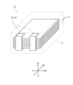
- FIG. 1 is a perspective view schematically showing a solid electrolytic capacitor according to Embodiment 1;
- FIG. 1A is a plan view of the capacitor element of Embodiment 1
- FIG. 1B is a cross-sectional view taken along line AA passing through the center of the joint.
- FIG. It is a graph which shows the relationship between the shortest distance b and the number of spatters when the maximum diameter a is 0.3 mm.
- FIG. 2B is a view corresponding to Modifications 1 to 3 of Embodiment 1;
- FIG. 11 is a perspective view showing a plurality of stacked capacitor elements corresponding to Modifications 4 to 7 of Embodiment 1;
- FIG. 10A is a plan view of the capacitor element of Embodiment 2, and FIG.
- a solid electrolytic capacitor according to the present disclosure includes a plurality of capacitor elements and two or more junctions.
- Each of the plurality of capacitor elements has an anode portion and a cathode portion.
- the plurality of capacitor elements are stacked together along the first direction.
- An insulating portion may be provided between the anode portion and the cathode portion to electrically insulate them.
- the insulating portion may be made of, for example, insulating tape or insulating resin.
- the anode portion may be configured to include a portion of the anode body made of the valve metal of the capacitor element (a portion on one side with respect to the insulating portion).
- the cathode portion may be composed of a solid electrolyte layer and a cathode layer which are sequentially formed on the surface of the cathode forming portion, which is the remainder of the anode body (part on the other side with respect to the insulating portion).
- a dielectric layer is provided between the anode body and the solid electrolyte layer.
- the dielectric layer is formed at least on the surface of the cathode formation portion, which is the remainder of the anode body.
- the dielectric layer may be composed of an oxide (for example, aluminum oxide) formed on the surface of the anode body by a vapor phase method such as anodization or vapor deposition.
- the solid electrolyte layer is formed on the surface of the dielectric layer.
- the solid electrolyte layer may contain a conductive polymer.
- the solid electrolyte layer may further contain a dopant as needed.
- conductive polymer a known one used in solid electrolytic capacitors, such as a ⁇ -conjugated conductive polymer, can be used.
- conductive polymers include polymers having polypyrrole, polythiophene, polyaniline, polyfuran, polyacetylene, polyphenylene, polyphenylenevinylene, polyacene, and polythiophenevinylene as a basic skeleton.
- polymers having a basic skeleton of polypyrrole, polythiophene, or polyaniline are preferred.
- the above polymers also include homopolymers, copolymers of two or more monomers, and derivatives thereof (substituents having substituents, etc.).
- polythiophenes include poly(3,4-ethylenedioxythiophene) and the like. Conductive polymers may be used singly or in combination of two or more.
- the solid electrolyte layer may further contain known additives and known conductive materials other than conductive polymers.
- a conductive material include at least one selected from the group consisting of conductive inorganic materials such as manganese dioxide and TCNQ complex salts.
- the cathode layer may be composed of a carbon layer formed on the surface of the solid electrolyte layer and a conductor layer formed on the surface of the carbon layer.
- the conductor layer may be composed of silver paste.
- the silver paste for example, a composition containing silver particles and a resin component (binder resin) can be used.
- a resin component a thermoplastic resin can be used, but it is preferable to use a thermosetting resin such as an imide resin or an epoxy resin.
- the two or more joints join and electrically connect the stacked anode parts.
- Each joint extends along the first direction.
- Each joint may be formed, for example, by laser welding.
- the laser In the laminated anode section, the laser may be irradiated from the first surface side arranged on one of the outermost surfaces in the first direction, and the laser may be irradiated from the second surface side arranged on the other outermost surface in the first direction. may be irradiated.
- the laser irradiation direction may be the same or different.
- Two or more joints may be formed, for example, by the following method. First, a plurality of capacitor elements are stacked along the first direction. Subsequently, the plurality of anode parts are crimped and temporarily fixed. After that, by irradiating the temporarily fixed portion with a laser, two or more joints for electrically and mechanically connecting the stacked anode portions are formed.
- a method for temporarily fixing a plurality of anode parts for example, a method using cold pressure bonding or a method using a needle for forming a through hole can be considered.
- the second direction is the direction from the anode part to the cathode part
- the third direction is the direction orthogonal to the second direction and the first direction.
- the difference between the dimension L1 [mm] of the anode portion in the third direction and the total dimension L2 [mm] of the maximum diameter of the joint portion in the third direction: L1 ⁇ L2 is 3.8 mm or less.
- the dimensional difference: L1-L2 is very small, in other words, the capacitor element is very small. Therefore, if each joint is formed without taking any measures, spatter is formed at the end of the anode. There is a risk that the bonding quality of the anode part will be impaired due to
- the predetermined cross section may be, for example, a cross section in which the diameter of the joint closest to the end of the anode part is the largest, or a cross section passing through the center of the joint.
- the dimension L1 of the anode part in the third direction may be 4.3 mm or less. Even when using a capacitor element having such a small anode portion, according to the present disclosure, the bonding quality of the anode portion can be improved.
- Each of the plurality of capacitor elements 11 has an anode portion 11a and a cathode portion 11b.
- the plurality of capacitor elements 11 are laminated along the first direction D1 (vertical direction in FIG. 1).
- An insulating portion 11c for electrically insulating the anode portion 11a and the cathode portion 11b is provided between the anode portion 11a and the cathode portion 11b.
- the stacked anode portions 11a are arranged on the outermost first surface S1 in one direction in the first direction (upper in FIG. 1) and the outermost in the other direction in the first direction (downward in FIG. 1). and a second surface S2.
- the anode lead terminal 12 is electrically connected to the anode portion 11 a of the capacitor element 11 .
- the anode lead terminal 12 has two arm portions 13 facing the anode portion 11a and a bridge portion 14 connecting the two arm portions 13 (see FIG. 2(b)).
- One main surface of the bridge portion 14 (lower surface in FIG. 2B) is exposed to the outside of the solid electrolytic capacitor 10 and functions as an anode terminal.
- Anode lead terminal 12 may be made of, for example, copper or a copper alloy.
- illustration of the bridge part 14 is abbreviate
- the arm portion 13 of the anode lead terminal 12 has a through hole 13a in a portion facing the first surface S1 of the anode portion 11a (see FIG. 2(b)).
- the through hole 13a is a circular hole penetrating through the arm portion 13 in the thickness direction.
- the through-holes 13 a are arranged at positions overlapping with the joints 16 .
- the shape of the through-hole 13a is not limited to a circular shape, and may be any other shape.
- the dimension L1 of the anode portion 11a in the third direction D3 is 4.3 mm or less.
- the dimension L1 may be, for example, 2.5 mm or more and 4.3 mm or less.
- the maximum diameter in the third direction D3 of the joint portion 16 closest to the end of the anode portion 11a in the third direction D3 is 0.5 mm or less.
- the maximum diameter may be, for example, 0.2 mm or more and 0.5 mm or less.
- the exterior resin 17 covers the plurality of capacitor elements 11 in a state in which a part of each of the anode lead terminal 12 and the cathode lead terminal is exposed to the outside.
- the exterior resin 17 may be made of an insulating resin material.
- the exposed portions of anode lead terminal 12 and cathode lead terminal constitute external terminals of solid electrolytic capacitor 10 .
- Bridge portion 14 of anode lead terminal 12 has a portion that widens as it separates from the plurality of laminated capacitor elements 11 .
- a solid electrolytic capacitor 10 of this modification differs from that of the first embodiment in that a spacer 18 is provided. Differences from the first embodiment will be mainly described below.
- the double-sided laminated structure refers to a structure in which the capacitor element 11 is laminated on both one main surface side and the other main surface side of the anode lead terminal 12 .
- three capacitor elements 11 are stacked on one (upper in the figure) main surface side of the anode lead terminal 12, and the other main surface side of the anode lead terminal 12 is stacked. Also, three capacitor elements 11 are laminated.
- the solid electrolytic capacitor 10 has three joints 16 .
- the three joints 16 are two first joints 16A having a first area on the first surface S1 and one second joint 16B having a second area smaller than the first area on the first surface S1. including.
- the second joint 16B is arranged between the two first joints 16A.
- the first joint 16A may be formed by laser welding that irradiates a laser from the first surface S1 side
- the second joint 16B is formed by laser welding that irradiates a laser from the second surface S2 side.
- the present disclosure can be used for solid electrolytic capacitors.
Landscapes
- Engineering & Computer Science (AREA)
- Power Engineering (AREA)
- Microelectronics & Electronic Packaging (AREA)
- Fixed Capacitors And Capacitor Manufacturing Machines (AREA)
Priority Applications (3)
| Application Number | Priority Date | Filing Date | Title |
|---|---|---|---|
| CN202280067946.2A CN118176555A (zh) | 2021-10-14 | 2022-09-01 | 固体电解电容器 |
| JP2023554981A JPWO2023062961A1 (https=) | 2021-10-14 | 2022-09-01 | |
| US18/694,622 US20240428998A1 (en) | 2021-10-14 | 2022-09-01 | Solid electrolytic capacitor |
Applications Claiming Priority (2)
| Application Number | Priority Date | Filing Date | Title |
|---|---|---|---|
| JP2021169062 | 2021-10-14 | ||
| JP2021-169062 | 2021-10-14 |
Publications (1)
| Publication Number | Publication Date |
|---|---|
| WO2023062961A1 true WO2023062961A1 (ja) | 2023-04-20 |
Family
ID=85987424
Family Applications (1)
| Application Number | Title | Priority Date | Filing Date |
|---|---|---|---|
| PCT/JP2022/033014 Ceased WO2023062961A1 (ja) | 2021-10-14 | 2022-09-01 | 固体電解コンデンサ |
Country Status (4)
| Country | Link |
|---|---|
| US (1) | US20240428998A1 (https=) |
| JP (1) | JPWO2023062961A1 (https=) |
| CN (1) | CN118176555A (https=) |
| WO (1) | WO2023062961A1 (https=) |
Citations (7)
| Publication number | Priority date | Publication date | Assignee | Title |
|---|---|---|---|---|
| JP2000138138A (ja) * | 1998-08-26 | 2000-05-16 | Matsushita Electric Ind Co Ltd | 固体電解コンデンサおよびその製造方法 |
| JP2005051051A (ja) * | 2003-07-29 | 2005-02-24 | Matsushita Electric Ind Co Ltd | 固体電解コンデンサ及びその製造方法 |
| JP2008235412A (ja) * | 2007-03-19 | 2008-10-02 | Matsushita Electric Ind Co Ltd | 固体電解コンデンサ |
| JP2009094474A (ja) * | 2007-09-19 | 2009-04-30 | Panasonic Corp | チップ形固体電解コンデンサ |
| JP2010153437A (ja) * | 2008-12-24 | 2010-07-08 | Sanyo Electric Co Ltd | 固体電解コンデンサ |
| JP2014110304A (ja) * | 2012-11-30 | 2014-06-12 | Nichicon Corp | 固体電解コンデンサおよびその製造方法 |
| WO2017163570A1 (ja) * | 2016-03-25 | 2017-09-28 | パナソニックIpマネジメント株式会社 | 電解コンデンサ |
Family Cites Families (5)
| Publication number | Priority date | Publication date | Assignee | Title |
|---|---|---|---|---|
| TW559845B (en) * | 2001-07-30 | 2003-11-01 | Matsushita Electric Industrial Co Ltd | Solid electrolytic capacitor and its manufacturing method |
| KR20030084256A (ko) * | 2002-04-26 | 2003-11-01 | 삼화전기주식회사 | 고체 전해 콘덴서 및 그에 사용되는 리드 프레임 |
| KR101117013B1 (ko) * | 2005-04-20 | 2012-03-15 | 사가 산요 고교 가부시키가이샤 | 적층형 고체 전해 콘덴서 및 그의 제조 방법 |
| TW200839820A (en) * | 2007-03-19 | 2008-10-01 | Matsushita Electric Industrial Co Ltd | Solid electrolytic capacitor |
| TWI674599B (zh) * | 2018-09-12 | 2019-10-11 | 鈺冠科技股份有限公司 | 堆疊型電容器組件結構 |
-
2022
- 2022-09-01 US US18/694,622 patent/US20240428998A1/en active Pending
- 2022-09-01 WO PCT/JP2022/033014 patent/WO2023062961A1/ja not_active Ceased
- 2022-09-01 JP JP2023554981A patent/JPWO2023062961A1/ja active Pending
- 2022-09-01 CN CN202280067946.2A patent/CN118176555A/zh active Pending
Patent Citations (7)
| Publication number | Priority date | Publication date | Assignee | Title |
|---|---|---|---|---|
| JP2000138138A (ja) * | 1998-08-26 | 2000-05-16 | Matsushita Electric Ind Co Ltd | 固体電解コンデンサおよびその製造方法 |
| JP2005051051A (ja) * | 2003-07-29 | 2005-02-24 | Matsushita Electric Ind Co Ltd | 固体電解コンデンサ及びその製造方法 |
| JP2008235412A (ja) * | 2007-03-19 | 2008-10-02 | Matsushita Electric Ind Co Ltd | 固体電解コンデンサ |
| JP2009094474A (ja) * | 2007-09-19 | 2009-04-30 | Panasonic Corp | チップ形固体電解コンデンサ |
| JP2010153437A (ja) * | 2008-12-24 | 2010-07-08 | Sanyo Electric Co Ltd | 固体電解コンデンサ |
| JP2014110304A (ja) * | 2012-11-30 | 2014-06-12 | Nichicon Corp | 固体電解コンデンサおよびその製造方法 |
| WO2017163570A1 (ja) * | 2016-03-25 | 2017-09-28 | パナソニックIpマネジメント株式会社 | 電解コンデンサ |
Also Published As
| Publication number | Publication date |
|---|---|
| JPWO2023062961A1 (https=) | 2023-04-20 |
| US20240428998A1 (en) | 2024-12-26 |
| CN118176555A (zh) | 2024-06-11 |
Similar Documents
| Publication | Publication Date | Title |
|---|---|---|
| JP5466722B2 (ja) | 固体電解コンデンサ | |
| US7916457B2 (en) | Multi-layered solid electrolytic capacitor and method of manufacturing same | |
| US12518932B2 (en) | Solid electrolytic capacitor capable of reducing ESR variation and method for manufacturing the same | |
| WO2022138556A1 (ja) | 電解コンデンサ | |
| WO2013088845A1 (ja) | 固体電解コンデンサ | |
| WO2022270195A1 (ja) | 固体電解コンデンサ | |
| JP4688675B2 (ja) | 積層型固体電解コンデンサ | |
| CN222213959U (zh) | 固体电解电容器 | |
| WO2023062961A1 (ja) | 固体電解コンデンサ | |
| WO2023218931A1 (ja) | 固体電解コンデンサおよび固体電解コンデンサの製造方法 | |
| WO2022202189A1 (ja) | 固体電解コンデンサおよびその製造方法 | |
| JP2008078312A (ja) | 固体電解コンデンサ | |
| JP7727956B2 (ja) | 固体電解コンデンサ | |
| US11984271B2 (en) | Electrolytic capacitor having reduced equivalent series resistance | |
| US20250191852A1 (en) | Solid electrolytic capacitor and production method for solid electrolytic capacitor | |
| US12340953B2 (en) | Solid electrolytic capacitor and method for manufacturing solid electrolytic capacitor with improved anode lead-out wire | |
| WO2020111278A1 (ja) | 電解コンデンサおよびその製造方法 | |
| JP6913875B2 (ja) | 電解コンデンサ | |
| US20250104927A1 (en) | Solid electrolytic capacitor element and solid electrolytic capacitor | |
| WO2025169887A1 (ja) | 固体電解コンデンサ | |
| JP5051851B2 (ja) | 積層型固体電解コンデンサ | |
| WO2024157805A1 (ja) | 固体電解コンデンサ | |
| WO2025206185A1 (ja) | 固体電解コンデンサ | |
| WO2023074376A1 (ja) | 固体電解コンデンサ | |
| WO2024029284A1 (ja) | 固体電解コンデンサ |
Legal Events
| Date | Code | Title | Description |
|---|---|---|---|
| 121 | Ep: the epo has been informed by wipo that ep was designated in this application |
Ref document number: 22880657 Country of ref document: EP Kind code of ref document: A1 |
|
| WWE | Wipo information: entry into national phase |
Ref document number: 18694622 Country of ref document: US Ref document number: 2023554981 Country of ref document: JP |
|
| WWE | Wipo information: entry into national phase |
Ref document number: 202280067946.2 Country of ref document: CN |
|
| NENP | Non-entry into the national phase |
Ref country code: DE |
|
| 122 | Ep: pct application non-entry in european phase |
Ref document number: 22880657 Country of ref document: EP Kind code of ref document: A1 |