WO2023062961A1 - Solid electrolytic capacitor - Google Patents
Solid electrolytic capacitor Download PDFInfo
- Publication number
- WO2023062961A1 WO2023062961A1 PCT/JP2022/033014 JP2022033014W WO2023062961A1 WO 2023062961 A1 WO2023062961 A1 WO 2023062961A1 JP 2022033014 W JP2022033014 W JP 2022033014W WO 2023062961 A1 WO2023062961 A1 WO 2023062961A1
- Authority
- WO
- WIPO (PCT)
- Prior art keywords
- anode
- solid electrolytic
- joint
- electrolytic capacitor
- cathode
- Prior art date
Links
- 239000003990 capacitor Substances 0.000 title claims abstract description 81
- 239000007787 solid Substances 0.000 title claims abstract description 45
- 238000005304 joining Methods 0.000 claims abstract description 9
- 230000004048 modification Effects 0.000 description 19
- 238000012986 modification Methods 0.000 description 19
- 229920005989 resin Polymers 0.000 description 12
- 239000011347 resin Substances 0.000 description 12
- 239000002253 acid Substances 0.000 description 9
- -1 polyphenylene Polymers 0.000 description 9
- 239000007784 solid electrolyte Substances 0.000 description 7
- 229920001940 conductive polymer Polymers 0.000 description 6
- 230000015572 biosynthetic process Effects 0.000 description 5
- 239000004020 conductor Substances 0.000 description 5
- 229910052751 metal Inorganic materials 0.000 description 5
- 239000002184 metal Substances 0.000 description 5
- 238000000034 method Methods 0.000 description 5
- 125000006850 spacer group Chemical group 0.000 description 5
- 238000003466 welding Methods 0.000 description 5
- 150000007513 acids Chemical class 0.000 description 4
- 229920000447 polyanionic polymer Polymers 0.000 description 4
- BQCADISMDOOEFD-UHFFFAOYSA-N Silver Chemical compound [Ag] BQCADISMDOOEFD-UHFFFAOYSA-N 0.000 description 3
- 239000002019 doping agent Substances 0.000 description 3
- 239000000463 material Substances 0.000 description 3
- 229920000642 polymer Polymers 0.000 description 3
- 229920000123 polythiophene Polymers 0.000 description 3
- 229910052709 silver Inorganic materials 0.000 description 3
- 239000004332 silver Substances 0.000 description 3
- OKTJSMMVPCPJKN-UHFFFAOYSA-N Carbon Chemical compound [C] OKTJSMMVPCPJKN-UHFFFAOYSA-N 0.000 description 2
- 150000001450 anions Chemical class 0.000 description 2
- 229910052799 carbon Inorganic materials 0.000 description 2
- 239000000470 constituent Substances 0.000 description 2
- 230000001771 impaired effect Effects 0.000 description 2
- NUJOXMJBOLGQSY-UHFFFAOYSA-N manganese dioxide Chemical compound O=[Mn]=O NUJOXMJBOLGQSY-UHFFFAOYSA-N 0.000 description 2
- 229920000767 polyaniline Polymers 0.000 description 2
- 229920000128 polypyrrole Polymers 0.000 description 2
- 125000001424 substituent group Chemical group 0.000 description 2
- JOXIMZWYDAKGHI-UHFFFAOYSA-N toluene-4-sulfonic acid Chemical compound CC1=CC=C(S(O)(=O)=O)C=C1 JOXIMZWYDAKGHI-UHFFFAOYSA-N 0.000 description 2
- WHOZNOZYMBRCBL-OUKQBFOZSA-N (2E)-2-Tetradecenal Chemical compound CCCCCCCCCCC\C=C\C=O WHOZNOZYMBRCBL-OUKQBFOZSA-N 0.000 description 1
- 229920003026 Acene Polymers 0.000 description 1
- NLZUEZXRPGMBCV-UHFFFAOYSA-N Butylhydroxytoluene Chemical compound CC1=CC(C(C)(C)C)=C(O)C(C(C)(C)C)=C1 NLZUEZXRPGMBCV-UHFFFAOYSA-N 0.000 description 1
- RYGMFSIKBFXOCR-UHFFFAOYSA-N Copper Chemical compound [Cu] RYGMFSIKBFXOCR-UHFFFAOYSA-N 0.000 description 1
- 229910000881 Cu alloy Inorganic materials 0.000 description 1
- 229910002651 NO3 Inorganic materials 0.000 description 1
- 229920001609 Poly(3,4-ethylenedioxythiophene) Polymers 0.000 description 1
- 229920002845 Poly(methacrylic acid) Polymers 0.000 description 1
- 229920000265 Polyparaphenylene Polymers 0.000 description 1
- 229920002125 Sokalan® Polymers 0.000 description 1
- QAOWNCQODCNURD-UHFFFAOYSA-L Sulfate Chemical compound [O-]S([O-])(=O)=O QAOWNCQODCNURD-UHFFFAOYSA-L 0.000 description 1
- RTAQQCXQSZGOHL-UHFFFAOYSA-N Titanium Chemical compound [Ti] RTAQQCXQSZGOHL-UHFFFAOYSA-N 0.000 description 1
- 239000000654 additive Substances 0.000 description 1
- HSFWRNGVRCDJHI-UHFFFAOYSA-N alpha-acetylene Natural products C#C HSFWRNGVRCDJHI-UHFFFAOYSA-N 0.000 description 1
- 230000004075 alteration Effects 0.000 description 1
- 229910052782 aluminium Inorganic materials 0.000 description 1
- XAGFODPZIPBFFR-UHFFFAOYSA-N aluminium Chemical compound [Al] XAGFODPZIPBFFR-UHFFFAOYSA-N 0.000 description 1
- 238000002048 anodisation reaction Methods 0.000 description 1
- SRSXLGNVWSONIS-UHFFFAOYSA-N benzenesulfonic acid Chemical compound OS(=O)(=O)C1=CC=CC=C1 SRSXLGNVWSONIS-UHFFFAOYSA-N 0.000 description 1
- 229940092714 benzenesulfonic acid Drugs 0.000 description 1
- 239000011230 binding agent Substances 0.000 description 1
- 239000011248 coating agent Substances 0.000 description 1
- 238000000576 coating method Methods 0.000 description 1
- 238000010276 construction Methods 0.000 description 1
- 229920001577 copolymer Polymers 0.000 description 1
- 229910052802 copper Inorganic materials 0.000 description 1
- 239000010949 copper Substances 0.000 description 1
- 230000006866 deterioration Effects 0.000 description 1
- 230000000694 effects Effects 0.000 description 1
- 239000003822 epoxy resin Substances 0.000 description 1
- 239000011888 foil Substances 0.000 description 1
- 229920001519 homopolymer Polymers 0.000 description 1
- 150000003949 imides Chemical class 0.000 description 1
- 229910010272 inorganic material Inorganic materials 0.000 description 1
- 239000011147 inorganic material Substances 0.000 description 1
- 230000001678 irradiating effect Effects 0.000 description 1
- 238000004519 manufacturing process Methods 0.000 description 1
- 150000002739 metals Chemical class 0.000 description 1
- 239000000203 mixture Substances 0.000 description 1
- 239000000178 monomer Substances 0.000 description 1
- PSZYNBSKGUBXEH-UHFFFAOYSA-N naphthalene-1-sulfonic acid Chemical compound C1=CC=C2C(S(=O)(=O)O)=CC=CC2=C1 PSZYNBSKGUBXEH-UHFFFAOYSA-N 0.000 description 1
- 229910052758 niobium Inorganic materials 0.000 description 1
- 239000010955 niobium Substances 0.000 description 1
- GUCVJGMIXFAOAE-UHFFFAOYSA-N niobium atom Chemical compound [Nb] GUCVJGMIXFAOAE-UHFFFAOYSA-N 0.000 description 1
- 229920003986 novolac Polymers 0.000 description 1
- TWNQGVIAIRXVLR-UHFFFAOYSA-N oxo(oxoalumanyloxy)alumane Chemical compound O=[Al]O[Al]=O TWNQGVIAIRXVLR-UHFFFAOYSA-N 0.000 description 1
- 239000002245 particle Substances 0.000 description 1
- 230000000149 penetrating effect Effects 0.000 description 1
- 229940044654 phenolsulfonic acid Drugs 0.000 description 1
- NBIIXXVUZAFLBC-UHFFFAOYSA-K phosphate Chemical compound [O-]P([O-])([O-])=O NBIIXXVUZAFLBC-UHFFFAOYSA-K 0.000 description 1
- 229920000553 poly(phenylenevinylene) Polymers 0.000 description 1
- 229920000172 poly(styrenesulfonic acid) Polymers 0.000 description 1
- 229920001197 polyacetylene Polymers 0.000 description 1
- 239000004584 polyacrylic acid Substances 0.000 description 1
- 229920000647 polyepoxide Polymers 0.000 description 1
- 229920000414 polyfuran Polymers 0.000 description 1
- 229940005642 polystyrene sulfonic acid Drugs 0.000 description 1
- 150000003839 salts Chemical class 0.000 description 1
- 229910052715 tantalum Inorganic materials 0.000 description 1
- GUVRBAGPIYLISA-UHFFFAOYSA-N tantalum atom Chemical compound [Ta] GUVRBAGPIYLISA-UHFFFAOYSA-N 0.000 description 1
- 229920005992 thermoplastic resin Polymers 0.000 description 1
- 229920001187 thermosetting polymer Polymers 0.000 description 1
- 229910052719 titanium Inorganic materials 0.000 description 1
- 239000010936 titanium Substances 0.000 description 1
- 238000007740 vapor deposition Methods 0.000 description 1
- 239000012808 vapor phase Substances 0.000 description 1
Images


Classifications
-
- H—ELECTRICITY
- H01—ELECTRIC ELEMENTS
- H01G—CAPACITORS; CAPACITORS, RECTIFIERS, DETECTORS, SWITCHING DEVICES OR LIGHT-SENSITIVE DEVICES, OF THE ELECTROLYTIC TYPE
- H01G9/00—Electrolytic capacitors, rectifiers, detectors, switching devices, light-sensitive or temperature-sensitive devices; Processes of their manufacture
- H01G9/004—Details
- H01G9/008—Terminals
- H01G9/012—Terminals specially adapted for solid capacitors
-
- H—ELECTRICITY
- H01—ELECTRIC ELEMENTS
- H01G—CAPACITORS; CAPACITORS, RECTIFIERS, DETECTORS, SWITCHING DEVICES OR LIGHT-SENSITIVE DEVICES, OF THE ELECTROLYTIC TYPE
- H01G9/00—Electrolytic capacitors, rectifiers, detectors, switching devices, light-sensitive or temperature-sensitive devices; Processes of their manufacture
- H01G9/004—Details
- H01G9/04—Electrodes or formation of dielectric layers thereon
- H01G9/048—Electrodes or formation of dielectric layers thereon characterised by their structure
-
- H—ELECTRICITY
- H01—ELECTRIC ELEMENTS
- H01G—CAPACITORS; CAPACITORS, RECTIFIERS, DETECTORS, SWITCHING DEVICES OR LIGHT-SENSITIVE DEVICES, OF THE ELECTROLYTIC TYPE
- H01G9/00—Electrolytic capacitors, rectifiers, detectors, switching devices, light-sensitive or temperature-sensitive devices; Processes of their manufacture
- H01G9/15—Solid electrolytic capacitors
Definitions
- solid electrolytic capacitors each having an anode portion and a cathode portion and including a plurality of stacked capacitor elements are known (for example, Patent Document 1).
- the stacked anode portions are welded together by laser irradiation.
- one object of the present disclosure is to improve the bonding quality of the anode portion.
- the solid electrolytic capacitor includes a plurality of capacitor elements each having an anode portion and a cathode portion, which are stacked along a first direction, and two capacitor elements that join and electrically connect the stacked anode portions. and a joint portion extending along the first direction, and a dimension L1 [mm] of the anode portion in a third direction perpendicular to the first direction and a second direction from the anode portion to the cathode portion.
- L1-L2 is 3.8 mm or less
- the capacitor element has a predetermined value perpendicular to the second direction In the cross section, let a [mm] be the maximum diameter of the joint in the third direction, and b [mm] be the shortest distance between the end of the anode part and the joint in the third direction, b ⁇ a/2 holds.
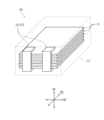
- FIG. 1 is a perspective view schematically showing a solid electrolytic capacitor according to Embodiment 1;
- FIG. 1A is a plan view of the capacitor element of Embodiment 1
- FIG. 1B is a cross-sectional view taken along line AA passing through the center of the joint.
- FIG. It is a graph which shows the relationship between the shortest distance b and the number of spatters when the maximum diameter a is 0.3 mm.
- FIG. 2B is a view corresponding to Modifications 1 to 3 of Embodiment 1;
- FIG. 11 is a perspective view showing a plurality of stacked capacitor elements corresponding to Modifications 4 to 7 of Embodiment 1;
- FIG. 10A is a plan view of the capacitor element of Embodiment 2, and FIG.
- a solid electrolytic capacitor according to the present disclosure includes a plurality of capacitor elements and two or more junctions.
- Each of the plurality of capacitor elements has an anode portion and a cathode portion.
- the plurality of capacitor elements are stacked together along the first direction.
- An insulating portion may be provided between the anode portion and the cathode portion to electrically insulate them.
- the insulating portion may be made of, for example, insulating tape or insulating resin.
- the anode portion may be configured to include a portion of the anode body made of the valve metal of the capacitor element (a portion on one side with respect to the insulating portion).
- the cathode portion may be composed of a solid electrolyte layer and a cathode layer which are sequentially formed on the surface of the cathode forming portion, which is the remainder of the anode body (part on the other side with respect to the insulating portion).
- a dielectric layer is provided between the anode body and the solid electrolyte layer.
- the dielectric layer is formed at least on the surface of the cathode formation portion, which is the remainder of the anode body.
- the dielectric layer may be composed of an oxide (for example, aluminum oxide) formed on the surface of the anode body by a vapor phase method such as anodization or vapor deposition.
- the solid electrolyte layer is formed on the surface of the dielectric layer.
- the solid electrolyte layer may contain a conductive polymer.
- the solid electrolyte layer may further contain a dopant as needed.
- conductive polymer a known one used in solid electrolytic capacitors, such as a ⁇ -conjugated conductive polymer, can be used.
- conductive polymers include polymers having polypyrrole, polythiophene, polyaniline, polyfuran, polyacetylene, polyphenylene, polyphenylenevinylene, polyacene, and polythiophenevinylene as a basic skeleton.
- polymers having a basic skeleton of polypyrrole, polythiophene, or polyaniline are preferred.
- the above polymers also include homopolymers, copolymers of two or more monomers, and derivatives thereof (substituents having substituents, etc.).
- polythiophenes include poly(3,4-ethylenedioxythiophene) and the like. Conductive polymers may be used singly or in combination of two or more.
- the solid electrolyte layer may further contain known additives and known conductive materials other than conductive polymers.
- a conductive material include at least one selected from the group consisting of conductive inorganic materials such as manganese dioxide and TCNQ complex salts.
- the cathode layer may be composed of a carbon layer formed on the surface of the solid electrolyte layer and a conductor layer formed on the surface of the carbon layer.
- the conductor layer may be composed of silver paste.
- the silver paste for example, a composition containing silver particles and a resin component (binder resin) can be used.
- a resin component a thermoplastic resin can be used, but it is preferable to use a thermosetting resin such as an imide resin or an epoxy resin.
- the two or more joints join and electrically connect the stacked anode parts.
- Each joint extends along the first direction.
- Each joint may be formed, for example, by laser welding.
- the laser In the laminated anode section, the laser may be irradiated from the first surface side arranged on one of the outermost surfaces in the first direction, and the laser may be irradiated from the second surface side arranged on the other outermost surface in the first direction. may be irradiated.
- the laser irradiation direction may be the same or different.
- Two or more joints may be formed, for example, by the following method. First, a plurality of capacitor elements are stacked along the first direction. Subsequently, the plurality of anode parts are crimped and temporarily fixed. After that, by irradiating the temporarily fixed portion with a laser, two or more joints for electrically and mechanically connecting the stacked anode portions are formed.
- a method for temporarily fixing a plurality of anode parts for example, a method using cold pressure bonding or a method using a needle for forming a through hole can be considered.
- the second direction is the direction from the anode part to the cathode part
- the third direction is the direction orthogonal to the second direction and the first direction.
- the difference between the dimension L1 [mm] of the anode portion in the third direction and the total dimension L2 [mm] of the maximum diameter of the joint portion in the third direction: L1 ⁇ L2 is 3.8 mm or less.
- the dimensional difference: L1-L2 is very small, in other words, the capacitor element is very small. Therefore, if each joint is formed without taking any measures, spatter is formed at the end of the anode. There is a risk that the bonding quality of the anode part will be impaired due to
- the predetermined cross section may be, for example, a cross section in which the diameter of the joint closest to the end of the anode part is the largest, or a cross section passing through the center of the joint.
- the dimension L1 of the anode part in the third direction may be 4.3 mm or less. Even when using a capacitor element having such a small anode portion, according to the present disclosure, the bonding quality of the anode portion can be improved.
- Each of the plurality of capacitor elements 11 has an anode portion 11a and a cathode portion 11b.
- the plurality of capacitor elements 11 are laminated along the first direction D1 (vertical direction in FIG. 1).
- An insulating portion 11c for electrically insulating the anode portion 11a and the cathode portion 11b is provided between the anode portion 11a and the cathode portion 11b.
- the stacked anode portions 11a are arranged on the outermost first surface S1 in one direction in the first direction (upper in FIG. 1) and the outermost in the other direction in the first direction (downward in FIG. 1). and a second surface S2.
- the anode lead terminal 12 is electrically connected to the anode portion 11 a of the capacitor element 11 .
- the anode lead terminal 12 has two arm portions 13 facing the anode portion 11a and a bridge portion 14 connecting the two arm portions 13 (see FIG. 2(b)).
- One main surface of the bridge portion 14 (lower surface in FIG. 2B) is exposed to the outside of the solid electrolytic capacitor 10 and functions as an anode terminal.
- Anode lead terminal 12 may be made of, for example, copper or a copper alloy.
- illustration of the bridge part 14 is abbreviate
- the arm portion 13 of the anode lead terminal 12 has a through hole 13a in a portion facing the first surface S1 of the anode portion 11a (see FIG. 2(b)).
- the through hole 13a is a circular hole penetrating through the arm portion 13 in the thickness direction.
- the through-holes 13 a are arranged at positions overlapping with the joints 16 .
- the shape of the through-hole 13a is not limited to a circular shape, and may be any other shape.
- the dimension L1 of the anode portion 11a in the third direction D3 is 4.3 mm or less.
- the dimension L1 may be, for example, 2.5 mm or more and 4.3 mm or less.
- the maximum diameter in the third direction D3 of the joint portion 16 closest to the end of the anode portion 11a in the third direction D3 is 0.5 mm or less.
- the maximum diameter may be, for example, 0.2 mm or more and 0.5 mm or less.
- the exterior resin 17 covers the plurality of capacitor elements 11 in a state in which a part of each of the anode lead terminal 12 and the cathode lead terminal is exposed to the outside.
- the exterior resin 17 may be made of an insulating resin material.
- the exposed portions of anode lead terminal 12 and cathode lead terminal constitute external terminals of solid electrolytic capacitor 10 .
- Bridge portion 14 of anode lead terminal 12 has a portion that widens as it separates from the plurality of laminated capacitor elements 11 .
- a solid electrolytic capacitor 10 of this modification differs from that of the first embodiment in that a spacer 18 is provided. Differences from the first embodiment will be mainly described below.
- the double-sided laminated structure refers to a structure in which the capacitor element 11 is laminated on both one main surface side and the other main surface side of the anode lead terminal 12 .
- three capacitor elements 11 are stacked on one (upper in the figure) main surface side of the anode lead terminal 12, and the other main surface side of the anode lead terminal 12 is stacked. Also, three capacitor elements 11 are laminated.
- the solid electrolytic capacitor 10 has three joints 16 .
- the three joints 16 are two first joints 16A having a first area on the first surface S1 and one second joint 16B having a second area smaller than the first area on the first surface S1. including.
- the second joint 16B is arranged between the two first joints 16A.
- the first joint 16A may be formed by laser welding that irradiates a laser from the first surface S1 side
- the second joint 16B is formed by laser welding that irradiates a laser from the second surface S2 side.
- the present disclosure can be used for solid electrolytic capacitors.
Abstract
A solid electrolytic capacitor 10 is provided with: a plurality of capacitor elements 11 each of which has a positive electrode section 11a and a negative electrode section 11b and that are layered one on another along a first direction D1; and at least two joining sections 16 that join and electrically connect the layered positive electrode sections 11a and that extend along the first direction D1. The difference L1 - L2 between a dimension L1 [mm] of each of the positive electrode sections 11a in a third direction D3, which is orthogonal to the first direction D1 and a second direction D2 extending from the positive electrode sections 11a toward the negative electrode sections 11b, and a total dimension L2 [mm] of the maximum diameters of the joining sections 16 in the third direction D3 is 3.8 mm or less. On a prescribed cross section taken along a line orthogonal to the second direction D2 of the capacitor elements 11, the relationship b ≥ a/2 holds, where a [mm] is the maximum diameter of a joining section 16 in the third direction D3, and b [mm] is the minimum distance in the third direction D3 between the end sections of the positive electrode sections 11a and the joining section 16. This can enhance the quality of joining the positive electrode sections.
Description
本開示は、固体電解コンデンサに関する。
The present disclosure relates to solid electrolytic capacitors.
従来、それぞれが陽極部および陰極部を有し、互いに積層された複数のコンデンサ素子を備える固体電解コンデンサが知られている(例えば、特許文献1)。特許文献1の固体電解コンデンサでは、積層された陽極部同士が、レーザ照射によって互いに溶接される。
Conventionally, solid electrolytic capacitors each having an anode portion and a cathode portion and including a plurality of stacked capacitor elements are known (for example, Patent Document 1). In the solid electrolytic capacitor of Patent Document 1, the stacked anode portions are welded together by laser irradiation.
ところで、近年、固体電解コンデンサは、より一層の小型化が求められている。そのような中、コンデンサ素子が有する陽極部の寸法も小さくなる傾向にある。しかし、陽極部が一定程度を超えて小さくなると、例えばレーザ溶接によって積層された陽極部同士を接合する際、陽極部の端部にスパッタが形成されるなどして接合品質が低下するおそれがある。このような状況において、本開示は、陽極部の接合品質を向上させることを目的の1つとする。
By the way, in recent years, there has been a demand for further miniaturization of solid electrolytic capacitors. Under such circumstances, the dimension of the anode part of the capacitor element also tends to be small. However, if the size of the anode portion becomes smaller than a certain level, spatter may be formed at the end of the anode portion when joining the stacked anode portions together by laser welding, for example, and the joining quality may deteriorate. . Under such circumstances, one object of the present disclosure is to improve the bonding quality of the anode portion.
本開示に係る一局面は、固体電解コンデンサに関する。当該固体電解コンデンサは、それぞれが陽極部および陰極部を有し、互いに第1方向に沿って積層された複数のコンデンサ素子と、積層された前記陽極部を接合すると共に電気的に接続する2つ以上の前記第1方向に沿って延びる接合部と、を備え、前記陽極部から前記陰極部に向かう第2方向と前記第1方向とに直交する第3方向における前記陽極部の寸法L1[mm]と、前記接合部の前記第3方向における最大径の合計寸法L2[mm]との差:L1-L2が、3.8mm以下であり、前記コンデンサ素子の前記第2方向に垂直な所定の断面において、前記第3方向における前記接合部の最大径をa[mm]とし、かつ前記第3方向における前記陽極部の端部と前記接合部との間の最短距離をb[mm]として、b≧a/2が成り立つ。
One aspect of the present disclosure relates to solid electrolytic capacitors. The solid electrolytic capacitor includes a plurality of capacitor elements each having an anode portion and a cathode portion, which are stacked along a first direction, and two capacitor elements that join and electrically connect the stacked anode portions. and a joint portion extending along the first direction, and a dimension L1 [mm] of the anode portion in a third direction perpendicular to the first direction and a second direction from the anode portion to the cathode portion. ] and the total dimension L2 [mm] of the maximum diameter of the joint portion in the third direction: L1-L2 is 3.8 mm or less, and the capacitor element has a predetermined value perpendicular to the second direction In the cross section, let a [mm] be the maximum diameter of the joint in the third direction, and b [mm] be the shortest distance between the end of the anode part and the joint in the third direction, b≧a/2 holds.
本開示によれば、陽極部の接合品質を向上させることができる。
According to the present disclosure, it is possible to improve the bonding quality of the anode part.
本発明の新規な特徴を添付の請求の範囲に記述するが、本発明は、構成および内容の両方に関し、本願の他の目的および特徴と併せ、図面を照合した以下の詳細な説明によりさらによく理解されるであろう。
While the novel features of the present invention are set forth in the appended claims, the present invention, both as to construction and content, together with other objects and features of the present application, will be better understood by the following detailed description taken in conjunction with the drawings. will be understood.
本開示に係る固体電解コンデンサの実施形態について例を挙げて以下に説明する。しかしながら、本開示は以下に説明する例に限定されない。以下の説明では、具体的な数値や材料を例示する場合があるが、本開示の効果が得られる限り、他の数値や材料を適用してもよい。
An embodiment of the solid electrolytic capacitor according to the present disclosure will be described below with examples. However, the disclosure is not limited to the examples described below. In the following description, specific numerical values and materials may be exemplified, but other numerical values and materials may be applied as long as the effects of the present disclosure can be obtained.
本開示に係る固体電解コンデンサは、複数のコンデンサ素子と、2つ以上の接合部とを備える。
A solid electrolytic capacitor according to the present disclosure includes a plurality of capacitor elements and two or more junctions.
複数のコンデンサ素子は、それぞれが陽極部および陰極部を有する。複数のコンデンサ素子は、互いに第1方向に沿って積層されている。陽極部と陰極部との間には、両者を電気的に絶縁する絶縁部が設けられてもよい。絶縁部は、例えば、絶縁テープや絶縁樹脂で構成されてもよい。
Each of the plurality of capacitor elements has an anode portion and a cathode portion. The plurality of capacitor elements are stacked together along the first direction. An insulating portion may be provided between the anode portion and the cathode portion to electrically insulate them. The insulating portion may be made of, for example, insulating tape or insulating resin.
陽極部は、コンデンサ素子が有する弁作用金属からなる陽極体の一部(絶縁部を基準として一方側の一部)を含むように構成されてもよい。陰極部は、陽極体の残部(絶縁部を基準として他方側の一部)である陰極形成部の表面上に順次形成された固体電解質層および陰極層で構成されてもよい。陽極体と固体電解質層との間には、誘電体層が設けられる。
The anode portion may be configured to include a portion of the anode body made of the valve metal of the capacitor element (a portion on one side with respect to the insulating portion). The cathode portion may be composed of a solid electrolyte layer and a cathode layer which are sequentially formed on the surface of the cathode forming portion, which is the remainder of the anode body (part on the other side with respect to the insulating portion). A dielectric layer is provided between the anode body and the solid electrolyte layer.
陽極体を構成する弁作用金属としては、アルミニウム、タンタル、ニオブ、チタンなどが挙げられる。陽極体は、弁作用金属の箔であってもよいし、弁作用金属からなる多孔質焼結体であってもよい。
Aluminum, tantalum, niobium, titanium and the like are examples of the valve action metals that make up the anode body. The anode body may be a valve-acting metal foil, or may be a porous sintered body made of a valve-acting metal.
誘電体層は、少なくとも陽極体の残部である陰極形成部の表面に形成される。誘電体層は、陽極体の表面に陽極酸化や蒸着などの気相法などにより形成された酸化物(例えば、酸化アルミニウム)で構成されてもよい。
The dielectric layer is formed at least on the surface of the cathode formation portion, which is the remainder of the anode body. The dielectric layer may be composed of an oxide (for example, aluminum oxide) formed on the surface of the anode body by a vapor phase method such as anodization or vapor deposition.
固体電解質層は、誘電体層の表面に形成される。固体電解質層は、導電性高分子を含んでもよい。固体電解質層は、必要に応じて、さらに、ドーパントを含んでもよい。
The solid electrolyte layer is formed on the surface of the dielectric layer. The solid electrolyte layer may contain a conductive polymer. The solid electrolyte layer may further contain a dopant as needed.
導電性高分子としては、固体電解コンデンサに使用される公知のもの、例えば、π共役系導電性高分子などが使用できる。導電性高分子としては、例えば、ポリピロール、ポリチオフェン、ポリアニリン、ポリフラン、ポリアセチレン、ポリフェニレン、ポリフェニレンビニレン、ポリアセン、およびポリチオフェンビニレンを基本骨格とする高分子が挙げられる。これらのうち、ポリピロール、ポリチオフェン、またはポリアニリンを基本骨格とする高分子が好ましい。上記の高分子には、単独重合体、二種以上のモノマーの共重合体、およびこれらの誘導体(置換基を有する置換体など)も含まれる。例えば、ポリチオフェンには、ポリ(3,4-エチレンジオキシチオフェン)などが含まれる。導電性高分子は、一種を単独で用いてもよく、二種以上を組み合わせて用いてもよい。
As the conductive polymer, a known one used in solid electrolytic capacitors, such as a π-conjugated conductive polymer, can be used. Examples of conductive polymers include polymers having polypyrrole, polythiophene, polyaniline, polyfuran, polyacetylene, polyphenylene, polyphenylenevinylene, polyacene, and polythiophenevinylene as a basic skeleton. Among these, polymers having a basic skeleton of polypyrrole, polythiophene, or polyaniline are preferred. The above polymers also include homopolymers, copolymers of two or more monomers, and derivatives thereof (substituents having substituents, etc.). For example, polythiophenes include poly(3,4-ethylenedioxythiophene) and the like. Conductive polymers may be used singly or in combination of two or more.
ドーパントとしては、例えば、低分子アニオンおよびポリアニオンからなる群より選択される少なくとも一種が使用される。アニオンとしては、例えば、硫酸イオン、硝酸イオン、燐酸イオン、硼酸イオン、有機スルホン酸イオン、カルボン酸イオンなどが挙げられるが、特に制限されない。スルホン酸イオンを生成するドーパントとしては、例えば、ベンゼンスルホン酸、p-トルエンスルホン酸、およびナフタレンスルホン酸などが挙げられる。ポリアニオンとしては、例えば、高分子タイプのポリスルホン酸および高分子タイプのポリカルボン酸などが挙げられる。高分子タイプのポリスルホン酸としては、ポリビニルスルホン酸、ポリスチレンスルホン酸、ポリアリルスルホン酸、ポリアクリルスルホン酸、およびポリメタクリルスルホン酸などが挙げられる。高分子タイプのポリカルボン酸としては、ポリアクリル酸、ポリメタクリル酸などが挙げられる。ポリアニオンには、ポリエステルスルホン酸、およびフェノールスルホン酸ノボラック樹脂なども含まれる。しかし、ポリアニオンは、これらに制限されるものではない。
As the dopant, for example, at least one selected from the group consisting of low-molecular-weight anions and polyanions is used. Examples of anions include sulfate ions, nitrate ions, phosphate ions, borate ions, organic sulfonate ions, and carboxylate ions, but are not particularly limited. Dopants that generate sulfonate ions include, for example, benzenesulfonic acid, p-toluenesulfonic acid, and naphthalenesulfonic acid. Polyanions include, for example, polymeric type polysulfonic acids and polymeric type polycarboxylic acids. Polymeric types of polysulfonic acids include polyvinylsulfonic acid, polystyrenesulfonic acid, polyallylsulfonic acid, polyacrylsulfonic acid, and polymethacrylsulfonic acid. Polymer-type polycarboxylic acids include polyacrylic acid and polymethacrylic acid. Polyanions also include polyestersulfonic acid, and phenolsulfonic acid novolak resins, and the like. However, polyanions are not limited to these.
固体電解質層は、必要に応じて、さらに、公知の添加剤、および導電性高分子以外の公知の導電性材料を含んでもよい。このような導電性材料としては、例えば、二酸化マンガンなどの導電性無機材料、およびTCNQ錯塩からなる群より選択される少なくとも一種が挙げられる。
If necessary, the solid electrolyte layer may further contain known additives and known conductive materials other than conductive polymers. Examples of such a conductive material include at least one selected from the group consisting of conductive inorganic materials such as manganese dioxide and TCNQ complex salts.
陰極層は、固体電解質層の表面に形成されたカーボン層と、カーボン層の表面に形成された導電体層とで構成されてもよい。導電体層は、銀ペーストで構成されてもよい。銀ペーストとしては、例えば、銀粒子と樹脂成分(バインダ樹脂)とを含む組成物を用い得る。樹脂成分としては、熱可塑性樹脂を用いることもできるが、イミド系樹脂、エポキシ樹脂などの熱硬化性樹脂を用いることが好ましい。
The cathode layer may be composed of a carbon layer formed on the surface of the solid electrolyte layer and a conductor layer formed on the surface of the carbon layer. The conductor layer may be composed of silver paste. As the silver paste, for example, a composition containing silver particles and a resin component (binder resin) can be used. As the resin component, a thermoplastic resin can be used, but it is preferable to use a thermosetting resin such as an imide resin or an epoxy resin.
2つ以上の接合部は、積層された陽極部を接合すると共に電気的に接続する。各接合部は、第1方向に沿って延びている。各接合部は、例えばレーザ溶接によって形成されてもよい。積層された陽極部において、レーザは、第1方向の一方の最外に配置される第1表面側から照射されてもよく、第1方向の他方の最外に配置される第2表面側から照射されてもよい。2つ以上の接合部において、レーザの照射方向は同じでもよく、異なってもよい。
The two or more joints join and electrically connect the stacked anode parts. Each joint extends along the first direction. Each joint may be formed, for example, by laser welding. In the laminated anode section, the laser may be irradiated from the first surface side arranged on one of the outermost surfaces in the first direction, and the laser may be irradiated from the second surface side arranged on the other outermost surface in the first direction. may be irradiated. In two or more joints, the laser irradiation direction may be the same or different.
2つ以上の接合部は、例えば、次の工法により形成されてもよい。まず、複数のコンデンサ素子を第1方向に沿って積層する。続いて、複数の陽極部をかしめて仮止めする。その後、仮止めした部分にレーザを照射することで、積層された陽極部を電気的および機械的に接続する2つ以上の接合部を形成する。なお、複数の陽極部を仮止めする方法として、例えば、冷間圧着による方法や、貫通孔を形成するための針を用いる方法も考えられる。
Two or more joints may be formed, for example, by the following method. First, a plurality of capacitor elements are stacked along the first direction. Subsequently, the plurality of anode parts are crimped and temporarily fixed. After that, by irradiating the temporarily fixed portion with a laser, two or more joints for electrically and mechanically connecting the stacked anode portions are formed. As a method for temporarily fixing a plurality of anode parts, for example, a method using cold pressure bonding or a method using a needle for forming a through hole can be considered.
陽極部から陰極部に向かう方向を第2方向とし、かつ第2方向および第1方向に直交する方向を第3方向とする。第3方向における陽極部の寸法L1[mm]と、接合部の第3方向における最大径の合計寸法L2[mm]との差:L1-L2は、3.8mm以下である。このように、当該寸法差:L1-L2が非常に小さいため、換言するとコンデンサ素子が非常に小さいため、何らの対策もせずに各接合部を形成すると、陽極部の端部にスパッタが形成されるなどして陽極部の接合品質が損なわれるおそれがある。
The second direction is the direction from the anode part to the cathode part, and the third direction is the direction orthogonal to the second direction and the first direction. The difference between the dimension L1 [mm] of the anode portion in the third direction and the total dimension L2 [mm] of the maximum diameter of the joint portion in the third direction: L1−L2 is 3.8 mm or less. In this way, the dimensional difference: L1-L2 is very small, in other words, the capacitor element is very small. Therefore, if each joint is formed without taking any measures, spatter is formed at the end of the anode. There is a risk that the bonding quality of the anode part will be impaired due to
これに対し、本開示の固体電解コンデンサでは、コンデンサ素子の第2方向に垂直な所定の断面において、第3方向における接合部の最大径をa[mm]とし、かつ第3方向における陽極部の端部と接合部との間の最短距離をb[mm]として、b≧a/2が成り立つ。ここで、所定の断面は、例えば、陽極部の端部に最も近い接合部の直径が最大となる断面、あるいは当該接合部の中心を通る断面であってもよい。そのような寸法の大小関係が成り立つことで、陽極部の端部と接合部との間の最短距離bを十分に大きく確保することができる。これにより、上述のように寸法差:L1-L2が非常に小さい場合であっても、各接合部の形成時に陽極部の端部にスパッタが形成され難く、陽極部の接合品質を向上させることが可能となる。
On the other hand, in the solid electrolytic capacitor of the present disclosure, in a predetermined cross section perpendicular to the second direction of the capacitor element, the maximum diameter of the joint portion in the third direction is a [mm], and the anode portion in the third direction is Assuming that the shortest distance between the end portion and the joint portion is b [mm], b≧a/2 holds. Here, the predetermined cross section may be, for example, a cross section in which the diameter of the joint closest to the end of the anode part is the largest, or a cross section passing through the center of the joint. By establishing such a size relationship between dimensions, it is possible to secure a sufficiently large shortest distance b between the end portion of the anode portion and the joint portion. As a result, even if the dimensional difference (L1-L2) is very small as described above, spatter is less likely to be formed at the end of the anode portion during formation of each bonding portion, and the bonding quality of the anode portion can be improved. becomes possible.
第3方向における陽極部の寸法L1が、4.3mm以下であってもよい。このように小さな陽極部を有するコンデンサ素子を用いる場合であっても、本開示によれば、陽極部の接合品質を向上させることができる。
The dimension L1 of the anode part in the third direction may be 4.3 mm or less. Even when using a capacitor element having such a small anode portion, according to the present disclosure, the bonding quality of the anode portion can be improved.
陽極部の端部に最も近い接合部の第3方向における最大径は、0.5mm以下であってもよい。このように接合部の最大径が比較的大きい場合であっても、本開示によれば、陽極部の接合品質を向上させることができる。
The maximum diameter in the third direction of the joint portion closest to the end of the anode portion may be 0.5 mm or less. Even when the maximum diameter of the joint portion is relatively large as described above, according to the present disclosure, the joint quality of the anode portion can be improved.
第2方向において、接合部の中心は、陽極部の中央よりも陰極部寄りに位置してもよい。これにより、第2方向における陽極部の端部と接合部との距離が十分に大きく確保される。これにより、第2方向における陽極部の端部でも、接合部の形成時におけるスパッタの形成が抑止され、陽極部の接合品質をより一層向上させることができる。
In the second direction, the center of the joint may be located closer to the cathode than the center of the anode. This ensures a sufficiently large distance between the end of the anode portion and the joint portion in the second direction. As a result, even at the end of the anode portion in the second direction, the formation of spatter during formation of the joint portion is suppressed, and the joint quality of the anode portion can be further improved.
固体電解コンデンサは、接合部を2つ備えてもよい。固体電解コンデンサは、例えば、接合部を2つのみ備えてもよい。
The solid electrolytic capacitor may have two joints. A solid electrolytic capacitor may, for example, have only two junctions.
固体電解コンデンサは、接合部を3つ以上備えてもよい。積層された陽極部は、第1方向の一方および他方の最外に配置される第1表面および第2表面を有してもよい。3つ以上の接合部は、第1表面において第1面積を有する第1接合部と、第1表面において第1面積よりも小さい第2面積を有する第2接合部とを含んでもよい。この構成では、接合部が3つ以上存在するため、陽極部の端部と接合部との間の距離が小さくなりやすい。これに対し、本開示による寸法の大小関係(すなわち、b≧a/2)が成り立つようにすることで、陽極部の接合品質が損なわれるのを回避することができる。
The solid electrolytic capacitor may have three or more joints. The stacked anode section may have a first surface and a second surface arranged on the outermost sides in one and the other of the first directions. The three or more joints may include a first joint having a first area at the first surface and a second joint having a second area at the first surface that is less than the first area. In this configuration, since there are three or more joints, the distance between the ends of the anode and the joints tends to be small. On the other hand, it is possible to avoid deterioration of the bonding quality of the anode section by establishing the magnitude relationship of the dimensions according to the present disclosure (that is, b≧a/2).
以上のように、本開示によれば、小さなコンデンサ素子を備える固体電解コンデンサにおいて、陽極部の接合品質を向上させることができる。
As described above, according to the present disclosure, it is possible to improve the bonding quality of the anode portion in a solid electrolytic capacitor having a small capacitor element.
以下では、本開示に係る固体電解コンデンサの一例について、図面を参照して具体的に説明する。以下で説明する一例の固体電解コンデンサの構成要素には、上述した構成要素を適用できる。以下で説明する一例の固体電解コンデンサの構成要素は、上述した記載に基づいて変更できる。また、以下で説明する事項を、上記の実施形態に適用してもよい。以下で説明する一例の固体電解コンデンサの構成要素のうち、本開示に係る固体電解コンデンサに必須ではない構成要素は省略してもよい。なお、以下で示す図は模式的なものであり、実際の部材の形状や数を正確に反映するものではない。
An example of the solid electrolytic capacitor according to the present disclosure will be specifically described below with reference to the drawings. The components described above can be applied to the components of an example of the solid electrolytic capacitor described below. The components of the example solid electrolytic capacitor described below can be varied based on the above description. Also, the matters described below may be applied to the above embodiments. Among the constituent elements of the solid electrolytic capacitor of the example described below, constituent elements that are not essential to the solid electrolytic capacitor according to the present disclosure may be omitted. It should be noted that the drawings shown below are schematic and do not accurately reflect the actual shape and number of members.
《実施形態1》
本開示の実施形態1について説明する。本実施形態の固体電解コンデンサ10は、図1および図2に示すように、複数(この例では、5つ)のコンデンサ素子11と、陽極リード端子12と、陰極リード端子(図示せず)と、2つの接合部16と、外装樹脂17とを備える。陰極リード端子は、後述の陰極部11bに電気的に接続される。 <<Embodiment 1>>
A first embodiment of the present disclosure will be described. As shown in FIGS. 1 and 2, the solidelectrolytic capacitor 10 of this embodiment includes a plurality of (five in this example) capacitor elements 11, an anode lead terminal 12, and a cathode lead terminal (not shown). , two joints 16 and an exterior resin 17 . The cathode lead terminal is electrically connected to a cathode portion 11b, which will be described later.
本開示の実施形態1について説明する。本実施形態の固体電解コンデンサ10は、図1および図2に示すように、複数(この例では、5つ)のコンデンサ素子11と、陽極リード端子12と、陰極リード端子(図示せず)と、2つの接合部16と、外装樹脂17とを備える。陰極リード端子は、後述の陰極部11bに電気的に接続される。 <<
A first embodiment of the present disclosure will be described. As shown in FIGS. 1 and 2, the solid
複数のコンデンサ素子11は、それぞれが陽極部11aおよび陰極部11bを有する。複数のコンデンサ素子11は、互いに第1方向D1(図1における上下方向)に沿って積層されている。陽極部11aと陰極部11bとの間には、両者を電気的に絶縁する絶縁部11cが設けられている。積層された陽極部11aは、第1方向の一方(図1における上方)の最外に配置される第1表面S1と、第1方向の他方(図1における下方)の最外に配置される第2表面S2とを有する。
Each of the plurality of capacitor elements 11 has an anode portion 11a and a cathode portion 11b. The plurality of capacitor elements 11 are laminated along the first direction D1 (vertical direction in FIG. 1). An insulating portion 11c for electrically insulating the anode portion 11a and the cathode portion 11b is provided between the anode portion 11a and the cathode portion 11b. The stacked anode portions 11a are arranged on the outermost first surface S1 in one direction in the first direction (upper in FIG. 1) and the outermost in the other direction in the first direction (downward in FIG. 1). and a second surface S2.
陽極リード端子12は、コンデンサ素子11の陽極部11aに電気的に接続される。陽極リード端子12は、陽極部11aに対向する2つのアーム部13と、2つのアーム部13を接続するブリッジ部14とを有する(図2(b)を参照)。ブリッジ部14の一方の主面(図2(b)における下面)は、固体電解コンデンサ10の外部に露出し、陽極端子として機能する。陽極リード端子12は、例えば、銅または銅合金で構成されてもよい。なお、図1では、ブリッジ部14の図示を省略している。
The anode lead terminal 12 is electrically connected to the anode portion 11 a of the capacitor element 11 . The anode lead terminal 12 has two arm portions 13 facing the anode portion 11a and a bridge portion 14 connecting the two arm portions 13 (see FIG. 2(b)). One main surface of the bridge portion 14 (lower surface in FIG. 2B) is exposed to the outside of the solid electrolytic capacitor 10 and functions as an anode terminal. Anode lead terminal 12 may be made of, for example, copper or a copper alloy. In addition, in FIG. 1, illustration of the bridge part 14 is abbreviate|omitted.
陽極リード端子12のアーム部13は、陽極部11aの第1表面S1に対向する部分に貫通孔13aを有する(図2(b)を参照)。貫通孔13aは、アーム部13を厚さ方向に貫通する円形の孔である。貫通孔13aは、各接合部16と重なる位置に配置される。なお、貫通孔13aの形状は、円形に限定されず、その他の任意の形状であってもよい。
The arm portion 13 of the anode lead terminal 12 has a through hole 13a in a portion facing the first surface S1 of the anode portion 11a (see FIG. 2(b)). The through hole 13a is a circular hole penetrating through the arm portion 13 in the thickness direction. The through-holes 13 a are arranged at positions overlapping with the joints 16 . In addition, the shape of the through-hole 13a is not limited to a circular shape, and may be any other shape.
2つの接合部16は、積層された陽極部11aを接合すると共に電気的に接続する。各接合部16は、第1方向D1に沿って延びている。各接合部16は、第1表面S1から第2表面S2にわたって延びていてもよい。各接合部16は、貫通孔13aを介して第1表面S1側からレーザを照射するレーザ溶接によって形成されてもよい。
The two joints 16 join and electrically connect the laminated anode parts 11a. Each joint 16 extends along the first direction D1. Each joint 16 may extend from the first surface S1 to the second surface S2. Each joint 16 may be formed by laser welding that irradiates a laser from the first surface S1 side through the through hole 13a.
陽極部11aから陰極部11bに向かう方向(図2(a)における左右方向)を第2方向D2とし、かつ第2方向D2および第1方向D1に直交する方向(図2(a)における上下方向)を第3方向D3とする。第3方向D3における陽極部11aの寸法L1[mm]と、2つの接合部16の第3方向D3における最大径の合計寸法L2[mm]との差:L1-L2は、3.8mm以下である。当該寸法差:L1-L2は、例えば、1.5mm以上、3.8mm以下であってもよい。
The direction from the anode part 11a to the cathode part 11b (horizontal direction in FIG. 2A) is defined as a second direction D2, and the direction perpendicular to the second direction D2 and the first direction D1 (vertical direction in FIG. 2A). ) is the third direction D3. The difference between the dimension L1 [mm] of the anode portion 11a in the third direction D3 and the total dimension L2 [mm] of the maximum diameters of the two joint portions 16 in the third direction D3: L1-L2 is 3.8 mm or less. be. The dimensional difference: L1-L2 may be, for example, 1.5 mm or more and 3.8 mm or less.
第3方向D3における陽極部11aの寸法L1は、4.3mm以下である。当該寸法L1は、例えば、2.5mm以上、4.3mm以下であってもよい。第3方向D3における陽極部11aの端部に最も近い接合部16の第3方向D3における最大径は、0.5mm以下である。当該最大径は、例えば、0.2mm以上、0.5mm以下であってもよい。
The dimension L1 of the anode portion 11a in the third direction D3 is 4.3 mm or less. The dimension L1 may be, for example, 2.5 mm or more and 4.3 mm or less. The maximum diameter in the third direction D3 of the joint portion 16 closest to the end of the anode portion 11a in the third direction D3 is 0.5 mm or less. The maximum diameter may be, for example, 0.2 mm or more and 0.5 mm or less.
図2(a)に示すように、第2方向D2において、接合部16の中心は、陽極部11aの中央よりも陰極部11b寄りに位置している。ここで、第2方向D2における陽極部11aの一端は、図2(a)における陽極部11aの左端であり、第2方向D2における陽極部11aの他端は、陽極部11aと絶縁部11cとの境界であり、第2方向D2における接合部16の中心は、当該一端と当該他端との間の中間位置である。
As shown in FIG. 2(a), in the second direction D2, the center of the joint portion 16 is positioned closer to the cathode portion 11b than the center of the anode portion 11a. Here, one end of the anode portion 11a in the second direction D2 is the left end of the anode portion 11a in FIG. , and the center of the joint 16 in the second direction D2 is an intermediate position between the one end and the other end.
コンデンサ素子11の第2方向D2に垂直な所定の断面(図2(b)の断面)において、第3方向D3における接合部16の最大径をa[mm]とし、かつ第3方向D3における陽極部11aの端部と接合部16との間の最短距離をb[mm]として、b≧a/2が成り立つ。ここで、所定の断面は、接合部16の中心を通る断面である。接合部16の最大径aは、例えば、第1表面S1における接合部16の直径であってもよい。
In a predetermined cross section of the capacitor element 11 perpendicular to the second direction D2 (the cross section of FIG. 2B), the maximum diameter of the joint 16 in the third direction D3 is a [mm], and the anode in the third direction D3 is Assuming that the shortest distance between the end of the portion 11a and the joint portion 16 is b [mm], b≧a/2 holds. Here, the predetermined cross section is a cross section passing through the center of the joint portion 16 . The maximum diameter a of the joint 16 may be, for example, the diameter of the joint 16 on the first surface S1.
図3は、本願発明者が固体電解コンデンサ10を作製して得たデータを示すグラフであり、横軸が上記最短距離b[mm]を示し、縦軸が固体電解コンデンサ10で形成されるスパッタの数[個/1つのコンデンサ]を示す。また、同グラフは、第3方向D3における接合部16の最大径aが0.3mmである場合のデータを示す。同グラフからわかるように、最短距離bが0.15mm未満である場合(すなわち、b<a/2である場合)、スパッタが発生して接合品質が損なわれることがわかる。一方、最短距離bが0.15mm以上である場合(すなわち、b≧a/2である場合)、スパッタは発生せず接合品質が向上することがわかる。なお、接合部16の最大径aに関わらず、特に当該最大径aが0.3mm以下である場合に、スパッタの形成について同様の傾向がある。
FIG. 3 is a graph showing data obtained by the inventors of the present application by manufacturing the solid electrolytic capacitor 10. The horizontal axis indicates the shortest distance b [mm], and the vertical axis indicates the spatter formed in the solid electrolytic capacitor 10. indicates the number of capacitors [pieces/one capacitor]. The graph also shows data when the maximum diameter a of the joint portion 16 in the third direction D3 is 0.3 mm. As can be seen from the graph, when the shortest distance b is less than 0.15 mm (that is, when b<a/2), spatter occurs and the bonding quality is impaired. On the other hand, when the shortest distance b is 0.15 mm or more (that is, when b≧a/2), no spatter occurs and the bonding quality is improved. It should be noted that regardless of the maximum diameter a of the joint 16, the same tendency exists for the formation of spatter especially when the maximum diameter a is 0.3 mm or less.
外装樹脂17は、陽極リード端子12および陰極リード端子の各々の一部が外部に露出する状態で、複数のコンデンサ素子11を被覆する。外装樹脂17は、絶縁性の樹脂材料で構成されてもよい。陽極リード端子12および陰極リード端子の露出部は、固体電解コンデンサ10の外部端子を構成する。
The exterior resin 17 covers the plurality of capacitor elements 11 in a state in which a part of each of the anode lead terminal 12 and the cathode lead terminal is exposed to the outside. The exterior resin 17 may be made of an insulating resin material. The exposed portions of anode lead terminal 12 and cathode lead terminal constitute external terminals of solid electrolytic capacitor 10 .
《実施形態1の変形例1》
本開示の実施形態1の変形例1について説明する。本変形例の固体電解コンデンサ10は、陽極リード端子12の構成が上記実施形態1と異なる。以下、上記実施形態1と異なる点について主に説明する。 <<Modification 1 of Embodiment 1>>
Modification 1 of Embodiment 1 of the present disclosure will be described. The solid electrolytic capacitor 10 of this modified example differs from that of the first embodiment in the configuration of the anode lead terminal 12 . Differences from the first embodiment will be mainly described below.
本開示の実施形態1の変形例1について説明する。本変形例の固体電解コンデンサ10は、陽極リード端子12の構成が上記実施形態1と異なる。以下、上記実施形態1と異なる点について主に説明する。 <<
図4(a)に示すように、2つのアーム部13は、第3方向D3において、陽極部11aの端部から離間して設けられている。陽極リード端子12のブリッジ部14は、積層された複数のコンデンサ素子11から離れるにつれて広がる部分を有する。
As shown in FIG. 4(a), the two arm portions 13 are spaced apart from the end portion of the anode portion 11a in the third direction D3. Bridge portion 14 of anode lead terminal 12 has a portion that widens as it separates from the plurality of laminated capacitor elements 11 .
《実施形態1の変形例2》
本開示の実施形態1の変形例2について説明する。本変形例の固体電解コンデンサ10は、陽極リード端子12の構成が上記実施形態1と異なる。以下、上記実施形態1と異なる点について主に説明する。 <<Modification 2 of Embodiment 1>>
Modification 2 of Embodiment 1 of the present disclosure will be described. The solid electrolytic capacitor 10 of this modified example differs from that of the first embodiment in the configuration of the anode lead terminal 12 . Differences from the first embodiment will be mainly described below.
本開示の実施形態1の変形例2について説明する。本変形例の固体電解コンデンサ10は、陽極リード端子12の構成が上記実施形態1と異なる。以下、上記実施形態1と異なる点について主に説明する。 <<
図4(b)に示すように、2つのアーム部13における第2表面S2に対向する部分は、第3方向D3において、陽極部11aの端部まで、あるいは当該端部近傍まで延びている。陽極リード端子12のブリッジ部14は、積層された複数のコンデンサ素子11から離れるにつれて広がる部分を有する。
As shown in FIG. 4(b), the portions of the two arm portions 13 facing the second surface S2 extend to or near the end of the anode portion 11a in the third direction D3. Bridge portion 14 of anode lead terminal 12 has a portion that widens as it separates from the plurality of laminated capacitor elements 11 .
《実施形態1の変形例3》
本開示の実施形態1の変形例3について説明する。本変形例の固体電解コンデンサ10は、陽極リード端子12の構成が上記実施形態1と異なる。以下、上記実施形態1と異なる点について主に説明する。 <<Modification 3 of Embodiment 1>>
Modification 3 of Embodiment 1 of the present disclosure will be described. The solid electrolytic capacitor 10 of this modified example differs from that of the first embodiment in the configuration of the anode lead terminal 12 . Differences from the first embodiment will be mainly described below.
本開示の実施形態1の変形例3について説明する。本変形例の固体電解コンデンサ10は、陽極リード端子12の構成が上記実施形態1と異なる。以下、上記実施形態1と異なる点について主に説明する。 <<
図4(c)に示すように、2つのアーム部13における第2表面S2に対向する部分は、第3方向D3において、陽極部11aの端部まで、あるいは当該端部近傍まで延びている。陽極リード端子12のブリッジ部14は、積層された複数のコンデンサ素子11から離れるにつれて狭まる部分を有する。
As shown in FIG. 4(c), the portions of the two arm portions 13 facing the second surface S2 extend to or near the end of the anode portion 11a in the third direction D3. Bridge portion 14 of anode lead terminal 12 has a portion that narrows with increasing distance from stacked capacitor elements 11 .
《実施形態1の変形例4》
本開示の実施形態1の変形例4について説明する。本変形例の固体電解コンデンサ10は、スペーサ18を備える点で上記実施形態1と異なる。以下、上記実施形態1と異なる点について主に説明する。 <<Modification 4 of Embodiment 1>>
Modification 4 of Embodiment 1 of the present disclosure will be described. A solid electrolytic capacitor 10 of this modification differs from that of the first embodiment in that a spacer 18 is provided. Differences from the first embodiment will be mainly described below.
本開示の実施形態1の変形例4について説明する。本変形例の固体電解コンデンサ10は、スペーサ18を備える点で上記実施形態1と異なる。以下、上記実施形態1と異なる点について主に説明する。 <<
図5(a)に示すように、固体電解コンデンサ10は、互いに積層された陽極部11aの間に設けられる複数のスペーサ18を備える。各スペーサ18は、第1方向D1において隣り合う陽極部11a同士の距離を規定する。スペーサ18は、導電性材料(例えば、金属)で構成されていてもよい。
As shown in FIG. 5(a), the solid electrolytic capacitor 10 includes a plurality of spacers 18 provided between mutually stacked anode portions 11a. Each spacer 18 defines the distance between adjacent anode portions 11a in the first direction D1. Spacer 18 may be composed of a conductive material (eg, metal).
《実施形態1の変形例5》
本開示の実施形態1の変形例5について説明する。本変形例の固体電解コンデンサ10は、陽極リード端子12の構成が上記実施形態1と異なる。以下、上記実施形態1と異なる点について主に説明する。 <<Modification 5 ofEmbodiment 1>>
Modification 5 ofEmbodiment 1 of the present disclosure will be described. The solid electrolytic capacitor 10 of this modified example differs from that of the first embodiment in the configuration of the anode lead terminal 12 . Differences from the first embodiment will be mainly described below.
本開示の実施形態1の変形例5について説明する。本変形例の固体電解コンデンサ10は、陽極リード端子12の構成が上記実施形態1と異なる。以下、上記実施形態1と異なる点について主に説明する。 <<Modification 5 of
Modification 5 of
図5(b)に示すように、陽極リード端子12は、陽極部11aのうち第2方向D2に沿って延びる縁部を覆う側壁部15を有する。側壁部15は、第1方向D1において、積層された陽極部11aの全長よりも長くてもよい。
As shown in FIG. 5(b), the anode lead terminal 12 has a side wall portion 15 covering an edge portion of the anode portion 11a extending along the second direction D2. The side wall portion 15 may be longer than the total length of the stacked anode portions 11a in the first direction D1.
《実施形態1の変形例6》
本開示の実施形態1の変形例6について説明する。本変形例の固体電解コンデンサ10は、陽極リード端子12の構成が上記実施形態1と異なる。以下、上記実施形態1と異なる点について主に説明する。 <<Modification 6 ofEmbodiment 1>>
Modification 6 ofEmbodiment 1 of the present disclosure will be described. The solid electrolytic capacitor 10 of this modified example differs from that of the first embodiment in the configuration of the anode lead terminal 12 . Differences from the first embodiment will be mainly described below.
本開示の実施形態1の変形例6について説明する。本変形例の固体電解コンデンサ10は、陽極リード端子12の構成が上記実施形態1と異なる。以下、上記実施形態1と異なる点について主に説明する。 <<Modification 6 of
Modification 6 of
図5(c)に示すように、陽極リード端子12は、1つのみのアーム部13を有する。当該アーム部13は、第3方向D3において、陽極部11aの寸法L1の半分以上の長さを有する。第3方向D3において、アーム部13の長さは、例えば、陽極部11aの寸法L1の50%以上、90%以下であってもよい。
As shown in FIG. 5(c), the anode lead terminal 12 has only one arm portion 13. The arm portion 13 has a length equal to or longer than half the dimension L1 of the anode portion 11a in the third direction D3. In the third direction D3, the length of the arm portion 13 may be, for example, 50% or more and 90% or less of the dimension L1 of the anode portion 11a.
《実施形態1の変形例7》
本開示の実施形態1の変形例7について説明する。本変形例の固体電解コンデンサ10は、いわゆる両面積層構造を有する点で上記実施形態1と異なる。以下、上記実施形態1と異なる点について主に説明する。 <<Modification 7 ofEmbodiment 1>>
Modification 7 ofEmbodiment 1 of the present disclosure will be described. The solid electrolytic capacitor 10 of this modified example differs from the first embodiment in that it has a so-called double-sided laminated structure. Differences from the first embodiment will be mainly described below.
本開示の実施形態1の変形例7について説明する。本変形例の固体電解コンデンサ10は、いわゆる両面積層構造を有する点で上記実施形態1と異なる。以下、上記実施形態1と異なる点について主に説明する。 <<Modification 7 of
Modification 7 of
両面積層構造とは、陽極リード端子12の一方の主面側と、他方の主面側との両方においてコンデンサ素子11が積層されている構造のことをいう。図5(d)に示すように、陽極リード端子12の一方(同図における上方)の主面側には、3つのコンデンサ素子11が積層されており、陽極リード端子12の他方の主面側にも、3つのコンデンサ素子11が積層されている。
The double-sided laminated structure refers to a structure in which the capacitor element 11 is laminated on both one main surface side and the other main surface side of the anode lead terminal 12 . As shown in FIG. 5(d), three capacitor elements 11 are stacked on one (upper in the figure) main surface side of the anode lead terminal 12, and the other main surface side of the anode lead terminal 12 is stacked. Also, three capacitor elements 11 are laminated.
《実施形態2》
本開示の実施形態2について説明する。本実施形態の固体電解コンデンサ10は、3つの接合部16を備える点で上記実施形態1と異なる。以下、上記実施形態1と異なる点について主に説明する。 <<Embodiment 2>>
A second embodiment of the present disclosure will be described. A solidelectrolytic capacitor 10 of the present embodiment differs from that of the first embodiment in that three joints 16 are provided. Differences from the first embodiment will be mainly described below.
本開示の実施形態2について説明する。本実施形態の固体電解コンデンサ10は、3つの接合部16を備える点で上記実施形態1と異なる。以下、上記実施形態1と異なる点について主に説明する。 <<
A second embodiment of the present disclosure will be described. A solid
図6に示すように、固体電解コンデンサ10は、3つの接合部16を備える。3つの接合部16は、第1表面S1において第1面積を有する2つの第1接合部16Aと、第1表面S1において第1面積よりも小さい第2面積を有する1つの第2接合部16Bとを含む。第2接合部16Bは、2つの第1接合部16Aの間に配置される。例えば、第1接合部16Aは、第1表面S1側からレーザを照射するレーザ溶接により形成されてもよく、第2接合部16Bは、第2表面S2側からレーザを照射するレーザ溶接により形成されてもよい。
As shown in FIG. 6 , the solid electrolytic capacitor 10 has three joints 16 . The three joints 16 are two first joints 16A having a first area on the first surface S1 and one second joint 16B having a second area smaller than the first area on the first surface S1. including. The second joint 16B is arranged between the two first joints 16A. For example, the first joint 16A may be formed by laser welding that irradiates a laser from the first surface S1 side, and the second joint 16B is formed by laser welding that irradiates a laser from the second surface S2 side. may
本発明を現時点での好ましい実施態様に関して説明したが、そのような開示を限定的に解釈してはならない。種々の変形および改変は、上記開示を読むことによって本発明に属する技術分野における当業者には間違いなく明らかになるであろう。したがって、添付の請求の範囲は、本発明の真の精神および範囲から逸脱することなく、すべての変形および改変を包含する、と解釈されるべきものである。
Although the present invention has been described in terms of its presently preferred embodiments, such disclosure should not be construed as limiting. Various alterations and modifications will no doubt become apparent to those skilled in the art to which the invention pertains after reading the above disclosure. Therefore, the appended claims are to be interpreted as covering all variations and modifications without departing from the true spirit and scope of the invention.
本開示は、固体電解コンデンサに利用できる。
The present disclosure can be used for solid electrolytic capacitors.
10:固体電解コンデンサ
11:コンデンサ素子
11a:陽極部
11b:陰極部
11c:絶縁部
12:陽極リード端子
13:アーム部
13a:貫通孔
14:ブリッジ部
15:側壁部
16:接合部
16A:第1接合部
16B:第2接合部
17:外装樹脂
18:スペーサ
a:接合部の最大径
b:陽極部の端部と接合部との間の最短距離
D1:第1方向
D2:第2方向
D3:第3方向
L1:陽極部の寸法
L2:接合部の最大径の合計寸法
S1:第1表面
S2:第2表面
10: Solid electrolytic capacitor 11:Capacitor element 11a: Anode part 11b: Cathode part 11c: Insulating part 12: Anode lead terminal 13: Arm part 13a: Through hole 14: Bridge part 15: Side wall part 16: Joint part 16A: First Joint portion 16B: Second joint portion 17: Coating resin 18: Spacer a: Maximum diameter of joint portion b: Shortest distance between end of anode portion and joint portion D1: First direction D2: Second direction D3: Third direction L1: dimension of anode part L2: total dimension of maximum diameter of joint part S1: first surface S2: second surface
11:コンデンサ素子
11a:陽極部
11b:陰極部
11c:絶縁部
12:陽極リード端子
13:アーム部
13a:貫通孔
14:ブリッジ部
15:側壁部
16:接合部
16A:第1接合部
16B:第2接合部
17:外装樹脂
18:スペーサ
a:接合部の最大径
b:陽極部の端部と接合部との間の最短距離
D1:第1方向
D2:第2方向
D3:第3方向
L1:陽極部の寸法
L2:接合部の最大径の合計寸法
S1:第1表面
S2:第2表面
10: Solid electrolytic capacitor 11:
Claims (6)
- それぞれが陽極部および陰極部を有し、互いに第1方向に沿って積層された複数のコンデンサ素子と、
積層された前記陽極部を接合すると共に電気的に接続する2つ以上の前記第1方向に沿って延びる接合部と、
を備え、
前記陽極部から前記陰極部に向かう第2方向と前記第1方向とに直交する第3方向における前記陽極部の寸法L1[mm]と、前記接合部の前記第3方向における最大径の合計寸法L2[mm]との差:L1-L2が、3.8mm以下であり、
前記コンデンサ素子の前記第2方向に垂直な所定の断面において、前記第3方向における前記接合部の最大径をa[mm]とし、かつ前記第3方向における前記陽極部の端部と前記接合部との間の最短距離をb[mm]として、b≧a/2が成り立つ、固体電解コンデンサ。 a plurality of capacitor elements each having an anode portion and a cathode portion and stacked along a first direction;
two or more joining portions extending along the first direction for joining and electrically connecting the stacked anode portions;
with
The total dimension of the dimension L1 [mm] of the anode portion in a third direction perpendicular to the first direction and the second direction from the anode portion to the cathode portion and the maximum diameter of the joint portion in the third direction. Difference from L2 [mm]: L1-L2 is 3.8 mm or less,
In a predetermined cross section perpendicular to the second direction of the capacitor element, the maximum diameter of the joint portion in the third direction is a [mm], and the end portion of the anode portion and the joint portion in the third direction A solid electrolytic capacitor that satisfies b≧a/2, where b [mm] is the shortest distance between - 前記第3方向における前記陽極部の寸法L1が、4.3mm以下である、請求項1に記載の固体電解コンデンサ。 The solid electrolytic capacitor according to claim 1, wherein the dimension L1 of said anode portion in said third direction is 4.3 mm or less.
- 前記陽極部の前記端部に最も近い前記接合部の前記第3方向における最大径は、0.5mm以下である、請求項1または2に記載の固体電解コンデンサ。 3. The solid electrolytic capacitor according to claim 1, wherein said joint portion closest to said end of said anode portion has a maximum diameter in said third direction of 0.5 mm or less.
- 前記第2方向において、前記接合部の中心は、前記陽極部の中央よりも前記陰極部寄りに位置する、請求項1~3のいずれか1項に記載の固体電解コンデンサ。 The solid electrolytic capacitor according to any one of claims 1 to 3, wherein in the second direction, the center of the joint portion is located closer to the cathode portion than the center of the anode portion.
- 前記接合部を2つ備える、請求項1~4のいずれか1項に記載の固体電解コンデンサ。 The solid electrolytic capacitor according to any one of claims 1 to 4, comprising two joints.
- 前記接合部を3つ以上備え、
積層された前記陽極部は、前記第1方向の一方および他方の最外に配置される第1表面および第2表面を有し、
前記3つ以上の接合部は、前記第1表面において第1面積を有する第1接合部と、前記第1表面において前記第1面積よりも小さい第2面積を有する第2接合部とを含む、請求項1~4のいずれか1項に記載の固体電解コンデンサ。
Equipped with three or more of the joints,
The stacked anode parts have first and second surfaces arranged on the outermost sides in one and the other of the first directions,
wherein the three or more joints include a first joint having a first area on the first surface and a second joint having a second area on the first surface that is smaller than the first area; A solid electrolytic capacitor according to any one of claims 1 to 4.
Applications Claiming Priority (2)
| Application Number | Priority Date | Filing Date | Title |
|---|---|---|---|
| JP2021-169062 | 2021-10-14 | ||
| JP2021169062 | 2021-10-14 |
Publications (1)
| Publication Number | Publication Date |
|---|---|
| WO2023062961A1 true WO2023062961A1 (en) | 2023-04-20 |
Family
ID=85987424
Family Applications (1)
| Application Number | Title | Priority Date | Filing Date |
|---|---|---|---|
| PCT/JP2022/033014 WO2023062961A1 (en) | 2021-10-14 | 2022-09-01 | Solid electrolytic capacitor |
Country Status (1)
| Country | Link |
|---|---|
| WO (1) | WO2023062961A1 (en) |
Citations (7)
| Publication number | Priority date | Publication date | Assignee | Title |
|---|---|---|---|---|
| JP2000138138A (en) * | 1998-08-26 | 2000-05-16 | Matsushita Electric Ind Co Ltd | Solid-state electrolytic capacitor and its manufacture |
| JP2005051051A (en) * | 2003-07-29 | 2005-02-24 | Matsushita Electric Ind Co Ltd | Solid electrolytic capacitor and manufacturing method thereof |
| JP2008235412A (en) * | 2007-03-19 | 2008-10-02 | Matsushita Electric Ind Co Ltd | Solid electrolytic capacitor |
| JP2009094474A (en) * | 2007-09-19 | 2009-04-30 | Panasonic Corp | Chip type solid electrolytic capacitor |
| JP2010153437A (en) * | 2008-12-24 | 2010-07-08 | Sanyo Electric Co Ltd | Solid electrolytic capacitor |
| JP2014110304A (en) * | 2012-11-30 | 2014-06-12 | Nichicon Corp | Solid electrolytic capacitor and method for manufacturing the same |
| WO2017163570A1 (en) * | 2016-03-25 | 2017-09-28 | パナソニックIpマネジメント株式会社 | Electrolytic capacitor |
-
2022
- 2022-09-01 WO PCT/JP2022/033014 patent/WO2023062961A1/en active Application Filing
Patent Citations (7)
| Publication number | Priority date | Publication date | Assignee | Title |
|---|---|---|---|---|
| JP2000138138A (en) * | 1998-08-26 | 2000-05-16 | Matsushita Electric Ind Co Ltd | Solid-state electrolytic capacitor and its manufacture |
| JP2005051051A (en) * | 2003-07-29 | 2005-02-24 | Matsushita Electric Ind Co Ltd | Solid electrolytic capacitor and manufacturing method thereof |
| JP2008235412A (en) * | 2007-03-19 | 2008-10-02 | Matsushita Electric Ind Co Ltd | Solid electrolytic capacitor |
| JP2009094474A (en) * | 2007-09-19 | 2009-04-30 | Panasonic Corp | Chip type solid electrolytic capacitor |
| JP2010153437A (en) * | 2008-12-24 | 2010-07-08 | Sanyo Electric Co Ltd | Solid electrolytic capacitor |
| JP2014110304A (en) * | 2012-11-30 | 2014-06-12 | Nichicon Corp | Solid electrolytic capacitor and method for manufacturing the same |
| WO2017163570A1 (en) * | 2016-03-25 | 2017-09-28 | パナソニックIpマネジメント株式会社 | Electrolytic capacitor |
Similar Documents
| Publication | Publication Date | Title |
|---|---|---|
| US7916457B2 (en) | Multi-layered solid electrolytic capacitor and method of manufacturing same | |
| JP5466722B2 (en) | Solid electrolytic capacitor | |
| JP4688675B2 (en) | Multilayer solid electrolytic capacitor | |
| US8179667B2 (en) | Solid electrolytic capacitor | |
| WO2004077466A1 (en) | Solid electrolytic capacitor | |
| US8179664B2 (en) | Solid electrolytic capacitor | |
| WO2013088845A1 (en) | Solid electrolytic capacitor | |
| US8559165B2 (en) | Solid electrolytic capacitor | |
| JP2008078312A (en) | Solid electrolytic capacitor | |
| WO2023062961A1 (en) | Solid electrolytic capacitor | |
| JP7029670B2 (en) | Electrolytic capacitor | |
| US20220399169A1 (en) | Electrolytic capacitor | |
| WO2023026811A1 (en) | Solid electrolytic capacitor and method for manufacturing solid electrolytic capacitor | |
| WO2023181745A1 (en) | Solid electrolytic capacitor | |
| JP2022101769A (en) | Electrolytic capacitor and method for manufacturing the same | |
| WO2022270195A1 (en) | Solid electrolytic capacitor | |
| WO2024004989A1 (en) | Solid electrolytic capacitor element and solid electrolytic capacitor | |
| WO2023074376A1 (en) | Solid electrolytic capacitor | |
| US11984271B2 (en) | Electrolytic capacitor having reduced equivalent series resistance | |
| WO2022202189A1 (en) | Solid electrolytic capacitor and manufacturing method therefor | |
| JP6913875B2 (en) | Electrolytic capacitor | |
| WO2012042950A1 (en) | Solid electrolytic capacitor and method for manufacturing same | |
| US20220310328A1 (en) | Electrolytic capacitor | |
| WO2024029284A1 (en) | Solid electrolytic capacitor | |
| WO2022138556A1 (en) | Electrolytic capacitor |
Legal Events
| Date | Code | Title | Description |
|---|---|---|---|
| 121 | Ep: the epo has been informed by wipo that ep was designated in this application |
Ref document number: 22880657 Country of ref document: EP Kind code of ref document: A1 |
|
| WWE | Wipo information: entry into national phase |
Ref document number: 2023554981 Country of ref document: JP |