WO2023062766A1 - 導波路型受光素子、導波路型受光素子アレイ及び導波路型受光素子の製造方法 - Google Patents
導波路型受光素子、導波路型受光素子アレイ及び導波路型受光素子の製造方法 Download PDFInfo
- Publication number
- WO2023062766A1 WO2023062766A1 PCT/JP2021/038000 JP2021038000W WO2023062766A1 WO 2023062766 A1 WO2023062766 A1 WO 2023062766A1 JP 2021038000 W JP2021038000 W JP 2021038000W WO 2023062766 A1 WO2023062766 A1 WO 2023062766A1
- Authority
- WO
- WIPO (PCT)
- Prior art keywords
- waveguide
- light
- semiconductor
- semiconductor substrate
- light incident
- Prior art date
- Legal status (The legal status is an assumption and is not a legal conclusion. Google has not performed a legal analysis and makes no representation as to the accuracy of the status listed.)
- Ceased
Links
Images


Classifications
-
- H—ELECTRICITY
- H10—SEMICONDUCTOR DEVICES; ELECTRIC SOLID-STATE DEVICES NOT OTHERWISE PROVIDED FOR
- H10F—INORGANIC SEMICONDUCTOR DEVICES SENSITIVE TO INFRARED RADIATION, LIGHT, ELECTROMAGNETIC RADIATION OF SHORTER WAVELENGTH OR CORPUSCULAR RADIATION
- H10F30/00—Individual radiation-sensitive semiconductor devices in which radiation controls the flow of current through the devices, e.g. photodetectors
- H10F30/20—Individual radiation-sensitive semiconductor devices in which radiation controls the flow of current through the devices, e.g. photodetectors the devices having potential barriers, e.g. phototransistors
- H10F30/21—Individual radiation-sensitive semiconductor devices in which radiation controls the flow of current through the devices, e.g. photodetectors the devices having potential barriers, e.g. phototransistors the devices being sensitive to infrared, visible or ultraviolet radiation
- H10F30/22—Individual radiation-sensitive semiconductor devices in which radiation controls the flow of current through the devices, e.g. photodetectors the devices having potential barriers, e.g. phototransistors the devices being sensitive to infrared, visible or ultraviolet radiation the devices having only one potential barrier, e.g. photodiodes
- H10F30/223—Individual radiation-sensitive semiconductor devices in which radiation controls the flow of current through the devices, e.g. photodetectors the devices having potential barriers, e.g. phototransistors the devices being sensitive to infrared, visible or ultraviolet radiation the devices having only one potential barrier, e.g. photodiodes the potential barrier being a PIN barrier
-
- H—ELECTRICITY
- H10—SEMICONDUCTOR DEVICES; ELECTRIC SOLID-STATE DEVICES NOT OTHERWISE PROVIDED FOR
- H10F—INORGANIC SEMICONDUCTOR DEVICES SENSITIVE TO INFRARED RADIATION, LIGHT, ELECTROMAGNETIC RADIATION OF SHORTER WAVELENGTH OR CORPUSCULAR RADIATION
- H10F77/00—Constructional details of devices covered by this subclass
- H10F77/40—Optical elements or arrangements
- H10F77/413—Optical elements or arrangements directly associated or integrated with the devices, e.g. back reflectors
-
- G—PHYSICS
- G02—OPTICS
- G02B—OPTICAL ELEMENTS, SYSTEMS OR APPARATUS
- G02B6/00—Light guides; Structural details of arrangements comprising light guides and other optical elements, e.g. couplings
- G02B6/10—Light guides; Structural details of arrangements comprising light guides and other optical elements, e.g. couplings of the optical waveguide type
- G02B6/12—Light guides; Structural details of arrangements comprising light guides and other optical elements, e.g. couplings of the optical waveguide type of the integrated circuit kind
- G02B6/12004—Combinations of two or more optical elements
-
- H—ELECTRICITY
- H10—SEMICONDUCTOR DEVICES; ELECTRIC SOLID-STATE DEVICES NOT OTHERWISE PROVIDED FOR
- H10F—INORGANIC SEMICONDUCTOR DEVICES SENSITIVE TO INFRARED RADIATION, LIGHT, ELECTROMAGNETIC RADIATION OF SHORTER WAVELENGTH OR CORPUSCULAR RADIATION
- H10F71/00—Manufacture or treatment of devices covered by this subclass
- H10F71/127—The active layers comprising only Group III-V materials, e.g. GaAs or InP
- H10F71/1272—The active layers comprising only Group III-V materials, e.g. GaAs or InP comprising at least three elements, e.g. GaAlAs or InGaAsP
-
- H—ELECTRICITY
- H10—SEMICONDUCTOR DEVICES; ELECTRIC SOLID-STATE DEVICES NOT OTHERWISE PROVIDED FOR
- H10F—INORGANIC SEMICONDUCTOR DEVICES SENSITIVE TO INFRARED RADIATION, LIGHT, ELECTROMAGNETIC RADIATION OF SHORTER WAVELENGTH OR CORPUSCULAR RADIATION
- H10F77/00—Constructional details of devices covered by this subclass
- H10F77/10—Semiconductor bodies
- H10F77/14—Shape of semiconductor bodies; Shapes, relative sizes or dispositions of semiconductor regions within semiconductor bodies
- H10F77/147—Shapes of bodies
-
- H—ELECTRICITY
- H10—SEMICONDUCTOR DEVICES; ELECTRIC SOLID-STATE DEVICES NOT OTHERWISE PROVIDED FOR
- H10F—INORGANIC SEMICONDUCTOR DEVICES SENSITIVE TO INFRARED RADIATION, LIGHT, ELECTROMAGNETIC RADIATION OF SHORTER WAVELENGTH OR CORPUSCULAR RADIATION
- H10F77/00—Constructional details of devices covered by this subclass
- H10F77/10—Semiconductor bodies
- H10F77/12—Active materials
- H10F77/124—Active materials comprising only Group III-V materials, e.g. GaAs
- H10F77/1248—Active materials comprising only Group III-V materials, e.g. GaAs having three or more elements, e.g. GaAlAs, InGaAs or InGaAsP
Definitions
- the present disclosure relates to a waveguide photodetector, a waveguide photodetector array, and a method for manufacturing a waveguide photodetector.
- PD photodiode
- the CR time constant is determined by the device capacitance and device resistance of the semiconductor light receiving device.
- a waveguide-type light receiving element capable of reducing the element capacity is adopted as the element structure of the PD.
- a waveguide type photodetector has an element structure in which light is incident from the side surface of an epitaxial crystal growth layer, and unlike a normal surface incidence type structure, the photosensitivity and the photodetection band can be individually optimized. Therefore, it can be said that the waveguide type photodetector has an element structure suitable for high-speed operation.
- Waveguide photodetectors are further classified into two types. One of them is, for example, a load-type light receiving element disclosed in Patent Document 1.
- the optical waveguide is formed up to the cleaved end face. Light is made incident on this optical waveguide, guided to a light absorption layer formed at a position separated by several ⁇ m or more from the incident part, and the evanescent light leaked out from the guide layer in the layer thickness direction in this light absorption layer. to photoelectric conversion.
- photoelectric conversion is indirect in the load-type light-receiving element, and there is an advantage that the concentration of photocurrent in the vicinity of the incident end surface is alleviated, and the deterioration of the response speed is less likely to occur even when high-intensity light is incident.
- the light leaking out from the guide layer in the layer thickness direction is photoelectrically converted, there is also a drawback that it is theoretically difficult to obtain high light receiving sensitivity.
- Patent Document 2 an element structure in which light is directly incident on a light absorption layer
- Patent Document 2 an element structure in which a light absorption layer or the like is embedded in a semiconductor embedding layer
- Patent Document 3 an element structure in which a light absorption layer or the like is embedded in a semiconductor embedding layer
- the junction In an element structure in which light directly enters the light absorption layer, the junction is covered with an insulating film.
- the heat dissipation property of the insulating film is poor, so the heat dissipation property is worse than that of the device structure in which the light absorption layer is embedded with the semiconductor material.
- the element structure in which the light absorption layer is embedded in the semiconductor embedding layer is desirable in terms of element characteristics and reliability.
- Patent Document 3 conventionally, in a waveguide type photodetector having an element structure in which a light absorption layer, etc. is embedded in a semiconductor embedding layer, the light incident end face to the chip was formed by cleaving after the completion of the wafer process.
- the cleavage position varies, the distance from the incident end surface to the light absorption layer (hereinafter referred to as window length) varies. Therefore, when the cleavage position is shifted in the direction away from the light absorption layer, the window length is formed long.
- the window length needs to be set longer than the amount of cleavage variation in order to cover the light absorption layer with the semiconductor embedded layer, so the overall window length becomes longer. There was a problem.
- the window length of the light receiving element is long, the light incident on the incident end face leaks from the top of the semiconductor buried layer before reaching the light absorption layer, and as a result, the amount of light incident on the light absorption layer decreases, resulting in a decrease in light reception sensitivity. descend.
- the absorption of light by this region increases when the window length is long. is reduced, resulting in a decrease in photosensitivity.
- the conventional waveguide type photodetector with an element structure in which a light absorption layer or the like is embedded in a semiconductor embedding layer has a longer window length, resulting in a decrease in photosensitivity.
- the present disclosure has been made to solve the above-described problems, and the object thereof is to provide a waveguide type light receiving element capable of controlling the window length to be short and obtaining high light receiving sensitivity, and a waveguide type light receiving element.
- An object of the present invention is to obtain a method for manufacturing an array and a waveguide type photodetector.
- the waveguide photodetector according to this disclosure is a semiconductor substrate; At least a first conductivity type contact layer, a first conductivity type cladding layer, a light absorption layer, a second conductivity type cladding layer and a second conductivity type contact layer laminated on the semiconductor substrate, and separated from one end of the semiconductor substrate.
- a ridge waveguide having a light incident surface facing upward and having a rear surface spaced apart from the other end of the semiconductor substrate; a first semiconductor embedding region provided in contact with the light incident surface of the ridge waveguide and having a light incident end surface which is one surface on the light incident side and which is separated from one end of the semiconductor substrate; a second semiconductor buried region provided in contact with the rear surface of the ridge waveguide and having a rear end surface which is one surface facing the rear surface and which is separated from the other end of the semiconductor substrate.
- the waveguide type light receiving element array according to this disclosure is obtained by integrating a plurality of the above waveguide type light receiving elements in parallel so that the ridge waveguides are positioned parallel to each other.
- a method for manufacturing a waveguide photodetector includes: a step of sequentially stacking at least a first conductivity type contact layer, a first conductivity type clad layer, a light absorption layer, a second conductivity type clad layer and a second conductivity type contact layer on a semiconductor substrate by crystal growth; By etching at least a part of the first-conductivity-type clad layer, the light absorption layer, the second-conductivity-type clad layer, and the second-conductivity-type contact layer, the light-incident surface is formed on the light-incidence side, and the light-incidence surface is formed on the opposite side to the light-incidence side.
- a ridge waveguide having a back surface crystal-growing a semiconductor burying layer so as to bury the ridge waveguide; a first semiconductor buried region having a light incident end surface spaced from one end of the semiconductor substrate on the light incident surface side of the ridge waveguide by etching the semiconductor buried layer, the ridge; and forming a second semiconductor buried region on the side of the rear surface of the waveguide, the second semiconductor embedding region having a rear end surface which is one surface facing the rear surface and which is spaced apart from the other end of the semiconductor substrate.
- the waveguide type light receiving device and the waveguide type light receiving device array according to this disclosure, in the device structure in which the ridge waveguide such as the light absorption layer is embedded in the semiconductor embedded layer, the light incident end face of the first semiconductor embedded region is the semiconductor substrate. Since it is separated from one end, the positional accuracy of the light incident end surface is improved, and the window length can be controlled to be short. There is an effect that it is possible to obtain
- the method for manufacturing a waveguide-type photodetector in a device structure in which a ridge waveguide such as a light absorption layer is embedded in a semiconductor embedding layer, the light incident facet of the first semiconductor embedding region is formed by etching. Since the positional accuracy of forming the light incident end surface is improved and the window length can be controlled to be short, it is possible to stably manufacture a waveguide type photodetector having high photosensitivity with good reproducibility.
- FIG. 2 is a cross-sectional view in a direction parallel to a light incident direction in the waveguide type light receiving element according to Embodiment 1;
- 1 is a general view of a waveguide photodetector according to Embodiment 1;
- FIG. 2 is a cross-sectional view including a ridge waveguide in a direction perpendicular to the light incident direction in the waveguide type light receiving element according to Embodiment 1;
- FIG. FIG. 4 is a cross-sectional view showing one step in the method of manufacturing the waveguide type photodetector according to Embodiment 1;
- FIG. 4 is a cross-sectional view showing one step in the method of manufacturing the waveguide type photodetector according to Embodiment 1;
- FIG. 4 is a cross-sectional view showing one step in the method of manufacturing the waveguide type photodetector according to Embodiment 1;
- FIG. 4 is a cross-sectional view showing one step in the method of manufacturing the waveguide type photodetector according to Embodiment 1;
- FIG. 4 is a cross-sectional view showing one step in the method of manufacturing the waveguide type photodetector according to Embodiment 1;
- FIG. 5 is a cross-sectional view parallel to the direction of light incidence in a waveguide type light receiving element as a comparative example;
- FIG. 10 is a cross-sectional view parallel to the light incident direction in the waveguide type light receiving element according to Modification 1 of Embodiment 1;
- FIG. 8 is a cross-sectional view parallel to the light incident direction in the waveguide type light receiving element according to Modification 2 of Embodiment 1;
- FIG. 10 is a cross-sectional view in a direction parallel to the light incident direction in the waveguide type light receiving element according to Embodiment 2;
- FIG. 11 is a cross-sectional view in a direction parallel to the light incident direction in the waveguide type light receiving element according to Embodiment 3;
- FIG. 11 is a top view of a waveguide type light receiving element array according to Embodiment 4;
- FIG. 11 is a top view of a waveguide type light receiving element array according to Embodiment 5;
- FIG. 11 is a top view of a waveguide type light receiving element array according to Embodiment 6;
- FIG. 11 is a top view of a waveguide type light receiving element array according to Embodiment 7;
- FIG. 20 is a top view of a waveguide type light receiving element array according to Embodiment 8;
- FIG. 21 is a top view of a waveguide-type photodetector array according to a ninth embodiment;
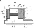
- FIG. 1 is a cross-sectional view parallel to the direction of light incidence in the waveguide type photodetector 100 according to Embodiment 1.
- FIG. 1 a waveguide photodetector 100 receives incident light 20 indicated by an arrow.
- the waveguide photodetector 100 includes at least an n-type contact layer 2 (first conductivity type contact layer) and an n-type cladding layer 3 (first conductivity type contact layer) laminated on a semiconductor substrate 1 (InP substrate).
- conductive type clad layer a light absorption layer 4 made of InGaAs, a p-type clad layer 5 (second conductive type clad layer), and a p-type contact layer 6 (second conductive type contact layer).
- a ridge waveguide 22 having a spaced light incident surface 22a and a rear surface 22b spaced from the other end of the semiconductor substrate 1; a first semiconductor embedded region 7a having a light incident end face 21 spaced apart from one end of the semiconductor substrate; , the passivation film 10 covering the upper surface of the first semiconductor buried region 7a and the second semiconductor buried region 7b, and the light incident end face 21 of the first semiconductor buried region 7a. It is composed of a covering antireflection film 11, a surface electrode 8 provided on the surface of the p-type contact layer 6 and the passivation film 10, and a back surface metal 9 provided on the back surface side of the semiconductor substrate 1 (InP substrate). be.
- the semiconductor buried layer 7 includes the first semiconductor buried region 7a and the second semiconductor buried region 7b.
- the first buried semiconductor region 7 a refers to a region of the buried semiconductor layer 7 that is in contact with the light incident surface 22 a of the ridge waveguide 22 .
- the second embedded semiconductor region 7 b refers to a region of the embedded semiconductor layer 7 that contacts the rear surface 22 b of the ridge waveguide 22 .
- the first semiconductor buried region 7a and the second semiconductor buried region 7b each constitute a part of the semiconductor buried layer 7, and together with the portions of the semiconductor buried layer 7 buried on both side surfaces along the ridge waveguide 22, form one layer as a whole. is making Also, the InP substrate is one specific example of the semiconductor substrate 1 .
- a portion of the semiconductor buried layer 7 is etched away at least until it reaches the semiconductor substrate 1 (InP substrate), forming a first etched portion 23 and a second etched portion 24 .
- One surface of the second semiconductor embedded region 7b provided in contact with the rear surface 22b of the ridge waveguide 22, that is, one surface of the second etched portion 24 forms a rear end surface 26.
- the rear end surface 26 is one surface of the second semiconductor embedded region 7 b and is located at a position separated from the other end of the semiconductor substrate 1 .
- a surface electrode 8 (p-type electrode) is provided on the surface of the p-type contact layer 6 .
- Surface electrode 8 is electrically connected to p-type contact layer 6 .
- a back surface metal 9 is provided on a part or the entire back surface of the semiconductor substrate 1 (InP substrate).
- the window length 25 is the distance from the light incident end surface 21 of the first semiconductor embedded region 7 a to the light incident surface 22 a of the ridge waveguide 22 . That is, the window length 25 means the layer thickness of the first semiconductor buried region 7a with respect to the light incident direction.
- the rear end surface 26 of the second semiconductor embedded region 7b is covered with the passivation film 10 and the surface electrode 8 (p-type electrode), and the light transmitted through the light absorption layer 4 of the ridge waveguide 22 without being completely absorbed is transferred to the ridge waveguide. It functions to reflect into 22 . This is because the reflected light returning to the ridge waveguide 22 contributes to the improvement of the light receiving sensitivity of the waveguide type light receiving element 100 according to the first embodiment.
- FIG. 2 is a general view of the waveguide photodetector 100 according to Embodiment 1.
- FIG. FIG. 3 is a cross-sectional view perpendicular to the light incident direction of the waveguide type photodetector 100 according to the first embodiment.
- An n-type electrode 12 a and an n-type electrode 12 b electrically connected to the n-type contact layer 2 are provided at a portion other than the ridge waveguide 22 .
- a method for manufacturing the waveguide photodetector 100 according to the first embodiment will be described below.
- a crystal growth method for each semiconductor layer of the waveguide type light receiving element 100 according to the first embodiment a liquid phase epitaxy (LPE) method, a vapor phase epitaxy (VPE) method, especially an organometallic epitaxy method is used.
- a phase growth method Metal Organic VPE: MO-VPE
- a molecular beam epitaxy growth method Molecular Beam Epitaxy: MBE
- n-type contact layer 2 an n-type cladding layer 3, a light absorption layer 4 made of InGaAs, a p-type cladding layer 5, and a p-type contact layer are formed on a semiconductor substrate 1 (InP substrate) by any of the crystal growth methods described above. 6 is sequentially crystal-grown.
- FIG. 4 is a cross-sectional view of each layer after crystal growth.
- FIG. 5 is a cross-sectional view parallel to the light incident direction in the ridge waveguide 22 formed by dry etching 41. As shown in FIG.
- the ridge waveguide 22 When the ridge waveguide 22 is formed by the dry etching 41, the light incident surface 22a of the ridge waveguide 22 and the rear surface 22b opposite to the light incident surface 22a are formed. That is, both the light incident surface 22a and the rear surface 22b are etched surfaces. A light incident surface 22 a of the ridge waveguide 22 is positioned away from one end of the semiconductor substrate 1 . Further, the rear surface 22b of the ridge waveguide 22 is positioned away from the other end of the semiconductor substrate 1. As shown in FIG.
- FIG. 6 is a cross-sectional view parallel to the light incident direction of the ridge waveguide 22 after crystal growth of the semiconductor buried layer 7 .
- FIG. 7 is a cross-sectional view parallel to the light incident direction of the ridge waveguide 22 after dry etching.
- a first embedded semiconductor is provided in contact with the light incident surface 22a of the ridge waveguide 22 and one surface on the light incident side forms the light incident end surface 21.
- a second semiconductor embedding region 7b is formed in contact with the region 7a and the rear surface 22b of the ridge waveguide 22, and the one surface facing the rear surface 22b forms the rear end surface 26.
- both the light incident end surface 21 and the rear end surface 26 are etched surfaces.
- a light incident end surface 21 of the first semiconductor embedded region 7 a is located away from one end of the semiconductor substrate 1 .
- the rear end surface 26 of the second semiconductor embedded region 7b is positioned away from the other end of the semiconductor substrate 1. As shown in FIG.
- the passivation film 10 covering the side surface of the first etching portion 23 other than the portion other than the p-type contact layer 6 and the light incident end face 21 on the front surface side is formed by plasma-enhanced chemical vapor deposition (PE- CVD) or a method such as sputtering.
- PE- CVD plasma-enhanced chemical vapor deposition
- passivation film 10 is formed by etching unnecessary portions of the insulating film using a known lithography technique while leaving an etching mask only in desired portions. be.
- part of the crystal-grown portion of the semiconductor embedding layer 7, ie, right above the n-type contact layer 2, is etched by dry etching such as RIE or wet etching.
- the surface electrode 8 (p-type electrode) and the n-type electrodes 12a and 12b are formed by electron beam vapor deposition or electron beam evaporation of a material such as Ti, Pt, or Au using a known lithography technique with the mask opened only at desired portions. It is formed by forming a film by a method such as sputtering and removing metal from unnecessary portions. Further, the surface electrode 8 (p-type electrode) and the n-type electrodes 12a and 12b are formed using a known lithography technique after metal is deposited on the entire surface, leaving only desired portions as a mask. It can also be formed by wet etching the metal of the part.
- the back surface metal 9 is formed by inverting the semiconductor substrate 1 (InP substrate), using a known lithography technique, and using a known lithography technique with a mask opened only at desired portions, and applying a metal material such as Ti, Pt, or Au by electron beam evaporation or the like. It is formed by forming a film by a method such as sputtering and removing metal from unnecessary portions. Further, the back surface metal 9 is formed by forming a metal film on the entire back surface of the semiconductor substrate 1 (InP substrate), using a known lithography technique, leaving only the desired portion of the mask, and removing the metal from the unnecessary portion. may be formed by removing by wet etching.
- the antireflection film 11 is formed by vapor deposition or sputtering on the light incident end surface 21 of the first semiconductor embedded region 7a in a state in which the wafer that has undergone the above process is cleaved into chips.
- the semiconductor substrate 1 (InP substrate) is preferably a semi-insulating substrate doped with Fe or the like.
- the constituent material of the n-type contact layer 2 may be InGaAs, InP, InGaAsP, AlInAs, AlGaInAs, or a combination thereof.
- the constituent material of the n-type cladding layer 3 may be InP, InGaAsP, AlInAs, AlGaInAs, or a combination thereof.
- the constituent material of the light absorption layer 4 is a semiconductor material that generates carriers when light is incident, that is, a semiconductor material having a small bandgap with respect to the incident light 20 , not InGaAs, but InGaAsP, InGaAsSb, or a combination thereof. And so on.
- the constituent material of the p-type cladding layer 5 may be InP, InGaAsP, AlInAs, AlGaInAs, or a combination thereof.
- the constituent material of the p-type contact layer 6 may be InGaAs, InP, InGaAsP, AlInAs, AlGaInAs, or a combination thereof.
- the constituent material of the semiconductor buried layer 7 may be InP, InGaAsP, or the like, which may be doped with Fe or Ru.
- a band discontinuity relaxation layer using InGaAsP, AlGaInAs or the like is included between each epitaxial crystal growth layer or between the surface electrode 8 (p-type electrode) and the epitaxial crystal growth layer. It's okay if it is.
- the constituent material of the passivation film 10 may be SiO 2 , SiN, SiON, or a combination of these materials.
- any material may be used for each of the above layers as long as the device characteristics necessary for the operation of the waveguide type light receiving device 100 can be obtained. That is, each constituent material of the waveguide photodetector 100 is not limited to the specific examples described above.
- Group II atoms such as Be, Mg, Zn, and Cd are used as p-type dopants that impart conductivity to Group III-V semiconductor crystals.
- Group VI atoms such as S, Se, and Te are used as n-type dopants.
- Group IV atoms such as C, Si, Ge, and Sn are used as amphoteric impurities that function as dopants of either conductivity type depending on the semiconductor crystal. Atoms such as Fe and Ru function as an insulating dopant that suppresses conductivity and becomes semi-insulating (SI).
- FIG. 8 shows an element structure in which the first etched portion 23 is not formed, unlike the element structure of the waveguide type light receiving element 100 according to Embodiment 1 shown in FIG.
- the light incident end surface 21a is formed by cleaving or the like after the completion of the wafer process.
- the cleaving process is, for example, a process of forming a scribe line at the edge of the wafer and dividing the wafer into chips by applying stress to the scribe line.
- the window length 25a is formed long.
- the design value of the window length 25a is set so that the variation amount at the time of cleavage is Since it is necessary to set a longer length to include the considered margin, in the waveguide type light receiving element 200 of the comparative example, the window length 25a tends to be longer than the length required to function as a window layer.
- the window length 25a is longer than the length required to function as a window layer, the light incident on the light incident end surface 21a leaks out from the top of the first semiconductor embedded region 7a before reaching the light absorption layer 4. As a result, the amount of light incident on the light absorption layer 4 is reduced, and the light receiving sensitivity is lowered.
- the n-type contact layer 2 is located at the bottom of the first semiconductor embedded region 7a. Since the absorption of light by the n-type contact layer 2 increases as the thickness increases, the amount of light incident on the light absorption layer 4 decreases, resulting in a decrease in light receiving sensitivity. In other words, in the waveguide type photodetector 200 of the comparative example, due to variations in the window length that inevitably occur in the manufacturing process, the window length 25 becomes unnecessarily long due to the margin for the variations. There was a possibility that the problem of causing a decrease in sensitivity would occur.
- the light incident end face 21 of the first semiconductor buried region 7a, into which the incident light 20 is incident is not cleaved, but etched in the manufacturing process.
- the amount of positional variation in the etching process that is, the positional accuracy is generally 1 ⁇ m or less. Since the light incident surface 22a of the ridge waveguide 22 is formed away from one end of the semiconductor substrate 1 by etching, the position of the light incident end surface 21 of the first semiconductor embedded region 7a provided in contact with the light incident surface 22a is , is not affected by positional variations due to the cleavage process as in the comparative example.
- the positional accuracy of the light incident end surface 21 is significantly improved, so that the design value of the window length 25 can be set shorter than in the comparative example. Therefore, as a result, the window length 25, which is shorter than that of the comparative example, can be accurately controlled.
- the light incident end surface 21 of the first semiconductor embedded region 7a is separated from one end of the semiconductor substrate 1. This improves the positional accuracy of the light incident end face 21 of the first semiconductor embedding region 7a, and as a result, the window length can be controlled to be short. In addition, there is an effect that such a waveguide type photodetector can be manufactured with good reproducibility.
- FIG. 9 is a cross-sectional view parallel to the light incident direction in the waveguide type light receiving element 300 according to Modification 1 of Embodiment 1.
- a passivation film 10 is formed instead of the antireflection film 11 formed on the light incident end surface 21 of the first semiconductor embedded region 7a.
- the portion of the passivation film 10 covering the light incident end surface 21 of the first semiconductor embedded region 7a also functions as an antireflection film.
- the passivation film 10 also functions as an antireflection film. An effect is obtained in that a waveguide type photodetector that can be manufactured by a simple manufacturing process can be obtained.
- FIG. 10 is a cross-sectional view parallel to the direction of light incidence in the waveguide type light receiving element 400 according to Modification 1 of Embodiment 1.
- a different point from the element structure of the waveguide type light receiving element 100 according to the first embodiment is that the rear surface metal 9 is not provided. In other words, the back metal is omitted because the back metal is not essential for the waveguide type photodetector.
- the waveguide type light receiving element 400 operates without the antireflection film, it is desirable to provide the antireflection film because the light receiving sensitivity is improved by providing the antireflection film. .
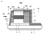
- FIG. 11 is a cross-sectional view parallel to the direction of light incidence in the waveguide type photodetector 500 according to the second embodiment.
- the difference from the device structure of the waveguide type light receiving device 100 according to the first embodiment is that at least the side surface of the n-type contact layer 2 on the light incident side is also covered with the first semiconductor buried region 7a.
- the n-type contact layer 2 is positioned at the bottom of the first semiconductor embedded region 7a.
- the material of the n-type contact layer 2 is a semiconductor material that absorbs the incident light 20
- light is absorbed by the n-type contact layer 2, resulting in a decrease in the amount of light incident on the light absorption layer 4.
- the light-receiving sensitivity decreases.
- the n-type contact layer 2 does not exist at the bottom of the first semiconductor embedded region 7a, that is, the first semiconductor embedded region Since the bottom portion of 7a is in contact with the semiconductor substrate 1, light absorption in the n-type contact layer 2 is reduced, so that the light receiving sensitivity of the waveguide type light receiving element 500 can be further enhanced.
- the waveguide type light receiving device 500 since the element structure in which the n-type contact layer 2 does not exist at the bottom of the first semiconductor buried region 7a is adopted, the waveguide type light receiving device 500 has a higher light receiving sensitivity. There is an effect that a device can be obtained.
- FIG. 12 is a cross-sectional view parallel to the direction of light incidence in the waveguide type photodetector 600 according to the third embodiment.
- a different point from the device structure of the waveguide type light receiving device 100 according to the first embodiment is that the light incident end surface 21b of the first semiconductor embedded region 7a is not vertical when viewed from the cross-sectional direction, but has an inclined shape. That is, the light incident end face 21b of the first semiconductor buried region 7a is inclined with respect to the surface of the semiconductor substrate 1. As shown in FIG.
- the incident light 20 is refracted by the light incident end surface 21b formed obliquely with respect to the incident direction when entering the waveguide type light receiving element 600, so the reflected light component by the light incident end surface 21b is reduced. That is, reflected return light can be reduced. As a result, the component of the incident light 20 that enters the waveguide type light receiving element 600 increases, so that the light receiving sensitivity of the waveguide type light receiving element 600 can be enhanced.
- FIG. 13 is a top view of a waveguide photodetector array 1000 according to Embodiment 4.
- FIG. A plurality of waveguide photodetectors 100 according to the first embodiment are integrated in parallel such that the ridge waveguides 22 are positioned parallel to each other. Note that the passivation film 10 and the antireflection film 11 are omitted in the top views of FIG. 13 and subsequent drawings.
- the light incident end surface 21 of the first semiconductor embedded region 7a is oriented perpendicular to the incident light 20. be provided.
- the waveguide-type photodetector array 1000 since the deviation of the cleaved position between the integrated waveguide-type photodetectors is reduced, as a result, the window length variation among the waveguide-type photodetectors is reduced. also decreases. Therefore, high photosensitivity can be uniformly obtained among the waveguide type photodetectors.
- each waveguide type light receiving element constituting the waveguide type light receiving element array 1000 according to the fourth embodiment is the light incident end face 21 of the first semiconductor embedded region 7a. is provided in a direction perpendicular to the incident light 20 .
- ⁇ Effect of Embodiment 4> As described above, according to the waveguide type light receiving element array 1000 according to the fourth embodiment, a plurality of waveguide type light receiving elements 100 according to the first embodiment are integrated in parallel so that the ridge waveguides 22 are positioned parallel to each other. , there is an effect that a high light-receiving sensitivity can be uniformly obtained among the waveguide-type light-receiving elements.
- FIG. 14 is a top view of a waveguide photodetector array 1100 according to Embodiment 5.
- FIG. A plurality of waveguide type photodetectors 100 according to the first embodiment are integrated in parallel so that the ridge waveguides 22 are positioned parallel to each other.
- each integrated waveguide-type light-receiving element is provided in a direction in which the light incident end surface 21 of the first semiconductor embedded region 7a is inclined with respect to the incident light 20 when the surface of the semiconductor substrate 1 is viewed from above. ing. Also, the light incident end face 21 of each waveguide type light receiving element is inclined in the same direction at the same angle.
- the chip itself in order to reduce the reflected return light from the light incident end surface 21 of the first semiconductor buried region 7a, the chip itself is arranged at an angle to the light incident direction when viewed from the upper surface side, and the light is incident.
- a method of changing the angle at which the incident light 20 is reflected by positioning the end surface 21 obliquely with respect to the incident light is effective.
- the optical path length will change between the waveguide type light receiving elements.
- the spot size of the incident light changes between them, which causes variation in the light receiving sensitivity.
- the integrated individual waveguide type light receiving elements can detect light in the first semiconductor embedded region 7a. Since the incident end surface 21 is provided in the direction inclined at the same angle with respect to the incident light 20, the reflected return light can be reduced, so that the waveguide type light receiving elements can uniformly obtain high light receiving sensitivity. play.
- FIG. 15 is a top view of a waveguide photodetector array 1200 according to Embodiment 6.
- FIG. The configuration of the waveguide photodetector array 1200 according to the sixth embodiment differs from the configuration according to the fifth embodiment in the following points.
- the light incident surface 22a of the ridge waveguide 22 of the individual integrated waveguide type light receiving elements is located in the first semiconductor embedded region 7a with respect to the incident light 20. It is provided in a direction that inclines to the side opposite to the light incident end surface 21 . Further, each light incident end surface 21 of each waveguide type light receiving element is inclined at the same angle in the same direction, and each light incident surface 22a is also inclined at the same angle in the same direction.
- the light reaching the ridge waveguide 22 is oblique to the ridge waveguide 22, and the light transmitted through the ridge waveguide 22 is also oblique.
- the light transmitted through the ridge waveguide 22 reaches the rear end surface 26 of the second semiconductor embedded region 7b at a certain angle, so the light is not reflected in the direction returning to the ridge waveguide 22.
- FIG. Therefore, the light does not return to the ridge waveguide 22, and the light receiving sensitivity cannot be increased.
- the light incident surface 22a of the ridge waveguide 22 on which the light is incident is inclined when viewed from the upper surface side so that the light passing through the ridge waveguide 22 is parallel to the light incident direction.
- the light emitted from the rear facet 22b of the ridge waveguide 22 is directed to the rear facet 26 of the second semiconductor-embedded region 7b, and the light is reflected by the rear facet 26 to return to the ridge waveguide 22.
- the photosensitivity can be increased.
- the waveguide-type photodetector array 1200 when the surface of the semiconductor substrate 1 is viewed from above, the light incident surface 22a of the ridge waveguide 22 is located at the first semiconductor region with respect to the incident light 20. Since the embedding region 7a is provided in a direction inclined in the direction opposite to the light incident end surface 21, the reflected return light can be further reduced, so that a higher light receiving sensitivity can be uniformly obtained among the waveguide type light receiving elements. play.
- FIG. 16 is a top view of a waveguide photodetector array 1300 according to Embodiment 7.
- FIG. The configuration of the waveguide photodetector array 1200 according to the seventh embodiment differs from the configuration according to the fifth embodiment in the following points.
- the individual integrated waveguide-type light-receiving elements have a rear end face 26 parallel to the light incident end face 21 of the first semiconductor buried region 7a. direction. That is, the rear end surface 26 of the second semiconductor embedded region 7b is also inclined at the same angle in the same direction as the light incident end surface 21 of the first semiconductor embedded region 7a.
- Each light incident end surface 21 of each waveguide type light receiving element is inclined at the same angle in the same direction, and each rear end surface 26 is also inclined at the same angle in the same direction.
- the angle at which the rear end surface 26 of the second semiconductor embedded region 7b is inclined is an angle at which it is substantially parallel to the light incident end surface 21 of the first semiconductor embedded region 7a.
- the light reaching the ridge waveguide 22 is oblique to the ridge waveguide 22, and the light transmitted through the ridge waveguide 22 is also oblique.
- the light transmitted through the ridge waveguide 22 reaches the rear end face 26 of the second semiconductor embedded region 7b at a certain angle, so the light is not reflected in the direction of the ridge waveguide 22.
- the light reaching the rear facet 26 of the second semiconductor embedded region 7b is reflected again toward the ridge waveguide 22, so that the light receiving sensitivity can be increased as a result.
- the waveguide-type photodetector array 1300 when the surface of the semiconductor substrate 1 is viewed from above, the rear end face 26 of the second semiconductor embedded region 7b is the light incident surface of the first semiconductor embedded region 7a. Since it is inclined in the same direction as the end face 21, it is possible to further reduce reflected return light, so that there is an effect that higher light receiving sensitivity can be uniformly obtained among the waveguide type light receiving elements.
- FIG. 17 is a top view of a waveguide photodetector array 1400 according to the eighth embodiment.
- the configuration of the waveguide photodetector array 1300 according to the eighth embodiment differs from the configuration according to the seventh embodiment in the following points.
- each integrated waveguide-type light-receiving element is provided in a direction in which the light incident end surface 21 of the first semiconductor embedded region 7a is inclined with respect to the incident light 20 when the surface of the semiconductor substrate 1 is viewed from above.
- the rear end surface 26 of the second semiconductor embedded region 7b is provided in a different inclination direction from the light incident end surface 21 of the first semiconductor embedded region 7a.
- Each light incident end surface 21 of each waveguide type light receiving element is inclined at the same angle in the same direction, and each rear end surface 26 is also inclined at the same angle in the same direction.
- the inclination angle of the rear end surface 26 of the second semiconductor embedded region 7b is set to be different from the inclination angle of the light incident end surface 21 of the first semiconductor embedded region 7a. changing.
- the light that reaches the rear facet 26 of the second semiconductor embedded region 7b returns to the ridge waveguide 22. Since the light transmitted through the second semiconductor buried region 7b does not face the rear end face 26 of the second semiconductor embedded region 7b, there is light that leaks without returning to the ridge waveguide 22 completely.
- the photosensitivity can be increased as a result.
- the waveguide type light receiving element array 1400 when the surface of the semiconductor substrate 1 is viewed from above, the rear end face 26 of the second semiconductor embedded region 7b is the light beam of the first semiconductor embedded region 7a. Since it is inclined at an angle different from that of the incident end surface 21, it is possible to further reduce the reflected return light, so that there is an effect that higher light receiving sensitivity can be uniformly obtained among the waveguide type light receiving elements.
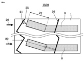
- FIG. 18 is a top view of a waveguide photodetector array 1500 according to the ninth embodiment.
- the configuration of the waveguide photodetector array 1500 according to the eighth embodiment differs from the configuration according to the eighth embodiment in the following points.
- the individual integrated waveguide type light receiving elements are tilted in a direction in which the ridge waveguide 22 faces the incident light 20 to the ridge waveguide 22.
- the ridge waveguides 22 in each waveguide type light receiving element are inclined in the same direction at the same angle.
- the ridge waveguide 22 is rotated as viewed from the upper surface side, and the light incident on the ridge waveguide 22 is directed to the light incident surface 22a of the ridge waveguide 22. are arranged to face each other.
- the light reaching the ridge waveguide 22 is oblique to the ridge waveguide 22, and the light passing through the ridge waveguide 22 is also oblique. In this case, when the width of the ridge waveguide 22 is narrowed, light may leak from the side surfaces of the ridge waveguide 22 .
- the light is incident parallel to the ridge waveguide 22 and Since the light faces the rear end face 26 of the two-semiconductor buried region 7b and is reflected back to the ridge waveguide 22, the light receiving sensitivity can be increased.
- the waveguide-type photodetector array 1500 when the surface of the semiconductor substrate 1 is viewed in plan, the ridge waveguide 22 faces the incident light 20 to the ridge waveguide 22 at an angle of Since the waveguides are provided in the direction inclined toward the direction of inclination, the reflected return light can be further reduced, so that there is an effect that a higher light receiving sensitivity can be uniformly obtained among the respective waveguide type light receiving elements.
Landscapes
- Physics & Mathematics (AREA)
- Engineering & Computer Science (AREA)
- Microelectronics & Electronic Packaging (AREA)
- General Physics & Mathematics (AREA)
- Optics & Photonics (AREA)
- Light Receiving Elements (AREA)
Priority Applications (4)
| Application Number | Priority Date | Filing Date | Title |
|---|---|---|---|
| CN202180103085.4A CN118077062A (zh) | 2021-10-14 | 2021-10-14 | 波导型受光元件、波导型受光元件阵列以及波导型受光元件的制造方法 |
| PCT/JP2021/038000 WO2023062766A1 (ja) | 2021-10-14 | 2021-10-14 | 導波路型受光素子、導波路型受光素子アレイ及び導波路型受光素子の製造方法 |
| JP2022506158A JP7118306B1 (ja) | 2021-10-14 | 2021-10-14 | 導波路型受光素子及び導波路型受光素子アレイ |
| US18/576,494 US20240332438A1 (en) | 2021-10-14 | 2021-10-14 | Waveguide-type light-receiving element, waveguide-type light-receiving element array, and method for manufacturing waveguide-type light-receiving element |
Applications Claiming Priority (1)
| Application Number | Priority Date | Filing Date | Title |
|---|---|---|---|
| PCT/JP2021/038000 WO2023062766A1 (ja) | 2021-10-14 | 2021-10-14 | 導波路型受光素子、導波路型受光素子アレイ及び導波路型受光素子の製造方法 |
Publications (1)
| Publication Number | Publication Date |
|---|---|
| WO2023062766A1 true WO2023062766A1 (ja) | 2023-04-20 |
Family
ID=82847638
Family Applications (1)
| Application Number | Title | Priority Date | Filing Date |
|---|---|---|---|
| PCT/JP2021/038000 Ceased WO2023062766A1 (ja) | 2021-10-14 | 2021-10-14 | 導波路型受光素子、導波路型受光素子アレイ及び導波路型受光素子の製造方法 |
Country Status (4)
| Country | Link |
|---|---|
| US (1) | US20240332438A1 (https=) |
| JP (1) | JP7118306B1 (https=) |
| CN (1) | CN118077062A (https=) |
| WO (1) | WO2023062766A1 (https=) |
Families Citing this family (1)
| Publication number | Priority date | Publication date | Assignee | Title |
|---|---|---|---|---|
| CN120266599A (zh) * | 2022-12-01 | 2025-07-04 | 三菱电机株式会社 | 波导型受光元件 |
Citations (6)
| Publication number | Priority date | Publication date | Assignee | Title |
|---|---|---|---|---|
| JPH10107310A (ja) * | 1996-09-26 | 1998-04-24 | Japan Aviation Electron Ind Ltd | 導波路型フォトダイオードアレイ |
| JP2000150925A (ja) * | 1998-11-05 | 2000-05-30 | Furukawa Electric Co Ltd:The | 導波路型集積半導体装置の作製方法 |
| JP2002033504A (ja) * | 2000-07-18 | 2002-01-31 | Nippon Sheet Glass Co Ltd | 受光素子アレイおよびその実装方法 |
| JP2002203984A (ja) * | 2000-10-30 | 2002-07-19 | Nec Corp | 半導体受光素子 |
| JP2002305319A (ja) * | 2001-04-06 | 2002-10-18 | Toshiba Corp | 半導体受光素子および光通信用モジュール |
| JP2006066488A (ja) * | 2004-08-25 | 2006-03-09 | Mitsubishi Electric Corp | 半導体受光素子およびその製造方法 |
Family Cites Families (3)
| Publication number | Priority date | Publication date | Assignee | Title |
|---|---|---|---|---|
| JPH07202263A (ja) * | 1993-12-28 | 1995-08-04 | Ricoh Co Ltd | 端面発光型発光ダイオード、アレイ状光源、側面受光型受光素子、受発光素子、端面発光型発光ダイオードアレイ状光源 |
| JP2004128064A (ja) * | 2002-09-30 | 2004-04-22 | Toshiba Corp | 光半導体装置及びその製造方法 |
| CN100573925C (zh) * | 2005-05-18 | 2009-12-23 | 三菱电机株式会社 | 雪崩光电二极管 |
-
2021
- 2021-10-14 US US18/576,494 patent/US20240332438A1/en active Pending
- 2021-10-14 WO PCT/JP2021/038000 patent/WO2023062766A1/ja not_active Ceased
- 2021-10-14 JP JP2022506158A patent/JP7118306B1/ja active Active
- 2021-10-14 CN CN202180103085.4A patent/CN118077062A/zh active Pending
Patent Citations (6)
| Publication number | Priority date | Publication date | Assignee | Title |
|---|---|---|---|---|
| JPH10107310A (ja) * | 1996-09-26 | 1998-04-24 | Japan Aviation Electron Ind Ltd | 導波路型フォトダイオードアレイ |
| JP2000150925A (ja) * | 1998-11-05 | 2000-05-30 | Furukawa Electric Co Ltd:The | 導波路型集積半導体装置の作製方法 |
| JP2002033504A (ja) * | 2000-07-18 | 2002-01-31 | Nippon Sheet Glass Co Ltd | 受光素子アレイおよびその実装方法 |
| JP2002203984A (ja) * | 2000-10-30 | 2002-07-19 | Nec Corp | 半導体受光素子 |
| JP2002305319A (ja) * | 2001-04-06 | 2002-10-18 | Toshiba Corp | 半導体受光素子および光通信用モジュール |
| JP2006066488A (ja) * | 2004-08-25 | 2006-03-09 | Mitsubishi Electric Corp | 半導体受光素子およびその製造方法 |
Also Published As
| Publication number | Publication date |
|---|---|
| JPWO2023062766A1 (https=) | 2023-04-20 |
| CN118077062A (zh) | 2024-05-24 |
| US20240332438A1 (en) | 2024-10-03 |
| JP7118306B1 (ja) | 2022-08-15 |
Similar Documents
| Publication | Publication Date | Title |
|---|---|---|
| US4358676A (en) | High speed edge illumination photodetector | |
| US12288827B2 (en) | Waveguide photodetector | |
| JPH022691A (ja) | 半導体受光素子 | |
| US12132131B2 (en) | Backside illuminated avalanche photodiode and manufacturing method thereof | |
| US6020620A (en) | Semiconductor light-receiving device with inclined multilayer structure | |
| US8999744B2 (en) | Avalanche photodiodes and methods of fabricating the same | |
| KR100464333B1 (ko) | 수광소자 및 그 제조방법 | |
| US11978812B2 (en) | Waveguide photodetector | |
| JP7118306B1 (ja) | 導波路型受光素子及び導波路型受光素子アレイ | |
| US7368750B2 (en) | Semiconductor light-receiving device | |
| JP3717785B2 (ja) | 半導体受光装置およびその製造方法 | |
| JPH09283786A (ja) | 導波路型半導体受光素子とその製造方法 | |
| JP7409489B2 (ja) | 受光装置 | |
| US20260052799A1 (en) | Waveguide-type light-receiving device | |
| JPH09139520A (ja) | 導波路型受光素子及びその製造方法 | |
| JP3783903B2 (ja) | 半導体受光素子及びその製造方法 | |
| US6064782A (en) | Edge receptive photodetector devices | |
| JP2962069B2 (ja) | 導波路構造半導体受光素子 | |
| JP2638445B2 (ja) | 半導体受光素子 | |
| JP3620761B2 (ja) | 半導体受光素子及びその製造方法 | |
| JPH04116977A (ja) | 半導体受光素子 | |
| JP2005086028A (ja) | 半導体受光装置 | |
| EP0889529A1 (en) | Semiconductor light-receiving device and method of fabricating the same | |
| JPH0677516A (ja) | 半導体光検出器およびその製造方法 | |
| JP2005093937A (ja) | 高速のエージ・カップル式フォトデテクタの改善方法 |
Legal Events
| Date | Code | Title | Description |
|---|---|---|---|
| WWE | Wipo information: entry into national phase |
Ref document number: 2022506158 Country of ref document: JP |
|
| 121 | Ep: the epo has been informed by wipo that ep was designated in this application |
Ref document number: 21960624 Country of ref document: EP Kind code of ref document: A1 |
|
| WWE | Wipo information: entry into national phase |
Ref document number: 18576494 Country of ref document: US |
|
| WWE | Wipo information: entry into national phase |
Ref document number: 202180103085.4 Country of ref document: CN |
|
| NENP | Non-entry into the national phase |
Ref country code: DE |
|
| 122 | Ep: pct application non-entry in european phase |
Ref document number: 21960624 Country of ref document: EP Kind code of ref document: A1 |