WO2023062745A1 - 電力用半導体素子の駆動回路、電力用半導体モジュール、および電力変換装置 - Google Patents
電力用半導体素子の駆動回路、電力用半導体モジュール、および電力変換装置 Download PDFInfo
- Publication number
- WO2023062745A1 WO2023062745A1 PCT/JP2021/037882 JP2021037882W WO2023062745A1 WO 2023062745 A1 WO2023062745 A1 WO 2023062745A1 JP 2021037882 W JP2021037882 W JP 2021037882W WO 2023062745 A1 WO2023062745 A1 WO 2023062745A1
- Authority
- WO
- WIPO (PCT)
- Prior art keywords
- circuit
- turn
- voltage
- power semiconductor
- signal
- Prior art date
- Legal status (The legal status is an assumption and is not a legal conclusion. Google has not performed a legal analysis and makes no representation as to the accuracy of the status listed.)
- Ceased
Links
Images









Classifications
-
- H—ELECTRICITY
- H02—GENERATION; CONVERSION OR DISTRIBUTION OF ELECTRIC POWER
- H02M—APPARATUS FOR CONVERSION BETWEEN AC AND AC, BETWEEN AC AND DC, OR BETWEEN DC AND DC, AND FOR USE WITH MAINS OR SIMILAR POWER SUPPLY SYSTEMS; CONVERSION OF DC OR AC INPUT POWER INTO SURGE OUTPUT POWER; CONTROL OR REGULATION THEREOF
- H02M1/00—Details of apparatus for conversion
- H02M1/08—Circuits specially adapted for the generation of control voltages for semiconductor devices incorporated in static converters
-
- H—ELECTRICITY
- H03—ELECTRONIC CIRCUITRY
- H03K—PULSE TECHNIQUE
- H03K17/00—Electronic switching or gating, i.e. not by contact-making and –breaking
- H03K17/08—Modifications for protecting switching circuit against overcurrent or overvoltage
Definitions
- the present disclosure relates to a power semiconductor device drive circuit, a power semiconductor module, and a power converter.
- Overvoltage may occur due to the surge voltage that occurs when the power semiconductor device is turned off.
- One of the means for preventing such overvoltage is to connect a voltage clamp circuit using a constant voltage diode between the main electrode on the high potential side of the power semiconductor element and the control electrode.
- the voltage between the high-potential main electrode and the control electrode reaches the operating voltage level of the voltage clamp circuit, the voltage of the high-potential main electrode is clamped to a constant voltage, and through the voltage clamp circuit A current flows from the main electrode on the high potential side to the control electrode.
- the voltage rise of the control electrode lengthens the turn-off operation time, resulting in a side effect of increasing the turn-off loss.
- Patent Document 1 discloses a method of changing the output stage impedance connected to the control electrode according to the detected value of the voltage of the control electrode in order to suppress an increase in turn-off loss. . Specifically, when the surge is alleviated, the voltage of the control electrode is lowered due to the decrease of the clamp current. After that, when the mirror period ends and it is detected that the voltage of the control electrode has dropped below the specified value, the output stage circuit reduces the output stage impedance.
- Patent Document 1 JP-A-2016-86490 (Patent Document 1) is sufficient to suppress the turn-off loss. Specifically, the output stage impedance is maintained at a high value both during the period in which the voltage between the high potential side main electrode and the control electrode changes and in the period in which the main current flowing between the main electrodes changes. there is Therefore, the turn-off loss increases during these periods.
- the present disclosure has been made in consideration of the above problems, and one of its purposes is to provide a drive circuit for a power semiconductor device that achieves both suppression of surge voltage and reduction of turn-off loss. to provide.
- a drive circuit for a power semiconductor device includes a first main electrode on the high potential side, a second main electrode on the low potential side, and a control electrode. A conducting state and a non-conducting state are switched between the first main electrode and the second main electrode according to the voltage applied to the control electrode.
- the drive circuit comprises a turn-on circuit, a first turn-off circuit, a voltage clamp circuit, a second turn-off circuit, and a turn-off control circuit.
- the turn-on circuit turns on the power semiconductor element by applying the first power supply voltage to the control electrode according to an on-command from the controller.
- the first turn-off circuit turns off the power semiconductor element by applying a second power supply voltage to the control electrode according to an off command from the controller.
- a voltage clamp circuit is connected between the first main electrode and the control electrode.
- the second turn-off circuit includes a capacitive element and a switching element connected in series between the control electrode and the second main electrode, and a resistive element connected in parallel with the capacitive element.
- the turn-off control circuit controls on and off of the switching element of the second turn-off circuit.
- the turn-off control circuit turns on the switching element when the voltage between the first main electrode and the second main electrode rises after the power semiconductor element is turned off by the first turn-off circuit. switch to
- the switching element is turned on when the voltage between the first main electrode and the second main electrode rises after the power semiconductor element is turned off. state can be switched. As a result, it is possible to achieve both suppression of surge voltage and reduction of turn-off loss.
- FIG. 1 is a circuit diagram showing a configuration of a drive circuit for a power semiconductor device according to Embodiment 1;
- FIG. FIG. 3 is a diagram schematically showing voltage or current waveforms at each part during turn-off by a drive circuit of a comparative example in which the second turn-off circuit of FIG. 1 is not provided;
- FIG. 2 is a diagram schematically showing voltage or current waveforms of respective parts when the drive circuit of the first embodiment shown in FIG. 1 is turned off;
- FIG. 10 is a circuit diagram showing the configuration of a drive circuit for a power semiconductor device according to a second embodiment;
- FIG. 10 is a diagram schematically showing voltage or current waveforms of respective parts when the drive circuit of the fifth embodiment shown in FIG. 9 is turned off;
- FIG. 12 is a circuit diagram showing a configuration of a drive circuit according to a modification of the fifth embodiment;
- FIG. 11 is a circuit diagram showing the configuration of a drive circuit for a power semiconductor device according to a sixth embodiment;
- FIG. 13 is a diagram schematically showing voltage or current waveforms of respective parts when the drive circuit of the sixth embodiment shown in FIG. 12 is turned off;
- FIG. 12 is a circuit diagram showing a configuration of a drive circuit according to a modification of Embodiment 6;
- FIG. 12 is a circuit diagram showing the configuration of a drive circuit for a power semiconductor device according to a seventh embodiment;
- FIG. 16 is a diagram showing voltage or current waveforms of respective parts when the drive circuit of the seventh embodiment shown in FIG. 15 is turned off;
- FIG. 14 is a circuit diagram showing the configuration of a drive circuit for a power semiconductor device according to a first example of an eighth embodiment;
- FIG. 14 is a circuit diagram showing the configuration of a drive circuit for a power semiconductor device according to a second example of the eighth embodiment;
- FIG. 14 is a circuit diagram showing the configuration of a drive circuit for a power semiconductor device according to a third example of the eighth embodiment;
- FIG. 12 is a block diagram showing the configuration of a power conversion system to which a power conversion device according to Embodiment 9 is applied;
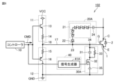
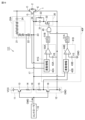
- FIG. 1 is a circuit diagram showing the configuration of a driving circuit 100 for a power semiconductor device 1 according to Embodiment 1.
- a power semiconductor module is configured by the power semiconductor element 1 and the driving circuit 100 .
- the power semiconductor element 1 and the driving circuit 100 may be integrally configured to constitute a power semiconductor module, or the power semiconductor element 1 and the driving circuit 100 may be separately configured to constitute a power semiconductor module. good.
- the power semiconductor element 1 has a first main electrode C (collector) on the high potential side and a second main electrode E (emitter) on the low potential side depending on the voltage applied to the control electrode G (gate). switch between a conducting (on) state or a non-conducting (off) state.
- the voltage applied to the control electrode G is generated by the drive circuit 100 based on the command signal CMD applied from the controller 10.
- FIG. 1 an IGBT (Insulated Gate Bipolar Transistor) is illustrated as the power semiconductor element 1, but it is not limited to the IGBT.
- power semiconductor devices such as power MOSFETs (Metal-Oxide-Semiconductor Field Effect Transistors) and reverse conducting IGBTs (RC-IGBTs) may be used.
- the material used for the power semiconductor element 1 is not limited to Si, and other semiconductor materials such as SiC, GaN, and Ga 2 O 3 may be used.
- a freewheeling diode 2 is connected in anti-parallel with the power semiconductor element 1 .
- the drive circuit 100 includes a turn-on circuit 11, a first turn-off circuit 12, a second turn-off circuit 30, a turn-off control circuit 40, and a voltage clamp circuit 20.
- the turn-on circuit 11 includes a semiconductor switching element 13 and an on-gate resistor 14.
- Semiconductor switching element 13 and on-gate resistor 14 are connected in this order between a node to which power supply voltage VCC is applied (hereinafter referred to as VCC node) and intermediate node 18 .
- First turn-off circuit 12 includes semiconductor switching element 16 and off-gate resistor 15 .
- Semiconductor switching element 16 and off-gate resistor 15 are connected in this order between a node to which ground potential GND is applied (hereinafter referred to as a GND node) and intermediate node 18 .
- Intermediate node 18 is connected to control electrode G of power semiconductor element 1 via control electrode wiring 17 .
- a GND node is connected to the second main electrode E of the power semiconductor element 1 .
- the power supply voltage VCC may be referred to as the first power supply voltage, and the ground potential GND may be referred to as the second power supply voltage.
- the VCC node may be referred to as the first power supply node, and the GND node may be referred to as the second power supply node.
- an NPN bipolar transistor is used as the semiconductor switching element 13 .
- a PNP type bipolar transistor is used as the semiconductor switching element 16 .
- a P-channel MOSFET may be used as the semiconductor switching element 13
- an N-channel MOSFET may be used as the semiconductor switching element 16, or other conductivity types or other types of semiconductor switching elements may be used.
- the semiconductor switching element 13 transitions to the ON state, and the semiconductor switching element 16 transitions to the OFF state.
- the ON command is H level voltage.
- the control electrode G of the power semiconductor element 1 is connected to the VCC node, so that the power semiconductor element 1 becomes conductive.
- the semiconductor switching element 13 transitions to the OFF state, and the semiconductor switching element 16 transitions to the ON state.
- the OFF command is L level voltage.
- the control electrode G of the power semiconductor element 1 is connected to the GND node, so that the power semiconductor element 1 becomes non-conductive.
- the second turn-off circuit 30 is connected between a node 34 on the control electrode wiring 17 and the second main electrode E of the power semiconductor device 1 . Connection node 34 is closer to control electrode G than intermediate node 18 .
- the second turn-off circuit 30 includes a capacitor 31 (also referred to as a capacitive element), a semiconductor switching element 32 and a resistor 33 .
- Capacitor 31 and semiconductor switching element 32 are connected between node 34 (that is, control electrode G) and second main electrode E in this order.
- Resistor 33 is connected in parallel with capacitor 31 .
- a passive component section is configured by the capacitor 31 and the resistor 33 .
- the second turn-off circuit 30 (that is, between the control electrode G and the second main electrode E) is in a non-conducting state, and when the semiconductor switching element 32 is in the on state. At the same time, the second turn-off circuit 30 becomes conductive.
- an N-channel MOSFET is used as the semiconductor switching element 32.
- the semiconductor switching element 32 is not limited to this, and for example, an NPN-type bipolar transistor may be used as the semiconductor switching element 32, or another conductivity type or other type of semiconductor switching element may be used.
- the turn-off control circuit 40 operates when the power semiconductor element 1 is turned off, that is, after the semiconductor switching element 13 of the turn-on circuit 11 is turned off and the semiconductor switching element 16 of the first turn-off circuit 12 is turned on. , the semiconductor switching of the second turn-off circuit 30 when the voltage between the first main electrode C and the second main electrode E (collector-emitter voltage Vce) rises (i.e. on the way up). Switch element 32 to the ON state. Desirably, the switching timing of the semiconductor switching element 32 is when the voltage between the first main electrode C and the second main electrode E (collector-emitter voltage Vce) starts to rise. After that, the turn-off control circuit 40 returns the semiconductor switching element 32 to the off state after a lapse of a certain period of time.
- the turn-off control circuit 40 includes a signal generator 41A.
- the signal generator 41A receives an OFF command as the command signal CMD from the controller 10, the signal generator 41A outputs a pulse signal that is at H level for a certain period of time in order to control the semiconductor switching element 32 to be in a conductive state.
- the semiconductor switching element 32 When the semiconductor switching element 32 is turned on and the second turn-off circuit 30 is turned on, current flows from the control electrode G of the power semiconductor element 1 to the GND node through two paths together with the first turn-off circuit 12 .
- the current path of the first turn-off circuit 12 does not include a capacitor
- the current path of the second turn-off circuit 30 includes a capacitor 31 in series with the semiconductor switching element 32.
- the turn-off operation period of the second turn-off circuit 30 (that is, the period until the current flowing through the second turn-off circuit 30 reaches a steady state) is uniquely determined by the capacitance of the capacitor 31, the signal generator 41A outputs It has nothing to do with the period during which the applied pulse signal has a high level. Thus, the turn-off current through the second turn-off circuit 30 dominates for a very short time depending on the capacitance of the capacitor 31 .
- the capacitance of the capacitor 31 is set so that the period during which the transient current actually flows through the second turn-off circuit 30 is the desired period. Specifically, the capacitance value of capacitor 31 is desirably set such that the collector-emitter voltage Vce is substantially clamped when the current through capacitor 31 becomes zero.
- the voltage clamp circuit 20 is connected between the first main electrode C and the control electrode G on the high potential side of the power semiconductor element 1, and clamps the voltage between the first main electrode C and the control electrode G.
- This circuit is for
- the voltage clamp circuit 20 includes one or more (six) Zener diodes 21 (six) connected in series between the first main electrode C and the control electrode G in this order. Also called a first diode) and a backflow prevention diode 22 (also called a second diode).
- Each Zener diode 21 has a cathode connected to the first main electrode C side.
- the backflow prevention diode 22 has a cathode connected to the control electrode G side.
- the number of Zener diodes 21 is appropriately set so that the sum of the breakdown voltages of each Zener diode 21 does not exceed the rated voltage of power semiconductor device 1 .
- the backflow prevention diode 22 may or may not be of Zener type.
- Losses that occur in power semiconductor devices include switching losses that occur in transient states of switching operations and conduction losses that occur in conductive states.
- the conduction loss is mainly determined by the characteristics of the power semiconductor device, whereas the switching loss can be reduced by devising the driving method of the power semiconductor device.
- Switching loss can be classified into turn-on loss that occurs during turn-on operation and turn-off loss that occurs during turn-off operation.
- turn-off loss In order to reduce the turn-off loss, there is a method of shortening the turn-off time, that is, increasing the switching speed.
- the voltage clamp circuit 20 suppresses overvoltage associated with the surge voltage. Specifically, during the turn-off operation, the voltage between the first main electrode C and the second main electrode E rises. At this time, when the voltage between the main electrodes becomes excessive due to the surge voltage, the Zener diode 21 of the voltage clamp circuit 20 breaks down and current flows through the control electrode G. As a result, the power semiconductor element 1 is temporarily brought into a conducting state, so that the voltage of the first main electrode C on the high potential side can be kept constant. On the other hand, the clamping operation of the voltage clamp circuit 20 lengthens the turn-off operation time, resulting in an increase in turn-off loss. A more detailed description will be given below with reference to the voltage and current waveforms of each part during turn-off.
- FIG. 2 is a diagram schematically showing voltage or current waveforms at each part during turn-off by a drive circuit of a comparative example in which the second turn-off circuit 30 of FIG. 1 is not provided.
- the voltage Vge between the control electrode G and the second main electrode E of the power semiconductor device 1 also referred to as “gate-emitter voltage”
- the main electrode of the power semiconductor device 1 The waveforms of the main current Ic (also referred to as "collector current") flowing between the power semiconductor device 1, the voltage Vce (also referred to as “collector-emitter voltage”) between the main electrodes of the power semiconductor device 1, and the command signal CMD are shown schematically. It is shown.
- a solid line indicates a voltage or current waveform when voltage clamp circuit 20 performs the clamping operation, and a dashed line indicates a voltage or current waveform when voltage clamp circuit 20 is not provided.
- command signal CMD output from controller 10 in FIG. 1 switches from H level (ON command) to L level (OFF command).
- the semiconductor switching element 13 of the turn-on circuit 11 is switched off, and the semiconductor switching element 16 of the first turn-off circuit 12 is switched on.
- the charge accumulated in the control electrode G of the power semiconductor element 1 begins to flow out through the control electrode wiring 17 and the first turn-off circuit 12 .
- the gate-emitter voltage Vge begins to drop at time t2 and drops further after a mirror period from time t3 to time t5.
- the collector-emitter voltage Vce rises from time t3 when it reaches the mirror period, and when it reaches the DC link voltage (the voltage applied in the non-conducting state), the collector current Ic starts to decrease.
- the voltage clamp circuit 20 when the voltage clamp circuit 20 is provided (the solid line in FIG. 2), when the collector-emitter voltage Vce becomes higher than the clamp voltage set by the voltage clamp circuit 20 at time t4, the voltage clamp circuit 20 is closed.
- the Zener diode 21 breaks down and current flows from the first main electrode C (collector) to the control electrode G (gate). This increases the gate-emitter voltage Vge and clamps the collector-emitter voltage Vce. Since collector-emitter voltage Vce is clamped by voltage clamp circuit 20 in this way, the surge voltage is suppressed.
- the voltage clamp circuit 20 when the voltage clamp circuit 20 is provided, the turn-off operation period of the power semiconductor element 1 becomes longer, so there is a problem that the turn-off loss increases.
- FIG. 3 is a diagram schematically showing voltage or current waveforms of respective parts when the drive circuit of the first embodiment shown in FIG. 1 is turned off.
- the waveforms of the gate-emitter voltage Vge of the power semiconductor device 1, the collector current Ic, the collector-emitter voltage Vce, the command signal CMD, and the output voltage of the signal generator 41A are schematically shown in this order from the top. It is shown.
- a solid line indicates a voltage or current waveform in the case of the drive circuit 100 of the first embodiment.
- a dashed line indicates a voltage or current waveform in the case of a comparative example in which neither the voltage clamp circuit 20 nor the second turn-off circuit 30 is provided in FIG. Waveform changes at times t1, t2, t3 and t5 are the same as in FIG.
- the signal generator 41A switches its output voltage to H level.
- the semiconductor switching element 32 is brought into a conducting state, so that a gate current abruptly flows through the capacitor 31 of the second turn-off circuit 30 .
- the gate-emitter voltage Vge decreases, the collector current Ic decreases, and the collector-emitter voltage Vce increases.
- the gate current through the capacitor 31 stops.
- the period from time t11 to time t12 is determined by the capacity of the capacitor 31 . Therefore, at time t12, the capacitance value of capacitor 31 is determined in advance so that the increase in collector-emitter voltage Vce is also substantially clamped.
- the signal generator 41 returns its output voltage to L level, thereby turning off the semiconductor switching device 32. do.
- the semiconductor switching device 32 is turned off.
- the signal generator 41 maintains the output signal at a high level so as to be conductive.
- the capacitance value of capacitor 31 is set so that the period during which the gate current flows through capacitor 31 is only the period during which collector-emitter voltage Vce is rising. In other words, the capacitance value of capacitor 31 is set so that the increase in collector-emitter voltage Vce is also clamped when current stops flowing through capacitor 31 .
- the period during which the current flows through the second turn-off circuit 30 is set by the capacitance value of the capacitor 31, not by the period during which the semiconductor switching element 32 is in the conductive state. It is possible to control the semiconductor switching element 32 with a pulse signal having a short pulse width of about 100 nanoseconds during the period in which the collector-emitter voltage Vce rises so that current actually flows through the second turn-off circuit 30. difficult. In comparison, it is easy to determine the period during which the current flows through the second turn-off circuit 30 by the capacitance value of the capacitor.
- a resistor 33 is connected in parallel with the capacitor 31 .
- the power semiconductor device Assuming a power conversion device as an application of the power semiconductor device, the power semiconductor device is controlled so as to continuously switch. That is, the turn-off operation is repeated. Therefore, in order to operate the second turn-off circuit at each turn-off operation, it is necessary to discharge the charge accumulated in the capacitor 31 each time the turn-off operation is completed.
- a resistor 33 is provided to discharge the capacitor 31 in such a case. Actually, when the semiconductor switching element 32 is turned off, the charge accumulated in the capacitor 31 is discharged.
- the time constant determined by the capacitor 31 and the resistor 33 is is preferably 5 microseconds or less.
- the voltage clamp circuit is provided between the first main electrode C and the control electrode G on the high potential side of the power semiconductor device 1.
- 20 is provided, and a second turn-off circuit 30 is provided between the control electrode G and the second main electrode E on the low potential side.
- the second turn-off circuit 30 differs from the first turn-off circuit 12 in that a capacitor 31 is provided in series with a semiconductor switching element 32 . Furthermore, a resistor 33 is connected in parallel with the capacitor 31 .
- the turn-off control circuit 40 that controls the semiconductor switching element 32 of the second turn-off circuit 30 turns on the semiconductor switching element 32 during the turn-off period after the first turn-off circuit 12 becomes conductive. At this time, a current larger than the current flowing through the first turn-off circuit 12 flows through the capacitor 31, so that the voltage between the main electrodes (collector-emitter voltage Vce) of the power semiconductor device 1 rises in a shorter time. can be made That is, the turn-off loss can be reduced because the voltage change (dV/dt) at the time of turn-off of the power semiconductor device 1 becomes steeper.
- Capacitor 31 is arranged so that the period during which current transiently flows through capacitor 31 is substantially equal to the period until collector-emitter voltage Vce reaches the DC link voltage after semiconductor switching element 32 is switched to the ON state. is set.
- Turn-off control circuit 40 turns off semiconductor switching element 32 at an arbitrary timing after collector-emitter voltage Vce reaches the DC link voltage. Therefore, the period during which the semiconductor switching element 32 is controlled to be on by the turn-off control circuit 40 is the period during which the voltage between the main electrodes of the power semiconductor element 1 (collector-emitter voltage Vce) rises from 0 to the maximum value. longer than
- the drive circuit 100 is provided with the voltage clamp circuit 20, the surge voltage associated with the current change (dI/dt) during the turn-off operation of the power semiconductor element 1 can be suppressed. As a result, the trade-off between turn-off loss and surge voltage can be improved, so that a power converter provided with power semiconductor device 1 can be made smaller and more efficient.
- FIG. 4 is a circuit diagram showing the configuration of the driving circuit 101 of the power semiconductor device 1 according to the second embodiment.
- the drive circuit 101 of the second embodiment differs from the drive circuit 100 of the first embodiment in that the voltage clamp circuit 20A further includes a capacitor 24 connected in series with a plurality of Zener diodes 21 .
- the capacitor 24 is connected between the first main electrode C of the power semiconductor device 1 and the plurality of Zener diodes 21 . 4 are the same as those in FIG. 1, so the same or corresponding parts are denoted by the same reference numerals and description thereof will not be repeated.
- the direct current can be cut off. Therefore, the DC voltage constantly applied between the first main electrode C and the second main electrode E of the power semiconductor device 1 is higher than the clamp voltage determined by the number of Zener diodes 21. However, no DC current flows through the voltage clamp circuit 20 .
- the drive circuit 101 of the second embodiment is the same as those of the drive circuit 100 of the first embodiment. That is, when the semiconductor switching element 32 of the second turn-off circuit 30 becomes conductive during the turn-off period of the power semiconductor element 1 , the electric charge of the control electrode G is extracted via the capacitor 31 . As a result, the voltage change (dV/dt) at turn-off can be made steeper, and the turn-off loss can be reduced. On the other hand, since the drive circuit 101 further includes a voltage clamp circuit, it is possible to suppress the surge voltage generated between the main electrodes.
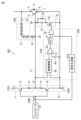
- FIG. 5 is a circuit diagram showing the configuration of the drive circuit 102 of the power semiconductor device 1 according to the third embodiment.
- the drive circuit 102 of the third embodiment differs from the drive circuit 101 of the second embodiment in that the second turn-off circuit 30A further includes a negative power supply 35.
- the above configuration increases the potential difference between the control electrode (gate) of the semiconductor switching element 32 and the main electrode (emitter) on the low potential side.
- the current flowing through the second turn-off circuit 30A through the semiconductor switching element 32 can be increased.
- the rate at which the collector-emitter voltage Vce rises when the power semiconductor device 1 is turned off can be further increased, thereby further enhancing the effect of reducing the turn-off loss.
- FIG. 5 The other points in FIG. 5 are the same as those described in FIGS. 1 and 4, so the same or corresponding parts are denoted by the same reference numerals and the description will not be repeated.
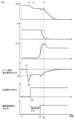
- FIG. 6 is a diagram schematically showing voltage or current waveforms at each part when drive circuit 102 of the third embodiment shown in FIG. 5 is turned off.
- the waveforms of the gate-emitter voltage Vge, collector current Ic, collector-emitter voltage Vce, and output voltage of the signal generator 41A of the power semiconductor device 1 are schematically shown in order from the top.
- a solid line indicates a voltage or current waveform in the case of the drive circuit 100 of the first embodiment.
- a dashed line indicates a voltage or current waveform in the case of a comparative example in which neither the voltage clamp circuit 20 nor the second turn-off circuit 30 is provided in FIG.
- a dotted line indicates a voltage or current waveform for the drive circuit 102 of the third embodiment. Waveform changes at times t2, t3, and t5 are the same as in FIG.
- the signal generator 41A switches its output voltage to H level at time t14 when the collector-emitter voltage Vce begins to rise.
- the semiconductor switching element 32 is brought into a conducting state, so that a current suddenly flows through the capacitor 31 of the second turn-off circuit 30A.
- the current flowing through the second turn-off circuit 30A is larger than that of the second turn-off circuit 30 of the first embodiment (solid line in FIG. 6).
- the amount of decrease in the gate-emitter voltage Vge is greater than in the first embodiment
- the rate of decrease in the collector current Ic is greater than in the first embodiment
- the rate of increase in the collector-emitter voltage Vce is It is larger than the case of the first embodiment.
- the capacitance value of the capacitor 31 is set so that the current flowing through the capacitor 31 of the second turn-off circuit 30A also stops.
- the signal generator 41 returns its output voltage to L level, thereby turning off the semiconductor switching device 32. do.
- the period during which the current flows through the capacitor 31 in the third embodiment is from time t14 to time t15. This period is shorter than from time t11 to time t12 in the first embodiment.
- the negative power supply 35 is connected in series to the low potential side of the semiconductor switching element 32 of the second turn-off circuit 30A.
- the current flowing through the semiconductor switching element 32 can be increased when the semiconductor switching element 32 is in the ON state, so that the turn-off speed of the power semiconductor element 1 can be further increased.
- the voltage change (dV/dt) of the power semiconductor device 1 can be sharpened, and the turn-off loss can be further reduced.
- the drive circuit 102 includes the voltage clamp circuit 20, so that surge voltage transiently generated between the main electrodes of the power semiconductor element 1 can be suppressed at the time of turn-off.
- the configuration of the second turn-off circuit 30A further including the negative power supply 35 can be combined with any of the driving circuits 103-111 of the fourth to ninth embodiments described later.
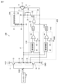
- FIG. 7 is a circuit diagram showing the configuration of the driving circuit 103 of the power semiconductor device 1 according to the fourth embodiment.
- the turn-off control circuit 40A includes a second signal generator 41B, a delay circuit 51, and logical operation in addition to the first signal generator 41A described in the first to third embodiments. It differs from the drive circuits 100 to 102 of the first to third embodiments in that it further includes a circuit 45.
- FIG. 1 is a circuit diagram showing the configuration of the driving circuit 103 of the power semiconductor device 1 according to the fourth embodiment.
- the turn-off control circuit 40A includes a second signal generator 41B, a delay circuit 51, and logical operation in addition to the first signal generator 41A described in the first to third embodiments. It differs from the drive circuits 100 to 102 of the first to third embodiments in that it further includes a circuit 45.
- the first signal generator 41A outputs a pulse signal that is at H level for a certain period of time based on the command signal CMD (off command) output from the controller 10.
- the second signal generator 41B detects the voltage between the control electrode G of the power semiconductor device 1 and the second main electrode E on the low potential side, and when the detected voltage becomes smaller than the reference voltage V1 output a pulse signal that is at H level for a certain period of time.
- the reference voltage V1 is set to a value lower than the voltage of the control electrode G when the power semiconductor element 1 is in the ON state and higher than the mirror voltage when the power semiconductor element 1 is turned off.
- the delay circuit 51 delays the timing at which the output of the second signal generator 41B switches from L level to H level by a predetermined delay time DT1. Thereby, the timing at which the semiconductor switching element 32 switches from the off state to the on state can be adjusted. If the turn-on timing of the semiconductor switching element 32 can be adjusted by the delay time of each of the later-described comparator 44 and logical operator 45 included in the second signal generator 41B, the delay circuit 51 is not required. good.
- a delay circuit 51 may be provided between the logic operator 45 and the control electrode G of the semiconductor switching element 32 .
- the logic operator 45 When the signal obtained by delaying the output signal of the second signal generator 41B by the delay circuit 51 and the output signal of the first signal generator 41A are both at H level, the logic operator 45 outputs the H level signal to the semiconductor device. Output to the control electrode G of the switching element 32 . As a result, the semiconductor switching element 32 becomes conductive. In this way, the logical operator 45 performs a logical AND operation on a plurality of input signals.
- the second signal generator 41B includes a differential amplifier 42, a DC power supply 43, and a comparator 44, as shown in FIG.
- the differential amplifier 42 functions as a control voltage detection circuit that detects the control voltage (gate-emitter voltage Vge) between the control electrode G of the power semiconductor element 1 and the second main electrode E on the low potential side.
- the comparator 44 compares the output voltage of the differential amplifier 42 and the output voltage of the DC power supply 43, and when the output voltage of the differential amplifier 42 becomes smaller than the output voltage of the DC power supply 43, an H level signal is generated. to output
- the drive circuit 103 of the fourth embodiment can be combined with the second turn-off circuit 30A having the negative power supply 35 of the third embodiment.
- FIG. 8 is a diagram schematically showing voltage or current waveforms at each part when drive circuit 103 of the fourth embodiment shown in FIG. 7 is turned off.
- the gate-emitter voltage Vge of the power semiconductor device 1 the collector current Ic, the collector-emitter voltage Vce, the output voltage of the differential amplifier 42, the output voltage of the comparator 44, and the logic operator 45 output voltage waveforms are shown schematically.
- a solid line indicates a voltage or current waveform in the case of the drive circuit 103 of the fourth embodiment.
- a dashed line indicates a voltage or current waveform in the case of a comparative example in which neither the voltage clamp circuit 20 nor the second turn-off circuit 30 is provided in FIG. Waveform changes at times t2, t3, and t5 are the same as in FIG.
- the output voltage of the differential amplifier 42 (that is, the gate-emitter voltage Vge of the power semiconductor device 1) becomes lower than the reference voltage V1.
- the output voltage of comparator 44 switches from the L level to the H level. It is assumed that the output signal of the first signal generator 41A has already switched from L level to H level when the OFF command is received from the controller 10 .
- the output voltage of the logic operator 45 switches from L level to H level.
- the semiconductor switching element 32 is brought into a conducting state, so that current flows rapidly through the capacitor 31 of the second turn-off circuit 30 .
- the gate-emitter voltage Vge decreases, the collector current Ic decreases, and the collector-emitter voltage Vce increases.
- the current through capacitor 31 stops.
- the period from time t18 to time t19 is determined by the capacity of the capacitor 31 . Therefore, the capacitance value of capacitor 31 is determined in advance so that the increase in collector-emitter voltage Vce is substantially clamped at time t19.
- the first and second signal generators 41A and 41B return their respective output voltages to the L level at an arbitrary timing until the power semiconductor element 1 is turned on next time, thereby turning on the semiconductor switching element. 32 is turned off.
- the drive circuit 103 further includes the voltage clamp circuit 20A, the voltage between the main electrodes of the power semiconductor device 1 (that is, the collector-emitter voltage Vce) can be suppressed.
- the first signal generator 41A when the power semiconductor device 1 is turned off, based on the switching of the command signal CMD from the controller 10 from the ON command to the OFF command, 2 turn-off circuit 30 is provided.
- the switching timing of the semiconductor switching element 32 from the OFF state to the ON state is determined by the second signal generator 41B.
- FIG. 9 is a circuit diagram showing the configuration of drive circuit 104 of power semiconductor device 1 according to the fifth embodiment.
- the function of the second signal generator 41C is different from the function of the second signal generator 41B in the drive circuit 103 of the fourth embodiment.
- the second signal generator 41C in FIG. 9 acquires the current value detected by the current sensor 60 provided on the current path of the first turn-off circuit 12. Then, the second signal generator 41C generates a pulse signal that becomes H level for a certain period of time when the absolute value of the detected current value becomes smaller than the reference value (corresponding to the reference voltage V2) after reaching the peak value. to output
- the signal generator 41C includes an amplifier 52, a comparator 44, and a DC power supply 43, as shown in FIG.
- Amplifier 52 acquires the gate current value detected by current sensor 60 when power semiconductor device 1 is turned off.
- the amplifier 52 may be configured as a differential amplifier that acquires a differential signal from the current sensor 60 .
- Comparator 44 compares the absolute value of the detection value of current sensor 60 output from amplifier 52 with reference voltage V2 output from DC power supply 43 . Comparator 44 outputs a pulse signal that is at H level for a certain period of time when the absolute value of the gate current detection value output from amplifier 52 exceeds the peak value and then becomes lower than reference voltage V2.
- FIG. 9 The rest of the configuration in FIG. 9 is the same as in FIG. 7, so the same or corresponding parts are denoted by the same reference numerals, and description thereof will not be repeated.
- FIG. 10 is a diagram schematically showing voltage or current waveforms at each part when drive circuit 104 of the fifth embodiment shown in FIG. 9 is turned off.
- the gate-emitter voltage Vge of the power semiconductor device 1 the collector current Ic, the collector-emitter voltage Vce, the output voltage of the current sensor 60 as a gate current detector, and the output voltage of the comparator 44 are shown in order from the top.
- the waveforms of the output voltage of the logical operator 45 are shown.
- a solid line indicates a voltage or current waveform in the case of the drive circuit 104 of the fifth embodiment.
- a dashed line indicates a voltage or current waveform in the case of a comparative example in which neither the voltage clamp circuit 20 nor the second turn-off circuit 30 is provided in FIG. Waveform changes at times t2, t3, and t5 are the same as in FIG.
- the value of the gate current is positive when it flows from the intermediate node 18 to the control electrode G of the power semiconductor element 1, and negative when it flows in the opposite direction
- the gate current begins to flow and has a peak value at time t22.
- the output voltage of comparator 44 switches from the L level to the H level. Assume that the output signal of the first signal generator 41A has already switched from the L level to the H level when the off command is received from the controller 10 .
- the output voltage of the logical operator 45 switches from L level to H level.
- the semiconductor switching element 32 is brought into a conducting state, so that current flows rapidly through the capacitor 31 of the second turn-off circuit 30 .
- the gate-emitter voltage Vge decreases
- the collector current Ic decreases
- the collector-emitter voltage Vce increases
- the absolute value of the gate current increases.
- the current through capacitor 31 stops.
- the period from time t24 to time t25 is determined by the capacity of the capacitor 31 . Therefore, the capacitance value of capacitor 31 is determined in advance so that the increase in collector-emitter voltage Vce is substantially clamped at time t25.
- the first and second signal generators 41A and 41C return their respective output voltages to the L level at an arbitrary timing until the power semiconductor device 1 starts to turn on next time, thereby turning on the semiconductor switching device. 32 is turned off.
- the operation timing of the semiconductor switching device 32 in the second turn-off circuit 30 is determined based on the detected value of the gate current flowing at the time of turn-off. can. Therefore, by considering the delay time DT2 of the delay circuit 51 and the delay time generated in the comparator 44 and the logic operator 45, at the timing when the collector-emitter voltage Vce starts to rise due to the operation of the first turn-off circuit 12, At some time t24, the semiconductor switching element 32 of the second turn-off circuit 30 can be switched to the conductive state.
- the drive circuit 106 further includes the voltage clamp circuit 20A, the voltage between the main electrodes of the power semiconductor device 1 (that is, the collector-emitter voltage Vce) can be suppressed.
- FIG. 11 is a circuit diagram showing a configuration of drive circuit 105 according to a modification of the fifth embodiment.
- the second signal generator 41D detects the gate current based on the voltage drop occurring in the off-gate resistor 15 provided in the first turn-off circuit 12 instead of the detection value of the current sensor 60. It differs from the drive circuit 104 in FIG. 9 in that it acquires a value. Therefore, the differential amplifier 42 of the second signal generator 41 ⁇ /b>D functions as a gate current detection circuit that detects the gate current from the voltage across the off-gate resistor 15 .
- FIG. 11 The other points in FIG. 11 are the same as in FIGS. 7 and 9, so the same or corresponding parts are denoted by the same reference numerals, and description thereof will not be repeated.
- FIG. 12 is a circuit diagram showing the configuration of drive circuit 106 of power semiconductor device 1 according to the sixth embodiment.
- the function of the second signal generator 41E is the same as the function of the second signal generator 41B in the drive circuit 103 of the fourth embodiment and the drive circuits 104 and 105 of the fifth embodiment. differs from the function of the second signal generators 41C and 41D in .
- the second signal generator 41E in FIG. 12 integrates the gate current detected by the gate resistor 46 provided in the control electrode wiring 17, thereby flowing into the control electrode G of the power semiconductor element 1. Alternatively, the amount of charge flowing out from the control electrode G is detected.
- the second signal generator 41E maintains the H level for a certain period of time when the amount of charge accumulated in the control electrode G of the power semiconductor element 1 becomes smaller than the reference value (corresponding to the reference voltage V4) at the time of turn-off.
- the signal generator 41E includes a differential amplifier 48, an integrator 49, a comparator 44, and a DC power supply 43, as shown in FIG.
- a differential amplifier 48 detects the current flowing through the control electrode wiring 17 based on the voltage applied across the gate resistor 46 .
- Integrator 49 detects the amount of charge flowing into and out of control electrode G of power semiconductor device 1 by integrating the gate current detected by differential amplifier 48 . Therefore, differential amplifier 48 and integrator 49 constitute charge amount detection circuit 47 for detecting the amount of charge accumulated in control electrode G of power semiconductor device 1 .
- Comparator 44 generates a pulse that becomes H level for a certain period of time when the amount of accumulated charge detected by charge amount detection circuit 47 becomes smaller than a reference value (corresponding to reference voltage V4) when power semiconductor device 1 is turned off. Output a signal.
- FIG. 12 Other points in FIG. 12 are the same as in FIGS. 7, 9, and 11, so the same or corresponding parts are denoted by the same reference numerals, and description thereof will not be repeated.
- FIG. 13 is a diagram schematically showing voltage or current waveforms at each part when driving circuit 106 of the sixth embodiment shown in FIG. 12 is turned off.
- the gate-emitter voltage Vge of the power semiconductor device 1 the collector current Ic, the collector-emitter voltage Vce, the output voltage of the integrator 49, the output voltage of the comparator 44, and the logic operator 45 are shown for each output voltage waveform.
- a solid line indicates a voltage or current waveform in the case of the driving circuit 106 of the sixth embodiment.
- a dashed line indicates a voltage or current waveform in the case of a comparative example in which neither the voltage clamp circuit 20 nor the second turn-off circuit 30 is provided in FIG. Waveform changes at times t2, t3, and t5 are the same as in FIG.
- the gate resistor 46 in FIG. 12 has a positive gate current when charges flow into the control electrode G of the power semiconductor element 1 at turn-on, and a gate current in the positive direction when charges flow out from the control electrode G of the power semiconductor element 1 at turn-off. , any of the negative going gate currents can be detected. Therefore, the output of the integrator 49 monotonously increases from 0 to reach the maximum value at turn-on, and monotonously decreases from the maximum value to return to 0 at turn-off.
- FIG. 13 shows the gate charge amount at turn-off as the output voltage of the integrator 49 . Therefore, after the semiconductor switching element 16 of the first turn-off circuit 12 is switched from the off state to the on state based on the off command from the controller 10 at time t1, the output voltage of the integrator 49 monotonically decreases from the maximum value. and return to 0.
- the output voltage of the logic operator 45 switches from L level to H level.
- the semiconductor switching element 32 is brought into a conducting state, so that current flows rapidly through the capacitor 31 of the second turn-off circuit 30 .
- the gate-emitter voltage Vge decreases, the collector current Ic decreases, and the collector-emitter voltage Vce increases.
- the current through the capacitor 31 stops.
- the period from time t31 to time t32 is determined by the capacity of the capacitor 31. FIG. Therefore, the capacitance value of capacitor 31 is determined in advance so that the increase in collector-emitter voltage Vce is substantially clamped at time t32.
- the first and second signal generators 41A and 41C return their respective output voltages to the L level at an arbitrary timing until the power semiconductor device 1 starts to turn on next time, thereby turning on the semiconductor switching device. 32 is turned off.
- the output voltage of the integrator 49 is smaller than the reference voltage even at the beginning of the turn-on operation.
- a first signal generator 41A is provided to prevent erroneous output during this period.
- the first signal generator 41A outputs a pulse signal that stays at H level for a certain period of time when the off command is output from the controller 10 .
- the final output of the turn-off control circuit 40B is obtained by ANDing the output voltage of the first signal generator 41A and the delayed output voltage of the second signal generator 41E.
- the operation timing of the semiconductor switching device 32 in the second turn-off circuit 30 is set to the detection value of the charge amount of the control electrode G at the time of turn-off. can be determined based on Therefore, by considering the delay time DT3 of the delay circuit 51 and the delay time generated in the comparator 44 and the logic operator 45, at the timing when the collector-emitter voltage Vce starts to rise due to the operation of the first turn-off circuit 12, At a certain time t31, the semiconductor switching element 32 of the second turn-off circuit 30 can be switched to the conducting state.
- the drive circuit 103 further includes the voltage clamp circuit 20A, the voltage between the main electrodes of the power semiconductor device 1 (that is, the collector-emitter voltage Vce) can be suppressed.
- FIG. 14 is a circuit diagram showing a configuration of drive circuit 107 according to a modification of the sixth embodiment.
- the second signal generator 41F has a gate current value flowing through the off-gate resistor 15 of the first turn-off circuit 12 instead of the gate current value flowing through the gate resistor 46 provided in the control electrode wiring 17. It differs from the drive circuit 106 in FIG. 12 in that it detects the current value.
- the charge amount detection circuit 47A of the second signal generator 41F of the drive circuit 107 includes an initialization circuit 50 for initializing the integrated value of the integrator 49. including.
- the comparator 44 of the second signal generator 41F generates a pulse voltage that becomes H level for a certain period of time when the outflow charge amount detected by the charge amount detection circuit 47A exceeds a reference value (corresponding to the reference voltage V5). Output.
- the delay time DT3 of the delay circuit 51 elapses after the outflow charge amount exceeds the reference value, the output voltage of the logical operator 45 switches from L level to H level. As a result, the semiconductor switching element 32 of the second turn-off circuit 30 becomes conductive.
- the first turn-off circuit 12 operates to At the timing when the voltage Vce starts rising, the semiconductor switching element 32 of the second turn-off circuit 30 can be switched to the conducting state.
- the voltage change (dV/dt) of the power semiconductor device 1 can be sharpened, and the turn-off loss can be further reduced.
- the drive circuit 107 further includes the voltage clamp circuit 20A, the voltage between the main electrodes of the power semiconductor device 1 (that is, the collector-emitter voltage Vce) can be suppressed.
- FIG. 15 is a circuit diagram showing the configuration of drive circuit 108 of power semiconductor device 1 according to the seventh embodiment.
- the function of the second signal generator 41G is different from the functions of the second signal generators 41B, 41C and 41D of FIGS.
- the second signal generator 41G of the turn-off control circuit 40A of FIG. 15 detects the voltage applied between the anode and cathode of the backflow prevention diode 22 of the voltage clamp circuit 20A.
- the voltage is detected with the positive side of the anode of the backflow prevention diode 22 and the negative side of the cathode.
- the second signal generator 41G outputs a pulse signal that is at H level for a certain period of time when the detected voltage applied across the backflow prevention diode 22 exceeds the reference voltage V6.
- the signal generator 41G includes a differential amplifier 42, a comparator 44, and a DC power supply 43, as shown in FIG.
- the differential amplifier 42 detects the voltage applied between the anode and cathode of the backflow prevention diode 22 when the power semiconductor device 1 is turned off.
- a comparator 44 compares the output voltage of the differential amplifier 42 with the reference voltage V6 of the DC power supply 43, and when the output voltage of the DC power supply 43 exceeds the reference voltage V6, the pulse signal becomes H level for a certain period of time. to output
- FIG. 16 is a diagram showing voltage or current waveforms at each part when the drive circuit 108 of the seventh embodiment shown in FIG. 15 is turned off. 16, in order from the top, the gate-emitter voltage Vge of the power semiconductor device 1, the collector current Ic, the collector-emitter voltage Vce, the output voltage of the differential amplifier 42, the output voltage of the comparator 44, and the logic operator 45 output voltage waveforms are shown.
- a solid line indicates a voltage or current waveform in the case of the driving circuit 108 of the seventh embodiment.
- a dashed line indicates a voltage or current waveform in the case of a comparative example in which neither the voltage clamp circuit 20 nor the second turn-off circuit 30 is provided in FIG. Waveform changes at times t2, t3, and t5 are the same as in FIG.
- the cathode terminal of the backflow prevention diode 22 has the same potential as the control electrode G of the power semiconductor element 1 . Therefore, the anode-cathode voltage of the backflow prevention diode 22 exhibits a waveform similar to the gate-emitter voltage Vge of the power semiconductor device 1 . Specifically, the anode-cathode voltage of the backflow prevention diode 22 becomes a negative value at the time of turn-off, and until the mirror period begins, the gate-emitter voltage Vge of the power semiconductor element 1 is offset in the negative direction. waveform. After that, when the mirror period starts at time t3 and the gate-emitter voltage Vge reaches a constant value, the anode-cathode voltage of the backflow prevention diode 22 increases correspondingly.
- the reference voltage V6 of the DC power supply 43 is set to a value slightly higher than the value when entering the mirror period.
- the output signal of comparator 44 switches from the L level to the H level. It is assumed that the output signal of the first signal generator 41A has already switched from the L level to the H level when the OFF command is received from the controller 10.
- the output voltage of the logic operator 45 switches from L level to H level.
- the semiconductor switching element 32 is brought into a conducting state, so that current flows rapidly through the capacitor 31 of the second turn-off circuit 30 .
- the gate-emitter voltage Vge decreases
- the collector current Ic decreases
- the collector-emitter voltage Vce increases
- the anode-cathode voltage of the backflow prevention diode 22 increases.
- the current through the capacitor 31 stops.
- the period from time t41 to time t42 is determined by the capacity of the capacitor 31. FIG. Therefore, the capacitance value of capacitor 31 is determined in advance so that the increase in collector-emitter voltage Vce is substantially clamped at time t32.
- the first and second signal generators 41A and 41G return their respective output voltages to the L level at an arbitrary timing until the power semiconductor device 1 starts to turn on next time, thereby turning the semiconductor switching device on. 32 is turned off.
- the operation timing of the semiconductor switching device 32 in the second turn-off circuit 30 is adjusted to the anode of the backflow prevention diode 22 of the voltage clamp circuit 20A. ⁇ It can be determined based on the detected value of the voltage between the cathodes. Therefore, by considering the delay time DT4 of the delay circuit 51 and the delay time occurring in the comparator 44 and the logic operator 45, at the timing when the collector-emitter voltage Vce starts to rise due to the operation of the first turn-off circuit 12, At a certain time t41, the semiconductor switching element 32 of the second turn-off circuit 30 can be switched to the conductive state.
- the drive circuit 108 further includes the voltage clamp circuit 20A, the voltage between the main electrodes of the power semiconductor device 1 (that is, the collector-emitter voltage Vce) can be suppressed.
- Embodiment 8 In the eighth embodiment, an example in which a turn-off control circuit is configured by combining a plurality of the second signal generators 41B to 41G described in the fourth to seventh embodiments will be described.
- FIG. 17 is a circuit diagram showing a configuration of drive circuit 109 for power semiconductor element 1 according to a first example of the eighth embodiment.
- Turn-off control circuit 40D of drive circuit 109 in FIG. 17 includes signal generator 41B described in FIG. 7, signal generator 41D described in FIG.
- the signal generator 41B detects the voltage between the control electrode G of the power semiconductor device 1 and the second main electrode E on the low potential side, and detects the voltage for a certain period of time when the detected voltage becomes smaller than the reference voltage V1. Outputs a pulse signal of H level.
- the reference voltage V1 is set to a value lower than the voltage of the control electrode G when the power semiconductor element 1 is in the ON state and higher than the mirror voltage when the power semiconductor element 1 is turned off.
- the delay circuit 51A delays the output voltage of the signal generator 41B by the delay time DT1. As a result, the output voltage of the delay circuit 51A is switched from the L level to the H level at the timing when the collector-emitter voltage Vce starts to rise due to the operation of the first turn-off circuit 12.
- the signal generator 41D detects the gate current based on the voltage drop across the off-gate resistor 15 provided in the first turn-off circuit 12.
- the signal generator 41D outputs a pulse signal that is at H level for a certain period of time when the absolute value of the detected gate current exceeds the peak value and becomes smaller than the reference value (corresponding to the reference voltage V3).
- the delay circuit 51B delays the output voltage of the signal generator 41D by the delay time DT2. As a result, the output voltage of the delay circuit 51B is switched from the L level to the H level at the timing when the collector-emitter voltage Vce starts to rise due to the operation of the first turn-off circuit 12.
- the logical operator 45 outputs the logical product of the delay circuit 51A and the delay circuit 51B. By switching the output of logic operator 45 from L level to H level, semiconductor switching element 32 of second turn-off circuit 30 becomes conductive.
- Other configurations in FIG. 17 are the same as those described in the fourth to seventh embodiments, so the same or corresponding parts are denoted by the same reference numerals and description thereof will not be repeated.
- the semiconductor switching element 32 of the second turn-off circuit 30 can be switched to the conductive state at the timing when the collector-emitter voltage Vce starts to rise due to the operation of the first turn-off circuit 12.
- the voltage change (dV/dt) of the power semiconductor device 1 can be steepened, and the turn-off loss can be further reduced.
- the drive circuit 109 further includes the voltage clamp circuit 20A, the voltage between the main electrodes of the power semiconductor device 1 (that is, the collector-emitter voltage Vce) can be suppressed.
- FIG. 18 is a circuit diagram showing the configuration of a drive circuit 110 for a power semiconductor device 1 according to a second example of the eighth embodiment.
- the turn-off control circuit 40E of the drive circuit 110 of FIG. 18 includes the signal generator 41D described with reference to FIG. 11, the signal generator 41E described with reference to FIG.
- the signal generator 41D detects the gate current based on the voltage drop across the off-gate resistor 15 provided in the first turn-off circuit 12.
- the signal generator 41D outputs a pulse signal that is at H level for a certain period of time when the absolute value of the detected gate current exceeds the peak value and becomes smaller than the reference value (corresponding to the reference voltage V3).
- the delay circuit 51A delays the output voltage of the signal generator 41D by the delay time DT2. As a result, the output voltage of the delay circuit 51A is switched from the L level to the H level at the timing when the collector-emitter voltage Vce starts to rise due to the operation of the first turn-off circuit 12.
- the signal generator 41E integrates the gate current detected by the gate resistor 46 provided in the control electrode wiring 17 to calculate the amount of charge flowing into and out of the control electrode G of the power semiconductor element 1. To detect.
- the second signal generator 41E maintains the H level for a certain period of time when the amount of charge accumulated in the control electrode G of the power semiconductor element 1 becomes smaller than the reference value (corresponding to the reference voltage V4) at the time of turn-off. Outputs a pulse signal that becomes
- the delay circuit 51B delays the output voltage of the signal generator 41E by the delay time DT3. As a result, the output voltage of the delay circuit 51B is switched from the L level to the H level at the timing when the collector-emitter voltage Vce starts to rise due to the operation of the first turn-off circuit 12.
- the logical operator 45 outputs the logical product of the delay circuit 51A and the delay circuit 51B. By switching the output of logic operator 45 from L level to H level, semiconductor switching element 32 of second turn-off circuit 30 becomes conductive.
- Other configurations in FIG. 18 are the same as those described in the fourth to seventh embodiments, so the same or corresponding parts are denoted by the same reference numerals and description thereof will not be repeated.
- the semiconductor switching element 32 of the second turn-off circuit 30 can be switched to the conductive state at the timing when the collector-emitter voltage Vce starts to rise due to the operation of the first turn-off circuit 12.
- the voltage change (dV/dt) of the power semiconductor device 1 can be steepened, and the turn-off loss can be further reduced.
- the drive circuit 110 further includes the voltage clamp circuit 20A, the voltage between the main electrodes of the power semiconductor device 1 (that is, the collector-emitter voltage Vce) can be suppressed.
- FIG. 19 is a circuit diagram showing a configuration of a drive circuit 111 for a power semiconductor element 1 according to a third example of the eighth embodiment.
- the turn-off control circuit 40F of the drive circuit 111 of FIG. 19 includes the signal generator 41D described with reference to FIG. 11, the signal generator 41G described with reference to FIG.
- the signal generator 41D detects the gate current based on the voltage drop across the off-gate resistor 15 provided in the first turn-off circuit 12.
- the signal generator 41D outputs a pulse signal that is at H level for a certain period of time when the absolute value of the detected gate current exceeds the peak value and becomes smaller than the reference value (corresponding to the reference voltage V3).
- the delay circuit 51A delays the output voltage of the signal generator 41D by the delay time DT2. As a result, the output voltage of the delay circuit 51A is switched from the L level to the H level at the timing when the collector-emitter voltage Vce starts to rise due to the operation of the first turn-off circuit 12.
- the signal generator 41G detects the voltage applied between the anode and cathode of the backflow prevention diode 22 of the voltage clamp circuit 20A. Here, the voltage is detected with the positive side of the anode of the backflow prevention diode 22 and the negative side of the cathode. Then, the second signal generator 41G outputs a pulse signal that is at H level for a certain period of time when the detected voltage applied across the backflow prevention diode 22 exceeds the reference voltage V6.
- the delay circuit 51B delays the output voltage of the signal generator 41G by the delay time DT4. As a result, the output voltage of the delay circuit 51B is switched from the L level to the H level at the timing when the collector-emitter voltage Vce starts to rise due to the operation of the first turn-off circuit 12.
- the logical operator 45 outputs the logical product of the delay circuit 51A and the delay circuit 51B. By switching the output of logic operator 45 from L level to H level, semiconductor switching element 32 of second turn-off circuit 30 becomes conductive.
- Other configurations in FIG. 18 are the same as those described in the fourth to seventh embodiments, so the same or corresponding parts are denoted by the same reference numerals and description thereof will not be repeated.
- the semiconductor switching element 32 of the second turn-off circuit 30 can be switched to the conductive state at the timing when the collector-emitter voltage Vce starts to rise due to the operation of the first turn-off circuit 12.
- the voltage change (dV/dt) of the power semiconductor device 1 can be steepened, and the turn-off loss can be further reduced.
- the drive circuit 111 further includes the voltage clamp circuit 20A, the voltage between the main electrodes of the power semiconductor device 1 (that is, the collector-emitter voltage Vce) can be suppressed.
- FIG. 20 is a block diagram showing the configuration of a power conversion system to which the power converter according to the ninth embodiment is applied.
- the power conversion system shown in FIG. 20 includes a power supply 220, a power conversion device 210, and a load 230.
- the power supply 220 is a DC power supply and supplies DC power to the power converter 210 .
- the power supply 220 can be composed of various things, for example, it can be composed of a DC system, a solar battery, a storage battery, or it can be composed of a rectifier circuit or an AC/DC converter connected to an AC system. good too.
- the power supply 220 may be configured by a DC/DC converter that converts the DC power output from the DC system into the set power.
- the power conversion device 210 is a three-phase inverter connected between the power supply 220 and the load 230, converts the DC power supplied from the power supply 220 into AC power, and supplies the AC power to the load 230. As shown in FIG. 20, the power conversion device 210 includes a main conversion circuit 211 that converts DC power into AC power and outputs it, and a control circuit 212 that outputs a control signal for controlling the main conversion circuit 211 to the main conversion circuit 211. and
- the load 230 is a three-phase electric motor driven by AC power supplied from the power converter 210 .
- the load 230 is not limited to a specific application, but is an electric motor mounted on various electrical equipment, such as a hybrid vehicle, an electric vehicle, a railroad vehicle, an elevator, or an electric motor for air conditioning equipment.
- the main conversion circuit 211 includes a switching element and a freewheeling diode (not shown). By switching the switching element, the DC power supplied from the power supply 220 is converted into AC power and supplied to the load 230 .
- the main conversion circuit 211 is a two-level three-phase full bridge circuit, and has six switching elements and It can consist of six freewheeling diodes in anti-parallel. At least one of the switching elements of the main conversion circuit 211 is the power semiconductor element 1 of any one of the first to eighth embodiments described above.
- each upper and lower arm forms each phase (U phase, V phase, W phase) of the full bridge circuit.
- Output terminals of the upper and lower arms, that is, three output terminals of the main conversion circuit 211 are connected to the load 230 .
- any one of the drive circuits 100 to 111 (not shown) for driving each switching element is built in the power module 200, so that the main conversion circuit 211 includes any one of the drive circuits 100-111.
- Any one of the drive circuits 100 to 111 generates a drive signal for driving the switching element of the main converter circuit 211 and supplies it to the control electrode of the switching element of the main converter circuit 211 .
- a drive signal for turning on the switching element and a drive signal for turning off the switching element are output to the control electrode of each switching element.
- the driving signal When maintaining the switching element in the ON state, the driving signal is a voltage signal (ON signal) equal to or higher than the threshold voltage of the switching element, and when maintaining the switching element in the OFF state, the driving signal is a voltage equal to or less than the threshold voltage of the switching element. signal (off signal).
- the control circuit 212 controls the switching elements of the main conversion circuit 211 so that the desired power is supplied to the load 230 .
- the control circuit 212 corresponds to the controller 10 of the first to eighth embodiments. More specifically, the control circuit 212 calculates the time (on time) during which each switching element of the main conversion circuit 211 should be in the ON state based on the power to be supplied to the load 230 .
- the main conversion circuit 211 can be controlled by PWM control that modulates the ON time of the switching element according to the voltage to be output.
- control circuit 212 outputs an ON signal to the switching element that should be in the ON state at each point of time, and an OFF signal to the switching element that should be in the OFF state at each time point, so that the drive circuits 100 to 100 included in the main conversion circuit 211 111 outputs a control command (control signal).
- the drive circuits 100 to 111 output an ON signal or an OFF signal as a drive signal to the control electrode of each switching element according to this control signal.
- the surge voltage It is possible to provide a power change device that achieves both suppression and reduction in turn-off loss.
- the present disclosure is not limited to this, and can be applied to various power converters.
- a two-level power conversion device is used, but a three-level or multi-level power conversion device may be used. You can apply it.
- the present disclosure can be applied to a DC/DC converter or an AC/DC converter when power is supplied to a DC load or the like.
- the power conversion device to which the present disclosure is applied is not limited to the case where the above-described load is an electric motor. It can also be used as a power conditioner for a photovoltaic power generation system, an electric storage system, or the like.
Landscapes
- Engineering & Computer Science (AREA)
- Power Engineering (AREA)
- Power Conversion In General (AREA)
Priority Applications (5)
| Application Number | Priority Date | Filing Date | Title |
|---|---|---|---|
| DE112021008351.1T DE112021008351T5 (de) | 2021-10-13 | 2021-10-13 | Treiberschaltung zum antreiben eines leistungshalbleiterelements, leistungshalbleitermodul und leistungsumwandlungsvorrichtung |
| US18/689,436 US12407342B2 (en) | 2021-10-13 | 2021-10-13 | Drive circuit to drive power semiconductor element, power semiconductor module, and power conversion device |
| CN202180103108.1A CN118077128A (zh) | 2021-10-13 | 2021-10-13 | 电力用半导体元件的驱动电路、电力用半导体模块以及电力变换装置 |
| JP2023553818A JP7595785B2 (ja) | 2021-10-13 | 2021-10-13 | 電力用半導体素子の駆動回路、電力用半導体モジュール、および電力変換装置 |
| PCT/JP2021/037882 WO2023062745A1 (ja) | 2021-10-13 | 2021-10-13 | 電力用半導体素子の駆動回路、電力用半導体モジュール、および電力変換装置 |
Applications Claiming Priority (1)
| Application Number | Priority Date | Filing Date | Title |
|---|---|---|---|
| PCT/JP2021/037882 WO2023062745A1 (ja) | 2021-10-13 | 2021-10-13 | 電力用半導体素子の駆動回路、電力用半導体モジュール、および電力変換装置 |
Publications (1)
| Publication Number | Publication Date |
|---|---|
| WO2023062745A1 true WO2023062745A1 (ja) | 2023-04-20 |
Family
ID=85987338
Family Applications (1)
| Application Number | Title | Priority Date | Filing Date |
|---|---|---|---|
| PCT/JP2021/037882 Ceased WO2023062745A1 (ja) | 2021-10-13 | 2021-10-13 | 電力用半導体素子の駆動回路、電力用半導体モジュール、および電力変換装置 |
Country Status (5)
| Country | Link |
|---|---|
| US (1) | US12407342B2 (https=) |
| JP (1) | JP7595785B2 (https=) |
| CN (1) | CN118077128A (https=) |
| DE (1) | DE112021008351T5 (https=) |
| WO (1) | WO2023062745A1 (https=) |
Cited By (2)
| Publication number | Priority date | Publication date | Assignee | Title |
|---|---|---|---|---|
| CN118117857A (zh) * | 2024-04-30 | 2024-05-31 | 华羿微电子股份有限公司 | 一种mos和igbt栅极米勒电容效应抑制电路及芯片 |
| DE102023203928A1 (de) | 2023-04-27 | 2024-10-31 | Vitesco Technologies Germany Gmbh | Ansteuerung von Leistungstransistoren mit erhöhtem negativem Ansteuersignalpegel |
Citations (4)
| Publication number | Priority date | Publication date | Assignee | Title |
|---|---|---|---|---|
| JP2000333441A (ja) * | 1999-05-24 | 2000-11-30 | Toshiba Corp | 絶縁ゲート型半導体素子のゲート制御回路 |
| JP2013078258A (ja) * | 2012-11-26 | 2013-04-25 | Fuji Electric Co Ltd | 半導体素子のゲート駆動方法 |
| JP2017005698A (ja) * | 2015-06-04 | 2017-01-05 | エルエス産電株式会社Lsis Co., Ltd. | Igbt駆動装置 |
| JP2017123709A (ja) * | 2016-01-05 | 2017-07-13 | 富士電機株式会社 | 半導体素子の駆動装置 |
Family Cites Families (8)
| Publication number | Priority date | Publication date | Assignee | Title |
|---|---|---|---|---|
| US5475329A (en) * | 1994-01-04 | 1995-12-12 | Texas Instruments Incorporated | Turn-off circuit to provide a discharge path from a first node to a second node |
| JP3193827B2 (ja) * | 1994-04-28 | 2001-07-30 | 三菱電機株式会社 | 半導体パワーモジュールおよび電力変換装置 |
| US5550701A (en) * | 1994-08-30 | 1996-08-27 | International Rectifier Corporation | Power MOSFET with overcurrent and over-temperature protection and control circuit decoupled from body diode |
| US6169439B1 (en) * | 1997-01-02 | 2001-01-02 | Texas Instruments Incorporated | Current limited power MOSFET device with improved safe operating area |
| JP3752943B2 (ja) | 2000-01-31 | 2006-03-08 | 株式会社日立製作所 | 半導体素子の駆動装置及びその制御方法 |
| JP5927739B2 (ja) | 2011-12-14 | 2016-06-01 | 富士電機株式会社 | 半導体装置 |
| JP6362996B2 (ja) | 2014-10-24 | 2018-07-25 | 株式会社日立製作所 | 半導体駆動装置ならびにそれを用いた電力変換装置 |
| JP6625215B2 (ja) | 2016-07-04 | 2019-12-25 | 三菱電機株式会社 | 駆動回路およびそれを用いたパワーモジュール |
-
2021
- 2021-10-13 JP JP2023553818A patent/JP7595785B2/ja active Active
- 2021-10-13 US US18/689,436 patent/US12407342B2/en active Active
- 2021-10-13 WO PCT/JP2021/037882 patent/WO2023062745A1/ja not_active Ceased
- 2021-10-13 DE DE112021008351.1T patent/DE112021008351T5/de not_active Withdrawn
- 2021-10-13 CN CN202180103108.1A patent/CN118077128A/zh active Pending
Patent Citations (4)
| Publication number | Priority date | Publication date | Assignee | Title |
|---|---|---|---|---|
| JP2000333441A (ja) * | 1999-05-24 | 2000-11-30 | Toshiba Corp | 絶縁ゲート型半導体素子のゲート制御回路 |
| JP2013078258A (ja) * | 2012-11-26 | 2013-04-25 | Fuji Electric Co Ltd | 半導体素子のゲート駆動方法 |
| JP2017005698A (ja) * | 2015-06-04 | 2017-01-05 | エルエス産電株式会社Lsis Co., Ltd. | Igbt駆動装置 |
| JP2017123709A (ja) * | 2016-01-05 | 2017-07-13 | 富士電機株式会社 | 半導体素子の駆動装置 |
Cited By (2)
| Publication number | Priority date | Publication date | Assignee | Title |
|---|---|---|---|---|
| DE102023203928A1 (de) | 2023-04-27 | 2024-10-31 | Vitesco Technologies Germany Gmbh | Ansteuerung von Leistungstransistoren mit erhöhtem negativem Ansteuersignalpegel |
| CN118117857A (zh) * | 2024-04-30 | 2024-05-31 | 华羿微电子股份有限公司 | 一种mos和igbt栅极米勒电容效应抑制电路及芯片 |
Also Published As
| Publication number | Publication date |
|---|---|
| CN118077128A (zh) | 2024-05-24 |
| US12407342B2 (en) | 2025-09-02 |
| DE112021008351T5 (de) | 2024-07-25 |
| US20250007507A1 (en) | 2025-01-02 |
| JPWO2023062745A1 (https=) | 2023-04-20 |
| JP7595785B2 (ja) | 2024-12-06 |
Similar Documents
| Publication | Publication Date | Title |
|---|---|---|
| US7710187B2 (en) | Gate drive circuit | |
| JP3339311B2 (ja) | 自己消弧形半導体素子の駆動回路 | |
| JP6617571B2 (ja) | 半導体スイッチング素子のゲート駆動回路 | |
| US7948276B2 (en) | Gate driver circuit, switch assembly and switch system | |
| WO2018158807A1 (ja) | 半導体装置、および、電力変換システム | |
| CN105553235A (zh) | 半导体驱动装置及使用该半导体驱动装置的电力变换装置 | |
| CN110401335B (zh) | 驱动电路、功率模块以及电力变换系统 | |
| JPH0947015A (ja) | 自己消弧形半導体素子の駆動回路 | |
| JP2009011013A (ja) | 電力変換装置 | |
| JP2018011467A (ja) | 半導体スイッチング素子のゲート駆動回路 | |
| US20170149330A1 (en) | Switching Circuit And Power Conversion Circuit | |
| JP2019110431A (ja) | 半導体装置およびパワーモジュール | |
| US10985749B2 (en) | Integrated circuit and semiconductor device | |
| CN100492862C (zh) | 电力转换装置 | |
| JP7595785B2 (ja) | 電力用半導体素子の駆動回路、電力用半導体モジュール、および電力変換装置 | |
| CN113169659B (zh) | 电力用半导体元件的驱动电路以及使用其的电力用半导体模块 | |
| JP5298557B2 (ja) | 電圧駆動型半導体素子のゲート駆動装置 | |
| JP2005328668A (ja) | 自己消弧形半導体素子の駆動回路 | |
| US12021511B2 (en) | Drive circuit of switching element and intelligent power module | |
| JP4321491B2 (ja) | 電圧駆動型半導体素子の駆動装置 | |
| US20220149833A1 (en) | Drive capability switching circuit for semiconductor element and drive device for semiconductor element | |
| US12620984B2 (en) | Semiconductor device | |
| US20240313763A1 (en) | Semiconductor device | |
| US20240259017A1 (en) | Drive circuit for bridge circuit, motor drive device using the same, and electronic device | |
| JP6679967B2 (ja) | 半導体素子の駆動装置 |
Legal Events
| Date | Code | Title | Description |
|---|---|---|---|
| 121 | Ep: the epo has been informed by wipo that ep was designated in this application |
Ref document number: 21960604 Country of ref document: EP Kind code of ref document: A1 |
|
| WWE | Wipo information: entry into national phase |
Ref document number: 18689436 Country of ref document: US |
|
| WWE | Wipo information: entry into national phase |
Ref document number: 2023553818 Country of ref document: JP |
|
| WWE | Wipo information: entry into national phase |
Ref document number: 202180103108.1 Country of ref document: CN |
|
| WWE | Wipo information: entry into national phase |
Ref document number: 112021008351 Country of ref document: DE |
|
| 122 | Ep: pct application non-entry in european phase |
Ref document number: 21960604 Country of ref document: EP Kind code of ref document: A1 |
|
| WWG | Wipo information: grant in national office |
Ref document number: 18689436 Country of ref document: US |