WO2023062745A1 - Driving circuit for power semiconductor device, power semiconductor module, and power converter - Google Patents
Driving circuit for power semiconductor device, power semiconductor module, and power converter Download PDFInfo
- Publication number
- WO2023062745A1 WO2023062745A1 PCT/JP2021/037882 JP2021037882W WO2023062745A1 WO 2023062745 A1 WO2023062745 A1 WO 2023062745A1 JP 2021037882 W JP2021037882 W JP 2021037882W WO 2023062745 A1 WO2023062745 A1 WO 2023062745A1
- Authority
- WO
- WIPO (PCT)
- Prior art keywords
- circuit
- turn
- voltage
- power semiconductor
- signal
- Prior art date
Links
- 239000004065 semiconductor Substances 0.000 title claims abstract description 248
- 239000003990 capacitor Substances 0.000 description 57
- 238000010586 diagram Methods 0.000 description 40
- 238000006243 chemical reaction Methods 0.000 description 26
- 230000002265 prevention Effects 0.000 description 18
- 230000007423 decrease Effects 0.000 description 16
- 230000008859 change Effects 0.000 description 14
- 238000001514 detection method Methods 0.000 description 11
- 230000000052 comparative effect Effects 0.000 description 9
- 230000001965 increasing effect Effects 0.000 description 9
- 230000000694 effects Effects 0.000 description 8
- 230000001934 delay Effects 0.000 description 7
- 230000004048 modification Effects 0.000 description 7
- 238000012986 modification Methods 0.000 description 7
- 238000000034 method Methods 0.000 description 4
- 230000007704 transition Effects 0.000 description 4
- 230000009467 reduction Effects 0.000 description 3
- 230000001629 suppression Effects 0.000 description 3
- 239000000463 material Substances 0.000 description 2
- 230000000630 rising effect Effects 0.000 description 2
- 238000004904 shortening Methods 0.000 description 2
- 230000001052 transient effect Effects 0.000 description 2
- 229910005191 Ga 2 O 3 Inorganic materials 0.000 description 1
- 238000004378 air conditioning Methods 0.000 description 1
- 230000015556 catabolic process Effects 0.000 description 1
- 230000003111 delayed effect Effects 0.000 description 1
- 230000002708 enhancing effect Effects 0.000 description 1
- 230000005669 field effect Effects 0.000 description 1
- 230000001151 other effect Effects 0.000 description 1
- 230000003071 parasitic effect Effects 0.000 description 1
- 238000010248 power generation Methods 0.000 description 1
Images


Classifications
-
- H—ELECTRICITY
- H02—GENERATION; CONVERSION OR DISTRIBUTION OF ELECTRIC POWER
- H02M—APPARATUS FOR CONVERSION BETWEEN AC AND AC, BETWEEN AC AND DC, OR BETWEEN DC AND DC, AND FOR USE WITH MAINS OR SIMILAR POWER SUPPLY SYSTEMS; CONVERSION OF DC OR AC INPUT POWER INTO SURGE OUTPUT POWER; CONTROL OR REGULATION THEREOF
- H02M1/00—Details of apparatus for conversion
- H02M1/08—Circuits specially adapted for the generation of control voltages for semiconductor devices incorporated in static converters
Definitions
- the present disclosure relates to a power semiconductor device drive circuit, a power semiconductor module, and a power converter.
- Overvoltage may occur due to the surge voltage that occurs when the power semiconductor device is turned off.
- One of the means for preventing such overvoltage is to connect a voltage clamp circuit using a constant voltage diode between the main electrode on the high potential side of the power semiconductor element and the control electrode.
- the voltage between the high-potential main electrode and the control electrode reaches the operating voltage level of the voltage clamp circuit, the voltage of the high-potential main electrode is clamped to a constant voltage, and through the voltage clamp circuit A current flows from the main electrode on the high potential side to the control electrode.
- the voltage rise of the control electrode lengthens the turn-off operation time, resulting in a side effect of increasing the turn-off loss.
- Patent Document 1 discloses a method of changing the output stage impedance connected to the control electrode according to the detected value of the voltage of the control electrode in order to suppress an increase in turn-off loss. . Specifically, when the surge is alleviated, the voltage of the control electrode is lowered due to the decrease of the clamp current. After that, when the mirror period ends and it is detected that the voltage of the control electrode has dropped below the specified value, the output stage circuit reduces the output stage impedance.
- Patent Document 1 JP-A-2016-86490 (Patent Document 1) is sufficient to suppress the turn-off loss. Specifically, the output stage impedance is maintained at a high value both during the period in which the voltage between the high potential side main electrode and the control electrode changes and in the period in which the main current flowing between the main electrodes changes. there is Therefore, the turn-off loss increases during these periods.
- the present disclosure has been made in consideration of the above problems, and one of its purposes is to provide a drive circuit for a power semiconductor device that achieves both suppression of surge voltage and reduction of turn-off loss. to provide.
- a drive circuit for a power semiconductor device includes a first main electrode on the high potential side, a second main electrode on the low potential side, and a control electrode. A conducting state and a non-conducting state are switched between the first main electrode and the second main electrode according to the voltage applied to the control electrode.
- the drive circuit comprises a turn-on circuit, a first turn-off circuit, a voltage clamp circuit, a second turn-off circuit, and a turn-off control circuit.
- the turn-on circuit turns on the power semiconductor element by applying the first power supply voltage to the control electrode according to an on-command from the controller.
- the first turn-off circuit turns off the power semiconductor element by applying a second power supply voltage to the control electrode according to an off command from the controller.
- a voltage clamp circuit is connected between the first main electrode and the control electrode.
- the second turn-off circuit includes a capacitive element and a switching element connected in series between the control electrode and the second main electrode, and a resistive element connected in parallel with the capacitive element.
- the turn-off control circuit controls on and off of the switching element of the second turn-off circuit.
- the turn-off control circuit turns on the switching element when the voltage between the first main electrode and the second main electrode rises after the power semiconductor element is turned off by the first turn-off circuit. switch to
- the switching element is turned on when the voltage between the first main electrode and the second main electrode rises after the power semiconductor element is turned off. state can be switched. As a result, it is possible to achieve both suppression of surge voltage and reduction of turn-off loss.
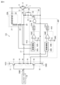
- FIG. 1 is a circuit diagram showing a configuration of a drive circuit for a power semiconductor device according to Embodiment 1;
- FIG. FIG. 3 is a diagram schematically showing voltage or current waveforms at each part during turn-off by a drive circuit of a comparative example in which the second turn-off circuit of FIG. 1 is not provided;
- FIG. 2 is a diagram schematically showing voltage or current waveforms of respective parts when the drive circuit of the first embodiment shown in FIG. 1 is turned off;
- FIG. 10 is a circuit diagram showing the configuration of a drive circuit for a power semiconductor device according to a second embodiment;
- FIG. 10 is a diagram schematically showing voltage or current waveforms of respective parts when the drive circuit of the fifth embodiment shown in FIG. 9 is turned off;
- FIG. 12 is a circuit diagram showing a configuration of a drive circuit according to a modification of the fifth embodiment;
- FIG. 11 is a circuit diagram showing the configuration of a drive circuit for a power semiconductor device according to a sixth embodiment;
- FIG. 13 is a diagram schematically showing voltage or current waveforms of respective parts when the drive circuit of the sixth embodiment shown in FIG. 12 is turned off;
- FIG. 12 is a circuit diagram showing a configuration of a drive circuit according to a modification of Embodiment 6;
- FIG. 12 is a circuit diagram showing the configuration of a drive circuit for a power semiconductor device according to a seventh embodiment;
- FIG. 16 is a diagram showing voltage or current waveforms of respective parts when the drive circuit of the seventh embodiment shown in FIG. 15 is turned off;
- FIG. 14 is a circuit diagram showing the configuration of a drive circuit for a power semiconductor device according to a first example of an eighth embodiment;
- FIG. 14 is a circuit diagram showing the configuration of a drive circuit for a power semiconductor device according to a second example of the eighth embodiment;
- FIG. 14 is a circuit diagram showing the configuration of a drive circuit for a power semiconductor device according to a third example of the eighth embodiment;
- FIG. 12 is a block diagram showing the configuration of a power conversion system to which a power conversion device according to Embodiment 9 is applied;
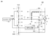
- FIG. 1 is a circuit diagram showing the configuration of a driving circuit 100 for a power semiconductor device 1 according to Embodiment 1.
- a power semiconductor module is configured by the power semiconductor element 1 and the driving circuit 100 .
- the power semiconductor element 1 and the driving circuit 100 may be integrally configured to constitute a power semiconductor module, or the power semiconductor element 1 and the driving circuit 100 may be separately configured to constitute a power semiconductor module. good.
- the power semiconductor element 1 has a first main electrode C (collector) on the high potential side and a second main electrode E (emitter) on the low potential side depending on the voltage applied to the control electrode G (gate). switch between a conducting (on) state or a non-conducting (off) state.
- the voltage applied to the control electrode G is generated by the drive circuit 100 based on the command signal CMD applied from the controller 10.
- FIG. 1 an IGBT (Insulated Gate Bipolar Transistor) is illustrated as the power semiconductor element 1, but it is not limited to the IGBT.
- power semiconductor devices such as power MOSFETs (Metal-Oxide-Semiconductor Field Effect Transistors) and reverse conducting IGBTs (RC-IGBTs) may be used.
- the material used for the power semiconductor element 1 is not limited to Si, and other semiconductor materials such as SiC, GaN, and Ga 2 O 3 may be used.
- a freewheeling diode 2 is connected in anti-parallel with the power semiconductor element 1 .
- the drive circuit 100 includes a turn-on circuit 11, a first turn-off circuit 12, a second turn-off circuit 30, a turn-off control circuit 40, and a voltage clamp circuit 20.
- the turn-on circuit 11 includes a semiconductor switching element 13 and an on-gate resistor 14.
- Semiconductor switching element 13 and on-gate resistor 14 are connected in this order between a node to which power supply voltage VCC is applied (hereinafter referred to as VCC node) and intermediate node 18 .
- First turn-off circuit 12 includes semiconductor switching element 16 and off-gate resistor 15 .
- Semiconductor switching element 16 and off-gate resistor 15 are connected in this order between a node to which ground potential GND is applied (hereinafter referred to as a GND node) and intermediate node 18 .
- Intermediate node 18 is connected to control electrode G of power semiconductor element 1 via control electrode wiring 17 .
- a GND node is connected to the second main electrode E of the power semiconductor element 1 .
- the power supply voltage VCC may be referred to as the first power supply voltage, and the ground potential GND may be referred to as the second power supply voltage.
- the VCC node may be referred to as the first power supply node, and the GND node may be referred to as the second power supply node.
- an NPN bipolar transistor is used as the semiconductor switching element 13 .
- a PNP type bipolar transistor is used as the semiconductor switching element 16 .
- a P-channel MOSFET may be used as the semiconductor switching element 13
- an N-channel MOSFET may be used as the semiconductor switching element 16, or other conductivity types or other types of semiconductor switching elements may be used.
- the semiconductor switching element 13 transitions to the ON state, and the semiconductor switching element 16 transitions to the OFF state.
- the ON command is H level voltage.
- the control electrode G of the power semiconductor element 1 is connected to the VCC node, so that the power semiconductor element 1 becomes conductive.
- the semiconductor switching element 13 transitions to the OFF state, and the semiconductor switching element 16 transitions to the ON state.
- the OFF command is L level voltage.
- the control electrode G of the power semiconductor element 1 is connected to the GND node, so that the power semiconductor element 1 becomes non-conductive.
- the second turn-off circuit 30 is connected between a node 34 on the control electrode wiring 17 and the second main electrode E of the power semiconductor device 1 . Connection node 34 is closer to control electrode G than intermediate node 18 .
- the second turn-off circuit 30 includes a capacitor 31 (also referred to as a capacitive element), a semiconductor switching element 32 and a resistor 33 .
- Capacitor 31 and semiconductor switching element 32 are connected between node 34 (that is, control electrode G) and second main electrode E in this order.
- Resistor 33 is connected in parallel with capacitor 31 .
- a passive component section is configured by the capacitor 31 and the resistor 33 .
- the second turn-off circuit 30 (that is, between the control electrode G and the second main electrode E) is in a non-conducting state, and when the semiconductor switching element 32 is in the on state. At the same time, the second turn-off circuit 30 becomes conductive.
- an N-channel MOSFET is used as the semiconductor switching element 32.
- the semiconductor switching element 32 is not limited to this, and for example, an NPN-type bipolar transistor may be used as the semiconductor switching element 32, or another conductivity type or other type of semiconductor switching element may be used.
- the turn-off control circuit 40 operates when the power semiconductor element 1 is turned off, that is, after the semiconductor switching element 13 of the turn-on circuit 11 is turned off and the semiconductor switching element 16 of the first turn-off circuit 12 is turned on. , the semiconductor switching of the second turn-off circuit 30 when the voltage between the first main electrode C and the second main electrode E (collector-emitter voltage Vce) rises (i.e. on the way up). Switch element 32 to the ON state. Desirably, the switching timing of the semiconductor switching element 32 is when the voltage between the first main electrode C and the second main electrode E (collector-emitter voltage Vce) starts to rise. After that, the turn-off control circuit 40 returns the semiconductor switching element 32 to the off state after a lapse of a certain period of time.
- the turn-off control circuit 40 includes a signal generator 41A.
- the signal generator 41A receives an OFF command as the command signal CMD from the controller 10, the signal generator 41A outputs a pulse signal that is at H level for a certain period of time in order to control the semiconductor switching element 32 to be in a conductive state.
- the semiconductor switching element 32 When the semiconductor switching element 32 is turned on and the second turn-off circuit 30 is turned on, current flows from the control electrode G of the power semiconductor element 1 to the GND node through two paths together with the first turn-off circuit 12 .
- the current path of the first turn-off circuit 12 does not include a capacitor
- the current path of the second turn-off circuit 30 includes a capacitor 31 in series with the semiconductor switching element 32.
- the turn-off operation period of the second turn-off circuit 30 (that is, the period until the current flowing through the second turn-off circuit 30 reaches a steady state) is uniquely determined by the capacitance of the capacitor 31, the signal generator 41A outputs It has nothing to do with the period during which the applied pulse signal has a high level. Thus, the turn-off current through the second turn-off circuit 30 dominates for a very short time depending on the capacitance of the capacitor 31 .
- the capacitance of the capacitor 31 is set so that the period during which the transient current actually flows through the second turn-off circuit 30 is the desired period. Specifically, the capacitance value of capacitor 31 is desirably set such that the collector-emitter voltage Vce is substantially clamped when the current through capacitor 31 becomes zero.
- the voltage clamp circuit 20 is connected between the first main electrode C and the control electrode G on the high potential side of the power semiconductor element 1, and clamps the voltage between the first main electrode C and the control electrode G.
- This circuit is for
- the voltage clamp circuit 20 includes one or more (six) Zener diodes 21 (six) connected in series between the first main electrode C and the control electrode G in this order. Also called a first diode) and a backflow prevention diode 22 (also called a second diode).
- Each Zener diode 21 has a cathode connected to the first main electrode C side.
- the backflow prevention diode 22 has a cathode connected to the control electrode G side.
- the number of Zener diodes 21 is appropriately set so that the sum of the breakdown voltages of each Zener diode 21 does not exceed the rated voltage of power semiconductor device 1 .
- the backflow prevention diode 22 may or may not be of Zener type.
- Losses that occur in power semiconductor devices include switching losses that occur in transient states of switching operations and conduction losses that occur in conductive states.
- the conduction loss is mainly determined by the characteristics of the power semiconductor device, whereas the switching loss can be reduced by devising the driving method of the power semiconductor device.
- Switching loss can be classified into turn-on loss that occurs during turn-on operation and turn-off loss that occurs during turn-off operation.
- turn-off loss In order to reduce the turn-off loss, there is a method of shortening the turn-off time, that is, increasing the switching speed.
- the voltage clamp circuit 20 suppresses overvoltage associated with the surge voltage. Specifically, during the turn-off operation, the voltage between the first main electrode C and the second main electrode E rises. At this time, when the voltage between the main electrodes becomes excessive due to the surge voltage, the Zener diode 21 of the voltage clamp circuit 20 breaks down and current flows through the control electrode G. As a result, the power semiconductor element 1 is temporarily brought into a conducting state, so that the voltage of the first main electrode C on the high potential side can be kept constant. On the other hand, the clamping operation of the voltage clamp circuit 20 lengthens the turn-off operation time, resulting in an increase in turn-off loss. A more detailed description will be given below with reference to the voltage and current waveforms of each part during turn-off.
- FIG. 2 is a diagram schematically showing voltage or current waveforms at each part during turn-off by a drive circuit of a comparative example in which the second turn-off circuit 30 of FIG. 1 is not provided.
- the voltage Vge between the control electrode G and the second main electrode E of the power semiconductor device 1 also referred to as “gate-emitter voltage”
- the main electrode of the power semiconductor device 1 The waveforms of the main current Ic (also referred to as "collector current") flowing between the power semiconductor device 1, the voltage Vce (also referred to as “collector-emitter voltage”) between the main electrodes of the power semiconductor device 1, and the command signal CMD are shown schematically. It is shown.
- a solid line indicates a voltage or current waveform when voltage clamp circuit 20 performs the clamping operation, and a dashed line indicates a voltage or current waveform when voltage clamp circuit 20 is not provided.
- command signal CMD output from controller 10 in FIG. 1 switches from H level (ON command) to L level (OFF command).
- the semiconductor switching element 13 of the turn-on circuit 11 is switched off, and the semiconductor switching element 16 of the first turn-off circuit 12 is switched on.
- the charge accumulated in the control electrode G of the power semiconductor element 1 begins to flow out through the control electrode wiring 17 and the first turn-off circuit 12 .
- the gate-emitter voltage Vge begins to drop at time t2 and drops further after a mirror period from time t3 to time t5.
- the collector-emitter voltage Vce rises from time t3 when it reaches the mirror period, and when it reaches the DC link voltage (the voltage applied in the non-conducting state), the collector current Ic starts to decrease.
- the voltage clamp circuit 20 when the voltage clamp circuit 20 is provided (the solid line in FIG. 2), when the collector-emitter voltage Vce becomes higher than the clamp voltage set by the voltage clamp circuit 20 at time t4, the voltage clamp circuit 20 is closed.
- the Zener diode 21 breaks down and current flows from the first main electrode C (collector) to the control electrode G (gate). This increases the gate-emitter voltage Vge and clamps the collector-emitter voltage Vce. Since collector-emitter voltage Vce is clamped by voltage clamp circuit 20 in this way, the surge voltage is suppressed.
- the voltage clamp circuit 20 when the voltage clamp circuit 20 is provided, the turn-off operation period of the power semiconductor element 1 becomes longer, so there is a problem that the turn-off loss increases.
- FIG. 3 is a diagram schematically showing voltage or current waveforms of respective parts when the drive circuit of the first embodiment shown in FIG. 1 is turned off.
- the waveforms of the gate-emitter voltage Vge of the power semiconductor device 1, the collector current Ic, the collector-emitter voltage Vce, the command signal CMD, and the output voltage of the signal generator 41A are schematically shown in this order from the top. It is shown.
- a solid line indicates a voltage or current waveform in the case of the drive circuit 100 of the first embodiment.
- a dashed line indicates a voltage or current waveform in the case of a comparative example in which neither the voltage clamp circuit 20 nor the second turn-off circuit 30 is provided in FIG. Waveform changes at times t1, t2, t3 and t5 are the same as in FIG.
- the signal generator 41A switches its output voltage to H level.
- the semiconductor switching element 32 is brought into a conducting state, so that a gate current abruptly flows through the capacitor 31 of the second turn-off circuit 30 .
- the gate-emitter voltage Vge decreases, the collector current Ic decreases, and the collector-emitter voltage Vce increases.
- the gate current through the capacitor 31 stops.
- the period from time t11 to time t12 is determined by the capacity of the capacitor 31 . Therefore, at time t12, the capacitance value of capacitor 31 is determined in advance so that the increase in collector-emitter voltage Vce is also substantially clamped.
- the signal generator 41 returns its output voltage to L level, thereby turning off the semiconductor switching device 32. do.
- the semiconductor switching device 32 is turned off.
- the signal generator 41 maintains the output signal at a high level so as to be conductive.
- the capacitance value of capacitor 31 is set so that the period during which the gate current flows through capacitor 31 is only the period during which collector-emitter voltage Vce is rising. In other words, the capacitance value of capacitor 31 is set so that the increase in collector-emitter voltage Vce is also clamped when current stops flowing through capacitor 31 .
- the period during which the current flows through the second turn-off circuit 30 is set by the capacitance value of the capacitor 31, not by the period during which the semiconductor switching element 32 is in the conductive state. It is possible to control the semiconductor switching element 32 with a pulse signal having a short pulse width of about 100 nanoseconds during the period in which the collector-emitter voltage Vce rises so that current actually flows through the second turn-off circuit 30. difficult. In comparison, it is easy to determine the period during which the current flows through the second turn-off circuit 30 by the capacitance value of the capacitor.
- a resistor 33 is connected in parallel with the capacitor 31 .
- the power semiconductor device Assuming a power conversion device as an application of the power semiconductor device, the power semiconductor device is controlled so as to continuously switch. That is, the turn-off operation is repeated. Therefore, in order to operate the second turn-off circuit at each turn-off operation, it is necessary to discharge the charge accumulated in the capacitor 31 each time the turn-off operation is completed.
- a resistor 33 is provided to discharge the capacitor 31 in such a case. Actually, when the semiconductor switching element 32 is turned off, the charge accumulated in the capacitor 31 is discharged.
- the time constant determined by the capacitor 31 and the resistor 33 is is preferably 5 microseconds or less.
- the voltage clamp circuit is provided between the first main electrode C and the control electrode G on the high potential side of the power semiconductor device 1.
- 20 is provided, and a second turn-off circuit 30 is provided between the control electrode G and the second main electrode E on the low potential side.
- the second turn-off circuit 30 differs from the first turn-off circuit 12 in that a capacitor 31 is provided in series with a semiconductor switching element 32 . Furthermore, a resistor 33 is connected in parallel with the capacitor 31 .
- the turn-off control circuit 40 that controls the semiconductor switching element 32 of the second turn-off circuit 30 turns on the semiconductor switching element 32 during the turn-off period after the first turn-off circuit 12 becomes conductive. At this time, a current larger than the current flowing through the first turn-off circuit 12 flows through the capacitor 31, so that the voltage between the main electrodes (collector-emitter voltage Vce) of the power semiconductor device 1 rises in a shorter time. can be made That is, the turn-off loss can be reduced because the voltage change (dV/dt) at the time of turn-off of the power semiconductor device 1 becomes steeper.
- Capacitor 31 is arranged so that the period during which current transiently flows through capacitor 31 is substantially equal to the period until collector-emitter voltage Vce reaches the DC link voltage after semiconductor switching element 32 is switched to the ON state. is set.
- Turn-off control circuit 40 turns off semiconductor switching element 32 at an arbitrary timing after collector-emitter voltage Vce reaches the DC link voltage. Therefore, the period during which the semiconductor switching element 32 is controlled to be on by the turn-off control circuit 40 is the period during which the voltage between the main electrodes of the power semiconductor element 1 (collector-emitter voltage Vce) rises from 0 to the maximum value. longer than
- the drive circuit 100 is provided with the voltage clamp circuit 20, the surge voltage associated with the current change (dI/dt) during the turn-off operation of the power semiconductor element 1 can be suppressed. As a result, the trade-off between turn-off loss and surge voltage can be improved, so that a power converter provided with power semiconductor device 1 can be made smaller and more efficient.
- FIG. 4 is a circuit diagram showing the configuration of the driving circuit 101 of the power semiconductor device 1 according to the second embodiment.
- the drive circuit 101 of the second embodiment differs from the drive circuit 100 of the first embodiment in that the voltage clamp circuit 20A further includes a capacitor 24 connected in series with a plurality of Zener diodes 21 .
- the capacitor 24 is connected between the first main electrode C of the power semiconductor device 1 and the plurality of Zener diodes 21 . 4 are the same as those in FIG. 1, so the same or corresponding parts are denoted by the same reference numerals and description thereof will not be repeated.
- the direct current can be cut off. Therefore, the DC voltage constantly applied between the first main electrode C and the second main electrode E of the power semiconductor device 1 is higher than the clamp voltage determined by the number of Zener diodes 21. However, no DC current flows through the voltage clamp circuit 20 .
- the drive circuit 101 of the second embodiment is the same as those of the drive circuit 100 of the first embodiment. That is, when the semiconductor switching element 32 of the second turn-off circuit 30 becomes conductive during the turn-off period of the power semiconductor element 1 , the electric charge of the control electrode G is extracted via the capacitor 31 . As a result, the voltage change (dV/dt) at turn-off can be made steeper, and the turn-off loss can be reduced. On the other hand, since the drive circuit 101 further includes a voltage clamp circuit, it is possible to suppress the surge voltage generated between the main electrodes.
- FIG. 5 is a circuit diagram showing the configuration of the drive circuit 102 of the power semiconductor device 1 according to the third embodiment.
- the drive circuit 102 of the third embodiment differs from the drive circuit 101 of the second embodiment in that the second turn-off circuit 30A further includes a negative power supply 35.
- the above configuration increases the potential difference between the control electrode (gate) of the semiconductor switching element 32 and the main electrode (emitter) on the low potential side.
- the current flowing through the second turn-off circuit 30A through the semiconductor switching element 32 can be increased.
- the rate at which the collector-emitter voltage Vce rises when the power semiconductor device 1 is turned off can be further increased, thereby further enhancing the effect of reducing the turn-off loss.
- FIG. 5 The other points in FIG. 5 are the same as those described in FIGS. 1 and 4, so the same or corresponding parts are denoted by the same reference numerals and the description will not be repeated.
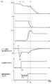
- FIG. 6 is a diagram schematically showing voltage or current waveforms at each part when drive circuit 102 of the third embodiment shown in FIG. 5 is turned off.
- the waveforms of the gate-emitter voltage Vge, collector current Ic, collector-emitter voltage Vce, and output voltage of the signal generator 41A of the power semiconductor device 1 are schematically shown in order from the top.
- a solid line indicates a voltage or current waveform in the case of the drive circuit 100 of the first embodiment.
- a dashed line indicates a voltage or current waveform in the case of a comparative example in which neither the voltage clamp circuit 20 nor the second turn-off circuit 30 is provided in FIG.
- a dotted line indicates a voltage or current waveform for the drive circuit 102 of the third embodiment. Waveform changes at times t2, t3, and t5 are the same as in FIG.
- the signal generator 41A switches its output voltage to H level at time t14 when the collector-emitter voltage Vce begins to rise.
- the semiconductor switching element 32 is brought into a conducting state, so that a current suddenly flows through the capacitor 31 of the second turn-off circuit 30A.
- the current flowing through the second turn-off circuit 30A is larger than that of the second turn-off circuit 30 of the first embodiment (solid line in FIG. 6).
- the amount of decrease in the gate-emitter voltage Vge is greater than in the first embodiment
- the rate of decrease in the collector current Ic is greater than in the first embodiment
- the rate of increase in the collector-emitter voltage Vce is It is larger than the case of the first embodiment.
- the capacitance value of the capacitor 31 is set so that the current flowing through the capacitor 31 of the second turn-off circuit 30A also stops.
- the signal generator 41 returns its output voltage to L level, thereby turning off the semiconductor switching device 32. do.
- the period during which the current flows through the capacitor 31 in the third embodiment is from time t14 to time t15. This period is shorter than from time t11 to time t12 in the first embodiment.
- the negative power supply 35 is connected in series to the low potential side of the semiconductor switching element 32 of the second turn-off circuit 30A.
- the current flowing through the semiconductor switching element 32 can be increased when the semiconductor switching element 32 is in the ON state, so that the turn-off speed of the power semiconductor element 1 can be further increased.
- the voltage change (dV/dt) of the power semiconductor device 1 can be sharpened, and the turn-off loss can be further reduced.
- the drive circuit 102 includes the voltage clamp circuit 20, so that surge voltage transiently generated between the main electrodes of the power semiconductor element 1 can be suppressed at the time of turn-off.
- the configuration of the second turn-off circuit 30A further including the negative power supply 35 can be combined with any of the driving circuits 103-111 of the fourth to ninth embodiments described later.
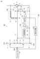
- FIG. 7 is a circuit diagram showing the configuration of the driving circuit 103 of the power semiconductor device 1 according to the fourth embodiment.
- the turn-off control circuit 40A includes a second signal generator 41B, a delay circuit 51, and logical operation in addition to the first signal generator 41A described in the first to third embodiments. It differs from the drive circuits 100 to 102 of the first to third embodiments in that it further includes a circuit 45.
- FIG. 1 is a circuit diagram showing the configuration of the driving circuit 103 of the power semiconductor device 1 according to the fourth embodiment.
- the turn-off control circuit 40A includes a second signal generator 41B, a delay circuit 51, and logical operation in addition to the first signal generator 41A described in the first to third embodiments. It differs from the drive circuits 100 to 102 of the first to third embodiments in that it further includes a circuit 45.
- the first signal generator 41A outputs a pulse signal that is at H level for a certain period of time based on the command signal CMD (off command) output from the controller 10.
- the second signal generator 41B detects the voltage between the control electrode G of the power semiconductor device 1 and the second main electrode E on the low potential side, and when the detected voltage becomes smaller than the reference voltage V1 output a pulse signal that is at H level for a certain period of time.
- the reference voltage V1 is set to a value lower than the voltage of the control electrode G when the power semiconductor element 1 is in the ON state and higher than the mirror voltage when the power semiconductor element 1 is turned off.
- the delay circuit 51 delays the timing at which the output of the second signal generator 41B switches from L level to H level by a predetermined delay time DT1. Thereby, the timing at which the semiconductor switching element 32 switches from the off state to the on state can be adjusted. If the turn-on timing of the semiconductor switching element 32 can be adjusted by the delay time of each of the later-described comparator 44 and logical operator 45 included in the second signal generator 41B, the delay circuit 51 is not required. good.
- a delay circuit 51 may be provided between the logic operator 45 and the control electrode G of the semiconductor switching element 32 .
- the logic operator 45 When the signal obtained by delaying the output signal of the second signal generator 41B by the delay circuit 51 and the output signal of the first signal generator 41A are both at H level, the logic operator 45 outputs the H level signal to the semiconductor device. Output to the control electrode G of the switching element 32 . As a result, the semiconductor switching element 32 becomes conductive. In this way, the logical operator 45 performs a logical AND operation on a plurality of input signals.
- the second signal generator 41B includes a differential amplifier 42, a DC power supply 43, and a comparator 44, as shown in FIG.
- the differential amplifier 42 functions as a control voltage detection circuit that detects the control voltage (gate-emitter voltage Vge) between the control electrode G of the power semiconductor element 1 and the second main electrode E on the low potential side.
- the comparator 44 compares the output voltage of the differential amplifier 42 and the output voltage of the DC power supply 43, and when the output voltage of the differential amplifier 42 becomes smaller than the output voltage of the DC power supply 43, an H level signal is generated. to output
- the drive circuit 103 of the fourth embodiment can be combined with the second turn-off circuit 30A having the negative power supply 35 of the third embodiment.
- FIG. 8 is a diagram schematically showing voltage or current waveforms at each part when drive circuit 103 of the fourth embodiment shown in FIG. 7 is turned off.
- the gate-emitter voltage Vge of the power semiconductor device 1 the collector current Ic, the collector-emitter voltage Vce, the output voltage of the differential amplifier 42, the output voltage of the comparator 44, and the logic operator 45 output voltage waveforms are shown schematically.
- a solid line indicates a voltage or current waveform in the case of the drive circuit 103 of the fourth embodiment.
- a dashed line indicates a voltage or current waveform in the case of a comparative example in which neither the voltage clamp circuit 20 nor the second turn-off circuit 30 is provided in FIG. Waveform changes at times t2, t3, and t5 are the same as in FIG.
- the output voltage of the differential amplifier 42 (that is, the gate-emitter voltage Vge of the power semiconductor device 1) becomes lower than the reference voltage V1.
- the output voltage of comparator 44 switches from the L level to the H level. It is assumed that the output signal of the first signal generator 41A has already switched from L level to H level when the OFF command is received from the controller 10 .
- the output voltage of the logic operator 45 switches from L level to H level.
- the semiconductor switching element 32 is brought into a conducting state, so that current flows rapidly through the capacitor 31 of the second turn-off circuit 30 .
- the gate-emitter voltage Vge decreases, the collector current Ic decreases, and the collector-emitter voltage Vce increases.
- the current through capacitor 31 stops.
- the period from time t18 to time t19 is determined by the capacity of the capacitor 31 . Therefore, the capacitance value of capacitor 31 is determined in advance so that the increase in collector-emitter voltage Vce is substantially clamped at time t19.
- the first and second signal generators 41A and 41B return their respective output voltages to the L level at an arbitrary timing until the power semiconductor element 1 is turned on next time, thereby turning on the semiconductor switching element. 32 is turned off.
- the drive circuit 103 further includes the voltage clamp circuit 20A, the voltage between the main electrodes of the power semiconductor device 1 (that is, the collector-emitter voltage Vce) can be suppressed.
- the first signal generator 41A when the power semiconductor device 1 is turned off, based on the switching of the command signal CMD from the controller 10 from the ON command to the OFF command, 2 turn-off circuit 30 is provided.
- the switching timing of the semiconductor switching element 32 from the OFF state to the ON state is determined by the second signal generator 41B.
- FIG. 9 is a circuit diagram showing the configuration of drive circuit 104 of power semiconductor device 1 according to the fifth embodiment.
- the function of the second signal generator 41C is different from the function of the second signal generator 41B in the drive circuit 103 of the fourth embodiment.
- the second signal generator 41C in FIG. 9 acquires the current value detected by the current sensor 60 provided on the current path of the first turn-off circuit 12. Then, the second signal generator 41C generates a pulse signal that becomes H level for a certain period of time when the absolute value of the detected current value becomes smaller than the reference value (corresponding to the reference voltage V2) after reaching the peak value. to output
- the signal generator 41C includes an amplifier 52, a comparator 44, and a DC power supply 43, as shown in FIG.
- Amplifier 52 acquires the gate current value detected by current sensor 60 when power semiconductor device 1 is turned off.
- the amplifier 52 may be configured as a differential amplifier that acquires a differential signal from the current sensor 60 .
- Comparator 44 compares the absolute value of the detection value of current sensor 60 output from amplifier 52 with reference voltage V2 output from DC power supply 43 . Comparator 44 outputs a pulse signal that is at H level for a certain period of time when the absolute value of the gate current detection value output from amplifier 52 exceeds the peak value and then becomes lower than reference voltage V2.
- FIG. 9 The rest of the configuration in FIG. 9 is the same as in FIG. 7, so the same or corresponding parts are denoted by the same reference numerals, and description thereof will not be repeated.
- FIG. 10 is a diagram schematically showing voltage or current waveforms at each part when drive circuit 104 of the fifth embodiment shown in FIG. 9 is turned off.
- the gate-emitter voltage Vge of the power semiconductor device 1 the collector current Ic, the collector-emitter voltage Vce, the output voltage of the current sensor 60 as a gate current detector, and the output voltage of the comparator 44 are shown in order from the top.
- the waveforms of the output voltage of the logical operator 45 are shown.
- a solid line indicates a voltage or current waveform in the case of the drive circuit 104 of the fifth embodiment.
- a dashed line indicates a voltage or current waveform in the case of a comparative example in which neither the voltage clamp circuit 20 nor the second turn-off circuit 30 is provided in FIG. Waveform changes at times t2, t3, and t5 are the same as in FIG.
- the value of the gate current is positive when it flows from the intermediate node 18 to the control electrode G of the power semiconductor element 1, and negative when it flows in the opposite direction
- the gate current begins to flow and has a peak value at time t22.
- the output voltage of comparator 44 switches from the L level to the H level. Assume that the output signal of the first signal generator 41A has already switched from the L level to the H level when the off command is received from the controller 10 .
- the output voltage of the logical operator 45 switches from L level to H level.
- the semiconductor switching element 32 is brought into a conducting state, so that current flows rapidly through the capacitor 31 of the second turn-off circuit 30 .
- the gate-emitter voltage Vge decreases
- the collector current Ic decreases
- the collector-emitter voltage Vce increases
- the absolute value of the gate current increases.
- the current through capacitor 31 stops.
- the period from time t24 to time t25 is determined by the capacity of the capacitor 31 . Therefore, the capacitance value of capacitor 31 is determined in advance so that the increase in collector-emitter voltage Vce is substantially clamped at time t25.
- the first and second signal generators 41A and 41C return their respective output voltages to the L level at an arbitrary timing until the power semiconductor device 1 starts to turn on next time, thereby turning on the semiconductor switching device. 32 is turned off.
- the operation timing of the semiconductor switching device 32 in the second turn-off circuit 30 is determined based on the detected value of the gate current flowing at the time of turn-off. can. Therefore, by considering the delay time DT2 of the delay circuit 51 and the delay time generated in the comparator 44 and the logic operator 45, at the timing when the collector-emitter voltage Vce starts to rise due to the operation of the first turn-off circuit 12, At some time t24, the semiconductor switching element 32 of the second turn-off circuit 30 can be switched to the conductive state.
- the drive circuit 106 further includes the voltage clamp circuit 20A, the voltage between the main electrodes of the power semiconductor device 1 (that is, the collector-emitter voltage Vce) can be suppressed.
- FIG. 11 is a circuit diagram showing a configuration of drive circuit 105 according to a modification of the fifth embodiment.
- the second signal generator 41D detects the gate current based on the voltage drop occurring in the off-gate resistor 15 provided in the first turn-off circuit 12 instead of the detection value of the current sensor 60. It differs from the drive circuit 104 in FIG. 9 in that it acquires a value. Therefore, the differential amplifier 42 of the second signal generator 41 ⁇ /b>D functions as a gate current detection circuit that detects the gate current from the voltage across the off-gate resistor 15 .
- FIG. 11 The other points in FIG. 11 are the same as in FIGS. 7 and 9, so the same or corresponding parts are denoted by the same reference numerals, and description thereof will not be repeated.
- FIG. 12 is a circuit diagram showing the configuration of drive circuit 106 of power semiconductor device 1 according to the sixth embodiment.
- the function of the second signal generator 41E is the same as the function of the second signal generator 41B in the drive circuit 103 of the fourth embodiment and the drive circuits 104 and 105 of the fifth embodiment. differs from the function of the second signal generators 41C and 41D in .
- the second signal generator 41E in FIG. 12 integrates the gate current detected by the gate resistor 46 provided in the control electrode wiring 17, thereby flowing into the control electrode G of the power semiconductor element 1. Alternatively, the amount of charge flowing out from the control electrode G is detected.
- the second signal generator 41E maintains the H level for a certain period of time when the amount of charge accumulated in the control electrode G of the power semiconductor element 1 becomes smaller than the reference value (corresponding to the reference voltage V4) at the time of turn-off.
- the signal generator 41E includes a differential amplifier 48, an integrator 49, a comparator 44, and a DC power supply 43, as shown in FIG.
- a differential amplifier 48 detects the current flowing through the control electrode wiring 17 based on the voltage applied across the gate resistor 46 .
- Integrator 49 detects the amount of charge flowing into and out of control electrode G of power semiconductor device 1 by integrating the gate current detected by differential amplifier 48 . Therefore, differential amplifier 48 and integrator 49 constitute charge amount detection circuit 47 for detecting the amount of charge accumulated in control electrode G of power semiconductor device 1 .
- Comparator 44 generates a pulse that becomes H level for a certain period of time when the amount of accumulated charge detected by charge amount detection circuit 47 becomes smaller than a reference value (corresponding to reference voltage V4) when power semiconductor device 1 is turned off. Output a signal.
- FIG. 12 Other points in FIG. 12 are the same as in FIGS. 7, 9, and 11, so the same or corresponding parts are denoted by the same reference numerals, and description thereof will not be repeated.
- FIG. 13 is a diagram schematically showing voltage or current waveforms at each part when driving circuit 106 of the sixth embodiment shown in FIG. 12 is turned off.
- the gate-emitter voltage Vge of the power semiconductor device 1 the collector current Ic, the collector-emitter voltage Vce, the output voltage of the integrator 49, the output voltage of the comparator 44, and the logic operator 45 are shown for each output voltage waveform.
- a solid line indicates a voltage or current waveform in the case of the driving circuit 106 of the sixth embodiment.
- a dashed line indicates a voltage or current waveform in the case of a comparative example in which neither the voltage clamp circuit 20 nor the second turn-off circuit 30 is provided in FIG. Waveform changes at times t2, t3, and t5 are the same as in FIG.
- the gate resistor 46 in FIG. 12 has a positive gate current when charges flow into the control electrode G of the power semiconductor element 1 at turn-on, and a gate current in the positive direction when charges flow out from the control electrode G of the power semiconductor element 1 at turn-off. , any of the negative going gate currents can be detected. Therefore, the output of the integrator 49 monotonously increases from 0 to reach the maximum value at turn-on, and monotonously decreases from the maximum value to return to 0 at turn-off.
- FIG. 13 shows the gate charge amount at turn-off as the output voltage of the integrator 49 . Therefore, after the semiconductor switching element 16 of the first turn-off circuit 12 is switched from the off state to the on state based on the off command from the controller 10 at time t1, the output voltage of the integrator 49 monotonically decreases from the maximum value. and return to 0.
- the output voltage of the logic operator 45 switches from L level to H level.
- the semiconductor switching element 32 is brought into a conducting state, so that current flows rapidly through the capacitor 31 of the second turn-off circuit 30 .
- the gate-emitter voltage Vge decreases, the collector current Ic decreases, and the collector-emitter voltage Vce increases.
- the current through the capacitor 31 stops.
- the period from time t31 to time t32 is determined by the capacity of the capacitor 31. FIG. Therefore, the capacitance value of capacitor 31 is determined in advance so that the increase in collector-emitter voltage Vce is substantially clamped at time t32.
- the first and second signal generators 41A and 41C return their respective output voltages to the L level at an arbitrary timing until the power semiconductor device 1 starts to turn on next time, thereby turning on the semiconductor switching device. 32 is turned off.
- the output voltage of the integrator 49 is smaller than the reference voltage even at the beginning of the turn-on operation.
- a first signal generator 41A is provided to prevent erroneous output during this period.
- the first signal generator 41A outputs a pulse signal that stays at H level for a certain period of time when the off command is output from the controller 10 .
- the final output of the turn-off control circuit 40B is obtained by ANDing the output voltage of the first signal generator 41A and the delayed output voltage of the second signal generator 41E.
- the operation timing of the semiconductor switching device 32 in the second turn-off circuit 30 is set to the detection value of the charge amount of the control electrode G at the time of turn-off. can be determined based on Therefore, by considering the delay time DT3 of the delay circuit 51 and the delay time generated in the comparator 44 and the logic operator 45, at the timing when the collector-emitter voltage Vce starts to rise due to the operation of the first turn-off circuit 12, At a certain time t31, the semiconductor switching element 32 of the second turn-off circuit 30 can be switched to the conducting state.
- the drive circuit 103 further includes the voltage clamp circuit 20A, the voltage between the main electrodes of the power semiconductor device 1 (that is, the collector-emitter voltage Vce) can be suppressed.
- FIG. 14 is a circuit diagram showing a configuration of drive circuit 107 according to a modification of the sixth embodiment.
- the second signal generator 41F has a gate current value flowing through the off-gate resistor 15 of the first turn-off circuit 12 instead of the gate current value flowing through the gate resistor 46 provided in the control electrode wiring 17. It differs from the drive circuit 106 in FIG. 12 in that it detects the current value.
- the charge amount detection circuit 47A of the second signal generator 41F of the drive circuit 107 includes an initialization circuit 50 for initializing the integrated value of the integrator 49. including.
- the comparator 44 of the second signal generator 41F generates a pulse voltage that becomes H level for a certain period of time when the outflow charge amount detected by the charge amount detection circuit 47A exceeds a reference value (corresponding to the reference voltage V5). Output.
- the delay time DT3 of the delay circuit 51 elapses after the outflow charge amount exceeds the reference value, the output voltage of the logical operator 45 switches from L level to H level. As a result, the semiconductor switching element 32 of the second turn-off circuit 30 becomes conductive.
- the first turn-off circuit 12 operates to At the timing when the voltage Vce starts rising, the semiconductor switching element 32 of the second turn-off circuit 30 can be switched to the conducting state.
- the voltage change (dV/dt) of the power semiconductor device 1 can be sharpened, and the turn-off loss can be further reduced.
- the drive circuit 107 further includes the voltage clamp circuit 20A, the voltage between the main electrodes of the power semiconductor device 1 (that is, the collector-emitter voltage Vce) can be suppressed.
- FIG. 15 is a circuit diagram showing the configuration of drive circuit 108 of power semiconductor device 1 according to the seventh embodiment.
- the function of the second signal generator 41G is different from the functions of the second signal generators 41B, 41C and 41D of FIGS.
- the second signal generator 41G of the turn-off control circuit 40A of FIG. 15 detects the voltage applied between the anode and cathode of the backflow prevention diode 22 of the voltage clamp circuit 20A.
- the voltage is detected with the positive side of the anode of the backflow prevention diode 22 and the negative side of the cathode.
- the second signal generator 41G outputs a pulse signal that is at H level for a certain period of time when the detected voltage applied across the backflow prevention diode 22 exceeds the reference voltage V6.
- the signal generator 41G includes a differential amplifier 42, a comparator 44, and a DC power supply 43, as shown in FIG.
- the differential amplifier 42 detects the voltage applied between the anode and cathode of the backflow prevention diode 22 when the power semiconductor device 1 is turned off.
- a comparator 44 compares the output voltage of the differential amplifier 42 with the reference voltage V6 of the DC power supply 43, and when the output voltage of the DC power supply 43 exceeds the reference voltage V6, the pulse signal becomes H level for a certain period of time. to output
- FIG. 16 is a diagram showing voltage or current waveforms at each part when the drive circuit 108 of the seventh embodiment shown in FIG. 15 is turned off. 16, in order from the top, the gate-emitter voltage Vge of the power semiconductor device 1, the collector current Ic, the collector-emitter voltage Vce, the output voltage of the differential amplifier 42, the output voltage of the comparator 44, and the logic operator 45 output voltage waveforms are shown.
- a solid line indicates a voltage or current waveform in the case of the driving circuit 108 of the seventh embodiment.
- a dashed line indicates a voltage or current waveform in the case of a comparative example in which neither the voltage clamp circuit 20 nor the second turn-off circuit 30 is provided in FIG. Waveform changes at times t2, t3, and t5 are the same as in FIG.
- the cathode terminal of the backflow prevention diode 22 has the same potential as the control electrode G of the power semiconductor element 1 . Therefore, the anode-cathode voltage of the backflow prevention diode 22 exhibits a waveform similar to the gate-emitter voltage Vge of the power semiconductor device 1 . Specifically, the anode-cathode voltage of the backflow prevention diode 22 becomes a negative value at the time of turn-off, and until the mirror period begins, the gate-emitter voltage Vge of the power semiconductor element 1 is offset in the negative direction. waveform. After that, when the mirror period starts at time t3 and the gate-emitter voltage Vge reaches a constant value, the anode-cathode voltage of the backflow prevention diode 22 increases correspondingly.
- the reference voltage V6 of the DC power supply 43 is set to a value slightly higher than the value when entering the mirror period.
- the output signal of comparator 44 switches from the L level to the H level. It is assumed that the output signal of the first signal generator 41A has already switched from the L level to the H level when the OFF command is received from the controller 10.
- the output voltage of the logic operator 45 switches from L level to H level.
- the semiconductor switching element 32 is brought into a conducting state, so that current flows rapidly through the capacitor 31 of the second turn-off circuit 30 .
- the gate-emitter voltage Vge decreases
- the collector current Ic decreases
- the collector-emitter voltage Vce increases
- the anode-cathode voltage of the backflow prevention diode 22 increases.
- the current through the capacitor 31 stops.
- the period from time t41 to time t42 is determined by the capacity of the capacitor 31. FIG. Therefore, the capacitance value of capacitor 31 is determined in advance so that the increase in collector-emitter voltage Vce is substantially clamped at time t32.
- the first and second signal generators 41A and 41G return their respective output voltages to the L level at an arbitrary timing until the power semiconductor device 1 starts to turn on next time, thereby turning the semiconductor switching device on. 32 is turned off.
- the operation timing of the semiconductor switching device 32 in the second turn-off circuit 30 is adjusted to the anode of the backflow prevention diode 22 of the voltage clamp circuit 20A. ⁇ It can be determined based on the detected value of the voltage between the cathodes. Therefore, by considering the delay time DT4 of the delay circuit 51 and the delay time occurring in the comparator 44 and the logic operator 45, at the timing when the collector-emitter voltage Vce starts to rise due to the operation of the first turn-off circuit 12, At a certain time t41, the semiconductor switching element 32 of the second turn-off circuit 30 can be switched to the conductive state.
- the drive circuit 108 further includes the voltage clamp circuit 20A, the voltage between the main electrodes of the power semiconductor device 1 (that is, the collector-emitter voltage Vce) can be suppressed.
- Embodiment 8 In the eighth embodiment, an example in which a turn-off control circuit is configured by combining a plurality of the second signal generators 41B to 41G described in the fourth to seventh embodiments will be described.
- FIG. 17 is a circuit diagram showing a configuration of drive circuit 109 for power semiconductor element 1 according to a first example of the eighth embodiment.
- Turn-off control circuit 40D of drive circuit 109 in FIG. 17 includes signal generator 41B described in FIG. 7, signal generator 41D described in FIG.
- the signal generator 41B detects the voltage between the control electrode G of the power semiconductor device 1 and the second main electrode E on the low potential side, and detects the voltage for a certain period of time when the detected voltage becomes smaller than the reference voltage V1. Outputs a pulse signal of H level.
- the reference voltage V1 is set to a value lower than the voltage of the control electrode G when the power semiconductor element 1 is in the ON state and higher than the mirror voltage when the power semiconductor element 1 is turned off.
- the delay circuit 51A delays the output voltage of the signal generator 41B by the delay time DT1. As a result, the output voltage of the delay circuit 51A is switched from the L level to the H level at the timing when the collector-emitter voltage Vce starts to rise due to the operation of the first turn-off circuit 12.
- the signal generator 41D detects the gate current based on the voltage drop across the off-gate resistor 15 provided in the first turn-off circuit 12.
- the signal generator 41D outputs a pulse signal that is at H level for a certain period of time when the absolute value of the detected gate current exceeds the peak value and becomes smaller than the reference value (corresponding to the reference voltage V3).
- the delay circuit 51B delays the output voltage of the signal generator 41D by the delay time DT2. As a result, the output voltage of the delay circuit 51B is switched from the L level to the H level at the timing when the collector-emitter voltage Vce starts to rise due to the operation of the first turn-off circuit 12.
- the logical operator 45 outputs the logical product of the delay circuit 51A and the delay circuit 51B. By switching the output of logic operator 45 from L level to H level, semiconductor switching element 32 of second turn-off circuit 30 becomes conductive.
- Other configurations in FIG. 17 are the same as those described in the fourth to seventh embodiments, so the same or corresponding parts are denoted by the same reference numerals and description thereof will not be repeated.
- the semiconductor switching element 32 of the second turn-off circuit 30 can be switched to the conductive state at the timing when the collector-emitter voltage Vce starts to rise due to the operation of the first turn-off circuit 12.
- the voltage change (dV/dt) of the power semiconductor device 1 can be steepened, and the turn-off loss can be further reduced.
- the drive circuit 109 further includes the voltage clamp circuit 20A, the voltage between the main electrodes of the power semiconductor device 1 (that is, the collector-emitter voltage Vce) can be suppressed.
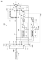
- FIG. 18 is a circuit diagram showing the configuration of a drive circuit 110 for a power semiconductor device 1 according to a second example of the eighth embodiment.
- the turn-off control circuit 40E of the drive circuit 110 of FIG. 18 includes the signal generator 41D described with reference to FIG. 11, the signal generator 41E described with reference to FIG.
- the signal generator 41D detects the gate current based on the voltage drop across the off-gate resistor 15 provided in the first turn-off circuit 12.
- the signal generator 41D outputs a pulse signal that is at H level for a certain period of time when the absolute value of the detected gate current exceeds the peak value and becomes smaller than the reference value (corresponding to the reference voltage V3).
- the delay circuit 51A delays the output voltage of the signal generator 41D by the delay time DT2. As a result, the output voltage of the delay circuit 51A is switched from the L level to the H level at the timing when the collector-emitter voltage Vce starts to rise due to the operation of the first turn-off circuit 12.
- the signal generator 41E integrates the gate current detected by the gate resistor 46 provided in the control electrode wiring 17 to calculate the amount of charge flowing into and out of the control electrode G of the power semiconductor element 1. To detect.
- the second signal generator 41E maintains the H level for a certain period of time when the amount of charge accumulated in the control electrode G of the power semiconductor element 1 becomes smaller than the reference value (corresponding to the reference voltage V4) at the time of turn-off. Outputs a pulse signal that becomes
- the delay circuit 51B delays the output voltage of the signal generator 41E by the delay time DT3. As a result, the output voltage of the delay circuit 51B is switched from the L level to the H level at the timing when the collector-emitter voltage Vce starts to rise due to the operation of the first turn-off circuit 12.
- the logical operator 45 outputs the logical product of the delay circuit 51A and the delay circuit 51B. By switching the output of logic operator 45 from L level to H level, semiconductor switching element 32 of second turn-off circuit 30 becomes conductive.
- Other configurations in FIG. 18 are the same as those described in the fourth to seventh embodiments, so the same or corresponding parts are denoted by the same reference numerals and description thereof will not be repeated.
- the semiconductor switching element 32 of the second turn-off circuit 30 can be switched to the conductive state at the timing when the collector-emitter voltage Vce starts to rise due to the operation of the first turn-off circuit 12.
- the voltage change (dV/dt) of the power semiconductor device 1 can be steepened, and the turn-off loss can be further reduced.
- the drive circuit 110 further includes the voltage clamp circuit 20A, the voltage between the main electrodes of the power semiconductor device 1 (that is, the collector-emitter voltage Vce) can be suppressed.
- FIG. 19 is a circuit diagram showing a configuration of a drive circuit 111 for a power semiconductor element 1 according to a third example of the eighth embodiment.
- the turn-off control circuit 40F of the drive circuit 111 of FIG. 19 includes the signal generator 41D described with reference to FIG. 11, the signal generator 41G described with reference to FIG.
- the signal generator 41D detects the gate current based on the voltage drop across the off-gate resistor 15 provided in the first turn-off circuit 12.
- the signal generator 41D outputs a pulse signal that is at H level for a certain period of time when the absolute value of the detected gate current exceeds the peak value and becomes smaller than the reference value (corresponding to the reference voltage V3).
- the delay circuit 51A delays the output voltage of the signal generator 41D by the delay time DT2. As a result, the output voltage of the delay circuit 51A is switched from the L level to the H level at the timing when the collector-emitter voltage Vce starts to rise due to the operation of the first turn-off circuit 12.
- the signal generator 41G detects the voltage applied between the anode and cathode of the backflow prevention diode 22 of the voltage clamp circuit 20A. Here, the voltage is detected with the positive side of the anode of the backflow prevention diode 22 and the negative side of the cathode. Then, the second signal generator 41G outputs a pulse signal that is at H level for a certain period of time when the detected voltage applied across the backflow prevention diode 22 exceeds the reference voltage V6.
- the delay circuit 51B delays the output voltage of the signal generator 41G by the delay time DT4. As a result, the output voltage of the delay circuit 51B is switched from the L level to the H level at the timing when the collector-emitter voltage Vce starts to rise due to the operation of the first turn-off circuit 12.
- the logical operator 45 outputs the logical product of the delay circuit 51A and the delay circuit 51B. By switching the output of logic operator 45 from L level to H level, semiconductor switching element 32 of second turn-off circuit 30 becomes conductive.
- Other configurations in FIG. 18 are the same as those described in the fourth to seventh embodiments, so the same or corresponding parts are denoted by the same reference numerals and description thereof will not be repeated.
- the semiconductor switching element 32 of the second turn-off circuit 30 can be switched to the conductive state at the timing when the collector-emitter voltage Vce starts to rise due to the operation of the first turn-off circuit 12.
- the voltage change (dV/dt) of the power semiconductor device 1 can be steepened, and the turn-off loss can be further reduced.
- the drive circuit 111 further includes the voltage clamp circuit 20A, the voltage between the main electrodes of the power semiconductor device 1 (that is, the collector-emitter voltage Vce) can be suppressed.
- FIG. 20 is a block diagram showing the configuration of a power conversion system to which the power converter according to the ninth embodiment is applied.
- the power conversion system shown in FIG. 20 includes a power supply 220, a power conversion device 210, and a load 230.
- the power supply 220 is a DC power supply and supplies DC power to the power converter 210 .
- the power supply 220 can be composed of various things, for example, it can be composed of a DC system, a solar battery, a storage battery, or it can be composed of a rectifier circuit or an AC/DC converter connected to an AC system. good too.
- the power supply 220 may be configured by a DC/DC converter that converts the DC power output from the DC system into the set power.
- the power conversion device 210 is a three-phase inverter connected between the power supply 220 and the load 230, converts the DC power supplied from the power supply 220 into AC power, and supplies the AC power to the load 230. As shown in FIG. 20, the power conversion device 210 includes a main conversion circuit 211 that converts DC power into AC power and outputs it, and a control circuit 212 that outputs a control signal for controlling the main conversion circuit 211 to the main conversion circuit 211. and
- the load 230 is a three-phase electric motor driven by AC power supplied from the power converter 210 .
- the load 230 is not limited to a specific application, but is an electric motor mounted on various electrical equipment, such as a hybrid vehicle, an electric vehicle, a railroad vehicle, an elevator, or an electric motor for air conditioning equipment.
- the main conversion circuit 211 includes a switching element and a freewheeling diode (not shown). By switching the switching element, the DC power supplied from the power supply 220 is converted into AC power and supplied to the load 230 .
- the main conversion circuit 211 is a two-level three-phase full bridge circuit, and has six switching elements and It can consist of six freewheeling diodes in anti-parallel. At least one of the switching elements of the main conversion circuit 211 is the power semiconductor element 1 of any one of the first to eighth embodiments described above.
- each upper and lower arm forms each phase (U phase, V phase, W phase) of the full bridge circuit.
- Output terminals of the upper and lower arms, that is, three output terminals of the main conversion circuit 211 are connected to the load 230 .
- any one of the drive circuits 100 to 111 (not shown) for driving each switching element is built in the power module 200, so that the main conversion circuit 211 includes any one of the drive circuits 100-111.
- Any one of the drive circuits 100 to 111 generates a drive signal for driving the switching element of the main converter circuit 211 and supplies it to the control electrode of the switching element of the main converter circuit 211 .
- a drive signal for turning on the switching element and a drive signal for turning off the switching element are output to the control electrode of each switching element.
- the driving signal When maintaining the switching element in the ON state, the driving signal is a voltage signal (ON signal) equal to or higher than the threshold voltage of the switching element, and when maintaining the switching element in the OFF state, the driving signal is a voltage equal to or less than the threshold voltage of the switching element. signal (off signal).
- the control circuit 212 controls the switching elements of the main conversion circuit 211 so that the desired power is supplied to the load 230 .
- the control circuit 212 corresponds to the controller 10 of the first to eighth embodiments. More specifically, the control circuit 212 calculates the time (on time) during which each switching element of the main conversion circuit 211 should be in the ON state based on the power to be supplied to the load 230 .
- the main conversion circuit 211 can be controlled by PWM control that modulates the ON time of the switching element according to the voltage to be output.
- control circuit 212 outputs an ON signal to the switching element that should be in the ON state at each point of time, and an OFF signal to the switching element that should be in the OFF state at each time point, so that the drive circuits 100 to 100 included in the main conversion circuit 211 111 outputs a control command (control signal).
- the drive circuits 100 to 111 output an ON signal or an OFF signal as a drive signal to the control electrode of each switching element according to this control signal.
- the surge voltage It is possible to provide a power change device that achieves both suppression and reduction in turn-off loss.
- the present disclosure is not limited to this, and can be applied to various power converters.
- a two-level power conversion device is used, but a three-level or multi-level power conversion device may be used. You can apply it.
- the present disclosure can be applied to a DC/DC converter or an AC/DC converter when power is supplied to a DC load or the like.
- the power conversion device to which the present disclosure is applied is not limited to the case where the above-described load is an electric motor. It can also be used as a power conditioner for a photovoltaic power generation system, an electric storage system, or the like.
Abstract
A driving circuit (100) for a power semiconductor device (1) includes: a voltage clamp circuit (20) that is connected between a first main electrode (C) and a control electrode (G); and a second turn-off circuit (30) including a capacitive element (31) and a switching element (32) that are connected in series between the control electrode (G) and a second main electrode (E), and a resistive element (33) that is connected in parallel with the capacitive element (31). When a voltage between the first main electrode (C) and the second main electrode (E) increases after the start of turn-off of the power semiconductor device (1), a turn-off control circuit (40) switches the switching element (32) of the second turn-off circuit (30) to an on state.
Description
本開示は、電力用半導体素子の駆動回路、電力用半導体モジュール、および電力変換装置に関する。
The present disclosure relates to a power semiconductor device drive circuit, a power semiconductor module, and a power converter.
電力用半導体素子のターンオフ時に発生するサージ電圧によって過電圧が生じる場合がある。このような過電圧を防止する手段の一つに、電力用半導体素子の高電位側の主電極と制御電極との間に定電圧ダイオードを用いた電圧クランプ回路を接続する方式がある。高電位側の主電極と制御電極との間の電圧が、電圧クランプ回路の動作電圧レベルに到達すると、高電位側の主電極の電圧が一定電圧にクランプされるとともに、電圧クランプ回路を介して高電位側の主電極から制御電極に電流が流れる。しかしながら、このとき制御電極の電圧上昇によってターンオフ動作時間が長くなるために、ターンオフ損失が大きくなるという副作用が生じる。
Overvoltage may occur due to the surge voltage that occurs when the power semiconductor device is turned off. One of the means for preventing such overvoltage is to connect a voltage clamp circuit using a constant voltage diode between the main electrode on the high potential side of the power semiconductor element and the control electrode. When the voltage between the high-potential main electrode and the control electrode reaches the operating voltage level of the voltage clamp circuit, the voltage of the high-potential main electrode is clamped to a constant voltage, and through the voltage clamp circuit A current flows from the main electrode on the high potential side to the control electrode. However, at this time, the voltage rise of the control electrode lengthens the turn-off operation time, resulting in a side effect of increasing the turn-off loss.
特開2016-86490号公報(特許文献1)は、ターンオフ損失の増加を抑制するために、制御電極の電圧の検出値に応じて制御電極に接続された出力段インピーダンスを変化させる手法を開示する。具体的には、サージが緩和されると、クランプ電流が減少することで制御電極の電圧が低下する。その後、ミラー期間が終了して制御電極の電圧が規定値以下に低下したことが検出されると、出力段回路は、出力段インピーダンスを低下させる。
Japanese Patent Application Laid-Open No. 2016-86490 (Patent Document 1) discloses a method of changing the output stage impedance connected to the control electrode according to the detected value of the voltage of the control electrode in order to suppress an increase in turn-off loss. . Specifically, when the surge is alleviated, the voltage of the control electrode is lowered due to the decrease of the clamp current. After that, when the mirror period ends and it is detected that the voltage of the control electrode has dropped below the specified value, the output stage circuit reduces the output stage impedance.
しかしながら、上記の特開2016-86490号公報(特許文献1)に記載の方法では、ターンオフ損失の抑制は十分とは言えない。具体的に、高電位側の主電極と制御電極との間の電圧が変化する期間と、主電極間を流れる主電流が変化する期間との両方で、出力段インピーダンスが高い値に維持されている。したがって、これらの期間でターンオフ損失が大きくなってしまう。
However, it cannot be said that the method described in JP-A-2016-86490 (Patent Document 1) is sufficient to suppress the turn-off loss. Specifically, the output stage impedance is maintained at a high value both during the period in which the voltage between the high potential side main electrode and the control electrode changes and in the period in which the main current flowing between the main electrodes changes. there is Therefore, the turn-off loss increases during these periods.
本開示は、上記の問題点を考慮してなされたものであって、その目的の一つは、サージ電圧の抑制とターンオフ損失の低減との両立を実現する、電力用半導体素子の駆動回路を提供することである。
The present disclosure has been made in consideration of the above problems, and one of its purposes is to provide a drive circuit for a power semiconductor device that achieves both suppression of surge voltage and reduction of turn-off loss. to provide.
一実施形態において、電力用半導体素子のための駆動回路が提供される。電力用半導体素子は、高電位側の第1の主電極、低電位側の第2の主電極、および制御電極を含む。制御電極に印加された電圧に応じて第1の主電極と第2の主電極との間が導通状態および非導通状態に切り替わる。駆動回路は、ターンオン回路と、第1のターンオフ回路と、電圧クランプ回路と、第2のターンオフ回路と、ターンオフ制御回路とを備える。ターンオン回路は、コントローラからのオン指令に従って、第1の電源電圧を制御電極に与えることにより、電力用半導体素子をターンオンする。第1のターンオフ回路は、コントローラからのオフ指令に従って、第2の電源電圧を制御電極に与えることにより、電力用半導体素子をターンオフする。電圧クランプ回路は、第1の主電極と制御電極との間に接続される。第2のターンオフ回路は、制御電極と第2の主電極との間に直列に接続された容量素子およびスイッチング素子ならびに容量素子と並列に接続された抵抗素子を含む。ターンオフ制御回路は、第2のターンオフ回路のスイッチング素子のオンおよびオフを制御する。ターンオフ制御回路は、第1のターンオフ回路によって電力用半導体素子のターンオフが開始された後、第1の主電極と第2の主電極との間の電圧が上昇するときに、スイッチング素子をオン状態に切り替える。
In one embodiment, a drive circuit for a power semiconductor device is provided. The power semiconductor element includes a first main electrode on the high potential side, a second main electrode on the low potential side, and a control electrode. A conducting state and a non-conducting state are switched between the first main electrode and the second main electrode according to the voltage applied to the control electrode. The drive circuit comprises a turn-on circuit, a first turn-off circuit, a voltage clamp circuit, a second turn-off circuit, and a turn-off control circuit. The turn-on circuit turns on the power semiconductor element by applying the first power supply voltage to the control electrode according to an on-command from the controller. The first turn-off circuit turns off the power semiconductor element by applying a second power supply voltage to the control electrode according to an off command from the controller. A voltage clamp circuit is connected between the first main electrode and the control electrode. The second turn-off circuit includes a capacitive element and a switching element connected in series between the control electrode and the second main electrode, and a resistive element connected in parallel with the capacitive element. The turn-off control circuit controls on and off of the switching element of the second turn-off circuit. The turn-off control circuit turns on the switching element when the voltage between the first main electrode and the second main electrode rises after the power semiconductor element is turned off by the first turn-off circuit. switch to
上記の一実施形態の駆動回路によれば、電力用半導体素子のターンオフが開始された後、第1の主電極と第2の主電極との間の電圧が上昇するときに、スイッチング素子がオン状態に切り替えられる。これにより、サージ電圧の抑制とターンオフ損失の低減との両立を実現できる。
According to the driving circuit of the above embodiment, the switching element is turned on when the voltage between the first main electrode and the second main electrode rises after the power semiconductor element is turned off. state can be switched. As a result, it is possible to achieve both suppression of surge voltage and reduction of turn-off loss.
以下、各実施の形態について図面を参照して詳しく説明する。以下の説明では、論理演算には正論理を用いる。すなわち、アクティブ状態(“1”)にHレベル(High Level)を割り当て、非アクティブ状態(“0”)にLレベル(Low Level)を割り当てる。しかしながら、本開示は負論理の場合にも適用可能である。なお、以下の説明において、同一または相当する部分には同一の参照符号を付して、その説明を繰り返さない場合がある。
Each embodiment will be described in detail below with reference to the drawings. In the following description, positive logic is used for logic operations. That is, an active state (“1”) is assigned an H level (High Level), and an inactive state (“0”) is assigned an L level (Low Level). However, the present disclosure is also applicable to the case of negative logic. In the following description, the same or corresponding parts are denoted by the same reference numerals, and the description thereof may not be repeated.
実施の形態1.
[駆動回路の構成例]
図1は、実施の形態1による電力用半導体素子1の駆動回路100の構成を示す回路図である。電力用半導体素子1と駆動回路100とによって電力用半導体モジュールが構成される。この場合、電力用半導体素子1と駆動回路100とが一体で電力用半導体モジュールを構成してもよく、電力用半導体素子1と駆動回路100とが別体で電力用半導体モジュールを構成してもよい。Embodiment 1.
[Configuration example of drive circuit]
FIG. 1 is a circuit diagram showing the configuration of adriving circuit 100 for a power semiconductor device 1 according to Embodiment 1. As shown in FIG. A power semiconductor module is configured by the power semiconductor element 1 and the driving circuit 100 . In this case, the power semiconductor element 1 and the driving circuit 100 may be integrally configured to constitute a power semiconductor module, or the power semiconductor element 1 and the driving circuit 100 may be separately configured to constitute a power semiconductor module. good.
[駆動回路の構成例]
図1は、実施の形態1による電力用半導体素子1の駆動回路100の構成を示す回路図である。電力用半導体素子1と駆動回路100とによって電力用半導体モジュールが構成される。この場合、電力用半導体素子1と駆動回路100とが一体で電力用半導体モジュールを構成してもよく、電力用半導体素子1と駆動回路100とが別体で電力用半導体モジュールを構成してもよい。
[Configuration example of drive circuit]
FIG. 1 is a circuit diagram showing the configuration of a
電力用半導体素子1は、制御電極G(ゲート)に与えられる電圧に応じて、高電位側の第1の主電極C(コレクタ)と低電位側の第2の主電極E(エミッタ)との間を、導通(オン)状態または非導通(オフ)状態に切り替える。制御電極Gに与えられる電圧は、コントローラ10から与えられる指令信号CMDに基づいて駆動回路100によって生成される。図1では、電力用半導体素子1としてIGBT(Insulated Gate Bipolar Transistor)が例示されているが、IGBTに限られない。たとえば、電力用MOSFET(Metal-Oxide-Semiconductor Field Effect Transistor)、逆導通IGBT(RC-IGBT:Reverse Conducting IGBT)など他の種類の電力用半導体素子を用いてもよい。また、電力用半導体素子1に用いられる材料は、Siに限らず、SiC、GaN、Ga2O3など他の半導体材料を用いてもよい。電力用半導体素子1と逆並列にフリーホイールダイオード2が接続される。
The power semiconductor element 1 has a first main electrode C (collector) on the high potential side and a second main electrode E (emitter) on the low potential side depending on the voltage applied to the control electrode G (gate). switch between a conducting (on) state or a non-conducting (off) state. The voltage applied to the control electrode G is generated by the drive circuit 100 based on the command signal CMD applied from the controller 10. FIG. In FIG. 1, an IGBT (Insulated Gate Bipolar Transistor) is illustrated as the power semiconductor element 1, but it is not limited to the IGBT. For example, other types of power semiconductor devices such as power MOSFETs (Metal-Oxide-Semiconductor Field Effect Transistors) and reverse conducting IGBTs (RC-IGBTs) may be used. Moreover, the material used for the power semiconductor element 1 is not limited to Si, and other semiconductor materials such as SiC, GaN, and Ga 2 O 3 may be used. A freewheeling diode 2 is connected in anti-parallel with the power semiconductor element 1 .
駆動回路100は、ターンオン回路11と、第1のターンオフ回路12と、第2のターンオフ回路30と、ターンオフ制御回路40と、電圧クランプ回路20とを備える。
The drive circuit 100 includes a turn-on circuit 11, a first turn-off circuit 12, a second turn-off circuit 30, a turn-off control circuit 40, and a voltage clamp circuit 20.
図1に示すように、ターンオン回路11は、半導体スイッチング素子13とオンゲート抵抗14とを含む。半導体スイッチング素子13およびオンゲート抵抗14は、この順で電源電圧VCCが与えられるノード(以下、VCCノードと称する)と中間ノード18との間に接続される。第1のターンオフ回路12は、半導体スイッチング素子16とオフゲート抵抗15とを含む。半導体スイッチング素子16およびオフゲート抵抗15は、この順でグランド電位GNDが与えられるノード(以下、GNDノードと称する)と中間ノード18との間に接続される。中間ノード18は、制御電極配線17を介して電力用半導体素子1の制御電極Gに接続される。GNDノードは、電力用半導体素子1の第2の主電極Eに接続される。
As shown in FIG. 1, the turn-on circuit 11 includes a semiconductor switching element 13 and an on-gate resistor 14. Semiconductor switching element 13 and on-gate resistor 14 are connected in this order between a node to which power supply voltage VCC is applied (hereinafter referred to as VCC node) and intermediate node 18 . First turn-off circuit 12 includes semiconductor switching element 16 and off-gate resistor 15 . Semiconductor switching element 16 and off-gate resistor 15 are connected in this order between a node to which ground potential GND is applied (hereinafter referred to as a GND node) and intermediate node 18 . Intermediate node 18 is connected to control electrode G of power semiconductor element 1 via control electrode wiring 17 . A GND node is connected to the second main electrode E of the power semiconductor element 1 .
なお、本開示では、より一般的に、電源電圧VCCを第1の電源電圧と称し、グランド電位GNDを第2の電源電圧と称する場合がある。また、VCCノードを第1の電源ノードと称し、GNDノードを第2の電源ノードと称する場合がある。
In the present disclosure, more generally, the power supply voltage VCC may be referred to as the first power supply voltage, and the ground potential GND may be referred to as the second power supply voltage. Also, the VCC node may be referred to as the first power supply node, and the GND node may be referred to as the second power supply node.
図1の場合、半導体スイッチング素子13としてNPN型バイポーラトランジスタが用いられる。また、半導体スイッチング素子16としてPNP型バイポーラトランジスタが用いられる。しかしながら、これに限定されず、たとえば、半導体スイッチング素子13としてPチャネルMOSFETを用い、半導体スイッチング素子16としてNチャネルMOSFETを用いてもよいし、他の導電型または他の種類の半導体スイッチング素子を用いてもよい。
In the case of FIG. 1, an NPN bipolar transistor is used as the semiconductor switching element 13 . A PNP type bipolar transistor is used as the semiconductor switching element 16 . However, it is not limited to this, and for example, a P-channel MOSFET may be used as the semiconductor switching element 13, an N-channel MOSFET may be used as the semiconductor switching element 16, or other conductivity types or other types of semiconductor switching elements may be used. may
コントローラ10からの指令信号CMDとしてオン指令を受けることにより、半導体スイッチング素子13がオン状態に遷移し、半導体スイッチング素子16がオフ状態に遷移する。図1の場合、オン指令はHレベル電圧である。これにより、電力用半導体素子1の制御電極GはVCCノードと接続されるので、電力用半導体素子1は導通状態になる。
By receiving an ON command as the command signal CMD from the controller 10, the semiconductor switching element 13 transitions to the ON state, and the semiconductor switching element 16 transitions to the OFF state. In the case of FIG. 1, the ON command is H level voltage. As a result, the control electrode G of the power semiconductor element 1 is connected to the VCC node, so that the power semiconductor element 1 becomes conductive.
一方、コントローラ10からの指令信号CMDとしてオフ指令を受けることにより、半導体スイッチング素子13がオフ状態に遷移し、半導体スイッチング素子16がオン状態に遷移する。図1の場合、オフ指令はLレベル電圧である。これにより、電力用半導体素子1の制御電極GはGNDノードと接続されるので、電力用半導体素子1は非導通状態になる。
On the other hand, by receiving an OFF command as the command signal CMD from the controller 10, the semiconductor switching element 13 transitions to the OFF state, and the semiconductor switching element 16 transitions to the ON state. In the case of FIG. 1, the OFF command is L level voltage. As a result, the control electrode G of the power semiconductor element 1 is connected to the GND node, so that the power semiconductor element 1 becomes non-conductive.
第2のターンオフ回路30は、制御電極配線17上のノード34と電力用半導体素子1の第2の主電極Eとの間に接続される。接続ノード34は、中間ノード18よりも制御電極Gに近い。図1に示すように、一例として第2のターンオフ回路30は、キャパシタ31(容量素子とも称する)と半導体スイッチング素子32と抵抗器33と含む。キャパシタ31と半導体スイッチング素子32とは、この順でノード34(すなわち、制御電極G)と第2の主電極Eとの間に接続される。抵抗器33はキャパシタ31と並列に接続される。キャパシタ31と抵抗器33とによって受動部品部が構成される。半導体スイッチング素子32がオフ状態の場合に、第2のターンオフ回路30(すなわち、制御電極Gと第2の主電極Eとの間)は非導通状態になり、半導体スイッチング素子32がオン状態の場合に、第2のターンオフ回路30は導通状態になる。
The second turn-off circuit 30 is connected between a node 34 on the control electrode wiring 17 and the second main electrode E of the power semiconductor device 1 . Connection node 34 is closer to control electrode G than intermediate node 18 . As shown in FIG. 1, as an example, the second turn-off circuit 30 includes a capacitor 31 (also referred to as a capacitive element), a semiconductor switching element 32 and a resistor 33 . Capacitor 31 and semiconductor switching element 32 are connected between node 34 (that is, control electrode G) and second main electrode E in this order. Resistor 33 is connected in parallel with capacitor 31 . A passive component section is configured by the capacitor 31 and the resistor 33 . When the semiconductor switching element 32 is in the off state, the second turn-off circuit 30 (that is, between the control electrode G and the second main electrode E) is in a non-conducting state, and when the semiconductor switching element 32 is in the on state. At the same time, the second turn-off circuit 30 becomes conductive.
図1の場合、半導体スイッチング素子32としてNチャネルMOSFETが用いられる。しかしながら、これに限定されず、たとえば、半導体スイッチング素子32としてNPN型バイポーラトランジスタとしてもよいし、他の導電型または他の種類の半導体スイッチング素子を用いてもよい。
In the case of FIG. 1, an N-channel MOSFET is used as the semiconductor switching element 32. However, the semiconductor switching element 32 is not limited to this, and for example, an NPN-type bipolar transistor may be used as the semiconductor switching element 32, or another conductivity type or other type of semiconductor switching element may be used.
ターンオフ制御回路40は、電力用半導体素子1のターンオフ時に、すなわち、ターンオン回路11の半導体スイッチング素子13がオフ状態になり、第1のターンオフ回路12の半導体スイッチング素子16がオン状態になった後で、第1の主電極Cと第2の主電極Eとの間の電圧(コレクタ-エミッタ間電圧Vce)が上昇するときに(すなわち、上昇の途中で)、第2のターンオフ回路30の半導体スイッチング素子32をオン状態に切り替える。望ましくは、半導体スイッチング素子32の切り替えタイミングは、第1の主電極Cと第2の主電極Eとの間の電圧(コレクタ-エミッタ間電圧Vce)が上昇し始めるときである。その後、ターンオフ制御回路40は、一定時間経過後に半導体スイッチング素子32をオフ状態に戻す。
The turn-off control circuit 40 operates when the power semiconductor element 1 is turned off, that is, after the semiconductor switching element 13 of the turn-on circuit 11 is turned off and the semiconductor switching element 16 of the first turn-off circuit 12 is turned on. , the semiconductor switching of the second turn-off circuit 30 when the voltage between the first main electrode C and the second main electrode E (collector-emitter voltage Vce) rises (i.e. on the way up). Switch element 32 to the ON state. Desirably, the switching timing of the semiconductor switching element 32 is when the voltage between the first main electrode C and the second main electrode E (collector-emitter voltage Vce) starts to rise. After that, the turn-off control circuit 40 returns the semiconductor switching element 32 to the off state after a lapse of a certain period of time.
図1に示す実施形態では、ターンオフ制御回路40は、信号生成器41Aを含む。信号生成器41Aは、コントローラ10から指令信号CMDとしてオフ指令を受けた場合に、半導体スイッチング素子32を導通状態に制御するために一定時間Hレベルとなるパルス信号を出力する。
In the embodiment shown in FIG. 1, the turn-off control circuit 40 includes a signal generator 41A. When the signal generator 41A receives an OFF command as the command signal CMD from the controller 10, the signal generator 41A outputs a pulse signal that is at H level for a certain period of time in order to control the semiconductor switching element 32 to be in a conductive state.
半導体スイッチング素子32がオン状態になることにより第2のターンオフ回路30が導通状態となると、第1のターンオフ回路12と併せて2つの経路で電力用半導体素子1の制御電極GからGNDノードに電流が流れることになる。ここで、第1のターンオフ回路12の電流経路にはキャパシタが含まれていないのに対して、第2のターンオフ回路30の電流経路には、半導体スイッチング素子32と直列にキャパシタ31が設けられている。したがって、半導体スイッチング素子32のターンオンの直後に、第2のターンオフ回路30に瞬時に電流が流れる。これにより、第2のターンオフ回路30を流れる電流は、第1のターンオフ回路12を流れる電流に比べて大きく支配的になる。第2のターンオフ回路30のターンオフ動作期間(すなわち、第2のターンオフ回路30を流れる電流が定常状態になるまでの期間)は、キャパシタ31の容量によって一意的に定まるため、信号生成器41Aから出力されるパルス信号がハイレベルを有する期間とは関係ない。このように、キャパシタ31の容量に応じて非常に短い時間だけ第2のターンオフ回路30を介したターンオフ電流が支配的になる。
When the semiconductor switching element 32 is turned on and the second turn-off circuit 30 is turned on, current flows from the control electrode G of the power semiconductor element 1 to the GND node through two paths together with the first turn-off circuit 12 . will flow. Here, the current path of the first turn-off circuit 12 does not include a capacitor, whereas the current path of the second turn-off circuit 30 includes a capacitor 31 in series with the semiconductor switching element 32. there is Therefore, immediately after the semiconductor switching element 32 is turned on, a current instantly flows through the second turn-off circuit 30 . As a result, the current flowing through the second turn-off circuit 30 becomes dominant over the current flowing through the first turn-off circuit 12 . Since the turn-off operation period of the second turn-off circuit 30 (that is, the period until the current flowing through the second turn-off circuit 30 reaches a steady state) is uniquely determined by the capacitance of the capacitor 31, the signal generator 41A outputs It has nothing to do with the period during which the applied pulse signal has a high level. Thus, the turn-off current through the second turn-off circuit 30 dominates for a very short time depending on the capacitance of the capacitor 31 .
キャパシタ31の容量は、第2のターンオフ回路30に実際に過渡電流が流れる期間が所望の期間となるように設定される。具体的には、キャパシタ31を介した電流が0になったときに、コレクタ-エミッタ間電圧Vceがほぼクランプされるように、キャパシタ31の容量値が設定されるのが望ましい。
The capacitance of the capacitor 31 is set so that the period during which the transient current actually flows through the second turn-off circuit 30 is the desired period. Specifically, the capacitance value of capacitor 31 is desirably set such that the collector-emitter voltage Vce is substantially clamped when the current through capacitor 31 becomes zero.
電圧クランプ回路20は、電力用半導体素子1の高電位側の第1の主電極Cと制御電極Gとの間に接続され、第1の主電極Cと制御電極Gとの間の電圧をクランプするための回路である。図1に示す構成例では、電圧クランプ回路20は、第1の主電極Cと制御電極Gとの間に、この順で互いに直列に接続された1つ以上(6個)のツェナーダイオード21(第1のダイオードとも称する)と逆流防止用ダイオード22(第2のダイオードとも称する)とを含む。各ツェナーダイオード21は、カソードが第1の主電極C側に接続される。逆流防止用ダイオード22は、カソードが制御電極G側に接続される。ツェナーダイオード21の個数は、各ツェナーダイオード21の降伏電圧の和が、電力用半導体素子1の定格電圧を超えないように適切に設定される。逆流防止用ダイオード22は、ツェナー型であってもよいし、ツェナー型でなくてもよい。
The voltage clamp circuit 20 is connected between the first main electrode C and the control electrode G on the high potential side of the power semiconductor element 1, and clamps the voltage between the first main electrode C and the control electrode G. This circuit is for In the configuration example shown in FIG. 1, the voltage clamp circuit 20 includes one or more (six) Zener diodes 21 (six) connected in series between the first main electrode C and the control electrode G in this order. Also called a first diode) and a backflow prevention diode 22 (also called a second diode). Each Zener diode 21 has a cathode connected to the first main electrode C side. The backflow prevention diode 22 has a cathode connected to the control electrode G side. The number of Zener diodes 21 is appropriately set so that the sum of the breakdown voltages of each Zener diode 21 does not exceed the rated voltage of power semiconductor device 1 . The backflow prevention diode 22 may or may not be of Zener type.
一般に、電力用半導体素子で発生する損失を低減することは、電力用半導体素子を用いた電力変換装置の小型化および高効率化を実現するために重要である。電力用半導体素子で発生する損失には、スイッチング動作の過渡状態で発生するスイッチング損失と、導通状態で発生する導通損失とがある。導通損失は、主として電力用半導体素子の特性によって決まるのに対して、スイッチング損失は、電力用半導体素子の駆動方法を工夫することによって低減できる。
In general, it is important to reduce the loss generated by power semiconductor devices in order to realize miniaturization and high efficiency of power converters using power semiconductor devices. Losses that occur in power semiconductor devices include switching losses that occur in transient states of switching operations and conduction losses that occur in conductive states. The conduction loss is mainly determined by the characteristics of the power semiconductor device, whereas the switching loss can be reduced by devising the driving method of the power semiconductor device.
スイッチング損失は、ターンオン動作時に発生するターンオン損失と、ターンオフ動作時に発生するターンオフ損失とに分類することができる。ターンオフ損失を低減するためにはターンオフ時間を短くする、すなわち、スイッチング速度を速くする方法がある。
Switching loss can be classified into turn-on loss that occurs during turn-on operation and turn-off loss that occurs during turn-off operation. In order to reduce the turn-off loss, there is a method of shortening the turn-off time, that is, increasing the switching speed.
しかしながら、ターンオフ時間を短くすると、サージ電圧が増大するという問題が生じる。具体的に、電力変換装置の主回路の寄生インダクタンスをLs、主電極間に流れる電流(コレクタ電流)の時間変化をdI/dtと表したとき、Ls×dI/dtで表されるサージ電圧が発生する。このため、スイッチング速度を速くしてdI/dtが高くなると、サージ電圧が高くなる。このように、ターンオフ損失とサージ電圧との間にはトレードオフの関係がある。
However, shortening the turn-off time raises the problem of an increase in surge voltage. Specifically, when the parasitic inductance of the main circuit of the power converter is represented by Ls, and the time change of the current flowing between the main electrodes (collector current) is represented by dI/dt, the surge voltage represented by Ls×dI/dt is Occur. Therefore, when the switching speed is increased and dI/dt is increased, the surge voltage is increased. Thus, there is a trade-off relationship between turn-off loss and surge voltage.
電圧クランプ回路20は、サージ電圧に伴う過電圧を抑制する。具体的に、ターンオフ動作中には、第1の主電極Cと第2の主電極Eとの間の電圧が上昇する。このとき、サージ電圧によって主電極間の電圧が過大になったとき、電圧クランプ回路20のツェナーダイオード21が降伏して制御電極Gに電流が流れる。この結果、電力用半導体素子1が一時的に導通状態になるので、高電位側の第1の主電極Cの電圧を一定値に保つことができる。一方で、電圧クランプ回路20のクランプ動作によってターンオフ動作時間が長くなるのでターンオフ損失は増大するという問題が生じる。以下、ターンオフ時の各部の電圧および電流波形を参照して、さらに詳しく説明する。
The voltage clamp circuit 20 suppresses overvoltage associated with the surge voltage. Specifically, during the turn-off operation, the voltage between the first main electrode C and the second main electrode E rises. At this time, when the voltage between the main electrodes becomes excessive due to the surge voltage, the Zener diode 21 of the voltage clamp circuit 20 breaks down and current flows through the control electrode G. As a result, the power semiconductor element 1 is temporarily brought into a conducting state, so that the voltage of the first main electrode C on the high potential side can be kept constant. On the other hand, the clamping operation of the voltage clamp circuit 20 lengthens the turn-off operation time, resulting in an increase in turn-off loss. A more detailed description will be given below with reference to the voltage and current waveforms of each part during turn-off.
[比較例の駆動回路における電流電圧波形]
図2は、図1の第2のターンオフ回路30が設けられていない比較例の駆動回路によるターンオフ時の各部の電圧または電流波形を概略的に示す図である。図2では、上から順に、電力用半導体素子1の制御電極Gと第2の主電極Eとの間の電圧Vge(「ゲート-エミッタ間電圧」とも称する)、電力用半導体素子1の主電極間を流れる主電流Ic(「コレクタ電流」とも称する)、電力用半導体素子1の主電極間の電圧Vce(「コレクタ-エミッタ間電圧」とも称する)、および指令信号CMDの各波形が概略的に示されている。実線は、電圧クランプ回路20がクランプ動作を実行した場合の電圧または電流波形を示し、破線は、電圧クランプ回路20が設けられていない場合の電圧または電流波形を示す。 [Current-voltage waveform in the drive circuit of the comparative example]
FIG. 2 is a diagram schematically showing voltage or current waveforms at each part during turn-off by a drive circuit of a comparative example in which the second turn-off circuit 30 of FIG. 1 is not provided. In FIG. 2, the voltage Vge between the control electrode G and the second main electrode E of the power semiconductor device 1 (also referred to as “gate-emitter voltage”), the main electrode of the power semiconductor device 1 The waveforms of the main current Ic (also referred to as "collector current") flowing between the power semiconductor device 1, the voltage Vce (also referred to as "collector-emitter voltage") between the main electrodes of the power semiconductor device 1, and the command signal CMD are shown schematically. It is shown. A solid line indicates a voltage or current waveform when voltage clamp circuit 20 performs the clamping operation, and a dashed line indicates a voltage or current waveform when voltage clamp circuit 20 is not provided.
図2は、図1の第2のターンオフ回路30が設けられていない比較例の駆動回路によるターンオフ時の各部の電圧または電流波形を概略的に示す図である。図2では、上から順に、電力用半導体素子1の制御電極Gと第2の主電極Eとの間の電圧Vge(「ゲート-エミッタ間電圧」とも称する)、電力用半導体素子1の主電極間を流れる主電流Ic(「コレクタ電流」とも称する)、電力用半導体素子1の主電極間の電圧Vce(「コレクタ-エミッタ間電圧」とも称する)、および指令信号CMDの各波形が概略的に示されている。実線は、電圧クランプ回路20がクランプ動作を実行した場合の電圧または電流波形を示し、破線は、電圧クランプ回路20が設けられていない場合の電圧または電流波形を示す。 [Current-voltage waveform in the drive circuit of the comparative example]
FIG. 2 is a diagram schematically showing voltage or current waveforms at each part during turn-off by a drive circuit of a comparative example in which the second turn-
図2を参照して、時刻t1において、図1のコントローラ10から出力される指令信号CMDがHレベル(オン指令)からLレベル(オフ指令)に切り替わる。これによって、ターンオン回路11の半導体スイッチング素子13がオフ状態に切り替わり、第1のターンオフ回路12の半導体スイッチング素子16がオン状態に切り替わる。この結果、電力用半導体素子1の制御電極Gに蓄積されていた電荷が制御電極配線17および第1のターンオフ回路12を通って流出し始める。
Referring to FIG. 2, at time t1, command signal CMD output from controller 10 in FIG. 1 switches from H level (ON command) to L level (OFF command). As a result, the semiconductor switching element 13 of the turn-on circuit 11 is switched off, and the semiconductor switching element 16 of the first turn-off circuit 12 is switched on. As a result, the charge accumulated in the control electrode G of the power semiconductor element 1 begins to flow out through the control electrode wiring 17 and the first turn-off circuit 12 .
電圧クランプ回路20が設けられていない場合(図2の破線)、ゲート-エミッタ間電圧Vgeは、時刻t2において下降し始め、時刻t3から時刻t5までのミラー期間を経てさらに低下する。コレクタ―エミッタ間電圧Vceはミラー期間に到達した時刻t3から上昇していき、直流リンク電圧(非導通状態時に印加されていた電圧)に到達するとコレクタ電流Icが減少し始める。
When the voltage clamp circuit 20 is not provided (broken line in FIG. 2), the gate-emitter voltage Vge begins to drop at time t2 and drops further after a mirror period from time t3 to time t5. The collector-emitter voltage Vce rises from time t3 when it reaches the mirror period, and when it reaches the DC link voltage (the voltage applied in the non-conducting state), the collector current Ic starts to decrease.
一方、電圧クランプ回路20が設けられている場合(図2の実線)、時刻t4において、コレクタ-エミッタ間電圧Vceが電圧クランプ回路20によって設定されたクランプ電圧よりも高くなると、電圧クランプ回路20のツェナーダイオード21が降伏して、第1の主電極C(コレクタ)から制御電極G(ゲート)に電流が流れる。これにより、ゲート-エミッタ間電圧Vge電圧が上昇するとともに、コレクタ-エミッタ間電圧Vceはクランプされる。このように電圧クランプ回路20によってコレクタ-エミッタ間電圧Vceがクランプされるために、サージ電圧が抑制される。しかしながら、電圧クランプ回路20を設けた場合のほうが電力用半導体素子1のターンオフ動作期間が長くなるために、ターンオフ損失が増大するという問題がある。
On the other hand, when the voltage clamp circuit 20 is provided (the solid line in FIG. 2), when the collector-emitter voltage Vce becomes higher than the clamp voltage set by the voltage clamp circuit 20 at time t4, the voltage clamp circuit 20 is closed. The Zener diode 21 breaks down and current flows from the first main electrode C (collector) to the control electrode G (gate). This increases the gate-emitter voltage Vge and clamps the collector-emitter voltage Vce. Since collector-emitter voltage Vce is clamped by voltage clamp circuit 20 in this way, the surge voltage is suppressed. However, when the voltage clamp circuit 20 is provided, the turn-off operation period of the power semiconductor element 1 becomes longer, so there is a problem that the turn-off loss increases.
[実施の形態1の駆動回路における電流電圧波形]
図3は、図1に示す実施の形態1の駆動回路によるターンオフ時の各部の電圧または電流波形を概略的に示す図である。図3では、上から順に電力用半導体素子1のゲート-エミッタ間電圧Vge、コレクタ電流Ic、コレクタ-エミッタ間電圧Vce、指令信号CMD、および信号生成器41Aの出力電圧の各波形が概略的に示されている。実線は、実施の形態1の駆動回路100の場合の電圧または電流波形を示す。破線は、図1において電圧クランプ回路20および第2のターンオフ回路30がいずれも設けられていない比較例の場合の電圧または電流波形を示す。時刻t1,t2,t3,t5における波形変化は、図2の場合と同じである。 [Current and voltage waveforms in the drive circuit of the first embodiment]
FIG. 3 is a diagram schematically showing voltage or current waveforms of respective parts when the drive circuit of the first embodiment shown in FIG. 1 is turned off. In FIG. 3, the waveforms of the gate-emitter voltage Vge of thepower semiconductor device 1, the collector current Ic, the collector-emitter voltage Vce, the command signal CMD, and the output voltage of the signal generator 41A are schematically shown in this order from the top. It is shown. A solid line indicates a voltage or current waveform in the case of the drive circuit 100 of the first embodiment. A dashed line indicates a voltage or current waveform in the case of a comparative example in which neither the voltage clamp circuit 20 nor the second turn-off circuit 30 is provided in FIG. Waveform changes at times t1, t2, t3 and t5 are the same as in FIG.
図3は、図1に示す実施の形態1の駆動回路によるターンオフ時の各部の電圧または電流波形を概略的に示す図である。図3では、上から順に電力用半導体素子1のゲート-エミッタ間電圧Vge、コレクタ電流Ic、コレクタ-エミッタ間電圧Vce、指令信号CMD、および信号生成器41Aの出力電圧の各波形が概略的に示されている。実線は、実施の形態1の駆動回路100の場合の電圧または電流波形を示す。破線は、図1において電圧クランプ回路20および第2のターンオフ回路30がいずれも設けられていない比較例の場合の電圧または電流波形を示す。時刻t1,t2,t3,t5における波形変化は、図2の場合と同じである。 [Current and voltage waveforms in the drive circuit of the first embodiment]
FIG. 3 is a diagram schematically showing voltage or current waveforms of respective parts when the drive circuit of the first embodiment shown in FIG. 1 is turned off. In FIG. 3, the waveforms of the gate-emitter voltage Vge of the
コレクタ-エミッタ間電圧Vceが上昇し始める時刻t11において、信号生成器41Aは、その出力電圧をHレベルに切り替える。これにより、半導体スイッチング素子32が導通状態になるので、第2のターンオフ回路30のキャパシタ31を介して急激にゲート電流が流れる。この結果、ゲート-エミッタ間電圧Vgeが低下し、コレクタ電流Icが減少し、コレクタ-エミッタ間電圧Vceが上昇する。
At time t11 when the collector-emitter voltage Vce begins to rise, the signal generator 41A switches its output voltage to H level. As a result, the semiconductor switching element 32 is brought into a conducting state, so that a gate current abruptly flows through the capacitor 31 of the second turn-off circuit 30 . As a result, the gate-emitter voltage Vge decreases, the collector current Ic decreases, and the collector-emitter voltage Vce increases.
次の時刻t12に、キャパシタ31を介したゲート電流が停止する。時刻t11から時刻t12までの期間はキャパシタ31の容量で決まる。したがって、時刻t12に、コレクタ-エミッタ間電圧Vceの上昇もほぼクランプされるように、キャパシタ31の容量値が予め決定される。その後、次に電力用半導体素子1のターンオンが開始されるまでの任意のタイミング(時刻t13)で、信号生成器41はその出力電圧をLレベルに戻すことにより、半導体スイッチング素子32をオフ状態にする。
At the next time t12, the gate current through the capacitor 31 stops. The period from time t11 to time t12 is determined by the capacity of the capacitor 31 . Therefore, at time t12, the capacitance value of capacitor 31 is determined in advance so that the increase in collector-emitter voltage Vce is also substantially clamped. After that, at an arbitrary timing (time t13) until the power semiconductor device 1 starts to turn on again, the signal generator 41 returns its output voltage to L level, thereby turning off the semiconductor switching device 32. do.
上記のように、電力用半導体素子1のターンオフ動作時において、少なくとも電力用半導体素子1の主電極間の電圧(コレクタ-エミッタ間電圧Vce)が上昇を続けている間は、半導体スイッチング素子32が導通状態となるように、信号生成器41は出力信号をハイレベルに維持する。さらに、キャパシタ31を介してゲート電流が流れる期間がコレクタ-エミッタ間電圧Vceが上昇している期間だけとなるように、キャパシタ31の容量値を設定する。言い替えると、キャパシタ31を介して電流が流れなくなるときにコレクタ-エミッタ間電圧Vceの上昇もクランプされるようにキャパシタ31の容量値が設定される。
As described above, during the turn-off operation of the power semiconductor device 1, at least while the voltage between the main electrodes of the power semiconductor device 1 (collector-emitter voltage Vce) continues to rise, the semiconductor switching device 32 is turned off. The signal generator 41 maintains the output signal at a high level so as to be conductive. Furthermore, the capacitance value of capacitor 31 is set so that the period during which the gate current flows through capacitor 31 is only the period during which collector-emitter voltage Vce is rising. In other words, the capacitance value of capacitor 31 is set so that the increase in collector-emitter voltage Vce is also clamped when current stops flowing through capacitor 31 .
このように、第2のターンオフ回路30を介して電流が流れる期間は、半導体スイッチング素子32が導通状態となる期間ではなく、キャパシタ31の容量値によって設定される。コレクタ-エミッタ間電圧Vceが上昇する期間中に100ナノ秒程度の短いパルス幅のパルス信号によって半導体スイッチング素子32を制御して、実際に第2のターンオフ回路30に電流が流れるようにすることは難しい。これに比べて、コンデンサの容量値によって第2のターンオフ回路30に電流が流れる期間が決定されるようにすることは容易である。
Thus, the period during which the current flows through the second turn-off circuit 30 is set by the capacitance value of the capacitor 31, not by the period during which the semiconductor switching element 32 is in the conductive state. It is possible to control the semiconductor switching element 32 with a pulse signal having a short pulse width of about 100 nanoseconds during the period in which the collector-emitter voltage Vce rises so that current actually flows through the second turn-off circuit 30. difficult. In comparison, it is easy to determine the period during which the current flows through the second turn-off circuit 30 by the capacitance value of the capacitor.
さらに、図1の第2のターンオフ回路30では、キャパシタ31と並列に抵抗器33が接続されている。この理由について説明する。電力用半導体素子のアプリケーションとして電力変換装置を想定した場合、電力用半導体素子は連続的にスイッチング動作するように制御される。すなわち、ターンオフ動作が繰り返し行われる。したがって、毎回のターンオフ動作で第2のターンオフ回路を動作させるためには、ターンオフ動作が終了する度にキャパシタ31に蓄積された電荷を放電する必要がある。抵抗器33はこのような場合にキャパシタ31の放電を行うために設けられている。実際に、半導体スイッチング素子32がオフ状態になると、キャパシタ31に蓄積された電荷が放電される。電力変換装置を駆動するPWM(Pulse Width Modulation)信号におけるキャリア周波数および最小オフパルス幅を考慮すると、キャパシタ31と抵抗器33とで決まる時定数(より一般的には、受動部品部の時定数)としては5マイクロ秒以下とすることが望ましい。
Furthermore, in the second turn-off circuit 30 of FIG. 1, a resistor 33 is connected in parallel with the capacitor 31 . The reason for this will be explained. Assuming a power conversion device as an application of the power semiconductor device, the power semiconductor device is controlled so as to continuously switch. That is, the turn-off operation is repeated. Therefore, in order to operate the second turn-off circuit at each turn-off operation, it is necessary to discharge the charge accumulated in the capacitor 31 each time the turn-off operation is completed. A resistor 33 is provided to discharge the capacitor 31 in such a case. Actually, when the semiconductor switching element 32 is turned off, the charge accumulated in the capacitor 31 is discharged. Considering the carrier frequency and minimum off-pulse width in the PWM (Pulse Width Modulation) signal that drives the power conversion device, the time constant determined by the capacitor 31 and the resistor 33 (more generally, the time constant of the passive component) is is preferably 5 microseconds or less.
[実施の形態1の効果]
以上のように、実施の形態1の電力用半導体素子1の駆動回路100によれば、電力用半導体素子1の高電位側の第1の主電極Cと制御電極Gとの間に電圧クランプ回路20が設けられるとともに、制御電極Gと低電位側の第2の主電極Eとの間に第2のターンオフ回路30が設けられる。第2のターンオフ回路30は、第1のターンオフ回路12と異なり、半導体スイッチング素子32と直列にキャパシタ31が設けられる。さらに、キャパシタ31と並列に抵抗器33が接続されている。 [Effect of Embodiment 1]
As described above, according to thedrive circuit 100 of the power semiconductor device 1 of the first embodiment, the voltage clamp circuit is provided between the first main electrode C and the control electrode G on the high potential side of the power semiconductor device 1. 20 is provided, and a second turn-off circuit 30 is provided between the control electrode G and the second main electrode E on the low potential side. The second turn-off circuit 30 differs from the first turn-off circuit 12 in that a capacitor 31 is provided in series with a semiconductor switching element 32 . Furthermore, a resistor 33 is connected in parallel with the capacitor 31 .
以上のように、実施の形態1の電力用半導体素子1の駆動回路100によれば、電力用半導体素子1の高電位側の第1の主電極Cと制御電極Gとの間に電圧クランプ回路20が設けられるとともに、制御電極Gと低電位側の第2の主電極Eとの間に第2のターンオフ回路30が設けられる。第2のターンオフ回路30は、第1のターンオフ回路12と異なり、半導体スイッチング素子32と直列にキャパシタ31が設けられる。さらに、キャパシタ31と並列に抵抗器33が接続されている。 [Effect of Embodiment 1]
As described above, according to the
第2のターンオフ回路30の半導体スイッチング素子32を制御するターンオフ制御回路40は、第1のターンオフ回路12が導通状態になった後のターンオフ期間中に、半導体スイッチング素子32をオン状態にする。このとき、第1のターンオフ回路12を流れる電流よりも大きな電流がキャパシタ31を介して流れるので、より短い時間で電力用半導体素子1の主電極間の電圧(コレクタ-エミッタ間電圧Vce)を上昇させることができる。すなわち、電力用半導体素子1のターンオフ時の電圧変化(dV/dt)がより急峻になるのでターンオフ損失を低減できる。キャパシタ31を介して過渡的に電流が流れる期間が、半導体スイッチング素子32がオン状態に切り替わった後、コレクタ-エミッタ間電圧Vceが直流リンク電圧に達するまでの期間に略等しくなるように、キャパシタ31の容量値が設定される。ターンオフ制御回路40は、コレクタ-エミッタ間電圧Vceが直流リンク電圧に達した後に、任意のタイミングで半導体スイッチング素子32をオフ状態にする。したがって、ターンオフ制御回路40によって半導体スイッチング素子32がオン状態に制御されている期間は、電力用半導体素子1の主電極間の電圧(コレクタ-エミッタ間電圧Vce)が0から最大値まで上昇する期間よりも長い。
The turn-off control circuit 40 that controls the semiconductor switching element 32 of the second turn-off circuit 30 turns on the semiconductor switching element 32 during the turn-off period after the first turn-off circuit 12 becomes conductive. At this time, a current larger than the current flowing through the first turn-off circuit 12 flows through the capacitor 31, so that the voltage between the main electrodes (collector-emitter voltage Vce) of the power semiconductor device 1 rises in a shorter time. can be made That is, the turn-off loss can be reduced because the voltage change (dV/dt) at the time of turn-off of the power semiconductor device 1 becomes steeper. Capacitor 31 is arranged so that the period during which current transiently flows through capacitor 31 is substantially equal to the period until collector-emitter voltage Vce reaches the DC link voltage after semiconductor switching element 32 is switched to the ON state. is set. Turn-off control circuit 40 turns off semiconductor switching element 32 at an arbitrary timing after collector-emitter voltage Vce reaches the DC link voltage. Therefore, the period during which the semiconductor switching element 32 is controlled to be on by the turn-off control circuit 40 is the period during which the voltage between the main electrodes of the power semiconductor element 1 (collector-emitter voltage Vce) rises from 0 to the maximum value. longer than
一方、駆動回路100には電圧クランプ回路20が設けられているので、電力用半導体素子1のターンオフ動作時の電流変化(dI/dt)に伴うサージ電圧を抑制できる。これにより、ターンオフ損失とサージ電圧とのトレードオフを改善できるので、電力用半導体素子1を備えた電力変換器の小型化および高効率化を実現できる。
On the other hand, since the drive circuit 100 is provided with the voltage clamp circuit 20, the surge voltage associated with the current change (dI/dt) during the turn-off operation of the power semiconductor element 1 can be suppressed. As a result, the trade-off between turn-off loss and surge voltage can be improved, so that a power converter provided with power semiconductor device 1 can be made smaller and more efficient.
[実施の形態1の変形例]
なお、本実施の形態1の駆動回路100では、オンゲート抵抗14とオフゲート抵抗15とが独立して設けられている。これに対して、ターンオン用とターンオフ用で共通化したゲート抵抗を制御電極配線17に設けた場合にも、上記と同様の効果が得られる。 [Modification of Embodiment 1]
It should be noted that in thedrive circuit 100 of the first embodiment, the on-gate resistor 14 and the off-gate resistor 15 are provided independently. On the other hand, when the control electrode wiring 17 is provided with a common gate resistor for turn-on and turn-off, the same effect as described above can be obtained.
なお、本実施の形態1の駆動回路100では、オンゲート抵抗14とオフゲート抵抗15とが独立して設けられている。これに対して、ターンオン用とターンオフ用で共通化したゲート抵抗を制御電極配線17に設けた場合にも、上記と同様の効果が得られる。 [Modification of Embodiment 1]
It should be noted that in the
実施の形態2.
図4は、実施の形態2による電力用半導体素子1の駆動回路101の構成を示す回路図である。Embodiment 2.
FIG. 4 is a circuit diagram showing the configuration of the drivingcircuit 101 of the power semiconductor device 1 according to the second embodiment.
図4は、実施の形態2による電力用半導体素子1の駆動回路101の構成を示す回路図である。
FIG. 4 is a circuit diagram showing the configuration of the driving
実施の形態2の駆動回路101は、電圧クランプ回路20Aが複数のツェナーダイオード21と直列に接続されたキャパシタ24をさらに含む点で、実施の形態1の駆動回路100と異なる。図4に示す例では、キャパシタ24は、電力用半導体素子1の第1の主電極Cと複数のツェナーダイオード21との間に接続されている。図4のその他の点は図1の場合と同様であるので、同一または相当する部分には同一の参照符号を付して説明を繰り返さない。
The drive circuit 101 of the second embodiment differs from the drive circuit 100 of the first embodiment in that the voltage clamp circuit 20A further includes a capacitor 24 connected in series with a plurality of Zener diodes 21 . In the example shown in FIG. 4 , the capacitor 24 is connected between the first main electrode C of the power semiconductor device 1 and the plurality of Zener diodes 21 . 4 are the same as those in FIG. 1, so the same or corresponding parts are denoted by the same reference numerals and description thereof will not be repeated.
キャパシタ24を設けることによって、直流電流を遮断できる。したがって、電力用半導体素子1の第1の主電極Cと第2の主電極Eとの間に定常的に印加される直流電圧が、ツェナーダイオード21の個数によって決まるクランプ電圧よりも高い場合であっても、電圧クランプ回路20に直流電流が流れることはない。
By providing the capacitor 24, the direct current can be cut off. Therefore, the DC voltage constantly applied between the first main electrode C and the second main electrode E of the power semiconductor device 1 is higher than the clamp voltage determined by the number of Zener diodes 21. However, no DC current flows through the voltage clamp circuit 20 .
実施の形態2の駆動回路101のその他の効果は、実施の形態1の駆動回路100の場合と同様である。すなわち、電力用半導体素子1のターンオフ期間中に第2のターンオフ回路30の半導体スイッチング素子32が導通状態になることによって、キャパシタ31を介して制御電極Gの電荷が引き抜かれる。この結果、ターンオフ時の電圧変化(dV/dt)をより急峻にできるので、ターンオフ損失を低減できる。一方で、駆動回路101は、さらに電圧クランプ回路を備えているので、主電極間に生じるサージ電圧を抑制できる。
Other effects of the drive circuit 101 of the second embodiment are the same as those of the drive circuit 100 of the first embodiment. That is, when the semiconductor switching element 32 of the second turn-off circuit 30 becomes conductive during the turn-off period of the power semiconductor element 1 , the electric charge of the control electrode G is extracted via the capacitor 31 . As a result, the voltage change (dV/dt) at turn-off can be made steeper, and the turn-off loss can be reduced. On the other hand, since the drive circuit 101 further includes a voltage clamp circuit, it is possible to suppress the surge voltage generated between the main electrodes.
実施の形態3.
図5は、実施の形態3による電力用半導体素子1の駆動回路102の構成を示す回路図である。Embodiment 3.
FIG. 5 is a circuit diagram showing the configuration of thedrive circuit 102 of the power semiconductor device 1 according to the third embodiment.
図5は、実施の形態3による電力用半導体素子1の駆動回路102の構成を示す回路図である。
FIG. 5 is a circuit diagram showing the configuration of the
実施の形態3の駆動回路102は、第2のターンオフ回路30Aが負電源35をさらに含む点で、実施の形態2の駆動回路101と異なる。図5に示す第2のターンオフ回路30Aでは、キャパシタ31、半導体スイッチング素子32および負電源35は、この順で接続ノード34とGNDノードとの間に(したがって、制御電極Gと第2の主電極Eとの間に)直列に接続される。すなわち、負電源35の正極はGNDノードに接続され、負電源35の負極は半導体スイッチング素子32の低電位側の主電極(エミッタ)に接続される。
The drive circuit 102 of the third embodiment differs from the drive circuit 101 of the second embodiment in that the second turn-off circuit 30A further includes a negative power supply 35. FIG. In the second turn-off circuit 30A shown in FIG. 5, the capacitor 31, the semiconductor switching element 32 and the negative power supply 35 are arranged in this order between the connection node 34 and the GND node (thus, between the control electrode G and the second main electrode). E) are connected in series. That is, the positive electrode of the negative power supply 35 is connected to the GND node, and the negative electrode of the negative power supply 35 is connected to the main electrode (emitter) of the semiconductor switching element 32 on the low potential side.
上記の構成によって、半導体スイッチング素子32の制御電極(ゲート)と低電位側の主電極(エミッタ)との電位差が大きくなる。これにより、半導体スイッチング素子32を介して第2のターンオフ回路30Aに流れる電流を大きくすることができる。結果として、電力用半導体素子1のターンオフ時にコレクタ-エミッタ間電圧Vceが上昇する速度をより一層速くでき、これにより、ターンオフ損失の低減効果をより一層高めることができる。
The above configuration increases the potential difference between the control electrode (gate) of the semiconductor switching element 32 and the main electrode (emitter) on the low potential side. As a result, the current flowing through the second turn-off circuit 30A through the semiconductor switching element 32 can be increased. As a result, the rate at which the collector-emitter voltage Vce rises when the power semiconductor device 1 is turned off can be further increased, thereby further enhancing the effect of reducing the turn-off loss.
図5のその他の点は、図1および図4で説明したものと同様であるので、同一または相当する部分には同一の参照符号を付して説明を繰り返さない。
The other points in FIG. 5 are the same as those described in FIGS. 1 and 4, so the same or corresponding parts are denoted by the same reference numerals and the description will not be repeated.
図6は、図5に示す実施の形態3の駆動回路102によるターンオフ時の各部の電圧または電流波形を概略的に示す図である。図6では、上から順に電力用半導体素子1のゲート-エミッタ間電圧Vge、コレクタ電流Ic、コレクタ-エミッタ間電圧Vce、および信号生成器41Aの出力電圧の各波形が概略的に示されている。実線は、実施の形態1の駆動回路100の場合の電圧または電流波形を示す。破線は、図1において電圧クランプ回路20および第2のターンオフ回路30がいずれも設けられていない比較例の場合の電圧または電流波形を示す。点線は、実施の形態3の駆動回路102の場合の電圧または電流波形を示す。時刻t2,t3,t5における波形変化は、図2の場合と同じである。
FIG. 6 is a diagram schematically showing voltage or current waveforms at each part when drive circuit 102 of the third embodiment shown in FIG. 5 is turned off. In FIG. 6, the waveforms of the gate-emitter voltage Vge, collector current Ic, collector-emitter voltage Vce, and output voltage of the signal generator 41A of the power semiconductor device 1 are schematically shown in order from the top. . A solid line indicates a voltage or current waveform in the case of the drive circuit 100 of the first embodiment. A dashed line indicates a voltage or current waveform in the case of a comparative example in which neither the voltage clamp circuit 20 nor the second turn-off circuit 30 is provided in FIG. A dotted line indicates a voltage or current waveform for the drive circuit 102 of the third embodiment. Waveform changes at times t2, t3, and t5 are the same as in FIG.
点線の波形で示すように、本実施の形態の駆動回路102では、コレクタ-エミッタ間電圧Vceが上昇し始める時刻t14に、信号生成器41Aは、その出力電圧をHレベルに切り替える。これにより、半導体スイッチング素子32が導通状態になるので、第2のターンオフ回路30Aのキャパシタ31を介して急激に電流が流れる。このとき、第2のターンオフ回路30Aに流れる電流は、実施の形態1の第2のターンオフ回路30の場合(図6の実線)よりも大きい。この結果、ゲート-エミッタ間電圧Vgeの低下量は実施の形態1の場合よりも大きく、コレクタ電流Icの減少速度は実施の形態1の場合よりも大きく、コレクタ-エミッタ間電圧Vceの上昇速度は実施の形態1の場合よりも大きい。
As shown by the dotted line waveform, in the drive circuit 102 of the present embodiment, the signal generator 41A switches its output voltage to H level at time t14 when the collector-emitter voltage Vce begins to rise. As a result, the semiconductor switching element 32 is brought into a conducting state, so that a current suddenly flows through the capacitor 31 of the second turn-off circuit 30A. At this time, the current flowing through the second turn-off circuit 30A is larger than that of the second turn-off circuit 30 of the first embodiment (solid line in FIG. 6). As a result, the amount of decrease in the gate-emitter voltage Vge is greater than in the first embodiment, the rate of decrease in the collector current Ic is greater than in the first embodiment, and the rate of increase in the collector-emitter voltage Vce is It is larger than the case of the first embodiment.
時刻t15に、コレクタ-エミッタ間電圧Vceの上昇がほぼクランプされる。このときに、第2のターンオフ回路30Aのキャパシタ31を介して流れる電流も停止するように、キャパシタ31の容量値が設定される。その後、次に電力用半導体素子1のターンオンが開始されるまでの任意のタイミング(時刻t16)で、信号生成器41はその出力電圧をLレベルに戻すことにより、半導体スイッチング素子32をオフ状態にする。図6に示すように、実施の形態3の場合にキャパシタ31を介して電流を流れる期間は、時刻t14から時刻t15までである。この期間は、実施の形態1の場合の時刻t11から時刻t12までよりも短い。
At time t15, the increase in collector-emitter voltage Vce is almost clamped. At this time, the capacitance value of the capacitor 31 is set so that the current flowing through the capacitor 31 of the second turn-off circuit 30A also stops. After that, at an arbitrary timing (time t16) until the power semiconductor device 1 starts to turn on again, the signal generator 41 returns its output voltage to L level, thereby turning off the semiconductor switching device 32. do. As shown in FIG. 6, the period during which the current flows through the capacitor 31 in the third embodiment is from time t14 to time t15. This period is shorter than from time t11 to time t12 in the first embodiment.
以上のように、実施の形態3の電力用半導体素子1の駆動回路102によれば、第2のターンオフ回路30Aの半導体スイッチング素子32の低電位側に負電源35が直列に接続される。これにより、半導体スイッチング素子32がオン状態のときに半導体スイッチング素子32に流れる電流を増加させることができるので、電力用半導体素子1がターンオフする速度を一層高めることができる。この結果、電力用半導体素子1の電圧変化(dV/dt)を急峻にすることができ、ターンオフ損失の更なる低減を実現できる。また、実施の形態1,2の場合と同様に、駆動回路102は電圧クランプ回路20を備えているため、ターンオフ時に電力用半導体素子1の主電極間に過渡的に生じるサージ電圧を抑制できる。
As described above, according to the drive circuit 102 of the power semiconductor element 1 of Embodiment 3, the negative power supply 35 is connected in series to the low potential side of the semiconductor switching element 32 of the second turn-off circuit 30A. As a result, the current flowing through the semiconductor switching element 32 can be increased when the semiconductor switching element 32 is in the ON state, so that the turn-off speed of the power semiconductor element 1 can be further increased. As a result, the voltage change (dV/dt) of the power semiconductor device 1 can be sharpened, and the turn-off loss can be further reduced. Further, as in the case of the first and second embodiments, the drive circuit 102 includes the voltage clamp circuit 20, so that surge voltage transiently generated between the main electrodes of the power semiconductor element 1 can be suppressed at the time of turn-off.
なお、負電源35をさらに備えた第2のターンオフ回路30Aの構成は、後述する実施の形態4~9のいずれの駆動回路103~111とも組み合わせることができる。
The configuration of the second turn-off circuit 30A further including the negative power supply 35 can be combined with any of the driving circuits 103-111 of the fourth to ninth embodiments described later.
実施の形態4.
図7は、実施の形態4による電力用半導体素子1の駆動回路103の構成を示す回路図である。実施の形態4の駆動回路103は、ターンオフ制御回路40Aが、実施の形態1~3で説明した第1の信号生成器41Aに加えて、第2の信号生成器41Bと遅延回路51と論理演算器45とをさらに含む点で、実施の形態1~3の駆動回路100~102と異なる。 Embodiment 4.
FIG. 7 is a circuit diagram showing the configuration of the drivingcircuit 103 of the power semiconductor device 1 according to the fourth embodiment. In the drive circuit 103 of the fourth embodiment, the turn-off control circuit 40A includes a second signal generator 41B, a delay circuit 51, and logical operation in addition to the first signal generator 41A described in the first to third embodiments. It differs from the drive circuits 100 to 102 of the first to third embodiments in that it further includes a circuit 45. FIG.
図7は、実施の形態4による電力用半導体素子1の駆動回路103の構成を示す回路図である。実施の形態4の駆動回路103は、ターンオフ制御回路40Aが、実施の形態1~3で説明した第1の信号生成器41Aに加えて、第2の信号生成器41Bと遅延回路51と論理演算器45とをさらに含む点で、実施の形態1~3の駆動回路100~102と異なる。 Embodiment 4.
FIG. 7 is a circuit diagram showing the configuration of the driving
既に説明したように、第1の信号生成器41Aは、コントローラ10から出力された指令信号CMD(オフ指令)に基づいて、一定期間Hレベルになるパルス信号を出力する。
As already described, the first signal generator 41A outputs a pulse signal that is at H level for a certain period of time based on the command signal CMD (off command) output from the controller 10.
第2の信号生成器41Bは、電力用半導体素子1の制御電極Gと低電位側の第2の主電極Eとの間の電圧を検出し、検出した電圧が基準電圧V1より小さくなったときに一定期間Hレベルになるパルス信号を出力する。基準電圧V1は、電力用半導体素子1がオン状態のときの制御電極Gの電圧よりも低く、電力用半導体素子1のターンオフ時のミラー電圧よりも高い値に設定される。
The second signal generator 41B detects the voltage between the control electrode G of the power semiconductor device 1 and the second main electrode E on the low potential side, and when the detected voltage becomes smaller than the reference voltage V1 output a pulse signal that is at H level for a certain period of time. The reference voltage V1 is set to a value lower than the voltage of the control electrode G when the power semiconductor element 1 is in the ON state and higher than the mirror voltage when the power semiconductor element 1 is turned off.
遅延回路51は、第2の信号生成器41Bの出力がLレベルからHレベルに切り替わるタイミングを予め定められた遅延時間DT1だけ遅延させる。これにより、半導体スイッチング素子32がオフ状態からオン状態に切り替わるタイミングを調整できる。第2の信号生成器41Bに含まれる後述する比較器44および論理演算器45の各々の遅延時間によって半導体スイッチング素子32のターンオンのタイミングを調整可能な場合には、遅延回路51を設けなくてもよい。また、論理演算器45と半導体スイッチング素子32の制御電極Gとの間に遅延回路51を設けてもよい。
The delay circuit 51 delays the timing at which the output of the second signal generator 41B switches from L level to H level by a predetermined delay time DT1. Thereby, the timing at which the semiconductor switching element 32 switches from the off state to the on state can be adjusted. If the turn-on timing of the semiconductor switching element 32 can be adjusted by the delay time of each of the later-described comparator 44 and logical operator 45 included in the second signal generator 41B, the delay circuit 51 is not required. good. A delay circuit 51 may be provided between the logic operator 45 and the control electrode G of the semiconductor switching element 32 .
論理演算器45は、第2の信号生成器41Bの出力信号を遅延回路51によって遅延させた信号と第1の信号生成器41Aの出力信号とが共にHレベルのとき、Hレベルの信号を半導体スイッチング素子32の制御電極Gに出力する。これにより、半導体スイッチング素子32は導通状態になる。このように、論理演算器45は、複数の入力信号に対して論理積演算を行う。
When the signal obtained by delaying the output signal of the second signal generator 41B by the delay circuit 51 and the output signal of the first signal generator 41A are both at H level, the logic operator 45 outputs the H level signal to the semiconductor device. Output to the control electrode G of the switching element 32 . As a result, the semiconductor switching element 32 becomes conductive. In this way, the logical operator 45 performs a logical AND operation on a plurality of input signals.
図7に示すように、より詳細には第2の信号生成器41Bは、差動増幅器42と、直流電源43と、比較器44とを含む。差動増幅器42は、電力用半導体素子1の制御電極Gと低電位側の第2の主電極Eとの間の制御電圧(ゲート-エミッタ間電圧Vge)を検出する制御電圧検出回路として機能する。比較器44は、差動増幅器42の出力電圧と直流電源43の出力電圧とを比較し、差動増幅器42の出力電圧が直流電源43の出力電圧よりも小さくなった場合に、Hレベルの信号を出力する。
More specifically, the second signal generator 41B includes a differential amplifier 42, a DC power supply 43, and a comparator 44, as shown in FIG. The differential amplifier 42 functions as a control voltage detection circuit that detects the control voltage (gate-emitter voltage Vge) between the control electrode G of the power semiconductor element 1 and the second main electrode E on the low potential side. . The comparator 44 compares the output voltage of the differential amplifier 42 and the output voltage of the DC power supply 43, and when the output voltage of the differential amplifier 42 becomes smaller than the output voltage of the DC power supply 43, an H level signal is generated. to output
図7のその他の点は図1および図4の場合と同様であるので、同一または相当する部分には同一の参照符号を付して説明を繰り返さない。なお、実施の形態4の駆動回路103は、実施の形態3における負電源35を備えた第2のターンオフ回路30Aと組み合わせることができる。
7 are the same as those in FIGS. 1 and 4, so the same or corresponding parts are denoted by the same reference numerals and description thereof will not be repeated. The drive circuit 103 of the fourth embodiment can be combined with the second turn-off circuit 30A having the negative power supply 35 of the third embodiment.
図8は、図7に示す実施の形態4の駆動回路103によるターンオフ時の各部の電圧または電流波形を概略的に示す図である。図8では、上から順に電力用半導体素子1のゲート-エミッタ間電圧Vge、コレクタ電流Ic、コレクタ-エミッタ間電圧Vce、差動増幅器42の出力電圧、比較器44の出力電圧、および論理演算器45の出力電圧の各波形が概略的に示されている。実線は、実施の形態4の駆動回路103の場合の電圧または電流波形を示す。破線は、図1において電圧クランプ回路20および第2のターンオフ回路30がいずれも設けられていない比較例の場合の電圧または電流波形を示す。時刻t2,t3,t5における波形変化は、図2の場合と同じである。
FIG. 8 is a diagram schematically showing voltage or current waveforms at each part when drive circuit 103 of the fourth embodiment shown in FIG. 7 is turned off. In FIG. 8, from the top, the gate-emitter voltage Vge of the power semiconductor device 1, the collector current Ic, the collector-emitter voltage Vce, the output voltage of the differential amplifier 42, the output voltage of the comparator 44, and the logic operator 45 output voltage waveforms are shown schematically. A solid line indicates a voltage or current waveform in the case of the drive circuit 103 of the fourth embodiment. A dashed line indicates a voltage or current waveform in the case of a comparative example in which neither the voltage clamp circuit 20 nor the second turn-off circuit 30 is provided in FIG. Waveform changes at times t2, t3, and t5 are the same as in FIG.
図8の時刻t17において、差動増幅器42の出力電圧(すなわち、電力用半導体素子1のゲート-エミッタ間電圧Vge)が基準電圧V1よりも小さくなる。これにより、比較器44の出力電圧は、LレベルからHレベルに切り替わる。なお、第1の信号生成器41Aの出力信号は、コントローラ10からオフ指令を受けたときに、既にLレベルからHレベルに切り替わっているとする。
At time t17 in FIG. 8, the output voltage of the differential amplifier 42 (that is, the gate-emitter voltage Vge of the power semiconductor device 1) becomes lower than the reference voltage V1. As a result, the output voltage of comparator 44 switches from the L level to the H level. It is assumed that the output signal of the first signal generator 41A has already switched from L level to H level when the OFF command is received from the controller 10 .
時刻t17から遅延回路51の遅延時間DT1が経過した時刻t18に、論理演算器45の出力電圧がLレベルからHレベルに切り替わる。これにより、半導体スイッチング素子32が導通状態になるので、第2のターンオフ回路30のキャパシタ31を介して急激に電流が流れる。この結果、ゲート-エミッタ間電圧Vgeが低下し、コレクタ電流Icが減少し、コレクタ-エミッタ間電圧Vceが上昇する。次の時刻t19に、キャパシタ31を介した電流が停止する。時刻t18から時刻t19までの期間はキャパシタ31の容量で決まる。したがって、時刻t19にコレクタ-エミッタ間電圧Vceの上昇もほぼクランプされるように、キャパシタ31の容量値が予め決定される。
At time t18 when the delay time DT1 of the delay circuit 51 has elapsed from time t17, the output voltage of the logic operator 45 switches from L level to H level. As a result, the semiconductor switching element 32 is brought into a conducting state, so that current flows rapidly through the capacitor 31 of the second turn-off circuit 30 . As a result, the gate-emitter voltage Vge decreases, the collector current Ic decreases, and the collector-emitter voltage Vce increases. At the next time t19, the current through capacitor 31 stops. The period from time t18 to time t19 is determined by the capacity of the capacitor 31 . Therefore, the capacitance value of capacitor 31 is determined in advance so that the increase in collector-emitter voltage Vce is substantially clamped at time t19.
その後、次に電力用半導体素子1のターンオンが開始されるまでの任意のタイミングで、第1および第2の信号生成器41A,41Bはそれぞれの出力電圧をLレベルに戻すことにより、半導体スイッチング素子32をオフ状態にする。
After that, the first and second signal generators 41A and 41B return their respective output voltages to the L level at an arbitrary timing until the power semiconductor element 1 is turned on next time, thereby turning on the semiconductor switching element. 32 is turned off.
[実施の形態4の効果]
ターンオフ動作では、ゲート-エミッタ間電圧Vgeが一定となるミラー期間において、コレクタ-エミッタ間電圧Vceが上昇する。したがって、図8に示すように、基準電圧V1をミラー電圧より少し高めの値に設定し、さらに遅延回路51の遅延時間DT1ならびに比較器44および論理演算器45に生じる遅延時間を考慮する。これにより、第1のターンオフ回路12の動作によってコレクタ-エミッタ間電圧Vceが上昇を開始するタイミングである時刻t18に、第2のターンオフ回路30の半導体スイッチング素子32を導通状態に切り替えることができる。この結果、電力用半導体素子1の電圧変化(dV/dt)を急峻にすることができ、ターンオフ損失のさらなる低減を実現できる。また、駆動回路103はさらに電圧クランプ回路20Aを備えているため、電力用半導体素子1の主電極間の電圧(すなわち、コレクタ-エミッタ間電圧Vce)を抑制できる。 [Effect of Embodiment 4]
In the turn-off operation, the collector-emitter voltage Vce rises during the mirror period in which the gate-emitter voltage Vge is constant. Therefore, as shown in FIG. 8, reference voltage V1 is set to a value slightly higher than the mirror voltage, and delay time DT1 ofdelay circuit 51 and delay times occurring in comparator 44 and logical operator 45 are taken into consideration. As a result, the semiconductor switching element 32 of the second turn-off circuit 30 can be switched to the conductive state at time t18 when the collector-emitter voltage Vce starts to rise due to the operation of the first turn-off circuit 12. As a result, the voltage change (dV/dt) of the power semiconductor device 1 can be sharpened, and the turn-off loss can be further reduced. Further, since the drive circuit 103 further includes the voltage clamp circuit 20A, the voltage between the main electrodes of the power semiconductor device 1 (that is, the collector-emitter voltage Vce) can be suppressed.
ターンオフ動作では、ゲート-エミッタ間電圧Vgeが一定となるミラー期間において、コレクタ-エミッタ間電圧Vceが上昇する。したがって、図8に示すように、基準電圧V1をミラー電圧より少し高めの値に設定し、さらに遅延回路51の遅延時間DT1ならびに比較器44および論理演算器45に生じる遅延時間を考慮する。これにより、第1のターンオフ回路12の動作によってコレクタ-エミッタ間電圧Vceが上昇を開始するタイミングである時刻t18に、第2のターンオフ回路30の半導体スイッチング素子32を導通状態に切り替えることができる。この結果、電力用半導体素子1の電圧変化(dV/dt)を急峻にすることができ、ターンオフ損失のさらなる低減を実現できる。また、駆動回路103はさらに電圧クランプ回路20Aを備えているため、電力用半導体素子1の主電極間の電圧(すなわち、コレクタ-エミッタ間電圧Vce)を抑制できる。 [Effect of Embodiment 4]
In the turn-off operation, the collector-emitter voltage Vce rises during the mirror period in which the gate-emitter voltage Vge is constant. Therefore, as shown in FIG. 8, reference voltage V1 is set to a value slightly higher than the mirror voltage, and delay time DT1 of
なお、実施の形態4の駆動回路103では、第1の信号生成器41Aは、コントローラ10からの指令信号CMDのオン指令からオフ指令への切り替わりに基づいて、電力用半導体素子1のターンオフ時に第2のターンオフ回路30を動作させるために設けられている。半導体スイッチング素子32のオフ状態からオン状態への切り替えタイミングは、第2の信号生成器41Bによって決定される。
Note that in the drive circuit 103 of the fourth embodiment, the first signal generator 41A, when the power semiconductor device 1 is turned off, based on the switching of the command signal CMD from the controller 10 from the ON command to the OFF command, 2 turn-off circuit 30 is provided. The switching timing of the semiconductor switching element 32 from the OFF state to the ON state is determined by the second signal generator 41B.
実施の形態5.
図9は、実施の形態5による電力用半導体素子1の駆動回路104の構成を示す回路図である。実施の形態5の駆動回路104では、第2の信号生成器41Cの機能が実施の形態4の駆動回路103における第2の信号生成器41Bの機能と異なる。 Embodiment 5.
FIG. 9 is a circuit diagram showing the configuration ofdrive circuit 104 of power semiconductor device 1 according to the fifth embodiment. In the drive circuit 104 of the fifth embodiment, the function of the second signal generator 41C is different from the function of the second signal generator 41B in the drive circuit 103 of the fourth embodiment.
図9は、実施の形態5による電力用半導体素子1の駆動回路104の構成を示す回路図である。実施の形態5の駆動回路104では、第2の信号生成器41Cの機能が実施の形態4の駆動回路103における第2の信号生成器41Bの機能と異なる。 Embodiment 5.
FIG. 9 is a circuit diagram showing the configuration of
具体的に、図9の第2の信号生成器41Cは、第1のターンオフ回路12の電流経路上に設けられた電流センサ60によって検出された電流値を取得する。そして、第2の信号生成器41Cは、検出した電流値の絶対値がピーク値になった後に、基準値(基準電圧V2に対応する)より小さくなったときに一定期間Hレベルになるパルス信号を出力する。
Specifically, the second signal generator 41C in FIG. 9 acquires the current value detected by the current sensor 60 provided on the current path of the first turn-off circuit 12. Then, the second signal generator 41C generates a pulse signal that becomes H level for a certain period of time when the absolute value of the detected current value becomes smaller than the reference value (corresponding to the reference voltage V2) after reaching the peak value. to output
図9に示すように、より詳細には信号生成器41Cは、増幅器52と、比較器44と、直流電源43とを含む。増幅器52は、電力用半導体素子1のターンオフ時に電流センサ60によって検出されたゲート電流値を取得する。なお、増幅器52は、電流センサ60から差動信号を取得する差動増幅器として構成されていてもよい。比較器44は、増幅器52から出力された電流センサ60の検出値の絶対値と直流電源43から出力された基準電圧V2とを比較する。比較器44は、増幅器52から出力されたゲート電流検出値の絶対値がピーク値を超えた後、基準電圧V2より低くなったときに、一定期間Hレベルとなるパルス信号を出力する。
More specifically, the signal generator 41C includes an amplifier 52, a comparator 44, and a DC power supply 43, as shown in FIG. Amplifier 52 acquires the gate current value detected by current sensor 60 when power semiconductor device 1 is turned off. Note that the amplifier 52 may be configured as a differential amplifier that acquires a differential signal from the current sensor 60 . Comparator 44 compares the absolute value of the detection value of current sensor 60 output from amplifier 52 with reference voltage V2 output from DC power supply 43 . Comparator 44 outputs a pulse signal that is at H level for a certain period of time when the absolute value of the gate current detection value output from amplifier 52 exceeds the peak value and then becomes lower than reference voltage V2.
図9のその他の構成は図7の場合と同様であるので、同一または相当する部分には同一の参照符号を付して説明を繰り返さない。
The rest of the configuration in FIG. 9 is the same as in FIG. 7, so the same or corresponding parts are denoted by the same reference numerals, and description thereof will not be repeated.
図10は、図9に示す実施の形態5の駆動回路104によるターンオフ時の各部の電圧または電流波形を概略的に示す図である。図10では、上から順に電力用半導体素子1のゲート-エミッタ間電圧Vge、コレクタ電流Ic、コレクタ-エミッタ間電圧Vce、ゲート電流検出器としての電流センサ60の出力電圧、比較器44の出力電圧、および論理演算器45の出力電圧の各波形が示されている。実線は、実施の形態5の駆動回路104の場合の電圧または電流波形を示す。破線は、図1において電圧クランプ回路20および第2のターンオフ回路30がいずれも設けられていない比較例の場合の電圧または電流波形を示す。時刻t2,t3,t5における波形変化は、図2の場合と同じである。なお、ゲート電流の値は、中間ノード18から電力用半導体素子1の制御電極Gの方向に流れる場合を正とし、その逆方向に流れる場合を負とする。
FIG. 10 is a diagram schematically showing voltage or current waveforms at each part when drive circuit 104 of the fifth embodiment shown in FIG. 9 is turned off. In FIG. 10, the gate-emitter voltage Vge of the power semiconductor device 1, the collector current Ic, the collector-emitter voltage Vce, the output voltage of the current sensor 60 as a gate current detector, and the output voltage of the comparator 44 are shown in order from the top. , and the waveforms of the output voltage of the logical operator 45 are shown. A solid line indicates a voltage or current waveform in the case of the drive circuit 104 of the fifth embodiment. A dashed line indicates a voltage or current waveform in the case of a comparative example in which neither the voltage clamp circuit 20 nor the second turn-off circuit 30 is provided in FIG. Waveform changes at times t2, t3, and t5 are the same as in FIG. The value of the gate current is positive when it flows from the intermediate node 18 to the control electrode G of the power semiconductor element 1, and negative when it flows in the opposite direction.
図10の時刻t21において、ゲート電流が流れ始め、時刻t22にピーク値を有する。その後、ゲート電流の絶対値が基準値(基準電圧V2に対応する)より小さくなる時刻t23に、比較器44の出力電圧がLレベルからHレベルに切り替わる。第1の信号生成器41Aの出力信号は、コントローラ10からオフ指令を受けたときに、既にLレベルからHレベルに切り替わっているとする。
At time t21 in FIG. 10, the gate current begins to flow and has a peak value at time t22. After that, at time t23 when the absolute value of the gate current becomes smaller than the reference value (corresponding to reference voltage V2), the output voltage of comparator 44 switches from the L level to the H level. Assume that the output signal of the first signal generator 41A has already switched from the L level to the H level when the off command is received from the controller 10 .
時刻t23から遅延回路51の遅延時間DT2が経過した時刻t24に、論理演算器45の出力電圧がLレベルからHレベルに切り替わる。これにより、半導体スイッチング素子32が導通状態になるので、第2のターンオフ回路30のキャパシタ31を介して急激に電流が流れる。この結果、ゲート-エミッタ間電圧Vgeが低下し、コレクタ電流Icが減少し、コレクタ-エミッタ間電圧Vceが上昇し、ゲート電流の絶対値が増加する。次の時刻t25に、キャパシタ31を介した電流が停止する。時刻t24から時刻t25までの期間はキャパシタ31の容量で決まる。したがって、時刻t25にコレクタ-エミッタ間電圧Vceの上昇もほぼクランプされるように、キャパシタ31の容量値が予め決定される。
At time t24 when the delay time DT2 of the delay circuit 51 has elapsed from time t23, the output voltage of the logical operator 45 switches from L level to H level. As a result, the semiconductor switching element 32 is brought into a conducting state, so that current flows rapidly through the capacitor 31 of the second turn-off circuit 30 . As a result, the gate-emitter voltage Vge decreases, the collector current Ic decreases, the collector-emitter voltage Vce increases, and the absolute value of the gate current increases. At the next time t25, the current through capacitor 31 stops. The period from time t24 to time t25 is determined by the capacity of the capacitor 31 . Therefore, the capacitance value of capacitor 31 is determined in advance so that the increase in collector-emitter voltage Vce is substantially clamped at time t25.
その後、次に電力用半導体素子1のターンオンが開始されるまでの任意のタイミングで、第1および第2の信号生成器41A,41Cはそれぞれの出力電圧をLレベルに戻すことにより、半導体スイッチング素子32をオフ状態にする。
After that, the first and second signal generators 41A and 41C return their respective output voltages to the L level at an arbitrary timing until the power semiconductor device 1 starts to turn on next time, thereby turning on the semiconductor switching device. 32 is turned off.
[実施の形態5の効果]
以上のとおり、実施の形態5の電力用半導体素子1の駆動回路104によれば、第2のターンオフ回路30における半導体スイッチング素子32の動作タイミングを、ターンオフ時に流れるゲート電流の検出値に基づいて決定できる。そのため、遅延回路51の遅延時間DT2ならびに比較器44および論理演算器45に生じる遅延時間を考慮することにより、第1のターンオフ回路12の動作によってコレクタ-エミッタ間電圧Vceが上昇を開始するタイミングである時刻t24に、第2のターンオフ回路30の半導体スイッチング素子32を導通状態に切り替えることができる。この結果、電力用半導体素子1の電圧変化(dV/dt)を急峻にすることができ、ターンオフ損失のさらなる低減を実現できる。また、駆動回路106はさらに電圧クランプ回路20Aを備えているため、電力用半導体素子1の主電極間の電圧(すなわち、コレクタ-エミッタ間電圧Vce)を抑制できる。 [Effect of Embodiment 5]
As described above, according to thedrive circuit 104 of the power semiconductor device 1 of the fifth embodiment, the operation timing of the semiconductor switching device 32 in the second turn-off circuit 30 is determined based on the detected value of the gate current flowing at the time of turn-off. can. Therefore, by considering the delay time DT2 of the delay circuit 51 and the delay time generated in the comparator 44 and the logic operator 45, at the timing when the collector-emitter voltage Vce starts to rise due to the operation of the first turn-off circuit 12, At some time t24, the semiconductor switching element 32 of the second turn-off circuit 30 can be switched to the conductive state. As a result, the voltage change (dV/dt) of the power semiconductor device 1 can be sharpened, and the turn-off loss can be further reduced. Further, since the drive circuit 106 further includes the voltage clamp circuit 20A, the voltage between the main electrodes of the power semiconductor device 1 (that is, the collector-emitter voltage Vce) can be suppressed.
以上のとおり、実施の形態5の電力用半導体素子1の駆動回路104によれば、第2のターンオフ回路30における半導体スイッチング素子32の動作タイミングを、ターンオフ時に流れるゲート電流の検出値に基づいて決定できる。そのため、遅延回路51の遅延時間DT2ならびに比較器44および論理演算器45に生じる遅延時間を考慮することにより、第1のターンオフ回路12の動作によってコレクタ-エミッタ間電圧Vceが上昇を開始するタイミングである時刻t24に、第2のターンオフ回路30の半導体スイッチング素子32を導通状態に切り替えることができる。この結果、電力用半導体素子1の電圧変化(dV/dt)を急峻にすることができ、ターンオフ損失のさらなる低減を実現できる。また、駆動回路106はさらに電圧クランプ回路20Aを備えているため、電力用半導体素子1の主電極間の電圧(すなわち、コレクタ-エミッタ間電圧Vce)を抑制できる。 [Effect of Embodiment 5]
As described above, according to the
[実施の形態5の変形例]
図11は、実施の形態5の変形例による駆動回路105の構成を示す回路図である。図11の駆動回路105は、第2の信号生成器41Dが、電流センサ60の検出値に代えて第1のターンオフ回路12に設けられたオフゲート抵抗15に生じる電圧降下に基づいて、ゲート電流の値を取得する点で、図9の駆動回路104と異なる。したがって、第2の信号生成器41Dの差動増幅器42は、オフゲート抵抗15の両端間の電圧からゲート電流を検出するゲート電流検出回路として機能する。 [Modification of Embodiment 5]
FIG. 11 is a circuit diagram showing a configuration ofdrive circuit 105 according to a modification of the fifth embodiment. In the drive circuit 105 of FIG. 11, the second signal generator 41D detects the gate current based on the voltage drop occurring in the off-gate resistor 15 provided in the first turn-off circuit 12 instead of the detection value of the current sensor 60. It differs from the drive circuit 104 in FIG. 9 in that it acquires a value. Therefore, the differential amplifier 42 of the second signal generator 41</b>D functions as a gate current detection circuit that detects the gate current from the voltage across the off-gate resistor 15 .
図11は、実施の形態5の変形例による駆動回路105の構成を示す回路図である。図11の駆動回路105は、第2の信号生成器41Dが、電流センサ60の検出値に代えて第1のターンオフ回路12に設けられたオフゲート抵抗15に生じる電圧降下に基づいて、ゲート電流の値を取得する点で、図9の駆動回路104と異なる。したがって、第2の信号生成器41Dの差動増幅器42は、オフゲート抵抗15の両端間の電圧からゲート電流を検出するゲート電流検出回路として機能する。 [Modification of Embodiment 5]
FIG. 11 is a circuit diagram showing a configuration of
図11のその他の点は図7および図9の場合と同様であるので、同一または相当する部分には同一の参照符号を付して説明を繰り返さない。
The other points in FIG. 11 are the same as in FIGS. 7 and 9, so the same or corresponding parts are denoted by the same reference numerals, and description thereof will not be repeated.
実施の形態6.
図12は、実施の形態6による電力用半導体素子1の駆動回路106の構成を示す回路図である。実施の形態6の駆動回路106では、第2の信号生成器41Eの機能が、実施の形態4の駆動回路103における第2の信号生成器41Bの機能および実施の形態5の駆動回路104,105における第2の信号生成器41C,41Dの機能と異なる。 Embodiment 6.
FIG. 12 is a circuit diagram showing the configuration ofdrive circuit 106 of power semiconductor device 1 according to the sixth embodiment. In the drive circuit 106 of the sixth embodiment, the function of the second signal generator 41E is the same as the function of the second signal generator 41B in the drive circuit 103 of the fourth embodiment and the drive circuits 104 and 105 of the fifth embodiment. differs from the function of the second signal generators 41C and 41D in .
図12は、実施の形態6による電力用半導体素子1の駆動回路106の構成を示す回路図である。実施の形態6の駆動回路106では、第2の信号生成器41Eの機能が、実施の形態4の駆動回路103における第2の信号生成器41Bの機能および実施の形態5の駆動回路104,105における第2の信号生成器41C,41Dの機能と異なる。 Embodiment 6.
FIG. 12 is a circuit diagram showing the configuration of
具体的に、図12の第2の信号生成器41Eは、制御電極配線17に設けられたゲート抵抗46によって検出されたゲート電流を積分することによって、電力用半導体素子1の制御電極Gに流入または制御電極Gから流出する電荷量を検出する。そして、第2の信号生成器41Eは、ターンオフ時に電力用半導体素子1の制御電極Gに蓄積している電荷量が基準値(基準電圧V4に対応する)より小さくなったときに一定期間Hレベルになるパルス信号を出力する。もしくは、パルス生成器41Eは、ターンオフ時に制御電極Gから流出する電荷量が基準値(図14の基準電圧V5に対応する)より大きくなったときに一定期間Hレベルになるパルス信号を出力してもよい。
Specifically, the second signal generator 41E in FIG. 12 integrates the gate current detected by the gate resistor 46 provided in the control electrode wiring 17, thereby flowing into the control electrode G of the power semiconductor element 1. Alternatively, the amount of charge flowing out from the control electrode G is detected. The second signal generator 41E maintains the H level for a certain period of time when the amount of charge accumulated in the control electrode G of the power semiconductor element 1 becomes smaller than the reference value (corresponding to the reference voltage V4) at the time of turn-off. Outputs a pulse signal that becomes Alternatively, the pulse generator 41E outputs a pulse signal that becomes H level for a certain period of time when the amount of charge flowing out from the control electrode G at turn-off becomes larger than a reference value (corresponding to the reference voltage V5 in FIG. 14). good too.
図12に示すように、より詳細には信号生成器41Eは、差動増幅器48と、積分器49と、比較器44と、直流電源43とを含む。差動増幅器48は、ゲート抵抗46の両端間にかかる電圧に基づいて制御電極配線17を流れる電流を検出する。積分器49は、差動増幅器48によって検出されたゲート電流を積分することによって、電力用半導体素子1の制御電極Gに流入および制御電極Gから流出する電荷量を検出する。したがって、差動増幅器48および積分器49によって、電力用半導体素子1の制御電極Gに蓄積されている電荷量を検出する電荷量検出回路47が構成される。比較器44は、電力用半導体素子1のターンオフ時に、電荷量検出回路47によって検出された蓄積電荷量が基準値(基準電圧V4に対応する)より小さくなったときに一定期間Hレベルになるパルス信号を出力する。
More specifically, the signal generator 41E includes a differential amplifier 48, an integrator 49, a comparator 44, and a DC power supply 43, as shown in FIG. A differential amplifier 48 detects the current flowing through the control electrode wiring 17 based on the voltage applied across the gate resistor 46 . Integrator 49 detects the amount of charge flowing into and out of control electrode G of power semiconductor device 1 by integrating the gate current detected by differential amplifier 48 . Therefore, differential amplifier 48 and integrator 49 constitute charge amount detection circuit 47 for detecting the amount of charge accumulated in control electrode G of power semiconductor device 1 . Comparator 44 generates a pulse that becomes H level for a certain period of time when the amount of accumulated charge detected by charge amount detection circuit 47 becomes smaller than a reference value (corresponding to reference voltage V4) when power semiconductor device 1 is turned off. Output a signal.
図12のその他の点は図7、図9,図11の場合と同様であるので、同一または相当する部分には同一の参照符号を付して説明を繰り返さない。
Other points in FIG. 12 are the same as in FIGS. 7, 9, and 11, so the same or corresponding parts are denoted by the same reference numerals, and description thereof will not be repeated.
図13は、図12に示す実施の形態6の駆動回路106によるターンオフ時の各部の電圧または電流波形を概略的に示す図である。図13では、上から順に電力用半導体素子1のゲート-エミッタ間電圧Vge、コレクタ電流Ic、コレクタ-エミッタ間電圧Vce、積分器49の出力電圧、比較器44の出力電圧、および論理演算器45の出力電圧の各波形が示されている。実線は、実施の形態6の駆動回路106の場合の電圧または電流波形を示す。破線は、図1において電圧クランプ回路20および第2のターンオフ回路30がいずれも設けられていない比較例の場合の電圧または電流波形を示す。時刻t2,t3,t5における波形変化は、図2の場合と同じである。
FIG. 13 is a diagram schematically showing voltage or current waveforms at each part when driving circuit 106 of the sixth embodiment shown in FIG. 12 is turned off. In FIG. 13, from the top, the gate-emitter voltage Vge of the power semiconductor device 1, the collector current Ic, the collector-emitter voltage Vce, the output voltage of the integrator 49, the output voltage of the comparator 44, and the logic operator 45 are shown for each output voltage waveform. A solid line indicates a voltage or current waveform in the case of the driving circuit 106 of the sixth embodiment. A dashed line indicates a voltage or current waveform in the case of a comparative example in which neither the voltage clamp circuit 20 nor the second turn-off circuit 30 is provided in FIG. Waveform changes at times t2, t3, and t5 are the same as in FIG.
図12のゲート抵抗46は、ターンオン時に電力用半導体素子1の制御電極Gに電荷が流入する場合の正方向のゲート電流、およびターンオフ時に電力用半導体素子1の制御電極Gから電荷が流出する場合の負方向ゲート電流のいずれも検出可能である。したがって、積分器49の出力は、ターンオン時には0から単調に増加して最大値に達し、ターンオフ時には最大値から単調に減少して0に戻る。図13には、積分器49の出力電圧として、ターンオフ時のゲート電荷量が示されている。したがって、時刻t1にコントローラ10からのオフ指令に基づいて第1のターンオフ回路12の半導体スイッチング素子16がオフ状態からオン状態に切り替わった後、積分器49の出力電圧は、最大値から単調に減少して0に戻る。
The gate resistor 46 in FIG. 12 has a positive gate current when charges flow into the control electrode G of the power semiconductor element 1 at turn-on, and a gate current in the positive direction when charges flow out from the control electrode G of the power semiconductor element 1 at turn-off. , any of the negative going gate currents can be detected. Therefore, the output of the integrator 49 monotonously increases from 0 to reach the maximum value at turn-on, and monotonously decreases from the maximum value to return to 0 at turn-off. FIG. 13 shows the gate charge amount at turn-off as the output voltage of the integrator 49 . Therefore, after the semiconductor switching element 16 of the first turn-off circuit 12 is switched from the off state to the on state based on the off command from the controller 10 at time t1, the output voltage of the integrator 49 monotonically decreases from the maximum value. and return to 0.
時刻t30に積分器49の出力電圧が基準電圧V4よりも小さくなると、比較器44の出力電圧がLレベルからHレベルに切り替わる。第1の信号生成器41Aの出力信号は、コントローラ10からオフ指令を受けたときに、既にLレベルからHレベルに切り替わっているとする。
When the output voltage of the integrator 49 becomes lower than the reference voltage V4 at time t30, the output voltage of the comparator 44 switches from L level to H level. Assume that the output signal of the first signal generator 41A has already switched from the L level to the H level when the off command is received from the controller 10 .
時刻t30から遅延回路51の遅延時間DT3が経過した時刻t31に、論理演算器45の出力電圧がLレベルからHレベルに切り替わる。これにより、半導体スイッチング素子32が導通状態になるので、第2のターンオフ回路30のキャパシタ31を介して急激に電流が流れる。この結果、ゲート-エミッタ間電圧Vgeが低下し、コレクタ電流Icが減少し、コレクタ-エミッタ間電圧Vceが上昇する。次の時刻t32に、キャパシタ31を介した電流が停止する。時刻t31から時刻t32までの期間はキャパシタ31の容量で決まる。したがって、時刻t32にコレクタ-エミッタ間電圧Vceの上昇もほぼクランプされるように、キャパシタ31の容量値が予め決定される。
At time t31 when the delay time DT3 of the delay circuit 51 has elapsed from time t30, the output voltage of the logic operator 45 switches from L level to H level. As a result, the semiconductor switching element 32 is brought into a conducting state, so that current flows rapidly through the capacitor 31 of the second turn-off circuit 30 . As a result, the gate-emitter voltage Vge decreases, the collector current Ic decreases, and the collector-emitter voltage Vce increases. At the next time t32, the current through the capacitor 31 stops. The period from time t31 to time t32 is determined by the capacity of the capacitor 31. FIG. Therefore, the capacitance value of capacitor 31 is determined in advance so that the increase in collector-emitter voltage Vce is substantially clamped at time t32.
その後、次に電力用半導体素子1のターンオンが開始されるまでの任意のタイミングで、第1および第2の信号生成器41A,41Cはそれぞれの出力電圧をLレベルに戻すことにより、半導体スイッチング素子32をオフ状態にする。
After that, the first and second signal generators 41A and 41C return their respective output voltages to the L level at an arbitrary timing until the power semiconductor device 1 starts to turn on next time, thereby turning on the semiconductor switching device. 32 is turned off.
なお、ターンオン動作の初期においても、積分器49の出力電圧が基準電圧よりも小さくなる。この期間に誤出力しないようにするために、第1の信号生成器41Aが設けられている。第1の信号生成器41Aは、コントローラ10からオフ指令が出力されているときに、一定時間Hレベルとなるパルス信号を出力する。最終的なターンオフ制御回路40Bの出力は、第1の信号生成器41Aの出力電圧と第2の信号生成器41Eの出力電圧を遅延させた信号との論理積によって得られる。
It should be noted that the output voltage of the integrator 49 is smaller than the reference voltage even at the beginning of the turn-on operation. A first signal generator 41A is provided to prevent erroneous output during this period. The first signal generator 41A outputs a pulse signal that stays at H level for a certain period of time when the off command is output from the controller 10 . The final output of the turn-off control circuit 40B is obtained by ANDing the output voltage of the first signal generator 41A and the delayed output voltage of the second signal generator 41E.
[実施の形態6の効果]
以上のとおり、実施の形態6の電力用半導体素子1の駆動回路106によれば、第2のターンオフ回路30における半導体スイッチング素子32の動作タイミングを、ターンオフ時の制御電極Gの電荷量の検出値に基づいて決定できる。そのため、遅延回路51の遅延時間DT3ならびに比較器44および論理演算器45に生じる遅延時間を考慮することにより、第1のターンオフ回路12の動作によってコレクタ-エミッタ間電圧Vceが上昇を開始するタイミングである時刻t31に、第2のターンオフ回路30の半導体スイッチング素子32を導通状態に切り替えることができる。この結果、電力用半導体素子1の電圧変化(dV/dt)を急峻にすることができ、ターンオフ損失のさらなる低減を実現できる。また、駆動回路103はさらに電圧クランプ回路20Aを備えているため、電力用半導体素子1の主電極間の電圧(すなわち、コレクタ-エミッタ間電圧Vce)を抑制できる。 [Effect of Embodiment 6]
As described above, according to thedrive circuit 106 of the power semiconductor device 1 of Embodiment 6, the operation timing of the semiconductor switching device 32 in the second turn-off circuit 30 is set to the detection value of the charge amount of the control electrode G at the time of turn-off. can be determined based on Therefore, by considering the delay time DT3 of the delay circuit 51 and the delay time generated in the comparator 44 and the logic operator 45, at the timing when the collector-emitter voltage Vce starts to rise due to the operation of the first turn-off circuit 12, At a certain time t31, the semiconductor switching element 32 of the second turn-off circuit 30 can be switched to the conducting state. As a result, the voltage change (dV/dt) of the power semiconductor device 1 can be sharpened, and the turn-off loss can be further reduced. Further, since the drive circuit 103 further includes the voltage clamp circuit 20A, the voltage between the main electrodes of the power semiconductor device 1 (that is, the collector-emitter voltage Vce) can be suppressed.
以上のとおり、実施の形態6の電力用半導体素子1の駆動回路106によれば、第2のターンオフ回路30における半導体スイッチング素子32の動作タイミングを、ターンオフ時の制御電極Gの電荷量の検出値に基づいて決定できる。そのため、遅延回路51の遅延時間DT3ならびに比較器44および論理演算器45に生じる遅延時間を考慮することにより、第1のターンオフ回路12の動作によってコレクタ-エミッタ間電圧Vceが上昇を開始するタイミングである時刻t31に、第2のターンオフ回路30の半導体スイッチング素子32を導通状態に切り替えることができる。この結果、電力用半導体素子1の電圧変化(dV/dt)を急峻にすることができ、ターンオフ損失のさらなる低減を実現できる。また、駆動回路103はさらに電圧クランプ回路20Aを備えているため、電力用半導体素子1の主電極間の電圧(すなわち、コレクタ-エミッタ間電圧Vce)を抑制できる。 [Effect of Embodiment 6]
As described above, according to the
[実施の形態6の変形例]
図14は、実施の形態6の変形例による駆動回路107の構成を示す回路図である。図14の駆動回路107は、第2の信号生成器41Fが、制御電極配線17に設けられたゲート抵抗46を流れるゲート電流値に代えて、第1のターンオフ回路12のオフゲート抵抗15を流れるゲート電流値を検出する点で、図12の駆動回路106と異なる。 [Modification of Embodiment 6]
FIG. 14 is a circuit diagram showing a configuration ofdrive circuit 107 according to a modification of the sixth embodiment. In the drive circuit 107 of FIG. 14, the second signal generator 41F has a gate current value flowing through the off-gate resistor 15 of the first turn-off circuit 12 instead of the gate current value flowing through the gate resistor 46 provided in the control electrode wiring 17. It differs from the drive circuit 106 in FIG. 12 in that it detects the current value.
図14は、実施の形態6の変形例による駆動回路107の構成を示す回路図である。図14の駆動回路107は、第2の信号生成器41Fが、制御電極配線17に設けられたゲート抵抗46を流れるゲート電流値に代えて、第1のターンオフ回路12のオフゲート抵抗15を流れるゲート電流値を検出する点で、図12の駆動回路106と異なる。 [Modification of Embodiment 6]
FIG. 14 is a circuit diagram showing a configuration of
ここで、第1のターンオフ回路12のオフゲート抵抗15には、ターンオフ時に中間ノード18からGNDノードの方向に電流が流れる(図14では、この方向の電流を正とする)。ターンオフ時にオフゲート抵抗15に流れるこの電流を積分することによって、制御電極Gから流出する電荷量を検出できる。この流出電荷量は0から単調に増加する。電力用半導体素子1のターンオフごとに流出電荷量を繰り返し測定するためには、次のターンオフ動作が開始されるまでに、積分器49の積分値を初期化する必要がある。このため、駆動回路107の第2の信号生成器41Fの電荷量検出回路47Aは、差動増幅器48および積分器49に加えて、積分器49の積分値を初期化するための初期化回路50を含む。
Here, in the off-gate resistor 15 of the first turn-off circuit 12, a current flows in the direction from the intermediate node 18 to the GND node during turn-off (in FIG. 14, the current in this direction is assumed to be positive). By integrating this current flowing through the off-gate resistor 15 during turn-off, the amount of charge flowing out of the control electrode G can be detected. This outflow charge amount monotonously increases from zero. In order to repeatedly measure the outflow charge amount each time the power semiconductor device 1 is turned off, it is necessary to initialize the integrated value of the integrator 49 before the next turn-off operation is started. Therefore, in addition to the differential amplifier 48 and the integrator 49, the charge amount detection circuit 47A of the second signal generator 41F of the drive circuit 107 includes an initialization circuit 50 for initializing the integrated value of the integrator 49. including.
第2の信号生成器41Fの比較器44は、電荷量検出回路47Aによって検出され流出電荷量が基準値(基準電圧V5に対応する)を超えたときに、一定時間Hレベルとなるパルス電圧を出力する。流出電荷量が基準値を超えてから遅延回路51の遅延時間DT3が経過すると、論理演算器45の出力電圧がLレベルからHレベルに切り替わる。これによって、第2のターンオフ回路30の半導体スイッチング素子32が導通状態になる。
The comparator 44 of the second signal generator 41F generates a pulse voltage that becomes H level for a certain period of time when the outflow charge amount detected by the charge amount detection circuit 47A exceeds a reference value (corresponding to the reference voltage V5). Output. When the delay time DT3 of the delay circuit 51 elapses after the outflow charge amount exceeds the reference value, the output voltage of the logical operator 45 switches from L level to H level. As a result, the semiconductor switching element 32 of the second turn-off circuit 30 becomes conductive.
図12および図13で説明したように、遅延回路51の遅延時間DT2ならびに比較器44および論理演算器45に生じる遅延時間を考慮することにより、第1のターンオフ回路12の動作によってコレクタ-エミッタ間電圧Vceが上昇を開始するタイミングに、第2のターンオフ回路30の半導体スイッチング素子32を導通状態に切り替えることができる。この結果、電力用半導体素子1の電圧変化(dV/dt)を急峻にすることができ、ターンオフ損失のさらなる低減を実現できる。また、駆動回路107はさらに電圧クランプ回路20Aを備えているため、電力用半導体素子1の主電極間の電圧(すなわち、コレクタ-エミッタ間電圧Vce)を抑制できる。
12 and 13, by considering the delay time DT2 of the delay circuit 51 and the delay time occurring in the comparator 44 and the logic operator 45, the first turn-off circuit 12 operates to At the timing when the voltage Vce starts rising, the semiconductor switching element 32 of the second turn-off circuit 30 can be switched to the conducting state. As a result, the voltage change (dV/dt) of the power semiconductor device 1 can be sharpened, and the turn-off loss can be further reduced. Further, since the drive circuit 107 further includes the voltage clamp circuit 20A, the voltage between the main electrodes of the power semiconductor device 1 (that is, the collector-emitter voltage Vce) can be suppressed.
実施の形態7.
図15は、実施の形態7による電力用半導体素子1の駆動回路108の構成を示す回路図である。図15の駆動回路108のターンオフ制御回路40Aでは、第2の信号生成器41Gの機能が、図7,図9,図11の第2の信号生成器41B,41C,41Dの機能と異なる。 Embodiment 7.
FIG. 15 is a circuit diagram showing the configuration ofdrive circuit 108 of power semiconductor device 1 according to the seventh embodiment. In the turn-off control circuit 40A of the drive circuit 108 of FIG. 15, the function of the second signal generator 41G is different from the functions of the second signal generators 41B, 41C and 41D of FIGS.
図15は、実施の形態7による電力用半導体素子1の駆動回路108の構成を示す回路図である。図15の駆動回路108のターンオフ制御回路40Aでは、第2の信号生成器41Gの機能が、図7,図9,図11の第2の信号生成器41B,41C,41Dの機能と異なる。 Embodiment 7.
FIG. 15 is a circuit diagram showing the configuration of
具体的に、図15のターンオフ制御回路40Aの第2の信号生成器41Gは、電圧クランプ回路20Aの逆流防止用ダイオード22のアノード・カソード間にかかる電圧を検出する。ここで、逆流防止用ダイオード22のアノードの正側、カソードを負側として電圧が検出される。そして、第2の信号生成器41Gは、検出した逆流防止用ダイオード22の両端間にかかる電圧が基準電圧V6を超えたときに、一定期間Hレベルになるパルス信号を出力する。
Specifically, the second signal generator 41G of the turn-off control circuit 40A of FIG. 15 detects the voltage applied between the anode and cathode of the backflow prevention diode 22 of the voltage clamp circuit 20A. Here, the voltage is detected with the positive side of the anode of the backflow prevention diode 22 and the negative side of the cathode. Then, the second signal generator 41G outputs a pulse signal that is at H level for a certain period of time when the detected voltage applied across the backflow prevention diode 22 exceeds the reference voltage V6.
図15に示すように、より詳細には信号生成器41Gは、差動増幅器42と、比較器44と、直流電源43とを含む。差動増幅器42は、電力用半導体素子1のターンオフ時に、逆流防止用ダイオード22のアノード・カソード間にかかる電圧を検出する。比較器44は、差動増幅器42の出力電圧と直流電源43の基準電圧V6とを比較し、直流電源43の出力電圧が基準電圧V6を超えている場合に、一定時間Hレベルとなるパルス信号を出力する。
More specifically, the signal generator 41G includes a differential amplifier 42, a comparator 44, and a DC power supply 43, as shown in FIG. The differential amplifier 42 detects the voltage applied between the anode and cathode of the backflow prevention diode 22 when the power semiconductor device 1 is turned off. A comparator 44 compares the output voltage of the differential amplifier 42 with the reference voltage V6 of the DC power supply 43, and when the output voltage of the DC power supply 43 exceeds the reference voltage V6, the pulse signal becomes H level for a certain period of time. to output
図15のその他の点は図7,図9,図11の第2の信号生成器41B,41C,41Dの場合と同様であるので、同一または相当する部分には同一の参照符号を付して説明を繰り返さない。
15 are the same as those of the second signal generators 41B, 41C, and 41D of FIGS. 7, 9, and 11, so the same or corresponding parts are denoted by the same reference numerals. Don't repeat the description.
図16は、図15に示す実施の形態7の駆動回路108によるターンオフ時の各部の電圧または電流波形を示す図である。図16では、上から順に電力用半導体素子1のゲート-エミッタ間電圧Vge、コレクタ電流Ic、コレクタ-エミッタ間電圧Vce、差動増幅器42の出力電圧、比較器44の出力電圧、および論理演算器45の出力電圧の各波形が示されている。実線は、実施の形態7の駆動回路108の場合の電圧または電流波形を示す。破線は、図1において電圧クランプ回路20および第2のターンオフ回路30がいずれも設けられていない比較例の場合の電圧または電流波形を示す。時刻t2,t3,t5における波形変化は、図2の場合と同じである。
FIG. 16 is a diagram showing voltage or current waveforms at each part when the drive circuit 108 of the seventh embodiment shown in FIG. 15 is turned off. 16, in order from the top, the gate-emitter voltage Vge of the power semiconductor device 1, the collector current Ic, the collector-emitter voltage Vce, the output voltage of the differential amplifier 42, the output voltage of the comparator 44, and the logic operator 45 output voltage waveforms are shown. A solid line indicates a voltage or current waveform in the case of the driving circuit 108 of the seventh embodiment. A dashed line indicates a voltage or current waveform in the case of a comparative example in which neither the voltage clamp circuit 20 nor the second turn-off circuit 30 is provided in FIG. Waveform changes at times t2, t3, and t5 are the same as in FIG.
逆流防止用ダイオード22のカソード端子は、電力用半導体素子1の制御電極Gと同電位である。したがって、逆流防止用ダイオード22のアノード・カソード間電圧は、電力用半導体素子1のゲート-エミッタ間電圧Vgeと類似の波形を示す。具体的には、逆流防止用ダイオード22のアノード・カソード間電圧はターンオフ時には負の値となり、ミラー期間が始まるまでは、電力用半導体素子1のゲート-エミッタ間電圧Vgeを負方向にオフセットしたような波形となる。その後、時刻t3にミラー期間に入ってゲート-エミッタ間電圧Vgeが一定値になると、それに呼応するように逆流防止用ダイオード22のアノード・カソード間電圧は上昇していく。
The cathode terminal of the backflow prevention diode 22 has the same potential as the control electrode G of the power semiconductor element 1 . Therefore, the anode-cathode voltage of the backflow prevention diode 22 exhibits a waveform similar to the gate-emitter voltage Vge of the power semiconductor device 1 . Specifically, the anode-cathode voltage of the backflow prevention diode 22 becomes a negative value at the time of turn-off, and until the mirror period begins, the gate-emitter voltage Vge of the power semiconductor element 1 is offset in the negative direction. waveform. After that, when the mirror period starts at time t3 and the gate-emitter voltage Vge reaches a constant value, the anode-cathode voltage of the backflow prevention diode 22 increases correspondingly.
直流電源43の基準電圧V6を、ミラー期間に入るときの値よりも少し高めの値に設定する。逆流防止用ダイオード22のアノード・カソード間電圧(すなわち、差動増幅器42の出力電圧)が基準電圧V6よりも高くなる時刻t40に、比較器44の出力信号はLレベルからHレベルに切り替わる。なお、第1の信号生成器41Aの出力信号は、コントローラ10からオフ指令を受けたときに、既にLレベルからHレベルに切り替わっているとする。
The reference voltage V6 of the DC power supply 43 is set to a value slightly higher than the value when entering the mirror period. At time t40 when the anode-cathode voltage of backflow prevention diode 22 (that is, the output voltage of differential amplifier 42) becomes higher than reference voltage V6, the output signal of comparator 44 switches from the L level to the H level. It is assumed that the output signal of the first signal generator 41A has already switched from the L level to the H level when the OFF command is received from the controller 10. FIG.
時刻t40から遅延回路51の遅延時間DT4が経過した時刻t41に、論理演算器45の出力電圧がLレベルからHレベルに切り替わる。これにより、半導体スイッチング素子32が導通状態になるので、第2のターンオフ回路30のキャパシタ31を介して急激に電流が流れる。この結果、ゲート-エミッタ間電圧Vgeが低下し、コレクタ電流Icが減少し、コレクタ-エミッタ間電圧Vceが上昇し、逆流防止用ダイオード22のアノード・カソード間電圧が上昇する。次の時刻t42に、キャパシタ31を介した電流が停止する。時刻t41から時刻t42までの期間はキャパシタ31の容量で決まる。したがって、時刻t32にコレクタ-エミッタ間電圧Vceの上昇もほぼクランプされるように、キャパシタ31の容量値が予め決定される。
At time t41 when the delay time DT4 of the delay circuit 51 has elapsed from time t40, the output voltage of the logic operator 45 switches from L level to H level. As a result, the semiconductor switching element 32 is brought into a conducting state, so that current flows rapidly through the capacitor 31 of the second turn-off circuit 30 . As a result, the gate-emitter voltage Vge decreases, the collector current Ic decreases, the collector-emitter voltage Vce increases, and the anode-cathode voltage of the backflow prevention diode 22 increases. At the next time t42, the current through the capacitor 31 stops. The period from time t41 to time t42 is determined by the capacity of the capacitor 31. FIG. Therefore, the capacitance value of capacitor 31 is determined in advance so that the increase in collector-emitter voltage Vce is substantially clamped at time t32.
その後、次に電力用半導体素子1のターンオンが開始されるまでの任意のタイミングで、第1および第2の信号生成器41A,41Gはそれぞれの出力電圧をLレベルに戻すことにより、半導体スイッチング素子32をオフ状態にする。
After that, the first and second signal generators 41A and 41G return their respective output voltages to the L level at an arbitrary timing until the power semiconductor device 1 starts to turn on next time, thereby turning the semiconductor switching device on. 32 is turned off.
[実施の形態7の効果]
以上のとおり、実施の形態7の電力用半導体素子1の駆動回路108によれば、第2のターンオフ回路30における半導体スイッチング素子32の動作タイミングを、電圧クランプ回路20Aの逆流防止用ダイオード22のアノード・カソード間電圧の検出値に基づいて決定できる。そのため、遅延回路51の遅延時間DT4ならびに比較器44および論理演算器45に生じる遅延時間を考慮することにより、第1のターンオフ回路12の動作によってコレクタ-エミッタ間電圧Vceが上昇を開始するタイミングである時刻t41に、第2のターンオフ回路30の半導体スイッチング素子32を導通状態に切り替えることができる。この結果、電力用半導体素子1の電圧変化(dV/dt)を急峻にすることができ、ターンオフ損失のさらなる低減を実現できる。また、駆動回路108はさらに電圧クランプ回路20Aを備えているため、電力用半導体素子1の主電極間の電圧(すなわち、コレクタ-エミッタ間電圧Vce)を抑制できる。 [Effect of Embodiment 7]
As described above, according to thedrive circuit 108 of the power semiconductor device 1 of the seventh embodiment, the operation timing of the semiconductor switching device 32 in the second turn-off circuit 30 is adjusted to the anode of the backflow prevention diode 22 of the voltage clamp circuit 20A.・It can be determined based on the detected value of the voltage between the cathodes. Therefore, by considering the delay time DT4 of the delay circuit 51 and the delay time occurring in the comparator 44 and the logic operator 45, at the timing when the collector-emitter voltage Vce starts to rise due to the operation of the first turn-off circuit 12, At a certain time t41, the semiconductor switching element 32 of the second turn-off circuit 30 can be switched to the conductive state. As a result, the voltage change (dV/dt) of the power semiconductor device 1 can be sharpened, and the turn-off loss can be further reduced. Further, since the drive circuit 108 further includes the voltage clamp circuit 20A, the voltage between the main electrodes of the power semiconductor device 1 (that is, the collector-emitter voltage Vce) can be suppressed.
以上のとおり、実施の形態7の電力用半導体素子1の駆動回路108によれば、第2のターンオフ回路30における半導体スイッチング素子32の動作タイミングを、電圧クランプ回路20Aの逆流防止用ダイオード22のアノード・カソード間電圧の検出値に基づいて決定できる。そのため、遅延回路51の遅延時間DT4ならびに比較器44および論理演算器45に生じる遅延時間を考慮することにより、第1のターンオフ回路12の動作によってコレクタ-エミッタ間電圧Vceが上昇を開始するタイミングである時刻t41に、第2のターンオフ回路30の半導体スイッチング素子32を導通状態に切り替えることができる。この結果、電力用半導体素子1の電圧変化(dV/dt)を急峻にすることができ、ターンオフ損失のさらなる低減を実現できる。また、駆動回路108はさらに電圧クランプ回路20Aを備えているため、電力用半導体素子1の主電極間の電圧(すなわち、コレクタ-エミッタ間電圧Vce)を抑制できる。 [Effect of Embodiment 7]
As described above, according to the
実施の形態8.
実施の形態8では、実施の形態4~7で説明した第2の信号生成器41B~41Gのうち複数個を組み合わせることによって、ターンオフ制御回路を構成した例について説明する。 Embodiment 8.
In the eighth embodiment, an example in which a turn-off control circuit is configured by combining a plurality of thesecond signal generators 41B to 41G described in the fourth to seventh embodiments will be described.
実施の形態8では、実施の形態4~7で説明した第2の信号生成器41B~41Gのうち複数個を組み合わせることによって、ターンオフ制御回路を構成した例について説明する。 Embodiment 8.
In the eighth embodiment, an example in which a turn-off control circuit is configured by combining a plurality of the
[第1の例]
図17は、実施の形態8の第1の例による電力用半導体素子1の駆動回路109の構成を示す回路図である。図17の駆動回路109のターンオフ制御回路40Dは、図7で説明した信号生成器41Bと、図11で説明した信号生成器41Dと、遅延回路51A,51Bと、論理演算器45とを含む。 [First example]
FIG. 17 is a circuit diagram showing a configuration ofdrive circuit 109 for power semiconductor element 1 according to a first example of the eighth embodiment. Turn-off control circuit 40D of drive circuit 109 in FIG. 17 includes signal generator 41B described in FIG. 7, signal generator 41D described in FIG.
図17は、実施の形態8の第1の例による電力用半導体素子1の駆動回路109の構成を示す回路図である。図17の駆動回路109のターンオフ制御回路40Dは、図7で説明した信号生成器41Bと、図11で説明した信号生成器41Dと、遅延回路51A,51Bと、論理演算器45とを含む。 [First example]
FIG. 17 is a circuit diagram showing a configuration of
信号生成器41Bは、電力用半導体素子1の制御電極Gと低電位側の第2の主電極Eとの間の電圧を検出し、検出した電圧が基準電圧V1より小さくなったときに一定期間Hレベルになるパルス信号を出力する。基準電圧V1は、電力用半導体素子1がオン状態のときの制御電極Gの電圧よりも低く、電力用半導体素子1のターンオフ時のミラー電圧よりも高い値に設定される。
The signal generator 41B detects the voltage between the control electrode G of the power semiconductor device 1 and the second main electrode E on the low potential side, and detects the voltage for a certain period of time when the detected voltage becomes smaller than the reference voltage V1. Outputs a pulse signal of H level. The reference voltage V1 is set to a value lower than the voltage of the control electrode G when the power semiconductor element 1 is in the ON state and higher than the mirror voltage when the power semiconductor element 1 is turned off.
遅延回路51Aは、信号生成器41Bの出力電圧を遅延時間DT1だけ遅延させる。これにより、第1のターンオフ回路12の動作によってコレクタ-エミッタ間電圧Vceが上昇を開始するタイミングで、遅延回路51Aの出力電圧がLレベルからHレベルに切り替わるようにする。
The delay circuit 51A delays the output voltage of the signal generator 41B by the delay time DT1. As a result, the output voltage of the delay circuit 51A is switched from the L level to the H level at the timing when the collector-emitter voltage Vce starts to rise due to the operation of the first turn-off circuit 12. FIG.
信号生成器41Dは、第1のターンオフ回路12に設けられたオフゲート抵抗15に生じる電圧降下に基づいてゲート電流を検出する。信号生成器41Dは、検出したゲート電流の絶対値がピーク値を超えた後に基準値(基準電圧V3に対応する)より小さくなったときに、一定期間Hレベルになるパルス信号を出力する。
The signal generator 41D detects the gate current based on the voltage drop across the off-gate resistor 15 provided in the first turn-off circuit 12. The signal generator 41D outputs a pulse signal that is at H level for a certain period of time when the absolute value of the detected gate current exceeds the peak value and becomes smaller than the reference value (corresponding to the reference voltage V3).
遅延回路51Bは、信号生成器41Dの出力電圧を遅延時間DT2だけ遅延させる。これにより、第1のターンオフ回路12の動作によってコレクタ-エミッタ間電圧Vceが上昇を開始するタイミングで、遅延回路51Bの出力電圧がLレベルからHレベルに切り替わるようにする。
The delay circuit 51B delays the output voltage of the signal generator 41D by the delay time DT2. As a result, the output voltage of the delay circuit 51B is switched from the L level to the H level at the timing when the collector-emitter voltage Vce starts to rise due to the operation of the first turn-off circuit 12. FIG.
論理演算器45は、遅延回路51Aと遅延回路51Bとの論理積を出力する。論理演算器45の出力がLレベルからHレベルに切り替わることによって、第2のターンオフ回路30の半導体スイッチング素子32が導通する。図17のその他の構成は実施の形態4~7で説明したものと同様であるので、同一または相当する部分には同一の参照符号を付して説明を繰り返さない。
The logical operator 45 outputs the logical product of the delay circuit 51A and the delay circuit 51B. By switching the output of logic operator 45 from L level to H level, semiconductor switching element 32 of second turn-off circuit 30 becomes conductive. Other configurations in FIG. 17 are the same as those described in the fourth to seventh embodiments, so the same or corresponding parts are denoted by the same reference numerals and description thereof will not be repeated.
以上の構成により、第1のターンオフ回路12の動作によってコレクタ-エミッタ間電圧Vceが上昇を開始するタイミングに、第2のターンオフ回路30の半導体スイッチング素子32を導通状態に切り替えることができる。これにより、電力用半導体素子1の電圧変化(dV/dt)を急峻にすることができ、ターンオフ損失のさらなる低減を実現できる。また、駆動回路109はさらに電圧クランプ回路20Aを備えているため、電力用半導体素子1の主電極間の電圧(すなわち、コレクタ-エミッタ間電圧Vce)を抑制できる。
With the above configuration, the semiconductor switching element 32 of the second turn-off circuit 30 can be switched to the conductive state at the timing when the collector-emitter voltage Vce starts to rise due to the operation of the first turn-off circuit 12. As a result, the voltage change (dV/dt) of the power semiconductor device 1 can be steepened, and the turn-off loss can be further reduced. Further, since the drive circuit 109 further includes the voltage clamp circuit 20A, the voltage between the main electrodes of the power semiconductor device 1 (that is, the collector-emitter voltage Vce) can be suppressed.
[第2の例]
図18は、実施の形態8の第2の例による電力用半導体素子1の駆動回路110の構成を示す回路図である。図18の駆動回路110のターンオフ制御回路40Eは、図11で説明した信号生成器41Dと、図12で説明した信号生成器41Eと、遅延回路51A,51Bと、論理演算器45とを含む。 [Second example]
FIG. 18 is a circuit diagram showing the configuration of adrive circuit 110 for a power semiconductor device 1 according to a second example of the eighth embodiment. The turn-off control circuit 40E of the drive circuit 110 of FIG. 18 includes the signal generator 41D described with reference to FIG. 11, the signal generator 41E described with reference to FIG.
図18は、実施の形態8の第2の例による電力用半導体素子1の駆動回路110の構成を示す回路図である。図18の駆動回路110のターンオフ制御回路40Eは、図11で説明した信号生成器41Dと、図12で説明した信号生成器41Eと、遅延回路51A,51Bと、論理演算器45とを含む。 [Second example]
FIG. 18 is a circuit diagram showing the configuration of a
信号生成器41Dは、第1のターンオフ回路12に設けられたオフゲート抵抗15に生じる電圧降下に基づいてゲート電流を検出する。信号生成器41Dは、検出したゲート電流の絶対値がピーク値を超えた後に基準値(基準電圧V3に対応する)より小さくなったときに、一定期間Hレベルになるパルス信号を出力する。
The signal generator 41D detects the gate current based on the voltage drop across the off-gate resistor 15 provided in the first turn-off circuit 12. The signal generator 41D outputs a pulse signal that is at H level for a certain period of time when the absolute value of the detected gate current exceeds the peak value and becomes smaller than the reference value (corresponding to the reference voltage V3).
遅延回路51Aは、信号生成器41Dの出力電圧を遅延時間DT2だけ遅延させる。これにより、第1のターンオフ回路12の動作によってコレクタ-エミッタ間電圧Vceが上昇を開始するタイミングで、遅延回路51Aの出力電圧がLレベルからHレベルに切り替わるようにする。
The delay circuit 51A delays the output voltage of the signal generator 41D by the delay time DT2. As a result, the output voltage of the delay circuit 51A is switched from the L level to the H level at the timing when the collector-emitter voltage Vce starts to rise due to the operation of the first turn-off circuit 12. FIG.
信号生成器41Eは、制御電極配線17に設けられたゲート抵抗46によって検出されたゲート電流を積分することによって、電力用半導体素子1の制御電極Gに流入および制御電極Gから流出する電荷量を検出する。そして、第2の信号生成器41Eは、ターンオフ時に電力用半導体素子1の制御電極Gに蓄積している電荷量が基準値(基準電圧V4に対応する)より小さくなったときに一定期間Hレベルになるパルス信号を出力する。
The signal generator 41E integrates the gate current detected by the gate resistor 46 provided in the control electrode wiring 17 to calculate the amount of charge flowing into and out of the control electrode G of the power semiconductor element 1. To detect. The second signal generator 41E maintains the H level for a certain period of time when the amount of charge accumulated in the control electrode G of the power semiconductor element 1 becomes smaller than the reference value (corresponding to the reference voltage V4) at the time of turn-off. Outputs a pulse signal that becomes
遅延回路51Bは、信号生成器41Eの出力電圧を遅延時間DT3だけ遅延させる。これにより、第1のターンオフ回路12の動作によってコレクタ-エミッタ間電圧Vceが上昇を開始するタイミングで、遅延回路51Bの出力電圧がLレベルからHレベルに切り替わるようにする。
The delay circuit 51B delays the output voltage of the signal generator 41E by the delay time DT3. As a result, the output voltage of the delay circuit 51B is switched from the L level to the H level at the timing when the collector-emitter voltage Vce starts to rise due to the operation of the first turn-off circuit 12. FIG.
論理演算器45は、遅延回路51Aと遅延回路51Bとの論理積を出力する。論理演算器45の出力がLレベルからHレベルに切り替わることによって、第2のターンオフ回路30の半導体スイッチング素子32が導通する。図18のその他の構成は実施の形態4~7で説明したものと同様であるので、同一または相当する部分には同一の参照符号を付して説明を繰り返さない。
The logical operator 45 outputs the logical product of the delay circuit 51A and the delay circuit 51B. By switching the output of logic operator 45 from L level to H level, semiconductor switching element 32 of second turn-off circuit 30 becomes conductive. Other configurations in FIG. 18 are the same as those described in the fourth to seventh embodiments, so the same or corresponding parts are denoted by the same reference numerals and description thereof will not be repeated.
以上の構成により、第1のターンオフ回路12の動作によってコレクタ-エミッタ間電圧Vceが上昇を開始するタイミングに、第2のターンオフ回路30の半導体スイッチング素子32を導通状態に切り替えることができる。これにより、電力用半導体素子1の電圧変化(dV/dt)を急峻にすることができ、ターンオフ損失のさらなる低減を実現できる。また、駆動回路110はさらに電圧クランプ回路20Aを備えているため、電力用半導体素子1の主電極間の電圧(すなわち、コレクタ-エミッタ間電圧Vce)を抑制できる。
With the above configuration, the semiconductor switching element 32 of the second turn-off circuit 30 can be switched to the conductive state at the timing when the collector-emitter voltage Vce starts to rise due to the operation of the first turn-off circuit 12. As a result, the voltage change (dV/dt) of the power semiconductor device 1 can be steepened, and the turn-off loss can be further reduced. Further, since the drive circuit 110 further includes the voltage clamp circuit 20A, the voltage between the main electrodes of the power semiconductor device 1 (that is, the collector-emitter voltage Vce) can be suppressed.
[第3の例]
図19は、実施の形態8の第3の例による電力用半導体素子1の駆動回路111の構成を示す回路図である。図19の駆動回路111のターンオフ制御回路40Fは、図11で説明した信号生成器41Dと、図15で説明した信号生成器41Gと、遅延回路51A,51Bと、論理演算器45とを含む。 [Third example]
FIG. 19 is a circuit diagram showing a configuration of adrive circuit 111 for a power semiconductor element 1 according to a third example of the eighth embodiment. The turn-off control circuit 40F of the drive circuit 111 of FIG. 19 includes the signal generator 41D described with reference to FIG. 11, the signal generator 41G described with reference to FIG.
図19は、実施の形態8の第3の例による電力用半導体素子1の駆動回路111の構成を示す回路図である。図19の駆動回路111のターンオフ制御回路40Fは、図11で説明した信号生成器41Dと、図15で説明した信号生成器41Gと、遅延回路51A,51Bと、論理演算器45とを含む。 [Third example]
FIG. 19 is a circuit diagram showing a configuration of a
信号生成器41Dは、第1のターンオフ回路12に設けられたオフゲート抵抗15に生じる電圧降下に基づいてゲート電流を検出する。信号生成器41Dは、検出したゲート電流の絶対値がピーク値を超えた後に基準値(基準電圧V3に対応する)より小さくなったときに、一定期間Hレベルになるパルス信号を出力する。
The signal generator 41D detects the gate current based on the voltage drop across the off-gate resistor 15 provided in the first turn-off circuit 12. The signal generator 41D outputs a pulse signal that is at H level for a certain period of time when the absolute value of the detected gate current exceeds the peak value and becomes smaller than the reference value (corresponding to the reference voltage V3).
遅延回路51Aは、信号生成器41Dの出力電圧を遅延時間DT2だけ遅延させる。これにより、第1のターンオフ回路12の動作によってコレクタ-エミッタ間電圧Vceが上昇を開始するタイミングで、遅延回路51Aの出力電圧がLレベルからHレベルに切り替わるようにする。
The delay circuit 51A delays the output voltage of the signal generator 41D by the delay time DT2. As a result, the output voltage of the delay circuit 51A is switched from the L level to the H level at the timing when the collector-emitter voltage Vce starts to rise due to the operation of the first turn-off circuit 12. FIG.
信号生成器41Gは、電圧クランプ回路20Aの逆流防止用ダイオード22のアノード・カソード間にかかる電圧を検出する。ここで、逆流防止用ダイオード22のアノードの正側、カソードを負側として電圧が検出される。そして、第2の信号生成器41Gは、検出した逆流防止用ダイオード22の両端間にかかる電圧が基準電圧V6を超えたときに、一定期間Hレベルになるパルス信号を出力する。
The signal generator 41G detects the voltage applied between the anode and cathode of the backflow prevention diode 22 of the voltage clamp circuit 20A. Here, the voltage is detected with the positive side of the anode of the backflow prevention diode 22 and the negative side of the cathode. Then, the second signal generator 41G outputs a pulse signal that is at H level for a certain period of time when the detected voltage applied across the backflow prevention diode 22 exceeds the reference voltage V6.
遅延回路51Bは、信号生成器41Gの出力電圧を遅延時間DT4だけ遅延させる。これにより、第1のターンオフ回路12の動作によってコレクタ-エミッタ間電圧Vceが上昇を開始するタイミングで、遅延回路51Bの出力電圧がLレベルからHレベルに切り替わるようにする。
The delay circuit 51B delays the output voltage of the signal generator 41G by the delay time DT4. As a result, the output voltage of the delay circuit 51B is switched from the L level to the H level at the timing when the collector-emitter voltage Vce starts to rise due to the operation of the first turn-off circuit 12. FIG.
論理演算器45は、遅延回路51Aと遅延回路51Bとの論理積を出力する。論理演算器45の出力がLレベルからHレベルに切り替わることによって、第2のターンオフ回路30の半導体スイッチング素子32が導通する。図18のその他の構成は実施の形態4~7で説明したものと同様であるので、同一または相当する部分には同一の参照符号を付して説明を繰り返さない。
The logical operator 45 outputs the logical product of the delay circuit 51A and the delay circuit 51B. By switching the output of logic operator 45 from L level to H level, semiconductor switching element 32 of second turn-off circuit 30 becomes conductive. Other configurations in FIG. 18 are the same as those described in the fourth to seventh embodiments, so the same or corresponding parts are denoted by the same reference numerals and description thereof will not be repeated.
以上の構成により、第1のターンオフ回路12の動作によってコレクタ-エミッタ間電圧Vceが上昇を開始するタイミングに、第2のターンオフ回路30の半導体スイッチング素子32を導通状態に切り替えることができる。これにより、電力用半導体素子1の電圧変化(dV/dt)を急峻にすることができ、ターンオフ損失のさらなる低減を実現できる。また、駆動回路111はさらに電圧クランプ回路20Aを備えているため、電力用半導体素子1の主電極間の電圧(すなわち、コレクタ-エミッタ間電圧Vce)を抑制できる。
With the above configuration, the semiconductor switching element 32 of the second turn-off circuit 30 can be switched to the conductive state at the timing when the collector-emitter voltage Vce starts to rise due to the operation of the first turn-off circuit 12. As a result, the voltage change (dV/dt) of the power semiconductor device 1 can be steepened, and the turn-off loss can be further reduced. Further, since the drive circuit 111 further includes the voltage clamp circuit 20A, the voltage between the main electrodes of the power semiconductor device 1 (that is, the collector-emitter voltage Vce) can be suppressed.
実施の形態9.
図20は、実施の形態9による電力変換装置を適用した電力変換システムの構成を示すブロック図である。 Embodiment 9.
FIG. 20 is a block diagram showing the configuration of a power conversion system to which the power converter according to the ninth embodiment is applied.
図20は、実施の形態9による電力変換装置を適用した電力変換システムの構成を示すブロック図である。 Embodiment 9.
FIG. 20 is a block diagram showing the configuration of a power conversion system to which the power converter according to the ninth embodiment is applied.
図20に示す電力変換システムは、電源220、電力変換装置210、負荷230を備える。電源220は、直流電源であり、電力変換装置210に直流電力を供給する。電源220は種々のもので構成することが可能であり、例えば、直流系統、太陽電池、蓄電池で構成することができるし、交流系統に接続された整流回路やAC/DCコンバータで構成することとしてもよい。また、電源220を、直流系統から出力される直流電力を設定された電力に変換するDC/DCコンバータによって構成することとしてもよい。
The power conversion system shown in FIG. 20 includes a power supply 220, a power conversion device 210, and a load 230. The power supply 220 is a DC power supply and supplies DC power to the power converter 210 . The power supply 220 can be composed of various things, for example, it can be composed of a DC system, a solar battery, a storage battery, or it can be composed of a rectifier circuit or an AC/DC converter connected to an AC system. good too. Also, the power supply 220 may be configured by a DC/DC converter that converts the DC power output from the DC system into the set power.
電力変換装置210は、電源220と負荷230の間に接続された三相のインバータであり、電源220から供給された直流電力を交流電力に変換し、負荷230に交流電力を供給する。電力変換装置210は、図20に示すように、直流電力を交流電力に変換して出力する主変換回路211と、主変換回路211を制御する制御信号を主変換回路211に出力する制御回路212とを備えている。
The power conversion device 210 is a three-phase inverter connected between the power supply 220 and the load 230, converts the DC power supplied from the power supply 220 into AC power, and supplies the AC power to the load 230. As shown in FIG. 20, the power conversion device 210 includes a main conversion circuit 211 that converts DC power into AC power and outputs it, and a control circuit 212 that outputs a control signal for controlling the main conversion circuit 211 to the main conversion circuit 211. and
負荷230は、電力変換装置210から供給された交流電力によって駆動される三相の電動機である。なお、負荷230は特定の用途に限られるものではなく、各種電気機器に搭載された電動機であり、例えば、ハイブリッド自動車や電気自動車、鉄道車両、エレベーター、もしくは、空調機器向けの電動機として用いられる。
The load 230 is a three-phase electric motor driven by AC power supplied from the power converter 210 . Note that the load 230 is not limited to a specific application, but is an electric motor mounted on various electrical equipment, such as a hybrid vehicle, an electric vehicle, a railroad vehicle, an elevator, or an electric motor for air conditioning equipment.
以下、電力変換装置210の詳細を説明する。主変換回路211は、スイッチング素子と還流ダイオードを備えており(図示せず)、スイッチング素子がスイッチングすることによって、電源220から供給される直流電力を交流電力に変換し、負荷230に供給する。主変換回路211の具体的な回路構成は種々のものがあるが、本実施の形態にかかる主変換回路211は2レベルの三相フルブリッジ回路であり、6つのスイッチング素子とそれぞれのスイッチング素子に逆並列された6つの還流ダイオードから構成することができる。主変換回路211の各スイッチング素子の少なくともいずれかは、上述した実施の形態1~8のいずれかの電力用半導体素子1である。6つのスイッチング素子は2つのスイッチング素子ごとに直列接続され上下アームを構成し、各上下アームはフルブリッジ回路の各相(U相、V相、W相)を構成する。そして、各上下アームの出力端子、すなわち主変換回路211の3つの出力端子は、負荷230に接続される。
The details of the power converter 210 will be described below. The main conversion circuit 211 includes a switching element and a freewheeling diode (not shown). By switching the switching element, the DC power supplied from the power supply 220 is converted into AC power and supplied to the load 230 . Although there are various specific circuit configurations of the main conversion circuit 211, the main conversion circuit 211 according to the present embodiment is a two-level three-phase full bridge circuit, and has six switching elements and It can consist of six freewheeling diodes in anti-parallel. At least one of the switching elements of the main conversion circuit 211 is the power semiconductor element 1 of any one of the first to eighth embodiments described above. Six switching elements are connected in series every two switching elements to form upper and lower arms, and each upper and lower arm forms each phase (U phase, V phase, W phase) of the full bridge circuit. Output terminals of the upper and lower arms, that is, three output terminals of the main conversion circuit 211 are connected to the load 230 .
また、上述した実施の形態1~8で説明したように、各スイッチング素子を駆動する駆動回路100~111のいずれか1つ(図示なし)がパワーモジュール200に内蔵されているため、主変換回路211は駆動回路100~111いずれか1つを備えている。駆動回路100~111のいずれか1つは、主変換回路211のスイッチング素子を駆動する駆動信号を生成し、主変換回路211のスイッチング素子の制御電極に供給する。具体的には、後述する制御回路212からの制御信号に従い、スイッチング素子をオン状態にする駆動信号とスイッチング素子をオフ状態にする駆動信号とを各スイッチング素子の制御電極に出力する。スイッチング素子をオン状態に維持する場合、駆動信号はスイッチング素子の閾値電圧以上の電圧信号(オン信号)であり、スイッチング素子をオフ状態に維持する場合、駆動信号はスイッチング素子の閾値電圧以下の電圧信号(オフ信号)となる。
Further, as described in the first to eighth embodiments, any one of the drive circuits 100 to 111 (not shown) for driving each switching element is built in the power module 200, so that the main conversion circuit 211 includes any one of the drive circuits 100-111. Any one of the drive circuits 100 to 111 generates a drive signal for driving the switching element of the main converter circuit 211 and supplies it to the control electrode of the switching element of the main converter circuit 211 . Specifically, in accordance with a control signal from the control circuit 212, which will be described later, a drive signal for turning on the switching element and a drive signal for turning off the switching element are output to the control electrode of each switching element. When maintaining the switching element in the ON state, the driving signal is a voltage signal (ON signal) equal to or higher than the threshold voltage of the switching element, and when maintaining the switching element in the OFF state, the driving signal is a voltage equal to or less than the threshold voltage of the switching element. signal (off signal).
制御回路212は、負荷230に所望の電力が供給されるよう主変換回路211のスイッチング素子を制御する。制御回路212は、実施の形態1~8のコントローラ10に対応する。より詳細には、制御回路212は、負荷230に供給すべき電力に基づいて主変換回路211の各スイッチング素子がオン状態となるべき時間(オン時間)を算出する。例えば、出力すべき電圧に応じてスイッチング素子のオン時間を変調するPWM制御によって主変換回路211を制御することができる。そして、制御回路212は、各時点においてオン状態となるべきスイッチング素子にはオン信号を、オフ状態となるべきスイッチング素子にはオフ信号が出力されるよう、主変換回路211が備える駆動回路100~111に制御指令(制御信号)を出力する。駆動回路100~111は、この制御信号に従い、各スイッチング素子の制御電極にオン信号又はオフ信号を駆動信号として出力する。
The control circuit 212 controls the switching elements of the main conversion circuit 211 so that the desired power is supplied to the load 230 . The control circuit 212 corresponds to the controller 10 of the first to eighth embodiments. More specifically, the control circuit 212 calculates the time (on time) during which each switching element of the main conversion circuit 211 should be in the ON state based on the power to be supplied to the load 230 . For example, the main conversion circuit 211 can be controlled by PWM control that modulates the ON time of the switching element according to the voltage to be output. Then, the control circuit 212 outputs an ON signal to the switching element that should be in the ON state at each point of time, and an OFF signal to the switching element that should be in the OFF state at each time point, so that the drive circuits 100 to 100 included in the main conversion circuit 211 111 outputs a control command (control signal). The drive circuits 100 to 111 output an ON signal or an OFF signal as a drive signal to the control electrode of each switching element according to this control signal.
本実施の形態に係る電力変換装置では、主変換回路211を構成するパワーモジュール200として実施の形態1~8にかかる電力用半導体素子1およびその駆動回路101~111を適用するため、サージ電圧の抑制とターンオフ損失の低減との両立を実現した電力変化装置を提供できる。
In the power converter according to the present embodiment, since the power semiconductor device 1 and its drive circuits 101 to 111 according to the first to eighth embodiments are applied as the power module 200 constituting the main converter circuit 211, the surge voltage It is possible to provide a power change device that achieves both suppression and reduction in turn-off loss.
本実施の形態では、2レベルの三相インバータに本開示を適用する例を説明したが、本開示は、これに限られるものではなく、種々の電力変換装置に適用することができる。本実施の形態では、2レベルの電力変換装置としたが3レベルやマルチレベルの電力変換装置であっても構わないし、単相負荷に電力を供給する場合には単相のインバータに本開示を適用しても構わない。また、直流負荷等に電力を供給する場合にはDC/DCコンバータやAC/DCコンバータに本開示を適用することも可能である。
Although an example in which the present disclosure is applied to a two-level three-phase inverter has been described in the present embodiment, the present disclosure is not limited to this, and can be applied to various power converters. In this embodiment, a two-level power conversion device is used, but a three-level or multi-level power conversion device may be used. You can apply it. In addition, the present disclosure can be applied to a DC/DC converter or an AC/DC converter when power is supplied to a DC load or the like.
また、本開示を適用した電力変換装置は、上述した負荷が電動機の場合に限定されるものではなく、例えば、放電加工機やレーザー加工機、又は誘導加熱調理器や非接触給電システムの電源装置として用いることもでき、さらには太陽光発電システムや蓄電システム等のパワーコンディショナーとして用いることも可能である。
In addition, the power conversion device to which the present disclosure is applied is not limited to the case where the above-described load is an electric motor. It can also be used as a power conditioner for a photovoltaic power generation system, an electric storage system, or the like.
今回開示された実施の形態はすべての点で例示であって制限的なものでないと考えられるべきである。この出願の範囲は上記した説明ではなくて請求の範囲によって示され、請求の範囲と均等の意味および範囲内でのすべての変更が含まれることが意図される。
The embodiments disclosed this time should be considered illustrative in all respects and not restrictive. The scope of this application is indicated by the scope of claims rather than the above description, and is intended to include all changes within the meaning and scope of equivalence to the scope of claims.
1 電力用半導体素子、2 フリーホイールダイオード、10 コントローラ、11 ターンオン回路、12 第1のターンオフ回路、13,16,32 半導体スイッチング素子、14 オンゲート抵抗、15 オフゲート抵抗、17 制御電極配線、18 中間ノード、20,20A 電圧クランプ回路、21 ツェナーダイオード(第1のダイオード)、22 逆流防止用ダイオード(第2のダイオード)、24,31 キャパシタ、30,30A 第2のターンオフ回路、33 抵抗器、35 負電源、40,40A~40F ターンオフ制御回路、41,41A~41G 信号生成器、42,48 差動増幅器、43 直流電源、44 比較器、45 論理演算器、46 ゲート抵抗、47,47A 電荷量検出回路、49 積分器、50 初期化回路、51,51A,51B 遅延回路、52 増幅器、60 電流センサ、100~111 駆動回路、200 パワーモジュール、210 電力変換装置、211 主変換回路、212 制御回路、220 電源、230 負荷、C 第1の主電極(コレクタ)、DT1~DT4 遅延時間、E 第2の主電極(エミッタ)、G 制御電極(ゲート)、V1~V6 基準電圧。
1 power semiconductor element, 2 freewheel diode, 10 controller, 11 turn-on circuit, 12 first turn-off circuit, 13, 16, 32 semiconductor switching element, 14 on-gate resistance, 15 off-gate resistance, 17 control electrode wiring, 18 intermediate node , 20, 20A voltage clamp circuit, 21 Zener diode (first diode), 22 backflow prevention diode (second diode), 24, 31 capacitor, 30, 30A second turn-off circuit, 33 resistor, 35 negative Power supply, 40, 40A to 40F Turn-off control circuit, 41, 41A to 41G Signal generator, 42, 48 Differential amplifier, 43 DC power supply, 44 Comparator, 45 Logical operator, 46 Gate resistance, 47, 47A Charge detection circuit, 49 integrator, 50 initialization circuit, 51, 51A, 51B delay circuit, 52 amplifier, 60 current sensor, 100 to 111 drive circuit, 200 power module, 210 power converter, 211 main conversion circuit, 212 control circuit, 220 power supply, 230 load, C first main electrode (collector), DT1 to DT4 delay time, E second main electrode (emitter), G control electrode (gate), V1 to V6 reference voltage.
Claims (14)
- 電力用半導体素子のための駆動回路であって、
前記電力用半導体素子は、高電位側の第1の主電極、低電位側の第2の主電極、および制御電極を含み、前記制御電極に印加された電圧に応じて前記第1の主電極と前記第2の主電極との間が導通状態および非導通状態に切り替わり、
前記駆動回路は、
コントローラからのオン指令に従って、第1の電源電圧を前記制御電極に与えることにより、前記電力用半導体素子をターンオンするターンオン回路と、
前記コントローラからのオフ指令に従って、第2の電源電圧を前記制御電極に与えることにより、前記電力用半導体素子をターンオフする第1のターンオフ回路と、
前記第1の主電極と前記制御電極との間に接続された電圧クランプ回路と、
前記制御電極と前記第2の主電極との間に直列に接続された容量素子およびスイッチング素子ならびに前記容量素子と並列に接続された抵抗素子を含む第2のターンオフ回路と、
前記第2のターンオフ回路の前記スイッチング素子のオンおよびオフを制御するターンオフ制御回路とを備え、
前記ターンオフ制御回路は、前記第1のターンオフ回路によって前記電力用半導体素子のターンオフが開始された後、前記第1の主電極と前記第2の主電極との間の電圧が上昇するときに、前記スイッチング素子をオン状態に切り替える、駆動回路。 A drive circuit for a power semiconductor device, comprising:
The power semiconductor element includes a first main electrode on a high potential side, a second main electrode on a low potential side, and a control electrode, and the first main electrode and the second main electrode are switched between a conducting state and a non-conducting state,
The drive circuit is
a turn-on circuit for turning on the power semiconductor element by applying a first power supply voltage to the control electrode according to an on-command from a controller;
a first turn-off circuit for turning off the power semiconductor element by applying a second power supply voltage to the control electrode according to an off command from the controller;
a voltage clamp circuit connected between the first main electrode and the control electrode;
a second turn-off circuit including a capacitive element and a switching element connected in series between the control electrode and the second main electrode, and a resistive element connected in parallel with the capacitive element;
a turn-off control circuit that controls on and off of the switching element of the second turn-off circuit;
The turn-off control circuit, when the voltage between the first main electrode and the second main electrode rises after the first turn-off circuit starts turning off the power semiconductor element, A driving circuit for switching the switching element to an ON state. - 前記ターンオフ制御回路が前記スイッチング素子をオン状態にすることにより、前記容量素子の容量値に応じた期間、前記第2のターンオフ回路には前記第1のターンオフ回路を流れるゲート電流よりも大きなゲート電流が流れ、
前記ターンオフ制御回路は、前記容量素子の容量値に応じた前記期間が経過した後に、前記スイッチング素子をオフ状態に切り替える、請求項1に記載の駆動回路。 When the turn-off control circuit turns on the switching element, the second turn-off circuit has a gate current larger than the gate current flowing through the first turn-off circuit for a period corresponding to the capacitance value of the capacitive element. flows,
2. The drive circuit according to claim 1, wherein said turn-off control circuit switches said switching element to an off state after said period corresponding to the capacitance value of said capacitive element has elapsed. - 前記ターンオフ制御回路は、第1の信号生成器を含み、
前記第1の信号生成器は、前記コントローラから前記オフ指令を受信し、前記オフ指令を受信したタイミングに基づいて、前記スイッチング素子をオン状態に切り替えるための信号を出力する、請求項1または2に記載の駆動回路。 the turn-off control circuit includes a first signal generator;
3. The first signal generator receives the off command from the controller, and outputs a signal for switching the switching element to the on state based on the timing of receiving the off command. 3. The drive circuit described in . - 前記ターンオフ制御回路は、第2の信号生成器を含み、
前記第2の信号生成器は、前記第1のターンオフ回路による前記電力用半導体素子のターンオフ時に、前記電力用半導体素子の前記制御電極と前記第2の主電極との間の電圧を検出し、前記検出した電圧が基準値より小さくなったときに、前記スイッチング素子をオン状態に切り替えるための信号を出力する、請求項1~3のいずれか1項に記載の駆動回路。 the turn-off control circuit includes a second signal generator;
the second signal generator detects a voltage between the control electrode and the second main electrode of the power semiconductor element when the power semiconductor element is turned off by the first turn-off circuit; 4. The drive circuit according to claim 1, outputting a signal for switching said switching element to an ON state when said detected voltage becomes smaller than a reference value. - 前記ターンオフ制御回路は、第2の信号生成器を含み、
前記第2の信号生成器は、前記第1のターンオフ回路による前記電力用半導体素子のターンオフ時に、前記制御電極から流出する電流を検出し、前記検出した電流の絶対値がピーク値に達した後に基準値より小さくなったときに、前記スイッチング素子をオン状態に切り替えるための信号を出力する、請求項1~3のいずれか1項に記載の駆動回路。 the turn-off control circuit includes a second signal generator;
The second signal generator detects a current flowing out from the control electrode when the power semiconductor device is turned off by the first turn-off circuit, and after an absolute value of the detected current reaches a peak value, 4. The drive circuit according to any one of claims 1 to 3, outputting a signal for switching said switching element to an ON state when said value becomes smaller than a reference value. - 前記ターンオフ制御回路は、第2の信号生成器を含み、
前記第2の信号生成器は、前記第1のターンオフ回路による前記電力用半導体素子のターンオフ時に、前記制御電極から流出する電荷量を検出し、前記検出した電荷量が第1の基準値を超えたとき、または前記制御電極に残留する電荷量が第2の基準値未満となったときに、前記スイッチング素子をオン状態に切り替えるための信号を出力する、請求項1~3のいずれか1項に記載の駆動回路。 the turn-off control circuit includes a second signal generator;
The second signal generator detects a charge amount flowing out from the control electrode when the power semiconductor element is turned off by the first turn-off circuit, and the detected charge amount exceeds a first reference value. or when the amount of charge remaining in the control electrode becomes less than a second reference value, outputting a signal for switching the switching element to the ON state. 3. The drive circuit described in . - 前記電圧クランプ回路は、前記第1の主電極と前記制御電極との間に順に直列に接続された電圧クランプ用の1つ以上のツェナー型の第1のダイオードと前記第1のダイオードと逆向きに直列接続される第2のダイオードとを含み、
前記ターンオフ制御回路は、第2の信号生成器を含み、
前記第2の信号生成器は、前記第1のターンオフ回路による前記電力用半導体素子のターンオフ時に、前記第2のダイオードのアノード・カソード間の電圧を検出し、前記検出した電圧が基準値を超えたときに、前記スイッチング素子をオン状態に切り替えるための信号を出力する、請求項1~3のいずれか1項に記載の駆動回路。 The voltage clamp circuit includes one or more Zener-type first diodes for voltage clamping connected in series between the first main electrode and the control electrode, and the first diode and the opposite direction. and a second diode connected in series with
the turn-off control circuit includes a second signal generator;
The second signal generator detects a voltage between the anode and the cathode of the second diode when the power semiconductor element is turned off by the first turn-off circuit, and the detected voltage exceeds a reference value. 4. The driving circuit according to claim 1, outputting a signal for switching said switching element to an ON state when said switching element is turned on. - 前記ターンオフ制御回路は、
第1の信号生成器と、
第2の信号生成器と、
論理演算器とを含み、
前記第1の信号生成器は、前記電力用半導体素子の前記制御電極と前記第2の主電極との間の電圧を検出し、前記検出した電圧が第1の基準値より小さくなったときに第1信号を出力し、
前記第2の信号生成器は、前記制御電極から流出する電流を検出し、前記検出した電流の絶対値がピーク値に達した後に第2の基準値より小さくなったときに第2信号を出力し、
前記論理演算器は、前記第1信号および前記第2信号に基づいて、前記スイッチング素子をオン状態に切り替えるための信号を出力する、請求項1または2に記載の駆動回路。 The turn-off control circuit is
a first signal generator;
a second signal generator;
and a logic operator,
The first signal generator detects a voltage between the control electrode and the second main electrode of the power semiconductor device, and detects when the detected voltage becomes smaller than a first reference value. outputting a first signal;
The second signal generator detects the current flowing out of the control electrode and outputs a second signal when the absolute value of the detected current reaches a peak value and then becomes smaller than a second reference value. death,
3. The drive circuit according to claim 1, wherein said logic operator outputs a signal for switching said switching element to an ON state based on said first signal and said second signal. - 前記ターンオフ制御回路は、
第1の信号生成器と、
第2の信号生成器と、
論理演算器とを含み、
前記第1の信号生成器は、前記制御電極から流出する電流を検出し、前記検出した電流の絶対値がピーク値に達した後に第1の基準値より小さくなったときに第1信号を出力し、
前記第2の信号生成器は、前記制御電極から流出する電荷量を検出し、前記検出した電荷量が第2の基準値を超えたとき、または前記制御電極に残留する電荷量が第3の基準値未満となったときに、第2信号を出力し、
前記論理演算器は、前記第1信号および前記第2信号に基づいて、前記スイッチング素子をオン状態に切り替えるための信号を出力する、請求項1または2に記載の駆動回路。 The turn-off control circuit is
a first signal generator;
a second signal generator;
and a logic operator,
The first signal generator detects a current flowing out from the control electrode and outputs a first signal when the absolute value of the detected current reaches a peak value and then becomes smaller than a first reference value. death,
The second signal generator detects the amount of charge flowing out from the control electrode, and when the detected amount of charge exceeds a second reference value or when the amount of charge remaining in the control electrode reaches a third When it becomes less than the reference value, output the second signal,
3. The drive circuit according to claim 1, wherein said logic operator outputs a signal for switching said switching element to an ON state based on said first signal and said second signal. - 前記電圧クランプ回路は、前記第1の主電極と前記制御電極との間に順に直列に接続された電圧クランプ用の1つ以上のツェナー型の第1のダイオードと前記第1のダイオードと逆向きに直列接続される第2のダイオードとを含み、
前記ターンオフ制御回路は、
第1の信号生成器と、
第2の信号生成器と、
論理演算器とを含み、
前記第1の信号生成器は、前記制御電極から流出する電流を検出し、前記検出した電流の絶対値がピーク値に達した後に第1の基準値より小さくなったときに第1信号を出力し、
前記第2の信号生成器は、前記第2のダイオードのアノード・カソード間の電圧を検出し、前記検出した電圧が第2の基準値を超えたときに第2信号を出力し、
前記論理演算器は、前記第1信号および前記第2信号に基づいて、前記スイッチング素子をオン状態に切り替えるための信号を出力する、請求項1または2に記載の駆動回路。 The voltage clamp circuit includes one or more Zener-type first diodes for voltage clamping connected in series between the first main electrode and the control electrode, and the first diode and the opposite direction. and a second diode connected in series with
The turn-off control circuit is
a first signal generator;
a second signal generator;
and a logic operator,
The first signal generator detects a current flowing out from the control electrode and outputs a first signal when the absolute value of the detected current reaches a peak value and then becomes smaller than a first reference value. death,
the second signal generator detects a voltage between the anode and the cathode of the second diode and outputs a second signal when the detected voltage exceeds a second reference value;
3. The drive circuit according to claim 1, wherein said logic operator outputs a signal for switching said switching element to an ON state based on said first signal and said second signal. - 前記第2のターンオフ回路は、負電源をさらに含み、
前記容量素子、前記スイッチング素子、および前記負電源は、前記制御電極と前記第2の主電極との間に順に直列に接続される、請求項1~10のいずれか1項に記載の駆動回路。 the second turn-off circuit further comprising a negative power supply;
11. The drive circuit according to claim 1, wherein said capacitive element, said switching element, and said negative power supply are connected in series between said control electrode and said second main electrode. . - 前記第2のターンオフ回路は、前記容量素子および前記抵抗素子を含むとともに前記スイッチング素子と直列に接続された受動部品部を備え、
前記受動部品部の時定数は、5マイクロ秒以下である、請求項1~11のいずれか1項に記載の駆動回路。 The second turn-off circuit includes a passive component section including the capacitive element and the resistive element and connected in series with the switching element,
The driving circuit according to any one of claims 1 to 11, wherein the time constant of said passive component section is 5 microseconds or less. - 請求項1~12のいずれか1項に記載の電力用半導体素子とその駆動回路とを備えた電力用半導体モジュール。 A power semiconductor module comprising the power semiconductor element according to any one of claims 1 to 12 and a driving circuit thereof.
- 請求項1~12のいずれか1項に記載の電力用半導体素子とその駆動回路とを搭載した電力変換装置。 A power converter equipped with the power semiconductor device according to any one of claims 1 to 12 and a drive circuit thereof.
Priority Applications (1)
| Application Number | Priority Date | Filing Date | Title |
|---|---|---|---|
| PCT/JP2021/037882 WO2023062745A1 (en) | 2021-10-13 | 2021-10-13 | Driving circuit for power semiconductor device, power semiconductor module, and power converter |
Applications Claiming Priority (1)
| Application Number | Priority Date | Filing Date | Title |
|---|---|---|---|
| PCT/JP2021/037882 WO2023062745A1 (en) | 2021-10-13 | 2021-10-13 | Driving circuit for power semiconductor device, power semiconductor module, and power converter |
Publications (1)
| Publication Number | Publication Date |
|---|---|
| WO2023062745A1 true WO2023062745A1 (en) | 2023-04-20 |
Family
ID=85987338
Family Applications (1)
| Application Number | Title | Priority Date | Filing Date |
|---|---|---|---|
| PCT/JP2021/037882 WO2023062745A1 (en) | 2021-10-13 | 2021-10-13 | Driving circuit for power semiconductor device, power semiconductor module, and power converter |
Country Status (1)
| Country | Link |
|---|---|
| WO (1) | WO2023062745A1 (en) |
Citations (4)
| Publication number | Priority date | Publication date | Assignee | Title |
|---|---|---|---|---|
| JP2000333441A (en) * | 1999-05-24 | 2000-11-30 | Toshiba Corp | Gate control circuit for insulated gate semiconductor device |
| JP2013078258A (en) * | 2012-11-26 | 2013-04-25 | Fuji Electric Co Ltd | Gate drive method of semiconductor element |
| JP2017005698A (en) * | 2015-06-04 | 2017-01-05 | エルエス産電株式会社Lsis Co., Ltd. | Igbt driving apparatus |
| JP2017123709A (en) * | 2016-01-05 | 2017-07-13 | 富士電機株式会社 | Driving device semiconductor element |
-
2021
- 2021-10-13 WO PCT/JP2021/037882 patent/WO2023062745A1/en active Application Filing
Patent Citations (4)
| Publication number | Priority date | Publication date | Assignee | Title |
|---|---|---|---|---|
| JP2000333441A (en) * | 1999-05-24 | 2000-11-30 | Toshiba Corp | Gate control circuit for insulated gate semiconductor device |
| JP2013078258A (en) * | 2012-11-26 | 2013-04-25 | Fuji Electric Co Ltd | Gate drive method of semiconductor element |
| JP2017005698A (en) * | 2015-06-04 | 2017-01-05 | エルエス産電株式会社Lsis Co., Ltd. | Igbt driving apparatus |
| JP2017123709A (en) * | 2016-01-05 | 2017-07-13 | 富士電機株式会社 | Driving device semiconductor element |
Similar Documents
| Publication | Publication Date | Title |
|---|---|---|
| US7710187B2 (en) | Gate drive circuit | |
| WO2018158807A1 (en) | Semiconductor device and power conversion system | |
| US20180062633A1 (en) | Gate driver | |
| JP3339311B2 (en) | Driver circuit for self-extinguishing semiconductor device | |
| JP6351736B2 (en) | Short-circuit protection circuit for self-extinguishing semiconductor devices | |
| US7948276B2 (en) | Gate driver circuit, switch assembly and switch system | |
| JP6617571B2 (en) | Semiconductor switching element gate drive circuit | |
| US20130242438A1 (en) | Driver for switching element and control system for rotary machine using the same | |
| CN110401335B (en) | Drive circuit, power module, and power conversion system | |
| KR101986475B1 (en) | drive | |
| JPH0947015A (en) | Drive circuit for self-extinguishing semiconductor element | |
| JP2009011013A (en) | Power conversion equipment | |
| JP7087371B2 (en) | Semiconductor devices and power modules | |
| JP4321491B2 (en) | Voltage-driven semiconductor device driving apparatus | |
| CN113056864A (en) | Power conversion device | |
| CN111869068B (en) | Switching device and control method for switching device | |
| JP5298557B2 (en) | Voltage-driven semiconductor device gate drive device | |
| JP4506276B2 (en) | Drive circuit for self-extinguishing semiconductor device | |
| WO2023062745A1 (en) | Driving circuit for power semiconductor device, power semiconductor module, and power converter | |
| US10985749B2 (en) | Integrated circuit and semiconductor device | |
| CN113169659B (en) | Driving circuit for power semiconductor element and power semiconductor module using same | |
| CN113497546A (en) | Gate driving device, gate driving method, power semiconductor module, and power conversion device | |
| CN111527684A (en) | Power module with built-in driving circuit | |
| JPH10209832A (en) | Semiconductor switch circuit | |
| JP7218836B2 (en) | Semiconductor device drive capability switching circuit and semiconductor device drive device |
Legal Events
| Date | Code | Title | Description |
|---|---|---|---|
| 121 | Ep: the epo has been informed by wipo that ep was designated in this application |
Ref document number: 21960604 Country of ref document: EP Kind code of ref document: A1 |
|
| WWE | Wipo information: entry into national phase |
Ref document number: 2023553818 Country of ref document: JP |