WO2023058351A1 - 感光性ペーストおよび電子部品の製造方法 - Google Patents
感光性ペーストおよび電子部品の製造方法 Download PDFInfo
- Publication number
- WO2023058351A1 WO2023058351A1 PCT/JP2022/031972 JP2022031972W WO2023058351A1 WO 2023058351 A1 WO2023058351 A1 WO 2023058351A1 JP 2022031972 W JP2022031972 W JP 2022031972W WO 2023058351 A1 WO2023058351 A1 WO 2023058351A1
- Authority
- WO
- WIPO (PCT)
- Prior art keywords
- paste
- photosensitive
- inorganic powder
- polyvalent metal
- becomes
- Prior art date
- Legal status (The legal status is an assumption and is not a legal conclusion. Google has not performed a legal analysis and makes no representation as to the accuracy of the status listed.)
- Ceased
Links
Images





Classifications
-
- G—PHYSICS
- G03—PHOTOGRAPHY; CINEMATOGRAPHY; ANALOGOUS TECHNIQUES USING WAVES OTHER THAN OPTICAL WAVES; ELECTROGRAPHY; HOLOGRAPHY
- G03F—PHOTOMECHANICAL PRODUCTION OF TEXTURED OR PATTERNED SURFACES, e.g. FOR PRINTING, FOR PROCESSING OF SEMICONDUCTOR DEVICES; MATERIALS THEREFOR; ORIGINALS THEREFOR; APPARATUS SPECIALLY ADAPTED THEREFOR
- G03F7/00—Photomechanical, e.g. photolithographic, production of textured or patterned surfaces, e.g. printing surfaces; Materials therefor, e.g. comprising photoresists; Apparatus specially adapted therefor
- G03F7/004—Photosensitive materials
- G03F7/0048—Photosensitive materials characterised by the solvents or agents facilitating spreading, e.g. tensio-active agents
-
- C—CHEMISTRY; METALLURGY
- C03—GLASS; MINERAL OR SLAG WOOL
- C03C—CHEMICAL COMPOSITION OF GLASSES, GLAZES OR VITREOUS ENAMELS; SURFACE TREATMENT OF GLASS; SURFACE TREATMENT OF FIBRES OR FILAMENTS MADE FROM GLASS, MINERALS OR SLAGS; JOINING GLASS TO GLASS OR OTHER MATERIALS
- C03C3/00—Glass compositions
- C03C3/04—Glass compositions containing silica
- C03C3/076—Glass compositions containing silica with 40% to 90% silica, by weight
- C03C3/089—Glass compositions containing silica with 40% to 90% silica, by weight containing boron
- C03C3/091—Glass compositions containing silica with 40% to 90% silica, by weight containing boron containing aluminium
-
- C—CHEMISTRY; METALLURGY
- C03—GLASS; MINERAL OR SLAG WOOL
- C03C—CHEMICAL COMPOSITION OF GLASSES, GLAZES OR VITREOUS ENAMELS; SURFACE TREATMENT OF GLASS; SURFACE TREATMENT OF FIBRES OR FILAMENTS MADE FROM GLASS, MINERALS OR SLAGS; JOINING GLASS TO GLASS OR OTHER MATERIALS
- C03C3/00—Glass compositions
- C03C3/04—Glass compositions containing silica
- C03C3/076—Glass compositions containing silica with 40% to 90% silica, by weight
- C03C3/095—Glass compositions containing silica with 40% to 90% silica, by weight containing rare earths
-
- C—CHEMISTRY; METALLURGY
- C03—GLASS; MINERAL OR SLAG WOOL
- C03C—CHEMICAL COMPOSITION OF GLASSES, GLAZES OR VITREOUS ENAMELS; SURFACE TREATMENT OF GLASS; SURFACE TREATMENT OF FIBRES OR FILAMENTS MADE FROM GLASS, MINERALS OR SLAGS; JOINING GLASS TO GLASS OR OTHER MATERIALS
- C03C8/00—Enamels; Glazes; Fusion seal compositions being frit compositions having non-frit additions
- C03C8/02—Frit compositions, i.e. in a powdered or comminuted form
-
- C—CHEMISTRY; METALLURGY
- C03—GLASS; MINERAL OR SLAG WOOL
- C03C—CHEMICAL COMPOSITION OF GLASSES, GLAZES OR VITREOUS ENAMELS; SURFACE TREATMENT OF GLASS; SURFACE TREATMENT OF FIBRES OR FILAMENTS MADE FROM GLASS, MINERALS OR SLAGS; JOINING GLASS TO GLASS OR OTHER MATERIALS
- C03C8/00—Enamels; Glazes; Fusion seal compositions being frit compositions having non-frit additions
- C03C8/14—Glass frit mixtures having non-frit additions, e.g. opacifiers, colorants, mill-additions
-
- C—CHEMISTRY; METALLURGY
- C03—GLASS; MINERAL OR SLAG WOOL
- C03C—CHEMICAL COMPOSITION OF GLASSES, GLAZES OR VITREOUS ENAMELS; SURFACE TREATMENT OF GLASS; SURFACE TREATMENT OF FIBRES OR FILAMENTS MADE FROM GLASS, MINERALS OR SLAGS; JOINING GLASS TO GLASS OR OTHER MATERIALS
- C03C8/00—Enamels; Glazes; Fusion seal compositions being frit compositions having non-frit additions
- C03C8/24—Fusion seal compositions being frit compositions having non-frit additions, i.e. for use as seals between dissimilar materials, e.g. glass and metal; Glass solders
-
- G—PHYSICS
- G03—PHOTOGRAPHY; CINEMATOGRAPHY; ANALOGOUS TECHNIQUES USING WAVES OTHER THAN OPTICAL WAVES; ELECTROGRAPHY; HOLOGRAPHY
- G03F—PHOTOMECHANICAL PRODUCTION OF TEXTURED OR PATTERNED SURFACES, e.g. FOR PRINTING, FOR PROCESSING OF SEMICONDUCTOR DEVICES; MATERIALS THEREFOR; ORIGINALS THEREFOR; APPARATUS SPECIALLY ADAPTED THEREFOR
- G03F7/00—Photomechanical, e.g. photolithographic, production of textured or patterned surfaces, e.g. printing surfaces; Materials therefor, e.g. comprising photoresists; Apparatus specially adapted therefor
- G03F7/004—Photosensitive materials
-
- G—PHYSICS
- G03—PHOTOGRAPHY; CINEMATOGRAPHY; ANALOGOUS TECHNIQUES USING WAVES OTHER THAN OPTICAL WAVES; ELECTROGRAPHY; HOLOGRAPHY
- G03F—PHOTOMECHANICAL PRODUCTION OF TEXTURED OR PATTERNED SURFACES, e.g. FOR PRINTING, FOR PROCESSING OF SEMICONDUCTOR DEVICES; MATERIALS THEREFOR; ORIGINALS THEREFOR; APPARATUS SPECIALLY ADAPTED THEREFOR
- G03F7/00—Photomechanical, e.g. photolithographic, production of textured or patterned surfaces, e.g. printing surfaces; Materials therefor, e.g. comprising photoresists; Apparatus specially adapted therefor
- G03F7/004—Photosensitive materials
- G03F7/0047—Photosensitive materials characterised by additives for obtaining a metallic or ceramic pattern, e.g. by firing
-
- G—PHYSICS
- G03—PHOTOGRAPHY; CINEMATOGRAPHY; ANALOGOUS TECHNIQUES USING WAVES OTHER THAN OPTICAL WAVES; ELECTROGRAPHY; HOLOGRAPHY
- G03F—PHOTOMECHANICAL PRODUCTION OF TEXTURED OR PATTERNED SURFACES, e.g. FOR PRINTING, FOR PROCESSING OF SEMICONDUCTOR DEVICES; MATERIALS THEREFOR; ORIGINALS THEREFOR; APPARATUS SPECIALLY ADAPTED THEREFOR
- G03F7/00—Photomechanical, e.g. photolithographic, production of textured or patterned surfaces, e.g. printing surfaces; Materials therefor, e.g. comprising photoresists; Apparatus specially adapted therefor
- G03F7/004—Photosensitive materials
- G03F7/027—Non-macromolecular photopolymerisable compounds having carbon-to-carbon double bonds, e.g. ethylenic compounds
-
- H—ELECTRICITY
- H01—ELECTRIC ELEMENTS
- H01B—CABLES; CONDUCTORS; INSULATORS; SELECTION OF MATERIALS FOR THEIR CONDUCTIVE, INSULATING OR DIELECTRIC PROPERTIES
- H01B1/00—Conductors or conductive bodies characterised by the conductive materials; Selection of materials as conductors
- H01B1/20—Conductive material dispersed in non-conductive organic material
- H01B1/22—Conductive material dispersed in non-conductive organic material the conductive material comprising metals or alloys
-
- C—CHEMISTRY; METALLURGY
- C03—GLASS; MINERAL OR SLAG WOOL
- C03C—CHEMICAL COMPOSITION OF GLASSES, GLAZES OR VITREOUS ENAMELS; SURFACE TREATMENT OF GLASS; SURFACE TREATMENT OF FIBRES OR FILAMENTS MADE FROM GLASS, MINERALS OR SLAGS; JOINING GLASS TO GLASS OR OTHER MATERIALS
- C03C2205/00—Compositions applicable for the manufacture of vitreous enamels or glazes
Definitions
- the present invention relates to a method for manufacturing a photosensitive paste and an electronic component.
- a method of using a photosensitive paste containing an inorganic component and an organic component is known for forming insulating layers and wiring conductors of electronic parts and printed wiring boards.
- Patent Document 1 discloses a photosensitive glass paste comprising an inorganic component containing glass powder and a ceramic filler, and an organic component having photosensitivity.
- the organic component having photosensitivity includes an alkali-soluble polymer, a photosensitive monomer, a photopolymerization initiator, a solvent, and the like. in the side chains.
- the glass powder used in the photosensitive glass paste of Patent Document 1 contains alkaline earth metal elements and lanthanoids.
- a polymer having an acidic functional group such as a carboxyl group to form a paste
- polyvalent metal ions such as alkaline earth metal elements present on the surface of the glass powder and the glass powder in the paste
- the eluted polyvalent metal ions such as alkaline earth metal elements are adsorbed to the acidic functional groups of the polymer and crosslinked.
- the glass powder, which is an inorganic powder, and the polymer are bound together by cross-linking, resulting in a problem of thickening (gelation) of the paste.
- Patent Document 2 discloses a conductive paste containing polycarboxylic acid and a chelating agent in addition to copper particles and a photosensitive organic component. It is According to Patent Document 2, low-molecular-weight organic acids such as polycarboxylic acid and a chelating agent adsorb and cover the surfaces of copper particles, which are inorganic powders, to prevent adsorption of the copper particles and the polymer, thereby preventing the adhesion of the conductive paste. thickening can be prevented. However, since the low-molecular-weight organic acid to be added is a substance that dissolves in the paste solution, elution of copper ions into the paste cannot be prevented.
- the present invention has been made to solve the above problems, and an object of the present invention is to provide a photosensitive paste that prevents thickening and insolubilization in an alkaline developer caused by polyvalent metal ions. . Another object of the present invention is to provide a method of manufacturing an electronic component comprising a step of forming an insulating layer using the photosensitive paste. Another object of the present invention is to provide a method of manufacturing an electronic component, which comprises a step of forming a conductor layer using the photosensitive paste.
- the photosensitive paste of the present invention contains an inorganic powder containing an element that becomes a polyvalent metal ion, an alkali-soluble polymer, a photosensitive monomer, and a photopolymerization initiator, and the element that becomes the polyvalent metal ion
- the conductivity of a dispersion obtained by dispersing 1% by weight of an inorganic powder containing in pure water after 10 minutes from the time of dispersion is 170 mS/m or less.
- a method of manufacturing an electronic component according to the present invention includes a step of forming an insulating layer using an insulating paste, and a step of forming a conductive layer on the insulating layer using a conductive paste.
- the first electronic component manufacturing method of the present invention is characterized in that the insulating paste is the photosensitive paste of the present invention.
- the second electronic component manufacturing method of the present invention is characterized in that the conductive paste is the photosensitive paste of the present invention.
- FIG. 1 is a graph showing the conductivity of a dispersion liquid in which 1% by weight of inorganic powder is dispersed in pure water.
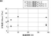
- FIG. 2 is a graph showing the measurement results of the Brookfield viscosity of the photosensitive pastes produced in Examples.
- FIG. 3A is a photograph showing planar shapes of various patterns formed by photolithography using a photosensitive paste containing glass frit coated with 3% by weight of tetraethoxysilane.
- FIG. 3B is a photograph showing the cross-sectional shape of the pattern of FIG. 3A.
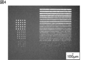
- FIG. 4 is a photograph showing planar shapes of various patterns formed by photolithography using a photosensitive paste containing glass frit coated with 3% by weight of tetraethoxysilane and polyvinylpyrrolidone.
- FIG. 5 is a photograph showing planar shapes of various patterns formed by photolithography using a photosensitive paste containing glass frit coated with 6% by weight of tetraethoxysilane and polyvinylpyrrolidone.
- FIG. 6A is a photograph showing planar shapes of various patterns formed by photolithography using a photosensitive paste containing glass frit coated with malonic acid.
- FIG. 6B is a photograph showing the cross-sectional shape of the pattern of FIG. 6A.
- the photosensitive paste of the present invention is not limited to the following configurations, and may be modified as appropriate without departing from the gist of the present invention.
- the present invention also includes a combination of a plurality of individual preferred configurations described below.
- the photosensitive paste of the present invention contains an inorganic powder containing elements that form polyvalent metal ions, an alkali-soluble polymer, a photosensitive monomer, and a photopolymerization initiator.
- the photosensitive paste of the present invention includes a photosensitive insulating paste used for forming an insulating layer or a photosensitive conductive paste used for forming a conductive layer. First, the case where the photosensitive paste of the present invention is a photosensitive insulating paste will be described.
- the "element that becomes a polyvalent metal ion" in the inorganic powder containing the element that becomes a polyvalent metal ion is not particularly limited as long as it is an element that becomes a metal ion having a valence of 2 or more. Metal elements of groups 14 and below are listed.
- the element that becomes the polyvalent metal ion is selected from the group consisting of alkaline earth metals, lanthanides, Ni, Cu, Pd, Al, Ti, Zr, Zn, Ga, Pb, Nb, Fe, Co and V. It is preferably at least one selected element.
- the inorganic powder containing the element that becomes the polyvalent metal ion is an insulator mainly composed of metal oxide crystals or an amorphous insulator mainly composed of SiO 2 .
- a high-strength insulator material can be obtained by firing a photosensitive paste containing an insulator mainly composed of metal oxide crystals or an amorphous insulator mainly composed of SiO 2 .
- Examples of insulators mainly composed of metal oxide crystals include TiO 2 , BaTiO, and NiO.
- amorphous insulators containing SiO 2 as a main component include SiO 2 —B 2 O 3 —Na 2 O—K 2 O—CaO—Al 2 O 3 glass powder, SiO 2 —B 2 O. 3 -Na 2 O--K 2 O--Al 2 O 3- based glass powder and the like.
- a glass powder having a crystallization point is preferable as the inorganic powder containing the element that becomes the polyvalent metal ion. This is because an insulator material with higher strength can be obtained by firing a photosensitive paste containing glass powder having a crystallization point.
- Glass powders having a crystallization point include, in addition to SiO 2 , B 2 O 3 , CaO, ZnO, Bi 2 O 3 , BaO, MgO, La 2 O 3 , Na 2 O, K 2 O and/or Glass powder containing Al 2 O 3 and the like, such as SiO 2 —B 2 O 3 —Al 2 O 3 —CaO glass powder, SiO 2 —B 2 O 3 —BaO—ZnO—Al 2 O 3 —MgO—La 2O3 - based glass powder, SiO2-B2O3-CaO-Al2O3-Na2O - K2O - based glass powder , and the like.
- the glass powder having the above crystallization point preferably has a softening point (Ts) and a crystallization point (Tc) adjusted according to the firing conditions. C. and Tc of 890.degree. C. are preferably used.
- the composition of the glass powder having the above crystallization point is not limited to the above examples as long as the glass powder has equivalent Ts and Tc.
- inorganic powders containing elements that become polyvalent metal ions may be used singly or in combination of two or more.
- a dispersion obtained by dispersing 1% by weight of the inorganic powder containing the element that becomes the polyvalent metal ion in pure water has a conductivity of 170 mS/m after 10 minutes from the time of dispersion. It is characterized by the following.
- the thickening of the photosensitive insulating paste and the deterioration of its alkali solubility are caused by acidic functional groups such as carboxyl groups possessed by the alkali-soluble polymer, polyvalent metal ions on the surface of the inorganic powder, and polyvalent metal ions eluted from the inorganic powder into the paste. It is generated by cross-linking of metal ions.
- the easiness of elution of polyvalent metal ions can be examined by the electrical conductivity when the target inorganic powder is dispersed in pure water.
- the photosensitive insulating paste of the present invention by using the above inorganic powder having a conductivity of 170 mS/m or less, the thickening of the photosensitive insulating paste caused by polyvalent metal ions and the insolubilization in an alkaline developer are prevented. can be suppressed.
- the conductivity is preferably 100 mS/m or less, more preferably 50 mS/m or less. On the other hand, the conductivity is, for example, 0 mS/m or more.
- the content of the element that becomes the polyvalent metal ion is less than 2.0 atomic % on the surface of the inorganic powder that contains the element that becomes the polyvalent metal ion.
- the amount of elements that become polyvalent metal ions on the surface of the inorganic powder is less than 2.0 atomic percent, the adsorption of the polyvalent metal ions on the surface of the inorganic powder to the alkali-soluble polymer is suppressed, and the viscosity of the photosensitive insulating paste increases. You can prevent it from rising. More preferably, the content of elements that form polyvalent metal ions is less than 1.0 atomic percent.
- the content of the element that becomes the polyvalent metal ion may be 0 atomic %.
- the content of elements that become polyvalent metal ions on the surface of the inorganic powder is a value qualitatively and quantitatively determined by X-ray photoelectron spectroscopy (XPS).
- the photosensitive insulating paste of the present invention it is preferable that at least part of the surface of the inorganic powder containing the element that becomes the polyvalent metal ion is covered with a ceramic film. At least part of the surface of the inorganic powder is covered with a ceramic film having high chemical stability, so that the inorganic powder does not adsorb the alkali-soluble polymer or the inorganic powder elutes polyvalent metal ions. can be suppressed. More preferably, the entire surface of the inorganic powder is covered with a ceramic film.
- the main component of the ceramic coating is preferably SiO2 . This is because SiO 2 has high chemical stability and can prevent adsorption of an alkali-soluble polymer to the inorganic powder and elution of polyvalent metal ions from the inorganic powder.
- the ceramic coating may contain elements other than SiO 2 that become the polyvalent metal ions, but the concentration thereof is preferably lower than that inside the inorganic powder.
- the content of SiO 2 which is the main component of the ceramic coating, is preferably 95% by mass or more, more preferably 98% by mass or more, and even more preferably 99% by mass or more.
- the ratio of the ceramic coating to the inorganic powder is preferably 2.5% by weight or more and 6.5% by weight or less relative to 100% by weight of the inorganic powder in terms of SiO2 . If the proportion of the ceramic coating is less than 2.5% by weight, the effect of preventing the adsorption of the alkali-soluble polymer to the inorganic powder and the elution of polyvalent metal ions may not be sufficient. Even if it exceeds, the adsorption of the alkali-soluble polymer to the inorganic powder and the effect of preventing the elution of polyvalent metal ions are not further improved, which is economically unfavorable.
- the ceramic coating may be a film containing an inorganic component such as SiO 2 and an organic substance, or may be an organic-inorganic hybrid film.
- the ceramic coating is an organic-inorganic hybrid film, the flexibility of the ceramic coating is improved, and the occurrence of cracks in the ceramic coating can be prevented.
- the organic material poly(2-methyloxazoline), poly(N,N-dimethylacrylamide), polyvinylpyrrolidone (PVP), etc. having an amidocarbonyl group can be used.
- the proportion of the organic substance in the ceramic coating is preferably 0.01% by weight or more and 1.0% by weight or less with respect to 100% by weight of the inorganic powder in terms of SiO2 .
- the difference between the refractive index N1 of the ceramic coating and the refractive index N2 of the mixture of the alkali-soluble polymer, the photosensitive monomer and the photopolymerization initiator is
- 0 may be satisfied.
- Examples of the method of covering the surface of the inorganic powder with a ceramic film include a method of coating the surface of the inorganic powder with a separately prepared ceramic material, a method of oxidizing the inorganic powder to form an oxide film of the inorganic powder on the surface, and a method of forming an oxide film of the inorganic powder on the surface.
- After attaching a solution that turns into an oxide by heat treatment etc. on the surface of the inorganic powder heat treatment under predetermined conditions so that the surface of the inorganic powder is covered with ceramics (for example, sol-gel method etc.)
- the sol-gel method is preferred because it facilitates the formation of an organic-inorganic hybrid film.
- the photosensitive insulating paste of the present invention preferably contains a filler (aggregate) in addition to the insulator mainly composed of metal oxide crystals and the amorphous insulator mainly composed of SiO 2 .
- the term "filler” means inorganic particles that do not soften even in the baking temperature range of the photosensitive paste (for example, 850° C. or higher and 950° C. or lower) and exist as particles.
- Various ceramic materials can be used as the filler, and examples thereof include crystalline fillers such as quartz, alumina, magnesia, spinel, silica, forsteride, steatite, and zirconia. You may use the said filler in combination of 1 type(s) or 2 or more types.
- the coefficient of thermal expansion of the insulating layer can be lowered to avoid formation defects and breakage during firing.
- Alumina and quartz are preferably used as the filler.
- Alumina has a refractive index close to that of an alkali-soluble polymer, and when alumina is used, the insulating layer has good strength and is excellent in resolution.
- quartz has a low refractive index and a refractive index close to that of alkali-soluble polymers, it is possible to control sinterability while maintaining resolution.
- the crystallinity of quartz is not particularly limited.
- the particle size of the inorganic powder and filler containing the element that becomes the polyvalent metal ion is preferably 0.1 ⁇ m or more and 5.0 ⁇ m or less. If the particle size is smaller than 0.1 ⁇ m, it may become difficult to disperse in the paste, and if the particle size is larger than 5.0 ⁇ m, the smoothness of the insulating layer and the groove shape formed after development become distorted. Sometimes. More preferably, it is 0.3 ⁇ m or more and 3.0 ⁇ m or less.
- the particle sizes of the inorganic powder and filler are values measured by a laser diffraction particle size distribution analyzer (LA960) manufactured by Horiba, Ltd.
- the total content of the inorganic powder containing the element that becomes the polyvalent metal ion and the filler is preferably 50% by weight or more and 80% by weight or less, and 60% by weight or more and 70% by weight or less. is more preferred.
- the content ratio of the inorganic powder containing the element that becomes the polyvalent metal ion and the filler is 40% by weight or more and 60% by weight or less when the total of the inorganic powder and the filler is 100% by weight. preferable.
- alkali-soluble polymer for example, a polymer such as an acrylic copolymer having a functional group such as a carboxyl group in a side chain can be used. Examples thereof include copolymers of ethylenically unsaturated compounds. Examples of unsaturated carboxylic acids include acrylic acid, methacrylic acid, maleic acid, fumaric acid, vinylacetic acid and acid anhydrides thereof. Examples of ethylenically unsaturated compounds other than unsaturated carboxylic acids include unsaturated carboxylic acid esters, and specific examples include acrylic acid esters such as methyl acrylate and ethyl acrylate, methyl methacrylate, and ethyl methacrylate.
- the acrylic copolymer having a carboxyl group in the side chain one into which unsaturated bonds of the following form are introduced may be used.
- An acrylic monomer having a functional group such as an epoxy group capable of reacting with the carboxy group of the side chain of the acrylic copolymer is added.
- a saturated or unsaturated polycarboxylic acid anhydride is further introduced.
- the acrylic copolymer having carboxy groups in side chains preferably has a weight average molecular weight (Mw) of 50000 or less and an acid value of 30 mgKOH/g or more and 150 mgKOH/g or less.
- the photosensitive monomer and photopolymerization initiator are not particularly limited, and known ones used for photosensitive paste can be used.
- the content of the alkali-soluble polymer, photosensitive monomer and photopolymerization initiator in the photosensitive insulating paste of the present invention is preferably 25% by weight or more, more preferably 30% by weight or more, and preferably 45% by weight. % or less, more preferably 35 wt % or less.
- the photosensitive insulating paste of the present invention may further contain organic solvents, organic dyes, and the like.
- organic solvent and organic dye known ones used for photosensitive paste can be used.
- the "elements that form polyvalent metal ions" in the photosensitive conductive paste of the present invention include the same as those exemplified for the above photosensitive insulating paste.
- metal is preferable as the inorganic powder containing the element that becomes the polyvalent metal ion.
- a base metal which has conventionally been a problem of thickening in the photosensitive paste, is suitable.
- an element that becomes the polyvalent metal ion is preferable, and consists of alkaline earth metals, lanthanides, Ni, Cu, Pd, Al, Ti, Zr, Zn, Ga, Pb, Nb, Fe, Co and V. At least one element selected from the group is more preferable. More preferably, the metal is Cu element or Ni element.
- the content of the element that becomes the polyvalent metal ion in the inorganic powder containing the element that becomes the polyvalent metal ion is preferably 0.01% by mass or more, and is preferably 0.1% by mass or more. More preferably, it may be 100% by mass.
- one kind of inorganic powder when the inorganic powder containing the element that becomes the polyvalent metal ion is a metal, one kind of inorganic powder may contain two or more kinds of metals. Two or more kinds of inorganic powders containing one kind may be contained. When two or more kinds of inorganic powder each containing one kind of different metal are contained, when the photosensitive conductor paste is fired, the different kinds of metals react with each other to form an alloy. When two or more metals are used in the photosensitive conductive paste of the present invention, it is preferable to use two or more inorganic powders containing different metals.
- the photosensitive conductive paste of the present invention may contain a bonding agent in addition to the inorganic powder containing the element that becomes the polyvalent metal ion.
- the bonding agent include, but are not limited to, SiO 2 —B 2 O 3 —Bi 2 O 3 -based glass powder.
- the total content of the inorganic powder containing the elements that become the polyvalent metal ions is preferably 60% by weight or more and 85% by weight or less, more preferably 65% by weight or more and 80% by weight or less. preferable.
- the particle size of the inorganic powder containing the element that becomes the polyvalent metal ion and the bonding agent is preferably 0.1 ⁇ m or more and 5.0 ⁇ m or less.
- the particle size of the inorganic powder and the bonding agent can be measured by the method described for the photosensitive insulating paste above.
- the content rate is the same as the value in the above photosensitive insulating paste.
- the types and aspects of the alkali-soluble polymer, photosensitive monomer, photopolymerization initiator, organic solvent and organic dye contained in the photosensitive conductive paste of the present invention are the same as those of the photosensitive insulating paste described above.
- the content of the alkali-soluble polymer, photosensitive monomer and photopolymerization initiator in the photosensitive conductor paste of the present invention is preferably 10% by weight or more, more preferably 15% by weight or more, and preferably 35% by weight. % or less, more preferably 20% by weight or less.
- the electronic component manufacturing method of the present invention includes a first electronic component manufacturing method or a second electronic component manufacturing method.
- a first method for manufacturing an electronic component according to the present invention comprises the steps of: forming an insulating layer using an insulating paste; forming a conductive layer on the insulating layer using a conductive paste; The paste is characterized by being the photosensitive insulating paste of the present invention.
- the insulating paste layer is an outer insulating layer located outside the conductor layer.
- grooves for the internal electrode pattern are formed by photolithography.
- a conductor paste layer is formed by filling and applying a conductor paste on the insulating paste layer having the grooves of the internal electrode pattern, and patterning is performed to form a conductor layer having a desired pattern by a photolithography method.
- a conductive paste layer that becomes an internal electrode is formed on the insulating paste layer.
- a desired coil pattern can be drawn on the photomask.
- the conductive paste used in the first electronic component manufacturing method of the present invention is not particularly limited, and for example, a known Ag paste or the like can be used, but the photosensitive conductive paste of the present invention may also be used.
- the photosensitive insulating paste of the present invention is applied onto the conductive paste layer to form an insulating paste layer that will serve as an internal insulating layer. form a layer.
- a paste laminate of an outer insulating layer, an insulating paste layer serving as an inner insulating layer, and a conductor paste layer is formed.
- an insulating paste layer is formed by repeatedly applying an insulating paste to the paste laminate by screen printing.
- the insulating paste layer is an outer insulating layer located outside the conductor layer.
- the obtained mother laminate is cut into a plurality of unfired laminates by dicing or the like.
- the cut unfired laminate is fired at 850° C. or higher and 950° C. or lower to obtain a laminate. Barreling or plating is applied to the obtained laminate, if necessary.
- An electronic component is completed through the above processes.
- a second method for manufacturing an electronic component according to the present invention comprises the steps of: forming an insulating layer using an insulating paste; forming a conductor layer on the insulating layer using a conductive paste;
- the paste is characterized by being the photosensitive conductive paste of the present invention.
- the second electronic component manufacturing method of the present invention can be performed in the same manner as the method described as an example of the first electronic component manufacturing method.
- a known insulating paste can be used, such as a known photosensitive glass paste.
- the conductive layer is formed using the photosensitive conductive paste of the present invention.
- Photosensitive paste Inorganic powder sol-gel coating
- the main component is SiO 2 —B 2 O 3 —Al 2 O 3 —CaO
- the average particle size is 1.0 ⁇ m
- the softening point (Ts) is A glass frit having a temperature of 800°C and a crystallization point (Tc) of 890°C was used. 20 g of this glass frit was added to 37.2 g of ethanol.
- TEOS tetraethoxysilane
- PVP polyvinylpyrrolidone
- a glass frit coated with TEOS or TEOS and PVP to form a ceramic coating was obtained.
- malonic acid was added instead of TEOS and PVP to obtain a glass frit having a malonic acid film formed on the surface.
- a photosensitive paste was prepared by blending each material in the following proportions. Specifically, each material was weighed, and after stirring the weighed material with a planetary mixer for 30 minutes, it was kneaded by passing it through a three-roll mill four times to prepare a photosensitive paste. Also, as a comparative example, a photosensitive paste was prepared using a non-coated glass frit in place of the coated glass frit.
- the refractive index of the mixture of the alkali-soluble polymer, the photosensitive monomer and the photopolymerization initiators (1) to (3) is about 1.5, and the refractive index of the ceramic film containing 3% by weight of TEOS is 1.55. rice field.
- the refractive index of the ceramic coating containing 3% by weight of TEOS and containing PVP and the refractive index of the ceramic coating containing 6% by weight of TEOS and containing PVP were 1.50 or more and 1.80 or less, respectively.
- FIG. 1 is a graph showing the electrical conductivity of a dispersion liquid in which 1% by weight of inorganic powder is dispersed in pure water.
- the glass frit coated with TEOS and the glass frit coated with TEOS and PVP had a low conductivity of 170 mS/m or less 10 minutes after dispersion.
- the uncoated glass frit (uncoated) and the glass frit coated with malonic acid (malonic acid coated) had a high electrical conductivity of 1200 mS/m or more 10 minutes after dispersion.
- the glass frit coated only with TEOS had the lowest conductivity.
- Table 1 The numerical values in Table 1 are not absolute values, but calculated so that the total of all compositions is 100 atomic %. "-" in Table 1 indicates that the value is below the detection limit. Note that Table 1 omits the description of trace amounts of atoms, so the total may not be 100 atomic %.
- the content of Ca which is an element that becomes a polyvalent metal ion, was 9 atomic %, but on the surface of the coated glass frit, The content of Ca was 1 atomic % or less.
- FIG. 2 is a graph showing the measurement results of the BF viscosity of the photosensitive pastes produced in Examples.
- the photosensitive paste containing the coated glass frit had a gradual increase in viscosity from the time of preparation until 10 days after preparation, but there was almost no increase in viscosity after that, even after 38 days from preparation. It could be used for screen printing and the like.
- the photosensitive paste containing the glass frit that was not coated gelled immediately after kneading with the organic component, and the viscosity could not be measured.
- the photosensitive paste containing glass frit coated with 3% by weight of TEOS and the glass frit coated with 3% by weight of TEOS and PVP are contained.
- the viscosity of the photosensitive paste used was relatively low.
- a photosensitive paste containing a coated glass frit was printed by screen printing to a thickness of 20 ⁇ m, dried in a safety oven, exposed through a photomask having openings of various sizes, and subjected to an alkaline aqueous solution. A pattern was formed by developing. A pattern was similarly formed on a photosensitive paste containing a glass frit coated with malonic acid. The results are shown in Figures 3A, 3B, 4, 5, 6A and 6B.
- FIG. 3A is a photograph showing planar shapes of various patterns formed by photolithography using a photosensitive paste containing glass frit coated with 3% by weight of TEOS.
- FIG. 3B is a photograph showing the cross-sectional shape of the pattern of FIG. 3A.
- FIG. 4 is a photograph showing planar shapes of various patterns formed by photolithography using a photosensitive paste containing glass frit coated with 3% by weight of TEOS and PVP.
- FIG. 5 is a photograph showing the planar shapes of various patterns formed by photolithography using a photosensitive paste containing glass frit coated with 6% by weight of TEOS and PVP.
- FIG. 6A is a photograph showing the planar shapes of various patterns formed by photolithography using a photosensitive paste containing glass frit whose surface is coated with malonic acid.
- FIG. 6B is a photograph showing the cross-sectional shape of the pattern of FIG. 6A.
- the photosensitive paste containing the glass frit coated with TEOS or TEOS and PVP was dissolved in an alkaline aqueous solution to form grooves.
- the unexposed areas were not dissolved in the alkaline aqueous solution and were swollen, and grooves were not formed.
Landscapes
- Chemical & Material Sciences (AREA)
- Physics & Mathematics (AREA)
- Engineering & Computer Science (AREA)
- Materials Engineering (AREA)
- General Chemical & Material Sciences (AREA)
- Geochemistry & Mineralogy (AREA)
- Life Sciences & Earth Sciences (AREA)
- Organic Chemistry (AREA)
- Chemical Kinetics & Catalysis (AREA)
- General Physics & Mathematics (AREA)
- Spectroscopy & Molecular Physics (AREA)
- Dispersion Chemistry (AREA)
- Ceramic Engineering (AREA)
- Materials For Photolithography (AREA)
- Inorganic Insulating Materials (AREA)
Priority Applications (3)
| Application Number | Priority Date | Filing Date | Title |
|---|---|---|---|
| JP2023552736A JPWO2023058351A1 (https=) | 2021-10-05 | 2022-08-25 | |
| CN202280066646.2A CN118043738A (zh) | 2021-10-05 | 2022-08-25 | 感光性糊剂和电子部件的制造方法 |
| US18/627,130 US20240248399A1 (en) | 2021-10-05 | 2024-04-04 | Photosensitive paste and method for producing electronic components |
Applications Claiming Priority (2)
| Application Number | Priority Date | Filing Date | Title |
|---|---|---|---|
| JP2021163960 | 2021-10-05 | ||
| JP2021-163960 | 2021-10-05 |
Related Child Applications (1)
| Application Number | Title | Priority Date | Filing Date |
|---|---|---|---|
| US18/627,130 Continuation US20240248399A1 (en) | 2021-10-05 | 2024-04-04 | Photosensitive paste and method for producing electronic components |
Publications (1)
| Publication Number | Publication Date |
|---|---|
| WO2023058351A1 true WO2023058351A1 (ja) | 2023-04-13 |
Family
ID=85803384
Family Applications (1)
| Application Number | Title | Priority Date | Filing Date |
|---|---|---|---|
| PCT/JP2022/031972 Ceased WO2023058351A1 (ja) | 2021-10-05 | 2022-08-25 | 感光性ペーストおよび電子部品の製造方法 |
Country Status (4)
| Country | Link |
|---|---|
| US (1) | US20240248399A1 (https=) |
| JP (1) | JPWO2023058351A1 (https=) |
| CN (1) | CN118043738A (https=) |
| WO (1) | WO2023058351A1 (https=) |
Cited By (2)
| Publication number | Priority date | Publication date | Assignee | Title |
|---|---|---|---|---|
| JP2024160601A (ja) * | 2023-05-01 | 2024-11-14 | 株式会社村田製作所 | 感光性絶縁ペーストおよび電子部品 |
| JPWO2025022694A1 (https=) * | 2023-07-26 | 2025-01-30 |
Citations (5)
| Publication number | Priority date | Publication date | Assignee | Title |
|---|---|---|---|---|
| JP2001281878A (ja) * | 2000-03-30 | 2001-10-10 | Kansai Research Institute | パターン形成方法及び感光性樹脂組成物 |
| JP2005241801A (ja) * | 2004-02-25 | 2005-09-08 | Kri Inc | 感光性グリーンシート及びそれを用いた複合グリーンシート |
| JP2006259717A (ja) * | 2005-02-21 | 2006-09-28 | Toray Ind Inc | ネガ型感光性ペーストおよびその製造方法、パターンの形成方法ならびに平面ディスプレイ用パネルの製造方法。 |
| JP2010210766A (ja) * | 2009-03-09 | 2010-09-24 | Jsr Corp | 感光性組成物、パターン形成方法およびフラットパネルディスプレイ用電極の製造方法 |
| JP2019105857A (ja) * | 2013-08-23 | 2019-06-27 | 味の素株式会社 | 感光性樹脂組成物 |
-
2022
- 2022-08-25 WO PCT/JP2022/031972 patent/WO2023058351A1/ja not_active Ceased
- 2022-08-25 JP JP2023552736A patent/JPWO2023058351A1/ja active Pending
- 2022-08-25 CN CN202280066646.2A patent/CN118043738A/zh active Pending
-
2024
- 2024-04-04 US US18/627,130 patent/US20240248399A1/en active Pending
Patent Citations (5)
| Publication number | Priority date | Publication date | Assignee | Title |
|---|---|---|---|---|
| JP2001281878A (ja) * | 2000-03-30 | 2001-10-10 | Kansai Research Institute | パターン形成方法及び感光性樹脂組成物 |
| JP2005241801A (ja) * | 2004-02-25 | 2005-09-08 | Kri Inc | 感光性グリーンシート及びそれを用いた複合グリーンシート |
| JP2006259717A (ja) * | 2005-02-21 | 2006-09-28 | Toray Ind Inc | ネガ型感光性ペーストおよびその製造方法、パターンの形成方法ならびに平面ディスプレイ用パネルの製造方法。 |
| JP2010210766A (ja) * | 2009-03-09 | 2010-09-24 | Jsr Corp | 感光性組成物、パターン形成方法およびフラットパネルディスプレイ用電極の製造方法 |
| JP2019105857A (ja) * | 2013-08-23 | 2019-06-27 | 味の素株式会社 | 感光性樹脂組成物 |
Cited By (5)
| Publication number | Priority date | Publication date | Assignee | Title |
|---|---|---|---|---|
| JP2024160601A (ja) * | 2023-05-01 | 2024-11-14 | 株式会社村田製作所 | 感光性絶縁ペーストおよび電子部品 |
| KR102936593B1 (ko) * | 2023-05-01 | 2026-03-10 | 가부시키가이샤 무라타 세이사쿠쇼 | 감광성 절연 페이스트 및 전자 부품 |
| JPWO2025022694A1 (https=) * | 2023-07-26 | 2025-01-30 | ||
| WO2025022694A1 (ja) * | 2023-07-26 | 2025-01-30 | 株式会社村田製作所 | 光結合器の製造方法、光結合器、光電変換回路モジュール及び光トランシーバ |
| JP7835298B2 (ja) | 2023-07-26 | 2026-03-25 | 株式会社村田製作所 | 光結合器の製造方法、光結合器、光電変換回路モジュール及び光トランシーバ |
Also Published As
| Publication number | Publication date |
|---|---|
| CN118043738A (zh) | 2024-05-14 |
| JPWO2023058351A1 (https=) | 2023-04-13 |
| US20240248399A1 (en) | 2024-07-25 |
Similar Documents
| Publication | Publication Date | Title |
|---|---|---|
| US20240248399A1 (en) | Photosensitive paste and method for producing electronic components | |
| JP3460657B2 (ja) | 多層配線回路板用感光性ガラスペースト及び多層配線回路板の製造方法 | |
| JPWO2018037729A1 (ja) | 感光性ガラスペースト、電子部品、及び、電子部品の製造方法 | |
| JP3668978B2 (ja) | 感光性絶縁ペースト | |
| JPH10112216A (ja) | 感光性導電ペースト、それを用いた電極およびその製造方法 | |
| JP3637286B2 (ja) | 焼成ジルコニア基材用導体ペースト | |
| US10390427B2 (en) | Photosensitive glass paste and electronic component | |
| JPH09142878A (ja) | 感光性導電ペーストおよび電極の製造方法 | |
| JP5421523B2 (ja) | 導電性樹脂組成物、それを用いて得られる導電性パターンを有する基板 | |
| JP5399193B2 (ja) | 感光性導電ペーストおよびその製造方法 | |
| JP3473353B2 (ja) | 絶縁体ペースト | |
| JP6051631B2 (ja) | 感光性ガラスペーストの製造方法 | |
| JP2917457B2 (ja) | 導体ペースト | |
| JP6718722B2 (ja) | 感光性導電ペースト形成用銀被覆樹脂粒子及びその製造方法並びに該粒子を含む感光性導電ペースト | |
| KR100653819B1 (ko) | 돌기체의 제조 방법 | |
| JP5858136B2 (ja) | 感光性ペースト | |
| JPH05311097A (ja) | 感光性絶縁ペ−スト | |
| CN102265373A (zh) | Pdp正面电极 | |
| KR100589339B1 (ko) | 디스플레이 장치용 감광성 도전 조성물 | |
| JP5538016B2 (ja) | 導電性樹脂組成物及び電子回路基板 | |
| JPH051963B2 (https=) | ||
| JPS62104004A (ja) | 抵抗材料 | |
| JP2000284471A (ja) | 感光性ペースト | |
| JPH0362287B2 (https=) | ||
| JPH0362284B2 (https=) |
Legal Events
| Date | Code | Title | Description |
|---|---|---|---|
| 121 | Ep: the epo has been informed by wipo that ep was designated in this application |
Ref document number: 22878222 Country of ref document: EP Kind code of ref document: A1 |
|
| WWE | Wipo information: entry into national phase |
Ref document number: 2023552736 Country of ref document: JP |
|
| WWE | Wipo information: entry into national phase |
Ref document number: 202280066646.2 Country of ref document: CN |
|
| NENP | Non-entry into the national phase |
Ref country code: DE |
|
| 122 | Ep: pct application non-entry in european phase |
Ref document number: 22878222 Country of ref document: EP Kind code of ref document: A1 |