WO2023058103A1 - Élément d'emballage hermétique et module d'élément - Google Patents
Élément d'emballage hermétique et module d'élément Download PDFInfo
- Publication number
- WO2023058103A1 WO2023058103A1 PCT/JP2021/036754 JP2021036754W WO2023058103A1 WO 2023058103 A1 WO2023058103 A1 WO 2023058103A1 JP 2021036754 W JP2021036754 W JP 2021036754W WO 2023058103 A1 WO2023058103 A1 WO 2023058103A1
- Authority
- WO
- WIPO (PCT)
- Prior art keywords
- wafer
- device wafer
- package element
- crystal orientation
- lid
- Prior art date
Links
- 239000013078 crystal Substances 0.000 claims abstract description 45
- 239000004065 semiconductor Substances 0.000 claims abstract description 32
- 238000007789 sealing Methods 0.000 claims description 20
- 229910000679 solder Inorganic materials 0.000 claims description 10
- 239000003566 sealing material Substances 0.000 claims description 9
- PXHVJJICTQNCMI-UHFFFAOYSA-N Nickel Chemical compound [Ni] PXHVJJICTQNCMI-UHFFFAOYSA-N 0.000 claims description 8
- 229910052759 nickel Inorganic materials 0.000 claims description 4
- 239000000758 substrate Substances 0.000 abstract description 11
- 208000032368 Device malfunction Diseases 0.000 abstract 1
- 239000000463 material Substances 0.000 description 11
- 230000000694 effects Effects 0.000 description 7
- XUIMIQQOPSSXEZ-UHFFFAOYSA-N Silicon Chemical compound [Si] XUIMIQQOPSSXEZ-UHFFFAOYSA-N 0.000 description 5
- 238000005336 cracking Methods 0.000 description 5
- 230000007257 malfunction Effects 0.000 description 5
- 229910052710 silicon Inorganic materials 0.000 description 5
- 239000010703 silicon Substances 0.000 description 5
- 238000003384 imaging method Methods 0.000 description 4
- 238000009413 insulation Methods 0.000 description 3
- 238000012986 modification Methods 0.000 description 3
- 230000004048 modification Effects 0.000 description 3
- 238000003776 cleavage reaction Methods 0.000 description 2
- 239000011248 coating agent Substances 0.000 description 2
- 238000000576 coating method Methods 0.000 description 2
- 239000012141 concentrate Substances 0.000 description 2
- 230000006378 damage Effects 0.000 description 2
- 238000010586 diagram Methods 0.000 description 2
- 238000005516 engineering process Methods 0.000 description 2
- 238000007747 plating Methods 0.000 description 2
- 230000007017 scission Effects 0.000 description 2
- 238000002834 transmittance Methods 0.000 description 2
- 230000001133 acceleration Effects 0.000 description 1
- 239000000853 adhesive Substances 0.000 description 1
- 230000001070 adhesive effect Effects 0.000 description 1
- 239000003463 adsorbent Substances 0.000 description 1
- 239000003990 capacitor Substances 0.000 description 1
- 238000001514 detection method Methods 0.000 description 1
- 230000007613 environmental effect Effects 0.000 description 1
- 239000007789 gas Substances 0.000 description 1
- 238000003331 infrared imaging Methods 0.000 description 1
- 238000004519 manufacturing process Methods 0.000 description 1
- 238000000034 method Methods 0.000 description 1
- 239000001301 oxygen Substances 0.000 description 1
- 229910052760 oxygen Inorganic materials 0.000 description 1
- 238000000206 photolithography Methods 0.000 description 1
- 230000035945 sensitivity Effects 0.000 description 1
- 229920001187 thermosetting polymer Polymers 0.000 description 1
Images


Classifications
-
- H—ELECTRICITY
- H01—ELECTRIC ELEMENTS
- H01L—SEMICONDUCTOR DEVICES NOT COVERED BY CLASS H10
- H01L23/00—Details of semiconductor or other solid state devices
- H01L23/02—Containers; Seals
-
- H—ELECTRICITY
- H01—ELECTRIC ELEMENTS
- H01L—SEMICONDUCTOR DEVICES NOT COVERED BY CLASS H10
- H01L23/00—Details of semiconductor or other solid state devices
- H01L23/02—Containers; Seals
- H01L23/10—Containers; Seals characterised by the material or arrangement of seals between parts, e.g. between cap and base of the container or between leads and walls of the container
-
- H—ELECTRICITY
- H01—ELECTRIC ELEMENTS
- H01L—SEMICONDUCTOR DEVICES NOT COVERED BY CLASS H10
- H01L25/00—Assemblies consisting of a plurality of individual semiconductor or other solid state devices ; Multistep manufacturing processes thereof
- H01L25/03—Assemblies consisting of a plurality of individual semiconductor or other solid state devices ; Multistep manufacturing processes thereof all the devices being of a type provided for in the same subgroup of groups H01L27/00 - H01L33/00, or in a single subclass of H10K, H10N, e.g. assemblies of rectifier diodes
- H01L25/04—Assemblies consisting of a plurality of individual semiconductor or other solid state devices ; Multistep manufacturing processes thereof all the devices being of a type provided for in the same subgroup of groups H01L27/00 - H01L33/00, or in a single subclass of H10K, H10N, e.g. assemblies of rectifier diodes the devices not having separate containers
- H01L25/065—Assemblies consisting of a plurality of individual semiconductor or other solid state devices ; Multistep manufacturing processes thereof all the devices being of a type provided for in the same subgroup of groups H01L27/00 - H01L33/00, or in a single subclass of H10K, H10N, e.g. assemblies of rectifier diodes the devices not having separate containers the devices being of a type provided for in group H01L27/00
-
- H—ELECTRICITY
- H01—ELECTRIC ELEMENTS
- H01L—SEMICONDUCTOR DEVICES NOT COVERED BY CLASS H10
- H01L25/00—Assemblies consisting of a plurality of individual semiconductor or other solid state devices ; Multistep manufacturing processes thereof
- H01L25/03—Assemblies consisting of a plurality of individual semiconductor or other solid state devices ; Multistep manufacturing processes thereof all the devices being of a type provided for in the same subgroup of groups H01L27/00 - H01L33/00, or in a single subclass of H10K, H10N, e.g. assemblies of rectifier diodes
- H01L25/04—Assemblies consisting of a plurality of individual semiconductor or other solid state devices ; Multistep manufacturing processes thereof all the devices being of a type provided for in the same subgroup of groups H01L27/00 - H01L33/00, or in a single subclass of H10K, H10N, e.g. assemblies of rectifier diodes the devices not having separate containers
- H01L25/07—Assemblies consisting of a plurality of individual semiconductor or other solid state devices ; Multistep manufacturing processes thereof all the devices being of a type provided for in the same subgroup of groups H01L27/00 - H01L33/00, or in a single subclass of H10K, H10N, e.g. assemblies of rectifier diodes the devices not having separate containers the devices being of a type provided for in group H01L29/00
-
- H—ELECTRICITY
- H01—ELECTRIC ELEMENTS
- H01L—SEMICONDUCTOR DEVICES NOT COVERED BY CLASS H10
- H01L25/00—Assemblies consisting of a plurality of individual semiconductor or other solid state devices ; Multistep manufacturing processes thereof
- H01L25/18—Assemblies consisting of a plurality of individual semiconductor or other solid state devices ; Multistep manufacturing processes thereof the devices being of types provided for in two or more different subgroups of the same main group of groups H01L27/00 - H01L33/00, or in a single subclass of H10K, H10N
Definitions
- the present disclosure relates to hermetic package devices and device modules.
- MEMS devices which are devices in which sensors, actuators, etc. are integrated on a silicon substrate or the like by microfabrication technology, have been put to practical use.
- MEMS devices include infrared sensors, gyro sensors, acceleration sensors, and the like.
- an uncooled infrared sensor converts incident infrared rays into heat so as to be called a thermal sensor. Therefore, it has a structure that reads changes in the temperature of the object as changes in electrical signals, and has a heat insulating structure in which the sensor (imaging device) is thermally isolated from the substrate in order to increase the detection sensitivity.
- the infrared sensor is placed in a sealed vacuum space, that is, placed inside a vacuum package in order to improve heat insulation.
- low-oxygen-containing silicon or ZnS with high infrared transmittance should be used, or an anti-reflection coating (AR coat: Anti-Reflection Coating) should be formed. It has been known.
- a wafer level package has been proposed in which a device wafer on which MEMS devices are manufactured and a lid wafer facing the device wafer are bonded in a vacuum atmosphere to form a plurality of vacuum packages. (See Patent Document 1, for example).
- An airtight package element configured as a wafer level package inevitably has a structure in which the bonding pads for electrical connection provided on the device wafer are exposed from the lid wafer, and the bonding part of the device wafer protrudes from the lid wafer. Then, the stress concentrates on the part where the device wafer and the sealing portion on the overhanging side of the device wafer are in contact with each other.
- the present disclosure discloses a technique for solving the above problems, and aims to prevent device wafer cracking and obtain a highly reliable airtight package element.
- the airtight package element includes a device wafer having a mounting surface provided with terminals for electrically connecting a semiconductor circuit and the semiconductor circuit to the outside, a lid wafer disposed facing the mounting surface, and a device wafer. and a sealing part interposed between the device wafer and the lid wafer and forming a vacuum atmosphere sealed space for housing the semiconductor circuit between the device wafer and the lid wafer, the device wafer projecting from the lid wafer in a plan view.
- the terminal is provided in the overhanging region
- the seal portion is polygonal in plan view
- the sides of the polygon facing the overhanging region are formed in a direction different from the crystal orientation of the device wafer. do.
- An element module includes a device wafer having a mounting surface provided with terminals for electrically connecting a semiconductor circuit and the semiconductor circuit to the outside, a lid wafer disposed facing the mounting surface, and a device wafer.
- a sealing portion interposed between the lid wafer and the device wafer and forming a sealed space of a vacuum atmosphere for accommodating the semiconductor circuit is provided between the device wafer and the lid wafer.
- the terminal is provided in the overhanging region
- the seal portion is polygonal in plan view, and the side of the polygon facing the overhanging region is formed in a direction different from the crystal orientation of the device wafer. It is characterized by comprising an airtight package element, a circuit board, the airtight package element mounted on the circuit board, and an electronic component mounted on the circuit board and electrically connected to the terminals.
- the stress at the portion where the sealing portion and the device wafer are in contact can be relaxed, cracking of the device wafer can be prevented, and a highly reliable hermetic package element or element module can be obtained.
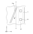
- FIG. 2 is a transparent plan view of a lid wafer portion of the hermetic package element according to the first embodiment;
- FIG. 2 is a cross-sectional view corresponding to line II-II of FIG. 1;
- FIG. FIG. 2 is a partially enlarged view enlarging a region A in FIG. 1;
- FIG. 11 is a transparent plan view of a lid wafer portion of the hermetic package element according to the second embodiment;
- FIG. 11 is a transparent plan view of a lid wafer portion of an airtight package element according to a modification of the second embodiment;
- FIG. 11 is a transparent plan view of a lid wafer portion of an airtight package element according to a third embodiment;
- 3 is a diagram showing the relationship between sides 13 and crystal orientations of the device wafer 1.
- FIG. 11 is a transparent plan view of a lid wafer portion of an airtight package element according to a fourth embodiment;
- FIG. 11 is a plan view of an element module according to Embodiment 5;
- FIG. 10 is a cross-sectional view corresponding to line IX-IX in FIG. 9;
- FIG. 4 is a transparent plan view of a lid wafer portion of a conventional hermetic package device;
- FIG. 1 is a transparent plan view of a lid wafer portion of an airtight package device.
- FIG. 2 is a sectional view corresponding to line II-II of FIG.
- FIG. 3 is a partially enlarged view enlarging a region A in FIG. 1.
- FIG. 1 is a transparent plan view of a lid wafer portion of an airtight package device.
- FIG. 2 is a sectional view corresponding to line II-II of FIG.
- FIG. 3 is a partially enlarged view enlarging a region A in FIG. 1.
- a silicon substrate is processed so that its crystal orientations are parallel and orthogonal to the substrate surface.
- Both the device wafer 1 and the lid wafer 2 are manufactured by processing a silicon substrate. 1 to 9 and 11, the device wafer 1 and the lid wafer 2 are arranged such that their crystal orientations are parallel to the X-axis or Y-axis shown in the drawings.
- the outer shape of the device wafer 1 and the lid wafer 2 is a rectangle parallel to the X-axis or the Y-axis. As shown in FIGS.
- the device wafer 1 and the lid wafer 2 are flat with each other in a plan view, that is, when viewed from the Z-axis direction, so that a part of the device wafer 1 protrudes from the lid wafer 2 .
- the surfaces are made parallel and opposed to each other, and are joined by a seal portion 10 .
- the sealing portion 10 includes a first base layer 31 patterned on the mounting surface 1a of the device wafer 1, a second base layer 32 patterned on the surface of the lid wafer 2 facing the mounting surface 1a, and a first It is composed of a sealing material layer 33 interposed between the base layer 31 and the second base layer 32 and filling the space therebetween. Both the first underlayer 31 and the second underlayer 32 are patterned continuously without a break, and are sometimes called a sealing ring.
- the sealing material layer 33 is made of a solder material. However, the solder material has low wettability to the surface (mounting surface 1a) of the device wafer 1 and the surface of the lid wafer 2, and it is difficult to bond the device wafer 1 and the lid wafer 2 as they are.
- the first base layer 31 and the second base layer 32 have good wettability with the solder material and are compatible with each wafer so as to function as an intermediate layer for bonding each wafer and the sealing material layer 33 .
- It is made of a material with good adhesion.
- Such materials are, for example, lead-free solder for the sealing material layer 33 and nickel for the material of the first underlayer 31 and the second underlayer 32, but are not limited to these, and any material may be used. can be selected.
- lead-free solder is preferable because high-temperature solder and AuSn solder impose a high environmental burden and are expensive.
- the sealed space 22 surrounded by the device wafer 1, the lid wafer 2, and the sealing section 10 is held in a vacuum atmosphere.
- the seal portion 10 is formed with a thickness of 50 to 150 ⁇ m, and has a thickness of 100 ⁇ m in this embodiment.
- the inside of the sealed space 22 is called a vacuum atmosphere, it does not mean a complete vacuum, and the degree of vacuum required to maintain heat insulation may be sufficient.
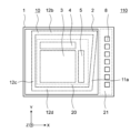
- an infrared imaging element 3, a scanning circuit 4, and a readout circuit 5 are arranged in a region 20 inside the sealing portion 10 of the mounting surface 1a of the device wafer 1.
- the MEMS and semiconductor elements arranged in the region 20, including the imaging device 3, the scanning circuit 4, and the readout circuit 5, are referred to as a semiconductor circuit 7.
- FIG. The semiconductor circuit 7 is arranged inside a sealed space 22 which is kept in a vacuum atmosphere with excellent heat insulation, thereby increasing the reliability of the infrared sensor.
- a gas adsorbent (not shown) called a getter for maintaining the degree of vacuum is formed on the lid wafer 2 at a portion surrounded by the second underlayer 32 .
- a recess may be formed to increase the vacuum volume.
- the outer surface of the lid wafer 2 may be coated with an anti-reflection film called an AR coat for improving infrared transmittance.
- the device wafer 1 has a region overhanging from the lid wafer 2 , and this overhanging region is referred to as an overhanging region 21 .
- a plurality of terminals 8 (bonding pads) for electrically connecting the semiconductor circuit 7 to the outside are provided on the mounting surface 1a of the projecting region 21 .
- the terminals 8 and the semiconductor circuit 7 are electrically connected via wiring (not shown) provided on the mounting surface 1a.
- the terminal 8 configured in this way functions as an element module 200 (FIGS. 9 and 10), which will be described later, by being electrically connected to a circuit board or the like (not shown) with a wire or the like.
- the shape of the seal portion 10 is a polygon having sides 11a, 11b, 11c, and 11d.
- the crystal orientations of the device wafer 1 and the lid wafer 2 are parallel to the X-axis or the Y-axis.
- none of the sides of the seal portion 10 are parallel to the X-axis or the Y-axis, and are formed in directions different from the crystal orientations of the device wafer 1 and the lid wafer 2 .
- the auxiliary line yy shown in FIG. 3 is a straight line parallel to the Y-axis.
- the side 11a facing the projecting region 21 and the auxiliary line yy form an angle ⁇ . where the angle ⁇ is neither zero degrees nor 90 degrees.
- a point D in FIG. 2 is a contact point between the device wafer 1 and the sealing portion 10 on the side where the device wafer 1 protrudes from the lid wafer 2 .
- the airtight package element 100 is once heated to a high temperature in a vacuum atmosphere to melt the solder material of the sealing material layer 33, and then the temperature is lowered to form a sealed space 22 between the device wafer 1 and the lid wafer 2.
- the coefficient of linear expansion of the solder used for the sealing material layer 33 is greater than the coefficient of linear expansion of silicon used for the device wafer 1 and the lid wafer 2 . Therefore, in normal use, residual stress acts on the point D from the point D in the direction of the lid wafer (+Z direction) and from the point D in the direction of the semiconductor circuit (-X direction).
- FIG. 11 is a transparent plan view of a lid wafer portion of a conventional hermetic package element 900.
- FIG. In conventional airtight package devices, structures such as devices, circuits, and wiring formed on a semiconductor substrate are formed along the crystal orientation of the semiconductor substrate.
- a seal portion 10 for bonding the device wafer and the lid wafer is also arranged along the crystal orientation of the device wafer. Description will be made with reference to FIG. 2 as a cross-sectional view corresponding to line II-II of FIG.
- a residual stress similar to the residual stress acting on the point D acts on the entire end 16f on the right side of the drawing of the side 16a. That is, the residual stress acting on the side 16a concentrates along the edge 16f.
- the edge 16f is parallel to the Y-axis in the drawing and coincides with the cleavage direction of the device wafer, that is, the crystal orientation.
- the side 11a is arranged so as to be inclined at an angle ⁇ with respect to the crystal orientation of the device wafer 1 . That is, the direction in which the concentrated stress acts is shifted by an angle ⁇ from the crystal orientation, and the stress concentration is relieved. Therefore, malfunction of the device due to cracking of the device wafer 1, destruction of circuits arranged on the device wafer 1, or disconnection of wiring can be avoided. Thereby, a highly reliable hermetic package element can be obtained.
- the angle ⁇ is preferably more than 0 degree and 5 degrees or less, more preferably 1 degree or more and 3 degrees or less.
- the sealing rings of the device wafer and the lid wafer in this embodiment are formed by electrolytic nickel plating.
- the width of the sealing ring by electrolytic nickel plating is formed using the existing photolithography technology, and it is possible to form an arbitrary angle ⁇ by the pattern of the photomask.
- the hermetic package element 100 includes the device wafer 1 provided with the semiconductor circuit 7 and the terminals 8 for electrically connecting the semiconductor circuit 7 to the outside on the mounting surface 1a, and the mounting surface 1a. and a seal interposed between the device wafer 1 and the lid wafer 2 to form a sealed space 22 with a vacuum atmosphere containing the semiconductor circuit 7 between the device wafer 1 and the lid wafer 2. a part 10;
- the device wafer 1 has an overhang region 21 overhanging from the lid wafer 2 in plan view.
- the terminal 8 is provided in the projecting region 21 .
- the seal portion 10 has a polygonal shape in plan view, and the side 11 a facing the projecting region 21 is formed in a direction different from the crystal orientation of the device wafer 1 . Further, the angle ⁇ between the side 11a facing the projecting region 21 and the crystal orientation of the device wafer 1 is preferably more than 0 degrees and 5 degrees or less, more preferably 1 degree or more and 3 degrees or less.
- the side 11a is arranged so as to be inclined at an angle ⁇ with respect to the crystal orientation of the device wafer 1, the direction in which concentrated stress acts is shifted from the crystal orientation by the angle ⁇ .
- the stress concentration is relieved, so that the device wafer 1 can be cracked, the circuits arranged on the device wafer 1 can be broken, or the device can be prevented from malfunctioning due to the disconnection of the wiring. There is an effect that it can be obtained.
- Embodiment 2 A hermetic package element 110 according to the second embodiment will be described.
- all sides of the seal portion 10 are configured so as not to be parallel to the crystal orientation of the device wafer 1 .
- the side 11a of the seal portion 10 facing the projecting region 21 is not parallel to the crystal orientation, and the other sides are parallel to the crystal orientation.
- FIG. 4 is a transparent plan view of the lid wafer portion of the airtight package element 110 according to the second embodiment.
- the seal portion 10 of the hermetic package element 110 according to the second embodiment has sides 11a, 12b, 12c, and 12d.
- the material, cross-sectional structure, etc. of the sides 12b, 12c and 12d are the same as those of the sides 11a, 11b, 11c and 11d.
- Sides 12b, 12c, and 12d correspond to sides 11b, 11c, and 11d in the first embodiment, respectively, but are arranged parallel to the X-axis or Y-axis as in the conventional hermetic package element. That is, the sides 12b, 12c, and 12d are arranged parallel to the crystal orientation of the device wafer 1.
- the device wafer 1 does not protrude from the lid wafer 2 where the sides 12b, 12c, and 12d face, and the sides 12b, 12c, and 12d do not face the protruding region.
- the wiring that electrically connects the semiconductor circuit 7 on the device wafer 1 to the outside is arranged so as not to cross the seal portion 10 at a portion other than the side 11 a facing the projecting region 21 .
- the second embodiment there is no fear of malfunction of the device due to concentration of stress, cracking of the device wafer 1, destruction of circuits arranged on the device wafer 1, or disconnection of wiring.
- the sides 12b, 12c, and 12d of the sealing portion 10, which are not sealed, are formed in the same direction as the crystal orientation of the device wafer 1 as in the conventional hermetic package.
- Other parts are the same as those in the first embodiment, and description thereof is omitted.
- the size of the hermetic package element 110 can be made smaller than in the first embodiment. This is effective when the size of the hermetic package element 110 cannot be increased by inclining all sides of the sealing ring due to device layout restrictions.
- FIG. 5 is a transparent plan view of a lid wafer portion of an airtight package element 111 according to a modification of the second embodiment.
- the side of the seal portion 10 facing the projecting region 21 in the airtight package element 111 consists of a side 11a that is not parallel to the crystal orientation, and sides 12e and 12f that are continuous with the side 11a and parallel to the crystal orientation.
- the length of side 11a is longer than the length of sides 12e and 12f. In this way, even if a portion of the side of the seal portion 10 facing the overhanging region 21 is parallel to the crystal orientation, most of the portion is not parallel to the crystal orientation. Note that it has a certain effect on
- Embodiment 3 An airtight package element 120 according to the third embodiment will be described with reference to FIGS. 6 and 7.
- the side of the seal portion 10 facing the projecting region 21 is a single side 11a.
- a plurality of sides of the seal portion 10 facing the projecting region 21 are arranged in a zigzag pattern.
- FIG. 6 is a transparent plan view of the lid wafer portion of the hermetic package element 120 according to the third embodiment.
- the sealing portion 10 of the airtight package element 120 according to the third embodiment has sides 12b, 12c, 12d and a side 13 facing the projecting region 21.
- the side 13 is continuous and consists of a plurality of sides 13a, 13b, 13c arranged in a zigzag pattern.
- the sides 12b, 12c, 12d and the side 13 are made of the same material and have the same cross-sectional structure.
- the side 13 is a side of the seal portion 10 facing the overhanging region 21 like the side 11a. It is a side that is not parallel to the orientation.
- FIG. 7 is a diagram showing the relationship between the side 13 and the crystal orientation of the device wafer 1. As shown in FIG. In FIG. 7, parts other than those necessary for explanation are not shown and are omitted.
- the two auxiliary lines yy shown in FIG. 7 are straight lines parallel to the Y-axis, that is, the auxiliary lines yy indicate the same direction as the crystal orientation. None of the sides 13a, 13b, and 13c are arranged so as not to be parallel to the crystal orientation (the X direction and the Y direction on the paper surface).
- the angles formed by the sides 11a, 11b, 11c and the auxiliary line yy are ⁇ 1, ⁇ 2, ⁇ 3, respectively.
- the absolute values of ⁇ 1, ⁇ 2, and ⁇ 3 may be the same or different.
- ⁇ 1 and ⁇ 3 measure angles clockwise from the auxiliary line yy, while ⁇ 2 measures angles counterclockwise from the auxiliary line yy. That is, it can be said that the signs of ⁇ 1 and ⁇ 3 and ⁇ 2 are different, or zigzag with respect to the auxiliary line yy (crystal orientation).
- W in FIG. 7 is the width occupied by the side 13 in the X-axis direction.
- the lengths of sides 13a, 13b, and 13c in Embodiment 3 are set to 1/3 of the length of side 11a in Embodiment 1, and the angle ⁇ in Embodiment 1 and the angle in Embodiment 3
- W can be reduced to 1/3 of the width of the side 11a in the X-axis direction in the first embodiment. That is, by forming a plurality of zigzag sides of the seal portion 10 facing the projecting region 21 as shown in the third embodiment, an increase in the size of the hermetic package element can be suppressed. Description of other parts is omitted.
- the airtight package element 120 includes the device wafer 1 provided with the semiconductor circuit 7 and the terminals 8 for electrically connecting the semiconductor circuit 7 and the outside on the mounting surface 1a, and the mounting surface 1a. and a lid wafer 2 arranged to face the device wafer 1 and the lid wafer 2, forming a sealed space 22 with a vacuum atmosphere for housing the semiconductor circuit 7 between the device wafer 1 and the lid wafer 2. and a seal portion 10 .
- the device wafer 1 has an overhang region 21 overhanging from the lid wafer 2 in plan view.
- the terminal 8 is provided in the projecting region 21 .
- the sealing portion 10 has a polygonal shape in plan view, and has a side 13 a facing an overhanging region 21 formed in a direction different from the crystal orientation of the device wafer 1 .
- the side 13 is sides 13a, 13b, and 13c arranged in a zigzag pattern.
- the same effect as the hermetic package element 100 shown in the first embodiment can be obtained.
- the sides of the seal portion 10 facing the projecting region 21 are arranged in a zigzag manner, thereby suppressing an increase in the size of the airtight package element. It also has the effect of being able to
- the side of the seal portion 10 facing the overhanging region 21 is divided into three and arranged in a zigzag pattern, but it may be divided into two and arranged in a V shape. Also, the number of divisions may be four or more, and the division lengths may not be equal. In addition, even if a plurality of sides arranged in a zigzag or V shape are accompanied by sides arranged parallel to the crystal orientation, an increase in the size of the hermetic package element can be suppressed.
- Embodiment 4 A hermetic package element 130 according to the fourth embodiment will be described with reference to FIG. In Embodiments 1 to 3, the case where the projecting region 21 is on one side of the hermetic package element has been described, but in Embodiment 4, the case where the hermetic package element has projecting regions on two sides will be described.
- FIG. 8 is a transparent plan view of the lid wafer portion of the airtight package element 130 according to the fourth embodiment.
- the device wafer 1 has two protruding portions from the lid wafer 2 .
- One is the projecting region 21 as in the first embodiment, and the other is the projecting region 21a.
- the projecting region 21a which is the second projecting region, is arranged on the opposite side of the projecting region 21, which is the first projecting region, with the closed space 22 interposed therebetween.
- a plurality of terminals 8 (bonding pads) electrically connected to the imaging device 3, the scanning circuit 4, and the readout circuit 5 via wiring (not shown) are also arranged on the mounting surface 1a of the projecting region 21a.
- the shape of the seal portion 10 in Embodiment 4 is a polygon having sides 11a, 12b, 14c, and 12d.
- the side 11a faces the projecting region 21 and is formed in a direction different from the crystal orientation.
- Sides 12b and 12d are formed in the same direction as the crystal orientation.
- Side 14 c faces projecting region 21 a and is formed in a direction different from the crystal orientation of device wafer 1 .
- the material, cross-sectional structure, etc. of the side 14c are the same as those of the sides 11a, 12b, and 12d. Description of other parts is omitted.
- the hermetic package element 130 according to the fourth embodiment configured as described above also has the same stress relaxation effect as the first embodiment.
- the first projecting region 21 and the second projecting region 21a are arranged on opposite sides of the closed space 22, they may be arranged adjacent to each other, for example, on the sides 11a and 12b. Also, the overhang areas may be arranged on three or more sides.
- Embodiment 5 describes an element module in which the airtight package element described in Embodiments 1 to 4 is mounted on a circuit board together with other electronic components.
- 9 and 10 are for explaining the configuration of the element module according to the fifth embodiment.
- 9 is a plan view of an element module according to Embodiment 5
- FIG. 10 is a cross-sectional view corresponding to line XX of FIG.
- the configuration of the airtight package element portion will be described using the airtight package element 100, it is the same as in any one of the first to fourth embodiments, and any one of the airtight package elements 110, 111, 120 or 130 can be used instead. good. 1 to 8 are used while omitting the description of the same parts.
- an element module 200 includes an airtight package element 100, components 204 such as resistors and capacitors, and semiconductor devices 205 on a mounting surface 203 of a circuit board 202.
- the electronic component 206 including is mounted. Then, the mounted electronic component is electrically connected to the terminals 8 of the hermetic package element 100 by wire bonding or the like (not shown) to form an element module 200 .
- the hermetic package element 100 and the electronic component 206 are fixed to the circuit board 202 using a thermosetting conductive adhesive 208 .
- other components, covers, and the like necessary for configuring the element module 200 are provided.
- the element module 200 according to Embodiment 5 includes the airtight package element described in any one of Embodiments 1 to 4, and is robust against vibration and impact.
- the airtight package element 100 that functions as an infrared sensor is used, it is possible to obtain an infrared sensor that is robust against vibration and impact, prevents cracking of the device wafer, and has high reliability.
- the present disclosure is not limited to the above-described examples, and includes various modifications.
- the above embodiments have been described in detail to facilitate understanding of the present disclosure, and are not necessarily limited to those having all the described configurations.
- it is possible to replace part of the configuration of one embodiment with the configuration of another embodiment and it is also possible to add the configuration of another embodiment to the configuration of one embodiment.
Landscapes
- Engineering & Computer Science (AREA)
- Microelectronics & Electronic Packaging (AREA)
- Power Engineering (AREA)
- Physics & Mathematics (AREA)
- Condensed Matter Physics & Semiconductors (AREA)
- General Physics & Mathematics (AREA)
- Computer Hardware Design (AREA)
- Solid State Image Pick-Up Elements (AREA)
- Piezo-Electric Or Mechanical Vibrators, Or Delay Or Filter Circuits (AREA)
Abstract
La présente divulgation concerne, dans un élément d'emballage hermétique classique, une partie d'étanchéité joignant une tranche de dispositif et une tranche de couvercle formée le long d'une orientation cristalline d'un substrat semi-conducteur. Pour cette raison, des problèmes de dysfonctionnements de dispositif surviennent en raison de la rupture de la tranche de dispositif, des circuits disposés sur la tranche de dispositif étant brisés, et du câblage étant coupé. Un élément d'emballage hermétique 100 selon la présente divulgation est caractérisé en ce que : une tranche de dispositif 1 comprend une région saillante 21 qui fait saillie à partir d'une tranche de couvercle 2 dans une vue en plan ; une partie d'étanchéité 10 a une forme polygonale dans une vue en plan ; et un côté 11a de la forme polygonale qui fait face à la région saillante 21 est formé dans une direction différente de l'orientation cristalline de la tranche de dispositif 1.
Priority Applications (3)
| Application Number | Priority Date | Filing Date | Title |
|---|---|---|---|
| CN202180102852.XA CN118043280A (zh) | 2021-10-05 | 2021-10-05 | 气密封装元件以及元件模块 |
| PCT/JP2021/036754 WO2023058103A1 (fr) | 2021-10-05 | 2021-10-05 | Élément d'emballage hermétique et module d'élément |
| JP2023552427A JPWO2023058103A1 (fr) | 2021-10-05 | 2021-10-05 |
Applications Claiming Priority (1)
| Application Number | Priority Date | Filing Date | Title |
|---|---|---|---|
| PCT/JP2021/036754 WO2023058103A1 (fr) | 2021-10-05 | 2021-10-05 | Élément d'emballage hermétique et module d'élément |
Publications (1)
| Publication Number | Publication Date |
|---|---|
| WO2023058103A1 true WO2023058103A1 (fr) | 2023-04-13 |
Family
ID=85804009
Family Applications (1)
| Application Number | Title | Priority Date | Filing Date |
|---|---|---|---|
| PCT/JP2021/036754 WO2023058103A1 (fr) | 2021-10-05 | 2021-10-05 | Élément d'emballage hermétique et module d'élément |
Country Status (3)
| Country | Link |
|---|---|
| JP (1) | JPWO2023058103A1 (fr) |
| CN (1) | CN118043280A (fr) |
| WO (1) | WO2023058103A1 (fr) |
Citations (3)
| Publication number | Priority date | Publication date | Assignee | Title |
|---|---|---|---|---|
| JPH05335435A (ja) * | 1992-05-29 | 1993-12-17 | Kyocera Corp | 半導体素子収納用パッケージ |
| JP2003133535A (ja) * | 2001-10-22 | 2003-05-09 | Kyocera Corp | 撮像素子収納用パッケージ |
| JP2020017717A (ja) * | 2018-07-11 | 2020-01-30 | 三菱電機株式会社 | パッケージ素子の製造方法およびパッケージ素子 |
-
2021
- 2021-10-05 CN CN202180102852.XA patent/CN118043280A/zh active Pending
- 2021-10-05 WO PCT/JP2021/036754 patent/WO2023058103A1/fr active Application Filing
- 2021-10-05 JP JP2023552427A patent/JPWO2023058103A1/ja active Pending
Patent Citations (3)
| Publication number | Priority date | Publication date | Assignee | Title |
|---|---|---|---|---|
| JPH05335435A (ja) * | 1992-05-29 | 1993-12-17 | Kyocera Corp | 半導体素子収納用パッケージ |
| JP2003133535A (ja) * | 2001-10-22 | 2003-05-09 | Kyocera Corp | 撮像素子収納用パッケージ |
| JP2020017717A (ja) * | 2018-07-11 | 2020-01-30 | 三菱電機株式会社 | パッケージ素子の製造方法およびパッケージ素子 |
Also Published As
| Publication number | Publication date |
|---|---|
| CN118043280A (zh) | 2024-05-14 |
| JPWO2023058103A1 (fr) | 2023-04-13 |
Similar Documents
| Publication | Publication Date | Title |
|---|---|---|
| KR100932824B1 (ko) | 고체 촬상 장치 및 그의 제조 방법 | |
| US20060219008A1 (en) | Angular velocity sensor | |
| US20100271787A1 (en) | Sensor module | |
| KR101048085B1 (ko) | 기능성 소자 패키지 및 그 제조 방법 | |
| JP5743075B2 (ja) | 光学センサおよび光学センサの製造方法 | |
| JP7196934B2 (ja) | 圧電振動デバイス | |
| JP2022125097A (ja) | 圧電振動デバイス | |
| US20080113164A1 (en) | Method for manufacturing electronic component, and electronic component | |
| US8836095B2 (en) | Electronic component package and base of the same | |
| US11411550B2 (en) | Piezoelectric resonator device | |
| WO2023058103A1 (fr) | Élément d'emballage hermétique et module d'élément | |
| JP2007042786A (ja) | マイクロデバイス及びそのパッケージング方法 | |
| US20040263186A1 (en) | Capacitance type dynamic quantity sensor | |
| JP2007322191A (ja) | 半導体加速度センサ | |
| WO2022239153A1 (fr) | Élément de boîtier étanche à l'air et module d'élément | |
| US20240178247A1 (en) | Hermetic package device and device module | |
| WO2018061394A1 (fr) | Composant électronique | |
| US20240162637A1 (en) | Electronic Device | |
| TWI823401B (zh) | 壓電振動板及壓電振動裝置 | |
| WO2024058037A1 (fr) | Module de capteur infrarouge | |
| TWI824717B (zh) | 壓電振動裝置 | |
| JP5651977B2 (ja) | 加速度センサの製造方法 | |
| JP2022086505A (ja) | 圧電共振デバイス | |
| JP6614258B2 (ja) | 圧電振動デバイス | |
| JP6919502B2 (ja) | Mems発振器 |
Legal Events
| Date | Code | Title | Description |
|---|---|---|---|
| 121 | Ep: the epo has been informed by wipo that ep was designated in this application |
Ref document number: 21959846 Country of ref document: EP Kind code of ref document: A1 |
|
| WWE | Wipo information: entry into national phase |
Ref document number: 2023552427 Country of ref document: JP |