WO2023058103A1 - Hermetic package element, and element module - Google Patents
Hermetic package element, and element module Download PDFInfo
- Publication number
- WO2023058103A1 WO2023058103A1 PCT/JP2021/036754 JP2021036754W WO2023058103A1 WO 2023058103 A1 WO2023058103 A1 WO 2023058103A1 JP 2021036754 W JP2021036754 W JP 2021036754W WO 2023058103 A1 WO2023058103 A1 WO 2023058103A1
- Authority
- WO
- WIPO (PCT)
- Prior art keywords
- wafer
- device wafer
- package element
- crystal orientation
- lid
- Prior art date
Links
- 239000013078 crystal Substances 0.000 claims abstract description 45
- 239000004065 semiconductor Substances 0.000 claims abstract description 32
- 238000007789 sealing Methods 0.000 claims description 20
- 229910000679 solder Inorganic materials 0.000 claims description 10
- 239000003566 sealing material Substances 0.000 claims description 9
- PXHVJJICTQNCMI-UHFFFAOYSA-N Nickel Chemical compound [Ni] PXHVJJICTQNCMI-UHFFFAOYSA-N 0.000 claims description 8
- 229910052759 nickel Inorganic materials 0.000 claims description 4
- 239000000758 substrate Substances 0.000 abstract description 11
- 208000032368 Device malfunction Diseases 0.000 abstract 1
- 239000000463 material Substances 0.000 description 11
- 230000000694 effects Effects 0.000 description 7
- XUIMIQQOPSSXEZ-UHFFFAOYSA-N Silicon Chemical compound [Si] XUIMIQQOPSSXEZ-UHFFFAOYSA-N 0.000 description 5
- 238000005336 cracking Methods 0.000 description 5
- 230000007257 malfunction Effects 0.000 description 5
- 229910052710 silicon Inorganic materials 0.000 description 5
- 239000010703 silicon Substances 0.000 description 5
- 238000003384 imaging method Methods 0.000 description 4
- 238000009413 insulation Methods 0.000 description 3
- 238000012986 modification Methods 0.000 description 3
- 230000004048 modification Effects 0.000 description 3
- 238000003776 cleavage reaction Methods 0.000 description 2
- 239000011248 coating agent Substances 0.000 description 2
- 238000000576 coating method Methods 0.000 description 2
- 239000012141 concentrate Substances 0.000 description 2
- 230000006378 damage Effects 0.000 description 2
- 238000010586 diagram Methods 0.000 description 2
- 238000005516 engineering process Methods 0.000 description 2
- 238000007747 plating Methods 0.000 description 2
- 230000007017 scission Effects 0.000 description 2
- 238000002834 transmittance Methods 0.000 description 2
- 230000001133 acceleration Effects 0.000 description 1
- 239000000853 adhesive Substances 0.000 description 1
- 230000001070 adhesive effect Effects 0.000 description 1
- 239000003463 adsorbent Substances 0.000 description 1
- 239000003990 capacitor Substances 0.000 description 1
- 238000001514 detection method Methods 0.000 description 1
- 230000007613 environmental effect Effects 0.000 description 1
- 239000007789 gas Substances 0.000 description 1
- 238000003331 infrared imaging Methods 0.000 description 1
- 238000004519 manufacturing process Methods 0.000 description 1
- 238000000034 method Methods 0.000 description 1
- 239000001301 oxygen Substances 0.000 description 1
- 229910052760 oxygen Inorganic materials 0.000 description 1
- 238000000206 photolithography Methods 0.000 description 1
- 230000035945 sensitivity Effects 0.000 description 1
- 229920001187 thermosetting polymer Polymers 0.000 description 1
Images


Classifications
-
- H—ELECTRICITY
- H01—ELECTRIC ELEMENTS
- H01L—SEMICONDUCTOR DEVICES NOT COVERED BY CLASS H10
- H01L23/00—Details of semiconductor or other solid state devices
- H01L23/02—Containers; Seals
-
- H—ELECTRICITY
- H01—ELECTRIC ELEMENTS
- H01L—SEMICONDUCTOR DEVICES NOT COVERED BY CLASS H10
- H01L23/00—Details of semiconductor or other solid state devices
- H01L23/02—Containers; Seals
- H01L23/10—Containers; Seals characterised by the material or arrangement of seals between parts, e.g. between cap and base of the container or between leads and walls of the container
-
- H—ELECTRICITY
- H01—ELECTRIC ELEMENTS
- H01L—SEMICONDUCTOR DEVICES NOT COVERED BY CLASS H10
- H01L25/00—Assemblies consisting of a plurality of individual semiconductor or other solid state devices ; Multistep manufacturing processes thereof
- H01L25/03—Assemblies consisting of a plurality of individual semiconductor or other solid state devices ; Multistep manufacturing processes thereof all the devices being of a type provided for in the same subgroup of groups H01L27/00 - H01L33/00, or in a single subclass of H10K, H10N, e.g. assemblies of rectifier diodes
- H01L25/04—Assemblies consisting of a plurality of individual semiconductor or other solid state devices ; Multistep manufacturing processes thereof all the devices being of a type provided for in the same subgroup of groups H01L27/00 - H01L33/00, or in a single subclass of H10K, H10N, e.g. assemblies of rectifier diodes the devices not having separate containers
- H01L25/065—Assemblies consisting of a plurality of individual semiconductor or other solid state devices ; Multistep manufacturing processes thereof all the devices being of a type provided for in the same subgroup of groups H01L27/00 - H01L33/00, or in a single subclass of H10K, H10N, e.g. assemblies of rectifier diodes the devices not having separate containers the devices being of a type provided for in group H01L27/00
-
- H—ELECTRICITY
- H01—ELECTRIC ELEMENTS
- H01L—SEMICONDUCTOR DEVICES NOT COVERED BY CLASS H10
- H01L25/00—Assemblies consisting of a plurality of individual semiconductor or other solid state devices ; Multistep manufacturing processes thereof
- H01L25/03—Assemblies consisting of a plurality of individual semiconductor or other solid state devices ; Multistep manufacturing processes thereof all the devices being of a type provided for in the same subgroup of groups H01L27/00 - H01L33/00, or in a single subclass of H10K, H10N, e.g. assemblies of rectifier diodes
- H01L25/04—Assemblies consisting of a plurality of individual semiconductor or other solid state devices ; Multistep manufacturing processes thereof all the devices being of a type provided for in the same subgroup of groups H01L27/00 - H01L33/00, or in a single subclass of H10K, H10N, e.g. assemblies of rectifier diodes the devices not having separate containers
- H01L25/07—Assemblies consisting of a plurality of individual semiconductor or other solid state devices ; Multistep manufacturing processes thereof all the devices being of a type provided for in the same subgroup of groups H01L27/00 - H01L33/00, or in a single subclass of H10K, H10N, e.g. assemblies of rectifier diodes the devices not having separate containers the devices being of a type provided for in group H01L29/00
-
- H—ELECTRICITY
- H01—ELECTRIC ELEMENTS
- H01L—SEMICONDUCTOR DEVICES NOT COVERED BY CLASS H10
- H01L25/00—Assemblies consisting of a plurality of individual semiconductor or other solid state devices ; Multistep manufacturing processes thereof
- H01L25/18—Assemblies consisting of a plurality of individual semiconductor or other solid state devices ; Multistep manufacturing processes thereof the devices being of types provided for in two or more different subgroups of the same main group of groups H01L27/00 - H01L33/00, or in a single subclass of H10K, H10N
Definitions
- the present disclosure relates to hermetic package devices and device modules.
- MEMS devices which are devices in which sensors, actuators, etc. are integrated on a silicon substrate or the like by microfabrication technology, have been put to practical use.
- MEMS devices include infrared sensors, gyro sensors, acceleration sensors, and the like.
- an uncooled infrared sensor converts incident infrared rays into heat so as to be called a thermal sensor. Therefore, it has a structure that reads changes in the temperature of the object as changes in electrical signals, and has a heat insulating structure in which the sensor (imaging device) is thermally isolated from the substrate in order to increase the detection sensitivity.
- the infrared sensor is placed in a sealed vacuum space, that is, placed inside a vacuum package in order to improve heat insulation.
- low-oxygen-containing silicon or ZnS with high infrared transmittance should be used, or an anti-reflection coating (AR coat: Anti-Reflection Coating) should be formed. It has been known.
- a wafer level package has been proposed in which a device wafer on which MEMS devices are manufactured and a lid wafer facing the device wafer are bonded in a vacuum atmosphere to form a plurality of vacuum packages. (See Patent Document 1, for example).
- An airtight package element configured as a wafer level package inevitably has a structure in which the bonding pads for electrical connection provided on the device wafer are exposed from the lid wafer, and the bonding part of the device wafer protrudes from the lid wafer. Then, the stress concentrates on the part where the device wafer and the sealing portion on the overhanging side of the device wafer are in contact with each other.
- the present disclosure discloses a technique for solving the above problems, and aims to prevent device wafer cracking and obtain a highly reliable airtight package element.
- the airtight package element includes a device wafer having a mounting surface provided with terminals for electrically connecting a semiconductor circuit and the semiconductor circuit to the outside, a lid wafer disposed facing the mounting surface, and a device wafer. and a sealing part interposed between the device wafer and the lid wafer and forming a vacuum atmosphere sealed space for housing the semiconductor circuit between the device wafer and the lid wafer, the device wafer projecting from the lid wafer in a plan view.
- the terminal is provided in the overhanging region
- the seal portion is polygonal in plan view
- the sides of the polygon facing the overhanging region are formed in a direction different from the crystal orientation of the device wafer. do.
- An element module includes a device wafer having a mounting surface provided with terminals for electrically connecting a semiconductor circuit and the semiconductor circuit to the outside, a lid wafer disposed facing the mounting surface, and a device wafer.
- a sealing portion interposed between the lid wafer and the device wafer and forming a sealed space of a vacuum atmosphere for accommodating the semiconductor circuit is provided between the device wafer and the lid wafer.
- the terminal is provided in the overhanging region
- the seal portion is polygonal in plan view, and the side of the polygon facing the overhanging region is formed in a direction different from the crystal orientation of the device wafer. It is characterized by comprising an airtight package element, a circuit board, the airtight package element mounted on the circuit board, and an electronic component mounted on the circuit board and electrically connected to the terminals.
- the stress at the portion where the sealing portion and the device wafer are in contact can be relaxed, cracking of the device wafer can be prevented, and a highly reliable hermetic package element or element module can be obtained.
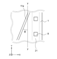
- FIG. 2 is a transparent plan view of a lid wafer portion of the hermetic package element according to the first embodiment;
- FIG. 2 is a cross-sectional view corresponding to line II-II of FIG. 1;
- FIG. FIG. 2 is a partially enlarged view enlarging a region A in FIG. 1;
- FIG. 11 is a transparent plan view of a lid wafer portion of the hermetic package element according to the second embodiment;
- FIG. 11 is a transparent plan view of a lid wafer portion of an airtight package element according to a modification of the second embodiment;
- FIG. 11 is a transparent plan view of a lid wafer portion of an airtight package element according to a third embodiment;
- 3 is a diagram showing the relationship between sides 13 and crystal orientations of the device wafer 1.
- FIG. 11 is a transparent plan view of a lid wafer portion of an airtight package element according to a fourth embodiment;
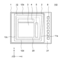
- FIG. 11 is a plan view of an element module according to Embodiment 5;
- FIG. 10 is a cross-sectional view corresponding to line IX-IX in FIG. 9;
- FIG. 4 is a transparent plan view of a lid wafer portion of a conventional hermetic package device;
- FIG. 1 is a transparent plan view of a lid wafer portion of an airtight package device.
- FIG. 2 is a sectional view corresponding to line II-II of FIG.
- FIG. 3 is a partially enlarged view enlarging a region A in FIG. 1.
- FIG. 1 is a transparent plan view of a lid wafer portion of an airtight package device.
- FIG. 2 is a sectional view corresponding to line II-II of FIG.
- FIG. 3 is a partially enlarged view enlarging a region A in FIG. 1.
- a silicon substrate is processed so that its crystal orientations are parallel and orthogonal to the substrate surface.
- Both the device wafer 1 and the lid wafer 2 are manufactured by processing a silicon substrate. 1 to 9 and 11, the device wafer 1 and the lid wafer 2 are arranged such that their crystal orientations are parallel to the X-axis or Y-axis shown in the drawings.
- the outer shape of the device wafer 1 and the lid wafer 2 is a rectangle parallel to the X-axis or the Y-axis. As shown in FIGS.
- the device wafer 1 and the lid wafer 2 are flat with each other in a plan view, that is, when viewed from the Z-axis direction, so that a part of the device wafer 1 protrudes from the lid wafer 2 .
- the surfaces are made parallel and opposed to each other, and are joined by a seal portion 10 .
- the sealing portion 10 includes a first base layer 31 patterned on the mounting surface 1a of the device wafer 1, a second base layer 32 patterned on the surface of the lid wafer 2 facing the mounting surface 1a, and a first It is composed of a sealing material layer 33 interposed between the base layer 31 and the second base layer 32 and filling the space therebetween. Both the first underlayer 31 and the second underlayer 32 are patterned continuously without a break, and are sometimes called a sealing ring.
- the sealing material layer 33 is made of a solder material. However, the solder material has low wettability to the surface (mounting surface 1a) of the device wafer 1 and the surface of the lid wafer 2, and it is difficult to bond the device wafer 1 and the lid wafer 2 as they are.
- the first base layer 31 and the second base layer 32 have good wettability with the solder material and are compatible with each wafer so as to function as an intermediate layer for bonding each wafer and the sealing material layer 33 .
- It is made of a material with good adhesion.
- Such materials are, for example, lead-free solder for the sealing material layer 33 and nickel for the material of the first underlayer 31 and the second underlayer 32, but are not limited to these, and any material may be used. can be selected.
- lead-free solder is preferable because high-temperature solder and AuSn solder impose a high environmental burden and are expensive.
- the sealed space 22 surrounded by the device wafer 1, the lid wafer 2, and the sealing section 10 is held in a vacuum atmosphere.
- the seal portion 10 is formed with a thickness of 50 to 150 ⁇ m, and has a thickness of 100 ⁇ m in this embodiment.
- the inside of the sealed space 22 is called a vacuum atmosphere, it does not mean a complete vacuum, and the degree of vacuum required to maintain heat insulation may be sufficient.
- an infrared imaging element 3, a scanning circuit 4, and a readout circuit 5 are arranged in a region 20 inside the sealing portion 10 of the mounting surface 1a of the device wafer 1.
- the MEMS and semiconductor elements arranged in the region 20, including the imaging device 3, the scanning circuit 4, and the readout circuit 5, are referred to as a semiconductor circuit 7.
- FIG. The semiconductor circuit 7 is arranged inside a sealed space 22 which is kept in a vacuum atmosphere with excellent heat insulation, thereby increasing the reliability of the infrared sensor.
- a gas adsorbent (not shown) called a getter for maintaining the degree of vacuum is formed on the lid wafer 2 at a portion surrounded by the second underlayer 32 .
- a recess may be formed to increase the vacuum volume.
- the outer surface of the lid wafer 2 may be coated with an anti-reflection film called an AR coat for improving infrared transmittance.
- the device wafer 1 has a region overhanging from the lid wafer 2 , and this overhanging region is referred to as an overhanging region 21 .
- a plurality of terminals 8 (bonding pads) for electrically connecting the semiconductor circuit 7 to the outside are provided on the mounting surface 1a of the projecting region 21 .
- the terminals 8 and the semiconductor circuit 7 are electrically connected via wiring (not shown) provided on the mounting surface 1a.
- the terminal 8 configured in this way functions as an element module 200 (FIGS. 9 and 10), which will be described later, by being electrically connected to a circuit board or the like (not shown) with a wire or the like.
- the shape of the seal portion 10 is a polygon having sides 11a, 11b, 11c, and 11d.
- the crystal orientations of the device wafer 1 and the lid wafer 2 are parallel to the X-axis or the Y-axis.
- none of the sides of the seal portion 10 are parallel to the X-axis or the Y-axis, and are formed in directions different from the crystal orientations of the device wafer 1 and the lid wafer 2 .
- the auxiliary line yy shown in FIG. 3 is a straight line parallel to the Y-axis.
- the side 11a facing the projecting region 21 and the auxiliary line yy form an angle ⁇ . where the angle ⁇ is neither zero degrees nor 90 degrees.
- a point D in FIG. 2 is a contact point between the device wafer 1 and the sealing portion 10 on the side where the device wafer 1 protrudes from the lid wafer 2 .
- the airtight package element 100 is once heated to a high temperature in a vacuum atmosphere to melt the solder material of the sealing material layer 33, and then the temperature is lowered to form a sealed space 22 between the device wafer 1 and the lid wafer 2.
- the coefficient of linear expansion of the solder used for the sealing material layer 33 is greater than the coefficient of linear expansion of silicon used for the device wafer 1 and the lid wafer 2 . Therefore, in normal use, residual stress acts on the point D from the point D in the direction of the lid wafer (+Z direction) and from the point D in the direction of the semiconductor circuit (-X direction).
- FIG. 11 is a transparent plan view of a lid wafer portion of a conventional hermetic package element 900.
- FIG. In conventional airtight package devices, structures such as devices, circuits, and wiring formed on a semiconductor substrate are formed along the crystal orientation of the semiconductor substrate.
- a seal portion 10 for bonding the device wafer and the lid wafer is also arranged along the crystal orientation of the device wafer. Description will be made with reference to FIG. 2 as a cross-sectional view corresponding to line II-II of FIG.
- a residual stress similar to the residual stress acting on the point D acts on the entire end 16f on the right side of the drawing of the side 16a. That is, the residual stress acting on the side 16a concentrates along the edge 16f.
- the edge 16f is parallel to the Y-axis in the drawing and coincides with the cleavage direction of the device wafer, that is, the crystal orientation.
- the side 11a is arranged so as to be inclined at an angle ⁇ with respect to the crystal orientation of the device wafer 1 . That is, the direction in which the concentrated stress acts is shifted by an angle ⁇ from the crystal orientation, and the stress concentration is relieved. Therefore, malfunction of the device due to cracking of the device wafer 1, destruction of circuits arranged on the device wafer 1, or disconnection of wiring can be avoided. Thereby, a highly reliable hermetic package element can be obtained.
- the angle ⁇ is preferably more than 0 degree and 5 degrees or less, more preferably 1 degree or more and 3 degrees or less.
- the sealing rings of the device wafer and the lid wafer in this embodiment are formed by electrolytic nickel plating.
- the width of the sealing ring by electrolytic nickel plating is formed using the existing photolithography technology, and it is possible to form an arbitrary angle ⁇ by the pattern of the photomask.
- the hermetic package element 100 includes the device wafer 1 provided with the semiconductor circuit 7 and the terminals 8 for electrically connecting the semiconductor circuit 7 to the outside on the mounting surface 1a, and the mounting surface 1a. and a seal interposed between the device wafer 1 and the lid wafer 2 to form a sealed space 22 with a vacuum atmosphere containing the semiconductor circuit 7 between the device wafer 1 and the lid wafer 2. a part 10;
- the device wafer 1 has an overhang region 21 overhanging from the lid wafer 2 in plan view.
- the terminal 8 is provided in the projecting region 21 .
- the seal portion 10 has a polygonal shape in plan view, and the side 11 a facing the projecting region 21 is formed in a direction different from the crystal orientation of the device wafer 1 . Further, the angle ⁇ between the side 11a facing the projecting region 21 and the crystal orientation of the device wafer 1 is preferably more than 0 degrees and 5 degrees or less, more preferably 1 degree or more and 3 degrees or less.
- the side 11a is arranged so as to be inclined at an angle ⁇ with respect to the crystal orientation of the device wafer 1, the direction in which concentrated stress acts is shifted from the crystal orientation by the angle ⁇ .
- the stress concentration is relieved, so that the device wafer 1 can be cracked, the circuits arranged on the device wafer 1 can be broken, or the device can be prevented from malfunctioning due to the disconnection of the wiring. There is an effect that it can be obtained.
- Embodiment 2 A hermetic package element 110 according to the second embodiment will be described.
- all sides of the seal portion 10 are configured so as not to be parallel to the crystal orientation of the device wafer 1 .
- the side 11a of the seal portion 10 facing the projecting region 21 is not parallel to the crystal orientation, and the other sides are parallel to the crystal orientation.
- FIG. 4 is a transparent plan view of the lid wafer portion of the airtight package element 110 according to the second embodiment.
- the seal portion 10 of the hermetic package element 110 according to the second embodiment has sides 11a, 12b, 12c, and 12d.
- the material, cross-sectional structure, etc. of the sides 12b, 12c and 12d are the same as those of the sides 11a, 11b, 11c and 11d.
- Sides 12b, 12c, and 12d correspond to sides 11b, 11c, and 11d in the first embodiment, respectively, but are arranged parallel to the X-axis or Y-axis as in the conventional hermetic package element. That is, the sides 12b, 12c, and 12d are arranged parallel to the crystal orientation of the device wafer 1.
- the device wafer 1 does not protrude from the lid wafer 2 where the sides 12b, 12c, and 12d face, and the sides 12b, 12c, and 12d do not face the protruding region.
- the wiring that electrically connects the semiconductor circuit 7 on the device wafer 1 to the outside is arranged so as not to cross the seal portion 10 at a portion other than the side 11 a facing the projecting region 21 .
- the second embodiment there is no fear of malfunction of the device due to concentration of stress, cracking of the device wafer 1, destruction of circuits arranged on the device wafer 1, or disconnection of wiring.
- the sides 12b, 12c, and 12d of the sealing portion 10, which are not sealed, are formed in the same direction as the crystal orientation of the device wafer 1 as in the conventional hermetic package.
- Other parts are the same as those in the first embodiment, and description thereof is omitted.
- the size of the hermetic package element 110 can be made smaller than in the first embodiment. This is effective when the size of the hermetic package element 110 cannot be increased by inclining all sides of the sealing ring due to device layout restrictions.
- FIG. 5 is a transparent plan view of a lid wafer portion of an airtight package element 111 according to a modification of the second embodiment.
- the side of the seal portion 10 facing the projecting region 21 in the airtight package element 111 consists of a side 11a that is not parallel to the crystal orientation, and sides 12e and 12f that are continuous with the side 11a and parallel to the crystal orientation.
- the length of side 11a is longer than the length of sides 12e and 12f. In this way, even if a portion of the side of the seal portion 10 facing the overhanging region 21 is parallel to the crystal orientation, most of the portion is not parallel to the crystal orientation. Note that it has a certain effect on
- Embodiment 3 An airtight package element 120 according to the third embodiment will be described with reference to FIGS. 6 and 7.
- the side of the seal portion 10 facing the projecting region 21 is a single side 11a.
- a plurality of sides of the seal portion 10 facing the projecting region 21 are arranged in a zigzag pattern.
- FIG. 6 is a transparent plan view of the lid wafer portion of the hermetic package element 120 according to the third embodiment.
- the sealing portion 10 of the airtight package element 120 according to the third embodiment has sides 12b, 12c, 12d and a side 13 facing the projecting region 21.
- the side 13 is continuous and consists of a plurality of sides 13a, 13b, 13c arranged in a zigzag pattern.
- the sides 12b, 12c, 12d and the side 13 are made of the same material and have the same cross-sectional structure.
- the side 13 is a side of the seal portion 10 facing the overhanging region 21 like the side 11a. It is a side that is not parallel to the orientation.
- FIG. 7 is a diagram showing the relationship between the side 13 and the crystal orientation of the device wafer 1. As shown in FIG. In FIG. 7, parts other than those necessary for explanation are not shown and are omitted.
- the two auxiliary lines yy shown in FIG. 7 are straight lines parallel to the Y-axis, that is, the auxiliary lines yy indicate the same direction as the crystal orientation. None of the sides 13a, 13b, and 13c are arranged so as not to be parallel to the crystal orientation (the X direction and the Y direction on the paper surface).
- the angles formed by the sides 11a, 11b, 11c and the auxiliary line yy are ⁇ 1, ⁇ 2, ⁇ 3, respectively.
- the absolute values of ⁇ 1, ⁇ 2, and ⁇ 3 may be the same or different.
- ⁇ 1 and ⁇ 3 measure angles clockwise from the auxiliary line yy, while ⁇ 2 measures angles counterclockwise from the auxiliary line yy. That is, it can be said that the signs of ⁇ 1 and ⁇ 3 and ⁇ 2 are different, or zigzag with respect to the auxiliary line yy (crystal orientation).
- W in FIG. 7 is the width occupied by the side 13 in the X-axis direction.
- the lengths of sides 13a, 13b, and 13c in Embodiment 3 are set to 1/3 of the length of side 11a in Embodiment 1, and the angle ⁇ in Embodiment 1 and the angle in Embodiment 3
- W can be reduced to 1/3 of the width of the side 11a in the X-axis direction in the first embodiment. That is, by forming a plurality of zigzag sides of the seal portion 10 facing the projecting region 21 as shown in the third embodiment, an increase in the size of the hermetic package element can be suppressed. Description of other parts is omitted.
- the airtight package element 120 includes the device wafer 1 provided with the semiconductor circuit 7 and the terminals 8 for electrically connecting the semiconductor circuit 7 and the outside on the mounting surface 1a, and the mounting surface 1a. and a lid wafer 2 arranged to face the device wafer 1 and the lid wafer 2, forming a sealed space 22 with a vacuum atmosphere for housing the semiconductor circuit 7 between the device wafer 1 and the lid wafer 2. and a seal portion 10 .
- the device wafer 1 has an overhang region 21 overhanging from the lid wafer 2 in plan view.
- the terminal 8 is provided in the projecting region 21 .
- the sealing portion 10 has a polygonal shape in plan view, and has a side 13 a facing an overhanging region 21 formed in a direction different from the crystal orientation of the device wafer 1 .
- the side 13 is sides 13a, 13b, and 13c arranged in a zigzag pattern.
- the same effect as the hermetic package element 100 shown in the first embodiment can be obtained.
- the sides of the seal portion 10 facing the projecting region 21 are arranged in a zigzag manner, thereby suppressing an increase in the size of the airtight package element. It also has the effect of being able to
- the side of the seal portion 10 facing the overhanging region 21 is divided into three and arranged in a zigzag pattern, but it may be divided into two and arranged in a V shape. Also, the number of divisions may be four or more, and the division lengths may not be equal. In addition, even if a plurality of sides arranged in a zigzag or V shape are accompanied by sides arranged parallel to the crystal orientation, an increase in the size of the hermetic package element can be suppressed.
- Embodiment 4 A hermetic package element 130 according to the fourth embodiment will be described with reference to FIG. In Embodiments 1 to 3, the case where the projecting region 21 is on one side of the hermetic package element has been described, but in Embodiment 4, the case where the hermetic package element has projecting regions on two sides will be described.
- FIG. 8 is a transparent plan view of the lid wafer portion of the airtight package element 130 according to the fourth embodiment.
- the device wafer 1 has two protruding portions from the lid wafer 2 .
- One is the projecting region 21 as in the first embodiment, and the other is the projecting region 21a.
- the projecting region 21a which is the second projecting region, is arranged on the opposite side of the projecting region 21, which is the first projecting region, with the closed space 22 interposed therebetween.
- a plurality of terminals 8 (bonding pads) electrically connected to the imaging device 3, the scanning circuit 4, and the readout circuit 5 via wiring (not shown) are also arranged on the mounting surface 1a of the projecting region 21a.
- the shape of the seal portion 10 in Embodiment 4 is a polygon having sides 11a, 12b, 14c, and 12d.
- the side 11a faces the projecting region 21 and is formed in a direction different from the crystal orientation.
- Sides 12b and 12d are formed in the same direction as the crystal orientation.
- Side 14 c faces projecting region 21 a and is formed in a direction different from the crystal orientation of device wafer 1 .
- the material, cross-sectional structure, etc. of the side 14c are the same as those of the sides 11a, 12b, and 12d. Description of other parts is omitted.
- the hermetic package element 130 according to the fourth embodiment configured as described above also has the same stress relaxation effect as the first embodiment.
- the first projecting region 21 and the second projecting region 21a are arranged on opposite sides of the closed space 22, they may be arranged adjacent to each other, for example, on the sides 11a and 12b. Also, the overhang areas may be arranged on three or more sides.
- Embodiment 5 describes an element module in which the airtight package element described in Embodiments 1 to 4 is mounted on a circuit board together with other electronic components.
- 9 and 10 are for explaining the configuration of the element module according to the fifth embodiment.
- 9 is a plan view of an element module according to Embodiment 5
- FIG. 10 is a cross-sectional view corresponding to line XX of FIG.
- the configuration of the airtight package element portion will be described using the airtight package element 100, it is the same as in any one of the first to fourth embodiments, and any one of the airtight package elements 110, 111, 120 or 130 can be used instead. good. 1 to 8 are used while omitting the description of the same parts.
- an element module 200 includes an airtight package element 100, components 204 such as resistors and capacitors, and semiconductor devices 205 on a mounting surface 203 of a circuit board 202.
- the electronic component 206 including is mounted. Then, the mounted electronic component is electrically connected to the terminals 8 of the hermetic package element 100 by wire bonding or the like (not shown) to form an element module 200 .
- the hermetic package element 100 and the electronic component 206 are fixed to the circuit board 202 using a thermosetting conductive adhesive 208 .
- other components, covers, and the like necessary for configuring the element module 200 are provided.
- the element module 200 according to Embodiment 5 includes the airtight package element described in any one of Embodiments 1 to 4, and is robust against vibration and impact.
- the airtight package element 100 that functions as an infrared sensor is used, it is possible to obtain an infrared sensor that is robust against vibration and impact, prevents cracking of the device wafer, and has high reliability.
- the present disclosure is not limited to the above-described examples, and includes various modifications.
- the above embodiments have been described in detail to facilitate understanding of the present disclosure, and are not necessarily limited to those having all the described configurations.
- it is possible to replace part of the configuration of one embodiment with the configuration of another embodiment and it is also possible to add the configuration of another embodiment to the configuration of one embodiment.
Abstract
In a conventional hermetic package element, a seal portion joining a device wafer and a lid wafer is formed along a crystal orientation of a semiconductor substrate. For this reason, problems of device malfunctions arise due to the device wafer becoming cracked, circuits disposed on the device wafer being broken, and wiring being cut. A hermetic package element 100 according to the present disclosure is characterized in that: a device wafer 1 includes a projecting region 21 which projects from a lid wafer 2 in a plan view; a seal portion 10 has a polygonal shape in a plan view; and a side 11a of the polygonal shape that faces the projecting region 21 is formed in a different direction to the crystal orientation of the device wafer 1.
Description
本開示は、気密パッケージ素子および素子モジュールに関するものである。
The present disclosure relates to hermetic package devices and device modules.
センサ、アクチュエータなどをシリコン基板等の上に微細加工技術によって集積化したデバイスであるマイクロ電気機械システム(MEMS:Micro Electro Mechanical Systems)デバイスが実用化されている。MEMSデバイスの例としては、赤外線センサ、ジャイロセンサ、加速度センサなどが挙げられる。
Micro Electro Mechanical Systems (MEMS) devices, which are devices in which sensors, actuators, etc. are integrated on a silicon substrate or the like by microfabrication technology, have been put to practical use. Examples of MEMS devices include infrared sensors, gyro sensors, acceleration sensors, and the like.
赤外線センサのうち、非冷却赤外線センサは熱型センサと称されるように入射する赤外線を熱に変換するものである。そのため、対象物の温度変化を電気信号の変化として読み出す構成を有し、検出感度を高めるためにセンサ(撮像素子)が基材から熱的に隔離された断熱構造を有している。
具体的には、赤外線センサは、断熱性を高めるために密閉された真空空間に配置、つまり真空パッケージの内部に配置されている。その際、真空パッケージの蓋(リッド)となる部材には、赤外線透過率の高い低酸素含有のシリコン、ZnSを用いたり、反射防止膜(ARコート:Anti-Reflection Coating)を形成したりすることが知られている。 Among infrared sensors, an uncooled infrared sensor converts incident infrared rays into heat so as to be called a thermal sensor. Therefore, it has a structure that reads changes in the temperature of the object as changes in electrical signals, and has a heat insulating structure in which the sensor (imaging device) is thermally isolated from the substrate in order to increase the detection sensitivity.
Specifically, the infrared sensor is placed in a sealed vacuum space, that is, placed inside a vacuum package in order to improve heat insulation. At that time, for the member that becomes the lid of the vacuum package, low-oxygen-containing silicon or ZnS with high infrared transmittance should be used, or an anti-reflection coating (AR coat: Anti-Reflection Coating) should be formed. It has been known.
一方、真空パッケージの製造方法として、MEMSデバイスを製造したデバイスウエハと、デバイスウエハに対向するリッドウエハを真空雰囲気にて接合し、複数の真空パッケージを形成するウエハレベルパッケージ(Wafer Level Package)が提案されている(例えば特許文献1参照。)。
On the other hand, as a method of manufacturing a vacuum package, a wafer level package has been proposed in which a device wafer on which MEMS devices are manufactured and a lid wafer facing the device wafer are bonded in a vacuum atmosphere to form a plurality of vacuum packages. (See Patent Document 1, for example).
ウエハレベルパッケージで構成された気密パッケージ素子は、デバイスウエハに設けられている電気接続のためのボンディングパッドがリッドウエハより露出した構造が必然となり、デバイスウエハのボンディング部がリッドウエハより張り出した構造となる。すると、デバイスウエハが張り出した辺のシール部とデバイスウエハとが接する部位に応力が集中する。
An airtight package element configured as a wafer level package inevitably has a structure in which the bonding pads for electrical connection provided on the device wafer are exposed from the lid wafer, and the bonding part of the device wafer protrudes from the lid wafer. Then, the stress concentrates on the part where the device wafer and the sealing portion on the overhanging side of the device wafer are in contact with each other.
ところで、半導体基板上に形成される素子や回路、配線などの構造物は、半導体基板の結晶方位に沿って形成されている。この様な構成の従来のウエハレベル気密パッケージでは、デバイスウエハとリッドウエハを接合するシール部もデバイスウエハの結晶方位に沿って配置されている。
すると、集中した応力が作用する方向はデバイス半導体基板のへき開方向と一致する。このため、デバイスウエハに割れが生じ、デバイスウエハ上に配置された回路が破壊、または配線が切断されてデバイスの動作不良を生じる課題があった。 By the way, structures such as elements, circuits, and wiring formed on a semiconductor substrate are formed along the crystal orientation of the semiconductor substrate. In the conventional wafer-level hermetic package having such a configuration, the seal portion that joins the device wafer and the lid wafer is also arranged along the crystal orientation of the device wafer.
Then, the direction in which the concentrated stress acts coincides with the cleavage direction of the device semiconductor substrate. As a result, there is a problem that the device wafer cracks, the circuits arranged on the device wafer are destroyed, or the wiring is cut, resulting in malfunction of the device.
本開示は上記のような課題を解決するための技術を開示するものであり、デバイスウエハの割れを防止し、信頼性の高い気密パッケージ素子を得ることを目的とする。
The present disclosure discloses a technique for solving the above problems, and aims to prevent device wafer cracking and obtain a highly reliable airtight package element.
本開示に係る気密パッケージ素子は、半導体回路と該半導体回路と外部とを電気接続するための端子が実装面に設けられたデバイスウエハと、実装面に対向して配置されたリッドウエハと、デバイスウエハとリッドウエハとの間に介在し、デバイスウエハとリッドウエハとの間に、半導体回路を収容する真空雰囲気の密閉空間を形成するシール部と、を備え、デバイスウエハは平面視においてリッドウエハから張り出した張り出し領域を有し、端子は張り出し領域に設けられており、シール部は平面視において多角形であり、張り出し領域を臨む多角形の辺はデバイスウエハの結晶方位と異なる方向に形成されたことを特徴とする。
The airtight package element according to the present disclosure includes a device wafer having a mounting surface provided with terminals for electrically connecting a semiconductor circuit and the semiconductor circuit to the outside, a lid wafer disposed facing the mounting surface, and a device wafer. and a sealing part interposed between the device wafer and the lid wafer and forming a vacuum atmosphere sealed space for housing the semiconductor circuit between the device wafer and the lid wafer, the device wafer projecting from the lid wafer in a plan view. , the terminal is provided in the overhanging region, the seal portion is polygonal in plan view, and the sides of the polygon facing the overhanging region are formed in a direction different from the crystal orientation of the device wafer. do.
本開示に係る素子モジュールは、半導体回路と該半導体回路と外部とを電気接続するための端子が実装面に設けられたデバイスウエハと、実装面に対向して配置されたリッドウエハと、デバイスウエハとリッドウエハとの間に介在し、デバイスウエハとリッドウエハとの間に、半導体回路を収容する真空雰囲気の密閉空間を形成するシール部とを有し、デバイスウエハは平面視においてリッドウエハから張り出した張り出し領域を有し、端子は張り出し領域に設けられており、シール部は平面視において多角形であり、張り出し領域を臨む多角形の辺はデバイスウエハの結晶方位と異なる方向に形成されたことを特徴とする気密パッケージ素子と、回路基板と、回路基板に実装された該気密パッケージ素子、および回路基板に実装され、該端子と電気接続された電子部品を備えたことを特徴とする。
An element module according to the present disclosure includes a device wafer having a mounting surface provided with terminals for electrically connecting a semiconductor circuit and the semiconductor circuit to the outside, a lid wafer disposed facing the mounting surface, and a device wafer. A sealing portion interposed between the lid wafer and the device wafer and forming a sealed space of a vacuum atmosphere for accommodating the semiconductor circuit is provided between the device wafer and the lid wafer. wherein the terminal is provided in the overhanging region, the seal portion is polygonal in plan view, and the side of the polygon facing the overhanging region is formed in a direction different from the crystal orientation of the device wafer. It is characterized by comprising an airtight package element, a circuit board, the airtight package element mounted on the circuit board, and an electronic component mounted on the circuit board and electrically connected to the terminals.
本開示によれば、シール部とデバイスウエハとが接触する部位の応力を緩和できるので、デバイスウエハの割れを防止し、信頼性の高い気密パッケージ素子あるいは素子モジュールを得ることができる。
According to the present disclosure, since the stress at the portion where the sealing portion and the device wafer are in contact can be relaxed, cracking of the device wafer can be prevented, and a highly reliable hermetic package element or element module can be obtained.
以下、本開示の実施の形態に係る気密パッケージ素子および素子モジュールについて図面を参照して説明する。同じ又は対応する構成要素には同じ符号を付し、説明の繰り返しを省略する場合がある。このことは、明細書の全文において共通することである。
A hermetic package element and an element module according to an embodiment of the present disclosure will be described below with reference to the drawings. The same reference numerals are given to the same or corresponding components, and repetition of description may be omitted. This is common throughout the specification.
実施の形態1.
図1から図3を用いて、実施の形態1にかかる気密パッケージ素子100について説明する。図1は気密パッケージ素子のリッドウエハ部分を透過させた平面図である。図2は図1のII-II線に対応する断面図である。図3は図1における領域Aを拡大した部分拡大図である。Embodiment 1.
Anairtight package device 100 according to the first embodiment will be described with reference to FIGS. 1 to 3. FIG. FIG. 1 is a transparent plan view of a lid wafer portion of an airtight package device. FIG. 2 is a sectional view corresponding to line II-II of FIG. FIG. 3 is a partially enlarged view enlarging a region A in FIG. 1. FIG.
図1から図3を用いて、実施の形態1にかかる気密パッケージ素子100について説明する。図1は気密パッケージ素子のリッドウエハ部分を透過させた平面図である。図2は図1のII-II線に対応する断面図である。図3は図1における領域Aを拡大した部分拡大図である。
An
はじめに、気密パッケージ素子の基本的な構成について説明する。
一般にシリコン基板はその結晶方位が基板面に対し平行かつ直行する2方向となるように加工される。デバイスウエハ1及びリッドウエハ2は、共にシリコン基板を加工して製造されている。図1から図9、及び図11において、デバイスウエハ1及びリッドウエハ2はその結晶方位が、図中に示したX軸又はY軸に平行であるように配置されている。デバイスウエハ1及びリッドウエハ2の外形はX軸又はY軸に平行な長方形である。
図1、図2に示すように、デバイスウエハ1とリッドウエハ2は、平面視、すなわちZ軸方向から見た場合において、デバイスウエハ1の一部がリッドウエハ2から張り出すようにして、互いに平坦な面どうしを平行にして対向させ、シール部10によって接合されている。 First, the basic configuration of the airtight package device will be described.
In general, a silicon substrate is processed so that its crystal orientations are parallel and orthogonal to the substrate surface. Both the device wafer 1 and thelid wafer 2 are manufactured by processing a silicon substrate. 1 to 9 and 11, the device wafer 1 and the lid wafer 2 are arranged such that their crystal orientations are parallel to the X-axis or Y-axis shown in the drawings. The outer shape of the device wafer 1 and the lid wafer 2 is a rectangle parallel to the X-axis or the Y-axis.
As shown in FIGS. 1 and 2, the device wafer 1 and thelid wafer 2 are flat with each other in a plan view, that is, when viewed from the Z-axis direction, so that a part of the device wafer 1 protrudes from the lid wafer 2 . The surfaces are made parallel and opposed to each other, and are joined by a seal portion 10 .
一般にシリコン基板はその結晶方位が基板面に対し平行かつ直行する2方向となるように加工される。デバイスウエハ1及びリッドウエハ2は、共にシリコン基板を加工して製造されている。図1から図9、及び図11において、デバイスウエハ1及びリッドウエハ2はその結晶方位が、図中に示したX軸又はY軸に平行であるように配置されている。デバイスウエハ1及びリッドウエハ2の外形はX軸又はY軸に平行な長方形である。
図1、図2に示すように、デバイスウエハ1とリッドウエハ2は、平面視、すなわちZ軸方向から見た場合において、デバイスウエハ1の一部がリッドウエハ2から張り出すようにして、互いに平坦な面どうしを平行にして対向させ、シール部10によって接合されている。 First, the basic configuration of the airtight package device will be described.
In general, a silicon substrate is processed so that its crystal orientations are parallel and orthogonal to the substrate surface. Both the device wafer 1 and the
As shown in FIGS. 1 and 2, the device wafer 1 and the
シール部10は、デバイスウエハ1の実装面1a上にパターン形成された第一下地層31と、実装面1aと対向するリッドウエハ2の表面上にパターン形成された第二下地層32と、第一下地層31と第二下地層32との間に介在し、その間を充填するシール材層33とで構成されている。第一下地層31、第二下地層32はともに切れ目なく連続してパターン形成されており、シーリングリングと称されることもある。
シール材層33ははんだ材料からなる。しかしはんだ材料はデバイスウエハ1の表面(実装面1a)、およびリッドウエハ2の表面に対する濡れ性が低く、そのままではデバイスウエハ1とリッドウエハ2とを接合することは困難である。そこで、第一下地層31と第二下地層32は、各ウエハとシール材層33を接着するための中間層として機能するよう、はんだ材料との濡れ性が良好で、かつ、各ウエハとの密着性が良好な材料で形成されている。
このような材料は、例えばシール材層33は鉛フリーはんだであり、第一下地層31と第二下地層32の材質はニッケルであるが、これに制限されることはなく、任意の材料を選択することができる。ただし、高温はんだやAuSnはんだは環境負荷や価格が高いため鉛フリーはんだが好適である。 Thesealing portion 10 includes a first base layer 31 patterned on the mounting surface 1a of the device wafer 1, a second base layer 32 patterned on the surface of the lid wafer 2 facing the mounting surface 1a, and a first It is composed of a sealing material layer 33 interposed between the base layer 31 and the second base layer 32 and filling the space therebetween. Both the first underlayer 31 and the second underlayer 32 are patterned continuously without a break, and are sometimes called a sealing ring.
The sealingmaterial layer 33 is made of a solder material. However, the solder material has low wettability to the surface (mounting surface 1a) of the device wafer 1 and the surface of the lid wafer 2, and it is difficult to bond the device wafer 1 and the lid wafer 2 as they are. Therefore, the first base layer 31 and the second base layer 32 have good wettability with the solder material and are compatible with each wafer so as to function as an intermediate layer for bonding each wafer and the sealing material layer 33 . It is made of a material with good adhesion.
Such materials are, for example, lead-free solder for the sealingmaterial layer 33 and nickel for the material of the first underlayer 31 and the second underlayer 32, but are not limited to these, and any material may be used. can be selected. However, lead-free solder is preferable because high-temperature solder and AuSn solder impose a high environmental burden and are expensive.
シール材層33ははんだ材料からなる。しかしはんだ材料はデバイスウエハ1の表面(実装面1a)、およびリッドウエハ2の表面に対する濡れ性が低く、そのままではデバイスウエハ1とリッドウエハ2とを接合することは困難である。そこで、第一下地層31と第二下地層32は、各ウエハとシール材層33を接着するための中間層として機能するよう、はんだ材料との濡れ性が良好で、かつ、各ウエハとの密着性が良好な材料で形成されている。
このような材料は、例えばシール材層33は鉛フリーはんだであり、第一下地層31と第二下地層32の材質はニッケルであるが、これに制限されることはなく、任意の材料を選択することができる。ただし、高温はんだやAuSnはんだは環境負荷や価格が高いため鉛フリーはんだが好適である。 The
The sealing
Such materials are, for example, lead-free solder for the sealing
このように構成したシール部10により、デバイスウエハ1、リッドウエハ2、およびシール部10で囲まれた密閉空間22は真空雰囲気に保持されている。この真空容積を確保するために、シール部10は50~150μmの厚さで形成されており、本実施の形態では100μmの厚みを有している。なお、密閉空間22内は真空雰囲気と称しているが、完全な真空を意味するものではなく、断熱性を保つのに必要な真空度でよい。
Due to the sealing section 10 configured in this manner, the sealed space 22 surrounded by the device wafer 1, the lid wafer 2, and the sealing section 10 is held in a vacuum atmosphere. In order to secure this vacuum volume, the seal portion 10 is formed with a thickness of 50 to 150 μm, and has a thickness of 100 μm in this embodiment. Although the inside of the sealed space 22 is called a vacuum atmosphere, it does not mean a complete vacuum, and the degree of vacuum required to maintain heat insulation may be sufficient.
デバイスウエハ1の実装面1aのシール部10よりも内側の領域20には、赤外線用の撮像素子3、走査回路4、読出回路5がそれぞれ配置されている。なお、撮像素子3、走査回路4、読出回路5を含め、領域20に配置されているMEMSおよび半導体素子を半導体回路7と呼称する。半導体回路7は、断熱性に優れた真空雰囲気に保持された密閉空間22の内部に配置されており、赤外線センサとしての信頼性を高めている。
リッドウエハ2には真空度を保持するためのゲッターと称される図示しないガス吸着剤が、第二下地層32に囲まれた部位に形成される。また、真空容積を増やすための窪みが形成される場合がある。さらに、リッドウエハ2の外面には、赤外線の透過率を向上するためのARコートと称される反射防止膜が形成される場合がある。 In aregion 20 inside the sealing portion 10 of the mounting surface 1a of the device wafer 1, an infrared imaging element 3, a scanning circuit 4, and a readout circuit 5 are arranged. The MEMS and semiconductor elements arranged in the region 20, including the imaging device 3, the scanning circuit 4, and the readout circuit 5, are referred to as a semiconductor circuit 7. FIG. The semiconductor circuit 7 is arranged inside a sealed space 22 which is kept in a vacuum atmosphere with excellent heat insulation, thereby increasing the reliability of the infrared sensor.
A gas adsorbent (not shown) called a getter for maintaining the degree of vacuum is formed on thelid wafer 2 at a portion surrounded by the second underlayer 32 . Also, a recess may be formed to increase the vacuum volume. Furthermore, the outer surface of the lid wafer 2 may be coated with an anti-reflection film called an AR coat for improving infrared transmittance.
リッドウエハ2には真空度を保持するためのゲッターと称される図示しないガス吸着剤が、第二下地層32に囲まれた部位に形成される。また、真空容積を増やすための窪みが形成される場合がある。さらに、リッドウエハ2の外面には、赤外線の透過率を向上するためのARコートと称される反射防止膜が形成される場合がある。 In a
A gas adsorbent (not shown) called a getter for maintaining the degree of vacuum is formed on the
平面視、すなわちZ軸方向から見た場合において、デバイスウエハ1はリッドウエハ2から張り出した領域を有し、この張り出した領域を張り出し領域21と呼称する。張り出し領域21の実装面1aには、半導体回路7と外部とを電気的に接続するための端子8(ボンディングパッド)が複数設けられている。端子8と半導体回路7とは、実装面1aに設けられた図示しない配線を介して電気接続されている。
このように構成した端子8が、図示しない回路基板等とワイヤーなどで電気接続されることで、後述する素子モジュール200(図9、図10)として機能する。 In a plan view, that is, when viewed from the Z-axis direction, thedevice wafer 1 has a region overhanging from the lid wafer 2 , and this overhanging region is referred to as an overhanging region 21 . A plurality of terminals 8 (bonding pads) for electrically connecting the semiconductor circuit 7 to the outside are provided on the mounting surface 1a of the projecting region 21 . The terminals 8 and the semiconductor circuit 7 are electrically connected via wiring (not shown) provided on the mounting surface 1a.
Theterminal 8 configured in this way functions as an element module 200 (FIGS. 9 and 10), which will be described later, by being electrically connected to a circuit board or the like (not shown) with a wire or the like.
このように構成した端子8が、図示しない回路基板等とワイヤーなどで電気接続されることで、後述する素子モジュール200(図9、図10)として機能する。 In a plan view, that is, when viewed from the Z-axis direction, the
The
上述した構成を前提として、本開示の気密パッケージ素子100の特徴的な構成について説明する。図1に示すように平面視、すなわちZ軸方向から見た場合において、シール部10の形状は、辺11a、11b、11c、及び11dからなる多角形である。前述の通り、デバイスウエハ1及びリッドウエハ2の結晶方位は、X軸又はY軸に平行である。 これに対しシール部10の辺はいずれもX軸又はY軸に平行ではなく、デバイスウエハ1及びリッドウエハ2の結晶方位と異なる方向に形成されている。
図3に示す補助線y-yはY軸に平行な直線である。張り出し領域21を臨む辺11aと補助線y-yとは、角度θをなしている。ここで角度θはゼロ度又は90度でない。 On the premise of the configuration described above, the characteristic configuration of thehermetic package element 100 of the present disclosure will be described. As shown in FIG. 1, in plan view, that is, when viewed from the Z-axis direction, the shape of the seal portion 10 is a polygon having sides 11a, 11b, 11c, and 11d. As described above, the crystal orientations of the device wafer 1 and the lid wafer 2 are parallel to the X-axis or the Y-axis. In contrast, none of the sides of the seal portion 10 are parallel to the X-axis or the Y-axis, and are formed in directions different from the crystal orientations of the device wafer 1 and the lid wafer 2 .
The auxiliary line yy shown in FIG. 3 is a straight line parallel to the Y-axis. Theside 11a facing the projecting region 21 and the auxiliary line yy form an angle θ. where the angle θ is neither zero degrees nor 90 degrees.
図3に示す補助線y-yはY軸に平行な直線である。張り出し領域21を臨む辺11aと補助線y-yとは、角度θをなしている。ここで角度θはゼロ度又は90度でない。 On the premise of the configuration described above, the characteristic configuration of the
The auxiliary line yy shown in FIG. 3 is a straight line parallel to the Y-axis. The
次に本開示の実施の形態1における気密パッケージセンサの効果を説明する。
図2における点Dは、デバイスウエハ1がリッドウエハ2から張り出した側の、デバイスウエハ1とシール部10との接触点である。
気密パッケージ素子100は、真空雰囲気中で一旦高温にされてシール材層33のはんだ材料が溶融されその後降温されることで、デバイスウエハ1とリッドウエハ2との間に
密閉空間22が形成される。シール材層33に用いられるはんだの線膨張係数は、デバイスウエハ1及びリッドウエハ2に用いられるシリコンの線膨張係数より大きい。このため、通常の使用状態において、点Dには点Dからリッドウエハの方向(+Z方向)及び点Dから半導体回路の方向(-X方向)への残留応力が働く。 Next, the effects of the airtight package sensor according toEmbodiment 1 of the present disclosure will be described.
A point D in FIG. 2 is a contact point between thedevice wafer 1 and the sealing portion 10 on the side where the device wafer 1 protrudes from the lid wafer 2 .
Theairtight package element 100 is once heated to a high temperature in a vacuum atmosphere to melt the solder material of the sealing material layer 33, and then the temperature is lowered to form a sealed space 22 between the device wafer 1 and the lid wafer 2. The coefficient of linear expansion of the solder used for the sealing material layer 33 is greater than the coefficient of linear expansion of silicon used for the device wafer 1 and the lid wafer 2 . Therefore, in normal use, residual stress acts on the point D from the point D in the direction of the lid wafer (+Z direction) and from the point D in the direction of the semiconductor circuit (-X direction).
図2における点Dは、デバイスウエハ1がリッドウエハ2から張り出した側の、デバイスウエハ1とシール部10との接触点である。
気密パッケージ素子100は、真空雰囲気中で一旦高温にされてシール材層33のはんだ材料が溶融されその後降温されることで、デバイスウエハ1とリッドウエハ2との間に
密閉空間22が形成される。シール材層33に用いられるはんだの線膨張係数は、デバイスウエハ1及びリッドウエハ2に用いられるシリコンの線膨張係数より大きい。このため、通常の使用状態において、点Dには点Dからリッドウエハの方向(+Z方向)及び点Dから半導体回路の方向(-X方向)への残留応力が働く。 Next, the effects of the airtight package sensor according to
A point D in FIG. 2 is a contact point between the
The
図11は従来の気密パッケージ素子900のリッドウエハ部分を透過させた平面図である。従来の気密パッケージ素子では、半導体基板上に形成される素子や回路、配線などの構造物は、半導体基板の結晶方位に沿って形成されている。またデバイスウエハとリッドウエハを接合するシール部10もデバイスウエハの結晶方位に沿って配置されている。
図11のII-II線に対応する断面図として図2を援用して説明する。辺16aの図面右側の端16f全体に、点Dに働く残留応力と同様に残留応力が作用している。つまり辺16aに働く残留応力は端16fに沿って集中して作用する。端16fは図中のY軸に平行であり、デバイスウエハのへき開方向、すなわち結晶方位と一致する。このため、デバイスウエハに割れが生じ、デバイスウエハ上に配置された回路が破壊、または配線が切断されてデバイスの動作不良を生じる問題があった。 FIG. 11 is a transparent plan view of a lid wafer portion of a conventionalhermetic package element 900. FIG. In conventional airtight package devices, structures such as devices, circuits, and wiring formed on a semiconductor substrate are formed along the crystal orientation of the semiconductor substrate. A seal portion 10 for bonding the device wafer and the lid wafer is also arranged along the crystal orientation of the device wafer.
Description will be made with reference to FIG. 2 as a cross-sectional view corresponding to line II-II of FIG. A residual stress similar to the residual stress acting on the point D acts on theentire end 16f on the right side of the drawing of the side 16a. That is, the residual stress acting on the side 16a concentrates along the edge 16f. The edge 16f is parallel to the Y-axis in the drawing and coincides with the cleavage direction of the device wafer, that is, the crystal orientation. As a result, there is a problem that the device wafer cracks, the circuits arranged on the device wafer are destroyed, or the wiring is cut, resulting in malfunction of the device.
図11のII-II線に対応する断面図として図2を援用して説明する。辺16aの図面右側の端16f全体に、点Dに働く残留応力と同様に残留応力が作用している。つまり辺16aに働く残留応力は端16fに沿って集中して作用する。端16fは図中のY軸に平行であり、デバイスウエハのへき開方向、すなわち結晶方位と一致する。このため、デバイスウエハに割れが生じ、デバイスウエハ上に配置された回路が破壊、または配線が切断されてデバイスの動作不良を生じる問題があった。 FIG. 11 is a transparent plan view of a lid wafer portion of a conventional
Description will be made with reference to FIG. 2 as a cross-sectional view corresponding to line II-II of FIG. A residual stress similar to the residual stress acting on the point D acts on the
これに対し本開示の実施の形態1における気密パッケージ素子100では、辺11aはデバイスウエハ1の結晶方位に対し、角度θ傾くように配置されている。つまり集中した応力が作用する方向が結晶方位から角度θ分ずれることになり、応力集中が緩和される。このため、デバイスウエハ1の割れや、デバイスウエハ1上に配置された回路の破壊、または配線の切断によるデバイスの動作不良を回避できる。これにより、信頼性の高い気密パッケージ素子を得ることができる。
On the other hand, in the hermetic package element 100 according to the first embodiment of the present disclosure, the side 11a is arranged so as to be inclined at an angle θ with respect to the crystal orientation of the device wafer 1 . That is, the direction in which the concentrated stress acts is shifted by an angle θ from the crystal orientation, and the stress concentration is relieved. Therefore, malfunction of the device due to cracking of the device wafer 1, destruction of circuits arranged on the device wafer 1, or disconnection of wiring can be avoided. Thereby, a highly reliable hermetic package element can be obtained.
従来の気密パッケージと同じく角度θが0、つまりデバイスウエハ1の結晶方位に対しシール部10の辺11aが平行である場合には、我々の信頼性試験ではデバイスウエハ1とシール部10の接触点である点Dの部位にクラックが発生した結果、密閉空間22の気密が破れ気密パッケージ素子100に動作不良が発生した。しかし、角度θを0から増加させた結果、信頼性試験において動作不良は発生しなかった。
When the angle θ is 0, that is, when the side 11a of the seal portion 10 is parallel to the crystal orientation of the device wafer 1 as in the conventional hermetic package, the contact point between the device wafer 1 and the seal portion 10 is As a result, the airtightness of the sealed space 22 was broken and the airtight package element 100 malfunctioned. However, as a result of increasing the angle θ from 0, no malfunction occurred in the reliability test.
一方で、半導体回路7、端子8等の外形は結晶方向に平行に配置されるので、角度θを大きく設定するにつれ、気密パッケージ素子におけるシール部10を設置するための面積が大きくなり、デバイスサイズが増加する問題が生じる。半導体回路7の面積が大きいほど、角度θによる影響が大きくなるため、気密パッケージ素子のサイズが許容される範囲内に収まるよう選択する必要がある。このため、角度θの好ましい角度は、0度を超え5度以下であり、より好ましくは1度以上3度以下である。
On the other hand, since the external shapes of the semiconductor circuit 7, the terminals 8, etc. are arranged parallel to the crystal direction, the larger the angle θ is set, the larger the area for installing the sealing portion 10 in the airtight package element, and the smaller the device size. increases. The larger the area of the semiconductor circuit 7, the greater the influence of the angle θ. Therefore, it is necessary to select the size of the airtight package element within the allowable range. Therefore, the angle θ is preferably more than 0 degree and 5 degrees or less, more preferably 1 degree or more and 3 degrees or less.
本実施の形態におけるデバイスウエハおよびリッドウエハのシーリングリングは電解ニッケルめっきで形成されている。電解ニッケルめっきによるシーリングリングの幅は既存の写真製版技術を用いて形成されており、フォトマスクのパターンにより任意の角度θを形成することが可能である。
The sealing rings of the device wafer and the lid wafer in this embodiment are formed by electrolytic nickel plating. The width of the sealing ring by electrolytic nickel plating is formed using the existing photolithography technology, and it is possible to form an arbitrary angle θ by the pattern of the photomask.
以上のとおり、実施の形態1に係る気密パッケージ素子100は、実装面1aに半導体回路7及び半導体回路7と外部とを電気接続するための端子8が設けられたデバイスウエハ1と、実装面1aに対向して配置されたリッドウエハ2と、デバイスウエハ1とリッドウエハ2との間に介在し、デバイスウエハ1とリッドウエハ2との間に半導体回路7を収容する真空雰囲気の密閉空間22を形成するシール部10と、を備える。
ここでデバイスウエハ1は平面視においてリッドウエハ2から張り出した張り出し領域21を有する。端子8は張り出し領域21に設けられている。シール部10は平面視において多角形であり、張り出し領域21を臨む辺11aはデバイスウエハ1の結晶方位と異なる方向に形成されている。
更に、張り出し領域21を臨む辺11aとデバイスウエハ1の結晶方位とのなす角度θは、0度を超え5度以下が望ましく、更に望ましくは1度以上かつ3度以下である。 As described above, thehermetic package element 100 according to the first embodiment includes the device wafer 1 provided with the semiconductor circuit 7 and the terminals 8 for electrically connecting the semiconductor circuit 7 to the outside on the mounting surface 1a, and the mounting surface 1a. and a seal interposed between the device wafer 1 and the lid wafer 2 to form a sealed space 22 with a vacuum atmosphere containing the semiconductor circuit 7 between the device wafer 1 and the lid wafer 2. a part 10;
Here, thedevice wafer 1 has an overhang region 21 overhanging from the lid wafer 2 in plan view. The terminal 8 is provided in the projecting region 21 . The seal portion 10 has a polygonal shape in plan view, and the side 11 a facing the projecting region 21 is formed in a direction different from the crystal orientation of the device wafer 1 .
Further, the angle θ between theside 11a facing the projecting region 21 and the crystal orientation of the device wafer 1 is preferably more than 0 degrees and 5 degrees or less, more preferably 1 degree or more and 3 degrees or less.
ここでデバイスウエハ1は平面視においてリッドウエハ2から張り出した張り出し領域21を有する。端子8は張り出し領域21に設けられている。シール部10は平面視において多角形であり、張り出し領域21を臨む辺11aはデバイスウエハ1の結晶方位と異なる方向に形成されている。
更に、張り出し領域21を臨む辺11aとデバイスウエハ1の結晶方位とのなす角度θは、0度を超え5度以下が望ましく、更に望ましくは1度以上かつ3度以下である。 As described above, the
Here, the
Further, the angle θ between the
このような構成によれば、デバイスウエハ1の結晶方位に対し、辺11aは角度θ傾くように配置されているので、集中した応力が作用する方向が結晶方位から角度θ分ずれることになる。このため応力集中が緩和されるので、デバイスウエハ1の割れや、デバイスウエハ1上に配置された回路の破壊、または配線の切断によるデバイスの動作不良を回避でき、信頼性の高い気密パッケージ素子を得ることができるという効果を奏する。
According to such a configuration, since the side 11a is arranged so as to be inclined at an angle θ with respect to the crystal orientation of the device wafer 1, the direction in which concentrated stress acts is shifted from the crystal orientation by the angle θ. As a result, the stress concentration is relieved, so that the device wafer 1 can be cracked, the circuits arranged on the device wafer 1 can be broken, or the device can be prevented from malfunctioning due to the disconnection of the wiring. There is an effect that it can be obtained.
実施の形態2.
実施の形態2に係る気密パッケージ素子110を説明する。実施の形態1ではシール部10の全ての辺を、デバイスウエハ1の結晶方位と平行にならない様に構成した。実施の形態2では、張り出し領域21に臨むシール部10の辺11aは結晶方位と平行にならないようにし、その他の辺は結晶方位と平行に構成した。Embodiment 2.
Ahermetic package element 110 according to the second embodiment will be described. In the first embodiment, all sides of the seal portion 10 are configured so as not to be parallel to the crystal orientation of the device wafer 1 . In the second embodiment, the side 11a of the seal portion 10 facing the projecting region 21 is not parallel to the crystal orientation, and the other sides are parallel to the crystal orientation.
実施の形態2に係る気密パッケージ素子110を説明する。実施の形態1ではシール部10の全ての辺を、デバイスウエハ1の結晶方位と平行にならない様に構成した。実施の形態2では、張り出し領域21に臨むシール部10の辺11aは結晶方位と平行にならないようにし、その他の辺は結晶方位と平行に構成した。
A
図4は実施の形態2に係る気密パッケージ素子110のリッドウエハ部分を透過させた平面図である。
実施の形態2に係る気密パッケージ素子110のシール部10は、辺11a、12b、12c、12dを有する。辺12b、12c、12dの材料、断面構造等は辺11a、11b、11c、11dと同じである。
辺12b、12c、12dは、実施の形態1における辺11b、11c、11dにそれぞれ対応するが、従来の気密パッケージ素子と同様にX軸又はY軸に平行に配置されている。すなわち辺12b、12c、12dはデバイスウエハ1の結晶方位と平行に配置されている。辺12b、12c、12dが臨む部分において、デバイスウエハ1はリッドウエハ2から張り出してはおらず、辺12b、12c、12dは張り出し領域に臨んではいない。
デバイスウエハ1上の半導体回路7と外部とを電気的に接続する配線は、張り出し領域21を臨む辺11a以外の部分でシール部10と交差しないように配置されている。 FIG. 4 is a transparent plan view of the lid wafer portion of theairtight package element 110 according to the second embodiment.
Theseal portion 10 of the hermetic package element 110 according to the second embodiment has sides 11a, 12b, 12c, and 12d. The material, cross-sectional structure, etc. of the sides 12b, 12c and 12d are the same as those of the sides 11a, 11b, 11c and 11d.
Sides 12b, 12c, and 12d correspond to sides 11b, 11c, and 11d in the first embodiment, respectively, but are arranged parallel to the X-axis or Y-axis as in the conventional hermetic package element. That is, the sides 12b, 12c, and 12d are arranged parallel to the crystal orientation of the device wafer 1. FIG. The device wafer 1 does not protrude from the lid wafer 2 where the sides 12b, 12c, and 12d face, and the sides 12b, 12c, and 12d do not face the protruding region.
The wiring that electrically connects thesemiconductor circuit 7 on the device wafer 1 to the outside is arranged so as not to cross the seal portion 10 at a portion other than the side 11 a facing the projecting region 21 .
実施の形態2に係る気密パッケージ素子110のシール部10は、辺11a、12b、12c、12dを有する。辺12b、12c、12dの材料、断面構造等は辺11a、11b、11c、11dと同じである。
辺12b、12c、12dは、実施の形態1における辺11b、11c、11dにそれぞれ対応するが、従来の気密パッケージ素子と同様にX軸又はY軸に平行に配置されている。すなわち辺12b、12c、12dはデバイスウエハ1の結晶方位と平行に配置されている。辺12b、12c、12dが臨む部分において、デバイスウエハ1はリッドウエハ2から張り出してはおらず、辺12b、12c、12dは張り出し領域に臨んではいない。
デバイスウエハ1上の半導体回路7と外部とを電気的に接続する配線は、張り出し領域21を臨む辺11a以外の部分でシール部10と交差しないように配置されている。 FIG. 4 is a transparent plan view of the lid wafer portion of the
The
The wiring that electrically connects the
つまり実施の形態2において、応力の集中や、デバイスウエハ1の割れや、デバイスウエハ1上に配置された回路の破壊、または配線の切断によるデバイスの動作不良の懸念が無い、張り出し領域21に臨まないシール部10の辺12b、12c、12dは、従来の気密パッケージ同様にデバイスウエハ1の結晶方位と同じ方向に形成されている。
他の部分は実施の形態1と同様であり、説明を省略する。 In other words, in the second embodiment, there is no fear of malfunction of the device due to concentration of stress, cracking of thedevice wafer 1, destruction of circuits arranged on the device wafer 1, or disconnection of wiring. The sides 12b, 12c, and 12d of the sealing portion 10, which are not sealed, are formed in the same direction as the crystal orientation of the device wafer 1 as in the conventional hermetic package.
Other parts are the same as those in the first embodiment, and description thereof is omitted.
他の部分は実施の形態1と同様であり、説明を省略する。 In other words, in the second embodiment, there is no fear of malfunction of the device due to concentration of stress, cracking of the
Other parts are the same as those in the first embodiment, and description thereof is omitted.
実施の形態2においても、実施の形態1と同様に応力緩和の効果を奏する。また、実施の形態2は実施の形態1に対し、気密パッケージ素子110のサイズを小さくすることができる。デバイスレイアウトの制約でシーリングリングの全ての辺を傾けて気密パッケージ素子110のサイズを拡大できない場合に有効である。
In the second embodiment as well, the same effect of stress relaxation as in the first embodiment is obtained. Moreover, in the second embodiment, the size of the hermetic package element 110 can be made smaller than in the first embodiment. This is effective when the size of the hermetic package element 110 cannot be increased by inclining all sides of the sealing ring due to device layout restrictions.
なお、張り出し領域21に臨むシール部10の辺は結晶方位と平行でない単一の辺でなくともよい。
図5は、実施の形態2の変形例に係る気密パッケージ素子111のリッドウエハ部分を透過させた平面図である。気密パッケージ素子110と異なり、気密パッケージ素子111において張り出し領域21に臨むシール部10の辺は、結晶方位と平行でない辺11aと、辺11aに連続する結晶方位と平行な辺12e及び12fからなる。ここで辺11aの長さは辺12e及び12fの長さと比べて長い。
このように張り出し領域21に臨むシール部10の辺を、その一部に結晶方位と平行な部分があっても、その多くの部分が結晶方位と平行でないように構成すれば、応力集中の緩和に対し一定の効果を発揮することを付記しておく。 The side of theseal portion 10 facing the overhanging region 21 may not be a single side that is not parallel to the crystal orientation.
FIG. 5 is a transparent plan view of a lid wafer portion of anairtight package element 111 according to a modification of the second embodiment. Unlike the airtight package element 110, the side of the seal portion 10 facing the projecting region 21 in the airtight package element 111 consists of a side 11a that is not parallel to the crystal orientation, and sides 12e and 12f that are continuous with the side 11a and parallel to the crystal orientation. Here, the length of side 11a is longer than the length of sides 12e and 12f.
In this way, even if a portion of the side of theseal portion 10 facing the overhanging region 21 is parallel to the crystal orientation, most of the portion is not parallel to the crystal orientation. Note that it has a certain effect on
図5は、実施の形態2の変形例に係る気密パッケージ素子111のリッドウエハ部分を透過させた平面図である。気密パッケージ素子110と異なり、気密パッケージ素子111において張り出し領域21に臨むシール部10の辺は、結晶方位と平行でない辺11aと、辺11aに連続する結晶方位と平行な辺12e及び12fからなる。ここで辺11aの長さは辺12e及び12fの長さと比べて長い。
このように張り出し領域21に臨むシール部10の辺を、その一部に結晶方位と平行な部分があっても、その多くの部分が結晶方位と平行でないように構成すれば、応力集中の緩和に対し一定の効果を発揮することを付記しておく。 The side of the
FIG. 5 is a transparent plan view of a lid wafer portion of an
In this way, even if a portion of the side of the
実施の形態3.
図6及び図7を参照して、実施の形態3に係る気密パッケージ素子120を説明する。
実施の形態1において張り出し領域21を臨むシール部10の辺は、単一の辺11aとした。これに対し、実施の形態3においては、張り出し領域21を臨むシール部10の辺を複数とし、ジグザグに配置した。Embodiment 3.
Anairtight package element 120 according to the third embodiment will be described with reference to FIGS. 6 and 7. FIG.
InEmbodiment 1, the side of the seal portion 10 facing the projecting region 21 is a single side 11a. On the other hand, in the third embodiment, a plurality of sides of the seal portion 10 facing the projecting region 21 are arranged in a zigzag pattern.
図6及び図7を参照して、実施の形態3に係る気密パッケージ素子120を説明する。
実施の形態1において張り出し領域21を臨むシール部10の辺は、単一の辺11aとした。これに対し、実施の形態3においては、張り出し領域21を臨むシール部10の辺を複数とし、ジグザグに配置した。
An
In
図6は、実施の形態3に係る気密パッケージ素子120のリッドウエハ部分を透過させた平面図である。実施の形態3に係る気密パッケージ素子120のシール部10は、辺12b、12c、12d及び張り出し領域21を臨む辺13を有する。辺13は連続しておりジグザグに配置された複数の辺13a、13b、13cからなる。辺12b、12c、12d及び辺13は材料、断面構造は同じである。辺13は辺11aと同様に張り出し領域21を臨むシール部10の辺であり、いずれも結晶方位(紙面X方向およびY方向)に平行ではないように配置された、屈曲点を有する連続した結晶方位に平行ではない辺である。
FIG. 6 is a transparent plan view of the lid wafer portion of the hermetic package element 120 according to the third embodiment. The sealing portion 10 of the airtight package element 120 according to the third embodiment has sides 12b, 12c, 12d and a side 13 facing the projecting region 21. As shown in FIG. The side 13 is continuous and consists of a plurality of sides 13a, 13b, 13c arranged in a zigzag pattern. The sides 12b, 12c, 12d and the side 13 are made of the same material and have the same cross-sectional structure. The side 13 is a side of the seal portion 10 facing the overhanging region 21 like the side 11a. It is a side that is not parallel to the orientation.
図7は、辺13とデバイスウエハ1の結晶方位との関係を示す図である。図7には説明に必要な部分以外は図示せず省略している。図7に示す2本の補助線y-yはY軸に平行な直線である、つまり補助線y-yは結晶方位と同じ方向を示す。
辺13a、13b、13cはいずれも結晶方位(紙面X方向およびY方向)に平行ではないように配置されている。辺11a、11b、11cと補助線y-yの成す角度はそれぞれθ1、θ2、θ3である。θ1、θ2、θ3の絶対値は同じであってもそれぞれ異なっていても良い。
θ1及びθ3は補助線y-yからみて時計回りの方向に角度を測っており、一方でθ2は補助線y-yからみて反時計回りの方向に角度を測っている。すなわちθ1及びθ3とθ2の符号は異なっている、あるいは補助線y-y(結晶方位)に対してジグザグであると言える。 FIG. 7 is a diagram showing the relationship between theside 13 and the crystal orientation of the device wafer 1. As shown in FIG. In FIG. 7, parts other than those necessary for explanation are not shown and are omitted. The two auxiliary lines yy shown in FIG. 7 are straight lines parallel to the Y-axis, that is, the auxiliary lines yy indicate the same direction as the crystal orientation.
None of the sides 13a, 13b, and 13c are arranged so as not to be parallel to the crystal orientation (the X direction and the Y direction on the paper surface). The angles formed by the sides 11a, 11b, 11c and the auxiliary line yy are θ1, θ2, θ3, respectively. The absolute values of θ1, θ2, and θ3 may be the same or different.
θ1 and θ3 measure angles clockwise from the auxiliary line yy, while θ2 measures angles counterclockwise from the auxiliary line yy. That is, it can be said that the signs of θ1 and θ3 and θ2 are different, or zigzag with respect to the auxiliary line yy (crystal orientation).
辺13a、13b、13cはいずれも結晶方位(紙面X方向およびY方向)に平行ではないように配置されている。辺11a、11b、11cと補助線y-yの成す角度はそれぞれθ1、θ2、θ3である。θ1、θ2、θ3の絶対値は同じであってもそれぞれ異なっていても良い。
θ1及びθ3は補助線y-yからみて時計回りの方向に角度を測っており、一方でθ2は補助線y-yからみて反時計回りの方向に角度を測っている。すなわちθ1及びθ3とθ2の符号は異なっている、あるいは補助線y-y(結晶方位)に対してジグザグであると言える。 FIG. 7 is a diagram showing the relationship between the
None of the
θ1 and θ3 measure angles clockwise from the auxiliary line yy, while θ2 measures angles counterclockwise from the auxiliary line yy. That is, it can be said that the signs of θ1 and θ3 and θ2 are different, or zigzag with respect to the auxiliary line yy (crystal orientation).
図7中のWは、X軸方向に対して辺13が占める幅である。例えば、実施の形態1における辺11aの長さに対し、実施の形態3における辺13a、13b、13cの長さをそれぞれ1/3とし、実施の形態1における角度θと実施の形態3における角度θ1、θ2、θ3とを同じに設定した場合を考える。すると、実施の形態1において辺11aがX軸方向に対して占める幅と比較して、Wを1/3とする事ができる。
すなわち、実施の形態3に示すように張り出し領域21を臨むシール部10の辺をジグザグに配置された複数の辺とすることにより、気密パッケージ素子のサイズ増加を抑えることが出来る。
他の部分は説明を省略する。 W in FIG. 7 is the width occupied by theside 13 in the X-axis direction. For example, the lengths of sides 13a, 13b, and 13c in Embodiment 3 are set to 1/3 of the length of side 11a in Embodiment 1, and the angle θ in Embodiment 1 and the angle in Embodiment 3 Consider the case where .theta.1, .theta.2, and .theta.3 are set to be the same. As a result, W can be reduced to 1/3 of the width of the side 11a in the X-axis direction in the first embodiment.
That is, by forming a plurality of zigzag sides of theseal portion 10 facing the projecting region 21 as shown in the third embodiment, an increase in the size of the hermetic package element can be suppressed.
Description of other parts is omitted.
すなわち、実施の形態3に示すように張り出し領域21を臨むシール部10の辺をジグザグに配置された複数の辺とすることにより、気密パッケージ素子のサイズ増加を抑えることが出来る。
他の部分は説明を省略する。 W in FIG. 7 is the width occupied by the
That is, by forming a plurality of zigzag sides of the
Description of other parts is omitted.
以上のとおり、実施の形態3に係る気密パッケージ素子120は、実装面1aに半導体回路7及び半導体回路7と外部とを電気接続するための端子8が設けられたデバイスウエハ1と、実装面1aに対向して配置されたリッドウエハ2と、デバイスウエハ1とリッドウエハ2との間に介在し、デバイスウエハ1とリッドウエハ2との間に、半導体回路7を収容する真空雰囲気の密閉空間22を形成するシール部10と、を備える。
ここでデバイスウエハ1は平面視においてリッドウエハ2から張り出した張り出し領域21を有する。端子8は張り出し領域21に設けられている。シール部10は平面視において多角形であり、デバイスウエハ1の結晶方位と異なる方向に形成された張り出し領域21を臨む辺13aを有している。ここで実施の形態3において辺13はジグザグに配置された辺13a、13b、13cである。 As described above, theairtight package element 120 according to the third embodiment includes the device wafer 1 provided with the semiconductor circuit 7 and the terminals 8 for electrically connecting the semiconductor circuit 7 and the outside on the mounting surface 1a, and the mounting surface 1a. and a lid wafer 2 arranged to face the device wafer 1 and the lid wafer 2, forming a sealed space 22 with a vacuum atmosphere for housing the semiconductor circuit 7 between the device wafer 1 and the lid wafer 2. and a seal portion 10 .
Here, thedevice wafer 1 has an overhang region 21 overhanging from the lid wafer 2 in plan view. The terminal 8 is provided in the projecting region 21 . The sealing portion 10 has a polygonal shape in plan view, and has a side 13 a facing an overhanging region 21 formed in a direction different from the crystal orientation of the device wafer 1 . Here, in Embodiment 3, the side 13 is sides 13a, 13b, and 13c arranged in a zigzag pattern.
ここでデバイスウエハ1は平面視においてリッドウエハ2から張り出した張り出し領域21を有する。端子8は張り出し領域21に設けられている。シール部10は平面視において多角形であり、デバイスウエハ1の結晶方位と異なる方向に形成された張り出し領域21を臨む辺13aを有している。ここで実施の形態3において辺13はジグザグに配置された辺13a、13b、13cである。 As described above, the
Here, the
このような構成によれば、実施の形態1に示した気密パッケージ素子100と同様の効果を奏する。上記に加え、実施の形態3に係る気密パッケージ素子120では、張り出し領域21を臨むシール部10の辺をジグザグに配置された複数の辺とすることにより、気密パッケージ素子のサイズ増加を抑えることができるという効果も奏する。
With such a configuration, the same effect as the hermetic package element 100 shown in the first embodiment can be obtained. In addition to the above, in the airtight package element 120 according to the third embodiment, the sides of the seal portion 10 facing the projecting region 21 are arranged in a zigzag manner, thereby suppressing an increase in the size of the airtight package element. It also has the effect of being able to
なお実施の形態3において、張り出し領域21を臨むシール部10の辺は3分割されジグザグに配置された形状としたが、2分割されてV字型に配置された形状であってもよい。また分割数は4以上であってもよく、分割された長さは等しくなくともよい。またジグザグに配置された、あるいはV字型に配置された複数の辺に対し、結晶方位と平行に配置された辺を伴っていても、気密パッケージ素子のサイズ増加を抑えることが出来る。
In Embodiment 3, the side of the seal portion 10 facing the overhanging region 21 is divided into three and arranged in a zigzag pattern, but it may be divided into two and arranged in a V shape. Also, the number of divisions may be four or more, and the division lengths may not be equal. In addition, even if a plurality of sides arranged in a zigzag or V shape are accompanied by sides arranged parallel to the crystal orientation, an increase in the size of the hermetic package element can be suppressed.
実施の形態4.
図8を参照して、実施の形態4に係る気密パッケージ素子130を説明する。実施の形態1から3では張り出し領域21が気密パッケージ素子の一辺にある場合について説明したが、実施の形態4では気密パッケージ素子の二辺に張り出し領域がある場合について説明する。Embodiment 4.
Ahermetic package element 130 according to the fourth embodiment will be described with reference to FIG. In Embodiments 1 to 3, the case where the projecting region 21 is on one side of the hermetic package element has been described, but in Embodiment 4, the case where the hermetic package element has projecting regions on two sides will be described.
図8を参照して、実施の形態4に係る気密パッケージ素子130を説明する。実施の形態1から3では張り出し領域21が気密パッケージ素子の一辺にある場合について説明したが、実施の形態4では気密パッケージ素子の二辺に張り出し領域がある場合について説明する。
A
図8は実施の形態4に係る気密パッケージ素子130のリッドウエハ部分を透過させた平面図である。
実施の形態4において、デバイスウエハ1はリッドウエハ2から張り出した部分が2カ所設けられている。1つは実施の形態1と同じく張り出し領域21であり、もう1つは張り出し領域21aである。
第2の張り出し領域である張り出し領域21aは、第1の張り出し領域である張り出し領域21に対し密閉空間22を挟んで反対側に配置されている。張り出し領域21aの実装面1aにも、撮像素子3、走査回路4、読出回路5と図示しない配線を介して電気接続された端子8(ボンディングパッド)が、複数配置されている。 FIG. 8 is a transparent plan view of the lid wafer portion of theairtight package element 130 according to the fourth embodiment.
In the fourth embodiment, thedevice wafer 1 has two protruding portions from the lid wafer 2 . One is the projecting region 21 as in the first embodiment, and the other is the projecting region 21a.
The projectingregion 21a, which is the second projecting region, is arranged on the opposite side of the projecting region 21, which is the first projecting region, with the closed space 22 interposed therebetween. A plurality of terminals 8 (bonding pads) electrically connected to the imaging device 3, the scanning circuit 4, and the readout circuit 5 via wiring (not shown) are also arranged on the mounting surface 1a of the projecting region 21a.
実施の形態4において、デバイスウエハ1はリッドウエハ2から張り出した部分が2カ所設けられている。1つは実施の形態1と同じく張り出し領域21であり、もう1つは張り出し領域21aである。
第2の張り出し領域である張り出し領域21aは、第1の張り出し領域である張り出し領域21に対し密閉空間22を挟んで反対側に配置されている。張り出し領域21aの実装面1aにも、撮像素子3、走査回路4、読出回路5と図示しない配線を介して電気接続された端子8(ボンディングパッド)が、複数配置されている。 FIG. 8 is a transparent plan view of the lid wafer portion of the
In the fourth embodiment, the
The projecting
実施の形態4におけるシール部10の形状は辺11a、12b、14c、及び12dからなる多角形である。辺11aは張り出し領域21に臨み結晶方位と異なる方向に形成されている。辺12b及び12dは結晶方位と同じ方向に形成されている。
辺14cは張り出し領域21aに臨み、デバイスウエハ1の結晶方位とは異なる方向に形成されている。辺14cの材料、断面構造等は辺11a、12b、12dと同じである。その他の部分は説明を省略する。 The shape of theseal portion 10 in Embodiment 4 is a polygon having sides 11a, 12b, 14c, and 12d. The side 11a faces the projecting region 21 and is formed in a direction different from the crystal orientation. Sides 12b and 12d are formed in the same direction as the crystal orientation.
Side 14 c faces projecting region 21 a and is formed in a direction different from the crystal orientation of device wafer 1 . The material, cross-sectional structure, etc. of the side 14c are the same as those of the sides 11a, 12b, and 12d. Description of other parts is omitted.
辺14cは張り出し領域21aに臨み、デバイスウエハ1の結晶方位とは異なる方向に形成されている。辺14cの材料、断面構造等は辺11a、12b、12dと同じである。その他の部分は説明を省略する。 The shape of the
以上のように構成された実施の形態4に係る気密パッケージ素子130においても、実施の形態1と同様に応力緩和の効果を奏する。
なお、第1の張り出し領域21と第2の張り出し領域21aは密閉空間22を挟んで反対側に配置したが、例えば辺11aと辺12bの側のように隣り合うように配置しても良い。また張り出し領域が3つ以上の辺に配置されても良い。 Thehermetic package element 130 according to the fourth embodiment configured as described above also has the same stress relaxation effect as the first embodiment.
Although the first projectingregion 21 and the second projecting region 21a are arranged on opposite sides of the closed space 22, they may be arranged adjacent to each other, for example, on the sides 11a and 12b. Also, the overhang areas may be arranged on three or more sides.
なお、第1の張り出し領域21と第2の張り出し領域21aは密閉空間22を挟んで反対側に配置したが、例えば辺11aと辺12bの側のように隣り合うように配置しても良い。また張り出し領域が3つ以上の辺に配置されても良い。 The
Although the first projecting
実施の形態5.
実施の形態5では、実施の形態1~4で説明した気密パッケージ素子を他の電子部品とともに回路基板に実装した素子モジュールについて説明する。図9と図10は実施の形態5に係る素子モジュールの構成について説明するためのものである。図9は実施の形態5に係る素子モジュールの平面図、図10は図9のX-X線に対応する断面図である。
なお、気密パッケージ素子部分の構成について気密パッケージ素子100を用いて説明するが、実施の形態1~4のいずれかと同様であり、気密パッケージ素子110,111、120又は130のいずれかに替えてもよい。また同様部分の説明を省略するとともに、図1から図8を援用する。Embodiment 5.
Embodiment 5 describes an element module in which the airtight package element described in Embodiments 1 to 4 is mounted on a circuit board together with other electronic components. 9 and 10 are for explaining the configuration of the element module according to the fifth embodiment. 9 is a plan view of an element module according to Embodiment 5, and FIG. 10 is a cross-sectional view corresponding to line XX of FIG.
Although the configuration of the airtight package element portion will be described using theairtight package element 100, it is the same as in any one of the first to fourth embodiments, and any one of the airtight package elements 110, 111, 120 or 130 can be used instead. good. 1 to 8 are used while omitting the description of the same parts.
実施の形態5では、実施の形態1~4で説明した気密パッケージ素子を他の電子部品とともに回路基板に実装した素子モジュールについて説明する。図9と図10は実施の形態5に係る素子モジュールの構成について説明するためのものである。図9は実施の形態5に係る素子モジュールの平面図、図10は図9のX-X線に対応する断面図である。
なお、気密パッケージ素子部分の構成について気密パッケージ素子100を用いて説明するが、実施の形態1~4のいずれかと同様であり、気密パッケージ素子110,111、120又は130のいずれかに替えてもよい。また同様部分の説明を省略するとともに、図1から図8を援用する。
Although the configuration of the airtight package element portion will be described using the
実施の形態5にかかる素子モジュール200は、図9、図10に示すように、回路基板202の実装面203上に、気密パッケージ素子100、抵抗、コンデンサ等の部品204、および半導体デバイス205等を含む電子部品206を実装したものである。
そして、実装した電子部品を図示しないワイヤボンドなどで気密パッケージ素子100の端子8と電気接続し、素子モジュール200とした形態である。本実施の形態5においては、気密パッケージ素子100、電子部品206は、熱硬化型の導電性接着剤208を用いて、回路基板202に固定している。また、図示していないが、素子モジュール200を構成する為に必要な他の部品、カバー等を設けている。 As shown in FIGS. 9 and 10, anelement module 200 according to the fifth embodiment includes an airtight package element 100, components 204 such as resistors and capacitors, and semiconductor devices 205 on a mounting surface 203 of a circuit board 202. The electronic component 206 including is mounted.
Then, the mounted electronic component is electrically connected to theterminals 8 of the hermetic package element 100 by wire bonding or the like (not shown) to form an element module 200 . In the fifth embodiment, the hermetic package element 100 and the electronic component 206 are fixed to the circuit board 202 using a thermosetting conductive adhesive 208 . Also, although not shown, other components, covers, and the like necessary for configuring the element module 200 are provided.
そして、実装した電子部品を図示しないワイヤボンドなどで気密パッケージ素子100の端子8と電気接続し、素子モジュール200とした形態である。本実施の形態5においては、気密パッケージ素子100、電子部品206は、熱硬化型の導電性接着剤208を用いて、回路基板202に固定している。また、図示していないが、素子モジュール200を構成する為に必要な他の部品、カバー等を設けている。 As shown in FIGS. 9 and 10, an
Then, the mounted electronic component is electrically connected to the
実施の形態5に係る素子モジュール200は、実施の形態1~4のいずれかで説明した気密パッケージ素子を備えており、振動、衝撃に対して堅牢なものとなる。例えば、赤外線センサとして機能する気密パッケージ素子100を用いた場合、振動、衝撃に対して堅牢で、デバイスウエハの割れを防止し、信頼性の高い赤外線センサを得ることができる。
The element module 200 according to Embodiment 5 includes the airtight package element described in any one of Embodiments 1 to 4, and is robust against vibration and impact. For example, when the airtight package element 100 that functions as an infrared sensor is used, it is possible to obtain an infrared sensor that is robust against vibration and impact, prevents cracking of the device wafer, and has high reliability.
本開示は、上記した実施例に限定されるものではなく、様々な変形例が含まれる。例えば、上記した実施例は本開示を分かりやすく説明するために詳細に説明したものであり、必ずしも説明した全ての構成を備えるものに限定されるものではない。
また、ある実施例の構成の一部を他の実施例の構成に置き換えることが可能であり、また、ある実施例の構成に他の実施例の構成を加えることも可能である。また、各実施例の構成の一部について、他の構成の追加・削除・置換をすることが可能である。 The present disclosure is not limited to the above-described examples, and includes various modifications. For example, the above embodiments have been described in detail to facilitate understanding of the present disclosure, and are not necessarily limited to those having all the described configurations.
In addition, it is possible to replace part of the configuration of one embodiment with the configuration of another embodiment, and it is also possible to add the configuration of another embodiment to the configuration of one embodiment. Moreover, it is possible to add, delete, or replace a part of the configuration of each embodiment with another configuration.
1 デバイスウエハ、1a 実装面、2 リッドウエハ、3 撮像素子、4 走査回路、
5 読出回路、7 半導体回路、8 端子(ボンディングパッド)、10 シール部、
11a、11b、11c、11d、12b、12c、12d、12e、12f、13、13a、13b、13c 辺、21、21a 張り出し領域、22 密閉空間、
31 第一下地層、32 第二下地層、33 シール材層、
100,110,11,120,130 気密パッケージ素子、
200 素子モジュール、202 回路基板、206 電子部品、
θ、θ1、θ2、θ3 角度 1 device wafer, 1a mounting surface, 2 lid wafer, 3 imaging element, 4 scanning circuit,
5 readout circuit, 7 semiconductor circuit, 8 terminal (bonding pad), 10 seal portion,
11a, 11b, 11c, 11d, 12b, 12c, 12d, 12e, 12f, 13, 13a, 13b, 13c side, 21, 21a projecting region, 22 closed space,
31 first base layer, 32 second base layer, 33 sealing material layer,
100, 110, 11, 120, 130 hermetic package element,
200 element module, 202 circuit board, 206 electronic component,
θ, θ1, θ2, θ3 Angle
Claims (7)
- 半導体回路及び該半導体回路と外部とを電気接続するための端子が実装面に設けられたデバイスウエハと、
前記実装面に対向して配置されたリッドウエハと、
前記デバイスウエハと前記リッドウエハとの間に介在し、前記デバイスウエハと前記リッドウエハとの間に前記半導体回路を収容する真空雰囲気の密閉空間を形成するシール部と、を備え、
前記デバイスウエハは平面視において前記リッドウエハから張り出した張り出し領域を有し、
前記端子は前記張り出し領域に設けられており、
前記シール部は平面視において多角形であり、前記張り出し領域を臨む前記多角形の辺は前記デバイスウエハの結晶方位と異なる方向に形成されたこと
を特徴とする気密パッケージ素子。 a device wafer having a mounting surface provided with a semiconductor circuit and terminals for electrically connecting the semiconductor circuit to the outside;
a lid wafer arranged to face the mounting surface;
a sealing portion interposed between the device wafer and the lid wafer and forming a sealed space with a vacuum atmosphere for accommodating the semiconductor circuit between the device wafer and the lid wafer;
The device wafer has an overhanging region that overhangs from the lid wafer in plan view,
The terminal is provided in the projecting region,
An airtight package element according to claim 1, wherein the sealing portion is polygonal in plan view, and the sides of the polygon facing the overhanging region are formed in a direction different from the crystal orientation of the device wafer. - 前記多角形の前記張り出し領域を臨まない辺は前記デバイスウエハの結晶方位と同じ方向に形成されていることを特徴とする請求項1に記載の気密パッケージ素子。 The airtight package element according to claim 1, characterized in that the sides of the polygon not facing the projecting region are formed in the same direction as the crystal orientation of the device wafer.
- 前記張り出し領域を臨む辺と、前記デバイスウエハの結晶方位とのなす角度は、0度を超え5度以下である
ことを特徴とする請求項1又は2に記載の気密パッケージ素子。 3. The hermetic package element according to claim 1, wherein an angle formed by a side facing said projecting region and a crystal orientation of said device wafer is more than 0 degree and 5 degrees or less. - 前記張り出し領域を臨む辺と前記デバイスウエハの結晶方位とのなす角度は、1度以上かつ3度以下である
ことを特徴とする請求項1又は2に記載の気密パッケージ素子。 3. The hermetic package element according to claim 1, wherein an angle formed by a side facing said projecting region and a crystal orientation of said device wafer is 1 degree or more and 3 degrees or less. - 前記張り出し領域を臨む辺は、V字型又はジグザグに配置された辺を含むこと
を特徴とする請求項1から4のいずれか1項に記載の気密パッケージ素子。 5. The hermetic package element according to any one of claims 1 to 4, wherein the sides facing the projecting region include sides arranged in a V shape or zigzag. - 前記シール部は、前記実装面にパターン形成された第一下地層と、前記リッドウエハの前記実装面と対向する表面にパターン形成された第二下地層と、前記第一下地層と前記第二下地層との間を充填するシール材層とで形成され、前記シール材層に鉛フリーはんだが用いられ、前記第一下地層と前記第二下地層にニッケルが用いられていることを特徴とする請求項1から5のいずれか1項に記載の気密パッケージ素子。 The sealing portion includes a first underlayer pattern-formed on the mounting surface, a second underlayer pattern-formed on the surface of the lid wafer facing the mounting surface, the first underlayer and the second bottom layer. It is characterized in that it is formed with a sealing material layer that fills a space between it and a stratum, wherein lead-free solder is used for the sealing material layer, and nickel is used for the first underlayer and the second underlayer. A hermetic package device according to any one of claims 1 to 5.
- 回路基板、前記回路基板に実装された請求項1から6のいずれか1項に記載の気密パッケージ素子、および前記回路基板に実装され、前記端子と電気接続された電子部品を備えたことを特徴とする素子モジュール。 A circuit board, an airtight package element according to any one of claims 1 to 6 mounted on the circuit board, and an electronic component mounted on the circuit board and electrically connected to the terminals. element module.
Priority Applications (2)
| Application Number | Priority Date | Filing Date | Title |
|---|---|---|---|
| PCT/JP2021/036754 WO2023058103A1 (en) | 2021-10-05 | 2021-10-05 | Hermetic package element, and element module |
| JP2023552427A JPWO2023058103A1 (en) | 2021-10-05 | 2021-10-05 |
Applications Claiming Priority (1)
| Application Number | Priority Date | Filing Date | Title |
|---|---|---|---|
| PCT/JP2021/036754 WO2023058103A1 (en) | 2021-10-05 | 2021-10-05 | Hermetic package element, and element module |
Publications (1)
| Publication Number | Publication Date |
|---|---|
| WO2023058103A1 true WO2023058103A1 (en) | 2023-04-13 |
Family
ID=85804009
Family Applications (1)
| Application Number | Title | Priority Date | Filing Date |
|---|---|---|---|
| PCT/JP2021/036754 WO2023058103A1 (en) | 2021-10-05 | 2021-10-05 | Hermetic package element, and element module |
Country Status (2)
| Country | Link |
|---|---|
| JP (1) | JPWO2023058103A1 (en) |
| WO (1) | WO2023058103A1 (en) |
Citations (3)
| Publication number | Priority date | Publication date | Assignee | Title |
|---|---|---|---|---|
| JPH05335435A (en) * | 1992-05-29 | 1993-12-17 | Kyocera Corp | Package for accommodating semiconductor element |
| JP2003133535A (en) * | 2001-10-22 | 2003-05-09 | Kyocera Corp | Package for housing imaging element |
| JP2020017717A (en) * | 2018-07-11 | 2020-01-30 | 三菱電機株式会社 | Manufacturing method for package element and package element |
-
2021
- 2021-10-05 JP JP2023552427A patent/JPWO2023058103A1/ja active Pending
- 2021-10-05 WO PCT/JP2021/036754 patent/WO2023058103A1/en active Application Filing
Patent Citations (3)
| Publication number | Priority date | Publication date | Assignee | Title |
|---|---|---|---|---|
| JPH05335435A (en) * | 1992-05-29 | 1993-12-17 | Kyocera Corp | Package for accommodating semiconductor element |
| JP2003133535A (en) * | 2001-10-22 | 2003-05-09 | Kyocera Corp | Package for housing imaging element |
| JP2020017717A (en) * | 2018-07-11 | 2020-01-30 | 三菱電機株式会社 | Manufacturing method for package element and package element |
Also Published As
| Publication number | Publication date |
|---|---|
| JPWO2023058103A1 (en) | 2023-04-13 |
Similar Documents
| Publication | Publication Date | Title |
|---|---|---|
| KR100932824B1 (en) | Solid state imaging device and manufacturing method thereof | |
| US6225692B1 (en) | Flip chip package for micromachined semiconductors | |
| US20060219008A1 (en) | Angular velocity sensor | |
| US8426930B2 (en) | Sensor module | |
| KR101048085B1 (en) | Functional device package and manufacturing method thereof | |
| JP5743075B2 (en) | Optical sensor and optical sensor manufacturing method | |
| JP7196934B2 (en) | piezoelectric vibration device | |
| JP2022125097A (en) | piezoelectric vibration device | |
| US7507346B2 (en) | Method for manufacturing electronic component, and electronic component | |
| US8836095B2 (en) | Electronic component package and base of the same | |
| US11411550B2 (en) | Piezoelectric resonator device | |
| WO2023058103A1 (en) | Hermetic package element, and element module | |
| JP2007042786A (en) | Micro device and its packaging method | |
| US20040263186A1 (en) | Capacitance type dynamic quantity sensor | |
| JP2007322191A (en) | Semiconductor acceleration sensor | |
| WO2022239153A1 (en) | Airtight package element and element module | |
| WO2018061394A1 (en) | Electronic component | |
| TWI823401B (en) | Piezoelectric vibration plate and piezoelectric vibration device | |
| WO2024058037A1 (en) | Infrared sensor module | |
| TWI824717B (en) | Piezoelectric vibration device | |
| JP5651977B2 (en) | Method for manufacturing acceleration sensor | |
| JP2022086505A (en) | Piezoelectric resonance device | |
| JP6614258B2 (en) | Piezoelectric vibration device | |
| JP6919502B2 (en) | MEMS oscillator | |
| JP2023070787A (en) | Inertial measurement device |
Legal Events
| Date | Code | Title | Description |
|---|---|---|---|
| 121 | Ep: the epo has been informed by wipo that ep was designated in this application |
Ref document number: 21959846 Country of ref document: EP Kind code of ref document: A1 |
|
| WWE | Wipo information: entry into national phase |
Ref document number: 2023552427 Country of ref document: JP |