WO2023054264A1 - Tranche monocristalline de carbure de silicium et lingot monocristallin de carbure de silicium - Google Patents
Tranche monocristalline de carbure de silicium et lingot monocristallin de carbure de silicium Download PDFInfo
- Publication number
- WO2023054264A1 WO2023054264A1 PCT/JP2022/035724 JP2022035724W WO2023054264A1 WO 2023054264 A1 WO2023054264 A1 WO 2023054264A1 JP 2022035724 W JP2022035724 W JP 2022035724W WO 2023054264 A1 WO2023054264 A1 WO 2023054264A1
- Authority
- WO
- WIPO (PCT)
- Prior art keywords
- silicon carbide
- single crystal
- carbide single
- wafer
- crystal
- Prior art date
Links
- 239000013078 crystal Substances 0.000 title claims abstract description 289
- 229910010271 silicon carbide Inorganic materials 0.000 title claims abstract description 161
- HBMJWWWQQXIZIP-UHFFFAOYSA-N silicon carbide Chemical compound [Si+]#[C-] HBMJWWWQQXIZIP-UHFFFAOYSA-N 0.000 title claims abstract description 153
- 229910052796 boron Inorganic materials 0.000 claims abstract description 46
- ZOXJGFHDIHLPTG-UHFFFAOYSA-N Boron Chemical compound [B] ZOXJGFHDIHLPTG-UHFFFAOYSA-N 0.000 claims abstract description 43
- 235000012431 wafers Nutrition 0.000 description 88
- 239000007789 gas Substances 0.000 description 42
- 238000000034 method Methods 0.000 description 37
- 239000002994 raw material Substances 0.000 description 30
- 238000010438 heat treatment Methods 0.000 description 29
- 239000012535 impurity Substances 0.000 description 27
- 229910052736 halogen Inorganic materials 0.000 description 21
- 150000002367 halogens Chemical class 0.000 description 21
- OKTJSMMVPCPJKN-UHFFFAOYSA-N Carbon Chemical compound [C] OKTJSMMVPCPJKN-UHFFFAOYSA-N 0.000 description 17
- 229910052757 nitrogen Inorganic materials 0.000 description 17
- 229910052799 carbon Inorganic materials 0.000 description 14
- 230000005499 meniscus Effects 0.000 description 13
- IJGRMHOSHXDMSA-UHFFFAOYSA-N Atomic nitrogen Chemical compound N#N IJGRMHOSHXDMSA-UHFFFAOYSA-N 0.000 description 12
- 230000000052 comparative effect Effects 0.000 description 9
- 239000007788 liquid Substances 0.000 description 9
- 238000004519 manufacturing process Methods 0.000 description 9
- 238000005259 measurement Methods 0.000 description 9
- 230000002093 peripheral effect Effects 0.000 description 9
- XUIMIQQOPSSXEZ-UHFFFAOYSA-N Silicon Chemical compound [Si] XUIMIQQOPSSXEZ-UHFFFAOYSA-N 0.000 description 8
- 229910052710 silicon Inorganic materials 0.000 description 8
- 239000010703 silicon Substances 0.000 description 8
- 238000011156 evaluation Methods 0.000 description 7
- 229910052782 aluminium Inorganic materials 0.000 description 5
- 238000010586 diagram Methods 0.000 description 5
- XAGFODPZIPBFFR-UHFFFAOYSA-N aluminium Chemical compound [Al] XAGFODPZIPBFFR-UHFFFAOYSA-N 0.000 description 4
- 238000001953 recrystallisation Methods 0.000 description 4
- 238000000859 sublimation Methods 0.000 description 4
- 230000008022 sublimation Effects 0.000 description 4
- 238000007872 degassing Methods 0.000 description 3
- 229910002804 graphite Inorganic materials 0.000 description 3
- 239000010439 graphite Substances 0.000 description 3
- 239000000463 material Substances 0.000 description 3
- 238000000691 measurement method Methods 0.000 description 3
- VNWKTOKETHGBQD-UHFFFAOYSA-N methane Chemical compound C VNWKTOKETHGBQD-UHFFFAOYSA-N 0.000 description 3
- 238000001004 secondary ion mass spectrometry Methods 0.000 description 3
- 239000004215 Carbon black (E152) Substances 0.000 description 2
- ATUOYWHBWRKTHZ-UHFFFAOYSA-N Propane Chemical compound CCC ATUOYWHBWRKTHZ-UHFFFAOYSA-N 0.000 description 2
- 229910000676 Si alloy Inorganic materials 0.000 description 2
- 229910008458 Si—Cr Inorganic materials 0.000 description 2
- 239000000654 additive Substances 0.000 description 2
- 230000000996 additive effect Effects 0.000 description 2
- 229910045601 alloy Inorganic materials 0.000 description 2
- 239000000956 alloy Substances 0.000 description 2
- -1 boron halide Chemical class 0.000 description 2
- 238000011109 contamination Methods 0.000 description 2
- 238000001816 cooling Methods 0.000 description 2
- 230000005672 electromagnetic field Effects 0.000 description 2
- 229930195733 hydrocarbon Natural products 0.000 description 2
- 150000002430 hydrocarbons Chemical class 0.000 description 2
- 239000011261 inert gas Substances 0.000 description 2
- 230000000737 periodic effect Effects 0.000 description 2
- 229910052698 phosphorus Inorganic materials 0.000 description 2
- 230000001681 protective effect Effects 0.000 description 2
- 230000009257 reactivity Effects 0.000 description 2
- 230000002441 reversible effect Effects 0.000 description 2
- 150000003377 silicon compounds Chemical class 0.000 description 2
- 239000002904 solvent Substances 0.000 description 2
- 229910021642 ultra pure water Inorganic materials 0.000 description 2
- 239000012498 ultrapure water Substances 0.000 description 2
- 229910052692 Dysprosium Inorganic materials 0.000 description 1
- OTMSDBZUPAUEDD-UHFFFAOYSA-N Ethane Chemical compound CC OTMSDBZUPAUEDD-UHFFFAOYSA-N 0.000 description 1
- GYHNNYVSQQEPJS-UHFFFAOYSA-N Gallium Chemical compound [Ga] GYHNNYVSQQEPJS-UHFFFAOYSA-N 0.000 description 1
- 229910052779 Neodymium Inorganic materials 0.000 description 1
- OAICVXFJPJFONN-UHFFFAOYSA-N Phosphorus Chemical compound [P] OAICVXFJPJFONN-UHFFFAOYSA-N 0.000 description 1
- 229910018540 Si C Inorganic materials 0.000 description 1
- 238000002441 X-ray diffraction Methods 0.000 description 1
- HSFWRNGVRCDJHI-UHFFFAOYSA-N alpha-acetylene Natural products C#C HSFWRNGVRCDJHI-UHFFFAOYSA-N 0.000 description 1
- 229910052785 arsenic Inorganic materials 0.000 description 1
- 230000001174 ascending effect Effects 0.000 description 1
- 230000015572 biosynthetic process Effects 0.000 description 1
- 229910052804 chromium Inorganic materials 0.000 description 1
- 150000001875 compounds Chemical class 0.000 description 1
- 239000000470 constituent Substances 0.000 description 1
- 238000005520 cutting process Methods 0.000 description 1
- 230000007547 defect Effects 0.000 description 1
- 239000003085 diluting agent Substances 0.000 description 1
- 238000007599 discharging Methods 0.000 description 1
- 238000009826 distribution Methods 0.000 description 1
- 238000005516 engineering process Methods 0.000 description 1
- 125000002534 ethynyl group Chemical group [H]C#C* 0.000 description 1
- 230000002349 favourable effect Effects 0.000 description 1
- 239000012530 fluid Substances 0.000 description 1
- 229910052733 gallium Inorganic materials 0.000 description 1
- 229910021397 glassy carbon Inorganic materials 0.000 description 1
- 229910052738 indium Inorganic materials 0.000 description 1
- APFVFJFRJDLVQX-UHFFFAOYSA-N indium atom Chemical compound [In] APFVFJFRJDLVQX-UHFFFAOYSA-N 0.000 description 1
- 230000006698 induction Effects 0.000 description 1
- 150000002500 ions Chemical group 0.000 description 1
- 229910052742 iron Inorganic materials 0.000 description 1
- 229910052748 manganese Inorganic materials 0.000 description 1
- 229910052751 metal Inorganic materials 0.000 description 1
- 239000002184 metal Substances 0.000 description 1
- 239000000203 mixture Substances 0.000 description 1
- 229910052758 niobium Inorganic materials 0.000 description 1
- 230000003287 optical effect Effects 0.000 description 1
- 229910052760 oxygen Inorganic materials 0.000 description 1
- 239000011574 phosphorus Substances 0.000 description 1
- 238000005498 polishing Methods 0.000 description 1
- 239000000843 powder Substances 0.000 description 1
- 239000001294 propane Substances 0.000 description 1
- 230000005855 radiation Effects 0.000 description 1
- 229920006395 saturated elastomer Polymers 0.000 description 1
- 238000004088 simulation Methods 0.000 description 1
- 239000007787 solid Substances 0.000 description 1
- 239000000126 substance Substances 0.000 description 1
- 239000000758 substrate Substances 0.000 description 1
- 230000001629 suppression Effects 0.000 description 1
- 229910052719 titanium Inorganic materials 0.000 description 1
- 238000009849 vacuum degassing Methods 0.000 description 1
- 229910052727 yttrium Inorganic materials 0.000 description 1
Images


Classifications
-
- C—CHEMISTRY; METALLURGY
- C30—CRYSTAL GROWTH
- C30B—SINGLE-CRYSTAL GROWTH; UNIDIRECTIONAL SOLIDIFICATION OF EUTECTIC MATERIAL OR UNIDIRECTIONAL DEMIXING OF EUTECTOID MATERIAL; REFINING BY ZONE-MELTING OF MATERIAL; PRODUCTION OF A HOMOGENEOUS POLYCRYSTALLINE MATERIAL WITH DEFINED STRUCTURE; SINGLE CRYSTALS OR HOMOGENEOUS POLYCRYSTALLINE MATERIAL WITH DEFINED STRUCTURE; AFTER-TREATMENT OF SINGLE CRYSTALS OR A HOMOGENEOUS POLYCRYSTALLINE MATERIAL WITH DEFINED STRUCTURE; APPARATUS THEREFOR
- C30B19/00—Liquid-phase epitaxial-layer growth
- C30B19/12—Liquid-phase epitaxial-layer growth characterised by the substrate
-
- C—CHEMISTRY; METALLURGY
- C30—CRYSTAL GROWTH
- C30B—SINGLE-CRYSTAL GROWTH; UNIDIRECTIONAL SOLIDIFICATION OF EUTECTIC MATERIAL OR UNIDIRECTIONAL DEMIXING OF EUTECTOID MATERIAL; REFINING BY ZONE-MELTING OF MATERIAL; PRODUCTION OF A HOMOGENEOUS POLYCRYSTALLINE MATERIAL WITH DEFINED STRUCTURE; SINGLE CRYSTALS OR HOMOGENEOUS POLYCRYSTALLINE MATERIAL WITH DEFINED STRUCTURE; AFTER-TREATMENT OF SINGLE CRYSTALS OR A HOMOGENEOUS POLYCRYSTALLINE MATERIAL WITH DEFINED STRUCTURE; APPARATUS THEREFOR
- C30B29/00—Single crystals or homogeneous polycrystalline material with defined structure characterised by the material or by their shape
- C30B29/10—Inorganic compounds or compositions
- C30B29/36—Carbides
Definitions
- the present invention relates to silicon carbide single crystal wafers and silicon carbide single crystal ingots.
- Patent Document 1 discloses a silicon carbide single crystal obtained by a solution growth method. Patent Document 1 discloses the basal plane dislocation density and the like of a silicon carbide single crystal.
- Patent Document 2 discloses a silicon carbide single crystal obtained by a sublimation recrystallization method. Patent document 2 discloses the basal plane dislocation density, carrier concentration, etc. of a silicon carbide single crystal.
- Patent Document 3 discloses a silicon carbide single crystal obtained by a solution growth method. Patent document 3 discloses the boron concentration, nitrogen concentration, etc. of a silicon carbide single crystal.
- Patent Document 4 discloses a silicon carbide single crystal obtained by a sublimation recrystallization method. Patent Document 4 discloses boron concentration, nitrogen concentration, aluminum concentration, resistivity, etc. of a silicon carbide single crystal.
- Patent Document 5 discloses a silicon carbide single crystal obtained by a sublimation recrystallization method. Patent Document 5 discloses boron concentration, nitrogen concentration, aluminum concentration, resistivity, etc. of a silicon carbide single crystal.
- Patent Document 6 discloses a silicon carbide single crystal obtained by a sublimation recrystallization method. Patent Document 6 discloses the nitrogen concentration, aluminum concentration, resistivity, stacking fault density, etc. of a silicon carbide single crystal.
- Patent Document 7 discloses a silicon carbide single crystal obtained by a solution growth method.
- An object of the present invention is to realize a high-quality silicon carbide single crystal not disclosed in Patent Documents 1 to 7.
- a silicon carbide single crystal wafer contains boron at a concentration of 1.0 ⁇ 10 16 atoms/cm 3 or less, On the surface of the silicon carbide single crystal wafer, there is a region in which the orientation difference in the crystal plane of the silicon carbide single crystal wafer is 50 arcsec or less, the region includes the center of the surface; A silicon carbide single crystal wafer is provided in which the area of the region is at least a quarter of the area of the surface.
- a substantially cylindrical or polygonal silicon carbide single crystal ingot contains boron at a concentration of 1.0 ⁇ 10 16 atoms/cm 3 or less, A region having a misorientation of 50 arcsec or less in the crystal plane of the wafer exists on the surface of the wafer, the region includes the center of the surface; A silicon carbide single crystal ingot is provided in which the area of the region is equal to or greater than a quarter of the area of the surface.
- FIG. 2 is a diagram showing a state of crystal growth using the crystal growth apparatus 1;
- FIG. 4 is a schematic diagram of a cross section of a seed crystal 9 having an off angle;
- FIG. 4 is a diagram for explaining a meniscus angle ⁇ ;
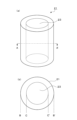
- FIG. 1 shows an example of a silicon carbide single crystal wafer 31 of this embodiment.
- the drawing shows a silicon carbide single crystal wafer 31 having a circular surface shape.
- the silicon carbide single crystal wafer 31 may have a polygonal shape (such as a hexagonal shape) instead of a circular shape.
- Silicon carbide single crystal wafer 31 preferably has a diameter of 100 mm or more and a thickness of 50 ⁇ m or more and 500 ⁇ m or less.
- the silicon carbide single crystal wafer 31 is preferably cut from an ingot so that the surface is within ⁇ 5 degrees from the (0001) plane of 4H—SiC or 6H—SiC.
- the surface may have an off angle of 0.5 degrees or more and 5 degrees or less from the (0001) plane of the silicon carbide single crystal.
- the silicon carbide single crystal wafer 31 may have a plane portion called an orientation flat and a groove called a notch.
- the silicon carbide single crystal wafer 31 has features 1 and 2 below. Moreover, the silicon carbide single crystal wafer 31 preferably has features 3 and 4 below.
- Silicon carbide single crystal wafer 31 contains boron at a concentration of 1.0 ⁇ 10 16 atoms/cm 3 or less. Boron is included as an unavoidable impurity.
- Characteristic 1 is that the concentration of boron, which is an unavoidable impurity, is sufficiently reduced to 1.0 ⁇ 10 16 atoms/cm 3 or less.
- the characteristic 1 is that the concentration range of boron, which is an inevitable impurity (the range of concentrations that can be mixed into the silicon carbide single crystal wafer 31), is sufficiently narrow to be greater than 0 and 1.0 ⁇ 10 16 atoms/cm 3 or less. It is what was done. Preferably, it may be greater than 0 and 1.0 ⁇ 10 15 atoms/cm 3 or less.
- the characteristics (eg, crystallinity and electrical characteristics) of the silicon carbide single crystal wafer 31 may deviate greatly from the intended ones.
- the impurity concentration cannot be predicted, or if the concentration range that can be predicted is wide, product design becomes difficult.
- Silicon carbide single crystal wafer 31 having feature 1 has a narrow concentration range of 1.0 ⁇ 10 16 atoms/cm 3 or less of boron, which is an unavoidable impurity that enters unintentionally. Therefore, it becomes relatively easy to design products in consideration of the concentration of boron.
- the boron concentration was measured at a plurality of points in the plane as described later, the boron concentration was 1.0 ⁇ 10 16 atoms/cm 3 or less at any of the measurement points, and there was no variation in the boron concentration in the plane. Since it is small, it is considered that the uniformity of in-plane crystallinity and electrical characteristics of the obtained silicon carbide single crystal wafer 31 is good.
- the concentration of boron is a value obtained by measuring one center point of the silicon carbide single crystal wafer 31 by secondary ion mass spectrometry (SIMS).
- SIMS secondary ion mass spectrometry
- values measured in dynamic SIMS mode using a secondary ion mass spectrometer (IMS 6f, CAMECA) were used.
- the measurement results were obtained at one point at the center of the silicon carbide single crystal wafer 31 (hereinafter referred to as "central point") and four peripheral points 50 mm away from the center (hereinafter referred to as "peripheral points”). was evaluated based on The boron concentrations at these five points were measured in the same manner as the measurement method for the central one point described above.
- the evaluation value is calculated by the formula "(boron concentration at the peripheral point ⁇ boron concentration at the central point)/boron concentration at the central point” for four pairs of the central point and each of the four peripheral points. and when the average value of the evaluation values of the four pairs is -0.3 or more and 3.0 or less, more preferably all the evaluation values of the four pairs are -0.3 or more and 3.0 or less It was assumed that the variation was small at that time.
- central area 33 On the surface of the silicon carbide single crystal wafer 31, there is a region where the orientation difference within the crystal plane of the silicon carbide single crystal wafer 31 is 50 arcsec or less.
- this area will be referred to as "central area 33".
- the central region 33 refers to an undivided region that includes the center of the surface of the silicon carbide single crystal wafer 31 . It is preferable that the center of the central region 33 and the center of the surface of the silicon carbide single crystal wafer 31 overlap, and it is more preferable that the shape of the central region 33 and the shape of the surface of the silicon carbide single crystal wafer 31 are the same or similar.
- the area of central region 33 is at least one fourth of the area of the surface of silicon carbide single crystal wafer 31 . Also, the central region 33 may preferably be one-third or more of the area of the surface.
- Characteristic 2 is provided with a central region 33 in which the orientation difference in the crystal plane is sufficiently reduced to 50 arcsec or less, and the central region 33 is as wide as 1/4 or more of the area of the surface and includes the center of the surface. be.
- the central region 33 has excellent crystallinity due to suppression of distortion in the crystal. Preferably, it may be 40 arcsec or less.
- the misorientation is between one point at the center of the silicon carbide single crystal wafer 31 and four points on the outer periphery of the wafer (0 degrees, 90 degrees, 180 degrees, and 270 degrees. Each point is 80% of the wafer radius away from the center.). It is the average value of the measurement results of the misorientation using the X-ray diffraction method at each of a total of five points. In this embodiment, the measurement was performed using an X-ray diffractometer (manufactured by RIGAKU, smartlab).
- the electrical resistivity of the silicon carbide single crystal wafer 31 is 60 m ⁇ cm or less. Characteristic 3 is that the electrical resistivity is 60 m ⁇ cm or less, and the electrical conductivity is excellent. It is preferably 50 m ⁇ cm or less, more preferably 30 m ⁇ cm or less.
- the electrical resistivity is measured at one point in the center of the silicon carbide single crystal wafer 31 and four points in the outer peripheral portion of the wafer (0 degrees, 90 degrees, 180 degrees, and 270 degrees, each at a distance of 80% of the wafer radius from the center). It is the average value of the measurement results at each of a total of 5 points.
- the measurement method is non-contact measurement by the eddy current method. In this embodiment, the measurement was performed using an EC-80P manufactured by Napson.
- the region (central region 33) has a basal plane dislocation density of 100/cm 2 or less.
- Characteristic 4 is that the basal plane dislocation density is sufficiently reduced to 100/cm 2 or less, and the crystallinity is improved.
- the basal plane dislocation density is 80/cm 2 or less, more preferably 50/cm 2 or less.
- the basal plane dislocations in this specification refer to dislocations observable by the etch pit method using KOH, and the basal plane dislocation density is the value measured by the etch pit method using KOH.
- a silicon carbide single crystal wafer 31 whose Si surface side was CMP-polished was immersed in a KOH melt heated to 520° C. for 30 minutes in an air atmosphere. After being taken out, the silicon carbide single crystal wafer 31 was washed with ultrapure water and subjected to measurement.
- the silicon carbide single crystal wafer 31 having features 1 and 2 has a low concentration of boron, which is an unavoidable impurity, has a narrow concentration range, and is a wafer excellent in crystallinity due to a reduction in the in-plane orientation difference.
- boron concentration exceeded 1.0 ⁇ 10 16 atoms/cm 3
- the higher the boron concentration the higher the orientation difference in the crystal plane.
- a boron concentration of 1.0 ⁇ 10 16 atoms/cm 3 or less makes it easier to reduce the misorientation in the crystal plane.
- the silicon carbide single crystal wafer 31 having features 3 and/or 4 in addition to features 1 and 2 is a wafer that achieves both conductivity and crystallinity.
- the conductivity described above is provided by conductive impurities contained within the silicon carbide single crystal wafer 31 .
- the conductive impurities include donor-type conductive impurities (hereinafter sometimes referred to as "donor-type”) and acceptor-type conductive impurities (hereinafter sometimes referred to as "acceptor-type").
- donor-type donor-type
- acceptor-type conductive impurities hereinafter sometimes referred to as "acceptor-type”
- the electrical resistivity can be lowered as the carrier concentration calculated from the difference between the carrier type and the acceptor type increases.
- the higher the concentration of donor-type conductive impurities in particular the lower the crystallinity.
- a preferred embodiment of the present invention is more preferably an n-type silicon carbide single crystal wafer 31 that has donor-type conductive impurities and acceptor-type conductive impurities and has more donor types than acceptor types. good too.
- This embodiment can reduce basal plane dislocations even when the n-type carrier concentration is in the range of 1 ⁇ 10 19 atoms/cm 3 or more and 10 ⁇ 10 19 atoms/cm 3 or less.
- the concentration of the donor-type conductive impurity may be 1 ⁇ 10 18 atoms/cm 3 or more and 1 ⁇ 10 21 atoms/cm 3 or less, more preferably 5 ⁇ 10 18 atoms/cm 3 or more, It may be 2 ⁇ 10 20 atoms/cm 3 or less.
- Nitrogen and phosphorus are well known as the donor-type conductive impurities, and more preferably nitrogen may be used.
- elements belonging to group 13 of the periodic table are well known as acceptor-type conductive impurities, and the present invention has found that the above-described favorable characteristics can be obtained by reducing the boron concentration. Therefore, as the acceptor-type conductive impurity in this embodiment, it is preferable to use an element belonging to Group 13 of the periodic table, excluding boron. More preferably, aluminum, gallium, and indium may be used.
- the conductive impurity concentration can be measured by the same method as the boron concentration.
- the silicon carbide single crystal ingot of the present embodiment may have a substantially cylindrical shape or a substantially polygonal shape.
- the two planes may be the upper surface and the lower surface, and the surfaces in contact with the upper surface and the lower surface may be the side surfaces.
- the upper and lower surfaces are parallel to the AA' and DD' cross-sections, which will be described later.
- FIG. 2 shows a substantially cylindrical silicon carbide single crystal ingot 21 .
- FIG. 2(a) is a perspective view
- FIG. 2(b) is a sectional view taken along line AA' in FIG. 2(a).
- 2(b) is the diameter of the silicon carbide single crystal ingot 21, and CC' of FIG. 2(b) is the center of the silicon carbide single crystal ingot 21.
- a region 23 may be used.
- FIG. 3 shows a silicon carbide single crystal ingot 22 having a substantially polygonal prism shape.
- 3(a) is a perspective view
- FIG. 3(b) is a cross-sectional view taken along line DD' in FIG. 3(a).
- the diameter may be the maximum length passing through the center of the DD′ cross section in FIG. may be the diameter of silicon carbide single crystal ingot 22 .
- the central region 23 of the silicon carbide single crystal ingot 22 may be the region whose diameter is FF' in FIG. 3(b).
- the length of the silicon carbide single crystal ingot of the present embodiment in the crystal growth direction is preferably 10 mm or more, more preferably 15 mm or more. Moreover, it is preferable that the difference between the diameter of the upper surface and the diameter of the lower surface of the silicon carbide single crystal ingot is small, and the difference may be 0 mm or more and 0.5 mm or less.
- Wafers cut perpendicular to the crystal growth direction (c-axis direction) from the silicon carbide single crystal ingots 21 and 22 of the present embodiment can be used as the silicon carbide single crystal wafers 31 described above. That is, the wafers cut out from the silicon carbide single crystal ingots 21 and 22 of the present embodiment have the excellent features described above.
- the central region 23, which is the region within the silicon carbide single crystal ingots 21 and 22, can be cut out as a wafer to become the central region 33 of the silicon carbide single crystal wafer 31 described above.
- the silicon carbide single crystal ingots 21 and 22 can have the aforementioned features 1 and 2, and further features 3 and/or 4 on the plane cut perpendicular to the c-axis direction. Since features 1 to 4 overlap with the above description, their description is omitted here.
- FIG. 4 is a diagram showing an overview of the crystal growth apparatus 1 used in the manufacturing method of this embodiment.
- the crystal growth apparatus 1 has a crucible 3, a pulling shaft 7, and heaters 4a and 4b (hereinafter collectively referred to as heater 4 in some cases).
- the crystal growth apparatus 1 has an internal space in which the crucible 3, the pulling shaft 7 and the like can be placed (hereinafter sometimes referred to as a "furnace"), and the internal space may be sealed. .
- the heater 4 may be arranged in the internal space, or may heat the internal space from outside.
- the crystal growth apparatus 1 can measure a supply port (not shown) capable of supplying various gases to the internal space, an exhaust port (not shown) capable of discharging from the internal space, and the pressure within the internal space. pressure gauge or the like.
- a silicon carbide single crystal is produced by growing a crystal while bringing a silicon carbide seed crystal 9 into contact with a raw material solution 5 containing silicon and carbon from above.
- a heating step of heating the members used in the crystal growing step is performed prior to the crystal growing step (hereinafter referred to as “crystal growing step”). Boron in the member can be reduced by this heating step. As a result, it is possible to reduce the inconvenience of unintentional contamination of boron from this member.
- the member may be heated in a halogen gas atmosphere. By doing so, boron in the member can be volatilized as boron halide.
- the member to be heated is a member containing boron, and examples thereof include the crucible 3, the pulling shaft 7, and a jig for holding the seed crystal (not shown). but not limited to these.
- halogen gas includes gases consisting of a single halogen such as Cl 2 and F 2 , interhalogen gases such as ClF 3 , IF 5 and IF 3 and halogen-containing gases such as HCl.
- the heating conditions are preferably 1600° C. to 2000° C. for 1 to 20 hours and a halogen gas pressure of 5 to 100 kPa.
- the temperature may be more preferably 1700° C. or higher and 2000° C. or lower, and even more preferably 1800° C. or higher and 2000° C. or lower.
- the temperature below indicates the temperature of the object to be heated. For example, when the temperature is 1600°C, the temperature of the object to be heated is 1600°C. Also, the temperature of the object to be heated can be measured with a radiation thermometer.
- the heating process may be performed before the crystal growth process, and the timing is not particularly limited. For example, after obtaining a member to be subjected to heat treatment, a heating step of heating the member at least once may be performed before using the member for the first time to perform the crystal growth step. Alternatively, the heating step may be performed immediately before each crystal growth step. Alternatively, the heating step may be performed at a predetermined timing such as the beginning of the day, the beginning of the week, or the beginning of the month.
- the "pressure in the apparatus" during the heating process described above can be adjusted by supplying or exhausting gas so that the pressure in the furnace is within the range described above.
- the "halogen gas pressure” refers to the pressure in the furnace when only halogen gas is supplied, and the partial pressure of halogen gas in the furnace when halogen gas and any diluent gas are supplied to the apparatus. shall refer to
- the airtight state may be established after the gas is supplied, or the gas may be supplied and discharged at the same time to allow the gas to flow while maintaining a predetermined pressure.
- the gas to be supplied include inert gas such as He gas and Ar gas, halogen gas, and the like.
- H 2 gas may also be used under conditions of low reactivity such as low pressure.
- Cl 2 or HCl because it is easy to suppress damage and reactivity to members in contact with the gas.
- a separate operation may be performed in order to suppress the influence of the halogen gas on the seed crystal.
- the heating step may be performed without placing the seed crystal 9, then the temperature may be once lowered to a workable temperature, and after placing the seed crystal 9 on the pulling shaft 7, the next step may be performed.
- an isolating member or protective material capable of isolating the seed crystal 9 from the atmosphere in the furnace may be installed, and after the heating step is performed, the isolating member or protective material may be removed and the next step may be performed. In the case of the latter operation, if the work is possible, it is not necessary to intentionally lower the temperature.
- a degassing step of degassing the inside of the furnace may be provided between the heating step and the crystal growth step.
- the degassing method may be a known method and is not particularly limited, but vacuum degassing is preferable because it efficiently removes the atmosphere in the furnace.
- a crystal growth apparatus 1 shown in FIG. 4 has a raw material solution 5 containing silicon and carbon inside a crucible 3, and a pulling shaft 7 can rotate a seed crystal 9 attached to the tip with its long axis as a rotation axis. be. Also, an upward flow 6 is formed in which the raw material solution 5 flows from bottom to top toward the seed crystal 9 .
- the centers of the crucible 3 and the pull-up shaft 7 do not necessarily have to match, but preferably match. More preferably, all the axes are aligned.
- a graphite crucible that can supply carbon to the raw material solution 5 is preferable.
- Crucibles other than graphite crucibles can be used as long as they can be added.
- the rotational speed of the crucible 3 is preferably 5-30 rpm, more preferably 5-20 rpm. By setting it within the above range, it is possible to efficiently grow the crystal without imposing an excessive burden on the apparatus.
- the crucible 3 may be rotated in the forward direction and the reverse direction while periodically reversing the rotation direction.
- the raw material solution 5 is heated by heaters 4a, 4b, etc. provided around the crucible 3 and kept in a molten state.
- the heaters 4a and 4b may be of induction heating type or resistance heating type.
- the temperature in the crucible 3 is preferably 1700-2100°C.
- the temperature inside the crucible can be obtained by measuring the surface of the raw material solution 5 or its vicinity with a non-contact thermometer (IR-CZH7 type, manufactured by Chino).
- silicon source for the raw material solution 5 metal silicon, silicon alloys, silicon compounds, etc. can be used.
- carbon source of the raw material solution solid carbon sources such as graphite, glassy carbon and silicon carbide, and hydrocarbon gases such as methane, ethane, propane and acetylene can be used.
- the raw material solution 5 is not particularly limited as long as it is a solution containing silicon and carbon used for crystal growth of silicon carbide, but it is preferable to use a solution in which carbon is dissolved in a Si solvent to which additive elements are added.
- Silicon alloys or silicon compounds used as the silicon source of the raw material solution include silicon and Ti, Cr, Sc, Ni, Al, Co, Mn, Mg, Ge, As, P, N, O, Dy, Y, An alloy or compound with at least one additive element selected from Nb, Nd and Fe can be used.
- An inert gas such as a rare gas is preferably circulated in the crystal growth apparatus 1 during the crystal growth step to create an inert atmosphere.
- the pressure is not particularly limited, it may be about atmospheric pressure (about 100 kPa).
- a hydrocarbon-based gas such as CH4 may be added to create a mixed gas atmosphere.
- a mixed gas atmosphere may be formed by adding a gas that is a source of the conductive impurities.
- the raw material solution 5 in FIG. 4 forms an upward flow 6 in the center of the crucible 3 and contacts the center of the seed crystal 9 .
- Forming the upward flow 6 is preferable because it is possible to stabilize the concentration of the raw material solution 5 at the growth interface.
- the velocity of the upward flow is preferably 0.5 cm/s or more and 5 cm/s or less at a position 1 cm away from the growth interface in the downward direction.
- the method of forming the ascending flow 6 is not particularly limited, but a method of adjusting the output of the heater 4a on the side and the heater 4b on the bottom, a method of providing a protrusion or a plate portion capable of controlling the flow in the crucible 3, or a method of A possible method is to form an upward flow by the Lorentz force generated by the electromagnetic field generated by the magnetic field coil. For example, if the output of the heater 4b on the bottom surface is increased, an upward convection is generated from the heater 4b, and an upward flow 6 is formed.
- the pulling shaft 7 pulls the seed crystal 9 relatively slowly upward with respect to the raw material solution 5 to grow the silicon carbide single crystal 11 .
- the pull-up shaft 7 may be moved upward or the crucible 3 may be moved downward, but it is preferable to move the pull-up shaft 7 upward in order to relatively reduce the influence on the temperature distribution.
- the direction of the seed crystal 9 from the liquid surface of the raw material solution 5 is formed between the seed crystal 9 and the liquid surface of the raw material solution 5 .
- a convex meniscus may be formed. It is presumed that the formation of the meniscus lowers the temperature of the raw material solution 5 around the seed crystal 9, increases the degree of carbon supersaturation, and improves the growth rate. Further, by adjusting the shape of the meniscus, it is possible to increase the growth rate of the seed crystal 9 in the lateral direction, so that the diameter of the silicon carbide single crystal 11, which is the grown crystal, is made larger than the diameter of the seed crystal 9. It is possible to
- the diameter of silicon carbide single crystal 11 may be about the same as the diameter of seed crystal 9, but as shown in FIG. good too.
- the meniscus angle ⁇ when enlarging the diameter of the grown crystal is preferably 35 degrees or more. More preferably 60 degrees or more, more preferably 65 degrees or more. Also, since ⁇ is 90 degrees when no meniscus is formed, the upper limit is not particularly limited, but may be less than 90 degrees, more preferably 85 degrees or less.
- crystal growth may be performed while maintaining the predetermined diameter.
- the meniscus may or may not be formed, but if it is formed, the aforementioned angle ⁇ may be 10 degrees or more.
- the upper limit may be less than 35 degrees, more preferably less than 30 degrees, for example, as long as the diameter of the grown crystal does not expand.
- the meniscus angle .theta be the angle formed by ⁇ : contact point between the edge of the seed crystal and the liquid surface of the raw material solution (hereinafter sometimes referred to as “liquid surface”)
- l 0 liquid surface when no meniscus is formed
- l meniscus formed
- FIG. 6 is a schematic diagram of the surface of the seed crystal 9.
- the seed crystal 9 has a surface cut at an angle of more than 0 degrees and 5 degrees or less with respect to the (000-1) plane, and the angle between the surface of the seed crystal 9 and the (000-1) plane is off. called a corner. It is preferably 0.1 degrees or more and 5 degrees or less, more preferably 0.5 degrees or more and 5 degrees or less. Further, in order to obtain a desired silicon carbide single crystal, the seed crystal 9 may have a surface cut along the (000-1) plane without providing the above-described off-angle.
- the step flow direction is the direction in which steps progress. For example, if the off angle is formed toward the [11-20] direction, the step flow direction is the [11-20] direction.
- the off-angle reference may be made to FIG. 20 of International Publication No. 2014/034080, which is a patent document.
- the thickness of the seed crystal 9 is not particularly limited, it may normally be 0.1 mm or more. In the present embodiment, the thickness of the seed crystal 9 tends to be 0.3 mm or more because the defect density of the resulting silicon carbide single crystal 11 tends to decrease as the thickness of the seed crystal 9 increases. It is preferably 1 mm or more, more preferably 3 mm or more. In addition, if the seed crystal 9 is excessively thick, the seed crystal 9 becomes too expensive.
- At least the raw material solution 5 that contacts the crystal growth surface of the seed crystal 9 must be in a supersaturated state.
- a seed crystal 9 is immersed in a raw material solution 5 having a carbon saturated concentration, and then supercooled to make the carbon concentration supersaturated.
- a temperature difference method or the like is possible in which a seed crystal 9 is immersed in a solution 5 and crystals are grown at a low temperature.
- the entire raw material solution 5 becomes supersaturated, so it is possible to grow the crystal by rotating the pulling shaft 7 while the seed crystal 9 is immersed in the raw material solution 5.
- the seed crystal 9 may remain fixed, it is preferable to rotate it in a plane parallel to the surface of the raw material solution 5 .
- the rotation speed is preferably 20 to 300 rpm, more preferably 20 to 150 rpm.
- the rotation of the seed crystal 9 is preferably rotation that periodically repeats forward rotation and reverse rotation, and the cycle is about 30 seconds to 5 minutes. By periodically changing the direction of rotation, it is possible to control the flow of the raw material solution 5 on the growth surface of the seed crystal during crystal growth.
- the off-substrate seed crystal 9 shown in FIG. 6 is cut to have a predetermined off-angle with respect to the (000-1) plane, as described above.
- the seed crystal 9 described above is preferably attached to the pulling shaft 7 so that the surface having the off-angle is brought into contact with the raw material solution 5 as a crystal growth surface.
- the temperature T1 of the crystal growth interface P1 and the temperature T2 of the solution at the point P2 at a distance of 5 mm from the crystal growth interface P1 satisfy T2>T1, and between P1 and P2 is greater than 0 K/cm and less than or equal to 40 K/cm.
- the temperature gradient is a value calculated by thermal fluid simulation.
- the lower limit of the temperature gradient may be preferably 2 K/cm or more, more preferably 4 K/cm or more.
- the upper limit of the temperature gradient may be preferably 30 K/cm or less, more preferably 20 K/cm or less.
- the silicon carbide single crystal 11 is separated from the pulling shaft 7, and if necessary, the periphery thereof is processed by polishing or the like to obtain a silicon carbide single crystal ingot 21 as shown in FIG. 2(a) or FIG. 3(a). , 22.
- the crystal growth direction of silicon carbide single crystal ingots 21 and 22 coincides with the long axis direction of silicon carbide single crystal ingots 21 and 22 .
- the silicon carbide single crystal ingots 21 and 22 may be separated from the seed crystal 9 .
- the silicon carbide single crystal wafers 31 are manufactured by cutting the silicon carbide single crystal ingots 21 and 22 thus manufactured.
- the silicon carbide single crystal wafer 31 can be used as a bare wafer or used as a seed crystal wafer for epitaxial growth.
- Example 1 First, as the heating step described above, the pressure of the halogen gas (HCl is used here) in the furnace is set to 10 kPa with respect to the crucible 3 and the pulling shaft 7 of the crystal growth apparatus 1 as shown in FIG. C. or lower for 20 hours in a halogen gas atmosphere.
- the pressure of the halogen gas (HCl is used here
- the halogen gas in the crystal growth apparatus 1 is removed, and a disk-shaped 4H-SiC seed crystal with a diameter of 150 mm and a thickness of 500 ⁇ m is fixed to the lower end of the pulling shaft 7 made of carbon. bottom.
- the growth plane of the seed crystal 9 in contact with the solution was the C plane, which was offset by 1 degree from the [0001] direction to the [11-20] direction.
- the inside of the crystal growth apparatus 1 was replaced with atmospheric gas (He+0.1 vol % N 2 ), and the pressure inside the apparatus was set to 100 kPa. Then, the Si—Cr powder (containing 0.4 mol % of the acceptor-type element) in the crucible 3 is heated by the heater 4 to form a silicon melt. A solution was prepared.
- the seed crystal 9 was brought into contact with the Si—C solution surface to grow a silicon carbide crystal from the lower end of the seed crystal 9 .
- the temperature of the surface of the solution was set to 1950° C., and conditions were set so that the flow of the solution formed an upward flow with respect to the growth interface during the growth.
- the solution flow was set to a desired upward flow by applying Lorentz force to the solution side by an electromagnetic field formed by energizing the magnetic field coil and controlling the conditions.
- the pulling speed of the pulling shaft 7 was appropriately adjusted according to the crystal growth speed, and the crystal growth was continued until the crystal length exceeded 20 mm. .
- the rotational speed of the pull-up shaft 7 was controlled to a maximum of 100 rpm, and the temperature in the vicinity of the growth interface was controlled to 1950°C ⁇ 20°C.
- the temperature T1 of the crystal growth interface P1 and the temperature T2 of the solution at the point P2 at a distance of 5 mm from the crystal growth interface P1 satisfy T2>T1, and the temperature gradient between P1 and P2 is 18 K/ cm.
- the temperature of the growth interface and the temperature gradient were realized by controlling the output balance of the heater that heats the crucible. After that, the obtained silicon carbide single crystal was separated from the pulling shaft.
- the central portion of the separated silicon carbide single crystal was sliced with a wire saw at an off angle of 4 degrees with respect to the (0001) plane to a thickness of 500 ⁇ m, and then the Si surface side was mirror-polished to obtain a silicon carbide single crystal. I got a wafer.
- the center point (central point) of the silicon carbide single crystal wafer 31 and the peripheral four points (peripheral points) 50 mm apart from the center were measured using the above-described center point measurement method. Boron concentration was measured in a similar manner. As a result, the obtained five boron concentrations were all 1.0 ⁇ 10 16 atoms/cm 3 or less.
- the evaluation value was calculated by the formula "(boron concentration at peripheral point ⁇ boron concentration at central point)/boron concentration at central point". As a result, all the evaluation values of the four pairs were within the range of -0.3 or more and 3.0 or less.
- Table 1 shows the evaluation results.
- the table shows the off angle from the (0001) plane, the donor concentration, the acceptor concentration, the n-type carrier concentration, and the temperature gradient in addition to the above characteristics.
- Examples 1 to 4 have the features 1 to 4 described above, have a low concentration of boron, which is an unavoidable impurity, and have excellent crystallinity and conductivity by reducing basal plane dislocations and misorientation. It can be seen that the wafer is a silicon carbide single crystal wafer.
- Comparative Examples 1 to 6 manufactured by a method different from Examples 1 to 4 do not have at least one of features 1 or 2 and do not have at least one of features 1 to 4.
- HCl was used as the halogen gas in the furnace in the examples shown here, but the inventors have confirmed that similar results can be obtained when other halogen gases are used.
- a silicon carbide single crystal wafer the silicon carbide single crystal wafer contains boron at a concentration of 1.0 ⁇ 10 16 atoms/cm 3 or less; On the surface of the silicon carbide single crystal wafer, there is a region where the orientation difference in the crystal plane of the silicon carbide single crystal wafer is 50 arcsec or less, the region includes the center of the surface; The silicon carbide single crystal wafer, wherein the area of the region is at least one fourth of the area of the surface. 2. 2. The silicon carbide single crystal wafer according to 1, wherein the region has a basal plane dislocation density of 100/cm 2 or less. 3. 3. 3.
- the silicon carbide single crystal wafer according to 2 wherein the region is circular and the center of the region overlaps the center of the surface. 4. 4. The silicon carbide single crystal wafer according to any one of 1 to 3, wherein the silicon carbide single crystal wafer has an electric resistivity of 60 m ⁇ cm or less. 5. 5. The silicon carbide single crystal wafer according to any one of 1 to 4, wherein the silicon carbide single crystal wafer has a diameter of 100 mm or more. 6.
- a substantially cylindrical or polygonal silicon carbide single crystal ingot The wafer cut perpendicular to the crystal growth direction contains boron at a concentration of 1.0 ⁇ 10 16 atoms/cm 3 or less, a region having a misorientation of 50 arcsec or less in the crystal plane of the wafer exists on the surface of the wafer; the region includes the center of the surface; A silicon carbide single crystal ingot, wherein the area of the region is at least a quarter of the area of the surface. 7. 7. The silicon carbide single crystal ingot according to 6, wherein the length in the crystal growth direction of the silicon carbide single crystal ingot is 10 mm or more.
Abstract
Cette tranche de monocristal de carbure de silicium comprend du bore à une concentration de 1,0 × 10¹⁶atomes/cm3 ou moins et a, sur sa surface, une région dans laquelle la différence d'orientation à l'intérieur d'un plan cristallin de la tranche de monocristal de carbure de silicium (31) est inférieure ou égale à 50 arcsec. La superficie de ladite région constitue au moins un quart de la superficie de la surface de la tranche monocristalline de carbure de silicium.
Applications Claiming Priority (2)
| Application Number | Priority Date | Filing Date | Title |
|---|---|---|---|
| JP2021-160608 | 2021-09-30 | ||
| JP2021160608 | 2021-09-30 |
Publications (1)
| Publication Number | Publication Date |
|---|---|
| WO2023054264A1 true WO2023054264A1 (fr) | 2023-04-06 |
Family
ID=85782667
Family Applications (1)
| Application Number | Title | Priority Date | Filing Date |
|---|---|---|---|
| PCT/JP2022/035724 WO2023054264A1 (fr) | 2021-09-30 | 2022-09-26 | Tranche monocristalline de carbure de silicium et lingot monocristallin de carbure de silicium |
Country Status (2)
| Country | Link |
|---|---|
| TW (1) | TW202331031A (fr) |
| WO (1) | WO2023054264A1 (fr) |
Citations (12)
| Publication number | Priority date | Publication date | Assignee | Title |
|---|---|---|---|---|
| JPH107488A (ja) * | 1997-03-19 | 1998-01-13 | Toyo Tanso Kk | 単結晶引上装置、高純度黒鉛材料及びその製造方法 |
| JP2009091222A (ja) * | 2007-10-11 | 2009-04-30 | Sumitomo Metal Ind Ltd | SiC単結晶の製造方法、SiC単結晶ウエハ及びSiC半導体デバイス |
| JP2009167047A (ja) | 2008-01-15 | 2009-07-30 | Nippon Steel Corp | 炭化珪素単結晶インゴット、これから得られる基板及びエピタキシャルウェハ |
| JP2013075771A (ja) * | 2011-09-29 | 2013-04-25 | Toyota Motor Corp | SiC単結晶の製造方法及び製造装置 |
| WO2014034080A1 (fr) | 2012-08-26 | 2014-03-06 | 国立大学法人名古屋大学 | Monocristal 3c-sic et son procédé de production |
| WO2014189008A1 (fr) * | 2013-05-20 | 2014-11-27 | 日立化成株式会社 | Monocristal de carbure de silicium et son procédé de fabrication |
| JP2015030640A (ja) | 2013-08-02 | 2015-02-16 | 株式会社デンソー | 炭化珪素単結晶 |
| JP2016088794A (ja) | 2014-10-31 | 2016-05-23 | トヨタ自動車株式会社 | SiC単結晶の製造方法 |
| JP2016164120A (ja) | 2016-03-15 | 2016-09-08 | 新日鉄住金マテリアルズ株式会社 | 炭化珪素単結晶ウェハ |
| WO2017047536A1 (fr) | 2015-09-14 | 2017-03-23 | 新日鐵住金株式会社 | APPAREIL ET PROCÉDÉ DE FABRICATION DE MONOCRISTAL SiC, ET MATÉRIAU MONOCRISTALLIN SiC |
| JP2018111639A (ja) | 2017-01-13 | 2018-07-19 | セントラル硝子株式会社 | 炭化ケイ素単結晶ウェハ、インゴット及びその製造方法 |
| JP2021160608A (ja) | 2020-03-31 | 2021-10-11 | 株式会社エクォス・リサーチ | 移動装置 |
-
2022
- 2022-09-26 WO PCT/JP2022/035724 patent/WO2023054264A1/fr active Application Filing
- 2022-09-30 TW TW111137382A patent/TW202331031A/zh unknown
Patent Citations (12)
| Publication number | Priority date | Publication date | Assignee | Title |
|---|---|---|---|---|
| JPH107488A (ja) * | 1997-03-19 | 1998-01-13 | Toyo Tanso Kk | 単結晶引上装置、高純度黒鉛材料及びその製造方法 |
| JP2009091222A (ja) * | 2007-10-11 | 2009-04-30 | Sumitomo Metal Ind Ltd | SiC単結晶の製造方法、SiC単結晶ウエハ及びSiC半導体デバイス |
| JP2009167047A (ja) | 2008-01-15 | 2009-07-30 | Nippon Steel Corp | 炭化珪素単結晶インゴット、これから得られる基板及びエピタキシャルウェハ |
| JP2013075771A (ja) * | 2011-09-29 | 2013-04-25 | Toyota Motor Corp | SiC単結晶の製造方法及び製造装置 |
| WO2014034080A1 (fr) | 2012-08-26 | 2014-03-06 | 国立大学法人名古屋大学 | Monocristal 3c-sic et son procédé de production |
| WO2014189008A1 (fr) * | 2013-05-20 | 2014-11-27 | 日立化成株式会社 | Monocristal de carbure de silicium et son procédé de fabrication |
| JP2015030640A (ja) | 2013-08-02 | 2015-02-16 | 株式会社デンソー | 炭化珪素単結晶 |
| JP2016088794A (ja) | 2014-10-31 | 2016-05-23 | トヨタ自動車株式会社 | SiC単結晶の製造方法 |
| WO2017047536A1 (fr) | 2015-09-14 | 2017-03-23 | 新日鐵住金株式会社 | APPAREIL ET PROCÉDÉ DE FABRICATION DE MONOCRISTAL SiC, ET MATÉRIAU MONOCRISTALLIN SiC |
| JP2016164120A (ja) | 2016-03-15 | 2016-09-08 | 新日鉄住金マテリアルズ株式会社 | 炭化珪素単結晶ウェハ |
| JP2018111639A (ja) | 2017-01-13 | 2018-07-19 | セントラル硝子株式会社 | 炭化ケイ素単結晶ウェハ、インゴット及びその製造方法 |
| JP2021160608A (ja) | 2020-03-31 | 2021-10-11 | 株式会社エクォス・リサーチ | 移動装置 |
Also Published As
| Publication number | Publication date |
|---|---|
| TW202331031A (zh) | 2023-08-01 |
Similar Documents
| Publication | Publication Date | Title |
|---|---|---|
| US9234297B2 (en) | Silicon carbide single crystal wafer and manufacturing method for same | |
| JP4853449B2 (ja) | SiC単結晶の製造方法、SiC単結晶ウエハ及びSiC半導体デバイス | |
| JP5706823B2 (ja) | SiC単結晶ウエハーとその製造方法 | |
| CN106435733B (zh) | 碳化硅单晶和碳化硅单晶晶片 | |
| JP5304712B2 (ja) | 炭化珪素単結晶ウェハ | |
| JP4585359B2 (ja) | 炭化珪素単結晶の製造方法 | |
| US7520930B2 (en) | Silicon carbide single crystal and a method for its production | |
| JP2004002173A (ja) | 炭化珪素単結晶とその製造方法 | |
| WO2008033994A1 (fr) | Carbure de silicium exempt de micropipes et procede de fabrication associe | |
| US20190024257A1 (en) | Silicon carbide single crystal substrate and process for producing same | |
| JP2006111478A (ja) | 炭化珪素単結晶インゴット、炭化珪素単結晶ウェハ及びその製造方法 | |
| WO2015137439A1 (fr) | PROCÉDÉ DE PRODUCTION DE SiC MONOCRISTALLIN | |
| JP2004099340A (ja) | 炭化珪素単結晶育成用種結晶と炭化珪素単結晶インゴット及びその製造方法 | |
| JP6784220B2 (ja) | SiC単結晶の製造方法 | |
| JP3590485B2 (ja) | 単結晶炭化珪素インゴット及びその製造方法 | |
| JP2018111639A (ja) | 炭化ケイ素単結晶ウェハ、インゴット及びその製造方法 | |
| JP3662694B2 (ja) | 単結晶炭化珪素インゴットの製造方法 | |
| WO2023054264A1 (fr) | Tranche monocristalline de carbure de silicium et lingot monocristallin de carbure de silicium | |
| WO2023054263A1 (fr) | Tranche de carbure de silicium monocristallin, lingot de carbure de silicium monocristallin et procédé de production de carbure de silicium monocristallin | |
| JP4157326B2 (ja) | 4h型炭化珪素単結晶インゴット及びウエハ | |
| EP1498518B1 (fr) | Procede de prodution d'un monocristal de carbure de silicium | |
| JP5428706B2 (ja) | SiC単結晶の製造方法 | |
| JP6748613B2 (ja) | 炭化珪素単結晶基板 | |
| CN107366013B (zh) | SiC单晶及其制造方法 | |
| CN118043504A (en) | Silicon carbide single crystal wafer, silicon carbide single crystal ingot, and method for producing silicon carbide single crystal |
Legal Events
| Date | Code | Title | Description |
|---|---|---|---|
| 121 | Ep: the epo has been informed by wipo that ep was designated in this application |
Ref document number: 22876131 Country of ref document: EP Kind code of ref document: A1 |
|
| WWE | Wipo information: entry into national phase |
Ref document number: 2023551472 Country of ref document: JP |
|
| ENP | Entry into the national phase |
Ref document number: 2022876131 Country of ref document: EP Effective date: 20240430 |