WO2023053823A1 - 半導体装置 - Google Patents
半導体装置 Download PDFInfo
- Publication number
- WO2023053823A1 WO2023053823A1 PCT/JP2022/032604 JP2022032604W WO2023053823A1 WO 2023053823 A1 WO2023053823 A1 WO 2023053823A1 JP 2022032604 W JP2022032604 W JP 2022032604W WO 2023053823 A1 WO2023053823 A1 WO 2023053823A1
- Authority
- WO
- WIPO (PCT)
- Prior art keywords
- semiconductor device
- semiconductor elements
- conductor
- semiconductor
- electrode
- Prior art date
- Legal status (The legal status is an assumption and is not a legal conclusion. Google has not performed a legal analysis and makes no representation as to the accuracy of the status listed.)
- Ceased
Links
Images


Classifications
-
- H—ELECTRICITY
- H10—SEMICONDUCTOR DEVICES; ELECTRIC SOLID-STATE DEVICES NOT OTHERWISE PROVIDED FOR
- H10W—GENERIC PACKAGES, INTERCONNECTIONS, CONNECTORS OR OTHER CONSTRUCTIONAL DETAILS OF DEVICES COVERED BY CLASS H10
- H10W72/00—Interconnections or connectors in packages
- H10W72/851—Dispositions of multiple connectors or interconnections
-
- H—ELECTRICITY
- H02—GENERATION; CONVERSION OR DISTRIBUTION OF ELECTRIC POWER
- H02M—APPARATUS FOR CONVERSION BETWEEN AC AND AC, BETWEEN AC AND DC, OR BETWEEN DC AND DC, AND FOR USE WITH MAINS OR SIMILAR POWER SUPPLY SYSTEMS; CONVERSION OF DC OR AC INPUT POWER INTO SURGE OUTPUT POWER; CONTROL OR REGULATION THEREOF
- H02M7/00—Conversion of AC power input into DC power output; Conversion of DC power input into AC power output
- H02M7/42—Conversion of DC power input into AC power output without possibility of reversal
- H02M7/44—Conversion of DC power input into AC power output without possibility of reversal by static converters
- H02M7/48—Conversion of DC power input into AC power output without possibility of reversal by static converters using discharge tubes with control electrode or semiconductor devices with control electrode
-
- H—ELECTRICITY
- H10—SEMICONDUCTOR DEVICES; ELECTRIC SOLID-STATE DEVICES NOT OTHERWISE PROVIDED FOR
- H10W—GENERIC PACKAGES, INTERCONNECTIONS, CONNECTORS OR OTHER CONSTRUCTIONAL DETAILS OF DEVICES COVERED BY CLASS H10
- H10W70/00—Package substrates; Interposers; Redistribution layers [RDL]
- H10W70/60—Insulating or insulated package substrates; Interposers; Redistribution layers
- H10W70/611—Insulating or insulated package substrates; Interposers; Redistribution layers for connecting multiple chips together
-
- H—ELECTRICITY
- H10—SEMICONDUCTOR DEVICES; ELECTRIC SOLID-STATE DEVICES NOT OTHERWISE PROVIDED FOR
- H10W—GENERIC PACKAGES, INTERCONNECTIONS, CONNECTORS OR OTHER CONSTRUCTIONAL DETAILS OF DEVICES COVERED BY CLASS H10
- H10W70/00—Package substrates; Interposers; Redistribution layers [RDL]
- H10W70/60—Insulating or insulated package substrates; Interposers; Redistribution layers
- H10W70/62—Insulating or insulated package substrates; Interposers; Redistribution layers characterised by their interconnections
- H10W70/65—Shapes or dispositions of interconnections
-
- H—ELECTRICITY
- H10—SEMICONDUCTOR DEVICES; ELECTRIC SOLID-STATE DEVICES NOT OTHERWISE PROVIDED FOR
- H10W—GENERIC PACKAGES, INTERCONNECTIONS, CONNECTORS OR OTHER CONSTRUCTIONAL DETAILS OF DEVICES COVERED BY CLASS H10
- H10W72/00—Interconnections or connectors in packages
- H10W72/30—Die-attach connectors
-
- H—ELECTRICITY
- H10—SEMICONDUCTOR DEVICES; ELECTRIC SOLID-STATE DEVICES NOT OTHERWISE PROVIDED FOR
- H10W—GENERIC PACKAGES, INTERCONNECTIONS, CONNECTORS OR OTHER CONSTRUCTIONAL DETAILS OF DEVICES COVERED BY CLASS H10
- H10W72/00—Interconnections or connectors in packages
- H10W72/50—Bond wires
-
- H—ELECTRICITY
- H10—SEMICONDUCTOR DEVICES; ELECTRIC SOLID-STATE DEVICES NOT OTHERWISE PROVIDED FOR
- H10W—GENERIC PACKAGES, INTERCONNECTIONS, CONNECTORS OR OTHER CONSTRUCTIONAL DETAILS OF DEVICES COVERED BY CLASS H10
- H10W90/00—Package configurations
-
- H—ELECTRICITY
- H10—SEMICONDUCTOR DEVICES; ELECTRIC SOLID-STATE DEVICES NOT OTHERWISE PROVIDED FOR
- H10W—GENERIC PACKAGES, INTERCONNECTIONS, CONNECTORS OR OTHER CONSTRUCTIONAL DETAILS OF DEVICES COVERED BY CLASS H10
- H10W72/00—Interconnections or connectors in packages
- H10W72/851—Dispositions of multiple connectors or interconnections
- H10W72/874—On different surfaces
- H10W72/884—Die-attach connectors and bond wires
-
- H—ELECTRICITY
- H10—SEMICONDUCTOR DEVICES; ELECTRIC SOLID-STATE DEVICES NOT OTHERWISE PROVIDED FOR
- H10W—GENERIC PACKAGES, INTERCONNECTIONS, CONNECTORS OR OTHER CONSTRUCTIONAL DETAILS OF DEVICES COVERED BY CLASS H10
- H10W90/00—Package configurations
- H10W90/701—Package configurations characterised by the relative positions of pads or connectors relative to package parts
- H10W90/731—Package configurations characterised by the relative positions of pads or connectors relative to package parts of die-attach connectors
- H10W90/734—Package configurations characterised by the relative positions of pads or connectors relative to package parts of die-attach connectors between a chip and a stacked insulating package substrate, interposer or RDL
-
- H—ELECTRICITY
- H10—SEMICONDUCTOR DEVICES; ELECTRIC SOLID-STATE DEVICES NOT OTHERWISE PROVIDED FOR
- H10W—GENERIC PACKAGES, INTERCONNECTIONS, CONNECTORS OR OTHER CONSTRUCTIONAL DETAILS OF DEVICES COVERED BY CLASS H10
- H10W90/00—Package configurations
- H10W90/701—Package configurations characterised by the relative positions of pads or connectors relative to package parts
- H10W90/751—Package configurations characterised by the relative positions of pads or connectors relative to package parts of bond wires
- H10W90/754—Package configurations characterised by the relative positions of pads or connectors relative to package parts of bond wires between a chip and a stacked insulating package substrate, interposer or RDL
Definitions
- the present disclosure relates to semiconductor devices.
- a semiconductor device (power module) described in Patent Document 1 includes a plurality of first semiconductor elements, a plurality of first connection wirings, wiring layers, and signal terminals.
- the plurality of first semiconductor elements are, for example, MOSFETs. Each first semiconductor element is turned on/off according to a drive signal input to the gate terminal. The plurality of first semiconductor elements are connected in parallel.
- the plurality of first connection wirings are wires, for example, and connect the gate terminals of the plurality of first semiconductor elements and the wiring layer.
- a signal terminal is connected to the wiring layer.
- the signal terminal is connected to the gate terminal of each first semiconductor element via the wiring layer and each first connection wiring.
- the signal terminal supplies a drive signal for driving each first semiconductor element to the gate terminal of each first semiconductor element.
- an oscillation phenomenon may occur during switching (during ON/OFF driving) of each semiconductor element.
- This oscillation phenomenon may oscillate drive signals for a plurality of semiconductor elements, and is a cause of malfunction of each semiconductor element or destruction of each semiconductor element.
- the present disclosure has been conceived in view of the above circumstances, and one object thereof is to provide a semiconductor device capable of suppressing an oscillation phenomenon that occurs when a plurality of semiconductor elements are operated in parallel.
- the semiconductor device of the present disclosure each has a first electrode, a second electrode, and a third electrode, and can be switched between an on state and an off state according to a first drive signal input to the third electrode.
- two first semiconductor elements to be controlled a first conductor electrically interposed between the first electrodes of the two first semiconductor elements; electrically connected to the first conductor; a first power terminal in communication with the first electrode of each of the semiconductor devices.
- the two first semiconductor elements are electrically connected in parallel.
- the first conductor is arranged to avoid part of a first line segment connecting the centers of the two first semiconductor elements when viewed in the thickness direction of the first conductor.
- the semiconductor device of the present disclosure it is possible to suppress the oscillation phenomenon.
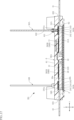
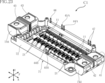
- FIG. 1 is a perspective view showing a semiconductor device according to a first embodiment
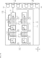
- FIG. FIG. 2 is a plan view showing the semiconductor device according to the first embodiment, showing a sealing member with imaginary lines.
- FIG. 3 is a plan view of FIG. 2 with a plurality of connecting members and sealing members omitted.
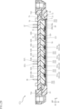
- FIG. 4 is a cross-sectional view taken along line IV-IV of FIG.
- FIG. 5 is a cross-sectional view along line VV in FIG.
- FIG. 6 is a cross-sectional view taken along line VI-VI of FIG.
- FIG. 7 is a fragmentary plan view showing a semiconductor device according to a first modification of the first embodiment, and corresponds to the plan view of FIG. FIG.
- FIG. 8 is a fragmentary plan view showing a semiconductor device according to a second modification of the first embodiment, and corresponds to the plan view of FIG. 9 is a fragmentary plan view showing a semiconductor device according to a third modification of the first embodiment, and corresponds to the plan view of FIG. 3.
- FIG. 10 is a fragmentary plan view showing a semiconductor device according to a fourth modification of the first embodiment, and corresponds to the plan view of FIG. 11 is a fragmentary plan view showing a semiconductor device according to another modification of the first embodiment, and corresponds to the plan view of FIG. 3.
- FIG. FIG. 12 is a perspective view showing a semiconductor device according to a second embodiment;
- FIG. 13 is a perspective view of FIG. 12 with the sealing member omitted.
- FIG. 14 is a plan view showing the semiconductor device according to the second embodiment, showing the sealing member with imaginary lines.
- FIG. 15 is a plan view of FIG. 14 with some connection members omitted.
- FIG. 16 is a plan view of a main part with a part omitted in the plan view of FIG. 15.
- FIG. 17 is a cross-sectional view along line XVII-XVII of FIG. 14.
- FIG. 18 is a fragmentary plan view showing a semiconductor device according to a first modification of the second embodiment, and corresponds to the plan view of FIG. 16.
- FIG. FIG. 19 is a fragmentary plan view showing a semiconductor device according to a second modification of the second embodiment, and corresponds to the plan view of FIG. FIG.
- FIG. 20 is a fragmentary plan view showing a semiconductor device according to a third modification of the second embodiment, and corresponds to the plan view of FIG.
- FIG. 21 is a fragmentary plan view showing a semiconductor device according to a fourth modification of the second embodiment, corresponding to the plan view of FIG. 16.
- FIG. 22 is a perspective view showing a semiconductor device according to a third embodiment; 23 is a perspective view of FIG. 22 with a portion of the case (top plate) and the resin member omitted.
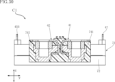
- FIG. 24 is a plan view showing a semiconductor device according to a third embodiment;
- FIG. 25 is a plan view of FIG. 24 with a portion of the case (top plate) and the resin member omitted.
- FIG. 26 is an enlarged plan view of a part of FIG.
- FIG. 27 is an enlarged plan view of a part of FIG. 25, omitting a plurality of connection members.
- 28 is a cross-sectional view taken along line XXVIII--XXVIII of FIG. 25.
- FIG. 29 is a cross-sectional view along line XXIX-XXIX in FIG. 25.
- FIG. 30 is a cross-sectional view taken along line XXX-XXX in FIG. 25.
- FIG. 31 is a cross-sectional view along line XXI-XXI of FIG. 25.
- FIG. 32 is a cross-sectional view taken along line XXII-XXXII of FIG. 25.
- a certain entity A is formed on a certain entity B
- a certain entity A is formed on (of) an entity B
- mean a certain entity A is directly formed in a certain thing B
- a certain thing A is formed in a certain thing B while another thing is interposed between a certain thing A and a certain thing B” including.
- ⁇ an entity A is arranged on an entity B'' and ⁇ an entity A is arranged on (of) an entity B'' mean ⁇ an entity A being placed directly on a certain thing B", and "a thing A being placed on a certain thing B with another thing interposed between something A and something B" include.
- ⁇ an object A is located on (of) an object B'' means ⁇ a certain object A is in contact with an object B, and an object A is located on an object B. Being located on (of)" and "something A is located on (something) B while another thing is interposed between something A and something B including "things”.
- ⁇ a certain object A overlaps an object B when viewed in a certain direction'' means ⁇ a certain object A overlaps all of an object B'', and ⁇ a certain object A overlaps an object B.'' It includes "overlapping a part of a certain thing B".
- First embodiment: 1 to 6 show a semiconductor device A1 according to the first embodiment.
- the semiconductor device A1 includes a plurality of first semiconductor elements 11, a plurality of second semiconductor elements 12, a support substrate 2, a plurality of terminals, a plurality of connection members, and a sealing member 6.
- the plurality of terminals includes a plurality of power terminals 41-43 and a plurality of signal terminals 44A, 44B, 45A, 45B, 49.
- the plurality of connecting members includes a plurality of connecting members 51A, 51B, 52A, 52B, 531A, 531B, 541A, 541B.
- the thickness direction of the semiconductor device A1 will be referred to as "thickness direction z".
- One of the thickness directions z may be called upward and the other downward.
- descriptions such as “upper”, “lower”, “upper”, “lower”, “upper surface” and “lower surface” indicate the relative positional relationship of each component etc. in the thickness direction z, and are not necessarily It is not a term that defines the relationship with the direction of gravity.
- “planar view” means when viewed along the thickness direction z.
- a direction orthogonal to the thickness direction z is called a “first direction x”.
- the first direction x is the horizontal direction in the plan view (see FIG. 2) of the semiconductor device A1.
- a direction orthogonal to the thickness direction z and the first direction x is called a "second direction y".
- the second direction y is the vertical direction in the plan view (see FIG. 2) of the semiconductor device A1.
- Each of the plurality of first semiconductor elements 11 and the plurality of second semiconductor elements 12 is, for example, a MOSFET.
- Each of the plurality of first semiconductor elements 11 and the plurality of second semiconductor elements 12 is a field effect transistor including a MISFET (Metal-Insulator-Semiconductor FET) instead of a MOSFET, or other switching such as a bipolar transistor including an IGBT. It may be an element.
- Each of the plurality of first semiconductor elements 11 and the plurality of second semiconductor elements 12 is configured using SiC (silicon carbide).
- the semiconductor material is not limited to SiC, and may be Si (silicon), GaAs (gallium arsenide), GaN (gallium nitride), Ga 2 O 3 (gallium oxide), or the like.
- Each of the plurality of first semiconductor elements 11 is bonded to the support substrate 2 (power wiring section 31 described later) via a conductive bonding material.
- the conductive bonding material is, for example, solder, metal paste material, or sintered metal.
- the plurality of first semiconductor elements 11 are arranged, for example, at regular intervals in the first direction x, as shown in FIGS.
- the plurality of first semiconductor elements 11 includes a first near-field element 110, as shown in FIG.
- the first near-field element 110 has the shortest conduction distance to the power terminal 41 among the plurality of first semiconductor elements 11 .
- Each of the plurality of first semiconductor elements 11 has a first element main surface 11a and a first element rear surface 11b. As shown in FIGS. 4 and 6, the first element main surface 11a and the first element back surface 11b are separated from each other in the thickness direction z.
- the first element main surface 11a faces one direction (upward) in the thickness direction z, and the first element rear surface 11b faces the other direction (downward) in the thickness direction z.
- the first element rear surface 11b faces the support substrate 2 (power wiring section 31 described later).
- Each of the plurality of first semiconductor elements 11 has a first electrode 111, a second electrode 112 and a third electrode 113.
- the first electrode 111 is the drain
- the second electrode 112 is the source
- the third electrode 113 is the gate.
- the first electrode 111 is arranged on the first element rear surface 11b
- the second electrode 112 and the third electrode 113 are arranged on the first element rear surface 11b. It is arranged on the one-element main surface 11a.
- a first drive signal (for example, gate voltage) is input to the third electrode 113 (gate) of each of the plurality of first semiconductor elements 11 .
- Each of the plurality of first semiconductor elements 11 switches between an ON state (conducting state) and an OFF state (interrupting state) according to the input first drive signal.
- the operation of switching between the ON state and the OFF state is called a switching operation.
- a forward current flows from the first electrode 111 (drain) to the second electrode 112 (source) in the ON state, and does not flow in the OFF state.
- Each first semiconductor element 11 is turned on/off between the first electrode 111 (drain) and the second electrode 112 (source) by a first drive signal (for example, gate voltage) input to the third electrode 113 (gate). controlled.
- the switching frequency of each first semiconductor element 11 depends on the frequency of the first drive signal.
- the first electrodes 111 are electrically connected to each other and the second electrodes 112 (source) are electrically connected to each other by a configuration described in detail later. ing. Thereby, the plurality of first semiconductor elements 11 are electrically connected in parallel.
- the semiconductor device A1 inputs a common first drive signal to the plurality of first semiconductor elements 11 connected in parallel to operate the plurality of first semiconductor elements 11 in parallel.
- Each of the plurality of second semiconductor elements 12 is bonded to the support substrate 2 (power wiring section 33 described later) via a conductive bonding material.
- the conductive bonding material is, for example, solder, metal paste material, or sintered metal.
- the plurality of second semiconductor elements 12 are arranged, for example, at regular intervals in the first direction x, as shown in FIGS.
- the plurality of second semiconductor elements 12 includes a second near-field element 120, as shown in FIG.
- the second near element 120 has the shortest conduction distance to the power terminal 43 among the plurality of second semiconductor elements 12 .
- Each of the plurality of second semiconductor elements 12 has a second element main surface 12a and a second element rear surface 12b. As shown in FIGS. 5 and 6, the second element main surface 12a and the second element back surface 12b are separated from each other in the thickness direction z.
- the second element principal surface 12a faces one direction (upward) in the thickness direction z, and the second element rear surface 12b faces the other direction (downward) in the thickness direction z.
- the second element back surface 12b faces the support substrate 2 (power wiring section 33, which will be described later).
- Each of the plurality of second semiconductor elements 12 has a fourth electrode 121, a fifth electrode 122 and a sixth electrode 123.
- the fourth electrode 121 is the drain
- the fifth electrode 122 is the source
- the sixth electrode 123 is the gate. 2
- the fourth electrode 121 is arranged on the second element rear surface 12b
- the fifth electrode 122 and the sixth electrode 123 are arranged on the second element rear surface 12b. It is arranged on the two-element main surface 12a.
- a second drive signal (for example, gate voltage) is input to the sixth electrode 123 (gate) of each of the plurality of second semiconductor elements 12 .
- Each of the plurality of second semiconductor elements 12 switches between an ON state and an OFF state according to the input second drive signal.
- a forward current flows from the fourth electrode 121 (drain) to the fifth electrode 122 (source) in the ON state, and does not flow in the OFF state.
- Each second semiconductor element 12 is turned on/off between the fourth electrode 121 (drain) and the fifth electrode 122 (source) by a second drive signal (for example, gate voltage) input to the sixth electrode 123 (gate). controlled.
- the switching frequency of each second semiconductor element 12 depends on the frequency of the second drive signal.
- the fourth electrodes 121 are electrically connected to each other and the fifth electrodes 122 (source) are electrically connected to each other by a configuration described in detail later. ing. Thereby, the plurality of second semiconductor elements 12 are electrically connected in parallel.
- the semiconductor device A1 inputs a common second drive signal to the plurality of second semiconductor elements 12 connected in parallel to operate the plurality of second semiconductor elements 12 in parallel.
- the support substrate 2 supports the plurality of first semiconductor elements 11 and the plurality of second semiconductor elements 12 and electrically connects the plurality of first semiconductor elements 11 and the plurality of second semiconductor elements 12 to the plurality of terminals.
- support substrate 2 is, for example, a DBC (Direct Bonded Copper) substrate. Unlike this configuration, the support substrate 2 may be, for example, a DBA (Direct Bonded Aluminum) substrate.
- the support substrate 2 includes an insulating substrate 20 , a main surface metal layer 21 and a back surface metal layer 22 .
- Insulating substrate 20 is made of, for example, ceramic having excellent thermal conductivity. Examples of such ceramic include AlN (aluminum nitride), SiN (silicon nitride), Al 2 O 3 (aluminum oxide), and the like. Insulating substrate 20 has, for example, a flat plate shape. As shown in FIGS. 2 and 3, insulating substrate 20 has, for example, a rectangular shape in plan view.
- the insulating substrate 20 has a main surface 20a and a back surface 20b. As shown in FIGS. 4-6, the main surface 20a and the back surface 20b are spaced apart in the thickness direction z. The main surface 20a faces upward in the thickness direction z, and the back surface 20b faces downward in the thickness direction z.
- the main surface metal layer 21 and the back surface metal layer 22 are each made of, for example, copper or a copper alloy.
- the main surface metal layer 21 and the back surface metal layer 22 may each be made of aluminum or an aluminum alloy instead of copper or a copper alloy.
- the main surface metal layer 21 is formed on the main surface 20a, and the back surface metal layer 22 is formed on the back surface 20b.
- the lower surface of the back metal layer 22 (the surface facing downward in the thickness direction z) is exposed from the sealing member 6 . Unlike this configuration, the lower surface of the back metal layer 22 may be covered with the sealing member 6 .
- the main surface metal layer 21 includes a plurality of power wiring portions 31 to 33 and a plurality of signal wiring portions 34A, 34B, 35A, 35B, and 39, as shown in FIG.
- the plurality of power wiring sections 31 to 33 and the plurality of signal wiring sections 34A, 34B, 35A, 35B, 39 are separated from each other.
- a plurality of power wiring portions 31, 32, and 33 form conduction paths for the main circuit current in the semiconductor device A1.
- the main circuit current includes a first main circuit current and a second main circuit current.
- the first main circuit current is the current that flows between the power terminals 41 and 43 .
- the second main circuit current is the current that flows between the power terminals 43 and 42 .
- the power wiring portion 31 is an example of the "first conductor”
- the power wiring portion 32 is an example of the "third conductor”
- the power wiring portion 33 is an example of the "second conductor".
- the power wiring portion 31 is electrically connected to each first electrode 111 (drain) of the plurality of first semiconductor elements 11 .
- the power wiring portion 31 is electrically connected to the power terminal 41 .
- the power wiring portion 31 is arranged to avoid part of each first line segment S1 in plan view.
- Each first line segment S1 is an auxiliary line shown in FIG. 3 for convenience of understanding, and is a line segment connecting the respective centers of two first semiconductor elements 11 adjacent in the first direction x.
- the center of each first semiconductor element 11 may be the center of the entire first semiconductor element 11 in plan view, or the center of the first electrode 111 in plan view. For convenience of understanding, the center is indicated by a cross in FIG.
- the power wiring portion 31 is arranged so as to avoid a portion of 15% or more and 90% or less (preferably 25% or more and 90% or less) of each first line segment S1 in plan view.
- the power wiring section 31 includes two pad sections 311 and 312 . As shown in FIGS. 2 and 3, the two pad portions 311 and 312 are connected to each other and formed integrally.
- the pad portion 311 includes a plurality of mounting portions 311a and connecting portions 311b.
- each of the plurality of first semiconductor elements 11 is mounted on each of the plurality of mounting portions 311a.
- the first electrodes 111 (drain) of the plurality of first semiconductor elements 11 are joined to the plurality of mounting portions 311a, respectively.
- Each of the plurality of mounting portions 311a has, for example, a rectangular shape in plan view.
- Each of the plurality of mounting portions 311a includes, in plan view, a portion overlapping each of the plurality of first semiconductor elements 11 and a portion extending from this portion.
- the plurality of mounting portions 311a are arranged along the first direction x while being spaced apart in the first direction x.
- Each of the plurality of mounting portions 311a has one end edge in the second direction y connected to the connecting portion 311b. Accordingly, the plurality of mounting portions 311a are electrically connected to each other by the connecting portions 311b.
- the mounting portion 311a is an example of the "first mounting portion”.
- each first gap G1 is indicated by a dot-like pattern in FIG. As shown in FIG. 3, each first gap G1 overlaps each first line segment S1.
- Each first gap G1 is formed, for example, by each notch provided in the edge of the pad portion 311 on the other side in the second direction y (the side closer to the power wiring portion 33). A part of the power wiring portion 33 (each projecting portion 333 to be described later) is arranged in each first gap G1.
- the connecting portion 311b is connected to each of the plurality of mounting portions 311a as shown in FIGS.
- the connecting portion 311b extends from the pad portion 312 to the other side in the first direction x.
- the other side in the first direction x is the side opposite to the direction in which the power terminals 41 extend with respect to the pad portion 312 and the side where the plurality of first semiconductor elements 11 are located.
- the connecting portion 311b has a strip shape in plan view. As shown in FIGS. 2 and 3, the connecting portion 311b is located on the side opposite to the plurality of second semiconductor elements 12 with respect to the plurality of mounting portions 311a in the second direction y.
- the connecting portion 311b is positioned on one side in the second direction y (the side opposite to the plurality of second semiconductor elements 12) with respect to each first line segment S1 in plan view.
- the connecting portion 311b is an example of the "first connecting portion”.
- the power terminal 41 is joined to the pad portion 312 as shown in FIGS.
- the pad portion 312 has a strip shape with the second direction y as its longitudinal direction in plan view.
- the pad portion 312 is connected to the edge of the pad portion 311 on one side in the first direction x (the side on which the power terminal 41 is located).
- the power wiring section 32 is electrically connected to each fifth electrode 122 (source) of the plurality of second semiconductor elements 12 .
- the power wiring portion 32 is electrically connected to the power terminal 42 .
- the power wiring section 32 includes two pad sections 321 and 322 and a plurality of protrusions 323 . Unlike this configuration, the power wiring portion 32 may not include any of the plurality of projecting portions 323 . As shown in FIGS. 2 and 3, the two pad portions 321 and 322 and the plurality of projecting portions 323 are connected to each other and formed integrally.
- the pad portion 321 is joined to a plurality of connection members 51B, and is connected to each of the fifth electrodes 122 (sources) of the plurality of second semiconductor elements 12 via the plurality of connection members 51B. conduct.
- the pad portion 321 extends along the other side of the first direction x from the pad portion 322, as shown in FIGS.
- the other side in the first direction x is the side opposite to the direction in which the power terminals 42 extend with respect to the pad portion 322, and is the side on which the plurality of first semiconductor elements 11 and the plurality of second semiconductor elements 12 are located.
- the pad portion 321 has a strip shape, for example, with the first direction x as its longitudinal direction in a plan view.
- the pad portion 321 is positioned on the other side (lower side in FIG. 2) in the second direction y with respect to the pad portion 311 .
- the power terminal 42 is joined to the pad portion 322, as shown in FIGS.
- the pad portion 322 has a strip shape with the second direction y as its longitudinal direction in plan view.
- the pad portion 322 is connected to the edge of the pad portion 321 on one side in the first direction x (the side on which the power terminal 42 is located).
- the pad portion 322 is positioned on the other side in the second direction y (lower side in FIG. 2) with respect to the pad portion 321 .
- the plurality of protrusions 323 protrude from the edge of the pad 321 on one side in the second direction y to one side in the second direction y.
- One side in the second direction y is the side on which the plurality of second semiconductor elements 12 are positioned with respect to the pad section 321 .
- Each projecting portion 323 has, for example, a rectangular shape in plan view.
- Each projecting portion 323 is arranged between two second semiconductor elements 12 adjacent in the first direction x and between two mounting portions 331a adjacent in the first direction x.
- each part of the plurality of protrusions 323 overlaps each of the plurality of second gaps G2 (described later) in plan view.
- the power wiring portion 33 is electrically connected to each second electrode 112 (source) of the plurality of first semiconductor elements 11 and electrically connected to each fourth electrode 121 (drain) of the plurality of second semiconductor elements 12 .
- the power wiring portion 33 is electrically connected to two power terminals 43 .
- the power wiring portion 33 is arranged to avoid part of each of the second line segments S2 in plan view (see FIG. 3).
- Each second line segment S2 is an auxiliary line shown in FIG. 3 for convenience of understanding, and is a line segment connecting the centers of two second semiconductor elements 12 adjacent in the first direction x.
- the center of each second semiconductor element 12 may be the center of the entire second semiconductor element 12 in plan view, or the center of the fourth electrode 121 in plan view.
- the center is indicated by a cross in FIG.
- the power wiring portion 33 is arranged so as to avoid 15% or more and 90% or less (preferably 25% or more and 90% or less) of each second line segment S2 in plan view.
- the power wiring section 33 includes two pad sections 331 and 332 and a plurality of protrusions 333 . Unlike this configuration, the power wiring portion 33 may not include any of the plurality of projecting portions 333 . As shown in FIGS. 2 and 3, the two pad portions 331 and 332 and the plurality of projecting portions 333 are connected to each other and integrally formed.
- the pad portion 331 includes a plurality of mounting portions 331a and connecting portions 331b.
- each of the plurality of second semiconductor elements 12 is mounted on each of the plurality of mounting portions 331a.
- Each fourth electrode 121 (drain) of the plurality of second semiconductor elements 12 is joined to the plurality of mounting portions 331a.
- Each of the plurality of mounting portions 331a has, for example, a rectangular shape in plan view.
- Each of the plurality of mounting portions 331a includes, in plan view, a portion overlapping each of the plurality of second semiconductor elements 12 and a portion extending from this portion.
- the plurality of mounting portions 331a are arranged along the first direction x while being spaced apart in the first direction x.
- Each of the plurality of mounting portions 331a has one end edge in the second direction y connected to the connecting portion 331b. Thereby, the plurality of mounting portions 331a are electrically connected to each other by the connecting portions 331b.
- the mounting portion 331a is an example of the "second mounting portion”.
- each second gap G2 is indicated by a dot-like pattern in FIG.
- Each second gap G2 overlaps each second line segment S2.
- Each second gap G2 is formed, for example, by each notch provided at the edge of the pad portion 331 on the other side in the second direction y (the side closer to the power wiring portion 32).
- a portion of the power wiring portion 32 (each projecting portion 323) is arranged in each second gap G2.
- the connecting portion 331b is connected to each of the plurality of mounting portions 331a as shown in FIGS.
- the connecting portion 331b extends from the pad portion 332 to one side in the first direction x.
- the one side in the first direction x is the side opposite to the direction in which the power terminals 43 extend with respect to the pad portion 332 and the side where the plurality of second semiconductor elements 12 are located.
- the connecting portion 331b has a strip shape in plan view.
- the connecting portion 331b is connected to the plurality of connection members 51A and connected to the second electrodes 112 (sources) of the plurality of first semiconductor elements 11 via the plurality of connection members 51A. conduct.
- the connecting portion 331b is located on the same side as the plurality of first semiconductor elements 11 with respect to the plurality of mounting portions 331a in the second direction y.
- the connecting portion 331b is positioned on one side in the second direction y (the same side as the plurality of first semiconductor elements 11) with respect to each second line segment S2 in plan view.
- the connecting portion 331b is an example of the "second connecting portion".
- the power terminal 43 is joined to the pad portion 332 as shown in FIGS.
- the pad portion 332 has a strip shape with the second direction y as its longitudinal direction in a plan view.
- the pad portion 332 is connected to the edge of the pad portion 331 on the other side in the first direction x (the side on which the power terminal 43 is located).
- each of the plurality of projecting portions 333 extends from one edge of the connecting portion 331b (pad portion 331) in the second direction y to one side in the second direction y in plan view. protrude.
- One side in the second direction y is the side on which the plurality of first semiconductor elements 11 are positioned with respect to the connecting portion 331b.
- Each of the plurality of protrusions 333 has, for example, a rectangular shape in plan view.
- Each projecting portion 333 is arranged between two first semiconductor elements 11 adjacent in the first direction x and between two mounting portions 311a adjacent in the first direction x. Therefore, as shown in FIG. 3, each part of the plurality of projections 333 overlaps each of the plurality of first gaps G1 in plan view.
- a plurality of signal wiring portions 34A, 34B, 35A, and 35B form conduction paths for electrical signals for controlling the semiconductor device A1.
- the signal wiring portion 34A is connected to a plurality of connection members 531A and electrically connected to the third electrodes 113 (gates) of the plurality of first semiconductor elements 11 via the plurality of connection members 531A. . 34 A of signal wiring parts transmit a 1st drive signal. A signal terminal 44A is joined to the signal wiring portion 34A.
- the signal wiring portion 34B is connected to a plurality of connection members 531B and electrically connected to the sixth electrodes 123 (gates) of the plurality of second semiconductor elements 12 via the plurality of connection members 531B. .
- the signal wiring portion 34B transmits the second drive signal.
- a signal terminal 44B is joined to the signal wiring portion 34B.
- the signal wiring portion 34A and the signal wiring portion 34B are located on opposite sides of each other with the pad portions 311, 321, 331 interposed therebetween in the second direction y.
- the signal wiring portion 34A is located on the side opposite to the pad portion 331 with respect to the pad portion 311 in the second direction y.
- the signal wiring portion 34B is located on the side opposite to the pad portion 331 with respect to the pad portion 321 in the second direction y.
- the signal wiring portion 35A is connected to a plurality of connection members 541A and electrically connected to the second electrodes 112 (sources) of the plurality of first semiconductor elements 11 via the plurality of connection members 541A. .
- the signal wiring portion 35A transmits the first detection signal.
- the first detection signal is an electrical signal indicating the conduction state of each first semiconductor element 11, and is, for example, a voltage signal corresponding to the current (source current) flowing through each second electrode 112 (source).
- a signal terminal 45A is joined to the signal wiring portion 35A.
- the signal wiring portion 35B is connected to a plurality of connection members 541B and electrically connected to the fifth electrodes 122 (sources) of the plurality of second semiconductor elements 12 via the plurality of connection members 541B. .
- the signal wiring portion 35B transmits the second detection signal.
- the second detection signal is an electrical signal indicating the conduction state of each second semiconductor element 12, and is, for example, a voltage signal corresponding to the current (source current) flowing through each fifth electrode 122 (source).
- a signal terminal 45B is joined to the signal wiring portion 35B.
- the signal wiring portion 35A and the signal wiring portion 35B are located on opposite sides of each other with the pad portions 311, 321, 331 interposed therebetween in the second direction y.
- the signal wiring portion 35A is located on the same side as the signal wiring portion 34A with respect to the pad portion 311 in the second direction y.
- the signal wiring portion 35B is located on the same side as the signal wiring portion 34B with respect to the pad portion 321 in the second direction y.
- Each of the plurality of signal wiring portions 39 is electrically connected to none of the plurality of first semiconductor elements 11 and the plurality of second semiconductor elements 12 . In other words, neither the main circuit current nor the electric signal flows through any of the plurality of signal wiring portions 39 .
- the plurality of power terminals 41 to 43 and the plurality of signal terminals 44A, 44B, 45A, 45B, and 49 are partially exposed from the sealing member 6 as shown in FIGS.
- Each constituent material of the plurality of power terminals 41 to 43 and the plurality of signal terminals 44A, 44B, 45A, 45B, 49 is, for example, copper or copper alloy, but may be other metals.
- the plurality of power terminals 41 to 43 and the plurality of signal terminals 44A, 44B, 45A, 45B, 49 are each made of a metal plate and bent appropriately.
- the power terminals 41 and 42 are connected to a power supply and applied with a power supply voltage (for example, DC voltage).
- a power supply voltage for example, DC voltage
- the power terminal 41 is a positive power input terminal (P terminal)
- the power terminal 42 is a negative power input terminal (N terminal).
- the power terminal 43 outputs a voltage (for example, AC voltage) that is power-converted by each switching operation of the plurality of first semiconductor elements 11 and each switching operation of the plurality of second semiconductor elements 12 .
- Each of the power terminals 43 is a power output terminal (OUT terminal).
- the main circuit current (first main circuit current and second main circuit current) in the semiconductor device A1 is generated by the power supply voltage and the converted voltage.
- the power terminal 41 is an example of a "first power terminal”
- the power terminal 42 is an example of a "third power terminal”
- the power terminal 43 is an example of a "second power terminal”.
- the power terminal 41 is electrically connected to each first electrode 111 (drain) of the plurality of first semiconductor elements 11 via the power wiring portion 31 .
- Power terminal 41 includes a joint portion 411 and a terminal portion 412 .
- the joint 411 is covered with the sealing member 6 as shown in FIGS.
- the joint portion 411 is joined to the pad portion 312 of the power wiring portion 31 as shown in FIGS. Thereby, the power terminal 41 and the power wiring portion 31 are electrically connected.
- the bonding portion 411 and the pad portion 312 may be bonded by any method such as bonding using a conductive bonding material (solder, sintered metal, etc.), laser bonding, or ultrasonic bonding.
- the terminal portion 412 is exposed from the sealing member 6 as shown in FIGS. As shown in FIG. 2, the terminal portion 412 extends from the sealing member 6 to one side in the first direction x in plan view.
- the surface of terminal portion 412 may be plated with silver, for example.
- the power terminal 42 is electrically connected to each fifth electrode 122 (source) of the plurality of second semiconductor elements 12 via the power wiring portion 32 .
- Power terminal 42 includes joint portion 421 and terminal portion 422 .
- the joint 421 is covered with the sealing member 6 as shown in FIGS.
- the joint portion 421 is joined to the pad portion 322 of the power wiring portion 32 as shown in FIGS. Thereby, the power terminal 42 and the power wiring portion 32 are electrically connected.
- the bonding portion 421 and the pad portion 322 may be bonded by any method such as bonding using a conductive bonding material (such as solder or sintered metal), laser bonding, or ultrasonic bonding.
- the terminal portion 422 is exposed from the sealing member 6 as shown in FIGS. As shown in FIG. 2, the terminal portion 422 extends from the sealing member 6 to one side in the first direction x in plan view.
- the surface of terminal portion 422 may be plated with silver, for example.
- the power terminal 43 is electrically connected to each of the second electrodes 112 (sources) of the plurality of first semiconductor elements 11 via the power wiring portion 33, and is connected to each of the fourth electrodes 121 (drain) of the plurality of second semiconductor elements 12. conducts to Power terminal 43 includes joint portion 431 and terminal portion 432 .
- the joint 431 is covered with the sealing member 6 as shown in FIGS.
- the joint portion 431 is joined to the pad portion 332 of the power wiring portion 33 as shown in FIGS. Thereby, the power terminal 43 and the power wiring portion 33 are electrically connected.
- the joining portion 431 and the pad portion 332 may be joined by any method such as joining using a conductive joining material (solder or sintered metal, etc.), laser joining, or ultrasonic joining.
- the terminal portion 432 is exposed from the sealing member 6 as shown in FIGS. As shown in FIG. 2, the terminal portion 432 extends from the sealing member 6 to the other side in the first direction x in plan view.
- the surface of terminal portion 432 may be plated with silver, for example.
- the power terminals 41 and 42 are spaced apart from each other and arranged along the second direction y.
- the power terminals 41 and 42 and the power terminals 43 are arranged on opposite sides of the support substrate 2 in the first direction x.
- the number of power terminals 43 may be two or more instead of one.
- a plurality of signal terminals 44A, 44B, 45A, and 45B are input terminals or output terminals of electrical signals for controlling the semiconductor device A1.
- Each of the plurality of signal terminals 44A, 44B, 45A, 45B, and 49 includes a portion covered with the sealing member 6 and a portion exposed from the sealing member 6. As shown in FIG.
- Each of the plurality of signal terminals 44A, 44B, 45A, 45B, and 49 is a pin-shaped metal member.
- the metal member is made of copper or copper alloy, for example.
- the portion of the signal terminal 44A covered with the sealing member 6 is joined to the signal wiring portion 34A, as shown in FIG. Since the signal wiring portion 34A is electrically connected to each third electrode 113 (gate) of the plurality of first semiconductor elements 11, the signal terminal 44A is electrically connected to each third electrode 113 (gate) of the plurality of first semiconductor elements 11. do.
- the signal terminal 44A is an input terminal for the first drive signal.
- the portion of the signal terminal 44B covered with the sealing member 6 is joined to the signal wiring portion 34B. Since the signal wiring portion 34B is electrically connected to each sixth electrode 123 (gate) of the plurality of second semiconductor elements 12, the signal terminal 44B is electrically connected to each sixth electrode 123 (gate) of the plurality of second semiconductor elements 12. do.
- the signal terminal 44B is an input terminal for the second drive signal.
- the portion of the signal terminal 45A covered with the sealing member 6 is joined to the signal wiring portion 35A, as shown in FIG. Since the signal wiring portion 35A is electrically connected to the second electrodes 112 (sources) of the plurality of first semiconductor elements 11, the signal terminal 45A is electrically connected to the second electrodes 112 (sources) of the plurality of first semiconductor elements 11. do.
- the signal terminal 45A is an output terminal for the first detection signal.
- the portion of the signal terminal 45B covered with the sealing member 6 is joined to the signal wiring portion 35B. Since the signal wiring portion 35B is electrically connected to each fifth electrode 122 (source) of the plurality of second semiconductor elements 12, the signal terminal 45B is electrically connected to each fifth electrode 122 (source) of the plurality of second semiconductor elements 12. do.
- the signal terminal 45B is an output terminal for the second detection signal.
- each of the plurality of signal terminals 49 is electrically connected to none of the plurality of first semiconductor elements 11 and the plurality of second semiconductor elements 12 .
- Each of the plurality of signal terminals 49 is a non-connect terminal.
- a plurality of signal terminals 49 may be omitted.
- Each of the plurality of connection members 51A, 51B, 52A, 52B, 531A, 531B, 541A, 541B conducts two parts separated from each other.
- all of the plurality of connecting members 51A, 51B, 52A, 52B, 531A, 531B, 541A, 541B are bonding wires. Any of gold, copper, or aluminum may be used as the constituent material of each of the plurality of connection members 51A, 51B, 52A, 52B, 531A, 531B, 541A, and 541B.
- the plurality of connecting members 51A are respectively joined to the second electrodes 112 (sources) of the plurality of first semiconductor elements 11 and the connecting portions 331b of the pad portions 331, and The electrode 112 and the power wiring portion 33 are electrically connected.
- a plurality of connection members 51A are joined to each of the plurality of second electrodes 112.
- a main circuit current (first main circuit current) in the semiconductor device A1 flows through the plurality of connection members 51A.
- each connecting member 51A may be a plate-shaped member made of metal (for example, made of copper) instead of the bonding wire.
- the number of connection members 51A each joined to each second electrode 112 and pad portion 331 may be one.
- the connecting member 51A is an example of a "first connecting member".
- the plurality of connection members 51B are respectively joined to the fifth electrodes 122 (sources) and the pad portions 321 of the plurality of second semiconductor elements 12 to connect the fifth electrodes 122 and the power supply.
- the wiring part 32 is electrically connected.
- a plurality of connection members 51B are joined to each of the plurality of fifth electrodes 122.
- a main circuit current (second main circuit current) in the semiconductor device A1 flows through the plurality of connecting members 51B.
- each connecting member 51B may be a plate-like member made of metal (for example, made of copper) instead of the bonding wire.
- the number of connection members 51B each joined to each fifth electrode 122 and pad portion 321 may be one.
- the connecting member 51B is an example of a "second connecting member".
- the plurality of connection members 52A are connected to the second electrodes 112 (sources) of the plurality of first semiconductor elements 11 and the protrusions adjacent to the first semiconductor elements 11 in the first direction x. 333 to make them conductive.
- Two connection members 52A are joined to each protrusion 333 .
- Each of the plurality of connection members 52A extends, for example, along the first direction x in plan view. Note that in a configuration in which the power wiring portion 33 does not include the projecting portions 333, the plurality of connection members 52A may be omitted, and the second electrodes 112 of the two first semiconductor elements 11 adjacent in the first direction x may be provided. may be directly bonded to
- the plurality of connection members 52B are adjacent to the fifth electrodes 122 (sources) of the plurality of second semiconductor elements 12 and the second semiconductor elements 12 in the first direction x. It is joined to the projecting portion 323 and conducts them. Two connection members 52B are joined to each protrusion 323 . Each of the plurality of connection members 52B extends, for example, along the first direction x in plan view. Note that in a configuration in which the power wiring portion 32 does not include the protruding portions 323, the plurality of connecting members 52B may be omitted, and the fifth electrodes 122 of the two second semiconductor elements 12 adjacent in the first direction x may be omitted. may be directly bonded to
- the plurality of connection members 531A are respectively joined to the respective third electrodes 113 (gates) of the plurality of first semiconductor elements 11 and the signal wiring portion 34A, and are connected to the respective third electrodes 113 and the signal wiring portion. 34A.
- the signal terminal 44A is electrically connected to each third electrode 113 of the plurality of first semiconductor elements 11 via the signal wiring portion 34A and the plurality of connection members 531A.
- the plurality of connection members 531B are respectively joined to the respective sixth electrodes 123 (gates) of the plurality of second semiconductor elements 12 and the signal wiring portion 34B to connect the respective sixth electrodes 123 and the signal wiring portion. 34B are electrically connected.
- the signal terminal 44B is electrically connected to each of the sixth electrodes 123 of the plurality of second semiconductor elements 12 via the signal wiring portion 34B and the plurality of connection members 531B.
- the plurality of connection members 541A are respectively joined to the second electrodes 112 (sources) of the plurality of first semiconductor elements 11 and the signal wiring portion 35A to connect the second electrodes 112 and the signal wiring portion 35A. 35A.
- the signal terminal 45A is electrically connected to the second electrodes 112 of the plurality of first semiconductor elements 11 via the signal wiring portion 35A and the plurality of connection members 541A.
- the plurality of connecting members 541B are respectively joined to the fifth electrodes 122 (sources) of the plurality of second semiconductor elements 12 and the signal wiring portion 35B to connect the fifth electrodes 122 and the signal wiring portion 35B. 35B are electrically connected.
- the signal terminal 45B is electrically connected to each of the fifth electrodes 122 of the plurality of second semiconductor elements 12 via the signal wiring portion 35B and the plurality of connection members 541B.
- the sealing member 6 is a sealing material that protects the plurality of first semiconductor elements 11, the plurality of second semiconductor elements 12, and the like.
- the sealing member 6 includes the plurality of first semiconductor elements 11, the plurality of second semiconductor elements 12, a portion of the support substrate 2, the plurality of power terminals 41 to 43, and the plurality of signal terminals 44A, 44B, 45A, 45B, 49. , cover the plurality of connection members 51A, 51B, 52A, 52B, 531A, 531B, 541A, 541B, respectively.
- the sealing member 6 is made of, for example, an insulating resin material, such as an epoxy resin.
- the sealing member 6 is black, for example.
- the sealing member 6 has a rectangular shape in plan view.
- the sealing member 6 has a resin main surface 61, a resin back surface 62 and a plurality of resin side surfaces 631-634.
- the resin main surface 61 and the resin back surface 62 are spaced apart in the thickness direction z, as shown in FIGS.
- the resin main surface 61 faces upward in the thickness direction z
- the resin rear surface 62 faces downward in the thickness direction z.
- Each of the plurality of resin side surfaces 631 to 634 is sandwiched between and connected to the resin main surface 61 and the resin back surface 62 in the thickness direction z.
- the pair of resin side surfaces 631 and 632 face opposite sides in the first direction x.
- Each power terminal 41 , 42 protrudes from the resin side surface 632
- the power terminal 43 protrudes from the resin side surface 631 .
- the pair of resin side surfaces 633 and 634 face opposite sides in the second direction y.
- the signal terminals 44A, 45A protrude from the resin side surface 634, and the signal terminals 44B, 45B protrude from the resin side surface 633. As shown in FIG.
- the conduction path R11 (see FIG. 3) between the first electrodes 111 (drain) of the two first semiconductor elements 11 adjacent in the first direction x is the first electrode 111 of the first near element 110. (drain) and the power terminal 41 (P terminal) longer than the conduction path R12 (see FIG. 3).
- the element-element inductance L1 which is the inductance of the conduction path R11, is greater than the element-terminal inductance L2, which is the inductance of the conduction path R12.
- the element-element inductance L1 is an example of a "first inductance”
- the element-terminal inductance L2 is an example of a "second inductance”.
- the conduction path R21 (see FIG. 3) between the fourth electrodes 121 (drain) of the two second semiconductor elements 12 adjacent in the first direction x is the second near element 120 of the second near element 120. It is longer than the conduction path R22 (see FIG. 3) between the four electrodes 121 (drain) and the power terminal 43 (OUT terminal).
- the element-element inductance L3 which is the inductance of the conduction path R21, is larger than the element-terminal inductance L4, which is the inductance of the conduction path R22.
- the element-element inductance L3 is an example of the "third inductance”
- the element-terminal inductance L4 is an example of the "fourth inductance".
- the actions and effects of the semiconductor device A1 are as follows.
- the semiconductor device A1 includes a plurality of first semiconductor elements 11, and the plurality of first semiconductor elements 11 are electrically connected in parallel.
- the semiconductor device A1 includes a power wiring portion 31 as a first conductor.
- the power wiring portion 31 is arranged to avoid part of the first line segment S1 when viewed in the thickness direction z. According to this configuration, the element-to-element inductance L1 is increased compared to the configuration in which the power wiring portion 31 is arranged without avoiding the first line segment S1 (hereinafter referred to as "first comparative configuration").
- the first comparative configuration is, for example, a configuration in which the conduction paths between the first electrodes 111 (drain) of the plurality of first semiconductor elements 11 are straight, as in Patent Document 1.
- the semiconductor device A1 can suppress the occurrence of an oscillation phenomenon when the plurality of first semiconductor elements 11 are operated in parallel, as compared with the first comparative configuration.
- the power wiring portion 31 as the first conductor avoids 15% or more of the first line segment S1 when viewed in the thickness direction z.
- the length of each conduction path R11 can be made sufficiently large relative to the length of the first line segment S1. Therefore, in order to suppress an oscillation phenomenon that occurs when a plurality of first semiconductor elements 11 are operated in parallel, an appropriate element-to-element inductance L1 can be ensured.
- the power wiring portion 31 avoids a portion of 25% or more of the first line segment S1 when viewed in the thickness direction z, the oscillation phenomenon during parallel operation of the plurality of first semiconductor elements 11 can be prevented.
- the power wiring portion 31 avoids 90% or less of the first line segment S1 when viewed in the thickness direction z. Unlike this configuration, if the power wiring portion 31 avoids a portion larger than 90% of the first line segment S1 when viewed in the thickness direction z, each first line segment S1 can be viewed in the thickness direction z.
- the semiconductor element 11 may protrude from each mounting portion 311a. If each first semiconductor element 11 protrudes from each mounting portion 311a when viewed in the thickness direction z, the bonding strength between each first semiconductor element 11 may be reduced, or the first electrode 111 and each mounting portion 311a may be damaged. The bonding area with is reduced.
- each first semiconductor element 11 is arranged.
- An appropriate size of the area (each mounting portion 311a) can be ensured.
- the semiconductor device A1 prevents the first semiconductor elements 11 from protruding from the mounting portions 311a, reduces the bonding strength of the first semiconductor elements 11, and reduces the bonding strength between the first electrodes 111 and the mounting portions 311a. Reduction in area can be suppressed.
- the semiconductor device A1 adopts a configuration in which the power wiring portion 31 as the first conductor avoids a portion of 15% or more and 90% or less of the first line segment S1 when viewed in the thickness direction z.
- each first semiconductor element 11 can be appropriately bonded to each mounting portion 311a while ensuring an appropriate element-to-element inductance L1.
- the power wiring portion 31 includes a plurality of mounting portions 311a on which each of the plurality of first semiconductor elements 11 is mounted.
- the plurality of mounting portions 311a any two mounting portions 311a adjacent in the first direction x are arranged with a first gap G1 interposed therebetween in the first direction x.
- the first gap G1 intersects the first line segment S1 when viewed in the thickness direction z.
- the power wiring portion 31 has a shape that avoids part of the first line segment S1. Therefore, the semiconductor device A1 can increase the element-to-element inductance L1 compared to the first comparative configuration.
- the semiconductor device A1 includes a plurality of second semiconductor elements 12, and the plurality of second semiconductor elements 12 are electrically connected in parallel.
- the semiconductor device A1 includes a power wiring portion 33 as a second conductor.
- the power wiring portion 33 is arranged to avoid part of the second line segment S2 when viewed in the thickness direction z.
- the element-to-element inductance L3 is increased compared to the configuration in which the power wiring portion 33 is arranged without avoiding the second line segment S2 (hereinafter referred to as "second comparative configuration").
- the second comparative configuration is, for example, a configuration in which the conduction path between the fourth electrodes 121 (drain) of the plurality of second semiconductor elements 12 is straight, as in Patent Document 1. Therefore, the semiconductor device A1 can suppress the occurrence of an oscillation phenomenon when the plurality of second semiconductor elements 12 are operated in parallel, compared to the second comparative configuration.
- the power wiring portion 33 as the second conductor avoids 15% or more of the second line segment S2 when viewed in the thickness direction z.
- the length of each conduction path R21 can be sufficiently increased with respect to the length of the second line segment S2. Therefore, in order to suppress the oscillation phenomenon that occurs when the plurality of second semiconductor elements 12 operate in parallel, an appropriate element-to-element inductance L3 can be ensured.
- the power wiring portion 33 avoids a portion of 25% or more of the second line segment S2 when viewed in the thickness direction z, the oscillation phenomenon during parallel operation of the plurality of second semiconductor elements 12 can be prevented. In terms of suppression, a more favorable element-to-element inductance L3 is ensured.
- the power wiring portion 33 avoids 90% or less of the second line segment S2 when viewed in the thickness direction z.
- the power wiring portion 31 avoids 90% or less of the first line segment S1 when viewed in the thickness direction z.
- the size of the portion 331a) can be appropriately secured.
- the semiconductor device A1 suppresses the protruding of each second semiconductor element 12 from each mounting portion 331a, reduces the bonding strength of each second semiconductor element 12, and reduces the bonding between each fourth electrode 121 and each mounting portion 331a. Reduction in area can be suppressed.
- the semiconductor device A1 adopts a configuration in which the power wiring portion 32 as the second conductor avoids a portion of 15% or more and 90% or less of the second line segment S2 when viewed in the thickness direction z.
- each second semiconductor element 12 can be appropriately bonded to each mounting portion 331a while ensuring an appropriate element-to-element inductance L3.
- the power wiring portion 33 includes a plurality of mounting portions 331a on which each of the plurality of second semiconductor elements 12 is mounted. Any two mounting portions 331a adjacent in the first direction x among the plurality of mounting portions 331a are arranged with a second gap G2 interposed therebetween in the first direction x. The second gap G2 intersects the second line segment S2 when viewed in the thickness direction z. According to this configuration, the power wiring portion 33 has a shape that avoids part of the second line segment S2. Therefore, the semiconductor device A1 can increase the element-to-element inductance L3 compared to the second comparative configuration.
- the power wiring portion 33 includes a protruding portion 333.
- the protruding portion 333 protrudes in the second direction y from the connecting portion 331b (pad portion 331) when viewed in the thickness direction z.
- the projecting portion 333 partially overlaps the first gap G1 when viewed in the thickness direction z.
- the projecting portion 333 is arranged between two first semiconductor elements 11 adjacent in the first direction x.
- the second electrodes 112 of the two first semiconductor elements 11 located on both sides of the projecting portion 333 in the first direction x are electrically connected via the projecting portion 333 by each connecting member 52A. be able to.
- the semiconductor device A1 electrically connects the second electrodes 112 of the two first semiconductor elements 11 located on both sides of the protruding portion 333 in the first direction x by the connecting members 52A through the protruding portion 333.
- the power wiring portion 32 includes a protruding portion 323.
- the protruding portion 323 protrudes from the pad portion 332 in the second direction y when viewed in the thickness direction z.
- the projecting portion 323 partially overlaps the second gap G2 when viewed in the thickness direction z.
- the projecting portion 323 is arranged between two second semiconductor elements 12 adjacent in the first direction x.
- the fifth electrodes 122 of the two second semiconductor elements 12 located on both sides of the projecting portion 323 in the first direction x are electrically connected to each other via the projecting portion 323 by each connecting member 52B. be able to.
- the semiconductor device A1 electrically connects the fifth electrodes 122 of the two second semiconductor elements 12 located on both sides of the projecting portion 323 in the first direction x with the connecting members 52B through the projecting portion 323. By connecting, it becomes possible to further suppress the occurrence of the oscillation phenomenon when the plurality of second semiconductor elements 12 are operated in parallel.
- FIG. 7 to 10 show semiconductor devices A2 to A5 according to first to fourth modifications of the first embodiment, respectively.
- Each of the semiconductor devices A2 to A5 has the following points in common with the semiconductor device A1.
- the power wiring portion 31 is arranged so as to avoid part of each first line segment S1 when viewed in the thickness direction z.
- the power wiring portion 33 is arranged so as to avoid part of each second line segment S2 when viewed in the thickness direction z.
- two mounting portions 311a adjacent in the first direction x are arranged with a first gap G1 interposed therebetween, and the first gap G1 extends in the thickness direction z. See, it is the point that intersects the first line segment S1.
- two connecting portions 331b adjacent in the first direction x are arranged with a second gap G2 interposed therebetween, and the second gap G2 extends in the thickness direction z. Look, it is the point that intersects the second line segment S2.
- each of the semiconductor devices A2 to A5 has an increased element-to-element inductance L1 compared to the first comparative configuration, similarly to the semiconductor device A1. That is, each of the semiconductor devices A2 to A5, like the semiconductor device A1, can suppress the occurrence of the oscillation phenomenon when the plurality of first semiconductor elements 11 are operated in parallel, compared to the first comparative configuration.
- each of the semiconductor devices A2 to A5 has an increased element-to-element inductance L3 compared to the second comparative configuration, similarly to the semiconductor device A1. That is, each of the semiconductor devices A2 to A5, like the semiconductor device A1, can suppress the occurrence of the oscillation phenomenon when the plurality of second semiconductor elements 12 are operated in parallel, compared to the second comparative configuration.
- each conduction path R11 of the semiconductor device A2 is longer than each conduction path R11 of the semiconductor device A1. That is, the element-element inductance L1 of the semiconductor device A2 is larger than the element-element inductance L1 of the semiconductor device A1.
- the semiconductor device A2 is different from the semiconductor device A1 in the second direction from the portion where each first semiconductor element 11 is joined to the portion connected to the connecting portion 311b in each mounting portion 311a. By increasing the dimension along y, each conductive path R11 is lengthened.
- the conduction path R12 of the semiconductor device A2 is the same (or substantially the same) as the conduction path R12 of the semiconductor device A1.
- each conduction path R11 is longer than the conduction path R12. That is, in the semiconductor device A2, the element-element inductance L1 is larger than the element-terminal inductance L2, like the semiconductor device A1.
- the semiconductor device A2 configured as described above has a larger element-to-element inductance L1 than the semiconductor device A1. Therefore, the semiconductor device A2 can suppress the occurrence of an oscillation phenomenon more than the semiconductor device A1 when the plurality of first semiconductor elements 11 are operated in parallel.
- each conduction path R21 of the semiconductor device A2 is longer than each conduction path R21 of the semiconductor device A1. That is, the element-to-element inductance L3 of the semiconductor device A2 is larger than the element-to-element inductance L3 of the semiconductor device A1.
- the semiconductor device A2 is different from the semiconductor device A1 in the second direction from the portion where each second semiconductor element 12 is joined to the portion connected to the connecting portion 331b in each mounting portion 331a.
- each conductive path R21 is lengthened.
- the conduction path R22 of the semiconductor device A2 is the same (or substantially the same) as the conduction path R22 of the semiconductor device A1.
- each conduction path R21 is longer than the conduction path R22. That is, in the semiconductor device A2, the element-element inductance L3 is larger than the element-terminal inductance L4, like the semiconductor device A1.
- the semiconductor device A2 configured as described above has a larger element-to-element inductance L3 than the semiconductor device A1. Therefore, the semiconductor device A2 can suppress the occurrence of the oscillation phenomenon more than the semiconductor device A1 when the plurality of second semiconductor elements 12 are operated in parallel.
- the pad portion 311 (power wiring portion 31) further includes a plurality of connecting portions 311c compared to the semiconductor device A2.
- Each connecting portion 311c electrically connects two mounting portions 311a adjacent in the first direction x.
- two mounting portions 311a adjacent to each other in the first direction x are electrically connected via connecting portions 311b and 311c.
- each conductive path R11 is a path via the connecting portion 311c instead of the connecting portion 311b.
- the conduction paths R11 of the semiconductor device A3 are shorter than the conduction paths R11 of the semiconductor device A2, so that the element-to-element inductance L1 of the semiconductor device A3 is smaller than the element-to-element inductance L1 of the semiconductor device A2. Also in the semiconductor device A3, the element-element inductance L1 is larger than the element-terminal inductance L2, similarly to the semiconductor device A1.
- the pad portion 331 (power wiring portion 33) further includes a plurality of connecting portions 331c as compared with the semiconductor device A2.
- Each connecting portion 331c electrically connects two mounting portions 331a adjacent in the first direction x.
- two mounting portions 331a adjacent to each other in the first direction x are electrically connected via connecting portions 331b and 331c.
- each conductive path R21 is a path via the connecting portion 311c instead of the connecting portion 311b.
- the conduction paths R21 of the semiconductor device A3 are shorter than the conduction paths R21 of the semiconductor device A2, so that the element-to-element inductance L3 of the semiconductor device A3 is smaller than the element-to-element inductance L3 of the semiconductor device A2.
- the element-element inductance L3 is larger than the element-terminal inductance L4.
- the pad portion 311 (power wiring portion 31) includes a plurality of strip portions 311d.
- Each band-shaped portion 311 d connects each of the plurality of mounting portions 311 a and the pad portion 312 .
- the plurality of band-shaped portions 311d each have a band-like shape extending in the first direction x in a plan view, and are arranged parallel (or substantially parallel) to the second direction y.
- the semiconductor device A4 since the first electrodes 111 of the two first semiconductor elements 11 adjacent in the first direction x are electrically connected to each other through the pad portion 312, the first electrodes 111 are connected to each other.
- the conducting path is longer than each of the semiconductor devices A1-A3. Therefore, the element-to-element inductance L1 of the semiconductor device A4 is larger than the element-to-element inductance L1 of each of the semiconductor devices A1 to A3. In other words, the semiconductor device A4 can suppress the occurrence of an oscillation phenomenon when the plurality of first semiconductor elements 11 are operated in parallel, compared to each of the semiconductor devices A1 to A3.
- the pad portion 331 (power wiring portion 33) includes a plurality of strip portions 331d.
- Each band-shaped portion 331 d connects each of the plurality of mounting portions 331 a and the pad portion 332 .
- the plurality of band-shaped portions 331d each have a band-like shape extending in the first direction x in a plan view, and are arranged parallel (or substantially parallel) to the second direction y.
- the semiconductor device A4 since the fourth electrodes 121 of the two second semiconductor elements 12 adjacent in the first direction x are electrically connected to each other through the pad portion 332, the fourth electrodes 121 are connected to each other.
- the conducting path is longer than each of the semiconductor devices A1-A3. Therefore, the element-to-element inductance L1 of the semiconductor device A4 is larger than the element-to-element inductance L1 of each of the semiconductor devices A1 to A3. In other words, the semiconductor device A4 can suppress the occurrence of the oscillation phenomenon when the plurality of second semiconductor elements 12 are operated in parallel, compared to the semiconductor devices A1 to A3.
- the conduction paths R11 of the semiconductor device A5 are shorter than the conduction paths R11 of the semiconductor device A1. That is, the element-to-element inductance L1 of the semiconductor device A5 is smaller than the element-to-element inductance L1 of the semiconductor device A1. Further, the conductive path R12 of the semiconductor device A5 is longer than the conductive path R12 of the semiconductor device A1. That is, the element-terminal inductance L2 of the semiconductor device A5 is larger than the element-terminal inductance L2 of the semiconductor device A1. In the example shown in FIG.
- the plurality of first semiconductor elements 11 are arranged to be biased away from the power terminals 41 in the first direction x, thereby shortening each conduction path R11 and increasing conduction.
- Route R12 is lengthened.
- each conductive path R11 is shorter than the conductive path R12. That is, in the semiconductor device A5, the element-element inductance L1 is smaller than the element-terminal inductance L2.
- each conduction path R21 of the semiconductor device A5 is shorter than each conduction path R21 of the semiconductor device A1. That is, the element-to-element inductance L3 of the semiconductor device A5 is smaller than the element-to-element inductance L3 of the semiconductor device A1. Further, the conduction path R22 of the semiconductor device A5 is longer than the conduction path R22 of the semiconductor device A1. That is, the element-terminal inductance L4 of the semiconductor device A5 is larger than the element-terminal inductance L4 of the semiconductor device A1. In the example shown in FIG.
- the plurality of second semiconductor elements 12 are arranged to be biased away from the power terminals 43 in the first direction x, thereby shortening each conduction path R21 and increasing conduction.
- Route R22 is lengthened.
- each conduction path R21 is shorter than the conduction path R22. That is, in the semiconductor device A5, the element-element inductance L3 is smaller than the element-terminal inductance L4.
- each first gap G1 is provided by forming a notch in the pad portion 311
- a through hole 311e may be formed in the pad portion 311, and each first gap G1 may be formed by the through hole 311e.
- the through hole 311e penetrates the pad portion 311 (main surface metal layer 21) in the thickness direction z.
- each second gap G2 is provided by forming a notch in the pad portion 331
- a through hole 331e may be formed in the pad portion 331, and each second gap G2 may be formed by this through hole 331e.
- Each through-hole 331e penetrates the pad portion 331 (main surface metal layer 21) in the thickness direction z.
- the semiconductor device B1 includes a plurality of first semiconductor elements 11, a plurality of second semiconductor elements 12, a support substrate 2, a plurality of terminals, a plurality of connection members, and a sealing member 6.
- the plurality of terminals includes a plurality of power terminals 41-43 and a plurality of signal terminals 44A, 44B, 45A, 45B, 46,49.
- the plurality of connecting members includes a plurality of connecting members 531A, 531B, 541A, 541B, 56 and a plurality of connecting members 58A, 57B.
- the support substrate 2 includes an insulating substrate 20, a main surface metal layer 21, a back surface metal layer 22, a pair of conductive substrates 23A, 23B, and a pair of signal substrates 24A, 24B.
- the support substrate 2 has a configuration in which a pair of conductive substrates 23A and 23B and a pair of signal substrates 24A and 24B are arranged on a DBC substrate (or DBA substrate).
- the DBC substrate (or DBA substrate) is composed of an insulating substrate 20, a pair of main surface metal layers 21A and 21B, and a back surface metal layer 22, similarly to the semiconductor device A1.
- a pair of main surface metal layers 21A and 21B are formed on the main surface 20a of the insulating substrate 20, respectively, as shown in FIG.
- the pair of main surface metal layers 21A and 21B are spaced apart in the first direction x.
- a conductive substrate 23A is bonded to the main surface metal layer 21A
- a conductive substrate 23B is bonded to the main surface metal layer 21B.
- Each of the pair of main surface metal layers 21A and 21B has, for example, a rectangular shape in plan view. Unlike this configuration, the main surface metal layers 21A and 21B are formed so that the outer peripheral edges of the respective main surface metal layers 21A and 21B and the outer peripheral edges of the respective conductive substrates 23A and 23B are similar in plan view. may be
- the pair of conductive substrates 23A and 23B are each made of metal.
- the metal is copper or a copper alloy, aluminum or an aluminum alloy, or the like.
- the conductive substrate 23A is arranged on the main surface metal layer 21A, as shown in FIG.
- a plurality of first semiconductor elements 11 are mounted on the conductive substrate 23A, as shown in FIG.
- the plurality of first semiconductor elements 11 of the semiconductor device B1 are arranged along the second direction y on the conductive substrate 23A.
- the conductive substrate 23 ⁇ /b>A faces the first element back surfaces 11 b of the plurality of first semiconductor elements 11 .
- the first electrodes 111 (drain) of the plurality of first semiconductor elements 11 are conductively joined to the conductive substrate 23A.
- the first electrodes 111 of the plurality of first semiconductor elements 11 are electrically connected to each other via the conductive substrate 23A. As shown in FIG.
- the conductive substrate 23A is arranged to avoid part of each first line segment S1 in plan view.
- the conductive substrate 23A is arranged so as to avoid 15% or more and 90% or less (preferably 25% or more and 90% or less) of each first line segment S1 in plan view.
- the conductive substrate 23A is an example of the "first conductor".
- the conductive substrate 23A includes a plurality of mounting portions 231A and connecting portions 232A.
- each of the plurality of first semiconductor elements 11 is mounted on each of the plurality of mounting portions 231A.
- the first electrodes 111 (drain) of the plurality of first semiconductor elements 11 are joined to the plurality of mounting portions 231A, respectively.
- Each of the plurality of mounting portions 231A has, for example, a rectangular shape in plan view.
- Each of the plurality of mounting portions 231A includes a portion overlapping each of the plurality of first semiconductor elements 11 in plan view and a portion extending from this portion.
- the plurality of mounting portions 231A are arranged parallel (or substantially parallel) along the second direction y while being spaced apart in the second direction y.
- Each of the plurality of mounting portions 231A has an end edge on one side in the first direction x connected to the connecting portion 232A. Thereby, the plurality of mounting portions 231A are electrically connected to each other by the connecting portion 232A.
- the mounting portion 231A is an example of the "first mounting portion”.
- each first gap G1 is indicated by a dot-like pattern.
- Each first gap G1 crosses each first line segment S1.
- Each first gap G1 is formed, for example, by each notch provided in the edge of the conductive substrate 23A on the other side in the first direction x (the side farther from the power terminal 41).
- the connecting portion 232A is connected to each of the plurality of mounting portions 231A as shown in FIG.
- the connecting portion 232A has, for example, a rectangular shape in a plan view, and the longitudinal direction thereof is the second direction y.
- the connecting portion 232A is located on the side opposite to the plurality of second semiconductor elements 12 with respect to the plurality of mounting portions 231A in the first direction x.
- the connecting portion 232A is located on the side opposite to the plurality of second semiconductor elements 12 with respect to each first line segment S1 in the first direction x.
- 232 A of connection parts overlap with 24 A of signal boards in planar view.
- the connecting portion 232A is an example of the "first connecting portion".
- the conductive substrate 23B is arranged on the main surface metal layer 21B, as shown in FIG.
- a plurality of second semiconductor elements 12 are mounted on the conductive substrate 23B, as shown in FIG.
- the plurality of second semiconductor elements 12 of the semiconductor device B1 are arranged along the second direction y on the conductive substrate 23B.
- the conductive substrate 23B faces each of the second element back surfaces 12b of the plurality of second semiconductor elements 12 .
- Each fourth electrode 121 (drain) of the plurality of second semiconductor elements 12 is conductively joined to the conductive substrate 23B.
- the fourth electrodes 121 of the plurality of second semiconductor elements 12 are electrically connected to each other via the conductive substrate 23B. As shown in FIG.
- the conductive substrate 23B is arranged to avoid part of each of the second line segments S2 in plan view.
- the conductive substrate 23B is arranged so as to avoid 15% or more and 90% or less (preferably 25% or more and 90% or less) of each second line segment S2 in plan view.
- a plurality of connection members 58A are joined to the conductive substrate 23B, and the conductive substrate 23B is electrically connected to the second electrodes 112 (sources) of the plurality of first semiconductor elements 11 via the connection members 58A.
- the conductive substrate 23B is an example of the "second conductor".
- the conductive substrate 23B includes a plurality of mounting portions 231B and connecting portions 232B.
- each of the plurality of second semiconductor elements 12 is mounted on each of the plurality of mounting portions 231B.
- Each fourth electrode 121 (drain) of the plurality of second semiconductor elements 12 is joined to each of the plurality of mounting portions 231B.
- Each of the plurality of mounting portions 231B has, for example, a rectangular shape in plan view.
- Each of the plurality of mounting portions 231B includes a portion overlapping each of the plurality of second semiconductor elements 12 in plan view and a portion extending from this portion.
- the multiple mounting portions 231B are arranged parallel (or substantially parallel) along the second direction y while being spaced apart in the second direction y.
- Each of the plurality of mounting portions 231B has an end edge on the other side in the first direction x connected to the connecting portion 232B. Thereby, the plurality of mounting portions 231B are electrically connected to each other by the connecting portions 232B.
- the mounting portion 231B is an example of the "second mounting portion”.
- each second gap G2 is indicated by a dot-like pattern.
- Each second gap G2 crosses each second line segment S2.
- Each of the second gaps G2 is formed, for example, by each notch provided in one edge of the conductive substrate 23B in the first direction x (the side farther from each power terminal 43).
- the connecting portion 232B is connected to each of the plurality of mounting portions 231B as shown in FIG.
- the connecting portion 232B has, for example, a rectangular shape in a plan view, and the longitudinal direction thereof is the second direction y.
- the connecting portion 232B is located on the side opposite to the plurality of first semiconductor elements 11 with respect to the plurality of mounting portions 231B in the first direction x.
- the connecting portion 232B is located on the side opposite to the plurality of first semiconductor elements 11 with respect to each second line segment S2 in the first direction x.
- the connecting portion 232B overlaps the signal substrate 24B in plan view.
- the connecting portion 232B is an example of the "second connecting portion".
- a pair of signal boards 24A, 24B support a plurality of signal terminals 44A, 44B, 45A, 45B, 46, 49. As shown in FIG. 17, the pair of signal substrates 24A, 24B are interposed between the pair of conductive substrates 23A, 23B and the plurality of signal terminals 44A, 44B, 45A, 45B, 46, 49 in the thickness direction z. do.
- Each of the pair of signal boards 24A and 24B is composed of, for example, a DBC board. Different from this configuration, each of the pair of signal boards 24A and 24B may be configured by, for example, a DBA board. Also, the pair of signal boards 24A and 24B may each be formed of a printed circuit board instead of a DBC board or a DBA board.
- the signal board 24A is arranged on the conductive board 23A, as shown in FIG.
- the signal board 24A supports a plurality of signal terminals 44A, 45A, 46,49.
- the signal substrate 24A is bonded to the conductive substrate 23A via a bonding material.
- the bonding material may be conductive or insulating, and solder is used, for example.
- the signal board 24B is arranged on the conductive board 23B as shown in FIG.
- the signal board 24B supports a plurality of signal terminals 44B, 45B, 49.
- the signal substrate 24B is bonded to the conductive substrate 23B via a bonding material.
- the bonding material may be conductive or insulating, and solder is used, for example.
- Each of the pair of signal substrates 24A and 24B includes an insulating layer 241, a main surface metal layer 242 and a back surface metal layer 243, as shown in FIG.
- the insulating layer 241, the main surface metal layer 242, and the back surface metal layer 243, which will be described below, are configured similarly in each of the pair of signal substrates 24A and 24B unless otherwise specified.
- Insulating layer 241 is made of ceramic, for example. This ceramic is for example AlN, SiN or Al 2 O 3 or the like.
- the insulating layer 241 has, for example, a rectangular shape in plan view. Insulating layer 241, as shown in FIG. 17, has main surface 241a and back surface 241b.
- the main surface 241a and the back surface 241b are spaced apart in the thickness direction z.
- the main surface 241a faces upward in the thickness direction z, and the back surface 241b faces downward in the thickness direction z.
- the main surface 241a and the back surface 241b are flat (or substantially flat).
- the back metal layer 243 is formed on the back surface 241b of the insulating layer 241, as shown in FIG.
- the back metal layer 243 of the signal substrate 24A is bonded to the conductive substrate 23A via a bonding material.
- the back metal layer 243 of the signal substrate 24B is bonded to the conductive substrate 23B via a bonding material.
- the constituent material of the back metal layer 243 is, for example, Cu or a Cu alloy.
- the constituent material may be Al or an Al alloy instead of Cu or a Cu alloy.
- the main surface metal layer 242 is formed on the main surface 241a of the insulating layer 241, as shown in FIG.
- a plurality of signal terminals 44A, 44B, 45A, 45B, 46, 49 are provided upright on the main surface metal layer 242 of either one of the pair of signal substrates 24A, 24B.
- a constituent material of the main surface metal layer 242 is, for example, Cu or a Cu alloy.
- the constituent material may be Al or an Al alloy instead of Cu or a Cu alloy.
- the main surface metal layer 242 of the signal substrate 24A includes a plurality of signal wiring portions 34A, 35A, 36, 39.
- the main surface metal layer 242 of the signal substrate 24B includes a plurality of signal wiring portions 34B, 35B and 39. As shown in FIG.
- connection member 56 is joined to the signal wiring portion 36 , and is electrically connected to the conductive substrate 23A via the connection member 56 . Since the conductive substrate 23A is electrically connected to the first electrodes 111 (drain) of the plurality of first semiconductor elements 11, the signal wiring portion 36 is electrically connected to the first electrodes 111 (drain) of the plurality of first semiconductor elements 11. .
- the power terminal 41 is integrally formed with the conductive substrate 23A. Alternatively, the power terminals 41 may be bonded to the conductive substrate 23A. The power terminal 41 is connected to the connecting portion 232A. The power terminal 41 has a dimension in the thickness direction z smaller than that of the conductive substrate 23A. The power terminal 41 extends from the conductive substrate 23A to one side in the first direction x. The one side in the first direction x is the side opposite to the side where the conductive substrate 23B is located with respect to the conductive substrate 23A. The power terminal 41 protrudes from the resin side surface 632 . The power terminal 41 is electrically connected to the first electrodes 111 (drain) of the plurality of first semiconductor elements 11 through the conductive substrate 23A.
- Each of the two power terminals 42 is separated from the conductive substrate 23A.
- the two power terminals 42 are arranged opposite to each other with the power terminal 41 interposed therebetween in the second direction y.
- the two power terminals 42 are arranged on one side in the first direction x with respect to the conductive substrate 23A.
- One side of the first direction x is the side where the power terminals 41 are positioned with respect to the conductive substrate 23A.
- Two power terminals 42 protrude from the resin side surface 632 .
- a connection member 58B is joined to each of the two power terminals 42 .
- the two power terminals 42 are each electrically connected to the fifth electrodes 122 (sources) of the plurality of second semiconductor elements 12 via the connecting members 58B.
- the two power terminals 43 are each integrally formed with the conductive substrate 23B. Alternatively to this configuration, each of the two power terminals 43 may be bonded to the conductive substrate 23B. The two power terminals 43 are each connected to the connecting portion 232B. Each of the two power terminals 43 has a smaller dimension in the thickness direction z than the conductive substrate 23B. The two power terminals 43 each extend from the conductive substrate 23B to the other side in the first direction x. The other side in the first direction x is the side opposite to the side where the conductive substrate 23A is located with respect to the conductive substrate 23B. Two power terminals 43 protrude from the resin side surface 631 . The two power terminals 43 are electrically connected to the second electrodes 112 (source) of the plurality of first semiconductor elements 11 and the fourth electrodes 121 (drain) of the plurality of second semiconductor elements 12 through the conductive substrate 23B.
- a plurality of signal terminals 44A, 44B, 45A, 45B, 46, and 49 protrude from the resin main surface 61 respectively.
- Each of the plurality of signal terminals 44A, 44B, 45A, 45B, 46, 49 is, for example, a press-fit terminal.
- Each of the plurality of signal terminals 44A, 44B, 45A, 45B, 46, 49 includes a holder 441 and a metal pin 442.
- the holder 441 is made of a conductive material.
- the holder 441 is tubular.
- the holder 441 of the signal terminal 44A is joined to the signal wiring portion 34A, and the holder 441 of the signal terminal 44B is joined to the signal wiring portion 34B.
- the holder 441 of the signal terminal 45A is joined to the signal wiring portion 35A, the holder 441 of the signal terminal 45B is joined to the signal wiring portion 35B, and the holder 441 of the signal terminal 46 is joined to the signal wiring portion 36.
- the metal pin 442 is press-fitted into the holder 441 and extends in the thickness direction z.
- the metal pin 442 protrudes upward in the thickness direction z from the resin main surface 61 of the sealing member 6 and is partially exposed from the sealing member 6 .
- the signal terminal 46 is erected on the signal wiring portion 36 .
- the signal terminal 46 is electrically connected to the signal wiring portion 36 . Since the signal wiring portion 36 is electrically connected to the first electrodes 111 of the plurality of first semiconductor elements 11 , the signal terminal 46 is electrically connected to the first electrodes 111 of the plurality of first semiconductor elements 11 .
- a plurality of signal terminals 49 are erected on the signal wiring portion 39 .
- the plurality of signal terminals 49 are electrically connected to none of the plurality of first semiconductor elements 11 and the plurality of second semiconductor elements 12 .
- Each of the plurality of signal terminals 49 is a non-connect terminal.
- connection member 56 is, for example, a bonding wire.
- the constituent material of the bonding wire may be gold, copper or aluminum.
- the connection member 56 is joined to the signal wiring portion 36 and the conductive substrate 23A to electrically connect them.
- the plurality of connection members 58A and 57B configure the paths of the main circuit current switched by the plurality of first semiconductor elements 11 and the plurality of second semiconductor elements 12 together with the support substrate 2. It is composed of a plate-like member made of metal. The metal is for example Cu or a Cu alloy. A plurality of connection members 58A and 57B are partially bent.
- connection members 58A are respectively joined to the second electrodes 112 (sources) of the plurality of first semiconductor elements 11 and the conductive substrate 23B, and are connected to the second electrodes 112 of the plurality of first semiconductor elements 11 and the conductive substrate 23B. and conduct.
- Each connection member 58A, each second electrode 112 of the plurality of first semiconductor elements 11, and each connection member 58A and the conductive substrate 23B are formed of a conductive bonding material (for example, solder, metal paste, or sintered metal). etc.).
- each connecting member 58A has a strip shape extending in the first direction x in plan view.
- the number of connecting members 58A is three corresponding to the number of first semiconductor elements 11. Unlike this configuration, for example, one connection member 58A may be used for a plurality of first semiconductor elements 11 without depending on the number of the plurality of first semiconductor elements 11 .
- connection member 58B electrically connects each fifth electrode 122 (source) of the plurality of second semiconductor elements 12 and each power terminal 42 .
- the connecting member 58B includes a pair of first wiring portion 581B, second wiring portion 582B, third wiring portion 583B, and a plurality of fourth wiring portions 584B, as shown in FIG.
- One of the pair of first wiring portions 581B is connected to one of the pair of power terminals 42, and the other of the pair of first wiring portions 581B is connected to the other of the pair of power terminals 42.
- Each first wiring portion 581B and each power terminal 42 are bonded with a conductive bonding material (for example, solder, metal paste material, sintered metal, or the like).
- a conductive bonding material for example, solder, metal paste material, sintered metal, or the like.
- each of the pair of first wiring portions 581B has a strip shape extending in the first direction x in plan view.
- the pair of first wiring portions 581B are spaced apart in the second direction y and arranged parallel (or substantially parallel).
- the second wiring portion 582B is connected to both of the pair of first wiring portions 581B.
- the second wiring portion 582B is a strip-shaped portion extending in the second direction y in plan view. As understood from FIGS. 14 and 17, the second wiring portion 582B overlaps the plurality of second semiconductor elements 12 in plan view.
- the second wiring portion 582B is connected to the fifth electrode 122 (source) of each second semiconductor element 12, as shown in FIG. A portion of the second wiring portion 582B that overlaps each of the second semiconductor elements 12 in plan view protrudes downward in the thickness direction z from other portions.
- the second wiring portion 582 ⁇ /b>B is joined to each of the fifth electrodes 122 of the plurality of second semiconductor elements 12 at the portion protruding downward in the thickness direction z.
- the second wiring portion 582B and each fifth electrode 122 are bonded, for example, by a conductive bonding material (for example, solder, metal paste material, sintered metal, or the like).
- the third wiring portion 583B is connected to both of the pair of first wiring portions 581B.
- the third wiring portion 583B has a strip shape extending in the second direction y in plan view.
- the third wiring portion 583B is separated from the second wiring portion 582B in the first direction x.
- the third wiring portion 583B is arranged parallel (or substantially parallel) to the second wiring portion 582B.
- the third wiring portion 583B overlaps the plurality of first semiconductor elements 11 in plan view.
- a portion of the third wiring portion 583B that overlaps with each first semiconductor element 11 in a plan view protrudes upward in the thickness direction z from other portions.
- a region for bonding each connection member 58A is formed on each first semiconductor element 11 by the portion that protrudes upward in the thickness direction z, and it is possible to prevent the third wiring portion 583B from contacting each connection member 58A.
- Each of the plurality of fourth wiring portions 584B is connected to both the second wiring portion 582B and the third wiring portion 583B as shown in FIG.
- Each fourth wiring portion 584B has a strip shape extending in the first direction x in plan view.
- the plurality of fourth wiring portions 584B are spaced apart in the second direction y and arranged parallel (or substantially parallel) in plan view.
- One end of each of the plurality of fourth wiring portions 584B in the first direction x is connected to a portion of the third wiring portion 583B that overlaps between two first semiconductor elements 11 adjacent in the second direction y in plan view.
- the other end in the first direction x is connected to a portion of the second wiring portion 582B that overlaps between two second semiconductor elements 12 adjacent in the second direction y in plan view.
- the conduction path R11 (see FIG. 16) between the first electrodes 111 (drain) of the two first semiconductor elements 11 adjacent in the second direction y is the first electrode 111 of the first near element 110. (drain) and the electrical connection path R12 (see FIG. 16) between the power terminal 41 (P terminal).
- the element-element inductance L1 which is the inductance of the conduction path R11, is greater than the element-terminal inductance L2, which is the inductance of the conduction path R12.
- the conduction path R21 (see FIG. 16) between the fourth electrodes 121 (drain) of the two second semiconductor elements 12 adjacent in the second direction y is the second near element 120 of the second near element 120. It is longer than the conduction path R22 (see FIG. 16) between the four electrodes 121 (drain) and each power terminal 43 (OUT terminal).
- the element-element inductance L3 which is the inductance of the conduction path R21, is larger than the element-terminal inductance L4, which is the inductance of the conduction path R22.
- the actions and effects of the semiconductor device B1 are as follows.
- the semiconductor device B1 includes a plurality of first semiconductor elements 11, and the plurality of first semiconductor elements 11 are electrically connected in parallel.
- the semiconductor device B1 includes a conductive substrate 23A as a first conductor.
- the conductive substrate 23A is arranged to avoid part of the first line segment S1 when viewed in the thickness direction z. According to this configuration, the element-to-element inductance L1 is increased compared to the configuration in which the conductive substrate 23A is arranged without avoiding the first line segment S1 (hereinafter referred to as "third comparative configuration").
- the third comparative configuration is, for example, a configuration in which the conduction paths between the first electrodes 111 (drain) of the plurality of first semiconductor elements 11 are straight, as in Patent Document 1. Therefore, the semiconductor device B1 can suppress the occurrence of an oscillation phenomenon when the plurality of first semiconductor elements 11 are operated in parallel, as compared with the third comparative configuration.
- the conductive substrate 23A as the first conductor avoids 15% or more of the first line segment S1 when viewed in the thickness direction z.
- the semiconductor device B1 like the semiconductor device A1, can ensure an appropriate element-to-element inductance L1 in order to suppress an oscillation phenomenon that occurs when the plurality of first semiconductor elements 11 operate in parallel.
- the conductive substrate 23A avoids 90% or less of the first line segment S1 when viewed in the thickness direction z.
- the semiconductor device B1 prevents the first semiconductor elements 11 from protruding from the mounting portions 231A, reduces the bonding strength of the first semiconductor elements 11, It is possible to suppress a decrease in the bonding area between the one electrode 111 and each mounting portion 231A.
- the semiconductor device B1 adopts a configuration in which the conductive substrate 23A as the first conductor avoids a portion of 15% or more and 90% or less of the first line segment S1 when viewed in the thickness direction z.
- each first semiconductor element 11 can be appropriately bonded to each mounting portion 231A while ensuring an appropriate element-to-element inductance L1.
- the conductive substrate 23A includes a plurality of mounting portions 231A on which each of the plurality of first semiconductor elements 11 is mounted. Any two mounting portions 231A adjacent in the second direction y among the plurality of mounting portions 231A are arranged across the first gap G1 in the second direction y.
- the first gap G1 intersects the first line segment S1 when viewed in the thickness direction z.
- the conductive substrate 23A has a shape that avoids part of the first line segment S1. Therefore, the semiconductor device B1 can increase the element-to-element inductance L1 as compared with the third comparative configuration, similarly to the semiconductor device A1.
- the semiconductor device B1 includes two or more second semiconductor elements 12, and the two or more second semiconductor elements 12 are electrically connected in parallel.
- the semiconductor device B1 includes a conductive substrate 23B as a second conductor.
- the conductive substrate 23B is arranged to avoid part of the second line segment S2 when viewed in the thickness direction z.
- the element-to-element inductance L3 is increased compared to the configuration in which the conductive substrate 23B is arranged without avoiding the second line segment S2 (hereinafter referred to as "fourth comparative configuration").
- the fourth comparative configuration is, for example, a configuration in which the conduction paths between the fourth electrodes 121 (drain) of the plurality of second semiconductor elements 12 are straight, as in Patent Document 1. Therefore, the semiconductor device B1 can suppress the occurrence of an oscillation phenomenon when two or more second semiconductor elements 12 are operated in parallel, compared to the fourth comparative configuration.
- the conductive substrate 23B as the first conductor avoids 15% or more of the second line segment S2 when viewed in the thickness direction z.
- the semiconductor device B1 like the semiconductor device A1, can secure an appropriate element-to-element inductance L3 in order to suppress an oscillation phenomenon that occurs when the plurality of second semiconductor elements 12 operate in parallel.
- the conductive substrate 23B avoids 90% or less of the second line segment S2 when viewed in the thickness direction z.
- the semiconductor device B1 prevents the second semiconductor elements 12 from protruding from the mounting portions 231B, reduces the bonding strength of the second semiconductor elements 12, It is possible to suppress reduction in the bonding area between the four electrodes 121 and each mounting portion 231B.
- the semiconductor device B1 adopts a configuration in which the conductive substrate 23B as the first conductor avoids a portion of 15% or more and 90% or less of the second line segment S2 when viewed in the thickness direction z.
- each second semiconductor element 12 can be appropriately bonded to each mounting portion 231B while ensuring an appropriate element-to-element inductance L3.
- the conductive substrate 23B includes a plurality of mounting portions 231B on which each of the plurality of second semiconductor elements 12 is mounted. Any two mounting portions 231B adjacent in the second direction y among the plurality of mounting portions 231B are arranged across the second gap G2 in the second direction y.
- the second gap G2 intersects the second line segment S2 when viewed in the thickness direction z.
- the conductive substrate 23B has a shape that avoids part of the second line segment S2. Therefore, the semiconductor device B1 can increase the element-to-element inductance L3 compared to the fourth comparative configuration.
- FIG. 18 to 21 show semiconductor devices B2 to B5 according to first to fourth modifications of the second embodiment, respectively.
- Each of the semiconductor devices B2 to B5 has the following points in common with the semiconductor device B1.
- the conductive substrate 23A is arranged to avoid part of each first line segment S1 when viewed in the thickness direction z.
- the conductive substrate 23B is arranged so as to avoid part of each second line segment S2 when viewed in the thickness direction z.
- two mounting portions 231A adjacent in the second direction y are arranged with a first gap G1 interposed therebetween, and the first gap G1 extends in the thickness direction z. See, it is the point that intersects the first line segment S1.
- two mounting portions 231B adjacent in the second direction y are arranged with a second gap G2 therebetween, and the second gap G2 extends in the thickness direction z. See, it is the point that intersects the second line segment S2.
- each of the semiconductor devices B2 to B5 has an increased element-to-element inductance L1 compared to the third comparative configuration, similar to the semiconductor device B1. That is, each of the semiconductor devices B2 to B5, like the semiconductor device B1, can suppress the occurrence of the oscillation phenomenon when the plurality of first semiconductor elements 11 are operated in parallel, as compared with the third comparative configuration.
- each of the semiconductor devices B2 to B5 has an increased element-to-element inductance L3 compared to the fourth comparative configuration, similarly to the semiconductor device B1. That is, each of the semiconductor devices B2 to B5, like the semiconductor device B1, can suppress the occurrence of the oscillation phenomenon when the plurality of second semiconductor elements 12 are operated in parallel, compared to the fourth comparative configuration.
- each conductive path R11 of the semiconductor device B2 is longer than each conductive path R11 of the semiconductor device B1. That is, the element-to-element inductance L1 in the semiconductor device B2 is larger than the element-to-element inductance L1 in the semiconductor device B1. Also, in the semiconductor device B2, the conduction path R12 is longer than the conduction path R12 in the semiconductor device B1. In the example shown in FIG. 18, in the semiconductor device B2, each first semiconductor element 11 has a smaller planar dimension than the semiconductor device B1, and each first semiconductor element 11 is a power source of each mounting portion 231A.
- Each conduction path R11 is long because it is arranged on the far side in the first direction x from the terminal 41 .
- each conduction path R11 is longer than the conduction path R12, similarly to the semiconductor device B1. That is, in the semiconductor device B2, the element-element inductance L1 is larger than the element-terminal inductance L2.
- the semiconductor device B2 configured as described above has a larger element-to-element inductance L1 than the semiconductor device B1. Therefore, the semiconductor device B2 can suppress the occurrence of an oscillation phenomenon more than the semiconductor device B1 when the plurality of first semiconductor elements 11 are operated in parallel.
- each conduction path R21 of the semiconductor device B2 is longer than each conduction path R21 of the semiconductor device B1. That is, the element-element inductance L3 in the semiconductor device B2 is larger than the element-element inductance L3 in the semiconductor device B1. Also, in the semiconductor device B2, the conduction path R22 is longer than the conduction path R22 in the semiconductor device B1. In the example shown in FIG. 18, the semiconductor device B2 has smaller planar dimensions of the second semiconductor elements 12 than the semiconductor device B1, and the second semiconductor elements 12 are located on the respective mounting portions 231B. Each conduction path R21 is long because it is arranged on the far side in the first direction x from the power terminal 43 . In the example shown in FIG. 18, in the semiconductor device B2, each conduction path R21 is longer than the conduction path R22, similarly to the semiconductor device B1. Element-to-element inductance L3 is greater than element-to-terminal inductance L4.
- the semiconductor device B2 configured as described above has a larger element-to-element inductance L3 than the semiconductor device B1. Therefore, the semiconductor device B2 can suppress the occurrence of an oscillation phenomenon more than the semiconductor device B1 when the plurality of second semiconductor elements 12 are operated in parallel.
- conductive substrate 23A further includes a plurality of connecting portions 233A, compared to semiconductor device B2.
- Each connecting portion 233A electrically connects two mounting portions 231A adjacent in the second direction y.
- the two mounting portions 231A adjacent in the second direction y are electrically connected via the connecting portion 232A and the connecting portion 233A.
- each conductive path R11 is a path via each connecting portion 233A instead of connecting portion 232A.
- the conduction paths R11 of the semiconductor device B3 are shorter than the conduction paths R11 of the semiconductor device B2, so that the element-element inductance L1 of the semiconductor device B3 is smaller than the element-element inductance L1 of the semiconductor device B2.
- the element-to-element inductance L1 is greater than the element-to-terminal inductance L2.
- the opening 234A penetrates the conductive substrate 23A in the thickness direction z.
- the dimension along the first direction x of each cut (first gap G1) of the conductive substrate 23A is larger than the dimension along the first direction x of each opening 234A.
- the conductive substrate 23B further includes a plurality of connecting portions 233B compared to the semiconductor device B2.
- Each connecting portion 233B electrically connects two mounting portions 231B adjacent to each other in the second direction y.
- the two mounting portions 231B adjacent to each other in the second direction y are electrically connected via the connecting portion 232B and the connecting portion 233B.
- each conducting path R21 is a path via each connecting portion 233B instead of connecting portion 232B.
- the conduction paths R21 of the semiconductor device B3 are shorter than the conduction paths R21 of the semiconductor device B2, so that the element-to-element inductance L3 of the semiconductor device B3 is smaller than the element-to-element inductance L3 of the semiconductor device B2.
- the element-to-element inductance L3 is greater than the element-to-terminal inductance L4. Note that when a plurality of connecting portions 233B are provided on the conductive substrate 23B, as shown in FIG. 19, openings 234B are formed on the side opposite to the cuts (second gaps G2) of the conductive substrate 23B across the connecting portions 233B. It is formed.
- the opening 234B penetrates the conductive substrate 23B in the thickness direction z.
- the dimension along the first direction x of each cut (second gap G2) of the conductive substrate 23B is larger than the dimension along the first direction x of each opening 234B.
- each conduction path R11 of the semiconductor device B4 is shorter than the conduction paths R11 of the semiconductor device B2. That is, the element-to-element inductance L1 of the semiconductor device B4 is smaller than the element-to-element inductance L1 of the semiconductor device B2.
- each conduction path R11 is shortened by reducing the dimension in the first direction x of each notch (that is, the first gap G1) formed in the conductive substrate 23A.
- the conductive path R12 of the semiconductor device B4 is longer than the conductive path R12 of the semiconductor device B2.
- the element-terminal inductance L2 of the semiconductor device B4 is larger than the element-terminal inductance L2 of the semiconductor device B2.
- the plurality of first semiconductor elements 11 are further separated from the power terminals 41 in the first direction x than the plurality of first semiconductor elements 11 of the semiconductor device B2, thereby making each conduction path R12 longer. are doing.
- each conduction path R11 is shorter than the conduction path R12. That is, in the semiconductor device B4, the element-element inductance L1 is smaller than the element-terminal inductance L2.
- each conduction path R21 is shortened by reducing the dimension in the first direction x of each cut (that is, the second gap G2) formed in the conductive substrate 23B.
- the conductive path R22 of the semiconductor device B4 is longer than the conductive path R22 of the semiconductor device B2.
- the element-terminal inductance L4 of the semiconductor device B4 is larger than the element-terminal inductance L4 of the semiconductor device B2.
- the plurality of second semiconductor elements 12 are further separated from the respective power terminals 43 in the first direction x than the plurality of second semiconductor elements 12 of the semiconductor device B2, thereby forming the conduction paths R22. lengthening.
- each conductive path R21 is shorter than the conductive path R22. That is, in the semiconductor device B4, the element-element inductance L3 is smaller than the element-terminal inductance L4.
- the conductive substrate 23A includes a plurality of connecting portions 233A, similar to the semiconductor device B3.
- the dimension along the first direction x of each cut (first gap G1) of the conductive substrate 23A is smaller than the dimension along the first direction x of each opening 234A.
- each conduction path R11 is shorter than the conduction path R12, similarly to the semiconductor device B4. That is, in the semiconductor device B5, the element-element inductance L1 is smaller than the element-terminal inductance L2.
- the conductive substrate 23B includes a plurality of connecting portions 233B, similar to the semiconductor device B3.
- the dimension along the first direction x of each cut (second gap G2) of the conductive substrate 23B is smaller than the dimension along the first direction x of each opening 234B.
- each conduction path R21 is shorter than each conduction path R22, similarly to the semiconductor device B4. That is, in the semiconductor device B5, the element-element inductance L3 is smaller than the element-terminal inductance L4.
- each first gap G1 is provided by forming a notch in the conductive substrate 23A.
- each first gap G1 may be ensured by forming a through hole in the conductive substrate 23A. The through hole penetrates the conductive substrate 23A in the thickness direction z.
- each second gap G2 is provided by forming a notch in the conductive substrate 23B.
- each second gap G2 may be secured by forming a through hole in the conductive substrate 23B. The through hole penetrates the conductive substrate 23B in the thickness direction z.
- a semiconductor device C1 includes a plurality of first semiconductor elements 11, a plurality of second semiconductor elements 12, a support substrate 2, a plurality of terminals, a plurality of connection members, a radiator plate 70, a case 71, and a resin member. 75.
- the plurality of terminals includes a plurality of power terminals 41-43 and a plurality of signal terminals 44A, 44B, 45A, 45B, 46,47.
- the plurality of connection members includes a plurality of connection members 51A, 51B, 52A, 52B, 531A, 531B, 532A, 541A, 541B, 542A, 542B, 56, 57.
- the semiconductor device C1 has a case-type module structure in which a plurality of first semiconductor elements 11 and a plurality of second semiconductor elements 12 are housed in a case 71 .
- the case 71 is, for example, a rectangular parallelepiped, as can be understood from FIGS. 22-25 and 28-32.
- the case 71 is made of a synthetic resin having electrical insulation and excellent heat resistance, such as PPS (polyphenylene sulfide).
- the case 71 has a rectangular shape with approximately the same size as the heat sink 70 in plan view.
- the case 71 includes a frame portion 72, a top plate 73 and a plurality of terminal blocks 741-744.
- the frame portion 72 is fixed to the upper surface of the heat sink 70 in the thickness direction z.
- the top plate 73 is fixed to the frame portion 72 . As shown in FIGS. 22, 24, 28, 29 and 32, the top plate 73 closes the upper opening of the frame portion 72 in the thickness direction z. As shown in FIGS. 28, 29 and 32, the top plate 73 faces the radiator plate 70 that closes the lower side of the frame portion 72 in the thickness direction z.
- a circuit housing space space for housing the plurality of first semiconductor elements 11 and the plurality of second semiconductor elements 12 , etc.
- this circuit accommodation space may be referred to as the inside of the case 71 .
- the two terminal blocks 741 and 742 are arranged on one side of the frame portion 72 in the first direction x and formed integrally with the frame portion 72 .
- the two terminal blocks 743 and 744 are arranged on the other side of the frame portion 72 in the first direction x and formed integrally with the frame portion 72 .
- the two terminal blocks 741 and 742 are arranged along the second direction y with respect to one side wall of the frame portion 72 in the first direction x.
- the terminal block 741 covers part of the power terminal 41, and part of the power terminal 41 is arranged on the upper surface in the thickness direction z as shown in FIG.
- the terminal block 742 covers part of the power terminal 42, and part of the power terminal 42 is arranged on the upper surface in the thickness direction z as shown in FIG.
- the two terminal blocks 743 and 744 are arranged along the second direction y with respect to the side wall of the frame portion 72 on the other side in the first direction x.
- the terminal block 743 partially covers one of the two power terminals 43, and part of the power terminal 43 is arranged on the upper surface in the thickness direction z as shown in FIG.
- the terminal block 744 covers the other part of the two power terminals 43, and a part of the power terminal 43 is arranged on the upper surface in the thickness direction z as shown in FIG.
- the resin member 75 is filled in the area (the circuit housing space) surrounded by the top plate 73, the radiator plate 70 and the frame portion 72. As shown in FIG.
- the resin member 75 covers the plurality of first semiconductor elements 11, the plurality of second semiconductor elements 12, and the like.
- Resin member 75 is made of, for example, black epoxy resin.
- the constituent material of the resin member 75 may be other insulating material such as silicone gel instead of epoxy resin.
- the semiconductor device C ⁇ b>1 is not limited to the configuration including the resin member 75 , and may not include the resin member 75 .
- the case 71 does not have to include the top plate 73 .
- the support substrate 2 of the semiconductor device C1 is bonded to the heat sink 70.
- Support substrate 2 of semiconductor device C1 includes insulating substrate 20 and main surface metal layer 21 . Unlike this configuration, the support substrate 2 may include the back metal layer 22 .
- the main surface metal layer 21 includes a plurality of power wiring portions 31 to 33 and a plurality of signal wiring portions 34A, 34B, 35A, 35B, and 37.
- the main surface metal layer 21 of the semiconductor device C1 further includes a signal wiring portion 37 compared to the main surface metal layer 21 of the semiconductor device A1.
- the pair of signal wiring portions 37 are separated from each other in the second direction y, as shown in FIG.
- a thermistor 91 is joined to each of the pair of signal wiring portions 37 .
- the thermistor 91 is arranged across the pair of signal wiring portions 37 .
- the thermistor 91 may not be joined to the pair of signal wiring portions 37 .
- the pair of signal wiring portions 37 are located near the corners of the insulating substrate 20 .
- a pair of signal wiring portions 37 are located between the pad portion 311 and the two signal wiring portions 34A and 35A in the first direction x.
- the power wiring portion 31 of the semiconductor device C1 includes two pad portions 311 and 312, and unlike the power wiring portion 31 of the semiconductor device A1, the power wiring portion 31 further extends. include.
- the extending portion 313 extends in the second direction y from the end of the pad portion 311 on the other side in the first direction x (the side opposite to the side where the power terminal 41 is located). .
- the extending portion 313 is positioned between the pad portion 332 (power wiring portion 33) and the two signal wiring portions 34A and 35A in plan view.
- a slit 321s is formed in the pad portion 321 of the power wiring portion 32, as shown in FIG.
- the slit 321s extends along the first direction x with the edge of the pad portion 321 on one side in the first direction x (the side where the pad portion 322 is located) as a base end in plan view.
- the tip of the slit 321s is positioned at the center of the pad portion 321 in the first direction x.
- a connection member 56 is joined to the signal terminal 46 as shown in FIG.
- the signal terminal 47 is electrically connected to the power wiring portion 31 via the connection member 56 .
- the signal terminal 46 is electrically connected to each first electrode 111 (drain) of the plurality of first semiconductor elements 11 .
- a signal terminal 46 is an output terminal for the third detection signal.
- the third detection signal is a voltage signal corresponding to the current flowing through the power wiring portion 31 (that is, the current (drain current) flowing through each of the first electrodes 111 (drain) of the plurality of first semiconductor elements 11).
- the signal terminal 46 is a press-fit terminal, but in the semiconductor device C1, it is a pin-shaped metal member like the other signal terminals 44A, 44B, 45A, 45B.
- a pair of signal terminals 47 are joined to a pair of connection members 57, respectively, as shown in FIG.
- the pair of signal terminals 47 are electrically connected to the pair of signal wiring portions 37 via the pair of connection members 57 .
- the pair of signal terminals 47 are electrically connected to the thermistor 91 .
- a pair of signal terminals 47 are terminals for detecting the temperature inside the case 71 . When the thermistor 91 is not joined to the pair of signal wiring portions 37, the pair of signal terminals 47 are non-connect terminals.
- connection member 532A is joined to the signal wiring portion 34A and the signal terminal 44A to conduct them. Therefore, in the semiconductor device C1, the signal terminal 44A is electrically connected to each third electrode 113 (gate) of the plurality of first semiconductor elements 11 via the connection member 532A, the signal wiring portion 34A, and the plurality of connection members 531A. .
- the connecting member 532B is joined to the signal wiring portion 34B and the signal terminal 44B to conduct them. Therefore, in the semiconductor device C1, the signal terminal 44B conducts to each sixth electrode 123 (gate) of the plurality of second semiconductor elements 12 via the connection member 532B, the signal wiring portion 34B and the plurality of connection members 531B.
- the connecting member 542A is joined to the signal wiring portion 35A and the signal terminal 45A to conduct them. Therefore, in the semiconductor device C1, the signal terminal 45A is electrically connected to the second electrodes 112 (sources) of the plurality of first semiconductor elements 11 via the connection member 542A, the signal wiring portion 35A and the plurality of connection members 541A.
- the connecting member 542B is joined to the signal wiring portion 35B and the signal terminal 45B to conduct them. Therefore, in the semiconductor device C1, the signal terminal 45B is electrically connected to each fifth electrode 122 (source) of the plurality of second semiconductor elements 12 via the connection member 542B, the signal wiring portion 35B and the plurality of connection members 541B.
- the connecting member 56 is joined to the extending portion 313 and the signal terminal 47 to electrically connect the power wiring portion 31 and the signal terminal 47 . Therefore, the signal terminal 47 is electrically connected to each first electrode 111 (drain) of the plurality of first semiconductor elements 11 via the connection member 56 and the power wiring portion 31 .
- the pair of connection members 57 are respectively joined to the pair of signal wiring portions 37 and the pair of signal terminals 47 to electrically connect them. Therefore, the pair of signal terminals 47 are electrically connected to the thermistor 91 via the pair of connection members 57 and the pair of signal wiring portions 37 . If the thermistor 91 is not joined to the pair of signal wiring portions 37, the pair of connecting members 57 is unnecessary.
- the conduction path R11 (see FIG. 26) between the first electrodes 111 (drain) of the two first semiconductor elements 11 adjacent in the first direction x is the first electrode 111 of the first near element 110. (drain) and the power terminal 41 (P terminal) is longer than the conduction path R12 (see FIG. 26).
- the element-element inductance L1 which is the inductance of the conduction path R11, is greater than the element-terminal inductance L2, which is the inductance of the conduction path R12.
- the conduction path R21 (see FIG. 27) between the fourth electrodes 121 (drain) of the two second semiconductor elements 12 adjacent in the first direction x is connected to the second near element 120 of the second near element 120. It is longer than the conduction path R22 (see FIG. 27) between the four electrodes 121 (drain) and the power terminal 43 (OUT terminal).
- the element-element inductance L3 which is the inductance of the conduction path R21, is larger than the element-terminal inductance L4, which is the inductance of the conduction path R22.
- the semiconductor device C1 includes a plurality of first semiconductor elements 11, and the plurality of first semiconductor elements 11 are electrically connected in parallel.
- the semiconductor device C1 includes a mounting portion 311a as a first conductor.
- the mounting portion 311a is arranged to avoid part of the first line segment S1 when viewed in the thickness direction z. Therefore, like the semiconductor device A1, the semiconductor device C1 can suppress the occurrence of an oscillation phenomenon when the plurality of first semiconductor elements 11 are operated in parallel, compared to the first comparative configuration.
- the semiconductor device C1 includes a plurality of second semiconductor elements 12, and the plurality of second semiconductor elements 12 are electrically connected in parallel.
- the semiconductor device C1 includes a mounting portion 331a as a first conductor.
- the mounting portion 331a is arranged to avoid part of the second line segment S2 when viewed in the thickness direction z. Therefore, like the semiconductor device A1, the semiconductor device C1 can suppress the occurrence of an oscillation phenomenon when the plurality of second semiconductor elements 12 are operated in parallel, compared to the second comparative configuration.
- the semiconductor device C1 has the same effect as any of the semiconductor devices A1 to A5 and B1 to B5 due to the configuration common to any of the semiconductor devices A1 to A5 and B1 to B5. .
- the semiconductor device C1 it is possible to adopt the configuration for each of the semiconductor devices A2 to A5 or each of the semiconductor devices B2 to B5.
- the semiconductor device according to the present disclosure is not limited to the above-described embodiments.
- the specific configuration of each part of the semiconductor device of the present disclosure can be changed in various ways.
- the present disclosure includes embodiments set forth in the following appendices. Appendix 1.
- Each of the two first electrodes has a first electrode, a second electrode and a third electrode, and switching between an ON state and an OFF state is controlled according to a first drive signal input to the third electrode.
- the first conductor is a semiconductor device arranged to avoid part of a first line connecting the centers of the two first semiconductor elements when viewed in the thickness direction of the first conductor.
- Appendix 2 The semiconductor device according to appendix 1, wherein the first conductor is arranged to avoid a portion of 15% or more and 90% or less of the first line segment when viewed in the thickness direction.
- the first conductor includes two first mounting portions on which each of the two first semiconductor elements is mounted; The two first mounting portions are arranged across a first gap in a first direction perpendicular to the thickness direction, 3.
- Appendix 4. the first conductor includes a first connecting portion connected to both of the two first mounting portions; 3.
- the first conductor includes a pad portion to which the first power terminal is joined, the first power terminal is arranged on one side in the first direction relative to the two first semiconductor elements; 5.
- each of the two first semiconductor elements has a first element main surface and a first element back surface that are spaced apart in the thickness direction;
- the first electrode is arranged on the back surface of the first element, the second electrode and the third electrode are arranged on the main surface of the first element,
- Each of the two second electrodes has a fourth electrode, a fifth electrode and a sixth electrode, and switching between an ON state and an OFF state is controlled according to a second drive signal input to the sixth electrode.
- further comprising a semiconductor element The two second semiconductor elements are electrically connected in parallel, the second conductor is electrically interposed between the fourth electrodes of the two second semiconductor elements; 9.
- Appendix 11. The semiconductor device according to appendix 10, wherein the second conductor is arranged to avoid part of a second line segment connecting the centers of the two second semiconductor elements when viewed in the thickness direction. Appendix 12. 12.
- the second conductor is arranged to avoid a portion of 15% or more and 90% or less of the second line segment when viewed in the thickness direction.
- the second conductor includes two second mounting portions on which each of the two second semiconductor elements is mounted; The two second mounting portions are arranged across a second gap in the first direction, 13.
- the second conductor includes a second connecting portion connected to both of the two second mounting portions; the second connecting portion is positioned on one side in the second direction with respect to the second line segment; 14.
- each of the two second semiconductor elements has a second element main surface and a second element back surface that are spaced apart in the thickness direction;
- the fourth electrode is arranged on the back surface of the second element, the fifth electrode and the sixth electrode are arranged on the second main surface of the element, 15.
- the semiconductor device according to appendix 14 wherein each of the two second semiconductor elements has a back surface of the second element facing the second conductor.
- Appendix 16. a third conductor spaced apart from the first conductor and the second conductor; two second connection members each electrically connecting the third conductor and the fifth electrode of each of the two second semiconductor elements; 16.
- the first power terminal and the third power terminal are DC voltage input terminals;
- the DC voltage is converted to an AC voltage by switching each of the two first semiconductor elements between an ON state and an OFF state and switching each of the two second semiconductor elements between an ON state and an OFF state.
- the semiconductor device according to appendix 16 wherein the second power terminal is an output terminal for the AC voltage.
- Appendix 18. 18.
Landscapes
- Engineering & Computer Science (AREA)
- Power Engineering (AREA)
- Semiconductor Integrated Circuits (AREA)
- Physics & Mathematics (AREA)
- Geometry (AREA)
Priority Applications (4)
| Application Number | Priority Date | Filing Date | Title |
|---|---|---|---|
| JP2023550479A JPWO2023053823A1 (https=) | 2021-09-29 | 2022-08-30 | |
| DE112022004169.2T DE112022004169T5 (de) | 2021-09-29 | 2022-08-30 | Halbleiterbauteil |
| CN202280064956.0A CN118020155A (zh) | 2021-09-29 | 2022-08-30 | 半导体装置 |
| US18/440,470 US20240186256A1 (en) | 2021-09-29 | 2024-02-13 | Semiconductor device |
Applications Claiming Priority (2)
| Application Number | Priority Date | Filing Date | Title |
|---|---|---|---|
| JP2021159368 | 2021-09-29 | ||
| JP2021-159368 | 2021-09-29 |
Related Child Applications (1)
| Application Number | Title | Priority Date | Filing Date |
|---|---|---|---|
| US18/440,470 Continuation US20240186256A1 (en) | 2021-09-29 | 2024-02-13 | Semiconductor device |
Publications (1)
| Publication Number | Publication Date |
|---|---|
| WO2023053823A1 true WO2023053823A1 (ja) | 2023-04-06 |
Family
ID=85780595
Family Applications (1)
| Application Number | Title | Priority Date | Filing Date |
|---|---|---|---|
| PCT/JP2022/032604 Ceased WO2023053823A1 (ja) | 2021-09-29 | 2022-08-30 | 半導体装置 |
Country Status (5)
| Country | Link |
|---|---|
| US (1) | US20240186256A1 (https=) |
| JP (1) | JPWO2023053823A1 (https=) |
| CN (1) | CN118020155A (https=) |
| DE (1) | DE112022004169T5 (https=) |
| WO (1) | WO2023053823A1 (https=) |
Cited By (3)
| Publication number | Priority date | Publication date | Assignee | Title |
|---|---|---|---|---|
| EP4567881A1 (en) * | 2023-12-04 | 2025-06-11 | Hunan San'an Semiconductor Co., Ltd. | Power semiconductor module, power semiconductor module heat dissipation packaging structure, and electrode controller |
| WO2025177812A1 (ja) * | 2024-02-20 | 2025-08-28 | ローム株式会社 | 半導体装置 |
| WO2026023121A1 (ja) * | 2024-07-22 | 2026-01-29 | 株式会社 東芝 | 半導体装置 |
Citations (4)
| Publication number | Priority date | Publication date | Assignee | Title |
|---|---|---|---|---|
| WO2013179547A1 (ja) * | 2012-06-01 | 2013-12-05 | パナソニック株式会社 | パワー半導体装置 |
| WO2017175686A1 (ja) * | 2016-04-04 | 2017-10-12 | ローム株式会社 | パワーモジュールおよびその製造方法 |
| WO2019235097A1 (ja) * | 2018-06-06 | 2019-12-12 | 富士電機株式会社 | 半導体装置 |
| JP2021141220A (ja) * | 2020-03-06 | 2021-09-16 | 富士電機株式会社 | 半導体モジュール |
-
2022
- 2022-08-30 WO PCT/JP2022/032604 patent/WO2023053823A1/ja not_active Ceased
- 2022-08-30 CN CN202280064956.0A patent/CN118020155A/zh active Pending
- 2022-08-30 DE DE112022004169.2T patent/DE112022004169T5/de active Pending
- 2022-08-30 JP JP2023550479A patent/JPWO2023053823A1/ja active Pending
-
2024
- 2024-02-13 US US18/440,470 patent/US20240186256A1/en active Pending
Patent Citations (4)
| Publication number | Priority date | Publication date | Assignee | Title |
|---|---|---|---|---|
| WO2013179547A1 (ja) * | 2012-06-01 | 2013-12-05 | パナソニック株式会社 | パワー半導体装置 |
| WO2017175686A1 (ja) * | 2016-04-04 | 2017-10-12 | ローム株式会社 | パワーモジュールおよびその製造方法 |
| WO2019235097A1 (ja) * | 2018-06-06 | 2019-12-12 | 富士電機株式会社 | 半導体装置 |
| JP2021141220A (ja) * | 2020-03-06 | 2021-09-16 | 富士電機株式会社 | 半導体モジュール |
Cited By (3)
| Publication number | Priority date | Publication date | Assignee | Title |
|---|---|---|---|---|
| EP4567881A1 (en) * | 2023-12-04 | 2025-06-11 | Hunan San'an Semiconductor Co., Ltd. | Power semiconductor module, power semiconductor module heat dissipation packaging structure, and electrode controller |
| WO2025177812A1 (ja) * | 2024-02-20 | 2025-08-28 | ローム株式会社 | 半導体装置 |
| WO2026023121A1 (ja) * | 2024-07-22 | 2026-01-29 | 株式会社 東芝 | 半導体装置 |
Also Published As
| Publication number | Publication date |
|---|---|
| US20240186256A1 (en) | 2024-06-06 |
| CN118020155A (zh) | 2024-05-10 |
| DE112022004169T5 (de) | 2024-06-13 |
| JPWO2023053823A1 (https=) | 2023-04-06 |
Similar Documents
| Publication | Publication Date | Title |
|---|---|---|
| WO2023053823A1 (ja) | 半導体装置 | |
| US11742333B2 (en) | Semiconductor module | |
| US9159715B2 (en) | Miniaturized semiconductor device | |
| JP7143277B2 (ja) | 半導体装置 | |
| JP7781069B2 (ja) | 半導体装置 | |
| CN113228265B (zh) | 半导体组件的电路构造 | |
| WO2021251126A1 (ja) | 半導体装置 | |
| CN117337490A (zh) | 半导体装置 | |
| WO2022259824A1 (ja) | 接合構造および半導体装置 | |
| US20240047433A1 (en) | Semiconductor device | |
| JP7491043B2 (ja) | 半導体モジュール | |
| JP2025142342A (ja) | 半導体装置 | |
| TW201721830A (zh) | 電動馬達用的功率模組 | |
| JP4349364B2 (ja) | 半導体装置 | |
| WO2024147302A1 (ja) | 半導体装置 | |
| JP7820312B2 (ja) | 半導体装置 | |
| JP7835681B2 (ja) | 半導体装置 | |
| WO2022224935A1 (ja) | 半導体装置 | |
| WO2022074971A1 (ja) | 半導体装置 | |
| CN115699308A (zh) | 半导体单元及半导体装置 | |
| CN117080175A (zh) | 功率封装模块 | |
| JP2022190215A (ja) | 半導体装置 | |
| CN115380377A (zh) | 半导体模块 | |
| JP7735327B2 (ja) | 半導体装置 | |
| WO2023149276A1 (ja) | 半導体装置 |
Legal Events
| Date | Code | Title | Description |
|---|---|---|---|
| 121 | Ep: the epo has been informed by wipo that ep was designated in this application |
Ref document number: 22875695 Country of ref document: EP Kind code of ref document: A1 |
|
| WWE | Wipo information: entry into national phase |
Ref document number: 2023550479 Country of ref document: JP |
|
| WWE | Wipo information: entry into national phase |
Ref document number: 202280064956.0 Country of ref document: CN |
|
| 122 | Ep: pct application non-entry in european phase |
Ref document number: 22875695 Country of ref document: EP Kind code of ref document: A1 |