WO2023053823A1 - Semiconductor device - Google Patents
Semiconductor device Download PDFInfo
- Publication number
- WO2023053823A1 WO2023053823A1 PCT/JP2022/032604 JP2022032604W WO2023053823A1 WO 2023053823 A1 WO2023053823 A1 WO 2023053823A1 JP 2022032604 W JP2022032604 W JP 2022032604W WO 2023053823 A1 WO2023053823 A1 WO 2023053823A1
- Authority
- WO
- WIPO (PCT)
- Prior art keywords
- semiconductor device
- semiconductor elements
- conductor
- semiconductor
- electrode
- Prior art date
Links
- 239000004065 semiconductor Substances 0.000 title claims abstract description 727
- 239000004020 conductor Substances 0.000 claims abstract description 89
- 239000000758 substrate Substances 0.000 claims description 152
- 238000004891 communication Methods 0.000 abstract description 2
- 229910052751 metal Inorganic materials 0.000 description 76
- 239000002184 metal Substances 0.000 description 76
- 229920005989 resin Polymers 0.000 description 37
- 239000011347 resin Substances 0.000 description 37
- 238000007789 sealing Methods 0.000 description 35
- 239000000463 material Substances 0.000 description 30
- 230000010355 oscillation Effects 0.000 description 30
- 230000000052 comparative effect Effects 0.000 description 26
- 238000012986 modification Methods 0.000 description 24
- 230000004048 modification Effects 0.000 description 24
- 239000010949 copper Substances 0.000 description 15
- RYGMFSIKBFXOCR-UHFFFAOYSA-N Copper Chemical compound [Cu] RYGMFSIKBFXOCR-UHFFFAOYSA-N 0.000 description 10
- 229910000881 Cu alloy Inorganic materials 0.000 description 10
- 229910052802 copper Inorganic materials 0.000 description 10
- 229910000679 solder Inorganic materials 0.000 description 10
- 239000000470 constituent Substances 0.000 description 8
- 238000001514 detection method Methods 0.000 description 8
- 229910052782 aluminium Inorganic materials 0.000 description 5
- XAGFODPZIPBFFR-UHFFFAOYSA-N aluminium Chemical compound [Al] XAGFODPZIPBFFR-UHFFFAOYSA-N 0.000 description 5
- 229910000838 Al alloy Inorganic materials 0.000 description 4
- 239000000919 ceramic Substances 0.000 description 4
- 230000000694 effects Effects 0.000 description 4
- 229910052581 Si3N4 Inorganic materials 0.000 description 3
- PMHQVHHXPFUNSP-UHFFFAOYSA-M copper(1+);methylsulfanylmethane;bromide Chemical compound Br[Cu].CSC PMHQVHHXPFUNSP-UHFFFAOYSA-M 0.000 description 3
- 239000003822 epoxy resin Substances 0.000 description 3
- 238000000034 method Methods 0.000 description 3
- 229920000647 polyepoxide Polymers 0.000 description 3
- HBMJWWWQQXIZIP-UHFFFAOYSA-N silicon carbide Chemical compound [Si+]#[C-] HBMJWWWQQXIZIP-UHFFFAOYSA-N 0.000 description 3
- 229910010271 silicon carbide Inorganic materials 0.000 description 3
- HQVNEWCFYHHQES-UHFFFAOYSA-N silicon nitride Chemical compound N12[Si]34N5[Si]62N3[Si]51N64 HQVNEWCFYHHQES-UHFFFAOYSA-N 0.000 description 3
- 229910052709 silver Inorganic materials 0.000 description 3
- 239000004332 silver Substances 0.000 description 3
- 229910018072 Al 2 O 3 Inorganic materials 0.000 description 2
- JBRZTFJDHDCESZ-UHFFFAOYSA-N AsGa Chemical compound [As]#[Ga] JBRZTFJDHDCESZ-UHFFFAOYSA-N 0.000 description 2
- 229910002601 GaN Inorganic materials 0.000 description 2
- 229910001218 Gallium arsenide Inorganic materials 0.000 description 2
- JMASRVWKEDWRBT-UHFFFAOYSA-N Gallium nitride Chemical compound [Ga]#N JMASRVWKEDWRBT-UHFFFAOYSA-N 0.000 description 2
- 239000004734 Polyphenylene sulfide Substances 0.000 description 2
- 230000002349 favourable effect Effects 0.000 description 2
- 230000005669 field effect Effects 0.000 description 2
- PCHJSUWPFVWCPO-UHFFFAOYSA-N gold Chemical compound [Au] PCHJSUWPFVWCPO-UHFFFAOYSA-N 0.000 description 2
- 229910052737 gold Inorganic materials 0.000 description 2
- 239000010931 gold Substances 0.000 description 2
- 230000002093 peripheral effect Effects 0.000 description 2
- 229920000069 polyphenylene sulfide Polymers 0.000 description 2
- 238000004904 shortening Methods 0.000 description 2
- 230000001629 suppression Effects 0.000 description 2
- 229910005191 Ga 2 O 3 Inorganic materials 0.000 description 1
- 230000004308 accommodation Effects 0.000 description 1
- 230000006378 damage Effects 0.000 description 1
- AJNVQOSZGJRYEI-UHFFFAOYSA-N digallium;oxygen(2-) Chemical compound [O-2].[O-2].[O-2].[Ga+3].[Ga+3] AJNVQOSZGJRYEI-UHFFFAOYSA-N 0.000 description 1
- 238000010292 electrical insulation Methods 0.000 description 1
- 229910001195 gallium oxide Inorganic materials 0.000 description 1
- 230000005484 gravity Effects 0.000 description 1
- 239000011810 insulating material Substances 0.000 description 1
- 230000007257 malfunction Effects 0.000 description 1
- 229910044991 metal oxide Inorganic materials 0.000 description 1
- 150000004706 metal oxides Chemical class 0.000 description 1
- 150000002739 metals Chemical class 0.000 description 1
- TWNQGVIAIRXVLR-UHFFFAOYSA-N oxo(oxoalumanyloxy)alumane Chemical compound O=[Al]O[Al]=O TWNQGVIAIRXVLR-UHFFFAOYSA-N 0.000 description 1
- 229920001296 polysiloxane Polymers 0.000 description 1
- 239000003566 sealing material Substances 0.000 description 1
- 229910052710 silicon Inorganic materials 0.000 description 1
- 239000010703 silicon Substances 0.000 description 1
- 229920003002 synthetic resin Polymers 0.000 description 1
- 239000000057 synthetic resin Substances 0.000 description 1
Images


Classifications
-
- H—ELECTRICITY
- H01—ELECTRIC ELEMENTS
- H01L—SEMICONDUCTOR DEVICES NOT COVERED BY CLASS H10
- H01L25/00—Assemblies consisting of a plurality of individual semiconductor or other solid state devices ; Multistep manufacturing processes thereof
- H01L25/03—Assemblies consisting of a plurality of individual semiconductor or other solid state devices ; Multistep manufacturing processes thereof all the devices being of a type provided for in the same subgroup of groups H01L27/00 - H01L33/00, or in a single subclass of H10K, H10N, e.g. assemblies of rectifier diodes
- H01L25/04—Assemblies consisting of a plurality of individual semiconductor or other solid state devices ; Multistep manufacturing processes thereof all the devices being of a type provided for in the same subgroup of groups H01L27/00 - H01L33/00, or in a single subclass of H10K, H10N, e.g. assemblies of rectifier diodes the devices not having separate containers
- H01L25/07—Assemblies consisting of a plurality of individual semiconductor or other solid state devices ; Multistep manufacturing processes thereof all the devices being of a type provided for in the same subgroup of groups H01L27/00 - H01L33/00, or in a single subclass of H10K, H10N, e.g. assemblies of rectifier diodes the devices not having separate containers the devices being of a type provided for in group H01L29/00
-
- H—ELECTRICITY
- H01—ELECTRIC ELEMENTS
- H01L—SEMICONDUCTOR DEVICES NOT COVERED BY CLASS H10
- H01L25/00—Assemblies consisting of a plurality of individual semiconductor or other solid state devices ; Multistep manufacturing processes thereof
- H01L25/18—Assemblies consisting of a plurality of individual semiconductor or other solid state devices ; Multistep manufacturing processes thereof the devices being of types provided for in two or more different subgroups of the same main group of groups H01L27/00 - H01L33/00, or in a single subclass of H10K, H10N
-
- H—ELECTRICITY
- H02—GENERATION; CONVERSION OR DISTRIBUTION OF ELECTRIC POWER
- H02M—APPARATUS FOR CONVERSION BETWEEN AC AND AC, BETWEEN AC AND DC, OR BETWEEN DC AND DC, AND FOR USE WITH MAINS OR SIMILAR POWER SUPPLY SYSTEMS; CONVERSION OF DC OR AC INPUT POWER INTO SURGE OUTPUT POWER; CONTROL OR REGULATION THEREOF
- H02M7/00—Conversion of ac power input into dc power output; Conversion of dc power input into ac power output
- H02M7/42—Conversion of dc power input into ac power output without possibility of reversal
- H02M7/44—Conversion of dc power input into ac power output without possibility of reversal by static converters
- H02M7/48—Conversion of dc power input into ac power output without possibility of reversal by static converters using discharge tubes with control electrode or semiconductor devices with control electrode
Definitions
- the present disclosure relates to semiconductor devices.
- a semiconductor device (power module) described in Patent Document 1 includes a plurality of first semiconductor elements, a plurality of first connection wirings, wiring layers, and signal terminals.
- the plurality of first semiconductor elements are, for example, MOSFETs. Each first semiconductor element is turned on/off according to a drive signal input to the gate terminal. The plurality of first semiconductor elements are connected in parallel.
- the plurality of first connection wirings are wires, for example, and connect the gate terminals of the plurality of first semiconductor elements and the wiring layer.
- a signal terminal is connected to the wiring layer.
- the signal terminal is connected to the gate terminal of each first semiconductor element via the wiring layer and each first connection wiring.
- the signal terminal supplies a drive signal for driving each first semiconductor element to the gate terminal of each first semiconductor element.
- an oscillation phenomenon may occur during switching (during ON/OFF driving) of each semiconductor element.
- This oscillation phenomenon may oscillate drive signals for a plurality of semiconductor elements, and is a cause of malfunction of each semiconductor element or destruction of each semiconductor element.
- the present disclosure has been conceived in view of the above circumstances, and one object thereof is to provide a semiconductor device capable of suppressing an oscillation phenomenon that occurs when a plurality of semiconductor elements are operated in parallel.
- the semiconductor device of the present disclosure each has a first electrode, a second electrode, and a third electrode, and can be switched between an on state and an off state according to a first drive signal input to the third electrode.
- two first semiconductor elements to be controlled a first conductor electrically interposed between the first electrodes of the two first semiconductor elements; electrically connected to the first conductor; a first power terminal in communication with the first electrode of each of the semiconductor devices.
- the two first semiconductor elements are electrically connected in parallel.
- the first conductor is arranged to avoid part of a first line segment connecting the centers of the two first semiconductor elements when viewed in the thickness direction of the first conductor.
- the semiconductor device of the present disclosure it is possible to suppress the oscillation phenomenon.
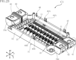
- FIG. 1 is a perspective view showing a semiconductor device according to a first embodiment
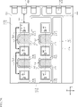
- FIG. FIG. 2 is a plan view showing the semiconductor device according to the first embodiment, showing a sealing member with imaginary lines.
- FIG. 3 is a plan view of FIG. 2 with a plurality of connecting members and sealing members omitted.
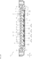
- FIG. 4 is a cross-sectional view taken along line IV-IV of FIG.
- FIG. 5 is a cross-sectional view along line VV in FIG.
- FIG. 6 is a cross-sectional view taken along line VI-VI of FIG.
- FIG. 7 is a fragmentary plan view showing a semiconductor device according to a first modification of the first embodiment, and corresponds to the plan view of FIG. FIG.
- FIG. 8 is a fragmentary plan view showing a semiconductor device according to a second modification of the first embodiment, and corresponds to the plan view of FIG. 9 is a fragmentary plan view showing a semiconductor device according to a third modification of the first embodiment, and corresponds to the plan view of FIG. 3.
- FIG. 10 is a fragmentary plan view showing a semiconductor device according to a fourth modification of the first embodiment, and corresponds to the plan view of FIG. 11 is a fragmentary plan view showing a semiconductor device according to another modification of the first embodiment, and corresponds to the plan view of FIG. 3.
- FIG. FIG. 12 is a perspective view showing a semiconductor device according to a second embodiment;
- FIG. 13 is a perspective view of FIG. 12 with the sealing member omitted.
- FIG. 14 is a plan view showing the semiconductor device according to the second embodiment, showing the sealing member with imaginary lines.
- FIG. 15 is a plan view of FIG. 14 with some connection members omitted.
- FIG. 16 is a plan view of a main part with a part omitted in the plan view of FIG. 15.
- FIG. 17 is a cross-sectional view along line XVII-XVII of FIG. 14.
- FIG. 18 is a fragmentary plan view showing a semiconductor device according to a first modification of the second embodiment, and corresponds to the plan view of FIG. 16.
- FIG. FIG. 19 is a fragmentary plan view showing a semiconductor device according to a second modification of the second embodiment, and corresponds to the plan view of FIG. FIG.
- FIG. 20 is a fragmentary plan view showing a semiconductor device according to a third modification of the second embodiment, and corresponds to the plan view of FIG.
- FIG. 21 is a fragmentary plan view showing a semiconductor device according to a fourth modification of the second embodiment, corresponding to the plan view of FIG. 16.
- FIG. 22 is a perspective view showing a semiconductor device according to a third embodiment; 23 is a perspective view of FIG. 22 with a portion of the case (top plate) and the resin member omitted.
- FIG. 24 is a plan view showing a semiconductor device according to a third embodiment;
- FIG. 25 is a plan view of FIG. 24 with a portion of the case (top plate) and the resin member omitted.
- FIG. 26 is an enlarged plan view of a part of FIG.
- FIG. 27 is an enlarged plan view of a part of FIG. 25, omitting a plurality of connection members.
- 28 is a cross-sectional view taken along line XXVIII--XXVIII of FIG. 25.
- FIG. 29 is a cross-sectional view along line XXIX-XXIX in FIG. 25.
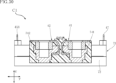
- FIG. 30 is a cross-sectional view taken along line XXX-XXX in FIG. 25.
- FIG. 31 is a cross-sectional view along line XXI-XXI of FIG. 25.
- FIG. 32 is a cross-sectional view taken along line XXII-XXXII of FIG. 25.
- a certain entity A is formed on a certain entity B
- a certain entity A is formed on (of) an entity B
- mean a certain entity A is directly formed in a certain thing B
- a certain thing A is formed in a certain thing B while another thing is interposed between a certain thing A and a certain thing B” including.
- ⁇ an entity A is arranged on an entity B'' and ⁇ an entity A is arranged on (of) an entity B'' mean ⁇ an entity A being placed directly on a certain thing B", and "a thing A being placed on a certain thing B with another thing interposed between something A and something B" include.
- ⁇ an object A is located on (of) an object B'' means ⁇ a certain object A is in contact with an object B, and an object A is located on an object B. Being located on (of)" and "something A is located on (something) B while another thing is interposed between something A and something B including "things”.
- ⁇ a certain object A overlaps an object B when viewed in a certain direction'' means ⁇ a certain object A overlaps all of an object B'', and ⁇ a certain object A overlaps an object B.'' It includes "overlapping a part of a certain thing B".
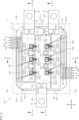
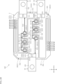
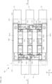
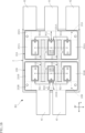
- First embodiment: 1 to 6 show a semiconductor device A1 according to the first embodiment.
- the semiconductor device A1 includes a plurality of first semiconductor elements 11, a plurality of second semiconductor elements 12, a support substrate 2, a plurality of terminals, a plurality of connection members, and a sealing member 6.
- the plurality of terminals includes a plurality of power terminals 41-43 and a plurality of signal terminals 44A, 44B, 45A, 45B, 49.
- the plurality of connecting members includes a plurality of connecting members 51A, 51B, 52A, 52B, 531A, 531B, 541A, 541B.
- the thickness direction of the semiconductor device A1 will be referred to as "thickness direction z".
- One of the thickness directions z may be called upward and the other downward.
- descriptions such as “upper”, “lower”, “upper”, “lower”, “upper surface” and “lower surface” indicate the relative positional relationship of each component etc. in the thickness direction z, and are not necessarily It is not a term that defines the relationship with the direction of gravity.
- “planar view” means when viewed along the thickness direction z.
- a direction orthogonal to the thickness direction z is called a “first direction x”.
- the first direction x is the horizontal direction in the plan view (see FIG. 2) of the semiconductor device A1.
- a direction orthogonal to the thickness direction z and the first direction x is called a "second direction y".
- the second direction y is the vertical direction in the plan view (see FIG. 2) of the semiconductor device A1.
- Each of the plurality of first semiconductor elements 11 and the plurality of second semiconductor elements 12 is, for example, a MOSFET.
- Each of the plurality of first semiconductor elements 11 and the plurality of second semiconductor elements 12 is a field effect transistor including a MISFET (Metal-Insulator-Semiconductor FET) instead of a MOSFET, or other switching such as a bipolar transistor including an IGBT. It may be an element.
- Each of the plurality of first semiconductor elements 11 and the plurality of second semiconductor elements 12 is configured using SiC (silicon carbide).
- the semiconductor material is not limited to SiC, and may be Si (silicon), GaAs (gallium arsenide), GaN (gallium nitride), Ga 2 O 3 (gallium oxide), or the like.
- Each of the plurality of first semiconductor elements 11 is bonded to the support substrate 2 (power wiring section 31 described later) via a conductive bonding material.
- the conductive bonding material is, for example, solder, metal paste material, or sintered metal.
- the plurality of first semiconductor elements 11 are arranged, for example, at regular intervals in the first direction x, as shown in FIGS.
- the plurality of first semiconductor elements 11 includes a first near-field element 110, as shown in FIG.
- the first near-field element 110 has the shortest conduction distance to the power terminal 41 among the plurality of first semiconductor elements 11 .
- Each of the plurality of first semiconductor elements 11 has a first element main surface 11a and a first element rear surface 11b. As shown in FIGS. 4 and 6, the first element main surface 11a and the first element back surface 11b are separated from each other in the thickness direction z.
- the first element main surface 11a faces one direction (upward) in the thickness direction z, and the first element rear surface 11b faces the other direction (downward) in the thickness direction z.
- the first element rear surface 11b faces the support substrate 2 (power wiring section 31 described later).
- Each of the plurality of first semiconductor elements 11 has a first electrode 111, a second electrode 112 and a third electrode 113.
- the first electrode 111 is the drain
- the second electrode 112 is the source
- the third electrode 113 is the gate.
- the first electrode 111 is arranged on the first element rear surface 11b
- the second electrode 112 and the third electrode 113 are arranged on the first element rear surface 11b. It is arranged on the one-element main surface 11a.
- a first drive signal (for example, gate voltage) is input to the third electrode 113 (gate) of each of the plurality of first semiconductor elements 11 .
- Each of the plurality of first semiconductor elements 11 switches between an ON state (conducting state) and an OFF state (interrupting state) according to the input first drive signal.
- the operation of switching between the ON state and the OFF state is called a switching operation.
- a forward current flows from the first electrode 111 (drain) to the second electrode 112 (source) in the ON state, and does not flow in the OFF state.
- Each first semiconductor element 11 is turned on/off between the first electrode 111 (drain) and the second electrode 112 (source) by a first drive signal (for example, gate voltage) input to the third electrode 113 (gate). controlled.
- the switching frequency of each first semiconductor element 11 depends on the frequency of the first drive signal.
- the first electrodes 111 are electrically connected to each other and the second electrodes 112 (source) are electrically connected to each other by a configuration described in detail later. ing. Thereby, the plurality of first semiconductor elements 11 are electrically connected in parallel.
- the semiconductor device A1 inputs a common first drive signal to the plurality of first semiconductor elements 11 connected in parallel to operate the plurality of first semiconductor elements 11 in parallel.
- Each of the plurality of second semiconductor elements 12 is bonded to the support substrate 2 (power wiring section 33 described later) via a conductive bonding material.
- the conductive bonding material is, for example, solder, metal paste material, or sintered metal.
- the plurality of second semiconductor elements 12 are arranged, for example, at regular intervals in the first direction x, as shown in FIGS.
- the plurality of second semiconductor elements 12 includes a second near-field element 120, as shown in FIG.
- the second near element 120 has the shortest conduction distance to the power terminal 43 among the plurality of second semiconductor elements 12 .
- Each of the plurality of second semiconductor elements 12 has a second element main surface 12a and a second element rear surface 12b. As shown in FIGS. 5 and 6, the second element main surface 12a and the second element back surface 12b are separated from each other in the thickness direction z.
- the second element principal surface 12a faces one direction (upward) in the thickness direction z, and the second element rear surface 12b faces the other direction (downward) in the thickness direction z.
- the second element back surface 12b faces the support substrate 2 (power wiring section 33, which will be described later).
- Each of the plurality of second semiconductor elements 12 has a fourth electrode 121, a fifth electrode 122 and a sixth electrode 123.
- the fourth electrode 121 is the drain
- the fifth electrode 122 is the source
- the sixth electrode 123 is the gate. 2
- the fourth electrode 121 is arranged on the second element rear surface 12b
- the fifth electrode 122 and the sixth electrode 123 are arranged on the second element rear surface 12b. It is arranged on the two-element main surface 12a.
- a second drive signal (for example, gate voltage) is input to the sixth electrode 123 (gate) of each of the plurality of second semiconductor elements 12 .
- Each of the plurality of second semiconductor elements 12 switches between an ON state and an OFF state according to the input second drive signal.
- a forward current flows from the fourth electrode 121 (drain) to the fifth electrode 122 (source) in the ON state, and does not flow in the OFF state.
- Each second semiconductor element 12 is turned on/off between the fourth electrode 121 (drain) and the fifth electrode 122 (source) by a second drive signal (for example, gate voltage) input to the sixth electrode 123 (gate). controlled.
- the switching frequency of each second semiconductor element 12 depends on the frequency of the second drive signal.
- the fourth electrodes 121 are electrically connected to each other and the fifth electrodes 122 (source) are electrically connected to each other by a configuration described in detail later. ing. Thereby, the plurality of second semiconductor elements 12 are electrically connected in parallel.
- the semiconductor device A1 inputs a common second drive signal to the plurality of second semiconductor elements 12 connected in parallel to operate the plurality of second semiconductor elements 12 in parallel.
- the support substrate 2 supports the plurality of first semiconductor elements 11 and the plurality of second semiconductor elements 12 and electrically connects the plurality of first semiconductor elements 11 and the plurality of second semiconductor elements 12 to the plurality of terminals.
- support substrate 2 is, for example, a DBC (Direct Bonded Copper) substrate. Unlike this configuration, the support substrate 2 may be, for example, a DBA (Direct Bonded Aluminum) substrate.
- the support substrate 2 includes an insulating substrate 20 , a main surface metal layer 21 and a back surface metal layer 22 .
- Insulating substrate 20 is made of, for example, ceramic having excellent thermal conductivity. Examples of such ceramic include AlN (aluminum nitride), SiN (silicon nitride), Al 2 O 3 (aluminum oxide), and the like. Insulating substrate 20 has, for example, a flat plate shape. As shown in FIGS. 2 and 3, insulating substrate 20 has, for example, a rectangular shape in plan view.
- the insulating substrate 20 has a main surface 20a and a back surface 20b. As shown in FIGS. 4-6, the main surface 20a and the back surface 20b are spaced apart in the thickness direction z. The main surface 20a faces upward in the thickness direction z, and the back surface 20b faces downward in the thickness direction z.
- the main surface metal layer 21 and the back surface metal layer 22 are each made of, for example, copper or a copper alloy.
- the main surface metal layer 21 and the back surface metal layer 22 may each be made of aluminum or an aluminum alloy instead of copper or a copper alloy.
- the main surface metal layer 21 is formed on the main surface 20a, and the back surface metal layer 22 is formed on the back surface 20b.
- the lower surface of the back metal layer 22 (the surface facing downward in the thickness direction z) is exposed from the sealing member 6 . Unlike this configuration, the lower surface of the back metal layer 22 may be covered with the sealing member 6 .
- the main surface metal layer 21 includes a plurality of power wiring portions 31 to 33 and a plurality of signal wiring portions 34A, 34B, 35A, 35B, and 39, as shown in FIG.
- the plurality of power wiring sections 31 to 33 and the plurality of signal wiring sections 34A, 34B, 35A, 35B, 39 are separated from each other.
- a plurality of power wiring portions 31, 32, and 33 form conduction paths for the main circuit current in the semiconductor device A1.
- the main circuit current includes a first main circuit current and a second main circuit current.
- the first main circuit current is the current that flows between the power terminals 41 and 43 .
- the second main circuit current is the current that flows between the power terminals 43 and 42 .
- the power wiring portion 31 is an example of the "first conductor”
- the power wiring portion 32 is an example of the "third conductor”
- the power wiring portion 33 is an example of the "second conductor".
- the power wiring portion 31 is electrically connected to each first electrode 111 (drain) of the plurality of first semiconductor elements 11 .
- the power wiring portion 31 is electrically connected to the power terminal 41 .
- the power wiring portion 31 is arranged to avoid part of each first line segment S1 in plan view.
- Each first line segment S1 is an auxiliary line shown in FIG. 3 for convenience of understanding, and is a line segment connecting the respective centers of two first semiconductor elements 11 adjacent in the first direction x.
- the center of each first semiconductor element 11 may be the center of the entire first semiconductor element 11 in plan view, or the center of the first electrode 111 in plan view. For convenience of understanding, the center is indicated by a cross in FIG.
- the power wiring portion 31 is arranged so as to avoid a portion of 15% or more and 90% or less (preferably 25% or more and 90% or less) of each first line segment S1 in plan view.
- the power wiring section 31 includes two pad sections 311 and 312 . As shown in FIGS. 2 and 3, the two pad portions 311 and 312 are connected to each other and formed integrally.
- the pad portion 311 includes a plurality of mounting portions 311a and connecting portions 311b.
- each of the plurality of first semiconductor elements 11 is mounted on each of the plurality of mounting portions 311a.
- the first electrodes 111 (drain) of the plurality of first semiconductor elements 11 are joined to the plurality of mounting portions 311a, respectively.
- Each of the plurality of mounting portions 311a has, for example, a rectangular shape in plan view.
- Each of the plurality of mounting portions 311a includes, in plan view, a portion overlapping each of the plurality of first semiconductor elements 11 and a portion extending from this portion.
- the plurality of mounting portions 311a are arranged along the first direction x while being spaced apart in the first direction x.
- Each of the plurality of mounting portions 311a has one end edge in the second direction y connected to the connecting portion 311b. Accordingly, the plurality of mounting portions 311a are electrically connected to each other by the connecting portions 311b.
- the mounting portion 311a is an example of the "first mounting portion”.
- each first gap G1 is indicated by a dot-like pattern in FIG. As shown in FIG. 3, each first gap G1 overlaps each first line segment S1.
- Each first gap G1 is formed, for example, by each notch provided in the edge of the pad portion 311 on the other side in the second direction y (the side closer to the power wiring portion 33). A part of the power wiring portion 33 (each projecting portion 333 to be described later) is arranged in each first gap G1.
- the connecting portion 311b is connected to each of the plurality of mounting portions 311a as shown in FIGS.
- the connecting portion 311b extends from the pad portion 312 to the other side in the first direction x.
- the other side in the first direction x is the side opposite to the direction in which the power terminals 41 extend with respect to the pad portion 312 and the side where the plurality of first semiconductor elements 11 are located.
- the connecting portion 311b has a strip shape in plan view. As shown in FIGS. 2 and 3, the connecting portion 311b is located on the side opposite to the plurality of second semiconductor elements 12 with respect to the plurality of mounting portions 311a in the second direction y.
- the connecting portion 311b is positioned on one side in the second direction y (the side opposite to the plurality of second semiconductor elements 12) with respect to each first line segment S1 in plan view.
- the connecting portion 311b is an example of the "first connecting portion”.
- the power terminal 41 is joined to the pad portion 312 as shown in FIGS.
- the pad portion 312 has a strip shape with the second direction y as its longitudinal direction in plan view.
- the pad portion 312 is connected to the edge of the pad portion 311 on one side in the first direction x (the side on which the power terminal 41 is located).
- the power wiring section 32 is electrically connected to each fifth electrode 122 (source) of the plurality of second semiconductor elements 12 .
- the power wiring portion 32 is electrically connected to the power terminal 42 .
- the power wiring section 32 includes two pad sections 321 and 322 and a plurality of protrusions 323 . Unlike this configuration, the power wiring portion 32 may not include any of the plurality of projecting portions 323 . As shown in FIGS. 2 and 3, the two pad portions 321 and 322 and the plurality of projecting portions 323 are connected to each other and formed integrally.
- the pad portion 321 is joined to a plurality of connection members 51B, and is connected to each of the fifth electrodes 122 (sources) of the plurality of second semiconductor elements 12 via the plurality of connection members 51B. conduct.
- the pad portion 321 extends along the other side of the first direction x from the pad portion 322, as shown in FIGS.
- the other side in the first direction x is the side opposite to the direction in which the power terminals 42 extend with respect to the pad portion 322, and is the side on which the plurality of first semiconductor elements 11 and the plurality of second semiconductor elements 12 are located.
- the pad portion 321 has a strip shape, for example, with the first direction x as its longitudinal direction in a plan view.
- the pad portion 321 is positioned on the other side (lower side in FIG. 2) in the second direction y with respect to the pad portion 311 .
- the power terminal 42 is joined to the pad portion 322, as shown in FIGS.
- the pad portion 322 has a strip shape with the second direction y as its longitudinal direction in plan view.
- the pad portion 322 is connected to the edge of the pad portion 321 on one side in the first direction x (the side on which the power terminal 42 is located).
- the pad portion 322 is positioned on the other side in the second direction y (lower side in FIG. 2) with respect to the pad portion 321 .
- the plurality of protrusions 323 protrude from the edge of the pad 321 on one side in the second direction y to one side in the second direction y.
- One side in the second direction y is the side on which the plurality of second semiconductor elements 12 are positioned with respect to the pad section 321 .
- Each projecting portion 323 has, for example, a rectangular shape in plan view.
- Each projecting portion 323 is arranged between two second semiconductor elements 12 adjacent in the first direction x and between two mounting portions 331a adjacent in the first direction x.
- each part of the plurality of protrusions 323 overlaps each of the plurality of second gaps G2 (described later) in plan view.
- the power wiring portion 33 is electrically connected to each second electrode 112 (source) of the plurality of first semiconductor elements 11 and electrically connected to each fourth electrode 121 (drain) of the plurality of second semiconductor elements 12 .
- the power wiring portion 33 is electrically connected to two power terminals 43 .
- the power wiring portion 33 is arranged to avoid part of each of the second line segments S2 in plan view (see FIG. 3).
- Each second line segment S2 is an auxiliary line shown in FIG. 3 for convenience of understanding, and is a line segment connecting the centers of two second semiconductor elements 12 adjacent in the first direction x.
- the center of each second semiconductor element 12 may be the center of the entire second semiconductor element 12 in plan view, or the center of the fourth electrode 121 in plan view.
- the center is indicated by a cross in FIG.
- the power wiring portion 33 is arranged so as to avoid 15% or more and 90% or less (preferably 25% or more and 90% or less) of each second line segment S2 in plan view.
- the power wiring section 33 includes two pad sections 331 and 332 and a plurality of protrusions 333 . Unlike this configuration, the power wiring portion 33 may not include any of the plurality of projecting portions 333 . As shown in FIGS. 2 and 3, the two pad portions 331 and 332 and the plurality of projecting portions 333 are connected to each other and integrally formed.
- the pad portion 331 includes a plurality of mounting portions 331a and connecting portions 331b.
- each of the plurality of second semiconductor elements 12 is mounted on each of the plurality of mounting portions 331a.
- Each fourth electrode 121 (drain) of the plurality of second semiconductor elements 12 is joined to the plurality of mounting portions 331a.
- Each of the plurality of mounting portions 331a has, for example, a rectangular shape in plan view.
- Each of the plurality of mounting portions 331a includes, in plan view, a portion overlapping each of the plurality of second semiconductor elements 12 and a portion extending from this portion.
- the plurality of mounting portions 331a are arranged along the first direction x while being spaced apart in the first direction x.
- Each of the plurality of mounting portions 331a has one end edge in the second direction y connected to the connecting portion 331b. Thereby, the plurality of mounting portions 331a are electrically connected to each other by the connecting portions 331b.
- the mounting portion 331a is an example of the "second mounting portion”.
- each second gap G2 is indicated by a dot-like pattern in FIG.
- Each second gap G2 overlaps each second line segment S2.
- Each second gap G2 is formed, for example, by each notch provided at the edge of the pad portion 331 on the other side in the second direction y (the side closer to the power wiring portion 32).
- a portion of the power wiring portion 32 (each projecting portion 323) is arranged in each second gap G2.
- the connecting portion 331b is connected to each of the plurality of mounting portions 331a as shown in FIGS.
- the connecting portion 331b extends from the pad portion 332 to one side in the first direction x.
- the one side in the first direction x is the side opposite to the direction in which the power terminals 43 extend with respect to the pad portion 332 and the side where the plurality of second semiconductor elements 12 are located.
- the connecting portion 331b has a strip shape in plan view.
- the connecting portion 331b is connected to the plurality of connection members 51A and connected to the second electrodes 112 (sources) of the plurality of first semiconductor elements 11 via the plurality of connection members 51A. conduct.
- the connecting portion 331b is located on the same side as the plurality of first semiconductor elements 11 with respect to the plurality of mounting portions 331a in the second direction y.
- the connecting portion 331b is positioned on one side in the second direction y (the same side as the plurality of first semiconductor elements 11) with respect to each second line segment S2 in plan view.
- the connecting portion 331b is an example of the "second connecting portion".
- the power terminal 43 is joined to the pad portion 332 as shown in FIGS.
- the pad portion 332 has a strip shape with the second direction y as its longitudinal direction in a plan view.
- the pad portion 332 is connected to the edge of the pad portion 331 on the other side in the first direction x (the side on which the power terminal 43 is located).
- each of the plurality of projecting portions 333 extends from one edge of the connecting portion 331b (pad portion 331) in the second direction y to one side in the second direction y in plan view. protrude.
- One side in the second direction y is the side on which the plurality of first semiconductor elements 11 are positioned with respect to the connecting portion 331b.
- Each of the plurality of protrusions 333 has, for example, a rectangular shape in plan view.
- Each projecting portion 333 is arranged between two first semiconductor elements 11 adjacent in the first direction x and between two mounting portions 311a adjacent in the first direction x. Therefore, as shown in FIG. 3, each part of the plurality of projections 333 overlaps each of the plurality of first gaps G1 in plan view.
- a plurality of signal wiring portions 34A, 34B, 35A, and 35B form conduction paths for electrical signals for controlling the semiconductor device A1.
- the signal wiring portion 34A is connected to a plurality of connection members 531A and electrically connected to the third electrodes 113 (gates) of the plurality of first semiconductor elements 11 via the plurality of connection members 531A. . 34 A of signal wiring parts transmit a 1st drive signal. A signal terminal 44A is joined to the signal wiring portion 34A.
- the signal wiring portion 34B is connected to a plurality of connection members 531B and electrically connected to the sixth electrodes 123 (gates) of the plurality of second semiconductor elements 12 via the plurality of connection members 531B. .
- the signal wiring portion 34B transmits the second drive signal.
- a signal terminal 44B is joined to the signal wiring portion 34B.
- the signal wiring portion 34A and the signal wiring portion 34B are located on opposite sides of each other with the pad portions 311, 321, 331 interposed therebetween in the second direction y.
- the signal wiring portion 34A is located on the side opposite to the pad portion 331 with respect to the pad portion 311 in the second direction y.
- the signal wiring portion 34B is located on the side opposite to the pad portion 331 with respect to the pad portion 321 in the second direction y.
- the signal wiring portion 35A is connected to a plurality of connection members 541A and electrically connected to the second electrodes 112 (sources) of the plurality of first semiconductor elements 11 via the plurality of connection members 541A. .
- the signal wiring portion 35A transmits the first detection signal.
- the first detection signal is an electrical signal indicating the conduction state of each first semiconductor element 11, and is, for example, a voltage signal corresponding to the current (source current) flowing through each second electrode 112 (source).
- a signal terminal 45A is joined to the signal wiring portion 35A.
- the signal wiring portion 35B is connected to a plurality of connection members 541B and electrically connected to the fifth electrodes 122 (sources) of the plurality of second semiconductor elements 12 via the plurality of connection members 541B. .
- the signal wiring portion 35B transmits the second detection signal.
- the second detection signal is an electrical signal indicating the conduction state of each second semiconductor element 12, and is, for example, a voltage signal corresponding to the current (source current) flowing through each fifth electrode 122 (source).
- a signal terminal 45B is joined to the signal wiring portion 35B.
- the signal wiring portion 35A and the signal wiring portion 35B are located on opposite sides of each other with the pad portions 311, 321, 331 interposed therebetween in the second direction y.
- the signal wiring portion 35A is located on the same side as the signal wiring portion 34A with respect to the pad portion 311 in the second direction y.
- the signal wiring portion 35B is located on the same side as the signal wiring portion 34B with respect to the pad portion 321 in the second direction y.
- Each of the plurality of signal wiring portions 39 is electrically connected to none of the plurality of first semiconductor elements 11 and the plurality of second semiconductor elements 12 . In other words, neither the main circuit current nor the electric signal flows through any of the plurality of signal wiring portions 39 .
- the plurality of power terminals 41 to 43 and the plurality of signal terminals 44A, 44B, 45A, 45B, and 49 are partially exposed from the sealing member 6 as shown in FIGS.
- Each constituent material of the plurality of power terminals 41 to 43 and the plurality of signal terminals 44A, 44B, 45A, 45B, 49 is, for example, copper or copper alloy, but may be other metals.
- the plurality of power terminals 41 to 43 and the plurality of signal terminals 44A, 44B, 45A, 45B, 49 are each made of a metal plate and bent appropriately.
- the power terminals 41 and 42 are connected to a power supply and applied with a power supply voltage (for example, DC voltage).
- a power supply voltage for example, DC voltage
- the power terminal 41 is a positive power input terminal (P terminal)
- the power terminal 42 is a negative power input terminal (N terminal).
- the power terminal 43 outputs a voltage (for example, AC voltage) that is power-converted by each switching operation of the plurality of first semiconductor elements 11 and each switching operation of the plurality of second semiconductor elements 12 .
- Each of the power terminals 43 is a power output terminal (OUT terminal).
- the main circuit current (first main circuit current and second main circuit current) in the semiconductor device A1 is generated by the power supply voltage and the converted voltage.
- the power terminal 41 is an example of a "first power terminal”
- the power terminal 42 is an example of a "third power terminal”
- the power terminal 43 is an example of a "second power terminal”.
- the power terminal 41 is electrically connected to each first electrode 111 (drain) of the plurality of first semiconductor elements 11 via the power wiring portion 31 .
- Power terminal 41 includes a joint portion 411 and a terminal portion 412 .
- the joint 411 is covered with the sealing member 6 as shown in FIGS.
- the joint portion 411 is joined to the pad portion 312 of the power wiring portion 31 as shown in FIGS. Thereby, the power terminal 41 and the power wiring portion 31 are electrically connected.
- the bonding portion 411 and the pad portion 312 may be bonded by any method such as bonding using a conductive bonding material (solder, sintered metal, etc.), laser bonding, or ultrasonic bonding.
- the terminal portion 412 is exposed from the sealing member 6 as shown in FIGS. As shown in FIG. 2, the terminal portion 412 extends from the sealing member 6 to one side in the first direction x in plan view.
- the surface of terminal portion 412 may be plated with silver, for example.
- the power terminal 42 is electrically connected to each fifth electrode 122 (source) of the plurality of second semiconductor elements 12 via the power wiring portion 32 .
- Power terminal 42 includes joint portion 421 and terminal portion 422 .
- the joint 421 is covered with the sealing member 6 as shown in FIGS.
- the joint portion 421 is joined to the pad portion 322 of the power wiring portion 32 as shown in FIGS. Thereby, the power terminal 42 and the power wiring portion 32 are electrically connected.
- the bonding portion 421 and the pad portion 322 may be bonded by any method such as bonding using a conductive bonding material (such as solder or sintered metal), laser bonding, or ultrasonic bonding.
- the terminal portion 422 is exposed from the sealing member 6 as shown in FIGS. As shown in FIG. 2, the terminal portion 422 extends from the sealing member 6 to one side in the first direction x in plan view.
- the surface of terminal portion 422 may be plated with silver, for example.
- the power terminal 43 is electrically connected to each of the second electrodes 112 (sources) of the plurality of first semiconductor elements 11 via the power wiring portion 33, and is connected to each of the fourth electrodes 121 (drain) of the plurality of second semiconductor elements 12. conducts to Power terminal 43 includes joint portion 431 and terminal portion 432 .
- the joint 431 is covered with the sealing member 6 as shown in FIGS.
- the joint portion 431 is joined to the pad portion 332 of the power wiring portion 33 as shown in FIGS. Thereby, the power terminal 43 and the power wiring portion 33 are electrically connected.
- the joining portion 431 and the pad portion 332 may be joined by any method such as joining using a conductive joining material (solder or sintered metal, etc.), laser joining, or ultrasonic joining.
- the terminal portion 432 is exposed from the sealing member 6 as shown in FIGS. As shown in FIG. 2, the terminal portion 432 extends from the sealing member 6 to the other side in the first direction x in plan view.
- the surface of terminal portion 432 may be plated with silver, for example.
- the power terminals 41 and 42 are spaced apart from each other and arranged along the second direction y.
- the power terminals 41 and 42 and the power terminals 43 are arranged on opposite sides of the support substrate 2 in the first direction x.
- the number of power terminals 43 may be two or more instead of one.
- a plurality of signal terminals 44A, 44B, 45A, and 45B are input terminals or output terminals of electrical signals for controlling the semiconductor device A1.
- Each of the plurality of signal terminals 44A, 44B, 45A, 45B, and 49 includes a portion covered with the sealing member 6 and a portion exposed from the sealing member 6. As shown in FIG.
- Each of the plurality of signal terminals 44A, 44B, 45A, 45B, and 49 is a pin-shaped metal member.
- the metal member is made of copper or copper alloy, for example.
- the portion of the signal terminal 44A covered with the sealing member 6 is joined to the signal wiring portion 34A, as shown in FIG. Since the signal wiring portion 34A is electrically connected to each third electrode 113 (gate) of the plurality of first semiconductor elements 11, the signal terminal 44A is electrically connected to each third electrode 113 (gate) of the plurality of first semiconductor elements 11. do.
- the signal terminal 44A is an input terminal for the first drive signal.
- the portion of the signal terminal 44B covered with the sealing member 6 is joined to the signal wiring portion 34B. Since the signal wiring portion 34B is electrically connected to each sixth electrode 123 (gate) of the plurality of second semiconductor elements 12, the signal terminal 44B is electrically connected to each sixth electrode 123 (gate) of the plurality of second semiconductor elements 12. do.
- the signal terminal 44B is an input terminal for the second drive signal.
- the portion of the signal terminal 45A covered with the sealing member 6 is joined to the signal wiring portion 35A, as shown in FIG. Since the signal wiring portion 35A is electrically connected to the second electrodes 112 (sources) of the plurality of first semiconductor elements 11, the signal terminal 45A is electrically connected to the second electrodes 112 (sources) of the plurality of first semiconductor elements 11. do.
- the signal terminal 45A is an output terminal for the first detection signal.
- the portion of the signal terminal 45B covered with the sealing member 6 is joined to the signal wiring portion 35B. Since the signal wiring portion 35B is electrically connected to each fifth electrode 122 (source) of the plurality of second semiconductor elements 12, the signal terminal 45B is electrically connected to each fifth electrode 122 (source) of the plurality of second semiconductor elements 12. do.
- the signal terminal 45B is an output terminal for the second detection signal.
- each of the plurality of signal terminals 49 is electrically connected to none of the plurality of first semiconductor elements 11 and the plurality of second semiconductor elements 12 .
- Each of the plurality of signal terminals 49 is a non-connect terminal.
- a plurality of signal terminals 49 may be omitted.
- Each of the plurality of connection members 51A, 51B, 52A, 52B, 531A, 531B, 541A, 541B conducts two parts separated from each other.
- all of the plurality of connecting members 51A, 51B, 52A, 52B, 531A, 531B, 541A, 541B are bonding wires. Any of gold, copper, or aluminum may be used as the constituent material of each of the plurality of connection members 51A, 51B, 52A, 52B, 531A, 531B, 541A, and 541B.
- the plurality of connecting members 51A are respectively joined to the second electrodes 112 (sources) of the plurality of first semiconductor elements 11 and the connecting portions 331b of the pad portions 331, and The electrode 112 and the power wiring portion 33 are electrically connected.
- a plurality of connection members 51A are joined to each of the plurality of second electrodes 112.
- a main circuit current (first main circuit current) in the semiconductor device A1 flows through the plurality of connection members 51A.
- each connecting member 51A may be a plate-shaped member made of metal (for example, made of copper) instead of the bonding wire.
- the number of connection members 51A each joined to each second electrode 112 and pad portion 331 may be one.
- the connecting member 51A is an example of a "first connecting member".
- the plurality of connection members 51B are respectively joined to the fifth electrodes 122 (sources) and the pad portions 321 of the plurality of second semiconductor elements 12 to connect the fifth electrodes 122 and the power supply.
- the wiring part 32 is electrically connected.
- a plurality of connection members 51B are joined to each of the plurality of fifth electrodes 122.
- a main circuit current (second main circuit current) in the semiconductor device A1 flows through the plurality of connecting members 51B.
- each connecting member 51B may be a plate-like member made of metal (for example, made of copper) instead of the bonding wire.
- the number of connection members 51B each joined to each fifth electrode 122 and pad portion 321 may be one.
- the connecting member 51B is an example of a "second connecting member".
- the plurality of connection members 52A are connected to the second electrodes 112 (sources) of the plurality of first semiconductor elements 11 and the protrusions adjacent to the first semiconductor elements 11 in the first direction x. 333 to make them conductive.
- Two connection members 52A are joined to each protrusion 333 .
- Each of the plurality of connection members 52A extends, for example, along the first direction x in plan view. Note that in a configuration in which the power wiring portion 33 does not include the projecting portions 333, the plurality of connection members 52A may be omitted, and the second electrodes 112 of the two first semiconductor elements 11 adjacent in the first direction x may be provided. may be directly bonded to
- the plurality of connection members 52B are adjacent to the fifth electrodes 122 (sources) of the plurality of second semiconductor elements 12 and the second semiconductor elements 12 in the first direction x. It is joined to the projecting portion 323 and conducts them. Two connection members 52B are joined to each protrusion 323 . Each of the plurality of connection members 52B extends, for example, along the first direction x in plan view. Note that in a configuration in which the power wiring portion 32 does not include the protruding portions 323, the plurality of connecting members 52B may be omitted, and the fifth electrodes 122 of the two second semiconductor elements 12 adjacent in the first direction x may be omitted. may be directly bonded to
- the plurality of connection members 531A are respectively joined to the respective third electrodes 113 (gates) of the plurality of first semiconductor elements 11 and the signal wiring portion 34A, and are connected to the respective third electrodes 113 and the signal wiring portion. 34A.
- the signal terminal 44A is electrically connected to each third electrode 113 of the plurality of first semiconductor elements 11 via the signal wiring portion 34A and the plurality of connection members 531A.
- the plurality of connection members 531B are respectively joined to the respective sixth electrodes 123 (gates) of the plurality of second semiconductor elements 12 and the signal wiring portion 34B to connect the respective sixth electrodes 123 and the signal wiring portion. 34B are electrically connected.
- the signal terminal 44B is electrically connected to each of the sixth electrodes 123 of the plurality of second semiconductor elements 12 via the signal wiring portion 34B and the plurality of connection members 531B.
- the plurality of connection members 541A are respectively joined to the second electrodes 112 (sources) of the plurality of first semiconductor elements 11 and the signal wiring portion 35A to connect the second electrodes 112 and the signal wiring portion 35A. 35A.
- the signal terminal 45A is electrically connected to the second electrodes 112 of the plurality of first semiconductor elements 11 via the signal wiring portion 35A and the plurality of connection members 541A.
- the plurality of connecting members 541B are respectively joined to the fifth electrodes 122 (sources) of the plurality of second semiconductor elements 12 and the signal wiring portion 35B to connect the fifth electrodes 122 and the signal wiring portion 35B. 35B are electrically connected.
- the signal terminal 45B is electrically connected to each of the fifth electrodes 122 of the plurality of second semiconductor elements 12 via the signal wiring portion 35B and the plurality of connection members 541B.
- the sealing member 6 is a sealing material that protects the plurality of first semiconductor elements 11, the plurality of second semiconductor elements 12, and the like.
- the sealing member 6 includes the plurality of first semiconductor elements 11, the plurality of second semiconductor elements 12, a portion of the support substrate 2, the plurality of power terminals 41 to 43, and the plurality of signal terminals 44A, 44B, 45A, 45B, 49. , cover the plurality of connection members 51A, 51B, 52A, 52B, 531A, 531B, 541A, 541B, respectively.
- the sealing member 6 is made of, for example, an insulating resin material, such as an epoxy resin.
- the sealing member 6 is black, for example.
- the sealing member 6 has a rectangular shape in plan view.
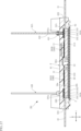
- the sealing member 6 has a resin main surface 61, a resin back surface 62 and a plurality of resin side surfaces 631-634.
- the resin main surface 61 and the resin back surface 62 are spaced apart in the thickness direction z, as shown in FIGS.
- the resin main surface 61 faces upward in the thickness direction z
- the resin rear surface 62 faces downward in the thickness direction z.
- Each of the plurality of resin side surfaces 631 to 634 is sandwiched between and connected to the resin main surface 61 and the resin back surface 62 in the thickness direction z.
- the pair of resin side surfaces 631 and 632 face opposite sides in the first direction x.
- Each power terminal 41 , 42 protrudes from the resin side surface 632
- the power terminal 43 protrudes from the resin side surface 631 .
- the pair of resin side surfaces 633 and 634 face opposite sides in the second direction y.
- the signal terminals 44A, 45A protrude from the resin side surface 634, and the signal terminals 44B, 45B protrude from the resin side surface 633. As shown in FIG.
- the conduction path R11 (see FIG. 3) between the first electrodes 111 (drain) of the two first semiconductor elements 11 adjacent in the first direction x is the first electrode 111 of the first near element 110. (drain) and the power terminal 41 (P terminal) longer than the conduction path R12 (see FIG. 3).
- the element-element inductance L1 which is the inductance of the conduction path R11, is greater than the element-terminal inductance L2, which is the inductance of the conduction path R12.
- the element-element inductance L1 is an example of a "first inductance”
- the element-terminal inductance L2 is an example of a "second inductance”.
- the conduction path R21 (see FIG. 3) between the fourth electrodes 121 (drain) of the two second semiconductor elements 12 adjacent in the first direction x is the second near element 120 of the second near element 120. It is longer than the conduction path R22 (see FIG. 3) between the four electrodes 121 (drain) and the power terminal 43 (OUT terminal).
- the element-element inductance L3 which is the inductance of the conduction path R21, is larger than the element-terminal inductance L4, which is the inductance of the conduction path R22.
- the element-element inductance L3 is an example of the "third inductance”
- the element-terminal inductance L4 is an example of the "fourth inductance".
- the actions and effects of the semiconductor device A1 are as follows.
- the semiconductor device A1 includes a plurality of first semiconductor elements 11, and the plurality of first semiconductor elements 11 are electrically connected in parallel.
- the semiconductor device A1 includes a power wiring portion 31 as a first conductor.
- the power wiring portion 31 is arranged to avoid part of the first line segment S1 when viewed in the thickness direction z. According to this configuration, the element-to-element inductance L1 is increased compared to the configuration in which the power wiring portion 31 is arranged without avoiding the first line segment S1 (hereinafter referred to as "first comparative configuration").
- the first comparative configuration is, for example, a configuration in which the conduction paths between the first electrodes 111 (drain) of the plurality of first semiconductor elements 11 are straight, as in Patent Document 1.
- the semiconductor device A1 can suppress the occurrence of an oscillation phenomenon when the plurality of first semiconductor elements 11 are operated in parallel, as compared with the first comparative configuration.
- the power wiring portion 31 as the first conductor avoids 15% or more of the first line segment S1 when viewed in the thickness direction z.
- the length of each conduction path R11 can be made sufficiently large relative to the length of the first line segment S1. Therefore, in order to suppress an oscillation phenomenon that occurs when a plurality of first semiconductor elements 11 are operated in parallel, an appropriate element-to-element inductance L1 can be ensured.
- the power wiring portion 31 avoids a portion of 25% or more of the first line segment S1 when viewed in the thickness direction z, the oscillation phenomenon during parallel operation of the plurality of first semiconductor elements 11 can be prevented.
- the power wiring portion 31 avoids 90% or less of the first line segment S1 when viewed in the thickness direction z. Unlike this configuration, if the power wiring portion 31 avoids a portion larger than 90% of the first line segment S1 when viewed in the thickness direction z, each first line segment S1 can be viewed in the thickness direction z.
- the semiconductor element 11 may protrude from each mounting portion 311a. If each first semiconductor element 11 protrudes from each mounting portion 311a when viewed in the thickness direction z, the bonding strength between each first semiconductor element 11 may be reduced, or the first electrode 111 and each mounting portion 311a may be damaged. The bonding area with is reduced.
- each first semiconductor element 11 is arranged.
- An appropriate size of the area (each mounting portion 311a) can be ensured.
- the semiconductor device A1 prevents the first semiconductor elements 11 from protruding from the mounting portions 311a, reduces the bonding strength of the first semiconductor elements 11, and reduces the bonding strength between the first electrodes 111 and the mounting portions 311a. Reduction in area can be suppressed.
- the semiconductor device A1 adopts a configuration in which the power wiring portion 31 as the first conductor avoids a portion of 15% or more and 90% or less of the first line segment S1 when viewed in the thickness direction z.
- each first semiconductor element 11 can be appropriately bonded to each mounting portion 311a while ensuring an appropriate element-to-element inductance L1.
- the power wiring portion 31 includes a plurality of mounting portions 311a on which each of the plurality of first semiconductor elements 11 is mounted.
- the plurality of mounting portions 311a any two mounting portions 311a adjacent in the first direction x are arranged with a first gap G1 interposed therebetween in the first direction x.
- the first gap G1 intersects the first line segment S1 when viewed in the thickness direction z.
- the power wiring portion 31 has a shape that avoids part of the first line segment S1. Therefore, the semiconductor device A1 can increase the element-to-element inductance L1 compared to the first comparative configuration.
- the semiconductor device A1 includes a plurality of second semiconductor elements 12, and the plurality of second semiconductor elements 12 are electrically connected in parallel.
- the semiconductor device A1 includes a power wiring portion 33 as a second conductor.
- the power wiring portion 33 is arranged to avoid part of the second line segment S2 when viewed in the thickness direction z.
- the element-to-element inductance L3 is increased compared to the configuration in which the power wiring portion 33 is arranged without avoiding the second line segment S2 (hereinafter referred to as "second comparative configuration").
- the second comparative configuration is, for example, a configuration in which the conduction path between the fourth electrodes 121 (drain) of the plurality of second semiconductor elements 12 is straight, as in Patent Document 1. Therefore, the semiconductor device A1 can suppress the occurrence of an oscillation phenomenon when the plurality of second semiconductor elements 12 are operated in parallel, compared to the second comparative configuration.
- the power wiring portion 33 as the second conductor avoids 15% or more of the second line segment S2 when viewed in the thickness direction z.
- the length of each conduction path R21 can be sufficiently increased with respect to the length of the second line segment S2. Therefore, in order to suppress the oscillation phenomenon that occurs when the plurality of second semiconductor elements 12 operate in parallel, an appropriate element-to-element inductance L3 can be ensured.
- the power wiring portion 33 avoids a portion of 25% or more of the second line segment S2 when viewed in the thickness direction z, the oscillation phenomenon during parallel operation of the plurality of second semiconductor elements 12 can be prevented. In terms of suppression, a more favorable element-to-element inductance L3 is ensured.
- the power wiring portion 33 avoids 90% or less of the second line segment S2 when viewed in the thickness direction z.
- the power wiring portion 31 avoids 90% or less of the first line segment S1 when viewed in the thickness direction z.
- the size of the portion 331a) can be appropriately secured.
- the semiconductor device A1 suppresses the protruding of each second semiconductor element 12 from each mounting portion 331a, reduces the bonding strength of each second semiconductor element 12, and reduces the bonding between each fourth electrode 121 and each mounting portion 331a. Reduction in area can be suppressed.
- the semiconductor device A1 adopts a configuration in which the power wiring portion 32 as the second conductor avoids a portion of 15% or more and 90% or less of the second line segment S2 when viewed in the thickness direction z.
- each second semiconductor element 12 can be appropriately bonded to each mounting portion 331a while ensuring an appropriate element-to-element inductance L3.
- the power wiring portion 33 includes a plurality of mounting portions 331a on which each of the plurality of second semiconductor elements 12 is mounted. Any two mounting portions 331a adjacent in the first direction x among the plurality of mounting portions 331a are arranged with a second gap G2 interposed therebetween in the first direction x. The second gap G2 intersects the second line segment S2 when viewed in the thickness direction z. According to this configuration, the power wiring portion 33 has a shape that avoids part of the second line segment S2. Therefore, the semiconductor device A1 can increase the element-to-element inductance L3 compared to the second comparative configuration.
- the power wiring portion 33 includes a protruding portion 333.
- the protruding portion 333 protrudes in the second direction y from the connecting portion 331b (pad portion 331) when viewed in the thickness direction z.
- the projecting portion 333 partially overlaps the first gap G1 when viewed in the thickness direction z.
- the projecting portion 333 is arranged between two first semiconductor elements 11 adjacent in the first direction x.
- the second electrodes 112 of the two first semiconductor elements 11 located on both sides of the projecting portion 333 in the first direction x are electrically connected via the projecting portion 333 by each connecting member 52A. be able to.
- the semiconductor device A1 electrically connects the second electrodes 112 of the two first semiconductor elements 11 located on both sides of the protruding portion 333 in the first direction x by the connecting members 52A through the protruding portion 333.
- the power wiring portion 32 includes a protruding portion 323.
- the protruding portion 323 protrudes from the pad portion 332 in the second direction y when viewed in the thickness direction z.
- the projecting portion 323 partially overlaps the second gap G2 when viewed in the thickness direction z.
- the projecting portion 323 is arranged between two second semiconductor elements 12 adjacent in the first direction x.
- the fifth electrodes 122 of the two second semiconductor elements 12 located on both sides of the projecting portion 323 in the first direction x are electrically connected to each other via the projecting portion 323 by each connecting member 52B. be able to.
- the semiconductor device A1 electrically connects the fifth electrodes 122 of the two second semiconductor elements 12 located on both sides of the projecting portion 323 in the first direction x with the connecting members 52B through the projecting portion 323. By connecting, it becomes possible to further suppress the occurrence of the oscillation phenomenon when the plurality of second semiconductor elements 12 are operated in parallel.
- FIG. 7 to 10 show semiconductor devices A2 to A5 according to first to fourth modifications of the first embodiment, respectively.
- Each of the semiconductor devices A2 to A5 has the following points in common with the semiconductor device A1.
- the power wiring portion 31 is arranged so as to avoid part of each first line segment S1 when viewed in the thickness direction z.
- the power wiring portion 33 is arranged so as to avoid part of each second line segment S2 when viewed in the thickness direction z.
- two mounting portions 311a adjacent in the first direction x are arranged with a first gap G1 interposed therebetween, and the first gap G1 extends in the thickness direction z. See, it is the point that intersects the first line segment S1.
- two connecting portions 331b adjacent in the first direction x are arranged with a second gap G2 interposed therebetween, and the second gap G2 extends in the thickness direction z. Look, it is the point that intersects the second line segment S2.
- each of the semiconductor devices A2 to A5 has an increased element-to-element inductance L1 compared to the first comparative configuration, similarly to the semiconductor device A1. That is, each of the semiconductor devices A2 to A5, like the semiconductor device A1, can suppress the occurrence of the oscillation phenomenon when the plurality of first semiconductor elements 11 are operated in parallel, compared to the first comparative configuration.
- each of the semiconductor devices A2 to A5 has an increased element-to-element inductance L3 compared to the second comparative configuration, similarly to the semiconductor device A1. That is, each of the semiconductor devices A2 to A5, like the semiconductor device A1, can suppress the occurrence of the oscillation phenomenon when the plurality of second semiconductor elements 12 are operated in parallel, compared to the second comparative configuration.
- each conduction path R11 of the semiconductor device A2 is longer than each conduction path R11 of the semiconductor device A1. That is, the element-element inductance L1 of the semiconductor device A2 is larger than the element-element inductance L1 of the semiconductor device A1.
- the semiconductor device A2 is different from the semiconductor device A1 in the second direction from the portion where each first semiconductor element 11 is joined to the portion connected to the connecting portion 311b in each mounting portion 311a. By increasing the dimension along y, each conductive path R11 is lengthened.
- the conduction path R12 of the semiconductor device A2 is the same (or substantially the same) as the conduction path R12 of the semiconductor device A1.
- each conduction path R11 is longer than the conduction path R12. That is, in the semiconductor device A2, the element-element inductance L1 is larger than the element-terminal inductance L2, like the semiconductor device A1.
- the semiconductor device A2 configured as described above has a larger element-to-element inductance L1 than the semiconductor device A1. Therefore, the semiconductor device A2 can suppress the occurrence of an oscillation phenomenon more than the semiconductor device A1 when the plurality of first semiconductor elements 11 are operated in parallel.
- each conduction path R21 of the semiconductor device A2 is longer than each conduction path R21 of the semiconductor device A1. That is, the element-to-element inductance L3 of the semiconductor device A2 is larger than the element-to-element inductance L3 of the semiconductor device A1.
- the semiconductor device A2 is different from the semiconductor device A1 in the second direction from the portion where each second semiconductor element 12 is joined to the portion connected to the connecting portion 331b in each mounting portion 331a.
- each conductive path R21 is lengthened.
- the conduction path R22 of the semiconductor device A2 is the same (or substantially the same) as the conduction path R22 of the semiconductor device A1.
- each conduction path R21 is longer than the conduction path R22. That is, in the semiconductor device A2, the element-element inductance L3 is larger than the element-terminal inductance L4, like the semiconductor device A1.
- the semiconductor device A2 configured as described above has a larger element-to-element inductance L3 than the semiconductor device A1. Therefore, the semiconductor device A2 can suppress the occurrence of the oscillation phenomenon more than the semiconductor device A1 when the plurality of second semiconductor elements 12 are operated in parallel.
- the pad portion 311 (power wiring portion 31) further includes a plurality of connecting portions 311c compared to the semiconductor device A2.
- Each connecting portion 311c electrically connects two mounting portions 311a adjacent in the first direction x.
- two mounting portions 311a adjacent to each other in the first direction x are electrically connected via connecting portions 311b and 311c.
- each conductive path R11 is a path via the connecting portion 311c instead of the connecting portion 311b.
- the conduction paths R11 of the semiconductor device A3 are shorter than the conduction paths R11 of the semiconductor device A2, so that the element-to-element inductance L1 of the semiconductor device A3 is smaller than the element-to-element inductance L1 of the semiconductor device A2. Also in the semiconductor device A3, the element-element inductance L1 is larger than the element-terminal inductance L2, similarly to the semiconductor device A1.
- the pad portion 331 (power wiring portion 33) further includes a plurality of connecting portions 331c as compared with the semiconductor device A2.
- Each connecting portion 331c electrically connects two mounting portions 331a adjacent in the first direction x.
- two mounting portions 331a adjacent to each other in the first direction x are electrically connected via connecting portions 331b and 331c.
- each conductive path R21 is a path via the connecting portion 311c instead of the connecting portion 311b.
- the conduction paths R21 of the semiconductor device A3 are shorter than the conduction paths R21 of the semiconductor device A2, so that the element-to-element inductance L3 of the semiconductor device A3 is smaller than the element-to-element inductance L3 of the semiconductor device A2.
- the element-element inductance L3 is larger than the element-terminal inductance L4.
- the pad portion 311 (power wiring portion 31) includes a plurality of strip portions 311d.
- Each band-shaped portion 311 d connects each of the plurality of mounting portions 311 a and the pad portion 312 .
- the plurality of band-shaped portions 311d each have a band-like shape extending in the first direction x in a plan view, and are arranged parallel (or substantially parallel) to the second direction y.
- the semiconductor device A4 since the first electrodes 111 of the two first semiconductor elements 11 adjacent in the first direction x are electrically connected to each other through the pad portion 312, the first electrodes 111 are connected to each other.
- the conducting path is longer than each of the semiconductor devices A1-A3. Therefore, the element-to-element inductance L1 of the semiconductor device A4 is larger than the element-to-element inductance L1 of each of the semiconductor devices A1 to A3. In other words, the semiconductor device A4 can suppress the occurrence of an oscillation phenomenon when the plurality of first semiconductor elements 11 are operated in parallel, compared to each of the semiconductor devices A1 to A3.
- the pad portion 331 (power wiring portion 33) includes a plurality of strip portions 331d.
- Each band-shaped portion 331 d connects each of the plurality of mounting portions 331 a and the pad portion 332 .
- the plurality of band-shaped portions 331d each have a band-like shape extending in the first direction x in a plan view, and are arranged parallel (or substantially parallel) to the second direction y.
- the semiconductor device A4 since the fourth electrodes 121 of the two second semiconductor elements 12 adjacent in the first direction x are electrically connected to each other through the pad portion 332, the fourth electrodes 121 are connected to each other.
- the conducting path is longer than each of the semiconductor devices A1-A3. Therefore, the element-to-element inductance L1 of the semiconductor device A4 is larger than the element-to-element inductance L1 of each of the semiconductor devices A1 to A3. In other words, the semiconductor device A4 can suppress the occurrence of the oscillation phenomenon when the plurality of second semiconductor elements 12 are operated in parallel, compared to the semiconductor devices A1 to A3.
- the conduction paths R11 of the semiconductor device A5 are shorter than the conduction paths R11 of the semiconductor device A1. That is, the element-to-element inductance L1 of the semiconductor device A5 is smaller than the element-to-element inductance L1 of the semiconductor device A1. Further, the conductive path R12 of the semiconductor device A5 is longer than the conductive path R12 of the semiconductor device A1. That is, the element-terminal inductance L2 of the semiconductor device A5 is larger than the element-terminal inductance L2 of the semiconductor device A1. In the example shown in FIG.
- the plurality of first semiconductor elements 11 are arranged to be biased away from the power terminals 41 in the first direction x, thereby shortening each conduction path R11 and increasing conduction.
- Route R12 is lengthened.
- each conductive path R11 is shorter than the conductive path R12. That is, in the semiconductor device A5, the element-element inductance L1 is smaller than the element-terminal inductance L2.
- each conduction path R21 of the semiconductor device A5 is shorter than each conduction path R21 of the semiconductor device A1. That is, the element-to-element inductance L3 of the semiconductor device A5 is smaller than the element-to-element inductance L3 of the semiconductor device A1. Further, the conduction path R22 of the semiconductor device A5 is longer than the conduction path R22 of the semiconductor device A1. That is, the element-terminal inductance L4 of the semiconductor device A5 is larger than the element-terminal inductance L4 of the semiconductor device A1. In the example shown in FIG.
- the plurality of second semiconductor elements 12 are arranged to be biased away from the power terminals 43 in the first direction x, thereby shortening each conduction path R21 and increasing conduction.
- Route R22 is lengthened.
- each conduction path R21 is shorter than the conduction path R22. That is, in the semiconductor device A5, the element-element inductance L3 is smaller than the element-terminal inductance L4.
- each first gap G1 is provided by forming a notch in the pad portion 311
- a through hole 311e may be formed in the pad portion 311, and each first gap G1 may be formed by the through hole 311e.
- the through hole 311e penetrates the pad portion 311 (main surface metal layer 21) in the thickness direction z.
- each second gap G2 is provided by forming a notch in the pad portion 331
- a through hole 331e may be formed in the pad portion 331, and each second gap G2 may be formed by this through hole 331e.
- Each through-hole 331e penetrates the pad portion 331 (main surface metal layer 21) in the thickness direction z.
- the semiconductor device B1 includes a plurality of first semiconductor elements 11, a plurality of second semiconductor elements 12, a support substrate 2, a plurality of terminals, a plurality of connection members, and a sealing member 6.
- the plurality of terminals includes a plurality of power terminals 41-43 and a plurality of signal terminals 44A, 44B, 45A, 45B, 46,49.
- the plurality of connecting members includes a plurality of connecting members 531A, 531B, 541A, 541B, 56 and a plurality of connecting members 58A, 57B.
- the support substrate 2 includes an insulating substrate 20, a main surface metal layer 21, a back surface metal layer 22, a pair of conductive substrates 23A, 23B, and a pair of signal substrates 24A, 24B.
- the support substrate 2 has a configuration in which a pair of conductive substrates 23A and 23B and a pair of signal substrates 24A and 24B are arranged on a DBC substrate (or DBA substrate).
- the DBC substrate (or DBA substrate) is composed of an insulating substrate 20, a pair of main surface metal layers 21A and 21B, and a back surface metal layer 22, similarly to the semiconductor device A1.
- a pair of main surface metal layers 21A and 21B are formed on the main surface 20a of the insulating substrate 20, respectively, as shown in FIG.
- the pair of main surface metal layers 21A and 21B are spaced apart in the first direction x.
- a conductive substrate 23A is bonded to the main surface metal layer 21A
- a conductive substrate 23B is bonded to the main surface metal layer 21B.
- Each of the pair of main surface metal layers 21A and 21B has, for example, a rectangular shape in plan view. Unlike this configuration, the main surface metal layers 21A and 21B are formed so that the outer peripheral edges of the respective main surface metal layers 21A and 21B and the outer peripheral edges of the respective conductive substrates 23A and 23B are similar in plan view. may be
- the pair of conductive substrates 23A and 23B are each made of metal.
- the metal is copper or a copper alloy, aluminum or an aluminum alloy, or the like.
- the conductive substrate 23A is arranged on the main surface metal layer 21A, as shown in FIG.
- a plurality of first semiconductor elements 11 are mounted on the conductive substrate 23A, as shown in FIG.
- the plurality of first semiconductor elements 11 of the semiconductor device B1 are arranged along the second direction y on the conductive substrate 23A.
- the conductive substrate 23 ⁇ /b>A faces the first element back surfaces 11 b of the plurality of first semiconductor elements 11 .
- the first electrodes 111 (drain) of the plurality of first semiconductor elements 11 are conductively joined to the conductive substrate 23A.
- the first electrodes 111 of the plurality of first semiconductor elements 11 are electrically connected to each other via the conductive substrate 23A. As shown in FIG.
- the conductive substrate 23A is arranged to avoid part of each first line segment S1 in plan view.
- the conductive substrate 23A is arranged so as to avoid 15% or more and 90% or less (preferably 25% or more and 90% or less) of each first line segment S1 in plan view.
- the conductive substrate 23A is an example of the "first conductor".
- the conductive substrate 23A includes a plurality of mounting portions 231A and connecting portions 232A.
- each of the plurality of first semiconductor elements 11 is mounted on each of the plurality of mounting portions 231A.
- the first electrodes 111 (drain) of the plurality of first semiconductor elements 11 are joined to the plurality of mounting portions 231A, respectively.
- Each of the plurality of mounting portions 231A has, for example, a rectangular shape in plan view.
- Each of the plurality of mounting portions 231A includes a portion overlapping each of the plurality of first semiconductor elements 11 in plan view and a portion extending from this portion.
- the plurality of mounting portions 231A are arranged parallel (or substantially parallel) along the second direction y while being spaced apart in the second direction y.
- Each of the plurality of mounting portions 231A has an end edge on one side in the first direction x connected to the connecting portion 232A. Thereby, the plurality of mounting portions 231A are electrically connected to each other by the connecting portion 232A.
- the mounting portion 231A is an example of the "first mounting portion”.
- each first gap G1 is indicated by a dot-like pattern.
- Each first gap G1 crosses each first line segment S1.
- Each first gap G1 is formed, for example, by each notch provided in the edge of the conductive substrate 23A on the other side in the first direction x (the side farther from the power terminal 41).
- the connecting portion 232A is connected to each of the plurality of mounting portions 231A as shown in FIG.
- the connecting portion 232A has, for example, a rectangular shape in a plan view, and the longitudinal direction thereof is the second direction y.
- the connecting portion 232A is located on the side opposite to the plurality of second semiconductor elements 12 with respect to the plurality of mounting portions 231A in the first direction x.
- the connecting portion 232A is located on the side opposite to the plurality of second semiconductor elements 12 with respect to each first line segment S1 in the first direction x.
- 232 A of connection parts overlap with 24 A of signal boards in planar view.
- the connecting portion 232A is an example of the "first connecting portion".
- the conductive substrate 23B is arranged on the main surface metal layer 21B, as shown in FIG.
- a plurality of second semiconductor elements 12 are mounted on the conductive substrate 23B, as shown in FIG.
- the plurality of second semiconductor elements 12 of the semiconductor device B1 are arranged along the second direction y on the conductive substrate 23B.
- the conductive substrate 23B faces each of the second element back surfaces 12b of the plurality of second semiconductor elements 12 .
- Each fourth electrode 121 (drain) of the plurality of second semiconductor elements 12 is conductively joined to the conductive substrate 23B.
- the fourth electrodes 121 of the plurality of second semiconductor elements 12 are electrically connected to each other via the conductive substrate 23B. As shown in FIG.
- the conductive substrate 23B is arranged to avoid part of each of the second line segments S2 in plan view.
- the conductive substrate 23B is arranged so as to avoid 15% or more and 90% or less (preferably 25% or more and 90% or less) of each second line segment S2 in plan view.
- a plurality of connection members 58A are joined to the conductive substrate 23B, and the conductive substrate 23B is electrically connected to the second electrodes 112 (sources) of the plurality of first semiconductor elements 11 via the connection members 58A.
- the conductive substrate 23B is an example of the "second conductor".
- the conductive substrate 23B includes a plurality of mounting portions 231B and connecting portions 232B.
- each of the plurality of second semiconductor elements 12 is mounted on each of the plurality of mounting portions 231B.
- Each fourth electrode 121 (drain) of the plurality of second semiconductor elements 12 is joined to each of the plurality of mounting portions 231B.
- Each of the plurality of mounting portions 231B has, for example, a rectangular shape in plan view.
- Each of the plurality of mounting portions 231B includes a portion overlapping each of the plurality of second semiconductor elements 12 in plan view and a portion extending from this portion.
- the multiple mounting portions 231B are arranged parallel (or substantially parallel) along the second direction y while being spaced apart in the second direction y.
- Each of the plurality of mounting portions 231B has an end edge on the other side in the first direction x connected to the connecting portion 232B. Thereby, the plurality of mounting portions 231B are electrically connected to each other by the connecting portions 232B.
- the mounting portion 231B is an example of the "second mounting portion”.
- each second gap G2 is indicated by a dot-like pattern.
- Each second gap G2 crosses each second line segment S2.
- Each of the second gaps G2 is formed, for example, by each notch provided in one edge of the conductive substrate 23B in the first direction x (the side farther from each power terminal 43).
- the connecting portion 232B is connected to each of the plurality of mounting portions 231B as shown in FIG.
- the connecting portion 232B has, for example, a rectangular shape in a plan view, and the longitudinal direction thereof is the second direction y.
- the connecting portion 232B is located on the side opposite to the plurality of first semiconductor elements 11 with respect to the plurality of mounting portions 231B in the first direction x.
- the connecting portion 232B is located on the side opposite to the plurality of first semiconductor elements 11 with respect to each second line segment S2 in the first direction x.
- the connecting portion 232B overlaps the signal substrate 24B in plan view.
- the connecting portion 232B is an example of the "second connecting portion".
- a pair of signal boards 24A, 24B support a plurality of signal terminals 44A, 44B, 45A, 45B, 46, 49. As shown in FIG. 17, the pair of signal substrates 24A, 24B are interposed between the pair of conductive substrates 23A, 23B and the plurality of signal terminals 44A, 44B, 45A, 45B, 46, 49 in the thickness direction z. do.
- Each of the pair of signal boards 24A and 24B is composed of, for example, a DBC board. Different from this configuration, each of the pair of signal boards 24A and 24B may be configured by, for example, a DBA board. Also, the pair of signal boards 24A and 24B may each be formed of a printed circuit board instead of a DBC board or a DBA board.
- the signal board 24A is arranged on the conductive board 23A, as shown in FIG.
- the signal board 24A supports a plurality of signal terminals 44A, 45A, 46,49.
- the signal substrate 24A is bonded to the conductive substrate 23A via a bonding material.
- the bonding material may be conductive or insulating, and solder is used, for example.
- the signal board 24B is arranged on the conductive board 23B as shown in FIG.
- the signal board 24B supports a plurality of signal terminals 44B, 45B, 49.
- the signal substrate 24B is bonded to the conductive substrate 23B via a bonding material.
- the bonding material may be conductive or insulating, and solder is used, for example.
- Each of the pair of signal substrates 24A and 24B includes an insulating layer 241, a main surface metal layer 242 and a back surface metal layer 243, as shown in FIG.
- the insulating layer 241, the main surface metal layer 242, and the back surface metal layer 243, which will be described below, are configured similarly in each of the pair of signal substrates 24A and 24B unless otherwise specified.
- Insulating layer 241 is made of ceramic, for example. This ceramic is for example AlN, SiN or Al 2 O 3 or the like.
- the insulating layer 241 has, for example, a rectangular shape in plan view. Insulating layer 241, as shown in FIG. 17, has main surface 241a and back surface 241b.
- the main surface 241a and the back surface 241b are spaced apart in the thickness direction z.
- the main surface 241a faces upward in the thickness direction z, and the back surface 241b faces downward in the thickness direction z.
- the main surface 241a and the back surface 241b are flat (or substantially flat).
- the back metal layer 243 is formed on the back surface 241b of the insulating layer 241, as shown in FIG.
- the back metal layer 243 of the signal substrate 24A is bonded to the conductive substrate 23A via a bonding material.
- the back metal layer 243 of the signal substrate 24B is bonded to the conductive substrate 23B via a bonding material.
- the constituent material of the back metal layer 243 is, for example, Cu or a Cu alloy.
- the constituent material may be Al or an Al alloy instead of Cu or a Cu alloy.
- the main surface metal layer 242 is formed on the main surface 241a of the insulating layer 241, as shown in FIG.
- a plurality of signal terminals 44A, 44B, 45A, 45B, 46, 49 are provided upright on the main surface metal layer 242 of either one of the pair of signal substrates 24A, 24B.
- a constituent material of the main surface metal layer 242 is, for example, Cu or a Cu alloy.
- the constituent material may be Al or an Al alloy instead of Cu or a Cu alloy.
- the main surface metal layer 242 of the signal substrate 24A includes a plurality of signal wiring portions 34A, 35A, 36, 39.
- the main surface metal layer 242 of the signal substrate 24B includes a plurality of signal wiring portions 34B, 35B and 39. As shown in FIG.
- connection member 56 is joined to the signal wiring portion 36 , and is electrically connected to the conductive substrate 23A via the connection member 56 . Since the conductive substrate 23A is electrically connected to the first electrodes 111 (drain) of the plurality of first semiconductor elements 11, the signal wiring portion 36 is electrically connected to the first electrodes 111 (drain) of the plurality of first semiconductor elements 11. .
- the power terminal 41 is integrally formed with the conductive substrate 23A. Alternatively, the power terminals 41 may be bonded to the conductive substrate 23A. The power terminal 41 is connected to the connecting portion 232A. The power terminal 41 has a dimension in the thickness direction z smaller than that of the conductive substrate 23A. The power terminal 41 extends from the conductive substrate 23A to one side in the first direction x. The one side in the first direction x is the side opposite to the side where the conductive substrate 23B is located with respect to the conductive substrate 23A. The power terminal 41 protrudes from the resin side surface 632 . The power terminal 41 is electrically connected to the first electrodes 111 (drain) of the plurality of first semiconductor elements 11 through the conductive substrate 23A.
- Each of the two power terminals 42 is separated from the conductive substrate 23A.
- the two power terminals 42 are arranged opposite to each other with the power terminal 41 interposed therebetween in the second direction y.
- the two power terminals 42 are arranged on one side in the first direction x with respect to the conductive substrate 23A.
- One side of the first direction x is the side where the power terminals 41 are positioned with respect to the conductive substrate 23A.
- Two power terminals 42 protrude from the resin side surface 632 .
- a connection member 58B is joined to each of the two power terminals 42 .
- the two power terminals 42 are each electrically connected to the fifth electrodes 122 (sources) of the plurality of second semiconductor elements 12 via the connecting members 58B.
- the two power terminals 43 are each integrally formed with the conductive substrate 23B. Alternatively to this configuration, each of the two power terminals 43 may be bonded to the conductive substrate 23B. The two power terminals 43 are each connected to the connecting portion 232B. Each of the two power terminals 43 has a smaller dimension in the thickness direction z than the conductive substrate 23B. The two power terminals 43 each extend from the conductive substrate 23B to the other side in the first direction x. The other side in the first direction x is the side opposite to the side where the conductive substrate 23A is located with respect to the conductive substrate 23B. Two power terminals 43 protrude from the resin side surface 631 . The two power terminals 43 are electrically connected to the second electrodes 112 (source) of the plurality of first semiconductor elements 11 and the fourth electrodes 121 (drain) of the plurality of second semiconductor elements 12 through the conductive substrate 23B.
- a plurality of signal terminals 44A, 44B, 45A, 45B, 46, and 49 protrude from the resin main surface 61 respectively.
- Each of the plurality of signal terminals 44A, 44B, 45A, 45B, 46, 49 is, for example, a press-fit terminal.
- Each of the plurality of signal terminals 44A, 44B, 45A, 45B, 46, 49 includes a holder 441 and a metal pin 442.
- the holder 441 is made of a conductive material.
- the holder 441 is tubular.
- the holder 441 of the signal terminal 44A is joined to the signal wiring portion 34A, and the holder 441 of the signal terminal 44B is joined to the signal wiring portion 34B.
- the holder 441 of the signal terminal 45A is joined to the signal wiring portion 35A, the holder 441 of the signal terminal 45B is joined to the signal wiring portion 35B, and the holder 441 of the signal terminal 46 is joined to the signal wiring portion 36.
- the metal pin 442 is press-fitted into the holder 441 and extends in the thickness direction z.
- the metal pin 442 protrudes upward in the thickness direction z from the resin main surface 61 of the sealing member 6 and is partially exposed from the sealing member 6 .
- the signal terminal 46 is erected on the signal wiring portion 36 .
- the signal terminal 46 is electrically connected to the signal wiring portion 36 . Since the signal wiring portion 36 is electrically connected to the first electrodes 111 of the plurality of first semiconductor elements 11 , the signal terminal 46 is electrically connected to the first electrodes 111 of the plurality of first semiconductor elements 11 .
- a plurality of signal terminals 49 are erected on the signal wiring portion 39 .
- the plurality of signal terminals 49 are electrically connected to none of the plurality of first semiconductor elements 11 and the plurality of second semiconductor elements 12 .
- Each of the plurality of signal terminals 49 is a non-connect terminal.
- connection member 56 is, for example, a bonding wire.
- the constituent material of the bonding wire may be gold, copper or aluminum.
- the connection member 56 is joined to the signal wiring portion 36 and the conductive substrate 23A to electrically connect them.
- the plurality of connection members 58A and 57B configure the paths of the main circuit current switched by the plurality of first semiconductor elements 11 and the plurality of second semiconductor elements 12 together with the support substrate 2. It is composed of a plate-like member made of metal. The metal is for example Cu or a Cu alloy. A plurality of connection members 58A and 57B are partially bent.
- connection members 58A are respectively joined to the second electrodes 112 (sources) of the plurality of first semiconductor elements 11 and the conductive substrate 23B, and are connected to the second electrodes 112 of the plurality of first semiconductor elements 11 and the conductive substrate 23B. and conduct.
- Each connection member 58A, each second electrode 112 of the plurality of first semiconductor elements 11, and each connection member 58A and the conductive substrate 23B are formed of a conductive bonding material (for example, solder, metal paste, or sintered metal). etc.).
- each connecting member 58A has a strip shape extending in the first direction x in plan view.
- the number of connecting members 58A is three corresponding to the number of first semiconductor elements 11. Unlike this configuration, for example, one connection member 58A may be used for a plurality of first semiconductor elements 11 without depending on the number of the plurality of first semiconductor elements 11 .
- connection member 58B electrically connects each fifth electrode 122 (source) of the plurality of second semiconductor elements 12 and each power terminal 42 .
- the connecting member 58B includes a pair of first wiring portion 581B, second wiring portion 582B, third wiring portion 583B, and a plurality of fourth wiring portions 584B, as shown in FIG.
- One of the pair of first wiring portions 581B is connected to one of the pair of power terminals 42, and the other of the pair of first wiring portions 581B is connected to the other of the pair of power terminals 42.
- Each first wiring portion 581B and each power terminal 42 are bonded with a conductive bonding material (for example, solder, metal paste material, sintered metal, or the like).
- a conductive bonding material for example, solder, metal paste material, sintered metal, or the like.
- each of the pair of first wiring portions 581B has a strip shape extending in the first direction x in plan view.
- the pair of first wiring portions 581B are spaced apart in the second direction y and arranged parallel (or substantially parallel).
- the second wiring portion 582B is connected to both of the pair of first wiring portions 581B.
- the second wiring portion 582B is a strip-shaped portion extending in the second direction y in plan view. As understood from FIGS. 14 and 17, the second wiring portion 582B overlaps the plurality of second semiconductor elements 12 in plan view.
- the second wiring portion 582B is connected to the fifth electrode 122 (source) of each second semiconductor element 12, as shown in FIG. A portion of the second wiring portion 582B that overlaps each of the second semiconductor elements 12 in plan view protrudes downward in the thickness direction z from other portions.
- the second wiring portion 582 ⁇ /b>B is joined to each of the fifth electrodes 122 of the plurality of second semiconductor elements 12 at the portion protruding downward in the thickness direction z.
- the second wiring portion 582B and each fifth electrode 122 are bonded, for example, by a conductive bonding material (for example, solder, metal paste material, sintered metal, or the like).
- the third wiring portion 583B is connected to both of the pair of first wiring portions 581B.
- the third wiring portion 583B has a strip shape extending in the second direction y in plan view.
- the third wiring portion 583B is separated from the second wiring portion 582B in the first direction x.
- the third wiring portion 583B is arranged parallel (or substantially parallel) to the second wiring portion 582B.
- the third wiring portion 583B overlaps the plurality of first semiconductor elements 11 in plan view.
- a portion of the third wiring portion 583B that overlaps with each first semiconductor element 11 in a plan view protrudes upward in the thickness direction z from other portions.
- a region for bonding each connection member 58A is formed on each first semiconductor element 11 by the portion that protrudes upward in the thickness direction z, and it is possible to prevent the third wiring portion 583B from contacting each connection member 58A.
- Each of the plurality of fourth wiring portions 584B is connected to both the second wiring portion 582B and the third wiring portion 583B as shown in FIG.
- Each fourth wiring portion 584B has a strip shape extending in the first direction x in plan view.
- the plurality of fourth wiring portions 584B are spaced apart in the second direction y and arranged parallel (or substantially parallel) in plan view.
- One end of each of the plurality of fourth wiring portions 584B in the first direction x is connected to a portion of the third wiring portion 583B that overlaps between two first semiconductor elements 11 adjacent in the second direction y in plan view.
- the other end in the first direction x is connected to a portion of the second wiring portion 582B that overlaps between two second semiconductor elements 12 adjacent in the second direction y in plan view.
- the conduction path R11 (see FIG. 16) between the first electrodes 111 (drain) of the two first semiconductor elements 11 adjacent in the second direction y is the first electrode 111 of the first near element 110. (drain) and the electrical connection path R12 (see FIG. 16) between the power terminal 41 (P terminal).
- the element-element inductance L1 which is the inductance of the conduction path R11, is greater than the element-terminal inductance L2, which is the inductance of the conduction path R12.
- the conduction path R21 (see FIG. 16) between the fourth electrodes 121 (drain) of the two second semiconductor elements 12 adjacent in the second direction y is the second near element 120 of the second near element 120. It is longer than the conduction path R22 (see FIG. 16) between the four electrodes 121 (drain) and each power terminal 43 (OUT terminal).
- the element-element inductance L3 which is the inductance of the conduction path R21, is larger than the element-terminal inductance L4, which is the inductance of the conduction path R22.
- the actions and effects of the semiconductor device B1 are as follows.
- the semiconductor device B1 includes a plurality of first semiconductor elements 11, and the plurality of first semiconductor elements 11 are electrically connected in parallel.
- the semiconductor device B1 includes a conductive substrate 23A as a first conductor.
- the conductive substrate 23A is arranged to avoid part of the first line segment S1 when viewed in the thickness direction z. According to this configuration, the element-to-element inductance L1 is increased compared to the configuration in which the conductive substrate 23A is arranged without avoiding the first line segment S1 (hereinafter referred to as "third comparative configuration").
- the third comparative configuration is, for example, a configuration in which the conduction paths between the first electrodes 111 (drain) of the plurality of first semiconductor elements 11 are straight, as in Patent Document 1. Therefore, the semiconductor device B1 can suppress the occurrence of an oscillation phenomenon when the plurality of first semiconductor elements 11 are operated in parallel, as compared with the third comparative configuration.
- the conductive substrate 23A as the first conductor avoids 15% or more of the first line segment S1 when viewed in the thickness direction z.
- the semiconductor device B1 like the semiconductor device A1, can ensure an appropriate element-to-element inductance L1 in order to suppress an oscillation phenomenon that occurs when the plurality of first semiconductor elements 11 operate in parallel.
- the conductive substrate 23A avoids 90% or less of the first line segment S1 when viewed in the thickness direction z.
- the semiconductor device B1 prevents the first semiconductor elements 11 from protruding from the mounting portions 231A, reduces the bonding strength of the first semiconductor elements 11, It is possible to suppress a decrease in the bonding area between the one electrode 111 and each mounting portion 231A.
- the semiconductor device B1 adopts a configuration in which the conductive substrate 23A as the first conductor avoids a portion of 15% or more and 90% or less of the first line segment S1 when viewed in the thickness direction z.
- each first semiconductor element 11 can be appropriately bonded to each mounting portion 231A while ensuring an appropriate element-to-element inductance L1.
- the conductive substrate 23A includes a plurality of mounting portions 231A on which each of the plurality of first semiconductor elements 11 is mounted. Any two mounting portions 231A adjacent in the second direction y among the plurality of mounting portions 231A are arranged across the first gap G1 in the second direction y.
- the first gap G1 intersects the first line segment S1 when viewed in the thickness direction z.
- the conductive substrate 23A has a shape that avoids part of the first line segment S1. Therefore, the semiconductor device B1 can increase the element-to-element inductance L1 as compared with the third comparative configuration, similarly to the semiconductor device A1.
- the semiconductor device B1 includes two or more second semiconductor elements 12, and the two or more second semiconductor elements 12 are electrically connected in parallel.
- the semiconductor device B1 includes a conductive substrate 23B as a second conductor.
- the conductive substrate 23B is arranged to avoid part of the second line segment S2 when viewed in the thickness direction z.
- the element-to-element inductance L3 is increased compared to the configuration in which the conductive substrate 23B is arranged without avoiding the second line segment S2 (hereinafter referred to as "fourth comparative configuration").
- the fourth comparative configuration is, for example, a configuration in which the conduction paths between the fourth electrodes 121 (drain) of the plurality of second semiconductor elements 12 are straight, as in Patent Document 1. Therefore, the semiconductor device B1 can suppress the occurrence of an oscillation phenomenon when two or more second semiconductor elements 12 are operated in parallel, compared to the fourth comparative configuration.
- the conductive substrate 23B as the first conductor avoids 15% or more of the second line segment S2 when viewed in the thickness direction z.
- the semiconductor device B1 like the semiconductor device A1, can secure an appropriate element-to-element inductance L3 in order to suppress an oscillation phenomenon that occurs when the plurality of second semiconductor elements 12 operate in parallel.
- the conductive substrate 23B avoids 90% or less of the second line segment S2 when viewed in the thickness direction z.
- the semiconductor device B1 prevents the second semiconductor elements 12 from protruding from the mounting portions 231B, reduces the bonding strength of the second semiconductor elements 12, It is possible to suppress reduction in the bonding area between the four electrodes 121 and each mounting portion 231B.
- the semiconductor device B1 adopts a configuration in which the conductive substrate 23B as the first conductor avoids a portion of 15% or more and 90% or less of the second line segment S2 when viewed in the thickness direction z.
- each second semiconductor element 12 can be appropriately bonded to each mounting portion 231B while ensuring an appropriate element-to-element inductance L3.
- the conductive substrate 23B includes a plurality of mounting portions 231B on which each of the plurality of second semiconductor elements 12 is mounted. Any two mounting portions 231B adjacent in the second direction y among the plurality of mounting portions 231B are arranged across the second gap G2 in the second direction y.
- the second gap G2 intersects the second line segment S2 when viewed in the thickness direction z.
- the conductive substrate 23B has a shape that avoids part of the second line segment S2. Therefore, the semiconductor device B1 can increase the element-to-element inductance L3 compared to the fourth comparative configuration.
- FIG. 18 to 21 show semiconductor devices B2 to B5 according to first to fourth modifications of the second embodiment, respectively.
- Each of the semiconductor devices B2 to B5 has the following points in common with the semiconductor device B1.
- the conductive substrate 23A is arranged to avoid part of each first line segment S1 when viewed in the thickness direction z.
- the conductive substrate 23B is arranged so as to avoid part of each second line segment S2 when viewed in the thickness direction z.
- two mounting portions 231A adjacent in the second direction y are arranged with a first gap G1 interposed therebetween, and the first gap G1 extends in the thickness direction z. See, it is the point that intersects the first line segment S1.
- two mounting portions 231B adjacent in the second direction y are arranged with a second gap G2 therebetween, and the second gap G2 extends in the thickness direction z. See, it is the point that intersects the second line segment S2.
- each of the semiconductor devices B2 to B5 has an increased element-to-element inductance L1 compared to the third comparative configuration, similar to the semiconductor device B1. That is, each of the semiconductor devices B2 to B5, like the semiconductor device B1, can suppress the occurrence of the oscillation phenomenon when the plurality of first semiconductor elements 11 are operated in parallel, as compared with the third comparative configuration.
- each of the semiconductor devices B2 to B5 has an increased element-to-element inductance L3 compared to the fourth comparative configuration, similarly to the semiconductor device B1. That is, each of the semiconductor devices B2 to B5, like the semiconductor device B1, can suppress the occurrence of the oscillation phenomenon when the plurality of second semiconductor elements 12 are operated in parallel, compared to the fourth comparative configuration.
- each conductive path R11 of the semiconductor device B2 is longer than each conductive path R11 of the semiconductor device B1. That is, the element-to-element inductance L1 in the semiconductor device B2 is larger than the element-to-element inductance L1 in the semiconductor device B1. Also, in the semiconductor device B2, the conduction path R12 is longer than the conduction path R12 in the semiconductor device B1. In the example shown in FIG. 18, in the semiconductor device B2, each first semiconductor element 11 has a smaller planar dimension than the semiconductor device B1, and each first semiconductor element 11 is a power source of each mounting portion 231A.
- Each conduction path R11 is long because it is arranged on the far side in the first direction x from the terminal 41 .
- each conduction path R11 is longer than the conduction path R12, similarly to the semiconductor device B1. That is, in the semiconductor device B2, the element-element inductance L1 is larger than the element-terminal inductance L2.
- the semiconductor device B2 configured as described above has a larger element-to-element inductance L1 than the semiconductor device B1. Therefore, the semiconductor device B2 can suppress the occurrence of an oscillation phenomenon more than the semiconductor device B1 when the plurality of first semiconductor elements 11 are operated in parallel.
- each conduction path R21 of the semiconductor device B2 is longer than each conduction path R21 of the semiconductor device B1. That is, the element-element inductance L3 in the semiconductor device B2 is larger than the element-element inductance L3 in the semiconductor device B1. Also, in the semiconductor device B2, the conduction path R22 is longer than the conduction path R22 in the semiconductor device B1. In the example shown in FIG. 18, the semiconductor device B2 has smaller planar dimensions of the second semiconductor elements 12 than the semiconductor device B1, and the second semiconductor elements 12 are located on the respective mounting portions 231B. Each conduction path R21 is long because it is arranged on the far side in the first direction x from the power terminal 43 . In the example shown in FIG. 18, in the semiconductor device B2, each conduction path R21 is longer than the conduction path R22, similarly to the semiconductor device B1. Element-to-element inductance L3 is greater than element-to-terminal inductance L4.
- the semiconductor device B2 configured as described above has a larger element-to-element inductance L3 than the semiconductor device B1. Therefore, the semiconductor device B2 can suppress the occurrence of an oscillation phenomenon more than the semiconductor device B1 when the plurality of second semiconductor elements 12 are operated in parallel.
- conductive substrate 23A further includes a plurality of connecting portions 233A, compared to semiconductor device B2.
- Each connecting portion 233A electrically connects two mounting portions 231A adjacent in the second direction y.
- the two mounting portions 231A adjacent in the second direction y are electrically connected via the connecting portion 232A and the connecting portion 233A.
- each conductive path R11 is a path via each connecting portion 233A instead of connecting portion 232A.
- the conduction paths R11 of the semiconductor device B3 are shorter than the conduction paths R11 of the semiconductor device B2, so that the element-element inductance L1 of the semiconductor device B3 is smaller than the element-element inductance L1 of the semiconductor device B2.
- the element-to-element inductance L1 is greater than the element-to-terminal inductance L2.
- the opening 234A penetrates the conductive substrate 23A in the thickness direction z.
- the dimension along the first direction x of each cut (first gap G1) of the conductive substrate 23A is larger than the dimension along the first direction x of each opening 234A.
- the conductive substrate 23B further includes a plurality of connecting portions 233B compared to the semiconductor device B2.
- Each connecting portion 233B electrically connects two mounting portions 231B adjacent to each other in the second direction y.
- the two mounting portions 231B adjacent to each other in the second direction y are electrically connected via the connecting portion 232B and the connecting portion 233B.
- each conducting path R21 is a path via each connecting portion 233B instead of connecting portion 232B.
- the conduction paths R21 of the semiconductor device B3 are shorter than the conduction paths R21 of the semiconductor device B2, so that the element-to-element inductance L3 of the semiconductor device B3 is smaller than the element-to-element inductance L3 of the semiconductor device B2.
- the element-to-element inductance L3 is greater than the element-to-terminal inductance L4. Note that when a plurality of connecting portions 233B are provided on the conductive substrate 23B, as shown in FIG. 19, openings 234B are formed on the side opposite to the cuts (second gaps G2) of the conductive substrate 23B across the connecting portions 233B. It is formed.
- the opening 234B penetrates the conductive substrate 23B in the thickness direction z.
- the dimension along the first direction x of each cut (second gap G2) of the conductive substrate 23B is larger than the dimension along the first direction x of each opening 234B.
- each conduction path R11 of the semiconductor device B4 is shorter than the conduction paths R11 of the semiconductor device B2. That is, the element-to-element inductance L1 of the semiconductor device B4 is smaller than the element-to-element inductance L1 of the semiconductor device B2.
- each conduction path R11 is shortened by reducing the dimension in the first direction x of each notch (that is, the first gap G1) formed in the conductive substrate 23A.
- the conductive path R12 of the semiconductor device B4 is longer than the conductive path R12 of the semiconductor device B2.
- the element-terminal inductance L2 of the semiconductor device B4 is larger than the element-terminal inductance L2 of the semiconductor device B2.
- the plurality of first semiconductor elements 11 are further separated from the power terminals 41 in the first direction x than the plurality of first semiconductor elements 11 of the semiconductor device B2, thereby making each conduction path R12 longer. are doing.
- each conduction path R11 is shorter than the conduction path R12. That is, in the semiconductor device B4, the element-element inductance L1 is smaller than the element-terminal inductance L2.
- each conduction path R21 is shortened by reducing the dimension in the first direction x of each cut (that is, the second gap G2) formed in the conductive substrate 23B.
- the conductive path R22 of the semiconductor device B4 is longer than the conductive path R22 of the semiconductor device B2.
- the element-terminal inductance L4 of the semiconductor device B4 is larger than the element-terminal inductance L4 of the semiconductor device B2.
- the plurality of second semiconductor elements 12 are further separated from the respective power terminals 43 in the first direction x than the plurality of second semiconductor elements 12 of the semiconductor device B2, thereby forming the conduction paths R22. lengthening.
- each conductive path R21 is shorter than the conductive path R22. That is, in the semiconductor device B4, the element-element inductance L3 is smaller than the element-terminal inductance L4.
- the conductive substrate 23A includes a plurality of connecting portions 233A, similar to the semiconductor device B3.
- the dimension along the first direction x of each cut (first gap G1) of the conductive substrate 23A is smaller than the dimension along the first direction x of each opening 234A.
- each conduction path R11 is shorter than the conduction path R12, similarly to the semiconductor device B4. That is, in the semiconductor device B5, the element-element inductance L1 is smaller than the element-terminal inductance L2.
- the conductive substrate 23B includes a plurality of connecting portions 233B, similar to the semiconductor device B3.
- the dimension along the first direction x of each cut (second gap G2) of the conductive substrate 23B is smaller than the dimension along the first direction x of each opening 234B.
- each conduction path R21 is shorter than each conduction path R22, similarly to the semiconductor device B4. That is, in the semiconductor device B5, the element-element inductance L3 is smaller than the element-terminal inductance L4.
- each first gap G1 is provided by forming a notch in the conductive substrate 23A.
- each first gap G1 may be ensured by forming a through hole in the conductive substrate 23A. The through hole penetrates the conductive substrate 23A in the thickness direction z.
- each second gap G2 is provided by forming a notch in the conductive substrate 23B.
- each second gap G2 may be secured by forming a through hole in the conductive substrate 23B. The through hole penetrates the conductive substrate 23B in the thickness direction z.
- a semiconductor device C1 includes a plurality of first semiconductor elements 11, a plurality of second semiconductor elements 12, a support substrate 2, a plurality of terminals, a plurality of connection members, a radiator plate 70, a case 71, and a resin member. 75.
- the plurality of terminals includes a plurality of power terminals 41-43 and a plurality of signal terminals 44A, 44B, 45A, 45B, 46,47.
- the plurality of connection members includes a plurality of connection members 51A, 51B, 52A, 52B, 531A, 531B, 532A, 541A, 541B, 542A, 542B, 56, 57.
- the semiconductor device C1 has a case-type module structure in which a plurality of first semiconductor elements 11 and a plurality of second semiconductor elements 12 are housed in a case 71 .
- the case 71 is, for example, a rectangular parallelepiped, as can be understood from FIGS. 22-25 and 28-32.
- the case 71 is made of a synthetic resin having electrical insulation and excellent heat resistance, such as PPS (polyphenylene sulfide).
- the case 71 has a rectangular shape with approximately the same size as the heat sink 70 in plan view.
- the case 71 includes a frame portion 72, a top plate 73 and a plurality of terminal blocks 741-744.
- the frame portion 72 is fixed to the upper surface of the heat sink 70 in the thickness direction z.
- the top plate 73 is fixed to the frame portion 72 . As shown in FIGS. 22, 24, 28, 29 and 32, the top plate 73 closes the upper opening of the frame portion 72 in the thickness direction z. As shown in FIGS. 28, 29 and 32, the top plate 73 faces the radiator plate 70 that closes the lower side of the frame portion 72 in the thickness direction z.
- a circuit housing space space for housing the plurality of first semiconductor elements 11 and the plurality of second semiconductor elements 12 , etc.
- this circuit accommodation space may be referred to as the inside of the case 71 .
- the two terminal blocks 741 and 742 are arranged on one side of the frame portion 72 in the first direction x and formed integrally with the frame portion 72 .
- the two terminal blocks 743 and 744 are arranged on the other side of the frame portion 72 in the first direction x and formed integrally with the frame portion 72 .
- the two terminal blocks 741 and 742 are arranged along the second direction y with respect to one side wall of the frame portion 72 in the first direction x.
- the terminal block 741 covers part of the power terminal 41, and part of the power terminal 41 is arranged on the upper surface in the thickness direction z as shown in FIG.
- the terminal block 742 covers part of the power terminal 42, and part of the power terminal 42 is arranged on the upper surface in the thickness direction z as shown in FIG.
- the two terminal blocks 743 and 744 are arranged along the second direction y with respect to the side wall of the frame portion 72 on the other side in the first direction x.
- the terminal block 743 partially covers one of the two power terminals 43, and part of the power terminal 43 is arranged on the upper surface in the thickness direction z as shown in FIG.
- the terminal block 744 covers the other part of the two power terminals 43, and a part of the power terminal 43 is arranged on the upper surface in the thickness direction z as shown in FIG.
- the resin member 75 is filled in the area (the circuit housing space) surrounded by the top plate 73, the radiator plate 70 and the frame portion 72. As shown in FIG.
- the resin member 75 covers the plurality of first semiconductor elements 11, the plurality of second semiconductor elements 12, and the like.
- Resin member 75 is made of, for example, black epoxy resin.
- the constituent material of the resin member 75 may be other insulating material such as silicone gel instead of epoxy resin.
- the semiconductor device C ⁇ b>1 is not limited to the configuration including the resin member 75 , and may not include the resin member 75 .
- the case 71 does not have to include the top plate 73 .
- the support substrate 2 of the semiconductor device C1 is bonded to the heat sink 70.
- Support substrate 2 of semiconductor device C1 includes insulating substrate 20 and main surface metal layer 21 . Unlike this configuration, the support substrate 2 may include the back metal layer 22 .
- the main surface metal layer 21 includes a plurality of power wiring portions 31 to 33 and a plurality of signal wiring portions 34A, 34B, 35A, 35B, and 37.
- the main surface metal layer 21 of the semiconductor device C1 further includes a signal wiring portion 37 compared to the main surface metal layer 21 of the semiconductor device A1.
- the pair of signal wiring portions 37 are separated from each other in the second direction y, as shown in FIG.
- a thermistor 91 is joined to each of the pair of signal wiring portions 37 .
- the thermistor 91 is arranged across the pair of signal wiring portions 37 .
- the thermistor 91 may not be joined to the pair of signal wiring portions 37 .
- the pair of signal wiring portions 37 are located near the corners of the insulating substrate 20 .
- a pair of signal wiring portions 37 are located between the pad portion 311 and the two signal wiring portions 34A and 35A in the first direction x.
- the power wiring portion 31 of the semiconductor device C1 includes two pad portions 311 and 312, and unlike the power wiring portion 31 of the semiconductor device A1, the power wiring portion 31 further extends. include.
- the extending portion 313 extends in the second direction y from the end of the pad portion 311 on the other side in the first direction x (the side opposite to the side where the power terminal 41 is located). .
- the extending portion 313 is positioned between the pad portion 332 (power wiring portion 33) and the two signal wiring portions 34A and 35A in plan view.
- a slit 321s is formed in the pad portion 321 of the power wiring portion 32, as shown in FIG.
- the slit 321s extends along the first direction x with the edge of the pad portion 321 on one side in the first direction x (the side where the pad portion 322 is located) as a base end in plan view.
- the tip of the slit 321s is positioned at the center of the pad portion 321 in the first direction x.
- a connection member 56 is joined to the signal terminal 46 as shown in FIG.
- the signal terminal 47 is electrically connected to the power wiring portion 31 via the connection member 56 .
- the signal terminal 46 is electrically connected to each first electrode 111 (drain) of the plurality of first semiconductor elements 11 .
- a signal terminal 46 is an output terminal for the third detection signal.
- the third detection signal is a voltage signal corresponding to the current flowing through the power wiring portion 31 (that is, the current (drain current) flowing through each of the first electrodes 111 (drain) of the plurality of first semiconductor elements 11).
- the signal terminal 46 is a press-fit terminal, but in the semiconductor device C1, it is a pin-shaped metal member like the other signal terminals 44A, 44B, 45A, 45B.
- a pair of signal terminals 47 are joined to a pair of connection members 57, respectively, as shown in FIG.
- the pair of signal terminals 47 are electrically connected to the pair of signal wiring portions 37 via the pair of connection members 57 .
- the pair of signal terminals 47 are electrically connected to the thermistor 91 .
- a pair of signal terminals 47 are terminals for detecting the temperature inside the case 71 . When the thermistor 91 is not joined to the pair of signal wiring portions 37, the pair of signal terminals 47 are non-connect terminals.
- connection member 532A is joined to the signal wiring portion 34A and the signal terminal 44A to conduct them. Therefore, in the semiconductor device C1, the signal terminal 44A is electrically connected to each third electrode 113 (gate) of the plurality of first semiconductor elements 11 via the connection member 532A, the signal wiring portion 34A, and the plurality of connection members 531A. .
- the connecting member 532B is joined to the signal wiring portion 34B and the signal terminal 44B to conduct them. Therefore, in the semiconductor device C1, the signal terminal 44B conducts to each sixth electrode 123 (gate) of the plurality of second semiconductor elements 12 via the connection member 532B, the signal wiring portion 34B and the plurality of connection members 531B.
- the connecting member 542A is joined to the signal wiring portion 35A and the signal terminal 45A to conduct them. Therefore, in the semiconductor device C1, the signal terminal 45A is electrically connected to the second electrodes 112 (sources) of the plurality of first semiconductor elements 11 via the connection member 542A, the signal wiring portion 35A and the plurality of connection members 541A.
- the connecting member 542B is joined to the signal wiring portion 35B and the signal terminal 45B to conduct them. Therefore, in the semiconductor device C1, the signal terminal 45B is electrically connected to each fifth electrode 122 (source) of the plurality of second semiconductor elements 12 via the connection member 542B, the signal wiring portion 35B and the plurality of connection members 541B.
- the connecting member 56 is joined to the extending portion 313 and the signal terminal 47 to electrically connect the power wiring portion 31 and the signal terminal 47 . Therefore, the signal terminal 47 is electrically connected to each first electrode 111 (drain) of the plurality of first semiconductor elements 11 via the connection member 56 and the power wiring portion 31 .
- the pair of connection members 57 are respectively joined to the pair of signal wiring portions 37 and the pair of signal terminals 47 to electrically connect them. Therefore, the pair of signal terminals 47 are electrically connected to the thermistor 91 via the pair of connection members 57 and the pair of signal wiring portions 37 . If the thermistor 91 is not joined to the pair of signal wiring portions 37, the pair of connecting members 57 is unnecessary.
- the conduction path R11 (see FIG. 26) between the first electrodes 111 (drain) of the two first semiconductor elements 11 adjacent in the first direction x is the first electrode 111 of the first near element 110. (drain) and the power terminal 41 (P terminal) is longer than the conduction path R12 (see FIG. 26).
- the element-element inductance L1 which is the inductance of the conduction path R11, is greater than the element-terminal inductance L2, which is the inductance of the conduction path R12.
- the conduction path R21 (see FIG. 27) between the fourth electrodes 121 (drain) of the two second semiconductor elements 12 adjacent in the first direction x is connected to the second near element 120 of the second near element 120. It is longer than the conduction path R22 (see FIG. 27) between the four electrodes 121 (drain) and the power terminal 43 (OUT terminal).
- the element-element inductance L3 which is the inductance of the conduction path R21, is larger than the element-terminal inductance L4, which is the inductance of the conduction path R22.
- the semiconductor device C1 includes a plurality of first semiconductor elements 11, and the plurality of first semiconductor elements 11 are electrically connected in parallel.
- the semiconductor device C1 includes a mounting portion 311a as a first conductor.
- the mounting portion 311a is arranged to avoid part of the first line segment S1 when viewed in the thickness direction z. Therefore, like the semiconductor device A1, the semiconductor device C1 can suppress the occurrence of an oscillation phenomenon when the plurality of first semiconductor elements 11 are operated in parallel, compared to the first comparative configuration.
- the semiconductor device C1 includes a plurality of second semiconductor elements 12, and the plurality of second semiconductor elements 12 are electrically connected in parallel.
- the semiconductor device C1 includes a mounting portion 331a as a first conductor.
- the mounting portion 331a is arranged to avoid part of the second line segment S2 when viewed in the thickness direction z. Therefore, like the semiconductor device A1, the semiconductor device C1 can suppress the occurrence of an oscillation phenomenon when the plurality of second semiconductor elements 12 are operated in parallel, compared to the second comparative configuration.
- the semiconductor device C1 has the same effect as any of the semiconductor devices A1 to A5 and B1 to B5 due to the configuration common to any of the semiconductor devices A1 to A5 and B1 to B5. .
- the semiconductor device C1 it is possible to adopt the configuration for each of the semiconductor devices A2 to A5 or each of the semiconductor devices B2 to B5.
- the semiconductor device according to the present disclosure is not limited to the above-described embodiments.
- the specific configuration of each part of the semiconductor device of the present disclosure can be changed in various ways.
- the present disclosure includes embodiments set forth in the following appendices. Appendix 1.
- Each of the two first electrodes has a first electrode, a second electrode and a third electrode, and switching between an ON state and an OFF state is controlled according to a first drive signal input to the third electrode.
- the first conductor is a semiconductor device arranged to avoid part of a first line connecting the centers of the two first semiconductor elements when viewed in the thickness direction of the first conductor.
- Appendix 2 The semiconductor device according to appendix 1, wherein the first conductor is arranged to avoid a portion of 15% or more and 90% or less of the first line segment when viewed in the thickness direction.
- the first conductor includes two first mounting portions on which each of the two first semiconductor elements is mounted; The two first mounting portions are arranged across a first gap in a first direction perpendicular to the thickness direction, 3.
- Appendix 4. the first conductor includes a first connecting portion connected to both of the two first mounting portions; 3.
- the first conductor includes a pad portion to which the first power terminal is joined, the first power terminal is arranged on one side in the first direction relative to the two first semiconductor elements; 5.
- each of the two first semiconductor elements has a first element main surface and a first element back surface that are spaced apart in the thickness direction;
- the first electrode is arranged on the back surface of the first element, the second electrode and the third electrode are arranged on the main surface of the first element,
- Each of the two second electrodes has a fourth electrode, a fifth electrode and a sixth electrode, and switching between an ON state and an OFF state is controlled according to a second drive signal input to the sixth electrode.
- further comprising a semiconductor element The two second semiconductor elements are electrically connected in parallel, the second conductor is electrically interposed between the fourth electrodes of the two second semiconductor elements; 9.
- Appendix 11. The semiconductor device according to appendix 10, wherein the second conductor is arranged to avoid part of a second line segment connecting the centers of the two second semiconductor elements when viewed in the thickness direction. Appendix 12. 12.
- the second conductor is arranged to avoid a portion of 15% or more and 90% or less of the second line segment when viewed in the thickness direction.
- the second conductor includes two second mounting portions on which each of the two second semiconductor elements is mounted; The two second mounting portions are arranged across a second gap in the first direction, 13.
- the second conductor includes a second connecting portion connected to both of the two second mounting portions; the second connecting portion is positioned on one side in the second direction with respect to the second line segment; 14.
- each of the two second semiconductor elements has a second element main surface and a second element back surface that are spaced apart in the thickness direction;
- the fourth electrode is arranged on the back surface of the second element, the fifth electrode and the sixth electrode are arranged on the second main surface of the element, 15.
- the semiconductor device according to appendix 14 wherein each of the two second semiconductor elements has a back surface of the second element facing the second conductor.
- Appendix 16. a third conductor spaced apart from the first conductor and the second conductor; two second connection members each electrically connecting the third conductor and the fifth electrode of each of the two second semiconductor elements; 16.
- the first power terminal and the third power terminal are DC voltage input terminals;
- the DC voltage is converted to an AC voltage by switching each of the two first semiconductor elements between an ON state and an OFF state and switching each of the two second semiconductor elements between an ON state and an OFF state.
- the semiconductor device according to appendix 16 wherein the second power terminal is an output terminal for the AC voltage.
- Appendix 18. 18.
Abstract
This semiconductor device comprises two first semiconductor elements, a first conductor, and a first power terminal. Each of the two semiconductor elements includes a first electrode, a second electrode, and a third electrode, and is switched between an on-state and an off-state in accordance with a first drive signal input to the third electrode. The first conductor is electrically interposed between the first electrodes of the two first semiconductor elements. The first power terminal is electrically connected to the first conductor, and is in electrical communication with the first electrode of each of the two first semiconductor elements. The two first semiconductor elements are electrically connected in parallel. The first conductor, as viewed in the thickness direction of the first conductor, is disposed to clear a part of a first segment connecting the centers of the two first semiconductor elements.
Description
本開示は、半導体装置に関する。
The present disclosure relates to semiconductor devices.
従来、MOSFET(Metal Oxide Semiconductor Field Effect Transistor)やIGBT(Insulated Gate Bipolar Transistor)などの電力用半導体素子を備える半導体装置が知られている。このような半導体装置において、半導体装置の許容電流を確保するために、複数の電力用半導体素子を並列に接続した構成が知られている(たとえば特許文献1)。特許文献1に記載の半導体装置(パワーモジュール)は、複数の第1半導体素子、複数の第1接続配線、配線層および信号端子を備える。複数の第1半導体素子は、たとえばMOSFETからなる。各第1半導体素子は、ゲート端子に入力された駆動信号に応じてオン・オフ駆動する。複数の第1半導体素子は、並列に接続されている。複数の第1接続配線は、たとえばワイヤであり、複数の第1半導体素子のゲート端子と配線層とを接続する。配線層は、信号端子が接続されている。信号端子は、配線層および各第1接続配線を介して、各第1半導体素子のゲート端子に接続される。信号端子は、各第1半導体素子を駆動するための駆動信号を、各第1半導体素子のゲート端子に供給する。
Conventionally, semiconductor devices equipped with power semiconductor elements such as MOSFETs (Metal Oxide Semiconductor Field Effect Transistors) and IGBTs (Insulated Gate Bipolar Transistors) are known. In such a semiconductor device, there is known a configuration in which a plurality of power semiconductor elements are connected in parallel in order to ensure the allowable current of the semiconductor device (for example, Patent Document 1). A semiconductor device (power module) described in Patent Document 1 includes a plurality of first semiconductor elements, a plurality of first connection wirings, wiring layers, and signal terminals. The plurality of first semiconductor elements are, for example, MOSFETs. Each first semiconductor element is turned on/off according to a drive signal input to the gate terminal. The plurality of first semiconductor elements are connected in parallel. The plurality of first connection wirings are wires, for example, and connect the gate terminals of the plurality of first semiconductor elements and the wiring layer. A signal terminal is connected to the wiring layer. The signal terminal is connected to the gate terminal of each first semiconductor element via the wiring layer and each first connection wiring. The signal terminal supplies a drive signal for driving each first semiconductor element to the gate terminal of each first semiconductor element.
特許文献1のように、複数の半導体素子を並列に接続して使用する場合、各半導体素子のスイッチング時(オン・オフ駆動時)に、発振現象が発生することがある。この発振現象は、複数の半導体素子の駆動信号を振動させることがあり、各半導体素子の誤作動または各半導体素子の破壊の要因である。
As in Patent Document 1, when a plurality of semiconductor elements are connected in parallel and used, an oscillation phenomenon may occur during switching (during ON/OFF driving) of each semiconductor element. This oscillation phenomenon may oscillate drive signals for a plurality of semiconductor elements, and is a cause of malfunction of each semiconductor element or destruction of each semiconductor element.
本開示は、上記事情に鑑みて考え出されたものであり、複数の半導体素子を並列動作させる場合に生じる発振現象を抑制することが可能な半導体装置を提供することを一の課題とする。
The present disclosure has been conceived in view of the above circumstances, and one object thereof is to provide a semiconductor device capable of suppressing an oscillation phenomenon that occurs when a plurality of semiconductor elements are operated in parallel.
本開示の半導体装置は、各々が、第1電極、第2電極および第3電極を有し、前記第3電極に入力される第1駆動信号に応じて、オン状態とオフ状態との切り替えが制御される2つの第1半導体素子と、前記2つの第1半導体素子の前記第1電極間に電気的に介在する第1導体と、前記第1導体に電気的に接続され、前記2つの第1半導体素子の各々の前記第1電極に導通する第1電力端子と、を備えている。前記2つの第1半導体素子は、電気的に並列に接続されている。前記第1導体は、前記第1導体の厚さ方向に見て、前記2つの第1半導体素子の中心を結ぶ第1線分の一部を避けて配置されている。
The semiconductor device of the present disclosure each has a first electrode, a second electrode, and a third electrode, and can be switched between an on state and an off state according to a first drive signal input to the third electrode. two first semiconductor elements to be controlled; a first conductor electrically interposed between the first electrodes of the two first semiconductor elements; electrically connected to the first conductor; a first power terminal in communication with the first electrode of each of the semiconductor devices. The two first semiconductor elements are electrically connected in parallel. The first conductor is arranged to avoid part of a first line segment connecting the centers of the two first semiconductor elements when viewed in the thickness direction of the first conductor.
本開示の半導体装置によれば、発振現象を抑制することができる。
According to the semiconductor device of the present disclosure, it is possible to suppress the oscillation phenomenon.
本開示の半導体装置の好ましい実施の形態について、図面を参照して、以下に説明する。以下では、同一あるいは類似の構成要素には同じ符号を付して、重複する説明を省略する。本開示における「第1」、「第2」、「第3」等の用語は、単にラベルとして用いたものであり、必ずしもそれらの対象物に順列を付することを意図していない。
Preferred embodiments of the semiconductor device of the present disclosure will be described below with reference to the drawings. Below, the same reference numerals are given to the same or similar components, and overlapping descriptions are omitted. The terms "first", "second", "third", etc. in this disclosure are used merely as labels and are not necessarily intended to impose a permutation of the objects.
本開示において、「ある物Aがある物Bに形成されている」および「ある物Aがある物B(の)上に形成されている」とは、特段の断りのない限り、「ある物Aがある物Bに直接形成されていること」、および、「ある物Aとある物Bとの間に他の物を介在させつつ、ある物Aがある物Bに形成されていること」を含む。同様に、「ある物Aがある物Bに配置されている」および「ある物Aがある物B(の)上に配置されている」とは、特段の断りのない限り、「ある物Aがある物Bに直接配置されていること」、および、「ある物Aとある物Bとの間に他の物を介在させつつ、ある物Aがある物Bに配置されていること」を含む。同様に、「ある物Aがある物B(の)上に位置している」とは、特段の断りのない限り、「ある物Aがある物Bに接して、ある物Aがある物B(の)上に位置していること」、および、「ある物Aとある物Bとの間に他の物が介在しつつ、ある物Aがある物B(の)上に位置していること」を含む。また、「ある方向に見てある物Aがある物Bに重なる」とは、特段の断りのない限り、「ある物Aがある物Bのすべてに重なること」、および、「ある物Aがある物Bの一部に重なること」を含む。
In the present disclosure, "a certain entity A is formed on a certain entity B" and "a certain entity A is formed on (of) an entity B" mean "a certain entity A is directly formed in a certain thing B", and "a certain thing A is formed in a certain thing B while another thing is interposed between a certain thing A and a certain thing B" including. Similarly, ``an entity A is arranged on an entity B'' and ``an entity A is arranged on (of) an entity B'' mean ``an entity A being placed directly on a certain thing B", and "a thing A being placed on a certain thing B with another thing interposed between something A and something B" include. Similarly, unless otherwise specified, ``an object A is located on (of) an object B'' means ``a certain object A is in contact with an object B, and an object A is located on an object B. Being located on (of)" and "something A is located on (something) B while another thing is interposed between something A and something B including "things". In addition, unless otherwise specified, ``a certain object A overlaps an object B when viewed in a certain direction'' means ``a certain object A overlaps all of an object B'', and ``a certain object A overlaps an object B.'' It includes "overlapping a part of a certain thing B".
第1実施形態:
図1~図6は、第1実施形態にかかる半導体装置A1を示している。半導体装置A1は、複数の第1半導体素子11、複数の第2半導体素子12、支持基板2、複数の端子、複数の接続部材、および、封止部材6を備える。複数の端子は、複数の電力端子41~43および複数の信号端子44A,44B,45A,45B,49を含む。複数の接続部材は、複数の接続部材51A,51B,52A,52B,531A,531B,541A,541Bを含む。 First embodiment:
1 to 6 show a semiconductor device A1 according to the first embodiment. The semiconductor device A1 includes a plurality offirst semiconductor elements 11, a plurality of second semiconductor elements 12, a support substrate 2, a plurality of terminals, a plurality of connection members, and a sealing member 6. The plurality of terminals includes a plurality of power terminals 41-43 and a plurality of signal terminals 44A, 44B, 45A, 45B, 49. The plurality of connecting members includes a plurality of connecting members 51A, 51B, 52A, 52B, 531A, 531B, 541A, 541B.
図1~図6は、第1実施形態にかかる半導体装置A1を示している。半導体装置A1は、複数の第1半導体素子11、複数の第2半導体素子12、支持基板2、複数の端子、複数の接続部材、および、封止部材6を備える。複数の端子は、複数の電力端子41~43および複数の信号端子44A,44B,45A,45B,49を含む。複数の接続部材は、複数の接続部材51A,51B,52A,52B,531A,531B,541A,541Bを含む。 First embodiment:
1 to 6 show a semiconductor device A1 according to the first embodiment. The semiconductor device A1 includes a plurality of
説明の便宜上、半導体装置A1の厚さ方向を「厚さ方向z」という。厚さ方向zの一方を上方といい、他方を下方ということがある。なお、「上」、「下」、「上方」、「下方」、「上面」および「下面」などの記載は、厚さ方向zにおける各部品等の相対的位置関係を示すものであり、必ずしも重力方向との関係を規定する用語ではない。また、以下の説明において、「平面視」とは、厚さ方向zに沿って見たときをいう。厚さ方向zに対して直交する方向を「第1方向x」という。一例として、第1方向xは、半導体装置A1の平面図(図2参照)における左右方向である。厚さ方向zおよび第1方向xに直交する方向を「第2方向y」という。図示の例では、第2方向yは、半導体装置A1の平面図(図2参照)における上下方向である。
For convenience of explanation, the thickness direction of the semiconductor device A1 will be referred to as "thickness direction z". One of the thickness directions z may be called upward and the other downward. Note that descriptions such as “upper”, “lower”, “upper”, “lower”, “upper surface” and “lower surface” indicate the relative positional relationship of each component etc. in the thickness direction z, and are not necessarily It is not a term that defines the relationship with the direction of gravity. Further, in the following description, "planar view" means when viewed along the thickness direction z. A direction orthogonal to the thickness direction z is called a “first direction x”. As an example, the first direction x is the horizontal direction in the plan view (see FIG. 2) of the semiconductor device A1. A direction orthogonal to the thickness direction z and the first direction x is called a "second direction y". In the illustrated example, the second direction y is the vertical direction in the plan view (see FIG. 2) of the semiconductor device A1.
複数の第1半導体素子11および複数の第2半導体素子12はそれぞれ、たとえばMOSFETである。複数の第1半導体素子11および複数の第2半導体素子12はそれぞれ、MOSFETの代わりに、MISFET(Metal-Insulator-Semiconductor FET)を含む電界効果トランジスタ、または、IGBTを含むバイポーラトランジスタなどの他のスイッチング素子であってもよい。複数の第1半導体素子11および複数の第2半導体素子12はそれぞれ、SiC(炭化ケイ素)を用いて構成されている。当該半導体材料は、SiCに限定されず、Si(シリコン)、GaAs(ヒ化ガリウム)、GaN(窒化ガリウム)、あるいは、Ga2O3(酸化ガリウム)などであってもよい。
Each of the plurality of first semiconductor elements 11 and the plurality of second semiconductor elements 12 is, for example, a MOSFET. Each of the plurality of first semiconductor elements 11 and the plurality of second semiconductor elements 12 is a field effect transistor including a MISFET (Metal-Insulator-Semiconductor FET) instead of a MOSFET, or other switching such as a bipolar transistor including an IGBT. It may be an element. Each of the plurality of first semiconductor elements 11 and the plurality of second semiconductor elements 12 is configured using SiC (silicon carbide). The semiconductor material is not limited to SiC, and may be Si (silicon), GaAs (gallium arsenide), GaN (gallium nitride), Ga 2 O 3 (gallium oxide), or the like.
複数の第1半導体素子11はそれぞれ、導電性接合材を介して、支持基板2(後述の電力配線部31)に接合されている。当該導電性接合材は、たとえば、はんだ、金属ペースト材、あるいは、焼結金属などである。複数の第1半導体素子11は、図2~図4に示すように、たとえば第1方向xに等間隔に配列されている。複数の第1半導体素子11は、図3に示すように、第1近方素子110を含む。第1近方素子110は、複数の第1半導体素子11のうち、電力端子41までの導通距離が一番短い。
Each of the plurality of first semiconductor elements 11 is bonded to the support substrate 2 (power wiring section 31 described later) via a conductive bonding material. The conductive bonding material is, for example, solder, metal paste material, or sintered metal. The plurality of first semiconductor elements 11 are arranged, for example, at regular intervals in the first direction x, as shown in FIGS. The plurality of first semiconductor elements 11 includes a first near-field element 110, as shown in FIG. The first near-field element 110 has the shortest conduction distance to the power terminal 41 among the plurality of first semiconductor elements 11 .
複数の第1半導体素子11はそれぞれ、第1素子主面11aおよび第1素子裏面11bを有する。図4および図6に示すように、第1素子主面11aおよび第1素子裏面11bは、厚さ方向zにおいて互いに離間する。第1素子主面11aは、厚さ方向zの一方(上方)を向き、第1素子裏面11bは、厚さ方向zの他方(下方)を向く。第1素子裏面11bは、支持基板2(後述の電力配線部31)に対向する。
Each of the plurality of first semiconductor elements 11 has a first element main surface 11a and a first element rear surface 11b. As shown in FIGS. 4 and 6, the first element main surface 11a and the first element back surface 11b are separated from each other in the thickness direction z. The first element main surface 11a faces one direction (upward) in the thickness direction z, and the first element rear surface 11b faces the other direction (downward) in the thickness direction z. The first element rear surface 11b faces the support substrate 2 (power wiring section 31 described later).
複数の第1半導体素子11はそれぞれ、第1電極111、第2電極112および第3電極113を有する。各第1半導体素子11がMOSFETである例において、第1電極111はドレインであり、第2電極112はソースであり、第3電極113はゲートである。図2、図4および図6から理解されるように、各第1半導体素子11において、第1電極111は、第1素子裏面11bに配置され、第2電極112および第3電極113は、第1素子主面11aに配置されている。
Each of the plurality of first semiconductor elements 11 has a first electrode 111, a second electrode 112 and a third electrode 113. In the example where each first semiconductor element 11 is a MOSFET, the first electrode 111 is the drain, the second electrode 112 is the source and the third electrode 113 is the gate. As can be understood from FIGS. 2, 4 and 6, in each first semiconductor element 11, the first electrode 111 is arranged on the first element rear surface 11b, and the second electrode 112 and the third electrode 113 are arranged on the first element rear surface 11b. It is arranged on the one-element main surface 11a.
複数の第1半導体素子11はそれぞれ、第3電極113(ゲート)に第1駆動信号(たとえばゲート電圧)が入力される。複数の第1半導体素子11はそれぞれ、入力される第1駆動信号に応じてオン状態(導通状態)とオフ状態(遮断状態)とが切り替わる。このオン状態とオフ状態とが切り替わる動作をスイッチング動作という。オン状態では、第1電極111(ドレイン)から第2電極112(ソース)に順方向電流が流れ、オフ状態ではこの電流が流れない。各第1半導体素子11は、第3電極113(ゲート)に入力される第1駆動信号(たとえばゲート電圧)によって、第1電極111(ドレイン)および第2電極112(ソース)間がオン・オフ制御される。各第1半導体素子11のスイッチング周波数は、第1駆動信号の周波数に依存する。
A first drive signal (for example, gate voltage) is input to the third electrode 113 (gate) of each of the plurality of first semiconductor elements 11 . Each of the plurality of first semiconductor elements 11 switches between an ON state (conducting state) and an OFF state (interrupting state) according to the input first drive signal. The operation of switching between the ON state and the OFF state is called a switching operation. A forward current flows from the first electrode 111 (drain) to the second electrode 112 (source) in the ON state, and does not flow in the OFF state. Each first semiconductor element 11 is turned on/off between the first electrode 111 (drain) and the second electrode 112 (source) by a first drive signal (for example, gate voltage) input to the third electrode 113 (gate). controlled. The switching frequency of each first semiconductor element 11 depends on the frequency of the first drive signal.
複数の第1半導体素子11は、後に詳述される構成によって、各第1電極111(ドレイン)同士が電気的に接続され、かつ、各第2電極112(ソース)同士が電気的に接続されている。これにより、複数の第1半導体素子11は、電気的に並列に接続されている。半導体装置A1は、並列に接続された複数の第1半導体素子11に共通の第1駆動信号を入力して、複数の第1半導体素子11を並列動作させる。
In the plurality of first semiconductor elements 11, the first electrodes 111 (drain) are electrically connected to each other and the second electrodes 112 (source) are electrically connected to each other by a configuration described in detail later. ing. Thereby, the plurality of first semiconductor elements 11 are electrically connected in parallel. The semiconductor device A1 inputs a common first drive signal to the plurality of first semiconductor elements 11 connected in parallel to operate the plurality of first semiconductor elements 11 in parallel.
複数の第2半導体素子12はそれぞれ、導電性接合材を介して、支持基板2(後述の電力配線部33)に接合されている。当該導電性接合材は、たとえば、はんだ、金属ペースト材、あるいは、焼結金属などである。複数の第2半導体素子12は、図2、図3および図5に示すように、たとえば第1方向xに等間隔に配列されている。複数の第2半導体素子12は、図3に示すように、第2近方素子120を含む。第2近方素子120は、複数の第2半導体素子12のうち、電力端子43までの導通距離が一番短い。
Each of the plurality of second semiconductor elements 12 is bonded to the support substrate 2 (power wiring section 33 described later) via a conductive bonding material. The conductive bonding material is, for example, solder, metal paste material, or sintered metal. The plurality of second semiconductor elements 12 are arranged, for example, at regular intervals in the first direction x, as shown in FIGS. The plurality of second semiconductor elements 12 includes a second near-field element 120, as shown in FIG. The second near element 120 has the shortest conduction distance to the power terminal 43 among the plurality of second semiconductor elements 12 .
複数の第2半導体素子12はそれぞれ、第2素子主面12aおよび第2素子裏面12bを有する。図5および図6に示すように、第2素子主面12aおよび第2素子裏面12bは、厚さ方向zにおいて互いに離間する。第2素子主面12aは、厚さ方向zの一方(上方)を向き、第2素子裏面12bは、厚さ方向zの他方(下方)を向く。第2素子裏面12bは、支持基板2(後述の電力配線部33)に対向する。
Each of the plurality of second semiconductor elements 12 has a second element main surface 12a and a second element rear surface 12b. As shown in FIGS. 5 and 6, the second element main surface 12a and the second element back surface 12b are separated from each other in the thickness direction z. The second element principal surface 12a faces one direction (upward) in the thickness direction z, and the second element rear surface 12b faces the other direction (downward) in the thickness direction z. The second element back surface 12b faces the support substrate 2 (power wiring section 33, which will be described later).
複数の第2半導体素子12はそれぞれ、第4電極121、第5電極122および第6電極123を有する。各第2半導体素子12がMOSFETである例において、第4電極121はドレインであり、第5電極122は、ソースであり、第6電極123はゲートである。図2、図5および図6から理解されるように、各第2半導体素子12において、第4電極121は、第2素子裏面12bに配置され、第5電極122および第6電極123は、第2素子主面12aに配置されている。
Each of the plurality of second semiconductor elements 12 has a fourth electrode 121, a fifth electrode 122 and a sixth electrode 123. In the example where each second semiconductor element 12 is a MOSFET, the fourth electrode 121 is the drain, the fifth electrode 122 is the source and the sixth electrode 123 is the gate. 2, 5 and 6, in each second semiconductor element 12, the fourth electrode 121 is arranged on the second element rear surface 12b, and the fifth electrode 122 and the sixth electrode 123 are arranged on the second element rear surface 12b. It is arranged on the two-element main surface 12a.
複数の第2半導体素子12はそれぞれ、第6電極123(ゲート)に第2駆動信号(たとえばゲート電圧)が入力される。複数の第2半導体素子12はそれぞれ、入力される第2駆動信号に応じてオン状態とオフ状態とが切り替わる。オン状態では、第4電極121(ドレイン)から第5電極122(ソース)に順方向電流が流れ、オフ状態ではこの電流が流れない。各第2半導体素子12は、第6電極123(ゲート)に入力される第2駆動信号(たとえばゲート電圧)によって、第4電極121(ドレイン)および第5電極122(ソース)間がオン・オフ制御される。各第2半導体素子12のスイッチング周波数は、第2駆動信号の周波数に依存する。
A second drive signal (for example, gate voltage) is input to the sixth electrode 123 (gate) of each of the plurality of second semiconductor elements 12 . Each of the plurality of second semiconductor elements 12 switches between an ON state and an OFF state according to the input second drive signal. A forward current flows from the fourth electrode 121 (drain) to the fifth electrode 122 (source) in the ON state, and does not flow in the OFF state. Each second semiconductor element 12 is turned on/off between the fourth electrode 121 (drain) and the fifth electrode 122 (source) by a second drive signal (for example, gate voltage) input to the sixth electrode 123 (gate). controlled. The switching frequency of each second semiconductor element 12 depends on the frequency of the second drive signal.
複数の第2半導体素子12は、後に詳述される構成によって、各第4電極121(ドレイン)同士が電気的に接続され、かつ、各第5電極122(ソース)同士が電気的に接続されている。これにより、複数の第2半導体素子12は、電気的に並列に接続されている。半導体装置A1は、並列に接続された複数の第2半導体素子12に共通の第2駆動信号を入力して、複数の第2半導体素子12を並列動作させる。
In the plurality of second semiconductor elements 12, the fourth electrodes 121 (drain) are electrically connected to each other and the fifth electrodes 122 (source) are electrically connected to each other by a configuration described in detail later. ing. Thereby, the plurality of second semiconductor elements 12 are electrically connected in parallel. The semiconductor device A1 inputs a common second drive signal to the plurality of second semiconductor elements 12 connected in parallel to operate the plurality of second semiconductor elements 12 in parallel.
支持基板2は、複数の第1半導体素子11および複数の第2半導体素子12を支持するとともに、複数の第1半導体素子11および複数の第2半導体素子12と、複数の端子とを導通させる。半導体装置A1では、支持基板2は、たとえばDBC(Direct Bonded Copper)基板である。この構成とは異なり、支持基板2は、たとえばDBA(Direct Bonded Aluminum)基板であってもよい。支持基板2は、絶縁基板20、主面金属層21および裏面金属層22を含む。
The support substrate 2 supports the plurality of first semiconductor elements 11 and the plurality of second semiconductor elements 12 and electrically connects the plurality of first semiconductor elements 11 and the plurality of second semiconductor elements 12 to the plurality of terminals. In semiconductor device A1, support substrate 2 is, for example, a DBC (Direct Bonded Copper) substrate. Unlike this configuration, the support substrate 2 may be, for example, a DBA (Direct Bonded Aluminum) substrate. The support substrate 2 includes an insulating substrate 20 , a main surface metal layer 21 and a back surface metal layer 22 .
絶縁基板20は、たとえば熱伝導性に優れたセラミックにより構成される。このようなセラミックとしては、たとえばAlN(窒化アルミニウム)、SiN(窒化ケイ素)、Al2O3(酸化アルミニウム)などが用いられる。絶縁基板20は、たとえば平板状である。図2および図3に示すように、絶縁基板20は、たとえば平面視矩形状である。
Insulating substrate 20 is made of, for example, ceramic having excellent thermal conductivity. Examples of such ceramic include AlN (aluminum nitride), SiN (silicon nitride), Al 2 O 3 (aluminum oxide), and the like. Insulating substrate 20 has, for example, a flat plate shape. As shown in FIGS. 2 and 3, insulating substrate 20 has, for example, a rectangular shape in plan view.
絶縁基板20は、主面20aおよび裏面20bを有する。図4~図6に示すように、主面20aおよび裏面20bは、厚さ方向zに離間する。主面20aは、厚さ方向zの上方を向き、裏面20bは、厚さ方向zの下方を向く。
The insulating substrate 20 has a main surface 20a and a back surface 20b. As shown in FIGS. 4-6, the main surface 20a and the back surface 20b are spaced apart in the thickness direction z. The main surface 20a faces upward in the thickness direction z, and the back surface 20b faces downward in the thickness direction z.
主面金属層21および裏面金属層22はそれぞれ、たとえば銅または銅合金により構成される。主面金属層21および裏面金属層22はそれぞれ、銅または銅合金のいずれでもなく、アルミニウムまたはアルミニウム合金により構成されてもよい。図4~図6に示すように、主面金属層21は、主面20aに形成され、裏面金属層22は、裏面20bに形成される。裏面金属層22の下面(厚さ方向z下方を向く面)は、封止部材6から露出する。この構成と異なり、裏面金属層22の下面は、封止部材6に覆われていてもよい。
The main surface metal layer 21 and the back surface metal layer 22 are each made of, for example, copper or a copper alloy. The main surface metal layer 21 and the back surface metal layer 22 may each be made of aluminum or an aluminum alloy instead of copper or a copper alloy. As shown in FIGS. 4 to 6, the main surface metal layer 21 is formed on the main surface 20a, and the back surface metal layer 22 is formed on the back surface 20b. The lower surface of the back metal layer 22 (the surface facing downward in the thickness direction z) is exposed from the sealing member 6 . Unlike this configuration, the lower surface of the back metal layer 22 may be covered with the sealing member 6 .
主面金属層21は、図2に示すように、複数の電力配線部31~33、および、複数の信号配線部34A,34B,35A,35B,39を含む。複数の電力配線部31~33および複数の信号配線部34A,34B,35A,35B,39は、互いに離間する。
The main surface metal layer 21 includes a plurality of power wiring portions 31 to 33 and a plurality of signal wiring portions 34A, 34B, 35A, 35B, and 39, as shown in FIG. The plurality of power wiring sections 31 to 33 and the plurality of signal wiring sections 34A, 34B, 35A, 35B, 39 are separated from each other.
複数の電力配線部31,32,33は、半導体装置A1における主回路電流の導通経路をなす。主回路電流は、第1主回路電流と第2主回路電流とを含む。第1主回路電流は、電力端子41と電力端子43との間に流れる電流である。第2主回路電流は、電力端子43と電力端子42との間に流れる電流である。本実施形態では、電力配線部31が「第1導体」の一例であり、電力配線部32が「第3導体」の一例であり、電力配線部33が「第2導体」の一例である。
A plurality of power wiring portions 31, 32, and 33 form conduction paths for the main circuit current in the semiconductor device A1. The main circuit current includes a first main circuit current and a second main circuit current. The first main circuit current is the current that flows between the power terminals 41 and 43 . The second main circuit current is the current that flows between the power terminals 43 and 42 . In this embodiment, the power wiring portion 31 is an example of the "first conductor", the power wiring portion 32 is an example of the "third conductor", and the power wiring portion 33 is an example of the "second conductor".
電力配線部31は、複数の第1半導体素子11の各第1電極111(ドレイン)に導通する。電力配線部31は、電力端子41に導通する。電力配線部31は、図3に示すように、平面視において、各第1線分S1の一部ずつを避けて配置される。各第1線分S1は、理解の便利上、図3に図示した補助線であって、第1方向xに隣接する2つの第1半導体素子11の各中心を結ぶ線分である。なお、各第1半導体素子11の中心とは、平面視における各第1半導体素子11全体の中心であってもよいし、平面視における第1電極111の中心であってもよい。理解の便宜上、図3において、当該中心を×印で示す。たとえば、電力配線部31は、平面視において、各第1線分S1の15%以上90%以下(好ましくは25%以上90%以下)の部分を避けるように配置されている。電力配線部31は、2つのパッド部311,312を含む。図2および図3に示すように、2つのパッド部311,312は、互いに繋がっており、一体的に形成されている。
The power wiring portion 31 is electrically connected to each first electrode 111 (drain) of the plurality of first semiconductor elements 11 . The power wiring portion 31 is electrically connected to the power terminal 41 . As shown in FIG. 3, the power wiring portion 31 is arranged to avoid part of each first line segment S1 in plan view. Each first line segment S1 is an auxiliary line shown in FIG. 3 for convenience of understanding, and is a line segment connecting the respective centers of two first semiconductor elements 11 adjacent in the first direction x. The center of each first semiconductor element 11 may be the center of the entire first semiconductor element 11 in plan view, or the center of the first electrode 111 in plan view. For convenience of understanding, the center is indicated by a cross in FIG. For example, the power wiring portion 31 is arranged so as to avoid a portion of 15% or more and 90% or less (preferably 25% or more and 90% or less) of each first line segment S1 in plan view. The power wiring section 31 includes two pad sections 311 and 312 . As shown in FIGS. 2 and 3, the two pad portions 311 and 312 are connected to each other and formed integrally.
パッド部311は、複数の搭載部311aおよび連結部311bを含む。
The pad portion 311 includes a plurality of mounting portions 311a and connecting portions 311b.
複数の搭載部311aはそれぞれ、図2および図3に示すように、複数の第1半導体素子11の各々が搭載される。複数の搭載部311aはそれぞれ、複数の第1半導体素子11の各第1電極111(ドレイン)が接合される。複数の搭載部311aはそれぞれ、たとえば平面視矩形状である。複数の搭載部311aはそれぞれ、平面視において、複数の第1半導体素子11の各々に重なる部分と、この部分から拡張された部分を含む。図3に示すように、複数の搭載部311aは、第1方向xに離間しつつ、第1方向xに沿って配列される。複数の搭載部311aはそれぞれ、第2方向yの一方側の端縁が連結部311bに繋がる。これにより、複数の搭載部311aは、連結部311bによって、互いに電気的に接続される。本実施形態では、搭載部311aが「第1搭載部」の一例である。
As shown in FIGS. 2 and 3, each of the plurality of first semiconductor elements 11 is mounted on each of the plurality of mounting portions 311a. The first electrodes 111 (drain) of the plurality of first semiconductor elements 11 are joined to the plurality of mounting portions 311a, respectively. Each of the plurality of mounting portions 311a has, for example, a rectangular shape in plan view. Each of the plurality of mounting portions 311a includes, in plan view, a portion overlapping each of the plurality of first semiconductor elements 11 and a portion extending from this portion. As shown in FIG. 3, the plurality of mounting portions 311a are arranged along the first direction x while being spaced apart in the first direction x. Each of the plurality of mounting portions 311a has one end edge in the second direction y connected to the connecting portion 311b. Accordingly, the plurality of mounting portions 311a are electrically connected to each other by the connecting portions 311b. In this embodiment, the mounting portion 311a is an example of the "first mounting portion".
図3に示すように、第1方向xに隣接するいずれの2つの搭載部311aにおいても、当該2つの搭載部311aは、第1方向xに第1間隙G1を挟んで配置される。理解の便宜上、図3において、各第1間隙G1をドット状のパターンで示している。図3に示すように、各第1間隙G1は、各第1線分S1に重なる。各第1間隙G1は、たとえばパッド部311の第2方向yの他方側(電力配線部33に近い側)の端縁に設けられた各切り欠きによって形成されている。各第1間隙G1には、電力配線部33の一部(後述の各突出部333)が配置される。
As shown in FIG. 3, in any two mounting portions 311a adjacent in the first direction x, the two mounting portions 311a are arranged across the first gap G1 in the first direction x. For convenience of understanding, each first gap G1 is indicated by a dot-like pattern in FIG. As shown in FIG. 3, each first gap G1 overlaps each first line segment S1. Each first gap G1 is formed, for example, by each notch provided in the edge of the pad portion 311 on the other side in the second direction y (the side closer to the power wiring portion 33). A part of the power wiring portion 33 (each projecting portion 333 to be described later) is arranged in each first gap G1.
連結部311bは、図2および図3に示すように、複数の搭載部311aの各々に繋がる。連結部311bは、パッド部312から第1方向xの他方側に延びる。当該第1方向xの他方側は、パッド部312に対して、電力端子41が延びる方向と反対側であって、複数の第1半導体素子11が位置する側である。連結部311bは、平面視において帯状である。図2および図3に示すように、連結部311bは、第2方向yにおいて、複数の搭載部311aに対して、複数の第2半導体素子12と反対側に位置する。また、連結部311bは、平面視において、各第1線分S1に対して、第2方向yの一方側(複数の第2半導体素子12と反対側)に位置する。本実施形態では、連結部311bが「第1連結部」の一例である。
The connecting portion 311b is connected to each of the plurality of mounting portions 311a as shown in FIGS. The connecting portion 311b extends from the pad portion 312 to the other side in the first direction x. The other side in the first direction x is the side opposite to the direction in which the power terminals 41 extend with respect to the pad portion 312 and the side where the plurality of first semiconductor elements 11 are located. The connecting portion 311b has a strip shape in plan view. As shown in FIGS. 2 and 3, the connecting portion 311b is located on the side opposite to the plurality of second semiconductor elements 12 with respect to the plurality of mounting portions 311a in the second direction y. In addition, the connecting portion 311b is positioned on one side in the second direction y (the side opposite to the plurality of second semiconductor elements 12) with respect to each first line segment S1 in plan view. In this embodiment, the connecting portion 311b is an example of the "first connecting portion".
パッド部312は、図2~図4に示すように、電力端子41が接合される。パッド部312は、図2および図3に示すように、平面視において、第2方向yを長手方向とする帯状である。パッド部312は、パッド部311のうちの、第1方向xの一方側(電力端子41が位置する側)の端縁に繋がる。
The power terminal 41 is joined to the pad portion 312 as shown in FIGS. As shown in FIGS. 2 and 3, the pad portion 312 has a strip shape with the second direction y as its longitudinal direction in plan view. The pad portion 312 is connected to the edge of the pad portion 311 on one side in the first direction x (the side on which the power terminal 41 is located).
電力配線部32は、複数の第2半導体素子12の各第5電極122(ソース)に導通する。電力配線部32は、電力端子42に導通する。電力配線部32は、2つのパッド部321,322および複数の突出部323を含む。この構成と異なり、電力配線部32は、複数の突出部323のいずれも含んでいなくてもよい。図2および図3に示すように、2つのパッド部321,322および複数の突出部323は、互いに繋がっており、一体的に形成されている。
The power wiring section 32 is electrically connected to each fifth electrode 122 (source) of the plurality of second semiconductor elements 12 . The power wiring portion 32 is electrically connected to the power terminal 42 . The power wiring section 32 includes two pad sections 321 and 322 and a plurality of protrusions 323 . Unlike this configuration, the power wiring portion 32 may not include any of the plurality of projecting portions 323 . As shown in FIGS. 2 and 3, the two pad portions 321 and 322 and the plurality of projecting portions 323 are connected to each other and formed integrally.
パッド部321は、図2および図6に示すように、複数の接続部材51Bが接合され、複数の接続部材51Bを介して、複数の第2半導体素子12の各第5電極122(ソース)に導通する。パッド部321は、図2および図3に示すように、パッド部322から第1方向xの他方側に沿って延びる。当該第1方向xの他方側は、パッド部322に対して電力端子42が延びる方向と反対側であって、複数の第1半導体素子11および複数の第2半導体素子12が位置する側である。パッド部321は、平面視において、たとえば第1方向xを長手方向とする帯状である。パッド部321は、パッド部311に対して、第2方向yの他方側(図2の下側)に位置する。
As shown in FIGS. 2 and 6, the pad portion 321 is joined to a plurality of connection members 51B, and is connected to each of the fifth electrodes 122 (sources) of the plurality of second semiconductor elements 12 via the plurality of connection members 51B. conduct. The pad portion 321 extends along the other side of the first direction x from the pad portion 322, as shown in FIGS. The other side in the first direction x is the side opposite to the direction in which the power terminals 42 extend with respect to the pad portion 322, and is the side on which the plurality of first semiconductor elements 11 and the plurality of second semiconductor elements 12 are located. . The pad portion 321 has a strip shape, for example, with the first direction x as its longitudinal direction in a plan view. The pad portion 321 is positioned on the other side (lower side in FIG. 2) in the second direction y with respect to the pad portion 311 .
パッド部322は、図2、図3および図5に示すように、電力端子42が接合されている。パッド部322は、図2および図3に示すように、平面視において、第2方向yを長手方向とする帯状である。パッド部322は、パッド部321のうちの、第1方向xの一方側(電力端子42が位置する側)の端縁に繋がる。パッド部322は、パッド部321に対して、第2方向yの他方側(図2における下側)に位置する。
The power terminal 42 is joined to the pad portion 322, as shown in FIGS. As shown in FIGS. 2 and 3, the pad portion 322 has a strip shape with the second direction y as its longitudinal direction in plan view. The pad portion 322 is connected to the edge of the pad portion 321 on one side in the first direction x (the side on which the power terminal 42 is located). The pad portion 322 is positioned on the other side in the second direction y (lower side in FIG. 2) with respect to the pad portion 321 .
複数の突出部323は、図2および図3に示すように、パッド部321の第2方向yの一方側の端縁から第2方向yの一方側に突き出る。当該第2方向yの一方側は、パッド部321に対して、複数の第2半導体素子12が位置する側である。各突出部323は、たとえば平面視矩形状である。各突出部323は、第1方向xに隣接する2つの第2半導体素子12の間、および、第1方向xに隣接する2つの搭載部331aの間に配置される。図3に示すように、複数の突出部323の一部ずつは、平面視において、複数の第2間隙G2(後述)の各々に重なる。
As shown in FIGS. 2 and 3, the plurality of protrusions 323 protrude from the edge of the pad 321 on one side in the second direction y to one side in the second direction y. One side in the second direction y is the side on which the plurality of second semiconductor elements 12 are positioned with respect to the pad section 321 . Each projecting portion 323 has, for example, a rectangular shape in plan view. Each projecting portion 323 is arranged between two second semiconductor elements 12 adjacent in the first direction x and between two mounting portions 331a adjacent in the first direction x. As shown in FIG. 3 , each part of the plurality of protrusions 323 overlaps each of the plurality of second gaps G2 (described later) in plan view.
電力配線部33は、複数の第1半導体素子11の各第2電極112(ソース)に導通するとともに、複数の第2半導体素子12の各第4電極121(ドレイン)に導通する。電力配線部33は、2つの電力端子43に導通する。電力配線部33は、図3に示すように、平面視において、各第2線分S2の一部ずつを避けて配置される(図3参照)。各第2線分S2は、理解の便宜上、図3に図示した補助線であって、第1方向xに隣接する2つの第2半導体素子12の各中心を結ぶ線分である。なお、各第2半導体素子12の中心とは、平面視における各第2半導体素子12全体の中心であってもよいし、平面視における第4電極121の中心であってもよい。理解の便宜上、図3において、当該中心を×印で示す。たとえば、電力配線部33は、平面視において、各第2線分S2の15%以上90%以下(好ましくは25%以上90%以下)の部分を避けるように配置されている。電力配線部33は、2つのパッド部331,332および複数の突出部333を含む。この構成と異なり、電力配線部33は、複数の突出部333のいずれも含んでいなくてもよい。図2および図3に示すように、2つのパッド部331,332および複数の突出部333は、互いに繋がっており、一体的に形成されている。
The power wiring portion 33 is electrically connected to each second electrode 112 (source) of the plurality of first semiconductor elements 11 and electrically connected to each fourth electrode 121 (drain) of the plurality of second semiconductor elements 12 . The power wiring portion 33 is electrically connected to two power terminals 43 . As shown in FIG. 3, the power wiring portion 33 is arranged to avoid part of each of the second line segments S2 in plan view (see FIG. 3). Each second line segment S2 is an auxiliary line shown in FIG. 3 for convenience of understanding, and is a line segment connecting the centers of two second semiconductor elements 12 adjacent in the first direction x. The center of each second semiconductor element 12 may be the center of the entire second semiconductor element 12 in plan view, or the center of the fourth electrode 121 in plan view. For convenience of understanding, the center is indicated by a cross in FIG. For example, the power wiring portion 33 is arranged so as to avoid 15% or more and 90% or less (preferably 25% or more and 90% or less) of each second line segment S2 in plan view. The power wiring section 33 includes two pad sections 331 and 332 and a plurality of protrusions 333 . Unlike this configuration, the power wiring portion 33 may not include any of the plurality of projecting portions 333 . As shown in FIGS. 2 and 3, the two pad portions 331 and 332 and the plurality of projecting portions 333 are connected to each other and integrally formed.
パッド部331は、複数の搭載部331a、および、連結部331bを含む。
The pad portion 331 includes a plurality of mounting portions 331a and connecting portions 331b.
複数の搭載部331aはそれぞれ、図2および図3に示すように、複数の第2半導体素子12の各々がそれぞれ搭載される。複数の搭載部331aはそれぞれ、複数の第2半導体素子12の各第4電極121(ドレイン)が接合される。複数の搭載部331aはそれぞれ、たとえば平面視矩形状である。複数の搭載部331aはそれぞれ、平面視において、複数の第2半導体素子12の各々に重なる部分と、この部分から拡張された部分とを含む。図3に示すように、複数の搭載部331aは、第1方向xに離間しつつ、第1方向xに沿って配列される。複数の搭載部331aはそれぞれ、第2方向yの一方側の端縁が連結部331bに繋がる。これにより、複数の搭載部331aは、連結部331bによって、互いに電気的に接続される。本実施形態では、搭載部331aが「第2搭載部」の一例である。
As shown in FIGS. 2 and 3, each of the plurality of second semiconductor elements 12 is mounted on each of the plurality of mounting portions 331a. Each fourth electrode 121 (drain) of the plurality of second semiconductor elements 12 is joined to the plurality of mounting portions 331a. Each of the plurality of mounting portions 331a has, for example, a rectangular shape in plan view. Each of the plurality of mounting portions 331a includes, in plan view, a portion overlapping each of the plurality of second semiconductor elements 12 and a portion extending from this portion. As shown in FIG. 3, the plurality of mounting portions 331a are arranged along the first direction x while being spaced apart in the first direction x. Each of the plurality of mounting portions 331a has one end edge in the second direction y connected to the connecting portion 331b. Thereby, the plurality of mounting portions 331a are electrically connected to each other by the connecting portions 331b. In this embodiment, the mounting portion 331a is an example of the "second mounting portion".
図3に示すように、第1方向xに隣り合ういずれの2つの搭載部331aにおいても、当該2つの搭載部331aは、第1方向xに第2間隙G2を挟んで配置される。理解の便宜上、図3において、各第2間隙G2をドット状のパターンで示している。各第2間隙G2は、各第2線分S2に重なる。各第2間隙G2は、たとえばパッド部331の第2方向yの他方側(電力配線部32に近い側)の端縁に設けられた各切り欠きによって形成されている。各第2間隙G2には、電力配線部32の一部(各突出部323)が配置される。
As shown in FIG. 3, in any two mounting portions 331a adjacent in the first direction x, the two mounting portions 331a are arranged across the second gap G2 in the first direction x. For convenience of understanding, each second gap G2 is indicated by a dot-like pattern in FIG. Each second gap G2 overlaps each second line segment S2. Each second gap G2 is formed, for example, by each notch provided at the edge of the pad portion 331 on the other side in the second direction y (the side closer to the power wiring portion 32). A portion of the power wiring portion 32 (each projecting portion 323) is arranged in each second gap G2.
連結部331bは、図2および図3に示すように、複数の搭載部331aのそれぞれに繋がる。連結部331bは、パッド部332から第1方向xの一方側に延びる。当該第1方向xの一方側は、パッド部332に対して、電力端子43が延びる方向と反対側であって、複数の第2半導体素子12が位置する側である。連結部331bは、平面視において帯状である。連結部331bは、図2および図6に示すように、複数の接続部材51Aが接合され、複数の接続部材51Aを介して、複数の第1半導体素子11の各第2電極112(ソース)に導通する。図2および図3に示すように、連結部331bは、第2方向yにおいて、複数の搭載部331aに対して、複数の第1半導体素子11と同じ側に位置する。また、連結部331bは、平面視において、各第2線分S2に対して、第2方向yの一方側(複数の第1半導体素子11と同じ側側)に位置する。本実施形態では、連結部331bが「第2連結部」の一例である。
The connecting portion 331b is connected to each of the plurality of mounting portions 331a as shown in FIGS. The connecting portion 331b extends from the pad portion 332 to one side in the first direction x. The one side in the first direction x is the side opposite to the direction in which the power terminals 43 extend with respect to the pad portion 332 and the side where the plurality of second semiconductor elements 12 are located. The connecting portion 331b has a strip shape in plan view. As shown in FIGS. 2 and 6, the connecting portion 331b is connected to the plurality of connection members 51A and connected to the second electrodes 112 (sources) of the plurality of first semiconductor elements 11 via the plurality of connection members 51A. conduct. As shown in FIGS. 2 and 3, the connecting portion 331b is located on the same side as the plurality of first semiconductor elements 11 with respect to the plurality of mounting portions 331a in the second direction y. In addition, the connecting portion 331b is positioned on one side in the second direction y (the same side as the plurality of first semiconductor elements 11) with respect to each second line segment S2 in plan view. In this embodiment, the connecting portion 331b is an example of the "second connecting portion".
パッド部332は、図2および図3に示すように、電力端子43が接合される。パッド部332は、平面視において、第2方向yを長手方向とする帯状である。パッド部332は、パッド部331のうちの、第1方向xの他方側(電力端子43が位置する側)の端縁に繋がる。
The power terminal 43 is joined to the pad portion 332 as shown in FIGS. The pad portion 332 has a strip shape with the second direction y as its longitudinal direction in a plan view. The pad portion 332 is connected to the edge of the pad portion 331 on the other side in the first direction x (the side on which the power terminal 43 is located).
複数の突出部333はそれぞれ、図2および図3に示すように、平面視において、連結部331b(パッド部331)の第2方向yの一方側の端縁から第2方向yの一方側に突き出る。当該第2方向yの一方側は、連結部331bに対して、複数の第1半導体素子11が位置する側である。複数の突出部333はそれぞれ、たとえば平面視矩形状である。各突出部333は、第1方向xに隣り合う2つの第1半導体素子11の間、および、第1方向xに隣接する2つの搭載部311aの間に配置される。よって、図3に示すように、複数の突出部333の一部ずつは、平面視において、複数の第1間隙G1の各々に重なる。
As shown in FIGS. 2 and 3, each of the plurality of projecting portions 333 extends from one edge of the connecting portion 331b (pad portion 331) in the second direction y to one side in the second direction y in plan view. protrude. One side in the second direction y is the side on which the plurality of first semiconductor elements 11 are positioned with respect to the connecting portion 331b. Each of the plurality of protrusions 333 has, for example, a rectangular shape in plan view. Each projecting portion 333 is arranged between two first semiconductor elements 11 adjacent in the first direction x and between two mounting portions 311a adjacent in the first direction x. Therefore, as shown in FIG. 3, each part of the plurality of projections 333 overlaps each of the plurality of first gaps G1 in plan view.
複数の信号配線部34A,34B,35A,35Bは、半導体装置A1を制御するための各電気信号の導通経路をなす。
A plurality of signal wiring portions 34A, 34B, 35A, and 35B form conduction paths for electrical signals for controlling the semiconductor device A1.
信号配線部34Aは、図2に示すように、複数の接続部材531Aが接合され、複数の接続部材531Aを介して、複数の第1半導体素子11の各第3電極113(ゲート)に導通する。信号配線部34Aは、第1駆動信号を伝送する。信号配線部34Aには、信号端子44Aが接合される。
As shown in FIG. 2, the signal wiring portion 34A is connected to a plurality of connection members 531A and electrically connected to the third electrodes 113 (gates) of the plurality of first semiconductor elements 11 via the plurality of connection members 531A. . 34 A of signal wiring parts transmit a 1st drive signal. A signal terminal 44A is joined to the signal wiring portion 34A.
信号配線部34Bは、図2に示すように、複数の接続部材531Bが接合され、複数の接続部材531Bを介して、複数の第2半導体素子12の各第6電極123(ゲート)に導通する。信号配線部34Bは、第2駆動信号を伝送する。信号配線部34Bには、信号端子44Bが接合される。
As shown in FIG. 2, the signal wiring portion 34B is connected to a plurality of connection members 531B and electrically connected to the sixth electrodes 123 (gates) of the plurality of second semiconductor elements 12 via the plurality of connection members 531B. . The signal wiring portion 34B transmits the second drive signal. A signal terminal 44B is joined to the signal wiring portion 34B.
図2に示すように、信号配線部34Aと信号配線部34Bとは、第2方向yにおいて、各パッド部311,321,331を挟んで、互いに反対側に位置する。信号配線部34Aは、第2方向yにおいて、パッド部311に対して、パッド部331とは反対側に位置する。信号配線部34Bは、第2方向yにおいて、パッド部321に対して、パッド部331とは反対側に位置する。
As shown in FIG. 2, the signal wiring portion 34A and the signal wiring portion 34B are located on opposite sides of each other with the pad portions 311, 321, 331 interposed therebetween in the second direction y. The signal wiring portion 34A is located on the side opposite to the pad portion 331 with respect to the pad portion 311 in the second direction y. The signal wiring portion 34B is located on the side opposite to the pad portion 331 with respect to the pad portion 321 in the second direction y.
信号配線部35Aは、図2に示すように、複数の接続部材541Aが接合され、複数の接続部材541Aを介して、複数の第1半導体素子11の各第2電極112(ソース)に導通する。信号配線部35Aは、第1検出信号を伝送する。第1検出信号は、各第1半導体素子11の導通状態を示す電気信号であり、たとえば各第2電極112(ソース)に流れる電流(ソース電流)に応じた電圧信号である。信号配線部35Aには、信号端子45Aが接合される。
As shown in FIG. 2, the signal wiring portion 35A is connected to a plurality of connection members 541A and electrically connected to the second electrodes 112 (sources) of the plurality of first semiconductor elements 11 via the plurality of connection members 541A. . The signal wiring portion 35A transmits the first detection signal. The first detection signal is an electrical signal indicating the conduction state of each first semiconductor element 11, and is, for example, a voltage signal corresponding to the current (source current) flowing through each second electrode 112 (source). A signal terminal 45A is joined to the signal wiring portion 35A.
信号配線部35Bは、図2に示すように、複数の接続部材541Bが接合され、複数の接続部材541Bを介して、複数の第2半導体素子12の各第5電極122(ソース)に導通する。信号配線部35Bは、第2検出信号を伝送する。第2検出信号は、各第2半導体素子12の導通状態を示す電気信号であり、たとえば各第5電極122(ソース)に流れる電流(ソース電流)に応じた電圧信号である。信号配線部35Bには、信号端子45Bが接合される。
As shown in FIG. 2, the signal wiring portion 35B is connected to a plurality of connection members 541B and electrically connected to the fifth electrodes 122 (sources) of the plurality of second semiconductor elements 12 via the plurality of connection members 541B. . The signal wiring portion 35B transmits the second detection signal. The second detection signal is an electrical signal indicating the conduction state of each second semiconductor element 12, and is, for example, a voltage signal corresponding to the current (source current) flowing through each fifth electrode 122 (source). A signal terminal 45B is joined to the signal wiring portion 35B.
図2に示すように、信号配線部35Aと信号配線部35Bとは、第2方向yにおいて、各パッド部311,321,331を挟んで、互いに反対側に位置する。信号配線部35Aは、第2方向yにおいて、パッド部311に対して、信号配線部34Aと同じ側に位置する。信号配線部35Bは、第2方向yにおいて、パッド部321に対して、信号配線部34Bと同じ側に位置する。
As shown in FIG. 2, the signal wiring portion 35A and the signal wiring portion 35B are located on opposite sides of each other with the pad portions 311, 321, 331 interposed therebetween in the second direction y. The signal wiring portion 35A is located on the same side as the signal wiring portion 34A with respect to the pad portion 311 in the second direction y. The signal wiring portion 35B is located on the same side as the signal wiring portion 34B with respect to the pad portion 321 in the second direction y.
複数の信号配線部39はそれぞれ、複数の第1半導体素子11および複数の第2半導体素子12のいずれにも導通していない。つまり、複数の信号配線部39はいずれも、主回路電流も電気信号も流れない。
Each of the plurality of signal wiring portions 39 is electrically connected to none of the plurality of first semiconductor elements 11 and the plurality of second semiconductor elements 12 . In other words, neither the main circuit current nor the electric signal flows through any of the plurality of signal wiring portions 39 .
複数の電力端子41~43および複数の信号端子44A,44B,45A,45B,49はそれぞれ、図1および図2に示すように、一部が封止部材6から露出する。複数の電力端子41~43および複数の信号端子44A,44B,45A,45B,49の各構成材料は、たとえば銅または銅合金であるが、他の金属であってもよい。複数の電力端子41~43および複数の信号端子44A,44B,45A,45B,49はそれぞれ、金属板により構成され、適宜折り曲げられている。
The plurality of power terminals 41 to 43 and the plurality of signal terminals 44A, 44B, 45A, 45B, and 49 are partially exposed from the sealing member 6 as shown in FIGS. Each constituent material of the plurality of power terminals 41 to 43 and the plurality of signal terminals 44A, 44B, 45A, 45B, 49 is, for example, copper or copper alloy, but may be other metals. The plurality of power terminals 41 to 43 and the plurality of signal terminals 44A, 44B, 45A, 45B, 49 are each made of a metal plate and bent appropriately.
電力端子41および電力端子42は、電源に接続され、電源電圧(たとえば直流電圧)が印加される。たとえば、電力端子41は、正極側の電力入力端子(P端子)であり、電力端子42は、負極側の電力入力端子(N端子)である。電力端子43は、複数の第1半導体素子11の各スイッチング動作および複数の第2半導体素子12の各スイッチング動作によって電力変換された電圧(たとえば交流電圧)を出力する。電力端子43はそれぞれ、電力出力端子(OUT端子)である。半導体装置A1における主回路電流(第1主回路電流および第2主回路電流)は、上記電源電圧および上記変換後の電圧によって発生するものである。電力端子41は、「第1電力端子」の一例であり、電力端子42は、「第3電力端子」の一例であり、電力端子43は、「第2電力端子」の一例である。
The power terminals 41 and 42 are connected to a power supply and applied with a power supply voltage (for example, DC voltage). For example, the power terminal 41 is a positive power input terminal (P terminal), and the power terminal 42 is a negative power input terminal (N terminal). The power terminal 43 outputs a voltage (for example, AC voltage) that is power-converted by each switching operation of the plurality of first semiconductor elements 11 and each switching operation of the plurality of second semiconductor elements 12 . Each of the power terminals 43 is a power output terminal (OUT terminal). The main circuit current (first main circuit current and second main circuit current) in the semiconductor device A1 is generated by the power supply voltage and the converted voltage. The power terminal 41 is an example of a "first power terminal", the power terminal 42 is an example of a "third power terminal", and the power terminal 43 is an example of a "second power terminal".
電力端子41は、電力配線部31を介して、複数の第1半導体素子11の各第1電極111(ドレイン)に導通する。電力端子41は、接合部411および端子部412を含む。
The power terminal 41 is electrically connected to each first electrode 111 (drain) of the plurality of first semiconductor elements 11 via the power wiring portion 31 . Power terminal 41 includes a joint portion 411 and a terminal portion 412 .
接合部411は、図2および図3に示すように、封止部材6に覆われている。接合部411は、図2および図3に示すように、電力配線部31のパッド部312に接合されている。これにより、電力端子41と電力配線部31とが導通する。接合部411とパッド部312との接合は、導電性接合材(はんだまたは焼結金属など)を用いた接合、レーザ接合、あるいは、超音波接合などのいずれの手法であってもよい。
The joint 411 is covered with the sealing member 6 as shown in FIGS. The joint portion 411 is joined to the pad portion 312 of the power wiring portion 31 as shown in FIGS. Thereby, the power terminal 41 and the power wiring portion 31 are electrically connected. The bonding portion 411 and the pad portion 312 may be bonded by any method such as bonding using a conductive bonding material (solder, sintered metal, etc.), laser bonding, or ultrasonic bonding.
端子部412は、図2および図3に示すように、封止部材6から露出する。端子部412は、図2に示すように、平面視において封止部材6から第1方向xの一方側に延びる。端子部412の表面には、たとえば銀めっきが施されてもよい。
The terminal portion 412 is exposed from the sealing member 6 as shown in FIGS. As shown in FIG. 2, the terminal portion 412 extends from the sealing member 6 to one side in the first direction x in plan view. The surface of terminal portion 412 may be plated with silver, for example.
電力端子42は、電力配線部32を介して、複数の第2半導体素子12の各第5電極122(ソース)に導通する。電力端子42は、接合部421および端子部422を含む。
The power terminal 42 is electrically connected to each fifth electrode 122 (source) of the plurality of second semiconductor elements 12 via the power wiring portion 32 . Power terminal 42 includes joint portion 421 and terminal portion 422 .
接合部421は、図2および図3に示すように、封止部材6に覆われている。接合部421は、図2および図3に示すように、電力配線部32のパッド部322に接合されている。これにより、電力端子42と電力配線部32とが導通する。接合部421とパッド部322との接合は、導電性接合材(はんだまたは焼結金属など)を用いた接合、レーザ接合、あるいは、超音波接合などのいずれの手法であってもよい。
The joint 421 is covered with the sealing member 6 as shown in FIGS. The joint portion 421 is joined to the pad portion 322 of the power wiring portion 32 as shown in FIGS. Thereby, the power terminal 42 and the power wiring portion 32 are electrically connected. The bonding portion 421 and the pad portion 322 may be bonded by any method such as bonding using a conductive bonding material (such as solder or sintered metal), laser bonding, or ultrasonic bonding.
端子部422は、図2および図3に示すように、封止部材6から露出する。端子部422は、図2に示すように、平面視において封止部材6から第1方向xの一方側に延びる。端子部422の表面には、たとえば銀めっきが施されてもよい。
The terminal portion 422 is exposed from the sealing member 6 as shown in FIGS. As shown in FIG. 2, the terminal portion 422 extends from the sealing member 6 to one side in the first direction x in plan view. The surface of terminal portion 422 may be plated with silver, for example.
電力端子43は、電力配線部33を介して、複数の第1半導体素子11の各第2電極112(ソース)に導通しつつ、複数の第2半導体素子12の各第4電極121(ドレイン)に導通する。電力端子43は、接合部431および端子部432を含む。
The power terminal 43 is electrically connected to each of the second electrodes 112 (sources) of the plurality of first semiconductor elements 11 via the power wiring portion 33, and is connected to each of the fourth electrodes 121 (drain) of the plurality of second semiconductor elements 12. conducts to Power terminal 43 includes joint portion 431 and terminal portion 432 .
接合部431は、図2および図3に示すように、封止部材6に覆われている。接合部431は、図2および図3に示すように、電力配線部33のパッド部332に接合されている。これにより、電力端子43と電力配線部33とが導通する。接合部431とパッド部332との接合は、導電性接合材(はんだまたは焼結金属など)を用いた接合、レーザ接合、あるいは、超音波接合などのいずれの手法であってもよい。
The joint 431 is covered with the sealing member 6 as shown in FIGS. The joint portion 431 is joined to the pad portion 332 of the power wiring portion 33 as shown in FIGS. Thereby, the power terminal 43 and the power wiring portion 33 are electrically connected. The joining portion 431 and the pad portion 332 may be joined by any method such as joining using a conductive joining material (solder or sintered metal, etc.), laser joining, or ultrasonic joining.
端子部432は、図2および図3に示すように、封止部材6から露出する。端子部432は、図2に示すように、平面視において、封止部材6から第1方向xの他方側に延びる。端子部432の表面には、たとえば銀めっきが施されてもよい。
The terminal portion 432 is exposed from the sealing member 6 as shown in FIGS. As shown in FIG. 2, the terminal portion 432 extends from the sealing member 6 to the other side in the first direction x in plan view. The surface of terminal portion 432 may be plated with silver, for example.
電力端子41および電力端子42は、互いに離間し、第2方向yに沿って配置されている。電力端子41および電力端子42と、電力端子43とは、第1方向xにおいて、支持基板2を挟んで反対側に配置されている。半導体装置A1と異なる構成において、電力端子43の数は、1つではなく、2つ以上であってもよい。
The power terminals 41 and 42 are spaced apart from each other and arranged along the second direction y. The power terminals 41 and 42 and the power terminals 43 are arranged on opposite sides of the support substrate 2 in the first direction x. In a configuration different from the semiconductor device A1, the number of power terminals 43 may be two or more instead of one.
複数の信号端子44A,44B,45A,45Bは、半導体装置A1を制御するための各電気信号の入力端子あるいは出力端子である。複数の信号端子44A,44B,45A,45B,49はそれぞれ、封止部材6に覆われた部分と、封止部材6から露出する部分とを含む。複数の信号端子44A,44B,45A,45B,49はそれぞれ、ピン状の金属部材である。当該金属部材は、たとえば銅または銅合金により構成される。
A plurality of signal terminals 44A, 44B, 45A, and 45B are input terminals or output terminals of electrical signals for controlling the semiconductor device A1. Each of the plurality of signal terminals 44A, 44B, 45A, 45B, and 49 includes a portion covered with the sealing member 6 and a portion exposed from the sealing member 6. As shown in FIG. Each of the plurality of signal terminals 44A, 44B, 45A, 45B, and 49 is a pin-shaped metal member. The metal member is made of copper or copper alloy, for example.
信号端子44Aは、図2に示すように、封止部材6に覆われた部分が信号配線部34Aに接合される。信号配線部34Aが複数の第1半導体素子11の各第3電極113(ゲート)に導通することから、信号端子44Aは、複数の第1半導体素子11の各第3電極113(ゲート)に導通する。信号端子44Aは、第1駆動信号の入力端子である。
The portion of the signal terminal 44A covered with the sealing member 6 is joined to the signal wiring portion 34A, as shown in FIG. Since the signal wiring portion 34A is electrically connected to each third electrode 113 (gate) of the plurality of first semiconductor elements 11, the signal terminal 44A is electrically connected to each third electrode 113 (gate) of the plurality of first semiconductor elements 11. do. The signal terminal 44A is an input terminal for the first drive signal.
信号端子44Bは、図2に示すように、封止部材6に覆われた部分が信号配線部34Bに接合される。信号配線部34Bが複数の第2半導体素子12の各第6電極123(ゲート)に導通することから、信号端子44Bは、複数の第2半導体素子12の各第6電極123(ゲート)に導通する。信号端子44Bは、第2駆動信号の入力端子である。
As shown in FIG. 2, the portion of the signal terminal 44B covered with the sealing member 6 is joined to the signal wiring portion 34B. Since the signal wiring portion 34B is electrically connected to each sixth electrode 123 (gate) of the plurality of second semiconductor elements 12, the signal terminal 44B is electrically connected to each sixth electrode 123 (gate) of the plurality of second semiconductor elements 12. do. The signal terminal 44B is an input terminal for the second drive signal.
信号端子45Aは、図2に示すように、封止部材6に覆われた部分が信号配線部35Aに接合される。信号配線部35Aが複数の第1半導体素子11の各第2電極112(ソース)に導通することから、信号端子45Aは、複数の第1半導体素子11の各第2電極112(ソース)に導通する。信号端子45Aは、第1検出信号の出力端子である。
The portion of the signal terminal 45A covered with the sealing member 6 is joined to the signal wiring portion 35A, as shown in FIG. Since the signal wiring portion 35A is electrically connected to the second electrodes 112 (sources) of the plurality of first semiconductor elements 11, the signal terminal 45A is electrically connected to the second electrodes 112 (sources) of the plurality of first semiconductor elements 11. do. The signal terminal 45A is an output terminal for the first detection signal.
信号端子45Bは、図2に示すように、封止部材6に覆われた部分が信号配線部35Bに接合される。信号配線部35Bが複数の第2半導体素子12の各第5電極122(ソース)に導通することから、信号端子45Bは、複数の第2半導体素子12の各第5電極122(ソース)に導通する。信号端子45Bは、第2検出信号の出力端子である。
As shown in FIG. 2, the portion of the signal terminal 45B covered with the sealing member 6 is joined to the signal wiring portion 35B. Since the signal wiring portion 35B is electrically connected to each fifth electrode 122 (source) of the plurality of second semiconductor elements 12, the signal terminal 45B is electrically connected to each fifth electrode 122 (source) of the plurality of second semiconductor elements 12. do. The signal terminal 45B is an output terminal for the second detection signal.
複数の信号端子49はそれぞれ、図2に示すように、封止部材6に覆われた部分が複数の信号配線部39にそれぞれ接合されている。複数の信号端子49はそれぞれ、複数の第1半導体素子11および複数の第2半導体素子12のいずれにも導通していない。複数の信号端子49はそれぞれ、ノンコネクト端子である。複数の信号端子49はなくてもよい。
As shown in FIG. 2, the portions of the signal terminals 49 covered with the sealing member 6 are joined to the signal wiring portions 39, respectively. Each of the plurality of signal terminals 49 is electrically connected to none of the plurality of first semiconductor elements 11 and the plurality of second semiconductor elements 12 . Each of the plurality of signal terminals 49 is a non-connect terminal. A plurality of signal terminals 49 may be omitted.
複数の接続部材51A,51B,52A,52B,531A,531B,541A,541Bはそれぞれ、互いに離間する2つの部位を導通させる。半導体装置A1では、複数の接続部材51A,51B,52A,52B,531A,531B,541A,541Bはいずれも、ボンディングワイヤである。複数の接続部材51A,51B,52A,52B,531A,531B,541A,541Bの各構成材料は、金、銅またはアルミニウムのいずれであってもよい。
Each of the plurality of connection members 51A, 51B, 52A, 52B, 531A, 531B, 541A, 541B conducts two parts separated from each other. In the semiconductor device A1, all of the plurality of connecting members 51A, 51B, 52A, 52B, 531A, 531B, 541A, 541B are bonding wires. Any of gold, copper, or aluminum may be used as the constituent material of each of the plurality of connection members 51A, 51B, 52A, 52B, 531A, 531B, 541A, and 541B.
複数の接続部材51Aはそれぞれ、図2および図6に示すように、複数の第1半導体素子11の各第2電極112(ソース)とパッド部331の連結部331bとに接合され、各第2電極112と電力配線部33とを導通させる。半導体装置A1では、図2に示すように、複数の第2電極112の各々に対して、複数の接続部材51Aが接合されている。複数の接続部材51Aには、半導体装置A1における主回路電流(第1主回路電流)が流れる。半導体装置A1において、各接続部材51Aは、ボンディングワイヤではなく、金属製(たとえば銅製)の板状部材であってもよい。この場合、各第2電極112とパッド部331とにそれぞれ接合される接続部材51Aの数は、1つでもよい。接続部材51Aは、「第1接続部材」の一例である。
As shown in FIGS. 2 and 6, the plurality of connecting members 51A are respectively joined to the second electrodes 112 (sources) of the plurality of first semiconductor elements 11 and the connecting portions 331b of the pad portions 331, and The electrode 112 and the power wiring portion 33 are electrically connected. In the semiconductor device A1, as shown in FIG. 2, a plurality of connection members 51A are joined to each of the plurality of second electrodes 112. As shown in FIG. A main circuit current (first main circuit current) in the semiconductor device A1 flows through the plurality of connection members 51A. In the semiconductor device A1, each connecting member 51A may be a plate-shaped member made of metal (for example, made of copper) instead of the bonding wire. In this case, the number of connection members 51A each joined to each second electrode 112 and pad portion 331 may be one. The connecting member 51A is an example of a "first connecting member".
複数の接続部材51Bはそれぞれ、図2および図6に示すように、複数の第2半導体素子12の各第5電極122(ソース)とパッド部321とに接合され、各第5電極122と電力配線部32とを導通させる。半導体装置A1では、図2に示すように、複数の第5電極122の各々に対して、複数の接続部材51Bが接合されている。複数の接続部材51Bには、半導体装置A1における主回路電流(第2主回路電流)が流れる。半導体装置A1において、各接続部材51Bは、ボンディングワイヤではなく、金属製(たとえば銅製)の板状部材であってもよい。この場合、各第5電極122とパッド部321とにそれぞれ接合される接続部材51Bの数は、1つでもよい。接続部材51Bは、「第2接続部材」の一例である。
As shown in FIGS. 2 and 6, the plurality of connection members 51B are respectively joined to the fifth electrodes 122 (sources) and the pad portions 321 of the plurality of second semiconductor elements 12 to connect the fifth electrodes 122 and the power supply. The wiring part 32 is electrically connected. In the semiconductor device A1, as shown in FIG. 2, a plurality of connection members 51B are joined to each of the plurality of fifth electrodes 122. As shown in FIG. A main circuit current (second main circuit current) in the semiconductor device A1 flows through the plurality of connecting members 51B. In the semiconductor device A1, each connecting member 51B may be a plate-like member made of metal (for example, made of copper) instead of the bonding wire. In this case, the number of connection members 51B each joined to each fifth electrode 122 and pad portion 321 may be one. The connecting member 51B is an example of a "second connecting member".
複数の接続部材52Aはそれぞれ、図2および図4に示すように、複数の第1半導体素子11の第2電極112(ソース)と、当該第1半導体素子11に第1方向xに隣接する突出部333とに接合され、これらを導通させる。各突出部333には、2つの接続部材52Aを接合されている。複数の接続部材52Aはそれぞれ、平面視において、たとえば第1方向xに沿って延びる。なお、電力配線部33が各突出部333を含まない構成では、複数の接続部材52Aは、なくてもよいし、第1方向xに隣接する2つの第1半導体素子11の各第2電極112に直接接合させてもよい。
As shown in FIGS. 2 and 4, the plurality of connection members 52A are connected to the second electrodes 112 (sources) of the plurality of first semiconductor elements 11 and the protrusions adjacent to the first semiconductor elements 11 in the first direction x. 333 to make them conductive. Two connection members 52A are joined to each protrusion 333 . Each of the plurality of connection members 52A extends, for example, along the first direction x in plan view. Note that in a configuration in which the power wiring portion 33 does not include the projecting portions 333, the plurality of connection members 52A may be omitted, and the second electrodes 112 of the two first semiconductor elements 11 adjacent in the first direction x may be provided. may be directly bonded to
複数の接続部材52Bはそれぞれ、図2および図5に示すように、複数の第2半導体素子12の各第5電極122(ソース)と、当該第2半導体素子12に第1方向xに隣接する突出部323とに接合され、これらを導通させる。各突出部323には、2つの接続部材52Bが接合されている。複数の接続部材52Bはそれぞれ、平面視において、たとえば第1方向xに沿って延びる。なお、電力配線部32が各突出部323を含まない構成では、複数の接続部材52Bは、なくてもよいし、第1方向xに隣接する2つの第2半導体素子12の各第5電極122に直接接合させてもよい。
As shown in FIGS. 2 and 5, the plurality of connection members 52B are adjacent to the fifth electrodes 122 (sources) of the plurality of second semiconductor elements 12 and the second semiconductor elements 12 in the first direction x. It is joined to the projecting portion 323 and conducts them. Two connection members 52B are joined to each protrusion 323 . Each of the plurality of connection members 52B extends, for example, along the first direction x in plan view. Note that in a configuration in which the power wiring portion 32 does not include the protruding portions 323, the plurality of connecting members 52B may be omitted, and the fifth electrodes 122 of the two second semiconductor elements 12 adjacent in the first direction x may be omitted. may be directly bonded to
複数の接続部材531Aはそれぞれ、図2に示すように、複数の第1半導体素子11の各第3電極113(ゲート)と信号配線部34Aとに接合され、各第3電極113と信号配線部34Aとを導通させる。これにより、信号端子44Aは、信号配線部34Aおよび複数の接続部材531Aを介して、複数の第1半導体素子11の各第3電極113に導通する。
As shown in FIG. 2, the plurality of connection members 531A are respectively joined to the respective third electrodes 113 (gates) of the plurality of first semiconductor elements 11 and the signal wiring portion 34A, and are connected to the respective third electrodes 113 and the signal wiring portion. 34A. Thereby, the signal terminal 44A is electrically connected to each third electrode 113 of the plurality of first semiconductor elements 11 via the signal wiring portion 34A and the plurality of connection members 531A.
複数の接続部材531Bはそれぞれ、図2に示すように、複数の第2半導体素子12の各第6電極123(ゲート)と信号配線部34Bとに接合され、各第6電極123と信号配線部34Bとを導通させる。これにより、信号端子44Bは、信号配線部34Bおよび複数の接続部材531Bを介して、複数の第2半導体素子12の各第6電極123に導通する。
As shown in FIG. 2, the plurality of connection members 531B are respectively joined to the respective sixth electrodes 123 (gates) of the plurality of second semiconductor elements 12 and the signal wiring portion 34B to connect the respective sixth electrodes 123 and the signal wiring portion. 34B are electrically connected. Thereby, the signal terminal 44B is electrically connected to each of the sixth electrodes 123 of the plurality of second semiconductor elements 12 via the signal wiring portion 34B and the plurality of connection members 531B.
複数の接続部材541Aはそれぞれ、図2に示すように、複数の第1半導体素子11の各第2電極112(ソース)と信号配線部35Aとに接合され、各第2電極112と信号配線部35Aとを導通させる。これにより、信号端子45Aは、信号配線部35Aおよび複数の接続部材541Aを介して、複数の第1半導体素子11の各第2電極112に導通する。
As shown in FIG. 2, the plurality of connection members 541A are respectively joined to the second electrodes 112 (sources) of the plurality of first semiconductor elements 11 and the signal wiring portion 35A to connect the second electrodes 112 and the signal wiring portion 35A. 35A. As a result, the signal terminal 45A is electrically connected to the second electrodes 112 of the plurality of first semiconductor elements 11 via the signal wiring portion 35A and the plurality of connection members 541A.
複数の接続部材541Bはそれぞれ、図2に示すように、複数の第2半導体素子12の各第5電極122(ソース)と信号配線部35Bとに接合され、各第5電極122と信号配線部35Bとを導通させる。これにより、信号端子45Bは、信号配線部35Bおよび複数の接続部材541Bを介して、複数の第2半導体素子12の各第5電極122に導通する。
As shown in FIG. 2, the plurality of connecting members 541B are respectively joined to the fifth electrodes 122 (sources) of the plurality of second semiconductor elements 12 and the signal wiring portion 35B to connect the fifth electrodes 122 and the signal wiring portion 35B. 35B are electrically connected. Thereby, the signal terminal 45B is electrically connected to each of the fifth electrodes 122 of the plurality of second semiconductor elements 12 via the signal wiring portion 35B and the plurality of connection members 541B.
封止部材6は、複数の第1半導体素子11および複数の第2半導体素子12などを保護する封止材である。封止部材6は、複数の第1半導体素子11、複数の第2半導体素子12、支持基板2の一部、複数の電力端子41~43、複数の信号端子44A,44B,45A,45B,49、複数の接続部材51A,51B,52A,52B,531A,531B,541A,541Bをそれぞれ覆う。封止部材6は、たとえば絶縁性樹脂材料により構成され、当該絶縁性樹脂材料は、たとえばエポキシ樹脂である。封止部材6は、たとえば黒色である。封止部材6は、平面視矩形状である。封止部材6は、樹脂主面61、樹脂裏面62および複数の樹脂側面631~634を有する。
The sealing member 6 is a sealing material that protects the plurality of first semiconductor elements 11, the plurality of second semiconductor elements 12, and the like. The sealing member 6 includes the plurality of first semiconductor elements 11, the plurality of second semiconductor elements 12, a portion of the support substrate 2, the plurality of power terminals 41 to 43, and the plurality of signal terminals 44A, 44B, 45A, 45B, 49. , cover the plurality of connection members 51A, 51B, 52A, 52B, 531A, 531B, 541A, 541B, respectively. The sealing member 6 is made of, for example, an insulating resin material, such as an epoxy resin. The sealing member 6 is black, for example. The sealing member 6 has a rectangular shape in plan view. The sealing member 6 has a resin main surface 61, a resin back surface 62 and a plurality of resin side surfaces 631-634.
樹脂主面61および樹脂裏面62は、図4~図6に示すように、厚さ方向zに離間する。樹脂主面61は、厚さ方向zの上方を向き、樹脂裏面62は、厚さ方向zの下方を向く。複数の樹脂側面631~634はそれぞれ、厚さ方向zにおいて、樹脂主面61および樹脂裏面62に挟まれ、これらに繋がる。図4および図5に示すように、一対の樹脂側面631,632は、第1方向xにおいて互いに反対側を向く。各電力端子41,42は、樹脂側面632から突き出ており、電力端子43は、樹脂側面631から突き出ている。図6に示すように、一対の樹脂側面633,634は、第2方向yにおいて互いに反対側をむく。各信号端子44A,45Aは、樹脂側面634から突き出ており、信号端子44B,45Bは、樹脂側面633から突き出ている。
The resin main surface 61 and the resin back surface 62 are spaced apart in the thickness direction z, as shown in FIGS. The resin main surface 61 faces upward in the thickness direction z, and the resin rear surface 62 faces downward in the thickness direction z. Each of the plurality of resin side surfaces 631 to 634 is sandwiched between and connected to the resin main surface 61 and the resin back surface 62 in the thickness direction z. As shown in FIGS. 4 and 5, the pair of resin side surfaces 631 and 632 face opposite sides in the first direction x. Each power terminal 41 , 42 protrudes from the resin side surface 632 , and the power terminal 43 protrudes from the resin side surface 631 . As shown in FIG. 6, the pair of resin side surfaces 633 and 634 face opposite sides in the second direction y. The signal terminals 44A, 45A protrude from the resin side surface 634, and the signal terminals 44B, 45B protrude from the resin side surface 633. As shown in FIG.
半導体装置A1では、第1方向xに隣接する2つの第1半導体素子11の第1電極111(ドレイン)同士の導通経路R11(図3参照)が、第1近方素子110の第1電極111(ドレイン)と電力端子41(P端子)との導通経路R12(図3参照)よりも長い。これにより、導通経路R11のインダクタンスである素子-素子インダクタンスL1は、導通経路R12のインダクタンスである素子-端子インダクタンスL2よりも大きい。素子-素子インダクタンスL1は、「第1インダクタンス」の一例であり、素子-端子インダクタンスL2は、「第2インダクタンス」の一例である。
In the semiconductor device A1, the conduction path R11 (see FIG. 3) between the first electrodes 111 (drain) of the two first semiconductor elements 11 adjacent in the first direction x is the first electrode 111 of the first near element 110. (drain) and the power terminal 41 (P terminal) longer than the conduction path R12 (see FIG. 3). As a result, the element-element inductance L1, which is the inductance of the conduction path R11, is greater than the element-terminal inductance L2, which is the inductance of the conduction path R12. The element-element inductance L1 is an example of a "first inductance", and the element-terminal inductance L2 is an example of a "second inductance".
同様に、半導体装置A1では、第1方向xに隣接する2つの第2半導体素子12の第4電極121(ドレイン)同士の導通経路R21(図3参照)が、第2近方素子120の第4電極121(ドレイン)と電力端子43(OUT端子)との導通経路R22(図3参照)よりも長い。これにより、導通経路R21のインダクタンスである素子-素子インダクタンスL3は、導通経路R22のインダクタンスである素子-端子インダクタンスL4よりも大きい。素子-素子インダクタンスL3は、「第3インダクタンス」の一例であり、素子-端子インダクタンスL4は、「第4インダクタンス」の一例である。
Similarly, in the semiconductor device A1, the conduction path R21 (see FIG. 3) between the fourth electrodes 121 (drain) of the two second semiconductor elements 12 adjacent in the first direction x is the second near element 120 of the second near element 120. It is longer than the conduction path R22 (see FIG. 3) between the four electrodes 121 (drain) and the power terminal 43 (OUT terminal). As a result, the element-element inductance L3, which is the inductance of the conduction path R21, is larger than the element-terminal inductance L4, which is the inductance of the conduction path R22. The element-element inductance L3 is an example of the "third inductance", and the element-terminal inductance L4 is an example of the "fourth inductance".
半導体装置A1の作用および効果は、次の通りである。
The actions and effects of the semiconductor device A1 are as follows.
半導体装置A1は、複数の第1半導体素子11を備えており、複数の第1半導体素子11は、電気的に並列に接続されている。半導体装置A1は、第1導体としての電力配線部31を備える。電力配線部31は、厚さ方向zに見て、第1線分S1の一部を避けて配置されている。この構成によると、電力配線部31が第1線分S1を避けずに配置された構成(以下「第1比較構成」という)と比較して、素子-素子インダクタンスL1が増加する。第1比較構成は、たとえば、特許文献1のように、複数の第1半導体素子11の第1電極111(ドレイン)同士の導通経路が直線的である構成のことである。本願発明者の研究では、各第1半導体素子11の第1電極111(ドレイン)同士の導通において、インダクタンスが大きい程、発振現象の発生が抑制されるとの知見を得た。したがって、半導体装置A1は、第1比較構成と比べて、複数の第1半導体素子11を並列動作させた際の発振現象の発生を抑制できる。
The semiconductor device A1 includes a plurality of first semiconductor elements 11, and the plurality of first semiconductor elements 11 are electrically connected in parallel. The semiconductor device A1 includes a power wiring portion 31 as a first conductor. The power wiring portion 31 is arranged to avoid part of the first line segment S1 when viewed in the thickness direction z. According to this configuration, the element-to-element inductance L1 is increased compared to the configuration in which the power wiring portion 31 is arranged without avoiding the first line segment S1 (hereinafter referred to as "first comparative configuration"). The first comparative configuration is, for example, a configuration in which the conduction paths between the first electrodes 111 (drain) of the plurality of first semiconductor elements 11 are straight, as in Patent Document 1. In the study of the inventor of the present application, it was found that in the conduction between the first electrodes 111 (drain) of the first semiconductor elements 11, the larger the inductance, the more the occurrence of the oscillation phenomenon is suppressed. Therefore, the semiconductor device A1 can suppress the occurrence of an oscillation phenomenon when the plurality of first semiconductor elements 11 are operated in parallel, as compared with the first comparative configuration.
半導体装置A1では、第1導体としての電力配線部31は、厚さ方向zに見て、第1線分S1のうちの15%以上の部分を避けている。この構成によれば、各導通経路R11の長さを第1線分S1の長さに対して十分に大きくできる。したがって、複数の第1半導体素子11の並列動作時に生じる発振現象を抑制するために、適度な素子-素子インダクタンスL1を確保できる。特に、電力配線部31が、厚さ方向zに見て、第1線分S1のうちの25%以上の部分を避けていれば、複数の第1半導体素子11の並列動作時における発振現象を抑制する上で、より好ましい素子-素子インダクタンスL1が確保される。また、電力配線部31は、厚さ方向zに見て、第1線分S1のうちの90%以下の部分を避けている。この構成とは異なり、電力配線部31が、厚さ方向zに見て、第1線分S1のうちの90%より大きい部分を避けていれば、厚さ方向zに見て、各第1半導体素子11が各搭載部311aからはみ出る虞がある。仮に、厚さ方向zに見て、各第1半導体素子11が各搭載部311aからはみ出た場合、各第1半導体素子11の接合強度が低下したり、各第1電極111と各搭載部311aとの接合面積が低下したりする。これに対して、半導体装置A1では、電力配線部31は、厚さ方向zに見て、第1線分S1のうちの90%以下の部分を避けるので、各第1半導体素子11を配置する領域(各搭載部311a)の大きさを適度に確保できる。つまり、半導体装置A1は、各第1半導体素子11が各搭載部311aからはみ出ることを抑制し、各第1半導体素子11の接合強度の低下および各第1電極111と各搭載部311aとの接合面積の低下を抑制できる。以上のことから、半導体装置A1は、第1導体としての電力配線部31が、厚さ方向zに見て、第1線分S1のうちの15%以上90%以下の部分を避ける構成を採用することで、素子-素子インダクタンスL1を適度に確保しつつ、各第1半導体素子11を各搭載部311aに適切に接合できる。
In the semiconductor device A1, the power wiring portion 31 as the first conductor avoids 15% or more of the first line segment S1 when viewed in the thickness direction z. According to this configuration, the length of each conduction path R11 can be made sufficiently large relative to the length of the first line segment S1. Therefore, in order to suppress an oscillation phenomenon that occurs when a plurality of first semiconductor elements 11 are operated in parallel, an appropriate element-to-element inductance L1 can be ensured. In particular, if the power wiring portion 31 avoids a portion of 25% or more of the first line segment S1 when viewed in the thickness direction z, the oscillation phenomenon during parallel operation of the plurality of first semiconductor elements 11 can be prevented. In terms of suppression, a more favorable element-to-element inductance L1 is ensured. In addition, the power wiring portion 31 avoids 90% or less of the first line segment S1 when viewed in the thickness direction z. Unlike this configuration, if the power wiring portion 31 avoids a portion larger than 90% of the first line segment S1 when viewed in the thickness direction z, each first line segment S1 can be viewed in the thickness direction z. The semiconductor element 11 may protrude from each mounting portion 311a. If each first semiconductor element 11 protrudes from each mounting portion 311a when viewed in the thickness direction z, the bonding strength between each first semiconductor element 11 may be reduced, or the first electrode 111 and each mounting portion 311a may be damaged. The bonding area with is reduced. On the other hand, in the semiconductor device A1, since the power wiring portion 31 avoids 90% or less of the first line segment S1 when viewed in the thickness direction z, each first semiconductor element 11 is arranged. An appropriate size of the area (each mounting portion 311a) can be ensured. In other words, the semiconductor device A1 prevents the first semiconductor elements 11 from protruding from the mounting portions 311a, reduces the bonding strength of the first semiconductor elements 11, and reduces the bonding strength between the first electrodes 111 and the mounting portions 311a. Reduction in area can be suppressed. From the above, the semiconductor device A1 adopts a configuration in which the power wiring portion 31 as the first conductor avoids a portion of 15% or more and 90% or less of the first line segment S1 when viewed in the thickness direction z. By doing so, each first semiconductor element 11 can be appropriately bonded to each mounting portion 311a while ensuring an appropriate element-to-element inductance L1.
半導体装置A1では、電力配線部31は、複数の第1半導体素子11の各々が搭載された複数の搭載部311aを含む。複数の搭載部311aのうちの第1方向xに隣接するいずれの2つの搭載部311aにおいても、当該2つの搭載部311aは、第1方向xに第1間隙G1を挟んで配置される。第1間隙G1は、厚さ方向zに見て、第1線分S1に交差する。この構成によれば、電力配線部31が第1線分S1の一部を避けた形状となる。したがって、半導体装置A1は、素子-素子インダクタンスL1を、上記第1比較構成と比べて増加させることができる。
In the semiconductor device A1, the power wiring portion 31 includes a plurality of mounting portions 311a on which each of the plurality of first semiconductor elements 11 is mounted. Among the plurality of mounting portions 311a, any two mounting portions 311a adjacent in the first direction x are arranged with a first gap G1 interposed therebetween in the first direction x. The first gap G1 intersects the first line segment S1 when viewed in the thickness direction z. According to this configuration, the power wiring portion 31 has a shape that avoids part of the first line segment S1. Therefore, the semiconductor device A1 can increase the element-to-element inductance L1 compared to the first comparative configuration.
半導体装置A1は、複数の第2半導体素子12を備えており、複数の第2半導体素子12は、電気的に並列に接続されている。半導体装置A1は、第2導体としての電力配線部33を備える。電力配線部33は、厚さ方向zに見て、第2線分S2の一部を避けて配置されている。この構成によると、電力配線部33が第2線分S2を避けずに配置された構成(以下「第2比較構成」という)と比較して、素子-素子インダクタンスL3が増加する。第2比較構成は、たとえば、特許文献1のように、複数の第2半導体素子12の第4電極121(ドレイン)同士の導通経路が直線的である構成のことである。したがって、半導体装置A1は、第2比較構成と比べて、複数の第2半導体素子12を並列動作させた際の発振現象の発生を抑制できる。
The semiconductor device A1 includes a plurality of second semiconductor elements 12, and the plurality of second semiconductor elements 12 are electrically connected in parallel. The semiconductor device A1 includes a power wiring portion 33 as a second conductor. The power wiring portion 33 is arranged to avoid part of the second line segment S2 when viewed in the thickness direction z. According to this configuration, the element-to-element inductance L3 is increased compared to the configuration in which the power wiring portion 33 is arranged without avoiding the second line segment S2 (hereinafter referred to as "second comparative configuration"). The second comparative configuration is, for example, a configuration in which the conduction path between the fourth electrodes 121 (drain) of the plurality of second semiconductor elements 12 is straight, as in Patent Document 1. Therefore, the semiconductor device A1 can suppress the occurrence of an oscillation phenomenon when the plurality of second semiconductor elements 12 are operated in parallel, compared to the second comparative configuration.
半導体装置A1では、第2導体としての電力配線部33は、厚さ方向zに見て、第2線分S2のうちの15%以上の部分を避けている。この構成によれば、各導通経路R21の長さを第2線分S2の長さに対して十分に大きくできる。したがって、複数の第2半導体素子12の並列動作時に生じる発振現象を抑制するために、適度な素子-素子インダクタンスL3を確保できる。特に、電力配線部33が、厚さ方向zに見て、第2線分S2のうちの25%以上の部分を避けていれば、複数の第2半導体素子12の並列動作時における発振現象を抑制する上で、より好ましい素子-素子インダクタンスL3が確保される。また、電力配線部33は、厚さ方向zに見て、第2線分S2のうちの90%以下の部分を避けている。これにより、厚さ方向zに見て電力配線部31が第1線分S1のうちの90%以下の部分を避けていることと同様に、各第2半導体素子12を配置する領域(各搭載部331a)の大きさを適度に確保できる。つまり、半導体装置A1は、各第2半導体素子12が各搭載部331aからはみ出ることを抑制し、各第2半導体素子12の接合強度の低下および各第4電極121と各搭載部331aとの接合面積の低下を抑制できる。以上のことから、半導体装置A1は、第2導体としての電力配線部32が、厚さ方向zに見て、第2線分S2のうちの15%以上90%以下の部分を避ける構成を採用することで、素子-素子インダクタンスL3を適度に確保しつつ、各第2半導体素子12を各搭載部331aに適切に接合できる。
In the semiconductor device A1, the power wiring portion 33 as the second conductor avoids 15% or more of the second line segment S2 when viewed in the thickness direction z. According to this configuration, the length of each conduction path R21 can be sufficiently increased with respect to the length of the second line segment S2. Therefore, in order to suppress the oscillation phenomenon that occurs when the plurality of second semiconductor elements 12 operate in parallel, an appropriate element-to-element inductance L3 can be ensured. In particular, if the power wiring portion 33 avoids a portion of 25% or more of the second line segment S2 when viewed in the thickness direction z, the oscillation phenomenon during parallel operation of the plurality of second semiconductor elements 12 can be prevented. In terms of suppression, a more favorable element-to-element inductance L3 is ensured. Also, the power wiring portion 33 avoids 90% or less of the second line segment S2 when viewed in the thickness direction z. As a result, the power wiring portion 31 avoids 90% or less of the first line segment S1 when viewed in the thickness direction z. The size of the portion 331a) can be appropriately secured. In other words, the semiconductor device A1 suppresses the protruding of each second semiconductor element 12 from each mounting portion 331a, reduces the bonding strength of each second semiconductor element 12, and reduces the bonding between each fourth electrode 121 and each mounting portion 331a. Reduction in area can be suppressed. From the above, the semiconductor device A1 adopts a configuration in which the power wiring portion 32 as the second conductor avoids a portion of 15% or more and 90% or less of the second line segment S2 when viewed in the thickness direction z. By doing so, each second semiconductor element 12 can be appropriately bonded to each mounting portion 331a while ensuring an appropriate element-to-element inductance L3.
半導体装置A1では、電力配線部33は、複数の第2半導体素子12の各々が搭載された複数の搭載部331aを含む。複数の搭載部331aのうちの第1方向xに隣接するいずれの2つの搭載部331aにおいても、当該2つの搭載部331aは、第1方向xに第2間隙G2を挟んで配置される。第2間隙G2は、厚さ方向zに見て、第2線分S2に交差する。この構成によれば、電力配線部33が第2線分S2の一部を避けた形状となる。したがって、半導体装置A1は、素子-素子インダクタンスL3を、上記第2比較構成と比べて増加させることができる。
In the semiconductor device A1, the power wiring portion 33 includes a plurality of mounting portions 331a on which each of the plurality of second semiconductor elements 12 is mounted. Any two mounting portions 331a adjacent in the first direction x among the plurality of mounting portions 331a are arranged with a second gap G2 interposed therebetween in the first direction x. The second gap G2 intersects the second line segment S2 when viewed in the thickness direction z. According to this configuration, the power wiring portion 33 has a shape that avoids part of the second line segment S2. Therefore, the semiconductor device A1 can increase the element-to-element inductance L3 compared to the second comparative configuration.
半導体装置A1では、電力配線部33は、突出部333を含む。突出部333は、厚さ方向zに見て、連結部331b(パッド部331)から第2方向yに突き出る。また、突出部333は、厚さ方向zに見て、一部が第1間隙G1に重なる。この構成によれば、第1方向xに隣接する2つの第1半導体素子11の間に、突出部333が配置される。これにより、たとえば、各接続部材52Aによって、突出部333の第1方向x両隣に位置する2つの第1半導体素子11の第2電極112同士を、当該突出部333を介して電気的に接続することができる。このような接続部材52Aの接続により、第1方向xに隣接する2つの第1半導体素子11の第2電極112同士は、主回路電流の導通経路とは、別の導通経路が形成される。本願発明者の研究によれば、2つの第1半導体素子11を並列動作させる際、各第2電極112(ソース)間のインダクタンスが小さい程、発振現象の発生を抑制できるとの知見を得た。したがって、半導体装置A1は、各接続部材52Aによって、突出部333の第1方向x両隣に位置する2つの第1半導体素子11の各第2電極112を、当該突出部333を介して電気的に接続することで、複数の第1半導体素子11を並列動作させた際の発振現象の発生をさらに抑制することが可能となる。
In the semiconductor device A1, the power wiring portion 33 includes a protruding portion 333. The protruding portion 333 protrudes in the second direction y from the connecting portion 331b (pad portion 331) when viewed in the thickness direction z. Also, the projecting portion 333 partially overlaps the first gap G1 when viewed in the thickness direction z. According to this configuration, the projecting portion 333 is arranged between two first semiconductor elements 11 adjacent in the first direction x. Thereby, for example, the second electrodes 112 of the two first semiconductor elements 11 located on both sides of the projecting portion 333 in the first direction x are electrically connected via the projecting portion 333 by each connecting member 52A. be able to. By connecting the connecting members 52A in this way, the second electrodes 112 of the two first semiconductor elements 11 adjacent in the first direction x form a conduction path different from the conduction path of the main circuit current. According to research conducted by the inventor of the present application, it was found that when two first semiconductor elements 11 are operated in parallel, the smaller the inductance between the second electrodes 112 (sources), the more the oscillation phenomenon can be suppressed. . Therefore, the semiconductor device A1 electrically connects the second electrodes 112 of the two first semiconductor elements 11 located on both sides of the protruding portion 333 in the first direction x by the connecting members 52A through the protruding portion 333. By connecting, it becomes possible to further suppress the occurrence of the oscillation phenomenon when the plurality of first semiconductor elements 11 are operated in parallel.
半導体装置A1では、電力配線部32は、突出部323を含む。突出部323は、厚さ方向zに見て、パッド部332から第2方向yに突き出る。また、突出部323は、厚さ方向zに見て、一部が第2間隙G2に重なる。この構成によれば、第1方向xに隣接する2つの第2半導体素子12の間に、突出部323が配置される。これにより、たとえば、各接続部材52Bによって、突出部323の第1方向x両隣に位置する2つの第2半導体素子12の第5電極122同士を、当該突出部323を介して電気的に接続することができる。このような接続部材52Bの接続により、第1方向xに隣接する2つの第2半導体素子12の第5電極122同士は、主回路電流の導通経路とは、別の導通経路が形成される。したがって、半導体装置A1は、各接続部材52Bによって、突出部323の第1方向x両隣に位置する2つの第2半導体素子12の各第5電極122を、当該突出部323を介して電気的に接続することで、複数の第2半導体素子12を並列動作させた時の発振現象の発生をさらに抑制することが可能となる。
In the semiconductor device A1, the power wiring portion 32 includes a protruding portion 323. The protruding portion 323 protrudes from the pad portion 332 in the second direction y when viewed in the thickness direction z. Also, the projecting portion 323 partially overlaps the second gap G2 when viewed in the thickness direction z. According to this configuration, the projecting portion 323 is arranged between two second semiconductor elements 12 adjacent in the first direction x. Thereby, for example, the fifth electrodes 122 of the two second semiconductor elements 12 located on both sides of the projecting portion 323 in the first direction x are electrically connected to each other via the projecting portion 323 by each connecting member 52B. be able to. By connecting the connecting members 52B in this way, the fifth electrodes 122 of the two second semiconductor elements 12 adjacent in the first direction x form a conduction path different from the conduction path of the main circuit current. Therefore, the semiconductor device A1 electrically connects the fifth electrodes 122 of the two second semiconductor elements 12 located on both sides of the projecting portion 323 in the first direction x with the connecting members 52B through the projecting portion 323. By connecting, it becomes possible to further suppress the occurrence of the oscillation phenomenon when the plurality of second semiconductor elements 12 are operated in parallel.
第1実施形態の変形例:
次に、第1実施形態にかかる半導体装置A1の各変形例について、図7~図10を参照して、説明する。図7~図10は、第1実施形態の第1変形例ないし第4変形例のそれぞれにかかる各半導体装置A2~A5を示している。 Modification of the first embodiment:
Next, modifications of the semiconductor device A1 according to the first embodiment will be described with reference to FIGS. 7 to 10. FIG. 7 to 10 show semiconductor devices A2 to A5 according to first to fourth modifications of the first embodiment, respectively.
まず、各半導体装置A2~A5が、半導体装置A1に共通し、且つ、相互に共通する点について、説明する。
First, the points that the semiconductor devices A2 to A5 have in common with the semiconductor device A1 and with each other will be described.
各半導体装置A2~A5はいずれも、次の点で半導体装置A1と共通する。第1に、図7~図10に示すように、電力配線部31が、厚さ方向zに見て、各第1線分S1の一部ずつを避けて配置されている点である。第2に、図7~図10に示すように、電力配線部33が、厚さ方向zに見て、各第2線分S2の一部ずつを避けて配置されている点である。第3に、図7~図10に示すように、第1方向xに隣接する2つの搭載部311aが、第1間隙G1を挟んで配置され、当該第1間隙G1は、厚さ方向zに見て、第1線分S1に交差する点である。第4に、図7~図10に示すように、第1方向xに隣接する2つの連結部331bが、第2間隙G2を挟んで配置され、当該第2間隙G2は、厚さ方向zに見て、第2線分S2に交差する点である。
Each of the semiconductor devices A2 to A5 has the following points in common with the semiconductor device A1. First, as shown in FIGS. 7 to 10, the power wiring portion 31 is arranged so as to avoid part of each first line segment S1 when viewed in the thickness direction z. Secondly, as shown in FIGS. 7 to 10, the power wiring portion 33 is arranged so as to avoid part of each second line segment S2 when viewed in the thickness direction z. Third, as shown in FIGS. 7 to 10, two mounting portions 311a adjacent in the first direction x are arranged with a first gap G1 interposed therebetween, and the first gap G1 extends in the thickness direction z. See, it is the point that intersects the first line segment S1. Fourth, as shown in FIGS. 7 to 10, two connecting portions 331b adjacent in the first direction x are arranged with a second gap G2 interposed therebetween, and the second gap G2 extends in the thickness direction z. Look, it is the point that intersects the second line segment S2.
上記第1の共通点により、各半導体装置A2~A5はいずれも、半導体装置A1と同様に、上記第1比較構成と比べて、素子-素子インダクタンスL1が増加する。つまり、各半導体装置A2~A5はいずれも、半導体装置A1と同様に、上記第1比較構成と比べて、複数の第1半導体素子11を並列動作させた際の発振現象の発生を抑制できる。また、上記第2の共通点により、各半導体装置A2~A5はいずれも、半導体装置A1と同様に、上記第2比較構成と比べて、素子-素子インダクタンスL3が増加する。つまり、各半導体装置A2~A5はいずれも、半導体装置A1と同様に、上記第2比較構成と比べて、複数の第2半導体素子12を並列動作させた際の発振現象の発生を抑制できる。
Due to the first common point, each of the semiconductor devices A2 to A5 has an increased element-to-element inductance L1 compared to the first comparative configuration, similarly to the semiconductor device A1. That is, each of the semiconductor devices A2 to A5, like the semiconductor device A1, can suppress the occurrence of the oscillation phenomenon when the plurality of first semiconductor elements 11 are operated in parallel, compared to the first comparative configuration. In addition, due to the second common point, each of the semiconductor devices A2 to A5 has an increased element-to-element inductance L3 compared to the second comparative configuration, similarly to the semiconductor device A1. That is, each of the semiconductor devices A2 to A5, like the semiconductor device A1, can suppress the occurrence of the oscillation phenomenon when the plurality of second semiconductor elements 12 are operated in parallel, compared to the second comparative configuration.
次に、第1実施形態の第1変形例ないし第4変形例にかかる半導体装置A2~A5の各構成例について、順に説明する。
Next, configuration examples of the semiconductor devices A2 to A5 according to the first to fourth modifications of the first embodiment will be described in order.
第1実施形態の第1変形例:
図7に示すように、半導体装置A2は、各導通経路R11が、半導体装置A1の各導通経路R11よりも長い。つまり、半導体装置A2の素子-素子インダクタンスL1は、半導体装置A1の素子-素子インダクタンスL1よりも大きい。図7に示す例では、半導体装置A2は、半導体装置A1と比較して、各搭載部311aのうち、各第1半導体素子11が接合された部分から連結部311bに繋がる部分までの第2方向yに沿う寸法を大きくすることで、各導通経路R11を長くしている。なお、半導体装置A2の導通経路R12は、半導体装置A1の導通経路R12と同じ(あるいは略同じ)である。図7に示す例では、半導体装置A2は、各導通経路R11が導通経路R12よりも長い。つまり、半導体装置A2は、半導体装置A1と同様に、素子-素子インダクタンスL1が素子-端子インダクタンスL2よりも大きい。 First Modification of First Embodiment:
As shown in FIG. 7, each conduction path R11 of the semiconductor device A2 is longer than each conduction path R11 of the semiconductor device A1. That is, the element-element inductance L1 of the semiconductor device A2 is larger than the element-element inductance L1 of the semiconductor device A1. In the example shown in FIG. 7, the semiconductor device A2 is different from the semiconductor device A1 in the second direction from the portion where eachfirst semiconductor element 11 is joined to the portion connected to the connecting portion 311b in each mounting portion 311a. By increasing the dimension along y, each conductive path R11 is lengthened. The conduction path R12 of the semiconductor device A2 is the same (or substantially the same) as the conduction path R12 of the semiconductor device A1. In the example shown in FIG. 7, in the semiconductor device A2, each conduction path R11 is longer than the conduction path R12. That is, in the semiconductor device A2, the element-element inductance L1 is larger than the element-terminal inductance L2, like the semiconductor device A1.
図7に示すように、半導体装置A2は、各導通経路R11が、半導体装置A1の各導通経路R11よりも長い。つまり、半導体装置A2の素子-素子インダクタンスL1は、半導体装置A1の素子-素子インダクタンスL1よりも大きい。図7に示す例では、半導体装置A2は、半導体装置A1と比較して、各搭載部311aのうち、各第1半導体素子11が接合された部分から連結部311bに繋がる部分までの第2方向yに沿う寸法を大きくすることで、各導通経路R11を長くしている。なお、半導体装置A2の導通経路R12は、半導体装置A1の導通経路R12と同じ(あるいは略同じ)である。図7に示す例では、半導体装置A2は、各導通経路R11が導通経路R12よりも長い。つまり、半導体装置A2は、半導体装置A1と同様に、素子-素子インダクタンスL1が素子-端子インダクタンスL2よりも大きい。 First Modification of First Embodiment:
As shown in FIG. 7, each conduction path R11 of the semiconductor device A2 is longer than each conduction path R11 of the semiconductor device A1. That is, the element-element inductance L1 of the semiconductor device A2 is larger than the element-element inductance L1 of the semiconductor device A1. In the example shown in FIG. 7, the semiconductor device A2 is different from the semiconductor device A1 in the second direction from the portion where each
以上のように構成された半導体装置A2は、半導体装置A1と比較して、素子-素子インダクタンスL1が大きい。したがって、半導体装置A2は、半導体装置A1よりも、複数の第1半導体素子11を並列動作させた際の発振現象の発生を抑制できる。
The semiconductor device A2 configured as described above has a larger element-to-element inductance L1 than the semiconductor device A1. Therefore, the semiconductor device A2 can suppress the occurrence of an oscillation phenomenon more than the semiconductor device A1 when the plurality of first semiconductor elements 11 are operated in parallel.
同様に、図7に示すように、半導体装置A2は、各導通経路R21が、半導体装置A1の各導通経路R21よりも長い。つまり、半導体装置A2の素子-素子インダクタンスL3は、半導体装置A1の素子-素子インダクタンスL3よりも大きい。図7に示す例では、半導体装置A2は、半導体装置A1と比較して、各搭載部331aのうち、各第2半導体素子12が接合された部分から連結部331bに繋がる部分までの第2方向yに沿う寸法を大きくすることで、各導通経路R21を長くしている。なお、半導体装置A2の導通経路R22は、半導体装置A1の導通経路R22と同じ(あるいは略同じ)である。図7に示す例では、半導体装置A2は、各導通経路R21が導通経路R22よりも長い。つまり、半導体装置A2は、半導体装置A1と同様に、素子-素子インダクタンスL3が素子-端子インダクタンスL4よりも大きい。
Similarly, as shown in FIG. 7, each conduction path R21 of the semiconductor device A2 is longer than each conduction path R21 of the semiconductor device A1. That is, the element-to-element inductance L3 of the semiconductor device A2 is larger than the element-to-element inductance L3 of the semiconductor device A1. In the example shown in FIG. 7, the semiconductor device A2 is different from the semiconductor device A1 in the second direction from the portion where each second semiconductor element 12 is joined to the portion connected to the connecting portion 331b in each mounting portion 331a. By increasing the dimension along y, each conductive path R21 is lengthened. The conduction path R22 of the semiconductor device A2 is the same (or substantially the same) as the conduction path R22 of the semiconductor device A1. In the example shown in FIG. 7, in the semiconductor device A2, each conduction path R21 is longer than the conduction path R22. That is, in the semiconductor device A2, the element-element inductance L3 is larger than the element-terminal inductance L4, like the semiconductor device A1.
以上のように構成された半導体装置A2は、半導体装置A1と比較して、素子-素子インダクタンスL3が大きい。したがって、半導体装置A2は、半導体装置A1よりも、複数の第2半導体素子12を並列動作させた際の発振現象の発生を抑制できる。
The semiconductor device A2 configured as described above has a larger element-to-element inductance L3 than the semiconductor device A1. Therefore, the semiconductor device A2 can suppress the occurrence of the oscillation phenomenon more than the semiconductor device A1 when the plurality of second semiconductor elements 12 are operated in parallel.
第1実施形態の第2変形例:
図8に示すように、半導体装置A3は、半導体装置A2と比較して、パッド部311(電力配線部31)が複数の連結部311cをさらに含む。各連結部311cは、第1方向xに隣接する2つの搭載部311aを導通させる。半導体装置A3では、第1方向xに隣接する2つの搭載部311aは、連結部311bおよび連結部311cを介して電気的に接続される。この構成では、各導通経路R11は、連結部311bではなく、連結部311cを介した経路となる。これにより、半導体装置A3の各導通経路R11が半導体装置A2の各導通経路R11よりも短くなるので、半導体装置A3の素子-素子インダクタンスL1は、半導体装置A2の素子-素子インダクタンスL1よりも小さい。なお、半導体装置A3においても、半導体装置A1と同様に、素子-素子インダクタンスL1が素子-端子インダクタンスL2よりも大きい。 Second Modification of First Embodiment:
As shown in FIG. 8, in the semiconductor device A3, the pad portion 311 (power wiring portion 31) further includes a plurality of connectingportions 311c compared to the semiconductor device A2. Each connecting portion 311c electrically connects two mounting portions 311a adjacent in the first direction x. In the semiconductor device A3, two mounting portions 311a adjacent to each other in the first direction x are electrically connected via connecting portions 311b and 311c. In this configuration, each conductive path R11 is a path via the connecting portion 311c instead of the connecting portion 311b. As a result, the conduction paths R11 of the semiconductor device A3 are shorter than the conduction paths R11 of the semiconductor device A2, so that the element-to-element inductance L1 of the semiconductor device A3 is smaller than the element-to-element inductance L1 of the semiconductor device A2. Also in the semiconductor device A3, the element-element inductance L1 is larger than the element-terminal inductance L2, similarly to the semiconductor device A1.
図8に示すように、半導体装置A3は、半導体装置A2と比較して、パッド部311(電力配線部31)が複数の連結部311cをさらに含む。各連結部311cは、第1方向xに隣接する2つの搭載部311aを導通させる。半導体装置A3では、第1方向xに隣接する2つの搭載部311aは、連結部311bおよび連結部311cを介して電気的に接続される。この構成では、各導通経路R11は、連結部311bではなく、連結部311cを介した経路となる。これにより、半導体装置A3の各導通経路R11が半導体装置A2の各導通経路R11よりも短くなるので、半導体装置A3の素子-素子インダクタンスL1は、半導体装置A2の素子-素子インダクタンスL1よりも小さい。なお、半導体装置A3においても、半導体装置A1と同様に、素子-素子インダクタンスL1が素子-端子インダクタンスL2よりも大きい。 Second Modification of First Embodiment:
As shown in FIG. 8, in the semiconductor device A3, the pad portion 311 (power wiring portion 31) further includes a plurality of connecting
同様に、図8に示すように、半導体装置A3は、半導体装置A2と比較して、パッド部331(電力配線部33)が複数の連結部331cをさらに含む。各連結部331cは、第1方向xに隣接する2つの搭載部331aを導通させる。半導体装置A3では、第1方向xに隣接する2つの搭載部331aは、連結部331bおよび連結部331cを介して電気的に接続される。この構成では、図8に示すように、各導通経路R21は、連結部311bではなく、連結部311cを介した経路となる。これにより、半導体装置A3の各導通経路R21が半導体装置A2の各導通経路R21よりも短くなるので、半導体装置A3の素子-素子インダクタンスL3は、半導体装置A2の素子-素子インダクタンスL3よりも小さい。なお、図8に示す例では、半導体装置A3は、素子-素子インダクタンスL3が素子-端子インダクタンスL4よりも大きい。
Similarly, as shown in FIG. 8, in the semiconductor device A3, the pad portion 331 (power wiring portion 33) further includes a plurality of connecting portions 331c as compared with the semiconductor device A2. Each connecting portion 331c electrically connects two mounting portions 331a adjacent in the first direction x. In the semiconductor device A3, two mounting portions 331a adjacent to each other in the first direction x are electrically connected via connecting portions 331b and 331c. In this configuration, as shown in FIG. 8, each conductive path R21 is a path via the connecting portion 311c instead of the connecting portion 311b. As a result, the conduction paths R21 of the semiconductor device A3 are shorter than the conduction paths R21 of the semiconductor device A2, so that the element-to-element inductance L3 of the semiconductor device A3 is smaller than the element-to-element inductance L3 of the semiconductor device A2. In the example shown in FIG. 8, in the semiconductor device A3, the element-element inductance L3 is larger than the element-terminal inductance L4.
第1実施形態の第3変形例:
図9に示すように、半導体装置A4は、パッド部311(電力配線部31)が複数の帯状部311dを含む。各帯状部311dは、複数の搭載部311aの各々とパッド部312とを繋ぐ。複数の帯状部311dは、平面視において、各々が第1方向xに延びる帯状であり、第2方向yに平行(あるいは略平行)に配置される。 Third Modification of First Embodiment:
As shown in FIG. 9, in the semiconductor device A4, the pad portion 311 (power wiring portion 31) includes a plurality ofstrip portions 311d. Each band-shaped portion 311 d connects each of the plurality of mounting portions 311 a and the pad portion 312 . The plurality of band-shaped portions 311d each have a band-like shape extending in the first direction x in a plan view, and are arranged parallel (or substantially parallel) to the second direction y.
図9に示すように、半導体装置A4は、パッド部311(電力配線部31)が複数の帯状部311dを含む。各帯状部311dは、複数の搭載部311aの各々とパッド部312とを繋ぐ。複数の帯状部311dは、平面視において、各々が第1方向xに延びる帯状であり、第2方向yに平行(あるいは略平行)に配置される。 Third Modification of First Embodiment:
As shown in FIG. 9, in the semiconductor device A4, the pad portion 311 (power wiring portion 31) includes a plurality of
以上のように構成された半導体装置A4は、第1方向xに隣接する2つの第1半導体素子11の第1電極111同士がパッド部312を介して導通するので、当該第1電極111同士の導通経路が、各半導体装置A1~A3よりも長くなる。したがって、半導体装置A4の素子-素子インダクタンスL1は、各半導体装置A1~A3の素子-素子インダクタンスL1よりも大きくなる。つまり、半導体装置A4は、各半導体装置A1~A3と比較して、複数の第1半導体素子11を並列動作させた際の発振現象の発生を抑制できる。
In the semiconductor device A4 configured as described above, since the first electrodes 111 of the two first semiconductor elements 11 adjacent in the first direction x are electrically connected to each other through the pad portion 312, the first electrodes 111 are connected to each other. The conducting path is longer than each of the semiconductor devices A1-A3. Therefore, the element-to-element inductance L1 of the semiconductor device A4 is larger than the element-to-element inductance L1 of each of the semiconductor devices A1 to A3. In other words, the semiconductor device A4 can suppress the occurrence of an oscillation phenomenon when the plurality of first semiconductor elements 11 are operated in parallel, compared to each of the semiconductor devices A1 to A3.
同様に、図9に示すように、半導体装置A4は、パッド部331(電力配線部33)が複数の帯状部331dを含む。各帯状部331dは、複数の搭載部331aの各々とパッド部332とを繋ぐ。複数の帯状部331dは、平面視において、各々が第1方向xに延びる帯状であり、第2方向yに平行(あるいは略平行)に配置される。
Similarly, as shown in FIG. 9, in the semiconductor device A4, the pad portion 331 (power wiring portion 33) includes a plurality of strip portions 331d. Each band-shaped portion 331 d connects each of the plurality of mounting portions 331 a and the pad portion 332 . The plurality of band-shaped portions 331d each have a band-like shape extending in the first direction x in a plan view, and are arranged parallel (or substantially parallel) to the second direction y.
以上のように構成された半導体装置A4は、第1方向xに隣接する2つの第2半導体素子12の第4電極121同士がパッド部332を介して導通するので、当該第4電極121同士の導通経路が、各半導体装置A1~A3よりも長くなる。したがって、半導体装置A4の素子-素子インダクタンスL1は、各半導体装置A1~A3の素子-素子インダクタンスL1よりも大きくなる。つまり、半導体装置A4は、各半導体装置A1~A3と比較して、複数の第2半導体素子12を並列動作させた際の発振現象の発生を抑制できる。
In the semiconductor device A4 configured as described above, since the fourth electrodes 121 of the two second semiconductor elements 12 adjacent in the first direction x are electrically connected to each other through the pad portion 332, the fourth electrodes 121 are connected to each other. The conducting path is longer than each of the semiconductor devices A1-A3. Therefore, the element-to-element inductance L1 of the semiconductor device A4 is larger than the element-to-element inductance L1 of each of the semiconductor devices A1 to A3. In other words, the semiconductor device A4 can suppress the occurrence of the oscillation phenomenon when the plurality of second semiconductor elements 12 are operated in parallel, compared to the semiconductor devices A1 to A3.
第1実施形態の第4変形例:
図10に示すように、半導体装置A5は、各導通経路R11が、半導体装置A1の各導通経路R11よりも短い。つまり、半導体装置A5の素子-素子インダクタンスL1は、半導体装置A1の素子-素子インダクタンスL1よりも小さい。また、半導体装置A5は、導通経路R12が、半導体装置A1の導通経路R12よりも長い。つまり、半導体装置A5の素子-端子インダクタンスL2は、半導体装置A1の素子-端子インダクタンスL2よりも大きい。図10に示す例では、たとえば、複数の第1半導体素子11を、第1方向xにおいて電力端子41から遠い側に、偏らせて配置することで、各導通経路R11を短くし、且つ、導通経路R12を長くしている。そして、半導体装置A5は、各導通経路R11が導通経路R12より短い。つまり、半導体装置A5は、素子-素子インダクタンスL1が素子-端子インダクタンスL2よりも小さい。 Fourth modification of the first embodiment:
As shown in FIG. 10, the conduction paths R11 of the semiconductor device A5 are shorter than the conduction paths R11 of the semiconductor device A1. That is, the element-to-element inductance L1 of the semiconductor device A5 is smaller than the element-to-element inductance L1 of the semiconductor device A1. Further, the conductive path R12 of the semiconductor device A5 is longer than the conductive path R12 of the semiconductor device A1. That is, the element-terminal inductance L2 of the semiconductor device A5 is larger than the element-terminal inductance L2 of the semiconductor device A1. In the example shown in FIG. 10 , for example, the plurality offirst semiconductor elements 11 are arranged to be biased away from the power terminals 41 in the first direction x, thereby shortening each conduction path R11 and increasing conduction. Route R12 is lengthened. In the semiconductor device A5, each conductive path R11 is shorter than the conductive path R12. That is, in the semiconductor device A5, the element-element inductance L1 is smaller than the element-terminal inductance L2.
図10に示すように、半導体装置A5は、各導通経路R11が、半導体装置A1の各導通経路R11よりも短い。つまり、半導体装置A5の素子-素子インダクタンスL1は、半導体装置A1の素子-素子インダクタンスL1よりも小さい。また、半導体装置A5は、導通経路R12が、半導体装置A1の導通経路R12よりも長い。つまり、半導体装置A5の素子-端子インダクタンスL2は、半導体装置A1の素子-端子インダクタンスL2よりも大きい。図10に示す例では、たとえば、複数の第1半導体素子11を、第1方向xにおいて電力端子41から遠い側に、偏らせて配置することで、各導通経路R11を短くし、且つ、導通経路R12を長くしている。そして、半導体装置A5は、各導通経路R11が導通経路R12より短い。つまり、半導体装置A5は、素子-素子インダクタンスL1が素子-端子インダクタンスL2よりも小さい。 Fourth modification of the first embodiment:
As shown in FIG. 10, the conduction paths R11 of the semiconductor device A5 are shorter than the conduction paths R11 of the semiconductor device A1. That is, the element-to-element inductance L1 of the semiconductor device A5 is smaller than the element-to-element inductance L1 of the semiconductor device A1. Further, the conductive path R12 of the semiconductor device A5 is longer than the conductive path R12 of the semiconductor device A1. That is, the element-terminal inductance L2 of the semiconductor device A5 is larger than the element-terminal inductance L2 of the semiconductor device A1. In the example shown in FIG. 10 , for example, the plurality of
同様に、図10に示すように、半導体装置A5は、各導通経路R21が、半導体装置A1の各導通経路R21よりも短い。つまり、半導体装置A5の素子-素子インダクタンスL3は、半導体装置A1の素子-素子インダクタンスL3よりも小さい。また、半導体装置A5は、導通経路R22が、半導体装置A1の導通経路R22よりも長い。つまり、半導体装置A5の素子-端子インダクタンスL4は、半導体装置A1の素子-端子インダクタンスL4よりも大きい。図10に示す例では、たとえば、複数の第2半導体素子12を、第1方向xにおいて電力端子43から遠い側に、偏らせて配置することで、各導通経路R21を短くし、且つ、導通経路R22を長くしている。そして、半導体装置A5は、各導通経路R21が導通経路R22よりも短い。つまり、半導体装置A5は、素子-素子インダクタンスL3が素子-端子インダクタンスL4よりも小さい。
Similarly, as shown in FIG. 10, each conduction path R21 of the semiconductor device A5 is shorter than each conduction path R21 of the semiconductor device A1. That is, the element-to-element inductance L3 of the semiconductor device A5 is smaller than the element-to-element inductance L3 of the semiconductor device A1. Further, the conduction path R22 of the semiconductor device A5 is longer than the conduction path R22 of the semiconductor device A1. That is, the element-terminal inductance L4 of the semiconductor device A5 is larger than the element-terminal inductance L4 of the semiconductor device A1. In the example shown in FIG. 10 , for example, the plurality of second semiconductor elements 12 are arranged to be biased away from the power terminals 43 in the first direction x, thereby shortening each conduction path R21 and increasing conduction. Route R22 is lengthened. In the semiconductor device A5, each conduction path R21 is shorter than the conduction path R22. That is, in the semiconductor device A5, the element-element inductance L3 is smaller than the element-terminal inductance L4.
各半導体装置A1~A5では、パッド部311に切り欠きを形成することで、各第1間隙G1を設けた例を示した。この構成と異なり、たとえば図11に示すように、パッド部311に貫通孔311eが形成され、この貫通孔311eによって各第1間隙G1が、構成されていてもよい。貫通孔311eは、パッド部311(主面金属層21)を厚さ方向zに貫通する。同様に、各半導体装置A1~A5では、パッド部331に切り欠きを形成することで、各第2間隙G2を設けた例を示した。この構成と異なり、たとえば図11に示すようにパッド部331に貫通孔331eが形成され、この貫通孔331eによって、各第2間隙G2が形成されていてもよい。各貫通孔331eは、パッド部331(主面金属層21)を厚さ方向zに貫通する。
In each of the semiconductor devices A1 to A5, an example in which each first gap G1 is provided by forming a notch in the pad portion 311 is shown. Unlike this configuration, for example, as shown in FIG. 11, a through hole 311e may be formed in the pad portion 311, and each first gap G1 may be formed by the through hole 311e. The through hole 311e penetrates the pad portion 311 (main surface metal layer 21) in the thickness direction z. Similarly, in each of the semiconductor devices A1 to A5, an example in which each second gap G2 is provided by forming a notch in the pad portion 331 is shown. Unlike this configuration, for example, as shown in FIG. 11, a through hole 331e may be formed in the pad portion 331, and each second gap G2 may be formed by this through hole 331e. Each through-hole 331e penetrates the pad portion 331 (main surface metal layer 21) in the thickness direction z.
第2実施形態:
図12~図17は、第2実施形態にかかる半導体装置B1を示している。同図に示すように、半導体装置B1は、複数の第1半導体素子11、複数の第2半導体素子12、支持基板2、複数の端子、複数の接続部材、および封止部材6を備える。複数の端子は、複数の電力端子41~43および複数の信号端子44A,44B,45A,45B,46,49を含む。複数の接続部材は、複数の接続部材531A,531B,541A,541B,56および複数の接続部材58A,57Bを含む。 Second embodiment:
12 to 17 show a semiconductor device B1 according to the second embodiment. As shown in the figure, the semiconductor device B1 includes a plurality offirst semiconductor elements 11, a plurality of second semiconductor elements 12, a support substrate 2, a plurality of terminals, a plurality of connection members, and a sealing member 6. The plurality of terminals includes a plurality of power terminals 41-43 and a plurality of signal terminals 44A, 44B, 45A, 45B, 46,49. The plurality of connecting members includes a plurality of connecting members 531A, 531B, 541A, 541B, 56 and a plurality of connecting members 58A, 57B.
図12~図17は、第2実施形態にかかる半導体装置B1を示している。同図に示すように、半導体装置B1は、複数の第1半導体素子11、複数の第2半導体素子12、支持基板2、複数の端子、複数の接続部材、および封止部材6を備える。複数の端子は、複数の電力端子41~43および複数の信号端子44A,44B,45A,45B,46,49を含む。複数の接続部材は、複数の接続部材531A,531B,541A,541B,56および複数の接続部材58A,57Bを含む。 Second embodiment:
12 to 17 show a semiconductor device B1 according to the second embodiment. As shown in the figure, the semiconductor device B1 includes a plurality of
半導体装置B1では、支持基板2は、絶縁基板20、主面金属層21、裏面金属層22、一対の導電基板23A,23B、および、一対の信号基板24A,24Bを含む。当該支持基板2は、一対の導電基板23A,23Bおよび一対の信号基板24A,24BがDBC基板(あるいはDBA基板)上に配置された構成である。なお、当該DBC基板(あるいはDBA基板)は、半導体装置A1と同様に、絶縁基板20、一対の主面金属層21A,21Bおよび裏面金属層22により構成される。
In the semiconductor device B1, the support substrate 2 includes an insulating substrate 20, a main surface metal layer 21, a back surface metal layer 22, a pair of conductive substrates 23A, 23B, and a pair of signal substrates 24A, 24B. The support substrate 2 has a configuration in which a pair of conductive substrates 23A and 23B and a pair of signal substrates 24A and 24B are arranged on a DBC substrate (or DBA substrate). The DBC substrate (or DBA substrate) is composed of an insulating substrate 20, a pair of main surface metal layers 21A and 21B, and a back surface metal layer 22, similarly to the semiconductor device A1.
一対の主面金属層21A,21Bはそれぞれ、図17に示すように、絶縁基板20の主面20aに形成される。一対の主面金属層21A,21Bは、第1方向xに離間する。主面金属層21Aには、導電基板23Aが接合され、主面金属層21Bには、導電基板23Bが接合される。一対の主面金属層21A,21Bはそれぞれ、たとえば平面視矩形状である。この構成と異なり、平面視において、各主面金属層21A,21Bの外周縁と各導電基板23A,23Bの外周縁とが相似形となるように、各主面金属層21A,21Bが形成されていてもよい。
A pair of main surface metal layers 21A and 21B are formed on the main surface 20a of the insulating substrate 20, respectively, as shown in FIG. The pair of main surface metal layers 21A and 21B are spaced apart in the first direction x. A conductive substrate 23A is bonded to the main surface metal layer 21A, and a conductive substrate 23B is bonded to the main surface metal layer 21B. Each of the pair of main surface metal layers 21A and 21B has, for example, a rectangular shape in plan view. Unlike this configuration, the main surface metal layers 21A and 21B are formed so that the outer peripheral edges of the respective main surface metal layers 21A and 21B and the outer peripheral edges of the respective conductive substrates 23A and 23B are similar in plan view. may be
一対の導電基板23A,23Bはそれぞれ、金属により構成される。当該金属は、銅または銅合金、もしくは、アルミニウムまたはアルミニウム合金などである。
The pair of conductive substrates 23A and 23B are each made of metal. The metal is copper or a copper alloy, aluminum or an aluminum alloy, or the like.
導電基板23Aは、図17に示すように、主面金属層21A上に配置される。導電基板23Aは、図17に示すように、複数の第1半導体素子11が搭載される。図16に示すように、半導体装置B1の複数の第1半導体素子11は、導電基板23A上に第2方向yに沿って配置されている。導電基板23Aは、複数の第1半導体素子11の各第1素子裏面11bに対向する。導電基板23Aは、複数の第1半導体素子11の各第1電極111(ドレイン)が導通接合されている。複数の第1半導体素子11の第1電極111は、導電基板23Aを介して、互いに電気的に接続される。導電基板23Aは、図16に示すように、平面視において、各第1線分S1の一部ずつを避けて配置される。たとえば、導電基板23Aは、平面視において、各第1線分S1の15%以上90%以下(好ましくは25%以上90%以下)の部分を避けるように配置されている。本実施形態では、導電基板23Aが「第1導体」の一例である。
The conductive substrate 23A is arranged on the main surface metal layer 21A, as shown in FIG. A plurality of first semiconductor elements 11 are mounted on the conductive substrate 23A, as shown in FIG. As shown in FIG. 16, the plurality of first semiconductor elements 11 of the semiconductor device B1 are arranged along the second direction y on the conductive substrate 23A. The conductive substrate 23</b>A faces the first element back surfaces 11 b of the plurality of first semiconductor elements 11 . The first electrodes 111 (drain) of the plurality of first semiconductor elements 11 are conductively joined to the conductive substrate 23A. The first electrodes 111 of the plurality of first semiconductor elements 11 are electrically connected to each other via the conductive substrate 23A. As shown in FIG. 16, the conductive substrate 23A is arranged to avoid part of each first line segment S1 in plan view. For example, the conductive substrate 23A is arranged so as to avoid 15% or more and 90% or less (preferably 25% or more and 90% or less) of each first line segment S1 in plan view. In this embodiment, the conductive substrate 23A is an example of the "first conductor".
導電基板23Aは、複数の搭載部231Aおよび連結部232Aを含む。
The conductive substrate 23A includes a plurality of mounting portions 231A and connecting portions 232A.
複数の搭載部231Aはそれぞれ、図16に示すように、複数の第1半導体素子11の各々が搭載される。複数の搭載部231Aはそれぞれ、複数の第1半導体素子11の各第1電極111(ドレイン)が接合される。複数の搭載部231Aはそれぞれ、たとえば平面視矩形状である。複数の搭載部231Aはそれぞれ、平面視において複数の第1半導体素子11の各々に重なる部分と、この部分から拡張された部分を含む。図16に示すように、複数の搭載部231Aは、第2方向yに離間しつつ、第2方向yに沿って平行(あるいは略平行)に配置される。複数の搭載部231Aはそれぞれ、第1方向xの一方側の端縁が連結部232Aに繋がる。これにより、複数の搭載部231Aは、連結部232Aによって、互いに電気的に接続される。本実施形態では、搭載部231Aが「第1搭載部」の一例である。
As shown in FIG. 16, each of the plurality of first semiconductor elements 11 is mounted on each of the plurality of mounting portions 231A. The first electrodes 111 (drain) of the plurality of first semiconductor elements 11 are joined to the plurality of mounting portions 231A, respectively. Each of the plurality of mounting portions 231A has, for example, a rectangular shape in plan view. Each of the plurality of mounting portions 231A includes a portion overlapping each of the plurality of first semiconductor elements 11 in plan view and a portion extending from this portion. As shown in FIG. 16, the plurality of mounting portions 231A are arranged parallel (or substantially parallel) along the second direction y while being spaced apart in the second direction y. Each of the plurality of mounting portions 231A has an end edge on one side in the first direction x connected to the connecting portion 232A. Thereby, the plurality of mounting portions 231A are electrically connected to each other by the connecting portion 232A. In this embodiment, the mounting portion 231A is an example of the "first mounting portion".
図16に示すように、第2方向yに隣接するいずれの2つの搭載部231Aにおいても、当該2つの搭載部231Aは、第2方向yに第1間隙G1を挟んで配置される。理解の便宜上、図16において、各第1間隙G1をドット状のパターンで示している。各第1間隙G1は、各第1線分S1に交差する。各第1間隙G1は、たとえば導電基板23Aの第1方向xの他方側(電力端子41から遠い側)の端縁に設けられた各切り欠きによって形成されている。
As shown in FIG. 16, in any two mounting portions 231A adjacent in the second direction y, the two mounting portions 231A are arranged across the first gap G1 in the second direction y. For convenience of understanding, in FIG. 16, each first gap G1 is indicated by a dot-like pattern. Each first gap G1 crosses each first line segment S1. Each first gap G1 is formed, for example, by each notch provided in the edge of the conductive substrate 23A on the other side in the first direction x (the side farther from the power terminal 41).
連結部232Aは、図16に示すように、複数の搭載部231Aの各々に繋がる。連結部232Aは、たとえば平面視矩形状であり、第2方向yを長手方向とする。図16に示すように、連結部232Aは、第1方向xにおいて、複数の搭載部231Aに対して、複数の第2半導体素子12と反対側に位置する。また、連結部232Aは、第1方向xにおいて、各第1線分S1に対して、複数の第2半導体素子12と反対側に位置する。連結部232Aは、平面視において、信号基板24Aに重なる。本実施形態では、連結部232Aが「第1連結部」の一例である。
The connecting portion 232A is connected to each of the plurality of mounting portions 231A as shown in FIG. The connecting portion 232A has, for example, a rectangular shape in a plan view, and the longitudinal direction thereof is the second direction y. As shown in FIG. 16, the connecting portion 232A is located on the side opposite to the plurality of second semiconductor elements 12 with respect to the plurality of mounting portions 231A in the first direction x. In addition, the connecting portion 232A is located on the side opposite to the plurality of second semiconductor elements 12 with respect to each first line segment S1 in the first direction x. 232 A of connection parts overlap with 24 A of signal boards in planar view. In this embodiment, the connecting portion 232A is an example of the "first connecting portion".
導電基板23Bは、図17に示すように、主面金属層21B上に配置される。導電基板23Bは、図17に示すように、複数の第2半導体素子12が搭載される。図16に示すように、半導体装置B1の複数の第2半導体素子12は、導電基板23B上に第2方向yに沿って配置されている。導電基板23Bは、複数の第2半導体素子12の各第2素子裏面12bに対向する。導電基板23Bは、複数の第2半導体素子12の各第4電極121(ドレイン)が導通接合されている。複数の第2半導体素子12の第4電極121は、導電基板23Bを介して、互いに電気的に接続される。導電基板23Bは、図16に示すように、平面視において、各第2線分S2の一部ずつを避けて配置される。たとえば、導電基板23Bは、平面視において、各第2線分S2の15%以上90%以下(好ましくは25%以上90%以下)の部分を避けるように配置されている。また、導電基板23Bは、複数の接続部材58Aが接合され、各接続部材58Aを介して、複数の第1半導体素子11の各第2電極112(ソース)に導通する。本実施形態では、導電基板23Bが「第2導体」の一例である。
The conductive substrate 23B is arranged on the main surface metal layer 21B, as shown in FIG. A plurality of second semiconductor elements 12 are mounted on the conductive substrate 23B, as shown in FIG. As shown in FIG. 16, the plurality of second semiconductor elements 12 of the semiconductor device B1 are arranged along the second direction y on the conductive substrate 23B. The conductive substrate 23B faces each of the second element back surfaces 12b of the plurality of second semiconductor elements 12 . Each fourth electrode 121 (drain) of the plurality of second semiconductor elements 12 is conductively joined to the conductive substrate 23B. The fourth electrodes 121 of the plurality of second semiconductor elements 12 are electrically connected to each other via the conductive substrate 23B. As shown in FIG. 16, the conductive substrate 23B is arranged to avoid part of each of the second line segments S2 in plan view. For example, the conductive substrate 23B is arranged so as to avoid 15% or more and 90% or less (preferably 25% or more and 90% or less) of each second line segment S2 in plan view. A plurality of connection members 58A are joined to the conductive substrate 23B, and the conductive substrate 23B is electrically connected to the second electrodes 112 (sources) of the plurality of first semiconductor elements 11 via the connection members 58A. In this embodiment, the conductive substrate 23B is an example of the "second conductor".
導電基板23Bは、複数の搭載部231Bおよび連結部232Bを含む。
The conductive substrate 23B includes a plurality of mounting portions 231B and connecting portions 232B.
複数の搭載部231Bはそれぞれ、図16に示すように、複数の第2半導体素子12の各々がそれぞれ搭載される。複数の搭載部231Bはそれぞれ、複数の第2半導体素子12の各第4電極121(ドレイン)が接合される。複数の搭載部231Bはそれぞれ、たとえば平面視矩形状である。複数の搭載部231Bはそれぞれ、平面視において複数の第2半導体素子12の各々に重なる部分と、この部分から拡張された部分とを含む。複数の搭載部231Bは、第2方向yに離間しつつ、第2方向yに沿って平行(あるいは略平行)に配置される。複数の搭載部231Bはそれぞれ、第1方向xの他方側の端縁が連結部232Bに繋がる。これにより、複数の搭載部231Bは、連結部232Bによって、互いに電気的に接続される。本実施形態では、搭載部231Bが「第2搭載部」の一例である。
As shown in FIG. 16, each of the plurality of second semiconductor elements 12 is mounted on each of the plurality of mounting portions 231B. Each fourth electrode 121 (drain) of the plurality of second semiconductor elements 12 is joined to each of the plurality of mounting portions 231B. Each of the plurality of mounting portions 231B has, for example, a rectangular shape in plan view. Each of the plurality of mounting portions 231B includes a portion overlapping each of the plurality of second semiconductor elements 12 in plan view and a portion extending from this portion. The multiple mounting portions 231B are arranged parallel (or substantially parallel) along the second direction y while being spaced apart in the second direction y. Each of the plurality of mounting portions 231B has an end edge on the other side in the first direction x connected to the connecting portion 232B. Thereby, the plurality of mounting portions 231B are electrically connected to each other by the connecting portions 232B. In this embodiment, the mounting portion 231B is an example of the "second mounting portion".
図16に示すように、第2方向yに隣り合ういずれの2つの搭載部231Bにおいても、当該2つの搭載部231Bは、第2方向yに第2間隙G2を挟んで配置される。理解の便宜上、図16において、各第2間隙G2をドット状のパターンで示している。各第2間隙G2は、各第2線分S2に交差する。各第2間隙G2は、たとえば導電基板23Bの第1方向xの一方側の端縁(各電力端子43から遠い側)に設けられた各切り欠きによって形成されている。
As shown in FIG. 16, in any two mounting portions 231B adjacent in the second direction y, the two mounting portions 231B are arranged across the second gap G2 in the second direction y. For convenience of understanding, in FIG. 16, each second gap G2 is indicated by a dot-like pattern. Each second gap G2 crosses each second line segment S2. Each of the second gaps G2 is formed, for example, by each notch provided in one edge of the conductive substrate 23B in the first direction x (the side farther from each power terminal 43).
連結部232Bは、図16に示すように、複数の搭載部231Bのそれぞれに繋がる。連結部232Bは、たとえば平面視矩形状であり、第2方向yを長手方向とする。図16に示すように、連結部232Bは、第1方向xにおいて、複数の搭載部231Bに対して、複数の第1半導体素子11と反対側に位置する。また、連結部232Bは、第1方向xにおいて、各第2線分S2に対して、複数の第1半導体素子11と反対側に位置する。連結部232Bは、平面視において、信号基板24Bに重なる。本実施形態では、連結部232Bが「第2連結部」の一例である。
The connecting portion 232B is connected to each of the plurality of mounting portions 231B as shown in FIG. The connecting portion 232B has, for example, a rectangular shape in a plan view, and the longitudinal direction thereof is the second direction y. As shown in FIG. 16, the connecting portion 232B is located on the side opposite to the plurality of first semiconductor elements 11 with respect to the plurality of mounting portions 231B in the first direction x. In addition, the connecting portion 232B is located on the side opposite to the plurality of first semiconductor elements 11 with respect to each second line segment S2 in the first direction x. The connecting portion 232B overlaps the signal substrate 24B in plan view. In this embodiment, the connecting portion 232B is an example of the "second connecting portion".
一対の信号基板24A,24Bは、複数の信号端子44A,44B,45A,45B,46,49を支持する。図17に示すように、一対の信号基板24A,24Bは、厚さ方向zにおいて、一対の導電基板23A,23Bと複数の信号端子44A,44B,45A,45B,46,49との間に介在する。一対の信号基板24A,24Bはそれぞれ、たとえばDBC基板により構成される。この構成とは異なり、一対の信号基板24A,24Bはそれぞれ、たとえばDBA基板により構成されてもよい。また、一対の信号基板24A,24Bはそれぞれ、DBC基板あるいはDBA基板のいずれでもなく、プリント基板で構成されてもよい。
A pair of signal boards 24A, 24B support a plurality of signal terminals 44A, 44B, 45A, 45B, 46, 49. As shown in FIG. 17, the pair of signal substrates 24A, 24B are interposed between the pair of conductive substrates 23A, 23B and the plurality of signal terminals 44A, 44B, 45A, 45B, 46, 49 in the thickness direction z. do. Each of the pair of signal boards 24A and 24B is composed of, for example, a DBC board. Different from this configuration, each of the pair of signal boards 24A and 24B may be configured by, for example, a DBA board. Also, the pair of signal boards 24A and 24B may each be formed of a printed circuit board instead of a DBC board or a DBA board.
信号基板24Aは、図17に示すように、導電基板23A上に配置される。信号基板24Aは、複数の信号端子44A,45A,46,49を支持する。信号基板24Aは、接合材を介して、導電基板23Aに接合される。当該接合材は、導電性でも絶縁性でもよいが、たとえばはんだが用いられる。信号基板24Bは、図17に示すように、導電基板23B上に配置される。信号基板24Bは、複数の信号端子44B,45B,49を支持する。信号基板24Bは、接合材を介して、導電基板23Bに接合される。当該接合材は、導電性でも絶縁性でもよいが、たとえばはんだが用いられる。
The signal board 24A is arranged on the conductive board 23A, as shown in FIG. The signal board 24A supports a plurality of signal terminals 44A, 45A, 46,49. The signal substrate 24A is bonded to the conductive substrate 23A via a bonding material. The bonding material may be conductive or insulating, and solder is used, for example. The signal board 24B is arranged on the conductive board 23B as shown in FIG. The signal board 24B supports a plurality of signal terminals 44B, 45B, 49. As shown in FIG. The signal substrate 24B is bonded to the conductive substrate 23B via a bonding material. The bonding material may be conductive or insulating, and solder is used, for example.
一対の信号基板24A,24Bはそれぞれ、図17に示すように、絶縁層241、主面金属層242および裏面金属層243を含む。以下で説明する絶縁層241、主面金属層242および裏面金属層243は、特段の断りがない限り、一対の信号基板24A,24Bの各々において同様に構成される。
Each of the pair of signal substrates 24A and 24B includes an insulating layer 241, a main surface metal layer 242 and a back surface metal layer 243, as shown in FIG. The insulating layer 241, the main surface metal layer 242, and the back surface metal layer 243, which will be described below, are configured similarly in each of the pair of signal substrates 24A and 24B unless otherwise specified.
絶縁層241は、たとえばセラミックにより構成される。このセラミックは、たとえばAlN、SiNまたはAl2O3などである。絶縁層241は、たとえば平面視矩形状である。絶縁層241は、図17に示すように、主面241aおよび裏面241bを有する。主面241aおよび裏面241bは、厚さ方向zに離間する。主面241aは、厚さ方向z上方を向き、裏面241bは、厚さ方向z下方を向く。主面241aおよび裏面241bは、平坦(あるいは略平坦)である。
Insulating layer 241 is made of ceramic, for example. This ceramic is for example AlN, SiN or Al 2 O 3 or the like. The insulating layer 241 has, for example, a rectangular shape in plan view. Insulating layer 241, as shown in FIG. 17, has main surface 241a and back surface 241b. The main surface 241a and the back surface 241b are spaced apart in the thickness direction z. The main surface 241a faces upward in the thickness direction z, and the back surface 241b faces downward in the thickness direction z. The main surface 241a and the back surface 241b are flat (or substantially flat).
裏面金属層243は、図17に示すように、絶縁層241の裏面241bに形成される。信号基板24Aの裏面金属層243は、接合材を介して、導電基板23Aに接合される。信号基板24Bの裏面金属層243は、接合材を介して、導電基板23Bに接合される。裏面金属層243の構成材料は、たとえばCuまたはCu合金である。当該構成材料は、CuまたはCu合金のいずれでもなくAlまたはAl合金であってもよい。
The back metal layer 243 is formed on the back surface 241b of the insulating layer 241, as shown in FIG. The back metal layer 243 of the signal substrate 24A is bonded to the conductive substrate 23A via a bonding material. The back metal layer 243 of the signal substrate 24B is bonded to the conductive substrate 23B via a bonding material. The constituent material of the back metal layer 243 is, for example, Cu or a Cu alloy. The constituent material may be Al or an Al alloy instead of Cu or a Cu alloy.
主面金属層242は、図17に示すように、絶縁層241の主面241aに形成される。複数の信号端子44A,44B,45A,45B,46,49はそれぞれ、一対の信号基板24A,24Bのいずれかの主面金属層242上に立設されている。主面金属層242の構成材料は、たとえばCuまたはCu合金である。当該構成材料は、CuまたはCu合金のいずれでもなくAlまたはAl合金であってもよい。
The main surface metal layer 242 is formed on the main surface 241a of the insulating layer 241, as shown in FIG. A plurality of signal terminals 44A, 44B, 45A, 45B, 46, 49 are provided upright on the main surface metal layer 242 of either one of the pair of signal substrates 24A, 24B. A constituent material of the main surface metal layer 242 is, for example, Cu or a Cu alloy. The constituent material may be Al or an Al alloy instead of Cu or a Cu alloy.
信号基板24Aの主面金属層242は、複数の信号配線部34A,35A,36,39を含む。信号基板24Bの主面金属層242は、複数の信号配線部34B,35B,39を含む。
The main surface metal layer 242 of the signal substrate 24A includes a plurality of signal wiring portions 34A, 35A, 36, 39. The main surface metal layer 242 of the signal substrate 24B includes a plurality of signal wiring portions 34B, 35B and 39. As shown in FIG.
信号配線部36は、接続部材56が接合され、接続部材56を介して、導電基板23Aに導通する。導電基板23Aは、複数の第1半導体素子11の第1電極111(ドレイン)に導通することから、信号配線部36は、複数の第1半導体素子11の第1電極111(ドレイン)に導通する。
A connection member 56 is joined to the signal wiring portion 36 , and is electrically connected to the conductive substrate 23A via the connection member 56 . Since the conductive substrate 23A is electrically connected to the first electrodes 111 (drain) of the plurality of first semiconductor elements 11, the signal wiring portion 36 is electrically connected to the first electrodes 111 (drain) of the plurality of first semiconductor elements 11. .
電力端子41は、導電基板23Aと一体的に形成されている。この構成とは異なり、電力端子41は、導電基板23Aに接合されていてもよい。電力端子41は、連結部232Aに繋がる。電力端子41は、導電基板23Aよりも厚さ方向zの寸法が小さい。電力端子41は、導電基板23Aから第1方向xの一方側に延びている。当該第1方向xの一方側は、導電基板23Aに対して、導電基板23Bが位置する側と反対側である。電力端子41は、樹脂側面632から突き出ている。電力端子41は、導電基板23Aを介して、複数の第1半導体素子11の第1電極111(ドレイン)に導通する。
The power terminal 41 is integrally formed with the conductive substrate 23A. Alternatively, the power terminals 41 may be bonded to the conductive substrate 23A. The power terminal 41 is connected to the connecting portion 232A. The power terminal 41 has a dimension in the thickness direction z smaller than that of the conductive substrate 23A. The power terminal 41 extends from the conductive substrate 23A to one side in the first direction x. The one side in the first direction x is the side opposite to the side where the conductive substrate 23B is located with respect to the conductive substrate 23A. The power terminal 41 protrudes from the resin side surface 632 . The power terminal 41 is electrically connected to the first electrodes 111 (drain) of the plurality of first semiconductor elements 11 through the conductive substrate 23A.
2つの電力端子42はそれぞれ、導電基板23Aから離間する。2つの電力端子42は、第2方向yにおいて、電力端子41を挟んで、互いに反対側に配置される。2つの電力端子42は、導電基板23Aに対して、第1方向xの一方側に配置される。当該第1方向xの一方側は、導電基板23Aに対して、電力端子41が位置する側である。2つの電力端子42は、樹脂側面632から突き出ている。2つの電力端子42にはそれぞれ、接続部材58Bが接合されている。2つの電力端子42はそれぞれ、接続部材58Bを介して、複数の第2半導体素子12の第5電極122(ソース)に導通する。
Each of the two power terminals 42 is separated from the conductive substrate 23A. The two power terminals 42 are arranged opposite to each other with the power terminal 41 interposed therebetween in the second direction y. The two power terminals 42 are arranged on one side in the first direction x with respect to the conductive substrate 23A. One side of the first direction x is the side where the power terminals 41 are positioned with respect to the conductive substrate 23A. Two power terminals 42 protrude from the resin side surface 632 . A connection member 58B is joined to each of the two power terminals 42 . The two power terminals 42 are each electrically connected to the fifth electrodes 122 (sources) of the plurality of second semiconductor elements 12 via the connecting members 58B.
2つの電力端子43はそれぞれ、導電基板23Bと一体的に形成されている。この構成とは異なり、2つの電力端子43はそれぞれ、導電基板23Bに接合されていてもよい。2つの電力端子43はそれぞれ、連結部232Bに繋がる。2つの電力端子43はそれぞれ導電基板23Bよりも厚さ方向zの寸法が小さい。2つの電力端子43はそれぞれ、導電基板23Bから、第1方向xの他方側に延びている。当該第1方向xの他方側は、導電基板23Bに対して、導電基板23Aが位置する側と反対側である。2つの電力端子43は、樹脂側面631から突き出ている。2つの電力端子43はそれぞれ、導電基板23Bを介して、複数の第1半導体素子11の第2電極112(ソース)および複数の第2半導体素子12の第4電極121(ドレイン)に導通する。
The two power terminals 43 are each integrally formed with the conductive substrate 23B. Alternatively to this configuration, each of the two power terminals 43 may be bonded to the conductive substrate 23B. The two power terminals 43 are each connected to the connecting portion 232B. Each of the two power terminals 43 has a smaller dimension in the thickness direction z than the conductive substrate 23B. The two power terminals 43 each extend from the conductive substrate 23B to the other side in the first direction x. The other side in the first direction x is the side opposite to the side where the conductive substrate 23A is located with respect to the conductive substrate 23B. Two power terminals 43 protrude from the resin side surface 631 . The two power terminals 43 are electrically connected to the second electrodes 112 (source) of the plurality of first semiconductor elements 11 and the fourth electrodes 121 (drain) of the plurality of second semiconductor elements 12 through the conductive substrate 23B.
複数の信号端子44A,44B,45A,45B,46,49はそれぞれ、樹脂主面61から突き出る。複数の信号端子44A,44B,45A,45B,46,49はそれぞれ、たとえばプレスフィット端子である。複数の信号端子44A,44B,45A,45B,46,49はそれぞれ、ホルダ441および金属ピン442を含む。
A plurality of signal terminals 44A, 44B, 45A, 45B, 46, and 49 protrude from the resin main surface 61 respectively. Each of the plurality of signal terminals 44A, 44B, 45A, 45B, 46, 49 is, for example, a press-fit terminal. Each of the plurality of signal terminals 44A, 44B, 45A, 45B, 46, 49 includes a holder 441 and a metal pin 442.
ホルダ441は、導電性材料により構成される。ホルダ441は、筒状である。信号端子44Aのホルダ441は、信号配線部34Aに接合され、信号端子44Bのホルダ441は、信号配線部34Bに接合されている。信号端子45Aのホルダ441は、信号配線部35Aに接合され、信号端子45Bのホルダ441は、信号配線部35Bに接合され、信号端子46のホルダ441は、信号配線部36に接合される。金属ピン442は、ホルダ441に圧入されるとともに、厚さ方向zに延びる。金属ピン442は、封止部材6の樹脂主面61から厚さ方向z上方に突き出ており、一部が封止部材6から露出する。
The holder 441 is made of a conductive material. The holder 441 is tubular. The holder 441 of the signal terminal 44A is joined to the signal wiring portion 34A, and the holder 441 of the signal terminal 44B is joined to the signal wiring portion 34B. The holder 441 of the signal terminal 45A is joined to the signal wiring portion 35A, the holder 441 of the signal terminal 45B is joined to the signal wiring portion 35B, and the holder 441 of the signal terminal 46 is joined to the signal wiring portion 36. The metal pin 442 is press-fitted into the holder 441 and extends in the thickness direction z. The metal pin 442 protrudes upward in the thickness direction z from the resin main surface 61 of the sealing member 6 and is partially exposed from the sealing member 6 .
信号端子46は、信号配線部36に立設されている。信号端子46は、信号配線部36に導通する。信号配線部36が複数の第1半導体素子11の第1電極111に導通することから、信号端子46は、複数の第1半導体素子11の第1電極111に導通する。
The signal terminal 46 is erected on the signal wiring portion 36 . The signal terminal 46 is electrically connected to the signal wiring portion 36 . Since the signal wiring portion 36 is electrically connected to the first electrodes 111 of the plurality of first semiconductor elements 11 , the signal terminal 46 is electrically connected to the first electrodes 111 of the plurality of first semiconductor elements 11 .
複数の信号端子49は、信号配線部39に立設されている。複数の信号端子49は、複数の第1半導体素子11および複数の第2半導体素子12のいずれにも導通しない。複数の信号端子49はそれぞれ、ノンコネクト端子である。
A plurality of signal terminals 49 are erected on the signal wiring portion 39 . The plurality of signal terminals 49 are electrically connected to none of the plurality of first semiconductor elements 11 and the plurality of second semiconductor elements 12 . Each of the plurality of signal terminals 49 is a non-connect terminal.
接続部材56は、たとえばボンディングワイヤである。当該ボンディングワイヤの構成材料は、金、銅またはアルミニウムのいずれであってもよい。接続部材56は、図15に示すように、信号配線部36と導電基板23Aとに接合され、これらを導通させる。
The connection member 56 is, for example, a bonding wire. The constituent material of the bonding wire may be gold, copper or aluminum. As shown in FIG. 15, the connection member 56 is joined to the signal wiring portion 36 and the conductive substrate 23A to electrically connect them.
複数の接続部材58A,57Bは、支持基板2とともに、複数の第1半導体素子11および複数の第2半導体素子12によってスイッチングされる主回路電流の経路を構成する複数の接続部材58A,57Bは、金属製の板状部材により構成される。当該金属は、たとえばCuまたはCu合金である。複数の接続部材58A,57Bは、部分的に折り曲げられている。
The plurality of connection members 58A and 57B configure the paths of the main circuit current switched by the plurality of first semiconductor elements 11 and the plurality of second semiconductor elements 12 together with the support substrate 2. It is composed of a plate-like member made of metal. The metal is for example Cu or a Cu alloy. A plurality of connection members 58A and 57B are partially bent.
複数の接続部材58Aはそれぞれ、複数の第1半導体素子11の各第2電極112(ソース)と導電基板23Bとに接合され、複数の第1半導体素子11の各第2電極112と導電基板23Bとを導通させる。各接続部材58Aと複数の第1半導体素子11の各第2電極112と、および、各接続部材58Aと導電基板23Bとはそれぞれ、導電性接合材(たとえば、はんだ、金属ペースト材あるいは焼結金属など)により接合される。各接続部材58Aは、図15に示すように、平面視において第1方向xに延びる帯状である。
The plurality of connection members 58A are respectively joined to the second electrodes 112 (sources) of the plurality of first semiconductor elements 11 and the conductive substrate 23B, and are connected to the second electrodes 112 of the plurality of first semiconductor elements 11 and the conductive substrate 23B. and conduct. Each connection member 58A, each second electrode 112 of the plurality of first semiconductor elements 11, and each connection member 58A and the conductive substrate 23B are formed of a conductive bonding material (for example, solder, metal paste, or sintered metal). etc.). As shown in FIG. 15, each connecting member 58A has a strip shape extending in the first direction x in plan view.
図示された例では、接続部材58Aの数は、第1半導体素子11の数に対応して、3つである。この構成と異なり、複数の第1半導体素子11の数に依存せず、複数の第1半導体素子11に対して、たとえば1つの接続部材58Aを用いてもよい。
In the illustrated example, the number of connecting members 58A is three corresponding to the number of first semiconductor elements 11. Unlike this configuration, for example, one connection member 58A may be used for a plurality of first semiconductor elements 11 without depending on the number of the plurality of first semiconductor elements 11 .
接続部材58Bは、複数の第2半導体素子12の各第5電極122(ソース)と、各電力端子42とを導通させる。接続部材58Bは、図14に示すように、一対の第1配線部581B、第2配線部582B、第3配線部583Bおよび複数の第4配線部584Bを含む。
The connection member 58B electrically connects each fifth electrode 122 (source) of the plurality of second semiconductor elements 12 and each power terminal 42 . The connecting member 58B includes a pair of first wiring portion 581B, second wiring portion 582B, third wiring portion 583B, and a plurality of fourth wiring portions 584B, as shown in FIG.
一対の第1配線部581Bの一方は、一対の電力端子42の一方に接続され、一対の第1配線部581Bの他方は、一対の電力端子42の他方に接続される。各第1配線部581Bと各電力端子42とは、導電性接合材(たとえば、はんだ、金属ペースト材あるいは焼結金属など)により接合される。図14に示すように、一対の第1配線部581Bはそれぞれ、平面視において、第1方向xに延びる帯状である。一対の第1配線部581Bは、第2方向yに離間し、且つ、平行(あるいは略平行)に配置されている。
One of the pair of first wiring portions 581B is connected to one of the pair of power terminals 42, and the other of the pair of first wiring portions 581B is connected to the other of the pair of power terminals 42. Each first wiring portion 581B and each power terminal 42 are bonded with a conductive bonding material (for example, solder, metal paste material, sintered metal, or the like). As shown in FIG. 14, each of the pair of first wiring portions 581B has a strip shape extending in the first direction x in plan view. The pair of first wiring portions 581B are spaced apart in the second direction y and arranged parallel (or substantially parallel).
第2配線部582Bは、図14に示すように、一対の第1配線部581Bの両方に繋がる。第2配線部582Bは、平面視において、第2方向yに延びる帯状の部位である。第2配線部582Bは、図14および図17から理解されるように、平面視において、複数の第2半導体素子12に重なる。第2配線部582Bは、図17に示すように、各第2半導体素子12の第5電極122(ソース)に接続される。第2配線部582Bは、平面視において各第2半導体素子12に重なる部位が、他の部位よりも厚さ方向z下方に突き出ている。第2配線部582Bは、この厚さ方向z下方に突き出た部位が複数の第2半導体素子12の各第5電極122に接合される。第2配線部582Bと、各第5電極122とは、たとえば導電性接合材(たとえば、はんだ、金属ペースト材あるいは焼結金属など)によって接合される。
As shown in FIG. 14, the second wiring portion 582B is connected to both of the pair of first wiring portions 581B. The second wiring portion 582B is a strip-shaped portion extending in the second direction y in plan view. As understood from FIGS. 14 and 17, the second wiring portion 582B overlaps the plurality of second semiconductor elements 12 in plan view. The second wiring portion 582B is connected to the fifth electrode 122 (source) of each second semiconductor element 12, as shown in FIG. A portion of the second wiring portion 582B that overlaps each of the second semiconductor elements 12 in plan view protrudes downward in the thickness direction z from other portions. The second wiring portion 582</b>B is joined to each of the fifth electrodes 122 of the plurality of second semiconductor elements 12 at the portion protruding downward in the thickness direction z. The second wiring portion 582B and each fifth electrode 122 are bonded, for example, by a conductive bonding material (for example, solder, metal paste material, sintered metal, or the like).
第3配線部583Bは、図14に示すように、一対の第1配線部581Bの両方に繋がる。第3配線部583Bは、平面視において、第2方向yに延びる帯状である。第3配線部583Bは、第1方向xにおいて、第2配線部582Bと離間する。第3配線部583Bは、第2配線部582Bと平行(あるいは略平行)に並んでいる。図14および図17から理解されるように、第3配線部583Bは、平面視において、複数の第1半導体素子11に重なる。第3配線部583Bは、平面視において各第1半導体素子11に重なる部位が、他の部位よりも厚さ方向z上方に突き出ている。この厚さ方向z上方に突き出た部位によって、各第1半導体素子11上に各接続部材58Aを接合する領域が形成され、第3配線部583Bが各接続部材58Aに接触することを抑制できる。
As shown in FIG. 14, the third wiring portion 583B is connected to both of the pair of first wiring portions 581B. The third wiring portion 583B has a strip shape extending in the second direction y in plan view. The third wiring portion 583B is separated from the second wiring portion 582B in the first direction x. The third wiring portion 583B is arranged parallel (or substantially parallel) to the second wiring portion 582B. As understood from FIGS. 14 and 17, the third wiring portion 583B overlaps the plurality of first semiconductor elements 11 in plan view. A portion of the third wiring portion 583B that overlaps with each first semiconductor element 11 in a plan view protrudes upward in the thickness direction z from other portions. A region for bonding each connection member 58A is formed on each first semiconductor element 11 by the portion that protrudes upward in the thickness direction z, and it is possible to prevent the third wiring portion 583B from contacting each connection member 58A.
複数の第4配線部584Bはそれぞれ、図14に示すように、第2配線部582Bおよび第3配線部583Bの両方に繋がる。各第4配線部584Bは、平面視において、第1方向xに延びる帯状である。複数の第4配線部584Bは、第2方向yに離間しており、平面視において平行(あるいは略平行)に配置されている。複数の第4配線部584Bはそれぞれ、第1方向xにおける一端が、第3配線部583Bのうちの平面視において第2方向yに隣接する2つの第1半導体素子11の間に重なる部分に繋がり、且つ、第1方向xにおける他端が、第2配線部582Bのうちの平面視において第2方向yに隣接する2つの第2半導体素子12の間に重なる部分に繋がる。
Each of the plurality of fourth wiring portions 584B is connected to both the second wiring portion 582B and the third wiring portion 583B as shown in FIG. Each fourth wiring portion 584B has a strip shape extending in the first direction x in plan view. The plurality of fourth wiring portions 584B are spaced apart in the second direction y and arranged parallel (or substantially parallel) in plan view. One end of each of the plurality of fourth wiring portions 584B in the first direction x is connected to a portion of the third wiring portion 583B that overlaps between two first semiconductor elements 11 adjacent in the second direction y in plan view. And, the other end in the first direction x is connected to a portion of the second wiring portion 582B that overlaps between two second semiconductor elements 12 adjacent in the second direction y in plan view.
半導体装置B1では、第2方向yに隣接する2つの第1半導体素子11の第1電極111(ドレイン)同士の導通経路R11(図16参照)が、第1近方素子110の第1電極111(ドレイン)と電力端子41(P端子)との導通経路R12(図16参照)よりも長い。これにより、導通経路R11のインダクタンスである素子-素子インダクタンスL1は、導通経路R12のインダクタンスである素子-端子インダクタンスL2よりも大きい。
In the semiconductor device B1, the conduction path R11 (see FIG. 16) between the first electrodes 111 (drain) of the two first semiconductor elements 11 adjacent in the second direction y is the first electrode 111 of the first near element 110. (drain) and the electrical connection path R12 (see FIG. 16) between the power terminal 41 (P terminal). As a result, the element-element inductance L1, which is the inductance of the conduction path R11, is greater than the element-terminal inductance L2, which is the inductance of the conduction path R12.
同様に、半導体装置B1では、第2方向yに隣接する2つの第2半導体素子12の第4電極121(ドレイン)同士の導通経路R21(図16参照)が、第2近方素子120の第4電極121(ドレイン)と各電力端子43(OUT端子)との導通経路R22(図16参照)よりも長い。これにより、導通経路R21のインダクタンスである素子-素子インダクタンスL3は、導通経路R22のインダクタンスである素子-端子インダクタンスL4よりも大きい。
Similarly, in the semiconductor device B1, the conduction path R21 (see FIG. 16) between the fourth electrodes 121 (drain) of the two second semiconductor elements 12 adjacent in the second direction y is the second near element 120 of the second near element 120. It is longer than the conduction path R22 (see FIG. 16) between the four electrodes 121 (drain) and each power terminal 43 (OUT terminal). As a result, the element-element inductance L3, which is the inductance of the conduction path R21, is larger than the element-terminal inductance L4, which is the inductance of the conduction path R22.
半導体装置B1の作用および効果は、次の通りである。
The actions and effects of the semiconductor device B1 are as follows.
半導体装置B1は、半導体装置A1と同様に、複数の第1半導体素子11を備えており、複数の第1半導体素子11は、電気的に並列に接続されている。半導体装置B1は、第1導体としての導電基板23Aを備える。導電基板23Aは、厚さ方向zに見て、第1線分S1の一部を避けて配置されている。この構成によると、導電基板23Aが第1線分S1を避けずに配置された構成(以下「第3比較構成」という)と比較して、素子-素子インダクタンスL1が増加する。第3比較構成は、たとえば、特許文献1のように、複数の第1半導体素子11の第1電極111(ドレイン)同士の導通経路が直線的である構成のことである。したがって、半導体装置B1は、第3比較構成と比べて、複数の第1半導体素子11を並列動作させた際の発振現象の発生を抑制できる。
Similar to the semiconductor device A1, the semiconductor device B1 includes a plurality of first semiconductor elements 11, and the plurality of first semiconductor elements 11 are electrically connected in parallel. The semiconductor device B1 includes a conductive substrate 23A as a first conductor. The conductive substrate 23A is arranged to avoid part of the first line segment S1 when viewed in the thickness direction z. According to this configuration, the element-to-element inductance L1 is increased compared to the configuration in which the conductive substrate 23A is arranged without avoiding the first line segment S1 (hereinafter referred to as "third comparative configuration"). The third comparative configuration is, for example, a configuration in which the conduction paths between the first electrodes 111 (drain) of the plurality of first semiconductor elements 11 are straight, as in Patent Document 1. Therefore, the semiconductor device B1 can suppress the occurrence of an oscillation phenomenon when the plurality of first semiconductor elements 11 are operated in parallel, as compared with the third comparative configuration.
半導体装置B1では、第1導体としての導電基板23Aは、厚さ方向zに見て、第1線分S1のうちの15%以上の部分を避けている。この構成によれば、半導体装置B1は、半導体装置A1と同様に、複数の第1半導体素子11の並列動作時に生じる発振現象を抑制するために、適度な素子-素子インダクタンスL1を確保できる。また、導電基板23Aは、厚さ方向zに見て、第1線分S1のうちの90%以下の部分を避けている。この構成によれば、半導体装置B1は、半導体装置A1と同様に、各第1半導体素子11が各搭載部231Aからはみ出ることを抑制し、各第1半導体素子11の接合強度の低下および各第1電極111と各搭載部231Aとの接合面積の低下を抑制できる。以上のことから、半導体装置B1は、第1導体としての導電基板23Aが、厚さ方向zに見て、第1線分S1のうちの15%以上90%以下の部分を避ける構成を採用することで、素子-素子インダクタンスL1を適度に確保しつつ、各第1半導体素子11を各搭載部231Aに適切に接合できる。
In the semiconductor device B1, the conductive substrate 23A as the first conductor avoids 15% or more of the first line segment S1 when viewed in the thickness direction z. According to this configuration, the semiconductor device B1, like the semiconductor device A1, can ensure an appropriate element-to-element inductance L1 in order to suppress an oscillation phenomenon that occurs when the plurality of first semiconductor elements 11 operate in parallel. In addition, the conductive substrate 23A avoids 90% or less of the first line segment S1 when viewed in the thickness direction z. According to this configuration, like the semiconductor device A1, the semiconductor device B1 prevents the first semiconductor elements 11 from protruding from the mounting portions 231A, reduces the bonding strength of the first semiconductor elements 11, It is possible to suppress a decrease in the bonding area between the one electrode 111 and each mounting portion 231A. From the above, the semiconductor device B1 adopts a configuration in which the conductive substrate 23A as the first conductor avoids a portion of 15% or more and 90% or less of the first line segment S1 when viewed in the thickness direction z. Thus, each first semiconductor element 11 can be appropriately bonded to each mounting portion 231A while ensuring an appropriate element-to-element inductance L1.
半導体装置B1では、導電基板23Aは、複数の第1半導体素子11の各々が搭載された複数の搭載部231Aを含む。複数の搭載部231Aのうちの第2方向yに隣接するいずれの2つの搭載部231Aにおいても、当該2つの搭載部231Aは、第2方向yに第1間隙G1を挟んで配置される。第1間隙G1は、厚さ方向zに見て、第1線分S1に交差する。この構成によれば、導電基板23Aが第1線分S1の一部を避けた形状となる。したがって、半導体装置B1は、半導体装置A1と同様に、素子-素子インダクタンスL1を、上記第3比較構成と比べて増加させることができる。
In the semiconductor device B1, the conductive substrate 23A includes a plurality of mounting portions 231A on which each of the plurality of first semiconductor elements 11 is mounted. Any two mounting portions 231A adjacent in the second direction y among the plurality of mounting portions 231A are arranged across the first gap G1 in the second direction y. The first gap G1 intersects the first line segment S1 when viewed in the thickness direction z. According to this configuration, the conductive substrate 23A has a shape that avoids part of the first line segment S1. Therefore, the semiconductor device B1 can increase the element-to-element inductance L1 as compared with the third comparative configuration, similarly to the semiconductor device A1.
半導体装置B1は、半導体装置A1と同様に、2つ以上の第2半導体素子12を備えており、2つ以上の第2半導体素子12は、電気的に並列に接続されている。半導体装置B1は、第2導体としての導電基板23Bを備える。導電基板23Bは、厚さ方向zに見て、第2線分S2の一部を避けて配置されている。この構成によると、導電基板23Bが第2線分S2を避けずに配置された構成(以下「第4比較構成」という)と比較して、素子-素子インダクタンスL3が増加する。第4比較構成は、たとえば、特許文献1のように、複数の第2半導体素子12の第4電極121(ドレイン)同士の導通経路が直線的である構成のことである。したがって、半導体装置B1は、第4比較構成と比べて、2つ以上の第2半導体素子12を並列動作させた際の発振現象の発生を抑制できる。
As with the semiconductor device A1, the semiconductor device B1 includes two or more second semiconductor elements 12, and the two or more second semiconductor elements 12 are electrically connected in parallel. The semiconductor device B1 includes a conductive substrate 23B as a second conductor. The conductive substrate 23B is arranged to avoid part of the second line segment S2 when viewed in the thickness direction z. According to this configuration, the element-to-element inductance L3 is increased compared to the configuration in which the conductive substrate 23B is arranged without avoiding the second line segment S2 (hereinafter referred to as "fourth comparative configuration"). The fourth comparative configuration is, for example, a configuration in which the conduction paths between the fourth electrodes 121 (drain) of the plurality of second semiconductor elements 12 are straight, as in Patent Document 1. Therefore, the semiconductor device B1 can suppress the occurrence of an oscillation phenomenon when two or more second semiconductor elements 12 are operated in parallel, compared to the fourth comparative configuration.
半導体装置B1では、第1導体としての導電基板23Bは、厚さ方向zに見て、第2線分S2のうちの15%以上の部分を避けている。この構成によれば、半導体装置B1は、半導体装置A1と同様に、複数の第2半導体素子12の並列動作時に生じる発振現象を抑制するために、適度な素子-素子インダクタンスL3を確保できる。また、導電基板23Bは、厚さ方向zに見て、第2線分S2のうちの90%以下の部分を避けている。この構成によれば、半導体装置B1は、半導体装置A1と同様に、各第2半導体素子12が各搭載部231Bからはみ出ることを抑制し、各第2半導体素子12の接合強度の低下および各第4電極121と各搭載部231Bとの接合面積の低下を抑制できる。以上のことから、半導体装置B1は、第1導体としての導電基板23Bが、厚さ方向zに見て、第2線分S2のうちの15%以上90%以下の部分を避ける構成を採用することで、素子-素子インダクタンスL3を適度に確保しつつ、各第2半導体素子12を各搭載部231Bに適切に接合できる。
In the semiconductor device B1, the conductive substrate 23B as the first conductor avoids 15% or more of the second line segment S2 when viewed in the thickness direction z. According to this configuration, the semiconductor device B1, like the semiconductor device A1, can secure an appropriate element-to-element inductance L3 in order to suppress an oscillation phenomenon that occurs when the plurality of second semiconductor elements 12 operate in parallel. Also, the conductive substrate 23B avoids 90% or less of the second line segment S2 when viewed in the thickness direction z. According to this configuration, like the semiconductor device A1, the semiconductor device B1 prevents the second semiconductor elements 12 from protruding from the mounting portions 231B, reduces the bonding strength of the second semiconductor elements 12, It is possible to suppress reduction in the bonding area between the four electrodes 121 and each mounting portion 231B. In view of the above, the semiconductor device B1 adopts a configuration in which the conductive substrate 23B as the first conductor avoids a portion of 15% or more and 90% or less of the second line segment S2 when viewed in the thickness direction z. Thus, each second semiconductor element 12 can be appropriately bonded to each mounting portion 231B while ensuring an appropriate element-to-element inductance L3.
半導体装置B1では、導電基板23Bは、複数の第2半導体素子12の各々が搭載された複数の搭載部231Bを含む。複数の搭載部231Bのうちの第2方向yに隣接するいずれの2つの搭載部231Bにおいても、当該2つの搭載部231Bは、第2方向yに第2間隙G2を挟んで配置される。第2間隙G2は、厚さ方向zに見て、第2線分S2に交差する。この構成によれば、導電基板23Bが第2線分S2の一部を避けた形状となる。したがって、半導体装置B1は、素子-素子インダクタンスL3を、上記第4比較構成と比べて増加させることができる。
In the semiconductor device B1, the conductive substrate 23B includes a plurality of mounting portions 231B on which each of the plurality of second semiconductor elements 12 is mounted. Any two mounting portions 231B adjacent in the second direction y among the plurality of mounting portions 231B are arranged across the second gap G2 in the second direction y. The second gap G2 intersects the second line segment S2 when viewed in the thickness direction z. According to this configuration, the conductive substrate 23B has a shape that avoids part of the second line segment S2. Therefore, the semiconductor device B1 can increase the element-to-element inductance L3 compared to the fourth comparative configuration.
第2実施形態の変形例:
次に、第2実施形態にかかる半導体装置B1の各変形例について、図18~図21を参照して、説明する。図18~図21は、第2実施形態の第1変形例ないし第4変形例のそれぞれにかかる各半導体装置B2~B5を示している。 Modified example of the second embodiment:
Next, modifications of the semiconductor device B1 according to the second embodiment will be described with reference to FIGS. 18 to 21. FIG. 18 to 21 show semiconductor devices B2 to B5 according to first to fourth modifications of the second embodiment, respectively.
まず、各半導体装置B2~B5が、半導体装置B1と共通し、且つ、相互に共通する点について説明する。
First, the points that the semiconductor devices B2 to B5 have in common with the semiconductor device B1 and with each other will be described.
各半導体装置B2~B5はいずれも、次の点で半導体装置B1と共通する。第1に、図18~図21に示すように、導電基板23Aが、厚さ方向zに見て、各第1線分S1の一部ずつを避けて配置されている点である。第2に、図18~図21に示すように、導電基板23Bが、厚さ方向zに見て、各第2線分S2の一部ずつを避けて配置されている点である。第3に、図18~図21に示すように、第2方向yに隣接する2つの搭載部231Aが、第1間隙G1を挟んで配置され、当該第1間隙G1は、厚さ方向zに見て、第1線分S1に交差する点である。第4に、図18~図21に示すように、第2方向yに隣接する2つの搭載部231Bが、第2間隙G2を挟んで配置され、当該第2間隙G2は、厚さ方向zに見て、第2線分S2に交差する点である。
Each of the semiconductor devices B2 to B5 has the following points in common with the semiconductor device B1. First, as shown in FIGS. 18 to 21, the conductive substrate 23A is arranged to avoid part of each first line segment S1 when viewed in the thickness direction z. Secondly, as shown in FIGS. 18 to 21, the conductive substrate 23B is arranged so as to avoid part of each second line segment S2 when viewed in the thickness direction z. Third, as shown in FIGS. 18 to 21, two mounting portions 231A adjacent in the second direction y are arranged with a first gap G1 interposed therebetween, and the first gap G1 extends in the thickness direction z. See, it is the point that intersects the first line segment S1. Fourthly, as shown in FIGS. 18 to 21, two mounting portions 231B adjacent in the second direction y are arranged with a second gap G2 therebetween, and the second gap G2 extends in the thickness direction z. See, it is the point that intersects the second line segment S2.
上記第1の共通点により、各半導体装置B2~B5はいずれも、半導体装置B1と同様に、上記第3比較構成と比べて、素子-素子インダクタンスL1が増加する。つまり、各半導体装置B2~B5はいずれも、半導体装置B1と同様に、上記第3比較構成と比べて、複数の第1半導体素子11を並列動作させた際の発振現象の発生を抑制できる。また、上記第2の共通点により、各半導体装置B2~B5はいずれも、半導体装置B1と同様に、上記第4比較構成と比べて、素子-素子インダクタンスL3が増加する。つまり、各半導体装置B2~B5はいずれも、半導体装置B1と同様に、上記第4比較構成と比べて、複数の第2半導体素子12を並列動作させた際の発振現象の発生を抑制できる。
Due to the first common point, each of the semiconductor devices B2 to B5 has an increased element-to-element inductance L1 compared to the third comparative configuration, similar to the semiconductor device B1. That is, each of the semiconductor devices B2 to B5, like the semiconductor device B1, can suppress the occurrence of the oscillation phenomenon when the plurality of first semiconductor elements 11 are operated in parallel, as compared with the third comparative configuration. In addition, due to the second common point, each of the semiconductor devices B2 to B5 has an increased element-to-element inductance L3 compared to the fourth comparative configuration, similarly to the semiconductor device B1. That is, each of the semiconductor devices B2 to B5, like the semiconductor device B1, can suppress the occurrence of the oscillation phenomenon when the plurality of second semiconductor elements 12 are operated in parallel, compared to the fourth comparative configuration.
次に、第2実施形態の第1変形例ないし第4変形例にかかる半導体装置B2~B5の各構成例について、順に説明する。
Next, configuration examples of the semiconductor devices B2 to B5 according to the first to fourth modifications of the second embodiment will be described in order.
第2実施形態の第1変形例:
図18に示すように、半導体装置B2は、各導通経路R11が、半導体装置B1の各導通経路R11よりも長い。つまり、半導体装置B2における素子-素子インダクタンスL1は、半導体装置B1における素子-素子インダクタンスL1よりも大きい。また、半導体装置B2では、導通経路R12が、半導体装置B1における導通経路R12よりも長い。図18に示す例では、半導体装置B2は、半導体装置B1と比較して、各第1半導体素子11の平面視寸法が小さく、且つ、各第1半導体素子11が各搭載部231Aのうちの電力端子41よりも第1方向xの遠い側に配置されたことで、各導通経路R11が長くなっている。なお、図18に示す例では、半導体装置B2は、半導体装置B1と同様に、各導通経路R11が導通経路R12よりも長い。つまり、半導体装置B2は、素子-素子インダクタンスL1が素子-端子インダクタンスL2よりも大きい。 First Modification of Second Embodiment:
As shown in FIG. 18, each conductive path R11 of the semiconductor device B2 is longer than each conductive path R11 of the semiconductor device B1. That is, the element-to-element inductance L1 in the semiconductor device B2 is larger than the element-to-element inductance L1 in the semiconductor device B1. Also, in the semiconductor device B2, the conduction path R12 is longer than the conduction path R12 in the semiconductor device B1. In the example shown in FIG. 18, in the semiconductor device B2, eachfirst semiconductor element 11 has a smaller planar dimension than the semiconductor device B1, and each first semiconductor element 11 is a power source of each mounting portion 231A. Each conduction path R11 is long because it is arranged on the far side in the first direction x from the terminal 41 . In the example shown in FIG. 18, in the semiconductor device B2, each conduction path R11 is longer than the conduction path R12, similarly to the semiconductor device B1. That is, in the semiconductor device B2, the element-element inductance L1 is larger than the element-terminal inductance L2.
図18に示すように、半導体装置B2は、各導通経路R11が、半導体装置B1の各導通経路R11よりも長い。つまり、半導体装置B2における素子-素子インダクタンスL1は、半導体装置B1における素子-素子インダクタンスL1よりも大きい。また、半導体装置B2では、導通経路R12が、半導体装置B1における導通経路R12よりも長い。図18に示す例では、半導体装置B2は、半導体装置B1と比較して、各第1半導体素子11の平面視寸法が小さく、且つ、各第1半導体素子11が各搭載部231Aのうちの電力端子41よりも第1方向xの遠い側に配置されたことで、各導通経路R11が長くなっている。なお、図18に示す例では、半導体装置B2は、半導体装置B1と同様に、各導通経路R11が導通経路R12よりも長い。つまり、半導体装置B2は、素子-素子インダクタンスL1が素子-端子インダクタンスL2よりも大きい。 First Modification of Second Embodiment:
As shown in FIG. 18, each conductive path R11 of the semiconductor device B2 is longer than each conductive path R11 of the semiconductor device B1. That is, the element-to-element inductance L1 in the semiconductor device B2 is larger than the element-to-element inductance L1 in the semiconductor device B1. Also, in the semiconductor device B2, the conduction path R12 is longer than the conduction path R12 in the semiconductor device B1. In the example shown in FIG. 18, in the semiconductor device B2, each
以上のように構成された半導体装置B2は、半導体装置B1と比較して、素子-素子インダクタンスL1が大きい。したがって、半導体装置B2は、半導体装置B1よりも、複数の第1半導体素子11を並列動作させた際の発振現象の発生を抑制できる。
The semiconductor device B2 configured as described above has a larger element-to-element inductance L1 than the semiconductor device B1. Therefore, the semiconductor device B2 can suppress the occurrence of an oscillation phenomenon more than the semiconductor device B1 when the plurality of first semiconductor elements 11 are operated in parallel.
同様に、図18に示すように、半導体装置B2は、各導通経路R21が、半導体装置B1の各導通経路R21よりも長い。つまり、半導体装置B2における素子-素子インダクタンスL3は、半導体装置B1における素子-素子インダクタンスL3よりも大きい。また、半導体装置B2では、導通経路R22が、半導体装置B1における導通経路R22よりも長い。図18に示す例では、半導体装置B2は、半導体装置B1と比較して、各第2半導体素子12の平面視寸法が小さく、且つ、各第2半導体素子12が各搭載部231Bのうちの各電力端子43よりも第1方向xの遠い側に配置されたことで、各導通経路R21が長くなっている。なお、図18に示す例では、半導体装置B2は、半導体装置B1と同様に、各導通経路R21が導通経路R22よりも長い。素子-素子インダクタンスL3が素子-端子インダクタンスL4よりも大きい。
Similarly, as shown in FIG. 18, each conduction path R21 of the semiconductor device B2 is longer than each conduction path R21 of the semiconductor device B1. That is, the element-element inductance L3 in the semiconductor device B2 is larger than the element-element inductance L3 in the semiconductor device B1. Also, in the semiconductor device B2, the conduction path R22 is longer than the conduction path R22 in the semiconductor device B1. In the example shown in FIG. 18, the semiconductor device B2 has smaller planar dimensions of the second semiconductor elements 12 than the semiconductor device B1, and the second semiconductor elements 12 are located on the respective mounting portions 231B. Each conduction path R21 is long because it is arranged on the far side in the first direction x from the power terminal 43 . In the example shown in FIG. 18, in the semiconductor device B2, each conduction path R21 is longer than the conduction path R22, similarly to the semiconductor device B1. Element-to-element inductance L3 is greater than element-to-terminal inductance L4.
以上のように構成された半導体装置B2は、半導体装置B1と比較して、素子-素子インダクタンスL3が大きい。したがって、半導体装置B2は、半導体装置B1よりも、複数の第2半導体素子12を並列動作させた際の発振現象の発生を抑制できる。
The semiconductor device B2 configured as described above has a larger element-to-element inductance L3 than the semiconductor device B1. Therefore, the semiconductor device B2 can suppress the occurrence of an oscillation phenomenon more than the semiconductor device B1 when the plurality of second semiconductor elements 12 are operated in parallel.
第2実施形態の第2変形例:
図19に示すように、半導体装置B3は、半導体装置B2と比較して、導電基板23Aが複数の連結部233Aをさらに含む。各連結部233Aは、第2方向yに隣接する2つの搭載部231Aを導通させる。半導体装置B3では、第2方向yに隣接する2つの搭載部231Aは、連結部232Aおよび連結部233Aを介して、電気的に接続される。この構成では、図19に示すように、各導通経路R11は、連結部232Aではなく、各連結部233Aを介する経路となる。これにより、半導体装置B3の各導通経路R11が、半導体装置B2の各導通経路R11よりも短くなるので、半導体装置B3の素子-素子インダクタンスL1は、半導体装置B2の素子-素子インダクタンスL1よりも小さい。ただし、図19に示す例では、素子-素子インダクタンスL1は、素子-端子インダクタンスL2よりも大きい。なお、導電基板23Aに複数の連結部233Aを設けると、図19に示すように、各連結部233Aを挟んで、導電基板23Aの各切り込み(第1間隙G1)と反対側に、開口234Aが形成される。当該開口234Aは、導電基板23Aを厚さ方向zに貫通する。図19に示す例では、導電基板23Aの各切り込み(第1間隙G1)の第1方向xに沿う寸法は、各開口234Aの第1方向xに沿う寸法よりも大きい。 Second Modification of Second Embodiment:
As shown in FIG. 19, in semiconductor device B3,conductive substrate 23A further includes a plurality of connecting portions 233A, compared to semiconductor device B2. Each connecting portion 233A electrically connects two mounting portions 231A adjacent in the second direction y. In the semiconductor device B3, the two mounting portions 231A adjacent in the second direction y are electrically connected via the connecting portion 232A and the connecting portion 233A. In this configuration, as shown in FIG. 19, each conductive path R11 is a path via each connecting portion 233A instead of connecting portion 232A. As a result, the conduction paths R11 of the semiconductor device B3 are shorter than the conduction paths R11 of the semiconductor device B2, so that the element-element inductance L1 of the semiconductor device B3 is smaller than the element-element inductance L1 of the semiconductor device B2. . However, in the example shown in FIG. 19, the element-to-element inductance L1 is greater than the element-to-terminal inductance L2. When the conductive substrate 23A is provided with a plurality of connecting portions 233A, as shown in FIG. 19, openings 234A are formed on the side opposite to the cuts (first gaps G1) of the conductive substrate 23A across the connecting portions 233A. It is formed. The opening 234A penetrates the conductive substrate 23A in the thickness direction z. In the example shown in FIG. 19, the dimension along the first direction x of each cut (first gap G1) of the conductive substrate 23A is larger than the dimension along the first direction x of each opening 234A.
図19に示すように、半導体装置B3は、半導体装置B2と比較して、導電基板23Aが複数の連結部233Aをさらに含む。各連結部233Aは、第2方向yに隣接する2つの搭載部231Aを導通させる。半導体装置B3では、第2方向yに隣接する2つの搭載部231Aは、連結部232Aおよび連結部233Aを介して、電気的に接続される。この構成では、図19に示すように、各導通経路R11は、連結部232Aではなく、各連結部233Aを介する経路となる。これにより、半導体装置B3の各導通経路R11が、半導体装置B2の各導通経路R11よりも短くなるので、半導体装置B3の素子-素子インダクタンスL1は、半導体装置B2の素子-素子インダクタンスL1よりも小さい。ただし、図19に示す例では、素子-素子インダクタンスL1は、素子-端子インダクタンスL2よりも大きい。なお、導電基板23Aに複数の連結部233Aを設けると、図19に示すように、各連結部233Aを挟んで、導電基板23Aの各切り込み(第1間隙G1)と反対側に、開口234Aが形成される。当該開口234Aは、導電基板23Aを厚さ方向zに貫通する。図19に示す例では、導電基板23Aの各切り込み(第1間隙G1)の第1方向xに沿う寸法は、各開口234Aの第1方向xに沿う寸法よりも大きい。 Second Modification of Second Embodiment:
As shown in FIG. 19, in semiconductor device B3,
同様に、図19に示すように、半導体装置B3は、半導体装置B2と比較して、導電基板23Bが複数の連結部233Bをさらに含む。各連結部233Bは第2方向yに隣接する2つの搭載部231Bを導通させる。半導体装置B3では、第2方向yに隣接する2つの搭載部231Bは、連結部232Bおよび連結部233Bを介して、電気的に接続される。この構成では、図19に示すように、各導通経路R21は、連結部232Bではなく、各連結部233Bを介する経路となる。これにより、半導体装置B3の各導通経路R21が半導体装置B2の各導通経路R21よりも短くなるので、半導体装置B3の素子-素子インダクタンスL3は、半導体装置B2の素子-素子インダクタンスL3よりも小さい。ただし、図19に示す例では、素子-素子インダクタンスL3は、素子-端子インダクタンスL4よりも大きい。なお、導電基板23Bに複数の連結部233Bを設けると、図19に示すように、各連結部233Bを挟んで、導電基板23Bの各切り込み(第2間隙G2)と反対側に、開口234Bが形成される。当該開口234Bは、導電基板23Bを厚さ方向zに貫通する。図19に示す例では、導電基板23Bの各切り込み(第2間隙G2)の第1方向xに沿う寸法は、各開口234Bの第1方向xに沿う寸法よりも大きい。
Similarly, as shown in FIG. 19, in the semiconductor device B3, the conductive substrate 23B further includes a plurality of connecting portions 233B compared to the semiconductor device B2. Each connecting portion 233B electrically connects two mounting portions 231B adjacent to each other in the second direction y. In the semiconductor device B3, the two mounting portions 231B adjacent to each other in the second direction y are electrically connected via the connecting portion 232B and the connecting portion 233B. In this configuration, as shown in FIG. 19, each conducting path R21 is a path via each connecting portion 233B instead of connecting portion 232B. As a result, the conduction paths R21 of the semiconductor device B3 are shorter than the conduction paths R21 of the semiconductor device B2, so that the element-to-element inductance L3 of the semiconductor device B3 is smaller than the element-to-element inductance L3 of the semiconductor device B2. However, in the example shown in FIG. 19, the element-to-element inductance L3 is greater than the element-to-terminal inductance L4. Note that when a plurality of connecting portions 233B are provided on the conductive substrate 23B, as shown in FIG. 19, openings 234B are formed on the side opposite to the cuts (second gaps G2) of the conductive substrate 23B across the connecting portions 233B. It is formed. The opening 234B penetrates the conductive substrate 23B in the thickness direction z. In the example shown in FIG. 19, the dimension along the first direction x of each cut (second gap G2) of the conductive substrate 23B is larger than the dimension along the first direction x of each opening 234B.
第2実施形態の第3変形例:
図20に示すように、半導体装置B4は、各導通経路R11が、半導体装置B2の導通経路R11よりも短い。つまり、半導体装置B4の素子-素子インダクタンスL1は、半導体装置B2の素子-素子インダクタンスL1よりも小さい。図20に示す例では、たとえば、導電基板23Aに形成する各切り込み(つまり第1間隙G1)の第1方向xの寸法を小さくすることで、各導通経路R11を短くしている。また、半導体装置B4は、導通経路R12が、半導体装置B2の導通経路R12よりも長い。つまり、半導体装置B4の素子-端子インダクタンスL2は、半導体装置B2の素子-端子インダクタンスL2よりも大きい。図20に示す例では、複数の第1半導体素子11を、半導体装置B2の複数の第1半導体素子11よりも、第1方向xにおいて電力端子41からさらに遠ざけることで、各導通経路R12を長くしている。そして、半導体装置B4は、各導通経路R11が導通経路R12よりも短い。つまり、半導体装置B4は、素子-素子インダクタンスL1が素子-端子インダクタンスL2よりも小さい。 Third Modification of Second Embodiment:
As shown in FIG. 20, the conduction paths R11 of the semiconductor device B4 are shorter than the conduction paths R11 of the semiconductor device B2. That is, the element-to-element inductance L1 of the semiconductor device B4 is smaller than the element-to-element inductance L1 of the semiconductor device B2. In the example shown in FIG. 20, for example, each conduction path R11 is shortened by reducing the dimension in the first direction x of each notch (that is, the first gap G1) formed in theconductive substrate 23A. Further, the conductive path R12 of the semiconductor device B4 is longer than the conductive path R12 of the semiconductor device B2. That is, the element-terminal inductance L2 of the semiconductor device B4 is larger than the element-terminal inductance L2 of the semiconductor device B2. In the example shown in FIG. 20, the plurality of first semiconductor elements 11 are further separated from the power terminals 41 in the first direction x than the plurality of first semiconductor elements 11 of the semiconductor device B2, thereby making each conduction path R12 longer. are doing. In the semiconductor device B4, each conduction path R11 is shorter than the conduction path R12. That is, in the semiconductor device B4, the element-element inductance L1 is smaller than the element-terminal inductance L2.
図20に示すように、半導体装置B4は、各導通経路R11が、半導体装置B2の導通経路R11よりも短い。つまり、半導体装置B4の素子-素子インダクタンスL1は、半導体装置B2の素子-素子インダクタンスL1よりも小さい。図20に示す例では、たとえば、導電基板23Aに形成する各切り込み(つまり第1間隙G1)の第1方向xの寸法を小さくすることで、各導通経路R11を短くしている。また、半導体装置B4は、導通経路R12が、半導体装置B2の導通経路R12よりも長い。つまり、半導体装置B4の素子-端子インダクタンスL2は、半導体装置B2の素子-端子インダクタンスL2よりも大きい。図20に示す例では、複数の第1半導体素子11を、半導体装置B2の複数の第1半導体素子11よりも、第1方向xにおいて電力端子41からさらに遠ざけることで、各導通経路R12を長くしている。そして、半導体装置B4は、各導通経路R11が導通経路R12よりも短い。つまり、半導体装置B4は、素子-素子インダクタンスL1が素子-端子インダクタンスL2よりも小さい。 Third Modification of Second Embodiment:
As shown in FIG. 20, the conduction paths R11 of the semiconductor device B4 are shorter than the conduction paths R11 of the semiconductor device B2. That is, the element-to-element inductance L1 of the semiconductor device B4 is smaller than the element-to-element inductance L1 of the semiconductor device B2. In the example shown in FIG. 20, for example, each conduction path R11 is shortened by reducing the dimension in the first direction x of each notch (that is, the first gap G1) formed in the
同様に、図20に示すように、半導体装置B4は、各導通経路R21が、半導体装置B2の導通経路R21よりも短い。つまり、半導体装置B4の素子-素子インダクタンスL3は、半導体装置B2の素子-素子インダクタンスL3よりも小さい。図20に示す例では、たとえば、導電基板23Bに形成する各切り込み(つまり第2間隙G2)の第1方向xの寸法を小さくすることで、各導通経路R21を短くしている。また、半導体装置B4は、導通経路R22が、半導体装置B2の導通経路R22よりも長い。つまり、半導体装置B4の素子-端子インダクタンスL4は、半導体装置B2の素子-端子インダクタンスL4よりも大きい。図20に示す例では、複数の第2半導体素子12を、半導体装置B2の複数の第2半導体素子12よりも、第1方向xにおいて各電力端子43からさらに遠ざけることで、各導通経路R22を長くしている。そして、半導体装置B4は、各導通経路R21が導通経路R22よりも短い。つまり、半導体装置B4は、素子-素子インダクタンスL3が素子-端子インダクタンスL4よりも小さい。
Similarly, as shown in FIG. 20, the conduction paths R21 of the semiconductor device B4 are shorter than the conduction paths R21 of the semiconductor device B2. That is, the element-to-element inductance L3 of the semiconductor device B4 is smaller than the element-to-element inductance L3 of the semiconductor device B2. In the example shown in FIG. 20, for example, each conduction path R21 is shortened by reducing the dimension in the first direction x of each cut (that is, the second gap G2) formed in the conductive substrate 23B. Further, the conductive path R22 of the semiconductor device B4 is longer than the conductive path R22 of the semiconductor device B2. That is, the element-terminal inductance L4 of the semiconductor device B4 is larger than the element-terminal inductance L4 of the semiconductor device B2. In the example shown in FIG. 20, the plurality of second semiconductor elements 12 are further separated from the respective power terminals 43 in the first direction x than the plurality of second semiconductor elements 12 of the semiconductor device B2, thereby forming the conduction paths R22. lengthening. In the semiconductor device B4, each conductive path R21 is shorter than the conductive path R22. That is, in the semiconductor device B4, the element-element inductance L3 is smaller than the element-terminal inductance L4.
第2実施形態の第4変形例:
図21に示すように、半導体装置B5は、半導体装置B3と同様に、導電基板23Aが複数の連結部233Aを含む。図21に示す例では、導電基板23Aの各切り込み(第1間隙G1)の第1方向xに沿う寸法は、各開口234Aの第1方向xに沿う寸法よりも小さい。半導体装置B5は、半導体装置B4と同様に、各導通経路R11が導通経路R12よりも短い。つまり、半導体装置B5は、素子-素子インダクタンスL1が素子-端子インダクタンスL2よりも小さい。 Fourth modification of the second embodiment:
As shown in FIG. 21, in the semiconductor device B5, theconductive substrate 23A includes a plurality of connecting portions 233A, similar to the semiconductor device B3. In the example shown in FIG. 21, the dimension along the first direction x of each cut (first gap G1) of the conductive substrate 23A is smaller than the dimension along the first direction x of each opening 234A. In the semiconductor device B5, each conduction path R11 is shorter than the conduction path R12, similarly to the semiconductor device B4. That is, in the semiconductor device B5, the element-element inductance L1 is smaller than the element-terminal inductance L2.
図21に示すように、半導体装置B5は、半導体装置B3と同様に、導電基板23Aが複数の連結部233Aを含む。図21に示す例では、導電基板23Aの各切り込み(第1間隙G1)の第1方向xに沿う寸法は、各開口234Aの第1方向xに沿う寸法よりも小さい。半導体装置B5は、半導体装置B4と同様に、各導通経路R11が導通経路R12よりも短い。つまり、半導体装置B5は、素子-素子インダクタンスL1が素子-端子インダクタンスL2よりも小さい。 Fourth modification of the second embodiment:
As shown in FIG. 21, in the semiconductor device B5, the
また、図21に示すように、半導体装置B5は、半導体装置B3と同様に、導電基板23Bが複数の連結部233Bを含む。図21に示す例では、導電基板23Bの各切り込み(第2間隙G2)の第1方向xに沿う寸法は、各開口234Bの第1方向xに沿う寸法よりも小さい。半導体装置B5は、半導体装置B4と同様に、各導通経路R21が各導通経路R22よりも短い。つまり、半導体装置B5は、素子-素子インダクタンスL3が素子-端子インダクタンスL4よりも小さい。
Also, as shown in FIG. 21, in the semiconductor device B5, the conductive substrate 23B includes a plurality of connecting portions 233B, similar to the semiconductor device B3. In the example shown in FIG. 21, the dimension along the first direction x of each cut (second gap G2) of the conductive substrate 23B is smaller than the dimension along the first direction x of each opening 234B. In the semiconductor device B5, each conduction path R21 is shorter than each conduction path R22, similarly to the semiconductor device B4. That is, in the semiconductor device B5, the element-element inductance L3 is smaller than the element-terminal inductance L4.
各半導体装置B1~B5では、導電基板23Aに切り欠きを形成することで、各第1間隙G1を設けた例を示した。この構成と異なり、たとえば図11に示す例と同様に、導電基板23Aに貫通孔を形成することで、各第1間隙G1を確保してもよい。当該貫通孔は、導電基板23Aを厚さ方向zに貫通する。同様に、各半導体装置B1~B5では、導電基板23Bに切り欠きを形成することで、各第2間隙G2を設けた例を示した。この構成と異なり、たとえば図11に示す例と同様に、導電基板23Bに貫通孔を形成することで、各第2間隙G2を確保してもよい。当該貫通孔は、導電基板23Bを厚さ方向zに貫通する。
In each semiconductor device B1 to B5, an example is shown in which each first gap G1 is provided by forming a notch in the conductive substrate 23A. Unlike this configuration, for example, similar to the example shown in FIG. 11, each first gap G1 may be ensured by forming a through hole in the conductive substrate 23A. The through hole penetrates the conductive substrate 23A in the thickness direction z. Similarly, in each of the semiconductor devices B1 to B5, an example is shown in which each second gap G2 is provided by forming a notch in the conductive substrate 23B. Unlike this configuration, for example, like the example shown in FIG. 11, each second gap G2 may be secured by forming a through hole in the conductive substrate 23B. The through hole penetrates the conductive substrate 23B in the thickness direction z.
第3実施形態:
図22~図32は、第3実施形態にかかる半導体装置C1を示している。同図に示すように、半導体装置C1は、複数の第1半導体素子11、複数の第2半導体素子12、支持基板2、複数の端子、複数の接続部材、放熱板70、ケース71および樹脂部材75を備える。複数の端子は、複数の電力端子41~43および複数の信号端子44A,44B,45A,45B,46,47を含む。複数の接続部材は、複数の接続部材51A,51B,52A,52B,531A,531B,532A,541A,541B,542A,542B,56,57を含む。 Third embodiment:
22 to 32 show a semiconductor device C1 according to the third embodiment. As shown in the figure, a semiconductor device C1 includes a plurality offirst semiconductor elements 11, a plurality of second semiconductor elements 12, a support substrate 2, a plurality of terminals, a plurality of connection members, a radiator plate 70, a case 71, and a resin member. 75. The plurality of terminals includes a plurality of power terminals 41-43 and a plurality of signal terminals 44A, 44B, 45A, 45B, 46,47. The plurality of connection members includes a plurality of connection members 51A, 51B, 52A, 52B, 531A, 531B, 532A, 541A, 541B, 542A, 542B, 56, 57.
図22~図32は、第3実施形態にかかる半導体装置C1を示している。同図に示すように、半導体装置C1は、複数の第1半導体素子11、複数の第2半導体素子12、支持基板2、複数の端子、複数の接続部材、放熱板70、ケース71および樹脂部材75を備える。複数の端子は、複数の電力端子41~43および複数の信号端子44A,44B,45A,45B,46,47を含む。複数の接続部材は、複数の接続部材51A,51B,52A,52B,531A,531B,532A,541A,541B,542A,542B,56,57を含む。 Third embodiment:
22 to 32 show a semiconductor device C1 according to the third embodiment. As shown in the figure, a semiconductor device C1 includes a plurality of
第1実施形態および第2実施形態では、複数の第1半導体素子11および複数の第2半導体素子12が封止部材6に覆われた樹脂モールドタイプのモジュール構造である例を示した。これに対して、半導体装置C1は、複数の第1半導体素子11および複数の第2半導体素子12がケース71に収容されたケースタイプのモジュール構造である。
In the first and second embodiments, an example of a resin mold type module structure in which the plurality of first semiconductor elements 11 and the plurality of second semiconductor elements 12 are covered with the sealing member 6 is shown. On the other hand, the semiconductor device C1 has a case-type module structure in which a plurality of first semiconductor elements 11 and a plurality of second semiconductor elements 12 are housed in a case 71 .
ケース71は、図22~図25および図28~図32から理解されるように、たとえば直方体である。ケース71は、電気絶縁性を有し、かつ耐熱性に優れた合成樹脂から構成されており、たとえばPPS(ポリフェニレンサルファイド)により構成される。ケース71は、平面視において放熱板70とおよそ同じ大きさの矩形状である。ケース71は、枠部72、天板73および複数の端子台741~744を含む。
The case 71 is, for example, a rectangular parallelepiped, as can be understood from FIGS. 22-25 and 28-32. The case 71 is made of a synthetic resin having electrical insulation and excellent heat resistance, such as PPS (polyphenylene sulfide). The case 71 has a rectangular shape with approximately the same size as the heat sink 70 in plan view. The case 71 includes a frame portion 72, a top plate 73 and a plurality of terminal blocks 741-744.
枠部72は、放熱板70の厚さ方向z上方の表面に固定される。天板73は、枠部72に固定される。天板73は、図22、図24、図28、図29および図32に示すように、枠部72の厚さ方向z上方側の開口を閉鎖する。天板73は、図28、図29および図32に示すように、枠部72の厚さ方向z下方側を閉鎖する放熱板70と対向している。天板73、放熱板70および枠部72によって、回路収容空間(複数の第1半導体素子11および複数の第2半導体素子12などを収容する空間)がケース71の内部に区画されている。以下では、この回路収容空間を、ケース71の内側ということがある。
The frame portion 72 is fixed to the upper surface of the heat sink 70 in the thickness direction z. The top plate 73 is fixed to the frame portion 72 . As shown in FIGS. 22, 24, 28, 29 and 32, the top plate 73 closes the upper opening of the frame portion 72 in the thickness direction z. As shown in FIGS. 28, 29 and 32, the top plate 73 faces the radiator plate 70 that closes the lower side of the frame portion 72 in the thickness direction z. A circuit housing space (space for housing the plurality of first semiconductor elements 11 and the plurality of second semiconductor elements 12 , etc.) is defined inside the case 71 by the top plate 73 , the heat sink 70 , and the frame portion 72 . Hereinafter, this circuit accommodation space may be referred to as the inside of the case 71 .
2つの端子台741,742は、枠部72よりも第1方向xの一方側に配置され、枠部72と一体的に形成されている。2つの端子台743,744は、枠部72よりも第1方向xの他方側に配置され、枠部72と一体的に形成されている。2つの端子台741,742は、枠部72の第1方向xの一方側の側壁に対して、第2方向yに沿って配置されている。端子台741は、電力端子41の一部を覆っており、且つ、図22に示すように厚さ方向z上方側の表面に電力端子41の一部が配置されている。端子台742は、電力端子42の一部を覆っており、且つ、図22に示すように厚さ方向z上方側の表面に電力端子42の一部が配置されている。2つの端子台743,744は、枠部72の第1方向xの他方側の側壁に対して、第2方向yに沿って配置されている。端子台743は、2つの電力端子43の一方の一部を覆っており、且つ、図22に示すように厚さ方向z上方側の表面にこの電力端子43の一部が配置されている。端子台744は、2つの電力端子43の他方の一部を覆っており、且つ、図22に示すように厚さ方向z上方側の表面にこの電力端子43の一部が配置されている。
The two terminal blocks 741 and 742 are arranged on one side of the frame portion 72 in the first direction x and formed integrally with the frame portion 72 . The two terminal blocks 743 and 744 are arranged on the other side of the frame portion 72 in the first direction x and formed integrally with the frame portion 72 . The two terminal blocks 741 and 742 are arranged along the second direction y with respect to one side wall of the frame portion 72 in the first direction x. The terminal block 741 covers part of the power terminal 41, and part of the power terminal 41 is arranged on the upper surface in the thickness direction z as shown in FIG. The terminal block 742 covers part of the power terminal 42, and part of the power terminal 42 is arranged on the upper surface in the thickness direction z as shown in FIG. The two terminal blocks 743 and 744 are arranged along the second direction y with respect to the side wall of the frame portion 72 on the other side in the first direction x. The terminal block 743 partially covers one of the two power terminals 43, and part of the power terminal 43 is arranged on the upper surface in the thickness direction z as shown in FIG. The terminal block 744 covers the other part of the two power terminals 43, and a part of the power terminal 43 is arranged on the upper surface in the thickness direction z as shown in FIG.
樹脂部材75は、図28、図29および図32に示すように、天板73、放熱板70および枠部72によって、囲まれた領域(上記回路収容空間)に充填される。樹脂部材75は、複数の第1半導体素子11および複数の第2半導体素子12などを覆っている。樹脂部材75は、たとえば、黒色のエポキシ樹脂により構成される。樹脂部材75の構成材料は、エポキシ樹脂ではなく、シリコーンゲルなどの他の絶縁材料でもよい。半導体装置C1は、樹脂部材75を備える構成に限定されず、樹脂部材75を備えなくてもよい。また、樹脂部材75を備える構成においては、ケース71が天板73を含んでいなくてもよい。
As shown in FIGS. 28, 29 and 32, the resin member 75 is filled in the area (the circuit housing space) surrounded by the top plate 73, the radiator plate 70 and the frame portion 72. As shown in FIG. The resin member 75 covers the plurality of first semiconductor elements 11, the plurality of second semiconductor elements 12, and the like. Resin member 75 is made of, for example, black epoxy resin. The constituent material of the resin member 75 may be other insulating material such as silicone gel instead of epoxy resin. The semiconductor device C<b>1 is not limited to the configuration including the resin member 75 , and may not include the resin member 75 . Moreover, in the configuration including the resin member 75 , the case 71 does not have to include the top plate 73 .
半導体装置C1の支持基板2は、放熱板70に接合される。半導体装置C1の支持基板2は、絶縁基板20および主面金属層21を含む。この構成と異なり、支持基板2が裏面金属層22を含んでいてもよい。
The support substrate 2 of the semiconductor device C1 is bonded to the heat sink 70. Support substrate 2 of semiconductor device C1 includes insulating substrate 20 and main surface metal layer 21 . Unlike this configuration, the support substrate 2 may include the back metal layer 22 .
主面金属層21は、複数の電力配線部31~33および複数の信号配線部34A,34B,35A,35B,37を含む。半導体装置C1の主面金属層21は、半導体装置A1の主面金属層21と比較して、信号配線部37をさらに含む。
The main surface metal layer 21 includes a plurality of power wiring portions 31 to 33 and a plurality of signal wiring portions 34A, 34B, 35A, 35B, and 37. The main surface metal layer 21 of the semiconductor device C1 further includes a signal wiring portion 37 compared to the main surface metal layer 21 of the semiconductor device A1.
一対の信号配線部37は、図25に示すように、第2方向yにおいて互いに離間する。一対の信号配線部37はそれぞれ、たとえばサーミスタ91が接合される。サーミスタ91は、一対の信号配線部37に跨って配置される。半導体装置C1と異なる例において、一対の信号配線部37にサーミスタ91が接合されていなくてもよい。図25に示すように、一対の信号配線部37は、絶縁基板20の隅の近傍に位置する。一対の信号配線部37は、第1方向xにおいて、パッド部311と2つの信号配線部34A,35Aとの間に位置する。
The pair of signal wiring portions 37 are separated from each other in the second direction y, as shown in FIG. For example, a thermistor 91 is joined to each of the pair of signal wiring portions 37 . The thermistor 91 is arranged across the pair of signal wiring portions 37 . In an example different from the semiconductor device C<b>1 , the thermistor 91 may not be joined to the pair of signal wiring portions 37 . As shown in FIG. 25, the pair of signal wiring portions 37 are located near the corners of the insulating substrate 20 . A pair of signal wiring portions 37 are located between the pad portion 311 and the two signal wiring portions 34A and 35A in the first direction x.
半導体装置C1の電力配線部31は、半導体装置A1の電力配線部31と同様に、2つのパッド部311,312を含むとともに、半導体装置A1の電力配線部31と異なり、延出部313をさらに含む。
Like the power wiring portion 31 of the semiconductor device A1, the power wiring portion 31 of the semiconductor device C1 includes two pad portions 311 and 312, and unlike the power wiring portion 31 of the semiconductor device A1, the power wiring portion 31 further extends. include.
延出部313は、図25に示すように、パッド部311のうち、第1方向xの他方側(電力端子41が位置する側と反対側)の端部から第2方向yに延びている。図25に示す例では、延出部313は、平面視において、パッド部332(電力配線部33)との2つの信号配線部34A,35Aとの間に位置する。
As shown in FIG. 25, the extending portion 313 extends in the second direction y from the end of the pad portion 311 on the other side in the first direction x (the side opposite to the side where the power terminal 41 is located). . In the example shown in FIG. 25, the extending portion 313 is positioned between the pad portion 332 (power wiring portion 33) and the two signal wiring portions 34A and 35A in plan view.
電力配線部32のパッド部321には、図25に示すように、スリット321sが形成されている。スリット321sは、平面視において、パッド部321のうちの、第1方向xの一方側(パッド部322が位置する側)の端縁を基端として、第1方向xに沿って延びる。スリット321sの先端は、パッド部321の第1方向x中央部に位置する。
A slit 321s is formed in the pad portion 321 of the power wiring portion 32, as shown in FIG. The slit 321s extends along the first direction x with the edge of the pad portion 321 on one side in the first direction x (the side where the pad portion 322 is located) as a base end in plan view. The tip of the slit 321s is positioned at the center of the pad portion 321 in the first direction x.
信号端子46は、図25に示すように、接続部材56が接合される。信号端子47は、接続部材56を介して、電力配線部31に導通する。これにより、信号端子46は、複数の第1半導体素子11の各第1電極111(ドレイン)に導通する。信号端子46は、第3検出信号の出力端子である。第3検出信号は、電力配線部31に流れる電流(つまり、複数の第1半導体素子11の各第1電極111(ドレイン)に流れる電流(ドレイン電流))に応じた電圧信号である。半導体装置B1において、信号端子46は、プレスフィット端子であったが、半導体装置C1では、他の信号端子44A,44B,45A,45Bなどと同様に、ピン状の金属部材である。
A connection member 56 is joined to the signal terminal 46 as shown in FIG. The signal terminal 47 is electrically connected to the power wiring portion 31 via the connection member 56 . Thereby, the signal terminal 46 is electrically connected to each first electrode 111 (drain) of the plurality of first semiconductor elements 11 . A signal terminal 46 is an output terminal for the third detection signal. The third detection signal is a voltage signal corresponding to the current flowing through the power wiring portion 31 (that is, the current (drain current) flowing through each of the first electrodes 111 (drain) of the plurality of first semiconductor elements 11). In the semiconductor device B1, the signal terminal 46 is a press-fit terminal, but in the semiconductor device C1, it is a pin-shaped metal member like the other signal terminals 44A, 44B, 45A, 45B.
一対の信号端子47はそれぞれ、図25に示すように、一対の接続部材57のそれぞれが接合される。一対の信号端子47は、一対の接続部材57を介して、一対の信号配線部37に導通する。これにより、一対の信号端子47は、サーミスタ91に導通する。一対の信号端子47は、ケース71内部の温度を検出するための端子である。一対の信号配線部37にサーミスタ91が接合されない場合、一対の信号端子47は、ノンコネクト端子である。
A pair of signal terminals 47 are joined to a pair of connection members 57, respectively, as shown in FIG. The pair of signal terminals 47 are electrically connected to the pair of signal wiring portions 37 via the pair of connection members 57 . As a result, the pair of signal terminals 47 are electrically connected to the thermistor 91 . A pair of signal terminals 47 are terminals for detecting the temperature inside the case 71 . When the thermistor 91 is not joined to the pair of signal wiring portions 37, the pair of signal terminals 47 are non-connect terminals.
接続部材532Aは、図25に示すように、信号配線部34Aと信号端子44Aとに接合され、これらを導通させる。したがって、半導体装置C1では、信号端子44Aは、接続部材532A、信号配線部34A、および複数の接続部材531Aを介して、複数の第1半導体素子11の各第3電極113(ゲート)に導通する。
As shown in FIG. 25, the connection member 532A is joined to the signal wiring portion 34A and the signal terminal 44A to conduct them. Therefore, in the semiconductor device C1, the signal terminal 44A is electrically connected to each third electrode 113 (gate) of the plurality of first semiconductor elements 11 via the connection member 532A, the signal wiring portion 34A, and the plurality of connection members 531A. .
接続部材532Bは、図25に示すように、信号配線部34Bと信号端子44Bとに接合され、これらを導通させる。したがって、半導体装置C1では、信号端子44Bは、接続部材532B、信号配線部34Bおよび複数の接続部材531Bを介して、複数の第2半導体素子12の各第6電極123(ゲート)に導通する。
As shown in FIG. 25, the connecting member 532B is joined to the signal wiring portion 34B and the signal terminal 44B to conduct them. Therefore, in the semiconductor device C1, the signal terminal 44B conducts to each sixth electrode 123 (gate) of the plurality of second semiconductor elements 12 via the connection member 532B, the signal wiring portion 34B and the plurality of connection members 531B.
接続部材542Aは、図25に示すように、信号配線部35Aと信号端子45Aとに接合され、これらを導通させる。したがって、半導体装置C1では、信号端子45Aは、接続部材542A、信号配線部35Aおよび複数の接続部材541Aを介して、複数の第1半導体素子11の各第2電極112(ソース)に導通する。
As shown in FIG. 25, the connecting member 542A is joined to the signal wiring portion 35A and the signal terminal 45A to conduct them. Therefore, in the semiconductor device C1, the signal terminal 45A is electrically connected to the second electrodes 112 (sources) of the plurality of first semiconductor elements 11 via the connection member 542A, the signal wiring portion 35A and the plurality of connection members 541A.
接続部材542Bは、図25に示すように、信号配線部35Bと信号端子45Bとに接合され、これらを導通させる。したがって、半導体装置C1では、信号端子45Bは、接続部材542B、信号配線部35Bおよび複数の接続部材541Bを介して、複数の第2半導体素子12の各第5電極122(ソース)に導通する。
As shown in FIG. 25, the connecting member 542B is joined to the signal wiring portion 35B and the signal terminal 45B to conduct them. Therefore, in the semiconductor device C1, the signal terminal 45B is electrically connected to each fifth electrode 122 (source) of the plurality of second semiconductor elements 12 via the connection member 542B, the signal wiring portion 35B and the plurality of connection members 541B.
接続部材56は、図25に示すように、延出部313と信号端子47とに接合され、電力配線部31と信号端子47とを導通させる。よって、信号端子47は、接続部材56および電力配線部31を介して、複数の第1半導体素子11の各第1電極111(ドレイン)に導通する。
As shown in FIG. 25, the connecting member 56 is joined to the extending portion 313 and the signal terminal 47 to electrically connect the power wiring portion 31 and the signal terminal 47 . Therefore, the signal terminal 47 is electrically connected to each first electrode 111 (drain) of the plurality of first semiconductor elements 11 via the connection member 56 and the power wiring portion 31 .
一対の接続部材57はそれぞれ、図25に示すように、一対の信号配線部37と一対の信号端子47とにそれぞれ接合され、これらを導通する。よって、一対の信号端子47は、一対の接続部材57および一対の信号配線部37を介して、サーミスタ91に導通する。一対の信号配線部37にサーミスタ91が接合されない場合、一対の接続部材57は、不要である。
As shown in FIG. 25, the pair of connection members 57 are respectively joined to the pair of signal wiring portions 37 and the pair of signal terminals 47 to electrically connect them. Therefore, the pair of signal terminals 47 are electrically connected to the thermistor 91 via the pair of connection members 57 and the pair of signal wiring portions 37 . If the thermistor 91 is not joined to the pair of signal wiring portions 37, the pair of connecting members 57 is unnecessary.
半導体装置C1では、第1方向xに隣接する2つの第1半導体素子11の第1電極111(ドレイン)同士の導通経路R11(図26参照)が、第1近方素子110の第1電極111(ドレイン)と電力端子41(P端子)との導通経路R12(図26参照)よりも長い。これにより、導通経路R11のインダクタンスである素子-素子インダクタンスL1は、導通経路R12のインダクタンスである素子-端子インダクタンスL2よりも大きい。
In the semiconductor device C1, the conduction path R11 (see FIG. 26) between the first electrodes 111 (drain) of the two first semiconductor elements 11 adjacent in the first direction x is the first electrode 111 of the first near element 110. (drain) and the power terminal 41 (P terminal) is longer than the conduction path R12 (see FIG. 26). As a result, the element-element inductance L1, which is the inductance of the conduction path R11, is greater than the element-terminal inductance L2, which is the inductance of the conduction path R12.
同様に、半導体装置C1では、第1方向xに隣接する2つの第2半導体素子12の第4電極121(ドレイン)同士の導通経路R21(図27参照)が、第2近方素子120の第4電極121(ドレイン)と電力端子43(OUT端子)との導通経路R22(図27参照)よりも長い。これにより、導通経路R21のインダクタンスである素子-素子インダクタンスL3は、導通経路R22のインダクタンスである素子-端子インダクタンスL4よりも大きい。
Similarly, in the semiconductor device C1, the conduction path R21 (see FIG. 27) between the fourth electrodes 121 (drain) of the two second semiconductor elements 12 adjacent in the first direction x is connected to the second near element 120 of the second near element 120. It is longer than the conduction path R22 (see FIG. 27) between the four electrodes 121 (drain) and the power terminal 43 (OUT terminal). As a result, the element-element inductance L3, which is the inductance of the conduction path R21, is larger than the element-terminal inductance L4, which is the inductance of the conduction path R22.
半導体装置C1の作用および効果は、次の通りである。
The actions and effects of the semiconductor device C1 are as follows.
半導体装置C1は、半導体装置A1と同様に、複数の第1半導体素子11を備えており、複数の第1半導体素子11は、電気的に並列に接続されている。半導体装置C1は、第1導体としての搭載部311aを備える。搭載部311aは、厚さ方向zに見て、第1線分S1の一部を避けて配置されている。したがって、半導体装置C1は、半導体装置A1と同様に、上記第1比較構成と比べて、複数の第1半導体素子11を並列動作させた際の発振現象の発生を抑制できる。
Similar to the semiconductor device A1, the semiconductor device C1 includes a plurality of first semiconductor elements 11, and the plurality of first semiconductor elements 11 are electrically connected in parallel. The semiconductor device C1 includes a mounting portion 311a as a first conductor. The mounting portion 311a is arranged to avoid part of the first line segment S1 when viewed in the thickness direction z. Therefore, like the semiconductor device A1, the semiconductor device C1 can suppress the occurrence of an oscillation phenomenon when the plurality of first semiconductor elements 11 are operated in parallel, compared to the first comparative configuration.
半導体装置C1は、半導体装置A1と同様に、複数の第2半導体素子12を備えており、複数の第2半導体素子12は、電気的に並列に接続されている。半導体装置C1は、第1導体としての搭載部331aを備える。搭載部331aは、厚さ方向zに見て、第2線分S2の一部を避けて配置されている。したがって、半導体装置C1は、半導体装置A1と同様に、上記第2比較構成と比べて、複数の第2半導体素子12を並列動作させた際の発振現象の発生を抑制できる。
Similar to the semiconductor device A1, the semiconductor device C1 includes a plurality of second semiconductor elements 12, and the plurality of second semiconductor elements 12 are electrically connected in parallel. The semiconductor device C1 includes a mounting portion 331a as a first conductor. The mounting portion 331a is arranged to avoid part of the second line segment S2 when viewed in the thickness direction z. Therefore, like the semiconductor device A1, the semiconductor device C1 can suppress the occurrence of an oscillation phenomenon when the plurality of second semiconductor elements 12 are operated in parallel, compared to the second comparative configuration.
その他、半導体装置C1は、各半導体装置A1~A5および各半導体装置B1~B5のいずれかと共通する構成によって、当該各半導体装置A1~A5および各半導体装置B1~B5のいずれかと同様の効果を奏する。また、半導体装置C1において、各半導体装置A2~A5あるいは各半導体装置B2~B5にかかる構成を採用することも可能である。
In addition, the semiconductor device C1 has the same effect as any of the semiconductor devices A1 to A5 and B1 to B5 due to the configuration common to any of the semiconductor devices A1 to A5 and B1 to B5. . In addition, in the semiconductor device C1, it is possible to adopt the configuration for each of the semiconductor devices A2 to A5 or each of the semiconductor devices B2 to B5.
上記第1実施形態ないし第3実施形態では、複数の第1半導体素子11および複数の第2半導体素子12を備える例を示したが、これに限定されず、複数の第2半導体素子12を備えなくてもよい。
In the first to third embodiments described above, an example in which a plurality of first semiconductor elements 11 and a plurality of second semiconductor elements 12 are provided was shown, but the present invention is not limited to this, and a plurality of second semiconductor elements 12 are provided. It doesn't have to be.
本開示にかかる半導体装置は、上記した実施形態に限定されるものではない。本開示の半導体装置の各部の具体的な構成は、種々に設計変更自在である。本開示は、以下の付記に記載された実施形態を含む。
付記1.
各々が、第1電極、第2電極および第3電極を有し、前記第3電極に入力される第1駆動信号に応じて、オン状態とオフ状態との切り替えが制御される2つの第1半導体素子と、
前記2つの第1半導体素子の前記第1電極間に電気的に介在する第1導体と、
前記第1導体に電気的に接続され、前記2つの第1半導体素子の各々の前記第1電極に導通する第1電力端子と、
を備えており、
前記2つの第1半導体素子は、電気的に並列に接続され、
前記第1導体は、前記第1導体の厚さ方向に見て、前記2つの第1半導体素子の中心を結ぶ第1線分の一部を避けて配置されている、半導体装置。
付記2.
前記第1導体は、前記厚さ方向に見て、前記第1線分の15%以上90%以下の部分を避けて配置されている、付記1に記載の半導体装置。
付記3.
前記第1導体は、前記2つの第1半導体素子の各々がそれぞれ搭載された2つの第1搭載部を含み、
前記2つの第1搭載部は、前記厚さ方向に直交する第1方向において第1間隙を挟んで配置され、
前記第1間隙は、前記厚さ方向に見て、前記第1線分に交差する、付記1または付記2のいずれかに記載の半導体装置。
付記4.
前記第1導体は、前記2つの第1搭載部の両方に繋がる第1連結部を含み、
前記第1連結部は、前記第1線分に対して、前記厚さ方向および前記第1方向に直交する第2方向の一方側に位置する、付記3に記載の半導体装置。
付記5.
前記第1導体は、前記第1電力端子が接合されるパッド部を含み、
前記第1電力端子は、前記2つの第1半導体素子よりも前記第1方向の一方側に配置され、
前記第1連結部は、前記厚さ方向に見て、前記パッド部から前記第1方向の他方側に向かって延びる、付記4に記載の半導体装置。
付記6.
前記2つの第1半導体素子の各々は、前記厚さ方向に離間する第1素子主面および第1素子裏面を有し、
前記第1電極は、前記第1素子裏面に配置され、
前記第2電極および前記第3電極は、前記第1素子主面に配置され、
前記2つの第1半導体素子の各々は、前記第1素子裏面が前記第1導体に対向する、付記5に記載の半導体装置。
付記7.
前記第1導体から離間する第2導体と、
各々が前記第2導体と前記2つの第1半導体素子の各々の前記第2電極とを電気的に接続する2つの第1接続部材と、
前記第2導体に電気的に接続され、前記2つの第1半導体素子の各々の前記第2電極に導通する第2電力端子と、をさらに備える、付記6に記載の半導体装置。
付記8.
前記第2導体は、前記第2方向において、前記第1連結部に対して前記2つの第1搭載部と同じ側に位置する、付記7に記載の半導体装置。
付記9.
前記第2導体は、前記厚さ方向に見て前記第2方向に突き出ており、且つ、前記厚さ方向に見て一部が前記第1間隙に重なる突出部を含む、付記8に記載の半導体装置。
付記10.
各々が、第4電極、第5電極および第6電極を有し、前記第6電極に入力される第2駆動信号に応じて、オン状態とオフ状態との切り替えが制御される2つの第2半導体素子をさらに備え、
前記2つの第2半導体素子は、電気的に並列に接続され、
前記第2導体は、前記2つの第2半導体素子の前記第4電極間に電気的に介在し、
前記第2電力端子は、前記2つの第2半導体素子の各々の前記第4電極に導通する、付記8または付記9のいずれかに記載の半導体装置。
付記11.
前記第2導体は、前記厚さ方向に見て、前記2つの第2半導体素子の中心を結ぶ第2線分の一部を避けて配置されている、付記10に記載の半導体装置。
付記12.
前記第2導体は、前記厚さ方向に見て、前記第2線分の15%以上90%以下の部分を避けて配置されている、付記11に記載の半導体装置。
付記13.
前記第2導体は、前記2つの第2半導体素子の各々がそれぞれ搭載された2つの第2搭載部を含み、
前記2つの第2搭載部は、前記第1方向において第2間隙を挟んで配置され、
前記第2間隙は、前記厚さ方向に見て、前記第2線分に交差する、付記11または付記12のいずれかに記載の半導体装置。
付記14.
前記第2導体は、前記2つの第2搭載部の両方に繋がる第2連結部を含み、
前記第2連結部は、前記第2線分に対して、前記第2方向の一方側に位置し、
前記2つの第1接続部材の各々は、前記第2連結部に接続される、付記13に記載の半導体装置。
付記15.
前記2つの第2半導体素子の各々は、前記厚さ方向に離間する第2素子主面および第2素子裏面を有し、
前記第4電極は、前記第2素子裏面に配置され、
前記第5電極および前記第6電極は、前記第2素子主面に配置され、
前記2つの第2半導体素子の各々は、前記第2素子裏面が前記第2導体に対向する、付記14に記載の半導体装置。
付記16.
前記第1導体および前記第2導体から離間する第3導体と、
各々が前記第3導体と前記2つの第2半導体素子の各々の前記第5電極とを電気的に接続する2つの第2接続部材と、
前記第3導体に電気的に接続され、前記2つの第2半導体素子の各々の前記第5電極に導通する第3電力端子と、をさらに備える、付記15に記載の半導体装置。
付記17.
前記第1電力端子および前記第3電力端子は、直流電圧の入力端子であり、
前記直流電圧は、前記2つの第1半導体素子の各々のオン状態とオフ状態との切り替わり、および、前記2つの第2半導体素子の各々のオン状態とオフ状態との切り替わりによって交流電圧に変換され、
前記第2電力端子は、前記交流電圧の出力端子である、付記16に記載の半導体装置。
付記18.
前記第1導体、前記第2導体および前記第3導体を支持する絶縁基板をさらに備える、付記17に記載の半導体装置。 The semiconductor device according to the present disclosure is not limited to the above-described embodiments. The specific configuration of each part of the semiconductor device of the present disclosure can be changed in various ways. The present disclosure includes embodiments set forth in the following appendices.
Appendix 1.
Each of the two first electrodes has a first electrode, a second electrode and a third electrode, and switching between an ON state and an OFF state is controlled according to a first drive signal input to the third electrode. a semiconductor element;
a first conductor electrically interposed between the first electrodes of the two first semiconductor elements;
a first power terminal electrically connected to the first conductor and conducting to the first electrode of each of the two first semiconductor elements;
and
The two first semiconductor elements are electrically connected in parallel,
The first conductor is a semiconductor device arranged to avoid part of a first line connecting the centers of the two first semiconductor elements when viewed in the thickness direction of the first conductor.
Appendix 2.
The semiconductor device according toappendix 1, wherein the first conductor is arranged to avoid a portion of 15% or more and 90% or less of the first line segment when viewed in the thickness direction.
Appendix 3.
the first conductor includes two first mounting portions on which each of the two first semiconductor elements is mounted;
The two first mounting portions are arranged across a first gap in a first direction perpendicular to the thickness direction,
3. The semiconductor device according to any one of appendices 1 and 2, wherein the first gap intersects the first line segment when viewed in the thickness direction.
Appendix 4.
the first conductor includes a first connecting portion connected to both of the two first mounting portions;
3. The semiconductor device according to appendix 3, wherein the first connecting portion is positioned on one side of the first line segment in a second direction orthogonal to the thickness direction and the first direction.
Appendix 5.
The first conductor includes a pad portion to which the first power terminal is joined,
the first power terminal is arranged on one side in the first direction relative to the two first semiconductor elements;
5. The semiconductor device according to appendix 4, wherein the first connecting portion extends from the pad portion toward the other side in the first direction when viewed in the thickness direction.
Appendix 6.
each of the two first semiconductor elements has a first element main surface and a first element back surface that are spaced apart in the thickness direction;
The first electrode is arranged on the back surface of the first element,
the second electrode and the third electrode are arranged on the main surface of the first element,
The semiconductor device according to appendix 5, wherein each of the two first semiconductor elements has a rear surface of the first element facing the first conductor.
Appendix 7.
a second conductor spaced apart from the first conductor;
two first connection members each electrically connecting the second conductor and the second electrode of each of the two first semiconductor elements;
7. The semiconductor device according toclaim 6, further comprising a second power terminal electrically connected to the second conductor and conducting to the second electrode of each of the two first semiconductor elements.
Appendix 8.
8. The semiconductor device according to appendix 7, wherein the second conductor is located on the same side as the two first mounting portions with respect to the first connecting portion in the second direction.
Appendix 9.
8. The second conductor according to appendix 8, wherein the second conductor protrudes in the second direction when viewed in the thickness direction, and includes a protrusion part of which overlaps the first gap when viewed in the thickness direction. semiconductor device.
Appendix 10.
Each of the two second electrodes has a fourth electrode, a fifth electrode and a sixth electrode, and switching between an ON state and an OFF state is controlled according to a second drive signal input to the sixth electrode. further comprising a semiconductor element,
The two second semiconductor elements are electrically connected in parallel,
the second conductor is electrically interposed between the fourth electrodes of the two second semiconductor elements;
9. The semiconductor device according to any one of appendices 8 and 9, wherein the second power terminal is electrically connected to the fourth electrode of each of the two second semiconductor elements.
Appendix 11.
11. The semiconductor device according to appendix 10, wherein the second conductor is arranged to avoid part of a second line segment connecting the centers of the two second semiconductor elements when viewed in the thickness direction.
Appendix 12.
12. The semiconductor device according toappendix 11, wherein the second conductor is arranged to avoid a portion of 15% or more and 90% or less of the second line segment when viewed in the thickness direction.
Appendix 13.
the second conductor includes two second mounting portions on which each of the two second semiconductor elements is mounted;
The two second mounting portions are arranged across a second gap in the first direction,
13. The semiconductor device according to appendix 11 or 12, wherein the second gap intersects the second line segment when viewed in the thickness direction.
Appendix 14.
the second conductor includes a second connecting portion connected to both of the two second mounting portions;
the second connecting portion is positioned on one side in the second direction with respect to the second line segment;
14. The semiconductor device according to appendix 13, wherein each of the two first connecting members is connected to the second connecting portion.
Appendix 15.
each of the two second semiconductor elements has a second element main surface and a second element back surface that are spaced apart in the thickness direction;
The fourth electrode is arranged on the back surface of the second element,
the fifth electrode and the sixth electrode are arranged on the second main surface of the element,
15. The semiconductor device according to appendix 14, wherein each of the two second semiconductor elements has a back surface of the second element facing the second conductor.
Appendix 16.
a third conductor spaced apart from the first conductor and the second conductor;
two second connection members each electrically connecting the third conductor and the fifth electrode of each of the two second semiconductor elements;
16. The semiconductor device according to claim 15, further comprising a third power terminal electrically connected to the third conductor and conducting to the fifth electrode of each of the two second semiconductor elements.
Appendix 17.
the first power terminal and the third power terminal are DC voltage input terminals;
The DC voltage is converted to an AC voltage by switching each of the two first semiconductor elements between an ON state and an OFF state and switching each of the two second semiconductor elements between an ON state and an OFF state. ,
17. The semiconductor device according to appendix 16, wherein the second power terminal is an output terminal for the AC voltage.
Appendix 18.
18. The semiconductor device according to appendix 17, further comprising an insulating substrate that supports the first conductor, the second conductor, and the third conductor.
付記1.
各々が、第1電極、第2電極および第3電極を有し、前記第3電極に入力される第1駆動信号に応じて、オン状態とオフ状態との切り替えが制御される2つの第1半導体素子と、
前記2つの第1半導体素子の前記第1電極間に電気的に介在する第1導体と、
前記第1導体に電気的に接続され、前記2つの第1半導体素子の各々の前記第1電極に導通する第1電力端子と、
を備えており、
前記2つの第1半導体素子は、電気的に並列に接続され、
前記第1導体は、前記第1導体の厚さ方向に見て、前記2つの第1半導体素子の中心を結ぶ第1線分の一部を避けて配置されている、半導体装置。
付記2.
前記第1導体は、前記厚さ方向に見て、前記第1線分の15%以上90%以下の部分を避けて配置されている、付記1に記載の半導体装置。
付記3.
前記第1導体は、前記2つの第1半導体素子の各々がそれぞれ搭載された2つの第1搭載部を含み、
前記2つの第1搭載部は、前記厚さ方向に直交する第1方向において第1間隙を挟んで配置され、
前記第1間隙は、前記厚さ方向に見て、前記第1線分に交差する、付記1または付記2のいずれかに記載の半導体装置。
付記4.
前記第1導体は、前記2つの第1搭載部の両方に繋がる第1連結部を含み、
前記第1連結部は、前記第1線分に対して、前記厚さ方向および前記第1方向に直交する第2方向の一方側に位置する、付記3に記載の半導体装置。
付記5.
前記第1導体は、前記第1電力端子が接合されるパッド部を含み、
前記第1電力端子は、前記2つの第1半導体素子よりも前記第1方向の一方側に配置され、
前記第1連結部は、前記厚さ方向に見て、前記パッド部から前記第1方向の他方側に向かって延びる、付記4に記載の半導体装置。
付記6.
前記2つの第1半導体素子の各々は、前記厚さ方向に離間する第1素子主面および第1素子裏面を有し、
前記第1電極は、前記第1素子裏面に配置され、
前記第2電極および前記第3電極は、前記第1素子主面に配置され、
前記2つの第1半導体素子の各々は、前記第1素子裏面が前記第1導体に対向する、付記5に記載の半導体装置。
付記7.
前記第1導体から離間する第2導体と、
各々が前記第2導体と前記2つの第1半導体素子の各々の前記第2電極とを電気的に接続する2つの第1接続部材と、
前記第2導体に電気的に接続され、前記2つの第1半導体素子の各々の前記第2電極に導通する第2電力端子と、をさらに備える、付記6に記載の半導体装置。
付記8.
前記第2導体は、前記第2方向において、前記第1連結部に対して前記2つの第1搭載部と同じ側に位置する、付記7に記載の半導体装置。
付記9.
前記第2導体は、前記厚さ方向に見て前記第2方向に突き出ており、且つ、前記厚さ方向に見て一部が前記第1間隙に重なる突出部を含む、付記8に記載の半導体装置。
付記10.
各々が、第4電極、第5電極および第6電極を有し、前記第6電極に入力される第2駆動信号に応じて、オン状態とオフ状態との切り替えが制御される2つの第2半導体素子をさらに備え、
前記2つの第2半導体素子は、電気的に並列に接続され、
前記第2導体は、前記2つの第2半導体素子の前記第4電極間に電気的に介在し、
前記第2電力端子は、前記2つの第2半導体素子の各々の前記第4電極に導通する、付記8または付記9のいずれかに記載の半導体装置。
付記11.
前記第2導体は、前記厚さ方向に見て、前記2つの第2半導体素子の中心を結ぶ第2線分の一部を避けて配置されている、付記10に記載の半導体装置。
付記12.
前記第2導体は、前記厚さ方向に見て、前記第2線分の15%以上90%以下の部分を避けて配置されている、付記11に記載の半導体装置。
付記13.
前記第2導体は、前記2つの第2半導体素子の各々がそれぞれ搭載された2つの第2搭載部を含み、
前記2つの第2搭載部は、前記第1方向において第2間隙を挟んで配置され、
前記第2間隙は、前記厚さ方向に見て、前記第2線分に交差する、付記11または付記12のいずれかに記載の半導体装置。
付記14.
前記第2導体は、前記2つの第2搭載部の両方に繋がる第2連結部を含み、
前記第2連結部は、前記第2線分に対して、前記第2方向の一方側に位置し、
前記2つの第1接続部材の各々は、前記第2連結部に接続される、付記13に記載の半導体装置。
付記15.
前記2つの第2半導体素子の各々は、前記厚さ方向に離間する第2素子主面および第2素子裏面を有し、
前記第4電極は、前記第2素子裏面に配置され、
前記第5電極および前記第6電極は、前記第2素子主面に配置され、
前記2つの第2半導体素子の各々は、前記第2素子裏面が前記第2導体に対向する、付記14に記載の半導体装置。
付記16.
前記第1導体および前記第2導体から離間する第3導体と、
各々が前記第3導体と前記2つの第2半導体素子の各々の前記第5電極とを電気的に接続する2つの第2接続部材と、
前記第3導体に電気的に接続され、前記2つの第2半導体素子の各々の前記第5電極に導通する第3電力端子と、をさらに備える、付記15に記載の半導体装置。
付記17.
前記第1電力端子および前記第3電力端子は、直流電圧の入力端子であり、
前記直流電圧は、前記2つの第1半導体素子の各々のオン状態とオフ状態との切り替わり、および、前記2つの第2半導体素子の各々のオン状態とオフ状態との切り替わりによって交流電圧に変換され、
前記第2電力端子は、前記交流電圧の出力端子である、付記16に記載の半導体装置。
付記18.
前記第1導体、前記第2導体および前記第3導体を支持する絶縁基板をさらに備える、付記17に記載の半導体装置。 The semiconductor device according to the present disclosure is not limited to the above-described embodiments. The specific configuration of each part of the semiconductor device of the present disclosure can be changed in various ways. The present disclosure includes embodiments set forth in the following appendices.
Each of the two first electrodes has a first electrode, a second electrode and a third electrode, and switching between an ON state and an OFF state is controlled according to a first drive signal input to the third electrode. a semiconductor element;
a first conductor electrically interposed between the first electrodes of the two first semiconductor elements;
a first power terminal electrically connected to the first conductor and conducting to the first electrode of each of the two first semiconductor elements;
and
The two first semiconductor elements are electrically connected in parallel,
The first conductor is a semiconductor device arranged to avoid part of a first line connecting the centers of the two first semiconductor elements when viewed in the thickness direction of the first conductor.
The semiconductor device according to
Appendix 3.
the first conductor includes two first mounting portions on which each of the two first semiconductor elements is mounted;
The two first mounting portions are arranged across a first gap in a first direction perpendicular to the thickness direction,
3. The semiconductor device according to any one of
Appendix 4.
the first conductor includes a first connecting portion connected to both of the two first mounting portions;
3. The semiconductor device according to appendix 3, wherein the first connecting portion is positioned on one side of the first line segment in a second direction orthogonal to the thickness direction and the first direction.
Appendix 5.
The first conductor includes a pad portion to which the first power terminal is joined,
the first power terminal is arranged on one side in the first direction relative to the two first semiconductor elements;
5. The semiconductor device according to appendix 4, wherein the first connecting portion extends from the pad portion toward the other side in the first direction when viewed in the thickness direction.
each of the two first semiconductor elements has a first element main surface and a first element back surface that are spaced apart in the thickness direction;
The first electrode is arranged on the back surface of the first element,
the second electrode and the third electrode are arranged on the main surface of the first element,
The semiconductor device according to appendix 5, wherein each of the two first semiconductor elements has a rear surface of the first element facing the first conductor.
Appendix 7.
a second conductor spaced apart from the first conductor;
two first connection members each electrically connecting the second conductor and the second electrode of each of the two first semiconductor elements;
7. The semiconductor device according to
Appendix 8.
8. The semiconductor device according to appendix 7, wherein the second conductor is located on the same side as the two first mounting portions with respect to the first connecting portion in the second direction.
Appendix 9.
8. The second conductor according to appendix 8, wherein the second conductor protrudes in the second direction when viewed in the thickness direction, and includes a protrusion part of which overlaps the first gap when viewed in the thickness direction. semiconductor device.
Appendix 10.
Each of the two second electrodes has a fourth electrode, a fifth electrode and a sixth electrode, and switching between an ON state and an OFF state is controlled according to a second drive signal input to the sixth electrode. further comprising a semiconductor element,
The two second semiconductor elements are electrically connected in parallel,
the second conductor is electrically interposed between the fourth electrodes of the two second semiconductor elements;
9. The semiconductor device according to any one of appendices 8 and 9, wherein the second power terminal is electrically connected to the fourth electrode of each of the two second semiconductor elements.
11. The semiconductor device according to appendix 10, wherein the second conductor is arranged to avoid part of a second line segment connecting the centers of the two second semiconductor elements when viewed in the thickness direction.
12. The semiconductor device according to
Appendix 13.
the second conductor includes two second mounting portions on which each of the two second semiconductor elements is mounted;
The two second mounting portions are arranged across a second gap in the first direction,
13. The semiconductor device according to
Appendix 14.
the second conductor includes a second connecting portion connected to both of the two second mounting portions;
the second connecting portion is positioned on one side in the second direction with respect to the second line segment;
14. The semiconductor device according to appendix 13, wherein each of the two first connecting members is connected to the second connecting portion.
Appendix 15.
each of the two second semiconductor elements has a second element main surface and a second element back surface that are spaced apart in the thickness direction;
The fourth electrode is arranged on the back surface of the second element,
the fifth electrode and the sixth electrode are arranged on the second main surface of the element,
15. The semiconductor device according to appendix 14, wherein each of the two second semiconductor elements has a back surface of the second element facing the second conductor.
Appendix 16.
a third conductor spaced apart from the first conductor and the second conductor;
two second connection members each electrically connecting the third conductor and the fifth electrode of each of the two second semiconductor elements;
16. The semiconductor device according to claim 15, further comprising a third power terminal electrically connected to the third conductor and conducting to the fifth electrode of each of the two second semiconductor elements.
Appendix 17.
the first power terminal and the third power terminal are DC voltage input terminals;
The DC voltage is converted to an AC voltage by switching each of the two first semiconductor elements between an ON state and an OFF state and switching each of the two second semiconductor elements between an ON state and an OFF state. ,
17. The semiconductor device according to appendix 16, wherein the second power terminal is an output terminal for the AC voltage.
Appendix 18.
18. The semiconductor device according to appendix 17, further comprising an insulating substrate that supports the first conductor, the second conductor, and the third conductor.
A1~A5,B1~B5,C1:半導体装置
11:第1半導体素子 11a:第1素子主面
11b:第1素子裏面 110:第1近方素子
111:第1電極 112:第2電極
113:第3電極 12:第2半導体素子
12a:第2素子主面 12b:第2素子裏面
120:第2近方素子 121:第4電極
122:第5電極 123:第6電極
2:支持基板 20:絶縁基板
20a:主面 20b:裏面
21,21A,21B:主面金属層 22:裏面金属層
23A,23B:導電基板 231A,231B:搭載部
232A,232B:連結部 233A,233B:連結部
234A,234B:開口 24A,24B:信号基板
241:絶縁層 241a:主面
241b:裏面 242:主面金属層
243:裏面金属層 31,32,33:電力配線部
311,321,331:パッド部 311a,331a:搭載部
311b,331b:連結部 311c,331c:連結部
311d,331d:帯状部 311e,331e:貫通孔
321s:スリット 312,322,332:パッド部
313:延出部 323,333:突出部
34A,34B,35A,35B,36,37,39:信号配線部
41,42,43:電力端子 411,421,431:接合部
412,422,432:端子部
44A,44B,45A,45B,46,47,49:信号端子
441:ホルダ 442:金属ピン
51A,51B,52A,52B,56,57:接続部材
531A,531B,532A,532B:接続部材
541A,541B,542A,542B:接続部材
58A,58B:接続部材 581B:第1配線部
582B:第2配線部 583B:第3配線部
584B:第4配線部 6:封止部材
61:樹脂主面 62:樹脂裏面
631~634:樹脂側面 70:放熱板
71:ケース 72:枠部
73:天板 741~743:端子台
75:樹脂部材 91:サーミスタ A1 to A5, B1 to B5, C1: semiconductor device 11: first semiconductor element 11a: first element main surface 11b: first element back surface 110: first near element 111: first electrode 112: second electrode 113: Third electrode 12: Second semiconductor element 12a: Second element main surface 12b: Second element rear surface 120: Second near element 121: Fourth electrode 122: Fifth electrode 123: Sixth electrode 2: Support substrate 20: Insulating substrate 20a: Main surface 20b: Back surface 21, 21A, 21B: Main surface metal layer 22: Back surface metal layer 23A, 23B: Conductive substrate 231A, 231B: Mounting portions 232A, 232B: Connecting portion 233A, 233B: Connecting portion 234A, 234B: opening 24A, 24B: signal substrate 241: insulating layer 241a: main surface 241b: back surface 242: main surface metal layer 243: back surface metal layer 31, 32, 33: power wiring portions 311, 321, 331: pad portion 311a, 331a: mounting portions 311b, 331b: connecting portion 311c, 331c: connecting portions 311d, 331d: belt-like portion 311e, 331e: through hole 321s: slit 312, 322, 332: pad portion 313: extending portion 323, 333: projecting portion 34A, 34B, 35A, 35B, 36, 37, 39: signal wiring portions 41, 42, 43: power terminals 411, 421, 431: joint portions 412, 422, 432: terminal portions 44A, 44B, 45A, 45B, 46 , 47, 49: signal terminals 441: holder 442: metal pins 51A, 51B, 52A, 52B, 56, 57: connecting members 531A, 531B, 532A, 532B: connecting members 541A, 541B, 542A, 542B: connecting members 58A, 58B: Connection member 581B: First wiring portion 582B: Second wiring portion 583B: Third wiring portion 584B: Fourth wiring portion 6: Sealing member 61: Resin main surface 62: Resin back surface 631 to 634: Resin side surface 70: Radiator plate 71: Case 72: Frame portion 73: Top plate 741 to 743: Terminal block 75: Resin member 91: Thermistor
Claims (18)
- 各々が、第1電極、第2電極および第3電極を有し、前記第3電極に入力される第1駆動信号に応じて、オン状態とオフ状態との切り替えが制御される2つの第1半導体素子と、
前記2つの第1半導体素子の前記第1電極間に電気的に介在する第1導体と、
前記第1導体に電気的に接続され、前記2つの第1半導体素子の各々の前記第1電極に導通する第1電力端子と、
を備えており、
前記2つの第1半導体素子は、電気的に並列に接続され、
前記第1導体は、前記第1導体の厚さ方向に見て、前記2つの第1半導体素子の中心を結ぶ第1線分の一部を避けて配置されている、半導体装置。 Each of the two first electrodes has a first electrode, a second electrode and a third electrode, and switching between an ON state and an OFF state is controlled according to a first drive signal input to the third electrode. a semiconductor element;
a first conductor electrically interposed between the first electrodes of the two first semiconductor elements;
a first power terminal electrically connected to the first conductor and conducting to the first electrode of each of the two first semiconductor elements;
and
The two first semiconductor elements are electrically connected in parallel,
The first conductor is a semiconductor device arranged to avoid part of a first line connecting the centers of the two first semiconductor elements when viewed in the thickness direction of the first conductor. - 前記第1導体は、前記厚さ方向に見て、前記第1線分の15%以上90%以下の部分を避けて配置されている、請求項1に記載の半導体装置。 2. The semiconductor device according to claim 1, wherein said first conductor is arranged to avoid a portion of 15% or more and 90% or less of said first line segment when viewed in said thickness direction.
- 前記第1導体は、前記2つの第1半導体素子の各々がそれぞれ搭載された2つの第1搭載部を含み、
前記2つの第1搭載部は、前記厚さ方向に直交する第1方向において第1間隙を挟んで配置され、
前記第1間隙は、前記厚さ方向に見て、前記第1線分に交差する、請求項1または請求項2のいずれかに記載の半導体装置。 the first conductor includes two first mounting portions on which each of the two first semiconductor elements is mounted;
The two first mounting portions are arranged across a first gap in a first direction perpendicular to the thickness direction,
3. The semiconductor device according to claim 1, wherein said first gap intersects said first line segment when viewed in said thickness direction. - 前記第1導体は、前記2つの第1搭載部の両方に繋がる第1連結部を含み、
前記第1連結部は、前記第1線分に対して、前記厚さ方向および前記第1方向に直交する第2方向の一方側に位置する、請求項3に記載の半導体装置。 the first conductor includes a first connecting portion connected to both of the two first mounting portions;
4. The semiconductor device according to claim 3, wherein said first connecting portion is positioned on one side of said first line segment in a second direction orthogonal to said thickness direction and said first direction. - 前記第1導体は、前記第1電力端子が接合されるパッド部を含み、
前記第1電力端子は、前記2つの第1半導体素子よりも前記第1方向の一方側に配置され、
前記第1連結部は、前記厚さ方向に見て、前記パッド部から前記第1方向の他方側に向かって延びる、請求項4に記載の半導体装置。 The first conductor includes a pad portion to which the first power terminal is joined,
the first power terminal is arranged on one side in the first direction relative to the two first semiconductor elements;
5. The semiconductor device according to claim 4, wherein said first connecting portion extends from said pad portion toward the other side in said first direction when viewed in said thickness direction. - 前記2つの第1半導体素子の各々は、前記厚さ方向に離間する第1素子主面および第1素子裏面を有し、
前記第1電極は、前記第1素子裏面に配置され、
前記第2電極および前記第3電極は、前記第1素子主面に配置され、
前記2つの第1半導体素子の各々は、前記第1素子裏面が前記第1導体に対向する、請求項5に記載の半導体装置。 each of the two first semiconductor elements has a first element main surface and a first element back surface that are spaced apart in the thickness direction;
The first electrode is arranged on the back surface of the first element,
the second electrode and the third electrode are arranged on the main surface of the first element,
6. The semiconductor device according to claim 5, wherein each of said two first semiconductor elements has a rear surface of said first element facing said first conductor. - 前記第1導体から離間する第2導体と、
各々が前記第2導体と前記2つの第1半導体素子の各々の前記第2電極とを電気的に接続する2つの第1接続部材と、
前記第2導体に電気的に接続され、前記2つの第1半導体素子の各々の前記第2電極に導通する第2電力端子と、をさらに備える、請求項6に記載の半導体装置。 a second conductor spaced apart from the first conductor;
two first connection members each electrically connecting the second conductor and the second electrode of each of the two first semiconductor elements;
7. The semiconductor device according to claim 6, further comprising a second power terminal electrically connected to said second conductor and conducting to said second electrode of each of said two first semiconductor elements. - 前記第2導体は、前記第2方向において、前記第1連結部に対して前記2つの第1搭載部と同じ側に位置する、請求項7に記載の半導体装置。 8. The semiconductor device according to claim 7, wherein said second conductor is positioned on the same side as said two first mounting portions with respect to said first connecting portion in said second direction.
- 前記第2導体は、前記厚さ方向に見て前記第2方向に突き出ており、且つ、前記厚さ方向に見て一部が前記第1間隙に重なる突出部を含む、請求項8に記載の半導体装置。 9. The second conductor according to claim 8, wherein said second conductor protrudes in said second direction when viewed in said thickness direction, and includes a projecting portion partially overlapping said first gap when viewed in said thickness direction. semiconductor equipment.
- 各々が、第4電極、第5電極および第6電極を有し、前記第6電極に入力される第2駆動信号に応じて、オン状態とオフ状態との切り替えが制御される2つの第2半導体素子をさらに備え、
前記2つの第2半導体素子は、電気的に並列に接続され、
前記第2導体は、前記2つの第2半導体素子の前記第4電極間に電気的に介在し、
前記第2電力端子は、前記2つの第2半導体素子の各々の前記第4電極に導通する、請求項8または請求項9のいずれかに記載の半導体装置。 Each of the two second electrodes has a fourth electrode, a fifth electrode and a sixth electrode, and switching between an ON state and an OFF state is controlled according to a second drive signal input to the sixth electrode. further comprising a semiconductor element,
The two second semiconductor elements are electrically connected in parallel,
the second conductor is electrically interposed between the fourth electrodes of the two second semiconductor elements;
10. The semiconductor device according to claim 8, wherein said second power terminal is electrically connected to said fourth electrode of each of said two second semiconductor elements. - 前記第2導体は、前記厚さ方向に見て、前記2つの第2半導体素子の中心を結ぶ第2線分の一部を避けて配置されている、請求項10に記載の半導体装置。 11. The semiconductor device according to claim 10, wherein said second conductor is arranged to avoid part of a second line segment connecting the centers of said two second semiconductor elements when viewed in said thickness direction.
- 前記第2導体は、前記厚さ方向に見て、前記第2線分の15%以上90%以下の部分を避けて配置されている、請求項11に記載の半導体装置。 12. The semiconductor device according to claim 11, wherein said second conductor is arranged to avoid a portion of 15% or more and 90% or less of said second line segment when viewed in said thickness direction.
- 前記第2導体は、前記2つの第2半導体素子の各々がそれぞれ搭載された2つの第2搭載部を含み、
前記2つの第2搭載部は、前記第1方向において第2間隙を挟んで配置され、
前記第2間隙は、前記厚さ方向に見て、前記第2線分に交差する、請求項11または請求項12のいずれかに記載の半導体装置。 the second conductor includes two second mounting portions on which each of the two second semiconductor elements is mounted;
The two second mounting portions are arranged across a second gap in the first direction,
13. The semiconductor device according to claim 11, wherein said second gap intersects said second line segment when viewed in said thickness direction. - 前記第2導体は、前記2つの第2搭載部の両方に繋がる第2連結部を含み、
前記第2連結部は、前記第2線分に対して、前記第2方向の一方側に位置し、
前記2つの第1接続部材の各々は、前記第2連結部に接続される、請求項13に記載の半導体装置。 the second conductor includes a second connecting portion connected to both of the two second mounting portions;
the second connecting portion is positioned on one side in the second direction with respect to the second line segment;
14. The semiconductor device according to claim 13, wherein each of said two first connecting members is connected to said second connecting portion. - 前記2つの第2半導体素子の各々は、前記厚さ方向に離間する第2素子主面および第2素子裏面を有し、
前記第4電極は、前記第2素子裏面に配置され、
前記第5電極および前記第6電極は、前記第2素子主面に配置され、
前記2つの第2半導体素子の各々は、前記第2素子裏面が前記第2導体に対向する、請求項14に記載の半導体装置。 each of the two second semiconductor elements has a second element main surface and a second element back surface that are spaced apart in the thickness direction;
The fourth electrode is arranged on the back surface of the second element,
the fifth electrode and the sixth electrode are arranged on the second main surface of the element,
15. The semiconductor device according to claim 14, wherein each of said two second semiconductor elements has a back surface of said second element facing said second conductor. - 前記第1導体および前記第2導体から離間する第3導体と、
各々が前記第3導体と前記2つの第2半導体素子の各々の前記第5電極とを電気的に接続する2つの第2接続部材と、
前記第3導体に電気的に接続され、前記2つの第2半導体素子の各々の前記第5電極に導通する第3電力端子と、をさらに備える、請求項15に記載の半導体装置。 a third conductor spaced apart from the first conductor and the second conductor;
two second connection members each electrically connecting the third conductor and the fifth electrode of each of the two second semiconductor elements;
16. The semiconductor device according to claim 15, further comprising a third power terminal electrically connected to said third conductor and conducting to said fifth electrode of each of said two second semiconductor elements. - 前記第1電力端子および前記第3電力端子は、直流電圧の入力端子であり、
前記直流電圧は、前記2つの第1半導体素子の各々のオン状態とオフ状態との切り替わり、および、前記2つの第2半導体素子の各々のオン状態とオフ状態との切り替わりによって交流電圧に変換され、
前記第2電力端子は、前記交流電圧の出力端子である、請求項16に記載の半導体装置。 the first power terminal and the third power terminal are DC voltage input terminals;
The DC voltage is converted to an AC voltage by switching each of the two first semiconductor elements between an ON state and an OFF state and switching each of the two second semiconductor elements between an ON state and an OFF state. ,
17. The semiconductor device according to claim 16, wherein said second power terminal is an output terminal for said alternating voltage. - 前記第1導体、前記第2導体および前記第3導体を支持する絶縁基板をさらに備える、請求項17に記載の半導体装置。 18. The semiconductor device according to claim 17, further comprising an insulating substrate that supports said first conductor, said second conductor and said third conductor.
Applications Claiming Priority (2)
| Application Number | Priority Date | Filing Date | Title |
|---|---|---|---|
| JP2021159368 | 2021-09-29 | ||
| JP2021-159368 | 2021-09-29 |
Publications (1)
| Publication Number | Publication Date |
|---|---|
| WO2023053823A1 true WO2023053823A1 (en) | 2023-04-06 |
Family
ID=85780595
Family Applications (1)
| Application Number | Title | Priority Date | Filing Date |
|---|---|---|---|
| PCT/JP2022/032604 WO2023053823A1 (en) | 2021-09-29 | 2022-08-30 | Semiconductor device |
Country Status (1)
| Country | Link |
|---|---|
| WO (1) | WO2023053823A1 (en) |
Citations (4)
| Publication number | Priority date | Publication date | Assignee | Title |
|---|---|---|---|---|
| WO2013179547A1 (en) * | 2012-06-01 | 2013-12-05 | パナソニック株式会社 | Power semiconductor device |
| WO2017175686A1 (en) * | 2016-04-04 | 2017-10-12 | ローム株式会社 | Power module and method for manufacturing same |
| WO2019235097A1 (en) * | 2018-06-06 | 2019-12-12 | 富士電機株式会社 | Semiconductor device |
| JP2021141220A (en) * | 2020-03-06 | 2021-09-16 | 富士電機株式会社 | Semiconductor module |
-
2022
- 2022-08-30 WO PCT/JP2022/032604 patent/WO2023053823A1/en active Application Filing
Patent Citations (4)
| Publication number | Priority date | Publication date | Assignee | Title |
|---|---|---|---|---|
| WO2013179547A1 (en) * | 2012-06-01 | 2013-12-05 | パナソニック株式会社 | Power semiconductor device |
| WO2017175686A1 (en) * | 2016-04-04 | 2017-10-12 | ローム株式会社 | Power module and method for manufacturing same |
| WO2019235097A1 (en) * | 2018-06-06 | 2019-12-12 | 富士電機株式会社 | Semiconductor device |
| JP2021141220A (en) * | 2020-03-06 | 2021-09-16 | 富士電機株式会社 | Semiconductor module |
Similar Documents
| Publication | Publication Date | Title |
|---|---|---|
| CN110383475B (en) | Semiconductor device with a semiconductor device having a plurality of semiconductor chips | |
| US9159715B2 (en) | Miniaturized semiconductor device | |
| KR101614669B1 (en) | Electric power semiconductor device | |
| WO2021251126A1 (en) | Semiconductor device | |
| US20230352453A1 (en) | Semiconductor module | |
| JP4349364B2 (en) | Semiconductor device | |
| CN113228265A (en) | Circuit structure of semiconductor assembly | |
| JP7428017B2 (en) | semiconductor module | |
| WO2023053823A1 (en) | Semiconductor device | |
| TW201721830A (en) | Power module for an electric motor | |
| WO2022059251A1 (en) | Semiconductor device | |
| JP2021180234A (en) | Semiconductor module | |
| WO2023149276A1 (en) | Semiconductor device | |
| WO2022259824A1 (en) | Junction structure and semiconductor device | |
| WO2022224935A1 (en) | Semiconductor device | |
| WO2023243306A1 (en) | Semiconductor device | |
| WO2022074971A1 (en) | Semiconductor apparatus | |
| WO2021215294A1 (en) | Semiconductor device | |
| US20240047433A1 (en) | Semiconductor device | |
| JP7448038B2 (en) | Semiconductor units and semiconductor devices | |
| WO2022239626A1 (en) | Semiconductor device | |
| WO2022145250A1 (en) | Semiconductor apparatus | |
| US11658231B2 (en) | Semiconductor device | |
| WO2023243418A1 (en) | Semiconductor device | |
| WO2023199808A1 (en) | Semiconductor device |
Legal Events
| Date | Code | Title | Description |
|---|---|---|---|
| 121 | Ep: the epo has been informed by wipo that ep was designated in this application |
Ref document number: 22875695 Country of ref document: EP Kind code of ref document: A1 |
|
| WWE | Wipo information: entry into national phase |
Ref document number: 2023550479 Country of ref document: JP |