WO2023042846A1 - 透明導電層、透明導電性フィルムおよび物品 - Google Patents
透明導電層、透明導電性フィルムおよび物品 Download PDFInfo
- Publication number
- WO2023042846A1 WO2023042846A1 PCT/JP2022/034349 JP2022034349W WO2023042846A1 WO 2023042846 A1 WO2023042846 A1 WO 2023042846A1 JP 2022034349 W JP2022034349 W JP 2022034349W WO 2023042846 A1 WO2023042846 A1 WO 2023042846A1
- Authority
- WO
- WIPO (PCT)
- Prior art keywords
- transparent conductive
- conductive layer
- less
- region
- thickness
- Prior art date
- Legal status (The legal status is an assumption and is not a legal conclusion. Google has not performed a legal analysis and makes no representation as to the accuracy of the status listed.)
- Ceased
Links
Images


Classifications
-
- H—ELECTRICITY
- H01—ELECTRIC ELEMENTS
- H01B—CABLES; CONDUCTORS; INSULATORS; SELECTION OF MATERIALS FOR THEIR CONDUCTIVE, INSULATING OR DIELECTRIC PROPERTIES
- H01B1/00—Conductors or conductive bodies characterised by the conductive materials; Selection of materials as conductors
- H01B1/20—Conductive material dispersed in non-conductive organic material
-
- B—PERFORMING OPERATIONS; TRANSPORTING
- B32—LAYERED PRODUCTS
- B32B—LAYERED PRODUCTS, i.e. PRODUCTS BUILT-UP OF STRATA OF FLAT OR NON-FLAT, e.g. CELLULAR OR HONEYCOMB, FORM
- B32B7/00—Layered products characterised by the relation between layers; Layered products characterised by the relative orientation of features between layers, or by the relative values of a measurable parameter between layers, i.e. products comprising layers having different physical, chemical or physicochemical properties; Layered products characterised by the interconnection of layers
- B32B7/02—Physical, chemical or physicochemical properties
- B32B7/023—Optical properties
-
- B—PERFORMING OPERATIONS; TRANSPORTING
- B32—LAYERED PRODUCTS
- B32B—LAYERED PRODUCTS, i.e. PRODUCTS BUILT-UP OF STRATA OF FLAT OR NON-FLAT, e.g. CELLULAR OR HONEYCOMB, FORM
- B32B7/00—Layered products characterised by the relation between layers; Layered products characterised by the relative orientation of features between layers, or by the relative values of a measurable parameter between layers, i.e. products comprising layers having different physical, chemical or physicochemical properties; Layered products characterised by the interconnection of layers
- B32B7/02—Physical, chemical or physicochemical properties
- B32B7/025—Electric or magnetic properties
-
- B—PERFORMING OPERATIONS; TRANSPORTING
- B32—LAYERED PRODUCTS
- B32B—LAYERED PRODUCTS, i.e. PRODUCTS BUILT-UP OF STRATA OF FLAT OR NON-FLAT, e.g. CELLULAR OR HONEYCOMB, FORM
- B32B9/00—Layered products comprising a layer of a particular substance not covered by groups B32B11/00 - B32B29/00
-
- H—ELECTRICITY
- H01—ELECTRIC ELEMENTS
- H01B—CABLES; CONDUCTORS; INSULATORS; SELECTION OF MATERIALS FOR THEIR CONDUCTIVE, INSULATING OR DIELECTRIC PROPERTIES
- H01B1/00—Conductors or conductive bodies characterised by the conductive materials; Selection of materials as conductors
- H01B1/06—Conductors or conductive bodies characterised by the conductive materials; Selection of materials as conductors mainly consisting of other non-metallic substances
- H01B1/08—Conductors or conductive bodies characterised by the conductive materials; Selection of materials as conductors mainly consisting of other non-metallic substances oxides
-
- H—ELECTRICITY
- H01—ELECTRIC ELEMENTS
- H01B—CABLES; CONDUCTORS; INSULATORS; SELECTION OF MATERIALS FOR THEIR CONDUCTIVE, INSULATING OR DIELECTRIC PROPERTIES
- H01B5/00—Non-insulated conductors or conductive bodies characterised by their form
- H01B5/14—Non-insulated conductors or conductive bodies characterised by their form comprising conductive layers or films on insulating-supports
Definitions
- the present invention relates to transparent conductive layers, transparent conductive films and articles.
- a transparent conductive layer on a film substrate is known (see, for example, Patent Document 1 below).
- the transparent conductive layer described in Patent Document 1 is crystalline.
- a transparent conductive layer is provided on the article.
- the article includes a touch panel.
- Items may be placed in a high-temperature atmosphere for a long time depending on their type, use and purpose. In that case, suppression of an increase in surface resistance is required for the transparent conductive layer provided in the article. That is, the transparent conductive layer is required to have excellent long-term heating reliability.
- the present invention provides a transparent conductive layer, a transparent conductive film, and an article that suppress an increase in surface resistance even when placed in a high-temperature atmosphere for a long time.
- the present invention (1) is a transparent conductive layer containing an inorganic oxide containing a noble gas having an atomic number larger than that of argon, wherein the half width of the peak in the (440) plane when the transparent conductive layer is subjected to X-ray diffraction is greater than 0.27 degrees, including the transparent conductive layer.
- the present invention (2) is a transparent conductive layer containing an inorganic oxide, wherein the half width of the peak on the (440) plane in X-ray diffraction of the transparent conductive layer exceeds 0.27 degrees, and the thickness is greater than 40 nm.
- the present invention (3) includes the transparent conductive layer according to (1) or (2), wherein the inorganic oxide is an indium-tin composite oxide.
- the present invention (4) is a transparent conductive film comprising a substrate containing a resin and the transparent conductive layer according to any one of (1) to (3) in this order toward one side in the thickness direction. including.
- the present invention (5) includes an article comprising the transparent conductive layer according to any one of (1) to (3).
- the present invention (6) includes an article comprising the transparent conductive film according to (4).
- the transparent conductive layer, transparent conductive film and article of the present invention suppress an increase in surface resistance even when placed in a high-temperature atmosphere for a long time.
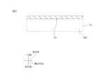
- FIG. 1 is a cross-sectional view of a first embodiment of a transparent conductive layer of the present invention
- FIG. FIG. 2 is a cross-sectional view of a transparent conductive film having a transparent conductive layer shown in FIG. 1
- FIG. 4 is a cross-sectional view of a second embodiment of the transparent conductive layer of the present invention
- 4 is a graph showing the relationship between the amount of introduced oxygen and the specific resistance in reactive sputtering of Example 1.
- First Embodiment A transparent conductive layer 1A according to a first embodiment of the present invention will be described with reference to FIG.
- This transparent conductive layer 1A extends in the planar direction.
- the plane direction is perpendicular to the thickness direction.
- the transparent conductive layer 1A is crystalline.
- the transparent conductive layer 1A contains an inorganic oxide.
- inorganic oxides include metal oxides.
- the metal oxide contains at least one metal selected from the group consisting of In, Sn, Zn, Ga, Sb, Nb, Ti, Si, Zr, Mg, Al, Au, Ag, Cu, Pd and W .
- the material of the transparent conductive layer 1A is preferably indium zinc composite oxide (IZO), indium gallium zinc composite oxide (IGZO), indium gallium composite oxide (IGO), indium tin composite oxide. (ITO) and antimony tin composite oxide (ATO), preferably indium tin composite oxide (ITO) from the viewpoint of improving long-term heating reliability.
- the content of tin oxide (SnO 2 ) in the indium-tin composite oxide is, for example, 0.5% by mass or more, preferably 1% by mass or more, and more preferably 3% by mass or more, more preferably 5% by mass or more, particularly preferably 6% by mass or more, and, for example, less than 50% by mass, preferably 25% by mass or less, more preferably 15% by mass or less , more preferably less than 10% by mass, more preferably 9% by mass or less, 8% by mass or less, or 7% by mass or less.
- the content of tin oxide in the indium-tin composite oxide is at least the above lower limit, the long-term heating reliability is excellent.
- the transparent conductive layer 1A having excellent heating reliability can be obtained. It is easy to achieve both excellent resistance characteristics and etching properties of the transparent conductive layer 1 . For example, it may be judged from the content of tin oxide (SnO 2 ) in a sintered body (target) of a mixture of indium oxide and tin oxide. Alternatively, for example, the determination can be made by analyzing the transparent conductive layer 1 by XPS (X-ray Photoelectron Spectroscopy). The content of tin oxide (SnO 2 ) in the thickness direction of the transparent conductive layer 1 can also be determined by obtaining an XPS depth profile as necessary.
- XPS X-ray Photoelectron Spectroscopy
- the tin oxide content in the indium-tin composite oxide is uniform in the thickness direction or distributed in the thickness direction.
- the tin oxide content in the indium-tin composite oxide preferably has a distribution in the thickness direction.
- the transparent conductive layer 1 includes first regions 3 and second regions 4 having different tin oxide contents in order toward one side in the thickness direction. That is, in this embodiment, the second region 4 is arranged on one side of the first region 3 in the thickness direction.
- the tin oxide content C1 in the first region 3 is higher than that of the tin oxide content C2 in the second region 4, for example.
- the ratio (C1/C2) of the tin oxide content C1 in the first region 3 to the tin oxide content C2 in the second region 4 is, for example, greater than 1, preferably 1.5 or more, more preferably 2 Above, more preferably 2.5 or more, particularly preferably 3 or more, and most preferably 3.3 or more.
- the above ratio (C1/C2) is, for example, 100 or less, preferably 25 or less, more preferably 10 or less. Note that the boundary between the first region 3 and the second region 4 may not be clearly observed.
- the tin oxide content C1 in the first region 3 is, for example, 5% by mass or more, preferably 7% by mass or more, and more preferably is 9% by mass or more, and, for example, 50% by mass or less, preferably 30% by mass or less, more preferably 25% by mass or less, even more preferably 20% by mass or less, particularly preferably 15% by mass % or less.
- the tin oxide content C1 in the second region 4 is, for example, 0.1% by mass or more, preferably 1% by mass or more, and more preferably 2% by mass or more. % by mass or more, and for example, 9% by mass or less, preferably 7% by mass or less, more preferably 5% by mass or less, and even more preferably 4% by mass or less.
- the above inorganic oxide contains a rare gas having an atomic number higher than that of argon.
- the rare gas 2 having an atomic number greater than that of argon exists in the entire transparent conductive layer 1A in the thickness direction, as shown in the enlarged view of FIG.
- the transparent conductive layer 1A is a composition in which an inorganic oxide (preferably a metal oxide) is mixed with a rare gas having an atomic number greater than that of argon.
- an inorganic oxide preferably a metal oxide
- Rare gases with atomic numbers greater than argon include, for example, krypton, xenon, and radon. These can be used alone or in combination.
- the noble gas having an atomic number greater than that of argon is preferably krypton and xenon, and more preferably krypton (Kr) from the viewpoint of obtaining low cost and excellent electrical conductivity.
- the inorganic oxide of the transparent conductive layer 1A preferably does not contain argon.
- the method of identifying noble gases with atomic numbers greater than argon is not limited.
- Rutherford Backscattering Spectrometry, secondary ion mass spectrometry, laser resonance ionization mass spectrometry, and/or X-ray fluorescence spectrometry show that noble gases with atomic numbers higher than argon in the transparent conductive layer 1A are Identified (existence or non-existence is determined), preferably by fluorescent X-ray analysis from the viewpoint of analysis simplicity. Details of the fluorescent X-ray analysis are described in Examples.
- the content ratio of the rare gas having an atomic number larger than that of argon in the inorganic oxide (transparent conductive layer 1A) is, for example, 0.0001 atom % or more, preferably 0.001 atom % or more, or, for example, 1. 0 atom% or less, more preferably 0.7 atom% or less, still more preferably 0.5 atom% or less, even more preferably 0.3 atom% or less, particularly preferably 0.2 atom% or less, most preferably 0 .15 atom % or less. If the content of the rare gas having an atomic number greater than that of argon in the inorganic oxide (transparent conductive layer 1A) is within the above range, the long-term heating reliability of the transparent conductive layer 1A can be improved.
- the transparent conductive layer 1A is suppressed from taking in a large amount of sputtering gas. Therefore, the crystallinity of the transparent conductive layer 1A is improved, and as a result, long-term heating reliability of the transparent conductive layer 1A is improved.
- Peak at (440) plane in X-ray diffraction There is a peak at (440) plane when the transparent conductive layer 1A is subjected to X-ray diffraction.
- the (440) plane is a unique peak included in the spectrum obtained by X-ray diffraction of the crystalline transparent conductive layer 1A.
- the half width of the peak in the (440) plane in X-ray diffraction is 0.27 degrees or less, the long-term heating reliability of the transparent conductive layer 1A is poor. That is, when the transparent conductive layer 1A is placed in a high-temperature atmosphere for a long time, the surface resistance increases.
- the transparent conductive layer 1A when the transparent conductive layer 1A is subjected to X-ray diffraction, the half width of the peak in the (440) plane exceeds 0.27 degrees, so the transparent conductive layer 1A is excellent in long-term heating reliability. That is, when the transparent conductive layer 1A is placed in a high-temperature atmosphere for a long time, an increase in surface resistance can be suppressed.
- the half width of the peak in the (440) plane is preferably 0.275 degrees or more, more preferably 0.28 degrees or more, and still more preferably 0.29 degrees. above, particularly preferably 0.30 degrees or more, more preferably 0.31 degrees or more, 0.32 degrees or more, 0.33 degrees or more, 0.35 degrees or more, 0.37 degrees or more, 0.38 degrees or more is preferred.
- the half width of the peak in the (440) plane is, for example, 5.00 degrees or less, preferably 3.00 degrees or less, more preferably 1.00 degrees. Below, more preferably 0.75 degrees or less, particularly preferably 0.50 degrees or less.
- the method for setting the half width of the peak in the (440) plane in X-ray diffraction to the above range is not limited.
- the half-value width of the peak in the (440) plane of X-ray diffraction is measured based on the description of the later examples.
- the crystal grain size of the transparent conductive layer 1A is, for example, 3 ⁇ m or less, preferably 2 ⁇ m or less, more preferably 1 ⁇ m or less, still more preferably 0.8 ⁇ m or less, and particularly preferably 0.8 ⁇ m or less. is 0.7 ⁇ m or less. If the crystal grain size is equal to or less than the upper limit described above, the transparent conductive layer 1 is less likely to crack even if the substrate 6 containing a flexible resin is employed.
- the crystal grain size in the transparent conductive layer 1A is, for example, 0.01 ⁇ m or more, preferably 0.1 ⁇ m or more, more preferably 0.2 ⁇ m or more, still more preferably 0.3 ⁇ m or more, and particularly preferably 0.4 ⁇ m. Above all, the thickness is most preferably 0.5 ⁇ m or more, and more preferably 0.6 ⁇ m or more. If the crystal grain size is equal to or more than the above-described lower limit, the transparent conductive layer 1A is excellent in long-term heating reliability.
- the crystal grain size is obtained by FE-SEM observation. The details of the method of determination will be described in Examples below.
- the thickness of the transparent conductive layer 1A is, for example, 1 nm or more, preferably 5 nm or more, more preferably 10 nm or more, even more preferably 15 nm or more, particularly preferably 20 nm or more, and for example, 500 nm or less, preferably. is 300 nm or less, more preferably 200 nm or less, still more preferably 100 nm or less, particularly preferably 50 nm or less, and further preferably 40 nm or less, 35 nm or less, 30 nm or less, and 25 nm or less.
- the thickness of the transparent conductive layer 1A is equal to or less than the above upper limit, heating reliability can be improved.
- the thickness of the transparent conductive layer 1A is measured by FE-TEM observation (cross-sectional observation).
- each of the first region 3 and the second region 4 is, for example, 3 nm or more, preferably 5 nm or more, more preferably 7 nm or more, and is, for example, 200 nm or less, preferably 100 nm or less, more preferably. is 50 nm or less, more preferably 25 nm or less, even more preferably 20 nm or less, and particularly preferably 15 nm or less.
- the ratio of the thickness of the first region 3 to the thickness of the second region 4 is, for example, 0.1 or more, preferably 0. .3 or more, more preferably 0.5 or more, still more preferably 0.7 or more, and for example, 10 or less, preferably 5 or less, more preferably 3 or less, further preferably 2 or less is.
- the total light transmittance of the transparent conductive layer 1A is, for example, 75% or higher, preferably 80% or higher, more preferably 85% or higher, still more preferably 90% or higher.
- the upper limit of the total light transmittance of the transparent conductive layer 1A is not limited.
- the upper limit of the total light transmittance of the transparent conductive layer 1A is, for example, 100%.
- the specific resistance of the transparent conductive layer 1A is, for example, 5.0 ⁇ 10 ⁇ 4 ⁇ cm or less, preferably 3 ⁇ 10 ⁇ 4 ⁇ cm or less, and for example, 0.1 ⁇ 10 ⁇ 4 ⁇ . ⁇ It is more than cm.
- a specific resistance is measured by the four-probe method.
- the transparent conductive film 5A provided with the transparent conductive layer 1A described above will be described with reference to FIG. 5 A of transparent conductive films are extended in a surface direction.
- 5 A of transparent conductive films are provided with the base material 6 and 1 A of transparent conductive layers in order toward one side of the thickness direction. That is, in this embodiment, in the transparent conductive film 5A, the substrate 6 and the transparent conductive layer 1A are arranged in order toward one side in the thickness direction.
- the transparent conductive film 5A preferably includes only the substrate 6 and the transparent conductive layer 1A.
- the substrate 6 forms the other surface of the transparent conductive film 5A in the thickness direction.
- the base material 6 improves the mechanical strength of the transparent conductive film 5A.
- the base material 6 extends in the surface direction.
- the base material 6 contains resin, for example. If the substrate 6 contains a resin, both good resistance characteristics and heating reliability of the transparent conductive layer 1A can be achieved. The resin will be explained later.
- substrate 6 is not adjacent to a glass plate (not shown). In this embodiment, the other surface of the substrate 6 in the thickness direction does not come into contact with the glass plate.
- the base material 6 includes a base sheet 61 and a functional layer 60 in order in the thickness direction.
- the functional layer 60 is a single layer.
- the functional layer 60 contacts one side of the base sheet 61 in the thickness direction.
- Functional layer 60 is preferably hard coat layer 62 .
- the base material 6 preferably includes a base material sheet 61 and a hard coat layer 62 in order toward the other side in the thickness direction.
- the base sheet 61 has flexibility.
- Examples of the base sheet 61 include a resin film.
- the resin in the resin film is not limited.
- Examples of resins include polyester resins, acrylic resins, olefin resins, polycarbonate resins, polyethersulfone resins, polyarylate resins, melamine resins, polyamide resins, polyimide resins, cellulose resins, polystyrene resins, and norbornene resins. From the viewpoint of transparency and mechanical strength, the resin is preferably a polyester resin.
- Polyester resins include, for example, polyethylene terephthalate (PET), polybutylene terephthalate, and polyethylene naphthalate, preferably PET.
- the thickness of the base sheet 61 is preferably 1 ⁇ m or more, more preferably 10 ⁇ m or more, and even more preferably 30 ⁇ m or more.
- the thickness of the base sheet 61 is preferably 300 ⁇ m or less, more preferably 200 ⁇ m or less, still more preferably 150 ⁇ m or less, and particularly preferably 100 ⁇ m or less.
- the ratio of the thickness of the base sheet 61 to the thickness of the base material 6 is, for example, 0.80 or more, preferably 0.90 or more, more preferably 0.95 or more, and for example, 0.99 or less. , preferably 0.97 or less.
- the hard coat layer 62 makes it difficult for scratches to form on one surface of the transparent conductive layer 1A in the thickness direction.
- the hard coat layer 62 contacts one side of the base sheet 61 in the thickness direction.
- the hard coat layer 62 is made of resin.
- the hard coat layer 62 is, for example, a cured product layer of a curable composition containing a curable resin.
- curable resins include acrylic resins, urethane resins, amide resins, silicone resins, epoxy resins, and melamine resins.
- the curable resin preferably includes an acrylic resin.
- the thickness of the hard coat layer 62 is, for example, 0.1 ⁇ m or more, preferably 0.5 ⁇ m or more, and is, for example, 10 ⁇ m or less, preferably 3 ⁇ m or less.
- the ratio of the thickness of the hard coat layer 62 to the thickness of the base sheet 61 is, for example, 0.01 or more, preferably 0.02 or more, more preferably 0.03 or more, and for example, 0.20. Below, it is preferably 0.10 or less, more preferably 0.05 or less.
- the thickness of the hard coat layer 62 corresponds to the thickness of the functional layer 60 .
- Thickness of Base Material 6 More preferably, it is 100 ⁇ m or less.
- the thickness of the base material 6 is the total thickness of the base material sheet 61 and the hard coat layer 62 .
- the total light transmittance of the substrate 6 is, for example, 75% or higher, preferably 80% or higher, more preferably 85% or higher, and still more preferably 90% or higher. .
- the upper limit of the total light transmittance of the base material 6 is not limited.
- the upper limit of the total light transmittance of the substrate 6 is, for example, 100%.
- the total light transmittance of the substrate 6 is obtained based on JIS K 7375-2008.
- the total light transmittance of the following members is obtained based on the same method as above.
- a commercially available product can be used for the base material 6 .
- the transparent conductive layer 1A forms one surface of the transparent conductive film 5A in the thickness direction.
- the transparent conductive layer 1A is arranged on one surface of the substrate 6 in the thickness direction. 1 A of transparent conductive layers contact the one side of the base material 6 in the thickness direction. That is, the other surface of the transparent conductive layer 1A in the thickness direction is in contact with the substrate 6. As shown in FIG. In this embodiment, the other surface of the transparent conductive layer 1A contacts one surface of the hard coat layer 62 (functional layer 60) in the thickness direction.
- the transparent conductive layer 1A when the transparent conductive layer 1A has the first region 3 and the second region 4, preferably the first region 3 is formed on one side of the substrate 6 in the thickness direction. placed. Preferably, the first region 3 contacts one surface of the hard coat layer 62 (see FIG. 2) in the thickness direction.
- the transparent conductive film 5A when the transparent conductive layer 1A has the first region 3 and the second region 4, the transparent conductive film 5A has the base material A sheet 61, a hard coat layer 62, a first region 3, and a second region 4 are provided in order toward one side in the thickness direction. That is, the second region 4 is arranged on the opposite side of the base material 6 with respect to the first region 3 in the thickness direction.
- Thickness of transparent conductive film 5A and other physical properties It is preferably 200 ⁇ m or less, more preferably 100 ⁇ m or less.
- the total light transmittance of the transparent conductive film 5A is, for example, 75% or more, preferably 80% or more, and is, for example, 100% or less.
- each layer is arranged by a roll-to-roll method.
- the base material 6 is prepared. Specifically, a curable composition is applied to one surface of the base sheet 61 . After that, the curable resin in the curable composition is cured by heat or ultraviolet irradiation. As a result, the hard coat layer 62 is formed on one side of the base sheet 61 . The base material 6 is prepared by this.
- the transparent conductive layer 1A is formed on one side of the substrate 6 in the thickness direction. Specifically, first, an amorphous transparent conductive layer is formed on one side of the substrate 6 in the thickness direction, and then the amorphous transparent conductive layer is converted into a crystalline to form the transparent conductive layer 1A. .
- amorphous transparent conductive layer Formation of amorphous transparent conductive layer (sputtering process) To form the amorphous transparent conductive layer, for example, sputtering, preferably reactive sputtering, is carried out.
- a sputtering apparatus is used for sputtering.
- a sputtering apparatus includes a single film-forming roll and a plurality of film-forming chambers.
- the film-forming roll is equipped with a temperature control device.
- the temperature adjusting device can adjust the temperature of the film forming roll. Since the film-forming roll can contact the base material 6, the temperature of the base material 6 can be adjusted.
- the surface temperature of the film-forming roll corresponds to the film-forming temperature in sputtering.
- the film formation temperature is, for example, ⁇ 50° C. or higher, preferably ⁇ 30° C. or higher, more preferably ⁇ 20° C. or higher, still more preferably ⁇ 10° C. or higher, and for example, 20° C. or lower, preferably , 10° C. or lower, more preferably 5° C. or lower, and still more preferably 0° C. or lower.
- a sputtering gas can be supplied to the inside of each of the plurality of film forming chambers.
- Sputtering gases include noble gases having atomic numbers higher than argon.
- Noble gases having atomic numbers greater than argon include, for example, krypton, xenon, and radon, preferably krypton (Kr).
- the sputtering gas may contain, for example, argon.
- a sputtering gas can be used alone or in combination.
- the sputtering gas preferably contains a noble gas with an atomic number greater than argon and does not contain argon.
- the sputtering gas supplied to each of the plurality of film formation chambers is, for example, the same, and for example, the sputtering gas supplied to one film formation chamber is a rare gas having an atomic number greater than that of argon.
- the sputtering gas supplied to one film formation chamber is argon.
- the same sputtering gas is supplied to each of the plurality of film forming chambers.
- the sputtering gas is preferably mixed with a reactive gas.
- Reactive gases include, for example, oxygen.
- the ratio of the introduction amount of the reactive gas to the total introduction amount of the sputtering gas and the reactive gas is, for example, 0.1 flow % or more, preferably 0.5 flow % or more, and for example, 5.0 flow rate. %, preferably 4.0 flow % or less, more preferably 3.5 flow % or less.
- the target is, for example, (a sintered body of) the metal oxide described above.
- Each of the plurality of targets is arranged in each of the plurality of deposition chambers.
- a first target is arranged in a first film forming chamber.
- a second target is placed in the second deposition chamber.
- the first target and the second target are, for example, different from each other. Specifically, if both are ITO, the contents of tin oxide are different from each other.
- the first target is (a sintered body of) a metal oxide corresponding to the first region 3 and has the above-described (high) content of tin oxide.
- the second film forming chamber is arranged downstream of the first film forming chamber in the transport direction of the substrate 6 .
- the second target is (a sintered body of) a metal oxide corresponding to the second region 4 and has the aforementioned (low) content of tin oxide.
- a first sputtering step is performed in a first deposition chamber, and a second deposition is performed.
- a second sputtering step is performed in the chamber.
- the atmospheric pressure in the sputtering apparatus is, for example, 1.0 Pa or less and, for example, 0.01 Pa or more.
- the amorphous transparent conductive layer includes first region 3 and second region 4 .
- the amorphous transparent conductive layer (laminate comprising) is heated.
- the heating temperature is, for example, 80° C. or higher, preferably 110° C. or higher, more preferably 130° C. or higher, particularly preferably 150° C. or higher, and for example, 200° C. or lower, preferably It is 180° C. or lower, more preferably 175° C. or lower, still more preferably 170° C. or lower.
- the heating time is, for example, 1 minute or longer, preferably 3 minutes or longer, more preferably 5 minutes or longer, and is, for example, 5 hours or shorter, preferably 3 hours or shorter, more preferably 2 hours or shorter. be. Heating is performed, for example, under vacuum or in the atmosphere. From the viewpoint of improving long-term heating reliability, the heating is preferably performed under vacuum.
- the transparent conductive film 5A having an amorphous transparent conductive layer is allowed to stand in the atmosphere at a temperature of 20° C. or more and less than 80° C. for, for example, 10 hours or more, preferably 24 hours or more.
- a crystalline transparent conductive layer can also be converted to a crystalline one.
- the transparent conductive film 5A is used for articles, for example.
- Articles include optical articles. More specifically, examples of articles include touch sensors, electromagnetic wave shields, light control elements, photoelectric conversion elements, heat ray control members, light-transmitting antenna members, light-transmitting heater members, image display devices, and lighting.
- the transparent conductive layer 1A and the transparent conductive film 5A are prevented from increasing in surface resistance even when placed in a high-temperature atmosphere for a long time. Therefore, the above article including the transparent conductive layer 1A and/or the transparent conductive film 5A has excellent long-term heating reliability.
- solar cells, light control elements, heat ray control members, and light transmissive heater members may be placed in a high temperature environment for a long time and exposed to high temperatures for a long time.
- each article described above includes the transparent conductive layer 1A and/or the transparent conductive film 5A described above, an increase in the surface resistance of the transparent conductive layer 1A is suppressed.
- the transparent conductive layer 1A may consist of one region.
- a sputtering apparatus includes a single film formation chamber.
- the noble gas having an atomic number greater than that of argon is contained only in the first region 3 or the second region 4.
- the transparent conductive film 5A includes a substrate 6, a second region 4, and a first region 3 in order toward one side in the thickness direction.
- the transparent conductive layer 1A has a repeating structure of the first regions 3 and the second regions 4.
- the functional layer 60 is multi-layered.
- the functional layer 60 is arranged on one side and the other side of the base sheet 61 in the thickness direction.
- the functional layer 60 includes an optical adjustment layer and a hard coat layer.
- the optical adjustment layer is arranged on one side of the base sheet 61 .
- the hard coat layer is arranged on the other side of the base sheet 61 .
- Second Embodiment In the following second embodiment, the same reference numerals are given to the same members and processes as those of the first embodiment and the modified example described above, and detailed description thereof will be omitted. Moreover, the second embodiment can achieve the same effects as those of the first embodiment and the modified example unless otherwise specified. Furthermore, the first embodiment, the modified example, and the second embodiment can be combined as appropriate.
- a transparent conductive layer 1B according to the second embodiment of the present invention will be described with reference to FIG.
- the transparent conductive layer 1B of the second embodiment has a thickness of more than 40 nm, and the inorganic oxide does not need to contain the noble gas 2 having an atomic number larger than that of argon. different from Other physical properties of the transparent conductive layer 1B may be the same as or different from those of the transparent conductive layer 1A.
- the thickness of the transparent conductive layer 1B is more than 40 nm.
- the thickness of the transparent conductive layer 1B is 40 nm or less, long-term heating reliability is lowered. That is, when the transparent conductive layer 1B is placed in a high temperature atmosphere for a long time, the surface resistance increases.
- the thickness of the transparent conductive layer 1B exceeds 40 nm, it is excellent in long-term heating reliability. That is, when the transparent conductive layer 1B is placed in a high-temperature atmosphere for a long time, an increase in surface resistance can be suppressed.
- the thickness of the transparent conductive layer 1B is preferably 45 nm or more, more preferably 50 nm or more, still more preferably 60 nm or more, particularly preferably 70 nm or more, and further preferably 80 nm or more, 90 nm or more, 100 nm or more, and 110 nm. Above, 120 nm or more, 125 nm or more, or 130 nm or more is preferable.
- the thickness of the transparent conductive layer 1B is, for example, 750 nm or less, preferably 500 nm or less, more preferably 350 nm or less, even more preferably 300 nm or less, particularly preferably 200 nm or less, most preferably 150 nm or less.
- the thickness of the transparent conductive layer 1B is equal to or less than the upper limit described above, the heat stability is excellent.
- the inorganic oxide may contain a noble gas. That is, in the present embodiment, the inorganic oxide of the transparent conductive layer 1B is allowed to contain a rare gas.
- Noble gases include, for example, argon, krypton, xenon, and radon. These can be used alone or in combination.
- Argon is preferably used as the rare gas from the viewpoint of reducing production costs.
- the inorganic oxide of the transparent conductive layer 1B preferably does not contain a noble gas having an atomic number greater than that of argon, from the viewpoint of reducing manufacturing costs.
- the method for identifying noble gases is not limited.
- Rutherford Backscattering Spectrometry, secondary ion mass spectrometry, laser resonance ionization mass spectrometry, and/or X-ray fluorescence analysis identify noble gases in the transparent conductive layer 1B.
- the content of tin oxide in ITO is, for example, 1% by mass or more, preferably 3% by mass or more, and more preferably 5% by mass. Above, more preferably 7% by mass or more, particularly preferably 9% by mass or more, and for example, 50% by mass or less, preferably 35% by mass or less, more preferably 30% by mass or less, still more preferably is 25% by mass or less, more preferably 20% by mass or less, more preferably 15% by mass or less.
- the content of tin oxide in ITO is at least the above lower limit, the long-term heating reliability is excellent.
- the content of tin oxide (SnO 2 ) in the indium-tin composite oxide is equal to or less than the above upper limit, the heating stability can be improved.
- the crystal grain size in the transparent conductive layer 1B is, for example, 1.0 ⁇ m or less, preferably 0.5 ⁇ m or less, more preferably 0.4 ⁇ m or less, still more preferably 0.3 ⁇ m or less. . If the crystal grain size is equal to or less than the above upper limit, the heating stability is excellent.
- the crystal grain size of the transparent conductive layer 1B is, for example, 0.001 ⁇ m or more, preferably 0.01 ⁇ m or more, more preferably 0.03 ⁇ m or more, still more preferably 0.05 ⁇ m or more, and particularly preferably 0.07 ⁇ m. That's it. If the crystal grain size in the transparent conductive layer 1B is equal to or greater than the above lower limit, long-term heating reliability is excellent.
- the half-value width of the peak on the (440) plane in the X-ray diffraction of the transparent conductive layer 1B exceeds 0.27 degrees, preferably 0.272 degrees or more, more preferably , 0.275 degrees or more, more preferably 0.277 degrees or more, particularly preferably 0.280 degrees or more, most preferably 0.285 degrees or more, furthermore 0.287 degrees or more, 0.288 degrees or more is preferred.
- the half width of the peak in the (440) plane in the X-ray diffraction of the transparent conductive layer 1B is, for example, 5 degrees or less, 3.00 degrees or less, preferably 1.00 degrees or less, more preferably 0.75 degrees or less. , more preferably 0.50 degrees or less, particularly preferably 0.40 degrees or less, most preferably 0.35 degrees or less, further preferably 0.30 degrees or less.
- the sputtering gas examples include rare gases. Noble gases may be used alone or in combination. Argon is preferably used as the sputtering gas. Also, the sputtering gas is preferably free of noble gases with atomic numbers higher than argon.
- the deposition chamber can supply the sputtering gas described above.
- the transparent conductive layer 1B in FIG. 2 is provided on the transparent conductive film 5B together with the base material 6 indicated by phantom lines.
- the transparent conductive film 5B includes a substrate 6 and a transparent conductive layer 1B in order toward one side in the thickness direction.
- the above-described transparent conductive layer 1B and/or transparent conductive film 5B are used in the above-described articles.
- Example 1 ⁇ Preparation of base material 6> A substrate 6 having a thickness of 52 ⁇ m was prepared.
- a base sheet 61 made of PET was prepared.
- a hard coat composition (ultraviolet curable resin containing an acrylic resin) was applied to one surface of the base sheet 61 in the thickness direction to form a coating film.
- the coating was then cured by UV irradiation.
- a hard coat layer 62 having a thickness of 2 ⁇ m was formed on one side of the base sheet 61 .
- the base material 6 having the base material sheet 61 and the hard coat layer 62 in order toward one side in the thickness direction was produced.
- An amorphous transparent conductive layer was formed on one side of the substrate 6 .
- a first sputtering process and a second sputtering process were performed in order. Both the first sputtering step and the second sputtering step are reactive magnetron sputtering.
- An amorphous first region 3 was formed on one side of the substrate 6 in a first sputtering step.
- an amorphous second region 4 was formed on one side of the first region 3 .
- ⁇ First sputtering step> A sintered body of indium oxide and tin oxide was used as the first target.
- the tin oxide concentration in the sintered body was 10% by mass.
- a voltage was applied to the first target using a DC power supply.
- the horizontal magnetic field strength on the first target was 90 mT.
- the film formation temperature was -5°C.
- the inside of the first film forming chamber was evacuated until the ultimate degree of vacuum in the first film forming chamber reached 0.9 ⁇ 10 ⁇ 4 Pa, and the substrate 6 was degassed. After that, Kr as a sputtering gas and oxygen as a reactive gas were introduced into the first film forming chamber, and the pressure inside the first film forming chamber was set to 0.2 Pa.
- the ratio of the introduced amount of oxygen to the total introduced amount of Kr and oxygen introduced into the first deposition chamber was about 2.6 flow rate %.
- the oxygen introduction amount is within the region X of the resistivity-oxygen introduction amount curve, and the resistivity of the amorphous first region 3 is 6.5 ⁇ 10 ⁇ 4 ⁇ cm. adjusted to be The thickness of the first region 3 was 11 nm.
- ⁇ Second sputtering step> A sintered body of indium oxide and tin oxide was used as the second target.
- the tin oxide concentration in the sintered body was 3% by mass.
- a voltage was applied to the second target using a DC power supply.
- the horizontal magnetic field strength on the second target was 90 mT.
- the film formation temperature was -5°C.
- the second film forming chamber in the DC magnetron sputtering apparatus is evacuated until the ultimate vacuum in the second film forming chamber reaches 0.9 ⁇ 10 -4 Pa, and then a sputtering gas is introduced into the second film forming chamber. Kr and oxygen as a reactive gas were introduced, and the pressure in the second film forming chamber was set to 0.2 Pa.
- the ratio of the introduced amount of oxygen to the total introduced amount of Kr and oxygen introduced into the second deposition chamber was about 2.5 flow rate %.
- the amount of oxygen introduced is within the region X of the resistivity-oxygen introduction curve, and the amorphous transparent region consisting of the amorphous first region 3 and the amorphous second region 4
- the resistivity of the conductive layer was adjusted to 6.5 ⁇ 10 ⁇ 4 ⁇ cm.
- the thickness of the second region 4 was 11 nm.
- the layered product including the substrate 6 and the amorphous transparent conductive layer was heated in a vacuum heating device by bringing it into contact with a heating roll. This crystallized the amorphous transparent conductive layer.
- the heating temperature was 160° C. and the heating time was 0.1 hour.
- the amorphous transparent conductive layer was converted into a crystalline transparent conductive layer to form the transparent conductive layer 1A.
- the thickness of the transparent conductive layer 1A was 22 nm.
- a transparent conductive film 5 was manufactured, which includes the substrate 6 and the crystalline transparent conductive layer 1A in order toward one side in the thickness direction.
- Example 2 A transparent conductive layer 1B was produced in the same manner as in Example 1, and then a transparent conductive film 5B having a thickness of 130 nm was produced.
- the first sputtering process, the second sputtering process, and the heating process were changed as follows.
- ⁇ First sputtering step> The sputtering gas was changed to argon.
- the air pressure in the first film forming chamber was changed to 0.4 Pa.
- the ratio of the introduced amount of oxygen to the total introduced amount of argon and oxygen introduced into the sputtering film forming apparatus was changed to about 1.5 flow rate %.
- the amorphous transparent conductive layer was crystallized by heating in a hot air oven.
- the heating temperature was 160° C., and the heating time was 0.5 hours.
- Comparative example 1 After carrying out the first sputtering process and the second sputtering process in the same manner as in Example 2, a transparent conductive film 5 was produced. However, the following points have been changed.
- ⁇ First sputtering step> The sputtering gas was changed to argon.
- the pressure inside the sputtering film forming apparatus was changed to 0.4 Pa.
- the ratio of the amount of oxygen introduced to the total amount of argon and oxygen introduced into the first deposition chamber was set to about 1.5 flow rate %.
- a first region 3 having a thickness of 19 nm was formed by the first sputtering step.
- ⁇ Second sputtering step> The sputtering gas was changed to argon.
- the air pressure in the second film forming chamber was changed to 0.4 Pa.
- the ratio of the amount of oxygen introduced to the total amount of argon and oxygen introduced into the first deposition chamber was set to about 1.5 flow rate %.
- a second region 4 having a thickness of 3 nm was formed by a second sputtering step.
- the thickness of the transparent conductive layer 1 was 22 nm.
- ⁇ Thickness> ⁇ Thickness of transparent conductive layers 1A and 1B> The thicknesses of the transparent conductive layers 1A, 1B, 1 were measured by FE-TEM observation. Specifically, first, cross-sectional observation samples of the transparent conductive layers 1A, 1B, 1 were prepared by the FIB microsampling method. In the FIB microsampling method, an FIB device (trade name “FB2200”, manufactured by Hitachi) was used, and the acceleration voltage was set to 10 kV. Next, the thicknesses of the transparent conductive layers 1A, 1B, 1 in the samples for cross-sectional observation were measured by FE-TEM observation. In the FE-TEM observation, an FE-TEM apparatus (trade name “JEM-2800” manufactured by JEOL) was used with an acceleration voltage of 200 kV.
- the thickness of the second region 4 was calculated by subtracting the thickness of the first region 3 from the thickness of the transparent conductive layers 1A and 1A.
- the X-ray peak profile was obtained by subtracting the background derived from the base material 6 (the base material 6 heated under the same conditions as the transparent conductive layers 1A and 1B of each example and each comparative example). After that, using analysis software (software name "SmartLab Studio II"), create an X-ray diffraction peak profile corresponding to the (440) plane so that 2 ⁇ is in the range of 49.8 ° to 51.8 °, By fitting the X-ray diffraction peak (peak shape: split Pearson VII function, background type: B-spline, fitting conditions: automatic), the half width of the X-ray diffraction peak in the (440) plane (FWHM, unit ;°) was obtained.
- analysis software software name "SmartLab Studio II”
- ⁇ Crystal grain size> One surface of the transparent conductive layers 1A, 1B, 1 was observed with an FE-SEM (device: SU8020 manufactured by Hitachi) to determine the crystal grain size of the transparent conductive layers 1A, 1B, 1. Specifically, after fixing the transparent conductive layers 1A, 1B, 1 to a table, surface FE-SEM observation (accelerating voltage: 0.8 kV, observed image: secondary electron image) was performed to obtain the transparent conductive layer 1A. , 1B, 1 were photographed in plan view. The magnification was adjusted so that the grains could be clearly identified.
- FE-SEM device: SU8020 manufactured by Hitachi
- the area of the region is obtained from the number of pixels present in the region defined by the grain boundary (region within each grain boundary), and the area of the same area as the area is obtained.
- the diameter of the circle was determined as the crystal grain size (equivalent circle diameter).
- Example 1 the crystal grain size of Example 1 was 0.6 ⁇ m.
- the grain size of Example 2 was 0.1 ⁇ m.
- the crystal grain size of Comparative Example 1 was 0.4 ⁇ m.
- the transparent conductive film 5 was placed in a hot air oven at 80°C for 500 hours. After removing the transparent conductive film 5 from the hot air oven, the surface resistance of the transparent conductive film 5 was obtained as the surface resistance R1 after heating.
- the rate of increase in surface resistance before and after the heating test was obtained by dividing the initial surface resistance R0 by the surface resistance R1 after heating. The results are listed in Table 1.
- Example 1 the rate of increase in surface resistance before and after the heating test in Example 1 was less than 1, and compared to Example 2, it can be seen that the increase in surface resistance after the heating test was further suppressed.
- the transparent conductive layer is used for optical articles.
Landscapes
- Physics & Mathematics (AREA)
- Chemical & Material Sciences (AREA)
- Dispersion Chemistry (AREA)
- Spectroscopy & Molecular Physics (AREA)
- Non-Insulated Conductors (AREA)
- Laminated Bodies (AREA)
- Conductive Materials (AREA)
- Physical Vapour Deposition (AREA)
Priority Applications (4)
| Application Number | Priority Date | Filing Date | Title |
|---|---|---|---|
| JP2023548480A JP7488425B2 (ja) | 2021-09-17 | 2022-09-14 | 透明導電性フィルムおよび物品 |
| KR1020237025547A KR20240058799A (ko) | 2021-09-17 | 2022-09-14 | 투명 도전층, 투명 도전성 필름 및 물품 |
| CN202280013108.7A CN116848593A (zh) | 2021-09-17 | 2022-09-14 | 透明导电层、透明导电性薄膜及物品 |
| JP2024024279A JP2024061727A (ja) | 2021-09-17 | 2024-02-21 | 透明導電層、透明導電性フィルムおよび物品 |
Applications Claiming Priority (2)
| Application Number | Priority Date | Filing Date | Title |
|---|---|---|---|
| JP2021152347 | 2021-09-17 | ||
| JP2021-152347 | 2021-09-17 |
Publications (1)
| Publication Number | Publication Date |
|---|---|
| WO2023042846A1 true WO2023042846A1 (ja) | 2023-03-23 |
Family
ID=85602916
Family Applications (1)
| Application Number | Title | Priority Date | Filing Date |
|---|---|---|---|
| PCT/JP2022/034349 Ceased WO2023042846A1 (ja) | 2021-09-17 | 2022-09-14 | 透明導電層、透明導電性フィルムおよび物品 |
Country Status (4)
| Country | Link |
|---|---|
| JP (2) | JP7488425B2 (https=) |
| KR (1) | KR20240058799A (https=) |
| CN (1) | CN116848593A (https=) |
| WO (1) | WO2023042846A1 (https=) |
Citations (4)
| Publication number | Priority date | Publication date | Assignee | Title |
|---|---|---|---|---|
| JPH05334924A (ja) * | 1992-05-29 | 1993-12-17 | Tonen Corp | 透明導電薄膜の製造法 |
| JP2000038654A (ja) * | 1998-07-21 | 2000-02-08 | Nippon Sheet Glass Co Ltd | 透明導電膜付き基板の製造方法、透明導電膜付き基板およびそれを用いた液晶表示素子 |
| WO2011034145A1 (ja) * | 2009-09-18 | 2011-03-24 | 三洋電機株式会社 | 太陽電池、太陽電池モジュールおよび太陽電池システム |
| JP2016191157A (ja) * | 2013-01-16 | 2016-11-10 | 日東電工株式会社 | 透明導電フィルムおよびその製造方法 |
Family Cites Families (4)
| Publication number | Priority date | Publication date | Assignee | Title |
|---|---|---|---|---|
| JP2000129427A (ja) | 1998-10-20 | 2000-05-09 | Teijin Ltd | 透明導電積層体の製造方法 |
| JP6261987B2 (ja) | 2013-01-16 | 2018-01-17 | 日東電工株式会社 | 透明導電フィルムおよびその製造方法 |
| WO2016158606A1 (ja) * | 2015-03-31 | 2016-10-06 | 東洋紡株式会社 | 透明導電性フィルム |
| JP7505865B2 (ja) * | 2019-07-23 | 2024-06-25 | Tdk株式会社 | 透明導電体及び有機デバイス |
-
2022
- 2022-09-14 CN CN202280013108.7A patent/CN116848593A/zh active Pending
- 2022-09-14 WO PCT/JP2022/034349 patent/WO2023042846A1/ja not_active Ceased
- 2022-09-14 JP JP2023548480A patent/JP7488425B2/ja active Active
- 2022-09-14 KR KR1020237025547A patent/KR20240058799A/ko active Pending
-
2024
- 2024-02-21 JP JP2024024279A patent/JP2024061727A/ja active Pending
Patent Citations (4)
| Publication number | Priority date | Publication date | Assignee | Title |
|---|---|---|---|---|
| JPH05334924A (ja) * | 1992-05-29 | 1993-12-17 | Tonen Corp | 透明導電薄膜の製造法 |
| JP2000038654A (ja) * | 1998-07-21 | 2000-02-08 | Nippon Sheet Glass Co Ltd | 透明導電膜付き基板の製造方法、透明導電膜付き基板およびそれを用いた液晶表示素子 |
| WO2011034145A1 (ja) * | 2009-09-18 | 2011-03-24 | 三洋電機株式会社 | 太陽電池、太陽電池モジュールおよび太陽電池システム |
| JP2016191157A (ja) * | 2013-01-16 | 2016-11-10 | 日東電工株式会社 | 透明導電フィルムおよびその製造方法 |
Also Published As
| Publication number | Publication date |
|---|---|
| JP2024061727A (ja) | 2024-05-08 |
| JPWO2023042846A1 (https=) | 2023-03-23 |
| CN116848593A (zh) | 2023-10-03 |
| JP7488425B2 (ja) | 2024-05-21 |
| KR20240058799A (ko) | 2024-05-07 |
Similar Documents
| Publication | Publication Date | Title |
|---|---|---|
| US20230127104A1 (en) | Transparent electroconductive film | |
| JP7213962B2 (ja) | 光透過性導電層および光透過性導電フィルム | |
| JP2026026105A (ja) | 透明導電層および透明導電性フィルム | |
| KR102665515B1 (ko) | 적층체 | |
| JP7389940B2 (ja) | 透明導電層、透明導電性フィルムおよび物品 | |
| JP7488425B2 (ja) | 透明導電性フィルムおよび物品 | |
| US20230129748A1 (en) | Transparent electroconductive film | |
| CN115298757A (zh) | 透光性导电膜和透明导电性薄膜 | |
| JP7419609B2 (ja) | 透明導電性フィルム | |
| WO2023042844A1 (ja) | 透明導電性フィルム | |
| WO2026005019A1 (ja) | 透明導電フィルムおよびその製造方法 | |
| KR20220156823A (ko) | 투명 도전성 필름 | |
| JP2024131595A (ja) | 透明導電性フィルム | |
| JP2024131594A (ja) | 透明導電性フィルム | |
| WO2026005018A1 (ja) | 透明導電フィルムおよびその製造方法 | |
| TW202222562A (zh) | 透明導電性膜、及透明導電性膜之製造方法 |
Legal Events
| Date | Code | Title | Description |
|---|---|---|---|
| 121 | Ep: the epo has been informed by wipo that ep was designated in this application |
Ref document number: 22869993 Country of ref document: EP Kind code of ref document: A1 |
|
| WWE | Wipo information: entry into national phase |
Ref document number: 202280013108.7 Country of ref document: CN |
|
| WWE | Wipo information: entry into national phase |
Ref document number: 2023548480 Country of ref document: JP |
|
| NENP | Non-entry into the national phase |
Ref country code: DE |
|
| 122 | Ep: pct application non-entry in european phase |
Ref document number: 22869993 Country of ref document: EP Kind code of ref document: A1 |