WO2023032462A1 - 半導体装置およびその製造方法 - Google Patents
半導体装置およびその製造方法 Download PDFInfo
- Publication number
- WO2023032462A1 WO2023032462A1 PCT/JP2022/026677 JP2022026677W WO2023032462A1 WO 2023032462 A1 WO2023032462 A1 WO 2023032462A1 JP 2022026677 W JP2022026677 W JP 2022026677W WO 2023032462 A1 WO2023032462 A1 WO 2023032462A1
- Authority
- WO
- WIPO (PCT)
- Prior art keywords
- support
- layer
- semiconductor device
- heat sink
- bonding
- Prior art date
- Legal status (The legal status is an assumption and is not a legal conclusion. Google has not performed a legal analysis and makes no representation as to the accuracy of the status listed.)
- Ceased
Links
Images










Classifications
-
- H—ELECTRICITY
- H10—SEMICONDUCTOR DEVICES; ELECTRIC SOLID-STATE DEVICES NOT OTHERWISE PROVIDED FOR
- H10W—GENERIC PACKAGES, INTERCONNECTIONS, CONNECTORS OR OTHER CONSTRUCTIONAL DETAILS OF DEVICES COVERED BY CLASS H10
- H10W40/00—Arrangements for thermal protection or thermal control
- H10W40/20—Arrangements for cooling
- H10W40/25—Arrangements for cooling characterised by their materials
- H10W40/255—Arrangements for cooling characterised by their materials having a laminate or multilayered structure, e.g. direct bond copper [DBC] ceramic substrates
-
- H—ELECTRICITY
- H10—SEMICONDUCTOR DEVICES; ELECTRIC SOLID-STATE DEVICES NOT OTHERWISE PROVIDED FOR
- H10W—GENERIC PACKAGES, INTERCONNECTIONS, CONNECTORS OR OTHER CONSTRUCTIONAL DETAILS OF DEVICES COVERED BY CLASS H10
- H10W40/00—Arrangements for thermal protection or thermal control
- H10W40/20—Arrangements for cooling
- H10W40/22—Arrangements for cooling characterised by their shape, e.g. having conical or cylindrical projections
-
- H—ELECTRICITY
- H10—SEMICONDUCTOR DEVICES; ELECTRIC SOLID-STATE DEVICES NOT OTHERWISE PROVIDED FOR
- H10W—GENERIC PACKAGES, INTERCONNECTIONS, CONNECTORS OR OTHER CONSTRUCTIONAL DETAILS OF DEVICES COVERED BY CLASS H10
- H10W40/00—Arrangements for thermal protection or thermal control
- H10W40/20—Arrangements for cooling
- H10W40/25—Arrangements for cooling characterised by their materials
- H10W40/258—Metallic materials
-
- H—ELECTRICITY
- H10—SEMICONDUCTOR DEVICES; ELECTRIC SOLID-STATE DEVICES NOT OTHERWISE PROVIDED FOR
- H10W—GENERIC PACKAGES, INTERCONNECTIONS, CONNECTORS OR OTHER CONSTRUCTIONAL DETAILS OF DEVICES COVERED BY CLASS H10
- H10W40/00—Arrangements for thermal protection or thermal control
- H10W40/40—Arrangements for thermal protection or thermal control involving heat exchange by flowing fluids
- H10W40/43—Arrangements for thermal protection or thermal control involving heat exchange by flowing fluids by flowing gases, e.g. forced air cooling
-
- H—ELECTRICITY
- H10—SEMICONDUCTOR DEVICES; ELECTRIC SOLID-STATE DEVICES NOT OTHERWISE PROVIDED FOR
- H10W—GENERIC PACKAGES, INTERCONNECTIONS, CONNECTORS OR OTHER CONSTRUCTIONAL DETAILS OF DEVICES COVERED BY CLASS H10
- H10W40/00—Arrangements for thermal protection or thermal control
- H10W40/40—Arrangements for thermal protection or thermal control involving heat exchange by flowing fluids
- H10W40/47—Arrangements for thermal protection or thermal control involving heat exchange by flowing fluids by flowing liquids, e.g. forced water cooling
-
- H—ELECTRICITY
- H10—SEMICONDUCTOR DEVICES; ELECTRIC SOLID-STATE DEVICES NOT OTHERWISE PROVIDED FOR
- H10W—GENERIC PACKAGES, INTERCONNECTIONS, CONNECTORS OR OTHER CONSTRUCTIONAL DETAILS OF DEVICES COVERED BY CLASS H10
- H10W40/00—Arrangements for thermal protection or thermal control
- H10W40/70—Fillings or auxiliary members in containers or in encapsulations for thermal protection or control
-
- H—ELECTRICITY
- H10—SEMICONDUCTOR DEVICES; ELECTRIC SOLID-STATE DEVICES NOT OTHERWISE PROVIDED FOR
- H10W—GENERIC PACKAGES, INTERCONNECTIONS, CONNECTORS OR OTHER CONSTRUCTIONAL DETAILS OF DEVICES COVERED BY CLASS H10
- H10W40/00—Arrangements for thermal protection or thermal control
- H10W40/70—Fillings or auxiliary members in containers or in encapsulations for thermal protection or control
- H10W40/77—Auxiliary members characterised by their shape
- H10W40/778—Auxiliary members characterised by their shape in encapsulations
-
- H—ELECTRICITY
- H10—SEMICONDUCTOR DEVICES; ELECTRIC SOLID-STATE DEVICES NOT OTHERWISE PROVIDED FOR
- H10W—GENERIC PACKAGES, INTERCONNECTIONS, CONNECTORS OR OTHER CONSTRUCTIONAL DETAILS OF DEVICES COVERED BY CLASS H10
- H10W42/00—Arrangements for protection of devices
- H10W42/80—Arrangements for protection of devices protecting against overcurrent or overload, e.g. fuses or shunts
-
- H—ELECTRICITY
- H10—SEMICONDUCTOR DEVICES; ELECTRIC SOLID-STATE DEVICES NOT OTHERWISE PROVIDED FOR
- H10W—GENERIC PACKAGES, INTERCONNECTIONS, CONNECTORS OR OTHER CONSTRUCTIONAL DETAILS OF DEVICES COVERED BY CLASS H10
- H10W70/00—Package substrates; Interposers; Redistribution layers [RDL]
- H10W70/40—Leadframes
- H10W70/481—Leadframes for devices being provided for in groups H10D8/00 - H10D48/00
-
- H—ELECTRICITY
- H10—SEMICONDUCTOR DEVICES; ELECTRIC SOLID-STATE DEVICES NOT OTHERWISE PROVIDED FOR
- H10W—GENERIC PACKAGES, INTERCONNECTIONS, CONNECTORS OR OTHER CONSTRUCTIONAL DETAILS OF DEVICES COVERED BY CLASS H10
- H10W72/00—Interconnections or connectors in packages
- H10W72/30—Die-attach connectors
-
- H—ELECTRICITY
- H10—SEMICONDUCTOR DEVICES; ELECTRIC SOLID-STATE DEVICES NOT OTHERWISE PROVIDED FOR
- H10W—GENERIC PACKAGES, INTERCONNECTIONS, CONNECTORS OR OTHER CONSTRUCTIONAL DETAILS OF DEVICES COVERED BY CLASS H10
- H10W74/00—Encapsulations, e.g. protective coatings
- H10W74/01—Manufacture or treatment
-
- H—ELECTRICITY
- H10—SEMICONDUCTOR DEVICES; ELECTRIC SOLID-STATE DEVICES NOT OTHERWISE PROVIDED FOR
- H10W—GENERIC PACKAGES, INTERCONNECTIONS, CONNECTORS OR OTHER CONSTRUCTIONAL DETAILS OF DEVICES COVERED BY CLASS H10
- H10W74/00—Encapsulations, e.g. protective coatings
- H10W74/10—Encapsulations, e.g. protective coatings characterised by their shape or disposition
- H10W74/111—Encapsulations, e.g. protective coatings characterised by their shape or disposition the semiconductor body being completely enclosed
-
- H—ELECTRICITY
- H10—SEMICONDUCTOR DEVICES; ELECTRIC SOLID-STATE DEVICES NOT OTHERWISE PROVIDED FOR
- H10W—GENERIC PACKAGES, INTERCONNECTIONS, CONNECTORS OR OTHER CONSTRUCTIONAL DETAILS OF DEVICES COVERED BY CLASS H10
- H10W90/00—Package configurations
-
- H—ELECTRICITY
- H10—SEMICONDUCTOR DEVICES; ELECTRIC SOLID-STATE DEVICES NOT OTHERWISE PROVIDED FOR
- H10W—GENERIC PACKAGES, INTERCONNECTIONS, CONNECTORS OR OTHER CONSTRUCTIONAL DETAILS OF DEVICES COVERED BY CLASS H10
- H10W72/00—Interconnections or connectors in packages
- H10W72/071—Connecting or disconnecting
- H10W72/073—Connecting or disconnecting of die-attach connectors
- H10W72/07331—Connecting techniques
- H10W72/07336—Soldering or alloying
-
- H—ELECTRICITY
- H10—SEMICONDUCTOR DEVICES; ELECTRIC SOLID-STATE DEVICES NOT OTHERWISE PROVIDED FOR
- H10W—GENERIC PACKAGES, INTERCONNECTIONS, CONNECTORS OR OTHER CONSTRUCTIONAL DETAILS OF DEVICES COVERED BY CLASS H10
- H10W74/00—Encapsulations, e.g. protective coatings
- H10W74/10—Encapsulations, e.g. protective coatings characterised by their shape or disposition
- H10W74/111—Encapsulations, e.g. protective coatings characterised by their shape or disposition the semiconductor body being completely enclosed
- H10W74/114—Encapsulations, e.g. protective coatings characterised by their shape or disposition the semiconductor body being completely enclosed by a substrate and the encapsulations
-
- H—ELECTRICITY
- H10—SEMICONDUCTOR DEVICES; ELECTRIC SOLID-STATE DEVICES NOT OTHERWISE PROVIDED FOR
- H10W—GENERIC PACKAGES, INTERCONNECTIONS, CONNECTORS OR OTHER CONSTRUCTIONAL DETAILS OF DEVICES COVERED BY CLASS H10
- H10W90/00—Package configurations
- H10W90/811—Multiple chips on leadframes
Definitions
- the present disclosure relates to a semiconductor device and its manufacturing method.
- a semiconductor device has been developed that includes a semiconductor chip, a support with the semiconductor chip fixed to the upper surface, a sealing resin for sealing the semiconductor chip and the support, and a heat sink bonded to the lower surface of the support. (See Patent Document 1, for example).
- a problem with this type of semiconductor device is that the bonding interface between the support and the heat sink deteriorates over time, reducing the heat dissipation effect.
- An object of the present disclosure is to provide a semiconductor device and a method of manufacturing the same that can suppress aged deterioration of the bonding interface between the support and the heat sink.
- An embodiment of the present disclosure includes a semiconductor chip, a support having an upper surface and a lower surface, the semiconductor chip fixed to the upper surface, and a sealing resin for sealing the semiconductor chip and the support. , a heat sink bonded to the bottom surface of the support, wherein a recess is formed in the top surface of the heat sink, the bottom surface of the support is bonded to the bottom surface of the recess via a bonding structure, A semiconductor device is provided in which the sealing resin enters a gap between at least the bonding structure of the supporting body and the bonding structure and the side surface of the recess.
- An embodiment of the present disclosure includes a semiconductor chip, a support having an upper surface and a lower surface, the semiconductor chip being fixed to the upper surface, a heat sink bonded to the lower surface of the support, the semiconductor chip and the A method of manufacturing a semiconductor device including a sealing resin for sealing a support, comprising: a bonding step of bonding the semiconductor chip, the support, and the heat sink; , and a sealing step of sealing with the sealing resin.
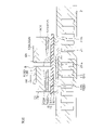
- FIG. 1 is an illustrative cross-sectional view for explaining the configuration of the semiconductor device according to the first embodiment of the present disclosure.
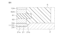
- FIG. 2 is an enlarged cross-sectional view of part A in FIG. 3A is a cross-sectional view showing an example of a manufacturing process of the semiconductor device of FIG. 1, and is a cross-sectional view corresponding to the cross-sectional view of FIG. 1.
- FIG. 3B is a cross-sectional view showing the next step of FIG. 3A.
- FIG. 3C is a cross-sectional view showing the next step of FIG. 3B.
- FIG. 3D is a cross-sectional view showing the next step of FIG. 3C.
- FIG. 4 is an enlarged cross-sectional view showing a modification of the insulating substrate.
- FIG. 1 is an illustrative cross-sectional view for explaining the configuration of the semiconductor device according to the first embodiment of the present disclosure.
- FIG. 2 is an enlarged cross-sectional view of part A in FIG. 3
- FIG. 5A is an enlarged cross-sectional view showing a modification of the heat sink.
- FIG. 5B is an enlarged cross-sectional view showing another modification of the heat sink.
- FIG. 6 is an enlarged cross-sectional view showing a modification of the shape of the side surface of the recess.
- FIG. 7 is an enlarged cross-sectional view showing a modification of the depth of the recess.
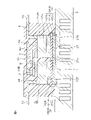
- FIG. 8 is an illustrative cross-sectional view for explaining the configuration of the semiconductor device according to the second embodiment of the present disclosure.
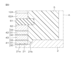
- 9 is an enlarged cross-sectional view of the A portion of FIG. 8.
- FIG. 10 is an illustrative cross-sectional view for explaining the configuration of a semiconductor device according to the third embodiment of the invention.
- 11 is an enlarged cross-sectional view of a portion A in FIG. 10.
- An embodiment of the present disclosure includes a semiconductor chip, a support having an upper surface and a lower surface, the semiconductor chip fixed to the upper surface, and a sealing resin for sealing the semiconductor chip and the support. , a heat sink bonded to the bottom surface of the support, wherein a recess is formed in the top surface of the heat sink, the bottom surface of the support is bonded to the bottom surface of the recess via a bonding structure, A semiconductor device is provided in which the sealing resin enters a gap between at least the bonding structure of the supporting body and the bonding structure and the side surface of the recess.
- the side surface of the recess is curved or inclined such that the cross-sectional area of the recess gradually increases from the bottom surface of the recess toward the opening of the recess on the upper surface of the heat sink. is formed in
- the bonding structure includes a solid phase diffusion bonding sheet.
- the solid phase diffusion bonding sheet includes an Al layer, a first laminated film in which a Ni layer and an Ag layer are formed in that order on the lower surface of the Al layer, and the upper surface of the Al layer. and a second laminated film in which a Ni layer and an Ag layer are formed in that order.
- the bonding structure includes a first solid phase diffusion bonding sheet, a second solid phase diffusion bonding sheet disposed above the first solid phase diffusion bonding sheet, and the first solid phase a stress buffer layer provided between the diffusion bonding sheet and the second solid state diffusion bonding sheet.
- each of the solid phase diffusion bonding sheets includes an Al layer, a first laminated film in which a Ni layer and an Ag layer are formed in that order on the lower surface of the Al layer, and the Al layer.
- the upper surface is composed of a second laminated film in which a Ni layer and an Ag layer are formed in that order.
- the stress buffer layer is made of a CuMo layer.
- the joint structure includes sintered silver.
- the joint structure includes solder.
- the support includes an insulating substrate and a metal substrate disposed on the insulating substrate, and the semiconductor chip is provided on the surface of the metal substrate opposite to the insulating substrate. Fixed.
- the support is made of an insulating substrate.
- the heat sink is a water cooler.
- the heat sink is an air cooler.
- the heat sink is made of a Cu block.
- An embodiment of the present disclosure includes a semiconductor chip, a support having an upper surface and a lower surface, the semiconductor chip being fixed to the upper surface, a heat sink bonded to the lower surface of the support, the semiconductor chip and the A method of manufacturing a semiconductor device including a sealing resin for sealing a support, comprising: a bonding step of bonding the semiconductor chip, the support, and the heat sink; , and a sealing step of sealing with the sealing resin.
- the bonding step among the bonding between the semiconductor chip and the support and the bonding between the support and the heat sink, at least the bonding between the support and the heat sink is performed by solid phase diffusion bonding.
- FIG. 1 is an illustrative cross-sectional view for explaining the configuration of the semiconductor device according to the first embodiment of the present disclosure.
- FIG. 2 is an enlarged cross-sectional view of part A in FIG.
- the left side of the paper surface of FIG. 1 is called “left” and the right side of the paper surface of FIG. 1 is called “right”.
- the semiconductor device 1 is a power module.
- a semiconductor device 1 includes a heat sink 2, a support 3 bonded to the upper surface of the heat sink 2, semiconductor chips 4A and 4B fixed to the upper surface of the support 3, and the semiconductor chips 4A and 4B and the support 3 sealed. and a sealing resin 5 that A main portion (module portion) of the semiconductor device 1 excluding the heat sink 2 has a rectangular parallelepiped shape.
- the heat sink 2 is, in this embodiment, a water cooler that causes coolant such as cooling water or oil to flow through holes formed in the heat sink 2 .
- the support 3 includes an insulating substrate 6 bonded to the upper surface of the heat sink 2 via a first bonding structure 11, and a pair of left and right substrates bonded to the insulating substrate 6 via a pair of left and right second bonding structures 12A and 12B. It includes metal substrates 7A and 7B.
- the insulating substrate 6 is made of a DBC (Direct Bonded Copper) substrate, and includes a ceramic plate 61, a copper foil 62 formed on the lower surface of the ceramic plate 61, and a space on the upper surface of the ceramic plate 61. A pair of left and right copper foils 62A and 62B are arranged with a gap between them.
- DBC Direct Bonded Copper
- the right metal substrate 7A is bonded to the upper surface of the right copper foil 62A via the right second bonding structure 12A.
- the left metal substrate 7B is bonded to the upper surface of the left copper foil 62B via the left second bonding structure 12B.
- the metal substrates 7A, 7B are made of copper substrates in this embodiment.
- a semiconductor chip 4A is bonded onto the right metal substrate 7A via a third bonding structure 13A (right third bonding structure 13A).
- a semiconductor chip 4B and a later-described spacer 8 are bonded to the left metal substrate 7B via a third bonding structure 13B (left third bonding structure 13B).
- the semiconductor chip 4A on the right side is a switching element for high side
- the semiconductor chip 4B on the left side is a switching element for low side.
- the first bonding structure 11, the second bonding structures 12A, 12B, and the third bonding structures 13A, 13B include solid phase diffusion bonding sheets. That is, in this embodiment, the insulating substrate 6 and the heat sink 2 are bonded by solid phase diffusion bonding. The insulating substrate 6 and the metal substrates 7A and 7B are bonded by solid phase diffusion bonding. Also, the semiconductor chip 4A is bonded to the metal substrate 7A by solid phase diffusion bonding. Also, the semiconductor chip 4B and the spacer 8 are bonded to the metal substrate 7B by solid-phase diffusion bonding.
- the solid-phase diffusion bonding sheet consists of an Al preform sheet, as shown in FIG.
- the Al preform sheet consists of an Al layer 31, a first laminated film 32 formed on the lower surface of the Al layer 31, and a second laminated film 33 formed on the upper surface of the Al layer.
- the first laminated film 32 is composed of a Ni layer formed on the lower surface of the Al layer 31 and an Ag layer formed on the lower surface of the Ni layer.
- the second laminated film 33 is composed of a Ni layer formed on the upper surface of the Al layer 31 and an Ag layer formed on the upper surface of the Ni layer.
- the semiconductor device 1 includes spacers 8 arranged on the left metal substrate 7B, wires 9 connected to the spacers 8 and the semiconductor chips 4A and 4B, and terminals 10 .
- the terminal 10 includes a positive power supply terminal, a negative power supply terminal, an output terminal, a gate terminal, etc., but only part of them are shown in FIG.
- the upper surface of the heat sink 2 is formed with a recess 21 having an outer peripheral edge (opening edge) surrounding the lower surface of the support 3 in plan view.
- the lower surface of the support 3 (lower surface of the insulating substrate 6 ) is bonded to the bottom surface 21 a of the recess 21 via the first bonding structure 11 .
- substantially the entire first bonding structure 11 is arranged within the recess 21 . That is, the side surface 21 b of the recess 21 is arranged so as to surround the outer peripheral surface of the first joint structure 11 .
- the side surface 21 b of the recess 21 is formed in a curved shape in which the cross-sectional area of the recess 21 gradually increases from the bottom surface of the recess 21 toward the opening of the recess 21 on the upper surface of the heat sink 2 .
- the recesses 21 are formed in the process of manufacturing the semiconductor device 1. Specifically, the heat sink 2, the insulating substrate 6, the metal substrates 7A and 7B, the semiconductor chips 4A and 4B and the spacers 8 are collectively formed. It is formed when
- the sealing resin 5 has a rectangular shape slightly larger than the support 3 in a plan view, and covers a part of the terminal 10, the wiring 9, the support 3, and the area near the support 3 on the upper surface of the heat sink 2. is formed as In the entire space between the portion of the first joint structure 11 and the support 3 that is arranged in the recess 21 (in this embodiment, substantially the entire first joint structure 11) and the side surface 21b of the recess 21 , a part of the sealing resin 5 is entrapped. A portion of the terminal 10 protruding from the sealing resin 5 serves as an external wiring connection portion for connecting the terminal 10 to an external wiring.
- the sealing resin 5 is made of epoxy resin, for example.
- the recess 21 is formed on the upper surface of the heat sink 2 , and the lower surface of the support 3 is bonded to the bottom surface 21 a of the recess 21 via the first bonding structure 11 .
- a space portion between the portion of the first joint structure 11 and the support 3 that is arranged in the recess 21 (in this embodiment, substantially the entire first joint structure 11) and the side surface 21b of the recess 21 A part of the sealing resin 5 enters the entire area.
- a so-called anchor effect works, making it difficult for the sealing resin 5 to peel off from the heat sink 2 .
- the bonding strength between the heat sink 2 and the support 3 (insulating substrate 6) can be increased.
- aged deterioration of the bonding interface between the support 3 and the heat sink 2 can be suppressed.
- the heat sink 2 and the support 3 are bonded by solid-phase diffusion bonding. Therefore, it is possible to suppress aging deterioration of these bonding interfaces.
- 3A to 3D are schematic cross-sectional views sequentially showing manufacturing steps of the semiconductor device 1 shown in FIGS. 1 and 2, and are cross-sectional views corresponding to the cross-sectional plane of FIG.
- an Al preform sheet 91 for forming the first joint structure 11 is placed on the heat sink 2 , and the insulating substrate 6 is placed on the Al preform sheet 91 .
- the insulating substrate 6 is made of a DBC substrate, and includes a ceramic plate 51, a copper foil 62 formed on the lower surface of the ceramic plate 51, and a pair of right and left copper foils arranged on the upper surface of the ceramic plate 51 with a space therebetween. 62A and 62B.
- Al preform sheets 92A and 92B for forming the second joint structures 12A and 12B are arranged on the pair of copper foils 62A and 62B on the upper side of the insulating substrate 6, and on the Al preform sheets 92A and 92B , metal substrates 7A and 7B are arranged.
- an Al preform sheet 93A for forming the third bonding structure 13A is arranged on the metal substrate 7A, and the semiconductor chip 4A is arranged on the Al preform sheet 93A. Furthermore, an Al preform sheet 93B for forming the third bonding structure 13B is arranged on the metal substrate 7B, and the semiconductor chip 4B and the spacer 8 are arranged on the Al preform sheet 93B.
- the members placed on the heat sink 2 are pressed with a pressure of 20 MPa or more.
- the recess 21 is formed in the heat sink 2, and the lower surface of the insulating substrate 6 is bonded to the bottom surface of the recess 21 via the first bonding structure 11 including the Al preform sheet 91 (this implementation solid phase diffusion bonding).
- metal substrates 7A and 7B are joined (in this embodiment, solid-phase diffusion bonding).
- the semiconductor chip 4A is bonded (solid phase diffusion bonding in this embodiment) to the upper surface of the metal substrate 7A via the third bonding structure 13A including the Al preform sheet 93A.
- the semiconductor chip 4B and the spacer 8 are bonded (solid phase diffusion bonding in this embodiment) to the upper surface of the metal substrate 7B via the third bonding structure 13B including the Al preform sheet 93B.
- the bonding between the heat sink 2 and the insulating substrate 6, the bonding between the insulating substrate 6 and the metal substrates 7A and 7B, and the bonding between the metal substrates 7A and 7B and the semiconductor chips 4A and 4B and the spacers 8 are performed separately in time. You can go to
- the wiring 9 is joined to the semiconductor chips 4A and 4B and the spacer 8.
- the terminals 10 are joined to the metal substrates 7A and 7B, the wiring 9, and the like.
- a sealing resin 5 is formed so as to cover part of the terminals 10 , the wiring 9 , the support 3 , and the area near the support 3 on the upper surface of the heat sink 2 . Thereby, the semiconductor device 1 as shown in FIGS. 1 and 2 is obtained.
- the parts other than the heat sink are manufactured, and then the module part is bonded to the heat sink. If the module portion and the heat sink are to be bonded by solid-phase diffusion bonding, the heat sink and the module portion must be heated to a relatively high temperature (approximately 300° C.), resulting in deterioration of the sealing resin 5 . For this reason, in a general manufacturing method, it is difficult to solid-phase diffusion bond the heat sink 2 and the support 3 (insulating substrate 6) under a temperature environment suitable for solid-phase diffusion bonding.
- solid phase diffusion bonding is performed between the heat sink 2 and the support 3 (insulating substrate 6) before the sealing resin 5 is formed.
- the heat sink 2 and the support 3 (insulating substrate 6) can be solid phase diffusion bonded under a suitable temperature environment. As a result, the heat sink 2 and the support 3 (insulating substrate 6) can be firmly bonded together.
- the heat sink 2 and the support 3 (insulating substrate 6) may be bonded by silver firing instead of solid phase diffusion bonding. In that case as well, by manufacturing the semiconductor device in the same order as in FIGS. can do. As a result, the heat sink 2 and the support 3 (insulating substrate 6) can be firmly bonded together.
- the portion of the first bonding structure 11 and the support 3 that is arranged in the recess 21 (in this embodiment, substantially the entire first bonding structure 11) and the recess 21 A portion of the sealing resin 5 can enter the entire space portion between the side surface 21b.
- a so-called anchor effect works, making it difficult for the sealing resin 5 to peel off from the heat sink 2 .
- the bonding strength between the heat sink 2 and the support 3 (insulating substrate 6) can be increased.
- aged deterioration of the bonding interface between the support 3 and the heat sink 2 can be suppressed.
- the insulating substrate 6 includes a ceramic plate 61, a copper foil 62 formed on the lower surface of the ceramic plate 61, a pair of right and left copper foils 62A arranged on the upper surface of the ceramic plate 61 with a space therebetween. 62B.
- the insulating substrate 6 may be composed of a pair of left and right insulating substrates 6A and 6B spaced apart in the left-right direction.
- One insulating substrate 6A is made of a DBC substrate and consists of a ceramic plate 61A, a copper foil 63A formed on the lower surface of the ceramic plate 61A, and a copper foil 62A formed on the upper surface of the ceramic plate 61A.
- the other insulating substrate 6B is made of a DBC substrate and consists of a ceramic plate 61B, a copper foil 63B formed on the lower surface of the ceramic plate 61B, and a copper foil 62B formed on the upper surface of the ceramic plate 61B.
- the parts corresponding to the parts in FIG. 1 are denoted by the same reference numerals as in FIG.
- the heat sink 2 is a water cooler.
- the heat sink 2 may be a finned air cooler as shown in FIG. 5A.
- the heat sink 2 may be constructed from a copper block, as shown in FIG. 5B. 5A and 5B, parts corresponding to those in FIG. 1 are denoted by the same reference numerals as in FIG.
- the side surface 21b of the recess 21 is formed in a curved shape in which the cross-sectional area of the recess 21 gradually increases from the bottom surface of the recess 21 toward the opening of the recess 21 on the upper surface of the heat sink 2. ing.
- the side surface 21 b of the recess 21 has an inclined surface shape in which the cross-sectional area of the recess 21 gradually increases from the bottom surface of the recess 21 toward the opening of the recess 21 on the upper surface of the heat sink 2 ( tapered surface).
- FIG. 6 is an enlarged sectional view corresponding to FIG.
- parts corresponding to those in FIG. 2 are denoted by the same reference numerals as those in FIG.
- the portion of the first joint structure 11 and the support 3 that is arranged in the recess 21 in the example of FIG. 6, substantially the entire first joint structure 11
- the side surface 21b of the recess 21 A portion of the sealing resin 5 enters the entire space between the .
- the depth of the recess 21 is substantially equal to the thickness of the first bonding structure 11 in the above-described embodiment, the depth of the recess 21 may be smaller than the thickness of the first bonding structure 11 . Further, the depth of the concave portion 21 may be a depth into which the entire first joint structure 11 and the lower end portion of the support body 3 enter, as shown in FIG. 7 . That is, the depth of recess 21 may be greater than the thickness of first bonding structure 11 .
- FIG. 7 is an enlarged sectional view corresponding to FIG. 7, parts corresponding to those in FIG. 2 are denoted by the same reference numerals as those in FIG.
- a portion of the sealing resin 5 fills the entire space between the portion of the first bonding structure 11 and the support 3 that is disposed within the recess 21 and the side surface 21 b of the recess 21 . I'm in.
- FIG. 8 is an illustrative cross-sectional view for explaining the configuration of the semiconductor device according to the second embodiment of the present disclosure.
- 9 is an enlarged cross-sectional view of the A portion of FIG. 8.
- FIG. 8 and 9, parts corresponding to those in FIGS. 1 and 2 are denoted by the same reference numerals as in FIGS.
- the first joint structure 11 includes a lower joint structure 41 arranged on the bottom surface 21a of the heat sink 2 and an upper joint structure 42 arranged above the lower joint structure 41. and a stress buffer layer 43 interposed between the lower joint structure 41 and the upper joint structure 42 .
- the lower junction structure 41 and the upper junction structure 42 each have the same structure as the first junction structure 11 of the semiconductor device 1 according to the first embodiment.
- Other configurations are the same as those of the semiconductor device 1 according to the first embodiment.
- the stress buffer layer 43 is made of, for example, a CuMo layer.
- the first bonding structure 11 includes the stress buffering layer 43, aging deterioration of the bonding interface between the support 3 and the heat sink 2 is more effectively prevented than in the first embodiment. can be suppressed to
- FIG. 10 is an illustrative cross-sectional view for explaining the configuration of the semiconductor device according to the third embodiment of the present disclosure.
- 11 is an enlarged cross-sectional view of a portion A in FIG. 10.
- FIG. 10 and 11 parts corresponding to those in FIGS. 1 and 2 are denoted by the same reference numerals as in FIGS.
- the insulating substrate 6 is made up of an insulating layer 65 and a metal layer (metallized layer) 66 formed under the insulating layer 65 .
- a metal substrate 7A and a metal substrate 7B are arranged on the insulating layer 65 with a space therebetween.
- the insulating layer 65 and the metal substrates 7A and 7B are bonded by ceramic coating such as thermal spraying or aerosol deposition, instead of solid phase diffusion bonding. Therefore, the semiconductor device 1B according to the third embodiment does not have the second junction structures 12A and 12B.
- Other configurations are the same as those of the semiconductor device 1 according to the first embodiment.
- the insulating layer 65 is made of, for example, an Al 2 O 3 layer.
- the insulating layer 65 may be a Si3N4 layer or an AlN layer.
- the metal layer 66 is made of, for example, a Cu layer, Ag layer, Au layer, Ni layer, Al layer, or the like.
- the first bonding structure 11 includes a solid phase diffusion bonding sheet, but the first bonding structure 11 may include sintered silver or solder. .
- the heat sink 2 and the support 3 may be joined by silver firing joining, or may be joined by soldering.
- the third bonding structures 13A and 13B include solid phase diffusion bonding sheets, but the third bonding structures 13A and 13B are made of sintered silver or solder. may contain That is, the support 3 (metal substrates 7A, 7B) and the semiconductor chips 4A, 4B may be joined by silver firing joining, or may be joined by soldering.
- the second bonding structures 12A and 12B contain the solid phase diffusion bonding sheets, but the second bonding structures 12A and 12B contain sintered silver or solder. You can stay. That is, the insulating substrate 6 (copper foils 62A, 62B) and the metal substrates 7A, 7B may be joined by silver firing joining, or may be joined by soldering.
- the recess 21 is formed in the upper surface of the heat sink 2 by joining the heat sink 2 and the support 3 (insulating substrate 6) in a pressure-contact state.
- the concave portion 21 may be formed on the upper surface of the heat sink 2 before the support 3 (insulating substrate 6) is bonded to the upper surface of the heat sink 2.
- Reference Signs List 1 1A, 1B semiconductor device 2 heat sink 3 support 4A, 4B semiconductor chip 5 sealing resin 6, 6A, 6B insulating substrate 61, 61A, 61B ceramic plate 62, 62A, 62B, 63A, 63B copper foil 7A, 7B metal Substrate 8 Spacer 9 Wiring 10 Terminal 11 First bonding structure 12A, 12B Second bonding structure 13A, 13B Third bonding structure 21 Recess 21a Bottom surface 21b Side surface 31 Al layer 32 First laminated film 32 Second laminated film 41 Lower bonding structure 42 upper joint structure 43 stress buffer layer 91, 92A, 92B, 93A, 93B Al preform sheet
Landscapes
- Cooling Or The Like Of Semiconductors Or Solid State Devices (AREA)
- Chemical & Material Sciences (AREA)
- Engineering & Computer Science (AREA)
- Materials Engineering (AREA)
Priority Applications (4)
| Application Number | Priority Date | Filing Date | Title |
|---|---|---|---|
| DE112022003837.3T DE112022003837T5 (de) | 2021-09-02 | 2022-07-05 | Halbleitervorrichtung und herstellungsverfahren |
| JP2023545127A JPWO2023032462A1 (https=) | 2021-09-02 | 2022-07-05 | |
| CN202280059171.4A CN117882187A (zh) | 2021-09-02 | 2022-07-05 | 半导体装置及其制造方法 |
| US18/591,744 US20240203817A1 (en) | 2021-09-02 | 2024-02-29 | Semiconductor apparatus, and manufacturing method therefor |
Applications Claiming Priority (2)
| Application Number | Priority Date | Filing Date | Title |
|---|---|---|---|
| JP2021-143182 | 2021-09-02 | ||
| JP2021143182 | 2021-09-02 |
Related Child Applications (1)
| Application Number | Title | Priority Date | Filing Date |
|---|---|---|---|
| US18/591,744 Continuation US20240203817A1 (en) | 2021-09-02 | 2024-02-29 | Semiconductor apparatus, and manufacturing method therefor |
Publications (1)
| Publication Number | Publication Date |
|---|---|
| WO2023032462A1 true WO2023032462A1 (ja) | 2023-03-09 |
Family
ID=85412092
Family Applications (1)
| Application Number | Title | Priority Date | Filing Date |
|---|---|---|---|
| PCT/JP2022/026677 Ceased WO2023032462A1 (ja) | 2021-09-02 | 2022-07-05 | 半導体装置およびその製造方法 |
Country Status (5)
| Country | Link |
|---|---|
| US (1) | US20240203817A1 (https=) |
| JP (1) | JPWO2023032462A1 (https=) |
| CN (1) | CN117882187A (https=) |
| DE (1) | DE112022003837T5 (https=) |
| WO (1) | WO2023032462A1 (https=) |
Cited By (5)
| Publication number | Priority date | Publication date | Assignee | Title |
|---|---|---|---|---|
| WO2024241786A1 (ja) * | 2023-05-19 | 2024-11-28 | ローム株式会社 | 接合構造、半導体装置、および接合方法 |
| WO2025173483A1 (ja) * | 2024-02-14 | 2025-08-21 | ローム株式会社 | 半導体装置および半導体装置の製造方法 |
| WO2025177769A1 (ja) * | 2024-02-19 | 2025-08-28 | ローム株式会社 | 半導体装置の製造方法、半導体装置および車両 |
| WO2026074979A1 (ja) * | 2024-10-01 | 2026-04-09 | ローム株式会社 | 半導体装置および半導体装置の製造方法 |
| WO2026074948A1 (ja) * | 2024-10-01 | 2026-04-09 | ローム株式会社 | 半導体モジュール |
Citations (3)
| Publication number | Priority date | Publication date | Assignee | Title |
|---|---|---|---|---|
| JP2016042529A (ja) * | 2014-08-18 | 2016-03-31 | 三菱マテリアル株式会社 | 接合体の製造方法、パワーモジュール用基板の製造方法、及び、ヒートシンク付パワーモジュール用基板の製造方法 |
| WO2019146640A1 (ja) * | 2018-01-24 | 2019-08-01 | 三菱マテリアル株式会社 | ヒートシンク付きパワーモジュール用基板及びパワーモジュール |
| JP2021114537A (ja) * | 2020-01-17 | 2021-08-05 | パナソニックIpマネジメント株式会社 | 半導体装置 |
Family Cites Families (7)
| Publication number | Priority date | Publication date | Assignee | Title |
|---|---|---|---|---|
| JPH0786444A (ja) * | 1993-06-28 | 1995-03-31 | Sumitomo Electric Ind Ltd | 半導体用複合放熱基板の製造方法 |
| JP6230522B2 (ja) * | 2014-11-14 | 2017-11-15 | 三菱電機株式会社 | パワー半導体装置およびその製造方法ならびに絶縁基板部 |
| US20190054090A1 (en) | 2015-10-01 | 2019-02-21 | Gilead Sciences, Inc. | Combination of a btk inhibitor and a checkpoint inhibitor for treating cancers |
| DE112016006332B4 (de) * | 2016-01-28 | 2021-02-04 | Mitsubishi Electric Corporation | Leistungsmodul |
| WO2018207856A1 (ja) | 2017-05-10 | 2018-11-15 | ローム株式会社 | パワー半導体装置およびその製造方法 |
| JP2020072101A (ja) * | 2018-10-29 | 2020-05-07 | 京セラ株式会社 | パワーユニット、パワーユニットの製造方法、パワーユニットを有する電気装置及びヒートシンク |
| WO2021199384A1 (ja) * | 2020-04-01 | 2021-10-07 | 三菱電機株式会社 | 半導体装置および半導体装置の製造方法 |
-
2022
- 2022-07-05 CN CN202280059171.4A patent/CN117882187A/zh active Pending
- 2022-07-05 DE DE112022003837.3T patent/DE112022003837T5/de active Pending
- 2022-07-05 WO PCT/JP2022/026677 patent/WO2023032462A1/ja not_active Ceased
- 2022-07-05 JP JP2023545127A patent/JPWO2023032462A1/ja active Pending
-
2024
- 2024-02-29 US US18/591,744 patent/US20240203817A1/en active Pending
Patent Citations (3)
| Publication number | Priority date | Publication date | Assignee | Title |
|---|---|---|---|---|
| JP2016042529A (ja) * | 2014-08-18 | 2016-03-31 | 三菱マテリアル株式会社 | 接合体の製造方法、パワーモジュール用基板の製造方法、及び、ヒートシンク付パワーモジュール用基板の製造方法 |
| WO2019146640A1 (ja) * | 2018-01-24 | 2019-08-01 | 三菱マテリアル株式会社 | ヒートシンク付きパワーモジュール用基板及びパワーモジュール |
| JP2021114537A (ja) * | 2020-01-17 | 2021-08-05 | パナソニックIpマネジメント株式会社 | 半導体装置 |
Cited By (5)
| Publication number | Priority date | Publication date | Assignee | Title |
|---|---|---|---|---|
| WO2024241786A1 (ja) * | 2023-05-19 | 2024-11-28 | ローム株式会社 | 接合構造、半導体装置、および接合方法 |
| WO2025173483A1 (ja) * | 2024-02-14 | 2025-08-21 | ローム株式会社 | 半導体装置および半導体装置の製造方法 |
| WO2025177769A1 (ja) * | 2024-02-19 | 2025-08-28 | ローム株式会社 | 半導体装置の製造方法、半導体装置および車両 |
| WO2026074979A1 (ja) * | 2024-10-01 | 2026-04-09 | ローム株式会社 | 半導体装置および半導体装置の製造方法 |
| WO2026074948A1 (ja) * | 2024-10-01 | 2026-04-09 | ローム株式会社 | 半導体モジュール |
Also Published As
| Publication number | Publication date |
|---|---|
| JPWO2023032462A1 (https=) | 2023-03-09 |
| US20240203817A1 (en) | 2024-06-20 |
| CN117882187A (zh) | 2024-04-12 |
| DE112022003837T5 (de) | 2024-05-23 |
Similar Documents
| Publication | Publication Date | Title |
|---|---|---|
| WO2023032462A1 (ja) | 半導体装置およびその製造方法 | |
| KR101905995B1 (ko) | 양면냉각형 파워모듈 | |
| US12040301B2 (en) | Semiconductor device | |
| US11380646B2 (en) | Multi-sided cooling semiconductor package and method of manufacturing the same | |
| US20120306086A1 (en) | Semiconductor device and wiring substrate | |
| JPWO2020071185A1 (ja) | 半導体装置および半導体装置の製造方法 | |
| JP4610414B2 (ja) | 電子部品収納用パッケージおよび電子装置ならびに電子装置の実装構造 | |
| US20130112993A1 (en) | Semiconductor device and wiring substrate | |
| WO2011040313A1 (ja) | 半導体モジュールおよびその製造方法 | |
| JP2023527378A (ja) | パワー半導体モジュール | |
| US20230077964A1 (en) | Semiconductor device and method for manufacturing semiconductor device | |
| JPWO2023032462A5 (https=) | ||
| JP2012119597A (ja) | 半導体装置及びその製造方法 | |
| JP2017174927A (ja) | パワーモジュール及びその製造方法 | |
| WO2020241238A1 (ja) | 半導体装置 | |
| WO2020241239A1 (ja) | 半導体装置 | |
| US5200640A (en) | Hermetic package having covers and a base providing for direct electrical connection | |
| JP2011054889A (ja) | 樹脂封止型半導体装置およびその製造方法 | |
| JP5091459B2 (ja) | 高放熱型電子部品収納用パッケージの製造方法 | |
| CN120359612A (zh) | 双面冷却功率封装件 | |
| CN117043931A (zh) | 电源模块及其制造方法 | |
| WO2022162871A1 (ja) | 両面冷却パワーモジュール | |
| JP2009099709A (ja) | 半導体装置 | |
| JP2014143342A (ja) | 半導体モジュール及びその製造方法 | |
| JP2005285885A (ja) | 半導体装置 |
Legal Events
| Date | Code | Title | Description |
|---|---|---|---|
| 121 | Ep: the epo has been informed by wipo that ep was designated in this application |
Ref document number: 22864050 Country of ref document: EP Kind code of ref document: A1 |
|
| WWE | Wipo information: entry into national phase |
Ref document number: 2023545127 Country of ref document: JP |
|
| WWE | Wipo information: entry into national phase |
Ref document number: 202280059171.4 Country of ref document: CN |
|
| 122 | Ep: pct application non-entry in european phase |
Ref document number: 22864050 Country of ref document: EP Kind code of ref document: A1 |