WO2023032214A1 - 熱処理装置、熱処理方法及び記憶媒体 - Google Patents
熱処理装置、熱処理方法及び記憶媒体 Download PDFInfo
- Publication number
- WO2023032214A1 WO2023032214A1 PCT/JP2021/032713 JP2021032713W WO2023032214A1 WO 2023032214 A1 WO2023032214 A1 WO 2023032214A1 JP 2021032713 W JP2021032713 W JP 2021032713W WO 2023032214 A1 WO2023032214 A1 WO 2023032214A1
- Authority
- WO
- WIPO (PCT)
- Prior art keywords
- hot plate
- substrate
- gas
- heat treatment
- wafer
- Prior art date
- Legal status (The legal status is an assumption and is not a legal conclusion. Google has not performed a legal analysis and makes no representation as to the accuracy of the status listed.)
- Ceased
Links
Images



Classifications
-
- H—ELECTRICITY
- H10—SEMICONDUCTOR DEVICES; ELECTRIC SOLID-STATE DEVICES NOT OTHERWISE PROVIDED FOR
- H10P—GENERIC PROCESSES OR APPARATUS FOR THE MANUFACTURE OR TREATMENT OF DEVICES COVERED BY CLASS H10
- H10P72/00—Handling or holding of wafers, substrates or devices during manufacture or treatment thereof
- H10P72/04—Apparatus for manufacture or treatment
- H10P72/0431—Apparatus for thermal treatment
-
- H—ELECTRICITY
- H10—SEMICONDUCTOR DEVICES; ELECTRIC SOLID-STATE DEVICES NOT OTHERWISE PROVIDED FOR
- H10P—GENERIC PROCESSES OR APPARATUS FOR THE MANUFACTURE OR TREATMENT OF DEVICES COVERED BY CLASS H10
- H10P72/00—Handling or holding of wafers, substrates or devices during manufacture or treatment thereof
- H10P72/04—Apparatus for manufacture or treatment
- H10P72/0431—Apparatus for thermal treatment
- H10P72/0432—Apparatus for thermal treatment mainly by conduction
-
- H—ELECTRICITY
- H01—ELECTRIC ELEMENTS
- H01J—ELECTRIC DISCHARGE TUBES OR DISCHARGE LAMPS
- H01J37/00—Discharge tubes with provision for introducing objects or material to be exposed to the discharge, e.g. for the purpose of examination or processing thereof
- H01J37/32—Gas-filled discharge tubes
- H01J37/32431—Constructional details of the reactor
- H01J37/3244—Gas supply means
-
- H—ELECTRICITY
- H10—SEMICONDUCTOR DEVICES; ELECTRIC SOLID-STATE DEVICES NOT OTHERWISE PROVIDED FOR
- H10P—GENERIC PROCESSES OR APPARATUS FOR THE MANUFACTURE OR TREATMENT OF DEVICES COVERED BY CLASS H10
- H10P72/00—Handling or holding of wafers, substrates or devices during manufacture or treatment thereof
- H10P72/04—Apparatus for manufacture or treatment
- H10P72/0402—Apparatus for fluid treatment
-
- H—ELECTRICITY
- H10—SEMICONDUCTOR DEVICES; ELECTRIC SOLID-STATE DEVICES NOT OTHERWISE PROVIDED FOR
- H10P—GENERIC PROCESSES OR APPARATUS FOR THE MANUFACTURE OR TREATMENT OF DEVICES COVERED BY CLASS H10
- H10P72/00—Handling or holding of wafers, substrates or devices during manufacture or treatment thereof
- H10P72/04—Apparatus for manufacture or treatment
- H10P72/0431—Apparatus for thermal treatment
- H10P72/0434—Apparatus for thermal treatment mainly by convection
-
- H—ELECTRICITY
- H10—SEMICONDUCTOR DEVICES; ELECTRIC SOLID-STATE DEVICES NOT OTHERWISE PROVIDED FOR
- H10P—GENERIC PROCESSES OR APPARATUS FOR THE MANUFACTURE OR TREATMENT OF DEVICES COVERED BY CLASS H10
- H10P72/00—Handling or holding of wafers, substrates or devices during manufacture or treatment thereof
- H10P72/70—Handling or holding of wafers, substrates or devices during manufacture or treatment thereof for supporting or gripping
- H10P72/76—Handling or holding of wafers, substrates or devices during manufacture or treatment thereof for supporting or gripping using mechanical means, e.g. clamps or pinches
- H10P72/7604—Handling or holding of wafers, substrates or devices during manufacture or treatment thereof for supporting or gripping using mechanical means, e.g. clamps or pinches the wafers being placed on a susceptor, stage or support
- H10P72/7624—Handling or holding of wafers, substrates or devices during manufacture or treatment thereof for supporting or gripping using mechanical means, e.g. clamps or pinches the wafers being placed on a susceptor, stage or support characterised by the mechanical construction of the susceptor, stage or support
-
- H—ELECTRICITY
- H10—SEMICONDUCTOR DEVICES; ELECTRIC SOLID-STATE DEVICES NOT OTHERWISE PROVIDED FOR
- H10P—GENERIC PROCESSES OR APPARATUS FOR THE MANUFACTURE OR TREATMENT OF DEVICES COVERED BY CLASS H10
- H10P76/00—Manufacture or treatment of masks on semiconductor bodies, e.g. by lithography or photolithography
-
- H—ELECTRICITY
- H10—SEMICONDUCTOR DEVICES; ELECTRIC SOLID-STATE DEVICES NOT OTHERWISE PROVIDED FOR
- H10P—GENERIC PROCESSES OR APPARATUS FOR THE MANUFACTURE OR TREATMENT OF DEVICES COVERED BY CLASS H10
- H10P76/00—Manufacture or treatment of masks on semiconductor bodies, e.g. by lithography or photolithography
- H10P76/20—Manufacture or treatment of masks on semiconductor bodies, e.g. by lithography or photolithography of masks comprising organic materials
- H10P76/204—Manufacture or treatment of masks on semiconductor bodies, e.g. by lithography or photolithography of masks comprising organic materials of organic photoresist masks
- H10P76/2041—Photolithographic processes
-
- H—ELECTRICITY
- H10—SEMICONDUCTOR DEVICES; ELECTRIC SOLID-STATE DEVICES NOT OTHERWISE PROVIDED FOR
- H10P—GENERIC PROCESSES OR APPARATUS FOR THE MANUFACTURE OR TREATMENT OF DEVICES COVERED BY CLASS H10
- H10P95/00—Generic processes or apparatus for manufacture or treatments not covered by the other groups of this subclass
- H10P95/90—Thermal treatments, e.g. annealing or sintering
-
- H—ELECTRICITY
- H10—SEMICONDUCTOR DEVICES; ELECTRIC SOLID-STATE DEVICES NOT OTHERWISE PROVIDED FOR
- H10P—GENERIC PROCESSES OR APPARATUS FOR THE MANUFACTURE OR TREATMENT OF DEVICES COVERED BY CLASS H10
- H10P72/00—Handling or holding of wafers, substrates or devices during manufacture or treatment thereof
- H10P72/70—Handling or holding of wafers, substrates or devices during manufacture or treatment thereof for supporting or gripping
- H10P72/78—Handling or holding of wafers, substrates or devices during manufacture or treatment thereof for supporting or gripping using vacuum or suction, e.g. Bernoulli chucks
Definitions
- the present disclosure relates to a heat treatment apparatus, a heat treatment method, and a storage medium.
- Patent Document 1 discloses a method for patterning a substrate with radiation. The method includes irradiating a coated substrate along a selected pattern to form an irradiated structure having regions of irradiated coating and regions of irradiated coating.
- Coated substrates include coatings containing metal oxo-hydroxo networks with organic ligands via metal carbon bonds and/or metal carboxylate bonds.
- the technology according to the present disclosure suppresses contamination of the substrate by a sublimate generated from the resist coating on the substrate, and improves the substrate in-plane uniformity of heat treatment.
- One aspect of the present disclosure is a heat treatment apparatus for heat-treating a substrate on which a resist film is formed and the film is subjected to exposure processing, comprising: a hot plate supporting and heating the substrate; a chamber for performing the heat treatment, the chamber forming a processing space in which the heat treatment is performed, and having a ceiling facing the substrate on the hot plate; a gas discharge part for discharging from above toward the substrate on the hot plate, and a gas from a side of the substrate on the hot plate and below the processing space toward the substrate on the hot plate.
- a central exhaust unit for exhausting the inside of the processing space in the chamber from a position near the center of the substrate on the hot plate in top view in the ceiling portion; a peripheral edge exhaust section that exhausts the inside of the processing space from a peripheral edge side of the substrate on the hot plate rather than the central exhaust section when viewed from above; and a controller, wherein the controller controls the heat treatment During the heat treatment, control is performed so that discharge by the gas discharge unit, gas supply by the gas supply unit, and exhaust by the peripheral exhaust unit are continued, and exhaust by the central exhaust unit is strengthened from the middle of the heat treatment.
- the present disclosure it is possible to suppress contamination of the substrate by a sublimate generated from the resist coating on the substrate, and improve uniformity of heat treatment within the substrate surface.
- FIG. 1 is an explanatory diagram showing an outline of an internal configuration of a coating and developing system as a substrate processing system including a heat treatment apparatus according to this embodiment
- FIG. FIG. 2 is a diagram showing the outline of the internal configuration on the front side of the coating and developing system
- FIG. 2 is a diagram showing the outline of the internal configuration on the back side of the coating and developing system
- 1 is a vertical cross-sectional view schematically showing the outline of the configuration of a heat treatment apparatus used for PEB processing
- FIG. It is a bottom view which shows the outline of a structure of an upper chamber typically. It is a figure which shows the state of the heat processing apparatus during the wafer processing performed using the heat processing apparatus.
- a predetermined process is performed to form a resist pattern on a semiconductor wafer (hereinafter referred to as "wafer").
- the predetermined processing includes, for example, a resist coating process of supplying a resist solution onto a wafer to form a resist coating, an exposure process of exposing the coating, and heating to promote a chemical reaction in the coating after exposure.
- PEB Post Exposure Bake
- development processing for developing the exposed film and the like.
- the PEB process is performed, for example, while evacuating the atmosphere around the substrate.
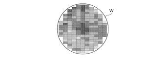
- the dimensions of the resist pattern may vary within the plane depending on the form of the exhaust.
- the sublimate may contaminate the bevel portion and the back surface of the substrate depending on the form of exhaust.
- the technique according to the present disclosure suppresses the contamination of the substrate by the sublimate generated from the resist coating on the substrate, and improves the substrate in-plane uniformity of the heat treatment.
- FIG. 1 is an explanatory diagram showing the outline of the internal configuration of a coating and developing system as a substrate processing system including a heat treatment apparatus according to this embodiment.
- 2 and 3 are diagrams showing the outline of the internal configuration on the front side and the back side of the coating and developing system, respectively.
- the coating and developing system 1 uses a resist to form a resist pattern on a wafer W as a substrate.
- the resists used are those which produce sublimates, for example metal-containing resists.
- the metal contained in the metal-containing resist is arbitrary, but is tin, for example.
- the coating and developing system 1 includes a cassette station 2 for loading and unloading a cassette C, which is a container capable of accommodating a plurality of wafers, and various processing devices for performing predetermined processing such as resist coating processing. and a plurality of processing stations 3 .
- the coating and developing system 1 has a configuration in which a cassette station 2, a processing station 3, and an interface station 5 for transferring wafers W between an exposure apparatus 4 adjacent to the processing station 3 are integrally connected. ing.
- the cassette station 2 is divided into, for example, a cassette loading/unloading section 10 and a wafer transfer section 11 .
- the cassette loading/unloading section 10 is provided at the end of the coating and developing system 1 in the negative Y direction (leftward direction in FIG. 1).
- a cassette mounting table 12 is provided in the cassette loading/unloading section 10 .
- a plurality of, for example, four mounting plates 13 are provided on the cassette mounting table 12 .
- the mounting plates 13 are arranged in a row in the horizontal X direction (vertical direction in FIG. 1).
- the cassette C can be placed on these mounting plates 13 when the cassette C is carried into and out of the coating and developing system 1 .
- a transfer device 20 for transferring the wafer W is provided in the wafer transfer unit 11 .
- the transport device 20 is configured to be movable along a transport path 21 extending in the X direction.
- the conveying device 20 is movable in the vertical direction and around the vertical axis (the direction of ⁇ ), and is between the cassette C on each mounting plate 13 and the transfer device of the third block G3 of the processing station 3, which will be described later. , the wafer W can be transported.
- the processing station 3 is provided with a plurality of, for example, first to fourth blocks G1, G2, G3, and G4, which are equipped with various devices.
- a first block G1 is provided on the front side of the processing station 3 (negative X direction side in FIG. 1), and a second block G1 is provided on the back side of the processing station 3 (positive X direction side in FIG. 1).
- a block G2 of is provided.
- a third block G3 is provided on the cassette station 2 side of the processing station 3 (negative Y direction side in FIG. 1), and the interface station 5 side of the processing station 3 (positive Y direction side in FIG. 1). is provided with a fourth block G4.
- a plurality of liquid processing devices such as a developing device 30, a lower antireflection film forming device 31, a resist coating device 32, and an upper antireflection film forming device 33 are arranged from below. are arranged in order.
- the development processing device 30 subjects the wafer W to development processing. Specifically, the development processing device 30 develops the metal-containing resist film of the wafer W that has undergone the PEB processing.
- the lower antireflection film forming apparatus 31 forms an antireflection film (hereinafter referred to as “lower antireflection film”) on the wafer W under the metal-containing resist film.
- the resist coating device 32 coats the wafer W with a metal-containing resist to form a coating of the metal-containing resist, that is, a metal-containing resist film.
- the upper antireflection film forming apparatus 33 forms an antireflection film (hereinafter referred to as “upper antireflection film”) on the metal-containing resist film of the wafer W. As shown in FIG.
- three development processing devices 30, lower antireflection film forming devices 31, resist coating devices 32, and upper antireflection film forming devices 33 are arranged horizontally.
- the number and arrangement of the developing device 30, the lower antireflection film forming device 31, the resist coating device 32, and the upper antireflection film forming device 33 can be arbitrarily selected.
- a predetermined processing liquid is applied onto the wafer W by spin coating, for example.
- the processing liquid is discharged onto the wafer W from a discharge nozzle, and the wafer W is rotated to spread the processing liquid on the surface of the wafer W.
- heat treatment apparatuses 40 for heat-treating wafers W are arranged vertically and horizontally.
- the number and arrangement of heat treatment apparatuses 40 can also be arbitrarily selected.
- the heat treatment apparatus 40 performs a pre-baking process (hereinafter referred to as "PAB process”) for heat-treating the wafer W after the resist coating process, a PEB process for heat-treating the wafer W after the exposure process, and a wafer after the development process.
- a post-baking process hereinafter referred to as "POST process” for heat-treating W is performed.
- a plurality of transfer devices 50, 51, 52, 53, 54, 55, and 56 are provided in order from the bottom.
- a plurality of transfer devices 60, 61, 62 and a back surface cleaning device 63 for cleaning the back surface of the wafer W are provided in this order from the bottom.
- a wafer transfer area D is formed in the area surrounded by the first block G1 to the fourth block G4.
- a transfer device 70 as a substrate transfer device for transferring the wafer W, for example, is arranged.
- the transport device 70 has a transport arm 70a that is movable in, for example, the Y direction, the ⁇ direction, and the vertical direction.
- the transfer device 70 moves the transfer arm 70a holding the wafer W within the wafer transfer region D, and moves the transfer arm 70a within the surrounding first block G1, second block G2, third block G3 and fourth block G4.
- a wafer W can be transported to a predetermined device.
- a plurality of transport devices 70 are arranged vertically, and wafers W can be transported to predetermined devices having approximately the same height in blocks G1 to G4, for example.
- a shuttle transfer device 80 is provided for transferring the wafer W linearly between the third block G3 and the fourth block G4.
- the shuttle transport device 80 linearly moves the supported wafer W in the Y direction, and transfers the wafer between the transfer device 52 of the third block G3 and the transfer device 62 of the fourth block G4, which are approximately the same height. W can be transported.
- a conveying device 90 is provided on the positive side of the X direction of the third block G3.
- the transport device 90 has a transport arm 90a that is movable in, for example, the ⁇ direction and the vertical direction.
- the transfer device 90 can move the transfer arm 90a holding the wafer W up and down to transfer the wafer W to each transfer device in the third block G3.
- the interface station 5 is provided with a transport device 100 and a transfer device 101 .
- the transport device 100 has a transport arm 100a that is movable in, for example, the ⁇ direction and the vertical direction.
- the transfer device 100 can hold the wafer W on the transfer arm 100a and transfer the wafer W between the transfer devices, the transfer device 101 and the exposure device 4 in the fourth block G4.
- the coating and developing system 1 described above is provided with a control section 200 as shown in FIG.
- the control unit 200 is, for example, a computer including a processor such as a CPU, a memory, and the like, and has a program storage unit (not shown).
- the program storage unit stores a program for controlling the operation of drive systems such as the above-described various processing devices and various transfer devices, and for controlling wafer processing, which will be described later.
- the program may be recorded in a non-temporary computer-readable storage medium H and installed in the control unit 200 from the storage medium H.
- the storage medium H may be temporary or non-temporary. Part or all of the program may be realized by dedicated hardware (circuit board).
- a cassette C containing a plurality of wafers W is carried into the cassette station 2 of the coating and developing system 1 and placed on the placing plate 13 . After that, each wafer W in the cassette C is sequentially taken out by the transfer device 20 and transferred to the delivery device 53 of the third block G3 of the processing station 3 .
- the wafer W is transferred by the transfer device 70 to the heat treatment device 40 of the second block G2 and subjected to temperature control processing. After that, the wafer W is transferred by the transfer device 70 to, for example, the lower antireflection film forming device 31 of the first block G1, and a lower antireflection film is formed on the wafer W.
- the wafer W is transported to the heat treatment device 40 of the second block G2 and subjected to heat treatment. After that, the wafer W is returned to the delivery device 53 of the third block G3.
- the wafer W is transferred to the resist coating device 32 by the transfer device 70, and a metal-containing resist film is formed on the wafer W. After that, the wafer W is transferred to the heat treatment apparatus 40 by the transfer apparatus 70 and subjected to the PAB process. After that, the wafer W is transferred by the transfer device 70 to the delivery device 55 of the third block G3.
- the wafer W is transferred by the transfer device 70 to the upper antireflection film forming device 33, and an upper antireflection film is formed on the wafer W. After that, the wafer W is transferred to the heat treatment apparatus 40 by the transfer apparatus 70, heated, and temperature-controlled.
- the wafer W is transferred by the transfer device 70 to the delivery device 56 of the third block G3.
- the wafer W is transferred to the transfer device 52 by the transfer device 90, and transferred to the transfer device 62 of the fourth block G4 by the shuttle transfer device 80. After that, the wafer W is transferred by the transfer device 100 to the back surface cleaning device 63, and the back surface thereof is cleaned. Next, the wafer W is transferred to the exposure apparatus 4 by the transfer apparatus 100 of the interface station 5, and exposed in a predetermined pattern using EUV light.
- the wafer W is transferred by the transfer device 100 to the delivery device 60 of the fourth block G4. After that, the wafer W is transported to the heat treatment apparatus 40 and subjected to PEB processing.
- the wafer W is transported to the developing treatment device 30 by the transport device 70 and developed. After completion of the development, the wafer W is transported to the heat treatment apparatus 40 by the transport apparatus 90 and subjected to POST processing.
- the wafer W is transferred by the transfer device 70 to the transfer device 50 of the third block G3, and then transferred to the cassette C on the predetermined mounting plate 13 by the transfer device 20 of the cassette station 2.
- a series of photolithography steps are completed.
- FIG. 4 is a vertical cross-sectional view schematically showing the outline of the configuration of a heat treatment apparatus 40 used for PEB processing.
- FIG. 5 is a bottom view schematically showing the outline of the configuration of the upper chamber 301, which will be described later.
- the heat treatment apparatus 40 in FIG. 4 includes a chamber 300.
- the chamber 300 includes an upper chamber 301 , a lower chamber 302 and a straightening member 303 .
- the upper chamber 301 is positioned above and the lower chamber 302 is positioned below.
- the rectifying member 303 is positioned between the upper chamber 301 and the lower chamber 302 , specifically between the peripheral edge of the upper chamber 301 and the peripheral edge of the lower chamber 302 .
- the upper chamber 301 is configured to be vertically movable.
- An elevating mechanism (not shown) having a driving source such as a motor for elevating the upper chamber 301 is controlled by the controller 200 .
- the upper chamber 301 is formed in a disc shape, for example.
- Upper chamber 301 has a ceiling 310 .
- the ceiling part 310 forms a processing space K ⁇ b>1 in which heat treatment is performed below, and is provided so as to face the wafer W on the heating plate 328 .
- the ceiling portion 310 is provided with a shower head 311 as a gas discharge portion.
- the shower head 311 discharges the processing gas from above toward the wafer W on the hot plate 328 .
- the processing gas is, for example, a gas containing water, ie, a water-containing gas.
- showerhead 311 has a plurality of outlet holes 312 and gas distribution space 313 .
- the discharge holes 312 are formed on the lower surface of the shower head 311 respectively.
- the discharge holes 312 are arranged substantially uniformly on the lower surface of the shower head 311 except for exhaust holes, which will be described later.
- the plurality of discharge holes 312 includes a first discharge hole positioned above the peripheral portion of the wafer W on the hot plate 328 and a second discharge hole positioned above the central portion of the wafer W on the hot plate 328 . include.
- the gas distribution space 313 distributes the processing gas supplied to the gas distribution space 313 and supplies it to each discharge hole 312 .
- a processing gas source 315 that stores processing gas is connected to the shower head 311 via a gas supply pipe 314 .
- the gas supply pipe 314 is provided with a supply device group 316 including a valve for controlling the flow of the processing gas, a flow control valve, and the like.
- a central exhaust section 317 is provided in the ceiling section 310 of the upper chamber 301 .
- the central exhaust part 317 is located in the ceiling part 310 from a position closer to the center of the wafer W on the hot plate 328 in a top view (from the above-mentioned central position in the example of the figure), and the processing space above the hot plate 328 in the chamber 300 .
- the inside of K1 is exhausted.
- Central vent 317 has vent holes 318 . As shown in FIG. 5, the exhaust hole 318 is provided on the lower surface of the shower head 311 at a position closer to the center of the wafer W on the hot plate 328 when viewed from above (in the example shown, the center position).
- the central exhaust section 317 exhausts the inside of the processing space K ⁇ b>1 through this exhaust hole 318 .
- a plurality of exhaust ports 318 may be provided so as to surround a position directly above the center of the wafer W. In this case, the plurality of exhaust ports 318 are positioned within a region within one-third of the wafer radius from the center of the wafer W when viewed from above, for example, so as not to impair the exhaust effect of the central exhaust portion 317, which will be described later. be provided.
- the central exhaust section 317 has a central exhaust path 319 extending upward from the exhaust hole 318 .
- An exhaust device 321 such as a vacuum pump is connected to the central exhaust passage 319 via an exhaust pipe 320 .
- the exhaust pipe 320 is provided with an exhaust equipment group 322 having a valve for adjusting the exhaust amount.
- a peripheral exhaust portion 323 is provided in the ceiling portion 310 of the upper chamber 301 .
- the peripheral exhaust portion 323 exhausts the inside of the processing space K1 from the peripheral portion side of the wafer W on the hot plate 328 rather than the central exhaust portion 317 in the top view of the ceiling portion 310 .
- the peripheral exhaust portion 323 has an exhaust port 324 . As shown in FIG. 5 , the exhaust port 324 opens downward from the lower surface of the ceiling portion 310 so as to surround the outer circumference of the shower head 311 .
- the exhaust port 324 may be formed by arranging a plurality of exhaust holes along the outer circumference of the shower head 311 .
- the peripheral exhaust part 323 exhausts the inside of the processing space K ⁇ b>1 through the exhaust port 324 .
- the exhaust port 324 is provided, for example, between a position where the peripheral edge of the exhaust port 324 overlaps the peripheral edge of the wafer W on the hot plate 328 and a position 10 mm inside thereof when viewed from above.
- the peripheral exhaust portion 323 of FIG. 4 has a peripheral exhaust path extending from the exhaust port 324 .
- An exhaust device 326 such as a vacuum pump is connected to the peripheral exhaust path via an exhaust pipe 325 .
- the exhaust pipe 325 is provided with an exhaust device group 327 having a valve for adjusting the exhaust amount.
- the upper chamber 301 is configured to be able to heat the upper chamber 301 .
- the upper chamber 301 incorporates a heater (not shown) for heating the upper chamber 301 .
- This heater is controlled by the controller 200, and the upper chamber 301 (specifically, the shower head 311, for example) is adjusted to a predetermined temperature.
- the lower chamber 302 is provided so as to surround a hot plate 328 that supports and heats the wafer W.
- the hot plate 328 has a thick disc shape. Further, the hot plate 328 incorporates, for example, a heater 329 . The temperature of the hot plate 328 is controlled by, for example, the controller 200, and the wafer W placed on the hot plate 328 is heated to a predetermined temperature.
- the hot plate 328 has, for example, a plurality of suction holes 330 for sucking the wafer W onto the hot plate 328 .
- Each suction hole 330 is formed so as to pass through the hot plate 328 in the thickness direction.
- each suction hole 330 is connected to a relay hole 332 of a relay member 331 .
- Each relay hole 332 is connected to an exhaust line 333 for performing exhaust for adsorption.
- connection between the suction holes 330 and the relay holes 332 is made through metal members 334 made of metal and pads 335 made of resin. Specifically, the connection between the suction hole 330 and the relay hole 332 is made through a channel in the metal member 334 and a channel in the resin pad 335 .
- the metal member 334 is positioned on the suction hole 330 side, and the resin pad 335 is positioned on the relay hole 332 side.
- One end of the metal member 334 is directly connected to the hot plate 328 (specifically, the suction hole 330 ), and the other end is directly connected to one end of the corresponding resin pad 335 .
- each resin pad 335 communicates with the corresponding suction hole 330 and is connected to the heat plate 328 via the metal member 334 .
- the other end of the resin pad 335 is directly connected to the relay member 331 (specifically, the relay hole 332).
- the metal member 334 has a large diameter portion 336 on the resin pad 335 side.
- the interior of the large-diameter portion 336 has a channel space 336a having a larger cross-sectional area than the portion of the metal member 334 connected to the hot plate 328, thereby reducing the risk of clogging due to sublimation generated during heat treatment.
- the passage space 336a having a large cross-sectional area reduces the heat of the gas sucked from the processing space K1 when the wafer W is sucked, and the gas flows toward the exhaust line 333 for sucking. In other words, it is possible to suppress the risk of deterioration due to high temperature of the equipment that constitutes the exhaust passage up to the resin pad 335 and the exhaust line 333 .
- three elevating pins are provided below the hot plate 328 to support and elevate the wafer W from below.
- the lift pins are lifted and lowered by a lift mechanism (not shown) having a drive source such as a motor. This lifting mechanism is controlled by the controller 200 .
- a through hole (not shown) through which the elevating pin passes is formed in the central portion of the hot plate 328 .
- the lifting pins can pass through the through holes and protrude from the upper surface of the hot plate.
- the lower chamber 302 has a support ring 337 and a bottom chamber 338.
- the support ring 337 has a cylindrical shape. Metal such as stainless steel is used as the material of the support ring 337 .
- a support ring 337 covers the outer surface of the hot plate 328 .
- a support ring 337 is secured over the bottom chamber 338 .
- the bottom chamber 338 has a cylindrical shape with a bottom.
- the aforementioned hot plate 328 is supported, for example, on the bottom wall of the bottom chamber 338 .
- the hot plate 328 is supported by the bottom wall of the bottom chamber 338 via the supports 339 .
- the support part 339 includes, for example, a support column 340 whose upper end is connected to the hot plate 328, an annular member 341 that supports the support column 340, leg members 342 that support the annular member 341 on the bottom wall of the bottom chamber 338, have
- the annular member 341 is made of metal, and is provided with a gap corresponding to the height of the support column 340 with respect to most of the back surface of the hot plate 328 .
- the annular member 341 effectively blocks the heat from the hot plate 328, and the resin pad 335 is not exposed to high temperatures. It is hard to be damaged (hard to be thermally deteriorated).
- the lower chamber 302 has an inlet 343 .
- the intake port 343 takes gas into the chamber 300 from the outside of the chamber 300 .
- Inlet 343 is formed, for example, in a cylindrical side wall of bottom chamber 338 .
- the inner peripheral surface of the side wall of the bottom chamber 338 and the inner peripheral surface of the support ring 337 have, for example, the same diameter.
- the chamber 300 also has a gas supply section 344 .
- the gas supply unit 344 supplies gas toward the wafer W on the hot plate 328 from below the surface (that is, the upper surface) of the wafer W on the hot plate 328 .
- the gas supply part 344 includes a gas flow path 345 provided to surround the side surface of the hot plate 328 and the straightening member 303 .
- the gas flow path 345 is configured by, for example, the space between the outer surface of the hot plate 328 and the inner peripheral surface of the support ring 337 . Therefore, the gas flow path 345 is formed, for example, in an annular shape in plan view.
- the outer surface of the hot plate 328 is supported by the inner peripheral surface of the side wall of the lower chamber 302 via a support member, and a plurality of through holes penetrating in the vertical direction are annularly provided in the support member. A hole may be used as the gas flow path 345 .
- the straightening member 303 is a member that directs the gas rising along the gas flow path 345 toward the wafer W on the hot plate 328 .
- the straightening member 303 is formed, for example, in an annular shape in plan view.
- the lower inner peripheral surface of the rectifying member 303 serves as a guide surface that guides the gas rising along the gas flow path 345 toward the center of the hot plate 328 .
- the inner peripheral side end of the lower surface of the rectifying member 303 faces the wafer W on the hot plate 328 from the height of the processing space K1, that is, the surface of the hot plate 328 on which the wafer W is placed.
- the height to the lower surface of the shower head 311 is located at a height of 1/2 or less.
- the inner edge of the lower surface of the rectifying member 303 is located below the surface of the wafer W on the hot plate 328 .
- the inner peripheral side portion of the rectifying member 303 overlaps the peripheral edge portion of the hot plate 328 when viewed from the top, and does not overlap the wafer W on the hot plate 328 when viewed from the top.
- the gas rising along the gas flow path 345 passes through the gap G between the inner peripheral side lower surface of the straightening member 303 and the peripheral upper surface of the hot plate 328, and reaches the wafer W on the hot plate 328 in the processing space K1. toward the wafer W from the side of the .
- a gap G for allowing gas to flow into the processing space K1 is provided below the processing space K1.
- the gap G is connected to one end of the gas flow path 345 .
- the other end of the gas flow path 345 is connected to the buffer space K2 below the hot plate 328 inside the chamber 300 .
- the buffer space K2 below the hot plate 328 is larger in volume than the processing space above the hot plate 328 .
- the inner peripheral surface of the rectifying member 303 linearly extends downward from the ceiling portion 310 of the upper chamber 301 .
- straightening member 303 is a solid body.
- a metal material such as stainless steel is used as the material of the rectifying member 303, for example.
- the entire upper surface of the straightening member 303 contacts the lower surface of the upper chamber 301 . More specifically, the rectifying member 303 is fixed to the upper chamber 301 in such a manner that the entire upper surface thereof contacts the lower surface of the upper chamber 301 and moves up and down together with the upper chamber 301 .
- the rectifying member 303 descends together with the upper chamber 301 and comes into contact with the lower chamber 302 (specifically, the support ring 337), thereby closing the chamber 300.
- the following measures may be taken. That is, a resin projection may be provided on the surface of the support ring 337 facing the rectifying member 303 so that the rectifying member 303 contacts the resin projection when the rectifying member 303 descends.
- a resin projection may be provided on the surface of the rectifying member 303 facing the support ring 337 so that the resin projection and the support ring 337 come into contact with each other when the rectifying member 303 descends.
- the height of the resin projection is preferably as small as possible. This is to reduce the gap between the lower surface of the rectifying member 303 and the upper surface of the support ring 337, thereby suppressing entry of sublimate or the like into this gap.
- the height of the resin projection is such that at least the gap between the lower surface of the straightening member 303 and the upper surface of the support ring 337 is smaller than the shortest distance from the straightening member 303 to the wafer W on the hot plate 328 . be.
- the heat treatment apparatus 40 may further include a cooling plate (not shown) having a function of cooling the wafer W.
- the cooling plate reciprocates, for example, between a cooling position outside the chamber 300 and a transfer position at least part of which is disposed within the chamber 300 and the wafer W is transferred between the cooling plate and the hot plate 328.
- the cooling plate may be fixed at a position horizontally aligned with the hot plate 328 , and the heat treatment apparatus 40 may have a transfer arm for transferring the wafer W between the cooling plate and the hot plate 328 .
- FIGS. 6 to 8 are diagrams showing the state of the heat treatment apparatus 40 during wafer processing performed using the heat treatment apparatus 40.
- the wafer processing described below is performed under the control of the controller 200 .
- Step S1 condition adjustment in the chamber
- the condition inside the chamber 300 is adjusted. Specifically, the hot plate 328 is adjusted to a predetermined temperature. Also, the humidity in the processing space K1 is adjusted. The adjustment of the humidity in the processing space K1 is performed by exhausting air from the central exhaust unit 317, exhausting from the peripheral exhaust unit 323, and discharging the processing gas from the shower head 311, as shown in FIG. 6A.
- Step S2 Place wafer
- the wafer W coated with the metal-containing resist is placed on the hot plate 328 .
- the upper chamber 301 is raised.
- the wafer W is transferred above the hot plate 328 by the transfer device 70 .
- the lift pins are moved up and down, and the wafer W is transferred from the transfer device 70 to the lift pins and transferred from the lift pins to the hot plate 328.
- a wafer W is placed on the hot plate 328 . Thereafter, the wafer W is sucked onto the hot plate 328 through the suction holes 330 .
- Step S3 PEB processing
- Step S3a Start of PEB processing
- the upper chamber 301 is lowered, the rectifying member 303 contacts the support ring 337 of the lower chamber 302, and the chamber 300 is closed. Thereby, the PEB process for the wafer W on the hot plate 328 is started.
- gas is discharged from the shower head 311 and exhausted by the peripheral exhaust section 323 without being exhausted by the central exhaust section 317 .
- the discharge of the processing gas from the shower head 311 and the exhaust by the peripheral exhaust part 323 are performed so that the gas is supplied by the gas supply part 344 .
- control is performed such that the discharge flow rate L2 from the processing space K1 by the peripheral exhaust portion 323 is greater than the discharge flow rate L1 from the shower head 311 to the processing space K1.
- the gas corresponding to the flow rate (L2 ⁇ L1) is taken into the chamber 300 from the outside of the chamber 300 through the intake port 343 .
- the gas corresponding to the flow rate (L2-L1) is supplied from the gas supply unit 344 toward the wafer W on the hot plate 328.
- FIG. The flow rate of the gas supplied from the gas supply part 344 toward the wafer W on the hot plate 328 is substantially uniform over the circumferential direction.
- the intake port 343 can be said to be an introduction portion for the gas to be introduced into the processing space K ⁇ b>1 at a position below the hot plate 328 .
- the first predetermined time is set such that the coating of metal-containing resist on wafer W hardens to a desired level.
- the first predetermined time is set such that dehydration condensation of the metal-containing resist on the wafer W progresses to a desired level.
- the processing gas is discharged from the shower head 311 and exhausted by the peripheral exhaust unit 323 so that the gas supply unit 344 supplies the gas, the gas supply unit 344 does not flow into the wafer W around the wafer W.
- the gas supplied toward it moves to the exhaust port 324 and an upward flow is formed.
- the processing gas that may contain a sublimate which is discharged from the shower head 311 toward the wafer W and moves along the surface of the wafer W, also moves upward together with the upward flow and passes through the exhaust port 324. is discharged to the outside. Therefore, the sublimate can be prevented from adhering to the back surface of the wafer W and the bevel.
- the upper chamber 301 is heated during the PEB process. This is to prevent the sublimate from solidifying again and adhering to the upper chamber 301 .
- the processing gas supplied from the shower head 311 is heated by the heated upper chamber 301 during the PEB processing.
- the gas supplied from the gas supply unit 344 toward the wafer W on the hot plate 328 is the gas taken into the chamber 300 through the intake port 343, and the hot plate 328 in the buffer space K2. It is a gas heated by or a gas heated by the gas.
- the gas supplied from the gas supply unit 344 toward the wafer W on the hot plate 328 is also heated by the rectifying member 303 heated by the upper chamber 301 .
- Step S3b Start of central exhaust
- the first predetermined time is set such that the coating of metal-containing resist on wafer W hardens to a desired level, as described above.
- Information on the first predetermined time is stored in a storage unit (not shown).
- the exhaust by the central exhaust unit 317, the discharge of the processing gas from the shower head 311, and the exhaust by the peripheral exhaust unit 323 are performed so that the gas is supplied by the gas supply unit 344.
- control is performed so that the sum of the exhaust flow rate L2 from the processing space K1 by the peripheral exhaust section 323 and the exhaust L3 by the central exhaust section 317 is greater than the discharge flow rate L1 from the shower head 311 to the processing space K1. . That is, control is performed so that L2+L3>L1.
- the gas corresponding to the flow rate (L2+L3-L1) is taken into the chamber 300 from outside the chamber 300 through the intake port 343.
- the gas corresponding to the flow rate (L2+L3-L1) is supplied from the gas supply unit 344 toward the wafer W on the hot plate 328.
- FIG. The flow rate of the gas supplied from the gas supply part 344 toward the wafer W on the hot plate 328 is substantially uniform over the circumferential direction.
- the central exhaust part 317 By performing the central exhaust part 317, a flow of the processing gas from the outer peripheral side of the wafer W to the central part of the wafer W is formed in the vicinity of the surface of the wafer W. Therefore, the processing gas that may contain the sublimate near the surface of the wafer W is also discharged through the central exhaust portion 317 .
- the amount of exhaust by the central exhaust section 317 may be larger than the amount of exhaust by the peripheral exhaust section 323 . discharged through Therefore, it is possible to further prevent the sublimate from adhering to the back surface of the wafer W and the bevel.
- Step S3c Stop PEB processing
- the PEB processing ends. Specifically, for example, the upper chamber 301 is raised to open the chamber 300 . At this time, the exhaust by the central exhaust unit 317, the discharge of the processing gas from the shower head 311, and the exhaust by the peripheral exhaust unit 323 are continued.
- the second predetermined time is set such that the coating of metal-containing resist on wafer W hardens to a desired level. Information on the second predetermined time is stored in a storage unit (not shown).
- the first predetermined time and the second predetermined time are set as follows. That is, the ratio of the period during which the central exhaust unit 317 is performing the exhaust to the total time of the PEB process is set to be 1/20 to 1/2. More specifically, when the total time of PEB processing is 60 seconds, the period during which the central exhaust section 317 is performing exhaust is set to 3 to 30 seconds.
- the total time of the PEB processing is, for example, after the wafer W is placed on the hot plate 328, the upper chamber 301 is lowered and the chamber 300 is closed, and then the upper chamber 301 is raised and the chamber 300 is opened. It is the time until
- Step S4 Wafer unloading
- the central exhaust part 317 is not exhausted at the start of the PEB process, and the central exhaust part 317 is performed in the middle of the PEB process.
- the central exhaust part 317 may be weakly exhausted, and from the middle of the PEB process, the central exhaust part 317 may be strongly exhausted.
- control unit 200 controls the gas distribution of the shower head 311 during the period during which the central exhaust unit 317 performs the exhaust or the period during which the central exhaust unit 317 strengthens the exhaust (hereinafter referred to as the central exhaust enhancement period) from the middle of the PEB process. Control may be performed to increase the flow rate of the processing gas supplied to the space 313 .
- the reason is as follows.
- a gas distribution space 313 is shared by the discharge holes 312 on the peripheral side and the discharge holes 312 on the central side.
- the discharge flow rate of the processing gas from the discharge holes 312 on the central side near the central exhaust portion 317 (specifically, the exhaust hole 318) increases. Therefore, during the central exhaust enhancement period, as shown in FIG.
- gas may be sucked from the processing space K1 by the discharge holes 312 on the peripheral edge side.
- the gas is sucked from the processing space K1 by the discharge holes 312 in the peripheral portion, that is, the shower head Backflow of gas into 311 can be suppressed.
- the heat treatment apparatus 40 has the hot plate 328 that supports and heats the wafer W, and the ceiling portion 310 that accommodates the hot plate 328 and faces the wafer W on the hot plate 328. a chamber 300;
- the heat treatment apparatus 40 also includes a shower head 311 provided on a ceiling portion 310 for discharging a processing gas toward the wafer W from above, and a shower head 311 for discharging a processing gas toward the wafer W from below the surface of the wafer W.
- the heat treatment apparatus 40 includes a central exhaust section 317 that exhausts the inside of the processing space K1 above the hot plate 328 in the chamber 300 from a position near the center of the wafer W in top view in the ceiling section 310, and a ceiling section 310 , a peripheral exhaust portion 323 for exhausting the inside of the processing space K ⁇ b>1 from the peripheral portion side of the wafer W rather than the central exhaust portion 317 in top view, and a control portion 200 .
- the control unit 200 controls so that the discharge by the gas discharge unit, the gas supply by the gas supply unit, and the exhaust by the peripheral exhaust unit are continued, and the exhaust by the central exhaust unit is strengthened from the middle of the heat treatment. I do.
- the wafer processing includes a step of placing the wafer W on the hot plate 328 and a step of heat-treating the wafer W on the hot plate 328 .
- the heat treatment process is (A) discharging a processing gas toward the wafer W from the ceiling portion 310 facing the wafer W of the chamber 300 housing the hot plate 328; (B) supplying a gas toward the wafer W from below the surface of the wafer W; (C) a step of evacuating the processing space K1 above the hot plate 328 in the chamber 300 from a position near the center of the wafer W in the top view of the ceiling portion 310; (D) A step of evacuating the inside of the processing space K ⁇ b>1 from the peripheral edge portion side of the wafer W in the top view of the ceiling portion 310 from the step (C).
- the above step (A) is continuously performed, and the above steps (B) and (D) are continuously performed to form an upward flow around the wafer W, thereby performing the heat treatment. From the middle of , the exhaust in the above step (C) is strengthened.
- the supply of the processing gas to the wafer W on the hot plate 328 and the exhaust from the position of the ceiling portion 310 near the periphery of the wafer W on the hot plate 328 are performed during the heat treatment. , is continued. Therefore, the in-plane uniformity of heat treatment can be improved. Therefore, contamination of the bevel and back surface of the wafer W by the sublimate generated from the resist coating on the wafer W can be suppressed. Also, in the ceiling part 310, the exhaust from the position closer to the peripheral edge of the wafer W on the hot plate 328 and the supply of gas toward the wafer W from below the surface of the wafer W on the hot plate 328 are , is continued during the heat treatment.
- the present embodiment it is possible to suppress contamination of the wafer W by the sublimate generated from the resist coating on the wafer and to improve the in-wafer uniformity of the heat treatment. Furthermore, since the upward flow is formed as described above, according to the present embodiment, the sublimate can be prevented from adhering to members (for example, the chamber 300) located around the hot plate 328. FIG.
- the gas supplied from below the surface of the wafer on the hot plate 328 toward the wafer W on the hot plate 328 by the gas supply unit 344 is heated by the hot plate 328 in the buffer space K2. It is a gas heated by or heated by the gas.
- the buffer space K2 has a larger volume than the processing space K1. Therefore, the heated gas can be supplied to the processing space K1 for as long as possible. If the unheated gas is supplied to the processing space K1, the gas may cool the surrounding members (for example, the upper chamber 301) of the processing space K1 and solidify the sublimate. In this embodiment, since the heated gas can be supplied to the processing space K1 for as long as possible, the solidification of the sublimate can be suppressed.
- the heat treatment of the peripheral edge of the wafer W may be affected.
- the gas supplied from the gas supply unit 344 toward the wafer W is heated, it is possible to suppress deterioration of the in-plane uniformity of the heat treatment due to the gas.
- the volume of the processing space K1 is small, the heat capacity of the gas inside the processing space K1 is also small. Become.
- the upper chamber 301 is configured to be able to heat the upper chamber 301 .
- the rectifying member 303 is in contact with the lower surface of the upper chamber 301 over its entire upper surface. Therefore, by heating the upper chamber 301, the straightening member 303 can be efficiently heated.
- the straightening member 303 is a solid body and has a large heat capacity. Therefore, by heating the rectifying member 303 , the gas supplied from the gas supply unit 344 can be efficiently heated by the rectifying member 303 . Therefore, according to this embodiment, the gas supplied from the gas supply unit 344 can be heated by the heated upper chamber 301 . Therefore, it is possible to suppress the solidification of the sublimate and the deterioration of the in-plane uniformity of the heat treatment due to the gas supplied from the gas supply unit 344 .
- the straightening member 303 moves up and down together with the upper chamber 301 . Therefore, the straightening member 303 is heated by the upper chamber 301 regardless of the position of the upper chamber 301 . In other words, even if the upper chamber 301 is raised to open the chamber 300 to place the wafer W on the hot plate 328 , the rectifying member 303 is heated by the upper chamber 301 . As a result, the straightening member 303 can be maintained at a high temperature. Therefore, according to the present embodiment, the gas supplied from the gas supply unit 344 can be heated by the straightening member 303 even immediately after the chamber 300 is closed. Therefore, it is possible to suppress the solidification of the sublimate and the deterioration of the in-plane uniformity of the heat treatment due to the gas supplied from the gas supply unit 344 .
- the inner peripheral surface of the rectifying member 303 linearly extends downward from the ceiling portion 310 of the upper chamber 301 .
- the inner peripheral side portion of the rectifying member 303 does not have an outward concave portion above the lower surface of the inner peripheral side portion, that is, the guide surface. If such recesses exist, gas that may contain sublimates stays in the recesses, causing particles. On the other hand, since there is no recess as described above, it is possible to suppress the generation of particles.
- the shape in which the inner peripheral surface of the rectifying member 303 extends downward from the ceiling portion 310 of the upper chamber 301 may not be completely straight. It may be slightly recessed toward the outside as long as it does not occur.
- the upper corners may be chamfered, and as a result, the inner peripheral surface of the rectifying member 303 may be recessed outward.
- the recesses formed by the chamfering process for suppressing breakage of the corners are sufficiently small, and gas does not accumulate, and even if it does, the effect is small.
- a resin pad 335 communicates with the suction hole 330 and is connected to the heat plate 328 via the metal member 334 . Therefore, according to the present embodiment, deterioration of the resin pads 335 due to heat from the hot plate 328 can be suppressed compared to the case where the resin pads 335 are directly connected to the hot plate 328 .
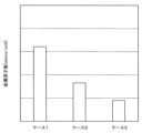
- (Case 1) A conventional heat treatment apparatus having no gas supply unit 344 was used. During the PEB process, the central exhaust portion 317 exhausted and the processing gas was discharged from the shower head 311, but the peripheral exhaust portion 323 did not exhaust.
- (Case 2) The heat treatment apparatus 40 shown in FIG. 4 and the like was used. Evacuation by the peripheral exhaust part 323 and ejection of the processing gas from the shower head 311 were performed so that the gas supply from the gas supply part 344 was continued from the start to the end of the PEB process. Further, during the PEB process, no exhaust was performed by the central exhaust section 317 at all. (Case 3) The heat treatment apparatus 40 shown in FIG. 4 and the like was used.
- Evacuation by the peripheral exhaust part 323 and ejection of the processing gas from the shower head 311 were performed so that the gas supply from the gas supply part 344 was continued from the start to the end of the PEB process.
- the central exhaust part 317 performed exhaust from the middle of the PEB process to the end of the PEB process.
- Heat treatment apparatus 200 Control unit 300 Chamber 310 Ceiling unit 311 shower head 317 Central exhaust unit 323 Peripheral exhaust unit 328 Hot plate 344 Gas supply unit K1 Processing space W Wafer
Landscapes
- Physics & Mathematics (AREA)
- Engineering & Computer Science (AREA)
- Plasma & Fusion (AREA)
- Chemical & Material Sciences (AREA)
- Analytical Chemistry (AREA)
- Exposure Of Semiconductors, Excluding Electron Or Ion Beam Exposure (AREA)
Priority Applications (6)
| Application Number | Priority Date | Filing Date | Title |
|---|---|---|---|
| KR1020237016180A KR102945105B1 (ko) | 2021-09-06 | 2021-09-06 | 열처리 장치, 열처리 방법 및 기억 매체 |
| JP2022571247A JP7432770B2 (ja) | 2021-09-06 | 2021-09-06 | 熱処理装置、熱処理方法及び記憶媒体 |
| US18/040,669 US20240234174A1 (en) | 2021-09-06 | 2021-09-06 | Thermal treatment apparatus, thermal treatment method, and storage medium |
| CN202180063042.8A CN116097399A (zh) | 2021-09-06 | 2021-09-06 | 热处理装置、热处理方法以及存储介质 |
| PCT/JP2021/032713 WO2023032214A1 (ja) | 2021-09-06 | 2021-09-06 | 熱処理装置、熱処理方法及び記憶媒体 |
| JP2024015515A JP7742438B2 (ja) | 2021-09-06 | 2024-02-05 | 熱処理装置、熱処理方法及び記憶媒体 |
Applications Claiming Priority (1)
| Application Number | Priority Date | Filing Date | Title |
|---|---|---|---|
| PCT/JP2021/032713 WO2023032214A1 (ja) | 2021-09-06 | 2021-09-06 | 熱処理装置、熱処理方法及び記憶媒体 |
Publications (1)
| Publication Number | Publication Date |
|---|---|
| WO2023032214A1 true WO2023032214A1 (ja) | 2023-03-09 |
Family
ID=85411114
Family Applications (1)
| Application Number | Title | Priority Date | Filing Date |
|---|---|---|---|
| PCT/JP2021/032713 Ceased WO2023032214A1 (ja) | 2021-09-06 | 2021-09-06 | 熱処理装置、熱処理方法及び記憶媒体 |
Country Status (5)
| Country | Link |
|---|---|
| US (1) | US20240234174A1 (https=) |
| JP (2) | JP7432770B2 (https=) |
| KR (1) | KR102945105B1 (https=) |
| CN (1) | CN116097399A (https=) |
| WO (1) | WO2023032214A1 (https=) |
Families Citing this family (1)
| Publication number | Priority date | Publication date | Assignee | Title |
|---|---|---|---|---|
| CN121419569A (zh) * | 2024-07-24 | 2026-01-27 | 盛美半导体设备(上海)股份有限公司 | 基板热处理装置、热处理方法及涂覆显影设备 |
Citations (5)
| Publication number | Priority date | Publication date | Assignee | Title |
|---|---|---|---|---|
| JP2016115919A (ja) * | 2014-12-10 | 2016-06-23 | 東京エレクトロン株式会社 | 加熱処理装置、加熱処理方法及び記憶媒体 |
| JP2018098229A (ja) * | 2016-12-08 | 2018-06-21 | 東京エレクトロン株式会社 | 基板処理方法及び熱処理装置 |
| JP2018137308A (ja) * | 2017-02-21 | 2018-08-30 | 東京エレクトロン株式会社 | 基板処理装置及び基板処理方法 |
| JP2020129607A (ja) * | 2019-02-08 | 2020-08-27 | 東京エレクトロン株式会社 | 基板処理装置及び基板処理方法 |
| JP2021068886A (ja) * | 2019-10-17 | 2021-04-30 | 東京エレクトロン株式会社 | 基板処理装置、基板処理方法、及び記憶媒体 |
Family Cites Families (7)
| Publication number | Priority date | Publication date | Assignee | Title |
|---|---|---|---|---|
| JP2564288B2 (ja) * | 1987-01-23 | 1996-12-18 | 株式会社日立製作所 | ベ−ク装置 |
| JP3547724B2 (ja) * | 2001-09-25 | 2004-07-28 | 沖電気工業株式会社 | レジストパターンのベーク装置及びレジストパターンの形成方法 |
| JP3989221B2 (ja) * | 2001-10-25 | 2007-10-10 | 東京エレクトロン株式会社 | 熱処理装置および熱処理方法 |
| JP2004260117A (ja) | 2003-02-27 | 2004-09-16 | Nikon Corp | ステージ装置、露光装置、及びデバイス製造方法 |
| JP2005129698A (ja) | 2003-10-23 | 2005-05-19 | Matsushita Electric Ind Co Ltd | 半導体装置の製造装置および製造方法 |
| US9310684B2 (en) | 2013-08-22 | 2016-04-12 | Inpria Corporation | Organometallic solution based high resolution patterning compositions |
| JP7359680B2 (ja) | 2019-07-22 | 2023-10-11 | 東京エレクトロン株式会社 | 熱処理装置及び処理方法 |
-
2021
- 2021-09-06 WO PCT/JP2021/032713 patent/WO2023032214A1/ja not_active Ceased
- 2021-09-06 KR KR1020237016180A patent/KR102945105B1/ko active Active
- 2021-09-06 US US18/040,669 patent/US20240234174A1/en active Pending
- 2021-09-06 JP JP2022571247A patent/JP7432770B2/ja active Active
- 2021-09-06 CN CN202180063042.8A patent/CN116097399A/zh active Pending
-
2024
- 2024-02-05 JP JP2024015515A patent/JP7742438B2/ja active Active
Patent Citations (5)
| Publication number | Priority date | Publication date | Assignee | Title |
|---|---|---|---|---|
| JP2016115919A (ja) * | 2014-12-10 | 2016-06-23 | 東京エレクトロン株式会社 | 加熱処理装置、加熱処理方法及び記憶媒体 |
| JP2018098229A (ja) * | 2016-12-08 | 2018-06-21 | 東京エレクトロン株式会社 | 基板処理方法及び熱処理装置 |
| JP2018137308A (ja) * | 2017-02-21 | 2018-08-30 | 東京エレクトロン株式会社 | 基板処理装置及び基板処理方法 |
| JP2020129607A (ja) * | 2019-02-08 | 2020-08-27 | 東京エレクトロン株式会社 | 基板処理装置及び基板処理方法 |
| JP2021068886A (ja) * | 2019-10-17 | 2021-04-30 | 東京エレクトロン株式会社 | 基板処理装置、基板処理方法、及び記憶媒体 |
Also Published As
| Publication number | Publication date |
|---|---|
| JP7742438B2 (ja) | 2025-09-19 |
| JP2024056775A (ja) | 2024-04-23 |
| JP7432770B2 (ja) | 2024-02-16 |
| KR20240050299A (ko) | 2024-04-18 |
| JPWO2023032214A1 (https=) | 2023-03-09 |
| KR102945105B1 (ko) | 2026-03-30 |
| US20240234174A1 (en) | 2024-07-11 |
| CN116097399A (zh) | 2023-05-09 |
Similar Documents
| Publication | Publication Date | Title |
|---|---|---|
| KR102753390B1 (ko) | 열처리 방법 및 열처리 장치 | |
| KR101878992B1 (ko) | 소수화 처리 장치, 소수화 처리 방법 및 컴퓨터 기억 매체 | |
| US7797855B2 (en) | Heating apparatus, and coating and developing apparatus | |
| JP4601080B2 (ja) | 基板処理装置 | |
| WO2004109779A1 (ja) | 基板の処理膜の表面荒れを改善する方法及び基板の処理装置 | |
| CN101840151A (zh) | 涂布显影装置、涂布显影方法和存储介质 | |
| KR102188354B1 (ko) | 기판 처리 장치 및 방법 | |
| JP7742438B2 (ja) | 熱処理装置、熱処理方法及び記憶媒体 | |
| US20230393483A1 (en) | Heat treatment apparatus, heat treatment method, and recording medium | |
| JP3909574B2 (ja) | レジスト塗布装置 | |
| TWI902892B (zh) | 熱處理裝置、熱處理方法及記錄媒體 | |
| JP7158549B2 (ja) | 基板処理方法、基板処理システム及びコンピュータ読み取り可能な記憶媒体 | |
| JP4066255B2 (ja) | 基板の処理装置及び基板の処理方法 | |
| TW202601299A (zh) | 熱處理裝置、熱處理方法及記錄媒體 | |
| TW202323985A (zh) | 基板處理裝置及基板處理方法 | |
| US20240347354A1 (en) | Heat-treating method, heat-treating apparatus, and storage medium | |
| JP2001210584A (ja) | シリル化処理装置及びシリル化処理方法 | |
| KR20250015377A (ko) | 기판처리장치 및 기판처리방법 |
Legal Events
| Date | Code | Title | Description |
|---|---|---|---|
| ENP | Entry into the national phase |
Ref document number: 2022571247 Country of ref document: JP Kind code of ref document: A |
|
| WWE | Wipo information: entry into national phase |
Ref document number: 18040669 Country of ref document: US |
|
| 121 | Ep: the epo has been informed by wipo that ep was designated in this application |
Ref document number: 21956099 Country of ref document: EP Kind code of ref document: A1 |
|
| NENP | Non-entry into the national phase |
Ref country code: DE |
|
| 122 | Ep: pct application non-entry in european phase |
Ref document number: 21956099 Country of ref document: EP Kind code of ref document: A1 |