WO2023026919A1 - 画素回路、表示パネルおよび表示装置 - Google Patents
画素回路、表示パネルおよび表示装置 Download PDFInfo
- Publication number
- WO2023026919A1 WO2023026919A1 PCT/JP2022/031053 JP2022031053W WO2023026919A1 WO 2023026919 A1 WO2023026919 A1 WO 2023026919A1 JP 2022031053 W JP2022031053 W JP 2022031053W WO 2023026919 A1 WO2023026919 A1 WO 2023026919A1
- Authority
- WO
- WIPO (PCT)
- Prior art keywords
- transistor
- potential
- signal
- input
- light emitting
- Prior art date
Links
- 230000006870 function Effects 0.000 claims description 359
- 101000739577 Homo sapiens Selenocysteine-specific elongation factor Proteins 0.000 description 81
- 102100037498 Selenocysteine-specific elongation factor Human genes 0.000 description 81
- 230000007423 decrease Effects 0.000 description 62
- 238000010586 diagram Methods 0.000 description 58
- 238000012937 correction Methods 0.000 description 44
- 239000000758 substrate Substances 0.000 description 37
- 238000006243 chemical reaction Methods 0.000 description 35
- 230000007850 degeneration Effects 0.000 description 32
- 230000000694 effects Effects 0.000 description 14
- 238000013459 approach Methods 0.000 description 8
- 101001063555 Canis lupus familiaris Epididymal sperm-binding protein 1 Proteins 0.000 description 7
- 238000005401 electroluminescence Methods 0.000 description 7
- 239000010409 thin film Substances 0.000 description 7
- 239000011521 glass Substances 0.000 description 5
- 239000011159 matrix material Substances 0.000 description 5
- 239000003086 colorant Substances 0.000 description 4
- 238000000034 method Methods 0.000 description 4
- 238000009877 rendering Methods 0.000 description 4
- 230000007547 defect Effects 0.000 description 3
- 239000003990 capacitor Substances 0.000 description 2
- 239000000969 carrier Substances 0.000 description 2
- 238000005229 chemical vapour deposition Methods 0.000 description 2
- 239000004020 conductor Substances 0.000 description 2
- 230000002950 deficient Effects 0.000 description 2
- 239000000919 ceramic Substances 0.000 description 1
- 239000002131 composite material Substances 0.000 description 1
- 230000001419 dependent effect Effects 0.000 description 1
- 230000006866 deterioration Effects 0.000 description 1
- 230000009977 dual effect Effects 0.000 description 1
- 239000005337 ground glass Substances 0.000 description 1
- 230000010354 integration Effects 0.000 description 1
- 239000002184 metal Substances 0.000 description 1
- 239000000203 mixture Substances 0.000 description 1
- 238000012986 modification Methods 0.000 description 1
- 230000004048 modification Effects 0.000 description 1
- 230000000149 penetrating effect Effects 0.000 description 1
- 229910021420 polycrystalline silicon Inorganic materials 0.000 description 1
- 229920005591 polysilicon Polymers 0.000 description 1
- 239000004065 semiconductor Substances 0.000 description 1
- 230000009131 signaling function Effects 0.000 description 1
- 238000012546 transfer Methods 0.000 description 1
Images


Classifications
-
- G—PHYSICS
- G09—EDUCATION; CRYPTOGRAPHY; DISPLAY; ADVERTISING; SEALS
- G09F—DISPLAYING; ADVERTISING; SIGNS; LABELS OR NAME-PLATES; SEALS
- G09F9/00—Indicating arrangements for variable information in which the information is built-up on a support by selection or combination of individual elements
- G09F9/30—Indicating arrangements for variable information in which the information is built-up on a support by selection or combination of individual elements in which the desired character or characters are formed by combining individual elements
-
- G—PHYSICS
- G09—EDUCATION; CRYPTOGRAPHY; DISPLAY; ADVERTISING; SEALS
- G09G—ARRANGEMENTS OR CIRCUITS FOR CONTROL OF INDICATING DEVICES USING STATIC MEANS TO PRESENT VARIABLE INFORMATION
- G09G3/00—Control arrangements or circuits, of interest only in connection with visual indicators other than cathode-ray tubes
- G09G3/20—Control arrangements or circuits, of interest only in connection with visual indicators other than cathode-ray tubes for presentation of an assembly of a number of characters, e.g. a page, by composing the assembly by combination of individual elements arranged in a matrix no fixed position being assigned to or needed to be assigned to the individual characters or partial characters
- G09G3/22—Control arrangements or circuits, of interest only in connection with visual indicators other than cathode-ray tubes for presentation of an assembly of a number of characters, e.g. a page, by composing the assembly by combination of individual elements arranged in a matrix no fixed position being assigned to or needed to be assigned to the individual characters or partial characters using controlled light sources
- G09G3/30—Control arrangements or circuits, of interest only in connection with visual indicators other than cathode-ray tubes for presentation of an assembly of a number of characters, e.g. a page, by composing the assembly by combination of individual elements arranged in a matrix no fixed position being assigned to or needed to be assigned to the individual characters or partial characters using controlled light sources using electroluminescent panels
- G09G3/32—Control arrangements or circuits, of interest only in connection with visual indicators other than cathode-ray tubes for presentation of an assembly of a number of characters, e.g. a page, by composing the assembly by combination of individual elements arranged in a matrix no fixed position being assigned to or needed to be assigned to the individual characters or partial characters using controlled light sources using electroluminescent panels semiconductive, e.g. using light-emitting diodes [LED]
- G09G3/3208—Control arrangements or circuits, of interest only in connection with visual indicators other than cathode-ray tubes for presentation of an assembly of a number of characters, e.g. a page, by composing the assembly by combination of individual elements arranged in a matrix no fixed position being assigned to or needed to be assigned to the individual characters or partial characters using controlled light sources using electroluminescent panels semiconductive, e.g. using light-emitting diodes [LED] organic, e.g. using organic light-emitting diodes [OLED]
- G09G3/3225—Control arrangements or circuits, of interest only in connection with visual indicators other than cathode-ray tubes for presentation of an assembly of a number of characters, e.g. a page, by composing the assembly by combination of individual elements arranged in a matrix no fixed position being assigned to or needed to be assigned to the individual characters or partial characters using controlled light sources using electroluminescent panels semiconductive, e.g. using light-emitting diodes [LED] organic, e.g. using organic light-emitting diodes [OLED] using an active matrix
- G09G3/3233—Control arrangements or circuits, of interest only in connection with visual indicators other than cathode-ray tubes for presentation of an assembly of a number of characters, e.g. a page, by composing the assembly by combination of individual elements arranged in a matrix no fixed position being assigned to or needed to be assigned to the individual characters or partial characters using controlled light sources using electroluminescent panels semiconductive, e.g. using light-emitting diodes [LED] organic, e.g. using organic light-emitting diodes [OLED] using an active matrix with pixel circuitry controlling the current through the light-emitting element
-
- H—ELECTRICITY
- H05—ELECTRIC TECHNIQUES NOT OTHERWISE PROVIDED FOR
- H05B—ELECTRIC HEATING; ELECTRIC LIGHT SOURCES NOT OTHERWISE PROVIDED FOR; CIRCUIT ARRANGEMENTS FOR ELECTRIC LIGHT SOURCES, IN GENERAL
- H05B33/00—Electroluminescent light sources
- H05B33/02—Details
Definitions
- the present disclosure relates to pixel circuits, display panels, and display devices.
- a plurality of scanning signal lines and a plurality of image signal lines are arranged in a grid pattern, and a plurality of pixel units are arranged in a matrix corresponding to each intersection of the plurality of scanning signal lines and the plurality of image signal lines.
- a display device having an image display unit that is designed to display images (see Patent Documents 1 and 2).
- a pixel circuit, a display panel and a display device are disclosed.
- One aspect of the pixel circuit includes a first power supply potential input section, a second power supply potential input section, and a plurality of elements.
- the first power supply potential input section supplies a first power supply potential.
- the second power supply potential input section supplies a second power supply potential lower than the first power supply potential.
- the plurality of elements are connected in series or cascade between the first power supply potential input section and the second power supply potential input section.
- the plurality of elements includes a light emitting element, a first transistor, and a second transistor.
- the first transistor is connected in series to the light emitting element, and controls current flowing through the light emitting element by inputting a potential corresponding to an image signal to a gate electrode.
- the second transistor is cascaded to the first transistor and switches the light emitting element between a light emitting state and a non-light emitting state. Either one of the first potential and the second potential is selectively input to the gate electrode of the second transistor.
- the first potential is a potential equal to or higher than the first power supply potential or lower than the second power supply potential for setting the second transistor to a non-conducting state in which current cannot flow between the source electrode and the drain electrode.
- the second potential is a potential between the first power potential and the second power potential for causing a current to flow between the source electrode and the drain electrode of the second transistor.
- One aspect of a display panel is a display panel including a plurality of pixel circuits according to the above aspect, wherein the first potential or the second potential is applied to the gate electrode of the second transistor in each of the plurality of pixel circuits. and a control unit that selectively outputs the
- One aspect of the pixel circuit includes a light-emitting element, a first transistor, and a second transistor, and includes a control section.
- the first transistor is connected in series to the light emitting element, and controls current flowing through the light emitting element by inputting a potential corresponding to an image signal to a gate electrode.
- the second transistor is cascaded to the first transistor and switches the light emitting element between a light emitting state and a non-light emitting state.
- the control unit has a function of a plurality of switch elements that switch-control the second transistor. A signal relating to ON or OFF of each of the functions of the plurality of switch elements is selectively input to the control unit.
- the control unit connects the light-emitting element to the gate electrode of the second transistor in a non-light-emitting state in response to an input of a signal relating to turning off the function of one or more switch elements among the functions of the plurality of switch elements.
- Output the potential for The control unit causes the gate electrode of the second transistor to cause the light emitting element to emit light in response to an input of a signal relating to ON of each of the functions of all the switching elements among the functions of the plurality of switching elements.
- One aspect of the display panel includes a plurality of pixel circuits and a control section having the functions of a plurality of switch elements.
- Each of the plurality of pixel circuits includes a light emitting element, a first transistor, and a second transistor.
- the first transistor is connected in series to the light emitting element, and controls current flowing through the light emitting element by inputting a potential corresponding to an image signal to a gate electrode.
- the second transistor is cascaded to the first transistor and switches the light emitting element between a light emitting state and a non-light emitting state.
- a signal relating to ON or OFF of each of the functions of the plurality of switch elements is selectively input to the control unit.
- the control unit controls the gate electrode of the second transistor in each of the plurality of pixel circuits in response to input of a signal relating to turning off one or more of the functions of the plurality of switch elements. , a potential for setting the light-emitting element to a non-light-emitting state is output.
- the control unit controls the gate electrode of the second transistor in each of the plurality of pixel circuits in response to the input of a signal relating to ON of each of the functions of all the switching elements among the functions of the plurality of switching elements. , a potential for setting the light-emitting element to a light-emitting state is output.
- One aspect of the display device includes the display panel of any one aspect described above and a drive unit.
- the driving section is located on the side opposite to the display surface of the display panel, and is electrically connected to the pixel circuit.
- FIG. 1 is a front view schematically showing an example of a display device according to each embodiment.
- FIG. 2 is a back view schematically showing an example of the display device according to each embodiment.
- FIG. 3 is a block circuit diagram schematically showing an example of the configuration of the display device according to each embodiment.
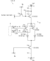
- FIG. 4 is a circuit diagram showing an example of a first sub-pixel circuit according to the first embodiment;
- FIG. 5 is a gate circuit diagram schematically showing a configuration example of an input/output gate of a control section.
- FIG. 6 is a circuit diagram showing an example of a control unit.
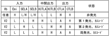
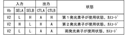
- FIG. 7 is a truth table showing an example of the relationship between the input and output of the control section and the state of the first sub-pixel circuit.
- FIG. 8 is a block circuit diagram showing an example of connection between a control section and a plurality of sub-pixel circuits.
- FIG. 9 is a block circuit diagram showing an example of connection between a control unit and a plurality of pixel circuits.
- FIG. 10 is a circuit diagram showing a first sub-pixel circuit according to another example of the first embodiment;
- FIG. 11 is a circuit diagram showing an example of a first subpixel circuit according to the second embodiment.
- FIG. 12 is a gate circuit diagram schematically showing a configuration example related to input/output gates of the control section.
- FIG. 13 is a circuit diagram showing an example of a control unit;
- FIG. 13 is a circuit diagram showing an example of a control unit;
- FIG. 14 is a truth table showing an example of the relationship between the input, the intermediate output signal, the output, and the state of the first sub-pixel circuit in the control section.
- FIG. 15 is a block circuit diagram showing an example of a signal output circuit that outputs a setting control signal to the control section.
- FIG. 16 is a block circuit diagram showing an example of connections between a control section, a signal output circuit, and a plurality of sub-pixel circuits.
- FIG. 17 is a block circuit diagram showing an example of connections between a control section, a signal output circuit, and a plurality of pixel circuits.
- FIG. 18 is a circuit diagram showing an example of a first sub-pixel circuit according to the third embodiment; FIG.
- FIG. 19 is a gate circuit diagram schematically showing one configuration example related to the input/output gates of the control section.
- FIG. 20 is a circuit diagram showing an example of a control unit;
- FIG. 21 is a truth table showing an example of the relationship between the input and output of the control section and the state of the first sub-pixel circuit.
- FIG. 22 is a circuit diagram showing an example of a first sub-pixel circuit according to the fourth embodiment;
- FIG. 23 is a truth table showing an example of the relationship between the input and output of the control section and the state of the first sub-pixel circuit.
- FIG. 24 is a circuit diagram showing an example of a first sub-pixel circuit according to the fifth embodiment;
- FIG. 25 is a truth table showing an example of the relationship between the input, the intermediate output signal, the output, and the state of the first sub-pixel circuit in the control section.
- FIG. 26 is a circuit diagram showing an example of the first sub-pixel circuit according to the sixth embodiment.
- FIG. 27 is a truth table showing an example of the relationship between the input and output of the control section and the state of the first sub-pixel circuit.
- FIG. 28 is a circuit diagram showing an example of a first sub-pixel circuit according to the seventh embodiment;
- FIG. 29 is a gate circuit diagram schematically showing one configuration example related to the input/output gates of the control section.
- FIG. 30 is a truth table showing an example of the relationship between the input and output of the control section and the state of the first sub-pixel circuit.
- FIG. 31 is a circuit diagram showing an example of a first sub-pixel circuit according to another example of the seventh embodiment
- FIG. 32 is a truth table showing an example of the relationship between the input and output of the control section and the state of the first sub-pixel circuit.
- FIG. 33 is a circuit diagram showing an example of a first sub-pixel circuit according to the eighth embodiment;
- FIG. 34 is a truth table showing an example of the relationship between the input and output of the control section and the state of the first sub-pixel circuit.
- FIG. 35 is a circuit diagram showing an example of the first sub-pixel circuit according to the ninth embodiment.
- FIG. 36 is a truth table showing an example of the relationship between the input and output of the control section and the state of the first sub-pixel circuit.
- FIG. 37 is a circuit diagram showing an example of a first sub-pixel circuit in which an N-channel transistor is applied as the first transistor.
- FIG. 38 is a circuit diagram showing an example of a first sub-pixel circuit incorporating a threshold voltage correction circuit.
- FIG. 39 is a timing chart showing an example of the operation of the first sub-pixel circuit incorporating the threshold voltage correction circuit.
- FIG. 40 is a front view schematically showing an example of a tiling display.
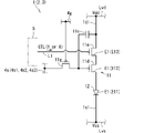
- FIG. 41 is a circuit diagram schematically showing a circuit configuration of a sub-pixel portion according to the first reference example.
- FIG. 42 is a circuit diagram schematically showing a circuit configuration of a sub-pixel portion according to the second reference example.
- FIG. 43 is a circuit diagram schematically showing a circuit configuration of a sub-pixel portion according to the third reference example.
- FIG. 44 is a circuit diagram schematically showing a circuit configuration of a sub-pixel portion according to the fourth reference example.
- pixel circuits, display panels, and display devices of the present disclosure are described below.
- First, the configuration that is the premise of the pixel circuit of the present disclosure will be described using first to fourth reference examples shown in FIGS. 41 to 44 .
- the display device a plurality of scanning signal lines and a plurality of image signal lines are arranged in a lattice, and a plurality of pixel portions are arranged in a matrix in a manner corresponding to intersections of the plurality of scanning signal lines and the plurality of image signal lines. has an image display unit arranged in a row.
- each pixel portion includes a subpixel portion including a first light emitting element that emits light of a first color, a subpixel portion including a second light emitting element that emits light of a second color, and a sub-pixel portion including a third light-emitting element that emits light of a third color.
- the display device can display a color image or the like. Red, green and blue can be applied for the first, second and third colors.
- FIG. 41 is a circuit diagram schematically showing the circuit configuration of the sub-pixel portion 915 according to the first reference example.
- Each sub-pixel portion 915 includes a light emitting element 914 and a light emission control portion 922 that controls light emission, non-light emission, light emission intensity, and the like of the light emitting element 914 .
- a micro light emitting diode (LED) element, an organic electroluminescence (EL) element, or the like is applied to the light emitting element 914 .
- Light emitting element 914 is located on an insulating layer disposed on a first surface of a substrate such as a glass plate.
- the light emitting element 914 is electrically connected to the light emission control section 922 and the second power supply potential input section 917 via through conductors arranged in through holes penetrating the insulating layer arranged in the pixel section.
- a positive electrode of the light emitting element 914 is connected to the first power supply potential input section 916 via the light emission control section 922 .
- a negative electrode of the light emitting element 914 is connected to the second power supply potential input section 917 .
- the first power supply potential input section 916 may be a first power supply potential terminal or a first power supply potential input line.
- the second power supply potential input section 917 may be a second power supply potential terminal or a second power supply potential input line.
- the light emission control unit 922 includes a selection transistor 912 , a drive transistor 913 , a capacitive element 918 and a light emission control transistor 919 .
- the selection transistor 912 is a transistor that functions as a switch for inputting an image signal to the sub-pixel portion 915 .
- a P-channel thin film transistor also referred to as a P-channel transistor or the like is used as the selection transistor 912 .
- a gate electrode of the selection transistor 912 is connected to the scanning signal line 902 .
- a source electrode of the selection transistor 912 is connected to the image signal line 903 .
- a drain electrode of the selection transistor 912 is connected to a gate electrode of the drive transistor 913 .
- an ON signal (Low (L) signal) as a scanning signal from the scanning signal line 902 is input to the gate electrode of the selection transistor 912
- the selection transistor 912 allows current to flow between the source electrode and the drain electrode. It is in a conductive state (also called an ON state or a closed state as a switch).
- the image signal from the image signal line 903 is applied to the gate electrode of the driving transistor 913 through the selection transistor 912 .
- the driving transistor 913 receives the potential difference (Vdd ⁇ Vss) between the first power supply potential Vdd applied by the first power supply potential input section 916 and the second power supply potential Vss applied by the second power supply potential input section 917 and the image signal line 903 . It functions as an element (also referred to as a driving element) that current-drives the light emitting element 914 according to the level (potential) of the image signal transmitted from the . In other words, the driving transistor 913 can control the current flowing through the light emitting element 914 .
- the first power supply potential input portion 916 is connected to a first power supply line Lvd as a power supply line on the positive power supply potential (also referred to as first power supply potential) side.
- the first power supply potential Vdd applied from the first power supply line Lvd to the first power supply potential input section 916 is set to approximately 3 volts (V) to 5V. Also, the first power supply potential Vdd may be about 8V to 15V.
- the second power supply potential input portion 917 is connected to a second power supply line Lvs as a power supply line on the negative power supply potential (also referred to as second power supply potential) side.
- the second power supply potential Vss applied from the second power supply line Lvs to the second power supply potential input section 917 is set to about -3V to 0V.
- the second power line Lvs may be a grounded ground line.
- a P-channel transistor or the like is applied to the driving transistor 913 .
- the source electrode of the driving transistor 913 is connected to the first power supply potential input section 916 .
- a drain electrode of the drive transistor 913 is connected to the second power supply potential input section 917 via the light emission control transistor 919 and the light emitting element 914 .
- a capacitive element 918 is arranged on a connection line that connects the gate electrode and the source electrode of the drive transistor 913 .
- the capacitive element 918 functions as a holding capacitor that holds the potential of the image signal input to the gate electrode of the driving transistor 913 for a period (also referred to as one frame period) until the next image signal is input (also referred to as rewriting). .
- the light emission control transistor 919 is arranged on the drive line 925 between the drive transistor 913 and the light emitting element 914 and can control light emission and non-light emission of the light emitting element 914 .
- a P-channel transistor or the like is applied to the light emission control transistor 919 .
- the source electrode of the emission control transistor 919 is connected to the drain electrode of the driving transistor 913 .
- the emission control transistor 919 is connected in cascade with the drive transistor 913 .
- the drain electrode of the light emission control transistor 919 is connected to the positive electrode of the light emitting element 914 .
- the gate electrode of the light emission control transistor 919 receives an L signal as a light emission control signal (also referred to as an Emi signal), the light emission control transistor 919 is turned on. Accordingly, a current (also referred to as driving current) flows from the first power supply potential input portion 916 to the light emitting element 914 through the driving transistor 913, the light emission control transistor 919, and the driving line 925, and the light emitting element 914 emits light. At this time, the intensity (luminance) of light emitted from the light emitting element 914 can be controlled by controlling the level (potential) of the image signal.
- the L signal functions as an ON signal capable of making the light emission control transistor 919 conductive (ON).
- a potential lower than the second power supply potential Vss supplied by the second power supply line Lvs can be applied to the potential (also referred to as L potential) Vgl of the L signal as the ON signal.
- the drive current does not sufficiently flow through the light-emitting element 914 , and the light-emitting element 914 does not operate. It may not emit light with the desired intensity. Further, even if the light-emitting element 914 is defective, such as a defect, deterioration, or breakage, in some sub-pixel portions 915 among the plurality of sub-pixel portions 915, the light-emitting element 914 does not emit light at a desired intensity. defects may occur.
- two light emitting elements 914 connected in parallel are arranged in each sub-pixel portion 915, and one of the two light emitting elements 914 having no defect is selected.
- a configuration that always emits light is conceivable.
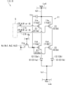
- FIG. 42 is a circuit diagram schematically showing the circuit configuration of the sub-pixel portion 915 according to the second reference example.
- the circuit of the sub-pixel portion 915 shown in FIG. 42 is based on the circuit of the sub-pixel portion 915 in FIG. 41 described above, with some configurations replaced with other configurations and additional configurations added. .
- part of the circuit configuration of the sub-pixel portion 915 in FIG. Of the circuit configuration of the sub-pixel portion 915 shown in FIG. A first light emitting element 914a and a second light emitting element 914b, a first switch 926a and a second switch 926b.
- the additional configuration in the circuit configuration of the sub-pixel portion 915 shown in FIG. 42 is the switching control portion 927 .
- the first drive line 925a and the second drive line 925b are connected to the light emission control section 922 and connected in parallel.
- one drive line 925 is a normal drive line (also referred to as a normal drive line)
- the other drive line 925 is a preliminary drive line (also called a redundant drive line).
- the first drive line 925a is connected to the positive electrode of the first light emitting element 914a
- the negative electrode of the first light emitting element 914a is connected to the second power supply potential input section 917.
- the second drive line 925b is connected to the positive electrode of the second light emitting element 914b, and the negative electrode of the second light emitting element 914b is connected to the second power supply potential input section 917.
- the first switch 926a is arranged on the first drive line 925a, and can set the first drive line 925a to a use state (also referred to as a drive state) or a non-use state (also referred to as a non-drive state).
- the second switch 926b is arranged on the second drive line 925b, and can set the second drive line 925b to a use state (drive state) or a non-use state (non-drive state).
- the switching control unit 927 sets one of the first switch 926a and the second switch 926b to a non-conducting state (also referred to as an OFF state or an open state as a switch) in which current cannot flow, and switches the other switch. Set to conductive state.
- a non-conducting state also referred to as an OFF state or an open state as a switch
- one of the first light emitting element 914a and the second light emitting element 914b as the two light emitting elements 914 which is not defective, can always emit light.
- a P-channel transistor or the like is applied to the first switch 926a and the second switch 926b. In this case, the P-channel transistor as the first switch 926 a is cascade-connected to the light emission control transistor 919 .
- the P-channel transistor as the second switch 926b is cascade-connected to the light emission control transistor 919 .
- the switching control section 927 inputs an on signal (Vga: L signal) to the gate electrode of the first switch 926a and turns off the gate electrode of the second switch 926b.
- a signal (Vgb: H signal) is input.
- a potential higher than the first power supply potential Vdd supplied by the first power supply line Lvd can be applied to the potential (also referred to as H potential) Vgh of the H signal as the off signal.
- the switching control section 927 inputs an off signal (Vga: H signal) to the gate electrode of the first switch 926a and turns on the gate electrode of the second switch 926b.
- Vga: H signal an off signal
- Vgb: L signal A signal
- the drain current (also called source-drain current) Ids as an output current can vary. Therefore, in any of the driving transistors 913 of the sub-pixel portions 915 according to the first and second reference examples, among the first power supply potential Vdd, the second power supply potential Vss, and the forward voltage applied to the light emitting element 914, A variation in one or more values of may vary the voltage Vds between the source and drain electrodes and the drain current Ids as the output current.
- the first power supply potential Vdd can drop according to the distance between the power supply and the portion of the first power supply line Lvd to which the first power supply potential input section 916 is connected.
- the second power supply potential Vss can rise according to the distance between the power supply and the portion of the second power supply line Lvs to which the second power supply potential input section 917 is connected.
- the forward voltage applied to the light emitting element 914 may vary depending on the characteristics of the light emitting element 914, such as luminous efficiency and internal resistance, and the setting values of the drive current, forward voltage, and luminance.
- the output resistance Ro1 the variation ⁇ Vds of the voltage between the drain electrode and the source electrode (also referred to as the voltage between the drain and the source) Vds, and the variation of the drain current Ids as the output current
- the output resistance Ro1 is small, the variation ⁇ Ids of the drain current Ids corresponding to the variation ⁇ Vds of the drain-source voltage Vds increases.
- Brightness unevenness includes brightness unevenness of a single color such as red (R), green (G), blue (B), or white (W).
- Color unevenness includes RGB mixture ratio unevenness.
- a transistor (also referred to as a cascode connection transistor) 920 that is connected in cascade to the drain electrode side of the driving transistor 913 and forms a cascode connection with the driving transistor 913 is provided.
- the cascode connection transistor 920 is a transistor having the same conductivity type as the driving transistor 913, and a predetermined potential (also referred to as an input potential) Vb between the first power supply potential Vdd and the second power supply potential Vss is input to the gate electrode. be done.
- the drain electrode of the P-channel transistor as the drive transistor 913 and the source electrode of the P-channel transistor as the cascode connection transistor 920 are connected, and the P-channel transistor as the cascode connection transistor 920 is connected.
- a drain electrode of the channel transistor and a source electrode of the P-channel transistor as the emission control transistor 919 are connected.
- the apparent output resistance Ro of the driving transistor 913 has a relationship of Ro ⁇ gm2 ⁇ Ro2 ⁇ Ro1. In other words, the output resistance of the drive transistor 913 is approximately (gm2 ⁇ Ro2) times due to the cascode connection provided by the cascode connection transistor 920 .
- the output resistance of the drive transistor 913 is approximately ten times as large.
- the variation ⁇ Ids of the drain current Ids with respect to the variation ⁇ Vds of the drain-source voltage Vds is approximately 1/10.
- the drain current is kept constant due to the channel length modulation effect. Fluctuations in Ids are less likely to occur.
- the light emission control transistor 919, the cascode connection transistor 920, and the first switch 926a or the second switch 926b are connected to the driving transistor 913.
- a plurality of transistors are connected in cascade, such as those applied to Therefore, in the potential difference (Vdd-Vss), the series resistance of the plurality of transistors connected in series with the drive transistor 913 accounts for a large proportion, and the drain-source voltage Vds of the drive transistor 913 becomes small.
- This problem is caused by a pixel in which a driving transistor 913 as a driving element for current-driving a light emitting element 914 and a plurality of transistors are connected in cascade between the first power supply potential input section 916 and the second power supply potential input section 917 . It can occur commonly in display devices having circuits.
- the display device has room for improvement in terms of improving image quality.
- the inventor of the present disclosure has created a technique capable of improving the image quality of display devices.
- the pixel circuit is connected in series with the light-emitting element, and is connected in tandem with the first transistor that controls the current flowing through the light-emitting element when a potential corresponding to an image signal is input to the gate electrode.
- the first transistor that controls the current flowing through the light-emitting element when a potential corresponding to an image signal is input to the gate electrode.
- a second transistor that switches the light-emitting element between a light-emitting state and a non-light-emitting state.
- a gate electrode of the second transistor is provided with a first potential higher than or equal to the first power supply potential or lower than the second power supply potential for setting a non-conducting state between the source electrode and the drain electrode of the second transistor, and One potential of a second potential between the first power potential and the second power potential that causes a current to flow between the source electrode and the drain electrode is selectively input.
- the second transistor is connected in tandem with the first transistor on the drain electrode side of the first transistor, inputting the second potential to the gate electrode of the second transistor causes the second transistor to form a cascode connection to the first transistor.
- the second potential is, for example, a potential lower than the drain potential of the first transistor for operating the first transistor in the saturation region.
- the second potential is, for example, a potential higher than the drain potential of the first transistor for operating the first transistor in the saturation region.
- the second potential is a potential that is applied to the gate electrode of the second transistor and causes the light emitting element to emit light. It is a potential for providing the second transistor with the function of an analog element having a linear relationship with the current.
- the second potential is a potential lower than the source potential of the first transistor.
- the first transistor and the second transistor are each of an N-channel type, the second potential is a potential higher than the source potential of the first transistor.
- the transistor connected in series with the first transistor may be only the second transistor. This makes it easier to drive the first transistor as the drive transistor in the saturation region. As a result, when the display device is viewed in plan, gradation in which the brightness gradually decreases is less likely to occur.
- the second potential is a potential lower than the drain potential of the first transistor.
- This second potential can be defined as, for example, the following potential.
- the second potential is the negative voltage that is the overdrive voltage of the first transistor and the gate-source voltage (gate voltage) of the second transistor, with the potential of the source electrode (source potential) of the first transistor as a reference. It should be less than the potential obtained by subtracting the sum of the negative voltage and the negative voltage.
- the overdrive voltage is a value obtained by subtracting the threshold voltage Vth1 (eg, about ⁇ 1 V) of the first transistor from the gate-source voltage (gate voltage) Vgs1 (eg, about ⁇ 1.5 V) in the first transistor. (eg, about -0.5V).
- the second potential may be a potential that is about 0.5V to 2V lower than the drain potential of the first transistor.
- the second potential may be a potential higher than the source potential of the first transistor by about 0.5V to 2V.
- FIG. 1 is a front view schematically showing an example of the display device 100 according to the first embodiment.
- FIG. 2 is a back view schematically showing an example of the display device 100 according to the first embodiment.
- FIG. 3 is a block circuit diagram schematically showing an example of the configuration of the display device 100 according to the first embodiment.
- the display device 100 includes a display panel 100p and a driving section 30.
- the display panel 100p includes a plurality of pixel circuits 10.
- the display panel 100p has a surface (also referred to as a display surface) Sf1 for displaying an image, and a surface (also referred to as an anti-display surface or a non-display surface) Sf2 opposite to the display surface Sf1.
- the display panel 100p has a rectangular flat plate shape, a trapezoidal flat plate shape, a circular flat plate shape, or the like when viewed from above.
- the display panel 100p includes a substrate 20 and a plurality of pixel circuits 10. FIG.
- the substrate 20 has a first surface (also referred to as a first main surface) F1, a second surface (also referred to as a second main surface) F2, and a plurality of side surfaces F3.
- the second surface F2 is a surface opposite to the first surface F1.
- the plurality of side faces F3 connect the first face F1 and the second face F2, respectively.
- a flat substrate is applied to the substrate 20 .
- a rectangular surface having four sides is applied to each of the first surface F1 and the second surface F2.
- the multiple side faces F3 include a first side face F31, a second side face F32, a third side face F33, and a fourth side face F34.
- the first side surface F31 connects the first side of the first surface F1 and the first side of the second surface F2.
- the first side surface F31 has the first side of the first surface F1 and the first side of the second surface F2 as two opposite sides.
- the second side surface F32 connects the second side of the first surface F1 and the second side of the second surface F2. In other words, the second side surface F32 has the second side of the first surface F1 and the second side of the second surface F2 as two opposite sides.
- the third side surface F33 connects the third side of the first surface F1 and the third side of the second surface F2. In other words, the third side surface F33 has the third side of the first surface F1 and the third side of the second surface F2 as two opposing sides.
- the fourth side surface F34 connects the fourth side of the first surface F1 and the fourth side of the second surface F2.
- the fourth side surface F34 has the fourth side of the first surface F1 and the fourth side of the second surface F2 as two opposite sides.
- the first surface F1 is a flat surface along the XZ plane and faces the -Y direction.
- the second surface F2 is a flat surface along the XZ plane and faces the +Y direction.
- the first side surface F31 faces the +Z direction.
- the second side face F32 faces the -X direction.
- the third side surface F33 faces the -Z direction.
- the fourth side surface F34 faces the +X direction.
- a glass plate is applied as the substrate 20 .
- the glass plate may or may not be transparent.
- the substrate 20 is a colored glass substrate, a ground glass substrate, a plastic substrate, a ceramic substrate, a metal substrate, or a composite substrate in which two or more of these substrates are laminated. may be
- the plurality of pixel circuits 10 are circuits that respectively constitute a pixel section.
- a plurality of pixel circuits 10 are arranged in a matrix.
- a plurality of pixel circuits 10 are arranged in a matrix on the first surface F ⁇ b>1 of the substrate 20 .
- the plurality of pixel circuits 10 constitute one column of pixel circuits 10
- the plurality of pixel circuits 10 constitute one row of pixel circuits 10 . More specifically, pixel circuits 10 of n rows ⁇ m columns (n and m are natural numbers) are arranged.
- the plurality of pixel circuits 10 constitute a portion (also referred to as an image display portion) 300 that displays an image.
- the image display unit 300 is located on the first surface F1 side of the substrate 20 .
- the surface of the image display unit 300 facing the -Y direction constitutes the display surface Sf1 of the display panel 100p.
- the image display section 300 may be positioned so as to cover substantially the entire surface of the first surface F1.
- the display device 100 has a structure in which the image display section 300 is arranged on the entire surface (also referred to as a frameless structure) or a frame portion around the image display section 300 on one side of the substrate 20 on the first surface F1 side. It has a structure that is made as narrow as possible (also called a narrow frame structure).
- Each of the plurality of pixel circuits 10 has a plurality of sub-pixel circuits.
- the plurality of sub-pixel circuits are circuits forming sub-pixel portions included in the pixel portion.
- the plurality of sub-pixel circuits includes a first sub-pixel circuit 1, a second sub-pixel circuit 2 and a third sub-pixel circuit 3.
- the first sub-pixel circuit 1 can emit light of a first color.
- the second sub-pixel circuit 2 can emit light of a second color different from the first color.
- the third sub-pixel circuit 3 can emit light of a third color different from the first and second colors. Red, green and blue are applied to the first, second and third colors.
- each pixel circuit 10 a first subpixel circuit 1, a second subpixel circuit 2, and a third subpixel circuit 3 are arranged in order in the row direction.
- a plurality of first subpixel circuits 1 constitute one row of first subpixel circuits 1
- a plurality of second subpixel circuits 2 constitute one row of second subpixel circuits 2
- a plurality of second subpixel circuits 2 constitute one row of second subpixel circuits 2
- the three sub-pixel circuits 3 constitute one row of third sub-pixel circuits 3
- a plurality of first subpixel circuits 1 constitute a row of first subpixel circuits 1
- a plurality of second subpixel circuits 2 constitute a row of second subpixel circuits 2
- a plurality of third subpixel circuits 2 constitute a row of second subpixel circuits 2.
- the sub-pixel circuits 3 form a column of third sub-pixel circuits 3 .
- the first subpixel circuit 1, the second subpixel circuit 2 and the third subpixel circuit 3 may be arranged in any order.
- the drive unit 30 is electrically connected to each of the plurality of pixel circuits 10.
- the drive unit 30 is located on the side opposite to the display surface Sf2 of the display panel 100p.
- the driving section 30 is positioned on the second surface F2 side of the substrate 20 .
- a driving element such as an integrated circuit (IC) or a large-scale integration (LSI) is mounted on the second surface F2 of the substrate 20 in a chip-on-glass (COG) method. It can be formed by mounting on.
- the drive unit 30 may be a circuit board on which drive elements are mounted.
- the driving unit 30 includes low temperature polysilicon (LTPS) directly formed on the second surface F2 of the substrate 20 by a thin film forming method such as a chemical vapor deposition (CVD) method.
- a thin film circuit also referred to as a thin film circuit including a thin film transistor (TFT) having a semiconductor layer of .
- the drive unit 30 connects wiring (also referred to as back wiring) W2 positioned on the second surface F2 of the substrate 20 and wiring (also referred to as side wiring) W3 positioned on the side surface F3 of the substrate 20. It is electrically connected to the image display section 300 positioned on the first surface F1 side of the substrate 20 by a plurality of wirings included therein. Therefore, multiple wirings are included in the display panel 100p.
- the display panel 100p includes a plurality of image signal lines 4s, a plurality of scanning signal lines (also referred to as gate signal lines) 4g, and a plurality of emission control signal lines 4e.
- the plurality of scanning signal lines 4g and the plurality of image signal lines 4s are arranged in a grid pattern.
- the display panel 100p also includes a scanning signal line driving section 30g and a light emission control signal line driving section 30e.
- Each of the plurality of image signal lines 4s transmits a signal (also referred to as an image signal) for controlling the degree of light emission to the first subpixel circuit 1, the second subpixel circuit 2, and the third subpixel circuit 3. be able to.
- the image signal line 4 s is positioned along one column of pixel circuits 10 .
- three image signal lines 4s are positioned along one column of pixel circuits 10 .
- the three image signal lines 4s are a first image signal line (also referred to as a first image signal line) 4s1, a second image signal line (also referred to as a second image signal line) 4s2, and a third image signal line. lines (also referred to as third image signal lines) 4s3.
- a first image signal line 4s1 located along one column of first sub-pixel circuits 1 and one column of second sub-pixel circuits 2 are positioned.
- the first image signal line 4s1 is electrically connected to each of the plurality of first sub-pixel circuits 1 forming one column
- the second image signal line 4s2 is It is electrically connected to each of the second sub-pixel circuits 2 forming one column
- the third image signal line 4s3 is electrically connected to each of the third sub-pixel circuits 3 forming one column.
- An image signal can be supplied from the drive unit 30 to each of the plurality of image signal lines 4s.
- the drive unit 30 may time-divisionally supply image signals to the plurality of image signal lines 4s via a time-divisional selector circuit or the like.
- One selector circuit is arranged for the pixel circuits 10 in each column, and the image signals supplied from the driving unit 30 to the selector circuit are transferred to the first image signal line 4s1 and the second image signal line 4s2 by the selector circuit. , and the third image signal line 4s3 may be supplied time-sequentially (line-sequentially).
- a configuration having three transfer gate elements or the like is applied to the selector circuit.
- the selector circuit may be arranged in the empty area of the image display section 300 on the first surface F ⁇ b>1 of the substrate 20 , or may be arranged in the frame portion outside the image display section 300 .
- Each of the plurality of scanning signal lines 4g is a signal (also called a scanning signal) for controlling the timing of inputting an image signal to each of the first subpixel circuit 1, the second subpixel circuit 2, and the third subpixel circuit 3. ) can be transmitted.
- One scanning signal line 4 g is positioned along one row of pixel circuits 10 .
- the Mth scanning signal line 4g is positioned along the row of the pixel circuits 10 of the Mth row (M is a natural number). Then, for each of the plurality of first sub-pixel circuits 1, the plurality of second sub-pixel circuits 2 and the plurality of third sub-pixel circuits 3 included in the pixel circuit 10 of the M-th row, the M-th scanning signal line is provided. 4g are electrically connected.
- Scanning signals can be supplied to the plurality of scanning signal lines 4g in a time-sequential manner (line-sequential manner) from a scanning signal line driving section 30g.
- Various circuits such as a shift register are applied to the scanning signal line driving section 30g.
- the scanning signal line driver 30 g is located on the first surface F 1 of the substrate 20 .
- the scanning signal line driving section 30 g may be arranged in the empty area of the image display section 300 or may be arranged in the frame portion outside the image display section 300 .
- the scanning signal line driving section 30g can supply scanning signals to the plurality of scanning signal lines 4g time-sequentially (line-sequentially) in response to signals from the driving section 30 .
- the emission control signal line 4e can transmit a signal for controlling emission timing (also referred to as emission control signal) to each of the first subpixel circuit 1, the second subpixel circuit 2, and the third subpixel circuit 3. can.
- One light emission control signal line 4 e is positioned along one row of pixel circuits 10 .
- the Mth emission control signal line 4e is positioned along the row of the pixel circuits 10 of the Mth row (M is a natural number). Then, each of the plurality of first sub-pixel circuits 1, the plurality of second sub-pixel circuits 2 and the plurality of third sub-pixel circuits 3 included in the pixel circuit 10 of the M-th row is supplied with the M-th light emission control signal.
- a line 4e is electrically connected.
- Light emission control signals can be supplied to the plurality of light emission control signal lines 4e in time sequence (line sequence) from the light emission control signal line driving section 30e.
- Various circuits such as a shift register are applied to the light emission control signal line driving section 30e.
- the light emission control signal line driver 30 e is located on the first surface F 1 of the substrate 20 .
- the light emission control signal line driving section 30 e may be arranged in an empty area of the image display section 300 or may be arranged in a frame portion outside the image display section 300 .
- the light emission control signal line drive unit 30e can supply light emission control signals to the plurality of light emission control signal lines 4e in time sequence (line sequence) in response to signals from the drive unit 30.
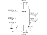
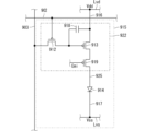
- FIG. 4 is a circuit diagram showing an example of the first sub-pixel circuit 1 according to the first embodiment.
- the first subpixel circuit 1 has the same or similar configuration.
- each of the second subpixel circuit 2 and the third subpixel circuit 3 has the same or similar configuration as the first subpixel circuit 1 .
- the first subpixel circuit 1 is connected in series or cascade between the first power supply potential input section 1dl, the second power supply potential input section 1sl, and the first power supply potential input section 1dl and the second power supply potential input section 1sl. and a plurality of elements E1.
- the first power supply potential input section 1dl can supply the first power supply potential Vdd.
- the first power supply potential input section 1dl is connected to the first power supply line Lvd.
- the first power supply line Lvd is connected to a power supply that applies the first power supply potential Vdd to the first power supply line Lvd.
- the first power supply potential Vdd can be set to any positive potential. A mode in which the first power supply potential Vdd is set to about 8V is conceivable.
- the second power supply potential input section 1sl can supply a second power supply potential Vss that is lower than the first power supply potential Vdd.
- the second power supply potential input section 1sl is connected to the second power supply line Lvs.
- the second power supply line Lvs is connected to a power supply that applies the second power supply potential Vss to the second power supply line Lvs.
- the second power supply potential Vss may be a positive potential or a negative potential as long as it is lower than the first power supply potential Vdd. A mode in which the second power supply potential Vss is set to about 0V is conceivable.
- the second power line Lvs may be a grounded ground line.
- the multiple elements E1 include the light emitting element 12 as the first element E11, the first transistor 11d as the second element E12, and the second transistor 11e as the third element E13.
- the first transistor 11d as the second element E12, the second transistor 11e as the third element E13 between the first power supply potential input section 1dl and the second power supply potential input section 1sl, the first transistor 11d as the second element E12, the second transistor 11e as the third element E13,
- the light emitting element 12 as the first element E11 is connected in series or cascade in the order of this description.
- the first subpixel circuit 1 includes the third transistor 11g and the capacitive element 11c.
- the light emission of the light emitting element 12 can be controlled by the light emission control section 11 having the first transistor 11d, the second transistor 11e, the third transistor 11g, and the capacitive element 11c. More specifically, the light emission control unit 11 can control light emission, non-light emission, light emission intensity, and the like of the light emitting element 12 .
- the light emitting element 12 can emit light of a predetermined color.
- the light emitting element 12 of the first sub-pixel circuit 1 can emit light of a first color.
- the light emitting element 12 of the two sub-pixel circuit 2 can emit light of a second color.
- the light emitting element 12 of the third sub-pixel circuit 3 can emit light of a third color.
- a micro light emitting diode (LED) element, an organic electroluminescence (EL) element, or the like is applied to the light emitting element 12 .
- a micro LED element or an organic EL element that emits light of a first color is applied to the light emitting element 12 of the first sub-pixel circuit 1 .
- a micro LED element or an organic EL element that emits light of the second color is applied to the light emitting element 12 of the second sub-pixel circuit 2 .
- a micro LED element or an organic EL element that emits light of a third color is applied to the light emitting element 12 of the third sub-pixel circuit 3 .
- the first transistor 11 d is connected in series with the light emitting element 12 .
- the first transistor 11d can control the current flowing through the light emitting element 12 by inputting a potential corresponding to an image signal to the gate electrode.
- the first transistor 11d can control the current flowing through the light emitting element 12 by inputting a potential corresponding to the image signal input from the first image signal line 4s1 to the gate electrode.
- the first transistor 11d has the potential difference (Vdd ⁇ Vss) between the first power supply potential Vdd and the second power supply potential Vss and the level of the image signal transmitted from the first image signal line 4s1 (potential ) and functions as an element (also referred to as a driving element) for current-driving the light emitting element 12 .
- a P-channel type thin film transistor (P-channel transistor) or the like is applied to the first transistor 11d.
- the source electrode of the first transistor 11d is connected to the first power supply potential input section 1dl.
- a drain electrode of the first transistor 11 d is connected to the second power supply potential input section 1 sl via the second transistor 11 e and the light emitting element 12 .
- the first transistor 11d changes to the source electrode. and the drain electrode (also referred to as a conductive state or an ON state).
- a drive current can flow from the first power supply potential input section 1dl to the light emitting element 12 via the first transistor 11d and the second transistor 11e.
- the light emission intensity (luminance) of the light emitting element 12 can be controlled according to the level (potential) of the image signal.
- the first transistor 11 d can control the light emission intensity of the light emitting element 12 .
- an image signal is input from the second image signal line 4s2 instead of the first image signal line 4s1.
- an image signal is input from the third image signal line 4s3 instead of the first image signal line 4s1.
- the third transistor 11g functions as an element for inputting an image signal into the light emission control section 11.
- a P-channel transistor or the like is applied to the third transistor 11g.
- the gate electrode of the third transistor 11g is connected to the scanning signal line 4g.
- a source electrode (drain electrode) of the third transistor 11g is connected to the first image signal line 4s1.
- the drain electrode (source electrode) of the third transistor 11g is connected to the gate electrode of the first transistor 11d.
- the image signal from the first image signal line 4s1 is input to the gate electrode of the first transistor 11d through the third transistor 11g.
- a signal also referred to as an L signal
- Vss the second power supply potential
- the L potential Vgl is set from about -2V to 0V.
- the source electrode (drain electrode) of the third transistor 11g is connected to the second image signal line 4s2 instead of the first image signal line 4s1.
- An image signal is input from the second image signal line 4s2 instead of 4s1.
- the source electrode (drain electrode) of the third transistor 11g is connected to the third image signal line 4s3 instead of the first image signal line 4s1. is inputted from the third image signal line 4s3.
- the capacitive element 11c is located on a connection line connecting the gate electrode and the source electrode of the first transistor 11d.
- the capacitive element 11c functions as a holding capacitor that holds the potential Vsig of the image signal input to the gate electrode of the first transistor 11d for a period (one frame period) until the next image signal is input (rewritten).
- the second transistor 11e is cascade-connected to the first transistor 11d.
- the second transistor 11e can switch the light-emitting element 12 between a state in which it emits light (also referred to as a light-emitting state) and a state in which it does not emit light (also referred to as a non-light-emitting state).
- the second transistor 11e functions as an element for controlling light emission and non-light emission of the light emitting element 12 (also referred to as light emission control element).
- the second transistor 11e is located on a connection line (also called a drive line) that connects the first transistor 11d and the light emitting element 12 .
- a transistor of the same conductivity type as the first transistor 11d is applied to the second transistor 11e.
- the conductivity types include a P-type in which the carriers that generate a current between the source and drain electrodes are holes, and an N-type in which the carriers that generate a current between the source and drain electrodes are electrons.
- a P-channel transistor or the like is applied to the second transistor 11e.
- the second transistor 11e is cascade-connected to the first transistor 11d on the drain electrode side of the first transistor 11d. More specifically, the source electrode of the second transistor 11e is connected to the drain electrode of the first transistor 11d.
- a light emitting element 12 is connected to the drain electrode of the second transistor 11e. More specifically, the anode electrode (positive electrode) of the light emitting element 12 is connected to the drain electrode of the second transistor 11e.
- a cathode electrode (negative electrode) of the light emitting element 12 is connected to the second power supply potential input section 1sl.
- the first potential V1 or the second potential V2 is selectively input to the gate electrode of the second transistor 11e.
- the first potential V1 is a potential (also referred to as an off potential) for setting the second transistor 11e to a state in which current cannot flow between the source electrode and the drain electrode (also referred to as a non-conducting state or an off state).
- the first potential V1 is set to a potential equal to or higher than the first power supply potential Vdd. More specifically, as the first potential V1, the potential (H potential) Vgh of a High (H) signal serving as an off signal for bringing the second transistor 11e into a non-conducting state (off state) is applied.
- the first potential V1 is set from 8V to about 10V.
- the second potential V2 is a potential for causing current to flow between the source electrode and the drain electrode of the second transistor 11e.
- the second potential V2 is set to a potential between the first power potential Vdd and the second power potential Vss.
- the second potential V2 is set to a potential that is less than the first power supply potential Vdd and greater than the second power supply potential Vss.
- the second potential V2 can be set to any analog potential between the L potential and the H potential, instead of digital discrete values such as the L potential and the H potential.
- the second potential V2 is set to a potential higher than 0V and lower than 8V.
- the signal having the second potential V2 is also called an analog (A) signal as appropriate.
- the light-emitting element 12 is in a light-emitting state (light-emitting state).
- the second transistor 11e is cascade-connected to the drain electrode side of the first transistor 11d and has the same conductivity type as the first transistor 11d.
- a second potential V2 between the second power supply potential Vss is input. Therefore, the second transistor 11e forms a cascode connection with the first transistor 11d.
- the output resistance of the first transistor 11d is Ro1
- the output resistance of the second transistor 11e is Ro2
- the mutual conductance of the second transistor 11e is gm2.
- the apparent output resistance Ro of the first transistor 11d has a relationship of Ro ⁇ gm2 ⁇ Ro2 ⁇ Ro1. Therefore, the cascode connection by the second transistor 11e increases the output resistance of the first transistor 11d by approximately (gm2 ⁇ Ro2). Specifically, if (gm2 ⁇ Ro2) is set to about 10, the output resistance of the first transistor 11d will be about 10 times.
- the variation ⁇ Ids of the drain current Ids as the output current with respect to the variation ⁇ Vds of the voltage Vds between the drain electrode and the source electrode (also referred to as the drain-source voltage) is about 1/ Become 10.
- the drain voltage is reduced by the channel length modulation effect. Fluctuations in the current Ids are less likely to occur. As a result, uneven brightness and uneven color are less likely to occur in the display device 100 .
- the second transistor 11e functions as an analog element that forms a cascode connection with the first transistor 11d in addition to the function of a switch that switches the light emitting element 12 between the light emitting state and the non-light emitting state. It also has functions.
- the effect of the cascode connection to the first transistor 11d by the second transistor 11e can be obtained without increasing the number of transistors connected in cascade with the first transistor 11d. Therefore, among the potential difference (Vdd ⁇ Vss) between the first power supply potential Vdd and the second power supply potential Vss, the drain-source voltage Vds of the first transistor 11d is less likely to decrease.
- the second potential V2 can be appropriately set before the display panel 100p or the display device 100 is shipped.
- the second potential V2 includes the conductivity types of the first transistor 11d and the second transistor 11e, the first power supply potential Vdd, the second power supply potential Vss, and the threshold voltage (also referred to as the first threshold voltage) Vth1 of the first transistor 11d. and the threshold voltage (also referred to as a second threshold voltage) Vth2 of the second transistor 11e and the range of the potential Vin according to the image signal input to the gate electrode of the first transistor 11d.
- both the first transistor 11d and the second transistor 11e are P-channel transistors, the first power supply potential Vdd is 8V, the second power supply potential Vss is 0V, and the first threshold voltage Vth1 is -1V. , the second threshold voltage Vth2 is ⁇ 1V, and the minimum value of the value range of the potential Vin is 5V.
- the pinch-off voltage (also referred to as first pinch-off voltage) Vdsat1 of the first transistor 11d is a value obtained by subtracting the first threshold voltage Vth1 from the gate voltage (also referred to as first gate voltage) Vgs1 of the first transistor 11d.
- the first pinch-off voltage Vdsat1 is larger than the source-drain voltage Vds of the first transistor 11d, and the relationship (Vdsat1>Vds) is satisfied, and the first transistor 11d is driven in the saturation region.
- the pinch-off voltage (also referred to as the second pinch-off voltage) Vsat2 of the second transistor 11e is a value obtained by subtracting the second threshold voltage Vth2 from the gate voltage (also referred to as the second gate voltage) Vgs2 of the second transistor 11e.
- a setting in which the second pinch-off voltage Vdsat2 is closer to 0 V than the first pinch-off voltage Vdsat1 and the setting in which the second transistor 11e is driven in the saturation region is adopted.
- the second gate voltage Vgs2 is ⁇ 2 V, which is the sum of ⁇ 1 V as the second pinch-off voltage Vdsat2 and ⁇ 1 V as the second threshold voltage Vth2. becomes. Then, it is conceivable to set the second potential V2 to 3V, which is a value obtained by adding -2V as the second gate voltage Vgs2 to 5V as the drain potential of the first transistor 11d.
- the second transistor 11e is connected in series with the first transistor 11d.
- the drain-source voltage Vds of the first transistor 11d is less likely to decrease.
- the first transistor 11d is driven in the saturation region. Conditions are unlikely to be severe. Therefore, gradation (brightness unevenness) in which the brightness gradually decreases is less likely to occur in the display device 100, and the image quality of the display device 100 can be improved.
- the first potential V1 or the second potential V2 is selectively output from the control section 5 to the gate electrode of the second transistor 11e.
- the controller 5 can selectively output the first potential V1 or the second potential V2 to the gate electrode of the second transistor 11e.
- the light emitting element 12 of each of the sub-pixel circuits 1, 2 and 3 emits light. It can be switched between a state and a non-luminous state.
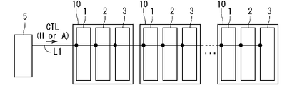
- the control unit 5 is connected to the gate electrode of the second transistor 11e via a signal line (also called a potential output signal line) L1. Thereby, the control unit 5 can output a signal (also referred to as a switching control signal) CTL to the gate electrode of the second transistor 11e via the potential output signal line L1.
- a signal also referred to as a switching control signal
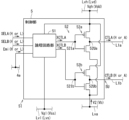
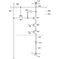
- FIG. 5 is a diagram schematically showing a configuration example related to input/output of the control unit 5.
- the control unit 5 has a function of an element (also referred to as a switch element) that performs switch control of the second transistor 11e.
- the switch control includes control to selectively switch the second transistor 11e between a state in which a current flows between the source electrode and the drain electrode and a state in which the current does not flow.
- the function of the switch element includes the function of selectively setting the light emitting element 12 to a light emitting state or a non-light emitting state. As shown in FIG.
- the control unit 5 has a portion (also referred to as a signal input unit) 5I to which a signal is input and a portion (also referred to as a signal output unit) 5U to output a signal.
- the signal input section 5I can be configured by, for example, a plurality of terminals or a plurality of wirings.
- the signal output unit 5U may be configured by, for example, one or more terminals or one or more wirings.
- a signal relating to ON or OFF is selectively input to 5I, which is also called a signal input section of the control section 5, and the second potential V2 is also input.
- a signal for setting the light emitting element 12 to the non-light emitting state which is input to the control unit 5 from the light emission control signal line 4e, is applied as the off signal.
- An H signal is applied to a signal related to OFF, and an L signal is applied to a signal related to ON.
- an H signal or an L signal is selectively input to the controller 5 as a light emission control signal (also referred to as an Emi signal) from the light emission control signal line 4e.
- the second potential V2 is input to the control unit 5 from a wiring (also referred to as a second potential supply line) Lva that supplies the second potential V2.
- the second potential supply line Lva is connected to a power supply that applies the second potential V2 to the second potential supply line Lva.
- the control section 5 outputs the first potential V1 from the signal output section 5U to the gate electrode of the second transistor 11e in response to the input of the signal relating to turning off to the signal input section 5I.
- the control unit 5 in response to the input of the H signal as the signal relating to turning off to the signal input unit 5I, the control unit 5 outputs the voltage of the second transistor 11e from the signal output unit 5U via the potential output signal line L1.
- An H signal having the first potential V1 is output to the gate electrode.
- the control unit 5 applies the second potential V2 to the gate electrode of the second transistor 11e from the signal output unit 5U in response to the input of the signal relating to ON and the input of the second potential V2 to the signal input unit 5I. Output.
- control unit 5 causes the signal output unit 5U to output the potential output signal line L1 in response to the input of the L signal as the signal relating to ON to the signal input unit 5I and the input of the second potential V2.
- a signal having the second potential V2 is output to the gate electrode of the second transistor 11e via the second transistor 11e.
- the control unit 5 supplies the gate electrode of the second transistor 11e via the potential output signal line L1 with an H signal as an off signal having the first potential V1 or the second potential V2 as the switching control signal CTL. can selectively output an A signal having
- one second transistor 11e is used to function as a switch for switching the light-emitting element 12 between a light-emitting state and a non-light-emitting state, and to function as an analog element that forms a cascode connection with the first transistor 11d. and can be easily realized.
- control unit 5 can control the timing of light emission of the light emitting element 12 by the function of the switch element.
- the H potential Vgh may be input to the control unit 5 from a wiring Lvh for supplying the H potential Vgh (also referred to as an H potential supply line or a high potential supply line), or an L potential Vgl.
- the L potential Vgl may be input from a wiring (also referred to as an L potential supply line or a low potential supply line) Lvl that supplies the L potential Vgl.
- the H-potential supply line Lvh is connected to a power supply that applies an H-potential Vgh to the H-potential supply line Lvh.
- the L potential supply line Lvl is connected to a power supply that applies an L potential Vgl to the L potential supply line Lvl.
- the controller 5 may receive the first power supply potential Vdd from the first power supply line Lvd.
- the control unit 5 may receive the second power supply potential Vss from the second power supply line Lvs instead of the L potential Vgl from the L potential supply line Lvl.
- FIG. 6 is a circuit diagram showing an example of the control unit 5.
- the control section 5 has a logic circuit section 51 and a potential conversion section 52 .
- the logic circuit section 51 appropriately converts the light emission control signal input from the light emission control signal line 4 e and outputs it to the potential conversion section 52 .
- a NOT gate 51n is applied to the logic circuit section 51.
- FIG. In this case, when an H signal is input from the light emission control signal line 4 e , the logic circuit section 51 converts it into an L signal and outputs it to the potential conversion section 52 .
- the logic circuit section 51 converts it into an H signal and outputs it to the potential conversion section 52 .
- the potential conversion section 52 converts it into an H signal as an OFF signal having the first potential V1 and outputs the H signal. Further, when the H signal is input from the logic circuit section 51, the potential conversion section 52 converts it into an A signal having the second potential V2 and outputs the A signal.
- a circuit similar to a CMOS type NOT circuit is applied to the potential converter 52 as an inverting logic circuit.
- the potential converter 52 includes a P-channel transistor and an N-channel thin film transistor which are connected in series between an H potential supply line Lvh that supplies an H potential Vgh and a second potential supply line Lva that supplies a second potential V2. (also referred to as an N-channel transistor).
- the source electrode of the P-channel transistor is connected to the H potential supply line Lvh
- the drain electrode of the P-channel transistor is connected to the drain electrode of the N-channel transistor
- the source electrode of the N-channel transistor is connected to the H potential supply line Lvh. It is connected to the second potential supply line Lva.
- the portion where the gate electrode of the P-channel transistor and the gate electrode of the N-channel transistor are connected is the input section 52I, and the drain electrode of the P-channel transistor and the drain electrode of the N-channel transistor are connected.
- the portion that is marked is the output section 52U.
- the potential conversion section 52 When an L signal is input from the logic circuit section 51 to the input section 52I, the potential conversion section 52 outputs an H signal as an OFF signal having the first potential V1 from the output section 52U. Further, when the H signal is input from the logic circuit section 51 to the input section 52I, the potential conversion section 52 outputs the A signal having the second potential V2 from the output section 52U.
- the output section 52U of the potential conversion section 52 is connected to the potential output signal line L1.
- the control unit 5 outputs the second transistor 11e from the signal output unit 5U via the potential output signal line L1 in response to the input of the H signal as a signal relating to turning off the light emission control signal to the signal input unit 5I. can output the first potential V1 to the gate electrode of the . Further, the control unit 5 outputs the potential output signal line L1 from the signal output unit 5U to the signal input unit 5I in response to the input of the L signal as a signal relating to the ON state of the light emission control signal and the input of the second potential V2. to output the second potential V2 to the gate electrode of the second transistor 11e.
- FIG. 7 is a truth table showing an example of the relationship between the input and output of the control section 5 and the state of the first sub-pixel circuit 1.
- the control unit 5 outputs the potential (also referred to as input potential) Vb input from the second potential supply line Lva, the light emission control signal input from the light emission control signal line 4e, and the potential output signal line L1.
- the switching control signal CTL is designed in a manner that satisfies the relationship shown in FIG.
- the control unit 5 If the input potential Vb input to the control unit 5 from the second potential supply line Lva is an arbitrary potential and the light emission control signal input to the control unit 5 is an H signal as a signal relating to turning off, the control unit 5 , the switching control signal CTL output to the potential output signal line L1 becomes an H signal having the first potential V1. At this time, the gate electrode of the second transistor 11e receives an H signal as an off signal having the first potential V1, so that the second transistor 11e becomes non-conductive. As a result, the light-emitting element 12 enters a non-light-emitting state in which it does not emit light.
- the input potential Vb input to the control unit 5 from the second potential supply line Lva is the second potential V2
- the light emission control signal input to the control unit 5 is an L signal as a signal relating to ON
- the switching control signal CTL output from the control section 5 to the potential output signal line L1 becomes the A signal having the second potential V2.
- the A signal having the second potential V2 is input to the gate electrode of the second transistor 11e, and current flows between the source electrode and the drain electrode of the second transistor 11e.
- the light emitting element 12 emits light
- the second transistor 11e forms a cascode connection with the first transistor 11d.
- the L signal may be applied to the off signal, and the H signal may be applied to the on signal.
- the control section 5 does not have the logic circuit section 51, and the light emission control signal input from the light emission control signal line 4e may be directly input to the input section 52I of the potential conversion section 52.
- the control unit 5 in response to the input of the L signal as a signal relating to OFF from the light emission control signal line 4e to the signal input unit 5I, the control unit 5 outputs from the signal output unit 5U through the potential output signal line L1, A first potential V1 can be output to the gate electrode of the second transistor 11e.
- the control unit 5 outputs a potential from the signal output unit 5U in response to the input of the H signal as a signal relating to ON from the light emission control signal line 4e and the input of the second potential V2 to the signal input unit 5I.
- a second potential V2 can be output to the gate electrode of the second transistor 11e via the signal line L1.
- Each pixel circuit 10 includes a control section 5 that selectively outputs the first potential V1 or the second potential V2 to each of the first subpixel circuit 1, the second subpixel circuit 2 and the third subpixel circuit 3.
- FIG. 8 is a block circuit diagram showing an example of connection between the control section 5 and the plurality of sub-pixel circuits 1, 2 and 3. As shown in FIG. As shown in FIG. 8, a configuration in which a potential output signal line L1 connected to the control section 5 is connected to a plurality of sub-pixel circuits 1, 2 and 3 can be adopted. With this configuration, the number of control units 5 in one pixel circuit 10 is less likely to increase, and the number of pixel circuits 10 is less likely to increase. Accordingly, in the display device 100 and the display panel 100p, it is possible to narrow the pitch at which the plurality of pixel circuits 10 are arranged, thereby improving the resolution. Therefore, the image quality of the display device 100 can be improved.
- the display panel 100p may include a control section 5 that selectively outputs the first potential V1 or the second potential V2 to each of the plurality of pixel circuits 10.
- the control unit 5 can selectively output the first potential V1 or the second potential V2 to the gate electrode of the second transistor 11e in each of the plurality of pixel circuits 10.
- the control unit 5 may be arranged on the first surface F1 of the substrate 20 in the empty area or frame portion of the image display unit 300, or may be arranged on the second surface F2 of the substrate 20. good.
- the control unit 5 can be arranged for each of the plurality of pixel circuits 10 forming one row of pixel circuits 10 .
- FIG. 9 is a block circuit diagram showing an example of connection between the control section 5 and the plurality of pixel circuits 10.
- a configuration in which the potential output signal line L1 connected to the control section 5 is connected to a plurality of pixel circuits 10 can be adopted. More specifically, a configuration is adopted in which the potential output signal line L1 connected to the control unit 5 is connected to a plurality of sub-pixel circuits 1, 2, and 3 included in each of the plurality of pixel circuits 10. can be With this configuration, one control unit 5 is provided for a plurality of pixel circuits 10, and the number of pixel circuits 10 is less likely to increase. Accordingly, in the display device 100 and the display panel 100p, it is possible to narrow the pitch at which the plurality of pixel circuits 10 are arranged, thereby improving the resolution. Therefore, the image quality of the display device 100 can be improved.
- the control unit 5 outputs the gate electrode of the second transistor 11e in each of the plurality of pixel circuits 10 from the signal output unit 5U in response to the input of the signal related to turning off the function of the switch element to the signal input unit 5I.
- the control unit 5 outputs from the signal output unit 5U to the plurality of pixels included in the plurality of pixel circuits 10 in response to the input of a signal relating to turning off the function of the switch element to the signal input unit 5I.
- a first potential V1 as an off potential can be output to the gate electrode of the second transistor 11e in each of the sub-pixel circuits 1, 2, and 3.
- the control unit 5 in response to the input of the H signal as a signal relating to turning off the function of the switch element to the signal input unit 5I, the control unit 5 outputs a plurality of voltages from the signal output unit 5U via the potential output signal line L1.
- an H signal as an off signal having the first potential V1 can be output to the gate electrode of the second transistor 11e in each of the pixel circuits 10 of FIG.
- the control unit 5 in response to the input of the H signal as a signal relating to turning off the function of the switch element to the signal input unit 5I, the control unit 5 outputs the voltage from the signal output unit 5U through the potential output signal line L1.
- the gate electrode of the second transistor 11e in each of the plurality of sub-pixel circuits 1, 2, 3 included in the plurality of pixel circuits 10 can output an H signal as an off signal having the first potential V1.
- the control unit 5 In response to the input of a signal relating to ON of the function of the switch element to the signal input unit 5I and the input of the second potential V2, the control unit 5 outputs the second potential in each of the plurality of pixel circuits 10 from the signal output unit 5U.
- a second potential V2 can be output to the gate electrode of the transistor 11e. More specifically, the control unit 5 outputs a plurality of pixel circuits from the signal output unit 5U to the signal input unit 5I in response to the input of a signal relating to ON of the function of the switch element and the input of the second potential V2.
- a second potential V2 can be output to the gate electrode of the second transistor 11e in each of the plurality of subpixel circuits 1, 2, and 3 included in 10, respectively.
- control unit 5 causes the signal output unit 5U to output potential from the signal output unit 5U in response to the input of the L signal as a signal relating to ON of the function of the switch element to the signal input unit 5I and the input of the second potential V2.
- An A signal having the second potential V2 can be output to the gate electrode of the second transistor 11e in each of the plurality of pixel circuits 10 via the signal line L1.
- the control unit 5 in response to the input of the L signal as a signal relating to the ON of the function of the switch element to the signal input unit 5I and the input of the second potential V2, the control unit 5 outputs from the signal output unit 5U, A signal having the second potential V2 is output to the gate electrode of the second transistor 11e in each of the plurality of sub-pixel circuits 1, 2 and 3 included in the plurality of pixel circuits 10 through the potential output signal line L1.
- control unit 5 outputs an OFF signal having the first potential V1 as the switching control signal CTL to the gate electrode of the second transistor 11e in each of the plurality of pixel circuits 10 via the potential output signal line L1. or an A signal having the second potential V2 can be selectively output. More specifically, the control unit 5 controls the gate electrode of the second transistor 11e in each of the plurality of sub-pixel circuits 1, 2, 3 included in the plurality of pixel circuits 10 via the potential output signal line L1. In addition, as the switching control signal CTL, an H signal as an off signal having a first potential V1 or an A signal having a second potential V2 can be selectively output.
- the plurality of elements E1 connected in series or cascade between the first power supply potential input section 1dl and the second power supply potential input section 1sl are the light emitting elements 12 as the first elements E11, Elements other than the first transistor 11d as the second element E12 and the second transistor 11e as the third element E13 may be included.
- the light emitting element 12 as the first element E11 is connected in parallel, and the light emitting element 12 (first light emitting element 12a) and the light emitting element 12 (also referred to as the second light emitting element 12b) as the second first element (also referred to as the 1B element) E11b.
- the plurality of elements E1 serves as a first fourth element (also referred to as a 4A element) E14a connected in series to the first light emitting element 12a, and a fourth transistor 13 (also referred to as a 4A transistor 13a).
- a fourth transistor 13 also referred to as a 4th B transistor 13b
- a second fourth element also referred to as a 4th B element
- FIG. 10 is a circuit diagram showing the first sub-pixel circuit 1 according to another example of the first embodiment. Also in another example of the first embodiment, each of the second subpixel circuit 2 and the third subpixel circuit 3 has the same or similar configuration as the first subpixel circuit 1 .
- the first sub-pixel circuit 1 according to another example of the first embodiment is based on the example of the first sub-pixel circuit 1 according to the first embodiment shown in FIG.
- two subpixel circuits are connected in parallel between the second transistor 11e and the second power supply potential input section 1sl. It includes a set of fourth transistors 13 and a light emitting element 12 .
- the fourth transistor 13 and the light emitting element 12 are connected in series.
- the two series-connected sets of the fourth transistor 13 and the light-emitting element 12 are a series-connected set of the 4A transistor 13a and the first light-emitting element 12a, and a series-connected set of the 4B transistor 13b and the light-emitting element 12. and a set of second light emitting elements 12b.
- the first subpixel circuit 1 includes two sets of multiple elements E1 connected in series or cascade between the first power supply potential input section 1dl and the second power supply potential input section 1sl. .
- the two sets of elements E1 include a first set of elements E1 and a second set of elements E1.
- the plurality of elements E1 in the first set includes a first light emitting element 12a as a first element (first A element) E11a, a first transistor 11d as a second element E12, and a third element E13 as It includes a second transistor 11e and a 4A transistor 13a as a first fourth element (4A element) E14a.
- first transistor 11d as the second element E12
- second transistor 11e as the third element E13
- the 4th A transistor 13a as the 4th A element E14a and the first light emitting element 12a as the 1st A element E11a are connected in series or cascade in this order.
- the second set of multiple elements E1 includes a second light emitting element 12b as a second first element (first B element) E11b, a first transistor 11d as a second element E12, and a third element E13 as It includes a second transistor 11e and a fourth B transistor 13b as a second fourth element (fourth B element) E14b.
- the fourth B transistor 13b as the fourth B element E14b and the second light emitting element 12b as the first B element E11b are connected in series or tandem in this order.
- the 4th A transistor 13a is cascade-connected to the first transistor 11d and the second transistor 11e.
- the fourth A transistor 13a is located on a connection line (drive line) connecting the second transistor 11e and the first light emitting element 12a.
- a P-channel transistor is applied to the 4th A transistor 13a, the source electrode of the 4th A transistor 13a is connected to the drain electrode of the second transistor 11e, and the drain electrode of the 4th A transistor 13a is connected to the first light emitting element 12a.
- the 4A transistor 13a is an element (also referred to as a use state setting element) for selectively setting the first light emitting element 12a to a state in which it is used (also referred to as a use state) or a state in which it is not used (also referred to as a non-use state).
- the fourth A transistor 13a is in a state in which current cannot flow between the source electrode and the drain electrode (non-conducting state) and a and the drain electrode (conducting state). Assume that a P-channel transistor is applied to the fourth A transistor 13a.
- the setting control unit 7 may be a control circuit included in each of the plurality of sub-pixel circuits 1, 2, 3, or may be a control circuit included in each of the plurality of pixel circuits 10. , it may be a control circuit included in each of the plurality of pixel circuits 10 in the display panel 100p, or may be a control circuit included in the driving section 30.
- the fourth B transistor 13b is cascade-connected to the first transistor 11d and the second transistor 11e.
- the fourth B transistor 13b is located on a connection line (drive line) that connects the second transistor 11e and the second light emitting element 12b.
- a P-channel transistor is applied to the fourth B transistor 13b, the source electrode of the fourth B transistor 13b is connected to the drain electrode of the second transistor 11e, and the drain electrode of the fourth B transistor 13b is connected to the second light emitting element 12b.
- the 4B transistor 13b has a function of an element (use state setting element) for selectively setting the second light emitting element 12b to a state of use (use state) or a state of not using it (non-use state).
- the fourth B transistor 13b is switched between a non-conducting state and a conducting state according to an H signal or an L signal selectively input from the setting control section 7.
- FIG. Assume that a P-channel transistor is applied to the fourth B transistor 13b.
- the 4B transistor 13b becomes non-conducting and the second light emitting element 12b is set to the non-use state.
- the L signal is input to the gate electrode of the 4B transistor 13b, the 4B transistor 13b becomes conductive and the second light emitting element 12b is set to use.
- an N-channel transistor may be applied to the 4th A transistor 13a
- an N-channel transistor may be applied to the 4th B transistor 13b.
- the fourth A transistor 13a is an N-channel transistor.
- the 4A transistor 13a becomes non-conductive and the first light emitting element 12a is set to a non-use state.
- the H signal is input to the gate electrode of the 4th A transistor 13a
- the 4th A transistor 13a becomes conductive, and the first light emitting element 12a is set to the use state.
- the fourth B transistor 13b is an N-channel transistor.
- the 4B transistor 13b becomes non-conducting and the second light emitting element 12b is set to the non-use state.
- the 4B transistor 13b becomes conductive and the second light emitting element 12b is set to use.
- the 4A transistor 13a may be positioned between the first light emitting element 12a and the second power supply potential input section 1sl
- the 4B transistor 13b may be positioned between the second light emitting element 12b and the second power supply potential input section 1sl. It may be positioned between the power supply potential input section 1sl.
- the pixel circuit 10 includes the light emitting element 12, the first transistor 11d, and the second transistor connected in series or cascade between the first power supply potential input section 1dl and the second power supply potential input section 1sl. 11e.
- the first transistor 11d can control the current flowing through the light emitting element 12 by inputting a potential corresponding to the image signal to the gate electrode.
- the second transistor 11e is cascade-connected to the first transistor 11d, and can switch the light-emitting element 12 between a light-emitting state and a non-light-emitting state.
- the second transistor 11e is of the same conductivity type as the first transistor 11d, and is connected in series with the first transistor 11d on the drain side of the first transistor 11d.
- a light emitting element 12 is connected to the drain electrode of the second transistor 11e.
- the gate electrode of the second transistor 11e has a first potential V1 for setting the second transistor 11e in a non-conducting state and a potential V1 for causing a current to flow between the source electrode and the drain electrode of the second transistor 11e. Either one of the second potential V2 between the first power potential Vdd and the second power potential Vss is selectively input.
- the second transistor 11e functions not only as a switch for switching the light-emitting element 12 between the light-emitting state and the non-light-emitting state, but also as an analog element that forms a cascode connection with the first transistor 11d. have.
- the effect of the cascode connection to the first transistor 11d by the second transistor 11e can be obtained without increasing the number of transistors connected in cascade with the first transistor 11d. Therefore, among the potential difference (Vdd ⁇ Vss) between the first power supply potential Vdd and the second power supply potential Vss, the drain-source voltage Vds of the first transistor 11d is less likely to decrease.
- the first subpixel circuit 1 may include a plurality of light emitting elements 12 and a plurality of second transistors 11e.
- the plurality of light emitting elements 12 includes a first light emitting element 12a and a second light emitting element 12b connected in parallel.
- the plurality of second transistors 11e includes a second transistor 11e (also referred to as a second A transistor 11ea) connected in series to the first light emitting element 12a and a second transistor 11e (also referred to as a second transistor 11ea) connected in series to the second light emitting element 12b. 2B transistor 11eb).
- the first potential V1 or the second potential V2 is selectively input to the gate electrode of the second A transistor 11ea, and the first potential V1 or the second potential V2 is selectively input to the gate electrode of the second B transistor 11eb. may be entered in
- the plurality of second transistors 11e having the function of switching the plurality of redundantly provided light emitting elements 12 between the light emitting state and the non-light emitting state are analog elements forming a cascode connection with the first transistor 11d. It has a function as As a result, the effect of the cascode connection to the first transistor 11d by the second transistor 11e can be obtained without increasing the number of transistors connected in series with the first transistor 11d. Therefore, among the potential difference (Vdd ⁇ Vss) between the first power supply potential Vdd and the second power supply potential Vss, the drain-source voltage Vds of the first transistor 11d is less likely to decrease.
- FIG. 11 is a circuit diagram showing an example of the first sub-pixel circuit 1 according to the second embodiment.
- the first subpixel circuit 1 has the same or similar configuration.
- the second subpixel circuit 2 and the third subpixel circuit 3 has the same or similar configuration as the first subpixel circuit 1 .
- An example of the first sub-pixel circuit 1 according to the second embodiment is based on the example of the first sub-pixel circuit 1 according to the first embodiment shown in FIG.
- the first subpixel circuit 1 according to the second embodiment instead of a set of the second transistor 11e and the light emitting element 12 connected in series between the first transistor 11d and the second power supply potential input section 1sl, , includes two sets of second transistors 11e and light emitting elements 12 connected in parallel. The second transistor 11e and the light emitting element 12 are connected in series.
- the two series-connected sets of the second transistor 11e and the light-emitting element 12 are a series-connected set of the second A transistor 11ea and the first light-emitting element 12a, and a series-connected set of the second B transistor 11eb and the light-emitting element 12a. and a set of second light emitting elements 12b.
- the first sub-pixel circuit 1 includes two sets of multiple elements E1 connected in series or cascade between the first power supply potential input section 1dl and the second power supply potential input section 1sl. include.
- the two sets of elements E1 include a first set of elements E1 and a second set of elements E1.
- the plurality of elements E1 in the first set includes a first light emitting element 12a as a first element (first A element) E11a, a first transistor 11d as a second element E12, and a first third element E12.
- 2A transistor 11ea as element (also referred to as 3A element) E13a.
- a first transistor 11d as the second element E12, a second A transistor 11ea as the third A element E13a between the first power supply potential input section 1dl and the second power supply potential input section 1sl, a first transistor 11d as the second element E12, a second A transistor 11ea as the third A element E13a,
- the first light emitting element 12a as the first A element E11a is connected in series or cascade in the order of this description.
- the second set of multiple elements E1 includes a second light emitting element 12b as a second first element (first B element) E11b, a first transistor 11d as a second element E12, and a second third element E12. and a second B transistor 11eb as an element (also referred to as a third B element) E13b.
- a first transistor 11d as the second element E12, a second B transistor 11eb as the third B element E13b between the first power supply potential input section 1dl and the second power supply potential input section 1sl, a first transistor 11d as the second element E12, a second B transistor 11eb as the third B element E13b,
- the second light emitting element 12b as the first B element E11b is connected in series or cascade in this order.
- the light emission of the plurality of light emitting elements 12 can be controlled by the light emission control section 11 having the first transistor 11d, the plurality of second transistors 11e, the third transistor 11g, and the capacitive element 11c.
- the second A transistor 11ea can switch the first light emitting element 12a between a light emitting state and a non-light emitting state.
- the second A transistor 11ea functions as an element (use state setting element) for selectively setting the first light emitting element 12a to the use state or the non-use state, and and a function as an element (light emission control element) for controlling light emission and non-light emission of.
- the second A transistor 11ea is located on a connection line (drive line) that connects the first transistor 11d and the first light emitting element 12a.
- a transistor of the same conductivity type as the first transistor 11d is applied to the second A transistor 11ea.
- P-channel transistors are applied to transistors of the same conductivity type.
- the second A transistor 11ea is cascade-connected to the first transistor 11d on the drain electrode side of the first transistor 11d. More specifically, the source electrode of the second A transistor 11ea is connected to the drain electrode of the first transistor 11d.
- a first light emitting element 12a is connected to the drain electrode of the second A transistor 11ea. More specifically, the positive electrode of the first light emitting element 12a is connected to the drain electrode of the second A transistor 11ea.
- a negative electrode of the first light emitting element 12a is connected to the second power supply potential input section 1sl.
- the second B transistor 11eb can switch the second light emitting element 12b between a light emitting state and a non-light emitting state.
- the second B transistor 11eb functions as an element (use state setting element) for selectively setting the second light emitting element 12b to the use state or the non-use state, and and a function as an element (light emission control element) for controlling light emission and non-light emission of.
- the second B transistor 11eb is located on a connection line (drive line) that connects the first transistor 11d and the second light emitting element 12b.
- a transistor of the same conductivity type as the first transistor 11d is applied to the second B transistor 11eb.
- P-channel transistors are applied to transistors of the same conductivity type.
- the second B transistor 11eb is cascade-connected to the first transistor 11d on the drain electrode side of the first transistor 11d. More specifically, the source electrode of the second B transistor 11eb is connected to the drain electrode of the first transistor 11d.
- a second light emitting element 12b is connected to the drain electrode of the second B transistor 11eb. More specifically, the positive electrode of the second light emitting element 12b is connected to the drain electrode of the second B transistor 11eb.
- a negative electrode of the second light emitting element 12b is connected to the second power supply potential input section 1sl.
- the first transistor 11d is provided with a second A transistor 11ea and a second B transistor as the second transistor 11e.
- a form in which only 11eb is connected in cascade may be employed. In this case, among the potential difference (Vdd ⁇ Vss) between the first power supply potential Vdd and the second power supply potential Vss, the drain-source voltage Vds of the first transistor 11d is less likely to decrease.
- the first potential V1 or the second potential V2 is selectively output from the control section 5 to the gate electrode of the second A transistor 11ea.
- the controller 5 can selectively output the first potential V1 or the second potential V2 to the gate electrode of the second A transistor 11ea.
- the first potential V1 or the second potential V2 is selectively output from the control section 5 to the gate electrode of the second B transistor 11eb.
- the control unit 5 can selectively output the first potential V1 or the second potential V2 to the gate electrode of the second B transistor 11eb.
- the first light emitting element 12a for each of the sub-pixel circuits 1, 2 and 3 and the second light emitting element 12b can be switched between a light emitting state and a non-light emitting state.
- control section 5 is connected to the gate electrode of the second A transistor 11ea via the first potential output signal line (first potential output signal line) L1a.
- control unit 5 can output a first switching control signal (also referred to as a first switching control signal) CTLA to the gate electrode of the second A transistor 11ea via the first potential output signal line L1a.
- control unit 5 is connected to the gate electrode of the second B transistor 11eb via a second potential output signal line (second potential output signal line) L1b.
- the control section 5 can output a second switching control signal (also referred to as a second switching control signal) CTLB to the gate electrode of the second B transistor 11eb via the second potential output signal line L1b.
- FIG. 12 is a gate circuit diagram schematically showing a configuration example related to the input/output gates of the control section 5.
- the control unit 5 has the functions of a plurality of switch elements that perform switch control of the second transistor 11e.
- the switch control includes control to selectively switch the second transistor 11e between a state in which a current flows between the source electrode and the drain electrode and a state in which the current does not flow.
- the functions of the plurality of switch elements are a function of selectively setting the light emitting element 12 to a state of use (use state) or a state of not being used (non-use state), and a function of selectively setting the light emitting element 12 to a light emitting state or a non-light emitting state.
- the functions of the plurality of switch elements are the function of selectively setting the first light emitting element 12a to the use state or the non-use state, and the function of selectively setting the light emitting element 12 to the light emitting state or the non-light emitting state.
- the functions of the plurality of switch elements are a function of selectively setting the second light emitting element 12b to a use state or a non-use state, and a function of selectively setting the light emitting element 12 to a light emitting state or a non-light emitting state.
- the control unit 5 controls the function of the switch element (also referred to as the first switch element) including the function of selectively setting the first light emitting element 12a to the use state or the non-use state, and the second light emission. a function of a switch element (also referred to as a second switch element) including a function of selectively setting the element 12b to the use state or the non-use state.
- the control unit 5 further controls the function of the switch element (also referred to as a third switch element) including the function of selectively setting each of the first light emitting element 12a and the second light emitting element 12b to a light emitting state or a non-light emitting state. I have.
- a signal input unit 5I of the control unit 5 selectively receives signals for turning on or off each function of a plurality of switch elements that perform switch control of one second transistor 11e. 2nd electric potential V2 is input while inputting.
- the signal input unit 5I of the control unit 5 selectively receives a signal for turning on or off the function of the first switch element, and turns the function of the second switch element on or off. Such a signal is selectively input, and the second potential V2 is also input.
- a signal input section 5I of the control section 5 selectively receives a signal for turning on or off the function of the third switch element.
- a signal for disabling the first light emitting element 12a is applied to the signal for turning off, and the signal for turning on the first light emitting element 12a is applied to the signal for turning on. 12a is applied.
- a signal for disabling the second light emitting element 12b is applied to the signal relating to OFF, and the second light emitting element 12b is used for the signal relating to ON. A signal is applied to make the state.
- the signal for turning off the light emitting element 12 is applied to the signal for turning off the light emitting element 12, and the signal for turning on the signal for turning the light emitting element 12 to the light emitting state is applied.
- An H signal is applied to a signal related to OFF, and an L signal is applied to a signal related to ON.
- control unit 5 receives a signal SELA (also referred to as a first selection setting signal) relating to ON or OFF of the function of the first switch element, and a signal SELA for ON or OFF of the function of the second switch element.
- a related signal also referred to as a second selection setting signal
- An H signal as a signal relating to OFF or an L signal as a signal relating to ON is selectively input to the control unit 5 as the first selection setting signal SELA.
- the controller 5 selectively receives an H signal as a signal relating to OFF or an L signal as a signal relating to ON.
- the controller 5 selectively receives an H signal as a signal relating to OFF or an L signal as a signal relating to ON as a light emission control signal from a light emission control signal line 4e.
- the second potential V2 is input to the controller 5 from the second potential supply line Lva.
- the control unit 5 responds to a signal input to the signal input unit 5I for turning off one or more of the functions of a plurality of switch elements,
- the signal output unit 5U outputs the first potential V1 to the gate electrode of the second transistor 11e.
- the control unit 5 inputs to the signal input unit 5I a signal related to turning on the functions of all the switch elements among the functions of the plurality of switch elements, and the second potential V2.
- the signal output unit 5U outputs the second potential V2 to the gate electrode of the second transistor 11e.
- the control unit 5 In response to input of one or more signals of a signal relating to turning off the function of the first switch element and a signal relating to turning off the function of the third switching element to the signal input part 5I, the control unit 5 The signal output unit 5U outputs the first potential V1 to the gate electrode of the second A transistor 11ea. Further, the control unit 5 inputs a signal related to turning on the function of the first switch element, inputs a signal related to turning on the function of the third switching element, and inputs a signal related to turning on the function of the third switching element to the signal input unit 5I. In response to the input, the signal output unit 5U outputs the second potential V2 to the gate electrode of the second A transistor 11ea.
- the control unit 5 supplies the signal input unit 5I with an H signal as a signal related to turning off the first light emitting element 12a and an off signal for turning the light emitting element 12 into a non-light emitting state.
- the first potential V1 is applied to the gate electrode of the second A transistor 11ea from the signal output unit 5U via the first potential output signal line L1a. output an H signal as an off signal.
- the control unit 5 outputs an H signal, which is a signal related to turning off as the first selection setting signal SELA, and an H signal, which is a signal related to turning off as the light emission control signal, to the signal input unit 5I.
- the control unit 5 inputs an L signal as a signal relating to ON for setting the first light emitting element 12a to the use state and an ON signal for setting the light emitting element 12 to the light emitting state to the signal input unit 5I.
- the second potential V2 is applied to the gate electrode of the second A transistor 11ea from the signal output unit 5U via the first potential output signal line L1a. output the A signal.
- control unit 5 inputs an L signal, which is a signal related to ON as the first selection setting signal SELA, and an L signal, which is a signal related to ON as the light emission control signal, to the signal input unit 5I. and the input of the second potential V2 from the second potential supply line Lva, from the signal output unit 5U to the gate electrode of the second A transistor 11ea via the first potential output signal line L1a, A signal having the second potential V2 is output as the first switching control signal CTLA.
- L signal which is a signal related to ON as the first selection setting signal SELA
- L signal which is a signal related to ON as the light emission control signal
- the control unit 5 supplies the gate electrode of the second A transistor 11ea via the first potential output signal line L1a as the first switching control signal CTLA.
- a signal having two potentials V2 can be selectively output.
- the first light emitting element 12a of the two redundantly provided light emitting elements 12 has a switch function for switching between the use state and the non-use state, and emits light.
- the function of a switch to switch between a state and a non-luminous state and the function of an analog element forming a cascode connection to the first transistor 11d can be easily realized.
- control unit 5 outputs one or more signals to the signal input unit 5I among a signal related to turning off the function of the second switching element and a signal related to turning off the function of the third switching element.
- the signal output unit 5U outputs the first potential V1 to the gate electrode of the second B transistor 11eb.
- control unit 5 inputs a signal related to turning on the function of the second switch element, inputs a signal related to turning on the function of the third switching element, and inputs a signal related to turning on the function of the third switching element to the signal input unit 5I.
- the signal output unit 5U outputs the second potential V2 to the gate electrode of the second B transistor 11eb.
- the control unit 5 supplies the signal input unit 5I with an H signal as a signal related to turning off the second light emitting element 12b and an off signal for turning the light emitting element 12 into a non-light emitting state.
- the first potential V1 is applied to the gate electrode of the second B transistor 11eb from the signal output unit 5U via the second potential output signal line L1b. output an H signal as an off signal.
- the control unit 5 outputs an H signal, which is a signal related to OFF as the second selection setting signal SELB, and an H signal, which is a signal related to OFF as the light emission control signal, to the signal input unit 5I.
- the control unit 5 inputs an L signal as a signal relating to ON for setting the second light emitting element 12b to the use state and an ON signal for setting the light emitting element 12 to the light emitting state to the signal input unit 5I.
- the second potential V2 is applied to the gate electrode of the second B transistor 11eb from the signal output unit 5U via the second potential output signal line L1b. output the A signal.
- control unit 5 inputs an L signal, which is a signal related to ON as the second selection setting signal SELB, and an L signal, which is a signal related to ON as the light emission control signal, to the signal input unit 5I. and the input of the second potential V2 from the second potential supply line Lva, from the signal output unit 5U to the gate electrode of the second B transistor 11eb via the second potential output signal line L1b, A signal having the second potential V2 is output as the second switching control signal CTLB.
- L signal which is a signal related to ON as the second selection setting signal SELB
- L signal which is a signal related to ON as the light emission control signal
- the control unit 5 supplies the gate electrode of the second B transistor 11eb via the second potential output signal line L1b as the second switching control signal CTLB, which is the H signal or the second OFF signal having the first potential V1.
- a signal having two potentials V2 can be selectively output.
- the second light emitting element 12b of the two redundantly provided light emitting elements 12 has a function of a switch for switching between the use state and the non-use state, and emits light.
- the function of a switch to switch between a state and a non-luminous state and the function of an analog element forming a cascode connection to the first transistor 11d can be easily realized.
- FIG. 13 is a circuit diagram showing an example of the control unit 5.
- FIG. An example of the control unit 5 according to the second embodiment is based on an example of the control unit 5 according to the first embodiment shown in FIG.
- the control unit 5 according to the second embodiment has a logic circuit unit 51 and a potential conversion unit 52 that are different configurations from the logic circuit unit 51 and the potential conversion unit 52 according to the first embodiment.
- the logic circuit unit 51 generates a first intermediate signal (also referred to as a first intermediate output signal) according to the inputs of the first selection setting signal SELA, the second selection setting signal SELB, and the light emission control signal. ) XCTLA and a second intermediate signal (also referred to as a second intermediate output signal) XCTLB.
- the logic circuit unit 51 selects the first selection setting signal SELA, the second selection setting signal SELB, and the light emission control signal according to the combination of the L signal as the ON signal and the H signal as the OFF signal. Therefore, an L signal or an H signal can be output as each of the first intermediate output signal XCTLA and the second intermediate output signal XCTLB.
- the control unit 5 and the logic circuit unit 51 may receive the H potential Vgh from the H potential supply line Lvh, or the L potential Vgl from the L potential supply line Lvl.
- the control unit 5 and the logic circuit unit 51 may receive the first power supply potential Vdd from the first power supply line Lvd.
- the control unit 5 and the logic circuit unit 51 may receive the second power supply potential Vss from the second power supply line Lvs instead of the L potential Vgl from the L potential supply line Lvl.
- the potential converter 52 includes a first potential converter 52a and a second potential converter 52b.
- the first potential conversion unit 52a converts it into an H signal having the first potential V1, and outputs the OFF signal as the first switching control signal CTLA. output an H signal. Further, when the H signal as the first intermediate output signal XCTLA is input from the logic circuit unit 51, the first potential conversion unit 52a converts it into the A signal having the second potential V2, and converts it into the A signal having the second potential V2 as the first switching control signal CTLA. A signal of is output.
- a circuit similar to a CMOS-type NOT circuit as an inverting logic circuit is applied to the first potential converter 52a.
- the first potential converter 52a includes a P-channel transistor and an N-channel transistor connected in cascade between an H potential supply line Lvh that supplies an H potential Vgh and a second potential supply line Lva that supplies a second potential V2. and a transistor. More specifically, the source electrode of the P-channel transistor is connected to the H potential supply line Lvh, the drain electrode of the P-channel transistor is connected to the drain electrode of the N-channel transistor, and the source electrode of the N-channel transistor is connected to the H potential supply line Lvh. It is connected to the second potential supply line Lva.
- the portion where the gate electrode of the P-channel transistor and the gate electrode of the N-channel transistor are connected is an input section (also referred to as a first input section) 52Ia, and the drain electrode of the P-channel transistor. and the drain electrode of the N-channel transistor are connected to an output section (also referred to as a first output section) 52Ua.
- the first potential conversion section 52a outputs an OFF signal having the first potential V1 from the first output section 52Ua.
- the first potential conversion unit 52a receives the A signal having the second potential V2 from the first output unit 52Ua. Output a signal.
- the first output section 52Ua of the first potential conversion section 52a is connected to the first potential output signal line L1a.
- the control unit 5 outputs one or more of an H signal as a signal related to turning off the first selection setting signal SELA and an H signal as a signal related to turning off the light emission control signal to the signal input unit 5I.
- the signal output unit 5U can output the first potential V1 to the gate electrode of the second A transistor 11ea via the first potential output signal line L1a.
- the control unit 5 inputs an L signal as a signal associated with turning on the first selection setting signal SELA, inputs an L signal as a signal associated with turning on the light emission control signal, and inputs an L signal as a signal associated with turning on the light emission control signal to the signal input unit 5I.
- the signal output section 5U can output the second potential V2 to the gate electrode of the second A transistor 11ea via the first potential output signal line L1a.
- the second potential converter 52b has the same or similar configuration as the first potential converter 52a.
- the second potential conversion unit 52b converts it into an H signal having the first potential V1, and outputs the OFF signal as the second switching control signal CTLB. output an H signal.
- the second potential conversion unit 52b converts it into the A signal having the second potential V2, and converts it into the A signal having the second potential V2 as the second switching control signal CTLB.
- a signal of is output.
- a circuit similar to a CMOS-type NOT circuit as an inverting logic circuit is applied to the second potential converter 52b.
- the second potential converter 52b includes a P-channel transistor and an N-channel transistor connected in series between an H potential supply line Lvh that supplies an H potential Vgh and a second potential supply line Lva that supplies a second potential V2. and a transistor. More specifically, the source electrode of the P-channel transistor is connected to the H potential supply line Lvh, the drain electrode of the P-channel transistor is connected to the drain electrode of the N-channel transistor, and the source electrode of the N-channel transistor is connected to the H potential supply line Lvh. It is connected to the second potential supply line Lva.
- the portion where the gate electrode of the P-channel transistor and the gate electrode of the N-channel transistor are connected is an input section (also referred to as a second input section) 52Ib, and the drain electrode of the P-channel transistor. and the drain electrode of the N-channel transistor are connected to an output section (also referred to as a second output section) 52Ub.
- the second potential conversion section 52b outputs an OFF signal having the first potential V1 from the second output section 52Ub.
- the second potential converting section 52b receives the A signal having the second potential V2 from the second output section 52Ub. Output a signal.
- the second output section 52Ub of the second potential conversion section 52b is connected to the second potential output signal line L1b.
- the control unit 5 outputs one or more of an H signal as a signal related to turning off the second selection setting signal SELB and an H signal as a signal related to turning off the light emission control signal to the signal input unit 5I.
- the signal output unit 5U can output the first potential V1 to the gate electrode of the second B transistor 11eb via the second potential output signal line L1b.
- the control unit 5 inputs an L signal as a signal related to turning on the second selection setting signal SELB, inputs an L signal as a signal related to turning on the light emission control signal, and inputs an L signal as a signal related to turning on the light emission control signal to the signal input unit 5I.
- the signal output section 5U can output the second potential V2 to the gate electrode of the second B transistor 11eb via the second potential output signal line L1b.
- FIG. 14 is a truth table showing an example of the relationship between the input, the intermediate output signal, the output, and the state of the first sub-pixel circuit 1 in the control section 5.
- the controller 5 receives the input potential Vb input from the second potential supply line Lva, the light emission control signal input from the light emission control signal line 4e, and the first selection setting signal SELA.
- the second selection setting signal SELB, the first switching control signal CTLA output to the first potential output signal line L1a, and the second switching control signal CTLB output to the second potential output signal line L1b are shown in FIG.
- the logic circuit section 51 includes a light emission control signal input from the light emission control signal line 4e, a first selection setting signal SELA input, a second selection setting signal SELB input, and a first potential.
- the first intermediate output signal XCTLA output to the conversion section 52a and the second intermediate output signal XCTLB output to the second potential conversion section 52b satisfy the relationship shown in FIG. 14, and perform various logic outputs. Designed with configuration.
- the input potential Vb input to the control unit 5 from the second potential supply line Lva is an arbitrary potential
- the light emission control signal input to the control unit 5 is H as a signal relating to OFF. If it is a signal, the first switching control signal CTLA output by the control unit 5 to the first potential output signal line L1a and the second switching control signal CTLB output by the control unit 5 to the second potential output signal line L1b are respectively the first switching control signal CTLA and the second switching control signal CTLB. It becomes an H signal as an off signal having 1 potential V1.
- the first selection setting signal SELA and the second selection setting signal SELB are turned on.
- the first intermediate output signal XCTLA and the second intermediate output signal XCTLB are each an L signal regardless of whether the L signal is the relevant signal or the H signal is the OFF signal.
- each of the second A transistor 11ea and the second B transistor 11eb is turned off by inputting an H signal as an off signal having the first potential V1 to the gate electrode.
- both the first light emitting element 12a and the second light emitting element 12b enter the non-light emitting state.
- the input potential Vb input to the control unit 5 from the second potential supply line Lva is the second potential V2
- the light emission control signal input to the control unit 5 is an L signal as a signal relating to ON
- the control unit 5 outputs to the first potential output signal line L1a.
- the first switching control signal CTLA becomes an A signal having the second potential V2
- the second switching control signal CTLB output by the control section 5 to the second potential output signal line L1b becomes an H signal as an OFF signal having the first potential V1. becomes.
- the light emission control signal input to the control unit 5 is an L signal as a signal relating to ON
- the first selection setting signal SELA is an L signal as a signal relating to ON
- the first selection setting signal SELA is an L signal as a signal relating to ON. Since the second selection setting signal SELB is an H signal as a signal relating to OFF, the first intermediate output signal XCTLA becomes an H signal and the second intermediate output signal XCTLB becomes an L signal.
- the A signal having the second potential V2 is input to the gate electrode of the second A transistor 11ea, and the first light emitting element 12a enters a light emitting state (also referred to as a first light emitting state).
- the second A transistor 11ea is in a state of forming a cascode connection with the first transistor 11d. Further, an H signal as an OFF signal having the first potential V1 is input to the gate electrode of the second B transistor 11eb, and the second light emitting element 12b enters a non-light emitting state (also referred to as a second non-light emitting state). .
- the input potential Vb input to the control unit 5 from the second potential supply line Lva is the second potential V2
- the light emission control signal input to the control unit 5 is an L signal as a signal relating to ON
- the control unit 5 outputs to the first potential output signal line L1a.
- the first switching control signal CTLA becomes an H signal as an OFF signal having a first potential V1
- the second switching control signal CTLB output by the control unit 5 to the second potential output signal line L1b becomes an A signal having a second potential V2. becomes.
- the light emission control signal input to the control section 5 is an L signal as a signal relating to ON
- the first selection setting signal SELA is an H signal as a signal relating to OFF
- the first selection setting signal SELA is a signal relating to OFF. Since the second selection setting signal SELB is an L signal as a signal relating to ON, the first intermediate output signal XCTLA becomes an L signal and the second intermediate output signal XCTLB becomes an H signal. Then, an H signal as an OFF signal having the first potential V1 is input to the gate electrode of the second A transistor 11ea, and the first light emitting element 12a enters a non-light emitting state (also referred to as a first non-light emitting state).
- the A signal having the second potential V2 is input to the gate electrode of the second B transistor 11eb, and the second light emitting element 12b enters a light emitting state (also referred to as a second light emitting state).
- the second B transistor 11eb forms a cascode connection with the first transistor 11d.
- the input potential Vb input to the control unit 5 from the second potential supply line Lva is the second potential V2
- the light emission control signal input to the control unit 5 is an L signal as a signal relating to ON
- the control unit 5 outputs to the first potential output signal line L1a.
- the first switching control signal CTLA becomes the A signal having the second potential V2
- the second switching control signal CTLB output by the control section 5 to the second potential output signal line L1b becomes the A signal having the second potential V2.
- the light emission control signal input to the control unit 5 is an L signal as a signal relating to ON
- the first selection setting signal SELA is an L signal as a signal relating to ON
- the first selection setting signal SELA is an L signal as a signal relating to ON. Since the second selection setting signal SELB is an L signal as a signal relating to ON, both the first intermediate output signal XCTLA and the second intermediate output signal XCTLB become an H signal.
- the A signal having the second potential V2 is input to the gate electrodes of the second A transistor 11ea and the second B transistor 11eb, and both the first light emitting element 12a and the second light emitting element 12b are in a light emitting state ( (also referred to as a dual emission state).
- both the second A transistor 11ea and the second B transistor 11eb form a cascode connection with the first transistor 11d.
- the signal output circuit 6 includes a first signal output section 6a and a second signal output section 6b.
- the first signal output section 6a can output the first selection setting signal SELA.
- the second signal output section 6b can output the second selection setting signal SELB. More specifically, the first signal output unit 6a can selectively output to the control unit 5, as the first selection setting signal SELA, an H signal as a signal relating to OFF or an L signal as a signal relating to ON. .
- the second signal output unit 6b can selectively output to the control unit 5, as the second selection setting signal SELB, an H signal as a signal relating to OFF or an L signal as a signal relating to ON.
- the first signal output unit 6a includes a data holding circuit (such as a flip-flop circuit or a latch circuit capable of selectively switching the first selection setting signal SELA to an L signal or an H signal and holding the state). (also called a holding circuit) is applied.
- the second signal output unit 6b includes a data holding circuit (such as a flip-flop circuit or a latch circuit capable of selectively switching the second selection setting signal SELB to an L signal or an H signal and holding the state). holding circuit) is applied.
- the holding circuit as the first signal output unit 6a is once input (written) with a signal (also referred to as a first setting signal) as data for setting the state, so that the first selection setting signal SELA is L. It is set to a state in which it continues to output either the signal or the H signal.
- the holding circuit as the second signal output unit 6b is once input (written) with a signal (also referred to as a second setting signal) as data for setting the state, so that the second selection setting signal SELB is L. It is set to a state in which it continues to output either the signal or the H signal.
- the image signal line 4s is used as a signal line (also referred to as a first write signal line) for inputting (writing) a first setting signal to the first signal output section 6a, and is used as a second signal line for the second signal output section 6b.
- a mode of use as a signal line (also referred to as a second write signal line) for inputting (writing) a setting signal is conceivable.
- the scanning signal line 4g is a signal line (first designation signal line) for inputting a signal (also referred to as a first designation signal) that designates the timing of inputting (writing) the setting signal to the first signal output section 6a. ), and a signal line (second designation signal (also referred to as a line) can be considered.
- a configuration in which one image signal line 4s is connected to each of the first signal output section 6a and the second signal output section 6b is conceivable.
- a configuration in which one scanning signal line 4g is connected to the first signal output section 6a and is also connected to the second signal output section 6b via a NOT circuit is conceivable.
- a single scanning signal line 4g inputs (writes) a setting signal from the image signal line 4s to the holding circuit serving as the first signal output section 6a at a first timing and at a second timing from the image signal line 4s.
- the second timing at which the setting signal is input (written) to the holding circuit as the signal output unit 6b can be specified in time sequence.
- the L signal as the first designation signal from the scanning signal line 4g is input to the holding circuit as the first signal output section 6a, and the L signal as the first designation signal from the scanning signal line 4g is the second non-designation signal in the NOT circuit. It is converted into an H signal as a signal and input to the holding circuit as the second signal output section 6b. At this time, it becomes possible to input (write) the first setting signal from the image signal line 4s to the holding circuit as the first signal output section 6a.
- An H signal as a signal (also referred to as a first non-designating signal) from the scanning signal line 4g is input to a holding circuit as a first signal output section 6a, and an H signal as a first non-designating signal from the scanning signal line 4g is input.
- the signal is converted into an L signal as the second designated signal by the NOT circuit and input to the holding circuit as the second signal output section 6b. At this time, it becomes possible to input (write) the second setting signal from the image signal line 4s to the holding circuit as the second signal output section 6b.
- the holding circuit as the first signal output unit 6a at the timing when the first designation signal is input from the scanning signal line 4g, the L signal or H signal is input (written) as the first setting signal from the image signal line 4s. done.
- the holding circuit as the second signal output unit 6b at the timing when the second designation signal is input from the scanning signal line 4g, the L signal or H signal as the second setting signal is input (write ) is performed.
- each pixel circuit 10 includes one control section 5 and one signal output circuit 6 for a set of the first subpixel circuit 1, the second subpixel circuit 2 and the third subpixel circuit 3.
- each pixel circuit 10 is a control unit that selectively outputs the first potential V1 or the second potential V2 to each of the first subpixel circuit 1, the second subpixel circuit 2, and the third subpixel circuit 3. 5 may be provided.
- FIG. 16 is a block circuit diagram showing an example of connections between the control section 5, the signal output circuit 6, and the plurality of sub-pixel circuits 1, 2, and 3. As shown in FIG. As shown in FIG.
- the display panel 100p may include one control section 5 and one signal output circuit 6 for a plurality of pixel circuits 10.
- the display panel 100p may include the control section 5 that selectively outputs the first potential V1 or the second potential V2 to each of the plurality of pixel circuits 10.
- the control unit 5 and the signal output circuit 6 may be arranged on the first surface F1 of the substrate 20 in an empty area or frame portion of the image display unit 300, or may be arranged on the second surface F2 of the substrate 20. may be placed.
- the control unit 5 can selectively output the first potential V1 or the second potential V2 to the gate electrode of the second transistor 11e in each of the plurality of pixel circuits 10.
- control section 5 can selectively output the first potential V1 or the second potential V2 to the gate electrode of the second A transistor 11ea in each of the plurality of pixel circuits 10 . Also, the control unit 5 can selectively output the first potential V1 or the second potential V2 to the gate electrode of the second B transistor 11eb in each of the plurality of pixel circuits 10 .
- FIG. 17 is a block circuit diagram showing an example of connection between the control section 5, the signal output circuit 6 and the plurality of pixel circuits 10.
- a configuration may be adopted in which each of the first potential output signal line L1a and the second potential output signal line L1b connected to the control section 5 is connected to a plurality of pixel circuits 10. More specifically, each of the first potential output signal line L1a and the second potential output signal line L1b connected to the control unit 5 is connected to a plurality of sub-pixel circuits 1, 2 and 3, respectively, may be adopted.
- one control section 5 and one signal output circuit 6 are provided for a plurality of pixel circuits 10, and the number of pixel circuits 10 is less likely to increase. Accordingly, in the display device 100 and the display panel 100p, it is possible to narrow the pitch at which the plurality of pixel circuits 10 are arranged, thereby improving the resolution. Therefore, the image quality of the display device 100 can be improved.
- the control unit 5 controls the signal output unit 5U in response to a signal input to the signal input unit 5I for turning off one or more of the functions of a plurality of switch elements.
- the first potential V1 is output to the gate electrode of the second transistor 11e in each of the plurality of pixel circuits 10.
- the control unit 5 inputs, to the signal input unit 5I, a signal associated with turning on each of the functions of all the switch elements among the functions of the plurality of switch elements, and the second potential V2.
- the signal output unit 5U outputs the second potential V2 to the gate electrode of the second transistor 11e in each of the plurality of pixel circuits 10 in response to the input of .
- the control unit 5 receives one or more signals out of a signal related to turning off the function of the first switching element and a signal related to turning off the function of the third switching element to the signal input unit 5I.
- the signal output unit 5U outputs the first potential V1 to the gate electrode of the second A transistor 11ea in each of the plurality of pixel circuits 10.
- the control unit 5 supplies the signal input unit 5I with an H signal as a signal relating to OFF for putting the first light emitting element 12a into a non-use state, and an H signal for putting the light emitting element 12 into a non-light emitting state.
- the control unit 5 inputs a signal related to turning on the function of the first switch element, inputs a signal related to turning on the function of the third switching element, and inputs the second potential V2 to the signal input unit 5I.
- the second potential V2 is output from the signal output unit 5U to the gate electrode of the second A transistor 11ea in each of the plurality of pixel circuits 10 .
- control unit 5 inputs an L signal as a signal relating to ON for setting the first light emitting element 12a to the use state to the signal input unit 5I, and sets the first light emitting element 12a to the light emitting state.
- L signal as a signal relating to the ON state for turning on and the input of the second potential V2
- the A signal having the second potential V2 is output to the gate electrode of the second A transistor 11ea in each of the plurality of subpixel circuits 1, 2, and 3 included.
- the control unit 5 applies the first potential V1 as the first switching control signal CTLA to the gate electrode of the second A transistor 11ea in each of the plurality of pixel circuits 10 via the first potential output signal line L1a. It can selectively output an H signal as an OFF signal having the H signal or an A signal having the second potential V2. More specifically, the control unit 5 controls the second A transistor 11ea in each of the plurality of sub-pixel circuits 1, 2, and 3 included in the plurality of pixel circuits 10 via the first potential output signal line L1a.
- the first switching control signal CTLA an H signal as an off signal having a first potential V1 or an A signal having a second potential V2 can be selectively output to the gate electrode.
- the control unit 5 In response to input of one or more signals of a signal related to turning off the function of the second switch element and a signal related to turning off the function of the third switching element to the signal input unit 5I, the control unit 5 A first potential V1 is output from the signal output unit 5U to the gate electrode of the second B transistor 11eb in each of the plurality of pixel circuits 10 . More specifically, the control unit 5 supplies the signal input unit 5I with an H signal as a signal relating to OFF for putting the second light emitting element 12b into a non-use state, and an H signal for putting the light emitting element 12 into a non-light emitting state.
- the control unit 5 inputs a signal related to turning on the function of the second switch element, inputs a signal related to turning on the function of the third switching element, and inputs the second potential V2 to the signal input unit 5I.
- the signal output unit 5U outputs the second potential V2 to the gate electrode of the second B transistor 11eb in each of the plurality of pixel circuits 10 .
- control unit 5 inputs an L signal as a signal relating to ON for setting the second light emitting element 12b to the use state to the signal input unit 5I, and sets the second light emitting element 12b to the light emitting state.
- L signal as a signal relating to the ON state for turning on and the input of the second potential V2
- the A signal having the second potential V2 is output to the gate electrode of the second B transistor 11eb in each of the plurality of subpixel circuits 1, 2, and 3 included.
- the control unit 5 applies the first potential V1 as the second switching control signal CTLB to the gate electrode of the second B transistor 11eb in each of the plurality of pixel circuits 10 via the second potential output signal line L1b. It is possible to selectively output an H signal as an OFF signal having the H signal or an A signal having the second potential V2. More specifically, the control unit 5 controls the second B transistor 11eb in each of the plurality of sub-pixel circuits 1, 2, 3 included in the plurality of pixel circuits 10 via the second potential output signal line L1b. As the second switching control signal CTLB, an H signal as an off signal having a first potential V1 or an A signal having a second potential V2 can be selectively output to the gate electrode.
- the first subpixel circuit 1 includes a plurality of light emitting elements 12 and a plurality of second transistors 11e.
- the multiple light emitting elements 12 include a first light emitting element 12a and a second light emitting element 12b connected in parallel.
- the plurality of second transistors 11e include a second A transistor 11ea that is a second transistor 11e connected in series with the first light emitting element 12a, and a second transistor 11e that is a second transistor 11e connected in series with the second light emitting element 12b. and a transistor 11eb. Then, the first potential V1 or the second potential V2 is selectively input to the gate electrode of the second A transistor 11ea, and the first potential V1 or the second potential V2 is selectively input to the gate electrode of the second B transistor 11eb. is entered in
- a plurality of second transistors 11e having a function of switching a plurality of redundantly provided light emitting elements 12 between a light emitting state and a non-light emitting state form a cascode connection with the first transistor 11d. It has a function as an analog element.
- the effect of the cascode connection to the first transistor 11d by the second transistor 11e can be obtained without increasing the number of transistors connected in series with the first transistor 11d.
- the drain-source voltage Vds of the first transistor 11d is less likely to decrease.
- FIG. 18 is a circuit diagram showing an example of the first sub-pixel circuit 1 according to the third embodiment.
- the first subpixel circuit 1 has the same or similar configuration.
- the second subpixel circuit 2 and the third subpixel circuit 3 has the same or similar configuration as the first subpixel circuit 1 .
- the first sub-pixel circuit 1 is based on the example of the first sub-pixel circuit 1 according to the second embodiment shown in FIG. It has a form in which a transistor 11m is added.
- the fifth transistor 11m is included in the light emission control section 11 .
- the first sub-pixel circuit 1 includes a first set of multiple elements E1, 2 a set of elements E1.
- the plurality of elements E1 in the first set includes a first light emitting element 12a as a first A element E11a, a first transistor 11d as a second element E12, a second A transistor 11ea as a third A element E13a, and a fifth element. and a fifth transistor 11m as E15.
- 5 transistors 11m are connected in series or cascade in this order.
- the second set of multiple elements E1 includes a second light emitting element 12b as a first B element E11b, a first transistor 11d as a second element E12, a second B transistor 11eb as a third B element E13b, and a fifth element. and a fifth transistor 11m as E15.
- the first transistor 11d as the second element E12, the second B transistor 11eb as the third B element E13b, the second light emitting element 12b as the first B element E11b, and the fifth element E15 as the 5 transistors 11m are connected in series or cascade in this order.
- light emission from the plurality of light emitting elements 12 is controlled by the light emission control section 11 having the first transistor 11d, the plurality of second transistors 11e, the third transistor 11g, the capacitive element 11c, and the fifth transistor 11m. can be controlled.
- the second A transistor 11ea has a function as an element (use state setting element) for selectively setting the first light emitting element 12a to the use state or the non-use state. It does not have a function as an element (light emission control element) for controlling light emission and non-light emission of the element 12a.
- the second B transistor 11eb has a function as an element (use state setting element) for selectively setting the second light emitting element 12b to the use state or the non-use state, and is used to It does not have a function as an element for controlling light emission (light emission control element).
- the fifth transistor 11m can switch the first light emitting element 12a and the second light emitting element 12b between a light emitting state and a non-light emitting state.
- the fifth transistor 11m functions as an element (light emission control element) for controlling light emission and non-light emission of the first light emitting element 12a and the second light emitting element 12b.
- the fifth transistor 11m is positioned between the first light emitting element 12a and the second power supply potential input section 1sl. Also, the fifth transistor 11m is positioned between the second light emitting element 12b and the second power supply potential input section 1sl.
- a P-channel transistor is applied to the fifth transistor 11m.
- the source electrode of the fifth transistor 11m is connected to the negative electrode of the first light emitting element 12a and to the negative electrode of the second light emitting element 12b.
- a drain electrode of the fifth transistor 11m is connected to the second power supply potential input section 1sl.
- a light emission control signal is input from the light emission control signal line 4e to the gate electrode of the fifth transistor 11m.
- the gate electrode of the fifth transistor 11m receives an L signal, which is a signal relating to ON as a light emission control signal
- the fifth transistor 11m becomes conductive so that a current can flow between the source electrode and the drain electrode. state.
- an H signal which is a signal relating to turning off as a light emission control signal
- the fifth transistor 11m becomes non-conductive so that no current can flow between the source electrode and the drain electrode. state.
- control section 5 can selectively output the first potential V1 or the second potential V2 to the gate electrode of the second A transistor 11ea.
- the control unit 5 can selectively output the first potential V1 or the second potential V2 to the gate electrode of the second B transistor 11eb.
- the first light emitting element 12a for each of the sub-pixel circuits 1, 2 and 3 and the second light emitting element 12b can be switched between the use state and the non-use state.
- control unit 5 is connected to the gate electrode of the second A transistor 11ea through the first potential output signal line L1a. Thereby, the control section 5 can output the first switching control signal CTLA to the gate electrode of the second A transistor 11ea via the first potential output signal line L1a. Also, the control unit 5 is connected to the gate electrode of the second B transistor 11eb via the second potential output signal line L1b. Thereby, the control section 5 can output the second switching control signal CTLB to the gate electrode of the second B transistor 11eb via the second potential output signal line L1b.
- FIG. 19 is a diagram schematically showing a configuration example related to input/output of the control unit 5.
- the control unit 5 has a function of a switch element that performs switch control of the second transistor 11e.
- the switch control includes control to selectively switch the second transistor 11e between a state in which a current flows between the source electrode and the drain electrode and a state in which the current does not flow.
- the function of the switch element includes a function of selectively setting the light emitting element 12 to a state of use (use state) or a state of not being used (non-use state).
- the function of the switching element includes the function of selectively setting the first light emitting element 12a to the use state or the non-use state.
- the function of the switch element includes the function of selectively setting the second light emitting element 12b to the use state or the non-use state.
- the control unit 5 controls the function of a switch element (first switch element) that selectively sets the first light emitting element 12a to the use state or the non-use state and the second light emitting element 12b to the use state or the non-use state.
- a switch element second switch element
- the signal input unit 5I of the control unit 5 selectively receives a signal for turning on or off the function of the first switch element, and turns the function of the second switch element on or off.
- a signal relating to OFF is selectively input, and the second potential V2 is also input.
- a signal for disabling the first light emitting element 12a is applied to the signal for turning off, and the signal for turning on the first light emitting element 12a is applied to the signal for turning on. 12a is applied.
- a signal for disabling the second light emitting element 12b is applied to the signal relating to OFF, and a signal for disabling the second light emitting element 12b is applied to the signal relating to ON.
- An H signal is applied to a signal related to OFF, and an L signal is applied to a signal related to ON.
- the controller 5 receives a signal (first selection setting signal) SELA for turning on or off the function of the first switch element, and a signal for turning on or off the function of the second switch element.
- (Second selection setting signal) SELB is input.
- An H signal as a signal relating to OFF or an L signal as a signal relating to ON is selectively input to the control unit 5 as the first selection setting signal SELA.
- the controller 5 selectively receives an H signal as a signal relating to OFF or an L signal as a signal relating to ON.
- the second potential V2 is input to the controller 5 from the second potential supply line Lva.
- control unit 5 outputs the first potential V1 from the signal output unit 5U to the gate electrode of the second A transistor 11ea in response to the input of the signal related to turning off the function of the first switch element to the signal input unit 5I. to output In this case, the control unit 5 outputs the first potential from the signal output unit 5U in response to the input of the H signal to the signal input unit 5I as a signal related to turning off the first light emitting element 12a.
- An H signal which is an off signal having a first potential V1 is output as the first switching control signal CTLA to the gate electrode of the second A transistor 11ea via the output signal line L1a.
- control unit 5 controls the signal output unit 5U to switch the second A transistor 11ea from the signal output unit 5U in response to the input of the signal relating to the ON state of the function of the first switch element and the input of the second potential V2 to the signal input unit 5I.
- a second potential V2 is output to the gate electrode.
- the control unit 5 outputs a signal to the signal input unit 5I in response to the input of the L signal as the ON-related signal for putting the first light emitting element 12a into the use state and the input of the second potential V2.
- the A signal having the second potential V2 is output as the first switching control signal CTLA to the gate electrode of the second A transistor 11ea via the first potential output signal line L1a.
- the control unit 5 supplies the gate electrode of the second A transistor 11ea via the first potential output signal line L1a as the first switching control signal CTLA, which is the H signal or the first OFF signal having the first potential V1.
- a signal having two potentials V2 can be selectively output.
- one second A transistor 11ea is used to switch the first light emitting element 12a of the two redundantly provided light emitting elements 12 between the use state and the non-use state.
- a function as an analog element forming a cascode connection with one transistor 11d can be easily realized.
- the control unit 5 outputs the first potential V1 from the signal output unit 5U to the gate electrode of the second B transistor 11eb in response to the input of the signal relating to turning off the function of the second switch element to the signal input unit 5I. .
- the control unit 5 outputs the second potential from the signal output unit 5U in response to the input of the H signal to the signal input unit 5I as a signal related to turning off the second light emitting element 12b.
- An H signal which is an off signal having the first potential V1 is output as the second switching control signal CTLB to the gate electrode of the second B transistor 11eb via the output signal line L1b.
- the control unit 5 in response to the input of a signal relating to ON of the function of the second switch element and the input of the second potential V2 to the signal input unit 5I, the control unit 5 outputs the second B transistor 11eb from the signal output unit 5U.
- a second potential V2 is output to the gate electrode.
- the control unit 5 outputs a signal to the signal input unit 5I in response to the input of the L signal as a signal relating to ON for putting the second light emitting element 12b into the use state and the input of the second potential V2.
- the A signal having the second potential V2 is output as the second switching control signal CTLB from the unit 5U to the gate electrode of the second B transistor 11eb via the second potential output signal line L1b.
- the control unit 5 supplies the gate electrode of the second B transistor 11eb via the second potential output signal line L1b as the second switching control signal CTLB, which is an H signal as an OFF signal having the first potential V1 or a second H signal.
- a signal having two potentials V2 can be selectively output.
- one second B transistor 11eb is used to switch the second light emitting element 12b of the two redundantly provided light emitting elements 12 between the use state and the non-use state.
- a function as an analog element forming a cascode connection with one transistor 11d can be easily realized.
- FIG. 20 is a circuit diagram showing an example of the control unit 5.
- FIG. An example of the control unit 5 according to the third embodiment is based on an example of the control unit 5 according to the second embodiment shown in FIG.
- the control unit 5 according to the third embodiment has a configuration in which the logic circuit unit 51 of the control unit 5 according to the second embodiment is changed.
- the logic circuit section 51 appropriately converts the first switching control signal SELA and outputs it to the first potential conversion section 52a, and also appropriately converts the second switching control signal SELB and outputs it to the second potential conversion section 52b.
- the logic circuit section 51 has a first NOT gate 51na and a second NOT gate 51nb.
- the first NOT gate 51na converts the H signal as the first switching control signal SELA into an L signal and outputs the L signal to the first potential converter 52a.
- the first NOT gate 51na converts the L signal as the first switching control signal SELA into an H signal and outputs the H signal to the first potential converter 52a.
- the second NOT gate 51nb converts the H signal as the second switching control signal SELB into an L signal and outputs the L signal to the second potential converter 52b.
- the second NOT gate 51nb converts the L signal as the second switching control signal SELB into an H signal and outputs the H signal to the second potential converter 52b.
- the first potential conversion section 52a converts it into an H signal having the first potential V1, and outputs an H signal, which is an OFF signal, as the first switching control signal CTLA. Further, when the H signal is input from the logic circuit section 51, the first potential conversion section 52a converts it into an A signal having the second potential V2, and outputs the A signal as the first switching control signal CTLA.
- the first potential converter 52a has the same or similar configuration as the first potential converter 52a according to the second embodiment.
- the control unit 5 outputs the second A voltage from the signal output unit 5U through the first potential output signal line L1a in response to the input of the signal related to turning off the first selection setting signal SELA to the signal input unit 5I.
- a first potential V1 can be output to the gate electrode of the transistor 11ea. Further, the control unit 5 controls the signal output unit 5U in response to the input of the L signal as a signal relating to turning on of the first selection setting signal SELA and the input of the second potential V2 to the signal input unit 5I. A second potential V2 can be output to the gate electrode of the second A transistor 11ea via the first potential output signal line L1a.
- the second potential conversion section 52b converts it into an H signal having the first potential V1, and outputs an H signal, which is an OFF signal, as the second switching control signal CTLB. Further, when the H signal is input from the logic circuit section 51, the second potential converting section 52b converts it into an A signal having the second potential V2, and outputs the A signal as the second switching control signal CTLB.
- the second potential converter 52b has the same or similar configuration as the second potential converter 52b according to the second embodiment.
- the control unit 5 outputs the second potential output signal line L1b from the signal output unit 5U to the signal input unit 5I in response to the input of the signal related to turning off the second selection setting signal SELB.
- a first potential V1 can be output to the gate electrode of the transistor 11eb. Further, the control unit 5 controls the signal output unit 5U in response to the input of the L signal as a signal relating to turning on of the second selection setting signal SELB and the input of the second potential V2 to the signal input unit 5I.
- the second potential V2 can be output to the gate electrode of the second B transistor 11eb via the second potential output signal line L1b.
- FIG. 21 is a truth table showing an example of the relationship between the input and output of the control section 5 and the state of the first sub-pixel circuit 1.
- the control unit 5 controls the input potential Vb input from the second potential supply line Lva, the input first selection setting signal SELA, the input second selection setting signal SELB, and the first potential output signal.
- the first switching control signal CTLA output to the line L1a and the second switching control signal CTLB output to the second potential output signal line L1b are designed to satisfy the relationship shown in FIG.
- the first selection setting signal SELA is an L signal as a signal relating to ON
- the second selection setting signal SELB is an H signal as a signal relating to OFF
- the first The switching control signal CTLA becomes the A signal having the second potential V2
- the second switching control signal CTLB becomes the H signal, which is the OFF signal having the first potential V1.
- the first light emitting element 12a is set to the use state
- the second A transistor 11ea forms a cascode connection with the first transistor 11d.
- the second B transistor 11eb becomes non-conducting
- the second light emitting element 12b is set to a non-use state.
- the first selection setting signal SELA is an H signal as a signal relating to OFF
- the second selection setting signal SELB is an L signal as a signal relating to ON
- the first The switching control signal CTLA becomes an H signal as an OFF signal having a first potential V1
- the second switching control signal CTLB becomes an A signal having a second potential V2.
- the second A transistor 11ea becomes non-conductive
- the first light emitting element 12a is set to a non-use state.
- the second light emitting element 12b is set to the use state
- the second B transistor 11eb forms a cascode connection with the first transistor 11d.
- the first switching control signal CTLA and the second switching control are L signals as signals relating to ON
- the first switching control signal CTLB becomes an A signal having the second potential V2.
- both the first light-emitting element 12a and the second light-emitting element 12b are set to the use state, and the second A transistor 11ea and the second B transistor 11eb each form a cascode connection with the first transistor 11d. becomes.
- the signal output circuit 6 for outputting the first selection setting signal SELA and the second selection setting signal SELB to the control unit 5 is the same as or similar to the signal output circuit 6 according to the second embodiment.
- a circuit having a configuration may be employed.
- the L signal may be applied to the signal relating to OFF, and the H signal may be applied to the signal relating to ON.
- the control unit 5 does not have the logic circuit unit 51, and the first switching control signal SELA may be directly input to the first input unit 52Ia of the first potential conversion unit 52a.
- the switching control signal SELB may be directly input to the second input section 52Ib of the second potential conversion section 52b.
- the control unit 5 can output the first potential V1 to the gate electrode of the second A transistor 11ea.
- the first light emitting element 12a is set in a non-use state.
- the control unit 5 outputs the first voltage level from the signal output unit 5U to the signal input unit 5I in response to the input of the H signal as a signal relating to turning on of the first switching control signal SELA and the input of the second potential V2 to the signal input unit 5I.
- the second potential V2 can be output to the gate electrode of the second A transistor 11ea via the potential output signal line L1a.
- the first light emitting element 12a is set to use.
- the control unit 5 in response to the input of the L signal as a signal relating to turning off the second switching control signal SELB to the signal input unit 5I, the control unit 5 outputs the signal from the signal output unit 5U through the second potential output signal line L1b. , can output the first potential V1 to the gate electrode of the second B transistor 11eb. As a result, the second light emitting element 12b is set in a non-use state. Further, the control unit 5 outputs the second potential V2 from the signal output unit 5U to the signal input unit 5I in response to the input of the H signal as a signal relating to turning on of the second switching control signal SELB and the input of the second potential V2. A second potential V2 can be output to the gate electrode of the second B transistor 11eb via the potential output signal line L1b. As a result, the second light emitting element 12b is set to use.
- each pixel circuit 10 includes one control unit 5 and 1 for each set of the first subpixel circuit 1, the second subpixel circuit 2 and the third subpixel circuit 3. 1 signal output circuit 6 may be provided.
- each pixel circuit 10 is a control unit that selectively outputs the first potential V1 or the second potential V2 to each of the first subpixel circuit 1, the second subpixel circuit 2, and the third subpixel circuit 3. 5 may be provided.
- the first potential output signal line L1a and the second potential output signal line L1b connected to the control unit 5 are connected to the plurality of subpixel circuits 1, 2, and 3, respectively. can be employed.
- the number of control units 5 in one pixel circuit 10 is less likely to increase, and the number of pixel circuits 10 is less likely to increase. Accordingly, in the display device 100 and the display panel 100p, it is possible to narrow the pitch at which the plurality of pixel circuits 10 are arranged, thereby improving the resolution. Therefore, the image quality of the display device 100 can be improved.
- the display panel 100p may include one control section 5 and one signal output circuit 6 for a plurality of pixel circuits 10.
- the display panel 100p may include the control section 5 that selectively outputs the first potential V1 or the second potential V2 to each of the plurality of pixel circuits 10.
- the control unit 5 can selectively output the first potential V1 or the second potential V2 to the gate electrode of the second transistor 11e in each of the plurality of pixel circuits 10.
- the control section 5 can selectively output the first potential V1 or the second potential V2 to the gate electrode of the second A transistor 11ea in each of the plurality of pixel circuits 10 .
- the control section 5 can selectively output the first potential V1 or the second potential V2 to the gate electrode of the second B transistor 11eb in each of the plurality of pixel circuits 10 .
- the control unit 5 and the signal output circuit 6 may be arranged on the first surface F1 of the substrate 20 in an empty area or frame portion of the image display unit 300, or may be arranged on the second surface F2 of the substrate 20. may be placed in
- the number of pixel circuits 10 is less likely to increase. Accordingly, in the display device 100 and the display panel 100p, it is possible to narrow the pitch at which the plurality of pixel circuits 10 are arranged, thereby improving the resolution. Therefore, the image quality of the display device 100 can be improved.
- control unit 5 and the signal output circuit 6 can be arranged for each of the plurality of pixel circuits 10 forming one row of pixel circuits 10 .
- a configuration may be adopted in which each of the first potential output signal line L1a and the second potential output signal line L1b connected to the control section 5 is connected to a plurality of pixel circuits 10. .
- each of the first potential output signal line L1a and the second potential output signal line L1b connected to the control unit 5 is connected to a plurality of sub-pixel circuits 1, 2 and 3, respectively, may be adopted.
- control unit 5 outputs the second A transistor 11ea in each of the plurality of pixel circuits 10 from the signal output unit 5U in response to the input of a signal related to turning off the function of the first switch element to the signal input unit 5I. outputs a first potential V1 to the gate electrode of . More specifically, the control unit 5 controls the signal output unit 5U in response to input of an H signal as a signal relating to OFF for putting the first light emitting element 12a into the non-use state, to the signal input unit 5I. An H signal as an off signal having a first potential V1 is output to the gate electrode of the second A transistor 11ea in each of the plurality of pixel circuits 10 via the first potential output signal line L1a.
- control unit 5 outputs a plurality of pixel circuits 10 from the signal output unit 5U to the signal input unit 5I in response to the input of a signal relating to turning on the function of the first switch element and the input of the second potential V2.
- the second potential V2 is output to the gate electrode of the second A transistor 11ea in each of the . More specifically, the control unit 5 controls the signal input unit 5I to input an L signal as a signal relating to ON for putting the first light emitting element 12a into the use state, and according to the input of the second potential V2.
- the control unit 5 applies the first potential V1 as the first switching control signal CTLA to the gate electrode of the second A transistor 11ea in each of the plurality of pixel circuits 10 via the first potential output signal line L1a. It is possible to selectively output an H signal as an OFF signal having the H signal or an A signal having the second potential V2.
- control unit 5 controls the second A transistor 11ea in each of the plurality of sub-pixel circuits 1, 2, and 3 included in the plurality of pixel circuits 10 via the first potential output signal line L1a.
- first switching control signal CTLA an H signal as an off signal having a first potential V1 or an A signal having a second potential V2 can be selectively output to the gate electrode.
- control unit 5 outputs the second B transistor 11eb in each of the plurality of pixel circuits 10 from the signal output unit 5U in response to the input of a signal related to turning off the function of the second switch element to the signal input unit 5I. outputs a first potential V1 to the gate electrode of . More specifically, the control unit 5 controls the signal output unit 5U in response to the input of the H signal to the signal input unit 5I as a signal relating to OFF for putting the second light emitting element 12b into the non-use state. An H signal as an off signal having the first potential V1 is output to the gate electrode of the second B transistor 11eb in each of the plurality of pixel circuits 10 via the second potential output signal line L1b.
- control unit 5 outputs a plurality of pixel circuits 10 from the signal output unit 5U to the signal input unit 5I in response to the input of a signal relating to turning on the function of the second switch element and the input of the second potential V2. outputs the second potential V2 to the gate electrode of the second B transistor 11eb in each of the . More specifically, the control unit 5 controls the signal input unit 5I to input an L signal as a signal relating to ON for putting the second light emitting element 12b into the use state, and according to the input of the second potential V2.
- the control unit 5 applies the first potential V1 as the second switching control signal CTLB to the gate electrode of the second B transistor 11eb in each of the plurality of pixel circuits 10 via the second potential output signal line L1b. It is possible to selectively output an H signal as an OFF signal having the H signal or an A signal having the second potential V2.
- control unit 5 controls the second B transistor 11eb in each of the plurality of sub-pixel circuits 1, 2, 3 included in the plurality of pixel circuits 10 via the second potential output signal line L1b.
- the second switching control signal CTLB an H signal as an off signal having a first potential V1 or an A signal having a second potential V2 can be selectively output to the gate electrode.
- an N-channel transistor may be applied to the fifth transistor 11m.
- an H signal which is a signal relating to ON as a light emission control signal
- the fifth transistor 11m becomes conductive.
- the gate electrode of the fifth transistor 11m receives an L signal, which is a signal relating to turning off as a light emission control signal, the fifth transistor 11m becomes non-conductive.
- the second transistor 11e may be tandemly connected to the first transistor 11d on the source electrode side of the first transistor 11d.
- the second transistor 11e which has the function of switching the light-emitting element 12 between the light-emitting state and the non-light-emitting state, can have the function of a degeneration resistor as an analog element function.
- the relationship between the gate voltage Vgs and the drain current Ids in the first transistor 11d can approach linearity. Therefore, fine adjustment of the drain current Ids by changing the gate voltage Vgs using the first transistor 11d can be facilitated. As a result, the image quality of display device 100 can be improved.
- the second transistor 11e provides a degeneration resistance effect for the first transistor 11d without increasing the number of transistors connected in series with the first transistor 11d. Therefore, among the potential difference (Vdd ⁇ Vss) between the first power supply potential Vdd and the second power supply potential Vss, the drain-source voltage Vds of the first transistor 11d is less likely to decrease. As a result, even if the potential difference (Vdd-Vss) decreases due to a drop in the first power supply potential Vdd or the like, and even if the forward voltage applied to the light emitting element 12 increases, the first transistor 11d is driven in the saturation region. Conditions are unlikely to be severe. Therefore, gradation (brightness unevenness) in which the brightness gradually decreases is less likely to occur in the display device 100, and the image quality of the display device 100 can be improved.
- the light-emitting element 12 is switched between the light-emitting state and the non-light-emitting state by selectively inputting the first potential V1 or the second potential V2 to the gate electrode of the second transistor 11e connected in series with the first transistor 11d.
- the second transistor 11e which has the function of switching between , can have the function of an analog element. Thereby, the image quality of the display device 100 can be improved.
- FIG. 22 is a circuit diagram showing an example of the first sub-pixel circuit 1 according to the fourth embodiment.
- the first subpixel circuit 1 has the same or similar configuration.
- the second subpixel circuit 2 and the third subpixel circuit 3 has the same or similar configuration as the first subpixel circuit 1 .
- the first sub-pixel circuit 1 according to the fourth embodiment is based on an example of the first sub-pixel circuit 1 according to the first embodiment shown in FIG.
- the second transistor 11e is connected in cascade to the first transistor 11d not on the drain electrode side of the first transistor 11d but on the source electrode side of the first transistor 11d. It has a configuration that In the example of FIG. 22, between the first power supply potential input section 1dl and the second power supply potential input section 1sl, the second transistor 11e as the third element E13, the first transistor 11d as the second element E12, The light emitting element 12 as the first element E11 is connected in series or cascade in the order of this description.
- the electrode of the source electrode and the drain electrode of the second transistor 11e that are not connected to the first transistor 11d and the gate electrode of the first transistor 11d It has a configuration in which the capacitive element 11c is positioned on the connecting line.
- the light emission of the light emitting element 12 is controlled by the light emission control section 11 having the first transistor 11d, the second transistor 11e, the third transistor 11g, and the capacitive element 11c. obtain.
- the source electrode of the second transistor 11e is connected to the first power supply potential input section 1dl.
- the capacitive element 11c is located on a connection line connecting the source electrode of the second transistor 11e and the gate electrode of the first transistor 11d.
- the drain electrode of the second transistor 11e is connected to the source electrode of the first transistor 11d.
- a drain electrode of the first transistor 11 d is connected to the positive electrode of the light emitting element 12 .
- a negative electrode of the light emitting element 12 is connected to the second power supply potential input section 1sl.
- the first potential V1 or the second potential V2 is selectively input to the gate electrode of the second transistor 11e.
- the second potential V2 is the gate voltage Vgs of the first transistor 11d when the second potential V2 is applied to the gate electrode of the second transistor 11e at a predetermined timing such as before shipment of the display panel 100p or the display device 100.
- the drain current Ids can be appropriately set to a potential at which the relationship between the current Ids and the drain current Ids approaches a linear state.
- the second transistor 11e is connected in series with the first transistor 11d.
- the drain-source voltage Vds of the first transistor 11d is less likely to decrease.
- the first transistor 11d is driven in the saturation region. Conditions are unlikely to be severe. Therefore, gradation (brightness unevenness) in which the brightness gradually decreases is less likely to occur in the display device 100, and the image quality of the display device 100 can be improved.
- a configuration in which the first potential V1 or the second potential V2 is selectively output from the control section 5 to the gate electrode of the second transistor 11e can be adopted.
- a configuration can be adopted in which the control section 5 can selectively output the first potential V1 or the second potential V2 to the gate electrode of the second transistor 11e.
- the control unit 5 according to the first embodiment can be applied to the control unit 5 according to the fourth embodiment.
- each of the first sub-pixel circuit 1, the second sub-pixel circuit 2 and the third sub-pixel circuit 3 has the control unit 5 as described in the first embodiment, the sub-pixel circuit 1 , 2, 3, the light-emitting element 12 can be switched between a light-emitting state and a non-light-emitting state.
- each pixel circuit 10 applies the first potential V1 or the second potential to each of the first sub-pixel circuit 1, the second sub-pixel circuit 2 and the third sub-pixel circuit 3.
- a control unit 5 that selectively outputs V2 may be provided. In this case, it is difficult to increase the number of control units 5 in one pixel circuit 10 and the number of pixel circuits 10 is difficult to increase.
- the display panel 100p may include the control section 5 that selectively outputs the first potential V1 or the second potential V2 to each of the plurality of pixel circuits 10. .
- the control unit 5 can selectively output the first potential V1 or the second potential V2 to the gate electrode of the second transistor 11e in each of the plurality of pixel circuits 10.
- one control unit 5 is provided for a plurality of pixel circuits 10, and the number of pixel circuits 10 is difficult to increase. Accordingly, in the display device 100 and the display panel 100p, it is possible to narrow the pitch at which the plurality of pixel circuits 10 are arranged, thereby improving the resolution. Therefore, the image quality of the display device 100 can be improved.
- FIG. 23 is a truth table showing an example of the relationship between the input and output of the control section 5 and the state of the first sub-pixel circuit 1.
- the control unit 5 controls the switching control of the potential (input potential) Vb input from the second potential supply line Lva, the light emission control signal input from the light emission control signal line 4e, and the output to the potential output signal line L1.
- the signals CTL and CTL are designed in a manner that satisfies the relationship shown in FIG.
- the truth table in FIG. FIG. 10 is a modified truth table that forms a degeneration resistor for transistor 11d.
- the switching control signal CTL becomes an H signal as an OFF signal having the first potential V1.
- the gate electrode of the second transistor 11e receives an H signal as an off signal having the first potential V1, so that the second transistor 11e becomes non-conductive.
- the light-emitting element 12 enters a non-light-emitting state.
- the switching control signal CTL is an A signal having the second potential V2.
- the A signal having the second potential V2 is input to the gate electrode of the second transistor 11e, and current flows between the source electrode and the drain electrode of the second transistor 11e.
- the light-emitting element 12 is in a light-emitting state.
- the second transistor 11e forms a degeneration resistor with respect to the first transistor 11d.
- an N-channel transistor may be applied to the second transistor 11e.
- the first potential V1 as the OFF potential for the second transistor 11e is set to a potential lower than or equal to the second power supply potential Vss.
- the L potential Vgl of the L signal as the OFF signal for making the second transistor 11e non-conductive (OFF state) is applied to the first potential V1 as the OFF potential.
- the second power supply potential Vss is 0V
- the first potential V1 is set from about -2V to 0V.
- the first potential V1 as the OFF potential input to the gate electrode of the second transistor 11e is equal to or higher than the first power supply potential Vdd or lower than the second power supply potential Vss depending on the conductivity type of the second transistor 11e. obtain.
- the second transistor 11e may be tandemly connected to the first transistor 11d on the source electrode side of the first transistor 11d.
- the second transistor 11e which has the function of switching the light-emitting element 12 between the light-emitting state and the non-light-emitting state, can have a function of a degeneration resistor as an analog element function.
- the relationship between the gate voltage Vgs and the drain current Ids in the first transistor 11d can approach linearity. Therefore, fine adjustment of the drain current Ids by changing the gate voltage Vgs using the first transistor 11d can be facilitated. As a result, the image quality of display device 100 can be improved.
- the second transistor 11e provides a degeneration resistance effect for the first transistor 11d without increasing the number of transistors connected in series with the first transistor 11d. Therefore, among the potential difference (Vdd ⁇ Vss) between the first power supply potential Vdd and the second power supply potential Vss, the drain-source voltage Vds of the first transistor 11d is less likely to decrease. As a result, even if the potential difference (Vdd-Vss) decreases due to a drop in the first power supply potential Vdd or the like, and even if the forward voltage applied to the light emitting element 12 increases, the first transistor 11d is driven in the saturation region. Conditions are unlikely to be severe. Therefore, gradation (brightness unevenness) in which the brightness gradually decreases is less likely to occur in the display device 100, and the image quality of the display device 100 can be improved.
- FIG. 24 is a circuit diagram showing an example of the first sub-pixel circuit 1 according to the fifth embodiment.
- the first subpixel circuit 1 has the same or similar configuration.
- the second subpixel circuit 2 and the third subpixel circuit 3 has the same or similar configuration as the first subpixel circuit 1 .
- the first sub-pixel circuit 1 according to the fifth embodiment is based on an example of the first sub-pixel circuit 1 according to the second embodiment shown in FIG.
- the first subpixel circuit 1 according to the fifth embodiment includes a plurality of first transistors 11d instead of the first transistor 11d. Therefore, the first subpixel circuit 1 according to the fifth embodiment includes multiple light emitting elements 12, multiple first transistors 11d, and multiple second transistors 11e. Further, in the first sub-pixel circuit 1 according to the fifth embodiment, each of the plurality of second transistors 11e is located on the source electrode side of the first transistor 11d, not on the drain electrode side of the first transistor 11d. 11d in cascade connection.
- the electrode of the source electrode and the drain electrode of the second transistor 11e that is not connected to the first transistor 11d and the gate electrode of the first transistor 11d are connected to each other. It has a configuration in which the capacitive element 11c is positioned on the connecting line.
- the first sub-pixel circuit 1 includes a first set of multiple elements E1 connected in series or cascade between the first power supply potential input section 1dl and the second power supply potential input section 1sl. and a second set of elements E1.
- the plurality of elements E1 in the first set includes a first light emitting element 12a as a first A element E11a and a first transistor 11d (also referred to as a first A transistor 11da) as a first second element (also referred to as a second A element) E12a. ), and the second A transistor 11ea as the third A element E13a.
- the second A transistor 11ea as the third A element E13a, the first A transistor 11da as the second A element E12a,
- the first light emitting element 12a as the first A element E11a is connected in series or cascade in the order of this description.
- the second set of multiple elements E1 includes a second light emitting element 12b as a first B element E11b and a first transistor 11d (also referred to as a first B transistor 11db) as a second second element (also referred to as a second B element) E12b. ), and the second B transistor 11eb as the third B element E13b.
- the second B transistor 11eb as the third B element E13b, the first B transistor 11db as the second B element E12b,
- the second light emitting element 12b as the first B element E11b is connected in series or cascade in this order.
- the multiple light emitting elements 12 include first light emitting elements 12a and second light emitting elements 12b connected in parallel.
- the multiple first transistors 11d include a first A transistor 11da and a first B transistor 11db.
- the first A transistor 11da is connected in series with the first light emitting element 12a.
- the first B transistor 11db is connected in series with the second light emitting element 12b.
- the multiple second transistors 11e include a second A transistor 11ea and a second B transistor 11eb.
- the second A transistor 11ea is cascade-connected to the first A transistor 11da on the source electrode side of the first A transistor 11da.
- the second B transistor 11eb is cascade-connected to the first B transistor 11db on the source electrode side of the first B transistor 11db.
- Light emission of the plurality of light emitting elements 12 can be controlled by the light emission control section 11 having the plurality of first transistors 11d, the plurality of second transistors 11e, the third transistor 11g, and the capacitive element 11c.
- P-channel transistors of the same conductivity type are applied to each of the first A transistor 11da, the first B transistor 11db, the second A transistor 11ea, and the second B transistor 11eb.
- the source electrode of the second A transistor 11ea is connected to the first power supply potential input section 1dl.
- the drain electrode of the second A transistor 11ea is connected to the source electrode of the first A transistor 11da.
- the drain electrode of the 1A transistor 11da is connected to the positive electrode of the first light emitting element 12a.
- a negative electrode of the first light emitting element 12a is connected to the second power supply potential input section 1sl.
- a source electrode of the second B transistor 11eb is connected to the first power supply potential input section 1dl.
- the drain electrode of the second B transistor 11eb is connected to the source electrode of the first B transistor 11db.
- the drain electrode of the 1B transistor 11db is connected to the positive electrode of the second light emitting element 12b.
- a negative electrode of the second light emitting element 12b is connected to the second power supply potential input section 1sl.
- the drain electrode (source electrode) of the third transistor 11g is connected to the respective gate electrodes of the first A transistor 11da and the first B transistor 11db.
- an ON signal as a scanning signal from the scanning signal line 4g is input to the gate electrode of the third transistor 11g, the third transistor 11g enters a conducting state in which current can flow between the source electrode and the drain electrode.
- the image signal from the first image signal line 4s1 is input to the gate electrodes of the first A transistor 11da and the first B transistor 11db through the third transistor 11g.
- an L signal having an L potential Vgl is applied to the ON signal.
- the image signal is input from the second image signal line 4s2 instead of the first image signal line 4s1, and in the third subpixel circuit 3, instead of the first image signal line 4s1, the image signal is input from the second image signal line 4s2.
- An image signal is input from the third image signal line 4s3.
- the capacitive element 11c is located on a connection line connecting the gate electrode of the 1A transistor 11da and the source electrode of the 2A transistor 11ea, and is connected to the gate electrode of the 1B transistor 11db and the 2B transistor 11eb. It is located on the connection line connecting with the source electrode.
- the capacitive element 11c holds the potential Vsig of the image signal input to each of the gate electrodes of the first A transistor 11da and the first B transistor 11db for a period (one frame period) until the next image signal is input (rewritten). Acts as capacity.
- the first potential V1 or the second potential V2 is selectively input to the gate electrode of the second A transistor 11ea, and the first potential is applied to the gate electrode of the second B transistor 11eb.
- V1 or second potential V2 is selectively input.
- the second potential V2 is applied to the gate electrode of the second transistor 11e connected in series with the first transistor 11d for each first transistor 11d at a predetermined timing such as before shipment of the display panel 100p or the display device 100. It can be appropriately set to a potential at which the relationship between the gate voltage Vgs and the drain current Ids in the first transistor 11d can approach a linear state when the second potential V2 is applied.
- the second A transistor 11ea and the second B transistor 11eb which have the function of switching the redundantly provided first light emitting element 12a and the second light emitting element 12b between the light emitting state and the non-light emitting state, have the function of a degeneration resistor. can have.
- the relationship between the gate voltage Vgs and the drain current Ids can approach linearity in each of the first A transistor 11da and the first B transistor 11db. Therefore, fine adjustment of the drain current Ids by changing the gate voltage Vgs using each of the first A transistor 11da and the first B transistor 11db can be facilitated. As a result, the image quality of display device 100 can be improved.
- the second A transistor 11ea provides the effect of degeneration resistance to the first A transistor 11da without increasing the number of transistors connected in cascade with the first A transistor 11da.
- the second B transistor 11eb provides a degeneration resistance effect to the first B transistor 11db without increasing the number of transistors connected in cascade with the first B transistor 11db. Therefore, among the potential difference (Vdd ⁇ Vss) between the first power supply potential Vdd and the second power supply potential Vss, the drain-source voltage Vds of each of the 1A transistor 11da and the 1B transistor 11db is less likely to decrease.
- the first A The conditions for driving the transistor 11da and the 1B transistor 11db in the saturation region are less likely to become severe. Therefore, gradation (luminance unevenness) in which the luminance gradually decreases is less likely to occur in the display device 100, and the image quality of the display device 100 can be improved.
- the second A transistor 11ea is connected in series with the first A transistor 11da.
- the drain-source voltage Vds in the firstA transistor 11da is less likely to decrease.
- the first A transistor 11da remains in the saturation region.
- Driving conditions are less likely to be severe. Further, in the first sub-pixel circuit 1, between the first power supply potential input section 1dl and the second power supply potential input section 1sl, only the second B transistor 11eb is connected in series with the first B transistor 11db. can be adopted. In this case, among the potential difference (Vdd ⁇ Vss) between the first power supply potential Vdd and the second power supply potential Vss, the drain-source voltage Vds of the firstB transistor 11db is less likely to decrease.
- control unit 5 selectively outputs the first potential V1 or the second potential V2 to the gate electrode of the second A transistor 11ea, and the gate electrode of the second B transistor 11eb.
- a configuration that can selectively output the first potential V1 or the second potential V2 can be adopted.
- the control unit 5 according to the second embodiment can be applied to the control unit 5 according to the fifth embodiment.
- each of the first sub-pixel circuit 1, the second sub-pixel circuit 2, and the third sub-pixel circuit 3 includes the control unit 5 as described in the second embodiment, the sub-pixel circuit 1 , 2 and 3, each of the first light emitting element 12a and the second light emitting element 12b can be switched between a light emitting state and a non-light emitting state.
- each pixel circuit 10 is one control unit for a set of the first subpixel circuit 1, the second subpixel circuit 2, and the third subpixel circuit 3. 5 and one signal output circuit 6 . In this case, it is difficult to increase the number of control units 5 in one pixel circuit 10 and the number of pixel circuits 10 is difficult to increase.
- the display panel 100p may include one control section 5 and one signal output circuit 6 for the plurality of pixel circuits 10.
- the control unit 5 can selectively output the first potential V1 or the second potential V2 to the gate electrode of the second transistor 11e in each of the plurality of pixel circuits 10.
- the control section 5 can selectively output the first potential V1 or the second potential V2 to the gate electrode of the second A transistor 11ea in each of the plurality of pixel circuits 10 .
- control unit 5 can selectively output the first potential V1 or the second potential V2 to the gate electrode of the second B transistor 11eb in each of the plurality of pixel circuits 10 .
- one control section 5 and one signal output circuit 6 are provided for a plurality of pixel circuits 10, and the number of pixel circuits 10 is difficult to increase. Accordingly, in the display device 100 and the display panel 100p, it is possible to narrow the pitch at which the plurality of pixel circuits 10 are arranged, thereby improving the resolution. Therefore, the image quality of the display device 100 can be improved.
- FIG. 25 is a truth table showing an example of the relationship between the input, the intermediate output signal, the output, and the state of the first sub-pixel circuit 1 in the control section 5.
- the controller 5 receives the input potential Vb input from the second potential supply line Lva, the light emission control signal input from the light emission control signal line 4e, and the first selection setting signal SELA.
- the second selection setting signal SELB, the first switching control signal CTLA output to the first potential output signal line L1a, and the second switching control signal CTLB output to the second potential output signal line L1b are shown in FIG.
- the logic circuit section 51 includes a light emission control signal input from the light emission control signal line 4e, a first selection setting signal SELA input, a second selection setting signal SELB input, and a first potential.
- the first intermediate output signal XCTLA output to the conversion section 52a and the second intermediate output signal XCTLB output to the second potential conversion section 52b satisfy the relationship shown in FIG. 25, and perform various logic outputs.
- the truth table of FIG. 25 is based on the truth table shown in FIG. 14.
- the state in which the cascode connection is formed with the first transistor 11d is the first
- a Fig. 10 is a modified truth table forming a degeneration resistor for one or more of the first transistor 11d of the transistor 11da and the first B transistor 11db;
- the first switching control signal CTLA and the second Each of the switching control signals CTLB becomes an H signal as an OFF signal having the first potential V1.
- the first selection setting signal SELA and the second selection setting signal SELB are turned on.
- the first intermediate output signal XCTLA and the second intermediate output signal XCTLB are each an L signal regardless of whether the L signal is the relevant signal or the H signal is the OFF signal.
- each of the second A transistor 11ea and the second B transistor 11eb is turned off by inputting an H signal as an off signal having the first potential V1 to the gate electrode.
- both the first light emitting element 12a and the second light emitting element 12b enter the non-light emitting state.
- the input potential Vb is the second potential V2
- the light emission control signal input to the control unit 5 is an L signal as a signal relating to ON
- the first selection setting signal SELA is an L signal as a signal relating to ON.
- the second selection setting signal SELB is an H signal as a signal relating to turning off
- the first switching control signal CTLA becomes an A signal having the second potential V2
- the second switching control signal CTLB becomes the first potential V1.
- the light emission control signal input to the control unit 5 is an L signal as a signal relating to ON
- the first selection setting signal SELA is an L signal as a signal relating to ON
- the first selection setting signal SELA is an L signal as a signal relating to ON. Since the second selection setting signal SELB is an H signal as a signal relating to OFF, the first intermediate output signal XCTLA becomes an H signal and the second intermediate output signal XCTLB becomes an L signal.
- the A signal having the second potential V2 is input to the gate electrode of the second A transistor 11ea, and the first light emitting element 12a enters a light emitting state (first light emitting state).
- the second A transistor 11ea forms a degeneration resistor with respect to the first A transistor 11da. Further, an H signal as an OFF signal having the first potential V1 is input to the gate electrode of the second B transistor 11eb, and the second light emitting element 12b enters a non-light emitting state (second non-light emitting state).
- the input potential Vb is the second potential V2
- the light emission control signal input to the control unit 5 is an L signal as a signal relating to ON
- the first selection setting signal SELA is an H signal as a signal relating to OFF.
- the second selection setting signal SELB is an L signal as a signal relating to ON
- the first switching control signal CTLA becomes an H signal having the first potential V1
- the second switching control signal CTLB becomes the second potential V2.
- the light emission control signal input to the control unit 5 is an L signal as a signal relating to ON
- the first selection setting signal SELA is an H signal as a signal relating to OFF
- the first selection setting signal SELA is an H signal as a signal relating to OFF. Since the second selection setting signal SELB is an L signal as a signal relating to ON, the first intermediate output signal XCTLA becomes an L signal and the second intermediate output signal XCTLB becomes an H signal.
- an H signal as an OFF signal having the first potential V1 is input to the gate electrode of the second A transistor 11ea, and the first light emitting element 12a enters a non-light emitting state (first non-light emitting state).
- the A signal having the second potential V2 is input to the gate electrode of the second B transistor 11eb, and the second light emitting element 12b enters a light emitting state (second light emitting state).
- the second B transistor 11eb forms a degeneration resistance with respect to the first B transistor 11db.
- the input potential Vb is the second potential V2
- the light emission control signal input to the control unit 5 is an L signal as a signal relating to ON
- the first selection setting signal SELA is an L signal as a signal relating to ON
- each of the first switching control signal CTLA and the second switching control signal CTLB becomes an A signal having the second potential V2.
- the light emission control signal input to the control unit 5 is an L signal as a signal relating to ON
- the first selection setting signal SELA is an L signal as a signal relating to ON
- the first selection setting signal SELA is an L signal as a signal relating to ON.
- both the first intermediate output signal XCTLA and the second intermediate output signal XCTLB become an H signal.
- the A signal having the second potential V2 is input to the gate electrodes of the second A transistor 11ea and the second B transistor 11eb, and both the first light emitting element 12a and the second light emitting element 12b are in a light emitting state ( both light emitting states).
- the second A transistor 11ea forms a degeneration resistance with respect to the first A transistor 11da
- the second B transistor 11eb forms a degeneration resistance with respect to the first B transistor 11db.
- an N-channel transistor may be applied to the second A transistor 11ea, and an N-channel transistor may be applied to the second B transistor 11eb.
- the first potential V1 as the OFF potential for the second A transistor 11ea is set to a potential lower than or equal to the second power supply potential Vss.
- the first potential V1 as the OFF potential for the second B transistor 11eb is set to a potential lower than or equal to the second power supply potential Vss.
- the L potential Vgl of the L signal as the OFF signal for making the second transistor 11e non-conductive (OFF state) is applied to the first potential V1 as the OFF potential.
- the first potential V1 is set from about -2V to 0V.
- the first potential V1 as the OFF potential input to the gate electrodes of the second A transistor 11ea and the second B transistor 11eb is set to the first power supply potential according to the conductivity types of the second A transistor 11ea and the second B transistor 11eb. It can be Vdd or higher or the second power supply potential Vss or lower.
- the first subpixel circuit 1 includes a plurality of light emitting elements 12, a plurality of first transistors 11d, and a plurality of second transistors 11e.
- the plurality of light emitting elements 12 includes first light emitting elements 12a and second light emitting elements 12b connected in parallel.
- the plurality of first transistors 11d includes a first A transistor 11da connected in series with the first light emitting element 12a and a first B transistor 11db connected in series with the second light emitting element 12b.
- the plurality of second transistors 11e includes a second A transistor 11ea connected in cascade to the first A transistor 11da on the source side of the first A transistor 11da and a plurality of second transistors 11e connected in cascade to the first B transistor 11db on the source side of the first B transistor 11db. and a second B transistor 11eb. Then, the first potential V1 or the second potential V2 is selectively input to the gate electrode of the second A transistor 11ea, and the first potential V1 or the second potential V2 is selectively input to the gate electrode of the second B transistor 11eb. is entered in
- the second A transistor 11ea and the second B transistor 11eb which have the function of switching the redundantly provided first light emitting element 12a and second light emitting element 12b between the light emitting state and the non-light emitting state, are provided with degeneration resistors. can have a function.
- the relationship between the gate voltage Vgs and the drain current Ids can approach linearity in each of the first A transistor 11da and the first B transistor 11db. Therefore, fine adjustment of the drain current Ids by changing the gate voltage Vgs using each of the first A transistor 11da and the first B transistor 11db can be facilitated. As a result, the image quality of display device 100 can be improved.
- the second A transistor 11ea provides the effect of degeneration resistance to the first A transistor 11da without increasing the number of transistors connected in cascade with the first A transistor 11da.
- the second B transistor 11eb provides a degeneration resistance effect to the first B transistor 11db without increasing the number of transistors connected in cascade with the first B transistor 11db.
- the first A The conditions for driving the transistor 11da and the 1B transistor 11db in the saturation region are less likely to become severe. Therefore, gradation (luminance unevenness) in which the luminance gradually decreases is less likely to occur in the display device 100, and the image quality of the display device 100 can be improved.
- FIG. 26 is a circuit diagram showing an example of the first sub-pixel circuit 1 according to the sixth embodiment.
- the first subpixel circuit 1 has the same or similar configuration.
- the second subpixel circuit 2 and the third subpixel circuit 3 has the same or similar configuration as the first subpixel circuit 1 .
- the first sub-pixel circuit 1 is based on the example of the first sub-pixel circuit 1 according to the sixth embodiment shown in FIG. 11m has an added form.
- the fifth transistor 11m is included in the light emission control section 11 .
- the first sub-pixel circuit 1 includes the first set of multiple elements E1 connected in series or cascade between the first power supply potential input section 1dl and the second power supply potential input section 1sl. , and a second set of elements E1.
- the plurality of elements E1 in the first set includes a first light emitting element 12a as a first A element E11a, a first A transistor 11da as a second A element E12a, a second A transistor 11ea as a third A element E13a, and a fifth element. and a fifth transistor 11m as E15.
- a first light emitting element 12a as a first A element E11a
- a first A transistor 11da as a second A element E12a
- a second A transistor 11ea as a third A element E13a
- the first A transistor 11da as the second A element E12a
- the first light emitting element 12a as the first A element E11a and the fifth transistor 11m as the fifth element E15 are connected in series or cascade in this order.
- the second set of multiple elements E1 includes a second light emitting element 12b as a first B element E11b, a first B transistor 11db as a second B element E12b, a second B transistor 11eb as a third B element E13b, and a fifth element. and a fifth transistor 11m as E15.
- the second B transistor 11eb as the third B element E13b
- the first B transistor 11db as the second B element E12b
- the second light emitting element 12b as the first B element E11b and the fifth transistor 11m as the fifth element E15 are connected in series or cascade in this order.
- the light emission control unit 11 having the plurality of first transistors 11d, the plurality of second transistors 11e, the third transistor 11g, the capacitive element 11c, and the fifth transistor 11m causes the plurality of light emitting elements 12 to emit light. can be controlled.
- the second A transistor 11ea has a function as an element (use state setting element) for selectively setting the first light emitting element 12a to the use state or the non-use state. It does not have a function as an element (light emission control element) for controlling light emission and non-light emission of the element 12a.
- the second B transistor 11eb has a function as an element (use state setting element) for selectively setting the second light emitting element 12b to the use state or the non-use state, and is used to It does not have a function as an element for controlling light emission (light emission control element).
- the fifth transistor 11m can switch the first light emitting element 12a and the second light emitting element 12b between a light emitting state and a non-light emitting state.
- the fifth transistor 11m functions as an element (light emission control element) for controlling light emission and non-light emission of the first light emitting element 12a and the second light emitting element 12b.
- the fifth transistor 11m is positioned between the first light emitting element 12a and the second power supply potential input section 1sl. Also, the fifth transistor 11m is positioned between the second light emitting element 12b and the second power supply potential input section 1sl.
- a P-channel transistor is applied to the fifth transistor 11m.
- the source electrode of the fifth transistor 11m is connected to the negative electrode of the first light emitting element 12a and to the negative electrode of the second light emitting element 12b.
- a drain electrode of the fifth transistor 11m is connected to the second power supply potential input section 1sl.
- a light emission control signal is input from the light emission control signal line 4e to the gate electrode of the fifth transistor 11m.
- an L signal which is a signal relating to ON as a light emission control signal
- the fifth transistor 11m becomes conductive.
- an H signal which is a signal relating to turning off as a light emission control signal
- control unit 5 selectively outputs the first potential V1 or the second potential V2 to the gate electrode of the second A transistor 11ea and the gate electrode of the second B transistor 11eb.
- a configuration that can selectively output the first potential V1 or the second potential V2 can be adopted.
- the control unit 5 according to the third embodiment can be applied to the control unit 5 according to the sixth embodiment. In this configuration, if each of the first sub-pixel circuit 1, the second sub-pixel circuit 2 and the third sub-pixel circuit 3 has the control unit 5 as described in the third embodiment, the sub-pixel circuit Each of the first light emitting element 12a and the second light emitting element 12b can be switched between the use state and the non-use state every 1, 2, 3.
- each pixel circuit 10 is provided for a set of the first sub-pixel circuit 1, the second sub-pixel circuit 2 and the third sub-pixel circuit 3.
- the controller 5 and one signal output circuit 6 may be provided.
- the display panel 100p it is possible to narrow the pitch at which the plurality of pixel circuits 10 are arranged, thereby improving the resolution. Therefore, the image quality of the display device 100 can be improved.
- the display panel 100p may include one control section 5 and one signal output circuit 6 for the plurality of pixel circuits 10. FIG.
- the control unit 5 can selectively output the first potential V1 or the second potential V2 to the gate electrode of the second transistor 11e in each of the plurality of pixel circuits 10.
- the control section 5 can selectively output the first potential V1 or the second potential V2 to the gate electrode of the second A transistor 11ea in each of the plurality of pixel circuits 10 .
- the control unit 5 can selectively output the first potential V1 or the second potential V2 to the gate electrode of the second B transistor 11eb in each of the plurality of pixel circuits 10 .
- one control section 5 and one signal output circuit 6 are provided for a plurality of pixel circuits 10, and the number of pixel circuits 10 is difficult to increase. Accordingly, in the display device 100 and the display panel 100p, it is possible to narrow the pitch at which the plurality of pixel circuits 10 are arranged, thereby improving the resolution. Therefore, the image quality of the display device 100 can be improved.
- FIG. 27 is a truth table showing an example of the relationship between the input and output of the control section 5 and the state of the first sub-pixel circuit 1.
- the control unit 5 controls the input potential Vb input from the second potential supply line Lva, the input first selection setting signal SELA, the input second selection setting signal SELB, and the first potential output signal.
- the first switching control signal CTLA output to the line L1a and the second switching control signal CTLB output to the second potential output signal line L1b are designed to satisfy the relationship shown in FIG.
- the truth table in FIG. Fig. 10 is a modified truth table forming a degeneration resistor for one or more of the first transistor 11d of the transistor 11da and the first B transistor 11db;
- the input potential Vb is the second potential V2
- the first selection setting signal SELA is an L signal as a signal relating to ON
- the second selection setting signal SELB is a signal relating to OFF.
- the first switching control signal CTLA becomes an A signal having the second potential V2
- the second switching control signal CTLB becomes an H signal as an OFF signal having the first potential V1.
- the A signal having the second potential V2 is input to the gate electrode of the second A transistor 11ea, and the first light emitting element 12a is set to the use state.
- the second A transistor 11ea forms a degeneration resistor with respect to the first A transistor 11da.
- an H signal as an off signal having the first potential V1 is input to the gate electrode of the second B transistor 11eb, and the second light emitting element 12b is set to the non-use state.
- the first selection setting signal SELA is an H signal as a signal relating to OFF
- the second selection setting signal SELB is an L signal as a signal relating to ON
- the first The switching control signal CTLA becomes an H signal as an OFF signal having a first potential V1
- the second switching control signal CTLB becomes an A signal having a second potential V2.
- the H signal as the OFF signal having the first potential V1 is input to the gate electrode of the second A transistor 11ea, and the first light emitting element 12a is set to the non-use state.
- the A signal having the second potential V2 is input to the gate electrode of the second B transistor 11eb, and the second light emitting element 12b is set to the use state.
- the second B transistor 11eb forms a degeneration resistance with respect to the first B transistor 11db.
- the first selection setting signal SELA is an L signal as a signal relating to ON
- the second selection setting signal SELB is an L signal as a signal relating to ON
- the first Each of the switching control signal CTLA and the second switching control signal CTLB becomes the A signal having the second potential V2.
- the A signal having the second potential V2 is input to the respective gate electrodes of the second A transistor 11ea and the second B transistor 11eb, and both the first light emitting element 12a and the second light emitting element 12b are set to the use state. be.
- the second A transistor 11ea forms a degeneration resistance with respect to the first A transistor 11da
- the second B transistor 11eb forms a degeneration resistance with respect to the first B transistor 11db.
- an N-channel transistor may be applied to the second A transistor 11ea, and an N-channel transistor may be applied to the second B transistor 11eb.
- the first potential V1 as the OFF potential for the second A transistor 11ea is set to a potential lower than or equal to the second power supply potential Vss.
- the first potential V1 as the OFF potential for the second B transistor 11eb is set to a potential lower than or equal to the second power supply potential Vss.
- the L potential Vgl of the L signal as the OFF signal for making the second transistor 11e non-conductive (OFF state) is applied to the first potential V1 as the OFF potential.
- the first potential V1 is set from about -2V to 0V.
- the first potential V1 as the OFF potential input to the gate electrodes of the second A transistor 11ea and the second B transistor 11eb is set to the first power supply potential according to the conductivity types of the second A transistor 11ea and the second B transistor 11eb. It can be Vdd or higher or the second power supply potential Vss or lower.
- the second potential V2 is not input to the signal input unit 5I of the control unit 5, and the functions of the plurality of switch elements that perform switch control of one second transistor 11e are turned on or off. may be selectively input. Then, for one light-emitting element 12, the control unit 5 outputs a signal to the signal input unit 5I in response to input of a signal relating to turning off one or more of the functions of the plurality of switch elements. A potential for setting one light emitting element 12 to a non-light emitting state may be output from the output unit 5U to the gate electrode of the second transistor 11e.
- control unit 5 outputs a signal to the signal input unit 5I in response to input of a signal relating to ON of each of the functions of all the switch elements among the functions of the plurality of switch elements.
- a potential for making one light emitting element 12 emit light may be output from the output unit 5U to the gate electrode of the second transistor 11e.
- a switch control for the functions of a plurality of switch elements can be realized.
- the functions of the plurality of switch elements include a function of selectively setting the light emitting element 12 to a use state or a non-use state and a function of selectively setting the light emitting element 12 to a light emitting state or a non-light emitting state.
- the drain-source voltage Vds of the first transistor 11d is less likely to decrease.
- the potential difference (Vdd ⁇ Vss) decreases due to a drop in the first power supply potential Vdd or the like, and even if the forward voltage applied to the light emitting element 12 increases, the first transistor 11d is driven in the saturation region. Conditions are unlikely to be severe. Therefore, gradation (brightness unevenness) in which the brightness gradually decreases is less likely to occur in the display device 100, and the image quality of the display device 100 can be improved.
- FIG. 28 is a circuit diagram showing an example of the first sub-pixel circuit 1 according to the seventh embodiment.
- the first subpixel circuit 1 has the same or similar configuration.
- the second subpixel circuit 2 and the third subpixel circuit 3 has the same or similar configuration as the first subpixel circuit 1 .
- An example of the first sub-pixel circuit 1 according to the seventh embodiment is based on the example of the first sub-pixel circuit 1 according to the second embodiment shown in FIG.
- a signal having a second potential V2 input to each gate electrode is changed to a signal having a third potential V3.
- the third potential V3 is a potential (also referred to as ON potential) for setting the second A transistor 11ea and the second B transistor 11eb to a state (conducting state) in which current can flow between the source electrode and the drain electrode.
- a P-channel transistor is applied as the second A transistor 11ea
- an L potential Vgl lower than the second power supply potential Vss is applied as the ON potential.
- the second power supply potential Vss is 0V
- the L potential Vgl is set from about -2V to 0V.
- the first subpixel circuit 1 includes a plurality of light emitting elements 12 and a plurality of second transistors 11e, as in the second embodiment.
- the multiple light emitting elements 12 include a first light emitting element 12a and a second light emitting element 12b connected in parallel.
- the plurality of second transistors 11e include a second A transistor 11ea connected in series with the first light emitting element 12a and a second B transistor 11eb connected in series with the second light emitting element 12b.
- the first subpixel circuit 1 includes a first light emitting element 12a as the first A element E11a, a first transistor 11d as the second element E12, and a second A transistor 11ea as the third A element E13a.
- the first transistor 11d is connected in series to the first light emitting element 12a, and can control the current flowing through the first light emitting element 12a by inputting a potential corresponding to an image signal to the gate electrode.
- the second A transistor 11ea is cascade-connected to the first transistor 11d, and can switch the first light emitting element 12a between a light emitting state and a non-light emitting state.
- the first subpixel circuit 1 includes a second light emitting element 12b as the first B element E11b, a first transistor 11d as the second element E12, and a second B transistor 11eb as the third B element E13b.
- the first transistor 11d is connected in series to the second light emitting element 12b, and can control the current flowing through the second light emitting element 12b by inputting a potential corresponding to an image signal to the gate electrode.
- the second B transistor 11eb is cascade-connected to the first transistor 11d, and can switch the second light emitting element 12b between a light emitting state and a non-light emitting state.
- the light emission control unit 11 having the first transistor 11d, the plurality of second transistors 11e, the third transistor 11g, and the capacitive element 11c controls the plurality of light emitting elements. Light emission at 12 can be controlled.
- FIG. 29 is a gate circuit diagram schematically showing one configuration example related to the input/output gates of the control section 5.
- the control unit 5 has the functions of a plurality of switch elements that perform switch control of the second transistor 11e.
- the control unit 5 has the function of a plurality of switch elements that perform switch control of the 2A transistor 11ea as the 3A element E13a.
- the control unit 5 also has the function of a plurality of switch elements that perform switch control of the second B transistor 11eb as the third B element E13b.
- the switch control includes control to selectively switch the second transistor 11e between a state in which a current flows between the source electrode and the drain electrode and a state in which the current does not flow.
- the functions of the plurality of switch elements include a function of selectively setting the light emitting element 12 to the use state or the non-use state and a function of selectively setting the light emitting element 12 to the light emitting state or the non-light emitting state.
- the functions of the plurality of switch elements are the function of selectively setting the first light emitting element 12a to the use state or the non-use state, and the function of selectively setting the light emitting element 12 to the light emitting state or the non-use state. and the ability to selectively set to a light emitting state.
- the functions of the plurality of switch elements are the function of selectively setting the second light emitting element 12b to the use state or the non-use state, and the function of selectively setting the light emitting element 12 to the light emitting state or the non-use state. and the ability to selectively set to a light emitting state.
- the control unit 5 has the function of the first switch element, the function of the second switch element, and the function of the third switch element.
- the function of the first switch element includes the function of selectively setting the first light emitting element 12a to the use state or the non-use state.
- the function of the second switch element includes the function of selectively setting the second light emitting element 12b to the use state or the non-use state.
- the function of the third switch element includes a function of selectively setting the first light emitting element 12a and the second light emitting element 12b as the plurality of light emitting elements 12 to a light emitting state or a non-light emitting state.
- the signal input section 5I of the control section 5 selectively receives a signal for turning on or off each of the functions of the plurality of switch elements for each light emitting element 12 .
- the signal input unit 5I of the control unit 5 selectively receives a signal for turning on or off each of the functions of the plurality of switch elements of the first light emitting element 12a as the first A element E11a.
- a signal relating to ON or OFF of each of the functions of the plurality of switch elements is selectively input to the signal input section 5I of the control section 5 for the second light emitting element 12b as the first B element E11b.
- the signal input unit 5I of the control unit 5 selectively receives a signal for turning on or off the function of the first switch element, and a signal for turning on or off the function of the second switch element. is selectively input, and a signal relating to ON or OFF of the function of the third switch element is selectively input.
- a signal for disabling the first light emitting element 12a is applied to the signal for turning off, and a signal for turning on the first light emitting element 12a is used.
- signal is applied.
- a signal for disabling the second light emitting element 12b is applied to the signal relating to OFF, and a signal for disabling the second light emitting element 12b is applied to the signal relating to ON.
- the signal for turning off the light emitting element 12 is applied to the signal for turning off the light emitting element 12, and the signal for turning on the signal for turning the light emitting element 12 to the light emitting state is applied.
- An H signal is applied to a signal related to OFF, and an L signal is applied to a signal related to ON.
- the controller 5 receives a first selection setting signal SELA for turning on or off the function of the first switch element and a second selection setting signal for turning on or off the function of the second switch element.
- a signal SELB and a light emission control signal from the light emission control signal line 4e relating to ON or OFF of the function of the third switch element are input.
- An H signal as a signal relating to OFF or an L signal as a signal relating to ON is selectively input to the control unit 5 as the first selection setting signal SELA.
- the controller 5 selectively receives an H signal as a signal relating to OFF or an L signal as a signal relating to ON.
- the controller 5 selectively receives an H signal as a signal relating to OFF or an L signal as a signal relating to ON as a light emission control signal from a light emission control signal line 4e.
- the control unit 5 For one light emitting element 12, the control unit 5 outputs a signal to the signal input unit 5I in response to the input of a signal relating to turning off one or more of the functions of the plurality of switch elements. 5U outputs a potential for setting one light emitting element 12 to a non-light emitting state to the gate electrode of the second transistor 11e. In addition, for one light-emitting element 12, the control unit 5 outputs a signal to the signal input unit 5I in response to input of a signal relating to ON of each of the functions of all the switch elements among the functions of the plurality of switch elements. A potential for making one light emitting element 12 emit light is output from the output unit 5U to the gate electrode of the second transistor 11e.
- the control unit 5 outputs a signal related to turning off one or more of the functions of the plurality of switch elements to the signal input unit 5I.
- a potential for making the first light emitting element 12a non-light emitting can be output from the signal output unit 5U to the gate electrode of the 2A transistor 11ea as the 3A element E13a.
- the control unit 5 supplies the signal input unit 5I with respect to the first light emitting element 12a as the first A element E11a.
- the signal output unit 5U can output a potential to the gate electrode of the second A transistor 11ea to bring the first light emitting element 12a into a light emitting state.
- the control unit 5 turns off the function of one or more of the plurality of switch element functions for the signal input unit 5I for the second light emitting element 12b as the first B element E11b.
- a potential for making the second light emitting element 12b non-light emitting can be output from the signal output section 5U to the gate electrode of the second B transistor 11eb as the third B element E13b.
- the control unit 5 supplies the signal input unit 5I with respect to the second light emitting element 12b as the first B element E11b.
- a potential for making the second light emitting element 12b emit light can be output from the signal output section 5U to the gate electrode of the second B transistor 11eb.
- one second transistor 11e is used to switch one light-emitting element 12 between the light-emitting state and the non-light-emitting state without increasing the number of transistors connected in series with the first transistor 11d.
- switch control for the functions of a plurality of switch elements can be realized. Therefore, among the potential difference (Vdd ⁇ Vss) between the first power supply potential Vdd and the second power supply potential Vss, the drain-source voltage Vds of the first transistor 11d is less likely to decrease.
- the control unit 5 outputs one or more signals to the signal input unit 5I among a signal related to turning off the function of the first switching element and a signal related to turning off the function of the third switching element.
- a potential (off potential) for setting the second A transistor 11ea to a non-conducting state is output from the signal output unit 5U to the gate electrode of the second A transistor 11ea.
- the control unit 5 outputs a signal to the signal input unit 5I in response to input of a signal related to turning on the function of the first switching element and input of a signal related to turning on of the function of the third switching element.
- a potential (ON potential) for setting the second A transistor 11ea to a conductive state is output from 5U to the gate electrode of the second A transistor 11ea.
- the control unit 5 supplies the signal input unit 5I with an H signal as an OFF signal for putting the first light emitting element 12a into a non-use state, and an H signal as an OFF signal for putting the light emitting element 12 into a non-light emitting state.
- an H signal as an OFF signal for putting the light emitting element 12 into a non-light emitting state.
- the control unit 5 outputs one of the H signal, which is a signal related to OFF as the first selection setting signal SELA, and the H signal, which is a signal related to OFF as the light emission control signal, to the signal input unit 5I.
- an off signal having an off potential as the first switching control signal CTLA is supplied from the signal output unit 5U to the gate electrode of the second A transistor 11ea via the first potential output signal line L1a. Outputs an H signal. As a result, the second A transistor 11ea becomes non-conductive. Further, the control unit 5 inputs an L signal as a signal relating to ON for setting the first light emitting element 12a to the use state and an ON signal for setting the light emitting element 12 to the light emitting state to the signal input unit 5I.
- the signal output unit 5U In response to the input of the L signal as the signal, the signal output unit 5U outputs the L signal as the ON signal having ON potential to the gate electrode of the second A transistor 11ea via the first potential output signal line L1a. do.
- the control unit 5 inputs an L signal, which is a signal related to ON as the first selection setting signal SELA, and an L signal, which is a signal related to ON as the light emission control signal, to the signal input unit 5I.
- an L signal which is an ON signal having an ON potential
- the second A transistor 11ea becomes conductive.
- the control unit 5 supplies the gate electrode of the second A transistor 11ea via the first potential output signal line L1a as the first switching control signal CTLA. can selectively output an L signal that is an ON signal having As a result, for the first light emitting element 12a of the two redundantly provided light emitting elements 12, one second A transistor 11ea is used to selectively switch between the use state and the non-use state. , and switch control related to the timing of light emission can be easily realized.
- control unit 5 responds to the input of one or more signals of the signal related to turning off the function of the second switch element and the signal related to turning off the function of the third switching element to the signal input unit 5I. Then, from the signal output unit 5U, a potential (off potential) for making the second B transistor 11eb non-conductive is output to the gate electrode of the second B transistor 11eb.
- the control unit 5 outputs a signal to the signal input unit 5I in response to input of a signal associated with turning on the function of the second switch element and input of a signal associated with turning on of the function of the third switch element.
- a potential (ON potential) for setting the second B transistor 11eb to a conductive state is output from 5U to the gate electrode of the second B transistor 11eb.
- the control unit 5 supplies the signal input unit 5I with an H signal as an OFF signal for putting the second light emitting element 12b into a non-use state, and an H signal as an OFF signal for putting the light emitting element 12 into a non-light emitting state. in response to the input of one or more of the H signals, from the signal output unit 5U, via the second potential output signal line L1b, to the gate electrode of the second B transistor 11eb as an OFF signal having an OFF potential Output an H signal. In this case, the control unit 5 outputs one of the H signal, which is a signal related to OFF as the second selection setting signal SELB, and the H signal, which is a signal related to OFF as the light emission control signal, to the signal input unit 5I.
- an off signal having an off potential as the second switching control signal CTLB is supplied from the signal output unit 5U to the gate electrode of the second B transistor 11eb via the second potential output signal line L1b. Output an H signal. As a result, the second B transistor 11eb becomes non-conductive. Further, the control unit 5 inputs an L signal as a signal relating to ON for setting the second light emitting element 12b to the use state and an ON signal for setting the light emitting element 12 to the light emitting state to the signal input unit 5I.
- the signal output unit 5U In response to the input of the L signal as the signal, the signal output unit 5U outputs the L signal as the ON signal having the ON potential to the gate electrode of the second B transistor 11eb via the second potential output signal line L1b. do.
- the control unit 5 inputs an L signal, which is a signal related to ON as the second selection setting signal SELB, and an L signal, which is a signal related to ON as the light emission control signal, to the signal input unit 5I. , from the signal output unit 5U to the gate electrode of the second B transistor 11eb via the second potential output signal line L1b, as the second switching control signal CTLB. do.
- the second B transistor 11eb becomes conductive.
- the control unit 5 supplies the gate electrode of the second B transistor 11eb via the second potential output signal line L1b as the second switching control signal CTLB, which is an H signal that is an OFF signal having an OFF potential or an ON potential. can selectively output an L signal that is an ON signal having As a result, for the second light emitting element 12b of the two redundantly provided light emitting elements 12, one second B transistor 11eb is used to selectively switch between the use state and the non-use state. , and switch control related to the timing of light emission can be easily realized.
- FIG. 30 is a truth table showing an example of the relationship between the input and output of the control section 5 and the state of the first sub-pixel circuit 1.
- the control unit 5 controls the light emission control signal input from the light emission control signal line 4e, the first selection setting signal SELA input, the second selection setting signal SELB input, and the first potential output signal line.
- the control unit 5 can be configured by combining a plurality of logic circuits.
- each of the first switching control signal CTLA and the second switching control signal CTLB is at the first potential. It becomes an H signal as an off signal having V1.
- each of the second A transistor 11ea and the second B transistor 11eb is turned off by inputting an H signal as an off signal having the first potential V1 to the gate electrode.
- both the first light emitting element 12a and the second light emitting element 12b enter the non-light emitting state.
- the light emission control signal input to the control unit 5 is an L signal as a signal relating to ON
- the first selection setting signal SELA is an L signal as a signal relating to ON
- the second selection setting signal SELB is an OFF signal. If it is an H signal as a signal, the first switching control signal CTLA becomes an L signal as an ON signal having an ON potential, and the second switching control signal CTLB becomes an H signal as an OFF signal having a first potential V1.
- the 2A transistor 11ea becomes conductive when an L signal as an ON signal having an ON potential is input to the gate electrode.
- the first light emitting element 12a is in a light emitting state (first light emitting state).
- the second B transistor 11eb becomes non-conductive when an H signal as an off signal having the first potential V1 is input to the gate electrode.
- the second light emitting element 12b enters a non-light-emitting state (second non-light-emitting state).
- the light emission control signal input to the control unit 5 is an L signal as a signal relating to ON
- the first selection setting signal SELA is an H signal as a signal relating to OFF
- the second selection setting signal SELB is an ON signal.
- the signal is an L signal
- the first switching control signal CTLA becomes an H signal as an OFF signal having the first potential V1
- the second switching control signal CTLB becomes an L signal as an ON signal having an ON potential.
- the 2A transistor 11ea becomes non-conducting when an H signal as an off signal having the first potential V1 is input to the gate electrode of the 2A transistor 11ea.
- the first light emitting element 12a enters a non-light-emitting state (first non-light-emitting state).
- the 2B transistor 11eb becomes conductive when an L signal as an ON signal having an ON potential is input to the gate electrode.
- the second light emitting element 12b is in a light emitting state (second light emitting state).
- the light emission control signal input to the control unit 5 is an L signal as a signal relating to ON
- the first selection setting signal SELA is an L signal as a signal relating to ON
- the second selection setting signal SELB is an ON signal. If it is an L signal as a signal, each of the first switching control signal CTLA and the second switching control signal CTLB becomes an L signal as an ON signal having an ON potential.
- each of the second A transistor 11ea and the second B transistor 11eb is turned on by inputting an L signal as an ON signal having an ON potential to the gate electrode.
- both the first light emitting element 12a and the second light emitting element 12b are in a light emitting state (both light emitting state).
- the first transistor 11d is provided with a second A transistor 11ea and a second B transistor as the second transistor 11e.
- a form in which only 11eb is connected in cascade may be adopted. In this case, among the potential difference (Vdd ⁇ Vss) between the first power supply potential Vdd and the second power supply potential Vss, the drain-source voltage Vds of the first transistor 11d is less likely to decrease.
- each pixel circuit 10 has one control section 5 and one One signal output circuit 6 may be provided.
- each of the first sub-pixel circuit 1, the second sub-pixel circuit 2 and the third sub-pixel circuit 3 is provided with a potential or a potential for turning the light emitting element 12 into a non-light emitting state.
- the first potential output signal line L1a and the second potential output signal line L1b connected to the control unit 5 are connected to the plurality of subpixel circuits 1, 2, and 3, respectively. can be employed.
- the number of control units 5 in one pixel circuit 10 is less likely to increase, and the number of pixel circuits 10 is less likely to increase. Accordingly, in the display device 100 and the display panel 100p, it is possible to narrow the pitch at which the plurality of pixel circuits 10 are arranged, thereby improving the resolution. Therefore, the image quality of the display device 100 can be improved.
- the display panel 100p may include one control section 5 and one signal output circuit 6 for a plurality of pixel circuits 10.
- FIG. the display panel 100p is a control unit that selectively outputs to each of the plurality of pixel circuits 10 a potential for setting the light emitting element 12 to a non-light emitting state or a potential for setting the light emitting element 12 to a light emitting state.
- 5 may be provided.
- the control unit 5 and the signal output circuit 6 may be arranged on the first surface F1 of the substrate 20 in an empty area or frame portion of the image display unit 300, or may be arranged on the second surface F2 of the substrate 20. may be placed.
- the control unit 5 responds to a signal input to the signal input unit 5I for turning off one or more of the functions of the plurality of switch elements, From the signal output unit 5U, a potential for setting one light emitting element 12 to a non-light emitting state can be output to the gate electrode of the second transistor 11e in each of the plurality of pixel circuits 10.
- the control unit 5 outputs a signal to the signal input unit 5I in response to the input of a signal relating to ON of each of the functions of all the switch elements among the plurality of switch elements.
- a potential for making one light emitting element 12 emit light can be output from 5U to the gate electrode of the second transistor 11 e in each of the plurality of pixel circuits 10 .
- control unit 5 and the signal output circuit 6 can be arranged for each of the plurality of pixel circuits 10 forming one row of pixel circuits 10 .
- a configuration may be employed in which each of the first potential output signal line L1a and the second potential output signal line L1b connected to the control section 5 is connected to a plurality of pixel circuits 10. .
- each of the first potential output signal line L1a and the second potential output signal line L1b connected to the control unit 5 is connected to a plurality of sub-pixel circuits 1, 2 and 3, respectively, may be adopted.
- one control section 5 and one signal output circuit 6 are provided for a plurality of pixel circuits 10, and the number of pixel circuits 10 is difficult to increase. Accordingly, in the display device 100 and the display panel 100p, it is possible to narrow the pitch at which the plurality of pixel circuits 10 are arranged, thereby improving the resolution. Therefore, the image quality of the display device 100 can be improved.
- the control unit 5 outputs a signal related to turning off one or more of the functions of the plurality of switch elements to the signal input unit 5I.
- the signal output unit 5U outputs to the gate electrode of the 2A transistor 11ea as the 3A element E13a in each of the plurality of pixel circuits 10 a potential for turning the first light emitting element 12a into a non-light emitting state. can.
- the control unit 5 supplies the signal input unit 5I with respect to the first light emitting element 12a as the first A element E11a.
- the signal output unit 5U can output a potential for making the first light emitting element 12a emit light to the gate electrode of the second A transistor 11ea in each of the plurality of pixel circuits 10.
- the control unit 5 turns off the function of one or more of the plurality of switch element functions for the signal input unit 5I for the second light emitting element 12b as the first B element E11b.
- the signal output unit 5U supplies the gate electrode of the second B transistor 11eb as the third B element E13b in each of the plurality of pixel circuits 10 with a potential for making the second light emitting element 12b non-light emitting. can be output.
- the control unit 5 supplies the signal input unit 5I with respect to the second light emitting element 12b as the first B element E11b.
- the signal output unit 5U can output a potential to the gate electrode of the second B transistor 11eb in each of the plurality of pixel circuits 10 to cause the second light emitting element 12b to emit light.
- control unit 5 outputs one or more of a signal related to turning off the function of the first switching element and a signal related to turning off the function of the third switching element to the signal input unit 5I.
- a potential (off potential) for setting the second A transistor 11ea to a non-conducting state can be output from the signal output unit 5U to the gate electrode of the second A transistor 11ea in each of the plurality of pixel circuits 10 in response to the input of .
- the control unit 5 outputs a signal to the signal input unit 5I in response to input of a signal related to turning on the function of the first switching element and input of a signal related to turning on of the function of the third switching element.
- 5U can output a potential (ON potential) for setting the second A transistor 11ea to the conductive state to the gate electrode of the second A transistor 11ea in each of the plurality of pixel circuits 10 .
- the control unit 5 supplies the signal input unit 5I with an H signal as an OFF signal for putting the first light emitting element 12a into a non-use state, and an H signal as an OFF signal for putting the light emitting element 12 into a non-light emitting state.
- an H signal as an OFF signal for putting the light emitting element 12 into a non-light emitting state.
- to the gate electrode of the second A transistor 11ea in each of the plurality of pixel circuits 10 from the signal output unit 5U through the first potential output signal line L1a in response to the input of one or more of the H signals of An H signal is output as an off signal having an off potential.
- the control unit 5 outputs one of the H signal, which is a signal related to OFF as the first selection setting signal SELA, and the H signal, which is a signal related to OFF as the light emission control signal, to the signal input unit 5I.
- the signal output unit 5U In response to the input of the above signals, from the signal output unit 5U to the gate electrode of the second A transistor 11ea in each of the plurality of pixel circuits 10 via the first potential output signal line L1a, as the first switching control signal CTLA.
- An H signal which is an off signal having an off potential, is output.
- the second A transistor 11ea becomes non-conductive.
- control unit 5 inputs an L signal as a signal relating to ON for setting the first light emitting element 12a to the use state and an ON signal for setting the light emitting element 12 to the light emitting state to the signal input unit 5I.
- the gate electrode of the second A transistor 11ea in each of the plurality of pixel circuits 10 has an ON potential from the signal output unit 5U via the first potential output signal line L1a.
- An L signal is output as an ON signal.
- the control unit 5 inputs an L signal, which is a signal related to ON as the first selection setting signal SELA, and an L signal, which is a signal related to ON as the light emission control signal, to the signal input unit 5I.
- control unit 5 supplies the gate electrode of the second A transistor 11ea in each of the plurality of pixel circuits 10 via the first potential output signal line L1a as the first switching control signal CTLA.
- An H signal that is a signal or an L signal that is an ON signal having an ON potential can be selectively output.
- control unit 5 responds to the input of one or more signals of the signal related to turning off the function of the second switch element and the signal related to turning off the function of the third switching element to the signal input unit 5I.
- a potential (off potential) for setting the second B transistor 11eb in a non-conducting state can be output from the signal output unit 5U to the gate electrode of the second B transistor 11eb in each of the plurality of pixel circuits 10 .
- the control unit 5 outputs a signal to the signal input unit 5I in response to input of a signal associated with turning on the function of the second switch element and input of a signal associated with turning on of the function of the third switch element.
- a potential (on potential) for setting the second B transistor 11eb to a conductive state can be output from 5U to the gate electrode of the second B transistor 11eb in each of the plurality of pixel circuits 10 .
- the control unit 5 supplies the signal input unit 5I with an H signal as an OFF signal for putting the second light emitting element 12b into a non-use state, and an H signal as an OFF signal for putting the light emitting element 12 into a non-light emitting state.
- an H signal as an OFF signal for putting the light emitting element 12 into a non-light emitting state.
- to the gate electrode of the second B transistor 11eb in each of the plurality of pixel circuits 10 from the signal output unit 5U through the second potential output signal line L1b in response to the input of one or more of the H signals of An H signal is output as an off signal having an off potential.
- the control unit 5 outputs one of the H signal, which is a signal related to OFF as the second selection setting signal SELB, and the H signal, which is a signal related to OFF as the light emission control signal, to the signal input unit 5I.
- the second switching control signal CTLB is transmitted.
- An H signal which is an off signal having an off potential, is output.
- the second B transistor 11eb becomes non-conductive.
- control unit 5 inputs an L signal as a signal relating to ON for setting the second light emitting element 12b to the use state and an ON signal for setting the light emitting element 12 to the light emitting state to the signal input unit 5I.
- the gate electrode of the second B transistor 11eb in each of the plurality of pixel circuits 10 has an ON potential from the signal output unit 5U via the second potential output signal line L1b.
- An L signal is output as an ON signal.
- the control unit 5 inputs an L signal, which is a signal related to ON as the second selection setting signal SELB, and an L signal, which is a signal related to ON as the light emission control signal, to the signal input unit 5I.
- control unit 5 supplies the gate electrode of the second B transistor 11eb in each of the plurality of pixel circuits 10 via the second potential output signal line L1b as the second switching control signal CTLB.
- An H signal that is a signal or an L signal that is an ON signal having an ON potential can be selectively output.
- an N-channel transistor may be applied to the second A transistor 11ea, and an N-channel transistor may be applied to the second B transistor 11eb.
- the OFF potential of the second A transistor 11ea is set to a potential lower than or equal to the second power supply potential Vss, and the ON potential is set to a potential higher than or equal to the first power supply potential Vdd. be done.
- the off potential of the second B transistor 11eb is set to a potential lower than or equal to the second power supply potential Vss, and the on potential is set to a potential higher than or equal to the first power supply potential Vdd. be done.
- the OFF potential the L potential Vgl of the L signal serving as the OFF signal for making the second transistor 11e non-conductive (OFF state) is applied.
- the OFF potential is set from about -2V to 0V.
- the ON potential the H potential Vgh of the H signal as the ON signal for turning on the second transistor 11e is applied.
- the second power supply potential Vdd is 8V, the ON potential is set from 8V to about 10V.
- the second A transistor 11ea when the L potential Vgl as the OFF potential is input to the gate electrode of the second A transistor 11ea, the second A transistor 11ea becomes non-conductive and the first light emitting element 12a becomes non-light emitting.
- the H potential Vgh as the ON potential is input to the gate electrode of the second A transistor 11ea
- the second A transistor 11ea becomes conductive and the first light emitting element 12a becomes light emitting.
- the second B transistor 11eb when the L potential Vgl as the OFF potential is input to the gate electrode of the second B transistor 11eb, the second B transistor 11eb becomes non-conductive and the second light emitting element 12b becomes non-light emitting.
- the H potential Vgh as the ON potential is input to the gate electrode of the second B transistor 11eb
- the second B transistor 11eb becomes conductive and the second light emitting element 12b becomes light emitting.
- FIG. 31 is a circuit diagram showing an example of the first sub-pixel circuit 1 according to another example of the seventh embodiment. Also in another example of the seventh embodiment, each of the second sub-pixel circuit 2 and the third sub-pixel circuit 3 has the same or similar configuration as the first sub-pixel circuit 1 .
- An example of the first sub-pixel circuit 1 according to another example of the seventh embodiment is based on the example of the first sub-pixel circuit 1 according to the seventh embodiment shown in FIG.
- the first sub-pixel circuit 1 according to another example of the seventh embodiment has an N-channel transistor positioned on the negative electrode side of the first light emitting element 12a instead of the second A transistor 11ea to which the P-channel transistor is applied. is applied to the second A transistor 11ea.
- the N It instead of the second B transistor 11eb to which the P-channel transistor is applied, has a second B transistor 11eb to which a channel transistor is applied.
- the first transistor 11d as the second element E12 and the first light emitting element 12a as the first A element E11a are connected between the first power supply potential input section 1dl and the second power supply potential input section 1sl.
- the second A transistor 11ea as the third A element E13a are connected in series or cascade in this order.
- a first transistor 11d as a second element E12, a second light emitting element 12b as a first B element E11b, and a third B element E13b are provided. , are connected in series or cascade in the order of this description.
- the source electrode of the first transistor 11d is connected to the first power supply potential input section 1dl.
- the drain electrode of the first transistor 11d is connected to the positive electrodes of the first light emitting element 12a and the second light emitting element 12b.
- the negative electrode of the first light emitting element 12a is connected to the drain electrode of the second A transistor 11ea.
- the negative electrode of the second light emitting element 12b is connected to the drain electrode of the second B transistor 11eb.
- the source electrodes of the second A transistor 11ea and the second B transistor 11eb are connected to the second power supply potential input section 1sl.
- FIG. 32 is a truth table showing an example of the relationship between the input and output of the control section 5 and the state of the first sub-pixel circuit 1 in another example of the seventh embodiment.
- the control unit 5 controls the light emission control signal input from the light emission control signal line 4e, the first selection setting signal SELA input, the second selection setting signal SELB input, and the first potential output signal line.
- the first switching control signal CTLA output to L1a and the second switching control signal CTLB output to the second potential output signal line L1b satisfy the relationship shown in FIG. 32, and perform various logic outputs. Designed with.
- the truth table shown in FIG. 32 is based on the truth table shown in FIG. 30, and the L signal and the H signal are exchanged for each of the first switching control signal CTLA and the second switching control signal CTLB. It is a truth table.
- each of the first switching control signal CTLA and the second switching control signal CTLB is at the first potential. It becomes an L signal as an OFF signal having V1.
- each of the second A transistor 11ea and the second B transistor 11eb is turned off by inputting an L signal as an off signal having the first potential V1 to the gate electrode.
- both the first light emitting element 12a and the second light emitting element 12b enter the non-light emitting state.
- the light emission control signal input to the control unit 5 is an L signal as a signal relating to ON
- the first selection setting signal SELA is an L signal as a signal relating to ON
- the second selection setting signal SELB is an OFF signal. If it is an H signal as a signal, the first switching control signal CTLA becomes an H signal as an ON signal having an ON potential, and the second switching control signal CTLB becomes an L signal as an OFF signal having a first potential V1.
- an H signal as an ON signal having ON potential is input to the gate electrode of the second A transistor 11ea, and the first light emitting element 12a enters a light emitting state (first light emitting state).
- an L signal as an OFF signal having the first potential V1 is input to the gate electrode of the second B transistor 11eb, and the second light emitting element 12b enters a non-light emitting state (second non-light emitting state).
- the light emission control signal input to the control unit 5 is an L signal as a signal relating to ON
- the first selection setting signal SELA is an H signal as a signal relating to OFF
- the second selection setting signal SELB is an ON signal. If it is an L signal as a signal, the first switching control signal CTLA becomes an L signal as an OFF signal having the first potential V1, and the second switching control signal CTLB becomes an H signal as an ON signal having an ON potential.
- an L signal as an OFF signal having the first potential V1 is input to the gate electrode of the second A transistor 11ea, and the first light emitting element 12a enters a non-light emitting state (first non-light emitting state).
- an H signal as an ON signal having an ON potential is input to the gate electrode of the second B transistor 11eb, and the second light emitting element 12b enters a light emitting state (second light emitting state).
- each of the first selection setting signal SELA and the second selection setting signal SELB is an L signal as a signal relating to ON
- Each of the first switching control signal CTLA and the second switching control signal CTLB becomes an H signal as an ON signal having an ON potential.
- an H signal as an on-signal having an on-potential is input to each of the gate electrodes of the second A transistor 11ea and the second B transistor 11eb, and both the first light emitting element 12a and the second light emitting element 12b enter the light emitting state. A certain state (both light emission state) is reached.
- the connection form of the plurality of light emitting elements 12 and the plurality of second transistors 11e may be changed.
- the plurality of light emitting elements 12 includes first light emitting elements 12a and second light emitting elements 12b connected in series instead of first light emitting elements 12a and second light emitting elements 12b connected in parallel.
- the plurality of second transistors 11e are connected to the first light emitting element 12a instead of the second A transistor 11ea connected in series to the first light emitting element 12a and the second B transistor 11eb connected in series to the second light emitting element 12b. and a second B transistor 11eb connected in parallel to the second light emitting element 12b.
- one of the two redundantly provided light emitting elements 12 can be switched between the light emitting state and the non-light emitting state without increasing the number of transistors connected in series with the first transistor 11d.
- Switch control relating to the functions of a plurality of switch elements can be realized using one second transistor 11e that switches between and.
- the functions of the plurality of switch elements include a function of selectively setting the light emitting element 12 to the use state or the non-use state and a function of selectively setting the light emitting element 12 to the light emitting state or the non-light emitting state.
- the drain-source voltage Vds of the first transistor 11d is less likely to decrease.
- the potential difference (Vdd-Vss) decreases due to a drop in the first power supply potential Vdd or the like, and even if the forward voltage applied to the light emitting element 12 increases, the first transistor 11d is driven in the saturation region. Conditions are unlikely to be severe. Therefore, gradation (brightness unevenness) in which the brightness gradually decreases is less likely to occur in the display device 100, and the image quality of the display device 100 can be improved.
- FIG. 33 is a circuit diagram showing an example of the first sub-pixel circuit 1 according to the eighth embodiment.
- the first subpixel circuit 1 has the same or similar configuration.
- the second subpixel circuit 2 and the third subpixel circuit 3 has the same or similar configuration as the first subpixel circuit 1 .
- An example of the first sub-pixel circuit 1 according to the eighth embodiment is based on the example of the first sub-pixel circuit 1 according to the seventh embodiment shown in FIG. It has a form in which the connection form of the two transistors 11e is changed.
- the plurality of light emitting elements 12 in the first sub-pixel circuit 1 are the first light emitting element 12a and the second light emitting element 12b connected in series instead of the first light emitting element 12a and the second light emitting element 12b connected in parallel. It includes two light emitting elements 12b.
- the first sub-pixel circuit 1 includes, as a plurality of second transistors 11e, a second A transistor 11ea connected in series with the first light emitting element 12a and a second B transistor 11eb connected in series with the second light emitting element 12b. Instead, it includes a second A transistor 11ea connected in parallel with the first light emitting element 12a and a second B transistor 11eb connected in parallel with the second light emitting element 12b.
- a first transistor 11d as the second element E12 and a first light emitting element as the first A element E11a are provided between the first power supply potential input section 1dl and the second power supply potential input section 1sl. 12a and the second light emitting element 12b as the first B element E11b are connected in series.
- the first transistor 11d as the second element E12 and the first light emitting element 12a as the first A element E11a are connected between the first power supply potential input section 1dl and the second power supply potential input section 1sl.
- the first transistor 11d as the second element E12 and the first light emitting element 12a as the first A element E11a are connected between the first power supply potential input section 1dl and the second power supply potential input section 1sl.
- the first transistor 11d as the second element E12 and the first light emitting element 12a as the first A element E11a are connected between the first power supply potential input section 1dl and the second power supply potential input section 1sl.
- a source electrode of the first transistor 11d is connected to the first power supply potential input section 1dl.
- the drain electrode of the first transistor 11d is connected to the positive electrode of the first light emitting element 12a.
- the negative electrode of the first light emitting element 12a is connected to the positive electrode of the second light emitting element 12b.
- a negative electrode of the second light emitting element 12b is connected to the second power supply potential input section 1sl.
- the second A transistor 11ea is positioned on the connection line connecting the positive electrode and the negative electrode of the first light emitting element 12a.
- a second B transistor 11eb is positioned on a connection line connecting the positive electrode and the negative electrode of the second light emitting element 12b.
- Either a P-channel transistor or an N-channel transistor may be applied to the second A transistor 11ea.
- Either a P-channel transistor or an N-channel transistor may be applied to the second B transistor 11eb.
- a P-channel transistor is applied to the second A transistor 11ea
- an N-channel transistor is applied to the second B transistor 11eb.
- the source electrode of the second A transistor 11ea is connected to the positive electrode of the first light emitting element 12a, and the drain electrode of the second A transistor 11ea is connected to the negative electrode of the first light emitting element 12a.
- the drain electrode of the second B transistor 11eb is connected to the positive electrode of the second light emitting element 12b, and the source electrode of the second B transistor 11eb is connected to the negative electrode of the second light emitting element 12b.
- the light emission of the plurality of light emitting elements 12 can be controlled by the light emission control section 11 having the first transistor 11d, the plurality of second transistors 11e, the third transistor 11g, and the capacitive element 11c.
- control section 5 has the functions of a plurality of switch elements that perform switch control of the second transistor 11e.
- control unit 5 has the function of a plurality of switch elements that perform switch control of the 2A transistor 11ea as the 3A element E13a.
- the control unit 5 also has the function of a plurality of switch elements that perform switch control of the second B transistor 11eb as the third B element E13b.
- the functions of the plurality of switch elements include a function of selectively setting the light emitting element 12 to the use state or the non-use state and a function of selectively setting the light emitting element 12 to the light emitting state or the non-light emitting state.
- the functions of the plurality of switch elements are the function of selectively setting the first light emitting element 12a to the use state or the non-use state, and the function of selectively setting the light emitting element 12 to the light emitting state or the non-light emitting state.
- the functions of the plurality of switch elements are a function of selectively setting the second light emitting element 12b to a use state or a non-use state, and a function of selectively setting the light emitting element 12 to a light emitting state or a non-light emitting state. and the ability to set to
- the control unit 5 has the functions of the first switch element, the function of the second switch element, and the function of the third switch element, as in the seventh embodiment.
- the function of the first switch element includes the function of selectively setting the first light emitting element 12a to the use state or the non-use state.
- the function of the second switch element includes the function of selectively setting the second light emitting element 12b to the use state or the non-use state.
- the function of the third switch element includes a function of selectively setting the first light emitting element 12a and the second light emitting element 12b as the plurality of light emitting elements 12 to a light emitting state or a non-light emitting state.
- the signal input section 5I of the control section 5 selectively outputs a signal for turning on or off each of the functions of the plurality of switch elements with respect to each light emitting element 12.
- the signal input unit 5I of the control unit 5 selectively receives a signal for turning on or off each of the functions of the plurality of switch elements with respect to the first light emitting element 12a as the first A element E11a.
- a signal for turning on or off each of the functions of the plurality of switch elements is selectively input to the signal input section 5I of the control section 5 with respect to the second light emitting element 12b as the first B element E11b.
- the signal input section 5I of the control section 5 selectively receives a signal for turning on or off the function of the first switch element.
- a signal relating to ON or OFF of the function is selectively input, and a signal relating to ON or OFF of the function of the third switch element is selectively input.
- the control unit 5 For one light emitting element 12, the control unit 5 outputs a signal to the signal input unit 5I in response to the input of a signal relating to turning off one or more of the functions of the plurality of switch elements. 5U outputs a potential for setting one light emitting element 12 to a non-light emitting state to the gate electrode of the second transistor 11e. In addition, for one light-emitting element 12, the control unit 5 outputs a signal to the signal input unit 5I in response to input of a signal relating to ON of each of the functions of all the switch elements among the functions of the plurality of switch elements. A potential for making one light emitting element 12 emit light is output from the output unit 5U to the gate electrode of the second transistor 11e.
- the control unit 5 sends a signal for turning off one or more of the functions of the plurality of switch elements to the signal input unit 5I.
- a potential for making the first light emitting element 12a non-light emitting can be output from the signal output unit 5U to the gate electrode of the 2A transistor 11ea as the 3A element E13a.
- the control unit 5 supplies the signal input unit 5I with respect to the first light emitting element 12a as the first A element E11a.
- the signal output unit 5U can output a potential to the gate electrode of the second A transistor 11ea to bring the first light emitting element 12a into a light emitting state.
- control unit 5 outputs a signal related to turning off one or more of the functions of the plurality of switch elements to the signal input unit 5I for the second light emitting element 12b as the first B element E11b.
- a potential for making the second light emitting element 12b non-light emitting can be output from the signal output section 5U to the gate electrode of the second B transistor 11eb as the third B element E13b.
- the control unit 5 supplies the signal input unit 5I with respect to the second light emitting element 12b as the first B element E11b.
- the signal output unit 5U can output a potential to the gate electrode of the second B transistor 11eb to make the second light emitting element 12b emit light.
- the control unit 5 outputs one or more signals to the signal input unit 5I among a signal related to turning off the function of the first switching element and a signal related to turning off the function of the third switching element.
- the signal output unit 5U outputs to the gate electrode of the second A transistor 11ea a potential (ON potential) for setting the second A transistor 11ea to a conductive state.
- the control unit 5 outputs a signal to the signal input unit 5I in response to input of a signal related to turning on the function of the first switching element and input of a signal related to turning on of the function of the third switching element.
- a potential (off potential) for setting the second A transistor 11ea to a non-conducting state is output from 5U to the gate electrode of the second A transistor 11ea.
- the control unit 5 supplies the signal input unit 5I with an H signal as an OFF signal for putting the first light emitting element 12a into a non-use state, and an H signal as an OFF signal for putting the light emitting element 12 into a non-light emitting state.
- an H signal as an OFF signal for putting the first light emitting element 12a into a non-use state
- an H signal as an OFF signal for putting the light emitting element 12 into a non-light emitting state.
- an ON signal having an ON potential as the first switching control signal CTLA is sent from the signal output unit 5U to the gate electrode of the second A transistor 11ea via the first potential output signal line L1a. Outputs an L signal. As a result, the second A transistor 11ea becomes conductive. Further, the control unit 5 inputs an L signal as a signal relating to ON for setting the first light emitting element 12a to the use state and an ON signal for setting the light emitting element 12 to the light emitting state to the signal input unit 5I.
- the signal output unit 5U In response to the input of the L signal as the signal, the signal output unit 5U outputs the H signal as the OFF signal having the OFF potential to the gate electrode of the second A transistor 11ea via the first potential output signal line L1a. do.
- the control unit 5 inputs an L signal, which is a signal related to ON as the first selection setting signal SELA, and an L signal, which is a signal related to ON as the light emission control signal, to the signal input unit 5I.
- an H signal which is an off signal having an off potential as the first switching control signal CTLA, is output from the signal output unit 5U to the gate electrode of the second A transistor 11ea via the first potential output signal line L1a. do.
- the second A transistor 11ea becomes non-conductive.
- the control unit 5 supplies the gate electrode of the second A transistor 11ea via the first potential output signal line L1a as the first switching control signal CTLA, which is an L signal as an ON signal having an ON potential or an OFF potential. can selectively output an H signal as an off signal having As a result, for the first light emitting element 12a of the two redundantly provided light emitting elements 12, one second A transistor 11ea is used to selectively switch between the use state and the non-use state. , and switch control related to the timing of light emission can be easily realized.
- control unit 5 responds to the input of one or more signals of the signal related to turning off the function of the second switch element and the signal related to turning off the function of the third switching element to the signal input unit 5I. Then, from the signal output unit 5U, a potential (ON potential) for making the second B transistor 11eb conductive is output to the gate electrode of the second B transistor 11eb.
- the control unit 5 controls the signal output unit 51 according to the input of a signal related to turning on the function of the second switch element and the input of a signal related to turning on the function of the third switching element to the signal input unit 5I.
- a potential (off potential) for setting the second B transistor 11eb to a non-conducting state is output from 5U to the gate electrode of the second B transistor 11eb.
- the control unit 5 supplies the signal input unit 5I with an H signal as an OFF signal for putting the second light emitting element 12b into a non-use state, and an H signal as an OFF signal for putting the light emitting element 12 into a non-light emitting state. in response to the input of one or more of the H signals, from the signal output unit 5U, via the second potential output signal line L1b, to the gate electrode of the second B transistor 11eb as an ON signal having an ON potential Output an H signal. In this case, the control unit 5 outputs one of the H signal, which is a signal related to OFF as the second selection setting signal SELB, and the H signal, which is a signal related to OFF as the light emission control signal, to the signal input unit 5I.
- an ON signal having an ON potential as the second switching control signal CTLB is sent from the signal output unit 5U to the gate electrode of the second B transistor 11eb via the second potential output signal line L1b. Output an H signal. As a result, the second B transistor 11eb becomes conductive. Further, the control unit 5 inputs an L signal as a signal relating to ON for setting the second light emitting element 12b to the use state and an ON signal for setting the light emitting element 12 to the light emitting state to the signal input unit 5I.
- the signal output unit 5U In response to the input of the L signal as the signal, the signal output unit 5U outputs the L signal as the OFF signal having the OFF potential to the gate electrode of the second B transistor 11eb via the second potential output signal line L1b. do.
- the control unit 5 inputs an L signal, which is a signal related to ON as the second selection setting signal SELB, and an L signal, which is a signal related to ON as the light emission control signal, to the signal input unit 5I.
- an L signal as an off signal having an off potential as the second switching control signal CTLB is output from the signal output unit 5U to the gate electrode of the second B transistor 11eb via the second potential output signal line L1b. do.
- the second B transistor 11eb becomes non-conductive.
- the control unit 5 supplies the gate electrode of the second B transistor 11eb via the second potential output signal line L1b as the second switching control signal CTLB, which is an H signal as an ON signal having an ON potential or an OFF potential. can selectively output an L signal as an off signal having As a result, for the second light emitting element 12b of the two redundantly provided light emitting elements 12, one second B transistor 11eb is used to selectively switch between the use state and the non-use state. , and switch control relating to the timing of light emission can be easily realized.
- FIG. 34 is a truth table showing an example of the relationship between the input and output of the control section 5 and the state of the first sub-pixel circuit 1.
- the control unit 5 controls the light emission control signal input from the light emission control signal line 4e, the first selection setting signal SELA input, the second selection setting signal SELB input, and the first potential output signal line.
- the truth table of FIG. 34 is based on the truth table shown in FIG. 30, and is a truth table in which the L signal and the H signal of the first switching control signal CTLA are interchanged.
- the first switching control signal CTLA becomes an L signal as an ON signal
- the second switching control is performed.
- the signal CTLB becomes an H signal as an ON signal.
- the second A transistor 11ea and the second B transistor 11eb become conductive.
- both the first light emitting element 12a and the second light emitting element 12b enter the non-light emitting state.
- the light emission control signal input to the control unit 5 is an L signal as a signal relating to ON
- the first selection setting signal SELA is an L signal as a signal relating to ON
- the second selection setting signal SELB is an OFF signal. If it is an H signal as a signal, the first switching control signal CTLA becomes an H signal as an OFF signal, and the second switching control signal CTLB becomes an H signal as an ON signal. In this case, the second A transistor 11ea becomes non-conductive and the second B transistor 11eb becomes conductive.
- the first light-emitting element 12a is in a light-emitting state (first light-emitting state)
- the second light-emitting element 12b is in a non-light-emitting state (second non-light-emitting state).
- the light emission control signal input to the control unit 5 is an L signal as a signal relating to ON
- the first selection setting signal SELA is an H signal as a signal relating to OFF
- the second selection setting signal SELB is an ON signal. If it is an L signal as a signal, the first switching control signal CTLA becomes an L signal as an ON signal, and the second switching control signal CTLB becomes an L signal as an OFF signal. In this case, the second A transistor 11ea becomes conductive and the second B transistor 11eb becomes non-conductive.
- the first light-emitting element 12a is in a non-light-emitting state (first non-light-emitting state), and the second light-emitting element 12b is in a light-emitting state (second light-emitting state).
- the light emission control signal input to the control unit 5 is an L signal as a signal relating to ON
- the first selection setting signal SELA is an L signal as a signal relating to ON
- the second selection setting signal SELB is an ON signal. If it is an L signal as a signal, the first switching control signal CTLA becomes an H signal as an OFF signal, and the second switching control signal CTLB becomes an L signal as an OFF signal.
- the second A transistor 11ea and the second B transistor 11eb are rendered non-conductive. As a result, both the first light emitting element 12a and the second light emitting element 12b are in a light emitting state (both light emitting state).
- the first transistor 11d is provided with a second A transistor 11ea and a second B transistor as the second transistor 11e.
- a form in which only 11eb is connected in cascade may be adopted. In this case, among the potential difference (Vdd ⁇ Vss) between the first power supply potential Vdd and the second power supply potential Vss, the drain-source voltage Vds of the first transistor 11d is less likely to decrease.
- each pixel circuit 10 includes one control section 5 and one signal output circuit 6 for each set of first subpixel circuit 1, second subpixel circuit 2 and third subpixel circuit 3.
- each of the first sub-pixel circuit 1, the second sub-pixel circuit 2 and the third sub-pixel circuit 3 is provided with a potential or a potential for turning the light emitting element 12 into a non-light emitting state.
- the first potential output signal line L1a and the second potential output signal line L1b connected to the control unit 5 are connected to the plurality of subpixel circuits 1, 2, and 3, respectively. can be employed.
- the number of control units 5 in one pixel circuit 10 is less likely to increase, and the number of pixel circuits 10 is less likely to increase. Accordingly, in the display device 100 and the display panel 100p, it is possible to narrow the pitch at which the plurality of pixel circuits 10 are arranged, thereby improving the resolution. Therefore, the image quality of the display device 100 can be improved.
- the display panel 100p may include one control section 5 and one signal output circuit 6 for a plurality of pixel circuits 10.
- FIG. the display panel 100p is a control unit that selectively outputs to each of the plurality of pixel circuits 10 a potential for setting the light emitting element 12 to a non-light emitting state or a potential for setting the light emitting element 12 to a light emitting state.
- 5 may be provided.
- the control unit 5 and the signal output circuit 6 may be arranged on the first surface F1 of the substrate 20 in an empty area or frame portion of the image display unit 300, or may be arranged on the second surface F2 of the substrate 20. may be placed.
- the control unit 5 turns off one or more of the functions of a plurality of switch elements for the signal input unit 5I for one light emitting element 12.
- the signal output unit 5U can output a potential for setting one light emitting element 12 to a non-light emitting state to the gate electrode of the second transistor 11e in each of the plurality of pixel circuits 10.
- the control unit 5 outputs a signal from the signal output unit 5U to the signal input unit 5I in response to the input of a signal relating to ON of the functions of all the switch elements among the plurality of switch elements.
- a potential for making one light emitting element 12 emit light to the gate electrode of the second transistor 11e in each of the plurality of pixel circuits 10.
- control unit 5 and the signal output circuit 6 can be arranged for each of the plurality of pixel circuits 10 forming one row of pixel circuits 10 .
- a configuration may be employed in which each of the first potential output signal line L1a and the second potential output signal line L1b connected to the control section 5 is connected to a plurality of pixel circuits 10. .
- each of the first potential output signal line L1a and the second potential output signal line L1b connected to the control unit 5 is connected to a plurality of sub-pixel circuits 1, 2 and 3, respectively, may be adopted.
- one control section 5 and one signal output circuit 6 are provided for a plurality of pixel circuits 10, and the number of pixel circuits 10 is difficult to increase. Accordingly, in the display device 100 and the display panel 100p, it is possible to narrow the pitch at which the plurality of pixel circuits 10 are arranged, thereby improving the resolution. Therefore, the image quality of the display device 100 can be improved.
- the control unit 5 causes the first light emitting element 12a as the first A element E11a to perform one or more switch element functions out of the plurality of switch element functions for the signal input unit 5I. function is turned off, the signal output unit 5U transmits the first light emitting element 12a to the gate electrode of the second A transistor 11ea as the third A element E13a in each of the plurality of pixel circuits 10 in response to the input of the signal. A potential can be output to set the state.
- the control unit 5 supplies the signal input unit 5I with respect to the first light emitting element 12a as the first A element E11a.
- the signal output unit 5U can output a potential for making the first light emitting element 12a emit light to the gate electrode of the second A transistor 11ea in each of the plurality of pixel circuits 10.
- the control unit 5 turns off the function of one or more of the plurality of switch element functions for the signal input unit 5I for the second light emitting element 12b as the first B element E11b.
- the signal output unit 5U supplies the gate electrode of the second B transistor 11eb as the third B element E13b in each of the plurality of pixel circuits 10 with a potential for making the second light emitting element 12b non-light emitting. can be output.
- the control unit 5 supplies the signal input unit 5I with respect to the second light emitting element 12b as the first B element E11b.
- the signal output unit 5U can output a potential to the gate electrode of the second B transistor 11eb in each of the plurality of pixel circuits 10 to cause the second light emitting element 12b to emit light.
- control unit 5 outputs one or more of a signal related to turning off the function of the first switching element and a signal related to turning off the function of the third switching element to the signal input unit 5I.
- a potential (on-potential) for setting the second A transistor 11ea to a conductive state can be output from the signal output unit 5U to the gate electrode of the second A transistor 11ea in each of the plurality of pixel circuits 10 .
- the control unit 5 outputs a signal to the signal input unit 5I in response to input of a signal related to turning on the function of the first switching element and input of a signal related to turning on of the function of the third switching element.
- a potential (off potential) for setting the second A transistor 11ea to a non-conducting state can be output from 5U to the gate electrode of the second A transistor 11ea in each of the plurality of pixel circuits 10 .
- the control unit 5 supplies the signal input unit 5I with an H signal as an OFF signal for putting the first light emitting element 12a into a non-use state, and an H signal as an OFF signal for putting the light emitting element 12 into a non-light emitting state.
- an H signal as an OFF signal for putting the light emitting element 12 into a non-light emitting state.
- to the gate electrode of the second A transistor 11ea in each of the plurality of pixel circuits 10 from the signal output unit 5U through the first potential output signal line L1a in response to the input of one or more of the H signals of An L signal is output as an ON signal having an ON potential.
- the control unit 5 outputs one of the H signal, which is a signal related to OFF as the first selection setting signal SELA, and the H signal, which is a signal related to OFF as the light emission control signal, to the signal input unit 5I.
- the signal output unit 5U In response to the input of the above signals, from the signal output unit 5U to the gate electrode of the second A transistor 11ea in each of the plurality of pixel circuits 10 via the first potential output signal line L1a, as the first switching control signal CTLA.
- An L signal which is an ON signal having an ON potential, is output.
- the second A transistor 11ea becomes conductive.
- control unit 5 inputs an L signal as a signal relating to ON for setting the first light emitting element 12a to the use state and an ON signal for setting the light emitting element 12 to the light emitting state to the signal input unit 5I.
- the gate electrode of the second A transistor 11ea in each of the plurality of pixel circuits 10 has an OFF potential from the signal output unit 5U via the first potential output signal line L1a.
- An H signal is output as an off signal.
- the control unit 5 inputs an L signal, which is a signal related to ON as the first selection setting signal SELA, and an L signal, which is a signal related to ON as the light emission control signal, to the signal input unit 5I.
- the gate electrode of the second A transistor 11ea in each of the plurality of pixel circuits 10 has an off potential as the first switching control signal CTLA from the signal output unit 5U via the first potential output signal line L1a.
- An H signal is output as an off signal.
- the second A transistor 11ea becomes non-conductive.
- control unit 5 supplies the gate electrode of the second A transistor 11ea in each of the plurality of pixel circuits 10 via the first potential output signal line L1a as the first switching control signal CTLA.
- An H signal that is a signal or an L signal that is an ON signal having an ON potential can be selectively output.
- the control unit 5 In response to input of one or more signals of a signal related to turning off the function of the second switch element and a signal related to turning off the function of the third switching element to the signal input unit 5I, the control unit 5 A potential (on potential) for setting the second B transistor 11eb in a conductive state can be output from the signal output unit 5U to the gate electrode of the second B transistor 11eb in each of the plurality of pixel circuits 10 .
- the control unit 5 controls the signal output unit 51 according to the input of a signal related to turning on the function of the second switch element and the input of a signal related to turning on the function of the third switching element to the signal input unit 5I.
- a potential (off potential) for setting the second B transistor 11eb in a non-conducting state can be output from 5U to the gate electrode of the second B transistor 11eb in each of the plurality of pixel circuits 10 .
- the control unit 5 supplies the signal input unit 5I with an H signal as an OFF signal for putting the second light emitting element 12b into a non-use state, and an H signal as an OFF signal for putting the light emitting element 12 into a non-light emitting state.
- an H signal as an OFF signal for putting the light emitting element 12 into a non-light emitting state.
- to the gate electrode of the second B transistor 11eb in each of the plurality of pixel circuits 10 from the signal output unit 5U through the second potential output signal line L1b in response to the input of one or more of the H signals of An H signal is output as an ON signal having an ON potential.
- the control unit 5 outputs one of the H signal, which is a signal related to OFF as the second selection setting signal SELB, and the H signal, which is a signal related to OFF as the light emission control signal, to the signal input unit 5I.
- the second switching control signal CTLB is transmitted.
- An H signal which is an ON signal having an ON potential, is output.
- the second B transistor 11eb becomes conductive.
- control unit 5 inputs an L signal as a signal relating to ON for setting the second light emitting element 12b to the use state and an ON signal for setting the light emitting element 12 to the light emitting state to the signal input unit 5I.
- the gate electrode of the second B transistor 11eb in each of the plurality of pixel circuits 10 has an OFF potential from the signal output unit 5U via the second potential output signal line L1b.
- An L signal is output as an off signal.
- the control unit 5 inputs an L signal, which is a signal related to ON as the second selection setting signal SELB, and an L signal, which is a signal related to ON as the light emission control signal, to the signal input unit 5I.
- the off potential as the second switching control signal CTLB.
- An L signal which is an off signal, is output.
- the second B transistor 11eb becomes non-conductive.
- control unit 5 supplies the gate electrode of the second B transistor 11eb in each of the plurality of pixel circuits 10 via the second potential output signal line L1b as the second switching control signal CTLB.
- An L signal that is a signal or an H signal that is an ON signal having an ON potential can be selectively output.
- the ON potential is set to a potential equal to or higher than the first power supply potential Vdd
- the OFF potential is set to a potential equal to or lower than the second power supply potential Vss.
- the ON potential the H potential Vgh of the H signal as the ON signal for turning on the second A transistor 11ea is applied.
- the L-potential Vgl of the L signal serving as an off-signal for making the second A transistor 11ea non-conductive (off-state) is applied.
- the ON potential is set to a potential equal to or lower than the second power supply potential Vss
- the OFF potential is set to a potential equal to or higher than the first power supply potential Vdd.
- the ON potential the L potential Vgl of the L signal as the ON signal for bringing the second B transistor 11eb into a conducting state (on state) is applied.
- the H-potential Vgh of the H-signal as the off-signal for making the second B transistor 11eb non-conductive (off-state) is applied.
- the second B transistor 11eb when the L signal as ON potential is input to the gate electrode of the second B transistor 11eb, the second B transistor 11eb becomes conductive and the second light emitting element 12b becomes non-light emitting.
- an H signal as an off-potential is input to the gate electrode of the second B transistor 11eb, the second B transistor 11eb becomes non-conductive and the second light emitting element 12b becomes light emitting.
- the second transistor 11e may be tandemly connected to the first transistor 11d on the source electrode side of the first transistor 11d.
- the second transistor 11e is cascade-connected to the source electrode side of the first transistor 11d, and has a resistance even when the light-emitting element 12 is turned on to make it emit light. Therefore, the second transistor 11e for performing switch control related to the functions of a plurality of switch elements can have the function of a degeneration resistor as the function of an analog element.
- the relationship between the gate voltage Vgs and the drain current Ids in the first transistor 11d can approach linearity, so fine adjustment of the drain current Ids by changing the gate voltage Vgs using the first transistor 11d can be facilitated.
- the image quality of display device 100 can be improved.
- the second transistor 11e provides a degeneration resistance effect for the first transistor 11d without increasing the number of transistors connected in series with the first transistor 11d. Therefore, among the potential difference (Vdd ⁇ Vss) between the first power supply potential Vdd and the second power supply potential Vss, the drain-source voltage Vds of the first transistor 11d is less likely to decrease.
- FIG. 35 is a circuit diagram showing an example of the first sub-pixel circuit 1 according to the ninth embodiment.
- the first subpixel circuit 1 has the same or similar configuration.
- the second subpixel circuit 2 and the third subpixel circuit 3 has the same or similar configuration as the first subpixel circuit 1 .
- the first sub-pixel circuit 1 according to the ninth embodiment is based on an example of the first sub-pixel circuit 1 according to the seventh embodiment shown in FIG.
- the first subpixel circuit 1 according to the ninth embodiment includes a plurality of first transistors 11d instead of the first transistor 11d.
- each of the plurality of second transistors 11e is located on the source electrode side of the first transistor 11d, not on the drain electrode side of the first transistor 11d. 11d in cascade connection.
- the electrode of the source electrode and the drain electrode of the second transistor 11e that is not connected to the first transistor 11d and the gate electrode of the first transistor 11d are connected to each other. It has a configuration in which the capacitive element 11c is positioned on the connecting line.
- the first sub-pixel circuit 1 includes a first set of multiple elements E1 connected in series or cascade between the first power supply potential input section 1dl and the second power supply potential input section 1sl. and a second set of elements E1.
- the first set of multiple elements E1 includes a first light emitting element 12a as a first A element E11a, a first A transistor 11da as a second A element E12a, and a second A transistor 11ea as a third A element E13a.
- the second A transistor 11ea as the third A element E13a
- the first A transistor 11da as the second A element E12a
- the first light emitting element 12a as the first A element E11a is connected in series or cascade in the order of this description.
- the second set of multiple elements E1 includes a second light emitting element 12b as a first B element E11b, a first B transistor 11db as a second B element E12b, and a second B transistor 11eb as a third B element E13b.
- the second B transistor 11eb as the third B element E13b
- the first B transistor 11db as the second B element E12b
- the second light emitting element 12b as the first B element E11b is connected in series or cascade in this order.
- the first set of elements E1 connected in series or cascade and the are connected in parallel.
- the first subpixel circuit 1 includes a plurality of light emitting elements 12, a plurality of first transistors 11d, and a plurality of second transistors 11e. ing.
- the multiple light emitting elements 12 include a first light emitting element 12a and a second light emitting element 12b connected in parallel.
- the multiple first transistors 11d include a first A transistor 11da and a first B transistor 11db.
- the first A transistor 11da is connected in series with the first light emitting element 12a.
- the first B transistor 11db is connected in series with the second light emitting element 12b.
- the multiple second transistors 11e include a second A transistor 11ea and a second B transistor 11eb.
- the second A transistor 11ea is cascade-connected to the first A transistor 11da.
- the second B transistor 11eb is connected in cascade with the first B transistor 11db.
- the second A transistor 11ea is cascade-connected to the first A transistor 11da on the source electrode side of the first A transistor 11da.
- the second B transistor 11eb is cascade-connected to the first B transistor 11db on the source electrode side of the first B transistor 11db.
- the second A transistor 11ea connected in series with the first light emitting element 12a can have the function of a degeneration resistor
- the second B transistor 11eb connected in series with the second light emitting element 12b can have the function of a degeneration resistor.
- the relationship between the gate voltage and the drain current in each of the 1A transistor 11da and the 1B transistor 11db can approach linearity. Therefore, fine adjustment of the drain current Ids by changing the gate voltage Vgs using each of the first A transistor 11da and the first B transistor 11db can be facilitated. As a result, the image quality of display device 100 can be improved.
- the first subpixel circuit 1 includes a first light emitting element 12a as the first A element E11a, a first A transistor 11da as the second A element E12a, and a second A transistor 11ea as the third A element E13a.
- the first A transistor 11da is connected in series to the first light emitting element 12a, and can control the current flowing through the first light emitting element 12a by inputting a potential corresponding to an image signal to the gate electrode.
- the second A transistor 11ea is cascade-connected to the first A transistor 11da, and can switch the first light emitting element 12a between a light emitting state and a non-light emitting state.
- the second A transistor 11ea is cascade-connected to the first A transistor 11da on the source electrode side of the first A transistor 11da.
- the first subpixel circuit 1 includes a second light emitting element 12b as the first B element E11b, a first B transistor 11db as the second B element E12b, and a second B transistor 11eb as the third B element E13b.
- the first B transistor 11db is connected in series with the first light emitting element 12a, and can control the current flowing through the second light emitting element 12b by inputting a potential corresponding to an image signal to the gate electrode.
- the second B transistor 11eb is cascade-connected to the first B transistor 11db, and can switch the second light emitting element 12b between a light emitting state and a non-light emitting state.
- the second B transistor 11eb is cascade-connected to the first B transistor 11db on the source electrode side of the first B transistor 11db.
- P-channel transistors are applied to each of the first A transistor 11da, the first B transistor 11db, the second A transistor 11ea, and the second B transistor 11eb.
- the source electrode of the second A transistor 11ea is connected to the first power supply potential input section 1dl.
- the drain electrode of the second A transistor 11ea is connected to the source electrode of the first A transistor 11da.
- the drain electrode of the 1A transistor 11da is connected to the positive electrode of the first light emitting element 12a.
- a negative electrode of the first light emitting element 12a is connected to the second power supply potential input section 1sl.
- a source electrode of the second B transistor 11eb is connected to the first power supply potential input section 1dl.
- the drain electrode of the second B transistor 11eb is connected to the source electrode of the first B transistor 11db.
- the drain electrode of the 1B transistor 11db is connected to the positive electrode of the second light emitting element 12b.
- a negative electrode of the second light emitting element 12b is connected to the second power supply potential input section 1sl.
- the drain electrode (source electrode) of the third transistor 11g is connected to the gate electrodes of the first A transistor 11da and the first B transistor 11db.
- an ON signal as a scanning signal from the scanning signal line 4g is input to the gate electrode of the third transistor 11g, the third transistor 11g enters a conducting state in which current can flow between the source electrode and the drain electrode.
- the image signal from the first image signal line 4s1 is input to the gate electrodes of the first A transistor 11da and the first B transistor 11db through the third transistor 11g.
- an L signal having an L potential Vgl is applied to the ON signal.
- the image signal is input from the second image signal line 4s2 instead of the first image signal line 4s1, and in the third subpixel circuit 3, instead of the first image signal line 4s1, the image signal is input from the second image signal line 4s2.
- An image signal is input from the third image signal line 4s3.
- the capacitive element 11c is located on the connection line connecting the gate electrode of the 1A transistor 11da and the source electrode of the 2A transistor 11ea, and is connected to the gate electrode of the 1B transistor 11db and the 2B transistor 11eb. It is located on the connection line connecting with the source electrode.
- the capacitive element 11c holds the potential Vsig of the image signal input to each of the gate electrodes of the first A transistor 11da and the first B transistor 11db for a period (one frame period) until the next image signal is input (rewritten). Acts as capacity.
- the light emission of the plurality of light emitting elements 12 can be controlled by the light emission control section 11 having the plurality of first transistors 11d, the plurality of second transistors 11e, the third transistor 11g, and the capacitive element 11c.
- the first A transistor 11da serving as the first transistor 11d is connected to the first power supply potential input section 1sl.
- a form in which only the second A transistor 11ea as the second transistor 11e is connected in cascade may be employed.
- the first B transistor 11db as the second first transistor 11d and the second B transistor 11eb as the second second transistor 11e are provided.
- a form in which only are connected in cascade can be adopted.
- the drain-source voltage Vds of the first A transistor 11da and the first B transistor 11db is less likely to decrease.
- the potential difference (Vdd ⁇ Vss) decreases due to a drop in the first power supply potential Vdd or the like, even if the forward voltage applied to the first light emitting element 12a and the second light emitting element 12b increases, the first The conditions for driving the transistor 11d in the saturation region are unlikely to be severe. Therefore, gradation (luminance unevenness) in which the luminance gradually decreases is less likely to occur in the display device 100, and the image quality of the display device 100 can be improved.
- control unit 5 according to the seventh embodiment can be applied to the control unit 5 according to the ninth embodiment.
- FIG. 36 is a truth table showing an example of the relationship between the input and output of the control section 5 and the state of the first sub-pixel circuit 1.
- the control unit 5 controls the light emission control signal input from the light emission control signal line 4e, the first selection setting signal SELA input, the second selection setting signal SELB input, and the first potential output signal line.
- the truth table of FIG. It is a truth table with added states.
- the control unit 5 can be configured by combining a plurality of logic circuits.
- each of the first switching control signal CTLA and the second switching control signal CTLB is at the first potential. It becomes an H signal as an off signal having V1.
- each of the second A transistor 11ea and the second B transistor 11eb is turned off by inputting an H signal as an off signal having the first potential V1 to the gate electrode.
- both the first light emitting element 12a and the second light emitting element 12b enter the non-light emitting state.
- the light emission control signal input to the control unit 5 is an L signal as a signal relating to ON
- the first selection setting signal SELA is an L signal as a signal relating to ON
- the second selection setting signal SELB is an OFF signal. If it is an H signal as a signal, the first switching control signal CTLA becomes an L signal as an ON signal having an ON potential, and the second switching control signal CTLB becomes an H signal as an OFF signal having a first potential V1.
- the 2A transistor 11ea becomes conductive when an L signal as an ON signal having an ON potential is input to the gate electrode.
- the first light emitting element 12a is in a light emitting state (first light emitting state).
- the second B transistor 11eb becomes non-conductive when an H signal as an off signal having the first potential V1 is input to the gate electrode.
- the second light emitting element 12b enters a non-light-emitting state (second non-light-emitting state).
- the second A transistor 11ea forms a degeneration resistor with respect to the first A transistor 11da.
- the light emission control signal input to the control unit 5 is an L signal as a signal relating to ON
- the first selection setting signal SELA is an H signal as a signal relating to OFF
- the second selection setting signal SELB is an ON signal. If the signal is an L signal, the first switching control signal CTLA becomes an H signal as an OFF signal having the first potential V1, and the second switching control signal CTLB becomes an L signal as an ON signal having an ON potential.
- the 2A transistor 11ea becomes non-conducting when an H signal as an off signal having the first potential V1 is input to the gate electrode of the 2A transistor 11ea.
- the first light emitting element 12a enters a non-light-emitting state (first non-light-emitting state).
- the 2B transistor 11eb becomes conductive when an L signal as an ON signal having an ON potential is input to the gate electrode.
- the second light emitting element 12b is in a light emitting state (second light emitting state).
- the second B transistor 11eb forms a degeneration resistance with respect to the first B transistor 11db.
- the light emission control signal input to the control unit 5 is an L signal as a signal relating to ON
- the first selection setting signal SELA is an L signal as a signal relating to ON
- the second selection setting signal SELB is an ON signal. If it is an L signal as a signal, each of the first switching control signal CTLA and the second switching control signal CTLB becomes an L signal as an ON signal having an ON potential.
- each of the second A transistor 11ea and the second B transistor 11eb is turned on by inputting an L signal as an ON signal having an ON potential to the gate electrode.
- both the first light emitting element 12a and the second light emitting element 12b are in a light emitting state (both light emitting state).
- the second A transistor 11ea forms a degeneration resistance with respect to the first A transistor 11da
- the second B transistor 11eb forms a degeneration resistance with respect to the first B transistor 11db. state.
- the first selection setting signal SELA and the second selection setting signal SELB are output to the control unit 5 from the signal output circuit 6 having the same or similar configuration as that of the second embodiment.
- an N-channel transistor may be applied to the second A transistor 11ea, and an N-channel transistor may be applied to the second B transistor 11eb.
- the OFF potential of the second A transistor 11ea is set to a potential lower than or equal to the second power supply potential Vss, and the ON potential is set to a potential higher than or equal to the first power supply potential Vdd. be done.
- the off potential of the second B transistor 11eb is set to a potential lower than or equal to the second power supply potential Vss, and the on potential is set to a potential higher than or equal to the first power supply potential Vdd. be done.
- the OFF potential the L potential Vgl of the L signal serving as the OFF signal for making the second transistor 11e non-conductive (OFF state) is applied.
- the second power supply potential Vss is 0V
- the OFF potential is set from about -2V to 0V.
- the ON potential the H potential Vgh of the H signal as the ON signal for turning on the second transistor 11e is applied.
- the second power supply potential Vdd is 8V, the ON potential is set from 8V to about 10V.
- the light emission control section 11 may be appropriately changed to a circuit having various configurations.
- an N-channel transistor may be applied to the first transistor 11d for each of the first sub-pixel circuit 1, the second sub-pixel circuit 2 and the third sub-pixel circuit 3.
- the arrangement order of the plurality of elements E1 connected in series or cascade between the first power supply potential input section Ldl and the second power supply potential input section Lsl is opposite to that in each of the above embodiments. can be considered.
- the same or similar circuit configuration can be applied to each of the first subpixel circuit 1, the second subpixel circuit 2, and the third subpixel circuit 3.
- FIG. 37 is a circuit diagram showing an example of the first sub-pixel circuit 1 in which an N-channel transistor is applied as the first transistor 11d.
- the first sub-pixel circuit 1 shown in FIG. 37 can be employed in the first embodiment.
- N-channel transistors are applied to each of the first transistor 11d, the second transistor 11e and the third transistor 11g.
- the light emitting element 12 as the first element E11, the second transistor 11e as the third element E13, and the second element E12 and the first transistor 11d are connected in series or cascade in the order of this description.
- the light emitting element 12 is connected to the first power supply potential input section 1dl. More specifically, the positive electrode of the light emitting element 12 is connected to the first power supply potential input section 1dl. Also, the light emitting element 12 is connected to the second power supply potential input section 1sl via the second transistor 11e and the first transistor 11d. More specifically, the negative electrode of the light emitting element 12 is connected to the drain electrode of the second transistor 11e.
- the source electrode of the second transistor 11e is connected to the drain electrode of the first transistor 11d.
- a source electrode of the first transistor 11d is connected to the second power supply potential input section 1sl. In other words, the second transistor 11e is connected in cascade with the first transistor 11d.
- the gate electrode of the third transistor 11g is connected to the scanning signal line 4g.
- a drain electrode (source electrode) of the third transistor 11g is connected to the first image signal line 4s1.
- the source electrode (drain electrode) of the third transistor 11g is connected to the gate electrode of the first transistor 11d.
- the first transistor 11d enters a conducting state in which a current can flow between the drain electrode and the source electrode.
- the capacitive element 11c is located on a connection line connecting the gate electrode and the source electrode of the first transistor 11d.
- a gate electrode of the second transistor 11e is connected to the potential output signal line L1.
- a first potential V1 as an off potential or a second potential V2 as an analog potential is selectively input to the gate electrode of the second transistor 11e from the control section 5 via the potential output signal line L1.
- an L signal having the first potential V1 is input to the gate electrode of the second transistor 11e as the switching control signal CTL, current cannot flow between the source electrode and the drain electrode of the second transistor 11e. It becomes a non-conducting state.
- the A signal having the second potential V2 as the switching control signal CTL is input to the gate electrode of the second transistor 11e, the second transistor 11e enters a state in which current can flow between the source electrode and the drain electrode.
- a driving current flows from the first power supply potential input section 1dl to the light emitting element 12, and the light emitting element 12 can emit light.
- the intensity (luminance) of light emitted from the light emitting element 12 can be controlled according to the level (potential) of the image signal.
- the second transistor 11e forms a cascode connection with the first transistor 11d.
- the light emission control unit 11 has the level (potential) of the image signal set to the threshold value of the drive element.
- a voltage-dependent correction circuit also referred to as a threshold voltage correction circuit
- each of the first subpixel circuit 1, the second subpixel circuit 2 and the third subpixel circuit 3 can incorporate the same or similar circuits. Therefore, a specific example in which a threshold voltage correction circuit is incorporated in the first sub-pixel circuit 1 will be described.
- FIG. 38 is a circuit diagram showing an example of the first sub-pixel circuit 1 in which the threshold voltage correction circuit 14 is incorporated.
- Each of the second subpixel circuit 2 and the third subpixel circuit 3 may incorporate the threshold voltage correction circuit 14 shown in FIG.
- the first subpixel circuit 1 shown in FIG. 38 has a configuration in which a threshold voltage correction circuit 14 is added to the first subpixel circuit 1 shown in FIG.
- the threshold voltage correction circuit 14 includes a first correction transistor (also referred to as a first correction transistor) 11p and a second correction transistor (also referred to as a second correction transistor). 11z and a capacitive element for correction (also referred to as a capacitive element for correction) 11i.
- the correction capacitive element 11i is located on the connection line that connects the third transistor 11g and the gate electrode of the first transistor 11d.
- the first correction transistor 11p is an element for applying a reference potential (also referred to as a reference potential) Vref to the gate electrode of the first transistor 11d via the correction capacitive element 11i.
- a reference potential also referred to as a reference potential
- An N-channel transistor is applied to the first correction transistor 11p.
- the gate electrode of the first correction transistor 11p is connected to a signal line (also referred to as a first open/close switching signal) for switching the first correction transistor 11p between a conducting state and a non-conducting state.
- 4r also referred to as a first open/close switching signal line.
- a signal is input to the first open/close switching signal line 4r from the drive unit 30 via a predetermined wiring.
- a drain electrode of the first correction transistor 11p is connected to a power line (also referred to as a third power line) Lvr that supplies the reference potential Vref.
- the third power line Lvr is connected to a power supply that applies a reference potential Vref to the third power line Lvr.
- a predetermined positive potential is applied as the reference potential Vref.
- the source electrode of the first correction transistor 11p is connected to the connection line that connects the source electrode (drain electrode) of the third transistor 11g and the correction capacitive element 11i.
- the second correction transistor 11z is an element for bringing the first transistor 11d into a state in which the gate electrode and the drain electrode are connected (diode connection state).
- the second correction transistor 11z is located on a connection line connecting the gate electrode of the first transistor 11d and the drain electrode of the first transistor 11d.
- An N-channel transistor is applied to the second correction transistor 11z.
- the gate electrode of the second correction transistor 11z is connected to a signal line (also referred to as a second open/close switching signal) for switching the second correction transistor 11z between the conducting state and the non-conducting state.
- 4z (also referred to as a second open/close switching signal line).
- a signal is input to the second open/close switching signal line 4z from the drive unit 30 via a predetermined wiring.
- the drain electrode of the second correction transistor 11z is connected to the gate electrode of the first transistor 11d.
- the source electrode of the second correction transistor 11z is connected to the drain electrode of the first transistor 11d.
- FIG. 39 is a timing chart showing an example of the operation of the first sub-pixel circuit 1 in which the threshold voltage correction circuit 14 is incorporated.
- the potential of the first open/close switching signal input from the first open/close switching signal line 4r to the gate electrode of the first correction transistor 11p is assumed to be the potential Vr.
- a potential Vg is the potential input from the scanning signal line 4g to the gate electrode of the third transistor 11g.
- Va be the potential of the second open/close switching signal input from the second open/close switching signal line 4z to the gate electrode of the second correction transistor 11z.
- the potential of the switching control signal CTL input from the control section 5 to the gate electrode of the second transistor 11e via the potential output signal line L1 is assumed to be the potential Vc.
- FIG. 39 shows changes in each of the potential Vr, the potential Vg, the potential Va, and the potential Vc over time when the first sub-pixel circuit 1 emits light once in accordance with the image signal.
- the following operations [i] to [vii] are performed in order.
- the gate voltage Vgs of the first transistor 11 d corresponding to the potential of the image signal becomes a value compensated according to the threshold voltage Vth of the first transistor 11 d which differs for each first sub-pixel circuit 1 .
- the voltage (Vsig-Vref) of the gate voltage Vgs of the first transistor 11d controls the magnitude of the current (drain current) Ids flowing between the drain electrode and the source electrode of the first transistor 11d.
- the signal A having the second potential V2 is applied to the gate electrode of the second transistor 11e, so that the second transistor 11e enters a state in which current flows between the source electrode and the drain electrode. .
- a current (driving current) corresponding to the gate voltage Vgs (substantially, the voltage (Vsig ⁇ Vref)) of the first transistor 11d flows from the first power supply potential input section 1dl toward the second power supply potential input section 1sl. ) flows, and the light emitting element 12 emits light.
- the second transistor 11e forms a cascode connection with the first transistor 11d.
- the light emission control unit 11 is configured to correspond to the first light emitting element 12a and the second light emitting element 12b, which are redundantly provided and connected in parallel. It may have a modified circuit configuration with two elements provided in the .
- the first transistor 11d and the second first transistor 11d are provided redundantly and connected in parallel. It may be replaced with transistor 11d.
- the first transistor 11d has a source electrode connected to the first power supply potential input section 1dl and a source electrode of the second A transistor 11ea. and a connected drain electrode.
- the second first transistor 11d may have a source electrode connected to the first power supply potential input section 1dl and a drain electrode connected to the source electrode of the second B transistor 11eb.
- the capacitive element 11c may be replaced with a first capacitive element 11c and a second capacitive element 11c that are provided redundantly and connected in parallel.
- the first capacitive element 11c may be positioned on a connection line that connects the gate electrode and the source electrode of the first first transistor 11d.
- the second capacitive element 11c may be positioned on a connection line that connects the gate electrode and the source electrode of the second first transistor 11d.
- the first transistor 11d has a source electrode connected to the first power supply potential input section 1dl and a drain electrode connected to the positive electrode of the first light emitting element 12a.
- the second first transistor 11d may have a source electrode connected to the first power supply potential input section 1dl and a drain electrode connected to the positive electrode of the second light emitting element 12b.
- the capacitive element 11c may be replaced with a first capacitive element 11c and a second capacitive element 11c that are provided redundantly and connected in parallel.
- the first capacitive element 11c may be positioned on a connection line that connects the gate electrode and the source electrode of the first first transistor 11d.
- the second capacitive element 11c may be positioned on a connection line that connects the gate electrode and the source electrode of the second first transistor 11d.
- the capacitive element 11c is provided redundantly and connected in parallel to the first capacitive element 11c and the second capacitive element 11c. may be substituted.
- the first capacitive element 11c is located on the connection line connecting the gate electrode of the first A transistor 11da and the source electrode of the second A transistor 11ea. You may have The second capacitive element 11c may be positioned on a connection line that connects the gate electrode of the first B transistor 11db and the source electrode of the second B transistor 11eb.
- a degeneration resistor may be added to the source electrode side of the first transistor 11d.
- a transistor for forming a cascode connection with the first transistor 11d may be added on the drain electrode side of the first transistor 11d.
- FIG. 40 a single display (also referred to as a tiling display or multi-display) 700 in which a plurality of display devices 100 are arranged in tiles may be configured.
- FIG. 40 is a front view schematically showing an example of the tiling display 700.
- a tiling display 700 has a plurality of display devices 100 arranged in a matrix along the XZ plane.
- Each of the plurality of display devices 100 has a flat plate shape.
- the first subpixel circuit 1 and the second subpixel circuit 2 may have different configurations, or the first subpixel circuit 1 and the third subpixel circuit 3 may have different configurations.
- the second subpixel circuit 2 and the third subpixel circuit 3 may have different configurations.
- the first sub-pixel circuit 1, the second sub-pixel circuit 2, and the third sub-pixel circuit 3 may have different configurations.
- each pixel circuit 10 should have at least the first sub-pixel circuit 1 .
- Each pixel circuit 10 may have a first subpixel circuit 1 and a second subpixel circuit 2 .
- each pixel circuit 10 emits light of a color different from the first, second and third colors. It may have one or more sub-pixel circuits.
- the gate electrodes of the second transistors 11e in each of the first subpixel circuit 1 and one or more other subpixel circuits may be connected to a common potential output signal line L1.
- the signal output circuit 6 may function as part of the driving section 30 .
- the driving section 30 may output the first selection setting signal SELA and the second selection setting signal SELB to each control section 5 .
- the drive unit 30 can collectively set which of the multiple light emitting elements 12 redundantly provided in the pixel circuits 10 is to be used for all the pixel circuits 10 .
- first sub-pixel circuit 10 pixel circuit 100 display device 100p display panel 11d first transistor 11da first A transistor 11db first B transistor 11e second transistor 11ea second A transistor 11eb second B transistor 12 light emitting element 12a first light emitting element 12b second second Light-emitting element 1dl First power supply potential input section 1sl Second power supply potential input section 2 Second sub-pixel circuit 3 Third sub-pixel circuit 30 Driving section 5 Control section 5I Signal input section 5U Signal output section E1 Element Sf1 Display surface Sf2 Opposite display Surface V1 1st potential (off potential) V2 Second potential V3 Third potential (ON potential)
Landscapes
- Engineering & Computer Science (AREA)
- Physics & Mathematics (AREA)
- General Physics & Mathematics (AREA)
- Theoretical Computer Science (AREA)
- Computer Hardware Design (AREA)
- Control Of Indicators Other Than Cathode Ray Tubes (AREA)
Priority Applications (2)
| Application Number | Priority Date | Filing Date | Title |
|---|---|---|---|
| JP2023543841A JPWO2023026919A1 (zh) | 2021-08-23 | 2022-08-17 | |
| CN202280054572.0A CN117859168A (zh) | 2021-08-23 | 2022-08-17 | 像素电路、显示面板以及显示装置 |
Applications Claiming Priority (2)
| Application Number | Priority Date | Filing Date | Title |
|---|---|---|---|
| JP2021135713 | 2021-08-23 | ||
| JP2021-135713 | 2021-08-23 |
Publications (1)
| Publication Number | Publication Date |
|---|---|
| WO2023026919A1 true WO2023026919A1 (ja) | 2023-03-02 |
Family
ID=85322011
Family Applications (1)
| Application Number | Title | Priority Date | Filing Date |
|---|---|---|---|
| PCT/JP2022/031053 WO2023026919A1 (ja) | 2021-08-23 | 2022-08-17 | 画素回路、表示パネルおよび表示装置 |
Country Status (3)
| Country | Link |
|---|---|
| JP (1) | JPWO2023026919A1 (zh) |
| CN (1) | CN117859168A (zh) |
| WO (1) | WO2023026919A1 (zh) |
Citations (7)
| Publication number | Priority date | Publication date | Assignee | Title |
|---|---|---|---|---|
| JP2003255895A (ja) * | 2002-02-28 | 2003-09-10 | Semiconductor Energy Lab Co Ltd | 発光装置及びその駆動方法 |
| JP2006039505A (ja) * | 2004-07-28 | 2006-02-09 | Samsung Sdi Co Ltd | 発光表示装置,発光表示装置に備わる表示パネル,および画素回路 |
| JP2006195307A (ja) * | 2005-01-17 | 2006-07-27 | Hitachi Displays Ltd | 画像表示装置 |
| JP2008040326A (ja) * | 2006-08-09 | 2008-02-21 | Seiko Epson Corp | アクティブマトリクス型発光装置、電子機器およびアクティブマトリクス型発光装置の画素駆動方法 |
| JP2016075946A (ja) * | 2005-12-02 | 2016-05-12 | 株式会社半導体エネルギー研究所 | 表示装置、表示モジュール及び電子機器 |
| WO2020174879A1 (ja) * | 2019-02-26 | 2020-09-03 | 京セラ株式会社 | 発光素子基板、表示装置および表示装置のリペア方法 |
| JP2021520508A (ja) * | 2018-05-09 | 2021-08-19 | 京東方科技集團股▲ふん▼有限公司Boe Technology Group Co.,Ltd. | 画素回路及びその駆動方法、表示基板、表示装置 |
-
2022
- 2022-08-17 WO PCT/JP2022/031053 patent/WO2023026919A1/ja active Application Filing
- 2022-08-17 CN CN202280054572.0A patent/CN117859168A/zh active Pending
- 2022-08-17 JP JP2023543841A patent/JPWO2023026919A1/ja active Pending
Patent Citations (7)
| Publication number | Priority date | Publication date | Assignee | Title |
|---|---|---|---|---|
| JP2003255895A (ja) * | 2002-02-28 | 2003-09-10 | Semiconductor Energy Lab Co Ltd | 発光装置及びその駆動方法 |
| JP2006039505A (ja) * | 2004-07-28 | 2006-02-09 | Samsung Sdi Co Ltd | 発光表示装置,発光表示装置に備わる表示パネル,および画素回路 |
| JP2006195307A (ja) * | 2005-01-17 | 2006-07-27 | Hitachi Displays Ltd | 画像表示装置 |
| JP2016075946A (ja) * | 2005-12-02 | 2016-05-12 | 株式会社半導体エネルギー研究所 | 表示装置、表示モジュール及び電子機器 |
| JP2008040326A (ja) * | 2006-08-09 | 2008-02-21 | Seiko Epson Corp | アクティブマトリクス型発光装置、電子機器およびアクティブマトリクス型発光装置の画素駆動方法 |
| JP2021520508A (ja) * | 2018-05-09 | 2021-08-19 | 京東方科技集團股▲ふん▼有限公司Boe Technology Group Co.,Ltd. | 画素回路及びその駆動方法、表示基板、表示装置 |
| WO2020174879A1 (ja) * | 2019-02-26 | 2020-09-03 | 京セラ株式会社 | 発光素子基板、表示装置および表示装置のリペア方法 |
Also Published As
| Publication number | Publication date |
|---|---|
| JPWO2023026919A1 (zh) | 2023-03-02 |
| CN117859168A (zh) | 2024-04-09 |
Similar Documents
| Publication | Publication Date | Title |
|---|---|---|
| US10891895B2 (en) | Light emitting device, display device, and LED display device | |
| US7375705B2 (en) | Reference voltage generation circuit, data driver, display device, and electronic instrument | |
| US8031140B2 (en) | Display device and driving method thereof | |
| US7038392B2 (en) | Active-matrix light emitting display and method for obtaining threshold voltage compensation for same | |
| US9135859B2 (en) | Organic light-emitting diode display for minimizing power consumption in standby mode, circuit and method for driving thereof | |
| US7652647B2 (en) | Image display device | |
| JP5294274B2 (ja) | 画素回路および表示装置 | |
| US8749460B2 (en) | Image display device having a reset switch for setting a potential of a capacitor to a predetermined reference state | |
| US10140918B2 (en) | Actively driven organic light-emitting display apparatus | |
| WO2011125105A1 (ja) | 有機el表示装置及びその制御方法 | |
| US7482997B2 (en) | Voltage/current driven active matrix organic electroluminescent pixel circuit and display device | |
| KR20060023534A (ko) | 화소회로, 표시장치 및 화소회로의 구동방법 | |
| US11996050B2 (en) | Display device | |
| US20090096723A1 (en) | Pixel drive circuit for electroluminescent element | |
| US20220310003A1 (en) | Display device and bootstrap circuit | |
| TWI834387B (zh) | 用於發光二極體面板的驅動電路及其發光二極體面板 | |
| CN111354315B (zh) | 显示面板及显示装置、像素驱动方法 | |
| US20180131385A1 (en) | Digital analog conversion circuit, data driver, display device, electronic apparatus, and driving method of digital analog conversion circuit, driving method of data driver, and driving method of display device | |
| KR102045346B1 (ko) | 표시패널 및 이를 포함하는 유기전계 발광표시장치 | |
| WO2023026919A1 (ja) | 画素回路、表示パネルおよび表示装置 | |
| CN115731857A (zh) | 显示面板和包含该显示面板的显示装置 | |
| KR102345847B1 (ko) | 전압선택장치 및 이를 포함하는 유기발광표시장치 | |
| WO2009142033A1 (ja) | 表示装置、画素回路およびその駆動方法 | |
| WO2022249869A1 (ja) | 画素回路、表示パネル、表示装置および複合型表示装置 | |
| CN110634441A (zh) | Oled显示面板 |
Legal Events
| Date | Code | Title | Description |
|---|---|---|---|
| 121 | Ep: the epo has been informed by wipo that ep was designated in this application |
Ref document number: 22861207 Country of ref document: EP Kind code of ref document: A1 |
|
| WWE | Wipo information: entry into national phase |
Ref document number: 2023543841 Country of ref document: JP |
|
| WWE | Wipo information: entry into national phase |
Ref document number: 202280054572.0 Country of ref document: CN |
|
| WWE | Wipo information: entry into national phase |
Ref document number: 18685456 Country of ref document: US |
|
| NENP | Non-entry into the national phase |
Ref country code: DE |
|
| 122 | Ep: pct application non-entry in european phase |
Ref document number: 22861207 Country of ref document: EP Kind code of ref document: A1 |