WO2023026919A1 - Pixel circuit, display panel, and display device - Google Patents
Pixel circuit, display panel, and display device Download PDFInfo
- Publication number
- WO2023026919A1 WO2023026919A1 PCT/JP2022/031053 JP2022031053W WO2023026919A1 WO 2023026919 A1 WO2023026919 A1 WO 2023026919A1 JP 2022031053 W JP2022031053 W JP 2022031053W WO 2023026919 A1 WO2023026919 A1 WO 2023026919A1
- Authority
- WO
- WIPO (PCT)
- Prior art keywords
- transistor
- potential
- signal
- input
- light emitting
- Prior art date
Links
- 230000006870 function Effects 0.000 claims description 359
- 101000739577 Homo sapiens Selenocysteine-specific elongation factor Proteins 0.000 description 81
- 102100037498 Selenocysteine-specific elongation factor Human genes 0.000 description 81
- 230000007423 decrease Effects 0.000 description 62
- 238000010586 diagram Methods 0.000 description 58
- 238000012937 correction Methods 0.000 description 44
- 239000000758 substrate Substances 0.000 description 37
- 238000006243 chemical reaction Methods 0.000 description 35
- 230000007850 degeneration Effects 0.000 description 32
- 230000000694 effects Effects 0.000 description 14
- 238000013459 approach Methods 0.000 description 8
- 101001063555 Canis lupus familiaris Epididymal sperm-binding protein 1 Proteins 0.000 description 7
- 238000005401 electroluminescence Methods 0.000 description 7
- 239000010409 thin film Substances 0.000 description 7
- 239000011521 glass Substances 0.000 description 5
- 239000011159 matrix material Substances 0.000 description 5
- 239000003086 colorant Substances 0.000 description 4
- 238000000034 method Methods 0.000 description 4
- 238000009877 rendering Methods 0.000 description 4
- 230000007547 defect Effects 0.000 description 3
- 239000003990 capacitor Substances 0.000 description 2
- 239000000969 carrier Substances 0.000 description 2
- 238000005229 chemical vapour deposition Methods 0.000 description 2
- 239000004020 conductor Substances 0.000 description 2
- 230000002950 deficient Effects 0.000 description 2
- 239000000919 ceramic Substances 0.000 description 1
- 239000002131 composite material Substances 0.000 description 1
- 230000001419 dependent effect Effects 0.000 description 1
- 230000006866 deterioration Effects 0.000 description 1
- 230000009977 dual effect Effects 0.000 description 1
- 239000005337 ground glass Substances 0.000 description 1
- 230000010354 integration Effects 0.000 description 1
- 239000002184 metal Substances 0.000 description 1
- 239000000203 mixture Substances 0.000 description 1
- 238000012986 modification Methods 0.000 description 1
- 230000004048 modification Effects 0.000 description 1
- 230000000149 penetrating effect Effects 0.000 description 1
- 229910021420 polycrystalline silicon Inorganic materials 0.000 description 1
- 229920005591 polysilicon Polymers 0.000 description 1
- 239000004065 semiconductor Substances 0.000 description 1
- 230000009131 signaling function Effects 0.000 description 1
- 238000012546 transfer Methods 0.000 description 1
Images


Classifications
-
- G—PHYSICS
- G09—EDUCATION; CRYPTOGRAPHY; DISPLAY; ADVERTISING; SEALS
- G09F—DISPLAYING; ADVERTISING; SIGNS; LABELS OR NAME-PLATES; SEALS
- G09F9/00—Indicating arrangements for variable information in which the information is built-up on a support by selection or combination of individual elements
- G09F9/30—Indicating arrangements for variable information in which the information is built-up on a support by selection or combination of individual elements in which the desired character or characters are formed by combining individual elements
-
- G—PHYSICS
- G09—EDUCATION; CRYPTOGRAPHY; DISPLAY; ADVERTISING; SEALS
- G09G—ARRANGEMENTS OR CIRCUITS FOR CONTROL OF INDICATING DEVICES USING STATIC MEANS TO PRESENT VARIABLE INFORMATION
- G09G3/00—Control arrangements or circuits, of interest only in connection with visual indicators other than cathode-ray tubes
- G09G3/20—Control arrangements or circuits, of interest only in connection with visual indicators other than cathode-ray tubes for presentation of an assembly of a number of characters, e.g. a page, by composing the assembly by combination of individual elements arranged in a matrix no fixed position being assigned to or needed to be assigned to the individual characters or partial characters
- G09G3/22—Control arrangements or circuits, of interest only in connection with visual indicators other than cathode-ray tubes for presentation of an assembly of a number of characters, e.g. a page, by composing the assembly by combination of individual elements arranged in a matrix no fixed position being assigned to or needed to be assigned to the individual characters or partial characters using controlled light sources
- G09G3/30—Control arrangements or circuits, of interest only in connection with visual indicators other than cathode-ray tubes for presentation of an assembly of a number of characters, e.g. a page, by composing the assembly by combination of individual elements arranged in a matrix no fixed position being assigned to or needed to be assigned to the individual characters or partial characters using controlled light sources using electroluminescent panels
- G09G3/32—Control arrangements or circuits, of interest only in connection with visual indicators other than cathode-ray tubes for presentation of an assembly of a number of characters, e.g. a page, by composing the assembly by combination of individual elements arranged in a matrix no fixed position being assigned to or needed to be assigned to the individual characters or partial characters using controlled light sources using electroluminescent panels semiconductive, e.g. using light-emitting diodes [LED]
- G09G3/3208—Control arrangements or circuits, of interest only in connection with visual indicators other than cathode-ray tubes for presentation of an assembly of a number of characters, e.g. a page, by composing the assembly by combination of individual elements arranged in a matrix no fixed position being assigned to or needed to be assigned to the individual characters or partial characters using controlled light sources using electroluminescent panels semiconductive, e.g. using light-emitting diodes [LED] organic, e.g. using organic light-emitting diodes [OLED]
- G09G3/3225—Control arrangements or circuits, of interest only in connection with visual indicators other than cathode-ray tubes for presentation of an assembly of a number of characters, e.g. a page, by composing the assembly by combination of individual elements arranged in a matrix no fixed position being assigned to or needed to be assigned to the individual characters or partial characters using controlled light sources using electroluminescent panels semiconductive, e.g. using light-emitting diodes [LED] organic, e.g. using organic light-emitting diodes [OLED] using an active matrix
- G09G3/3233—Control arrangements or circuits, of interest only in connection with visual indicators other than cathode-ray tubes for presentation of an assembly of a number of characters, e.g. a page, by composing the assembly by combination of individual elements arranged in a matrix no fixed position being assigned to or needed to be assigned to the individual characters or partial characters using controlled light sources using electroluminescent panels semiconductive, e.g. using light-emitting diodes [LED] organic, e.g. using organic light-emitting diodes [OLED] using an active matrix with pixel circuitry controlling the current through the light-emitting element
-
- H—ELECTRICITY
- H05—ELECTRIC TECHNIQUES NOT OTHERWISE PROVIDED FOR
- H05B—ELECTRIC HEATING; ELECTRIC LIGHT SOURCES NOT OTHERWISE PROVIDED FOR; CIRCUIT ARRANGEMENTS FOR ELECTRIC LIGHT SOURCES, IN GENERAL
- H05B33/00—Electroluminescent light sources
- H05B33/02—Details
Definitions
- the present disclosure relates to pixel circuits, display panels, and display devices.
- a plurality of scanning signal lines and a plurality of image signal lines are arranged in a grid pattern, and a plurality of pixel units are arranged in a matrix corresponding to each intersection of the plurality of scanning signal lines and the plurality of image signal lines.
- a display device having an image display unit that is designed to display images (see Patent Documents 1 and 2).
- a pixel circuit, a display panel and a display device are disclosed.
- One aspect of the pixel circuit includes a first power supply potential input section, a second power supply potential input section, and a plurality of elements.
- the first power supply potential input section supplies a first power supply potential.
- the second power supply potential input section supplies a second power supply potential lower than the first power supply potential.
- the plurality of elements are connected in series or cascade between the first power supply potential input section and the second power supply potential input section.
- the plurality of elements includes a light emitting element, a first transistor, and a second transistor.
- the first transistor is connected in series to the light emitting element, and controls current flowing through the light emitting element by inputting a potential corresponding to an image signal to a gate electrode.
- the second transistor is cascaded to the first transistor and switches the light emitting element between a light emitting state and a non-light emitting state. Either one of the first potential and the second potential is selectively input to the gate electrode of the second transistor.
- the first potential is a potential equal to or higher than the first power supply potential or lower than the second power supply potential for setting the second transistor to a non-conducting state in which current cannot flow between the source electrode and the drain electrode.
- the second potential is a potential between the first power potential and the second power potential for causing a current to flow between the source electrode and the drain electrode of the second transistor.
- One aspect of a display panel is a display panel including a plurality of pixel circuits according to the above aspect, wherein the first potential or the second potential is applied to the gate electrode of the second transistor in each of the plurality of pixel circuits. and a control unit that selectively outputs the
- One aspect of the pixel circuit includes a light-emitting element, a first transistor, and a second transistor, and includes a control section.
- the first transistor is connected in series to the light emitting element, and controls current flowing through the light emitting element by inputting a potential corresponding to an image signal to a gate electrode.
- the second transistor is cascaded to the first transistor and switches the light emitting element between a light emitting state and a non-light emitting state.
- the control unit has a function of a plurality of switch elements that switch-control the second transistor. A signal relating to ON or OFF of each of the functions of the plurality of switch elements is selectively input to the control unit.
- the control unit connects the light-emitting element to the gate electrode of the second transistor in a non-light-emitting state in response to an input of a signal relating to turning off the function of one or more switch elements among the functions of the plurality of switch elements.
- Output the potential for The control unit causes the gate electrode of the second transistor to cause the light emitting element to emit light in response to an input of a signal relating to ON of each of the functions of all the switching elements among the functions of the plurality of switching elements.
- One aspect of the display panel includes a plurality of pixel circuits and a control section having the functions of a plurality of switch elements.
- Each of the plurality of pixel circuits includes a light emitting element, a first transistor, and a second transistor.
- the first transistor is connected in series to the light emitting element, and controls current flowing through the light emitting element by inputting a potential corresponding to an image signal to a gate electrode.
- the second transistor is cascaded to the first transistor and switches the light emitting element between a light emitting state and a non-light emitting state.
- a signal relating to ON or OFF of each of the functions of the plurality of switch elements is selectively input to the control unit.
- the control unit controls the gate electrode of the second transistor in each of the plurality of pixel circuits in response to input of a signal relating to turning off one or more of the functions of the plurality of switch elements. , a potential for setting the light-emitting element to a non-light-emitting state is output.
- the control unit controls the gate electrode of the second transistor in each of the plurality of pixel circuits in response to the input of a signal relating to ON of each of the functions of all the switching elements among the functions of the plurality of switching elements. , a potential for setting the light-emitting element to a light-emitting state is output.
- One aspect of the display device includes the display panel of any one aspect described above and a drive unit.
- the driving section is located on the side opposite to the display surface of the display panel, and is electrically connected to the pixel circuit.
- FIG. 1 is a front view schematically showing an example of a display device according to each embodiment.
- FIG. 2 is a back view schematically showing an example of the display device according to each embodiment.
- FIG. 3 is a block circuit diagram schematically showing an example of the configuration of the display device according to each embodiment.
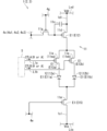
- FIG. 4 is a circuit diagram showing an example of a first sub-pixel circuit according to the first embodiment;
- FIG. 5 is a gate circuit diagram schematically showing a configuration example of an input/output gate of a control section.
- FIG. 6 is a circuit diagram showing an example of a control unit.
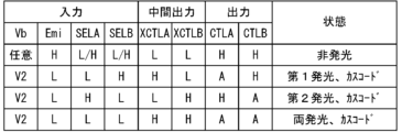
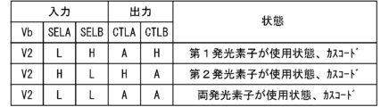
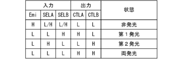
- FIG. 7 is a truth table showing an example of the relationship between the input and output of the control section and the state of the first sub-pixel circuit.
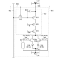
- FIG. 8 is a block circuit diagram showing an example of connection between a control section and a plurality of sub-pixel circuits.
- FIG. 9 is a block circuit diagram showing an example of connection between a control unit and a plurality of pixel circuits.
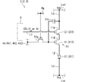
- FIG. 10 is a circuit diagram showing a first sub-pixel circuit according to another example of the first embodiment;
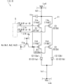
- FIG. 11 is a circuit diagram showing an example of a first subpixel circuit according to the second embodiment.
- FIG. 12 is a gate circuit diagram schematically showing a configuration example related to input/output gates of the control section.
- FIG. 13 is a circuit diagram showing an example of a control unit;
- FIG. 13 is a circuit diagram showing an example of a control unit;
- FIG. 14 is a truth table showing an example of the relationship between the input, the intermediate output signal, the output, and the state of the first sub-pixel circuit in the control section.
- FIG. 15 is a block circuit diagram showing an example of a signal output circuit that outputs a setting control signal to the control section.
- FIG. 16 is a block circuit diagram showing an example of connections between a control section, a signal output circuit, and a plurality of sub-pixel circuits.
- FIG. 17 is a block circuit diagram showing an example of connections between a control section, a signal output circuit, and a plurality of pixel circuits.
- FIG. 18 is a circuit diagram showing an example of a first sub-pixel circuit according to the third embodiment; FIG.
- FIG. 19 is a gate circuit diagram schematically showing one configuration example related to the input/output gates of the control section.
- FIG. 20 is a circuit diagram showing an example of a control unit;
- FIG. 21 is a truth table showing an example of the relationship between the input and output of the control section and the state of the first sub-pixel circuit.
- FIG. 22 is a circuit diagram showing an example of a first sub-pixel circuit according to the fourth embodiment;
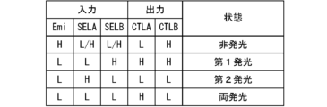
- FIG. 23 is a truth table showing an example of the relationship between the input and output of the control section and the state of the first sub-pixel circuit.
- FIG. 24 is a circuit diagram showing an example of a first sub-pixel circuit according to the fifth embodiment;
- FIG. 25 is a truth table showing an example of the relationship between the input, the intermediate output signal, the output, and the state of the first sub-pixel circuit in the control section.
- FIG. 26 is a circuit diagram showing an example of the first sub-pixel circuit according to the sixth embodiment.
- FIG. 27 is a truth table showing an example of the relationship between the input and output of the control section and the state of the first sub-pixel circuit.
- FIG. 28 is a circuit diagram showing an example of a first sub-pixel circuit according to the seventh embodiment;
- FIG. 29 is a gate circuit diagram schematically showing one configuration example related to the input/output gates of the control section.
- FIG. 30 is a truth table showing an example of the relationship between the input and output of the control section and the state of the first sub-pixel circuit.
- FIG. 31 is a circuit diagram showing an example of a first sub-pixel circuit according to another example of the seventh embodiment
- FIG. 32 is a truth table showing an example of the relationship between the input and output of the control section and the state of the first sub-pixel circuit.
- FIG. 33 is a circuit diagram showing an example of a first sub-pixel circuit according to the eighth embodiment;
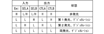
- FIG. 34 is a truth table showing an example of the relationship between the input and output of the control section and the state of the first sub-pixel circuit.
- FIG. 35 is a circuit diagram showing an example of the first sub-pixel circuit according to the ninth embodiment.
- FIG. 36 is a truth table showing an example of the relationship between the input and output of the control section and the state of the first sub-pixel circuit.
- FIG. 37 is a circuit diagram showing an example of a first sub-pixel circuit in which an N-channel transistor is applied as the first transistor.
- FIG. 38 is a circuit diagram showing an example of a first sub-pixel circuit incorporating a threshold voltage correction circuit.
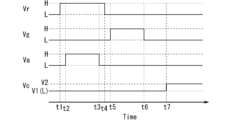
- FIG. 39 is a timing chart showing an example of the operation of the first sub-pixel circuit incorporating the threshold voltage correction circuit.
- FIG. 40 is a front view schematically showing an example of a tiling display.
- FIG. 41 is a circuit diagram schematically showing a circuit configuration of a sub-pixel portion according to the first reference example.
- FIG. 42 is a circuit diagram schematically showing a circuit configuration of a sub-pixel portion according to the second reference example.
- FIG. 43 is a circuit diagram schematically showing a circuit configuration of a sub-pixel portion according to the third reference example.
- FIG. 44 is a circuit diagram schematically showing a circuit configuration of a sub-pixel portion according to the fourth reference example.
- pixel circuits, display panels, and display devices of the present disclosure are described below.
- First, the configuration that is the premise of the pixel circuit of the present disclosure will be described using first to fourth reference examples shown in FIGS. 41 to 44 .
- the display device a plurality of scanning signal lines and a plurality of image signal lines are arranged in a lattice, and a plurality of pixel portions are arranged in a matrix in a manner corresponding to intersections of the plurality of scanning signal lines and the plurality of image signal lines. has an image display unit arranged in a row.
- each pixel portion includes a subpixel portion including a first light emitting element that emits light of a first color, a subpixel portion including a second light emitting element that emits light of a second color, and a sub-pixel portion including a third light-emitting element that emits light of a third color.
- the display device can display a color image or the like. Red, green and blue can be applied for the first, second and third colors.
- FIG. 41 is a circuit diagram schematically showing the circuit configuration of the sub-pixel portion 915 according to the first reference example.
- Each sub-pixel portion 915 includes a light emitting element 914 and a light emission control portion 922 that controls light emission, non-light emission, light emission intensity, and the like of the light emitting element 914 .
- a micro light emitting diode (LED) element, an organic electroluminescence (EL) element, or the like is applied to the light emitting element 914 .
- Light emitting element 914 is located on an insulating layer disposed on a first surface of a substrate such as a glass plate.
- the light emitting element 914 is electrically connected to the light emission control section 922 and the second power supply potential input section 917 via through conductors arranged in through holes penetrating the insulating layer arranged in the pixel section.
- a positive electrode of the light emitting element 914 is connected to the first power supply potential input section 916 via the light emission control section 922 .
- a negative electrode of the light emitting element 914 is connected to the second power supply potential input section 917 .
- the first power supply potential input section 916 may be a first power supply potential terminal or a first power supply potential input line.
- the second power supply potential input section 917 may be a second power supply potential terminal or a second power supply potential input line.
- the light emission control unit 922 includes a selection transistor 912 , a drive transistor 913 , a capacitive element 918 and a light emission control transistor 919 .
- the selection transistor 912 is a transistor that functions as a switch for inputting an image signal to the sub-pixel portion 915 .
- a P-channel thin film transistor also referred to as a P-channel transistor or the like is used as the selection transistor 912 .
- a gate electrode of the selection transistor 912 is connected to the scanning signal line 902 .
- a source electrode of the selection transistor 912 is connected to the image signal line 903 .
- a drain electrode of the selection transistor 912 is connected to a gate electrode of the drive transistor 913 .
- an ON signal (Low (L) signal) as a scanning signal from the scanning signal line 902 is input to the gate electrode of the selection transistor 912
- the selection transistor 912 allows current to flow between the source electrode and the drain electrode. It is in a conductive state (also called an ON state or a closed state as a switch).
- the image signal from the image signal line 903 is applied to the gate electrode of the driving transistor 913 through the selection transistor 912 .
- the driving transistor 913 receives the potential difference (Vdd ⁇ Vss) between the first power supply potential Vdd applied by the first power supply potential input section 916 and the second power supply potential Vss applied by the second power supply potential input section 917 and the image signal line 903 . It functions as an element (also referred to as a driving element) that current-drives the light emitting element 914 according to the level (potential) of the image signal transmitted from the . In other words, the driving transistor 913 can control the current flowing through the light emitting element 914 .
- the first power supply potential input portion 916 is connected to a first power supply line Lvd as a power supply line on the positive power supply potential (also referred to as first power supply potential) side.
- the first power supply potential Vdd applied from the first power supply line Lvd to the first power supply potential input section 916 is set to approximately 3 volts (V) to 5V. Also, the first power supply potential Vdd may be about 8V to 15V.
- the second power supply potential input portion 917 is connected to a second power supply line Lvs as a power supply line on the negative power supply potential (also referred to as second power supply potential) side.
- the second power supply potential Vss applied from the second power supply line Lvs to the second power supply potential input section 917 is set to about -3V to 0V.
- the second power line Lvs may be a grounded ground line.
- a P-channel transistor or the like is applied to the driving transistor 913 .
- the source electrode of the driving transistor 913 is connected to the first power supply potential input section 916 .
- a drain electrode of the drive transistor 913 is connected to the second power supply potential input section 917 via the light emission control transistor 919 and the light emitting element 914 .
- a capacitive element 918 is arranged on a connection line that connects the gate electrode and the source electrode of the drive transistor 913 .
- the capacitive element 918 functions as a holding capacitor that holds the potential of the image signal input to the gate electrode of the driving transistor 913 for a period (also referred to as one frame period) until the next image signal is input (also referred to as rewriting). .
- the light emission control transistor 919 is arranged on the drive line 925 between the drive transistor 913 and the light emitting element 914 and can control light emission and non-light emission of the light emitting element 914 .
- a P-channel transistor or the like is applied to the light emission control transistor 919 .
- the source electrode of the emission control transistor 919 is connected to the drain electrode of the driving transistor 913 .
- the emission control transistor 919 is connected in cascade with the drive transistor 913 .
- the drain electrode of the light emission control transistor 919 is connected to the positive electrode of the light emitting element 914 .
- the gate electrode of the light emission control transistor 919 receives an L signal as a light emission control signal (also referred to as an Emi signal), the light emission control transistor 919 is turned on. Accordingly, a current (also referred to as driving current) flows from the first power supply potential input portion 916 to the light emitting element 914 through the driving transistor 913, the light emission control transistor 919, and the driving line 925, and the light emitting element 914 emits light. At this time, the intensity (luminance) of light emitted from the light emitting element 914 can be controlled by controlling the level (potential) of the image signal.
- the L signal functions as an ON signal capable of making the light emission control transistor 919 conductive (ON).
- a potential lower than the second power supply potential Vss supplied by the second power supply line Lvs can be applied to the potential (also referred to as L potential) Vgl of the L signal as the ON signal.
- the drive current does not sufficiently flow through the light-emitting element 914 , and the light-emitting element 914 does not operate. It may not emit light with the desired intensity. Further, even if the light-emitting element 914 is defective, such as a defect, deterioration, or breakage, in some sub-pixel portions 915 among the plurality of sub-pixel portions 915, the light-emitting element 914 does not emit light at a desired intensity. defects may occur.
- two light emitting elements 914 connected in parallel are arranged in each sub-pixel portion 915, and one of the two light emitting elements 914 having no defect is selected.
- a configuration that always emits light is conceivable.
- FIG. 42 is a circuit diagram schematically showing the circuit configuration of the sub-pixel portion 915 according to the second reference example.
- the circuit of the sub-pixel portion 915 shown in FIG. 42 is based on the circuit of the sub-pixel portion 915 in FIG. 41 described above, with some configurations replaced with other configurations and additional configurations added. .
- part of the circuit configuration of the sub-pixel portion 915 in FIG. Of the circuit configuration of the sub-pixel portion 915 shown in FIG. A first light emitting element 914a and a second light emitting element 914b, a first switch 926a and a second switch 926b.
- the additional configuration in the circuit configuration of the sub-pixel portion 915 shown in FIG. 42 is the switching control portion 927 .
- the first drive line 925a and the second drive line 925b are connected to the light emission control section 922 and connected in parallel.
- one drive line 925 is a normal drive line (also referred to as a normal drive line)
- the other drive line 925 is a preliminary drive line (also called a redundant drive line).
- the first drive line 925a is connected to the positive electrode of the first light emitting element 914a
- the negative electrode of the first light emitting element 914a is connected to the second power supply potential input section 917.
- the second drive line 925b is connected to the positive electrode of the second light emitting element 914b, and the negative electrode of the second light emitting element 914b is connected to the second power supply potential input section 917.
- the first switch 926a is arranged on the first drive line 925a, and can set the first drive line 925a to a use state (also referred to as a drive state) or a non-use state (also referred to as a non-drive state).
- the second switch 926b is arranged on the second drive line 925b, and can set the second drive line 925b to a use state (drive state) or a non-use state (non-drive state).
- the switching control unit 927 sets one of the first switch 926a and the second switch 926b to a non-conducting state (also referred to as an OFF state or an open state as a switch) in which current cannot flow, and switches the other switch. Set to conductive state.
- a non-conducting state also referred to as an OFF state or an open state as a switch
- one of the first light emitting element 914a and the second light emitting element 914b as the two light emitting elements 914 which is not defective, can always emit light.
- a P-channel transistor or the like is applied to the first switch 926a and the second switch 926b. In this case, the P-channel transistor as the first switch 926 a is cascade-connected to the light emission control transistor 919 .
- the P-channel transistor as the second switch 926b is cascade-connected to the light emission control transistor 919 .
- the switching control section 927 inputs an on signal (Vga: L signal) to the gate electrode of the first switch 926a and turns off the gate electrode of the second switch 926b.
- a signal (Vgb: H signal) is input.
- a potential higher than the first power supply potential Vdd supplied by the first power supply line Lvd can be applied to the potential (also referred to as H potential) Vgh of the H signal as the off signal.
- the switching control section 927 inputs an off signal (Vga: H signal) to the gate electrode of the first switch 926a and turns on the gate electrode of the second switch 926b.
- Vga: H signal an off signal
- Vgb: L signal A signal
- the drain current (also called source-drain current) Ids as an output current can vary. Therefore, in any of the driving transistors 913 of the sub-pixel portions 915 according to the first and second reference examples, among the first power supply potential Vdd, the second power supply potential Vss, and the forward voltage applied to the light emitting element 914, A variation in one or more values of may vary the voltage Vds between the source and drain electrodes and the drain current Ids as the output current.
- the first power supply potential Vdd can drop according to the distance between the power supply and the portion of the first power supply line Lvd to which the first power supply potential input section 916 is connected.
- the second power supply potential Vss can rise according to the distance between the power supply and the portion of the second power supply line Lvs to which the second power supply potential input section 917 is connected.
- the forward voltage applied to the light emitting element 914 may vary depending on the characteristics of the light emitting element 914, such as luminous efficiency and internal resistance, and the setting values of the drive current, forward voltage, and luminance.
- the output resistance Ro1 the variation ⁇ Vds of the voltage between the drain electrode and the source electrode (also referred to as the voltage between the drain and the source) Vds, and the variation of the drain current Ids as the output current
- the output resistance Ro1 is small, the variation ⁇ Ids of the drain current Ids corresponding to the variation ⁇ Vds of the drain-source voltage Vds increases.
- Brightness unevenness includes brightness unevenness of a single color such as red (R), green (G), blue (B), or white (W).
- Color unevenness includes RGB mixture ratio unevenness.
- a transistor (also referred to as a cascode connection transistor) 920 that is connected in cascade to the drain electrode side of the driving transistor 913 and forms a cascode connection with the driving transistor 913 is provided.
- the cascode connection transistor 920 is a transistor having the same conductivity type as the driving transistor 913, and a predetermined potential (also referred to as an input potential) Vb between the first power supply potential Vdd and the second power supply potential Vss is input to the gate electrode. be done.
- the drain electrode of the P-channel transistor as the drive transistor 913 and the source electrode of the P-channel transistor as the cascode connection transistor 920 are connected, and the P-channel transistor as the cascode connection transistor 920 is connected.
- a drain electrode of the channel transistor and a source electrode of the P-channel transistor as the emission control transistor 919 are connected.
- the apparent output resistance Ro of the driving transistor 913 has a relationship of Ro ⁇ gm2 ⁇ Ro2 ⁇ Ro1. In other words, the output resistance of the drive transistor 913 is approximately (gm2 ⁇ Ro2) times due to the cascode connection provided by the cascode connection transistor 920 .
- the output resistance of the drive transistor 913 is approximately ten times as large.
- the variation ⁇ Ids of the drain current Ids with respect to the variation ⁇ Vds of the drain-source voltage Vds is approximately 1/10.
- the drain current is kept constant due to the channel length modulation effect. Fluctuations in Ids are less likely to occur.
- the light emission control transistor 919, the cascode connection transistor 920, and the first switch 926a or the second switch 926b are connected to the driving transistor 913.
- a plurality of transistors are connected in cascade, such as those applied to Therefore, in the potential difference (Vdd-Vss), the series resistance of the plurality of transistors connected in series with the drive transistor 913 accounts for a large proportion, and the drain-source voltage Vds of the drive transistor 913 becomes small.
- This problem is caused by a pixel in which a driving transistor 913 as a driving element for current-driving a light emitting element 914 and a plurality of transistors are connected in cascade between the first power supply potential input section 916 and the second power supply potential input section 917 . It can occur commonly in display devices having circuits.
- the display device has room for improvement in terms of improving image quality.
- the inventor of the present disclosure has created a technique capable of improving the image quality of display devices.
- the pixel circuit is connected in series with the light-emitting element, and is connected in tandem with the first transistor that controls the current flowing through the light-emitting element when a potential corresponding to an image signal is input to the gate electrode.
- the first transistor that controls the current flowing through the light-emitting element when a potential corresponding to an image signal is input to the gate electrode.
- a second transistor that switches the light-emitting element between a light-emitting state and a non-light-emitting state.
- a gate electrode of the second transistor is provided with a first potential higher than or equal to the first power supply potential or lower than the second power supply potential for setting a non-conducting state between the source electrode and the drain electrode of the second transistor, and One potential of a second potential between the first power potential and the second power potential that causes a current to flow between the source electrode and the drain electrode is selectively input.
- the second transistor is connected in tandem with the first transistor on the drain electrode side of the first transistor, inputting the second potential to the gate electrode of the second transistor causes the second transistor to form a cascode connection to the first transistor.
- the second potential is, for example, a potential lower than the drain potential of the first transistor for operating the first transistor in the saturation region.
- the second potential is, for example, a potential higher than the drain potential of the first transistor for operating the first transistor in the saturation region.
- the second potential is a potential that is applied to the gate electrode of the second transistor and causes the light emitting element to emit light. It is a potential for providing the second transistor with the function of an analog element having a linear relationship with the current.
- the second potential is a potential lower than the source potential of the first transistor.
- the first transistor and the second transistor are each of an N-channel type, the second potential is a potential higher than the source potential of the first transistor.
- the transistor connected in series with the first transistor may be only the second transistor. This makes it easier to drive the first transistor as the drive transistor in the saturation region. As a result, when the display device is viewed in plan, gradation in which the brightness gradually decreases is less likely to occur.
- the second potential is a potential lower than the drain potential of the first transistor.
- This second potential can be defined as, for example, the following potential.
- the second potential is the negative voltage that is the overdrive voltage of the first transistor and the gate-source voltage (gate voltage) of the second transistor, with the potential of the source electrode (source potential) of the first transistor as a reference. It should be less than the potential obtained by subtracting the sum of the negative voltage and the negative voltage.
- the overdrive voltage is a value obtained by subtracting the threshold voltage Vth1 (eg, about ⁇ 1 V) of the first transistor from the gate-source voltage (gate voltage) Vgs1 (eg, about ⁇ 1.5 V) in the first transistor. (eg, about -0.5V).
- the second potential may be a potential that is about 0.5V to 2V lower than the drain potential of the first transistor.
- the second potential may be a potential higher than the source potential of the first transistor by about 0.5V to 2V.
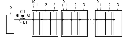
- FIG. 1 is a front view schematically showing an example of the display device 100 according to the first embodiment.
- FIG. 2 is a back view schematically showing an example of the display device 100 according to the first embodiment.
- FIG. 3 is a block circuit diagram schematically showing an example of the configuration of the display device 100 according to the first embodiment.
- the display device 100 includes a display panel 100p and a driving section 30.
- the display panel 100p includes a plurality of pixel circuits 10.
- the display panel 100p has a surface (also referred to as a display surface) Sf1 for displaying an image, and a surface (also referred to as an anti-display surface or a non-display surface) Sf2 opposite to the display surface Sf1.
- the display panel 100p has a rectangular flat plate shape, a trapezoidal flat plate shape, a circular flat plate shape, or the like when viewed from above.
- the display panel 100p includes a substrate 20 and a plurality of pixel circuits 10. FIG.
- the substrate 20 has a first surface (also referred to as a first main surface) F1, a second surface (also referred to as a second main surface) F2, and a plurality of side surfaces F3.
- the second surface F2 is a surface opposite to the first surface F1.
- the plurality of side faces F3 connect the first face F1 and the second face F2, respectively.
- a flat substrate is applied to the substrate 20 .
- a rectangular surface having four sides is applied to each of the first surface F1 and the second surface F2.
- the multiple side faces F3 include a first side face F31, a second side face F32, a third side face F33, and a fourth side face F34.
- the first side surface F31 connects the first side of the first surface F1 and the first side of the second surface F2.
- the first side surface F31 has the first side of the first surface F1 and the first side of the second surface F2 as two opposite sides.
- the second side surface F32 connects the second side of the first surface F1 and the second side of the second surface F2. In other words, the second side surface F32 has the second side of the first surface F1 and the second side of the second surface F2 as two opposite sides.
- the third side surface F33 connects the third side of the first surface F1 and the third side of the second surface F2. In other words, the third side surface F33 has the third side of the first surface F1 and the third side of the second surface F2 as two opposing sides.
- the fourth side surface F34 connects the fourth side of the first surface F1 and the fourth side of the second surface F2.
- the fourth side surface F34 has the fourth side of the first surface F1 and the fourth side of the second surface F2 as two opposite sides.
- the first surface F1 is a flat surface along the XZ plane and faces the -Y direction.
- the second surface F2 is a flat surface along the XZ plane and faces the +Y direction.
- the first side surface F31 faces the +Z direction.
- the second side face F32 faces the -X direction.
- the third side surface F33 faces the -Z direction.
- the fourth side surface F34 faces the +X direction.
- a glass plate is applied as the substrate 20 .
- the glass plate may or may not be transparent.
- the substrate 20 is a colored glass substrate, a ground glass substrate, a plastic substrate, a ceramic substrate, a metal substrate, or a composite substrate in which two or more of these substrates are laminated. may be
- the plurality of pixel circuits 10 are circuits that respectively constitute a pixel section.
- a plurality of pixel circuits 10 are arranged in a matrix.
- a plurality of pixel circuits 10 are arranged in a matrix on the first surface F ⁇ b>1 of the substrate 20 .
- the plurality of pixel circuits 10 constitute one column of pixel circuits 10
- the plurality of pixel circuits 10 constitute one row of pixel circuits 10 . More specifically, pixel circuits 10 of n rows ⁇ m columns (n and m are natural numbers) are arranged.
- the plurality of pixel circuits 10 constitute a portion (also referred to as an image display portion) 300 that displays an image.
- the image display unit 300 is located on the first surface F1 side of the substrate 20 .
- the surface of the image display unit 300 facing the -Y direction constitutes the display surface Sf1 of the display panel 100p.
- the image display section 300 may be positioned so as to cover substantially the entire surface of the first surface F1.
- the display device 100 has a structure in which the image display section 300 is arranged on the entire surface (also referred to as a frameless structure) or a frame portion around the image display section 300 on one side of the substrate 20 on the first surface F1 side. It has a structure that is made as narrow as possible (also called a narrow frame structure).
- Each of the plurality of pixel circuits 10 has a plurality of sub-pixel circuits.
- the plurality of sub-pixel circuits are circuits forming sub-pixel portions included in the pixel portion.
- the plurality of sub-pixel circuits includes a first sub-pixel circuit 1, a second sub-pixel circuit 2 and a third sub-pixel circuit 3.
- the first sub-pixel circuit 1 can emit light of a first color.
- the second sub-pixel circuit 2 can emit light of a second color different from the first color.
- the third sub-pixel circuit 3 can emit light of a third color different from the first and second colors. Red, green and blue are applied to the first, second and third colors.
- each pixel circuit 10 a first subpixel circuit 1, a second subpixel circuit 2, and a third subpixel circuit 3 are arranged in order in the row direction.
- a plurality of first subpixel circuits 1 constitute one row of first subpixel circuits 1
- a plurality of second subpixel circuits 2 constitute one row of second subpixel circuits 2
- a plurality of second subpixel circuits 2 constitute one row of second subpixel circuits 2
- the three sub-pixel circuits 3 constitute one row of third sub-pixel circuits 3
- a plurality of first subpixel circuits 1 constitute a row of first subpixel circuits 1
- a plurality of second subpixel circuits 2 constitute a row of second subpixel circuits 2
- a plurality of third subpixel circuits 2 constitute a row of second subpixel circuits 2.
- the sub-pixel circuits 3 form a column of third sub-pixel circuits 3 .
- the first subpixel circuit 1, the second subpixel circuit 2 and the third subpixel circuit 3 may be arranged in any order.
- the drive unit 30 is electrically connected to each of the plurality of pixel circuits 10.
- the drive unit 30 is located on the side opposite to the display surface Sf2 of the display panel 100p.
- the driving section 30 is positioned on the second surface F2 side of the substrate 20 .
- a driving element such as an integrated circuit (IC) or a large-scale integration (LSI) is mounted on the second surface F2 of the substrate 20 in a chip-on-glass (COG) method. It can be formed by mounting on.
- the drive unit 30 may be a circuit board on which drive elements are mounted.
- the driving unit 30 includes low temperature polysilicon (LTPS) directly formed on the second surface F2 of the substrate 20 by a thin film forming method such as a chemical vapor deposition (CVD) method.
- a thin film circuit also referred to as a thin film circuit including a thin film transistor (TFT) having a semiconductor layer of .
- the drive unit 30 connects wiring (also referred to as back wiring) W2 positioned on the second surface F2 of the substrate 20 and wiring (also referred to as side wiring) W3 positioned on the side surface F3 of the substrate 20. It is electrically connected to the image display section 300 positioned on the first surface F1 side of the substrate 20 by a plurality of wirings included therein. Therefore, multiple wirings are included in the display panel 100p.
- the display panel 100p includes a plurality of image signal lines 4s, a plurality of scanning signal lines (also referred to as gate signal lines) 4g, and a plurality of emission control signal lines 4e.
- the plurality of scanning signal lines 4g and the plurality of image signal lines 4s are arranged in a grid pattern.
- the display panel 100p also includes a scanning signal line driving section 30g and a light emission control signal line driving section 30e.
- Each of the plurality of image signal lines 4s transmits a signal (also referred to as an image signal) for controlling the degree of light emission to the first subpixel circuit 1, the second subpixel circuit 2, and the third subpixel circuit 3. be able to.
- the image signal line 4 s is positioned along one column of pixel circuits 10 .
- three image signal lines 4s are positioned along one column of pixel circuits 10 .
- the three image signal lines 4s are a first image signal line (also referred to as a first image signal line) 4s1, a second image signal line (also referred to as a second image signal line) 4s2, and a third image signal line. lines (also referred to as third image signal lines) 4s3.
- a first image signal line 4s1 located along one column of first sub-pixel circuits 1 and one column of second sub-pixel circuits 2 are positioned.
- the first image signal line 4s1 is electrically connected to each of the plurality of first sub-pixel circuits 1 forming one column
- the second image signal line 4s2 is It is electrically connected to each of the second sub-pixel circuits 2 forming one column
- the third image signal line 4s3 is electrically connected to each of the third sub-pixel circuits 3 forming one column.
- An image signal can be supplied from the drive unit 30 to each of the plurality of image signal lines 4s.
- the drive unit 30 may time-divisionally supply image signals to the plurality of image signal lines 4s via a time-divisional selector circuit or the like.
- One selector circuit is arranged for the pixel circuits 10 in each column, and the image signals supplied from the driving unit 30 to the selector circuit are transferred to the first image signal line 4s1 and the second image signal line 4s2 by the selector circuit. , and the third image signal line 4s3 may be supplied time-sequentially (line-sequentially).
- a configuration having three transfer gate elements or the like is applied to the selector circuit.
- the selector circuit may be arranged in the empty area of the image display section 300 on the first surface F ⁇ b>1 of the substrate 20 , or may be arranged in the frame portion outside the image display section 300 .
- Each of the plurality of scanning signal lines 4g is a signal (also called a scanning signal) for controlling the timing of inputting an image signal to each of the first subpixel circuit 1, the second subpixel circuit 2, and the third subpixel circuit 3. ) can be transmitted.
- One scanning signal line 4 g is positioned along one row of pixel circuits 10 .
- the Mth scanning signal line 4g is positioned along the row of the pixel circuits 10 of the Mth row (M is a natural number). Then, for each of the plurality of first sub-pixel circuits 1, the plurality of second sub-pixel circuits 2 and the plurality of third sub-pixel circuits 3 included in the pixel circuit 10 of the M-th row, the M-th scanning signal line is provided. 4g are electrically connected.
- Scanning signals can be supplied to the plurality of scanning signal lines 4g in a time-sequential manner (line-sequential manner) from a scanning signal line driving section 30g.
- Various circuits such as a shift register are applied to the scanning signal line driving section 30g.
- the scanning signal line driver 30 g is located on the first surface F 1 of the substrate 20 .
- the scanning signal line driving section 30 g may be arranged in the empty area of the image display section 300 or may be arranged in the frame portion outside the image display section 300 .
- the scanning signal line driving section 30g can supply scanning signals to the plurality of scanning signal lines 4g time-sequentially (line-sequentially) in response to signals from the driving section 30 .
- the emission control signal line 4e can transmit a signal for controlling emission timing (also referred to as emission control signal) to each of the first subpixel circuit 1, the second subpixel circuit 2, and the third subpixel circuit 3. can.
- One light emission control signal line 4 e is positioned along one row of pixel circuits 10 .
- the Mth emission control signal line 4e is positioned along the row of the pixel circuits 10 of the Mth row (M is a natural number). Then, each of the plurality of first sub-pixel circuits 1, the plurality of second sub-pixel circuits 2 and the plurality of third sub-pixel circuits 3 included in the pixel circuit 10 of the M-th row is supplied with the M-th light emission control signal.
- a line 4e is electrically connected.
- Light emission control signals can be supplied to the plurality of light emission control signal lines 4e in time sequence (line sequence) from the light emission control signal line driving section 30e.
- Various circuits such as a shift register are applied to the light emission control signal line driving section 30e.
- the light emission control signal line driver 30 e is located on the first surface F 1 of the substrate 20 .
- the light emission control signal line driving section 30 e may be arranged in an empty area of the image display section 300 or may be arranged in a frame portion outside the image display section 300 .
- the light emission control signal line drive unit 30e can supply light emission control signals to the plurality of light emission control signal lines 4e in time sequence (line sequence) in response to signals from the drive unit 30.
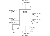
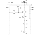
- FIG. 4 is a circuit diagram showing an example of the first sub-pixel circuit 1 according to the first embodiment.
- the first subpixel circuit 1 has the same or similar configuration.
- each of the second subpixel circuit 2 and the third subpixel circuit 3 has the same or similar configuration as the first subpixel circuit 1 .
- the first subpixel circuit 1 is connected in series or cascade between the first power supply potential input section 1dl, the second power supply potential input section 1sl, and the first power supply potential input section 1dl and the second power supply potential input section 1sl. and a plurality of elements E1.
- the first power supply potential input section 1dl can supply the first power supply potential Vdd.
- the first power supply potential input section 1dl is connected to the first power supply line Lvd.
- the first power supply line Lvd is connected to a power supply that applies the first power supply potential Vdd to the first power supply line Lvd.
- the first power supply potential Vdd can be set to any positive potential. A mode in which the first power supply potential Vdd is set to about 8V is conceivable.
- the second power supply potential input section 1sl can supply a second power supply potential Vss that is lower than the first power supply potential Vdd.
- the second power supply potential input section 1sl is connected to the second power supply line Lvs.
- the second power supply line Lvs is connected to a power supply that applies the second power supply potential Vss to the second power supply line Lvs.
- the second power supply potential Vss may be a positive potential or a negative potential as long as it is lower than the first power supply potential Vdd. A mode in which the second power supply potential Vss is set to about 0V is conceivable.
- the second power line Lvs may be a grounded ground line.
- the multiple elements E1 include the light emitting element 12 as the first element E11, the first transistor 11d as the second element E12, and the second transistor 11e as the third element E13.
- the first transistor 11d as the second element E12, the second transistor 11e as the third element E13 between the first power supply potential input section 1dl and the second power supply potential input section 1sl, the first transistor 11d as the second element E12, the second transistor 11e as the third element E13,
- the light emitting element 12 as the first element E11 is connected in series or cascade in the order of this description.
- the first subpixel circuit 1 includes the third transistor 11g and the capacitive element 11c.
- the light emission of the light emitting element 12 can be controlled by the light emission control section 11 having the first transistor 11d, the second transistor 11e, the third transistor 11g, and the capacitive element 11c. More specifically, the light emission control unit 11 can control light emission, non-light emission, light emission intensity, and the like of the light emitting element 12 .
- the light emitting element 12 can emit light of a predetermined color.
- the light emitting element 12 of the first sub-pixel circuit 1 can emit light of a first color.
- the light emitting element 12 of the two sub-pixel circuit 2 can emit light of a second color.
- the light emitting element 12 of the third sub-pixel circuit 3 can emit light of a third color.
- a micro light emitting diode (LED) element, an organic electroluminescence (EL) element, or the like is applied to the light emitting element 12 .
- a micro LED element or an organic EL element that emits light of a first color is applied to the light emitting element 12 of the first sub-pixel circuit 1 .
- a micro LED element or an organic EL element that emits light of the second color is applied to the light emitting element 12 of the second sub-pixel circuit 2 .
- a micro LED element or an organic EL element that emits light of a third color is applied to the light emitting element 12 of the third sub-pixel circuit 3 .
- the first transistor 11 d is connected in series with the light emitting element 12 .
- the first transistor 11d can control the current flowing through the light emitting element 12 by inputting a potential corresponding to an image signal to the gate electrode.
- the first transistor 11d can control the current flowing through the light emitting element 12 by inputting a potential corresponding to the image signal input from the first image signal line 4s1 to the gate electrode.
- the first transistor 11d has the potential difference (Vdd ⁇ Vss) between the first power supply potential Vdd and the second power supply potential Vss and the level of the image signal transmitted from the first image signal line 4s1 (potential ) and functions as an element (also referred to as a driving element) for current-driving the light emitting element 12 .
- a P-channel type thin film transistor (P-channel transistor) or the like is applied to the first transistor 11d.
- the source electrode of the first transistor 11d is connected to the first power supply potential input section 1dl.
- a drain electrode of the first transistor 11 d is connected to the second power supply potential input section 1 sl via the second transistor 11 e and the light emitting element 12 .
- the first transistor 11d changes to the source electrode. and the drain electrode (also referred to as a conductive state or an ON state).
- a drive current can flow from the first power supply potential input section 1dl to the light emitting element 12 via the first transistor 11d and the second transistor 11e.
- the light emission intensity (luminance) of the light emitting element 12 can be controlled according to the level (potential) of the image signal.
- the first transistor 11 d can control the light emission intensity of the light emitting element 12 .
- an image signal is input from the second image signal line 4s2 instead of the first image signal line 4s1.
- an image signal is input from the third image signal line 4s3 instead of the first image signal line 4s1.
- the third transistor 11g functions as an element for inputting an image signal into the light emission control section 11.
- a P-channel transistor or the like is applied to the third transistor 11g.
- the gate electrode of the third transistor 11g is connected to the scanning signal line 4g.
- a source electrode (drain electrode) of the third transistor 11g is connected to the first image signal line 4s1.
- the drain electrode (source electrode) of the third transistor 11g is connected to the gate electrode of the first transistor 11d.
- the image signal from the first image signal line 4s1 is input to the gate electrode of the first transistor 11d through the third transistor 11g.
- a signal also referred to as an L signal
- Vss the second power supply potential
- the L potential Vgl is set from about -2V to 0V.
- the source electrode (drain electrode) of the third transistor 11g is connected to the second image signal line 4s2 instead of the first image signal line 4s1.
- An image signal is input from the second image signal line 4s2 instead of 4s1.
- the source electrode (drain electrode) of the third transistor 11g is connected to the third image signal line 4s3 instead of the first image signal line 4s1. is inputted from the third image signal line 4s3.
- the capacitive element 11c is located on a connection line connecting the gate electrode and the source electrode of the first transistor 11d.
- the capacitive element 11c functions as a holding capacitor that holds the potential Vsig of the image signal input to the gate electrode of the first transistor 11d for a period (one frame period) until the next image signal is input (rewritten).
- the second transistor 11e is cascade-connected to the first transistor 11d.
- the second transistor 11e can switch the light-emitting element 12 between a state in which it emits light (also referred to as a light-emitting state) and a state in which it does not emit light (also referred to as a non-light-emitting state).
- the second transistor 11e functions as an element for controlling light emission and non-light emission of the light emitting element 12 (also referred to as light emission control element).
- the second transistor 11e is located on a connection line (also called a drive line) that connects the first transistor 11d and the light emitting element 12 .
- a transistor of the same conductivity type as the first transistor 11d is applied to the second transistor 11e.
- the conductivity types include a P-type in which the carriers that generate a current between the source and drain electrodes are holes, and an N-type in which the carriers that generate a current between the source and drain electrodes are electrons.
- a P-channel transistor or the like is applied to the second transistor 11e.
- the second transistor 11e is cascade-connected to the first transistor 11d on the drain electrode side of the first transistor 11d. More specifically, the source electrode of the second transistor 11e is connected to the drain electrode of the first transistor 11d.
- a light emitting element 12 is connected to the drain electrode of the second transistor 11e. More specifically, the anode electrode (positive electrode) of the light emitting element 12 is connected to the drain electrode of the second transistor 11e.
- a cathode electrode (negative electrode) of the light emitting element 12 is connected to the second power supply potential input section 1sl.
- the first potential V1 or the second potential V2 is selectively input to the gate electrode of the second transistor 11e.
- the first potential V1 is a potential (also referred to as an off potential) for setting the second transistor 11e to a state in which current cannot flow between the source electrode and the drain electrode (also referred to as a non-conducting state or an off state).
- the first potential V1 is set to a potential equal to or higher than the first power supply potential Vdd. More specifically, as the first potential V1, the potential (H potential) Vgh of a High (H) signal serving as an off signal for bringing the second transistor 11e into a non-conducting state (off state) is applied.
- the first potential V1 is set from 8V to about 10V.
- the second potential V2 is a potential for causing current to flow between the source electrode and the drain electrode of the second transistor 11e.
- the second potential V2 is set to a potential between the first power potential Vdd and the second power potential Vss.
- the second potential V2 is set to a potential that is less than the first power supply potential Vdd and greater than the second power supply potential Vss.
- the second potential V2 can be set to any analog potential between the L potential and the H potential, instead of digital discrete values such as the L potential and the H potential.
- the second potential V2 is set to a potential higher than 0V and lower than 8V.
- the signal having the second potential V2 is also called an analog (A) signal as appropriate.
- the light-emitting element 12 is in a light-emitting state (light-emitting state).
- the second transistor 11e is cascade-connected to the drain electrode side of the first transistor 11d and has the same conductivity type as the first transistor 11d.
- a second potential V2 between the second power supply potential Vss is input. Therefore, the second transistor 11e forms a cascode connection with the first transistor 11d.
- the output resistance of the first transistor 11d is Ro1
- the output resistance of the second transistor 11e is Ro2
- the mutual conductance of the second transistor 11e is gm2.
- the apparent output resistance Ro of the first transistor 11d has a relationship of Ro ⁇ gm2 ⁇ Ro2 ⁇ Ro1. Therefore, the cascode connection by the second transistor 11e increases the output resistance of the first transistor 11d by approximately (gm2 ⁇ Ro2). Specifically, if (gm2 ⁇ Ro2) is set to about 10, the output resistance of the first transistor 11d will be about 10 times.
- the variation ⁇ Ids of the drain current Ids as the output current with respect to the variation ⁇ Vds of the voltage Vds between the drain electrode and the source electrode (also referred to as the drain-source voltage) is about 1/ Become 10.
- the drain voltage is reduced by the channel length modulation effect. Fluctuations in the current Ids are less likely to occur. As a result, uneven brightness and uneven color are less likely to occur in the display device 100 .
- the second transistor 11e functions as an analog element that forms a cascode connection with the first transistor 11d in addition to the function of a switch that switches the light emitting element 12 between the light emitting state and the non-light emitting state. It also has functions.
- the effect of the cascode connection to the first transistor 11d by the second transistor 11e can be obtained without increasing the number of transistors connected in cascade with the first transistor 11d. Therefore, among the potential difference (Vdd ⁇ Vss) between the first power supply potential Vdd and the second power supply potential Vss, the drain-source voltage Vds of the first transistor 11d is less likely to decrease.
- the second potential V2 can be appropriately set before the display panel 100p or the display device 100 is shipped.
- the second potential V2 includes the conductivity types of the first transistor 11d and the second transistor 11e, the first power supply potential Vdd, the second power supply potential Vss, and the threshold voltage (also referred to as the first threshold voltage) Vth1 of the first transistor 11d. and the threshold voltage (also referred to as a second threshold voltage) Vth2 of the second transistor 11e and the range of the potential Vin according to the image signal input to the gate electrode of the first transistor 11d.
- both the first transistor 11d and the second transistor 11e are P-channel transistors, the first power supply potential Vdd is 8V, the second power supply potential Vss is 0V, and the first threshold voltage Vth1 is -1V. , the second threshold voltage Vth2 is ⁇ 1V, and the minimum value of the value range of the potential Vin is 5V.
- the pinch-off voltage (also referred to as first pinch-off voltage) Vdsat1 of the first transistor 11d is a value obtained by subtracting the first threshold voltage Vth1 from the gate voltage (also referred to as first gate voltage) Vgs1 of the first transistor 11d.
- the first pinch-off voltage Vdsat1 is larger than the source-drain voltage Vds of the first transistor 11d, and the relationship (Vdsat1>Vds) is satisfied, and the first transistor 11d is driven in the saturation region.
- the pinch-off voltage (also referred to as the second pinch-off voltage) Vsat2 of the second transistor 11e is a value obtained by subtracting the second threshold voltage Vth2 from the gate voltage (also referred to as the second gate voltage) Vgs2 of the second transistor 11e.
- a setting in which the second pinch-off voltage Vdsat2 is closer to 0 V than the first pinch-off voltage Vdsat1 and the setting in which the second transistor 11e is driven in the saturation region is adopted.
- the second gate voltage Vgs2 is ⁇ 2 V, which is the sum of ⁇ 1 V as the second pinch-off voltage Vdsat2 and ⁇ 1 V as the second threshold voltage Vth2. becomes. Then, it is conceivable to set the second potential V2 to 3V, which is a value obtained by adding -2V as the second gate voltage Vgs2 to 5V as the drain potential of the first transistor 11d.
- the second transistor 11e is connected in series with the first transistor 11d.
- the drain-source voltage Vds of the first transistor 11d is less likely to decrease.
- the first transistor 11d is driven in the saturation region. Conditions are unlikely to be severe. Therefore, gradation (brightness unevenness) in which the brightness gradually decreases is less likely to occur in the display device 100, and the image quality of the display device 100 can be improved.
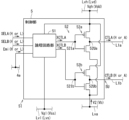
- the first potential V1 or the second potential V2 is selectively output from the control section 5 to the gate electrode of the second transistor 11e.
- the controller 5 can selectively output the first potential V1 or the second potential V2 to the gate electrode of the second transistor 11e.
- the light emitting element 12 of each of the sub-pixel circuits 1, 2 and 3 emits light. It can be switched between a state and a non-luminous state.
- the control unit 5 is connected to the gate electrode of the second transistor 11e via a signal line (also called a potential output signal line) L1. Thereby, the control unit 5 can output a signal (also referred to as a switching control signal) CTL to the gate electrode of the second transistor 11e via the potential output signal line L1.
- a signal also referred to as a switching control signal
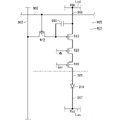
- FIG. 5 is a diagram schematically showing a configuration example related to input/output of the control unit 5.
- the control unit 5 has a function of an element (also referred to as a switch element) that performs switch control of the second transistor 11e.
- the switch control includes control to selectively switch the second transistor 11e between a state in which a current flows between the source electrode and the drain electrode and a state in which the current does not flow.
- the function of the switch element includes the function of selectively setting the light emitting element 12 to a light emitting state or a non-light emitting state. As shown in FIG.
- the control unit 5 has a portion (also referred to as a signal input unit) 5I to which a signal is input and a portion (also referred to as a signal output unit) 5U to output a signal.
- the signal input section 5I can be configured by, for example, a plurality of terminals or a plurality of wirings.
- the signal output unit 5U may be configured by, for example, one or more terminals or one or more wirings.
- a signal relating to ON or OFF is selectively input to 5I, which is also called a signal input section of the control section 5, and the second potential V2 is also input.
- a signal for setting the light emitting element 12 to the non-light emitting state which is input to the control unit 5 from the light emission control signal line 4e, is applied as the off signal.
- An H signal is applied to a signal related to OFF, and an L signal is applied to a signal related to ON.
- an H signal or an L signal is selectively input to the controller 5 as a light emission control signal (also referred to as an Emi signal) from the light emission control signal line 4e.
- the second potential V2 is input to the control unit 5 from a wiring (also referred to as a second potential supply line) Lva that supplies the second potential V2.
- the second potential supply line Lva is connected to a power supply that applies the second potential V2 to the second potential supply line Lva.
- the control section 5 outputs the first potential V1 from the signal output section 5U to the gate electrode of the second transistor 11e in response to the input of the signal relating to turning off to the signal input section 5I.
- the control unit 5 in response to the input of the H signal as the signal relating to turning off to the signal input unit 5I, the control unit 5 outputs the voltage of the second transistor 11e from the signal output unit 5U via the potential output signal line L1.
- An H signal having the first potential V1 is output to the gate electrode.
- the control unit 5 applies the second potential V2 to the gate electrode of the second transistor 11e from the signal output unit 5U in response to the input of the signal relating to ON and the input of the second potential V2 to the signal input unit 5I. Output.
- control unit 5 causes the signal output unit 5U to output the potential output signal line L1 in response to the input of the L signal as the signal relating to ON to the signal input unit 5I and the input of the second potential V2.
- a signal having the second potential V2 is output to the gate electrode of the second transistor 11e via the second transistor 11e.
- the control unit 5 supplies the gate electrode of the second transistor 11e via the potential output signal line L1 with an H signal as an off signal having the first potential V1 or the second potential V2 as the switching control signal CTL. can selectively output an A signal having
- one second transistor 11e is used to function as a switch for switching the light-emitting element 12 between a light-emitting state and a non-light-emitting state, and to function as an analog element that forms a cascode connection with the first transistor 11d. and can be easily realized.
- control unit 5 can control the timing of light emission of the light emitting element 12 by the function of the switch element.
- the H potential Vgh may be input to the control unit 5 from a wiring Lvh for supplying the H potential Vgh (also referred to as an H potential supply line or a high potential supply line), or an L potential Vgl.
- the L potential Vgl may be input from a wiring (also referred to as an L potential supply line or a low potential supply line) Lvl that supplies the L potential Vgl.
- the H-potential supply line Lvh is connected to a power supply that applies an H-potential Vgh to the H-potential supply line Lvh.
- the L potential supply line Lvl is connected to a power supply that applies an L potential Vgl to the L potential supply line Lvl.
- the controller 5 may receive the first power supply potential Vdd from the first power supply line Lvd.
- the control unit 5 may receive the second power supply potential Vss from the second power supply line Lvs instead of the L potential Vgl from the L potential supply line Lvl.
- FIG. 6 is a circuit diagram showing an example of the control unit 5.
- the control section 5 has a logic circuit section 51 and a potential conversion section 52 .
- the logic circuit section 51 appropriately converts the light emission control signal input from the light emission control signal line 4 e and outputs it to the potential conversion section 52 .
- a NOT gate 51n is applied to the logic circuit section 51.
- FIG. In this case, when an H signal is input from the light emission control signal line 4 e , the logic circuit section 51 converts it into an L signal and outputs it to the potential conversion section 52 .
- the logic circuit section 51 converts it into an H signal and outputs it to the potential conversion section 52 .
- the potential conversion section 52 converts it into an H signal as an OFF signal having the first potential V1 and outputs the H signal. Further, when the H signal is input from the logic circuit section 51, the potential conversion section 52 converts it into an A signal having the second potential V2 and outputs the A signal.
- a circuit similar to a CMOS type NOT circuit is applied to the potential converter 52 as an inverting logic circuit.
- the potential converter 52 includes a P-channel transistor and an N-channel thin film transistor which are connected in series between an H potential supply line Lvh that supplies an H potential Vgh and a second potential supply line Lva that supplies a second potential V2. (also referred to as an N-channel transistor).
- the source electrode of the P-channel transistor is connected to the H potential supply line Lvh
- the drain electrode of the P-channel transistor is connected to the drain electrode of the N-channel transistor
- the source electrode of the N-channel transistor is connected to the H potential supply line Lvh. It is connected to the second potential supply line Lva.
- the portion where the gate electrode of the P-channel transistor and the gate electrode of the N-channel transistor are connected is the input section 52I, and the drain electrode of the P-channel transistor and the drain electrode of the N-channel transistor are connected.
- the portion that is marked is the output section 52U.
- the potential conversion section 52 When an L signal is input from the logic circuit section 51 to the input section 52I, the potential conversion section 52 outputs an H signal as an OFF signal having the first potential V1 from the output section 52U. Further, when the H signal is input from the logic circuit section 51 to the input section 52I, the potential conversion section 52 outputs the A signal having the second potential V2 from the output section 52U.
- the output section 52U of the potential conversion section 52 is connected to the potential output signal line L1.
- the control unit 5 outputs the second transistor 11e from the signal output unit 5U via the potential output signal line L1 in response to the input of the H signal as a signal relating to turning off the light emission control signal to the signal input unit 5I. can output the first potential V1 to the gate electrode of the . Further, the control unit 5 outputs the potential output signal line L1 from the signal output unit 5U to the signal input unit 5I in response to the input of the L signal as a signal relating to the ON state of the light emission control signal and the input of the second potential V2. to output the second potential V2 to the gate electrode of the second transistor 11e.
- FIG. 7 is a truth table showing an example of the relationship between the input and output of the control section 5 and the state of the first sub-pixel circuit 1.
- the control unit 5 outputs the potential (also referred to as input potential) Vb input from the second potential supply line Lva, the light emission control signal input from the light emission control signal line 4e, and the potential output signal line L1.
- the switching control signal CTL is designed in a manner that satisfies the relationship shown in FIG.
- the control unit 5 If the input potential Vb input to the control unit 5 from the second potential supply line Lva is an arbitrary potential and the light emission control signal input to the control unit 5 is an H signal as a signal relating to turning off, the control unit 5 , the switching control signal CTL output to the potential output signal line L1 becomes an H signal having the first potential V1. At this time, the gate electrode of the second transistor 11e receives an H signal as an off signal having the first potential V1, so that the second transistor 11e becomes non-conductive. As a result, the light-emitting element 12 enters a non-light-emitting state in which it does not emit light.
- the input potential Vb input to the control unit 5 from the second potential supply line Lva is the second potential V2
- the light emission control signal input to the control unit 5 is an L signal as a signal relating to ON
- the switching control signal CTL output from the control section 5 to the potential output signal line L1 becomes the A signal having the second potential V2.
- the A signal having the second potential V2 is input to the gate electrode of the second transistor 11e, and current flows between the source electrode and the drain electrode of the second transistor 11e.
- the light emitting element 12 emits light
- the second transistor 11e forms a cascode connection with the first transistor 11d.
- the L signal may be applied to the off signal, and the H signal may be applied to the on signal.
- the control section 5 does not have the logic circuit section 51, and the light emission control signal input from the light emission control signal line 4e may be directly input to the input section 52I of the potential conversion section 52.
- the control unit 5 in response to the input of the L signal as a signal relating to OFF from the light emission control signal line 4e to the signal input unit 5I, the control unit 5 outputs from the signal output unit 5U through the potential output signal line L1, A first potential V1 can be output to the gate electrode of the second transistor 11e.
- the control unit 5 outputs a potential from the signal output unit 5U in response to the input of the H signal as a signal relating to ON from the light emission control signal line 4e and the input of the second potential V2 to the signal input unit 5I.
- a second potential V2 can be output to the gate electrode of the second transistor 11e via the signal line L1.
- Each pixel circuit 10 includes a control section 5 that selectively outputs the first potential V1 or the second potential V2 to each of the first subpixel circuit 1, the second subpixel circuit 2 and the third subpixel circuit 3.
- FIG. 8 is a block circuit diagram showing an example of connection between the control section 5 and the plurality of sub-pixel circuits 1, 2 and 3. As shown in FIG. As shown in FIG. 8, a configuration in which a potential output signal line L1 connected to the control section 5 is connected to a plurality of sub-pixel circuits 1, 2 and 3 can be adopted. With this configuration, the number of control units 5 in one pixel circuit 10 is less likely to increase, and the number of pixel circuits 10 is less likely to increase. Accordingly, in the display device 100 and the display panel 100p, it is possible to narrow the pitch at which the plurality of pixel circuits 10 are arranged, thereby improving the resolution. Therefore, the image quality of the display device 100 can be improved.
- the display panel 100p may include a control section 5 that selectively outputs the first potential V1 or the second potential V2 to each of the plurality of pixel circuits 10.
- the control unit 5 can selectively output the first potential V1 or the second potential V2 to the gate electrode of the second transistor 11e in each of the plurality of pixel circuits 10.
- the control unit 5 may be arranged on the first surface F1 of the substrate 20 in the empty area or frame portion of the image display unit 300, or may be arranged on the second surface F2 of the substrate 20. good.
- the control unit 5 can be arranged for each of the plurality of pixel circuits 10 forming one row of pixel circuits 10 .
- FIG. 9 is a block circuit diagram showing an example of connection between the control section 5 and the plurality of pixel circuits 10.
- a configuration in which the potential output signal line L1 connected to the control section 5 is connected to a plurality of pixel circuits 10 can be adopted. More specifically, a configuration is adopted in which the potential output signal line L1 connected to the control unit 5 is connected to a plurality of sub-pixel circuits 1, 2, and 3 included in each of the plurality of pixel circuits 10. can be With this configuration, one control unit 5 is provided for a plurality of pixel circuits 10, and the number of pixel circuits 10 is less likely to increase. Accordingly, in the display device 100 and the display panel 100p, it is possible to narrow the pitch at which the plurality of pixel circuits 10 are arranged, thereby improving the resolution. Therefore, the image quality of the display device 100 can be improved.
- the control unit 5 outputs the gate electrode of the second transistor 11e in each of the plurality of pixel circuits 10 from the signal output unit 5U in response to the input of the signal related to turning off the function of the switch element to the signal input unit 5I.
- the control unit 5 outputs from the signal output unit 5U to the plurality of pixels included in the plurality of pixel circuits 10 in response to the input of a signal relating to turning off the function of the switch element to the signal input unit 5I.
- a first potential V1 as an off potential can be output to the gate electrode of the second transistor 11e in each of the sub-pixel circuits 1, 2, and 3.
- the control unit 5 in response to the input of the H signal as a signal relating to turning off the function of the switch element to the signal input unit 5I, the control unit 5 outputs a plurality of voltages from the signal output unit 5U via the potential output signal line L1.
- an H signal as an off signal having the first potential V1 can be output to the gate electrode of the second transistor 11e in each of the pixel circuits 10 of FIG.
- the control unit 5 in response to the input of the H signal as a signal relating to turning off the function of the switch element to the signal input unit 5I, the control unit 5 outputs the voltage from the signal output unit 5U through the potential output signal line L1.
- the gate electrode of the second transistor 11e in each of the plurality of sub-pixel circuits 1, 2, 3 included in the plurality of pixel circuits 10 can output an H signal as an off signal having the first potential V1.
- the control unit 5 In response to the input of a signal relating to ON of the function of the switch element to the signal input unit 5I and the input of the second potential V2, the control unit 5 outputs the second potential in each of the plurality of pixel circuits 10 from the signal output unit 5U.
- a second potential V2 can be output to the gate electrode of the transistor 11e. More specifically, the control unit 5 outputs a plurality of pixel circuits from the signal output unit 5U to the signal input unit 5I in response to the input of a signal relating to ON of the function of the switch element and the input of the second potential V2.
- a second potential V2 can be output to the gate electrode of the second transistor 11e in each of the plurality of subpixel circuits 1, 2, and 3 included in 10, respectively.
- control unit 5 causes the signal output unit 5U to output potential from the signal output unit 5U in response to the input of the L signal as a signal relating to ON of the function of the switch element to the signal input unit 5I and the input of the second potential V2.
- An A signal having the second potential V2 can be output to the gate electrode of the second transistor 11e in each of the plurality of pixel circuits 10 via the signal line L1.
- the control unit 5 in response to the input of the L signal as a signal relating to the ON of the function of the switch element to the signal input unit 5I and the input of the second potential V2, the control unit 5 outputs from the signal output unit 5U, A signal having the second potential V2 is output to the gate electrode of the second transistor 11e in each of the plurality of sub-pixel circuits 1, 2 and 3 included in the plurality of pixel circuits 10 through the potential output signal line L1.
- control unit 5 outputs an OFF signal having the first potential V1 as the switching control signal CTL to the gate electrode of the second transistor 11e in each of the plurality of pixel circuits 10 via the potential output signal line L1. or an A signal having the second potential V2 can be selectively output. More specifically, the control unit 5 controls the gate electrode of the second transistor 11e in each of the plurality of sub-pixel circuits 1, 2, 3 included in the plurality of pixel circuits 10 via the potential output signal line L1. In addition, as the switching control signal CTL, an H signal as an off signal having a first potential V1 or an A signal having a second potential V2 can be selectively output.
- the plurality of elements E1 connected in series or cascade between the first power supply potential input section 1dl and the second power supply potential input section 1sl are the light emitting elements 12 as the first elements E11, Elements other than the first transistor 11d as the second element E12 and the second transistor 11e as the third element E13 may be included.
- the light emitting element 12 as the first element E11 is connected in parallel, and the light emitting element 12 (first light emitting element 12a) and the light emitting element 12 (also referred to as the second light emitting element 12b) as the second first element (also referred to as the 1B element) E11b.
- the plurality of elements E1 serves as a first fourth element (also referred to as a 4A element) E14a connected in series to the first light emitting element 12a, and a fourth transistor 13 (also referred to as a 4A transistor 13a).
- a fourth transistor 13 also referred to as a 4th B transistor 13b
- a second fourth element also referred to as a 4th B element
- FIG. 10 is a circuit diagram showing the first sub-pixel circuit 1 according to another example of the first embodiment. Also in another example of the first embodiment, each of the second subpixel circuit 2 and the third subpixel circuit 3 has the same or similar configuration as the first subpixel circuit 1 .
- the first sub-pixel circuit 1 according to another example of the first embodiment is based on the example of the first sub-pixel circuit 1 according to the first embodiment shown in FIG.
- two subpixel circuits are connected in parallel between the second transistor 11e and the second power supply potential input section 1sl. It includes a set of fourth transistors 13 and a light emitting element 12 .
- the fourth transistor 13 and the light emitting element 12 are connected in series.
- the two series-connected sets of the fourth transistor 13 and the light-emitting element 12 are a series-connected set of the 4A transistor 13a and the first light-emitting element 12a, and a series-connected set of the 4B transistor 13b and the light-emitting element 12. and a set of second light emitting elements 12b.
- the first subpixel circuit 1 includes two sets of multiple elements E1 connected in series or cascade between the first power supply potential input section 1dl and the second power supply potential input section 1sl. .
- the two sets of elements E1 include a first set of elements E1 and a second set of elements E1.
- the plurality of elements E1 in the first set includes a first light emitting element 12a as a first element (first A element) E11a, a first transistor 11d as a second element E12, and a third element E13 as It includes a second transistor 11e and a 4A transistor 13a as a first fourth element (4A element) E14a.
- first transistor 11d as the second element E12
- second transistor 11e as the third element E13
- the 4th A transistor 13a as the 4th A element E14a and the first light emitting element 12a as the 1st A element E11a are connected in series or cascade in this order.
- the second set of multiple elements E1 includes a second light emitting element 12b as a second first element (first B element) E11b, a first transistor 11d as a second element E12, and a third element E13 as It includes a second transistor 11e and a fourth B transistor 13b as a second fourth element (fourth B element) E14b.
- the fourth B transistor 13b as the fourth B element E14b and the second light emitting element 12b as the first B element E11b are connected in series or tandem in this order.
- the 4th A transistor 13a is cascade-connected to the first transistor 11d and the second transistor 11e.
- the fourth A transistor 13a is located on a connection line (drive line) connecting the second transistor 11e and the first light emitting element 12a.
- a P-channel transistor is applied to the 4th A transistor 13a, the source electrode of the 4th A transistor 13a is connected to the drain electrode of the second transistor 11e, and the drain electrode of the 4th A transistor 13a is connected to the first light emitting element 12a.
- the 4A transistor 13a is an element (also referred to as a use state setting element) for selectively setting the first light emitting element 12a to a state in which it is used (also referred to as a use state) or a state in which it is not used (also referred to as a non-use state).
- the fourth A transistor 13a is in a state in which current cannot flow between the source electrode and the drain electrode (non-conducting state) and a and the drain electrode (conducting state). Assume that a P-channel transistor is applied to the fourth A transistor 13a.
- the setting control unit 7 may be a control circuit included in each of the plurality of sub-pixel circuits 1, 2, 3, or may be a control circuit included in each of the plurality of pixel circuits 10. , it may be a control circuit included in each of the plurality of pixel circuits 10 in the display panel 100p, or may be a control circuit included in the driving section 30.
- the fourth B transistor 13b is cascade-connected to the first transistor 11d and the second transistor 11e.
- the fourth B transistor 13b is located on a connection line (drive line) that connects the second transistor 11e and the second light emitting element 12b.
- a P-channel transistor is applied to the fourth B transistor 13b, the source electrode of the fourth B transistor 13b is connected to the drain electrode of the second transistor 11e, and the drain electrode of the fourth B transistor 13b is connected to the second light emitting element 12b.
- the 4B transistor 13b has a function of an element (use state setting element) for selectively setting the second light emitting element 12b to a state of use (use state) or a state of not using it (non-use state).
- the fourth B transistor 13b is switched between a non-conducting state and a conducting state according to an H signal or an L signal selectively input from the setting control section 7.
- FIG. Assume that a P-channel transistor is applied to the fourth B transistor 13b.
- the 4B transistor 13b becomes non-conducting and the second light emitting element 12b is set to the non-use state.
- the L signal is input to the gate electrode of the 4B transistor 13b, the 4B transistor 13b becomes conductive and the second light emitting element 12b is set to use.
- an N-channel transistor may be applied to the 4th A transistor 13a
- an N-channel transistor may be applied to the 4th B transistor 13b.
- the fourth A transistor 13a is an N-channel transistor.
- the 4A transistor 13a becomes non-conductive and the first light emitting element 12a is set to a non-use state.
- the H signal is input to the gate electrode of the 4th A transistor 13a
- the 4th A transistor 13a becomes conductive, and the first light emitting element 12a is set to the use state.
- the fourth B transistor 13b is an N-channel transistor.
- the 4B transistor 13b becomes non-conducting and the second light emitting element 12b is set to the non-use state.
- the 4B transistor 13b becomes conductive and the second light emitting element 12b is set to use.
- the 4A transistor 13a may be positioned between the first light emitting element 12a and the second power supply potential input section 1sl
- the 4B transistor 13b may be positioned between the second light emitting element 12b and the second power supply potential input section 1sl. It may be positioned between the power supply potential input section 1sl.
- the pixel circuit 10 includes the light emitting element 12, the first transistor 11d, and the second transistor connected in series or cascade between the first power supply potential input section 1dl and the second power supply potential input section 1sl. 11e.
- the first transistor 11d can control the current flowing through the light emitting element 12 by inputting a potential corresponding to the image signal to the gate electrode.
- the second transistor 11e is cascade-connected to the first transistor 11d, and can switch the light-emitting element 12 between a light-emitting state and a non-light-emitting state.
- the second transistor 11e is of the same conductivity type as the first transistor 11d, and is connected in series with the first transistor 11d on the drain side of the first transistor 11d.
- a light emitting element 12 is connected to the drain electrode of the second transistor 11e.
- the gate electrode of the second transistor 11e has a first potential V1 for setting the second transistor 11e in a non-conducting state and a potential V1 for causing a current to flow between the source electrode and the drain electrode of the second transistor 11e. Either one of the second potential V2 between the first power potential Vdd and the second power potential Vss is selectively input.
- the second transistor 11e functions not only as a switch for switching the light-emitting element 12 between the light-emitting state and the non-light-emitting state, but also as an analog element that forms a cascode connection with the first transistor 11d. have.
- the effect of the cascode connection to the first transistor 11d by the second transistor 11e can be obtained without increasing the number of transistors connected in cascade with the first transistor 11d. Therefore, among the potential difference (Vdd ⁇ Vss) between the first power supply potential Vdd and the second power supply potential Vss, the drain-source voltage Vds of the first transistor 11d is less likely to decrease.
- the first subpixel circuit 1 may include a plurality of light emitting elements 12 and a plurality of second transistors 11e.
- the plurality of light emitting elements 12 includes a first light emitting element 12a and a second light emitting element 12b connected in parallel.
- the plurality of second transistors 11e includes a second transistor 11e (also referred to as a second A transistor 11ea) connected in series to the first light emitting element 12a and a second transistor 11e (also referred to as a second transistor 11ea) connected in series to the second light emitting element 12b. 2B transistor 11eb).
- the first potential V1 or the second potential V2 is selectively input to the gate electrode of the second A transistor 11ea, and the first potential V1 or the second potential V2 is selectively input to the gate electrode of the second B transistor 11eb. may be entered in
- the plurality of second transistors 11e having the function of switching the plurality of redundantly provided light emitting elements 12 between the light emitting state and the non-light emitting state are analog elements forming a cascode connection with the first transistor 11d. It has a function as As a result, the effect of the cascode connection to the first transistor 11d by the second transistor 11e can be obtained without increasing the number of transistors connected in series with the first transistor 11d. Therefore, among the potential difference (Vdd ⁇ Vss) between the first power supply potential Vdd and the second power supply potential Vss, the drain-source voltage Vds of the first transistor 11d is less likely to decrease.
- FIG. 11 is a circuit diagram showing an example of the first sub-pixel circuit 1 according to the second embodiment.
- the first subpixel circuit 1 has the same or similar configuration.
- the second subpixel circuit 2 and the third subpixel circuit 3 has the same or similar configuration as the first subpixel circuit 1 .
- An example of the first sub-pixel circuit 1 according to the second embodiment is based on the example of the first sub-pixel circuit 1 according to the first embodiment shown in FIG.
- the first subpixel circuit 1 according to the second embodiment instead of a set of the second transistor 11e and the light emitting element 12 connected in series between the first transistor 11d and the second power supply potential input section 1sl, , includes two sets of second transistors 11e and light emitting elements 12 connected in parallel. The second transistor 11e and the light emitting element 12 are connected in series.
- the two series-connected sets of the second transistor 11e and the light-emitting element 12 are a series-connected set of the second A transistor 11ea and the first light-emitting element 12a, and a series-connected set of the second B transistor 11eb and the light-emitting element 12a. and a set of second light emitting elements 12b.
- the first sub-pixel circuit 1 includes two sets of multiple elements E1 connected in series or cascade between the first power supply potential input section 1dl and the second power supply potential input section 1sl. include.
- the two sets of elements E1 include a first set of elements E1 and a second set of elements E1.
- the plurality of elements E1 in the first set includes a first light emitting element 12a as a first element (first A element) E11a, a first transistor 11d as a second element E12, and a first third element E12.
- 2A transistor 11ea as element (also referred to as 3A element) E13a.
- a first transistor 11d as the second element E12, a second A transistor 11ea as the third A element E13a between the first power supply potential input section 1dl and the second power supply potential input section 1sl, a first transistor 11d as the second element E12, a second A transistor 11ea as the third A element E13a,
- the first light emitting element 12a as the first A element E11a is connected in series or cascade in the order of this description.
- the second set of multiple elements E1 includes a second light emitting element 12b as a second first element (first B element) E11b, a first transistor 11d as a second element E12, and a second third element E12. and a second B transistor 11eb as an element (also referred to as a third B element) E13b.
- a first transistor 11d as the second element E12, a second B transistor 11eb as the third B element E13b between the first power supply potential input section 1dl and the second power supply potential input section 1sl, a first transistor 11d as the second element E12, a second B transistor 11eb as the third B element E13b,
- the second light emitting element 12b as the first B element E11b is connected in series or cascade in this order.
- the light emission of the plurality of light emitting elements 12 can be controlled by the light emission control section 11 having the first transistor 11d, the plurality of second transistors 11e, the third transistor 11g, and the capacitive element 11c.
- the second A transistor 11ea can switch the first light emitting element 12a between a light emitting state and a non-light emitting state.
- the second A transistor 11ea functions as an element (use state setting element) for selectively setting the first light emitting element 12a to the use state or the non-use state, and and a function as an element (light emission control element) for controlling light emission and non-light emission of.
- the second A transistor 11ea is located on a connection line (drive line) that connects the first transistor 11d and the first light emitting element 12a.
- a transistor of the same conductivity type as the first transistor 11d is applied to the second A transistor 11ea.
- P-channel transistors are applied to transistors of the same conductivity type.
- the second A transistor 11ea is cascade-connected to the first transistor 11d on the drain electrode side of the first transistor 11d. More specifically, the source electrode of the second A transistor 11ea is connected to the drain electrode of the first transistor 11d.
- a first light emitting element 12a is connected to the drain electrode of the second A transistor 11ea. More specifically, the positive electrode of the first light emitting element 12a is connected to the drain electrode of the second A transistor 11ea.
- a negative electrode of the first light emitting element 12a is connected to the second power supply potential input section 1sl.
- the second B transistor 11eb can switch the second light emitting element 12b between a light emitting state and a non-light emitting state.
- the second B transistor 11eb functions as an element (use state setting element) for selectively setting the second light emitting element 12b to the use state or the non-use state, and and a function as an element (light emission control element) for controlling light emission and non-light emission of.
- the second B transistor 11eb is located on a connection line (drive line) that connects the first transistor 11d and the second light emitting element 12b.
- a transistor of the same conductivity type as the first transistor 11d is applied to the second B transistor 11eb.
- P-channel transistors are applied to transistors of the same conductivity type.
- the second B transistor 11eb is cascade-connected to the first transistor 11d on the drain electrode side of the first transistor 11d. More specifically, the source electrode of the second B transistor 11eb is connected to the drain electrode of the first transistor 11d.
- a second light emitting element 12b is connected to the drain electrode of the second B transistor 11eb. More specifically, the positive electrode of the second light emitting element 12b is connected to the drain electrode of the second B transistor 11eb.
- a negative electrode of the second light emitting element 12b is connected to the second power supply potential input section 1sl.
- the first transistor 11d is provided with a second A transistor 11ea and a second B transistor as the second transistor 11e.
- a form in which only 11eb is connected in cascade may be employed. In this case, among the potential difference (Vdd ⁇ Vss) between the first power supply potential Vdd and the second power supply potential Vss, the drain-source voltage Vds of the first transistor 11d is less likely to decrease.
- the first potential V1 or the second potential V2 is selectively output from the control section 5 to the gate electrode of the second A transistor 11ea.
- the controller 5 can selectively output the first potential V1 or the second potential V2 to the gate electrode of the second A transistor 11ea.
- the first potential V1 or the second potential V2 is selectively output from the control section 5 to the gate electrode of the second B transistor 11eb.
- the control unit 5 can selectively output the first potential V1 or the second potential V2 to the gate electrode of the second B transistor 11eb.
- the first light emitting element 12a for each of the sub-pixel circuits 1, 2 and 3 and the second light emitting element 12b can be switched between a light emitting state and a non-light emitting state.
- control section 5 is connected to the gate electrode of the second A transistor 11ea via the first potential output signal line (first potential output signal line) L1a.
- control unit 5 can output a first switching control signal (also referred to as a first switching control signal) CTLA to the gate electrode of the second A transistor 11ea via the first potential output signal line L1a.
- control unit 5 is connected to the gate electrode of the second B transistor 11eb via a second potential output signal line (second potential output signal line) L1b.
- the control section 5 can output a second switching control signal (also referred to as a second switching control signal) CTLB to the gate electrode of the second B transistor 11eb via the second potential output signal line L1b.
- FIG. 12 is a gate circuit diagram schematically showing a configuration example related to the input/output gates of the control section 5.
- the control unit 5 has the functions of a plurality of switch elements that perform switch control of the second transistor 11e.
- the switch control includes control to selectively switch the second transistor 11e between a state in which a current flows between the source electrode and the drain electrode and a state in which the current does not flow.
- the functions of the plurality of switch elements are a function of selectively setting the light emitting element 12 to a state of use (use state) or a state of not being used (non-use state), and a function of selectively setting the light emitting element 12 to a light emitting state or a non-light emitting state.
- the functions of the plurality of switch elements are the function of selectively setting the first light emitting element 12a to the use state or the non-use state, and the function of selectively setting the light emitting element 12 to the light emitting state or the non-light emitting state.
- the functions of the plurality of switch elements are a function of selectively setting the second light emitting element 12b to a use state or a non-use state, and a function of selectively setting the light emitting element 12 to a light emitting state or a non-light emitting state.
- the control unit 5 controls the function of the switch element (also referred to as the first switch element) including the function of selectively setting the first light emitting element 12a to the use state or the non-use state, and the second light emission. a function of a switch element (also referred to as a second switch element) including a function of selectively setting the element 12b to the use state or the non-use state.
- the control unit 5 further controls the function of the switch element (also referred to as a third switch element) including the function of selectively setting each of the first light emitting element 12a and the second light emitting element 12b to a light emitting state or a non-light emitting state. I have.
- a signal input unit 5I of the control unit 5 selectively receives signals for turning on or off each function of a plurality of switch elements that perform switch control of one second transistor 11e. 2nd electric potential V2 is input while inputting.
- the signal input unit 5I of the control unit 5 selectively receives a signal for turning on or off the function of the first switch element, and turns the function of the second switch element on or off. Such a signal is selectively input, and the second potential V2 is also input.
- a signal input section 5I of the control section 5 selectively receives a signal for turning on or off the function of the third switch element.
- a signal for disabling the first light emitting element 12a is applied to the signal for turning off, and the signal for turning on the first light emitting element 12a is applied to the signal for turning on. 12a is applied.
- a signal for disabling the second light emitting element 12b is applied to the signal relating to OFF, and the second light emitting element 12b is used for the signal relating to ON. A signal is applied to make the state.
- the signal for turning off the light emitting element 12 is applied to the signal for turning off the light emitting element 12, and the signal for turning on the signal for turning the light emitting element 12 to the light emitting state is applied.
- An H signal is applied to a signal related to OFF, and an L signal is applied to a signal related to ON.
- control unit 5 receives a signal SELA (also referred to as a first selection setting signal) relating to ON or OFF of the function of the first switch element, and a signal SELA for ON or OFF of the function of the second switch element.
- a related signal also referred to as a second selection setting signal
- An H signal as a signal relating to OFF or an L signal as a signal relating to ON is selectively input to the control unit 5 as the first selection setting signal SELA.
- the controller 5 selectively receives an H signal as a signal relating to OFF or an L signal as a signal relating to ON.
- the controller 5 selectively receives an H signal as a signal relating to OFF or an L signal as a signal relating to ON as a light emission control signal from a light emission control signal line 4e.
- the second potential V2 is input to the controller 5 from the second potential supply line Lva.
- the control unit 5 responds to a signal input to the signal input unit 5I for turning off one or more of the functions of a plurality of switch elements,
- the signal output unit 5U outputs the first potential V1 to the gate electrode of the second transistor 11e.
- the control unit 5 inputs to the signal input unit 5I a signal related to turning on the functions of all the switch elements among the functions of the plurality of switch elements, and the second potential V2.
- the signal output unit 5U outputs the second potential V2 to the gate electrode of the second transistor 11e.
- the control unit 5 In response to input of one or more signals of a signal relating to turning off the function of the first switch element and a signal relating to turning off the function of the third switching element to the signal input part 5I, the control unit 5 The signal output unit 5U outputs the first potential V1 to the gate electrode of the second A transistor 11ea. Further, the control unit 5 inputs a signal related to turning on the function of the first switch element, inputs a signal related to turning on the function of the third switching element, and inputs a signal related to turning on the function of the third switching element to the signal input unit 5I. In response to the input, the signal output unit 5U outputs the second potential V2 to the gate electrode of the second A transistor 11ea.
- the control unit 5 supplies the signal input unit 5I with an H signal as a signal related to turning off the first light emitting element 12a and an off signal for turning the light emitting element 12 into a non-light emitting state.
- the first potential V1 is applied to the gate electrode of the second A transistor 11ea from the signal output unit 5U via the first potential output signal line L1a. output an H signal as an off signal.
- the control unit 5 outputs an H signal, which is a signal related to turning off as the first selection setting signal SELA, and an H signal, which is a signal related to turning off as the light emission control signal, to the signal input unit 5I.
- the control unit 5 inputs an L signal as a signal relating to ON for setting the first light emitting element 12a to the use state and an ON signal for setting the light emitting element 12 to the light emitting state to the signal input unit 5I.
- the second potential V2 is applied to the gate electrode of the second A transistor 11ea from the signal output unit 5U via the first potential output signal line L1a. output the A signal.
- control unit 5 inputs an L signal, which is a signal related to ON as the first selection setting signal SELA, and an L signal, which is a signal related to ON as the light emission control signal, to the signal input unit 5I. and the input of the second potential V2 from the second potential supply line Lva, from the signal output unit 5U to the gate electrode of the second A transistor 11ea via the first potential output signal line L1a, A signal having the second potential V2 is output as the first switching control signal CTLA.
- L signal which is a signal related to ON as the first selection setting signal SELA
- L signal which is a signal related to ON as the light emission control signal
- the control unit 5 supplies the gate electrode of the second A transistor 11ea via the first potential output signal line L1a as the first switching control signal CTLA.
- a signal having two potentials V2 can be selectively output.
- the first light emitting element 12a of the two redundantly provided light emitting elements 12 has a switch function for switching between the use state and the non-use state, and emits light.
- the function of a switch to switch between a state and a non-luminous state and the function of an analog element forming a cascode connection to the first transistor 11d can be easily realized.
- control unit 5 outputs one or more signals to the signal input unit 5I among a signal related to turning off the function of the second switching element and a signal related to turning off the function of the third switching element.
- the signal output unit 5U outputs the first potential V1 to the gate electrode of the second B transistor 11eb.
- control unit 5 inputs a signal related to turning on the function of the second switch element, inputs a signal related to turning on the function of the third switching element, and inputs a signal related to turning on the function of the third switching element to the signal input unit 5I.
- the signal output unit 5U outputs the second potential V2 to the gate electrode of the second B transistor 11eb.
- the control unit 5 supplies the signal input unit 5I with an H signal as a signal related to turning off the second light emitting element 12b and an off signal for turning the light emitting element 12 into a non-light emitting state.
- the first potential V1 is applied to the gate electrode of the second B transistor 11eb from the signal output unit 5U via the second potential output signal line L1b. output an H signal as an off signal.
- the control unit 5 outputs an H signal, which is a signal related to OFF as the second selection setting signal SELB, and an H signal, which is a signal related to OFF as the light emission control signal, to the signal input unit 5I.
- the control unit 5 inputs an L signal as a signal relating to ON for setting the second light emitting element 12b to the use state and an ON signal for setting the light emitting element 12 to the light emitting state to the signal input unit 5I.
- the second potential V2 is applied to the gate electrode of the second B transistor 11eb from the signal output unit 5U via the second potential output signal line L1b. output the A signal.
- control unit 5 inputs an L signal, which is a signal related to ON as the second selection setting signal SELB, and an L signal, which is a signal related to ON as the light emission control signal, to the signal input unit 5I. and the input of the second potential V2 from the second potential supply line Lva, from the signal output unit 5U to the gate electrode of the second B transistor 11eb via the second potential output signal line L1b, A signal having the second potential V2 is output as the second switching control signal CTLB.
- L signal which is a signal related to ON as the second selection setting signal SELB
- L signal which is a signal related to ON as the light emission control signal
- the control unit 5 supplies the gate electrode of the second B transistor 11eb via the second potential output signal line L1b as the second switching control signal CTLB, which is the H signal or the second OFF signal having the first potential V1.
- a signal having two potentials V2 can be selectively output.
- the second light emitting element 12b of the two redundantly provided light emitting elements 12 has a function of a switch for switching between the use state and the non-use state, and emits light.
- the function of a switch to switch between a state and a non-luminous state and the function of an analog element forming a cascode connection to the first transistor 11d can be easily realized.
- FIG. 13 is a circuit diagram showing an example of the control unit 5.
- FIG. An example of the control unit 5 according to the second embodiment is based on an example of the control unit 5 according to the first embodiment shown in FIG.
- the control unit 5 according to the second embodiment has a logic circuit unit 51 and a potential conversion unit 52 that are different configurations from the logic circuit unit 51 and the potential conversion unit 52 according to the first embodiment.
- the logic circuit unit 51 generates a first intermediate signal (also referred to as a first intermediate output signal) according to the inputs of the first selection setting signal SELA, the second selection setting signal SELB, and the light emission control signal. ) XCTLA and a second intermediate signal (also referred to as a second intermediate output signal) XCTLB.
- the logic circuit unit 51 selects the first selection setting signal SELA, the second selection setting signal SELB, and the light emission control signal according to the combination of the L signal as the ON signal and the H signal as the OFF signal. Therefore, an L signal or an H signal can be output as each of the first intermediate output signal XCTLA and the second intermediate output signal XCTLB.
- the control unit 5 and the logic circuit unit 51 may receive the H potential Vgh from the H potential supply line Lvh, or the L potential Vgl from the L potential supply line Lvl.
- the control unit 5 and the logic circuit unit 51 may receive the first power supply potential Vdd from the first power supply line Lvd.
- the control unit 5 and the logic circuit unit 51 may receive the second power supply potential Vss from the second power supply line Lvs instead of the L potential Vgl from the L potential supply line Lvl.
- the potential converter 52 includes a first potential converter 52a and a second potential converter 52b.
- the first potential conversion unit 52a converts it into an H signal having the first potential V1, and outputs the OFF signal as the first switching control signal CTLA. output an H signal. Further, when the H signal as the first intermediate output signal XCTLA is input from the logic circuit unit 51, the first potential conversion unit 52a converts it into the A signal having the second potential V2, and converts it into the A signal having the second potential V2 as the first switching control signal CTLA. A signal of is output.
- a circuit similar to a CMOS-type NOT circuit as an inverting logic circuit is applied to the first potential converter 52a.
- the first potential converter 52a includes a P-channel transistor and an N-channel transistor connected in cascade between an H potential supply line Lvh that supplies an H potential Vgh and a second potential supply line Lva that supplies a second potential V2. and a transistor. More specifically, the source electrode of the P-channel transistor is connected to the H potential supply line Lvh, the drain electrode of the P-channel transistor is connected to the drain electrode of the N-channel transistor, and the source electrode of the N-channel transistor is connected to the H potential supply line Lvh. It is connected to the second potential supply line Lva.
- the portion where the gate electrode of the P-channel transistor and the gate electrode of the N-channel transistor are connected is an input section (also referred to as a first input section) 52Ia, and the drain electrode of the P-channel transistor. and the drain electrode of the N-channel transistor are connected to an output section (also referred to as a first output section) 52Ua.
- the first potential conversion section 52a outputs an OFF signal having the first potential V1 from the first output section 52Ua.
- the first potential conversion unit 52a receives the A signal having the second potential V2 from the first output unit 52Ua. Output a signal.
- the first output section 52Ua of the first potential conversion section 52a is connected to the first potential output signal line L1a.
- the control unit 5 outputs one or more of an H signal as a signal related to turning off the first selection setting signal SELA and an H signal as a signal related to turning off the light emission control signal to the signal input unit 5I.
- the signal output unit 5U can output the first potential V1 to the gate electrode of the second A transistor 11ea via the first potential output signal line L1a.
- the control unit 5 inputs an L signal as a signal associated with turning on the first selection setting signal SELA, inputs an L signal as a signal associated with turning on the light emission control signal, and inputs an L signal as a signal associated with turning on the light emission control signal to the signal input unit 5I.
- the signal output section 5U can output the second potential V2 to the gate electrode of the second A transistor 11ea via the first potential output signal line L1a.
- the second potential converter 52b has the same or similar configuration as the first potential converter 52a.
- the second potential conversion unit 52b converts it into an H signal having the first potential V1, and outputs the OFF signal as the second switching control signal CTLB. output an H signal.
- the second potential conversion unit 52b converts it into the A signal having the second potential V2, and converts it into the A signal having the second potential V2 as the second switching control signal CTLB.
- a signal of is output.
- a circuit similar to a CMOS-type NOT circuit as an inverting logic circuit is applied to the second potential converter 52b.
- the second potential converter 52b includes a P-channel transistor and an N-channel transistor connected in series between an H potential supply line Lvh that supplies an H potential Vgh and a second potential supply line Lva that supplies a second potential V2. and a transistor. More specifically, the source electrode of the P-channel transistor is connected to the H potential supply line Lvh, the drain electrode of the P-channel transistor is connected to the drain electrode of the N-channel transistor, and the source electrode of the N-channel transistor is connected to the H potential supply line Lvh. It is connected to the second potential supply line Lva.
- the portion where the gate electrode of the P-channel transistor and the gate electrode of the N-channel transistor are connected is an input section (also referred to as a second input section) 52Ib, and the drain electrode of the P-channel transistor. and the drain electrode of the N-channel transistor are connected to an output section (also referred to as a second output section) 52Ub.
- the second potential conversion section 52b outputs an OFF signal having the first potential V1 from the second output section 52Ub.
- the second potential converting section 52b receives the A signal having the second potential V2 from the second output section 52Ub. Output a signal.
- the second output section 52Ub of the second potential conversion section 52b is connected to the second potential output signal line L1b.
- the control unit 5 outputs one or more of an H signal as a signal related to turning off the second selection setting signal SELB and an H signal as a signal related to turning off the light emission control signal to the signal input unit 5I.
- the signal output unit 5U can output the first potential V1 to the gate electrode of the second B transistor 11eb via the second potential output signal line L1b.
- the control unit 5 inputs an L signal as a signal related to turning on the second selection setting signal SELB, inputs an L signal as a signal related to turning on the light emission control signal, and inputs an L signal as a signal related to turning on the light emission control signal to the signal input unit 5I.
- the signal output section 5U can output the second potential V2 to the gate electrode of the second B transistor 11eb via the second potential output signal line L1b.
- FIG. 14 is a truth table showing an example of the relationship between the input, the intermediate output signal, the output, and the state of the first sub-pixel circuit 1 in the control section 5.
- the controller 5 receives the input potential Vb input from the second potential supply line Lva, the light emission control signal input from the light emission control signal line 4e, and the first selection setting signal SELA.
- the second selection setting signal SELB, the first switching control signal CTLA output to the first potential output signal line L1a, and the second switching control signal CTLB output to the second potential output signal line L1b are shown in FIG.
- the logic circuit section 51 includes a light emission control signal input from the light emission control signal line 4e, a first selection setting signal SELA input, a second selection setting signal SELB input, and a first potential.
- the first intermediate output signal XCTLA output to the conversion section 52a and the second intermediate output signal XCTLB output to the second potential conversion section 52b satisfy the relationship shown in FIG. 14, and perform various logic outputs. Designed with configuration.
- the input potential Vb input to the control unit 5 from the second potential supply line Lva is an arbitrary potential
- the light emission control signal input to the control unit 5 is H as a signal relating to OFF. If it is a signal, the first switching control signal CTLA output by the control unit 5 to the first potential output signal line L1a and the second switching control signal CTLB output by the control unit 5 to the second potential output signal line L1b are respectively the first switching control signal CTLA and the second switching control signal CTLB. It becomes an H signal as an off signal having 1 potential V1.
- the first selection setting signal SELA and the second selection setting signal SELB are turned on.
- the first intermediate output signal XCTLA and the second intermediate output signal XCTLB are each an L signal regardless of whether the L signal is the relevant signal or the H signal is the OFF signal.
- each of the second A transistor 11ea and the second B transistor 11eb is turned off by inputting an H signal as an off signal having the first potential V1 to the gate electrode.
- both the first light emitting element 12a and the second light emitting element 12b enter the non-light emitting state.
- the input potential Vb input to the control unit 5 from the second potential supply line Lva is the second potential V2
- the light emission control signal input to the control unit 5 is an L signal as a signal relating to ON
- the control unit 5 outputs to the first potential output signal line L1a.
- the first switching control signal CTLA becomes an A signal having the second potential V2
- the second switching control signal CTLB output by the control section 5 to the second potential output signal line L1b becomes an H signal as an OFF signal having the first potential V1. becomes.
- the light emission control signal input to the control unit 5 is an L signal as a signal relating to ON
- the first selection setting signal SELA is an L signal as a signal relating to ON
- the first selection setting signal SELA is an L signal as a signal relating to ON. Since the second selection setting signal SELB is an H signal as a signal relating to OFF, the first intermediate output signal XCTLA becomes an H signal and the second intermediate output signal XCTLB becomes an L signal.
- the A signal having the second potential V2 is input to the gate electrode of the second A transistor 11ea, and the first light emitting element 12a enters a light emitting state (also referred to as a first light emitting state).
- the second A transistor 11ea is in a state of forming a cascode connection with the first transistor 11d. Further, an H signal as an OFF signal having the first potential V1 is input to the gate electrode of the second B transistor 11eb, and the second light emitting element 12b enters a non-light emitting state (also referred to as a second non-light emitting state). .
- the input potential Vb input to the control unit 5 from the second potential supply line Lva is the second potential V2
- the light emission control signal input to the control unit 5 is an L signal as a signal relating to ON
- the control unit 5 outputs to the first potential output signal line L1a.
- the first switching control signal CTLA becomes an H signal as an OFF signal having a first potential V1
- the second switching control signal CTLB output by the control unit 5 to the second potential output signal line L1b becomes an A signal having a second potential V2. becomes.
- the light emission control signal input to the control section 5 is an L signal as a signal relating to ON
- the first selection setting signal SELA is an H signal as a signal relating to OFF
- the first selection setting signal SELA is a signal relating to OFF. Since the second selection setting signal SELB is an L signal as a signal relating to ON, the first intermediate output signal XCTLA becomes an L signal and the second intermediate output signal XCTLB becomes an H signal. Then, an H signal as an OFF signal having the first potential V1 is input to the gate electrode of the second A transistor 11ea, and the first light emitting element 12a enters a non-light emitting state (also referred to as a first non-light emitting state).
- the A signal having the second potential V2 is input to the gate electrode of the second B transistor 11eb, and the second light emitting element 12b enters a light emitting state (also referred to as a second light emitting state).
- the second B transistor 11eb forms a cascode connection with the first transistor 11d.
- the input potential Vb input to the control unit 5 from the second potential supply line Lva is the second potential V2
- the light emission control signal input to the control unit 5 is an L signal as a signal relating to ON
- the control unit 5 outputs to the first potential output signal line L1a.
- the first switching control signal CTLA becomes the A signal having the second potential V2
- the second switching control signal CTLB output by the control section 5 to the second potential output signal line L1b becomes the A signal having the second potential V2.
- the light emission control signal input to the control unit 5 is an L signal as a signal relating to ON
- the first selection setting signal SELA is an L signal as a signal relating to ON
- the first selection setting signal SELA is an L signal as a signal relating to ON. Since the second selection setting signal SELB is an L signal as a signal relating to ON, both the first intermediate output signal XCTLA and the second intermediate output signal XCTLB become an H signal.
- the A signal having the second potential V2 is input to the gate electrodes of the second A transistor 11ea and the second B transistor 11eb, and both the first light emitting element 12a and the second light emitting element 12b are in a light emitting state ( (also referred to as a dual emission state).
- both the second A transistor 11ea and the second B transistor 11eb form a cascode connection with the first transistor 11d.
- the signal output circuit 6 includes a first signal output section 6a and a second signal output section 6b.
- the first signal output section 6a can output the first selection setting signal SELA.
- the second signal output section 6b can output the second selection setting signal SELB. More specifically, the first signal output unit 6a can selectively output to the control unit 5, as the first selection setting signal SELA, an H signal as a signal relating to OFF or an L signal as a signal relating to ON. .
- the second signal output unit 6b can selectively output to the control unit 5, as the second selection setting signal SELB, an H signal as a signal relating to OFF or an L signal as a signal relating to ON.
- the first signal output unit 6a includes a data holding circuit (such as a flip-flop circuit or a latch circuit capable of selectively switching the first selection setting signal SELA to an L signal or an H signal and holding the state). (also called a holding circuit) is applied.
- the second signal output unit 6b includes a data holding circuit (such as a flip-flop circuit or a latch circuit capable of selectively switching the second selection setting signal SELB to an L signal or an H signal and holding the state). holding circuit) is applied.
- the holding circuit as the first signal output unit 6a is once input (written) with a signal (also referred to as a first setting signal) as data for setting the state, so that the first selection setting signal SELA is L. It is set to a state in which it continues to output either the signal or the H signal.
- the holding circuit as the second signal output unit 6b is once input (written) with a signal (also referred to as a second setting signal) as data for setting the state, so that the second selection setting signal SELB is L. It is set to a state in which it continues to output either the signal or the H signal.
- the image signal line 4s is used as a signal line (also referred to as a first write signal line) for inputting (writing) a first setting signal to the first signal output section 6a, and is used as a second signal line for the second signal output section 6b.
- a mode of use as a signal line (also referred to as a second write signal line) for inputting (writing) a setting signal is conceivable.
- the scanning signal line 4g is a signal line (first designation signal line) for inputting a signal (also referred to as a first designation signal) that designates the timing of inputting (writing) the setting signal to the first signal output section 6a. ), and a signal line (second designation signal (also referred to as a line) can be considered.
- a configuration in which one image signal line 4s is connected to each of the first signal output section 6a and the second signal output section 6b is conceivable.
- a configuration in which one scanning signal line 4g is connected to the first signal output section 6a and is also connected to the second signal output section 6b via a NOT circuit is conceivable.
- a single scanning signal line 4g inputs (writes) a setting signal from the image signal line 4s to the holding circuit serving as the first signal output section 6a at a first timing and at a second timing from the image signal line 4s.
- the second timing at which the setting signal is input (written) to the holding circuit as the signal output unit 6b can be specified in time sequence.
- the L signal as the first designation signal from the scanning signal line 4g is input to the holding circuit as the first signal output section 6a, and the L signal as the first designation signal from the scanning signal line 4g is the second non-designation signal in the NOT circuit. It is converted into an H signal as a signal and input to the holding circuit as the second signal output section 6b. At this time, it becomes possible to input (write) the first setting signal from the image signal line 4s to the holding circuit as the first signal output section 6a.
- An H signal as a signal (also referred to as a first non-designating signal) from the scanning signal line 4g is input to a holding circuit as a first signal output section 6a, and an H signal as a first non-designating signal from the scanning signal line 4g is input.
- the signal is converted into an L signal as the second designated signal by the NOT circuit and input to the holding circuit as the second signal output section 6b. At this time, it becomes possible to input (write) the second setting signal from the image signal line 4s to the holding circuit as the second signal output section 6b.
- the holding circuit as the first signal output unit 6a at the timing when the first designation signal is input from the scanning signal line 4g, the L signal or H signal is input (written) as the first setting signal from the image signal line 4s. done.
- the holding circuit as the second signal output unit 6b at the timing when the second designation signal is input from the scanning signal line 4g, the L signal or H signal as the second setting signal is input (write ) is performed.
- each pixel circuit 10 includes one control section 5 and one signal output circuit 6 for a set of the first subpixel circuit 1, the second subpixel circuit 2 and the third subpixel circuit 3.
- each pixel circuit 10 is a control unit that selectively outputs the first potential V1 or the second potential V2 to each of the first subpixel circuit 1, the second subpixel circuit 2, and the third subpixel circuit 3. 5 may be provided.
- FIG. 16 is a block circuit diagram showing an example of connections between the control section 5, the signal output circuit 6, and the plurality of sub-pixel circuits 1, 2, and 3. As shown in FIG. As shown in FIG.
- the display panel 100p may include one control section 5 and one signal output circuit 6 for a plurality of pixel circuits 10.
- the display panel 100p may include the control section 5 that selectively outputs the first potential V1 or the second potential V2 to each of the plurality of pixel circuits 10.
- the control unit 5 and the signal output circuit 6 may be arranged on the first surface F1 of the substrate 20 in an empty area or frame portion of the image display unit 300, or may be arranged on the second surface F2 of the substrate 20. may be placed.
- the control unit 5 can selectively output the first potential V1 or the second potential V2 to the gate electrode of the second transistor 11e in each of the plurality of pixel circuits 10.
- control section 5 can selectively output the first potential V1 or the second potential V2 to the gate electrode of the second A transistor 11ea in each of the plurality of pixel circuits 10 . Also, the control unit 5 can selectively output the first potential V1 or the second potential V2 to the gate electrode of the second B transistor 11eb in each of the plurality of pixel circuits 10 .
- FIG. 17 is a block circuit diagram showing an example of connection between the control section 5, the signal output circuit 6 and the plurality of pixel circuits 10.
- a configuration may be adopted in which each of the first potential output signal line L1a and the second potential output signal line L1b connected to the control section 5 is connected to a plurality of pixel circuits 10. More specifically, each of the first potential output signal line L1a and the second potential output signal line L1b connected to the control unit 5 is connected to a plurality of sub-pixel circuits 1, 2 and 3, respectively, may be adopted.
- one control section 5 and one signal output circuit 6 are provided for a plurality of pixel circuits 10, and the number of pixel circuits 10 is less likely to increase. Accordingly, in the display device 100 and the display panel 100p, it is possible to narrow the pitch at which the plurality of pixel circuits 10 are arranged, thereby improving the resolution. Therefore, the image quality of the display device 100 can be improved.
- the control unit 5 controls the signal output unit 5U in response to a signal input to the signal input unit 5I for turning off one or more of the functions of a plurality of switch elements.
- the first potential V1 is output to the gate electrode of the second transistor 11e in each of the plurality of pixel circuits 10.
- the control unit 5 inputs, to the signal input unit 5I, a signal associated with turning on each of the functions of all the switch elements among the functions of the plurality of switch elements, and the second potential V2.
- the signal output unit 5U outputs the second potential V2 to the gate electrode of the second transistor 11e in each of the plurality of pixel circuits 10 in response to the input of .
- the control unit 5 receives one or more signals out of a signal related to turning off the function of the first switching element and a signal related to turning off the function of the third switching element to the signal input unit 5I.
- the signal output unit 5U outputs the first potential V1 to the gate electrode of the second A transistor 11ea in each of the plurality of pixel circuits 10.
- the control unit 5 supplies the signal input unit 5I with an H signal as a signal relating to OFF for putting the first light emitting element 12a into a non-use state, and an H signal for putting the light emitting element 12 into a non-light emitting state.
- the control unit 5 inputs a signal related to turning on the function of the first switch element, inputs a signal related to turning on the function of the third switching element, and inputs the second potential V2 to the signal input unit 5I.
- the second potential V2 is output from the signal output unit 5U to the gate electrode of the second A transistor 11ea in each of the plurality of pixel circuits 10 .
- control unit 5 inputs an L signal as a signal relating to ON for setting the first light emitting element 12a to the use state to the signal input unit 5I, and sets the first light emitting element 12a to the light emitting state.
- L signal as a signal relating to the ON state for turning on and the input of the second potential V2
- the A signal having the second potential V2 is output to the gate electrode of the second A transistor 11ea in each of the plurality of subpixel circuits 1, 2, and 3 included.
- the control unit 5 applies the first potential V1 as the first switching control signal CTLA to the gate electrode of the second A transistor 11ea in each of the plurality of pixel circuits 10 via the first potential output signal line L1a. It can selectively output an H signal as an OFF signal having the H signal or an A signal having the second potential V2. More specifically, the control unit 5 controls the second A transistor 11ea in each of the plurality of sub-pixel circuits 1, 2, and 3 included in the plurality of pixel circuits 10 via the first potential output signal line L1a.
- the first switching control signal CTLA an H signal as an off signal having a first potential V1 or an A signal having a second potential V2 can be selectively output to the gate electrode.
- the control unit 5 In response to input of one or more signals of a signal related to turning off the function of the second switch element and a signal related to turning off the function of the third switching element to the signal input unit 5I, the control unit 5 A first potential V1 is output from the signal output unit 5U to the gate electrode of the second B transistor 11eb in each of the plurality of pixel circuits 10 . More specifically, the control unit 5 supplies the signal input unit 5I with an H signal as a signal relating to OFF for putting the second light emitting element 12b into a non-use state, and an H signal for putting the light emitting element 12 into a non-light emitting state.
- the control unit 5 inputs a signal related to turning on the function of the second switch element, inputs a signal related to turning on the function of the third switching element, and inputs the second potential V2 to the signal input unit 5I.
- the signal output unit 5U outputs the second potential V2 to the gate electrode of the second B transistor 11eb in each of the plurality of pixel circuits 10 .
- control unit 5 inputs an L signal as a signal relating to ON for setting the second light emitting element 12b to the use state to the signal input unit 5I, and sets the second light emitting element 12b to the light emitting state.
- L signal as a signal relating to the ON state for turning on and the input of the second potential V2
- the A signal having the second potential V2 is output to the gate electrode of the second B transistor 11eb in each of the plurality of subpixel circuits 1, 2, and 3 included.
- the control unit 5 applies the first potential V1 as the second switching control signal CTLB to the gate electrode of the second B transistor 11eb in each of the plurality of pixel circuits 10 via the second potential output signal line L1b. It is possible to selectively output an H signal as an OFF signal having the H signal or an A signal having the second potential V2. More specifically, the control unit 5 controls the second B transistor 11eb in each of the plurality of sub-pixel circuits 1, 2, 3 included in the plurality of pixel circuits 10 via the second potential output signal line L1b. As the second switching control signal CTLB, an H signal as an off signal having a first potential V1 or an A signal having a second potential V2 can be selectively output to the gate electrode.
- the first subpixel circuit 1 includes a plurality of light emitting elements 12 and a plurality of second transistors 11e.
- the multiple light emitting elements 12 include a first light emitting element 12a and a second light emitting element 12b connected in parallel.
- the plurality of second transistors 11e include a second A transistor 11ea that is a second transistor 11e connected in series with the first light emitting element 12a, and a second transistor 11e that is a second transistor 11e connected in series with the second light emitting element 12b. and a transistor 11eb. Then, the first potential V1 or the second potential V2 is selectively input to the gate electrode of the second A transistor 11ea, and the first potential V1 or the second potential V2 is selectively input to the gate electrode of the second B transistor 11eb. is entered in
- a plurality of second transistors 11e having a function of switching a plurality of redundantly provided light emitting elements 12 between a light emitting state and a non-light emitting state form a cascode connection with the first transistor 11d. It has a function as an analog element.
- the effect of the cascode connection to the first transistor 11d by the second transistor 11e can be obtained without increasing the number of transistors connected in series with the first transistor 11d.
- the drain-source voltage Vds of the first transistor 11d is less likely to decrease.
- FIG. 18 is a circuit diagram showing an example of the first sub-pixel circuit 1 according to the third embodiment.
- the first subpixel circuit 1 has the same or similar configuration.
- the second subpixel circuit 2 and the third subpixel circuit 3 has the same or similar configuration as the first subpixel circuit 1 .
- the first sub-pixel circuit 1 is based on the example of the first sub-pixel circuit 1 according to the second embodiment shown in FIG. It has a form in which a transistor 11m is added.
- the fifth transistor 11m is included in the light emission control section 11 .
- the first sub-pixel circuit 1 includes a first set of multiple elements E1, 2 a set of elements E1.
- the plurality of elements E1 in the first set includes a first light emitting element 12a as a first A element E11a, a first transistor 11d as a second element E12, a second A transistor 11ea as a third A element E13a, and a fifth element. and a fifth transistor 11m as E15.
- 5 transistors 11m are connected in series or cascade in this order.
- the second set of multiple elements E1 includes a second light emitting element 12b as a first B element E11b, a first transistor 11d as a second element E12, a second B transistor 11eb as a third B element E13b, and a fifth element. and a fifth transistor 11m as E15.
- the first transistor 11d as the second element E12, the second B transistor 11eb as the third B element E13b, the second light emitting element 12b as the first B element E11b, and the fifth element E15 as the 5 transistors 11m are connected in series or cascade in this order.
- light emission from the plurality of light emitting elements 12 is controlled by the light emission control section 11 having the first transistor 11d, the plurality of second transistors 11e, the third transistor 11g, the capacitive element 11c, and the fifth transistor 11m. can be controlled.
- the second A transistor 11ea has a function as an element (use state setting element) for selectively setting the first light emitting element 12a to the use state or the non-use state. It does not have a function as an element (light emission control element) for controlling light emission and non-light emission of the element 12a.
- the second B transistor 11eb has a function as an element (use state setting element) for selectively setting the second light emitting element 12b to the use state or the non-use state, and is used to It does not have a function as an element for controlling light emission (light emission control element).
- the fifth transistor 11m can switch the first light emitting element 12a and the second light emitting element 12b between a light emitting state and a non-light emitting state.
- the fifth transistor 11m functions as an element (light emission control element) for controlling light emission and non-light emission of the first light emitting element 12a and the second light emitting element 12b.
- the fifth transistor 11m is positioned between the first light emitting element 12a and the second power supply potential input section 1sl. Also, the fifth transistor 11m is positioned between the second light emitting element 12b and the second power supply potential input section 1sl.
- a P-channel transistor is applied to the fifth transistor 11m.
- the source electrode of the fifth transistor 11m is connected to the negative electrode of the first light emitting element 12a and to the negative electrode of the second light emitting element 12b.
- a drain electrode of the fifth transistor 11m is connected to the second power supply potential input section 1sl.
- a light emission control signal is input from the light emission control signal line 4e to the gate electrode of the fifth transistor 11m.
- the gate electrode of the fifth transistor 11m receives an L signal, which is a signal relating to ON as a light emission control signal
- the fifth transistor 11m becomes conductive so that a current can flow between the source electrode and the drain electrode. state.
- an H signal which is a signal relating to turning off as a light emission control signal
- the fifth transistor 11m becomes non-conductive so that no current can flow between the source electrode and the drain electrode. state.
- control section 5 can selectively output the first potential V1 or the second potential V2 to the gate electrode of the second A transistor 11ea.
- the control unit 5 can selectively output the first potential V1 or the second potential V2 to the gate electrode of the second B transistor 11eb.
- the first light emitting element 12a for each of the sub-pixel circuits 1, 2 and 3 and the second light emitting element 12b can be switched between the use state and the non-use state.
- control unit 5 is connected to the gate electrode of the second A transistor 11ea through the first potential output signal line L1a. Thereby, the control section 5 can output the first switching control signal CTLA to the gate electrode of the second A transistor 11ea via the first potential output signal line L1a. Also, the control unit 5 is connected to the gate electrode of the second B transistor 11eb via the second potential output signal line L1b. Thereby, the control section 5 can output the second switching control signal CTLB to the gate electrode of the second B transistor 11eb via the second potential output signal line L1b.
- FIG. 19 is a diagram schematically showing a configuration example related to input/output of the control unit 5.
- the control unit 5 has a function of a switch element that performs switch control of the second transistor 11e.
- the switch control includes control to selectively switch the second transistor 11e between a state in which a current flows between the source electrode and the drain electrode and a state in which the current does not flow.
- the function of the switch element includes a function of selectively setting the light emitting element 12 to a state of use (use state) or a state of not being used (non-use state).
- the function of the switching element includes the function of selectively setting the first light emitting element 12a to the use state or the non-use state.
- the function of the switch element includes the function of selectively setting the second light emitting element 12b to the use state or the non-use state.
- the control unit 5 controls the function of a switch element (first switch element) that selectively sets the first light emitting element 12a to the use state or the non-use state and the second light emitting element 12b to the use state or the non-use state.
- a switch element second switch element
- the signal input unit 5I of the control unit 5 selectively receives a signal for turning on or off the function of the first switch element, and turns the function of the second switch element on or off.
- a signal relating to OFF is selectively input, and the second potential V2 is also input.
- a signal for disabling the first light emitting element 12a is applied to the signal for turning off, and the signal for turning on the first light emitting element 12a is applied to the signal for turning on. 12a is applied.
- a signal for disabling the second light emitting element 12b is applied to the signal relating to OFF, and a signal for disabling the second light emitting element 12b is applied to the signal relating to ON.
- An H signal is applied to a signal related to OFF, and an L signal is applied to a signal related to ON.
- the controller 5 receives a signal (first selection setting signal) SELA for turning on or off the function of the first switch element, and a signal for turning on or off the function of the second switch element.
- (Second selection setting signal) SELB is input.
- An H signal as a signal relating to OFF or an L signal as a signal relating to ON is selectively input to the control unit 5 as the first selection setting signal SELA.
- the controller 5 selectively receives an H signal as a signal relating to OFF or an L signal as a signal relating to ON.
- the second potential V2 is input to the controller 5 from the second potential supply line Lva.
- control unit 5 outputs the first potential V1 from the signal output unit 5U to the gate electrode of the second A transistor 11ea in response to the input of the signal related to turning off the function of the first switch element to the signal input unit 5I. to output In this case, the control unit 5 outputs the first potential from the signal output unit 5U in response to the input of the H signal to the signal input unit 5I as a signal related to turning off the first light emitting element 12a.
- An H signal which is an off signal having a first potential V1 is output as the first switching control signal CTLA to the gate electrode of the second A transistor 11ea via the output signal line L1a.
- control unit 5 controls the signal output unit 5U to switch the second A transistor 11ea from the signal output unit 5U in response to the input of the signal relating to the ON state of the function of the first switch element and the input of the second potential V2 to the signal input unit 5I.
- a second potential V2 is output to the gate electrode.
- the control unit 5 outputs a signal to the signal input unit 5I in response to the input of the L signal as the ON-related signal for putting the first light emitting element 12a into the use state and the input of the second potential V2.
- the A signal having the second potential V2 is output as the first switching control signal CTLA to the gate electrode of the second A transistor 11ea via the first potential output signal line L1a.
- the control unit 5 supplies the gate electrode of the second A transistor 11ea via the first potential output signal line L1a as the first switching control signal CTLA, which is the H signal or the first OFF signal having the first potential V1.
- a signal having two potentials V2 can be selectively output.
- one second A transistor 11ea is used to switch the first light emitting element 12a of the two redundantly provided light emitting elements 12 between the use state and the non-use state.
- a function as an analog element forming a cascode connection with one transistor 11d can be easily realized.
- the control unit 5 outputs the first potential V1 from the signal output unit 5U to the gate electrode of the second B transistor 11eb in response to the input of the signal relating to turning off the function of the second switch element to the signal input unit 5I. .
- the control unit 5 outputs the second potential from the signal output unit 5U in response to the input of the H signal to the signal input unit 5I as a signal related to turning off the second light emitting element 12b.
- An H signal which is an off signal having the first potential V1 is output as the second switching control signal CTLB to the gate electrode of the second B transistor 11eb via the output signal line L1b.
- the control unit 5 in response to the input of a signal relating to ON of the function of the second switch element and the input of the second potential V2 to the signal input unit 5I, the control unit 5 outputs the second B transistor 11eb from the signal output unit 5U.
- a second potential V2 is output to the gate electrode.
- the control unit 5 outputs a signal to the signal input unit 5I in response to the input of the L signal as a signal relating to ON for putting the second light emitting element 12b into the use state and the input of the second potential V2.
- the A signal having the second potential V2 is output as the second switching control signal CTLB from the unit 5U to the gate electrode of the second B transistor 11eb via the second potential output signal line L1b.
- the control unit 5 supplies the gate electrode of the second B transistor 11eb via the second potential output signal line L1b as the second switching control signal CTLB, which is an H signal as an OFF signal having the first potential V1 or a second H signal.
- a signal having two potentials V2 can be selectively output.
- one second B transistor 11eb is used to switch the second light emitting element 12b of the two redundantly provided light emitting elements 12 between the use state and the non-use state.
- a function as an analog element forming a cascode connection with one transistor 11d can be easily realized.
- FIG. 20 is a circuit diagram showing an example of the control unit 5.
- FIG. An example of the control unit 5 according to the third embodiment is based on an example of the control unit 5 according to the second embodiment shown in FIG.
- the control unit 5 according to the third embodiment has a configuration in which the logic circuit unit 51 of the control unit 5 according to the second embodiment is changed.
- the logic circuit section 51 appropriately converts the first switching control signal SELA and outputs it to the first potential conversion section 52a, and also appropriately converts the second switching control signal SELB and outputs it to the second potential conversion section 52b.
- the logic circuit section 51 has a first NOT gate 51na and a second NOT gate 51nb.
- the first NOT gate 51na converts the H signal as the first switching control signal SELA into an L signal and outputs the L signal to the first potential converter 52a.
- the first NOT gate 51na converts the L signal as the first switching control signal SELA into an H signal and outputs the H signal to the first potential converter 52a.
- the second NOT gate 51nb converts the H signal as the second switching control signal SELB into an L signal and outputs the L signal to the second potential converter 52b.
- the second NOT gate 51nb converts the L signal as the second switching control signal SELB into an H signal and outputs the H signal to the second potential converter 52b.
- the first potential conversion section 52a converts it into an H signal having the first potential V1, and outputs an H signal, which is an OFF signal, as the first switching control signal CTLA. Further, when the H signal is input from the logic circuit section 51, the first potential conversion section 52a converts it into an A signal having the second potential V2, and outputs the A signal as the first switching control signal CTLA.
- the first potential converter 52a has the same or similar configuration as the first potential converter 52a according to the second embodiment.
- the control unit 5 outputs the second A voltage from the signal output unit 5U through the first potential output signal line L1a in response to the input of the signal related to turning off the first selection setting signal SELA to the signal input unit 5I.
- a first potential V1 can be output to the gate electrode of the transistor 11ea. Further, the control unit 5 controls the signal output unit 5U in response to the input of the L signal as a signal relating to turning on of the first selection setting signal SELA and the input of the second potential V2 to the signal input unit 5I. A second potential V2 can be output to the gate electrode of the second A transistor 11ea via the first potential output signal line L1a.
- the second potential conversion section 52b converts it into an H signal having the first potential V1, and outputs an H signal, which is an OFF signal, as the second switching control signal CTLB. Further, when the H signal is input from the logic circuit section 51, the second potential converting section 52b converts it into an A signal having the second potential V2, and outputs the A signal as the second switching control signal CTLB.
- the second potential converter 52b has the same or similar configuration as the second potential converter 52b according to the second embodiment.
- the control unit 5 outputs the second potential output signal line L1b from the signal output unit 5U to the signal input unit 5I in response to the input of the signal related to turning off the second selection setting signal SELB.
- a first potential V1 can be output to the gate electrode of the transistor 11eb. Further, the control unit 5 controls the signal output unit 5U in response to the input of the L signal as a signal relating to turning on of the second selection setting signal SELB and the input of the second potential V2 to the signal input unit 5I.
- the second potential V2 can be output to the gate electrode of the second B transistor 11eb via the second potential output signal line L1b.
- FIG. 21 is a truth table showing an example of the relationship between the input and output of the control section 5 and the state of the first sub-pixel circuit 1.
- the control unit 5 controls the input potential Vb input from the second potential supply line Lva, the input first selection setting signal SELA, the input second selection setting signal SELB, and the first potential output signal.
- the first switching control signal CTLA output to the line L1a and the second switching control signal CTLB output to the second potential output signal line L1b are designed to satisfy the relationship shown in FIG.
- the first selection setting signal SELA is an L signal as a signal relating to ON
- the second selection setting signal SELB is an H signal as a signal relating to OFF
- the first The switching control signal CTLA becomes the A signal having the second potential V2
- the second switching control signal CTLB becomes the H signal, which is the OFF signal having the first potential V1.
- the first light emitting element 12a is set to the use state
- the second A transistor 11ea forms a cascode connection with the first transistor 11d.
- the second B transistor 11eb becomes non-conducting
- the second light emitting element 12b is set to a non-use state.
- the first selection setting signal SELA is an H signal as a signal relating to OFF
- the second selection setting signal SELB is an L signal as a signal relating to ON
- the first The switching control signal CTLA becomes an H signal as an OFF signal having a first potential V1
- the second switching control signal CTLB becomes an A signal having a second potential V2.
- the second A transistor 11ea becomes non-conductive
- the first light emitting element 12a is set to a non-use state.
- the second light emitting element 12b is set to the use state
- the second B transistor 11eb forms a cascode connection with the first transistor 11d.
- the first switching control signal CTLA and the second switching control are L signals as signals relating to ON
- the first switching control signal CTLB becomes an A signal having the second potential V2.
- both the first light-emitting element 12a and the second light-emitting element 12b are set to the use state, and the second A transistor 11ea and the second B transistor 11eb each form a cascode connection with the first transistor 11d. becomes.
- the signal output circuit 6 for outputting the first selection setting signal SELA and the second selection setting signal SELB to the control unit 5 is the same as or similar to the signal output circuit 6 according to the second embodiment.
- a circuit having a configuration may be employed.
- the L signal may be applied to the signal relating to OFF, and the H signal may be applied to the signal relating to ON.
- the control unit 5 does not have the logic circuit unit 51, and the first switching control signal SELA may be directly input to the first input unit 52Ia of the first potential conversion unit 52a.
- the switching control signal SELB may be directly input to the second input section 52Ib of the second potential conversion section 52b.
- the control unit 5 can output the first potential V1 to the gate electrode of the second A transistor 11ea.
- the first light emitting element 12a is set in a non-use state.
- the control unit 5 outputs the first voltage level from the signal output unit 5U to the signal input unit 5I in response to the input of the H signal as a signal relating to turning on of the first switching control signal SELA and the input of the second potential V2 to the signal input unit 5I.
- the second potential V2 can be output to the gate electrode of the second A transistor 11ea via the potential output signal line L1a.
- the first light emitting element 12a is set to use.
- the control unit 5 in response to the input of the L signal as a signal relating to turning off the second switching control signal SELB to the signal input unit 5I, the control unit 5 outputs the signal from the signal output unit 5U through the second potential output signal line L1b. , can output the first potential V1 to the gate electrode of the second B transistor 11eb. As a result, the second light emitting element 12b is set in a non-use state. Further, the control unit 5 outputs the second potential V2 from the signal output unit 5U to the signal input unit 5I in response to the input of the H signal as a signal relating to turning on of the second switching control signal SELB and the input of the second potential V2. A second potential V2 can be output to the gate electrode of the second B transistor 11eb via the potential output signal line L1b. As a result, the second light emitting element 12b is set to use.
- each pixel circuit 10 includes one control unit 5 and 1 for each set of the first subpixel circuit 1, the second subpixel circuit 2 and the third subpixel circuit 3. 1 signal output circuit 6 may be provided.
- each pixel circuit 10 is a control unit that selectively outputs the first potential V1 or the second potential V2 to each of the first subpixel circuit 1, the second subpixel circuit 2, and the third subpixel circuit 3. 5 may be provided.
- the first potential output signal line L1a and the second potential output signal line L1b connected to the control unit 5 are connected to the plurality of subpixel circuits 1, 2, and 3, respectively. can be employed.
- the number of control units 5 in one pixel circuit 10 is less likely to increase, and the number of pixel circuits 10 is less likely to increase. Accordingly, in the display device 100 and the display panel 100p, it is possible to narrow the pitch at which the plurality of pixel circuits 10 are arranged, thereby improving the resolution. Therefore, the image quality of the display device 100 can be improved.
- the display panel 100p may include one control section 5 and one signal output circuit 6 for a plurality of pixel circuits 10.
- the display panel 100p may include the control section 5 that selectively outputs the first potential V1 or the second potential V2 to each of the plurality of pixel circuits 10.
- the control unit 5 can selectively output the first potential V1 or the second potential V2 to the gate electrode of the second transistor 11e in each of the plurality of pixel circuits 10.
- the control section 5 can selectively output the first potential V1 or the second potential V2 to the gate electrode of the second A transistor 11ea in each of the plurality of pixel circuits 10 .
- the control section 5 can selectively output the first potential V1 or the second potential V2 to the gate electrode of the second B transistor 11eb in each of the plurality of pixel circuits 10 .
- the control unit 5 and the signal output circuit 6 may be arranged on the first surface F1 of the substrate 20 in an empty area or frame portion of the image display unit 300, or may be arranged on the second surface F2 of the substrate 20. may be placed in
- the number of pixel circuits 10 is less likely to increase. Accordingly, in the display device 100 and the display panel 100p, it is possible to narrow the pitch at which the plurality of pixel circuits 10 are arranged, thereby improving the resolution. Therefore, the image quality of the display device 100 can be improved.
- control unit 5 and the signal output circuit 6 can be arranged for each of the plurality of pixel circuits 10 forming one row of pixel circuits 10 .
- a configuration may be adopted in which each of the first potential output signal line L1a and the second potential output signal line L1b connected to the control section 5 is connected to a plurality of pixel circuits 10. .
- each of the first potential output signal line L1a and the second potential output signal line L1b connected to the control unit 5 is connected to a plurality of sub-pixel circuits 1, 2 and 3, respectively, may be adopted.
- control unit 5 outputs the second A transistor 11ea in each of the plurality of pixel circuits 10 from the signal output unit 5U in response to the input of a signal related to turning off the function of the first switch element to the signal input unit 5I. outputs a first potential V1 to the gate electrode of . More specifically, the control unit 5 controls the signal output unit 5U in response to input of an H signal as a signal relating to OFF for putting the first light emitting element 12a into the non-use state, to the signal input unit 5I. An H signal as an off signal having a first potential V1 is output to the gate electrode of the second A transistor 11ea in each of the plurality of pixel circuits 10 via the first potential output signal line L1a.
- control unit 5 outputs a plurality of pixel circuits 10 from the signal output unit 5U to the signal input unit 5I in response to the input of a signal relating to turning on the function of the first switch element and the input of the second potential V2.
- the second potential V2 is output to the gate electrode of the second A transistor 11ea in each of the . More specifically, the control unit 5 controls the signal input unit 5I to input an L signal as a signal relating to ON for putting the first light emitting element 12a into the use state, and according to the input of the second potential V2.
- the control unit 5 applies the first potential V1 as the first switching control signal CTLA to the gate electrode of the second A transistor 11ea in each of the plurality of pixel circuits 10 via the first potential output signal line L1a. It is possible to selectively output an H signal as an OFF signal having the H signal or an A signal having the second potential V2.
- control unit 5 controls the second A transistor 11ea in each of the plurality of sub-pixel circuits 1, 2, and 3 included in the plurality of pixel circuits 10 via the first potential output signal line L1a.
- first switching control signal CTLA an H signal as an off signal having a first potential V1 or an A signal having a second potential V2 can be selectively output to the gate electrode.
- control unit 5 outputs the second B transistor 11eb in each of the plurality of pixel circuits 10 from the signal output unit 5U in response to the input of a signal related to turning off the function of the second switch element to the signal input unit 5I. outputs a first potential V1 to the gate electrode of . More specifically, the control unit 5 controls the signal output unit 5U in response to the input of the H signal to the signal input unit 5I as a signal relating to OFF for putting the second light emitting element 12b into the non-use state. An H signal as an off signal having the first potential V1 is output to the gate electrode of the second B transistor 11eb in each of the plurality of pixel circuits 10 via the second potential output signal line L1b.
- control unit 5 outputs a plurality of pixel circuits 10 from the signal output unit 5U to the signal input unit 5I in response to the input of a signal relating to turning on the function of the second switch element and the input of the second potential V2. outputs the second potential V2 to the gate electrode of the second B transistor 11eb in each of the . More specifically, the control unit 5 controls the signal input unit 5I to input an L signal as a signal relating to ON for putting the second light emitting element 12b into the use state, and according to the input of the second potential V2.
- the control unit 5 applies the first potential V1 as the second switching control signal CTLB to the gate electrode of the second B transistor 11eb in each of the plurality of pixel circuits 10 via the second potential output signal line L1b. It is possible to selectively output an H signal as an OFF signal having the H signal or an A signal having the second potential V2.
- control unit 5 controls the second B transistor 11eb in each of the plurality of sub-pixel circuits 1, 2, 3 included in the plurality of pixel circuits 10 via the second potential output signal line L1b.
- the second switching control signal CTLB an H signal as an off signal having a first potential V1 or an A signal having a second potential V2 can be selectively output to the gate electrode.
- an N-channel transistor may be applied to the fifth transistor 11m.
- an H signal which is a signal relating to ON as a light emission control signal
- the fifth transistor 11m becomes conductive.
- the gate electrode of the fifth transistor 11m receives an L signal, which is a signal relating to turning off as a light emission control signal, the fifth transistor 11m becomes non-conductive.
- the second transistor 11e may be tandemly connected to the first transistor 11d on the source electrode side of the first transistor 11d.
- the second transistor 11e which has the function of switching the light-emitting element 12 between the light-emitting state and the non-light-emitting state, can have the function of a degeneration resistor as an analog element function.
- the relationship between the gate voltage Vgs and the drain current Ids in the first transistor 11d can approach linearity. Therefore, fine adjustment of the drain current Ids by changing the gate voltage Vgs using the first transistor 11d can be facilitated. As a result, the image quality of display device 100 can be improved.
- the second transistor 11e provides a degeneration resistance effect for the first transistor 11d without increasing the number of transistors connected in series with the first transistor 11d. Therefore, among the potential difference (Vdd ⁇ Vss) between the first power supply potential Vdd and the second power supply potential Vss, the drain-source voltage Vds of the first transistor 11d is less likely to decrease. As a result, even if the potential difference (Vdd-Vss) decreases due to a drop in the first power supply potential Vdd or the like, and even if the forward voltage applied to the light emitting element 12 increases, the first transistor 11d is driven in the saturation region. Conditions are unlikely to be severe. Therefore, gradation (brightness unevenness) in which the brightness gradually decreases is less likely to occur in the display device 100, and the image quality of the display device 100 can be improved.
- the light-emitting element 12 is switched between the light-emitting state and the non-light-emitting state by selectively inputting the first potential V1 or the second potential V2 to the gate electrode of the second transistor 11e connected in series with the first transistor 11d.
- the second transistor 11e which has the function of switching between , can have the function of an analog element. Thereby, the image quality of the display device 100 can be improved.
- FIG. 22 is a circuit diagram showing an example of the first sub-pixel circuit 1 according to the fourth embodiment.
- the first subpixel circuit 1 has the same or similar configuration.
- the second subpixel circuit 2 and the third subpixel circuit 3 has the same or similar configuration as the first subpixel circuit 1 .
- the first sub-pixel circuit 1 according to the fourth embodiment is based on an example of the first sub-pixel circuit 1 according to the first embodiment shown in FIG.
- the second transistor 11e is connected in cascade to the first transistor 11d not on the drain electrode side of the first transistor 11d but on the source electrode side of the first transistor 11d. It has a configuration that In the example of FIG. 22, between the first power supply potential input section 1dl and the second power supply potential input section 1sl, the second transistor 11e as the third element E13, the first transistor 11d as the second element E12, The light emitting element 12 as the first element E11 is connected in series or cascade in the order of this description.
- the electrode of the source electrode and the drain electrode of the second transistor 11e that are not connected to the first transistor 11d and the gate electrode of the first transistor 11d It has a configuration in which the capacitive element 11c is positioned on the connecting line.
- the light emission of the light emitting element 12 is controlled by the light emission control section 11 having the first transistor 11d, the second transistor 11e, the third transistor 11g, and the capacitive element 11c. obtain.
- the source electrode of the second transistor 11e is connected to the first power supply potential input section 1dl.
- the capacitive element 11c is located on a connection line connecting the source electrode of the second transistor 11e and the gate electrode of the first transistor 11d.
- the drain electrode of the second transistor 11e is connected to the source electrode of the first transistor 11d.
- a drain electrode of the first transistor 11 d is connected to the positive electrode of the light emitting element 12 .
- a negative electrode of the light emitting element 12 is connected to the second power supply potential input section 1sl.
- the first potential V1 or the second potential V2 is selectively input to the gate electrode of the second transistor 11e.
- the second potential V2 is the gate voltage Vgs of the first transistor 11d when the second potential V2 is applied to the gate electrode of the second transistor 11e at a predetermined timing such as before shipment of the display panel 100p or the display device 100.
- the drain current Ids can be appropriately set to a potential at which the relationship between the current Ids and the drain current Ids approaches a linear state.
- the second transistor 11e is connected in series with the first transistor 11d.
- the drain-source voltage Vds of the first transistor 11d is less likely to decrease.
- the first transistor 11d is driven in the saturation region. Conditions are unlikely to be severe. Therefore, gradation (brightness unevenness) in which the brightness gradually decreases is less likely to occur in the display device 100, and the image quality of the display device 100 can be improved.
- a configuration in which the first potential V1 or the second potential V2 is selectively output from the control section 5 to the gate electrode of the second transistor 11e can be adopted.
- a configuration can be adopted in which the control section 5 can selectively output the first potential V1 or the second potential V2 to the gate electrode of the second transistor 11e.
- the control unit 5 according to the first embodiment can be applied to the control unit 5 according to the fourth embodiment.
- each of the first sub-pixel circuit 1, the second sub-pixel circuit 2 and the third sub-pixel circuit 3 has the control unit 5 as described in the first embodiment, the sub-pixel circuit 1 , 2, 3, the light-emitting element 12 can be switched between a light-emitting state and a non-light-emitting state.
- each pixel circuit 10 applies the first potential V1 or the second potential to each of the first sub-pixel circuit 1, the second sub-pixel circuit 2 and the third sub-pixel circuit 3.
- a control unit 5 that selectively outputs V2 may be provided. In this case, it is difficult to increase the number of control units 5 in one pixel circuit 10 and the number of pixel circuits 10 is difficult to increase.
- the display panel 100p may include the control section 5 that selectively outputs the first potential V1 or the second potential V2 to each of the plurality of pixel circuits 10. .
- the control unit 5 can selectively output the first potential V1 or the second potential V2 to the gate electrode of the second transistor 11e in each of the plurality of pixel circuits 10.
- one control unit 5 is provided for a plurality of pixel circuits 10, and the number of pixel circuits 10 is difficult to increase. Accordingly, in the display device 100 and the display panel 100p, it is possible to narrow the pitch at which the plurality of pixel circuits 10 are arranged, thereby improving the resolution. Therefore, the image quality of the display device 100 can be improved.
- FIG. 23 is a truth table showing an example of the relationship between the input and output of the control section 5 and the state of the first sub-pixel circuit 1.
- the control unit 5 controls the switching control of the potential (input potential) Vb input from the second potential supply line Lva, the light emission control signal input from the light emission control signal line 4e, and the output to the potential output signal line L1.
- the signals CTL and CTL are designed in a manner that satisfies the relationship shown in FIG.
- the truth table in FIG. FIG. 10 is a modified truth table that forms a degeneration resistor for transistor 11d.
- the switching control signal CTL becomes an H signal as an OFF signal having the first potential V1.
- the gate electrode of the second transistor 11e receives an H signal as an off signal having the first potential V1, so that the second transistor 11e becomes non-conductive.
- the light-emitting element 12 enters a non-light-emitting state.
- the switching control signal CTL is an A signal having the second potential V2.
- the A signal having the second potential V2 is input to the gate electrode of the second transistor 11e, and current flows between the source electrode and the drain electrode of the second transistor 11e.
- the light-emitting element 12 is in a light-emitting state.
- the second transistor 11e forms a degeneration resistor with respect to the first transistor 11d.
- an N-channel transistor may be applied to the second transistor 11e.
- the first potential V1 as the OFF potential for the second transistor 11e is set to a potential lower than or equal to the second power supply potential Vss.
- the L potential Vgl of the L signal as the OFF signal for making the second transistor 11e non-conductive (OFF state) is applied to the first potential V1 as the OFF potential.
- the second power supply potential Vss is 0V
- the first potential V1 is set from about -2V to 0V.
- the first potential V1 as the OFF potential input to the gate electrode of the second transistor 11e is equal to or higher than the first power supply potential Vdd or lower than the second power supply potential Vss depending on the conductivity type of the second transistor 11e. obtain.
- the second transistor 11e may be tandemly connected to the first transistor 11d on the source electrode side of the first transistor 11d.
- the second transistor 11e which has the function of switching the light-emitting element 12 between the light-emitting state and the non-light-emitting state, can have a function of a degeneration resistor as an analog element function.
- the relationship between the gate voltage Vgs and the drain current Ids in the first transistor 11d can approach linearity. Therefore, fine adjustment of the drain current Ids by changing the gate voltage Vgs using the first transistor 11d can be facilitated. As a result, the image quality of display device 100 can be improved.
- the second transistor 11e provides a degeneration resistance effect for the first transistor 11d without increasing the number of transistors connected in series with the first transistor 11d. Therefore, among the potential difference (Vdd ⁇ Vss) between the first power supply potential Vdd and the second power supply potential Vss, the drain-source voltage Vds of the first transistor 11d is less likely to decrease. As a result, even if the potential difference (Vdd-Vss) decreases due to a drop in the first power supply potential Vdd or the like, and even if the forward voltage applied to the light emitting element 12 increases, the first transistor 11d is driven in the saturation region. Conditions are unlikely to be severe. Therefore, gradation (brightness unevenness) in which the brightness gradually decreases is less likely to occur in the display device 100, and the image quality of the display device 100 can be improved.
- FIG. 24 is a circuit diagram showing an example of the first sub-pixel circuit 1 according to the fifth embodiment.
- the first subpixel circuit 1 has the same or similar configuration.
- the second subpixel circuit 2 and the third subpixel circuit 3 has the same or similar configuration as the first subpixel circuit 1 .
- the first sub-pixel circuit 1 according to the fifth embodiment is based on an example of the first sub-pixel circuit 1 according to the second embodiment shown in FIG.
- the first subpixel circuit 1 according to the fifth embodiment includes a plurality of first transistors 11d instead of the first transistor 11d. Therefore, the first subpixel circuit 1 according to the fifth embodiment includes multiple light emitting elements 12, multiple first transistors 11d, and multiple second transistors 11e. Further, in the first sub-pixel circuit 1 according to the fifth embodiment, each of the plurality of second transistors 11e is located on the source electrode side of the first transistor 11d, not on the drain electrode side of the first transistor 11d. 11d in cascade connection.
- the electrode of the source electrode and the drain electrode of the second transistor 11e that is not connected to the first transistor 11d and the gate electrode of the first transistor 11d are connected to each other. It has a configuration in which the capacitive element 11c is positioned on the connecting line.
- the first sub-pixel circuit 1 includes a first set of multiple elements E1 connected in series or cascade between the first power supply potential input section 1dl and the second power supply potential input section 1sl. and a second set of elements E1.
- the plurality of elements E1 in the first set includes a first light emitting element 12a as a first A element E11a and a first transistor 11d (also referred to as a first A transistor 11da) as a first second element (also referred to as a second A element) E12a. ), and the second A transistor 11ea as the third A element E13a.
- the second A transistor 11ea as the third A element E13a, the first A transistor 11da as the second A element E12a,
- the first light emitting element 12a as the first A element E11a is connected in series or cascade in the order of this description.
- the second set of multiple elements E1 includes a second light emitting element 12b as a first B element E11b and a first transistor 11d (also referred to as a first B transistor 11db) as a second second element (also referred to as a second B element) E12b. ), and the second B transistor 11eb as the third B element E13b.
- the second B transistor 11eb as the third B element E13b, the first B transistor 11db as the second B element E12b,
- the second light emitting element 12b as the first B element E11b is connected in series or cascade in this order.
- the multiple light emitting elements 12 include first light emitting elements 12a and second light emitting elements 12b connected in parallel.
- the multiple first transistors 11d include a first A transistor 11da and a first B transistor 11db.
- the first A transistor 11da is connected in series with the first light emitting element 12a.
- the first B transistor 11db is connected in series with the second light emitting element 12b.
- the multiple second transistors 11e include a second A transistor 11ea and a second B transistor 11eb.
- the second A transistor 11ea is cascade-connected to the first A transistor 11da on the source electrode side of the first A transistor 11da.
- the second B transistor 11eb is cascade-connected to the first B transistor 11db on the source electrode side of the first B transistor 11db.
- Light emission of the plurality of light emitting elements 12 can be controlled by the light emission control section 11 having the plurality of first transistors 11d, the plurality of second transistors 11e, the third transistor 11g, and the capacitive element 11c.
- P-channel transistors of the same conductivity type are applied to each of the first A transistor 11da, the first B transistor 11db, the second A transistor 11ea, and the second B transistor 11eb.
- the source electrode of the second A transistor 11ea is connected to the first power supply potential input section 1dl.
- the drain electrode of the second A transistor 11ea is connected to the source electrode of the first A transistor 11da.
- the drain electrode of the 1A transistor 11da is connected to the positive electrode of the first light emitting element 12a.
- a negative electrode of the first light emitting element 12a is connected to the second power supply potential input section 1sl.
- a source electrode of the second B transistor 11eb is connected to the first power supply potential input section 1dl.
- the drain electrode of the second B transistor 11eb is connected to the source electrode of the first B transistor 11db.
- the drain electrode of the 1B transistor 11db is connected to the positive electrode of the second light emitting element 12b.
- a negative electrode of the second light emitting element 12b is connected to the second power supply potential input section 1sl.
- the drain electrode (source electrode) of the third transistor 11g is connected to the respective gate electrodes of the first A transistor 11da and the first B transistor 11db.
- an ON signal as a scanning signal from the scanning signal line 4g is input to the gate electrode of the third transistor 11g, the third transistor 11g enters a conducting state in which current can flow between the source electrode and the drain electrode.
- the image signal from the first image signal line 4s1 is input to the gate electrodes of the first A transistor 11da and the first B transistor 11db through the third transistor 11g.
- an L signal having an L potential Vgl is applied to the ON signal.
- the image signal is input from the second image signal line 4s2 instead of the first image signal line 4s1, and in the third subpixel circuit 3, instead of the first image signal line 4s1, the image signal is input from the second image signal line 4s2.
- An image signal is input from the third image signal line 4s3.
- the capacitive element 11c is located on a connection line connecting the gate electrode of the 1A transistor 11da and the source electrode of the 2A transistor 11ea, and is connected to the gate electrode of the 1B transistor 11db and the 2B transistor 11eb. It is located on the connection line connecting with the source electrode.
- the capacitive element 11c holds the potential Vsig of the image signal input to each of the gate electrodes of the first A transistor 11da and the first B transistor 11db for a period (one frame period) until the next image signal is input (rewritten). Acts as capacity.
- the first potential V1 or the second potential V2 is selectively input to the gate electrode of the second A transistor 11ea, and the first potential is applied to the gate electrode of the second B transistor 11eb.
- V1 or second potential V2 is selectively input.
- the second potential V2 is applied to the gate electrode of the second transistor 11e connected in series with the first transistor 11d for each first transistor 11d at a predetermined timing such as before shipment of the display panel 100p or the display device 100. It can be appropriately set to a potential at which the relationship between the gate voltage Vgs and the drain current Ids in the first transistor 11d can approach a linear state when the second potential V2 is applied.
- the second A transistor 11ea and the second B transistor 11eb which have the function of switching the redundantly provided first light emitting element 12a and the second light emitting element 12b between the light emitting state and the non-light emitting state, have the function of a degeneration resistor. can have.
- the relationship between the gate voltage Vgs and the drain current Ids can approach linearity in each of the first A transistor 11da and the first B transistor 11db. Therefore, fine adjustment of the drain current Ids by changing the gate voltage Vgs using each of the first A transistor 11da and the first B transistor 11db can be facilitated. As a result, the image quality of display device 100 can be improved.
- the second A transistor 11ea provides the effect of degeneration resistance to the first A transistor 11da without increasing the number of transistors connected in cascade with the first A transistor 11da.
- the second B transistor 11eb provides a degeneration resistance effect to the first B transistor 11db without increasing the number of transistors connected in cascade with the first B transistor 11db. Therefore, among the potential difference (Vdd ⁇ Vss) between the first power supply potential Vdd and the second power supply potential Vss, the drain-source voltage Vds of each of the 1A transistor 11da and the 1B transistor 11db is less likely to decrease.
- the first A The conditions for driving the transistor 11da and the 1B transistor 11db in the saturation region are less likely to become severe. Therefore, gradation (luminance unevenness) in which the luminance gradually decreases is less likely to occur in the display device 100, and the image quality of the display device 100 can be improved.
- the second A transistor 11ea is connected in series with the first A transistor 11da.
- the drain-source voltage Vds in the firstA transistor 11da is less likely to decrease.
- the first A transistor 11da remains in the saturation region.
- Driving conditions are less likely to be severe. Further, in the first sub-pixel circuit 1, between the first power supply potential input section 1dl and the second power supply potential input section 1sl, only the second B transistor 11eb is connected in series with the first B transistor 11db. can be adopted. In this case, among the potential difference (Vdd ⁇ Vss) between the first power supply potential Vdd and the second power supply potential Vss, the drain-source voltage Vds of the firstB transistor 11db is less likely to decrease.
- control unit 5 selectively outputs the first potential V1 or the second potential V2 to the gate electrode of the second A transistor 11ea, and the gate electrode of the second B transistor 11eb.
- a configuration that can selectively output the first potential V1 or the second potential V2 can be adopted.
- the control unit 5 according to the second embodiment can be applied to the control unit 5 according to the fifth embodiment.
- each of the first sub-pixel circuit 1, the second sub-pixel circuit 2, and the third sub-pixel circuit 3 includes the control unit 5 as described in the second embodiment, the sub-pixel circuit 1 , 2 and 3, each of the first light emitting element 12a and the second light emitting element 12b can be switched between a light emitting state and a non-light emitting state.
- each pixel circuit 10 is one control unit for a set of the first subpixel circuit 1, the second subpixel circuit 2, and the third subpixel circuit 3. 5 and one signal output circuit 6 . In this case, it is difficult to increase the number of control units 5 in one pixel circuit 10 and the number of pixel circuits 10 is difficult to increase.
- the display panel 100p may include one control section 5 and one signal output circuit 6 for the plurality of pixel circuits 10.
- the control unit 5 can selectively output the first potential V1 or the second potential V2 to the gate electrode of the second transistor 11e in each of the plurality of pixel circuits 10.
- the control section 5 can selectively output the first potential V1 or the second potential V2 to the gate electrode of the second A transistor 11ea in each of the plurality of pixel circuits 10 .
- control unit 5 can selectively output the first potential V1 or the second potential V2 to the gate electrode of the second B transistor 11eb in each of the plurality of pixel circuits 10 .
- one control section 5 and one signal output circuit 6 are provided for a plurality of pixel circuits 10, and the number of pixel circuits 10 is difficult to increase. Accordingly, in the display device 100 and the display panel 100p, it is possible to narrow the pitch at which the plurality of pixel circuits 10 are arranged, thereby improving the resolution. Therefore, the image quality of the display device 100 can be improved.
- FIG. 25 is a truth table showing an example of the relationship between the input, the intermediate output signal, the output, and the state of the first sub-pixel circuit 1 in the control section 5.
- the controller 5 receives the input potential Vb input from the second potential supply line Lva, the light emission control signal input from the light emission control signal line 4e, and the first selection setting signal SELA.
- the second selection setting signal SELB, the first switching control signal CTLA output to the first potential output signal line L1a, and the second switching control signal CTLB output to the second potential output signal line L1b are shown in FIG.
- the logic circuit section 51 includes a light emission control signal input from the light emission control signal line 4e, a first selection setting signal SELA input, a second selection setting signal SELB input, and a first potential.
- the first intermediate output signal XCTLA output to the conversion section 52a and the second intermediate output signal XCTLB output to the second potential conversion section 52b satisfy the relationship shown in FIG. 25, and perform various logic outputs.
- the truth table of FIG. 25 is based on the truth table shown in FIG. 14.
- the state in which the cascode connection is formed with the first transistor 11d is the first
- a Fig. 10 is a modified truth table forming a degeneration resistor for one or more of the first transistor 11d of the transistor 11da and the first B transistor 11db;
- the first switching control signal CTLA and the second Each of the switching control signals CTLB becomes an H signal as an OFF signal having the first potential V1.
- the first selection setting signal SELA and the second selection setting signal SELB are turned on.
- the first intermediate output signal XCTLA and the second intermediate output signal XCTLB are each an L signal regardless of whether the L signal is the relevant signal or the H signal is the OFF signal.
- each of the second A transistor 11ea and the second B transistor 11eb is turned off by inputting an H signal as an off signal having the first potential V1 to the gate electrode.
- both the first light emitting element 12a and the second light emitting element 12b enter the non-light emitting state.
- the input potential Vb is the second potential V2
- the light emission control signal input to the control unit 5 is an L signal as a signal relating to ON
- the first selection setting signal SELA is an L signal as a signal relating to ON.
- the second selection setting signal SELB is an H signal as a signal relating to turning off
- the first switching control signal CTLA becomes an A signal having the second potential V2
- the second switching control signal CTLB becomes the first potential V1.
- the light emission control signal input to the control unit 5 is an L signal as a signal relating to ON
- the first selection setting signal SELA is an L signal as a signal relating to ON
- the first selection setting signal SELA is an L signal as a signal relating to ON. Since the second selection setting signal SELB is an H signal as a signal relating to OFF, the first intermediate output signal XCTLA becomes an H signal and the second intermediate output signal XCTLB becomes an L signal.
- the A signal having the second potential V2 is input to the gate electrode of the second A transistor 11ea, and the first light emitting element 12a enters a light emitting state (first light emitting state).
- the second A transistor 11ea forms a degeneration resistor with respect to the first A transistor 11da. Further, an H signal as an OFF signal having the first potential V1 is input to the gate electrode of the second B transistor 11eb, and the second light emitting element 12b enters a non-light emitting state (second non-light emitting state).
- the input potential Vb is the second potential V2
- the light emission control signal input to the control unit 5 is an L signal as a signal relating to ON
- the first selection setting signal SELA is an H signal as a signal relating to OFF.
- the second selection setting signal SELB is an L signal as a signal relating to ON
- the first switching control signal CTLA becomes an H signal having the first potential V1
- the second switching control signal CTLB becomes the second potential V2.
- the light emission control signal input to the control unit 5 is an L signal as a signal relating to ON
- the first selection setting signal SELA is an H signal as a signal relating to OFF
- the first selection setting signal SELA is an H signal as a signal relating to OFF. Since the second selection setting signal SELB is an L signal as a signal relating to ON, the first intermediate output signal XCTLA becomes an L signal and the second intermediate output signal XCTLB becomes an H signal.
- an H signal as an OFF signal having the first potential V1 is input to the gate electrode of the second A transistor 11ea, and the first light emitting element 12a enters a non-light emitting state (first non-light emitting state).
- the A signal having the second potential V2 is input to the gate electrode of the second B transistor 11eb, and the second light emitting element 12b enters a light emitting state (second light emitting state).
- the second B transistor 11eb forms a degeneration resistance with respect to the first B transistor 11db.
- the input potential Vb is the second potential V2
- the light emission control signal input to the control unit 5 is an L signal as a signal relating to ON
- the first selection setting signal SELA is an L signal as a signal relating to ON
- each of the first switching control signal CTLA and the second switching control signal CTLB becomes an A signal having the second potential V2.
- the light emission control signal input to the control unit 5 is an L signal as a signal relating to ON
- the first selection setting signal SELA is an L signal as a signal relating to ON
- the first selection setting signal SELA is an L signal as a signal relating to ON.
- both the first intermediate output signal XCTLA and the second intermediate output signal XCTLB become an H signal.
- the A signal having the second potential V2 is input to the gate electrodes of the second A transistor 11ea and the second B transistor 11eb, and both the first light emitting element 12a and the second light emitting element 12b are in a light emitting state ( both light emitting states).
- the second A transistor 11ea forms a degeneration resistance with respect to the first A transistor 11da
- the second B transistor 11eb forms a degeneration resistance with respect to the first B transistor 11db.
- an N-channel transistor may be applied to the second A transistor 11ea, and an N-channel transistor may be applied to the second B transistor 11eb.
- the first potential V1 as the OFF potential for the second A transistor 11ea is set to a potential lower than or equal to the second power supply potential Vss.
- the first potential V1 as the OFF potential for the second B transistor 11eb is set to a potential lower than or equal to the second power supply potential Vss.
- the L potential Vgl of the L signal as the OFF signal for making the second transistor 11e non-conductive (OFF state) is applied to the first potential V1 as the OFF potential.
- the first potential V1 is set from about -2V to 0V.
- the first potential V1 as the OFF potential input to the gate electrodes of the second A transistor 11ea and the second B transistor 11eb is set to the first power supply potential according to the conductivity types of the second A transistor 11ea and the second B transistor 11eb. It can be Vdd or higher or the second power supply potential Vss or lower.
- the first subpixel circuit 1 includes a plurality of light emitting elements 12, a plurality of first transistors 11d, and a plurality of second transistors 11e.
- the plurality of light emitting elements 12 includes first light emitting elements 12a and second light emitting elements 12b connected in parallel.
- the plurality of first transistors 11d includes a first A transistor 11da connected in series with the first light emitting element 12a and a first B transistor 11db connected in series with the second light emitting element 12b.
- the plurality of second transistors 11e includes a second A transistor 11ea connected in cascade to the first A transistor 11da on the source side of the first A transistor 11da and a plurality of second transistors 11e connected in cascade to the first B transistor 11db on the source side of the first B transistor 11db. and a second B transistor 11eb. Then, the first potential V1 or the second potential V2 is selectively input to the gate electrode of the second A transistor 11ea, and the first potential V1 or the second potential V2 is selectively input to the gate electrode of the second B transistor 11eb. is entered in
- the second A transistor 11ea and the second B transistor 11eb which have the function of switching the redundantly provided first light emitting element 12a and second light emitting element 12b between the light emitting state and the non-light emitting state, are provided with degeneration resistors. can have a function.
- the relationship between the gate voltage Vgs and the drain current Ids can approach linearity in each of the first A transistor 11da and the first B transistor 11db. Therefore, fine adjustment of the drain current Ids by changing the gate voltage Vgs using each of the first A transistor 11da and the first B transistor 11db can be facilitated. As a result, the image quality of display device 100 can be improved.
- the second A transistor 11ea provides the effect of degeneration resistance to the first A transistor 11da without increasing the number of transistors connected in cascade with the first A transistor 11da.
- the second B transistor 11eb provides a degeneration resistance effect to the first B transistor 11db without increasing the number of transistors connected in cascade with the first B transistor 11db.
- the first A The conditions for driving the transistor 11da and the 1B transistor 11db in the saturation region are less likely to become severe. Therefore, gradation (luminance unevenness) in which the luminance gradually decreases is less likely to occur in the display device 100, and the image quality of the display device 100 can be improved.
- FIG. 26 is a circuit diagram showing an example of the first sub-pixel circuit 1 according to the sixth embodiment.
- the first subpixel circuit 1 has the same or similar configuration.
- the second subpixel circuit 2 and the third subpixel circuit 3 has the same or similar configuration as the first subpixel circuit 1 .
- the first sub-pixel circuit 1 is based on the example of the first sub-pixel circuit 1 according to the sixth embodiment shown in FIG. 11m has an added form.
- the fifth transistor 11m is included in the light emission control section 11 .
- the first sub-pixel circuit 1 includes the first set of multiple elements E1 connected in series or cascade between the first power supply potential input section 1dl and the second power supply potential input section 1sl. , and a second set of elements E1.
- the plurality of elements E1 in the first set includes a first light emitting element 12a as a first A element E11a, a first A transistor 11da as a second A element E12a, a second A transistor 11ea as a third A element E13a, and a fifth element. and a fifth transistor 11m as E15.
- a first light emitting element 12a as a first A element E11a
- a first A transistor 11da as a second A element E12a
- a second A transistor 11ea as a third A element E13a
- the first A transistor 11da as the second A element E12a
- the first light emitting element 12a as the first A element E11a and the fifth transistor 11m as the fifth element E15 are connected in series or cascade in this order.
- the second set of multiple elements E1 includes a second light emitting element 12b as a first B element E11b, a first B transistor 11db as a second B element E12b, a second B transistor 11eb as a third B element E13b, and a fifth element. and a fifth transistor 11m as E15.
- the second B transistor 11eb as the third B element E13b
- the first B transistor 11db as the second B element E12b
- the second light emitting element 12b as the first B element E11b and the fifth transistor 11m as the fifth element E15 are connected in series or cascade in this order.
- the light emission control unit 11 having the plurality of first transistors 11d, the plurality of second transistors 11e, the third transistor 11g, the capacitive element 11c, and the fifth transistor 11m causes the plurality of light emitting elements 12 to emit light. can be controlled.
- the second A transistor 11ea has a function as an element (use state setting element) for selectively setting the first light emitting element 12a to the use state or the non-use state. It does not have a function as an element (light emission control element) for controlling light emission and non-light emission of the element 12a.
- the second B transistor 11eb has a function as an element (use state setting element) for selectively setting the second light emitting element 12b to the use state or the non-use state, and is used to It does not have a function as an element for controlling light emission (light emission control element).
- the fifth transistor 11m can switch the first light emitting element 12a and the second light emitting element 12b between a light emitting state and a non-light emitting state.
- the fifth transistor 11m functions as an element (light emission control element) for controlling light emission and non-light emission of the first light emitting element 12a and the second light emitting element 12b.
- the fifth transistor 11m is positioned between the first light emitting element 12a and the second power supply potential input section 1sl. Also, the fifth transistor 11m is positioned between the second light emitting element 12b and the second power supply potential input section 1sl.
- a P-channel transistor is applied to the fifth transistor 11m.
- the source electrode of the fifth transistor 11m is connected to the negative electrode of the first light emitting element 12a and to the negative electrode of the second light emitting element 12b.
- a drain electrode of the fifth transistor 11m is connected to the second power supply potential input section 1sl.
- a light emission control signal is input from the light emission control signal line 4e to the gate electrode of the fifth transistor 11m.
- an L signal which is a signal relating to ON as a light emission control signal
- the fifth transistor 11m becomes conductive.
- an H signal which is a signal relating to turning off as a light emission control signal
- control unit 5 selectively outputs the first potential V1 or the second potential V2 to the gate electrode of the second A transistor 11ea and the gate electrode of the second B transistor 11eb.
- a configuration that can selectively output the first potential V1 or the second potential V2 can be adopted.
- the control unit 5 according to the third embodiment can be applied to the control unit 5 according to the sixth embodiment. In this configuration, if each of the first sub-pixel circuit 1, the second sub-pixel circuit 2 and the third sub-pixel circuit 3 has the control unit 5 as described in the third embodiment, the sub-pixel circuit Each of the first light emitting element 12a and the second light emitting element 12b can be switched between the use state and the non-use state every 1, 2, 3.
- each pixel circuit 10 is provided for a set of the first sub-pixel circuit 1, the second sub-pixel circuit 2 and the third sub-pixel circuit 3.
- the controller 5 and one signal output circuit 6 may be provided.
- the display panel 100p it is possible to narrow the pitch at which the plurality of pixel circuits 10 are arranged, thereby improving the resolution. Therefore, the image quality of the display device 100 can be improved.
- the display panel 100p may include one control section 5 and one signal output circuit 6 for the plurality of pixel circuits 10. FIG.
- the control unit 5 can selectively output the first potential V1 or the second potential V2 to the gate electrode of the second transistor 11e in each of the plurality of pixel circuits 10.
- the control section 5 can selectively output the first potential V1 or the second potential V2 to the gate electrode of the second A transistor 11ea in each of the plurality of pixel circuits 10 .
- the control unit 5 can selectively output the first potential V1 or the second potential V2 to the gate electrode of the second B transistor 11eb in each of the plurality of pixel circuits 10 .
- one control section 5 and one signal output circuit 6 are provided for a plurality of pixel circuits 10, and the number of pixel circuits 10 is difficult to increase. Accordingly, in the display device 100 and the display panel 100p, it is possible to narrow the pitch at which the plurality of pixel circuits 10 are arranged, thereby improving the resolution. Therefore, the image quality of the display device 100 can be improved.
- FIG. 27 is a truth table showing an example of the relationship between the input and output of the control section 5 and the state of the first sub-pixel circuit 1.
- the control unit 5 controls the input potential Vb input from the second potential supply line Lva, the input first selection setting signal SELA, the input second selection setting signal SELB, and the first potential output signal.
- the first switching control signal CTLA output to the line L1a and the second switching control signal CTLB output to the second potential output signal line L1b are designed to satisfy the relationship shown in FIG.
- the truth table in FIG. Fig. 10 is a modified truth table forming a degeneration resistor for one or more of the first transistor 11d of the transistor 11da and the first B transistor 11db;
- the input potential Vb is the second potential V2
- the first selection setting signal SELA is an L signal as a signal relating to ON
- the second selection setting signal SELB is a signal relating to OFF.
- the first switching control signal CTLA becomes an A signal having the second potential V2
- the second switching control signal CTLB becomes an H signal as an OFF signal having the first potential V1.
- the A signal having the second potential V2 is input to the gate electrode of the second A transistor 11ea, and the first light emitting element 12a is set to the use state.
- the second A transistor 11ea forms a degeneration resistor with respect to the first A transistor 11da.
- an H signal as an off signal having the first potential V1 is input to the gate electrode of the second B transistor 11eb, and the second light emitting element 12b is set to the non-use state.
- the first selection setting signal SELA is an H signal as a signal relating to OFF
- the second selection setting signal SELB is an L signal as a signal relating to ON
- the first The switching control signal CTLA becomes an H signal as an OFF signal having a first potential V1
- the second switching control signal CTLB becomes an A signal having a second potential V2.
- the H signal as the OFF signal having the first potential V1 is input to the gate electrode of the second A transistor 11ea, and the first light emitting element 12a is set to the non-use state.
- the A signal having the second potential V2 is input to the gate electrode of the second B transistor 11eb, and the second light emitting element 12b is set to the use state.
- the second B transistor 11eb forms a degeneration resistance with respect to the first B transistor 11db.
- the first selection setting signal SELA is an L signal as a signal relating to ON
- the second selection setting signal SELB is an L signal as a signal relating to ON
- the first Each of the switching control signal CTLA and the second switching control signal CTLB becomes the A signal having the second potential V2.
- the A signal having the second potential V2 is input to the respective gate electrodes of the second A transistor 11ea and the second B transistor 11eb, and both the first light emitting element 12a and the second light emitting element 12b are set to the use state. be.
- the second A transistor 11ea forms a degeneration resistance with respect to the first A transistor 11da
- the second B transistor 11eb forms a degeneration resistance with respect to the first B transistor 11db.
- an N-channel transistor may be applied to the second A transistor 11ea, and an N-channel transistor may be applied to the second B transistor 11eb.
- the first potential V1 as the OFF potential for the second A transistor 11ea is set to a potential lower than or equal to the second power supply potential Vss.
- the first potential V1 as the OFF potential for the second B transistor 11eb is set to a potential lower than or equal to the second power supply potential Vss.
- the L potential Vgl of the L signal as the OFF signal for making the second transistor 11e non-conductive (OFF state) is applied to the first potential V1 as the OFF potential.
- the first potential V1 is set from about -2V to 0V.
- the first potential V1 as the OFF potential input to the gate electrodes of the second A transistor 11ea and the second B transistor 11eb is set to the first power supply potential according to the conductivity types of the second A transistor 11ea and the second B transistor 11eb. It can be Vdd or higher or the second power supply potential Vss or lower.
- the second potential V2 is not input to the signal input unit 5I of the control unit 5, and the functions of the plurality of switch elements that perform switch control of one second transistor 11e are turned on or off. may be selectively input. Then, for one light-emitting element 12, the control unit 5 outputs a signal to the signal input unit 5I in response to input of a signal relating to turning off one or more of the functions of the plurality of switch elements. A potential for setting one light emitting element 12 to a non-light emitting state may be output from the output unit 5U to the gate electrode of the second transistor 11e.
- control unit 5 outputs a signal to the signal input unit 5I in response to input of a signal relating to ON of each of the functions of all the switch elements among the functions of the plurality of switch elements.
- a potential for making one light emitting element 12 emit light may be output from the output unit 5U to the gate electrode of the second transistor 11e.
- a switch control for the functions of a plurality of switch elements can be realized.
- the functions of the plurality of switch elements include a function of selectively setting the light emitting element 12 to a use state or a non-use state and a function of selectively setting the light emitting element 12 to a light emitting state or a non-light emitting state.
- the drain-source voltage Vds of the first transistor 11d is less likely to decrease.
- the potential difference (Vdd ⁇ Vss) decreases due to a drop in the first power supply potential Vdd or the like, and even if the forward voltage applied to the light emitting element 12 increases, the first transistor 11d is driven in the saturation region. Conditions are unlikely to be severe. Therefore, gradation (brightness unevenness) in which the brightness gradually decreases is less likely to occur in the display device 100, and the image quality of the display device 100 can be improved.
- FIG. 28 is a circuit diagram showing an example of the first sub-pixel circuit 1 according to the seventh embodiment.
- the first subpixel circuit 1 has the same or similar configuration.
- the second subpixel circuit 2 and the third subpixel circuit 3 has the same or similar configuration as the first subpixel circuit 1 .
- An example of the first sub-pixel circuit 1 according to the seventh embodiment is based on the example of the first sub-pixel circuit 1 according to the second embodiment shown in FIG.
- a signal having a second potential V2 input to each gate electrode is changed to a signal having a third potential V3.
- the third potential V3 is a potential (also referred to as ON potential) for setting the second A transistor 11ea and the second B transistor 11eb to a state (conducting state) in which current can flow between the source electrode and the drain electrode.
- a P-channel transistor is applied as the second A transistor 11ea
- an L potential Vgl lower than the second power supply potential Vss is applied as the ON potential.
- the second power supply potential Vss is 0V
- the L potential Vgl is set from about -2V to 0V.
- the first subpixel circuit 1 includes a plurality of light emitting elements 12 and a plurality of second transistors 11e, as in the second embodiment.
- the multiple light emitting elements 12 include a first light emitting element 12a and a second light emitting element 12b connected in parallel.
- the plurality of second transistors 11e include a second A transistor 11ea connected in series with the first light emitting element 12a and a second B transistor 11eb connected in series with the second light emitting element 12b.
- the first subpixel circuit 1 includes a first light emitting element 12a as the first A element E11a, a first transistor 11d as the second element E12, and a second A transistor 11ea as the third A element E13a.
- the first transistor 11d is connected in series to the first light emitting element 12a, and can control the current flowing through the first light emitting element 12a by inputting a potential corresponding to an image signal to the gate electrode.
- the second A transistor 11ea is cascade-connected to the first transistor 11d, and can switch the first light emitting element 12a between a light emitting state and a non-light emitting state.
- the first subpixel circuit 1 includes a second light emitting element 12b as the first B element E11b, a first transistor 11d as the second element E12, and a second B transistor 11eb as the third B element E13b.
- the first transistor 11d is connected in series to the second light emitting element 12b, and can control the current flowing through the second light emitting element 12b by inputting a potential corresponding to an image signal to the gate electrode.
- the second B transistor 11eb is cascade-connected to the first transistor 11d, and can switch the second light emitting element 12b between a light emitting state and a non-light emitting state.
- the light emission control unit 11 having the first transistor 11d, the plurality of second transistors 11e, the third transistor 11g, and the capacitive element 11c controls the plurality of light emitting elements. Light emission at 12 can be controlled.
- FIG. 29 is a gate circuit diagram schematically showing one configuration example related to the input/output gates of the control section 5.
- the control unit 5 has the functions of a plurality of switch elements that perform switch control of the second transistor 11e.
- the control unit 5 has the function of a plurality of switch elements that perform switch control of the 2A transistor 11ea as the 3A element E13a.
- the control unit 5 also has the function of a plurality of switch elements that perform switch control of the second B transistor 11eb as the third B element E13b.
- the switch control includes control to selectively switch the second transistor 11e between a state in which a current flows between the source electrode and the drain electrode and a state in which the current does not flow.
- the functions of the plurality of switch elements include a function of selectively setting the light emitting element 12 to the use state or the non-use state and a function of selectively setting the light emitting element 12 to the light emitting state or the non-light emitting state.
- the functions of the plurality of switch elements are the function of selectively setting the first light emitting element 12a to the use state or the non-use state, and the function of selectively setting the light emitting element 12 to the light emitting state or the non-use state. and the ability to selectively set to a light emitting state.
- the functions of the plurality of switch elements are the function of selectively setting the second light emitting element 12b to the use state or the non-use state, and the function of selectively setting the light emitting element 12 to the light emitting state or the non-use state. and the ability to selectively set to a light emitting state.
- the control unit 5 has the function of the first switch element, the function of the second switch element, and the function of the third switch element.
- the function of the first switch element includes the function of selectively setting the first light emitting element 12a to the use state or the non-use state.
- the function of the second switch element includes the function of selectively setting the second light emitting element 12b to the use state or the non-use state.
- the function of the third switch element includes a function of selectively setting the first light emitting element 12a and the second light emitting element 12b as the plurality of light emitting elements 12 to a light emitting state or a non-light emitting state.
- the signal input section 5I of the control section 5 selectively receives a signal for turning on or off each of the functions of the plurality of switch elements for each light emitting element 12 .
- the signal input unit 5I of the control unit 5 selectively receives a signal for turning on or off each of the functions of the plurality of switch elements of the first light emitting element 12a as the first A element E11a.
- a signal relating to ON or OFF of each of the functions of the plurality of switch elements is selectively input to the signal input section 5I of the control section 5 for the second light emitting element 12b as the first B element E11b.
- the signal input unit 5I of the control unit 5 selectively receives a signal for turning on or off the function of the first switch element, and a signal for turning on or off the function of the second switch element. is selectively input, and a signal relating to ON or OFF of the function of the third switch element is selectively input.
- a signal for disabling the first light emitting element 12a is applied to the signal for turning off, and a signal for turning on the first light emitting element 12a is used.
- signal is applied.
- a signal for disabling the second light emitting element 12b is applied to the signal relating to OFF, and a signal for disabling the second light emitting element 12b is applied to the signal relating to ON.
- the signal for turning off the light emitting element 12 is applied to the signal for turning off the light emitting element 12, and the signal for turning on the signal for turning the light emitting element 12 to the light emitting state is applied.
- An H signal is applied to a signal related to OFF, and an L signal is applied to a signal related to ON.
- the controller 5 receives a first selection setting signal SELA for turning on or off the function of the first switch element and a second selection setting signal for turning on or off the function of the second switch element.
- a signal SELB and a light emission control signal from the light emission control signal line 4e relating to ON or OFF of the function of the third switch element are input.
- An H signal as a signal relating to OFF or an L signal as a signal relating to ON is selectively input to the control unit 5 as the first selection setting signal SELA.
- the controller 5 selectively receives an H signal as a signal relating to OFF or an L signal as a signal relating to ON.
- the controller 5 selectively receives an H signal as a signal relating to OFF or an L signal as a signal relating to ON as a light emission control signal from a light emission control signal line 4e.
- the control unit 5 For one light emitting element 12, the control unit 5 outputs a signal to the signal input unit 5I in response to the input of a signal relating to turning off one or more of the functions of the plurality of switch elements. 5U outputs a potential for setting one light emitting element 12 to a non-light emitting state to the gate electrode of the second transistor 11e. In addition, for one light-emitting element 12, the control unit 5 outputs a signal to the signal input unit 5I in response to input of a signal relating to ON of each of the functions of all the switch elements among the functions of the plurality of switch elements. A potential for making one light emitting element 12 emit light is output from the output unit 5U to the gate electrode of the second transistor 11e.
- the control unit 5 outputs a signal related to turning off one or more of the functions of the plurality of switch elements to the signal input unit 5I.
- a potential for making the first light emitting element 12a non-light emitting can be output from the signal output unit 5U to the gate electrode of the 2A transistor 11ea as the 3A element E13a.
- the control unit 5 supplies the signal input unit 5I with respect to the first light emitting element 12a as the first A element E11a.
- the signal output unit 5U can output a potential to the gate electrode of the second A transistor 11ea to bring the first light emitting element 12a into a light emitting state.
- the control unit 5 turns off the function of one or more of the plurality of switch element functions for the signal input unit 5I for the second light emitting element 12b as the first B element E11b.
- a potential for making the second light emitting element 12b non-light emitting can be output from the signal output section 5U to the gate electrode of the second B transistor 11eb as the third B element E13b.
- the control unit 5 supplies the signal input unit 5I with respect to the second light emitting element 12b as the first B element E11b.
- a potential for making the second light emitting element 12b emit light can be output from the signal output section 5U to the gate electrode of the second B transistor 11eb.
- one second transistor 11e is used to switch one light-emitting element 12 between the light-emitting state and the non-light-emitting state without increasing the number of transistors connected in series with the first transistor 11d.
- switch control for the functions of a plurality of switch elements can be realized. Therefore, among the potential difference (Vdd ⁇ Vss) between the first power supply potential Vdd and the second power supply potential Vss, the drain-source voltage Vds of the first transistor 11d is less likely to decrease.
- the control unit 5 outputs one or more signals to the signal input unit 5I among a signal related to turning off the function of the first switching element and a signal related to turning off the function of the third switching element.
- a potential (off potential) for setting the second A transistor 11ea to a non-conducting state is output from the signal output unit 5U to the gate electrode of the second A transistor 11ea.
- the control unit 5 outputs a signal to the signal input unit 5I in response to input of a signal related to turning on the function of the first switching element and input of a signal related to turning on of the function of the third switching element.
- a potential (ON potential) for setting the second A transistor 11ea to a conductive state is output from 5U to the gate electrode of the second A transistor 11ea.
- the control unit 5 supplies the signal input unit 5I with an H signal as an OFF signal for putting the first light emitting element 12a into a non-use state, and an H signal as an OFF signal for putting the light emitting element 12 into a non-light emitting state.
- an H signal as an OFF signal for putting the light emitting element 12 into a non-light emitting state.
- the control unit 5 outputs one of the H signal, which is a signal related to OFF as the first selection setting signal SELA, and the H signal, which is a signal related to OFF as the light emission control signal, to the signal input unit 5I.
- an off signal having an off potential as the first switching control signal CTLA is supplied from the signal output unit 5U to the gate electrode of the second A transistor 11ea via the first potential output signal line L1a. Outputs an H signal. As a result, the second A transistor 11ea becomes non-conductive. Further, the control unit 5 inputs an L signal as a signal relating to ON for setting the first light emitting element 12a to the use state and an ON signal for setting the light emitting element 12 to the light emitting state to the signal input unit 5I.
- the signal output unit 5U In response to the input of the L signal as the signal, the signal output unit 5U outputs the L signal as the ON signal having ON potential to the gate electrode of the second A transistor 11ea via the first potential output signal line L1a. do.
- the control unit 5 inputs an L signal, which is a signal related to ON as the first selection setting signal SELA, and an L signal, which is a signal related to ON as the light emission control signal, to the signal input unit 5I.
- an L signal which is an ON signal having an ON potential
- the second A transistor 11ea becomes conductive.
- the control unit 5 supplies the gate electrode of the second A transistor 11ea via the first potential output signal line L1a as the first switching control signal CTLA. can selectively output an L signal that is an ON signal having As a result, for the first light emitting element 12a of the two redundantly provided light emitting elements 12, one second A transistor 11ea is used to selectively switch between the use state and the non-use state. , and switch control related to the timing of light emission can be easily realized.
- control unit 5 responds to the input of one or more signals of the signal related to turning off the function of the second switch element and the signal related to turning off the function of the third switching element to the signal input unit 5I. Then, from the signal output unit 5U, a potential (off potential) for making the second B transistor 11eb non-conductive is output to the gate electrode of the second B transistor 11eb.
- the control unit 5 outputs a signal to the signal input unit 5I in response to input of a signal associated with turning on the function of the second switch element and input of a signal associated with turning on of the function of the third switch element.
- a potential (ON potential) for setting the second B transistor 11eb to a conductive state is output from 5U to the gate electrode of the second B transistor 11eb.
- the control unit 5 supplies the signal input unit 5I with an H signal as an OFF signal for putting the second light emitting element 12b into a non-use state, and an H signal as an OFF signal for putting the light emitting element 12 into a non-light emitting state. in response to the input of one or more of the H signals, from the signal output unit 5U, via the second potential output signal line L1b, to the gate electrode of the second B transistor 11eb as an OFF signal having an OFF potential Output an H signal. In this case, the control unit 5 outputs one of the H signal, which is a signal related to OFF as the second selection setting signal SELB, and the H signal, which is a signal related to OFF as the light emission control signal, to the signal input unit 5I.
- an off signal having an off potential as the second switching control signal CTLB is supplied from the signal output unit 5U to the gate electrode of the second B transistor 11eb via the second potential output signal line L1b. Output an H signal. As a result, the second B transistor 11eb becomes non-conductive. Further, the control unit 5 inputs an L signal as a signal relating to ON for setting the second light emitting element 12b to the use state and an ON signal for setting the light emitting element 12 to the light emitting state to the signal input unit 5I.
- the signal output unit 5U In response to the input of the L signal as the signal, the signal output unit 5U outputs the L signal as the ON signal having the ON potential to the gate electrode of the second B transistor 11eb via the second potential output signal line L1b. do.
- the control unit 5 inputs an L signal, which is a signal related to ON as the second selection setting signal SELB, and an L signal, which is a signal related to ON as the light emission control signal, to the signal input unit 5I. , from the signal output unit 5U to the gate electrode of the second B transistor 11eb via the second potential output signal line L1b, as the second switching control signal CTLB. do.
- the second B transistor 11eb becomes conductive.
- the control unit 5 supplies the gate electrode of the second B transistor 11eb via the second potential output signal line L1b as the second switching control signal CTLB, which is an H signal that is an OFF signal having an OFF potential or an ON potential. can selectively output an L signal that is an ON signal having As a result, for the second light emitting element 12b of the two redundantly provided light emitting elements 12, one second B transistor 11eb is used to selectively switch between the use state and the non-use state. , and switch control related to the timing of light emission can be easily realized.
- FIG. 30 is a truth table showing an example of the relationship between the input and output of the control section 5 and the state of the first sub-pixel circuit 1.
- the control unit 5 controls the light emission control signal input from the light emission control signal line 4e, the first selection setting signal SELA input, the second selection setting signal SELB input, and the first potential output signal line.
- the control unit 5 can be configured by combining a plurality of logic circuits.
- each of the first switching control signal CTLA and the second switching control signal CTLB is at the first potential. It becomes an H signal as an off signal having V1.
- each of the second A transistor 11ea and the second B transistor 11eb is turned off by inputting an H signal as an off signal having the first potential V1 to the gate electrode.
- both the first light emitting element 12a and the second light emitting element 12b enter the non-light emitting state.
- the light emission control signal input to the control unit 5 is an L signal as a signal relating to ON
- the first selection setting signal SELA is an L signal as a signal relating to ON
- the second selection setting signal SELB is an OFF signal. If it is an H signal as a signal, the first switching control signal CTLA becomes an L signal as an ON signal having an ON potential, and the second switching control signal CTLB becomes an H signal as an OFF signal having a first potential V1.
- the 2A transistor 11ea becomes conductive when an L signal as an ON signal having an ON potential is input to the gate electrode.
- the first light emitting element 12a is in a light emitting state (first light emitting state).
- the second B transistor 11eb becomes non-conductive when an H signal as an off signal having the first potential V1 is input to the gate electrode.
- the second light emitting element 12b enters a non-light-emitting state (second non-light-emitting state).
- the light emission control signal input to the control unit 5 is an L signal as a signal relating to ON
- the first selection setting signal SELA is an H signal as a signal relating to OFF
- the second selection setting signal SELB is an ON signal.
- the signal is an L signal
- the first switching control signal CTLA becomes an H signal as an OFF signal having the first potential V1
- the second switching control signal CTLB becomes an L signal as an ON signal having an ON potential.
- the 2A transistor 11ea becomes non-conducting when an H signal as an off signal having the first potential V1 is input to the gate electrode of the 2A transistor 11ea.
- the first light emitting element 12a enters a non-light-emitting state (first non-light-emitting state).
- the 2B transistor 11eb becomes conductive when an L signal as an ON signal having an ON potential is input to the gate electrode.
- the second light emitting element 12b is in a light emitting state (second light emitting state).
- the light emission control signal input to the control unit 5 is an L signal as a signal relating to ON
- the first selection setting signal SELA is an L signal as a signal relating to ON
- the second selection setting signal SELB is an ON signal. If it is an L signal as a signal, each of the first switching control signal CTLA and the second switching control signal CTLB becomes an L signal as an ON signal having an ON potential.
- each of the second A transistor 11ea and the second B transistor 11eb is turned on by inputting an L signal as an ON signal having an ON potential to the gate electrode.
- both the first light emitting element 12a and the second light emitting element 12b are in a light emitting state (both light emitting state).
- the first transistor 11d is provided with a second A transistor 11ea and a second B transistor as the second transistor 11e.
- a form in which only 11eb is connected in cascade may be adopted. In this case, among the potential difference (Vdd ⁇ Vss) between the first power supply potential Vdd and the second power supply potential Vss, the drain-source voltage Vds of the first transistor 11d is less likely to decrease.
- each pixel circuit 10 has one control section 5 and one One signal output circuit 6 may be provided.
- each of the first sub-pixel circuit 1, the second sub-pixel circuit 2 and the third sub-pixel circuit 3 is provided with a potential or a potential for turning the light emitting element 12 into a non-light emitting state.
- the first potential output signal line L1a and the second potential output signal line L1b connected to the control unit 5 are connected to the plurality of subpixel circuits 1, 2, and 3, respectively. can be employed.
- the number of control units 5 in one pixel circuit 10 is less likely to increase, and the number of pixel circuits 10 is less likely to increase. Accordingly, in the display device 100 and the display panel 100p, it is possible to narrow the pitch at which the plurality of pixel circuits 10 are arranged, thereby improving the resolution. Therefore, the image quality of the display device 100 can be improved.
- the display panel 100p may include one control section 5 and one signal output circuit 6 for a plurality of pixel circuits 10.
- FIG. the display panel 100p is a control unit that selectively outputs to each of the plurality of pixel circuits 10 a potential for setting the light emitting element 12 to a non-light emitting state or a potential for setting the light emitting element 12 to a light emitting state.
- 5 may be provided.
- the control unit 5 and the signal output circuit 6 may be arranged on the first surface F1 of the substrate 20 in an empty area or frame portion of the image display unit 300, or may be arranged on the second surface F2 of the substrate 20. may be placed.
- the control unit 5 responds to a signal input to the signal input unit 5I for turning off one or more of the functions of the plurality of switch elements, From the signal output unit 5U, a potential for setting one light emitting element 12 to a non-light emitting state can be output to the gate electrode of the second transistor 11e in each of the plurality of pixel circuits 10.
- the control unit 5 outputs a signal to the signal input unit 5I in response to the input of a signal relating to ON of each of the functions of all the switch elements among the plurality of switch elements.
- a potential for making one light emitting element 12 emit light can be output from 5U to the gate electrode of the second transistor 11 e in each of the plurality of pixel circuits 10 .
- control unit 5 and the signal output circuit 6 can be arranged for each of the plurality of pixel circuits 10 forming one row of pixel circuits 10 .
- a configuration may be employed in which each of the first potential output signal line L1a and the second potential output signal line L1b connected to the control section 5 is connected to a plurality of pixel circuits 10. .
- each of the first potential output signal line L1a and the second potential output signal line L1b connected to the control unit 5 is connected to a plurality of sub-pixel circuits 1, 2 and 3, respectively, may be adopted.
- one control section 5 and one signal output circuit 6 are provided for a plurality of pixel circuits 10, and the number of pixel circuits 10 is difficult to increase. Accordingly, in the display device 100 and the display panel 100p, it is possible to narrow the pitch at which the plurality of pixel circuits 10 are arranged, thereby improving the resolution. Therefore, the image quality of the display device 100 can be improved.
- the control unit 5 outputs a signal related to turning off one or more of the functions of the plurality of switch elements to the signal input unit 5I.
- the signal output unit 5U outputs to the gate electrode of the 2A transistor 11ea as the 3A element E13a in each of the plurality of pixel circuits 10 a potential for turning the first light emitting element 12a into a non-light emitting state. can.
- the control unit 5 supplies the signal input unit 5I with respect to the first light emitting element 12a as the first A element E11a.
- the signal output unit 5U can output a potential for making the first light emitting element 12a emit light to the gate electrode of the second A transistor 11ea in each of the plurality of pixel circuits 10.
- the control unit 5 turns off the function of one or more of the plurality of switch element functions for the signal input unit 5I for the second light emitting element 12b as the first B element E11b.
- the signal output unit 5U supplies the gate electrode of the second B transistor 11eb as the third B element E13b in each of the plurality of pixel circuits 10 with a potential for making the second light emitting element 12b non-light emitting. can be output.
- the control unit 5 supplies the signal input unit 5I with respect to the second light emitting element 12b as the first B element E11b.
- the signal output unit 5U can output a potential to the gate electrode of the second B transistor 11eb in each of the plurality of pixel circuits 10 to cause the second light emitting element 12b to emit light.
- control unit 5 outputs one or more of a signal related to turning off the function of the first switching element and a signal related to turning off the function of the third switching element to the signal input unit 5I.
- a potential (off potential) for setting the second A transistor 11ea to a non-conducting state can be output from the signal output unit 5U to the gate electrode of the second A transistor 11ea in each of the plurality of pixel circuits 10 in response to the input of .
- the control unit 5 outputs a signal to the signal input unit 5I in response to input of a signal related to turning on the function of the first switching element and input of a signal related to turning on of the function of the third switching element.
- 5U can output a potential (ON potential) for setting the second A transistor 11ea to the conductive state to the gate electrode of the second A transistor 11ea in each of the plurality of pixel circuits 10 .
- the control unit 5 supplies the signal input unit 5I with an H signal as an OFF signal for putting the first light emitting element 12a into a non-use state, and an H signal as an OFF signal for putting the light emitting element 12 into a non-light emitting state.
- an H signal as an OFF signal for putting the light emitting element 12 into a non-light emitting state.
- to the gate electrode of the second A transistor 11ea in each of the plurality of pixel circuits 10 from the signal output unit 5U through the first potential output signal line L1a in response to the input of one or more of the H signals of An H signal is output as an off signal having an off potential.
- the control unit 5 outputs one of the H signal, which is a signal related to OFF as the first selection setting signal SELA, and the H signal, which is a signal related to OFF as the light emission control signal, to the signal input unit 5I.
- the signal output unit 5U In response to the input of the above signals, from the signal output unit 5U to the gate electrode of the second A transistor 11ea in each of the plurality of pixel circuits 10 via the first potential output signal line L1a, as the first switching control signal CTLA.
- An H signal which is an off signal having an off potential, is output.
- the second A transistor 11ea becomes non-conductive.
- control unit 5 inputs an L signal as a signal relating to ON for setting the first light emitting element 12a to the use state and an ON signal for setting the light emitting element 12 to the light emitting state to the signal input unit 5I.
- the gate electrode of the second A transistor 11ea in each of the plurality of pixel circuits 10 has an ON potential from the signal output unit 5U via the first potential output signal line L1a.
- An L signal is output as an ON signal.
- the control unit 5 inputs an L signal, which is a signal related to ON as the first selection setting signal SELA, and an L signal, which is a signal related to ON as the light emission control signal, to the signal input unit 5I.
- control unit 5 supplies the gate electrode of the second A transistor 11ea in each of the plurality of pixel circuits 10 via the first potential output signal line L1a as the first switching control signal CTLA.
- An H signal that is a signal or an L signal that is an ON signal having an ON potential can be selectively output.
- control unit 5 responds to the input of one or more signals of the signal related to turning off the function of the second switch element and the signal related to turning off the function of the third switching element to the signal input unit 5I.
- a potential (off potential) for setting the second B transistor 11eb in a non-conducting state can be output from the signal output unit 5U to the gate electrode of the second B transistor 11eb in each of the plurality of pixel circuits 10 .
- the control unit 5 outputs a signal to the signal input unit 5I in response to input of a signal associated with turning on the function of the second switch element and input of a signal associated with turning on of the function of the third switch element.
- a potential (on potential) for setting the second B transistor 11eb to a conductive state can be output from 5U to the gate electrode of the second B transistor 11eb in each of the plurality of pixel circuits 10 .
- the control unit 5 supplies the signal input unit 5I with an H signal as an OFF signal for putting the second light emitting element 12b into a non-use state, and an H signal as an OFF signal for putting the light emitting element 12 into a non-light emitting state.
- an H signal as an OFF signal for putting the light emitting element 12 into a non-light emitting state.
- to the gate electrode of the second B transistor 11eb in each of the plurality of pixel circuits 10 from the signal output unit 5U through the second potential output signal line L1b in response to the input of one or more of the H signals of An H signal is output as an off signal having an off potential.
- the control unit 5 outputs one of the H signal, which is a signal related to OFF as the second selection setting signal SELB, and the H signal, which is a signal related to OFF as the light emission control signal, to the signal input unit 5I.
- the second switching control signal CTLB is transmitted.
- An H signal which is an off signal having an off potential, is output.
- the second B transistor 11eb becomes non-conductive.
- control unit 5 inputs an L signal as a signal relating to ON for setting the second light emitting element 12b to the use state and an ON signal for setting the light emitting element 12 to the light emitting state to the signal input unit 5I.
- the gate electrode of the second B transistor 11eb in each of the plurality of pixel circuits 10 has an ON potential from the signal output unit 5U via the second potential output signal line L1b.
- An L signal is output as an ON signal.
- the control unit 5 inputs an L signal, which is a signal related to ON as the second selection setting signal SELB, and an L signal, which is a signal related to ON as the light emission control signal, to the signal input unit 5I.
- control unit 5 supplies the gate electrode of the second B transistor 11eb in each of the plurality of pixel circuits 10 via the second potential output signal line L1b as the second switching control signal CTLB.
- An H signal that is a signal or an L signal that is an ON signal having an ON potential can be selectively output.
- an N-channel transistor may be applied to the second A transistor 11ea, and an N-channel transistor may be applied to the second B transistor 11eb.
- the OFF potential of the second A transistor 11ea is set to a potential lower than or equal to the second power supply potential Vss, and the ON potential is set to a potential higher than or equal to the first power supply potential Vdd. be done.
- the off potential of the second B transistor 11eb is set to a potential lower than or equal to the second power supply potential Vss, and the on potential is set to a potential higher than or equal to the first power supply potential Vdd. be done.
- the OFF potential the L potential Vgl of the L signal serving as the OFF signal for making the second transistor 11e non-conductive (OFF state) is applied.
- the OFF potential is set from about -2V to 0V.
- the ON potential the H potential Vgh of the H signal as the ON signal for turning on the second transistor 11e is applied.
- the second power supply potential Vdd is 8V, the ON potential is set from 8V to about 10V.
- the second A transistor 11ea when the L potential Vgl as the OFF potential is input to the gate electrode of the second A transistor 11ea, the second A transistor 11ea becomes non-conductive and the first light emitting element 12a becomes non-light emitting.
- the H potential Vgh as the ON potential is input to the gate electrode of the second A transistor 11ea
- the second A transistor 11ea becomes conductive and the first light emitting element 12a becomes light emitting.
- the second B transistor 11eb when the L potential Vgl as the OFF potential is input to the gate electrode of the second B transistor 11eb, the second B transistor 11eb becomes non-conductive and the second light emitting element 12b becomes non-light emitting.
- the H potential Vgh as the ON potential is input to the gate electrode of the second B transistor 11eb
- the second B transistor 11eb becomes conductive and the second light emitting element 12b becomes light emitting.
- FIG. 31 is a circuit diagram showing an example of the first sub-pixel circuit 1 according to another example of the seventh embodiment. Also in another example of the seventh embodiment, each of the second sub-pixel circuit 2 and the third sub-pixel circuit 3 has the same or similar configuration as the first sub-pixel circuit 1 .
- An example of the first sub-pixel circuit 1 according to another example of the seventh embodiment is based on the example of the first sub-pixel circuit 1 according to the seventh embodiment shown in FIG.
- the first sub-pixel circuit 1 according to another example of the seventh embodiment has an N-channel transistor positioned on the negative electrode side of the first light emitting element 12a instead of the second A transistor 11ea to which the P-channel transistor is applied. is applied to the second A transistor 11ea.
- the N It instead of the second B transistor 11eb to which the P-channel transistor is applied, has a second B transistor 11eb to which a channel transistor is applied.
- the first transistor 11d as the second element E12 and the first light emitting element 12a as the first A element E11a are connected between the first power supply potential input section 1dl and the second power supply potential input section 1sl.
- the second A transistor 11ea as the third A element E13a are connected in series or cascade in this order.
- a first transistor 11d as a second element E12, a second light emitting element 12b as a first B element E11b, and a third B element E13b are provided. , are connected in series or cascade in the order of this description.
- the source electrode of the first transistor 11d is connected to the first power supply potential input section 1dl.
- the drain electrode of the first transistor 11d is connected to the positive electrodes of the first light emitting element 12a and the second light emitting element 12b.
- the negative electrode of the first light emitting element 12a is connected to the drain electrode of the second A transistor 11ea.
- the negative electrode of the second light emitting element 12b is connected to the drain electrode of the second B transistor 11eb.
- the source electrodes of the second A transistor 11ea and the second B transistor 11eb are connected to the second power supply potential input section 1sl.
- FIG. 32 is a truth table showing an example of the relationship between the input and output of the control section 5 and the state of the first sub-pixel circuit 1 in another example of the seventh embodiment.
- the control unit 5 controls the light emission control signal input from the light emission control signal line 4e, the first selection setting signal SELA input, the second selection setting signal SELB input, and the first potential output signal line.
- the first switching control signal CTLA output to L1a and the second switching control signal CTLB output to the second potential output signal line L1b satisfy the relationship shown in FIG. 32, and perform various logic outputs. Designed with.
- the truth table shown in FIG. 32 is based on the truth table shown in FIG. 30, and the L signal and the H signal are exchanged for each of the first switching control signal CTLA and the second switching control signal CTLB. It is a truth table.
- each of the first switching control signal CTLA and the second switching control signal CTLB is at the first potential. It becomes an L signal as an OFF signal having V1.
- each of the second A transistor 11ea and the second B transistor 11eb is turned off by inputting an L signal as an off signal having the first potential V1 to the gate electrode.
- both the first light emitting element 12a and the second light emitting element 12b enter the non-light emitting state.
- the light emission control signal input to the control unit 5 is an L signal as a signal relating to ON
- the first selection setting signal SELA is an L signal as a signal relating to ON
- the second selection setting signal SELB is an OFF signal. If it is an H signal as a signal, the first switching control signal CTLA becomes an H signal as an ON signal having an ON potential, and the second switching control signal CTLB becomes an L signal as an OFF signal having a first potential V1.
- an H signal as an ON signal having ON potential is input to the gate electrode of the second A transistor 11ea, and the first light emitting element 12a enters a light emitting state (first light emitting state).
- an L signal as an OFF signal having the first potential V1 is input to the gate electrode of the second B transistor 11eb, and the second light emitting element 12b enters a non-light emitting state (second non-light emitting state).
- the light emission control signal input to the control unit 5 is an L signal as a signal relating to ON
- the first selection setting signal SELA is an H signal as a signal relating to OFF
- the second selection setting signal SELB is an ON signal. If it is an L signal as a signal, the first switching control signal CTLA becomes an L signal as an OFF signal having the first potential V1, and the second switching control signal CTLB becomes an H signal as an ON signal having an ON potential.
- an L signal as an OFF signal having the first potential V1 is input to the gate electrode of the second A transistor 11ea, and the first light emitting element 12a enters a non-light emitting state (first non-light emitting state).
- an H signal as an ON signal having an ON potential is input to the gate electrode of the second B transistor 11eb, and the second light emitting element 12b enters a light emitting state (second light emitting state).
- each of the first selection setting signal SELA and the second selection setting signal SELB is an L signal as a signal relating to ON
- Each of the first switching control signal CTLA and the second switching control signal CTLB becomes an H signal as an ON signal having an ON potential.
- an H signal as an on-signal having an on-potential is input to each of the gate electrodes of the second A transistor 11ea and the second B transistor 11eb, and both the first light emitting element 12a and the second light emitting element 12b enter the light emitting state. A certain state (both light emission state) is reached.
- the connection form of the plurality of light emitting elements 12 and the plurality of second transistors 11e may be changed.
- the plurality of light emitting elements 12 includes first light emitting elements 12a and second light emitting elements 12b connected in series instead of first light emitting elements 12a and second light emitting elements 12b connected in parallel.
- the plurality of second transistors 11e are connected to the first light emitting element 12a instead of the second A transistor 11ea connected in series to the first light emitting element 12a and the second B transistor 11eb connected in series to the second light emitting element 12b. and a second B transistor 11eb connected in parallel to the second light emitting element 12b.
- one of the two redundantly provided light emitting elements 12 can be switched between the light emitting state and the non-light emitting state without increasing the number of transistors connected in series with the first transistor 11d.
- Switch control relating to the functions of a plurality of switch elements can be realized using one second transistor 11e that switches between and.
- the functions of the plurality of switch elements include a function of selectively setting the light emitting element 12 to the use state or the non-use state and a function of selectively setting the light emitting element 12 to the light emitting state or the non-light emitting state.
- the drain-source voltage Vds of the first transistor 11d is less likely to decrease.
- the potential difference (Vdd-Vss) decreases due to a drop in the first power supply potential Vdd or the like, and even if the forward voltage applied to the light emitting element 12 increases, the first transistor 11d is driven in the saturation region. Conditions are unlikely to be severe. Therefore, gradation (brightness unevenness) in which the brightness gradually decreases is less likely to occur in the display device 100, and the image quality of the display device 100 can be improved.
- FIG. 33 is a circuit diagram showing an example of the first sub-pixel circuit 1 according to the eighth embodiment.
- the first subpixel circuit 1 has the same or similar configuration.
- the second subpixel circuit 2 and the third subpixel circuit 3 has the same or similar configuration as the first subpixel circuit 1 .
- An example of the first sub-pixel circuit 1 according to the eighth embodiment is based on the example of the first sub-pixel circuit 1 according to the seventh embodiment shown in FIG. It has a form in which the connection form of the two transistors 11e is changed.
- the plurality of light emitting elements 12 in the first sub-pixel circuit 1 are the first light emitting element 12a and the second light emitting element 12b connected in series instead of the first light emitting element 12a and the second light emitting element 12b connected in parallel. It includes two light emitting elements 12b.
- the first sub-pixel circuit 1 includes, as a plurality of second transistors 11e, a second A transistor 11ea connected in series with the first light emitting element 12a and a second B transistor 11eb connected in series with the second light emitting element 12b. Instead, it includes a second A transistor 11ea connected in parallel with the first light emitting element 12a and a second B transistor 11eb connected in parallel with the second light emitting element 12b.
- a first transistor 11d as the second element E12 and a first light emitting element as the first A element E11a are provided between the first power supply potential input section 1dl and the second power supply potential input section 1sl. 12a and the second light emitting element 12b as the first B element E11b are connected in series.
- the first transistor 11d as the second element E12 and the first light emitting element 12a as the first A element E11a are connected between the first power supply potential input section 1dl and the second power supply potential input section 1sl.
- the first transistor 11d as the second element E12 and the first light emitting element 12a as the first A element E11a are connected between the first power supply potential input section 1dl and the second power supply potential input section 1sl.
- the first transistor 11d as the second element E12 and the first light emitting element 12a as the first A element E11a are connected between the first power supply potential input section 1dl and the second power supply potential input section 1sl.
- a source electrode of the first transistor 11d is connected to the first power supply potential input section 1dl.
- the drain electrode of the first transistor 11d is connected to the positive electrode of the first light emitting element 12a.
- the negative electrode of the first light emitting element 12a is connected to the positive electrode of the second light emitting element 12b.
- a negative electrode of the second light emitting element 12b is connected to the second power supply potential input section 1sl.
- the second A transistor 11ea is positioned on the connection line connecting the positive electrode and the negative electrode of the first light emitting element 12a.
- a second B transistor 11eb is positioned on a connection line connecting the positive electrode and the negative electrode of the second light emitting element 12b.
- Either a P-channel transistor or an N-channel transistor may be applied to the second A transistor 11ea.
- Either a P-channel transistor or an N-channel transistor may be applied to the second B transistor 11eb.
- a P-channel transistor is applied to the second A transistor 11ea
- an N-channel transistor is applied to the second B transistor 11eb.
- the source electrode of the second A transistor 11ea is connected to the positive electrode of the first light emitting element 12a, and the drain electrode of the second A transistor 11ea is connected to the negative electrode of the first light emitting element 12a.
- the drain electrode of the second B transistor 11eb is connected to the positive electrode of the second light emitting element 12b, and the source electrode of the second B transistor 11eb is connected to the negative electrode of the second light emitting element 12b.
- the light emission of the plurality of light emitting elements 12 can be controlled by the light emission control section 11 having the first transistor 11d, the plurality of second transistors 11e, the third transistor 11g, and the capacitive element 11c.
- control section 5 has the functions of a plurality of switch elements that perform switch control of the second transistor 11e.
- control unit 5 has the function of a plurality of switch elements that perform switch control of the 2A transistor 11ea as the 3A element E13a.
- the control unit 5 also has the function of a plurality of switch elements that perform switch control of the second B transistor 11eb as the third B element E13b.
- the functions of the plurality of switch elements include a function of selectively setting the light emitting element 12 to the use state or the non-use state and a function of selectively setting the light emitting element 12 to the light emitting state or the non-light emitting state.
- the functions of the plurality of switch elements are the function of selectively setting the first light emitting element 12a to the use state or the non-use state, and the function of selectively setting the light emitting element 12 to the light emitting state or the non-light emitting state.
- the functions of the plurality of switch elements are a function of selectively setting the second light emitting element 12b to a use state or a non-use state, and a function of selectively setting the light emitting element 12 to a light emitting state or a non-light emitting state. and the ability to set to
- the control unit 5 has the functions of the first switch element, the function of the second switch element, and the function of the third switch element, as in the seventh embodiment.
- the function of the first switch element includes the function of selectively setting the first light emitting element 12a to the use state or the non-use state.
- the function of the second switch element includes the function of selectively setting the second light emitting element 12b to the use state or the non-use state.
- the function of the third switch element includes a function of selectively setting the first light emitting element 12a and the second light emitting element 12b as the plurality of light emitting elements 12 to a light emitting state or a non-light emitting state.
- the signal input section 5I of the control section 5 selectively outputs a signal for turning on or off each of the functions of the plurality of switch elements with respect to each light emitting element 12.
- the signal input unit 5I of the control unit 5 selectively receives a signal for turning on or off each of the functions of the plurality of switch elements with respect to the first light emitting element 12a as the first A element E11a.
- a signal for turning on or off each of the functions of the plurality of switch elements is selectively input to the signal input section 5I of the control section 5 with respect to the second light emitting element 12b as the first B element E11b.
- the signal input section 5I of the control section 5 selectively receives a signal for turning on or off the function of the first switch element.
- a signal relating to ON or OFF of the function is selectively input, and a signal relating to ON or OFF of the function of the third switch element is selectively input.
- the control unit 5 For one light emitting element 12, the control unit 5 outputs a signal to the signal input unit 5I in response to the input of a signal relating to turning off one or more of the functions of the plurality of switch elements. 5U outputs a potential for setting one light emitting element 12 to a non-light emitting state to the gate electrode of the second transistor 11e. In addition, for one light-emitting element 12, the control unit 5 outputs a signal to the signal input unit 5I in response to input of a signal relating to ON of each of the functions of all the switch elements among the functions of the plurality of switch elements. A potential for making one light emitting element 12 emit light is output from the output unit 5U to the gate electrode of the second transistor 11e.
- the control unit 5 sends a signal for turning off one or more of the functions of the plurality of switch elements to the signal input unit 5I.
- a potential for making the first light emitting element 12a non-light emitting can be output from the signal output unit 5U to the gate electrode of the 2A transistor 11ea as the 3A element E13a.
- the control unit 5 supplies the signal input unit 5I with respect to the first light emitting element 12a as the first A element E11a.
- the signal output unit 5U can output a potential to the gate electrode of the second A transistor 11ea to bring the first light emitting element 12a into a light emitting state.
- control unit 5 outputs a signal related to turning off one or more of the functions of the plurality of switch elements to the signal input unit 5I for the second light emitting element 12b as the first B element E11b.
- a potential for making the second light emitting element 12b non-light emitting can be output from the signal output section 5U to the gate electrode of the second B transistor 11eb as the third B element E13b.
- the control unit 5 supplies the signal input unit 5I with respect to the second light emitting element 12b as the first B element E11b.
- the signal output unit 5U can output a potential to the gate electrode of the second B transistor 11eb to make the second light emitting element 12b emit light.
- the control unit 5 outputs one or more signals to the signal input unit 5I among a signal related to turning off the function of the first switching element and a signal related to turning off the function of the third switching element.
- the signal output unit 5U outputs to the gate electrode of the second A transistor 11ea a potential (ON potential) for setting the second A transistor 11ea to a conductive state.
- the control unit 5 outputs a signal to the signal input unit 5I in response to input of a signal related to turning on the function of the first switching element and input of a signal related to turning on of the function of the third switching element.
- a potential (off potential) for setting the second A transistor 11ea to a non-conducting state is output from 5U to the gate electrode of the second A transistor 11ea.
- the control unit 5 supplies the signal input unit 5I with an H signal as an OFF signal for putting the first light emitting element 12a into a non-use state, and an H signal as an OFF signal for putting the light emitting element 12 into a non-light emitting state.
- an H signal as an OFF signal for putting the first light emitting element 12a into a non-use state
- an H signal as an OFF signal for putting the light emitting element 12 into a non-light emitting state.
- an ON signal having an ON potential as the first switching control signal CTLA is sent from the signal output unit 5U to the gate electrode of the second A transistor 11ea via the first potential output signal line L1a. Outputs an L signal. As a result, the second A transistor 11ea becomes conductive. Further, the control unit 5 inputs an L signal as a signal relating to ON for setting the first light emitting element 12a to the use state and an ON signal for setting the light emitting element 12 to the light emitting state to the signal input unit 5I.
- the signal output unit 5U In response to the input of the L signal as the signal, the signal output unit 5U outputs the H signal as the OFF signal having the OFF potential to the gate electrode of the second A transistor 11ea via the first potential output signal line L1a. do.
- the control unit 5 inputs an L signal, which is a signal related to ON as the first selection setting signal SELA, and an L signal, which is a signal related to ON as the light emission control signal, to the signal input unit 5I.
- an H signal which is an off signal having an off potential as the first switching control signal CTLA, is output from the signal output unit 5U to the gate electrode of the second A transistor 11ea via the first potential output signal line L1a. do.
- the second A transistor 11ea becomes non-conductive.
- the control unit 5 supplies the gate electrode of the second A transistor 11ea via the first potential output signal line L1a as the first switching control signal CTLA, which is an L signal as an ON signal having an ON potential or an OFF potential. can selectively output an H signal as an off signal having As a result, for the first light emitting element 12a of the two redundantly provided light emitting elements 12, one second A transistor 11ea is used to selectively switch between the use state and the non-use state. , and switch control related to the timing of light emission can be easily realized.
- control unit 5 responds to the input of one or more signals of the signal related to turning off the function of the second switch element and the signal related to turning off the function of the third switching element to the signal input unit 5I. Then, from the signal output unit 5U, a potential (ON potential) for making the second B transistor 11eb conductive is output to the gate electrode of the second B transistor 11eb.
- the control unit 5 controls the signal output unit 51 according to the input of a signal related to turning on the function of the second switch element and the input of a signal related to turning on the function of the third switching element to the signal input unit 5I.
- a potential (off potential) for setting the second B transistor 11eb to a non-conducting state is output from 5U to the gate electrode of the second B transistor 11eb.
- the control unit 5 supplies the signal input unit 5I with an H signal as an OFF signal for putting the second light emitting element 12b into a non-use state, and an H signal as an OFF signal for putting the light emitting element 12 into a non-light emitting state. in response to the input of one or more of the H signals, from the signal output unit 5U, via the second potential output signal line L1b, to the gate electrode of the second B transistor 11eb as an ON signal having an ON potential Output an H signal. In this case, the control unit 5 outputs one of the H signal, which is a signal related to OFF as the second selection setting signal SELB, and the H signal, which is a signal related to OFF as the light emission control signal, to the signal input unit 5I.
- an ON signal having an ON potential as the second switching control signal CTLB is sent from the signal output unit 5U to the gate electrode of the second B transistor 11eb via the second potential output signal line L1b. Output an H signal. As a result, the second B transistor 11eb becomes conductive. Further, the control unit 5 inputs an L signal as a signal relating to ON for setting the second light emitting element 12b to the use state and an ON signal for setting the light emitting element 12 to the light emitting state to the signal input unit 5I.
- the signal output unit 5U In response to the input of the L signal as the signal, the signal output unit 5U outputs the L signal as the OFF signal having the OFF potential to the gate electrode of the second B transistor 11eb via the second potential output signal line L1b. do.
- the control unit 5 inputs an L signal, which is a signal related to ON as the second selection setting signal SELB, and an L signal, which is a signal related to ON as the light emission control signal, to the signal input unit 5I.
- an L signal as an off signal having an off potential as the second switching control signal CTLB is output from the signal output unit 5U to the gate electrode of the second B transistor 11eb via the second potential output signal line L1b. do.
- the second B transistor 11eb becomes non-conductive.
- the control unit 5 supplies the gate electrode of the second B transistor 11eb via the second potential output signal line L1b as the second switching control signal CTLB, which is an H signal as an ON signal having an ON potential or an OFF potential. can selectively output an L signal as an off signal having As a result, for the second light emitting element 12b of the two redundantly provided light emitting elements 12, one second B transistor 11eb is used to selectively switch between the use state and the non-use state. , and switch control relating to the timing of light emission can be easily realized.
- FIG. 34 is a truth table showing an example of the relationship between the input and output of the control section 5 and the state of the first sub-pixel circuit 1.
- the control unit 5 controls the light emission control signal input from the light emission control signal line 4e, the first selection setting signal SELA input, the second selection setting signal SELB input, and the first potential output signal line.
- the truth table of FIG. 34 is based on the truth table shown in FIG. 30, and is a truth table in which the L signal and the H signal of the first switching control signal CTLA are interchanged.
- the first switching control signal CTLA becomes an L signal as an ON signal
- the second switching control is performed.
- the signal CTLB becomes an H signal as an ON signal.
- the second A transistor 11ea and the second B transistor 11eb become conductive.
- both the first light emitting element 12a and the second light emitting element 12b enter the non-light emitting state.
- the light emission control signal input to the control unit 5 is an L signal as a signal relating to ON
- the first selection setting signal SELA is an L signal as a signal relating to ON
- the second selection setting signal SELB is an OFF signal. If it is an H signal as a signal, the first switching control signal CTLA becomes an H signal as an OFF signal, and the second switching control signal CTLB becomes an H signal as an ON signal. In this case, the second A transistor 11ea becomes non-conductive and the second B transistor 11eb becomes conductive.
- the first light-emitting element 12a is in a light-emitting state (first light-emitting state)
- the second light-emitting element 12b is in a non-light-emitting state (second non-light-emitting state).
- the light emission control signal input to the control unit 5 is an L signal as a signal relating to ON
- the first selection setting signal SELA is an H signal as a signal relating to OFF
- the second selection setting signal SELB is an ON signal. If it is an L signal as a signal, the first switching control signal CTLA becomes an L signal as an ON signal, and the second switching control signal CTLB becomes an L signal as an OFF signal. In this case, the second A transistor 11ea becomes conductive and the second B transistor 11eb becomes non-conductive.
- the first light-emitting element 12a is in a non-light-emitting state (first non-light-emitting state), and the second light-emitting element 12b is in a light-emitting state (second light-emitting state).
- the light emission control signal input to the control unit 5 is an L signal as a signal relating to ON
- the first selection setting signal SELA is an L signal as a signal relating to ON
- the second selection setting signal SELB is an ON signal. If it is an L signal as a signal, the first switching control signal CTLA becomes an H signal as an OFF signal, and the second switching control signal CTLB becomes an L signal as an OFF signal.
- the second A transistor 11ea and the second B transistor 11eb are rendered non-conductive. As a result, both the first light emitting element 12a and the second light emitting element 12b are in a light emitting state (both light emitting state).
- the first transistor 11d is provided with a second A transistor 11ea and a second B transistor as the second transistor 11e.
- a form in which only 11eb is connected in cascade may be adopted. In this case, among the potential difference (Vdd ⁇ Vss) between the first power supply potential Vdd and the second power supply potential Vss, the drain-source voltage Vds of the first transistor 11d is less likely to decrease.
- each pixel circuit 10 includes one control section 5 and one signal output circuit 6 for each set of first subpixel circuit 1, second subpixel circuit 2 and third subpixel circuit 3.
- each of the first sub-pixel circuit 1, the second sub-pixel circuit 2 and the third sub-pixel circuit 3 is provided with a potential or a potential for turning the light emitting element 12 into a non-light emitting state.
- the first potential output signal line L1a and the second potential output signal line L1b connected to the control unit 5 are connected to the plurality of subpixel circuits 1, 2, and 3, respectively. can be employed.
- the number of control units 5 in one pixel circuit 10 is less likely to increase, and the number of pixel circuits 10 is less likely to increase. Accordingly, in the display device 100 and the display panel 100p, it is possible to narrow the pitch at which the plurality of pixel circuits 10 are arranged, thereby improving the resolution. Therefore, the image quality of the display device 100 can be improved.
- the display panel 100p may include one control section 5 and one signal output circuit 6 for a plurality of pixel circuits 10.
- FIG. the display panel 100p is a control unit that selectively outputs to each of the plurality of pixel circuits 10 a potential for setting the light emitting element 12 to a non-light emitting state or a potential for setting the light emitting element 12 to a light emitting state.
- 5 may be provided.
- the control unit 5 and the signal output circuit 6 may be arranged on the first surface F1 of the substrate 20 in an empty area or frame portion of the image display unit 300, or may be arranged on the second surface F2 of the substrate 20. may be placed.
- the control unit 5 turns off one or more of the functions of a plurality of switch elements for the signal input unit 5I for one light emitting element 12.
- the signal output unit 5U can output a potential for setting one light emitting element 12 to a non-light emitting state to the gate electrode of the second transistor 11e in each of the plurality of pixel circuits 10.
- the control unit 5 outputs a signal from the signal output unit 5U to the signal input unit 5I in response to the input of a signal relating to ON of the functions of all the switch elements among the plurality of switch elements.
- a potential for making one light emitting element 12 emit light to the gate electrode of the second transistor 11e in each of the plurality of pixel circuits 10.
- control unit 5 and the signal output circuit 6 can be arranged for each of the plurality of pixel circuits 10 forming one row of pixel circuits 10 .
- a configuration may be employed in which each of the first potential output signal line L1a and the second potential output signal line L1b connected to the control section 5 is connected to a plurality of pixel circuits 10. .
- each of the first potential output signal line L1a and the second potential output signal line L1b connected to the control unit 5 is connected to a plurality of sub-pixel circuits 1, 2 and 3, respectively, may be adopted.
- one control section 5 and one signal output circuit 6 are provided for a plurality of pixel circuits 10, and the number of pixel circuits 10 is difficult to increase. Accordingly, in the display device 100 and the display panel 100p, it is possible to narrow the pitch at which the plurality of pixel circuits 10 are arranged, thereby improving the resolution. Therefore, the image quality of the display device 100 can be improved.
- the control unit 5 causes the first light emitting element 12a as the first A element E11a to perform one or more switch element functions out of the plurality of switch element functions for the signal input unit 5I. function is turned off, the signal output unit 5U transmits the first light emitting element 12a to the gate electrode of the second A transistor 11ea as the third A element E13a in each of the plurality of pixel circuits 10 in response to the input of the signal. A potential can be output to set the state.
- the control unit 5 supplies the signal input unit 5I with respect to the first light emitting element 12a as the first A element E11a.
- the signal output unit 5U can output a potential for making the first light emitting element 12a emit light to the gate electrode of the second A transistor 11ea in each of the plurality of pixel circuits 10.
- the control unit 5 turns off the function of one or more of the plurality of switch element functions for the signal input unit 5I for the second light emitting element 12b as the first B element E11b.
- the signal output unit 5U supplies the gate electrode of the second B transistor 11eb as the third B element E13b in each of the plurality of pixel circuits 10 with a potential for making the second light emitting element 12b non-light emitting. can be output.
- the control unit 5 supplies the signal input unit 5I with respect to the second light emitting element 12b as the first B element E11b.
- the signal output unit 5U can output a potential to the gate electrode of the second B transistor 11eb in each of the plurality of pixel circuits 10 to cause the second light emitting element 12b to emit light.
- control unit 5 outputs one or more of a signal related to turning off the function of the first switching element and a signal related to turning off the function of the third switching element to the signal input unit 5I.
- a potential (on-potential) for setting the second A transistor 11ea to a conductive state can be output from the signal output unit 5U to the gate electrode of the second A transistor 11ea in each of the plurality of pixel circuits 10 .
- the control unit 5 outputs a signal to the signal input unit 5I in response to input of a signal related to turning on the function of the first switching element and input of a signal related to turning on of the function of the third switching element.
- a potential (off potential) for setting the second A transistor 11ea to a non-conducting state can be output from 5U to the gate electrode of the second A transistor 11ea in each of the plurality of pixel circuits 10 .
- the control unit 5 supplies the signal input unit 5I with an H signal as an OFF signal for putting the first light emitting element 12a into a non-use state, and an H signal as an OFF signal for putting the light emitting element 12 into a non-light emitting state.
- an H signal as an OFF signal for putting the light emitting element 12 into a non-light emitting state.
- to the gate electrode of the second A transistor 11ea in each of the plurality of pixel circuits 10 from the signal output unit 5U through the first potential output signal line L1a in response to the input of one or more of the H signals of An L signal is output as an ON signal having an ON potential.
- the control unit 5 outputs one of the H signal, which is a signal related to OFF as the first selection setting signal SELA, and the H signal, which is a signal related to OFF as the light emission control signal, to the signal input unit 5I.
- the signal output unit 5U In response to the input of the above signals, from the signal output unit 5U to the gate electrode of the second A transistor 11ea in each of the plurality of pixel circuits 10 via the first potential output signal line L1a, as the first switching control signal CTLA.
- An L signal which is an ON signal having an ON potential, is output.
- the second A transistor 11ea becomes conductive.
- control unit 5 inputs an L signal as a signal relating to ON for setting the first light emitting element 12a to the use state and an ON signal for setting the light emitting element 12 to the light emitting state to the signal input unit 5I.
- the gate electrode of the second A transistor 11ea in each of the plurality of pixel circuits 10 has an OFF potential from the signal output unit 5U via the first potential output signal line L1a.
- An H signal is output as an off signal.
- the control unit 5 inputs an L signal, which is a signal related to ON as the first selection setting signal SELA, and an L signal, which is a signal related to ON as the light emission control signal, to the signal input unit 5I.
- the gate electrode of the second A transistor 11ea in each of the plurality of pixel circuits 10 has an off potential as the first switching control signal CTLA from the signal output unit 5U via the first potential output signal line L1a.
- An H signal is output as an off signal.
- the second A transistor 11ea becomes non-conductive.
- control unit 5 supplies the gate electrode of the second A transistor 11ea in each of the plurality of pixel circuits 10 via the first potential output signal line L1a as the first switching control signal CTLA.
- An H signal that is a signal or an L signal that is an ON signal having an ON potential can be selectively output.
- the control unit 5 In response to input of one or more signals of a signal related to turning off the function of the second switch element and a signal related to turning off the function of the third switching element to the signal input unit 5I, the control unit 5 A potential (on potential) for setting the second B transistor 11eb in a conductive state can be output from the signal output unit 5U to the gate electrode of the second B transistor 11eb in each of the plurality of pixel circuits 10 .
- the control unit 5 controls the signal output unit 51 according to the input of a signal related to turning on the function of the second switch element and the input of a signal related to turning on the function of the third switching element to the signal input unit 5I.
- a potential (off potential) for setting the second B transistor 11eb in a non-conducting state can be output from 5U to the gate electrode of the second B transistor 11eb in each of the plurality of pixel circuits 10 .
- the control unit 5 supplies the signal input unit 5I with an H signal as an OFF signal for putting the second light emitting element 12b into a non-use state, and an H signal as an OFF signal for putting the light emitting element 12 into a non-light emitting state.
- an H signal as an OFF signal for putting the light emitting element 12 into a non-light emitting state.
- to the gate electrode of the second B transistor 11eb in each of the plurality of pixel circuits 10 from the signal output unit 5U through the second potential output signal line L1b in response to the input of one or more of the H signals of An H signal is output as an ON signal having an ON potential.
- the control unit 5 outputs one of the H signal, which is a signal related to OFF as the second selection setting signal SELB, and the H signal, which is a signal related to OFF as the light emission control signal, to the signal input unit 5I.
- the second switching control signal CTLB is transmitted.
- An H signal which is an ON signal having an ON potential, is output.
- the second B transistor 11eb becomes conductive.
- control unit 5 inputs an L signal as a signal relating to ON for setting the second light emitting element 12b to the use state and an ON signal for setting the light emitting element 12 to the light emitting state to the signal input unit 5I.
- the gate electrode of the second B transistor 11eb in each of the plurality of pixel circuits 10 has an OFF potential from the signal output unit 5U via the second potential output signal line L1b.
- An L signal is output as an off signal.
- the control unit 5 inputs an L signal, which is a signal related to ON as the second selection setting signal SELB, and an L signal, which is a signal related to ON as the light emission control signal, to the signal input unit 5I.
- the off potential as the second switching control signal CTLB.
- An L signal which is an off signal, is output.
- the second B transistor 11eb becomes non-conductive.
- control unit 5 supplies the gate electrode of the second B transistor 11eb in each of the plurality of pixel circuits 10 via the second potential output signal line L1b as the second switching control signal CTLB.
- An L signal that is a signal or an H signal that is an ON signal having an ON potential can be selectively output.
- the ON potential is set to a potential equal to or higher than the first power supply potential Vdd
- the OFF potential is set to a potential equal to or lower than the second power supply potential Vss.
- the ON potential the H potential Vgh of the H signal as the ON signal for turning on the second A transistor 11ea is applied.
- the L-potential Vgl of the L signal serving as an off-signal for making the second A transistor 11ea non-conductive (off-state) is applied.
- the ON potential is set to a potential equal to or lower than the second power supply potential Vss
- the OFF potential is set to a potential equal to or higher than the first power supply potential Vdd.
- the ON potential the L potential Vgl of the L signal as the ON signal for bringing the second B transistor 11eb into a conducting state (on state) is applied.
- the H-potential Vgh of the H-signal as the off-signal for making the second B transistor 11eb non-conductive (off-state) is applied.
- the second B transistor 11eb when the L signal as ON potential is input to the gate electrode of the second B transistor 11eb, the second B transistor 11eb becomes conductive and the second light emitting element 12b becomes non-light emitting.
- an H signal as an off-potential is input to the gate electrode of the second B transistor 11eb, the second B transistor 11eb becomes non-conductive and the second light emitting element 12b becomes light emitting.
- the second transistor 11e may be tandemly connected to the first transistor 11d on the source electrode side of the first transistor 11d.
- the second transistor 11e is cascade-connected to the source electrode side of the first transistor 11d, and has a resistance even when the light-emitting element 12 is turned on to make it emit light. Therefore, the second transistor 11e for performing switch control related to the functions of a plurality of switch elements can have the function of a degeneration resistor as the function of an analog element.
- the relationship between the gate voltage Vgs and the drain current Ids in the first transistor 11d can approach linearity, so fine adjustment of the drain current Ids by changing the gate voltage Vgs using the first transistor 11d can be facilitated.
- the image quality of display device 100 can be improved.
- the second transistor 11e provides a degeneration resistance effect for the first transistor 11d without increasing the number of transistors connected in series with the first transistor 11d. Therefore, among the potential difference (Vdd ⁇ Vss) between the first power supply potential Vdd and the second power supply potential Vss, the drain-source voltage Vds of the first transistor 11d is less likely to decrease.
- FIG. 35 is a circuit diagram showing an example of the first sub-pixel circuit 1 according to the ninth embodiment.
- the first subpixel circuit 1 has the same or similar configuration.
- the second subpixel circuit 2 and the third subpixel circuit 3 has the same or similar configuration as the first subpixel circuit 1 .
- the first sub-pixel circuit 1 according to the ninth embodiment is based on an example of the first sub-pixel circuit 1 according to the seventh embodiment shown in FIG.
- the first subpixel circuit 1 according to the ninth embodiment includes a plurality of first transistors 11d instead of the first transistor 11d.
- each of the plurality of second transistors 11e is located on the source electrode side of the first transistor 11d, not on the drain electrode side of the first transistor 11d. 11d in cascade connection.
- the electrode of the source electrode and the drain electrode of the second transistor 11e that is not connected to the first transistor 11d and the gate electrode of the first transistor 11d are connected to each other. It has a configuration in which the capacitive element 11c is positioned on the connecting line.
- the first sub-pixel circuit 1 includes a first set of multiple elements E1 connected in series or cascade between the first power supply potential input section 1dl and the second power supply potential input section 1sl. and a second set of elements E1.
- the first set of multiple elements E1 includes a first light emitting element 12a as a first A element E11a, a first A transistor 11da as a second A element E12a, and a second A transistor 11ea as a third A element E13a.
- the second A transistor 11ea as the third A element E13a
- the first A transistor 11da as the second A element E12a
- the first light emitting element 12a as the first A element E11a is connected in series or cascade in the order of this description.
- the second set of multiple elements E1 includes a second light emitting element 12b as a first B element E11b, a first B transistor 11db as a second B element E12b, and a second B transistor 11eb as a third B element E13b.
- the second B transistor 11eb as the third B element E13b
- the first B transistor 11db as the second B element E12b
- the second light emitting element 12b as the first B element E11b is connected in series or cascade in this order.
- the first set of elements E1 connected in series or cascade and the are connected in parallel.
- the first subpixel circuit 1 includes a plurality of light emitting elements 12, a plurality of first transistors 11d, and a plurality of second transistors 11e. ing.
- the multiple light emitting elements 12 include a first light emitting element 12a and a second light emitting element 12b connected in parallel.
- the multiple first transistors 11d include a first A transistor 11da and a first B transistor 11db.
- the first A transistor 11da is connected in series with the first light emitting element 12a.
- the first B transistor 11db is connected in series with the second light emitting element 12b.
- the multiple second transistors 11e include a second A transistor 11ea and a second B transistor 11eb.
- the second A transistor 11ea is cascade-connected to the first A transistor 11da.
- the second B transistor 11eb is connected in cascade with the first B transistor 11db.
- the second A transistor 11ea is cascade-connected to the first A transistor 11da on the source electrode side of the first A transistor 11da.
- the second B transistor 11eb is cascade-connected to the first B transistor 11db on the source electrode side of the first B transistor 11db.
- the second A transistor 11ea connected in series with the first light emitting element 12a can have the function of a degeneration resistor
- the second B transistor 11eb connected in series with the second light emitting element 12b can have the function of a degeneration resistor.
- the relationship between the gate voltage and the drain current in each of the 1A transistor 11da and the 1B transistor 11db can approach linearity. Therefore, fine adjustment of the drain current Ids by changing the gate voltage Vgs using each of the first A transistor 11da and the first B transistor 11db can be facilitated. As a result, the image quality of display device 100 can be improved.
- the first subpixel circuit 1 includes a first light emitting element 12a as the first A element E11a, a first A transistor 11da as the second A element E12a, and a second A transistor 11ea as the third A element E13a.
- the first A transistor 11da is connected in series to the first light emitting element 12a, and can control the current flowing through the first light emitting element 12a by inputting a potential corresponding to an image signal to the gate electrode.
- the second A transistor 11ea is cascade-connected to the first A transistor 11da, and can switch the first light emitting element 12a between a light emitting state and a non-light emitting state.
- the second A transistor 11ea is cascade-connected to the first A transistor 11da on the source electrode side of the first A transistor 11da.
- the first subpixel circuit 1 includes a second light emitting element 12b as the first B element E11b, a first B transistor 11db as the second B element E12b, and a second B transistor 11eb as the third B element E13b.
- the first B transistor 11db is connected in series with the first light emitting element 12a, and can control the current flowing through the second light emitting element 12b by inputting a potential corresponding to an image signal to the gate electrode.
- the second B transistor 11eb is cascade-connected to the first B transistor 11db, and can switch the second light emitting element 12b between a light emitting state and a non-light emitting state.
- the second B transistor 11eb is cascade-connected to the first B transistor 11db on the source electrode side of the first B transistor 11db.
- P-channel transistors are applied to each of the first A transistor 11da, the first B transistor 11db, the second A transistor 11ea, and the second B transistor 11eb.
- the source electrode of the second A transistor 11ea is connected to the first power supply potential input section 1dl.
- the drain electrode of the second A transistor 11ea is connected to the source electrode of the first A transistor 11da.
- the drain electrode of the 1A transistor 11da is connected to the positive electrode of the first light emitting element 12a.
- a negative electrode of the first light emitting element 12a is connected to the second power supply potential input section 1sl.
- a source electrode of the second B transistor 11eb is connected to the first power supply potential input section 1dl.
- the drain electrode of the second B transistor 11eb is connected to the source electrode of the first B transistor 11db.
- the drain electrode of the 1B transistor 11db is connected to the positive electrode of the second light emitting element 12b.
- a negative electrode of the second light emitting element 12b is connected to the second power supply potential input section 1sl.
- the drain electrode (source electrode) of the third transistor 11g is connected to the gate electrodes of the first A transistor 11da and the first B transistor 11db.
- an ON signal as a scanning signal from the scanning signal line 4g is input to the gate electrode of the third transistor 11g, the third transistor 11g enters a conducting state in which current can flow between the source electrode and the drain electrode.
- the image signal from the first image signal line 4s1 is input to the gate electrodes of the first A transistor 11da and the first B transistor 11db through the third transistor 11g.
- an L signal having an L potential Vgl is applied to the ON signal.
- the image signal is input from the second image signal line 4s2 instead of the first image signal line 4s1, and in the third subpixel circuit 3, instead of the first image signal line 4s1, the image signal is input from the second image signal line 4s2.
- An image signal is input from the third image signal line 4s3.
- the capacitive element 11c is located on the connection line connecting the gate electrode of the 1A transistor 11da and the source electrode of the 2A transistor 11ea, and is connected to the gate electrode of the 1B transistor 11db and the 2B transistor 11eb. It is located on the connection line connecting with the source electrode.
- the capacitive element 11c holds the potential Vsig of the image signal input to each of the gate electrodes of the first A transistor 11da and the first B transistor 11db for a period (one frame period) until the next image signal is input (rewritten). Acts as capacity.
- the light emission of the plurality of light emitting elements 12 can be controlled by the light emission control section 11 having the plurality of first transistors 11d, the plurality of second transistors 11e, the third transistor 11g, and the capacitive element 11c.
- the first A transistor 11da serving as the first transistor 11d is connected to the first power supply potential input section 1sl.
- a form in which only the second A transistor 11ea as the second transistor 11e is connected in cascade may be employed.
- the first B transistor 11db as the second first transistor 11d and the second B transistor 11eb as the second second transistor 11e are provided.
- a form in which only are connected in cascade can be adopted.
- the drain-source voltage Vds of the first A transistor 11da and the first B transistor 11db is less likely to decrease.
- the potential difference (Vdd ⁇ Vss) decreases due to a drop in the first power supply potential Vdd or the like, even if the forward voltage applied to the first light emitting element 12a and the second light emitting element 12b increases, the first The conditions for driving the transistor 11d in the saturation region are unlikely to be severe. Therefore, gradation (luminance unevenness) in which the luminance gradually decreases is less likely to occur in the display device 100, and the image quality of the display device 100 can be improved.
- control unit 5 according to the seventh embodiment can be applied to the control unit 5 according to the ninth embodiment.
- FIG. 36 is a truth table showing an example of the relationship between the input and output of the control section 5 and the state of the first sub-pixel circuit 1.
- the control unit 5 controls the light emission control signal input from the light emission control signal line 4e, the first selection setting signal SELA input, the second selection setting signal SELB input, and the first potential output signal line.
- the truth table of FIG. It is a truth table with added states.
- the control unit 5 can be configured by combining a plurality of logic circuits.
- each of the first switching control signal CTLA and the second switching control signal CTLB is at the first potential. It becomes an H signal as an off signal having V1.
- each of the second A transistor 11ea and the second B transistor 11eb is turned off by inputting an H signal as an off signal having the first potential V1 to the gate electrode.
- both the first light emitting element 12a and the second light emitting element 12b enter the non-light emitting state.
- the light emission control signal input to the control unit 5 is an L signal as a signal relating to ON
- the first selection setting signal SELA is an L signal as a signal relating to ON
- the second selection setting signal SELB is an OFF signal. If it is an H signal as a signal, the first switching control signal CTLA becomes an L signal as an ON signal having an ON potential, and the second switching control signal CTLB becomes an H signal as an OFF signal having a first potential V1.
- the 2A transistor 11ea becomes conductive when an L signal as an ON signal having an ON potential is input to the gate electrode.
- the first light emitting element 12a is in a light emitting state (first light emitting state).
- the second B transistor 11eb becomes non-conductive when an H signal as an off signal having the first potential V1 is input to the gate electrode.
- the second light emitting element 12b enters a non-light-emitting state (second non-light-emitting state).
- the second A transistor 11ea forms a degeneration resistor with respect to the first A transistor 11da.
- the light emission control signal input to the control unit 5 is an L signal as a signal relating to ON
- the first selection setting signal SELA is an H signal as a signal relating to OFF
- the second selection setting signal SELB is an ON signal. If the signal is an L signal, the first switching control signal CTLA becomes an H signal as an OFF signal having the first potential V1, and the second switching control signal CTLB becomes an L signal as an ON signal having an ON potential.
- the 2A transistor 11ea becomes non-conducting when an H signal as an off signal having the first potential V1 is input to the gate electrode of the 2A transistor 11ea.
- the first light emitting element 12a enters a non-light-emitting state (first non-light-emitting state).
- the 2B transistor 11eb becomes conductive when an L signal as an ON signal having an ON potential is input to the gate electrode.
- the second light emitting element 12b is in a light emitting state (second light emitting state).
- the second B transistor 11eb forms a degeneration resistance with respect to the first B transistor 11db.
- the light emission control signal input to the control unit 5 is an L signal as a signal relating to ON
- the first selection setting signal SELA is an L signal as a signal relating to ON
- the second selection setting signal SELB is an ON signal. If it is an L signal as a signal, each of the first switching control signal CTLA and the second switching control signal CTLB becomes an L signal as an ON signal having an ON potential.
- each of the second A transistor 11ea and the second B transistor 11eb is turned on by inputting an L signal as an ON signal having an ON potential to the gate electrode.
- both the first light emitting element 12a and the second light emitting element 12b are in a light emitting state (both light emitting state).
- the second A transistor 11ea forms a degeneration resistance with respect to the first A transistor 11da
- the second B transistor 11eb forms a degeneration resistance with respect to the first B transistor 11db. state.
- the first selection setting signal SELA and the second selection setting signal SELB are output to the control unit 5 from the signal output circuit 6 having the same or similar configuration as that of the second embodiment.
- an N-channel transistor may be applied to the second A transistor 11ea, and an N-channel transistor may be applied to the second B transistor 11eb.
- the OFF potential of the second A transistor 11ea is set to a potential lower than or equal to the second power supply potential Vss, and the ON potential is set to a potential higher than or equal to the first power supply potential Vdd. be done.
- the off potential of the second B transistor 11eb is set to a potential lower than or equal to the second power supply potential Vss, and the on potential is set to a potential higher than or equal to the first power supply potential Vdd. be done.
- the OFF potential the L potential Vgl of the L signal serving as the OFF signal for making the second transistor 11e non-conductive (OFF state) is applied.
- the second power supply potential Vss is 0V
- the OFF potential is set from about -2V to 0V.
- the ON potential the H potential Vgh of the H signal as the ON signal for turning on the second transistor 11e is applied.
- the second power supply potential Vdd is 8V, the ON potential is set from 8V to about 10V.
- the light emission control section 11 may be appropriately changed to a circuit having various configurations.
- an N-channel transistor may be applied to the first transistor 11d for each of the first sub-pixel circuit 1, the second sub-pixel circuit 2 and the third sub-pixel circuit 3.
- the arrangement order of the plurality of elements E1 connected in series or cascade between the first power supply potential input section Ldl and the second power supply potential input section Lsl is opposite to that in each of the above embodiments. can be considered.
- the same or similar circuit configuration can be applied to each of the first subpixel circuit 1, the second subpixel circuit 2, and the third subpixel circuit 3.
- FIG. 37 is a circuit diagram showing an example of the first sub-pixel circuit 1 in which an N-channel transistor is applied as the first transistor 11d.
- the first sub-pixel circuit 1 shown in FIG. 37 can be employed in the first embodiment.
- N-channel transistors are applied to each of the first transistor 11d, the second transistor 11e and the third transistor 11g.
- the light emitting element 12 as the first element E11, the second transistor 11e as the third element E13, and the second element E12 and the first transistor 11d are connected in series or cascade in the order of this description.
- the light emitting element 12 is connected to the first power supply potential input section 1dl. More specifically, the positive electrode of the light emitting element 12 is connected to the first power supply potential input section 1dl. Also, the light emitting element 12 is connected to the second power supply potential input section 1sl via the second transistor 11e and the first transistor 11d. More specifically, the negative electrode of the light emitting element 12 is connected to the drain electrode of the second transistor 11e.
- the source electrode of the second transistor 11e is connected to the drain electrode of the first transistor 11d.
- a source electrode of the first transistor 11d is connected to the second power supply potential input section 1sl. In other words, the second transistor 11e is connected in cascade with the first transistor 11d.
- the gate electrode of the third transistor 11g is connected to the scanning signal line 4g.
- a drain electrode (source electrode) of the third transistor 11g is connected to the first image signal line 4s1.
- the source electrode (drain electrode) of the third transistor 11g is connected to the gate electrode of the first transistor 11d.
- the first transistor 11d enters a conducting state in which a current can flow between the drain electrode and the source electrode.
- the capacitive element 11c is located on a connection line connecting the gate electrode and the source electrode of the first transistor 11d.
- a gate electrode of the second transistor 11e is connected to the potential output signal line L1.
- a first potential V1 as an off potential or a second potential V2 as an analog potential is selectively input to the gate electrode of the second transistor 11e from the control section 5 via the potential output signal line L1.
- an L signal having the first potential V1 is input to the gate electrode of the second transistor 11e as the switching control signal CTL, current cannot flow between the source electrode and the drain electrode of the second transistor 11e. It becomes a non-conducting state.
- the A signal having the second potential V2 as the switching control signal CTL is input to the gate electrode of the second transistor 11e, the second transistor 11e enters a state in which current can flow between the source electrode and the drain electrode.
- a driving current flows from the first power supply potential input section 1dl to the light emitting element 12, and the light emitting element 12 can emit light.
- the intensity (luminance) of light emitted from the light emitting element 12 can be controlled according to the level (potential) of the image signal.
- the second transistor 11e forms a cascode connection with the first transistor 11d.
- the light emission control unit 11 has the level (potential) of the image signal set to the threshold value of the drive element.
- a voltage-dependent correction circuit also referred to as a threshold voltage correction circuit
- each of the first subpixel circuit 1, the second subpixel circuit 2 and the third subpixel circuit 3 can incorporate the same or similar circuits. Therefore, a specific example in which a threshold voltage correction circuit is incorporated in the first sub-pixel circuit 1 will be described.
- FIG. 38 is a circuit diagram showing an example of the first sub-pixel circuit 1 in which the threshold voltage correction circuit 14 is incorporated.
- Each of the second subpixel circuit 2 and the third subpixel circuit 3 may incorporate the threshold voltage correction circuit 14 shown in FIG.
- the first subpixel circuit 1 shown in FIG. 38 has a configuration in which a threshold voltage correction circuit 14 is added to the first subpixel circuit 1 shown in FIG.
- the threshold voltage correction circuit 14 includes a first correction transistor (also referred to as a first correction transistor) 11p and a second correction transistor (also referred to as a second correction transistor). 11z and a capacitive element for correction (also referred to as a capacitive element for correction) 11i.
- the correction capacitive element 11i is located on the connection line that connects the third transistor 11g and the gate electrode of the first transistor 11d.
- the first correction transistor 11p is an element for applying a reference potential (also referred to as a reference potential) Vref to the gate electrode of the first transistor 11d via the correction capacitive element 11i.
- a reference potential also referred to as a reference potential
- An N-channel transistor is applied to the first correction transistor 11p.
- the gate electrode of the first correction transistor 11p is connected to a signal line (also referred to as a first open/close switching signal) for switching the first correction transistor 11p between a conducting state and a non-conducting state.
- 4r also referred to as a first open/close switching signal line.
- a signal is input to the first open/close switching signal line 4r from the drive unit 30 via a predetermined wiring.
- a drain electrode of the first correction transistor 11p is connected to a power line (also referred to as a third power line) Lvr that supplies the reference potential Vref.
- the third power line Lvr is connected to a power supply that applies a reference potential Vref to the third power line Lvr.
- a predetermined positive potential is applied as the reference potential Vref.
- the source electrode of the first correction transistor 11p is connected to the connection line that connects the source electrode (drain electrode) of the third transistor 11g and the correction capacitive element 11i.
- the second correction transistor 11z is an element for bringing the first transistor 11d into a state in which the gate electrode and the drain electrode are connected (diode connection state).
- the second correction transistor 11z is located on a connection line connecting the gate electrode of the first transistor 11d and the drain electrode of the first transistor 11d.
- An N-channel transistor is applied to the second correction transistor 11z.
- the gate electrode of the second correction transistor 11z is connected to a signal line (also referred to as a second open/close switching signal) for switching the second correction transistor 11z between the conducting state and the non-conducting state.
- 4z (also referred to as a second open/close switching signal line).
- a signal is input to the second open/close switching signal line 4z from the drive unit 30 via a predetermined wiring.
- the drain electrode of the second correction transistor 11z is connected to the gate electrode of the first transistor 11d.
- the source electrode of the second correction transistor 11z is connected to the drain electrode of the first transistor 11d.
- FIG. 39 is a timing chart showing an example of the operation of the first sub-pixel circuit 1 in which the threshold voltage correction circuit 14 is incorporated.
- the potential of the first open/close switching signal input from the first open/close switching signal line 4r to the gate electrode of the first correction transistor 11p is assumed to be the potential Vr.
- a potential Vg is the potential input from the scanning signal line 4g to the gate electrode of the third transistor 11g.
- Va be the potential of the second open/close switching signal input from the second open/close switching signal line 4z to the gate electrode of the second correction transistor 11z.
- the potential of the switching control signal CTL input from the control section 5 to the gate electrode of the second transistor 11e via the potential output signal line L1 is assumed to be the potential Vc.
- FIG. 39 shows changes in each of the potential Vr, the potential Vg, the potential Va, and the potential Vc over time when the first sub-pixel circuit 1 emits light once in accordance with the image signal.
- the following operations [i] to [vii] are performed in order.
- the gate voltage Vgs of the first transistor 11 d corresponding to the potential of the image signal becomes a value compensated according to the threshold voltage Vth of the first transistor 11 d which differs for each first sub-pixel circuit 1 .
- the voltage (Vsig-Vref) of the gate voltage Vgs of the first transistor 11d controls the magnitude of the current (drain current) Ids flowing between the drain electrode and the source electrode of the first transistor 11d.
- the signal A having the second potential V2 is applied to the gate electrode of the second transistor 11e, so that the second transistor 11e enters a state in which current flows between the source electrode and the drain electrode. .
- a current (driving current) corresponding to the gate voltage Vgs (substantially, the voltage (Vsig ⁇ Vref)) of the first transistor 11d flows from the first power supply potential input section 1dl toward the second power supply potential input section 1sl. ) flows, and the light emitting element 12 emits light.
- the second transistor 11e forms a cascode connection with the first transistor 11d.
- the light emission control unit 11 is configured to correspond to the first light emitting element 12a and the second light emitting element 12b, which are redundantly provided and connected in parallel. It may have a modified circuit configuration with two elements provided in the .
- the first transistor 11d and the second first transistor 11d are provided redundantly and connected in parallel. It may be replaced with transistor 11d.
- the first transistor 11d has a source electrode connected to the first power supply potential input section 1dl and a source electrode of the second A transistor 11ea. and a connected drain electrode.
- the second first transistor 11d may have a source electrode connected to the first power supply potential input section 1dl and a drain electrode connected to the source electrode of the second B transistor 11eb.
- the capacitive element 11c may be replaced with a first capacitive element 11c and a second capacitive element 11c that are provided redundantly and connected in parallel.
- the first capacitive element 11c may be positioned on a connection line that connects the gate electrode and the source electrode of the first first transistor 11d.
- the second capacitive element 11c may be positioned on a connection line that connects the gate electrode and the source electrode of the second first transistor 11d.
- the first transistor 11d has a source electrode connected to the first power supply potential input section 1dl and a drain electrode connected to the positive electrode of the first light emitting element 12a.
- the second first transistor 11d may have a source electrode connected to the first power supply potential input section 1dl and a drain electrode connected to the positive electrode of the second light emitting element 12b.
- the capacitive element 11c may be replaced with a first capacitive element 11c and a second capacitive element 11c that are provided redundantly and connected in parallel.
- the first capacitive element 11c may be positioned on a connection line that connects the gate electrode and the source electrode of the first first transistor 11d.
- the second capacitive element 11c may be positioned on a connection line that connects the gate electrode and the source electrode of the second first transistor 11d.
- the capacitive element 11c is provided redundantly and connected in parallel to the first capacitive element 11c and the second capacitive element 11c. may be substituted.
- the first capacitive element 11c is located on the connection line connecting the gate electrode of the first A transistor 11da and the source electrode of the second A transistor 11ea. You may have The second capacitive element 11c may be positioned on a connection line that connects the gate electrode of the first B transistor 11db and the source electrode of the second B transistor 11eb.
- a degeneration resistor may be added to the source electrode side of the first transistor 11d.
- a transistor for forming a cascode connection with the first transistor 11d may be added on the drain electrode side of the first transistor 11d.
- FIG. 40 a single display (also referred to as a tiling display or multi-display) 700 in which a plurality of display devices 100 are arranged in tiles may be configured.
- FIG. 40 is a front view schematically showing an example of the tiling display 700.
- a tiling display 700 has a plurality of display devices 100 arranged in a matrix along the XZ plane.
- Each of the plurality of display devices 100 has a flat plate shape.
- the first subpixel circuit 1 and the second subpixel circuit 2 may have different configurations, or the first subpixel circuit 1 and the third subpixel circuit 3 may have different configurations.
- the second subpixel circuit 2 and the third subpixel circuit 3 may have different configurations.
- the first sub-pixel circuit 1, the second sub-pixel circuit 2, and the third sub-pixel circuit 3 may have different configurations.
- each pixel circuit 10 should have at least the first sub-pixel circuit 1 .
- Each pixel circuit 10 may have a first subpixel circuit 1 and a second subpixel circuit 2 .
- each pixel circuit 10 emits light of a color different from the first, second and third colors. It may have one or more sub-pixel circuits.
- the gate electrodes of the second transistors 11e in each of the first subpixel circuit 1 and one or more other subpixel circuits may be connected to a common potential output signal line L1.
- the signal output circuit 6 may function as part of the driving section 30 .
- the driving section 30 may output the first selection setting signal SELA and the second selection setting signal SELB to each control section 5 .
- the drive unit 30 can collectively set which of the multiple light emitting elements 12 redundantly provided in the pixel circuits 10 is to be used for all the pixel circuits 10 .
- first sub-pixel circuit 10 pixel circuit 100 display device 100p display panel 11d first transistor 11da first A transistor 11db first B transistor 11e second transistor 11ea second A transistor 11eb second B transistor 12 light emitting element 12a first light emitting element 12b second second Light-emitting element 1dl First power supply potential input section 1sl Second power supply potential input section 2 Second sub-pixel circuit 3 Third sub-pixel circuit 30 Driving section 5 Control section 5I Signal input section 5U Signal output section E1 Element Sf1 Display surface Sf2 Opposite display Surface V1 1st potential (off potential) V2 Second potential V3 Third potential (ON potential)
Abstract
This display circuit comprises a first power supply potential input part, a second power supply potential input part, and a plurality of elements. The first power supply potential input part supplies a first power supply potential. The second power supply potential input part supplies a second power supply potential lower than the first power supply potential. The plurality of elements are connected in series or in cascade between the first power supply potential input part and the second power supply potential input part. The plurality of elements include a light-emitting element, a first transistor, and a second transistor. The first transistor is connected in series with the light-emitting element and controls a current flowing through the light-emitting element. The second transistor is connected in cascade with the first transistor and switches the light-emitting element between a light-emitting state and a non-light-emitting state. A first potential or a second potential is selectively inputted to a gate electrode of the second transistor. The first potential is a potential at which the second transistor is set to a non-conduction state. The second potential is a potential between the first power supply potential and the second power supply potential.
Description
本出願は、日本国出願2021-135713号(2021年8月23日出願)の優先権を主張する出願であり、当該日本国出願の開示全体を、ここに参照のために取り込む。
This application is an application claiming the priority of Japanese application No. 2021-135713 (filed on August 23, 2021), and the entire disclosure of the Japanese application is incorporated herein for reference.
本開示は、画素回路、表示パネルおよび表示装置に関する。
The present disclosure relates to pixel circuits, display panels, and display devices.
従来、複数の走査信号線と複数の画像信号線とが格子状に位置し、複数の走査信号線と複数の画像信号線との交差点にそれぞれ対応する形態で複数の画素部が行列状に配列された画像表示部を有する表示装置がある(特許文献1,2の記載を参照)。
Conventionally, a plurality of scanning signal lines and a plurality of image signal lines are arranged in a grid pattern, and a plurality of pixel units are arranged in a matrix corresponding to each intersection of the plurality of scanning signal lines and the plurality of image signal lines. There is a display device having an image display unit that is designed to display images (see Patent Documents 1 and 2).
画素回路、表示パネルおよび表示装置が開示される。
A pixel circuit, a display panel and a display device are disclosed.
画素回路の一態様は、第1電源電位入力部と、第2電源電位入力部と、複数の素子と、を備えている。前記第1電源電位入力部は、第1電源電位を供給する。前記第2電源電位入力部は、前記第1電源電位よりも低電位の第2電源電位を供給する。前記複数の素子は、前記第1電源電位入力部と前記第2電源電位入力部との間で直列または縦続に接続されている。前記複数の素子は、発光素子と、第1トランジスタと、第2トランジスタと、を含む。前記第1トランジスタは、前記発光素子に直列に接続されており、画像信号に応じた電位がゲート電極に入力されることで前記発光素子を流れる電流を制御する。前記第2トランジスタは、前記第1トランジスタに縦続に接続されており、前記発光素子を発光状態と非発光状態との間で切り替える。前記第2トランジスタのゲート電極には、第1電位および第2電位のうちの何れか一方の電位が選択的に入力される。前記第1電位は、前記第2トランジスタをソース電極とドレイン電極との間に電流が流れ得ない非導通状態に設定するための前記第1電源電位以上もしくは前記第2電源電位以下の電位である。前記第2電位は、前記第2トランジスタのソース電極とドレイン電極との間に電流を流すための前記第1電源電位と前記第2電源電位との間の電位である。
One aspect of the pixel circuit includes a first power supply potential input section, a second power supply potential input section, and a plurality of elements. The first power supply potential input section supplies a first power supply potential. The second power supply potential input section supplies a second power supply potential lower than the first power supply potential. The plurality of elements are connected in series or cascade between the first power supply potential input section and the second power supply potential input section. The plurality of elements includes a light emitting element, a first transistor, and a second transistor. The first transistor is connected in series to the light emitting element, and controls current flowing through the light emitting element by inputting a potential corresponding to an image signal to a gate electrode. The second transistor is cascaded to the first transistor and switches the light emitting element between a light emitting state and a non-light emitting state. Either one of the first potential and the second potential is selectively input to the gate electrode of the second transistor. The first potential is a potential equal to or higher than the first power supply potential or lower than the second power supply potential for setting the second transistor to a non-conducting state in which current cannot flow between the source electrode and the drain electrode. . The second potential is a potential between the first power potential and the second power potential for causing a current to flow between the source electrode and the drain electrode of the second transistor.
表示パネルの一態様は、上記一態様の画素回路を複数備えている表示パネルであって、複数の前記画素回路のそれぞれにおける前記第2トランジスタのゲート電極に、前記第1電位または前記第2電位を選択的に出力する制御部、を備えている。
One aspect of a display panel is a display panel including a plurality of pixel circuits according to the above aspect, wherein the first potential or the second potential is applied to the gate electrode of the second transistor in each of the plurality of pixel circuits. and a control unit that selectively outputs the
画素回路の一態様は、発光素子と、第1トランジスタと、第2トランジスタと、を含み、制御部を備えている。前記第1トランジスタは、前記発光素子に直列に接続されており、画像信号に応じた電位がゲート電極に入力されることで前記発光素子を流れる電流を制御する。前記第2トランジスタは、前記第1トランジスタに縦続に接続されており、前記発光素子を発光状態と非発光状態との間で切り替える。前記制御部は、前記第2トランジスタをスイッチ制御する複数のスイッチ素子の機能を備える。前記制御部には、前記複数のスイッチ素子の機能のそれぞれについてオンまたはオフに係る信号が選択的に入力される。前記制御部は、前記複数のスイッチ素子の機能のうちの1つ以上のスイッチ素子の機能についてのオフに係る信号の入力に応じて、前記第2トランジスタのゲート電極に前記発光素子を非発光状態とするための電位を出力する。前記制御部は、前記複数のスイッチ素子の機能のうちの全てのスイッチ素子の機能のそれぞれについてのオンに係る信号の入力に応じて、前記第2トランジスタのゲート電極に前記発光素子を発光状態とするための電位を出力する。
One aspect of the pixel circuit includes a light-emitting element, a first transistor, and a second transistor, and includes a control section. The first transistor is connected in series to the light emitting element, and controls current flowing through the light emitting element by inputting a potential corresponding to an image signal to a gate electrode. The second transistor is cascaded to the first transistor and switches the light emitting element between a light emitting state and a non-light emitting state. The control unit has a function of a plurality of switch elements that switch-control the second transistor. A signal relating to ON or OFF of each of the functions of the plurality of switch elements is selectively input to the control unit. The control unit connects the light-emitting element to the gate electrode of the second transistor in a non-light-emitting state in response to an input of a signal relating to turning off the function of one or more switch elements among the functions of the plurality of switch elements. Output the potential for The control unit causes the gate electrode of the second transistor to cause the light emitting element to emit light in response to an input of a signal relating to ON of each of the functions of all the switching elements among the functions of the plurality of switching elements. Output potential for
表示パネルの一態様は、複数の画素回路と、複数のスイッチ素子の機能を有する制御部と、を備えている。前記複数の画素回路のそれぞれは、発光素子と、第1トランジスタと、第2トランジスタと、を含む。前記第1トランジスタは、前記発光素子に直列に接続されており、画像信号に応じた電位がゲート電極に入力されることで前記発光素子を流れる電流を制御する。前記第2トランジスタは、前記第1トランジスタに縦続に接続されており、前記発光素子を発光状態と非発光状態との間で切り替える。前記制御部には、前記複数のスイッチ素子の機能のそれぞれついてのオンまたはオフに係る信号が選択的に入力される。前記制御部は、前記複数のスイッチ素子の機能のうちの1つ以上のスイッチ素子の機能についてのオフに係る信号の入力に応じて、前記複数の画素回路のそれぞれにおける前記第2トランジスタのゲート電極に、前記発光素子を非発光状態とするための電位を出力する。前記制御部は、前記複数のスイッチ素子の機能のうちの全てのスイッチ素子の機能のそれぞれについてのオンに係る信号の入力に応じて、前記複数の画素回路のそれぞれにおける前記第2トランジスタのゲート電極に、前記発光素子を発光状態とするための電位を出力する。
One aspect of the display panel includes a plurality of pixel circuits and a control section having the functions of a plurality of switch elements. Each of the plurality of pixel circuits includes a light emitting element, a first transistor, and a second transistor. The first transistor is connected in series to the light emitting element, and controls current flowing through the light emitting element by inputting a potential corresponding to an image signal to a gate electrode. The second transistor is cascaded to the first transistor and switches the light emitting element between a light emitting state and a non-light emitting state. A signal relating to ON or OFF of each of the functions of the plurality of switch elements is selectively input to the control unit. The control unit controls the gate electrode of the second transistor in each of the plurality of pixel circuits in response to input of a signal relating to turning off one or more of the functions of the plurality of switch elements. , a potential for setting the light-emitting element to a non-light-emitting state is output. The control unit controls the gate electrode of the second transistor in each of the plurality of pixel circuits in response to the input of a signal relating to ON of each of the functions of all the switching elements among the functions of the plurality of switching elements. , a potential for setting the light-emitting element to a light-emitting state is output.
表示装置の一態様は、上記の何れかの一態様の表示パネルと、駆動部と、を備えている。前記駆動部は、前記表示パネルの表示面と反対側の反表示面の側に位置し、前記画素回路に電気的に接続している。
One aspect of the display device includes the display panel of any one aspect described above and a drive unit. The driving section is located on the side opposite to the display surface of the display panel, and is electrically connected to the pixel circuit.
本開示の画素回路、表示パネルおよび表示装置の種々の実施形態に係る例について、以下に説明する。まず、本開示の画素回路の前提となる構成について、図41から図44に示す第1参考例から第4参考例を用いて説明する。表示装置は、複数の走査信号線と複数の画像信号線とが格子状に位置し、複数の走査信号線と複数の画像信号線との交差点にそれぞれ対応する形態で複数の画素部が行列状に配列された画像表示部を有する。
Examples according to various embodiments of pixel circuits, display panels, and display devices of the present disclosure are described below. First, the configuration that is the premise of the pixel circuit of the present disclosure will be described using first to fourth reference examples shown in FIGS. 41 to 44 . In the display device, a plurality of scanning signal lines and a plurality of image signal lines are arranged in a lattice, and a plurality of pixel portions are arranged in a matrix in a manner corresponding to intersections of the plurality of scanning signal lines and the plurality of image signal lines. has an image display unit arranged in a row.
この表示装置では、各画素部が、第1色の光を発する第1の発光素子を備えた副画素部と、第2色の光を発する第2の発光素子を備えた副画素部と、第3色の光を発する第3の発光素子を備えた副画素部と、を有する。これにより、表示装置は、カラー画像等を表示することができる。第1色、第2色および第3色には、赤色、緑色および青色が適用され得る。
In this display device, each pixel portion includes a subpixel portion including a first light emitting element that emits light of a first color, a subpixel portion including a second light emitting element that emits light of a second color, and a sub-pixel portion including a third light-emitting element that emits light of a third color. Thereby, the display device can display a color image or the like. Red, green and blue can be applied for the first, second and third colors.
図41は、第1参考例に係る副画素部915の回路の構成を模式的に示す回路図である。各副画素部915は、発光素子914と、この発光素子914における発光、非発光および発光強度などを制御する発光制御部922と、を備える。
FIG. 41 is a circuit diagram schematically showing the circuit configuration of the sub-pixel portion 915 according to the first reference example. Each sub-pixel portion 915 includes a light emitting element 914 and a light emission control portion 922 that controls light emission, non-light emission, light emission intensity, and the like of the light emitting element 914 .
発光素子914には、マイクロ発光ダイオード(LED)素子、または有機エレクトルルミネッセンス(EL)素子などが適用される。発光素子914は、ガラス板などの基板の第1面上に配置された絶縁層上に位置している。発光素子914は、画素部に配された絶縁層を貫通するスルーホールなどに配された貫通導体を介して、発光制御部922および第2電源電位入力部917に電気的に接続している。発光素子914の正電極は、発光制御部922を介して第1電源電位入力部916に接続している。発光素子914の負電極は、第2電源電位入力部917に接続している。第1電源電位入力部916は、第1電源電位端子であってもよく、第1電源電位入力線であってもよい。第2電源電位入力部917も同じく、第2電源電位端子であってもよく、第2電源電位入力線であってもよい。
A micro light emitting diode (LED) element, an organic electroluminescence (EL) element, or the like is applied to the light emitting element 914 . Light emitting element 914 is located on an insulating layer disposed on a first surface of a substrate such as a glass plate. The light emitting element 914 is electrically connected to the light emission control section 922 and the second power supply potential input section 917 via through conductors arranged in through holes penetrating the insulating layer arranged in the pixel section. A positive electrode of the light emitting element 914 is connected to the first power supply potential input section 916 via the light emission control section 922 . A negative electrode of the light emitting element 914 is connected to the second power supply potential input section 917 . The first power supply potential input section 916 may be a first power supply potential terminal or a first power supply potential input line. Similarly, the second power supply potential input section 917 may be a second power supply potential terminal or a second power supply potential input line.
発光制御部922は、選択トランジスタ912と、駆動トランジスタ913と、容量素子918と、発光制御トランジスタ919と、を備える。
The light emission control unit 922 includes a selection transistor 912 , a drive transistor 913 , a capacitive element 918 and a light emission control transistor 919 .
選択トランジスタ912は、副画素部915に画像信号を入力するためのスイッチとして機能するトランジスタである。選択トランジスタ912には、Pチャネル型薄膜トランジスタ(Pチャネルトランジスタともいう)などが適用される。選択トランジスタ912のゲート電極は、走査信号線902に接続している。選択トランジスタ912のソース電極は、画像信号線903に接続している。選択トランジスタ912のドレイン電極は、駆動トランジスタ913のゲート電極に接続している。走査信号線902からの走査信号としてのオン信号(Low(L)信号)が選択トランジスタ912のゲート電極に入力されると、選択トランジスタ912は、ソース電極とドレイン電極との間に電流が流れ得る導通状態(オン状態またはスイッチとしての閉状態ともいう)となる。これにより、画像信号線903からの画像信号が選択トランジスタ912を介して駆動トランジスタ913のゲート電極に付与される。
The selection transistor 912 is a transistor that functions as a switch for inputting an image signal to the sub-pixel portion 915 . A P-channel thin film transistor (also referred to as a P-channel transistor) or the like is used as the selection transistor 912 . A gate electrode of the selection transistor 912 is connected to the scanning signal line 902 . A source electrode of the selection transistor 912 is connected to the image signal line 903 . A drain electrode of the selection transistor 912 is connected to a gate electrode of the drive transistor 913 . When an ON signal (Low (L) signal) as a scanning signal from the scanning signal line 902 is input to the gate electrode of the selection transistor 912, the selection transistor 912 allows current to flow between the source electrode and the drain electrode. It is in a conductive state (also called an ON state or a closed state as a switch). Thereby, the image signal from the image signal line 903 is applied to the gate electrode of the driving transistor 913 through the selection transistor 912 .
駆動トランジスタ913は、第1電源電位入力部916が付与する第1電源電位Vddと第2電源電位入力部917が付与する第2電源電位Vssとの電位差(Vdd-Vss)と、画像信号線903から伝達される画像信号のレベル(電位)と、に応じて、発光素子914を電流駆動させる素子(駆動素子ともいう)として機能する。換言すれば、駆動トランジスタ913は、発光素子914に流れる電流を制御することができる。第1電源電位入力部916は、正の電源電位(第1電源電位ともいう)側の電源線としての第1電源線Lvdに接続している。第1電源線Lvdから第1電源電位入力部916に付与される第1電源電位Vddは、3ボルト(V)から5V程度とされる。また、第1電源電位Vddは8V~15V程度であってもよい。第2電源電位入力部917は、負の電源電位(第2電源電位ともいう)側の電源線としての第2電源線Lvsに接続している。第2電源線Lvsから第2電源電位入力部917に付与される第2電源電位Vssは、-3Vから0V程度とされる。第2電源線Lvsは、接地された接地線であってもよい。駆動トランジスタ913には、Pチャネルトランジスタなどが適用される。この場合、駆動トランジスタ913のソース電極は、第1電源電位入力部916に接続している。駆動トランジスタ913のドレイン電極は、発光制御トランジスタ919および発光素子914を介して第2電源電位入力部917に接続している。画像信号線903からの画像信号が駆動トランジスタ913のゲート電極に入力されると、駆動トランジスタ913が導通状態となる。
The driving transistor 913 receives the potential difference (Vdd−Vss) between the first power supply potential Vdd applied by the first power supply potential input section 916 and the second power supply potential Vss applied by the second power supply potential input section 917 and the image signal line 903 . It functions as an element (also referred to as a driving element) that current-drives the light emitting element 914 according to the level (potential) of the image signal transmitted from the . In other words, the driving transistor 913 can control the current flowing through the light emitting element 914 . The first power supply potential input portion 916 is connected to a first power supply line Lvd as a power supply line on the positive power supply potential (also referred to as first power supply potential) side. The first power supply potential Vdd applied from the first power supply line Lvd to the first power supply potential input section 916 is set to approximately 3 volts (V) to 5V. Also, the first power supply potential Vdd may be about 8V to 15V. The second power supply potential input portion 917 is connected to a second power supply line Lvs as a power supply line on the negative power supply potential (also referred to as second power supply potential) side. The second power supply potential Vss applied from the second power supply line Lvs to the second power supply potential input section 917 is set to about -3V to 0V. The second power line Lvs may be a grounded ground line. A P-channel transistor or the like is applied to the driving transistor 913 . In this case, the source electrode of the driving transistor 913 is connected to the first power supply potential input section 916 . A drain electrode of the drive transistor 913 is connected to the second power supply potential input section 917 via the light emission control transistor 919 and the light emitting element 914 . When the image signal from the image signal line 903 is input to the gate electrode of the driving transistor 913, the driving transistor 913 becomes conductive.
容量素子918は、駆動トランジスタ913のゲート電極とソース電極とを接続している接続線上に配置されている。この容量素子918は、駆動トランジスタ913のゲート電極に入力された画像信号の電位を次の画像信号の入力(書き換えともいう)までの期間(1フレームの期間ともいう)保持する保持容量として機能する。
A capacitive element 918 is arranged on a connection line that connects the gate electrode and the source electrode of the drive transistor 913 . The capacitive element 918 functions as a holding capacitor that holds the potential of the image signal input to the gate electrode of the driving transistor 913 for a period (also referred to as one frame period) until the next image signal is input (also referred to as rewriting). .
発光制御トランジスタ919は、駆動トランジスタ913と発光素子914との間の駆動線925上に配置され、発光素子914の発光および非発光を制御することができる。発光制御トランジスタ919には、Pチャネルトランジスタなどが適用される。この場合、発光制御トランジスタ919のソース電極は、駆動トランジスタ913のドレイン電極に接続している。換言すれば、発光制御トランジスタ919は、駆動トランジスタ913に対して縦続に接続している。また、発光制御トランジスタ919のドレイン電極は、発光素子914の正電極に接続している。ここで、発光制御トランジスタ919において、ゲート電極に発光制御信号(Emi信号ともいう)としてのL信号が入力されると、発光制御トランジスタ919が導通状態となる。これにより、第1電源電位入力部916から駆動トランジスタ913、発光制御トランジスタ919および駆動線925を介して発光素子914に電流(駆動電流ともいう)が流れ、発光素子914が発光する。このとき、画像信号のレベル(電位)の制御により、発光素子914の発光の強度(輝度)が制御され得る。この場合、L信号は、発光制御トランジスタ919を導通状態(オン状態)にすることができるオン信号として機能する。オン信号としてのL信号の電位(L電位ともいう)Vglには、第2電源線Lvsによって供給される第2電源電位Vssよりも低い電位が適用され得る。
The light emission control transistor 919 is arranged on the drive line 925 between the drive transistor 913 and the light emitting element 914 and can control light emission and non-light emission of the light emitting element 914 . A P-channel transistor or the like is applied to the light emission control transistor 919 . In this case, the source electrode of the emission control transistor 919 is connected to the drain electrode of the driving transistor 913 . In other words, the emission control transistor 919 is connected in cascade with the drive transistor 913 . Also, the drain electrode of the light emission control transistor 919 is connected to the positive electrode of the light emitting element 914 . Here, when the gate electrode of the light emission control transistor 919 receives an L signal as a light emission control signal (also referred to as an Emi signal), the light emission control transistor 919 is turned on. Accordingly, a current (also referred to as driving current) flows from the first power supply potential input portion 916 to the light emitting element 914 through the driving transistor 913, the light emission control transistor 919, and the driving line 925, and the light emitting element 914 emits light. At this time, the intensity (luminance) of light emitted from the light emitting element 914 can be controlled by controlling the level (potential) of the image signal. In this case, the L signal functions as an ON signal capable of making the light emission control transistor 919 conductive (ON). A potential lower than the second power supply potential Vss supplied by the second power supply line Lvs can be applied to the potential (also referred to as L potential) Vgl of the L signal as the ON signal.
ところで、複数の副画素部915のうちの一部の副画素部915において、発光素子914と貫通導体との接続に不良が生じると、駆動電流が発光素子914に十分流れず、発光素子914が所望の強度で発光しない場合がある。また、複数の副画素部915のうちの一部の副画素部915において、発光素子914の欠陥、劣化もしくは破損などの素子の不良が生じても、発光素子914が所望の強度で発光しない発光の不良が生じる場合がある。
By the way, in some sub-pixel portions 915 among the plurality of sub-pixel portions 915 , if a connection failure occurs between the light-emitting element 914 and the through conductor, the drive current does not sufficiently flow through the light-emitting element 914 , and the light-emitting element 914 does not operate. It may not emit light with the desired intensity. Further, even if the light-emitting element 914 is defective, such as a defect, deterioration, or breakage, in some sub-pixel portions 915 among the plurality of sub-pixel portions 915, the light-emitting element 914 does not emit light at a desired intensity. defects may occur.
そこで、図42で示されるように、各副画素部915において、並列に接続させた2つの発光素子914を配置し、2つの発光素子914のうちの不良が生じていない1つの発光素子914を常に発光させる構成が考えられる。
Therefore, as shown in FIG. 42, two light emitting elements 914 connected in parallel are arranged in each sub-pixel portion 915, and one of the two light emitting elements 914 having no defect is selected. A configuration that always emits light is conceivable.
図42は、第2参考例に係る副画素部915の回路の構成を模式的に示す回路図である。図42で示される副画素部915の回路は、上述した図41における副画素部915の回路をベースとして、一部の構成が他の構成に置換され、追加の構成が加えられた回路である。ここで、図41における副画素部915の回路の構成のうちの置換される対象としての一部の構成は、駆動線925および発光素子914である。図42で示される副画素部915の回路の構成のうちの置換後の他の構成は、2つの駆動線925としての第1駆動線925aおよび第2駆動線925b、2つの発光素子914としての第1発光素子914aおよび第2発光素子914b、第1スイッチ926aならびに第2スイッチ926bである。また、図42で示される副画素部915の回路の構成のうちの追加の構成は、切替制御部927である。
FIG. 42 is a circuit diagram schematically showing the circuit configuration of the sub-pixel portion 915 according to the second reference example. The circuit of the sub-pixel portion 915 shown in FIG. 42 is based on the circuit of the sub-pixel portion 915 in FIG. 41 described above, with some configurations replaced with other configurations and additional configurations added. . Here, part of the circuit configuration of the sub-pixel portion 915 in FIG. Of the circuit configuration of the sub-pixel portion 915 shown in FIG. A first light emitting element 914a and a second light emitting element 914b, a first switch 926a and a second switch 926b. Further, the additional configuration in the circuit configuration of the sub-pixel portion 915 shown in FIG. 42 is the switching control portion 927 .
図42で示されるように、第1駆動線925aおよび第2駆動線925bは、それぞれ発光制御部922に接続しているとともに、互いに並列に接続している。この構成において、第1駆動線925aおよび第2駆動線925bのうち、一方の駆動線925が通常の駆動線(通常駆動線ともいう)であり、他方の駆動線925が予備的な駆動線(冗長駆動線ともいう)である。第1駆動線925aは、第1発光素子914aの正電極に接続しており、第1発光素子914aの負電極は、第2電源電位入力部917に接続している。第2駆動線925bは、第2発光素子914bの正電極に接続しており、第2発光素子914bの負電極は、第2電源電位入力部917に接続している。第1スイッチ926aは、第1駆動線925a上に配置されており、第1駆動線925aを使用状態(駆動状態ともいう)または不使用状態(非駆動状態ともいう)に設定することができる。第2スイッチ926bは、第2駆動線925b上に配置されており、第2駆動線925bを使用状態(駆動状態)または不使用状態(非駆動状態)に設定することができる。切替制御部927は、第1スイッチ926aおよび第2スイッチ926bのうち、一方のスイッチを電流が流れ得ない非導通状態(オフ状態またはスイッチとしての開状態ともいう)に設定し、他方のスイッチを導通状態に設定する。これにより、2つの発光素子914としての第1発光素子914aおよび第2発光素子914bのうちの不良が生じていない1つの発光素子914を常に発光させることができる。第1スイッチ926aおよび第2スイッチ926bには、Pチャネルトランジスタなどが適用される。この場合、第1スイッチ926aとしてのPチャネルトランジスタは、発光制御トランジスタ919に対して縦続に接続している。また、第2スイッチ926bとしてのPチャネルトランジスタは、発光制御トランジスタ919に対して縦続に接続している。そして、第1発光素子914aを常に発光させる際には、切替制御部927は、第1スイッチ926aのゲート電極にオン信号(Vga:L信号)を入力し且つ第2スイッチ926bのゲート電極にオフ信号(Vgb:H信号)を入力する。オフ信号としてのH信号の電位(H電位ともいう)Vghには、第1電源線Lvdによって供給される第1電源電位Vddよりも高い電位が適用され得る。一方、第2発光素子914bを常に発光させる際には、切替制御部927は、第1スイッチ926aのゲート電極にオフ信号(Vga:H信号)を入力し且つ第2スイッチ926bのゲート電極にオン信号(Vgb:L信号)を入力する。
As shown in FIG. 42, the first drive line 925a and the second drive line 925b are connected to the light emission control section 922 and connected in parallel. In this configuration, of the first drive line 925a and the second drive line 925b, one drive line 925 is a normal drive line (also referred to as a normal drive line), and the other drive line 925 is a preliminary drive line ( (also called a redundant drive line). The first drive line 925a is connected to the positive electrode of the first light emitting element 914a, and the negative electrode of the first light emitting element 914a is connected to the second power supply potential input section 917. The second drive line 925b is connected to the positive electrode of the second light emitting element 914b, and the negative electrode of the second light emitting element 914b is connected to the second power supply potential input section 917. The first switch 926a is arranged on the first drive line 925a, and can set the first drive line 925a to a use state (also referred to as a drive state) or a non-use state (also referred to as a non-drive state). The second switch 926b is arranged on the second drive line 925b, and can set the second drive line 925b to a use state (drive state) or a non-use state (non-drive state). The switching control unit 927 sets one of the first switch 926a and the second switch 926b to a non-conducting state (also referred to as an OFF state or an open state as a switch) in which current cannot flow, and switches the other switch. Set to conductive state. As a result, one of the first light emitting element 914a and the second light emitting element 914b as the two light emitting elements 914, which is not defective, can always emit light. A P-channel transistor or the like is applied to the first switch 926a and the second switch 926b. In this case, the P-channel transistor as the first switch 926 a is cascade-connected to the light emission control transistor 919 . Also, the P-channel transistor as the second switch 926b is cascade-connected to the light emission control transistor 919 . When the first light emitting element 914a is caused to emit light at all times, the switching control section 927 inputs an on signal (Vga: L signal) to the gate electrode of the first switch 926a and turns off the gate electrode of the second switch 926b. A signal (Vgb: H signal) is input. A potential higher than the first power supply potential Vdd supplied by the first power supply line Lvd can be applied to the potential (also referred to as H potential) Vgh of the H signal as the off signal. On the other hand, when the second light emitting element 914b is to emit light all the time, the switching control section 927 inputs an off signal (Vga: H signal) to the gate electrode of the first switch 926a and turns on the gate electrode of the second switch 926b. A signal (Vgb: L signal) is input.
ところで、ソース接地の増幅回路を構成するトランジスタについては、出力抵抗が低く、ゲート電圧Vgsが一定であっても、ソース電極とドレイン電極との間の電圧Vdsが変動すると、チャネル長変調効果によって、出力電流としてのドレイン電流(ソース-ドレイン間電流ともいう)Idsが変動し得ることが知られている。このため、第1参考例および第2参考例に係る副画素部915の何れの駆動トランジスタ913においても、第1電源電位Vdd、第2電源電位Vssおよび発光素子914にかかる順方向の電圧のうちの1つ以上の値の変動によって、ソース電極とドレイン電極との間の電圧Vdsが変動し、出力電流としてのドレイン電流Idsが変動し得る。第1電源電位Vddは、第1電源線Lvdのうちの第1電源電位入力部916が接続された箇所と電源との距離に応じて降下し得る。第2電源電位Vssは、第2電源線Lvsのうちの第2電源電位入力部917が接続された箇所と電源との距離に応じて上昇し得る。発光素子914にかかる順方向の電圧は、発光素子914における発光効率および内部抵抗などの各特性ならびに駆動電流、順方向電圧および輝度の各設定値などに応じて変動し得る。この場合、駆動トランジスタ913については、出力抵抗Ro1と、ドレイン電極とソース電極との間の電圧(ドレイン-ソース間電圧ともいう)Vdsの変動量ΔVdsと、出力電流としてのドレイン電流Idsの変動量ΔIdsと、の間には、ΔIds=ΔVds/Ro1の関係が成立する。ここで、出力抵抗Ro1が小さければ、ドレイン-ソース間電圧Vdsの変動量ΔVdsに応じたドレイン電流Idsの変動量ΔIdsが大きくなる。そして、駆動トランジスタ913のドレイン電流Idsが変動すると、発光素子914の発光輝度が所望の発光輝度からずれ、表示装置100において輝度のむら(輝度むらともいう)および色のむら(色むらともいう)が生じ得る。輝度むらには、赤(R:Red)、緑(G:Green)、青(B:Blue)もしくは白(W:White)などの一色の明暗のむらが含まれる。色むらには、RGBの混合比のむらが含まれる。
By the way, even if the output resistance of a transistor constituting a source-grounded amplifier circuit is low and the gate voltage Vgs is constant, when the voltage Vds between the source electrode and the drain electrode fluctuates, the channel length modulation effect causes It is known that the drain current (also called source-drain current) Ids as an output current can vary. Therefore, in any of the driving transistors 913 of the sub-pixel portions 915 according to the first and second reference examples, among the first power supply potential Vdd, the second power supply potential Vss, and the forward voltage applied to the light emitting element 914, A variation in one or more values of may vary the voltage Vds between the source and drain electrodes and the drain current Ids as the output current. The first power supply potential Vdd can drop according to the distance between the power supply and the portion of the first power supply line Lvd to which the first power supply potential input section 916 is connected. The second power supply potential Vss can rise according to the distance between the power supply and the portion of the second power supply line Lvs to which the second power supply potential input section 917 is connected. The forward voltage applied to the light emitting element 914 may vary depending on the characteristics of the light emitting element 914, such as luminous efficiency and internal resistance, and the setting values of the drive current, forward voltage, and luminance. In this case, for the driving transistor 913, the output resistance Ro1, the variation ΔVds of the voltage between the drain electrode and the source electrode (also referred to as the voltage between the drain and the source) Vds, and the variation of the drain current Ids as the output current A relationship of ΔIds=ΔVds/Ro1 is established between ΔIds and . Here, if the output resistance Ro1 is small, the variation ΔIds of the drain current Ids corresponding to the variation ΔVds of the drain-source voltage Vds increases. When the drain current Ids of the driving transistor 913 fluctuates, the emission luminance of the light-emitting element 914 deviates from the desired emission luminance, and luminance unevenness (also referred to as luminance unevenness) and color unevenness (also referred to as color unevenness) occur in the display device 100. obtain. Brightness unevenness includes brightness unevenness of a single color such as red (R), green (G), blue (B), or white (W). Color unevenness includes RGB mixture ratio unevenness.
そこで、図43および図44で示されるように、駆動トランジスタ913のドレイン電極側に縦続に接続しており、駆動トランジスタ913とカスコード接続を形成するトランジスタ(カスコード接続用トランジスタともいう)920を設けることが考えられる。カスコード接続用トランジスタ920は、駆動トランジスタ913と同じ導電型を有するトランジスタであり、第1電源電位Vddと第2電源電位Vssとの間の所定の電位(入力電位ともいう)Vbがゲート電極に入力される。図43および図44の例では、駆動トランジスタ913としてのPチャネルトランジスタのドレイン電極と、カスコード接続用トランジスタ920としてのPチャネルトランジスタのソース電極とが接続されており、カスコード接続用トランジスタ920としてのPチャネルトランジスタのドレイン電極と、発光制御トランジスタ919としてのPチャネルトランジスタのソース電極とが接続されている。ここで、カスコード接続用トランジスタ920について、出力抵抗をRo2とし、相互コンダクタンスをgm2とすれば、駆動トランジスタ913における見かけ上の出力抵抗Roは、Ro≒gm2×Ro2×Ro1の関係を有する。換言すれば、カスコード接続用トランジスタ920の設置によるカスコード接続によって、駆動トランジスタ913の出力抵抗は、約(gm2×Ro2)倍となる。具体的には、(gm2×Ro2)が10であれば、駆動トランジスタ913の出力抵抗は、約10倍となる。この場合、駆動トランジスタ913では、ドレイン-ソース間電圧Vdsの変動量ΔVdsに対するドレイン電流Idsの変動量ΔIdsは、約1/10になる。これにより、駆動トランジスタ913では、第1電源電位Vdd、第2電源電位Vssおよび発光素子914にかかる順方向の電圧のうちの1つ以上の値が変動しても、チャネル長変調効果によるドレイン電流Idsの変動が生じにくい。
Therefore, as shown in FIGS. 43 and 44, a transistor (also referred to as a cascode connection transistor) 920 that is connected in cascade to the drain electrode side of the driving transistor 913 and forms a cascode connection with the driving transistor 913 is provided. can be considered. The cascode connection transistor 920 is a transistor having the same conductivity type as the driving transistor 913, and a predetermined potential (also referred to as an input potential) Vb between the first power supply potential Vdd and the second power supply potential Vss is input to the gate electrode. be done. 43 and 44, the drain electrode of the P-channel transistor as the drive transistor 913 and the source electrode of the P-channel transistor as the cascode connection transistor 920 are connected, and the P-channel transistor as the cascode connection transistor 920 is connected. A drain electrode of the channel transistor and a source electrode of the P-channel transistor as the emission control transistor 919 are connected. Here, assuming that the output resistance of the cascode connection transistor 920 is Ro2 and the mutual conductance is gm2, the apparent output resistance Ro of the driving transistor 913 has a relationship of Ro≈gm2×Ro2×Ro1. In other words, the output resistance of the drive transistor 913 is approximately (gm2×Ro2) times due to the cascode connection provided by the cascode connection transistor 920 . Specifically, when (gm2×Ro2) is 10, the output resistance of the drive transistor 913 is approximately ten times as large. In this case, in the driving transistor 913, the variation ΔIds of the drain current Ids with respect to the variation ΔVds of the drain-source voltage Vds is approximately 1/10. As a result, in the driving transistor 913, even if one or more of the first power supply potential Vdd, the second power supply potential Vss, and the forward voltage applied to the light emitting element 914 fluctuate, the drain current is kept constant due to the channel length modulation effect. Fluctuations in Ids are less likely to occur.
しかしながら、第1電源電位入力部916と第2電源電位入力部917との間において、駆動トランジスタ913に対して、発光制御トランジスタ919、カスコード接続用トランジスタ920、および第1スイッチ926aもしくは第2スイッチ926bに適用されるトランジスタなどの複数のトランジスタが縦続に接続している。このため、電位差(Vdd-Vss)のうち、駆動トランジスタ913に縦続に接続された複数のトランジスタにおける直列抵抗が占める割合が大きくなり、駆動トランジスタ913におけるドレイン-ソース間電圧Vdsが小さくなる。これにより、第1電源電位Vddの降下あるいは第2電源電位Vssの上昇などによって電位差(Vdd-Vss)が低下すると、駆動トランジスタ913を飽和領域で駆動させる条件が厳しくなる。換言すれば、駆動トランジスタ913を飽和領域で駆動させにくくなる。その結果、表示装置を平面視した場合に輝度が徐々に低下するグラデーション(輝度むらともいう)が生じ易くなる。よって、表示装置における画質が低下し得る。
However, between the first power supply potential input section 916 and the second power supply potential input section 917, the light emission control transistor 919, the cascode connection transistor 920, and the first switch 926a or the second switch 926b are connected to the driving transistor 913. A plurality of transistors are connected in cascade, such as those applied to Therefore, in the potential difference (Vdd-Vss), the series resistance of the plurality of transistors connected in series with the drive transistor 913 accounts for a large proportion, and the drain-source voltage Vds of the drive transistor 913 becomes small. As a result, when the potential difference (Vdd−Vss) decreases due to a drop in the first power supply potential Vdd or an increase in the second power supply potential Vss, the conditions for driving the driving transistor 913 in the saturation region become severe. In other words, it becomes difficult to drive the drive transistor 913 in the saturation region. As a result, gradation (also referred to as luminance unevenness) in which the luminance gradually decreases when the display device is viewed from above tends to occur. Therefore, the image quality in the display device may be degraded.
この問題は、第1電源電位入力部916と第2電源電位入力部917との間において、発光素子914を電流駆動させる駆動素子としての駆動トランジスタ913と複数のトランジスタとが縦続に接続された画素回路を有する表示装置一般に共通して生じ得る。
This problem is caused by a pixel in which a driving transistor 913 as a driving element for current-driving a light emitting element 914 and a plurality of transistors are connected in cascade between the first power supply potential input section 916 and the second power supply potential input section 917 . It can occur commonly in display devices having circuits.
従って、表示装置については、画質を向上させる点で改善の余地がある。
Therefore, the display device has room for improvement in terms of improving image quality.
そこで、本開示の発明者は、表示装置について画質を向上させることができる技術を創出した。例えば、画素回路は、発光素子に直列に接続され、画像信号に応じた電位がゲート電極に入力されることで発光素子を流れる電流を制御する第1トランジスタと、第1トランジスタに縦続に接続され、発光素子を発光状態と非発光状態との間で切り替える第2トランジスタと、を含む。第2トランジスタのゲート電極には、第2トランジスタのソース電極とドレイン電極との間を非導通状態に設定する、第1電源電位以上もしくは第2電源電位以下の第1電位、および第2トランジスタのソース電極とドレイン電極との間に電流を流す、第1電源電位と第2電源電位との間の第2電位、のうちの一方の電位が選択的に入力される。ここで、第2トランジスタが、第1トランジスタのドレイン電極側において第1トランジスタに対して縦続に接続されている場合、第2トランジスタのゲート電極に第2電位が入力されることで、第2トランジスタは、第1トランジスタに対してカスコード接続を形成する。ここでは、第1トランジスタおよび第2トランジスタがそれぞれPチャネル型である場合、第2電位は、例えば、第1トランジスタを飽和領域で動作させるための、第1トランジスタのドレイン電位よりも低い電位である。また、第1トランジスタおよび第2トランジスタがそれぞれNチャネル型である場合、第2電位は、例えば、第1トランジスタを飽和領域で動作させるための、第1トランジスタのドレイン電位よりも高い電位である。
Therefore, the inventor of the present disclosure has created a technique capable of improving the image quality of display devices. For example, the pixel circuit is connected in series with the light-emitting element, and is connected in tandem with the first transistor that controls the current flowing through the light-emitting element when a potential corresponding to an image signal is input to the gate electrode. , and a second transistor that switches the light-emitting element between a light-emitting state and a non-light-emitting state. A gate electrode of the second transistor is provided with a first potential higher than or equal to the first power supply potential or lower than the second power supply potential for setting a non-conducting state between the source electrode and the drain electrode of the second transistor, and One potential of a second potential between the first power potential and the second power potential that causes a current to flow between the source electrode and the drain electrode is selectively input. Here, when the second transistor is connected in tandem with the first transistor on the drain electrode side of the first transistor, inputting the second potential to the gate electrode of the second transistor causes the second transistor to form a cascode connection to the first transistor. Here, when each of the first transistor and the second transistor is of the P-channel type, the second potential is, for example, a potential lower than the drain potential of the first transistor for operating the first transistor in the saturation region. . Further, when the first transistor and the second transistor are each N-channel type, the second potential is, for example, a potential higher than the drain potential of the first transistor for operating the first transistor in the saturation region.
また、第2トランジスタが、第1トランジスタのソース電極側において第1トランジスタに対して縦続に接続されている場合、第2トランジスタのゲート電極に第2電位が入力されることで、第2トランジスタは、第1トランジスタに対してデジェネレーション抵抗を形成する。ここで、第2電位は、第2トランジスタのゲート電極に印加される、発光素子を発光状態とする電位であって、第1トランジスタを飽和領域で動作させるとともに、第1トランジスタにおけるゲート電圧とドレイン電流との関係が線形的になるアナログ素子の機能を第2トランジスタに付与するための電位である。ここでは、第1トランジスタおよび第2トランジスタがそれぞれPチャネル型である場合、第2電位は、第1トランジスタのソース電位よりも低い電位である。また、第1トランジスタおよび第2トランジスタがそれぞれNチャネル型である場合、第2電位は、第1トランジスタのソース電位よりも高い電位である。
Further, when the second transistor is connected in tandem with the first transistor on the source electrode side of the first transistor, inputting the second potential to the gate electrode of the second transistor causes the second transistor to , forming a degeneration resistor for the first transistor. Here, the second potential is a potential that is applied to the gate electrode of the second transistor and causes the light emitting element to emit light. It is a potential for providing the second transistor with the function of an analog element having a linear relationship with the current. Here, when each of the first transistor and the second transistor is of the P-channel type, the second potential is a potential lower than the source potential of the first transistor. Moreover, when the first transistor and the second transistor are each of an N-channel type, the second potential is a potential higher than the source potential of the first transistor.
第1トランジスタに縦続に接続されているトランジスタは、第2トランジスタだけであってもよい。これにより、駆動トランジスタとしての第1トランジスタを飽和領域で駆動させやすくなる。その結果、表示装置を平面視した場合に輝度が徐々に低下するグラデーションが生じにくくなる。
The transistor connected in series with the first transistor may be only the second transistor. This makes it easier to drive the first transistor as the drive transistor in the saturation region. As a result, when the display device is viewed in plan, gradation in which the brightness gradually decreases is less likely to occur.
第1トランジスタおよび第2トランジスタがそれぞれPチャネル型である場合であって、第2トランジスタが、第1トランジスタのドレイン電極側において第1トランジスタに対して縦続に接続されている場合、第2電位は、第1トランジスタのドレイン電位よりも低い電位である。この第2電位は、例えば以下の電位として規定することができる。第2電位は、第1トランジスタのソース電極の電位(ソース電位)を基準として、第1トランジスタのオーバードライブ電圧であるマイナスの電圧と、第2トランジスタのゲート-ソース間電圧(ゲート電圧)であるマイナスの電圧と、の和だけ減じた電位以下とする。例えば、オーバードライブ電圧は、第1トランジスタにおけるゲート-ソース間電圧(ゲート電圧)Vgs1(例えば、-1.5V程度)から、第1トランジスタの閾値電圧Vth1(例えば、-1V程度)を減じた値(例えば、-0.5V程度)である。第2電位は、第1トランジスタのドレイン電位よりも0.5Vから2V程度低い電位であってもよい。第1トランジスタおよび第2トランジスタがそれぞれNチャネル型である場合、第2電位は、第1トランジスタのソース電位よりも0.5Vから2V程度高い電位であってもよい。
When the first transistor and the second transistor are each of a P-channel type, and the second transistor is connected in series with the first transistor on the drain electrode side of the first transistor, the second potential is , is a potential lower than the drain potential of the first transistor. This second potential can be defined as, for example, the following potential. The second potential is the negative voltage that is the overdrive voltage of the first transistor and the gate-source voltage (gate voltage) of the second transistor, with the potential of the source electrode (source potential) of the first transistor as a reference. It should be less than the potential obtained by subtracting the sum of the negative voltage and the negative voltage. For example, the overdrive voltage is a value obtained by subtracting the threshold voltage Vth1 (eg, about −1 V) of the first transistor from the gate-source voltage (gate voltage) Vgs1 (eg, about −1.5 V) in the first transistor. (eg, about -0.5V). The second potential may be a potential that is about 0.5V to 2V lower than the drain potential of the first transistor. When the first transistor and the second transistor are each of an N-channel type, the second potential may be a potential higher than the source potential of the first transistor by about 0.5V to 2V.
これらの構成および機能などについて、以下、各種実施形態について図面を参照しつつ説明する。図面においては同一もしくは類似の構成および機能を有する部分に同じ符号が付されており、下記説明では重複説明が省略される。各図面は模式的に示されている。図1、図2および図40には、右手系のXYZ座標系が付されている。このXYZ座標系では、基板20の第1面F1に沿った第1の方向が+X方向とされ、第1面F1に沿った+X方向と直交する第2の方向が+Z方向とされ、第1面F1に垂直な第3の方向が+Y方向とされている。
Regarding these configurations and functions, various embodiments will be described below with reference to the drawings. In the drawings, the same reference numerals are given to parts having the same or similar configurations and functions, and redundant description will be omitted in the following description. Each drawing is shown schematically. 1, 2 and 40 are labeled with a right-handed XYZ coordinate system. In this XYZ coordinate system, a first direction along the first surface F1 of the substrate 20 is the +X direction, a second direction orthogonal to the +X direction along the first surface F1 is the +Z direction, and the first direction is the +X direction. A third direction perpendicular to the plane F1 is the +Y direction.
<1.第1実施形態>
<1-1.表示装置の概略構成>
図1は、第1実施形態に係る表示装置100の一例を模式的に示す正面図である。図2は、第1実施形態に係る表示装置100の一例を模式的に示す裏面図である。図3は、第1実施形態に係る表示装置100の構成の一例を模式的に示すブロック回路図である。図1から図3で示されるように、表示装置100は、表示パネル100pと、駆動部30と、を備えている。表示パネル100pは、複数の画素回路10を備えている。表示パネル100pは、画像を表示する面(表示面ともいう)Sf1と、この表示面Sf1とは反対側の面(反表示面とも非表示面ともいう)Sf2と、を有する。表示パネル100pは、平面視形状が矩形の矩形平板状、台形平板状、円形平板状等の形状である。第1実施形態では、表示パネル100pは、基板20と、複数の画素回路10と、を備えている。 <1. First Embodiment>
<1-1. Schematic Configuration of Display Device>
FIG. 1 is a front view schematically showing an example of thedisplay device 100 according to the first embodiment. FIG. 2 is a back view schematically showing an example of the display device 100 according to the first embodiment. FIG. 3 is a block circuit diagram schematically showing an example of the configuration of the display device 100 according to the first embodiment. As shown in FIGS. 1 to 3, the display device 100 includes a display panel 100p and a driving section 30. As shown in FIG. The display panel 100p includes a plurality of pixel circuits 10. FIG. The display panel 100p has a surface (also referred to as a display surface) Sf1 for displaying an image, and a surface (also referred to as an anti-display surface or a non-display surface) Sf2 opposite to the display surface Sf1. The display panel 100p has a rectangular flat plate shape, a trapezoidal flat plate shape, a circular flat plate shape, or the like when viewed from above. In the first embodiment, the display panel 100p includes a substrate 20 and a plurality of pixel circuits 10. FIG.
<1-1.表示装置の概略構成>
図1は、第1実施形態に係る表示装置100の一例を模式的に示す正面図である。図2は、第1実施形態に係る表示装置100の一例を模式的に示す裏面図である。図3は、第1実施形態に係る表示装置100の構成の一例を模式的に示すブロック回路図である。図1から図3で示されるように、表示装置100は、表示パネル100pと、駆動部30と、を備えている。表示パネル100pは、複数の画素回路10を備えている。表示パネル100pは、画像を表示する面(表示面ともいう)Sf1と、この表示面Sf1とは反対側の面(反表示面とも非表示面ともいう)Sf2と、を有する。表示パネル100pは、平面視形状が矩形の矩形平板状、台形平板状、円形平板状等の形状である。第1実施形態では、表示パネル100pは、基板20と、複数の画素回路10と、を備えている。 <1. First Embodiment>
<1-1. Schematic Configuration of Display Device>
FIG. 1 is a front view schematically showing an example of the
基板20は、第1面(第1主面ともいう)F1と、第2面(第2主面ともいう)F2と、複数の側面F3と、を有する。第2面F2は、第1面F1の逆側の面である。複数の側面F3は、それぞれ第1面F1と第2面F2とを接続している。基板20には、平板状の基板が適用される。第1面F1および第2面F2のそれぞれには、4辺を有する矩形状の面が適用される。この場合、複数の側面F3は、第1側面F31と、第2側面F32と、第3側面F33と、第4側面F34と、を含む。第1側面F31は、第1面F1の第1辺と、第2面F2の第1辺と、を接続している。換言すれば、第1側面F31は、第1面F1の第1辺および第2面F2の第1辺を対向する2辺として有する。第2側面F32は、第1面F1の第2辺と第2面F2の第2辺とを接続している。換言すれば、第2側面F32は、第1面F1の第2辺および第2面F2の第2辺を対向する2辺として有する。第3側面F33は、第1面F1の第3辺と、第2面F2の第3辺と、を接続している。換言すれば、第3側面F33は、第1面F1の第3辺および第2面F2の第3辺を対向する2辺として有する。第4側面F34は、第1面F1の第4辺と、第2面F2の第4辺と、を接続している。換言すれば、第4側面F34は、第1面F1の第4辺および第2面F2の第4辺を対向する2辺として有する。図1および図2の例では、第1面F1は、XZ平面に沿った平坦な面であり、-Y方向を向いている。第2面F2は、XZ平面に沿った平坦な面であり、+Y方向を向いている。第1側面F31は、+Z方向を向いている。第2側面F32は、-X方向を向いている。第3側面F33は、-Z方向を向いている。第4側面F34は、+X方向を向いている。基板20には、ガラス板が適用される。ガラス板は、透明であっても透明でなくてもよい。基板20には、着色されたガラス製の基板、摺りガラス製の基板、プラスチック製の基板、セラミック製の基板または金属製の基板、あるいはそれらの2枚以上の基板が積層された複合基板が適用されてもよい。
The substrate 20 has a first surface (also referred to as a first main surface) F1, a second surface (also referred to as a second main surface) F2, and a plurality of side surfaces F3. The second surface F2 is a surface opposite to the first surface F1. The plurality of side faces F3 connect the first face F1 and the second face F2, respectively. A flat substrate is applied to the substrate 20 . A rectangular surface having four sides is applied to each of the first surface F1 and the second surface F2. In this case, the multiple side faces F3 include a first side face F31, a second side face F32, a third side face F33, and a fourth side face F34. The first side surface F31 connects the first side of the first surface F1 and the first side of the second surface F2. In other words, the first side surface F31 has the first side of the first surface F1 and the first side of the second surface F2 as two opposite sides. The second side surface F32 connects the second side of the first surface F1 and the second side of the second surface F2. In other words, the second side surface F32 has the second side of the first surface F1 and the second side of the second surface F2 as two opposite sides. The third side surface F33 connects the third side of the first surface F1 and the third side of the second surface F2. In other words, the third side surface F33 has the third side of the first surface F1 and the third side of the second surface F2 as two opposing sides. The fourth side surface F34 connects the fourth side of the first surface F1 and the fourth side of the second surface F2. In other words, the fourth side surface F34 has the fourth side of the first surface F1 and the fourth side of the second surface F2 as two opposite sides. In the examples of FIGS. 1 and 2, the first surface F1 is a flat surface along the XZ plane and faces the -Y direction. The second surface F2 is a flat surface along the XZ plane and faces the +Y direction. The first side surface F31 faces the +Z direction. The second side face F32 faces the -X direction. The third side surface F33 faces the -Z direction. The fourth side surface F34 faces the +X direction. A glass plate is applied as the substrate 20 . The glass plate may or may not be transparent. The substrate 20 is a colored glass substrate, a ground glass substrate, a plastic substrate, a ceramic substrate, a metal substrate, or a composite substrate in which two or more of these substrates are laminated. may be
複数の画素回路10は、それぞれ画素部を構成している回路である。複数の画素回路10は、行列状に配列されている。複数の画素回路10は、基板20の第1面F1上において、行列状に配列されている。この場合、複数の画素回路10が1列の画素回路10を構成しており、複数の画素回路10が1行の画素回路10を構成している。より具体的には、n行×m列(n、mは自然数)の画素回路10が配列されている。複数の画素回路10は、画像を表示する部分(画像表示部ともいう)300を構成している。この画像表示部300は、基板20のうちの第1面F1側に位置している。図1および図2の例では、画像表示部300の-Y方向を向いた表面が、表示パネル100pの表示面Sf1を構成している。ここで、画像表示部300は、第1面F1の略全面を覆っている状態で位置していてもよい。この場合、表示装置100は、基板20の第1面F1側の片面において、画像表示部300が全面に配置されている構造(額縁レス構造ともいう)または画像表示部300の周囲の額縁部分を極力狭くした構造(狭額縁構造ともいう)を有する。
The plurality of pixel circuits 10 are circuits that respectively constitute a pixel section. A plurality of pixel circuits 10 are arranged in a matrix. A plurality of pixel circuits 10 are arranged in a matrix on the first surface F<b>1 of the substrate 20 . In this case, the plurality of pixel circuits 10 constitute one column of pixel circuits 10 , and the plurality of pixel circuits 10 constitute one row of pixel circuits 10 . More specifically, pixel circuits 10 of n rows×m columns (n and m are natural numbers) are arranged. The plurality of pixel circuits 10 constitute a portion (also referred to as an image display portion) 300 that displays an image. The image display unit 300 is located on the first surface F1 side of the substrate 20 . In the examples of FIGS. 1 and 2, the surface of the image display unit 300 facing the -Y direction constitutes the display surface Sf1 of the display panel 100p. Here, the image display section 300 may be positioned so as to cover substantially the entire surface of the first surface F1. In this case, the display device 100 has a structure in which the image display section 300 is arranged on the entire surface (also referred to as a frameless structure) or a frame portion around the image display section 300 on one side of the substrate 20 on the first surface F1 side. It has a structure that is made as narrow as possible (also called a narrow frame structure).
複数の画素回路10のそれぞれは、複数の副画素回路を有する。複数の副画素回路は、それぞれ画素部に含まれた副画素部を構成している回路である。複数の副画素回路は、第1副画素回路1と、第2副画素回路2と、第3副画素回路3と、を含む。第1副画素回路1は、第1色の光を発することができる。第2副画素回路2は、第1色とは異なる第2色の光を発することができる。第3副画素回路3は、第1色および第2色とは異なる第3色の光を発することができる。第1色、第2色および第3色には、赤色、緑色および青色が適用される。第1色に赤色が適用される場合、第2色に緑色が適用され且つ第3色に青色が適用されるか、もしくは第2色に青色が適用され且つ第3色に緑色が適用され得る。第1色に緑色が適用される場合、第2色に赤色が適用され且つ第3色に青色が適用されるか、もしくは第2色に青色が適用され且つ第3色に赤色が適用され得る。第1色に青色が適用される場合、第2色に赤色が適用され且つ第3色に緑色が適用されるか、もしくは第2色に緑色が適用され且つ第3色に赤色が適用され得る。各画素回路10では、第1副画素回路1と、第2副画素回路2と、第3副画素回路3と、が行方向において順に並んでいる。この場合、複数の第1副画素回路1が1行の第1副画素回路1を構成し、複数の第2副画素回路2が1行の第2副画素回路2を構成し、複数の第3副画素回路3が1行の第3副画素回路3を構成している。また、複数の第1副画素回路1が1列の第1副画素回路1を構成し、複数の第2副画素回路2が1列の第2副画素回路2を構成し、複数の第3副画素回路3が1列の第3副画素回路3を構成している。各画素回路10において、第1副画素回路1、第2副画素回路2および第3副画素回路3は、任意の順に並んでいてもよい。
Each of the plurality of pixel circuits 10 has a plurality of sub-pixel circuits. The plurality of sub-pixel circuits are circuits forming sub-pixel portions included in the pixel portion. The plurality of sub-pixel circuits includes a first sub-pixel circuit 1, a second sub-pixel circuit 2 and a third sub-pixel circuit 3. The first sub-pixel circuit 1 can emit light of a first color. The second sub-pixel circuit 2 can emit light of a second color different from the first color. The third sub-pixel circuit 3 can emit light of a third color different from the first and second colors. Red, green and blue are applied to the first, second and third colors. If red is applied to the first color, then either green is applied to the second color and blue is applied to the third color, or blue is applied to the second color and green is applied to the third color. . If the first color is green, then the second color is red and the third color is blue, or the second color is blue and the third color is red. . If the first color is blue, then the second color is red and the third color is green, or the second color is green and the third color is red. . In each pixel circuit 10, a first subpixel circuit 1, a second subpixel circuit 2, and a third subpixel circuit 3 are arranged in order in the row direction. In this case, a plurality of first subpixel circuits 1 constitute one row of first subpixel circuits 1 , a plurality of second subpixel circuits 2 constitute one row of second subpixel circuits 2 , and a plurality of second subpixel circuits 2 constitute one row of second subpixel circuits 2 . The three sub-pixel circuits 3 constitute one row of third sub-pixel circuits 3 . In addition, a plurality of first subpixel circuits 1 constitute a row of first subpixel circuits 1, a plurality of second subpixel circuits 2 constitute a row of second subpixel circuits 2, and a plurality of third subpixel circuits 2 constitute a row of second subpixel circuits 2. The sub-pixel circuits 3 form a column of third sub-pixel circuits 3 . In each pixel circuit 10, the first subpixel circuit 1, the second subpixel circuit 2 and the third subpixel circuit 3 may be arranged in any order.
駆動部30は、複数の画素回路10のそれぞれに電気的に接続している。駆動部30は、表示パネル100pの反表示面Sf2の側に位置している。第1実施形態では、駆動部30は、基板20のうちの第2面F2側に位置している。駆動部30は、集積回路(Integrated Circuit:IC)または大規模集積回路(Large-Scale Integration:LSI)などの駆動素子がチップオングラス(Chip On Glass:COG)方式で基板20の第2面F2上に実装されることで形成され得る。駆動部30は、駆動素子が搭載された回路基板であってもよい。また、駆動部30は、化学蒸着(Chemical Vapor Deposition:CVD)法などの薄膜形成法によって、基板20の第2面F2上に直接的に形成された低温ポリシリコン(Low Temperature Poly Silicon:LTPS)の半導体層を有する薄膜トランジスタ(Thin Film Transistor:TFT)などを備えた薄膜の回路(薄膜回路ともいう)であってもよい。駆動部30は、基板20の第2面F2上に位置している配線(裏面配線ともいう)W2と、基板20の側面F3上に位置している配線(側面配線ともいう)W3と、をそれぞれ含む複数の配線によって、基板20の第1面F1側に位置している画像表示部300に電気的に接続している。このため、複数の配線は、表示パネル100pに含まれる。
The drive unit 30 is electrically connected to each of the plurality of pixel circuits 10. The drive unit 30 is located on the side opposite to the display surface Sf2 of the display panel 100p. In the first embodiment, the driving section 30 is positioned on the second surface F2 side of the substrate 20 . In the driving unit 30, a driving element such as an integrated circuit (IC) or a large-scale integration (LSI) is mounted on the second surface F2 of the substrate 20 in a chip-on-glass (COG) method. It can be formed by mounting on. The drive unit 30 may be a circuit board on which drive elements are mounted. In addition, the driving unit 30 includes low temperature polysilicon (LTPS) directly formed on the second surface F2 of the substrate 20 by a thin film forming method such as a chemical vapor deposition (CVD) method. A thin film circuit (also referred to as a thin film circuit) including a thin film transistor (TFT) having a semiconductor layer of . The drive unit 30 connects wiring (also referred to as back wiring) W2 positioned on the second surface F2 of the substrate 20 and wiring (also referred to as side wiring) W3 positioned on the side surface F3 of the substrate 20. It is electrically connected to the image display section 300 positioned on the first surface F1 side of the substrate 20 by a plurality of wirings included therein. Therefore, multiple wirings are included in the display panel 100p.
また、表示パネル100pは、図3で示されるように、複数の画像信号線4sと、複数の走査信号線(ゲート信号線ともいう)4gと、複数の発光制御信号線4eと、を備えている。複数の走査信号線4gと複数の画像信号線4sとは、格子状に位置している。また、表示パネル100pは、走査信号線駆動部30gと、発光制御信号線駆動部30eと、を備えている。
Further, as shown in FIG. 3, the display panel 100p includes a plurality of image signal lines 4s, a plurality of scanning signal lines (also referred to as gate signal lines) 4g, and a plurality of emission control signal lines 4e. there is The plurality of scanning signal lines 4g and the plurality of image signal lines 4s are arranged in a grid pattern. The display panel 100p also includes a scanning signal line driving section 30g and a light emission control signal line driving section 30e.
複数の画像信号線4sのそれぞれは、第1副画素回路1、第2副画素回路2および第3副画素回路3に、発光の度合いを制御するための信号(画像信号ともいう)を伝送することができる。画像信号線4sは、1列の画素回路10に沿って位置している。図3の例では、3本の画像信号線4sが、1列の画素回路10に沿って位置している。3本の画像信号線4sは、1本目の画像信号線(第1画像信号線ともいう)4s1と、2本目の画像信号線(第2画像信号線ともいう)4s2と、3本目の画像信号線(第3画像信号線ともいう)4s3と、を含む。より具体的には、1列の画素回路10毎に、1列の第1副画素回路1に沿って位置している第1画像信号線4s1と、1列の第2副画素回路2に沿って位置している第2画像信号線4s2と、1列の第3副画素回路3に沿って位置している第3画像信号線4s3と、が存在している。この場合、各列の画素回路10について、第1画像信号線4s1が、1列を成す複数の第1副画素回路1のそれぞれに電気的に接続しており、第2画像信号線4s2が、1列を成す第2副画素回路2のそれぞれに電気的に接続しており、第3画像信号線4s3が、1列を成す第3副画素回路3のそれぞれに電気的に接続している。複数の画像信号線4sのそれぞれには、駆動部30から画像信号が供給され得る。駆動部30は、時分割方式のセレクタ回路などを介して複数の画像信号線4sに画像信号を時分割で供給してもよい。各列の画素回路10に対して1つのセレクタ回路が配置され、駆動部30からセレクタ回路に供給される画像信号が、セレクタ回路によって、第1画像信号線4s1と、第2画像信号線4s2と、第3画像信号線4s3と、に時間順次(線順次)に供給されてもよい。セレクタ回路には、3つのトランスファゲート素子を有する構成などが適用される。セレクタ回路は、基板20の第1面F1上において、画像表示部300の空き領域に配置されていてもよいし、画像表示部300の外側の額縁部分に配置されていてもよい。
Each of the plurality of image signal lines 4s transmits a signal (also referred to as an image signal) for controlling the degree of light emission to the first subpixel circuit 1, the second subpixel circuit 2, and the third subpixel circuit 3. be able to. The image signal line 4 s is positioned along one column of pixel circuits 10 . In the example of FIG. 3, three image signal lines 4s are positioned along one column of pixel circuits 10 . The three image signal lines 4s are a first image signal line (also referred to as a first image signal line) 4s1, a second image signal line (also referred to as a second image signal line) 4s2, and a third image signal line. lines (also referred to as third image signal lines) 4s3. More specifically, for each column of pixel circuits 10, a first image signal line 4s1 located along one column of first sub-pixel circuits 1 and one column of second sub-pixel circuits 2 are positioned. There are a second image signal line 4s2 positioned along the third sub-pixel circuit 3 in one column and a third image signal line 4s3 positioned along the third sub-pixel circuit 3 in one column. In this case, for the pixel circuits 10 in each column, the first image signal line 4s1 is electrically connected to each of the plurality of first sub-pixel circuits 1 forming one column, and the second image signal line 4s2 is It is electrically connected to each of the second sub-pixel circuits 2 forming one column, and the third image signal line 4s3 is electrically connected to each of the third sub-pixel circuits 3 forming one column. An image signal can be supplied from the drive unit 30 to each of the plurality of image signal lines 4s. The drive unit 30 may time-divisionally supply image signals to the plurality of image signal lines 4s via a time-divisional selector circuit or the like. One selector circuit is arranged for the pixel circuits 10 in each column, and the image signals supplied from the driving unit 30 to the selector circuit are transferred to the first image signal line 4s1 and the second image signal line 4s2 by the selector circuit. , and the third image signal line 4s3 may be supplied time-sequentially (line-sequentially). A configuration having three transfer gate elements or the like is applied to the selector circuit. The selector circuit may be arranged in the empty area of the image display section 300 on the first surface F<b>1 of the substrate 20 , or may be arranged in the frame portion outside the image display section 300 .
複数の走査信号線4gのそれぞれは、第1副画素回路1、第2副画素回路2および第3副画素回路3のそれぞれに画像信号を入力するタイミングを制御するための信号(走査信号ともいう)を伝送することができる。1本の走査信号線4gは、1行の画素回路10に沿って位置している。この場合、M行目(Mは自然数)の画素回路10の行に沿って、M本目の走査信号線4gが位置している。そして、M行目の画素回路10に含まれている複数の第1副画素回路1、複数の第2副画素回路2および複数の第3副画素回路3のそれぞれに、M本目の走査信号線4gが電気的に接続している。複数の走査信号線4gには、走査信号線駆動部30gから時間順次(線順次)に走査信号が供給され得る。走査信号線駆動部30gには、シフトレジスタなどの各種の回路が適用される。走査信号線駆動部30gは、基板20の第1面F1上に位置している。この場合、走査信号線駆動部30gは、画像表示部300の空き領域に配置されていてもよいし、画像表示部300の外側の額縁部分に配置されていてもよい。走査信号線駆動部30gは、駆動部30からの信号に応答して、複数の走査信号線4gに対して時間順次(線順次)に走査信号を供給することができる。
Each of the plurality of scanning signal lines 4g is a signal (also called a scanning signal) for controlling the timing of inputting an image signal to each of the first subpixel circuit 1, the second subpixel circuit 2, and the third subpixel circuit 3. ) can be transmitted. One scanning signal line 4 g is positioned along one row of pixel circuits 10 . In this case, the Mth scanning signal line 4g is positioned along the row of the pixel circuits 10 of the Mth row (M is a natural number). Then, for each of the plurality of first sub-pixel circuits 1, the plurality of second sub-pixel circuits 2 and the plurality of third sub-pixel circuits 3 included in the pixel circuit 10 of the M-th row, the M-th scanning signal line is provided. 4g are electrically connected. Scanning signals can be supplied to the plurality of scanning signal lines 4g in a time-sequential manner (line-sequential manner) from a scanning signal line driving section 30g. Various circuits such as a shift register are applied to the scanning signal line driving section 30g. The scanning signal line driver 30 g is located on the first surface F 1 of the substrate 20 . In this case, the scanning signal line driving section 30 g may be arranged in the empty area of the image display section 300 or may be arranged in the frame portion outside the image display section 300 . The scanning signal line driving section 30g can supply scanning signals to the plurality of scanning signal lines 4g time-sequentially (line-sequentially) in response to signals from the driving section 30 .
発光制御信号線4eは、第1副画素回路1、第2副画素回路2および第3副画素回路3のそれぞれに、発光のタイミングを制御する信号(発光制御信号ともいう)を伝送することができる。1本の発光制御信号線4eは、1行の画素回路10に沿って位置している。この場合、M行目(Mは自然数)の画素回路10の行に沿って、M本目の発光制御信号線4eが位置している。そして、M行目の画素回路10に含まれている複数の第1副画素回路1、複数の第2副画素回路2および複数の第3副画素回路3のそれぞれに、M本目の発光制御信号線4eが電気的に接続している。複数の発光制御信号線4eには、発光制御信号線駆動部30eから時間順次(線順次)に発光制御信号が供給され得る。発光制御信号線駆動部30eには、シフトレジスタなどの各種の回路が適用される。発光制御信号線駆動部30eは、基板20の第1面F1上に位置している。この場合、発光制御信号線駆動部30eは、画像表示部300の空き領域に配置されていてもよいし、画像表示部300の外側の額縁部分に配置されていてもよい。発光制御信号線駆動部30eは、駆動部30からの信号に応答して、複数の発光制御信号線4eに対して時間順次(線順次)に発光制御信号を供給することができる。
The emission control signal line 4e can transmit a signal for controlling emission timing (also referred to as emission control signal) to each of the first subpixel circuit 1, the second subpixel circuit 2, and the third subpixel circuit 3. can. One light emission control signal line 4 e is positioned along one row of pixel circuits 10 . In this case, the Mth emission control signal line 4e is positioned along the row of the pixel circuits 10 of the Mth row (M is a natural number). Then, each of the plurality of first sub-pixel circuits 1, the plurality of second sub-pixel circuits 2 and the plurality of third sub-pixel circuits 3 included in the pixel circuit 10 of the M-th row is supplied with the M-th light emission control signal. A line 4e is electrically connected. Light emission control signals can be supplied to the plurality of light emission control signal lines 4e in time sequence (line sequence) from the light emission control signal line driving section 30e. Various circuits such as a shift register are applied to the light emission control signal line driving section 30e. The light emission control signal line driver 30 e is located on the first surface F 1 of the substrate 20 . In this case, the light emission control signal line driving section 30 e may be arranged in an empty area of the image display section 300 or may be arranged in a frame portion outside the image display section 300 . The light emission control signal line drive unit 30e can supply light emission control signals to the plurality of light emission control signal lines 4e in time sequence (line sequence) in response to signals from the drive unit 30. FIG.
<1-2.副画素回路の構成>
図4は、第1実施形態に係る第1副画素回路1の一例を示す回路図である。複数の画素回路10のそれぞれにおいて、第1副画素回路1は同一もしくは類似の構成を有する。第1実施形態では、第2副画素回路2および第3副画素回路3のそれぞれは、第1副画素回路1と同一もしくは類似の構成を有する。 <1-2. Configuration of sub-pixel circuit>
FIG. 4 is a circuit diagram showing an example of thefirst sub-pixel circuit 1 according to the first embodiment. In each of the plurality of pixel circuits 10, the first subpixel circuit 1 has the same or similar configuration. In the first embodiment, each of the second subpixel circuit 2 and the third subpixel circuit 3 has the same or similar configuration as the first subpixel circuit 1 .
図4は、第1実施形態に係る第1副画素回路1の一例を示す回路図である。複数の画素回路10のそれぞれにおいて、第1副画素回路1は同一もしくは類似の構成を有する。第1実施形態では、第2副画素回路2および第3副画素回路3のそれぞれは、第1副画素回路1と同一もしくは類似の構成を有する。 <1-2. Configuration of sub-pixel circuit>
FIG. 4 is a circuit diagram showing an example of the
第1副画素回路1は、第1電源電位入力部1dlと、第2電源電位入力部1slと、第1電源電位入力部1dlと第2電源電位入力部1slとの間で直列または縦続に接続された複数の素子E1と、を備えている。
The first subpixel circuit 1 is connected in series or cascade between the first power supply potential input section 1dl, the second power supply potential input section 1sl, and the first power supply potential input section 1dl and the second power supply potential input section 1sl. and a plurality of elements E1.
第1電源電位入力部1dlは、第1電源電位Vddを供給することができる。第1電源電位入力部1dlは、第1電源線Lvdに接続している。第1電源線Lvdは、第1電源線Lvdに第1電源電位Vddを付与する電源に接続している。第1電源電位Vddは、任意の正の電位に設定され得る。第1電源電位Vddが8V程度に設定される態様が考えられる。
The first power supply potential input section 1dl can supply the first power supply potential Vdd. The first power supply potential input section 1dl is connected to the first power supply line Lvd. The first power supply line Lvd is connected to a power supply that applies the first power supply potential Vdd to the first power supply line Lvd. The first power supply potential Vdd can be set to any positive potential. A mode in which the first power supply potential Vdd is set to about 8V is conceivable.
第2電源電位入力部1slは、第1電源電位Vddよりも低電位の第2電源電位Vssを供給することができる。第2電源電位入力部1slは、第2電源線Lvsに接続している。第2電源線Lvsは、第2電源線Lvsに第2電源電位Vssを付与する電源に接続している。第2電源電位Vssは、第1電源電位Vddよりも低電位であれば、正の電位であっても負の電位であってもよい。第2電源電位Vssが0V程度に設定される態様が考えられる。第2電源線Lvsは、接地された接地線であってもよい。
The second power supply potential input section 1sl can supply a second power supply potential Vss that is lower than the first power supply potential Vdd. The second power supply potential input section 1sl is connected to the second power supply line Lvs. The second power supply line Lvs is connected to a power supply that applies the second power supply potential Vss to the second power supply line Lvs. The second power supply potential Vss may be a positive potential or a negative potential as long as it is lower than the first power supply potential Vdd. A mode in which the second power supply potential Vss is set to about 0V is conceivable. The second power line Lvs may be a grounded ground line.
複数の素子E1は、第1素子E11としての発光素子12と、第2素子E12としての第1トランジスタ11dと、第3素子E13としての第2トランジスタ11eと、を含む。図4の例では、第1電源電位入力部1dlと第2電源電位入力部1slとの間において、第2素子E12としての第1トランジスタ11dと、第3素子E13としての第2トランジスタ11eと、第1素子E11としての発光素子12とが、この記載の順に直列または縦続に接続している。また、第1実施形態では、第1副画素回路1は、第3トランジスタ11gと、容量素子11cと、を備えている。この場合、第1トランジスタ11dと、第2トランジスタ11eと、第3トランジスタ11gと、容量素子11cと、を有する発光制御部11によって、発光素子12における発光が制御され得る。より具体的には、発光制御部11は、発光素子12における発光、非発光および発光強度などを制御することができる。
The multiple elements E1 include the light emitting element 12 as the first element E11, the first transistor 11d as the second element E12, and the second transistor 11e as the third element E13. In the example of FIG. 4, between the first power supply potential input section 1dl and the second power supply potential input section 1sl, the first transistor 11d as the second element E12, the second transistor 11e as the third element E13, The light emitting element 12 as the first element E11 is connected in series or cascade in the order of this description. Further, in the first embodiment, the first subpixel circuit 1 includes the third transistor 11g and the capacitive element 11c. In this case, the light emission of the light emitting element 12 can be controlled by the light emission control section 11 having the first transistor 11d, the second transistor 11e, the third transistor 11g, and the capacitive element 11c. More specifically, the light emission control unit 11 can control light emission, non-light emission, light emission intensity, and the like of the light emitting element 12 .
発光素子12は、所定の色の光を発することができる。第1副画素回路1の発光素子12は、第1色の光を発することができる。2副画素回路2の発光素子12は、第2色の光を発することができる。第3副画素回路3の発光素子12は、第3色の光を発することができる。発光素子12には、マイクロ発光ダイオード(LED)素子、または有機エレクトルルミネッセンス(EL)素子などが適用される。第1副画素回路1の発光素子12には、第1色の光を発するマイクロLED素子または有機EL素子などが適用される。第2副画素回路2の発光素子12には、第2色の光を発するマイクロLED素子または有機EL素子などが適用される。第3副画素回路3の発光素子12には、第3色の光を発するマイクロLED素子または有機EL素子などが適用される。
The light emitting element 12 can emit light of a predetermined color. The light emitting element 12 of the first sub-pixel circuit 1 can emit light of a first color. The light emitting element 12 of the two sub-pixel circuit 2 can emit light of a second color. The light emitting element 12 of the third sub-pixel circuit 3 can emit light of a third color. A micro light emitting diode (LED) element, an organic electroluminescence (EL) element, or the like is applied to the light emitting element 12 . A micro LED element or an organic EL element that emits light of a first color is applied to the light emitting element 12 of the first sub-pixel circuit 1 . A micro LED element or an organic EL element that emits light of the second color is applied to the light emitting element 12 of the second sub-pixel circuit 2 . A micro LED element or an organic EL element that emits light of a third color is applied to the light emitting element 12 of the third sub-pixel circuit 3 .
第1トランジスタ11dは、発光素子12に直列に接続されている。この第1トランジスタ11dは、画像信号に応じた電位がゲート電極に入力されることで、発光素子12を流れる電流を制御することができる。第1トランジスタ11dは、第1画像信号線4s1から入力される画像信号に応じた電位がゲート電極に入力されることで、発光素子12を流れる電流を制御することができる。別の観点から言えば、第1トランジスタ11dは、第1電源電位Vddと第2電源電位Vssとの電位差(Vdd-Vss)と、第1画像信号線4s1から伝達される画像信号のレベル(電位)と、に応じて、発光素子12を電流駆動させる素子(駆動素子ともいう)として機能する。第1トランジスタ11dには、Pチャネル型薄膜トランジスタ(Pチャネルトランジスタ)などが適用される。この場合、第1トランジスタ11dのソース電極は、第1電源電位入力部1dlに接続している。第1トランジスタ11dのドレイン電極は、第2トランジスタ11eおよび発光素子12を介して第2電源電位入力部1slに接続している。ここで、第1画像信号線4s1から画像信号に応じた第1電源電位Vddよりも低い所定の範囲の電位が第1トランジスタ11dのゲート電極に入力されると、第1トランジスタ11dは、ソース電極とドレイン電極との間に電流が流れ得る状態(導通状態ともオン状態ともいう)となる。これにより、第1電源電位入力部1dlから第1トランジスタ11dおよび第2トランジスタ11eを介して、発光素子12に駆動電流が流れ得る。このとき、発光素子12は、画像信号のレベル(電位)に応じて、発光の強度(輝度)が制御され得る。換言すれば、第1トランジスタ11dは、発光素子12における発光強度を制御することができる。ここで、第2副画素回路2では、第1画像信号線4s1の代わりに第2画像信号線4s2から画像信号が入力される。第3副画素回路3では、第1画像信号線4s1の代わりに第3画像信号線4s3から画像信号が入力される。
The first transistor 11 d is connected in series with the light emitting element 12 . The first transistor 11d can control the current flowing through the light emitting element 12 by inputting a potential corresponding to an image signal to the gate electrode. The first transistor 11d can control the current flowing through the light emitting element 12 by inputting a potential corresponding to the image signal input from the first image signal line 4s1 to the gate electrode. From another point of view, the first transistor 11d has the potential difference (Vdd−Vss) between the first power supply potential Vdd and the second power supply potential Vss and the level of the image signal transmitted from the first image signal line 4s1 (potential ) and functions as an element (also referred to as a driving element) for current-driving the light emitting element 12 . A P-channel type thin film transistor (P-channel transistor) or the like is applied to the first transistor 11d. In this case, the source electrode of the first transistor 11d is connected to the first power supply potential input section 1dl. A drain electrode of the first transistor 11 d is connected to the second power supply potential input section 1 sl via the second transistor 11 e and the light emitting element 12 . Here, when a potential in a predetermined range lower than the first power supply potential Vdd corresponding to the image signal is input from the first image signal line 4s1 to the gate electrode of the first transistor 11d, the first transistor 11d changes to the source electrode. and the drain electrode (also referred to as a conductive state or an ON state). As a result, a drive current can flow from the first power supply potential input section 1dl to the light emitting element 12 via the first transistor 11d and the second transistor 11e. At this time, the light emission intensity (luminance) of the light emitting element 12 can be controlled according to the level (potential) of the image signal. In other words, the first transistor 11 d can control the light emission intensity of the light emitting element 12 . Here, in the second sub-pixel circuit 2, an image signal is input from the second image signal line 4s2 instead of the first image signal line 4s1. In the third sub-pixel circuit 3, an image signal is input from the third image signal line 4s3 instead of the first image signal line 4s1.
第3トランジスタ11gは、発光制御部11内に画像信号を入力するための素子としての機能を有する。第3トランジスタ11gには、Pチャネルトランジスタなどが適用される。この場合、第3トランジスタ11gのゲート電極は、走査信号線4gに接続している。第3トランジスタ11gのソース電極(ドレイン電極)は、第1画像信号線4s1に接続している。ここで、第3トランジスタ11gのドレイン電極(ソース電極)は、第1トランジスタ11dのゲート電極に接続している。走査信号線4gからの走査信号としてのオン信号が第3トランジスタ11gのゲート電極に入力されると、第3トランジスタ11gは、ソース電極とドレイン電極との間に電流が流れ得る導通状態となる。これにより、第1画像信号線4s1からの画像信号が第3トランジスタ11gを介して第1トランジスタ11dのゲート電極に入力される。この場合、オン信号には、第2電源電位Vss以下の電位(Low(L)電位ともいう)Vglを有する信号(L信号ともいう)が適用される。第2電源電位Vssが0Vである場合、L電位Vglは、約-2Vから0Vに設定される。ここで、第2副画素回路2では、第3トランジスタ11gのソース電極(ドレイン電極)は、第1画像信号線4s1の代わりに第2画像信号線4s2に接続しており、第1画像信号線4s1の代わりに第2画像信号線4s2からの画像信号が入力される。第3副画素回路3では、第3トランジスタ11gのソース電極(ドレイン電極)は、第1画像信号線4s1の代わりに第3画像信号線4s3に接続しており、第1画像信号線4s1の代わりに第3画像信号線4s3からの画像信号が入力される。
The third transistor 11g functions as an element for inputting an image signal into the light emission control section 11. A P-channel transistor or the like is applied to the third transistor 11g. In this case, the gate electrode of the third transistor 11g is connected to the scanning signal line 4g. A source electrode (drain electrode) of the third transistor 11g is connected to the first image signal line 4s1. Here, the drain electrode (source electrode) of the third transistor 11g is connected to the gate electrode of the first transistor 11d. When an ON signal as a scanning signal from the scanning signal line 4g is input to the gate electrode of the third transistor 11g, the third transistor 11g enters a conducting state in which current can flow between the source electrode and the drain electrode. As a result, the image signal from the first image signal line 4s1 is input to the gate electrode of the first transistor 11d through the third transistor 11g. In this case, a signal (also referred to as an L signal) having a potential Vgl lower than or equal to the second power supply potential Vss (also referred to as a Low (L) potential) is applied to the ON signal. When the second power supply potential Vss is 0V, the L potential Vgl is set from about -2V to 0V. Here, in the second sub-pixel circuit 2, the source electrode (drain electrode) of the third transistor 11g is connected to the second image signal line 4s2 instead of the first image signal line 4s1. An image signal is input from the second image signal line 4s2 instead of 4s1. In the third sub-pixel circuit 3, the source electrode (drain electrode) of the third transistor 11g is connected to the third image signal line 4s3 instead of the first image signal line 4s1. is inputted from the third image signal line 4s3.
容量素子11cは、第1トランジスタ11dのゲート電極とソース電極とを接続している接続線上に位置している。この容量素子11cは、第1トランジスタ11dのゲート電極に入力された画像信号の電位Vsigを次の画像信号の入力(書き換え)までの期間(1フレームの期間)保持する保持容量として機能する。
The capacitive element 11c is located on a connection line connecting the gate electrode and the source electrode of the first transistor 11d. The capacitive element 11c functions as a holding capacitor that holds the potential Vsig of the image signal input to the gate electrode of the first transistor 11d for a period (one frame period) until the next image signal is input (rewritten).
第2トランジスタ11eは、第1トランジスタ11dに縦続に接続されている。この第2トランジスタ11eは、発光素子12を発光している状態(発光状態ともいう)と発光していない状態(非発光状態ともいう)との間で切り替えることができる。第1実施形態では、第2トランジスタ11eは、発光素子12の発光および非発光を制御するための素子(発光制御用素子ともいう)としての機能を有する。第2トランジスタ11eは、第1トランジスタ11dと発光素子12とを接続する接続線(駆動線ともいう)上に位置している。第2トランジスタ11eには、第1トランジスタ11dと同一の導電型のトランジスタが適用される。導電型としては、ソース電極とドレイン電極との間に電流を生じさせるキャリアが正孔であるP型と、ソース電極とドレイン電極との間に電流を生じさせるキャリアが電子であるN型と、がある。第2トランジスタ11eには、Pチャネルトランジスタなどが適用される。この場合、第2トランジスタ11eは、第1トランジスタ11dのドレイン電極側において第1トランジスタ11dに対して縦続に接続している。より具体的には、第1トランジスタ11dのドレイン電極に、第2トランジスタ11eのソース電極が接続している。また、第2トランジスタ11eのドレイン電極に、発光素子12が接続している。より具体的には、第2トランジスタ11eのドレイン電極に、発光素子12のアノード電極(正電極)が接続している。そして、発光素子12のカソード電極(負電極)は、第2電源電位入力部1slに接続している。
The second transistor 11e is cascade-connected to the first transistor 11d. The second transistor 11e can switch the light-emitting element 12 between a state in which it emits light (also referred to as a light-emitting state) and a state in which it does not emit light (also referred to as a non-light-emitting state). In the first embodiment, the second transistor 11e functions as an element for controlling light emission and non-light emission of the light emitting element 12 (also referred to as light emission control element). The second transistor 11e is located on a connection line (also called a drive line) that connects the first transistor 11d and the light emitting element 12 . A transistor of the same conductivity type as the first transistor 11d is applied to the second transistor 11e. The conductivity types include a P-type in which the carriers that generate a current between the source and drain electrodes are holes, and an N-type in which the carriers that generate a current between the source and drain electrodes are electrons. There is A P-channel transistor or the like is applied to the second transistor 11e. In this case, the second transistor 11e is cascade-connected to the first transistor 11d on the drain electrode side of the first transistor 11d. More specifically, the source electrode of the second transistor 11e is connected to the drain electrode of the first transistor 11d. A light emitting element 12 is connected to the drain electrode of the second transistor 11e. More specifically, the anode electrode (positive electrode) of the light emitting element 12 is connected to the drain electrode of the second transistor 11e. A cathode electrode (negative electrode) of the light emitting element 12 is connected to the second power supply potential input section 1sl.
第2トランジスタ11eのゲート電極には、第1電位V1または第2電位V2が選択的に入力される。第1電位V1は、第2トランジスタ11eをソース電極とドレイン電極との間に電流が流れ得ない状態(非導通状態、オフ状態ともいう)に設定するための電位(オフ電位ともいう)である。第1実施形態では、第2トランジスタ11eがPチャネルトランジスタであれば、第1電位V1は、第1電源電位Vdd以上の電位に設定される。より具体的には、第1電位V1には、第2トランジスタ11eを非導通状態(オフ状態)とするオフ信号としてのHigh(H)信号の電位(H電位)Vghが適用される。この場合、第1電源電位Vddが8Vである場合、第1電位V1は、8Vから約10Vに設定される。第2電位V2は、第2トランジスタ11eのソース電極とドレイン電極との間に電流を流すための電位である。第2電位V2は、第1電源電位Vddと第2電源電位Vssとの間の電位に設定される。換言すれば、第2電位V2は、第1電源電位Vdd未満であり且つ第2電源電位Vssよりも大きな電位に設定される。第2電位V2は、L電位およびH電位といったデジタルの離散的な値ではなく、L電位とH電位との間における任意のアナログ的な電位に設定され得る。第1電源電位Vddが8Vであり、第2電源電位Vssが0Vである場合、第2電位V2は、0Vよりも大きく且つ8Vよりも小さな電位に設定される。ここで、第2電位V2を有する信号を適宜アナログ(A)信号ともいう。
The first potential V1 or the second potential V2 is selectively input to the gate electrode of the second transistor 11e. The first potential V1 is a potential (also referred to as an off potential) for setting the second transistor 11e to a state in which current cannot flow between the source electrode and the drain electrode (also referred to as a non-conducting state or an off state). . In the first embodiment, if the second transistor 11e is a P-channel transistor, the first potential V1 is set to a potential equal to or higher than the first power supply potential Vdd. More specifically, as the first potential V1, the potential (H potential) Vgh of a High (H) signal serving as an off signal for bringing the second transistor 11e into a non-conducting state (off state) is applied. In this case, when the first power supply potential Vdd is 8V, the first potential V1 is set from 8V to about 10V. The second potential V2 is a potential for causing current to flow between the source electrode and the drain electrode of the second transistor 11e. The second potential V2 is set to a potential between the first power potential Vdd and the second power potential Vss. In other words, the second potential V2 is set to a potential that is less than the first power supply potential Vdd and greater than the second power supply potential Vss. The second potential V2 can be set to any analog potential between the L potential and the H potential, instead of digital discrete values such as the L potential and the H potential. When the first power supply potential Vdd is 8V and the second power supply potential Vss is 0V, the second potential V2 is set to a potential higher than 0V and lower than 8V. Here, the signal having the second potential V2 is also called an analog (A) signal as appropriate.
この場合、第1トランジスタ11dが導通状態(オン状態)にあっても、第2トランジスタ11eのゲート電極に第1電位V1が入力されると、第2トランジスタ11eが非導通状態(オフ状態)となり、発光素子12には電流が流れない。これにより、発光素子12は発光していない状態(非発光状態)となる。また、第1トランジスタ11dが導通状態(オン状態)にある場合に、第2トランジスタ11eのゲート電極に第2電位V2が入力されると、第2トランジスタ11eのソース電極とドレイン電極との間には電流が流れる。これにより、発光素子12は発光している状態(発光状態)となる。この場合、第2トランジスタ11eは、第1トランジスタ11dのドレイン電極側に縦続に接続しており、第1トランジスタ11dと同一の導電型を有するトランジスタであるとともに、ゲート電極に第1電源電位Vddと第2電源電位Vssとの間の第2電位V2が入力されている。このため、第2トランジスタ11eは、第1トランジスタ11dに対してカスコード接続を形成している状態となる。
In this case, even if the first transistor 11d is in a conducting state (on state), when the first potential V1 is input to the gate electrode of the second transistor 11e, the second transistor 11e becomes non-conducting state (off state). , no current flows through the light emitting element 12 . As a result, the light-emitting element 12 enters a non-light-emitting state (non-light-emitting state). Further, when the first transistor 11d is in a conductive state (on state), when the second potential V2 is input to the gate electrode of the second transistor 11e, the voltage between the source electrode and the drain electrode of the second transistor 11e is increased. current flows. As a result, the light-emitting element 12 is in a light-emitting state (light-emitting state). In this case, the second transistor 11e is cascade-connected to the drain electrode side of the first transistor 11d and has the same conductivity type as the first transistor 11d. A second potential V2 between the second power supply potential Vss is input. Therefore, the second transistor 11e forms a cascode connection with the first transistor 11d.
ここで、第1トランジスタ11dの出力抵抗をRo1とし、第2トランジスタ11eの出力抵抗をRo2とし、第2トランジスタ11eの相互コンダクタンスをgm2とする。この場合、第1トランジスタ11dの見かけ上の出力抵抗Roは、Ro≒gm2×Ro2×Ro1の関係を有する。このため、第2トランジスタ11eによるカスコード接続によって、第1トランジスタ11dの出力抵抗が、約(gm2×Ro2)倍となる。具体的には、(gm2×Ro2)が約10に設定されれば、第1トランジスタ11dの出力抵抗は、約10倍となる。このとき、第1トランジスタ11dでは、ドレイン電極とソース電極との間の電圧(ドレイン-ソース間電圧ともいう)Vdsの変動量ΔVdsに対する出力電流としてのドレイン電流Idsの変動量ΔIdsは、約1/10になる。これにより、第1トランジスタ11dでは、第1電源電位Vdd、第2電源電位Vssおよび発光素子12にかかる順方向の電圧のうちの1つ以上の値が変動しても、チャネル長変調効果によるドレイン電流Idsの変動が生じにくい。その結果、表示装置100において輝度むらおよび色むらが生じにくい。
Here, the output resistance of the first transistor 11d is Ro1, the output resistance of the second transistor 11e is Ro2, and the mutual conductance of the second transistor 11e is gm2. In this case, the apparent output resistance Ro of the first transistor 11d has a relationship of Ro≈gm2×Ro2×Ro1. Therefore, the cascode connection by the second transistor 11e increases the output resistance of the first transistor 11d by approximately (gm2×Ro2). Specifically, if (gm2×Ro2) is set to about 10, the output resistance of the first transistor 11d will be about 10 times. At this time, in the first transistor 11d, the variation ΔIds of the drain current Ids as the output current with respect to the variation ΔVds of the voltage Vds between the drain electrode and the source electrode (also referred to as the drain-source voltage) is about 1/ Become 10. As a result, in the first transistor 11d, even if one or more of the first power supply potential Vdd, the second power supply potential Vss, and the forward voltage applied to the light emitting element 12 fluctuate, the drain voltage is reduced by the channel length modulation effect. Fluctuations in the current Ids are less likely to occur. As a result, uneven brightness and uneven color are less likely to occur in the display device 100 .
第1実施形態では、第2トランジスタ11eは、発光素子12を発光状態と非発光状態との間で切り替えるスイッチの機能に加えて、第1トランジスタ11dに対してカスコード接続を形成するアナログ素子としての機能も有する。これにより、第1トランジスタ11dに縦続に接続されているトランジスタの数を増加させることなく、第2トランジスタ11eによって第1トランジスタ11dに対するカスコード接続による効果が得られる。このため、第1電源電位Vddと第2電源電位Vssとの電位差(Vdd-Vss)のうち、第1トランジスタ11dにおけるドレイン-ソース間電圧Vdsが低下しにくい。その結果、仮に第1電源電位Vddの降下などによって電位差(Vdd-Vss)が低下しても、発光素子12にかかる順方向の電圧が大きくなっても、第1トランジスタ11dを飽和領域で駆動させる条件が厳しくなりにくい。従って、表示装置100において輝度が徐々に低下するグラデーション(輝度むら)が生じ難くなり、表示装置100における画質が向上し得る。
In the first embodiment, the second transistor 11e functions as an analog element that forms a cascode connection with the first transistor 11d in addition to the function of a switch that switches the light emitting element 12 between the light emitting state and the non-light emitting state. It also has functions. As a result, the effect of the cascode connection to the first transistor 11d by the second transistor 11e can be obtained without increasing the number of transistors connected in cascade with the first transistor 11d. Therefore, among the potential difference (Vdd−Vss) between the first power supply potential Vdd and the second power supply potential Vss, the drain-source voltage Vds of the first transistor 11d is less likely to decrease. As a result, even if the potential difference (Vdd-Vss) decreases due to a drop in the first power supply potential Vdd or the like, and even if the forward voltage applied to the light emitting element 12 increases, the first transistor 11d is driven in the saturation region. Conditions are unlikely to be severe. Therefore, gradation (brightness unevenness) in which the brightness gradually decreases is less likely to occur in the display device 100, and the image quality of the display device 100 can be improved.
第2電位V2は、表示パネル100pまたは表示装置100が出荷される前に、適宜設定され得る。第2電位V2は、第1トランジスタ11dおよび第2トランジスタ11eの導電型と、第1電源電位Vddと、第2電源電位Vssと、第1トランジスタ11dの閾値電圧(第1閾値電圧ともいう)Vth1と、第2トランジスタ11eの閾値電圧(第2閾値電圧ともいう)Vth2と、第1トランジスタ11dのゲート電極に入力される画像信号に応じた電位Vinの値域と、に基づいた所定の電位に設定され得る。ここでは、第1トランジスタ11dおよび第2トランジスタ11eが両方ともPチャネルトランジスタであり、第1電源電位Vddが8Vであり、第2電源電位Vssが0Vであり、第1閾値電圧Vth1が-1Vであり、第2閾値電圧Vth2が-1Vであり、電位Vinの値域の最小値が5Vである場合を想定する。この場合、第1トランジスタ11dのピンチオフ電圧(第1ピンチオフ電圧ともいう)Vdsat1は、第1トランジスタ11dのゲート電圧(第1ゲート電圧ともいう)Vgs1から第1閾値電圧Vth1を減じた値となる。具体的には、Vdsat1=Vgs1-Vth1=-3V-(-1V)=-2Vとなる。ここで、第1ピンチオフ電圧Vdsat1が、第1トランジスタ11dのソース-ドレイン間電圧Vdsよりも大きい関係(Vdsat1>Vds)を満たすとともに、第1トランジスタ11dを飽和領域で駆動させる設定を採用する。具体的には、第1トランジスタ11dのソース-ドレイン間電圧Vdsを第1ピンチオフ電圧Vdsat1(=-2V)よりも小さな-3Vとして、第1トランジスタ11dのドレイン電極の電位(ドレイン電位ともいう)を5V(=8V-3V)に維持する設定が考えられる。また、第2トランジスタ11eのピンチオフ電圧(第2ピンチオフ電圧ともいう)Vsat2は、第2トランジスタ11eのゲート電圧(第2ゲート電圧ともいう)Vgs2から第2閾値電圧Vth2を減じた値となる。ここで、第1ピンチオフ電圧Vdsat1よりも第2ピンチオフ電圧Vdsat2が0Vに近くなる設定であって、第2トランジスタ11eを飽和領域で駆動させる設定を採用する。具体的には、第2ピンチオフ電圧Vdsat2を-1Vとすると、第2ゲート電圧Vgs2は、第2ピンチオフ電圧Vdsat2としての-1Vに第2閾値電圧Vth2としての-1Vを加えた値である-2Vとなる。そして、第2電位V2を、第1トランジスタ11dのドレイン電位としての5Vに第2ゲート電圧Vgs2としての-2Vを加えた値である3Vに設定する態様が考えられる。
The second potential V2 can be appropriately set before the display panel 100p or the display device 100 is shipped. The second potential V2 includes the conductivity types of the first transistor 11d and the second transistor 11e, the first power supply potential Vdd, the second power supply potential Vss, and the threshold voltage (also referred to as the first threshold voltage) Vth1 of the first transistor 11d. and the threshold voltage (also referred to as a second threshold voltage) Vth2 of the second transistor 11e and the range of the potential Vin according to the image signal input to the gate electrode of the first transistor 11d. can be Here, both the first transistor 11d and the second transistor 11e are P-channel transistors, the first power supply potential Vdd is 8V, the second power supply potential Vss is 0V, and the first threshold voltage Vth1 is -1V. , the second threshold voltage Vth2 is −1V, and the minimum value of the value range of the potential Vin is 5V. In this case, the pinch-off voltage (also referred to as first pinch-off voltage) Vdsat1 of the first transistor 11d is a value obtained by subtracting the first threshold voltage Vth1 from the gate voltage (also referred to as first gate voltage) Vgs1 of the first transistor 11d. Specifically, Vdsat1=Vgs1-Vth1=-3V-(-1V)=-2V. Here, the first pinch-off voltage Vdsat1 is larger than the source-drain voltage Vds of the first transistor 11d, and the relationship (Vdsat1>Vds) is satisfied, and the first transistor 11d is driven in the saturation region. Specifically, the source-drain voltage Vds of the first transistor 11d is −3 V, which is lower than the first pinch-off voltage Vdsat1 (=−2 V), and the potential of the drain electrode of the first transistor 11d (also referred to as the drain potential) is set to A setting to maintain at 5V (=8V-3V) is conceivable. The pinch-off voltage (also referred to as the second pinch-off voltage) Vsat2 of the second transistor 11e is a value obtained by subtracting the second threshold voltage Vth2 from the gate voltage (also referred to as the second gate voltage) Vgs2 of the second transistor 11e. Here, a setting in which the second pinch-off voltage Vdsat2 is closer to 0 V than the first pinch-off voltage Vdsat1 and the setting in which the second transistor 11e is driven in the saturation region is adopted. Specifically, if the second pinch-off voltage Vdsat2 is −1 V, the second gate voltage Vgs2 is −2 V, which is the sum of −1 V as the second pinch-off voltage Vdsat2 and −1 V as the second threshold voltage Vth2. becomes. Then, it is conceivable to set the second potential V2 to 3V, which is a value obtained by adding -2V as the second gate voltage Vgs2 to 5V as the drain potential of the first transistor 11d.
また、第1副画素回路1では、第1電源電位入力部1dlと第2電源電位入力部1slとの間において、第1トランジスタ11dに、第2トランジスタ11eのみが縦続に接続されている形態が採用され得る。この場合、第1電源電位Vddと第2電源電位Vssとの電位差(Vdd-Vss)のうち、第1トランジスタ11dにおけるドレイン-ソース間電圧Vdsが低下しにくい。その結果、仮に第1電源電位Vddの降下などによって電位差(Vdd-Vss)が低下しても、発光素子12にかかる順方向の電圧が大きくなっても、第1トランジスタ11dを飽和領域で駆動させる条件が厳しくなりにくい。従って、表示装置100において輝度が徐々に低下するグラデーション(輝度むら)が生じ難くなり、表示装置100における画質が向上し得る。
In addition, in the first sub-pixel circuit 1, between the first power supply potential input section 1dl and the second power supply potential input section 1sl, only the second transistor 11e is connected in series with the first transistor 11d. can be adopted. In this case, among the potential difference (Vdd−Vss) between the first power supply potential Vdd and the second power supply potential Vss, the drain-source voltage Vds of the first transistor 11d is less likely to decrease. As a result, even if the potential difference (Vdd−Vss) decreases due to a drop in the first power supply potential Vdd or the like, and even if the forward voltage applied to the light emitting element 12 increases, the first transistor 11d is driven in the saturation region. Conditions are unlikely to be severe. Therefore, gradation (brightness unevenness) in which the brightness gradually decreases is less likely to occur in the display device 100, and the image quality of the display device 100 can be improved.
<1-3.制御部>
第2トランジスタ11eのゲート電極には、制御部5から第1電位V1または第2電位V2が選択的に出力される。換言すれば、制御部5は、第2トランジスタ11eのゲート電極に第1電位V1または第2電位V2を選択的に出力し得る。ここで、第1副画素回路1、第2副画素回路2および第3副画素回路3のそれぞれが制御部5を備えていれば、副画素回路1,2,3ごとに発光素子12が発光状態と非発光状態との間で切り替えられ得る。 <1-3. Control section>
The first potential V1 or the second potential V2 is selectively output from thecontrol section 5 to the gate electrode of the second transistor 11e. In other words, the controller 5 can selectively output the first potential V1 or the second potential V2 to the gate electrode of the second transistor 11e. Here, if each of the first sub-pixel circuit 1, the second sub-pixel circuit 2 and the third sub-pixel circuit 3 has the control unit 5, the light emitting element 12 of each of the sub-pixel circuits 1, 2 and 3 emits light. It can be switched between a state and a non-luminous state.
第2トランジスタ11eのゲート電極には、制御部5から第1電位V1または第2電位V2が選択的に出力される。換言すれば、制御部5は、第2トランジスタ11eのゲート電極に第1電位V1または第2電位V2を選択的に出力し得る。ここで、第1副画素回路1、第2副画素回路2および第3副画素回路3のそれぞれが制御部5を備えていれば、副画素回路1,2,3ごとに発光素子12が発光状態と非発光状態との間で切り替えられ得る。 <1-3. Control section>
The first potential V1 or the second potential V2 is selectively output from the
制御部5は、信号線(電位出力信号線ともいう)L1を介して、第2トランジスタ11eのゲート電極に接続している。これにより、制御部5は、電位出力信号線L1を介して、第2トランジスタ11eのゲート電極に、信号(切替制御信号ともいう)CTLを出力し得る。
The control unit 5 is connected to the gate electrode of the second transistor 11e via a signal line (also called a potential output signal line) L1. Thereby, the control unit 5 can output a signal (also referred to as a switching control signal) CTL to the gate electrode of the second transistor 11e via the potential output signal line L1.
図5は、制御部5の入出力に係る一構成例を模式的に示す図である。制御部5は、第2トランジスタ11eのスイッチ制御を行う素子(スイッチ素子ともいう)の機能を備えている。スイッチ制御は、第2トランジスタ11eを、ソース電極とドレイン電極との間における電流が流れている状態と流れていない状態とに選択的に切り替える制御を含む。スイッチ素子の機能は、発光素子12を発光状態または非発光状態に選択的に設定する機能を含む。図5で示されるように、制御部5は、信号が入力される部分(信号入力部ともいう)5Iと、信号を出力する部分(信号出力部ともいう)5Uと、を有する。信号入力部5Iは、例えば、複数の端子または複数の配線などによって構成され得る。信号出力部5Uは、例えば、1つ以上の端子または1つ以上の配線などによって構成され得る。制御部5の信号入力部ともいう5Iには、オンまたはオフに係る信号が選択的に入力されるとともに、第2電位V2が入力される。第1実施形態では、オフに係る信号には、発光制御信号線4eから制御部5に入力される発光素子12を非発光状態とするための信号が適用される。オンに係る信号には、発光制御信号線4eから制御部5に入力される発光素子12を発光状態とするための信号が適用される。オフに係る信号にH信号が適用され、オンに係る信号にL信号が適用される。換言すれば、制御部5には、発光制御信号線4eから発光制御信号(Emi信号ともいう)として、H信号またはL信号が選択的に入力される。第2電位V2は、第2電位V2を供給する配線(第2電位供給線ともいう)Lvaから制御部5に入力される。第2電位供給線Lvaは、第2電位供給線Lvaに第2電位V2を付与する電源に接続している。
FIG. 5 is a diagram schematically showing a configuration example related to input/output of the control unit 5. As shown in FIG. The control unit 5 has a function of an element (also referred to as a switch element) that performs switch control of the second transistor 11e. The switch control includes control to selectively switch the second transistor 11e between a state in which a current flows between the source electrode and the drain electrode and a state in which the current does not flow. The function of the switch element includes the function of selectively setting the light emitting element 12 to a light emitting state or a non-light emitting state. As shown in FIG. 5, the control unit 5 has a portion (also referred to as a signal input unit) 5I to which a signal is input and a portion (also referred to as a signal output unit) 5U to output a signal. The signal input section 5I can be configured by, for example, a plurality of terminals or a plurality of wirings. The signal output unit 5U may be configured by, for example, one or more terminals or one or more wirings. A signal relating to ON or OFF is selectively input to 5I, which is also called a signal input section of the control section 5, and the second potential V2 is also input. In the first embodiment, a signal for setting the light emitting element 12 to the non-light emitting state, which is input to the control unit 5 from the light emission control signal line 4e, is applied as the off signal. A signal for turning on the light-emitting element 12, which is input to the control unit 5 from the light emission control signal line 4e, is applied to the signal relating to the ON state. An H signal is applied to a signal related to OFF, and an L signal is applied to a signal related to ON. In other words, an H signal or an L signal is selectively input to the controller 5 as a light emission control signal (also referred to as an Emi signal) from the light emission control signal line 4e. The second potential V2 is input to the control unit 5 from a wiring (also referred to as a second potential supply line) Lva that supplies the second potential V2. The second potential supply line Lva is connected to a power supply that applies the second potential V2 to the second potential supply line Lva.
制御部5は、信号入力部5Iに対するオフに係る信号の入力に応じて、信号出力部5Uから、第2トランジスタ11eのゲート電極に第1電位V1を出力する。第1実施形態では、制御部5は、信号入力部5Iに対するオフに係る信号としてのH信号の入力に応じて、信号出力部5Uから、電位出力信号線L1を介して、第2トランジスタ11eのゲート電極に第1電位V1を有するH信号を出力する。また、制御部5は、信号入力部5Iに対する、オンに係る信号の入力と第2電位V2の入力とに応じて、信号出力部5Uから、第2トランジスタ11eのゲート電極に第2電位V2を出力する。第1実施形態では、制御部5は、信号入力部5Iに対するオンに係る信号としてのL信号の入力と第2電位V2の入力とに応じて、信号出力部5Uから、電位出力信号線L1を介して、第2トランジスタ11eのゲート電極に第2電位V2を有するA信号を出力する。
The control section 5 outputs the first potential V1 from the signal output section 5U to the gate electrode of the second transistor 11e in response to the input of the signal relating to turning off to the signal input section 5I. In the first embodiment, in response to the input of the H signal as the signal relating to turning off to the signal input unit 5I, the control unit 5 outputs the voltage of the second transistor 11e from the signal output unit 5U via the potential output signal line L1. An H signal having the first potential V1 is output to the gate electrode. Further, the control unit 5 applies the second potential V2 to the gate electrode of the second transistor 11e from the signal output unit 5U in response to the input of the signal relating to ON and the input of the second potential V2 to the signal input unit 5I. Output. In the first embodiment, the control unit 5 causes the signal output unit 5U to output the potential output signal line L1 in response to the input of the L signal as the signal relating to ON to the signal input unit 5I and the input of the second potential V2. A signal having the second potential V2 is output to the gate electrode of the second transistor 11e via the second transistor 11e.
換言すれば、制御部5は、電位出力信号線L1を介して、第2トランジスタ11eのゲート電極に、切替制御信号CTLとして、第1電位V1を有するオフ信号としてのH信号または第2電位V2を有するA信号を選択的に出力し得る。これにより、1つの第2トランジスタ11eを用いて、発光素子12を発光状態と非発光状態との間で切り替えるスイッチの機能と、第1トランジスタ11dに対してカスコード接続を形成するアナログ素子としての機能と、が容易に実現され得る。
In other words, the control unit 5 supplies the gate electrode of the second transistor 11e via the potential output signal line L1 with an H signal as an off signal having the first potential V1 or the second potential V2 as the switching control signal CTL. can selectively output an A signal having Thus, one second transistor 11e is used to function as a switch for switching the light-emitting element 12 between a light-emitting state and a non-light-emitting state, and to function as an analog element that forms a cascode connection with the first transistor 11d. and can be easily realized.
ここで、制御部5は、スイッチ素子の機能によって発光素子12の発光のタイミングを制御することができる。これにより、1つの第2トランジスタ11eを用いて、発光素子12の発光のタイミングに係るスイッチ制御と、第1トランジスタ11dに対してカスコード接続を形成するアナログ素子としての機能と、が容易に実現され得る。
Here, the control unit 5 can control the timing of light emission of the light emitting element 12 by the function of the switch element. As a result, by using one second transistor 11e, it is possible to easily realize the switch control related to the timing of light emission of the light emitting element 12 and the function as an analog element forming a cascode connection with the first transistor 11d. obtain.
図5で示されるように、制御部5には、H電位Vghを供給する配線(H電位供給線とも高電位供給線ともいう)LvhからH電位Vghが入力されてもよいし、L電位Vglを供給する配線(L電位供給線とも低電位供給線ともいう)LvlからL電位Vglが入力されてもよい。H電位供給線Lvhは、H電位供給線LvhにH電位Vghを付与する電源に接続している。L電位供給線Lvlは、L電位供給線LvlにL電位Vglを付与する電源に接続している。ここで、制御部5には、H電位供給線LvhからH電位Vghが入力される代わりに第1電源線Lvdから第1電源電位Vddが入力されてもよい。制御部5には、L電位供給線LvlからL電位Vglが入力される代わりに第2電源線Lvsから第2電源電位Vssが入力されてもよい。
As shown in FIG. 5, the H potential Vgh may be input to the control unit 5 from a wiring Lvh for supplying the H potential Vgh (also referred to as an H potential supply line or a high potential supply line), or an L potential Vgl. The L potential Vgl may be input from a wiring (also referred to as an L potential supply line or a low potential supply line) Lvl that supplies the L potential Vgl. The H-potential supply line Lvh is connected to a power supply that applies an H-potential Vgh to the H-potential supply line Lvh. The L potential supply line Lvl is connected to a power supply that applies an L potential Vgl to the L potential supply line Lvl. Here, instead of receiving the H potential Vgh from the H potential supply line Lvh, the controller 5 may receive the first power supply potential Vdd from the first power supply line Lvd. The control unit 5 may receive the second power supply potential Vss from the second power supply line Lvs instead of the L potential Vgl from the L potential supply line Lvl.
図6は、制御部5の一例を示す回路図である。図6で示されるように、制御部5は、論理回路部51と、電位変換部52と、を有する。
FIG. 6 is a circuit diagram showing an example of the control unit 5. FIG. As shown in FIG. 6 , the control section 5 has a logic circuit section 51 and a potential conversion section 52 .
論理回路部51は、発光制御信号線4eから入力される発光制御信号を適宜変換して電位変換部52に出力する。図6の例では、論理回路部51には、NOTゲート51nが適用される。この場合、論理回路部51は、発光制御信号線4eからH信号が入力されると、L信号に変換し、電位変換部52に出力する。論理回路部51は、発光制御信号線4eからL信号が入力されると、H信号に変換し、電位変換部52に出力する。
The logic circuit section 51 appropriately converts the light emission control signal input from the light emission control signal line 4 e and outputs it to the potential conversion section 52 . In the example of FIG. 6, a NOT gate 51n is applied to the logic circuit section 51. FIG. In this case, when an H signal is input from the light emission control signal line 4 e , the logic circuit section 51 converts it into an L signal and outputs it to the potential conversion section 52 . When the L signal is input from the light emission control signal line 4 e , the logic circuit section 51 converts it into an H signal and outputs it to the potential conversion section 52 .
電位変換部52は、論理回路部51からL信号が入力されると、第1電位V1を有するオフ信号としてのH信号に変換して出力する。また、電位変換部52は、論理回路部51からH信号が入力されると、第2電位V2を有するA信号に変換して出力する。電位変換部52には、反転論理回路としてのCMOS型NOT回路に類似した回路が適用される。電位変換部52は、H電位Vghを供給するH電位供給線Lvhと、第2電位V2を供給する第2電位供給線Lvaと、の間において縦続に接続されたPチャネルトランジスタとNチャネル型薄膜トランジスタ(Nチャネルトランジスタともいう)とを有する。より具体的には、Pチャネルトランジスタのソース電極がH電位供給線Lvhに接続しており、Pチャネルトランジスタのドレイン電極がNチャネルトランジスタのドレイン電極に接続されており、Nチャネルトランジスタのソース電極が第2電位供給線Lvaに接続されている。また、電位変換部52では、Pチャネルトランジスタのゲート電極とNチャネルトランジスタのゲート電極とが接続された部分が入力部52Iであり、Pチャネルトランジスタのドレイン電極とNチャネルトランジスタのドレイン電極とが接続された部分が出力部52Uである。この電位変換部52は、論理回路部51から入力部52IにL信号が入力されると、出力部52Uから第1電位V1を有するオフ信号としてのH信号を出力する。また、電位変換部52は、論理回路部51から入力部52IにH信号が入力されると、出力部52Uから第2電位V2を有するA信号を出力する。電位変換部52の出力部52Uは、電位出力信号線L1に接続している。
When the L signal is input from the logic circuit section 51, the potential conversion section 52 converts it into an H signal as an OFF signal having the first potential V1 and outputs the H signal. Further, when the H signal is input from the logic circuit section 51, the potential conversion section 52 converts it into an A signal having the second potential V2 and outputs the A signal. A circuit similar to a CMOS type NOT circuit is applied to the potential converter 52 as an inverting logic circuit. The potential converter 52 includes a P-channel transistor and an N-channel thin film transistor which are connected in series between an H potential supply line Lvh that supplies an H potential Vgh and a second potential supply line Lva that supplies a second potential V2. (also referred to as an N-channel transistor). More specifically, the source electrode of the P-channel transistor is connected to the H potential supply line Lvh, the drain electrode of the P-channel transistor is connected to the drain electrode of the N-channel transistor, and the source electrode of the N-channel transistor is connected to the H potential supply line Lvh. It is connected to the second potential supply line Lva. In the potential conversion section 52, the portion where the gate electrode of the P-channel transistor and the gate electrode of the N-channel transistor are connected is the input section 52I, and the drain electrode of the P-channel transistor and the drain electrode of the N-channel transistor are connected. The portion that is marked is the output section 52U. When an L signal is input from the logic circuit section 51 to the input section 52I, the potential conversion section 52 outputs an H signal as an OFF signal having the first potential V1 from the output section 52U. Further, when the H signal is input from the logic circuit section 51 to the input section 52I, the potential conversion section 52 outputs the A signal having the second potential V2 from the output section 52U. The output section 52U of the potential conversion section 52 is connected to the potential output signal line L1.
これにより、制御部5は、信号入力部5Iに対する発光制御信号のオフに係る信号としてのH信号の入力に応じて、信号出力部5Uから、電位出力信号線L1を介して、第2トランジスタ11eのゲート電極に第1電位V1を出力し得る。また、制御部5は、信号入力部5Iに対する、発光制御信号のオンに係る信号としてのL信号の入力と第2電位V2の入力とに応じて、信号出力部5Uから、電位出力信号線L1を介して、第2トランジスタ11eのゲート電極に第2電位V2を出力し得る。
As a result, the control unit 5 outputs the second transistor 11e from the signal output unit 5U via the potential output signal line L1 in response to the input of the H signal as a signal relating to turning off the light emission control signal to the signal input unit 5I. can output the first potential V1 to the gate electrode of the . Further, the control unit 5 outputs the potential output signal line L1 from the signal output unit 5U to the signal input unit 5I in response to the input of the L signal as a signal relating to the ON state of the light emission control signal and the input of the second potential V2. to output the second potential V2 to the gate electrode of the second transistor 11e.
図7は、制御部5における入力と出力と第1副画素回路1の状態との関係の一例を示す真理値表である。この場合、制御部5は、第2電位供給線Lvaから入力される電位(入力電位ともいう)Vbと、発光制御信号線4eから入力される発光制御信号と、電位出力信号線L1に出力する切替制御信号CTLとが、図7で示される関係を満たす態様で設計されている。第2電位供給線Lvaから制御部5に入力される入力電位Vbが任意の電位であり、制御部5に入力される発光制御信号がオフに係る信号としてのH信号であれば、制御部5から電位出力信号線L1に出力する切替制御信号CTLが第1電位V1を有するH信号となる。このとき、第2トランジスタ11eは、ゲート電極に第1電位V1を有するオフ信号としてのH信号が入力されて、非導通状態となる。これにより、発光素子12は、発光していない非発光状態となる。また、第2電位供給線Lvaから制御部5に入力される入力電位Vbが第2電位V2であり、制御部5に入力される発光制御信号がオンに係る信号としてのL信号であれば、制御部5から電位出力信号線L1に出力する切替制御信号CTLが第2電位V2を有するA信号となる。このとき、第2トランジスタ11eは、ゲート電極に第2電位V2を有するA信号が入力されて、第2トランジスタ11eのソース電極とドレイン電極との間には電流が流れる。これにより、発光素子12が発光している発光状態となるとともに、第2トランジスタ11eは、第1トランジスタ11dに対してカスコード接続を形成している状態となる。
7 is a truth table showing an example of the relationship between the input and output of the control section 5 and the state of the first sub-pixel circuit 1. FIG. In this case, the control unit 5 outputs the potential (also referred to as input potential) Vb input from the second potential supply line Lva, the light emission control signal input from the light emission control signal line 4e, and the potential output signal line L1. The switching control signal CTL is designed in a manner that satisfies the relationship shown in FIG. If the input potential Vb input to the control unit 5 from the second potential supply line Lva is an arbitrary potential and the light emission control signal input to the control unit 5 is an H signal as a signal relating to turning off, the control unit 5 , the switching control signal CTL output to the potential output signal line L1 becomes an H signal having the first potential V1. At this time, the gate electrode of the second transistor 11e receives an H signal as an off signal having the first potential V1, so that the second transistor 11e becomes non-conductive. As a result, the light-emitting element 12 enters a non-light-emitting state in which it does not emit light. Further, if the input potential Vb input to the control unit 5 from the second potential supply line Lva is the second potential V2, and the light emission control signal input to the control unit 5 is an L signal as a signal relating to ON, The switching control signal CTL output from the control section 5 to the potential output signal line L1 becomes the A signal having the second potential V2. At this time, the A signal having the second potential V2 is input to the gate electrode of the second transistor 11e, and current flows between the source electrode and the drain electrode of the second transistor 11e. As a result, the light emitting element 12 emits light, and the second transistor 11e forms a cascode connection with the first transistor 11d.
ここで、発光制御信号線4eから入力される発光制御信号として、オフに係る信号にL信号が適用され、オンに係る信号にH信号が適用されてもよい。この場合、制御部5は、論理回路部51を有しておらず、発光制御信号線4eから入力される発光制御信号が、電位変換部52の入力部52Iに直接入力されてもよい。この場合、制御部5は、信号入力部5Iに対する、発光制御信号線4eからのオフに係る信号としてのL信号の入力に応じて、信号出力部5Uから、電位出力信号線L1を介して、第2トランジスタ11eのゲート電極に第1電位V1を出力し得る。これにより、発光素子12は、発光していない非発光状態となる。また、制御部5は、信号入力部5Iに対する、発光制御信号線4eからのオンに係る信号としてのH信号の入力と第2電位V2の入力とに応じて、信号出力部5Uから、電位出力信号線L1を介して、第2トランジスタ11eのゲート電極に第2電位V2を出力し得る。これにより、発光素子12は、発光している発光状態となる。
Here, as the light emission control signal input from the light emission control signal line 4e, the L signal may be applied to the off signal, and the H signal may be applied to the on signal. In this case, the control section 5 does not have the logic circuit section 51, and the light emission control signal input from the light emission control signal line 4e may be directly input to the input section 52I of the potential conversion section 52. In this case, in response to the input of the L signal as a signal relating to OFF from the light emission control signal line 4e to the signal input unit 5I, the control unit 5 outputs from the signal output unit 5U through the potential output signal line L1, A first potential V1 can be output to the gate electrode of the second transistor 11e. As a result, the light-emitting element 12 enters a non-light-emitting state in which it does not emit light. In addition, the control unit 5 outputs a potential from the signal output unit 5U in response to the input of the H signal as a signal relating to ON from the light emission control signal line 4e and the input of the second potential V2 to the signal input unit 5I. A second potential V2 can be output to the gate electrode of the second transistor 11e via the signal line L1. As a result, the light-emitting element 12 enters a light-emitting state of emitting light.
<1-4.第1実施形態におけるバリエーション>
各画素回路10は、第1副画素回路1、第2副画素回路2および第3副画素回路3のそれぞれに第1電位V1または第2電位V2を選択的に出力する制御部5を備えていてもよい。図8は、制御部5と複数の副画素回路1,2,3との接続の一例を示すブロック回路図である。図8で示されるように、制御部5に接続された電位出力信号線L1が、複数の副画素回路1,2,3に接続されている構成が採用され得る。この構成によって、1つの画素回路10において制御部5の数が増加しにくく、画素回路10が増大しにくい。これにより、表示装置100および表示パネル100pでは、複数の画素回路10が配列されるピッチを狭くすることが可能となり、解像度の向上が図られ得る。従って、表示装置100における画質が向上し得る。 <1-4. Variations in First Embodiment>
Eachpixel circuit 10 includes a control section 5 that selectively outputs the first potential V1 or the second potential V2 to each of the first subpixel circuit 1, the second subpixel circuit 2 and the third subpixel circuit 3. may FIG. 8 is a block circuit diagram showing an example of connection between the control section 5 and the plurality of sub-pixel circuits 1, 2 and 3. As shown in FIG. As shown in FIG. 8, a configuration in which a potential output signal line L1 connected to the control section 5 is connected to a plurality of sub-pixel circuits 1, 2 and 3 can be adopted. With this configuration, the number of control units 5 in one pixel circuit 10 is less likely to increase, and the number of pixel circuits 10 is less likely to increase. Accordingly, in the display device 100 and the display panel 100p, it is possible to narrow the pitch at which the plurality of pixel circuits 10 are arranged, thereby improving the resolution. Therefore, the image quality of the display device 100 can be improved.
各画素回路10は、第1副画素回路1、第2副画素回路2および第3副画素回路3のそれぞれに第1電位V1または第2電位V2を選択的に出力する制御部5を備えていてもよい。図8は、制御部5と複数の副画素回路1,2,3との接続の一例を示すブロック回路図である。図8で示されるように、制御部5に接続された電位出力信号線L1が、複数の副画素回路1,2,3に接続されている構成が採用され得る。この構成によって、1つの画素回路10において制御部5の数が増加しにくく、画素回路10が増大しにくい。これにより、表示装置100および表示パネル100pでは、複数の画素回路10が配列されるピッチを狭くすることが可能となり、解像度の向上が図られ得る。従って、表示装置100における画質が向上し得る。 <1-4. Variations in First Embodiment>
Each
また、表示パネル100pは、複数の画素回路10のそれぞれに第1電位V1または第2電位V2を選択的に出力する制御部5を備えていてもよい。この場合、制御部5は、複数の画素回路10のそれぞれにおける第2トランジスタ11eのゲート電極に、第1電位V1または第2電位V2を選択的に出力し得る。この場合、制御部5は、基板20の第1面F1上において画像表示部300の空き領域もしくは額縁部分に配置されていてもよいし、基板20の第2面F2上に配置されていてもよい。ここで、制御部5は、1行の画素回路10を構成する複数の画素回路10ごとに配置され得る。図9は、制御部5と複数の画素回路10との接続の一例を示すブロック回路図である。図9で示されるように、制御部5に接続された電位出力信号線L1が、複数の画素回路10に接続されている構成が採用され得る。より具体的には、制御部5に接続された電位出力信号線L1が、複数の画素回路10のそれぞれに含まれた複数の副画素回路1,2,3にそれぞれ接続されている構成が採用され得る。この構成によって、複数の画素回路10に対して1つの制御部5が設けられ、画素回路10が増大しにくい。これにより、表示装置100および表示パネル100pでは、複数の画素回路10が配列されるピッチを狭くすることが可能となり、解像度の向上が図られ得る。従って、表示装置100における画質が向上し得る。
Further, the display panel 100p may include a control section 5 that selectively outputs the first potential V1 or the second potential V2 to each of the plurality of pixel circuits 10. In this case, the control unit 5 can selectively output the first potential V1 or the second potential V2 to the gate electrode of the second transistor 11e in each of the plurality of pixel circuits 10. FIG. In this case, the control unit 5 may be arranged on the first surface F1 of the substrate 20 in the empty area or frame portion of the image display unit 300, or may be arranged on the second surface F2 of the substrate 20. good. Here, the control unit 5 can be arranged for each of the plurality of pixel circuits 10 forming one row of pixel circuits 10 . FIG. 9 is a block circuit diagram showing an example of connection between the control section 5 and the plurality of pixel circuits 10. As shown in FIG. As shown in FIG. 9, a configuration in which the potential output signal line L1 connected to the control section 5 is connected to a plurality of pixel circuits 10 can be adopted. More specifically, a configuration is adopted in which the potential output signal line L1 connected to the control unit 5 is connected to a plurality of sub-pixel circuits 1, 2, and 3 included in each of the plurality of pixel circuits 10. can be With this configuration, one control unit 5 is provided for a plurality of pixel circuits 10, and the number of pixel circuits 10 is less likely to increase. Accordingly, in the display device 100 and the display panel 100p, it is possible to narrow the pitch at which the plurality of pixel circuits 10 are arranged, thereby improving the resolution. Therefore, the image quality of the display device 100 can be improved.
この場合、制御部5は、信号入力部5Iに対するスイッチ素子の機能についてのオフに係る信号の入力に応じて、信号出力部5Uから、複数の画素回路10のそれぞれにおける第2トランジスタ11eのゲート電極にオフ電位としての第1電位V1を出力し得る。より具体的には、制御部5は、信号入力部5Iに対するスイッチ素子の機能についてのオフに係る信号の入力に応じて、信号出力部5Uから、複数の画素回路10にそれぞれ含まれた複数の副画素回路1,2,3のそれぞれにおける第2トランジスタ11eのゲート電極にオフ電位としての第1電位V1を出力し得る。換言すれば、制御部5は、信号入力部5Iに対するスイッチ素子の機能についてのオフに係る信号としてのH信号の入力に応じて、信号出力部5Uから、電位出力信号線L1を介して、複数の画素回路10のそれぞれにおける第2トランジスタ11eのゲート電極に第1電位V1を有するオフ信号としてのH信号を出力し得る。より具体的には、制御部5は、信号入力部5Iに対するスイッチ素子の機能についてのオフに係る信号としてのH信号の入力に応じて、信号出力部5Uから、電位出力信号線L1を介して、複数の画素回路10にそれぞれ含まれた複数の副画素回路1,2,3のそれぞれにおける第2トランジスタ11eのゲート電極に第1電位V1を有するオフ信号としてのH信号を出力し得る。
In this case, the control unit 5 outputs the gate electrode of the second transistor 11e in each of the plurality of pixel circuits 10 from the signal output unit 5U in response to the input of the signal related to turning off the function of the switch element to the signal input unit 5I. can output the first potential V1 as an off potential to . More specifically, the control unit 5 outputs from the signal output unit 5U to the plurality of pixels included in the plurality of pixel circuits 10 in response to the input of a signal relating to turning off the function of the switch element to the signal input unit 5I. A first potential V1 as an off potential can be output to the gate electrode of the second transistor 11e in each of the sub-pixel circuits 1, 2, and 3. FIG. In other words, in response to the input of the H signal as a signal relating to turning off the function of the switch element to the signal input unit 5I, the control unit 5 outputs a plurality of voltages from the signal output unit 5U via the potential output signal line L1. , an H signal as an off signal having the first potential V1 can be output to the gate electrode of the second transistor 11e in each of the pixel circuits 10 of FIG. More specifically, in response to the input of the H signal as a signal relating to turning off the function of the switch element to the signal input unit 5I, the control unit 5 outputs the voltage from the signal output unit 5U through the potential output signal line L1. , the gate electrode of the second transistor 11e in each of the plurality of sub-pixel circuits 1, 2, 3 included in the plurality of pixel circuits 10 can output an H signal as an off signal having the first potential V1.
制御部5は、信号入力部5Iに対するスイッチ素子の機能についてのオンに係る信号の入力と第2電位V2の入力とに応じて、信号出力部5Uから、複数の画素回路10のそれぞれにおける第2トランジスタ11eのゲート電極に第2電位V2を出力し得る。より具体的には、制御部5は、信号入力部5Iに対するスイッチ素子の機能についてのオンに係る信号の入力と第2電位V2の入力とに応じて、信号出力部5Uから、複数の画素回路10にそれぞれ含まれた複数の副画素回路1,2,3のそれぞれにおける第2トランジスタ11eのゲート電極に第2電位V2を出力し得る。換言すれば、制御部5は、信号入力部5Iに対するスイッチ素子の機能についてのオンに係る信号としてのL信号の入力と第2電位V2の入力とに応じて、信号出力部5Uから、電位出力信号線L1を介して、複数の画素回路10のそれぞれにおける第2トランジスタ11eのゲート電極に第2電位V2を有するA信号を出力し得る。より具体的には、制御部5は、信号入力部5Iに対するスイッチ素子の機能についてのオンに係る信号としてのL信号の入力と第2電位V2の入力とに応じて、信号出力部5Uから、電位出力信号線L1を介して、複数の画素回路10にそれぞれ含まれた複数の副画素回路1,2,3のそれぞれにおける第2トランジスタ11eのゲート電極に第2電位V2を有するA信号を出力し得る。
In response to the input of a signal relating to ON of the function of the switch element to the signal input unit 5I and the input of the second potential V2, the control unit 5 outputs the second potential in each of the plurality of pixel circuits 10 from the signal output unit 5U. A second potential V2 can be output to the gate electrode of the transistor 11e. More specifically, the control unit 5 outputs a plurality of pixel circuits from the signal output unit 5U to the signal input unit 5I in response to the input of a signal relating to ON of the function of the switch element and the input of the second potential V2. A second potential V2 can be output to the gate electrode of the second transistor 11e in each of the plurality of subpixel circuits 1, 2, and 3 included in 10, respectively. In other words, the control unit 5 causes the signal output unit 5U to output potential from the signal output unit 5U in response to the input of the L signal as a signal relating to ON of the function of the switch element to the signal input unit 5I and the input of the second potential V2. An A signal having the second potential V2 can be output to the gate electrode of the second transistor 11e in each of the plurality of pixel circuits 10 via the signal line L1. More specifically, in response to the input of the L signal as a signal relating to the ON of the function of the switch element to the signal input unit 5I and the input of the second potential V2, the control unit 5 outputs from the signal output unit 5U, A signal having the second potential V2 is output to the gate electrode of the second transistor 11e in each of the plurality of sub-pixel circuits 1, 2 and 3 included in the plurality of pixel circuits 10 through the potential output signal line L1. can.
さらに換言すれば、制御部5は、電位出力信号線L1を介して、複数の画素回路10のそれぞれにおける第2トランジスタ11eのゲート電極に、切替制御信号CTLとして、第1電位V1を有するオフ信号としてのH信号または第2電位V2を有するA信号を選択的に出力し得る。より具体的には、制御部5は、電位出力信号線L1を介して、複数の画素回路10にそれぞれ含まれた複数の副画素回路1,2,3のそれぞれにおける第2トランジスタ11eのゲート電極に、切替制御信号CTLとして、第1電位V1を有するオフ信号としてのH信号または第2電位V2を有するA信号を選択的に出力し得る。
Furthermore, in other words, the control unit 5 outputs an OFF signal having the first potential V1 as the switching control signal CTL to the gate electrode of the second transistor 11e in each of the plurality of pixel circuits 10 via the potential output signal line L1. or an A signal having the second potential V2 can be selectively output. More specifically, the control unit 5 controls the gate electrode of the second transistor 11e in each of the plurality of sub-pixel circuits 1, 2, 3 included in the plurality of pixel circuits 10 via the potential output signal line L1. In addition, as the switching control signal CTL, an H signal as an off signal having a first potential V1 or an A signal having a second potential V2 can be selectively output.
また、第1実施形態において、第1電源電位入力部1dlと第2電源電位入力部1slとの間で直列または縦続に接続された複数の素子E1は、第1素子E11としての発光素子12、第2素子E12としての第1トランジスタ11dおよび第3素子E13としての第2トランジスタ11e以外の素子を含んでいてもよい。
Further, in the first embodiment, the plurality of elements E1 connected in series or cascade between the first power supply potential input section 1dl and the second power supply potential input section 1sl are the light emitting elements 12 as the first elements E11, Elements other than the first transistor 11d as the second element E12 and the second transistor 11e as the third element E13 may be included.
図10で示されるように、第1素子E11としての発光素子12が、並列に接続された、1つ目の第1素子(第1A素子ともいう)E11aとしての発光素子12(第1発光素子ともいう)12aと、2つ目の第1素子(第1B素子ともいう)E11bとしての発光素子12(第2発光素子12bともいう)とに変更されてもよい。この場合、複数の素子E1は、第1発光素子12aに直列に接続された1つ目の第4素子(第4A素子ともいう)E14aとしての第4トランジスタ13(第4Aトランジスタ13aともいう)と、第2発光素子12bに直列に接続された2つ目の第4素子(第4B素子ともいう)E14bとしての第4トランジスタ13(第4Bトランジスタ13bともいう)と、を含んでいてもよい。
As shown in FIG. 10, the light emitting element 12 as the first element E11 is connected in parallel, and the light emitting element 12 (first light emitting element 12a) and the light emitting element 12 (also referred to as the second light emitting element 12b) as the second first element (also referred to as the 1B element) E11b. In this case, the plurality of elements E1 serves as a first fourth element (also referred to as a 4A element) E14a connected in series to the first light emitting element 12a, and a fourth transistor 13 (also referred to as a 4A transistor 13a). , and a fourth transistor 13 (also referred to as a 4th B transistor 13b) as a second fourth element (also referred to as a 4th B element) E14b connected in series to the second light emitting element 12b.
図10は、第1実施形態の別の一例に係る第1副画素回路1を示す回路図である。第1実施形態の別の一例においても、第2副画素回路2および第3副画素回路3のそれぞれは、第1副画素回路1と同一もしくは類似の構成を有する。
FIG. 10 is a circuit diagram showing the first sub-pixel circuit 1 according to another example of the first embodiment. Also in another example of the first embodiment, each of the second subpixel circuit 2 and the third subpixel circuit 3 has the same or similar configuration as the first subpixel circuit 1 .
第1実施形態の別の一例に係る第1副画素回路1は、図4で示した第1実施形態に係る第1副画素回路1の一例が基礎とされている。第1実施形態の別の一例に係る第1副画素回路1は、第2トランジスタ11eと第2電源電位入力部1slとの間において、1つの発光素子12の代わりに、並列に接続された2組の第4トランジスタ13および発光素子12を含む。第4トランジスタ13および発光素子12は直列に接続されている。ここで、2組の直列に接続された第4トランジスタ13および発光素子12は、直列に接続された第4Aトランジスタ13aおよび第1発光素子12aの組と、直列に接続された第4Bトランジスタ13bおよび第2発光素子12bの組と、を含む。別の観点から言えば、第1副画素回路1は、第1電源電位入力部1dlと第2電源電位入力部1slとの間で直列または縦続に接続された2組の複数の素子E1を含む。2組の複数の素子E1は、1組目の複数の素子E1と、2組目の複数の素子E1と、を含む。
The first sub-pixel circuit 1 according to another example of the first embodiment is based on the example of the first sub-pixel circuit 1 according to the first embodiment shown in FIG. In the first subpixel circuit 1 according to another example of the first embodiment, instead of one light emitting element 12, two subpixel circuits are connected in parallel between the second transistor 11e and the second power supply potential input section 1sl. It includes a set of fourth transistors 13 and a light emitting element 12 . The fourth transistor 13 and the light emitting element 12 are connected in series. Here, the two series-connected sets of the fourth transistor 13 and the light-emitting element 12 are a series-connected set of the 4A transistor 13a and the first light-emitting element 12a, and a series-connected set of the 4B transistor 13b and the light-emitting element 12. and a set of second light emitting elements 12b. From another point of view, the first subpixel circuit 1 includes two sets of multiple elements E1 connected in series or cascade between the first power supply potential input section 1dl and the second power supply potential input section 1sl. . The two sets of elements E1 include a first set of elements E1 and a second set of elements E1.
1組目の複数の素子E1は、1つ目の第1素子(第1A素子)E11aとしての第1発光素子12aと、第2素子E12としての第1トランジスタ11dと、第3素子E13としての第2トランジスタ11eと、1つ目の第4素子(第4A素子)E14aとしての第4Aトランジスタ13aと、を含む。図10の例では、第1電源電位入力部1dlと第2電源電位入力部1slとの間において、第2素子E12としての第1トランジスタ11dと、第3素子E13としての第2トランジスタ11eと、第4A素子E14aとしての第4Aトランジスタ13aと、第1A素子E11aとしての第1発光素子12aとが、この記載の順に直列または縦続に接続している。
The plurality of elements E1 in the first set includes a first light emitting element 12a as a first element (first A element) E11a, a first transistor 11d as a second element E12, and a third element E13 as It includes a second transistor 11e and a 4A transistor 13a as a first fourth element (4A element) E14a. In the example of FIG. 10, between the first power supply potential input section 1dl and the second power supply potential input section 1sl, the first transistor 11d as the second element E12, the second transistor 11e as the third element E13, The 4th A transistor 13a as the 4th A element E14a and the first light emitting element 12a as the 1st A element E11a are connected in series or cascade in this order.
2組目の複数の素子E1は、2つ目の第1素子(第1B素子)E11bとしての第2発光素子12bと、第2素子E12としての第1トランジスタ11dと、第3素子E13としての第2トランジスタ11eと、2つ目の第4素子(第4B素子)E14bとしての第4Bトランジスタ13bと、を含む。図10の例では、第1電源電位入力部1dlと第2電源電位入力部1slとの間において、第2素子E12としての第1トランジスタ11dと、第3素子E13としての第2トランジスタ11eと、第4B素子E14bとしての第4Bトランジスタ13bと、第1B素子E11bとしての第2発光素子12bとが、この記載の順に直列または縦続に接続している。
The second set of multiple elements E1 includes a second light emitting element 12b as a second first element (first B element) E11b, a first transistor 11d as a second element E12, and a third element E13 as It includes a second transistor 11e and a fourth B transistor 13b as a second fourth element (fourth B element) E14b. In the example of FIG. 10, between the first power supply potential input section 1dl and the second power supply potential input section 1sl, the first transistor 11d as the second element E12, the second transistor 11e as the third element E13, The fourth B transistor 13b as the fourth B element E14b and the second light emitting element 12b as the first B element E11b are connected in series or tandem in this order.
第4Aトランジスタ13aは、第1トランジスタ11dおよび第2トランジスタ11eに対して縦続に接続している。第4Aトランジスタ13aは、第2トランジスタ11eと第1発光素子12aとを接続する接続線(駆動線)上に位置している。第4Aトランジスタ13aにPチャネルトランジスタが適用される場合、第4Aトランジスタ13aのソース電極は、第2トランジスタ11eのドレイン電極に接続されており、第4Aトランジスタ13aのドレイン電極は、第1発光素子12aの正電極に接続されている。第4Aトランジスタ13aは、第1発光素子12aを使用する状態(使用状態ともいう)または使用しない状態(不使用状態ともいう)に選択的に設定するための素子(使用状態設定用素子ともいう)の機能を有する。第4Aトランジスタ13aは、設定制御部7から選択的に入力されるH信号またはL信号に応じて、ソース電極とドレイン電極との間に電流が流れ得ない状態(非導通状態)と、ソース電極とドレイン電極との間に電流が流れ得る状態(導通状態)と、の間で切り替えられる。第4Aトランジスタ13aにPチャネルトランジスタが適用される場合を想定する。この場合、第4Aトランジスタ13aのゲート電極にH信号が入力されると、第4Aトランジスタ13aは非導通状態となり、第1発光素子12aは不使用状態に設定される。第4Aトランジスタ13aのゲート電極にL信号が入力されると、第4Aトランジスタ13aは導通状態となり、第1発光素子12aは使用状態に設定される。設定制御部7は、複数の副画素回路1,2,3のそれぞれに含まれた制御回路であってもよいし、複数の画素回路10のそれぞれに含まれた制御回路であってもよいし、表示パネル100pにおいて複数の画素回路10ごとに含まれた制御回路であってもよいし、駆動部30に含まれた制御回路であってもよい。
The 4th A transistor 13a is cascade-connected to the first transistor 11d and the second transistor 11e. The fourth A transistor 13a is located on a connection line (drive line) connecting the second transistor 11e and the first light emitting element 12a. When a P-channel transistor is applied to the 4th A transistor 13a, the source electrode of the 4th A transistor 13a is connected to the drain electrode of the second transistor 11e, and the drain electrode of the 4th A transistor 13a is connected to the first light emitting element 12a. is connected to the positive electrode of The 4A transistor 13a is an element (also referred to as a use state setting element) for selectively setting the first light emitting element 12a to a state in which it is used (also referred to as a use state) or a state in which it is not used (also referred to as a non-use state). has the function of The fourth A transistor 13a is in a state in which current cannot flow between the source electrode and the drain electrode (non-conducting state) and a and the drain electrode (conducting state). Assume that a P-channel transistor is applied to the fourth A transistor 13a. In this case, when the H signal is input to the gate electrode of the 4A transistor 13a, the 4A transistor 13a becomes non-conductive and the first light emitting element 12a is set to the non-use state. When the L signal is input to the gate electrode of the 4th A transistor 13a, the 4th A transistor 13a becomes conductive, and the first light emitting element 12a is set to the use state. The setting control unit 7 may be a control circuit included in each of the plurality of sub-pixel circuits 1, 2, 3, or may be a control circuit included in each of the plurality of pixel circuits 10. , it may be a control circuit included in each of the plurality of pixel circuits 10 in the display panel 100p, or may be a control circuit included in the driving section 30. FIG.
第4Bトランジスタ13bは、第1トランジスタ11dおよび第2トランジスタ11eに対して縦続に接続している。第4Bトランジスタ13bは、第2トランジスタ11eと第2発光素子12bとを接続する接続線(駆動線)上に位置している。第4Bトランジスタ13bにPチャネルトランジスタが適用される場合、第4Bトランジスタ13bのソース電極は、第2トランジスタ11eのドレイン電極に接続されており、第4Bトランジスタ13bのドレイン電極は、第2発光素子12bの正電極に接続されている。第4Bトランジスタ13bは、第2発光素子12bを使用する状態(使用状態)または使用しない状態(不使用状態)に選択的に設定するための素子(使用状態設定用素子)の機能を有する。第4Bトランジスタ13bは、設定制御部7から選択的に入力されるH信号またはL信号に応じて、非導通状態と導通状態との間で切り替えられる。第4Bトランジスタ13bにPチャネルトランジスタが適用される場合を想定する。この場合、第4Bトランジスタ13bのゲート電極にH信号が入力されると、第4Bトランジスタ13bは非導通状態となり、第2発光素子12bは不使用状態に設定される。第4Bトランジスタ13bのゲート電極にL信号が入力されると、第4Bトランジスタ13bは導通状態となり、第2発光素子12bは使用状態に設定される。
The fourth B transistor 13b is cascade-connected to the first transistor 11d and the second transistor 11e. The fourth B transistor 13b is located on a connection line (drive line) that connects the second transistor 11e and the second light emitting element 12b. When a P-channel transistor is applied to the fourth B transistor 13b, the source electrode of the fourth B transistor 13b is connected to the drain electrode of the second transistor 11e, and the drain electrode of the fourth B transistor 13b is connected to the second light emitting element 12b. is connected to the positive electrode of The 4B transistor 13b has a function of an element (use state setting element) for selectively setting the second light emitting element 12b to a state of use (use state) or a state of not using it (non-use state). The fourth B transistor 13b is switched between a non-conducting state and a conducting state according to an H signal or an L signal selectively input from the setting control section 7. FIG. Assume that a P-channel transistor is applied to the fourth B transistor 13b. In this case, when the H signal is input to the gate electrode of the 4B transistor 13b, the 4B transistor 13b becomes non-conducting and the second light emitting element 12b is set to the non-use state. When the L signal is input to the gate electrode of the 4B transistor 13b, the 4B transistor 13b becomes conductive and the second light emitting element 12b is set to use.
ここで、第4Aトランジスタ13aには、Nチャネルトランジスタが適用されてもよいし、第4Bトランジスタ13bには、Nチャネルトランジスタが適用されてもよい。第4Aトランジスタ13aがNチャネルトランジスタである場合を想定する。この場合、第4Aトランジスタ13aのゲート電極にL信号が入力されると、第4Aトランジスタ13aは非導通状態となり、第1発光素子12aは不使用状態に設定される。第4Aトランジスタ13aのゲート電極にH信号が入力されると、第4Aトランジスタ13aは導通状態となり、第1発光素子12aは使用状態に設定される。また、第4Bトランジスタ13bがNチャネルトランジスタである場合を想定する。この場合、第4Bトランジスタ13bのゲート電極にL信号が入力されると、第4Bトランジスタ13bは非導通状態となり、第2発光素子12bは不使用状態に設定される。第4Bトランジスタ13bのゲート電極にH信号が入力されると、第4Bトランジスタ13bは導通状態となり、第2発光素子12bは使用状態に設定される。
Here, an N-channel transistor may be applied to the 4th A transistor 13a, and an N-channel transistor may be applied to the 4th B transistor 13b. Assume that the fourth A transistor 13a is an N-channel transistor. In this case, when an L signal is input to the gate electrode of the 4A transistor 13a, the 4A transistor 13a becomes non-conductive and the first light emitting element 12a is set to a non-use state. When the H signal is input to the gate electrode of the 4th A transistor 13a, the 4th A transistor 13a becomes conductive, and the first light emitting element 12a is set to the use state. It is also assumed that the fourth B transistor 13b is an N-channel transistor. In this case, when the L signal is input to the gate electrode of the 4B transistor 13b, the 4B transistor 13b becomes non-conducting and the second light emitting element 12b is set to the non-use state. When the H signal is input to the gate electrode of the 4B transistor 13b, the 4B transistor 13b becomes conductive and the second light emitting element 12b is set to use.
また、ここで、第4Aトランジスタ13aは、第1発光素子12aと第2電源電位入力部1slとの間に位置していていもよいし、第4Bトランジスタ13bは、第2発光素子12bと第2電源電位入力部1slとの間に位置していていもよい。
Here, the 4A transistor 13a may be positioned between the first light emitting element 12a and the second power supply potential input section 1sl, and the 4B transistor 13b may be positioned between the second light emitting element 12b and the second power supply potential input section 1sl. It may be positioned between the power supply potential input section 1sl.
<1-5.第1実施形態のまとめ>
上述したように、画素回路10は、第1電源電位入力部1dlと第2電源電位入力部1slとの間において直列または縦属に接続された、発光素子12、第1トランジスタ11dおよび第2トランジスタ11eを備えている。この場合、第1トランジスタ11dは、画像信号に応じた電位がゲート電極に入力されることで発光素子12に流れる電流を制御することができる。第2トランジスタ11eは、第1トランジスタ11dに対して縦続に接続しており、発光素子12を発光状態と非発光状態との間で切り替えることができる。また、第2トランジスタ11eは、第1トランジスタ11dと同一の導電型のトランジスタであり、第1トランジスタ11dのドレイン側において第1トランジスタ11dに対して縦続に接続している。第2トランジスタ11eのドレイン電極に発光素子12が接続している。そして、第2トランジスタ11eのゲート電極には、第2トランジスタ11eを非導通状態に設定するための第1電位V1、および第2トランジスタ11eのソース電極とドレイン電極との間に電流を流すための第1電源電位Vddと第2電源電位Vssとの間の第2電位V2、のうちの何れか一方の電位が選択的に入力される。 <1-5. Summary of First Embodiment>
As described above, thepixel circuit 10 includes the light emitting element 12, the first transistor 11d, and the second transistor connected in series or cascade between the first power supply potential input section 1dl and the second power supply potential input section 1sl. 11e. In this case, the first transistor 11d can control the current flowing through the light emitting element 12 by inputting a potential corresponding to the image signal to the gate electrode. The second transistor 11e is cascade-connected to the first transistor 11d, and can switch the light-emitting element 12 between a light-emitting state and a non-light-emitting state. The second transistor 11e is of the same conductivity type as the first transistor 11d, and is connected in series with the first transistor 11d on the drain side of the first transistor 11d. A light emitting element 12 is connected to the drain electrode of the second transistor 11e. The gate electrode of the second transistor 11e has a first potential V1 for setting the second transistor 11e in a non-conducting state and a potential V1 for causing a current to flow between the source electrode and the drain electrode of the second transistor 11e. Either one of the second potential V2 between the first power potential Vdd and the second power potential Vss is selectively input.
上述したように、画素回路10は、第1電源電位入力部1dlと第2電源電位入力部1slとの間において直列または縦属に接続された、発光素子12、第1トランジスタ11dおよび第2トランジスタ11eを備えている。この場合、第1トランジスタ11dは、画像信号に応じた電位がゲート電極に入力されることで発光素子12に流れる電流を制御することができる。第2トランジスタ11eは、第1トランジスタ11dに対して縦続に接続しており、発光素子12を発光状態と非発光状態との間で切り替えることができる。また、第2トランジスタ11eは、第1トランジスタ11dと同一の導電型のトランジスタであり、第1トランジスタ11dのドレイン側において第1トランジスタ11dに対して縦続に接続している。第2トランジスタ11eのドレイン電極に発光素子12が接続している。そして、第2トランジスタ11eのゲート電極には、第2トランジスタ11eを非導通状態に設定するための第1電位V1、および第2トランジスタ11eのソース電極とドレイン電極との間に電流を流すための第1電源電位Vddと第2電源電位Vssとの間の第2電位V2、のうちの何れか一方の電位が選択的に入力される。 <1-5. Summary of First Embodiment>
As described above, the
この構成によって、第2トランジスタ11eは、発光素子12を発光状態と非発光状態との間で切り替えるスイッチの機能に加えて、第1トランジスタ11dに対してカスコード接続を形成するアナログ素子としての機能も有する。これにより、第1トランジスタ11dに縦続に接続されているトランジスタの数を増加させることなく、第2トランジスタ11eによって第1トランジスタ11dに対するカスコード接続による効果が得られる。このため、第1電源電位Vddと第2電源電位Vssとの電位差(Vdd-Vss)のうち、第1トランジスタ11dにおけるドレイン-ソース間電圧Vdsが低下しにくい。その結果、仮に第1電源電位Vddの降下などによって電位差(Vdd-Vss)が低下しても、発光素子12にかかる順方向の電圧が大きくなっても、第1トランジスタ11dを飽和領域で駆動させる条件が厳しくなりにくい。従って、表示装置100において輝度が徐々に低下するグラデーション(輝度むら)が生じ難くなり、表示装置100における画質が向上し得る。
With this configuration, the second transistor 11e functions not only as a switch for switching the light-emitting element 12 between the light-emitting state and the non-light-emitting state, but also as an analog element that forms a cascode connection with the first transistor 11d. have. As a result, the effect of the cascode connection to the first transistor 11d by the second transistor 11e can be obtained without increasing the number of transistors connected in cascade with the first transistor 11d. Therefore, among the potential difference (Vdd−Vss) between the first power supply potential Vdd and the second power supply potential Vss, the drain-source voltage Vds of the first transistor 11d is less likely to decrease. As a result, even if the potential difference (Vdd-Vss) decreases due to a drop in the first power supply potential Vdd or the like, and even if the forward voltage applied to the light emitting element 12 increases, the first transistor 11d is driven in the saturation region. Conditions are unlikely to be severe. Therefore, gradation (brightness unevenness) in which the brightness gradually decreases is less likely to occur in the display device 100, and the image quality of the display device 100 can be improved.
<2.他の実施形態>
本開示は、上述の第1実施形態に限定されず、本開示の要旨を逸脱しない範囲において種々の変更および改良などが可能である。 <2. Other Embodiments>
The present disclosure is not limited to the first embodiment described above, and various modifications and improvements are possible without departing from the gist of the present disclosure.
本開示は、上述の第1実施形態に限定されず、本開示の要旨を逸脱しない範囲において種々の変更および改良などが可能である。 <2. Other Embodiments>
The present disclosure is not limited to the first embodiment described above, and various modifications and improvements are possible without departing from the gist of the present disclosure.
<2-1.第2実施形態>
上記第1実施形態において、図11で示されるように、第1副画素回路1は、複数の発光素子12と、複数の第2トランジスタ11eと、を備えていてもよい。この場合、複数の発光素子12は、並列に接続された第1発光素子12aおよび第2発光素子12bを含む。複数の第2トランジスタ11eは、第1発光素子12aに直列に接続された第2トランジスタ11e(第2Aトランジスタ11eaともいう)と、第2発光素子12bに直列に接続された第2トランジスタ11e(第2Bトランジスタ11ebともいう)と、を含む。そして、第2Aトランジスタ11eaのゲート電極に、第1電位V1または第2電位V2が選択的に入力されるとともに、第2Bトランジスタ11ebのゲート電極に、第1電位V1または第2電位V2が選択的に入力されてもよい。 <2-1. Second Embodiment>
In the first embodiment described above, as shown in FIG. 11, thefirst subpixel circuit 1 may include a plurality of light emitting elements 12 and a plurality of second transistors 11e. In this case, the plurality of light emitting elements 12 includes a first light emitting element 12a and a second light emitting element 12b connected in parallel. The plurality of second transistors 11e includes a second transistor 11e (also referred to as a second A transistor 11ea) connected in series to the first light emitting element 12a and a second transistor 11e (also referred to as a second transistor 11ea) connected in series to the second light emitting element 12b. 2B transistor 11eb). Then, the first potential V1 or the second potential V2 is selectively input to the gate electrode of the second A transistor 11ea, and the first potential V1 or the second potential V2 is selectively input to the gate electrode of the second B transistor 11eb. may be entered in
上記第1実施形態において、図11で示されるように、第1副画素回路1は、複数の発光素子12と、複数の第2トランジスタ11eと、を備えていてもよい。この場合、複数の発光素子12は、並列に接続された第1発光素子12aおよび第2発光素子12bを含む。複数の第2トランジスタ11eは、第1発光素子12aに直列に接続された第2トランジスタ11e(第2Aトランジスタ11eaともいう)と、第2発光素子12bに直列に接続された第2トランジスタ11e(第2Bトランジスタ11ebともいう)と、を含む。そして、第2Aトランジスタ11eaのゲート電極に、第1電位V1または第2電位V2が選択的に入力されるとともに、第2Bトランジスタ11ebのゲート電極に、第1電位V1または第2電位V2が選択的に入力されてもよい。 <2-1. Second Embodiment>
In the first embodiment described above, as shown in FIG. 11, the
この場合、冗長に設けられた複数の発光素子12を発光状態と非発光状態との間で切り替える機能を有する複数の第2トランジスタ11eは、第1トランジスタ11dに対してカスコード接続を形成するアナログ素子としての機能を有する。これにより、第1トランジスタ11dに縦続に接続されているトランジスタの数を増加させることなく、第2トランジスタ11eによって第1トランジスタ11dに対するカスコード接続による効果が得られる。このため、第1電源電位Vddと第2電源電位Vssとの電位差(Vdd-Vss)のうち、第1トランジスタ11dにおけるドレイン-ソース間電圧Vdsが低下しにくい。その結果、仮に第1電源電位Vddの降下などによって電位差(Vdd-Vss)が低下しても、発光素子12にかかる順方向の電圧が大きくなっても、第1トランジスタ11dを飽和領域で駆動させる条件が厳しくなりにくい。従って、表示装置100において輝度が徐々に低下するグラデーション(輝度むら)が生じ難くなり、表示装置100における画質が向上し得る。
In this case, the plurality of second transistors 11e having the function of switching the plurality of redundantly provided light emitting elements 12 between the light emitting state and the non-light emitting state are analog elements forming a cascode connection with the first transistor 11d. It has a function as As a result, the effect of the cascode connection to the first transistor 11d by the second transistor 11e can be obtained without increasing the number of transistors connected in series with the first transistor 11d. Therefore, among the potential difference (Vdd−Vss) between the first power supply potential Vdd and the second power supply potential Vss, the drain-source voltage Vds of the first transistor 11d is less likely to decrease. As a result, even if the potential difference (Vdd−Vss) decreases due to a drop in the first power supply potential Vdd or the like, and even if the forward voltage applied to the light emitting element 12 increases, the first transistor 11d is driven in the saturation region. Conditions are unlikely to be severe. Therefore, gradation (brightness unevenness) in which the brightness gradually decreases is less likely to occur in the display device 100, and the image quality of the display device 100 can be improved.
<<副画素回路の構成>>
図11は、第2実施形態に係る第1副画素回路1の一例を示す回路図である。複数の画素回路10のそれぞれにおいて、第1副画素回路1は同一もしくは類似の構成を有する。第2副画素回路2および第3副画素回路3のそれぞれは、第1副画素回路1と同一もしくは類似の構成を有する。 <<Configuration of sub-pixel circuit>>
FIG. 11 is a circuit diagram showing an example of thefirst sub-pixel circuit 1 according to the second embodiment. In each of the plurality of pixel circuits 10, the first subpixel circuit 1 has the same or similar configuration. Each of the second subpixel circuit 2 and the third subpixel circuit 3 has the same or similar configuration as the first subpixel circuit 1 .
図11は、第2実施形態に係る第1副画素回路1の一例を示す回路図である。複数の画素回路10のそれぞれにおいて、第1副画素回路1は同一もしくは類似の構成を有する。第2副画素回路2および第3副画素回路3のそれぞれは、第1副画素回路1と同一もしくは類似の構成を有する。 <<Configuration of sub-pixel circuit>>
FIG. 11 is a circuit diagram showing an example of the
第2実施形態に係る第1副画素回路1の一例は、図4で示した第1実施形態に係る第1副画素回路1の一例が基礎とされている。第2実施形態に係る第1副画素回路1は、第1トランジスタ11dと第2電源電位入力部1slとの間において、1組の直列に接続された第2トランジスタ11eおよび発光素子12の代わりに、並列に接続された2組の第2トランジスタ11eおよび発光素子12を含む。第2トランジスタ11eおよび発光素子12は直列に接続されている。ここで、2組の直列に接続された第2トランジスタ11eおよび発光素子12は、直列に接続された第2Aトランジスタ11eaおよび第1発光素子12aの組と、直列に接続された第2Bトランジスタ11ebおよび第2発光素子12bの組と、を含む。別の観点から言えば、第1副画素回路1は、第1電源電位入力部1dlと第2電源電位入力部1slとの間でそれぞれ直列または縦続に接続された2組の複数の素子E1を含む。2組の複数の素子E1は、1組目の複数の素子E1と、2組目の複数の素子E1と、を含む。
An example of the first sub-pixel circuit 1 according to the second embodiment is based on the example of the first sub-pixel circuit 1 according to the first embodiment shown in FIG. In the first subpixel circuit 1 according to the second embodiment, instead of a set of the second transistor 11e and the light emitting element 12 connected in series between the first transistor 11d and the second power supply potential input section 1sl, , includes two sets of second transistors 11e and light emitting elements 12 connected in parallel. The second transistor 11e and the light emitting element 12 are connected in series. Here, the two series-connected sets of the second transistor 11e and the light-emitting element 12 are a series-connected set of the second A transistor 11ea and the first light-emitting element 12a, and a series-connected set of the second B transistor 11eb and the light-emitting element 12a. and a set of second light emitting elements 12b. From another point of view, the first sub-pixel circuit 1 includes two sets of multiple elements E1 connected in series or cascade between the first power supply potential input section 1dl and the second power supply potential input section 1sl. include. The two sets of elements E1 include a first set of elements E1 and a second set of elements E1.
1組目の複数の素子E1は、1つ目の第1素子(第1A素子)E11aとしての第1発光素子12aと、第2素子E12としての第1トランジスタ11dと、1つ目の第3素子(第3A素子ともいう)E13aとしての第2Aトランジスタ11eaと、を含む。図11の例では、第1電源電位入力部1dlと第2電源電位入力部1slとの間において、第2素子E12としての第1トランジスタ11dと、第3A素子E13aとしての第2Aトランジスタ11eaと、第1A素子E11aとしての第1発光素子12aとが、この記載の順に直列または縦続に接続している。
The plurality of elements E1 in the first set includes a first light emitting element 12a as a first element (first A element) E11a, a first transistor 11d as a second element E12, and a first third element E12. 2A transistor 11ea as element (also referred to as 3A element) E13a. In the example of FIG. 11, between the first power supply potential input section 1dl and the second power supply potential input section 1sl, a first transistor 11d as the second element E12, a second A transistor 11ea as the third A element E13a, The first light emitting element 12a as the first A element E11a is connected in series or cascade in the order of this description.
2組目の複数の素子E1は、2つ目の第1素子(第1B素子)E11bとしての第2発光素子12bと、第2素子E12としての第1トランジスタ11dと、2つ目の第3素子(第3B素子ともいう)E13bとしての第2Bトランジスタ11ebと、を含む。図11の例では、第1電源電位入力部1dlと第2電源電位入力部1slとの間において、第2素子E12としての第1トランジスタ11dと、第3B素子E13bとしての第2Bトランジスタ11ebと、第1B素子E11bとしての第2発光素子12bとが、この記載の順に直列または縦続に接続している。
The second set of multiple elements E1 includes a second light emitting element 12b as a second first element (first B element) E11b, a first transistor 11d as a second element E12, and a second third element E12. and a second B transistor 11eb as an element (also referred to as a third B element) E13b. In the example of FIG. 11, between the first power supply potential input section 1dl and the second power supply potential input section 1sl, a first transistor 11d as the second element E12, a second B transistor 11eb as the third B element E13b, The second light emitting element 12b as the first B element E11b is connected in series or cascade in this order.
この場合、第1トランジスタ11dと、複数の第2トランジスタ11eと、第3トランジスタ11gと、容量素子11cと、を有する発光制御部11によって、複数の発光素子12における発光が制御され得る。
In this case, the light emission of the plurality of light emitting elements 12 can be controlled by the light emission control section 11 having the first transistor 11d, the plurality of second transistors 11e, the third transistor 11g, and the capacitive element 11c.
第2Aトランジスタ11eaは、第1発光素子12aを発光状態と非発光状態との間で切り替えることができる。第2実施形態では、第2Aトランジスタ11eaは、第1発光素子12aを使用状態または不使用状態に選択的に設定するための素子(使用状態設定用素子)としての機能と、第1発光素子12aの発光および非発光を制御するための素子(発光制御用素子)としての機能と、を有する。第2Aトランジスタ11eaは、第1トランジスタ11dと第1発光素子12aとを接続する接続線(駆動線)上に位置している。第2Aトランジスタ11eaには、第1トランジスタ11dと同一の導電型のトランジスタが適用される。同一の導電型のトランジスタには、Pチャネルトランジスタが適用される。この場合、第2Aトランジスタ11eaは、第1トランジスタ11dのドレイン電極側において第1トランジスタ11dに対して縦続に接続している。より具体的には、第1トランジスタ11dのドレイン電極に、第2Aトランジスタ11eaのソース電極が接続している。第2Aトランジスタ11eaのドレイン電極に、第1発光素子12aが接続している。より具体的には、第2Aトランジスタ11eaのドレイン電極に、第1発光素子12aの正電極が接続している。第1発光素子12aの負電極は、第2電源電位入力部1slに接続している。
The second A transistor 11ea can switch the first light emitting element 12a between a light emitting state and a non-light emitting state. In the second embodiment, the second A transistor 11ea functions as an element (use state setting element) for selectively setting the first light emitting element 12a to the use state or the non-use state, and and a function as an element (light emission control element) for controlling light emission and non-light emission of. The second A transistor 11ea is located on a connection line (drive line) that connects the first transistor 11d and the first light emitting element 12a. A transistor of the same conductivity type as the first transistor 11d is applied to the second A transistor 11ea. P-channel transistors are applied to transistors of the same conductivity type. In this case, the second A transistor 11ea is cascade-connected to the first transistor 11d on the drain electrode side of the first transistor 11d. More specifically, the source electrode of the second A transistor 11ea is connected to the drain electrode of the first transistor 11d. A first light emitting element 12a is connected to the drain electrode of the second A transistor 11ea. More specifically, the positive electrode of the first light emitting element 12a is connected to the drain electrode of the second A transistor 11ea. A negative electrode of the first light emitting element 12a is connected to the second power supply potential input section 1sl.
第2Bトランジスタ11ebは、第2発光素子12bを発光状態と非発光状態との間で切り替えることができる。第2実施形態では、第2Bトランジスタ11ebは、第2発光素子12bを使用状態または不使用状態に選択的に設定するための素子(使用状態設定用素子)としての機能と、第2発光素子12bの発光および非発光を制御するための素子(発光制御用素子)としての機能と、を有する。第2Bトランジスタ11ebは、第1トランジスタ11dと第2発光素子12bとを接続する接続線(駆動線)上に位置している。第2Bトランジスタ11ebには、第1トランジスタ11dと同一の導電型のトランジスタが適用される。同一の導電型のトランジスタには、Pチャネルトランジスタが適用される。この場合、第2Bトランジスタ11ebは、第1トランジスタ11dのドレイン電極側において第1トランジスタ11dに対して縦続に接続している。より具体的には、第1トランジスタ11dのドレイン電極に、第2Bトランジスタ11ebのソース電極が接続している。第2Bトランジスタ11ebのドレイン電極に、第2発光素子12bが接続している。より具体的には、第2Bトランジスタ11ebのドレイン電極に、第2発光素子12bの正電極が接続している。第2発光素子12bの負電極は、第2電源電位入力部1slに接続している。
The second B transistor 11eb can switch the second light emitting element 12b between a light emitting state and a non-light emitting state. In the second embodiment, the second B transistor 11eb functions as an element (use state setting element) for selectively setting the second light emitting element 12b to the use state or the non-use state, and and a function as an element (light emission control element) for controlling light emission and non-light emission of. The second B transistor 11eb is located on a connection line (drive line) that connects the first transistor 11d and the second light emitting element 12b. A transistor of the same conductivity type as the first transistor 11d is applied to the second B transistor 11eb. P-channel transistors are applied to transistors of the same conductivity type. In this case, the second B transistor 11eb is cascade-connected to the first transistor 11d on the drain electrode side of the first transistor 11d. More specifically, the source electrode of the second B transistor 11eb is connected to the drain electrode of the first transistor 11d. A second light emitting element 12b is connected to the drain electrode of the second B transistor 11eb. More specifically, the positive electrode of the second light emitting element 12b is connected to the drain electrode of the second B transistor 11eb. A negative electrode of the second light emitting element 12b is connected to the second power supply potential input section 1sl.
また、第1副画素回路1では、第1電源電位入力部1dlと第2電源電位入力部1slとの間において、第1トランジスタ11dに、第2トランジスタ11eとしての第2Aトランジスタ11eaおよび第2Bトランジスタ11ebのみが縦続に接続されている形態が採用され得る。この場合、第1電源電位Vddと第2電源電位Vssとの電位差(Vdd-Vss)のうち、第1トランジスタ11dにおけるドレイン-ソース間電圧Vdsが低下しにくい。その結果、仮に第1電源電位Vddの降下などによって電位差(Vdd-Vss)が低下しても、第1発光素子12aおよび第2発光素子12bにかかる順方向の電圧が大きくなっても、第1トランジスタ11dを飽和領域で駆動させる条件が厳しくなりにくい。よって、表示装置100において輝度が徐々に低下するグラデーション(輝度むら)が生じ難くなり、表示装置100における画質が向上し得る。
In the first sub-pixel circuit 1, between the first power supply potential input section 1dl and the second power supply potential input section 1sl, the first transistor 11d is provided with a second A transistor 11ea and a second B transistor as the second transistor 11e. A form in which only 11eb is connected in cascade may be employed. In this case, among the potential difference (Vdd−Vss) between the first power supply potential Vdd and the second power supply potential Vss, the drain-source voltage Vds of the first transistor 11d is less likely to decrease. As a result, even if the potential difference (Vdd-Vss) decreases due to a drop in the first power supply potential Vdd or the like, even if the forward voltage applied to the first light emitting element 12a and the second light emitting element 12b increases, the first The conditions for driving the transistor 11d in the saturation region are unlikely to be severe. Therefore, gradation (brightness unevenness) in which the brightness gradually decreases is less likely to occur in the display device 100, and the image quality of the display device 100 can be improved.
<<制御部>>
第2実施形態では、第2Aトランジスタ11eaのゲート電極には、制御部5から第1電位V1または第2電位V2が選択的に出力される。換言すれば、制御部5は、第2Aトランジスタ11eaのゲート電極に第1電位V1または第2電位V2を選択的に出力し得る。また、第2Bトランジスタ11ebのゲート電極には、制御部5から第1電位V1または第2電位V2が選択的に出力される。換言すれば、制御部5は、第2Bトランジスタ11ebのゲート電極に第1電位V1または第2電位V2を選択的に出力し得る。ここで、第1副画素回路1、第2副画素回路2および第3副画素回路3のそれぞれが制御部5を備えていれば、副画素回路1,2,3ごとに第1発光素子12aおよび第2発光素子12bのそれぞれが発光状態と非発光状態との間で切り替えられ得る。 <<control section>>
In the second embodiment, the first potential V1 or the second potential V2 is selectively output from thecontrol section 5 to the gate electrode of the second A transistor 11ea. In other words, the controller 5 can selectively output the first potential V1 or the second potential V2 to the gate electrode of the second A transistor 11ea. Also, the first potential V1 or the second potential V2 is selectively output from the control section 5 to the gate electrode of the second B transistor 11eb. In other words, the control unit 5 can selectively output the first potential V1 or the second potential V2 to the gate electrode of the second B transistor 11eb. Here, if each of the first sub-pixel circuit 1, the second sub-pixel circuit 2 and the third sub-pixel circuit 3 is provided with the control unit 5, the first light emitting element 12a for each of the sub-pixel circuits 1, 2 and 3 and the second light emitting element 12b can be switched between a light emitting state and a non-light emitting state.
第2実施形態では、第2Aトランジスタ11eaのゲート電極には、制御部5から第1電位V1または第2電位V2が選択的に出力される。換言すれば、制御部5は、第2Aトランジスタ11eaのゲート電極に第1電位V1または第2電位V2を選択的に出力し得る。また、第2Bトランジスタ11ebのゲート電極には、制御部5から第1電位V1または第2電位V2が選択的に出力される。換言すれば、制御部5は、第2Bトランジスタ11ebのゲート電極に第1電位V1または第2電位V2を選択的に出力し得る。ここで、第1副画素回路1、第2副画素回路2および第3副画素回路3のそれぞれが制御部5を備えていれば、副画素回路1,2,3ごとに第1発光素子12aおよび第2発光素子12bのそれぞれが発光状態と非発光状態との間で切り替えられ得る。 <<control section>>
In the second embodiment, the first potential V1 or the second potential V2 is selectively output from the
この場合、制御部5は、1つ目の電位出力信号線(第1電位出力信号線)L1aを介して、第2Aトランジスタ11eaのゲート電極に接続している。これにより、制御部5は、第1電位出力信号線L1aを介して、第2Aトランジスタ11eaのゲート電極に、1つ目の切替制御信号(第1切替制御信号ともいう)CTLAを出力し得る。さらに、制御部5は、2つ目の電位出力信号線(第2電位出力信号線)L1bを介して、第2Bトランジスタ11ebのゲート電極に接続している。これにより、制御部5は、第2電位出力信号線L1bを介して、第2Bトランジスタ11ebのゲート電極に、2つ目の切替制御信号(第2切替制御信号ともいう)CTLBを出力し得る。
In this case, the control section 5 is connected to the gate electrode of the second A transistor 11ea via the first potential output signal line (first potential output signal line) L1a. As a result, the control unit 5 can output a first switching control signal (also referred to as a first switching control signal) CTLA to the gate electrode of the second A transistor 11ea via the first potential output signal line L1a. Furthermore, the control unit 5 is connected to the gate electrode of the second B transistor 11eb via a second potential output signal line (second potential output signal line) L1b. As a result, the control section 5 can output a second switching control signal (also referred to as a second switching control signal) CTLB to the gate electrode of the second B transistor 11eb via the second potential output signal line L1b.
図12は、制御部5の入出力ゲートに係る一構成例を模式的に示すゲート回路図である。第2実施形態では、制御部5は、第2トランジスタ11eのスイッチ制御を行う複数のスイッチ素子の機能を備えている。スイッチ制御は、第2トランジスタ11eを、ソース電極とドレイン電極との間における電流が流れている状態と流れていない状態とに選択的に切り替える制御を含む。複数のスイッチ素子の機能は、発光素子12を使用する状態(使用状態)または使用しない状態(不使用状態)に選択的に設定する機能と、発光素子12を発光状態または非発光状態に選択的に設定する機能を含む。第1発光素子12aについては、複数のスイッチ素子の機能は、第1発光素子12aを使用状態または不使用状態に選択的に設定する機能と、発光素子12を発光状態または非発光状態に選択的に設定する機能と、を含む。第2発光素子12bについては、複数のスイッチ素子の機能は、第2発光素子12bを使用状態または不使用状態に選択的に設定する機能と、発光素子12を発光状態または非発光状態に選択的に設定する機能と、を含む。別の観点から言えば、制御部5は、第1発光素子12aを使用状態または不使用状態に選択的に設定する機能を含むスイッチ素子(第1スイッチ素子ともいう)の機能と、第2発光素子12bを使用状態または不使用状態に選択的に設定する機能を含むスイッチ素子(第2スイッチ素子ともいう)の機能と、を備えている。また、制御部5は、第1発光素子12aおよび第2発光素子12bのそれぞれを発光状態または非発光状態に選択的に設定する機能を含むスイッチ素子(第3スイッチ素子ともいう)の機能をさらに備えている。
FIG. 12 is a gate circuit diagram schematically showing a configuration example related to the input/output gates of the control section 5. As shown in FIG. In the second embodiment, the control unit 5 has the functions of a plurality of switch elements that perform switch control of the second transistor 11e. The switch control includes control to selectively switch the second transistor 11e between a state in which a current flows between the source electrode and the drain electrode and a state in which the current does not flow. The functions of the plurality of switch elements are a function of selectively setting the light emitting element 12 to a state of use (use state) or a state of not being used (non-use state), and a function of selectively setting the light emitting element 12 to a light emitting state or a non-light emitting state. Includes the ability to set to For the first light emitting element 12a, the functions of the plurality of switch elements are the function of selectively setting the first light emitting element 12a to the use state or the non-use state, and the function of selectively setting the light emitting element 12 to the light emitting state or the non-light emitting state. and the ability to set to As for the second light emitting element 12b, the functions of the plurality of switch elements are a function of selectively setting the second light emitting element 12b to a use state or a non-use state, and a function of selectively setting the light emitting element 12 to a light emitting state or a non-light emitting state. and the ability to set to From another point of view, the control unit 5 controls the function of the switch element (also referred to as the first switch element) including the function of selectively setting the first light emitting element 12a to the use state or the non-use state, and the second light emission. a function of a switch element (also referred to as a second switch element) including a function of selectively setting the element 12b to the use state or the non-use state. In addition, the control unit 5 further controls the function of the switch element (also referred to as a third switch element) including the function of selectively setting each of the first light emitting element 12a and the second light emitting element 12b to a light emitting state or a non-light emitting state. I have.
図12で示されるように、制御部5の信号入力部5Iには、1つの第2トランジスタ11eのスイッチ制御を行う複数のスイッチ素子の機能のそれぞれについてのオンまたはオフに係る信号が選択的に入力されるとともに、第2電位V2が入力される。第2実施形態では、制御部5の信号入力部5Iには、第1スイッチ素子の機能についてのオンまたはオフに係る信号が選択的に入力され、第2スイッチ素子の機能についてのオンまたはオフに係る信号が選択的に入力されるとともに、第2電位V2が入力される。また、制御部5の信号入力部5Iには、第3スイッチ素子の機能についてのオンまたはオフに係る信号が選択的に入力される。
As shown in FIG. 12, a signal input unit 5I of the control unit 5 selectively receives signals for turning on or off each function of a plurality of switch elements that perform switch control of one second transistor 11e. 2nd electric potential V2 is input while inputting. In the second embodiment, the signal input unit 5I of the control unit 5 selectively receives a signal for turning on or off the function of the first switch element, and turns the function of the second switch element on or off. Such a signal is selectively input, and the second potential V2 is also input. A signal input section 5I of the control section 5 selectively receives a signal for turning on or off the function of the third switch element.
この場合、第1発光素子12aに係る第1スイッチ素子の機能について、オフに係る信号に第1発光素子12aを不使用状態とするための信号が適用され、オンに係る信号に第1発光素子12aを使用状態とするための信号が適用される。第2発光素子12bに係る第2スイッチ素子の機能について、オフに係る信号に第2発光素子12bを不使用状態とするための信号が適用され、オンに係る信号に第2発光素子12bを使用状態とするための信号が適用される。第3スイッチ素子の機能について、オフに係る信号に発光素子12を非発光状態とするための信号が適用され、オンに係る信号に発光素子12を発光状態とするための信号が適用される。オフに係る信号にH信号が適用され、オンに係る信号にL信号が適用される。
In this case, regarding the function of the first switch element related to the first light emitting element 12a, a signal for disabling the first light emitting element 12a is applied to the signal for turning off, and the signal for turning on the first light emitting element 12a is applied to the signal for turning on. 12a is applied. Regarding the function of the second switch element related to the second light emitting element 12b, a signal for disabling the second light emitting element 12b is applied to the signal relating to OFF, and the second light emitting element 12b is used for the signal relating to ON. A signal is applied to make the state. Regarding the function of the third switch element, the signal for turning off the light emitting element 12 is applied to the signal for turning off the light emitting element 12, and the signal for turning on the signal for turning the light emitting element 12 to the light emitting state is applied. An H signal is applied to a signal related to OFF, and an L signal is applied to a signal related to ON.
より具体的には、制御部5には、第1スイッチ素子の機能についてのオンまたはオフに係る信号(第1選択設定信号ともいう)SELAと、第2スイッチ素子の機能についてのオンまたはオフに係る信号(第2選択設定信号ともいう)SELBと、第3スイッチ素子の機能についてのオンまたはオフに係る発光制御信号線4eからの発光制御信号と、が入力される。制御部5には、第1選択設定信号SELAとして、オフに係る信号としてのH信号またはオンに係る信号としてのL信号が選択的に入力される。制御部5には、第2選択設定信号SELBとして、オフに係る信号としてのH信号またはオンに係る信号としてのL信号が選択的に入力される。制御部5には、発光制御信号線4eから、発光制御信号として、オフに係る信号としてのH信号またはオンに係る信号としてのL信号が選択的に入力される。第2電位V2は、第2電位供給線Lvaから制御部5に入力される。
More specifically, the control unit 5 receives a signal SELA (also referred to as a first selection setting signal) relating to ON or OFF of the function of the first switch element, and a signal SELA for ON or OFF of the function of the second switch element. A related signal (also referred to as a second selection setting signal) SELB and a light emission control signal from the light emission control signal line 4e relating to ON or OFF of the function of the third switch element are input. An H signal as a signal relating to OFF or an L signal as a signal relating to ON is selectively input to the control unit 5 as the first selection setting signal SELA. As the second selection setting signal SELB, the controller 5 selectively receives an H signal as a signal relating to OFF or an L signal as a signal relating to ON. The controller 5 selectively receives an H signal as a signal relating to OFF or an L signal as a signal relating to ON as a light emission control signal from a light emission control signal line 4e. The second potential V2 is input to the controller 5 from the second potential supply line Lva.
ここで、制御部5は、1つの発光素子12について、信号入力部5Iに対する、複数のスイッチ素子の機能のうちの1つ以上のスイッチ素子の機能についてのオフに係る信号の入力に応じて、信号出力部5Uから、第2トランジスタ11eのゲート電極に第1電位V1を出力する。また、制御部5は、1つの発光素子12について、信号入力部5Iに対する、複数のスイッチ素子の機能のうちの全てのスイッチ素子の機能についてのオンに係る信号の入力と第2電位V2の入力とに応じて、信号出力部5Uから、第2トランジスタ11eのゲート電極に第2電位V2を出力する。
Here, for one light emitting element 12, the control unit 5 responds to a signal input to the signal input unit 5I for turning off one or more of the functions of a plurality of switch elements, The signal output unit 5U outputs the first potential V1 to the gate electrode of the second transistor 11e. Further, for one light emitting element 12, the control unit 5 inputs to the signal input unit 5I a signal related to turning on the functions of all the switch elements among the functions of the plurality of switch elements, and the second potential V2. , the signal output unit 5U outputs the second potential V2 to the gate electrode of the second transistor 11e.
制御部5は、信号入力部5Iに対する、第1スイッチ素子の機能についてのオフに係る信号および第3スイッチ素子の機能についてのオフに係る信号のうちの1つ以上の信号の入力に応じて、信号出力部5Uから、第2Aトランジスタ11eaのゲート電極に第1電位V1を出力する。また、制御部5は、信号入力部5Iに対する、第1スイッチ素子の機能についてのオンに係る信号の入力と、第3スイッチ素子の機能についてのオンに係る信号の入力と、第2電位V2の入力と、に応じて、信号出力部5Uから、第2Aトランジスタ11eaのゲート電極に第2電位V2を出力する。
In response to input of one or more signals of a signal relating to turning off the function of the first switch element and a signal relating to turning off the function of the third switching element to the signal input part 5I, the control unit 5 The signal output unit 5U outputs the first potential V1 to the gate electrode of the second A transistor 11ea. Further, the control unit 5 inputs a signal related to turning on the function of the first switch element, inputs a signal related to turning on the function of the third switching element, and inputs a signal related to turning on the function of the third switching element to the signal input unit 5I. In response to the input, the signal output unit 5U outputs the second potential V2 to the gate electrode of the second A transistor 11ea.
この場合、制御部5は、信号入力部5Iに対する、第1発光素子12aを不使用状態とするためのオフに係る信号としてのH信号、および発光素子12を非発光状態とするためのオフに係る信号としてのH信号のうちの1つ以上の信号の入力に応じて、信号出力部5Uから、第1電位出力信号線L1aを介して、第2Aトランジスタ11eaのゲート電極に第1電位V1を有するオフ信号としてのH信号を出力する。より具体的には、制御部5は、信号入力部5Iに対する、第1選択設定信号SELAとしてのオフに係る信号であるH信号、および発光制御信号としてのオフに係る信号であるH信号のうちの1つ以上の信号の入力に応じて、信号出力部5Uから、第1電位出力信号線L1aを介して、第2Aトランジスタ11eaのゲート電極に、第1切替制御信号CTLAとして第1電位V1を有するオフ信号であるH信号を出力する。また、制御部5は、信号入力部5Iに対する、第1発光素子12aを使用状態とするためのオンに係る信号としてのL信号の入力と、発光素子12を発光状態とするためのオンに係る信号としてのL信号の入力と、第2電位V2の入力とに応じて、信号出力部5Uから、第1電位出力信号線L1aを介して、第2Aトランジスタ11eaのゲート電極に第2電位V2を有するA信号を出力する。より具体的には、制御部5は、信号入力部5Iに対する、第1選択設定信号SELAとしてのオンに係る信号であるL信号の入力と、発光制御信号としてのオンに係る信号であるL信号の入力と、第2電位供給線Lvaからの第2電位V2の入力と、に応じて、信号出力部5Uから、第1電位出力信号線L1aを介して、第2Aトランジスタ11eaのゲート電極に、第1切替制御信号CTLAとして第2電位V2を有するA信号を出力する。
In this case, the control unit 5 supplies the signal input unit 5I with an H signal as a signal related to turning off the first light emitting element 12a and an off signal for turning the light emitting element 12 into a non-light emitting state. In response to the input of one or more signals among the H signals as such signals, the first potential V1 is applied to the gate electrode of the second A transistor 11ea from the signal output unit 5U via the first potential output signal line L1a. output an H signal as an off signal. More specifically, the control unit 5 outputs an H signal, which is a signal related to turning off as the first selection setting signal SELA, and an H signal, which is a signal related to turning off as the light emission control signal, to the signal input unit 5I. from the signal output unit 5U to the gate electrode of the second A transistor 11ea via the first potential output signal line L1a in response to the input of one or more signals of the first potential V1 as the first switching control signal CTLA. output an H signal that is an off signal. Further, the control unit 5 inputs an L signal as a signal relating to ON for setting the first light emitting element 12a to the use state and an ON signal for setting the light emitting element 12 to the light emitting state to the signal input unit 5I. In response to the input of the L signal as a signal and the input of the second potential V2, the second potential V2 is applied to the gate electrode of the second A transistor 11ea from the signal output unit 5U via the first potential output signal line L1a. output the A signal. More specifically, the control unit 5 inputs an L signal, which is a signal related to ON as the first selection setting signal SELA, and an L signal, which is a signal related to ON as the light emission control signal, to the signal input unit 5I. and the input of the second potential V2 from the second potential supply line Lva, from the signal output unit 5U to the gate electrode of the second A transistor 11ea via the first potential output signal line L1a, A signal having the second potential V2 is output as the first switching control signal CTLA.
これにより、制御部5は、第1電位出力信号線L1aを介して、第2Aトランジスタ11eaのゲート電極に、第1切替制御信号CTLAとして、第1電位V1を有するオフ信号であるH信号または第2電位V2を有するA信号を選択的に出力し得る。その結果、1つの第2Aトランジスタ11eaを用いて、冗長に設けられた2つの発光素子12のうちの第1発光素子12aについて、使用状態と不使用状態との間で切り替えるスイッチの機能と、発光状態と非発光状態との間で切り替えるスイッチの機能と、第1トランジスタ11dに対してカスコード接続を形成するアナログ素子としての機能と、が容易に実現され得る。
As a result, the control unit 5 supplies the gate electrode of the second A transistor 11ea via the first potential output signal line L1a as the first switching control signal CTLA. A signal having two potentials V2 can be selectively output. As a result, using one second A transistor 11ea, the first light emitting element 12a of the two redundantly provided light emitting elements 12 has a switch function for switching between the use state and the non-use state, and emits light. The function of a switch to switch between a state and a non-luminous state and the function of an analog element forming a cascode connection to the first transistor 11d can be easily realized.
また、ここで、制御部5は、信号入力部5Iに対する、第2スイッチ素子の機能についてのオフに係る信号および第3スイッチ素子の機能についてのオフに係る信号のうちの1つ以上の信号の入力に応じて、信号出力部5Uから、第2Bトランジスタ11ebのゲート電極に第1電位V1を出力する。また、制御部5は、信号入力部5Iに対する、第2スイッチ素子の機能についてのオンに係る信号の入力と、第3スイッチ素子の機能についてのオンに係る信号の入力と、第2電位V2の入力と、に応じて、信号出力部5Uから、第2Bトランジスタ11ebのゲート電極に第2電位V2を出力する。
Further, here, the control unit 5 outputs one or more signals to the signal input unit 5I among a signal related to turning off the function of the second switching element and a signal related to turning off the function of the third switching element. In response to the input, the signal output unit 5U outputs the first potential V1 to the gate electrode of the second B transistor 11eb. Further, the control unit 5 inputs a signal related to turning on the function of the second switch element, inputs a signal related to turning on the function of the third switching element, and inputs a signal related to turning on the function of the third switching element to the signal input unit 5I. In response to the input, the signal output unit 5U outputs the second potential V2 to the gate electrode of the second B transistor 11eb.
この場合、制御部5は、信号入力部5Iに対する、第2発光素子12bを不使用状態とするためのオフに係る信号としてのH信号、および発光素子12を非発光状態とするためのオフに係る信号としてのH信号のうちの1つ以上の信号の入力に応じて、信号出力部5Uから、第2電位出力信号線L1bを介して、第2Bトランジスタ11ebのゲート電極に第1電位V1を有するオフ信号としてのH信号を出力する。より具体的には、制御部5は、信号入力部5Iに対する、第2選択設定信号SELBとしてのオフに係る信号であるH信号、および発光制御信号としてのオフに係る信号であるH信号のうちの1つ以上の信号の入力に応じて、信号出力部5Uから、第2電位出力信号線L1bを介して、第2Bトランジスタ11ebのゲート電極に、第2切替制御信号CTLBとして第1電位V1を有するオフ信号であるH信号を出力する。また、制御部5は、信号入力部5Iに対する、第2発光素子12bを使用状態とするためのオンに係る信号としてのL信号の入力と、発光素子12を発光状態とするためのオンに係る信号としてのL信号の入力と、第2電位V2の入力とに応じて、信号出力部5Uから、第2電位出力信号線L1bを介して、第2Bトランジスタ11ebのゲート電極に第2電位V2を有するA信号を出力する。より具体的には、制御部5は、信号入力部5Iに対する、第2選択設定信号SELBとしてのオンに係る信号であるL信号の入力と、発光制御信号としてのオンに係る信号であるL信号の入力と、第2電位供給線Lvaからの第2電位V2の入力と、に応じて、信号出力部5Uから、第2電位出力信号線L1bを介して、第2Bトランジスタ11ebのゲート電極に、第2切替制御信号CTLBとして第2電位V2を有するA信号を出力する。
In this case, the control unit 5 supplies the signal input unit 5I with an H signal as a signal related to turning off the second light emitting element 12b and an off signal for turning the light emitting element 12 into a non-light emitting state. In response to the input of one or more H signals as such signals, the first potential V1 is applied to the gate electrode of the second B transistor 11eb from the signal output unit 5U via the second potential output signal line L1b. output an H signal as an off signal. More specifically, the control unit 5 outputs an H signal, which is a signal related to OFF as the second selection setting signal SELB, and an H signal, which is a signal related to OFF as the light emission control signal, to the signal input unit 5I. to the gate electrode of the second B transistor 11eb from the signal output unit 5U via the second potential output signal line L1b in response to the input of one or more signals from the signal output unit 5U as the second switching control signal CTLB. output an H signal that is an off signal. Further, the control unit 5 inputs an L signal as a signal relating to ON for setting the second light emitting element 12b to the use state and an ON signal for setting the light emitting element 12 to the light emitting state to the signal input unit 5I. In response to the input of the L signal as a signal and the input of the second potential V2, the second potential V2 is applied to the gate electrode of the second B transistor 11eb from the signal output unit 5U via the second potential output signal line L1b. output the A signal. More specifically, the control unit 5 inputs an L signal, which is a signal related to ON as the second selection setting signal SELB, and an L signal, which is a signal related to ON as the light emission control signal, to the signal input unit 5I. and the input of the second potential V2 from the second potential supply line Lva, from the signal output unit 5U to the gate electrode of the second B transistor 11eb via the second potential output signal line L1b, A signal having the second potential V2 is output as the second switching control signal CTLB.
これにより、制御部5は、第2電位出力信号線L1bを介して、第2Bトランジスタ11ebのゲート電極に、第2切替制御信号CTLBとして、第1電位V1を有するオフ信号であるH信号または第2電位V2を有するA信号を選択的に出力し得る。その結果、1つの第2Bトランジスタ11ebを用いて、冗長に設けられた2つの発光素子12のうちの第2発光素子12bについて、使用状態と不使用状態との間で切り替えるスイッチの機能と、発光状態と非発光状態との間で切り替えるスイッチの機能と、第1トランジスタ11dに対してカスコード接続を形成するアナログ素子としての機能と、が容易に実現され得る。
As a result, the control unit 5 supplies the gate electrode of the second B transistor 11eb via the second potential output signal line L1b as the second switching control signal CTLB, which is the H signal or the second OFF signal having the first potential V1. A signal having two potentials V2 can be selectively output. As a result, using one second B transistor 11eb, the second light emitting element 12b of the two redundantly provided light emitting elements 12 has a function of a switch for switching between the use state and the non-use state, and emits light. The function of a switch to switch between a state and a non-luminous state and the function of an analog element forming a cascode connection to the first transistor 11d can be easily realized.
図13は、制御部5の一例を示す回路図である。第2実施形態に係る制御部5の一例は、図6で示した上記第1実施形態に係る制御部5の一例が基礎とされている。第2実施形態に係る制御部5は、第1実施形態に係る論理回路部51および電位変換部52の構成が変更された論理回路部51および電位変換部52を有する。
13 is a circuit diagram showing an example of the control unit 5. FIG. An example of the control unit 5 according to the second embodiment is based on an example of the control unit 5 according to the first embodiment shown in FIG. The control unit 5 according to the second embodiment has a logic circuit unit 51 and a potential conversion unit 52 that are different configurations from the logic circuit unit 51 and the potential conversion unit 52 according to the first embodiment.
第2実施形態では、論理回路部51は、第1選択設定信号SELA、第2選択設定信号SELBおよび発光制御信号の入力に応じて、第1の中間的な信号(第1中間出力信号ともいう)XCTLAと、第2の中間的な信号(第2中間出力信号ともいう)XCTLBと、を出力し得る。この場合、論理回路部51は、第1選択設定信号SELA、第2選択設定信号SELBおよび発光制御信号の3つの信号についてのオン信号としてのL信号とオフ信号としてのH信号との組み合わせに応じて、第1中間出力信号XCTLAおよび第2中間出力信号XCTLBのそれぞれとしてL信号またはH信号を出力し得る。制御部5および論理回路部51には、H電位供給線LvhからH電位Vghが入力されてもよいし、L電位供給線LvlからL電位Vglが入力されてもよい。ここで、制御部5および論理回路部51には、H電位供給線LvhからH電位Vghが入力される代わりに第1電源線Lvdから第1電源電位Vddが入力されてもよい。制御部5および論理回路部51には、L電位供給線LvlからL電位Vglが入力される代わりに第2電源線Lvsから第2電源電位Vssが入力されてもよい。
In the second embodiment, the logic circuit unit 51 generates a first intermediate signal (also referred to as a first intermediate output signal) according to the inputs of the first selection setting signal SELA, the second selection setting signal SELB, and the light emission control signal. ) XCTLA and a second intermediate signal (also referred to as a second intermediate output signal) XCTLB. In this case, the logic circuit unit 51 selects the first selection setting signal SELA, the second selection setting signal SELB, and the light emission control signal according to the combination of the L signal as the ON signal and the H signal as the OFF signal. Therefore, an L signal or an H signal can be output as each of the first intermediate output signal XCTLA and the second intermediate output signal XCTLB. The control unit 5 and the logic circuit unit 51 may receive the H potential Vgh from the H potential supply line Lvh, or the L potential Vgl from the L potential supply line Lvl. Here, instead of receiving the H potential Vgh from the H potential supply line Lvh, the control unit 5 and the logic circuit unit 51 may receive the first power supply potential Vdd from the first power supply line Lvd. The control unit 5 and the logic circuit unit 51 may receive the second power supply potential Vss from the second power supply line Lvs instead of the L potential Vgl from the L potential supply line Lvl.
電位変換部52は、第1電位変換部52aと第2電位変換部52bとを含む。
The potential converter 52 includes a first potential converter 52a and a second potential converter 52b.
第1電位変換部52aは、論理回路部51から第1中間出力信号XCTLAとしてのL信号が入力されると、第1電位V1を有するH信号に変換し、第1切替制御信号CTLAとしてのオフ信号であるH信号を出力する。また、第1電位変換部52aは、論理回路部51から第1中間出力信号XCTLAとしてのH信号が入力されると、第2電位V2を有するA信号に変換し、第1切替制御信号CTLAとしてのA信号を出力する。第1電位変換部52aには、反転論理回路としてのCMOS型NOT回路に類似した回路が適用される。第1電位変換部52aは、H電位Vghを供給するH電位供給線Lvhと、第2電位V2を供給する第2電位供給線Lvaと、の間において縦続に接続されたPチャネルトランジスタとNチャネルトランジスタとを有する。より具体的には、Pチャネルトランジスタのソース電極がH電位供給線Lvhに接続しており、Pチャネルトランジスタのドレイン電極がNチャネルトランジスタのドレイン電極に接続されており、Nチャネルトランジスタのソース電極が第2電位供給線Lvaに接続されている。また、第1電位変換部52aでは、Pチャネルトランジスタのゲート電極とNチャネルトランジスタのゲート電極とが接続された部分が入力部(第1入力部ともいう)52Iaであり、Pチャネルトランジスタのドレイン電極とNチャネルトランジスタのドレイン電極とが接続された部分が出力部(第1出力部ともいう)52Uaである。この第1電位変換部52aは、論理回路部51から第1入力部52Iaに第1中間出力信号XCTLAとしてのL信号が入力されると、第1出力部52Uaから第1電位V1を有するオフ信号としてのH信号を出力する。また、第1電位変換部52aは、論理回路部51から第1入力部52Iaに第1中間出力信号XCTLAとしてのH信号が入力されると、第1出力部52Uaから第2電位V2を有するA信号を出力する。第1電位変換部52aの第1出力部52Uaは、第1電位出力信号線L1aに接続している。
When the L signal as the first intermediate output signal XCTLA is input from the logic circuit unit 51, the first potential conversion unit 52a converts it into an H signal having the first potential V1, and outputs the OFF signal as the first switching control signal CTLA. output an H signal. Further, when the H signal as the first intermediate output signal XCTLA is input from the logic circuit unit 51, the first potential conversion unit 52a converts it into the A signal having the second potential V2, and converts it into the A signal having the second potential V2 as the first switching control signal CTLA. A signal of is output. A circuit similar to a CMOS-type NOT circuit as an inverting logic circuit is applied to the first potential converter 52a. The first potential converter 52a includes a P-channel transistor and an N-channel transistor connected in cascade between an H potential supply line Lvh that supplies an H potential Vgh and a second potential supply line Lva that supplies a second potential V2. and a transistor. More specifically, the source electrode of the P-channel transistor is connected to the H potential supply line Lvh, the drain electrode of the P-channel transistor is connected to the drain electrode of the N-channel transistor, and the source electrode of the N-channel transistor is connected to the H potential supply line Lvh. It is connected to the second potential supply line Lva. In the first potential conversion section 52a, the portion where the gate electrode of the P-channel transistor and the gate electrode of the N-channel transistor are connected is an input section (also referred to as a first input section) 52Ia, and the drain electrode of the P-channel transistor. and the drain electrode of the N-channel transistor are connected to an output section (also referred to as a first output section) 52Ua. When the L signal as the first intermediate output signal XCTLA is input from the logic circuit section 51 to the first input section 52Ia from the logic circuit section 51, the first potential conversion section 52a outputs an OFF signal having the first potential V1 from the first output section 52Ua. outputs an H signal as Further, when the H signal as the first intermediate output signal XCTLA is input from the logic circuit unit 51 to the first input unit 52Ia from the logic circuit unit 51, the first potential conversion unit 52a receives the A signal having the second potential V2 from the first output unit 52Ua. Output a signal. The first output section 52Ua of the first potential conversion section 52a is connected to the first potential output signal line L1a.
これにより、制御部5は、信号入力部5Iに対する、第1選択設定信号SELAのオフに係る信号としてのH信号、および発光制御信号のオフに係る信号としてのH信号のうちの1つ以上の信号の入力に応じて、信号出力部5Uから、第1電位出力信号線L1aを介して、第2Aトランジスタ11eaのゲート電極に第1電位V1を出力し得る。また、制御部5は、信号入力部5Iに対する、第1選択設定信号SELAのオンに係る信号としてのL信号の入力と、発光制御信号のオンに係る信号としてのL信号の入力と、第2電位V2の入力とに応じて、信号出力部5Uから、第1電位出力信号線L1aを介して、第2Aトランジスタ11eaのゲート電極に第2電位V2を出力し得る。
Accordingly, the control unit 5 outputs one or more of an H signal as a signal related to turning off the first selection setting signal SELA and an H signal as a signal related to turning off the light emission control signal to the signal input unit 5I. In response to the signal input, the signal output unit 5U can output the first potential V1 to the gate electrode of the second A transistor 11ea via the first potential output signal line L1a. Further, the control unit 5 inputs an L signal as a signal associated with turning on the first selection setting signal SELA, inputs an L signal as a signal associated with turning on the light emission control signal, and inputs an L signal as a signal associated with turning on the light emission control signal to the signal input unit 5I. In response to the input of the potential V2, the signal output section 5U can output the second potential V2 to the gate electrode of the second A transistor 11ea via the first potential output signal line L1a.
第2電位変換部52bは、第1電位変換部52aと同一もしくは類似の構成を有する。第2電位変換部52bは、論理回路部51から第2中間出力信号XCTLBとしてのL信号が入力されると、第1電位V1を有するH信号に変換し、第2切替制御信号CTLBとしてのオフ信号であるH信号を出力する。また、第2電位変換部52bは、論理回路部51から第2中間出力信号XCTLBとしてのH信号が入力されると、第2電位V2を有するA信号に変換し、第2切替制御信号CTLBとしてのA信号を出力する。第2電位変換部52bには、反転論理回路としてのCMOS型NOT回路に類似した回路が適用される。第2電位変換部52bは、H電位Vghを供給するH電位供給線Lvhと、第2電位V2を供給する第2電位供給線Lvaと、の間において縦続に接続されたPチャネルトランジスタとNチャネルトランジスタとを有する。より具体的には、Pチャネルトランジスタのソース電極がH電位供給線Lvhに接続しており、Pチャネルトランジスタのドレイン電極がNチャネルトランジスタのドレイン電極に接続されており、Nチャネルトランジスタのソース電極が第2電位供給線Lvaに接続されている。また、第2電位変換部52bでは、Pチャネルトランジスタのゲート電極とNチャネルトランジスタのゲート電極とが接続された部分が入力部(第2入力部ともいう)52Ibであり、Pチャネルトランジスタのドレイン電極とNチャネルトランジスタのドレイン電極とが接続された部分が出力部(第2出力部ともいう)52Ubである。この第2電位変換部52bは、論理回路部51から第2入力部52Ibに第2中間出力信号XCTLBとしてのL信号が入力されると、第2出力部52Ubから第1電位V1を有するオフ信号としてのH信号を出力する。また、第2電位変換部52bは、論理回路部51から第2入力部52Ibに第2中間出力信号XCTLBとしてのH信号が入力されると、第2出力部52Ubから第2電位V2を有するA信号を出力する。第2電位変換部52bの第2出力部52Ubは、第2電位出力信号線L1bに接続している。
The second potential converter 52b has the same or similar configuration as the first potential converter 52a. When the L signal as the second intermediate output signal XCTLB is input from the logic circuit unit 51, the second potential conversion unit 52b converts it into an H signal having the first potential V1, and outputs the OFF signal as the second switching control signal CTLB. output an H signal. Further, when the H signal as the second intermediate output signal XCTLB is input from the logic circuit unit 51, the second potential conversion unit 52b converts it into the A signal having the second potential V2, and converts it into the A signal having the second potential V2 as the second switching control signal CTLB. A signal of is output. A circuit similar to a CMOS-type NOT circuit as an inverting logic circuit is applied to the second potential converter 52b. The second potential converter 52b includes a P-channel transistor and an N-channel transistor connected in series between an H potential supply line Lvh that supplies an H potential Vgh and a second potential supply line Lva that supplies a second potential V2. and a transistor. More specifically, the source electrode of the P-channel transistor is connected to the H potential supply line Lvh, the drain electrode of the P-channel transistor is connected to the drain electrode of the N-channel transistor, and the source electrode of the N-channel transistor is connected to the H potential supply line Lvh. It is connected to the second potential supply line Lva. In the second potential conversion section 52b, the portion where the gate electrode of the P-channel transistor and the gate electrode of the N-channel transistor are connected is an input section (also referred to as a second input section) 52Ib, and the drain electrode of the P-channel transistor. and the drain electrode of the N-channel transistor are connected to an output section (also referred to as a second output section) 52Ub. When the L signal as the second intermediate output signal XCTLB is input from the logic circuit section 51 to the second input section 52Ib from the logic circuit section 51, the second potential conversion section 52b outputs an OFF signal having the first potential V1 from the second output section 52Ub. outputs an H signal as Further, when the H signal as the second intermediate output signal XCTLB is input from the logic circuit section 51 to the second input section 52Ib, the second potential converting section 52b receives the A signal having the second potential V2 from the second output section 52Ub. Output a signal. The second output section 52Ub of the second potential conversion section 52b is connected to the second potential output signal line L1b.
これにより、制御部5は、信号入力部5Iに対する、第2選択設定信号SELBのオフに係る信号としてのH信号、および発光制御信号のオフに係る信号としてのH信号のうちの1つ以上の信号の入力に応じて、信号出力部5Uから、第2電位出力信号線L1bを介して、第2Bトランジスタ11ebのゲート電極に第1電位V1を出力し得る。また、制御部5は、信号入力部5Iに対する、第2選択設定信号SELBのオンに係る信号としてのL信号の入力と、発光制御信号のオンに係る信号としてのL信号の入力と、第2電位V2の入力とに応じて、信号出力部5Uから、第2電位出力信号線L1bを介して、第2Bトランジスタ11ebのゲート電極に第2電位V2を出力し得る。
Accordingly, the control unit 5 outputs one or more of an H signal as a signal related to turning off the second selection setting signal SELB and an H signal as a signal related to turning off the light emission control signal to the signal input unit 5I. In response to the signal input, the signal output unit 5U can output the first potential V1 to the gate electrode of the second B transistor 11eb via the second potential output signal line L1b. Further, the control unit 5 inputs an L signal as a signal related to turning on the second selection setting signal SELB, inputs an L signal as a signal related to turning on the light emission control signal, and inputs an L signal as a signal related to turning on the light emission control signal to the signal input unit 5I. In response to the input of the potential V2, the signal output section 5U can output the second potential V2 to the gate electrode of the second B transistor 11eb via the second potential output signal line L1b.
図14は、制御部5における入力と中間出力信号と出力と第1副画素回路1の状態との関係の一例を示す真理値表である。この場合、制御部5は、第2電位供給線Lvaから入力される入力電位Vbと、発光制御信号線4eから入力される発光制御信号と、入力される第1選択設定信号SELAと、入力される第2選択設定信号SELBと、第1電位出力信号線L1aに出力する第1切替制御信号CTLAと、第2電位出力信号線L1bに出力する第2切替制御信号CTLBとが、図14で示される関係を満たす態様で設計されている。また、この場合、論理回路部51は、発光制御信号線4eから入力される発光制御信号と、入力される第1選択設定信号SELAと、入力される第2選択設定信号SELBと、第1電位変換部52aに出力する第1中間出力信号XCTLAと、第2電位変換部52bに出力する第2中間出力信号XCTLBとが、図14で示される関係を満たす態様で、各種の論理出力を実行する構成で設計されている。
14 is a truth table showing an example of the relationship between the input, the intermediate output signal, the output, and the state of the first sub-pixel circuit 1 in the control section 5. FIG. In this case, the controller 5 receives the input potential Vb input from the second potential supply line Lva, the light emission control signal input from the light emission control signal line 4e, and the first selection setting signal SELA. The second selection setting signal SELB, the first switching control signal CTLA output to the first potential output signal line L1a, and the second switching control signal CTLB output to the second potential output signal line L1b are shown in FIG. It is designed in a manner that satisfies the relationship Further, in this case, the logic circuit section 51 includes a light emission control signal input from the light emission control signal line 4e, a first selection setting signal SELA input, a second selection setting signal SELB input, and a first potential. The first intermediate output signal XCTLA output to the conversion section 52a and the second intermediate output signal XCTLB output to the second potential conversion section 52b satisfy the relationship shown in FIG. 14, and perform various logic outputs. Designed with configuration.
図14で示されるように、第2電位供給線Lvaから制御部5に入力される入力電位Vbが任意の電位であり、制御部5に入力される発光制御信号がオフに係る信号としてのH信号であれば、制御部5が第1電位出力信号線L1aに出力する第1切替制御信号CTLAおよび制御部5が第2電位出力信号線L1bに出力する第2切替制御信号CTLBのそれぞれが第1電位V1を有するオフ信号としてのH信号となる。この場合、論理回路部51では、制御部5に入力される発光制御信号がオフに係る信号としてのH信号であれば、第1選択設定信号SELAおよび第2選択設定信号SELBのそれぞれがオンに係る信号としてのL信号であってもオフに係る信号としてのH信号であっても、第1中間出力信号XCTLAおよび第2中間出力信号XCTLBのそれぞれはL信号となる。そして、第2Aトランジスタ11eaおよび第2Bトランジスタ11ebのそれぞれは、ゲート電極に第1電位V1を有するオフ信号としてのH信号が入力されて非導通状態となる。これにより、第1発光素子12aおよび第2発光素子12bが両方とも非発光状態となる。
As shown in FIG. 14, the input potential Vb input to the control unit 5 from the second potential supply line Lva is an arbitrary potential, and the light emission control signal input to the control unit 5 is H as a signal relating to OFF. If it is a signal, the first switching control signal CTLA output by the control unit 5 to the first potential output signal line L1a and the second switching control signal CTLB output by the control unit 5 to the second potential output signal line L1b are respectively the first switching control signal CTLA and the second switching control signal CTLB. It becomes an H signal as an off signal having 1 potential V1. In this case, in the logic circuit section 51, if the light emission control signal input to the control section 5 is an H signal as a signal relating to OFF, the first selection setting signal SELA and the second selection setting signal SELB are turned on. The first intermediate output signal XCTLA and the second intermediate output signal XCTLB are each an L signal regardless of whether the L signal is the relevant signal or the H signal is the OFF signal. Then, each of the second A transistor 11ea and the second B transistor 11eb is turned off by inputting an H signal as an off signal having the first potential V1 to the gate electrode. As a result, both the first light emitting element 12a and the second light emitting element 12b enter the non-light emitting state.
また、第2電位供給線Lvaから制御部5に入力される入力電位Vbが第2電位V2であり、制御部5に入力される発光制御信号がオンに係る信号としてのL信号であり、第1選択設定信号SELAがオンに係る信号としてのL信号であり、第2選択設定信号SELBがオフに係る信号としてのH信号であれば、制御部5が第1電位出力信号線L1aに出力する第1切替制御信号CTLAが第2電位V2を有するA信号となり、制御部5が第2電位出力信号線L1bに出力する第2切替制御信号CTLBが第1電位V1を有するオフ信号としてのH信号となる。この場合、論理回路部51では、制御部5に入力される発光制御信号がオンに係る信号としてのL信号であり、第1選択設定信号SELAがオンに係る信号としてのL信号であり、第2選択設定信号SELBがオフに係る信号としてのH信号であることで、第1中間出力信号XCTLAがH信号となり、第2中間出力信号XCTLBがL信号となる。そして、第2Aトランジスタ11eaのゲート電極に第2電位V2を有するA信号が入力されて、第1発光素子12aが発光状態にある状態(第1発光状態ともいう)となる。このとき、第2Aトランジスタ11eaは、第1トランジスタ11dに対してカスコード接続を形成している状態となる。また、第2Bトランジスタ11ebのゲート電極に第1電位V1を有するオフ信号としてのH信号が入力されて、第2発光素子12bが非発光状態にある状態(第2非発光状態ともいう)となる。
Further, the input potential Vb input to the control unit 5 from the second potential supply line Lva is the second potential V2, the light emission control signal input to the control unit 5 is an L signal as a signal relating to ON, and the If the first selection setting signal SELA is an L signal as a signal relating to ON and the second selection setting signal SELB is an H signal as a signal relating to OFF, the control unit 5 outputs to the first potential output signal line L1a. The first switching control signal CTLA becomes an A signal having the second potential V2, and the second switching control signal CTLB output by the control section 5 to the second potential output signal line L1b becomes an H signal as an OFF signal having the first potential V1. becomes. In this case, in the logic circuit unit 51, the light emission control signal input to the control unit 5 is an L signal as a signal relating to ON, the first selection setting signal SELA is an L signal as a signal relating to ON, and the first selection setting signal SELA is an L signal as a signal relating to ON. Since the second selection setting signal SELB is an H signal as a signal relating to OFF, the first intermediate output signal XCTLA becomes an H signal and the second intermediate output signal XCTLB becomes an L signal. Then, the A signal having the second potential V2 is input to the gate electrode of the second A transistor 11ea, and the first light emitting element 12a enters a light emitting state (also referred to as a first light emitting state). At this time, the second A transistor 11ea is in a state of forming a cascode connection with the first transistor 11d. Further, an H signal as an OFF signal having the first potential V1 is input to the gate electrode of the second B transistor 11eb, and the second light emitting element 12b enters a non-light emitting state (also referred to as a second non-light emitting state). .
また、第2電位供給線Lvaから制御部5に入力される入力電位Vbが第2電位V2であり、制御部5に入力される発光制御信号がオンに係る信号としてのL信号であり、第1選択設定信号SELAがオフに係る信号としてのH信号であり、第2選択設定信号SELBがオンに係る信号としてのL信号であれば、制御部5が第1電位出力信号線L1aに出力する第1切替制御信号CTLAが第1電位V1を有するオフ信号としてのH信号となり、制御部5が第2電位出力信号線L1bに出力する第2切替制御信号CTLBが第2電位V2を有するA信号となる。この場合、論理回路部51では、制御部5に入力される発光制御信号がオンに係る信号としてのL信号であり、第1選択設定信号SELAがオフに係る信号としてのH信号であり、第2選択設定信号SELBがオンに係る信号としてのL信号であることで、第1中間出力信号XCTLAがL信号となり、第2中間出力信号XCTLBがH信号となる。そして、第2Aトランジスタ11eaのゲート電極に第1電位V1を有するオフ信号としてのH信号が入力されて、第1発光素子12aが非発光状態にある状態(第1非発光状態ともいう)となる。また、第2Bトランジスタ11ebのゲート電極に第2電位V2を有するA信号が入力されて、第2発光素子12bが発光状態にある状態(第2発光状態ともいう)となる。このとき、第2Bトランジスタ11ebは、第1トランジスタ11dに対してカスコード接続を形成している状態となる。
Further, the input potential Vb input to the control unit 5 from the second potential supply line Lva is the second potential V2, the light emission control signal input to the control unit 5 is an L signal as a signal relating to ON, and the When the first selection setting signal SELA is an H signal as a signal relating to OFF and the second selection setting signal SELB is an L signal as a signal relating to ON, the control unit 5 outputs to the first potential output signal line L1a. The first switching control signal CTLA becomes an H signal as an OFF signal having a first potential V1, and the second switching control signal CTLB output by the control unit 5 to the second potential output signal line L1b becomes an A signal having a second potential V2. becomes. In this case, in the logic circuit section 51, the light emission control signal input to the control section 5 is an L signal as a signal relating to ON, the first selection setting signal SELA is an H signal as a signal relating to OFF, and the first selection setting signal SELA is a signal relating to OFF. Since the second selection setting signal SELB is an L signal as a signal relating to ON, the first intermediate output signal XCTLA becomes an L signal and the second intermediate output signal XCTLB becomes an H signal. Then, an H signal as an OFF signal having the first potential V1 is input to the gate electrode of the second A transistor 11ea, and the first light emitting element 12a enters a non-light emitting state (also referred to as a first non-light emitting state). . Further, the A signal having the second potential V2 is input to the gate electrode of the second B transistor 11eb, and the second light emitting element 12b enters a light emitting state (also referred to as a second light emitting state). At this time, the second B transistor 11eb forms a cascode connection with the first transistor 11d.
また、第2電位供給線Lvaから制御部5に入力される入力電位Vbが第2電位V2であり、制御部5に入力される発光制御信号がオンに係る信号としてのL信号であり、第1選択設定信号SELAがオンに係る信号としてのL信号であり、第2選択設定信号SELBがオンに係る信号としてのL信号であれば、制御部5が第1電位出力信号線L1aに出力する第1切替制御信号CTLAが第2電位V2を有するA信号となり、制御部5が第2電位出力信号線L1bに出力する第2切替制御信号CTLBが第2電位V2を有するA信号となる。この場合、論理回路部51では、制御部5に入力される発光制御信号がオンに係る信号としてのL信号であり、第1選択設定信号SELAがオンに係る信号としてのL信号であり、第2選択設定信号SELBがオンに係る信号としてのL信号であることで、第1中間出力信号XCTLAおよび第2中間出力信号XCTLBがともにH信号となる。そして、第2Aトランジスタ11eaおよび第2Bトランジスタ11ebのそれぞれのゲート電極に第2電位V2を有するA信号が入力されて、第1発光素子12aおよび第2発光素子12bが両方とも発光状態にある状態(両発光状態ともいう)となる。このとき、第2Aトランジスタ11eaおよび第2Bトランジスタ11ebは、両方とも第1トランジスタ11dに対してカスコード接続を形成している状態となる。
Further, the input potential Vb input to the control unit 5 from the second potential supply line Lva is the second potential V2, the light emission control signal input to the control unit 5 is an L signal as a signal relating to ON, and the When the first selection setting signal SELA is an L signal as a signal relating to ON and the second selection setting signal SELB is an L signal as a signal relating to ON, the control unit 5 outputs to the first potential output signal line L1a. The first switching control signal CTLA becomes the A signal having the second potential V2, and the second switching control signal CTLB output by the control section 5 to the second potential output signal line L1b becomes the A signal having the second potential V2. In this case, in the logic circuit unit 51, the light emission control signal input to the control unit 5 is an L signal as a signal relating to ON, the first selection setting signal SELA is an L signal as a signal relating to ON, and the first selection setting signal SELA is an L signal as a signal relating to ON. Since the second selection setting signal SELB is an L signal as a signal relating to ON, both the first intermediate output signal XCTLA and the second intermediate output signal XCTLB become an H signal. Then, the A signal having the second potential V2 is input to the gate electrodes of the second A transistor 11ea and the second B transistor 11eb, and both the first light emitting element 12a and the second light emitting element 12b are in a light emitting state ( (also referred to as a dual emission state). At this time, both the second A transistor 11ea and the second B transistor 11eb form a cascode connection with the first transistor 11d.
図15は、制御部5に第1選択設定信号SELAおよび第2選択設定信号SELBを出力する信号出力回路6の一例を示すブロック回路図である。図15で示されるように、信号出力回路6は、第1信号出力部6aと第2信号出力部6bとを含む。第1信号出力部6aは、第1選択設定信号SELAを出力し得る。第2信号出力部6bは、第2選択設定信号SELBを出力し得る。より具体的には、第1信号出力部6aは、第1選択設定信号SELAとして、オフに係る信号としてのH信号またはオンに係る信号であるL信号を選択的に制御部5に出力し得る。第2信号出力部6bは、第2選択設定信号SELBとして、オフに係る信号としてのH信号またはオンに係る信号であるL信号を選択的に制御部5に出力し得る。第1信号出力部6aには、第1選択設定信号SELAをL信号またはH信号に選択的に切り替えてその状態を保持することが可能なフリップフロップ回路もしくはラッチ回路などのデータを保持する回路(保持回路ともいう)などが適用される。第2信号出力部6bには、第2選択設定信号SELBをL信号またはH信号に選択的に切り替えてその状態を保持することが可能なフリップフロップ回路もしくはラッチ回路などのデータを保持する回路(保持回路)などが適用される。
15 is a block circuit diagram showing an example of the signal output circuit 6 that outputs the first selection setting signal SELA and the second selection setting signal SELB to the control section 5. FIG. As shown in FIG. 15, the signal output circuit 6 includes a first signal output section 6a and a second signal output section 6b. The first signal output section 6a can output the first selection setting signal SELA. The second signal output section 6b can output the second selection setting signal SELB. More specifically, the first signal output unit 6a can selectively output to the control unit 5, as the first selection setting signal SELA, an H signal as a signal relating to OFF or an L signal as a signal relating to ON. . The second signal output unit 6b can selectively output to the control unit 5, as the second selection setting signal SELB, an H signal as a signal relating to OFF or an L signal as a signal relating to ON. The first signal output unit 6a includes a data holding circuit (such as a flip-flop circuit or a latch circuit capable of selectively switching the first selection setting signal SELA to an L signal or an H signal and holding the state). (also called a holding circuit) is applied. The second signal output unit 6b includes a data holding circuit (such as a flip-flop circuit or a latch circuit capable of selectively switching the second selection setting signal SELB to an L signal or an H signal and holding the state). holding circuit) is applied.
第1信号出力部6aとしての保持回路は、状態を設定するためのデータとしての信号(第1設定信号ともいう)の入力(書き込み)が一旦行われることで、第1選択設定信号SELAとしてL信号およびH信号のうちの何れかを出力し続ける状態に設定される。第2信号出力部6bとしての保持回路は、状態を設定するためのデータとしての信号(第2設定信号ともいう)の入力(書き込み)が一旦行われることで、第2選択設定信号SELBとしてL信号およびH信号のうちの何れかを出力し続ける状態に設定される。画像信号線4sが、第1信号出力部6aに第1設定信号の入力(書き込み)を行う信号線(第1書き込み信号線ともいう)として使用されるとともに、第2信号出力部6bに第2設定信号の入力(書き込み)を行う信号線(第2書き込み信号線ともいう)として使用される態様が考えられる。また、走査信号線4gが、第1信号出力部6aに設定信号の入力(書き込み)を行うタイミングを指定する信号(第1指定信号ともいう)を入力するための信号線(第1指定信号線ともいう)として利用されるとともに、第2信号出力部6bに設定信号の入力(書き込み)を行うタイミングを指定する信号(第2指定信号ともいう)を入力するための信号線(第2指定信号線ともいう)として利用される態様が考えられる。
The holding circuit as the first signal output unit 6a is once input (written) with a signal (also referred to as a first setting signal) as data for setting the state, so that the first selection setting signal SELA is L. It is set to a state in which it continues to output either the signal or the H signal. The holding circuit as the second signal output unit 6b is once input (written) with a signal (also referred to as a second setting signal) as data for setting the state, so that the second selection setting signal SELB is L. It is set to a state in which it continues to output either the signal or the H signal. The image signal line 4s is used as a signal line (also referred to as a first write signal line) for inputting (writing) a first setting signal to the first signal output section 6a, and is used as a second signal line for the second signal output section 6b. A mode of use as a signal line (also referred to as a second write signal line) for inputting (writing) a setting signal is conceivable. Further, the scanning signal line 4g is a signal line (first designation signal line) for inputting a signal (also referred to as a first designation signal) that designates the timing of inputting (writing) the setting signal to the first signal output section 6a. ), and a signal line (second designation signal (also referred to as a line) can be considered.
図15で示されるように、1本の画像信号線4sが、第1信号出力部6aおよび第2信号出力部6bのそれぞれに接続されている構成が考えられる。そして、1本の走査信号線4gが、第1信号出力部6aに接続されているとともに、NOT回路を介して第2信号出力部6bに接続されている構成が考えられる。この場合、1本の走査信号線4gによって、画像信号線4sから第1信号出力部6aとしての保持回路に設定信号の入力(書き込み)が行われる第1タイミングと、画像信号線4sから第2信号出力部6bとしての保持回路に設定信号の入力(書き込み)が行われる第2タイミングと、を時間順次に指定することができる。走査信号線4gから第1指定信号としてのL信号が第1信号出力部6aとしての保持回路に入力され、走査信号線4gからの第1指定信号としてのL信号がNOT回路で第2非指定信号としてのH信号に変換されて第2信号出力部6bとしての保持回路に入力される。このとき、画像信号線4sから第1信号出力部6aとしての保持回路への第1設定信号の入力(書き込み)が可能となる。走査信号線4gから信号(第1非指定信号ともいう)としてのH信号が第1信号出力部6aとしての保持回路に入力され、走査信号線4gからの第1非指定信号としてのH信号がNOT回路で第2指定信号としてのL信号に変換されて第2信号出力部6bとしての保持回路に入力される。このとき、画像信号線4sから第2信号出力部6bとしての保持回路への第2設定信号の入力(書き込み)が可能となる。第1信号出力部6aとしての保持回路では、走査信号線4gから第1指定信号が入力されたタイミングで、画像信号線4sから第1設定信号としてのL信号またはH信号の入力(書き込み)が行われる。また、第2信号出力部6bとしての保持回路では、走査信号線4gから第2指定信号が入力されたタイミングで、画像信号線4sから第2設定信号としてのL信号またはH信号の入力(書き込み)が行われる。
As shown in FIG. 15, a configuration in which one image signal line 4s is connected to each of the first signal output section 6a and the second signal output section 6b is conceivable. A configuration in which one scanning signal line 4g is connected to the first signal output section 6a and is also connected to the second signal output section 6b via a NOT circuit is conceivable. In this case, a single scanning signal line 4g inputs (writes) a setting signal from the image signal line 4s to the holding circuit serving as the first signal output section 6a at a first timing and at a second timing from the image signal line 4s. The second timing at which the setting signal is input (written) to the holding circuit as the signal output unit 6b can be specified in time sequence. The L signal as the first designation signal from the scanning signal line 4g is input to the holding circuit as the first signal output section 6a, and the L signal as the first designation signal from the scanning signal line 4g is the second non-designation signal in the NOT circuit. It is converted into an H signal as a signal and input to the holding circuit as the second signal output section 6b. At this time, it becomes possible to input (write) the first setting signal from the image signal line 4s to the holding circuit as the first signal output section 6a. An H signal as a signal (also referred to as a first non-designating signal) from the scanning signal line 4g is input to a holding circuit as a first signal output section 6a, and an H signal as a first non-designating signal from the scanning signal line 4g is input. The signal is converted into an L signal as the second designated signal by the NOT circuit and input to the holding circuit as the second signal output section 6b. At this time, it becomes possible to input (write) the second setting signal from the image signal line 4s to the holding circuit as the second signal output section 6b. In the holding circuit as the first signal output unit 6a, at the timing when the first designation signal is input from the scanning signal line 4g, the L signal or H signal is input (written) as the first setting signal from the image signal line 4s. done. In addition, in the holding circuit as the second signal output unit 6b, at the timing when the second designation signal is input from the scanning signal line 4g, the L signal or H signal as the second setting signal is input (write ) is performed.
<<第2実施形態におけるバリエーション>>
ここで、各画素回路10は、第1副画素回路1、第2副画素回路2および第3副画素回路3の組に対して、1つの制御部5および1つの信号出力回路6を備えていてもよい。換言すれば、各画素回路10は、第1副画素回路1、第2副画素回路2および第3副画素回路3のそれぞれに第1電位V1または第2電位V2を選択的に出力する制御部5を備えていてもよい。図16は、制御部5と、信号出力回路6と、複数の副画素回路1,2,3との接続の一例を示すブロック回路図である。図16で示されるように、制御部5に接続された第1電位出力信号線L1aおよび第2電位出力信号線L1bのそれぞれが複数の副画素回路1,2,3に接続されている構成が採用され得る。この構成によって、1つの画素回路10において制御部5の数が増加しにくく、画素回路10が増大しにくい。これにより、表示装置100および表示パネル100pでは、複数の画素回路10が配列されるピッチを狭くすることが可能となり、解像度の向上が図られ得る。従って、表示装置100における画質が向上し得る。 <<Variations in Second Embodiment>>
Here, eachpixel circuit 10 includes one control section 5 and one signal output circuit 6 for a set of the first subpixel circuit 1, the second subpixel circuit 2 and the third subpixel circuit 3. may In other words, each pixel circuit 10 is a control unit that selectively outputs the first potential V1 or the second potential V2 to each of the first subpixel circuit 1, the second subpixel circuit 2, and the third subpixel circuit 3. 5 may be provided. FIG. 16 is a block circuit diagram showing an example of connections between the control section 5, the signal output circuit 6, and the plurality of sub-pixel circuits 1, 2, and 3. As shown in FIG. As shown in FIG. 16, there is a configuration in which a first potential output signal line L1a and a second potential output signal line L1b connected to the control section 5 are connected to a plurality of sub-pixel circuits 1, 2, and 3, respectively. can be adopted. With this configuration, the number of control units 5 in one pixel circuit 10 is less likely to increase, and the number of pixel circuits 10 is less likely to increase. Accordingly, in the display device 100 and the display panel 100p, it is possible to narrow the pitch at which the plurality of pixel circuits 10 are arranged, thereby improving the resolution. Therefore, the image quality of the display device 100 can be improved.
ここで、各画素回路10は、第1副画素回路1、第2副画素回路2および第3副画素回路3の組に対して、1つの制御部5および1つの信号出力回路6を備えていてもよい。換言すれば、各画素回路10は、第1副画素回路1、第2副画素回路2および第3副画素回路3のそれぞれに第1電位V1または第2電位V2を選択的に出力する制御部5を備えていてもよい。図16は、制御部5と、信号出力回路6と、複数の副画素回路1,2,3との接続の一例を示すブロック回路図である。図16で示されるように、制御部5に接続された第1電位出力信号線L1aおよび第2電位出力信号線L1bのそれぞれが複数の副画素回路1,2,3に接続されている構成が採用され得る。この構成によって、1つの画素回路10において制御部5の数が増加しにくく、画素回路10が増大しにくい。これにより、表示装置100および表示パネル100pでは、複数の画素回路10が配列されるピッチを狭くすることが可能となり、解像度の向上が図られ得る。従って、表示装置100における画質が向上し得る。 <<Variations in Second Embodiment>>
Here, each
また、表示パネル100pは、複数の画素回路10に対して1つの制御部5および1つの信号出力回路6を備えていてもよい。換言すれば、表示パネル100pは、複数の画素回路10のそれぞれに第1電位V1または第2電位V2を選択的に出力する制御部5を備えていてもよい。この場合、制御部5および信号出力回路6は、基板20の第1面F1上において画像表示部300の空き領域もしくは額縁部分に配置されていてもよいし、基板20の第2面F2上に配置されていてもよい。この場合、制御部5は、複数の画素回路10のそれぞれにおける第2トランジスタ11eのゲート電極に、第1電位V1または第2電位V2を選択的に出力し得る。より具体的には、制御部5は、複数の画素回路10のそれぞれにおける第2Aトランジスタ11eaのゲート電極に、第1電位V1または第2電位V2を選択的に出力し得る。また、制御部5は、複数の画素回路10のそれぞれにおける第2Bトランジスタ11ebのゲート電極に、第1電位V1または第2電位V2を選択的に出力し得る。
Further, the display panel 100p may include one control section 5 and one signal output circuit 6 for a plurality of pixel circuits 10. In other words, the display panel 100p may include the control section 5 that selectively outputs the first potential V1 or the second potential V2 to each of the plurality of pixel circuits 10. FIG. In this case, the control unit 5 and the signal output circuit 6 may be arranged on the first surface F1 of the substrate 20 in an empty area or frame portion of the image display unit 300, or may be arranged on the second surface F2 of the substrate 20. may be placed. In this case, the control unit 5 can selectively output the first potential V1 or the second potential V2 to the gate electrode of the second transistor 11e in each of the plurality of pixel circuits 10. FIG. More specifically, the control section 5 can selectively output the first potential V1 or the second potential V2 to the gate electrode of the second A transistor 11ea in each of the plurality of pixel circuits 10 . Also, the control unit 5 can selectively output the first potential V1 or the second potential V2 to the gate electrode of the second B transistor 11eb in each of the plurality of pixel circuits 10 .
この場合、制御部5および信号出力回路6は、1行の画素回路10を構成する複数の画素回路10ごとに配置され得る。図17は、制御部5と信号出力回路6と複数の画素回路10との接続の一例を示すブロック回路図である。図17で示されるように、制御部5に接続された第1電位出力信号線L1aおよび第2電位出力信号線L1bのそれぞれが、複数の画素回路10に接続されている構成が採用され得る。より具体的には、制御部5に接続された第1電位出力信号線L1aおよび第2電位出力信号線L1bのそれぞれが、複数の画素回路10のそれぞれに含まれた複数の副画素回路1,2,3にそれぞれ接続されている構成が採用され得る。この構成の場合、複数の画素回路10に対して1つの制御部5および1つの信号出力回路6が設けられ、画素回路10が増大しにくい。これにより、表示装置100および表示パネル100pでは、複数の画素回路10が配列されるピッチを狭くすることが可能となり、解像度の向上が図られ得る。従って、表示装置100における画質が向上し得る。
In this case, the control unit 5 and the signal output circuit 6 can be arranged for each of the plurality of pixel circuits 10 forming one row of pixel circuits 10 . FIG. 17 is a block circuit diagram showing an example of connection between the control section 5, the signal output circuit 6 and the plurality of pixel circuits 10. As shown in FIG. As shown in FIG. 17, a configuration may be adopted in which each of the first potential output signal line L1a and the second potential output signal line L1b connected to the control section 5 is connected to a plurality of pixel circuits 10. More specifically, each of the first potential output signal line L1a and the second potential output signal line L1b connected to the control unit 5 is connected to a plurality of sub-pixel circuits 1, 2 and 3, respectively, may be adopted. In this configuration, one control section 5 and one signal output circuit 6 are provided for a plurality of pixel circuits 10, and the number of pixel circuits 10 is less likely to increase. Accordingly, in the display device 100 and the display panel 100p, it is possible to narrow the pitch at which the plurality of pixel circuits 10 are arranged, thereby improving the resolution. Therefore, the image quality of the display device 100 can be improved.
制御部5は、1つの発光素子12について、信号入力部5Iに対する、複数のスイッチ素子の機能のうちの1つ以上のスイッチ素子の機能についてオフに係る信号の入力に応じて、信号出力部5Uから、複数の画素回路10のそれぞれにおける第2トランジスタ11eのゲート電極に第1電位V1を出力する。また、制御部5は、1つの発光素子12について、信号入力部5Iに対する、複数のスイッチ素子の機能のうちの全てのスイッチ素子の機能のそれぞれについてのオンに係る信号の入力と第2電位V2の入力とに応じて、信号出力部5Uから、複数の画素回路10のそれぞれにおける第2トランジスタ11eのゲート電極に第2電位V2を出力する。
For one light emitting element 12, the control unit 5 controls the signal output unit 5U in response to a signal input to the signal input unit 5I for turning off one or more of the functions of a plurality of switch elements. , the first potential V1 is output to the gate electrode of the second transistor 11e in each of the plurality of pixel circuits 10. FIG. Further, for one light emitting element 12, the control unit 5 inputs, to the signal input unit 5I, a signal associated with turning on each of the functions of all the switch elements among the functions of the plurality of switch elements, and the second potential V2. , the signal output unit 5U outputs the second potential V2 to the gate electrode of the second transistor 11e in each of the plurality of pixel circuits 10 in response to the input of .
この場合、制御部5は、信号入力部5Iに対する、第1スイッチ素子の機能についてのオフに係る信号および第3スイッチ素子の機能についてのオフに係る信号のうちの1つ以上の信号の入力に応じて、信号出力部5Uから、複数の画素回路10のそれぞれにおける第2Aトランジスタ11eaのゲート電極に第1電位V1を出力する。より具体的には、制御部5は、信号入力部5Iに対する、第1発光素子12aを不使用状態とするためのオフに係る信号としてのH信号、および発光素子12を非発光状態とするためのオフに係る信号としてのH信号のうちの1つ以上の信号の入力に応じて、信号出力部5Uから、第1電位出力信号線L1aを介して、複数の画素回路10のそれぞれにおける第2Aトランジスタ11eaのゲート電極に第1電位V1を有するオフ信号としてのH信号を出力する。また、制御部5は、信号入力部5Iに対する、第1スイッチ素子の機能についてのオンに係る信号の入力と第3スイッチ素子の機能についてのオンに係る信号の入力と第2電位V2の入力とに応じて、信号出力部5Uから、複数の画素回路10のそれぞれにおける第2Aトランジスタ11eaのゲート電極に第2電位V2を出力する。より具体的には、制御部5は、信号入力部5Iに対する、第1発光素子12aを使用状態とするためのオンに係る信号としてのL信号の入力と、第1発光素子12aを発光状態とするためのオンに係る信号としてのL信号の入力と、第2電位V2の入力とに応じて、信号出力部5Uから、第1電位出力信号線L1aを介して、複数の画素回路10にそれぞれ含まれた複数の副画素回路1,2,3のそれぞれにおける第2Aトランジスタ11eaのゲート電極に第2電位V2を有するA信号を出力する。換言すれば、制御部5は、第1電位出力信号線L1aを介して、複数の画素回路10のそれぞれにおける第2Aトランジスタ11eaのゲート電極に、第1切替制御信号CTLAとして、第1電位V1を有するオフ信号としてのH信号または第2電位V2を有するA信号を選択的に出力し得る。より具体的には、制御部5は、第1電位出力信号線L1aを介して、複数の画素回路10にそれぞれ含まれた複数の副画素回路1,2,3のそれぞれにおける第2Aトランジスタ11eaのゲート電極に、第1切替制御信号CTLAとして、第1電位V1を有するオフ信号としてのH信号または第2電位V2を有するA信号を選択的に出力し得る。
In this case, the control unit 5 receives one or more signals out of a signal related to turning off the function of the first switching element and a signal related to turning off the function of the third switching element to the signal input unit 5I. In response, the signal output unit 5U outputs the first potential V1 to the gate electrode of the second A transistor 11ea in each of the plurality of pixel circuits 10. FIG. More specifically, the control unit 5 supplies the signal input unit 5I with an H signal as a signal relating to OFF for putting the first light emitting element 12a into a non-use state, and an H signal for putting the light emitting element 12 into a non-light emitting state. in each of the plurality of pixel circuits 10 from the signal output unit 5U via the first potential output signal line L1a in response to the input of one or more signals among the H signals as signals relating to turning off the second A An H signal as an off signal having the first potential V1 is output to the gate electrode of the transistor 11ea. Further, the control unit 5 inputs a signal related to turning on the function of the first switch element, inputs a signal related to turning on the function of the third switching element, and inputs the second potential V2 to the signal input unit 5I. , the second potential V2 is output from the signal output unit 5U to the gate electrode of the second A transistor 11ea in each of the plurality of pixel circuits 10 . More specifically, the control unit 5 inputs an L signal as a signal relating to ON for setting the first light emitting element 12a to the use state to the signal input unit 5I, and sets the first light emitting element 12a to the light emitting state. In response to the input of the L signal as a signal relating to the ON state for turning on and the input of the second potential V2, from the signal output unit 5U to the plurality of pixel circuits 10 via the first potential output signal line L1a. The A signal having the second potential V2 is output to the gate electrode of the second A transistor 11ea in each of the plurality of subpixel circuits 1, 2, and 3 included. In other words, the control unit 5 applies the first potential V1 as the first switching control signal CTLA to the gate electrode of the second A transistor 11ea in each of the plurality of pixel circuits 10 via the first potential output signal line L1a. It can selectively output an H signal as an OFF signal having the H signal or an A signal having the second potential V2. More specifically, the control unit 5 controls the second A transistor 11ea in each of the plurality of sub-pixel circuits 1, 2, and 3 included in the plurality of pixel circuits 10 via the first potential output signal line L1a. As the first switching control signal CTLA, an H signal as an off signal having a first potential V1 or an A signal having a second potential V2 can be selectively output to the gate electrode.
制御部5は、信号入力部5Iに対する、第2スイッチ素子の機能についてのオフに係る信号および第3スイッチ素子の機能についてのオフに係る信号のうちの1つ以上の信号の入力に応じて、信号出力部5Uから、複数の画素回路10のそれぞれにおける第2Bトランジスタ11ebのゲート電極に第1電位V1を出力する。より具体的には、制御部5は、信号入力部5Iに対する、第2発光素子12bを不使用状態とするためのオフに係る信号としてのH信号、および発光素子12を非発光状態とするためのオフに係る信号としてのH信号のうちの1つ以上の信号の入力に応じて、信号出力部5Uから、第2電位出力信号線L1bを介して、複数の画素回路10のそれぞれにおける第2Bトランジスタ11ebのゲート電極に第1電位V1を有するオフ信号としてのH信号を出力する。また、制御部5は、信号入力部5Iに対する、第2スイッチ素子の機能についてのオンに係る信号の入力と第3スイッチ素子の機能についてのオンに係る信号の入力と第2電位V2の入力とに応じて、信号出力部5Uから、複数の画素回路10のそれぞれにおける第2Bトランジスタ11ebのゲート電極に第2電位V2を出力する。より具体的には、制御部5は、信号入力部5Iに対する、第2発光素子12bを使用状態とするためのオンに係る信号としてのL信号の入力と、第2発光素子12bを発光状態とするためのオンに係る信号としてのL信号の入力と、第2電位V2の入力とに応じて、信号出力部5Uから、第2電位出力信号線L1bを介して、複数の画素回路10にそれぞれ含まれた複数の副画素回路1,2,3のそれぞれにおける第2Bトランジスタ11ebのゲート電極に第2電位V2を有するA信号を出力する。換言すれば、制御部5は、第2電位出力信号線L1bを介して、複数の画素回路10のそれぞれにおける第2Bトランジスタ11ebのゲート電極に、第2切替制御信号CTLBとして、第1電位V1を有するオフ信号としてのH信号または第2電位V2を有するA信号を選択的に出力し得る。より具体的には、制御部5は、第2電位出力信号線L1bを介して、複数の画素回路10にそれぞれ含まれた複数の副画素回路1,2,3のそれぞれにおける第2Bトランジスタ11ebのゲート電極に、第2切替制御信号CTLBとして、第1電位V1を有するオフ信号としてのH信号または第2電位V2を有するA信号を選択的に出力し得る。
In response to input of one or more signals of a signal related to turning off the function of the second switch element and a signal related to turning off the function of the third switching element to the signal input unit 5I, the control unit 5 A first potential V1 is output from the signal output unit 5U to the gate electrode of the second B transistor 11eb in each of the plurality of pixel circuits 10 . More specifically, the control unit 5 supplies the signal input unit 5I with an H signal as a signal relating to OFF for putting the second light emitting element 12b into a non-use state, and an H signal for putting the light emitting element 12 into a non-light emitting state. 2B in each of the plurality of pixel circuits 10 from the signal output unit 5U via the second potential output signal line L1b in response to the input of one or more signals among the H signals as signals relating to turning off the An H signal as an off signal having the first potential V1 is output to the gate electrode of the transistor 11eb. Further, the control unit 5 inputs a signal related to turning on the function of the second switch element, inputs a signal related to turning on the function of the third switching element, and inputs the second potential V2 to the signal input unit 5I. , the signal output unit 5U outputs the second potential V2 to the gate electrode of the second B transistor 11eb in each of the plurality of pixel circuits 10 . More specifically, the control unit 5 inputs an L signal as a signal relating to ON for setting the second light emitting element 12b to the use state to the signal input unit 5I, and sets the second light emitting element 12b to the light emitting state. In response to the input of the L signal as a signal relating to the ON state for turning on and the input of the second potential V2, from the signal output unit 5U to the plurality of pixel circuits 10 via the second potential output signal line L1b. The A signal having the second potential V2 is output to the gate electrode of the second B transistor 11eb in each of the plurality of subpixel circuits 1, 2, and 3 included. In other words, the control unit 5 applies the first potential V1 as the second switching control signal CTLB to the gate electrode of the second B transistor 11eb in each of the plurality of pixel circuits 10 via the second potential output signal line L1b. It is possible to selectively output an H signal as an OFF signal having the H signal or an A signal having the second potential V2. More specifically, the control unit 5 controls the second B transistor 11eb in each of the plurality of sub-pixel circuits 1, 2, 3 included in the plurality of pixel circuits 10 via the second potential output signal line L1b. As the second switching control signal CTLB, an H signal as an off signal having a first potential V1 or an A signal having a second potential V2 can be selectively output to the gate electrode.
<2-2.第3実施形態>
上記第2実施形態において、図18で示されるように、第3A素子E13aとしての第2Aトランジスタ11eaおよび第3B素子E13bとしての第2Bトランジスタ11ebが有する機能のうちの発光制御用素子としての機能が、第5素子E15としての第5トランジスタ11mによって実現されてもよい。 <2-2. Third Embodiment>
In the above-described second embodiment, as shown in FIG. 18, among the functions of the second A transistor 11ea as the third A element E13a and the second B transistor 11eb as the third B element E13b, the light emission control element function is , afifth transistor 11m as the fifth element E15.
上記第2実施形態において、図18で示されるように、第3A素子E13aとしての第2Aトランジスタ11eaおよび第3B素子E13bとしての第2Bトランジスタ11ebが有する機能のうちの発光制御用素子としての機能が、第5素子E15としての第5トランジスタ11mによって実現されてもよい。 <2-2. Third Embodiment>
In the above-described second embodiment, as shown in FIG. 18, among the functions of the second A transistor 11ea as the third A element E13a and the second B transistor 11eb as the third B element E13b, the light emission control element function is , a
この場合にも、第1副画素回路1は、複数の発光素子12と、複数の第2トランジスタ11eと、を備えている。複数の発光素子12は、並列に接続された第1発光素子12aおよび第2発光素子12bを含む。複数の第2トランジスタ11eは、第1発光素子12aに直列に接続された第2トランジスタ11eである第2Aトランジスタ11eaと、第2発光素子12bに直列に接続された第2トランジスタ11eである第2Bトランジスタ11ebと、を含む。そして、第2Aトランジスタ11eaのゲート電極に、第1電位V1または第2電位V2が選択的に入力されるとともに、第2Bトランジスタ11ebのゲート電極に、第1電位V1または第2電位V2が選択的に入力される。
Also in this case, the first subpixel circuit 1 includes a plurality of light emitting elements 12 and a plurality of second transistors 11e. The multiple light emitting elements 12 include a first light emitting element 12a and a second light emitting element 12b connected in parallel. The plurality of second transistors 11e include a second A transistor 11ea that is a second transistor 11e connected in series with the first light emitting element 12a, and a second transistor 11e that is a second transistor 11e connected in series with the second light emitting element 12b. and a transistor 11eb. Then, the first potential V1 or the second potential V2 is selectively input to the gate electrode of the second A transistor 11ea, and the first potential V1 or the second potential V2 is selectively input to the gate electrode of the second B transistor 11eb. is entered in
この構成においても、冗長に設けられた複数の発光素子12を発光状態と非発光状態との間で切り替える機能を有する複数の第2トランジスタ11eは、第1トランジスタ11dに対してカスコード接続を形成するアナログ素子としての機能を有する。これにより、第1トランジスタ11dに縦続に接続されているトランジスタの数を増加させることなく、第2トランジスタ11eによって第1トランジスタ11dに対するカスコード接続による効果が得られる。これにより、第1電源電位Vddと第2電源電位Vssとの電位差(Vdd-Vss)のうち、第1トランジスタ11dにおけるドレイン-ソース間電圧Vdsが低下しにくい。その結果、仮に第1電源電位Vddの降下などによって電位差(Vdd-Vss)が低下しても、発光素子12にかかる順方向の電圧が大きくなっても、第1トランジスタ11dを飽和領域で駆動させる条件が厳しくなりにくい。従って、表示装置100において輝度が徐々に低下するグラデーション(輝度むら)が生じ難くなり、表示装置100における画質が向上し得る。
Also in this configuration, a plurality of second transistors 11e having a function of switching a plurality of redundantly provided light emitting elements 12 between a light emitting state and a non-light emitting state form a cascode connection with the first transistor 11d. It has a function as an analog element. As a result, the effect of the cascode connection to the first transistor 11d by the second transistor 11e can be obtained without increasing the number of transistors connected in series with the first transistor 11d. As a result, among the potential difference (Vdd−Vss) between the first power supply potential Vdd and the second power supply potential Vss, the drain-source voltage Vds of the first transistor 11d is less likely to decrease. As a result, even if the potential difference (Vdd−Vss) decreases due to a drop in the first power supply potential Vdd or the like, and even if the forward voltage applied to the light emitting element 12 increases, the first transistor 11d is driven in the saturation region. Conditions are unlikely to be severe. Therefore, gradation (brightness unevenness) in which the brightness gradually decreases is less likely to occur in the display device 100, and the image quality of the display device 100 can be improved.
<<副画素回路の構成>>
図18は、第3実施形態に係る第1副画素回路1の一例を示す回路図である。複数の画素回路10のそれぞれにおいて、第1副画素回路1は同一もしくは類似の構成を有する。第2副画素回路2および第3副画素回路3のそれぞれは、第1副画素回路1と同一もしくは類似の構成を有する。 <<Configuration of sub-pixel circuit>>
FIG. 18 is a circuit diagram showing an example of thefirst sub-pixel circuit 1 according to the third embodiment. In each of the plurality of pixel circuits 10, the first subpixel circuit 1 has the same or similar configuration. Each of the second subpixel circuit 2 and the third subpixel circuit 3 has the same or similar configuration as the first subpixel circuit 1 .
図18は、第3実施形態に係る第1副画素回路1の一例を示す回路図である。複数の画素回路10のそれぞれにおいて、第1副画素回路1は同一もしくは類似の構成を有する。第2副画素回路2および第3副画素回路3のそれぞれは、第1副画素回路1と同一もしくは類似の構成を有する。 <<Configuration of sub-pixel circuit>>
FIG. 18 is a circuit diagram showing an example of the
第3実施形態に係る第1副画素回路1の一例は、図11で示した上記第2実施形態に係る第1副画素回路1の一例が基礎とされて、第5素子E15としての第5トランジスタ11mが追加された形態を有する。第5トランジスタ11mは、発光制御部11に含まれる。ここでも、第1副画素回路1は、それぞれ第1電源電位入力部1dlと第2電源電位入力部1slとの間で直列または縦続に接続された、1組目の複数の素子E1と、2組目の複数の素子E1と、を含む。
An example of the first sub-pixel circuit 1 according to the third embodiment is based on the example of the first sub-pixel circuit 1 according to the second embodiment shown in FIG. It has a form in which a transistor 11m is added. The fifth transistor 11m is included in the light emission control section 11 . Here, too, the first sub-pixel circuit 1 includes a first set of multiple elements E1, 2 a set of elements E1.
1組目の複数の素子E1は、第1A素子E11aとしての第1発光素子12aと、第2素子E12としての第1トランジスタ11dと、第3A素子E13aとしての第2Aトランジスタ11eaと、第5素子E15としての第5トランジスタ11mと、を含む。図18の例では、第2素子E12としての第1トランジスタ11dと、第3A素子E13aとしての第2Aトランジスタ11eaと、第1A素子E11aとしての第1発光素子12aと、第5素子E15としての第5トランジスタ11mとが、この記載の順に直列または縦続に接続している。
The plurality of elements E1 in the first set includes a first light emitting element 12a as a first A element E11a, a first transistor 11d as a second element E12, a second A transistor 11ea as a third A element E13a, and a fifth element. and a fifth transistor 11m as E15. In the example of FIG. 18, a first transistor 11d as the second element E12, a second A transistor 11ea as the third A element E13a, a first light emitting element 12a as the first A element E11a, and a fifth transistor E15 as the fifth element E15. 5 transistors 11m are connected in series or cascade in this order.
2組目の複数の素子E1は、第1B素子E11bとしての第2発光素子12bと、第2素子E12としての第1トランジスタ11dと、第3B素子E13bとしての第2Bトランジスタ11ebと、第5素子E15としての第5トランジスタ11mと、を含む。図18の例では、第2素子E12としての第1トランジスタ11dと、第3B素子E13bとしての第2Bトランジスタ11ebと、第1B素子E11bとしての第2発光素子12bと、第5素子E15としての第5トランジスタ11mとが、この記載の順に直列または縦続に接続している。
The second set of multiple elements E1 includes a second light emitting element 12b as a first B element E11b, a first transistor 11d as a second element E12, a second B transistor 11eb as a third B element E13b, and a fifth element. and a fifth transistor 11m as E15. In the example of FIG. 18, the first transistor 11d as the second element E12, the second B transistor 11eb as the third B element E13b, the second light emitting element 12b as the first B element E11b, and the fifth element E15 as the 5 transistors 11m are connected in series or cascade in this order.
この場合、第1トランジスタ11dと、複数の第2トランジスタ11eと、第3トランジスタ11gと、容量素子11cと、第5トランジスタ11mと、を有する発光制御部11によって、複数の発光素子12における発光が制御され得る。
In this case, light emission from the plurality of light emitting elements 12 is controlled by the light emission control section 11 having the first transistor 11d, the plurality of second transistors 11e, the third transistor 11g, the capacitive element 11c, and the fifth transistor 11m. can be controlled.
第3実施形態では、第2Aトランジスタ11eaは、第1発光素子12aを使用状態または不使用状態に選択的に設定するための素子(使用状態設定用素子)としての機能を有し、第1発光素子12aの発光および非発光を制御するための素子(発光制御用素子)としての機能は有していない。第2Bトランジスタ11ebは、第2発光素子12bを使用状態または不使用状態に選択的に設定するための素子(使用状態設定用素子)としての機能を有し、第2発光素子12bの発光および非発光を制御するための素子(発光制御用素子)としての機能は有していない。
In the third embodiment, the second A transistor 11ea has a function as an element (use state setting element) for selectively setting the first light emitting element 12a to the use state or the non-use state. It does not have a function as an element (light emission control element) for controlling light emission and non-light emission of the element 12a. The second B transistor 11eb has a function as an element (use state setting element) for selectively setting the second light emitting element 12b to the use state or the non-use state, and is used to It does not have a function as an element for controlling light emission (light emission control element).
第5トランジスタ11mは、第1発光素子12aおよび第2発光素子12bを発光状態と非発光状態との間で切り替えることができる。第5トランジスタ11mは、第1発光素子12aおよび第2発光素子12bの発光および非発光を制御するための素子(発光制御用素子)としての機能を有する。第5トランジスタ11mは、第1発光素子12aと第2電源電位入力部1slとの間に位置している。また、第5トランジスタ11mは、第2発光素子12bと第2電源電位入力部1slとの間に位置している。第5トランジスタ11mには、Pチャネルトランジスタが適用される。この場合、第5トランジスタ11mのソース電極は、第1発光素子12aの負電極に接続されているとともに、第2発光素子12bの負電極に接続されている。第5トランジスタ11mのドレイン電極は、第2電源電位入力部1slに接続されている。第5トランジスタ11mのゲート電極には、発光制御信号線4eから発光制御信号が入力される。そして、第5トランジスタ11mのゲート電極に、発光制御信号としてのオンに係る信号であるL信号が入力されると、第5トランジスタ11mは、ソース電極とドレイン電極との間に電流が流れ得る導通状態となる。第5トランジスタ11mのゲート電極に、発光制御信号としてのオフに係る信号であるH信号が入力されると、第5トランジスタ11mは、ソース電極とドレイン電極との間に電流が流れ得ない非導通状態となる。
The fifth transistor 11m can switch the first light emitting element 12a and the second light emitting element 12b between a light emitting state and a non-light emitting state. The fifth transistor 11m functions as an element (light emission control element) for controlling light emission and non-light emission of the first light emitting element 12a and the second light emitting element 12b. The fifth transistor 11m is positioned between the first light emitting element 12a and the second power supply potential input section 1sl. Also, the fifth transistor 11m is positioned between the second light emitting element 12b and the second power supply potential input section 1sl. A P-channel transistor is applied to the fifth transistor 11m. In this case, the source electrode of the fifth transistor 11m is connected to the negative electrode of the first light emitting element 12a and to the negative electrode of the second light emitting element 12b. A drain electrode of the fifth transistor 11m is connected to the second power supply potential input section 1sl. A light emission control signal is input from the light emission control signal line 4e to the gate electrode of the fifth transistor 11m. When the gate electrode of the fifth transistor 11m receives an L signal, which is a signal relating to ON as a light emission control signal, the fifth transistor 11m becomes conductive so that a current can flow between the source electrode and the drain electrode. state. When an H signal, which is a signal relating to turning off as a light emission control signal, is input to the gate electrode of the fifth transistor 11m, the fifth transistor 11m becomes non-conductive so that no current can flow between the source electrode and the drain electrode. state.
<<制御部>>
第3実施形態では、上記第2実施形態と同じく、制御部5は、第2Aトランジスタ11eaのゲート電極に第1電位V1または第2電位V2を選択的に出力し得る。制御部5は、第2Bトランジスタ11ebのゲート電極に第1電位V1または第2電位V2を選択的に出力し得る。ここで、第1副画素回路1、第2副画素回路2および第3副画素回路3のそれぞれが制御部5を備えていれば、副画素回路1,2,3ごとに第1発光素子12aおよび第2発光素子12bのそれぞれが使用状態と不使用状態との間で切り替えられ得る。また、上記第2実施形態と同じく、制御部5は、第1電位出力信号線L1aを介して、第2Aトランジスタ11eaのゲート電極に接続している。これにより、制御部5は、第1電位出力信号線L1aを介して、第2Aトランジスタ11eaのゲート電極に、第1切替制御信号CTLAを出力し得る。また、制御部5は、第2電位出力信号線L1bを介して、第2Bトランジスタ11ebのゲート電極に接続している。これにより、制御部5は、第2電位出力信号線L1bを介して、第2Bトランジスタ11ebのゲート電極に、第2切替制御信号CTLBを出力し得る。 <<control section>>
In the third embodiment, similarly to the second embodiment, thecontrol section 5 can selectively output the first potential V1 or the second potential V2 to the gate electrode of the second A transistor 11ea. The control unit 5 can selectively output the first potential V1 or the second potential V2 to the gate electrode of the second B transistor 11eb. Here, if each of the first sub-pixel circuit 1, the second sub-pixel circuit 2 and the third sub-pixel circuit 3 is provided with the control unit 5, the first light emitting element 12a for each of the sub-pixel circuits 1, 2 and 3 and the second light emitting element 12b can be switched between the use state and the non-use state. As in the second embodiment, the control unit 5 is connected to the gate electrode of the second A transistor 11ea through the first potential output signal line L1a. Thereby, the control section 5 can output the first switching control signal CTLA to the gate electrode of the second A transistor 11ea via the first potential output signal line L1a. Also, the control unit 5 is connected to the gate electrode of the second B transistor 11eb via the second potential output signal line L1b. Thereby, the control section 5 can output the second switching control signal CTLB to the gate electrode of the second B transistor 11eb via the second potential output signal line L1b.
第3実施形態では、上記第2実施形態と同じく、制御部5は、第2Aトランジスタ11eaのゲート電極に第1電位V1または第2電位V2を選択的に出力し得る。制御部5は、第2Bトランジスタ11ebのゲート電極に第1電位V1または第2電位V2を選択的に出力し得る。ここで、第1副画素回路1、第2副画素回路2および第3副画素回路3のそれぞれが制御部5を備えていれば、副画素回路1,2,3ごとに第1発光素子12aおよび第2発光素子12bのそれぞれが使用状態と不使用状態との間で切り替えられ得る。また、上記第2実施形態と同じく、制御部5は、第1電位出力信号線L1aを介して、第2Aトランジスタ11eaのゲート電極に接続している。これにより、制御部5は、第1電位出力信号線L1aを介して、第2Aトランジスタ11eaのゲート電極に、第1切替制御信号CTLAを出力し得る。また、制御部5は、第2電位出力信号線L1bを介して、第2Bトランジスタ11ebのゲート電極に接続している。これにより、制御部5は、第2電位出力信号線L1bを介して、第2Bトランジスタ11ebのゲート電極に、第2切替制御信号CTLBを出力し得る。 <<control section>>
In the third embodiment, similarly to the second embodiment, the
図19は、制御部5の入出力に係る一構成例を模式的に示す図である。制御部5は、第2トランジスタ11eのスイッチ制御を行うスイッチ素子の機能を備えている。スイッチ制御は、第2トランジスタ11eを、ソース電極とドレイン電極との間における電流が流れている状態と流れていない状態とに選択的に切り替える制御を含む。スイッチ素子の機能は、発光素子12を使用する状態(使用状態)または使用しない状態(不使用状態)に選択的に設定する機能を含む。第1発光素子12aについては、スイッチ素子の機能は、第1発光素子12aを使用状態または不使用状態に選択的に設定する機能を含む。第2発光素子12bについては、スイッチ素子の機能は、第2発光素子12bを使用状態または不使用状態に選択的に設定する機能を含む。換言すれば、制御部5は、第1発光素子12aを使用状態または不使用状態に選択的に設定するスイッチ素子(第1スイッチ素子)の機能と、第2発光素子12bを使用状態または不使用状態に選択的に設定するスイッチ素子(第2スイッチ素子)の機能と、を備えている。
FIG. 19 is a diagram schematically showing a configuration example related to input/output of the control unit 5. As shown in FIG. The control unit 5 has a function of a switch element that performs switch control of the second transistor 11e. The switch control includes control to selectively switch the second transistor 11e between a state in which a current flows between the source electrode and the drain electrode and a state in which the current does not flow. The function of the switch element includes a function of selectively setting the light emitting element 12 to a state of use (use state) or a state of not being used (non-use state). As for the first light emitting element 12a, the function of the switching element includes the function of selectively setting the first light emitting element 12a to the use state or the non-use state. As for the second light emitting element 12b, the function of the switch element includes the function of selectively setting the second light emitting element 12b to the use state or the non-use state. In other words, the control unit 5 controls the function of a switch element (first switch element) that selectively sets the first light emitting element 12a to the use state or the non-use state and the second light emitting element 12b to the use state or the non-use state. a function of a switch element (second switch element) that is selectively set to a state.
図19で示されるように、制御部5の信号入力部5Iには、第1スイッチ素子の機能についてのオンまたはオフに係る信号が選択的に入力され、第2スイッチ素子の機能についてのオンまたはオフに係る信号が選択的に入力されるとともに、第2電位V2が入力される。この場合、第1発光素子12aに係る第1スイッチ素子の機能について、オフに係る信号に第1発光素子12aを不使用状態とするための信号が適用され、オンに係る信号に第1発光素子12aを使用状態とするための信号が適用される。第2スイッチ素子の機能について、オフに係る信号に第2発光素子12bを不使用状態とするための信号が適用され、オンに係る信号に第2発光素子12bを使用状態とするための信号が適用される。オフに係る信号にH信号が適用され、オンに係る信号にL信号が適用される。
As shown in FIG. 19, the signal input unit 5I of the control unit 5 selectively receives a signal for turning on or off the function of the first switch element, and turns the function of the second switch element on or off. A signal relating to OFF is selectively input, and the second potential V2 is also input. In this case, regarding the function of the first switch element related to the first light emitting element 12a, a signal for disabling the first light emitting element 12a is applied to the signal for turning off, and the signal for turning on the first light emitting element 12a is applied to the signal for turning on. 12a is applied. Regarding the function of the second switch element, a signal for disabling the second light emitting element 12b is applied to the signal relating to OFF, and a signal for disabling the second light emitting element 12b is applied to the signal relating to ON. Applies. An H signal is applied to a signal related to OFF, and an L signal is applied to a signal related to ON.
より具体的には、制御部5には、第1スイッチ素子の機能についてのオンまたはオフに係る信号(第1選択設定信号)SELAと、第2スイッチ素子の機能についてのオンまたはオフに係る信号(第2選択設定信号)SELBと、が入力される。制御部5には、第1選択設定信号SELAとして、オフに係る信号としてのH信号またはオンに係る信号としてのL信号が選択的に入力される。制御部5には、第2選択設定信号SELBとして、オフに係る信号としてのH信号またはオンに係る信号としてのL信号が選択的に入力される。第2電位V2は、第2電位供給線Lvaから制御部5に入力される。
More specifically, the controller 5 receives a signal (first selection setting signal) SELA for turning on or off the function of the first switch element, and a signal for turning on or off the function of the second switch element. (Second selection setting signal) SELB is input. An H signal as a signal relating to OFF or an L signal as a signal relating to ON is selectively input to the control unit 5 as the first selection setting signal SELA. As the second selection setting signal SELB, the controller 5 selectively receives an H signal as a signal relating to OFF or an L signal as a signal relating to ON. The second potential V2 is input to the controller 5 from the second potential supply line Lva.
ここで、制御部5は、信号入力部5Iに対する、第1スイッチ素子の機能についてのオフに係る信号の入力に応じて、信号出力部5Uから、第2Aトランジスタ11eaのゲート電極に第1電位V1を出力する。この場合、制御部5は、信号入力部5Iに対する、第1発光素子12aを不使用状態とするためのオフに係る信号としてのH信号の入力に応じて、信号出力部5Uから、第1電位出力信号線L1aを介して、第2Aトランジスタ11eaのゲート電極に、第1切替制御信号CTLAとして第1電位V1を有するオフ信号であるH信号を出力する。また、制御部5は、信号入力部5Iに対する、第1スイッチ素子の機能についてのオンに係る信号の入力と第2電位V2の入力とに応じて、信号出力部5Uから、第2Aトランジスタ11eaのゲート電極に第2電位V2を出力する。この場合、制御部5は、信号入力部5Iに対する、第1発光素子12aを使用状態とするためのオンに係る信号としてのL信号の入力と第2電位V2の入力とに応じて、信号出力部5Uから、第1電位出力信号線L1aを介して、第2Aトランジスタ11eaのゲート電極に、第1切替制御信号CTLAとして第2電位V2を有するA信号を出力する。これにより、制御部5は、第1電位出力信号線L1aを介して、第2Aトランジスタ11eaのゲート電極に、第1切替制御信号CTLAとして、第1電位V1を有するオフ信号であるH信号または第2電位V2を有するA信号を選択的に出力し得る。その結果、1つの第2Aトランジスタ11eaを用いて、冗長に設けられた2つの発光素子12のうちの第1発光素子12aについて、使用状態と不使用状態との間で切り替えるスイッチの機能と、第1トランジスタ11dに対してカスコード接続を形成するアナログ素子としての機能と、が容易に実現され得る。
Here, the control unit 5 outputs the first potential V1 from the signal output unit 5U to the gate electrode of the second A transistor 11ea in response to the input of the signal related to turning off the function of the first switch element to the signal input unit 5I. to output In this case, the control unit 5 outputs the first potential from the signal output unit 5U in response to the input of the H signal to the signal input unit 5I as a signal related to turning off the first light emitting element 12a. An H signal, which is an off signal having a first potential V1, is output as the first switching control signal CTLA to the gate electrode of the second A transistor 11ea via the output signal line L1a. In addition, the control unit 5 controls the signal output unit 5U to switch the second A transistor 11ea from the signal output unit 5U in response to the input of the signal relating to the ON state of the function of the first switch element and the input of the second potential V2 to the signal input unit 5I. A second potential V2 is output to the gate electrode. In this case, the control unit 5 outputs a signal to the signal input unit 5I in response to the input of the L signal as the ON-related signal for putting the first light emitting element 12a into the use state and the input of the second potential V2. From the unit 5U, the A signal having the second potential V2 is output as the first switching control signal CTLA to the gate electrode of the second A transistor 11ea via the first potential output signal line L1a. As a result, the control unit 5 supplies the gate electrode of the second A transistor 11ea via the first potential output signal line L1a as the first switching control signal CTLA, which is the H signal or the first OFF signal having the first potential V1. A signal having two potentials V2 can be selectively output. As a result, one second A transistor 11ea is used to switch the first light emitting element 12a of the two redundantly provided light emitting elements 12 between the use state and the non-use state. A function as an analog element forming a cascode connection with one transistor 11d can be easily realized.
制御部5は、信号入力部5Iに対する、第2スイッチ素子の機能についてのオフに係る信号の入力に応じて、信号出力部5Uから、第2Bトランジスタ11ebのゲート電極に第1電位V1を出力する。この場合、制御部5は、信号入力部5Iに対する、第2発光素子12bを不使用状態とするためのオフに係る信号としてのH信号の入力に応じて、信号出力部5Uから、第2電位出力信号線L1bを介して、第2Bトランジスタ11ebのゲート電極に、第2切替制御信号CTLBとして第1電位V1を有するオフ信号であるH信号を出力する。また、制御部5は、信号入力部5Iに対する、第2スイッチ素子の機能についてのオンに係る信号の入力と第2電位V2の入力とに応じて、信号出力部5Uから、第2Bトランジスタ11ebのゲート電極に第2電位V2を出力する。この場合、制御部5は、信号入力部5Iに対する、第2発光素子12bを使用状態とするためのオンに係る信号としてのL信号の入力と第2電位V2の入力とに応じて、信号出力部5Uから、第2電位出力信号線L1bを介して、第2Bトランジスタ11ebのゲート電極に、第2切替制御信号CTLBとして第2電位V2を有するA信号を出力する。これにより、制御部5は、第2電位出力信号線L1bを介して、第2Bトランジスタ11ebのゲート電極に、第2切替制御信号CTLBとして、第1電位V1を有するオフ信号としてのH信号または第2電位V2を有するA信号を選択的に出力し得る。その結果、1つの第2Bトランジスタ11ebを用いて、冗長に設けられた2つの発光素子12のうちの第2発光素子12bについて、使用状態と不使用状態との間で切り替えるスイッチの機能と、第1トランジスタ11dに対してカスコード接続を形成するアナログ素子としての機能と、が容易に実現され得る。
The control unit 5 outputs the first potential V1 from the signal output unit 5U to the gate electrode of the second B transistor 11eb in response to the input of the signal relating to turning off the function of the second switch element to the signal input unit 5I. . In this case, the control unit 5 outputs the second potential from the signal output unit 5U in response to the input of the H signal to the signal input unit 5I as a signal related to turning off the second light emitting element 12b. An H signal, which is an off signal having the first potential V1, is output as the second switching control signal CTLB to the gate electrode of the second B transistor 11eb via the output signal line L1b. Further, in response to the input of a signal relating to ON of the function of the second switch element and the input of the second potential V2 to the signal input unit 5I, the control unit 5 outputs the second B transistor 11eb from the signal output unit 5U. A second potential V2 is output to the gate electrode. In this case, the control unit 5 outputs a signal to the signal input unit 5I in response to the input of the L signal as a signal relating to ON for putting the second light emitting element 12b into the use state and the input of the second potential V2. The A signal having the second potential V2 is output as the second switching control signal CTLB from the unit 5U to the gate electrode of the second B transistor 11eb via the second potential output signal line L1b. As a result, the control unit 5 supplies the gate electrode of the second B transistor 11eb via the second potential output signal line L1b as the second switching control signal CTLB, which is an H signal as an OFF signal having the first potential V1 or a second H signal. A signal having two potentials V2 can be selectively output. As a result, one second B transistor 11eb is used to switch the second light emitting element 12b of the two redundantly provided light emitting elements 12 between the use state and the non-use state. A function as an analog element forming a cascode connection with one transistor 11d can be easily realized.
図20は、制御部5の一例を示す回路図である。第3実施形態に係る制御部5の一例は、図13で示した上記第2実施形態に係る制御部5の一例が基礎とされている。第3実施形態に係る制御部5は、上記第2実施形態に係る制御部5のうちの論理回路部51が変更された構成を有する。
20 is a circuit diagram showing an example of the control unit 5. FIG. An example of the control unit 5 according to the third embodiment is based on an example of the control unit 5 according to the second embodiment shown in FIG. The control unit 5 according to the third embodiment has a configuration in which the logic circuit unit 51 of the control unit 5 according to the second embodiment is changed.
論理回路部51は、第1切替制御信号SELAを適宜変換して第1電位変換部52aに出力するとともに、第2切替制御信号SELBを適宜変換して第2電位変換部52bに出力する。図20の例では、論理回路部51は、第1NOTゲート51naと、第2NOTゲート51nbと、を有する。第1NOTゲート51naは、第1切替制御信号SELAとしてのH信号をL信号に変換して、第1電位変換部52aに出力する。第1NOTゲート51naは、第1切替制御信号SELAとしてのL信号をH信号に変換して、第1電位変換部52aに出力する。第2NOTゲート51nbは、第2切替制御信号SELBとしてのH信号をL信号に変換して、第2電位変換部52bに出力する。第2NOTゲート51nbは、第2切替制御信号SELBとしてのL信号をH信号に変換して、第2電位変換部52bに出力する。
The logic circuit section 51 appropriately converts the first switching control signal SELA and outputs it to the first potential conversion section 52a, and also appropriately converts the second switching control signal SELB and outputs it to the second potential conversion section 52b. In the example of FIG. 20, the logic circuit section 51 has a first NOT gate 51na and a second NOT gate 51nb. The first NOT gate 51na converts the H signal as the first switching control signal SELA into an L signal and outputs the L signal to the first potential converter 52a. The first NOT gate 51na converts the L signal as the first switching control signal SELA into an H signal and outputs the H signal to the first potential converter 52a. The second NOT gate 51nb converts the H signal as the second switching control signal SELB into an L signal and outputs the L signal to the second potential converter 52b. The second NOT gate 51nb converts the L signal as the second switching control signal SELB into an H signal and outputs the H signal to the second potential converter 52b.
第1電位変換部52aは、論理回路部51からL信号が入力されると、第1電位V1を有するH信号に変換し、第1切替制御信号CTLAとしてオフ信号であるH信号を出力する。また、第1電位変換部52aは、論理回路部51からH信号が入力されると、第2電位V2を有するA信号に変換し、第1切替制御信号CTLAとしてA信号を出力する。第1電位変換部52aは、上記第2実施形態に係る第1電位変換部52aと同一もしくは類似の構成を有する。これにより、制御部5は、信号入力部5Iに対する、第1選択設定信号SELAのオフに係る信号の入力に応じて、信号出力部5Uから、第1電位出力信号線L1aを介して、第2Aトランジスタ11eaのゲート電極に第1電位V1を出力し得る。また、制御部5は、信号入力部5Iに対する、第1選択設定信号SELAのオンに係る信号としてのL信号の入力と、第2電位V2の入力と、に応じて、信号出力部5Uから、第1電位出力信号線L1aを介して、第2Aトランジスタ11eaのゲート電極に第2電位V2を出力し得る。
When the L signal is input from the logic circuit section 51, the first potential conversion section 52a converts it into an H signal having the first potential V1, and outputs an H signal, which is an OFF signal, as the first switching control signal CTLA. Further, when the H signal is input from the logic circuit section 51, the first potential conversion section 52a converts it into an A signal having the second potential V2, and outputs the A signal as the first switching control signal CTLA. The first potential converter 52a has the same or similar configuration as the first potential converter 52a according to the second embodiment. As a result, the control unit 5 outputs the second A voltage from the signal output unit 5U through the first potential output signal line L1a in response to the input of the signal related to turning off the first selection setting signal SELA to the signal input unit 5I. A first potential V1 can be output to the gate electrode of the transistor 11ea. Further, the control unit 5 controls the signal output unit 5U in response to the input of the L signal as a signal relating to turning on of the first selection setting signal SELA and the input of the second potential V2 to the signal input unit 5I. A second potential V2 can be output to the gate electrode of the second A transistor 11ea via the first potential output signal line L1a.
第2電位変換部52bは、論理回路部51からL信号が入力されると、第1電位V1を有するH信号に変換し、第2切替制御信号CTLBとしてオフ信号であるH信号を出力する。また、第2電位変換部52bは、論理回路部51からH信号が入力されると、第2電位V2を有するA信号に変換し、第2切替制御信号CTLBとしてA信号を出力する。第2電位変換部52bは、上記第2実施形態に係る第2電位変換部52bと同一もしくは類似の構成を有する。これにより、制御部5は、信号入力部5Iに対する、第2選択設定信号SELBのオフに係る信号の入力に応じて、信号出力部5Uから、第2電位出力信号線L1bを介して、第2Bトランジスタ11ebのゲート電極に第1電位V1を出力し得る。また、制御部5は、信号入力部5Iに対する、第2選択設定信号SELBのオンに係る信号としてのL信号の入力と、第2電位V2の入力と、に応じて、信号出力部5Uから、第2電位出力信号線L1bを介して、第2Bトランジスタ11ebのゲート電極に第2電位V2を出力し得る。
When the L signal is input from the logic circuit section 51, the second potential conversion section 52b converts it into an H signal having the first potential V1, and outputs an H signal, which is an OFF signal, as the second switching control signal CTLB. Further, when the H signal is input from the logic circuit section 51, the second potential converting section 52b converts it into an A signal having the second potential V2, and outputs the A signal as the second switching control signal CTLB. The second potential converter 52b has the same or similar configuration as the second potential converter 52b according to the second embodiment. As a result, the control unit 5 outputs the second potential output signal line L1b from the signal output unit 5U to the signal input unit 5I in response to the input of the signal related to turning off the second selection setting signal SELB. A first potential V1 can be output to the gate electrode of the transistor 11eb. Further, the control unit 5 controls the signal output unit 5U in response to the input of the L signal as a signal relating to turning on of the second selection setting signal SELB and the input of the second potential V2 to the signal input unit 5I. The second potential V2 can be output to the gate electrode of the second B transistor 11eb via the second potential output signal line L1b.
図21は、制御部5における入力と出力と第1副画素回路1の状態との関係の一例を示す真理値表である。この場合、制御部5は、第2電位供給線Lvaから入力される入力電位Vbと、入力される第1選択設定信号SELAと、入力される第2選択設定信号SELBと、第1電位出力信号線L1aに出力する第1切替制御信号CTLAと、第2電位出力信号線L1bに出力する第2切替制御信号CTLBとが、図21で示される関係を満たす態様で設計されている。
21 is a truth table showing an example of the relationship between the input and output of the control section 5 and the state of the first sub-pixel circuit 1. FIG. In this case, the control unit 5 controls the input potential Vb input from the second potential supply line Lva, the input first selection setting signal SELA, the input second selection setting signal SELB, and the first potential output signal. The first switching control signal CTLA output to the line L1a and the second switching control signal CTLB output to the second potential output signal line L1b are designed to satisfy the relationship shown in FIG.
入力電位Vbが第2電位V2であり、第1選択設定信号SELAがオンに係る信号としてのL信号であり、第2選択設定信号SELBがオフに係る信号としてのH信号であれば、第1切替制御信号CTLAが第2電位V2を有するA信号となり、第2切替制御信号CTLBが第1電位V1を有するオフ信号であるH信号となる。この場合、第1発光素子12aが使用状態に設定され、第2Aトランジスタ11eaが第1トランジスタ11dに対してカスコード接続を形成している状態となる。また、第2Bトランジスタ11ebが非導通状態となり、第2発光素子12bが不使用状態に設定される。
If the input potential Vb is the second potential V2, the first selection setting signal SELA is an L signal as a signal relating to ON, and the second selection setting signal SELB is an H signal as a signal relating to OFF, then the first The switching control signal CTLA becomes the A signal having the second potential V2, and the second switching control signal CTLB becomes the H signal, which is the OFF signal having the first potential V1. In this case, the first light emitting element 12a is set to the use state, and the second A transistor 11ea forms a cascode connection with the first transistor 11d. Also, the second B transistor 11eb becomes non-conducting, and the second light emitting element 12b is set to a non-use state.
入力電位Vbが第2電位V2であり、第1選択設定信号SELAがオフに係る信号としてのH信号であり、第2選択設定信号SELBがオンに係る信号としてのL信号であれば、第1切替制御信号CTLAが第1電位V1を有するオフ信号としてのH信号となり、第2切替制御信号CTLBが第2電位V2を有するA信号となる。この場合、第2Aトランジスタ11eaが非導通状態となり、第1発光素子12aが不使用状態に設定される。また、第2発光素子12bが使用状態に設定され、第2Bトランジスタ11ebが第1トランジスタ11dに対してカスコード接続を形成している状態となる。
If the input potential Vb is the second potential V2, the first selection setting signal SELA is an H signal as a signal relating to OFF, and the second selection setting signal SELB is an L signal as a signal relating to ON, then the first The switching control signal CTLA becomes an H signal as an OFF signal having a first potential V1, and the second switching control signal CTLB becomes an A signal having a second potential V2. In this case, the second A transistor 11ea becomes non-conductive, and the first light emitting element 12a is set to a non-use state. Also, the second light emitting element 12b is set to the use state, and the second B transistor 11eb forms a cascode connection with the first transistor 11d.
入力電位Vbが第2電位V2であり、第1選択設定信号SELAおよび第2選択設定信号SELBのそれぞれがオンに係る信号としてのL信号であれば、第1切替制御信号CTLAおよび第2切替制御信号CTLBのそれぞれが第2電位V2を有するA信号となる。この場合、第1発光素子12aおよび第2発光素子12bが両方とも使用状態に設定され、第2Aトランジスタ11eaおよび第2Bトランジスタ11ebのそれぞれが第1トランジスタ11dに対してカスコード接続を形成している状態となる。
When the input potential Vb is the second potential V2, and the first selection setting signal SELA and the second selection setting signal SELB are L signals as signals relating to ON, the first switching control signal CTLA and the second switching control Each of the signals CTLB becomes an A signal having the second potential V2. In this case, both the first light-emitting element 12a and the second light-emitting element 12b are set to the use state, and the second A transistor 11ea and the second B transistor 11eb each form a cascode connection with the first transistor 11d. becomes.
また、第3実施形態では、制御部5に第1選択設定信号SELAおよび第2選択設定信号SELBを出力する信号出力回路6として、上記第2実施形態に係る信号出力回路6と同一もしくは類似の構成を有する回路が採用され得る。
In the third embodiment, the signal output circuit 6 for outputting the first selection setting signal SELA and the second selection setting signal SELB to the control unit 5 is the same as or similar to the signal output circuit 6 according to the second embodiment. A circuit having a configuration may be employed.
ここで、第1切替制御信号SELAおよび第2切替制御信号SELBのそれぞれとして、オフに係る信号にL信号が適用され、オンに係る信号にH信号が適用されてもよい。この場合、制御部5は、論理回路部51を有しておらず、第1切替制御信号SELAが、第1電位変換部52aの第1入力部52Iaに直接入力されてもよいし、第2切替制御信号SELBが、第2電位変換部52bの第2入力部52Ibに直接入力されてもよい。これにより、制御部5は、信号入力部5Iに対する、第1切替制御信号SELAのオフに係る信号としてのL信号の入力に応じて、信号出力部5Uから、第1電位出力信号線L1aを介して、第2Aトランジスタ11eaのゲート電極に第1電位V1を出力し得る。その結果、第1発光素子12aは不使用状態に設定される。また、制御部5は、信号入力部5Iに対する、第1切替制御信号SELAのオンに係る信号としてのH信号の入力と第2電位V2の入力とに応じて、信号出力部5Uから、第1電位出力信号線L1aを介して、第2Aトランジスタ11eaのゲート電極に第2電位V2を出力し得る。その結果、第1発光素子12aは使用状態に設定される。また、制御部5は、信号入力部5Iに対する、第2切替制御信号SELBのオフに係る信号としてのL信号の入力に応じて、信号出力部5Uから、第2電位出力信号線L1bを介して、第2Bトランジスタ11ebのゲート電極に第1電位V1を出力し得る。その結果、第2発光素子12bは不使用状態に設定される。また、制御部5は、信号入力部5Iに対する、第2切替制御信号SELBのオンに係る信号としてのH信号の入力と第2電位V2の入力とに応じて、信号出力部5Uから、第2電位出力信号線L1bを介して、第2Bトランジスタ11ebのゲート電極に第2電位V2を出力し得る。その結果、第2発光素子12bは使用状態に設定される。
Here, as each of the first switching control signal SELA and the second switching control signal SELB, the L signal may be applied to the signal relating to OFF, and the H signal may be applied to the signal relating to ON. In this case, the control unit 5 does not have the logic circuit unit 51, and the first switching control signal SELA may be directly input to the first input unit 52Ia of the first potential conversion unit 52a. The switching control signal SELB may be directly input to the second input section 52Ib of the second potential conversion section 52b. As a result, in response to the input of the L signal as a signal relating to turning off the first switching control signal SELA to the signal input unit 5I, the control unit 5 outputs the signal from the signal output unit 5U through the first potential output signal line L1a. can output the first potential V1 to the gate electrode of the second A transistor 11ea. As a result, the first light emitting element 12a is set in a non-use state. Further, the control unit 5 outputs the first voltage level from the signal output unit 5U to the signal input unit 5I in response to the input of the H signal as a signal relating to turning on of the first switching control signal SELA and the input of the second potential V2 to the signal input unit 5I. The second potential V2 can be output to the gate electrode of the second A transistor 11ea via the potential output signal line L1a. As a result, the first light emitting element 12a is set to use. Further, in response to the input of the L signal as a signal relating to turning off the second switching control signal SELB to the signal input unit 5I, the control unit 5 outputs the signal from the signal output unit 5U through the second potential output signal line L1b. , can output the first potential V1 to the gate electrode of the second B transistor 11eb. As a result, the second light emitting element 12b is set in a non-use state. Further, the control unit 5 outputs the second potential V2 from the signal output unit 5U to the signal input unit 5I in response to the input of the H signal as a signal relating to turning on of the second switching control signal SELB and the input of the second potential V2. A second potential V2 can be output to the gate electrode of the second B transistor 11eb via the potential output signal line L1b. As a result, the second light emitting element 12b is set to use.
<<第3実施形態におけるバリエーション>>
ここで、上記第2実施形態と同じく、各画素回路10は、第1副画素回路1、第2副画素回路2および第3副画素回路3の組に対して、1つの制御部5および1つの信号出力回路6を備えていてもよい。換言すれば、各画素回路10は、第1副画素回路1、第2副画素回路2および第3副画素回路3のそれぞれに第1電位V1または第2電位V2を選択的に出力する制御部5を備えていてもよい。この場合、図16で示されたように、制御部5に接続された第1電位出力信号線L1aおよび第2電位出力信号線L1bのそれぞれが複数の副画素回路1,2,3に接続されている構成が採用され得る。この構成によって、1つの画素回路10において制御部5の数が増加しにくく、画素回路10が増大しにくい。これにより、表示装置100および表示パネル100pでは、複数の画素回路10が配列されるピッチを狭くすることが可能となり、解像度の向上が図られ得る。従って、表示装置100における画質が向上し得る。 <<Variations in the third embodiment>>
Here, as in the second embodiment, eachpixel circuit 10 includes one control unit 5 and 1 for each set of the first subpixel circuit 1, the second subpixel circuit 2 and the third subpixel circuit 3. 1 signal output circuit 6 may be provided. In other words, each pixel circuit 10 is a control unit that selectively outputs the first potential V1 or the second potential V2 to each of the first subpixel circuit 1, the second subpixel circuit 2, and the third subpixel circuit 3. 5 may be provided. In this case, as shown in FIG. 16, the first potential output signal line L1a and the second potential output signal line L1b connected to the control unit 5 are connected to the plurality of subpixel circuits 1, 2, and 3, respectively. can be employed. With this configuration, the number of control units 5 in one pixel circuit 10 is less likely to increase, and the number of pixel circuits 10 is less likely to increase. Accordingly, in the display device 100 and the display panel 100p, it is possible to narrow the pitch at which the plurality of pixel circuits 10 are arranged, thereby improving the resolution. Therefore, the image quality of the display device 100 can be improved.
ここで、上記第2実施形態と同じく、各画素回路10は、第1副画素回路1、第2副画素回路2および第3副画素回路3の組に対して、1つの制御部5および1つの信号出力回路6を備えていてもよい。換言すれば、各画素回路10は、第1副画素回路1、第2副画素回路2および第3副画素回路3のそれぞれに第1電位V1または第2電位V2を選択的に出力する制御部5を備えていてもよい。この場合、図16で示されたように、制御部5に接続された第1電位出力信号線L1aおよび第2電位出力信号線L1bのそれぞれが複数の副画素回路1,2,3に接続されている構成が採用され得る。この構成によって、1つの画素回路10において制御部5の数が増加しにくく、画素回路10が増大しにくい。これにより、表示装置100および表示パネル100pでは、複数の画素回路10が配列されるピッチを狭くすることが可能となり、解像度の向上が図られ得る。従って、表示装置100における画質が向上し得る。 <<Variations in the third embodiment>>
Here, as in the second embodiment, each
また、上記第2実施形態と同じく、表示パネル100pは、複数の画素回路10に対して1つの制御部5および1つの信号出力回路6を備えていてもよい。換言すれば、表示パネル100pは、複数の画素回路10のそれぞれに第1電位V1または第2電位V2を選択的に出力する制御部5を備えていてもよい。この場合、制御部5は、複数の画素回路10のそれぞれにおける第2トランジスタ11eのゲート電極に、第1電位V1または第2電位V2を選択的に出力し得る。より具体的には、制御部5は、複数の画素回路10のそれぞれにおける第2Aトランジスタ11eaのゲート電極に、第1電位V1または第2電位V2を選択的に出力し得る。制御部5は、複数の画素回路10のそれぞれにおける第2Bトランジスタ11ebのゲート電極に、第1電位V1または第2電位V2を選択的に出力し得る。この構成において、制御部5および信号出力回路6は、基板20の第1面F1上において画像表示部300の空き領域もしくは額縁部分に配置されていてもよいし、基板20の第2面F2上に配置されていてもよい。このように、複数の画素回路10に対して1つの制御部5および1つの信号出力回路6が設けられれば、画素回路10が増大しにくい。これにより、表示装置100および表示パネル100pでは、複数の画素回路10が配列されるピッチを狭くすることが可能となり、解像度の向上が図られ得る。従って、表示装置100における画質が向上し得る。
Also, as in the second embodiment, the display panel 100p may include one control section 5 and one signal output circuit 6 for a plurality of pixel circuits 10. FIG. In other words, the display panel 100p may include the control section 5 that selectively outputs the first potential V1 or the second potential V2 to each of the plurality of pixel circuits 10. FIG. In this case, the control unit 5 can selectively output the first potential V1 or the second potential V2 to the gate electrode of the second transistor 11e in each of the plurality of pixel circuits 10. FIG. More specifically, the control section 5 can selectively output the first potential V1 or the second potential V2 to the gate electrode of the second A transistor 11ea in each of the plurality of pixel circuits 10 . The control section 5 can selectively output the first potential V1 or the second potential V2 to the gate electrode of the second B transistor 11eb in each of the plurality of pixel circuits 10 . In this configuration, the control unit 5 and the signal output circuit 6 may be arranged on the first surface F1 of the substrate 20 in an empty area or frame portion of the image display unit 300, or may be arranged on the second surface F2 of the substrate 20. may be placed in Thus, if one control unit 5 and one signal output circuit 6 are provided for a plurality of pixel circuits 10, the number of pixel circuits 10 is less likely to increase. Accordingly, in the display device 100 and the display panel 100p, it is possible to narrow the pitch at which the plurality of pixel circuits 10 are arranged, thereby improving the resolution. Therefore, the image quality of the display device 100 can be improved.
この場合、制御部5および信号出力回路6は、1行の画素回路10を構成する複数の画素回路10ごとに配置され得る。図17で示されたように、制御部5に接続された第1電位出力信号線L1aおよび第2電位出力信号線L1bのそれぞれが、複数の画素回路10に接続されている構成が採用され得る。より具体的には、制御部5に接続された第1電位出力信号線L1aおよび第2電位出力信号線L1bのそれぞれが、複数の画素回路10のそれぞれに含まれた複数の副画素回路1,2,3にそれぞれ接続されている構成が採用され得る。
In this case, the control unit 5 and the signal output circuit 6 can be arranged for each of the plurality of pixel circuits 10 forming one row of pixel circuits 10 . As shown in FIG. 17, a configuration may be adopted in which each of the first potential output signal line L1a and the second potential output signal line L1b connected to the control section 5 is connected to a plurality of pixel circuits 10. . More specifically, each of the first potential output signal line L1a and the second potential output signal line L1b connected to the control unit 5 is connected to a plurality of sub-pixel circuits 1, 2 and 3, respectively, may be adopted.
この場合、制御部5は、信号入力部5Iに対する、第1スイッチ素子の機能についてのオフに係る信号の入力に応じて、信号出力部5Uから、複数の画素回路10のそれぞれにおける第2Aトランジスタ11eaのゲート電極に第1電位V1を出力する。より具体的には、制御部5は、信号入力部5Iに対する、第1発光素子12aを不使用状態とするためのオフに係る信号としてのH信号の入力に応じて、信号出力部5Uから、第1電位出力信号線L1aを介して、複数の画素回路10のそれぞれにおける第2Aトランジスタ11eaのゲート電極に第1電位V1を有するオフ信号としてのH信号を出力する。また、制御部5は、信号入力部5Iに対する、第1スイッチ素子の機能についてのオンに係る信号の入力と第2電位V2の入力とに応じて、信号出力部5Uから、複数の画素回路10のそれぞれにおける第2Aトランジスタ11eaのゲート電極に第2電位V2を出力する。より具体的には、制御部5は、信号入力部5Iに対する、第1発光素子12aを使用状態とするためのオンに係る信号としてのL信号の入力と、第2電位V2の入力とに応じて、信号出力部5Uから、第1電位出力信号線L1aを介して、複数の画素回路10にそれぞれ含まれた複数の副画素回路1,2,3のそれぞれにおける第2Aトランジスタ11eaのゲート電極に第2電位V2を有するA信号を出力する。換言すれば、制御部5は、第1電位出力信号線L1aを介して、複数の画素回路10のそれぞれにおける第2Aトランジスタ11eaのゲート電極に、第1切替制御信号CTLAとして、第1電位V1を有するオフ信号としてのH信号または第2電位V2を有するA信号を選択的に出力し得る。より具体的には、制御部5は、第1電位出力信号線L1aを介して、複数の画素回路10にそれぞれ含まれた複数の副画素回路1,2,3のそれぞれにおける第2Aトランジスタ11eaのゲート電極に、第1切替制御信号CTLAとして、第1電位V1を有するオフ信号としてのH信号または第2電位V2を有するA信号を選択的に出力し得る。
In this case, the control unit 5 outputs the second A transistor 11ea in each of the plurality of pixel circuits 10 from the signal output unit 5U in response to the input of a signal related to turning off the function of the first switch element to the signal input unit 5I. outputs a first potential V1 to the gate electrode of . More specifically, the control unit 5 controls the signal output unit 5U in response to input of an H signal as a signal relating to OFF for putting the first light emitting element 12a into the non-use state, to the signal input unit 5I. An H signal as an off signal having a first potential V1 is output to the gate electrode of the second A transistor 11ea in each of the plurality of pixel circuits 10 via the first potential output signal line L1a. In addition, the control unit 5 outputs a plurality of pixel circuits 10 from the signal output unit 5U to the signal input unit 5I in response to the input of a signal relating to turning on the function of the first switch element and the input of the second potential V2. , the second potential V2 is output to the gate electrode of the second A transistor 11ea in each of the . More specifically, the control unit 5 controls the signal input unit 5I to input an L signal as a signal relating to ON for putting the first light emitting element 12a into the use state, and according to the input of the second potential V2. Then, from the signal output unit 5U to the gate electrode of the second A transistor 11ea in each of the plurality of sub-pixel circuits 1, 2 and 3 included in the plurality of pixel circuits 10 via the first potential output signal line L1a. A signal having the second potential V2 is output. In other words, the control unit 5 applies the first potential V1 as the first switching control signal CTLA to the gate electrode of the second A transistor 11ea in each of the plurality of pixel circuits 10 via the first potential output signal line L1a. It is possible to selectively output an H signal as an OFF signal having the H signal or an A signal having the second potential V2. More specifically, the control unit 5 controls the second A transistor 11ea in each of the plurality of sub-pixel circuits 1, 2, and 3 included in the plurality of pixel circuits 10 via the first potential output signal line L1a. As the first switching control signal CTLA, an H signal as an off signal having a first potential V1 or an A signal having a second potential V2 can be selectively output to the gate electrode.
この場合、制御部5は、信号入力部5Iに対する、第2スイッチ素子の機能についてのオフに係る信号の入力に応じて、信号出力部5Uから、複数の画素回路10のそれぞれにおける第2Bトランジスタ11ebのゲート電極に第1電位V1を出力する。より具体的には、制御部5は、信号入力部5Iに対する、第2発光素子12bを不使用状態とするためのオフに係る信号としてのH信号の入力に応じて、信号出力部5Uから、第2電位出力信号線L1bを介して、複数の画素回路10のそれぞれにおける第2Bトランジスタ11ebのゲート電極に第1電位V1を有するオフ信号としてのH信号を出力する。また、制御部5は、信号入力部5Iに対する、第2スイッチ素子の機能についてのオンに係る信号の入力と第2電位V2の入力とに応じて、信号出力部5Uから、複数の画素回路10のそれぞれにおける第2Bトランジスタ11ebのゲート電極に第2電位V2を出力する。より具体的には、制御部5は、信号入力部5Iに対する、第2発光素子12bを使用状態とするためのオンに係る信号としてのL信号の入力と、第2電位V2の入力とに応じて、信号出力部5Uから、第2電位出力信号線L1bを介して、複数の画素回路10にそれぞれ含まれた複数の副画素回路1,2,3のそれぞれにおける第2Bトランジスタ11ebのゲート電極に第2電位V2を有するA信号を出力する。換言すれば、制御部5は、第2電位出力信号線L1bを介して、複数の画素回路10のそれぞれにおける第2Bトランジスタ11ebのゲート電極に、第2切替制御信号CTLBとして、第1電位V1を有するオフ信号としてのH信号または第2電位V2を有するA信号を選択的に出力し得る。より具体的には、制御部5は、第2電位出力信号線L1bを介して、複数の画素回路10にそれぞれ含まれた複数の副画素回路1,2,3のそれぞれにおける第2Bトランジスタ11ebのゲート電極に、第2切替制御信号CTLBとして、第1電位V1を有するオフ信号としてのH信号または第2電位V2を有するA信号を選択的に出力し得る。
In this case, the control unit 5 outputs the second B transistor 11eb in each of the plurality of pixel circuits 10 from the signal output unit 5U in response to the input of a signal related to turning off the function of the second switch element to the signal input unit 5I. outputs a first potential V1 to the gate electrode of . More specifically, the control unit 5 controls the signal output unit 5U in response to the input of the H signal to the signal input unit 5I as a signal relating to OFF for putting the second light emitting element 12b into the non-use state. An H signal as an off signal having the first potential V1 is output to the gate electrode of the second B transistor 11eb in each of the plurality of pixel circuits 10 via the second potential output signal line L1b. In addition, the control unit 5 outputs a plurality of pixel circuits 10 from the signal output unit 5U to the signal input unit 5I in response to the input of a signal relating to turning on the function of the second switch element and the input of the second potential V2. outputs the second potential V2 to the gate electrode of the second B transistor 11eb in each of the . More specifically, the control unit 5 controls the signal input unit 5I to input an L signal as a signal relating to ON for putting the second light emitting element 12b into the use state, and according to the input of the second potential V2. Then, from the signal output unit 5U to the gate electrode of the second B transistor 11eb in each of the plurality of sub-pixel circuits 1, 2 and 3 included in the plurality of pixel circuits 10 via the second potential output signal line L1b. A signal having the second potential V2 is output. In other words, the control unit 5 applies the first potential V1 as the second switching control signal CTLB to the gate electrode of the second B transistor 11eb in each of the plurality of pixel circuits 10 via the second potential output signal line L1b. It is possible to selectively output an H signal as an OFF signal having the H signal or an A signal having the second potential V2. More specifically, the control unit 5 controls the second B transistor 11eb in each of the plurality of sub-pixel circuits 1, 2, 3 included in the plurality of pixel circuits 10 via the second potential output signal line L1b. As the second switching control signal CTLB, an H signal as an off signal having a first potential V1 or an A signal having a second potential V2 can be selectively output to the gate electrode.
ここで、第5トランジスタ11mにNチャネルトランジスタが適用されてもよい。この場合、第5トランジスタ11mのゲート電極に、発光制御信号としてのオンに係る信号であるH信号が入力されると、第5トランジスタ11mは、導通状態となる。第5トランジスタ11mのゲート電極に、発光制御信号としてのオフに係る信号であるL信号が入力されると、第5トランジスタ11mは、非導通状態となる。
Here, an N-channel transistor may be applied to the fifth transistor 11m. In this case, when an H signal, which is a signal relating to ON as a light emission control signal, is input to the gate electrode of the fifth transistor 11m, the fifth transistor 11m becomes conductive. When the gate electrode of the fifth transistor 11m receives an L signal, which is a signal relating to turning off as a light emission control signal, the fifth transistor 11m becomes non-conductive.
<2-3.第4実施形態>
上記第1実施形態において、図22で示されるように、第2トランジスタ11eは、第1トランジスタ11dのソース電極側において第1トランジスタ11dに縦属に接続していてもよい。この構成の場合、発光素子12を発光状態と非発光状態との間で切り替える機能を有する第2トランジスタ11eにアナログ素子の機能としてのデジェネレーション抵抗の機能を持たせることができる。これにより、第1トランジスタ11dにおけるゲート電圧Vgsとドレイン電流Idsとの関係が線形に近づき得る。このため、第1トランジスタ11dを用いたゲート電圧Vgsの変更によるドレイン電流Idsの微調整が容易となり得る。その結果、表示装置100における画質が向上し得る。また、第1トランジスタ11dに縦続に接続されているトランジスタの数を増加させることなく、第2トランジスタ11eによって第1トランジスタ11dに対するデジェネレーション抵抗による効果が得られる。このため、第1電源電位Vddと第2電源電位Vssとの電位差(Vdd-Vss)のうち、第1トランジスタ11dにおけるドレイン-ソース間電圧Vdsが低下しにくい。その結果、仮に第1電源電位Vddの降下などによって電位差(Vdd-Vss)が低下しても、発光素子12にかかる順方向の電圧が大きくなっても、第1トランジスタ11dを飽和領域で駆動させる条件が厳しくなりにくい。従って、表示装置100において輝度が徐々に低下するグラデーション(輝度むら)が生じ難くなり、表示装置100における画質が向上し得る。 <2-3. Fourth Embodiment>
In the first embodiment described above, as shown in FIG. 22, thesecond transistor 11e may be tandemly connected to the first transistor 11d on the source electrode side of the first transistor 11d. In this configuration, the second transistor 11e, which has the function of switching the light-emitting element 12 between the light-emitting state and the non-light-emitting state, can have the function of a degeneration resistor as an analog element function. As a result, the relationship between the gate voltage Vgs and the drain current Ids in the first transistor 11d can approach linearity. Therefore, fine adjustment of the drain current Ids by changing the gate voltage Vgs using the first transistor 11d can be facilitated. As a result, the image quality of display device 100 can be improved. In addition, the second transistor 11e provides a degeneration resistance effect for the first transistor 11d without increasing the number of transistors connected in series with the first transistor 11d. Therefore, among the potential difference (Vdd−Vss) between the first power supply potential Vdd and the second power supply potential Vss, the drain-source voltage Vds of the first transistor 11d is less likely to decrease. As a result, even if the potential difference (Vdd-Vss) decreases due to a drop in the first power supply potential Vdd or the like, and even if the forward voltage applied to the light emitting element 12 increases, the first transistor 11d is driven in the saturation region. Conditions are unlikely to be severe. Therefore, gradation (brightness unevenness) in which the brightness gradually decreases is less likely to occur in the display device 100, and the image quality of the display device 100 can be improved.
上記第1実施形態において、図22で示されるように、第2トランジスタ11eは、第1トランジスタ11dのソース電極側において第1トランジスタ11dに縦属に接続していてもよい。この構成の場合、発光素子12を発光状態と非発光状態との間で切り替える機能を有する第2トランジスタ11eにアナログ素子の機能としてのデジェネレーション抵抗の機能を持たせることができる。これにより、第1トランジスタ11dにおけるゲート電圧Vgsとドレイン電流Idsとの関係が線形に近づき得る。このため、第1トランジスタ11dを用いたゲート電圧Vgsの変更によるドレイン電流Idsの微調整が容易となり得る。その結果、表示装置100における画質が向上し得る。また、第1トランジスタ11dに縦続に接続されているトランジスタの数を増加させることなく、第2トランジスタ11eによって第1トランジスタ11dに対するデジェネレーション抵抗による効果が得られる。このため、第1電源電位Vddと第2電源電位Vssとの電位差(Vdd-Vss)のうち、第1トランジスタ11dにおけるドレイン-ソース間電圧Vdsが低下しにくい。その結果、仮に第1電源電位Vddの降下などによって電位差(Vdd-Vss)が低下しても、発光素子12にかかる順方向の電圧が大きくなっても、第1トランジスタ11dを飽和領域で駆動させる条件が厳しくなりにくい。従って、表示装置100において輝度が徐々に低下するグラデーション(輝度むら)が生じ難くなり、表示装置100における画質が向上し得る。 <2-3. Fourth Embodiment>
In the first embodiment described above, as shown in FIG. 22, the
すなわち、第1トランジスタ11dに縦続に接続された第2トランジスタ11eのゲート電極に第1電位V1または第2電位V2が選択的に入力される構成によって、発光素子12を発光状態と非発光状態との間で切り替える機能を有する第2トランジスタ11eにアナログ素子の機能を持たせることができる。これにより、表示装置100における画質が向上し得る。
That is, the light-emitting element 12 is switched between the light-emitting state and the non-light-emitting state by selectively inputting the first potential V1 or the second potential V2 to the gate electrode of the second transistor 11e connected in series with the first transistor 11d. The second transistor 11e, which has the function of switching between , can have the function of an analog element. Thereby, the image quality of the display device 100 can be improved.
<<副画素回路の構成>>
図22は、第4実施形態に係る第1副画素回路1の一例を示す回路図である。複数の画素回路10のそれぞれにおいて、第1副画素回路1は同一もしくは類似の構成を有する。第2副画素回路2および第3副画素回路3のそれぞれは、第1副画素回路1と同一もしくは類似の構成を有する。 <<Configuration of sub-pixel circuit>>
FIG. 22 is a circuit diagram showing an example of thefirst sub-pixel circuit 1 according to the fourth embodiment. In each of the plurality of pixel circuits 10, the first subpixel circuit 1 has the same or similar configuration. Each of the second subpixel circuit 2 and the third subpixel circuit 3 has the same or similar configuration as the first subpixel circuit 1 .
図22は、第4実施形態に係る第1副画素回路1の一例を示す回路図である。複数の画素回路10のそれぞれにおいて、第1副画素回路1は同一もしくは類似の構成を有する。第2副画素回路2および第3副画素回路3のそれぞれは、第1副画素回路1と同一もしくは類似の構成を有する。 <<Configuration of sub-pixel circuit>>
FIG. 22 is a circuit diagram showing an example of the
第4実施形態に係る第1副画素回路1は、図4で示した上記第1実施形態に係る第1副画素回路1の一例が基礎とされている。第4実施形態に係る第1副画素回路1は、第2トランジスタ11eが、第1トランジスタ11dのドレイン電極側ではなく、第1トランジスタ11dのソース電極側において、第1トランジスタ11dに縦続に接続している構成を有する。図22の例では、第1電源電位入力部1dlと第2電源電位入力部1slとの間において、第3素子E13としての第2トランジスタ11eと、第2素子E12としての第1トランジスタ11dと、第1素子E11としての発光素子12とが、この記載の順に直列または縦続に接続している。また、第4実施形態に係る第1副画素回路1は、第2トランジスタ11eにおけるソース電極およびドレイン電極のうちの第1トランジスタ11dに接続されていない電極と、第1トランジスタ11dのゲート電極とを接続している接続線上に容量素子11cが位置している構成を有する。ここでも、上記第1実施形態と同じく、第1トランジスタ11dと、第2トランジスタ11eと、第3トランジスタ11gと、容量素子11cと、を有する発光制御部11によって、発光素子12における発光が制御され得る。
The first sub-pixel circuit 1 according to the fourth embodiment is based on an example of the first sub-pixel circuit 1 according to the first embodiment shown in FIG. In the first sub-pixel circuit 1 according to the fourth embodiment, the second transistor 11e is connected in cascade to the first transistor 11d not on the drain electrode side of the first transistor 11d but on the source electrode side of the first transistor 11d. It has a configuration that In the example of FIG. 22, between the first power supply potential input section 1dl and the second power supply potential input section 1sl, the second transistor 11e as the third element E13, the first transistor 11d as the second element E12, The light emitting element 12 as the first element E11 is connected in series or cascade in the order of this description. Further, in the first sub-pixel circuit 1 according to the fourth embodiment, the electrode of the source electrode and the drain electrode of the second transistor 11e that are not connected to the first transistor 11d and the gate electrode of the first transistor 11d It has a configuration in which the capacitive element 11c is positioned on the connecting line. Here, similarly to the first embodiment, the light emission of the light emitting element 12 is controlled by the light emission control section 11 having the first transistor 11d, the second transistor 11e, the third transistor 11g, and the capacitive element 11c. obtain.
ここで、第1トランジスタ11dと第2トランジスタ11eとに、同一の導電型のPチャネルトランジスタが適用される場合を想定する。この場合、第2トランジスタ11eのソース電極は、第1電源電位入力部1dlに接続している。容量素子11cは、第2トランジスタ11eのソース電極と、第1トランジスタ11dのゲート電極とを接続している接続線上に位置している。第2トランジスタ11eのドレイン電極は、第1トランジスタ11dのソース電極に接続している。第1トランジスタ11dのドレイン電極は、発光素子12の正電極に接続している。発光素子12の負電極は、第2電源電位入力部1slに接続している。ここでも、上記第1実施形態と同じく、第2トランジスタ11eのゲート電極には、第1電位V1または第2電位V2が選択的に入力される。第2電位V2は、表示パネル100pまたは表示装置100の出荷前等の所定のタイミングにおいて、第2トランジスタ11eのゲート電極に第2電位V2が印加された場合に、第1トランジスタ11dにおけるゲート電圧Vgsとドレイン電流Idsとの関係が線形に近づいた状態となり得る電位に、適宜設定され得る。
Here, it is assumed that P-channel transistors of the same conductivity type are applied to the first transistor 11d and the second transistor 11e. In this case, the source electrode of the second transistor 11e is connected to the first power supply potential input section 1dl. The capacitive element 11c is located on a connection line connecting the source electrode of the second transistor 11e and the gate electrode of the first transistor 11d. The drain electrode of the second transistor 11e is connected to the source electrode of the first transistor 11d. A drain electrode of the first transistor 11 d is connected to the positive electrode of the light emitting element 12 . A negative electrode of the light emitting element 12 is connected to the second power supply potential input section 1sl. Also here, as in the first embodiment, the first potential V1 or the second potential V2 is selectively input to the gate electrode of the second transistor 11e. The second potential V2 is the gate voltage Vgs of the first transistor 11d when the second potential V2 is applied to the gate electrode of the second transistor 11e at a predetermined timing such as before shipment of the display panel 100p or the display device 100. and the drain current Ids can be appropriately set to a potential at which the relationship between the current Ids and the drain current Ids approaches a linear state.
また、第1副画素回路1では、第1電源電位入力部1dlと第2電源電位入力部1slとの間において、第1トランジスタ11dに、第2トランジスタ11eのみが縦続に接続されている形態が採用され得る。この場合、第1電源電位Vddと第2電源電位Vssとの電位差(Vdd-Vss)のうち、第1トランジスタ11dにおけるドレイン-ソース間電圧Vdsが低下しにくい。その結果、仮に第1電源電位Vddの降下などによって電位差(Vdd-Vss)が低下しても、発光素子12にかかる順方向の電圧が大きくなっても、第1トランジスタ11dを飽和領域で駆動させる条件が厳しくなりにくい。従って、表示装置100において輝度が徐々に低下するグラデーション(輝度むら)が生じ難くなり、表示装置100における画質が向上し得る。
In addition, in the first sub-pixel circuit 1, between the first power supply potential input section 1dl and the second power supply potential input section 1sl, only the second transistor 11e is connected in series with the first transistor 11d. can be adopted. In this case, among the potential difference (Vdd−Vss) between the first power supply potential Vdd and the second power supply potential Vss, the drain-source voltage Vds of the first transistor 11d is less likely to decrease. As a result, even if the potential difference (Vdd−Vss) decreases due to a drop in the first power supply potential Vdd or the like, and even if the forward voltage applied to the light emitting element 12 increases, the first transistor 11d is driven in the saturation region. Conditions are unlikely to be severe. Therefore, gradation (brightness unevenness) in which the brightness gradually decreases is less likely to occur in the display device 100, and the image quality of the display device 100 can be improved.
<<制御部>>
第4実施形態では、上記第1実施形態と同じく、第2トランジスタ11eのゲート電極には、制御部5から第1電位V1または第2電位V2が選択的に出力される構成が採用され得る。換言すれば、上記第1実施形態で説明したように、制御部5が、第2トランジスタ11eのゲート電極に第1電位V1または第2電位V2を選択的に出力し得る構成が採用され得る。第4実施形態に係る制御部5には、上記第1実施形態に係る制御部5が適用され得る。ここで、上記第1実施形態で説明したように、第1副画素回路1、第2副画素回路2および第3副画素回路3のそれぞれが制御部5を備えていれば、副画素回路1,2,3ごとに発光素子12が発光状態と非発光状態との間で切り替えられ得る。また、上記第1実施形態で説明したように、各画素回路10が、第1副画素回路1、第2副画素回路2および第3副画素回路3のそれぞれに第1電位V1または第2電位V2を選択的に出力する制御部5を備えていてもよい。この場合、1つの画素回路10において制御部5の数が増加しにくく、画素回路10が増大しにくい。これにより、表示装置100および表示パネル100pでは、複数の画素回路10が配列されるピッチを狭くすることが可能となり、解像度の向上が図られ得る。従って、表示装置100における画質が向上し得る。また、上記第1実施形態で説明したように、表示パネル100pが、複数の画素回路10のそれぞれに第1電位V1または第2電位V2を選択的に出力する制御部5を備えていてもよい。この場合、制御部5は、複数の画素回路10のそれぞれにおける第2トランジスタ11eのゲート電極に、第1電位V1または第2電位V2を選択的に出力し得る。この場合、複数の画素回路10に対して1つの制御部5が設けられ、画素回路10が増大しにくい。これにより、表示装置100および表示パネル100pでは、複数の画素回路10が配列されるピッチを狭くすることが可能となり、解像度の向上が図られ得る。従って、表示装置100における画質が向上し得る。 <<control section>>
In the fourth embodiment, as in the first embodiment, a configuration in which the first potential V1 or the second potential V2 is selectively output from thecontrol section 5 to the gate electrode of the second transistor 11e can be adopted. In other words, as described in the first embodiment, a configuration can be adopted in which the control section 5 can selectively output the first potential V1 or the second potential V2 to the gate electrode of the second transistor 11e. The control unit 5 according to the first embodiment can be applied to the control unit 5 according to the fourth embodiment. Here, if each of the first sub-pixel circuit 1, the second sub-pixel circuit 2 and the third sub-pixel circuit 3 has the control unit 5 as described in the first embodiment, the sub-pixel circuit 1 , 2, 3, the light-emitting element 12 can be switched between a light-emitting state and a non-light-emitting state. Further, as described in the first embodiment, each pixel circuit 10 applies the first potential V1 or the second potential to each of the first sub-pixel circuit 1, the second sub-pixel circuit 2 and the third sub-pixel circuit 3. A control unit 5 that selectively outputs V2 may be provided. In this case, it is difficult to increase the number of control units 5 in one pixel circuit 10 and the number of pixel circuits 10 is difficult to increase. Accordingly, in the display device 100 and the display panel 100p, it is possible to narrow the pitch at which the plurality of pixel circuits 10 are arranged, thereby improving the resolution. Therefore, the image quality of the display device 100 can be improved. Further, as described in the first embodiment, the display panel 100p may include the control section 5 that selectively outputs the first potential V1 or the second potential V2 to each of the plurality of pixel circuits 10. . In this case, the control unit 5 can selectively output the first potential V1 or the second potential V2 to the gate electrode of the second transistor 11e in each of the plurality of pixel circuits 10. FIG. In this case, one control unit 5 is provided for a plurality of pixel circuits 10, and the number of pixel circuits 10 is difficult to increase. Accordingly, in the display device 100 and the display panel 100p, it is possible to narrow the pitch at which the plurality of pixel circuits 10 are arranged, thereby improving the resolution. Therefore, the image quality of the display device 100 can be improved.
第4実施形態では、上記第1実施形態と同じく、第2トランジスタ11eのゲート電極には、制御部5から第1電位V1または第2電位V2が選択的に出力される構成が採用され得る。換言すれば、上記第1実施形態で説明したように、制御部5が、第2トランジスタ11eのゲート電極に第1電位V1または第2電位V2を選択的に出力し得る構成が採用され得る。第4実施形態に係る制御部5には、上記第1実施形態に係る制御部5が適用され得る。ここで、上記第1実施形態で説明したように、第1副画素回路1、第2副画素回路2および第3副画素回路3のそれぞれが制御部5を備えていれば、副画素回路1,2,3ごとに発光素子12が発光状態と非発光状態との間で切り替えられ得る。また、上記第1実施形態で説明したように、各画素回路10が、第1副画素回路1、第2副画素回路2および第3副画素回路3のそれぞれに第1電位V1または第2電位V2を選択的に出力する制御部5を備えていてもよい。この場合、1つの画素回路10において制御部5の数が増加しにくく、画素回路10が増大しにくい。これにより、表示装置100および表示パネル100pでは、複数の画素回路10が配列されるピッチを狭くすることが可能となり、解像度の向上が図られ得る。従って、表示装置100における画質が向上し得る。また、上記第1実施形態で説明したように、表示パネル100pが、複数の画素回路10のそれぞれに第1電位V1または第2電位V2を選択的に出力する制御部5を備えていてもよい。この場合、制御部5は、複数の画素回路10のそれぞれにおける第2トランジスタ11eのゲート電極に、第1電位V1または第2電位V2を選択的に出力し得る。この場合、複数の画素回路10に対して1つの制御部5が設けられ、画素回路10が増大しにくい。これにより、表示装置100および表示パネル100pでは、複数の画素回路10が配列されるピッチを狭くすることが可能となり、解像度の向上が図られ得る。従って、表示装置100における画質が向上し得る。 <<control section>>
In the fourth embodiment, as in the first embodiment, a configuration in which the first potential V1 or the second potential V2 is selectively output from the
図23は、制御部5における入力と出力と第1副画素回路1の状態との関係の一例を示す真理値表である。この場合、制御部5は、第2電位供給線Lvaから入力される電位(入力電位)Vbと、発光制御信号線4eから入力される発光制御信号と、電位出力信号線L1に出力する切替制御信号CTLとが、図23で示される関係を満たす態様で設計されている。図23の真理値表は、図7で示された真理値表を基礎として、第1副画素回路1の状態について、第1トランジスタ11dに対してカスコード接続を形成している状態が、第1トランジスタ11dに対してデジェネレーション抵抗を形成している状態に変更された真理値表である。
23 is a truth table showing an example of the relationship between the input and output of the control section 5 and the state of the first sub-pixel circuit 1. FIG. In this case, the control unit 5 controls the switching control of the potential (input potential) Vb input from the second potential supply line Lva, the light emission control signal input from the light emission control signal line 4e, and the output to the potential output signal line L1. The signals CTL and CTL are designed in a manner that satisfies the relationship shown in FIG. Based on the truth table shown in FIG. 7, the truth table in FIG. FIG. 10 is a modified truth table that forms a degeneration resistor for transistor 11d. FIG.
入力電位Vbが任意の電位であり、発光制御信号がオフに係る信号としてのH信号であれば、切替制御信号CTLが第1電位V1を有するオフ信号としてのH信号となる。このとき、第2トランジスタ11eは、ゲート電極に第1電位V1を有するオフ信号としてのH信号が入力されて、非導通状態となる。これにより、発光素子12は、非発光状態となる。また、入力電位Vbが第2電位V2であり、発光制御信号がオンに係る信号としてのL信号であれば、切替制御信号CTLが第2電位V2を有するA信号となる。このとき、第2トランジスタ11eは、ゲート電極に第2電位V2を有するA信号が入力されて、第2トランジスタ11eのソース電極とドレイン電極との間には電流が流れる。これにより、発光素子12が発光状態となる。このとき、第2トランジスタ11eは、第1トランジスタ11dに対してデジェネレーション抵抗を形成している状態となる。
If the input potential Vb is an arbitrary potential and the light emission control signal is an H signal as a signal relating to OFF, the switching control signal CTL becomes an H signal as an OFF signal having the first potential V1. At this time, the gate electrode of the second transistor 11e receives an H signal as an off signal having the first potential V1, so that the second transistor 11e becomes non-conductive. As a result, the light-emitting element 12 enters a non-light-emitting state. Also, if the input potential Vb is the second potential V2 and the light emission control signal is an L signal as a signal relating to ON, the switching control signal CTL is an A signal having the second potential V2. At this time, the A signal having the second potential V2 is input to the gate electrode of the second transistor 11e, and current flows between the source electrode and the drain electrode of the second transistor 11e. As a result, the light-emitting element 12 is in a light-emitting state. At this time, the second transistor 11e forms a degeneration resistor with respect to the first transistor 11d.
<<第4実施形態におけるバリエーション>>
ここで、第2トランジスタ11eにNチャネルトランジスタが適用されてもよい。この場合、第2トランジスタ11eに対するオフ電位としての第1電位V1は、第2電源電位Vss以下の電位に設定される。この場合、オフ電位としての第1電位V1には、第2トランジスタ11eを非導通状態(オフ状態)とするオフ信号としてのL信号のL電位Vglが適用される。第2電源電位Vssが0Vである場合、第1電位V1は、約-2Vから0Vに設定される。このように、第2トランジスタ11eのゲート電極に入力されるオフ電位としての第1電位V1は、第2トランジスタ11eの導電型に応じて、第1電源電位Vdd以上もしくは第2電源電位Vss以下となり得る。 <<Variations in the fourth embodiment>>
Here, an N-channel transistor may be applied to thesecond transistor 11e. In this case, the first potential V1 as the OFF potential for the second transistor 11e is set to a potential lower than or equal to the second power supply potential Vss. In this case, the L potential Vgl of the L signal as the OFF signal for making the second transistor 11e non-conductive (OFF state) is applied to the first potential V1 as the OFF potential. When the second power supply potential Vss is 0V, the first potential V1 is set from about -2V to 0V. In this way, the first potential V1 as the OFF potential input to the gate electrode of the second transistor 11e is equal to or higher than the first power supply potential Vdd or lower than the second power supply potential Vss depending on the conductivity type of the second transistor 11e. obtain.
ここで、第2トランジスタ11eにNチャネルトランジスタが適用されてもよい。この場合、第2トランジスタ11eに対するオフ電位としての第1電位V1は、第2電源電位Vss以下の電位に設定される。この場合、オフ電位としての第1電位V1には、第2トランジスタ11eを非導通状態(オフ状態)とするオフ信号としてのL信号のL電位Vglが適用される。第2電源電位Vssが0Vである場合、第1電位V1は、約-2Vから0Vに設定される。このように、第2トランジスタ11eのゲート電極に入力されるオフ電位としての第1電位V1は、第2トランジスタ11eの導電型に応じて、第1電源電位Vdd以上もしくは第2電源電位Vss以下となり得る。 <<Variations in the fourth embodiment>>
Here, an N-channel transistor may be applied to the
<2-4.第5実施形態>
上記第2実施形態において、図24で示されるように、第2トランジスタ11eは、第1トランジスタ11dのソース電極側において第1トランジスタ11dに縦属に接続していてもよい。この構成によって、発光素子12を発光状態と非発光状態との間で切り替える機能を有する第2トランジスタ11eにアナログ素子の機能としてのデジェネレーション抵抗の機能を持たせることができる。これにより、第1トランジスタ11dにおけるゲート電圧Vgsとドレイン電流Idsとの関係が線形に近づき得る。このため、第1トランジスタ11dを用いたゲート電圧Vgsの変更によるドレイン電流Idsの微調整が容易となり得る。その結果、表示装置100における画質が向上し得る。また、第1トランジスタ11dに縦続に接続されているトランジスタの数を増加させることなく、第2トランジスタ11eによって第1トランジスタ11dに対するデジェネレーション抵抗による効果が得られる。このため、第1電源電位Vddと第2電源電位Vssとの電位差(Vdd-Vss)のうち、第1トランジスタ11dにおけるドレイン-ソース間電圧Vdsが低下しにくい。その結果、仮に第1電源電位Vddの降下などによって電位差(Vdd-Vss)が低下しても、発光素子12にかかる順方向の電圧が大きくなっても、第1トランジスタ11dを飽和領域で駆動させる条件が厳しくなりにくい。従って、表示装置100において輝度が徐々に低下するグラデーション(輝度むら)が生じ難くなり、表示装置100における画質が向上し得る。 <2-4. Fifth Embodiment>
In the above second embodiment, as shown in FIG. 24, thesecond transistor 11e may be tandemly connected to the first transistor 11d on the source electrode side of the first transistor 11d. With this configuration, the second transistor 11e, which has the function of switching the light-emitting element 12 between the light-emitting state and the non-light-emitting state, can have a function of a degeneration resistor as an analog element function. As a result, the relationship between the gate voltage Vgs and the drain current Ids in the first transistor 11d can approach linearity. Therefore, fine adjustment of the drain current Ids by changing the gate voltage Vgs using the first transistor 11d can be facilitated. As a result, the image quality of display device 100 can be improved. In addition, the second transistor 11e provides a degeneration resistance effect for the first transistor 11d without increasing the number of transistors connected in series with the first transistor 11d. Therefore, among the potential difference (Vdd−Vss) between the first power supply potential Vdd and the second power supply potential Vss, the drain-source voltage Vds of the first transistor 11d is less likely to decrease. As a result, even if the potential difference (Vdd-Vss) decreases due to a drop in the first power supply potential Vdd or the like, and even if the forward voltage applied to the light emitting element 12 increases, the first transistor 11d is driven in the saturation region. Conditions are unlikely to be severe. Therefore, gradation (brightness unevenness) in which the brightness gradually decreases is less likely to occur in the display device 100, and the image quality of the display device 100 can be improved.
上記第2実施形態において、図24で示されるように、第2トランジスタ11eは、第1トランジスタ11dのソース電極側において第1トランジスタ11dに縦属に接続していてもよい。この構成によって、発光素子12を発光状態と非発光状態との間で切り替える機能を有する第2トランジスタ11eにアナログ素子の機能としてのデジェネレーション抵抗の機能を持たせることができる。これにより、第1トランジスタ11dにおけるゲート電圧Vgsとドレイン電流Idsとの関係が線形に近づき得る。このため、第1トランジスタ11dを用いたゲート電圧Vgsの変更によるドレイン電流Idsの微調整が容易となり得る。その結果、表示装置100における画質が向上し得る。また、第1トランジスタ11dに縦続に接続されているトランジスタの数を増加させることなく、第2トランジスタ11eによって第1トランジスタ11dに対するデジェネレーション抵抗による効果が得られる。このため、第1電源電位Vddと第2電源電位Vssとの電位差(Vdd-Vss)のうち、第1トランジスタ11dにおけるドレイン-ソース間電圧Vdsが低下しにくい。その結果、仮に第1電源電位Vddの降下などによって電位差(Vdd-Vss)が低下しても、発光素子12にかかる順方向の電圧が大きくなっても、第1トランジスタ11dを飽和領域で駆動させる条件が厳しくなりにくい。従って、表示装置100において輝度が徐々に低下するグラデーション(輝度むら)が生じ難くなり、表示装置100における画質が向上し得る。 <2-4. Fifth Embodiment>
In the above second embodiment, as shown in FIG. 24, the
<<副画素回路の構成>>
図24は、第5実施形態に係る第1副画素回路1の一例を示す回路図である。複数の画素回路10のそれぞれにおいて、第1副画素回路1は同一もしくは類似の構成を有する。第2副画素回路2および第3副画素回路3のそれぞれは、第1副画素回路1と同一もしくは類似の構成を有する。 <<Configuration of sub-pixel circuit>>
FIG. 24 is a circuit diagram showing an example of thefirst sub-pixel circuit 1 according to the fifth embodiment. In each of the plurality of pixel circuits 10, the first subpixel circuit 1 has the same or similar configuration. Each of the second subpixel circuit 2 and the third subpixel circuit 3 has the same or similar configuration as the first subpixel circuit 1 .
図24は、第5実施形態に係る第1副画素回路1の一例を示す回路図である。複数の画素回路10のそれぞれにおいて、第1副画素回路1は同一もしくは類似の構成を有する。第2副画素回路2および第3副画素回路3のそれぞれは、第1副画素回路1と同一もしくは類似の構成を有する。 <<Configuration of sub-pixel circuit>>
FIG. 24 is a circuit diagram showing an example of the
第5実施形態に係る第1副画素回路1は、図11で示した上記第2実施形態に係る第1副画素回路1の一例が基礎とされている。第5実施形態に係る第1副画素回路1は、第1トランジスタ11dの代わりに、複数の第1トランジスタ11dを備えている。このため、第5実施形態に係る第1副画素回路1は、複数の発光素子12と、複数の第1トランジスタ11dと、複数の第2トランジスタ11eと、を備えている。また、第5実施形態に係る第1副画素回路1は、複数の第2トランジスタ11eのそれぞれが、第1トランジスタ11dのドレイン電極側ではなく、第1トランジスタ11dのソース電極側において、第1トランジスタ11dに縦続に接続している構成を有する。さらに、第5実施形態に係る第1副画素回路1は、第2トランジスタ11eのソース電極とドレイン電極のうちの第1トランジスタ11dと接続されていない電極と、第1トランジスタ11dのゲート電極とを接続している接続線上に容量素子11cが位置している構成を有する。
The first sub-pixel circuit 1 according to the fifth embodiment is based on an example of the first sub-pixel circuit 1 according to the second embodiment shown in FIG. The first subpixel circuit 1 according to the fifth embodiment includes a plurality of first transistors 11d instead of the first transistor 11d. Therefore, the first subpixel circuit 1 according to the fifth embodiment includes multiple light emitting elements 12, multiple first transistors 11d, and multiple second transistors 11e. Further, in the first sub-pixel circuit 1 according to the fifth embodiment, each of the plurality of second transistors 11e is located on the source electrode side of the first transistor 11d, not on the drain electrode side of the first transistor 11d. 11d in cascade connection. Further, in the first sub-pixel circuit 1 according to the fifth embodiment, the electrode of the source electrode and the drain electrode of the second transistor 11e that is not connected to the first transistor 11d and the gate electrode of the first transistor 11d are connected to each other. It has a configuration in which the capacitive element 11c is positioned on the connecting line.
第5実施形態に係る第1副画素回路1は、第1電源電位入力部1dlと第2電源電位入力部1slとの間でそれぞれ直列または縦続に接続された、1組目の複数の素子E1および2組目の複数の素子E1を含む。
The first sub-pixel circuit 1 according to the fifth embodiment includes a first set of multiple elements E1 connected in series or cascade between the first power supply potential input section 1dl and the second power supply potential input section 1sl. and a second set of elements E1.
1組目の複数の素子E1は、第1A素子E11aとしての第1発光素子12aと、1つ目の第2素子(第2A素子ともいう)E12aとしての第1トランジスタ11d(第1Aトランジスタ11daともいう)と、第3A素子E13aとしての第2Aトランジスタ11eaと、を含む。図24の例では、第1電源電位入力部1dlと第2電源電位入力部1slとの間において、第3A素子E13aとしての第2Aトランジスタ11eaと、第2A素子E12aとしての第1Aトランジスタ11daと、第1A素子E11aとしての第1発光素子12aとが、この記載の順に直列または縦続に接続している。
The plurality of elements E1 in the first set includes a first light emitting element 12a as a first A element E11a and a first transistor 11d (also referred to as a first A transistor 11da) as a first second element (also referred to as a second A element) E12a. ), and the second A transistor 11ea as the third A element E13a. In the example of FIG. 24, between the first power supply potential input section 1dl and the second power supply potential input section 1sl, the second A transistor 11ea as the third A element E13a, the first A transistor 11da as the second A element E12a, The first light emitting element 12a as the first A element E11a is connected in series or cascade in the order of this description.
2組目の複数の素子E1は、第1B素子E11bとしての第2発光素子12bと、2つ目の第2素子(第2B素子ともいう)E12bとしての第1トランジスタ11d(第1Bトランジスタ11dbともいう)と、第3B素子E13bとしての第2Bトランジスタ11ebと、を含む。図24の例では、第1電源電位入力部1dlと第2電源電位入力部1slとの間において、第3B素子E13bとしての第2Bトランジスタ11ebと、第2B素子E12bとしての第1Bトランジスタ11dbと、第1B素子E11bとしての第2発光素子12bとが、この記載の順に直列または縦続に接続している。
The second set of multiple elements E1 includes a second light emitting element 12b as a first B element E11b and a first transistor 11d (also referred to as a first B transistor 11db) as a second second element (also referred to as a second B element) E12b. ), and the second B transistor 11eb as the third B element E13b. In the example of FIG. 24, between the first power supply potential input section 1dl and the second power supply potential input section 1sl, the second B transistor 11eb as the third B element E13b, the first B transistor 11db as the second B element E12b, The second light emitting element 12b as the first B element E11b is connected in series or cascade in this order.
換言すれば、図24の例では、第1電源電位入力部1dlと第2電源電位入力部1slとの間において、直列または縦続に接続された1組目の複数の素子E1と、直列または縦続に接続された2組目の複数の素子E1と、が並列に接続されている。
In other words, in the example of FIG. 24, between the first power supply potential input section 1dl and the second power supply potential input section 1sl, the first set of elements E1 connected in series or in cascade and the are connected in parallel.
この場合、図24で示されるように、複数の発光素子12は、並列に接続された、第1発光素子12aと第2発光素子12bとを含む。複数の第1トランジスタ11dは、第1Aトランジスタ11daと第1Bトランジスタ11dbとを含む。第1Aトランジスタ11daは、第1発光素子12aに直列に接続されている。第1Bトランジスタ11dbは、第2発光素子12bに直列に接続されている。複数の第2トランジスタ11eは、第2Aトランジスタ11eaと第2Bトランジスタ11ebとを含む。第2Aトランジスタ11eaは、第1Aトランジスタ11daのソース電極側において第1Aトランジスタ11daに縦続に接続されている。第2Bトランジスタ11ebは、第1Bトランジスタ11dbのソース電極側において第1Bトランジスタ11dbに縦続に接続されている。そして、複数の第1トランジスタ11dと、複数の第2トランジスタ11eと、第3トランジスタ11gと、容量素子11cと、を有する発光制御部11によって、複数の発光素子12における発光が制御され得る。
In this case, as shown in FIG. 24, the multiple light emitting elements 12 include first light emitting elements 12a and second light emitting elements 12b connected in parallel. The multiple first transistors 11d include a first A transistor 11da and a first B transistor 11db. The first A transistor 11da is connected in series with the first light emitting element 12a. The first B transistor 11db is connected in series with the second light emitting element 12b. The multiple second transistors 11e include a second A transistor 11ea and a second B transistor 11eb. The second A transistor 11ea is cascade-connected to the first A transistor 11da on the source electrode side of the first A transistor 11da. The second B transistor 11eb is cascade-connected to the first B transistor 11db on the source electrode side of the first B transistor 11db. Light emission of the plurality of light emitting elements 12 can be controlled by the light emission control section 11 having the plurality of first transistors 11d, the plurality of second transistors 11e, the third transistor 11g, and the capacitive element 11c.
ここで、第1Aトランジスタ11da、第1Bトランジスタ11db、第2Aトランジスタ11eaおよび第2Bトランジスタ11ebのそれぞれに、同一の導電型のPチャネルトランジスタが適用される場合を想定する。この場合、第2Aトランジスタ11eaのソース電極は、第1電源電位入力部1dlに接続している。第2Aトランジスタ11eaのドレイン電極は、第1Aトランジスタ11daのソース電極に接続している。第1Aトランジスタ11daのドレイン電極は、第1発光素子12aの正電極に接続している。第1発光素子12aの負電極は、第2電源電位入力部1slに接続している。また、第2Bトランジスタ11ebのソース電極は、第1電源電位入力部1dlに接続している。第2Bトランジスタ11ebのドレイン電極は、第1Bトランジスタ11dbのソース電極に接続している。第1Bトランジスタ11dbのドレイン電極は、第2発光素子12bの正電極に接続している。第2発光素子12bの負電極は、第2電源電位入力部1slに接続している。
Here, it is assumed that P-channel transistors of the same conductivity type are applied to each of the first A transistor 11da, the first B transistor 11db, the second A transistor 11ea, and the second B transistor 11eb. In this case, the source electrode of the second A transistor 11ea is connected to the first power supply potential input section 1dl. The drain electrode of the second A transistor 11ea is connected to the source electrode of the first A transistor 11da. The drain electrode of the 1A transistor 11da is connected to the positive electrode of the first light emitting element 12a. A negative electrode of the first light emitting element 12a is connected to the second power supply potential input section 1sl. A source electrode of the second B transistor 11eb is connected to the first power supply potential input section 1dl. The drain electrode of the second B transistor 11eb is connected to the source electrode of the first B transistor 11db. The drain electrode of the 1B transistor 11db is connected to the positive electrode of the second light emitting element 12b. A negative electrode of the second light emitting element 12b is connected to the second power supply potential input section 1sl.
また、第3トランジスタ11gのドレイン電極(ソース電極)は、第1Aトランジスタ11daおよび第1Bトランジスタ11dbのそれぞれのゲート電極に接続している。走査信号線4gからの走査信号としてのオン信号が第3トランジスタ11gのゲート電極に入力されると、第3トランジスタ11gは、ソース電極とドレイン電極との間に電流が流れ得る導通状態となる。これにより、第1画像信号線4s1からの画像信号が第3トランジスタ11gを介して第1Aトランジスタ11daおよび第1Bトランジスタ11dbのそれぞれのゲート電極に入力される。第3トランジスタ11gにPチャネルトランジスタが適用される場合、オン信号には、L電位Vglを有するL信号が適用される。ここで、第2副画素回路2では、第1画像信号線4s1の代わりに第2画像信号線4s2から画像信号が入力され、第3副画素回路3では、第1画像信号線4s1の代わりに第3画像信号線4s3から画像信号が入力される。
Also, the drain electrode (source electrode) of the third transistor 11g is connected to the respective gate electrodes of the first A transistor 11da and the first B transistor 11db. When an ON signal as a scanning signal from the scanning signal line 4g is input to the gate electrode of the third transistor 11g, the third transistor 11g enters a conducting state in which current can flow between the source electrode and the drain electrode. As a result, the image signal from the first image signal line 4s1 is input to the gate electrodes of the first A transistor 11da and the first B transistor 11db through the third transistor 11g. When a P-channel transistor is applied to the third transistor 11g, an L signal having an L potential Vgl is applied to the ON signal. Here, in the second subpixel circuit 2, the image signal is input from the second image signal line 4s2 instead of the first image signal line 4s1, and in the third subpixel circuit 3, instead of the first image signal line 4s1, the image signal is input from the second image signal line 4s2. An image signal is input from the third image signal line 4s3.
また、容量素子11cは、第1Aトランジスタ11daのゲート電極と第2Aトランジスタ11eaのソース電極とを接続している接続線上に位置しているとともに、第1Bトランジスタ11dbのゲート電極と第2Bトランジスタ11ebのソース電極とを接続している接続線上に位置している。容量素子11cは、第1Aトランジスタ11daおよび第1Bトランジスタ11dbのそれぞれのゲート電極に入力された画像信号の電位Vsigを次の画像信号の入力(書き換え)までの期間(1フレームの期間)保持する保持容量として機能する。
The capacitive element 11c is located on a connection line connecting the gate electrode of the 1A transistor 11da and the source electrode of the 2A transistor 11ea, and is connected to the gate electrode of the 1B transistor 11db and the 2B transistor 11eb. It is located on the connection line connecting with the source electrode. The capacitive element 11c holds the potential Vsig of the image signal input to each of the gate electrodes of the first A transistor 11da and the first B transistor 11db for a period (one frame period) until the next image signal is input (rewritten). Acts as capacity.
ここでも、上記第2実施形態と同じく、第2Aトランジスタ11eaのゲート電極に、第1電位V1または第2電位V2が選択的に入力されるとともに、第2Bトランジスタ11ebのゲート電極に、第1電位V1または第2電位V2が選択的に入力される。第2電位V2は、表示パネル100pまたは表示装置100の出荷前等の所定のタイミングにおいて、各第1トランジスタ11dについて、第1トランジスタ11dに対して縦続に接続された第2トランジスタ11eのゲート電極に第2電位V2が印加された場合に、この第1トランジスタ11dにおけるゲート電圧Vgsとドレイン電流Idsとの関係が線形に近づいた状態となり得る電位に、適宜設定され得る。これにより、冗長に設けられた第1発光素子12aおよび第2発光素子12bを発光状態と非発光状態との間で切り替える機能を有する第2Aトランジスタ11eaおよび第2Bトランジスタ11ebにデジェネレーション抵抗の機能を持たせることができる。これにより、第1Aトランジスタ11daおよび第1Bトランジスタ11dbのそれぞれにおいて、ゲート電圧Vgsとドレイン電流Idsとの関係が線形に近づき得る。このため、第1Aトランジスタ11daおよび第1Bトランジスタ11dbのそれぞれを用いたゲート電圧Vgsの変更によるドレイン電流Idsの微調整が容易となり得る。その結果、表示装置100における画質が向上し得る。また、第1Aトランジスタ11daに縦続に接続されているトランジスタの数を増加させることなく、第2Aトランジスタ11eaによって第1Aトランジスタ11daに対するデジェネレーション抵抗による効果が得られる。第1Bトランジスタ11dbに縦続に接続されているトランジスタの数を増加させることなく、第2Bトランジスタ11ebによって第1Bトランジスタ11dbに対するデジェネレーション抵抗による効果が得られる。このため、第1電源電位Vddと第2電源電位Vssとの電位差(Vdd-Vss)のうち、第1Aトランジスタ11daおよび第1Bトランジスタ11dbのそれぞれにおけるドレイン-ソース間電圧Vdsが低下しにくい。その結果、仮に第1電源電位Vddの降下などによって電位差(Vdd-Vss)が低下しても、第1発光素子12aおよび第2発光素子12bにかかる順方向の電圧が大きくなっても、第1Aトランジスタ11daおよび第1Bトランジスタ11dbを飽和領域で駆動させる条件が厳しくなりにくい。よって、表示装置100において輝度が徐々に低下するグラデーション(輝度むら)が生じ難くなり、表示装置100における画質が向上し得る。
Here, as in the second embodiment, the first potential V1 or the second potential V2 is selectively input to the gate electrode of the second A transistor 11ea, and the first potential is applied to the gate electrode of the second B transistor 11eb. V1 or second potential V2 is selectively input. The second potential V2 is applied to the gate electrode of the second transistor 11e connected in series with the first transistor 11d for each first transistor 11d at a predetermined timing such as before shipment of the display panel 100p or the display device 100. It can be appropriately set to a potential at which the relationship between the gate voltage Vgs and the drain current Ids in the first transistor 11d can approach a linear state when the second potential V2 is applied. As a result, the second A transistor 11ea and the second B transistor 11eb, which have the function of switching the redundantly provided first light emitting element 12a and the second light emitting element 12b between the light emitting state and the non-light emitting state, have the function of a degeneration resistor. can have. As a result, the relationship between the gate voltage Vgs and the drain current Ids can approach linearity in each of the first A transistor 11da and the first B transistor 11db. Therefore, fine adjustment of the drain current Ids by changing the gate voltage Vgs using each of the first A transistor 11da and the first B transistor 11db can be facilitated. As a result, the image quality of display device 100 can be improved. Further, the second A transistor 11ea provides the effect of degeneration resistance to the first A transistor 11da without increasing the number of transistors connected in cascade with the first A transistor 11da. The second B transistor 11eb provides a degeneration resistance effect to the first B transistor 11db without increasing the number of transistors connected in cascade with the first B transistor 11db. Therefore, among the potential difference (Vdd−Vss) between the first power supply potential Vdd and the second power supply potential Vss, the drain-source voltage Vds of each of the 1A transistor 11da and the 1B transistor 11db is less likely to decrease. As a result, even if the potential difference (Vdd−Vss) decreases due to a drop in the first power supply potential Vdd or the like, even if the forward voltage applied to the first light emitting element 12a and the second light emitting element 12b increases, the first A The conditions for driving the transistor 11da and the 1B transistor 11db in the saturation region are less likely to become severe. Therefore, gradation (luminance unevenness) in which the luminance gradually decreases is less likely to occur in the display device 100, and the image quality of the display device 100 can be improved.
また、第1副画素回路1では、第1電源電位入力部1dlと第2電源電位入力部1slとの間において、第1Aトランジスタ11daに、第2Aトランジスタ11eaのみが縦続に接続されている形態が採用され得る。この場合、第1電源電位Vddと第2電源電位Vssとの電位差(Vdd-Vss)のうち、第1Aトランジスタ11daにおけるドレイン-ソース間電圧Vdsが低下しにくい。その結果、仮に第1電源電位Vddの降下などによって電位差(Vdd-Vss)が低下しても、第1発光素子12aにかかる順方向の電圧が大きくなっても、第1Aトランジスタ11daを飽和領域で駆動させる条件が厳しくなりにくい。また、第1副画素回路1では、第1電源電位入力部1dlと第2電源電位入力部1slとの間において、第1Bトランジスタ11dbに、第2Bトランジスタ11ebのみが縦続に接続されている形態が採用され得る。この場合、第1電源電位Vddと第2電源電位Vssとの電位差(Vdd-Vss)のうち、第1Bトランジスタ11dbにおけるドレイン-ソース間電圧Vdsが低下しにくい。その結果、仮に第1電源電位Vddの降下などによって電位差(Vdd-Vss)が低下しても、第2発光素子12bにかかる順方向の電圧が大きくなっても、第1Bトランジスタ11dbを飽和領域で駆動させる条件が厳しくなりにくい。よって、表示装置100において輝度が徐々に低下するグラデーション(輝度むら)が生じ難くなり、表示装置100における画質が向上し得る。
Further, in the first sub-pixel circuit 1, between the first power supply potential input section 1dl and the second power supply potential input section 1sl, only the second A transistor 11ea is connected in series with the first A transistor 11da. can be adopted. In this case, among the potential difference (Vdd−Vss) between the first power supply potential Vdd and the second power supply potential Vss, the drain-source voltage Vds in the firstA transistor 11da is less likely to decrease. As a result, even if the potential difference (Vdd−Vss) decreases due to a drop in the first power supply potential Vdd or the like, and even if the forward voltage applied to the first light emitting element 12a increases, the first A transistor 11da remains in the saturation region. Driving conditions are less likely to be severe. Further, in the first sub-pixel circuit 1, between the first power supply potential input section 1dl and the second power supply potential input section 1sl, only the second B transistor 11eb is connected in series with the first B transistor 11db. can be adopted. In this case, among the potential difference (Vdd−Vss) between the first power supply potential Vdd and the second power supply potential Vss, the drain-source voltage Vds of the firstB transistor 11db is less likely to decrease. As a result, even if the potential difference (Vdd-Vss) decreases due to a drop in the first power supply potential Vdd or the like, and even if the forward voltage applied to the second light emitting element 12b increases, the first B transistor 11db remains in the saturation region. Driving conditions are less likely to be severe. Therefore, gradation (luminance unevenness) in which the luminance gradually decreases is less likely to occur in the display device 100, and the image quality of the display device 100 can be improved.
<<制御部>>
第5実施形態では、上記第2実施形態と同じく、制御部5が、第2Aトランジスタ11eaのゲート電極に第1電位V1または第2電位V2を選択的に出力し、第2Bトランジスタ11ebのゲート電極に第1電位V1または第2電位V2を選択的に出力し得る構成が採用され得る。第5実施形態に係る制御部5には、上記第2実施形態に係る制御部5が適用され得る。ここで、上記第2実施形態で説明したように、第1副画素回路1、第2副画素回路2および第3副画素回路3のそれぞれが制御部5を備えていれば、副画素回路1,2,3ごとに第1発光素子12aおよび第2発光素子12bのそれぞれが発光状態と非発光状態との間で切り替えられ得る。ここで、上記第2実施形態で説明したように、各画素回路10が、第1副画素回路1、第2副画素回路2および第3副画素回路3の組に対して、1つの制御部5および1つの信号出力回路6を備えていてもよい。この場合、1つの画素回路10において制御部5の数が増加しにくく、画素回路10が増大しにくい。これにより、表示装置100および表示パネル100pでは、複数の画素回路10が配列されるピッチを狭くすることが可能となり、解像度の向上が図られ得る。従って、表示装置100における画質が向上し得る。また、上記第2実施形態で説明したように、表示パネル100pが、複数の画素回路10に対して1つの制御部5および1つの信号出力回路6を備えていてもよい。この場合、制御部5は、複数の画素回路10のそれぞれにおける第2トランジスタ11eのゲート電極に、第1電位V1または第2電位V2を選択的に出力し得る。より具体的には、制御部5は、複数の画素回路10のそれぞれにおける第2Aトランジスタ11eaのゲート電極に、第1電位V1または第2電位V2を選択的に出力し得る。また、制御部5は、複数の画素回路10のそれぞれにおける第2Bトランジスタ11ebのゲート電極に、第1電位V1または第2電位V2を選択的に出力し得る。この場合、複数の画素回路10に対して1つの制御部5および1つの信号出力回路6が設けられ、画素回路10が増大しにくい。これにより、表示装置100および表示パネル100pでは、複数の画素回路10が配列されるピッチを狭くすることが可能となり、解像度の向上が図られ得る。従って、表示装置100における画質が向上し得る。 <<control section>>
In the fifth embodiment, as in the second embodiment, thecontrol unit 5 selectively outputs the first potential V1 or the second potential V2 to the gate electrode of the second A transistor 11ea, and the gate electrode of the second B transistor 11eb. A configuration that can selectively output the first potential V1 or the second potential V2 can be adopted. The control unit 5 according to the second embodiment can be applied to the control unit 5 according to the fifth embodiment. Here, if each of the first sub-pixel circuit 1, the second sub-pixel circuit 2, and the third sub-pixel circuit 3 includes the control unit 5 as described in the second embodiment, the sub-pixel circuit 1 , 2 and 3, each of the first light emitting element 12a and the second light emitting element 12b can be switched between a light emitting state and a non-light emitting state. Here, as described in the second embodiment, each pixel circuit 10 is one control unit for a set of the first subpixel circuit 1, the second subpixel circuit 2, and the third subpixel circuit 3. 5 and one signal output circuit 6 . In this case, it is difficult to increase the number of control units 5 in one pixel circuit 10 and the number of pixel circuits 10 is difficult to increase. Accordingly, in the display device 100 and the display panel 100p, it is possible to narrow the pitch at which the plurality of pixel circuits 10 are arranged, thereby improving the resolution. Therefore, the image quality of the display device 100 can be improved. Further, as described in the second embodiment, the display panel 100p may include one control section 5 and one signal output circuit 6 for the plurality of pixel circuits 10. FIG. In this case, the control unit 5 can selectively output the first potential V1 or the second potential V2 to the gate electrode of the second transistor 11e in each of the plurality of pixel circuits 10. FIG. More specifically, the control section 5 can selectively output the first potential V1 or the second potential V2 to the gate electrode of the second A transistor 11ea in each of the plurality of pixel circuits 10 . Also, the control unit 5 can selectively output the first potential V1 or the second potential V2 to the gate electrode of the second B transistor 11eb in each of the plurality of pixel circuits 10 . In this case, one control section 5 and one signal output circuit 6 are provided for a plurality of pixel circuits 10, and the number of pixel circuits 10 is difficult to increase. Accordingly, in the display device 100 and the display panel 100p, it is possible to narrow the pitch at which the plurality of pixel circuits 10 are arranged, thereby improving the resolution. Therefore, the image quality of the display device 100 can be improved.
第5実施形態では、上記第2実施形態と同じく、制御部5が、第2Aトランジスタ11eaのゲート電極に第1電位V1または第2電位V2を選択的に出力し、第2Bトランジスタ11ebのゲート電極に第1電位V1または第2電位V2を選択的に出力し得る構成が採用され得る。第5実施形態に係る制御部5には、上記第2実施形態に係る制御部5が適用され得る。ここで、上記第2実施形態で説明したように、第1副画素回路1、第2副画素回路2および第3副画素回路3のそれぞれが制御部5を備えていれば、副画素回路1,2,3ごとに第1発光素子12aおよび第2発光素子12bのそれぞれが発光状態と非発光状態との間で切り替えられ得る。ここで、上記第2実施形態で説明したように、各画素回路10が、第1副画素回路1、第2副画素回路2および第3副画素回路3の組に対して、1つの制御部5および1つの信号出力回路6を備えていてもよい。この場合、1つの画素回路10において制御部5の数が増加しにくく、画素回路10が増大しにくい。これにより、表示装置100および表示パネル100pでは、複数の画素回路10が配列されるピッチを狭くすることが可能となり、解像度の向上が図られ得る。従って、表示装置100における画質が向上し得る。また、上記第2実施形態で説明したように、表示パネル100pが、複数の画素回路10に対して1つの制御部5および1つの信号出力回路6を備えていてもよい。この場合、制御部5は、複数の画素回路10のそれぞれにおける第2トランジスタ11eのゲート電極に、第1電位V1または第2電位V2を選択的に出力し得る。より具体的には、制御部5は、複数の画素回路10のそれぞれにおける第2Aトランジスタ11eaのゲート電極に、第1電位V1または第2電位V2を選択的に出力し得る。また、制御部5は、複数の画素回路10のそれぞれにおける第2Bトランジスタ11ebのゲート電極に、第1電位V1または第2電位V2を選択的に出力し得る。この場合、複数の画素回路10に対して1つの制御部5および1つの信号出力回路6が設けられ、画素回路10が増大しにくい。これにより、表示装置100および表示パネル100pでは、複数の画素回路10が配列されるピッチを狭くすることが可能となり、解像度の向上が図られ得る。従って、表示装置100における画質が向上し得る。 <<control section>>
In the fifth embodiment, as in the second embodiment, the
図25は、制御部5における入力と中間出力信号と出力と第1副画素回路1の状態との関係の一例を示す真理値表である。この場合、制御部5は、第2電位供給線Lvaから入力される入力電位Vbと、発光制御信号線4eから入力される発光制御信号と、入力される第1選択設定信号SELAと、入力される第2選択設定信号SELBと、第1電位出力信号線L1aに出力する第1切替制御信号CTLAと、第2電位出力信号線L1bに出力する第2切替制御信号CTLBとが、図25で示される関係を満たす態様で設計されている。また、この場合、論理回路部51は、発光制御信号線4eから入力される発光制御信号と、入力される第1選択設定信号SELAと、入力される第2選択設定信号SELBと、第1電位変換部52aに出力する第1中間出力信号XCTLAと、第2電位変換部52bに出力する第2中間出力信号XCTLBとが、図25で示される関係を満たす態様で、各種の論理出力を実行する構成で設計されている。図25の真理値表は、図14で示された真理値表を基礎として、第1副画素回路1の状態について、第1トランジスタ11dに対してカスコード接続を形成している状態が、第1Aトランジスタ11daおよび第1Bトランジスタ11dbのうちの1つ以上の第1トランジスタ11dに対してデジェネレーション抵抗を形成している状態に変更された真理値表である。
FIG. 25 is a truth table showing an example of the relationship between the input, the intermediate output signal, the output, and the state of the first sub-pixel circuit 1 in the control section 5. FIG. In this case, the controller 5 receives the input potential Vb input from the second potential supply line Lva, the light emission control signal input from the light emission control signal line 4e, and the first selection setting signal SELA. 25, the second selection setting signal SELB, the first switching control signal CTLA output to the first potential output signal line L1a, and the second switching control signal CTLB output to the second potential output signal line L1b are shown in FIG. It is designed in a manner that satisfies the relationship Further, in this case, the logic circuit section 51 includes a light emission control signal input from the light emission control signal line 4e, a first selection setting signal SELA input, a second selection setting signal SELB input, and a first potential. The first intermediate output signal XCTLA output to the conversion section 52a and the second intermediate output signal XCTLB output to the second potential conversion section 52b satisfy the relationship shown in FIG. 25, and perform various logic outputs. Designed with configuration. The truth table of FIG. 25 is based on the truth table shown in FIG. 14. Regarding the state of the first sub-pixel circuit 1, the state in which the cascode connection is formed with the first transistor 11d is the first A Fig. 10 is a modified truth table forming a degeneration resistor for one or more of the first transistor 11d of the transistor 11da and the first B transistor 11db;
図25で示されるように、入力電位Vbが任意の電位であり、制御部5に入力される発光制御信号がオフに係る信号としてのH信号であれば、第1切替制御信号CTLAおよび第2切替制御信号CTLBのそれぞれが第1電位V1を有するオフ信号としてのH信号となる。この場合、論理回路部51では、制御部5に入力される発光制御信号がオフに係る信号としてのH信号であれば、第1選択設定信号SELAおよび第2選択設定信号SELBのそれぞれがオンに係る信号としてのL信号であってもオフに係る信号としてのH信号であっても、第1中間出力信号XCTLAおよび第2中間出力信号XCTLBのそれぞれはL信号となる。そして、第2Aトランジスタ11eaおよび第2Bトランジスタ11ebのそれぞれは、ゲート電極に第1電位V1を有するオフ信号としてのH信号が入力されて非導通状態となる。これにより、第1発光素子12aおよび第2発光素子12bが両方とも非発光状態となる。
As shown in FIG. 25, if the input potential Vb is an arbitrary potential and the light emission control signal input to the control unit 5 is an H signal as a signal relating to turning off, the first switching control signal CTLA and the second Each of the switching control signals CTLB becomes an H signal as an OFF signal having the first potential V1. In this case, in the logic circuit section 51, if the light emission control signal input to the control section 5 is an H signal as a signal relating to OFF, the first selection setting signal SELA and the second selection setting signal SELB are turned on. The first intermediate output signal XCTLA and the second intermediate output signal XCTLB are each an L signal regardless of whether the L signal is the relevant signal or the H signal is the OFF signal. Then, each of the second A transistor 11ea and the second B transistor 11eb is turned off by inputting an H signal as an off signal having the first potential V1 to the gate electrode. As a result, both the first light emitting element 12a and the second light emitting element 12b enter the non-light emitting state.
また、入力電位Vbが第2電位V2であり、制御部5に入力される発光制御信号がオンに係る信号としてのL信号であり、第1選択設定信号SELAがオンに係る信号としてのL信号であり、第2選択設定信号SELBがオフに係る信号としてのH信号であれば、第1切替制御信号CTLAが第2電位V2を有するA信号となり、第2切替制御信号CTLBが第1電位V1を有するオフ信号としてのH信号となる。この場合、論理回路部51では、制御部5に入力される発光制御信号がオンに係る信号としてのL信号であり、第1選択設定信号SELAがオンに係る信号としてのL信号であり、第2選択設定信号SELBがオフに係る信号としてのH信号であることで、第1中間出力信号XCTLAがH信号となり、第2中間出力信号XCTLBがL信号となる。そして、第2Aトランジスタ11eaのゲート電極に第2電位V2を有するA信号が入力されて、第1発光素子12aが発光状態にある状態(第1発光状態)となる。このとき、第2Aトランジスタ11eaは、第1Aトランジスタ11daに対してデジェネレーション抵抗を形成している状態となる。また、第2Bトランジスタ11ebのゲート電極に第1電位V1を有するオフ信号としてのH信号が入力されて、第2発光素子12bが非発光状態にある状態(第2非発光状態)となる。
Further, the input potential Vb is the second potential V2, the light emission control signal input to the control unit 5 is an L signal as a signal relating to ON, and the first selection setting signal SELA is an L signal as a signal relating to ON. When the second selection setting signal SELB is an H signal as a signal relating to turning off, the first switching control signal CTLA becomes an A signal having the second potential V2, and the second switching control signal CTLB becomes the first potential V1. becomes an H signal as an off signal having In this case, in the logic circuit unit 51, the light emission control signal input to the control unit 5 is an L signal as a signal relating to ON, the first selection setting signal SELA is an L signal as a signal relating to ON, and the first selection setting signal SELA is an L signal as a signal relating to ON. Since the second selection setting signal SELB is an H signal as a signal relating to OFF, the first intermediate output signal XCTLA becomes an H signal and the second intermediate output signal XCTLB becomes an L signal. Then, the A signal having the second potential V2 is input to the gate electrode of the second A transistor 11ea, and the first light emitting element 12a enters a light emitting state (first light emitting state). At this time, the second A transistor 11ea forms a degeneration resistor with respect to the first A transistor 11da. Further, an H signal as an OFF signal having the first potential V1 is input to the gate electrode of the second B transistor 11eb, and the second light emitting element 12b enters a non-light emitting state (second non-light emitting state).
また、入力電位Vbが第2電位V2であり、制御部5に入力される発光制御信号がオンに係る信号としてのL信号であり、第1選択設定信号SELAがオフに係る信号としてのH信号であり、第2選択設定信号SELBがオンに係る信号としてのL信号であれば、第1切替制御信号CTLAが第1電位V1を有するH信号となり、第2切替制御信号CTLBが第2電位V2を有するA信号となる。この場合、論理回路部51では、制御部5に入力される発光制御信号がオンに係る信号としてのL信号であり、第1選択設定信号SELAがオフに係る信号としてのH信号であり、第2選択設定信号SELBがオンに係る信号としてのL信号であることで、第1中間出力信号XCTLAがL信号となり、第2中間出力信号XCTLBがH信号となる。そして、第2Aトランジスタ11eaのゲート電極に第1電位V1を有するオフ信号としてのH信号が入力されて、第1発光素子12aが非発光状態にある状態(第1非発光状態)となる。また、第2Bトランジスタ11ebのゲート電極に第2電位V2を有するA信号が入力されて、第2発光素子12bが発光状態にある状態(第2発光状態)となる。このとき、第2Bトランジスタ11ebは、第1Bトランジスタ11dbに対してデジェネレーション抵抗を形成している状態となる。
Further, the input potential Vb is the second potential V2, the light emission control signal input to the control unit 5 is an L signal as a signal relating to ON, and the first selection setting signal SELA is an H signal as a signal relating to OFF. When the second selection setting signal SELB is an L signal as a signal relating to ON, the first switching control signal CTLA becomes an H signal having the first potential V1, and the second switching control signal CTLB becomes the second potential V2. becomes an A signal having In this case, in the logic circuit unit 51, the light emission control signal input to the control unit 5 is an L signal as a signal relating to ON, the first selection setting signal SELA is an H signal as a signal relating to OFF, and the first selection setting signal SELA is an H signal as a signal relating to OFF. Since the second selection setting signal SELB is an L signal as a signal relating to ON, the first intermediate output signal XCTLA becomes an L signal and the second intermediate output signal XCTLB becomes an H signal. Then, an H signal as an OFF signal having the first potential V1 is input to the gate electrode of the second A transistor 11ea, and the first light emitting element 12a enters a non-light emitting state (first non-light emitting state). Further, the A signal having the second potential V2 is input to the gate electrode of the second B transistor 11eb, and the second light emitting element 12b enters a light emitting state (second light emitting state). At this time, the second B transistor 11eb forms a degeneration resistance with respect to the first B transistor 11db.
また、入力電位Vbが第2電位V2であり、制御部5に入力される発光制御信号がオンに係る信号としてのL信号であり、第1選択設定信号SELAがオンに係る信号としてのL信号であり、第2選択設定信号SELBがオンに係る信号としてのL信号であれば、第1切替制御信号CTLAおよび第2切替制御信号CTLBのそれぞれが第2電位V2を有するA信号となる。この場合、論理回路部51では、制御部5に入力される発光制御信号がオンに係る信号としてのL信号であり、第1選択設定信号SELAがオンに係る信号としてのL信号であり、第2選択設定信号SELBがオンに係る信号としてのL信号であることで、第1中間出力信号XCTLAおよび第2中間出力信号XCTLBが両方ともH信号となる。そして、第2Aトランジスタ11eaおよび第2Bトランジスタ11ebのそれぞれのゲート電極に第2電位V2を有するA信号が入力されて、第1発光素子12aおよび第2発光素子12bが両方とも発光状態にある状態(両発光状態)となる。このとき、第2Aトランジスタ11eaは第1Aトランジスタ11daに対してデジェネレーション抵抗を形成しており、第2Bトランジスタ11ebは第1Bトランジスタ11dbに対してデジェネレーション抵抗を形成している状態となる。
Further, the input potential Vb is the second potential V2, the light emission control signal input to the control unit 5 is an L signal as a signal relating to ON, and the first selection setting signal SELA is an L signal as a signal relating to ON. , and if the second selection setting signal SELB is an L signal as a signal relating to ON, each of the first switching control signal CTLA and the second switching control signal CTLB becomes an A signal having the second potential V2. In this case, in the logic circuit unit 51, the light emission control signal input to the control unit 5 is an L signal as a signal relating to ON, the first selection setting signal SELA is an L signal as a signal relating to ON, and the first selection setting signal SELA is an L signal as a signal relating to ON. Since the second selection setting signal SELB is an L signal as a signal relating to ON, both the first intermediate output signal XCTLA and the second intermediate output signal XCTLB become an H signal. Then, the A signal having the second potential V2 is input to the gate electrodes of the second A transistor 11ea and the second B transistor 11eb, and both the first light emitting element 12a and the second light emitting element 12b are in a light emitting state ( both light emitting states). At this time, the second A transistor 11ea forms a degeneration resistance with respect to the first A transistor 11da, and the second B transistor 11eb forms a degeneration resistance with respect to the first B transistor 11db.
<<第5実施形態におけるバリエーション>>
ここで、第2Aトランジスタ11eaにNチャネルトランジスタが適用されてもよいし、第2Bトランジスタ11ebにNチャネルトランジスタが適用されてもよい。第2Aトランジスタ11eaにNチャネルトランジスタが適用される場合、第2Aトランジスタ11eaに対するオフ電位としての第1電位V1は、第2電源電位Vss以下の電位に設定される。第2Bトランジスタ11ebにNチャネルトランジスタが適用される場合、第2Bトランジスタ11ebに対するオフ電位としての第1電位V1は、第2電源電位Vss以下の電位に設定される。この場合、オフ電位としての第1電位V1には、第2トランジスタ11eを非導通状態(オフ状態)とするオフ信号としてのL信号のL電位Vglが適用される。第2電源電位Vssが0Vである場合、第1電位V1は、約-2Vから0Vに設定される。このように、第2Aトランジスタ11eaおよび第2Bトランジスタ11ebのゲート電極に入力されるオフ電位としての第1電位V1は、第2Aトランジスタ11eaおよび第2Bトランジスタ11ebの導電型に応じて、第1電源電位Vdd以上もしくは第2電源電位Vss以下となり得る。 <<Variations in the Fifth Embodiment>>
Here, an N-channel transistor may be applied to the second A transistor 11ea, and an N-channel transistor may be applied to the second B transistor 11eb. When an N-channel transistor is used as the second A transistor 11ea, the first potential V1 as the OFF potential for the second A transistor 11ea is set to a potential lower than or equal to the second power supply potential Vss. When an N-channel transistor is applied to the second B transistor 11eb, the first potential V1 as the OFF potential for the second B transistor 11eb is set to a potential lower than or equal to the second power supply potential Vss. In this case, the L potential Vgl of the L signal as the OFF signal for making thesecond transistor 11e non-conductive (OFF state) is applied to the first potential V1 as the OFF potential. When the second power supply potential Vss is 0V, the first potential V1 is set from about -2V to 0V. In this manner, the first potential V1 as the OFF potential input to the gate electrodes of the second A transistor 11ea and the second B transistor 11eb is set to the first power supply potential according to the conductivity types of the second A transistor 11ea and the second B transistor 11eb. It can be Vdd or higher or the second power supply potential Vss or lower.
ここで、第2Aトランジスタ11eaにNチャネルトランジスタが適用されてもよいし、第2Bトランジスタ11ebにNチャネルトランジスタが適用されてもよい。第2Aトランジスタ11eaにNチャネルトランジスタが適用される場合、第2Aトランジスタ11eaに対するオフ電位としての第1電位V1は、第2電源電位Vss以下の電位に設定される。第2Bトランジスタ11ebにNチャネルトランジスタが適用される場合、第2Bトランジスタ11ebに対するオフ電位としての第1電位V1は、第2電源電位Vss以下の電位に設定される。この場合、オフ電位としての第1電位V1には、第2トランジスタ11eを非導通状態(オフ状態)とするオフ信号としてのL信号のL電位Vglが適用される。第2電源電位Vssが0Vである場合、第1電位V1は、約-2Vから0Vに設定される。このように、第2Aトランジスタ11eaおよび第2Bトランジスタ11ebのゲート電極に入力されるオフ電位としての第1電位V1は、第2Aトランジスタ11eaおよび第2Bトランジスタ11ebの導電型に応じて、第1電源電位Vdd以上もしくは第2電源電位Vss以下となり得る。 <<Variations in the Fifth Embodiment>>
Here, an N-channel transistor may be applied to the second A transistor 11ea, and an N-channel transistor may be applied to the second B transistor 11eb. When an N-channel transistor is used as the second A transistor 11ea, the first potential V1 as the OFF potential for the second A transistor 11ea is set to a potential lower than or equal to the second power supply potential Vss. When an N-channel transistor is applied to the second B transistor 11eb, the first potential V1 as the OFF potential for the second B transistor 11eb is set to a potential lower than or equal to the second power supply potential Vss. In this case, the L potential Vgl of the L signal as the OFF signal for making the
<2-5.第6実施形態>
上記第5実施形態において、図26で示されるように、第3A素子E13aとしての第2Aトランジスタ11eaおよび第3B素子E13bとしての第2Bトランジスタ11ebが有する機能のうちの発光制御用素子としての機能が、第5素子E15としての第5トランジスタ11mによって実現されてもよい。 <2-5. Sixth Embodiment>
In the above-described fifth embodiment, as shown in FIG. 26, among the functions of the 2A transistor 11ea as the 3A element E13a and the 2B transistor 11eb as the 3B element E13b, the light emission control element function is , afifth transistor 11m as the fifth element E15.
上記第5実施形態において、図26で示されるように、第3A素子E13aとしての第2Aトランジスタ11eaおよび第3B素子E13bとしての第2Bトランジスタ11ebが有する機能のうちの発光制御用素子としての機能が、第5素子E15としての第5トランジスタ11mによって実現されてもよい。 <2-5. Sixth Embodiment>
In the above-described fifth embodiment, as shown in FIG. 26, among the functions of the 2A transistor 11ea as the 3A element E13a and the 2B transistor 11eb as the 3B element E13b, the light emission control element function is , a
この場合にも、第1副画素回路1は、複数の発光素子12と、複数の第1トランジスタ11dと、複数の第2トランジスタ11eと、を備えている。複数の発光素子12は、並列に接続された第1発光素子12aおよび第2発光素子12bを含む。複数の第1トランジスタ11dは、第1発光素子12aに直列に接続された第1Aトランジスタ11daと、第2発光素子12bに直列に接続された第1Bトランジスタ11dbと、を含む。複数の第2トランジスタ11eは、第1Aトランジスタ11daのソース側において第1Aトランジスタ11daに縦続に接続された第2Aトランジスタ11eaと、第1Bトランジスタ11dbのソース側において第1Bトランジスタ11dbに縦続に接続された第2Bトランジスタ11ebと、を含む。そして、第2Aトランジスタ11eaのゲート電極に、第1電位V1または第2電位V2が選択的に入力されるとともに、第2Bトランジスタ11ebのゲート電極に、第1電位V1または第2電位V2が選択的に入力される。
Also in this case, the first subpixel circuit 1 includes a plurality of light emitting elements 12, a plurality of first transistors 11d, and a plurality of second transistors 11e. The plurality of light emitting elements 12 includes first light emitting elements 12a and second light emitting elements 12b connected in parallel. The plurality of first transistors 11d includes a first A transistor 11da connected in series with the first light emitting element 12a and a first B transistor 11db connected in series with the second light emitting element 12b. The plurality of second transistors 11e includes a second A transistor 11ea connected in cascade to the first A transistor 11da on the source side of the first A transistor 11da and a plurality of second transistors 11e connected in cascade to the first B transistor 11db on the source side of the first B transistor 11db. and a second B transistor 11eb. Then, the first potential V1 or the second potential V2 is selectively input to the gate electrode of the second A transistor 11ea, and the first potential V1 or the second potential V2 is selectively input to the gate electrode of the second B transistor 11eb. is entered in
この構成においても、冗長に設けられた第1発光素子12aおよび第2発光素子12bを発光状態と非発光状態との間で切り替える機能を有する第2Aトランジスタ11eaおよび第2Bトランジスタ11ebにデジェネレーション抵抗の機能を持たせることができる。これにより、第1Aトランジスタ11daおよび第1Bトランジスタ11dbのそれぞれにおいて、ゲート電圧Vgsとドレイン電流Idsとの関係が線形に近づき得る。このため、第1Aトランジスタ11daおよび第1Bトランジスタ11dbのそれぞれを用いたゲート電圧Vgsの変更によるドレイン電流Idsの微調整が容易となり得る。その結果、表示装置100における画質が向上し得る。また、第1Aトランジスタ11daに縦続に接続されているトランジスタの数を増加させることなく、第2Aトランジスタ11eaによって第1Aトランジスタ11daに対するデジェネレーション抵抗による効果が得られる。第1Bトランジスタ11dbに縦続に接続されているトランジスタの数を増加させることなく、第2Bトランジスタ11ebによって第1Bトランジスタ11dbに対するデジェネレーション抵抗による効果が得られる。これにより、第1電源電位Vddと第2電源電位Vssとの電位差(Vdd-Vss)のうち、第1Aトランジスタ11daおよび第1Bトランジスタ11dbのそれぞれにおけるドレイン-ソース間電圧Vdsが低下しにくい。その結果、仮に第1電源電位Vddの降下などによって電位差(Vdd-Vss)が低下しても、第1発光素子12aおよび第2発光素子12bにかかる順方向の電圧が大きくなっても、第1Aトランジスタ11daおよび第1Bトランジスタ11dbを飽和領域で駆動させる条件が厳しくなりにくい。よって、表示装置100において輝度が徐々に低下するグラデーション(輝度むら)が生じ難くなり、表示装置100における画質が向上し得る。
Also in this configuration, the second A transistor 11ea and the second B transistor 11eb, which have the function of switching the redundantly provided first light emitting element 12a and second light emitting element 12b between the light emitting state and the non-light emitting state, are provided with degeneration resistors. can have a function. As a result, the relationship between the gate voltage Vgs and the drain current Ids can approach linearity in each of the first A transistor 11da and the first B transistor 11db. Therefore, fine adjustment of the drain current Ids by changing the gate voltage Vgs using each of the first A transistor 11da and the first B transistor 11db can be facilitated. As a result, the image quality of display device 100 can be improved. Further, the second A transistor 11ea provides the effect of degeneration resistance to the first A transistor 11da without increasing the number of transistors connected in cascade with the first A transistor 11da. The second B transistor 11eb provides a degeneration resistance effect to the first B transistor 11db without increasing the number of transistors connected in cascade with the first B transistor 11db. As a result, among the potential difference (Vdd−Vss) between the first power supply potential Vdd and the second power supply potential Vss, the drain-source voltage Vds of each of the 1A transistor 11da and the 1B transistor 11db is less likely to decrease. As a result, even if the potential difference (Vdd−Vss) decreases due to a drop in the first power supply potential Vdd or the like, even if the forward voltage applied to the first light emitting element 12a and the second light emitting element 12b increases, the first A The conditions for driving the transistor 11da and the 1B transistor 11db in the saturation region are less likely to become severe. Therefore, gradation (luminance unevenness) in which the luminance gradually decreases is less likely to occur in the display device 100, and the image quality of the display device 100 can be improved.
<<副画素回路の構成>>
図26は、第6実施形態に係る第1副画素回路1の一例を示す回路図である。複数の画素回路10のそれぞれにおいて、第1副画素回路1は同一もしくは類似の構成を有する。第2副画素回路2および第3副画素回路3のそれぞれは、第1副画素回路1と同一もしくは類似の構成を有する。 <<Configuration of sub-pixel circuit>>
FIG. 26 is a circuit diagram showing an example of thefirst sub-pixel circuit 1 according to the sixth embodiment. In each of the plurality of pixel circuits 10, the first subpixel circuit 1 has the same or similar configuration. Each of the second subpixel circuit 2 and the third subpixel circuit 3 has the same or similar configuration as the first subpixel circuit 1 .
図26は、第6実施形態に係る第1副画素回路1の一例を示す回路図である。複数の画素回路10のそれぞれにおいて、第1副画素回路1は同一もしくは類似の構成を有する。第2副画素回路2および第3副画素回路3のそれぞれは、第1副画素回路1と同一もしくは類似の構成を有する。 <<Configuration of sub-pixel circuit>>
FIG. 26 is a circuit diagram showing an example of the
第6実施形態に係る第1副画素回路1の一例は、図24で示した第6実施形態に係る第1副画素回路1の一例が基礎とされて、第5素子E15としての第5トランジスタ11mが追加された形態を有する。第5トランジスタ11mは、発光制御部11に含まれる。この構成においても、第1副画素回路1は、それぞれ第1電源電位入力部1dlと第2電源電位入力部1slとの間で直列または縦続に接続された、1組目の複数の素子E1と、2組目の複数の素子E1と、を含む。
An example of the first sub-pixel circuit 1 according to the sixth embodiment is based on the example of the first sub-pixel circuit 1 according to the sixth embodiment shown in FIG. 11m has an added form. The fifth transistor 11m is included in the light emission control section 11 . Also in this configuration, the first sub-pixel circuit 1 includes the first set of multiple elements E1 connected in series or cascade between the first power supply potential input section 1dl and the second power supply potential input section 1sl. , and a second set of elements E1.
1組目の複数の素子E1は、第1A素子E11aとしての第1発光素子12aと、第2A素子E12aとしての第1Aトランジスタ11daと、第3A素子E13aとしての第2Aトランジスタ11eaと、第5素子E15としての第5トランジスタ11mと、を含む。図26の例では、第1電源電位入力部1dlと第2電源電位入力部1slとの間において、第3A素子E13aとしての第2Aトランジスタ11eaと、第2A素子E12aとしての第1Aトランジスタ11daと、第1A素子E11aとしての第1発光素子12aと、第5素子E15としての第5トランジスタ11mとが、この記載の順に直列または縦続に接続している。
The plurality of elements E1 in the first set includes a first light emitting element 12a as a first A element E11a, a first A transistor 11da as a second A element E12a, a second A transistor 11ea as a third A element E13a, and a fifth element. and a fifth transistor 11m as E15. In the example of FIG. 26, between the first power supply potential input section 1dl and the second power supply potential input section 1sl, the second A transistor 11ea as the third A element E13a, the first A transistor 11da as the second A element E12a, The first light emitting element 12a as the first A element E11a and the fifth transistor 11m as the fifth element E15 are connected in series or cascade in this order.
2組目の複数の素子E1は、第1B素子E11bとしての第2発光素子12bと、第2B素子E12bとしての第1Bトランジスタ11dbと、第3B素子E13bとしての第2Bトランジスタ11ebと、第5素子E15としての第5トランジスタ11mと、を含む。図26の例では、第1電源電位入力部1dlと第2電源電位入力部1slとの間において、第3B素子E13bとしての第2Bトランジスタ11ebと、第2B素子E12bとしての第1Bトランジスタ11dbと、第1B素子E11bとしての第2発光素子12bと、第5素子E15としての第5トランジスタ11mとが、この記載の順に直列または縦続に接続している。
The second set of multiple elements E1 includes a second light emitting element 12b as a first B element E11b, a first B transistor 11db as a second B element E12b, a second B transistor 11eb as a third B element E13b, and a fifth element. and a fifth transistor 11m as E15. In the example of FIG. 26, between the first power supply potential input section 1dl and the second power supply potential input section 1sl, the second B transistor 11eb as the third B element E13b, the first B transistor 11db as the second B element E12b, The second light emitting element 12b as the first B element E11b and the fifth transistor 11m as the fifth element E15 are connected in series or cascade in this order.
そして、複数の第1トランジスタ11dと、複数の第2トランジスタ11eと、第3トランジスタ11gと、容量素子11cと、第5トランジスタ11mと、を有する発光制御部11によって、複数の発光素子12における発光が制御され得る。
Then, the light emission control unit 11 having the plurality of first transistors 11d, the plurality of second transistors 11e, the third transistor 11g, the capacitive element 11c, and the fifth transistor 11m causes the plurality of light emitting elements 12 to emit light. can be controlled.
第6実施形態では、第2Aトランジスタ11eaは、第1発光素子12aを使用状態または不使用状態に選択的に設定するための素子(使用状態設定用素子)としての機能を有し、第1発光素子12aの発光および非発光を制御するための素子(発光制御用素子)としての機能は有していない。第2Bトランジスタ11ebは、第2発光素子12bを使用状態または不使用状態に選択的に設定するための素子(使用状態設定用素子)としての機能を有し、第2発光素子12bの発光および非発光を制御するための素子(発光制御用素子)としての機能は有していない。
In the sixth embodiment, the second A transistor 11ea has a function as an element (use state setting element) for selectively setting the first light emitting element 12a to the use state or the non-use state. It does not have a function as an element (light emission control element) for controlling light emission and non-light emission of the element 12a. The second B transistor 11eb has a function as an element (use state setting element) for selectively setting the second light emitting element 12b to the use state or the non-use state, and is used to It does not have a function as an element for controlling light emission (light emission control element).
第5トランジスタ11mは、第1発光素子12aおよび第2発光素子12bを発光状態と非発光状態との間で切り替えることができる。第5トランジスタ11mは、第1発光素子12aおよび第2発光素子12bの発光および非発光を制御するための素子(発光制御用素子)としての機能を有する。第5トランジスタ11mは、第1発光素子12aと第2電源電位入力部1slとの間に位置している。また、第5トランジスタ11mは、第2発光素子12bと第2電源電位入力部1slとの間に位置している。第5トランジスタ11mには、Pチャネルトランジスタが適用される。この場合、第5トランジスタ11mのソース電極は、第1発光素子12aの負電極に接続されているとともに、第2発光素子12bの負電極に接続されている。第5トランジスタ11mのドレイン電極は、第2電源電位入力部1slに接続されている。第5トランジスタ11mのゲート電極には、発光制御信号線4eから発光制御信号が入力される。そして、第5トランジスタ11mのゲート電極に、発光制御信号としてのオンに係る信号であるL信号が入力されると、第5トランジスタ11mは、導通状態となる。第5トランジスタ11mのゲート電極に、発光制御信号としてのオフに係る信号であるH信号が入力されると、第5トランジスタ11mは、非導通状態となる。
The fifth transistor 11m can switch the first light emitting element 12a and the second light emitting element 12b between a light emitting state and a non-light emitting state. The fifth transistor 11m functions as an element (light emission control element) for controlling light emission and non-light emission of the first light emitting element 12a and the second light emitting element 12b. The fifth transistor 11m is positioned between the first light emitting element 12a and the second power supply potential input section 1sl. Also, the fifth transistor 11m is positioned between the second light emitting element 12b and the second power supply potential input section 1sl. A P-channel transistor is applied to the fifth transistor 11m. In this case, the source electrode of the fifth transistor 11m is connected to the negative electrode of the first light emitting element 12a and to the negative electrode of the second light emitting element 12b. A drain electrode of the fifth transistor 11m is connected to the second power supply potential input section 1sl. A light emission control signal is input from the light emission control signal line 4e to the gate electrode of the fifth transistor 11m. Then, when an L signal, which is a signal relating to ON as a light emission control signal, is input to the gate electrode of the fifth transistor 11m, the fifth transistor 11m becomes conductive. When an H signal, which is a signal relating to turning off as a light emission control signal, is input to the gate electrode of the fifth transistor 11m, the fifth transistor 11m becomes non-conductive.
<<制御部>>
第6実施形態では、上記第3実施形態と同じく、制御部5が、第2Aトランジスタ11eaのゲート電極に第1電位V1または第2電位V2を選択的に出力し、第2Bトランジスタ11ebのゲート電極に第1電位V1または第2電位V2を選択的に出力し得る構成が採用され得る。第6実施形態に係る制御部5には、上記第3実施形態に係る制御部5が適用され得る。この構成において、上記第3実施形態で説明したように、第1副画素回路1、第2副画素回路2および第3副画素回路3のそれぞれが制御部5を備えていれば、副画素回路1,2,3ごとに第1発光素子12aおよび第2発光素子12bのそれぞれが使用状態と不使用状態との間で切り替えられ得る。またこの構成において、上記第3実施形態で説明したように、各画素回路10が、第1副画素回路1、第2副画素回路2および第3副画素回路3の組に対して、1つの制御部5および1つの信号出力回路6を備えていてもよい。この場合、1つの画素回路10において制御部5の数が増加しにくく、画素回路10が増大しにくい。これにより、表示装置100および表示パネル100pでは、複数の画素回路10が配列されるピッチを狭くすることが可能となり、解像度の向上が図られ得る。従って、表示装置100における画質が向上し得る。また、上記第3実施形態で説明したように、表示パネル100pが、複数の画素回路10に対して1つの制御部5および1つの信号出力回路6を備えていてもよい。この場合、制御部5は、複数の画素回路10のそれぞれにおける第2トランジスタ11eのゲート電極に、第1電位V1または第2電位V2を選択的に出力し得る。より具体的には、制御部5は、複数の画素回路10のそれぞれにおける第2Aトランジスタ11eaのゲート電極に、第1電位V1または第2電位V2を選択的に出力し得る。また、制御部5は、複数の画素回路10のそれぞれにおける第2Bトランジスタ11ebのゲート電極に、第1電位V1または第2電位V2を選択的に出力し得る。この場合、複数の画素回路10に対して1つの制御部5および1つの信号出力回路6が設けられ、画素回路10が増大しにくい。これにより、表示装置100および表示パネル100pでは、複数の画素回路10が配列されるピッチを狭くすることが可能となり、解像度の向上が図られ得る。従って、表示装置100における画質が向上し得る。 <<control section>>
In the sixth embodiment, as in the third embodiment, thecontrol unit 5 selectively outputs the first potential V1 or the second potential V2 to the gate electrode of the second A transistor 11ea and the gate electrode of the second B transistor 11eb. A configuration that can selectively output the first potential V1 or the second potential V2 can be adopted. The control unit 5 according to the third embodiment can be applied to the control unit 5 according to the sixth embodiment. In this configuration, if each of the first sub-pixel circuit 1, the second sub-pixel circuit 2 and the third sub-pixel circuit 3 has the control unit 5 as described in the third embodiment, the sub-pixel circuit Each of the first light emitting element 12a and the second light emitting element 12b can be switched between the use state and the non-use state every 1, 2, 3. Further, in this configuration, as described in the third embodiment, each pixel circuit 10 is provided for a set of the first sub-pixel circuit 1, the second sub-pixel circuit 2 and the third sub-pixel circuit 3. The controller 5 and one signal output circuit 6 may be provided. In this case, it is difficult to increase the number of control units 5 in one pixel circuit 10 and the number of pixel circuits 10 is difficult to increase. Accordingly, in the display device 100 and the display panel 100p, it is possible to narrow the pitch at which the plurality of pixel circuits 10 are arranged, thereby improving the resolution. Therefore, the image quality of the display device 100 can be improved. Further, as described in the third embodiment, the display panel 100p may include one control section 5 and one signal output circuit 6 for the plurality of pixel circuits 10. FIG. In this case, the control unit 5 can selectively output the first potential V1 or the second potential V2 to the gate electrode of the second transistor 11e in each of the plurality of pixel circuits 10. FIG. More specifically, the control section 5 can selectively output the first potential V1 or the second potential V2 to the gate electrode of the second A transistor 11ea in each of the plurality of pixel circuits 10 . Also, the control unit 5 can selectively output the first potential V1 or the second potential V2 to the gate electrode of the second B transistor 11eb in each of the plurality of pixel circuits 10 . In this case, one control section 5 and one signal output circuit 6 are provided for a plurality of pixel circuits 10, and the number of pixel circuits 10 is difficult to increase. Accordingly, in the display device 100 and the display panel 100p, it is possible to narrow the pitch at which the plurality of pixel circuits 10 are arranged, thereby improving the resolution. Therefore, the image quality of the display device 100 can be improved.
第6実施形態では、上記第3実施形態と同じく、制御部5が、第2Aトランジスタ11eaのゲート電極に第1電位V1または第2電位V2を選択的に出力し、第2Bトランジスタ11ebのゲート電極に第1電位V1または第2電位V2を選択的に出力し得る構成が採用され得る。第6実施形態に係る制御部5には、上記第3実施形態に係る制御部5が適用され得る。この構成において、上記第3実施形態で説明したように、第1副画素回路1、第2副画素回路2および第3副画素回路3のそれぞれが制御部5を備えていれば、副画素回路1,2,3ごとに第1発光素子12aおよび第2発光素子12bのそれぞれが使用状態と不使用状態との間で切り替えられ得る。またこの構成において、上記第3実施形態で説明したように、各画素回路10が、第1副画素回路1、第2副画素回路2および第3副画素回路3の組に対して、1つの制御部5および1つの信号出力回路6を備えていてもよい。この場合、1つの画素回路10において制御部5の数が増加しにくく、画素回路10が増大しにくい。これにより、表示装置100および表示パネル100pでは、複数の画素回路10が配列されるピッチを狭くすることが可能となり、解像度の向上が図られ得る。従って、表示装置100における画質が向上し得る。また、上記第3実施形態で説明したように、表示パネル100pが、複数の画素回路10に対して1つの制御部5および1つの信号出力回路6を備えていてもよい。この場合、制御部5は、複数の画素回路10のそれぞれにおける第2トランジスタ11eのゲート電極に、第1電位V1または第2電位V2を選択的に出力し得る。より具体的には、制御部5は、複数の画素回路10のそれぞれにおける第2Aトランジスタ11eaのゲート電極に、第1電位V1または第2電位V2を選択的に出力し得る。また、制御部5は、複数の画素回路10のそれぞれにおける第2Bトランジスタ11ebのゲート電極に、第1電位V1または第2電位V2を選択的に出力し得る。この場合、複数の画素回路10に対して1つの制御部5および1つの信号出力回路6が設けられ、画素回路10が増大しにくい。これにより、表示装置100および表示パネル100pでは、複数の画素回路10が配列されるピッチを狭くすることが可能となり、解像度の向上が図られ得る。従って、表示装置100における画質が向上し得る。 <<control section>>
In the sixth embodiment, as in the third embodiment, the
図27は、制御部5における入力と出力と第1副画素回路1の状態との関係の一例を示す真理値表である。この場合、制御部5は、第2電位供給線Lvaから入力される入力電位Vbと、入力される第1選択設定信号SELAと、入力される第2選択設定信号SELBと、第1電位出力信号線L1aに出力する第1切替制御信号CTLAと、第2電位出力信号線L1bに出力する第2切替制御信号CTLBとが、図27で示される関係を満たす態様で設計されている。図27の真理値表は、図21で示された真理値表を基礎として、第1副画素回路1の状態について、第1トランジスタ11dに対してカスコード接続を形成している状態が、第1Aトランジスタ11daおよび第1Bトランジスタ11dbのうちの1つ以上の第1トランジスタ11dに対してデジェネレーション抵抗を形成している状態に変更された真理値表である。
27 is a truth table showing an example of the relationship between the input and output of the control section 5 and the state of the first sub-pixel circuit 1. FIG. In this case, the control unit 5 controls the input potential Vb input from the second potential supply line Lva, the input first selection setting signal SELA, the input second selection setting signal SELB, and the first potential output signal. The first switching control signal CTLA output to the line L1a and the second switching control signal CTLB output to the second potential output signal line L1b are designed to satisfy the relationship shown in FIG. Based on the truth table shown in FIG. 21, the truth table in FIG. Fig. 10 is a modified truth table forming a degeneration resistor for one or more of the first transistor 11d of the transistor 11da and the first B transistor 11db;
図27で示されるように、入力電位Vbが第2電位V2であり、第1選択設定信号SELAがオンに係る信号としてのL信号であり、第2選択設定信号SELBがオフに係る信号としてのH信号であれば、第1切替制御信号CTLAが第2電位V2を有するA信号となり、第2切替制御信号CTLBが第1電位V1を有するオフ信号としてのH信号となる。この場合、第2Aトランジスタ11eaのゲート電極に第2電位V2を有するA信号が入力されて、第1発光素子12aが使用状態に設定される。このとき、第2Aトランジスタ11eaは、第1Aトランジスタ11daに対してデジェネレーション抵抗を形成している状態となる。また、第2Bトランジスタ11ebのゲート電極に第1電位V1を有するオフ信号としてのH信号が入力されて、第2発光素子12bが不使用状態に設定される。
As shown in FIG. 27, the input potential Vb is the second potential V2, the first selection setting signal SELA is an L signal as a signal relating to ON, and the second selection setting signal SELB is a signal relating to OFF. If it is an H signal, the first switching control signal CTLA becomes an A signal having the second potential V2, and the second switching control signal CTLB becomes an H signal as an OFF signal having the first potential V1. In this case, the A signal having the second potential V2 is input to the gate electrode of the second A transistor 11ea, and the first light emitting element 12a is set to the use state. At this time, the second A transistor 11ea forms a degeneration resistor with respect to the first A transistor 11da. Also, an H signal as an off signal having the first potential V1 is input to the gate electrode of the second B transistor 11eb, and the second light emitting element 12b is set to the non-use state.
入力電位Vbが第2電位V2であり、第1選択設定信号SELAがオフに係る信号としてのH信号であり、第2選択設定信号SELBがオンに係る信号としてのL信号であれば、第1切替制御信号CTLAが第1電位V1を有するオフ信号としてのH信号となり、第2切替制御信号CTLBが第2電位V2を有するA信号となる。この場合、第2Aトランジスタ11eaのゲート電極に第1電位V1を有するオフ信号としてのH信号が入力されて、第1発光素子12aが不使用状態に設定される。また、第2Bトランジスタ11ebのゲート電極に第2電位V2を有するA信号が入力されて、第2発光素子12bが使用状態に設定される。このとき、第2Bトランジスタ11ebは、第1Bトランジスタ11dbに対してデジェネレーション抵抗を形成している状態となる。
If the input potential Vb is the second potential V2, the first selection setting signal SELA is an H signal as a signal relating to OFF, and the second selection setting signal SELB is an L signal as a signal relating to ON, then the first The switching control signal CTLA becomes an H signal as an OFF signal having a first potential V1, and the second switching control signal CTLB becomes an A signal having a second potential V2. In this case, the H signal as the OFF signal having the first potential V1 is input to the gate electrode of the second A transistor 11ea, and the first light emitting element 12a is set to the non-use state. Also, the A signal having the second potential V2 is input to the gate electrode of the second B transistor 11eb, and the second light emitting element 12b is set to the use state. At this time, the second B transistor 11eb forms a degeneration resistance with respect to the first B transistor 11db.
入力電位Vbが第2電位V2であり、第1選択設定信号SELAがオンに係る信号としてのL信号であり、第2選択設定信号SELBがオンに係る信号としてのL信号であれば、第1切替制御信号CTLAおよび第2切替制御信号CTLBのそれぞれが第2電位V2を有するA信号となる。この場合、第2Aトランジスタ11eaおよび第2Bトランジスタ11ebのそれぞれのゲート電極に第2電位V2を有するA信号が入力されて、第1発光素子12aおよび第2発光素子12bが両方とも使用状態に設定される。このとき、第2Aトランジスタ11eaは第1Aトランジスタ11daに対してデジェネレーション抵抗を形成しており、第2Bトランジスタ11ebは第1Bトランジスタ11dbに対してデジェネレーション抵抗を形成している状態となる。
If the input potential Vb is the second potential V2, the first selection setting signal SELA is an L signal as a signal relating to ON, and the second selection setting signal SELB is an L signal as a signal relating to ON, then the first Each of the switching control signal CTLA and the second switching control signal CTLB becomes the A signal having the second potential V2. In this case, the A signal having the second potential V2 is input to the respective gate electrodes of the second A transistor 11ea and the second B transistor 11eb, and both the first light emitting element 12a and the second light emitting element 12b are set to the use state. be. At this time, the second A transistor 11ea forms a degeneration resistance with respect to the first A transistor 11da, and the second B transistor 11eb forms a degeneration resistance with respect to the first B transistor 11db.
<<第6実施形態におけるバリエーション>>
この構成において、第2Aトランジスタ11eaにNチャネルトランジスタが適用されてもよいし、第2Bトランジスタ11ebにNチャネルトランジスタが適用されてもよい。第2Aトランジスタ11eaにNチャネルトランジスタが適用される場合、第2Aトランジスタ11eaに対するオフ電位としての第1電位V1は、第2電源電位Vss以下の電位に設定される。第2Bトランジスタ11ebにNチャネルトランジスタが適用される場合、第2Bトランジスタ11ebに対するオフ電位としての第1電位V1は、第2電源電位Vss以下の電位に設定される。この場合、オフ電位としての第1電位V1には、第2トランジスタ11eを非導通状態(オフ状態)とするオフ信号としてのL信号のL電位Vglが適用される。第2電源電位Vssが0Vである場合、第1電位V1は、約-2Vから0Vに設定される。このように、第2Aトランジスタ11eaおよび第2Bトランジスタ11ebのゲート電極に入力されるオフ電位としての第1電位V1は、第2Aトランジスタ11eaおよび第2Bトランジスタ11ebの導電型に応じて、第1電源電位Vdd以上もしくは第2電源電位Vss以下となり得る。 <<Variations in the sixth embodiment>>
In this configuration, an N-channel transistor may be applied to the second A transistor 11ea, and an N-channel transistor may be applied to the second B transistor 11eb. When an N-channel transistor is used as the second A transistor 11ea, the first potential V1 as the OFF potential for the second A transistor 11ea is set to a potential lower than or equal to the second power supply potential Vss. When an N-channel transistor is applied to the second B transistor 11eb, the first potential V1 as the OFF potential for the second B transistor 11eb is set to a potential lower than or equal to the second power supply potential Vss. In this case, the L potential Vgl of the L signal as the OFF signal for making thesecond transistor 11e non-conductive (OFF state) is applied to the first potential V1 as the OFF potential. When the second power supply potential Vss is 0V, the first potential V1 is set from about -2V to 0V. In this manner, the first potential V1 as the OFF potential input to the gate electrodes of the second A transistor 11ea and the second B transistor 11eb is set to the first power supply potential according to the conductivity types of the second A transistor 11ea and the second B transistor 11eb. It can be Vdd or higher or the second power supply potential Vss or lower.
この構成において、第2Aトランジスタ11eaにNチャネルトランジスタが適用されてもよいし、第2Bトランジスタ11ebにNチャネルトランジスタが適用されてもよい。第2Aトランジスタ11eaにNチャネルトランジスタが適用される場合、第2Aトランジスタ11eaに対するオフ電位としての第1電位V1は、第2電源電位Vss以下の電位に設定される。第2Bトランジスタ11ebにNチャネルトランジスタが適用される場合、第2Bトランジスタ11ebに対するオフ電位としての第1電位V1は、第2電源電位Vss以下の電位に設定される。この場合、オフ電位としての第1電位V1には、第2トランジスタ11eを非導通状態(オフ状態)とするオフ信号としてのL信号のL電位Vglが適用される。第2電源電位Vssが0Vである場合、第1電位V1は、約-2Vから0Vに設定される。このように、第2Aトランジスタ11eaおよび第2Bトランジスタ11ebのゲート電極に入力されるオフ電位としての第1電位V1は、第2Aトランジスタ11eaおよび第2Bトランジスタ11ebの導電型に応じて、第1電源電位Vdd以上もしくは第2電源電位Vss以下となり得る。 <<Variations in the sixth embodiment>>
In this configuration, an N-channel transistor may be applied to the second A transistor 11ea, and an N-channel transistor may be applied to the second B transistor 11eb. When an N-channel transistor is used as the second A transistor 11ea, the first potential V1 as the OFF potential for the second A transistor 11ea is set to a potential lower than or equal to the second power supply potential Vss. When an N-channel transistor is applied to the second B transistor 11eb, the first potential V1 as the OFF potential for the second B transistor 11eb is set to a potential lower than or equal to the second power supply potential Vss. In this case, the L potential Vgl of the L signal as the OFF signal for making the
<2-6.第7実施形態>
上記第2実施形態において、制御部5の信号入力部5Iに、第2電位V2が入力されず、1つの第2トランジスタ11eのスイッチ制御を行う複数のスイッチ素子の機能のそれぞれについてのオンまたはオフに係る信号が選択的に入力されてもよい。そして、制御部5は、1つの発光素子12について、信号入力部5Iに対する、複数のスイッチ素子の機能のうちの1つ以上のスイッチ素子の機能についてのオフに係る信号の入力に応じて、信号出力部5Uから、第2トランジスタ11eのゲート電極に1つの発光素子12を非発光状態とするための電位を出力してもよい。また、制御部5は、1つの発光素子12について、信号入力部5Iに対する、複数のスイッチ素子の機能のうちの全てのスイッチ素子の機能のそれぞれについてのオンに係る信号の入力に応じて、信号出力部5Uから、第2トランジスタ11eのゲート電極に1つの発光素子12を発光状態とするための電位を出力してもよい。 <2-6. Seventh Embodiment>
In the second embodiment, the second potential V2 is not input to the signal input unit 5I of thecontrol unit 5, and the functions of the plurality of switch elements that perform switch control of one second transistor 11e are turned on or off. may be selectively input. Then, for one light-emitting element 12, the control unit 5 outputs a signal to the signal input unit 5I in response to input of a signal relating to turning off one or more of the functions of the plurality of switch elements. A potential for setting one light emitting element 12 to a non-light emitting state may be output from the output unit 5U to the gate electrode of the second transistor 11e. In addition, for one light-emitting element 12, the control unit 5 outputs a signal to the signal input unit 5I in response to input of a signal relating to ON of each of the functions of all the switch elements among the functions of the plurality of switch elements. A potential for making one light emitting element 12 emit light may be output from the output unit 5U to the gate electrode of the second transistor 11e.
上記第2実施形態において、制御部5の信号入力部5Iに、第2電位V2が入力されず、1つの第2トランジスタ11eのスイッチ制御を行う複数のスイッチ素子の機能のそれぞれについてのオンまたはオフに係る信号が選択的に入力されてもよい。そして、制御部5は、1つの発光素子12について、信号入力部5Iに対する、複数のスイッチ素子の機能のうちの1つ以上のスイッチ素子の機能についてのオフに係る信号の入力に応じて、信号出力部5Uから、第2トランジスタ11eのゲート電極に1つの発光素子12を非発光状態とするための電位を出力してもよい。また、制御部5は、1つの発光素子12について、信号入力部5Iに対する、複数のスイッチ素子の機能のうちの全てのスイッチ素子の機能のそれぞれについてのオンに係る信号の入力に応じて、信号出力部5Uから、第2トランジスタ11eのゲート電極に1つの発光素子12を発光状態とするための電位を出力してもよい。 <2-6. Seventh Embodiment>
In the second embodiment, the second potential V2 is not input to the signal input unit 5I of the
この場合、第1トランジスタ11dに縦続に接続されているトランジスタの数を増加させることなく、1つの発光素子12を発光状態と非発光状態との間で切り替える1つの第2トランジスタ11eを用いて、複数のスイッチ素子の機能に係るスイッチ制御が実現され得る。複数のスイッチ素子の機能は、発光素子12を使用状態または不使用状態に選択的に設定する機能と、発光素子12を発光状態または非発光状態に選択的に設定する機能と、を含む。このため、第1電源電位Vddと第2電源電位Vssとの電位差(Vdd-Vss)のうち、第1トランジスタ11dにおけるドレイン-ソース間電圧Vdsが低下しにくい。その結果、仮に第1電源電位Vddの降下などによって電位差(Vdd-Vss)が低下しても、発光素子12にかかる順方向の電圧が大きくなっても、第1トランジスタ11dを飽和領域で駆動させる条件が厳しくなりにくい。従って、表示装置100において輝度が徐々に低下するグラデーション(輝度むら)が生じ難くなり、表示装置100における画質が向上し得る。
In this case, without increasing the number of transistors connected in series with the first transistor 11d, using one second transistor 11e for switching one light-emitting element 12 between the light-emitting state and the non-light-emitting state, A switch control for the functions of a plurality of switch elements can be realized. The functions of the plurality of switch elements include a function of selectively setting the light emitting element 12 to a use state or a non-use state and a function of selectively setting the light emitting element 12 to a light emitting state or a non-light emitting state. Therefore, among the potential difference (Vdd−Vss) between the first power supply potential Vdd and the second power supply potential Vss, the drain-source voltage Vds of the first transistor 11d is less likely to decrease. As a result, even if the potential difference (Vdd−Vss) decreases due to a drop in the first power supply potential Vdd or the like, and even if the forward voltage applied to the light emitting element 12 increases, the first transistor 11d is driven in the saturation region. Conditions are unlikely to be severe. Therefore, gradation (brightness unevenness) in which the brightness gradually decreases is less likely to occur in the display device 100, and the image quality of the display device 100 can be improved.
<<副画素回路の構成>>
図28は、第7実施形態に係る第1副画素回路1の一例を示す回路図である。複数の画素回路10のそれぞれにおいて、第1副画素回路1は同一もしくは類似の構成を有する。第2副画素回路2および第3副画素回路3のそれぞれは、第1副画素回路1と同一もしくは類似の構成を有する。 <<Configuration of sub-pixel circuit>>
FIG. 28 is a circuit diagram showing an example of thefirst sub-pixel circuit 1 according to the seventh embodiment. In each of the plurality of pixel circuits 10, the first subpixel circuit 1 has the same or similar configuration. Each of the second subpixel circuit 2 and the third subpixel circuit 3 has the same or similar configuration as the first subpixel circuit 1 .
図28は、第7実施形態に係る第1副画素回路1の一例を示す回路図である。複数の画素回路10のそれぞれにおいて、第1副画素回路1は同一もしくは類似の構成を有する。第2副画素回路2および第3副画素回路3のそれぞれは、第1副画素回路1と同一もしくは類似の構成を有する。 <<Configuration of sub-pixel circuit>>
FIG. 28 is a circuit diagram showing an example of the
第7実施形態に係る第1副画素回路1の一例は、図11で示した上記第2実施形態に係る第1副画素回路1の一例が基礎とされ、第2Aトランジスタ11eaおよび第2Bトランジスタ11ebのぞれぞれのゲート電極に入力される第2電位V2を有するA信号が、第3電位V3を有する信号に変更された形態を有する。第3電位V3は、第2Aトランジスタ11eaおよび第2Bトランジスタ11ebをソース電極とドレイン電極との間に電流が流れ得る状態(導通状態)に設定するための電位(オン電位ともいう)である。第2Aトランジスタ11eaにPチャネルトランジスタが適用される場合、オン電位には、第2電源電位Vss以下のL電位Vglが適用される。第2電源電位Vssが0Vである場合、L電位Vglは、約-2Vから0Vに設定される。
An example of the first sub-pixel circuit 1 according to the seventh embodiment is based on the example of the first sub-pixel circuit 1 according to the second embodiment shown in FIG. A signal having a second potential V2 input to each gate electrode is changed to a signal having a third potential V3. The third potential V3 is a potential (also referred to as ON potential) for setting the second A transistor 11ea and the second B transistor 11eb to a state (conducting state) in which current can flow between the source electrode and the drain electrode. When a P-channel transistor is applied as the second A transistor 11ea, an L potential Vgl lower than the second power supply potential Vss is applied as the ON potential. When the second power supply potential Vss is 0V, the L potential Vgl is set from about -2V to 0V.
図28で示されるように、上記第2実施形態と同じく、第1副画素回路1は、複数の発光素子12と複数の第2トランジスタ11eを備えている。複数の発光素子12は、並列に接続された、第1発光素子12aと第2発光素子12bとを含む。複数の第2トランジスタ11eは、第1発光素子12aに直列に接続された第2Aトランジスタ11eaと、第2発光素子12bに直列に接続された第2Bトランジスタ11ebと、を含む。
As shown in FIG. 28, the first subpixel circuit 1 includes a plurality of light emitting elements 12 and a plurality of second transistors 11e, as in the second embodiment. The multiple light emitting elements 12 include a first light emitting element 12a and a second light emitting element 12b connected in parallel. The plurality of second transistors 11e include a second A transistor 11ea connected in series with the first light emitting element 12a and a second B transistor 11eb connected in series with the second light emitting element 12b.
ここで、第1電源電位入力部1dlと第2電源電位入力部1slとの間でそれぞれ直列または縦続に接続された2組の複数の素子E1のうちの1組目の複数の素子E1に着目する。この場合、第1副画素回路1は、第1A素子E11aとしての第1発光素子12aと、第2素子E12としての第1トランジスタ11dと、第3A素子E13aとしての第2Aトランジスタ11eaと、を含む。第1トランジスタ11dは、第1発光素子12aに直列に接続されており、画像信号に応じた電位がゲート電極に入力されることで第1発光素子12aを流れる電流を制御することができる。第2Aトランジスタ11eaは、第1トランジスタ11dに縦続に接続されており、第1発光素子12aを発光状態と非発光状態との間で切り替えることができる。
Here, attention is focused on the first set of elements E1 among the two sets of elements E1 connected in series or cascade between the first power supply potential input section 1dl and the second power supply potential input section 1sl. do. In this case, the first subpixel circuit 1 includes a first light emitting element 12a as the first A element E11a, a first transistor 11d as the second element E12, and a second A transistor 11ea as the third A element E13a. . The first transistor 11d is connected in series to the first light emitting element 12a, and can control the current flowing through the first light emitting element 12a by inputting a potential corresponding to an image signal to the gate electrode. The second A transistor 11ea is cascade-connected to the first transistor 11d, and can switch the first light emitting element 12a between a light emitting state and a non-light emitting state.
また、第1電源電位入力部1dlと第2電源電位入力部1slとの間でそれぞれ直列または縦続に接続された2組の複数の素子E1のうちの2組目の複数の素子E1に着目する。この場合、第1副画素回路1は、第1B素子E11bとしての第2発光素子12bと、第2素子E12としての第1トランジスタ11dと、第3B素子E13bとしての第2Bトランジスタ11ebと、を含む。第1トランジスタ11dは、第2発光素子12bに直列に接続されており、画像信号に応じた電位がゲート電極に入力されることで第2発光素子12bを流れる電流を制御することができる。第2Bトランジスタ11ebは、第1トランジスタ11dに縦続に接続されており、第2発光素子12bを発光状態と非発光状態との間で切り替えることができる。
Focusing on the second set of elements E1 among the two sets of elements E1 connected in series or cascade between the first power supply potential input section 1dl and the second power supply potential input section 1sl. . In this case, the first subpixel circuit 1 includes a second light emitting element 12b as the first B element E11b, a first transistor 11d as the second element E12, and a second B transistor 11eb as the third B element E13b. . The first transistor 11d is connected in series to the second light emitting element 12b, and can control the current flowing through the second light emitting element 12b by inputting a potential corresponding to an image signal to the gate electrode. The second B transistor 11eb is cascade-connected to the first transistor 11d, and can switch the second light emitting element 12b between a light emitting state and a non-light emitting state.
この構成においても、上記第2実施形態と同じく、第1トランジスタ11dと、複数の第2トランジスタ11eと、第3トランジスタ11gと、容量素子11cと、を有する発光制御部11によって、複数の発光素子12における発光が制御され得る。
Also in this configuration, as in the second embodiment, the light emission control unit 11 having the first transistor 11d, the plurality of second transistors 11e, the third transistor 11g, and the capacitive element 11c controls the plurality of light emitting elements. Light emission at 12 can be controlled.
<<制御部>>
図29は、制御部5の入出力ゲートに係る一構成例を模式的に示すゲート回路図である。第7実施形態では、制御部5は、第2トランジスタ11eのスイッチ制御を行う複数のスイッチ素子の機能を備えている。この場合、制御部5は、第3A素子E13aとしての第2Aトランジスタ11eaのスイッチ制御を行う複数のスイッチ素子の機能を備えている。また、制御部5は、第3B素子E13bとしての第2Bトランジスタ11ebのスイッチ制御を行う複数のスイッチ素子の機能を備えている。スイッチ制御は、第2トランジスタ11eを、ソース電極とドレイン電極との間における電流が流れている状態と流れていない状態とに選択的に切り替える制御を含む。複数のスイッチ素子の機能は、発光素子12を使用状態または不使用状態に選択的に設定する機能と、発光素子12を発光状態または非発光状態に選択的に設定する機能と、を含む。上述した1組目の複数の素子E1については、複数のスイッチ素子の機能は、第1発光素子12aを使用状態または不使用状態に選択的に設定する機能と、発光素子12を発光状態または非発光状態に選択的に設定する機能と、を含む。上述した2組目の複数の素子E1については、複数のスイッチ素子の機能は、第2発光素子12bを使用状態または不使用状態に選択的に設定する機能と、発光素子12を発光状態または非発光状態に選択的に設定する機能と、を含む。 <<control section>>
FIG. 29 is a gate circuit diagram schematically showing one configuration example related to the input/output gates of thecontrol section 5. As shown in FIG. In the seventh embodiment, the control unit 5 has the functions of a plurality of switch elements that perform switch control of the second transistor 11e. In this case, the control unit 5 has the function of a plurality of switch elements that perform switch control of the 2A transistor 11ea as the 3A element E13a. The control unit 5 also has the function of a plurality of switch elements that perform switch control of the second B transistor 11eb as the third B element E13b. The switch control includes control to selectively switch the second transistor 11e between a state in which a current flows between the source electrode and the drain electrode and a state in which the current does not flow. The functions of the plurality of switch elements include a function of selectively setting the light emitting element 12 to the use state or the non-use state and a function of selectively setting the light emitting element 12 to the light emitting state or the non-light emitting state. For the plurality of elements E1 of the first set described above, the functions of the plurality of switch elements are the function of selectively setting the first light emitting element 12a to the use state or the non-use state, and the function of selectively setting the light emitting element 12 to the light emitting state or the non-use state. and the ability to selectively set to a light emitting state. As for the plurality of elements E1 in the second set described above, the functions of the plurality of switch elements are the function of selectively setting the second light emitting element 12b to the use state or the non-use state, and the function of selectively setting the light emitting element 12 to the light emitting state or the non-use state. and the ability to selectively set to a light emitting state.
図29は、制御部5の入出力ゲートに係る一構成例を模式的に示すゲート回路図である。第7実施形態では、制御部5は、第2トランジスタ11eのスイッチ制御を行う複数のスイッチ素子の機能を備えている。この場合、制御部5は、第3A素子E13aとしての第2Aトランジスタ11eaのスイッチ制御を行う複数のスイッチ素子の機能を備えている。また、制御部5は、第3B素子E13bとしての第2Bトランジスタ11ebのスイッチ制御を行う複数のスイッチ素子の機能を備えている。スイッチ制御は、第2トランジスタ11eを、ソース電極とドレイン電極との間における電流が流れている状態と流れていない状態とに選択的に切り替える制御を含む。複数のスイッチ素子の機能は、発光素子12を使用状態または不使用状態に選択的に設定する機能と、発光素子12を発光状態または非発光状態に選択的に設定する機能と、を含む。上述した1組目の複数の素子E1については、複数のスイッチ素子の機能は、第1発光素子12aを使用状態または不使用状態に選択的に設定する機能と、発光素子12を発光状態または非発光状態に選択的に設定する機能と、を含む。上述した2組目の複数の素子E1については、複数のスイッチ素子の機能は、第2発光素子12bを使用状態または不使用状態に選択的に設定する機能と、発光素子12を発光状態または非発光状態に選択的に設定する機能と、を含む。 <<control section>>
FIG. 29 is a gate circuit diagram schematically showing one configuration example related to the input/output gates of the
別の観点から言えば、制御部5は、第1スイッチ素子の機能と、第2スイッチ素子の機能と、第3スイッチ素子の機能と、を備えている。第1スイッチ素子の機能は、第1発光素子12aを使用状態または不使用状態に選択的に設定する機能を含む。第2スイッチ素子の機能は、第2発光素子12bを使用状態または不使用状態に選択的に設定する機能を含む。第3スイッチ素子の機能は、複数の発光素子12としての第1発光素子12aおよび第2発光素子12bを発光状態または非発光状態に選択的に設定する機能を含む。これにより、冗長に設けられた複数の発光素子12のそれぞれについて、1つの第2トランジスタ11eを用いて、使用状態と不使用状態との間で選択的に切り替えるスイッチ制御と、発光のタイミングに係るスイッチ制御と、が容易に実現され得る。
From another point of view, the control unit 5 has the function of the first switch element, the function of the second switch element, and the function of the third switch element. The function of the first switch element includes the function of selectively setting the first light emitting element 12a to the use state or the non-use state. The function of the second switch element includes the function of selectively setting the second light emitting element 12b to the use state or the non-use state. The function of the third switch element includes a function of selectively setting the first light emitting element 12a and the second light emitting element 12b as the plurality of light emitting elements 12 to a light emitting state or a non-light emitting state. As a result, for each of the plurality of redundantly provided light emitting elements 12, one second transistor 11e is used to perform switch control for selectively switching between the use state and the non-use state, and the light emission timing. switch control can be easily implemented.
図29で示されるように、制御部5の信号入力部5Iには、各発光素子12について、複数のスイッチ素子の機能のそれぞれについてオンまたはオフに係る信号が選択的に入力される。この場合、制御部5の信号入力部5Iには、第1A素子E11aとしての第1発光素子12aについて、複数のスイッチ素子の機能のそれぞれについてオンまたはオフに係る信号が選択的に入力される。また、制御部5の信号入力部5Iには、第1B素子E11bとしての第2発光素子12bについて、複数のスイッチ素子の機能のそれぞれについてオンまたはオフに係る信号が選択的に入力される。第7実施形態では、制御部5の信号入力部5Iには、第1スイッチ素子の機能についてオンまたはオフに係る信号が選択的に入力され、第2スイッチ素子の機能についてオンまたはオフに係る信号が選択的に入力され、第3スイッチ素子の機能についてオンまたはオフに係る信号が選択的に入力される。
As shown in FIG. 29, the signal input section 5I of the control section 5 selectively receives a signal for turning on or off each of the functions of the plurality of switch elements for each light emitting element 12 . In this case, the signal input unit 5I of the control unit 5 selectively receives a signal for turning on or off each of the functions of the plurality of switch elements of the first light emitting element 12a as the first A element E11a. In addition, a signal relating to ON or OFF of each of the functions of the plurality of switch elements is selectively input to the signal input section 5I of the control section 5 for the second light emitting element 12b as the first B element E11b. In the seventh embodiment, the signal input unit 5I of the control unit 5 selectively receives a signal for turning on or off the function of the first switch element, and a signal for turning on or off the function of the second switch element. is selectively input, and a signal relating to ON or OFF of the function of the third switch element is selectively input.
この場合、第1スイッチ素子の機能について、オフに係る信号に第1発光素子12aを不使用状態とするための信号が適用され、オンに係る信号に第1発光素子12aを使用状態とするための信号が適用される。第2スイッチ素子の機能について、オフに係る信号に第2発光素子12bを不使用状態とするための信号が適用され、オンに係る信号に第2発光素子12bを使用状態とするための信号が適用される。第3スイッチ素子の機能について、オフに係る信号に発光素子12を非発光状態にするための信号が適用され、オンに係る信号に発光素子12を発光状態にするための信号が適用される。オフに係る信号にH信号が適用され、オンに係る信号にL信号が適用される。
In this case, regarding the function of the first switch element, a signal for disabling the first light emitting element 12a is applied to the signal for turning off, and a signal for turning on the first light emitting element 12a is used. signal is applied. Regarding the function of the second switch element, a signal for disabling the second light emitting element 12b is applied to the signal relating to OFF, and a signal for disabling the second light emitting element 12b is applied to the signal relating to ON. Applies. As for the function of the third switch element, the signal for turning off the light emitting element 12 is applied to the signal for turning off the light emitting element 12, and the signal for turning on the signal for turning the light emitting element 12 to the light emitting state is applied. An H signal is applied to a signal related to OFF, and an L signal is applied to a signal related to ON.
より具体的には、制御部5には、第1スイッチ素子の機能についてのオンまたはオフに係る第1選択設定信号SELAと、第2スイッチ素子の機能についてのオンまたはオフに係る第2選択設定信号SELBと、第3スイッチ素子の機能についてのオンまたはオフに係る発光制御信号線4eからの発光制御信号と、が入力される。制御部5には、第1選択設定信号SELAとして、オフに係る信号としてのH信号またはオンに係る信号としてのL信号が選択的に入力される。制御部5には、第2選択設定信号SELBとして、オフに係る信号としてのH信号またはオンに係る信号としてのL信号が選択的に入力される。制御部5には、発光制御信号線4eから、発光制御信号として、オフに係る信号としてのH信号またはオンに係る信号としてのL信号が選択的に入力される。
More specifically, the controller 5 receives a first selection setting signal SELA for turning on or off the function of the first switch element and a second selection setting signal for turning on or off the function of the second switch element. A signal SELB and a light emission control signal from the light emission control signal line 4e relating to ON or OFF of the function of the third switch element are input. An H signal as a signal relating to OFF or an L signal as a signal relating to ON is selectively input to the control unit 5 as the first selection setting signal SELA. As the second selection setting signal SELB, the controller 5 selectively receives an H signal as a signal relating to OFF or an L signal as a signal relating to ON. The controller 5 selectively receives an H signal as a signal relating to OFF or an L signal as a signal relating to ON as a light emission control signal from a light emission control signal line 4e.
制御部5は、1つの発光素子12について、信号入力部5Iに対する、複数のスイッチ素子の機能のうちの1つ以上のスイッチ素子の機能についてのオフに係る信号の入力に応じて、信号出力部5Uから、第2トランジスタ11eのゲート電極に1つの発光素子12を非発光状態とするための電位を出力する。また、制御部5は、1つの発光素子12について、信号入力部5Iに対する、複数のスイッチ素子の機能のうちの全てのスイッチ素子の機能のそれぞれについてのオンに係る信号の入力に応じて、信号出力部5Uから、第2トランジスタ11eのゲート電極に1つの発光素子12を発光状態とするための電位を出力する。
For one light emitting element 12, the control unit 5 outputs a signal to the signal input unit 5I in response to the input of a signal relating to turning off one or more of the functions of the plurality of switch elements. 5U outputs a potential for setting one light emitting element 12 to a non-light emitting state to the gate electrode of the second transistor 11e. In addition, for one light-emitting element 12, the control unit 5 outputs a signal to the signal input unit 5I in response to input of a signal relating to ON of each of the functions of all the switch elements among the functions of the plurality of switch elements. A potential for making one light emitting element 12 emit light is output from the output unit 5U to the gate electrode of the second transistor 11e.
この場合、制御部5は、第1A素子E11aとしての第1発光素子12aについて、信号入力部5Iに対する、複数のスイッチ素子の機能のうちの1つ以上のスイッチ素子の機能についてのオフに係る信号の入力に応じて、信号出力部5Uから、第3A素子E13aとしての第2Aトランジスタ11eaのゲート電極に第1発光素子12aを非発光状態とするための電位を出力し得る。また、制御部5は、第1A素子E11aとしての第1発光素子12aについて、信号入力部5Iに対する、複数のスイッチ素子の機能のうちの全てのスイッチ素子の機能のそれぞれについてのオンに係る信号の入力に応じて、信号出力部5Uから、第2Aトランジスタ11eaのゲート電極に第1発光素子12aを発光状態とするための電位を出力し得る。
In this case, for the first light emitting element 12a serving as the first A element E11a, the control unit 5 outputs a signal related to turning off one or more of the functions of the plurality of switch elements to the signal input unit 5I. , a potential for making the first light emitting element 12a non-light emitting can be output from the signal output unit 5U to the gate electrode of the 2A transistor 11ea as the 3A element E13a. In addition, the control unit 5 supplies the signal input unit 5I with respect to the first light emitting element 12a as the first A element E11a. In response to the input, the signal output unit 5U can output a potential to the gate electrode of the second A transistor 11ea to bring the first light emitting element 12a into a light emitting state.
また、この場合、制御部5は、第1B素子E11bとしての第2発光素子12bについて、信号入力部5Iに対する、複数のスイッチ素子の機能のうちの1つ以上のスイッチ素子の機能についてのオフに係る信号の入力に応じて、信号出力部5Uから、第3B素子E13bとしての第2Bトランジスタ11ebのゲート電極に第2発光素子12bを非発光状態とするための電位を出力し得る。また、制御部5は、第1B素子E11bとしての第2発光素子12bについて、信号入力部5Iに対する、複数のスイッチ素子の機能のうちの全てのスイッチ素子の機能のそれぞれについてのオンに係る信号の入力に応じて、信号出力部5Uから、第2Bトランジスタ11ebのゲート電極に第2発光素子12bを発光状態とするための電位を出力し得る。
Further, in this case, the control unit 5 turns off the function of one or more of the plurality of switch element functions for the signal input unit 5I for the second light emitting element 12b as the first B element E11b. In response to the input of such a signal, a potential for making the second light emitting element 12b non-light emitting can be output from the signal output section 5U to the gate electrode of the second B transistor 11eb as the third B element E13b. In addition, the control unit 5 supplies the signal input unit 5I with respect to the second light emitting element 12b as the first B element E11b. In response to the input, a potential for making the second light emitting element 12b emit light can be output from the signal output section 5U to the gate electrode of the second B transistor 11eb.
この構成によって、第1トランジスタ11dに縦続に接続されているトランジスタの数を増加させることなく、1つの発光素子12を発光状態と非発光状態との間で切り替える1つの第2トランジスタ11eを用いて、複数のスイッチ素子の機能に係るスイッチ制御が実現され得る。このため、第1電源電位Vddと第2電源電位Vssとの電位差(Vdd-Vss)のうち、第1トランジスタ11dにおけるドレイン-ソース間電圧Vdsが低下しにくい。その結果、仮に第1電源電位Vddの降下などによって電位差(Vdd-Vss)が低下しても、発光素子12にかかる順方向の電圧が大きくなっても、第1トランジスタ11dを飽和領域で駆動させる条件が厳しくなりにくい。従って、表示装置100において輝度が徐々に低下するグラデーション(輝度むら)が生じ難くなり、表示装置100における画質が向上し得る。
With this configuration, one second transistor 11e is used to switch one light-emitting element 12 between the light-emitting state and the non-light-emitting state without increasing the number of transistors connected in series with the first transistor 11d. , switch control for the functions of a plurality of switch elements can be realized. Therefore, among the potential difference (Vdd−Vss) between the first power supply potential Vdd and the second power supply potential Vss, the drain-source voltage Vds of the first transistor 11d is less likely to decrease. As a result, even if the potential difference (Vdd-Vss) decreases due to a drop in the first power supply potential Vdd or the like, and even if the forward voltage applied to the light emitting element 12 increases, the first transistor 11d is driven in the saturation region. Conditions are unlikely to be severe. Therefore, gradation (brightness unevenness) in which the brightness gradually decreases is less likely to occur in the display device 100, and the image quality of the display device 100 can be improved.
第7実施形態では、制御部5は、信号入力部5Iに対する、第1スイッチ素子の機能についてのオフに係る信号および第3スイッチ素子の機能についてのオフに係る信号のうちの1つ以上の信号の入力に応じて、信号出力部5Uから、第2Aトランジスタ11eaのゲート電極に第2Aトランジスタ11eaを非導通状態に設定する電位(オフ電位)を出力する。制御部5は、信号入力部5Iに対する、第1スイッチ素子の機能についてのオンに係る信号の入力と、第3スイッチ素子の機能についてのオンに係る信号の入力と、に応じて、信号出力部5Uから、第2Aトランジスタ11eaのゲート電極に第2Aトランジスタ11eaを導通状態に設定する電位(オン電位)を出力する。
In the seventh embodiment, the control unit 5 outputs one or more signals to the signal input unit 5I among a signal related to turning off the function of the first switching element and a signal related to turning off the function of the third switching element. , a potential (off potential) for setting the second A transistor 11ea to a non-conducting state is output from the signal output unit 5U to the gate electrode of the second A transistor 11ea. The control unit 5 outputs a signal to the signal input unit 5I in response to input of a signal related to turning on the function of the first switching element and input of a signal related to turning on of the function of the third switching element. A potential (ON potential) for setting the second A transistor 11ea to a conductive state is output from 5U to the gate electrode of the second A transistor 11ea.
制御部5は、信号入力部5Iに対する、第1発光素子12aを不使用状態とするためのオフに係る信号としてのH信号、および発光素子12を非発光状態とするためのオフに係る信号としてのH信号のうちの1つ以上の信号の入力に応じて、信号出力部5Uから、第1電位出力信号線L1aを介して、第2Aトランジスタ11eaのゲート電極にオフ電位を有するオフ信号としてのH信号を出力する。この場合、制御部5は、信号入力部5Iに対する、第1選択設定信号SELAとしてのオフに係る信号であるH信号、および発光制御信号としてのオフに係る信号であるH信号のうちの1つ以上の信号の入力に応じて、信号出力部5Uから、第1電位出力信号線L1aを介して、第2Aトランジスタ11eaのゲート電極に、第1切替制御信号CTLAとしてオフ電位を有するオフ信号であるH信号を出力する。これにより、第2Aトランジスタ11eaが非導通状態となる。また、制御部5は、信号入力部5Iに対する、第1発光素子12aを使用状態とするためのオンに係る信号としてのL信号の入力と、発光素子12を発光状態とするためのオンに係る信号としてのL信号の入力と、に応じて、信号出力部5Uから、第1電位出力信号線L1aを介して、第2Aトランジスタ11eaのゲート電極にオン電位を有するオン信号としてのL信号を出力する。この場合、制御部5は、信号入力部5Iに対する、第1選択設定信号SELAとしてのオンに係る信号であるL信号の入力と、発光制御信号としてのオンに係る信号であるL信号の入力と、に応じて、信号出力部5Uから、第1電位出力信号線L1aを介して、第2Aトランジスタ11eaのゲート電極に、第1切替制御信号CTLAとしてオン電位を有するオン信号であるL信号を出力する。これにより、第2Aトランジスタ11eaが導通状態となる。
The control unit 5 supplies the signal input unit 5I with an H signal as an OFF signal for putting the first light emitting element 12a into a non-use state, and an H signal as an OFF signal for putting the light emitting element 12 into a non-light emitting state. in response to the input of one or more of the H signals, from the signal output unit 5U, via the first potential output signal line L1a, to the gate electrode of the second A transistor 11ea as an OFF signal having an OFF potential Outputs an H signal. In this case, the control unit 5 outputs one of the H signal, which is a signal related to OFF as the first selection setting signal SELA, and the H signal, which is a signal related to OFF as the light emission control signal, to the signal input unit 5I. In response to the input of the above signals, an off signal having an off potential as the first switching control signal CTLA is supplied from the signal output unit 5U to the gate electrode of the second A transistor 11ea via the first potential output signal line L1a. Outputs an H signal. As a result, the second A transistor 11ea becomes non-conductive. Further, the control unit 5 inputs an L signal as a signal relating to ON for setting the first light emitting element 12a to the use state and an ON signal for setting the light emitting element 12 to the light emitting state to the signal input unit 5I. In response to the input of the L signal as the signal, the signal output unit 5U outputs the L signal as the ON signal having ON potential to the gate electrode of the second A transistor 11ea via the first potential output signal line L1a. do. In this case, the control unit 5 inputs an L signal, which is a signal related to ON as the first selection setting signal SELA, and an L signal, which is a signal related to ON as the light emission control signal, to the signal input unit 5I. , from the signal output unit 5U to the gate electrode of the second A transistor 11ea via the first potential output signal line L1a, an L signal, which is an ON signal having an ON potential, is output as the first switching control signal CTLA. do. As a result, the second A transistor 11ea becomes conductive.
この構成によって、制御部5は、第1電位出力信号線L1aを介して、第2Aトランジスタ11eaのゲート電極に、第1切替制御信号CTLAとして、オフ電位を有するオフ信号であるH信号またはオン電位を有するオン信号であるL信号を選択的に出力し得る。その結果、冗長に設けられた2つの発光素子12のうちの第1発光素子12aについて、1つの第2Aトランジスタ11eaを用いて、使用状態と不使用状態との間で選択的に切り替えるスイッチ制御と、発光のタイミングに係るスイッチ制御と、が容易に実現され得る。
With this configuration, the control unit 5 supplies the gate electrode of the second A transistor 11ea via the first potential output signal line L1a as the first switching control signal CTLA. can selectively output an L signal that is an ON signal having As a result, for the first light emitting element 12a of the two redundantly provided light emitting elements 12, one second A transistor 11ea is used to selectively switch between the use state and the non-use state. , and switch control related to the timing of light emission can be easily realized.
また、制御部5は、信号入力部5Iに対する、第2スイッチ素子の機能についてのオフに係る信号および第3スイッチ素子の機能についてのオフに係る信号のうちの1つ以上の信号の入力に応じて、信号出力部5Uから、第2Bトランジスタ11ebのゲート電極に第2Bトランジスタ11ebを非導通状態とする電位(オフ電位)を出力する。制御部5は、信号入力部5Iに対する、第2スイッチ素子の機能についてのオンに係る信号の入力と、第3スイッチ素子の機能についてのオンに係る信号の入力と、に応じて、信号出力部5Uから、第2Bトランジスタ11ebのゲート電極に第2Bトランジスタ11ebを導通状態に設定する電位(オン電位)を出力する。
Further, the control unit 5 responds to the input of one or more signals of the signal related to turning off the function of the second switch element and the signal related to turning off the function of the third switching element to the signal input unit 5I. Then, from the signal output unit 5U, a potential (off potential) for making the second B transistor 11eb non-conductive is output to the gate electrode of the second B transistor 11eb. The control unit 5 outputs a signal to the signal input unit 5I in response to input of a signal associated with turning on the function of the second switch element and input of a signal associated with turning on of the function of the third switch element. A potential (ON potential) for setting the second B transistor 11eb to a conductive state is output from 5U to the gate electrode of the second B transistor 11eb.
制御部5は、信号入力部5Iに対する、第2発光素子12bを不使用状態とするためのオフに係る信号としてのH信号、および発光素子12を非発光状態とするためのオフに係る信号としてのH信号のうちの1つ以上の信号の入力に応じて、信号出力部5Uから、第2電位出力信号線L1bを介して、第2Bトランジスタ11ebのゲート電極にオフ電位を有するオフ信号としてのH信号を出力する。この場合、制御部5は、信号入力部5Iに対する、第2選択設定信号SELBとしてのオフに係る信号であるH信号、および発光制御信号としてのオフに係る信号であるH信号のうちの1つ以上の信号の入力に応じて、信号出力部5Uから、第2電位出力信号線L1bを介して、第2Bトランジスタ11ebのゲート電極に、第2切替制御信号CTLBとしてオフ電位を有するオフ信号であるH信号を出力する。これにより、第2Bトランジスタ11ebが非導通状態となる。また、制御部5は、信号入力部5Iに対する、第2発光素子12bを使用状態とするためのオンに係る信号としてのL信号の入力と、発光素子12を発光状態とするためのオンに係る信号としてのL信号の入力と、に応じて、信号出力部5Uから、第2電位出力信号線L1bを介して、第2Bトランジスタ11ebのゲート電極にオン電位を有するオン信号としてのL信号を出力する。この場合、制御部5は、信号入力部5Iに対する、第2選択設定信号SELBとしてのオンに係る信号であるL信号の入力と、発光制御信号としてのオンに係る信号であるL信号の入力と、に応じて、信号出力部5Uから、第2電位出力信号線L1bを介して、第2Bトランジスタ11ebのゲート電極に、第2切替制御信号CTLBとしてオン電位を有するオン信号であるL信号を出力する。これにより、第2Bトランジスタ11ebが導通状態となる。
The control unit 5 supplies the signal input unit 5I with an H signal as an OFF signal for putting the second light emitting element 12b into a non-use state, and an H signal as an OFF signal for putting the light emitting element 12 into a non-light emitting state. in response to the input of one or more of the H signals, from the signal output unit 5U, via the second potential output signal line L1b, to the gate electrode of the second B transistor 11eb as an OFF signal having an OFF potential Output an H signal. In this case, the control unit 5 outputs one of the H signal, which is a signal related to OFF as the second selection setting signal SELB, and the H signal, which is a signal related to OFF as the light emission control signal, to the signal input unit 5I. In response to the input of the above signals, an off signal having an off potential as the second switching control signal CTLB is supplied from the signal output unit 5U to the gate electrode of the second B transistor 11eb via the second potential output signal line L1b. Output an H signal. As a result, the second B transistor 11eb becomes non-conductive. Further, the control unit 5 inputs an L signal as a signal relating to ON for setting the second light emitting element 12b to the use state and an ON signal for setting the light emitting element 12 to the light emitting state to the signal input unit 5I. In response to the input of the L signal as the signal, the signal output unit 5U outputs the L signal as the ON signal having the ON potential to the gate electrode of the second B transistor 11eb via the second potential output signal line L1b. do. In this case, the control unit 5 inputs an L signal, which is a signal related to ON as the second selection setting signal SELB, and an L signal, which is a signal related to ON as the light emission control signal, to the signal input unit 5I. , from the signal output unit 5U to the gate electrode of the second B transistor 11eb via the second potential output signal line L1b, as the second switching control signal CTLB. do. As a result, the second B transistor 11eb becomes conductive.
この構成によって、制御部5は、第2電位出力信号線L1bを介して、第2Bトランジスタ11ebのゲート電極に、第2切替制御信号CTLBとして、オフ電位を有するオフ信号であるH信号またはオン電位を有するオン信号であるL信号を選択的に出力し得る。その結果、冗長に設けられた2つの発光素子12のうちの第2発光素子12bについて、1つの第2Bトランジスタ11ebを用いて、使用状態と不使用状態との間で選択的に切り替えるスイッチ制御と、発光のタイミングに係るスイッチ制御と、が容易に実現され得る。
With this configuration, the control unit 5 supplies the gate electrode of the second B transistor 11eb via the second potential output signal line L1b as the second switching control signal CTLB, which is an H signal that is an OFF signal having an OFF potential or an ON potential. can selectively output an L signal that is an ON signal having As a result, for the second light emitting element 12b of the two redundantly provided light emitting elements 12, one second B transistor 11eb is used to selectively switch between the use state and the non-use state. , and switch control related to the timing of light emission can be easily realized.
図30は、制御部5における入力と出力と第1副画素回路1の状態との関係の一例を示す真理値表である。この場合、制御部5は、発光制御信号線4eから入力される発光制御信号と、入力される第1選択設定信号SELAと、入力される第2選択設定信号SELBと、第1電位出力信号線L1aに出力する第1切替制御信号CTLAと、第2電位出力信号線L1bに出力する第2切替制御信号CTLBとが、図30で示される関係を満たす態様で、各種の論理出力を実行する構成で設計されている。制御部5は、複数の論理回路の組み合わせなどによって構成され得る。
30 is a truth table showing an example of the relationship between the input and output of the control section 5 and the state of the first sub-pixel circuit 1. FIG. In this case, the control unit 5 controls the light emission control signal input from the light emission control signal line 4e, the first selection setting signal SELA input, the second selection setting signal SELB input, and the first potential output signal line. A configuration in which various logic outputs are performed in a manner in which the first switching control signal CTLA output to L1a and the second switching control signal CTLB output to the second potential output signal line L1b satisfy the relationship shown in FIG. Designed with. The control unit 5 can be configured by combining a plurality of logic circuits.
図30で示されるように、制御部5に入力される発光制御信号がオフに係る信号としてのH信号であれば、第1切替制御信号CTLAおよび第2切替制御信号CTLBのそれぞれが第1電位V1を有するオフ信号としてのH信号となる。この場合、第2Aトランジスタ11eaおよび第2Bトランジスタ11ebのそれぞれは、ゲート電極に第1電位V1を有するオフ信号としてのH信号が入力されて非導通状態となる。これにより、第1発光素子12aおよび第2発光素子12bが両方とも非発光状態となる。
As shown in FIG. 30, when the light emission control signal input to the control unit 5 is an H signal as a signal relating to turning off, each of the first switching control signal CTLA and the second switching control signal CTLB is at the first potential. It becomes an H signal as an off signal having V1. In this case, each of the second A transistor 11ea and the second B transistor 11eb is turned off by inputting an H signal as an off signal having the first potential V1 to the gate electrode. As a result, both the first light emitting element 12a and the second light emitting element 12b enter the non-light emitting state.
制御部5に入力される発光制御信号がオンに係る信号としてのL信号であり、第1選択設定信号SELAがオンに係る信号としてのL信号であり、第2選択設定信号SELBがオフに係る信号としてのH信号であれば、第1切替制御信号CTLAがオン電位を有するオン信号としてのL信号となり、第2切替制御信号CTLBが第1電位V1を有するオフ信号としてのH信号となる。この場合、第2Aトランジスタ11eaは、ゲート電極にオン電位を有するオン信号としてのL信号が入力されて導通状態となる。これにより、第1発光素子12aが発光状態にある状態(第1発光状態)となる。また、第2Bトランジスタ11ebは、ゲート電極に第1電位V1を有するオフ信号としてのH信号が入力されて非導通状態となる。これにより、第2発光素子12bが非発光状態にある状態(第2非発光状態)となる。
The light emission control signal input to the control unit 5 is an L signal as a signal relating to ON, the first selection setting signal SELA is an L signal as a signal relating to ON, and the second selection setting signal SELB is an OFF signal. If it is an H signal as a signal, the first switching control signal CTLA becomes an L signal as an ON signal having an ON potential, and the second switching control signal CTLB becomes an H signal as an OFF signal having a first potential V1. In this case, the 2A transistor 11ea becomes conductive when an L signal as an ON signal having an ON potential is input to the gate electrode. As a result, the first light emitting element 12a is in a light emitting state (first light emitting state). Also, the second B transistor 11eb becomes non-conductive when an H signal as an off signal having the first potential V1 is input to the gate electrode. As a result, the second light emitting element 12b enters a non-light-emitting state (second non-light-emitting state).
制御部5に入力される発光制御信号がオンに係る信号としてのL信号であり、第1選択設定信号SELAがオフに係る信号としてのH信号であり、第2選択設定信号SELBがオンに係る信号としてのL信号であれば、第1切替制御信号CTLAが第1電位V1を有するオフ信号としてのH信号となり、第2切替制御信号CTLBがオン電位を有するオン信号としてのL信号となる。この場合、第2Aトランジスタ11eaは、ゲート電極に第1電位V1を有するオフ信号としてのH信号が入力されて非導通状態となる。これにより、第1発光素子12aが非発光状態にある状態(第1非発光状態)となる。また、第2Bトランジスタ11ebは、ゲート電極にオン電位を有するオン信号としてのL信号が入力されて導通状態となる。これにより、第2発光素子12bが発光状態にある状態(第2発光状態)となる。
The light emission control signal input to the control unit 5 is an L signal as a signal relating to ON, the first selection setting signal SELA is an H signal as a signal relating to OFF, and the second selection setting signal SELB is an ON signal. If the signal is an L signal, the first switching control signal CTLA becomes an H signal as an OFF signal having the first potential V1, and the second switching control signal CTLB becomes an L signal as an ON signal having an ON potential. In this case, the 2A transistor 11ea becomes non-conducting when an H signal as an off signal having the first potential V1 is input to the gate electrode of the 2A transistor 11ea. As a result, the first light emitting element 12a enters a non-light-emitting state (first non-light-emitting state). In addition, the 2B transistor 11eb becomes conductive when an L signal as an ON signal having an ON potential is input to the gate electrode. As a result, the second light emitting element 12b is in a light emitting state (second light emitting state).
制御部5に入力される発光制御信号がオンに係る信号としてのL信号であり、第1選択設定信号SELAがオンに係る信号としてのL信号であり、第2選択設定信号SELBがオンに係る信号としてのL信号であれば、第1切替制御信号CTLAおよび第2切替制御信号CTLBのそれぞれがオン電位を有するオン信号としてのL信号となる。この場合、第2Aトランジスタ11eaおよび第2Bトランジスタ11ebのそれぞれは、ゲート電極にオン電位を有するオン信号としてのL信号が入力されて導通状態となる。これにより、第1発光素子12aおよび第2発光素子12bのそれぞれが発光状態にある状態(両発光状態)となる。
The light emission control signal input to the control unit 5 is an L signal as a signal relating to ON, the first selection setting signal SELA is an L signal as a signal relating to ON, and the second selection setting signal SELB is an ON signal. If it is an L signal as a signal, each of the first switching control signal CTLA and the second switching control signal CTLB becomes an L signal as an ON signal having an ON potential. In this case, each of the second A transistor 11ea and the second B transistor 11eb is turned on by inputting an L signal as an ON signal having an ON potential to the gate electrode. As a result, both the first light emitting element 12a and the second light emitting element 12b are in a light emitting state (both light emitting state).
この構成において、上記第2実施形態と同一もしくは類似の構成を有する信号出力回路6から制御部5に第1選択設定信号SELAおよび第2選択設定信号SELBを出力する構成が採用され得る。
In this configuration, a configuration can be adopted in which the first selection setting signal SELA and the second selection setting signal SELB are output to the control unit 5 from the signal output circuit 6 having the same or similar configuration as that of the second embodiment.
また、第1副画素回路1では、第1電源電位入力部1dlと第2電源電位入力部1slとの間において、第1トランジスタ11dに、第2トランジスタ11eとしての第2Aトランジスタ11eaおよび第2Bトランジスタ11ebのみが縦続に接続されている形態が採用され得る。この場合、第1電源電位Vddと第2電源電位Vssとの電位差(Vdd-Vss)のうち、第1トランジスタ11dにおけるドレイン-ソース間電圧Vdsが低下しにくい。その結果、仮に第1電源電位Vddの降下などによって電位差(Vdd-Vss)が低下しても、第1発光素子12aおよび第2発光素子12bにかかる順方向の電圧が大きくなっても、第1トランジスタ11dを飽和領域で駆動させる条件が厳しくなりにくい。よって、表示装置100において輝度が徐々に低下するグラデーション(輝度むら)が生じ難くなり、表示装置100における画質が向上し得る。
In the first subpixel circuit 1, between the first power supply potential input section 1dl and the second power supply potential input section 1sl, the first transistor 11d is provided with a second A transistor 11ea and a second B transistor as the second transistor 11e. A form in which only 11eb is connected in cascade may be adopted. In this case, among the potential difference (Vdd−Vss) between the first power supply potential Vdd and the second power supply potential Vss, the drain-source voltage Vds of the first transistor 11d is less likely to decrease. As a result, even if the potential difference (Vdd−Vss) decreases due to a drop in the first power supply potential Vdd or the like, even if the forward voltage applied to the first light emitting element 12a and the second light emitting element 12b increases, the first The conditions for driving the transistor 11d in the saturation region are unlikely to be severe. Therefore, gradation (luminance unevenness) in which the luminance gradually decreases is less likely to occur in the display device 100, and the image quality of the display device 100 can be improved.
<<第7実施形態におけるバリエーション>>
この構成において、上記第2実施形態と同じく、各画素回路10は、第1副画素回路1、第2副画素回路2および第3副画素回路3の組に対して、1つの制御部5および1つの信号出力回路6を備えていてもよい。換言すれば、各画素回路10は、第1副画素回路1、第2副画素回路2および第3副画素回路3のそれぞれに、発光素子12を非発光状態とするための電位または発光素子12を発光状態とするための電位を選択的に出力する制御部5を備えていてもよい。この場合、図16で示されたように、制御部5に接続された第1電位出力信号線L1aおよび第2電位出力信号線L1bのそれぞれが複数の副画素回路1,2,3に接続されている構成が採用され得る。この構成によって、1つの画素回路10において制御部5の数が増加しにくく、画素回路10が増大しにくい。これにより、表示装置100および表示パネル100pでは、複数の画素回路10が配列されるピッチを狭くすることが可能となり、解像度の向上が図られ得る。従って、表示装置100における画質が向上し得る。 <<Variations in the seventh embodiment>>
In this configuration, as in the second embodiment, eachpixel circuit 10 has one control section 5 and one One signal output circuit 6 may be provided. In other words, in each pixel circuit 10, each of the first sub-pixel circuit 1, the second sub-pixel circuit 2 and the third sub-pixel circuit 3 is provided with a potential or a potential for turning the light emitting element 12 into a non-light emitting state. may be provided with a control unit 5 for selectively outputting a potential for setting the to a light emitting state. In this case, as shown in FIG. 16, the first potential output signal line L1a and the second potential output signal line L1b connected to the control unit 5 are connected to the plurality of subpixel circuits 1, 2, and 3, respectively. can be employed. With this configuration, the number of control units 5 in one pixel circuit 10 is less likely to increase, and the number of pixel circuits 10 is less likely to increase. Accordingly, in the display device 100 and the display panel 100p, it is possible to narrow the pitch at which the plurality of pixel circuits 10 are arranged, thereby improving the resolution. Therefore, the image quality of the display device 100 can be improved.
この構成において、上記第2実施形態と同じく、各画素回路10は、第1副画素回路1、第2副画素回路2および第3副画素回路3の組に対して、1つの制御部5および1つの信号出力回路6を備えていてもよい。換言すれば、各画素回路10は、第1副画素回路1、第2副画素回路2および第3副画素回路3のそれぞれに、発光素子12を非発光状態とするための電位または発光素子12を発光状態とするための電位を選択的に出力する制御部5を備えていてもよい。この場合、図16で示されたように、制御部5に接続された第1電位出力信号線L1aおよび第2電位出力信号線L1bのそれぞれが複数の副画素回路1,2,3に接続されている構成が採用され得る。この構成によって、1つの画素回路10において制御部5の数が増加しにくく、画素回路10が増大しにくい。これにより、表示装置100および表示パネル100pでは、複数の画素回路10が配列されるピッチを狭くすることが可能となり、解像度の向上が図られ得る。従って、表示装置100における画質が向上し得る。 <<Variations in the seventh embodiment>>
In this configuration, as in the second embodiment, each
また、上記第2実施形態と同じく、表示パネル100pは、複数の画素回路10に対して1つの制御部5および1つの信号出力回路6を備えていてもよい。換言すれば、表示パネル100pは、複数の画素回路10のそれぞれに、発光素子12を非発光状態とするための電位または発光素子12を発光状態とするための電位を選択的に出力する制御部5を備えていてもよい。この場合、制御部5および信号出力回路6は、基板20の第1面F1上において画像表示部300の空き領域もしくは額縁部分に配置されていてもよいし、基板20の第2面F2上に配置されていてもよい。
Also, as in the second embodiment, the display panel 100p may include one control section 5 and one signal output circuit 6 for a plurality of pixel circuits 10. FIG. In other words, the display panel 100p is a control unit that selectively outputs to each of the plurality of pixel circuits 10 a potential for setting the light emitting element 12 to a non-light emitting state or a potential for setting the light emitting element 12 to a light emitting state. 5 may be provided. In this case, the control unit 5 and the signal output circuit 6 may be arranged on the first surface F1 of the substrate 20 in an empty area or frame portion of the image display unit 300, or may be arranged on the second surface F2 of the substrate 20. may be placed.
この場合、制御部5は、1つの発光素子12について、信号入力部5Iに対する、複数のスイッチ素子の機能のうちの1つ以上のスイッチ素子の機能についてのオフに係る信号の入力に応じて、信号出力部5Uから、複数の画素回路10のそれぞれにおける第2トランジスタ11eのゲート電極に、1つの発光素子12を非発光状態とするための電位を出力し得る。また、制御部5は、1つの発光素子12について、信号入力部5Iに対する、複数のスイッチ素子のうちの全てのスイッチ素子の機能のそれぞれについてのオンに係る信号の入力に応じて、信号出力部5Uから、複数の画素回路10のそれぞれにおける第2トランジスタ11eのゲート電極に、1つの発光素子12を発光状態とするための電位を出力し得る。
In this case, for one light emitting element 12, the control unit 5 responds to a signal input to the signal input unit 5I for turning off one or more of the functions of the plurality of switch elements, From the signal output unit 5U, a potential for setting one light emitting element 12 to a non-light emitting state can be output to the gate electrode of the second transistor 11e in each of the plurality of pixel circuits 10. FIG. In addition, for one light-emitting element 12, the control unit 5 outputs a signal to the signal input unit 5I in response to the input of a signal relating to ON of each of the functions of all the switch elements among the plurality of switch elements. A potential for making one light emitting element 12 emit light can be output from 5U to the gate electrode of the second transistor 11 e in each of the plurality of pixel circuits 10 .
この場合、制御部5および信号出力回路6は、1行の画素回路10を構成する複数の画素回路10ごとに配置され得る。図17で示されたように、制御部5に接続された第1電位出力信号線L1aおよび第2電位出力信号線L1bのそれぞれが、複数の画素回路10に接続されている構成が採用され得る。より具体的には、制御部5に接続された第1電位出力信号線L1aおよび第2電位出力信号線L1bのそれぞれが、複数の画素回路10のそれぞれに含まれた複数の副画素回路1,2,3にそれぞれ接続されている構成が採用され得る。この場合、複数の画素回路10に対して1つの制御部5および1つの信号出力回路6が設けられ、画素回路10が増大しにくい。これにより、表示装置100および表示パネル100pでは、複数の画素回路10が配列されるピッチを狭くすることが可能となり、解像度の向上が図られ得る。従って、表示装置100における画質が向上し得る。
In this case, the control unit 5 and the signal output circuit 6 can be arranged for each of the plurality of pixel circuits 10 forming one row of pixel circuits 10 . As shown in FIG. 17, a configuration may be employed in which each of the first potential output signal line L1a and the second potential output signal line L1b connected to the control section 5 is connected to a plurality of pixel circuits 10. . More specifically, each of the first potential output signal line L1a and the second potential output signal line L1b connected to the control unit 5 is connected to a plurality of sub-pixel circuits 1, 2 and 3, respectively, may be adopted. In this case, one control section 5 and one signal output circuit 6 are provided for a plurality of pixel circuits 10, and the number of pixel circuits 10 is difficult to increase. Accordingly, in the display device 100 and the display panel 100p, it is possible to narrow the pitch at which the plurality of pixel circuits 10 are arranged, thereby improving the resolution. Therefore, the image quality of the display device 100 can be improved.
この場合、制御部5は、第1A素子E11aとしての第1発光素子12aについて、信号入力部5Iに対する、複数のスイッチ素子の機能のうちの1つ以上のスイッチ素子の機能についてのオフに係る信号の入力に応じて、信号出力部5Uから、複数の画素回路10のそれぞれにおける第3A素子E13aとしての第2Aトランジスタ11eaのゲート電極に第1発光素子12aを非発光状態とするための電位を出力し得る。また、制御部5は、第1A素子E11aとしての第1発光素子12aについて、信号入力部5Iに対する、複数のスイッチ素子の機能のうちの全てのスイッチ素子の機能のそれぞれについてのオンに係る信号の入力に応じて、信号出力部5Uから、複数の画素回路10のそれぞれにおける第2Aトランジスタ11eaのゲート電極に第1発光素子12aを発光状態とするための電位を出力し得る。
In this case, for the first light emitting element 12a serving as the first A element E11a, the control unit 5 outputs a signal related to turning off one or more of the functions of the plurality of switch elements to the signal input unit 5I. , the signal output unit 5U outputs to the gate electrode of the 2A transistor 11ea as the 3A element E13a in each of the plurality of pixel circuits 10 a potential for turning the first light emitting element 12a into a non-light emitting state. can. In addition, the control unit 5 supplies the signal input unit 5I with respect to the first light emitting element 12a as the first A element E11a. In response to the input, the signal output unit 5U can output a potential for making the first light emitting element 12a emit light to the gate electrode of the second A transistor 11ea in each of the plurality of pixel circuits 10. FIG.
また、この場合、制御部5は、第1B素子E11bとしての第2発光素子12bについて、信号入力部5Iに対する、複数のスイッチ素子の機能のうちの1つ以上のスイッチ素子の機能についてのオフに係る信号の入力に応じて、信号出力部5Uから、複数の画素回路10のそれぞれにおける第3B素子E13bとしての第2Bトランジスタ11ebのゲート電極に第2発光素子12bを非発光状態とするための電位を出力し得る。また、制御部5は、第1B素子E11bとしての第2発光素子12bについて、信号入力部5Iに対する、複数のスイッチ素子の機能のうちの全てのスイッチ素子の機能のそれぞれについてのオンに係る信号の入力に応じて、信号出力部5Uから、複数の画素回路10のそれぞれにおける第2Bトランジスタ11ebのゲート電極に第2発光素子12bを発光状態とするための電位を出力し得る。
Further, in this case, the control unit 5 turns off the function of one or more of the plurality of switch element functions for the signal input unit 5I for the second light emitting element 12b as the first B element E11b. In response to the input of such a signal, the signal output unit 5U supplies the gate electrode of the second B transistor 11eb as the third B element E13b in each of the plurality of pixel circuits 10 with a potential for making the second light emitting element 12b non-light emitting. can be output. In addition, the control unit 5 supplies the signal input unit 5I with respect to the second light emitting element 12b as the first B element E11b. In response to the input, the signal output unit 5U can output a potential to the gate electrode of the second B transistor 11eb in each of the plurality of pixel circuits 10 to cause the second light emitting element 12b to emit light.
より具体的には、制御部5は、信号入力部5Iに対する、第1スイッチ素子の機能についてのオフに係る信号および第3スイッチ素子の機能についてのオフに係る信号のうちの1つ以上の信号の入力に応じて、信号出力部5Uから、複数の画素回路10のそれぞれにおける第2Aトランジスタ11eaのゲート電極に第2Aトランジスタ11eaを非導通状態に設定する電位(オフ電位)を出力し得る。制御部5は、信号入力部5Iに対する、第1スイッチ素子の機能についてのオンに係る信号の入力と、第3スイッチ素子の機能についてのオンに係る信号の入力と、に応じて、信号出力部5Uから、複数の画素回路10のそれぞれにおける第2Aトランジスタ11eaのゲート電極に第2Aトランジスタ11eaを導通状態に設定する電位(オン電位)を出力し得る。
More specifically, the control unit 5 outputs one or more of a signal related to turning off the function of the first switching element and a signal related to turning off the function of the third switching element to the signal input unit 5I. , a potential (off potential) for setting the second A transistor 11ea to a non-conducting state can be output from the signal output unit 5U to the gate electrode of the second A transistor 11ea in each of the plurality of pixel circuits 10 in response to the input of . The control unit 5 outputs a signal to the signal input unit 5I in response to input of a signal related to turning on the function of the first switching element and input of a signal related to turning on of the function of the third switching element. 5U can output a potential (ON potential) for setting the second A transistor 11ea to the conductive state to the gate electrode of the second A transistor 11ea in each of the plurality of pixel circuits 10 .
制御部5は、信号入力部5Iに対する、第1発光素子12aを不使用状態とするためのオフに係る信号としてのH信号、および発光素子12を非発光状態とするためのオフに係る信号としてのH信号のうちの1つ以上の信号の入力に応じて、信号出力部5Uから、第1電位出力信号線L1aを介して、複数の画素回路10のそれぞれにおける第2Aトランジスタ11eaのゲート電極にオフ電位を有するオフ信号としてのH信号を出力する。この場合、制御部5は、信号入力部5Iに対する、第1選択設定信号SELAとしてのオフに係る信号であるH信号、および発光制御信号としてのオフに係る信号であるH信号のうちの1つ以上の信号の入力に応じて、信号出力部5Uから、第1電位出力信号線L1aを介して、複数の画素回路10のそれぞれにおける第2Aトランジスタ11eaのゲート電極に、第1切替制御信号CTLAとしてオフ電位を有するオフ信号であるH信号を出力する。これにより、第2Aトランジスタ11eaが非導通状態となる。また、制御部5は、信号入力部5Iに対する、第1発光素子12aを使用状態とするためのオンに係る信号としてのL信号の入力と、発光素子12を発光状態とするためのオンに係る信号としてのL信号の入力と、に応じて、信号出力部5Uから、第1電位出力信号線L1aを介して、複数の画素回路10のそれぞれにおける第2Aトランジスタ11eaのゲート電極にオン電位を有するオン信号としてのL信号を出力する。この場合、制御部5は、信号入力部5Iに対する、第1選択設定信号SELAとしてのオンに係る信号であるL信号の入力と、発光制御信号としてのオンに係る信号であるL信号の入力と、に応じて、信号出力部5Uから、第1電位出力信号線L1aを介して、複数の画素回路10のそれぞれにおける第2Aトランジスタ11eaのゲート電極に、第1切替制御信号CTLAとしてオン電位を有するオン信号であるL信号を出力する。これにより、第2Aトランジスタ11eaが導通状態となる。
The control unit 5 supplies the signal input unit 5I with an H signal as an OFF signal for putting the first light emitting element 12a into a non-use state, and an H signal as an OFF signal for putting the light emitting element 12 into a non-light emitting state. to the gate electrode of the second A transistor 11ea in each of the plurality of pixel circuits 10 from the signal output unit 5U through the first potential output signal line L1a in response to the input of one or more of the H signals of An H signal is output as an off signal having an off potential. In this case, the control unit 5 outputs one of the H signal, which is a signal related to OFF as the first selection setting signal SELA, and the H signal, which is a signal related to OFF as the light emission control signal, to the signal input unit 5I. In response to the input of the above signals, from the signal output unit 5U to the gate electrode of the second A transistor 11ea in each of the plurality of pixel circuits 10 via the first potential output signal line L1a, as the first switching control signal CTLA. An H signal, which is an off signal having an off potential, is output. As a result, the second A transistor 11ea becomes non-conductive. Further, the control unit 5 inputs an L signal as a signal relating to ON for setting the first light emitting element 12a to the use state and an ON signal for setting the light emitting element 12 to the light emitting state to the signal input unit 5I. In response to the input of the L signal as a signal, the gate electrode of the second A transistor 11ea in each of the plurality of pixel circuits 10 has an ON potential from the signal output unit 5U via the first potential output signal line L1a. An L signal is output as an ON signal. In this case, the control unit 5 inputs an L signal, which is a signal related to ON as the first selection setting signal SELA, and an L signal, which is a signal related to ON as the light emission control signal, to the signal input unit 5I. , from the signal output unit 5U to the gate electrode of the second A transistor 11ea in each of the plurality of pixel circuits 10 through the first potential output signal line L1a to have the ON potential as the first switching control signal CTLA. An L signal, which is an ON signal, is output. As a result, the second A transistor 11ea becomes conductive.
この構成によって、制御部5は、第1電位出力信号線L1aを介して、複数の画素回路10のそれぞれにおける第2Aトランジスタ11eaのゲート電極に、第1切替制御信号CTLAとして、オフ電位を有するオフ信号であるH信号またはオン電位を有するオン信号であるL信号を選択的に出力し得る。
With this configuration, the control unit 5 supplies the gate electrode of the second A transistor 11ea in each of the plurality of pixel circuits 10 via the first potential output signal line L1a as the first switching control signal CTLA. An H signal that is a signal or an L signal that is an ON signal having an ON potential can be selectively output.
また、制御部5は、信号入力部5Iに対する、第2スイッチ素子の機能についてのオフに係る信号および第3スイッチ素子の機能についてのオフに係る信号のうちの1つ以上の信号の入力に応じて、信号出力部5Uから、複数の画素回路10のそれぞれにおける第2Bトランジスタ11ebのゲート電極に第2Bトランジスタ11ebを非導通状態に設定する電位(オフ電位)を出力し得る。制御部5は、信号入力部5Iに対する、第2スイッチ素子の機能についてのオンに係る信号の入力と、第3スイッチ素子の機能についてのオンに係る信号の入力と、に応じて、信号出力部5Uから、複数の画素回路10のそれぞれにおける第2Bトランジスタ11ebのゲート電極に第2Bトランジスタ11ebを導通状態に設定する電位(オン電位)を出力し得る。
Further, the control unit 5 responds to the input of one or more signals of the signal related to turning off the function of the second switch element and the signal related to turning off the function of the third switching element to the signal input unit 5I. Thus, a potential (off potential) for setting the second B transistor 11eb in a non-conducting state can be output from the signal output unit 5U to the gate electrode of the second B transistor 11eb in each of the plurality of pixel circuits 10 . The control unit 5 outputs a signal to the signal input unit 5I in response to input of a signal associated with turning on the function of the second switch element and input of a signal associated with turning on of the function of the third switch element. A potential (on potential) for setting the second B transistor 11eb to a conductive state can be output from 5U to the gate electrode of the second B transistor 11eb in each of the plurality of pixel circuits 10 .
制御部5は、信号入力部5Iに対する、第2発光素子12bを不使用状態とするためのオフに係る信号としてのH信号、および発光素子12を非発光状態とするためのオフに係る信号としてのH信号のうちの1つ以上の信号の入力に応じて、信号出力部5Uから、第2電位出力信号線L1bを介して、複数の画素回路10のそれぞれにおける第2Bトランジスタ11ebのゲート電極にオフ電位を有するオフ信号としてのH信号を出力する。この場合、制御部5は、信号入力部5Iに対する、第2選択設定信号SELBとしてのオフに係る信号であるH信号、および発光制御信号としてのオフに係る信号であるH信号のうちの1つ以上の信号の入力に応じて、信号出力部5Uから、第2電位出力信号線L1bを介して、複数の画素回路10のそれぞれにおける第2Bトランジスタ11ebのゲート電極に、第2切替制御信号CTLBとしてオフ電位を有するオフ信号であるH信号を出力する。これにより、第2Bトランジスタ11ebが非導通状態となる。また、制御部5は、信号入力部5Iに対する、第2発光素子12bを使用状態とするためのオンに係る信号としてのL信号の入力と、発光素子12を発光状態とするためのオンに係る信号としてのL信号の入力と、に応じて、信号出力部5Uから、第2電位出力信号線L1bを介して、複数の画素回路10のそれぞれにおける第2Bトランジスタ11ebのゲート電極にオン電位を有するオン信号としてのL信号を出力する。この場合、制御部5は、信号入力部5Iに対する、第2選択設定信号SELBとしてのオンに係る信号であるL信号の入力と、発光制御信号としてのオンに係る信号であるL信号の入力と、に応じて、信号出力部5Uから、第2電位出力信号線L1bを介して、複数の画素回路10のそれぞれにおける第2Bトランジスタ11ebのゲート電極に、第2切替制御信号CTLBとしてオン電位を有するオン信号であるL信号を出力する。これにより、第2Bトランジスタ11ebが導通状態となる。
The control unit 5 supplies the signal input unit 5I with an H signal as an OFF signal for putting the second light emitting element 12b into a non-use state, and an H signal as an OFF signal for putting the light emitting element 12 into a non-light emitting state. to the gate electrode of the second B transistor 11eb in each of the plurality of pixel circuits 10 from the signal output unit 5U through the second potential output signal line L1b in response to the input of one or more of the H signals of An H signal is output as an off signal having an off potential. In this case, the control unit 5 outputs one of the H signal, which is a signal related to OFF as the second selection setting signal SELB, and the H signal, which is a signal related to OFF as the light emission control signal, to the signal input unit 5I. In response to the input of the above signals, from the signal output unit 5U to the gate electrode of the second B transistor 11eb in each of the plurality of pixel circuits 10 via the second potential output signal line L1b, the second switching control signal CTLB is transmitted. An H signal, which is an off signal having an off potential, is output. As a result, the second B transistor 11eb becomes non-conductive. Further, the control unit 5 inputs an L signal as a signal relating to ON for setting the second light emitting element 12b to the use state and an ON signal for setting the light emitting element 12 to the light emitting state to the signal input unit 5I. In response to the input of the L signal as a signal, the gate electrode of the second B transistor 11eb in each of the plurality of pixel circuits 10 has an ON potential from the signal output unit 5U via the second potential output signal line L1b. An L signal is output as an ON signal. In this case, the control unit 5 inputs an L signal, which is a signal related to ON as the second selection setting signal SELB, and an L signal, which is a signal related to ON as the light emission control signal, to the signal input unit 5I. , from the signal output unit 5U to the gate electrode of the second B transistor 11eb in each of the plurality of pixel circuits 10 via the second potential output signal line L1b, the on potential as the second switching control signal CTLB. An L signal, which is an ON signal, is output. As a result, the second B transistor 11eb becomes conductive.
この構成によって、制御部5は、第2電位出力信号線L1bを介して、複数の画素回路10のそれぞれにおける第2Bトランジスタ11ebのゲート電極に、第2切替制御信号CTLBとして、オフ電位を有するオフ信号であるH信号またはオン電位を有するオン信号であるL信号を選択的に出力し得る。
With this configuration, the control unit 5 supplies the gate electrode of the second B transistor 11eb in each of the plurality of pixel circuits 10 via the second potential output signal line L1b as the second switching control signal CTLB. An H signal that is a signal or an L signal that is an ON signal having an ON potential can be selectively output.
この構成において、第2Aトランジスタ11eaにNチャネルトランジスタが適用されてもよいし、第2Bトランジスタ11ebにNチャネルトランジスタが適用されてもよい。第2Aトランジスタ11eaにNチャネルトランジスタが適用される場合、第2Aトランジスタ11eaに対して、オフ電位が第2電源電位Vss以下の電位に設定され、オン電位が第1電源電位Vdd以上の電位に設定される。第2Bトランジスタ11ebにNチャネルトランジスタが適用される場合、第2Bトランジスタ11ebに対して、オフ電位が第2電源電位Vss以下の電位に設定され、オン電位が第1電源電位Vdd以上の電位に設定される。この場合、オフ電位には、第2トランジスタ11eを非導通状態(オフ状態)とするオフ信号としてのL信号のL電位Vglが適用される。第2電源電位Vssが0Vである場合、オフ電位は、約-2Vから0Vに設定される。オン電位には、第2トランジスタ11eを導通状態(オン状態)とするオン信号としてのH信号のH電位Vghが適用される。第2電源電位Vddが8Vである場合、オン電位は、8Vから約10Vに設定される。
In this configuration, an N-channel transistor may be applied to the second A transistor 11ea, and an N-channel transistor may be applied to the second B transistor 11eb. When an N-channel transistor is used as the second A transistor 11ea, the OFF potential of the second A transistor 11ea is set to a potential lower than or equal to the second power supply potential Vss, and the ON potential is set to a potential higher than or equal to the first power supply potential Vdd. be done. When an N-channel transistor is used as the second B transistor 11eb, the off potential of the second B transistor 11eb is set to a potential lower than or equal to the second power supply potential Vss, and the on potential is set to a potential higher than or equal to the first power supply potential Vdd. be done. In this case, as the OFF potential, the L potential Vgl of the L signal serving as the OFF signal for making the second transistor 11e non-conductive (OFF state) is applied. When the second power supply potential Vss is 0V, the OFF potential is set from about -2V to 0V. As the ON potential, the H potential Vgh of the H signal as the ON signal for turning on the second transistor 11e is applied. When the second power supply potential Vdd is 8V, the ON potential is set from 8V to about 10V.
この場合、第2Aトランジスタ11eaのゲート電極にオフ電位としてのL電位Vglが入力されると、第2Aトランジスタ11eaは非導通状態となり、第1発光素子12aは非発光状態となる。第2Aトランジスタ11eaのゲート電極にオン電位としてのH電位Vghが入力されると、第2Aトランジスタ11eaは導通状態となり、第1発光素子12aは発光状態となる。また、第2Bトランジスタ11ebのゲート電極にオフ電位としてのL電位Vglが入力されると、第2Bトランジスタ11ebは非導通状態となり、第2発光素子12bは非発光状態となる。第2Bトランジスタ11ebのゲート電極にオン電位としてのH電位Vghが入力されると、第2Bトランジスタ11ebは導通状態となり、第2発光素子12bは発光状態となる。
In this case, when the L potential Vgl as the OFF potential is input to the gate electrode of the second A transistor 11ea, the second A transistor 11ea becomes non-conductive and the first light emitting element 12a becomes non-light emitting. When the H potential Vgh as the ON potential is input to the gate electrode of the second A transistor 11ea, the second A transistor 11ea becomes conductive and the first light emitting element 12a becomes light emitting. Further, when the L potential Vgl as the OFF potential is input to the gate electrode of the second B transistor 11eb, the second B transistor 11eb becomes non-conductive and the second light emitting element 12b becomes non-light emitting. When the H potential Vgh as the ON potential is input to the gate electrode of the second B transistor 11eb, the second B transistor 11eb becomes conductive and the second light emitting element 12b becomes light emitting.
図31は、第7実施形態の別の一例に係る第1副画素回路1の一例を示す回路図である。第7実施形態の別の一例においても、第2副画素回路2および第3副画素回路3のそれぞれは、第1副画素回路1と同一もしくは類似の構成を有する。
FIG. 31 is a circuit diagram showing an example of the first sub-pixel circuit 1 according to another example of the seventh embodiment. Also in another example of the seventh embodiment, each of the second sub-pixel circuit 2 and the third sub-pixel circuit 3 has the same or similar configuration as the first sub-pixel circuit 1 .
第7実施形態の別の一例に係る第1副画素回路1の一例は、図28で示した第7実施形態に係る第1副画素回路1の一例が基礎とされている。第7実施形態の別の一例に係る第1副画素回路1は、Pチャネルトランジスタが適用された第2Aトランジスタ11eaの代わりに、第1発光素子12aの負電極側に位置しているNチャネルトランジスタが適用された第2Aトランジスタ11eaを有する。また、第7実施形態の別の一例に係る第1副画素回路1は、Pチャネルトランジスタが適用された第2Bトランジスタ11ebの代わりに、第2発光素子12bの負電極側に位置しているNチャネルトランジスタが適用された第2Bトランジスタ11ebを有する。
An example of the first sub-pixel circuit 1 according to another example of the seventh embodiment is based on the example of the first sub-pixel circuit 1 according to the seventh embodiment shown in FIG. The first sub-pixel circuit 1 according to another example of the seventh embodiment has an N-channel transistor positioned on the negative electrode side of the first light emitting element 12a instead of the second A transistor 11ea to which the P-channel transistor is applied. is applied to the second A transistor 11ea. Also, in the first sub-pixel circuit 1 according to another example of the seventh embodiment, instead of the second B transistor 11eb to which the P-channel transistor is applied, the N It has a second B transistor 11eb to which a channel transistor is applied.
図31の例では、第1電源電位入力部1dlと第2電源電位入力部1slとの間において、第2素子E12としての第1トランジスタ11dと、第1A素子E11aとしての第1発光素子12aと、第3A素子E13aとしての第2Aトランジスタ11eaとが、この記載の順に直列または縦続に接続している。また、第1電源電位入力部1dlと第2電源電位入力部1slとの間において、第2素子E12としての第1トランジスタ11dと、第1B素子E11bとしての第2発光素子12bと第3B素子E13bとしての第2Bトランジスタ11ebとが、この記載の順に直列または縦続に接続している。より具体的には、第1トランジスタ11dのソース電極は、第1電源電位入力部1dlに接続している。第1トランジスタ11dのドレイン電極は、第1発光素子12aおよび第2発光素子12bのそれぞれの正電極に接続している。第1発光素子12aの負電極は、第2Aトランジスタ11eaのドレイン電極に接続している。第2発光素子12bの負電極は、第2Bトランジスタ11ebのドレイン電極に接続している。第2Aトランジスタ11eaおよび第2Bトランジスタ11ebのそれぞれのソース電極は、第2電源電位入力部1slに接続している。
In the example of FIG. 31, the first transistor 11d as the second element E12 and the first light emitting element 12a as the first A element E11a are connected between the first power supply potential input section 1dl and the second power supply potential input section 1sl. , and the second A transistor 11ea as the third A element E13a are connected in series or cascade in this order. Between the first power supply potential input section 1dl and the second power supply potential input section 1sl, a first transistor 11d as a second element E12, a second light emitting element 12b as a first B element E11b, and a third B element E13b are provided. , are connected in series or cascade in the order of this description. More specifically, the source electrode of the first transistor 11d is connected to the first power supply potential input section 1dl. The drain electrode of the first transistor 11d is connected to the positive electrodes of the first light emitting element 12a and the second light emitting element 12b. The negative electrode of the first light emitting element 12a is connected to the drain electrode of the second A transistor 11ea. The negative electrode of the second light emitting element 12b is connected to the drain electrode of the second B transistor 11eb. The source electrodes of the second A transistor 11ea and the second B transistor 11eb are connected to the second power supply potential input section 1sl.
図32は、第7実施形態の別の一例における、制御部5における入力と出力と第1副画素回路1の状態との関係の一例を示す真理値表である。この場合、制御部5は、発光制御信号線4eから入力される発光制御信号と、入力される第1選択設定信号SELAと、入力される第2選択設定信号SELBと、第1電位出力信号線L1aに出力する第1切替制御信号CTLAと、第2電位出力信号線L1bに出力する第2切替制御信号CTLBとが、図32で示される関係を満たす態様で、各種の論理出力を実行する構成で設計されている。図32の真理値表は、図30で示された真理値表が基礎とされて、第1切替制御信号CTLAおよび第2切替制御信号CTLBのそれぞれについて、L信号とH信号とが入れ替えられた真理値表である。
FIG. 32 is a truth table showing an example of the relationship between the input and output of the control section 5 and the state of the first sub-pixel circuit 1 in another example of the seventh embodiment. In this case, the control unit 5 controls the light emission control signal input from the light emission control signal line 4e, the first selection setting signal SELA input, the second selection setting signal SELB input, and the first potential output signal line. The first switching control signal CTLA output to L1a and the second switching control signal CTLB output to the second potential output signal line L1b satisfy the relationship shown in FIG. 32, and perform various logic outputs. Designed with. The truth table shown in FIG. 32 is based on the truth table shown in FIG. 30, and the L signal and the H signal are exchanged for each of the first switching control signal CTLA and the second switching control signal CTLB. It is a truth table.
図32で示されるように、制御部5に入力される発光制御信号がオフに係る信号としてのH信号であれば、第1切替制御信号CTLAおよび第2切替制御信号CTLBのそれぞれが第1電位V1を有するオフ信号としてのL信号となる。この場合、第2Aトランジスタ11eaおよび第2Bトランジスタ11ebのそれぞれは、ゲート電極に第1電位V1を有するオフ信号としてのL信号が入力されて非導通状態となる。これにより、第1発光素子12aおよび第2発光素子12bが両方とも非発光状態となる。
As shown in FIG. 32, when the light emission control signal input to the control unit 5 is an H signal as a signal relating to turning off, each of the first switching control signal CTLA and the second switching control signal CTLB is at the first potential. It becomes an L signal as an OFF signal having V1. In this case, each of the second A transistor 11ea and the second B transistor 11eb is turned off by inputting an L signal as an off signal having the first potential V1 to the gate electrode. As a result, both the first light emitting element 12a and the second light emitting element 12b enter the non-light emitting state.
制御部5に入力される発光制御信号がオンに係る信号としてのL信号であり、第1選択設定信号SELAがオンに係る信号としてのL信号であり、第2選択設定信号SELBがオフに係る信号としてのH信号であれば、第1切替制御信号CTLAがオン電位を有するオン信号としてのH信号となり、第2切替制御信号CTLBが第1電位V1を有するオフ信号としてのL信号となる。この場合、第2Aトランジスタ11eaのゲート電極にオン電位を有するオン信号としてのH信号が入力されて、第1発光素子12aが発光状態にある状態(第1発光状態)となる。また、第2Bトランジスタ11ebのゲート電極に第1電位V1を有するオフ信号としてのL信号が入力されて、第2発光素子12bが非発光状態にある状態(第2非発光状態)となる。
The light emission control signal input to the control unit 5 is an L signal as a signal relating to ON, the first selection setting signal SELA is an L signal as a signal relating to ON, and the second selection setting signal SELB is an OFF signal. If it is an H signal as a signal, the first switching control signal CTLA becomes an H signal as an ON signal having an ON potential, and the second switching control signal CTLB becomes an L signal as an OFF signal having a first potential V1. In this case, an H signal as an ON signal having ON potential is input to the gate electrode of the second A transistor 11ea, and the first light emitting element 12a enters a light emitting state (first light emitting state). Also, an L signal as an OFF signal having the first potential V1 is input to the gate electrode of the second B transistor 11eb, and the second light emitting element 12b enters a non-light emitting state (second non-light emitting state).
制御部5に入力される発光制御信号がオンに係る信号としてのL信号であり、第1選択設定信号SELAがオフに係る信号としてのH信号であり、第2選択設定信号SELBがオンに係る信号としてのL信号であれば、第1切替制御信号CTLAが第1電位V1を有するオフ信号としてのL信号となり、第2切替制御信号CTLBがオン電位を有するオン信号としてのH信号となる。この場合、第2Aトランジスタ11eaのゲート電極に第1電位V1を有するオフ信号としてのL信号が入力されて、第1発光素子12aが非発光状態にある状態(第1非発光状態)となる。また、第2Bトランジスタ11ebのゲート電極にオン電位を有するオン信号としてのH信号が入力されて、第2発光素子12bが発光状態にある状態(第2発光状態)となる。
The light emission control signal input to the control unit 5 is an L signal as a signal relating to ON, the first selection setting signal SELA is an H signal as a signal relating to OFF, and the second selection setting signal SELB is an ON signal. If it is an L signal as a signal, the first switching control signal CTLA becomes an L signal as an OFF signal having the first potential V1, and the second switching control signal CTLB becomes an H signal as an ON signal having an ON potential. In this case, an L signal as an OFF signal having the first potential V1 is input to the gate electrode of the second A transistor 11ea, and the first light emitting element 12a enters a non-light emitting state (first non-light emitting state). Further, an H signal as an ON signal having an ON potential is input to the gate electrode of the second B transistor 11eb, and the second light emitting element 12b enters a light emitting state (second light emitting state).
制御部5に入力される発光制御信号がオンに係る信号としてのL信号であり、第1選択設定信号SELAおよび第2選択設定信号SELBのそれぞれがオンに係る信号としてのL信号であれば、第1切替制御信号CTLAおよび第2切替制御信号CTLBのそれぞれがオン電位を有するオン信号としてのH信号となる。この場合、第2Aトランジスタ11eaおよび第2Bトランジスタ11ebのそれぞれのゲート電極にオン電位を有するオン信号としてのH信号が入力されて、第1発光素子12aおよび第2発光素子12bが両方とも発光状態にある状態(両発光状態)となる。
If the light emission control signal input to the control unit 5 is an L signal as a signal relating to ON, and each of the first selection setting signal SELA and the second selection setting signal SELB is an L signal as a signal relating to ON, Each of the first switching control signal CTLA and the second switching control signal CTLB becomes an H signal as an ON signal having an ON potential. In this case, an H signal as an on-signal having an on-potential is input to each of the gate electrodes of the second A transistor 11ea and the second B transistor 11eb, and both the first light emitting element 12a and the second light emitting element 12b enter the light emitting state. A certain state (both light emission state) is reached.
<2-7.第8実施形態>
上記第7実施形態において、図33で示されるように、複数の発光素子12および複数の第2トランジスタ11eの接続形態が変更されてもよい。この場合、複数の発光素子12は、並列に接続された第1発光素子12aおよび第2発光素子12bの代わりに、直列に接続された第1発光素子12aおよび第2発光素子12bを含む。また、複数の第2トランジスタ11eは、第1発光素子12aに直列に接続された第2Aトランジスタ11eaおよび第2発光素子12bに直列に接続された第2Bトランジスタ11ebの代わりに、第1発光素子12aに並列に接続された第2Aトランジスタ11eaおよび第2発光素子12bに並列に接続された第2Bトランジスタ11ebを含む。 <2-7. Eighth Embodiment>
In the above seventh embodiment, as shown in FIG. 33, the connection form of the plurality oflight emitting elements 12 and the plurality of second transistors 11e may be changed. In this case, the plurality of light emitting elements 12 includes first light emitting elements 12a and second light emitting elements 12b connected in series instead of first light emitting elements 12a and second light emitting elements 12b connected in parallel. In addition, the plurality of second transistors 11e are connected to the first light emitting element 12a instead of the second A transistor 11ea connected in series to the first light emitting element 12a and the second B transistor 11eb connected in series to the second light emitting element 12b. and a second B transistor 11eb connected in parallel to the second light emitting element 12b.
上記第7実施形態において、図33で示されるように、複数の発光素子12および複数の第2トランジスタ11eの接続形態が変更されてもよい。この場合、複数の発光素子12は、並列に接続された第1発光素子12aおよび第2発光素子12bの代わりに、直列に接続された第1発光素子12aおよび第2発光素子12bを含む。また、複数の第2トランジスタ11eは、第1発光素子12aに直列に接続された第2Aトランジスタ11eaおよび第2発光素子12bに直列に接続された第2Bトランジスタ11ebの代わりに、第1発光素子12aに並列に接続された第2Aトランジスタ11eaおよび第2発光素子12bに並列に接続された第2Bトランジスタ11ebを含む。 <2-7. Eighth Embodiment>
In the above seventh embodiment, as shown in FIG. 33, the connection form of the plurality of
この構成においても、第1トランジスタ11dに縦続に接続されているトランジスタの数を増加させることなく、冗長に設けられた2つの発光素子12のうちの1つの発光素子12を発光状態と非発光状態との間で切り替える1つの第2トランジスタ11eを用いて、複数のスイッチ素子の機能に係るスイッチ制御が実現され得る。複数のスイッチ素子の機能は、発光素子12を使用状態または不使用状態に選択的に設定する機能と、発光素子12を発光状態または非発光状態に選択的に設定する機能と、を含む。この場合、第1電源電位Vddと第2電源電位Vssとの電位差(Vdd-Vss)のうち、第1トランジスタ11dにおけるドレイン-ソース間電圧Vdsが低下しにくい。その結果、仮に第1電源電位Vddの降下などによって電位差(Vdd-Vss)が低下しても、発光素子12にかかる順方向の電圧が大きくなっても、第1トランジスタ11dを飽和領域で駆動させる条件が厳しくなりにくい。従って、表示装置100において輝度が徐々に低下するグラデーション(輝度むら)が生じ難くなり、表示装置100における画質が向上し得る。
Also in this configuration, one of the two redundantly provided light emitting elements 12 can be switched between the light emitting state and the non-light emitting state without increasing the number of transistors connected in series with the first transistor 11d. Switch control relating to the functions of a plurality of switch elements can be realized using one second transistor 11e that switches between and. The functions of the plurality of switch elements include a function of selectively setting the light emitting element 12 to the use state or the non-use state and a function of selectively setting the light emitting element 12 to the light emitting state or the non-light emitting state. In this case, among the potential difference (Vdd−Vss) between the first power supply potential Vdd and the second power supply potential Vss, the drain-source voltage Vds of the first transistor 11d is less likely to decrease. As a result, even if the potential difference (Vdd-Vss) decreases due to a drop in the first power supply potential Vdd or the like, and even if the forward voltage applied to the light emitting element 12 increases, the first transistor 11d is driven in the saturation region. Conditions are unlikely to be severe. Therefore, gradation (brightness unevenness) in which the brightness gradually decreases is less likely to occur in the display device 100, and the image quality of the display device 100 can be improved.
<<副画素回路の構成>>
図33は、第8実施形態に係る第1副画素回路1の一例を示す回路図である。複数の画素回路10のそれぞれにおいて、第1副画素回路1は同一もしくは類似の構成を有する。第2副画素回路2および第3副画素回路3のそれぞれは、第1副画素回路1と同一もしくは類似の構成を有する。 <<Configuration of sub-pixel circuit>>
FIG. 33 is a circuit diagram showing an example of thefirst sub-pixel circuit 1 according to the eighth embodiment. In each of the plurality of pixel circuits 10, the first subpixel circuit 1 has the same or similar configuration. Each of the second subpixel circuit 2 and the third subpixel circuit 3 has the same or similar configuration as the first subpixel circuit 1 .
図33は、第8実施形態に係る第1副画素回路1の一例を示す回路図である。複数の画素回路10のそれぞれにおいて、第1副画素回路1は同一もしくは類似の構成を有する。第2副画素回路2および第3副画素回路3のそれぞれは、第1副画素回路1と同一もしくは類似の構成を有する。 <<Configuration of sub-pixel circuit>>
FIG. 33 is a circuit diagram showing an example of the
第8実施形態に係る第1副画素回路1の一例は、図28で示した第7実施形態に係る第1副画素回路1の一例が基礎とされて、複数の発光素子12および複数の第2トランジスタ11eの接続形態が変更された形態を有する。この場合、第1副画素回路1は、複数の発光素子12として、並列に接続された第1発光素子12aおよび第2発光素子12bの代わりに、直列に接続された第1発光素子12aおよび第2発光素子12bを含む。また、第1副画素回路1は、複数の第2トランジスタ11eとして、第1発光素子12aに直列に接続された第2Aトランジスタ11eaおよび第2発光素子12bに直列に接続された第2Bトランジスタ11ebの代わりに、第1発光素子12aに並列に接続された第2Aトランジスタ11eaおよび第2発光素子12bに並列に接続された第2Bトランジスタ11ebを含む。
An example of the first sub-pixel circuit 1 according to the eighth embodiment is based on the example of the first sub-pixel circuit 1 according to the seventh embodiment shown in FIG. It has a form in which the connection form of the two transistors 11e is changed. In this case, the plurality of light emitting elements 12 in the first sub-pixel circuit 1 are the first light emitting element 12a and the second light emitting element 12b connected in series instead of the first light emitting element 12a and the second light emitting element 12b connected in parallel. It includes two light emitting elements 12b. In addition, the first sub-pixel circuit 1 includes, as a plurality of second transistors 11e, a second A transistor 11ea connected in series with the first light emitting element 12a and a second B transistor 11eb connected in series with the second light emitting element 12b. Instead, it includes a second A transistor 11ea connected in parallel with the first light emitting element 12a and a second B transistor 11eb connected in parallel with the second light emitting element 12b.
図33で示されるように、第1電源電位入力部1dlと第2電源電位入力部1slとの間において、第2素子E12としての第1トランジスタ11dと、第1A素子E11aとしての第1発光素子12aと、第1B素子E11bとしての第2発光素子12bとが、直列に接続されている。図33の例では、第1電源電位入力部1dlと第2電源電位入力部1slとの間において、第2素子E12としての第1トランジスタ11dと、第1A素子E11aとしての第1発光素子12aと、第1B素子E11bとしての第2発光素子12bとが、この記載の順に直列に接続されている。より具体的には、第1トランジスタ11dにはPチャネルトランジスタが適用されている。第1トランジスタ11dのソース電極が第1電源電位入力部1dlに接続している。第1トランジスタ11dのドレイン電極が第1発光素子12aの正電極に接続している。第1発光素子12aの負電極が第2発光素子12bの正電極に接続している。第2発光素子12bの負電極が第2電源電位入力部1slに接続している。
As shown in FIG. 33, between the first power supply potential input section 1dl and the second power supply potential input section 1sl, a first transistor 11d as the second element E12 and a first light emitting element as the first A element E11a are provided. 12a and the second light emitting element 12b as the first B element E11b are connected in series. In the example of FIG. 33, between the first power supply potential input section 1dl and the second power supply potential input section 1sl, the first transistor 11d as the second element E12 and the first light emitting element 12a as the first A element E11a are connected. , and the second light emitting element 12b as the first B element E11b are connected in series in this order. More specifically, a P-channel transistor is applied to the first transistor 11d. A source electrode of the first transistor 11d is connected to the first power supply potential input section 1dl. The drain electrode of the first transistor 11d is connected to the positive electrode of the first light emitting element 12a. The negative electrode of the first light emitting element 12a is connected to the positive electrode of the second light emitting element 12b. A negative electrode of the second light emitting element 12b is connected to the second power supply potential input section 1sl.
また、第1発光素子12aの正電極と負電極とを接続する接続線上に第2Aトランジスタ11eaが位置している。第2発光素子12bの正電極と負電極とを接続する接続線上に第2Bトランジスタ11ebが位置している。第2Aトランジスタ11eaには、PチャネルトランジスタおよびNチャネルトランジスタの何れが適用されてもよい。第2Bトランジスタ11ebには、PチャネルトランジスタおよびNチャネルトランジスタの何れが適用されてもよい。図33の例では、第2Aトランジスタ11eaにPチャネルトランジスタが適用され、第2Bトランジスタ11ebにNチャネルトランジスタが適用されている。より具体的には、第2Aトランジスタ11eaのソース電極が、第1発光素子12aの正電極に接続されており、第2Aトランジスタ11eaのドレイン電極が、第1発光素子12aの負電極に接続されている。第2Bトランジスタ11ebのドレイン電極が、第2発光素子12bの正電極に接続されており、第2Bトランジスタ11ebのソース電極が、第2発光素子12bの負電極に接続されている。
Also, the second A transistor 11ea is positioned on the connection line connecting the positive electrode and the negative electrode of the first light emitting element 12a. A second B transistor 11eb is positioned on a connection line connecting the positive electrode and the negative electrode of the second light emitting element 12b. Either a P-channel transistor or an N-channel transistor may be applied to the second A transistor 11ea. Either a P-channel transistor or an N-channel transistor may be applied to the second B transistor 11eb. In the example of FIG. 33, a P-channel transistor is applied to the second A transistor 11ea, and an N-channel transistor is applied to the second B transistor 11eb. More specifically, the source electrode of the second A transistor 11ea is connected to the positive electrode of the first light emitting element 12a, and the drain electrode of the second A transistor 11ea is connected to the negative electrode of the first light emitting element 12a. there is The drain electrode of the second B transistor 11eb is connected to the positive electrode of the second light emitting element 12b, and the source electrode of the second B transistor 11eb is connected to the negative electrode of the second light emitting element 12b.
そして、第1トランジスタ11dと、複数の第2トランジスタ11eと、第3トランジスタ11gと、容量素子11cと、を有する発光制御部11によって、複数の発光素子12における発光が制御され得る。
The light emission of the plurality of light emitting elements 12 can be controlled by the light emission control section 11 having the first transistor 11d, the plurality of second transistors 11e, the third transistor 11g, and the capacitive element 11c.
<<制御部>>
第8実施形態に係る制御部5には、上記第7実施形態に係る制御部5と同一もしくは類似の構成を有する制御部が適用され得る。第8実施形態では、上記第7実施形態と同じく、制御部5は、第2トランジスタ11eのスイッチ制御を行う複数のスイッチ素子の機能を備えている。この場合、制御部5は、第3A素子E13aとしての第2Aトランジスタ11eaのスイッチ制御を行う複数のスイッチ素子の機能を備えている。また、制御部5は、第3B素子E13bとしての第2Bトランジスタ11ebのスイッチ制御を行う複数のスイッチ素子の機能を備えている。複数のスイッチ素子の機能は、発光素子12を使用状態または不使用状態に選択的に設定する機能と、発光素子12を発光状態または非発光状態に選択的に設定する機能と、を含む。第1発光素子12aについては、複数のスイッチ素子の機能は、第1発光素子12aを使用状態または不使用状態に選択的に設定する機能と、発光素子12を発光状態または非発光状態に選択的に設定する機能と、を含む。第2発光素子12bについては、複数のスイッチ素子の機能は、第2発光素子12bを使用状態または不使用状態に選択的に設定する機能と、発光素子12を発光状態または非発光状態に選択的に設定する機能と、を含む。 <<control section>>
A control unit having the same or similar configuration as that of thecontrol unit 5 according to the seventh embodiment can be applied to the control unit 5 according to the eighth embodiment. In the eighth embodiment, as in the seventh embodiment, the control section 5 has the functions of a plurality of switch elements that perform switch control of the second transistor 11e. In this case, the control unit 5 has the function of a plurality of switch elements that perform switch control of the 2A transistor 11ea as the 3A element E13a. The control unit 5 also has the function of a plurality of switch elements that perform switch control of the second B transistor 11eb as the third B element E13b. The functions of the plurality of switch elements include a function of selectively setting the light emitting element 12 to the use state or the non-use state and a function of selectively setting the light emitting element 12 to the light emitting state or the non-light emitting state. For the first light emitting element 12a, the functions of the plurality of switch elements are the function of selectively setting the first light emitting element 12a to the use state or the non-use state, and the function of selectively setting the light emitting element 12 to the light emitting state or the non-light emitting state. and the ability to set to As for the second light emitting element 12b, the functions of the plurality of switch elements are a function of selectively setting the second light emitting element 12b to a use state or a non-use state, and a function of selectively setting the light emitting element 12 to a light emitting state or a non-light emitting state. and the ability to set to
第8実施形態に係る制御部5には、上記第7実施形態に係る制御部5と同一もしくは類似の構成を有する制御部が適用され得る。第8実施形態では、上記第7実施形態と同じく、制御部5は、第2トランジスタ11eのスイッチ制御を行う複数のスイッチ素子の機能を備えている。この場合、制御部5は、第3A素子E13aとしての第2Aトランジスタ11eaのスイッチ制御を行う複数のスイッチ素子の機能を備えている。また、制御部5は、第3B素子E13bとしての第2Bトランジスタ11ebのスイッチ制御を行う複数のスイッチ素子の機能を備えている。複数のスイッチ素子の機能は、発光素子12を使用状態または不使用状態に選択的に設定する機能と、発光素子12を発光状態または非発光状態に選択的に設定する機能と、を含む。第1発光素子12aについては、複数のスイッチ素子の機能は、第1発光素子12aを使用状態または不使用状態に選択的に設定する機能と、発光素子12を発光状態または非発光状態に選択的に設定する機能と、を含む。第2発光素子12bについては、複数のスイッチ素子の機能は、第2発光素子12bを使用状態または不使用状態に選択的に設定する機能と、発光素子12を発光状態または非発光状態に選択的に設定する機能と、を含む。 <<control section>>
A control unit having the same or similar configuration as that of the
別の観点から言えば、上記第7実施形態と同じく、制御部5は、第1スイッチ素子の機能と、第2スイッチ素子の機能と、第3スイッチ素子の機能と、を備えている。第1スイッチ素子の機能は、第1発光素子12aを使用状態または不使用状態に選択的に設定する機能を含む。第2スイッチ素子の機能は、第2発光素子12bを使用状態または不使用状態に選択的に設定する機能を含む。第3スイッチ素子の機能は、複数の発光素子12としての第1発光素子12aおよび第2発光素子12bを発光状態または非発光状態に選択的に設定する機能を含む。これにより、冗長に設けられた複数の発光素子12のそれぞれについて、1つの第2トランジスタ11eを用いて、使用状態と不使用状態との間で選択的に切り替えるスイッチ制御と、発光のタイミングに係るスイッチ制御と、が容易に実現され得る。
From another point of view, the control unit 5 has the functions of the first switch element, the function of the second switch element, and the function of the third switch element, as in the seventh embodiment. The function of the first switch element includes the function of selectively setting the first light emitting element 12a to the use state or the non-use state. The function of the second switch element includes the function of selectively setting the second light emitting element 12b to the use state or the non-use state. The function of the third switch element includes a function of selectively setting the first light emitting element 12a and the second light emitting element 12b as the plurality of light emitting elements 12 to a light emitting state or a non-light emitting state. As a result, for each of the plurality of redundantly provided light emitting elements 12, one second transistor 11e is used to perform switch control for selectively switching between the use state and the non-use state, and the light emission timing. switch control can be easily implemented.
第8実施形態では、上記第7実施形態と同じく、制御部5の信号入力部5Iには、各発光素子12に関して、複数のスイッチ素子の機能のそれぞれについてオンまたはオフに係る信号が選択的に入力される。この場合、制御部5の信号入力部5Iには、第1A素子E11aとしての第1発光素子12aに関して、複数のスイッチ素子の機能のそれぞれについてオンまたはオフに係る信号が選択的に入力される。また、制御部5の信号入力部5Iには、第1B素子E11bとしての第2発光素子12bに関して、複数のスイッチ素子の機能のそれぞれについてオンまたはオフに係る信号が選択的に入力される。第8実施形態では、上記第7実施形態と同じく、制御部5の信号入力部5Iには、第1スイッチ素子の機能についてオンまたはオフに係る信号が選択的に入力され、第2スイッチ素子の機能についてオンまたはオフに係る信号が選択的に入力され、第3スイッチ素子の機能についてオンまたはオフに係る信号が選択的に入力される。
In the eighth embodiment, as in the seventh embodiment, the signal input section 5I of the control section 5 selectively outputs a signal for turning on or off each of the functions of the plurality of switch elements with respect to each light emitting element 12. is entered. In this case, the signal input unit 5I of the control unit 5 selectively receives a signal for turning on or off each of the functions of the plurality of switch elements with respect to the first light emitting element 12a as the first A element E11a. In addition, a signal for turning on or off each of the functions of the plurality of switch elements is selectively input to the signal input section 5I of the control section 5 with respect to the second light emitting element 12b as the first B element E11b. In the eighth embodiment, as in the seventh embodiment, the signal input section 5I of the control section 5 selectively receives a signal for turning on or off the function of the first switch element. A signal relating to ON or OFF of the function is selectively input, and a signal relating to ON or OFF of the function of the third switch element is selectively input.
制御部5は、1つの発光素子12について、信号入力部5Iに対する、複数のスイッチ素子の機能のうちの1つ以上のスイッチ素子の機能についてのオフに係る信号の入力に応じて、信号出力部5Uから、第2トランジスタ11eのゲート電極に1つの発光素子12を非発光状態とするための電位を出力する。また、制御部5は、1つの発光素子12について、信号入力部5Iに対する、複数のスイッチ素子の機能のうちの全てのスイッチ素子の機能のそれぞれについてのオンに係る信号の入力に応じて、信号出力部5Uから、第2トランジスタ11eのゲート電極に1つの発光素子12を発光状態とするための電位を出力する。
For one light emitting element 12, the control unit 5 outputs a signal to the signal input unit 5I in response to the input of a signal relating to turning off one or more of the functions of the plurality of switch elements. 5U outputs a potential for setting one light emitting element 12 to a non-light emitting state to the gate electrode of the second transistor 11e. In addition, for one light-emitting element 12, the control unit 5 outputs a signal to the signal input unit 5I in response to input of a signal relating to ON of each of the functions of all the switch elements among the functions of the plurality of switch elements. A potential for making one light emitting element 12 emit light is output from the output unit 5U to the gate electrode of the second transistor 11e.
この場合、制御部5は、第1A素子E11aとしての第1発光素子12aについて、信号入力部5Iに対する、複数のスイッチ素子の機能のうちの1つ以上のスイッチ素子の機能についてのオフに係る信号の入力に応じて、信号出力部5Uから、第3A素子E13aとしての第2Aトランジスタ11eaのゲート電極に第1発光素子12aを非発光状態とするための電位を出力し得る。また、制御部5は、第1A素子E11aとしての第1発光素子12aについて、信号入力部5Iに対する、複数のスイッチ素子の機能のうちの全てのスイッチ素子の機能のそれぞれについてのオンに係る信号の入力に応じて、信号出力部5Uから、第2Aトランジスタ11eaのゲート電極に第1発光素子12aを発光状態とするための電位を出力し得る。
In this case, for the first light emitting element 12a as the first A element E11a, the control unit 5 sends a signal for turning off one or more of the functions of the plurality of switch elements to the signal input unit 5I. , a potential for making the first light emitting element 12a non-light emitting can be output from the signal output unit 5U to the gate electrode of the 2A transistor 11ea as the 3A element E13a. In addition, the control unit 5 supplies the signal input unit 5I with respect to the first light emitting element 12a as the first A element E11a. In response to the input, the signal output unit 5U can output a potential to the gate electrode of the second A transistor 11ea to bring the first light emitting element 12a into a light emitting state.
また、制御部5は、第1B素子E11bとしての第2発光素子12bについて、信号入力部5Iに対する、複数のスイッチ素子の機能のうちの1つ以上のスイッチ素子の機能についてのオフに係る信号の入力に応じて、信号出力部5Uから、第3B素子E13bとしての第2Bトランジスタ11ebのゲート電極に第2発光素子12bを非発光状態とするための電位を出力し得る。また、制御部5は、第1B素子E11bとしての第2発光素子12bについて、信号入力部5Iに対する、複数のスイッチ素子の機能のうちの全てのスイッチ素子の機能のそれぞれについてのオンに係る信号の入力に応じて、信号出力部5Uから、第2Bトランジスタ11ebのゲート電極に第2発光素子12bを発光状態とするための電位を出力し得る。
Further, the control unit 5 outputs a signal related to turning off one or more of the functions of the plurality of switch elements to the signal input unit 5I for the second light emitting element 12b as the first B element E11b. In response to the input, a potential for making the second light emitting element 12b non-light emitting can be output from the signal output section 5U to the gate electrode of the second B transistor 11eb as the third B element E13b. In addition, the control unit 5 supplies the signal input unit 5I with respect to the second light emitting element 12b as the first B element E11b. In response to the input, the signal output unit 5U can output a potential to the gate electrode of the second B transistor 11eb to make the second light emitting element 12b emit light.
第8実施形態では、制御部5は、信号入力部5Iに対する、第1スイッチ素子の機能についてのオフに係る信号および第3スイッチ素子の機能についてのオフに係る信号のうちの1つ以上の信号の入力に応じて、信号出力部5Uから、第2Aトランジスタ11eaのゲート電極に第2Aトランジスタ11eaを導通状態に設定する電位(オン電位)を出力する。制御部5は、信号入力部5Iに対する、第1スイッチ素子の機能についてのオンに係る信号の入力と、第3スイッチ素子の機能についてのオンに係る信号の入力と、に応じて、信号出力部5Uから、第2Aトランジスタ11eaのゲート電極に第2Aトランジスタ11eaを非導通状態に設定する電位(オフ電位)を出力する。
In the eighth embodiment, the control unit 5 outputs one or more signals to the signal input unit 5I among a signal related to turning off the function of the first switching element and a signal related to turning off the function of the third switching element. , the signal output unit 5U outputs to the gate electrode of the second A transistor 11ea a potential (ON potential) for setting the second A transistor 11ea to a conductive state. The control unit 5 outputs a signal to the signal input unit 5I in response to input of a signal related to turning on the function of the first switching element and input of a signal related to turning on of the function of the third switching element. A potential (off potential) for setting the second A transistor 11ea to a non-conducting state is output from 5U to the gate electrode of the second A transistor 11ea.
制御部5は、信号入力部5Iに対する、第1発光素子12aを不使用状態とするためのオフに係る信号としてのH信号、および発光素子12を非発光状態とするためのオフに係る信号としてのH信号のうちの1つ以上の信号の入力に応じて、信号出力部5Uから、第1電位出力信号線L1aを介して、第2Aトランジスタ11eaのゲート電極にオン電位を有するオン信号としてのL信号を出力する。この場合、制御部5は、信号入力部5Iに対する、第1選択設定信号SELAとしてのオフに係る信号であるH信号、および発光制御信号としてのオフに係る信号であるH信号のうちの1つ以上の信号の入力に応じて、信号出力部5Uから、第1電位出力信号線L1aを介して、第2Aトランジスタ11eaのゲート電極に、第1切替制御信号CTLAとしてオン電位を有するオン信号であるL信号を出力する。これにより、第2Aトランジスタ11eaが導通状態となる。また、制御部5は、信号入力部5Iに対する、第1発光素子12aを使用状態とするためのオンに係る信号としてのL信号の入力と、発光素子12を発光状態とするためのオンに係る信号としてのL信号の入力と、に応じて、信号出力部5Uから、第1電位出力信号線L1aを介して、第2Aトランジスタ11eaのゲート電極にオフ電位を有するオフ信号としてのH信号を出力する。この場合、制御部5は、信号入力部5Iに対する、第1選択設定信号SELAとしてのオンに係る信号であるL信号の入力と、発光制御信号としてのオンに係る信号であるL信号の入力と、に応じて、信号出力部5Uから、第1電位出力信号線L1aを介して、第2Aトランジスタ11eaのゲート電極に、第1切替制御信号CTLAとしてオフ電位を有するオフ信号であるH信号を出力する。これにより、第2Aトランジスタ11eaが非導通状態となる。
The control unit 5 supplies the signal input unit 5I with an H signal as an OFF signal for putting the first light emitting element 12a into a non-use state, and an H signal as an OFF signal for putting the light emitting element 12 into a non-light emitting state. , from the signal output unit 5U to the gate electrode of the 2A transistor 11ea via the first potential output signal line L1a in response to the input of one or more of the H signals of . Outputs an L signal. In this case, the control unit 5 outputs one of the H signal, which is a signal related to OFF as the first selection setting signal SELA, and the H signal, which is a signal related to OFF as the light emission control signal, to the signal input unit 5I. In response to the input of the above signals, an ON signal having an ON potential as the first switching control signal CTLA is sent from the signal output unit 5U to the gate electrode of the second A transistor 11ea via the first potential output signal line L1a. Outputs an L signal. As a result, the second A transistor 11ea becomes conductive. Further, the control unit 5 inputs an L signal as a signal relating to ON for setting the first light emitting element 12a to the use state and an ON signal for setting the light emitting element 12 to the light emitting state to the signal input unit 5I. In response to the input of the L signal as the signal, the signal output unit 5U outputs the H signal as the OFF signal having the OFF potential to the gate electrode of the second A transistor 11ea via the first potential output signal line L1a. do. In this case, the control unit 5 inputs an L signal, which is a signal related to ON as the first selection setting signal SELA, and an L signal, which is a signal related to ON as the light emission control signal, to the signal input unit 5I. , an H signal, which is an off signal having an off potential as the first switching control signal CTLA, is output from the signal output unit 5U to the gate electrode of the second A transistor 11ea via the first potential output signal line L1a. do. As a result, the second A transistor 11ea becomes non-conductive.
この構成によって、制御部5は、第1電位出力信号線L1aを介して、第2Aトランジスタ11eaのゲート電極に、第1切替制御信号CTLAとして、オン電位を有するオン信号としてのL信号またはオフ電位を有するオフ信号としてのH信号を選択的に出力し得る。その結果、冗長に設けられた2つの発光素子12のうちの第1発光素子12aについて、1つの第2Aトランジスタ11eaを用いて、使用状態と不使用状態との間で選択的に切り替えるスイッチ制御と、発光のタイミングに係るスイッチ制御と、が容易に実現され得る。
With this configuration, the control unit 5 supplies the gate electrode of the second A transistor 11ea via the first potential output signal line L1a as the first switching control signal CTLA, which is an L signal as an ON signal having an ON potential or an OFF potential. can selectively output an H signal as an off signal having As a result, for the first light emitting element 12a of the two redundantly provided light emitting elements 12, one second A transistor 11ea is used to selectively switch between the use state and the non-use state. , and switch control related to the timing of light emission can be easily realized.
また、制御部5は、信号入力部5Iに対する、第2スイッチ素子の機能についてのオフに係る信号および第3スイッチ素子の機能についてのオフに係る信号のうちの1つ以上の信号の入力に応じて、信号出力部5Uから、第2Bトランジスタ11ebのゲート電極に第2Bトランジスタ11ebを導通状態とする電位(オン電位)を出力する。制御部5は、信号入力部5Iに対する、第2スイッチ素子の機能についてのオンに係る信号の入力と、第3スイッチ素子の機能についてのオンに係る信号の入力と、に応じて、信号出力部5Uから、第2Bトランジスタ11ebのゲート電極に第2Bトランジスタ11ebを非導通状態に設定する電位(オフ電位)を出力する。
Further, the control unit 5 responds to the input of one or more signals of the signal related to turning off the function of the second switch element and the signal related to turning off the function of the third switching element to the signal input unit 5I. Then, from the signal output unit 5U, a potential (ON potential) for making the second B transistor 11eb conductive is output to the gate electrode of the second B transistor 11eb. The control unit 5 controls the signal output unit 51 according to the input of a signal related to turning on the function of the second switch element and the input of a signal related to turning on the function of the third switching element to the signal input unit 5I. A potential (off potential) for setting the second B transistor 11eb to a non-conducting state is output from 5U to the gate electrode of the second B transistor 11eb.
制御部5は、信号入力部5Iに対する、第2発光素子12bを不使用状態とするためのオフに係る信号としてのH信号、および発光素子12を非発光状態とするためのオフに係る信号としてのH信号のうちの1つ以上の信号の入力に応じて、信号出力部5Uから、第2電位出力信号線L1bを介して、第2Bトランジスタ11ebのゲート電極にオン電位を有するオン信号としてのH信号を出力する。この場合、制御部5は、信号入力部5Iに対する、第2選択設定信号SELBとしてのオフに係る信号であるH信号、および発光制御信号としてのオフに係る信号であるH信号のうちの1つ以上の信号の入力に応じて、信号出力部5Uから、第2電位出力信号線L1bを介して、第2Bトランジスタ11ebのゲート電極に、第2切替制御信号CTLBとしてオン電位を有するオン信号であるH信号を出力する。これにより、第2Bトランジスタ11ebが導通状態となる。また、制御部5は、信号入力部5Iに対する、第2発光素子12bを使用状態とするためのオンに係る信号としてのL信号の入力と、発光素子12を発光状態とするためのオンに係る信号としてのL信号の入力と、に応じて、信号出力部5Uから、第2電位出力信号線L1bを介して、第2Bトランジスタ11ebのゲート電極にオフ電位を有するオフ信号としてのL信号を出力する。この場合、制御部5は、信号入力部5Iに対する、第2選択設定信号SELBとしてのオンに係る信号であるL信号の入力と、発光制御信号としてのオンに係る信号であるL信号の入力と、に応じて、信号出力部5Uから、第2電位出力信号線L1bを介して、第2Bトランジスタ11ebのゲート電極に、第2切替制御信号CTLBとしてオフ電位を有するオフ信号としてのL信号を出力する。これにより、第2Bトランジスタ11ebが非導通状態となる。
The control unit 5 supplies the signal input unit 5I with an H signal as an OFF signal for putting the second light emitting element 12b into a non-use state, and an H signal as an OFF signal for putting the light emitting element 12 into a non-light emitting state. in response to the input of one or more of the H signals, from the signal output unit 5U, via the second potential output signal line L1b, to the gate electrode of the second B transistor 11eb as an ON signal having an ON potential Output an H signal. In this case, the control unit 5 outputs one of the H signal, which is a signal related to OFF as the second selection setting signal SELB, and the H signal, which is a signal related to OFF as the light emission control signal, to the signal input unit 5I. In response to the input of the above signals, an ON signal having an ON potential as the second switching control signal CTLB is sent from the signal output unit 5U to the gate electrode of the second B transistor 11eb via the second potential output signal line L1b. Output an H signal. As a result, the second B transistor 11eb becomes conductive. Further, the control unit 5 inputs an L signal as a signal relating to ON for setting the second light emitting element 12b to the use state and an ON signal for setting the light emitting element 12 to the light emitting state to the signal input unit 5I. In response to the input of the L signal as the signal, the signal output unit 5U outputs the L signal as the OFF signal having the OFF potential to the gate electrode of the second B transistor 11eb via the second potential output signal line L1b. do. In this case, the control unit 5 inputs an L signal, which is a signal related to ON as the second selection setting signal SELB, and an L signal, which is a signal related to ON as the light emission control signal, to the signal input unit 5I. , an L signal as an off signal having an off potential as the second switching control signal CTLB is output from the signal output unit 5U to the gate electrode of the second B transistor 11eb via the second potential output signal line L1b. do. As a result, the second B transistor 11eb becomes non-conductive.
この構成によって、制御部5は、第2電位出力信号線L1bを介して、第2Bトランジスタ11ebのゲート電極に、第2切替制御信号CTLBとして、オン電位を有するオン信号としてのH信号またはオフ電位を有するオフ信号としてのL信号を選択的に出力し得る。その結果、冗長に設けられた2つの発光素子12のうちの第2発光素子12bについて、1つの第2Bトランジスタ11ebを用いて、使用状態と不使用状態との間で選択的に切り替えるスイッチ制御と、発光のタイミングに係るスイッチ制御と、が容易に実現され得る。
With this configuration, the control unit 5 supplies the gate electrode of the second B transistor 11eb via the second potential output signal line L1b as the second switching control signal CTLB, which is an H signal as an ON signal having an ON potential or an OFF potential. can selectively output an L signal as an off signal having As a result, for the second light emitting element 12b of the two redundantly provided light emitting elements 12, one second B transistor 11eb is used to selectively switch between the use state and the non-use state. , and switch control relating to the timing of light emission can be easily realized.
図34は、制御部5における入力と出力と第1副画素回路1の状態との関係の一例を示す真理値表である。この場合、制御部5は、発光制御信号線4eから入力される発光制御信号と、入力される第1選択設定信号SELAと、入力される第2選択設定信号SELBと、第1電位出力信号線L1aに出力する第1切替制御信号CTLAと、第2電位出力信号線L1bに出力する第2切替制御信号CTLBとが、図34で示される関係を満たす態様で、各種の論理出力を実行する構成で設計されている。図34の真理値表は、図30で示された真理値表が基礎とされて、第1切替制御信号CTLAについて、L信号とH信号とが入れ替えられた真理値表である。
34 is a truth table showing an example of the relationship between the input and output of the control section 5 and the state of the first sub-pixel circuit 1. FIG. In this case, the control unit 5 controls the light emission control signal input from the light emission control signal line 4e, the first selection setting signal SELA input, the second selection setting signal SELB input, and the first potential output signal line. A configuration in which various logic outputs are performed in a manner in which the first switching control signal CTLA output to L1a and the second switching control signal CTLB output to the second potential output signal line L1b satisfy the relationship shown in FIG. Designed with. The truth table of FIG. 34 is based on the truth table shown in FIG. 30, and is a truth table in which the L signal and the H signal of the first switching control signal CTLA are interchanged.
図34で示されるように、制御部5に入力される発光制御信号がオフに係る信号としてのH信号であれば、第1切替制御信号CTLAがオン信号としてのL信号となり、第2切替制御信号CTLBがオン信号としてのH信号となる。この場合、第2Aトランジスタ11eaおよび第2Bトランジスタ11ebは、それぞれ導通状態となる。これにより、第1発光素子12aおよび第2発光素子12bが両方とも非発光状態となる。
As shown in FIG. 34, when the light emission control signal input to the control unit 5 is an H signal as a signal relating to OFF, the first switching control signal CTLA becomes an L signal as an ON signal, and the second switching control is performed. The signal CTLB becomes an H signal as an ON signal. In this case, the second A transistor 11ea and the second B transistor 11eb become conductive. As a result, both the first light emitting element 12a and the second light emitting element 12b enter the non-light emitting state.
制御部5に入力される発光制御信号がオンに係る信号としてのL信号であり、第1選択設定信号SELAがオンに係る信号としてのL信号であり、第2選択設定信号SELBがオフに係る信号としてのH信号であれば、第1切替制御信号CTLAがオフ信号としてのH信号となり、第2切替制御信号CTLBがオン信号としてのH信号となる。この場合、第2Aトランジスタ11eaが非導通状態となり、第2Bトランジスタ11ebが導通状態となる。これにより、第1発光素子12aが発光状態にある状態(第1発光状態)となり、第2発光素子12bが非発光状態にある状態(第2非発光状態)となる。
The light emission control signal input to the control unit 5 is an L signal as a signal relating to ON, the first selection setting signal SELA is an L signal as a signal relating to ON, and the second selection setting signal SELB is an OFF signal. If it is an H signal as a signal, the first switching control signal CTLA becomes an H signal as an OFF signal, and the second switching control signal CTLB becomes an H signal as an ON signal. In this case, the second A transistor 11ea becomes non-conductive and the second B transistor 11eb becomes conductive. As a result, the first light-emitting element 12a is in a light-emitting state (first light-emitting state), and the second light-emitting element 12b is in a non-light-emitting state (second non-light-emitting state).
制御部5に入力される発光制御信号がオンに係る信号としてのL信号であり、第1選択設定信号SELAがオフに係る信号としてのH信号であり、第2選択設定信号SELBがオンに係る信号としてのL信号であれば、第1切替制御信号CTLAがオン信号としてのL信号となり、第2切替制御信号CTLBがオフ信号としてのL信号となる。この場合、第2Aトランジスタ11eaが導通状態となり、第2Bトランジスタ11ebが非導通状態となる。これにより、第1発光素子12aが非発光状態にある状態(第1非発光状態)となり、第2発光素子12bが発光状態にある状態(第2発光状態)となる。
The light emission control signal input to the control unit 5 is an L signal as a signal relating to ON, the first selection setting signal SELA is an H signal as a signal relating to OFF, and the second selection setting signal SELB is an ON signal. If it is an L signal as a signal, the first switching control signal CTLA becomes an L signal as an ON signal, and the second switching control signal CTLB becomes an L signal as an OFF signal. In this case, the second A transistor 11ea becomes conductive and the second B transistor 11eb becomes non-conductive. As a result, the first light-emitting element 12a is in a non-light-emitting state (first non-light-emitting state), and the second light-emitting element 12b is in a light-emitting state (second light-emitting state).
制御部5に入力される発光制御信号がオンに係る信号としてのL信号であり、第1選択設定信号SELAがオンに係る信号としてのL信号であり、第2選択設定信号SELBがオンに係る信号としてのL信号であれば、第1切替制御信号CTLAがオフ信号としてのH信号となり、第2切替制御信号CTLBがオフ信号としてのL信号となる。この場合、第2Aトランジスタ11eaおよび第2Bトランジスタ11ebが、それぞれ非導通状態となる。これにより、第1発光素子12aおよび第2発光素子12bが両方とも発光状態にある状態(両発光状態)となる。
The light emission control signal input to the control unit 5 is an L signal as a signal relating to ON, the first selection setting signal SELA is an L signal as a signal relating to ON, and the second selection setting signal SELB is an ON signal. If it is an L signal as a signal, the first switching control signal CTLA becomes an H signal as an OFF signal, and the second switching control signal CTLB becomes an L signal as an OFF signal. In this case, the second A transistor 11ea and the second B transistor 11eb are rendered non-conductive. As a result, both the first light emitting element 12a and the second light emitting element 12b are in a light emitting state (both light emitting state).
この構成において、上記第2実施形態と同一もしくは類似の構成を有する信号出力回路6から制御部5に第1選択設定信号SELAおよび第2選択設定信号SELBを出力する構成が採用され得る。
In this configuration, a configuration can be adopted in which the first selection setting signal SELA and the second selection setting signal SELB are output to the control section 5 from the signal output circuit 6 having the same or similar configuration as that of the second embodiment.
また、第1副画素回路1では、第1電源電位入力部1dlと第2電源電位入力部1slとの間において、第1トランジスタ11dに、第2トランジスタ11eとしての第2Aトランジスタ11eaおよび第2Bトランジスタ11ebのみが縦続に接続されている形態が採用され得る。この場合、第1電源電位Vddと第2電源電位Vssとの電位差(Vdd-Vss)のうち、第1トランジスタ11dにおけるドレイン-ソース間電圧Vdsが低下しにくい。その結果、仮に第1電源電位Vddの降下などによって電位差(Vdd-Vss)が低下しても、第1発光素子12aおよび第2発光素子12bにかかる順方向の電圧が大きくなっても、第1トランジスタ11dを飽和領域で駆動させる条件が厳しくなりにくい。よって、表示装置100において輝度が徐々に低下するグラデーション(輝度むら)が生じ難くなり、表示装置100における画質が向上し得る。
In the first sub-pixel circuit 1, between the first power supply potential input section 1dl and the second power supply potential input section 1sl, the first transistor 11d is provided with a second A transistor 11ea and a second B transistor as the second transistor 11e. A form in which only 11eb is connected in cascade may be adopted. In this case, among the potential difference (Vdd−Vss) between the first power supply potential Vdd and the second power supply potential Vss, the drain-source voltage Vds of the first transistor 11d is less likely to decrease. As a result, even if the potential difference (Vdd-Vss) decreases due to a drop in the first power supply potential Vdd or the like, even if the forward voltage applied to the first light emitting element 12a and the second light emitting element 12b increases, the first The conditions for driving the transistor 11d in the saturation region are unlikely to be severe. Therefore, gradation (brightness unevenness) in which the brightness gradually decreases is less likely to occur in the display device 100, and the image quality of the display device 100 can be improved.
<<第8実施形態におけるバリエーション>>
この構成において、各画素回路10は、第1副画素回路1、第2副画素回路2および第3副画素回路3の組に対して、1つの制御部5および1つの信号出力回路6を備えていてもよい。換言すれば、各画素回路10は、第1副画素回路1、第2副画素回路2および第3副画素回路3のそれぞれに、発光素子12を非発光状態とするための電位または発光素子12を発光状態とするための電位を選択的に出力する制御部5を備えていてもよい。この場合、図16で示されたように、制御部5に接続された第1電位出力信号線L1aおよび第2電位出力信号線L1bのそれぞれが複数の副画素回路1,2,3に接続されている構成が採用され得る。この構成によって、1つの画素回路10において制御部5の数が増加しにくく、画素回路10が増大しにくい。これにより、表示装置100および表示パネル100pでは、複数の画素回路10が配列されるピッチを狭くすることが可能となり、解像度の向上が図られ得る。従って、表示装置100における画質が向上し得る。 <<Variations in the eighth embodiment>>
In this configuration, eachpixel circuit 10 includes one control section 5 and one signal output circuit 6 for each set of first subpixel circuit 1, second subpixel circuit 2 and third subpixel circuit 3. may be In other words, in each pixel circuit 10, each of the first sub-pixel circuit 1, the second sub-pixel circuit 2 and the third sub-pixel circuit 3 is provided with a potential or a potential for turning the light emitting element 12 into a non-light emitting state. may be provided with a control unit 5 for selectively outputting a potential for setting the to a light emitting state. In this case, as shown in FIG. 16, the first potential output signal line L1a and the second potential output signal line L1b connected to the control unit 5 are connected to the plurality of subpixel circuits 1, 2, and 3, respectively. can be employed. With this configuration, the number of control units 5 in one pixel circuit 10 is less likely to increase, and the number of pixel circuits 10 is less likely to increase. Accordingly, in the display device 100 and the display panel 100p, it is possible to narrow the pitch at which the plurality of pixel circuits 10 are arranged, thereby improving the resolution. Therefore, the image quality of the display device 100 can be improved.
この構成において、各画素回路10は、第1副画素回路1、第2副画素回路2および第3副画素回路3の組に対して、1つの制御部5および1つの信号出力回路6を備えていてもよい。換言すれば、各画素回路10は、第1副画素回路1、第2副画素回路2および第3副画素回路3のそれぞれに、発光素子12を非発光状態とするための電位または発光素子12を発光状態とするための電位を選択的に出力する制御部5を備えていてもよい。この場合、図16で示されたように、制御部5に接続された第1電位出力信号線L1aおよび第2電位出力信号線L1bのそれぞれが複数の副画素回路1,2,3に接続されている構成が採用され得る。この構成によって、1つの画素回路10において制御部5の数が増加しにくく、画素回路10が増大しにくい。これにより、表示装置100および表示パネル100pでは、複数の画素回路10が配列されるピッチを狭くすることが可能となり、解像度の向上が図られ得る。従って、表示装置100における画質が向上し得る。 <<Variations in the eighth embodiment>>
In this configuration, each
また、上記第7実施形態と同じく、表示パネル100pは、複数の画素回路10に対して1つの制御部5および1つの信号出力回路6を備えていてもよい。換言すれば、表示パネル100pは、複数の画素回路10のそれぞれに、発光素子12を非発光状態とするための電位または発光素子12を発光状態とするための電位を選択的に出力する制御部5を備えていてもよい。この場合、制御部5および信号出力回路6は、基板20の第1面F1上において画像表示部300の空き領域もしくは額縁部分に配置されていてもよいし、基板20の第2面F2上に配置されていてもよい。
Also, as in the seventh embodiment, the display panel 100p may include one control section 5 and one signal output circuit 6 for a plurality of pixel circuits 10. FIG. In other words, the display panel 100p is a control unit that selectively outputs to each of the plurality of pixel circuits 10 a potential for setting the light emitting element 12 to a non-light emitting state or a potential for setting the light emitting element 12 to a light emitting state. 5 may be provided. In this case, the control unit 5 and the signal output circuit 6 may be arranged on the first surface F1 of the substrate 20 in an empty area or frame portion of the image display unit 300, or may be arranged on the second surface F2 of the substrate 20. may be placed.
この場合、上記第7実施形態と同じく、制御部5は、1つの発光素子12について、信号入力部5Iに対する、複数のスイッチ素子の機能のうちの1つ以上のスイッチ素子の機能についてのオフに係る信号の入力に応じて、信号出力部5Uから、複数の画素回路10のそれぞれにおける第2トランジスタ11eのゲート電極に、1つの発光素子12を非発光状態とするための電位を出力し得る。また、制御部5は、1つの発光素子12について、信号入力部5Iに対する、複数のスイッチ素子のうちの全てのスイッチ素子の機能についてのオンに係る信号の入力に応じて、信号出力部5Uから、複数の画素回路10のそれぞれにおける第2トランジスタ11eのゲート電極に、1つの発光素子12を発光状態とするための電位を出力し得る。
In this case, as in the seventh embodiment, the control unit 5 turns off one or more of the functions of a plurality of switch elements for the signal input unit 5I for one light emitting element 12. In response to the input of such a signal, the signal output unit 5U can output a potential for setting one light emitting element 12 to a non-light emitting state to the gate electrode of the second transistor 11e in each of the plurality of pixel circuits 10. In addition, for one light emitting element 12, the control unit 5 outputs a signal from the signal output unit 5U to the signal input unit 5I in response to the input of a signal relating to ON of the functions of all the switch elements among the plurality of switch elements. , to the gate electrode of the second transistor 11e in each of the plurality of pixel circuits 10, a potential for making one light emitting element 12 emit light.
この場合、制御部5および信号出力回路6は、1行の画素回路10を構成する複数の画素回路10ごとに配置され得る。図17で示されたように、制御部5に接続された第1電位出力信号線L1aおよび第2電位出力信号線L1bのそれぞれが、複数の画素回路10に接続されている構成が採用され得る。より具体的には、制御部5に接続された第1電位出力信号線L1aおよび第2電位出力信号線L1bのそれぞれが、複数の画素回路10のそれぞれに含まれた複数の副画素回路1,2,3にそれぞれ接続されている構成が採用され得る。この場合、複数の画素回路10に対して1つの制御部5および1つの信号出力回路6が設けられ、画素回路10が増大しにくい。これにより、表示装置100および表示パネル100pでは、複数の画素回路10が配列されるピッチを狭くすることが可能となり、解像度の向上が図られ得る。従って、表示装置100における画質が向上し得る。
In this case, the control unit 5 and the signal output circuit 6 can be arranged for each of the plurality of pixel circuits 10 forming one row of pixel circuits 10 . As shown in FIG. 17, a configuration may be employed in which each of the first potential output signal line L1a and the second potential output signal line L1b connected to the control section 5 is connected to a plurality of pixel circuits 10. . More specifically, each of the first potential output signal line L1a and the second potential output signal line L1b connected to the control unit 5 is connected to a plurality of sub-pixel circuits 1, 2 and 3, respectively, may be adopted. In this case, one control section 5 and one signal output circuit 6 are provided for a plurality of pixel circuits 10, and the number of pixel circuits 10 is difficult to increase. Accordingly, in the display device 100 and the display panel 100p, it is possible to narrow the pitch at which the plurality of pixel circuits 10 are arranged, thereby improving the resolution. Therefore, the image quality of the display device 100 can be improved.
この場合、上記第7実施形態と同じく、制御部5は、第1A素子E11aとしての第1発光素子12aについて、信号入力部5Iに対する、複数のスイッチ素子の機能のうちの1つ以上のスイッチ素子の機能についてのオフに係る信号の入力に応じて、信号出力部5Uから、複数の画素回路10のそれぞれにおける第3A素子E13aとしての第2Aトランジスタ11eaのゲート電極に第1発光素子12aを非発光状態とするための電位を出力し得る。また、制御部5は、第1A素子E11aとしての第1発光素子12aについて、信号入力部5Iに対する、複数のスイッチ素子の機能のうちの全てのスイッチ素子の機能のそれぞれについてのオンに係る信号の入力に応じて、信号出力部5Uから、複数の画素回路10のそれぞれにおける第2Aトランジスタ11eaのゲート電極に第1発光素子12aを発光状態とするための電位を出力し得る。
In this case, as in the seventh embodiment, the control unit 5 causes the first light emitting element 12a as the first A element E11a to perform one or more switch element functions out of the plurality of switch element functions for the signal input unit 5I. function is turned off, the signal output unit 5U transmits the first light emitting element 12a to the gate electrode of the second A transistor 11ea as the third A element E13a in each of the plurality of pixel circuits 10 in response to the input of the signal. A potential can be output to set the state. In addition, the control unit 5 supplies the signal input unit 5I with respect to the first light emitting element 12a as the first A element E11a. In response to the input, the signal output unit 5U can output a potential for making the first light emitting element 12a emit light to the gate electrode of the second A transistor 11ea in each of the plurality of pixel circuits 10. FIG.
また、この場合、制御部5は、第1B素子E11bとしての第2発光素子12bについて、信号入力部5Iに対する、複数のスイッチ素子の機能のうちの1つ以上のスイッチ素子の機能についてのオフに係る信号の入力に応じて、信号出力部5Uから、複数の画素回路10のそれぞれにおける第3B素子E13bとしての第2Bトランジスタ11ebのゲート電極に第2発光素子12bを非発光状態とするための電位を出力し得る。また、制御部5は、第1B素子E11bとしての第2発光素子12bについて、信号入力部5Iに対する、複数のスイッチ素子の機能のうちの全てのスイッチ素子の機能のそれぞれについてのオンに係る信号の入力に応じて、信号出力部5Uから、複数の画素回路10のそれぞれにおける第2Bトランジスタ11ebのゲート電極に第2発光素子12bを発光状態とするための電位を出力し得る。
Further, in this case, the control unit 5 turns off the function of one or more of the plurality of switch element functions for the signal input unit 5I for the second light emitting element 12b as the first B element E11b. In response to the input of such a signal, the signal output unit 5U supplies the gate electrode of the second B transistor 11eb as the third B element E13b in each of the plurality of pixel circuits 10 with a potential for making the second light emitting element 12b non-light emitting. can be output. In addition, the control unit 5 supplies the signal input unit 5I with respect to the second light emitting element 12b as the first B element E11b. In response to the input, the signal output unit 5U can output a potential to the gate electrode of the second B transistor 11eb in each of the plurality of pixel circuits 10 to cause the second light emitting element 12b to emit light.
より具体的には、制御部5は、信号入力部5Iに対する、第1スイッチ素子の機能についてのオフに係る信号および第3スイッチ素子の機能についてのオフに係る信号のうちの1つ以上の信号の入力に応じて、信号出力部5Uから、複数の画素回路10のそれぞれにおける第2Aトランジスタ11eaのゲート電極に第2Aトランジスタ11eaを導通状態に設定する電位(オン電位)を出力し得る。制御部5は、信号入力部5Iに対する、第1スイッチ素子の機能についてのオンに係る信号の入力と、第3スイッチ素子の機能についてのオンに係る信号の入力と、に応じて、信号出力部5Uから、複数の画素回路10のそれぞれにおける第2Aトランジスタ11eaのゲート電極に第2Aトランジスタ11eaを非導通状態に設定する電位(オフ電位)を出力し得る。
More specifically, the control unit 5 outputs one or more of a signal related to turning off the function of the first switching element and a signal related to turning off the function of the third switching element to the signal input unit 5I. , a potential (on-potential) for setting the second A transistor 11ea to a conductive state can be output from the signal output unit 5U to the gate electrode of the second A transistor 11ea in each of the plurality of pixel circuits 10 . The control unit 5 outputs a signal to the signal input unit 5I in response to input of a signal related to turning on the function of the first switching element and input of a signal related to turning on of the function of the third switching element. A potential (off potential) for setting the second A transistor 11ea to a non-conducting state can be output from 5U to the gate electrode of the second A transistor 11ea in each of the plurality of pixel circuits 10 .
制御部5は、信号入力部5Iに対する、第1発光素子12aを不使用状態とするためのオフに係る信号としてのH信号、および発光素子12を非発光状態とするためのオフに係る信号としてのH信号のうちの1つ以上の信号の入力に応じて、信号出力部5Uから、第1電位出力信号線L1aを介して、複数の画素回路10のそれぞれにおける第2Aトランジスタ11eaのゲート電極にオン電位を有するオン信号としてのL信号を出力する。この場合、制御部5は、信号入力部5Iに対する、第1選択設定信号SELAとしてのオフに係る信号であるH信号、および発光制御信号としてのオフに係る信号であるH信号のうちの1つ以上の信号の入力に応じて、信号出力部5Uから、第1電位出力信号線L1aを介して、複数の画素回路10のそれぞれにおける第2Aトランジスタ11eaのゲート電極に、第1切替制御信号CTLAとしてオン電位を有するオン信号であるL信号を出力する。これにより、第2Aトランジスタ11eaが導通状態となる。また、制御部5は、信号入力部5Iに対する、第1発光素子12aを使用状態とするためのオンに係る信号としてのL信号の入力と、発光素子12を発光状態とするためのオンに係る信号としてのL信号の入力と、に応じて、信号出力部5Uから、第1電位出力信号線L1aを介して、複数の画素回路10のそれぞれにおける第2Aトランジスタ11eaのゲート電極にオフ電位を有するオフ信号としてのH信号を出力する。この場合、制御部5は、信号入力部5Iに対する、第1選択設定信号SELAとしてのオンに係る信号であるL信号の入力と、発光制御信号としてのオンに係る信号であるL信号の入力と、に応じて、信号出力部5Uから、第1電位出力信号線L1aを介して、複数の画素回路10のそれぞれにおける第2Aトランジスタ11eaのゲート電極に、第1切替制御信号CTLAとしてオフ電位を有するオフ信号としてのH信号を出力する。これにより、第2Aトランジスタ11eaが非導通状態となる。
The control unit 5 supplies the signal input unit 5I with an H signal as an OFF signal for putting the first light emitting element 12a into a non-use state, and an H signal as an OFF signal for putting the light emitting element 12 into a non-light emitting state. to the gate electrode of the second A transistor 11ea in each of the plurality of pixel circuits 10 from the signal output unit 5U through the first potential output signal line L1a in response to the input of one or more of the H signals of An L signal is output as an ON signal having an ON potential. In this case, the control unit 5 outputs one of the H signal, which is a signal related to OFF as the first selection setting signal SELA, and the H signal, which is a signal related to OFF as the light emission control signal, to the signal input unit 5I. In response to the input of the above signals, from the signal output unit 5U to the gate electrode of the second A transistor 11ea in each of the plurality of pixel circuits 10 via the first potential output signal line L1a, as the first switching control signal CTLA. An L signal, which is an ON signal having an ON potential, is output. As a result, the second A transistor 11ea becomes conductive. Further, the control unit 5 inputs an L signal as a signal relating to ON for setting the first light emitting element 12a to the use state and an ON signal for setting the light emitting element 12 to the light emitting state to the signal input unit 5I. In response to the input of the L signal as a signal, the gate electrode of the second A transistor 11ea in each of the plurality of pixel circuits 10 has an OFF potential from the signal output unit 5U via the first potential output signal line L1a. An H signal is output as an off signal. In this case, the control unit 5 inputs an L signal, which is a signal related to ON as the first selection setting signal SELA, and an L signal, which is a signal related to ON as the light emission control signal, to the signal input unit 5I. , the gate electrode of the second A transistor 11ea in each of the plurality of pixel circuits 10 has an off potential as the first switching control signal CTLA from the signal output unit 5U via the first potential output signal line L1a. An H signal is output as an off signal. As a result, the second A transistor 11ea becomes non-conductive.
この構成によって、制御部5は、第1電位出力信号線L1aを介して、複数の画素回路10のそれぞれにおける第2Aトランジスタ11eaのゲート電極に、第1切替制御信号CTLAとして、オフ電位を有するオフ信号であるH信号またはオン電位を有するオン信号であるL信号を選択的に出力し得る。
With this configuration, the control unit 5 supplies the gate electrode of the second A transistor 11ea in each of the plurality of pixel circuits 10 via the first potential output signal line L1a as the first switching control signal CTLA. An H signal that is a signal or an L signal that is an ON signal having an ON potential can be selectively output.
制御部5は、信号入力部5Iに対する、第2スイッチ素子の機能についてのオフに係る信号および第3スイッチ素子の機能についてのオフに係る信号のうちの1つ以上の信号の入力に応じて、信号出力部5Uから、複数の画素回路10のそれぞれにおける第2Bトランジスタ11ebのゲート電極に第2Bトランジスタ11ebを導通状態に設定する電位(オン電位)を出力し得る。制御部5は、信号入力部5Iに対する、第2スイッチ素子の機能についてのオンに係る信号の入力と、第3スイッチ素子の機能についてのオンに係る信号の入力と、に応じて、信号出力部5Uから、複数の画素回路10のそれぞれにおける第2Bトランジスタ11ebのゲート電極に第2Bトランジスタ11ebを非導通状態に設定する電位(オフ電位)を出力し得る。
In response to input of one or more signals of a signal related to turning off the function of the second switch element and a signal related to turning off the function of the third switching element to the signal input unit 5I, the control unit 5 A potential (on potential) for setting the second B transistor 11eb in a conductive state can be output from the signal output unit 5U to the gate electrode of the second B transistor 11eb in each of the plurality of pixel circuits 10 . The control unit 5 controls the signal output unit 51 according to the input of a signal related to turning on the function of the second switch element and the input of a signal related to turning on the function of the third switching element to the signal input unit 5I. A potential (off potential) for setting the second B transistor 11eb in a non-conducting state can be output from 5U to the gate electrode of the second B transistor 11eb in each of the plurality of pixel circuits 10 .
制御部5は、信号入力部5Iに対する、第2発光素子12bを不使用状態とするためのオフに係る信号としてのH信号、および発光素子12を非発光状態とするためのオフに係る信号としてのH信号のうちの1つ以上の信号の入力に応じて、信号出力部5Uから、第2電位出力信号線L1bを介して、複数の画素回路10のそれぞれにおける第2Bトランジスタ11ebのゲート電極にオン電位を有するオン信号としてのH信号を出力する。この場合、制御部5は、信号入力部5Iに対する、第2選択設定信号SELBとしてのオフに係る信号であるH信号、および発光制御信号としてのオフに係る信号であるH信号のうちの1つ以上の信号の入力に応じて、信号出力部5Uから、第2電位出力信号線L1bを介して、複数の画素回路10のそれぞれにおける第2Bトランジスタ11ebのゲート電極に、第2切替制御信号CTLBとしてオン電位を有するオン信号であるH信号を出力する。これにより、第2Bトランジスタ11ebが導通状態となる。また、制御部5は、信号入力部5Iに対する、第2発光素子12bを使用状態とするためのオンに係る信号としてのL信号の入力と、発光素子12を発光状態とするためのオンに係る信号としてのL信号の入力と、に応じて、信号出力部5Uから、第2電位出力信号線L1bを介して、複数の画素回路10のそれぞれにおける第2Bトランジスタ11ebのゲート電極にオフ電位を有するオフ信号としてのL信号を出力する。この場合、制御部5は、信号入力部5Iに対する、第2選択設定信号SELBとしてのオンに係る信号であるL信号の入力と、発光制御信号としてのオンに係る信号であるL信号の入力と、に応じて、信号出力部5Uから、第2電位出力信号線L1bを介して、複数の画素回路10のそれぞれにおける第2Bトランジスタ11ebのゲート電極に、第2切替制御信号CTLBとしてオフ電位を有するオフ信号であるL信号を出力する。これにより、第2Bトランジスタ11ebが非導通状態となる。
The control unit 5 supplies the signal input unit 5I with an H signal as an OFF signal for putting the second light emitting element 12b into a non-use state, and an H signal as an OFF signal for putting the light emitting element 12 into a non-light emitting state. to the gate electrode of the second B transistor 11eb in each of the plurality of pixel circuits 10 from the signal output unit 5U through the second potential output signal line L1b in response to the input of one or more of the H signals of An H signal is output as an ON signal having an ON potential. In this case, the control unit 5 outputs one of the H signal, which is a signal related to OFF as the second selection setting signal SELB, and the H signal, which is a signal related to OFF as the light emission control signal, to the signal input unit 5I. In response to the input of the above signals, from the signal output unit 5U to the gate electrode of the second B transistor 11eb in each of the plurality of pixel circuits 10 via the second potential output signal line L1b, the second switching control signal CTLB is transmitted. An H signal, which is an ON signal having an ON potential, is output. As a result, the second B transistor 11eb becomes conductive. Further, the control unit 5 inputs an L signal as a signal relating to ON for setting the second light emitting element 12b to the use state and an ON signal for setting the light emitting element 12 to the light emitting state to the signal input unit 5I. In response to the input of the L signal as a signal, the gate electrode of the second B transistor 11eb in each of the plurality of pixel circuits 10 has an OFF potential from the signal output unit 5U via the second potential output signal line L1b. An L signal is output as an off signal. In this case, the control unit 5 inputs an L signal, which is a signal related to ON as the second selection setting signal SELB, and an L signal, which is a signal related to ON as the light emission control signal, to the signal input unit 5I. , from the signal output unit 5U to the gate electrode of the second B transistor 11eb in each of the plurality of pixel circuits 10 via the second potential output signal line L1b, the off potential as the second switching control signal CTLB. An L signal, which is an off signal, is output. As a result, the second B transistor 11eb becomes non-conductive.
この構成によって、制御部5は、第2電位出力信号線L1bを介して、複数の画素回路10のそれぞれにおける第2Bトランジスタ11ebのゲート電極に、第2切替制御信号CTLBとして、オフ電位を有するオフ信号であるL信号またはオン電位を有するオン信号であるH信号を選択的に出力し得る。
With this configuration, the control unit 5 supplies the gate electrode of the second B transistor 11eb in each of the plurality of pixel circuits 10 via the second potential output signal line L1b as the second switching control signal CTLB. An L signal that is a signal or an H signal that is an ON signal having an ON potential can be selectively output.
ここで、第2Aトランジスタ11eaにNチャネルトランジスタが適用される場合、オン電位は、第1電源電位Vdd以上の電位に設定され、オフ電位は、第2電源電位Vss以下の電位に設定される。具体的には、オン電位には、第2Aトランジスタ11eaを導通状態(オン状態)とするオン信号としてのH信号のH電位Vghが適用される。オフ電位には、第2Aトランジスタ11eaを非導通状態(オフ状態)とするオフ信号としてのL信号のL電位Vglが適用される。この場合、第2Aトランジスタ11eaのゲート電極にオン電位としてのH信号が入力されると、第2Aトランジスタ11eaは導通状態となり、第1発光素子12aは非発光状態となる。第2Aトランジスタ11eaのゲート電極にオフ電位としてのL信号が入力されると、第2Aトランジスタ11eaは非導通状態となり、第1発光素子12aは発光状態となる。
Here, when an N-channel transistor is used as the second A transistor 11ea, the ON potential is set to a potential equal to or higher than the first power supply potential Vdd, and the OFF potential is set to a potential equal to or lower than the second power supply potential Vss. Specifically, as the ON potential, the H potential Vgh of the H signal as the ON signal for turning on the second A transistor 11ea is applied. As the off-potential, the L-potential Vgl of the L signal serving as an off-signal for making the second A transistor 11ea non-conductive (off-state) is applied. In this case, when an H signal as ON potential is input to the gate electrode of the second A transistor 11ea, the second A transistor 11ea becomes conductive and the first light emitting element 12a becomes non-light emitting. When an L signal as an off-potential is input to the gate electrode of the second A transistor 11ea, the second A transistor 11ea becomes non-conductive and the first light emitting element 12a becomes light emitting.
ここで、第2Bトランジスタ11ebにPチャネルトランジスタが適用される場合、オン電位は、第2電源電位Vss以下の電位に設定され、オフ電位は、第1電源電位Vdd以上の電位に設定される。具体的には、オン電位には、第2Bトランジスタ11ebを導通状態(オン状態)とするオン信号としてのL信号のL電位Vglが適用される。オフ電位には、第2Bトランジスタ11ebを非導通状態(オフ状態)とするオフ信号としてのH信号のH電位Vghが適用される。この場合、第2Bトランジスタ11ebのゲート電極にオン電位としてのL信号が入力されると、第2Bトランジスタ11ebは導通状態となり、第2発光素子12bは非発光状態となる。第2Bトランジスタ11ebのゲート電極にオフ電位としてのH信号が入力されると、第2Bトランジスタ11ebは非導通状態となり、第2発光素子12bは発光状態となる。
Here, when a P-channel transistor is used as the second B transistor 11eb, the ON potential is set to a potential equal to or lower than the second power supply potential Vss, and the OFF potential is set to a potential equal to or higher than the first power supply potential Vdd. Specifically, as the ON potential, the L potential Vgl of the L signal as the ON signal for bringing the second B transistor 11eb into a conducting state (on state) is applied. As the off-potential, the H-potential Vgh of the H-signal as the off-signal for making the second B transistor 11eb non-conductive (off-state) is applied. In this case, when the L signal as ON potential is input to the gate electrode of the second B transistor 11eb, the second B transistor 11eb becomes conductive and the second light emitting element 12b becomes non-light emitting. When an H signal as an off-potential is input to the gate electrode of the second B transistor 11eb, the second B transistor 11eb becomes non-conductive and the second light emitting element 12b becomes light emitting.
<2-8.第9実施形態>
上記第7実施形態において、図35で示されるように、第2トランジスタ11eは、第1トランジスタ11dのソース電極側において第1トランジスタ11dに縦属に接続していてもよい。この構成によって、第2トランジスタ11eは、第1トランジスタ11dのソース電極側に縦続に接続されており、発光素子12を発光状態とするために導通状態となっても抵抗を有する。このため、複数のスイッチ素子の機能に係るスイッチ制御を行うための第2トランジスタ11eにアナログ素子の機能としてのデジェネレーション抵抗の機能を持たせることができる。これにより、第1トランジスタ11dにおけるゲート電圧Vgsとドレイン電流Idsとの関係が線形に近づき得るため、第1トランジスタ11dを用いたゲート電圧Vgsの変更によるドレイン電流Idsの微調整が容易となり得る。その結果、表示装置100における画質が向上し得る。また、第1トランジスタ11dに縦続に接続されているトランジスタの数を増加させることなく、第2トランジスタ11eによって第1トランジスタ11dに対するデジェネレーション抵抗による効果が得られる。よって、第1電源電位Vddと第2電源電位Vssとの電位差(Vdd-Vss)のうち、第1トランジスタ11dにおけるドレイン-ソース間電圧Vdsが低下しにくい。その結果、仮に第1電源電位Vddの降下などによって電位差(Vdd-Vss)が低下しても、発光素子12にかかる順方向の電圧が大きくなっても、第1トランジスタ11dを飽和領域で駆動させる条件が厳しくなりにくい。従って、表示装置100において輝度が徐々に低下するグラデーション(輝度むら)が生じ難くなり、表示装置100における画質が向上し得る。 <2-8. Ninth Embodiment>
In the above seventh embodiment, as shown in FIG. 35, thesecond transistor 11e may be tandemly connected to the first transistor 11d on the source electrode side of the first transistor 11d. With this configuration, the second transistor 11e is cascade-connected to the source electrode side of the first transistor 11d, and has a resistance even when the light-emitting element 12 is turned on to make it emit light. Therefore, the second transistor 11e for performing switch control related to the functions of a plurality of switch elements can have the function of a degeneration resistor as the function of an analog element. As a result, the relationship between the gate voltage Vgs and the drain current Ids in the first transistor 11d can approach linearity, so fine adjustment of the drain current Ids by changing the gate voltage Vgs using the first transistor 11d can be facilitated. As a result, the image quality of display device 100 can be improved. In addition, the second transistor 11e provides a degeneration resistance effect for the first transistor 11d without increasing the number of transistors connected in series with the first transistor 11d. Therefore, among the potential difference (Vdd−Vss) between the first power supply potential Vdd and the second power supply potential Vss, the drain-source voltage Vds of the first transistor 11d is less likely to decrease. As a result, even if the potential difference (Vdd-Vss) decreases due to a drop in the first power supply potential Vdd or the like, and even if the forward voltage applied to the light emitting element 12 increases, the first transistor 11d is driven in the saturation region. Conditions are unlikely to be severe. Therefore, gradation (brightness unevenness) in which the brightness gradually decreases is less likely to occur in the display device 100, and the image quality of the display device 100 can be improved.
上記第7実施形態において、図35で示されるように、第2トランジスタ11eは、第1トランジスタ11dのソース電極側において第1トランジスタ11dに縦属に接続していてもよい。この構成によって、第2トランジスタ11eは、第1トランジスタ11dのソース電極側に縦続に接続されており、発光素子12を発光状態とするために導通状態となっても抵抗を有する。このため、複数のスイッチ素子の機能に係るスイッチ制御を行うための第2トランジスタ11eにアナログ素子の機能としてのデジェネレーション抵抗の機能を持たせることができる。これにより、第1トランジスタ11dにおけるゲート電圧Vgsとドレイン電流Idsとの関係が線形に近づき得るため、第1トランジスタ11dを用いたゲート電圧Vgsの変更によるドレイン電流Idsの微調整が容易となり得る。その結果、表示装置100における画質が向上し得る。また、第1トランジスタ11dに縦続に接続されているトランジスタの数を増加させることなく、第2トランジスタ11eによって第1トランジスタ11dに対するデジェネレーション抵抗による効果が得られる。よって、第1電源電位Vddと第2電源電位Vssとの電位差(Vdd-Vss)のうち、第1トランジスタ11dにおけるドレイン-ソース間電圧Vdsが低下しにくい。その結果、仮に第1電源電位Vddの降下などによって電位差(Vdd-Vss)が低下しても、発光素子12にかかる順方向の電圧が大きくなっても、第1トランジスタ11dを飽和領域で駆動させる条件が厳しくなりにくい。従って、表示装置100において輝度が徐々に低下するグラデーション(輝度むら)が生じ難くなり、表示装置100における画質が向上し得る。 <2-8. Ninth Embodiment>
In the above seventh embodiment, as shown in FIG. 35, the
<<副画素回路の構成>>
図35は、第9実施形態に係る第1副画素回路1の一例を示す回路図である。複数の画素回路10のそれぞれにおいて、第1副画素回路1は同一もしくは類似の構成を有する。第2副画素回路2および第3副画素回路3のそれぞれは、第1副画素回路1と同一もしくは類似の構成を有する。 <<Configuration of sub-pixel circuit>>
FIG. 35 is a circuit diagram showing an example of thefirst sub-pixel circuit 1 according to the ninth embodiment. In each of the plurality of pixel circuits 10, the first subpixel circuit 1 has the same or similar configuration. Each of the second subpixel circuit 2 and the third subpixel circuit 3 has the same or similar configuration as the first subpixel circuit 1 .
図35は、第9実施形態に係る第1副画素回路1の一例を示す回路図である。複数の画素回路10のそれぞれにおいて、第1副画素回路1は同一もしくは類似の構成を有する。第2副画素回路2および第3副画素回路3のそれぞれは、第1副画素回路1と同一もしくは類似の構成を有する。 <<Configuration of sub-pixel circuit>>
FIG. 35 is a circuit diagram showing an example of the
第9実施形態に係る第1副画素回路1は、図28で示した第7実施形態に係る第1副画素回路1の一例が基礎とされている。第9実施形態に係る第1副画素回路1は、第1トランジスタ11dの代わりに、複数の第1トランジスタ11dを備えている。また、第9実施形態に係る第1副画素回路1は、複数の第2トランジスタ11eのそれぞれが、第1トランジスタ11dのドレイン電極側ではなく、第1トランジスタ11dのソース電極側において、第1トランジスタ11dに縦続に接続している構成を有する。さらに、第9実施形態に係る第1副画素回路1は、第2トランジスタ11eのソース電極とドレイン電極のうちの第1トランジスタ11dと接続されていない電極と、第1トランジスタ11dのゲート電極とを接続している接続線上に容量素子11cが位置している構成を有する。
The first sub-pixel circuit 1 according to the ninth embodiment is based on an example of the first sub-pixel circuit 1 according to the seventh embodiment shown in FIG. The first subpixel circuit 1 according to the ninth embodiment includes a plurality of first transistors 11d instead of the first transistor 11d. Further, in the first sub-pixel circuit 1 according to the ninth embodiment, each of the plurality of second transistors 11e is located on the source electrode side of the first transistor 11d, not on the drain electrode side of the first transistor 11d. 11d in cascade connection. Further, in the first sub-pixel circuit 1 according to the ninth embodiment, the electrode of the source electrode and the drain electrode of the second transistor 11e that is not connected to the first transistor 11d and the gate electrode of the first transistor 11d are connected to each other. It has a configuration in which the capacitive element 11c is positioned on the connecting line.
第9実施形態に係る第1副画素回路1は、第1電源電位入力部1dlと第2電源電位入力部1slとの間でそれぞれ直列または縦続に接続された、1組目の複数の素子E1および2組目の複数の素子E1を含む。
The first sub-pixel circuit 1 according to the ninth embodiment includes a first set of multiple elements E1 connected in series or cascade between the first power supply potential input section 1dl and the second power supply potential input section 1sl. and a second set of elements E1.
1組目の複数の素子E1は、第1A素子E11aとしての第1発光素子12aと、第2A素子E12aとしての第1Aトランジスタ11daと、第3A素子E13aとしての第2Aトランジスタ11eaと、を含む。図35の例では、第1電源電位入力部1dlと第2電源電位入力部1slとの間において、第3A素子E13aとしての第2Aトランジスタ11eaと、第2A素子E12aとしての第1Aトランジスタ11daと、第1A素子E11aとしての第1発光素子12aとが、この記載の順に直列または縦続に接続している。
The first set of multiple elements E1 includes a first light emitting element 12a as a first A element E11a, a first A transistor 11da as a second A element E12a, and a second A transistor 11ea as a third A element E13a. In the example of FIG. 35, between the first power supply potential input section 1dl and the second power supply potential input section 1sl, the second A transistor 11ea as the third A element E13a, the first A transistor 11da as the second A element E12a, The first light emitting element 12a as the first A element E11a is connected in series or cascade in the order of this description.
2組目の複数の素子E1は、第1B素子E11bとしての第2発光素子12bと、第2B素子E12bとしての第1Bトランジスタ11dbと、第3B素子E13bとしての第2Bトランジスタ11ebと、を含む。図35の例では、第1電源電位入力部1dlと第2電源電位入力部1slとの間において、第3B素子E13bとしての第2Bトランジスタ11ebと、第2B素子E12bとしての第1Bトランジスタ11dbと、第1B素子E11bとしての第2発光素子12bとが、この記載の順に直列または縦続に接続している。
The second set of multiple elements E1 includes a second light emitting element 12b as a first B element E11b, a first B transistor 11db as a second B element E12b, and a second B transistor 11eb as a third B element E13b. In the example of FIG. 35, between the first power supply potential input section 1dl and the second power supply potential input section 1sl, the second B transistor 11eb as the third B element E13b, the first B transistor 11db as the second B element E12b, The second light emitting element 12b as the first B element E11b is connected in series or cascade in this order.
換言すれば、図35の例では、第1電源電位入力部1dlと第2電源電位入力部1slとの間において、直列または縦続に接続された1組目の複数の素子E1と、直列または縦続に接続された2組目の複数の素子E1と、が並列に接続されている。
In other words, in the example of FIG. 35, between the first power supply potential input section 1dl and the second power supply potential input section 1sl, the first set of elements E1 connected in series or cascade and the are connected in parallel.
この場合、図35で示されるように、第9実施形態に係る第1副画素回路1は、複数の発光素子12と、複数の第1トランジスタ11dと、複数の第2トランジスタ11eと、を備えている。複数の発光素子12は、並列に接続された、第1発光素子12aと第2発光素子12bとを含む。複数の第1トランジスタ11dは、第1Aトランジスタ11daと第1Bトランジスタ11dbとを含む。第1Aトランジスタ11daは、第1発光素子12aに直列に接続されている。第1Bトランジスタ11dbは、第2発光素子12bに直列に接続されている。複数の第2トランジスタ11eは、第2Aトランジスタ11eaと第2Bトランジスタ11ebとを含む。第2Aトランジスタ11eaは、第1Aトランジスタ11daに縦続に接続されている。第2Bトランジスタ11ebは、第1Bトランジスタ11dbに縦続に接続されている。そして、第2Aトランジスタ11eaは、第1Aトランジスタ11daのソース電極側において第1Aトランジスタ11daに縦続に接続されている。第2Bトランジスタ11ebは、第1Bトランジスタ11dbのソース電極側において第1Bトランジスタ11dbに縦続に接続されている。
In this case, as shown in FIG. 35, the first subpixel circuit 1 according to the ninth embodiment includes a plurality of light emitting elements 12, a plurality of first transistors 11d, and a plurality of second transistors 11e. ing. The multiple light emitting elements 12 include a first light emitting element 12a and a second light emitting element 12b connected in parallel. The multiple first transistors 11d include a first A transistor 11da and a first B transistor 11db. The first A transistor 11da is connected in series with the first light emitting element 12a. The first B transistor 11db is connected in series with the second light emitting element 12b. The multiple second transistors 11e include a second A transistor 11ea and a second B transistor 11eb. The second A transistor 11ea is cascade-connected to the first A transistor 11da. The second B transistor 11eb is connected in cascade with the first B transistor 11db. The second A transistor 11ea is cascade-connected to the first A transistor 11da on the source electrode side of the first A transistor 11da. The second B transistor 11eb is cascade-connected to the first B transistor 11db on the source electrode side of the first B transistor 11db.
この構成によって、第1発光素子12aに直列に接続された第2Aトランジスタ11eaに、デジェネレーション抵抗の機能を持たせることができるとともに、第2発光素子12bに直列に接続された第2Bトランジスタ11ebに、デジェネレーション抵抗の機能を持たせることができる。これにより、第1Aトランジスタ11daおよび第1Bトランジスタ11dbのそれぞれにおけるゲート電圧とドレイン電流との関係が線形に近づき得る。このため、第1Aトランジスタ11daおよび第1Bトランジスタ11dbのそれぞれを用いたゲート電圧Vgsの変更によるドレイン電流Idsの微調整が容易となり得る。その結果、表示装置100における画質が向上し得る。
With this configuration, the second A transistor 11ea connected in series with the first light emitting element 12a can have the function of a degeneration resistor, and the second B transistor 11eb connected in series with the second light emitting element 12b can , can have the function of a degeneration resistor. As a result, the relationship between the gate voltage and the drain current in each of the 1A transistor 11da and the 1B transistor 11db can approach linearity. Therefore, fine adjustment of the drain current Ids by changing the gate voltage Vgs using each of the first A transistor 11da and the first B transistor 11db can be facilitated. As a result, the image quality of display device 100 can be improved.
ここで、第1電源電位入力部1dlと第2電源電位入力部1slとの間でそれぞれ直列または縦続に接続された2組の複数の素子E1のうちの1組目の複数の素子E1に着目する。この場合、第1副画素回路1は、第1A素子E11aとしての第1発光素子12aと、第2A素子E12aとしての第1Aトランジスタ11daと、第3A素子E13aとしての第2Aトランジスタ11eaと、を含む。第1Aトランジスタ11daは、第1発光素子12aに直列に接続されており、画像信号に応じた電位がゲート電極に入力されることで第1発光素子12aを流れる電流を制御することができる。第2Aトランジスタ11eaは、第1Aトランジスタ11daに縦続に接続されており、第1発光素子12aを発光状態と非発光状態との間で切り替えることができる。そして、第2Aトランジスタ11eaは、第1Aトランジスタ11daのソース電極側において第1Aトランジスタ11daに縦続に接続されている。
Here, attention is paid to the first set of the plurality of elements E1 among the two sets of the plurality of elements E1 connected in series or cascade between the first power supply potential input section 1dl and the second power supply potential input section 1sl. do. In this case, the first subpixel circuit 1 includes a first light emitting element 12a as the first A element E11a, a first A transistor 11da as the second A element E12a, and a second A transistor 11ea as the third A element E13a. . The first A transistor 11da is connected in series to the first light emitting element 12a, and can control the current flowing through the first light emitting element 12a by inputting a potential corresponding to an image signal to the gate electrode. The second A transistor 11ea is cascade-connected to the first A transistor 11da, and can switch the first light emitting element 12a between a light emitting state and a non-light emitting state. The second A transistor 11ea is cascade-connected to the first A transistor 11da on the source electrode side of the first A transistor 11da.
また、第1電源電位入力部1dlと第2電源電位入力部1slとの間でそれぞれ直列または縦続に接続された2組の複数の素子E1のうちの2組目の複数の素子E1に着目する。この場合、第1副画素回路1は、第1B素子E11bとしての第2発光素子12bと、第2B素子E12bとしての第1Bトランジスタ11dbと、第3B素子E13bとしての第2Bトランジスタ11ebと、を含む。第1Bトランジスタ11dbは、第1発光素子12aに直列に接続されており、画像信号に応じた電位がゲート電極に入力されることで第2発光素子12bを流れる電流を制御することができる。第2Bトランジスタ11ebは、第1Bトランジスタ11dbに縦続に接続されており、第2発光素子12bを発光状態と非発光状態との間で切り替えることができる。そして、第2Bトランジスタ11ebは、第1Bトランジスタ11dbのソース電極側において第1Bトランジスタ11dbに縦続に接続されている。
Focusing on the second set of elements E1 among the two sets of elements E1 connected in series or cascade between the first power supply potential input section 1dl and the second power supply potential input section 1sl. . In this case, the first subpixel circuit 1 includes a second light emitting element 12b as the first B element E11b, a first B transistor 11db as the second B element E12b, and a second B transistor 11eb as the third B element E13b. . The first B transistor 11db is connected in series with the first light emitting element 12a, and can control the current flowing through the second light emitting element 12b by inputting a potential corresponding to an image signal to the gate electrode. The second B transistor 11eb is cascade-connected to the first B transistor 11db, and can switch the second light emitting element 12b between a light emitting state and a non-light emitting state. The second B transistor 11eb is cascade-connected to the first B transistor 11db on the source electrode side of the first B transistor 11db.
ここで、第1Aトランジスタ11da、第1Bトランジスタ11db、第2Aトランジスタ11eaおよび第2Bトランジスタ11ebのそれぞれに、Pチャネルトランジスタが適用される場合を想定する。この場合、第2Aトランジスタ11eaのソース電極は、第1電源電位入力部1dlに接続している。第2Aトランジスタ11eaのドレイン電極は、第1Aトランジスタ11daのソース電極に接続している。第1Aトランジスタ11daのドレイン電極は、第1発光素子12aの正電極に接続している。第1発光素子12aの負電極は、第2電源電位入力部1slに接続している。また、第2Bトランジスタ11ebのソース電極は、第1電源電位入力部1dlに接続している。第2Bトランジスタ11ebのドレイン電極は、第1Bトランジスタ11dbのソース電極に接続している。第1Bトランジスタ11dbのドレイン電極は、第2発光素子12bの正電極に接続している。第2発光素子12bの負電極は、第2電源電位入力部1slに接続している。
Here, it is assumed that P-channel transistors are applied to each of the first A transistor 11da, the first B transistor 11db, the second A transistor 11ea, and the second B transistor 11eb. In this case, the source electrode of the second A transistor 11ea is connected to the first power supply potential input section 1dl. The drain electrode of the second A transistor 11ea is connected to the source electrode of the first A transistor 11da. The drain electrode of the 1A transistor 11da is connected to the positive electrode of the first light emitting element 12a. A negative electrode of the first light emitting element 12a is connected to the second power supply potential input section 1sl. A source electrode of the second B transistor 11eb is connected to the first power supply potential input section 1dl. The drain electrode of the second B transistor 11eb is connected to the source electrode of the first B transistor 11db. The drain electrode of the 1B transistor 11db is connected to the positive electrode of the second light emitting element 12b. A negative electrode of the second light emitting element 12b is connected to the second power supply potential input section 1sl.
また、第3トランジスタ11gのドレイン電極(ソース電極)は、第1Aトランジスタ11daおよび第1Bトランジスタ11dbのそれぞれのゲート電極に接続している。走査信号線4gからの走査信号としてのオン信号が第3トランジスタ11gのゲート電極に入力されると、第3トランジスタ11gは、ソース電極とドレイン電極との間に電流が流れ得る導通状態となる。これにより、第1画像信号線4s1からの画像信号が第3トランジスタ11gを介して第1Aトランジスタ11daおよび第1Bトランジスタ11dbのそれぞれのゲート電極に入力される。第3トランジスタ11gにPチャネルトランジスタが適用される場合、オン信号には、L電位Vglを有するL信号が適用される。ここで、第2副画素回路2では、第1画像信号線4s1の代わりに第2画像信号線4s2から画像信号が入力され、第3副画素回路3では、第1画像信号線4s1の代わりに第3画像信号線4s3から画像信号が入力される。
Also, the drain electrode (source electrode) of the third transistor 11g is connected to the gate electrodes of the first A transistor 11da and the first B transistor 11db. When an ON signal as a scanning signal from the scanning signal line 4g is input to the gate electrode of the third transistor 11g, the third transistor 11g enters a conducting state in which current can flow between the source electrode and the drain electrode. As a result, the image signal from the first image signal line 4s1 is input to the gate electrodes of the first A transistor 11da and the first B transistor 11db through the third transistor 11g. When a P-channel transistor is applied to the third transistor 11g, an L signal having an L potential Vgl is applied to the ON signal. Here, in the second subpixel circuit 2, the image signal is input from the second image signal line 4s2 instead of the first image signal line 4s1, and in the third subpixel circuit 3, instead of the first image signal line 4s1, the image signal is input from the second image signal line 4s2. An image signal is input from the third image signal line 4s3.
また、容量素子11cは、第1Aトランジスタ11daのゲート電極と第2Aトランジスタ11eaのソース電極とを接続している接続線上に位置しているとともに、第1Bトランジスタ11dbのゲート電極と第2Bトランジスタ11ebのソース電極とを接続している接続線上に位置している。容量素子11cは、第1Aトランジスタ11daおよび第1Bトランジスタ11dbのそれぞれのゲート電極に入力された画像信号の電位Vsigを次の画像信号の入力(書き換え)までの期間(1フレームの期間)保持する保持容量として機能する。
The capacitive element 11c is located on the connection line connecting the gate electrode of the 1A transistor 11da and the source electrode of the 2A transistor 11ea, and is connected to the gate electrode of the 1B transistor 11db and the 2B transistor 11eb. It is located on the connection line connecting with the source electrode. The capacitive element 11c holds the potential Vsig of the image signal input to each of the gate electrodes of the first A transistor 11da and the first B transistor 11db for a period (one frame period) until the next image signal is input (rewritten). Acts as capacity.
そして、複数の第1トランジスタ11dと、複数の第2トランジスタ11eと、第3トランジスタ11gと、容量素子11cと、を有する発光制御部11によって、複数の発光素子12における発光が制御され得る。
The light emission of the plurality of light emitting elements 12 can be controlled by the light emission control section 11 having the plurality of first transistors 11d, the plurality of second transistors 11e, the third transistor 11g, and the capacitive element 11c.
また、第1副画素回路1では、第1電源電位入力部1dlと第2電源電位入力部1slとの間において、1つ目の第1トランジスタ11dとしての第1Aトランジスタ11daに、1つ目の第2トランジスタ11eとしての第2Aトランジスタ11eaのみが縦続に接続されている形態が採用され得る。第1電源電位入力部1dlと第2電源電位入力部1slとの間において、2つ目の第1トランジスタ11dとしての第1Bトランジスタ11dbに、2つ目の第2トランジスタ11eとしての第2Bトランジスタ11ebのみが縦続に接続されている形態が採用され得る。この場合、第1電源電位Vddと第2電源電位Vssとの電位差(Vdd-Vss)のうち、第1Aトランジスタ11daおよび第1Bトランジスタ11dbにおけるドレイン-ソース間電圧Vdsが低下しにくい。その結果、仮に第1電源電位Vddの降下などによって電位差(Vdd-Vss)が低下しても、第1発光素子12aおよび第2発光素子12bにかかる順方向の電圧が大きくなっても、第1トランジスタ11dを飽和領域で駆動させる条件が厳しくなりにくい。よって、表示装置100において輝度が徐々に低下するグラデーション(輝度むら)が生じ難くなり、表示装置100における画質が向上し得る。
Further, in the first sub-pixel circuit 1, between the first power supply potential input section 1dl and the second power supply potential input section 1sl, the first A transistor 11da serving as the first transistor 11d is connected to the first power supply potential input section 1sl. A form in which only the second A transistor 11ea as the second transistor 11e is connected in cascade may be employed. Between the first power supply potential input section 1dl and the second power supply potential input section 1sl, the first B transistor 11db as the second first transistor 11d and the second B transistor 11eb as the second second transistor 11e are provided. A form in which only are connected in cascade can be adopted. In this case, among the potential difference (Vdd−Vss) between the first power supply potential Vdd and the second power supply potential Vss, the drain-source voltage Vds of the first A transistor 11da and the first B transistor 11db is less likely to decrease. As a result, even if the potential difference (Vdd−Vss) decreases due to a drop in the first power supply potential Vdd or the like, even if the forward voltage applied to the first light emitting element 12a and the second light emitting element 12b increases, the first The conditions for driving the transistor 11d in the saturation region are unlikely to be severe. Therefore, gradation (luminance unevenness) in which the luminance gradually decreases is less likely to occur in the display device 100, and the image quality of the display device 100 can be improved.
<<制御部>>
第9実施形態に係る制御部5には、上記第7実施形態に係る制御部5と同一もしくは類似の構成を有する制御部が適用され得る。 <<control section>>
A control unit having the same or similar configuration as that of thecontrol unit 5 according to the seventh embodiment can be applied to the control unit 5 according to the ninth embodiment.
第9実施形態に係る制御部5には、上記第7実施形態に係る制御部5と同一もしくは類似の構成を有する制御部が適用され得る。 <<control section>>
A control unit having the same or similar configuration as that of the
図36は、制御部5における入力と出力と第1副画素回路1の状態との関係の一例を示す真理値表である。この場合、制御部5は、発光制御信号線4eから入力される発光制御信号と、入力される第1選択設定信号SELAと、入力される第2選択設定信号SELBと、第1電位出力信号線L1aに出力する第1切替制御信号CTLAと、第2電位出力信号線L1bに出力する第2切替制御信号CTLBとが、図36で示される関係を満たす態様で、各種の論理出力を実行する構成で設計されている。図36の真理値表は、図30で示された真理値表を基礎として、第1副画素回路1の状態について、第1トランジスタ11dに対して第2トランジスタ11eがデジェネレーション抵抗を形成している状態が加えられた真理値表である。制御部5は、複数の論理回路の組み合わせなどによって構成され得る。
36 is a truth table showing an example of the relationship between the input and output of the control section 5 and the state of the first sub-pixel circuit 1. FIG. In this case, the control unit 5 controls the light emission control signal input from the light emission control signal line 4e, the first selection setting signal SELA input, the second selection setting signal SELB input, and the first potential output signal line. A configuration in which various logic outputs are performed in a manner in which the first switching control signal CTLA output to L1a and the second switching control signal CTLB output to the second potential output signal line L1b satisfy the relationship shown in FIG. Designed with. Based on the truth table shown in FIG. 30, the truth table of FIG. It is a truth table with added states. The control unit 5 can be configured by combining a plurality of logic circuits.
図36で示されるように、制御部5に入力される発光制御信号がオフに係る信号としてのH信号であれば、第1切替制御信号CTLAおよび第2切替制御信号CTLBのそれぞれが第1電位V1を有するオフ信号としてのH信号となる。この場合、第2Aトランジスタ11eaおよび第2Bトランジスタ11ebのそれぞれは、ゲート電極に第1電位V1を有するオフ信号としてのH信号が入力されて非導通状態となる。これにより、第1発光素子12aおよび第2発光素子12bが両方とも非発光状態となる。
As shown in FIG. 36, when the light emission control signal input to the control unit 5 is an H signal as a signal relating to turning off, each of the first switching control signal CTLA and the second switching control signal CTLB is at the first potential. It becomes an H signal as an off signal having V1. In this case, each of the second A transistor 11ea and the second B transistor 11eb is turned off by inputting an H signal as an off signal having the first potential V1 to the gate electrode. As a result, both the first light emitting element 12a and the second light emitting element 12b enter the non-light emitting state.
制御部5に入力される発光制御信号がオンに係る信号としてのL信号であり、第1選択設定信号SELAがオンに係る信号としてのL信号であり、第2選択設定信号SELBがオフに係る信号としてのH信号であれば、第1切替制御信号CTLAがオン電位を有するオン信号としてのL信号となり、第2切替制御信号CTLBが第1電位V1を有するオフ信号としてのH信号となる。この場合、第2Aトランジスタ11eaは、ゲート電極にオン電位を有するオン信号としてのL信号が入力されて導通状態となる。これにより、第1発光素子12aが発光状態にある状態(第1発光状態)となる。また、第2Bトランジスタ11ebは、ゲート電極に第1電位V1を有するオフ信号としてのH信号が入力されて非導通状態となる。これにより、第2発光素子12bが非発光状態にある状態(第2非発光状態)となる。このとき、第2Aトランジスタ11eaは、第1Aトランジスタ11daに対してデジェネレーション抵抗を形成している状態となる。
The light emission control signal input to the control unit 5 is an L signal as a signal relating to ON, the first selection setting signal SELA is an L signal as a signal relating to ON, and the second selection setting signal SELB is an OFF signal. If it is an H signal as a signal, the first switching control signal CTLA becomes an L signal as an ON signal having an ON potential, and the second switching control signal CTLB becomes an H signal as an OFF signal having a first potential V1. In this case, the 2A transistor 11ea becomes conductive when an L signal as an ON signal having an ON potential is input to the gate electrode. As a result, the first light emitting element 12a is in a light emitting state (first light emitting state). Also, the second B transistor 11eb becomes non-conductive when an H signal as an off signal having the first potential V1 is input to the gate electrode. As a result, the second light emitting element 12b enters a non-light-emitting state (second non-light-emitting state). At this time, the second A transistor 11ea forms a degeneration resistor with respect to the first A transistor 11da.
制御部5に入力される発光制御信号がオンに係る信号としてのL信号であり、第1選択設定信号SELAがオフに係る信号としてのH信号であり、第2選択設定信号SELBがオンに係る信号としてのL信号であれば、第1切替制御信号CTLAが第1電位V1を有するオフ信号としてのH信号となり、第2切替制御信号CTLBがオン電位を有するオン信号としてのL信号となる。この場合、第2Aトランジスタ11eaは、ゲート電極に第1電位V1を有するオフ信号としてのH信号が入力されて非導通状態となる。これにより、第1発光素子12aが非発光状態にある状態(第1非発光状態)となる。また、第2Bトランジスタ11ebは、ゲート電極にオン電位を有するオン信号としてのL信号が入力されて導通状態となる。これにより、第2発光素子12bが発光状態にある状態(第2発光状態)となる。このとき、第2Bトランジスタ11ebは、第1Bトランジスタ11dbに対してデジェネレーション抵抗を形成している状態となる。
The light emission control signal input to the control unit 5 is an L signal as a signal relating to ON, the first selection setting signal SELA is an H signal as a signal relating to OFF, and the second selection setting signal SELB is an ON signal. If the signal is an L signal, the first switching control signal CTLA becomes an H signal as an OFF signal having the first potential V1, and the second switching control signal CTLB becomes an L signal as an ON signal having an ON potential. In this case, the 2A transistor 11ea becomes non-conducting when an H signal as an off signal having the first potential V1 is input to the gate electrode of the 2A transistor 11ea. As a result, the first light emitting element 12a enters a non-light-emitting state (first non-light-emitting state). In addition, the 2B transistor 11eb becomes conductive when an L signal as an ON signal having an ON potential is input to the gate electrode. As a result, the second light emitting element 12b is in a light emitting state (second light emitting state). At this time, the second B transistor 11eb forms a degeneration resistance with respect to the first B transistor 11db.
制御部5に入力される発光制御信号がオンに係る信号としてのL信号であり、第1選択設定信号SELAがオンに係る信号としてのL信号であり、第2選択設定信号SELBがオンに係る信号としてのL信号であれば、第1切替制御信号CTLAおよび第2切替制御信号CTLBのそれぞれがオン電位を有するオン信号としてのL信号となる。この場合、第2Aトランジスタ11eaおよび第2Bトランジスタ11ebのそれぞれは、ゲート電極にオン電位を有するオン信号としてのL信号が入力されて導通状態となる。これにより、第1発光素子12aおよび第2発光素子12bのそれぞれが発光状態にある状態(両発光状態)となる。このとき、第2Aトランジスタ11eaは、第1Aトランジスタ11daに対してデジェネレーション抵抗を形成している状態となるとともに、第2Bトランジスタ11ebは、第1Bトランジスタ11dbに対してデジェネレーション抵抗を形成している状態となる。
The light emission control signal input to the control unit 5 is an L signal as a signal relating to ON, the first selection setting signal SELA is an L signal as a signal relating to ON, and the second selection setting signal SELB is an ON signal. If it is an L signal as a signal, each of the first switching control signal CTLA and the second switching control signal CTLB becomes an L signal as an ON signal having an ON potential. In this case, each of the second A transistor 11ea and the second B transistor 11eb is turned on by inputting an L signal as an ON signal having an ON potential to the gate electrode. As a result, both the first light emitting element 12a and the second light emitting element 12b are in a light emitting state (both light emitting state). At this time, the second A transistor 11ea forms a degeneration resistance with respect to the first A transistor 11da, and the second B transistor 11eb forms a degeneration resistance with respect to the first B transistor 11db. state.
ここで、上記第2実施形態と同一もしくは類似の構成を有する信号出力回路6から制御部5に第1選択設定信号SELAおよび第2選択設定信号SELBを出力する構成が採用され得る。
Here, a configuration can be adopted in which the first selection setting signal SELA and the second selection setting signal SELB are output to the control unit 5 from the signal output circuit 6 having the same or similar configuration as that of the second embodiment.
<<第9実施形態におけるバリエーション>>
この構成において、第2Aトランジスタ11eaにNチャネルトランジスタが適用されてもよいし、第2Bトランジスタ11ebにNチャネルトランジスタが適用されてもよい。第2Aトランジスタ11eaにNチャネルトランジスタが適用される場合、第2Aトランジスタ11eaに対して、オフ電位が第2電源電位Vss以下の電位に設定され、オン電位が第1電源電位Vdd以上の電位に設定される。第2Bトランジスタ11ebにNチャネルトランジスタが適用される場合、第2Bトランジスタ11ebに対して、オフ電位が第2電源電位Vss以下の電位に設定され、オン電位が第1電源電位Vdd以上の電位に設定される。この場合、オフ電位には、第2トランジスタ11eを非導通状態(オフ状態)とするオフ信号としてのL信号のL電位Vglが適用される。第2電源電位Vssが0Vである場合、オフ電位は、約-2Vから0Vに設定される。オン電位には、第2トランジスタ11eを導通状態(オン状態)とするオン信号としてのH信号のH電位Vghが適用される。第2電源電位Vddが8Vである場合、オン電位は、8Vから約10Vに設定される。 <<Variations in the ninth embodiment>>
In this configuration, an N-channel transistor may be applied to the second A transistor 11ea, and an N-channel transistor may be applied to the second B transistor 11eb. When an N-channel transistor is used as the second A transistor 11ea, the OFF potential of the second A transistor 11ea is set to a potential lower than or equal to the second power supply potential Vss, and the ON potential is set to a potential higher than or equal to the first power supply potential Vdd. be done. When an N-channel transistor is used as the second B transistor 11eb, the off potential of the second B transistor 11eb is set to a potential lower than or equal to the second power supply potential Vss, and the on potential is set to a potential higher than or equal to the first power supply potential Vdd. be done. In this case, as the OFF potential, the L potential Vgl of the L signal serving as the OFF signal for making thesecond transistor 11e non-conductive (OFF state) is applied. When the second power supply potential Vss is 0V, the OFF potential is set from about -2V to 0V. As the ON potential, the H potential Vgh of the H signal as the ON signal for turning on the second transistor 11e is applied. When the second power supply potential Vdd is 8V, the ON potential is set from 8V to about 10V.
この構成において、第2Aトランジスタ11eaにNチャネルトランジスタが適用されてもよいし、第2Bトランジスタ11ebにNチャネルトランジスタが適用されてもよい。第2Aトランジスタ11eaにNチャネルトランジスタが適用される場合、第2Aトランジスタ11eaに対して、オフ電位が第2電源電位Vss以下の電位に設定され、オン電位が第1電源電位Vdd以上の電位に設定される。第2Bトランジスタ11ebにNチャネルトランジスタが適用される場合、第2Bトランジスタ11ebに対して、オフ電位が第2電源電位Vss以下の電位に設定され、オン電位が第1電源電位Vdd以上の電位に設定される。この場合、オフ電位には、第2トランジスタ11eを非導通状態(オフ状態)とするオフ信号としてのL信号のL電位Vglが適用される。第2電源電位Vssが0Vである場合、オフ電位は、約-2Vから0Vに設定される。オン電位には、第2トランジスタ11eを導通状態(オン状態)とするオン信号としてのH信号のH電位Vghが適用される。第2電源電位Vddが8Vである場合、オン電位は、8Vから約10Vに設定される。 <<Variations in the ninth embodiment>>
In this configuration, an N-channel transistor may be applied to the second A transistor 11ea, and an N-channel transistor may be applied to the second B transistor 11eb. When an N-channel transistor is used as the second A transistor 11ea, the OFF potential of the second A transistor 11ea is set to a potential lower than or equal to the second power supply potential Vss, and the ON potential is set to a potential higher than or equal to the first power supply potential Vdd. be done. When an N-channel transistor is used as the second B transistor 11eb, the off potential of the second B transistor 11eb is set to a potential lower than or equal to the second power supply potential Vss, and the on potential is set to a potential higher than or equal to the first power supply potential Vdd. be done. In this case, as the OFF potential, the L potential Vgl of the L signal serving as the OFF signal for making the
<3.その他>
上記各実施形態において、発光制御部11は、種々の構成を有する回路に適宜変更されてもよい。 <3. Others>
In each of the embodiments described above, the lightemission control section 11 may be appropriately changed to a circuit having various configurations.
上記各実施形態において、発光制御部11は、種々の構成を有する回路に適宜変更されてもよい。 <3. Others>
In each of the embodiments described above, the light
<<発光制御部の別の第1例>>
上記各実施形態において、第1副画素回路1、第2副画素回路2および第3副画素回路3の何れについても、第1トランジスタ11dにNチャネルトランジスタが適用されてもよい。この場合、第1電源電位入力部Ldlと第2電源電位入力部Lslとの間において直列または縦続に接続されている複数の素子E1の配置の順が、上記各実施形態とは逆となる構成が考えられる。この場合、第1副画素回路1、第2副画素回路2および第3副画素回路3のそれぞれには、同一もしくは類似の回路の構成を適用することができる。このため、第1副画素回路1の第1トランジスタ11dにNチャネルトランジスタが適用された具体例を挙げて説明する。 <<Another first example of the light emission control unit>>
In each of the above-described embodiments, an N-channel transistor may be applied to thefirst transistor 11d for each of the first sub-pixel circuit 1, the second sub-pixel circuit 2 and the third sub-pixel circuit 3. In this case, the arrangement order of the plurality of elements E1 connected in series or cascade between the first power supply potential input section Ldl and the second power supply potential input section Lsl is opposite to that in each of the above embodiments. can be considered. In this case, the same or similar circuit configuration can be applied to each of the first subpixel circuit 1, the second subpixel circuit 2, and the third subpixel circuit 3. FIG. Therefore, a specific example in which an N-channel transistor is applied to the first transistor 11d of the first sub-pixel circuit 1 will be described.
上記各実施形態において、第1副画素回路1、第2副画素回路2および第3副画素回路3の何れについても、第1トランジスタ11dにNチャネルトランジスタが適用されてもよい。この場合、第1電源電位入力部Ldlと第2電源電位入力部Lslとの間において直列または縦続に接続されている複数の素子E1の配置の順が、上記各実施形態とは逆となる構成が考えられる。この場合、第1副画素回路1、第2副画素回路2および第3副画素回路3のそれぞれには、同一もしくは類似の回路の構成を適用することができる。このため、第1副画素回路1の第1トランジスタ11dにNチャネルトランジスタが適用された具体例を挙げて説明する。 <<Another first example of the light emission control unit>>
In each of the above-described embodiments, an N-channel transistor may be applied to the
図37は、第1トランジスタ11dにNチャネルトランジスタが適用された第1副画素回路1の一例を示す回路図である。図37で示された第1副画素回路1は、上記第1実施形態において採用され得る。図37の例では、第1トランジスタ11d、第2トランジスタ11eおよび第3トランジスタ11gのそれぞれに、Nチャネルトランジスタが適用されている。
FIG. 37 is a circuit diagram showing an example of the first sub-pixel circuit 1 in which an N-channel transistor is applied as the first transistor 11d. The first sub-pixel circuit 1 shown in FIG. 37 can be employed in the first embodiment. In the example of FIG. 37, N-channel transistors are applied to each of the first transistor 11d, the second transistor 11e and the third transistor 11g.
この場合、第1電源電位入力部1dlと第2電源電位入力部1slとの間において、第1素子E11としての発光素子12と、第3素子E13としての第2トランジスタ11eと、第2素子E12としての第1トランジスタ11dとが、この記載の順に直列または縦続に接続している。発光素子12は、第1電源電位入力部1dlに接続している。より具体的には、発光素子12の正電極は、第1電源電位入力部1dlに接続している。また、発光素子12は、第2トランジスタ11eおよび第1トランジスタ11dを介して第2電源電位入力部1slに接続している。より具体的には、発光素子12の負電極は、第2トランジスタ11eのドレイン電極に接続している。第2トランジスタ11eのソース電極は、第1トランジスタ11dのドレイン電極に接続している。第1トランジスタ11dのソース電極は、第2電源電位入力部1slに接続している。換言すれば、第2トランジスタ11eは、第1トランジスタ11dに対して縦続に接続している。
In this case, between the first power supply potential input section 1dl and the second power supply potential input section 1sl, the light emitting element 12 as the first element E11, the second transistor 11e as the third element E13, and the second element E12 and the first transistor 11d are connected in series or cascade in the order of this description. The light emitting element 12 is connected to the first power supply potential input section 1dl. More specifically, the positive electrode of the light emitting element 12 is connected to the first power supply potential input section 1dl. Also, the light emitting element 12 is connected to the second power supply potential input section 1sl via the second transistor 11e and the first transistor 11d. More specifically, the negative electrode of the light emitting element 12 is connected to the drain electrode of the second transistor 11e. The source electrode of the second transistor 11e is connected to the drain electrode of the first transistor 11d. A source electrode of the first transistor 11d is connected to the second power supply potential input section 1sl. In other words, the second transistor 11e is connected in cascade with the first transistor 11d.
また、第3トランジスタ11gのゲート電極は、走査信号線4gに接続している。第3トランジスタ11gのドレイン電極(ソース電極)は、第1画像信号線4s1に接続している。第3トランジスタ11gのソース電極(ドレイン電極)は、第1トランジスタ11dのゲート電極に接続している。走査信号線4gからの走査信号としてのオン信号(この場合、H信号)が第3トランジスタ11gのゲート電極に入力されると、第3トランジスタ11gは、ドレイン電極とソース電極との間に電流が流れ得る導通状態となる。この場合、第1画像信号線4s1からの画像信号に応じた電位が第3トランジスタ11gを介して第1トランジスタ11dのゲート電極に入力される。これにより、第1トランジスタ11dは、ドレイン電極とソース電極との間に電流が流れ得る導通状態となる。容量素子11cは、第1トランジスタ11dのゲート電極とソース電極とを接続している接続線上に位置している。第2トランジスタ11eのゲート電極は、電位出力信号線L1に接続している。
Also, the gate electrode of the third transistor 11g is connected to the scanning signal line 4g. A drain electrode (source electrode) of the third transistor 11g is connected to the first image signal line 4s1. The source electrode (drain electrode) of the third transistor 11g is connected to the gate electrode of the first transistor 11d. When an ON signal (H signal in this case) as a scanning signal from the scanning signal line 4g is input to the gate electrode of the third transistor 11g, the third transistor 11g generates a current between the drain electrode and the source electrode. It becomes a conductive state that allows flow. In this case, a potential corresponding to the image signal from the first image signal line 4s1 is input to the gate electrode of the first transistor 11d through the third transistor 11g. As a result, the first transistor 11d enters a conducting state in which a current can flow between the drain electrode and the source electrode. The capacitive element 11c is located on a connection line connecting the gate electrode and the source electrode of the first transistor 11d. A gate electrode of the second transistor 11e is connected to the potential output signal line L1.
また、第2トランジスタ11eのゲート電極には、制御部5から電位出力信号線L1を介してオフ電位としての第1電位V1またはアナログ的な電位としての第2電位V2が選択的に入力される。ここで、切替制御信号CTLとして第1電位V1を有するL信号が第2トランジスタ11eのゲート電極に入力されると、第2トランジスタ11eは、ソース電極とドレイン電極との間に電流が流れ得ない非導通状態となる。切替制御信号CTLとして第2電位V2を有するA信号が第2トランジスタ11eのゲート電極に入力されると、第2トランジスタ11eは、ソース電極とドレイン電極との間に電流が流れ得る状態となる。このとき、第1電源電位入力部1dlから発光素子12に駆動電流が流れ、発光素子12が発光し得る。この場合、画像信号のレベル(電位)に応じて、発光素子12における発光の強度(輝度)が制御され得る。また、このとき、第2トランジスタ11eは、第1トランジスタ11dに対してカスコード接続を形成している状態となる。
A first potential V1 as an off potential or a second potential V2 as an analog potential is selectively input to the gate electrode of the second transistor 11e from the control section 5 via the potential output signal line L1. . Here, when an L signal having the first potential V1 is input to the gate electrode of the second transistor 11e as the switching control signal CTL, current cannot flow between the source electrode and the drain electrode of the second transistor 11e. It becomes a non-conducting state. When the A signal having the second potential V2 as the switching control signal CTL is input to the gate electrode of the second transistor 11e, the second transistor 11e enters a state in which current can flow between the source electrode and the drain electrode. At this time, a driving current flows from the first power supply potential input section 1dl to the light emitting element 12, and the light emitting element 12 can emit light. In this case, the intensity (luminance) of light emitted from the light emitting element 12 can be controlled according to the level (potential) of the image signal. At this time, the second transistor 11e forms a cascode connection with the first transistor 11d.
<<発光制御部の別の第2例>>
上記各実施形態において、第1副画素回路1、第2副画素回路2および第3副画素回路3の何れについても、発光制御部11には、画像信号のレベル(電位)を駆動素子の閾値電圧に応じて補正する回路(閾値電圧補正回路ともいう)などの種々の機能を有する各種の回路のうちの1つ以上の回路が組み込まれてもよい。この場合、第1副画素回路1、第2副画素回路2および第3副画素回路3のそれぞれには、同一もしくは類似の回路を組み込むことができる。このため、第1副画素回路1に閾値電圧補正回路が組み込まれた具体例を挙げて説明する。 <<Another second example of the light emission control unit>>
In each of the above-described embodiments, for each of thefirst sub-pixel circuit 1, the second sub-pixel circuit 2, and the third sub-pixel circuit 3, the light emission control unit 11 has the level (potential) of the image signal set to the threshold value of the drive element. One or more of various circuits having various functions, such as a voltage-dependent correction circuit (also referred to as a threshold voltage correction circuit), may be incorporated. In this case, each of the first subpixel circuit 1, the second subpixel circuit 2 and the third subpixel circuit 3 can incorporate the same or similar circuits. Therefore, a specific example in which a threshold voltage correction circuit is incorporated in the first sub-pixel circuit 1 will be described.
上記各実施形態において、第1副画素回路1、第2副画素回路2および第3副画素回路3の何れについても、発光制御部11には、画像信号のレベル(電位)を駆動素子の閾値電圧に応じて補正する回路(閾値電圧補正回路ともいう)などの種々の機能を有する各種の回路のうちの1つ以上の回路が組み込まれてもよい。この場合、第1副画素回路1、第2副画素回路2および第3副画素回路3のそれぞれには、同一もしくは類似の回路を組み込むことができる。このため、第1副画素回路1に閾値電圧補正回路が組み込まれた具体例を挙げて説明する。 <<Another second example of the light emission control unit>>
In each of the above-described embodiments, for each of the
図38は、閾値電圧補正回路14が組み込まれた第1副画素回路1の一例を示す回路図である。第2副画素回路2および第3副画素回路3のそれぞれには、図38で示された閾値電圧補正回路14が組み込まれてもよい。図38で示される第1副画素回路1は、図37で示された第1副画素回路1に閾値電圧補正回路14が加えられた構成を有する。
FIG. 38 is a circuit diagram showing an example of the first sub-pixel circuit 1 in which the threshold voltage correction circuit 14 is incorporated. Each of the second subpixel circuit 2 and the third subpixel circuit 3 may incorporate the threshold voltage correction circuit 14 shown in FIG. The first subpixel circuit 1 shown in FIG. 38 has a configuration in which a threshold voltage correction circuit 14 is added to the first subpixel circuit 1 shown in FIG.
図38で示されるように、閾値電圧補正回路14は、第1の補正用のトランジスタ(第1補正用トランジスタともいう)11pと、第2の補正用のトランジスタ(第2補正用トランジスタともいう)11zと、補正用の容量素子(補正用容量素子ともいう)11iと、を有する。
As shown in FIG. 38, the threshold voltage correction circuit 14 includes a first correction transistor (also referred to as a first correction transistor) 11p and a second correction transistor (also referred to as a second correction transistor). 11z and a capacitive element for correction (also referred to as a capacitive element for correction) 11i.
補正用容量素子11iは、第3トランジスタ11gと第1トランジスタ11dのゲート電極とを接続している接続線上に位置している。
The correction capacitive element 11i is located on the connection line that connects the third transistor 11g and the gate electrode of the first transistor 11d.
第1補正用トランジスタ11pは、第1トランジスタ11dのゲート電極に対して、補正用容量素子11iを介して基準の電位(基準電位ともいう)Vrefを付与するための素子である。第1補正用トランジスタ11pには、Nチャネルトランジスタが適用される。この場合、第1補正用トランジスタ11pのゲート電極は、第1補正用トランジスタ11pを導通状態と非導通状態との間で切り替えるための信号(第1開閉切替信号ともいう)を付与する信号線(第1開閉切替信号線ともいう)4rに接続している。第1開閉切替信号線4rには、駆動部30から所定の配線を介して信号が入力される。第1補正用トランジスタ11pのドレイン電極は、基準電位Vrefを供給する電源線(第3電源線ともいう)Lvrに接続している。第3電源線Lvrは、第3電源線Lvrに基準電位Vrefを付与する電源に接続している。基準電位Vrefには、正の所定の電位が適用される。第1補正用トランジスタ11pのソース電極は、第3トランジスタ11gのソース電極(ドレイン電極)と補正用容量素子11iとを接続している接続線に接続している。
The first correction transistor 11p is an element for applying a reference potential (also referred to as a reference potential) Vref to the gate electrode of the first transistor 11d via the correction capacitive element 11i. An N-channel transistor is applied to the first correction transistor 11p. In this case, the gate electrode of the first correction transistor 11p is connected to a signal line (also referred to as a first open/close switching signal) for switching the first correction transistor 11p between a conducting state and a non-conducting state. 4r (also referred to as a first open/close switching signal line). A signal is input to the first open/close switching signal line 4r from the drive unit 30 via a predetermined wiring. A drain electrode of the first correction transistor 11p is connected to a power line (also referred to as a third power line) Lvr that supplies the reference potential Vref. The third power line Lvr is connected to a power supply that applies a reference potential Vref to the third power line Lvr. A predetermined positive potential is applied as the reference potential Vref. The source electrode of the first correction transistor 11p is connected to the connection line that connects the source electrode (drain electrode) of the third transistor 11g and the correction capacitive element 11i.
第2補正用トランジスタ11zは、第1トランジスタ11dをゲート電極とドレイン電極とが接続された状態(ダイオード接続の状態)とするための素子である。第2補正用トランジスタ11zは、第1トランジスタ11dのゲート電極と第1トランジスタ11dのドレイン電極とを接続している接続線上に位置している。第2補正用トランジスタ11zには、Nチャネルトランジスタが適用される。この場合、第2補正用トランジスタ11zのゲート電極は、第2補正用トランジスタ11zを導通状態と非導通状態との間で切り替えるための信号(第2開閉切替信号ともいう)を付与する信号線(第2開閉切替信号線ともいう)4zに接続している。第2開閉切替信号線4zには、駆動部30から所定の配線を介して信号が入力される。第2補正用トランジスタ11zのドレイン電極は、第1トランジスタ11dのゲート電極に接続している。第2補正用トランジスタ11zのソース電極は、第1トランジスタ11dのドレイン電極に接続している。
The second correction transistor 11z is an element for bringing the first transistor 11d into a state in which the gate electrode and the drain electrode are connected (diode connection state). The second correction transistor 11z is located on a connection line connecting the gate electrode of the first transistor 11d and the drain electrode of the first transistor 11d. An N-channel transistor is applied to the second correction transistor 11z. In this case, the gate electrode of the second correction transistor 11z is connected to a signal line (also referred to as a second open/close switching signal) for switching the second correction transistor 11z between the conducting state and the non-conducting state. 4z (also referred to as a second open/close switching signal line). A signal is input to the second open/close switching signal line 4z from the drive unit 30 via a predetermined wiring. The drain electrode of the second correction transistor 11z is connected to the gate electrode of the first transistor 11d. The source electrode of the second correction transistor 11z is connected to the drain electrode of the first transistor 11d.
図39は、閾値電圧補正回路14が組み込まれた第1副画素回路1の動作の一例を示すタイミングチャートである。この場合、第1開閉切替信号線4rから第1補正用トランジスタ11pのゲート電極に入力される第1開閉切替信号の電位を電位Vrとする。走査信号線4gから第3トランジスタ11gのゲート電極に入力される電位を電位Vgとする。第2開閉切替信号線4zから第2補正用トランジスタ11zのゲート電極に入力される第2開閉切替信号の電位を電位Vaとする。制御部5から電位出力信号線L1を介して第2トランジスタ11eのゲート電極に入力される切替制御信号CTLの電位を電位Vcとする。図39では、第1副画素回路1が画像信号に応じて1回発光する際について、時間の経過に対する、電位Vr、電位Vg、電位Vaおよび電位Vcのそれぞれにおける変化が示されている。この場合、図39で示されるように、次の[i]から[vii]の動作が順に行われる。
FIG. 39 is a timing chart showing an example of the operation of the first sub-pixel circuit 1 in which the threshold voltage correction circuit 14 is incorporated. In this case, the potential of the first open/close switching signal input from the first open/close switching signal line 4r to the gate electrode of the first correction transistor 11p is assumed to be the potential Vr. A potential Vg is the potential input from the scanning signal line 4g to the gate electrode of the third transistor 11g. Let Va be the potential of the second open/close switching signal input from the second open/close switching signal line 4z to the gate electrode of the second correction transistor 11z. The potential of the switching control signal CTL input from the control section 5 to the gate electrode of the second transistor 11e via the potential output signal line L1 is assumed to be the potential Vc. FIG. 39 shows changes in each of the potential Vr, the potential Vg, the potential Va, and the potential Vc over time when the first sub-pixel circuit 1 emits light once in accordance with the image signal. In this case, as shown in FIG. 39, the following operations [i] to [vii] are performed in order.
[i]時刻t1において、第1補正用トランジスタ11pのゲート電極にH信号が入力されることで、第1補正用トランジスタ11pが導通状態となる。このとき、第1トランジスタ11dのゲート電極に、基準電位Vrefに応じた正電位が補正用容量素子11iを介して付与される。
[i] At time t1, an H signal is input to the gate electrode of the first correction transistor 11p, thereby turning on the first correction transistor 11p. At this time, a positive potential corresponding to the reference potential Vref is applied to the gate electrode of the first transistor 11d through the correction capacitive element 11i.
[ii]時刻t2において、第2補正用トランジスタ11zのゲート電極にH信号が入力されることで、第2補正用トランジスタ11zが導通状態となる。このとき、第1トランジスタ11dが、ゲート電極とドレイン電極が接続されたダイオード接続の状態となる。これにより、第1トランジスタ11dにおけるゲート電極とソース電極との間の電圧(ゲート電圧)Vgsが、第1トランジスタ11dの閾値電圧Vthに至るまで、第1トランジスタ11dにおいてゲート電極からドレイン電極を経てソース電極に電流が流れる。
[ii] At time t2, an H signal is input to the gate electrode of the second correction transistor 11z, thereby rendering the second correction transistor 11z conductive. At this time, the first transistor 11d is in a diode-connected state in which the gate electrode and the drain electrode are connected. As a result, the voltage (gate voltage) Vgs between the gate electrode and the source electrode of the first transistor 11d reaches the threshold voltage Vth of the first transistor 11d from the gate electrode to the source electrode via the drain electrode of the first transistor 11d. A current flows through the electrodes.
[iii]時刻t3において、第2補正用トランジスタ11zのゲート電極にL信号が入力されることで、第2補正用トランジスタ11zが非導通状態となる。このとき、第1トランジスタ11dにおけるゲート電圧Vgsが、閾値電圧Vthに維持される。
[iii] At time t3, an L signal is input to the gate electrode of the second correction transistor 11z, thereby rendering the second correction transistor 11z non-conductive. At this time, the gate voltage Vgs of the first transistor 11d is maintained at the threshold voltage Vth.
[iv]時刻t4において、第1補正用トランジスタ11pのゲート電極にL信号が入力されることで、第1補正用トランジスタ11pが非導通状態となる。このとき、容量素子11cによって、第1トランジスタ11dにおけるゲート電圧Vgsが、閾値電圧Vthに維持される。
[iv] At time t4, an L signal is input to the gate electrode of the first correction transistor 11p, thereby rendering the first correction transistor 11p non-conductive. At this time, the gate voltage Vgs of the first transistor 11d is maintained at the threshold voltage Vth by the capacitive element 11c.
[v]時刻t5において、第3トランジスタ11gのゲート電極にH信号が入力されることで、走査信号線4gが導通状態となる。このとき、画像信号線4sから第3トランジスタ11gおよび補正用容量素子11iを介して、画像信号の電位Vsigに応じた電位が、第1トランジスタ11dのゲート電極に付与される。これにより、第1トランジスタ11dのゲート電圧Vgsが、Vgs=Vth+(Vsig-Vref)の関係を満たす電圧となる態様で、画像信号の電位の入力(書き換え)が行われる。その結果、画像信号の電位に応じた第1トランジスタ11dのゲート電圧Vgsが、第1副画素回路1ごとに異なる第1トランジスタ11dの閾値電圧Vthに応じて補償された値となる。この場合、第1トランジスタ11dのゲート電圧Vgsのうちの電圧(Vsig-Vref)が、第1トランジスタ11dのドレイン電極とソース電極との間を流れる電流(ドレイン電流)Idsの大きさを制御する。
[v] At time t5, an H signal is input to the gate electrode of the third transistor 11g, so that the scanning signal line 4g becomes conductive. At this time, a potential corresponding to the potential Vsig of the image signal is applied to the gate electrode of the first transistor 11d from the image signal line 4s via the third transistor 11g and the correction capacitive element 11i. As a result, the potential of the image signal is input (rewritten) in such a manner that the gate voltage Vgs of the first transistor 11d becomes a voltage that satisfies the relationship of Vgs=Vth+(Vsig−Vref). As a result, the gate voltage Vgs of the first transistor 11 d corresponding to the potential of the image signal becomes a value compensated according to the threshold voltage Vth of the first transistor 11 d which differs for each first sub-pixel circuit 1 . In this case, the voltage (Vsig-Vref) of the gate voltage Vgs of the first transistor 11d controls the magnitude of the current (drain current) Ids flowing between the drain electrode and the source electrode of the first transistor 11d.
[vi]時刻t6において、第3トランジスタ11gのゲート電極にL信号が入力されることで、第3トランジスタ11gが非導通状態となる。これにより、第1トランジスタ11dに対する画像信号の電位の入力(書き換え)が終了する。
[vi] At time t6, an L signal is input to the gate electrode of the third transistor 11g, thereby rendering the third transistor 11g non-conductive. This completes the input (rewriting) of the potential of the image signal to the first transistor 11d.
[vii]時刻t7において、第2トランジスタ11eのゲート電極に第2電位V2を有するA信号が付与されることで、第2トランジスタ11eがソース電極とドレイン電極との間に電流が流れる状態となる。これにより、第1電源電位入力部1dlから第2電源電位入力部1slに向けて、第1トランジスタ11dのゲート電圧Vgs(実質的には、電圧(Vsig-Vref))に応じた電流(駆動電流)が流れ、発光素子12が発光する。このとき、第2トランジスタ11eは、第1トランジスタ11dに対してカスコード接続を形成している状態となる。
[vii] At time t7, the signal A having the second potential V2 is applied to the gate electrode of the second transistor 11e, so that the second transistor 11e enters a state in which current flows between the source electrode and the drain electrode. . As a result, a current (driving current) corresponding to the gate voltage Vgs (substantially, the voltage (Vsig−Vref)) of the first transistor 11d flows from the first power supply potential input section 1dl toward the second power supply potential input section 1sl. ) flows, and the light emitting element 12 emits light. At this time, the second transistor 11e forms a cascode connection with the first transistor 11d.
<<発光制御部の他の一例>>
上記第2実施形態、上記第3実施形態、上記第5実施形態、上記第6実施形態、上記第7実施形態および上記第9実施形態において、第1副画素回路1、第2副画素回路2および第3副画素回路3の何れについても、発光制御部11は、冗長に設けられ且つ並列に接続された第1発光素子12aおよび第2発光素子12bに対応する形で、各素子が適宜冗長に設けられた2つの素子に変更された回路の構成を有していてもよい。 <<Another example of light emission control section>>
In the second embodiment, the third embodiment, the fifth embodiment, the sixth embodiment, the seventh embodiment, and the ninth embodiment, thefirst sub-pixel circuit 1 and the second sub-pixel circuit 2 and the third sub-pixel circuit 3, the light emission control unit 11 is configured to correspond to the first light emitting element 12a and the second light emitting element 12b, which are redundantly provided and connected in parallel. It may have a modified circuit configuration with two elements provided in the .
上記第2実施形態、上記第3実施形態、上記第5実施形態、上記第6実施形態、上記第7実施形態および上記第9実施形態において、第1副画素回路1、第2副画素回路2および第3副画素回路3の何れについても、発光制御部11は、冗長に設けられ且つ並列に接続された第1発光素子12aおよび第2発光素子12bに対応する形で、各素子が適宜冗長に設けられた2つの素子に変更された回路の構成を有していてもよい。 <<Another example of light emission control section>>
In the second embodiment, the third embodiment, the fifth embodiment, the sixth embodiment, the seventh embodiment, and the ninth embodiment, the
上記第2実施形態、上記第3実施形態および上記第7実施形態では、第1トランジスタ11dは、冗長に設けられ且つ並列に接続された1つ目の第1トランジスタ11dおよび2つ目の第1トランジスタ11dに置換されてもよい。
In the second embodiment, the third embodiment, and the seventh embodiment, the first transistor 11d and the second first transistor 11d are provided redundantly and connected in parallel. It may be replaced with transistor 11d.
より具体的には、図11、図18、図28の例では、1つ目の第1トランジスタ11dは、第1電源電位入力部1dlに接続されたソース電極と第2Aトランジスタ11eaのソース電極に接続されたドレイン電極とを有していてもよい。2つ目の第1トランジスタ11dは、第1電源電位入力部1dlに接続されたソース電極と第2Bトランジスタ11ebのソース電極に接続されたドレイン電極とを有していてもよい。さらに、容量素子11cは、冗長に設けられ且つ並列に接続された1つ目の容量素子11cおよび2つ目の容量素子11cに置換されてもよい。この場合、1つ目の容量素子11cは、1つ目の第1トランジスタ11dのゲート電極とソース電極とを接続する接続線上に位置していてもよい。2つ目の容量素子11cは、2つ目の第1トランジスタ11dのゲート電極とソース電極とを接続する接続線上に位置していてもよい。
More specifically, in the examples of FIGS. 11, 18, and 28, the first transistor 11d has a source electrode connected to the first power supply potential input section 1dl and a source electrode of the second A transistor 11ea. and a connected drain electrode. The second first transistor 11d may have a source electrode connected to the first power supply potential input section 1dl and a drain electrode connected to the source electrode of the second B transistor 11eb. Further, the capacitive element 11c may be replaced with a first capacitive element 11c and a second capacitive element 11c that are provided redundantly and connected in parallel. In this case, the first capacitive element 11c may be positioned on a connection line that connects the gate electrode and the source electrode of the first first transistor 11d. The second capacitive element 11c may be positioned on a connection line that connects the gate electrode and the source electrode of the second first transistor 11d.
また、図31の例では、1つ目の第1トランジスタ11dは、第1電源電位入力部1dlに接続されたソース電極と第1発光素子12aの正電極に接続されたドレイン電極とを有していてもよい。2つ目の第1トランジスタ11dは、第1電源電位入力部1dlに接続されたソース電極と第2発光素子12bの正電極に接続されたドレイン電極とを有していてもよい。さらに、容量素子11cは、冗長に設けられ且つ並列に接続された1つ目の容量素子11cおよび2つ目の容量素子11cに置換されてもよい。この場合、1つ目の容量素子11cは、1つ目の第1トランジスタ11dのゲート電極とソース電極とを接続する接続線上に位置していてもよい。2つ目の容量素子11cは、2つ目の第1トランジスタ11dのゲート電極とソース電極とを接続する接続線上に位置していてもよい。
In the example of FIG. 31, the first transistor 11d has a source electrode connected to the first power supply potential input section 1dl and a drain electrode connected to the positive electrode of the first light emitting element 12a. may be The second first transistor 11d may have a source electrode connected to the first power supply potential input section 1dl and a drain electrode connected to the positive electrode of the second light emitting element 12b. Further, the capacitive element 11c may be replaced with a first capacitive element 11c and a second capacitive element 11c that are provided redundantly and connected in parallel. In this case, the first capacitive element 11c may be positioned on a connection line that connects the gate electrode and the source electrode of the first first transistor 11d. The second capacitive element 11c may be positioned on a connection line that connects the gate electrode and the source electrode of the second first transistor 11d.
上記第5実施形態、上記第6実施形態および上記第9実施形態では、容量素子11cは、冗長に設けられ且つ並列に接続された1つ目の容量素子11cおよび2つ目の容量素子11cに置換されてもよい。
In the fifth embodiment, the sixth embodiment, and the ninth embodiment, the capacitive element 11c is provided redundantly and connected in parallel to the first capacitive element 11c and the second capacitive element 11c. may be substituted.
より具体的には、図24、図26および図35の例では、1つ目の容量素子11cは、第1Aトランジスタ11daのゲート電極と第2Aトランジスタ11eaのソース電極とを接続する接続線上に位置していてもよい。2つ目の容量素子11cは、第1Bトランジスタ11dbのゲート電極と第2Bトランジスタ11ebのソース電極とを接続する接続線上に位置していてもよい。
More specifically, in the examples of FIGS. 24, 26 and 35, the first capacitive element 11c is located on the connection line connecting the gate electrode of the first A transistor 11da and the source electrode of the second A transistor 11ea. You may have The second capacitive element 11c may be positioned on a connection line that connects the gate electrode of the first B transistor 11db and the source electrode of the second B transistor 11eb.
<<その他の各種の例>>
上記第1実施形態から上記第3実施形態において、第1トランジスタ11dのソース電極側にデジェネレーション抵抗が加えられてもよい。 <<Other Examples>>
In the first to third embodiments, a degeneration resistor may be added to the source electrode side of thefirst transistor 11d.
上記第1実施形態から上記第3実施形態において、第1トランジスタ11dのソース電極側にデジェネレーション抵抗が加えられてもよい。 <<Other Examples>>
In the first to third embodiments, a degeneration resistor may be added to the source electrode side of the
上記第4実施形態から上記第9実施形態において、第1トランジスタ11dのドレイン電極側に、第1トランジスタ11dに対してカスコード接続を形成するためのトランジスタが加えられてもよい。
In the fourth to ninth embodiments, a transistor for forming a cascode connection with the first transistor 11d may be added on the drain electrode side of the first transistor 11d.
上記各実施形態において、図40で示されるように、複数の表示装置100がタイル状に並べられた1つのディスプレイ(タイリングディスプレイ、マルチディスプレイともいう)700を構成していてもよい。図40は、タイリングディスプレイ700の一例を模式的に示す正面図である。図40の例では、タイリングディスプレイ700は、XZ平面に沿ってマトリックス状に並べられた複数の表示装置100を有する。複数の表示装置100のそれぞれは、平板状である。
In each of the above embodiments, as shown in FIG. 40, a single display (also referred to as a tiling display or multi-display) 700 in which a plurality of display devices 100 are arranged in tiles may be configured. FIG. 40 is a front view schematically showing an example of the tiling display 700. As shown in FIG. In the example of FIG. 40, a tiling display 700 has a plurality of display devices 100 arranged in a matrix along the XZ plane. Each of the plurality of display devices 100 has a flat plate shape.
上記各実施形態において、第1副画素回路1と第2副画素回路2とが異なる構成を有していてもよいし、第1副画素回路1と第3副画素回路3とが異なる構成を有していてもよいし、第2副画素回路2と第3副画素回路3とが異なる構成を有していてもよい。また、第1副画素回路1と第2副画素回路2と第3副画素回路3とが相互に異なる構成を有していてもよい。
In each of the above embodiments, the first subpixel circuit 1 and the second subpixel circuit 2 may have different configurations, or the first subpixel circuit 1 and the third subpixel circuit 3 may have different configurations. Alternatively, the second subpixel circuit 2 and the third subpixel circuit 3 may have different configurations. Also, the first sub-pixel circuit 1, the second sub-pixel circuit 2, and the third sub-pixel circuit 3 may have different configurations.
上記各実施形態において、各画素回路10は、少なくとも第1副画素回路1を有していればよい。各画素回路10は、第1副画素回路1と第2副画素回路2とを有していてもよい。各画素回路10は、第1副画素回路1と第2副画素回路2および第3副画素回路3に加えて、第1色、第2色および第3色とは異なる色の光を発する1つ以上の副画素回路を有していてもよい。この場合、第1副画素回路1および他の1つ以上の副画素回路のそれぞれにおける第2トランジスタ11eのゲート電極が、共通の電位出力信号線L1に接続していてもよい。
In each of the above embodiments, each pixel circuit 10 should have at least the first sub-pixel circuit 1 . Each pixel circuit 10 may have a first subpixel circuit 1 and a second subpixel circuit 2 . In addition to the first sub-pixel circuit 1, the second sub-pixel circuit 2 and the third sub-pixel circuit 3, each pixel circuit 10 emits light of a color different from the first, second and third colors. It may have one or more sub-pixel circuits. In this case, the gate electrodes of the second transistors 11e in each of the first subpixel circuit 1 and one or more other subpixel circuits may be connected to a common potential output signal line L1.
上記第2実施形態、上記第3実施形態、上記第5実施形態から上記第9実施形態において、信号出力回路6は、駆動部30の一部の機能とされてもよい。この場合、駆動部30が、各制御部5に対して第1選択設定信号SELAおよび第2選択設定信号SELBを出力してもよい。この構成によって、駆動部30によって、全ての画素回路10について一括して、画素回路10において冗長に設けられた複数の発光素子12の何れの発光素子12を使用するのか設定することができる。
In the second embodiment, the third embodiment, the fifth embodiment to the ninth embodiment, the signal output circuit 6 may function as part of the driving section 30 . In this case, the driving section 30 may output the first selection setting signal SELA and the second selection setting signal SELB to each control section 5 . With this configuration, the drive unit 30 can collectively set which of the multiple light emitting elements 12 redundantly provided in the pixel circuits 10 is to be used for all the pixel circuits 10 .
上記各実施形態および各種の例をそれぞれ構成する全部または一部を、適宜、矛盾しない範囲で組み合わせ可能であることは、言うまでもない。
It goes without saying that all or part of each of the above embodiments and various examples can be appropriately combined within a range that is not inconsistent.
1 第1副画素回路
10 画素回路
100 表示装置
100p 表示パネル
11d 第1トランジスタ
11da 第1Aトランジスタ
11db 第1Bトランジスタ
11e 第2トランジスタ
11ea 第2Aトランジスタ
11eb 第2Bトランジスタ
12 発光素子
12a 第1発光素子
12b 第2発光素子
1dl 第1電源電位入力部
1sl 第2電源電位入力部
2 第2副画素回路
3 第3副画素回路
30 駆動部
5 制御部
5I 信号入力部
5U 信号出力部
E1 素子
Sf1 表示面
Sf2 反表示面
V1 第1電位(オフ電位)
V2 第2電位
V3 第3電位(オン電位) 1first sub-pixel circuit 10 pixel circuit 100 display device 100p display panel 11d first transistor 11da first A transistor 11db first B transistor 11e second transistor 11ea second A transistor 11eb second B transistor 12 light emitting element 12a first light emitting element 12b second second Light-emitting element 1dl First power supply potential input section 1sl Second power supply potential input section 2 Second sub-pixel circuit 3 Third sub-pixel circuit 30 Driving section 5 Control section 5I Signal input section 5U Signal output section E1 Element Sf1 Display surface Sf2 Opposite display Surface V1 1st potential (off potential)
V2 Second potential V3 Third potential (ON potential)
10 画素回路
100 表示装置
100p 表示パネル
11d 第1トランジスタ
11da 第1Aトランジスタ
11db 第1Bトランジスタ
11e 第2トランジスタ
11ea 第2Aトランジスタ
11eb 第2Bトランジスタ
12 発光素子
12a 第1発光素子
12b 第2発光素子
1dl 第1電源電位入力部
1sl 第2電源電位入力部
2 第2副画素回路
3 第3副画素回路
30 駆動部
5 制御部
5I 信号入力部
5U 信号出力部
E1 素子
Sf1 表示面
Sf2 反表示面
V1 第1電位(オフ電位)
V2 第2電位
V3 第3電位(オン電位) 1
V2 Second potential V3 Third potential (ON potential)
Claims (23)
- 第1電源電位を供給する第1電源電位入力部と、
前記第1電源電位よりも低電位の第2電源電位を供給する第2電源電位入力部と、
前記第1電源電位入力部と前記第2電源電位入力部との間で直列または縦続に接続された複数の素子と、を備え、
該複数の素子は、
発光素子と、
該発光素子に直列に接続されており、画像信号に応じた電位がゲート電極に入力されることで前記発光素子を流れる電流を制御する第1トランジスタと、
該第1トランジスタに縦続に接続されており、前記発光素子を発光状態と非発光状態との間で切り替える第2トランジスタと、を含み、
前記第2トランジスタのゲート電極には、該第2トランジスタをソース電極とドレイン電極との間に電流が流れ得ない非導通状態に設定するための前記第1電源電位以上もしくは前記第2電源電位以下の第1電位、および前記第2トランジスタのソース電極とドレイン電極との間に電流を流すための前記第1電源電位と前記第2電源電位との間の第2電位、のうちの何れか一方の電位が選択的に入力される、画素回路。 a first power supply potential input section for supplying a first power supply potential;
a second power supply potential input section for supplying a second power supply potential lower than the first power supply potential;
a plurality of elements connected in series or cascade between the first power supply potential input section and the second power supply potential input section;
The plurality of elements are
a light emitting element;
a first transistor that is connected in series to the light emitting element and that controls current flowing through the light emitting element when a potential corresponding to an image signal is input to a gate electrode;
a second transistor connected in cascade with the first transistor to switch the light emitting element between a light emitting state and a non-light emitting state;
The gate electrode of the second transistor is provided with a voltage higher than or equal to the first power supply potential or lower than the second power supply potential for setting the second transistor in a non-conducting state in which current cannot flow between the source electrode and the drain electrode. and a second potential between the first power potential and the second power potential for causing a current to flow between the source electrode and the drain electrode of the second transistor. is selectively input to the pixel circuit. - 請求項1に記載の画素回路であって、
前記第2トランジスタがPチャネルトランジスタである場合、前記第1電位は、前記第1電源電位以上であり、
前記第2トランジスタがNチャネルトランジスタである場合、前記第1電位は、前記第2電源電位以下である、画素回路。 The pixel circuit according to claim 1, comprising:
when the second transistor is a P-channel transistor, the first potential is equal to or higher than the first power supply potential;
The pixel circuit, wherein the first potential is equal to or lower than the second power supply potential when the second transistor is an N-channel transistor. - 請求項1または請求項2に記載の画素回路であって、
前記第2トランジスタは、前記第1トランジスタと同一の導電型のトランジスタであり、前記第1トランジスタのドレイン電極側において前記第1トランジスタに対して縦続に接続しており、
前記第2トランジスタのドレイン電極に、前記発光素子が接続している、画素回路。 3. The pixel circuit according to claim 1 or 2,
The second transistor is a transistor of the same conductivity type as the first transistor, and is connected in series with the first transistor on the drain electrode side of the first transistor,
A pixel circuit, wherein the light emitting element is connected to the drain electrode of the second transistor. - 請求項3に記載の画素回路であって、
複数の前記発光素子および複数の前記第2トランジスタを備え、
複数の前記発光素子は、並列に接続された、第1発光素子および第2発光素子を含み、
複数の前記第2トランジスタは、前記第1発光素子に直列に接続された第2Aトランジスタおよび前記第2発光素子に直列に接続された第2Bトランジスタを含み、
前記第2Aトランジスタのゲート電極には、前記第1電位または前記第2電位が選択的に入力され、
前記第2Bトランジスタのゲート電極には、前記第1電位または前記第2電位が選択的に入力される、画素回路。 4. The pixel circuit according to claim 3,
comprising a plurality of the light emitting elements and a plurality of the second transistors;
the plurality of light emitting elements includes a first light emitting element and a second light emitting element connected in parallel;
the plurality of second transistors includes a second A transistor connected in series with the first light emitting element and a second B transistor connected in series with the second light emitting element;
the first potential or the second potential is selectively input to the gate electrode of the second A transistor;
A pixel circuit, wherein the first potential or the second potential is selectively input to the gate electrode of the second B transistor. - 請求項1または請求項2に記載の画素回路であって、
前記第2トランジスタは、前記第1トランジスタのソース電極側において該第1トランジスタに縦続に接続している、画素回路。 3. The pixel circuit according to claim 1 or 2,
The pixel circuit, wherein the second transistor is cascade-connected to the first transistor on the source electrode side of the first transistor. - 請求項5に記載の画素回路であって、
複数の前記発光素子と複数の前記第1トランジスタと複数の前記第2トランジスタを備え、
複数の前記発光素子は、並列に接続された、第1発光素子および第2発光素子を含み、
複数の前記第1トランジスタは、前記第1発光素子に直列に接続された第1Aトランジスタおよび前記第2発光素子に直列に接続された第1Bトランジスタを含み、
複数の前記第2トランジスタは、前記第1Aトランジスタのソース電極側において該第1Aトランジスタに縦続に接続された第2Aトランジスタおよび前記第1Bトランジスタのソース電極側において該第1Bトランジスタに縦続に接続された第2Bトランジスタを含み、
前記第2Aトランジスタは、ゲート電極に前記第1電位または前記第2電位が選択的に入力され、
前記第2Bトランジスタは、ゲート電極に前記第1電位または前記第2電位が選択的に入力される、画素回路。 6. The pixel circuit of claim 5,
comprising a plurality of said light emitting elements, a plurality of said first transistors and a plurality of said second transistors;
the plurality of light emitting elements includes a first light emitting element and a second light emitting element connected in parallel;
the plurality of first transistors includes a first A transistor connected in series with the first light emitting element and a first B transistor connected in series with the second light emitting element;
A plurality of said second transistors are connected in cascade to said 1B transistor on a source electrode side of said 1B transistor and a 2A transistor connected in cascade to said 1A transistor on the source electrode side of said 1A transistor. including a second B transistor;
the first potential or the second potential is selectively input to a gate electrode of the second A transistor;
A pixel circuit in which the first potential or the second potential is selectively input to a gate electrode of the second B transistor. - 請求項1から請求項6の何れか1つの請求項に記載の画素回路であって、
前記第1電源電位入力部と前記第2電源電位入力部との間において、前記第1トランジスタは、前記第2トランジスタのみが縦続に接続されている、画素回路。 A pixel circuit according to any one of claims 1 to 6,
The pixel circuit, wherein only the second transistor is connected in tandem as the first transistor between the first power supply potential input section and the second power supply potential input section. - 請求項1から請求項7の何れか1つの請求項に記載の画素回路であって、
前記第2トランジスタのゲート電極に前記第1電位または前記第2電位を選択的に出力する制御部を備えている、画素回路。 A pixel circuit according to any one of claims 1 to 7,
A pixel circuit, comprising a control section that selectively outputs the first potential or the second potential to the gate electrode of the second transistor. - 請求項8に記載の画素回路であって、
前記制御部は、前記第2トランジスタをスイッチ制御するスイッチ素子の機能を備え、
前記制御部には、オンまたはオフに係る信号が選択的に入力されるとともに、前記第2電位が入力され、
前記制御部は、前記オフに係る信号の入力に応じて、前記第2トランジスタのゲート電極に前記第1電位を出力し、
前記制御部は、前記オンに係る信号の入力と前記第2電位の入力とに応じて、前記第2トランジスタのゲート電極に前記第2電位を出力する、画素回路。 9. The pixel circuit of claim 8,
The control unit has a function of a switch element that switches and controls the second transistor,
A signal relating to ON or OFF is selectively input to the control unit, and the second potential is input,
The control unit outputs the first potential to the gate electrode of the second transistor in response to the input of the signal relating to turning off,
The pixel circuit, wherein the control unit outputs the second potential to the gate electrode of the second transistor in response to the input of the signal relating to turning on and the input of the second potential. - 請求項9に記載の画素回路であって、
前記制御部は、前記スイッチ素子の機能によって前記発光素子の発光のタイミングを制御する、画素回路。 10. The pixel circuit according to claim 9,
The pixel circuit, wherein the control unit controls the timing of light emission of the light emitting element according to the function of the switch element. - 請求項8に記載の画素回路であって、
前記制御部は、前記第2トランジスタをスイッチ制御する複数のスイッチ素子の機能を備え、
前記制御部には、前記複数のスイッチ素子の機能のそれぞれについてのオンまたはオフに係る信号が選択的に入力されるとともに前記第2電位が入力され、
前記制御部は、前記複数のスイッチ素子の機能のうちの1つ以上のスイッチ素子の機能についてのオフに係る信号の入力に応じて、前記第2トランジスタのゲート電極に前記第1電位を出力し、
前記制御部は、前記複数のスイッチ素子の機能のうちの全てのスイッチ素子の機能のそれぞれについてのオンに係る信号の入力と前記第2電位の入力とに応じて、前記第2トランジスタのゲート電極に前記第2電位を出力する、画素回路。 9. The pixel circuit of claim 8,
The control unit has a function of a plurality of switch elements that switch-control the second transistor,
the controller selectively receives a signal relating to ON or OFF of each of the functions of the plurality of switch elements and receives the second potential;
The control unit outputs the first potential to the gate electrode of the second transistor in response to input of a signal relating to turning off one or more of the functions of the plurality of switch elements. ,
The control unit controls the gate electrode of the second transistor in response to the input of a signal relating to ON of each of the functions of all the switch elements among the functions of the plurality of switch elements and the input of the second potential. a pixel circuit that outputs the second potential to . - 請求項4または請求項6に記載の画素回路であって、
前記第2Aトランジスタのゲート電極に前記第1電位または前記第2電位を選択的に出力し、前記第2Bトランジスタのゲート電極に前記第1電位または前記第2電位を選択的に出力する制御部、を備え、
前記制御部は、前記第1発光素子を使用状態または不使用状態に選択的に設定する第1スイッチ素子の機能と、前記第2発光素子を使用状態または不使用状態に選択的に設定する第2スイッチ素子の機能と、を備え、
前記制御部には、前記第1スイッチ素子の機能についてのオンまたはオフに係る信号が選択的に入力され、前記第2スイッチ素子の機能についてのオンまたはオフに係る信号が選択的に入力されるとともに、前記第2電位が入力され、
前記制御部は、前記第1スイッチ素子の機能についてのオフに係る信号の入力に応じて、前記第2Aトランジスタのゲート電極に前記第1電位を出力し、
前記制御部は、前記第1スイッチ素子の機能についてのオンに係る信号の入力と前記第2電位の入力とに応じて、前記第2Aトランジスタのゲート電極に前記第2電位を出力し、
前記制御部は、前記第2スイッチ素子の機能についてのオフに係る信号の入力に応じて、前記第2Bトランジスタのゲート電極に前記第1電位を出力し、
前記制御部は、前記第2スイッチ素子の機能についてのオンに係る信号の入力と前記第2電位の入力とに応じて、前記第2Bトランジスタのゲート電極に前記第2電位を出力する、画素回路。 7. The pixel circuit according to claim 4 or claim 6,
a control unit that selectively outputs the first potential or the second potential to the gate electrode of the second A transistor and selectively outputs the first potential or the second potential to the gate electrode of the second B transistor; with
The control unit has a function of a first switch element that selectively sets the first light emitting element to the use state or the non-use state, and a second switch element that selectively sets the second light emitting element to the use state or the non-use state. and a function of two switch elements,
The control unit selectively receives a signal for turning on or off the function of the first switching element, and selectively receives a signal for turning on or off the function of the second switching element. and the second potential is input,
The control unit outputs the first potential to the gate electrode of the second A transistor in response to input of a signal relating to turning off the function of the first switch element,
The control unit outputs the second potential to the gate electrode of the second A transistor in response to the input of a signal relating to ON of the function of the first switch element and the input of the second potential,
The control unit outputs the first potential to the gate electrode of the second B transistor in response to input of a signal relating to turning off the function of the second switch element,
The pixel circuit, wherein the control unit outputs the second potential to the gate electrode of the second B transistor in response to an input of a signal relating to ON of the function of the second switch element and an input of the second potential. . - 請求項12に記載の画素回路であって、
前記制御部は、前記第1発光素子および前記第2発光素子のそれぞれを発光状態または非発光状態に選択的に設定する第3スイッチ素子の機能をさらに備え、
前記制御部には、前記第3スイッチ素子の機能についてのオンまたはオフに係る信号が選択的に入力され、
前記制御部は、前記第1スイッチ素子の機能についてのオフに係る信号および前記第3スイッチ素子の機能についてのオフに係る信号のうちの1つ以上の信号の入力に応じて、前記第2Aトランジスタのゲート電極に前記第1電位を出力し、
前記制御部は、前記第1スイッチ素子の機能についてのオンに係る信号の入力と前記第3スイッチ素子の機能についてのオンに係る信号の入力と前記第2電位の入力とに応じて、前記第2Aトランジスタのゲート電極に前記第2電位を出力し、
前記制御部は、前記第2スイッチ素子の機能についてのオフに係る信号および前記第3スイッチ素子の機能についてのオフに係る信号のうちの1つ以上の信号の入力に応じて、前記第2Bトランジスタのゲート電極に前記第1電位を出力し、
前記制御部は、前記第2スイッチ素子の機能についてのオンに係る信号の入力と前記第3スイッチ素子の機能についてのオンに係る信号の入力と前記第2電位の入力とに応じて、前記第2Bトランジスタのゲート電極に前記第2電位を出力する、画素回路。 13. The pixel circuit of claim 12, comprising:
The control unit further has a function of a third switch element for selectively setting each of the first light emitting element and the second light emitting element to a light emitting state or a non-light emitting state,
A signal relating to ON or OFF of the function of the third switch element is selectively input to the control unit,
The control unit, in response to input of one or more signals of a signal relating to turning off the function of the first switching element and a signal relating to turning off the function of the third switching element, outputting the first potential to the gate electrode of
The control unit responds to an input of a signal relating to ON of the function of the first switching element, an input of a signal relating to ON of the function of the third switching element, and an input of the second potential. outputting the second potential to the gate electrode of a 2A transistor;
The control unit controls the second B transistor in response to input of one or more signals of a signal related to turning off the function of the second switch element and a signal related to turning off the function of the third switching element. outputting the first potential to the gate electrode of
The control unit responds to an input of a signal relating to turning on the function of the second switching element, an input of a signal relating to turning on of the function of the third switching element, and an input of the second potential. A pixel circuit that outputs the second potential to a gate electrode of a 2B transistor. - 請求項1から請求項7の何れか1つの請求項に記載の画素回路を複数備えている表示パネルであって、
複数の前記画素回路のそれぞれにおける前記第2トランジスタのゲート電極に、前記第1電位または前記第2電位を選択的に出力する制御部、を備えている、表示パネル。 A display panel comprising a plurality of pixel circuits according to any one of claims 1 to 7,
A display panel, comprising: a control section that selectively outputs the first potential or the second potential to the gate electrode of the second transistor in each of the plurality of pixel circuits. - 発光素子と、
該発光素子に直列に接続されており、画像信号に応じた電位がゲート電極に入力されることで前記発光素子を流れる電流を制御する第1トランジスタと、
該第1トランジスタに縦続に接続されており、前記発光素子を発光状態と非発光状態との間で切り替える第2トランジスタと、を含み、
前記第2トランジスタをスイッチ制御する複数のスイッチ素子の機能を備える制御部を備え、
前記制御部には、前記複数のスイッチ素子の機能のそれぞれについてオンまたはオフに係る信号が選択的に入力され、
前記制御部は、前記複数のスイッチ素子の機能のうちの1つ以上のスイッチ素子の機能についてのオフに係る信号の入力に応じて、前記第2トランジスタのゲート電極に前記発光素子を非発光状態とするための電位を出力し、
前記制御部は、前記複数のスイッチ素子の機能のうちの全てのスイッチ素子の機能のそれぞれについてのオンに係る信号の入力に応じて、前記第2トランジスタのゲート電極に前記発光素子を発光状態とするための電位を出力する、画素回路。 a light emitting element;
a first transistor that is connected in series to the light emitting element and that controls current flowing through the light emitting element when a potential corresponding to an image signal is input to a gate electrode;
a second transistor connected in cascade with the first transistor to switch the light emitting element between a light emitting state and a non-light emitting state;
A control unit having a function of a plurality of switch elements for switch-controlling the second transistor,
a signal relating to ON or OFF of each of the functions of the plurality of switch elements is selectively input to the control unit;
The control unit connects the light-emitting element to the gate electrode of the second transistor in a non-light-emitting state in response to an input of a signal relating to turning off the function of one or more switch elements among the functions of the plurality of switch elements. and output a potential for
The control unit causes the gate electrode of the second transistor to cause the light emitting element to emit light in response to an input of a signal relating to ON of each of the functions of all the switching elements among the functions of the plurality of switching elements. A pixel circuit that outputs a potential for - 請求項15に記載の画素回路であって、
前記第2トランジスタは、前記第1トランジスタのソース電極側において該第1トランジスタに縦続に接続している、画素回路。 16. The pixel circuit of claim 15, comprising:
The pixel circuit, wherein the second transistor is cascade-connected to the first transistor on the source electrode side of the first transistor. - 請求項15または請求項16に記載の画素回路であって、
複数の前記発光素子と複数の前記第2トランジスタを備え、
複数の前記発光素子は、並列に接続された、第1発光素子および第2発光素子を含み、
複数の前記第2トランジスタは、前記第1発光素子に直列に接続された第2Aトランジスタおよび前記第2発光素子に直列に接続された第2Bトランジスタを含み、
前記制御部は、第1スイッチ素子の機能と第2スイッチ素子の機能と第3スイッチ素子の機能を備え、
前記制御部には、前記第1スイッチ素子の機能についてオンまたはオフに係る信号が選択的に入力され、前記第2スイッチ素子の機能についてオンまたはオフに係る信号が選択的に入力され、前記第3スイッチ素子の機能についてオンまたはオフに係る信号が選択的に入力され、
前記制御部は、前記第1スイッチ素子の機能についてのオフに係る信号および前記第3スイッチ素子の機能についてのオフに係る信号のうちの1つ以上の信号の入力に応じて、前記第2Aトランジスタのゲート電極に、該第2Aトランジスタをソース電極とドレイン電極との間に電流が流れ得ない非導通状態に設定する電位を出力し、
前記制御部は、前記第1スイッチ素子の機能についてのオンに係る信号の入力と前記第3スイッチ素子の機能についてのオンに係る信号の入力とに応じて、前記第2Aトランジスタのゲート電極に、該第2Aトランジスタをソース電極とドレイン電極との間に電流が流れ得る導通状態に設定する電位を出力し、
前記制御部は、前記第2スイッチ素子の機能についてのオフに係る信号および前記第3スイッチ素子の機能についてのオフに係る信号のうちの1つ以上の信号の入力に応じて、前記第2Bトランジスタのゲート電極に、該第2Bトランジスタをソース電極とドレイン電極との間に電流が流れ得ない非導通状態に設定する電位を出力し、
前記制御部は、前記第2スイッチ素子の機能についてのオンに係る信号の入力と前記第3スイッチ素子の機能についてのオンに係る信号の入力とに応じて、前記第2Bトランジスタのゲート電極に、該第2Bトランジスタをソース電極とドレイン電極との間に電流が流れ得る導通状態に設定する電位を出力する、画素回路。 17. The pixel circuit according to claim 15 or 16,
comprising a plurality of the light emitting elements and a plurality of the second transistors;
the plurality of light emitting elements includes a first light emitting element and a second light emitting element connected in parallel;
the plurality of second transistors includes a second A transistor connected in series with the first light emitting element and a second B transistor connected in series with the second light emitting element;
The control unit has a function of a first switch element, a function of a second switch element, and a function of a third switch element,
The control unit selectively receives a signal for turning on or off the function of the first switching element, selectively receives a signal for turning on or off the function of the second switching element, and 3 A signal relating to ON or OFF of the function of the switch element is selectively input,
The control unit, in response to input of one or more signals of a signal relating to turning off the function of the first switching element and a signal relating to turning off the function of the third switching element, outputting to the gate electrode of the second A transistor a potential that sets the second A transistor to a non-conducting state in which current cannot flow between the source electrode and the drain electrode;
The control unit, in response to input of a signal relating to turning on the function of the first switching element and input of a signal relating to turning on of the function of the third switching element, to the gate electrode of the second A transistor, outputting a potential that sets the second A transistor to a conductive state in which a current can flow between the source electrode and the drain electrode;
The control unit controls the second B transistor in response to input of one or more signals of a signal related to turning off the function of the second switch element and a signal related to turning off the function of the third switching element. outputting to the gate electrode of the second B transistor a potential that sets the second B transistor to a non-conducting state in which current cannot flow between the source electrode and the drain electrode;
The control unit, in response to an input of a signal relating to turning on the function of the second switching element and an input of a signal relating to turning on of the function of the third switching element, to the gate electrode of the second B transistor, A pixel circuit that outputs a potential that sets the second B transistor to a conductive state in which current can flow between the source electrode and the drain electrode. - 請求項17に記載の画素回路であって、
複数の前記第1トランジスタを備え、
複数の前記第1トランジスタは、前記第1発光素子に直列に接続された第1Aトランジスタおよび前記第2発光素子に直列に接続された第1Bトランジスタを含み、
前記第2Aトランジスタは、前記第1Aトランジスタのソース電極側において該第1Aトランジスタに縦続に接続されており、
前記第2Bトランジスタは、前記第1Bトランジスタのソース電極側において該第1Bトランジスタに縦続に接続されている、画素回路。 18. The pixel circuit of claim 17, comprising:
comprising a plurality of the first transistors;
the plurality of first transistors includes a first A transistor connected in series with the first light emitting element and a first B transistor connected in series with the second light emitting element;
the second A transistor is connected in cascade to the first A transistor on the source electrode side of the first A transistor,
The pixel circuit, wherein the second B transistor is connected in cascade with the first B transistor on the source electrode side of the first B transistor. - 請求項15に記載の画素回路であって、
複数の前記発光素子と複数の前記第2トランジスタを備え、
複数の前記発光素子は、直列に接続された、第1発光素子および第2発光素子を含み、
複数の前記第2トランジスタは、前記第1発光素子に並列に接続された第2Aトランジスタおよび前記第2発光素子に並列に接続された第2Bトランジスタを含み、
前記制御部は、第1スイッチ素子の機能と第2スイッチ素子の機能と第3スイッチ素子の機能を備え、
前記制御部には、前記第1スイッチ素子の機能についてオンまたはオフに係る信号が選択的に入力され、前記第2スイッチ素子の機能についてオンまたはオフに係る信号が選択的に入力され、前記第3スイッチ素子の機能についてオンまたはオフに係る信号が選択的に入力され、
前記制御部は、前記第1スイッチ素子の機能についてのオフに係る信号および前記第3スイッチ素子の機能についてのオフに係る信号のうちの1つ以上の信号の入力に応じて、前記第2Aトランジスタのゲート電極に、該第2Aトランジスタをソース電極とドレイン電極との間に電流が流れ得る導通状態に設定する電位を出力し、
前記制御部は、前記第1スイッチ素子の機能についてのオンに係る信号の入力と前記第3スイッチ素子の機能についてのオンに係る信号の入力とに応じて、前記第2Aトランジスタのゲート電極に、該第2Aトランジスタをソース電極とドレイン電極との間に電流が流れ得ない非導通状態に設定する電位を出力し、
前記制御部は、前記第2スイッチ素子の機能についてのオフに係る信号および前記第3スイッチ素子の機能についてのオフに係る信号のうちの1つ以上の信号の入力に応じて、前記第2Bトランジスタのゲート電極に、該第2Bトランジスタをソース電極とドレイン電極との間に電流が流れ得る導通状態に設定する電位を出力し、
前記制御部は、前記第2スイッチ素子の機能についてのオンに係る信号の入力と前記第3スイッチ素子の機能についてのオンに係る信号の入力とに応じて、前記第2Bトランジスタのゲート電極に、該第2Bトランジスタをソース電極とドレイン電極との間に電流が流れ得ない非導通状態に設定する電位を出力する、画素回路。 16. The pixel circuit of claim 15, comprising:
comprising a plurality of the light emitting elements and a plurality of the second transistors;
the plurality of light emitting elements includes a first light emitting element and a second light emitting element connected in series;
the plurality of second transistors includes a second A transistor connected in parallel to the first light emitting element and a second B transistor connected in parallel to the second light emitting element;
The control unit has a function of a first switch element, a function of a second switch element, and a function of a third switch element,
The control unit selectively receives a signal for turning on or off the function of the first switching element, selectively receives a signal for turning on or off the function of the second switching element, and 3 A signal relating to ON or OFF of the function of the switch element is selectively input,
The control unit, in response to input of one or more signals of a signal relating to turning off the function of the first switching element and a signal relating to turning off the function of the third switching element, outputting a potential to the gate electrode of the second A transistor to set the second A transistor to a conductive state in which a current can flow between the source electrode and the drain electrode;
The control unit, in response to input of a signal relating to turning on the function of the first switching element and input of a signal relating to turning on of the function of the third switching element, to the gate electrode of the second A transistor, outputting a potential that sets the second A transistor to a non-conducting state in which current cannot flow between the source electrode and the drain electrode;
The control unit controls the second B transistor in response to input of one or more signals of a signal related to turning off the function of the second switch element and a signal related to turning off the function of the third switching element. outputting a potential to the gate electrode of the second B transistor to set the second B transistor to a conductive state in which a current can flow between the source electrode and the drain electrode;
The control unit, in response to an input of a signal relating to turning on the function of the second switching element and an input of a signal relating to turning on of the function of the third switching element, to the gate electrode of the second B transistor, A pixel circuit that outputs a potential that sets the second B transistor to a non-conducting state in which current cannot flow between the source electrode and the drain electrode. - 請求項17から請求項19の何れか1つの請求項に記載の画素回路であって、
前記第1スイッチ素子の機能は、前記第1発光素子を使用状態または不使用状態に選択的に設定する機能を含み、
前記第2スイッチ素子の機能は、前記第2発光素子を使用状態または不使用状態に選択的に設定する機能を含み、
前記第3スイッチ素子の機能は、複数の前記発光素子を発光状態または非発光状態に選択的に設定する機能を含む、画素回路。 A pixel circuit according to any one of claims 17 to 19,
The function of the first switch element includes a function of selectively setting the first light emitting element to a use state or a non-use state,
The function of the second switch element includes a function of selectively setting the second light emitting element to a use state or a non-use state,
The pixel circuit, wherein the function of the third switch element includes a function of selectively setting the plurality of light emitting elements to a light emitting state or a non-light emitting state. - 請求項15から請求項20の何れか1つの請求項に記載の画素回路であって、
第1電源電位を供給する第1電源電位入力部と、前記第1電源電位よりも低電位の第2電源電位を供給する第2電源電位入力部と、を備え、
前記第1電源電位入力部と前記第2電源電位入力部との間において、前記第1トランジスタは、前記第2トランジスタのみが縦続に接続されている、画素回路。 A pixel circuit according to any one of claims 15 to 20,
a first power supply potential input section for supplying a first power supply potential; and a second power supply potential input section for supplying a second power supply potential lower than the first power supply potential,
The pixel circuit, wherein only the second transistor is connected in tandem as the first transistor between the first power supply potential input section and the second power supply potential input section. - 複数の画素回路と、
複数のスイッチ素子の機能を有する制御部と、を備え、
前記複数の画素回路のそれぞれは、
発光素子と、
該発光素子に直列に接続されており、画像信号に応じた電位がゲート電極に入力されることで前記発光素子を流れる電流を制御する第1トランジスタと、
該第1トランジスタに縦続に接続されており、前記発光素子を発光状態と非発光状態との間で切り替える第2トランジスタと、を含み、
前記制御部には、前記複数のスイッチ素子の機能のそれぞれついてのオンまたはオフに係る信号が選択的に入力され、
前記制御部は、前記複数のスイッチ素子の機能のうちの1つ以上のスイッチ素子の機能についてのオフに係る信号の入力に応じて、前記複数の画素回路のそれぞれにおける前記第2トランジスタのゲート電極に、前記発光素子を非発光状態とするための電位を出力し、
前記制御部は、前記複数のスイッチ素子の機能のうちの全てのスイッチ素子の機能のそれぞれについてのオンに係る信号の入力に応じて、前記複数の画素回路のそれぞれにおける前記第2トランジスタのゲート電極に、前記発光素子を発光状態とするための電位を出力する、表示パネル。 a plurality of pixel circuits;
A control unit having the functions of a plurality of switch elements,
each of the plurality of pixel circuits,
a light emitting element;
a first transistor that is connected in series to the light emitting element and that controls current flowing through the light emitting element when a potential corresponding to an image signal is input to a gate electrode;
a second transistor connected in cascade with the first transistor to switch the light emitting element between a light emitting state and a non-light emitting state;
a signal relating to ON or OFF of each of the functions of the plurality of switch elements is selectively input to the control unit;
The control unit controls the gate electrode of the second transistor in each of the plurality of pixel circuits in response to input of a signal relating to turning off one or more of the functions of the plurality of switch elements. , outputting a potential for setting the light emitting element to a non-light emitting state,
The control unit controls the gate electrode of the second transistor in each of the plurality of pixel circuits in response to the input of a signal relating to ON of each of the functions of all the switching elements among the functions of the plurality of switching elements. (2) a display panel for outputting a potential for setting the light-emitting element to a light-emitting state; - 請求項14または請求項22に記載の表示パネルと、
前記表示パネルの表示面と反対側の反表示面の側に位置し、前記画素回路に電気的に接続している駆動部と、を備えている、表示装置。 a display panel according to claim 14 or claim 22;
A display device, comprising: a driving section located on a side opposite to the display surface of the display panel and electrically connected to the pixel circuit.
Priority Applications (2)
| Application Number | Priority Date | Filing Date | Title |
|---|---|---|---|
| JP2023543841A JPWO2023026919A1 (en) | 2021-08-23 | 2022-08-17 | |
| CN202280054572.0A CN117859168A (en) | 2021-08-23 | 2022-08-17 | Pixel circuit, display panel and display device |
Applications Claiming Priority (2)
| Application Number | Priority Date | Filing Date | Title |
|---|---|---|---|
| JP2021135713 | 2021-08-23 | ||
| JP2021-135713 | 2021-08-23 |
Publications (1)
| Publication Number | Publication Date |
|---|---|
| WO2023026919A1 true WO2023026919A1 (en) | 2023-03-02 |
Family
ID=85322011
Family Applications (1)
| Application Number | Title | Priority Date | Filing Date |
|---|---|---|---|
| PCT/JP2022/031053 WO2023026919A1 (en) | 2021-08-23 | 2022-08-17 | Pixel circuit, display panel, and display device |
Country Status (3)
| Country | Link |
|---|---|
| JP (1) | JPWO2023026919A1 (en) |
| CN (1) | CN117859168A (en) |
| WO (1) | WO2023026919A1 (en) |
Citations (7)
| Publication number | Priority date | Publication date | Assignee | Title |
|---|---|---|---|---|
| JP2003255895A (en) * | 2002-02-28 | 2003-09-10 | Semiconductor Energy Lab Co Ltd | Light emitting device and its driving method |
| JP2006039505A (en) * | 2004-07-28 | 2006-02-09 | Samsung Sdi Co Ltd | Light emitting display and display panel provided in display panel and pixel circuit |
| JP2006195307A (en) * | 2005-01-17 | 2006-07-27 | Hitachi Displays Ltd | Image display device |
| JP2008040326A (en) * | 2006-08-09 | 2008-02-21 | Seiko Epson Corp | Active matrix type light emitting device, electronic equipment and method of driving pixel of active matrix type light emitting device |
| JP2016075946A (en) * | 2005-12-02 | 2016-05-12 | 株式会社半導体エネルギー研究所 | Display device, display module and electronic apparatus |
| WO2020174879A1 (en) * | 2019-02-26 | 2020-09-03 | 京セラ株式会社 | Light emission element substrate, display device, and method of repairing display device |
| JP2021520508A (en) * | 2018-05-09 | 2021-08-19 | 京東方科技集團股▲ふん▼有限公司Boe Technology Group Co.,Ltd. | Pixel circuit and its drive method, display board, display device |
-
2022
- 2022-08-17 CN CN202280054572.0A patent/CN117859168A/en active Pending
- 2022-08-17 WO PCT/JP2022/031053 patent/WO2023026919A1/en active Application Filing
- 2022-08-17 JP JP2023543841A patent/JPWO2023026919A1/ja active Pending
Patent Citations (7)
| Publication number | Priority date | Publication date | Assignee | Title |
|---|---|---|---|---|
| JP2003255895A (en) * | 2002-02-28 | 2003-09-10 | Semiconductor Energy Lab Co Ltd | Light emitting device and its driving method |
| JP2006039505A (en) * | 2004-07-28 | 2006-02-09 | Samsung Sdi Co Ltd | Light emitting display and display panel provided in display panel and pixel circuit |
| JP2006195307A (en) * | 2005-01-17 | 2006-07-27 | Hitachi Displays Ltd | Image display device |
| JP2016075946A (en) * | 2005-12-02 | 2016-05-12 | 株式会社半導体エネルギー研究所 | Display device, display module and electronic apparatus |
| JP2008040326A (en) * | 2006-08-09 | 2008-02-21 | Seiko Epson Corp | Active matrix type light emitting device, electronic equipment and method of driving pixel of active matrix type light emitting device |
| JP2021520508A (en) * | 2018-05-09 | 2021-08-19 | 京東方科技集團股▲ふん▼有限公司Boe Technology Group Co.,Ltd. | Pixel circuit and its drive method, display board, display device |
| WO2020174879A1 (en) * | 2019-02-26 | 2020-09-03 | 京セラ株式会社 | Light emission element substrate, display device, and method of repairing display device |
Also Published As
| Publication number | Publication date |
|---|---|
| JPWO2023026919A1 (en) | 2023-03-02 |
| CN117859168A (en) | 2024-04-09 |
Similar Documents
| Publication | Publication Date | Title |
|---|---|---|
| US7375705B2 (en) | Reference voltage generation circuit, data driver, display device, and electronic instrument | |
| US7038392B2 (en) | Active-matrix light emitting display and method for obtaining threshold voltage compensation for same | |
| US8031140B2 (en) | Display device and driving method thereof | |
| US10891895B2 (en) | Light emitting device, display device, and LED display device | |
| US9135859B2 (en) | Organic light-emitting diode display for minimizing power consumption in standby mode, circuit and method for driving thereof | |
| US7652647B2 (en) | Image display device | |
| US8749460B2 (en) | Image display device having a reset switch for setting a potential of a capacitor to a predetermined reference state | |
| US10140918B2 (en) | Actively driven organic light-emitting display apparatus | |
| US20100073344A1 (en) | Pixel circuit and display device | |
| JP5294274B2 (en) | Pixel circuit and display device | |
| US7482997B2 (en) | Voltage/current driven active matrix organic electroluminescent pixel circuit and display device | |
| WO2011125105A1 (en) | Organic el display device and method for controlling same | |
| KR20060023534A (en) | Pixel circuit, display unit, and pixel circuit drive method | |
| WO2007144976A1 (en) | Current drive type display and pixel circuit | |
| US20090096723A1 (en) | Pixel drive circuit for electroluminescent element | |
| US20210183316A1 (en) | Display device | |
| CN111354315B (en) | Display panel, display device and pixel driving method | |
| US20220310003A1 (en) | Display device and bootstrap circuit | |
| KR20200025091A (en) | Gate driver, organic light emitting display apparatus and driving method thereof | |
| US20180131385A1 (en) | Digital analog conversion circuit, data driver, display device, electronic apparatus, and driving method of digital analog conversion circuit, driving method of data driver, and driving method of display device | |
| KR102045346B1 (en) | Display panel and organic light emmiting display device inculding the same | |
| WO2023026919A1 (en) | Pixel circuit, display panel, and display device | |
| CN115731857A (en) | Display panel and display device comprising same | |
| KR102345847B1 (en) | Voltage selecting device and organic light emitting display device comprising thereof | |
| WO2009142033A1 (en) | Display device, pixel circuit and method for driving same |
Legal Events
| Date | Code | Title | Description |
|---|---|---|---|
| 121 | Ep: the epo has been informed by wipo that ep was designated in this application |
Ref document number: 22861207 Country of ref document: EP Kind code of ref document: A1 |
|
| WWE | Wipo information: entry into national phase |
Ref document number: 2023543841 Country of ref document: JP |