WO2020174879A1 - Light emission element substrate, display device, and method of repairing display device - Google Patents
Light emission element substrate, display device, and method of repairing display device Download PDFInfo
- Publication number
- WO2020174879A1 WO2020174879A1 PCT/JP2020/000091 JP2020000091W WO2020174879A1 WO 2020174879 A1 WO2020174879 A1 WO 2020174879A1 JP 2020000091 W JP2020000091 W JP 2020000091W WO 2020174879 A1 WO2020174879 A1 WO 2020174879A1
- Authority
- WO
- WIPO (PCT)
- Prior art keywords
- light emitting
- emitting element
- drive
- drive line
- switch
- Prior art date
Links
Images


Classifications
-
- G—PHYSICS
- G09—EDUCATION; CRYPTOGRAPHY; DISPLAY; ADVERTISING; SEALS
- G09G—ARRANGEMENTS OR CIRCUITS FOR CONTROL OF INDICATING DEVICES USING STATIC MEANS TO PRESENT VARIABLE INFORMATION
- G09G3/00—Control arrangements or circuits, of interest only in connection with visual indicators other than cathode-ray tubes
- G09G3/20—Control arrangements or circuits, of interest only in connection with visual indicators other than cathode-ray tubes for presentation of an assembly of a number of characters, e.g. a page, by composing the assembly by combination of individual elements arranged in a matrix no fixed position being assigned to or needed to be assigned to the individual characters or partial characters
- G09G3/22—Control arrangements or circuits, of interest only in connection with visual indicators other than cathode-ray tubes for presentation of an assembly of a number of characters, e.g. a page, by composing the assembly by combination of individual elements arranged in a matrix no fixed position being assigned to or needed to be assigned to the individual characters or partial characters using controlled light sources
- G09G3/30—Control arrangements or circuits, of interest only in connection with visual indicators other than cathode-ray tubes for presentation of an assembly of a number of characters, e.g. a page, by composing the assembly by combination of individual elements arranged in a matrix no fixed position being assigned to or needed to be assigned to the individual characters or partial characters using controlled light sources using electroluminescent panels
- G09G3/32—Control arrangements or circuits, of interest only in connection with visual indicators other than cathode-ray tubes for presentation of an assembly of a number of characters, e.g. a page, by composing the assembly by combination of individual elements arranged in a matrix no fixed position being assigned to or needed to be assigned to the individual characters or partial characters using controlled light sources using electroluminescent panels semiconductive, e.g. using light-emitting diodes [LED]
- G09G3/3208—Control arrangements or circuits, of interest only in connection with visual indicators other than cathode-ray tubes for presentation of an assembly of a number of characters, e.g. a page, by composing the assembly by combination of individual elements arranged in a matrix no fixed position being assigned to or needed to be assigned to the individual characters or partial characters using controlled light sources using electroluminescent panels semiconductive, e.g. using light-emitting diodes [LED] organic, e.g. using organic light-emitting diodes [OLED]
- G09G3/3225—Control arrangements or circuits, of interest only in connection with visual indicators other than cathode-ray tubes for presentation of an assembly of a number of characters, e.g. a page, by composing the assembly by combination of individual elements arranged in a matrix no fixed position being assigned to or needed to be assigned to the individual characters or partial characters using controlled light sources using electroluminescent panels semiconductive, e.g. using light-emitting diodes [LED] organic, e.g. using organic light-emitting diodes [OLED] using an active matrix
- G09G3/3233—Control arrangements or circuits, of interest only in connection with visual indicators other than cathode-ray tubes for presentation of an assembly of a number of characters, e.g. a page, by composing the assembly by combination of individual elements arranged in a matrix no fixed position being assigned to or needed to be assigned to the individual characters or partial characters using controlled light sources using electroluminescent panels semiconductive, e.g. using light-emitting diodes [LED] organic, e.g. using organic light-emitting diodes [OLED] using an active matrix with pixel circuitry controlling the current through the light-emitting element
-
- G—PHYSICS
- G09—EDUCATION; CRYPTOGRAPHY; DISPLAY; ADVERTISING; SEALS
- G09G—ARRANGEMENTS OR CIRCUITS FOR CONTROL OF INDICATING DEVICES USING STATIC MEANS TO PRESENT VARIABLE INFORMATION
- G09G3/00—Control arrangements or circuits, of interest only in connection with visual indicators other than cathode-ray tubes
- G09G3/20—Control arrangements or circuits, of interest only in connection with visual indicators other than cathode-ray tubes for presentation of an assembly of a number of characters, e.g. a page, by composing the assembly by combination of individual elements arranged in a matrix no fixed position being assigned to or needed to be assigned to the individual characters or partial characters
- G09G3/22—Control arrangements or circuits, of interest only in connection with visual indicators other than cathode-ray tubes for presentation of an assembly of a number of characters, e.g. a page, by composing the assembly by combination of individual elements arranged in a matrix no fixed position being assigned to or needed to be assigned to the individual characters or partial characters using controlled light sources
- G09G3/30—Control arrangements or circuits, of interest only in connection with visual indicators other than cathode-ray tubes for presentation of an assembly of a number of characters, e.g. a page, by composing the assembly by combination of individual elements arranged in a matrix no fixed position being assigned to or needed to be assigned to the individual characters or partial characters using controlled light sources using electroluminescent panels
- G09G3/32—Control arrangements or circuits, of interest only in connection with visual indicators other than cathode-ray tubes for presentation of an assembly of a number of characters, e.g. a page, by composing the assembly by combination of individual elements arranged in a matrix no fixed position being assigned to or needed to be assigned to the individual characters or partial characters using controlled light sources using electroluminescent panels semiconductive, e.g. using light-emitting diodes [LED]
-
- G—PHYSICS
- G09—EDUCATION; CRYPTOGRAPHY; DISPLAY; ADVERTISING; SEALS
- G09G—ARRANGEMENTS OR CIRCUITS FOR CONTROL OF INDICATING DEVICES USING STATIC MEANS TO PRESENT VARIABLE INFORMATION
- G09G3/00—Control arrangements or circuits, of interest only in connection with visual indicators other than cathode-ray tubes
- G09G3/006—Electronic inspection or testing of displays and display drivers, e.g. of LED or LCD displays
-
- H—ELECTRICITY
- H05—ELECTRIC TECHNIQUES NOT OTHERWISE PROVIDED FOR
- H05B—ELECTRIC HEATING; ELECTRIC LIGHT SOURCES NOT OTHERWISE PROVIDED FOR; CIRCUIT ARRANGEMENTS FOR ELECTRIC LIGHT SOURCES, IN GENERAL
- H05B33/00—Electroluminescent light sources
- H05B33/12—Light sources with substantially two-dimensional radiating surfaces
- H05B33/14—Light sources with substantially two-dimensional radiating surfaces characterised by the chemical or physical composition or the arrangement of the electroluminescent material, or by the simultaneous addition of the electroluminescent material in or onto the light source
-
- H—ELECTRICITY
- H05—ELECTRIC TECHNIQUES NOT OTHERWISE PROVIDED FOR
- H05B—ELECTRIC HEATING; ELECTRIC LIGHT SOURCES NOT OTHERWISE PROVIDED FOR; CIRCUIT ARRANGEMENTS FOR ELECTRIC LIGHT SOURCES, IN GENERAL
- H05B45/00—Circuit arrangements for operating light-emitting diodes [LED]
- H05B45/40—Details of LED load circuits
- H05B45/44—Details of LED load circuits with an active control inside an LED matrix
- H05B45/46—Details of LED load circuits with an active control inside an LED matrix having LEDs disposed in parallel lines
-
- H—ELECTRICITY
- H05—ELECTRIC TECHNIQUES NOT OTHERWISE PROVIDED FOR
- H05B—ELECTRIC HEATING; ELECTRIC LIGHT SOURCES NOT OTHERWISE PROVIDED FOR; CIRCUIT ARRANGEMENTS FOR ELECTRIC LIGHT SOURCES, IN GENERAL
- H05B45/00—Circuit arrangements for operating light-emitting diodes [LED]
- H05B45/50—Circuit arrangements for operating light-emitting diodes [LED] responsive to malfunctions or undesirable behaviour of LEDs; responsive to LED life; Protective circuits
- H05B45/52—Circuit arrangements for operating light-emitting diodes [LED] responsive to malfunctions or undesirable behaviour of LEDs; responsive to LED life; Protective circuits in a parallel array of LEDs
-
- G—PHYSICS
- G09—EDUCATION; CRYPTOGRAPHY; DISPLAY; ADVERTISING; SEALS
- G09G—ARRANGEMENTS OR CIRCUITS FOR CONTROL OF INDICATING DEVICES USING STATIC MEANS TO PRESENT VARIABLE INFORMATION
- G09G2300/00—Aspects of the constitution of display devices
- G09G2300/04—Structural and physical details of display devices
- G09G2300/0404—Matrix technologies
-
- G—PHYSICS
- G09—EDUCATION; CRYPTOGRAPHY; DISPLAY; ADVERTISING; SEALS
- G09G—ARRANGEMENTS OR CIRCUITS FOR CONTROL OF INDICATING DEVICES USING STATIC MEANS TO PRESENT VARIABLE INFORMATION
- G09G2300/00—Aspects of the constitution of display devices
- G09G2300/08—Active matrix structure, i.e. with use of active elements, inclusive of non-linear two terminal elements, in the pixels together with light emitting or modulating elements
- G09G2300/0804—Sub-multiplexed active matrix panel, i.e. wherein one active driving circuit is used at pixel level for multiple image producing elements
-
- G—PHYSICS
- G09—EDUCATION; CRYPTOGRAPHY; DISPLAY; ADVERTISING; SEALS
- G09G—ARRANGEMENTS OR CIRCUITS FOR CONTROL OF INDICATING DEVICES USING STATIC MEANS TO PRESENT VARIABLE INFORMATION
- G09G2300/00—Aspects of the constitution of display devices
- G09G2300/08—Active matrix structure, i.e. with use of active elements, inclusive of non-linear two terminal elements, in the pixels together with light emitting or modulating elements
- G09G2300/0809—Several active elements per pixel in active matrix panels
- G09G2300/0814—Several active elements per pixel in active matrix panels used for selection purposes, e.g. logical AND for partial update
-
- G—PHYSICS
- G09—EDUCATION; CRYPTOGRAPHY; DISPLAY; ADVERTISING; SEALS
- G09G—ARRANGEMENTS OR CIRCUITS FOR CONTROL OF INDICATING DEVICES USING STATIC MEANS TO PRESENT VARIABLE INFORMATION
- G09G2300/00—Aspects of the constitution of display devices
- G09G2300/08—Active matrix structure, i.e. with use of active elements, inclusive of non-linear two terminal elements, in the pixels together with light emitting or modulating elements
- G09G2300/0809—Several active elements per pixel in active matrix panels
- G09G2300/0842—Several active elements per pixel in active matrix panels forming a memory circuit, e.g. a dynamic memory with one capacitor
- G09G2300/0857—Static memory circuit, e.g. flip-flop
-
- G—PHYSICS
- G09—EDUCATION; CRYPTOGRAPHY; DISPLAY; ADVERTISING; SEALS
- G09G—ARRANGEMENTS OR CIRCUITS FOR CONTROL OF INDICATING DEVICES USING STATIC MEANS TO PRESENT VARIABLE INFORMATION
- G09G2310/00—Command of the display device
- G09G2310/02—Addressing, scanning or driving the display screen or processing steps related thereto
- G09G2310/0264—Details of driving circuits
- G09G2310/0267—Details of drivers for scan electrodes, other than drivers for liquid crystal, plasma or OLED displays
-
- G—PHYSICS
- G09—EDUCATION; CRYPTOGRAPHY; DISPLAY; ADVERTISING; SEALS
- G09G—ARRANGEMENTS OR CIRCUITS FOR CONTROL OF INDICATING DEVICES USING STATIC MEANS TO PRESENT VARIABLE INFORMATION
- G09G2310/00—Command of the display device
- G09G2310/02—Addressing, scanning or driving the display screen or processing steps related thereto
- G09G2310/0264—Details of driving circuits
- G09G2310/0272—Details of drivers for data electrodes, the drivers communicating data to the pixels by means of a current
-
- G—PHYSICS
- G09—EDUCATION; CRYPTOGRAPHY; DISPLAY; ADVERTISING; SEALS
- G09G—ARRANGEMENTS OR CIRCUITS FOR CONTROL OF INDICATING DEVICES USING STATIC MEANS TO PRESENT VARIABLE INFORMATION
- G09G2330/00—Aspects of power supply; Aspects of display protection and defect management
- G09G2330/08—Fault-tolerant or redundant circuits, or circuits in which repair of defects is prepared
-
- G—PHYSICS
- G09—EDUCATION; CRYPTOGRAPHY; DISPLAY; ADVERTISING; SEALS
- G09G—ARRANGEMENTS OR CIRCUITS FOR CONTROL OF INDICATING DEVICES USING STATIC MEANS TO PRESENT VARIABLE INFORMATION
- G09G2330/00—Aspects of power supply; Aspects of display protection and defect management
- G09G2330/12—Test circuits or failure detection circuits included in a display system, as permanent part thereof
-
- G—PHYSICS
- G09—EDUCATION; CRYPTOGRAPHY; DISPLAY; ADVERTISING; SEALS
- G09G—ARRANGEMENTS OR CIRCUITS FOR CONTROL OF INDICATING DEVICES USING STATIC MEANS TO PRESENT VARIABLE INFORMATION
- G09G2360/00—Aspects of the architecture of display systems
- G09G2360/14—Detecting light within display terminals, e.g. using a single or a plurality of photosensors
- G09G2360/145—Detecting light within display terminals, e.g. using a single or a plurality of photosensors the light originating from the display screen
- G09G2360/147—Detecting light within display terminals, e.g. using a single or a plurality of photosensors the light originating from the display screen the originated light output being determined for each pixel
- G09G2360/148—Detecting light within display terminals, e.g. using a single or a plurality of photosensors the light originating from the display screen the originated light output being determined for each pixel the light being detected by light detection means within each pixel
Definitions
- the present disclosure relates to a light emitting element substrate including a light emitting element such as a micro LED (Light Emitting Diode) element, a display device using the same, and a repair method for the display device.
- a light emitting element substrate including a light emitting element such as a micro LED (Light Emitting Diode) element, a display device using the same, and a repair method for the display device.
- a light emitting element such as a micro LED (Light Emitting Diode) element
- a light-emitting element substrate including a light-emitting element such as a micro LED element, and a self-luminous display device using the light-emitting element substrate that does not require a backlight device are known.
- a display device is described in Patent Document 1, for example.
- This conventional display device includes a glass substrate, a scanning signal line arranged in a predetermined direction (for example, a row direction) on the glass substrate, and a direction intersecting the scanning signal line with the predetermined direction (for example, , A column direction), an emission control signal line, an effective region (pixel region) composed of a plurality of pixel portions divided by the scanning signal line and the emission control signal line, and a plurality of regions disposed on the insulating layer.
- the scanning signal line and the light emission control signal line are connected to the back surface wiring on the back surface of the glass substrate through the side surface wiring arranged on the side surface of the glass substrate.
- the back surface wiring is connected to a driving element such as an IC or LSI installed on the back surface of the glass substrate. That is, in the display device, the display is driven and controlled by the drive element on the back surface of the glass substrate.
- the driving element is mounted on the back side of the glass substrate by means of COG (Chip On Glass) method or the like, for example.
- a light emission control unit for controlling light emission, non-light emission, light emission intensity, etc. of the light emitting element in the light emitting region is arranged in each pixel unit.
- the light emission control unit responds to the level (voltage) of a thin film transistor (TFT) as a switch for inputting a drive signal to each light emitting element and a level (voltage) of a light emission control signal (a signal transmitting a light emission control signal line).
- TFT thin film transistor
- a capacitive element is arranged on a connection line that connects the gate electrode and the source electrode of the TFT, and the capacitive element applies the voltage of the light emission control signal input to the gate electrode of the TFT until the next rewriting (in one frame.
- (Period) Functions as a holding capacity for holding.
- the light emitting element is electrically connected to the light emission control unit, the positive voltage input line, and the negative voltage input line through a through conductor such as a through hole that penetrates the insulating layer arranged in the effective area. That is, the positive electrode of the light emitting element is connected to the positive voltage input line via the through conductor and the light emission control unit, and the negative electrode of the light emitting element is connected to the negative voltage input line via the through conductor.
- the display device has a frame portion that does not contribute to display between the effective region and the edge of the glass substrate in a plan view, and the light emission control signal line drive circuit, the scanning signal line drive circuit, and the like are arranged in this frame portion. There are cases. It is desired to make the width of the frame portion as small as possible.
- a light emitting element substrate is a substrate having a mounting surface on which a first light emitting element and a second light emitting element are mounted, and a first mounting circuit disposed on the mounting surface side and connected in parallel to a driving circuit and the driving circuit.
- a light emitting element substrate comprising: a pixel portion including a drive line and a second drive line, wherein the first drive line is a constant drive line, the second drive line is a redundant drive line, and the first drive line is a redundant drive line.
- a first positive electrode pad and a first negative electrode pad connected to the first light emitting element are arranged, and one of the first positive electrode pad and the first negative electrode pad is connected to the first drive line.
- a second positive electrode pad and a second negative electrode pad connected to the second light emitting element are arranged on the mounting surface side, and one of the second positive electrode pad and the second negative electrode pad is disposed. Is connected to the second drive line.
- a light emitting element substrate is a substrate having a mounting surface on which a first light emitting element and a second light emitting element are mounted, and a first mounting circuit disposed on the mounting surface side and connected in parallel to a driving circuit and the driving circuit.
- a pixel portion including a drive line and a second drive line, wherein the first drive line is a constant drive line that constantly drives the first light emitting element, and the second drive line is the A redundant drive line that redundantly drives the second light emitting element, and a switching unit that sets one of the first drive line and the second drive line to a conductive state and the other to a non-conductive state, and a switching control that controls the switching unit. And a part.
- the display device of the present disclosure is a display device including the light emitting element substrate of the present disclosure, the substrate has an opposite surface and a side surface opposite to the mounting surface, the light emitting element substrate, A side wiring disposed on the side surface, and a driving unit disposed on the opposite surface side, wherein the first light emitting element and the second light emitting element are driven by the side wiring. It is the structure connected to the section.
- the repair method for a display device is the repair method for a display device according to the present disclosure, wherein the first light emitting element mounted on the mounting surface of the substrate is constantly driven, and then the first light emission is performed.
- the second light emitting element is mounted on the mounting surface, the first drive line is set in a non-driving state, and the second drive line is set in a driving state. is there.
- FIG. 1 is a circuit diagram of a pixel portion, showing an example of an embodiment of a light emitting element substrate of the present disclosure.
- FIG. 16 is a circuit diagram of a pixel portion showing another example of the embodiment of the light emitting element substrate of the present disclosure.
- FIG. 16 is a circuit diagram of a pixel portion showing another example of the embodiment of the light emitting element substrate of the present disclosure.
- FIG. 11 is a circuit diagram of a pixel portion showing another example of the embodiment of the light emitting element substrate of the present disclosure.
- 4C is a circuit diagram of a specific example of a switching control unit in the pixel unit of FIG. 4A.
- FIG. 11 is a circuit diagram of a pixel portion showing another example of the embodiment of the light emitting element substrate of the present disclosure.
- FIG. 11 is a circuit diagram of a pixel portion showing another example of the embodiment of the light emitting element substrate of the present disclosure.
- FIG. 11 is a circuit diagram of a pixel portion showing another example of the embodiment of the light emitting element substrate of the present disclosure.
- FIG. 11 is a circuit diagram of a pixel portion showing another example of the embodiment of the light emitting element substrate of the present disclosure.
- FIG. 12 is a graph of voltage-current correlation data used to detect an abnormal current of the first light emitting element, showing another example of the embodiment of the light emitting element substrate of the present disclosure.
- FIG. 10 shows another example of the embodiment of the light emitting element substrate of the present disclosure, and is a graph of voltage-light emission correlation data used for detecting abnormal light emission of the first light emitting element.
- FIG. 10 is a plan view of a driving unit and a back surface wiring arranged on the opposite surface of the light emitting element substrate, showing another example of the embodiment of the light emitting element substrate of the present disclosure. It is a block circuit diagram of a basic configuration showing an example of a conventional display device. It is sectional drawing in the A1-A2 line of FIG. FIG. 10 is an enlarged plan view of one pixel portion in FIG. 9. FIG.
- FIG. 7 is a circuit diagram of a pixel portion including a single light emitting element, showing a configuration of a pixel portion of a conventional display device.
- FIG. 11 is a circuit diagram of a pixel portion including a light emitting element having a redundant structure, showing a configuration of a pixel portion of a conventional display device.
- FIG. 16 is a circuit diagram of a pixel portion showing another example of the embodiment of the light emitting element substrate of the present disclosure.
- FIG. 13 is a circuit diagram showing an example of a static memory circuit as a switching control unit provided in the light emitting element substrate of FIG. 12.
- FIG. 13 is a circuit diagram showing an example of a static memory circuit as a switching control unit provided in the light emitting element substrate of FIG. 12.
- FIG. 12 is a circuit diagram showing an example of a static memory circuit as a switching control unit provided in the light emitting element substrate of FIG. 12.
- FIG. 14 is a circuit diagram showing another example of the embodiment of the light emitting element substrate of the present disclosure, in which one static memory circuit is provided corresponding to a plurality of pixel portions arranged in one row in a row direction. is there.
- FIG. 14 is a circuit diagram showing another example of the embodiment of the light emitting element substrate of the present disclosure, in which one static memory circuit is provided corresponding to a plurality of pixel portions arranged in one row in a row direction. is there.
- FIG. 14 is a circuit diagram showing another example of the embodiment of the light emitting element substrate of the present disclosure, in which one static memory circuit is provided corresponding to a plurality of pixel portions arranged in one row in a row direction. is there.
- FIG. 14 is a circuit diagram showing another example of the embodiment of the light emitting element substrate of the present disclosure, in which one static memory circuit is provided corresponding to a plurality of pixel portions arranged in one row in a row direction. is there.
- FIG. 11 is a circuit diagram showing another example of the light emitting element substrate of the present disclosure, in which one static memory circuit is provided corresponding to a plurality of pixel portions arranged in one column in a column direction. is there.
- FIG. 11 is a circuit diagram showing another example of the light emitting element substrate of the present disclosure, in which one static memory circuit is provided corresponding to a plurality of pixel portions arranged in one column in a column direction. is there.
- FIG. 11 is a circuit diagram showing another example of the light emitting element substrate of the present disclosure, in which one static memory circuit is provided corresponding to a plurality of pixel portions arranged in one column in a column direction. is there.
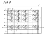
- a display device on which the display device of the present disclosure is based is a light emitting element substrate including a light emitting element such as a micro LED element, and a self-luminous display device using the light emitting element substrate, which does not require a backlight device.
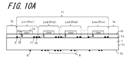
- a block circuit diagram of the basic configuration of such a display device is shown in FIG. Further, FIG. 10A shows a cross-sectional view taken along the line A1-A2 of FIG.
- a display device based on the display device of the present disclosure has a glass substrate 1, a scanning signal line 2 arranged in a predetermined direction (for example, a row direction) on the glass substrate 1, and a scanning signal line 2 intersecting the scanning signal line 2. And a plurality of pixel portions (Pmn) 15 divided by the scanning signal line 2 and the light emission control signal line 3 and arranged in a direction intersecting a predetermined direction (for example, a column direction).
- the effective area (pixel area) 11 and the plurality of light emitting elements 14 arranged on the insulating layer.
- the scanning signal line 2 and the light emission control signal line 3 are provided on the rear surface 9 of the glass substrate 1 via the side surface wiring 30 (shown in FIG. 10B) arranged on the side surface 1S (shown in FIG. 10) of the glass substrate 1. Connected to.
- the back surface wiring 9 is connected to a driving element 6 such as an IC or LSI installed on the back surface of the glass substrate 1. That is, in the display device, the display is driven and controlled by the drive element 6 on the back surface of the glass substrate 1.
- the drive element 6 is mounted on the back surface side of the glass substrate 1 by means of a COG (Chip On Glass) method or the like, for example.
- Each pixel unit (Pmn) 15 is provided with a light emission control unit 22 for controlling light emission, non-light emission, light emission intensity, etc. of the light emitting element (LDmn) 14 in the light emitting region (Lmn).
- the light emission control unit 22 transmits a thin film transistor (TFT) 12 (shown in FIG. 10B) as a switch for inputting a drive signal to each of the light emitting elements 14, and a light emission control signal (transmits the light emission control signal line 3).
- TFT thin film transistor
- the light emitting element 14 is current-driven from the potential difference (drive signal) between a positive voltage (anode voltage: about 3 to 5 V) and a negative voltage (cathode voltage: about -3 V to 0 V) according to the level (voltage) of the signal to be activated.
- TFT 13 shown in FIG. 10B as a driving element for A capacitive element is arranged on a connection line that connects the gate electrode and the source electrode of the TFT 13, and the capacitive element applies the voltage of the light emission control signal input to the gate electrode of the TFT 13 until the next rewriting (in one frame.
- (Period) Functions as a holding capacity for holding.
- the light emitting element 14 includes the light emission control unit 22, the positive voltage input line 16, and the negative voltage input line 16 via the through conductors 23a and 23b such as through holes that penetrate the insulating layer 41 (shown in FIG. 10A) arranged in the effective region 11. It is electrically connected to the voltage input line 17. That is, the positive electrode of the light emitting element 14 is connected to the positive voltage input line 16 via the through conductor 23a and the light emission control unit 22, and the negative electrode of the light emitting element 14 is connected to the negative voltage input line via the through conductor 23b. It is connected to 17.
- the display device has a frame portion 1g that does not contribute to the display between the effective region 11 and the edge of the glass substrate 1 in a plan view, and the frame portion 1g has a light emission control signal line drive circuit, a scanning signal line drive circuit, and the like. May be placed. It is desired that the width of the frame portion 1g be as small as possible.
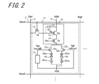
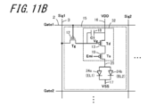
- FIGS. 11A and 11B are circuit diagrams of the pixel unit 15 including the drive circuit 32 as the light emission control unit in the conventional light emitting element substrate.
- a p-channel TFT (Tg) 12 as a switch is arranged in the preceding stage of the drive circuit 32, and the TFT 12 has an ON signal (L (Low) signal: ⁇ 3 to 0 V) transmitted from the scanning signal line (Gate 1) 2.
- L (Low) signal ⁇ 3 to 0 V
- the channel of the p-channel TFT 12 is turned on, and the light-emission control signal (L (Low) signal transmitted from the light-emission control signal line (Sig1) 3 is: Vg) is input to the drive circuit 32.
- the light-emission control signal (L signal: Vg) is input to the gate electrode of the p-channel TFT (Td) 13 as a drive element of the drive circuit 32, so that the channel of the p-channel TFT 13 is brought into a conductive state and turned on.
- a drive signal (VDD: about 3 V to 5 V) is input to the light emitting element 14 via the drive line 25 and emits light. By controlling the level (voltage) of the light emission control signal (Vg), the light emission intensity (luminance) of the light emitting element 14 can be controlled.
- a capacitive element (C1) 18 as a storage capacitor is arranged on the connection line that connects the gate electrode and the source electrode of the p-channel TFT 13.
- a p-channel TFT (Ts) 19 for controlling light emission (Emission) and non-light emission (Non-Emission) of the light emitting element 14 is arranged on the drive line 25 between the p channel TFT 13 and the light emitting element 14.
- the light emission/non-light emission control signal (L signal: Emi) is input to the gate electrode of the p-channel TFT (Ts) 19, the channel of the p-channel TFT 19 is turned on and the drive signal (VDD ) Is input to the light emitting element 14 via the drive line 25 and emits light.
- the light emitting element 14 is connected to the positive electrode pad 20p and the negative electrode pad 20n arranged on the drive line 25 via a conductive connecting member such as solder or a thick film type conductive layer.
- FIG. 11B shows another conventional example and is a circuit diagram of the pixel unit 15.
- the light emitting element is a two-terminal type thin film element (organic electroluminescence (EL) element) consisting of a pair of electrodes serving as an anode and a cathode and a light emitting layer held between them, and at least one of the pair of electrodes.
- EL organic electroluminescence
- one sub light emitting element 24a When one sub light emitting element 24a has a short-circuit defect, it is separated from the pixel portion 15 and a drive current is supplied to the remaining sub light emitting element 24b, so that the remaining sub light emitting element 24b responds to the video signal. It is an active matrix display device capable of maintaining emission of luminance.
- a large number (several hundreds to several millions) of light emitting elements are respectively soldered to the positive electrode pad 20p and the negative electrode pad 20n.
- connection failure occurs in some of the light emitting elements when conductively connected via, the drive signal is not sufficiently input and the emission intensity is reduced and the desired emission intensity cannot be obtained, or the drive signal is There may be a case where no light is emitted (lighted) due to no input.
- the same problem may occur when a large number of light emitting elements originally have a defective product or when the light emitting layer of the light emitting device deteriorates or breaks during use and becomes a defective product.
- the light emitting element is a thin film element (EL element) formed by laminating thin films on a substrate, and at least one of a pair of electrodes is divided into a plurality of sub light emitting elements 24a and 24b.
- EL element thin film element
- the remaining sub light emitting element 24b emits light with a brightness corresponding to a video signal. Therefore, the original video signal is input to the remaining one sub light emitting element 24b.
- the video signals for the two sub light emitting elements 24a and 24b are input to one sub light emitting element 24b, so that an excessive drive current flows in the sub light emitting element 24b, and the sub light emitting element 24b is changed over time. There was a problem that it deteriorated and its life was shortened easily. Further, if the voltage of the video signal input to one sub light emitting element 24b is reduced in order to solve this problem, the light emitting intensity of the sub light emitting element 24b is lowered and a sufficient light emitting intensity cannot be obtained.
- the drawings referred to below show the light emitting element substrate, the display device, and main constituent members of the display device repairing method according to the present embodiment. Therefore, the light emitting element substrate, the display device, and the method for repairing the display device according to the present embodiment include well-known constituent members such as a circuit board, wiring members, control ICs, LSIs, and casings, which are not shown. Good. Further, in each of the drawings showing the present embodiment, the same parts as those in FIGS. 8 to 11A and 11B showing the conventional example are denoted by the same reference numerals, and detailed description thereof will be omitted.
- the light emitting element substrate includes a substrate 1 having a mounting surface 1a (shown in FIGS. 10A and 10B) on which the first light emitting element 14a and the second light emitting element 14b are mounted, and the mounting surface 1a side. And a pixel portion 15 including a first drive line 25a and a second drive line 25b connected in parallel to the drive circuit 32, and the first drive line 25a is always provided.
- the drive line and the second drive line 25b are redundant drive lines, and the first positive electrode pad 20pa and the first negative electrode pad 20na connected to the first light emitting element 14a are arranged on the mounting surface 1a side, and One of the first positive electrode pad 20pa and the first negative electrode pad 20na is connected to the first drive line 25a, and the second positive electrode pad 20pb and the second positive electrode pad 20pb connected to the second light emitting element 14b are provided on the mounting surface 1a side.
- the negative electrode pad 20nb is arranged, and one of the second positive electrode pad 20pb and the second negative electrode pad 20nb is connected to the second drive line 25b.
- the first positive electrode pad 20pa is connected to the first drive line 25a and the first negative electrode pad 20na is connected to the ground potential terminal (VSS), but the power supply terminal (VDD) is negative.
- the connection relationship may be reversed.
- the second positive electrode pad 20pb is connected to the second drive line 25b and the second negative electrode pad 20nb is connected to the ground potential terminal (VSS), but the power supply terminal (VDD) is at a negative potential. May have opposite connection relationships.
- the first positive electrode pad 20pa and the second positive electrode pad 20pb are physically and electrically independent from each other, and the first negative electrode pad 20na and the second negative electrode pad nb are physically and electrically independent from each other. Since the drive systems are independent of each other, it is not necessary to readjust the drive signal even when the light emitting element that is constantly driven is switched from the first light emitting element 14a to the second light emitting element 14b. As a result, it is possible to prevent the drive signal line drive circuit (light emission control signal line drive circuit) from becoming complicated and the power consumption from increasing. Further, unlike the conventional case, an excessive drive current is not input to the second light emitting element 14b, so that the life of the second light emitting element 14b is not shortened.
- the configuration shown in FIG. 1 is a configuration in which one pixel unit 15 has one first drive line 25a as a constant drive line and one second drive line 25b as a redundant drive line.
- a plurality of redundant drive lines may be arranged. In that case, the redundancy is improved, and the risk of the defective display pixel portion 15 occurring can be reduced.
- a plurality of drive lines may be always arranged in one pixel unit 15. In that case, a display device or the like capable of multicolor display such as color display can be configured.
- the first light emitting element 14a and the second light emitting element 14b may not be mounted on the light emitting element substrate having the configuration of FIG. Further, only the first light emitting element 14a is mounted on the light emitting element substrate and is constantly driven, and when an abnormality such as a decrease in emission intensity occurs in the first light emitting element 14a, the second light emitting element 14b is mounted on the light emitting element substrate. Good. Further, the first light emitting element 14a and the second light emitting element 14b may be mounted on the light emitting element substrate in advance.
- the substrate 1 may be a transparent substrate such as a glass substrate or a plastic substrate, or a non-transparent substrate such as a ceramic substrate, a non-transparent plastic substrate or a metal substrate. May be Furthermore, a composite substrate in which a glass substrate and a plastic substrate are laminated, a composite substrate in which a glass substrate and a ceramic substrate are laminated, a composite substrate in which a glass substrate and a metal substrate are laminated, and a plurality of different materials among the above various substrates are laminated. It may be a composite substrate.
- the substrate 1 is preferably an electrically insulating substrate such as a glass substrate, a plastic substrate, or a ceramic substrate because it is easy to form wiring conductors.
- the substrate 1 may have various shapes such as a rectangular shape, a circular shape, an elliptical shape, and a trapezoidal shape.
- the light emitting element used for the light emitting element substrate of the present embodiment is a self-luminous type such as a micro LED element, a semiconductor laser element, an inorganic EL element, an organic EL element that does not require a backlight, and is mounted on the substrate 1. It is possible chip type. Among these, the micro LED element is preferable because it has low power consumption, high luminous efficiency, and long life. Further, since the micro LED element is a small-sized light emitting element that can be easily connected to the electrode pad, when a display device is configured using the light emitting element substrate of the present embodiment, it is possible to display a high quality image and emit light. The repair of the device is also easy.
- the micro LED element is a vertical type mounted vertically on the mounting surface 1a of the substrate 1 (direction perpendicular to the mounting surface 1a).
- a positive electrode, a light emitting layer from the mounting surface 1a side It has a structure in which negative electrodes are stacked. Further, it may have a structure in which a negative electrode, a light emitting layer, and a positive electrode are laminated from the mounting surface 1a side.
- one side has a length of about 1 ⁇ m or more and about 100 ⁇ m or less, and more specifically, about 3 ⁇ m or more and about 10 ⁇ m or less. It is not limited to size.
- the emission color may be different for each pixel unit 15.
- the micro LED element arranged in the first pixel portion has a luminescent color of red, orange, reddish orange, magenta and purple, and the micro LED arranged in the second pixel portion adjacent to the first pixel portion.
- the elements may emit green or yellow green light, and the micro LED arranged in the third pixel portion adjacent to the second pixel portion may have blue emission color. This makes it easy to manufacture a display device or the like capable of color display using the light emitting element substrate.
- one pixel section 15 may have two or more micro LED elements that are constantly driven.
- the first positive electrode pad 20pa, the first negative electrode pad 20na, the second positive electrode pad 20pb and the second negative electrode pad 20nb are, for example, tantalum (Ta), tungsten (W), titanium (Ti), molybdenum (Mo),
- the conductor layer is made of aluminum (Al), chromium (Cr), silver (Ag), copper (Cu), or the like.
- the positive electrode and the negative electrode of the light emitting element may also have the same configuration as the first positive electrode pad 20pa, the first negative electrode pad 20na, the second positive electrode pad 20pb, and the second negative electrode pad 20nb.
- the pixel unit 15 functions as a display unit.
- a display device that can display a single-color image can be obtained by controlling the emission intensity (luminance) of each of the first light-emitting elements 14a.
- a sub-pixel portion including a first light emitting element 14a whose emission color is red a sub pixel portion including a first light emitting element 14a whose emission color is green, and an emission color blue.
- the sub-pixel portion including the first light-emitting element 14a and one sub-pixel portion constitute one set of color display pixel portions, and a large number of sets of color display pixel portions are provided, whereby a display device capable of color gradation display is obtained.
- a drive circuit (light emission control unit) 32 including a switch and a TFT as a control element for controlling light emission, non-light emission, light emission intensity, etc. of the light emitting element is provided below the light emitting element with an insulating layer interposed. May be arranged. In this case, the size of the pixel portion 15 is reduced, and high-quality image display is possible in the display device using the light emitting element substrate of this embodiment.
- the area of the second positive electrode pad 20pb in plan view is larger than the area of the first positive electrode pad 20pa in plan view, and the second negative electrode pad 20nb in plan view. It is preferable to adopt at least one of the configurations in which the area is larger than the area of the first negative electrode pad 20na in plan view. In this case, the connectivity when connecting the second light emitting element 14b, which is a redundant light emitting element, to the second positive electrode pad 20pb and the second negative electrode pad 20nb is improved.
- the second light emitting element 14b is connected to the second positive electrode pad 20pb and the second negative electrode pad 20nb having a larger area, the second light emitting element 14b is easy to connect and the connection failure is less likely to occur.
- the second light emitting element 14b is aligned by optically recognizing the second positive electrode pad 20pb and the second negative electrode pad 20nb by an imaging device such as a camera, the second positive electrode pad 20pb and the second negative electrode Optical recognition of the pad 20nb becomes easy.
- a configuration in which the plan view shape of the second positive electrode pad 20pb is a rectangle larger than a square which is the plan view shape of the first positive electrode pad 20pa, and the plan view shape of the second negative electrode pad 20nb is the first negative At least one of the configurations that is a rectangle larger than the square that is the shape of the electrode pad 20na in plan view can be adopted.
- the second positive electrode pad 20pb is provided.
- the surface and the surface of the second negative electrode pad 20nb may be roughened.
- the arithmetic average roughness of the rough surface is preferably about 1 ⁇ m to 100 ⁇ m.
- a method for roughening the surface of the second positive electrode pad 20pb and the surface of the second negative electrode pad 20nb a method of subjecting those surfaces to an etching treatment such as a dry etching method, the second positive electrode pad 20pb and the second
- a thin film forming method such as a CVD (Chemical Vapor Deposition) method
- CVD Chemical Vapor Deposition
- the light reflectance of the second positive electrode pad 20pb is higher than that of the first positive electrode pad 20pa, and the light reflectance of the second negative electrode pad 20nb is first. It is preferable to adopt at least one of the configurations higher than the light reflectance of the negative electrode pad 20na.
- the connectivity when connecting the second light emitting element 14b, which is a redundant light emitting element, to the second positive electrode pad 20pb and the second negative electrode pad 20nb is improved. That is, since the second light emitting element 14b is connected to the second positive electrode pad 20pb and the second negative electrode pad 20nb having higher light reflectance, the second light emitting element 14b becomes easier to connect.
- the second light emitting element 14b is aligned by optically recognizing the second positive electrode pad 20pb and the second negative electrode pad 20nb by an imaging device such as a camera, the second positive electrode pad 20pb, the second negative electrode Optical recognition of the pad 20nb becomes easy.
- a first switch 26a for controlling the driving and non-driving of the first driving line 25a is arranged on the first driving line 25a, and the second driving line 25a is arranged.
- a second switch 26b that controls driving and non-driving of the second drive line 25b may be arranged on the line 25b.
- there are a drive mode in which the first drive line 25a is in the drive state and the second drive line 25b is in the non-drive state and a drive mode in which the first drive line 25a is in the non-drive state and the second drive line 25b is in the drive state. , Can be easily switched.
- a switching control unit 27 that performs switching control so that one of the first switch 26a and the second switch 26b is in the closed state and the other is in the open state. In this case, the operation of switching the constantly driven light emitting element from the first light emitting element 14a to the second light emitting element 14b is accelerated. As a result, the light emission failure state is immediately resolved.
- the switching control unit 27 makes the first switch 26a formed of a p-channel TFT so that the first driving line 25a, which is always driving line, is driven.
- An ON signal (Vga:L signal) is input to the gate electrode of the second switch 26b and the second switch 26b formed of a p-channel TFT is turned off so that the second drive line 25b, which is a redundant drive line, is not driven.
- a signal (Vgb:H signal) is input.
- the switching control unit 27 includes a p-channel TFT so that the first drive line 25a, which is a constant drive line, is in a non-driven state in the second drive mode in which the second light emitting element 14b is always driven.
- An OFF signal (Vga:H signal) is input to the gate electrode of the first switch 26a, and the gate electrode of the second switch 26b formed of a p-channel TFT so that the second drive line 25b, which is a redundant drive line, is driven.
- An ON signal (Vgb:L signal) is input to.
- the switching control unit 27 may have the configuration shown in FIG. In the first drive state, the switching control unit 27 inputs the ON signal (Vga:L signal) to the gate electrode of the first switch 26a and outputs the H signal to the VH signal terminal and the gate electrode of the first switch 26a.
- a resistor 27a is arranged on the connection line between the first switch 26a and the VL signal terminal that outputs the L signal, and the connection line between the VL signal terminal that outputs the L signal and the gate electrode of the first switch 26a is made conductive. Further, in order to input the OFF signal (Vgb:H signal) to the gate electrode of the second switch 26b, the connection line between the VH signal terminal that outputs the H signal and the gate electrode of the second switch 26b is made conductive. , The L signal is output on the connection line between the VL signal terminal for outputting the L signal and the gate electrode of the second switch 26b to prevent the L signal from being transmitted.
- the switching control unit 27 switches to the second driving mode, in order to input the OFF signal (Vga:H signal) to the gate electrode of the first switch 26a, the VL signal terminal and the gate electrode of the first switch 26a are connected. In the connection line, a laser cut is performed in which a portion between the VL signal terminal and the node nda is melted and cut by irradiating laser light. Then, the OFF signal (Vga:H signal) in consideration of the voltage drop of the resistor 27a is output from the VH signal terminal.
- the VH signal terminal and the node ndb are connected to the connection line between the VH signal terminal and the gate electrode of the second switch 26b.
- a laser cut is performed to melt and cut the part between the two by irradiating a laser beam.
- the ON signal (Vgb:L signal) in consideration of the voltage drop of the resistor 27b is output from the VL signal terminal.
- a mechanical cutting method using a grinding device or the like, a chemical cutting method using an etching method, or the like may be adopted.
- the switching control unit 28 includes a static memory circuit 28a connected in parallel to the first switch 26a and the second switch 26b, and an inverting logic circuit 28c.
- the inverting logic circuit 28c includes a static memory circuit 28a and a first memory circuit 28a. It may be arranged either on the first connection line LS1 between the switches 26a or on the second connection line LS2 between the static memory circuit 28a and the second switch 26b.
- the static memory circuit 28a can hold the H signal or the L signal input thereto as the output signal, the static memory circuit 28a keeps the first light emitting element 14a constantly driven and the second light emitting element 28a. It becomes easy to maintain the driving mode in which 14b is in the non-driving state. Further, it becomes easy to maintain the reverse driving form.
- the switching control unit 28 includes a static memory circuit 28a including a static RAM (Random Access Memory) and the like, a switch 28b including a p-channel TFT, and an inverting logic circuit so-called inverter 28c.
- the gate electrode of the switch 28b is connected to the gate control signal line (Cont), and the channel becomes conductive (ON state) by the ON signal (L signal) transmitted by the gate control signal line.
- the source electrode of the switch 28b is connected to the light emission control signal line (Sig1)3.
- the switch 28b When the first light emitting element 14a is always driven and the second light emitting element 14b is not driven, the switch 28b is turned on with an on signal input to the gate electrode and transmitted from the light emission control signal line 3.
- the generated ON signal (L signal) is transmitted to the switch 26a via the static memory circuit 28a, and the OFF signal (H signal) which is the inverted signal of the ON signal is transmitted to the switch 26b via the static memory circuit 28a and the inverter 28c. introduce.
- the first light emitting element 14a is always driven and the second light emitting element 14b is not driven.
- the static memory circuit 28a holds the signal output state of outputting the ON signal to the switch 26a and outputting the OFF signal to the switch 26b.
- the switch 28b is in an on state in which an on signal is input to the gate electrode and is transmitted from the light emission control signal line 3.
- the off signal (H signal) thus generated is transmitted to the switch 26a via the static memory circuit 28a, and the on signal (L signal) which is an inversion signal of the off signal is transmitted to the switch 26b via the static memory circuit 28a and the inverter 28c. introduce.
- the static memory circuit 28a holds the signal output state of outputting the OFF signal to the switch 26a and outputting the ON signal to the switch 26b.
- the static memory circuit 28a is configured by connecting a first inverter 28aa and a second inverter 28ab in series, as shown in FIG. 4B.
- the first inverter 28aa is composed of a p-channel TFT and an n-channel TFT, and has their gate electrodes commonly connected and their drain electrodes commonly connected.
- the source electrode of the p-channel TFT is connected to the positive voltage power source (VDD), and the source electrode of the n-channel TFT is connected to the negative voltage power source (VSS).
- VDD positive voltage power source
- VSS negative voltage power source
- the second inverter 28ab also has the same configuration as the first inverter 28aa.
- the static memory circuit 28a operates as follows.
- the ON signal (OFF signal) input to the input side (gate electrode side) of the first inverter 28aa is inverted by the first inverter 28aa to become an OFF signal (ON signal) output from the output side (drain electrode side). It is input to the input side of the 2-inverter 28ab.
- the off signal (on signal) input to the input side of the second inverter 28ab is inverted by the second inverter 28ab and becomes an on signal (off signal), which is output from the output side.
- the static memory circuit 28a holds this signal output state until a new OFF signal is transmitted from the switch 28b.
- the inverter 28c has the same configuration as the first inverter 28aa.
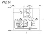
- the switching control unit 29 refers to the storage unit 29a that stores the voltage-current correlation data of the drive voltage and the drive current of the regular light emitting element and the voltage-current correlation data.
- a current abnormality detection unit 29b for detecting a current abnormality of the first light emitting element 14a and when the current abnormality of the first light emitting element 14a is detected, the first switch 26a is opened and the second switch 26a is opened. It is preferable to perform a switching control for closing 26b. In this case, as compared with the case where the light emitting state of the first light emitting element 14a is visually detected, the light emission failure of the first light emitting element 14a can be automatically and accurately detected.
- the current abnormality detection unit 29b has the reference driving current corresponding to the reference driving voltage in the voltage-current correlation data 50 (shown in FIG. 7A) and the first light emitting element 14a. It is preferable to compare the measured drive current at the reference drive voltage of 1) and determine the current abnormality of the first light emitting element 14a when the difference between the reference drive current and the measured drive current becomes a predetermined value or more. In this case, the light emission failure of the first light emitting element 14a can be detected more accurately.
- the current abnormality detection unit 29b that detects the current abnormality of the first drive line 25a measures the drive current transmitted from the detection line connected to the first drive line 25a and sets it as the measured drive current.
- the current abnormality detection unit 29b compares the reference drive current corresponding to the reference drive voltage in the voltage-current correlation data 50 (shown in FIG. 7A) stored in the storage unit 29a with the measured drive current 52a (52b).
- the measured drive current 52a is the case where its value deviates from the reference drive current within the allowable range, and the measured drive current 52b is the case whose value deviates from the reference drive current outside the allowable range.
- the switching control unit 29 does not perform the switching control, and the drive state in which the first light emitting element 14a is always in the drive state and the second light emitting element 14b is in the non-drive state is maintained.
- the switching control unit 29 executes the switching control by the ON/OFF control unit 29c. That is, the first light emitting element 14a is switched to the non-driving state and the second light emitting element 14b is constantly driven to the driving state.
- the on/off control unit 29c may be composed of, for example, a switch 28b, a static memory circuit 28a, and an inverter 28c shown in FIGS. 4A and 4B.
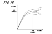
- reference numeral 51a indicates voltage-current correlation data when the deviation between the measured drive current and the reference drive current is +10%
- reference numeral 51b indicates that the deviation between the measured drive current and the reference drive current is ⁇ 10. It is voltage-current correlation data in the case of %.
- the degree of divergence is not limited to the above range, and can be variously set in consideration of the required allowable range of display quality, deterioration of the light emitting element over time, and the like.
- FIG. 5A shows a configuration in which the storage unit 29a is inside the pixel unit 15, and FIG. 5B shows a configuration in which the storage unit 29a is outside the pixel unit 15, for example, in the peripheral portion of the effective area (display area).
- the configuration of FIG. 5B can be used to prevent the size of the pixel unit 15 from becoming too large.
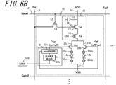
- the switching control unit 33 includes a storage unit 33a that stores the voltage-light emission correlation data 60 (shown in FIG. 7B) of the normal light emitting element drive voltage and light emission intensity, and the voltage.
- the light emission abnormality detection unit 33b has the reference light emission intensity corresponding to the reference drive voltage in the voltage-light emission correlation data 60 and the measured light emission at the reference drive voltage of the first light emitting element 14a. It is preferable to compare the intensities with each other and determine that the first light emitting element 14a has abnormal light emission when the difference between the reference light emission intensity and the measured light emission intensity becomes equal to or more than a predetermined value. In this case, the light emission failure of the first light emitting element 14a can be detected more accurately.
- the light emission abnormality detection unit 33b that detects the light emission abnormality of the first drive line 25a receives the light from the photodiode and the channel that detect the light emission intensity (luminance) of the first light emitting element 14a connected to the first drive line 25a.
- the light emission abnormality detection unit 33b receives the light emitted from the first light emitting element 14a and sets it as the measured light emission intensity.
- the light emission abnormality detection unit 33b compares the reference light emission intensity corresponding to the reference drive voltage in the voltage-light emission correlation data 60 (shown in FIG. 7B) stored in the storage unit 33a with the measured light emission intensity 62a (62b).
- the measured emission intensity 62a is the case where the value thereof deviates from the reference emission intensity within the allowable range
- the measured emission intensity 62b is the case where the value thereof deviates from the reference emission intensity outside the allowable range.
- the switching control unit 33 does not perform the switching control, and the driving state in which the first light emitting element 14a is always driven and the second light emitting element 14b is not driven is maintained.
- the switching control unit 33 executes the switching control by the on/off control unit 33c. That is, the first light emitting element 14a is switched to the non-driving state and the second light emitting element 14b is constantly driven to the driving state.
- the on/off control unit 33c may be composed of, for example, the switch 28b, the static memory circuit 28a, and the inverter 28c shown in FIGS. 4A and 4B.
- the difference between the measured emission intensity and the reference emission intensity is within ⁇ 10% with respect to the value of the reference emission intensity when the value of the reference emission intensity is 100%. If there is, it can be determined that it is within the allowable range.
- reference numeral 61a is voltage-light emission correlation data when the difference between the measured emission intensity and the reference emission intensity is +10%
- reference numeral 61b is the difference between the measured emission intensity and the reference emission intensity of ⁇ 10. It is voltage-light emission correlation data in the case of %.
- the degree of divergence is not limited to the above range, and can be variously set in consideration of the required allowable range of display quality, deterioration of the light emitting element over time, and the like.
- FIG. 6A shows a configuration in which the storage unit 33a is inside the pixel unit 15, and FIG. 6B shows a configuration in which the storage unit 33a is outside the pixel unit 15, for example, in the peripheral portion of the effective area (display area).
- the configuration of FIG. 6B can be adopted in order to prevent the size of the pixel unit 15 from becoming too large when the memory capacity of the storage unit 33a is large.
- the switching control units 27, 28, 29 and 33 are preferably provided in the pixel unit 15. In this case, the operation of switching the constantly driven light emitting element from the first light emitting element 14a to the second light emitting element 14b is further speeded up. As a result, the light emission failure state is eliminated more immediately. Further, when the switching control units 27, 28, 29, and 33 are in the peripheral portion of the effective region other than the pixel unit 15, the light emitting element substrate becomes large in size, but such a problem does not occur. Become.
- a light emitting element substrate of another disclosure is a substrate 1 having a mounting surface 1a on which the first light emitting element 14a and the second light emitting element 14b are mounted, and a driving circuit 32 and a driving circuit 32 which are arranged on the mounting surface 1a side.
- the second drive line 25b is a redundant drive line that redundantly drives the second light emitting element 14b, and a switching unit that sets one of the first drive line 25a and the second drive line 25b in a conductive state and the other in a non-conductive state. And a switching control unit that controls the switching unit. Also with this configuration, the same effect as that disclosed above can be obtained.
- the switching unit may be a single switch that switches the signal transmission path in one of two directions, or as shown in FIG. 2, it includes two switches including a first switch 26a and a second switch 26b. It may be a switch.
- the switching control unit is connected to the switching unit and performs the switching control.
- the switching unit and the switching control unit are preferably provided in the pixel unit 15.
- the pixel unit 15 includes the switching unit and the switching control unit, the operation of switching the constantly driven light emitting element from the first light emitting element 14a to the second light emitting element 14b is further speeded up. As a result, the light emission failure state is eliminated more immediately.
- a plurality of pixel units 15 are arranged in a matrix, and a first switch 26a and a second switch 26b as a switching unit are arranged in each of the plurality of pixel units 15.
- the static memory circuits 28G and 28S as switching control units are provided corresponding to the plurality of pixel units 15m1 to 15mn arranged in the row direction and/or the plurality of pixel units 151n to 15mn arranged in the column direction. Good to be. In this case, the number of switching control units can be significantly reduced. As a result, the light emitting element substrate is downsized. Further, since the circuit structure is simplified, the light emitting element substrate has low power consumption.
- one static memory circuit 28G as a switching control unit may be provided for each row of the plurality of pixel units 15m1 to 15mn arranged in the row direction.
- n static memory circuits 28G may be provided for n rows (when n is an integer of 2 or more).
- one static memory circuit 28G may be provided corresponding to a plurality of rows.
- one may be provided for every plurality of rows. Further, one may be provided for all the rows.
- one static memory circuit 28S as a switching control unit may be provided corresponding to one column of the plurality of pixel units 151n to 15mn arranged in the column direction.
- m static memory circuits 28S may be provided for m columns (when m is an integer of 2 or more).
- one static memory circuit 28S may be provided corresponding to a plurality of columns. Also, one may be provided for every plurality of rows. Further, one may be provided for all columns.
- one switching control unit may be provided for all pixel units 15.
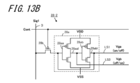
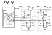
- the switching control unit includes a first inverter 28aa serving as a first inverting logic circuit and a second inverter 28ab serving as a second inverting logic circuit connected in series to the subsequent stage side.
- the static memory circuits 28-1 and 28-2 provided, and the first switch 26a and the second switch 26b as a switching unit are connected in parallel to the first inverter 28aa and the second inverter 28ab. .. That is, when the first switch 26a and the second switch 26b are viewed as a switching unit as a whole, the switching unit is connected in parallel to the first inverter 28aa and the second inverter 28ab.
- the switching unit can be switched and controlled only by the static memory circuits 28-1 and 28-2, the circuit configuration is simplified and the light emitting element substrate has low power consumption.
- the static memory circuits 28-1 and 28-2 which are the switching control units, are made conductive/non-conductive by the first output signal (Vga in FIG. 13A) of the first inverter 28aa. And the second output signal (Vgb in FIG. 13A) of the second inverter 28ab to control the non-conduction/conduction of the second drive line 25b, and the second output signal (Vga in FIG. 13B).
- One of a second switching control for controlling conduction/non-conduction of the first drive line 25a and controlling non-conduction/conduction of the second drive line 25b by the first output signal (Vgb in FIG. 13B) is performed.
- the switching control unit 28 includes a static memory circuit 28a and an inverter 28c as an inverting logic circuit connected in parallel at the subsequent stage side, and serves as a first switching unit.
- the first switch 26a and the second switch 26b may be connected in parallel to the static memory circuit 28a and the inverter 28c. That is, when the first switch 26a and the second switch 26b are viewed as a switching unit as a whole, the switching unit is connected in parallel to the static memory circuit 28a and the inverter 28c. In this case, the operation of the static memory circuit 28a is stabilized, so that the switching control can be stably performed. That is, if a branch line for deriving the inverted signal is connected to the output line of the first inverter 28aa, the potential of the inverted signal may decrease and the operation of the second inverter 28ab may become unstable. Disappear.
- the static memory circuit 28a and the inverter 28c which are the switching control unit 28, turn on/off the first drive line 25a by the first output signal (Vga in FIGS. 4A and 4B) of the static memory circuit 28a.
- a first switching control for controlling conduction and controlling non-conduction/conduction of the second drive line 25b by the second output signal (Vgb in FIGS. 4A and 4B) of the inverter 28c and the second output signal (Vgb) by the second switching signal (Vgb).
- One of the second switching control for controlling conduction/non-conduction of the first drive line 25a and controlling non-conduction/conduction of the second drive line 25b by the first output signal (Vga) is performed.
- Embodiments of a light emitting element substrate according to another disclosure are shown in FIGS. 12 to 17.
- the switching control units 28-1 and 28-2 have a static memory circuit 28a, and the static memory circuit 28a is the first inversion logic circuit.
- a first connection form shown in FIG.
- the static memory circuit 28a can hold the H signal or the L signal input thereto as an output signal, so that the static memory circuit 28a keeps the first light emitting element 14a constantly driven and the second light emitting element 28a. It becomes easy to maintain the driving mode in which 14b is in the non-driving state. Further, it becomes easy to maintain the reverse driving form. Further, an inversion logic circuit other than the static memory circuit 28a is unnecessary, and the circuit structure is simplified.
- the first connection line LS1 connects the static memory circuit 28a and the first switch 26a
- the third connection line LS3 connects the static memory circuit 28a and the second switch 26b.
- the first connection line LS1 is connected to the first output line 28aal. Therefore, the output (for example, L signal) of the first inverter 28aa is input to the gate electrode of the first switch 26a, so that the first switch 26a is always turned on and the first light emitting element 14a is always driven. ..
- the third connection line LS3 is connected to the second output line 28abl. Therefore, the output (for example, H signal) of the second inverter 28ab is input to the gate electrode of the second switch 26b, so that the second switch 26b is always off and the second light emitting element 14b is always in the non-driving state. Become.
- the output of the first inverter 28aa is set to an H signal (OFF signal) to keep the first switch 26a in the off state, and the output of the second inverter 28ab is set to L.
- the second switch 26b is always turned on. This switching operation is performed by a signal (H signal or L signal) input from the light emission control signal line (Sig1) 3 to the switch 28b.
- the first connection line LS1 is connected to the second output line 28abl. Therefore, the output (for example, L signal) of the second inverter 28ab is input to the gate electrode of the first switch 26a, so that the first switch 26a is always turned on and the first light emitting element 14a is always driven. ..
- the third connection line LS3 is connected to the first output line 28aal. Therefore, the output of the first inverter 28aa (for example, the H signal) is input to the gate electrode of the second switch 26b, so that the second switch 26b is always off and the second light emitting element 14b is always in the non-driving state. Become.
- the output of the second inverter 28ab is set to an H signal (OFF signal) to keep the first switch 26a in the off state at all times, and the output of the first inverter 28aa is set to L.
- OFF signal As a signal (ON signal), the second switch 26b is always turned on. This switching operation is performed by a signal (L signal or H signal) input to the switch 28b from the light emission control signal line (Sig1) 3.
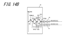
- FIG. 14A and FIG. 14B show another example of each embodiment, and are arranged in the row direction of one row (GATE[m]; m (natural number) indicates the m-th row).
- FIG. 16 is a circuit diagram of a configuration in which one static memory circuit 28G is provided corresponding to a plurality of pixel units 15m1 to 15mn. As shown in FIG. 14A, each first switch 26a is connected to the first output line 28Gal of the first inverter 28Ga, and each second switch 26b is connected to the second output line 28Gbl of the second inverter 28Gb. ..
- the output of the first inverter 28Ga (for example, L signal/LED_SEL1[m]) is input to the gate electrodes of the first switches 26a of the n (n is an integer of 2 or more) pixel units 15m1 to 15mn.
- n is an integer of 2 or more pixel units 15m1 to 15mn.
- each first switch 26a is always turned on, and each first light emitting element 14a is always driven.
- the output of the second inverter 28Gb (for example, H signal/LED_SEL2[m]) is input to the gate electrode of each second switch 26b, so that each second switch 26b is always in the off state and each second light emission.
- the element 14b is always in the non-driving state.
- the output of the first inverter 28Ga is set to an H signal (OFF signal) to constantly turn off each first switch 26a
- the output of the second inverter 28Gb is set to an L signal (ON signal) to keep each second switch 26b in the ON state at all times.
- This switching operation is performed by the light emission adjustment signal (H signal or L signal) input to the switch 28t from the light emission adjustment signal line (Sig_trim).
- the switch 28t is on/off controlled by a gate adjustment signal (TRIM[m]) input to its gate electrode.
- the static memory circuit 28G and the switch 28t may be included in the gate signal line drive circuit (gate driver) 70.
- the buffer circuit 81 is connected to the branch line of the first output line 28Gal, and the output of the first inverter 28Ga (for example, L signal/LED_SEL1 [m]) is output via the buffer circuit 81.
- N (n is an integer of 2 or more) is preferably input to the gate electrodes of the respective first switches 26a of the pixel units 15m1 to 15mn.
- the branch line of the first output line 28Gal tends to make the potential of the branch line unstable, and the branch line is connected to the gate electrodes of the plurality of first switches 26a. It is possible to suppress that it tends to be stable.
- the buffer circuit 82 is connected to the second output line 28Gbl, and the output (for example, H signal/LED_SEL2 [m]) of the second inverter 28Gb is n (n is 2 or more) via the buffer circuit 82. It is preferable that the data is input to the gate electrodes of the second switches 26b of the respective pixel units 15m1 to 15mn. In this case, the potential of the second output line 28Gbl tends to be unstable due to the branch line of the first output line 28Gal, and the second output line 28Gbl is connected to the gate electrodes of the plurality of second switches 26b. It is possible to prevent the potential of the second output line 28Gbl from becoming unstable easily.
- Each of the buffer circuits 81 and 82 has a configuration in which two inverters are connected in series, but is not limited to this configuration.
- FIGS. 14A and 14B corresponding to a plurality of pixel units 15m1 to 15mn, 15(m+1)1 to 15(m+1)n,... It may be configured to include one static memory circuit 28G. Furthermore, the configuration may be such that one static memory circuit 28G is provided for all the pixel units.
- FIG. 15 shows another example of the embodiment, in which one static memory circuit 28G corresponds to a plurality of pixel units 15m1 to 15mn arranged in the row direction of one row (GATE[m]). It is a circuit diagram of a structure provided. Each first switch 26a is connected to the second output line 28Gbl of the second inverter 28Gb, and each second switch 26b is connected to the first output line 28Gal of the first inverter 28Ga.
- the output of the second inverter 28Gb (for example, the L signal/LED_SEL1 [m]) is input to the gate electrodes of the first switches 26a of the n pixel units 15m1 to 15mn, so that each first switch 26a is activated.
- each first light emitting element 14a is always driven. Further, the output of the first inverter 28Ga (for example, H signal/LED_SEL2[m]) is input to the gate electrode of each second switch 26b, so that each second switch 26b is always turned off and each second light emission. The element 14b is always in the non-driving state. Then, when one or more of the n first light emitting elements 14a have a defect such as a light emission abnormality, the output of the second inverter 28Gb is set to an H signal (OFF signal) to constantly turn off each first switch 26a. The output of the first inverter 28Ga is set to the L signal (ON signal), and the second switches 26b are always turned on.
- H signal/LED_SEL2[m] the output of the second inverter 28Gb
- This switching operation is performed by the light emission adjustment signal (L signal or H signal) input to the switch 28t from the light emission adjustment signal line (Sig_trim).
- the switch 28t is on/off controlled by a gate adjustment signal (TRIM[m]) input to its gate electrode.
- the static memory circuit 28G and the switch 28t may be included in the gate signal line drive circuit 70.
- the configuration of FIG. 14B can be adopted in the configuration of FIG. That is, the buffer circuit 82 may be connected to the branch line of the first output line 28Gal and the buffer circuit 81 may be connected to the second output line 28Gbl.
- one static unit is provided corresponding to a plurality of pixel units 15m1 to 15mn, 15(m+1)1 to 15(m+1)n...
- a configuration including the memory circuit 28G may be used.
- the configuration may be such that one static memory circuit 28G is provided for all the pixel units.
- 16A and 16B show another example of the embodiment, in which one static memory is provided corresponding to the plurality of pixel units 151n to 15mn arranged in the column direction of one column (SOURCE[n]). It is a circuit diagram of the composition provided with circuit 28S. As shown in FIG. 16A, each first switch 26a is connected to the first output line 28Sal of the first inverter 28Sa, and each second switch 26b is connected to the second output line 28Sbl of the second inverter 28Sb. ..
- the output of the first inverter 28Sa (for example, L signal/LED_SEL1[n]) is input to the gate electrodes of the respective first switches 26a of the n pixel units 151n to 15mn, so that each first switch 26a is activated. It is always on, and each first light emitting element 14a is always driven.
- the output of the second inverter 28Sb (for example, H signal/LED_SEL2[n]) is input to the gate electrode of each second switch 26b, so that each second switch 26b is always turned off and each second light emission.
- the element 14b is always in the non-driving state.
- the output of the first inverter 28Sa is set to an H signal (OFF signal) to constantly turn off each first switch 26a
- the output of the second inverter 28Sb is set to the L signal (ON signal) to keep each second switch 26b in the ON state.
- This switching operation is performed by the light emission adjustment signal (L signal or H signal) input to the switch 28t from the light emission adjustment signal line (Sig_trim).
- the switch 28t is on/off controlled by a gate adjustment signal (TRIM[n]) input to its gate electrode.
- the static memory circuit 28S and the switch 28t may be included in the image signal line drive circuit (source driver) 71.
- the buffer circuit 81 is connected to the branch line of the first output line 28Sal, and the output (for example, L signal/LED_SEL1 [m]) of the first inverter 28Sa is output via the buffer circuit 81.
- N (n is an integer of 2 or more) is preferably input to the gate electrodes of the first switches 26a of the pixel units 151n to 15mn. In this case, the same effect as the effect of suppressing the destabilization of the potential described above can be obtained.
- the buffer circuit 82 is connected to the second output line 28Sbl, and the output (for example, H signal/LED_SEL2 [m]) of the second inverter 28Sb is n (n is 2 or more) via the buffer circuit 82. It is preferable that the data is input to the gate electrodes of the second switches 26b of the pixel units 151n to 15mn. In this case, the same effect as the effect of suppressing the destabilization of the potential described above can be obtained.
- the static memory circuit 28S may be provided. Furthermore, the configuration may be such that one static memory circuit 28S is provided for all pixel units.
- FIG. 17 shows another example of the embodiment, in which one static memory circuit 28S corresponds to a plurality of pixel units 151n to 15mn arranged in the column direction of one column (SOURCE[n]). It is a circuit diagram of a structure provided. Each first switch 26a is connected to the second output line 28Sbl of the second inverter 28Sb, and each second switch 26b is connected to the first output line 28Sal of the first inverter 28Sa. The output of the second inverter 28Sb (for example, the L signal/LED_SEL1[n]) is input to the gate electrodes of the first switches 26a of the n pixel units 151n to 15mn, so that each first switch 26a is activated.
- the second inverter 28Sb for example, the L signal/LED_SEL1[n]
- each first light emitting element 14a It is always on, and each first light emitting element 14a is always driven.
- the output of the first inverter 28Sa (for example, H signal/LED_SEL2[n]) is input to the gate electrode of each second switch 26b, so that each second switch 26b is always turned off and each second light emission.
- the element 14b is always in the non-driving state.
- the output of the second inverter 28Sb is set to an H signal (OFF signal), and each first switch 26a is always turned off.
- the output of the first inverter 28Sa is set to the L signal (ON signal) to keep the second switches 26b in the ON state at all times.
- This switching operation is performed by the light emission adjustment signal (L signal or H signal) input to the switch 28t from the light emission adjustment signal line (Sig_trim).
- the switch 28t is on/off controlled by a gate adjustment signal (TRIM[n]) input to its gate electrode.
- the static memory circuit 28S and the switch 28t may be included in the image signal line drive circuit 71.
- the configuration of FIG. 16B can be adopted in the configuration of FIG. That is, the buffer circuit 82 may be connected to the branch line of the first output line 28Sal and the buffer circuit 81 may be connected to the second output line 28Sbl.
- one static memory circuit is provided corresponding to the plurality of pixel portions 151n to 15mn, 151(n+1) to 15m(n+1),... 28S may be provided. Furthermore, the configuration may be such that one static memory circuit 28S is provided for all pixel units.
- the display device is a display device including the light emitting element substrate, and the substrate 1 includes an opposite surface 1b (shown in FIG. 10A) opposite to the mounting surface 1a and a side surface 1s (FIGS. 10A and 10B).
- the light emitting element substrate has a side surface wiring 30 (shown in FIGS. 10A and 10B) arranged on the side surface 1s, and a drive unit 6 (shown in FIG. 8) arranged on the opposite surface 1b side.
- the first light emitting element 14a and the second light emitting element 14b are connected to the drive unit 6 via the side surface wiring 1s. With this configuration, it is possible to effectively suppress the generation of the undisplayable pixel unit 15.
- the drive signal line drive circuit (light emission control signal line drive circuit) from becoming complicated, and thereby increasing power consumption. Further, unlike the conventional case, the life of the second light emitting element 14b is not shortened due to the excessive current flowing to the second light emitting element 14b by the switching control unit.
- the drive unit 6 may have a configuration in which drive elements such as IC and LSI are mounted by a chip-on-glass method, but may be a circuit board on which the drive elements are mounted. Further, the drive unit 6 includes a TFT having a semiconductor layer made of LTPS (Low Temperature Poly Silicon) directly formed on the opposite surface 1b of the substrate 1 made of a glass substrate by a thin film forming method such as a CVD method. It may be a thin film circuit provided.
- LTPS Low Temperature Poly Silicon
- the side wiring 30 is formed by using a conductive paste containing conductive particles such as silver (Ag), copper (Cu), aluminum (Al), and stainless steel, an uncured resin component, an alcohol solvent, water, and the like, by a heating method and ultraviolet rays.
- a conductive paste containing conductive particles such as silver (Ag), copper (Cu), aluminum (Al), and stainless steel, an uncured resin component, an alcohol solvent, water, and the like
- the side wiring 30 can also be formed by a thin film forming method such as a plating method, a vapor deposition method, or a CVD method.
- a groove may be provided on the side surface 1s of the substrate 1 where the side surface wiring 30 is arranged. In that case, the conductive paste is easily placed in the groove, which is a desired portion of the side surface 1s
- a plurality of substrates 1 on which a plurality of light emitting elements are mounted are arranged vertically and horizontally on the same surface, and their side surfaces are combined (tiled) with an adhesive material or the like to form a composite structure.
- a large and large-sized display device, so-called multi-display, can be configured.
- the display device of this embodiment can be configured as a light emitting device.
- the light emitting device can be used as a printer head, an illuminating device, a signboard device, a bulletin device, etc. used in an image forming apparatus or the like.
- the display device repairing method according to the present embodiment is the display device repairing method according to the above-described present embodiment.
- the first light emitting element 14a is connected and mounted, and is always driven.
- the second light emitting element 14b is connected to and mounted on the second negative electrode pad 20nb, and the first drive line 25a is set in the non-drive state and the second drive line 25b is set in the drive state.
- the light emitting element substrate and the display device of the present disclosure are not limited to the above-described embodiments, and may include appropriate design changes and improvements.
- the substrate 1 when the substrate 1 is non-translucent, the substrate 1 may be a glass substrate colored in black, gray or the like, or a glass substrate made of ground glass.
- the present disclosure can have the following embodiments.
- a light emitting element substrate is a substrate having a mounting surface on which a first light emitting element and a second light emitting element are mounted, and a first mounting circuit disposed on the mounting surface side and connected in parallel to a driving circuit and the driving circuit.
- a light emitting element substrate comprising: a pixel portion including a drive line and a second drive line, wherein the first drive line is a constant drive line, the second drive line is a redundant drive line, and the first drive line is a redundant drive line.
- a first positive electrode pad and a first negative electrode pad connected to the first light emitting element are arranged, and one of the first positive electrode pad and the first negative electrode pad is connected to the first drive line.
- a second positive electrode pad and a second negative electrode pad connected to the second light emitting element are arranged on the mounting surface side, and one of the second positive electrode pad and the second negative electrode pad is disposed. Is connected to the second drive line.
- a first switch for controlling driving and non-driving of the first driving line is arranged on the first driving line, and driving of the second driving line on the second driving line,
- a second switch for controlling non-driving may be arranged.
- the light emitting element substrate of the present disclosure may include a switching control unit that performs switching control such that one of the first switch and the second switch is in a closed state and the other is in an open state.
- the switching control unit refers to the storage unit that stores the voltage-current correlation data of the drive voltage and the drive current of the regular light emitting element, and the voltage-current correlation data.
- a current abnormality detection unit that detects a current abnormality of the first light emitting element, and when the current abnormality of the first light emitting element is detected, the first switch is opened and the second switch is turned on. It is better to make it closed.
- the switching control unit refers to the storage unit that stores the voltage-light emission correlation data of the normal light emitting element drive voltage and the light emission intensity, and the voltage-light emission correlation data.
- a light emission abnormality detection unit for detecting light emission abnormality of the first light emitting element, and when the light emission abnormality of the first light emitting element is detected, the first switch is opened and the second switch is turned on. It is better to make it closed.
- the switching control unit may be included in the pixel unit.
- a plurality of the pixel units are arranged in a matrix, the switching unit is arranged in each of the plurality of the pixel units, and the switching control unit is arranged in a row direction. It may be provided so as to correspond to the plurality of arranged pixel units and/or the plurality of pixel units arranged in the column direction.
- the first light emitting element and the second light emitting element may be micro LED elements.
- a light emitting element substrate is a substrate having a mounting surface on which a first light emitting element and a second light emitting element are mounted, and a first mounting circuit disposed on the mounting surface side and connected in parallel to a driving circuit and the driving circuit.
- a pixel portion including a drive line and a second drive line, wherein the first drive line is a constant drive line that constantly drives the first light emitting element, and the second drive line is the A redundant drive line that redundantly drives the second light emitting element, and a switching unit that sets one of the first drive line and the second drive line to a conductive state and the other to a non-conductive state, and a switching control that controls the switching unit. And a part.
- the switching unit and the switching control unit may be provided in the pixel unit.
- a plurality of the pixel units are arranged in a matrix, the switching unit is arranged in each of the plurality of the pixel units, and the switching control unit is arranged in a row direction. It may be provided so as to correspond to the plurality of arranged pixel units and/or the plurality of pixel units arranged in the column direction.
- the switching control unit is a static memory circuit including a first inversion logic circuit and a second inversion logic circuit connected in series at the subsequent stage side, and the switching unit is ,
- the first inverting logic circuit and the second inverting logic circuit may be connected in parallel.
- the switching control unit includes a static memory circuit and an inverting logic circuit connected in parallel on the subsequent stage side, and the switching unit includes the static memory circuit and the inverting circuit. It is preferably connected in parallel to the logic circuit.
- the display device of the present disclosure is a display device including the light emitting element substrate of the present disclosure, the substrate has an opposite surface and a side surface opposite to the mounting surface, the light emitting element substrate, A side wiring disposed on the side surface, and a driving unit disposed on the opposite surface side, wherein the first light emitting element and the second light emitting element are driven by the side wiring. It is the structure connected to the section.
- the repair method for a display device is the repair method for a display device according to the present disclosure, wherein the first light emitting element mounted on the mounting surface of the substrate is constantly driven, and then the first light emission is performed.
- the second light emitting element is mounted on the mounting surface, the first drive line is set in a non-driving state, and the second drive line is set in a driving state. is there.
- a light emitting element substrate is a substrate having a mounting surface on which a first light emitting element and a second light emitting element are mounted, and a first mounting circuit disposed on the mounting surface side and connected in parallel to a driving circuit and the driving circuit.
- a light emitting element substrate comprising: a pixel portion including a drive line and a second drive line, wherein the first drive line is a constant drive line, the second drive line is a redundant drive line, and the first drive line is a redundant drive line.
- a first positive electrode pad and a first negative electrode pad connected to the first light emitting element are arranged, and one of the first positive electrode pad and the first negative electrode pad is connected to the first drive line.
- a second positive electrode pad and a second negative electrode pad connected to the second light emitting element are arranged on the mounting surface side, and one of the second positive electrode pad and the second negative electrode pad is disposed. Is connected to the second drive line, the following effects can be obtained.
- the first drive line is set to a non-drive state (non-use state)
- the second light emitting element is connected to the second positive electrode pad and the second negative electrode pad
- the second drive line is set to the drive state (use state).
- the first positive electrode pad and the second positive electrode pad are physically and electrically independent from each other, and the first negative electrode pad and the second negative electrode pad are physically and electrically independent from each other. That is, since the drive systems are independent from each other, readjustment of the drive signal or the like is unnecessary even if the light emitting element that is constantly driven is switched to the second light emitting element. As a result, it is possible to prevent the drive signal line drive circuit (light emission control signal line drive circuit) from becoming complicated and the power consumption from increasing. Moreover, unlike the conventional case, an excessive current does not flow through the second light emitting element and the life thereof is not shortened.
- a first switch that controls driving and non-driving of the first driving line is arranged on the first driving line, and driving of the second driving line is performed on the second driving line.
- a second switch for controlling non-driving is arranged, a driving mode in which the first driving line is in a driving state and the second driving line is in a non-driving state, and a second driving line is in a non-driving state It becomes easy to switch between the drive mode in which the line is in the drive state.
- the light emitting element substrate of the present disclosure is provided with a switching control unit that performs switching control to close one of the first switch and the second switch and open the other, the first drive line is driven. It becomes easier to switch between the drive mode in which the second drive line is in the non-drive state and the drive mode in which the first drive line is in the non-drive state and the second drive line is in the drive state. As a result, the operation of switching the constantly driven light emitting element from the first light emitting element to the second light emitting element is speeded up, and the light emission failure state is immediately eliminated.
- the switching control unit refers to the storage unit that stores the voltage-current correlation data of the drive voltage and the drive current of the regular light emitting element, and the voltage-current correlation data.
- a current abnormality detection unit that detects a current abnormality of the first light emitting element, and when the current abnormality of the first light emitting element is detected, the first switch is opened and the second switch is turned on.
- the switching control unit refers to the storage unit that stores the voltage-light emission correlation data of the normal light emitting element drive voltage and the light emission intensity, and the voltage-light emission correlation data.
- a light emission abnormality detection unit for detecting light emission abnormality of the first light emitting element and when the light emission abnormality of the first light emitting element is detected, the first switch is opened and the second switch is turned on.
- the switching control for closing it is possible to automatically and accurately detect the light emission failure of the first light emitting element, as compared with the case of visually detecting the light emitting state of the first light emitting element.
- the switching control section when the switching control section is provided in the pixel section, the operation of switching the constantly driven light emitting element to the second light emitting element is further speeded up. As a result, the light emission failure state is eliminated more immediately. Further, when the switching control unit is located in the peripheral portion of the pixel portion other than the pixel portion, the light emitting element substrate becomes large in size, but the light emitting element substrate becomes small in size without such a problem.
- a plurality of the pixel units are arranged in a matrix, the switching unit is arranged in each of the plurality of the pixel units, and the switching control unit is arranged in a row direction.
- the number of switching control units can be significantly reduced.
- the light emitting element substrate is downsized. Further, since the circuit structure is simplified, the light emitting element substrate has low power consumption.
- the light emitting element substrate of the present disclosure is a small light emitting element that can be easily connected to an electrode pad, and thus the light emitting element of the present disclosure
- the display device is configured using the substrate, it is possible to display a high quality image and to easily repair the light emitting element.
- a light emitting element substrate is a substrate having a mounting surface on which a first light emitting element and a second light emitting element are mounted, and a first mounting circuit disposed on the mounting surface side and connected in parallel to a driving circuit and the driving circuit.
- a pixel portion including a drive line and a second drive line, wherein the first drive line is a constant drive line that constantly drives the first light emitting element, and the second drive line is the A redundant drive line that redundantly drives the second light emitting element, and a switching unit that sets one of the first drive line and the second drive line to a conductive state and the other to a non-conductive state, and a switching control that controls the switching unit. And a part.
- the first drive line When the first light emitting element is mounted on the mounting surface and a connection failure occurs in the first light emitting element, or when the first light emitting element is a defective product, the first drive line is in the non-driving state (non-driving state).
- the second drive line can be set to a driving state (usage state). Accordingly, it is possible to effectively suppress the occurrence of defective light emission or a pixel portion that cannot emit light. Further, since the first drive line and the second drive line are physically and electrically independent from each other, that is, the drive systems are independent from each other, the light emitting element that is constantly driven is the second light emitting element. Even if the switching is performed, readjustment of the drive signal is unnecessary.
- the switching unit and the switching control unit are provided in the pixel unit, the operation of switching the constantly driven light emitting device to the second light emitting device is further speeded up. As a result, the light emission failure state is eliminated more immediately.
- a plurality of the pixel units are arranged in a matrix, the switching unit is arranged in each of the plurality of the pixel units, and the switching control unit is arranged in a row direction.
- the number of switching control units can be significantly reduced.
- the light emitting element substrate is downsized. Further, since the circuit structure is simplified, the light emitting element substrate has low power consumption.
- the switching control unit is a static memory circuit including a first inversion logic circuit and a second inversion logic circuit connected in series at the subsequent stage side, and the switching unit is When the first inverting logic circuit and the second inverting logic circuit are connected in parallel, the switching unit can be switched and controlled only by the static memory circuit, so that the circuit configuration is simplified and the light-emitting element with low power consumption is provided. It becomes the substrate.
- the switching control unit includes a static memory circuit and an inverting logic circuit connected in parallel on the subsequent stage side, and the switching unit includes the static memory circuit and the inverting circuit.
- the operation of the static memory circuit is stabilized, so that the switching control can be stably performed.
- the display device of the present disclosure is a display device including the light emitting element substrate of the present disclosure, the substrate has an opposite surface and a side surface opposite to the mounting surface, the light emitting element substrate, A side wiring disposed on the side surface, and a driving unit disposed on the opposite surface side, wherein the first light emitting element and the second light emitting element are driven by the side wiring. It is possible to effectively suppress the generation of the undisplayable pixel portion because it is connected to the unit. Further, it is possible to prevent the drive signal line drive circuit (light emission control signal line drive circuit) from becoming complicated, and thereby increasing power consumption. Further, the life of the second light emitting element is not shortened.
- the repair method for a display device is the repair method for a display device according to the present disclosure, wherein the first light emitting element mounted on the mounting surface of the substrate is constantly driven, and then the first light emission is performed.
- the second light emitting element is mounted on the mounting surface, the first drive line is set in a non-driving state, and the second drive line is set in a driving state. Therefore, it is not necessary to connect the second light emitting element for redundant driving in a state where the first light emitting element is constantly driven. Therefore, in the case of manufacturing a display device which requires a large number of light-emitting elements, the number of light-emitting elements can be prevented from becoming enormous including redundant driving, and a display device which can be manufactured at low cost is provided. can do.
- the display device of the present disclosure can be applied to various electronic devices.
- the electronic devices are composite and large-sized display devices (multi-display), car route guidance systems (car navigation systems), ship route guidance systems, aircraft route guidance systems, smartphone terminals, mobile phones, tablet terminals, personal digital assistants.
- PDA personal digital assistants.
- video camera digital still camera, electronic organizer, electronic book, electronic dictionary, personal computer, copying machine, terminal device of game machine, television, product display tag, price display tag, programmable display device for industry,
Abstract
This light emission element substrate comprises: a substrate (1) having a mounting surface (1a) on which a first light emission element (14a) and a second light emission element (14b) are mounted; and a pixel unit (15) that is disposed on the mounting surface (1a) side and includes a driving circuit (32) and a first driving line (25a) and a second driving line (25b) connected in parallel to the driving circuit (32). The first driving line (25a) is a normal driving line, the second driving line (25b) is a redundant drive line, and a first positive electrode pad (20pa) and a first negative electrode pad (20na) connected to the first light emission element (14a) are arranged on the mounting surface (1a) side. One among the first positive electrode pad (20pa) and the first negative electrode pad (20na) is connected to the first driving line (25a), and the second positive electrode pad (20pb) and the second negative electrode pad (20nb) connected to the second light emission element (14b) are arranged on the mounting surface (1a) side. One among the second positive electrode pad (20pb) and the second negative electrode pad (20nb) is connected to the second driving line (25b).
Description
本開示は、マイクロLED(Light Emitting Diode)素子等の発光素子を備える発光素子基板、それを用いた表示装置および表示装置のリペア方法に関する。
The present disclosure relates to a light emitting element substrate including a light emitting element such as a micro LED (Light Emitting Diode) element, a display device using the same, and a repair method for the display device.
従来、マイクロLED素子等の発光素子を備える発光素子基板、及びその発光素子基板を用いた、バックライト装置が不要な自発光型の表示装置が知られている。そのような表示装置は、例えば特許文献1に記載されている。この従来技術の表示装置は、ガラス基板と、ガラス基板上の所定の方向(例えば、行方向)に配置された走査信号線と、走査信号線と交差させて所定の方向と交差する方向(例えば、列方向)に配置された発光制御信号線と、走査信号線と発光制御信号線によって区分けされた画素部の複数から構成された有効領域(画素領域)と、絶縁層上に配置された複数の発光素子と、を有する構成である。走査信号線及び発光制御信号線は、ガラス基板の側面に配置された側面配線を介してガラス基板の裏面にある裏面配線に接続される。裏面配線は、ガラス基板の裏面に設置されたIC,LSI等の駆動素子に接続される。即ち、表示装置はガラス基板の裏面にある駆動素子によって表示が駆動制御される。駆動素子は、例えば、ガラス基板の裏面側にCOG(Chip On Glass)方式等の手段によって搭載される。
Conventionally, a light-emitting element substrate including a light-emitting element such as a micro LED element, and a self-luminous display device using the light-emitting element substrate that does not require a backlight device are known. Such a display device is described in Patent Document 1, for example. This conventional display device includes a glass substrate, a scanning signal line arranged in a predetermined direction (for example, a row direction) on the glass substrate, and a direction intersecting the scanning signal line with the predetermined direction (for example, , A column direction), an emission control signal line, an effective region (pixel region) composed of a plurality of pixel portions divided by the scanning signal line and the emission control signal line, and a plurality of regions disposed on the insulating layer. And a light emitting element. The scanning signal line and the light emission control signal line are connected to the back surface wiring on the back surface of the glass substrate through the side surface wiring arranged on the side surface of the glass substrate. The back surface wiring is connected to a driving element such as an IC or LSI installed on the back surface of the glass substrate. That is, in the display device, the display is driven and controlled by the drive element on the back surface of the glass substrate. The driving element is mounted on the back side of the glass substrate by means of COG (Chip On Glass) method or the like, for example.
それぞれの画素部には、発光領域にある発光素子の発光、非発光、発光強度等を制御するための発光制御部が配置されている。発光制御部は、発光素子のそれぞれに駆動信号を入力するためのスイッチとしての薄膜トランジスタ(Thin Film Transistor:TFT)と、発光制御信号(発光制御信号線を伝達する信号)のレベル(電圧)に応じた、正電圧(アノード電圧:3~5V程度)と負電圧(カソード電圧:-3V~0V程度)の電位差(駆動信号)から発光素子を電流駆動するための駆動素子としてのTFTと、を含む。TFTのゲート電極とソース電極とを接続する接続線上には容量素子が配置されており、容量素子はTFTのゲート電極に入力された発光制御信号の電圧を次の書き換えまでの期間(1フレームの期間)保持する保持容量として機能する。
A light emission control unit for controlling light emission, non-light emission, light emission intensity, etc. of the light emitting element in the light emitting region is arranged in each pixel unit. The light emission control unit responds to the level (voltage) of a thin film transistor (TFT) as a switch for inputting a drive signal to each light emitting element and a level (voltage) of a light emission control signal (a signal transmitting a light emission control signal line). In addition, a TFT as a drive element for current-driving the light emitting element from a potential difference (drive signal) between a positive voltage (anode voltage: about 3 to 5 V) and a negative voltage (cathode voltage: about -3 V to 0 V) is included. .. A capacitive element is arranged on a connection line that connects the gate electrode and the source electrode of the TFT, and the capacitive element applies the voltage of the light emission control signal input to the gate electrode of the TFT until the next rewriting (in one frame. (Period) Functions as a holding capacity for holding.
発光素子は、有効領域に配設された絶縁層を貫通するスルーホール等の貫通導体を介して、発光制御部、正電圧入力線、負電圧入力線に電気的に接続されている。即ち、発光素子の正電極は、貫通導体及び発光制御部を介して正電圧入力線に接続されており、発光素子の負電極は、貫通導体を介して負電圧入力線に接続されている。
The light emitting element is electrically connected to the light emission control unit, the positive voltage input line, and the negative voltage input line through a through conductor such as a through hole that penetrates the insulating layer arranged in the effective area. That is, the positive electrode of the light emitting element is connected to the positive voltage input line via the through conductor and the light emission control unit, and the negative electrode of the light emitting element is connected to the negative voltage input line via the through conductor.
また表示装置は、平面視において、有効領域とガラス基板の端との間に表示に寄与しない額縁部があり、この額縁部に発光制御信号線駆動回路、走査信号線駆動回路等が配置される場合がある。この額縁部の幅はできるだけ小さくすることが要望されている。
Further, the display device has a frame portion that does not contribute to display between the effective region and the edge of the glass substrate in a plan view, and the light emission control signal line drive circuit, the scanning signal line drive circuit, and the like are arranged in this frame portion. There are cases. It is desired to make the width of the frame portion as small as possible.
本開示の発光素子基板は、第1発光素子および第2発光素子が搭載される搭載面を有する基板と、前記搭載面の側に配置され、駆動回路と前記駆動回路に並列接続された第1駆動線および第2駆動線を含む画素部と、を備える発光素子基板であって、前記第1駆動線は常時駆動線、前記第2駆動線は冗長駆動線であり、前記搭載面の側に前記第1発光素子に接続される第1正電極パッドおよび第1負電極パッドが配置されるとともに、前記第1正電極パッドおよび前記第1負電極パッドの一方が前記第1駆動線に接続されており、前記搭載面の側に前記第2発光素子に接続される第2正電極パッドおよび第2負電極パッドが配置されるとともに、前記第2正電極パッドおよび前記第2負電極パッドの一方が前記第2駆動線に接続されている構成である。
A light emitting element substrate according to the present disclosure is a substrate having a mounting surface on which a first light emitting element and a second light emitting element are mounted, and a first mounting circuit disposed on the mounting surface side and connected in parallel to a driving circuit and the driving circuit. A light emitting element substrate comprising: a pixel portion including a drive line and a second drive line, wherein the first drive line is a constant drive line, the second drive line is a redundant drive line, and the first drive line is a redundant drive line. A first positive electrode pad and a first negative electrode pad connected to the first light emitting element are arranged, and one of the first positive electrode pad and the first negative electrode pad is connected to the first drive line. And a second positive electrode pad and a second negative electrode pad connected to the second light emitting element are arranged on the mounting surface side, and one of the second positive electrode pad and the second negative electrode pad is disposed. Is connected to the second drive line.
本開示の発光素子基板は、第1発光素子および第2発光素子が搭載される搭載面を有する基板と、前記搭載面の側に配置され、駆動回路と前記駆動回路に並列接続された第1駆動線および第2駆動線を含む画素部と、を備える発光素子基板であって、前記第1駆動線は前記第1発光素子を常時駆動する常時駆動線であり、前記第2駆動線は前記第2発光素子を冗長駆動する冗長駆動線であり、前記第1駆動線および前記第2駆動線の一方を導通状態とし他方を非導通状態とする切替部と、前記切替部を制御する切替制御部と、を備えている構成である。
A light emitting element substrate according to the present disclosure is a substrate having a mounting surface on which a first light emitting element and a second light emitting element are mounted, and a first mounting circuit disposed on the mounting surface side and connected in parallel to a driving circuit and the driving circuit. A pixel portion including a drive line and a second drive line, wherein the first drive line is a constant drive line that constantly drives the first light emitting element, and the second drive line is the A redundant drive line that redundantly drives the second light emitting element, and a switching unit that sets one of the first drive line and the second drive line to a conductive state and the other to a non-conductive state, and a switching control that controls the switching unit. And a part.
本開示の表示装置は、上記本開示の発光素子基板を備える表示装置であって、前記基板は、前記搭載面と反対側の反対面と側面とを有しており、前記発光素子基板は、前記側面に配置された側面配線と、前記反対面の側に配置された駆動部と、を有しており、前記第1発光素子および前記第2発光素子は、前記側面配線を介して前記駆動部に接続されている構成である。
The display device of the present disclosure is a display device including the light emitting element substrate of the present disclosure, the substrate has an opposite surface and a side surface opposite to the mounting surface, the light emitting element substrate, A side wiring disposed on the side surface, and a driving unit disposed on the opposite surface side, wherein the first light emitting element and the second light emitting element are driven by the side wiring. It is the structure connected to the section.
本開示の表示装置のリペア方法は、上記本開示の表示装置のリペア方法であって、前記基板の前記搭載面に搭載された前記第1発光素子を常時駆動し、次に、前記第1発光素子の電流異常または発光異常を検知したときに、前記搭載面に前記第2発光素子を搭載するとともに、前記第1駆動線を非駆動状態とし、前記第2駆動線を駆動状態とする構成である。
The repair method for a display device according to the present disclosure is the repair method for a display device according to the present disclosure, wherein the first light emitting element mounted on the mounting surface of the substrate is constantly driven, and then the first light emission is performed. When a current abnormality or a light emission abnormality of the element is detected, the second light emitting element is mounted on the mounting surface, the first drive line is set in a non-driving state, and the second drive line is set in a driving state. is there.
本発明の目的、特色、および利点は、下記の詳細な説明と図面とからより明確になるであろう。
本開示の発光素子基板について実施の形態の1例を示すものであり、画素部の回路図である。
本開示の発光素子基板について実施の形態の他例を示すものであり、画素部の回路図である。
本開示の発光素子基板について実施の形態の他例を示すものであり、画素部の回路図である。
本開示の発光素子基板について実施の形態の他例を示す画素部の回路図である。
図4Aの画素部における切替制御部の具体例の回路図である。
本開示の発光素子基板について実施の形態の他例を示す画素部の回路図である。
本開示の発光素子基板について実施の形態の他例を示す画素部の回路図である。
本開示の発光素子基板について実施の形態の他例を示す画素部の回路図である。
本開示の発光素子基板について実施の形態の他例を示す画素部の回路図である。
本開示の発光素子基板について実施の形態の他例を示すものであり、第1発光素子の異常電流を検知するのに用いる電圧-電流相関データのグラフである。
本開示の発光素子基板について実施の形態の他例を示すものであり、第1発光素子の異常発光を検知するのに用いる電圧-発光相関データのグラフである。
本開示の発光素子基板について実施の形態の他例を示すものであり、発光素子基板の反対面に配置された駆動部および裏面配線の平面図である。
従来の表示装置の1例を示す基本構成のブロック回路図である。
図9のA1-A2線における断面図である。
図9における1つの画素部の拡大平面図である。
従来の表示装置の画素部の構成を示すものであり、一つの発光素子を備える画素部の回路図である。
従来の表示装置の画素部の構成を示すものであり、冗長構造の発光素子を備える画素部の回路図である。
本開示の発光素子基板について実施の形態の他例を示すものであり、画素部の回路図である。
図12の発光素子基板に備わった切替制御部としてのスタティックメモリ回路の例を示す回路図である。
図12の発光素子基板に備わった切替制御部としてのスタティックメモリ回路の例を示す回路図である。
本開示の発光素子基板について実施の形態の他例を示すものであり、1つの行の行方向に配列された複数の画素部に対応して1つのスタティックメモリ回路が備わった構成の回路図である。
本開示の発光素子基板について実施の形態の他例を示すものであり、1つの行の行方向に配列された複数の画素部に対応して1つのスタティックメモリ回路が備わった構成の回路図である。
本開示の発光素子基板について実施の形態の他例を示すものであり、1つの行の行方向に配列された複数の画素部に対応して1つのスタティックメモリ回路が備わった構成の回路図である。
本開示の発光素子基板について実施の形態の他例を示すものであり、1つの列の列方向に配列された複数の画素部に対応して1つのスタティックメモリ回路が備わった構成の回路図である。
本開示の発光素子基板について実施の形態の他例を示すものであり、1つの列の列方向に配列された複数の画素部に対応して1つのスタティックメモリ回路が備わった構成の回路図である。
本開示の発光素子基板について実施の形態の他例を示すものであり、1つの列の列方向に配列された複数の画素部に対応して1つのスタティックメモリ回路が備わった構成の回路図である。
Objects, features, and advantages of the present invention will become more apparent from the following detailed description and drawings.
1 is a circuit diagram of a pixel portion, showing an example of an embodiment of a light emitting element substrate of the present disclosure. FIG. 16 is a circuit diagram of a pixel portion showing another example of the embodiment of the light emitting element substrate of the present disclosure. FIG. 16 is a circuit diagram of a pixel portion showing another example of the embodiment of the light emitting element substrate of the present disclosure. FIG. 11 is a circuit diagram of a pixel portion showing another example of the embodiment of the light emitting element substrate of the present disclosure. 4C is a circuit diagram of a specific example of a switching control unit in the pixel unit of FIG. 4A. FIG. FIG. 11 is a circuit diagram of a pixel portion showing another example of the embodiment of the light emitting element substrate of the present disclosure. FIG. 11 is a circuit diagram of a pixel portion showing another example of the embodiment of the light emitting element substrate of the present disclosure. FIG. 11 is a circuit diagram of a pixel portion showing another example of the embodiment of the light emitting element substrate of the present disclosure. FIG. 11 is a circuit diagram of a pixel portion showing another example of the embodiment of the light emitting element substrate of the present disclosure. FIG. 12 is a graph of voltage-current correlation data used to detect an abnormal current of the first light emitting element, showing another example of the embodiment of the light emitting element substrate of the present disclosure. FIG. FIG. 10 shows another example of the embodiment of the light emitting element substrate of the present disclosure, and is a graph of voltage-light emission correlation data used for detecting abnormal light emission of the first light emitting element. FIG. 10 is a plan view of a driving unit and a back surface wiring arranged on the opposite surface of the light emitting element substrate, showing another example of the embodiment of the light emitting element substrate of the present disclosure. It is a block circuit diagram of a basic configuration showing an example of a conventional display device. It is sectional drawing in the A1-A2 line of FIG. FIG. 10 is an enlarged plan view of one pixel portion in FIG. 9. FIG. 7 is a circuit diagram of a pixel portion including a single light emitting element, showing a configuration of a pixel portion of a conventional display device. FIG. 11 is a circuit diagram of a pixel portion including a light emitting element having a redundant structure, showing a configuration of a pixel portion of a conventional display device. FIG. 16 is a circuit diagram of a pixel portion showing another example of the embodiment of the light emitting element substrate of the present disclosure. FIG. 13 is a circuit diagram showing an example of a static memory circuit as a switching control unit provided in the light emitting element substrate of FIG. 12. FIG. 13 is a circuit diagram showing an example of a static memory circuit as a switching control unit provided in the light emitting element substrate of FIG. 12. FIG. 14 is a circuit diagram showing another example of the embodiment of the light emitting element substrate of the present disclosure, in which one static memory circuit is provided corresponding to a plurality of pixel portions arranged in one row in a row direction. is there. FIG. 14 is a circuit diagram showing another example of the embodiment of the light emitting element substrate of the present disclosure, in which one static memory circuit is provided corresponding to a plurality of pixel portions arranged in one row in a row direction. is there. FIG. 14 is a circuit diagram showing another example of the embodiment of the light emitting element substrate of the present disclosure, in which one static memory circuit is provided corresponding to a plurality of pixel portions arranged in one row in a row direction. is there. FIG. 11 is a circuit diagram showing another example of the light emitting element substrate of the present disclosure, in which one static memory circuit is provided corresponding to a plurality of pixel portions arranged in one column in a column direction. is there. FIG. 11 is a circuit diagram showing another example of the light emitting element substrate of the present disclosure, in which one static memory circuit is provided corresponding to a plurality of pixel portions arranged in one column in a column direction. is there. FIG. 11 is a circuit diagram showing another example of the light emitting element substrate of the present disclosure, in which one static memory circuit is provided corresponding to a plurality of pixel portions arranged in one column in a column direction. is there.
本発明の目的、特色、および利点は、下記の詳細な説明と図面とからより明確になるであろう。
Objects, features, and advantages of the present invention will be more apparent from the following detailed description and drawings.
まず、図9~図11Bを参照して、本開示の表示装置が基礎とする構成について説明する。本開示の表示装置が基礎とする表示装置は、マイクロLED素子等の発光素子を備える発光素子基板、及びその発光素子基板を用いた、バックライト装置が不要な自発光型の表示装置であって、そのような表示装置の基本構成のブロック回路図を図9に示す。また、図9のA1-A2線における断面図を図10Aに示す。
First, the configuration on which the display device of the present disclosure is based will be described with reference to FIGS. 9 to 11B. A display device on which the display device of the present disclosure is based is a light emitting element substrate including a light emitting element such as a micro LED element, and a self-luminous display device using the light emitting element substrate, which does not require a backlight device. A block circuit diagram of the basic configuration of such a display device is shown in FIG. Further, FIG. 10A shows a cross-sectional view taken along the line A1-A2 of FIG.
本開示の表示装置が基礎とする構成の表示装置は、ガラス基板1と、ガラス基板1上の所定の方向(例えば、行方向)に配置された走査信号線2と、走査信号線2と交差させて所定の方向と交差する方向(例えば、列方向)に配置された発光制御信号線3と、走査信号線2と発光制御信号線3によって区分けされた画素部(Pmn)15の複数から構成された有効領域(画素領域)11と、絶縁層上に配置された複数の発光素子14と、を有する構成である。
A display device based on the display device of the present disclosure has a glass substrate 1, a scanning signal line 2 arranged in a predetermined direction (for example, a row direction) on the glass substrate 1, and a scanning signal line 2 intersecting the scanning signal line 2. And a plurality of pixel portions (Pmn) 15 divided by the scanning signal line 2 and the light emission control signal line 3 and arranged in a direction intersecting a predetermined direction (for example, a column direction). The effective area (pixel area) 11 and the plurality of light emitting elements 14 arranged on the insulating layer.
走査信号線2及び発光制御信号線3は、ガラス基板1の側面1S(図10に示す)に配置された側面配線30(図10Bに示す)を介してガラス基板1の裏面にある裏面配線9に接続される。裏面配線9は、ガラス基板1の裏面に設置されたIC,LSI等の駆動素子6に接続される。即ち、表示装置はガラス基板1の裏面にある駆動素子6によって表示が駆動制御される。駆動素子6は、例えば、ガラス基板1の裏面側にCOG(Chip On Glass)方式等の手段によって搭載される。
The scanning signal line 2 and the light emission control signal line 3 are provided on the rear surface 9 of the glass substrate 1 via the side surface wiring 30 (shown in FIG. 10B) arranged on the side surface 1S (shown in FIG. 10) of the glass substrate 1. Connected to. The back surface wiring 9 is connected to a driving element 6 such as an IC or LSI installed on the back surface of the glass substrate 1. That is, in the display device, the display is driven and controlled by the drive element 6 on the back surface of the glass substrate 1. The drive element 6 is mounted on the back surface side of the glass substrate 1 by means of a COG (Chip On Glass) method or the like, for example.
それぞれの画素部(Pmn)15には、発光領域(Lmn)にある発光素子(LDmn)14の発光、非発光、発光強度等を制御するための発光制御部22が配置されている。発光制御部22は、発光素子14のそれぞれに駆動信号を入力するためのスイッチとしての薄膜トランジスタ(Thin Film Transistor:TFT)12(図10Bに示す)と、発光制御信号(発光制御信号線3を伝達する信号)のレベル(電圧)に応じた、正電圧(アノード電圧:3~5V程度)と負電圧(カソード電圧:-3V~0V程度)の電位差(駆動信号)から発光素子14を電流駆動するための駆動素子としてのTFT13(図10Bに示す)と、を含む。TFT13のゲート電極とソース電極とを接続する接続線上には容量素子が配置されており、容量素子はTFT13のゲート電極に入力された発光制御信号の電圧を次の書き換えまでの期間(1フレームの期間)保持する保持容量として機能する。
Each pixel unit (Pmn) 15 is provided with a light emission control unit 22 for controlling light emission, non-light emission, light emission intensity, etc. of the light emitting element (LDmn) 14 in the light emitting region (Lmn). The light emission control unit 22 transmits a thin film transistor (TFT) 12 (shown in FIG. 10B) as a switch for inputting a drive signal to each of the light emitting elements 14, and a light emission control signal (transmits the light emission control signal line 3). The light emitting element 14 is current-driven from the potential difference (drive signal) between a positive voltage (anode voltage: about 3 to 5 V) and a negative voltage (cathode voltage: about -3 V to 0 V) according to the level (voltage) of the signal to be activated. TFT 13 (shown in FIG. 10B) as a driving element for A capacitive element is arranged on a connection line that connects the gate electrode and the source electrode of the TFT 13, and the capacitive element applies the voltage of the light emission control signal input to the gate electrode of the TFT 13 until the next rewriting (in one frame. (Period) Functions as a holding capacity for holding.
発光素子14は、有効領域11に配設された絶縁層41(図10Aに示す)を貫通するスルーホール等の貫通導体23a,23bを介して、発光制御部22、正電圧入力線16、負電圧入力線17に電気的に接続されている。即ち、発光素子14の正電極は、貫通導体23a及び発光制御部22を介して正電圧入力線16に接続されており、発光素子14の負電極は、貫通導体23bを介して負電圧入力線17に接続されている。
The light emitting element 14 includes the light emission control unit 22, the positive voltage input line 16, and the negative voltage input line 16 via the through conductors 23a and 23b such as through holes that penetrate the insulating layer 41 (shown in FIG. 10A) arranged in the effective region 11. It is electrically connected to the voltage input line 17. That is, the positive electrode of the light emitting element 14 is connected to the positive voltage input line 16 via the through conductor 23a and the light emission control unit 22, and the negative electrode of the light emitting element 14 is connected to the negative voltage input line via the through conductor 23b. It is connected to 17.
また表示装置は、平面視において、有効領域11とガラス基板1の端との間に表示に寄与しない額縁部1gがあり、この額縁部1gに発光制御信号線駆動回路、走査信号線駆動回路等が配置される場合がある。この額縁部1gの幅はできるだけ小さくすることが要望されている。
Further, the display device has a frame portion 1g that does not contribute to the display between the effective region 11 and the edge of the glass substrate 1 in a plan view, and the frame portion 1g has a light emission control signal line drive circuit, a scanning signal line drive circuit, and the like. May be placed. It is desired that the width of the frame portion 1g be as small as possible.
図11Aおよび図11Bは、従来の発光素子基板において発光制御部としての駆動回路32を備えた画素部15の回路図である。駆動回路32の前段にはスイッチとしてのpチャネルTFT(Tg)12が配置されており、TFT12は走査信号線(Gate1)2から伝送されたオン信号(L(Low)信号:-3~0V)がpチャネルTFT12のゲート電極に入力されることによって、pチャネルTFT12のチャネルが導通状態となるオン状態となり、発光制御信号線(Sig1)3から伝送された発光制御信号(L(Low)信号:Vg)が駆動回路32に入力される。
11A and 11B are circuit diagrams of the pixel unit 15 including the drive circuit 32 as the light emission control unit in the conventional light emitting element substrate. A p-channel TFT (Tg) 12 as a switch is arranged in the preceding stage of the drive circuit 32, and the TFT 12 has an ON signal (L (Low) signal: −3 to 0 V) transmitted from the scanning signal line (Gate 1) 2. Is input to the gate electrode of the p-channel TFT 12, the channel of the p-channel TFT 12 is turned on, and the light-emission control signal (L (Low) signal transmitted from the light-emission control signal line (Sig1) 3 is: Vg) is input to the drive circuit 32.
発光制御信号(L信号:Vg)は、駆動回路32の駆動素子としてのpチャネルTFT(Td)13のゲート電極に入力されることによって、pチャネルTFT13のチャネルが導通状態となるオン状態となり、駆動信号(VDD:3V~5V程度)が、駆動線25を介して発光素子14に入力され発光する。発光制御信号(Vg)のレベル(電圧)を制御することにより、発光素子14の発光強度(輝度)を制御することができる。
The light-emission control signal (L signal: Vg) is input to the gate electrode of the p-channel TFT (Td) 13 as a drive element of the drive circuit 32, so that the channel of the p-channel TFT 13 is brought into a conductive state and turned on. A drive signal (VDD: about 3 V to 5 V) is input to the light emitting element 14 via the drive line 25 and emits light. By controlling the level (voltage) of the light emission control signal (Vg), the light emission intensity (luminance) of the light emitting element 14 can be controlled.
なお、図11Aにおいて、pチャネルTFT13のゲート電極とソース電極とを接続する接続線上には保持容量としての容量素子(C1)18が配置されている。また、pチャネルTFT13と発光素子14との間の駆動線25上には、発光素子14の発光(Emission)、非発光(Non-Emission)を制御するpチャネルTFT(Ts)19が配置されており、pチャネルTFT(Ts)19のゲート電極に発光/非発光制御信号(L信号:Emi)が入力されることによって、pチャネルTFT19のチャネルが導通状態となるオン状態となり、駆動信号(VDD)が駆動線25を介して発光素子14に入力され発光する。発光素子14は、駆動線25上に配置された正電極パッド20pおよび負電極パッド20nに、ハンダ,厚膜型導電層等の導電性接続部材を介して接続される。
Note that, in FIG. 11A, a capacitive element (C1) 18 as a storage capacitor is arranged on the connection line that connects the gate electrode and the source electrode of the p-channel TFT 13. A p-channel TFT (Ts) 19 for controlling light emission (Emission) and non-light emission (Non-Emission) of the light emitting element 14 is arranged on the drive line 25 between the p channel TFT 13 and the light emitting element 14. When the light emission/non-light emission control signal (L signal: Emi) is input to the gate electrode of the p-channel TFT (Ts) 19, the channel of the p-channel TFT 19 is turned on and the drive signal (VDD ) Is input to the light emitting element 14 via the drive line 25 and emits light. The light emitting element 14 is connected to the positive electrode pad 20p and the negative electrode pad 20n arranged on the drive line 25 via a conductive connecting member such as solder or a thick film type conductive layer.
図11Bは、他の従来例を示すものであり、画素部15の回路図である。発光素子は、アノード及びカソードになる一対の電極と、その間に保持された発光層とからなる二端子型の薄膜素子(有機エレクトルルミネッセンス(EL)素子)であり、一対の電極のうち少なくとも片方を複数個に分割することで、発光素子が複数のサブ発光素子(EL1)24a,(EL2)24bに分割され、複数のサブ発光素子24a,24bは、駆動素子13から駆動電流の供給を受け、全体として映像信号に応じた輝度で発光する。一つのサブ発光素子24aに短絡欠陥がある場合、これを画素部15から切り離して、駆動電流を残りのサブ発光素子24bに供給し、以って残りのサブ発光素子24bで映像信号に応じた輝度の発光を維持可能にしたアクティブマトリクス表示装置である。
FIG. 11B shows another conventional example and is a circuit diagram of the pixel unit 15. The light emitting element is a two-terminal type thin film element (organic electroluminescence (EL) element) consisting of a pair of electrodes serving as an anode and a cathode and a light emitting layer held between them, and at least one of the pair of electrodes. By dividing the light emitting element into a plurality of sub light emitting elements (EL1) 24a, (EL2) 24b, and the plurality of sub light emitting elements 24a, 24b are supplied with a driving current from the driving element 13. , As a whole, emits light with a brightness according to the video signal. When one sub light emitting element 24a has a short-circuit defect, it is separated from the pixel portion 15 and a drive current is supplied to the remaining sub light emitting element 24b, so that the remaining sub light emitting element 24b responds to the video signal. It is an active matrix display device capable of maintaining emission of luminance.
図11Aおよび図11Bに示す発光素子基板において、図11Aの構成の場合、多数(数100個~数100万個程度)の発光素子のそれぞれを、正電極パッド20pおよび負電極パッド20nにハンダ等を介して導電接続したときに、一部の発光素子において接続不良が発生した場合、駆動信号が十分に入力されないために発光強度が低下して所望の発光強度が得られなかったり、駆動信号が入力されないために発光(点灯)しない場合が生じ得る。また、多数の発光素子の中に元々不良品があった場合、また使用中に発光素子の発光層の劣化、破損等が生じて不良品となった場合にも、同様の課題が生じ得る。
In the light emitting element substrate shown in FIGS. 11A and 11B, in the case of the configuration of FIG. 11A, a large number (several hundreds to several millions) of light emitting elements are respectively soldered to the positive electrode pad 20p and the negative electrode pad 20n. When connection failure occurs in some of the light emitting elements when conductively connected via, the drive signal is not sufficiently input and the emission intensity is reduced and the desired emission intensity cannot be obtained, or the drive signal is There may be a case where no light is emitted (lighted) due to no input. The same problem may occur when a large number of light emitting elements originally have a defective product or when the light emitting layer of the light emitting device deteriorates or breaks during use and becomes a defective product.
このような課題を解消するために、図11Bの冗長的な構成が提案されている。しかしながら、発光素子が基板上に薄膜で積層形成された薄膜素子(EL素子)であり、一対の電極のうち少なくとも片方を複数個に分割することによって複数のサブ発光素子24a,24bに分割し、一つのサブ発光素子24aに短絡欠陥がある場合、これを画素部15から切り離して、駆動電流を残りのサブ発光素子24bに供給し、残りのサブ発光素子24bで映像信号に応じた輝度の発光を維持していることから、元々の映像信号を残りの一つのサブ発光素子24bに入力することとなる。そのため、例えば2つのサブ発光素子24a,24b分の映像信号が、一つのサブ発光素子24bに入力されるために、サブ発光素子24bに過大な駆動電流が流れ、サブ発光素子24bが経時的に劣化し寿命が短くなりやすいという問題点があった。また、この問題点を解消するために一つのサブ発光素子24bに入力する映像信号の電圧を下げると、サブ発光素子24bの発光強度が低下し十分な発光強度が得られない。
In order to solve such a problem, the redundant configuration of FIG. 11B has been proposed. However, the light emitting element is a thin film element (EL element) formed by laminating thin films on a substrate, and at least one of a pair of electrodes is divided into a plurality of sub light emitting elements 24a and 24b. When one sub light emitting element 24a has a short-circuit defect, it is separated from the pixel portion 15, a driving current is supplied to the remaining sub light emitting element 24b, and the remaining sub light emitting element 24b emits light with a brightness corresponding to a video signal. Therefore, the original video signal is input to the remaining one sub light emitting element 24b. Therefore, for example, the video signals for the two sub light emitting elements 24a and 24b are input to one sub light emitting element 24b, so that an excessive drive current flows in the sub light emitting element 24b, and the sub light emitting element 24b is changed over time. There was a problem that it deteriorated and its life was shortened easily. Further, if the voltage of the video signal input to one sub light emitting element 24b is reduced in order to solve this problem, the light emitting intensity of the sub light emitting element 24b is lowered and a sufficient light emitting intensity cannot be obtained.
以下、本開示の発光素子基板、表示装置および表示装置のリペア方法の実施の形態について、図面を参照しながら説明する。但し、以下で参照する各図は、本実施の形態の発光素子基板、表示装置および表示装置のリペア方法の主要な構成部材等を示している。従って、本実施の形態の発光素子基板、表示装置および表示装置のリペア方法は、図に示されていない回路基板、配線部材、制御IC,LSI、筐体等の周知の構成部材を備えていてもよい。また、本実施の形態を示す各図において、従来例を示す図8~図11A、図11Bと同じ部位には同じ符号を付しており、それらの詳細な説明は省く。
Hereinafter, embodiments of a light emitting element substrate, a display device, and a display device repairing method of the present disclosure will be described with reference to the drawings. However, the drawings referred to below show the light emitting element substrate, the display device, and main constituent members of the display device repairing method according to the present embodiment. Therefore, the light emitting element substrate, the display device, and the method for repairing the display device according to the present embodiment include well-known constituent members such as a circuit board, wiring members, control ICs, LSIs, and casings, which are not shown. Good. Further, in each of the drawings showing the present embodiment, the same parts as those in FIGS. 8 to 11A and 11B showing the conventional example are denoted by the same reference numerals, and detailed description thereof will be omitted.
図1~図7A,図7Bは本実施の形態の発光素子基板を示すものである。図1に示すように、発光素子基板は、第1発光素子14aおよび第2発光素子14bが搭載される搭載面1a(図10Aおよび図10Bに示す)を有する基板1と、搭載面1aの側に配置され、駆動回路32と駆動回路32に並列接続された第1駆動線25aおよび第2駆動線25bを含む画素部15と、を備える発光素子基板であって、第1駆動線25aは常時駆動線、第2駆動線25bは冗長駆動線であり、搭載面1aの側に第1発光素子14aに接続される第1正電極パッド20paおよび第1負電極パッド20naが配置されるとともに、第1正電極パッド20paおよび第1負電極パッド20naの一方が第1駆動線25aに接続されており、搭載面1aの側に第2発光素子14bに接続される第2正電極パッド20pbおよび第2負電極パッド20nbが配置されるとともに、第2正電極パッド20pbおよび第2負電極パッド20nbの一方が第2駆動線25bに接続されている構成である。
1 to 7A and 7B show a light emitting element substrate of the present embodiment. As shown in FIG. 1, the light emitting element substrate includes a substrate 1 having a mounting surface 1a (shown in FIGS. 10A and 10B) on which the first light emitting element 14a and the second light emitting element 14b are mounted, and the mounting surface 1a side. And a pixel portion 15 including a first drive line 25a and a second drive line 25b connected in parallel to the drive circuit 32, and the first drive line 25a is always provided. The drive line and the second drive line 25b are redundant drive lines, and the first positive electrode pad 20pa and the first negative electrode pad 20na connected to the first light emitting element 14a are arranged on the mounting surface 1a side, and One of the first positive electrode pad 20pa and the first negative electrode pad 20na is connected to the first drive line 25a, and the second positive electrode pad 20pb and the second positive electrode pad 20pb connected to the second light emitting element 14b are provided on the mounting surface 1a side. The negative electrode pad 20nb is arranged, and one of the second positive electrode pad 20pb and the second negative electrode pad 20nb is connected to the second drive line 25b.
図1の構成の場合、第1正電極パッド20paが第1駆動線25aに接続され、第1負電極パッド20naが接地電位端子(VSS)に接続されているが、電源端子(VDD)が負電位である場合は接続関係が逆であってもよい。同様に、第2正電極パッド20pbが第2駆動線25bに接続され、第2負電極パッド20nbが接地電位端子(VSS)に接続されているが、電源端子(VDD)が負電位である場合は接続関係が逆であってもよい。
In the case of the configuration of FIG. 1, the first positive electrode pad 20pa is connected to the first drive line 25a and the first negative electrode pad 20na is connected to the ground potential terminal (VSS), but the power supply terminal (VDD) is negative. When the potential is applied, the connection relationship may be reversed. Similarly, when the second positive electrode pad 20pb is connected to the second drive line 25b and the second negative electrode pad 20nb is connected to the ground potential terminal (VSS), but the power supply terminal (VDD) is at a negative potential. May have opposite connection relationships.
上記の構成により、以下の効果を奏する。第1発光素子14aを第1正電極パッド20paおよび第1負電極パッド20naにハンダ等を介して導電接続したときに、第1発光素子14aにおいて接続不良が発生した場合、また第1発光素子14aが不良品であった場合等に、第1駆動線25aを非駆動状態(不使用状態)とし、第2正電極パッド20pbおよび第2負電極パッド20nbに第2発光素子14bを接続して第2駆動線25bを駆動状態(使用状態)とすることができる。これにより、発光不良または発光不能な画素部15が発生することを効果的に抑えることができる。また、第1正電極パッド20paと第2正電極パッド20pbは物理的および電気的に互いに独立し、かつ第1負電極パッド20naと第2負電極パッドnbは物理的および電気的に互いに独立していることから、即ち駆動系統が互いに独立していることから、常時駆動される発光素子を第1発光素子14aから第2発光素子14bに切り替えても駆動信号の再調整等は不要である。その結果、駆動信号線駆動回路(発光制御信号線駆動回路)が複雑化すること、それにより消費電力が増大することを抑えることができる。また、従来のように第2発光素子14bに過大な駆動電流が入力されることがないので、第2発光素子14bの寿命が短くなることもない。
The following effects are achieved by the above configuration. When a connection failure occurs in the first light emitting element 14a when the first light emitting element 14a is conductively connected to the first positive electrode pad 20pa and the first negative electrode pad 20na via solder or the like, or the first light emitting element 14a If the second light emitting element 14b is connected to the second positive electrode pad 20pb and the second negative electrode pad 20nb, the first drive line 25a is brought into a non-driving state (not in use), The 2nd drive line 25b can be made into a drive state (use state). As a result, it is possible to effectively suppress the occurrence of the pixel portion 15 that is defective in light emission or cannot emit light. The first positive electrode pad 20pa and the second positive electrode pad 20pb are physically and electrically independent from each other, and the first negative electrode pad 20na and the second negative electrode pad nb are physically and electrically independent from each other. Since the drive systems are independent of each other, it is not necessary to readjust the drive signal even when the light emitting element that is constantly driven is switched from the first light emitting element 14a to the second light emitting element 14b. As a result, it is possible to prevent the drive signal line drive circuit (light emission control signal line drive circuit) from becoming complicated and the power consumption from increasing. Further, unlike the conventional case, an excessive drive current is not input to the second light emitting element 14b, so that the life of the second light emitting element 14b is not shortened.
図1に示す構成は、1つの画素部15において、常時駆動線としての第1駆動線25aが1本配置され、冗長駆動線としての第2駆動線25bが1本配置された構成であるが、冗長駆動線が複数本配置されていてもよい。その場合、冗長性が向上し、表示不良の画素部15が発生するリスクを低減させることができる。また、1つの画素部15において常時駆動線が複数本配置されていてもよい。その場合、カラー表示等の多色表示等が可能な表示装置等を構成することができる。
The configuration shown in FIG. 1 is a configuration in which one pixel unit 15 has one first drive line 25a as a constant drive line and one second drive line 25b as a redundant drive line. A plurality of redundant drive lines may be arranged. In that case, the redundancy is improved, and the risk of the defective display pixel portion 15 occurring can be reduced. In addition, a plurality of drive lines may be always arranged in one pixel unit 15. In that case, a display device or the like capable of multicolor display such as color display can be configured.
また、図1の構成の発光素子基板において、第1発光素子14a,第2発光素子14bは搭載されていない状態であってもよい。また、第1発光素子14aのみを発光素子基板に搭載して常時駆動し、第1発光素子14aに発光強度低下等の異常が発生した場合に第2発光素子14bを発光素子基板に搭載してもよい。さらには、第1発光素子14aおよび第2発光素子14bを予め発光素子基板に搭載しておいてもよい。
The first light emitting element 14a and the second light emitting element 14b may not be mounted on the light emitting element substrate having the configuration of FIG. Further, only the first light emitting element 14a is mounted on the light emitting element substrate and is constantly driven, and when an abnormality such as a decrease in emission intensity occurs in the first light emitting element 14a, the second light emitting element 14b is mounted on the light emitting element substrate. Good. Further, the first light emitting element 14a and the second light emitting element 14b may be mounted on the light emitting element substrate in advance.
本実施の形態の発光素子基板において、基板1はガラス基板,プラスチック基板等の透光性基板であってもよく、あるいはセラミック基板,非透光性プラスチック基板,金属基板等の非透光性基板であってもよい。さらには、ガラス基板とプラスチック基板を積層した複合基板、ガラス基板とセラミック基板を積層した複合基板、ガラス基板と金属基板を積層した複合基板、その他上記の各種基板のうち異なる材質のものを複数積層した複合基板であってもよい。また基板1は、電気的に絶縁性の基板であるガラス基板,プラスチック基板,セラミック基板等が、配線導体が形成しやすい点でよい。また基板1は、矩形状、円形状、楕円形状、台形状等の種々の形状であってよい。
In the light emitting element substrate of the present embodiment, the substrate 1 may be a transparent substrate such as a glass substrate or a plastic substrate, or a non-transparent substrate such as a ceramic substrate, a non-transparent plastic substrate or a metal substrate. May be Furthermore, a composite substrate in which a glass substrate and a plastic substrate are laminated, a composite substrate in which a glass substrate and a ceramic substrate are laminated, a composite substrate in which a glass substrate and a metal substrate are laminated, and a plurality of different materials among the above various substrates are laminated. It may be a composite substrate. The substrate 1 is preferably an electrically insulating substrate such as a glass substrate, a plastic substrate, or a ceramic substrate because it is easy to form wiring conductors. The substrate 1 may have various shapes such as a rectangular shape, a circular shape, an elliptical shape, and a trapezoidal shape.
本実施の形態の発光素子基板に用いられる発光素子は、マイクロLED素子,半導体レーザ素子,無機EL素子,有機EL素子等のバックライトが不要な自発光型のものであり、基板1上に搭載可能なチップ型のものである。これらのうち、マイクロLED素子は、低消費電力で発光効率が高く長寿命であるため良い。またマイクロLED素子は、電極パッドとの接続が容易で小型の発光素子であることから、本実施の形態の発光素子基板を用いて表示装置を構成した場合、高品質の画像表示が可能で発光素子のリペアも容易なものとなる。またマイクロLED素子は、基板1の搭載面1aの上に縦方向(搭載面1aに垂直な方向)に搭載される縦型のものであり、例えば搭載面1aの側から正電極、発光層、負電極が積層された構造を有している。また、搭載面1aの側から負電極、発光層、正電極が積層された構造であってもよい。
The light emitting element used for the light emitting element substrate of the present embodiment is a self-luminous type such as a micro LED element, a semiconductor laser element, an inorganic EL element, an organic EL element that does not require a backlight, and is mounted on the substrate 1. It is possible chip type. Among these, the micro LED element is preferable because it has low power consumption, high luminous efficiency, and long life. Further, since the micro LED element is a small-sized light emitting element that can be easily connected to the electrode pad, when a display device is configured using the light emitting element substrate of the present embodiment, it is possible to display a high quality image and emit light. The repair of the device is also easy. The micro LED element is a vertical type mounted vertically on the mounting surface 1a of the substrate 1 (direction perpendicular to the mounting surface 1a). For example, a positive electrode, a light emitting layer from the mounting surface 1a side, It has a structure in which negative electrodes are stacked. Further, it may have a structure in which a negative electrode, a light emitting layer, and a positive electrode are laminated from the mounting surface 1a side.
マイクロLED素子のサイズは、平面視形状が矩形状のものである場合、一辺の長さが1μm程度以上100μm程度以下であり、より具体的には3μm程度以上10μm程度以下であるが、これらのサイズに限るものではない。
When the micro LED element has a rectangular shape in a plan view, one side has a length of about 1 μm or more and about 100 μm or less, and more specifically, about 3 μm or more and about 10 μm or less. It is not limited to size.
また、マイクロLED素子は、画素部15ごとに発光色が異なっていてもよい。例えば、第1画素部に配置されたマイクロLED素子は、その発光色が赤色,橙色,赤橙色,赤紫色,紫色であり、第1画素部に隣接した第2画素部に配置されたマイクロLED素子は、その発光色が緑色,黄緑色であり、第2画素部に隣接した第3画素部に配置されたマイクロLEDは、その発光色が青色であってもよい。これにより、発光素子基板を用いてカラー表示が可能な表示装置等を作製することが容易になる。また、1つの画素部15に常時駆動されるマイクロLED素子が2つ以上あってもよい。
Also, in the micro LED element, the emission color may be different for each pixel unit 15. For example, the micro LED element arranged in the first pixel portion has a luminescent color of red, orange, reddish orange, magenta and purple, and the micro LED arranged in the second pixel portion adjacent to the first pixel portion. The elements may emit green or yellow green light, and the micro LED arranged in the third pixel portion adjacent to the second pixel portion may have blue emission color. This makes it easy to manufacture a display device or the like capable of color display using the light emitting element substrate. Further, one pixel section 15 may have two or more micro LED elements that are constantly driven.
第1正電極パッド20pa、第1負電極パッド20na、第2正電極パッド20pbおよび第2負電極パッド20nbは、例えばタンタル(Ta)、タングステン(W),チタン(Ti),モリブデン(Mo),アルミニウム(Al),クロム(Cr),銀(Ag),銅(Cu)等の導体層から成る。また、第1正電極パッド20pa、第1負電極パッド20na、第2正電極パッド20pbおよび第2負電極パッド20nbは、Mo層/Al層/Mo層(Mo層上にAl層、Mo層が順次積層された積層構造を示す)等から成る金属層から構成されていてもよく、さらにはAl層,Al層/Ti層,Ti層/Al層/Ti層,Mo層,Mo層/Al層/Mo層,Ti層/Al層/Mo層,Mo層/Al層/Ti層,Cu層,Cr層,Ni層,Ag層等の金属層から構成されていてもよい。また、発光素子の正電極および負電極も、第1正電極パッド20pa、第1負電極パッド20na、第2正電極パッド20pbおよび第2負電極パッド20nbと同様の構成であってもよい。
The first positive electrode pad 20pa, the first negative electrode pad 20na, the second positive electrode pad 20pb and the second negative electrode pad 20nb are, for example, tantalum (Ta), tungsten (W), titanium (Ti), molybdenum (Mo), The conductor layer is made of aluminum (Al), chromium (Cr), silver (Ag), copper (Cu), or the like. In addition, the first positive electrode pad 20pa, the first negative electrode pad 20na, the second positive electrode pad 20pb and the second negative electrode pad 20nb, Mo layer / Al layer / Mo layer (Al layer, Mo layer on the Mo layer (Showing a laminated structure sequentially laminated) and the like, and further, an Al layer, an Al layer/Ti layer, a Ti layer/Al layer/Ti layer, a Mo layer, a Mo layer/Al layer. /Mo layer, Ti layer/Al layer/Mo layer, Mo layer/Al layer/Ti layer, Cu layer, Cr layer, Ni layer, Ag layer and the like may be used. The positive electrode and the negative electrode of the light emitting element may also have the same configuration as the first positive electrode pad 20pa, the first negative electrode pad 20na, the second positive electrode pad 20pb, and the second negative electrode pad 20nb.
画素部15は、表示単位として機能する。例えば、単色画像表示の表示装置の場合、多数の第1発光素子14aの個々の発光強度(輝度)を制御することによって、単色画像表示が可能な表示装置となる。また、カラー表示の表示装置の場合、発光色が赤色の第1発光素子14aを備えたサブ画素部と、発光色が緑色の第1発光素子14aを備えたサブ画素部と、発光色が青色の第1発光素子14aを備えたサブ画素部と、を1組のカラー表示画素部とし、カラー表示画素部を多数組有することによって、カラーの階調表示が可能な表示装置となる。
The pixel unit 15 functions as a display unit. For example, in the case of a display device that displays a single-color image, a display device that can display a single-color image can be obtained by controlling the emission intensity (luminance) of each of the first light-emitting elements 14a. Further, in the case of a display device for color display, a sub-pixel portion including a first light emitting element 14a whose emission color is red, a sub pixel portion including a first light emitting element 14a whose emission color is green, and an emission color blue. The sub-pixel portion including the first light-emitting element 14a and one sub-pixel portion constitute one set of color display pixel portions, and a large number of sets of color display pixel portions are provided, whereby a display device capable of color gradation display is obtained.
画素部15において、発光素子の発光、非発光、発光強度等を制御するための、スイッチ、制御素子としてのTFTを含む駆動回路(発光制御部)32は、発光素子の下方に絶縁層を介して配置されていてもよい。この場合、画素部15のサイズが小さくなり、本実施の形態の発光素子基板を用いた表示装置において高画質の画像表示が可能となる。
In the pixel unit 15, a drive circuit (light emission control unit) 32 including a switch and a TFT as a control element for controlling light emission, non-light emission, light emission intensity, etc. of the light emitting element is provided below the light emitting element with an insulating layer interposed. May be arranged. In this case, the size of the pixel portion 15 is reduced, and high-quality image display is possible in the display device using the light emitting element substrate of this embodiment.
本実施の形態の発光素子基板は、第2正電極パッド20pbの平面視での面積が第1正電極パッド20paの平面視での面積よりも大きい構成、第2負電極パッド20nbの平面視での面積が第1負電極パッド20naの平面視での面積よりも大きい構成のうち、少なくとも一方の構成を採用することがよい。この場合、冗長的発光素子である第2発光素子14bを第2正電極パッド20pbおよび第2負電極パッド20nbに接続するときの接続性が向上する。即ち、第2発光素子14bが、より広面積の第2正電極パッド20pb、第2負電極パッド20nbに接続されるため、第2発光素子14bが接続しやいとともに接続不良が発生しにくいものとなる。また、カメラ等の撮像装置によって第2正電極パッド20pb、第2負電極パッド20nbを光学的に認識して第2発光素子14bを位置合せする場合、第2正電極パッド20pb、第2負電極パッド20nbの光学的な認識が容易になる。
In the light emitting element substrate of the present embodiment, the area of the second positive electrode pad 20pb in plan view is larger than the area of the first positive electrode pad 20pa in plan view, and the second negative electrode pad 20nb in plan view. It is preferable to adopt at least one of the configurations in which the area is larger than the area of the first negative electrode pad 20na in plan view. In this case, the connectivity when connecting the second light emitting element 14b, which is a redundant light emitting element, to the second positive electrode pad 20pb and the second negative electrode pad 20nb is improved. That is, since the second light emitting element 14b is connected to the second positive electrode pad 20pb and the second negative electrode pad 20nb having a larger area, the second light emitting element 14b is easy to connect and the connection failure is less likely to occur. Becomes When the second light emitting element 14b is aligned by optically recognizing the second positive electrode pad 20pb and the second negative electrode pad 20nb by an imaging device such as a camera, the second positive electrode pad 20pb and the second negative electrode Optical recognition of the pad 20nb becomes easy.
具体例として、第2正電極パッド20pbの平面視形状が第1正電極パッド20paの平面視形状である正方形よりも大きな長方形である構成、第2負電極パッド20nbの平面視形状が第1負電極パッド20naの平面視形状である正方形よりも大きな長方形である構成のうち、少なくとも一方の構成を採用することができる。
As a specific example, a configuration in which the plan view shape of the second positive electrode pad 20pb is a rectangle larger than a square which is the plan view shape of the first positive electrode pad 20pa, and the plan view shape of the second negative electrode pad 20nb is the first negative At least one of the configurations that is a rectangle larger than the square that is the shape of the electrode pad 20na in plan view can be adopted.
また、第2正電極パッド20pbおよび第2負電極パッド20nbの、ハンダ等の導電性接続部材を介しての第2発光素子14bに対する導電接続性を向上させるために、第2正電極パッド20pbの表面および第2負電極パッド20nbの表面を粗面としてもよい。この場合、粗面の凹凸によるアンカー効果によって導電性接続部材の粗面に対する接合力が高まる。粗面の算術平均粗さは1μm~100μm程度であることがよい。第2正電極パッド20pbの表面および第2負電極パッド20nbの表面を粗面とする方法としては、それらの表面にドライエッチング法等のエッチング処理を施す方法、第2正電極パッド20pbおよび第2負電極パッド20nbをCVD(Chemical Vapor Deposition)法等の薄膜形成方法によって形成する際に、成膜時間、成膜温度等を制御することによって、薄膜中に巨大単結晶粒子、巨大多結晶粒子等の粒子化構造を生成させる方法等が採用できる。
Further, in order to improve the conductive connectivity of the second positive electrode pad 20pb and the second negative electrode pad 20nb to the second light emitting element 14b via the conductive connecting member such as solder, the second positive electrode pad 20pb is provided. The surface and the surface of the second negative electrode pad 20nb may be roughened. In this case, the bonding effect of the conductive connecting member to the rough surface is increased due to the anchor effect due to the unevenness of the rough surface. The arithmetic average roughness of the rough surface is preferably about 1 μm to 100 μm. As a method for roughening the surface of the second positive electrode pad 20pb and the surface of the second negative electrode pad 20nb, a method of subjecting those surfaces to an etching treatment such as a dry etching method, the second positive electrode pad 20pb and the second When the negative electrode pad 20nb is formed by a thin film forming method such as a CVD (Chemical Vapor Deposition) method, by controlling the film forming time, the film forming temperature, etc., huge single crystal particles, huge polycrystalline particles, etc. can be formed in the thin film. It is possible to employ a method of generating the grain structure of
また本実施の形態の発光素子基板は、第2正電極パッド20pbの光反射率が第1正電極パッド20paの光反射率よりも高い構成、第2負電極パッド20nbの光反射率が第1負電極パッド20naの光反射率よりも高い構成のうち、少なくとも一方の構成を採用することがよい。この場合、冗長的発光素子である第2発光素子14bを第2正電極パッド20pbおよび第2負電極パッド20nbに接続するときの接続性が向上する。即ち、第2発光素子14bが、より光反射率の第2正電極パッド20pb、第2負電極パッド20nbに接続されるため、第2発光素子14bが接続しやくなる。例えば、カメラ等の撮像装置によって第2正電極パッド20pb、第2負電極パッド20nbを光学的に認識して第2発光素子14bを位置合せする場合、第2正電極パッド20pb、第2負電極パッド20nbの光学的な認識が容易になる。
In the light emitting element substrate according to the present embodiment, the light reflectance of the second positive electrode pad 20pb is higher than that of the first positive electrode pad 20pa, and the light reflectance of the second negative electrode pad 20nb is first. It is preferable to adopt at least one of the configurations higher than the light reflectance of the negative electrode pad 20na. In this case, the connectivity when connecting the second light emitting element 14b, which is a redundant light emitting element, to the second positive electrode pad 20pb and the second negative electrode pad 20nb is improved. That is, since the second light emitting element 14b is connected to the second positive electrode pad 20pb and the second negative electrode pad 20nb having higher light reflectance, the second light emitting element 14b becomes easier to connect. For example, when the second light emitting element 14b is aligned by optically recognizing the second positive electrode pad 20pb and the second negative electrode pad 20nb by an imaging device such as a camera, the second positive electrode pad 20pb, the second negative electrode Optical recognition of the pad 20nb becomes easy.
本実施の形態の発光素子基板は、図2に示すように、第1駆動線25a上に第1駆動線25aの駆動、非駆動を制御する第1スイッチ26aが配置されており、第2駆動線25b上に第2駆動線25bの駆動、非駆動を制御する第2スイッチ26bが配置されていることがよい。この場合、第1駆動線25aを駆動状態とし第2駆動線25bを非駆動状態とする駆動形態と、第1駆動線25aを非駆動状態とし第2駆動線25bを駆動状態とする駆動形態と、の切り替えが容易になる。
As shown in FIG. 2, in the light emitting element substrate of the present embodiment, a first switch 26a for controlling the driving and non-driving of the first driving line 25a is arranged on the first driving line 25a, and the second driving line 25a is arranged. A second switch 26b that controls driving and non-driving of the second drive line 25b may be arranged on the line 25b. In this case, there are a drive mode in which the first drive line 25a is in the drive state and the second drive line 25b is in the non-drive state, and a drive mode in which the first drive line 25a is in the non-drive state and the second drive line 25b is in the drive state. , Can be easily switched.
また、第1スイッチ26aおよび第2スイッチ26bのいずれか一方を閉状態とし他方を開状態とする切り替え制御を行う切替制御部27を備えることがよい。この場合、常時駆動される発光素子を第1発光素子14aから第2発光素子14bに切り替える動作が迅速化される。その結果、発光不良状態が即座に解消される。
Further, it is preferable to include a switching control unit 27 that performs switching control so that one of the first switch 26a and the second switch 26b is in the closed state and the other is in the open state. In this case, the operation of switching the constantly driven light emitting element from the first light emitting element 14a to the second light emitting element 14b is accelerated. As a result, the light emission failure state is immediately resolved.
切替制御部27は、第1発光素子14aが常時駆動状態である第1駆動形態において、常時駆動線である第1駆動線25aが駆動状態となるように、pチャネルTFTから成る第1スイッチ26aのゲート電極にオン信号(Vga:L信号)を入力するとともに、冗長駆動線である第2駆動線25bが非駆動状態となるように、pチャネルTFTから成る第2スイッチ26bのゲート電極にオフ信号(Vgb:H信号)を入力する。一方、切替制御部27は、第2発光素子14bが常時駆動状態である第2駆動形態において、常時駆動線である第1駆動線25aが非駆動状態となるように、pチャネルTFTから成る第1スイッチ26aのゲート電極にオフ信号(Vga:H信号)を入力するとともに、冗長駆動線である第2駆動線25bが駆動状態となるように、pチャネルTFTから成る第2スイッチ26bのゲート電極にオン信号(Vgb:L信号)を入力する。
In the first driving mode in which the first light emitting element 14a is always driven, the switching control unit 27 makes the first switch 26a formed of a p-channel TFT so that the first driving line 25a, which is always driving line, is driven. An ON signal (Vga:L signal) is input to the gate electrode of the second switch 26b and the second switch 26b formed of a p-channel TFT is turned off so that the second drive line 25b, which is a redundant drive line, is not driven. A signal (Vgb:H signal) is input. On the other hand, the switching control unit 27 includes a p-channel TFT so that the first drive line 25a, which is a constant drive line, is in a non-driven state in the second drive mode in which the second light emitting element 14b is always driven. An OFF signal (Vga:H signal) is input to the gate electrode of the first switch 26a, and the gate electrode of the second switch 26b formed of a p-channel TFT so that the second drive line 25b, which is a redundant drive line, is driven. An ON signal (Vgb:L signal) is input to.
切替制御部27は、図3に示す構成であってもよい。切替制御部27は、第1駆動状態において、第1スイッチ26aのゲート電極にオン信号(Vga:L信号)を入力するために、H信号を出力するVH信号端子と第1スイッチ26aのゲート電極との間の接続線上に抵抗27aを配置してH信号の伝達を阻止し、L信号を出力するVL信号端子と第1スイッチ26aのゲート電極との間の接続線を導通状態としている。また、第2スイッチ26bのゲート電極にオフ信号(Vgb:H信号)を入力するために、H信号を出力するVH信号端子と第2スイッチ26bのゲート電極との間の接続線を導通状態とし、L信号を出力するVL信号端子と第2スイッチ26bのゲート電極との間の接続線上に抵抗27bを配置してL信号の伝達を阻止している。
The switching control unit 27 may have the configuration shown in FIG. In the first drive state, the switching control unit 27 inputs the ON signal (Vga:L signal) to the gate electrode of the first switch 26a and outputs the H signal to the VH signal terminal and the gate electrode of the first switch 26a. A resistor 27a is arranged on the connection line between the first switch 26a and the VL signal terminal that outputs the L signal, and the connection line between the VL signal terminal that outputs the L signal and the gate electrode of the first switch 26a is made conductive. Further, in order to input the OFF signal (Vgb:H signal) to the gate electrode of the second switch 26b, the connection line between the VH signal terminal that outputs the H signal and the gate electrode of the second switch 26b is made conductive. , The L signal is output on the connection line between the VL signal terminal for outputting the L signal and the gate electrode of the second switch 26b to prevent the L signal from being transmitted.
切替制御部27が第2駆動形態に切り替わる場合、第1スイッチ26aのゲート電極にオフ信号(Vga:H信号)を入力するために、VL信号端子と第1スイッチ26aのゲート電極との間の接続線において、VL信号端子とノードndaとの間の部位をレーザ光を照射することによって溶断し切断するレーザカットを施す。そして、VH信号端子から抵抗27aの電圧降下分を加味したオフ信号(Vga:H信号)を出力する。一方、第2スイッチ26bのゲート電極にオン信号(Vgb:L信号)を入力するために、VH信号端子と第2スイッチ26bのゲート電極との間の接続線において、VH信号端子とノードndbとの間の部位をレーザ光を照射することによって溶断し切断するレーザカットを施す。そして、VL信号端子から抵抗27bの電圧降下分を加味したオン信号(Vgb:L信号)を出力する。なお、レーザカットに代えて、研削装置等を用いた機械的切断法、エッチング法等を用いた化学的切断法等を採用してもよい。
When the switching control unit 27 switches to the second driving mode, in order to input the OFF signal (Vga:H signal) to the gate electrode of the first switch 26a, the VL signal terminal and the gate electrode of the first switch 26a are connected. In the connection line, a laser cut is performed in which a portion between the VL signal terminal and the node nda is melted and cut by irradiating laser light. Then, the OFF signal (Vga:H signal) in consideration of the voltage drop of the resistor 27a is output from the VH signal terminal. On the other hand, in order to input the ON signal (Vgb:L signal) to the gate electrode of the second switch 26b, the VH signal terminal and the node ndb are connected to the connection line between the VH signal terminal and the gate electrode of the second switch 26b. A laser cut is performed to melt and cut the part between the two by irradiating a laser beam. Then, the ON signal (Vgb:L signal) in consideration of the voltage drop of the resistor 27b is output from the VL signal terminal. Instead of laser cutting, a mechanical cutting method using a grinding device or the like, a chemical cutting method using an etching method, or the like may be adopted.
また他の開示の発光素子基板の実施の形態を図4A,図4Bに示す。切替制御部28は、第1スイッチ26aおよび第2スイッチ26bに並列接続されるスタティックメモリ回路28aと、反転論理回路28cと、を備えており、反転論理回路28cは、スタティックメモリ回路28aと第1スイッチ26a間の第1接続線LS1上またはスタティックメモリ回路28aと第2スイッチ26b間の第2接続線LS2上のいずれか一方に配置されていることがよい。この場合、スタティックメモリ回路28aはそれに入力されたH信号またはL信号を出力信号として保持することができるために、スタティックメモリ回路28aにより第1発光素子14aを常時駆動状態とするとともに第2発光素子14bを非駆動状態とする駆動形態を維持することが容易になる。また逆の駆動形態を維持することも容易になる。
Another embodiment of the disclosed light emitting element substrate is shown in FIGS. 4A and 4B. The switching control unit 28 includes a static memory circuit 28a connected in parallel to the first switch 26a and the second switch 26b, and an inverting logic circuit 28c. The inverting logic circuit 28c includes a static memory circuit 28a and a first memory circuit 28a. It may be arranged either on the first connection line LS1 between the switches 26a or on the second connection line LS2 between the static memory circuit 28a and the second switch 26b. In this case, since the static memory circuit 28a can hold the H signal or the L signal input thereto as the output signal, the static memory circuit 28a keeps the first light emitting element 14a constantly driven and the second light emitting element 28a. It becomes easy to maintain the driving mode in which 14b is in the non-driving state. Further, it becomes easy to maintain the reverse driving form.
切替制御部28は、スタティックRAM(Random Access Memory)等から成るスタティックメモリ回路28aと、pチャネルTFTから成るスイッチ28bと、反転論理回路所謂インバータ28cと、を含んで成る。スイッチ28bは、そのゲート電極がゲート制御信号線(Cont)に接続されており、ゲート制御信号線によって伝送されたオン信号(L信号)によってチャネルが導通状態(オン状態)となる。スイッチ28bのソース電極は発光制御信号線(Sig1)3に接続されている。
The switching control unit 28 includes a static memory circuit 28a including a static RAM (Random Access Memory) and the like, a switch 28b including a p-channel TFT, and an inverting logic circuit so-called inverter 28c. The gate electrode of the switch 28b is connected to the gate control signal line (Cont), and the channel becomes conductive (ON state) by the ON signal (L signal) transmitted by the gate control signal line. The source electrode of the switch 28b is connected to the light emission control signal line (Sig1)3.
そして、第1発光素子14aを常時駆動状態とし第2発光素子14bを非駆動状態とする場合、スイッチ28bは、ゲート電極にオン信号が入力されたオン状態とされ、発光制御信号線3から伝送されたオン信号(L信号)をスタティックメモリ回路28aを介してスイッチ26aに伝達するとともに、スタティックメモリ回路28aおよびインバータ28cを介してオン信号の反転信号であるオフ信号(H信号)をスイッチ26bに伝達する。これにより、第1発光素子14aが常時駆動状態となるとともに第2発光素子14bは非駆動状態となる。このとき、スタティックメモリ回路28aは、スイッチ26aに対してオン信号を出力するとともにスイッチ26bに対してオフ信号を出力する信号出力状態を保持する。
When the first light emitting element 14a is always driven and the second light emitting element 14b is not driven, the switch 28b is turned on with an on signal input to the gate electrode and transmitted from the light emission control signal line 3. The generated ON signal (L signal) is transmitted to the switch 26a via the static memory circuit 28a, and the OFF signal (H signal) which is the inverted signal of the ON signal is transmitted to the switch 26b via the static memory circuit 28a and the inverter 28c. introduce. As a result, the first light emitting element 14a is always driven and the second light emitting element 14b is not driven. At this time, the static memory circuit 28a holds the signal output state of outputting the ON signal to the switch 26a and outputting the OFF signal to the switch 26b.
一方、第1発光素子14aを非駆動状態とし第2発光素子14bを常時駆動状態とする場合、スイッチ28bは、ゲート電極にオン信号が入力されたオン状態とされ、発光制御信号線3から伝送されたオフ信号(H信号)をスタティックメモリ回路28aを介してスイッチ26aに伝達するとともに、スタティックメモリ回路28aおよびインバータ28cを介してオフ信号の反転信号であるオン信号(L信号)をスイッチ26bに伝達する。これにより、第1発光素子14aが非駆動状態となるとともに第2発光素子14bは常時駆動状態となる。このとき、スタティックメモリ回路28aは、スイッチ26aに対してオフ信号を出力するとともにスイッチ26bに対してオン信号を出力する信号出力状態を保持する。
On the other hand, when the first light emitting element 14a is in a non-driving state and the second light emitting element 14b is in a constant driving state, the switch 28b is in an on state in which an on signal is input to the gate electrode and is transmitted from the light emission control signal line 3. The off signal (H signal) thus generated is transmitted to the switch 26a via the static memory circuit 28a, and the on signal (L signal) which is an inversion signal of the off signal is transmitted to the switch 26b via the static memory circuit 28a and the inverter 28c. introduce. As a result, the first light emitting element 14a is in the non-driving state and the second light emitting element 14b is in the always driving state. At this time, the static memory circuit 28a holds the signal output state of outputting the OFF signal to the switch 26a and outputting the ON signal to the switch 26b.
スタティックメモリ回路28aは、図4Bに示すように、第1インバータ28aaと第2インバータ28abとを直列的に接続して構成される。第1インバータ28aaは、pチャネルTFTおよびnチャネルTFTから成り、それらのゲート電極が共通接続されるとともにそれらのドレイン電極が共通接続されている。pチャネルTFTのソース電極は正電圧電源(VDD)に接続され、nチャネルTFTのソース電極は負電圧電源(VSS)に接続されている。第2インバータ28abも第1インバータ28aaと同様の構成である。
The static memory circuit 28a is configured by connecting a first inverter 28aa and a second inverter 28ab in series, as shown in FIG. 4B. The first inverter 28aa is composed of a p-channel TFT and an n-channel TFT, and has their gate electrodes commonly connected and their drain electrodes commonly connected. The source electrode of the p-channel TFT is connected to the positive voltage power source (VDD), and the source electrode of the n-channel TFT is connected to the negative voltage power source (VSS). The second inverter 28ab also has the same configuration as the first inverter 28aa.
そして、スタティックメモリ回路28aは以下のように動作する。第1インバータ28aaの入力側(ゲート電極側)に入力されたオン信号(オフ信号)は、第1インバータ28aaで反転されオフ信号(オン信号)となり出力側(ドレイン電極側)から出力され、第2インバータ28abの入力側に入力される。第2インバータ28abの入力側に入力されたオフ信号(オン信号)は、第2インバータ28abで反転されオン信号(オフ信号)となり出力側から出力される。スタティックメモリ回路28aは、スイッチ28bから新たにオフ信号が伝送されてくるまで、この信号出力状態を保持する。なお、インバータ28cは第1インバータ28aaと同様の構成である。
Then, the static memory circuit 28a operates as follows. The ON signal (OFF signal) input to the input side (gate electrode side) of the first inverter 28aa is inverted by the first inverter 28aa to become an OFF signal (ON signal) output from the output side (drain electrode side). It is input to the input side of the 2-inverter 28ab. The off signal (on signal) input to the input side of the second inverter 28ab is inverted by the second inverter 28ab and becomes an on signal (off signal), which is output from the output side. The static memory circuit 28a holds this signal output state until a new OFF signal is transmitted from the switch 28b. The inverter 28c has the same configuration as the first inverter 28aa.
図5Aおよび図5Bは、図2の発光素子基板における切替制御部27の具体的な実施の形態を示すものである。図5Aおよび図5Bに示すように、切替制御部29は、正規の発光素子の駆動電圧と駆動電流の電圧-電流相関データを記憶している記憶部29aと、電圧-電流相関データを参照して第1発光素子14aの電流異常を検知する電流異常検知部29bと、を備えており、第1発光素子14aの電流異常を検知したときに、第1スイッチ26aを開状態とし、第2スイッチ26bを閉状態とする切り替え制御を行うことがよい。この場合、視認により第1発光素子14aの発光状態を検知する場合と比較して、第1発光素子14aの発光不良を自動的かつ正確に検知することができる。
5A and 5B show a concrete embodiment of the switching control unit 27 in the light emitting element substrate of FIG. As shown in FIGS. 5A and 5B, the switching control unit 29 refers to the storage unit 29a that stores the voltage-current correlation data of the drive voltage and the drive current of the regular light emitting element and the voltage-current correlation data. A current abnormality detection unit 29b for detecting a current abnormality of the first light emitting element 14a, and when the current abnormality of the first light emitting element 14a is detected, the first switch 26a is opened and the second switch 26a is opened. It is preferable to perform a switching control for closing 26b. In this case, as compared with the case where the light emitting state of the first light emitting element 14a is visually detected, the light emission failure of the first light emitting element 14a can be automatically and accurately detected.
また、図5Aおよび図5Bに示す発光素子基板は、電流異常検知部29bは、電圧-電流相関データ50(図7Aに示す)における参照駆動電圧に対応する参照駆動電流と、第1発光素子14aの参照駆動電圧における測定駆動電流と、を比較し、参照駆動電流と測定駆動電流との乖離が所定値以上になったときに第1発光素子14aを電流異常と判定することがよい。この場合、第1発光素子14aの発光不良をより正確に検知することができる。
In the light emitting element substrate shown in FIGS. 5A and 5B, the current abnormality detection unit 29b has the reference driving current corresponding to the reference driving voltage in the voltage-current correlation data 50 (shown in FIG. 7A) and the first light emitting element 14a. It is preferable to compare the measured drive current at the reference drive voltage of 1) and determine the current abnormality of the first light emitting element 14a when the difference between the reference drive current and the measured drive current becomes a predetermined value or more. In this case, the light emission failure of the first light emitting element 14a can be detected more accurately.
第1駆動線25aの電流異常を検知する電流異常検知部29bは、第1駆動線25aに接続された検知線から伝送された駆動電流を測定し、測定駆動電流とする。電流異常検知部29bは、記憶部29aに格納された電圧-電流相関データ50(図7Aに示す)における参照駆動電圧に対応する参照駆動電流と、測定駆動電流52a(52b)とを比較する。測定駆動電流52aは、その値が参照駆動電流との乖離が許容範囲内にある場合であり、測定駆動電流52bは、その値が参照駆動電流との乖離が許容範囲外にある場合である。測定駆動電流52aの場合、切替制御部29は切替制御は行わず、第1発光素子14aが常時駆動状態であるとともに第2発光素子14bが非駆動状態である駆動状態が維持される。測定駆動電流52bの場合、切替制御部29はオン/オフ制御部29cによって、切替制御を実行する。即ち、第1発光素子14aが非駆動状態であるとともに第2発光素子14bが常時駆動状態である駆動状態に、切り替える。オン/オフ制御部29cは、例えば図4Aおよび図4Bに示す、スイッチ28bとスタティックメモリ回路28aとインバータ28cとから構成されるものであってもよい。
The current abnormality detection unit 29b that detects the current abnormality of the first drive line 25a measures the drive current transmitted from the detection line connected to the first drive line 25a and sets it as the measured drive current. The current abnormality detection unit 29b compares the reference drive current corresponding to the reference drive voltage in the voltage-current correlation data 50 (shown in FIG. 7A) stored in the storage unit 29a with the measured drive current 52a (52b). The measured drive current 52a is the case where its value deviates from the reference drive current within the allowable range, and the measured drive current 52b is the case whose value deviates from the reference drive current outside the allowable range. In the case of the measured drive current 52a, the switching control unit 29 does not perform the switching control, and the drive state in which the first light emitting element 14a is always in the drive state and the second light emitting element 14b is in the non-drive state is maintained. In the case of the measurement drive current 52b, the switching control unit 29 executes the switching control by the ON/OFF control unit 29c. That is, the first light emitting element 14a is switched to the non-driving state and the second light emitting element 14b is constantly driven to the driving state. The on/off control unit 29c may be composed of, for example, a switch 28b, a static memory circuit 28a, and an inverter 28c shown in FIGS. 4A and 4B.
測定駆動電流と参照駆動電流との乖離が、例えば参照駆動電流の値を100%としたとき、参照駆動電流の値に対して±10%の範囲内であれば、許容範囲内にあると判定することができる。図7Aにおいて、符号51aは、測定駆動電流と参照駆動電流との乖離が+10%である場合の電圧-電流相関データであり、符号51bは、測定駆動電流と参照駆動電流との乖離が-10%である場合の電圧-電流相関データである。乖離の程度は上記範囲に限るものではなく、求められる表示品質の許容範囲、発光素子の経時劣化等を考慮して種々設定することができる。
If the difference between the measured drive current and the reference drive current is within ±10% of the value of the reference drive current when the value of the reference drive current is 100%, for example, it is determined to be within the allowable range. can do. In FIG. 7A, reference numeral 51a indicates voltage-current correlation data when the deviation between the measured drive current and the reference drive current is +10%, and reference numeral 51b indicates that the deviation between the measured drive current and the reference drive current is −10. It is voltage-current correlation data in the case of %. The degree of divergence is not limited to the above range, and can be variously set in consideration of the required allowable range of display quality, deterioration of the light emitting element over time, and the like.
図5Aは、記憶部29aが画素部15の中にある構成であり、図5Bは、記憶部29aが画素部15の外、例えば有効領域(表示領域)の周辺部、にある構成である。記憶部29aのメモリ容量が大きい場合等には、画素部15のサイズが大きくなり過ぎることがないようにするために、図5Bの構成とすることができる。
5A shows a configuration in which the storage unit 29a is inside the pixel unit 15, and FIG. 5B shows a configuration in which the storage unit 29a is outside the pixel unit 15, for example, in the peripheral portion of the effective area (display area). When the memory capacity of the storage unit 29a is large, for example, the configuration of FIG. 5B can be used to prevent the size of the pixel unit 15 from becoming too large.
図6Aおよび図6Bは、図2の発光素子基板における切替制御部27の他の具体的な実施の形態を示すものである。図6Aおよび図6Bに示すように、切替制御部33は、正規の発光素子の駆動電圧と発光強度の電圧-発光相関データ60(図7Bに示す)を記憶している記憶部33aと、電圧-発光相関データ60を参照して第1発光素子14aの発光異常を検知する発光異常検知部33bと、を備えており、第1発光素子14aの発光異常を検知したときに、第1スイッチ26aを開状態とし、第2スイッチ26bを閉状態とする切り替え制御を行うことがよい。この場合、視認により第1発光素子14aの発光状態を検知する場合と比較して、第1発光素子14aの発光不良を自動的かつ正確に検知することができる。
6A and 6B show another specific embodiment of the switching control unit 27 in the light emitting element substrate of FIG. As shown in FIGS. 6A and 6B, the switching control unit 33 includes a storage unit 33a that stores the voltage-light emission correlation data 60 (shown in FIG. 7B) of the normal light emitting element drive voltage and light emission intensity, and the voltage. A light emission abnormality detection unit 33b for detecting light emission abnormality of the first light emitting element 14a with reference to the light emission correlation data 60, and when the light emission abnormality of the first light emitting element 14a is detected, the first switch 26a It is preferable to perform switching control in which the switch is opened and the second switch 26b is closed. In this case, as compared with the case where the light emitting state of the first light emitting element 14a is visually detected, the light emission failure of the first light emitting element 14a can be automatically and accurately detected.
また図6Aおよび図6Bに示す発光素子基板は、発光異常検知部33bは、電圧-発光相関データ60における参照駆動電圧に対応する参照発光強度と、第1発光素子14aの参照駆動電圧における測定発光強度と、を比較し、参照発光強度と測定発光強度との乖離が所定値以上になったときに第1発光素子14aを発光異常と判定することがよい。この場合、第1発光素子14aの発光不良をより正確に検知することができる。
In the light emitting element substrate shown in FIGS. 6A and 6B, the light emission abnormality detection unit 33b has the reference light emission intensity corresponding to the reference drive voltage in the voltage-light emission correlation data 60 and the measured light emission at the reference drive voltage of the first light emitting element 14a. It is preferable to compare the intensities with each other and determine that the first light emitting element 14a has abnormal light emission when the difference between the reference light emission intensity and the measured light emission intensity becomes equal to or more than a predetermined value. In this case, the light emission failure of the first light emitting element 14a can be detected more accurately.
第1駆動線25aの発光異常を検知する発光異常検知部33bは、第1駆動線25aに接続された第1発光素子14aの発光強度(輝度)を検知するフォトダイオード、チャネルが受光することによって導通状態が変化するTFT等の光電変換機能を有する受光部を備えている。発光異常検知部33bは第1発光素子14aから放射された光を受光し、測定発光強度とする。発光異常検知部33bは、記憶部33aに格納された電圧-発光相関データ60(図7Bに示す)における参照駆動電圧に対応する参照発光強度と、測定発光強度62a(62b)とを比較する。測定発光強度62aは、その値が参照発光強度との乖離が許容範囲内にある場合であり、測定発光強度62bは、その値が参照発光強度との乖離が許容範囲外にある場合である。測定発光強度62aの場合、切替制御部33は切替制御は行わず、第1発光素子14aが常時駆動状態であるとともに第2発光素子14bが非駆動状態である駆動状態が維持される。測定発光強度62bの場合、切替制御部33はオン/オフ制御部33cによって、切替制御を実行する。即ち、第1発光素子14aが非駆動状態であるとともに第2発光素子14bが常時駆動状態である駆動状態に、切り替える。オン/オフ制御部33cは、例えば、図4Aおよび図4Bに示す、スイッチ28bとスタティックメモリ回路28aとインバータ28cとから構成されるものであってもよい。
The light emission abnormality detection unit 33b that detects the light emission abnormality of the first drive line 25a receives the light from the photodiode and the channel that detect the light emission intensity (luminance) of the first light emitting element 14a connected to the first drive line 25a. A light receiving portion having a photoelectric conversion function, such as a TFT whose conduction state changes, is provided. The light emission abnormality detection unit 33b receives the light emitted from the first light emitting element 14a and sets it as the measured light emission intensity. The light emission abnormality detection unit 33b compares the reference light emission intensity corresponding to the reference drive voltage in the voltage-light emission correlation data 60 (shown in FIG. 7B) stored in the storage unit 33a with the measured light emission intensity 62a (62b). The measured emission intensity 62a is the case where the value thereof deviates from the reference emission intensity within the allowable range, and the measured emission intensity 62b is the case where the value thereof deviates from the reference emission intensity outside the allowable range. In the case of the measured emission intensity 62a, the switching control unit 33 does not perform the switching control, and the driving state in which the first light emitting element 14a is always driven and the second light emitting element 14b is not driven is maintained. In the case of the measured emission intensity 62b, the switching control unit 33 executes the switching control by the on/off control unit 33c. That is, the first light emitting element 14a is switched to the non-driving state and the second light emitting element 14b is constantly driven to the driving state. The on/off control unit 33c may be composed of, for example, the switch 28b, the static memory circuit 28a, and the inverter 28c shown in FIGS. 4A and 4B.
本実施の形態の発光素子基板において、測定発光強度と参照発光強度との乖離が、例えば参照発光強度の値を100%としたとき、参照発光強度の値に対して±10%の範囲内であれば、許容範囲内にあると判定することができる。図7Bにおいて、符号61aは、測定発光強度と参照発光強度との乖離が+10%である場合の電圧-発光相関データであり、符号61bは、測定発光強度と参照発光強度との乖離が-10%である場合の電圧-発光相関データである。乖離の程度は上記範囲に限るものではなく、求められる表示品質の許容範囲、発光素子の経時劣化等を考慮して種々設定することができる。
In the light emitting element substrate of the present embodiment, the difference between the measured emission intensity and the reference emission intensity is within ±10% with respect to the value of the reference emission intensity when the value of the reference emission intensity is 100%. If there is, it can be determined that it is within the allowable range. In FIG. 7B, reference numeral 61a is voltage-light emission correlation data when the difference between the measured emission intensity and the reference emission intensity is +10%, and reference numeral 61b is the difference between the measured emission intensity and the reference emission intensity of −10. It is voltage-light emission correlation data in the case of %. The degree of divergence is not limited to the above range, and can be variously set in consideration of the required allowable range of display quality, deterioration of the light emitting element over time, and the like.
図6Aは、記憶部33aが画素部15の中にある構成であり、図6Bは、記憶部33aが画素部15の外、例えば有効領域(表示領域)の周辺部、にある構成である。記憶部33aのメモリ容量が大きい場合等には、画素部15のサイズが大きくなり過ぎることがないようにするために、図6Bの構成とすることができる。
6A shows a configuration in which the storage unit 33a is inside the pixel unit 15, and FIG. 6B shows a configuration in which the storage unit 33a is outside the pixel unit 15, for example, in the peripheral portion of the effective area (display area). The configuration of FIG. 6B can be adopted in order to prevent the size of the pixel unit 15 from becoming too large when the memory capacity of the storage unit 33a is large.
また本実施の形態の発光素子基板は、切替制御部27,28,29,33は、画素部15に備えられていることがよい。この場合、常時駆動される発光素子を第1発光素子14aから第2発光素子14bに切り替える動作がより迅速化される。その結果、発光不良状態がより即座に解消される。また、切替制御部27,28,29,33が画素部15以外の有効領域の周辺部にある場合には発光素子基板が大型化するが、そのような問題も生じない小型化されたものとなる。
Further, in the light emitting element substrate according to the present embodiment, the switching control units 27, 28, 29 and 33 are preferably provided in the pixel unit 15. In this case, the operation of switching the constantly driven light emitting element from the first light emitting element 14a to the second light emitting element 14b is further speeded up. As a result, the light emission failure state is eliminated more immediately. Further, when the switching control units 27, 28, 29, and 33 are in the peripheral portion of the effective region other than the pixel unit 15, the light emitting element substrate becomes large in size, but such a problem does not occur. Become.
また他の開示の発光素子基板は、第1発光素子14aおよび第2発光素子14bが搭載される搭載面1aを有する基板1と、搭載面1aの側に配置され、駆動回路32と駆動回路32に並列接続された第1駆動線25aおよび第2駆動線25bを含む画素部15と、を備える発光素子基板であって、第1駆動線25aは第1発光素子14aを常時駆動する常時駆動線であり、第2駆動線25bは第2発光素子14bを冗長駆動する冗長駆動線であり、第1駆動線25aおよび第2駆動線25bの一方を導通状態とし他方を非導通状態とする切替部と、切替部を制御する切替制御部と、を備えている構成である。この構成によっても、上記開示と同様の効果を奏する。
A light emitting element substrate of another disclosure is a substrate 1 having a mounting surface 1a on which the first light emitting element 14a and the second light emitting element 14b are mounted, and a driving circuit 32 and a driving circuit 32 which are arranged on the mounting surface 1a side. A pixel portion 15 including a first drive line 25a and a second drive line 25b that are connected in parallel to each other, and the first drive line 25a is a constant drive line that constantly drives the first light emitting element 14a. The second drive line 25b is a redundant drive line that redundantly drives the second light emitting element 14b, and a switching unit that sets one of the first drive line 25a and the second drive line 25b in a conductive state and the other in a non-conductive state. And a switching control unit that controls the switching unit. Also with this configuration, the same effect as that disclosed above can be obtained.
切替部は、信号の伝送路を2方向のうちのいずれか1方向に切り替える1つのスイッチであってもよく、または図2に示すような、第1スイッチ26aおよび第2スイッチ26bから成る2つのスイッチであってもよい。切替制御部は、切替部に接続されており、その切替制御を行う。
The switching unit may be a single switch that switches the signal transmission path in one of two directions, or as shown in FIG. 2, it includes two switches including a first switch 26a and a second switch 26b. It may be a switch. The switching control unit is connected to the switching unit and performs the switching control.
図2、図12に示すように、切替部および切替制御部は、画素部15に備えられていることがよい。この場合、画素部15内に切替部および切替制御部があることから、常時駆動される発光素子を第1発光素子14aから第2発光素子14bに切り替える動作がより迅速化される。その結果、発光不良状態がより即座に解消される。
As shown in FIGS. 2 and 12, the switching unit and the switching control unit are preferably provided in the pixel unit 15. In this case, since the pixel unit 15 includes the switching unit and the switching control unit, the operation of switching the constantly driven light emitting element from the first light emitting element 14a to the second light emitting element 14b is further speeded up. As a result, the light emission failure state is eliminated more immediately.
図14~図17に示すように、画素部15は、行列状に複数配列されており、切替部としての第1スイッチ26aおよび第2スイッチ26bは、複数の画素部15のそれぞれに配置されており、切替制御部としてのスタティックメモリ回路28G,28Sは、行方向に配列された複数の画素部15m1~15mnおよび/または列方向に配列された複数の画素部151n~15mnに対応して備わっていることがよい。この場合、切替制御部の数を大幅に減少させ得る。その結果、小型化された発光素子基板となる。また、回路構造が簡易化されるので、低消費電力の発光素子基板となる。
As shown in FIGS. 14 to 17, a plurality of pixel units 15 are arranged in a matrix, and a first switch 26a and a second switch 26b as a switching unit are arranged in each of the plurality of pixel units 15. The static memory circuits 28G and 28S as switching control units are provided corresponding to the plurality of pixel units 15m1 to 15mn arranged in the row direction and/or the plurality of pixel units 151n to 15mn arranged in the column direction. Good to be. In this case, the number of switching control units can be significantly reduced. As a result, the light emitting element substrate is downsized. Further, since the circuit structure is simplified, the light emitting element substrate has low power consumption.
例えば、切替制御部としてのスタティックメモリ回路28Gは、行方向に配列された複数の画素部15m1~15mnの1行に対応して1個が備わっていてもよい。その場合、n行(nは2以上の整数である場合)であれば、スタティックメモリ回路28Gはn個が備わっていてもよい。またスタティックメモリ回路28Gは、複数行に対応して1個が備わっていてもよい。また複数行毎に1個が備わっていてもよい。さらに全ての行に対応して1個が備わっていてもよい。
For example, one static memory circuit 28G as a switching control unit may be provided for each row of the plurality of pixel units 15m1 to 15mn arranged in the row direction. In that case, n static memory circuits 28G may be provided for n rows (when n is an integer of 2 or more). Further, one static memory circuit 28G may be provided corresponding to a plurality of rows. Moreover, one may be provided for every plurality of rows. Further, one may be provided for all the rows.
例えば、切替制御部としてのスタティックメモリ回路28Sは、列方向に配列された複数の画素部151n~15mnの1列に対応して1個が備わっていてもよい。その場合、m列(mは2以上の整数である場合)であれば、スタティックメモリ回路28Sはm個が備わっていてもよい。またスタティックメモリ回路28Sは、複数列に対応して1個が備わっていてもよい。また複数列毎に1個が備わっていてもよい。さらに全ての列に対応して1個が備わっていてもよい。
For example, one static memory circuit 28S as a switching control unit may be provided corresponding to one column of the plurality of pixel units 151n to 15mn arranged in the column direction. In that case, m static memory circuits 28S may be provided for m columns (when m is an integer of 2 or more). Further, one static memory circuit 28S may be provided corresponding to a plurality of columns. Also, one may be provided for every plurality of rows. Further, one may be provided for all columns.
また、1個の切替制御部が全ての画素部15に対応して備わっていてもよい。
Alternatively, one switching control unit may be provided for all pixel units 15.
図13Aおよび図13Bに示すように、切替制御部は、第1反転論理回路としての第1インバータ28aaと、その後段側に直列接続された第2反転論理回路としての第2インバータ28abと、を備えたスタティックメモリ回路28-1,28-2であり、切替部としての第1スイッチ26aおよび第2スイッチ26bは、第1インバータ28aaおよび第2インバータ28abに並列的に接続されていることがよい。即ち、第1スイッチ26aおよび第2スイッチ26bを総体的に切替部としてみると、切替部は第1インバータ28aaおよび第2インバータ28abに並列的に接続されている。この場合、スタティックメモリ回路28-1,28-2だけで切替部を切替制御できるので、回路構成が簡易化され、低消費電力の発光素子基板となる。
As illustrated in FIGS. 13A and 13B, the switching control unit includes a first inverter 28aa serving as a first inverting logic circuit and a second inverter 28ab serving as a second inverting logic circuit connected in series to the subsequent stage side. It is preferable that the static memory circuits 28-1 and 28-2 provided, and the first switch 26a and the second switch 26b as a switching unit are connected in parallel to the first inverter 28aa and the second inverter 28ab. .. That is, when the first switch 26a and the second switch 26b are viewed as a switching unit as a whole, the switching unit is connected in parallel to the first inverter 28aa and the second inverter 28ab. In this case, since the switching unit can be switched and controlled only by the static memory circuits 28-1 and 28-2, the circuit configuration is simplified and the light emitting element substrate has low power consumption.
そして、上記の構成において、切替制御部であるスタティックメモリ回路28-1,28-2は、第1インバータ28aaの第1出力信号(図13AにおけるVga)によって第1駆動線25aの導通/非導通を制御するとともに第2インバータ28abの第2出力信号(図13AにおけるVgb)によって第2駆動線25bの非導通/導通を制御する第1切替制御と、第2出力信号(図13BにおけるVga)によって第1駆動線25aの導通/非導通を制御するとともに第1出力信号(図13BにおけるVgb)によって第2駆動線25bの非導通/導通を制御する第2切替制御と、のいずれかを行う。
Then, in the above configuration, the static memory circuits 28-1 and 28-2, which are the switching control units, are made conductive/non-conductive by the first output signal (Vga in FIG. 13A) of the first inverter 28aa. And the second output signal (Vgb in FIG. 13A) of the second inverter 28ab to control the non-conduction/conduction of the second drive line 25b, and the second output signal (Vga in FIG. 13B). One of a second switching control for controlling conduction/non-conduction of the first drive line 25a and controlling non-conduction/conduction of the second drive line 25b by the first output signal (Vgb in FIG. 13B) is performed.
また、図4Aおよび図4Bに示すように、切替制御部28は、スタティックメモリ回路28aと、その後段側に並列接続された反転論理回路としてのインバータ28c、を備えており、切替部としての第1スイッチ26aおよび第2スイッチ26bは、スタティックメモリ回路28aおよびインバータ28cに並列的に接続されていてもよい。即ち、第1スイッチ26aおよび第2スイッチ26bを総体的に切替部としてみると、切替部はスタティックメモリ回路28aおよびインバータ28cに並列的に接続されている。この場合、スタティックメモリ回路28aの動作が安定化するので、切替制御を安定的に行える。即ち、第1インバータ28aaの出力線に反転信号を導出するための分岐線を接続すると、反転信号の電位が低下して第2インバータ28abの動作が不安定になるおそれがあるが、そのおそれがなくなる。
Further, as shown in FIGS. 4A and 4B, the switching control unit 28 includes a static memory circuit 28a and an inverter 28c as an inverting logic circuit connected in parallel at the subsequent stage side, and serves as a first switching unit. The first switch 26a and the second switch 26b may be connected in parallel to the static memory circuit 28a and the inverter 28c. That is, when the first switch 26a and the second switch 26b are viewed as a switching unit as a whole, the switching unit is connected in parallel to the static memory circuit 28a and the inverter 28c. In this case, the operation of the static memory circuit 28a is stabilized, so that the switching control can be stably performed. That is, if a branch line for deriving the inverted signal is connected to the output line of the first inverter 28aa, the potential of the inverted signal may decrease and the operation of the second inverter 28ab may become unstable. Disappear.
そして、上記の構成において、切替制御部28であるスタティックメモリ回路28aおよびインバータ28cは、スタティックメモリ回路28aの第1出力信号(図4Aおよび図4BにおけるVga)によって第1駆動線25aの導通/非導通を制御するとともにインバータ28cの第2出力信号(図4Aおよび図4BにおけるVgb)によって第2駆動線25bの非導通/導通を制御する第1切替制御と、第2出力信号(Vgb)によって第1駆動線25aの導通/非導通を制御するとともに第1出力信号(Vga)によって第2駆動線25bの非導通/導通を制御する第2切替制御と、のいずれかを行う。
Then, in the above-mentioned configuration, the static memory circuit 28a and the inverter 28c, which are the switching control unit 28, turn on/off the first drive line 25a by the first output signal (Vga in FIGS. 4A and 4B) of the static memory circuit 28a. A first switching control for controlling conduction and controlling non-conduction/conduction of the second drive line 25b by the second output signal (Vgb in FIGS. 4A and 4B) of the inverter 28c and the second output signal (Vgb) by the second switching signal (Vgb). One of the second switching control for controlling conduction/non-conduction of the first drive line 25a and controlling non-conduction/conduction of the second drive line 25b by the first output signal (Vga) is performed.
また他の開示の発光素子基板の実施の形態を図12~図17に示す。図12、図13A,図13Bに示すように、切替制御部28-1,28-2は、スタティックメモリ回路28aを有しており、スタティックメモリ回路28aは、第1反転論理回路としての第1インバータ28aa、第1インバータ28aaの後段側に直列接続された第2反転論理回路としての第2インバータ28abと、を有しており、第1スイッチ26aが第1インバータ28aaの第1出力線28aalに接続されるとともに第2スイッチ26bが第2インバータ28abの第2出力線28ablに接続されている第1接続形態(図13Aに示す)と、第1スイッチ26aが第2インバータ28abの第2出力線28ablに接続されるとともに第2スイッチ26bが第1インバータ28aaの第1出力線28aalに接続されている第2接続形態(図13Bに示す)と、のいずれかとされる。
Embodiments of a light emitting element substrate according to another disclosure are shown in FIGS. 12 to 17. As shown in FIGS. 12, 13A, and 13B, the switching control units 28-1 and 28-2 have a static memory circuit 28a, and the static memory circuit 28a is the first inversion logic circuit. An inverter 28aa and a second inverter 28ab as a second inverting logic circuit connected in series on the subsequent stage side of the first inverter 28aa, and the first switch 26a is connected to the first output line 28aa of the first inverter 28aa. A first connection form (shown in FIG. 13A) in which the second switch 26b is connected to the second output line 28abl of the second inverter 28ab, and the first switch 26a is connected to the second output line of the second inverter 28ab. 28abl and the second switch 26b is connected to the first output line 28aal of the first inverter 28aa (the second connection form (shown in FIG. 13B)).
これにより、スタティックメモリ回路28aはそれに入力されたH信号またはL信号を出力信号として保持することができるために、スタティックメモリ回路28aにより第1発光素子14aを常時駆動状態とするとともに第2発光素子14bを非駆動状態とする駆動形態を維持することが容易になる。また逆の駆動形態を維持することも容易になる。また、スタティックメモリ回路28aの他に反転論理回路が不要となり、回路構造が簡易化される。
As a result, the static memory circuit 28a can hold the H signal or the L signal input thereto as an output signal, so that the static memory circuit 28a keeps the first light emitting element 14a constantly driven and the second light emitting element 28a. It becomes easy to maintain the driving mode in which 14b is in the non-driving state. Further, it becomes easy to maintain the reverse driving form. Further, an inversion logic circuit other than the static memory circuit 28a is unnecessary, and the circuit structure is simplified.
図13Aおよび図13Bの構成において、第1接続線LS1は、スタティックメモリ回路28aと第1スイッチ26aを接続し、第3接続線LS3は、スタティックメモリ回路28aと第2スイッチ26bを接続する。
In the configurations of FIGS. 13A and 13B, the first connection line LS1 connects the static memory circuit 28a and the first switch 26a, and the third connection line LS3 connects the static memory circuit 28a and the second switch 26b.
図13Aの構成において、第1接続線LS1は第1出力線28aalに接続されている。従って、第1インバータ28aaの出力(例えば、L信号)が第1スイッチ26aのゲート電極に入力されることによって、第1スイッチ26aが常時オン状態となり、第1発光素子14aが常時駆動状態となる。また、第3接続線LS3は第2出力線28ablに接続されている。従って、第2インバータ28abの出力(例えば、H信号)が第2スイッチ26bのゲート電極に入力されることによって、第2スイッチ26bが常時オフ状態となり、第2発光素子14bが常時非駆動状態となる。そして、第1発光素子14aに発光異常等の不良が生じた場合、第1インバータ28aaの出力をH信号(オフ信号)として第1スイッチ26aを常時オフ状態とし、第2インバータ28abの出力をL信号(オン信号)として第2スイッチ26bを常時オン状態とする。この切替動作は、スイッチ28bに発光制御信号線(Sig1)3から入力される信号(H信号またはL信号)によって行われる。
In the configuration of FIG. 13A, the first connection line LS1 is connected to the first output line 28aal. Therefore, the output (for example, L signal) of the first inverter 28aa is input to the gate electrode of the first switch 26a, so that the first switch 26a is always turned on and the first light emitting element 14a is always driven. .. The third connection line LS3 is connected to the second output line 28abl. Therefore, the output (for example, H signal) of the second inverter 28ab is input to the gate electrode of the second switch 26b, so that the second switch 26b is always off and the second light emitting element 14b is always in the non-driving state. Become. When a defect such as abnormal light emission occurs in the first light emitting element 14a, the output of the first inverter 28aa is set to an H signal (OFF signal) to keep the first switch 26a in the off state, and the output of the second inverter 28ab is set to L. As a signal (ON signal), the second switch 26b is always turned on. This switching operation is performed by a signal (H signal or L signal) input from the light emission control signal line (Sig1) 3 to the switch 28b.
図13Bの構成において、第1接続線LS1は第2出力線28ablに接続されている。従って、第2インバータ28abの出力(例えば、L信号)が第1スイッチ26aのゲート電極に入力されることによって、第1スイッチ26aが常時オン状態となり、第1発光素子14aが常時駆動状態となる。また、第3接続線LS3は第1出力線28aalに接続されている。従って、第1インバータ28aaの出力(例えば、H信号)が第2スイッチ26bのゲート電極に入力されることによって、第2スイッチ26bが常時オフ状態となり、第2発光素子14bが常時非駆動状態となる。そして、第1発光素子14aに発光異常等の不良が生じた場合、第2インバータ28abの出力をH信号(オフ信号)として第1スイッチ26aを常時オフ状態とし、第1インバータ28aaの出力をL信号(オン信号)として第2スイッチ26bを常時オン状態とする。この切替動作は、スイッチ28bに発光制御信号線(Sig1)3から入力される信号(L信号またはH信号)によって行われる。
In the configuration of FIG. 13B, the first connection line LS1 is connected to the second output line 28abl. Therefore, the output (for example, L signal) of the second inverter 28ab is input to the gate electrode of the first switch 26a, so that the first switch 26a is always turned on and the first light emitting element 14a is always driven. .. The third connection line LS3 is connected to the first output line 28aal. Therefore, the output of the first inverter 28aa (for example, the H signal) is input to the gate electrode of the second switch 26b, so that the second switch 26b is always off and the second light emitting element 14b is always in the non-driving state. Become. When a defect such as light emission abnormality occurs in the first light emitting element 14a, the output of the second inverter 28ab is set to an H signal (OFF signal) to keep the first switch 26a in the off state at all times, and the output of the first inverter 28aa is set to L. As a signal (ON signal), the second switch 26b is always turned on. This switching operation is performed by a signal (L signal or H signal) input to the switch 28b from the light emission control signal line (Sig1) 3.
図14A,図14Bは、それぞれ実施の形態の他例を示すものであり、1つの行(GATE[m];m(自然数)はm番目の行であることを示す)の行方向に配列された複数の画素部15m1~15mnに対応して1つのスタティックメモリ回路28Gが備わった構成の回路図である。図14Aに示すように、各第1スイッチ26aが第1インバータ28Gaの第1出力線28Galに接続されるとともに、各第2スイッチ26bが第2インバータ28Gbの第2出力線28Gblに接続されている。第1インバータ28Gaの出力(例えば、L信号/LED_SEL1[m])が、n個(nは2以上の整数)の画素部15m1~15mnのそれぞれの第1スイッチ26aのゲート電極に入力されることによって、各第1スイッチ26aが常時オン状態となり、各第1発光素子14aが常時駆動状態となる。また、第2インバータ28Gbの出力(例えば、H信号/LED_SEL2[m])が各第2スイッチ26bのゲート電極に入力されることによって、各第2スイッチ26bが常時オフ状態となり、各第2発光素子14bが常時非駆動状態となる。そして、n個の第1発光素子14aの1つ以上に発光異常等の不良が生じた場合、第1インバータ28Gaの出力をH信号(オフ信号)として各第1スイッチ26aを常時オフ状態とし、第2インバータ28Gbの出力をL信号(オン信号)として各第2スイッチ26bを常時オン状態とする。この切替動作は、スイッチ28tに発光調節信号線(Sig_trim)から入力される発光調節信号(H信号またはL信号)によって行われる。スイッチ28tは、そのゲート電極に入力されるゲート調節信号(TRIM[m])によって、オン/オフ制御される。スタティックメモリ回路28Gおよびスイッチ28tは、ゲート信号線駆動回路(ゲートドライバ)70に含まれていてもよい。
FIG. 14A and FIG. 14B show another example of each embodiment, and are arranged in the row direction of one row (GATE[m]; m (natural number) indicates the m-th row). FIG. 16 is a circuit diagram of a configuration in which one static memory circuit 28G is provided corresponding to a plurality of pixel units 15m1 to 15mn. As shown in FIG. 14A, each first switch 26a is connected to the first output line 28Gal of the first inverter 28Ga, and each second switch 26b is connected to the second output line 28Gbl of the second inverter 28Gb. .. The output of the first inverter 28Ga (for example, L signal/LED_SEL1[m]) is input to the gate electrodes of the first switches 26a of the n (n is an integer of 2 or more) pixel units 15m1 to 15mn. As a result, each first switch 26a is always turned on, and each first light emitting element 14a is always driven. Further, the output of the second inverter 28Gb (for example, H signal/LED_SEL2[m]) is input to the gate electrode of each second switch 26b, so that each second switch 26b is always in the off state and each second light emission. The element 14b is always in the non-driving state. Then, when one or more of the n first light emitting elements 14a have a defect such as a light emission abnormality, the output of the first inverter 28Ga is set to an H signal (OFF signal) to constantly turn off each first switch 26a, The output of the second inverter 28Gb is set to an L signal (ON signal) to keep each second switch 26b in the ON state at all times. This switching operation is performed by the light emission adjustment signal (H signal or L signal) input to the switch 28t from the light emission adjustment signal line (Sig_trim). The switch 28t is on/off controlled by a gate adjustment signal (TRIM[m]) input to its gate electrode. The static memory circuit 28G and the switch 28t may be included in the gate signal line drive circuit (gate driver) 70.
図14Bに示すように、第1出力線28Galの分岐線にバッファ回路81が接続されており、バッファ回路81を介して、第1インバータ28Gaの出力(例えば、L信号/LED_SEL1[m])が、n個(nは2以上の整数)の画素部15m1~15mnのそれぞれの第1スイッチ26aのゲート電極に入力されることがよい。この場合、第1出力線28Galの分岐線によってその分岐線の電位が不安定になりやすいこと、分岐線が複数の第1スイッチ26aのゲート電極に接続されることによっても分岐線の電位が不安定になりやすいこと、を抑制することができる。また、第2出力線28Gblにバッファ回路82が接続されており、バッファ回路82を介して、第2インバータ28Gbの出力(例えば、H信号/LED_SEL2[m])が、n個(nは2以上の整数)の画素部15m1~15mnのそれぞれの第2スイッチ26bのゲート電極に入力されることがよい。この場合、第1出力線28Galの分岐線によって第2出力線28Gblの電位が不安定になりやすいこと、第2出力線28Gblが複数の第2スイッチ26bのゲート電極に接続されることによっても第2出力線28Gblの電位が不安定になりやすいこと、を抑制することができる。
As shown in FIG. 14B, the buffer circuit 81 is connected to the branch line of the first output line 28Gal, and the output of the first inverter 28Ga (for example, L signal/LED_SEL1 [m]) is output via the buffer circuit 81. , N (n is an integer of 2 or more) is preferably input to the gate electrodes of the respective first switches 26a of the pixel units 15m1 to 15mn. In this case, the branch line of the first output line 28Gal tends to make the potential of the branch line unstable, and the branch line is connected to the gate electrodes of the plurality of first switches 26a. It is possible to suppress that it tends to be stable. Further, the buffer circuit 82 is connected to the second output line 28Gbl, and the output (for example, H signal/LED_SEL2 [m]) of the second inverter 28Gb is n (n is 2 or more) via the buffer circuit 82. It is preferable that the data is input to the gate electrodes of the second switches 26b of the respective pixel units 15m1 to 15mn. In this case, the potential of the second output line 28Gbl tends to be unstable due to the branch line of the first output line 28Gal, and the second output line 28Gbl is connected to the gate electrodes of the plurality of second switches 26b. It is possible to prevent the potential of the second output line 28Gbl from becoming unstable easily.
バッファ回路81,82は、それぞれ2つのインバータを直列接続した構成であるが、この構成に限るものではない。
Each of the buffer circuits 81 and 82 has a configuration in which two inverters are connected in series, but is not limited to this configuration.
図14Aおよび図14Bの構成において、複数の行の行方向に配列された複数の画素部15m1~15mn,15(m+1)1~15(m+1)n・・・に対応して、1つのスタティックメモリ回路28Gが備わった構成であってもよい。さらには、全ての画素部に対応して1つのスタティックメモリ回路28Gが備わった構成であってもよい。
In the configurations of FIGS. 14A and 14B, corresponding to a plurality of pixel units 15m1 to 15mn, 15(m+1)1 to 15(m+1)n,... It may be configured to include one static memory circuit 28G. Furthermore, the configuration may be such that one static memory circuit 28G is provided for all the pixel units.
図15は、実施の形態の他例を示すものであり、1つの行(GATE[m])の行方向に配列された複数の画素部15m1~15mnに対応して1つのスタティックメモリ回路28Gが備わった構成の回路図である。各第1スイッチ26aが第2インバータ28Gbの第2出力線28Gblに接続されるとともに、各第2スイッチ26bが第1インバータ28Gaの第1出力線28Galに接続されている。第2インバータ28Gbの出力(例えば、L信号/LED_SEL1[m])が、n個の画素部15m1~15mnのそれぞれの第1スイッチ26aのゲート電極に入力されることによって、各第1スイッチ26aが常時オン状態となり、各第1発光素子14aが常時駆動状態となる。また、第1インバータ28Gaの出力(例えば、H信号/LED_SEL2[m])が各第2スイッチ26bのゲート電極に入力されることによって、各第2スイッチ26bが常時オフ状態となり、各第2発光素子14bが常時非駆動状態となる。そして、n個の第1発光素子14aの1つ以上に発光異常等の不良が生じた場合、第2インバータ28Gbの出力をH信号(オフ信号)として各第1スイッチ26aを常時オフ状態とし、第1インバータ28Gaの出力をL信号(オン信号)として各第2スイッチ26bを常時オン状態とする。この切替動作は、スイッチ28tに発光調節信号線(Sig_trim)から入力される発光調節信号(L信号またはH信号)によって行われる。スイッチ28tは、そのゲート電極に入力されるゲート調節信号(TRIM[m])によって、オン/オフ制御される。スタティックメモリ回路28Gおよびスイッチ28tは、ゲート信号線駆動回路70に含まれていてもよい。
FIG. 15 shows another example of the embodiment, in which one static memory circuit 28G corresponds to a plurality of pixel units 15m1 to 15mn arranged in the row direction of one row (GATE[m]). It is a circuit diagram of a structure provided. Each first switch 26a is connected to the second output line 28Gbl of the second inverter 28Gb, and each second switch 26b is connected to the first output line 28Gal of the first inverter 28Ga. The output of the second inverter 28Gb (for example, the L signal/LED_SEL1 [m]) is input to the gate electrodes of the first switches 26a of the n pixel units 15m1 to 15mn, so that each first switch 26a is activated. It is always on, and each first light emitting element 14a is always driven. Further, the output of the first inverter 28Ga (for example, H signal/LED_SEL2[m]) is input to the gate electrode of each second switch 26b, so that each second switch 26b is always turned off and each second light emission. The element 14b is always in the non-driving state. Then, when one or more of the n first light emitting elements 14a have a defect such as a light emission abnormality, the output of the second inverter 28Gb is set to an H signal (OFF signal) to constantly turn off each first switch 26a. The output of the first inverter 28Ga is set to the L signal (ON signal), and the second switches 26b are always turned on. This switching operation is performed by the light emission adjustment signal (L signal or H signal) input to the switch 28t from the light emission adjustment signal line (Sig_trim). The switch 28t is on/off controlled by a gate adjustment signal (TRIM[m]) input to its gate electrode. The static memory circuit 28G and the switch 28t may be included in the gate signal line drive circuit 70.
図15の構成において、図14Bの構成を採用し得る。即ち、第1出力線28Galの分岐線にバッファ回路82が接続され、第2出力線28Gblにバッファ回路81が接続されていてもよい。
The configuration of FIG. 14B can be adopted in the configuration of FIG. That is, the buffer circuit 82 may be connected to the branch line of the first output line 28Gal and the buffer circuit 81 may be connected to the second output line 28Gbl.
図15の構成において、複数の行の行方向に配列された複数の画素部15m1~15mn,15(m+1)1~15(m+1)n・・・に対応して、1つのスタティックメモリ回路28Gが備わった構成であってもよい。さらには、全ての画素部に対応して1つのスタティックメモリ回路28Gが備わった構成であってもよい。
In the configuration of FIG. 15, one static unit is provided corresponding to a plurality of pixel units 15m1 to 15mn, 15(m+1)1 to 15(m+1)n... A configuration including the memory circuit 28G may be used. Furthermore, the configuration may be such that one static memory circuit 28G is provided for all the pixel units.
図16A,図16Bは、実施の形態の他例を示すものであり、1つの列(SOURCE[n])の列方向に配列された複数の画素部151n~15mnに対応して1つのスタティックメモリ回路28Sが備わった構成の回路図である。図16Aに示すように、各第1スイッチ26aが第1インバータ28Saの第1出力線28Salに接続されるとともに、各第2スイッチ26bが第2インバータ28Sbの第2出力線28Sblに接続されている。第1インバータ28Saの出力(例えば、L信号/LED_SEL1[n])が、n個の画素部151n~15mnのそれぞれの第1スイッチ26aのゲート電極に入力されることによって、各第1スイッチ26aが常時オン状態となり、各第1発光素子14aが常時駆動状態となる。また、第2インバータ28Sbの出力(例えば、H信号/LED_SEL2[n])が各第2スイッチ26bのゲート電極に入力されることによって、各第2スイッチ26bが常時オフ状態となり、各第2発光素子14bが常時非駆動状態となる。そして、n個の第1発光素子14aの1つ以上に発光異常等の不良が生じた場合、第1インバータ28Saの出力をH信号(オフ信号)として各第1スイッチ26aを常時オフ状態とし、第2インバータ28Sbの出力をL信号(オン信号)として各第2スイッチ26bを常時オン状態とする。この切替動作は、スイッチ28tに発光調節信号線(Sig_trim)から入力される発光調節信号(L信号またはH信号)によって行われる。スイッチ28tは、そのゲート電極に入力されるゲート調節信号(TRIM[n])によって、オン/オフ制御される。スタティックメモリ回路28Sおよびスイッチ28tは、画像信号線駆動回路(ソースドライバ)71に含まれていてもよい。
16A and 16B show another example of the embodiment, in which one static memory is provided corresponding to the plurality of pixel units 151n to 15mn arranged in the column direction of one column (SOURCE[n]). It is a circuit diagram of the composition provided with circuit 28S. As shown in FIG. 16A, each first switch 26a is connected to the first output line 28Sal of the first inverter 28Sa, and each second switch 26b is connected to the second output line 28Sbl of the second inverter 28Sb. .. The output of the first inverter 28Sa (for example, L signal/LED_SEL1[n]) is input to the gate electrodes of the respective first switches 26a of the n pixel units 151n to 15mn, so that each first switch 26a is activated. It is always on, and each first light emitting element 14a is always driven. Further, the output of the second inverter 28Sb (for example, H signal/LED_SEL2[n]) is input to the gate electrode of each second switch 26b, so that each second switch 26b is always turned off and each second light emission. The element 14b is always in the non-driving state. When a defect such as a light emission abnormality occurs in one or more of the n first light emitting elements 14a, the output of the first inverter 28Sa is set to an H signal (OFF signal) to constantly turn off each first switch 26a, The output of the second inverter 28Sb is set to the L signal (ON signal) to keep each second switch 26b in the ON state. This switching operation is performed by the light emission adjustment signal (L signal or H signal) input to the switch 28t from the light emission adjustment signal line (Sig_trim). The switch 28t is on/off controlled by a gate adjustment signal (TRIM[n]) input to its gate electrode. The static memory circuit 28S and the switch 28t may be included in the image signal line drive circuit (source driver) 71.
図16Bに示すように、第1出力線28Salの分岐線にバッファ回路81が接続されており、バッファ回路81を介して、第1インバータ28Saの出力(例えば、L信号/LED_SEL1[m])が、n個(nは2以上の整数)の画素部151n~15mnのそれぞれの第1スイッチ26aのゲート電極に入力されることがよい。この場合、上述した電位の不安定化を抑制する効果と同様の効果が得られる。また、第2出力線28Sblにバッファ回路82が接続されており、バッファ回路82を介して、第2インバータ28Sbの出力(例えば、H信号/LED_SEL2[m])が、n個(nは2以上の整数)の画素部151n~15mnのそれぞれの第2スイッチ26bのゲート電極に入力されることがよい。この場合、上述した電位の不安定化を抑制する効果と同様の効果が得られる。
As illustrated in FIG. 16B, the buffer circuit 81 is connected to the branch line of the first output line 28Sal, and the output (for example, L signal/LED_SEL1 [m]) of the first inverter 28Sa is output via the buffer circuit 81. , N (n is an integer of 2 or more) is preferably input to the gate electrodes of the first switches 26a of the pixel units 151n to 15mn. In this case, the same effect as the effect of suppressing the destabilization of the potential described above can be obtained. Further, the buffer circuit 82 is connected to the second output line 28Sbl, and the output (for example, H signal/LED_SEL2 [m]) of the second inverter 28Sb is n (n is 2 or more) via the buffer circuit 82. It is preferable that the data is input to the gate electrodes of the second switches 26b of the pixel units 151n to 15mn. In this case, the same effect as the effect of suppressing the destabilization of the potential described above can be obtained.
図16Aおよび図16Bの構成において、複数の列の列方向に配列された複数の画素部151n~15mn,151(n+1)~15m(n+1)・・・に対応して、1つのスタティックメモリ回路28Sが備わった構成であってもよい。さらには、全ての画素部に対応して1つのスタティックメモリ回路28Sが備わった構成であってもよい。
In the configuration of FIGS. 16A and 16B, one pixel unit corresponding to the plurality of pixel units 151n to 15mn, 151(n+1) to 15m(n+1)... The static memory circuit 28S may be provided. Furthermore, the configuration may be such that one static memory circuit 28S is provided for all pixel units.
図17は、実施の形態の他例を示すものであり、1つの列(SOURCE[n])の列方向に配列された複数の画素部151n~15mnに対応して1つのスタティックメモリ回路28Sが備わった構成の回路図である。各第1スイッチ26aが第2インバータ28Sbの第2出力線28Sblに接続されるとともに、各第2スイッチ26bが第1インバータ28Saの第1出力線28Salに接続されている。第2インバータ28Sbの出力(例えば、L信号/LED_SEL1[n])が、n個の画素部151n~15mnのそれぞれの第1スイッチ26aのゲート電極に入力されることによって、各第1スイッチ26aが常時オン状態となり、各第1発光素子14aが常時駆動状態となる。また、第1インバータ28Saの出力(例えば、H信号/LED_SEL2[n])が各第2スイッチ26bのゲート電極に入力されることによって、各第2スイッチ26bが常時オフ状態となり、各第2発光素子14bが常時非駆動状態となる。そして、n個の第1発光素子14aの1つ以上に発光異常等の不良が生じた場合、第2インバータ28Sbの出力をH信号(オフ信号)として各第1スイッチ26aを常時オフ状態とし、第1インバータ28Saの出力をL信号(オン信号)として各第2スイッチ26bを常時オン状態とする。この切替動作は、スイッチ28tに発光調節信号線(Sig_trim)から入力される発光調節信号(L信号またはH信号)によって行われる。スイッチ28tは、そのゲート電極に入力されるゲート調節信号(TRIM[n])によって、オン/オフ制御される。スタティックメモリ回路28Sおよびスイッチ28tは、画像信号線駆動回路71に含まれていてもよい。
FIG. 17 shows another example of the embodiment, in which one static memory circuit 28S corresponds to a plurality of pixel units 151n to 15mn arranged in the column direction of one column (SOURCE[n]). It is a circuit diagram of a structure provided. Each first switch 26a is connected to the second output line 28Sbl of the second inverter 28Sb, and each second switch 26b is connected to the first output line 28Sal of the first inverter 28Sa. The output of the second inverter 28Sb (for example, the L signal/LED_SEL1[n]) is input to the gate electrodes of the first switches 26a of the n pixel units 151n to 15mn, so that each first switch 26a is activated. It is always on, and each first light emitting element 14a is always driven. In addition, the output of the first inverter 28Sa (for example, H signal/LED_SEL2[n]) is input to the gate electrode of each second switch 26b, so that each second switch 26b is always turned off and each second light emission. The element 14b is always in the non-driving state. Then, when one or more of the n first light emitting elements 14a have a defect such as a light emission abnormality, the output of the second inverter 28Sb is set to an H signal (OFF signal), and each first switch 26a is always turned off. The output of the first inverter 28Sa is set to the L signal (ON signal) to keep the second switches 26b in the ON state at all times. This switching operation is performed by the light emission adjustment signal (L signal or H signal) input to the switch 28t from the light emission adjustment signal line (Sig_trim). The switch 28t is on/off controlled by a gate adjustment signal (TRIM[n]) input to its gate electrode. The static memory circuit 28S and the switch 28t may be included in the image signal line drive circuit 71.
図17の構成において、図16Bの構成を採用し得る。即ち、第1出力線28Salの分岐線にバッファ回路82が接続され、第2出力線28Sblにバッファ回路81が接続されていてもよい。
The configuration of FIG. 16B can be adopted in the configuration of FIG. That is, the buffer circuit 82 may be connected to the branch line of the first output line 28Sal and the buffer circuit 81 may be connected to the second output line 28Sbl.
図17の構成において、複数の列の列方向に配列された複数の画素部151n~15mn,151(n+1)~15m(n+1)・・・に対応して、1つのスタティックメモリ回路28Sが備わった構成であってもよい。さらには、全ての画素部に対応して1つのスタティックメモリ回路28Sが備わった構成であってもよい。
In the configuration of FIG. 17, one static memory circuit is provided corresponding to the plurality of pixel portions 151n to 15mn, 151(n+1) to 15m(n+1),... 28S may be provided. Furthermore, the configuration may be such that one static memory circuit 28S is provided for all pixel units.
本実施の形態の表示装置は、上記発光素子基板を備える表示装置であって、基板1は、搭載面1aと反対側の反対面1b(図10Aに示す)と側面1s(図10Aおよび図10Bに示す)を有しており、発光素子基板は、側面1sに配置された側面配線30(図10Aおよび図10Bに示す)と、反対面1bの側に配置された駆動部6(図8に示す)と、を有しており、第1発光素子14aおよび第2発光素子14bは、側面配線1sを介して駆動部6に接続されている構成である。この構成により、表示不能な画素部15が発生することを効果的に抑えることができる。また、駆動信号線駆動回路(発光制御信号線駆動回路)が複雑化すること、それにより消費電力が増大することを抑えることができる。また、従来にように切替制御部によって過大な電流が第2発光素子14bに流れることに起因して第2発光素子14bの寿命が短くなることもない。
The display device according to the present embodiment is a display device including the light emitting element substrate, and the substrate 1 includes an opposite surface 1b (shown in FIG. 10A) opposite to the mounting surface 1a and a side surface 1s (FIGS. 10A and 10B). The light emitting element substrate has a side surface wiring 30 (shown in FIGS. 10A and 10B) arranged on the side surface 1s, and a drive unit 6 (shown in FIG. 8) arranged on the opposite surface 1b side. The first light emitting element 14a and the second light emitting element 14b are connected to the drive unit 6 via the side surface wiring 1s. With this configuration, it is possible to effectively suppress the generation of the undisplayable pixel unit 15. Further, it is possible to prevent the drive signal line drive circuit (light emission control signal line drive circuit) from becoming complicated, and thereby increasing power consumption. Further, unlike the conventional case, the life of the second light emitting element 14b is not shortened due to the excessive current flowing to the second light emitting element 14b by the switching control unit.
駆動部6は、IC,LSI等の駆動素子をチップオングラス方式で実装した構成のものでよいが、駆動素子を搭載した回路基板であってもよい。また、駆動部6は、ガラス基板から成る基板1の反対面1b上に、CVD法等の薄膜形成方法によって直接的に形成されたLTPS(Low Temperature Poly Silicon)から成る半導体層を有するTFT等を備えた薄膜回路であってもよい。
The drive unit 6 may have a configuration in which drive elements such as IC and LSI are mounted by a chip-on-glass method, but may be a circuit board on which the drive elements are mounted. Further, the drive unit 6 includes a TFT having a semiconductor layer made of LTPS (Low Temperature Poly Silicon) directly formed on the opposite surface 1b of the substrate 1 made of a glass substrate by a thin film forming method such as a CVD method. It may be a thin film circuit provided.
側面配線30は、銀(Ag),銅(Cu),アルミニウム(Al),ステンレススチール等の導電性粒子、未硬化の樹脂成分、アルコール溶媒および水等を含む導電性ペーストを、加熱法、紫外線等の光照射によって硬化させる光硬化法、光硬化加熱法等の方法によって形成され得る。また側面配線30は、メッキ法、蒸着法、CVD法等の薄膜形成方法によっても形成され得る。また、側面配線30が配置される基板1の側面1sの部位に溝があってもよい。その場合、導電性ペーストが側面1sの所望の部位である溝に配置されやすくなる。
The side wiring 30 is formed by using a conductive paste containing conductive particles such as silver (Ag), copper (Cu), aluminum (Al), and stainless steel, an uncured resin component, an alcohol solvent, water, and the like, by a heating method and ultraviolet rays. Can be formed by a method such as a photo-curing method of curing by light irradiation such as a photo-curing method or a photo-curing heating method. The side wiring 30 can also be formed by a thin film forming method such as a plating method, a vapor deposition method, or a CVD method. In addition, a groove may be provided on the side surface 1s of the substrate 1 where the side surface wiring 30 is arranged. In that case, the conductive paste is easily placed in the groove, which is a desired portion of the side surface 1s.
本実施の形態の表示装置は、複数の発光素子を搭載した基板1の複数を、同じ面上において縦横に配置するとともにそれらの側面同士を接着材等によって結合(タイリング)させることによって、複合型かつ大型の表示装置、所謂マルチディスプレイを構成することができる。
In the display device of the present embodiment, a plurality of substrates 1 on which a plurality of light emitting elements are mounted are arranged vertically and horizontally on the same surface, and their side surfaces are combined (tiled) with an adhesive material or the like to form a composite structure. A large and large-sized display device, so-called multi-display, can be configured.
また、本実施の形態の表示装置は発光装置として構成し得る。発光装置は、画像形成装置等に用いられるプリンタヘッド、照明装置、看板装置、掲示装置等として用いることができる。
Further, the display device of this embodiment can be configured as a light emitting device. The light emitting device can be used as a printer head, an illuminating device, a signboard device, a bulletin device, etc. used in an image forming apparatus or the like.
本実施の形態の表示装置のリペア方法は、上記本実施の形態の表示装置のリペア方法であって、基板1の搭載面1aにおいて、第1正電極パッド20paおよび第1負電極パッド20naに第1発光素子14aを接続し搭載して常時駆動し、次に、第1発光素子14aの電流異常または発光異常を検知したときに、基板1の搭載面1aにおいて、第2正電極パッド20pbおよび第2負電極パッド20nbに第2発光素子14bを接続し搭載するとともに、第1駆動線25aを非駆動状態とし、第2駆動線25bを駆動状態とする構成である。この構成により、第1発光素子14aを常時駆動している状態においては冗長駆動用の第2発光素子14bを接続しておく必要がない。従って、多数の発光素子を必要とする表示装置を作製する場合、発光素子の個数が冗長駆動分を含めて膨大なものになるのを抑えることができ、低コストに作製可能な表示装置を提供することができる。
The display device repairing method according to the present embodiment is the display device repairing method according to the above-described present embodiment. The first light emitting element 14a is connected and mounted, and is always driven. Next, when the current abnormality or the light emission abnormality of the first light emitting element 14a is detected, on the mounting surface 1a of the substrate 1, the second positive electrode pad 20pb and the second positive electrode pad 20pb The second light emitting element 14b is connected to and mounted on the second negative electrode pad 20nb, and the first drive line 25a is set in the non-drive state and the second drive line 25b is set in the drive state. With this configuration, it is not necessary to connect the second light emitting element 14b for redundant driving while the first light emitting element 14a is constantly driven. Therefore, in the case of manufacturing a display device which requires a large number of light-emitting elements, the number of light-emitting elements can be prevented from becoming enormous including redundant driving, and a display device which can be manufactured at low cost is provided. can do.
なお、本開示の発光素子基板及び表示装置は、上記実施の形態に限定されるものではなく、適宜の設計的な変更、改良を含んでいてもよい。例えば、基板1が非透光性のものである場合、基板1は黒色、灰色等の色に着色されたガラス基板、摺りガラスから成るガラス基板であってもよい。
Note that the light emitting element substrate and the display device of the present disclosure are not limited to the above-described embodiments, and may include appropriate design changes and improvements. For example, when the substrate 1 is non-translucent, the substrate 1 may be a glass substrate colored in black, gray or the like, or a glass substrate made of ground glass.
本開示は、次の実施の形態が可能である。
The present disclosure can have the following embodiments.
本開示の発光素子基板は、第1発光素子および第2発光素子が搭載される搭載面を有する基板と、前記搭載面の側に配置され、駆動回路と前記駆動回路に並列接続された第1駆動線および第2駆動線を含む画素部と、を備える発光素子基板であって、前記第1駆動線は常時駆動線、前記第2駆動線は冗長駆動線であり、前記搭載面の側に前記第1発光素子に接続される第1正電極パッドおよび第1負電極パッドが配置されるとともに、前記第1正電極パッドおよび前記第1負電極パッドの一方が前記第1駆動線に接続されており、前記搭載面の側に前記第2発光素子に接続される第2正電極パッドおよび第2負電極パッドが配置されるとともに、前記第2正電極パッドおよび前記第2負電極パッドの一方が前記第2駆動線に接続されている構成である。
A light emitting element substrate according to the present disclosure is a substrate having a mounting surface on which a first light emitting element and a second light emitting element are mounted, and a first mounting circuit disposed on the mounting surface side and connected in parallel to a driving circuit and the driving circuit. A light emitting element substrate comprising: a pixel portion including a drive line and a second drive line, wherein the first drive line is a constant drive line, the second drive line is a redundant drive line, and the first drive line is a redundant drive line. A first positive electrode pad and a first negative electrode pad connected to the first light emitting element are arranged, and one of the first positive electrode pad and the first negative electrode pad is connected to the first drive line. And a second positive electrode pad and a second negative electrode pad connected to the second light emitting element are arranged on the mounting surface side, and one of the second positive electrode pad and the second negative electrode pad is disposed. Is connected to the second drive line.
本開示の発光素子基板は、前記第1駆動線上に前記第1駆動線の駆動、非駆動を制御する第1スイッチが配置されており、前記第2駆動線上に前記第2駆動線の駆動、非駆動を制御する第2スイッチが配置されていることがよい。
In the light emitting element substrate of the present disclosure, a first switch for controlling driving and non-driving of the first driving line is arranged on the first driving line, and driving of the second driving line on the second driving line, A second switch for controlling non-driving may be arranged.
また本開示の発光素子基板は、前記第1スイッチおよび前記第2スイッチのいずれか一方を閉状態とし他方を開状態とする切り替え制御を行う切替制御部を備えていることがよい。
Further, the light emitting element substrate of the present disclosure may include a switching control unit that performs switching control such that one of the first switch and the second switch is in a closed state and the other is in an open state.
また本開示の発光素子基板において、前記切替制御部は、正規の発光素子の駆動電圧と駆動電流の電圧-電流相関データを記憶している記憶部と、前記電圧-電流相関データを参照して前記第1発光素子の電流異常を検知する電流異常検知部と、を備えており、前記第1発光素子の電流異常を検知したときに、前記第1スイッチを開状態とし、前記第2スイッチを閉状態とすることがよい。
Further, in the light emitting element substrate of the present disclosure, the switching control unit refers to the storage unit that stores the voltage-current correlation data of the drive voltage and the drive current of the regular light emitting element, and the voltage-current correlation data. A current abnormality detection unit that detects a current abnormality of the first light emitting element, and when the current abnormality of the first light emitting element is detected, the first switch is opened and the second switch is turned on. It is better to make it closed.
また本開示の発光素子基板は、前記切替制御部は、正規の発光素子の駆動電圧と発光強度の電圧-発光相関データを記憶している記憶部と、前記電圧-発光相関データを参照して前記第1発光素子の発光異常を検知する発光異常検知部と、を備えており、前記第1発光素子の発光異常を検知したときに、前記第1スイッチを開状態とし、前記第2スイッチを閉状態とすることがよい。
Further, in the light emitting element substrate according to the present disclosure, the switching control unit refers to the storage unit that stores the voltage-light emission correlation data of the normal light emitting element drive voltage and the light emission intensity, and the voltage-light emission correlation data. A light emission abnormality detection unit for detecting light emission abnormality of the first light emitting element, and when the light emission abnormality of the first light emitting element is detected, the first switch is opened and the second switch is turned on. It is better to make it closed.
また本開示の発光素子基板において、前記切替制御部は、前記画素部に備えられていることがよい。
In addition, in the light emitting element substrate according to the present disclosure, the switching control unit may be included in the pixel unit.
また本開示の発光素子基板は、前記画素部は、行列状に複数配列されており、前記切替部は、複数の前記画素部のそれぞれに配置されており、前記切替制御部は、行方向に配列された複数の前記画素部および/または列方向に配列された複数の前記画素部に対応して備わっていることがよい。
Further, in the light emitting element substrate of the present disclosure, a plurality of the pixel units are arranged in a matrix, the switching unit is arranged in each of the plurality of the pixel units, and the switching control unit is arranged in a row direction. It may be provided so as to correspond to the plurality of arranged pixel units and/or the plurality of pixel units arranged in the column direction.
また本開示の発光素子基板は、前記第1発光素子および前記第2発光素子はマイクロLED素子であることがよい。
Further, in the light emitting element substrate of the present disclosure, the first light emitting element and the second light emitting element may be micro LED elements.
本開示の発光素子基板は、第1発光素子および第2発光素子が搭載される搭載面を有する基板と、前記搭載面の側に配置され、駆動回路と前記駆動回路に並列接続された第1駆動線および第2駆動線を含む画素部と、を備える発光素子基板であって、前記第1駆動線は前記第1発光素子を常時駆動する常時駆動線であり、前記第2駆動線は前記第2発光素子を冗長駆動する冗長駆動線であり、前記第1駆動線および前記第2駆動線の一方を導通状態とし他方を非導通状態とする切替部と、前記切替部を制御する切替制御部と、を備えている構成である。
A light emitting element substrate according to the present disclosure is a substrate having a mounting surface on which a first light emitting element and a second light emitting element are mounted, and a first mounting circuit disposed on the mounting surface side and connected in parallel to a driving circuit and the driving circuit. A pixel portion including a drive line and a second drive line, wherein the first drive line is a constant drive line that constantly drives the first light emitting element, and the second drive line is the A redundant drive line that redundantly drives the second light emitting element, and a switching unit that sets one of the first drive line and the second drive line to a conductive state and the other to a non-conductive state, and a switching control that controls the switching unit. And a part.
本開示の発光素子基板において、前記切替部および前記切替制御部は、前記画素部に備えられていることがよい。
In the light emitting element substrate of the present disclosure, the switching unit and the switching control unit may be provided in the pixel unit.
また本開示の発光素子基板において、前記画素部は、行列状に複数配列されており、前記切替部は、複数の前記画素部のそれぞれに配置されており、前記切替制御部は、行方向に配列された複数の前記画素部および/または列方向に配列された複数の前記画素部に対応して備わっていることがよい。
Further, in the light-emitting element substrate of the present disclosure, a plurality of the pixel units are arranged in a matrix, the switching unit is arranged in each of the plurality of the pixel units, and the switching control unit is arranged in a row direction. It may be provided so as to correspond to the plurality of arranged pixel units and/or the plurality of pixel units arranged in the column direction.
また本開示の発光素子基板において、前記切替制御部は、第1反転論理回路と、その後段側に直列接続された第2反転論理回路と、を備えたスタティックメモリ回路であり、前記切替部は、前記第1反転論理回路および前記第2反転論理回路に並列的に接続されていることがよい。
Further, in the light emitting element substrate of the present disclosure, the switching control unit is a static memory circuit including a first inversion logic circuit and a second inversion logic circuit connected in series at the subsequent stage side, and the switching unit is , The first inverting logic circuit and the second inverting logic circuit may be connected in parallel.
また本開示の発光素子基板において、前記切替制御部は、スタティックメモリ回路と、その後段側に並列接続された反転論理回路と、を備えており、前記切替部は、前記スタティックメモリ回路および前記反転論理回路に並列的に接続されていることがよい。
Further, in the light-emitting element substrate according to the present disclosure, the switching control unit includes a static memory circuit and an inverting logic circuit connected in parallel on the subsequent stage side, and the switching unit includes the static memory circuit and the inverting circuit. It is preferably connected in parallel to the logic circuit.
本開示の表示装置は、上記本開示の発光素子基板を備える表示装置であって、前記基板は、前記搭載面と反対側の反対面と側面とを有しており、前記発光素子基板は、前記側面に配置された側面配線と、前記反対面の側に配置された駆動部と、を有しており、前記第1発光素子および前記第2発光素子は、前記側面配線を介して前記駆動部に接続されている構成である。
The display device of the present disclosure is a display device including the light emitting element substrate of the present disclosure, the substrate has an opposite surface and a side surface opposite to the mounting surface, the light emitting element substrate, A side wiring disposed on the side surface, and a driving unit disposed on the opposite surface side, wherein the first light emitting element and the second light emitting element are driven by the side wiring. It is the structure connected to the section.
本開示の表示装置のリペア方法は、上記本開示の表示装置のリペア方法であって、前記基板の前記搭載面に搭載された前記第1発光素子を常時駆動し、次に、前記第1発光素子の電流異常または発光異常を検知したときに、前記搭載面に前記第2発光素子を搭載するとともに、前記第1駆動線を非駆動状態とし、前記第2駆動線を駆動状態とする構成である。
The repair method for a display device according to the present disclosure is the repair method for a display device according to the present disclosure, wherein the first light emitting element mounted on the mounting surface of the substrate is constantly driven, and then the first light emission is performed. When a current abnormality or a light emission abnormality of the element is detected, the second light emitting element is mounted on the mounting surface, the first drive line is set in a non-driving state, and the second drive line is set in a driving state. is there.
本開示の発光素子基板は、第1発光素子および第2発光素子が搭載される搭載面を有する基板と、前記搭載面の側に配置され、駆動回路と前記駆動回路に並列接続された第1駆動線および第2駆動線を含む画素部と、を備える発光素子基板であって、前記第1駆動線は常時駆動線、前記第2駆動線は冗長駆動線であり、前記搭載面の側に前記第1発光素子に接続される第1正電極パッドおよび第1負電極パッドが配置されるとともに、前記第1正電極パッドおよび前記第1負電極パッドの一方が前記第1駆動線に接続されており、前記搭載面の側に前記第2発光素子に接続される第2正電極パッドおよび第2負電極パッドが配置されるとともに、前記第2正電極パッドおよび前記第2負電極パッドの一方が前記第2駆動線に接続されている構成であることから、以下の効果を奏する。第1発光素子を第1正電極パッドおよび第1負電極パッドにハンダ等を介して導電接続したときに、第1発光素子において接続不良が発生した場合、また第1発光素子が不良品であった場合等に、第1駆動線を非駆動状態(不使用状態)とし、第2正電極パッドおよび第2負電極パッドに第2発光素子を接続して第2駆動線を駆動状態(使用状態)とすることができる。これにより、発光不良または発光不能な画素部が発生することを効果的に抑えることができる。また、第1正電極パッドと第2正電極パッドは物理的および電気的に互いに独立し、かつ第1負電極パッドと第2負電極パッドは物理的および電気的に互いに独立していることから、即ち駆動系統が互いに独立していることから、常時駆動される発光素子を第2発光素子に切り替えても駆動信号の再調整等は不要である。その結果、駆動信号線駆動回路(発光制御信号線駆動回路)が複雑化すること、それにより消費電力が増大することを抑えることができる。また、従来のように第2発光素子に過大な電流が流れてその寿命が短くなることもない。
A light emitting element substrate according to the present disclosure is a substrate having a mounting surface on which a first light emitting element and a second light emitting element are mounted, and a first mounting circuit disposed on the mounting surface side and connected in parallel to a driving circuit and the driving circuit. A light emitting element substrate comprising: a pixel portion including a drive line and a second drive line, wherein the first drive line is a constant drive line, the second drive line is a redundant drive line, and the first drive line is a redundant drive line. A first positive electrode pad and a first negative electrode pad connected to the first light emitting element are arranged, and one of the first positive electrode pad and the first negative electrode pad is connected to the first drive line. And a second positive electrode pad and a second negative electrode pad connected to the second light emitting element are arranged on the mounting surface side, and one of the second positive electrode pad and the second negative electrode pad is disposed. Is connected to the second drive line, the following effects can be obtained. When a connection failure occurs in the first light emitting element when the first light emitting element is conductively connected to the first positive electrode pad and the first negative electrode pad via solder or the like, or the first light emitting element is a defective product. In such a case, the first drive line is set to a non-drive state (non-use state), the second light emitting element is connected to the second positive electrode pad and the second negative electrode pad, and the second drive line is set to the drive state (use state). ) Can be. Accordingly, it is possible to effectively suppress the occurrence of defective light emission or a pixel portion that cannot emit light. Further, the first positive electrode pad and the second positive electrode pad are physically and electrically independent from each other, and the first negative electrode pad and the second negative electrode pad are physically and electrically independent from each other. That is, since the drive systems are independent from each other, readjustment of the drive signal or the like is unnecessary even if the light emitting element that is constantly driven is switched to the second light emitting element. As a result, it is possible to prevent the drive signal line drive circuit (light emission control signal line drive circuit) from becoming complicated and the power consumption from increasing. Moreover, unlike the conventional case, an excessive current does not flow through the second light emitting element and the life thereof is not shortened.
本発開示の発光素子基板は、前記第1駆動線上に前記第1駆動線の駆動、非駆動を制御する第1スイッチが配置されており、前記第2駆動線上に前記第2駆動線の駆動、非駆動を制御する第2スイッチが配置されている場合、第1駆動線を駆動状態とし第2駆動線を非駆動状態とする駆動形態と、第1駆動線を非駆動状態とし第2駆動線を駆動状態とする駆動形態と、の切り替えが容易になる。
In the light emitting element substrate of the present disclosure, a first switch that controls driving and non-driving of the first driving line is arranged on the first driving line, and driving of the second driving line is performed on the second driving line. When a second switch for controlling non-driving is arranged, a driving mode in which the first driving line is in a driving state and the second driving line is in a non-driving state, and a second driving line is in a non-driving state It becomes easy to switch between the drive mode in which the line is in the drive state.
また本開示の発光素子基板は、前記第1スイッチおよび前記第2スイッチのいずれか一方を閉状態とし他方を開状態とする切り替え制御を行う切替制御部を備える場合、第1駆動線を駆動状態とし第2駆動線を非駆動状態とする駆動形態と、第1駆動線を非駆動状態とし第2駆動線を駆動状態とする駆動形態と、の切り替えがより容易になる。その結果、常時駆動される発光素子を第1発光素子から第2発光素子に切り替える動作が迅速化され、発光不良状態が即座に解消される。
Further, when the light emitting element substrate of the present disclosure is provided with a switching control unit that performs switching control to close one of the first switch and the second switch and open the other, the first drive line is driven. It becomes easier to switch between the drive mode in which the second drive line is in the non-drive state and the drive mode in which the first drive line is in the non-drive state and the second drive line is in the drive state. As a result, the operation of switching the constantly driven light emitting element from the first light emitting element to the second light emitting element is speeded up, and the light emission failure state is immediately eliminated.
また本開示の発光素子基板において、前記切替制御部は、正規の発光素子の駆動電圧と駆動電流の電圧-電流相関データを記憶している記憶部と、前記電圧-電流相関データを参照して前記第1発光素子の電流異常を検知する電流異常検知部と、を備えており、前記第1発光素子の電流異常を検知したときに、前記第1スイッチを開状態とし、前記第2スイッチを閉状態とする切り替え制御を行う場合、視認により第1発光素子の発光状態を検知する場合と比較して、第1発光素子の発光不良を自動的かつ正確に検知することができる。
Further, in the light emitting element substrate of the present disclosure, the switching control unit refers to the storage unit that stores the voltage-current correlation data of the drive voltage and the drive current of the regular light emitting element, and the voltage-current correlation data. A current abnormality detection unit that detects a current abnormality of the first light emitting element, and when the current abnormality of the first light emitting element is detected, the first switch is opened and the second switch is turned on. When performing the switching control for closing, it is possible to automatically and accurately detect the light emission failure of the first light emitting element, as compared with the case of visually detecting the light emitting state of the first light emitting element.
また本開示の発光素子基板において、前記切替制御部は、正規の発光素子の駆動電圧と発光強度の電圧-発光相関データを記憶している記憶部と、前記電圧-発光相関データを参照して前記第1発光素子の発光異常を検知する発光異常検知部と、を備えており、前記第1発光素子の発光異常を検知したときに、前記第1スイッチを開状態とし、前記第2スイッチを閉状態とする切り替え制御を行う場合、視認により第1発光素子の発光状態を検知する場合と比較して、第1発光素子の発光不良を自動的かつ正確に検知することができる。
Further, in the light emitting element substrate of the present disclosure, the switching control unit refers to the storage unit that stores the voltage-light emission correlation data of the normal light emitting element drive voltage and the light emission intensity, and the voltage-light emission correlation data. A light emission abnormality detection unit for detecting light emission abnormality of the first light emitting element, and when the light emission abnormality of the first light emitting element is detected, the first switch is opened and the second switch is turned on. When performing the switching control for closing, it is possible to automatically and accurately detect the light emission failure of the first light emitting element, as compared with the case of visually detecting the light emitting state of the first light emitting element.
また本開示の発光素子基板において、前記切替制御部は、前記画素部に備えられている場合、常時駆動される発光素子を第2発光素子に切り替える動作がより迅速化される。その結果、発光不良状態がより即座に解消される。また、切替制御部が画素部以外の画素部の周辺部にある場合には発光素子基板が大型化するが、そのような問題も生じない小型化されたものとなる。
Further, in the light emitting element substrate of the present disclosure, when the switching control section is provided in the pixel section, the operation of switching the constantly driven light emitting element to the second light emitting element is further speeded up. As a result, the light emission failure state is eliminated more immediately. Further, when the switching control unit is located in the peripheral portion of the pixel portion other than the pixel portion, the light emitting element substrate becomes large in size, but the light emitting element substrate becomes small in size without such a problem.
また本開示の発光素子基板において、前記画素部は、行列状に複数配列されており、前記切替部は、複数の前記画素部のそれぞれに配置されており、前記切替制御部は、行方向に配列された複数の前記画素部および/または列方向に配列された複数の前記画素部に対応して備わっている場合、切替制御部の数を大幅に減少させ得る。その結果、小型化された発光素子基板となる。また、回路構造が簡易化されるので、低消費電力の発光素子基板となる。
Further, in the light-emitting element substrate of the present disclosure, a plurality of the pixel units are arranged in a matrix, the switching unit is arranged in each of the plurality of the pixel units, and the switching control unit is arranged in a row direction. When the plurality of pixel units arranged and/or the plurality of pixel units arranged in the column direction are provided correspondingly, the number of switching control units can be significantly reduced. As a result, the light emitting element substrate is downsized. Further, since the circuit structure is simplified, the light emitting element substrate has low power consumption.
また本開示の発光素子基板は、前記第1発光素子および前記第2発光素子はマイクロLED素子である場合、電極パッドとの接続が容易で小型の発光素子であることから、本開示の発光素子基板を用いて表示装置を構成した場合、高品質の画像表示が可能で発光素子のリペアも容易なものとなる。
Further, when the first light emitting element and the second light emitting element are micro LED elements, the light emitting element substrate of the present disclosure is a small light emitting element that can be easily connected to an electrode pad, and thus the light emitting element of the present disclosure When the display device is configured using the substrate, it is possible to display a high quality image and to easily repair the light emitting element.
本開示の発光素子基板は、第1発光素子および第2発光素子が搭載される搭載面を有する基板と、前記搭載面の側に配置され、駆動回路と前記駆動回路に並列接続された第1駆動線および第2駆動線を含む画素部と、を備える発光素子基板であって、前記第1駆動線は前記第1発光素子を常時駆動する常時駆動線であり、前記第2駆動線は前記第2発光素子を冗長駆動する冗長駆動線であり、前記第1駆動線および前記第2駆動線の一方を導通状態とし他方を非導通状態とする切替部と、前記切替部を制御する切替制御部と、を備えている構成である。この構成により、以下の効果を奏する。第1発光素子を搭載面に搭載したときに、第1発光素子において接続不良が発生した場合、また第1発光素子が不良品であった場合等に、第1駆動線を非駆動状態(不使用状態)とし、第2駆動線を駆動状態(使用状態)とすることができる。これにより、発光不良または発光不能な画素部が発生することを効果的に抑えることができる。また、第1駆動線と第2駆動線は物理的および電気的に互いに独立していることから、即ち駆動系統が互いに独立していることから、常時駆動される発光素子を第2発光素子に切り替えても駆動信号の再調整等は不要である。その結果、駆動信号線駆動回路(発光制御信号線駆動回路)が複雑化すること、それにより消費電力が増大することを抑えることができる。また、従来のように第2発光素子に過大な電流が流れてその寿命が短くなることもない。
A light emitting element substrate according to the present disclosure is a substrate having a mounting surface on which a first light emitting element and a second light emitting element are mounted, and a first mounting circuit disposed on the mounting surface side and connected in parallel to a driving circuit and the driving circuit. A pixel portion including a drive line and a second drive line, wherein the first drive line is a constant drive line that constantly drives the first light emitting element, and the second drive line is the A redundant drive line that redundantly drives the second light emitting element, and a switching unit that sets one of the first drive line and the second drive line to a conductive state and the other to a non-conductive state, and a switching control that controls the switching unit. And a part. With this configuration, the following effects are achieved. When the first light emitting element is mounted on the mounting surface and a connection failure occurs in the first light emitting element, or when the first light emitting element is a defective product, the first drive line is in the non-driving state (non-driving state). The second drive line can be set to a driving state (usage state). Accordingly, it is possible to effectively suppress the occurrence of defective light emission or a pixel portion that cannot emit light. Further, since the first drive line and the second drive line are physically and electrically independent from each other, that is, the drive systems are independent from each other, the light emitting element that is constantly driven is the second light emitting element. Even if the switching is performed, readjustment of the drive signal is unnecessary. As a result, it is possible to prevent the drive signal line drive circuit (light emission control signal line drive circuit) from becoming complicated and the power consumption from increasing. Further, unlike the conventional case, an excessive current does not flow to the second light emitting element and the life thereof is not shortened.
本開示の発光素子基板において、前記切替部および前記切替制御部は、前記画素部に備えられている場合、常時駆動される発光素子を第2発光素子に切り替える動作がより迅速化される。その結果、発光不良状態がより即座に解消される。
In the light emitting device substrate of the present disclosure, when the switching unit and the switching control unit are provided in the pixel unit, the operation of switching the constantly driven light emitting device to the second light emitting device is further speeded up. As a result, the light emission failure state is eliminated more immediately.
また本開示の発光素子基板において、前記画素部は、行列状に複数配列されており、前記切替部は、複数の前記画素部のそれぞれに配置されており、前記切替制御部は、行方向に配列された複数の前記画素部および/または列方向に配列された複数の前記画素部に対応して備わっている場合、切替制御部の数を大幅に減少させ得る。その結果、小型化された発光素子基板となる。また、回路構造が簡易化されるので、低消費電力の発光素子基板となる。
Further, in the light-emitting element substrate of the present disclosure, a plurality of the pixel units are arranged in a matrix, the switching unit is arranged in each of the plurality of the pixel units, and the switching control unit is arranged in a row direction. When the plurality of pixel units arranged and/or the plurality of pixel units arranged in the column direction are provided correspondingly, the number of switching control units can be significantly reduced. As a result, the light emitting element substrate is downsized. Further, since the circuit structure is simplified, the light emitting element substrate has low power consumption.
また本開示の発光素子基板において、前記切替制御部は、第1反転論理回路と、その後段側に直列接続された第2反転論理回路と、を備えたスタティックメモリ回路であり、前記切替部は、前記第1反転論理回路および前記第2反転論理回路に並列的に接続されている場合、スタティックメモリ回路だけで切替部を切替制御できるので、回路構成が簡易化され、低消費電力の発光素子基板となる。
Further, in the light emitting element substrate of the present disclosure, the switching control unit is a static memory circuit including a first inversion logic circuit and a second inversion logic circuit connected in series at the subsequent stage side, and the switching unit is When the first inverting logic circuit and the second inverting logic circuit are connected in parallel, the switching unit can be switched and controlled only by the static memory circuit, so that the circuit configuration is simplified and the light-emitting element with low power consumption is provided. It becomes the substrate.
また本開示の発光素子基板において、前記切替制御部は、スタティックメモリ回路と、その後段側に並列接続された反転論理回路と、を備えており、前記切替部は、前記スタティックメモリ回路および前記反転論理回路に並列的に接続されている場合、スタティックメモリ回路の動作が安定化するので、切替制御を安定的に行える。
Further, in the light-emitting element substrate according to the present disclosure, the switching control unit includes a static memory circuit and an inverting logic circuit connected in parallel on the subsequent stage side, and the switching unit includes the static memory circuit and the inverting circuit. When connected in parallel to the logic circuit, the operation of the static memory circuit is stabilized, so that the switching control can be stably performed.
本開示の表示装置は、上記本開示の発光素子基板を備える表示装置であって、前記基板は、前記搭載面と反対側の反対面と側面とを有しており、前記発光素子基板は、前記側面に配置された側面配線と、前記反対面の側に配置された駆動部と、を有しており、前記第1発光素子および前記第2発光素子は、前記側面配線を介して前記駆動部に接続されている構成であることから、表示不能な画素部が発生することを効果的に抑えることができるものとなる。また、駆動信号線駆動回路(発光制御信号線駆動回路)が複雑化すること、それにより消費電力が増大することを抑えることができる。また、第2発光素子の寿命が短くなることもない。
The display device of the present disclosure is a display device including the light emitting element substrate of the present disclosure, the substrate has an opposite surface and a side surface opposite to the mounting surface, the light emitting element substrate, A side wiring disposed on the side surface, and a driving unit disposed on the opposite surface side, wherein the first light emitting element and the second light emitting element are driven by the side wiring. It is possible to effectively suppress the generation of the undisplayable pixel portion because it is connected to the unit. Further, it is possible to prevent the drive signal line drive circuit (light emission control signal line drive circuit) from becoming complicated, and thereby increasing power consumption. Further, the life of the second light emitting element is not shortened.
本開示の表示装置のリペア方法は、上記本開示の表示装置のリペア方法であって、前記基板の前記搭載面に搭載された前記第1発光素子を常時駆動し、次に、前記第1発光素子の電流異常または発光異常を検知したときに、前記搭載面に前記第2発光素子を搭載するとともに、前記第1駆動線を非駆動状態とし、前記第2駆動線を駆動状態とする構成であることから、第1発光素子を常時駆動している状態においては冗長駆動用の第2発光素子を接続しておく必要がない。従って、多数の発光素子を必要とする表示装置を作製する場合、発光素子の個数が冗長駆動分を含めて膨大なものになるのを抑えることができ、低コストに作製可能な表示装置を提供することができる。
The repair method for a display device according to the present disclosure is the repair method for a display device according to the present disclosure, wherein the first light emitting element mounted on the mounting surface of the substrate is constantly driven, and then the first light emission is performed. When a current abnormality or a light emission abnormality of the element is detected, the second light emitting element is mounted on the mounting surface, the first drive line is set in a non-driving state, and the second drive line is set in a driving state. Therefore, it is not necessary to connect the second light emitting element for redundant driving in a state where the first light emitting element is constantly driven. Therefore, in the case of manufacturing a display device which requires a large number of light-emitting elements, the number of light-emitting elements can be prevented from becoming enormous including redundant driving, and a display device which can be manufactured at low cost is provided. can do.
本開示の表示装置は、各種の電子機器に適用できる。その電子機器としては、複合型かつ大型の表示装置(マルチディスプレイ)、自動車経路誘導システム(カーナビゲーションシステム)、船舶経路誘導システム、航空機経路誘導システム、スマートフォン端末、携帯電話、タブレット端末、パーソナルデジタルアシスタント(PDA)、ビデオカメラ、デジタルスチルカメラ、電子手帳、電子書籍、電子辞書、パーソナルコンピュータ、複写機、ゲーム機器の端末装置、テレビジョン、商品表示タグ、価格表示タグ、産業用のプログラマブル表示装置、カーオーディオ、デジタルオーディオプレイヤー、ファクシミリ、プリンター、現金自動預け入れ払い機(ATM)、自動販売機、ヘッドマウントディスプレイ(HMD)、デジタル表示式腕時計、スマートウォッチなどがある。
The display device of the present disclosure can be applied to various electronic devices. The electronic devices are composite and large-sized display devices (multi-display), car route guidance systems (car navigation systems), ship route guidance systems, aircraft route guidance systems, smartphone terminals, mobile phones, tablet terminals, personal digital assistants. (PDA), video camera, digital still camera, electronic organizer, electronic book, electronic dictionary, personal computer, copying machine, terminal device of game machine, television, product display tag, price display tag, programmable display device for industry, There are car audio, digital audio player, facsimile, printer, automatic teller machine (ATM), vending machine, head mounted display (HMD), digital display wristwatch, smart watch and the like.
本開示は、その精神または主要な特徴から逸脱することなく、他のいろいろな形態で実施できる。したがって、前述の実施形態はあらゆる点で単なる例示に過ぎず、本発明開示の範囲は特許請求の範囲に示すものであって、明細書本文には何ら拘束されない。さらに、特許請求の範囲に属する変形や変更は全て本発明開示の範囲内のものである。
The present disclosure can be implemented in various other forms without departing from the spirit or the main feature. Therefore, the above-described embodiments are merely examples in all respects, and the scope of the present disclosure is set forth in the claims and is not bound by the text of the specification. Further, all modifications and changes belonging to the scope of the claims are within the scope of the present disclosure.
1 基板
1a 搭載面
1b 反対面
1s 側面
6 駆動部
14a 第1発光素子
14b 第2発光素子
15 画素部
20pa 第1正電極パッド
20na 第1負電極パッド
20pb 第2正電極パッド
20nb 第2負電極パッド
25a 第1駆動線
25b 第2駆動線
26a 第1スイッチ
26b 第2スイッチ
27,28,29,33 切替制御部
28a,28G,28S スタティックメモリ回路
28Ga,28Sa 第1インバータ
28Gal,28Sal 第1出力線
28Gb,28Sb 第2インバータ
28Gbl,28Sbl 第2出力線
30 側面配線
50 電圧-電流相関データ
60 電圧-発光相関データ
81,82 バッファ回路 1substrate 1a mounting surface 1b opposite surface 1s side surface 6 driving unit 14a first light emitting element 14b second light emitting element 15 pixel unit 20pa first positive electrode pad 20na first negative electrode pad 20pb second positive electrode pad 20nb second negative electrode pad 25a 1st drive line 25b 2nd drive line 26a 1st switch 26b 2nd switch 27,28,29,33 Switch control part 28a, 28G, 28S Static memory circuit 28Ga, 28Sa 1st inverter 28Gal, 28Sal 1st output line 28Gb , 28Sb Second inverter 28Gbl, 28Sbl Second output line 30 Side wiring 50 Voltage-current correlation data 60 Voltage-light emission correlation data 81, 82 Buffer circuit
1a 搭載面
1b 反対面
1s 側面
6 駆動部
14a 第1発光素子
14b 第2発光素子
15 画素部
20pa 第1正電極パッド
20na 第1負電極パッド
20pb 第2正電極パッド
20nb 第2負電極パッド
25a 第1駆動線
25b 第2駆動線
26a 第1スイッチ
26b 第2スイッチ
27,28,29,33 切替制御部
28a,28G,28S スタティックメモリ回路
28Ga,28Sa 第1インバータ
28Gal,28Sal 第1出力線
28Gb,28Sb 第2インバータ
28Gbl,28Sbl 第2出力線
30 側面配線
50 電圧-電流相関データ
60 電圧-発光相関データ
81,82 バッファ回路 1
Claims (15)
- 第1発光素子および第2発光素子が搭載される搭載面を有する基板と、
前記搭載面の側に配置され、駆動回路と前記駆動回路に並列接続された第1駆動線および第2駆動線を含む画素部と、を備える発光素子基板であって、
前記第1駆動線は常時駆動線、前記第2駆動線は冗長駆動線であり、
前記搭載面の側に前記第1発光素子に接続される第1正電極パッドおよび第1負電極パッドが配置されるとともに、前記第1正電極パッドおよび前記第1負電極パッドの一方が前記第1駆動線に接続されており、
前記搭載面の側に前記第2発光素子に接続される第2正電極パッドおよび第2負電極パッドが配置されるとともに、前記第2正電極パッドおよび前記第2負電極パッドの一方が前記第2駆動線に接続されている発光素子基板。 A substrate having a mounting surface on which the first light emitting element and the second light emitting element are mounted;
A light emitting element substrate provided on a side of the mounting surface, comprising: a drive circuit; and a pixel portion including a first drive line and a second drive line connected in parallel to the drive circuit,
The first drive line is a constant drive line, the second drive line is a redundant drive line,
A first positive electrode pad and a first negative electrode pad connected to the first light emitting element are disposed on the mounting surface side, and one of the first positive electrode pad and the first negative electrode pad is the first Connected to one drive line,
A second positive electrode pad and a second negative electrode pad connected to the second light emitting element are disposed on the mounting surface side, and one of the second positive electrode pad and the second negative electrode pad is the first 2 light emitting element substrate connected to the drive line. - 前記第1駆動線上に前記第1駆動線の駆動、非駆動を制御する第1スイッチが配置されており、
前記第2駆動線上に前記第2駆動線の駆動、非駆動を制御する第2スイッチが配置されている請求項1に記載の発光素子基板。 A first switch for controlling driving and non-driving of the first drive line is arranged on the first drive line,
The light emitting element substrate according to claim 1, wherein a second switch that controls driving and non-driving of the second drive line is arranged on the second drive line. - 前記第1スイッチおよび前記第2スイッチのいずれか一方を閉状態とし他方を開状態とする切り替え制御を行う切替制御部を備えている請求項2に記載の発光素子基板。 3. The light emitting element substrate according to claim 2, further comprising a switching control unit that performs switching control such that one of the first switch and the second switch is in a closed state and the other is in an open state.
- 前記切替制御部は、正規の発光素子の駆動電圧と駆動電流の電圧-電流相関データを記憶している記憶部と、前記電圧-電流相関データを参照して前記第1発光素子の電流異常を検知する電流異常検知部と、を備えており、前記第1発光素子の電流異常を検知したときに、前記第1スイッチを開状態とし、前記第2スイッチを閉状態とする請求項3に記載の発光素子基板。 The switching control unit refers to the storage unit that stores the voltage-current correlation data of the drive voltage and the drive current of the regular light-emitting element, and refers to the voltage-current correlation data to detect the current abnormality of the first light-emitting element. The current abnormality detection unit for detecting is provided, and when the current abnormality of the first light emitting element is detected, the first switch is opened and the second switch is closed. Light emitting element substrate.
- 前記切替制御部は、正規の発光素子の駆動電圧と発光強度の電圧-発光相関データを記憶している記憶部と、前記電圧-発光相関データを参照して前記第1発光素子の発光異常を検知する発光異常検知部と、を備えており、前記第1発光素子の発光異常を検知したときに、前記第1スイッチを開状態とし、前記第2スイッチを閉状態とする請求項3に記載の発光素子基板。 The switching control unit refers to the storage unit that stores the voltage-light emission correlation data of the normal drive voltage and the light emission intensity of the light emitting element and the light emission abnormality of the first light emitting element by referring to the voltage-light emission correlation data. The light emission abnormality detection part which detects, Comprising: When detecting the light emission abnormality of the said 1st light emitting element, the said 1st switch is made into an open state and the said 2nd switch is made into a closed state. Light emitting element substrate.
- 前記切替制御部は、前記画素部に備えられている請求項3~5のいずれか1項に記載の発光素子基板。 The light emitting element substrate according to any one of claims 3 to 5, wherein the switching control section is provided in the pixel section.
- 前記画素部は、行列状に複数配列されており、
前記切替部は、複数の前記画素部のそれぞれに配置されており、
前記切替制御部は、行方向に配列された複数の前記画素部および/または列方向に配列された複数の前記画素部に対応して備わっている請求項3~5のいずれか1項に記載の発光素子基板。 The plurality of pixel portions are arranged in a matrix,
The switching unit is arranged in each of the plurality of pixel units,
6. The switching control unit according to claim 3, wherein the switching control unit is provided corresponding to the plurality of pixel units arranged in a row direction and/or the plurality of pixel units arranged in a column direction. Light emitting element substrate. - 前記第1発光素子および前記第2発光素子はマイクロLED素子である請求項1~7のいずれか1項に記載の発光素子基板。 The light emitting element substrate according to any one of claims 1 to 7, wherein the first light emitting element and the second light emitting element are micro LED elements.
- 第1発光素子および第2発光素子が搭載される搭載面を有する基板と、
前記搭載面の側に配置され、駆動回路と前記駆動回路に並列接続された第1駆動線および第2駆動線を含む画素部と、を備える発光素子基板であって、
前記第1駆動線は前記第1発光素子を常時駆動する常時駆動線であり、
前記第2駆動線は前記第2発光素子を冗長駆動する冗長駆動線であり、
前記第1駆動線および前記第2駆動線の一方を導通状態とし他方を非導通状態とする切替部と、
前記切替部に接続された切替制御部と、を備えている発光素子基板。 A substrate having a mounting surface on which the first light emitting element and the second light emitting element are mounted;
A light emitting element substrate provided on a side of the mounting surface, comprising: a drive circuit; and a pixel portion including a first drive line and a second drive line connected in parallel to the drive circuit,
The first drive line is a constant drive line that constantly drives the first light emitting element,
The second drive line is a redundant drive line for redundantly driving the second light emitting element,
A switching unit that makes one of the first drive line and the second drive line conductive and the other non-conductive;
A light-emitting element substrate comprising: a switching control unit connected to the switching unit. - 前記切替部および前記切替制御部は、前記画素部に備えられている請求項9に記載の発光素子基板。 The light emitting element substrate according to claim 9, wherein the switching unit and the switching control unit are provided in the pixel unit.
- 前記画素部は、行列状に複数配列されており、
前記切替部は、複数の前記画素部のそれぞれに配置されており、
前記切替制御部は、行方向に配列された複数の前記画素部および/または列方向に配列された複数の前記画素部に対応して備わっている請求項9に記載の発光素子基板。 The plurality of pixel portions are arranged in a matrix,
The switching unit is arranged in each of the plurality of pixel units,
The light emitting device substrate according to claim 9, wherein the switching control unit is provided corresponding to the plurality of pixel units arranged in a row direction and/or the plurality of pixel units arranged in a column direction. - 前記切替制御部は、第1反転論理回路と、その後段側に直列接続された第2反転論理回路と、を備えたスタティックメモリ回路であり、
前記切替部は、前記第1反転論理回路および前記第2反転論理回路に並列的に接続されている請求項9~11のいずれか1項に記載の発光素子基板。 The switching control unit is a static memory circuit including a first inversion logic circuit and a second inversion logic circuit serially connected to the subsequent stage side,
The light emitting element substrate according to claim 9, wherein the switching unit is connected in parallel to the first inversion logic circuit and the second inversion logic circuit. - 前記切替制御部は、スタティックメモリ回路と、その後段側に並列接続された反転論理回路と、を備えており、
前記切替部は、前記スタティックメモリ回路および前記反転論理回路に並列的に接続されている請求項9~11のいずれか1項に記載の発光素子基板。 The switching control unit includes a static memory circuit and an inverting logic circuit connected in parallel on the subsequent stage side,
12. The light emitting element substrate according to claim 9, wherein the switching unit is connected in parallel to the static memory circuit and the inverting logic circuit. - 請求項1~13のいずれか1項に記載の発光素子基板を備える表示装置であって、
前記基板は、前記搭載面と反対側の反対面と側面とを有しており、
前記発光素子基板は、前記側面に配置された側面配線と、前記反対面の側に配置された駆動部と、を有しており、
前記第1発光素子および前記第2発光素子は、前記側面配線を介して前記駆動部に接続されている表示装置。 A display device comprising the light emitting element substrate according to any one of claims 1 to 13,
The substrate has an opposite surface and a side surface opposite to the mounting surface,
The light emitting element substrate has a side surface wiring arranged on the side surface, and a drive unit arranged on the opposite surface side,
The display device in which the first light emitting element and the second light emitting element are connected to the drive unit via the side surface wiring. - 請求項14に記載の表示装置のリペア方法であって、
前記基板の前記搭載面に搭載された前記第1発光素子を常時駆動し、
次に、前記第1発光素子の電流異常または発光異常を検知したときに、前記搭載面に前記第2発光素子を搭載するとともに、前記第1駆動線を非駆動状態とし、前記第2駆動線を駆動状態とする表示装置のリペア方法。 The method for repairing a display device according to claim 14, wherein
Constantly driving the first light emitting element mounted on the mounting surface of the substrate,
Next, when a current abnormality or a light emission abnormality of the first light emitting element is detected, the second light emitting element is mounted on the mounting surface, the first drive line is set in a non-driving state, and the second drive line is set. Method for repairing a display device in which a display device is driven.
Priority Applications (4)
| Application Number | Priority Date | Filing Date | Title |
|---|---|---|---|
| US17/433,583 US11600218B2 (en) | 2019-02-26 | 2020-01-06 | Light emitter board, display device, and method for repairing display device |
| CN202080014021.2A CN113424658A (en) | 2019-02-26 | 2020-01-06 | Light-emitting element substrate, display device, and method for repairing display device |
| EP20763349.6A EP3934383A4 (en) | 2019-02-26 | 2020-01-06 | Light emission element substrate, display device, and method of repairing display device |
| JP2021501662A JP7119201B2 (en) | 2019-02-26 | 2020-01-06 | Light-emitting element substrate, display device, and display device repair method |
Applications Claiming Priority (4)
| Application Number | Priority Date | Filing Date | Title |
|---|---|---|---|
| JP2019032738 | 2019-02-26 | ||
| JP2019-032738 | 2019-02-26 | ||
| JP2019-092002 | 2019-05-15 | ||
| JP2019092002 | 2019-05-15 |
Publications (1)
| Publication Number | Publication Date |
|---|---|
| WO2020174879A1 true WO2020174879A1 (en) | 2020-09-03 |
Family
ID=72239327
Family Applications (1)
| Application Number | Title | Priority Date | Filing Date |
|---|---|---|---|
| PCT/JP2020/000091 WO2020174879A1 (en) | 2019-02-26 | 2020-01-06 | Light emission element substrate, display device, and method of repairing display device |
Country Status (5)
| Country | Link |
|---|---|
| US (1) | US11600218B2 (en) |
| EP (1) | EP3934383A4 (en) |
| JP (1) | JP7119201B2 (en) |
| CN (1) | CN113424658A (en) |
| WO (1) | WO2020174879A1 (en) |
Cited By (4)
| Publication number | Priority date | Publication date | Assignee | Title |
|---|---|---|---|---|
| CN114256397A (en) * | 2020-09-11 | 2022-03-29 | 成都辰显光电有限公司 | Display panel, preparation method thereof and display device |
| WO2023026919A1 (en) * | 2021-08-23 | 2023-03-02 | 京セラ株式会社 | Pixel circuit, display panel, and display device |
| WO2023063164A1 (en) * | 2021-10-15 | 2023-04-20 | 京セラ株式会社 | Display device |
| WO2024004541A1 (en) * | 2022-06-29 | 2024-01-04 | 京セラ株式会社 | Light-emitting device |
Families Citing this family (4)
| Publication number | Priority date | Publication date | Assignee | Title |
|---|---|---|---|---|
| KR20220068446A (en) * | 2020-11-19 | 2022-05-26 | 삼성전자주식회사 | Display module, display apparatus and method for manufacturing the same |
| CN117321667A (en) * | 2022-04-29 | 2023-12-29 | 厦门市芯颖显示科技有限公司 | Light-emitting diode display and manufacturing method thereof |
| CN115050882A (en) * | 2022-06-22 | 2022-09-13 | 合肥京东方瑞晟科技有限公司 | Wiring substrate and electronic device |
| KR20240040895A (en) * | 2022-09-22 | 2024-03-29 | 주식회사 엘엑스세미콘 | Data driving circuit and display driving circuit including the same. |
Citations (7)
| Publication number | Priority date | Publication date | Assignee | Title |
|---|---|---|---|---|
| JPH08137413A (en) * | 1994-11-08 | 1996-05-31 | Hitachi Ltd | Semicondutor light emitting element display device |
| JP2007121424A (en) * | 2005-10-25 | 2007-05-17 | Toshiba Matsushita Display Technology Co Ltd | Active-matrix type display device and repair method of the same |
| JP2008065200A (en) | 2006-09-11 | 2008-03-21 | Sony Corp | Active matrix display device |
| CN101276528A (en) * | 2007-03-28 | 2008-10-01 | 中国科学院微电子研究所 | Fault-tolerant circuit for organic electroluminescent display/illuminating device |
| JP2010097040A (en) * | 2008-10-17 | 2010-04-30 | Sony Corp | Display element and display device using same |
| WO2018116814A1 (en) * | 2016-12-22 | 2018-06-28 | シャープ株式会社 | Display device and manufacturing method |
| JP2018518711A (en) * | 2015-06-10 | 2018-07-12 | アップル インコーポレイテッド | Display panel redundancy scheme |
Family Cites Families (42)
| Publication number | Priority date | Publication date | Assignee | Title |
|---|---|---|---|---|
| TWI248319B (en) * | 2001-02-08 | 2006-01-21 | Semiconductor Energy Lab | Light emitting device and electronic equipment using the same |
| JP2003077940A (en) * | 2001-09-06 | 2003-03-14 | Sony Corp | Method of transferring device, method of arranging device using same, and method of manufacturing image display device unit |
| JP5022547B2 (en) * | 2001-09-28 | 2012-09-12 | キヤノン株式会社 | Image forming apparatus characteristic adjusting method, image forming apparatus manufacturing method, image forming apparatus, and characteristic adjusting apparatus |
| DE102004045871B4 (en) * | 2004-09-20 | 2006-11-23 | Novaled Gmbh | Method and circuit arrangement for aging compensation of organic light emitting diodes |
| JP2006106568A (en) * | 2004-10-08 | 2006-04-20 | Sharp Corp | Display apparatus |
| US20080042943A1 (en) * | 2006-06-16 | 2008-02-21 | Cok Ronald S | Method and apparatus for averaged luminance and uniformity correction in an am-el display |
| KR20080049279A (en) * | 2006-11-30 | 2008-06-04 | 엘지디스플레이 주식회사 | Backlight device |
| JP2008268642A (en) * | 2007-04-23 | 2008-11-06 | Sony Corp | Backlight device, method for controlling backlight and liquid crystal display device |
| JP2009104104A (en) * | 2007-05-30 | 2009-05-14 | Canon Inc | Active matrix display and its driving method |
| JP5343073B2 (en) * | 2008-05-28 | 2013-11-13 | パナソニック株式会社 | Display device, display device manufacturing method and control method |
| US8259095B2 (en) * | 2009-08-20 | 2012-09-04 | Global Oled Technology Llc | Optically testing chiplets in display device |
| JP5555689B2 (en) * | 2010-04-05 | 2014-07-23 | パナソニック株式会社 | Organic EL display device and method of manufacturing organic EL display device |
| JPWO2011145174A1 (en) * | 2010-05-18 | 2013-07-22 | キヤノン株式会社 | Display device |
| EP2652547B1 (en) * | 2010-12-15 | 2019-10-23 | Switch Materials, Inc. | Variable transmittance optical filter with substantially co- planar electrode system |
| EP2973715B1 (en) * | 2013-03-15 | 2021-10-27 | Apple Inc. | Light emitting diode display with redundancy scheme |
| KR102047003B1 (en) * | 2013-04-24 | 2019-11-21 | 삼성디스플레이 주식회사 | Organic Light Emitting Display |
| KR20150042914A (en) * | 2013-10-14 | 2015-04-22 | 삼성디스플레이 주식회사 | Pixel and organic light emitting display device including the same |
| JP2015197544A (en) * | 2014-03-31 | 2015-11-09 | ソニー株式会社 | Mounting board and electronic apparatus |
| KR102148487B1 (en) * | 2014-05-08 | 2020-08-26 | 엘지디스플레이 주식회사 | Organic light emitting display and repairing method of the same |
| TWI537919B (en) * | 2014-05-23 | 2016-06-11 | 友達光電股份有限公司 | Display and sub-pixel driving method thereof |
| KR102222901B1 (en) * | 2014-07-07 | 2021-03-04 | 엘지디스플레이 주식회사 | Method of driving an organic light emitting display device |
| US9799261B2 (en) * | 2014-09-25 | 2017-10-24 | X-Celeprint Limited | Self-compensating circuit for faulty display pixels |
| US11145787B2 (en) * | 2014-10-31 | 2021-10-12 | eLux, Inc. | System and method for light emitting diode (LED) display repair |
| KR102387784B1 (en) * | 2014-12-29 | 2022-04-15 | 엘지디스플레이 주식회사 | Organic light emitting diode display device and method for repairing thereof |
| US10181284B2 (en) * | 2015-03-13 | 2019-01-15 | Boe Technology Group Co., Ltd. | Pixel driving circuit and repairing method thereof and display apparatus |
| US10255834B2 (en) * | 2015-07-23 | 2019-04-09 | X-Celeprint Limited | Parallel redundant chiplet system for controlling display pixels |
| GB2549734B (en) * | 2016-04-26 | 2020-01-01 | Facebook Tech Llc | A display |
| CN205564813U (en) * | 2016-03-14 | 2016-09-07 | 京东方光科技有限公司 | Emitting diode device and display device |
| KR102409881B1 (en) * | 2016-03-21 | 2022-06-17 | 삼성디스플레이 주식회사 | Display device and short test method |
| US10223962B2 (en) * | 2016-03-21 | 2019-03-05 | X-Celeprint Limited | Display with fused LEDs |
| KR102505328B1 (en) * | 2016-04-28 | 2023-03-03 | 삼성디스플레이 주식회사 | Organic light emitting diode display device |
| CN106409225B (en) * | 2016-12-09 | 2019-03-01 | 上海天马有机发光显示技术有限公司 | Organic light emissive pixels compensation circuit, organic light emitting display panel and driving method |
| US20180182295A1 (en) * | 2016-12-22 | 2018-06-28 | Intel Corporation | Current programmed pixel architecture for displays |
| CN106683605A (en) * | 2017-03-31 | 2017-05-17 | 京东方科技集团股份有限公司 | Failure pixel detection circuit and method and display device |
| US10354591B2 (en) * | 2017-05-27 | 2019-07-16 | Shenzhen China Star Optoelectronics Semiconductor Display Technology Co., Ltd. | Pixel driving circuit, repair method thereof and display device |
| KR102454108B1 (en) * | 2017-06-29 | 2022-10-14 | 엘지디스플레이 주식회사 | Led display panel and display device using the same |
| JP6856472B2 (en) * | 2017-07-31 | 2021-04-07 | 京セラ株式会社 | Display device |
| TWI627766B (en) * | 2017-08-04 | 2018-06-21 | 友達光電股份有限公司 | Bi-directional optical module and transparent display device using the same |
| CN108932931A (en) * | 2018-08-03 | 2018-12-04 | 武汉华星光电半导体显示技术有限公司 | OLED shines compensation method, device, storage medium and display device |
| US11282786B2 (en) * | 2018-12-12 | 2022-03-22 | X Display Company Technology Limited | Laser-formed interconnects for redundant devices |
| US11373566B2 (en) * | 2018-12-18 | 2022-06-28 | Innolux Corporation | Electronic device and manufacturing process thereof |
| JP2021026187A (en) * | 2019-08-08 | 2021-02-22 | 株式会社ジャパンディスプレイ | Display device |
-
2020
- 2020-01-06 EP EP20763349.6A patent/EP3934383A4/en active Pending
- 2020-01-06 US US17/433,583 patent/US11600218B2/en active Active
- 2020-01-06 JP JP2021501662A patent/JP7119201B2/en active Active
- 2020-01-06 WO PCT/JP2020/000091 patent/WO2020174879A1/en unknown
- 2020-01-06 CN CN202080014021.2A patent/CN113424658A/en active Pending
Patent Citations (7)
| Publication number | Priority date | Publication date | Assignee | Title |
|---|---|---|---|---|
| JPH08137413A (en) * | 1994-11-08 | 1996-05-31 | Hitachi Ltd | Semicondutor light emitting element display device |
| JP2007121424A (en) * | 2005-10-25 | 2007-05-17 | Toshiba Matsushita Display Technology Co Ltd | Active-matrix type display device and repair method of the same |
| JP2008065200A (en) | 2006-09-11 | 2008-03-21 | Sony Corp | Active matrix display device |
| CN101276528A (en) * | 2007-03-28 | 2008-10-01 | 中国科学院微电子研究所 | Fault-tolerant circuit for organic electroluminescent display/illuminating device |
| JP2010097040A (en) * | 2008-10-17 | 2010-04-30 | Sony Corp | Display element and display device using same |
| JP2018518711A (en) * | 2015-06-10 | 2018-07-12 | アップル インコーポレイテッド | Display panel redundancy scheme |
| WO2018116814A1 (en) * | 2016-12-22 | 2018-06-28 | シャープ株式会社 | Display device and manufacturing method |
Non-Patent Citations (1)
| Title |
|---|
| See also references of EP3934383A4 |
Cited By (5)
| Publication number | Priority date | Publication date | Assignee | Title |
|---|---|---|---|---|
| CN114256397A (en) * | 2020-09-11 | 2022-03-29 | 成都辰显光电有限公司 | Display panel, preparation method thereof and display device |
| CN114256397B (en) * | 2020-09-11 | 2023-10-27 | 成都辰显光电有限公司 | Display panel, preparation method thereof and display device |
| WO2023026919A1 (en) * | 2021-08-23 | 2023-03-02 | 京セラ株式会社 | Pixel circuit, display panel, and display device |
| WO2023063164A1 (en) * | 2021-10-15 | 2023-04-20 | 京セラ株式会社 | Display device |
| WO2024004541A1 (en) * | 2022-06-29 | 2024-01-04 | 京セラ株式会社 | Light-emitting device |
Also Published As
| Publication number | Publication date |
|---|---|
| JPWO2020174879A1 (en) | 2021-12-23 |
| US20220139300A1 (en) | 2022-05-05 |
| JP7119201B2 (en) | 2022-08-16 |
| CN113424658A (en) | 2021-09-21 |
| EP3934383A1 (en) | 2022-01-05 |
| EP3934383A4 (en) | 2022-11-23 |
| US11600218B2 (en) | 2023-03-07 |
Similar Documents
| Publication | Publication Date | Title |
|---|---|---|
| WO2020174879A1 (en) | Light emission element substrate, display device, and method of repairing display device | |
| JP7304929B2 (en) | Display device | |
| CN109416900B (en) | Display with redundant light emitting devices | |
| KR101239162B1 (en) | Display device and driving method thereof, semiconductor device, and electronic apparatus | |
| JP5640066B2 (en) | Semiconductor device | |
| US8207915B2 (en) | Display device and driving method thereof | |
| CN112020739B (en) | Method for manufacturing display device and display device | |
| JP2004334163A (en) | Image display panel, image display device, method for driving image display device, and pixel circuit | |
| CN102324218A (en) | Liquid crystal display device and electronic device | |
| JP2006293344A (en) | Semiconductor device, display, and driving method and electronic apparatus thereof | |
| JP5177953B2 (en) | Semiconductor device and display device | |
| JP2009139699A (en) | Luminous type display device | |
| KR102093627B1 (en) | Organic light emitting diode display device and repairing method thereof | |
| US11837165B2 (en) | Display device for repairing a defective pixel circuit and driving method thereof | |
| WO2023063164A1 (en) | Display device | |
| CN114586090A (en) | Light emitting display device | |
| JP2009058769A (en) | Display device | |
| JP2009122264A (en) | Active matrix type display device and manufacturing method of the active matrix type display device |
Legal Events
| Date | Code | Title | Description |
|---|---|---|---|
| 121 | Ep: the epo has been informed by wipo that ep was designated in this application |
Ref document number: 20763349 Country of ref document: EP Kind code of ref document: A1 |
|
| ENP | Entry into the national phase |
Ref document number: 2021501662 Country of ref document: JP Kind code of ref document: A |
|
| NENP | Non-entry into the national phase |
Ref country code: DE |
|
| ENP | Entry into the national phase |
Ref document number: 2020763349 Country of ref document: EP Effective date: 20210927 |