JP2006106568A - Display apparatus - Google Patents
Display apparatus Download PDFInfo
- Publication number
- JP2006106568A JP2006106568A JP2004296048A JP2004296048A JP2006106568A JP 2006106568 A JP2006106568 A JP 2006106568A JP 2004296048 A JP2004296048 A JP 2004296048A JP 2004296048 A JP2004296048 A JP 2004296048A JP 2006106568 A JP2006106568 A JP 2006106568A
- Authority
- JP
- Japan
- Prior art keywords
- voltage
- pixel
- electro
- wiring
- display
- Prior art date
- Legal status (The legal status is an assumption and is not a legal conclusion. Google has not performed a legal analysis and makes no representation as to the accuracy of the status listed.)
- Withdrawn
Links
Images


Landscapes
- Control Of Indicators Other Than Cathode Ray Tubes (AREA)
- Control Of El Displays (AREA)
- Electroluminescent Light Sources (AREA)
Abstract
Description
本発明は、有機EL(Electro Luminescence)ディスプレイやFED(Field Emission Display)等の電気光学素子を用いたアクティブマトリクス型の表示装置に関するものである。さらに詳しくは、画素の精細性、開口率を向上するための画素構成の最適技術に関するものである。 The present invention relates to an active matrix display device using an electro-optical element such as an organic EL (Electro Luminescence) display or FED (Field Emission Display). More specifically, the present invention relates to an optimum technique of pixel configuration for improving pixel definition and aperture ratio.
近年、有機EL(Electro Luminescence)ディスプレイ、無機ELディスプレイやLED(Light Emitting Diode)ディスプレイ、FED(Field Emission Display)等の素子に流される電荷量(電流量)に応じてその発光量が制御される電気光学素子を用いた研究が活発に行われている。特に有機ELディスプレイは、低電圧・低消費電力で発光可能であり、さらにバックライトが不要な分、液晶より薄型を実現できるディスプレイとして、携帯機器への応用商品として注目されている。その有機EL素子の駆動方法として、単純マトリクス方式とアクティブマトリクス方式があるが、前者は構造が単純であるが大型で高精細なディスプレイの実現が困難なために、アクティブマトリクス方式の開発が盛んに行われている。このアクティブマトリクス回路で駆動する際に、有機EL素子に流れる電流を制御するために用いられるアクティブ素子(スイッチング素子)としては、ダイオードやMIM(Metal Insulator Metal)があるが、スイッチ特性が優れた薄膜トランジスタ(Thin Film Transistor:以下「TFT」と略する)がより好ましく用いられる。このTFTのシリコン膜はアモルファスであってもよいが、より小型で、アモルファスよりも電流を多く流せて駆動できる、多結晶シリコンや連続粒界結晶シリコン(Continuous Grain Silicon:以下「CGシリコン」と略する)や、単結晶シリコン等の結晶化されたシリコン膜が好まれている。 In recent years, the amount of light emission is controlled in accordance with the amount of electric charge (current amount) flowing through an element such as an organic EL (Electro Luminescence) display, an inorganic EL display, an LED (Light Emitting Diode) display, or an FED (Field Emission Display). Research using electro-optic elements has been actively conducted. In particular, an organic EL display has been attracting attention as an application product for portable devices as a display that can emit light with low voltage and low power consumption and that can be made thinner than liquid crystal because it does not require a backlight. There are two methods for driving the organic EL element: the simple matrix method and the active matrix method. The former has a simple structure, but it is difficult to realize a large and high-definition display. Has been done. Active elements (switching elements) used to control the current flowing in the organic EL elements when driven by this active matrix circuit include diodes and MIM (Metal Insulator Metal), but thin film transistors with excellent switching characteristics (Thin Film Transistor: hereinafter abbreviated as “TFT”) is more preferably used. The silicon film of this TFT may be amorphous, but it is smaller and can be driven by flowing more current than amorphous, and it is abbreviated as “Continuous Grain Silicon” (hereinafter “CG silicon”). And a crystallized silicon film such as single crystal silicon is preferred.
この従来画素の動作としては、電圧指定方式の定電流駆動であり、順に、TFTQ1の閾値Vtを補正する期間、Q1のゲート電位にデータ電圧を書き込む期間、発光期間、のように動作する。この動作原理は非特許文献2に記載されている。 The operation of this conventional pixel is a voltage-designated constant current drive, which sequentially operates as a period for correcting the threshold value Vt of the TFT Q1, a period for writing a data voltage to the gate potential of Q1, and a light emission period. This operating principle is described in Non-Patent Document 2.
この上記多結晶シリコンやCGシリコン等を用いたTFTをスイッチング素子とし、上記有機EL素子を電気光学素子として用いた非特許文献1の画素回路構成例を図23に示す。
FIG. 23 shows a pixel circuit configuration example of Non-Patent
図23の画素Aij内には、有機EL素子EL1と、複数の電圧を選択できる供給電源の電圧線PW200と、有機EL素子に所定の電流値を流すように駆動する駆動用TFTQ1と、Q1のゲート電圧を保持するための容量C1と、容量Q1の電荷を保持するまたは放電するためのTFTQ3と、Q3のTFTを導通/遮断する信号を送るゲート配線Gi300と、有機EL素子に所望の電流を流れるようにQ1のゲート電圧を変化させる電圧Vdataを与えるデータ線Di500と、データ線Di500からの電圧をQ1に与えるか与えないかを決めるスイッチTFTQ2と、Q2のTFTを導通/遮断する信号を送るゲート配線Ei100と、グランド(0V)に接続された共通配線500が配置されている。
In the pixel Aij of FIG. 23, there are an organic EL element EL1, a voltage line PW200 of a power supply that can select a plurality of voltages, a driving TFT Q1 that drives the organic EL element to flow a predetermined current value, and Q1 A capacitor C1 for holding the gate voltage, a TFT Q3 for holding or discharging the charge of the capacitor Q1, a gate wiring Gi300 for sending a signal for turning on / off the TFT of Q3, and a desired current to the organic EL element A data line Di500 that applies a voltage Vdata that changes the gate voltage of Q1 to flow, a switch TFTQ2 that determines whether or not the voltage from the data line Di500 is applied to Q1, and a signal that turns on / off the TFT of Q2 are sent. A gate wiring Ei100 and a
この従来画素の動作としては図24に示すように、TFTQ1の閾値Vtを補正する期間、Q1のゲート電位にデータ電圧を書き込む期間、発光期間と動作する。この動作原理は非特許文献2に詳しく記載されている電圧指定方式の定電流駆動と同様の原理なのでここでは詳細な動作の説明は省くが、書き込み期間終了時においてTFTQ1のゲート・ソース間の電位差をVt+Vdataとすることにより、発光期間に所望の電流が有機EL素子EL1へ供給される。 As shown in FIG. 24, the conventional pixel operates as a period for correcting the threshold value Vt of the TFT Q1, a period for writing a data voltage to the gate potential of Q1, and a light emission period. Since this operating principle is the same as the constant current driving of the voltage designation system described in detail in Non-Patent Document 2, detailed description of the operation is omitted here, but the potential difference between the gate and source of the TFT Q1 at the end of the writing period. By setting Vt + Vdata, a desired current is supplied to the organic EL element EL1 during the light emission period.
なお、電圧指定方式の定電流駆動の一般的特徴としては、有機EL素子の発光量を制御するTFTの閾値を電圧の書き込みによって補正することで、表示品位を高め、書き込み時間を電流で書き込むよりも短くすることができ、かつ階調表示に定電流を用いて有機EL素子を発光させることによって、定電圧駆動を用いて有機EL素子を発光させるよりも発光の半減寿命が数倍延びることが挙げられる。 In addition, as a general feature of the constant current drive of the voltage designation method, the threshold value of the TFT that controls the light emission amount of the organic EL element is corrected by writing the voltage, thereby improving display quality and writing time by writing with current. The half life of light emission can be extended several times longer than when the organic EL element is made to emit light by using constant voltage driving by making the organic EL element emit light using a constant current for gradation display. Can be mentioned.
さらに、この有機EL素子の基本的構成および材料等については、非特許文献2等で発表されているので、ここではその詳細な説明は省略する。 Furthermore, since the basic configuration and materials of the organic EL element have been published in Non-Patent Document 2 and the like, detailed description thereof is omitted here.
この前記図23(非特許文献1)の画素回路構成および駆動方法では、非特許文献2の構成に比べ、画素内のTFT数や容量数が少ないため、画素の歩留まり向上や高精細化に効果がある。 The pixel circuit configuration and driving method shown in FIG. 23 (Non-Patent Document 1) has fewer TFTs and capacitors in the pixel than the configuration of Non-Patent Document 2, which is effective in improving the yield of pixels and increasing the definition. There is.
また、他には、特許文献1に記載のものがある。
前記図23(非特許文献1)の画素回路構成および駆動方法では、配線数が多く、画素の開口率やレイアウトの配置の自由度が低い。 In the pixel circuit configuration and driving method shown in FIG. 23 (Non-Patent Document 1), the number of wirings is large, and the aperture ratio of pixels and the degree of freedom in layout arrangement are low.
本発明は、上記の問題点に鑑みてなされたものであり、その目的は、画素内のTFT数や容量数を抑えて、画素の歩留まり向上や高精細化に効果があり、かつ、配線数の増加を抑えて、画素の開口率やレイアウトの配置の自由度を高めることができる表示装置を実現することにある。 The present invention has been made in view of the above problems, and its object is to suppress the number of TFTs and the number of capacitors in a pixel, and to improve the yield of pixels and increase the definition, and to increase the number of wirings. It is an object of the present invention to realize a display device that can suppress an increase in the number of pixels and increase the degree of aperture of pixels and the degree of freedom in layout arrangement.
上記の課題を解決するため、本発明に係る表示装置は、画像表示部上に複数の画素を有し、上記各画素は、電流量で発光量が制御される電気光学素子と、上記電気光学素子に電流を供給するための第1の配線と、上記第1の配線から上記電気光学素子に上記電流を流す経路の間に電気的に接続されるとともに、導通抵抗の制御端子を有する第1のスイッチング素子とを備えた表示装置において、上記各画素は、上記電気光学素子と上記第1の配線との間に電気的に接続されるとともに、導通または遮断用の制御端子を有する第2のスイッチング素子と、一方の端子である第1端子が、一定の電圧を有する領域に接続され、電荷を蓄積し、蓄積した電荷に応じた電圧を上記第1のスイッチング素子の導通抵抗の制御電圧として用いるための容量と、上記第1の配線と上記電気光学素子との間に一方が電気的に接続され、もう一方は上記容量から上記第1のスイッチング素子の導通抵抗の制御端子に至る電荷供給経路上に接続されるとともに、導通または遮断用の制御端子を有し、遮断によって上記容量に蓄積した電荷を保持させる第3のスイッチング素子と、上記各画素の第2のスイッチング素子の制御端子に導通または遮断用の制御電圧を印加する第2の配線と、上記各画素の第3のスイッチング素子の制御端子に導通または遮断用の制御電圧を印加する第3の配線とを備えており、上記第1の配線の末端に、各画素の駆動開始から終了までの間の時期に応じて、画像信号に応じた電圧である表示信号電圧の、上記第1のスイッチング素子の導通抵抗の制御端子への印加と、上記電気光学素子を駆動する電流を供給するための電圧である駆動用電圧の、上記電気光学素子への印加とを切り替える画素制御部が備えられていることを特徴としている。 In order to solve the above problems, a display device according to the present invention includes a plurality of pixels on an image display unit, and each of the pixels includes an electro-optic element whose light emission amount is controlled by a current amount, and the electro-optic device. A first wiring for supplying a current to the element and a path through which the current flows from the first wiring to the electro-optical element and a first terminal having a control terminal for conduction resistance In the display device including the switching element, each pixel is electrically connected between the electro-optical element and the first wiring, and has a second control terminal for conduction or cutoff. The switching element and the first terminal, which is one terminal, are connected to a region having a constant voltage, accumulate charges, and use a voltage corresponding to the accumulated charges as a control voltage for the conduction resistance of the first switching element. Capacity to use One is electrically connected between the first wiring and the electro-optical element, and the other is connected on a charge supply path from the capacitor to the control terminal of the conduction resistance of the first switching element. A third switching element having a control terminal for conduction or cutoff and holding the charge accumulated in the capacitor by the cutoff, and a control terminal of the second switching element of each pixel for conduction or cutoff. A second wiring for applying a control voltage, and a third wiring for applying a control voltage for conduction or cutoff to the control terminal of the third switching element of each pixel, At the end, the display signal voltage, which is a voltage corresponding to the image signal, is applied to the control terminal of the conduction resistance of the first switching element according to the timing from the start to the end of the driving of each pixel, Electric Driving voltage is a voltage for supplying current for driving the optical element, it is characterized in that the pixel control unit for switching between applying to said electro-optical element is provided.
上記の構成により、上記第1の配線の末端から、各画素の駆動開始から終了までの間の時期に応じて、表示信号電圧と駆動用電圧とを切り替えて印加する。 With the above configuration, the display signal voltage and the driving voltage are switched and applied in accordance with the timing from the end of the first wiring to the end of driving of each pixel.
そのため、各画素の駆動開始から終了までの間の、ある時期には、表示データに応じた電圧である表示信号電圧を電気光学素子に印加し、またある時期には、電気光学素子を駆動するための電圧である駆動用電圧を電気光学素子に印加することができる。 Therefore, a display signal voltage, which is a voltage corresponding to display data, is applied to the electro-optical element at a certain time between the start and end of driving of each pixel, and the electro-optical element is driven at a certain time. Therefore, a driving voltage that is a voltage for this purpose can be applied to the electro-optic element.
非特許文献1のような、従来の電気光学素子、スイッチング素子、容量等の配置を用いた場合は、表示信号電圧と駆動用電圧はそれぞれ専用の配線を設けなければ、不具合なく電圧指定方式の定電流駆動を行うことができない。これに対し、本発明では、上記のような電気光学素子、スイッチング素子、容量等の構成を採用することによって、表示信号電圧と駆動用電圧とを兼用することが可能となる。
When a conventional arrangement of electro-optical elements, switching elements, capacitors, etc., as in Non-Patent
したがって、配線数の増加を抑えることができるので、画素の開口率やレイアウトの配置の自由度を高めることができる。 Accordingly, an increase in the number of wirings can be suppressed, so that the aperture ratio of pixels and the degree of freedom in layout arrangement can be increased.
また、非特許文献1同様、画素内のTFT数や容量数を抑えて、画素の歩留まり向上や高精細化に効果がある。
Further, as in
それゆえ、画素内のTFT数や容量数を抑えて、画素の歩留まり向上や高精細化に効果があり、かつ、配線数の増加を抑えて、画素の開口率やレイアウトの配置の自由度を高めることができるという効果を奏する。 Therefore, reducing the number of TFTs and capacitors in the pixel is effective in improving the yield and high definition of the pixel, and suppressing the increase in the number of wirings, thereby increasing the aperture ratio of the pixel and the degree of layout layout. There is an effect that it can be increased.
例えば、画素制御部においては、表示信号電圧源によって画素の発光時に該画素が所望の発光輝度になるよう、上記第1のスイッチング素子の制御端子に電圧を書き込み、その後駆動用電圧源に切り替えることによって、該画素が所望の輝度を出力できる。また、該画素が非発光表示(黒表示)を行う場合は、該画素の書き込み時間に非発光用電圧源を接続して非発光表示の書き込みを行うことができる。 For example, in the pixel control unit, the display signal voltage source writes a voltage to the control terminal of the first switching element so that the pixel has a desired light emission luminance when the pixel emits light, and then switches to the driving voltage source. Thus, the pixel can output a desired luminance. When the pixel performs non-light emitting display (black display), non-light emitting display writing can be performed by connecting a non-light emitting voltage source during the writing time of the pixel.
また、本発明に係る表示装置は、上記の構成に加えて、上記画素制御部は、上記電気光学素子に上記駆動用電圧を供給するための駆動用電圧源と、上記表示信号電圧の電圧印加の代わりに、上記電気光学素子を非発光状態にするために上記第1のスイッチング素子を遮断状態にさせる電圧である非発光用電圧を上記スイッチング素子に印加する非発光用電圧源とを切り替え可能に備えていることを特徴としている。 In the display device according to the invention, in addition to the above configuration, the pixel control unit includes a driving voltage source for supplying the driving voltage to the electro-optical element, and a voltage application of the display signal voltage. In place of, a non-light emitting voltage source that applies a non-light emitting voltage, which is a voltage for putting the first switching element in a cut-off state, in order to put the electro-optical element in a non-light emitting state can be switched. It is characterized by being prepared for.
上記の構成により、画素制御部は、駆動用電圧源と非発光用電圧源とを備えている。 With the above configuration, the pixel control unit includes a driving voltage source and a non-light emitting voltage source.
したがって、上記の構成による効果に加えて、画素が非発光表示(黒表示)を行う場合は、該画素の書き込み時間に上記電圧源回路yを接続して非発光表示の書き込みを行うことができるという効果を奏する。 Therefore, in addition to the effect of the above configuration, when the pixel performs non-light-emitting display (black display), the voltage source circuit y can be connected during the pixel writing time to perform non-light-emitting display writing. There is an effect.
また、本発明に係る表示装置は、上記の構成に加えて、上記画素制御部は、画像信号に応じて所定の電流を書き込むために、上記各画素にアナログの定電圧を供給する表示信号電圧源と、画像信号に応じて、上記表示信号電圧源から供給される電圧を変圧することで、上記表示信号電圧を作る電圧作成部とを備えたことを特徴としている。 In addition to the above configuration, the display device according to the present invention may further include a display signal voltage for supplying an analog constant voltage to each of the pixels so that the pixel control unit writes a predetermined current in accordance with an image signal. And a voltage generating unit that generates the display signal voltage by transforming a voltage supplied from the display signal voltage source according to an image signal.
上記の構成により、画素制御部は表示信号電圧源と電圧作成部とを備えている。 With the above configuration, the pixel control unit includes a display signal voltage source and a voltage generation unit.
したがって、上記の構成による効果に加えて、簡単な構成で、画素の発光輝度を所望の値に制御することができるという効果を奏する。 Therefore, in addition to the effect of the above configuration, the light emission luminance of the pixel can be controlled to a desired value with a simple configuration.
また、本発明に係る表示装置は、上記の構成に加えて、上記電気光学素子の、上記第1の配線とは逆の側の端子は、共通の端子である共通端子として、全画素の全面にわたって形成されていることを特徴としている。 In addition to the above structure, the display device according to the present invention has a terminal on the side opposite to the first wiring of the electro-optical element as a common terminal which is a common terminal. It is characterized by being formed over.
上記の構成により、上記電気光学素子の共通端子は、全画素の全面にわたって形成されている。該端子とは、例えば、有機EL素子のカソード、またはアノードである。 With the above configuration, the common terminal of the electro-optic element is formed over the entire surface of all pixels. The terminal is, for example, a cathode or an anode of an organic EL element.
したがって、上記共通端子を、縞模様や水玉模様状に形成するのと比べて、簡素に作製でき、抵抗の分布を小さくすることができる。それゆえ、上記の構成による効果に加えて、上記共通端子のプロセスに起因する製造コストの増加や歩留まりの低下や装置作成の困難さを低減することができるという効果を奏する。 Therefore, the common terminal can be simply manufactured and the resistance distribution can be reduced as compared with the case where the common terminal is formed in a striped pattern or a polka dot pattern. Therefore, in addition to the effect of the above-described configuration, there is an effect that it is possible to reduce an increase in manufacturing cost, a decrease in yield, and difficulty in device creation due to the process of the common terminal.
また、本発明に係る表示装置は、上記の構成に加えて、上記第1端子は、上記共通端子に接続されていることを特徴としている。 In addition to the above configuration, the display device according to the present invention is characterized in that the first terminal is connected to the common terminal.
上記の構成により、上記第1端子は、上記共通端子に接続されている。 With the above configuration, the first terminal is connected to the common terminal.
したがって、上記の構成による効果に加えて、余計な共通配線をレイアウトしなくて済む分、好ましい形態となるという効果を奏する。 Therefore, in addition to the effect of the above-described configuration, there is an effect that a preferred form can be obtained because unnecessary common wiring is not required to be laid out.
また、本発明に係る表示装置は、上記の構成に加えて、上記第1、第2、および第3のスイッチング素子は、結晶化された薄膜トランジスタ素子であることを特徴としている。 In addition to the above structure, the display device according to the present invention is characterized in that the first, second, and third switching elements are crystallized thin film transistor elements.
上記の構成により、第1、第2、及び第3のスイッチング素子は、結晶化された薄膜トランジスタ素子である。 With the above configuration, the first, second, and third switching elements are crystallized thin film transistor elements.
したがって、上記の構成による効果に加えて、より高精細な画素を実現することができる。という効果を奏する。 Therefore, in addition to the effect of the above configuration, a higher definition pixel can be realized. There is an effect.
また、本発明に係る表示装置は、上記の構成に加えて、上記電気光学素子は、有機エレクトロルミネッセンス素子であることを特徴としている。 In addition to the above configuration, the display device according to the present invention is characterized in that the electro-optical element is an organic electroluminescence element.
上記の構成により、上記電気光学素子は、有機エレクトロルミネッセンス素子である。 With the above configuration, the electro-optical element is an organic electroluminescence element.
したがって、上記の構成による効果に加えて、表示能力に優れたディスプレイを提供できるという効果を奏する。 Therefore, in addition to the effect by said structure, there exists an effect that the display excellent in the display capability can be provided.
また、本発明に係る表示装置は、上記の構成に加えて、上記画素は、トップエミッション構造であることを特徴としている。 In addition to the above structure, the display device according to the present invention is characterized in that the pixel has a top emission structure.
上記の構成により、上記画素は、トップエミッション構造である。 With the above configuration, the pixel has a top emission structure.
したがって、上記の構成による効果に加えて、本発明のトップエミッション構造の画素構成では、開口率をボトムエミッション構造と同じくらい維持しながら、高精細なピッチの画素をレイアウトすることができるという効果を奏する。 Therefore, in addition to the effect of the above configuration, the pixel configuration of the top emission structure of the present invention has an effect that a pixel with a high definition pitch can be laid out while maintaining the aperture ratio as much as the bottom emission structure. Play.
以上のように、本発明に係る表示装置は、上記各画素は、上記電気光学素子と上記第1の配線との間に電気的に接続されるとともに、導通または遮断用の制御端子を有する第2のスイッチング素子と、一方の端子である第1端子が、一定の電圧を有する領域に接続され、電荷を蓄積し、蓄積した電荷に応じた電圧を上記第1のスイッチング素子の導通抵抗の制御電圧として用いるための容量と、上記第1の配線と上記電気光学素子との間に一方が電気的に接続され、もう一方は上記容量から上記第1のスイッチング素子の導通抵抗の制御端子に至る電荷供給経路上に接続されるとともに、導通または遮断用の制御端子を有し、遮断によって上記容量に蓄積した電荷を保持させる第3のスイッチング素子と、上記各画素の第2のスイッチング素子の制御端子に導通または遮断用の制御電圧を印加する第2の配線と、上記各画素の第3のスイッチング素子の制御端子に導通または遮断用の制御電圧を印加する第3の配線とを備えており、上記第1の配線の末端に、各画素の駆動開始から終了までの間の時期に応じて、画像信号に応じた電圧である表示信号電圧の、上記第1のスイッチング素子の導通抵抗の制御端子への印加と、上記電気光学素子を駆動する電流を供給するための電圧である駆動用電圧の、上記電気光学素子への印加とを切り替える画素制御部が備えられている構成である。 As described above, in the display device according to the present invention, each of the pixels is electrically connected between the electro-optic element and the first wiring and has a control terminal for conduction or cutoff. 2 switching elements and a first terminal, which is one terminal, are connected to a region having a constant voltage, accumulates electric charge, and controls the conduction resistance of the first switching element with a voltage corresponding to the accumulated electric charge. One is electrically connected between the capacitor for use as a voltage and the first wiring and the electro-optical element, and the other is connected from the capacitor to the control terminal of the conduction resistance of the first switching element. A third switching element connected to the charge supply path, having a control terminal for conduction or interruption, and holding charge accumulated in the capacitor by the interruption; and a second switching element of each pixel A second wiring for applying a control voltage for conduction or cutoff to the control terminal of the pixel, and a third wiring for applying a control voltage for conduction or cutoff to the control terminal of the third switching element of each pixel. At the end of the first wiring, the conduction resistance of the first switching element of the display signal voltage, which is a voltage corresponding to the image signal, according to the time from the start to the end of driving of each pixel A pixel control unit that switches between application to the control terminal and application of a driving voltage, which is a voltage for supplying a current for driving the electro-optical element, to the electro-optical element. .
これにより、配線数の増加を抑えることができるので、画素の開口率やレイアウトの配置の自由度を高めることができる。また、非特許文献1同様、画素内のTFT数や容量数を抑えて、画素の歩留まり向上や高精細化に効果がある。それゆえ、画素内のTFT数や容量数を抑えて、画素の歩留まり向上や高精細化に効果があり、かつ、配線数の増加を抑えて、画素の開口率やレイアウトの配置の自由度を高めることができるという効果を奏する。
Accordingly, an increase in the number of wirings can be suppressed, so that the aperture ratio of pixels and the degree of freedom in layout arrangement can be increased. Further, as in
本実施形態においては、電流量で発光量が制御される電気光学素子として、有機EL素子(有機エレクトロルミネッセンス素子)を用いている。 In the present embodiment, an organic EL element (organic electroluminescence element) is used as an electro-optical element whose light emission amount is controlled by the amount of current.
本発明に用いられる各スイッチング素子は、結晶化された薄膜トランジスタ素子である。これらのスイッチング素子は、前記従来例で示したようなダイオードやMIM(Metal Insulator Metal)、アモルファスシリコンTFTでも可能であるが、スイッチ特性に優れ、アモルファスTFTよりも小さいサイズで電流を多く流せる多結晶シリコンTFTやCGシリコンTFT、単結晶シリコンTFTなどでの結晶性TFT構成がより好ましく、以下の実施の形態ではその一例としてCGシリコンTFTを用いている。 Each switching element used in the present invention is a crystallized thin film transistor element. These switching elements can be diodes, MIMs (Metal Insulator Metals), and amorphous silicon TFTs as shown in the above-mentioned conventional examples. However, they are excellent in switching characteristics, and have a smaller size than amorphous TFTs and allow a large amount of current to flow. A crystalline TFT structure such as a silicon TFT, a CG silicon TFT, or a single crystal silicon TFT is more preferable. In the following embodiments, a CG silicon TFT is used as an example.
さらに以下の実施の形態で用いる電気光学素子に関しても、一例として用いている有機EL素子の構成については非特許文献2等で発表されているのでここではその詳細な説明は省略する。 Further, regarding the electro-optical element used in the following embodiments, the configuration of the organic EL element used as an example has been published in Non-Patent Document 2 and the like, and thus detailed description thereof is omitted here.
本実施形態の表示装置は、画素サイズが166PPIの(Pixel Per Inch)QVGA(320×240ドット)で構成されている。ただし特に限定されるものではない。 The display device of this embodiment is configured by (Pixel Per Inch) QVGA (320 × 240 dots) having a pixel size of 166 PPI. However, it is not particularly limited.
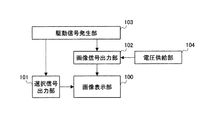
表示装置は基本的に、図1に示すようなI×Jのマトリクス状に配置された画像表示部100中の画素へ、選択信号出力部(ゲート部)101の信号および画像信号出力部(ソース部)102で決められた所定の電圧を供給する構成である。画像信号出力部102および選択信号出力部101はそれぞれ信号線駆動回路(ソースドライバ)、走査線駆動回路(ゲートドライバ)であり、公知の構成を利用して適宜構成できるので、詳しい説明は省略する。
The display device basically has the signals of the selection signal output unit (gate unit) 101 and the image signal output unit (source) to the pixels in the
電圧供給部104は、所定の定電圧をソース部の各画素ラインへ供給するために、該所定の定電圧を画像信号出力部102に供給するようになっている。画像信号出力部102へは、上記定電圧と、画像信号(表示すべきユーザデータ)とが入力され、その値に応じて、後述のアナログ電圧発生回路(電圧作成部)105によって、画素に印加する電圧が作成されるようになっている。なお、電圧供給部104と画像信号出力部102とは後述する。
The
駆動信号発生部103は、後述のように、電圧供給部104内の電圧源の電圧のうちでどれを画素に供給するかの切り替えを行うものであり、適宜、公知の技術を利用して、例えばクロック信号をカウンタで計数する等することで、製造時に設定された所定のタイミングで上記切り替えを行うように作成すればよい。
As will be described later, the drive
図2に、本実施の形態に係る表示装置の画素回路Pijを示す。画素回路はマトリクス状に配置されており、画素回路Pijは画素1つ分を示し、RGBの各画素があればその1つ分を示す。なお、図では、駆動信号発生部103等は省略している。すなわち、iは縦方向の画素の番号を示し、jは横方向の画素の番号を示す。すなわち、画面左上隅から右方向にP11、P12、P13、…、P1Jと続き、その1つ下の段でP21、P22、P23、…、P2Jと続く。以下同様であり、最下段ではPI1、PI2、PI3、…、PIJである。ただし、ここで、I、Jはそれぞれ縦方向、横方向の画素の個数であり、QVGA(320×240ドット)であればI=320、J=240である。なお、P123など、紛らわしい場合はP(12、3)、P(1、23)などのようにも表すこととする。
FIG. 2 shows a pixel circuit Pij of the display device according to the present embodiment. The pixel circuits are arranged in a matrix, and the pixel circuit Pij indicates one pixel, and if there are RGB pixels, it indicates one pixel. In the figure, the
画素回路Pijには、電流駆動型の有機EL素子EL10(電気光学素子)、p型のTFT素子Q10(第1のスイッチング素子)、p型のTFT素子Q20(第2のスイッチング素子)、n型のTFT素子Q30(第3のスイッチング素子)、容量C10、ゲート配線Ei110(第2の配線)、電源配線PW210(第1の配線)、および制御配線Gi310(第3の配線)が配置されている。前記n型のTFT素子Q30としては、電荷保持能力に優れたLDD(Lightly Doped Drain)構造を採用している。 The pixel circuit Pij includes a current-driven organic EL element EL10 (electro-optical element), a p-type TFT element Q10 (first switching element), a p-type TFT element Q20 (second switching element), an n-type TFT element Q30 (third switching element), capacitor C10, gate wiring Ei110 (second wiring), power supply wiring PW210 (first wiring), and control wiring Gi310 (third wiring) are arranged. . As the n-type TFT element Q30, an LDD (Lightly Doped Drain) structure excellent in charge retention capability is adopted.
電源配線PW210にTFT素子Q10が接続されている。TFT素子Q20のゲート端子はゲート配線Ei110に接続されている。また、TFT素子Q10と電源配線PW210との接続点と反対側に、TFT素子Q20と有機EL素子EL10とが直列に接続されている。有機EL素子EL10のアノード(陽極)側(Indium Tin Oxide:ITO等の透明電極を使用)はTFT素子Q20側と接続されており、有機EL素子のカソード側(例えばAl−Li等の金属)には共通電極510が配置されている。有機EL素子EL10のアノード側は、ITO(Indium Tin Oxide)等の透明電極を使用できる。有機EL素子のカソード側は、例えばAl−Li等の金属電極を使用できる。
A TFT element Q10 is connected to the power supply wiring PW210. The gate terminal of the TFT element Q20 is connected to the gate wiring Ei110. Further, the TFT element Q20 and the organic EL element EL10 are connected in series on the side opposite to the connection point between the TFT element Q10 and the power supply wiring PW210. The anode (anode) side (indium tin oxide: using a transparent electrode such as ITO) of the organic EL element EL10 is connected to the TFT element Q20 side, and is connected to the cathode side of the organic EL element (for example, a metal such as Al-Li). Is provided with a
有機EL素子EL10の、電源配線PW210とは逆の側の端子は、共通の端子である共通端子として、全画素の全面にわたって形成されている。すなわち、カソード側の共通電極510が全画素共通に使用できるよう、カソード側は画素全面に電極を配置する構成となっており、作製が簡素にできる一般的な構成のため、従来例よりも好ましい形態となっている。さらに、容量C10の、一方の端子である第1端子は、上記共通端子に接続されている。この第1端子とは、容量C10の、TFT素子Q10のゲート(導通抵抗の制御端子)に接続されていない側である。
A terminal of the organic EL element EL10 opposite to the power supply wiring PW210 is formed over the entire surface of all pixels as a common terminal which is a common terminal. That is, the cathode side has a configuration in which electrodes are arranged on the entire surface of the pixel so that the
このように、電源配線PW210は、有機EL素子EL10に電流を供給するための第1の配線である。TFT素子Q10は、電源配線PW210から有機EL素子EL10に上記電流を流す経路の間に電気的に接続されるとともに、導通抵抗の制御端子(ゲート)を有する第1のスイッチング素子である。すなわち、この制御端子は、Q20、Q30の制御端子と異なり、導通/遮断の二者択一ではない。TFT素子Q20は、有機EL素子EL10と電源配線PW210との間に電気的に接続されるとともに、導通または遮断用の制御端子(ゲート)を有する第2のスイッチング素子である。 Thus, the power supply wiring PW210 is a first wiring for supplying a current to the organic EL element EL10. The TFT element Q10 is a first switching element that is electrically connected between the path through which the current flows from the power supply wiring PW210 to the organic EL element EL10 and has a control terminal (gate) for conduction resistance. That is, this control terminal is not an alternative of conduction / cutoff unlike the control terminals of Q20 and Q30. The TFT element Q20 is a second switching element that is electrically connected between the organic EL element EL10 and the power supply wiring PW210 and has a control terminal (gate) for conduction or interruption.
容量C10は、一方の端子である第1端子が、一定の電圧を有する領域に接続され、電荷を蓄積し、蓄積した電荷に応じた電圧をTFT素子Q10の導通抵抗の制御電圧として用いるためのものである。ここでは、一定の電圧を有する領域とは、共通電極510である。
The capacitor C10 has a first terminal, which is one terminal, connected to a region having a constant voltage, accumulates charges, and uses a voltage corresponding to the accumulated charges as a control voltage for the conduction resistance of the TFT element Q10. Is. Here, the region having a constant voltage is the
TFT素子Q30は、電源配線PW210と有機EL素子EL10との間に一方が電気的に接続され、もう一方は上記容量C10からTFT素子Q10の導通抵抗の制御端子に至る電荷供給経路上に接続されるとともに、導通または遮断用の制御端子(ゲート)を有し、遮断によって上記容量C10に蓄積した電荷を保持させる第3のスイッチング素子である。 One of the TFT elements Q30 is electrically connected between the power supply wiring PW210 and the organic EL element EL10, and the other is connected on the charge supply path from the capacitor C10 to the control terminal of the conduction resistance of the TFT element Q10. And a third switching element having a control terminal (gate) for conduction or interruption, and holding the charge accumulated in the capacitor C10 by interruption.
ゲート配線Ei110は、上記各画素のTFT素子Q20の制御端子に導通または遮断用の制御電圧を印加する第2の配線である。制御配線Gi310は、上記各画素のTFT素子Q30の制御端子に導通または遮断用の制御電圧を印加する第3の配線である。 The gate wiring Ei110 is a second wiring that applies a control voltage for conduction or cutoff to the control terminal of the TFT element Q20 of each pixel. The control wiring Gi310 is a third wiring that applies a control voltage for conduction or cutoff to the control terminal of the TFT element Q30 of each pixel.
電圧供給部104と画像信号出力部102とから、画素制御部106が構成されている。すなわち、画素制御部106は、電源配線PW210の末端にあって、各画素の駆動開始から終了までの間の時期に応じて、
画像信号に応じた電圧である表示信号電圧の、TFT素子Q10の導通抵抗の制御端子(ゲート)への印加と、
有機EL素子EL10を駆動する電流を供給するための電圧である駆動用電圧の、有機EL素子EL10への印加と、
を切り替えるものである。電圧供給部104は、それぞれ定電圧の電圧を供給する電圧源としての電流供給用電圧源回路104x(駆動用電圧源)、スイッチ遮断用電圧源回路104y(非発光用電圧源)、アナログ電圧供給用電源回路104z(表示信号電圧源)を有している。電流供給用電圧源回路104x、スイッチ遮断用電圧源回路104yはそれぞれ、駆動用電圧、非発光用電圧を供給するものである。非発光用電圧とは、非発光時(黒表示時)に、表示信号電圧の電圧印加の代わりに、有機EL素子EL10を非発光状態にするためにTFT素子Q10を遮断状態にさせるときに供給する電圧である。アナログ電圧供給用電源回路104zは、アナログ電圧発生回路(電圧作成部)105と合わせて、表示信号電圧を供給するものであり、画像信号に応じて所定の電流を書き込むために、各画素にアナログの定電圧を供給するものである。なお、詳しくは後述する。このように、電源配線PW210の末端にはこの画素制御部106が接続されており、電流供給用電圧源回路104x、スイッチ遮断用電圧源回路104y、アナログ電圧供給用電源回路104zがPW210の配線と切り替え可能に接続されている。
The
Applying a display signal voltage, which is a voltage corresponding to an image signal, to the control terminal (gate) of the conduction resistance of the TFT element Q10;
Applying a driving voltage, which is a voltage for supplying a current for driving the organic EL element EL10, to the organic EL element EL10;
Is to switch. The
また、前記容量C10の一方は、有機EL素子EL10のカソードを介して共通電極510に接続されている。共通電極510とは、電圧源(対向電源)のことであり、図4の構成では0Vまたはグランドに設定される。すなわち、容量C10の一方が有機EL素子EL10のカソード(全画素共通の陰極、図5に示す金属薄膜53)に接続されており、そのカソードが共通電極510に接続されるということである。
One end of the capacitor C10 is connected to the
前記図23(非特許文献1)の画素回路構成および駆動方法では、複数の画素を有する表示装置とした場合、カソード側をゲート線方向に配線する必要がある。この配線を実現する方法としては、カソードを、ゲート線方向の各画素に沿って平行に縞模様型に配置する、或いは、TFT基板の反対側に配置されるカソードを、隣り合う画素に接触しないよう各画素に水玉模様型に作製し、そのカソードをTFT基板の図23のEiやGiのようなゲート線とコンタクトして配置する方法が考えられる。 In the pixel circuit configuration and driving method shown in FIG. 23 (Non-Patent Document 1), when a display device having a plurality of pixels is used, the cathode side needs to be wired in the gate line direction. As a method for realizing this wiring, the cathode is arranged in a striped pattern parallel to each pixel in the gate line direction, or the cathode arranged on the opposite side of the TFT substrate is not in contact with the adjacent pixel. A method of arranging each pixel in a polka dot pattern and placing the cathode in contact with a gate line such as Ei or Gi in FIG. 23 of the TFT substrate is conceivable.
しかしながら、上記のような方法では、プロセス数の増加による製造コストの増加や、マスク精度の低下や、有機EL素子等の発光素子上でエッチングをすることによる歩留まりの低下、その他、配線抵抗値の斑や画素全体に分布ができて輝度斑が発生しやすくなるなどの問題があり、上記のような画素回路構成で表示装置を作製することは現実的には難しい。 However, in the above method, an increase in manufacturing cost due to an increase in the number of processes, a decrease in mask accuracy, a decrease in yield due to etching on a light-emitting element such as an organic EL element, and other problems such as a decrease in wiring resistance value. There is a problem that distribution of spots and the entire pixel is likely to cause luminance spots, and it is practically difficult to manufacture a display device with the above-described pixel circuit configuration.
これに対し、本実施形態では、カソードは、画素全面に一様に形成・配置されているので、縞模様や水玉模様状に形成するのと比べて簡素に作製でき、抵抗の分布を小さくすることができる。それゆえ、カソードのプロセスに起因する製造コストの増加や歩留まりの低下や表示装置作成の困難さを低減することができる。 On the other hand, in the present embodiment, the cathode is uniformly formed and arranged on the entire surface of the pixel, so that it can be manufactured more simply than a stripe pattern or a polka dot pattern, and the resistance distribution is reduced. be able to. Therefore, an increase in manufacturing cost, a decrease in yield, and difficulty in manufacturing a display device due to the cathode process can be reduced.
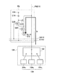
また、一例として、上記画素構成の画素回路Pijを2×3画素並べて配置したときの表示装置の回路構成を図3に示す。 As an example, FIG. 3 shows a circuit configuration of a display device when pixel circuits Pij having the above-described pixel configuration are arranged by arranging 2 × 3 pixels.
電圧供給部104の内部には、電流供給用電圧源回路104x、スイッチ遮断用電圧源回路104y、アナログ電圧供給用電源回路104zが設けられている。電流供給用電圧源回路104x、スイッチ遮断用電圧源回路104y、アナログ電圧供給用電源回路104zから出力される電圧については後述する。
Inside the
画像信号出力部102の内部には、画素に供給する電源配線の本数をn(図3ではn=3)とすると、画素ライン毎にn個の「単位」画像信号出力部VS1、VS2、…、VSnが設けられている。図3では、VS1は画素P11・P21用の単位画像信号出力部であり、VS2は画素P12・P22用の単位画像信号出力部であり、VS3は画素P13・P23用の単位画像信号出力部である。
In the image
さらに、アナログ電圧発生回路(電圧作成部)105は、外部から入力される画像信号に応じて、表示信号電圧源である、電圧供給部104のアナログ電圧供給用電源回路104zから供給される電圧を所望の電圧に変圧させることで表示信号電圧を作る役割を持っており、画素毎に所望の電圧を書き込むような構成となっている。この105は、例えば液晶用ドライバで使用されているR−DAC方式(抵抗分割デジタル−アナログ変換方式)等のように、数本の基準電圧を元に、抵抗を分割利用して階調電圧を作り出す回路等を適宜採用できる。
Further, the analog voltage generation circuit (voltage creation unit) 105 generates a voltage supplied from the analog voltage supply
画素内に複数の配線と3つのアクティブ素子と1つの容量と電気光学素子を有する従来の画素構成においては、表示品位や光学素子の発光寿命に優れた効果のある電圧指定方式の定電流駆動を行う場合は、カソード側をゲート線方向に配線する必要があるため、プロセス数の増加や、配線抵抗値の斑や画素全体に分布ができて輝度斑が発生しやすくなり、上記のような画素回路構成で表示能力に優れた表示装置を作製することは現実的には難しいという問題点がある。 In a conventional pixel configuration having a plurality of wirings, three active elements, one capacitor, and an electro-optic element in a pixel, voltage-designated constant-current driving that has an excellent effect on display quality and light emission lifetime of the optical element is performed. When doing so, it is necessary to wire the cathode side in the direction of the gate line, so the number of processes increases, wiring resistance variation and distribution across the entire pixel are likely to cause luminance variation, and the above pixels There is a problem that it is actually difficult to manufacture a display device having a circuit configuration and excellent display capability.
そこで、本実施形態では、電圧指定方式の定電流駆動を行い、カソード側(共通電極側)を、一般的に作製が簡素にできる画素全面にカソードを配置する構成にする。また、従来の画素回路構成のデータ線と共通配線を統一して用い、配線数を減らしている。それによって、上記問題点を解決しながら、かつ従来の画素構成よりも高精細で、レイアウトの自由度や開口率の向上した表示装置を実現することが可能である。 Therefore, in this embodiment, voltage-designated constant-current driving is performed, and the cathode side (common electrode side) is configured to be disposed on the entire pixel surface, which can generally be easily manufactured. In addition, the data lines and common wirings of the conventional pixel circuit configuration are used in a unified manner to reduce the number of wirings. Accordingly, it is possible to realize a display device that solves the above-described problems and has a higher definition than the conventional pixel configuration and an improved layout flexibility and aperture ratio.
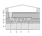
この場合の画素であって、TFT素子Q20および有機EL素子10付近の構造を図4に示す。同図に示すように、本実施形態では、各画素は、SiO2膜で表面をコーティングしてあるガラス基板60上に、SiO2膜59、SiO2/SiNx膜58、SiNx膜57がこの順に積層されている。そしてその内部において、上記SiO2膜59を介して、CGシリコン薄膜52とゲート電極51とが積層され、ゲート電極51の上に、上記SiO2/SiNx膜58を介して電源線電極12が積層されている。その上にポリイミド膜(PI)55、透明導電膜(アノード)54、有機EL素子20、金属薄膜(カソード)53が、画像表示部100の全画素にわたって積層されている。その一部では、有機EL素子20が、透明導電膜54を介して、電源線電極12と接続されている。上記ゲート電極51、CGシリコン薄膜52とその間のSiO2膜59でTFT素子Q20が形成されている。透明導電膜54の材料の例としては、ITO等が挙げられる。金属薄膜53の材料の例としては、Al−Li等が挙げられる。
FIG. 4 shows a structure in the vicinity of the TFT element Q20 and the
図中、矢印は、EL発光の光取り出し方向である。また、矢印の幅は、光を取り出せる幅(面積)に対応させて描いてある。すなわち、矢印の幅が広いほど、光を取り出せる幅(面積)が広いということである。他の図も同様である。上記のような構成で表示装置を実現すると、従来よりも開口率を向上することができるため、特にTFT基板側の方に向かって有機EL素子の発光を外部へ取り出す図4のようなボトムエミッション構造では好ましい様態となる。 In the figure, the arrow indicates the light extraction direction of EL light emission. The width of the arrow is drawn corresponding to the width (area) from which light can be extracted. That is, the wider the width of the arrow, the wider the width (area) from which light can be extracted. The same applies to the other figures. When the display device with the above configuration is realized, the aperture ratio can be improved as compared with the conventional case. Therefore, the bottom emission as shown in FIG. 4 in which the light emitted from the organic EL element is extracted to the outside especially toward the TFT substrate side. The structure is a preferred embodiment.
ゲート電極51を用いて、Gi310やEi110の配線が形成されている。また、電源線電極12を用いて、PW210や、TFT同士をつなぐ線が形成されている。
Using the
また、この場合の画素であって、容量C10付近の構造を図5に示す。同図に示すように、上記ゲート電極51、CGシリコン薄膜52とその間のSiO2膜59で容量C10が形成されている。この部位では、ゲート電極51は、ゲート電極・電源線電極コンタクト15および電源線電極12を介して、上記金属薄膜(カソード)53と接続されている。
Further, FIG. 5 shows the structure of the pixel in this case and in the vicinity of the capacitor C10. As shown in the figure, a capacitor C10 is formed by the
容量の一方であるゲート電極51は、直接金属薄膜53とコンタクトをとってもよいが、ゲート電極51と金属薄膜53の層間が深いため、歩留まりや開口率等に悪影響しやすくなる。これは、層が深いほどコンタクトを空ける穴(円錐型に空く)を大きくとらなければならないからである。そのため、一旦ゲート電極51と電源線電極12とでコンタクトをとり、次に電源線電極12と金属薄膜53とでコンタクトをとるように構成することができる。
The
このように、例えば本発明で容量に用いているゲート電極51・CGシリコン薄膜52間のゲート側に、電源線電極12の一部とのコンタクトをとり、その電源線電極12と金属薄膜(カソード)53とをコンタクトすることによって、容量C10の一方をカソードにコンタクトできるようにしている。それによって、容量用に共通配線を画素内に用意する必要がなくなるので、より開口率を増やすこともできる。なお、ここでの容量の取り方はゲート電極51・CGシリコン薄膜52間としているが、この層間に限られることなく、例えばゲート電極51・電源線電極12間であってもよい。
Thus, for example, a contact with a part of the
また、図4の構成を、トップエミッション構造に変更した場合の構造を図6に示す。図4の構成とは、カソードとアノードとの配置は同じであるが、金属薄膜(カソード)53、透明導電膜(アノード)54をそれぞれ、酸化インジウム・酸化亜鉛(IZO:Indium Zinc Oxide)等を用いた透明導電膜(カソード)61、アルミニウムやモリブデン等を用いた金属薄膜(アノード)62に変えた点が異なる。この構成では、画素の、広い領域から、EL発光の光を取り出すことができる。 FIG. 6 shows a structure when the configuration of FIG. 4 is changed to a top emission structure. The arrangement of FIG. 4 is the same as the arrangement of the cathode and the anode, but the metal thin film (cathode) 53 and the transparent conductive film (anode) 54 are each made of indium zinc oxide (IZO) or the like. The difference is that the transparent conductive film (cathode) 61 used and the metal thin film (anode) 62 using aluminum or molybdenum are used. In this configuration, EL light emission can be extracted from a wide area of the pixel.
すなわち、上記の画素構成のように、従来よりも画素内の配線等を減らし、レイアウトの自由度も向上することができることにより、より高精細な画素を実現できる。特にTFT基板の反対側から有機EL素子の発光を外部へ取り出すトップエミッション構造の画素構成では、開口率をボトムエミッション構造よりも大きくとることができ、高精細なピッチの画素をレイアウトすることができるため、携帯サイズの応用製品(例えば携帯電話等の情報機器端末やモバイルテレビ等)に好ましい形態となる。さらに、本発明で用いた有機EL素子は、低電圧・低消費電力で発光可能であり、さらにバックライトが不要な分、液晶より薄型を実現でき、前記携帯サイズの応用製品にとってより好ましい。 That is, as in the above-described pixel configuration, the number of wirings in the pixel can be reduced as compared to the conventional one, and the degree of freedom in layout can be improved, so that a higher definition pixel can be realized. In particular, in the pixel configuration of the top emission structure in which the light emission of the organic EL element is extracted to the outside from the opposite side of the TFT substrate, the aperture ratio can be made larger than that of the bottom emission structure, and pixels with a high definition pitch can be laid out. Therefore, this is a preferable form for mobile-size application products (for example, information equipment terminals such as mobile phones and mobile TVs). Furthermore, the organic EL element used in the present invention can emit light with low voltage and low power consumption, and can be made thinner than liquid crystal because it does not require a backlight, and is more preferable for the portable size application products.
本発明では、電圧指定方式の動作を応用した動作にしており、その動作を、図7〜図14を用いて説明する。 In the present invention, the operation of the voltage designation method is applied, and the operation will be described with reference to FIGS.
ここでマトリクス状に配置された図2のPij画素回路のうち最初にカウントされる画素P11〜P(1、240)に着目すると、この画素P11〜P(1、240)の書き込み期間と発光期間の動作は例えば図7のように動作する。電圧指定方式の動作の基本原理は非特許文献2に記載されているのでここでは省略するが、従来では1フレーム期間(1/60秒≒16.6m秒)内に(1)リセット期間、(2)閾値補正期間、(3)データ電圧書き込み期間、(4)発光期間の4つの期間がある。 Here, when attention is paid to the first counted pixels P11 to P (1,240) in the Pij pixel circuit of FIG. 2 arranged in a matrix, the writing period and the light emitting period of the pixels P11 to P (1,240) are shown. The operation is performed as shown in FIG. Since the basic principle of the operation of the voltage designation method is described in Non-Patent Document 2, it is omitted here. Conventionally, (1) a reset period, (1) within one frame period (1/60 seconds≈16.6 milliseconds), There are four periods: 2) a threshold correction period, (3) a data voltage writing period, and (4) a light emission period.
P11の電圧書き込み期間の次に、他の画素の電圧書き込み期間がある。これは、図3の構成であれば、「P11、P12、P13の電圧書き込み期間」、「P21、P22、P23の電圧書き込み期間」という意味である。すなわち、QVGAの場合、縦方向に320画素、横方向に240画素配置されている。例えばパネルの一番上の横一列の画素はP11、P12・・・P(1、239)、P(1、240)であり、この横一列の書き込み期間が26μ秒となる。この書き込みが縦列320個続くと8.3m秒となり、これが1フレーム間(16.6m秒)の全書き込み期間になる。したがって、1フレーム期間から全書き込み期間を引いた残り16.6−8.3=8.3ミリ秒が全画素の発光期間になる。 Next to the voltage writing period of P11, there is a voltage writing period of another pixel. In the configuration of FIG. 3, this means “voltage writing period of P11, P12, P13” and “voltage writing period of P21, P22, P23”. That is, in the case of QVGA, 320 pixels are arranged in the vertical direction and 240 pixels are arranged in the horizontal direction. For example, the pixels in the horizontal row at the top of the panel are P11, P12... P (1,239), P (1,240), and the horizontal writing period is 26 μsec. If this writing continues for 320 columns, it becomes 8.3 milliseconds, which is the entire writing period for one frame (16.6 milliseconds). Therefore, the remaining 16.6-8.3 = 8.3 milliseconds obtained by subtracting the entire writing period from one frame period is the light emitting period of all pixels.
P11〜P(1、240)の書き込み期間(ここでは16.6m秒/2/320画素≒26μ秒)中には(1)リセット期間、(2)TFTQ10の閾値補正期間の動作を行い、画素P11〜P(1、240)は、P11〜P(1、240)を含むI×J個の他の全ての画素が書き込み終了するまで発光動作を待機する。なお、図示しないラッチ回路を利用して、240個の画素について画像のデータ書き込みを同時に行う。 During the writing period of P11 to P (1,240) (here, 16.6 msec / 2/320 pixel≈26 μsec), (1) the reset period and (2) the threshold correction period of the TFT Q10 are performed. P11 to P (1,240) waits for the light emission operation until all other I × J pixels including P11 to P (1,240) have finished writing. Note that image data writing is simultaneously performed for 240 pixels using a latch circuit (not shown).
そして、(3)発光期間(16.6m秒/2≒8.3m秒)に入る発光動作切り替え時には、電流供給用電圧源回路104xから供給される電圧によって、所望の電流が流れるようにTFTQ10のゲート・ソース間電位Vgsを定められ、他の画素と同時に発光を行う。このとき次の書き込み期間が来るまでの1フレーム期間の間、TFTQ10は書き込み期間に与えたゲート電圧を保持している。なお、上記全ての画素の書き込み時間と、全ての画素が同時に発光する時間の比は、上記では1:1の関係にしているが、上記時間の比に限られることはない。
Then, (3) at the time of switching the light emission operation that enters the light emission period (16.6 msec / 2≈8.3 msec), the TFT Q10 is configured so that a desired current flows by the voltage supplied from the current supply
QVGA(320x240)パネルの一番左上の画素をP11とすると、図7のタイミングチャートでzの電圧が4回上昇しているのは、P11、P21、P31、P41の4回を指しており、その4回目のあと、信号電圧P51、P61・・・P(319、1)、P(320、1)と続いている。 When the upper left pixel of the QVGA (320 × 240) panel is P11, the z voltage rises four times in the timing chart of FIG. 7 indicates four times P11, P21, P31, and P41. After the fourth time, signal voltages P51, P61... P (319, 1), P (320, 1) are continued.
また、P11〜P(1、240)の画素を発光期間時に非発光(黒表示)にしたい場合は、図8に示すようにスイッチ遮断用電圧源回路104yを動作させ、非発光になるような電圧をTFTQ10のゲート電位に書き込む。そのため、スイッチ遮断用電圧源回路104yから与えられる電圧Vyと発光時に切り替える電流供給用電圧源回路104xから与えられる電圧Vxとの関係は上記画素構成ではVy>Vxとなり、黒表示をよりはっきりさせるにはVy>Vx+Q10の閾値(絶対値)の条件が好ましい。
Further, when it is desired to make the pixels P11 to P (1,240) not emit light (black display) during the light emission period, the switch cutoff
ここで、前記TFTQ10のゲート電圧は、電源配線PW210の電圧が変動するたびにTFTQ10やQ30の寄生容量の影響を受け若干変動する。そのため、容量C10の容量が小さいときは、階調が直線にならず、逆ガンマ補正がかかったような階調特性になる。そのため、容量C10は前記電位の変動を考慮すると200fF〜3000fFが好ましく、さらに1フレーム期間の電荷の保持能力や画素のサイズ等を考慮すると、500〜1000fFがより好ましい。 Here, the gate voltage of the TFT Q10 slightly varies depending on the parasitic capacitance of the TFTs Q10 and Q30 every time the voltage of the power supply wiring PW210 varies. For this reason, when the capacitance of the capacitor C10 is small, the gradation does not become a straight line, and the gradation characteristics are such that inverse gamma correction is applied. For this reason, the capacitance C10 is preferably 200 fF to 3000 fF in consideration of the potential variation, and more preferably 500 to 1000 fF in consideration of the charge holding capability in one frame period, the pixel size, and the like.
従来の画素動作は以下のように、
(1)画素内駆動用TFTのリセット期間
(2)画素内駆動用TFTの閾値補正期間
(3)画素内駆動用TFTのゲートに所定のデータ電圧を書き込む期間
(4)有機EL素子が発光する期間
となるが、本発明の画素動作では、(3)の動作を(2)の動作の中で同時に行うことができるので、
(1)画素内駆動用TFTのリセット期間
(2)画素内駆動用TFTの閾値補正期間
(3)有機EL素子が発光する期間
とのように、画素内は簡単な動作になる。
Conventional pixel operation is as follows:
(1) Reset period of in-pixel driving TFT (2) Threshold correction period of in-pixel driving TFT (3) Period of writing predetermined data voltage to gate of in-pixel driving TFT (4) Organic EL element emits light Although it is a period, in the pixel operation of the present invention, the operation (3) can be performed simultaneously with the operation (2).
(1) Reset period of the in-pixel driving TFT (2) Threshold correction period of the in-pixel driving TFT (3) Period in which the organic EL element emits light makes the operation in the pixel simple.
上記動作について、より詳細に述べると、以下のようである。すなわち、図9〜図11のようにして発光する。また、非発光(黒表示)時は図12〜図14のようになる。図中、丸で囲った素子は、スイッチオン、または発光オンを意味し、×を付けた素子は、スイッチオフ、または発光オフを意味する。また、電流供給用電圧源回路104x、スイッチ遮断用電圧源回路104y、アナログ電圧供給用電源回路104zの供給する電圧をそれぞれVx、Vy、Vzとする。
The above operation will be described in detail as follows. That is, light is emitted as shown in FIGS. Further, when no light is emitted (black display), it is as shown in FIGS. In the figure, a circled element means switch on or light emission on, and an element marked with x means switch off or light emission off. The voltages supplied by the current supply
(1)リセット期間においては、アナログ電圧供給用電源回路104zから電流Irを流す。(2)閾値補正期間においては、PW210から印加された電圧が容量C10に蓄えられる。それにより、TFT素子Q10のゲート・ソース間電圧が、TFT素子Q10の閾値電圧Vthの絶対値になる。(3)発光期間においては、電流供給用電圧源回路104xから電流Ionを流す。これにより、TFT素子Q10のゲート・ソース間電圧が、TFT素子Q10の閾値電圧Vthと電圧αとの和の絶対値になる。ただし、非発光時には、(3)発光期間においては、電流供給用電圧源回路104xから電流Ioffを流し、これにより、TFT素子Q10のゲート・ソース間電圧が、TFT素子Q10の閾値電圧Vthと電圧βとの差の絶対値になる。
(1) In the reset period, the current Ir is supplied from the analog voltage supply power supply circuit 104z. (2) In the threshold correction period, the voltage applied from the PW 210 is stored in the capacitor C10. Thereby, the gate-source voltage of the TFT element Q10 becomes the absolute value of the threshold voltage Vth of the TFT element Q10. (3) In the light emission period, the current Ion is supplied from the current supply
図の電流値Irは、リセット期間の動作で一瞬(1〜2μ秒間)流れる電流であり、本発明の画素回路ではおおよそ数十μ〜数百μアンペア流れる。この瞬間電流を流す動作の目的は、1つ前の画素動作に影響されず、TFTQ10のゲート・ソース間電位を大きくさせ(リセットさせ)、閾値補正の動作を安定して行うことにある。また、本実施形態では、動作原理を簡単に説明するために、リセット期間にアナログ電圧供給用電源回路104zを用いている。各画素によって瞬間電流が大きく異なり、例えば瞬間電流が小さいリセット電圧の場合には閾値補正の書き込み時間が安定しないため、リセット用瞬間電流は大きく流れることが望ましい。そのため、リセット期間中には電流供給用電圧源回路104xからアナログ電圧供給用電源回路104zまたはスイッチ遮断用電圧源回路104yへのスイッチ切り替えを行うことが好ましい。
The current value Ir shown in the figure is a current that flows for an instant (1-2 μsec) in the operation of the reset period. In the pixel circuit of the present invention, the current value Ir flows approximately several tens μ to several hundred μamperes. The purpose of the operation of supplying the instantaneous current is to increase the gate-source potential of the TFT Q10 (reset) and to stably perform the threshold correction operation without being affected by the previous pixel operation. In this embodiment, the analog voltage supply
Ionは、発光中(数ミリ秒間)に流れる電流で、おおよそ数十n〜数μアンペア流れる。つまり、電流Irは、画素の書き込み期間に流れる瞬間的な電流であり、Ionは、画素の発光期間に流れる電流で、お互い全く異なる動作の電流である。 Ion is a current that flows during light emission (several milliseconds), and approximately tens of n to several μamperes. That is, the current Ir is an instantaneous current that flows during the pixel writing period, and Ion is a current that flows during the light emission period of the pixel, and is a current that is completely different from each other.
Ioffは、発光期間中に画素を発光しないときの電流であり、理想的には0アンペアであるが、TFTスイッチをオフ(発光期間中のQ10のゲート・ソース間電位が閾値以下になっている)しても、漏れ電流が流れるため、実際には限りなく0に近い、数pアンペア〜数nアンペアレベルの電流が流れる。 Ioff is a current when the pixel does not emit light during the light emission period, and is ideally 0 ampere, but the TFT switch is turned off (the gate-source potential of Q10 during the light emission period is below the threshold value). However, since a leakage current flows, a current of several p amperes to several n amperes, which is practically close to 0, flows.
αは、アナログ電圧書き込み(オフ書き込みを含む)の電圧変化量を意味している。すなわち、例えば図の画素制御部106で電流供給用電圧源回路104xの電圧を12V、アナログ電圧供給用電源回路104zの電圧(zは例えば5V〜12Vに可変できる電圧)を7Vとし、pchTFTQ10の閾値電圧を−2Vと設定する。
α means the amount of voltage change in analog voltage writing (including off-writing). That is, for example, in the
上記設定のときQ10の閾値補正動作(2)が完了したときには、画素制御部106からはzの電位7Vが供給され、Q10のゲート・ソース間電圧は閾値−2Vになっているので、Q10のゲート電位Vgは5Vになっている。
When the threshold correction operation (2) of Q10 is completed at the above setting,
次に(3)の発光動作に移ったときには、TFTQ30のスイッチがオフされるので、Q10のゲート電位Vgが5Vのまま保持される。その後発光期間中は画素制御部106からはxの電位12Vが供給されるので、Q10のゲート・ソース間電位Vgsは5−12=−7Vとなる。ここでVgs=Vth+αなので、−7=−2+αなのでα=−5Vとなる。もし、設定条件でアナログ電圧供給用電源回路104zの電圧を5Vに変更すると、Vg=3Vとなり、発光期間時のVgs=−9Vとなりα=−7Vとなる。つまり、Q10の発光時のVgsは、アナログ電圧供給用電源回路104zの書き込み電圧に依存して変化する。そして、上記条件ではαは0〜−7Vの範囲で変化する。
Next, when the light emission operation of (3) is started, the switch of the TFT Q30 is turned off, so that the gate potential Vg of Q10 is held at 5V. Thereafter, during the light emission period, the potential 12V of x is supplied from the
スイッチ遮断用電圧源回路104yは、この原理を利用して発光期間時に画素を発光させない書き込み電圧を与える。例えば上記の閾値電圧、駆動用電圧の設定で、書き込み期間中に非発光用電圧として15Vを与えると、Q10のVg=13となり、この状態で発光動作に移ると、Vgs=13−12=1Vとなり、Vgs=Vth+αよりα=3Vとなる。p型TFTの場合、Vgs>Vthであればスイッチはオフになるので、この画素は、発光期間時に、発光しない電流Ioffが流れることになる。なお、上記画素を発光させない条件ではαはおおよそ2〜4Vの範囲で変化する。なお、ここでは、説明の便宜上、発光時はα、非発光時はβと称している。
Using this principle, the switch cutoff
なお、TFTQ10がn型ならば、TFTQ10がp型であるとして上記説明した各電位の正負が逆転する。 If the TFT Q10 is n-type, the positive and negative of each potential described above is reversed assuming that the TFT Q10 is p-type.
また、本実施形態では、TFTQ10がp型である場合、
Vy>Vx≧Vz
という条件を満たしている。
In the present embodiment, when the TFT Q10 is p-type,
Vy> Vx ≧ Vz
This condition is met.
もしTFTQ11がn型であれば正負が逆転して、
Vy'<Vx'≦Vz'
になる。
If TFTQ11 is n-type, the polarity is reversed,
Vy ′ <Vx ′ ≦ Vz ′
become.
また、その他の満たすべき条件として、発光期間中に画素を発光させないとき、図2のp型TFTQ10は
Vgs>0
になることがスイッチ特性上好ましく、つまり
Vy>Vx−Vth
の条件で設定することが好ましい。また同様に、図15のn型TFTQ11は
Vgs<0
になることがスイッチ特性上好ましく、つまり
Vy'<Vx'−Vth'
の条件で設定することが好ましい。
Further, as another condition to be satisfied, when the pixel is not caused to emit light during the light emission period, the p-type TFT Q10 of FIG.
Is preferable in terms of switch characteristics, that is, Vy> Vx−Vth.
It is preferable to set under the conditions. Similarly, the n-type TFT Q11 in FIG. 15 has Vgs <0.
Is preferable in terms of switch characteristics, that is, Vy ′ <Vx′−Vth ′.
It is preferable to set under the conditions.
動作はシンプルであり、発光時と非発光時とでは電源回路の切り替えスイッチの選択が変わるだけであり、画素の動きは基本的に変わらない。ここでは、電圧指定方式定電流駆動である。リセット期間から、画素内のTFTQ10またはQ11が閉鎖された系(電流が流れない状態)に変わったとき、上記TFTのゲート・ソース間電位は、ちょうど電流が流れないところ(閾値)で止まる。それによって、各画素の閾値のばらつきを補正できる。ただし、サイズや移動度等のバラツキは補正できないので、完璧な電流バラツキ補正はできない。 The operation is simple, and only the selection of the power supply circuit changeover switch changes between light emission and non-light emission, and the movement of the pixel basically does not change. Here, the voltage designation method is constant current driving. When the TFT Q10 or Q11 in the pixel is changed from the reset period to a closed system (a state in which no current flows), the gate-source potential of the TFT stops just where no current flows (threshold). Thereby, the variation in the threshold value of each pixel can be corrected. However, since variations such as size and mobility cannot be corrected, perfect current variation cannot be corrected.
上記図2の画素構成回路内のTFT素子は上記属性に限られることなくp型であってもn型であってもよく、例えば図15に示すように画素内全てのTFTをn型で構成することも可能である。なお、前記図15では前記図2と異なり、有機EL素子の電極が図2の有機EL素子に対して反転しており、アノード側が共通電極側として配置されており、EL素子の発光の光を取り出す方向がTFT基板と反対側になるトップエミッションとなっている。このように電気光学素子の一方の電極が全面に配置される作製が簡素な方法であれば共通電極はアノードであってもカソードであってもよい。 The TFT elements in the pixel configuration circuit of FIG. 2 are not limited to the above attributes, and may be p-type or n-type. For example, as shown in FIG. It is also possible to do. 15 differs from FIG. 2 in that the electrode of the organic EL element is inverted with respect to the organic EL element of FIG. 2, the anode side is arranged as the common electrode side, and the light emitted from the EL element is emitted. The top emission is such that the direction of extraction is opposite to the TFT substrate. As described above, the common electrode may be an anode or a cathode as long as one electrode of the electro-optic element is simply formed on the entire surface.
画像信号出力部112は図1の画像信号出力部102と同じである。
The image
図15の層構造を図16に示す。ここでは、ITOが上側に来るので、トップエミッション構造になる。それ以外は図4と同じである。すなわち、トップエミッション構造は、基本的に、図4、図5の透明導電膜54と金属薄膜53との位置を入れ替えて、EL発光の出力方向が上下逆転するだけで、他は変わらない。
The layer structure of FIG. 15 is shown in FIG. Here, since the ITO comes on the upper side, a top emission structure is obtained. The rest is the same as FIG. That is, the top emission structure is basically the same except that the positions of the transparent
動作については図4の場合と同様である。 The operation is the same as in FIG.
上記動作は、以下のようである。すなわち、図17〜図19のようにして発光する。また、非発光(黒表示)時は図20〜図22のようになる。 The above operation is as follows. That is, light is emitted as shown in FIGS. Further, when no light is emitted (black display), it is as shown in FIGS.
動作の条件については上述した通りである。すなわち、TFTQ10がn型ならば、TFTQ10がp型であるとして上記説明した各電位の正負が逆転する。また、
Vy'<Vx'≦Vz'
という条件を満たしている。また、その他の満たすべき条件として、発光期間中に画素を発光させないとき、
Vgs<0
になることがスイッチ特性上好ましく、つまり
Vy'<Vx'−Vth'
の条件で設定することが好ましい。
The operation conditions are as described above. That is, if the TFT Q10 is n-type, the positive and negative of each potential described above is reversed assuming that the TFT Q10 is p-type. Also,
Vy ′ <Vx ′ ≦ Vz ′
This condition is met. In addition, as another condition to be satisfied, when the pixel is not allowed to emit light during the light emission period,
Vgs <0
Is preferable in terms of switch characteristics, that is, Vy ′ <Vx′−Vth ′.
It is preferable to set under the conditions.
以上説明したように、本発明の表示装置は、カソード側(共通電極側)の構成を、一般的に作製が簡素にできる、画素全面にカソードを配置する構成にしながら、電圧指定方式の定電流駆動を行う。また、データ線と共通配線とを共用している。それによれば、従来の画素構成に比べプロセス数を多くすることなく、また配線数等を減らすことができ、より高精細で、高開口率な表示装置を提供できる。特にトップエミッション構造の画素構成では、開口率をボトムエミッション構造よりも大きくとりながら、高精細なピッチの画素をレイアウトすることができるため、携帯電話やモバイルテレビ等の携帯機器製品により好ましい効果を発揮できる。 As described above, in the display device of the present invention, the cathode side (common electrode side) configuration is generally a simple design, and the configuration in which the cathode is arranged on the entire surface of the pixel can be simplified. Drive. Further, the data line and the common wiring are shared. Accordingly, the number of processes and the like can be reduced without increasing the number of processes compared to the conventional pixel configuration, and a display device with higher definition and higher aperture ratio can be provided. Especially in the pixel configuration of the top emission structure, it is possible to lay out pixels with a high-definition pitch while taking the aperture ratio larger than that of the bottom emission structure, so that it is more effective for mobile device products such as mobile phones and mobile TVs. it can.
本発明は、カソード側を、一般的に作製が簡素にできる画素全面にカソード電極を配置する構成にしながら、表示品位や光学素子の発光寿命に優れた効果のある電圧指定方式の定電流駆動を用い、また上記画素回路のデータ線と共通配線を統一して用い、配線数を減らすことで、上記問題点を解決しながら、かつレイアウトの自由度や、開口率を向上することができる表示装置を提供することができる。 The present invention provides a voltage-designated constant-current drive that has an excellent effect on the display quality and the light emission life of the optical element, while the cathode side is generally configured so that the cathode electrode is disposed on the entire surface of the pixel that can be easily manufactured. A display device that can improve the degree of freedom of layout and the aperture ratio while solving the above problems by using the data lines and common wirings of the pixel circuit in a unified manner and reducing the number of wirings. Can be provided.
なお、有機EL素子は継続的に発光する輝度を高くすると、前記素子の半減寿命が短くなることが一般に知られており、画素の開口率が向上すると、前記画素輝度を低くしながら見た目には同じ輝度を表示できるため、高開口率にすることは有機EL素子の寿命を延ばす効果がある。 In addition, it is generally known that when the luminance of the organic EL element is continuously increased, the half-life of the element is shortened. When the aperture ratio of the pixel is improved, the appearance of the organic EL element is decreased while decreasing the pixel luminance. Since the same luminance can be displayed, increasing the aperture ratio has an effect of extending the life of the organic EL element.
本発明は上述した実施形態に限定されるものではなく、請求項に示した範囲で種々の変更が可能である。すなわち、請求項に示した範囲で適宜変更した技術的手段を組み合わせて得られる実施形態についても本発明の技術的範囲に含まれる。 The present invention is not limited to the above-described embodiments, and various modifications can be made within the scope shown in the claims. That is, embodiments obtained by combining technical means appropriately changed within the scope of the claims are also included in the technical scope of the present invention.
なお、本発明に係る表示装置は、
複数の画素を有し、
前記の各画素には、
電流量で発光量が制御される電気光学素子と、
前記電気光学素子に電流を供給するための第1の配線と、
前記第1の配線から前記電気光学素子に前記電流を流す経路の間に電気的に接続されるとともに、導通抵抗の制御端子を有する第1のアクティブ素子と、
前記電気光学素子と前記第1の配線との間に電気的に接続されるとともに導通または遮断用の制御端子を有する第2のアクティブ素子と、
一方が一定の電圧を有する電源に接続され、電荷を蓄積し、蓄積した電荷に応じた電圧を前記第1のアクティブ素子の導通抵抗の制御電圧として利用するための容量1と、
前記第1の配線と前記電気光学素子の間に一方が電気的に接続され、もう一方は前記容量1に対する電荷供給経路上に接続されるとともに、導通または遮断用の制御端子を有し、遮断によって前記容量1に蓄積した電荷を保持させる第3のアクティブ素子と、
前記第2のアクティブ素子の制御端子に導通または遮断用の制御電圧を印加する第2の配線と、
前記第3のアクティブ素子の制御端子に導通または遮断用の制御電圧を印加する第3の配線とを備えており、
前記第1の配線の末端には、各画素から出力される発光状態を書き込み、発光させるための複数の電圧源回路を有する画素制御部が接続されているように構成してもよい。
The display device according to the present invention is
Having a plurality of pixels,
For each of the above pixels,
An electro-optic element in which the amount of light emission is controlled by the amount of current;
A first wiring for supplying a current to the electro-optic element;
A first active element electrically connected between a path for passing the current from the first wiring to the electro-optic element and having a control terminal of a conduction resistance;
A second active element electrically connected between the electro-optic element and the first wiring and having a control terminal for conduction or interruption;
One of which is connected to a power source having a constant voltage, accumulates electric charge, and uses a voltage according to the accumulated electric charge as a control voltage of the conduction resistance of the first active element;
One is electrically connected between the first wiring and the electro-optic element, and the other is connected to the charge supply path for the
A second wiring for applying a control voltage for conduction or interruption to a control terminal of the second active element;
A third wiring for applying a control voltage for conduction or interruption to the control terminal of the third active element,
A pixel controller having a plurality of voltage source circuits for writing light emission states output from the respective pixels and emitting light may be connected to the end of the first wiring.
ここで上記表示装置において、電圧源回路とは、画素内にスイッチ切り替えによってある値に設定した電圧を与え続ける、または遮断する回路を意味する。 Here, in the display device, the voltage source circuit means a circuit that continuously applies or cuts off a voltage set to a certain value by switching a switch in the pixel.
すなわち、本発明では、全ての画素カソードを全面共通にすることで、余計なプロセスを増やすことなくカソード抵抗をほぼ均一にでき、また、発光輝度を制御するデータ線を、発光電流を供給する電源線と共有することで、配線数を減らせるため、画素の開口率やレイアウトの配置の自由度を高めることができる。 That is, in the present invention, all the pixel cathodes are made common to the entire surface, so that the cathode resistance can be made substantially uniform without increasing unnecessary processes, and the data line for controlling the light emission luminance can be used as a power source for supplying the light emission current. Since the number of wirings can be reduced by sharing with the lines, the aperture ratio of the pixels and the degree of freedom of layout arrangement can be increased.
また、本発明に係る表示装置は、上記構成において、
前記複数の画素制御部には、
前記電気光学素子に電流を供給するための電流供給用電圧源回路xと、
前記電気光学素子を非発光状態にするために前記第1のアクティブ素子を遮断状態にさせる書き込みを行うスイッチ遮断用電圧源回路yと、
画像信号に応じて所定の電流を書き込むために、前記各画素にアナログ電圧を供給するアナログ電圧供給用電源回路zとを備え、
前記第1の配線と、前記画素制御部が有する前記電流供給用電圧源回路x、前記スイッチ遮断用電圧源回路y、および前記アナログ電圧供給用電源回路zは切り替え可能に接続されているように構成してもよい。
Further, the display device according to the present invention has the above-described configuration,
The plurality of pixel control units include
A current supply voltage source circuit x for supplying current to the electro-optic element;
A switch cutoff voltage source circuit y for performing writing to put the first active element in a cutoff state in order to put the electro-optic element in a non-light-emitting state;
An analog voltage supply power supply circuit z for supplying an analog voltage to each pixel in order to write a predetermined current in accordance with an image signal;
The first wiring and the current supply voltage source circuit x, the switch cutoff voltage source circuit y, and the analog voltage supply power supply circuit z included in the pixel control unit are connected to be switchable. It may be configured.
上記の画素制御部においては、アナログ電圧供給用電源回路zによって画素の発光時に該画素が所望の発光輝度になるよう、前記第1のアクティブ素子の制御端子に電圧を書き込み、その後前記電流供給用電圧源回路xに切り替えることによって、該画素が所望の輝度を出力できる。また、該画素が非発光表示(黒表示)を行う場合は、該画素の書き込み時間に前記スイッチ遮断用電圧源回路yを接続して非発光表示の書き込みを行うことができる。 In the above-described pixel control unit, the analog voltage supply power supply circuit z writes a voltage to the control terminal of the first active element so that the pixel has a desired light emission luminance when the pixel emits light, and then supplies the current. By switching to the voltage source circuit x, the pixel can output a desired luminance. Further, when the pixel performs non-luminous display (black display), the non-luminous display can be written by connecting the switch cutoff voltage source circuit y during the writing time of the pixel.
また、本発明に係る表示装置は、上記構成において、前記容量1の一方に接続された電圧源はカソードに接続されているように構成してもよい。
The display device according to the present invention may be configured such that, in the above configuration, a voltage source connected to one of the
これにより、余計な共通配線をレイアウトしなくて済む分、好ましい形態となる。 As a result, it becomes a preferable form because unnecessary common wiring is not required to be laid out.
また、本発明に係る表示装置は、上記構成において、前記第1、第2、および第3のアクティブ素子は、結晶化された薄膜トランジスタ素子であるように構成してもよい。 The display device according to the present invention may be configured such that, in the above configuration, the first, second, and third active elements are crystallized thin film transistor elements.
これにより、高精細な画素を実現する上でもより好ましい。 Thereby, it is more preferable in realizing a high-definition pixel.
また、本発明に係る表示装置は、上記構成において、前記電気光学素子は、有機エレクトロルミネッセンス素子であるように構成してもよい。 The display device according to the present invention may be configured such that, in the above configuration, the electro-optical element is an organic electroluminescence element.
また、本発明に係る表示装置は、上記構成において、前記画素は、トップエミッション構造であるように構成してもよい。 In the display device according to the present invention, the pixel may have a top emission structure.
ディスプレイとしてやそれを備えた携帯機器のような用途にも適用できる。 It can also be applied to uses such as displays and portable devices equipped with the same.
12 ゲート配線
15 ゲート電極・電源線電極コンタクト
20 有機EL素子
51 ゲート電極
52 CGシリコン薄膜
53 金属薄膜(陰極)
54 透明導電膜(陽極)
55 ポリイミド膜
57 SiNx膜
58 SiO2/SiNx膜
59 SiO2膜
60 ガラス基板
61 透明導電膜
62 金属薄膜
100 画像表示部
101 選択信号出力部
102 画像信号出力部
103 駆動信号発生部
104 電圧供給部
104x 電流供給用電圧源回路
104y スイッチ遮断用電圧源回路
104z アナログ電圧供給用電源回路
105 アナログ電圧発生回路
510、520 共通電極
Pij 画素
EL10、EL11 有機EL素子
Q10、Q20、Q30、Q11、Q21、Q31 TFT素子
C10、C11 容量
Gi310、Gi320 ゲート配線
Ei110、Ei120 ゲート配線
PW210、PW220 電源配線
12
54 Transparent conductive film (anode)
55
Claims (8)
上記各画素は、
電流量で発光量が制御される電気光学素子と、
上記電気光学素子に電流を供給するための第1の配線と、
上記第1の配線から上記電気光学素子に上記電流を流す経路の間に電気的に接続されるとともに、導通抵抗の制御端子を有する第1のスイッチング素子とを備えた表示装置において、
上記各画素は、
上記電気光学素子と上記第1の配線との間に電気的に接続されるとともに、導通または遮断用の制御端子を有する第2のスイッチング素子と、
一方の端子である第1端子が、一定の電圧を有する領域に接続され、電荷を蓄積し、蓄積した電荷に応じた電圧を上記第1のスイッチング素子の導通抵抗の制御電圧として用いるための容量と、
上記第1の配線と上記電気光学素子との間に一方が電気的に接続され、もう一方は上記容量から上記第1のスイッチング素子の導通抵抗の制御端子に至る電荷供給経路上に接続されるとともに、導通または遮断用の制御端子を有し、遮断によって上記容量に蓄積した電荷を保持させる第3のスイッチング素子と、
上記各画素の第2のスイッチング素子の制御端子に導通または遮断用の制御電圧を印加する第2の配線と、
上記各画素の第3のスイッチング素子の制御端子に導通または遮断用の制御電圧を印加する第3の配線とを備えており、
上記第1の配線の末端に、各画素の駆動開始から終了までの間の時期に応じて、
画像信号に応じた電圧である表示信号電圧の、上記第1のスイッチング素子の導通抵抗の制御端子への印加と、
上記電気光学素子を駆動する電流を供給するための電圧である駆動用電圧の、上記電気光学素子への印加とを切り替える画素制御部が備えられていることを特徴とする表示装置。 A plurality of pixels on the image display unit;
Each of the above pixels
An electro-optic element in which the amount of light emission is controlled by the amount of current;
A first wiring for supplying a current to the electro-optic element;
A display device comprising: a first switching element that is electrically connected between a path through which the current flows from the first wiring to the electro-optical element, and that has a control terminal for conduction resistance;
Each of the above pixels
A second switching element electrically connected between the electro-optic element and the first wiring and having a control terminal for conduction or interruption;
A first terminal, which is one terminal, is connected to a region having a constant voltage, accumulates charge, and a capacitor for using a voltage corresponding to the accumulated charge as a control voltage for the conduction resistance of the first switching element. When,
One is electrically connected between the first wiring and the electro-optic element, and the other is connected on a charge supply path from the capacitor to the control terminal of the conduction resistance of the first switching element. And a third switching element having a control terminal for conduction or interruption, and holding the charge accumulated in the capacitor by the interruption;
A second wiring for applying a control voltage for conduction or cutoff to the control terminal of the second switching element of each pixel;
And a third wiring for applying a control voltage for conduction or cutoff to the control terminal of the third switching element of each pixel.
At the end of the first wiring, depending on the time from the start to the end of driving of each pixel,
Applying a display signal voltage, which is a voltage corresponding to an image signal, to the control terminal of the conduction resistance of the first switching element;
A display device comprising: a pixel control unit that switches a driving voltage, which is a voltage for supplying a current for driving the electro-optical element, to application to the electro-optical element.
上記電気光学素子に上記駆動用電圧を供給するための駆動用電圧源と、
上記表示信号電圧の電圧印加の代わりに、上記電気光学素子を非発光状態にするために上記第1のスイッチング素子を遮断状態にさせる電圧である非発光用電圧を上記スイッチング素子に印加する非発光用電圧源とを切り替え可能に備えていることを特徴とする請求項1に記載の表示装置。 The pixel control unit
A driving voltage source for supplying the driving voltage to the electro-optic element;
Non-light-emitting that applies a non-light-emitting voltage, which is a voltage that causes the first switching element to be in a cut-off state, in order to place the electro-optical element in a non-light-emitting state instead of applying the display signal voltage. The display device according to claim 1, wherein the voltage source is switchable.
画像信号に応じて所定の電流を書き込むために、上記各画素にアナログの定電圧を供給する表示信号電圧源と、
画像信号に応じて、上記表示信号電圧源から供給される電圧を変圧することで、上記表示信号電圧を作る電圧作成部とを備えたことを特徴とする請求項1に記載の表示装置。 The pixel control unit
A display signal voltage source for supplying an analog constant voltage to each of the pixels in order to write a predetermined current in accordance with an image signal;
The display device according to claim 1, further comprising: a voltage generating unit that generates the display signal voltage by transforming a voltage supplied from the display signal voltage source in accordance with an image signal.
Priority Applications (1)
| Application Number | Priority Date | Filing Date | Title |
|---|---|---|---|
| JP2004296048A JP2006106568A (en) | 2004-10-08 | 2004-10-08 | Display apparatus |
Applications Claiming Priority (1)
| Application Number | Priority Date | Filing Date | Title |
|---|---|---|---|
| JP2004296048A JP2006106568A (en) | 2004-10-08 | 2004-10-08 | Display apparatus |
Publications (1)
| Publication Number | Publication Date |
|---|---|
| JP2006106568A true JP2006106568A (en) | 2006-04-20 |
Family
ID=36376359
Family Applications (1)
| Application Number | Title | Priority Date | Filing Date |
|---|---|---|---|
| JP2004296048A Withdrawn JP2006106568A (en) | 2004-10-08 | 2004-10-08 | Display apparatus |
Country Status (1)
| Country | Link |
|---|---|
| JP (1) | JP2006106568A (en) |
Cited By (11)
| Publication number | Priority date | Publication date | Assignee | Title |
|---|---|---|---|---|
| JP2008286897A (en) * | 2007-05-16 | 2008-11-27 | Sony Corp | Display device, method for driving the display device, and electronic equipment |
| US20120019505A1 (en) * | 2010-07-20 | 2012-01-26 | Young-In Hwang | Pixel and organic light emitting display device using the same |
| KR101152504B1 (en) * | 2010-06-21 | 2012-06-01 | 삼성모바일디스플레이주식회사 | Pixel and Organic Light Emitting Display Device Using the same |
| JP2013061452A (en) * | 2011-09-13 | 2013-04-04 | Samsung Display Co Ltd | Pixel circuit and display device |
| JP2014002417A (en) * | 2013-09-24 | 2014-01-09 | Semiconductor Energy Lab Co Ltd | Semiconductor device, display device, display module and electronic apparatus |
| KR20140127748A (en) * | 2013-04-25 | 2014-11-04 | 삼성디스플레이 주식회사 | Display apparatus and driving method of display apparatus |
| KR20140133415A (en) * | 2013-05-07 | 2014-11-19 | 삼성디스플레이 주식회사 | Pixel circuit and driving method thereof |
| KR101765778B1 (en) | 2010-12-06 | 2017-08-08 | 삼성디스플레이 주식회사 | Organic Light Emitting Display Device |
| JP2019066896A (en) * | 2019-02-05 | 2019-04-25 | 株式会社半導体エネルギー研究所 | Semiconductor device |
| JP2020112821A (en) * | 2020-03-30 | 2020-07-27 | 株式会社半導体エネルギー研究所 | Semiconductor device |
| CN113424658A (en) * | 2019-02-26 | 2021-09-21 | 京瓷株式会社 | Light-emitting element substrate, display device, and method for repairing display device |
-
2004
- 2004-10-08 JP JP2004296048A patent/JP2006106568A/en not_active Withdrawn
Cited By (18)
| Publication number | Priority date | Publication date | Assignee | Title |
|---|---|---|---|---|
| JP2008286897A (en) * | 2007-05-16 | 2008-11-27 | Sony Corp | Display device, method for driving the display device, and electronic equipment |
| US9024846B2 (en) | 2010-06-21 | 2015-05-05 | Samsung Display Co., Ltd. | Pixel and organic light emitting display device using the same |
| KR101152504B1 (en) * | 2010-06-21 | 2012-06-01 | 삼성모바일디스플레이주식회사 | Pixel and Organic Light Emitting Display Device Using the same |
| US20120019505A1 (en) * | 2010-07-20 | 2012-01-26 | Young-In Hwang | Pixel and organic light emitting display device using the same |
| US8400377B2 (en) * | 2010-07-20 | 2013-03-19 | Samsung Display Co., Ltd. | Pixel and organic light emitting display device using the same |
| KR101765778B1 (en) | 2010-12-06 | 2017-08-08 | 삼성디스플레이 주식회사 | Organic Light Emitting Display Device |
| JP2013061452A (en) * | 2011-09-13 | 2013-04-04 | Samsung Display Co Ltd | Pixel circuit and display device |
| KR20140127748A (en) * | 2013-04-25 | 2014-11-04 | 삼성디스플레이 주식회사 | Display apparatus and driving method of display apparatus |
| KR102215242B1 (en) * | 2013-04-25 | 2021-02-16 | 삼성디스플레이 주식회사 | Display apparatus and driving method of display apparatus |
| KR20140133415A (en) * | 2013-05-07 | 2014-11-19 | 삼성디스플레이 주식회사 | Pixel circuit and driving method thereof |
| KR102137521B1 (en) * | 2013-05-07 | 2020-07-27 | 삼성디스플레이 주식회사 | Pixel circuit and driving method thereof |
| JP2014002417A (en) * | 2013-09-24 | 2014-01-09 | Semiconductor Energy Lab Co Ltd | Semiconductor device, display device, display module and electronic apparatus |
| JP2019066896A (en) * | 2019-02-05 | 2019-04-25 | 株式会社半導体エネルギー研究所 | Semiconductor device |
| CN113424658A (en) * | 2019-02-26 | 2021-09-21 | 京瓷株式会社 | Light-emitting element substrate, display device, and method for repairing display device |
| JP2020112821A (en) * | 2020-03-30 | 2020-07-27 | 株式会社半導体エネルギー研究所 | Semiconductor device |
| JP2022111157A (en) * | 2020-03-30 | 2022-07-29 | 株式会社半導体エネルギー研究所 | Semiconductor device |
| JP2023001140A (en) * | 2020-03-30 | 2023-01-04 | 株式会社半導体エネルギー研究所 | Display device |
| JP7545454B2 (en) | 2020-03-30 | 2024-09-04 | 株式会社半導体エネルギー研究所 | Display device |
Similar Documents
| Publication | Publication Date | Title |
|---|---|---|
| US20210280131A1 (en) | Display apparatus | |
| JP3989718B2 (en) | Memory integrated display element | |
| US8149187B2 (en) | Organic light emitting display | |
| US9693045B2 (en) | Organic light emitting display and driving method thereof | |
| JP3772889B2 (en) | Electro-optical device and driving device thereof | |
| KR100489272B1 (en) | Organic electroluminescence device and method for driving the same | |
| US10733933B2 (en) | Pixel driving circuit and driving method thereof, display panel and display device | |
| KR101687456B1 (en) | Display device | |
| US9111893B2 (en) | Display device | |
| TWI344633B (en) | Display device | |
| EP2450869B1 (en) | Active matrix substrate and organic el display device | |
| JP2009169071A (en) | Display device | |
| KR20040019207A (en) | Organic electro-luminescence device and apparatus and method driving the same | |
| WO2002075710A1 (en) | Circuit for driving active-matrix light-emitting element | |
| JP5738270B2 (en) | Display device | |
| JP4039441B2 (en) | Electro-optical device and electronic apparatus | |
| KR20040019208A (en) | Aging Circuit For Organic Electroluminescence Device And Method Of Driving The same | |
| JP2006106568A (en) | Display apparatus | |
| JP2012233950A (en) | Electrooptic device, driving method of electrooptic device, and electronic apparatus | |
| KR100623728B1 (en) | Organic Electro Luminescence Device for having a pixel circuit | |
| KR100948623B1 (en) | Organic electro-luminescent panel, and display device having the same | |
| JP2008134346A (en) | Active-matrix type display device | |
| JP2009115839A (en) | Active matrix display device and method for driving same | |
| JP4049190B2 (en) | Image display apparatus and driving method thereof | |
| JP4049191B2 (en) | Image display device |
Legal Events
| Date | Code | Title | Description |
|---|---|---|---|
| A300 | Application deemed to be withdrawn because no request for examination was validly filed |
Free format text: JAPANESE INTERMEDIATE CODE: A300 Effective date: 20080108 |