WO2023013733A1 - 積層体 - Google Patents
積層体 Download PDFInfo
- Publication number
- WO2023013733A1 WO2023013733A1 PCT/JP2022/029989 JP2022029989W WO2023013733A1 WO 2023013733 A1 WO2023013733 A1 WO 2023013733A1 JP 2022029989 W JP2022029989 W JP 2022029989W WO 2023013733 A1 WO2023013733 A1 WO 2023013733A1
- Authority
- WO
- WIPO (PCT)
- Prior art keywords
- transparent conductive
- conductive layer
- layer
- laminate
- thickness direction
- Prior art date
Links
- 229920005989 resin Polymers 0.000 claims abstract description 21
- 239000011347 resin Substances 0.000 claims abstract description 21
- 239000004973 liquid crystal related substance Substances 0.000 abstract 1
- 239000010410 layer Substances 0.000 description 204
- 239000000463 material Substances 0.000 description 33
- 230000000052 comparative effect Effects 0.000 description 17
- 238000010438 heat treatment Methods 0.000 description 17
- 239000010408 film Substances 0.000 description 16
- 239000000758 substrate Substances 0.000 description 15
- 238000000034 method Methods 0.000 description 12
- 239000001301 oxygen Substances 0.000 description 12
- 229910052760 oxygen Inorganic materials 0.000 description 12
- 238000002834 transmittance Methods 0.000 description 12
- 239000007789 gas Substances 0.000 description 11
- 238000004544 sputter deposition Methods 0.000 description 11
- QVGXLLKOCUKJST-UHFFFAOYSA-N atomic oxygen Chemical compound [O] QVGXLLKOCUKJST-UHFFFAOYSA-N 0.000 description 10
- 239000002245 particle Substances 0.000 description 8
- 239000002131 composite material Substances 0.000 description 7
- 239000013078 crystal Substances 0.000 description 7
- 230000008602 contraction Effects 0.000 description 6
- 239000011342 resin composition Substances 0.000 description 6
- 230000015572 biosynthetic process Effects 0.000 description 5
- 239000011248 coating agent Substances 0.000 description 5
- 238000000576 coating method Methods 0.000 description 5
- 238000012986 modification Methods 0.000 description 5
- 230000004048 modification Effects 0.000 description 5
- 238000005546 reactive sputtering Methods 0.000 description 5
- 229920000178 Acrylic resin Polymers 0.000 description 4
- 239000004925 Acrylic resin Substances 0.000 description 4
- 230000001133 acceleration Effects 0.000 description 4
- 230000003287 optical effect Effects 0.000 description 4
- -1 polyethylene terephthalate Polymers 0.000 description 4
- 239000011247 coating layer Substances 0.000 description 3
- 238000010586 diagram Methods 0.000 description 3
- 230000000694 effects Effects 0.000 description 3
- 229910052733 gallium Inorganic materials 0.000 description 3
- 229910052738 indium Inorganic materials 0.000 description 3
- RHZWSUVWRRXEJF-UHFFFAOYSA-N indium tin Chemical compound [In].[Sn] RHZWSUVWRRXEJF-UHFFFAOYSA-N 0.000 description 3
- 229910052751 metal Inorganic materials 0.000 description 3
- 239000002184 metal Substances 0.000 description 3
- 229910044991 metal oxide Inorganic materials 0.000 description 3
- 150000004706 metal oxides Chemical class 0.000 description 3
- 229920001225 polyester resin Polymers 0.000 description 3
- 239000004645 polyester resin Substances 0.000 description 3
- 229920000139 polyethylene terephthalate Polymers 0.000 description 3
- 239000005020 polyethylene terephthalate Substances 0.000 description 3
- 239000000523 sample Substances 0.000 description 3
- XOLBLPGZBRYERU-UHFFFAOYSA-N tin dioxide Chemical compound O=[Sn]=O XOLBLPGZBRYERU-UHFFFAOYSA-N 0.000 description 3
- 229910001887 tin oxide Inorganic materials 0.000 description 3
- GYHNNYVSQQEPJS-UHFFFAOYSA-N Gallium Chemical compound [Ga] GYHNNYVSQQEPJS-UHFFFAOYSA-N 0.000 description 2
- VEXZGXHMUGYJMC-UHFFFAOYSA-N Hydrochloric acid Chemical compound Cl VEXZGXHMUGYJMC-UHFFFAOYSA-N 0.000 description 2
- 229920000877 Melamine resin Polymers 0.000 description 2
- 239000000853 adhesive Substances 0.000 description 2
- 230000001070 adhesive effect Effects 0.000 description 2
- 238000001816 cooling Methods 0.000 description 2
- 229910052802 copper Inorganic materials 0.000 description 2
- 239000010949 copper Substances 0.000 description 2
- 238000002425 crystallisation Methods 0.000 description 2
- 230000008025 crystallization Effects 0.000 description 2
- APFVFJFRJDLVQX-UHFFFAOYSA-N indium atom Chemical compound [In] APFVFJFRJDLVQX-UHFFFAOYSA-N 0.000 description 2
- 238000001755 magnetron sputter deposition Methods 0.000 description 2
- 238000004519 manufacturing process Methods 0.000 description 2
- 238000002156 mixing Methods 0.000 description 2
- 230000000704 physical effect Effects 0.000 description 2
- 238000012545 processing Methods 0.000 description 2
- 229910052709 silver Inorganic materials 0.000 description 2
- 239000002356 single layer Substances 0.000 description 2
- 230000008961 swelling Effects 0.000 description 2
- 229910052719 titanium Inorganic materials 0.000 description 2
- 239000010936 titanium Substances 0.000 description 2
- 229910052725 zinc Inorganic materials 0.000 description 2
- 239000011701 zinc Substances 0.000 description 2
- 229920002799 BoPET Polymers 0.000 description 1
- RYGMFSIKBFXOCR-UHFFFAOYSA-N Copper Chemical compound [Cu] RYGMFSIKBFXOCR-UHFFFAOYSA-N 0.000 description 1
- 239000004695 Polyether sulfone Substances 0.000 description 1
- 239000004983 Polymer Dispersed Liquid Crystal Substances 0.000 description 1
- VYPSYNLAJGMNEJ-UHFFFAOYSA-N Silicium dioxide Chemical compound O=[Si]=O VYPSYNLAJGMNEJ-UHFFFAOYSA-N 0.000 description 1
- 229910006404 SnO 2 Inorganic materials 0.000 description 1
- RTAQQCXQSZGOHL-UHFFFAOYSA-N Titanium Chemical compound [Ti] RTAQQCXQSZGOHL-UHFFFAOYSA-N 0.000 description 1
- HCHKCACWOHOZIP-UHFFFAOYSA-N Zinc Chemical compound [Zn] HCHKCACWOHOZIP-UHFFFAOYSA-N 0.000 description 1
- 229920000180 alkyd Polymers 0.000 description 1
- 229910052782 aluminium Inorganic materials 0.000 description 1
- 229910052787 antimony Inorganic materials 0.000 description 1
- GVFOJDIFWSDNOY-UHFFFAOYSA-N antimony tin Chemical compound [Sn].[Sb] GVFOJDIFWSDNOY-UHFFFAOYSA-N 0.000 description 1
- 239000007864 aqueous solution Substances 0.000 description 1
- QHIWVLPBUQWDMQ-UHFFFAOYSA-N butyl prop-2-enoate;methyl 2-methylprop-2-enoate;prop-2-enoic acid Chemical compound OC(=O)C=C.COC(=O)C(C)=C.CCCCOC(=O)C=C QHIWVLPBUQWDMQ-UHFFFAOYSA-N 0.000 description 1
- 239000012461 cellulose resin Substances 0.000 description 1
- 238000006243 chemical reaction Methods 0.000 description 1
- 238000000151 deposition Methods 0.000 description 1
- 230000008021 deposition Effects 0.000 description 1
- 238000011156 evaluation Methods 0.000 description 1
- 229910052737 gold Inorganic materials 0.000 description 1
- 229910003437 indium oxide Inorganic materials 0.000 description 1
- NJWNEWQMQCGRDO-UHFFFAOYSA-N indium zinc Chemical compound [Zn].[In] NJWNEWQMQCGRDO-UHFFFAOYSA-N 0.000 description 1
- PJXISJQVUVHSOJ-UHFFFAOYSA-N indium(iii) oxide Chemical compound [O-2].[O-2].[O-2].[In+3].[In+3] PJXISJQVUVHSOJ-UHFFFAOYSA-N 0.000 description 1
- 229910052749 magnesium Inorganic materials 0.000 description 1
- 238000005259 measurement Methods 0.000 description 1
- 229910052758 niobium Inorganic materials 0.000 description 1
- JFNLZVQOOSMTJK-KNVOCYPGSA-N norbornene Chemical compound C1[C@@H]2CC[C@H]1C=C2 JFNLZVQOOSMTJK-KNVOCYPGSA-N 0.000 description 1
- 229910052763 palladium Inorganic materials 0.000 description 1
- 229920003207 poly(ethylene-2,6-naphthalate) Polymers 0.000 description 1
- 229920006122 polyamide resin Polymers 0.000 description 1
- 229920001230 polyarylate Polymers 0.000 description 1
- 229920001707 polybutylene terephthalate Polymers 0.000 description 1
- 239000004431 polycarbonate resin Substances 0.000 description 1
- 229920005668 polycarbonate resin Polymers 0.000 description 1
- 229920006393 polyether sulfone Polymers 0.000 description 1
- 239000011112 polyethylene naphthalate Substances 0.000 description 1
- 229920001721 polyimide Polymers 0.000 description 1
- 239000009719 polyimide resin Substances 0.000 description 1
- 229920005672 polyolefin resin Polymers 0.000 description 1
- 229920005990 polystyrene resin Polymers 0.000 description 1
- 239000002994 raw material Substances 0.000 description 1
- 229910052710 silicon Inorganic materials 0.000 description 1
- 229920002050 silicone resin Polymers 0.000 description 1
- 239000004332 silver Substances 0.000 description 1
- 239000007858 starting material Substances 0.000 description 1
- 238000012360 testing method Methods 0.000 description 1
- 229920002803 thermoplastic polyurethane Polymers 0.000 description 1
- 239000010409 thin film Substances 0.000 description 1
- 229910052718 tin Inorganic materials 0.000 description 1
- 229910052721 tungsten Inorganic materials 0.000 description 1
- XLYOFNOQVPJJNP-UHFFFAOYSA-N water Substances O XLYOFNOQVPJJNP-UHFFFAOYSA-N 0.000 description 1
- 229910052726 zirconium Inorganic materials 0.000 description 1
Images


Classifications
-
- C—CHEMISTRY; METALLURGY
- C08—ORGANIC MACROMOLECULAR COMPOUNDS; THEIR PREPARATION OR CHEMICAL WORKING-UP; COMPOSITIONS BASED THEREON
- C08J—WORKING-UP; GENERAL PROCESSES OF COMPOUNDING; AFTER-TREATMENT NOT COVERED BY SUBCLASSES C08B, C08C, C08F, C08G or C08H
- C08J7/00—Chemical treatment or coating of shaped articles made of macromolecular substances
- C08J7/04—Coating
- C08J7/042—Coating with two or more layers, where at least one layer of a composition contains a polymer binder
- C08J7/0423—Coating with two or more layers, where at least one layer of a composition contains a polymer binder with at least one layer of inorganic material and at least one layer of a composition containing a polymer binder
-
- B—PERFORMING OPERATIONS; TRANSPORTING
- B32—LAYERED PRODUCTS
- B32B—LAYERED PRODUCTS, i.e. PRODUCTS BUILT-UP OF STRATA OF FLAT OR NON-FLAT, e.g. CELLULAR OR HONEYCOMB, FORM
- B32B3/00—Layered products comprising a layer with external or internal discontinuities or unevennesses, or a layer of non-planar shape; Layered products comprising a layer having particular features of form
- B32B3/26—Layered products comprising a layer with external or internal discontinuities or unevennesses, or a layer of non-planar shape; Layered products comprising a layer having particular features of form characterised by a particular shape of the outline of the cross-section of a continuous layer; characterised by a layer with cavities or internal voids ; characterised by an apertured layer
- B32B3/30—Layered products comprising a layer with external or internal discontinuities or unevennesses, or a layer of non-planar shape; Layered products comprising a layer having particular features of form characterised by a particular shape of the outline of the cross-section of a continuous layer; characterised by a layer with cavities or internal voids ; characterised by an apertured layer characterised by a layer formed with recesses or projections, e.g. hollows, grooves, protuberances, ribs
-
- B—PERFORMING OPERATIONS; TRANSPORTING
- B32—LAYERED PRODUCTS
- B32B—LAYERED PRODUCTS, i.e. PRODUCTS BUILT-UP OF STRATA OF FLAT OR NON-FLAT, e.g. CELLULAR OR HONEYCOMB, FORM
- B32B27/00—Layered products comprising a layer of synthetic resin
-
- B—PERFORMING OPERATIONS; TRANSPORTING
- B32—LAYERED PRODUCTS
- B32B—LAYERED PRODUCTS, i.e. PRODUCTS BUILT-UP OF STRATA OF FLAT OR NON-FLAT, e.g. CELLULAR OR HONEYCOMB, FORM
- B32B7/00—Layered products characterised by the relation between layers; Layered products characterised by the relative orientation of features between layers, or by the relative values of a measurable parameter between layers, i.e. products comprising layers having different physical, chemical or physicochemical properties; Layered products characterised by the interconnection of layers
- B32B7/02—Physical, chemical or physicochemical properties
- B32B7/025—Electric or magnetic properties
-
- C—CHEMISTRY; METALLURGY
- C09—DYES; PAINTS; POLISHES; NATURAL RESINS; ADHESIVES; COMPOSITIONS NOT OTHERWISE PROVIDED FOR; APPLICATIONS OF MATERIALS NOT OTHERWISE PROVIDED FOR
- C09D—COATING COMPOSITIONS, e.g. PAINTS, VARNISHES OR LACQUERS; FILLING PASTES; CHEMICAL PAINT OR INK REMOVERS; INKS; CORRECTING FLUIDS; WOODSTAINS; PASTES OR SOLIDS FOR COLOURING OR PRINTING; USE OF MATERIALS THEREFOR
- C09D133/00—Coating compositions based on homopolymers or copolymers of compounds having one or more unsaturated aliphatic radicals, each having only one carbon-to-carbon double bond, and at least one being terminated by only one carboxyl radical, or of salts, anhydrides, esters, amides, imides, or nitriles thereof; Coating compositions based on derivatives of such polymers
- C09D133/04—Homopolymers or copolymers of esters
- C09D133/06—Homopolymers or copolymers of esters of esters containing only carbon, hydrogen and oxygen, the oxygen atom being present only as part of the carboxyl radical
- C09D133/08—Homopolymers or copolymers of acrylic acid esters
-
- C—CHEMISTRY; METALLURGY
- C23—COATING METALLIC MATERIAL; COATING MATERIAL WITH METALLIC MATERIAL; CHEMICAL SURFACE TREATMENT; DIFFUSION TREATMENT OF METALLIC MATERIAL; COATING BY VACUUM EVAPORATION, BY SPUTTERING, BY ION IMPLANTATION OR BY CHEMICAL VAPOUR DEPOSITION, IN GENERAL; INHIBITING CORROSION OF METALLIC MATERIAL OR INCRUSTATION IN GENERAL
- C23C—COATING METALLIC MATERIAL; COATING MATERIAL WITH METALLIC MATERIAL; SURFACE TREATMENT OF METALLIC MATERIAL BY DIFFUSION INTO THE SURFACE, BY CHEMICAL CONVERSION OR SUBSTITUTION; COATING BY VACUUM EVAPORATION, BY SPUTTERING, BY ION IMPLANTATION OR BY CHEMICAL VAPOUR DEPOSITION, IN GENERAL
- C23C14/00—Coating by vacuum evaporation, by sputtering or by ion implantation of the coating forming material
- C23C14/0021—Reactive sputtering or evaporation
- C23C14/0036—Reactive sputtering
-
- C—CHEMISTRY; METALLURGY
- C23—COATING METALLIC MATERIAL; COATING MATERIAL WITH METALLIC MATERIAL; CHEMICAL SURFACE TREATMENT; DIFFUSION TREATMENT OF METALLIC MATERIAL; COATING BY VACUUM EVAPORATION, BY SPUTTERING, BY ION IMPLANTATION OR BY CHEMICAL VAPOUR DEPOSITION, IN GENERAL; INHIBITING CORROSION OF METALLIC MATERIAL OR INCRUSTATION IN GENERAL
- C23C—COATING METALLIC MATERIAL; COATING MATERIAL WITH METALLIC MATERIAL; SURFACE TREATMENT OF METALLIC MATERIAL BY DIFFUSION INTO THE SURFACE, BY CHEMICAL CONVERSION OR SUBSTITUTION; COATING BY VACUUM EVAPORATION, BY SPUTTERING, BY ION IMPLANTATION OR BY CHEMICAL VAPOUR DEPOSITION, IN GENERAL
- C23C14/00—Coating by vacuum evaporation, by sputtering or by ion implantation of the coating forming material
- C23C14/06—Coating by vacuum evaporation, by sputtering or by ion implantation of the coating forming material characterised by the coating material
- C23C14/08—Oxides
- C23C14/086—Oxides of zinc, germanium, cadmium, indium, tin, thallium or bismuth
-
- C—CHEMISTRY; METALLURGY
- C23—COATING METALLIC MATERIAL; COATING MATERIAL WITH METALLIC MATERIAL; CHEMICAL SURFACE TREATMENT; DIFFUSION TREATMENT OF METALLIC MATERIAL; COATING BY VACUUM EVAPORATION, BY SPUTTERING, BY ION IMPLANTATION OR BY CHEMICAL VAPOUR DEPOSITION, IN GENERAL; INHIBITING CORROSION OF METALLIC MATERIAL OR INCRUSTATION IN GENERAL
- C23C—COATING METALLIC MATERIAL; COATING MATERIAL WITH METALLIC MATERIAL; SURFACE TREATMENT OF METALLIC MATERIAL BY DIFFUSION INTO THE SURFACE, BY CHEMICAL CONVERSION OR SUBSTITUTION; COATING BY VACUUM EVAPORATION, BY SPUTTERING, BY ION IMPLANTATION OR BY CHEMICAL VAPOUR DEPOSITION, IN GENERAL
- C23C14/00—Coating by vacuum evaporation, by sputtering or by ion implantation of the coating forming material
- C23C14/22—Coating by vacuum evaporation, by sputtering or by ion implantation of the coating forming material characterised by the process of coating
- C23C14/54—Controlling or regulating the coating process
- C23C14/541—Heating or cooling of the substrates
-
- G—PHYSICS
- G06—COMPUTING; CALCULATING OR COUNTING
- G06F—ELECTRIC DIGITAL DATA PROCESSING
- G06F3/00—Input arrangements for transferring data to be processed into a form capable of being handled by the computer; Output arrangements for transferring data from processing unit to output unit, e.g. interface arrangements
- G06F3/01—Input arrangements or combined input and output arrangements for interaction between user and computer
- G06F3/03—Arrangements for converting the position or the displacement of a member into a coded form
- G06F3/041—Digitisers, e.g. for touch screens or touch pads, characterised by the transducing means
-
- H—ELECTRICITY
- H05—ELECTRIC TECHNIQUES NOT OTHERWISE PROVIDED FOR
- H05B—ELECTRIC HEATING; ELECTRIC LIGHT SOURCES NOT OTHERWISE PROVIDED FOR; CIRCUIT ARRANGEMENTS FOR ELECTRIC LIGHT SOURCES, IN GENERAL
- H05B3/00—Ohmic-resistance heating
- H05B3/20—Heating elements having extended surface area substantially in a two-dimensional plane, e.g. plate-heater
-
- H—ELECTRICITY
- H05—ELECTRIC TECHNIQUES NOT OTHERWISE PROVIDED FOR
- H05B—ELECTRIC HEATING; ELECTRIC LIGHT SOURCES NOT OTHERWISE PROVIDED FOR; CIRCUIT ARRANGEMENTS FOR ELECTRIC LIGHT SOURCES, IN GENERAL
- H05B3/00—Ohmic-resistance heating
- H05B3/84—Heating arrangements specially adapted for transparent or reflecting areas, e.g. for demisting or de-icing windows, mirrors or vehicle windshields
-
- C—CHEMISTRY; METALLURGY
- C08—ORGANIC MACROMOLECULAR COMPOUNDS; THEIR PREPARATION OR CHEMICAL WORKING-UP; COMPOSITIONS BASED THEREON
- C08J—WORKING-UP; GENERAL PROCESSES OF COMPOUNDING; AFTER-TREATMENT NOT COVERED BY SUBCLASSES C08B, C08C, C08F, C08G or C08H
- C08J2333/00—Characterised by the use of homopolymers or copolymers of compounds having one or more unsaturated aliphatic radicals, each having only one carbon-to-carbon double bond, and only one being terminated by only one carboxyl radical, or of salts, anhydrides, esters, amides, imides, or nitriles thereof; Derivatives of such polymers
- C08J2333/04—Characterised by the use of homopolymers or copolymers of compounds having one or more unsaturated aliphatic radicals, each having only one carbon-to-carbon double bond, and only one being terminated by only one carboxyl radical, or of salts, anhydrides, esters, amides, imides, or nitriles thereof; Derivatives of such polymers esters
- C08J2333/06—Characterised by the use of homopolymers or copolymers of compounds having one or more unsaturated aliphatic radicals, each having only one carbon-to-carbon double bond, and only one being terminated by only one carboxyl radical, or of salts, anhydrides, esters, amides, imides, or nitriles thereof; Derivatives of such polymers esters of esters containing only carbon, hydrogen, and oxygen, the oxygen atom being present only as part of the carboxyl radical
- C08J2333/08—Homopolymers or copolymers of acrylic acid esters
-
- C—CHEMISTRY; METALLURGY
- C08—ORGANIC MACROMOLECULAR COMPOUNDS; THEIR PREPARATION OR CHEMICAL WORKING-UP; COMPOSITIONS BASED THEREON
- C08J—WORKING-UP; GENERAL PROCESSES OF COMPOUNDING; AFTER-TREATMENT NOT COVERED BY SUBCLASSES C08B, C08C, C08F, C08G or C08H
- C08J2367/00—Characterised by the use of polyesters obtained by reactions forming a carboxylic ester link in the main chain; Derivatives of such polymers
- C08J2367/02—Polyesters derived from dicarboxylic acids and dihydroxy compounds
-
- C—CHEMISTRY; METALLURGY
- C08—ORGANIC MACROMOLECULAR COMPOUNDS; THEIR PREPARATION OR CHEMICAL WORKING-UP; COMPOSITIONS BASED THEREON
- C08J—WORKING-UP; GENERAL PROCESSES OF COMPOUNDING; AFTER-TREATMENT NOT COVERED BY SUBCLASSES C08B, C08C, C08F, C08G or C08H
- C08J2433/00—Characterised by the use of homopolymers or copolymers of compounds having one or more unsaturated aliphatic radicals, each having only one carbon-to-carbon double bond, and only one being terminated by only one carboxyl radical, or of salts, anhydrides, esters, amides, imides, or nitriles thereof; Derivatives of such polymers
- C08J2433/04—Characterised by the use of homopolymers or copolymers of compounds having one or more unsaturated aliphatic radicals, each having only one carbon-to-carbon double bond, and only one being terminated by only one carboxyl radical, or of salts, anhydrides, esters, amides, imides, or nitriles thereof; Derivatives of such polymers esters
- C08J2433/06—Characterised by the use of homopolymers or copolymers of compounds having one or more unsaturated aliphatic radicals, each having only one carbon-to-carbon double bond, and only one being terminated by only one carboxyl radical, or of salts, anhydrides, esters, amides, imides, or nitriles thereof; Derivatives of such polymers esters of esters containing only carbon, hydrogen, and oxygen, the oxygen atom being present only as part of the carboxyl radical
- C08J2433/08—Homopolymers or copolymers of acrylic acid esters
Definitions
- the present invention relates to laminates.
- a laminate that includes an underlayer and a crystalline transparent conductive layer adjacent to the underlayer is known (see, for example, Patent Document 1 below).
- one side of the transparent conductive layer in the thickness direction has a first ridge.
- One surface in the thickness direction of the underlayer has a second ridge. The second ridges of the underlayer overlap the first ridges of the transparent conductive layer when projected in the thickness direction.
- a second bump corresponding to the shape of the particles is formed on the base layer by applying a resin composition containing particles. Also, a thin film is formed on one side of the base layer in the thickness direction to form the first bumps following the above-described second bumps on the transparent conductive layer.
- the transparent conductive layer is made crystalline by heating the amorphous transparent conductive layer.
- the laminate of Patent Document 1 due to the above-described second bumps, it is difficult to align the crystal orientation in the crystallization of the amorphous transparent conductive layer, that is, the crystal growth is inhibited. There is a problem that the specific resistance of the crystallized transparent conductive layer increases.
- the present invention provides a laminate comprising a transparent conductive layer with low specific resistance and excellent adhesion to other layers.
- the present invention (1) is a laminate comprising an underlying layer and a crystalline transparent conductive layer adjacent to one side in the thickness direction of the underlying layer, wherein the underlying layer contains a resin, and the transparent conductive layer contains a resin.
- One surface in the thickness direction of the layer may include first protrusions having a height of 3 nm or more, and the one surface of the underlayer may include second protrusions having a height of 3 nm or more.
- a ridge includes a laminate that does not overlap the first ridge when projected in the thickness direction.
- the present invention (2) includes the laminate according to (1), wherein the number of the first protrusions per unit length is greater than the number of the second protrusions per unit length.
- the present invention (3) includes the laminate according to (1) or (2), wherein the underlying layer does not include the second protuberances.
- the transparent conductive layer includes a grain boundary having an edge that reaches the one surface of the transparent conductive layer, and the protrusion start portion where the first protrusion starts to rise is the edge or It includes the laminate according to any one of (1) to (3) located in the vicinity thereof.
- the transparent conductive layer of the laminate of the present invention has low specific resistance and excellent adhesion to other layers.
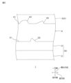
- FIG. 1 is a cross-sectional view of one embodiment of a laminate of the present invention; FIG. It is a modified example of the laminate. It is a modified example of the laminate. 1 is an image processing diagram of a TEM photograph of Example 1.
- FIG. 5 is an image processing diagram in which auxiliary lines are added to FIG. 4;
- FIG. 4 is a graph showing the relationship between the amount of introduced oxygen and the specific resistance in the reactive sputtering of the first step.
- FIG. 10 is a schematic cross-sectional view of Comparative Example 2;
- the laminate 1 extends in the planar direction.
- the plane direction is perpendicular to the thickness direction.
- the laminate 1 has, for example, a substantially rectangular shape in plan view. Planar view means viewing in the thickness direction.
- the laminate 1 has a sheet shape.
- a sheet includes a film. Sheets and films are not distinguished.
- the laminate 1 includes a base layer 2, a base layer 3, and a transparent conductive layer 4 in order toward one side in the thickness direction.
- the laminate 1 includes a base layer 2, a base layer 3 arranged on one side 21 in the thickness direction of the base layer 2, and one side 31 in the thickness direction of the base layer 3. and a transparent conductive layer 4 . Two layers that are adjacent in the thickness direction are adjacent.
- the base layer 2 is arranged on the side opposite to the transparent conductive layer 4 with respect to the base layer 3 in the thickness direction.
- the base material layer 2 has a sheet shape.
- the substrate layer 2 is preferably transparent.
- a material for the base material layer 2 includes a resin.
- the base material layer 2 contains resin.
- resins include polyester resins, acrylic resins, olefin resins, polycarbonate resins, polyethersulfone resins, polyarylate resins, melamine resins, polyamide resins, polyimide resins, cellulose resins, polystyrene resins, and norbornene resins.
- the resin is preferably a polyester resin.
- Polyester resins include, for example, polyethylene terephthalate (PET), polybutylene terephthalate, and polyethylene naphthalate, preferably PET.
- the thickness of the base material layer 2 is, for example, 5 ⁇ m or more, preferably 10 ⁇ m or more, and is, for example, 500 ⁇ m or less, preferably 200 ⁇ m or less, more preferably 100 ⁇ m or less.
- One surface 21 in the thickness direction of the base material layer 2 may have a third bump with a height of 3 nm or more.
- the height of the third protrusion is obtained in the same manner as the height of the first protrusion 42 which will be described later.
- the position and number of the above-described third protrusions in plan view are not limited.
- the total light transmittance of the substrate layer 2 is, for example, 70% or higher, preferably 80% or higher, more preferably 85% or higher.
- the upper limit of the total light transmittance of the base material layer 2 is not limited.
- the total light transmittance of the base material layer 2 is obtained based on JIS K 7375-2008.
- the base layer 3 is adjacent to one side of the base layer 2 in the thickness direction. Specifically, the base layer 3 contacts one surface 21 of the base material layer 2 in the thickness direction. Underlayer 3 is preferably transparent. Examples of the underlayer 3 include an optical adjustment layer and a hard coat layer. The underlying layer 3 is a single layer or multiple layers.
- the base layer 2 and the base layer 3 can be referred to as a base material 30. That is, the substrate 30 includes the substrate layer 2 and the base layer 3 in order toward one side in the thickness direction. Substrate 30 is preferably transparent. Therefore, the base material 30 can be called a transparent base material 30 .
- the base layer 3 contains resin, and may further contain particles, for example.
- the underlayer 3 contains a resin but does not contain particles.
- the one surface 31 in the thickness direction of the underlying layer 3 does not have the second bumps 32 (see FIG. 2), and the one surface 31 is preferably flat. It can be formed as a plane.
- resins include acrylic resins, urethane resins, melamine resins, alkyd resins, and silicone resins. If the raw material of the resin is a curable resin, the underlying layer 3 is formed as a cured film.
- one surface 31 in the thickness direction of the underlayer 3 does not have the second protrusion 32 with a height of 3 nm or more.
- one surface 31 in the thickness direction of the underlayer 3 is a flat surface. It should be noted that the flat surface allows the presence of bumps with a height of less than 3 nm.
- the crystal orientation in the transparent conductive layer 4 described below is well aligned, and as a result, The specific resistance of the transparent conductive layer 4 can be lowered.
- the thickness of the underlayer 3 is, for example, 5 nm or more, preferably 10 nm or more, more preferably 30 nm or more, and for example, 10,000 nm or less, preferably 5,000 nm or less.
- the total light transmittance of the underlying layer 3 is, for example, 70% or higher, preferably 80% or higher, and more preferably 85% or higher.
- the upper limit of the total light transmittance of the underlying layer 3 is not limited, and is, for example, 100% or less.
- the total light transmittance of the underlying layer 3 is obtained based on JIS K 7375-2008.
- the surface direction of the base material 30 includes the direction of heat shrinkage after the base material 30 is heated.
- the heating temperature can be selected according to the heat resistance of the substrate 30 .
- the thermal contraction rate after heating the substrate 30 at 160° C. for 1 hour is, for example, 0.01% or more, preferably 0.05% or more, and is, for example, 1.0% or less, preferably
- the surface direction of the base material 30 includes the direction in which the ratio is 0.5% or less. If the thermal contraction rate of the base material 30 is equal to or more than the above-described lower limit and equal to or less than the upper limit, cracks in the transparent conductive layer 4 are suppressed, and the first protrusions 42 described later can be formed.
- Transparent conductive layer 4 The transparent conductive layer 4 is adjacent to one side of the base layer 3 in the thickness direction. Specifically, the transparent conductive layer 4 contacts one surface 31 of the base layer 3 in the thickness direction. The transparent conductive layer 4 forms one surface of the laminate 1 in the thickness direction. The transparent conductive layer 4 has a sheet shape extending in the plane direction. In this embodiment, the transparent conductive layer 4 is a single layer.
- the transparent conductive layer 4 preferably has a height of 4 nm or more, more preferably 5 nm or more, more preferably 7 nm or more, still more preferably 10 nm or more, and particularly preferably a height of 10 nm or more. height of 15 nm or more and, for example, a height of 50 nm or less, preferably a height of 30 nm or less, more preferably a height of 20 nm or less.
- the transparent conductive layer 4 is provided with the first protrusions 42 having a height equal to or higher than the lower limit and equal to or lower than the upper limit, so that the transparent conductive layer 4 is excellent in adhesion to another layer 5 described later.
- the number of first protrusions 42 may be singular or plural, and preferably plural from the viewpoint of improving adhesion.
- the number of second protrusions 32 (see FIG. 2) per unit length is 0 because of the above. Therefore, the number of first ridges 42 per unit length is greater than the number of second ridges 32 (see FIG. 2) per unit length.
- the adhesive strength of the one surface 41 in the thickness direction of the transparent conductive layer 4 is reliable.
- the specific resistance of the transparent conductive layer 4 can be reliably reduced.
- the number of first protrusions 42 per unit length is, for example, 1/ ⁇ m or more, preferably 2/ ⁇ m or more, more preferably 3/ ⁇ m or more, and still more preferably 4 5/ ⁇ m or more, particularly preferably 5/ ⁇ m or more, and most preferably 6/ ⁇ m or more. It is 20 pieces/ ⁇ m or less.
- the number of first protrusions 42 per unit length is counted by observing the cross section of the transparent conductive layer 4 with a TEM, as will be described in the examples below.
- the average height of the first protrusions 42 is 3 nm or more, preferably 4 nm or more, more preferably 5 nm or more, even more preferably 6 nm or more, and particularly preferably 7 nm or more. It is preferably 20 nm or less, more preferably 15 nm or less, still more preferably 10 nm or less.
- the average height of the first ridges 42 is described in a later example. Since the transparent conductive layer 4 is provided with the first protrusions 42 having an average height equal to or more than the lower limit and equal to or less than the upper limit, the adhesiveness with the other layer 5 to be described later is excellent.
- one surface 41 in the thickness direction of the transparent conductive layer 4 further includes a flat portion 43, for example.
- the flat portion 43 is located outside the raised start portion 431 .
- the uplift starting portion 431 is a portion where the first uplift 42 starts uplifting from the flat portion 43 .
- the height of the first protrusion 42 is determined by making it hang down along the thickness direction from one end portion 432 located on one side in the thickness direction to the line segment connecting the two rise start portions 431 in a cross-sectional view. is the length from the one end 432 to the drooping point when obtaining The height of the first protrusion 42 is obtained by, for example, observing a TEM photograph (cross-sectional observation).
- the transparent conductive layer 4 is crystalline.
- the transparent conductive layer 4 does not contain amorphous regions.
- the transparent conductive layer 4 consists only of crystalline regions.
- the transparent conductive layer 4 is crystalline or amorphous is determined, for example, by the following test.
- the transparent conductive layer 4 is immersed in a 5% by mass hydrochloric acid aqueous solution for 15 minutes, then washed with water and dried. is 10 k ⁇ or less, the transparent conductive layer 4 is crystalline, and when the resistance between the two terminals exceeds 10 k ⁇ , the transparent conductive layer 4 is amorphous.
- the crystalline transparent conductive layer 4 can sufficiently reduce the specific resistance.
- the transparent conductive layer 4 has grain boundaries 44 .
- the grain boundary 44 includes one end edge 441 reaching one surface 41 of the transparent conductive layer 4 in the thickness direction.
- the grain boundaries 44 described above advance from each of the two one edges 441 to the other side in the thickness direction, and are connected at an intermediate portion in the thickness direction.
- the grain boundary 44 extends from the one edge 441 toward the other side in the thickness direction and reaches the other side of the transparent conductive layer 4 in the thickness direction, that is, the other edge 442 that reaches the one side 31 of the underlying layer 3 in the thickness direction.
- the grain boundary 44 does not include the other edge 442 and one grain boundary 44 includes two one edges 441 .
- the one surface 41 of the transparent conductive layer 4 can easily form the first protrusion 42 .
- the above-described protuberance start portion 431 is positioned, for example, at the above-described one end edge 441 and/or is positioned near the above-described one end edge 441 .
- the one end edge 441 corresponding to the first protrusion 42A is, for example, an endless shape in plan view. There is a beginning 431A.
- the two swelling start portions 431B of the first swelling 42B located on the right side of FIG. located nearby.
- the neighborhood is, for example, two distances within 15 nm, preferably within 10 nm.
- the remaining raised starter 431 B is located at one edge 441 .
- the protuberance starting portion 431 is positioned at and/or near one edge 441 of the grain boundary 44 , a large number of the first protuberances 42 are reliably formed on the one surface 41 of the transparent conductive layer 4 . Therefore, the adhesiveness of the one surface 41 of the transparent conductive layer 4 is excellent.
- Examples of materials for the transparent conductive layer 4 include metal oxides.
- the metal oxide contains at least one metal selected from the group consisting of In, Sn, Zn, Ga, Sb, Nb, Ti, Si, Zr, Mg, Al, Au, Ag, Cu, Pd and W .
- the material of the transparent conductive layer 4 is preferably indium zinc composite oxide (IZO), indium gallium zinc composite oxide (IGZO), indium gallium composite oxide (IGO), indium tin composite oxide. (ITO) and antimony tin composite oxide (ATO), preferably indium tin composite oxide (ITO) from the viewpoint of lowering the specific resistance.
- the content of tin oxide (SnO 2 ) in the indium tin composite oxide is, for example, 0.5% by mass or more, preferably 3% by mass or more, more preferably 6% by mass or more. , less than 50% by mass, preferably 25% by mass or less, more preferably 15% by mass or less.
- the thickness of the transparent conductive layer 4 is, for example, 15 nm or more, preferably 35 nm or more, more preferably 50 nm or more, even more preferably 75 nm or more, even more preferably 100 nm or more, particularly preferably 120 nm or more. If the thickness of the transparent conductive layer 4 is equal to or more than the above-described lower limit, the grain boundary 44 does not include the other edge 442 and one grain boundary 44 tends to include two one edges 441 . Therefore, the transparent conductive layer 4 can be reliably provided with the above-described first protrusions 42 .
- the thickness of the transparent conductive layer 4 is the length in the thickness direction between the one surface 31 (flat surface) of the base layer 3 and the flat portion 43 on the one surface 41 in the thickness direction of the transparent conductive layer 4 .
- the thickness of the transparent conductive layer 4 is, for example, 500 nm or less, preferably 300 nm or less, more preferably 200 nm or less.
- the thickness of the transparent conductive layer 4 is measured by TEM observation (cross-sectional observation).
- the total light transmittance of the transparent conductive layer 4 is, for example, 60% or more, preferably 80% or more, more preferably 85% or more.
- the upper limit of the total light transmittance of the transparent conductive layer 4 is not limited, and is, for example, 100% or less.
- the total light transmittance of the transparent conductive layer 4 is obtained based on JIS K 7375-2008.
- the specific resistance of one surface 41 in the thickness direction of the transparent conductive layer 4 is, for example, 3.0 ⁇ 10 ⁇ 4 ⁇ cm or less, preferably 2.5 ⁇ 10 ⁇ 4 ⁇ cm or less, more preferably 2 .3 ⁇ 10 ⁇ 4 ⁇ cm or less, more preferably 2.2 ⁇ 10 ⁇ 4 ⁇ cm or less, even more preferably 2.0 ⁇ 10 ⁇ 4 ⁇ cm or less, particularly preferably It is 1.9 ⁇ 10 ⁇ 4 ⁇ cm or less.
- the specific resistance of one surface 41 in the thickness direction of the transparent conductive layer 4 is, for example, 0.1 ⁇ 10 ⁇ 4 ⁇ cm or more, preferably 0.5 ⁇ 10 ⁇ 4 ⁇ cm or more, more preferably , 1.0 ⁇ 10 ⁇ 4 ⁇ cm or more, more preferably 1.1 ⁇ 10 ⁇ 4 ⁇ cm or more.
- a specific resistance is measured by the four-probe method.
- each layer is laid down in a roll-to-roll process.
- a long base material layer 2 is prepared.
- a resin composition containing the resin described above is applied to one surface 21 of the base material layer 2 .
- the resin composition contains a curable resin
- the curable resin is cured by heat or ultraviolet irradiation.
- a base material 30 having the base material layer 2 and the base layer 3 in order toward one side in the thickness direction is prepared.
- the resin composition contains a resin but does not contain particles, so the above-described second bumps 32 (see FIG. 2) are not formed on one surface 31 of the base layer 3 in the thickness direction.
- the heat shrinkage rate in the longitudinal direction (MD direction) of the base material 30 when heated at 160° C. for 1 hour is not limited, and is, for example, 0.1% or more, preferably 0.2% or more. and is, for example, 2.0% or less, preferably 1.0% or less.
- the thermal shrinkage rate in the width direction (the direction orthogonal to the longitudinal direction and the thickness direction) (TD direction) of the base material 30 when heated at 160 ° C. for 1 hour is not limited, for example, -0.2% or more, Preferably 0.00% or more, more preferably 0.01% or more, still more preferably 0.05% or more, and for example, 1.0% or less, preferably 0.5% or less be.
- the transparent conductive layer 4 is formed on one surface 31 of the base layer 3 in the thickness direction.
- the method of forming the transparent conductive layer 4 includes, for example, a first step and a second step.
- an amorphous transparent conductive layer 40 is formed on one side 31 of the underlying layer 3 in the thickness direction.
- an amorphous transparent conductive layer 40 is formed on one surface 31 of the underlying layer 3 in the thickness direction by sputtering, preferably reactive sputtering.
- a sputtering apparatus is used for sputtering.
- the sputtering device includes a film-forming roll.
- a film-forming roll is equipped with a cooling device.
- the cooling device can cool the film forming roll.
- the film-forming roll can cool the base layer 3 (including the base material 30).
- the above metal oxide (sintered body) is used as a target.
- the surface temperature of the film-forming roll corresponds to the film-forming temperature in sputtering.
- the film formation temperature is, for example, 10.0° C. or lower, preferably 0.0° C. or lower, more preferably ⁇ 2.5° C. or lower, further preferably ⁇ 5.0° C. or lower, further preferably ⁇ 7. 0° C. or lower, and for example, -50° C. or higher, preferably -20° C. or higher, more preferably -10° C. or higher.
- the base layer 3 (including the base material 30) can be sufficiently cooled, so that the grain boundary 44 does not include the other edge 442 and is one grain boundary. 44 tends to obtain a transparent conductive layer 4 comprising two one-sided edges 441 . Therefore, the first protrusion 42 can be reliably formed on the one surface 41 of the transparent conductive layer 4 .
- a rare gas can be mentioned as a sputtering gas.
- rare gases include Ar.
- the sputtering gas may be mixed with reactive gases.
- Reactive gases include, for example, oxygen.
- the ratio of the introduction amount of the reactive gas to the total introduction amount of the sputtering gas and the reactive gas is, for example, 0.1 flow % or more, preferably 0.5 flow % or more, more preferably 1.5 flow % or more. More preferably, it is 2.0 flow % or more, particularly preferably 2.5 flow % or more, and for example, 5 flow % or less, preferably 3 flow % or less.
- the amorphous transparent conductive layer 40 formed in the first step may not have the first protrusions 42 or may already have the first protrusions 42 .
- the amorphous transparent conductive layer 40 is crystallized to form the crystalline transparent conductive layer 4 . Specifically, in the second step, the amorphous transparent conductive layer 40 is heated.
- the heating temperature is, for example, 80° C. or higher, preferably 110° C. or higher, more preferably 130° C. or higher, still more preferably 150° C. or higher, and for example, 200° C. or lower, preferably 180° C. or lower. It is more preferably 175° C. or lower, still more preferably 170° C. or lower.
- the heating time is, for example, 1 minute or longer, preferably 3 minutes or longer, more preferably 5 minutes or longer, and is, for example, 5 hours or shorter, preferably 3 hours or shorter, more preferably 2 hours or shorter. be. Heating is performed, for example, under an air atmosphere.
- the laminate 1 having the substrate layer 2, the base layer 3, and the transparent conductive layer 4 in order toward one side in the thickness direction is manufactured.
- the heat shrinkage rate in the longitudinal direction (MD direction) of the laminate 1 when heated at 160 ° C. for 1 hour is not limited, and is, for example, 0.1% or more, preferably 0.2% or more. and is, for example, 2.0% or less, preferably 1.0% or less.
- the thermal shrinkage rate in the width direction (direction perpendicular to the longitudinal direction and thickness direction) (TD direction) of the laminate 1 when heated at 160 ° C. for 1 hour for example, -0.2% or more, Preferably 0.00% or more, more preferably 0.01% or more, still more preferably 0.05% or more, and for example, 1.0% or less, preferably 0.5% or less be.
- the first bumps 42 can be reliably formed on the one surface 41 of the transparent conductive layer 4 if the thermal contraction rate in each of the MD direction and the TD direction is equal to or higher than the above lower limit.
- the total light transmittance of the laminate 1 is, for example, 60% or higher, preferably 70% or higher, more preferably 80% or higher, still more preferably 85% or higher.
- the upper limit of the total light transmittance of the laminate 1 is not limited, and is, for example, 100% or less.
- the total light transmittance of the base material layer 2 is JIS K 7375-2008.
- another layer 5 is arranged on one side of the laminate 1 in the thickness direction, that is, on one side 41 of the transparent conductive layer 4 in the thickness direction.
- the coating layer 51 is formed by coating.
- Other layers 51 include, for example, a light-modulating coating layer, a metal paste layer, and the like.
- the other layer 5 is adjacent to one surface 41 of the transparent conductive layer 4 in the thickness direction.
- the other layer 5 is, for example, a light control layer (voltage-driven light control coating such as PDLC, PNLC, SPD, or current-driven light control coating such as electrochromic (EC)), silver, It is a functional member such as a metal paste containing copper, titanium, or the like.
- the laminate 1 is used for articles, for example.
- the laminate 1 is an optical laminate, and the above-described articles include optical articles. More specifically, examples of articles include touch sensors, electromagnetic wave shields, light control elements, photoelectric conversion elements, heat ray control members, light-transmitting antenna members, light-transmitting heater members, image display devices, and lighting.
- the base layer 3 does not have the second bumps 32 (see FIG. 2). Therefore, the crystal orientation of the crystalline transparent conductive layer 4 can be properly aligned. Therefore, the specific resistance of the transparent conductive layer 4 can be sufficiently reduced.
- one surface 41 in the thickness direction of the transparent conductive layer 4 is provided with a first protrusion 42 . Therefore, the transparent conductive layer 4 has excellent adhesion to the other layer 5 due to the anchor effect based on the first protrusions 42 .
- one surface 31 in the thickness direction of the base layer 3 has a second protrusion 32 with a height of 3 nm or more. That is, in the laminate of the present invention, one surface of the underlayer in the thickness direction may be provided with a second bump having a height of 3 nm or more. Does not overlap the first ridge.
- the second protrusions 32 described above do not overlap the first protrusions 42 of the transparent conductive layer 4 when projected in the thickness direction.
- the number of first protrusions 42 per unit length is, for example, greater than the number of second protrusions 32 per unit length.
- the adhesive strength of the one surface 41 in the thickness direction of the transparent conductive layer 4 is surely improved.
- the specific resistance of the transparent conductive layer 4 can be reliably reduced.
- the number of second protrusions 32 per unit length is, for example, 25/ ⁇ m or less, preferably 20/ ⁇ m or less, more preferably 10/ ⁇ m or less, still more preferably 5
- the number of particles per micrometer is less than or equal to 0 per micrometer, or more than 1 per micrometer.
- the ratio of the number of second protrusions 32 per unit length to the number of first protrusions 42 per unit length is, for example, 0.9 or less, preferably 0.5 or less, more preferably 0.3 or less. , more preferably 0.2 or less, particularly preferably 0.1 or less.
- the ratio of the number of second protrusions 32 per unit length to the number of first protrusions 42 per unit length is, for example, 0.0001 or more.
- the value obtained by subtracting the number per unit length of the second protrusions 32 from the number per unit length of the first protrusions 42 is, for example, 1/ ⁇ m or more, preferably 2/ ⁇ m or more, more preferably 5/ ⁇ m or more, more preferably 7/ ⁇ m or more, particularly preferably 10/ ⁇ m or more.
- the value obtained by subtracting the number of second bumps 32 per unit length from the number of first bumps 42 per unit length is, for example, 30 pieces/ ⁇ m or less.
- the method of providing the above-described second protrusions 32 on the underlying layer 3 is not particularly limited.
- the crystallization of the first protrusion 42 causes the transparent conductive layer 4 to
- the orientation of the crystals is difficult to align, that is, the growth of the crystals is inhibited, so that the specific resistance of the transparent conductive layer 4 increases.
- the second protrusions 32 do not overlap the first protrusions 42 of the transparent conductive layer 4 when projected in the thickness direction. Therefore, the specific resistance of the transparent conductive layer 4 can be lowered.
- one embodiment is preferred.
- one surface 31 of the underlayer 3 does not have the second bumps 32, so that the crystal orientation in the transparent conductive layer 4 can be further adjusted. Therefore, the specific resistance of the transparent conductive layer 4 can be sufficiently lowered.
- the laminate 1 does not include the base layer 2, but includes the underlying layer 3 and the transparent conductive layer 4.
- Examples and comparative examples are shown below to describe the present invention more specifically.
- the present invention is not limited to Examples and Comparative Examples.
- specific numerical values such as the mixing ratio (content ratio), physical property values, and parameters used in the following description are the corresponding mixing ratios ( content ratio), physical properties, parameters, etc. can.
- Example 1 An ultraviolet curable resin was applied to one surface 21 in the thickness direction of the substrate layer 2 made of a long PET film (thickness: 50 ⁇ m, manufactured by Toray Industries, Inc.) to form a coating film.
- the ultraviolet curable resin composition contains an acrylic resin.
- the coating film was cured by ultraviolet irradiation to form the underlayer 3 .
- the thickness of the underlying layer 3 was 2 ⁇ m.
- an amorphous transparent conductive layer 40 was formed on one surface 31 of the base layer 3 in the thickness direction by a reactive sputtering method (first step).
- a DC magnetron sputtering apparatus was used in the reactive sputtering method.
- Sputtering conditions in this example are as follows.
- a sintered body of indium oxide and tin oxide was used as a target.
- the tin oxide concentration in the sintered body was 10% by mass.
- a DC power supply was used to apply voltage to the target.
- the horizontal magnetic field strength on the target was set to 90 mT.
- the film formation temperature was -8°C.
- the film forming temperature is the surface temperature of the film forming roll, which is the same as the temperature of the substrate 30 .
- Ar as a sputtering gas and a reactive gas were introduced into the film formation chamber.
- the ratio of the introduced amount of oxygen to the total introduced amount of Ar and oxygen introduced into the deposition chamber is about 2.6 flow rate %.
- the oxygen introduction amount is within the region R of the resistivity-oxygen introduction amount curve, and the resistivity of the amorphous transparent conductive layer 40 is 6.4 ⁇ 10 ⁇ 4 ⁇ cm. adjusted to be The specific resistance-oxygen introduction amount curve shown in FIG. The dependence of the specific resistance of the layer 40 on the amount of introduced oxygen was investigated in advance.
- the amorphous transparent conductive layer 40 was crystallized by heating in a hot air oven (second step).
- the heating temperature was 160° C., and the heating time was 1 hour.
- the thickness of the crystalline transparent conductive layer 4 was 145 nm. The thickness of the transparent conductive layer 4 will be described later.
- a laminate 1 having a substrate layer 2, a base layer 3, and a crystalline transparent conductive layer 4 in order on one side in the thickness direction was manufactured (see FIG. 1).
- Example 2 A laminate 1 was produced in the same manner as in Example 1. However, the ratio of the introduced amount of oxygen to the total introduced amount of Ar and oxygen introduced into the film forming chamber was changed to about 1.3 flow rate %, and the thickness of the transparent conductive layer 4 was changed to 56 nm.
- Comparative example 1 A laminate 1 was produced in the same manner as in Example 1. However, the film forming temperature was changed to 80° C., the ratio of the introduced amount of oxygen to the total introduced amount of Ar and oxygen introduced into the film forming chamber was changed to about 1.6%, and the thickness of the transparent conductive layer 4 was reduced. changed to 32 nm.
- Comparative example 2 A laminate 1 was produced in the same manner as in Comparative Example 1. However, an ultraviolet curable resin composition containing an acrylic resin and silica particles with a particle size of 20 nm was used (see FIG. 7).
- the thickness of the transparent conductive layer 4 of each laminate 1 in each example and each comparative example was measured by FE-TEM observation. Specifically, first, samples for cross-sectional observation of each transparent conductive layer 4 in Example 1, Example 2, Comparative Example 1, and Comparative Example 2 were produced by the FIB microsampling method. In the FIB microsampling method, an FIB device (trade name “FB2200”, manufactured by Hitachi) was used, and the acceleration voltage was set to 10 kV. Next, the thickness of the transparent conductive layer 4 in the cross-sectional observation sample was measured by FE-TEM observation. In the FE-TEM observation, an FE-TEM apparatus (trade name “JEM-2800”, manufactured by JEOL) was used with an acceleration voltage of 200 kV.
- the apparatus and measurement conditions are as follows.
- FIB device Hitachi FB2200, acceleration voltage: 10 kV FE-TEM device; JEM-2800 manufactured by JEOL, acceleration voltage: 200 kV
- the height of the highest protrusion among the first protrusions 42 in Example 1 was 15 nm.
- the average height of the first bumps 42 obtained by selecting ten arbitrary first bumps 42 in Example 1 was 7 nm. That is, the average height of the first bumps 42 was determined as the average height of arbitrary ten first bumps 42 .
- FIG. 5 shows a diagram in which the grain boundaries 44 in FIG. 4 are drawn with dashed lines.
- the height of the highest protrusion was 14 nm.
- the average height of the first bumps 42 obtained by selecting 10 arbitrary first bumps 42 in Example 2 was 5 nm.
- Example 1 the number of first protrusions 42 per unit length of each of the first protrusions 42 of Example 1, Example 2, and Comparative Example 1 was counted. As a result, in Example 1, it was 7 pieces/ ⁇ m. In Example 2, it was 2 pieces/ ⁇ m. In Comparative Example 2, the number was 5/ ⁇ m.
- Thermal shrinkage rate of base material 30 and laminate 1 The thermal shrinkage rate was measured after heating the substrate 30 of Example 1 at 160° C. for 1 hour. As a result, the thermal contraction rate of the substrate 30 in the MD direction was 0.5%, and that of the laminate 1 in the TD direction was 0.1%.
- the thermal shrinkage rate was measured after heating the laminate 1 of Example 1 at 160°C for 1 hour. As a result, the thermal contraction rate of the laminate 1 in the MD direction was 0.3%, and that in the TD direction of the laminate 1 was 0.1%.
- the laminate is used for optical articles.
Landscapes
- Chemical & Material Sciences (AREA)
- Engineering & Computer Science (AREA)
- Organic Chemistry (AREA)
- Materials Engineering (AREA)
- Chemical Kinetics & Catalysis (AREA)
- Metallurgy (AREA)
- Mechanical Engineering (AREA)
- Theoretical Computer Science (AREA)
- General Engineering & Computer Science (AREA)
- Wood Science & Technology (AREA)
- Life Sciences & Earth Sciences (AREA)
- Polymers & Plastics (AREA)
- Medicinal Chemistry (AREA)
- Health & Medical Sciences (AREA)
- Human Computer Interaction (AREA)
- Physics & Mathematics (AREA)
- General Physics & Mathematics (AREA)
- Inorganic Chemistry (AREA)
- Laminated Bodies (AREA)
- Non-Insulated Conductors (AREA)
Abstract
積層体(1)は、下地層(3)と、下地層(3)の厚み方向の一方面(31)に隣接する結晶質の透明導電層(4)とを備える。下地層(3)は、樹脂を含む。透明導電層(4)の厚み方向の一方面(41)は、高さが3nm以上である第1隆起(42)を備える。下地層(3)の一方面(31)は、高さが3nm以上である第2隆起(32)を備えてもよく、第2隆起(32)は、厚み方向に投影したときに、第1隆起(42)に重ならない。
Description
本発明は、積層体に関する。
下地層と、下地層に隣接する結晶質の透明導電層とを備える積層体が知られている(例えば、下記特許文献1参照。)。特許文献1に記載の積層体では、透明導電性層の厚み方向の一方面は、第1隆起を有する。下地層の厚み方向の一方面は、第2隆起を有する。下地層の第2隆起は、厚み方向に投影したときに、透明導電性層の第1隆起に重なる。
特許文献1の積層体の製造において、粒子を含む樹脂組成物の塗布により、下地層に、粒子の形状に対応する第2隆起を形成する。また、下地層の厚み方向の一方面に薄膜形成して、上記した第2隆起に追従する第1隆起を、透明導電層に形成する。
透明導電層は、非晶質の透明導電層を加熱によって、結晶質とされる。しかし、特許文献1の積層体では、上記した第2隆起に起因して、非晶質の透明導電層の結晶化において、結晶の配向が揃いにくく、つまり、結晶の成長が阻害され、そのため、結晶化した透明導電層の比抵抗が高くなるという不具合がある。
一方、透明導電層の厚み方向の一方面に、他の層が配置されるときに、透明導電性層と上記した層との密着性も求められる。他の層は、例えば、コーティング層を含む。
本発明は、比抵抗が低く、他の層との密着性に優れる透明導電層を備える積層体を提供する。
本発明(1)は、下地層と、前記下地層の厚み方向の一方面に隣接する結晶質の透明導電層とを備える積層体であって、前記下地層は、樹脂を含み、前記透明導電層の厚み方向の一方面は、高さが3nm以上である第1隆起を備え、前記下地層の前記一方面は、高さが3nm以上である第2隆起を備えてもよく、前記第2隆起は、厚み方向に投影したときに、前記第1隆起に重ならない、積層体を含む。
本発明(2)は、前記第1隆起の単位長さ当たりの数は、前記第2隆起の単位長さ当たりの数よりも多い、(1)に記載の積層体を含む。
本発明(3)は、前記下地層は、前記第2隆起を備えない、(1)または(2)に記載の積層体を含む。
本発明(4)は、前記透明導電層は、前記透明導電層の前記一方面に至る端縁を有する粒界を含み、前記第1隆起が隆起を開始する隆起開始部が、前記端縁またはその近傍に位置する(1)から(3)のいずれか一項に記載の積層体を含む。
本発明の積層体の透明導電層は、比抵抗が低く、他の層との密着性に優れる。
1.積層体の一実施形態
本発明の積層体の一実施形態を、図1を参照して説明する。
本発明の積層体の一実施形態を、図1を参照して説明する。
積層体1は、面方向に延びる。面方向は、厚み方向に直交する。積層体1は、例えば、平面視略矩形状を有する。平面視とは、厚み方向に視ることを言う。詳しくは、積層体1は、シート形状を有する。シートは、フィルムを含む。なお、シートおよびフィルムは、峻別されない。
本実施形態では、積層体1は、基材層2と、下地層3と、透明導電層4とを厚み方向の一方側に向かって順に備える。具体的には、積層体1は、基材層2と、基材層2の厚み方向の一方面21に配置される下地層3と、下地層3の厚み方向の一方面31に配置される透明導電層4とを備える。厚み方向に隣り合う2つの層は、隣接する。
1.1 基材層2
基材層2は、厚み方向において、下地層3に対して透明導電層4の反対側に配置される。基材層2は、シート形状を有する。基材層2は、好ましくは、透明である。
基材層2は、厚み方向において、下地層3に対して透明導電層4の反対側に配置される。基材層2は、シート形状を有する。基材層2は、好ましくは、透明である。
基材層2の材料としては、樹脂が挙げられる。言い換えれば、基材層2は、樹脂を含む。樹脂としては、ポリエステル樹脂、アクリル樹脂、オレフィン樹脂、ポリカーボネート樹脂、ポリエーテルスルフォン樹脂、ポリアリレート樹脂、メラミン樹脂、ポリアミド樹脂、ポリイミド樹脂、セルロース樹脂、ポリスチレン樹脂、および、ノルボルネン樹脂が挙げられる。樹脂として、好ましくは、透明性および機械強度の観点から、ポリエステル樹脂が挙げられる。ポリエステル樹脂としては、例えば、ポリエチレンテレフタレート(PET)、ポリブチレンテレフタレート、および、ポリエチレンナフタレートが挙げられ、好ましくは、PETが挙げられる。基材層2の厚みは、例えば、5μm以上、好ましくは、10μm以上であり、また、例えば、500μm以下、好ましくは、200μm以下、より好ましくは、100μm以下である。
基材層2の厚み方向の一方面21は、高さが3nm以上である第3隆起を有してもよい。第3隆起の高さは、後の第1隆起42の高さと同様にして求められる。上記した第3隆起の平面視における位置および数は、限定されない。
基材層2の全光線透過率は、例えば、70%以上、好ましくは、80%以上、より好ましくは、85%以上である。基材層2の全光線透過率の上限は、限定されない。基材層2の全光線透過率は、JIS K 7375-2008に基づいて求められる。
1.2 下地層3
下地層3は、基材層2の厚み方向の一方側に隣接する。具体的には、下地層3は、基材層2の厚み方向の一方面21に接触する。下地層3は、好ましくは、透明である。下地層3としては、例えば、光学調整層、および、ハードコート層が挙げられる。下地層3は、単層または複層である。
下地層3は、基材層2の厚み方向の一方側に隣接する。具体的には、下地層3は、基材層2の厚み方向の一方面21に接触する。下地層3は、好ましくは、透明である。下地層3としては、例えば、光学調整層、および、ハードコート層が挙げられる。下地層3は、単層または複層である。
なお、基材層2と下地層3とを基材30と称呼することができる。つまり、基材30は、基材層2と下地層3とを厚み方向の一方側に向かって順に備える。基材30は、好ましくは、透明である。そのため、基材30は、透明基材30と称呼することができる。
下地層3は、樹脂を含み、例えば、粒子をさらに含んでもよい。好ましくは、下地層3は、樹脂を含む一方、粒子を含まない。本実施形態において、下地層3が上記した粒子を含まない場合には、下地層3の厚み方向の一方面31が第2隆起32(図2参照)を備えず、一方面31を好適な平坦面として形成できる。樹脂としては、例えば、アクリル樹脂、ウレタン樹脂、メラミン樹脂、アルキド樹脂、および、シリコーン樹脂が挙げられる。なお、樹脂の原料が硬化性樹脂であれば、下地層3は、硬化膜として形成される。
本実施形態では、下地層3の厚み方向の一方面31は、高さが3nm以上である第2隆起32を備えない。言い換えれば、下地層3の厚み方向の一方面31は、平坦面である。なお、平坦面では、高さが3nm未満の隆起の存在が許容される。
本実施形態では、下地層3の厚み方向の一方面31が上記した第2隆起32(図2参照)を備えないので、次に説明する透明導電層4における結晶の配向がうまく揃い、そのため、透明導電層4の比抵抗を低くできる。
下地層3の厚みは、例えば、5nm以上、好ましくは、10nm以上、より好ましくは、30nm以上であり、また、例えば、10,000nm以下、好ましくは、5,000nm以下である。
下地層3の全光線透過率は、例えば、70%以上、好ましくは、80%以上、より好ましくは、85%以上である。下地層3の全光線透過率の上限は、限定されず、例えば、100%以下である。下地層3の全光線透過率は、JIS K 7375-2008に基づいて求められる。
基材30における面方向は、基材30を加熱した後、熱収縮する方向を含む。加熱温度は基材30の耐熱性に応じて選択できる。基材30を160℃で、1時間加熱した後の熱収縮率が例えば、0.01%以上、好ましくは、0.05%以上であり、また、例えば、1.0%以下、好ましくは、0.5%以下である方向を基材30における面方向が含む。
基材30の熱収縮率が上記した下限以上、上限以下であれば、透明導電層4のクラックを抑制しつつ、後述する第1隆起42を作成できる。
基材30の熱収縮率が上記した下限以上、上限以下であれば、透明導電層4のクラックを抑制しつつ、後述する第1隆起42を作成できる。
1.3 透明導電層4
透明導電層4は、下地層3の厚み方向の一方側に隣接する。具体的には、透明導電層4は、下地層3の厚み方向の一方面31に接触する。透明導電層4は、積層体1における厚み方向の一方面を形成する。透明導電層4は、面方向に延びるシート形状を有する。本実施形態では、透明導電層4は、単一の層である。
透明導電層4は、下地層3の厚み方向の一方側に隣接する。具体的には、透明導電層4は、下地層3の厚み方向の一方面31に接触する。透明導電層4は、積層体1における厚み方向の一方面を形成する。透明導電層4は、面方向に延びるシート形状を有する。本実施形態では、透明導電層4は、単一の層である。
透明導電層4の厚み方向の一方面41は、高さが3nm以上である第1隆起42を備える。透明導電層4は、好ましくは、高さが4nm以上、さらに好ましくは、高さが5nm以上、より好ましくは、高さが7nm以上、さらに好ましくは、高さが10nm以上、とくに好ましくは、高さが15nm以上、また、例えば、高さが50nm以下、好ましくは、高さが30nm以下、より好ましくは、高さが20nm以下である第1隆起42を含む。透明導電層4は、上記下限以上、上記上限以下の高さの第1隆起42を備えることで、後述の他の層5との密着性に優れる。第1隆起42は、単数または複数であり、好ましくは、密着性の向上を図る観点から、複数である。
なお、本実施形態において、上記から、第2隆起32(図2参照)の単位長さ当たりの数は、0である。そのため、第1隆起42の単位長さ当たりの数は、第2隆起32(図2参照)の単位長さ当たりの数よりも多い。第1隆起42の単位長さ当たりの数が、第2隆起32(図2参照)の単位長さ当たりの数よりも多いと、透明導電層4の厚み方向の一方面41の密着力が確実に向上されるとともに、透明導電層4の比抵抗を確実に低くできる。
具体的には、第1隆起42の単位長さ当たりの数は、例えば、1個/μm以上、好ましくは、2個/μm以上、より好ましくは、3個/μm以上、さらに好ましくは、4個/μm以上、とりわけ好ましくは、5個/μm以上、最も好ましくは、6個/μm以上であり、また、例えば、50個/μm以下、好ましくは、30個/μm以下、より好ましくは、20個/μm以下である。
第1隆起42の単位長さ当たりの数は、後の実施例で説明される通り、透明導電層4の断面をTEMで観察することによって、カウントされる。
第1隆起42の高さの平均は、3nm以上、好ましくは、4nm以上、より好ましくは、5nm以上、さらに好ましくは、6nm以上、とりわけ好ましくは、7nm以上であり、また、例えば、40nm以下、好ましくは、20nm以下、より好ましくは、15nm以下、さらに好ましくは、10nm以下である。第1隆起42の高さの平均は、後の実施例で説明される。透明導電層4が上記下限以上、上記上限以下の高さの平均の第1隆起42を備えることで、後述の他の層5との密着性に優れる。
本実施形態では、透明導電層4の厚み方向の一方面41は、例えば、平坦部43をさらに備える。平坦部43は、隆起開始部431の外側に配置される。隆起開始部431は、平坦部43から第1隆起42が隆起を開始する部分である。
第1隆起42の高さは、断面視において、最も厚み方向の一方側に位置する一端部432から、2つの隆起開始部431を結ぶ線分に対して厚み方向に沿って垂下させて垂下点を得たときの、上記した一端部432から垂下点までの長さである。第1隆起42の高さは、例えば、TEM写真の観察(断面観察)によって、求められる。
また、透明導電層4は、結晶質である。好ましくは、透明導電層4は、非晶質な領域を含まない。好ましくは、透明導電層4は、結晶質な領域のみからなる。
なお、透明導電層4が結晶質か非晶質かは、例えば、以下の試験によって、判別される。透明導電層4を、5質量%の塩酸水溶液に15分間浸漬した後、水洗および乾燥し、透明導電層4の一方面41において15mm程度の間の二端子間抵抗を測定し、二端子間抵抗が10kΩ以下であれば、透明導電層4が結晶質であり、上記した二端子間抵抗が10kΩ超過であれば、透明導電層4が非晶質である。
結晶質の透明導電層4は、比抵抗を十分に低くできる。
透明導電層4は、粒界44を備える。粒界44は、透明導電層4の厚み方向の一方面41に至る一端縁441を含む。
なお、上記した粒界44は、2つの一端縁441のそれぞれから厚み方向の他方側に進み、厚み方向の中間部において、それらが連結されている。
また、粒界44は、上記した一端縁441から厚み方向の他方側に向かい、透明導電層4の厚み方向の他方面、すなわち、下地層3の厚み方向の一方面31に至る他端縁442をさらに含んでもよい。
好ましくは、粒界44は、他端縁442を含まず、一の粒界44が、2つの一端縁441を含む。この構成によれば、透明導電層4の一方面41は、第1隆起42を形成し易くなる。
そして、上記した隆起開始部431は、例えば、上記した一端縁441に位置し、および/または、上記した一端縁441の近傍に位置する。
具体的には、図1の左側部分に位置する第1隆起42Aにおける2つの隆起開始部431Aのそれぞれは、上記した一端縁441に位置する。図示しないが、上記した第1隆起42Aに対応する一端縁441は、例えば、平面視で無端形状であって、平面視において、上記した一端縁441に沿って、上記した第1隆起42Aの隆起開始部431Aが存在する。
また、図1の右側部分に位置する第1隆起42Bにおける2つの隆起開始部431Bのうち、左側の隆起開始部431Bは、一端縁441および他端縁442を含む粒界44における一端縁441の近傍に位置する。近傍は、例えば、2つの距離が15nm以内、好ましくは、10nm以内である。残りの隆起開始部431Bは、一端縁441に位置する。
隆起開始部431が、粒界44の一端縁441および/または近傍に位置すれば、上記した第1隆起42は、透明導電層4における一方面41に確実に多数形成される。そのため、透明導電層4の一方面41の密着性が優れる。
透明導電層4の材料としては、例えば、金属酸化物が挙げられる。金属酸化物は、In、Sn、Zn、Ga、Sb、Nb、Ti、Si、Zr、Mg、Al、Au、Ag、Cu、Pd、Wからなる群より選択される少なくとも1種の金属を含む。具体的には、透明導電層4の材料としては、好ましくは、インジウム亜鉛複合酸化物(IZO)、インジウムガリウム亜鉛複合酸化物(IGZO)、インジウムガリウム複合酸化物(IGO)、インジウムスズ複合酸化物(ITO)、および、アンチモンスズ複合酸化物(ATO)が挙げられ、好ましくは、比抵抗を低くする観点から、インジウムスズ複合酸化物(ITO)が挙げられる。
なお、インジウムスズ複合酸化物における酸化スズ(SnO2)の含有量は、例えば、0.5質量%以上、好ましくは、3質量%以上、より好ましくは、6質量%以上であり、また、例えば、50質量%未満、好ましくは、25質量%以下、より好ましくは、15質量%以下である。
透明導電層4の厚みは、例えば、15nm以上、好ましくは、35nm以上、より好ましくは、50nm以上、さらに好ましくは、75nm以上、ことさらに好ましくは、100nm以上、とりわけ好ましくは、120nm以上である。透明導電層4の厚みが上記した下限以上であれば、粒界44が、他端縁442を含まず、一の粒界44が、2つの一端縁441を含みやすい。そのため、透明導電層4に上記した第1隆起42を確実に備えさせることができる。
なお、透明導電層4の厚みは、下地層3の一方面31(平坦面)と、透明導電層4の厚み方向の一方面41における平坦部43との厚み方向の長さである。
透明導電層4の厚みは、例えば、500nm以下、好ましくは、300nm以下、より好ましくは、200nm以下である。
透明導電層4の厚みは、TEM観察(断面観察)によって測定される。
透明導電層4の全光線透過率は、例えば、60%以上、好ましくは、80%以上、より好ましくは、85%以上である。透明導電層4の全光線透過率の上限は、限定されず、例えば、100%以下である。透明導電層4の全光線透過率は、JIS K 7375-2008に基づいて求められる。
透明導電層4の厚み方向の一方面41の比抵抗は、例えば、3.0×10⁻⁴Ω・cm以下、好ましくは、2.5×10⁻⁴Ω・cm以下、より好ましくは、2.3×10⁻⁴Ω・cm以下であり、さらに好ましくは、2.2×10⁻⁴Ω・cm以下、ことさらに好ましくは、2.0×10⁻⁴Ω・cm以下、とりわけ好ましくは、1.9×10⁻⁴Ω・cm以下である。また、透明導電層4の厚み方向の一方面41の比抵抗は、例えば、0.1×10⁻⁴Ω・cm以上、好ましくは、0.5×10⁻⁴Ω・cm以上、より好ましくは、1.0×10⁻⁴Ω・cm以上、さらに好ましくは、1.1×10⁻⁴Ω・cm以上である。比抵抗は、四端子法により測定される。
次に、積層体1を製造する方法を説明する。この方法では、各層のそれぞれをロール-トゥ-ロール法で配置する。
まず、長尺の基材層2を準備する。
次いで、上記した樹脂を含む樹脂組成物を、基材層2の一方面21に塗布する。その後、樹脂組成物が硬化性樹脂を含む場合には、硬化性樹脂を、熱または紫外線照射によって、硬化させる。これによって、基材層2と下地層3とを厚み方向の一方側に向かって順に備える基材30を調製する。なお、本実施形態では、樹脂組成物が樹脂を含む一方、粒子を含まないので、下地層3の厚み方向の一方面31に上記した第2隆起32(図2参照)が形成されない。
なお、例えば、160℃で、1時間加熱したときの基材30の長尺方向(MD方向)の熱収縮率に限定はなく、例えば、0.1%以上、好ましくは、0.2%以上であり、また、例えば、2.0%以下、好ましくは、1.0%以下である。160℃で、1時間加熱したときの基材30の幅方向(長尺方向および厚み方向に直交する方向)(TD方向)の熱収縮率に限定はなく、例えば、-0.2%以上、好ましくは、0.00%以上、より好ましくは、0.01%以上、さらに好ましくは、0.05%以上であり、また、例えば、1.0%以下、好ましくは、0.5%以下である。
基材30の熱収縮率は、下記式により求められる。
基材30の熱収縮率(%)=100×[加熱前の基材30の長さ-加熱後の基材30の長さ]/加熱前の基材30の長さ
基材30の熱収縮率(%)=100×[加熱前の基材30の長さ-加熱後の基材30の長さ]/加熱前の基材30の長さ
その後、透明導電層4を、下地層3の厚み方向の一方面31に形成する。透明導電層4を形成する方法は、例えば、第1工程と、第2工程とを備える。
第1工程では、非晶質の透明導電層40を下地層3の厚み方向の一方面31に形成する。例えば、スパッタリング、好ましくは、反応性スパッタリングによって、非晶質の透明導電層40を下地層3の厚み方向の一方面31に形成する。
スパッタリングでは、スパッタリング装置が用いられる。スパッタリング装置は、成膜ロールを備える。成膜ロールは、冷却装置を備える。冷却装置は、成膜ロールを冷却可能である。成膜ロールは、下地層3(を含む基材30)を冷却可能である。
スパッタリング(好ましくは、反応性スパッタリング)では、上記した金属酸化物(の焼結体)がターゲットとして用いられる。成膜ロールの表面温度は、スパッタリングにおける成膜温度に相当する。成膜温度は、例えば、10.0℃以下、好ましくは、0.0℃以下、より好ましくは、-2.5℃以下、さらに好ましくは、-5.0℃以下、さらに好ましくは、-7.0℃以下であり、また、例えば、-50℃以上、好ましくは、-20℃以上、さらに好ましくは、-10℃以上である。
成膜ロールの表面温度が上記した上限以下であれば、下地層3(を含む基材30)を十分に冷却でき、そのため、粒界44が、他端縁442を含まず、一の粒界44が、2つの一端縁441を含む透明導電層4を得やすい。従って、透明導電層4の一方面41に第1隆起42を確実に形成することができる。
スパッタリングガスとしては、希ガスが挙げられる。希ガスとしては、例えば、Arが挙げられる。スパッタリングガスは、反応性ガスを混合されてもよい。反応性ガスとしては、例えば、酸素が挙げられる。スパッタリングガスおよび反応性ガスの合計導入量に対する反応性ガスの導入量の割合は、例えば、0.1流量%以上、好ましくは、0.5流量%以上、より好ましくは、1.5流量%以上、さらに好ましくは、2.0流量%以上、とりわけ好ましくは、2.5流量%以上であり、また、例えば、5流量%以下、好ましくは、3流量%以下である。
第1工程で形成される非晶質の透明導電層40は、第1隆起42を備えていなくもよく、また、第1隆起42をすでに備えていてもよい。
第2工程では、非晶質の透明導電層40を結晶化させて、結晶質の透明導電層4を形成する。具体的には、第2工程では、非晶質の透明導電層40を加熱する。
加熱温度は、例えば、80℃以上、好ましくは、110℃以上、より好ましくは、130℃以上、さらに好ましくは、150℃以上であり、また、例えば、200℃以下、好ましくは、180℃以下、より好ましくは、175℃以下、さらに好ましくは、170℃以下である。加熱時間は、例えば、1分間以上、好ましくは、3分間以上、より好ましくは、5分間以上であり、また、例えば、5時間以下、好ましくは、3時間以下、より好ましくは、2時間以下である。加熱は、例えば、大気雰囲気下で、実施される。
これによって、基材層2と、下地層3と、透明導電層4とを厚み方向の一方側に向かって順に備える積層体1が製造される。
なお、例えば、160℃で、1時間加熱したときの積層体1の長尺方向(MD方向)の熱収縮率に限定はなく、例えば、0.1%以上、好ましくは、0.2%以上であり、また、例えば、2.0%以下、好ましくは、1.0%以下である。160℃で、1時間加熱したときの積層体1の幅方向(長尺方向および厚み方向に直交する方向)(TD方向)の熱収縮率に限定はなく、例えば、-0.2%以上、好ましくは、0.00%以上、より好ましくは、0.01%以上、さらに好ましくは、0.05%以上であり、また、例えば、1.0%以下、好ましくは、0.5%以下である。
積層体1は、MD方向およびTD方向のそれぞれの熱収縮率が上記した下限以上であれば、透明導電層4の一方面41に第1隆起42を確実に形成できる。
積層体1の熱収縮率は、下記式により求められる。
積層体1の熱収縮率(%)=100×[加熱前の積層体1の長さ-加熱後の積層体1の長さ]/加熱前の積層体1の長さ
積層体1の熱収縮率(%)=100×[加熱前の積層体1の長さ-加熱後の積層体1の長さ]/加熱前の積層体1の長さ
積層体1の全光線透過率は、例えば、60%以上、好ましくは、70%以上、より好ましくは、80%以上、さらに好ましくは、85%以上である。積層体1の全光線透過率の上限は、限定されず、例えば、100%以下である。基材層2の全光線透過率は、JIS
K 7375-2008に基づいて求められる。
K 7375-2008に基づいて求められる。
その後、必要により、積層体1の厚み方向の一方面、すなわち、透明導電層4の厚み方向の一方面41に、他の層5を配置する。例えば、コーティングによってコーティング層51を形成する。他の層51は、例えば、調光機能コート層や金属ペースト層などを含む。他の層5は、透明導電層4の厚み方向の一方面41に隣接する。他の層5は、具体的には、例えば、調光機能層(PDLCやPNLC、SPDなどの電圧駆動型調光コーティングやエレクトロクロクロミック(EC)等の電流駆動型調光コーティング)や銀、銅、チタンなどを含む金属ペーストなどの機能部材である。
2. 積層体1の用途
積層体1は、例えば、物品に用いられる。具体的には、積層体1は、光学用積層体であって、上記した物品としては、光学用の物品が挙げられる。詳しくは、物品としては、例えば、タッチセンサ、電磁波シールド、調光素子、光電変換素子、熱線制御部材、光透過性アンテナ部材、光透過性ヒータ部材、画像表示装置、および、照明が挙げられる。
積層体1は、例えば、物品に用いられる。具体的には、積層体1は、光学用積層体であって、上記した物品としては、光学用の物品が挙げられる。詳しくは、物品としては、例えば、タッチセンサ、電磁波シールド、調光素子、光電変換素子、熱線制御部材、光透過性アンテナ部材、光透過性ヒータ部材、画像表示装置、および、照明が挙げられる。
3. 一実施形態の作用効果
積層体1では、下地層3は、第2隆起32(図2参照)を備えない。そのため、結晶質の透明導電層4は、結晶の配向がきちんと揃うことができる。そのため、透明導電層4の比抵抗を十分に低減できる。
積層体1では、下地層3は、第2隆起32(図2参照)を備えない。そのため、結晶質の透明導電層4は、結晶の配向がきちんと揃うことができる。そのため、透明導電層4の比抵抗を十分に低減できる。
また、透明導電層4の厚み方向の一方面41は、第1隆起42を備える。そのため、透明導電層4は、第1隆起42に基づくアンカー効果によって、他の層5との密着性に優れる。
4. 変形例
以下の各変形例において、上記した一実施形態と同様の部材および工程については、同一の参照符号を付し、その詳細な説明を省略する。また、各変形例は、特記する以外、一実施形態と同様の作用効果を奏することができる。さらに、一実施形態および変形例を適宜組み合わせることができる。
以下の各変形例において、上記した一実施形態と同様の部材および工程については、同一の参照符号を付し、その詳細な説明を省略する。また、各変形例は、特記する以外、一実施形態と同様の作用効果を奏することができる。さらに、一実施形態および変形例を適宜組み合わせることができる。
図2に示すように、変形例の積層体1では、下地層3の厚み方向の一方面31は、高さが3nm以上である第2隆起32を備える。つまり、本発明の積層体では、下地層の厚み方向の一方面は、高さが3nm以上である第2隆起を備えてもよいが、かかる第2隆起は、厚み方向に投影したときに、第1隆起に重ならない。
変形例の積層体1では、上記した第2隆起32は、厚み方向に投影したときに、透明導電層4の第1隆起42に重ならない。
第1隆起42の単位長さ当たりの数は、例えば、第2隆起32の単位長さ当たりの数よりも多い。第1隆起42の単位長さ当たりの数は、第2隆起32の単位長さ当たりの数よりも多いと、透明導電層4の厚み方向の一方面41の密着力が確実に向上されるとともに、透明導電層4の比抵抗を確実に低くできる。
具体的には、第2隆起32の単位長さ当たりの数は、例えば、25個/μm以下、好ましくは、20個/μm以下、より好ましくは、10個/μm以下、さらに好ましくは、5個/μm以下であり、また、例えば、0個/μm、また、1個/μm以上である。
第1隆起42の単位長さ当たりの数に対する第2隆起32の単位長さ当たりの数の比は、例えば、0.9以下、好ましくは、0.5以下、より好ましくは、0.3以下、さらに好ましくは、0.2以下、とりわけ好ましくは、0.1以下である。第1隆起42の単位長さ当たりの数に対する第2隆起32の単位長さ当たりの数の比は、例えば、0.0001以上である。
第1隆起42の単位長さ当たりの数から第2隆起32の単位長さ当たりの数を差し引いた値は、例えば、1個/μm以上、好ましくは、2個/μm以上、より好ましくは、5個/μm以上、さらに好ましくは、7個/μm以上、とりわけ好ましくは、10個/μm以上である。第1隆起42の単位長さ当たりの数から第2隆起32の単位長さ当たりの数を差し引いた値は、例えば、30個/μm以下である。
下地層3に上記した第2隆起32を備える方法は、特に限定されない。
例えば、図7に示すように、第2隆起32が、厚み方向に投影したときに、透明導電層4の第1隆起42に重なると、第1隆起42の結晶化において、透明導電層4において結晶の配向が揃いにくく、つまり、結晶の成長が阻害され、そのため、透明導電層4の比抵抗が高くなる。
しかし、この変形例の積層体1では、図2に示すように、第2隆起32は、厚み方向に投影したときに、透明導電層4の第1隆起42に重ならないので、上記した課題を生じず、透明導電層4の比抵抗を下げることができる。
一実施形態および変形例のうち、好ましくは、一実施形態である。一実施形態であれば、図1に示すように、下地層3の一方面31が第2隆起32を備えないので、透明導電層4における上記した結晶の配向性をより一層整えることができる。そのため、透明導電層4の比抵抗を十分に下げることができる。
図3に示すように、積層体1は、基材層2を備えず、下地層3と、透明導電層4とを備える。
以下に、実施例および比較例を示し、本発明をさらに具体的に説明する。なお、本発明は、何ら実施例および比較例に限定されない。また、以下の記載において用いられる配合割合(含有割合)、物性値、パラメータなどの具体的数値は、上記の「発明を実施するための形態」において記載されている、それらに対応する配合割合(含有割合)、物性値、パラメータなど該当記載の上限(「以下」、「未満」として定義されている数値)または下限(「以上」、「超過」として定義されている数値)に代替することができる。
実施例1
長尺のPETフィルム(厚み50μm,東レ社製)からなる基材層2の厚み方向の一方面21に、紫外線硬化性樹脂を塗布して塗膜を形成した。紫外線硬化性樹脂組成物は、アクリル樹脂を含有する。次に、紫外線照射によって当該塗膜を硬化させて下地層3を形成した。下地層3の厚みは、2μmであった。これによって、基材層2と、下地層3とを厚み方向に順に備える基材30を作製した。
長尺のPETフィルム(厚み50μm,東レ社製)からなる基材層2の厚み方向の一方面21に、紫外線硬化性樹脂を塗布して塗膜を形成した。紫外線硬化性樹脂組成物は、アクリル樹脂を含有する。次に、紫外線照射によって当該塗膜を硬化させて下地層3を形成した。下地層3の厚みは、2μmであった。これによって、基材層2と、下地層3とを厚み方向に順に備える基材30を作製した。
次に、非晶質の透明導電層40を、反応性スパッタリング法により、下地層3の厚み方向の一方面31に形成した(第1工程)。反応性スパッタリング法では、DCマグネトロンスパッタリング装置を用いた。
本実施例におけるスパッタリングの条件は、次のとおりである。ターゲットとして、酸化インジウムと酸化スズとの焼結体を用いた。焼結体における酸化スズ濃度は10質量%であった。DC電源を用いて、ターゲットに対して電圧を印加した。ターゲット上の水平磁場強度は90mTとした。成膜温度は-8℃とした。本願では、成膜温度は、成膜ロールの表面温度であって、基材30の温度と同一であるとする。また、DCマグネトロンスパッタリング装置における成膜室内の到達真空度が0.6×10⁻⁴Paに至るまで成膜室内を真空排気した後、成膜室内に、スパッタリングガスとしてのArと、反応性ガスとしての酸素とを導入し、成膜室内の気圧を0.4Paとした。成膜室に導入されるArおよび酸素の合計導入量に対する酸素導入量の割合は約2.6流量%である。酸素導入量は、図6に示すように、比抵抗-酸素導入量曲線の領域R内であって、非晶質の透明導電層40の比抵抗が6.4×10⁻⁴Ω・cmになるように調整した。図6に示す比抵抗-酸素導入量曲線は、酸素導入量以外の条件は上記と同じ条件で非晶質の透明導電層40を反応性スパッタリング法で形成した場合の、非晶質の透明導電層40の比抵抗の酸素導入量依存性を、予め調べて作成した。
次に、非晶質の透明導電層40を、熱風オーブン内での加熱によって結晶化させた(第2工程)。加熱温度は160℃とし、加熱時間は1時間とした。結晶質の透明導電層4の厚みは、145nmであった。透明導電層4の厚みは、後述する。
これによって、基材層2と、下地層3と、結晶質の透明導電層4とを厚み方向の一方面に順に備える積層体1を製造した(図1参照)。
実施例2
実施例1と同様にして、積層体1を製造した。但し、成膜室に導入されるArおよび酸素の合計導入量に対する酸素導入量の割合を約1.3流量%に変更し、透明導電層4の厚みを56nmに変更した。
実施例1と同様にして、積層体1を製造した。但し、成膜室に導入されるArおよび酸素の合計導入量に対する酸素導入量の割合を約1.3流量%に変更し、透明導電層4の厚みを56nmに変更した。
比較例1
実施例1と同様にして、積層体1を製造した。但し、成膜温度を80℃に変更し、成膜室に導入されるArおよび酸素の合計導入量に対する酸素導入量の割合を約1.6流量%に変更し、透明導電層4の厚みを32nmに変更した。
実施例1と同様にして、積層体1を製造した。但し、成膜温度を80℃に変更し、成膜室に導入されるArおよび酸素の合計導入量に対する酸素導入量の割合を約1.6流量%に変更し、透明導電層4の厚みを32nmに変更した。
比較例2
比較例1と同様にして、積層体1を製造した。但し、アクリル樹脂と、粒径が20nmであるシリカ粒子とを備える紫外線硬化性樹脂組成物を用いた(図7参照)。
比較例1と同様にして、積層体1を製造した。但し、アクリル樹脂と、粒径が20nmであるシリカ粒子とを備える紫外線硬化性樹脂組成物を用いた(図7参照)。
<評価>
各実施例および比較例の透明導電層4について、下記の項目を評価した。それらの結果を表1に示す。
各実施例および比較例の透明導電層4について、下記の項目を評価した。それらの結果を表1に示す。
[透明導電層4の厚み]
各実施例および各比較例における各積層体1の透明導電層4の厚みを、FE-TEM観察により測定した。具体的には、まず、FIBマイクロサンプリング法により、実施例1、実施例2、比較例1、および、比較例2における各透明導電層4の断面観察用サンプルを作製した。FIBマイクロサンプリング法では、FIB装置(商品名「FB2200」,Hitachi製)を使用し、加速電圧を10kVとした。次に、断面観察用サンプルにおける透明導電層4の厚みを、FE-TEM観察によって測定した。FE-TEM観察では、FE-TEM装置(商品名「JEM-2800」,JEOL製)を使用し、加速電圧を200kVとした。
各実施例および各比較例における各積層体1の透明導電層4の厚みを、FE-TEM観察により測定した。具体的には、まず、FIBマイクロサンプリング法により、実施例1、実施例2、比較例1、および、比較例2における各透明導電層4の断面観察用サンプルを作製した。FIBマイクロサンプリング法では、FIB装置(商品名「FB2200」,Hitachi製)を使用し、加速電圧を10kVとした。次に、断面観察用サンプルにおける透明導電層4の厚みを、FE-TEM観察によって測定した。FE-TEM観察では、FE-TEM装置(商品名「JEM-2800」,JEOL製)を使用し、加速電圧を200kVとした。
[第1隆起42および第2隆起32の断面観察と、第1隆起42の数のカウント]
FIBマイクロサンプリング法により、各実施例および各比較例の透明導電性積層体を断面調整した後、それぞれの下地層3および透明導電層4の断面をFE-TEM観察を実施し、第1隆起42および第2隆起32のそれぞれの存在を確認した。また、透明導電層4の厚み方向の一方面41における長さ1μmの中に存在する第1隆起42の数を数えた。なお、観察倍率は、第1隆起42および第2隆起32の存在の有無および高さを観察できるように、設定した。
FIBマイクロサンプリング法により、各実施例および各比較例の透明導電性積層体を断面調整した後、それぞれの下地層3および透明導電層4の断面をFE-TEM観察を実施し、第1隆起42および第2隆起32のそれぞれの存在を確認した。また、透明導電層4の厚み方向の一方面41における長さ1μmの中に存在する第1隆起42の数を数えた。なお、観察倍率は、第1隆起42および第2隆起32の存在の有無および高さを観察できるように、設定した。
装置および測定条件は以下のとおりである。
FIB装置; Hitachi製 FB2200、 加速電圧: 10kV
FE-TEM 装置; JEOL製 JEM-2800、加速電圧: 200kV
FIB装置; Hitachi製 FB2200、 加速電圧: 10kV
FE-TEM 装置; JEOL製 JEM-2800、加速電圧: 200kV
その結果、実施例1および実施例2のそれぞれでは、第1隆起42が観察されたが、第2隆起32は観察されなかった。
なお、実施例1における第1隆起42のうち、最も高い隆起の高さは、15nmであった。なお、実施例1における任意の第1隆起42を10個選択して求めた、第1隆起42の平均の高さは、7nmであった。つまり、第1隆起42の平均の高さは、任意の10個の第1隆起42の高さの平均として求めた。また、図4において粒界44を破線で描画した図を図5に示す。
実施例2における第1隆起42のうち、最も高い隆起の高さは、14nmであった。なお、実施例2における任意の第1隆起42を10個選択して求めた、第1隆起42の平均の高さは、5nmであった。
比較例1では、第1隆起42および第2隆起32のいずれも、観察されなかった。
比較例2では、第1隆起42および第2隆起32のいずれも、観察された(図7参照)。なお、比較例2における第1隆起42および第2隆起32のそれぞれの高さは、11nmであった。
併せて、実施例1、実施例2および比較例1のそれぞれの第1隆起42の単位長さ当たりの第1隆起42の数をカウントした。その結果、実施例1で、7個/μmであった。実施例2で、2個/μmであった。比較例2で、5個/μmであった。
[透明導電性積層体の抵抗特性]
各実施例、各比較例の透明導電層4の厚み方向の一方面41の比抵抗を、JIS K7194(1994年)に準じ、四端子法により測定した後、各例の厚みと乗じることで、比抵抗値を求めた。
各実施例、各比較例の透明導電層4の厚み方向の一方面41の比抵抗を、JIS K7194(1994年)に準じ、四端子法により測定した後、各例の厚みと乗じることで、比抵抗値を求めた。
[基材30および積層体1の熱収縮率]
実施例1の基材30を160℃、1時間加熱した後の熱収縮率を測定した。その結果、基材30のMD方向の熱収縮率は、0.5%であり、積層体1のTD方向の0.1%であった。
実施例1の基材30を160℃、1時間加熱した後の熱収縮率を測定した。その結果、基材30のMD方向の熱収縮率は、0.5%であり、積層体1のTD方向の0.1%であった。
実施例1の積層体1を160℃、1時間加熱した後の熱収縮率を測定した。その結果、積層体1のMD方向の熱収縮率は、0.3%であり、積層体1のTD方向の0.1%であった。

なお、上記発明は、本発明の例示の実施形態として提供したが、これは単なる例示に過ぎず、限定的に解釈してはならない。当該技術分野の当業者によって明らかな本発明の変形例は、後記請求の範囲に含まれる。
積層体は、光学用の物品に用いられる。
1 積層体
3 下地層
31 下地層の厚み方向の一方面
32 第2隆起
4 透明導電層
41 透明導電層の厚み方向の一方面
42 第1隆起
431 隆起開始部
44 粒界
441 一端縁
3 下地層
31 下地層の厚み方向の一方面
32 第2隆起
4 透明導電層
41 透明導電層の厚み方向の一方面
42 第1隆起
431 隆起開始部
44 粒界
441 一端縁
Claims (5)
- 下地層と、前記下地層の厚み方向の一方面に隣接する結晶質の透明導電層とを備える積層体であって、
前記下地層は、樹脂を含み、
前記透明導電層の厚み方向の一方面は、高さが3nm以上である第1隆起を備え、
前記下地層の前記一方面は、高さが3nm以上である第2隆起を備えてもよく、
前記第2隆起は、厚み方向に投影したときに、前記第1隆起に重ならない、積層体。 - 前記第1隆起の単位長さ当たりの数は、前記第2隆起の単位長さ当たりの数よりも多い、請求項1に記載の積層体。
- 前記下地層は、前記第2隆起を備えない、請求項1または請求項2に記載の積層体。
- 前記透明導電層は、前記透明導電層の前記一方面に至る端縁を有する粒界を含み、
前記第1隆起が隆起を開始する隆起開始部が、前記端縁またはその近傍に位置する、請求項1または請求項2に記載の積層体。 - 前記透明導電層は、前記透明導電層の前記一方面に至る端縁を有する粒界を含み、
前記第1隆起が隆起を開始する隆起開始部が、前記端縁またはその近傍に位置する、請求項3に記載の積層体。
Priority Applications (5)
| Application Number | Priority Date | Filing Date | Title |
|---|---|---|---|
| KR1020237010085A KR102665514B1 (ko) | 2021-08-06 | 2022-08-04 | 적층체 |
| US18/035,325 US20230391969A1 (en) | 2021-08-06 | 2022-08-04 | Laminate |
| JP2022573343A JP7377382B2 (ja) | 2021-08-06 | 2022-08-04 | 積層体 |
| CN202280006989.XA CN116348284B (zh) | 2021-08-06 | 2022-08-04 | 层叠体 |
| JP2023169713A JP2024009840A (ja) | 2021-08-06 | 2023-09-29 | 積層体 |
Applications Claiming Priority (2)
| Application Number | Priority Date | Filing Date | Title |
|---|---|---|---|
| JP2021-130170 | 2021-08-06 | ||
| JP2021130170 | 2021-08-06 |
Publications (1)
| Publication Number | Publication Date |
|---|---|
| WO2023013733A1 true WO2023013733A1 (ja) | 2023-02-09 |
Family
ID=85155999
Family Applications (1)
| Application Number | Title | Priority Date | Filing Date |
|---|---|---|---|
| PCT/JP2022/029989 WO2023013733A1 (ja) | 2021-08-06 | 2022-08-04 | 積層体 |
Country Status (4)
| Country | Link |
|---|---|
| US (1) | US20230391969A1 (ja) |
| JP (2) | JP7377382B2 (ja) |
| TW (1) | TW202313317A (ja) |
| WO (1) | WO2023013733A1 (ja) |
Citations (5)
| Publication number | Priority date | Publication date | Assignee | Title |
|---|---|---|---|---|
| JP2013022843A (ja) * | 2011-07-21 | 2013-02-04 | Nitto Denko Corp | 透明導電性フィルムおよびタッチパネル |
| JP2014229392A (ja) * | 2013-05-20 | 2014-12-08 | 東洋紡株式会社 | 透明導電性フィルムおよび静電容量式タッチパネル |
| JP2017170914A (ja) * | 2015-03-31 | 2017-09-28 | 東洋紡株式会社 | 透明導電性フィルム |
| JP2018012290A (ja) * | 2016-07-22 | 2018-01-25 | 日東電工株式会社 | 透明導電性フィルム |
| JP6987321B1 (ja) * | 2020-03-19 | 2021-12-22 | 日東電工株式会社 | 透明導電性フィルム |
Family Cites Families (22)
| Publication number | Priority date | Publication date | Assignee | Title |
|---|---|---|---|---|
| JP3213790B2 (ja) * | 1995-01-13 | 2001-10-02 | 株式会社日立製作所 | 液晶表示装置及びその製造方法 |
| AU1339700A (en) * | 1998-11-02 | 2000-05-22 | Presstek, Inc. | Transparent conductive oxides for plastic flat panel displays |
| GB0208506D0 (en) * | 2002-04-12 | 2002-05-22 | Dupont Teijin Films Us Ltd | Film coating |
| KR100514952B1 (ko) * | 2003-01-15 | 2005-09-14 | 주식회사 피앤아이 | 씨앗층과 벌크층의 성막 시퀀스 방법을 이용한 인듐 주석산화물 박막 형성 방법 |
| GB0505517D0 (en) * | 2005-03-17 | 2005-04-27 | Dupont Teijin Films Us Ltd | Coated polymeric substrates |
| KR20090063946A (ko) * | 2007-12-14 | 2009-06-18 | 삼성코닝정밀유리 주식회사 | 산화인듐주석 타겟 및 이를 이용한 투명 도전막의 제조방법 |
| KR20100004739A (ko) * | 2008-07-04 | 2010-01-13 | 삼성전자주식회사 | 투명 전도막 및 그 제조 방법 |
| EP2333818B1 (en) * | 2008-09-30 | 2019-12-25 | LG Chem, Ltd. | Transparent conductive film, and transparent electrode comprising same |
| TWI384551B (zh) * | 2008-10-24 | 2013-02-01 | Ind Tech Res Inst | 圖案化多晶氧化銦錫之方法 |
| WO2011035210A2 (en) * | 2009-09-18 | 2011-03-24 | Lexxe Pty Ltd | Method and system for scoring texts |
| US8003431B2 (en) * | 2009-10-21 | 2011-08-23 | Electronics And Telecommunications Research Institute | Method for antireflection treatment of a zinc oxide film and method for manufacturing solar cell using the same |
| US20120319223A1 (en) * | 2010-01-08 | 2012-12-20 | Magnolia Solar, Inc. | Diffuse omni-directional back reflectors and methods of manufacturing the same |
| TWI433148B (zh) * | 2010-01-18 | 2014-04-01 | Macronix Int Co Ltd | 利用位元線動態切換增加程式化效率之方法與裝置 |
| JP5101719B2 (ja) * | 2010-11-05 | 2012-12-19 | 日東電工株式会社 | 透明導電性フィルム、その製造方法及びそれを備えたタッチパネル |
| WO2012074059A1 (ja) * | 2010-12-02 | 2012-06-07 | 日東電工株式会社 | 透明導電性フィルムおよびタッチパネル |
| US11133118B2 (en) * | 2012-05-22 | 2021-09-28 | University Of Massachusetts | Patterned nanoparticle structures |
| KR101814375B1 (ko) * | 2012-06-07 | 2018-01-04 | 닛토덴코 가부시키가이샤 | 투명 도전성 필름 |
| JP5620967B2 (ja) * | 2012-11-22 | 2014-11-05 | 日東電工株式会社 | 透明導電性フィルム |
| JP6199605B2 (ja) * | 2013-05-27 | 2017-09-20 | 日東電工株式会社 | ハードコートフィルム及びハードコートフィルム巻回体 |
| JP6211557B2 (ja) * | 2014-04-30 | 2017-10-11 | 日東電工株式会社 | 透明導電性フィルム及びその製造方法 |
| US20190243237A1 (en) * | 2016-07-08 | 2019-08-08 | University Of Massachusetts | Patterning of nanostructures using imprint lithography |
| CN206489884U (zh) * | 2016-12-19 | 2017-09-12 | 南昌欧菲显示科技有限公司 | 透明导电性薄膜 |
-
2022
- 2022-08-04 JP JP2022573343A patent/JP7377382B2/ja active Active
- 2022-08-04 US US18/035,325 patent/US20230391969A1/en active Pending
- 2022-08-04 WO PCT/JP2022/029989 patent/WO2023013733A1/ja unknown
- 2022-08-05 TW TW111129540A patent/TW202313317A/zh unknown
-
2023
- 2023-09-29 JP JP2023169713A patent/JP2024009840A/ja active Pending
Patent Citations (5)
| Publication number | Priority date | Publication date | Assignee | Title |
|---|---|---|---|---|
| JP2013022843A (ja) * | 2011-07-21 | 2013-02-04 | Nitto Denko Corp | 透明導電性フィルムおよびタッチパネル |
| JP2014229392A (ja) * | 2013-05-20 | 2014-12-08 | 東洋紡株式会社 | 透明導電性フィルムおよび静電容量式タッチパネル |
| JP2017170914A (ja) * | 2015-03-31 | 2017-09-28 | 東洋紡株式会社 | 透明導電性フィルム |
| JP2018012290A (ja) * | 2016-07-22 | 2018-01-25 | 日東電工株式会社 | 透明導電性フィルム |
| JP6987321B1 (ja) * | 2020-03-19 | 2021-12-22 | 日東電工株式会社 | 透明導電性フィルム |
Also Published As
| Publication number | Publication date |
|---|---|
| JP2024009840A (ja) | 2024-01-23 |
| JP7377382B2 (ja) | 2023-11-09 |
| TW202313317A (zh) | 2023-04-01 |
| KR20230047204A (ko) | 2023-04-06 |
| US20230391969A1 (en) | 2023-12-07 |
| CN116348284A (zh) | 2023-06-27 |
| JPWO2023013733A1 (ja) | 2023-02-09 |
Similar Documents
| Publication | Publication Date | Title |
|---|---|---|
| TWI472830B (zh) | 顯示用基板及其製法與顯示裝置 | |
| TWI381401B (zh) | Transparent conductive film and manufacturing method thereof | |
| TWI716486B (zh) | 透光性導電膜及調光膜 | |
| US20180187300A1 (en) | Substrate with transparent electrode and method for manufacturing same | |
| WO2014115770A1 (ja) | 透明導電性基材ならびにその製造方法 | |
| CN115335924A (zh) | 透明导电性薄膜 | |
| WO2023013733A1 (ja) | 積層体 | |
| WO2023013734A1 (ja) | 積層体 | |
| US10490317B2 (en) | Conductive laminate and transparent electrode including same | |
| KR102665514B1 (ko) | 적층체 | |
| CN116348284B (zh) | 层叠体 | |
| JP7320510B2 (ja) | 透明電極付き基板およびその製造方法 | |
| JP7213961B2 (ja) | 透明導電性フィルムおよび透明導電性フィルムの製造方法 | |
| WO2020189229A1 (ja) | 透明電極付き基板の製造方法 | |
| KR102665515B1 (ko) | 적층체 | |
| KR101008237B1 (ko) | 투명 도전막 형성 방법 | |
| WO2023112716A1 (ja) | 透明導電性フィルム | |
| WO2023042845A1 (ja) | 透明導電層および透明導電性フィルム | |
| WO2023042846A1 (ja) | 透明導電層、透明導電性フィルムおよび物品 | |
| JP2023088847A (ja) | 透明導電性フィルム | |
| KR20160045389A (ko) | 산화주석과 아연으로 이루어진 다층구조 박막을 이용한 투명전극의 제조방법 및 그에 의한 투명전극 | |
| KR20090104776A (ko) | 표시용 기판 및 그 제조방법과 표시장치 |
Legal Events
| Date | Code | Title | Description |
|---|---|---|---|
| ENP | Entry into the national phase |
Ref document number: 2022573343 Country of ref document: JP Kind code of ref document: A |
|
| 121 | Ep: the epo has been informed by wipo that ep was designated in this application |
Ref document number: 22853151 Country of ref document: EP Kind code of ref document: A1 |
|
| ENP | Entry into the national phase |
Ref document number: 20237010085 Country of ref document: KR Kind code of ref document: A |
|
| NENP | Non-entry into the national phase |
Ref country code: DE |