WO2023008458A1 - 半導体デバイスの製造方法、テンプレート基板、半導体デバイス、電子機器、および半導体デバイスの製造装置 - Google Patents
半導体デバイスの製造方法、テンプレート基板、半導体デバイス、電子機器、および半導体デバイスの製造装置 Download PDFInfo
- Publication number
- WO2023008458A1 WO2023008458A1 PCT/JP2022/028868 JP2022028868W WO2023008458A1 WO 2023008458 A1 WO2023008458 A1 WO 2023008458A1 JP 2022028868 W JP2022028868 W JP 2022028868W WO 2023008458 A1 WO2023008458 A1 WO 2023008458A1
- Authority
- WO
- WIPO (PCT)
- Prior art keywords
- base
- semiconductor layer
- semiconductor
- layer
- substrate
- Prior art date
- Legal status (The legal status is an assumption and is not a legal conclusion. Google has not performed a legal analysis and makes no representation as to the accuracy of the status listed.)
- Ceased
Links
Images














Classifications
-
- H—ELECTRICITY
- H01—ELECTRIC ELEMENTS
- H01S—DEVICES USING THE PROCESS OF LIGHT AMPLIFICATION BY STIMULATED EMISSION OF RADIATION [LASER] TO AMPLIFY OR GENERATE LIGHT; DEVICES USING STIMULATED EMISSION OF ELECTROMAGNETIC RADIATION IN WAVE RANGES OTHER THAN OPTICAL
- H01S5/00—Semiconductor lasers
- H01S5/02—Structural details or components not essential to laser action
- H01S5/0201—Separation of the wafer into individual elements, e.g. by dicing, cleaving, etching or directly during growth
- H01S5/0202—Cleaving
-
- H—ELECTRICITY
- H01—ELECTRIC ELEMENTS
- H01S—DEVICES USING THE PROCESS OF LIGHT AMPLIFICATION BY STIMULATED EMISSION OF RADIATION [LASER] TO AMPLIFY OR GENERATE LIGHT; DEVICES USING STIMULATED EMISSION OF ELECTROMAGNETIC RADIATION IN WAVE RANGES OTHER THAN OPTICAL
- H01S5/00—Semiconductor lasers
- H01S5/02—Structural details or components not essential to laser action
- H01S5/0201—Separation of the wafer into individual elements, e.g. by dicing, cleaving, etching or directly during growth
- H01S5/0203—Etching
-
- H—ELECTRICITY
- H01—ELECTRIC ELEMENTS
- H01S—DEVICES USING THE PROCESS OF LIGHT AMPLIFICATION BY STIMULATED EMISSION OF RADIATION [LASER] TO AMPLIFY OR GENERATE LIGHT; DEVICES USING STIMULATED EMISSION OF ELECTROMAGNETIC RADIATION IN WAVE RANGES OTHER THAN OPTICAL
- H01S5/00—Semiconductor lasers
- H01S5/02—Structural details or components not essential to laser action
- H01S5/0206—Substrates, e.g. growth, shape, material, removal or bonding
- H01S5/0217—Removal of the substrate
-
- H—ELECTRICITY
- H01—ELECTRIC ELEMENTS
- H01S—DEVICES USING THE PROCESS OF LIGHT AMPLIFICATION BY STIMULATED EMISSION OF RADIATION [LASER] TO AMPLIFY OR GENERATE LIGHT; DEVICES USING STIMULATED EMISSION OF ELECTROMAGNETIC RADIATION IN WAVE RANGES OTHER THAN OPTICAL
- H01S5/00—Semiconductor lasers
- H01S5/04—Processes or apparatus for excitation, e.g. pumping, e.g. by electron beams
- H01S5/042—Electrical excitation ; Circuits therefor
- H01S5/0425—Electrodes, e.g. characterised by the structure
- H01S5/04256—Electrodes, e.g. characterised by the structure characterised by the configuration
-
- H—ELECTRICITY
- H01—ELECTRIC ELEMENTS
- H01S—DEVICES USING THE PROCESS OF LIGHT AMPLIFICATION BY STIMULATED EMISSION OF RADIATION [LASER] TO AMPLIFY OR GENERATE LIGHT; DEVICES USING STIMULATED EMISSION OF ELECTROMAGNETIC RADIATION IN WAVE RANGES OTHER THAN OPTICAL
- H01S5/00—Semiconductor lasers
- H01S5/20—Structure or shape of the semiconductor body to guide the optical wave ; Confining structures perpendicular to the optical axis, e.g. index or gain guiding, stripe geometry, broad area lasers, gain tailoring, transverse or lateral reflectors, special cladding structures, MQW barrier reflection layers
- H01S5/22—Structure or shape of the semiconductor body to guide the optical wave ; Confining structures perpendicular to the optical axis, e.g. index or gain guiding, stripe geometry, broad area lasers, gain tailoring, transverse or lateral reflectors, special cladding structures, MQW barrier reflection layers having a ridge or stripe structure
- H01S5/2201—Structure or shape of the semiconductor body to guide the optical wave ; Confining structures perpendicular to the optical axis, e.g. index or gain guiding, stripe geometry, broad area lasers, gain tailoring, transverse or lateral reflectors, special cladding structures, MQW barrier reflection layers having a ridge or stripe structure in a specific crystallographic orientation
-
- H—ELECTRICITY
- H01—ELECTRIC ELEMENTS
- H01S—DEVICES USING THE PROCESS OF LIGHT AMPLIFICATION BY STIMULATED EMISSION OF RADIATION [LASER] TO AMPLIFY OR GENERATE LIGHT; DEVICES USING STIMULATED EMISSION OF ELECTROMAGNETIC RADIATION IN WAVE RANGES OTHER THAN OPTICAL
- H01S5/00—Semiconductor lasers
- H01S5/30—Structure or shape of the active region; Materials used for the active region
- H01S5/32—Structure or shape of the active region; Materials used for the active region comprising PN junctions, e.g. hetero- or double- heterostructures
- H01S5/323—Structure or shape of the active region; Materials used for the active region comprising PN junctions, e.g. hetero- or double- heterostructures in AIIIBV compounds, e.g. AlGaAs-laser, InP-based laser
- H01S5/32308—Structure or shape of the active region; Materials used for the active region comprising PN junctions, e.g. hetero- or double- heterostructures in AIIIBV compounds, e.g. AlGaAs-laser, InP-based laser emitting light at a wavelength less than 900 nm
- H01S5/32341—Structure or shape of the active region; Materials used for the active region comprising PN junctions, e.g. hetero- or double- heterostructures in AIIIBV compounds, e.g. AlGaAs-laser, InP-based laser emitting light at a wavelength less than 900 nm blue laser based on GaN or GaP
-
- H—ELECTRICITY
- H01—ELECTRIC ELEMENTS
- H01S—DEVICES USING THE PROCESS OF LIGHT AMPLIFICATION BY STIMULATED EMISSION OF RADIATION [LASER] TO AMPLIFY OR GENERATE LIGHT; DEVICES USING STIMULATED EMISSION OF ELECTROMAGNETIC RADIATION IN WAVE RANGES OTHER THAN OPTICAL
- H01S2301/00—Functional characteristics
- H01S2301/17—Semiconductor lasers comprising special layers
- H01S2301/173—The laser chip comprising special buffer layers, e.g. dislocation prevention or reduction
-
- H—ELECTRICITY
- H01—ELECTRIC ELEMENTS
- H01S—DEVICES USING THE PROCESS OF LIGHT AMPLIFICATION BY STIMULATED EMISSION OF RADIATION [LASER] TO AMPLIFY OR GENERATE LIGHT; DEVICES USING STIMULATED EMISSION OF ELECTROMAGNETIC RADIATION IN WAVE RANGES OTHER THAN OPTICAL
- H01S2301/00—Functional characteristics
- H01S2301/17—Semiconductor lasers comprising special layers
- H01S2301/176—Specific passivation layers on surfaces other than the emission facet
-
- H—ELECTRICITY
- H01—ELECTRIC ELEMENTS
- H01S—DEVICES USING THE PROCESS OF LIGHT AMPLIFICATION BY STIMULATED EMISSION OF RADIATION [LASER] TO AMPLIFY OR GENERATE LIGHT; DEVICES USING STIMULATED EMISSION OF ELECTROMAGNETIC RADIATION IN WAVE RANGES OTHER THAN OPTICAL
- H01S2304/00—Special growth methods for semiconductor lasers
- H01S2304/12—Pendeo epitaxial lateral overgrowth [ELOG], e.g. for growing GaN based blue laser diodes
-
- H—ELECTRICITY
- H01—ELECTRIC ELEMENTS
- H01S—DEVICES USING THE PROCESS OF LIGHT AMPLIFICATION BY STIMULATED EMISSION OF RADIATION [LASER] TO AMPLIFY OR GENERATE LIGHT; DEVICES USING STIMULATED EMISSION OF ELECTROMAGNETIC RADIATION IN WAVE RANGES OTHER THAN OPTICAL
- H01S5/00—Semiconductor lasers
- H01S5/02—Structural details or components not essential to laser action
- H01S5/0206—Substrates, e.g. growth, shape, material, removal or bonding
- H01S5/0215—Bonding to the substrate
-
- H—ELECTRICITY
- H01—ELECTRIC ELEMENTS
- H01S—DEVICES USING THE PROCESS OF LIGHT AMPLIFICATION BY STIMULATED EMISSION OF RADIATION [LASER] TO AMPLIFY OR GENERATE LIGHT; DEVICES USING STIMULATED EMISSION OF ELECTROMAGNETIC RADIATION IN WAVE RANGES OTHER THAN OPTICAL
- H01S5/00—Semiconductor lasers
- H01S5/02—Structural details or components not essential to laser action
- H01S5/022—Mountings; Housings
- H01S5/023—Mount members, e.g. sub-mount members
- H01S5/02315—Support members, e.g. bases or carriers
-
- H—ELECTRICITY
- H01—ELECTRIC ELEMENTS
- H01S—DEVICES USING THE PROCESS OF LIGHT AMPLIFICATION BY STIMULATED EMISSION OF RADIATION [LASER] TO AMPLIFY OR GENERATE LIGHT; DEVICES USING STIMULATED EMISSION OF ELECTROMAGNETIC RADIATION IN WAVE RANGES OTHER THAN OPTICAL
- H01S5/00—Semiconductor lasers
- H01S5/02—Structural details or components not essential to laser action
- H01S5/022—Mountings; Housings
- H01S5/0233—Mounting configuration of laser chips
- H01S5/0234—Up-side down mountings, e.g. Flip-chip, epi-side down mountings or junction down mountings
-
- H—ELECTRICITY
- H01—ELECTRIC ELEMENTS
- H01S—DEVICES USING THE PROCESS OF LIGHT AMPLIFICATION BY STIMULATED EMISSION OF RADIATION [LASER] TO AMPLIFY OR GENERATE LIGHT; DEVICES USING STIMULATED EMISSION OF ELECTROMAGNETIC RADIATION IN WAVE RANGES OTHER THAN OPTICAL
- H01S5/00—Semiconductor lasers
- H01S5/02—Structural details or components not essential to laser action
- H01S5/022—Mountings; Housings
- H01S5/0233—Mounting configuration of laser chips
- H01S5/02345—Wire-bonding
-
- H—ELECTRICITY
- H01—ELECTRIC ELEMENTS
- H01S—DEVICES USING THE PROCESS OF LIGHT AMPLIFICATION BY STIMULATED EMISSION OF RADIATION [LASER] TO AMPLIFY OR GENERATE LIGHT; DEVICES USING STIMULATED EMISSION OF ELECTROMAGNETIC RADIATION IN WAVE RANGES OTHER THAN OPTICAL
- H01S5/00—Semiconductor lasers
- H01S5/04—Processes or apparatus for excitation, e.g. pumping, e.g. by electron beams
- H01S5/042—Electrical excitation ; Circuits therefor
- H01S5/0425—Electrodes, e.g. characterised by the structure
- H01S5/04254—Electrodes, e.g. characterised by the structure characterised by the shape
-
- H—ELECTRICITY
- H01—ELECTRIC ELEMENTS
- H01S—DEVICES USING THE PROCESS OF LIGHT AMPLIFICATION BY STIMULATED EMISSION OF RADIATION [LASER] TO AMPLIFY OR GENERATE LIGHT; DEVICES USING STIMULATED EMISSION OF ELECTROMAGNETIC RADIATION IN WAVE RANGES OTHER THAN OPTICAL
- H01S5/00—Semiconductor lasers
- H01S5/30—Structure or shape of the active region; Materials used for the active region
- H01S5/34—Structure or shape of the active region; Materials used for the active region comprising quantum well or superlattice structures, e.g. single quantum well [SQW] lasers, multiple quantum well [MQW] lasers or graded index separate confinement heterostructure [GRINSCH] lasers
- H01S5/343—Structure or shape of the active region; Materials used for the active region comprising quantum well or superlattice structures, e.g. single quantum well [SQW] lasers, multiple quantum well [MQW] lasers or graded index separate confinement heterostructure [GRINSCH] lasers in AIIIBV compounds, e.g. AlGaAs-laser, InP-based laser
- H01S5/34333—Structure or shape of the active region; Materials used for the active region comprising quantum well or superlattice structures, e.g. single quantum well [SQW] lasers, multiple quantum well [MQW] lasers or graded index separate confinement heterostructure [GRINSCH] lasers in AIIIBV compounds, e.g. AlGaAs-laser, InP-based laser with a well layer based on Ga(In)N or Ga(In)P, e.g. blue laser
Definitions
- the present disclosure relates to a method of manufacturing a semiconductor device and the like.
- Japanese Patent Laid-Open No. 2002-200002 describes a technique related to handling of a semiconductor laser device.
- a method for manufacturing a semiconductor device includes a step of preparing a main substrate, a base semiconductor portion formed above the main substrate, and a compound semiconductor portion formed on the base semiconductor portion. and separating the base semiconductor section and the compound semiconductor section so as to form a resonator plane in at least the compound semiconductor section, and separating the base semiconductor section and the compound semiconductor section into a plurality of element sections. include.
- a method for manufacturing a semiconductor device prepares a main substrate, a base semiconductor portion formed above the main substrate, and a compound semiconductor portion formed on the base semiconductor portion. and dividing the base semiconductor portion and the compound semiconductor portion to form a plurality of optical resonators each including a resonator plane.
- the main substrate is not divided, or the main substrate is divided into smaller pieces than the plurality of optical resonators.
- a template substrate in one aspect of the present disclosure includes a main substrate, a seed portion, and a mask.
- the mask includes a longitudinal opening and a mask portion, and the opening is provided with a notch.
- a semiconductor device includes a base semiconductor section and a compound semiconductor section positioned above the base semiconductor section and having an optical resonator including a pair of resonator planes.
- the base semiconductor portion and the compound semiconductor portion include a GaN-based semiconductor.
- the base semiconductor portion includes an m-plane cleaved plane of the GaN-based semiconductor.
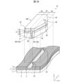
- FIG. 1 is a perspective view for explaining the structure of a semiconductor laser device according to an embodiment of the present disclosure
- FIG. FIG. 2 is a perspective view for explaining an optical resonator included in a semiconductor laser device
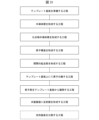
- 4 is a flow chart showing an example of a method for manufacturing a semiconductor laser device according to an embodiment of the present disclosure
- 1A and 1B are a plan view and a cross-sectional view showing the configuration of a template substrate according to an embodiment of the present disclosure
- FIG. 1 is a cross-sectional view for explaining a semiconductor substrate according to an embodiment of the present disclosure
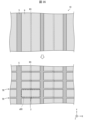
- FIG. FIG. 10 is a plan view for explaining an example of a process of element isolation
- 6B is a cross-sectional view taken along the line B-VI shown in FIG. 6A;
- FIG. 4 is a flow chart showing an example of a mounting stage of a method for manufacturing a semiconductor laser device according to an embodiment of the present disclosure; It is a block diagram which shows an example of a manufacturing apparatus. 4 is a flow chart showing an example of a method for manufacturing a semiconductor laser device in Example 1.
- FIG. 4 is a cross-sectional view showing the configuration of a template substrate in Example 1.
- FIG. 11 is an enlarged view of a main portion of FIG. 10;
- FIG. 3 is a plan view showing an example of a starting point inducing portion of Example 1; 4 is a plan view showing another example of the starting point inducing part of Example 1.
- FIG. 4 is a plan view showing another example of the starting point inducing portion of Example 1.
- FIG. 4 is a plan view showing another example of the starting point inducing portion of Example 1.
- FIG. 4 is a plan view showing another example of the starting point inducing portion of Example 1.
- FIG. 4 is a cross-sectional view showing an example of lateral growth of a base semiconductor layer in Example 1.
- FIG. 4 is a plan view for explaining a base semiconductor layer in Example 1.
- FIG. 4 is an enlarged view for explaining how the base semiconductor layer grows around the starting point inducing portion in Example 1.
- FIG. 2 is a cross-sectional view showing the structure of a compound semiconductor layer in Example 1.
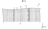
- FIG. 2 is a plan view for explaining a compound semiconductor layer in Example 1.
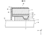
- FIG. 2 is a perspective view for explaining the configuration of an element portion in Example 1; 3 is a cross-sectional view showing the configuration of an element portion in Example 1.
- FIG. FIG. 4 is a cross-sectional view schematically showing a step of separating the element portion from the template substrate in the manufacturing method of the semiconductor laser element of Example 1;
- FIG. 4 is a perspective view schematically showing a state in which an element portion is bonded to a support substrate;
- FIG. 4 is a cross-sectional view schematically showing a state in which an element portion DS is bonded to a support substrate SK;
- FIG. 4 is a cross-sectional view schematically showing a step of forming a reflective film on the cavity surface in the manufacturing method of the semiconductor laser device of Example 1;
- FIG. 4 is a plan view showing the configuration of a compound semiconductor layer after forming a reflector film; 4 is a cross-sectional view schematically showing a step of dividing the support substrate in the method of manufacturing the semiconductor laser device of Example 1.
- FIG. 4 is a plan view for explaining another example of the base semiconductor layer in Example 1.
- FIG. 10 is an exploded perspective view for explaining another configuration example of the half-element portion in Example 1;
- FIG. 10 is a cross-sectional view showing the configuration of a semiconductor laser device in Example 2;
- 10A to 10C are schematic cross-sectional views showing an example of a method for manufacturing a semiconductor laser device in Example 2; 10 is a flow chart showing an example of a method for manufacturing a semiconductor laser device in Example 3.
- FIG. 11 is a plan view showing the configuration of a semiconductor substrate on which a base semiconductor layer is formed in Example 3;
- FIG. 11 is a plan view showing the configuration of a semiconductor substrate on which an element structure is formed in Example 3;
- 34 is a cross-sectional view showing the configuration of the semiconductor substrate of FIG. 33;
- FIG. 11 is a plan view showing an example of element isolation in Example 4;
- FIG. 11 is a schematic diagram showing the configuration of an electronic device in Example 5;
- a semiconductor laser (Laser Diode; LD) element will be described as an example of a semiconductor device, but the semiconductor device of the present disclosure is not necessarily limited to this.
- the semiconductor device of the present disclosure may be, for example, a sensor having an optical resonator, a sensor having a resonator plane, or the like.
- FIG. 1 is a perspective view for explaining the structure of a semiconductor laser device 20.
- FIG. FIG. 2 is a perspective view for explaining the optical resonator LK of the semiconductor laser device 20.
- FIG. 1 is an example, and the semiconductor laser element 20 may have a shape in which the depth direction in the perspective view shown in FIG. 1 is the longitudinal direction.
- the semiconductor laser device 20 has a structure having electrodes on the upper side and the lower side (hereinafter referred to as a “double-sided electrode structure”), but is not limited to this. (anode and cathode) (hereinafter referred to as a “single-sided two-electrode structure”). Further, the semiconductor laser element 20 may be mounted on a support substrate (also called a submount), and FIG. 1 omits the illustration of the support substrate.
- a semiconductor laser element (semiconductor device) 20 in this embodiment includes a base semiconductor portion 8 and a compound semiconductor portion located above the base semiconductor portion 8 and including an optical resonator LK. 9, a first electrode E1, a second electrode E2, and an insulating film DF.
- the optical resonator LK the surface from which the laser beam is emitted is called an emitting surface F1, and the surface facing the emitting surface F1 is called a facing surface F2.
- the exit surface F1 and the opposing surface F2 are a pair of resonator surfaces in the optical resonator LK.
- a specific aspect (element structure) of the optical resonator LK is not particularly limited.
- the base semiconductor portion 8 and the compound semiconductor portion 9 are typically layered. Therefore, the base semiconductor portion 8 can also be called the base semiconductor layer 8 and the compound semiconductor portion 9 can be called the compound semiconductor layer 9 .
- the base semiconductor layer 8 and the compound semiconductor layer 9 are referred to as the base semiconductor layer 8 and the compound semiconductor layer 9, but the base semiconductor layer 8 and the compound semiconductor layer 9 are not necessarily limited to layers.
- the base semiconductor layer 8 may contain, for example, a nitride semiconductor.
- a GaN-based semiconductor is a semiconductor containing gallium atoms (Ga) and nitrogen atoms (N), and typical examples include GaN, AlGaN, AlGaInN, and InGaN.
- the base semiconductor layer 8 may be a doped (eg, n-type containing donor) layer or a non-doped layer.
- the compound semiconductor layer 9 may contain, for example, the nitride semiconductor.
- the semiconductor laser device 20 in the present embodiment may have a semiconductor layer formed by an ELO (Epitaxial Lateral Overgrowth) method (hereinafter sometimes referred to as an ELO semiconductor layer) as the base semiconductor layer 8 .
- the base semiconductor layer 8 is not limited to the ELO semiconductor layer as long as it can reduce the defect density of the optical resonator LK included in the compound semiconductor layer 9 .
- the base semiconductor layer 8 may be a general semiconductor layer containing a nitride semiconductor.
- general semiconductor layer is meant a semiconductor layer epitaxially grown vertically on a growth substrate.
- GE semiconductor layer for convenience of explanation. Since the GE semiconductor layer can be formed by a known method, the description is omitted.
- a substrate used for growing various semiconductor layers of a semiconductor laser element may be referred to as a "growth substrate”.
- a semiconductor laser device 20 in which the base semiconductor layer 8 is an ELO semiconductor layer will be described.
- a method of manufacturing the base semiconductor layer 8 using the ELO method will be described later.
- the base semiconductor layer 8 which is an ELO semiconductor layer, includes a first portion (first portion) B1 and a first portion B1 having a lower density of threading dislocations KD (threading dislocation density) extending in the thickness direction (Z direction) than the first portion B1.
- the second portion B2, the first portion B1, and the third portion B3 are arranged in this order in the X direction, and the first portion B1 is positioned between the second portion B2 and the third portion B3.
- Threading dislocations KD are dislocations (defects) that extend from the lower surface or inside of base semiconductor layer 8 to the surface or surface layer along the thickness direction of base semiconductor layer 8 .
- the threading dislocation densities of the second portion B2 and the third portion B3 may be 1 ⁇ 5 or less (for example, 5 ⁇ 10 6 /cm 2 or less) of the threading dislocation density of the first portion B1.
- the compound semiconductor layer 9 including a plurality of layers is laminated on the base semiconductor layer 8, and this lamination direction can be the "upward direction".
- the Z-axis positive direction side of the XYZ coordinate axes shown in FIG. 1 may be referred to as "upper side”
- the Z-axis negative direction side may be referred to as "lower side”.
- the surface of each member on the Z-axis positive direction side is sometimes referred to as "upper surface”
- the surface of each member on the Z-axis negative direction side is sometimes referred to as "lower surface”.
- plan view viewing the object with a line of sight parallel to the normal direction of the upper surface.
- plane view viewing the object with a line of sight parallel to the normal direction of the upper surface.
- the compound semiconductor layer 9 includes an n-type semiconductor portion (first-type semiconductor portion) 9N, an active portion 9K, and a p-type semiconductor portion (second-type semiconductor portion) 9P in an upward direction from the base semiconductor layer 8. Including in order.
- the n-type semiconductor portion 9N, the active portion 9K, and the p-type semiconductor portion 9P are typically layered. Therefore, the n-type semiconductor portion 9N can also be said to be the n-type semiconductor layer 9N.
- the active portion 9K can also be said to be the active layer 9K.
- the p-type semiconductor portion 9P can also be said to be the p-type semiconductor layer 9P.
- n-type semiconductor layer 9N, active layer 9K, and p-type semiconductor layer 9P are referred to, but the n-type semiconductor layer 9N, active layer 9K, and p-type semiconductor layer 9P are not necessarily layered.
- the p-type semiconductor layer 9P may have a ridge portion RJ.
- the n-type semiconductor layer 9N, the active layer 9K, and the p-type semiconductor layer 9P may contain the aforementioned nitride semiconductor.
- Various layers included in the compound semiconductor layer 9 will be specifically described later.
- the compound semiconductor layer 9 may be affected by the first portion B1 of the base semiconductor layer 8 and have a high threading dislocation density above the first portion B1.
- the compound semiconductor layer 9 has an optical resonator LK at a position overlapping the second portion B2 in plan view.
- the optical resonator LK includes a waveguide extending between an emission surface F1 and a facing surface F2 that form a pair of resonator surfaces.
- the distance between the exit surface F1 and the opposing surface F2 can be defined as the resonator length (resonance length) L1 of the optical resonator LK.
- the end face of the active layer 9K included in the emission surface F1 and the end face of the active layer 9K included in the opposing surface F2 may each be coated with a reflective film (for example, a dielectric film).
- At least one of the emitting surface F1 and the facing surface F2 of the semiconductor laser element 20 may be the m-plane or c-plane of the compound semiconductor layer 9 containing a nitride semiconductor.
- the positive direction of the X-axis is the [11-20] direction of the nitride semiconductor
- the positive direction of the Y-axis is the [-1100] direction of the nitride semiconductor
- the positive direction of the Z-axis (thickness direction). ) can be the [0001] direction of the nitride semiconductor.
- the m-plane that at least one of the emission surface F1 and the opposing surface F2 can have is a plane parallel to the (1-100) plane (or (-1100) plane) of the nitride semiconductor.
- the c-plane that at least one of the emission surface F1 and the opposing surface F2 can have is a plane parallel to the (0001) plane of the nitride semiconductor.
- At least one of the emitting surface F1 and the facing surface F2 of the semiconductor laser element 20 may be included in the cleaved surface of the compound semiconductor layer 9 .
- Each of emission surface F ⁇ b>1 and opposing surface F ⁇ b>2 may be included in the cleaved surface of compound semiconductor layer 9 .
- the semiconductor laser device 20 can also be configured such that the cavity length L1 is 200 [ ⁇ m] or less.
- the semiconductor laser element 20 is provided with a first electrode E1 and a second electrode E2 for supplying current to the optical resonator LK.
- the first electrode E1 can be arranged so as to overlap the optical resonator LK in plan view in the thickness direction of the base semiconductor layer 8 .
- "two members overlap" in plan view means that at least a part of one member overlaps another member in plan view (including transparent plan view) in the thickness direction of each member. , and these members may or may not be in contact with each other.
- the first electrode E1 may be located above the compound semiconductor layer 9, overlap at least a portion of the ridge RJ in plan view, and have a shape extending along the longitudinal direction of the optical resonator LK.
- the first electrode E1 is electrically connected to the ridge portion RJ in the p-type semiconductor layer 9P and functions as an anode.
- the first electrode E1 and the ridge portion RJ may be in contact with each other, or may be connected via another layer.
- the second electrode E2 may be positioned below the compound semiconductor layer 9, for example, on the lower surface of the base semiconductor layer 8.
- the second electrode E2 may have a shape overlapping at least a portion of the first electrode E1 in plan view.
- the second electrode E2 is electrically connected to the base semiconductor layer 8 and functions as a cathode.
- the second electrode E2 and the base semiconductor layer 8 may be in contact with each other or may be connected via another layer.
- the second electrode E2 may be in contact with the compound semiconductor portion 9 (for example, the n-type semiconductor layer 9N).
- the insulating film DF is positioned above the compound semiconductor layer 9 .
- the insulating film DF may cover the upper surface of the p-type semiconductor layer 9P except for the contact portion between the first electrode E1 and the ridge portion RJ.
- Semiconductor lasers are sometimes fabricated from stacks containing multiple semiconductor layers (referred to as conventional CT).
- conventional CT a plurality of semiconductor lasers are formed on a growth substrate, and the plurality of semiconductor lasers are divided together with the growth substrate.
- the inventors of the present invention have diligently studied a method different from the conventional method CT, and came up with the method of manufacturing the semiconductor laser device of the present disclosure.
- the semiconductor laser device 20 in this embodiment is generally manufactured by a method including a step of forming an optical resonator (at least forming a resonator plane in the compound semiconductor layer 9) on a growth substrate.
- FIG. 3 is a flow chart showing an example of a method for manufacturing a semiconductor laser device according to this embodiment.
- 4A and 4B are a plan view and a cross-sectional view showing the configuration of the template substrate in this embodiment.
- a template substrate is prepared.
- the template substrate 7 in this embodiment includes a main substrate 1, a base portion 4 positioned above the main substrate 1, an opening KS and a mask positioned above the main substrate 1.
- the main substrate 1 and the base portion 4 may be collectively referred to as a base substrate UK.
- the base substrate UK and the template substrate 7 are an example of the aforementioned growth substrate.
- the underlying portion 4 and the mask 6 are typically layered. Therefore, the base portion 4 can be called the base layer 4 and the mask 6 can be called the mask layer 6 . In the following description, the base layer 4 and the mask layer 6 are referred to, but the base layer 4 and the mask layer 6 are not necessarily limited to layers.
- Mask 6 may be a mask pattern including mask portion 5 and opening KS.
- the opening KS is a region where the mask portion 5 does not exist, and the opening KS may not be surrounded by the mask portion 5 .
- a heterosubstrate having a lattice constant different from that of the nitride semiconductor can be used for the main substrate 1 .
- heterogeneous substrates include silicon (Si) substrates, sapphire (Al 2 O 3 ) substrates, silicon carbide (SiC) substrates, and the like.
- the plane orientation of the main substrate 1 is, for example, the (111) plane of the Si substrate, the (0001) plane of the Al 2 O 3 substrate, and the 6H—SiC (0001) plane of the SiC substrate.
- the main substrate 1 is not particularly limited as long as it has a substrate and a surface orientation that allow the base semiconductor layer 8 to be grown by the ELO method.
- the template substrate 7 may have the buffer portion 2 and the seed portion 3 in order from the main substrate 1 side as the underlying layer 4 .
- Buffer portion 2 and seed portion 3 are typically layered. Therefore, the buffer portion 2 can be called the buffer layer 2 and the seed portion 3 can be called the seed layer 3 .
- the buffer layer 2 and the seed layer 3 are referred to as the buffer layer 2 and the seed layer 3 below, the buffer layer 2 and the seed layer 3 are not necessarily limited to layers.
- the buffer layer 2 is a melting suppression layer that can reduce the possibility that the main substrate 1 and the seed layer 3 will come into direct contact with each other and melt together. Moreover, there is also an effect of improving the crystallinity of the seed layer 3 .
- the seed layer 3 is a layer that serves as a growth starting point for the base semiconductor layer 8 when forming the base semiconductor layer 8 to be described later. For example, when the main substrate 1 that does not melt with the seed layer 3, which is a GaN-based semiconductor, is used, a configuration in which the buffer layer 2 is not provided is also possible.
- a buffer layer 2 such as an AlN layer or a SiC layer is provided. This reduces the possibility that the GaN-based semiconductor and the Si substrate will melt.
- the mask layer 6 formed on the underlying substrate UK has a plurality of mask portions 5 and a plurality of openings KS. Both the mask portion 5 and the opening KS may have a longitudinal shape with the width direction in the first direction (X direction) and the longitudinal direction in the second direction (Y direction). The opening KS may have a tapered shape (a shape that narrows downward).
- an inorganic insulating film such as a silicon oxide (SiOx) film, a silicon nitride (SiNx) film, a silicon oxynitride (SiON) film, or a titanium nitride (TiNx) film can be used.
- a layered film containing the above materials may be used for the mask layer 6, for example, a layered film containing a silicon oxide film and a silicon nitride film may be used.
- Mask layer 6 may be formed, for example, as follows. That is, after a SiO 2 film is formed on the entire surface of the underlying substrate UK using a sputtering method, wet etching is performed while partially protecting it with a resist. A mask portion 5 and an opening KS are formed by removing a portion of the SiO 2 film.
- the opening KS of the mask layer 6 exposes the seed layer 3 and functions as a growth initiation hole for starting the growth of the base semiconductor layer 8 , and the mask portion 5 of the mask layer 6 laterally covers the base semiconductor layer 8 . It has the function of a selective growth mask for directional growth.
- the width WK of the opening KS may be, for example, approximately 0.1 ⁇ m to 20 ⁇ m. As the width of the opening KS becomes smaller, the number of threading dislocations propagating from the opening KS to the base semiconductor layer 8 decreases. Also, the base semiconductor layer 8 can be easily peeled off in a post-process. Furthermore, the areas of the second portion B2 and the third portion B3 having few surface defects can be increased.
- the width WM of the mask portion 5 may be, for example, approximately 25 ⁇ m to 200 ⁇ m.
- the mask portion 5 is partially formed in the X direction so that the opening KS has a shape having a notch.
- the mask layer 6 may be formed so as to protrude outward.
- the portion of the mask portion 5 that partially protrudes in the X direction will be referred to as a starting point induction portion. Since the mask layer 6 has the starting point inducing portion, the base semiconductor layer 8 and the compound semiconductor layer 9 can be formed on the template substrate 7 so as to have the starting point serving as the starting point of cleavage. Details will be described in Example 1 below.
- FIG. 5 is a cross-sectional view for explaining the semiconductor substrate in this embodiment.
- a method for manufacturing a semiconductor laser device may include a step of forming a semiconductor layer (see FIG. 3).
- the step of forming the semiconductor layers for example, after the base semiconductor layer 8 is formed on the template substrate 7 by the ELO method, the compound semiconductor layer 9 is formed above the base semiconductor layer 8 .
- a seed layer 3 containing a GaN-based semiconductor is used, an inorganic compound film such as a SiO 2 film is used as a mask layer 6 , and a base semiconductor layer 8 can be laterally grown on the mask portion 5 .
- the thickness direction (Z direction) of the base semiconductor layer 8 formed by the ELO method is the ⁇ 0001> direction (c-axis direction) of the GaN crystal, and the width direction (X direction) of the opening KS is the ⁇ 11- 20> direction (a-axis direction) and the longitudinal direction (Y-direction) of the opening KS can be the ⁇ 1-100> direction (m-axis direction) of the GaN-based crystal.
- the base semiconductor layer 8 overlaps the mask portion 5 in plan view, overlaps the second portion B2 and the third portion B3 with relatively few threading dislocations KD, and overlaps the opening KS in plan view.
- a first portion B1 having more threading dislocations KD than the second portion B2 and the third portion B3.
- the compound semiconductor layer 9 is influenced by the threading dislocations KD present on the surface of the first portion B1 and contains many threading dislocations KD above the first portion B1.
- the optical resonator LK can be provided so as to overlap the second portion B2 in plan view. This can reduce the possibility that the performance of the optical resonator LK is degraded due to the effect of the threading dislocation KD. This is because in the compound semiconductor layer 9 on the second portion B2, the amount of dislocations (defects) introduced due to the surface defects of the second portion B2 during the film formation of the compound semiconductor layer 9 is relatively small. is.
- a threading dislocation KD is a dislocation (defect) extending from the lower surface or inside of the base semiconductor layer 8 to its surface or superficial layer along the thickness direction of the base semiconductor layer 8 .
- Threading dislocations KD can be observed by, for example, CL (Cathode Luminescence) measurement on the surface (parallel to the c-plane) of the base semiconductor layer 8 .
- the second part B2 or the third part B3 can be configured such that the density of non-threading dislocations in the cross section parallel to the ⁇ 0001> direction is higher than the density of threading dislocations in the upper surface.
- Non-threading dislocations are dislocations that are CL-measured in a cross section along a plane parallel to the thickness direction, and are mainly basal plane (c-plane) dislocations.
- the semiconductor substrate 10 in this embodiment may have a template substrate 7 and a base semiconductor layer 8 formed on the template substrate 7 . Further, the semiconductor substrate 10 may have the template substrate 7 , the base semiconductor layer 8 , and the compound semiconductor layer 9 formed above the base semiconductor layer 8 .
- a plurality of base semiconductor layers 8 are formed so as to have gaps Gp between different base semiconductor layers 8 .
- the width WG of the gap Gp may be 4 ⁇ m or less, and may be 3 ⁇ m or less. Note that the semiconductor substrate 10 is not limited to having the gap Gp, and the base semiconductor layers 8 laterally grown from the seed layer 3 exposed in the two adjacent openings KS are in contact with each other on the mask portion 5. ).
- a template substrate 7 including the main substrate 1 and the mask layer 6 on the main substrate 1 may be used, the template substrate 7 covering the growth inhibiting regions corresponding to the mask portions 5 . (for example, a region that suppresses crystal growth in the Z direction) and a seed region corresponding to the opening KS.
- a growth suppression region and a seed region can be formed on the main substrate 1, and the base semiconductor layer 8 can be formed on the growth suppression region and the seed region using the ELO method.
- FIG. 6A is a plan view for explaining an example of the element isolation process.
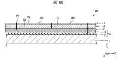
- FIG. 6B is a cross-sectional view taken along line B-VI shown in FIG. 6A.
- the base semiconductor layer 8 and the compound semiconductor layer 9 are formed on the template substrate 7 so as to form at least the cavity surface in the compound semiconductor layer 9, and the semiconductor laser device is formed into a plurality of half-device portions (second half-device portions). 1) may be separated into sDS.
- the “semi-element portion sDS” refers to a plurality of individual pieces aligned along the Y-axis direction formed by dividing the base semiconductor layer 8 and the compound semiconductor layer 9 on the template substrate 7. , a piece 8V of the base semiconductor layer 8 and a piece 9V of the compound semiconductor layer 9 located above the piece 8V of the base semiconductor layer 8 (laminate).
- the half-element part sDS can be said to be a kind of element part, but in that it does not have members such as electrodes for driving as an element, the element part as a product is in a state in the middle of manufacturing, that is, it is positioned as a semi-finished product. obtain.
- Such a half element portion sDS also falls within the category of the semiconductor device of the present disclosure.
- a boundary between adjacent half-element portions sDS is called a divided portion PS, and the divided portion PS is indicated by a thick black line in FIGS. 6A and 6B.
- each of the plurality of half-device portions sDS has an optical resonator LK (in other words, a plurality of half-device portions sDS).
- Each of the element portions sDS has a resonator face formed in at least the compound semiconductor layer 9 individually.
- FIG. 6B illustrates various forms of the divided portion PS, it is not limited to this.
- the mask portion 5 in the step of element isolation on the template substrate 7, the mask portion 5 may be partially or entirely divided in the thickness direction of the semiconductor substrate 10 at the divided portions PS, or 5 may not be divided, or the mask portion 5 and the underlying layer 4 may be divided.
- the main substrate 1 may not be divided entirely in the thickness direction.
- a crack may arise in a part in the thickness direction of the main substrate 1 .
- the specific technique of the step of element isolation on the template substrate 7 is not particularly limited.
- the base semiconductor layer 8 may be formed after forming the mask layer 6 so that the mask portion 5 has the starting point inducing portion. can have an origin that is Further, like the base semiconductor layer 8, the compound semiconductor layer 9 can also have a cleavage starting point.
- a plurality of half-element portions sDS may be formed by cleaving from the starting portion due to thermal stress or physical external force.
- the base semiconductor layer 8 may be cleaved before the compound semiconductor layer 9 is formed.
- a compound semiconductor layer 9 may be formed. By cleaving or dividing the compound semiconductor layer 9, it is possible to separate the elements into a plurality of half-element portions sDS.
- the mask portion 5 may not have the starting point inducing portion, and in this case, the starting point of the cleavage may be formed in the base semiconductor layer 8 or the compound semiconductor layer 9 by processing such as scribing. .
- the starting point of the cleavage may be formed in the base semiconductor layer 8 or the compound semiconductor layer 9 by processing such as scribing. .
- cleavage may be caused from the starting point.
- the internal stress of the base semiconductor layer 8 and the compound semiconductor layer 9 may allow the cleavage to progress naturally.
- the elements can be separated into a plurality of half-element portions sDS.
- the divided portions PS are trenches formed by etching. you can
- the main substrate 1, the base semiconductor portion 8 formed above the main substrate 1, and the base semiconductor portion 8 formed on the base semiconductor portion 8 (ii) separating the base semiconductor portion 8 and the compound semiconductor portion 9 so as to form a resonator plane in at least the compound semiconductor portion 9; separating 9 into a plurality of device portions (eg, half device portions sDS).
- element separation is performed on a growth substrate (eg, template substrate 7) into a plurality of half-element portions sDS having resonator planes (eg, emission surface F1 and opposing surface F2). good.
- an optical resonator LK including cavity planes eg, an exit plane F1 and an opposing plane F2 is formed. good.
- a resonator surface e.g., an exit surface F1 and an opposing surface F2
- the base semiconductor layer 8 and the compound semiconductor layer 9 may be divided to form a plurality of optical resonators LK each including a resonator plane.
- the main substrate 1 may not be divided, or the main substrate 1 may be divided into a smaller number than the plurality of optical resonators LK.
- the main substrate 1 may be divided so that one of the plurality of pieces formed by dividing the main substrate 1 has a plurality of half-element portions sDS on one piece.
- the manufacturing method of the semiconductor laser device of the present embodiment it is possible to easily form the cavity plane even if the semiconductor laser device 20 is miniaturized. Therefore, the optical resonator LK can be easily formed. Then, by separating the device portion DS formed as described later from the growth substrate, the device portion DS can be mounted on the support substrate to manufacture the semiconductor laser device 20 . Thereby, handling property can be improved. Also, a substrate suitable for mounting can be used as the support substrate.
- Step of forming element structure Then, in the method of manufacturing a semiconductor laser device according to the present embodiment, a step of forming a device structure for the half-device portion sDS on the template substrate 7 is performed. Thereby, the element part DS is formed. At this stage, the base semiconductor layer 8 included in the element portion DS is Van der Waals-bonded to the mask portion 5 , and the element portion DS may be a part of the semiconductor substrate 10 .
- the insulating film DF is formed, and then the first electrode E1 is formed at a position in contact with the ridge portion RJ. (anode).
- the semiconductor laser element 20 has a single-sided two-electrode structure
- the second electrode E2 is formed on the upper surface of the base semiconductor layer 8 after partially exposing the upper surface of the base semiconductor layer 8 by etching or the like. you can Thus, the element part DS can be formed.
- the ridge portion RJ and the insulating film DF in the element portion DS By providing the ridge portion RJ and the insulating film DF in the element portion DS, the current path between the first electrode E1 and the base semiconductor layer 8 is narrowed on the anode side, and light can be emitted efficiently within the resonator LK. . Further, the ridge portion RJ may overlap the second portion B2 (low-dislocation portion) of the base semiconductor portion 8 in plan view, and may not overlap the first portion B1. The second electrode E2 may overlap the second portion B2 (low dislocation portion) of the base semiconductor portion 8 in plan view.
- the current path from the first electrode E1 to the second electrode E2 via the compound semiconductor portion 9 and the base semiconductor portion 8 is formed in a portion overlapping the second portion B2 in plan view (a portion with few threading dislocations).
- the luminous efficiency in the active layer 9K is enhanced. This is because threading dislocations act as non-radiative recombination centers.
- the second electrode E2 may overlap the second portion B2 and the third portion B3 (low dislocation portion) of the base semiconductor portion 8 in plan view. Injection efficiency is enhanced.
- the second electrode E2 may be formed in a post-process.
- an element having an element structure without the second electrode E2, which is obtained by the step of forming the element structure is also referred to as an element portion DS.
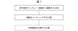
- FIG. 7 is a flow chart showing an example of the mounting stage of the method for manufacturing a semiconductor laser device according to this embodiment.
- a step of separating the element part DS from the template substrate 7 is performed.
- the element part DS can be separated from the template substrate 7 using the support substrate.
- the semiconductor laser device 20 may be formed by performing a step of coating the end face of the optical resonator LK of the device portion DS.
- the semiconductor laser element 20 may be formed by dividing the support substrate on which the element portion DS is mounted.
- the support substrate may have a function as a submount, whereby chips having semiconductor laser elements 20 mounted on the divided support substrates can be formed. A specific example of the support substrate will be described later.
- the template substrate 7 or the base substrate UK can be reused.
- the semiconductor laser element 20 can be formed by transferring the element portion DS from a substrate not suitable for mounting to a substrate (supporting substrate) suitable for mounting.
- FIG. 8 is a block diagram showing an example of a manufacturing apparatus.
- the manufacturing apparatus 70 includes a semiconductor layer forming section 72 for forming the base semiconductor layer 8 and the compound semiconductor layer 9 on the template substrate 7, a processing section 73 for forming the element structure, and a semiconductor layer forming section. 72 and a control unit 74 that controls the processing unit 73 .
- the semiconductor layer forming unit 72 may include, for example, a MOCVD (Metal-Organic Chemical Vapor Deposition) device, forms the base semiconductor layer 8 using the ELO method, and forms the compound semiconductor layer 9 on the base semiconductor layer 8. .
- a MOCVD Metal-Organic Chemical Vapor Deposition
- a step of element isolation may be performed.
- the semiconductor layer forming section 72 once takes out the object to be processed from the processing apparatus, and then puts the object into the processing apparatus again to form a compound semiconductor layer on the base semiconductor layer 8 . 9 may be controlled.
- the semiconductor layer forming section 72 may have the function of manufacturing the template substrate 7 .
- the processing portion 73 may perform a step of element isolation to form the half-element portion sDS.
- the processing unit 73 performs various processes on the half-element unit sDS positioned on the template substrate 7 to form the element unit DS.
- the processing part 73 may perform a step of separating the element part DS from the template substrate 7 using the support substrate, or may perform a process of coating the end face of the optical resonator LK.
- the control unit 74 may include a processor and memory.
- the control unit 74 may be configured to control the semiconductor layer forming unit 72 and the processing unit 73 by executing a program stored in an internal memory, a communicable communication device, or an accessible network, for example.
- the above program and a recording medium storing the above program are also included in this embodiment.
- a GaN substrate may be used as a growth substrate instead of the base substrate UK, and in this case, the main substrate 1 may be a GaN substrate. . That is, the main substrate 1 may be a growth substrate.
- a semiconductor substrate in which a semiconductor layer containing a nitride semiconductor (the aforementioned GE semiconductor layer) is formed on a GaN substrate without forming the mask layer 6 can also be used.
- a plurality of island-shaped semiconductor layers having a shape as shown in FIG. 5 can be formed. Then, after forming a compound semiconductor layer on this semiconductor layer, a step of element isolation may be performed to form a plurality of half-element portions sDS.
- the method of manufacturing the semiconductor laser device 20 according to another embodiment of the present disclosure is not limited to using the template substrate 7 in which the seed layer 3 entirely overlaps the mask portion 5 . Since the seed layer 3 may be exposed from the opening KS, the template substrate 7 may be used in which the seed layer 3 is locally formed so as not to partially or entirely overlap the mask portion 5 .
- the buffer layer 2 may be located on the main substrate 1 and the seed layer 3 may be locally provided on the buffer layer 2 so as to overlap the opening KS of the mask layer 6 .
- the base substrate UK having the configuration in which the buffer layer 2 is not provided between the main substrate 1 and the seed layer 3 is used as the growth substrate.
- a template substrate 7 comprising a base substrate UK having a main substrate 1 and a seed layer 3 and a mask layer 6 formed on the base substrate UK may be used.
- the template substrate 7 is provided with the buffer layer 2 when the main substrate 1 made of a material that does not melt with the seed layer 3 is used, or when the seed layer 3 made of a material with low reactivity with the main substrate 1 is used.
- the seed layer 3 may be made of a material that is less reactive with the main substrate 1 and that can serve as a growth starting point for the base semiconductor layer 8 .
- Seed layer 3 may be, for example, an AlN layer or a SiC layer, or a layer containing at least one of AlN and SiC.
- the semiconductor laser device 20 may have a configuration in which the base semiconductor layer 8 does not have the first portion B1, that is, may have a configuration in which there is one second portion B2. .
- the first part B1 may be removed by etching or the like.
- Example 1 Hereinafter, the method for manufacturing a semiconductor device according to the present disclosure will be described in more detail with reference to examples. Various changes in the range are possible. Further, hereinafter, the same or corresponding parts in the figures of the configurations of the multiple embodiments of the present disclosure will be described by attaching the same reference numerals. Forms obtained by appropriately combining technical means disclosed in the examples are also included in the technical scope of the present disclosure.
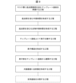
- FIG. 9 is a flow chart showing an example of a method for manufacturing the semiconductor laser device 20 according to the first embodiment.
- the mask layer 6 of the template substrate 7 includes the mask portion 5 having the starting point inducing portion.
- an ELO semiconductor layer having starting points is formed on the template substrate 7 .
- a template substrate 7 including an origin inducing portion in a mask layer 6 is prepared, and then a semiconductor layer (a base semiconductor layer 8 and a compound layer) including an origin inducing portion is formed on the template substrate 7 .
- a semiconductor layer 9) is formed.
- FIG. 10 is a cross-sectional view showing the configuration of the template substrate 7 in Example 1.
- FIG. 11A is an enlarged view of a main part of FIG. 10.
- FIG. 1 As the main substrate 1 in the template substrate 7, a heterosubstrate having a lattice constant different from that of the nitride semiconductor can be used.
- a Si substrate As the main substrate 1, the manufacturing cost of the template substrate 7 can be reduced.
- the main substrate 1 may be an Al 2 O 3 substrate or a SiC substrate that can reduce reactivity with Ga.
- the main substrate 1 may be made of any material and have a surface orientation that allows an ELO semiconductor layer to grow thereon, and the material and surface orientation of the main substrate 1 are not particularly limited.
- the base substrate UK may be manufactured by forming the base layer 4 (see FIG. 4) on the main substrate 1, or a previously prepared base substrate UK may be used.
- the base substrate UK prepared in advance it is easy to stably grow the base semiconductor layer 8 and the like. This is because when a process for forming the underlying layer 4 is performed, the base semiconductor layer 8 and the like may be affected by the process.
- the template substrate 7 may include, for example, the seed layer 3 as the underlying layer 4 .
- the seed layer 3 is a layer that serves as a growth starting point for the base semiconductor layer 8 when the base semiconductor layer 8 is formed.
- the seed layer 3 may contain a GaN-based semiconductor, aluminum nitride (AlN), SiC, graphene, or the like.
- the silicon carbide used for the seed layer 3 may be hexagonal 6H--SiC or 4H--SiC.
- the seed layer 3 may be, for example, an AlGaN layer, or a graded layer in which the Al composition gradually increases to approach GaN.
- the seed layer 3 can be configured to include a GaN layer.
- the seed layer 3 may be a GaN single layer, or the uppermost layer of the graded layer that is the seed layer 3 may be a GaN layer.
- the seed layer 3 may be made of any material and has a plane orientation that allows the growth of the base semiconductor layer 8 containing a nitride semiconductor.
- the template substrate 7 may include a buffer layer 2 (see FIG. 4) located between the main substrate 1 and the seed layer 3 as the underlying layer 4 .
- a buffer layer 2 (see FIG. 4) located between the main substrate 1 and the seed layer 3 as the underlying layer 4 .
- the buffer layer 2 is provided between the silicon substrate and the GaN-based semiconductor so that the silicon substrate and the GaN-based semiconductor are mutually connected. Melting can be reduced.
- the buffer layer 2 may have at least one of the effect of increasing the crystallinity of the seed layer 3 and the effect of relieving the internal stress of the seed layer 3 .
- the buffer layer 2 may typically be an AlN layer or may be a SiC layer.
- SiC used for the buffer layer 2 may be of a hexagonal system (6H--SiC, 4H--SiC) or a cubic system (3C--SiC).
- Buffer layer 2 may be a multilayer film including at least one of an AlN film and a SiC film.
- the buffer layer 2 may contain a strain relaxation layer. Examples of the strain relaxation layer include an AlGaN superlattice structure and a graded structure in which the Al composition of AlGaN is changed stepwise. The stress in the longitudinal direction of the base semiconductor layer 8 can be relaxed by the strain relief layer.
- An AlN layer which is an example of the buffer layer 2, can be formed to a thickness of about 10 nm to about 5 ⁇ m using, for example, an MOCVD apparatus.
- the underlying layer 4 can be formed by stacking various layers on the main substrate 1 using an MOCVD device, a sputtering device, or the like.
- MOCVD MOCVD
- a sputtering device e.g., a sputtering device
- the buffer layer 2 e.g. aluminum nitride
- the seed layer 3 e.g. GaN-based semiconductor
- PSD pulse sputter deposition
- PLD pulse laser deposition, etc.
- a template substrate 7 is manufactured by forming a mask layer 6 on a base substrate UK.
- a silicon oxide film (SiOx), a titanium nitride film (TiN, etc.), a silicon nitride film (SiNx), a silicon oxynitride film (SiON), and a metal film having a high melting point (for example, 1000° C. or higher) are used.
- a single layer film containing any one of or a laminated film containing at least two of these can be used.
- Example 1 the mask layer 6 is formed on the base substrate UK so that the mask portion 5 has the starting point inducing portion 5Y in part.
- the starting point inducing portion 5Y in Example 1 has a triangular shape in plan view.
- the starting point inducing portion 5Y has a vertex 5P and two sides 5A and 5B that intersect at the vertex 5P in plan view.
- a virtual line segment connecting the end of the side 5A and the end of the side 5B on the side opposite to the vertex 5P in a plan view is referred to as a side 5C.
- a virtual triangle is formed by side 5A, side 5B, and side 5C.
- Side 5C can also be said to be the base of a virtual triangle.
- the angle between the sides 5A and 5B is called ⁇ 1, and the angle between the sides 5B and 5C is called ⁇ 2.
- a distance from the side 5C to the vertex 5P is referred to as a projection length H1 of the starting point induction portion 5Y.
- the starting point inducing portion 5Y may have the same thickness as the other portions of the mask portion 5.
- the angle ⁇ 1 may be 30° or approximately 30°, for example, about 20° to 40°.
- the term “substantially” means within a variation range of ⁇ 10%.
- the angle ⁇ 1 and the angle ⁇ 2 may be the same as each other, and may be approximately the same as each other.
- the side 5A may have a length of about 0.1 ⁇ m to 20 ⁇ m, for example.
- the side 5A and the side 5B may have the same length as each other, or may have approximately the same length as each other.
- the term “comparable” means within a range of 10% difference based on the larger numerical value.
- the protruding length H1 of the starting point inducing portion 5Y may be, for example, about 0.1 ⁇ m to 10 ⁇ m.
- the starting point inducing portion 5Y is not limited to a specific shape as long as it can form a portion that serves as a starting point of cleavage in the base semiconductor layer 8, as will be described later.
- the starting point inducing portion 5Y is not limited to a shape in which the tip of the apex 5P is sharp in plan view, and the apex 5P may have a rounded shape.
- the angle ⁇ 1 and the angle ⁇ 2 of the starting point inducing portion 5Y may be different from each other.
- the starting point inducing portion 5Y may have a square shape in plan view, or may have another shape.
- a portion of the mask portion 5 other than the starting point inducing portion 5Y may be referred to as a main portion, and the thickness of the starting point inducing portion 5Y and the main portion may be different from each other. Further, the starting point inducing portion 5Y and the main portion may be formed integrally, or the starting point inducing portion 5Y may be formed after forming the main portion.
- the opening KS has a longitudinal shape except for the portion where the starting point inducing portion 5Y is provided, and the width is relatively narrow in the portion where the starting point inducing portion 5Y is provided.
- the mask layer 6 is formed so as to have a notch in the opening KS by providing the starting point inducing portion 5Y.
- a plurality of openings KS may be arranged periodically with a first period in the X direction.
- the width of the opening KS may be about 0.1 ⁇ m to 20 ⁇ m. As the width of the opening KS becomes smaller, the number of threading dislocations propagating from the opening KS to the base semiconductor layer 8 decreases. In addition, it becomes easy to peel off the base semiconductor layer 8 in a post-process. Furthermore, the area of the second portion B2 with few surface defects can be increased.
- the mask layer 6 having the mask portion 5 may be formed, for example, as follows. First, a silicon oxide film having a thickness of about 100 nm to 4 ⁇ m (preferably about 150 nm to 2 ⁇ m) is formed on the underlying layer 4 by sputtering. Then, a resist is applied to the entire surface of the silicon oxide film. After that, the resist is patterned by photolithography to form a resist having a plurality of striped openings. At this time, in Example 1, the resist at the position corresponding to the starting point induction portion 5Y is not removed.
- a portion of the silicon oxide film is removed with a wet etchant such as hydrofluoric acid (HF) or buffered hydrofluoric acid (BHF) to form a mask portion 5 including a plurality of openings KS and starting point induction portions 5Y. do.
- a mask layer 6 is then formed by removing the resist with an organic wash.
- the semiconductor laser device 20 manufactured using the template substrate 7 is, for example, the second portion B2 located farther from the origin inducing portion 5Y than the second portion B2 or the third portion B3. (See FIG. 1, etc.) can be formed with a pair of cavity surfaces (output surface F1 and opposing surface F2).
- the second portion B2 is less likely to be affected by the starting point inducing portion 5Y.
- the mask layer 6 can be formed by appropriately changing the direction of the starting point inducing portion 5Y.
- FIG. 11B is a plan view showing an example of the starting point inducing portion 5Y.
- an example starting point induction portion 5Y may have a shape in which the apex 5P does not exceed the center of the opening KS. That is, the starting point inducing portion 5Y may have a protrusion length H1 of, for example, 0.1 ⁇ m or more and less than (WK/2) (WK: width of the opening KS).
- WK width of the opening KS.
- the starting point inducing portion 5Y may have, for example, an isosceles triangular shape or an equilateral triangular shape in plan view.
- FIG. 11C is a plan view showing another example of the starting point inducing portion 5Y.
- an example starting point inducing portion 5Y may have a shape in which the apex 5P extends beyond the center of the opening KS. That is, the starting point inducing portion 5Y may have a protrusion length H1 of, for example, (WK/2) or more and less than WK. Also, for example, the angles ⁇ 1 and ⁇ 2 may exceed 40°.
- FIG. 11D is a plan view showing another example of the starting point inducing portion 5Y.
- an example starting point inducing portion 5Y may have a virtual pentagonal shape in plan view, which is a combination of a virtual triangle 5Y1 and a virtual quadrangle 5Y2.
- the virtual quadrangle 5Y2 may be square or rectangular.
- the imaginary quadrangle 5Y2 may have a virtual side 5D whose longitudinal direction is the width direction of the opening KS, for example, about 0.1 ⁇ m to 10 ⁇ m.
- the side 5D may be a line segment extending parallel or substantially parallel to the width direction of the opening KS.
- the virtual quadrangle 5Y2 may be trapezoidal, for example.
- the vertex 5P of the virtual triangle 5Y1 may or may not be positioned beyond the center of the opening KS.
- FIG. 11E is a plan view showing another example of the starting point inducing portion 5Y.
- an example starting point induction portion 5Y may have a quadrangular shape in a plan view.
- the distance between 5E and the main portion of the mask portion 5 is defined as a projection length H1.
- the side 5E may have a length of, for example, approximately 0.1 ⁇ m to 10 ⁇ m.
- the starting point inducing portion 5Y may have, for example, a trapezoidal shape or a parallelogram shape in plan view.
- the side 5E may or may not extend beyond the center of the opening KS. That is, the side 5D may have a length of, for example, approximately 0.1 ⁇ m to 20 ⁇ m.
- a base semiconductor layer 8 is deposited on the template substrate 7 .
- the template substrate 7 is loaded into an MOCVD apparatus, and a GaN-based semiconductor layer is deposited by the ELO method.
- FIG. 12 is a cross-sectional view showing an example of lateral growth of the base semiconductor layer 8 in Example 1.
- the base semiconductor layer 8 in Example 1 is a nitride semiconductor (for example, a GaN-based semiconductor layer) and is obtained by c-plane film formation on the template substrate 7 .
- the base semiconductor layer 8 may be an n-type semiconductor layer with donors.
- the [ ⁇ 1100] direction of the GaN-based semiconductor is the positive Y-axis direction
- the [11-20] direction of the GaN-based semiconductor is the positive X-axis direction
- the [0001] direction of the GaN-based semiconductor is the positive Z-axis direction ( thickness direction).
- an initial growth layer SL is first formed on the seed layer 3, and then the base semiconductor layer 8 can be laterally grown from the initial growth layer SL.
- the initial growth layer SL is a starting point of lateral growth of the base semiconductor layer 8 and a part of the first portion B1.
- the initial growth is performed immediately before the edge of the initial growth layer SL climbs over the upper surface of the mask portion 5 (at the stage where it is in contact with the upper end of the side surface of the mask portion 5) or immediately after it climbs over the upper surface of the mask portion 5.
- the ELO film formation conditions may be controlled so as to stop the film formation of the layer SL (that is, switch the ELO film formation conditions from the c-axis direction film formation conditions to the a-axis direction film formation conditions at this timing). In this way, since the lateral film formation is performed in a state where the initial growth layer SL slightly protrudes from the mask portion 5 , the material is less likely to be consumed in the growth of the base semiconductor layer 8 in the thickness direction. can grow laterally at high speed.
- the initial growth layer SL may be formed with a thickness of, for example, 2.0 ⁇ m or more and 3.0 ⁇ m or less.
- Example 1 an n-type GaN layer was used as the base semiconductor layer 8, and an ELO film of Si-doped GaN was formed on the template substrate 7 using an MOCVD apparatus.
- An initial growth layer SL is selectively grown on the seed layer 3 (the uppermost GaN layer of the seed layer 3 ) exposed in the opening KS, and subsequently grown laterally on the mask portion 5 . Then, the lateral growth was stopped before the base semiconductor layer 8 growing laterally from both sides of the mask portion 5 joined together.
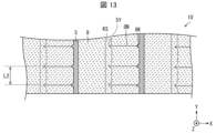
- Example 13 is a plan view for explaining the base semiconductor layer 8 in Example 1.
- the base semiconductor layer 8 has a starting point 8K that serves as a starting point for cleavage, and the starting point 8K extends from the opening KS having a notch to the base semiconductor layer. It is naturally formed in the base semiconductor layer 8 by growing 8 . Note that the relationship between the shape of the starting point inducing portion 5Y and the shape of the starting point portion 8K may change depending on the growth conditions of the base semiconductor layer 8. FIG. The shape of the starting point 8K may be smaller than or larger than the shape of the starting point inducing portion 5Y, or may be substantially the same as each other. An example of the starting point 8K will be described below.
- the base semiconductor layer 8 may have an oblique meeting portion 8N extending from the position of the starting point inducing portion 5Y of the mask layer 6 to the position of the starting point portion 8K of the base semiconductor layer 8 in plan view.
- the oblique meeting portion 8N is a portion where the semiconductor layers grown obliquely with respect to the X direction (a-axis direction) meet.
- the oblique meeting portion 8N may be, for example, a crystal grain boundary, or may be a portion of the base semiconductor layer 8 in which the disorder of the crystal structure is greater (that is, the number of lattice defects is greater) than in other portions.
- the oblique meeting portion 8N is illustrated with a solid line. If the base semiconductor layer 8 has an oblique junction 8N, the oblique junction 8N can be observed, for example, by performing a CL measurement.
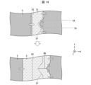
- FIG. 14 is an enlarged view for explaining how the base semiconductor layer 8 grows around the starting point inducing portion 5Y in Example 1.
- FIG. 14 first, an initial growth layer SL is formed from the opening KS.
- the lateral growth of the GaN-based semiconductor in the ⁇ 11-20> direction causes the portion of the opening KS other than the periphery of the starting point inducing portion 5Y to climb over the upper surface of the mask portion 5.
- An initial growth layer SL is formed in .
- the direction orthogonal to the side 5A of the starting point inducing portion 5Y is the m-plane direction (eg, [10-10] direction) of the GaN-based semiconductor
- the direction orthogonal to the side 5B is the direction of the GaN-based semiconductor. It may be another m-plane direction (eg, [01-10] direction).
- the growth rate in the m-plane direction in a GaN-based semiconductor is lower than the growth rate in the a-plane direction.
- the base semiconductor layer 8 can be grown so as to maintain the notch formed in the initial growth layer SL.
- the oblique meeting portion 8N can be generated, for example, by the meeting of the semiconductor layers grown in the [10-10] direction and the [01-10] direction.
- the oblique junction 8N may also exist on the surface of the base semiconductor layer 8 after being generated in the vicinity of the mask portion 5 and affecting (propagating) to the surface of the base semiconductor layer 8 after film formation.
- the starting point portion 8K may have a tapered shape such as a triangular shape in plan view. This makes it easier for stress to concentrate on one point during cleavage. As a result, it is possible to easily obtain a good cleavage plane.
- the starting point portion 8K may have an end surface that is the m-plane of the GaN-based semiconductor. Note that the end surface of the starting portion 8K may not be the m-plane of the GaN-based semiconductor.
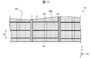
- L2 (see FIG. 17) be the interval between the plurality of starting points 8K in the base semiconductor layer 8 (the distance between the tips of the two starting points 8K). handle.
- the length of the interval L2 may be approximately 20 ⁇ m to 200 ⁇ m.
- the interval L2 may be 300 ⁇ m or more.
- the base semiconductor layer 8 In the film formation of the base semiconductor layer 8, it is preferable to reduce the mutual reaction between the base semiconductor layer 8 and the mask portion 5 and maintain the state where the base semiconductor layer 8 and the mask portion 5 are in contact with each other due to the Van der Waals force. That is, the base semiconductor layer 8 and the mask portion 5 may be in contact mainly by van der Waals forces.
- Example 1 (Step of forming compound semiconductor layer)
- the MOCVD apparatus is used without once taking out the semiconductor substrate 10 from the MOCVD apparatus.
- a compound semiconductor layer 9 is formed on the base semiconductor layer 8.
- the layered structure is continuously formed using the MOCVD apparatus.
- the compound semiconductor layer 9 includes a nitride semiconductor layer (for example, a GaN-based semiconductor layer).
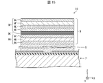
- FIG. 15 is a cross-sectional view showing the structure of the compound semiconductor layer 9 in Example 1.
- the compound semiconductor layer 9 is formed by sequentially forming an n-type semiconductor layer 9N having donors, an active layer 9K, and a p-type semiconductor layer 9P having acceptors.
- the n-type semiconductor layer 9N is formed by forming a first contact layer 9A, a first clad layer 9B, and a first optical guide layer 9C in this order.
- the p-type semiconductor layer 9P is composed of a second optical guide layer 9D, an electron blocking layer 9E, a second cladding layer 9F, and a second contact layer 9G formed in this order.
- the second optical guide layer 9D and the electron blocking layer 9E may be alternately arranged in the p-type semiconductor layer 9P.
- the p-type semiconductor layer 9P may consist of an electron blocking layer 9E, a second optical guide layer 9D, a second cladding layer 9F, and a second contact layer 9G formed in this order.
- An n-type GaN layer for example, can be used for the first contact layer 9A, and an n-type AlGaN layer, for example, can be used for the first clad layer 9B.
- the first cladding layer 9B may be an n-type GaN-based semiconductor layer, an n-type AlGaN-based semiconductor layer, or an n-type AlInGaN-based semiconductor layer, and may have a layer thickness of about 0.8 ⁇ m to 2 ⁇ m, for example. .
- the first optical guide layer 9C may be an n-type GaN layer, for example, and may be an InGaN layer having an In composition of about 3 to 10%.
- the first optical guide layer 9C may have a layer thickness of about 50 nm.
- an MQW (Multi-Quantum Well) structure including an InGaN layer can be used.
- the active layer 9K may typically have a structure of 5-6 periods.
- the In composition varies depending on the target emission wavelength. For example, in the case of blue emission (wavelength around 450 nm), the In concentration may be about 15 to 20%. For green light emission (wavelength around 530 nm), the In concentration may be about 30%.
- a p-type AlGaN layer can be used for the second optical guide layer 9D.
- the second optical guide layer 9D may have an Al composition of, for example, about 15 to 25%, and may have a layer thickness of, for example, about 5 to 25 nm.
- a p-type GaN layer for example, may be used for the electron blocking layer 9E, and may be an InGaN layer having an In composition of about 3 to 10%.
- the electron blocking layer 9E may have a layer thickness of about 50 nm.
- a p-type AlGaN layer for example, may be used for the second clad layer 9F.
- the second cladding layer 9F may be a p-type GaN-based semiconductor layer, an AlGaN-based semiconductor layer, or an AlInGaN-based semiconductor layer, and may have a layer thickness of about 0.1 ⁇ m to 1 ⁇ m, for example.
- a p-type GaN layer for example, can be used for the second contact layer 9G.
- the second contact layer 9G may have a layer thickness of, for example, approximately 0.1 ⁇ m to 0.3 ⁇ m. Although illustration is omitted, a highly doped layer having a thickness of about 10 nm and using Mg as a dopant may be formed on the surface of the second contact layer 9G.
- the refractive index of each layer of the compound semiconductor layer 9 refractive index of each layer of the compound semiconductor layer 9 (refractive index of light generated in the active layer 9K)
- FIG. 16 is a plan view for explaining the compound semiconductor layer 9 in Example 1.
- the compound semiconductor layer 9 is formed in a shape having starting points 9T corresponding to the starting points 8K of the base semiconductor layer 8 . This is because the compound semiconductor layer 9 is difficult to form at the position of the starting point 8K of the base semiconductor layer 8 .
- the starting point portion 9T may have an end face that is the m-plane of the GaN-based semiconductor by being formed in a shape corresponding to the starting point portion 8K. Note that the end surface of the starting point portion 9T may not be the m-plane of the GaN-based semiconductor.
- Example 1 The process described above can be organized as follows. That is, in Example 1, first, a step of preparing the main substrate 1, the base semiconductor layer 8 formed above the main substrate 1, and the compound semiconductor layer 9 formed on the base semiconductor layer 8 is performed. . A notch is formed in the opening KS of the mask layer 6 . As a result, a starting portion 8K is naturally formed in the base semiconductor layer 8. Next, as shown in FIG. Then, the compound semiconductor layer 9 is formed on the base semiconductor layer 8 having the starting portion 8K. As a result, the starting point portion 9T is naturally formed in the compound semiconductor layer 9. Next, as shown in FIG.
- Step of isolating elements on the template substrate Next, by cooling the semiconductor substrate 10 on which the compound semiconductor layer 9 is formed, element separation is performed on the template substrate 7 into a plurality of half-element portions sDS.
- 17A and 17B are plan views for explaining an example of the process of element isolation in the first embodiment. FIG.
- the film formation of the compound semiconductor layer 9 may be performed under high-temperature conditions using an MOCVD apparatus. In this case, a cooling step exists within the MOCVD apparatus.
- the coefficient of thermal expansion of the base semiconductor layer 8 and the compound semiconductor layer 9 may be different from the coefficient of thermal expansion of the main substrate 1. Internal stress is generated in the base semiconductor layer 8 and the compound semiconductor layer 9 due to the difference in thermal expansion coefficient from the substrate 1 .
- the main substrate 1 and the base semiconductor layer 8 may have different lattice constants.
- An internal stress is generated in the semiconductor layer 8 .
- internal stress may also occur in the compound semiconductor layer 9 .
- a substrate different from a GaN-based semiconductor for example, a Si substrate
- internal stress can be easily generated in the base semiconductor layer 8 and the compound semiconductor layer 9 .
- the base semiconductor layer 8 and the compound semiconductor layer 9 may each have a starting point portion 8K and a starting point portion 9T having a tapered notch shape. In this case, stress tends to concentrate at one point. , a high-quality cleaved surface can be easily produced by cleavage.
- the shapes of the starting point portion 8K and the starting point portion 9T are affected by the shape of the starting point inducing portion 5Y of the mask portion 5 in the mask layer 6.
- FIG. The shape of the starting point inducing portion 5Y can affect the quality of the cleavage plane.
- tensile stress may be generated as internal stress in the base semiconductor layer 8 .
- the coefficient of thermal expansion of the main substrate 1 is larger than the coefficient of thermal expansion of the base semiconductor layer 8
- compressive stress is generated in the base semiconductor layer 8
- the coefficient of thermal expansion of the main substrate 1 is larger than the coefficient of thermal expansion of the base semiconductor layer 8. If it is small, a tensile stress is generated in the base semiconductor layer 8 .
- the possibility that the divided pieces of the base semiconductor layer 8 come into contact with each other can be reduced. Therefore, the possibility that the end face of the divided base semiconductor layer 8 is damaged can be reduced.
- the base semiconductor layer 8 is cleaved from the starting point 8K, the cleaved surface tends to be smooth.
- Example 1 when the semiconductor substrate 10 is cooled, the base semiconductor layer 8 and the compound semiconductor layer 9 are cleaved to separate the elements on the template substrate 7 into a plurality of half-element portions sDS having the optical resonators LK. you can In this case, there is no need to separately perform a process for cleaving the base semiconductor layer 8 and the compound semiconductor layer 9, and the manufacturing cost of the semiconductor laser device 20 can be reduced. Also, it is possible to manufacture a half-element portion sDS having an optical resonator LK with a short resonator length.
- the length of the interval L2 can be about 20 ⁇ m to 200 ⁇ m, so that the resonator length L1 can be about 20 ⁇ m to 200 ⁇ m.
- the starting point 9T may be cleaved by applying a force in a direction perpendicular to the surface direction by applying a blade to the starting point 9T.
- the starting point 9T is cleaved relatively reliably. Since it can be generated, the yield can be improved.
- the starting point 9T may be cleaved by vibrating the starting point 9T.
- the manufacturing process can be simplified because the treatment can be performed relatively easily. Further, by raising or lowering the temperature of the semiconductor substrate 10 from room temperature, the thermal expansion coefficient difference between the main substrate 1 and the base semiconductor layer 8 is used to apply thermal stress to the starting point portion 9T to generate cleavage. You may let
- FIG. 18 is an exploded perspective view for explaining the configuration of the half element portion sDS in Example 1.
- the template substrate 7 and the base semiconductor layer 8 are shown to be virtually separated from each other for convenience of explanation, but the base semiconductor layer 8 and the mask portion 5 are actually in contact with each other.
- the base semiconductor layer 8 has a bonding portion 8S on its lower surface corresponding to the initial growth layer SL, and the bonding portion 8S and the seed layer 3 are bonded to each other.
- FIG. 18 shows a part of the template substrate 7 that is omitted, not the whole.
- the base semiconductor layer 8 in the half-element portion sDS includes a first base end face 8X, a second base end face 8Y adjacent to the first base end face 8X at an angle, have The base semiconductor layer 8 is adjacent to the second base end surface 8Y at an angle and has a third base end surface 8Z corresponding to the a-plane of the GaN-based semiconductor (for example, parallel to the a-plane).
- the second base end face 8Y may be located between the first base end face 8X and the third base end face 8Z.
- the half-element portion sDS may have two first base end faces 8X and two second base end faces 8Y as the end faces of the third portion B3.
- the first base end surface 8X may include a first partial surface 8X1, a second partial surface 8X2, and a third partial surface 8X3.
- the first partial surface 8X1 is a portion of the first base end surface 8X and is a surface at a position corresponding to the first portion B1 of the base semiconductor layer 8.
- the second partial surface 8X2 is a partial surface at a position corresponding to the second portion B2 on the first base end surface 8X.
- the third partial surface 8X3 is a partial surface at a position corresponding to the third portion B3 on the first base end surface 8X.
- the first partial surface 8X1 is located between the second partial surface 8X2 and the third partial surface 8X3.
- the third partial surface 8X3 may be a surface obtained by dividing the portion corresponding to the above-described oblique junction 8N, and is an m-plane cleaved surface formed by cleaving the base semiconductor layer 8 starting from the starting point 8K.
- the second partial surface 8X2 may be an m-plane cleaved surface formed by cleaving the base semiconductor layer 8 starting from the starting point 8K, and may be flush with the emission surface F1 of the optical resonator LK. .
- the first partial surface 8X1, the second partial surface 8X2, and the third partial surface 8X3 may be flush with each other.
- the surface roughness of the second partial surface 8X2 may be smaller than that of the third partial surface 8X3.
- the density of dislocations (dislocations measured by CL on the cleavage plane, mainly basal plane dislocations) in the second partial plane 8X2 may be equal to or higher than the threading dislocation density in the second portion B2.
- the second base end surface 8Y is a surface included in the notch-shaped starting portion 8K of the base semiconductor layer 8 before cleavage, and is not a cleavage surface formed by cleavage.
- the starting point portion 8K may have an end surface of the ELO semiconductor layer grown in the m-axis direction, and in this case, the second base end surface 8Y is not a cleaved surface.
- the compound semiconductor portion 9 may have a side surface 9S located above the second base end surface 8Y. The surface roughness of at least one of the pair of cavity surfaces (output surface F1 and opposing surface F2) can be made smaller than the surface roughness of the side surface 9S.
- the angle (inner angle) formed by the first base end face 8X and the second base end face 8Y is called ⁇ 3.
- the angle ⁇ 3 may be an obtuse angle, eg, 120° or approximately 120°, eg, about 110° to 130°.
- the optical resonator LK ( 1 and 2) can be formed.
- FIG. 18 exemplarily illustrates the optical resonator LK at a position overlapping the second portion B2 in plan view
- the position of the optical resonator LK in the X direction is not necessarily limited in the half-element portion sDS. More specifically, the optical resonator LK will be described later.
- the optical resonator LK including the resonator plane is formed by dividing the base semiconductor layer 8 and the compound semiconductor layer 9 so that the main substrate 1 is not entirely divided in the thickness direction. I can say
- the emission surface F1 and the opposing surface F2 of the optical resonator LK may each be the m-plane of the compound semiconductor layer 9 and may be included in the cleavage plane of the compound semiconductor layer 9 .
- Each of the emission surface F1 and the opposing surface F2 can be formed by m-plane cleaving the compound semiconductor layer 9, which is a nitride semiconductor layer (for example, a GaN-based semiconductor layer).
- the base semiconductor layer 8 and the compound semiconductor layer 9 may have traces of cleavage starting points for cleavage (for example, the second base end surface 8Y). Since the emission surface F1 and the opposing surface F2 are m-planes, the reflectance of the resonator surface of the optical resonator LK can be improved.
- Step of forming element structure a step of forming an element structure is performed on the semiconductor substrate 10 having a plurality of half-element portions sDS.
- the element portion DS is formed by forming the ridge portion RJ in the p-type semiconductor layer 9P and then forming the insulating film DF and the first electrode E1.
- a semiconductor laser device 20 having a double-sided electrode structure is manufactured. Therefore, the element portion DS does not include the second electrode E2, and the second electrode E2 may be provided in a later step.
- FIG. 19 is a perspective view for explaining the configuration of the element section DS in Example 1.
- FIG. 19 the template substrate 7 is omitted.
- FIG. 20 is a cross-sectional view showing the configuration of the element portion DS in Example 1.
- the compound semiconductor layer 9 may include a ridge portion (ridge portion) RJ overlapping the first electrode E1 in plan view.
- the ridge portion RJ may include a portion of the second cladding layer 9F and the electron blocking layer 9E (see FIG. 15) (the portion overlapping the first electrode E1 in plan view).
- the ridge portion RJ has a shape whose longitudinal direction is the Y direction, and the insulating film DF may be provided so as to cover the side surfaces of the ridge portion RJ.
- the insulating film DF for example, a single layer film or a laminated film containing oxides or nitrides of Si, Al, Zr, Ti, Nb, and Ta can be used.
- the film thickness of the insulating film DF can be about 10 to 500 nm.
- the refractive index of the insulating film DF is smaller than those of the second optical guide layer 9D and the second cladding layer 9F.
- the first electrode E1 is provided, for example, on the upper surface of the ridge portion RJ and functions as an anode.
- the material of the first electrode E1 include metals or alloys such as Ni, Rh, Cr, Au, W, Pt, Ti, and Al, and conductive oxides containing at least one selected from Zn, In, and Sn.
- single layer film or multilayer film such as Conductive oxides include ITO (Indium Tin Oxide), IZO (Indium Zinc Oxide), GZO (Gallium-doped Zinc Oxide), and the like.
- the thickness of the first electrode E1 may be, for example, about 0.1 to 2 ⁇ m.
- the optical resonator LK includes a portion of each of the n-type semiconductor layer 9N, the active layer 9K, and the p-type semiconductor layer 9P (the portion overlapping the first electrode E1 in plan view).
- the optical resonator LK is a part of each of the first clad layer 9B, the first optical guide layer 9C, the active layer 9K, the second optical guide layer 9D, the electron blocking layer 9E, and the second clad layer 9F (plan view and a portion overlapping with the first electrode E1).
- the refractive index decreases in the order of the active layer 9K, the first optical guide layer 9C, and the first clad layer 9B.
- the refractive index decreases in order of the cladding layer 9F. Therefore, the light generated by coupling the holes supplied from the first electrode E1 and the electrons supplied from the second electrode E2 in the active layer 9K enters the optical resonator LK (in particular, the active layer 9K). Confined, lasing occurs by stimulated emission and feedback action in the active layer 9K. Laser light generated by laser oscillation is emitted from the light emission area EA of the emission surface F1.
- the emission surface F1 and the facing surface F2 of the optical resonator LK are formed by m-plane cleavage, they are excellent in flatness and perpendicularity to the c-plane (parallelism between the emission surface F1 and the facing surface F2), resulting in high light reflection. have a rate. Therefore, the reflection loss can be reduced, and stable laser oscillation is possible even with a short resonance length of 200 ⁇ m or less where the optical gain is small. Since the emission surface F1 and the opposing surface F2 are formed above the second portion B2, which is a low-dislocation portion, the planarity of the cleaved surface is excellent, and high light reflectance is realized.
- the sum T1 of the thickness of the base semiconductor layer 8 and the thickness of the compound semiconductor layer 9 can be 50 [ ⁇ m] or less. If the sum T1 of the thicknesses is too large, it may become difficult to cleave the resonator so that the resonator length is 200 ⁇ m or less.
- a ratio of the resonator length L1 (see FIG. 2) to the thickness of the second portion B2 of the base semiconductor layer 8 can be set to 1-20.
- the direction perpendicular to the direction of the resonator length L1 is defined as the first direction (X direction)
- the size of the second portion B2 in the X direction is defined as the width W2 of the second portion B2
- the resonator with respect to the width W2 of the second portion B2 The ratio of the lengths L1 can be 1-10.
- the width W1 of the first portion B1 may be the size of the first portion B1 in the X direction, and the ratio of the resonator length L1 to the width W1 of the first portion may be 1-200.
- FIG. 21 is a cross-sectional view schematically showing the step of separating the element portion DS from the template substrate 7 in the method of manufacturing the semiconductor laser element of Example 1. As shown in FIG. FIG. 21 shows one element part DS, but it is of course possible to perform the process of separating a plurality of element parts DS from the template substrate 7 . Also, in FIG. 21, the illustration of the ridge portion RJ is simplified.
- the mask portion 5 of the template substrate 7 may be removed by etching using hydrofluoric acid, buffered hydrofluoric acid, or the like.
- the insulating film DF may be protected with a resist or the like so that the insulating film DF is not removed together with the mask portion 5 .
- the mask portion 5 may be removed after the element portion DS is formed on the template substrate 7 .
- the mask portion 5 is removed while the element portion DS is fixed to the template substrate 7 . Since it can be removed, the yield in manufacturing the semiconductor laser device 20 can be improved.
- the bonding portion 8S weak portion
- FIG. 22 is a perspective view schematically showing a state in which the element part DS is bonded to the support substrate SK.
- FIG. 23 is a cross-sectional view schematically showing a state in which the element portion DS is bonded to the support substrate SK.
- the support substrate SK includes conductive first pads P1 and second pads P2, for example, the first electrode E1 is connected to the first pad P1 via the first joint A1.
- the element portion DS is supported by the support substrate SK.
- the bonding portion 8S (weak portion) projecting downward from the back surface of the base semiconductor layer 8 is broken, and the element portion DS can be separated from the template substrate 7 .
- the insulating film DF and the second pad P2 may be bonded to each other via a second bonding portion A2 (not shown). can improve.
- the back surface of the base semiconductor layer 8 may be planarized by polishing or CMP (Chemical Mechanical Polish). Then, the second electrode E2 can be formed on the lower surface of the base semiconductor layer 8 of the element part DS while being supported by the support substrate SK.
- CMP Chemical Mechanical Polish
- the insulating film D1 covering the side surfaces of the base semiconductor layer 8 and the compound semiconductor layer 9, and (ii) the conductive film MF are formed.
- the conductive film MF electrically connects the second electrode E2 and the second joint portion A2 or the second pad P2.
- the material of the conductive film MF is not particularly limited.
- the first pad P1 and the second pad P2 may be provided apart from each other.
- the conductive film MF may be in contact with the second electrode E2, the insulating film D1, and at least one of the second bonding portion A2 and the second pad P2.
- Example 1 the second electrode E2 is located on the back surface of the base semiconductor section 8, and the compound semiconductor section 9 and the first electrode E1 are closer to the supporting substrate SK than the base semiconductor section 8 (junction-down type).
- a plurality of element units DS are arranged on the support substrate SK in a direction (X direction) perpendicular to the direction defining the resonator length so that the directions of the resonator lengths are aligned.
- First and second pads P1 and P2 may be provided corresponding to each of the portions DS.
- the support substrate SK can be formed, for example, as follows. That is, a plurality of recesses HL (rectangular in plan view) are provided in a matrix on a Si substrate, a SiC substrate, an AlN substrate, or the like, and a plurality of first pads P1, a plurality of second pads P2, and a plurality of second pads P2 are provided in the non-recesses. It can be formed by providing one joint portion A1. Note that a plurality of second joints A2 may be provided.
- the material forming the main body of the support substrate SK is not particularly limited, and the support substrate SK may be made of, for example, an insulator or semi-insulator, or may be made of a conductive material.
- Examples of conductive materials include metal materials containing Cu, Al, and the like.
- an insulating layer can be arranged on the upper surface of the support substrate SK, and wiring can be arranged on the insulating layer.
- the shape of the support substrate SK is also not particularly limited, and may be a substantially quadrangular prism shape (substantially cuboid shape), a substantially pentagonal prism shape, a substantially hexagonal prism shape, or other shapes.
- the shape of the support substrate SK is a substantially rectangular parallelepiped shape.
- the first pad P1 and the second pad P2 may have metal layers containing Au, Ti, Ni, etc., for example.
- the first joint portion A1 and the second joint portion A2 may consist of a single metal layer, or may consist of multiple metal layers.
- the outermost surface may be a metal layer composed of Au. Thereby, corrosion of the first joint portion A1 and the second joint portion A2 can be suppressed.
- the first joint A1 is a solder material such as AuSi or AuSn.
- the first pad P1 and the first electrode E1 may be metal-metal bonded without providing the first bonding portion A1, and the second pad P2 and the second electrode E2 may be metal-bonded without providing the second bonding portion A2. - May be metal bonded. In that case, for example, an Au—Au junction can be used.
- the first pad P1 and the second pad P2 may be positioned on the same plane.
- the second joint A2 may not be provided.
- the first bonding portion A1 may be, for example, a solder material, and the element portion DS may be held by the first bonding portion A1 and placed on the support substrate SK.
- FIG. 24 is a cross-sectional view schematically showing a step of forming a reflective film on the cavity surface in the method of manufacturing the semiconductor laser device of Example 1.
- FIG. 25 is a plan view showing the structure of the compound semiconductor layer 9 after forming the reflector film UF.
- a reflector film UF (dielectric film, for example) is formed on the first facet including the facets of the base semiconductor layer 8 and the compound semiconductor layer 9 .
- the first facet includes the emission facet F1 of the optical resonator LK.
- Dielectrics such as SiO 2 , Al 2 O 3 , AlN, AlON, Nb 2 O 5 , Ta 2 O 5 and ZrO 2 can be used as materials for the reflector film UF.
- the reflector film UF may be a multilayer film.
- the reflector film UF can be formed by electron beam evaporation, electron cyclotron resonance sputtering, chemical vapor deposition, or the like.
- the semiconductor laser element 20 should have a structure in which at least one of the pair of cavity surfaces (the emission surface F1 and the opposing surface F2) has an optical reflectance of 98% or more and a cavity length L1 of 200 [ ⁇ m] or less. can be done.
- the difference between the output surface F1 and the opposing surface F2 may be the reflectance.
- the cavity surface with the lower reflectance can be used as the emission surface F1.
- the reflectance can be controlled by the type, structure, film thickness, etc. of the reflector film UF.
- a reflector film UF may be provided to cover the facing surface F2.
- the light reflectance of each of the emission surface F1 and the opposing surface F2 may be 98% or more.
- the light reflectance of the opposing surface F2 on the light reflecting surface side is higher than the light reflectance of the exit surface F1.
- the reflector film UF can be formed over the entire cleaved plane (m-plane) of the base semiconductor layer 8 and the compound semiconductor layer 9 .
- the element part DS can be electrically connected to the support substrate SK and mechanically fixed. As a result, the element part DS is arranged on the support substrate SK with the end face exposed. Therefore, in the next step, it is possible to form a reflective film on the emission surface F1 and the opposing surface F2 of the optical resonator LK on the end face of the element part DS.
- the cavity surface is not exposed to the outside in the divided portion PS. It is difficult to form a reflective film on the emission surface F1 and the opposing surface F2 of the optical resonator LK.
- dielectric layers can be formed (facet coating) so that the cavity surfaces of a plurality of devices have desired reflectance.
- the support substrate SK functions as a jig for coating the facets of the optical resonator LK, and also functions as a submount in the final device (semiconductor laser element 20).
- the device portion DS fixed to the support substrate SK the reflection efficiency at the facing surface F2 is increased, and the semiconductor laser device 20 having excellent light emission efficiency can be obtained.
- the cavity length of practically used semiconductor lasers manufactured by the method of forming cavity planes by cleavage is about 300 ⁇ m for the shortest cavity length semiconductor laser. be.
- the semiconductor laser element 20 can be an ultra-short cavity of 20-200 ⁇ m.
- the cavity surfaces (the emission surface F1 and the opposing surface F2) has a high optical reflectance and a small reflection loss, stable laser oscillation is possible even with a short resonant length of 200 ⁇ m or less where the optical gain is small. .
- a short resonator can achieve low power consumption in low light output applications such as wearable devices.
- FIG. 26 is a cross-sectional view schematically showing the step of dividing the support substrate SK in the manufacturing method of the semiconductor laser device of Example 1.
- the support substrate SK is divided to form a plurality of semiconductor laser chips 21 on which the semiconductor laser elements 20 are respectively arranged.
- the support ST can be used as a substrate (also called a submount) for the semiconductor laser chip 21 .
- the semiconductor laser chip 21 functions as a COS (Chip on Submount).
- a known cutting method such as dicing or scribing may be used to divide the support substrate SK into the supports ST. Any portion of the support substrate SK may be cut while avoiding damage to the semiconductor laser element 20 .
- the support ST may contain one semiconductor laser element 20 or may contain two or more semiconductor laser elements 20 .
- Example 1 the base semiconductor layer 8 and the compound semiconductor layer 9 are spontaneously cleaved on the template substrate 7 to separate the elements into a plurality of half-element portions sDS. There is no need to add a separate step for cleaving the semiconductor layer 9 . As a result, the manufacturing cost of the semiconductor laser device 20 can be reduced.
- the ELO method is not limited to forming a plurality of base semiconductor layers 8 in the form of islands, and the adjacent base semiconductor layers 8 can be brought together by relatively lengthening the growth time when forming the base semiconductor layers 8 .
- the top surface of the base semiconductor layer 8 may be polished.
- a compound semiconductor layer 9 can be deposited on the flat base semiconductor layer 8 .
- the compound semiconductor layer 9 having the starting portion 9T may be formed by subjecting the base semiconductor layer 8 and the compound semiconductor layer 9 to dry etching or the like.
- a base semiconductor layer 8 having a starting point 8K may be formed.
- the semiconductor substrate 10 can be isolated on the template substrate 7 .
- a semiconductor substrate 10 having a base semiconductor layer 8 and a compound semiconductor layer 9 as shown in FIG. 16 may be used.
- the semiconductor substrate 10 may be once taken out from the MOCVD apparatus.
- the base semiconductor layer 8 may be cleaved by removing the semiconductor substrate 10 from the MOCVD apparatus.
- the semiconductor substrate 10 having the cleaved base semiconductor layer 8 may be loaded into an MOCVD apparatus, and the compound semiconductor layer 9 having the starting point portion 9T may be deposited.
- the emission surface F1 and the facing surface F2 are included in the end surfaces of the epitaxially grown compound semiconductor layer 9 .
- the end face of the compound semiconductor layer 9 can be made high-quality. Therefore, the facets of the epitaxially grown compound semiconductor layer 9 can be used as cavity planes.
- the mask portion 5 is removed after forming the element portion DS on the template substrate 7, but in another configuration example, the mask portion 5 is removed before the step of forming the element portion DS. may be removed.
- the mask part 5 may be removed before forming the element part DS after forming the half element part sDS by element separation on the template substrate 7 . In this case, there is an advantage that it is not necessary to protect the insulating film DF from being removed when removing the mask portion 5 .
- the semiconductor laser element 20 may be mounted on the support substrate SK after forming the second electrode E2 and the reflector film UF while supporting the element portion DS using a temporary substrate. Further, both the temporary substrate DK and the support substrate SK may be separated while the semiconductor laser element 20 is sandwiched between the temporary substrate DK and the support substrate SK. In this case, individual pieces of the divided temporary substrate DK may be removed.
- a first supporting substrate having wiring may be used instead of the temporary substrate DK.
- the semiconductor laser element 20 is placed between the first supporting substrate and the supporting substrate SK (second supporting substrate). Both the first support substrate and the support substrate SK may be cut while being sandwiched.
- the semiconductor laser chip 21 may include the piece of the first support substrate and the support ST.
- FIG. 27 is a plan view for explaining another example of the base semiconductor layer 8 in Example 1.
- the base semiconductor layer 8 as an example may have a starting point portion 8K in which a notch is formed to a position close to the starting point inducing portion 5Y in plan view.
- the tip of the starting point 8K is referred to as the tip 8P.
- the starting point portion 8K may be located at a position where the tip portion 8P overlaps the starting point inducing portion 5Y in plan view.
- the starting point portion 8K may have a virtual triangular shape in plan view. In this virtual triangle, a virtual line segment corresponding to the base when the tip 8P is the vertex is called a side 8C.
- a distance from the side 8C to the tip portion 8P is referred to as a notch length H2 of the starting portion 8K.
- the notch length H2 may be WM/4 or more, or may be WM/3 or more. Also, the notch length H2 may be WM/2 or less.
- the compound semiconductor layer 9 By forming the compound semiconductor layer 9 on the base semiconductor layer 8, the compound semiconductor layer 9 is formed in a shape having a starting point (not shown) corresponding to the starting point 8K.
- the starting point formed in the compound semiconductor layer 9 may have an end face that is the m-plane of the GaN-based semiconductor by being formed in a shape corresponding to the starting point 8K.
- the end face of the starting point formed in the compound semiconductor layer 9 may not be the m-plane of the GaN-based semiconductor.
- FIG. 28 is an exploded perspective view for explaining the configuration of the half-element portion sDS formed by separating the base semiconductor layer 8 and the compound semiconductor layer 9 into elements.
- the template substrate 7 and the base semiconductor layer 8 are shown to be virtually separated for convenience of explanation, but the base semiconductor layer 8 and the mask portion 5 are actually in contact with each other.
- the base semiconductor layer 8 has a bonding portion 8S on its lower surface corresponding to the initial growth layer SL, and the bonding portion 8S and the seed layer 3 are bonded to each other.
- FIG. 28 shows a part of the template substrate 7 that is omitted, not the whole.
- the first base end surface 8X may not have the third partial surface 8X3.
- the angle (inner angle) formed by the second base end face 8Y and the third base end face 8Z is called ⁇ 4.
- ⁇ 4 may be an obtuse angle, eg, 120° or approximately 120°, eg, about 110° to 130°. Alternatively, ⁇ 4 may exceed 130°.
- the second base end surface 8Y may be an m-plane of a GaN-based semiconductor.
- the element portion DS may have a part of the compound semiconductor layer 9 removed by etching or the like, or the compound semiconductor layer 9 may be partially formed on the base semiconductor layer 8 . It's okay.
- the first electrode E1 is connected to the first pad P1 via the first joint A1
- the second electrode E2 is connected to the second pad P2 via the conductive film MF and the second joint A2. you can In this example, the element portion DS can be mounted on the support substrate SK without forming the insulating film D1 covering the side surfaces of the base semiconductor layer 8 and the compound semiconductor layer 9.
- Example 2 In Example 1, the semiconductor laser device 20 has a double-sided electrode structure, but in Example 2, the semiconductor laser device 20 may have a single-sided two-electrode structure.
- FIG. 29 is a cross-sectional view showing the configuration of the semiconductor laser device 20 in Example 2.
- the semiconductor laser device 20 in Example 2 may include a device portion DS including the base semiconductor layer 8 and the compound semiconductor layer 9, and a support substrate SK holding the device portion DS.
- Materials for the support substrate SK include Si, SiC, AlN, and the like.
- the support substrate SK is arranged such that the compound semiconductor layer 9, the first electrode E1 and the second electrode E2 are positioned between the support substrate SK and the base semiconductor layer 8. As shown in FIG.
- the first electrode E1 overlaps the optical resonator LK (not shown) and the second portion B2 of the base semiconductor layer 8 in plan view.
- the second electrode E2 is provided on the same side of the base semiconductor layer 8 as the first electrode E1.
- the second electrode E2 is in contact with the base semiconductor layer 8, and the first electrode E1 and the second electrode E2 do not overlap each other in plan view.
- the base semiconductor layer 8 has a larger width in the X direction than the compound semiconductor layer 9, and the second electrode E2 is formed in the exposed portion where the compound semiconductor layer 9 is not formed.
- the exposed portion may be formed by removing part of the compound semiconductor layer 9 by reactive ion etching (RIE) or the like, and the compound semiconductor layer 9 is partially formed on the base semiconductor layer 8 to form a film. may be formed.
- the compound semiconductor layer 9 may have an optical resonator LK, and a pair of resonator surfaces of the optical resonator LK may be covered with a reflector film UF.
- the support substrate SK includes a conductive first pad P1 and a second pad P2, the first electrode E1 is connected to the first pad P1 via the first joint A1, the second electrode E2 is the second joint It is connected to the second pad P2 via A2.
- the second joint portion A2 is thicker than the first joint portion A1, and the difference in thickness between the first joint portion A1 and the second joint portion A2 is equal to or greater than the thickness of the compound semiconductor layer 9. This enables connection between the first and second electrodes E1 and E2 and the first and second pads P1 and P2 located on the same plane.
- the support substrate SK may be a divided support ST, and in this case, the semiconductor laser element 20 may be the semiconductor laser chip 21 .
- the support ST can be used as a substrate (also called a submount) for the semiconductor laser chip 21 .
- the semiconductor laser chip 21 functions as a COS (Chip on Submount).
- FIG. 30 is a schematic cross-sectional view showing an example of a method for manufacturing the semiconductor laser device 20 in Example 2.
- Example 2 a step of preparing a template substrate 7 including an underlying substrate UK and a mask layer 6, and a first semiconductor layer S1 (and a first semiconductor layer S1, which is the source of the base semiconductor layer 8) are performed by the ELO method. 3 semiconductor layer S3) (described later), and a step of forming the second semiconductor layer S2 (and the fourth semiconductor layer S4) from which the compound semiconductor layer 9 is formed.
- a mask layer 6 having a starting point inducing portion 5Y may be formed in the mask portion 5, in which case the first semiconductor layer S1 (and the third semiconductor layer S3) has a starting point portion 8K.
- the second semiconductor layer S2 can be formed to have the starting point 9T.
- the starting part 8K may be formed in the third part B3, and the second semiconductor layer S2 may be provided above the second part B2.
- the optical resonator LK is provided at a position overlapping the second portion B2 in plan view.
- the second semiconductor layer S2 may not have the starting point portion 9T, and a starting point for cleavage may be formed by scribing as described later (Example 3, etc.).
- element isolation is performed on the template substrate 7 to form the half-element portion sDS.
- the ridge portion RJ is formed in the first semiconductor layer S1, and the first electrode E1, the second electrode E2, and the like are formed.
- an element part DS having a single-sided two-electrode structure is formed on the template substrate 7 .
- a step of bonding the element part DS to the support substrate SK and separating the first semiconductor layer S1 and the template substrate 7 is performed.
- the mask part 5 is removed by etching, and the element part DS is attached to the support substrate SK in a state in which the first and second joint parts A1 and A2 (for example, solder) of the support substrate SK are heated and melted. Join.
- the support substrate SK and the base substrate UK are displaced so that the support substrate SK and the base substrate UK move away from each other.
- the two-dimensionally arranged semiconductor laser substrate may be divided into rows to form one-dimensionally arranged (rod-shaped) semiconductor laser substrates, and then the reflector films UF are formed on the emission surface F1 and the opposing surface F2, respectively.
- a step of dividing the support substrate SK into a plurality of supports ST may then be performed.
- a plurality of semiconductor laser chips 21 can be formed.
- Example 3 the template substrate 7 that does not have the starting point inducing portion 5Y in the mask portion 5 may be used.
- a semiconductor laser device 20 having a single-sided two-electrode structure is manufactured.
- FIG. 31 is a flow chart showing an example of a method for manufacturing a semiconductor laser device in Example 3.
- Example 3 As shown in FIG. 31 , in Example 3, first, a template substrate 7 (see FIG. 4 ) having no origin inducing portion in the mask layer 6 is prepared, and then the base semiconductor layer 8 and the compound are placed on the template substrate 7 . A semiconductor layer 9 is formed.
- the template substrate 7 may be prepared as follows. First, a silicon oxide film having a thickness of about 100 nm to 4 ⁇ m (preferably about 150 nm to 2 ⁇ m) is formed on the underlying layer 4 by sputtering, CVD, vapor deposition, or the like. Then, a resist is applied to the entire surface of the silicon oxide film. After that, the resist is patterned by photolithography to form a resist having a plurality of striped openings. After that, a plurality of openings KS and a mask portion 5 are formed by partially removing the silicon oxide film with a wet etchant such as hydrofluoric acid (HF) or buffered hydrofluoric acid (BHF). A mask layer 6 is then formed by removing the resist with an organic wash. Thereby, the template substrate 7 as shown in FIG. 4 can be obtained.
- a wet etchant such as hydrofluoric acid (HF) or buffered hydrofluoric acid (BHF).
- the template substrate 7 is loaded into an MOCVD apparatus, and a GaN-based semiconductor layer is deposited by the ELO method.
- a GaN-based semiconductor layer is deposited by the ELO method.
- an n-type GaN layer was used as the base semiconductor layer 8
- an ELO film of Si-doped GaN was formed on the template substrate 7 using an MOCVD apparatus.
- substrate temperature 1120° C.
- growth pressure 50 kPa
- NH 3 15 slm
- V/III 6000 supply ratio
- An initial growth layer SL is selectively grown on the seed layer 3 (the uppermost GaN layer of the seed layer 3 ) exposed in the opening KS, and subsequently grown laterally on the mask portion 5 . Then, the lateral growth was stopped before the base semiconductor layer 8 growing laterally from both sides of the mask portion 5 joined together.
- the film formation time may be further lengthened so that the adjacent base semiconductor layers 8 are associated with each other.
- the association portion of the base semiconductor layer 8 may be removed by dry etching or the like after the compound semiconductor layer 9 is formed on the base semiconductor layer 8 .
- FIG. 32 is a plan view showing the configuration of the semiconductor substrate 10 on which the base semiconductor layer 8 is formed according to Example 3.
- FIG. 32 As shown in FIG. 32, in Example 3, the base semiconductor layer 8 does not have the starting portion 8K.
- FIG. 33 is a plan view showing the configuration of the semiconductor substrate 10 formed with the element structure in Example 3.
- FIG. 34 is a cross-sectional view showing the configuration of the semiconductor substrate 10 of FIG. 33.
- the template substrate 7 is omitted.
- the compound semiconductor layer 9 may be formed on the entire surface of the base semiconductor layer 8, and in this case, a portion of the base semiconductor layer 8 may be exposed by reactive ion etching. Alternatively, the compound semiconductor layer 9 may be partially formed on the top surface of the base semiconductor layer 8 . A second electrode E2 may be formed on the exposed portion of the base semiconductor layer 8 . Then, the ridge portion RJ is formed in the compound semiconductor layer 9, and the insulating film DF and the first electrode E1 are formed. Thereby, the semiconductor substrate 10 having the template substrate 7 and the element structures 22 formed on the template substrate 7 can be obtained.
- a starting point for cleavage is formed in the element structure 22 .
- the starting point for cleavage may be formed in the base semiconductor layer 8 or may be formed in the compound semiconductor layer 9 .
- the method of forming the starting point for cleavage is not particularly limited.
- the starting point for cleavage may be formed by diamond scribing.
- the starting point for cleavage can be formed into a thin shape, so the starting point for cleavage tends to concentrate at one point. Therefore, a smooth cleavage plane can be easily obtained. Since the insulating film DF formed on the compound semiconductor layer 9 is thin, the starting point for cleavage can be formed in the compound semiconductor layer 9 ignoring the existence of the insulating film DF.
- the compound semiconductor layer 9 may be exposed at the portion of the insulating film DF where the starting point for cleavage is to be formed.
- the starting point for cleavage may be formed by laser scribing. In this case, variations in scribe length can be reduced, thereby improving the yield.
- the laser scribe length is the scanning distance of the laser.
- the starting point for cleavage may be formed by dry etching or wet etching. In this case, the cleavage progresses without deviating from the cleavage plane, making it easier to obtain a smooth cleavage plane.
- a starting point for cleavage may be formed by combining the above techniques. In that case, the advantages of each method can be enjoyed at the same time.
- the starting point formed by diamond scribing or laser scribing may be further wet etched, in which case the shape of the starting point for cleaving can be shaped.
- the starting point formed by dry etching may be further wet-etched, and in this case, the shape of the starting point for cleavage can be shaped.
- the element structure 22 having the starting point of cleavage is cleaved.
- a blade may be brought into contact with the starting point for cleavage and a force applied in a direction perpendicular to the surface direction may cause cleavage to occur at the starting point.
- a strong force may be applied to the starting point for cleavage. Therefore, the yield is improved.
- the cleavage may be caused by vibrating the starting point for cleavage. In this case, the manufacturing process can be simplified because the treatment can be performed relatively easily.
- a thermal stress is applied to the above-described starting points by utilizing the difference in thermal expansion coefficients between the main substrate 1 and the base semiconductor layer 8 to generate cleavage.
- the difference in thermal expansion coefficient is used, there is no in-plane variation in how the force is applied, and the yield is improved.
- the element structure 22 on the template substrate 7 may be cleaved by applying stress to the element structure 22 on the template substrate 7 by bending the template substrate 7, which is the main substrate 1 thinned by polishing or the like.
- a plurality of element portions DS can be formed at once by separation. Therefore, manufacturing costs can be reduced.
- the element structure 22 may be cleaved by combining the above cleavage techniques. In that case, the advantages of each method can be enjoyed at the same time.
- the timing of removing the mask portion 5 to separate the element portion DS from the template substrate 7 is desirably after formation of the starting point portion for cleavage or after cleavage. Thereby, the formation of the starting point portion or the cleavage can be stably performed, and the yield is improved.
- internal stress may occur in the base semiconductor layer 8 due to the difference in thermal expansion coefficient between the template substrate 7 and the base semiconductor layer 8 . Further, internal stress may be generated in the base semiconductor layer 8 due to the lattice constant difference between the template substrate 7 and the base semiconductor layer 8 . Due to the internal stress occurring in the base semiconductor layer 8, cleavage can occur more easily.
- the film formation temperature can be as high as 1000° C. or higher. Therefore, when the temperature is lowered to room temperature, stress is generated in the base semiconductor layer 8 .
- strain is generated in the base semiconductor layer 8 .
- the coefficient of thermal expansion of the main substrate 1 is larger than the coefficient of thermal expansion of the base semiconductor layer 8 , compressive stress is generated in the base semiconductor layer 8 , and the coefficient of thermal expansion of the main substrate 1 is larger than the coefficient of thermal expansion of the base semiconductor layer 8 . is too small, a tensile stress is generated in the base semiconductor layer 8 . Cleavage may occur by scribing the compound semiconductor layer 9 due to the tensile stress occurring in the base semiconductor layer 8 .
- the possibility that the divided pieces of the base semiconductor layer 8 come into contact with each other can be reduced. Therefore, the possibility that the end face of the divided base semiconductor layer 8 is damaged can be reduced.
- a tensile stress is applied to the element structure 22 so that the element structure 22 is cleaved from its starting point, the cleaved surface tends to be smooth.
- the internal stress of the base semiconductor layer 8 may be released and the cleavage of the element structure 22 may proceed naturally.
- the compound semiconductor layer 9 the internal stress of the base semiconductor layer 8 may be released, and the cleavage of the element structure 22 may proceed spontaneously.
- the spontaneous progress of cleavage by scribing means that scribing and cleavage occur at the same or almost the same timing (cleavage occurs spontaneously with scribing).
- the latter of the step of forming the starting point portion (scribing step) and the step of cleaving the starting point portion (breaking step) can be omitted. Therefore, the manufacturing cost of the semiconductor laser device 20 can be reduced.
- the element part DS is separated from the template substrate 7 . Since the subsequent steps are the same as those in Examples 1 and 2, description thereof is omitted.
- Example 3 the starting point of cleavage can be formed at an arbitrary position after the device structure is formed. Therefore, it is possible to control the position where the starting point of cleavage is formed. As a result, the position where cleavage occurs can be controlled, and the resonator length L1 can be adjusted. Therefore, it is easy to improve the yield.
- Example 3 In Example 3, after the step of forming the element structure, the step of forming the starting point portion and the step of isolating the elements on the template substrate 7 were performed, but the order is not limited. After performing the step of forming the starting point portion, the step of forming the element structure may be performed, and then the step of isolating the elements on the template substrate 7 may be performed.
- Example 4 element isolation may be performed by etching instead of cleaving.
- FIG. 35 is a plan view showing an example of element isolation in Example 4.
- etching is performed to form a plurality of trenches TR (separation grooves) in the semiconductor substrate 10 .
- element separation may be performed on the template substrate 7 into a plurality of half-element portions sDS having the optical resonators LK.
- Trench TR penetrates compound semiconductor layer 9 and base semiconductor layer 8 .
- Mask portion 5 and seed layer 3 or main substrate 1 may be exposed in trench TR.
- the end face of the compound semiconductor layer 9 may have a taper angle (the end face may deviate from the vertical) due to etching. Therefore, for example, element isolation may be performed as follows. That is, first, the semiconductor substrate 10 is set in a slightly inclined state in an apparatus for performing an etching process. Next, a trench TR corresponding to one side in the Y direction of the half element portion sDS to be formed by subsequent etching is formed by etching. As a result, one of the pair of cavity surfaces (for example, the exit surface F1) of the half-element portion sDS is formed. As a result, for example, the emission surface F1 can be formed vertically or substantially vertically.
- the semiconductor substrate 10 is set in a state of being slightly inclined to the opposite side (to the opposite side to the side where the trenches TR are formed) in an apparatus for performing an etching process. Then, a trench TR corresponding to one side of the half element portion sDS in the Y direction is formed by etching. As a result, the other of the pair of resonator surfaces (for example, the opposing surface F2) of the half-element portion sDS is formed. As a result, for example, the facing surface F2 can be formed vertically or substantially vertically.
- FIG. 36 is a schematic diagram illustrating the configuration of an electronic device according to the fifth embodiment;
- the electronic equipment 50 of FIG. 36 includes a semiconductor laser device ZD (semiconductor laser element 20 or semiconductor laser chip 21), and a controller 80 including a processor and controlling the semiconductor laser device ZD.
- Examples of the electronic device 50 include a lighting device, a display device, a communication device, an information processing device, a medical device, an electric vehicle (EV), and the like.
- Example 6 In Example 1, the compound semiconductor portion 9 is provided on the c-plane of the base semiconductor portion 8, and the m-plane of the nitride semiconductor is used as the pair of resonator planes, but the present invention is not limited to this.
- the compound semiconductor portion 9 may be provided on the m-plane ((1-100) plane) of the base semiconductor portion 8, and the pair of resonator planes may be the c-plane ((0001) plane) of the nitride semiconductor.
- the resonator length L1 is the length in the c-axis direction.
- the emission surface F1 and the facing surface F2 can be formed by c-plane cleavage of a nitride semiconductor, for example.
Landscapes
- Physics & Mathematics (AREA)
- Condensed Matter Physics & Semiconductors (AREA)
- General Physics & Mathematics (AREA)
- Electromagnetism (AREA)
- Optics & Photonics (AREA)
- Chemical & Material Sciences (AREA)
- Crystallography & Structural Chemistry (AREA)
- Geometry (AREA)
- Semiconductor Lasers (AREA)
Priority Applications (5)
| Application Number | Priority Date | Filing Date | Title |
|---|---|---|---|
| EP22849519.8A EP4379977A4 (en) | 2021-07-30 | 2022-07-27 | SEMICONDUCTOR COMPONENT MANUFACTURING METHOD, TEMPLATE SUBSTRATE, SEMICONDUCTOR COMPONENT, ELECTRONIC EQUIPMENT AND SEMICONDUCTOR COMPONENT MANUFACTURING APPARATUS |
| US18/292,721 US20240348003A1 (en) | 2021-07-30 | 2022-07-27 | Manufacturing method for semiconductor device, template substrate, semiconductor device, electronic device, and manufacturing apparatus for semiconductor device |
| JP2023538580A JP7638382B2 (ja) | 2021-07-30 | 2022-07-27 | 半導体デバイスの製造方法、テンプレート基板、半導体デバイス、電子機器、および半導体デバイスの製造装置 |
| JP2025024357A JP7775512B2 (ja) | 2021-07-30 | 2025-02-18 | 半導体基板、半導体デバイスの製造方法 |
| JP2025192692A JP2026021573A (ja) | 2021-07-30 | 2025-11-12 | 半導体基板、半導体デバイスの製造方法 |
Applications Claiming Priority (2)
| Application Number | Priority Date | Filing Date | Title |
|---|---|---|---|
| JP2021-125395 | 2021-07-30 | ||
| JP2021125395 | 2021-07-30 |
Publications (1)
| Publication Number | Publication Date |
|---|---|
| WO2023008458A1 true WO2023008458A1 (ja) | 2023-02-02 |
Family
ID=85087707
Family Applications (1)
| Application Number | Title | Priority Date | Filing Date |
|---|---|---|---|
| PCT/JP2022/028868 Ceased WO2023008458A1 (ja) | 2021-07-30 | 2022-07-27 | 半導体デバイスの製造方法、テンプレート基板、半導体デバイス、電子機器、および半導体デバイスの製造装置 |
Country Status (4)
| Country | Link |
|---|---|
| US (1) | US20240348003A1 (https=) |
| EP (1) | EP4379977A4 (https=) |
| JP (3) | JP7638382B2 (https=) |
| WO (1) | WO2023008458A1 (https=) |
Cited By (1)
| Publication number | Priority date | Publication date | Assignee | Title |
|---|---|---|---|---|
| EP4478563A4 (en) * | 2022-02-10 | 2025-06-11 | Kyocera Corporation | PRODUCTION DEVICE AND PRODUCTION METHOD FOR LASER ELEMENT |
Citations (8)
| Publication number | Priority date | Publication date | Assignee | Title |
|---|---|---|---|---|
| JPH10107380A (ja) * | 1996-09-30 | 1998-04-24 | Toshiba Corp | 積層体のへき開方法 |
| JP2005191547A (ja) * | 2003-12-01 | 2005-07-14 | Matsushita Electric Ind Co Ltd | 半導体レーザ素子及びその製造方法 |
| JP2006165407A (ja) * | 2004-12-10 | 2006-06-22 | Nichia Chem Ind Ltd | 窒化物半導体レーザ素子 |
| JP2008252069A (ja) | 2007-03-06 | 2008-10-16 | Sanyo Electric Co Ltd | 半導体レーザ素子の製造方法および半導体レーザ素子 |
| JP2008305911A (ja) * | 2007-06-06 | 2008-12-18 | Sharp Corp | 窒化物系半導体レーザ素子及びその製造方法 |
| JP2012019165A (ja) * | 2010-07-09 | 2012-01-26 | Panasonic Corp | 半導体レーザ装置 |
| JP2020536372A (ja) * | 2017-09-28 | 2020-12-10 | ソラア レイザー ダイオード インク | ガリウム及び窒素含有レーザ源を有するインテリジェント可視光 |
| WO2020262560A1 (ja) * | 2019-06-26 | 2020-12-30 | 京セラ株式会社 | 積層体および積層体の製造方法 |
Family Cites Families (6)
| Publication number | Priority date | Publication date | Assignee | Title |
|---|---|---|---|---|
| JPH0521901A (ja) * | 1991-07-11 | 1993-01-29 | Clarion Co Ltd | 半導体レーザの作製方法 |
| WO2002103866A1 (en) * | 2001-06-15 | 2002-12-27 | Nichia Corporation | Semiconductor laser element, and its manufacturing method |
| JP2003017791A (ja) * | 2001-07-03 | 2003-01-17 | Sharp Corp | 窒化物半導体素子及びこの窒化物半導体素子の製造方法 |
| JP4901477B2 (ja) * | 2004-10-15 | 2012-03-21 | パナソニック株式会社 | 窒化化合物半導体素子およびその製造方法 |
| JP5076746B2 (ja) * | 2006-09-04 | 2012-11-21 | 日亜化学工業株式会社 | 窒化物半導体レーザ素子及びその製造方法 |
| CN113767452B (zh) * | 2019-03-12 | 2025-02-21 | 加利福尼亚大学董事会 | 使用支撑板移除一条的一个或多个装置的方法 |
-
2022
- 2022-07-27 JP JP2023538580A patent/JP7638382B2/ja active Active
- 2022-07-27 US US18/292,721 patent/US20240348003A1/en active Pending
- 2022-07-27 WO PCT/JP2022/028868 patent/WO2023008458A1/ja not_active Ceased
- 2022-07-27 EP EP22849519.8A patent/EP4379977A4/en active Pending
-
2025
- 2025-02-18 JP JP2025024357A patent/JP7775512B2/ja active Active
- 2025-11-12 JP JP2025192692A patent/JP2026021573A/ja active Pending
Patent Citations (8)
| Publication number | Priority date | Publication date | Assignee | Title |
|---|---|---|---|---|
| JPH10107380A (ja) * | 1996-09-30 | 1998-04-24 | Toshiba Corp | 積層体のへき開方法 |
| JP2005191547A (ja) * | 2003-12-01 | 2005-07-14 | Matsushita Electric Ind Co Ltd | 半導体レーザ素子及びその製造方法 |
| JP2006165407A (ja) * | 2004-12-10 | 2006-06-22 | Nichia Chem Ind Ltd | 窒化物半導体レーザ素子 |
| JP2008252069A (ja) | 2007-03-06 | 2008-10-16 | Sanyo Electric Co Ltd | 半導体レーザ素子の製造方法および半導体レーザ素子 |
| JP2008305911A (ja) * | 2007-06-06 | 2008-12-18 | Sharp Corp | 窒化物系半導体レーザ素子及びその製造方法 |
| JP2012019165A (ja) * | 2010-07-09 | 2012-01-26 | Panasonic Corp | 半導体レーザ装置 |
| JP2020536372A (ja) * | 2017-09-28 | 2020-12-10 | ソラア レイザー ダイオード インク | ガリウム及び窒素含有レーザ源を有するインテリジェント可視光 |
| WO2020262560A1 (ja) * | 2019-06-26 | 2020-12-30 | 京セラ株式会社 | 積層体および積層体の製造方法 |
Non-Patent Citations (1)
| Title |
|---|
| See also references of EP4379977A4 |
Cited By (1)
| Publication number | Priority date | Publication date | Assignee | Title |
|---|---|---|---|---|
| EP4478563A4 (en) * | 2022-02-10 | 2025-06-11 | Kyocera Corporation | PRODUCTION DEVICE AND PRODUCTION METHOD FOR LASER ELEMENT |
Also Published As
| Publication number | Publication date |
|---|---|
| US20240348003A1 (en) | 2024-10-17 |
| JP7638382B2 (ja) | 2025-03-03 |
| EP4379977A4 (en) | 2024-11-13 |
| EP4379977A1 (en) | 2024-06-05 |
| JP7775512B2 (ja) | 2025-11-25 |
| JPWO2023008458A1 (https=) | 2023-02-02 |
| JP2026021573A (ja) | 2026-02-10 |
| JP2025081489A (ja) | 2025-05-27 |
Similar Documents
| Publication | Publication Date | Title |
|---|---|---|
| US12205847B2 (en) | Method of removing a substrate with a cleaving technique | |
| JP4963060B2 (ja) | 窒化物系半導体レーザ素子及びその製造方法 | |
| JP2026021573A (ja) | 半導体基板、半導体デバイスの製造方法 | |
| JP7745011B2 (ja) | レーザ素子の製造方法および製造装置、レーザ素子並びに電子機器 | |
| TWI907965B (zh) | 半導體裝置之製造方法及製造裝置 | |
| JP2025169330A (ja) | 半導体レーザデバイスの製造方法 | |
| JPH1084167A (ja) | 窒化ガリウム系化合物半導体発光デバイス及びその製造方法 | |
| JPWO2004086580A1 (ja) | 半導体レーザおよびその製造方法 | |
| JP7813820B2 (ja) | レーザ素子の製造方法および製造装置 | |
| JP7852035B2 (ja) | 発光素子並びにその製造方法および製造装置 | |
| JP7648763B2 (ja) | 発光体、発光体の製造方法および製造装置、発光素子およびその製造方法、並びに電子機器 | |
| EP4539267A1 (en) | Method and apparatus for producing semiconductor laser device | |
| JP5505379B2 (ja) | 半導体レーザ装置 | |
| KR101118789B1 (ko) | 반도체 레이저 다이오드의 거울면 형성방법 |
Legal Events
| Date | Code | Title | Description |
|---|---|---|---|
| 121 | Ep: the epo has been informed by wipo that ep was designated in this application |
Ref document number: 22849519 Country of ref document: EP Kind code of ref document: A1 |
|
| WWE | Wipo information: entry into national phase |
Ref document number: 2023538580 Country of ref document: JP |
|
| WWE | Wipo information: entry into national phase |
Ref document number: 2022849519 Country of ref document: EP |
|
| NENP | Non-entry into the national phase |
Ref country code: DE |
|
| ENP | Entry into the national phase |
Ref document number: 2022849519 Country of ref document: EP Effective date: 20240229 |