WO2023008185A1 - 固体電解コンデンサおよび固体電解コンデンサの製造方法 - Google Patents
固体電解コンデンサおよび固体電解コンデンサの製造方法 Download PDFInfo
- Publication number
- WO2023008185A1 WO2023008185A1 PCT/JP2022/027458 JP2022027458W WO2023008185A1 WO 2023008185 A1 WO2023008185 A1 WO 2023008185A1 JP 2022027458 W JP2022027458 W JP 2022027458W WO 2023008185 A1 WO2023008185 A1 WO 2023008185A1
- Authority
- WO
- WIPO (PCT)
- Prior art keywords
- recesses
- lead frame
- embedded portion
- electrolytic capacitor
- solid electrolytic
- Prior art date
- Legal status (The legal status is an assumption and is not a legal conclusion. Google has not performed a legal analysis and makes no representation as to the accuracy of the status listed.)
- Ceased
Links
Images








Classifications
-
- H—ELECTRICITY
- H01—ELECTRIC ELEMENTS
- H01G—CAPACITORS; CAPACITORS, RECTIFIERS, DETECTORS, SWITCHING DEVICES, LIGHT-SENSITIVE OR TEMPERATURE-SENSITIVE DEVICES OF THE ELECTROLYTIC TYPE
- H01G9/00—Electrolytic capacitors, rectifiers, detectors, switching devices, light-sensitive or temperature-sensitive devices; Processes of their manufacture
- H01G9/004—Details
- H01G9/08—Housing; Encapsulation
-
- H—ELECTRICITY
- H01—ELECTRIC ELEMENTS
- H01G—CAPACITORS; CAPACITORS, RECTIFIERS, DETECTORS, SWITCHING DEVICES, LIGHT-SENSITIVE OR TEMPERATURE-SENSITIVE DEVICES OF THE ELECTROLYTIC TYPE
- H01G9/00—Electrolytic capacitors, rectifiers, detectors, switching devices, light-sensitive or temperature-sensitive devices; Processes of their manufacture
-
- H—ELECTRICITY
- H01—ELECTRIC ELEMENTS
- H01G—CAPACITORS; CAPACITORS, RECTIFIERS, DETECTORS, SWITCHING DEVICES, LIGHT-SENSITIVE OR TEMPERATURE-SENSITIVE DEVICES OF THE ELECTROLYTIC TYPE
- H01G9/00—Electrolytic capacitors, rectifiers, detectors, switching devices, light-sensitive or temperature-sensitive devices; Processes of their manufacture
- H01G9/0029—Processes of manufacture
-
- H—ELECTRICITY
- H01—ELECTRIC ELEMENTS
- H01G—CAPACITORS; CAPACITORS, RECTIFIERS, DETECTORS, SWITCHING DEVICES, LIGHT-SENSITIVE OR TEMPERATURE-SENSITIVE DEVICES OF THE ELECTROLYTIC TYPE
- H01G9/00—Electrolytic capacitors, rectifiers, detectors, switching devices, light-sensitive or temperature-sensitive devices; Processes of their manufacture
- H01G9/004—Details
- H01G9/008—Terminals
- H01G9/012—Terminals specially adapted for solid capacitors
-
- H—ELECTRICITY
- H01—ELECTRIC ELEMENTS
- H01G—CAPACITORS; CAPACITORS, RECTIFIERS, DETECTORS, SWITCHING DEVICES, LIGHT-SENSITIVE OR TEMPERATURE-SENSITIVE DEVICES OF THE ELECTROLYTIC TYPE
- H01G9/00—Electrolytic capacitors, rectifiers, detectors, switching devices, light-sensitive or temperature-sensitive devices; Processes of their manufacture
- H01G9/004—Details
- H01G9/08—Housing; Encapsulation
- H01G9/10—Sealing, e.g. of lead-in wires
-
- H—ELECTRICITY
- H01—ELECTRIC ELEMENTS
- H01G—CAPACITORS; CAPACITORS, RECTIFIERS, DETECTORS, SWITCHING DEVICES, LIGHT-SENSITIVE OR TEMPERATURE-SENSITIVE DEVICES OF THE ELECTROLYTIC TYPE
- H01G9/00—Electrolytic capacitors, rectifiers, detectors, switching devices, light-sensitive or temperature-sensitive devices; Processes of their manufacture
- H01G9/15—Solid electrolytic capacitors
Definitions
- the present disclosure relates to solid electrolytic capacitors and methods for manufacturing solid electrolytic capacitors.
- a capacitor element which is the main part of a solid electrolytic capacitor, includes an anode portion, a dielectric layer, and a cathode portion.
- a capacitor element deteriorates in characteristics when it comes into contact with oxygen or moisture.
- the solid electrolyte layer is greatly deteriorated by the influence of oxygen and moisture.
- the periphery of the capacitor element is covered with an exterior body containing resin.
- the electrolyte layer deteriorates due to penetration of oxygen and moisture through various routes. Measures for suppressing such deterioration have been conventionally proposed.
- Patent Document 1 Japanese Unexamined Patent Application Publication No. 5-021290 describes that ⁇ an anodized film formed on a plate or foil made of a valve metal is used as a dielectric, and a dielectric polymer layer and a dielectric A capacitor element is formed by sequentially forming layers, a lead frame serving as a lead-out terminal is connected to the valve metal portion and the conductor layer portion of the capacitor element, and a part of the capacitor element and the lead frame is molded resin.
- a solder alloy layer or a tin metal layer with a copper metal layer as a base is formed on the surface of the lead frame other than the portion in contact with the mold resin, and the lead frame portion in contact with the mold resin.
- Patent Document 2 Japanese Unexamined Patent Application Publication No. 2013-1719866 describes "an anode body in which an anode wire is embedded, a dielectric film provided on the surface of the anode body, and a conductive film provided on the surface of the dielectric film.
- a capacitor element comprising a solid electrolyte containing a flexible polymer; an exterior body covering the capacitor element; an anode lead frame; and a cathode lead frame electrically connected to the solid electrolyte layer, extending from the inside to the outside of the exterior body and functioning as a cathode terminal, the surface of the cathode lead frame being solder-plated.
- a solid electrolytic capacitor wherein a layer is provided, and the solder plating layer has a dividing portion in a region including a first boundary portion that is a boundary between the inside and the outside of the outer package on the cathode lead frame side.” are doing.
- a solid electrolytic capacitor includes a capacitor element including an anode portion and a cathode portion, an anode lead frame electrically connected to the anode portion, and an anode lead frame electrically connected to the cathode portion. It includes a cathode lead frame and an exterior covering the capacitor element.
- the anode lead frame includes a first embedded portion that is part of the anode lead frame and is embedded in the outer package, and the cathode lead frame is a part of the cathode lead frame that is part of the outer package. It includes a second implant that is implanted within the body. A plurality of recesses are formed in the surface of at least one of the first embedded portion and the second embedded portion.
- a solid electrolytic capacitor includes a capacitor element including an anode portion and a cathode portion, an anode lead frame electrically connected to the anode portion, and a conductive adhesive layer containing conductive particles.
- a cathode lead frame electrically connected to the cathode portion via a cathode lead frame; and an exterior covering the capacitor element.
- the anode lead frame includes a first embedded portion that is part of the anode lead frame and is embedded in the outer package, and the cathode lead frame is a part of the cathode lead frame that is part of the outer package. It includes a second implant that is implanted within the body.
- At least one of the first embedded portion and the second embedded portion has a first surface in contact with the exterior body, and the second embedded portion has a second surface in contact with the conductive adhesive layer. has a surface of A plurality of first recesses are formed in the first surface.
- the exterior body includes a resin and an insulating filler. The average diameter D1 of the openings of the plurality of first recesses and the average particle diameter P1 of the insulating filler satisfy 0 ⁇ P1/D1 ⁇ 1.
- a method for manufacturing a solid electrolytic capacitor according to a third aspect of the present disclosure includes: a capacitor element including an anode portion and a cathode portion; an anode lead frame electrically connected to the anode portion; and a connected cathode lead frame.
- the anode leadframe includes a first embedded portion that is part of the anode leadframe
- the cathode leadframe includes a second embedded portion that is part of the cathode leadframe.
- the manufacturing method includes the following steps (i), (ii), and (iii).
- step (i) at least one of the first embedded portion and the second embedded portion is irradiated with a laser beam a plurality of times to irradiate at least one of the first embedded portion and the second embedded portion.
- a plurality of recesses are formed in one surface.
- the first embedded portion is electrically connected to the anode portion of the capacitor element, and the second embedded portion is electrically connected to the cathode portion of the capacitor element.
- the first embedded portion, the second embedded portion and the capacitor element are covered with an exterior body.
- the step (i) includes a step (ia) of preparing at least one of the anode lead frame and the cathode lead frame including a substrate and a plated layer formed on the substrate; By irradiating the plated layer on at least one of the first buried portion and the second buried portion with the laser beam a plurality of times, the plated layer remains in the regions between the plurality of recesses. and step (ib) of forming a plurality of recesses.
- FIG. 1 is a cross-sectional view schematically showing a solid electrolytic capacitor of a first embodiment
- FIG. FIG. 4 is a top view schematically showing an example of arrangement of recesses in the first embodiment
- FIG. 2B is a diagram schematically showing a cross section taken along line AA in FIG. 2A
- FIG. 4 is a top view showing an example of arrangement of a plurality of recesses
- FIG. 10 is a top view showing another example of arrangement of a plurality of recesses
- FIG. 10 is a top view showing another example of arrangement of a plurality of recesses
- FIG. 10 is a top view showing another example of arrangement of a plurality of recesses
- FIG. 10 is a top view showing another example of arrangement of a plurality of recesses
- FIG. 10 is a top view showing another example of arrangement of a plurality of recesses
- FIG. 10 is a top view showing another example of arrangement of a plurality of recesses
- FIG. 10 is
- FIG. 10 is a top view showing another example of arrangement of a plurality of recesses;
- FIG. 10 is a top view showing another example of arrangement of a plurality of recesses;
- FIG. 10 is a top view showing another example of arrangement of a plurality of recesses;
- FIG. 10 is a top view showing another example of arrangement of a plurality of recesses;
- FIG. 4 is a top view showing an example of an embedded portion of a lead frame;
- FIG. 11 is a top view schematically showing an example of arrangement of recesses in the second embodiment;
- FIG. 13B is a diagram schematically showing a cross section taken along line BB in FIG. 13A;
- FIG. 13B is a diagram schematically showing a cross section taken along line BB in FIG. 13A;
- FIG. 13B is a diagram schematically showing a cross section taken along line BB in FIG. 13A;
- FIG. 13B is a diagram schematically showing a cross section taken along line BB in
- FIG. 5 is a cross-sectional view schematically showing a solid electrolytic capacitor of a third embodiment
- FIG. 11 is a top view schematically showing an example of arrangement of recesses in the third embodiment
- 15B is a diagram schematically showing a cross section taken along line CC of FIG. 15A;
- a solid electrolytic capacitor may hereinafter be referred to as an electrolytic capacitor or a capacitor.
- the anode lead frame and the cathode lead frame may be collectively referred to as lead frames, and the first embedded portion and the second embedded portion may be generically referred to as embedded portions.
- the solid electrolytic capacitor according to this embodiment includes a capacitor element including an anode portion and a cathode portion, an anode lead frame electrically connected to the anode portion, a cathode lead frame electrically connected to the cathode portion, a capacitor and an exterior covering the element.
- the anode lead frame includes a first embedded portion that is part of the anode lead frame and is embedded in the housing, and the cathode lead frame is part of the cathode lead frame and is embedded in the housing.
- a second embedded portion is included.
- a plurality of recesses are formed in the surface of the buried portion (the first buried portion and the second buried portion). Below, the said recessed part may be called "recessed part (C)."
- Oxygen and the like easily reach the electrolyte layer through the interface between the embedded portion and the exterior body.
- a plurality of recesses (C) are formed on the surface of the embedded portion.
- the penetration path of oxygen and the like through the interface between the embedded portion and the exterior body is lengthened, so that the oxygen and the like is less likely to reach the electrolyte layer.
- the plurality of recesses (C) increase the surface area of the buried portion and the anchoring effect, thereby improving the adhesion between the buried portion and the exterior body or the like. These can suppress deterioration of the electrolyte layer due to intrusion of oxygen or the like. As a result, deterioration of the capacitor element can be suppressed, and a highly reliable solid electrolytic capacitor can be obtained.
- the surface in contact with the exterior body may be hereinafter referred to as the "first surface”, and the surface of the embedded portion in contact with the conductive adhesive layer (described later) is hereinafter referred to as the "second surface.” ” may be called.
- a plurality of recesses (C) are formed in the first surface and/or the second surface.
- a plurality of recesses (C) are preferably formed in at least the first surface, and may be formed in the first and second surfaces.
- the average diameter D1 of the openings of the recesses (C) that are not groove-shaped may be 5 ⁇ m or more, 10 ⁇ m or more, or 30 ⁇ m or more, and may be 200 ⁇ m or less, 100 ⁇ m or less, or 75 ⁇ m or less. There may be.
- the average diameter D1 may be in the range of 5 ⁇ m to 200 ⁇ m (eg, in the range of 10 ⁇ m to 100 ⁇ m).
- a circle equivalent diameter can be used for the diameter of the opening of each recess.
- the equivalent circle diameter is obtained by the following method. First, the opening of the recess is photographed from above. Next, the area of the opening is obtained by image processing the obtained image. Next, the equivalent circle diameter is calculated from the obtained area.
- the average diameter D1 is obtained by calculating the diameter of the opening (equivalent circle diameter) for each of the 20 arbitrarily selected recesses and arithmetically averaging the obtained diameters.
- the depth of the plurality of recesses (C) may be 0.5 ⁇ m or more, 2 ⁇ m or more, or 10 ⁇ m or more, and may be 100 ⁇ m or less, 50 ⁇ m or less, or 30 ⁇ m or less.
- the depth of the recess (C) may be 2 ⁇ m or more and 50 ⁇ m or less.
- the depth of the recess (C) can be changed by the power of the laser beam irradiated to form the recess (C).
- the recess (C) can be formed by irradiating the lead frame with laser light (for example, pulsed laser light). Forming the recesses (C) by irradiating laser light has the following advantages compared to roughening the surface by sandblasting, etching, or the like. First, since variations in the shape and size of the recess (C) can be reduced, it is possible to stably secure the adhesion (airtightness) between the lead frame and the exterior body. Second, since the size of the recess (C) can be controlled according to the size of the insulating filler in the exterior body and the conductive particles in the conductive adhesive layer, the above-mentioned adhesion (airtightness) can be further improved. is possible. Thirdly, since the size, shape, and arrangement pattern of the recesses (C) can be changed depending on the location, it is possible to further improve the adhesion (airtightness).
- laser light for example, pulsed laser light
- recesses (C) By forming the recesses (C) with a laser beam, recesses of uniform size and shape can be formed at desired locations. For example, it is possible to control the diameter of the opening of each recess (C) so as to be in the range of 50% to 150% of the average diameter D1.
- the plurality of recesses (C) are formed in at least one of the first embedded portion and the second embedded portion, and may be formed in each of the first embedded portion and the second embedded portion. .
- a plurality of recesses (C) may have similar shapes and sizes.
- the plurality of recesses (C) may include recesses (C) that differ in size and/or shape.
- the plurality of recesses (C) may include at least one groove-like first recess and a plurality of non-groove second recesses.
- first recess and the second recess may be referred to as "first recess (C1)” and “second recess (C2)", respectively.
- the groove-shaped first concave portion may be a linear groove or a non-linear groove.
- Examples of grooves that are not straight include grooves with openings that are zig-zag or wavy.
- the width of the opening of the groove-shaped first recess (C1) may be 5 ⁇ m or more, 10 ⁇ m or more, or 20 ⁇ m or more, and may be 200 ⁇ m or less, 50 ⁇ m or less, or 30 ⁇ m or less. For example, the width may be greater than or equal to 5 ⁇ m and less than or equal to 50 ⁇ m.
- the width of the opening means the maximum length of the opening in the direction perpendicular to the direction in which the groove-shaped first recess (C1) extends (longitudinal direction in the case of a straight groove). .
- the length of the opening of the groove-shaped first concave portion (C1) may be 15 ⁇ m or longer, 50 ⁇ m or longer, 100 ⁇ m or longer, or 1 mm or longer.
- the upper limit of the length is not particularly limited, and the first recess (C) may be formed over the entire width of the lead frame. That is, the length may be less than or equal to the width of the leadframe. Depending on the size of the electrolytic capacitor, the length may be 10 mm or less, 1 mm or less, or 100 ⁇ m or less.
- the length L1 of the opening along the direction in which the opening extends and the width W1 of the opening satisfy 3 ⁇ L1/W1.
- the length L1 and the width W1 may satisfy 5 ⁇ L1/W1.
- L1/W1 There is no particular upper limit to L1/W1, and it may be 200 or less (for example, 100 or less).
- the non-groove second recess (C2) may include a recess with a circular opening, a recess with a non-circular opening, or both.
- Examples of the recesses (C2) having non-circular openings include recesses obtained by forming a plurality of recesses having circular openings so as to partially overlap each other.
- Examples of non-circular shapes include shapes in which only a small portion of two adjacent circles overlap, and shapes in which a large portion of two adjacent circles overlap. Examples of non-circular shapes also include the shape of a trajectory when a circle is displaced. Examples of non-circular shapes include elliptical, elliptical, oval, substantially triangular, and the like.
- the solid electrolytic capacitor according to the present embodiment satisfies at least one of the following conditions (1) to (4). good.
- the following conditions (1) to (4) can be applied to the solid electrolytic capacitor of this embodiment in any combination.
- the groove-shaped first concave portion (C1) extends so as to intersect the longitudinal direction LD of the anode portion.
- At least part of the plurality of recesses (C) are arranged in a plurality of strip-shaped regions, and each of the plurality of strip-shaped regions extends along a cross direction WD crossing the longitudinal direction LD of the anode section. ing.
- the band-shaped region is hereinafter sometimes referred to as “region (R)”.
- region (R) the interval between two adjacent recesses (C) in each of the plurality of strip-shaped regions (R) is shorter than the interval between two adjacent regions (R).
- At least one first recess (C1) and at least one second recess (C2) are formed in each of the plurality of strip-shaped regions (R).
- the position where the first recess (C1) is formed in one region (R) is different from the position in the cross direction WD.
- the side surface of the embedded portion may be processed to be uneven. According to this configuration, it is possible to suppress the intrusion of oxygen or the like through the interface between the side surface of the embedded portion and the exterior body.
- a plurality of recesses (C) may be formed in the entire lead frame. Alternatively, the plurality of recesses (C) may be formed only on the surface of the buried portion without being formed on the exposed portion exposed from the exterior body. A plurality of recesses (C) may be formed only in part of the buried portion.
- the ratio of the area Sc occupied by the opening of the recess (C) to the apparent area Sa of the surface of the embedded portion (Sc/Sa) is 5% or more, 10% or more, 20% or more, or 30% or more. 90% or less, 80% or less, 70% or less, 60% or less, 50% or less, 40% or less, 30% or less, or 20% or less.
- the apparent area of the surface is the area of the surface assuming that the surface is flat without irregularities such as recesses (C), and can be calculated from the outline of the target portion.
- the apparent surface area of the embedded portion can be calculated from the outline of the embedded portion.
- the ratio (Sc1/Sa1) of the area Sc1 occupied by the opening of the recess (C) formed in the first embedded portion to the apparent area Sa1 of the surface of the first embedded portion (Sc/Sa ) may be within the range exemplified for.
- the ratio (Sc2/Sa2) of the area Sc2 occupied by the opening of the recess (C) formed in the second embedded portion to the apparent area Sa2 of the surface of the second embedded portion (Sc/Sa ) may be within the range exemplified for.
- the ratio (Sc/Sa), the ratio (Sc1/Sa1), and the ratio (Sc2/Sa2) may be the same or different.
- the ratio of the recess (C) to the surface of the embedded portion may be changed depending on the location.
- the ratio of the first surface in contact with the exterior body and the ratio of the second surface in contact with the conductive adhesive layer may be changed.
- the proportion of recesses (C) in the first surface may be higher than the proportion of recesses (C) in the second surface.
- the intervals between the recesses (C) on the first surface are narrower than the intervals between the recesses (C) on the second surface.
- An example of the solid electrolytic capacitor according to this embodiment includes a capacitor element, an anode lead frame, a cathode lead frame, and an exterior body. They are described below.
- capacitor element includes an anode portion, a dielectric layer, and a cathode portion. There is no particular limitation on the capacitor element, and capacitor elements used in known solid electrolytic capacitors may be used.
- the anode part may be composed of an anode body, or may include an anode body and an anode wire.
- the anode body may be a porous sintered body or a metal foil with a porous surface.
- a dielectric layer is formed on the surface of the anode body.
- the cathode part includes an electrolyte layer (solid electrolyte layer) and a cathode layer.
- the electrolyte layer is arranged between the dielectric layer formed on the surface of the anode body and the cathode layer.
- the anode body may be formed by sintering material particles.
- material particles include particles of valve metals, particles of alloys containing valve metals, and particles of compounds containing valve metals. These particles may be used alone or in combination of two or more.
- a metal foil having valve action may be used as the anode body.
- valve metals include titanium (Ti), tantalum (Ta), niobium (Nb), aluminum (Al), and the like.
- a preferred example of the sintered anode body is a tantalum sintered body.
- a preferred example of the anode body, which is a metal foil is an aluminum foil.
- the dielectric layer formed on the surface of the anode body is not particularly limited, and may be formed by a known method.
- the dielectric layer may be formed by anodizing the surface of the anode body.
- anode wire A wire made of metal can be used for the anode wire.
- Examples of anode wire materials include the valve metals, copper, aluminum alloys, and the like described above. A portion of the anode wire is embedded in the anode body and the remaining portion protrudes from the end face of the anode body.
- the electrolyte layer (solid electrolyte layer) is not particularly limited, and a solid electrolyte layer used in known solid electrolytic capacitors may be applied.
- An electrolyte layer is disposed over at least a portion of the dielectric layer.
- the electrolyte layer may be formed using a manganese compound or a conductive polymer.
- conductive polymers include polypyrrole, polythiophene, polyaniline, derivatives thereof, and the like. These may be used independently and may be used in combination of multiple types.
- the conductive polymer may be a copolymer of two or more monomers.
- a derivative of a conductive polymer means a polymer having a conductive polymer as a basic skeleton.
- examples of derivatives of polythiophene include poly(3,4-ethylenedioxythiophene) and the like.
- a dopant is preferably added to the conductive polymer.
- a dopant can be selected depending on the conductive polymer, and a known dopant (eg, polymer dopant) may be used.
- dopants include naphthalenesulfonic acid, p-toluenesulfonic acid, polystyrenesulfonic acid, and salts thereof.
- An example electrolyte layer is formed using poly(3,4-ethylenedioxythiophene) (PEDOT) doped with polystyrene sulfonic acid (PSS).
- the electrolyte layer containing the conductive polymer may be formed by polymerizing the raw material monomer on the dielectric layer. Alternatively, it may be formed by placing a liquid containing a conductive polymer (and dopant, if desired) on the dielectric layer and then drying.
- the cathode layer is a conductive layer and is arranged to cover at least a portion of the electrolyte layer.
- the cathode layer includes an electrically conductive cathode extraction layer.
- the cathode layer may include another conductive layer (eg, carbon layer) disposed between the electrolyte layer and the cathode extraction layer.
- the cathode layer may include a carbon layer formed on the electrolyte layer and a cathode extraction layer formed on the carbon layer.
- the cathode extraction layer may be formed of a metal paste (eg, silver paste) containing metal particles (eg, silver particles) and resin, or may be formed of a known silver paste.
- the carbon layer is a layer containing carbon, and may be formed of a conductive carbon material such as graphite and a resin.
- the leadframes include a substrate.
- the base material is made of metal (copper, copper alloy, etc.).
- the thickness of the substrate is not particularly limited, and may be in the range of 25 ⁇ m to 200 ⁇ m (for example, in the range of 25 ⁇ m to 100 ⁇ m).
- the lead frame may include a substrate and a plated layer formed on the substrate.
- the plated layer is made of metal (including alloys) such as nickel, gold, palladium, tin, and copper, and may include a nickel layer, a gold layer, a palladium layer, a tin layer, a copper layer, and the like.
- plated layers may be laminated on the substrate in the order of a nickel layer, a gold layer, and a palladium layer.
- the plated layer can be formed by a known plating method.
- the plated layer When forming a plated layer on the surface of the base material, the plated layer may be formed on the surface of the base material after forming a plurality of recesses in the base material by irradiating the base material with laser light. Since the plated layer is thin, the concave portion formed in the substrate becomes the concave portion (C). Alternatively, a plurality of recesses (C) may be formed after forming a plated layer on the surface of the substrate. In the latter case, recesses (C) may be formed to expose the substrate.
- the recess (C) is formed in the lead frame.
- the anode lead frame is electrically connected to the anode section.
- the anode lead frame includes a first embedded portion embedded in the outer package and an exposed portion exposed from the outer package.
- the first embedded portion and the anode portion may be connected by welding or the like. At least part of the exposed portion functions as a terminal portion.
- the terminal portion is a portion to which soldering or the like is performed.
- the cathode lead frame is electrically connected to the cathode section.
- the cathode lead frame includes a second embedded portion embedded in the outer package and an exposed portion exposed from the outer package.
- the second embedded portion and the cathode portion may be connected by a conductive adhesive layer. At least part of the exposed portion functions as a terminal portion.
- the terminal portion is a portion to which soldering or the like is performed.
- the conductive adhesive layer connecting the second embedded portion of the cathode lead frame and the cathode portion contains conductive particles.
- conductive particles include metal particles (eg, silver particles).
- the conductive adhesive layer can be formed using a metal paste (for example, silver paste) containing metal particles and resin.
- the exterior body is arranged around the capacitor element so that the capacitor element is not exposed on the surface of the electrolytic capacitor. Furthermore, the exterior body is arranged so as to cover the first embedded portion of the anode lead frame and the second embedded portion of the cathode lead frame.
- the exterior body usually contains a resin (insulating resin) and an insulating filler.
- the exterior body can be made of a resin composition containing an insulating resin and an insulating filler (for example, an inorganic filler).
- the resin composition may contain a curing agent, a polymerization initiator, and/or a catalyst in addition to the insulating resin and insulating filler.
- insulating resins include insulating thermosetting resins and insulating thermoplastic resins.
- examples of insulating resins include epoxy resin, phenolic resin, urea resin, polyimide, polyamideimide, polyurethane, diallyl phthalate, unsaturated polyester, polyphenylene sulfide (PPS), polybutylene terephthalate (PBT), and the like. is included.
- insulating fillers include insulating particles and insulating fibers.
- the insulating material that constitutes the insulating filler include insulating compounds (such as oxides) such as silica and alumina, glass, and mineral materials (such as talc, mica, and clay).
- the insulating filler contained in the exterior body may be of one type, or may be of two or more types.
- the manufacturing method of the present embodiment for manufacturing a solid electrolytic capacitor will be described below with an example.
- the manufacturing method may be hereinafter referred to as “manufacturing method (M)”.
- the solid electrolytic capacitor of this embodiment can be manufactured.
- the solid electrolytic capacitor of this embodiment may be manufactured by a method other than the manufacturing method (M) described below. Since the matters described about the solid electrolytic capacitor of the present embodiment can be applied to the following manufacturing method (M), redundant description may be omitted. Further, the matters described for the manufacturing method (M) below may be applied to the solid electrolytic capacitor of the present embodiment.
- the manufacturing method (M) is a solid electrolyte comprising a capacitor element including an anode portion and a cathode portion, an anode lead frame electrically connected to the anode portion, and a cathode lead frame electrically connected to the cathode portion.
- a method for manufacturing a capacitor includes a first embedded portion that is part of the anode leadframe and the cathode leadframe includes a second embedded portion that is part of the cathode leadframe.
- Production method (M) includes step (i), step (ii), and step (iii) in this order. These steps are described below.
- the step (i) includes a step of forming a plurality of recesses (C) on the surface of the embedded portion (first embedded portion, second embedded portion) by irradiating the embedded portion (first embedded portion, second embedded portion) with laser light multiple times.
- a plurality of recesses (C) may all be formed under the same conditions (for example, the same laser beam). Alternatively, some of the multiple recesses (C) may be formed under different conditions (for example, different laser beams). In that case, the recesses formed under different conditions can have different sizes and shapes. Incidentally, not only the buried portion but also the exposed portion may be irradiated with the laser beam to form a plurality of concave portions on the surfaces of the buried portion and the exposed portion.
- the formation of the recesses (C) can be performed using a known laser processing device capable of forming recesses in metal.
- the laser beam to be irradiated there is no particular limitation on the laser beam to be irradiated as long as the concave portion (C) can be formed.
- the wavelength of the laser light may be 1100 nm or less, 700 nm or less (eg, 600 nm or less), or 300 nm or more (eg, 350 nm or more).
- the wavelength of the laser light may be 1064 nm (near infrared laser), 532 nm (visible light laser), or 355 nm (ultraviolet laser).
- the plurality of recesses (C) may be recesses formed by irradiating laser light with a wavelength of 300 nm or more and 1100 nm or less (for example, 300 nm or more and 600 nm or less).
- the formation of the plurality of recesses (C) may be performed by scanning with laser light. Alternatively, it may be performed by moving the laser processing machine and/or the lead frame.
- the laser light may be pulsed laser light or continuous wave laser light (CW laser light).
- a concave portion having a circular opening may be formed by irradiating a pulsed laser beam.
- a concave portion having a non-circular opening may be formed by irradiating pulsed laser light a plurality of times so that a part of the irradiated portion overlaps.
- recesses with non-circular openings may be formed by irradiating CW laser light (continuous wave laser light).
- a preferred example of laser light for forming the recesses (C) is laser light with a wavelength of 355 nm.
- the light source of laser light with a wavelength of 355 nm is not particularly limited, and a third harmonic such as YVO 4 laser may be used.
- Step (ii) is a step of electrically connecting the first embedded portion to the anode portion of the capacitor element and electrically connecting the second embedded portion to the cathode portion of the capacitor element.
- connection methods are not particularly limited, and known connection methods may be used.
- the first embedded portion may be connected to the anode portion by welding.
- the second embedded portion may be electrically connected to the cathode portion via a conductive adhesive layer containing conductive particles.
- a metal paste may be used to connect the cathode portion and the second embedded portion. If a recess (C) is formed in the surface of the second embedded portion that contacts the conductive adhesive layer, the conductive adhesive layer enters the recess (C).
- the step (iii) is a step of covering the embedded portion and the capacitor element with the exterior body.
- Step (iii) can be performed by a known method. Specifically, the step (iii) can be carried out by coating the embedding portion and the capacitor element with a resin composition that forms the exterior body and then curing the resin composition. At this time, the exterior body enters into the recess (C) formed in the embedded portion.
- An exterior body containing a resin (insulating resin) and an insulating filler can be used as the exterior body.
- a solid electrolytic capacitor can be manufactured as described above.
- FIG. 100 A cross-sectional view of a solid electrolytic capacitor 100 (hereinafter sometimes referred to as "electrolytic capacitor 100") of the first embodiment is schematically shown in FIG.
- electrolytic capacitor 100 an example in which the anode section includes an anode body and an anode wire will be described.
- the electrolytic capacitor 100 includes a capacitor element 110, a lead frame 200, a conductive adhesive layer 130, and an exterior body 140.
- Leadframe 200 includes an anode leadframe 210 and a cathode leadframe 220 .
- Capacitor element 110 includes anode portion 111 , dielectric layer 114 and cathode portion 115 .
- Anode section 111 includes anode body 113 and anode wire 112 .
- Anode body 113 is a rectangular parallelepiped porous sintered body, and dielectric layer 114 is formed on the surface thereof.
- a part of anode wire 112 protrudes from one end surface of anode body 113 toward front surface 100f of electrolytic capacitor 100 .
- the other portion of anode wire 112 is embedded in anode body 113 .
- Anode wire 112 extends along longitudinal direction LD of anode body 113 .
- Cathode portion 115 includes an electrolyte layer 116 arranged to cover at least a portion of dielectric layer 114 and a cathode layer 117 formed to cover at least a portion of electrolyte layer 116 .
- Anode lead frame 210 includes first embedded portion 211 embedded in exterior body 140 and exposed portion 212 exposed from exterior body 140 .
- the exposed portion 212 includes a terminal portion 212a functioning as an anode-side terminal.
- the surface on which the terminal portion 212a exists is sometimes referred to as the bottom surface 100b of the electrolytic capacitor 100.
- the surface facing bottom surface 100b may be referred to as top surface 100t of electrolytic capacitor 100 .
- the surface facing front surface 100f may be referred to as rear surface 100r of electrolytic capacitor 100 .
- the cathode lead frame 220 includes a second embedded portion 221 embedded in the exterior body 140 and an exposed portion 222 exposed from the exterior body 140 .
- the exposed portion 222 includes a terminal portion 222a functioning as a cathode-side terminal.
- the first embedded portion 211 and the second embedded portion 221 may be collectively referred to as the embedded portion 201
- the exposed portion 212 and the exposed portion 222 may be collectively referred to as the exposed portion 202 .
- Lead frame 200 includes embedded portion 201 and exposed portion 202 .
- the cathode lead frame 220 may be connected to the cathode section 115 at a portion other than the top surface 100t (for example, the bottom surface 100b side or the rear surface 100r side).
- the embedded portion 201 has a first surface 201a that contacts the exterior body 140 . Further, the embedded portion 201 has a second surface 201 b that is the surface of the second embedded portion 221 and contacts the conductive adhesive layer 130 . The second surface 201b is electrically connected to the cathode portion 115 (more specifically, the cathode layer 117) by a conductive adhesive layer 130. As shown in FIG.
- a plurality of recesses are formed at intervals on the surface of the embedded portion of the solid electrolytic capacitor according to the present embodiment.
- a plurality of recesses 201c are formed on both the first surface 201a and the second surface 201b.
- Recesses 201 c are formed in both first surface 201 a of anode lead frame 210 and first surface 201 a of cathode lead frame 220 .
- FIG. 2A and 2B show an example of the arrangement of the recesses 201c in the embedded portion 201 (the first embedded portion 211 and the second embedded portion 221).
- FIG. 2A is a diagram of the buried portion 201 viewed from the top surface 100t side. A cross-section along line AA of FIG. 2A is shown in FIG. 2B.
- the plurality of recesses 201c are arranged in a matrix at regular intervals.
- the placement of recesses 201c on one side of embedded portion 201 is similar to the placement of recesses 201c on the other side.
- the arrangement of the plurality of recesses 201c is not limited to the arrangement shown in FIGS.
- the cross-sectional shape of the concave portion 201c is schematically shown to be hemispherical, but the cross-sectional shape of the concave portion 201c may not be hemispherical.
- the shape of openings Op1 and Op2 of recess 201c is circular.
- the concave portion 201c As described above, by forming the concave portion 201c, the deterioration of the capacitor element 110 (e.g., increase in ESR) can be suppressed. As a result, the reliability of electrolytic capacitor 100 can be improved. Further, by forming recess 201c in the surface of second embedded portion 221 of cathode lead frame 220 that is in contact with conductive adhesive layer 130, the resistance between conductive adhesive layer 130 and cathode lead frame 220 is reduced. can be reduced. As a result, the characteristics of electrolytic capacitor 100 can be improved.
- the concave portion 201c the deterioration of the capacitor element 110 (e.g., increase in ESR) can be suppressed. As a result, the reliability of electrolytic capacitor 100 can be improved. Further, by forming recess 201c in the surface of second embedded portion 221 of cathode lead frame 220 that is in contact with conductive adhesive layer 130, the resistance between conductive adhesive layer 130 and cathode lead
- FIG. 3 to 10 show some examples of alternative arrangements of the recesses 201c.
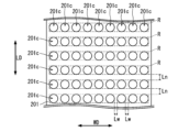
- at least a portion of the recessed portion 201c is arranged in a plurality of band-like regions R.
- Each of the plurality of regions R extends along a cross direction WD crossing the longitudinal direction LD of the anode portion.
- FIG. 3 shows an example in which the cross direction WD is perpendicular to the longitudinal direction LD.
- the interval between the concave portions 201c in the cross direction WD is defined as the interval Lw.
- the interval between two adjacent regions R is defined as Ln.
- Lw may be shorter than Ln.
- the intervals between the recesses 201c differ depending on the location.
- the interval between the concave portions 201c may be narrowed in a portion where adhesion is desired to be enhanced or in a portion where prevention of intrusion of oxygen or the like is particularly important.
- the interval between the recesses 201c on the first surface 201a in contact with the exterior body 140 may be narrower than the interval between the recesses 201c on the second surface 201b in contact with the conductive adhesive layer .
- the interval between the recesses 201c in the portion near the surface of the exterior body 140 may be narrower than the interval between the recesses 201c existing inside. An example of such an arrangement is shown in FIG. In the example shown in FIG. 5, the interval between the concave portions 201c is narrowed on the surface side of the exterior body.
- the arrangement of the concave portions 201c may be a matrix arrangement or may be a non-matrix arrangement.
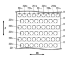
- the position of the concave portion 201c in the cross direction WD differs depending on the regions R.
- the plurality of recesses 201c are arranged in a zigzag pattern. Note that the arrangement of at least some of the concave portions 201c may not be a matrix arrangement, not limited to the arrangement shown in FIG. 6, but also in other arrangements.
- a part of the plurality of recesses 201c may include at least one groove-shaped first recess 201c1 and a plurality of non-groove-shaped second recesses 201c2.
- An example of the arrangement of such recesses 201c is shown in FIGS. 7 and 8.
- FIG. 7 and 8 An example of the arrangement of such recesses 201c is shown in FIGS. 7 and 8. FIG.
- the plurality of recesses 201c includes a groove-shaped first recess 201c1 and a plurality of non-groove-shaped second recesses 201c2.
- the first concave portion 201c1 extends linearly so as to intersect the longitudinal direction LD.
- the first recessed portion 201c1 extends over substantially the entire width of the embedded portion 201.
- FIG. 7 shows the length L1 of the opening along the extending direction of the opening of the first recess 201c1 and the width W1 of the opening.
- the length L1 and the width W1 satisfy the relationship described above.
- FIG. 8 shows an example of an arrangement using such first recesses 201c1.
- the plurality of recesses 201c are arranged in a strip-shaped region R. As shown in FIG. Each region R is provided with one first recess 201c1 and a plurality of second recesses 201c2.
- the recess 201c2 has a circular opening.
- the position where the first recess 201c1 is formed and in the cross direction WD, and in the other region R adjacent to the one region R This is the position where the first concave portion 201c1 is formed and is different from the position in the cross direction WD.
- the recesses 201c1 are preferably arranged such that a line passing through two adjacent regions R and orthogonal to the cross direction WD always passes through at least one recess 201c1. This makes it possible to particularly suppress the intrusion of oxygen and the like.
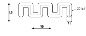
- the groove-shaped first recess 201c1 extends linearly. However, at least one first recess 201c1 may not be linear. Examples of the shape of such an opening of the first recess 201c1 are shown in FIGS. 9 and 10. FIG.
- Each of the first recesses 201c1 shown in FIGS. 9 and 10 extends zigzag.
- the length L1 of the opening of the first concave portion 201c1 along the extending direction is the length along the dotted line in FIGS. 9 and 10 .
- a dotted line shown in FIGS. 9 and 10 is a line passing through the center of the opening in the width direction.
- the shape of the opening of the second recess 201c2 is circular.
- the shape of the opening of the recess 201c (the shape of the opening of the recess 201c2) may be other shapes than the circular shape described above.
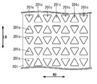
- FIG. 11 shows an example of a recess 201c whose opening has a substantially triangular shape.
- the shape of the opening of the recess 201c in FIG. 11 is substantially triangular.
- the side surface of the embedded portion 201 may be processed to be uneven.
- a top view of an example of such embedded portion 201 is shown in FIG.
- a side surface 201s of the embedded portion 201 shown in FIG. 12 is processed to be uneven.
- the side surface 201s is formed with a plurality of concave portions 201sc and convex portions existing therebetween.
- Such irregularities may be formed when the shape of the lead frame is formed by punching, laser irradiation, or the like.
- the solid electrolytic capacitor according to this embodiment includes a capacitor element including an anode portion and a cathode portion, an anode lead frame electrically connected to the anode portion, a cathode lead frame electrically connected to the cathode portion, a capacitor and an exterior covering the element.
- the anode lead frame includes a first embedded portion that is part of the anode lead frame and is embedded in the housing, and the cathode lead frame is part of the cathode lead frame and is embedded in the housing.
- a second embedded portion is included.
- a plurality of recesses are formed in the surface of the buried portion (the first buried portion and the second buried portion).
- a lead frame (anode lead frame, cathode lead frame) includes a substrate and a plated layer formed on the surface of the substrate. No plated layer exists in the plurality of recesses. A plated layer exists in a region between the plurality of recesses on the surface of the embedded portion. In other words, the plurality of recesses are formed so as to partially remove the plating layer.
- Oxygen and the like easily reach the electrolyte layer through the interface between the embedded portion and the exterior body.
- a plurality of recesses (C) are formed on the surface of the embedded portion.
- the penetration path of oxygen and the like through the interface between the embedded portion and the exterior body is lengthened, so that the oxygen and the like is less likely to reach the electrolyte layer.
- the plurality of recesses (C) increase the surface area of the embedded portion and the anchor effect, thereby improving the adhesion between the embedded portion and the exterior body. These can suppress deterioration of the electrolyte layer due to intrusion of oxygen or the like. As a result, deterioration of the capacitor element can be suppressed, and a highly reliable solid electrolytic capacitor can be obtained.
- a plated layer is formed on the surface of the embedded portion of the lead frame.
- the adhesion between the plated layer and the exterior body can be made higher than the adhesion between the base material of the lead frame and the exterior body. Therefore, deterioration of the capacitor element can be particularly suppressed.
- the plating layer of the lead frame is formed to improve the solderability of the terminal portion (described later) of the exposed portion of the lead frame. Since forming the plated layer only on the terminal portion complicates the manufacturing process, the plated layer is usually formed not only on the exposed portion but also on the embedded portion.
- a plating layer is usually formed on both the base material of the anode lead frame and the base material of the cathode lead frame.
- a plurality of recesses (C) are preferably formed in both the first embedded portion of the anode lead frame and the second embedded portion of the cathode lead frame. However, the plurality of recesses (C) may be formed in only one of those buried portions.
- the recess (C) may be formed on both main surfaces of the lead frame, or may be formed on only one main surface of the lead frame.
- the surface in contact with the exterior body may be hereinafter referred to as the "first surface”, and the surface of the embedded portion in contact with the conductive adhesive layer (described later) is hereinafter referred to as the "second surface.” ” may be called.
- a plurality of recesses (C) are formed in the first surface and/or the second surface.
- a plurality of recesses (C) are preferably formed in at least the first surface, and may be formed in the first and second surfaces.
- a plurality of recesses (C) may be formed on the surface of the first embedded portion and the surface of the second embedded portion. Furthermore, the surfaces of the buried portions (the first and second buried portions) where the plurality of recesses (C) are not formed may be covered with a plating layer.
- the average thickness of the plated layer may be 0.1 ⁇ m or more, or 0.5 ⁇ m or more, and may be 50 ⁇ m or less, or 10 ⁇ m or less.
- the plated layer may have an average thickness of 0.1 ⁇ m or more and 10 ⁇ m or less.
- the average thickness of the plated layer can be obtained, for example, by measuring the thickness at arbitrary 10 points from a photograph of the cross section and averaging the measured thicknesses. In addition, you may measure the thickness of ten arbitrary points
- the description of the configuration similar to that described in the first embodiment will be omitted.
- the depth of the plurality of recesses (C) is preferably larger than the average thickness of the plated layer.
- the depth of the recess (C) can be changed by the power of the laser beam irradiated to form the recess (C).
- the base material of the lead frame may be exposed at the bottoms of the plurality of recesses (C).
- the exterior body is in close contact with both the base material and the plating layer on the inner surface of the recess (C). As a result, peeling of the plated layer from the substrate is suppressed by the exterior body.
- the plated layer is made of metal (including alloys) such as nickel, gold, palladium, tin, and copper, and may include a nickel layer, a gold layer, a palladium layer, a tin layer, a copper layer, and the like.
- plating layers may be formed on the lead frame in the order of a nickel layer, a gold layer, and a palladium layer.
- the plurality of recesses (C) may include recesses with circular openings, recesses with non-circular openings, or both. Examples of recesses having non-circular openings include recesses obtained by forming a plurality of recesses having circular openings so that they partially overlap.
- non-circular shapes include shapes in which only a small portion of two adjacent circles overlap, and shapes in which a large portion of two adjacent circles overlap. Examples of non-circular shapes also include the shape of a trajectory when a circle is displaced. Examples of non-circular shapes include elliptical, oblong, oval, and the like.
- the plurality of recesses (C) may include at least one groove-shaped recess.
- the area S1 of the surface of the embedded portion covered with the plating layer may be 10% or more and 90% or less of the area S0 of the surface of the embedded portion.
- the area S1 may be 10% or more, 20% or more, 30% or more, or 40% or more of the area S0.
- the area S1 may be 90% or less, 80% or less, 70% or less, or 60% or less of the area S0.
- Area S1 and area S0 are apparent areas, respectively.
- the apparent area of the surface is the area of the surface assuming that the surface is flat without irregularities such as recesses (C), and can be calculated from the outline of the target portion.
- the apparent surface area of the embedded portion can be calculated from the outline of the embedded portion.
- the leadframe (anode lead frame and cathode lead frame) includes a substrate and a plating layer formed on the substrate.
- the base material is made of metal (copper, copper alloy, etc.).
- the thickness of the substrate is not particularly limited, and may be in the range of 25 ⁇ m to 200 ⁇ m (for example, in the range of 25 ⁇ m to 100 ⁇ m).
- the plated layer is made of metal (including alloys) such as nickel, gold, palladium, tin, and copper, and may include a nickel layer, a gold layer, a palladium layer, a tin layer, a copper layer, and the like.
- plated layers may be laminated on the substrate in the order of a nickel layer, a gold layer, and a palladium layer.
- the plated layer can be formed by a known plating method.
- the recess (C) is formed in the lead frame.
- the anode lead frame is electrically connected to the anode section.
- the anode lead frame includes a first embedded portion embedded in the outer package and an exposed portion exposed from the outer package.
- the first embedded portion and the anode portion may be connected by welding or the like. At least part of the exposed portion functions as a terminal portion.
- the terminal portion is a portion to which soldering or the like is performed.
- the cathode lead frame is electrically connected to the cathode section.
- the cathode lead frame includes a second embedded portion embedded in the outer package and an exposed portion exposed from the outer package.
- the second embedded portion and the cathode portion may be connected by a conductive adhesive layer. At least part of the exposed portion functions as a terminal portion.
- the terminal portion is a portion to which soldering or the like is performed.
- the manufacturing method (M) is a solid electrolyte comprising a capacitor element including an anode portion and a cathode portion, an anode lead frame electrically connected to the anode portion, and a cathode lead frame electrically connected to the cathode portion.
- a method for manufacturing a capacitor includes a first embedded portion that is part of the anode leadframe and the cathode leadframe includes a second embedded portion that is part of the cathode leadframe.
- Production method (M) includes step (i), step (ii), and step (iii) in this order. These steps are described below.
- the step (i) includes a step of forming a plurality of recesses (C) in the surface of the buried portion by irradiating the buried portion (the first buried portion, the second buried portion) with a laser beam a plurality of times.
- Step (i) may include step (ia) and step (ib) described below in this order.
- Step (ia) is a step of preparing a lead frame (anode lead frame, cathode lead frame) including a base material and a plated layer formed on the base material.
- the plated layer is formed on at least the surface of the terminal portion and the surface of the embedded portion among the surfaces of the base material.
- the plated layer is usually formed on the entire surface of the substrate.
- Step (ia) may be carried out by plating the substrate that will become the leadframe (eg, a metal sheet that includes the portion that will become the leadframe).
- the method of forming the plated layer is not limited, and it may be formed by a known method.
- a plurality of recesses (C) are formed by irradiating the plated layer on the embedded portion with a laser beam a plurality of times so that the plated layer remains in the regions between the plurality of recesses (C). It is a process of forming.
- a plated layer exists on the surface of the embedded portion where the recess (C) is formed. Therefore, when the recess (C) is formed, at least part of the plated layer in the recess (C) is removed, and the plated layer other than the recess (C) remains without being removed. When the recesses (C) are formed to reach the base material, the plated layer in the recesses (C) is removed, while the plated layer remains on the surface between the recesses (C).
- a plurality of recesses (C) may all be formed under the same conditions (for example, the same laser beam). Alternatively, some of the multiple recesses (C) may be formed under different conditions (for example, different laser beams). In that case, the recesses formed under different conditions can have different sizes and shapes. Incidentally, not only the buried portion but also the exposed portion may be irradiated with the laser beam to form a plurality of concave portions on the surfaces of the buried portion and the exposed portion.
- the formation of the recesses (C) can be performed using a known laser processing device capable of forming recesses in metal.
- the laser beam to be irradiated there is no particular limitation on the laser beam to be irradiated as long as the concave portion (C) can be formed.
- the wavelength of the laser light may be 1100 nm or less, 700 nm or less (eg, 600 nm or less), or 300 nm or more (eg, 350 nm or more).
- the wavelength of the laser light may be 1064 nm (near infrared laser), 532 nm (visible light laser), or 355 nm (ultraviolet laser).
- the plurality of recesses (C) may be recesses formed by irradiating laser light with a wavelength of 300 nm or more and 1100 nm or less (for example, 300 nm or more and 600 nm or less).
- the formation of the plurality of recesses (C) may be performed by scanning with laser light. Alternatively, it may be performed by moving the laser processing machine and/or the lead frame.
- the laser light may be pulsed laser light or continuous wave laser light (CW laser light).
- a concave portion having a circular opening may be formed by irradiating a pulsed laser beam.
- a concave portion having a non-circular opening may be formed by irradiating pulsed laser light a plurality of times so that a part of the irradiated portion overlaps.
- recesses with non-circular openings may be formed by irradiating CW laser light (continuous wave laser light).
- a preferred example of laser light for forming the recesses (C) is laser light with a wavelength of 355 nm.
- the light source of laser light with a wavelength of 355 nm is not particularly limited, and a third harmonic such as YVO 4 laser may be used.
- a metal sheet including a plurality of lead frame portions and having a plated layer formed thereon is prepared.
- the recess (C) is formed by irradiating the portion of the metal sheet where the recess (C) is to be formed with a laser beam.
- unnecessary portions of the metal sheet are removed by known metal processing.
- the portions of the lead frame that need to be bent are bent by known metal processing. The metal sheet processed in this way is used in the next step (ii).
- Step (ii) is a step of electrically connecting the first embedded portion to the anode portion of the capacitor element and electrically connecting the second embedded portion to the cathode portion of the capacitor element.
- connection methods are not particularly limited, and known connection methods may be used.
- the first embedded portion may be connected to the anode portion by welding.
- the second embedded portion may be electrically connected to the cathode portion via a conductive adhesive layer containing conductive particles.
- a metal paste may be used to connect the cathode portion and the second embedded portion. If a recess (C) is formed in the surface of the second embedded portion that contacts the conductive adhesive layer, the conductive adhesive layer enters the recess (C).
- the step (iii) is a step of covering the embedded portion and the capacitor element with the exterior body.
- Step (iii) can be performed by a known method. Specifically, the step (iii) can be carried out by coating the embedding portion and the capacitor element with a resin composition that forms the exterior body and then curing the resin composition. At this time, the exterior body enters into the recess formed in the embedded portion.
- An exterior body containing a resin (insulating resin) and an insulating filler can be used as the exterior body.
- a solid electrolytic capacitor can be manufactured as described above.
- a plurality of recesses are formed at intervals on the surface of the embedded portion of the solid electrolytic capacitor according to the present embodiment.
- Recesses 201 c are formed in both first surface 201 a of anode lead frame 210 and first surface 201 a of cathode lead frame 220 .
- FIG. 13A and 13B show an example of arrangement of recesses 201c in the embedded portion 201 (the first embedded portion 211 and the second embedded portion 221).
- FIG. 13A is a diagram of the buried portion 201 viewed from the upper surface 100t side. A cross-section taken along line BB of FIG. 13A is shown in FIG. 13B.
- the plurality of recesses 201c are arranged in a matrix at regular intervals L from each other.
- the placement of recesses 201c on one surface of embedded portion 201 is the same as the placement of recesses 201c on the other surface.
- the arrangement of the plurality of recesses 201c is not limited to the arrangement shown in FIGS. 13A and 13B, and other arrangements may be used. Further, in FIG. 13B, the cross-sectional shape of the concave portion 201c is typically hemispherical, but the cross-sectional shape of the concave portion 201c may not be hemispherical.
- lead frame 200 (anode lead frame 210 and cathode lead frame 220) includes base material 200a and plated layers 200b formed on both sides of base material 200a.
- the plated layer 200b is formed on the surface of the buried portion 201 and the surface of the exposed portion 202 (surfaces of the terminal portion 212a and the terminal portion 222a).
- the plated layer formed on the surface of the embedded portion 201 and the plated layer formed on the surface of the exposed portion 202 are connected without being separated.
- Recesses 201 c are formed on both sides of the embedded portion 201 of the lead frame 200 .
- the plated layer 200b in the portion of the recess 201c is removed.
- a plated layer 200b exists (remains) on the first surface 201a of the embedded portion 201 and between the plurality of recesses 201c.
- the base material 200a is exposed at the bottom of the recess 201c. That is, the concave portion 201c is formed so as to reach the base material 200a and cut a part of the base material 200a.
- the shape of the opening Op of the recess 201c is circular.
- the concave portion 201c As described above, by forming the concave portion 201c, the deterioration of the capacitor element 110 (e.g., increase in ESR) can be suppressed. As a result, the reliability of electrolytic capacitor 100 can be improved. Further, by forming recess 201c in the surface of second embedded portion 221 of cathode lead frame 220 that is in contact with conductive adhesive layer 130, the resistance between conductive adhesive layer 130 and cathode lead frame 220 is reduced. can be reduced. As a result, the characteristics of electrolytic capacitor 100 can be improved.
- the concave portion 201c the deterioration of the capacitor element 110 (e.g., increase in ESR) can be suppressed. As a result, the reliability of electrolytic capacitor 100 can be improved. Further, by forming recess 201c in the surface of second embedded portion 221 of cathode lead frame 220 that is in contact with conductive adhesive layer 130, the resistance between conductive adhesive layer 130 and cathode lead
- the solid electrolytic capacitor according to this embodiment includes a capacitor element including an anode portion and a cathode portion, an anode lead frame electrically connected to the anode portion, and a cathode portion via a conductive adhesive layer containing conductive particles. It includes an electrically connected cathode lead frame and an exterior covering the capacitor element.
- the anode lead frame includes a first embedded portion that is part of the anode lead frame and is embedded in the housing, and the cathode lead frame is part of the cathode lead frame and is embedded in the housing. A second embedded portion is included.
- the embedded part (first embedded part, second embedded part) has a first surface in contact with the exterior body, and the second embedded part has a second surface in contact with the conductive adhesive layer.
- a plurality of first recesses are formed in the first surface.
- the exterior body includes resin and insulating filler.
- the average diameter D1 of the openings of the plurality of first recesses and the average particle size P1 of the insulating filler satisfy 0 ⁇ P1/D1 ⁇ 1.
- a plurality of recesses are formed on the surface of the embedded portion.
- the said recessed part may be called “recessed part (C).”
- the plurality of recesses (C) includes a plurality of first recesses formed on the first surface in contact with the exterior body.
- the first recess may be formed only in the first buried portion, may be formed only in the second buried portion, or may be formed in both of them.
- the recess (C) may be formed on both main surfaces of the lead frame, or may be formed on only one main surface of the lead frame.
- Oxygen and the like easily reach the electrolyte layer through the interface between the embedded portion and the exterior body.
- a plurality of recesses (C) are formed on the surface of the embedded portion.
- the penetration path of oxygen and the like through the interface between the embedded portion and the exterior body is lengthened, so that the oxygen and the like is less likely to reach the electrolyte layer.
- the plurality of concave portions increase the surface area of the embedded portion and the anchor effect, thereby improving the adhesion between the embedded portion and the exterior body. These can suppress deterioration of the electrolyte layer due to intrusion of oxygen or the like. As a result, deterioration of the capacitor element can be suppressed, and a highly reliable solid electrolytic capacitor can be obtained.
- the average diameter D1 and the average particle diameter P1 of the insulating filler satisfy 0 ⁇ P1/D1 ⁇ 1. This makes it easier for the insulating filler to enter the first recess. Since the insulating filler having a small thermal expansion is present in the first recess, it is possible to suppress deterioration in adhesion between the lead frame and the exterior body due to temperature change. As a result, deterioration of the electrolyte layer due to intrusion of oxygen or the like can be particularly suppressed.
- the ratio P1/D1 between the average particle size P1 and the average diameter D1 may be greater than 0, 0.1 or more, 0.3 or more, or 0.5 or more.
- the ratio P1/D1 is less than 1 and may be 0.9 or less, or 0.8 or less. From the viewpoint of suppressing penetration of oxygen and the like, it is preferable that the average diameter D1 and the average particle diameter P1 satisfy 0.5 ⁇ P1/D1 ⁇ 0.8.
- the average diameter D1 may be 0.1 ⁇ m or more, 1 ⁇ m or more, 3 ⁇ m or more, 5 ⁇ m or more, 10 ⁇ m or more, or 20 ⁇ m or more, and may be 300 ⁇ m or less, 250 ⁇ m or less, 200 ⁇ m or less, 100 ⁇ m or less, or 50 ⁇ m or less. good.
- the average diameter D1 may be in the range of 0.1 ⁇ m to 300 ⁇ m (eg, 5 ⁇ m to 100 ⁇ m, 10 ⁇ m to 100 ⁇ m, 10 ⁇ m to 50 ⁇ m).
- a circle equivalent diameter can be used for the diameter of the opening of each recess.
- the equivalent circle diameter is obtained by the following method. First, the opening of the recess is photographed from above. Next, the area of the opening is obtained by image processing the obtained image. Next, the equivalent circle diameter is calculated from the obtained area.
- the average diameter D1 is obtained by calculating the diameter of the opening (equivalent circle diameter) for each of the 20 arbitrarily selected recesses and arithmetically averaging the obtained diameters. Note that the average diameter D2, which will be described later, is also obtained by the same method as for the average diameter D1.
- the average particle diameter P1 is the median diameter (D50) at which the cumulative volume is 50% in the volume-based particle size distribution.
- the median diameter is determined using a laser diffraction/scattering particle size analyzer.
- the average particle diameter P2 which will be described later, is also the median diameter (D50), and is obtained by the same method as for the average particle diameter P1.
- a plurality of second recesses may be formed on the second surface in contact with the conductive adhesive layer.
- the plurality of recesses (C) may include a plurality of first recesses and a plurality of second recesses. Descriptions of the recess (C) are applicable to the first recess and the second recess unless otherwise specified.
- the average diameter D2 of the openings of the plurality of second recesses and the average particle diameter P2 of the conductive particles may satisfy 1.2 ⁇ D2/P2.
- This configuration makes it easier for the conductive particles to enter the second recess. As a result, the resistance between the second buried portion and the cathode portion can be reduced.
- the presence of the conductive particles with small thermal expansion in the second recess can suppress deterioration in adhesion between the lead frame and the conductive adhesive layer due to temperature changes. As a result, deterioration of the electrolyte layer due to intrusion of oxygen or the like and an increase in internal resistance can be particularly suppressed.
- the ratio D2/P2 between the average diameter D2 and the average particle diameter P2 may be less than 1.2, preferably 1.2 or more, and may be 2 or more.
- the ratio D2/P2 may be 20 or less, or 15 or less.
- the average diameter D2 may be 5 ⁇ m or more, 10 ⁇ m or more, or 20 ⁇ m or more, and may be 500 ⁇ m or less, 400 ⁇ m or less, 300 ⁇ m or less, or 100 ⁇ m or less.
- the average diameter D2 may be in the range of 5 ⁇ m to 500 ⁇ m (eg, in the range of 5 ⁇ m to 100 ⁇ m).
- the average diameter D2 may be larger than the average diameter D1. Alternatively, the average diameter D2 may be less than or equal to the average diameter D1.
- the average value Dmin(1) of the shortest diameters of the openings of the plurality of first recesses and the average particle diameter P1 may satisfy a predetermined relationship. Specifically, the ratio P1/Dmin(1) may satisfy the above relationship that the ratio P1/D1 satisfies. Further, in the solid electrolytic capacitor of the present embodiment, the average value Dmin(2) of the shortest diameters of the openings of the plurality of second recesses and the average particle size P2 may satisfy a predetermined relationship. Specifically, the ratio Dmin(2)/P2 may satisfy the above relationship satisfied by the ratio D2/P2.
- the shortest diameter of the opening of the recess is the shortest diameter of the diameters passing through the center of gravity of the opening of the recess.
- the shortest diameter can be obtained as follows. First, images of the openings of the recesses are acquired by photographing the plurality of recesses from above. By image analysis of the image, the center of gravity and the shortest diameter of the opening can be obtained. The average of the shortest diameters of the openings is obtained by finding the shortest diameters for each of 20 arbitrarily selected openings in the image and arithmetically averaging the found 20 shortest diameters.
- the present disclosure provides another solid electrolytic capacitor.
- the ratio P1/D1 satisfies the above relationship is not limited, but the ratio P1/Dmin(1) satisfies the above relationship that the ratio P1/D1 satisfies.
- the ratio Dmin(2)/P2 may satisfy the above relationship satisfied by the ratio D2/P2. Except for these relationships, the solid electrolytic capacitor is the same as the solid electrolytic capacitor according to the present embodiment, and redundant description will be omitted.
- the recess (C) can be formed by irradiating the lead frame with laser light (for example, pulsed laser light).
- laser light for example, pulsed laser light
- Each of the plurality of first recesses and the plurality of second recesses can be formed by irradiating laser light.
- Forming the recesses (C) by irradiating laser light has the following advantages compared to roughening the surface by sandblasting, etching, or the like. First, since variations in the shape and size of the recess (C) can be reduced, it is possible to stably secure the adhesion (airtightness) between the lead frame and the exterior body.
- the size of the recess (C) can be controlled according to the size of the insulating filler in the exterior body and the conductive particles in the conductive adhesive layer, the above-mentioned adhesion (airtightness) can be further improved. is possible.
- the size, shape, and arrangement pattern of the recesses (C) can be changed depending on the location, it is possible to further improve the adhesion (airtightness).
- recesses (C) By forming the recesses (C) with a laser beam, recesses of uniform size and shape can be formed at desired locations. For example, it is possible to control the diameter of the opening of the first concave portion to be in the range of 50% to 150% of the average diameter D1. Similarly, it is also possible to control the diameter of the opening of the second recess so as to be in the range of 50% to 150% of the average diameter D2.
- the depth of the plurality of recesses (C) may be 0.5 ⁇ m or more, 2 ⁇ m or more, or 10 ⁇ m or more, and may be 100 ⁇ m or less, 50 ⁇ m or less, or 30 ⁇ m or less.
- the depth of the recess (C) may be 2 ⁇ m or more and 50 ⁇ m or less.
- the depth of the recess (C) can be changed by the power of the laser beam irradiated to form the recess (C).
- the plurality of recesses (C) may include recesses with circular openings, recesses with non-circular openings, or both.
- Examples of recesses having non-circular openings include recesses obtained by forming a plurality of recesses having circular openings so that they partially overlap.
- Examples of non-circular shapes include shapes in which only a small portion of two adjacent circles overlap, and shapes in which a large portion of two adjacent circles overlap. Examples of non-circular shapes also include the shape of a trajectory when a circle is displaced. Examples of non-circular shapes include elliptical, oblong, oval, and the like.
- the plurality of recesses (C) may include at least one groove-shaped recess.
- a plurality of recesses (C) may be formed in the entire lead frame. Alternatively, the plurality of recesses (C) may be formed only on the surface of the buried portion without being formed on the exposed portion exposed from the exterior body. A plurality of recesses (C) may be formed only in part of the buried portion.
- the ratio of the area Sc occupied by the opening of the recess (C) to the apparent area Sa of the surface of the embedded portion (Sc/Sa) is 5% or more, 10% or more, 20% or more, or 30% or more. 90% or less, 80% or less, 70% or less, 60% or less, 50% or less, 40% or less, 30% or less, or 20% or less.
- the apparent area of the surface of the embedded portion is the area when it is assumed that the surface is flat without the concave portion (C), and can be calculated from the outer shape of the embedded portion.
- the ratio (Sc1/Sa1) of the area Sc1 occupied by the opening of the first recess formed in the first embedded portion to the apparent area Sa1 of the surface of the first embedded portion (Sc/Sa ) may be within the range exemplified for.
- the ratio (Sc2/Sa2) of the area Sc2 occupied by the opening of the recess (C) formed in the second embedded portion to the apparent area Sa2 of the surface of the second embedded portion (Sc/Sa ) may be within the range exemplified for.
- the ratio (Sc/Sa), the ratio (Sc1/Sa1), and the ratio (Sc2/Sa2) may be the same or different.
- anode lead frame and cathode lead frame As described above, the lead frame is formed with the recess (C).
- the anode lead frame is electrically connected to the anode section.
- the anode lead frame includes a first embedded portion embedded in the outer package and an exposed portion exposed from the outer package. At least part of the exposed portion functions as a terminal portion.
- the terminal portion is a portion to which soldering or the like is performed.
- the first embedded portion and the anode portion can be connected by welding or the like.
- the cathode lead frame is electrically connected to the cathode section.
- the cathode lead frame includes a second embedded portion embedded in the outer package and an exposed portion exposed from the outer package. At least part of the exposed portion functions as a terminal portion.
- the terminal portion is a portion to which soldering or the like is performed.
- the lead frames are made of metal (copper, copper alloy, etc.).
- the lead frame before forming the recess (C) may be formed by processing a metal sheet (including metal plate and metal foil) made of metal (copper, copper alloy, etc.) by a known metal processing method. good.
- the thickness of the lead frame is not particularly limited, and may be in the range of 25 ⁇ m to 200 ⁇ m (for example, in the range of 25 ⁇ m to 100 ⁇ m).
- the lead frame may include a plated layer formed on the surface.
- the lead frame includes a base material made of metal (copper, copper alloy, etc.) and a plated layer formed on the base material.
- the plated layer is made of metal (including alloys) such as nickel, gold, palladium, tin, and copper, and may include a nickel layer, a gold layer, a palladium layer, a tin layer, a copper layer, and the like.
- plating layers may be formed on the lead frame in the order of a nickel layer, a gold layer, and a palladium layer.
- the conductive adhesive layer contains conductive particles.
- conductive particles include metal particles (eg, silver particles).
- the conductive adhesive layer can be formed using a metal paste (for example, silver paste) containing metal particles and resin.
- the exterior body is arranged around the capacitor element so that the capacitor element is not exposed on the surface of the electrolytic capacitor. Furthermore, the exterior body is arranged so as to cover the buried portion of the anode lead frame and the buried portion of the cathode lead frame.
- the exterior body can be made of a resin composition containing an insulating resin and an insulating filler (for example, an inorganic filler).
- the resin composition may contain a curing agent, a polymerization initiator, and/or a catalyst in addition to the insulating resin and insulating filler.
- insulating resins include insulating thermosetting resins and insulating thermoplastic resins.
- examples of insulating resins include epoxy resin, phenolic resin, urea resin, polyimide, polyamideimide, polyurethane, diallyl phthalate, unsaturated polyester, polyphenylene sulfide (PPS), polybutylene terephthalate (PBT), and the like. is included.
- insulating fillers include insulating particles and insulating fibers.
- the insulating material that constitutes the insulating filler include insulating compounds (such as oxides) such as silica and alumina, glass, and mineral materials (such as talc, mica, and clay).
- the insulating filler contained in the exterior body may be of one type, or may be of two or more types.
- the content of the insulating filler in the exterior body is not particularly limited, and may be in the range of 30% by mass to 95% by mass (for example, the range of 50% by mass to 90% by mass).
- the manufacturing method of the present embodiment for manufacturing a solid electrolytic capacitor will be described below with an example, but the description of the same configuration as that described in the first embodiment will be omitted.
- the manufacturing method (M) is a solid electrolyte comprising a capacitor element including an anode portion and a cathode portion, an anode lead frame electrically connected to the anode portion, and a cathode lead frame electrically connected to the cathode portion.
- a method for manufacturing a capacitor is a first embedded portion that is part of the anode leadframe and the cathode leadframe includes a second embedded portion that is part of the cathode leadframe.
- the embedded portion includes a first surface that is the surface of the first and second embedded portions and a second surface that is the surface of the second embedded portion and is different from the first surface.
- Production method (M) includes step (i), step (ii), and step (iii) in this order. These steps are described below.
- the step (i) is a step of forming a plurality of recesses (C) on the surface of the embedded portion by irradiating the embedded portion with laser light multiple times.
- the step (i) includes forming a plurality of first recesses in the first surface by irradiating the first surface of the buried portion with the first laser beam a plurality of times.
- the step (i) may include forming a plurality of second recesses in the second surface by irradiating the second surface of the second embedded portion with the second laser light a plurality of times.
- the first recess and the second recess may be formed under the same conditions using the same laser beam. Alternatively, the first recess and the second recess may be formed under different conditions using different laser beams.
- a plurality of concave portions may be formed also on the surface of the exposed portion by irradiating the exposed portion other than the embedded portion with the laser beam.
- a plurality of recesses (C) may all be formed under the same conditions (for example, the same laser beam). Alternatively, some of the multiple recesses (C) may be formed under different conditions (for example, different laser beams). In that case, the recesses formed under different conditions can have different sizes and shapes. Incidentally, not only the buried portion but also the exposed portion may be irradiated with the laser beam to form a plurality of concave portions on the surfaces of the buried portion and the exposed portion.
- the formation of the recesses (C) can be performed using a known laser processing device capable of forming recesses in metal.
- the laser beam to be irradiated there is no particular limitation on the laser beam to be irradiated as long as the concave portion (C) can be formed.
- the wavelength of the laser light may be 1100 nm or less, 700 nm or less (eg, 600 nm or less), or 300 nm or more (eg, 350 nm or more).
- the wavelength of the laser light may be 1064 nm (near infrared laser), 532 nm (visible light laser), or 355 nm (ultraviolet laser).
- the plurality of recesses (C) may be recesses formed by irradiating laser light with a wavelength of 300 nm or more and 1100 nm or less (for example, 300 nm or more and 600 nm or less).
- the formation of the plurality of recesses (C) may be performed by scanning with laser light. Alternatively, it may be performed by moving the laser processing machine and/or the lead frame.
- the laser light may be pulsed laser light or continuous wave laser light (CW laser light).
- a concave portion having a circular opening may be formed by irradiating a pulsed laser beam.
- a concave portion having a non-circular opening may be formed by irradiating pulsed laser light a plurality of times so that a part of the irradiated portion overlaps.
- recesses with non-circular openings may be formed by irradiating CW laser light (continuous wave laser light).
- a preferred example of laser light for forming the recess (C) is laser light with a wavelength of 355 nm.
- the light source of laser light with a wavelength of 355 nm is not particularly limited, and a third harmonic such as YVO4 laser may be used.
- the diameter and average diameter D1 of the first recess and the diameter and average diameter D2 of the second recess can be controlled by changing the irradiation conditions of the laser light (for example, laser output and laser light spot diameter). For example, when increasing the diameter and average diameter of the recesses, the spot diameter of the laser beam may be increased.
- step (i) first, a metal sheet including portions that will become a plurality of lead frames is prepared.
- the recess (C) is formed by irradiating the portion of the metal sheet where the recess (C) is to be formed with a laser beam.
- unnecessary portions of the metal sheet are removed by known metal processing.
- portions of the lead frame that need to be bent are bent by known metal processing. The metal sheet processed in this way is used in the next step (ii).
- Step (ii) is a step of electrically connecting the first buried portion to the anode portion of the capacitor element and electrically connecting the second buried portion to the cathode portion of the capacitor element.
- connection methods are not particularly limited, and known connection methods may be used.
- the first embedded portion may be connected to the anode portion by welding.
- the second surface of the second embedded portion may be electrically connected to the cathode portion via a conductive adhesive layer containing conductive particles.
- a metal paste may be used to connect the cathode portion and the second surface. In this case, the conductive adhesive layer enters into the second recess.
- the step (iii) is a step of covering the embedded portion and the capacitor element with the exterior body.
- Step (iii) can be performed by a known method. Specifically, the step (iii) can be carried out by coating the embedding portion and the capacitor element with a resin composition that forms the exterior body and then curing the resin composition. At this time, the exterior body enters into the first recess.
- An exterior body containing a resin (insulating resin) and an insulating filler can be used as the exterior body.
- a solid electrolytic capacitor can be manufactured as described above.
- a solid electrolytic capacitor can be manufactured as described above.
- the average diameter D1 of the openings of the plurality of first recesses and the average particle diameter P1 of the insulating filler satisfy the above-described relationship.
- the average diameter D2 of the openings of the plurality of second recesses and the average particle diameter P2 of the conductive particles satisfy the above-described relationship.
- the average particle size P1 and average particle size P2 can be controlled by selecting the insulating filler and conductive particles to be used.
- FIG. 14 schematically shows a cross-sectional view of a solid electrolytic capacitor 100 (hereinafter referred to as "electrolytic capacitor 100") of the third embodiment.
- electrolytic capacitor 100 a solid electrolytic capacitor 100 of the third embodiment.
- the anode section includes an anode body and an anode wire will be described.
- the electrolytic capacitor 100 includes a capacitor element 110, a lead frame 200, a conductive adhesive layer 130, and an exterior body 140.
- Leadframe 200 includes an anode leadframe 210 and a cathode leadframe 220 .
- Capacitor element 110 includes anode portion 111 , dielectric layer 114 and cathode portion 115 .
- Anode section 111 includes anode body 113 and anode wire 112 .
- Anode body 113 is a rectangular parallelepiped porous sintered body, and dielectric layer 114 is formed on the surface thereof.
- a part of anode wire 112 protrudes from one end surface of anode body 113 toward front surface 100f of electrolytic capacitor 100 .
- the other portion of anode wire 112 is embedded in anode body 113 .
- Anode wire 112 extends along longitudinal direction LD of anode body 113 .
- Cathode portion 115 includes an electrolyte layer 116 arranged to cover at least a portion of dielectric layer 114 and a cathode layer 117 formed to cover at least a portion of electrolyte layer 116 .
- Anode lead frame 210 includes first embedded portion 211 embedded in exterior body 140 and exposed portion 212 exposed from exterior body 140 .
- the exposed portion 212 includes a terminal portion 212a functioning as an anode-side terminal.
- the surface on which the terminal portion 212a exists is sometimes referred to as the bottom surface 100b of the electrolytic capacitor 100.
- the surface facing bottom surface 100b may be referred to as top surface 100t of electrolytic capacitor 100 .
- the surface facing front surface 100f may be referred to as rear surface 100r of electrolytic capacitor 100 .
- the cathode lead frame 220 includes a second embedded portion 221 embedded in the exterior body 140 and an exposed portion 222 exposed from the exterior body 140 .
- the exposed portion 222 includes a terminal portion 222a functioning as a cathode-side terminal.
- the first embedded portion 211 and the second embedded portion 221 may be collectively referred to as the embedded portion 201
- the exposed portion 212 and the exposed portion 222 may be collectively referred to as the exposed portion 202 .
- Lead frame 200 includes embedded portion 201 and exposed portion 202 .
- the cathode lead frame 220 may be connected to the cathode section 115 at a portion other than the top surface 100t (for example, the bottom surface 100b side or the rear surface 100r side).
- the embedded portion 201 has a first surface 201a that contacts the exterior body 140 . Further, the embedded portion 201 has a second surface 201 b that is the surface of the second embedded portion 221 and contacts the conductive adhesive layer 130 . The second surface 201b is electrically connected to the cathode portion 115 (more specifically, the cathode layer 117) by a conductive adhesive layer 130. As shown in FIG.
- a plurality of recesses are formed at intervals on the surface of the embedded portion of the solid electrolytic capacitor according to the present embodiment.
- Multiple recesses 201c of electrolytic capacitor 100 include multiple first recesses 201c1 formed in first surface 201a and multiple second recesses 201c2 formed in second surface 201b.
- the plurality of recesses 201c includes a first recess 201c1 and a second recess 201c2 will be described.
- First recess 201c1 is formed on both first surface 201a of anode lead frame 210 and first surface 201a of cathode lead frame 220 .
- FIGS. 15A and 15B An example of the arrangement of the first recess 201c1 and the second recess 201c2 in the second embedded portion 221 is shown in FIGS. 15A and 15B.
- FIG. 15A is a diagram of the second embedded portion 221 viewed from the top surface 100t side.
- a cross section taken along line CC of FIG. 15A is shown in FIG. 15B.
- the plurality of first recesses 201c1 are arranged in a matrix at regular intervals L from each other.
- the second recesses 201c2 are arranged similarly to the first recesses 201c1.
- the arrangement of the plurality of recesses 201c is not limited to the arrangement shown in FIGS. 15A and 15B, and may be other arrangements.
- the cross-sectional shape of the concave portion 201c is typically hemispherical, but the cross-sectional shape of the concave portion 201c may not be hemispherical.
- the exterior body 140 includes insulating resin and insulating filler (not shown).
- Conductive adhesive layer 130 includes conductive particles (not shown).
- the exterior body 140 is inserted inside the first concave portion 201c1.
- the conductive adhesive layer 130 enters inside the second concave portion 201c2.
- the average diameter D1 of the openings Op1 of the plurality of first recesses 201c1 and the average particle diameter P1 of the insulating filler satisfy the above-described relationship.
- the average diameter D2 of the openings Op2 of the plurality of second recesses 201c2 and the average particle diameter P2 of the conductive particles preferably satisfy the above-described relationship.
- the concave portion 201c As described above, by forming the concave portion 201c, the deterioration of the capacitor element 110 (e.g., increase in ESR) can be suppressed. As a result, the reliability of electrolytic capacitor 100 can be improved. Moreover, the resistance between the conductive adhesive layer 130 and the cathode lead frame 220 can be reduced by forming the second concave portion 201c2. As a result, the characteristics of electrolytic capacitor 100 can be improved.
- the present disclosure can be used for solid electrolytic capacitors and manufacturing methods thereof.
- Solid electrolytic capacitor 110 Capacitor element 111 : Anode part 112 : Anode wire 113 : Anode body 114 : Dielectric layer 115 : Cathode part 116 : Electrolyte layer 117 : Cathode layer 130 : Conductive adhesive layer 140 : Exterior body 200 : Lead frame 200a: base material 200b: plating layer 201: embedded portion 201a: first surface 201b: second surface 201c: recess 201c1: first recess 201c2: second recesses 202, 212, 222: exposed portion 210 : Anode lead frame 211 : First buried portions 212a, 222a : Terminal portion 220 : Cathode lead frame 221 : Second buried portion Op : Opening Op1 : Opening Op2 : Opening R : Region
Landscapes
- Engineering & Computer Science (AREA)
- Power Engineering (AREA)
- Microelectronics & Electronic Packaging (AREA)
- Manufacturing & Machinery (AREA)
- Fixed Capacitors And Capacitor Manufacturing Machines (AREA)
Priority Applications (3)
| Application Number | Priority Date | Filing Date | Title |
|---|---|---|---|
| CN202280052069.1A CN117716458A (zh) | 2021-07-29 | 2022-07-12 | 固体电解电容器及固体电解电容器的制造方法 |
| US18/290,785 US20240242891A1 (en) | 2021-07-29 | 2022-07-12 | Solid electrolytic capacitor and method for producing solid electrolytic capacitor |
| JP2023538416A JPWO2023008185A1 (https=) | 2021-07-29 | 2022-07-12 |
Applications Claiming Priority (6)
| Application Number | Priority Date | Filing Date | Title |
|---|---|---|---|
| JP2021-124385 | 2021-07-29 | ||
| JP2021124385 | 2021-07-29 | ||
| JP2021141481 | 2021-08-31 | ||
| JP2021-141482 | 2021-08-31 | ||
| JP2021-141481 | 2021-08-31 | ||
| JP2021141482 | 2021-08-31 |
Publications (1)
| Publication Number | Publication Date |
|---|---|
| WO2023008185A1 true WO2023008185A1 (ja) | 2023-02-02 |
Family
ID=85086698
Family Applications (1)
| Application Number | Title | Priority Date | Filing Date |
|---|---|---|---|
| PCT/JP2022/027458 Ceased WO2023008185A1 (ja) | 2021-07-29 | 2022-07-12 | 固体電解コンデンサおよび固体電解コンデンサの製造方法 |
Country Status (3)
| Country | Link |
|---|---|
| US (1) | US20240242891A1 (https=) |
| JP (1) | JPWO2023008185A1 (https=) |
| WO (1) | WO2023008185A1 (https=) |
Families Citing this family (1)
| Publication number | Priority date | Publication date | Assignee | Title |
|---|---|---|---|---|
| JP2025056499A (ja) * | 2023-09-27 | 2025-04-08 | パナソニックIpマネジメント株式会社 | 電解コンデンサ |
Citations (5)
| Publication number | Priority date | Publication date | Assignee | Title |
|---|---|---|---|---|
| JP2006237195A (ja) * | 2005-02-24 | 2006-09-07 | Sanyo Electric Co Ltd | 固体電解コンデンサ |
| JP2008135460A (ja) * | 2006-11-27 | 2008-06-12 | Nichicon Corp | チップ状固体電解コンデンサ |
| JP2008277331A (ja) * | 2007-04-25 | 2008-11-13 | Nichicon Corp | 固体電解コンデンサ |
| JP2015230976A (ja) * | 2014-06-05 | 2015-12-21 | 株式会社村田製作所 | 固体電解コンデンサの製造方法および固体電解コンデンサ |
| WO2018061535A1 (ja) * | 2016-09-29 | 2018-04-05 | パナソニックIpマネジメント株式会社 | 固体電解コンデンサ |
Family Cites Families (10)
| Publication number | Priority date | Publication date | Assignee | Title |
|---|---|---|---|---|
| US6972943B2 (en) * | 2002-12-12 | 2005-12-06 | Sanyo Electric Co., Ltd. | Electronic component having lead frame |
| JP2005093591A (ja) * | 2003-09-16 | 2005-04-07 | Sanyo Electric Co Ltd | 固体電解コンデンサ |
| JP5268763B2 (ja) * | 2009-04-22 | 2013-08-21 | 三洋電機株式会社 | 固体電解コンデンサ |
| US8339771B2 (en) * | 2010-02-19 | 2012-12-25 | Avx Corporation | Conductive adhesive for use in a solid electrolytic capacitor |
| US9949378B2 (en) * | 2014-04-14 | 2018-04-17 | Presidio Components, Inc. | Electrical devices with solder dam |
| TWI559349B (zh) * | 2014-10-28 | 2016-11-21 | 鈺邦科技股份有限公司 | 導電端子改良之固態電解電容器封裝結構之製造方法 |
| JPWO2016117711A1 (ja) * | 2015-01-23 | 2017-11-02 | 古河電気工業株式会社 | 金属部材と樹脂モールドとの複合体および樹脂モールドとの複合体形成用金属部材 |
| WO2019065077A1 (ja) * | 2017-09-29 | 2019-04-04 | パナソニックIpマネジメント株式会社 | 電解コンデンサ |
| JP2020072186A (ja) * | 2018-10-31 | 2020-05-07 | パナソニックIpマネジメント株式会社 | 電解コンデンサ |
| JP2022049987A (ja) * | 2020-09-17 | 2022-03-30 | 株式会社村田製作所 | 積層セラミック電子部品、積層セラミック電子部品の実装構造 |
-
2022
- 2022-07-12 JP JP2023538416A patent/JPWO2023008185A1/ja active Pending
- 2022-07-12 US US18/290,785 patent/US20240242891A1/en active Pending
- 2022-07-12 WO PCT/JP2022/027458 patent/WO2023008185A1/ja not_active Ceased
Patent Citations (5)
| Publication number | Priority date | Publication date | Assignee | Title |
|---|---|---|---|---|
| JP2006237195A (ja) * | 2005-02-24 | 2006-09-07 | Sanyo Electric Co Ltd | 固体電解コンデンサ |
| JP2008135460A (ja) * | 2006-11-27 | 2008-06-12 | Nichicon Corp | チップ状固体電解コンデンサ |
| JP2008277331A (ja) * | 2007-04-25 | 2008-11-13 | Nichicon Corp | 固体電解コンデンサ |
| JP2015230976A (ja) * | 2014-06-05 | 2015-12-21 | 株式会社村田製作所 | 固体電解コンデンサの製造方法および固体電解コンデンサ |
| WO2018061535A1 (ja) * | 2016-09-29 | 2018-04-05 | パナソニックIpマネジメント株式会社 | 固体電解コンデンサ |
Also Published As
| Publication number | Publication date |
|---|---|
| US20240242891A1 (en) | 2024-07-18 |
| JPWO2023008185A1 (https=) | 2023-02-02 |
Similar Documents
| Publication | Publication Date | Title |
|---|---|---|
| US9007743B2 (en) | Solid electrolytic capacitor | |
| US5198967A (en) | Solid electrolytic capacitor and method for making same | |
| CN110249400B (zh) | 固体电解电容器及其制造方法 | |
| US8014127B2 (en) | Solid electrolytic capacitor | |
| JP2010258049A (ja) | 固体電解コンデンサ | |
| KR100623804B1 (ko) | 고체 전해질 캐패시터 및 그 제조방법 | |
| US20250046526A1 (en) | Electrolytic capacitor | |
| WO2023008174A1 (ja) | 固体電解コンデンサ | |
| WO2023008185A1 (ja) | 固体電解コンデンサおよび固体電解コンデンサの製造方法 | |
| WO2021193327A1 (ja) | 電解コンデンサ | |
| JP7706065B2 (ja) | 電解コンデンサ | |
| JP7576742B2 (ja) | 電解コンデンサおよびその製造方法 | |
| WO2023210509A1 (ja) | 固体電解コンデンサおよびその製造方法 | |
| CN117836884A (zh) | 固体电解电容器和固体电解电容器的制造方法 | |
| US7957120B2 (en) | Capacitor chip and method for manufacturing same | |
| CN117716458A (zh) | 固体电解电容器及固体电解电容器的制造方法 | |
| US20220319778A1 (en) | Electrolytic capacitor | |
| JPWO2023008185A5 (https=) | ||
| CN117730384A (zh) | 固体电解电容器 | |
| US20250104931A1 (en) | Electrolytic capacitor | |
| JP7850940B2 (ja) | 固体電解コンデンサおよび固体電解コンデンサの製造方法 | |
| US20240412927A1 (en) | Solid electrolytic capacitor | |
| WO2023112765A1 (ja) | リード端子およびその製造方法ならびに固体電解コンデンサ | |
| WO2026094451A1 (ja) | 固体電解コンデンサ | |
| JP6913875B2 (ja) | 電解コンデンサ |
Legal Events
| Date | Code | Title | Description |
|---|---|---|---|
| 121 | Ep: the epo has been informed by wipo that ep was designated in this application |
Ref document number: 22849249 Country of ref document: EP Kind code of ref document: A1 |
|
| WWE | Wipo information: entry into national phase |
Ref document number: 2023538416 Country of ref document: JP |
|
| WWE | Wipo information: entry into national phase |
Ref document number: 18290785 Country of ref document: US |
|
| WWE | Wipo information: entry into national phase |
Ref document number: 202280052069.1 Country of ref document: CN |
|
| NENP | Non-entry into the national phase |
Ref country code: DE |
|
| 122 | Ep: pct application non-entry in european phase |
Ref document number: 22849249 Country of ref document: EP Kind code of ref document: A1 |