WO2023007643A1 - バスバーモジュール及び電力変換システム - Google Patents
バスバーモジュール及び電力変換システム Download PDFInfo
- Publication number
- WO2023007643A1 WO2023007643A1 PCT/JP2021/028019 JP2021028019W WO2023007643A1 WO 2023007643 A1 WO2023007643 A1 WO 2023007643A1 JP 2021028019 W JP2021028019 W JP 2021028019W WO 2023007643 A1 WO2023007643 A1 WO 2023007643A1
- Authority
- WO
- WIPO (PCT)
- Prior art keywords
- conductor
- power conversion
- cross
- flat plate
- plate portion
- Prior art date
- Legal status (The legal status is an assumption and is not a legal conclusion. Google has not performed a legal analysis and makes no representation as to the accuracy of the status listed.)
- Ceased
Links
Images







Classifications
-
- H—ELECTRICITY
- H02—GENERATION; CONVERSION OR DISTRIBUTION OF ELECTRIC POWER
- H02G—INSTALLATION OF ELECTRIC CABLES OR LINES, OR OF COMBINED OPTICAL AND ELECTRIC CABLES OR LINES
- H02G5/00—Installations of bus-bars
- H02G5/02—Open installations
-
- H—ELECTRICITY
- H02—GENERATION; CONVERSION OR DISTRIBUTION OF ELECTRIC POWER
- H02M—APPARATUS FOR CONVERSION BETWEEN AC AND AC, BETWEEN AC AND DC, OR BETWEEN DC AND DC, AND FOR USE WITH MAINS OR SIMILAR POWER SUPPLY SYSTEMS; CONVERSION OF DC OR AC INPUT POWER INTO SURGE OUTPUT POWER; CONTROL OR REGULATION THEREOF
- H02M7/00—Conversion of AC power input into DC power output; Conversion of DC power input into AC power output
- H02M7/003—Constructional details, e.g. physical layout, assembly, wiring or busbar connections
-
- H—ELECTRICITY
- H02—GENERATION; CONVERSION OR DISTRIBUTION OF ELECTRIC POWER
- H02M—APPARATUS FOR CONVERSION BETWEEN AC AND AC, BETWEEN AC AND DC, OR BETWEEN DC AND DC, AND FOR USE WITH MAINS OR SIMILAR POWER SUPPLY SYSTEMS; CONVERSION OF DC OR AC INPUT POWER INTO SURGE OUTPUT POWER; CONTROL OR REGULATION THEREOF
- H02M7/00—Conversion of AC power input into DC power output; Conversion of DC power input into AC power output
- H02M7/42—Conversion of DC power input into AC power output without possibility of reversal
- H02M7/44—Conversion of DC power input into AC power output without possibility of reversal by static converters
- H02M7/48—Conversion of DC power input into AC power output without possibility of reversal by static converters using discharge tubes with control electrode or semiconductor devices with control electrode
Definitions
- the +Y direction and the -Y direction are opposite to each other. When the +Y direction and the -Y direction are not distinguished, they are simply referred to as the "Y direction". When each device related to the power conversion system is viewed in the +Y direction, it is called the front, and when it is viewed in the -Y direction, it is called the rear.
- the +Z direction and ⁇ Z direction are directions that intersect (for example, substantially perpendicular to) the X direction and the Y direction, and are, for example, vertical directions.
- the +Z direction is the upward direction.
- the -Z direction is the opposite direction to the +Z direction. When the +Z direction and the -Z direction are not distinguished, they are simply referred to as the "Z direction".
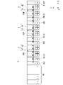
- FIG. 1 is a schematic configuration diagram of a power conversion system 1 of the first embodiment.
- the power conversion system 1 includes, for example, a transformer group 2 ( FIG. 2 ), a forward converter group 3 , an inverse converter group 5 , and a control device 40 .
- the power conversion system 1 steps down three-phase AC power supplied from an AC power supply PS (FIG. 2), forward-converts the stepped-down AC power to generate DC power, and reverse-converts the DC power to generate three-phase AC power. to supply three-phase AC power to the electric motor 8 (Fig. 2).
- PS AC power supply PS
- Transformers 20U, 20V, and 20W may be arranged on the AC input panels 3UI, 3VI, and 3WI shown in FIG. 1, respectively.
- an AC input panel 3UI, a forward conversion device 3U, an inverse conversion device 5X, and an inverse conversion device 5U are arranged along the +X direction in the stated order.
- An AC input panel 3VI, a forward conversion device 3V, an inverse conversion device 5Y, and an inverse conversion device 5V are arranged along the +X direction in the stated order.
- An AC input panel 3WI, a forward conversion device 3W, an inverse conversion device 5Z, and an inverse conversion device 5W are arranged along the +X direction in the stated order.
- a control device 40 is arranged in the -X direction from the AC input board 3UI, and an output board 5OUT is arranged in the +X direction from the inverter 5W.
- the output panel 5OUT is connected to load power lines 58U, 58V, 58W (Fig. 2), and the electric motor 8 is connected via the load power lines 58U, 58V, 58W (Fig. 2).
- a transformer 20V and a transformer 20W are also configured in the same manner as the transformer 20U.
- the description of the transformer 20U is incorporated herein by replacing the U in the reference numerals of the components in the description of the transformer 20U with V and W, respectively.
- One end of a positive electrode bus 60U is connected to the rectifier positive electrode terminal 33UP.
- a positive input terminal 52U of the inverter 5U and a positive input terminal 52X of the inverter 5X are connected to the extension destination of the positive electrode bus 60U.
- the one end of the positive electrode bus 60U does not necessarily have to be the structural end of the positive electrode bus 60U.
- the forward converter 3U supplies DC power to the capacitor and the inverter (power converter) provided in the subsequent stage.
- a connection point 65UA between the capacitor 55UP and the capacitor 55UN is connected to the neutral wire 65U.
- Capacitor 55UP and capacitor 55UN have substantially the same capacitance so that the potential of connection point 65UA becomes the intermediate potential between positive electrode bus 60U and negative electrode bus 70U.
- the forward conversion devices 3V and 3W are also configured in the same manner as the forward conversion device 3U.
- the description of the forward converters 3V and 3W is incorporated by replacing U in the reference numerals of the components in the description of the forward converter 3U with V and W, respectively.
- inverter 5U when inverter 5U outputs the highest five-level voltage, current flows through positive electrode bus 60U in the direction from forward converter 3U to inverter 5U. At this time, the potential of the positive input terminal 52X of the inverter 5X also becomes a high potential. At another timing, when the inverter 5U outputs the lowest five-level voltage, a current flows through the negative electrode bus 70U in the direction from the inverter 5U to the forward converter 3U. At this time, the potential of the positive input terminal 52X of the inverter 5X becomes a potential close to the potential of the neutral point N.
- the potentials of the positive electrode bus 60U, the negative electrode bus 70U, and the neutral wire 65U fluctuate with respect to the potential of the neutral point N.
- the wiring inductance L increases by the amount of each extension.
- the capacitance of the smoothing capacitor C needs to be increased in proportion to the output capacity of the power conversion system 1 (capacity of the inverter group 5).
- a closed circuit including the wiring inductance L and the smoothing capacitor C is formed as shown in FIG. The resonance frequency of this closed circuit may decrease as the capacity of the power conversion system increases. In the case of such a comparative example, when the closed circuit vibrates and resonates due to switching noise when the power conversion system is operated, a current larger than the rated current may be generated in the DC bus.
- a reactor which is a lumped constant type circuit element, is provided in the closed circuit to adjust the inductance of the closed circuit, thereby reducing the resonance frequency of the closed circuit. may suppress resonance by moving .
- a reactor which is a lumped constant type circuit element
- it is sometimes difficult to mount the reactor since the size of a reactor that can pass a relatively large current is large, it is sometimes difficult to mount the reactor. In response to this, there has been a need for a coping method that does not use a lumped-constant type circuit element such as a reactor.
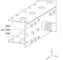
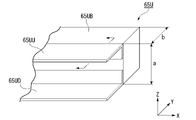
- the neutral wire 65U includes a first conductor 65UB, a second conductor 65UU, and a third conductor 65UD.
- a plurality of through holes are provided at predetermined positions along the extending direction (X direction).
- a nut (FIG. 6B) having a predetermined thread diameter may be press-fitted into each through hole.
- the plurality of through holes are used to respectively fix the second conductor 65UU and the third conductor 65UD.
- FIG. 4B shows an example of the second conductor 65UU of the neutral wire 65U.
- the second conductor 65UU is shaped like a plate, extends in the X direction, and is arranged so that the normal to the surface faces the Z direction.
- the width direction of the surface is the Y direction.
- a flange for fixing to the first conductor 65UB is provided at the +Y direction end of the second conductor 65UU. This flange may be provided over the entire length in the extending direction of the second conductor 65UU, and is formed with a predetermined length (bending width) shorter than the entire length in the extending direction. It may be placed in place.
- the flange shown in FIG. 4B is an example of the latter.
- the flange is provided with a plurality of through holes FH at predetermined intervals along the extending direction.
- the plurality of through holes FH are used to fix the second conductor 65UU to the first conductor 65UB.
- the surface of the second conductor 65UU may be provided with a plurality of through holes WC for ventilation.
- the third conductor 65UD may be formed in the same shape as the second conductor 65UU.
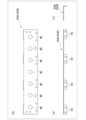
- the layout diagram of FIG. 5 is a plan view showing the schematic positions of the DC bus lines in each housing of the power conversion system 1 .
- a plurality of rectangular frames in FIG. 5 indicate housings of the forward transforming device 3U, the inverse transforming device 5X, and the inverse transforming device 5U.
- the neutral wire 65U is arranged across the casings of the forward conversion device 3U, the inverse conversion device 5X, and the inverse conversion device 5U.
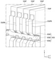
- the bird's-eye view of FIG. 6A is a view of the inside of the housing of the inverse conversion device 5U from a position closer to the front.
- the bird's-eye view of FIG. 6B is a view of the inside of the housing of the inverter 5U from a position closer to the back.
- the neutral wire 65U is arranged at a position lower than the capacitor 55UP.
- the neutral wire 65U is mounted within a limited range in the height direction without protruding beyond the width of the first conductor 65UB.
- the neutral wire 65U can be attached from the front side of the housing of the inverter 5U.
- the first conductor 65UB is applied to a pole bus bar that becomes a U-phase DC reference potential (DC midpoint potential).
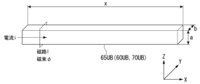
- the first conductor 65UB includes a first flat plate portion having a width a and a thickness b (first thickness) in a cross section perpendicular to the X direction (stretching direction).
- FIG. 8 is a diagram for explaining the distribution of the current flowing through the DC bus and the generated magnetic flux ⁇ according to the first embodiment.
- the lower frequency component and the DC component flow through the first conductor 65UB, the second conductor 65UU, and the third conductor 65UD
- the higher frequency component flows through the second conductor 65UU, the third conductor 65UD, and the third conductor 65UD. 1 flow near the surface of the conductor 65UB.
- the range in which the higher frequency component flows is indicated by hatching in the cross-sectional view in FIG.
- the magnetic flux generated in the neutral wire 65U by the current i flowing in the extending direction of the neutral wire 65U forms a magnetic path along the outer circumference of the cross section of the first conductor 65UB, the second conductor 65UU, and the third conductor 65UD. be. This is indicated by a dashed line.
- the first conductor 65UB is provided with the second conductor 65UU and the third conductor 65UD.
- the magnetic path formed in the first conductor 65UB is longer than in the comparative example formed only by the first conductor 65UB.
- the second conductor 65UU and the third conductor 65UD are used to increase the length of the magnetic path.
- FIGS. 9A to 9D are diagrams for explaining a DC bus of a comparative example.
- 9C and 9D are diagrams for explaining the DC bus according to the embodiment.
- FIG. 9C shows an overhead view of the neutral wire 65U.
- FIG. 9D shows a cross-sectional view of the second conductor 65UU in a plane perpendicular to the X direction.
- the second conductor 65UU has a cross section that is bent at a predetermined angle in a cross section perpendicular to the X direction (stretching direction), and has a thickness 2d (second thickness) that is thinner than the thickness b (first thickness). and a second plate portion formed of a flat plate.
- the cross section of the second flat plate portion is bent in an L shape.
- the above predetermined angle is an example of a substantially right angle. Note that the length e of the flange may be determined as appropriate.
- the thickness 2d of the second flat plate portion of the second conductor 65UU is at least twice the skin depth ⁇ 1 at the reference frequency HFref higher than the carrier frequency for PWM control of the power conversion unit (hereinafter simply referred to as carrier frequency).
- the reference frequency HFref may be determined based on harmonic frequencies of the carrier frequency.
- the reference frequency HFref may be an integer multiple of the carrier frequency, and may be aligned with harmonic frequencies of a particular order.
- the thickness 2d of the second flat plate portion of the second conductor 65UU is thinner than the skin depth ⁇ 2 of the fundamental frequency of the alternating current generated by the power conversion unit.
- the impedance in the fundamental frequency component of the alternating current increases, making it difficult for the current to flow through the second flat plate portion.
- the above reference frequency HFref is associated with frequency components (carrier frequency and its harmonic frequencies) generated by the carrier frequency.
- the second conductor 65UU is exemplified and described, but the same applies to the third conductor 65UD.
- the third conductor 65UD has a cross section that is bent at a predetermined angle in a cross section perpendicular to the X direction (stretching direction), and has a thickness 2d (first thickness) that is thinner than the thickness b (first thickness). 3 thickness).
- the cross section of the third flat plate portion is bent in an L shape.
- the thickness (third thickness) of the third flat plate portion of the third conductor 65UD may be the same as the thickness (second thickness) of the second flat plate portion of the second conductor 65UU. can be
- the +Y direction side surface of the flange portion (first end side of the second flat plate portion) formed on the second flat plate portion of the second conductor 65UU is the -Y direction side of the first conductor 65UB. It touches the side face.
- a second flat plate portion (second end portion) of the second conductor 65UU connected to the flange portion extends in a direction away from the first conductor 65UB (-Y direction).
- the plane perpendicular to the X direction of the first conductor 65UB has a cross section with a width a and a thickness b.
- the area S of this cross section is the product of the width a and the thickness b.
- Magnetic path l in the above equation (3) is the length of the magnetic path.
- the length of the magnetic path l and the inductance L are in an inversely proportional relationship.
- the inductance L can be reduced by lengthening the magnetic path l.
- the inductance L will also decrease if the area S is reduced.
- the comparative example shown here has a rectangular cross section with a length of circumference substantially equal to the length of the circumference of the cross section of the neutral wire 65U shown in FIG. 9C.
- the length of the circumference of the cross section of the neutral wire 65U is regarded as the length of the magnetic path l.
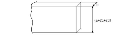
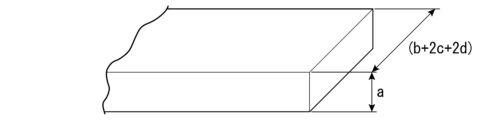
- the first conductor 65UB is widened in the thickness direction (Y direction).
- This conductor includes a flat plate portion having a width of a and a thickness of (b+2c+2d) in a cross section perpendicular to the X direction (stretching direction). The area of this cross section is (ab+2ac+2ad).
- the first comparative example is an example in which the total amount of conductors in the DC bus can be reduced with respect to the same magnetic path l.
- the cross-sectional area S of the neutral wire 65U of the embodiment focusing on the first flat plate portion of the second conductor 65UU, the cross-sectional area of the second conductor 65UU is approximated to (2cd). do.
- the cross-sectional area S of the neutral wire 65U can be approximated to (ab+4cd) including the third conductor 65UD.
- the thickness 2d of the second conductor 65UU is thinner than the thickness b of the first conductor 65UB (2d ⁇ b).
- the area S of the cross section of the neutral wire 65U is smaller.
- the total amount of conductors in the DC bus can be made smaller than in the first comparative example (and the second comparative example) for the same amount of magnetic path l.
- the inductance L of the neutral wire 65U also decreases, so that the neutral wire 65U is less likely to resonate than in the first comparative example (and the second comparative example).
- the busbar module applied to the DC bus distributes DC power to the smoothing capacitors and the power conversion units that are arranged over a plurality of housings and connected to each other.
- the DC busbar includes a first conductor applied to either a first pole or a second pole of DC, and a second conductor connected in parallel to the first conductor.
- the first conductor includes a first flat plate portion having a thickness b (first thickness) in a cross section perpendicular to the extending direction along the X direction.
- the second conductor has a cross section that is bent at a predetermined angle in a cross section perpendicular to the extending direction along the X direction, and has a thickness 2d (second thickness) that is thinner than the thickness b (first thickness). ).
- the power conversion system 1 includes a DC bus, a first smoothing capacitor arranged in a first housing among a plurality of housings, and a second power converter arranged in a second housing among the plurality of housings. and a device.
- the power conversion system 1 includes a capacitor 55UP (first smoothing capacitor) arranged in a housing (first housing) of the inverter 5U, a leg 50U (first power conversion unit), and a housing of the inverter 5X.
- a capacitor 55XP (second smoothing capacitor) and a leg 50X (second power conversion unit) arranged in the body (second housing) may be provided.
- Modification of the first embodiment A modification of the first embodiment will be described.
- the flanges of the second conductor 65UU and the third conductor 65UD in the first embodiment are divided into predetermined lengths (bending widths).
- the flanges of the second conductor 65UUa and the third conductor 65UDa in this modified example are continuous over the length in the extension direction (X direction) of the second conductor 65UU. This will be explained below.
- FIG. 10 is a diagram for explaining a DC bus according to a modification of the first embodiment.
- FIG. 11 is a bird's-eye view of the DC bus line portion of the modification of the first embodiment.
- Figures 10 and 11 replace Figures 4B and 6B described above.
- the flange of the second conductor 65UUa shown in FIGS. 10 and 11 is continuous over the entire length in the extending direction (X direction) of the second conductor 65UU. If the length in the extension direction of the flange is increased in this way, it may become difficult to bend the flange. The contact resistance between the two conductors 65UUa and the first conductor 65UB can be reduced.
- the total amount of conductors in the DC bus can be reduced in the same manner as in the first embodiment.
- FIG. 1st Embodiment demonstrated the structural example which reduces the conductor total amount and inductance of a DC bus.
- a DC bus is used as a branch circuit. This application will be explained.
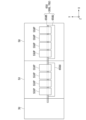
- FIG. 12 is a diagram showing a branch circuit from the DC bus to the capacitor 55 of the second embodiment.
- FIG. 13 is a bird's-eye view of the DC bus line portion of the second embodiment. Figures 12 and 13 replace Figures 5 and 6A described above.
- connection conductor 55UPN is provided between each capacitor 55 and the second conductor 65UU.
- the connection conductor 55UPN connects the electrode of each capacitor 55 and the second conductor 65UU.
- the electrode of each capacitor 55 is connected to the second conductor 65UU via the connection conductor 55UPN.
- each capacitor 55 is connected to the first conductor 65UB via the connection conductor 55UPN and the second conductor 65UU.
- the second conductor 65UU can be used as part of the branch circuit from the DC bus.
- the connection conductor 55UPN and the second conductor 65UU are used together rather than separately, thereby reducing the total amount of conductors of the DC bus as in the first embodiment. It is possible to reduce the total amount of conductors in the range including the connection conductor 55UPN and the second conductor 65UU.
- the busbar module distributes DC power to the smoothing capacitors and power conversion units arranged in a plurality of housings.
- the busbar module comprises a first conductor and a second conductor.
- the first conductor is applied to either a first pole or a second pole of direct current.
- the second conductor is connected in parallel with the first conductor.
- the first conductor includes a first flat plate portion having a first thickness in a cross section perpendicular to the extending direction.
- the second conductor includes a second flat plate portion having a cross section bent at a predetermined angle in a cross section perpendicular to the extending direction and having a second thickness thinner than the first thickness.
- leg 50 of the inverter group 5 may be a full-bridge 3-level inverter instead of the full-bridge NPC type 5-level inverter.
- positive electrode busbar (busbar module), negative electrode busbar 70U, 70V, 70W... negative electrode busbar (busbar module), 65UB... first conductor, 65UU... second conductor, 65UD... third conductor, 8... electric motor, PS ... AC power supply
Landscapes
- Engineering & Computer Science (AREA)
- Power Engineering (AREA)
- Inverter Devices (AREA)
Abstract
Description
実施形態において「接続されている」とは、電気的に接続されていることを含む。「XXに基づく」とは、「少なくともXXに基づく」ことを意味し、XXに加えて別の要素に基づく場合も含み得る。「XXに基づく」とは、XXを直接に用いる場合に限定されず、XXに対して演算や加工が行われたものに基づく場合も含み得る。「XX又はYY」とは、XXとYYのうち何れか一方の場合に限定されず、XXとYYの両方の場合も含み得る。これは選択的要素が3つ以上の場合も同様である。「XX」及び「YY」は、任意の要素(例えば任意の情報)である。
図1は、第1の実施形態の電力変換システム1の概略構成図である。
電力変換システム1は、例えば、変圧器群2(図2)、順変換装置群3、逆変換装置群5、制御装置40とを備える。電力変換システム1は、交流電源PS(図2)から供給される三相交流電力を降圧し、降圧した交流電力を順変換して直流電力を作り、直流電力を逆変換して三相交流電力を作り、三相交流電力を電動機8(図2)に供給する。
逆変換装置群5は、逆変換装置5Uと5Xの組と、逆変換装置5Vと5Yの組と、逆変換装置5Wと5Zの組とを備える。
図2には、電力変換システム1の他に交流電源PSと、電動機8とが示される。
例えば、交流電源PSは、商用電源の電力網や発電機などであり、三相交流電力を電力変換システム1に供給する。電動機8は、例えば、誘導電動機などの交流可変速電動機である。電動機8は、電力変換システム1から供給された交流電力によって駆動し、回転駆動力を図示しない出力軸に出力する。
変圧器群2は、例えば、変圧器20U、20V、20Wと備える。変圧器20U、20V、20Wのそれぞれは、2次側の結線方式の異なった三巻線トランスである。変圧器20U、20V、20Wのそれぞれは、同様の構成を有するため、以下では代表として変圧器20Uについて説明する。
整流器32UP、32UNのそれぞれは、三相フルブリッジ型のダイオード整流回路を含む。整流器32UPの交流側は、変圧器出力線25UPRSTを介して二次巻線24UPに接続されている。整流器32UNの交流側は、変圧器出力線25UNRSTを介して三次巻線24UNに接続されている。整流器32UP、32UNの負荷側は互いに直列に接続される。互いに直列に接続された整流器32UP、32UNによって整流された直流電力は、整流器正極端子33UPと整流器負極端子33UNとから出力される。
また、別のタイミングに、逆変換装置5Uが、5レベルの最低位の電圧を出力する場合には、逆変換装置5Uから順変換装置3Uに向かう方向に、負極母線70Uに電流が流れる。このときに逆変換装置5Xの正極入力端子52Xの電位は、中性点Nの電位に近い電位になる。
このような比較例の場合、電力変換システムを作動させたときのスイッチングノイズによって、この閉回路が加振されて共振すると、定格電流よりも大きな電流が直流母線に生じることがあった。
なお、図4Aから図7に示す直流母線の説明は、正極母線60Uと負極母線70Uと中性線65Uに適用できる。以下、直流母線の一例として中性線65Uを挙げて説明する。
図4A中の(a)に第1導体65UBの正面図を示し、図4A中の(b)に第1導体65UBの上面図を示し、図4A中の(c)に第1導体65UBの側面図を示す。
第2導体65UUは、板状に成形されていて、X方向に延伸して、Z方向に面の法線が向くように配置されている。面の幅方向が、Y方向になっている。第2導体65UUの+Y方向の端部には、第1導体65UBに固定するためのフランジが設けられている。このフランジは、第2導体65UUの延伸方向の全長に亘って設けられていてもよく、延伸方向の全長よりも短い所定の長さ(曲げ幅)で形成されて延伸方向の全長のなかで複数個所に配置されていてもよい。図4Bに示すフランジは、後者の一例である。フランジには、延伸方向に沿って所定の間隔で複数の貫通穴FHが設けられている。この複数の貫通穴FHは、第2導体65UUを第1導体65UBに固定することに利用されている。第2導体65UUの面に、通風可能にするための複数の貫通穴WCが設けられていてもよい。
第1導体65UBは、X方向(延伸方向)と垂直な断面において、幅a、厚さb(第1厚さ)で形成された第1平板部を含む。
図8は、第1の実施形態の直流母線に流れる電流の分布と生成される磁束φを説明するための図である。
図9Dに、第2導体65UUのX方向に直交する面における断面図を示す。第2導体65UUは、X方向(延伸方向)と垂直な断面において所定の角度を成して屈曲した断面を有し、厚さb(第1厚さ)よりも薄い厚さ2d(第2厚さ)で形成された第2平板部を含む。例えば、第2平板部の断面は、L字状に屈曲している。上記の所定の角度は、略直角の一例である。なお、フランジの長さeは、適宜決定してよい。
第3導体65UDの第3平板部の厚さ(第3厚さ)は、第2導体65UUの第2平板部の厚さ(第2厚さ)と同じであってよく、条件によって異なる厚さにしてもよい。
磁束φ=磁束密度B×面積S (2)
磁界H=電流i/磁路l (3)
磁束密度B=透磁率μ×磁界H (4)
上記の式(1)から(4)を整理すると、インダクタンスLは、次の式を使って算出できる。
中性線65Uの断面の面積Sとしての(ab+4cd)と、第1比較例の面積の(ab+2bc+2bd)とを比べると、中性線65Uの断面の面積Sの方が狭いので、中性線65Uは、等量の磁路lに対して、第1比較例(及び第2比較例)よりも直流母線の導体総量をより少なく構成できる。これに伴い、中性線65UのインダクタンスLも小さくなるため、中性線65Uは、第1比較例(及び第2比較例)よりも共振が生じにくくなっている。
第1の実施形態の変形例について説明する。
第1の実施形態における第2導体65UUと、第3導体65UDのフランジは、所定の長さ(曲げ幅)に分割されているものであった。これに対し、本変形例における第2導体65UUaと、第3導体65UDaのフランジは、第2導体65UUの延伸方向(X方向)の長さに亘って連続しているものである。以下、これについて説明する。
図12と図13を参照して、第2の実施形態について説明する。
第1の実施形態では、直流母線の導体総量とインダクタンスを低減させる構成例について説明した。本実施形態では、直流母線を分岐回路として利用する。この適用について説明する。
Claims (15)
- 複数の筐体に亘って配置され、平滑コンデンサと電力変換ユニットとに直流電力を配分するためのバスバーモジュールであって、
直流の第1極と第2極の何れかの極に適用される第1導体と、
前記第1導体に並列に接続される第2導体と
を備え、
前記第1導体は、延伸方向と垂直な断面において第1厚さで形成された第1平板部を含み、
前記第2導体は、前記延伸方向と垂直な断面において所定の角度を成して屈曲した断面を有し、前記第1厚さよりも薄い第2厚さで形成された第2平板部を含む、
バスバーモジュール。 - 前記第2平板部の断面は、L字状に屈曲している、
請求項1に記載のバスバーモジュール。 - 前記第2導体の厚さが、前記電力変換ユニットのPWM制御のキャリア周波数よりも周波数が高い基準周波数の表皮深さの2倍以上である、
請求項1に記載のバスバーモジュール。 - 前記第2導体の厚さが、前記電力変換ユニットが生成する交流の基本周波数の表皮深さよりも薄い、
請求項3に記載のバスバーモジュール。 - 前記基準周波数は、前記キャリア周波数により生成される周波数成分に対応付けられている、
請求項3に記載のバスバーモジュール。 - 前記屈曲してフランジを成す前記第2平板部の第1端部側が、前記第1導体の面に接していて、
前記第1端部から繋がっている前記第2平板部の第2端部が、前記第1導体から離れる方向に延伸している、
請求項2に記載のバスバーモジュール。 - 前記平滑コンデンサが、前記第2導体を介して前記第1導体に接続されている、
請求項1に記載のバスバーモジュール。 - 前記第1導体に並列に接続される第3導体
をさらに備え、
前記第3導体は、前記延伸方向と垂直な断面において所定の角度で屈曲した断面を有し、前記第1厚さよりも薄い第3厚さで形成された第3平板部を含む、
請求項1に記載のバスバーモジュール。 - 前記第3平板部の断面は、L字状に屈曲していて、
前記第2平板部と前記第3平板部は、前記第1導体から離れる方向に延伸している、
請求項8に記載のバスバーモジュール。 - 直流成分の大きさと交流成分の大きさとに基づいて、前記第1導体の断面の形状と面積と、前記第2導体の断面の形状と面積とが決定されている
請求項8に記載のバスバーモジュール。 - 前記第2平板部には、通風可能な貫通穴が設けられている、
請求項1に記載のバスバーモジュール。 - 前記第2平板部の第1端部側にフランジが形成され、
前記フランジの前記延伸方向の長さは、前記第2導体の延伸方向の長さの一部又は全部になっている、
請求項1に記載のバスバーモジュール。 - 請求項1から請求項12の何れか1項に記載のバスバーモジュール
を備え、
前記複数の筐体のうちの第1筐体に平滑コンデンサが配置され、
前記複数の筐体のうちの第2筐体に電力変換装置が配置される、
電力変換システム。 - 前記第1筐体に配置された第1平滑コンデンサと第1電力変換ユニットと、
前記第2筐体に配置された第2平滑コンデンサと第2電力変換ユニットと、
を含む請求項13に記載の電力変換システム。 - 前記平滑コンデンサと前記電力変換装置に直流電力を供給する順変換装置
を備える請求項13に記載の電力変換システム。
Priority Applications (4)
| Application Number | Priority Date | Filing Date | Title |
|---|---|---|---|
| PCT/JP2021/028019 WO2023007643A1 (ja) | 2021-07-29 | 2021-07-29 | バスバーモジュール及び電力変換システム |
| JP2022540831A JP7275397B1 (ja) | 2021-07-29 | 2021-07-29 | バスバーモジュール及び電力変換システム |
| US18/291,788 US20250096695A1 (en) | 2021-07-29 | 2021-07-29 | Bus bar module and power conversion system |
| CN202180052017.XA CN115989626A (zh) | 2021-07-29 | 2021-07-29 | 母线组件及电力转换系统 |
Applications Claiming Priority (1)
| Application Number | Priority Date | Filing Date | Title |
|---|---|---|---|
| PCT/JP2021/028019 WO2023007643A1 (ja) | 2021-07-29 | 2021-07-29 | バスバーモジュール及び電力変換システム |
Publications (1)
| Publication Number | Publication Date |
|---|---|
| WO2023007643A1 true WO2023007643A1 (ja) | 2023-02-02 |
Family
ID=85087727
Family Applications (1)
| Application Number | Title | Priority Date | Filing Date |
|---|---|---|---|
| PCT/JP2021/028019 Ceased WO2023007643A1 (ja) | 2021-07-29 | 2021-07-29 | バスバーモジュール及び電力変換システム |
Country Status (4)
| Country | Link |
|---|---|
| US (1) | US20250096695A1 (ja) |
| JP (1) | JP7275397B1 (ja) |
| CN (1) | CN115989626A (ja) |
| WO (1) | WO2023007643A1 (ja) |
Citations (3)
| Publication number | Priority date | Publication date | Assignee | Title |
|---|---|---|---|---|
| JPH0869872A (ja) * | 1994-08-31 | 1996-03-12 | Mitsubishi Electric Corp | 高周波加熱装置 |
| JP2005204464A (ja) * | 2004-01-19 | 2005-07-28 | Terasaki Electric Co Ltd | 配電盤 |
| JP2020022263A (ja) * | 2018-07-31 | 2020-02-06 | 富士電機株式会社 | 電力変換装置および鉄道車両用電力変換装置 |
Family Cites Families (6)
| Publication number | Priority date | Publication date | Assignee | Title |
|---|---|---|---|---|
| JP5508357B2 (ja) * | 2011-07-29 | 2014-05-28 | 日立オートモティブシステムズ株式会社 | 電力変換装置 |
| JP5972775B2 (ja) * | 2012-12-13 | 2016-08-17 | 日立オートモティブシステムズ株式会社 | 電力変換装置 |
| DE102015113123B4 (de) * | 2015-08-10 | 2017-03-16 | Sma Solar Technology Ag | Vorrichtung zur Herstellung einer mehrphasigen elektrischen Verbindung sowie eine Anordnung mit entsprechenden Vorrichtungen |
| US11239762B2 (en) * | 2017-11-02 | 2022-02-01 | Hitachi Astemo, Ltd. | Power converter |
| CN207459656U (zh) * | 2017-12-08 | 2018-06-05 | 浙江桥架母线有限公司 | 一种防火型母线槽 |
| EP3817215B1 (en) * | 2019-08-02 | 2024-01-10 | Fuji Electric Co., Ltd. | Power conversion device |
-
2021
- 2021-07-29 JP JP2022540831A patent/JP7275397B1/ja active Active
- 2021-07-29 US US18/291,788 patent/US20250096695A1/en active Pending
- 2021-07-29 WO PCT/JP2021/028019 patent/WO2023007643A1/ja not_active Ceased
- 2021-07-29 CN CN202180052017.XA patent/CN115989626A/zh active Pending
Patent Citations (3)
| Publication number | Priority date | Publication date | Assignee | Title |
|---|---|---|---|---|
| JPH0869872A (ja) * | 1994-08-31 | 1996-03-12 | Mitsubishi Electric Corp | 高周波加熱装置 |
| JP2005204464A (ja) * | 2004-01-19 | 2005-07-28 | Terasaki Electric Co Ltd | 配電盤 |
| JP2020022263A (ja) * | 2018-07-31 | 2020-02-06 | 富士電機株式会社 | 電力変換装置および鉄道車両用電力変換装置 |
Also Published As
| Publication number | Publication date |
|---|---|
| CN115989626A (zh) | 2023-04-18 |
| JPWO2023007643A1 (ja) | 2023-02-02 |
| JP7275397B1 (ja) | 2023-05-17 |
| US20250096695A1 (en) | 2025-03-20 |
Similar Documents
| Publication | Publication Date | Title |
|---|---|---|
| RU2556245C1 (ru) | Устройство преобразования энергии | |
| JP7354629B2 (ja) | フライングキャパシタ回路、回路モジュールおよび電力変換装置 | |
| JP5860581B2 (ja) | 電力コンバータを提供するシステム及び方法 | |
| US11177741B2 (en) | AC-AC converter circuit | |
| KR102149314B1 (ko) | 전력 변환 장치 | |
| JP3780949B2 (ja) | 電力変換装置 | |
| EP3955453B1 (en) | Power conversion device | |
| JP7275397B1 (ja) | バスバーモジュール及び電力変換システム | |
| US10284111B2 (en) | Power conversion apparatus having connection conductors having inductance which inhibits ripple current | |
| JP2018182880A (ja) | 電力変換装置 | |
| Obara et al. | Systematization of a Multilevel-Topology-Based Linear Amplifier Family for Noiseless DC–AC Power Conversion | |
| WO2016180626A1 (en) | Arrangement for oscillation dampening | |
| CN109643958B (zh) | 电力转换装置 | |
| US10951127B2 (en) | Power conversion apparatus | |
| WO2023021933A1 (ja) | 電力変換器装置 | |
| JP7537813B2 (ja) | 非絶縁変圧器を用いた18相整流回路によるジェットファン駆動用電源回路システム | |
| JP6568788B2 (ja) | 変圧器及び電力変換装置 | |
| EP4429096A1 (en) | Power conversion device | |
| US12395097B2 (en) | Power conversion apparatus, air conditioner and refrigeration apparatus | |
| JP7506522B2 (ja) | ノイズフィルタ、電力変換装置 | |
| KR200410899Y1 (ko) | 공극의 이격을 방지하는 인버터 트랜스포머 | |
| JPH09135582A (ja) | 電力変換装置 | |
| CN119856354A (zh) | 电路 | |
| KR20070059763A (ko) | 공극의 이격을 방지하는 인버터 트랜스포머 | |
| JPH04299072A (ja) | 電力変換装置 |
Legal Events
| Date | Code | Title | Description |
|---|---|---|---|
| ENP | Entry into the national phase |
Ref document number: 2022540831 Country of ref document: JP Kind code of ref document: A |
|
| 121 | Ep: the epo has been informed by wipo that ep was designated in this application |
Ref document number: 21951845 Country of ref document: EP Kind code of ref document: A1 |
|
| WWE | Wipo information: entry into national phase |
Ref document number: 18291788 Country of ref document: US |
|
| WWE | Wipo information: entry into national phase |
Ref document number: 202417009747 Country of ref document: IN |
|
| NENP | Non-entry into the national phase |
Ref country code: DE |
|
| 122 | Ep: pct application non-entry in european phase |
Ref document number: 21951845 Country of ref document: EP Kind code of ref document: A1 |
|
| WWP | Wipo information: published in national office |
Ref document number: 18291788 Country of ref document: US |