WO2022264980A1 - 絶縁モジュール - Google Patents
絶縁モジュール Download PDFInfo
- Publication number
- WO2022264980A1 WO2022264980A1 PCT/JP2022/023700 JP2022023700W WO2022264980A1 WO 2022264980 A1 WO2022264980 A1 WO 2022264980A1 JP 2022023700 W JP2022023700 W JP 2022023700W WO 2022264980 A1 WO2022264980 A1 WO 2022264980A1
- Authority
- WO
- WIPO (PCT)
- Prior art keywords
- die pad
- light
- light emitting
- emitting element
- resin
- Prior art date
Links
- 238000009413 insulation Methods 0.000 title claims abstract description 203
- 239000011347 resin Substances 0.000 claims abstract description 955
- 229920005989 resin Polymers 0.000 claims abstract description 955
- 239000000463 material Substances 0.000 claims abstract description 225
- 239000010954 inorganic particle Substances 0.000 claims abstract description 76
- 238000007789 sealing Methods 0.000 claims description 207
- 239000000725 suspension Substances 0.000 claims description 45
- 238000002955 isolation Methods 0.000 claims description 19
- 238000000926 separation method Methods 0.000 claims description 16
- 230000000694 effects Effects 0.000 abstract description 27
- 238000005538 encapsulation Methods 0.000 abstract description 3
- 239000010410 layer Substances 0.000 description 166
- 239000004065 semiconductor Substances 0.000 description 73
- 238000006243 chemical reaction Methods 0.000 description 40
- RTAQQCXQSZGOHL-UHFFFAOYSA-N Titanium Chemical compound [Ti] RTAQQCXQSZGOHL-UHFFFAOYSA-N 0.000 description 31
- 238000012986 modification Methods 0.000 description 22
- 230000004048 modification Effects 0.000 description 22
- 229910052751 metal Inorganic materials 0.000 description 16
- 239000002184 metal Substances 0.000 description 16
- 239000010931 gold Substances 0.000 description 12
- 229910000679 solder Inorganic materials 0.000 description 12
- 238000007747 plating Methods 0.000 description 11
- 239000000758 substrate Substances 0.000 description 11
- 239000004020 conductor Substances 0.000 description 10
- 239000013256 coordination polymer Substances 0.000 description 9
- 230000007423 decrease Effects 0.000 description 9
- 230000003287 optical effect Effects 0.000 description 8
- 229910052782 aluminium Inorganic materials 0.000 description 7
- 238000010586 diagram Methods 0.000 description 7
- 238000013459 approach Methods 0.000 description 6
- 230000008859 change Effects 0.000 description 6
- 239000003822 epoxy resin Substances 0.000 description 6
- 230000000149 penetrating effect Effects 0.000 description 6
- 229920000647 polyepoxide Polymers 0.000 description 6
- 229910052709 silver Inorganic materials 0.000 description 6
- 229910052802 copper Inorganic materials 0.000 description 5
- 229910052737 gold Inorganic materials 0.000 description 5
- 238000005520 cutting process Methods 0.000 description 4
- 238000001514 detection method Methods 0.000 description 4
- 239000007769 metal material Substances 0.000 description 4
- PXHVJJICTQNCMI-UHFFFAOYSA-N nickel Substances [Ni] PXHVJJICTQNCMI-UHFFFAOYSA-N 0.000 description 4
- 238000004382 potting Methods 0.000 description 4
- 229920000178 Acrylic resin Polymers 0.000 description 3
- 239000004925 Acrylic resin Substances 0.000 description 3
- 230000015572 biosynthetic process Effects 0.000 description 3
- 239000011651 chromium Substances 0.000 description 3
- 239000008393 encapsulating agent Substances 0.000 description 3
- 230000002159 abnormal effect Effects 0.000 description 2
- 229910052804 chromium Inorganic materials 0.000 description 2
- 239000000945 filler Substances 0.000 description 2
- 239000011810 insulating material Substances 0.000 description 2
- 230000007257 malfunction Effects 0.000 description 2
- 238000000034 method Methods 0.000 description 2
- 229910052759 nickel Inorganic materials 0.000 description 2
- 238000012545 processing Methods 0.000 description 2
- 229920002050 silicone resin Polymers 0.000 description 2
- 239000004332 silver Substances 0.000 description 2
- 239000010936 titanium Substances 0.000 description 2
- 229910052719 titanium Inorganic materials 0.000 description 2
- 238000002834 transmittance Methods 0.000 description 2
- VYZAMTAEIAYCRO-UHFFFAOYSA-N Chromium Chemical compound [Cr] VYZAMTAEIAYCRO-UHFFFAOYSA-N 0.000 description 1
- 229910004298 SiO 2 Inorganic materials 0.000 description 1
- VYPSYNLAJGMNEJ-UHFFFAOYSA-N Silicium dioxide Chemical compound O=[Si]=O VYPSYNLAJGMNEJ-UHFFFAOYSA-N 0.000 description 1
- 230000009471 action Effects 0.000 description 1
- XAGFODPZIPBFFR-UHFFFAOYSA-N aluminium Chemical compound [Al] XAGFODPZIPBFFR-UHFFFAOYSA-N 0.000 description 1
- 230000005540 biological transmission Effects 0.000 description 1
- 239000011248 coating agent Substances 0.000 description 1
- 238000000576 coating method Methods 0.000 description 1
- 230000000295 complement effect Effects 0.000 description 1
- 230000000994 depressogenic effect Effects 0.000 description 1
- 230000009977 dual effect Effects 0.000 description 1
- 238000005516 engineering process Methods 0.000 description 1
- 230000005669 field effect Effects 0.000 description 1
- PCHJSUWPFVWCPO-UHFFFAOYSA-N gold Chemical compound [Au] PCHJSUWPFVWCPO-UHFFFAOYSA-N 0.000 description 1
- 230000012447 hatching Effects 0.000 description 1
- 230000006872 improvement Effects 0.000 description 1
- 230000010354 integration Effects 0.000 description 1
- 239000011229 interlayer Substances 0.000 description 1
- 238000004519 manufacturing process Methods 0.000 description 1
- 238000003672 processing method Methods 0.000 description 1
- 229910052710 silicon Inorganic materials 0.000 description 1
- 239000010703 silicon Substances 0.000 description 1
- 229910052814 silicon oxide Inorganic materials 0.000 description 1
- 238000012360 testing method Methods 0.000 description 1
Images


Classifications
-
- H—ELECTRICITY
- H01—ELECTRIC ELEMENTS
- H01L—SEMICONDUCTOR DEVICES NOT COVERED BY CLASS H10
- H01L23/00—Details of semiconductor or other solid state devices
- H01L23/28—Encapsulations, e.g. encapsulating layers, coatings, e.g. for protection
-
- H—ELECTRICITY
- H01—ELECTRIC ELEMENTS
- H01L—SEMICONDUCTOR DEVICES NOT COVERED BY CLASS H10
- H01L23/00—Details of semiconductor or other solid state devices
- H01L23/28—Encapsulations, e.g. encapsulating layers, coatings, e.g. for protection
- H01L23/29—Encapsulations, e.g. encapsulating layers, coatings, e.g. for protection characterised by the material, e.g. carbon
-
- H—ELECTRICITY
- H01—ELECTRIC ELEMENTS
- H01L—SEMICONDUCTOR DEVICES NOT COVERED BY CLASS H10
- H01L23/00—Details of semiconductor or other solid state devices
- H01L23/28—Encapsulations, e.g. encapsulating layers, coatings, e.g. for protection
- H01L23/31—Encapsulations, e.g. encapsulating layers, coatings, e.g. for protection characterised by the arrangement or shape
-
- H—ELECTRICITY
- H01—ELECTRIC ELEMENTS
- H01L—SEMICONDUCTOR DEVICES NOT COVERED BY CLASS H10
- H01L25/00—Assemblies consisting of a plurality of individual semiconductor or other solid state devices ; Multistep manufacturing processes thereof
- H01L25/16—Assemblies consisting of a plurality of individual semiconductor or other solid state devices ; Multistep manufacturing processes thereof the devices being of types provided for in two or more different main groups of groups H01L27/00 - H01L33/00, or in a single subclass of H10K, H10N, e.g. forming hybrid circuits
- H01L25/167—Assemblies consisting of a plurality of individual semiconductor or other solid state devices ; Multistep manufacturing processes thereof the devices being of types provided for in two or more different main groups of groups H01L27/00 - H01L33/00, or in a single subclass of H10K, H10N, e.g. forming hybrid circuits comprising optoelectronic devices, e.g. LED, photodiodes
-
- H—ELECTRICITY
- H01—ELECTRIC ELEMENTS
- H01L—SEMICONDUCTOR DEVICES NOT COVERED BY CLASS H10
- H01L31/00—Semiconductor devices sensitive to infrared radiation, light, electromagnetic radiation of shorter wavelength or corpuscular radiation and specially adapted either for the conversion of the energy of such radiation into electrical energy or for the control of electrical energy by such radiation; Processes or apparatus specially adapted for the manufacture or treatment thereof or of parts thereof; Details thereof
- H01L31/02—Details
- H01L31/0203—Containers; Encapsulations, e.g. encapsulation of photodiodes
-
- H—ELECTRICITY
- H01—ELECTRIC ELEMENTS
- H01L—SEMICONDUCTOR DEVICES NOT COVERED BY CLASS H10
- H01L31/00—Semiconductor devices sensitive to infrared radiation, light, electromagnetic radiation of shorter wavelength or corpuscular radiation and specially adapted either for the conversion of the energy of such radiation into electrical energy or for the control of electrical energy by such radiation; Processes or apparatus specially adapted for the manufacture or treatment thereof or of parts thereof; Details thereof
- H01L31/02—Details
- H01L31/0232—Optical elements or arrangements associated with the device
-
- H—ELECTRICITY
- H01—ELECTRIC ELEMENTS
- H01L—SEMICONDUCTOR DEVICES NOT COVERED BY CLASS H10
- H01L31/00—Semiconductor devices sensitive to infrared radiation, light, electromagnetic radiation of shorter wavelength or corpuscular radiation and specially adapted either for the conversion of the energy of such radiation into electrical energy or for the control of electrical energy by such radiation; Processes or apparatus specially adapted for the manufacture or treatment thereof or of parts thereof; Details thereof
- H01L31/12—Semiconductor devices sensitive to infrared radiation, light, electromagnetic radiation of shorter wavelength or corpuscular radiation and specially adapted either for the conversion of the energy of such radiation into electrical energy or for the control of electrical energy by such radiation; Processes or apparatus specially adapted for the manufacture or treatment thereof or of parts thereof; Details thereof structurally associated with, e.g. formed in or on a common substrate with, one or more electric light sources, e.g. electroluminescent light sources, and electrically or optically coupled thereto
- H01L31/16—Semiconductor devices sensitive to infrared radiation, light, electromagnetic radiation of shorter wavelength or corpuscular radiation and specially adapted either for the conversion of the energy of such radiation into electrical energy or for the control of electrical energy by such radiation; Processes or apparatus specially adapted for the manufacture or treatment thereof or of parts thereof; Details thereof structurally associated with, e.g. formed in or on a common substrate with, one or more electric light sources, e.g. electroluminescent light sources, and electrically or optically coupled thereto the semiconductor device sensitive to radiation being controlled by the light source or sources
- H01L31/167—Semiconductor devices sensitive to infrared radiation, light, electromagnetic radiation of shorter wavelength or corpuscular radiation and specially adapted either for the conversion of the energy of such radiation into electrical energy or for the control of electrical energy by such radiation; Processes or apparatus specially adapted for the manufacture or treatment thereof or of parts thereof; Details thereof structurally associated with, e.g. formed in or on a common substrate with, one or more electric light sources, e.g. electroluminescent light sources, and electrically or optically coupled thereto the semiconductor device sensitive to radiation being controlled by the light source or sources the light sources and the devices sensitive to radiation all being semiconductor devices characterised by potential barriers
- H01L31/173—Semiconductor devices sensitive to infrared radiation, light, electromagnetic radiation of shorter wavelength or corpuscular radiation and specially adapted either for the conversion of the energy of such radiation into electrical energy or for the control of electrical energy by such radiation; Processes or apparatus specially adapted for the manufacture or treatment thereof or of parts thereof; Details thereof structurally associated with, e.g. formed in or on a common substrate with, one or more electric light sources, e.g. electroluminescent light sources, and electrically or optically coupled thereto the semiconductor device sensitive to radiation being controlled by the light source or sources the light sources and the devices sensitive to radiation all being semiconductor devices characterised by potential barriers formed in, or on, a common substrate
Definitions
- the present disclosure relates to insulation modules.
- Patent Document 1 discloses an optocoupler comprising an optical transmitter, an optical receiver, a transparent encapsulant encapsulating the optical transmitter and the optical receiver, and an opaque encapsulant encapsulating the transparent encapsulant. disclosed.
- An insulation module includes a light-emitting element, a light-receiving element that receives light from the light-emitting element, a first die pad on which the light-emitting element is mounted, and provided in parallel with the first die pad, a second die pad on which a light-receiving element is mounted; a transparent resin covering at least both the light-emitting element and the light-receiving element; and a reflecting member made of a material that covers at least the transparent resin and reflects the light from the light-emitting element.
- a sealing resin that seals the reflective member together with the transparent resin and is made of a material having a light-shielding property, wherein at least one of the reflective member and the transparent resin is the light emitting element Contains inorganic particles that absorb or reflect light from the
- the amount of light received by the light receiving element can be adjusted.
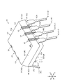
- FIG. 1 is a perspective view of the insulation module of the first embodiment.
- FIG. 2 is a plan view schematically showing the internal structure of the insulation module of FIG. 1.
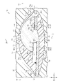
- FIG. 3 is a cross-sectional view of the insulation module of FIG. 2 taken along line 3--3.
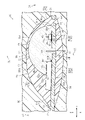
- 4 is a partially enlarged view of the insulation module of FIG. 3.
- FIG. 5 is an enlarged view of a light emitting element and its periphery in the insulation module of FIG. 4.
- FIG. 6 is an enlarged view of a part of the light receiving element and its surroundings in the insulation module of FIG. 4.
- FIG. FIG. 7 is an enlarged view of a light-emitting element, a light-receiving element, and their surroundings in the insulation module of FIG.
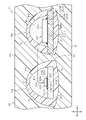
- FIG. 8 is an enlarged plan view of a part of the sealing resin of the insulation module of FIG. 1.
- FIG. 9 is an enlarged plan view of a part of the sealing resin of the insulation module of FIG. 1, different from that of FIG. 8.
- FIG. 10 is a circuit diagram schematically showing the electrical configuration of the insulation module of FIG. 1.
- FIG. 11 is a cross-sectional view showing the cross-sectional structure of part of the insulation module of the second embodiment.
- FIG. 12 is a cross-sectional view showing the cross-sectional structure of part of the insulation module of the third embodiment.
- FIG. 13 is a cross-sectional view showing the cross-sectional structure of part of the insulation module of the fourth embodiment.
- FIG. 14 is a cross-sectional view showing a cross-sectional structure of part of the insulation module of the fifth embodiment.
- FIG. 15 is a cross-sectional view showing the cross-sectional structure of part of the insulation module of the sixth embodiment.
- FIG. 16 is a plan view schematically showing the internal structure of the insulation module of the seventh embodiment. 17 is a cross-sectional view of the isolation module of FIG. 16 taken along line 17--17. 18 is a cross-sectional view of the isolation module of FIG. 16 taken along line 18--18. 19 is a circuit diagram schematically showing the electrical configuration of the insulation module of FIG. 16.
- FIG. 20 is a plan view schematically showing the internal structure of the insulation module of the eighth embodiment. 21 is a cross-sectional view of the insulation module of FIG.
- FIG. 20 taken along line 21--21.
- 22 is a cross-sectional view of the insulation module of FIG. 20 taken along line 22--22.
- 23 is a circuit diagram schematically showing the electrical configuration of the insulation module of FIG. 20.
- FIG. FIG. 24 is a cross-sectional view schematically showing the internal structure of the insulation module of the modification.
- FIG. 25 is a cross-sectional view showing a cross-sectional structure of a part of the insulation module of the modified example.
- FIG. 26 is a cross-sectional view showing a cross-sectional structure of a part of the insulation module of the modified example.
- FIG. 27 is a plan view schematically showing the internal structure of the insulation module of the modification.
- FIG. 28 is a cross-sectional view of part of a light receiving element in an insulation module of a modification.
- FIG. 29 is a cross-sectional view of part of the light receiving element in the insulation module of the modification.
- FIG. 30 is a cross-sectional view of part of a light receiving element in an insulation module of a modification.
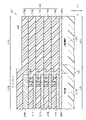
- FIG. 1 to 3 show the overall configuration of the insulation module 10.
- FIG. 4 to 9 show enlarged portions of the insulation module 10.
- FIG. 10 shows the electrical configuration of the insulation module 10. As shown in FIG.
- the insulation module 10 is used for a gate driver that applies a drive voltage signal to the gates of switching elements. As shown in FIGS. 1 and 2, the insulation module 10 has a package structure of DIP (Dual In-line Package).
- the insulation module 10 includes a rectangular sealing resin 80 and a plurality of terminals 41 and 51 projecting from the sealing resin 80 .
- the insulation voltage of the insulation module 10 is, for example, 3500 Vrms or more and 7500 Vrms or less. However, the specific numerical value of the dielectric strength voltage of the insulation module 10 is not limited to this and is arbitrary.
- the encapsulating resin 80 is made of an insulating material with light shielding properties.
- An example of an insulating material is epoxy resin.
- the sealing resin 80 is made of black epoxy resin.
- the sealing resin 80 has a resin main surface 80s, a resin rear surface 80r, and first to fourth resin side surfaces 81-84.
- the thickness direction of the sealing resin 80 is defined as the z-direction, and two mutually orthogonal directions among the directions orthogonal to the z-direction are defined as the x-direction and the y-direction, respectively.
- the resin main surface 80s and the resin rear surface 80r constitute both end surfaces of the sealing resin 80 in the thickness direction (z direction). Both the resin main surface 80s and the resin rear surface 80r are formed in a rectangular shape when viewed from the z direction.
- the shape of both the resin main surface 80s and the resin rear surface 80r viewed from the z-direction is a rectangular shape with short sides in the x-direction and long sides in the y-direction. Note that the z-direction can also be said to be the "height direction of the insulation module".
- the first resin side surface 81 and the second resin side surface 82 form both end surfaces in the x direction. Both the first resin side surface 81 and the second resin side surface 82 extend along the y direction when viewed from the z direction.
- a plurality of (four in this embodiment) terminals 41A to 41D are provided on the first resin side surface 81, and a plurality of (four in this embodiment) terminals 51A to 51D are provided on the second resin side surface 82.
- there is A plurality of terminals 41A to 41D protrude from the first resin side surface 81. As shown in FIG. A plurality of terminals 51A to 51D protrude from the second resin side surface .
- the plurality of terminals 41A to 41D and the plurality of terminals 51A to 51D are arranged side by side at intervals in the x direction.
- the x direction can also be said to be the direction in which the terminals 41A to 41D and the terminals 51A to 51D are arranged.
- the plurality of terminals 51A-51D have the same shape as the plurality of terminals 41A-41D.
- the third resin side surface 83 and the fourth resin side surface 84 constitute both end surfaces in the y direction. Both the third resin side surface 83 and the fourth resin side surface 84 are side surfaces on which the plurality of terminals 41A to 41D and 51A to 51D are not provided. Both the third resin side surface 83 and the fourth resin side surface 84 extend along the x direction when viewed from the z direction.
- each of the terminals 41A to 41D and 51A to 51D have the same shape. More specifically, as shown in FIG. 1, each of the terminals 41A to 41D has a first portion extending in the x direction from the first resin side surface 81, a bent portion bent downward from the first portion, and a and a second portion extending so as to incline downward with distance from the sealing resin 80 .
- the second portion has a wide portion with a relatively wide width and a narrow portion with a relatively narrow width.
- the wide portion is a portion of the second portion that is continuous with the bent portion and has the same width as the first portion.
- the narrow portion constitutes the tip portion of each of the terminals 41A to 41D.
- the length of the wide portion in the direction in which the second portion extends is shorter than the length of the narrow portion. In other words, the length of the narrow portion in the direction in which the second portion extends is longer than the length of the wide portion.
- the plurality of terminals 41A to 41D and 51A to 51D constitute external terminals that are inserted into through holes provided in the wiring board (not shown) when the insulation module 10 is mounted on the wiring board (not shown).
- the narrow portions of the second portions of the terminals 41A to 41D and 51A to 51D are joined by a conductive joining material such as solder, Ag (silver) paste, etc. while being inserted into the through holes of the wiring board. be done. Thereby, the insulation module 10 is electrically connected to the wiring board.
- Each resin side surface 81-84 has a first side surface 85 and a second side surface 86.
- the first side surface 85 is continuous with the second side surface 86 .
- the first side surface 85 is arranged closer to the resin main surface 80s than the resin back surface 80r in the z-direction.
- the second side surface 86 is arranged closer to the resin rear surface 80r than the resin main surface 80s in the z-direction.
- the first side surface 85 of the first resin side surface 81 and the first side surface 85 of the second resin side surface 82 are inclined so as to approach each other in the x direction toward the resin main surface 80s.
- the side surface 86 and the second side surface 86 of the second resin side surface 82 are inclined so as to approach each other in the x direction toward the resin back surface 80r.
- a first side surface 85 (not shown) of the third resin side surface 83 and a first side surface 85 of the fourth resin side surface 84 are inclined toward each other in the y direction toward the resin main surface 80s.
- a second side surface 86 (not shown) of 83 and a second side surface 86 of the fourth resin side surface 84 are inclined so as to approach each other in the y direction toward the resin back surface 80r.
- the length in the z direction of the first side surface 85 of each of the resin side surfaces 81 to 84 is longer than the length of the second side surface 86 of each of the resin side surfaces 81 to 84 in the z direction.
- the four terminals 41A to 41D protrude from between the first side surface 85 and the second side surface 86 of the first resin side surface 81 respectively.
- the four terminals 41A-41D are arranged apart from each other in the y direction.
- Each of the terminals 41A to 41D protrudes from a portion of the first resin side surface 81 closer to the resin back surface 80r than the center of the sealing resin 80 in the z direction.
- the four terminals 51A to 51D protrude from between the first side surface 85 and the second side surface 86 of the second resin side surface 82 respectively.
- the four terminals 51A to 51D are arranged apart from each other in the y direction.
- Each of the terminals 51A to 51D protrudes from a portion of the second resin side surface 82 closer to the resin back surface 80r than the center of the sealing resin 80 in the z direction.
- FIG. 2 is a plan view of the insulation module 10 showing the internal structure of the insulation module 10.
- the sealing resin 80 is indicated by a chain double-dashed line for convenience.
- the transparent resin 60 and the reflecting member 70 which will be described later, are omitted.
- the insulation module 10 includes a light emitting element 20, a light receiving element 30, a first lead frame 40, and a second lead frame 50.
- a photocoupler is composed of the light emitting element 20 and the light receiving element 30 .
- the light emitting element 20 is mounted on the first lead frame 40 .
- the first lead frame 40 includes first lead frames 40A to 40D as four first lead frames.
- the first lead frames 40A to 40D are arranged near the first resin side surface 81 with respect to the center of the sealing resin 80 in the x direction when viewed from the z direction.
- the first lead frames 40A to 40D are arranged apart from each other in the y direction when viewed from the z direction.
- the first lead frame 40A is arranged closer to the third resin side surface 83 than the first lead frames 40B to 40D.
- the first lead frame 40A includes terminals 41A.
- the terminal 41A is a portion of the first lead frame 40A protruding from the first resin side surface 81 to the outside of the sealing resin 80 .
- the inner leads 42A which are portions of the first lead frame 40A provided in the sealing resin 80, extend in the x direction.
- the tip of the inner lead 42A is located closer to the first resin side surface 81 than the center of the sealing resin 80 in the x direction when viewed from the z direction.
- a through hole 43A is provided in a portion near the tip of the inner lead 42A.
- the shape of the through-hole 43A viewed from the z-direction is a substantially rectangular shape with long sides in the x-direction and short sides in the y-direction.
- a sealing resin 80 is filled in the through hole 43A.
- the sealing resin 80 in the through hole 43A can prevent the first lead frame 40A from moving with respect to the sealing resin 80 in the direction orthogonal to the z direction.
- a protrusion 44A extending toward the third resin side surface 83 is provided at the tip of the inner lead 42A.
- the protrusion 44A extends along the y direction.
- the tip of the projection 44A is provided at a position separated from the third resin side surface 83 in the y direction. That is, the protrusion 44A is not exposed from the third resin side surface 83.
- the sealing resin 80 exists on both sides of the protrusion 44A in the x direction. Therefore, it is possible to prevent the first lead frame 40A from moving in the x direction with respect to the sealing resin 80 by the projection 44A.
- the first lead frame 40B is arranged near the fourth resin side surface 84 with respect to the first lead frame 40A.
- the first lead frame 40B includes terminals 41B. That is, the terminal 41B is a portion of the first lead frame 40B protruding from the first resin side surface 81 to the outside of the sealing resin 80 .
- the inner leads 42B which are portions of the first lead frame 40B provided in the sealing resin 80, extend in the x direction.
- the tip of the inner lead 42B is located closer to the first resin side surface 81 than the center of the sealing resin 80 in the x direction when viewed from the z direction.
- the length of the inner lead 42B in the x direction is longer than the length of the inner lead 42A in the x direction.
- the inner lead 42B includes a first lead portion 42BA and a second lead portion 42BB.
- the first lead portion 42BA is a portion continuous with the terminal 41B and extends from the first resin side surface 81 in the x direction.
- a through hole 43B is provided in a portion of the first lead portion 42BA near the second lead portion 42BB.
- the shape of the through-hole 43B viewed from the z-direction is a rectangular shape with long sides in the x-direction and short sides in the y-direction.
- the length of the short side of the through hole 43B is equal to the length of the short side of the through hole 43A, and the length of the long side of the through hole 43B is longer than the length of the long side of the through hole 43A.
- a sealing resin 80 is filled in the through hole 43B.
- the sealing resin 80 in the through hole 43B can suppress the movement of the first lead frame 40A with respect to the sealing resin 80 in the direction perpendicular to the z direction.
- the second lead portion 42BB is a portion including the tip of the inner lead 42B.
- the second lead portion 42BB is arranged to be shifted toward the inner lead 42A with respect to the first lead portion 42BA in the y-direction.
- a recess 44B is provided in a portion near the tip of the inner lead 42B.
- the depression 44B is depressed toward the third resin side surface 83 from the edge near the fourth resin side surface 84 among the y direction end edges of the first lead portion 42BA.
- the second lead portion 42BB protrudes from the first lead portion 42BA toward the inner lead 42A when viewed in the z direction.
- the sealing resin 80 exists on both sides of the second lead portion 42BB in the x direction. Therefore, the movement of the first lead frame 40B in the x direction with respect to the sealing resin 80 can be suppressed by the second lead portion 42BB.
- the second lead portion 42BB has a portion closer to the second resin side surface 82 than the inner lead 42A of the first lead frame 40A in the x direction.
- the shape of the second lead portion 42BB viewed from the z-direction is a substantially rectangular shape with long sides in the x-direction and short sides in the y-direction.
- the first lead frame 40C is arranged near the fourth resin side surface 84 with respect to the first lead frame 40B.
- the first lead frame 40C includes terminals 41C. That is, the terminal 41C is a portion of the first lead frame 40C protruding from the first resin side surface 81 to the outside of the sealing resin 80 .
- Inner leads 42C which are portions of the first lead frame 40C provided in the sealing resin 80, extend in the x direction.
- Inner lead 42C includes lead portion 42CA and die pad portion 42CB.
- the die pad portion 42CB corresponds to the "first die pad”.
- the lead portion 42CA is a portion continuous with the terminal 41C and extends from the first resin side surface 81 in the x direction.
- a through hole 43C is provided in a portion of the lead portion 42CA near the die pad portion 42CB.
- the shape of the through-hole 43C viewed from the z-direction is the same as the shape of the through-hole 43B viewed from the z-direction.
- the area of the through hole 43C viewed from the z direction is the same as the area of the through hole 43B viewed from the z direction.
- a sealing resin 80 is filled in the through hole 43C. The sealing resin 80 in the through hole 43C can suppress the movement of the first lead frame 40C with respect to the sealing resin 80 in the direction orthogonal to the z direction.
- the die pad portion 42CB is provided at a position aligned with the second lead portion 42BB of the first lead frame 40B in the x direction and separated from the second lead portion 42BB in the y direction.
- the end portion closer to the second lead portion 42BB enters the recess 44B of the second lead portion 42BB. That is, the die pad portion 42CB is arranged so that a part thereof overlaps the lead portion 42BA when viewed in the x direction.
- the shape of the die pad portion 42CB viewed from the z-direction is a substantially rectangular shape with short sides in the x-direction and long sides in the y-direction.
- the length of the die pad portion 42CB in the y direction is longer than the length of the lead portion 42CA in the y direction.
- the die pad portion 42CB protrudes on both sides in the y direction with respect to the lead portion 42CA.
- the sealing resin 80 exists on both sides of the die pad portion 42CB in the x direction. Therefore, the die pad portion 42CB can suppress the movement of the first lead frame 40C in the x direction with respect to the sealing resin 80 .
- the die pad portion 42CB has a recess 44C.
- the recessed portion 44C is provided at one of the y-direction end portions of the die pad portion 42CB that is closer to the second lead portion 42BB.
- the recess 44C opens toward the second lead portion 42BB.
- the concave portion 44C is provided closer to the lead portion 42CA than the center of the die pad portion 42CB in the x direction.
- the first lead frame 40D is arranged closer to the fourth resin side surface 84 than the first lead frames 40A to 40C.
- the first lead frame 40D includes terminals 41D. That is, the terminal 41D is a portion of the first lead frame 40D protruding from the first resin side surface 81 to the outside of the sealing resin 80. As shown in FIG.
- Inner leads 42D which are portions of the first lead frame 40D provided in the sealing resin 80, extend in the x direction.
- the tip of the inner lead 42D is located closer to the first resin side surface 81 than the center of the sealing resin 80 in the x direction when viewed from the z direction.
- a through hole 43D is provided in a portion near the tip of the inner lead 42D.
- the shape of the through-hole 43D viewed from the z-direction is a substantially rectangular shape with long sides in the x-direction and short sides in the y-direction.
- a sealing resin 80 is filled in the through hole 43D. The sealing resin 80 in the through hole 43D can prevent the first lead frame 40D from moving with respect to the sealing resin 80 in the direction orthogonal to the z direction.
- a protrusion 44D extending toward the third resin side surface 83 is provided at the tip of the inner lead 42D.
- the protrusion 44D extends along the y direction.
- the tip of the protrusion 44D is provided at a position separated from the fourth resin side surface 84 in the y direction. That is, the projection 44D is not exposed from the fourth resin side surface 84.
- the sealing resin 80 exists on both sides of the projection 44D in the x direction. Therefore, it is possible to prevent the first lead frame 40D from moving in the x direction with respect to the sealing resin 80 by the projection 44D.
- the first lead frame 40D when viewed from the z direction, has a shape that is symmetrical to the first lead frame 40A with respect to a straight line extending along the x direction at the center of the sealing resin 80 in the y direction. have.
- the light emitting element 20 is mounted on the die pad portion 42CB of the first lead frame 40C. More specifically, the light emitting element 20 is arranged at the end portion closer to the second resin side surface 82 among both end portions in the x direction of the die pad portion 42CB. The light emitting element 20 is arranged closer to the second lead portion 42BB of the first lead frame 40B than the lead portion 42CA in the die pad portion 42CB in the y direction. The light emitting element 20 is arranged at a position overlapping the recess 44C of the die pad portion 42CB when viewed from the x direction.
- the light emitting element 20 is arranged in the center of the sealing resin 80 in the y direction when viewed from the z direction. Further, the light emitting element 20 is arranged closer to the first resin side surface 81 than the center of the sealing resin 80 in the x direction.
- the shape of the light emitting element 20 viewed from the z direction is rectangular. In this embodiment, the shape of the light emitting element 20 viewed from the z direction is a square.
- Wires WA are bonding wires formed by, for example, a wire bonding apparatus (not shown).
- the wire WA is made of a conductive material such as Cu, Al (aluminum), Au (gold), Ag, or the like.
- the wire WA is made of a material containing Au.
- Second lead frame 50 includes second lead frames 50A to 50D as four second lead frames.
- the second lead frames 50A to 50D are arranged closer to the second resin side surface 82 with respect to the center of the sealing resin 80 in the x direction when viewed from the z direction.
- the second lead frames 50A to 50D are arranged apart from each other in the y direction when viewed from the z direction.
- the second lead frame 50A is arranged closer to the third resin side surface 83 than the second lead frames 50B to 50D.
- the second lead frame 50A includes terminals 51A.
- the terminal 51A is a portion of the second lead frame 50A protruding outside the sealing resin 80 from the second resin side surface 82 .
- the terminal 51A is arranged at a position overlapping the terminal 41A when viewed in the x direction.
- Inner leads 52A which are portions of the second lead frame 50A provided in the sealing resin 80, include lead portions 52AA and die pad portions 52AB.
- the die pad portion 52AB corresponds to the "second die pad”.
- the lead portion 52AA When viewed from the z-direction, the lead portion 52AA has a first portion extending along the x-direction from the second resin side surface 82, and is inclined toward the fourth resin side surface 84 from the first portion toward the first resin side surface 81. and a third portion extending from the second portion in the x direction and continuing to the die pad portion 52AB.
- a through hole 53A is provided in the lead portion 52AA.
- 53 A of through-holes are formed over the 1st part and the 2nd part. More specifically, the through hole 53A is formed from a portion of the first portion closer to the second portion to a portion of the second portion closer to the third portion.
- the through hole 53A has a first through portion extending in the x direction and an inclination from the third resin side surface 83 toward the fourth resin side surface 84 from the second resin side surface 82 toward the first resin side surface 81. and a second penetrating portion extending to.
- the first penetrating portion is provided in the first portion of the lead portion 52AA, and the second penetrating portion is provided in the second portion of the lead portion 52AA.
- a sealing resin 80 is filled in the through hole 53A.
- the sealing resin 80 in the through hole 53A can prevent the second lead frame 50A from moving with respect to the sealing resin 80 in the direction perpendicular to the z direction.
- the fourth resin Both of the second edges closer to the side surface 84 are inclined toward the fourth resin side surface 84 as they approach the die pad portion 52AB.
- the inclination angle of the second edge of the third portion with respect to the x direction is greater than the inclination angle of the first edge of the third portion with respect to the x direction. Therefore, when viewed from the z direction, the third portion is tapered such that the width dimension of the third portion (dimension in the y direction) increases toward the die pad portion 52AB.
- both the inclination angle of the first edge of the third portion with respect to the x direction and the inclination angle of the second edge of the third portion with respect to the x direction are smaller than the inclination angle of the second portion with respect to the x direction.
- the die pad portion 52AB is arranged closer to the first resin side surface 81 than the lead portion 52AA in the x direction.
- the die pad portion 52AB is arranged in the center of the sealing resin 80 in the y direction when viewed from the z direction.
- the shape of the die pad portion 52AB viewed from the z-direction is a substantially rectangular shape with short sides in the x-direction and long sides in the y-direction.
- the die pad portion 52AB is arranged at a position facing both the first lead frames 40B and 40C in the x direction. That is, the die pad portion 52AB extends in the y direction so as to face both the first lead frames 40B and 40C in the x direction. Therefore, the y-direction length of the die pad portion 52AB is longer than the y-direction length of the die pad portion 42CB of the first lead frame 40C.
- the die pad portion 52AB is arranged closer to the second resin side surface 82 than both the first lead frames 40B and 40C.
- the die pad portion 52AB is arranged closer to the second resin side surface 82 than the center of the sealing resin 80 in the x direction when viewed from the z direction.
- the edge closer to the first resin side surface 81 is closer to the second resin side surface 82 of the x-direction edges of the first lead frames 40B and 40C. It is positioned closer to the center of the sealing resin 80 in the x direction than the closer edge. That is, the die pad portion 52AB is arranged closer to the center of the sealing resin 80 in the x direction than the die pad portion 42CB.
- a recess 54A is provided in the die pad portion 52AB.
- the recess 54A is provided at an end of the die pad portion 52AB near the second resin side surface 82 and near the fourth resin side surface 84. As shown in FIG.
- the depression 54A opens toward both the second resin side surface 82 and the fourth resin side surface 84. As shown in FIG.
- a hanging lead 55A is provided on the die pad portion 52AB.
- the suspension lead 55A extends along the x direction toward the second resin side surface 82 from the edge closer to the second resin side surface 82 out of both x direction edges of the die pad portion 52AB.
- the suspension lead 55A is provided at the center of the die pad portion 52AB in the y direction. It can be said that the suspension lead 55A is provided at the center of the sealing resin 80 in the y direction when viewed from the z direction.
- the suspension lead 55A is exposed from the second resin side surface 82. As shown in FIG.
- the second lead frame 50B is arranged near the fourth resin side surface 84 with respect to the second lead frame 50A.
- the second lead frame 50B includes terminals 51B. That is, the terminal 51B is a portion of the second lead frame 50B protruding from the second resin side surface 82 to the outside of the sealing resin 80 .
- the terminal 51B is arranged at a position overlapping the terminal 41B when viewed in the x direction.
- Inner leads 52B which are portions of the second lead frame 50B provided in the sealing resin 80, extend in the x direction.
- the tip of the inner lead 52B is positioned closer to the second resin side surface 82 than the center of the sealing resin 80 in the x direction when viewed from the z direction. More specifically, the tip of the inner lead 52B is positioned closer to the second resin side surface 82 than the die pad portion 52AB of the second lead frame 50A.
- the end portion near the lead portion 52AA of the second lead frame 50A has an inclined portion that inclines toward the fourth resin side surface 84 toward the tip of the inner lead 52B. ing. As shown in FIG. 2, the inner lead 52B is tapered toward its tip.
- a through hole 53B is provided in a portion near the tip of the inner lead 52B.
- the shape of the through-hole 53B when viewed from the z-direction is formed into a substantially trapezoidal shape with long sides in the x-direction and short sides in the y-direction, tapering toward the tip of the inner lead 52B.
- a sealing resin 80 is filled in the through hole 53B. The sealing resin 80 in the through hole 53B can suppress the movement of the second lead frame 50B with respect to the sealing resin 80 in the direction perpendicular to the z direction.
- a portion of the inner lead 52B spaced from the second resin side surface 82 in the x direction is provided with a protruding portion 54B that protrudes in the y direction from a portion closer to the second resin side surface 82 than that portion.
- the protruding portion 54B protrudes to the side opposite to the lead portion 52AA.
- the sealing resin 80 exists on both sides of the protruding portion 54B in the x direction. Therefore, the movement of the second lead frame 50B in the x direction with respect to the sealing resin 80 can be suppressed.
- the second lead frame 50C is arranged near the fourth resin side surface 84 with respect to the second lead frame 50B. More specifically, the second lead frame 50C is arranged near the fourth resin side surface 84 with respect to the suspension leads 55A of the second lead frame 50A. In other words, the suspension lead 55A is spaced from both the second lead frames 50B and 50C in the y direction between the second lead frames 50B and 50C. In this embodiment, the suspension lead 55A is arranged in the center of the terminal 51B and the terminal 51C in the y direction on the second resin side surface 82 .
- the second lead frame 50C includes terminals 51C.
- the terminal 51C is a portion of the second lead frame 50C protruding outside the sealing resin 80 from the second resin side surface 82 .
- the terminal 51C is arranged at a position overlapping the terminal 41C when viewed in the x direction.
- Inner leads 52C which are portions of the second lead frame 50C provided in the sealing resin 80, extend in the x direction.
- the tip of the inner lead 52C is located closer to the second resin side surface 82 than the center of the sealing resin 80 in the x direction when viewed from the z direction. More specifically, the tip of the inner lead 52C is positioned closer to the second resin side surface 82 than the die pad portion 52AB of the second lead frame 50A.
- a through hole 53C is provided in a portion near the tip of the inner lead 52C.
- the shape of the through-hole 53C viewed from the z-direction is a rectangular shape with long sides in the x-direction and short sides in the y-direction.
- a sealing resin 80 is filled in the through hole 53C. The sealing resin 80 in the through hole 53C can suppress the movement of the second lead frame 50C with respect to the sealing resin 80 in the direction orthogonal to the z direction.
- a protrusion 54C extending toward the third resin side surface 83 is provided at the tip of the inner lead 52C.
- the projection 54C extends along the y direction.
- the sealing resin 80 exists on both sides of the projection 54C in the x direction. Therefore, it is possible to prevent the second lead frame 50C from moving in the x direction with respect to the sealing resin 80 by the projection 54C.
- the second lead frame 50D is arranged near the fourth resin side surface 84 with respect to the second lead frame 50C.
- the second lead frame 50D includes terminals 51D. That is, the terminal 51D is a portion of the second lead frame 50D protruding from the second resin side surface 82 to the outside of the sealing resin 80 . In this embodiment, the terminal 51D is arranged at a position overlapping the terminal 41D when viewed in the x direction.
- the inner lead 52D which is the portion of the second lead frame 50D provided in the sealing resin 80, has a first portion extending in the x direction and a third resin side surface 83 extending from the first portion toward the first resin side surface 81. and a third portion extending from the second portion toward the recess 54A of the die pad portion 52AB.
- a through hole 53D is provided in the inner lead 52D.
- a through hole 53D is formed over the first portion and the second portion. More specifically, the through hole 53D is formed from a portion of the first portion closer to the second portion to a portion of the second portion closer to the third portion.
- the through hole 53D has a first through portion extending in the x direction and an inclination from the fourth resin side surface 84 toward the third resin side surface 83 as it goes from the second resin side surface 82 to the first resin side surface 81. and a second penetrating portion extending to.
- the first penetrating portion is provided in the first portion of the inner lead 52D
- the second penetrating portion is provided in the second portion of the inner lead 52D.
- a sealing resin 80 is filled in the through hole 53D.
- the sealing resin 80 in the through hole 53D can prevent the second lead frame 50D from moving with respect to the sealing resin 80 in the direction perpendicular to the z direction.
- the third portion enters the recess 54A of the die pad portion 52AB.
- the third portion has a portion closer to the first resin side surface 81 than the second lead frames 50B and 50C in the x direction.
- the third portion is arranged at a position overlapping the die pad portion 42CB of the first lead frame 40C when viewed in the x direction.
- the first edge closer to the third resin side surface 83 extends along the x-direction when viewed from the z-direction.
- the second edge closer to the fourth resin side surface 84 is inclined toward the third resin side surface 83 as it approaches the die pad portion 52AB. . Therefore, when viewed from the z-direction, the third portion is formed so that the width dimension of the third portion (dimension in the y-direction) of the third portion decreases toward the die pad portion 52AB.
- both the angles of inclination of the second edge with respect to the x-direction are smaller than the angles of inclination of the second portion with respect to the x-direction.
- the light receiving element 30 is mounted on the die pad portion 52AB of the second lead frame 50A. More specifically, the light-receiving element 30 is arranged near the end portion closer to the second resin side surface 82 among both end portions in the x direction of the die pad portion 52AB. The light receiving element 30 is arranged in the center of the die pad portion 52AB in the y direction. The light receiving element 30 is arranged at a position overlapping the second lead frames 50B and 50C when viewed in the x direction. The light receiving element 30 is arranged closer to the third resin side surface 83 than the second lead frame 50D in the y direction. On the other hand, when viewed in the y direction, the light receiving element 30 is arranged at a position overlapping the third portion of the second lead frame 50D.
- the light receiving element 30 When viewed from the z direction, the light receiving element 30 is arranged in the center of the sealing resin 80 in the y direction. Therefore, the light receiving element 30 is arranged at a position overlapping the light emitting element 20 when viewed from the x direction. It can also be said that the light receiving element 30 is arranged to face the light emitting element 20 in the x direction. Further, the light receiving element 30 is arranged closer to the second resin side surface 82 than the center of the sealing resin 80 in the x direction.
- the shape of the light receiving element 30 viewed from the z direction is rectangular.
- the shape of the light receiving element 30 viewed from the z direction is a rectangular shape with short sides in the x direction and long sides in the y direction.
- the light receiving element 30 is configured to receive light from the light emitting element 20 .
- the light receiving element 30 includes a first semiconductor region that receives light from the light emitting element 20 and a second semiconductor region that generates a signal based on the received light.
- a photoelectric conversion element is provided in the first semiconductor region. Photodiodes, for example, are used as photoelectric conversion elements.
- the second semiconductor region is formed by, for example, LSI (Large Scale Integration).
- the light-receiving element 30 of this embodiment is an element in which the function of receiving light from the light-emitting element 20 and the function of generating a signal from the received light are integrated.
- the first semiconductor region and the second semiconductor region are formed side by side in the x-direction.
- the first semiconductor region is formed in a portion of the light receiving element 30 closer to the light emitting element 20 when viewed from the z direction.
- the second semiconductor region is formed in a portion of the light receiving element 30 near the second lead frames 50B and 50C.
- the area of the first semiconductor region viewed in the z-direction is smaller than the area of the second semiconductor region viewed in the z-direction.
- the x-direction dimension of the first semiconductor region is smaller than the x-direction dimension of the second semiconductor region.
- the first semiconductor region of the light receiving element 30 forms a light receiving surface 33 when viewed from the z direction.
- the area of the light receiving element 30 viewed from the z direction is larger than the area of the light emitting element 20 viewed from the z direction.
- the area of the light-receiving element 30 viewed from the z-direction is at least twice the area of the light-emitting element 20 viewed from the z-direction, preferably at least 5 times.
- the area of the light receiving element 30 viewed from the z direction is about ten times the area of the light emitting element 20 viewed from the z direction.
- the light receiving element 30 is connected to the second lead frames 50A-50D by wires WB1-WB4, respectively.
- Wires WB1 to WB4 are bonding wires formed, for example, by a wire bonding apparatus (not shown), like wires WA.
- the wires WB1 to WB4 are made of a conductive material (Au in this embodiment) like the wires WA.
- two wires WB1 connect the second semiconductor region of the light receiving element 30 and the third portion of the lead portion 52AA of the second lead frame 50A.
- One wire WB2 connects the second semiconductor region of the light-receiving element 30 and the portion of the inner lead 52B of the second lead frame 50B on the tip side of the through hole 53B.
- the two wires WB3 connect the second semiconductor region of the light receiving element 30 and the portion of the inner lead 52C of the second lead frame 50C that is closer to the tip than the through hole 53C.
- Two wires WB4 connect the second semiconductor region of the light receiving element 30 and the third portion of the inner lead 52D of the second lead frame 50D. These wires WB1 to WB4 are connected to the outer periphery of the second semiconductor region of the light receiving element 30 when viewed from the z direction.
- FIG. 3 shows a cross-sectional structure of the insulation module 10.
- FIG. FIG. 4 mainly shows an enlarged structure inside a reflecting member 70, which will be described later, of the cross-sectional structure of the insulation module 10.
- FIG. 5 mainly shows the light-emitting element 20 and its surrounding structure in the cross-sectional structure of the insulation module 10 in an enlarged manner.
- FIG. 6 mainly shows a portion of the light receiving element 30 and its surrounding structure in the cross-sectional structure of the insulation module 10 in an enlarged manner.
- FIG. 7 is a schematic plan view in which the transparent resin 60 and the reflecting member 70 are added to FIG. 2 and the reflecting member 70 and its periphery are enlarged. In addition, in FIG. 3, for the sake of convenience, some of the terminals 41 and 51 are omitted.
- the die pad portion 42CB of the first lead frame 40C extends so as to be slightly inclined from the first resin side surface 81 toward the second resin side surface 82 toward the resin back surface 80r. ing.
- the inclination angle of the die pad portion 42CB with respect to the direction (horizontal direction) perpendicular to the z-direction is, for example, 1° or more and 2° or less. Note that the inclination angle of the die pad portion 42CB with respect to the horizontal direction is not limited to this, and may be, for example, greater than 0° and equal to or less than 10°.
- the inclination angles of the die pad portion 42CB with respect to the horizontal direction are 2° to 3°, 3° to 4°, 4° to 5°, 5° to 6°, 6° to 7°, and 7°. ° or more and 8° or less.
- the die pad section 42CB has a pad front surface 42s and a pad rear surface 42r facing opposite sides in the thickness direction of the die pad section 42CB.
- the pad surface 42s is a surface forming a mounting surface on which the light emitting element 20 is mounted. That is, in this embodiment, the pad surface 42s corresponds to the "mounting surface of the first die pad".
- the pad surface 42s faces the same side as the resin main surface 80s of the sealing resin 80 .
- the pad rear surface 42r faces the same side as the resin rear surface 80r of the sealing resin 80.
- the pad back surface 42r is spaced apart from the resin back surface 80r in the z direction. That is, the pad rear surface 42r is not exposed from the resin rear surface 80r.
- the die pad section 42CB has a main metal layer 45C and a plated layer 46C formed on the outer surface of the main metal layer 45C.
- the main metal layer 45C is made of a metal material containing Cu, for example.
- the plated layer 46C is made of a material containing Ni (nickel), Cr (chromium), or the like. As shown in FIG. 5, the plated layer 46C is sufficiently thin compared to the main metal layer 45C.
- the light emitting element 20 has an element main surface 20s and an element rear surface 20r facing opposite sides in the thickness direction.
- the element main surface 20s faces the same side as the pad surface 42s, and the element rear surface 20r faces the same side as the pad rear surface 42r (see FIG. 3).
- a first electrode 21 is provided on the element main surface 20s.
- the first electrode 21 is provided, for example, at the center of both the x direction and the y direction of the element main surface 20s.
- a second electrode 22 is provided on the element rear surface 20r.
- the second electrode 22 is provided, for example, over the entire element back surface 20r.
- the element main surface 20s constitutes a "light emitting surface".
- the light emitting element 20 is bonded to the pad surface 42s of the die pad portion 42CB of the first lead frame 40C with a conductive bonding material 90 (see FIG. 5).
- the light emitting element 20 is bonded to the die pad section 42CB by die bonding the light emitting element 20 to the die pad section 42CB using the conductive bonding material 90 .
- the conductive bonding material 90 is interposed between the pad surface 42 s of the die pad portion 42 CB and the element back surface 20 r of the light emitting element 20 .
- the conductive bonding material 90 corresponds to the "first bonding material".
- the conductive bonding material 90 is made of a material that reflects light from the light emitting element 20P, for example.
- the conductive bonding material 90 is made of a conductive material such as solder or Ag (silver) paste. Solder and Ag paste reflect light.
- the conductive bonding material 90 includes a first bonding region 91 interposed between the element back surface 20r of the light emitting element 20 and the pad surface 42s of the die pad portion 42CB, and a region protruding from the light emitting element 20 when viewed in the z direction. and a second bonding region 92 bonded to the outer surface of the light emitting element 20 .
- the second bonding region 92 is provided so that the thickness of the second bonding region 92 decreases as the distance from the light emitting element 20 increases from the bonding portion with the outer surface of the light emitting element 20 .
- the second bonding region 92 is formed over the entire circumference of the light emitting element 20 when viewed from the z direction.
- the surface 92s of the second bonding region 92 is curved such that the center of curvature CF is located above the surface 92s, that is, the center of curvature CF is located on the opposite side of the surface 92s from the die pad portion 42CB in the z direction. It is The curvature of a region of the surface 92 s of the second bonding region 92 adjacent to the light emitting element 20 is greater than the curvature of a region of the surface 92 s of the second bonding region 92 far from the light emitting element 20 .
- the height HS of the portion of the second junction region 92 in contact with the outer surface of the light emitting element 20 is 1/2 or less of the height H1 of the light emitting element 20 .
- the height HS is less than half the height H1.
- the height HS is defined by the height from the pad surface 42s of the die pad portion 42CB of the portion of the second bonding region 92 in contact with the outer surface of the light emitting element 20 . That is, it can be said that the height HS is the thickness of the portion of the second junction region 92 that is in contact with the outer surface of the light emitting element 20 .
- the height H1 is defined by the distance between the pad surface 42s of the die pad portion 42CB and the element main surface 20s of the light emitting element 20 in the z direction.
- the light emitting element 20 is electrically connected to the first lead frames 40B and 40C.
- the first electrode 21 of the light emitting element 20 is electrically connected to the first lead frame 40B via the wire WA.
- the second electrode 22 of the light emitting element 20 is electrically connected to the first lead frame 40C through the conductive bonding material 90.
- the first electrode 21 is a cathode electrode and the second electrode 22 is an anode electrode. Therefore, as shown in FIG. 2, the terminal 41C constitutes an anode terminal and the terminal 41B constitutes a cathode terminal.
- the die pad portion 52AB of the second lead frame 50A is slightly inclined from the second resin side surface 82 toward the first resin side surface 81 toward the resin back surface 80r. It extends like That is, it can be said that both the die pad portion 52AB and the die pad portion 42CB of the first lead frame 40C are inclined toward the resin back surface 80r as they approach each other.
- the inclination angle of the die pad portion 52AB with respect to the direction (horizontal direction) perpendicular to the z direction is, for example, 1° or more and 2° or less.
- the inclination angle of the die pad portion 52AB with respect to the horizontal direction is not limited to this, and may be, for example, greater than 0° and equal to or less than 10°.
- the inclination angles of the die pad portion 52AB with respect to the horizontal direction are 2° to 3°, 3° to 4°, 4° to 5°, 5° to 6°, 6° to 7°, and 7°. ° or more and 8° or less.
- the die pad portion 52AB has a pad front surface 52s and a pad rear surface 52r facing opposite sides in the thickness direction of the die pad portion 52AB.
- the pad surface 52s is a surface forming a mounting surface on which the light receiving element 30 is mounted. That is, in this embodiment, the pad surface 52s corresponds to the "mounting surface of the second die pad".
- the pad surface 52s faces the same side as the pad surface 42s of the die pad portion 42CB.
- the pad rear surface 52r faces the same side as the pad rear surface 42r of the die pad portion 42CB.
- the pad back surface 52r is arranged apart from the resin back surface 80r in the z-direction. That is, the pad rear surface 52r is not exposed from the resin rear surface 80r.
- the die pad portion 52AB has a main metal layer 56A and a plated layer 57A formed on the outer surface of the main metal layer 56A.
- the main metal layer 56A is made of a metal material containing Cu, for example.
- the plated layer 57A is made of a material containing Ni, Cr, or the like. As shown in FIG. 6, the plating layer 57A is sufficiently thin compared to the main metal layer 56A.
- a protrusion 58A is provided at one of the x-direction end portions of the die pad portion 52AB that is closer to the first resin side surface 81 (see FIG. 2).
- the projection 58A extends upward. More specifically, the protrusion 58A is composed of a main metal layer 56A and a plating layer 57A. The thickness of the plating layer 57A in the protrusion 58A is thinner than the thickness of the portion of the plating layer 57A that constitutes the pad surface 52s.
- the height of the portion of the protrusion 58A formed by the main metal layer 56A is equal to the thickness of the portion of the plating layer 57A forming the pad surface 52s.
- the difference between the height of the portion of the protrusion 58A formed by the main metal layer 56A and the thickness of the portion of the plating layer 57A forming the pad surface 52s is formed by the main metal layer 56A of the protrusion 58A, for example.
- the height of the portion of the protrusion 58A formed by the main metal layer 56A is equal to the thickness of the portion of the plating layer 57A forming the pad surface 52s.
- the light receiving element 30 is bonded to the pad surface 52s of the die pad portion 52AB of the second lead frame 50A with a conductive bonding material 100 (see FIG. 6).
- the conductive bonding material 100 is interposed between the pad surface 52s of the die pad portion 52AB and the element back surface 30r of the light receiving element 30. As shown in FIG. Here, in the present embodiment, the conductive bonding material 100 corresponds to the "second bonding material".
- the conductive bonding material 100 is made of a material that reflects light from the light emitting element 20P, for example.
- the conductive bonding material 100 is made of a conductive material such as solder or Ag paste.
- the conductive bonding material 100 includes a first bonding region 101 interposed between the element back surface 30r of the light receiving element 30 and the pad surface 52s of the die pad portion 52AB, and a region protruding from the light receiving element 30 when viewed in the z direction. and a second bonding region 102 bonded to the outer surface of the light receiving element 30 .
- the second bonding region 102 is provided so that the thickness of the second bonding region 102 becomes thinner as the distance from the light receiving element 30 increases from the bonding portion with the outer surface of the light receiving element 30 .
- the second bonding region 102 is formed over the entire circumference of the light receiving element 30 when viewed from the z direction.
- the surface 102s of the second bonding region 102 is curved such that the center of curvature CG is located above the surface 102s, that is, the center of curvature CG is located on the opposite side of the surface 102s from the die pad portion 52AB in the z direction. It is The curvature of a region of the surface 102 s of the second bonding region 102 adjacent to the light receiving element 30 is greater than the curvature of a region far from the light receiving element 30 of the surface 102 s of the second bonding region 102 .
- the height HT of the portion of the second junction region 102 in contact with the outer surface of the light receiving element 30 is less than or equal to half the height H2 of the light receiving element 30 (see FIG. 4). In this embodiment, the height HT is less than half the height H2.
- the height HT is defined by the height from the pad surface 52s of the die pad portion 52AB of the portion of the second bonding region 102 in contact with the outer surface of the light receiving element 30 . That is, it can be said that the height HT is the thickness of the portion of the second junction region 102 that is in contact with the outer side surface of the light receiving element 30 .
- the height H2 is defined by the distance between the pad surface 52s of the die pad portion 52AB and the element main surface 30s of the light receiving element 30 in the z direction.
- the light-receiving element 30 is arranged near the end portion closer to the first resin side surface 81 (see FIG. 2) among both end portions in the x direction of the die pad portion 52AB.
- the second bonding region 102 provided at the end portion closer to the first resin side surface 81 (see FIG. 2) of the both end portions of the die pad portion 52AB in the x direction is separated from the die pad portion 52AB by the protrusion 58A. Protruding toward the resin side surface 81 is suppressed.
- the thickness of the light emitting element 20 (the dimension of the light emitting element 20 in the z direction) is thinner than the thickness of the light receiving element 30 (the dimension of the light receiving element 30 in the thickness direction of the die pad portion 52AB).
- the z-direction position of the pad surface 42s of the die pad portion 42CB and the z-direction position of the pad surface 52s of the die pad portion 52AB are substantially aligned with each other. Therefore, the height H2 of the light receiving element 30 is higher than the height H1 of the light emitting element 20.
- the insulation module 10 includes a transparent resin 60 and a reflecting member 70.
- the transparent resin 60 is made of a resin material through which light from the light emitting element 20 can pass. Transparent epoxy resin, acrylic resin, silicone resin, or the like, for example, is used as the transparent resin 60 .
- the transparent resin 60 is formed by potting, for example.
- the transparent resin 60 covers at least both the light emitting element 20 and the light receiving element 30. More specifically, the transparent resin 60 covers the entire light-emitting element 20 and partially covers the light-receiving element 30 when viewed in the z-direction.
- the transparent resin 60 covers a portion closer to the light emitting element 20 than the center of the light receiving element 30 in the x direction.
- the transparent resin 60 covers the first semiconductor region of the light receiving element 30 . That is, the transparent resin 60 covers the light receiving surface 33 of the light receiving element 30 .
- the transparent resin 60 does not cover the second semiconductor region of the light receiving element 30 . Therefore, the wires WB1 to WB4 connected to the light receiving element 30 are arranged outside the transparent resin 60, respectively. Each of the wires WB1-WB4 is arranged inside the reflecting member 70. As shown in FIG.
- the transparent resin 60 covers most of the die pad section 42CB including the light emitting element 20 in the x direction. More specifically, the transparent resin 60 covers a portion of the die pad portion 42CB on the opposite side of the light emitting element 20 from the light receiving element 30 in the x direction. In the present embodiment, the transparent resin 60 covers a portion closer to the first resin side surface 81 (see FIG. 3) than the center of the die pad portion 42CB in the x direction. Therefore, part of one wire WA connected to the light emitting element 20 is arranged inside the transparent resin 60 . The remaining portion of one wire WA is arranged outside the transparent resin 60 , that is, inside the reflecting member 70 . In other words, the wire WA is provided from the transparent resin 60 to the reflecting member 70 .
- the transparent resin 60 is also provided in a portion between the light emitting element 20 and the light receiving element 30 in the x direction.
- the transparent resin 60 is also provided in a portion between the die pad portion 42CB of the first lead frame 40C and the die pad portion 52AB of the second lead frame 50A in the x direction.
- the lower end surface 64 of the transparent resin 60 is provided so as to be at the same position in the z direction as the pad rear surface 42r of the die pad section 42CB.
- the transparent resin 60 is formed between the side surface of the die pad portion 42CB that is closer to the die pad portion 52AB among both side surfaces of the die pad portion 42CB in the x direction and the side surface of the die pad portion 52AB that is closer to the die pad portion 42CB among both side surfaces of the die pad portion 52AB in the x direction. in contact with both.
- the lower end surface 64 of the transparent resin 60 is formed in a straight line extending in the x direction.
- the transparent resin 60 covers the light emitting element 20 and the pad surface 42s of the die pad portion 42CB. It is in contact with the junction area 92 . Further, as shown in FIG. 6, the transparent resin 60 covers the first semiconductor region of the light receiving element 30 and the portion of the die pad portion 52AB closer to the die pad portion 42CB than the light receiving element 30. Therefore, the transparent resin 60 is conductive. It is in contact with a portion closer to the light emitting element 20 than the light receiving element 30 in the second bonding region 102 , which is a portion of the bonding material 100 protruding from the light receiving element 30 .
- the transparent resin 60 covers the entire first semiconductor region of the light receiving element 30 in the y direction when viewed from the z direction. That is, the y-direction dimension of the portion of the transparent resin 60 that covers the light receiving element 30 is larger than the y-direction dimension of the light receiving element 30 when viewed from the z direction.
- the transparent resin 60 has a first end 61 closer to the light emitting element 20 in the x direction and a second end 61 closer to the light receiving element 30 in the x direction. It has an end portion 62 and an upwardly convex curved surface 63 .
- the first end 61 is provided on the side opposite to the light receiving element 30 with respect to the light emitting element 20 in the x direction.
- the first end portion 61 is provided at a position separated from the light emitting element 20 in the x direction. More specifically, the first end 61 is provided at a position separated from the conductive bonding material 90 in the x direction.
- the first end portion 61 is provided at a position closer to the first resin side surface 81 (see FIG. 3) than the center of the die pad portion 42CB in the x direction. Therefore, the transparent resin 60 is also provided on the side opposite to the light receiving element 30 with respect to the light emitting element 20 in the x direction.
- the first end portion 61 has a first portion 61a extending in the z direction and an inclination toward the light emitting element 20 in the z direction from the first portion 61a. and a second portion 61b.
- the first portion 61a is formed to rise from the pad surface 42s of the die pad portion 42CB.
- the second portion 61 b is a portion that connects the first portion 61 a and the curved surface 63 .
- the distance between the first portion 61a of the first end 61 and the light emitting element 20 in the x direction is longer than the length of the light emitting element 20 in the x direction.
- the distance between the conductive bonding material 90 and the first portion 61a in the x direction is longer than the length of the light emitting element 20 in the x direction.
- the second end 62 is provided at a position overlapping the second semiconductor region of the light receiving element 30 when viewed from the z direction.
- the second end portion 62 is provided at a position adjacent to the light receiving surface 33 of the light receiving element 30 in the x direction. Therefore, the transparent resin 60 is not provided in the portion of the second semiconductor region of the light receiving element 30 on the side opposite to the light receiving surface 33 with respect to the second end portion 62 .
- the transparent resin 60 is provided so as to cover the light receiving surface 33 of the light receiving element 30 .
- the second end portion 62 has a first portion 62a extending in the z-direction and an inclination toward the light-emitting element 20 in the z-direction from the first portion 62a. and a second portion 62b.
- the first portion 62a is formed to rise from the pad surface 52s of the die pad portion 52AB.
- the second portion 62 b is a portion that connects the first portion 62 a and the curved surface 63 .
- the z-direction position of the second end portion 62 provided on the light receiving element 30 is higher than the z-direction position of the first end portion 61 provided on the die pad portion 42CB. It is in.
- the curved surface 63 is formed so as to connect the first end 61 and the second end 62 .
- the curved surface 63 is provided above both the element main surface 20 s of the light emitting element 20 and the element main surface 30 s of the light receiving element 30 .
- the curved shape of the curved surface 63 is not a uniform curved shape. Specifically, the radius of curvature of the portion of the curved surface 63 closer to the first end 61 is smaller than the radius of curvature of the portion of the curved surface 63 closer to the second end 62 . Therefore, the uppermost position of the curved surface 63, that is, the position where the curved surface 63 bends downward (hereinafter referred to as an inflection position CP) is located from the center of the curved surface 63 in the x direction. are also closer to the first end 61 . The inflection position CP is positioned closer to the light emitting element 20 than the light receiving element 30 in the x direction.
- the thickness of the transparent resin 60 at the portion of the curved surface 63 that overlaps with the light emitting element 20 when viewed from the z direction is the thickness of the light receiving element 20 from the first end far from the light receiving element 30 among both ends of the light emitting element 20 in the x direction. It thickens towards the second end closer to 30 . That is, the portion of the curved surface 63 that overlaps the light emitting element 20 when viewed in the z direction is curved upward from the first end to the second end of the light emitting element 20 .
- the thickness of the transparent resin 60 at the portion of the curved surface 63 overlapping the light emitting element 20 when viewed from the z direction is defined by the distance between the element main surface 20s of the light emitting element 20 and the curved surface 63 in the z direction. be.
- the thickness of the transparent resin 60 at the portion of the curved surface 63 that overlaps the light receiving surface 33 of the light receiving element 30 when viewed from the z-direction becomes thinner toward the second end 62 . That is, the portion of the curved surface 63 that overlaps with the light receiving surface 33 when viewed in the z direction is curved downward toward the second end 62 . Therefore, the light reflected by the portion of the curved surface 63 that overlaps the light receiving surface 33 when viewed from the z direction is likely to enter the light receiving surface 33 .
- the thickness of the transparent resin 60 at the portion of the curved surface 63 overlapping the light receiving surface 33 of the light receiving element 30 when viewed from the z direction is the distance between the light receiving surface 33 of the light receiving element 30 and the curved surface 63 in the z direction.
- the transparent resin 60 contains inorganic particles 65 that absorb or reflect light from the light emitting element 20 .
- An example of the inorganic particles 65 is a filler.
- the inorganic particles 65 are arranged all over the transparent resin 60 .
- the content of the inorganic particles 65 in the transparent resin 60 can be arbitrarily changed.
- the content of inorganic particles 65 in transparent resin 60 is set, for example, so that light receiving element 30 can receive light from light emitting element 20 within a predetermined range.
- the cross-sectional shape of the inorganic particles 65 may be elliptical or circular.
- the inorganic particles 65 may include multiple types of inorganic particles having different cross-sectional shapes.
- the inorganic particles 65 may include first inorganic particles having a first cross-sectional shape and second inorganic particles having a second cross-sectional shape different from the first cross-sectional shape.
- the inorganic particles 65 may have the same size. Moreover, the inorganic particles 65 may include a plurality of types of inorganic particles having different sizes. In one example, inorganic particles 65 may include first inorganic particles having a first size and second inorganic particles having a second size different from the first size.
- the inorganic particles 65 may contain multiple types of inorganic particles of different materials.
- the inorganic particles 65 may include first inorganic particles made of a first material and second inorganic particles made of a second material different from the first material.
- the inorganic particles 65 of this embodiment are composed of inorganic particles having the same size, the same cross-sectional shape, and the same material.
- the inorganic particles 65 may include a plurality of types of inorganic particles having a combination of a plurality of cross-sectional shapes, a plurality of sizes, and a plurality of materials.
- the color of the inorganic particles 65 may be black, which mainly absorbs light, or white, which mainly reflects light.
- the reflective member 70 is made of a material that reflects the light from the light emitting element 20 .
- Reflecting member 70 is made of, for example, a white resin material.
- An example of this resin material is a white epoxy resin.
- the refractive index of the reflecting member 70 and the refractive index of the transparent resin 60 are different from each other.
- the reflecting member 70 does not contain inorganic particles that absorb or reflect the light from the light emitting element 20 .
- Reflective member 70 is formed by potting, for example.
- the reflective member 70 covers at least the transparent resin 60 . That is, the reflecting member 70 covers all of the first end portion 61 , the second end portion 62 , the curved surface 63 and the lower end surface 64 of the transparent resin 60 . Reflective member 70 covers the second semiconductor region of light receiving element 30 . Therefore, it can be said that the reflecting member 70 covers both the light emitting element 20 and the light receiving element 30 .
- the reflecting member 70 is the first resin side surface in the x direction of the die pad portion 42CB of the first lead frame 40C. It covers the entire die pad portion 42CB except for the side surface near 81 .
- the reflecting member 70 enters the recess 44C of the die pad portion 42CB.
- the reflecting member 70 covers the entire die pad portion 52AB of the second lead frame 50A. Also, the reflecting member 70 partially covers the suspension lead 55A.
- the reflecting member 70 in the cross-sectional structure of the reflecting member 70 cut along the xz plane, includes, as both ends in the x direction, a first end 71 closer to the light emitting element 20 in the x direction, and a second end 72 closer to the light receiving element 30 in the x direction.
- the reflecting member 70 also has an upward curved surface 73 that is convex upward and a downward curved surface 74 that is convex downward.
- the reflecting member 70 has an upper portion 75 positioned above the die pad portions 42CB and 52AB of the reflecting member 70 and a lower portion 76 positioned below the die pad portions 42CB and 52AB of the reflecting member 70. have.
- Upper portion 75 includes upper curved surface 73 and lower portion 76 includes lower curved surface 74 .
- the first end portion 71 constitutes the end portion of the upper curved surface 73 and the lower curved surface 74 closer to the light emitting element 20 in the x direction.
- the first end portion 71 is provided at the end portion closer to the first resin side surface 81 (see FIG. 3) of the x-direction end portions of the die pad portion 42CB. In other words, the first end portion 71 is spaced from the light emitting element 20 toward the first resin side surface 81 .
- a transparent resin 60 is interposed between the first end portion 71 and the light emitting element 20 .
- the second end portion 72 constitutes the end portion of the upper curved surface 73 and the lower curved surface 74 closer to the light receiving element 30 in the x direction.
- the second end portion 72 is provided closer to the second resin side surface 82 (see FIG. 3) than the die pad portion 52AB in the x direction. In other words, the second end portion 72 is spaced from the light receiving element 30 toward the second resin side surface 82 .
- the transparent resin 60 is not interposed between the second end portion 72 and the light receiving element 30, and only the reflecting member 70 is provided.
- the second end portion 72 is provided at a portion closer to the die pad portion 52AB than the center of the suspension lead 55A in the x direction.
- the upper curved surface 73 is a curved surface that covers the die pad portions 42CB and 52AB, the light emitting element 20, and the light receiving element 30 from above. It has three curved surfaces 73c.
- the first curved surface 73a corresponds to the "first end curved surface”
- the second curved surface 73b corresponds to the "second end curved surface”
- the third curved surface 73c It corresponds to the "intermediate curved surface”.
- the first curved surface 73a is provided at a position opposite to the light receiving element 30 with respect to the light emitting element 20 in the x direction.
- the first curved surface 73 a is a curved surface forming the first end portion 71 .
- the first curved surface 73a has a curved shape such that the center of curvature CA thereof is located on the opposite side of the first curved surface 73a from the die pad section 42CB. ing.
- the center of curvature CA is located above the die pad portion 42CB and outside the reflecting member 70 . Therefore, in the cross-sectional structure of the reflecting member 70 cut along the xz plane, the first curved surface 73 a is a curved surface that is convex downward and toward the light emitting element 20 .
- the second curved surface 73b is provided at a position opposite to the light emitting element 20 with respect to the light receiving element 30 in the x direction.
- the second curved surface 73 b is a curved surface forming the second end portion 72 .
- the second curved surface 73b has a curved shape such that the center of curvature CB of the second curved surface 73b is located on the opposite side of the second curved surface 73b from the die pad portion 52AB. ing.
- the center of curvature CB is located above the die pad portion 52AB and outside the reflecting member 70 . Therefore, in the cross-sectional structure of the reflecting member 70 cut along the xz plane, the second curved surface 73b is a curved surface that protrudes downward and toward the light receiving element 30 .
- the distance between the first end 71 of the reflecting member 70 and the first end 61 of the transparent resin 60 in the x direction is It is smaller than the distance between the two ends 62 in the x direction. Therefore, since the upper curved surface 73 is more susceptible to the curved surface 63 of the transparent resin 60 at the first end 71 than at the second end 72, the pad surface 42s of the die pad portion 42CB at the first curved surface 73a rises steeper than the rise from the pad surface 52s of the die pad portion 52AB on the second curved surface 73b.
- the second curved surface 73b can have a shape that gently rises from the pad surface 52s of the die pad portion 52AB.
- the third curved surface 73c is provided between the first curved surface 73a and the second curved surface 73b, and is formed to connect the first curved surface 73a and the second curved surface 73b.
- the third curved surface 73c has a curved shape such that the center of curvature CC thereof is located closer to the die pad portions 42CB and 52AB than the third curved surface 73c.
- the center of curvature CC is located below the die pad portions 42CB and 52AB.
- the center of curvature CC is positioned below the reflecting member 70 . Therefore, in the cross-sectional structure of the reflecting member 70 cut along the xz plane, the third curved surface 73c is a curved surface that is convex upward.
- the third curved surface 73c may be formed by combining curved surfaces having a plurality of curvatures.
- the inflection position CQ which is the highest point of the third curved surface 73c, is located closer to the light receiving element 30 than the light emitting element 20 in the x direction.
- the inflection position CQ is positioned closer to the light receiving element 30 than the inflection position CP of the curved surface 63 of the transparent resin 60 when viewed from the z direction.
- the inflection position CP of the curved surface 63 of the transparent resin 60 is positioned closer to the light emitting element 20 than the inflection position CQ of the third curved surface 73c of the reflecting member 70 is.
- the radius of curvature of the third curved surface 73 c is larger than the radius of curvature of the curved surface 63 of the transparent resin 60 . Therefore, the thickness of the upper portion 75 of the reflecting member 70 increases from the inflection position CP of the curved surface 63 toward the first end portion 71 . It can also be said that the thickness of the upper portion 75 of the reflecting member 70 decreases upward from the first end portion 71 . Also, the thickness of the upper portion 75 of the reflecting member 70 increases from the inflection position CP of the curved surface 63 toward the second end portion 72 .
- the thickness of the upper portion 75 of the reflecting member 70 is said to decrease from a portion of the upper portion 75 closer to the second end 62 than the inflection position CP of the curved surface 63 toward the inflection position CP of the curved surface 63 .
- the thickness of the upper portion 75 is defined by the distance between the curved surface 63 and the third curved surface 73c in the direction along the radius of curvature of the curved surface 63, for example.
- the upper portion 75 of the reflecting member 70 covers the light emitting element 20 and the light receiving element 30 by covering the transparent resin 60 from the outside. That is, the upper portion 75 has portions overlapping the light emitting element 20 and the light receiving element 30 when viewed from the z direction.
- the upper portion 75 (reflecting member 70) has a light emitting side facing portion 75A and a light receiving side facing portion 75B.
- the light emitting side facing portion 75A is a portion of the upper portion 75 that faces the element main surface 20s (light emitting surface) of the light emitting element 20 with a gap therebetween in the direction (z direction) perpendicular to the element main surface 20s.
- the light-receiving side facing portion 75B is a portion of the upper portion 75 that faces the light-receiving surface 33 of the light-receiving element 30 with a gap therebetween in the direction perpendicular to the light-receiving surface 33 .
- Both the light emitting side facing portion 75A and the light receiving side facing portion 75B are provided between the first curved surface 73a and the second curved surface 73b in the x direction. That is, both the light emitting side facing portion 75A and the light receiving side facing portion 75B include the third curved surface 73c.
- the light emitting side facing portion 75A is provided closer to the inflection position CP of the curved surface 63 than the light receiving side facing portion 75B. Therefore, it can be said that the light emitting side facing portion 75A is formed to be thinner than the light receiving side facing portion 75B.
- a lower portion 76 of the reflecting member 70 is in contact with the pad rear surface 42 r of the die pad portion 42 CB, the pad rear surface 52 r of the die pad portion 52 AB, and the lower end surface 64 of the transparent resin 60 . That is, the lower portion 76 covers the die pad portions 42CB and 52AB from the pad rear surfaces 42r and 52r. In other words, the lower portion 76 covers the surface of the die pad portions 42CB and 52AB opposite to the surface on which the light emitting element 20 and the light receiving element 30 are mounted.
- the thickness of the lower portion 76 decreases from the center of the lower portion 76 in the x direction toward the first end portion 71 . Also, the thickness of the lower portion 76 decreases from the center of the lower portion 76 in the x direction toward the second end portion 72 .
- the lower portion 76 of the reflecting member 70 corresponds to the "pad cover portion".
- the lower curved surface 74 is a curved surface that covers the die pad portions 42CB and 52AB, the light emitting element 20, and the light receiving element 30 from below.
- the radius of curvature of the lower curved surface 74 is greater than each radius of curvature of the upper curved surface 73 .
- the center of curvature CE of the lower curved surface 74 is located above both the die pad portions 42CB and 52AB.
- a center of curvature CE of the lower curved surface 74 is located above both the light emitting element 20 and the light receiving element 30 .
- a center of curvature CE of the lower curved surface 74 is located above the transparent resin 60 .
- a center of curvature CE of the lower curved surface 74 is located above the reflecting member 70 .
- the inflection position CR which is the lowest point of the lower curved surface 74, is provided substantially at the center of the reflecting member 70 in the x direction. Therefore, the inflection position CR is positioned closer to the light receiving element 30 than the light emitting element 20 in the x direction.
- a lower portion 76 of the reflecting member 70 is provided so as to be thinner than the upper portion 75 .
- the maximum thickness of the lower portion 76 is thinner than the maximum distance between the third curved surface 73c of the upper portion 75 and the die pad portion 52AB in the z direction.
- the maximum thickness of the lower portion 76 is defined by the distance between the pad back surface 52r of the die pad portion 52AB and the inflection position CR in the z direction.
- the maximum distance between the third curved surface 73c and the die pad portion 52AB in the z direction is defined by the distance between the pad surface 52s of the die pad portion 52AB and the inflection position CQ of the third curved surface 73c.
- the boundary surface between the transparent resin 60 and the reflective member 70 serves as a reflective surface that reflects light.
- the reflecting surfaces include an upper reflecting surface located above the die pad portions 42CB and 52AB, and a lower reflecting surface located on the same side as the pad back surfaces 42r and 52r of the die pad portions 42CB and 52AB.
- the upper reflecting surface includes the first portion 61a and the second portion 61b of the first end portion 61 of the transparent resin 60, the first portion 62a and the second portion 62b of the second end portion 62, the curved surface 63, and the lower end surface 64. have the same shape.
- the lower reflecting surface has the same shape as the lower end surface 64 of the transparent resin 60 .
- the insulating module 10 has a reflecting surface that reflects light even in areas other than the boundary surface between the transparent resin 60 and the reflecting member 70 .
- the pad surfaces 42s, 52s of the die pad portions 42CB, 52AB, the end surfaces of the x-direction end surfaces of the die pad portions 42CB, 52AB located in the transparent resin 60, and the surfaces 92s of the conductive bonding materials 90, 100 , 102s are reflecting surfaces that reflect light.
- the light emitted from the light emitting element 20 is reflected at the portion of the curved surface 63 corresponding to the light emitting side facing portion 75A, which is the portion overlapping the light emitting element 20 when viewed from the z direction.
- the light-emitting side facing portion 75A is formed so that the light from the light-emitting element 20 is not totally reflected. That is, when the light from the light emitting element 20 is irradiated to the light emitting side facing portion 75A, part of the light irradiated to the light emitting side facing portion 75A is reflected, and the remaining light passes through the reflecting member 70. do. Light traveling through the reflecting member 70 is absorbed by the sealing resin 80 .
- the material of the reflective member 70 and the material of the transparent resin 60 are selected such that the refractive index of the reflective member 70 is greater than the refractive index of the transparent resin 60 .
- epoxy resin has a refractive index of 1.55 to 1.61
- silicone resin has a refractive index of about 1.57
- acrylic resin has a refractive index of about 1.49. Therefore, for example, when reflecting member 70 is made of epoxy resin and transparent resin 60 is made of acrylic resin, light from light emitting element 20 is not totally reflected at light emitting side facing portion 75A.
- the light emitting side facing portion 75A is formed so that the angle with respect to the light from the light emitting element 20 is smaller than the critical angle. Therefore, the light from the light emitting element 20 is not totally reflected at the light emitting side facing portion 75A.
- the light reflected by the curved surface 63 is reflected in the lower end surface 64 of the transparent resin 60, the pad surfaces 42s and 52s of the die pad portions 42CB and 52AB, and the x-direction end surfaces of the die pad portions 42CB and 52AB located in the transparent resin 60. and the conductive bonding materials 90 and 100 . Then, the lower end surface 64 of the transparent resin 60, the pad surfaces 42s and 52s of the die pad portions 42CB and 52AB, the end surfaces of the x-direction end surfaces of the die pad portions 42CB and 52AB which are located in the transparent resin 60, and the conductive bonding.
- Light reflected at material 90, 100 is reflected again at curved surface 63, or is reflected again at first portion 61a and second portion 61b of first end 61 and first portion 62a and second portion 62a of second end 62. reflected at 62b. In this way, the light emitted from the light emitting element 20 is reflected one or more times and enters the light receiving element 30 .
- the transparent resin 60 contains inorganic particles 65 that absorb light
- part of the light emitted from the light emitting element 20 is absorbed by the inorganic particles 65 as it travels through the transparent resin 60 . Therefore, the light emitted from the light emitting element 20 enters the light receiving element 30 in a weakened state.
- the inorganic particles 65 that reflect light are contained in the transparent resin 60
- part of the light emitted from the light emitting element 20 is reflected by the inorganic particles 65 when traveling through the transparent resin 60 .
- not all of the light incident on the inorganic particles 65 is reflected, and part of the light is absorbed by the inorganic particles 65 . Therefore, the light emitted from the light emitting element 20 enters the light receiving element 30 in a weakened state.
- FIG. 8 is a plan view of the insulation module 10 showing the terminals 41A to 41D and part of the sealing resin 80
- FIG. 9 is a plan view of the insulation module 10 showing the terminals 51A to 51D and part of the sealing resin 80. It is a diagram.
- an uneven portion 87 is provided on the first resin side surface 81 of the sealing resin 80 at a portion between terminals adjacent in the y direction among the plurality of terminals 41A to 41D. .
- the uneven portion 87 is formed between the first resin side surface 81 between the terminals 41A and 41B in the y direction and the first resin side surface 81 between the terminals 41B and 41C in the y direction. and a portion of the first resin side surface 81 between the terminal 41C and the terminal 41D in the y direction.
- any two terminals among the terminals 41A to 41D correspond to the "first terminal" and the "second terminal".
- the uneven portion 87 is formed over the entire first resin side surface 81 in the z direction.
- Each concave-convex portion 87 is composed of a first resin side surface 81 and a concave portion 87 a recessed from the first resin side surface 81 .
- Each concave-convex portion 87 has, for example, a plurality of (three in this embodiment) concave portions 87a.
- Each recess 87a is provided so as to penetrate the sealing resin 80 in the z direction.
- the bottom surface of each recess 87a is formed parallel to the first side surface 85 and the second side surface 86 of the first resin side surface 81 (see FIG. 3).
- each recess 87a corresponding to the first side surface 85 extends so as to be inclined outward from the sealing resin 80 in the x direction from the resin main surface 80s toward the resin rear surface 80r.
- a portion of the bottom surface of each concave portion 87a corresponding to the second side surface 86 extends so as to be inclined outward from the sealing resin 80 in the x direction from the resin back surface 80r (see FIG. 3) toward the resin main surface 80s. ing.
- an uneven portion 88 is provided in a portion between terminals adjacent to each other in the y direction among the plurality of terminals 51A to 51D.
- the uneven portion 88 is formed between the second resin side surface 82 between the terminals 51A and 51B in the y direction and the second resin side surface 82 between the terminals 51B and 51C in the y direction. and a portion of the second resin side surface 82 between the terminal 51C and the terminal 51D in the y direction.
- the terminal 51B corresponds to the "first terminal”
- the terminal 51C corresponds to the "second terminal".
- the uneven portion 88 is formed over the entire second resin side surface 82 in the z direction.
- Each uneven portion 88 is composed of a second resin side surface 82 and a recessed portion 88 a recessed from the second resin side surface 82 .
- Each concave-convex portion 88 has, for example, a plurality of concave portions 88a.
- the concave-convex portion 88 provided between the terminals 51A and 51B in the y direction has three concave portions 88a.
- the concave-convex portion 88 provided between the terminal 51B and the terminal 51C in the y direction has two concave portions 88a.
- the concave-convex portion 88 provided between the terminal 51C and the terminal 51D in the y direction has three concave portions 88a.
- Each recess 88a is provided so as to penetrate the sealing resin 80 in the z direction.
- the bottom surface of each recess 88 a is formed parallel to the first side surface 85 and the second side surface 86 of the second resin side surface 82 . That is, the portion of the bottom surface of each recess 88a corresponding to the first side surface 85 extends so as to be inclined outward from the sealing resin 80 in the x direction from the resin main surface 80s toward the resin rear surface 80r.
- a portion of the bottom surface of each recess 88a corresponding to the second side surface 86 extends so as to be inclined outward from the sealing resin 80 in the x-direction from the resin rear surface 80r toward the resin main surface 80s.
- the two concave portions 88a of the uneven portion 88 provided between the terminals 51B and 51C in the y direction are the portion between the terminal 51B and the suspension lead 55A in the y direction and the y direction between the suspension lead 55A and the terminal 51C. It is distributed in the part between the directions.
- the bottom surfaces of the recesses 87a and 88a may be formed so as to extend along the z direction. Further, the number of concave portions 87a, 88a of each uneven portion 87, 88 can be changed arbitrarily. Each uneven portion 87, 88 may have at least one recessed portion 87a, 88a. Further, the concave-convex portion 87 may have a convex portion that protrudes from the first resin side surface 81 instead of the concave portion 87a. The concave-convex portion 88 may have a convex portion that protrudes from the second resin side surface 82 instead of the concave portion 88a.
- FIG. 10 is a circuit diagram schematically showing the circuit configuration of the insulation module 10 and the connection configuration between the insulation module 10 and the inverter circuit 500, respectively.
- the inverter circuit 500 has a first switching element 501 and a second switching element 502 connected in series.
- Each switching element 501, 502 is, for example, a power transistor.
- power transistors include IGBTs (Insulated Gate Bipolar Transistors) and MOSFETs (Metal-Oxide-Semiconductor Field Effect Transistors).
- IGBTs Insulated Gate Bipolar Transistors
- MOSFETs Metal-Oxide-Semiconductor Field Effect Transistors
- the insulation module 10 applies a drive voltage signal to the gate of the first switching element 501 .
- the insulation module 10 is a gate driver that drives the first switching element 501 .
- the positive terminal of the control power supply 503 is electrically connected to the terminal 51D of the insulation module 10.
- the terminal 51A of the insulation module 10 is electrically connected to the negative electrode of the control power supply 503 .
- the insulation module 10 includes a light-emitting diode 20A, a light-receiving diode 30A, and a control circuit 110.
- the light emitting element 20 includes a light emitting diode 20A.
- Light receiving element 30 includes a light receiving diode 30A and a control circuit 110 .
- the light-emitting diode 20A includes the first electrode 21 (cathode electrode) and the second electrode 22 (anode electrode) of the light-emitting element 20 .
- the first electrode 21 of the light emitting diode 20A is electrically connected to the terminal 41B, and the second electrode 22 is electrically connected to the terminal 41C.
- terminals 41A and 41D constitute unconnected terminals that are not electrically connected to light emitting element 20, light receiving element 30, and control circuit 110.
- the light-receiving diode 30A is electrically connected to the control circuit 110 and insulated from the light-emitting element 20 .
- the light emitting element 20 is insulated from the control circuit 110 .
- the control circuit 110 is electrically connected to the terminals 51A to 51D.
- the terminals 41A-41D and the terminals 51A-51D are insulated by the photocoupler composed of the light-emitting element 20 (light-emitting diode 20A) and the light-receiving element 30 (light-receiving diode 30A).
- the light receiving diode 30A has a first electrode 31 and a second electrode 32 .
- the first electrode 31 is an anode electrode and the second electrode 32 is a cathode electrode. Both the first electrode 31 and the second electrode 32 are electrically connected to the control circuit 110 .
- the control circuit 110 has a Schmidt trigger 111 , a UVLO (Under Voltage Lock Out) section 112 , a comparator 113 and an output section 114 .
- the control circuit 110 generates an output signal based on the voltage change of the light receiving element 30 caused by the light receiving element 30 receiving the light from the light emitting element 20 .
- the Schmidt trigger 111 is electrically connected to both the first electrode 31 and the second electrode 32 of the light receiving element 30 . Also, the Schmitt trigger 111 is electrically connected to the terminals 51D and 51A. That is, the Schmitt trigger 111 is powered by the control power supply 503 . Schmitt trigger 111 transmits the voltage of light receiving element 30 to comparator 113 and output section 114 . A predetermined hysteresis is given to the threshold voltage of the Schmitt trigger 111 . With such a configuration, resistance to noise can be enhanced.
- the UVLO section 112 is electrically connected to the terminals 51D and 51B. That is, the UVLO unit 112 is electrically connected between the control power supply 503 and between the source of the first switching element 501 and the drain of the second switching element 502, respectively. UVLO unit 112 stops the operation of control circuit 110 to suppress the occurrence of malfunction when the voltage of control power supply 503 falls below the threshold voltage.
- the comparator 113 is electrically connected to the Schmitt trigger 111 and the UVLO section 112 on the input side, and electrically connected to the output section 114 on the output side. Comparator 113 generates a control signal for controlling output section 114 based on a comparison between the signal from Schmitt trigger 111 and the signal from UVLO section 112 . Comparator 113 outputs the generated control signal to output section 114 .
- the output section 114 has a first switching element 114a and a second switching element 114b connected in series.
- a p-type MOSFET is used for the first switching element 114a
- an n-type MOSFET is used for the second switching element 114b.
- the output section 114 is configured as a complementary MOS (CMOS).
- CMOS complementary MOS
- the comparator 113 is electrically connected to the first switching element 114a of the output section 114 on the output side.
- the source of the first switching element 114a is electrically connected to the terminal 51D.
- the source of the second switching element 114b is electrically connected to the terminal 51A.
- a node N between the drain of the first switching element 114a and the drain of the second switching element 114b is electrically connected to the terminal 51C.
- a gate of the first switching element 114 a is electrically connected to the comparator 113 . That is, the control signal from the comparator 113 is applied to the gate of the first switching element 114a.
- the gate of the second switching element 114b is electrically connected to the Schmitt trigger 111. That is, the signal from the Schmitt trigger 111 is applied to the gate of the second switching element 114b.
- the output unit 114 generates a drive voltage signal based on the ON/OFF operation of the first switching element 114a based on the control signal of the comparator 113 and the ON/OFF operation of the second switching element 114b based on the signal from the Schmitt trigger 111.
- the output section 114 applies the drive voltage signal to the gate of the switching element 501 .
- the transparent resin 60 contains inorganic particles 65 that absorb or reflect the light from the light emitting elements 20 . Accordingly, when the light from the light emitting element 20 travels through the transparent resin 60 , the light is weakened by the inorganic particles 65 . As a result, the amount of light received by the light receiving element 30 can be reduced, and an increase in the processing load of the control circuit of the light receiving element 30 can be suppressed.
- the insulation module 10 the amount of light received by the light receiving element 30 from the light emitting element 20 is suppressed from being excessively reduced by, for example, reducing the distance between the light emitting element 20 and the light receiving element 30 in the x direction. ing. That is, in the insulation module 10, the amount of light received by the light receiving element 30 from the light emitting element 20 is adjusted within a predetermined range. Thereby, the insulation module 10 can realize stable operation of the first switching element 501 .
- the insulation module 10 includes the light-emitting element 20, the light-receiving element 30 that receives light from the light-emitting element 20, the die pad section 42CB on which the light-emitting element 20 is mounted, and the die pad section 42CB.
- the die pad portion 52AB on which the light receiving element 30 is mounted, the transparent resin 60 that covers at least both the light emitting element 20 and the light receiving element 30, and the material that covers at least the transparent resin 60 and reflects the light from the light emitting element 20 are formed.
- the transparent resin 60 contains inorganic particles 65 that absorb or reflect light from the light emitting element 20 .
- the light from the light emitting element 20 travels through the transparent resin 60 , the light from the light emitting element 20 is weakened by the inorganic particles 65 . As a result, the light from the light-emitting element 20 enters the light-receiving element 30 in a weakened state, so the amount of light received by the light-receiving element 30 can be reduced.
- the reflecting member 70 has a light emitting side facing portion 75A that faces the element main surface 20s (light emitting surface) of the light emitting element 20 with a gap in the direction (z direction) perpendicular to the element main surface 20s (light emitting surface). have.
- the angle of the interface between the reflecting member 70 and the transparent resin 60 in the light emitting side facing portion 75A is smaller than the critical angle.
- the light emitted upward from the element main surface 20s of the light emitting element 20 is not totally reflected at the interface between the reflecting member 70 and the transparent resin 60 in the light emitting side facing portion 75A.
- the light from the light-emitting element 20 enters the light-receiving element 30 in a weakened state, so the amount of light received by the light-receiving element 30 can be reduced.
- the refractive index of the reflecting member 70 may be higher than the refractive index of the transparent resin 60 . According to this configuration, the light from the light emitting element 20 is not totally reflected at the interface between the reflecting member 70 and the transparent resin 60 . Therefore, the amount of light received by the light receiving element 30 from the light emitting element 20 can be reduced.
- the reflecting member 70 has a light-receiving side facing portion 75B that faces the light-receiving surface 33 of the light-receiving element 30 with a gap therebetween in the direction perpendicular to the light-receiving surface 33 of the light-receiving element 30 .
- the light emitting side facing portion 75A is formed to be thinner than the light receiving side facing portion 75B.
- the thickness of the light emitting side facing portion 75A to which the light from the light emitting element 20 is likely to irradiate the temperature of the light emitting side facing portion 75A rises due to the light from the light emitting element 20.
- the effect on the reflecting member 70 and the sealing resin 80 due to the difference in thermal expansion between the light emitting side facing portion 75A and the sealing resin 80 can be reduced.
- the sealing resin 80 includes a first resin side surface 81 provided with a plurality of terminals 41A to 41D and a second resin side surface 82 provided with a plurality of terminals 51A to 51D.
- Concavo-convex portions 87 are provided in portions of the first resin side surface 81 between terminals adjacent to each other in the y direction among the plurality of terminals 41A to 41D.
- Concavo-convex portions 88 are provided in portions of the second resin side surface 82 between terminals adjacent to each other in the y direction among the plurality of terminals 51A to 51D.
- the die pad portion 52AB of the second lead frame 50A includes suspension leads 55A.
- the suspension lead 55A is exposed from a portion of the second resin side surface 82 between the terminal 51B and the terminal 51C.
- Concavo-convex portions 88 are provided on both the portion between the terminal 51B and the suspension lead 55A and the portion between the terminal 51C and the suspension lead 55A on the second resin side surface 82 .
- both the creepage distance between the terminal 51B and the suspension lead 55A and the creepage distance between the terminal 51C and the suspension lead 55A can be increased. Therefore, both the insulation between the terminal 51B and the suspension lead 55A and the insulation between the terminal 51C and the suspension lead 55A can be improved.
- the die pad portion 52AB of the second lead frame 50A is formed longer than the die pad portion 42CB of the first lead frame 40C.
- the distance between the die pad portion 52AB and the die pad portion 42CB in the x direction is shorter than the length of the die pad portion 42CB in the x direction.
- the distance between the light emitting element 20 and the light receiving element 30 in the x direction can be shortened. That is, the distance of the optical path for the light emitted from the light emitting element 20 to enter the light receiving element 30 can be shortened. Therefore, the amount of light received by the light receiving element 30 can be increased.
- the transparent resin 60 covers the entire light emitting element 20 and partially covers the light receiving element 30 .
- a transparent resin 60 covers the light receiving surface 33 of the light receiving element 30 .
- a first end portion 61 of the transparent resin 60 is provided at a position adjacent to the light receiving surface 33 in the x direction.
- the light traveling through the transparent resin may reach a portion other than the light receiving surface 33 of the light receiving element 30, or a portion closer to the second resin side surface 82 than the light receiving element 30. may be incident.
- the transparent resin 60 is configured to cover the light receiving surface 33 and the position adjacent to the light receiving surface 33 , so that the light traveling through the transparent resin 60 reaches the light receiving element 30 . It is possible to prevent light from entering a portion other than the light receiving surface 33 and a portion closer to the second resin side surface 82 than the light receiving element 30 . Therefore, light traveling through the transparent resin 60 is more likely to enter the light receiving surface 33 .
- the conductive bonding material 90 that bonds the light emitting element 20 and the die pad portion 42CB of the first lead frame 40C is formed so as to protrude from the light emitting element 20 when viewed from the z direction.
- a conductive bonding material 100 that bonds the light receiving element 30 and the die pad portion 52AB of the second lead frame 50A is formed so as to protrude from the light receiving element 30 when viewed in the z direction.
- Both the conductive bonding materials 90 and 100 are made of a material that reflects light from the light emitting element 20 .
- the portion (second bonding region 102 ) When the light from the light emitting element 20 is reflected by the portion (second bonding region 102 ), the reflected light may enter the light receiving surface 33 of the light receiving element 30 . As a result, the amount of light received by the light receiving element 30 from the light emitting element 20 can be increased.
- the light-receiving element 30 is bonded by the conductive bonding material 100 to the end portion closer to the die pad portion 42CB of the first lead frame 40C of the x-direction end portions of the die pad portion 52AB of the second lead frame 50A. It is A projection 58A that protrudes in a vertical direction from the pad surface 52s of the die pad portion 52AB is provided at the end portion of the die pad portion 52AB that is closer to the die pad portion 42CB of the first lead frame 40C among the x-direction end portions of the die pad portion 52AB. ing.
- the die pad portion 52AB of the second lead frame 50A is inclined from the second resin side surface 82 toward the first resin side surface 81 toward the resin rear surface 80r. According to this configuration, the height positions of the terminals 51A to 51D protruding from the second resin side surface 82 of the sealing resin 80 are aligned with the height positions of the predetermined standard, and the thick inorganic particles 65 are arranged in the transparent resin. 60 can be enclosed. That is, even if the volume of the transparent resin 60 is increased by encapsulating the inorganic particles 65 in the transparent resin 60, the die pad portion 52AB is inclined with respect to the horizontal direction, so that a space corresponding to the increased volume can be secured. .
- the die pad portion 42CB of the first lead frame 40C is inclined from the first resin side surface 81 toward the second resin side surface 82 toward the resin rear surface 80r. According to this configuration, the height positions of the terminals 41A to 41D protruding from the first resin side surface 81 of the sealing resin 80 are aligned with the height positions of the predetermined standard, and the thick inorganic particles 65 are arranged in the transparent resin. 60 can be enclosed. That is, even if the volume of the transparent resin 60 is increased by encapsulating the inorganic particles 65 in the transparent resin 60, the die pad portion 42CB is inclined with respect to the horizontal direction, so that a space corresponding to the increased volume can be secured. .
- the insulation module 10 of this embodiment differs from the insulation module 10 of the first embodiment mainly in the configuration of the transparent resin 60 and the reflecting member 70 .
- the same reference numerals are given to the components common to the insulation module 10 of the first embodiment, and the description thereof will be omitted.
- the transparent resin 60 does not contain inorganic particles 65 (see FIG. 4). Further, as shown in FIG. 11, the shapes of the transparent resin 60 and the reflecting member 70 of this embodiment are the same as the shapes of the transparent resin 60 and the reflecting member 70 of the first embodiment.
- the reflecting member 70 includes inorganic particles 77 that reflect the light from the light emitting element 20, unlike the first embodiment.
- An example of the inorganic particles 77 is a filler.
- the inorganic particles 77 are arranged all over the reflecting member 70 .
- the content of the inorganic particles 77 in the reflecting member 70 can be arbitrarily changed.
- the content of inorganic particles 77 in reflecting member 70 is set, for example, so that light receiving element 30 can receive light from light emitting element 20 within a predetermined range.
- the reflecting member 70 and the transparent resin 60 are configured so that the light from the light emitting element 20 is not totally reflected at the interface between the reflecting member 70 and the transparent resin 60 .
- the light from the light emitting element 20 is not totally reflected at the interface between the reflecting member 70 and the transparent resin 60 , part of the light is transmitted through the reflecting member 70 .
- the inorganic particles 77 are included in the reflecting member 70 , the light traveling through the reflecting member 70 is reflected by the inorganic particles 77 .
- the light in the reflecting member 70 may be reflected by the inorganic particles 77 and enter the light receiving element 30 .
- Reflective member 70 includes inorganic particles 77 that absorb or reflect light from light emitting element 20 . According to this configuration, when the light from the light emitting element 20 is refracted at the interface between the reflecting member 70 and the transparent resin 60 and travels through the reflecting member 70 , the light traveling through the reflecting member 70 is In some cases, the light is reflected by the inorganic particles 77 inside and enters the light receiving element 30 . This makes it easier for the light from the light emitting element 20 to enter the light receiving element 30, so that the amount of light received by the light receiving element 30 can be increased.
- the insulation module 10 of the present embodiment differs from the insulation module 10 of the first embodiment mainly in the shape of the die pad portion 42CB and the relative positions of the light emitting element 20 and the light receiving element 30.
- FIG. the same reference numerals are given to the components common to the insulation module 10 of the first embodiment, and the description thereof will be omitted.
- the distance between the die pad portion 42CB of the first lead frame 40C and the die pad portion 52AB of the second lead frame 50A in the x direction is larger than in the first embodiment. It's becoming The arrangement position of the light emitting element 20 with respect to the die pad section 42CB and the arrangement position of the light receiving element 30 with respect to the die pad section 52AB are the same as in the first embodiment. For this reason, in this embodiment, the distance between the light emitting element 20 and the light receiving element 30 in the x direction is larger than in the first embodiment.
- the die pad section 52AB is formed longer than the die pad section 42CB in the x direction, which is the arrangement direction of the die pad sections 42CB and 52AB.
- the distance between the die pad portion 42CB and the die pad portion 52AB in the x direction is greater than the length of the die pad portion 42AB in the x direction.
- the x-direction length of the die pad portion 42CB is, for example, the x-direction length of the die pad portion 42CB at the center of the die pad portion 42CB in the y direction.
- the distance between the die pad portion 42CB and the die pad portion 52AB in the x direction is smaller than the length of the die pad portion 52AB in the x direction.
- the x-direction length of the die pad portion 52AB is, for example, the x-direction length of the die pad portion 52AB at the center of the die pad portion 52AB in the y direction.
- the die pad portion 52AB of the second lead frame 50A is formed longer than the die pad portion 42CB of the first lead frame 40C.
- the distance between the die pad portion 42CB and the die pad portion 52AB in the x direction is longer than the length of the die pad portion 42CB in the x direction.
- the distance between the light emitting element 20 and the light receiving element 30 in the x direction is increased. That is, the distance of the optical path for the light emitted from the light emitting element 20 to enter the light receiving element 30 becomes longer. Therefore, the amount of light received by the light receiving element 30 can be reduced.
- the insulation module 10 of the present embodiment differs from the insulation module 10 of the first embodiment mainly in the shapes of both the die pad portion 42CB of the first lead frame 40C and the die pad portion 52AB of the second lead frame 50A.
- the same reference numerals are given to the components common to the insulation module 10 of the first embodiment, and the description thereof will be omitted.
- the x-direction length of the die pad portion 42CB of the present embodiment is greater than the x-direction length of the die pad portion 42CB of the first embodiment.
- the x-direction length of the die pad portion 52AB is greater than the x-direction length of the die pad portion 52AB in the first embodiment.
- the die pad portion 52AB is formed longer than the die pad portion 42CB in the x direction, which is the arrangement direction of the die pad portions 42CB and 52AB.
- the x-direction length of the die pad portion 42CB is, for example, the x-direction length of the die pad portion 42CB at the center of the die pad portion 42CB in the y direction.
- the x-direction length of the die pad portion 52AB is, for example, the x-direction length of the die pad portion 52AB at the y-direction center of the die pad portion 52AB.
- the die pad portion 42CB among both ends of the die pad portion 42CB in the x direction, the end portion closer to the die pad portion 52AB and among both ends of the die pad portion 52AB in the x direction, the die pad portion 42CB and extend close to each other. Therefore, in the present embodiment, the distance between the die pad section 42CB and the die pad section 52AB in the x direction is smaller than the length of the die pad section 42CB in the x direction. It can also be said that the distance between the die pad portion 42CB and the die pad portion 52AB in the x direction is smaller than the length of the light receiving element 30 in the x direction.
- the positions of the light emitting element 20 and the light receiving element 30 with respect to the sealing resin 80 are the same as in the first embodiment.
- the light emitting element 20 is arranged on the far side from the die pad portion 52AB with respect to the end portion closer to the die pad portion 52AB among the x-direction end portions of the die pad portion 42CB. That is, of the x-direction end portions of the die pad portion 42CB, the end portion closer to the die pad portion 52AB is positioned closer to the die pad portion 52AB than the second bonding region 92 of the conductive bonding material 90 is.
- the light receiving element 30 is arranged on the far side from the die pad portion 42CB with respect to the end portion closer to the die pad portion 42CB among the both end portions of the die pad portion 52AB in the x direction. That is, of the x-direction end portions of the die pad portion 52AB, the end portion closer to the die pad portion 42CB is positioned closer to the die pad portion 42CB than the second bonding region 102 of the conductive bonding material 100 is.
- the die pad portion 42CB is provided with the protruding portion 47 that protrudes from the conductive bonding material 90 toward the die pad portion 52AB.
- the die pad portion 52AB is provided with a protruding portion 59 that protrudes from the conductive bonding material 100 toward the die pad portion 42CB.
- the projection 58A may be omitted from the die pad portion 52AB.
- the protruding portions 47 and 59 are in contact with the transparent resin 60 .
- the protruding portion 47 corresponds to the "first protruding portion”
- the protruding portion 59 corresponds to the "second protruding portion”.
- the length in the x direction of the protruding portion 47 of the die pad portion 42CB is longer than the distance between the die pad portion 42CB and the die pad portion 52AB in the x direction.
- the length in the x direction of the protruding portion 47 is longer than the length in the x direction of the region adjacent to the protruding portion 47 in the second bonding region 92 of the conductive bonding material 90 .
- the length of the protrusion 47 in the x direction is longer than the length of the light emitting element 20 in the x direction.
- the length in the x direction of the protruding portion 59 of the die pad portion 52AB is longer than the length in the x direction of the region adjacent to the protruding portion 59 in the second bonding region 102 of the conductive bonding material 100 in the x direction.
- the length of the protruding portion 59 of the die pad portion 52AB in the x direction is longer than the distance between the die pad portion 42CB and the die pad portion 52AB in the x direction.
- the length of the protruding portion 59 in the x direction may be equal to the length of the protruding portion 47 in the x direction.
- the x-direction length of protruding portion 59 is, for example, within 10% of the x-direction length of protruding portion 59, the x-direction length of protruding portion 59 It can be said that it is equal to the length of the protrusion 47 in the x direction.
- each protruding portion 47, 59 in the x direction is arbitrary.
- the amount of light reflected by each of the protruding portions 47 and 59 may be adjusted by adjusting the length of each of the protruding portions 47 and 59 in the x direction.
- the length in the x direction of each of the overhanging portions 47 and 59 may be set by testing or the like so that the amount of light received by the light receiving element 30 is within a predetermined range.
- the die pad portion 42CB of the first lead frame 40C has a protruding portion 47 extending from the conductive bonding material 90 toward the die pad portion 52AB of the second lead frame 50A.
- the die pad portion 52AB has a protruding portion 59 extending from the conductive bonding material 100 toward the die pad portion 42CB.
- the light reflected at the interface between the transparent resin 60 and the reflecting member 70 can be reflected at the projecting portions 47 and 59 of the die pad portions 42CB and 52AB. Since the reflectance of the die pad portions 42CB and 52AB made of metal material is higher than that of, for example, a resin material, the light incident on the die pad portions 42CB and 52AB can be efficiently reflected. Thereby, the amount of light received by the light receiving element 30 can be increased.
- the insulation module 10 of this embodiment differs from the insulation module 10 of the first embodiment mainly in the shape of the lower end surface 64 of the transparent resin 60 .
- the same reference numerals are given to the components common to the insulation module 10 of the first embodiment, and the description thereof will be omitted.
- an uneven portion 120 is provided at the boundary between the lower end surface 64 of the transparent resin 60 and the lower portion 76 of the reflecting member 70 .
- the uneven portion 120 is provided at the boundary between the transparent resin 60 and the reflecting member 70 interposed between the die pad portion 42CB of the first lead frame 40C and the die pad portion 52AB of the second lead frame 50A in the x direction. It can also be said.
- the uneven portion 120 may be provided on at least part of the boundary between the lower end surface 64 of the transparent resin 60 and the lower portion 76 of the reflecting member 70 . In this embodiment, the uneven portion 120 is formed over the entire boundary between the lower end surface 64 of the transparent resin 60 and the lower portion 76 of the reflecting member 70 in the x direction.
- the transparent resin 60 forming the lower end surface 64 is provided below the pad rear surface 42r of the die pad portion 42CB of the first lead frame 40C and the pad rear surface 52r of the die pad portion 52AB of the second lead frame 50A. have a part.
- the lower portion 76 has a portion provided above the pad back surfaces 42r, 52r of the die pad portions 42CB, 52AB.
- the uneven portion 120 is provided over the entire transparent resin 60 in, for example, the y direction.
- corrugation part 120 can be changed arbitrarily.
- An uneven portion 120 is provided at the boundary between the lower end surface 64 of the transparent resin 60 and the lower portion 76 of the reflecting member 70 . According to this configuration, since the creepage distance between the die pad portion 42CB and the die pad portion 52AB can be increased by the uneven portion 120, it is possible to improve the withstand voltage between the die pad portion 42CB and the die pad portion 52AB. can.
- the insulation module 10 of the fifth embodiment can be modified, for example, as follows.
- the uneven portion 120 is provided so that the lower portion 76 is above the pad rear surfaces 42r, 52r of the die pad portions 42CB, 52AB, but the present invention is not limited to this.
- the lower portion 76 is formed at the same position in the z-direction as the pad back surfaces 42r, 52r of the die pad portions 42CB, 52AB so that the transparent resin 60 is located below the pad back surfaces 42r, 52r of the die pad portions 42CB, 52AB.
- An uneven portion 120 may be provided.
- the uneven portion 120 is provided so that the transparent resin 60 is below the pad rear surfaces 42r, 52r of the die pad portions 42CB, 52AB, but the present invention is not limited to this.
- the lower end surface 64 of the transparent resin 60 is formed at the same position in the z-direction as the pad rear surfaces 42r, 52r of the die pad portions 42CB, 52AB, and the lower portion 76 is positioned above the pad rear surfaces 42r, 52r of the die pad portions 42CB, 52AB.
- Concavo-convex part 120 may be provided so that it may be located.
- the formation range of the uneven portion 120 can be arbitrarily changed.
- the uneven portion 120 may be provided on a portion of the lower end surface 64 of the transparent resin 60 in the x direction, that is, a portion of the interface between the transparent resin 60 and the lower portion 76 of the reflecting member 70 in the x direction.
- the uneven portion 120 may be provided on at least part of the interface between the transparent resin 60 and the lower portion 76 of the reflecting member 70 in the x direction.
- FIG. 10 An insulation module 10 according to the sixth embodiment will be described with reference to FIG.
- the insulation module 10 of this embodiment differs from the insulation module 10 of the first embodiment mainly in the shape of the first lead frame 40C.
- the same reference numerals are given to the components common to the insulation module 10 of the first embodiment, and the description thereof will be omitted.
- the position of the die pad portion 42CB of the first lead frame 40C in the z direction is positioned higher than in the first embodiment. Therefore, the position of the light emitting element 20 in the z direction is positioned higher than in the first embodiment.
- the die pad portion 42CB is formed such that the z-direction position of the element main surface 20s of the light emitting element 20 is the same as the z-direction position of the element main surface 30s of the light receiving element 30 or higher than the z-direction position of the element main surface 30s. is set in the z-direction.
- the position of the light emitting surface (element main surface 20s) of the light emitting element 20 in the z direction is the same as the position of the light receiving surface 33 (element main surface 30s) of the light receiving element 30 in the z direction, or the position of the light receiving surface 33 in the z direction is the same.
- the position of the die pad portion 42CB in the z direction is set so as to be higher than the position.
- the z-direction position of the die pad portion 42CB is set such that the z-direction position of the element main surface 20s of the light emitting element 20 is higher than the z-direction position of the element main surface 30s of the light receiving element 30. ing.
- the pad rear surface 42r of the die pad portion 42CB is located above the pad rear surface 52r of the die pad portion 52AB in the z-direction.
- the die pad portion 42CB is arranged such that the pad back surface 42r thereof is at the same position as the pad surface 52s of the die pad portion 52AB in the z direction.
- the lead portion 42CA (see FIG. 2) of the inner lead 42C of the first lead frame 40C is bent upward and connected to the die pad portion 42CB. Therefore, the position of the terminal 41C (see FIG. 2) in the z direction is the same as in the first embodiment.
- the shape of the transparent resin 60 is changed as the position of the die pad portion 42CB in the z direction is changed upward. Specifically, the first end 61 of the transparent resin 60 is positioned higher than in the first embodiment. A lower end surface 64 of the transparent resin 60 is inclined upward from the die pad portion 52AB toward the die pad portion 42CB.
- the shape of the reflecting member 70 is changed in accordance with the upward change in the z-direction position of the die pad portion 42CB. Specifically, the first end 71 of the reflecting member 70 is positioned higher than in the first embodiment. Also, the lower portion 76 of the reflecting member 70 has a portion formed along the lower end surface 64 of the transparent resin 60 . That is, the lower portion 76 has a portion that slopes upward from the pad back surface 52r of the die pad portion 52AB toward the die pad portion 42CB from the die pad portion 52AB.
- the height position of the element main surface 20s constituting the light emitting surface of the light emitting element 20 is higher than the height position of the element main surface 30s including the light receiving surface 33 of the light receiving element 30 . According to this configuration, by changing the relative position in the z direction between the element main surface 20s of the light emitting element 20 and the element main surface 30s of the light receiving element 30, the amount of light received by the light receiving element 30 from the light from the light emitting element 20 can be changed. can be adjusted.
- the insulation module 10 of the sixth embodiment will be described with reference to FIGS. 16 to 19.
- FIG. The insulation module 10 of this embodiment differs from the insulation module 10 of the first embodiment mainly in that two light emitting elements 20 and two light receiving elements 30 are provided.
- the same reference numerals are given to the components common to the insulation module 10 of the first embodiment, and the description thereof will be omitted.
- the x direction corresponds to the "second direction” and the y direction corresponds to the "first direction”.
- FIG. 16 is a plan view schematically showing the internal configuration of the insulation module 10 of this embodiment.
- 17 is a cross-sectional view of insulation module 10 of FIG. 16 taken along line 17--17.
- 18 is a cross-sectional view of insulation module 10 of FIG. 16 taken along line 18--18.
- the insulation module 10 includes a first lead frame 140, a second lead frame 150, a first light emitting element 20P and a second light emitting element 20Q, a first light receiving element 30P and a second light receiving element 30Q. and have.
- a first photocoupler is composed of the first light emitting element 20P and the first light receiving element 30P
- a second photocoupler is composed of the second light emitting element 20Q and the second light receiving element 30Q.
- the lead frames 140, 150 are made of the same material as the lead frames 40, 50 of the first embodiment, for example. Further, each lead frame 140, 150 has a plating layer, for example, like each lead frame 40, 50 of the first embodiment.
- the first lead frame 140 includes first lead frames 140A to 140D as four first lead frames.
- the first light emitting element 20P is mounted on the first lead frame 140A
- the second light emitting element 20Q is mounted on the first lead frame 140D.
- the first lead frames 140A to 140D are arranged closer to the first resin side surface 81 than the center of the sealing resin 80 in the x direction when viewed from the z direction.
- the first lead frames 140A to 140D are arranged apart from each other in the y direction when viewed from the z direction.
- the first lead frames 140A-140D include terminals 141A-141D, like the terminals 41A-41D of the first lead frames 40A-40D of the first embodiment.
- the layout of the terminals 141A-141D is the same as the layout of the terminals 41A-41D.
- the first lead frames 140A-140D have inner leads 142A-142D, like the first lead frames 40A-40D of the first embodiment.
- Inner lead 142A of first lead frame 140A includes lead portion 142AA and die pad portion 142AB.
- the die pad portion 142AB corresponds to the "first light emitting die pad”.
- the lead portion 142AA is a portion continuous with the terminal 141A and extends from the first resin side surface 81 in the x direction.
- a through hole 143A is provided in the lead portion 142AA.
- the die pad portion 142AB is arranged closer to the second resin side surface 82 than the lead portion 142AA in the x direction. In this embodiment, the die pad portion 142AB is arranged closer to the first resin side surface 81 than the center of the sealing resin 80 in the x direction.
- the shape of the die pad portion 142AB viewed from the z-direction is a substantially rectangular shape with short sides in the x-direction and long sides in the y-direction.
- the die pad portion 142AB extends in the y direction toward the fourth resin side surface 84 from the lead portion 142AA when viewed in the z direction.
- the die pad portion 142AB is arranged to face the first lead frame 140B in the x direction.
- the inner lead 142B of the first lead frame 140B is arranged closer to the first resin side surface 81 than the die pad portion 142AB.
- the die pad portion 142AB is formed so as to be inclined with respect to the direction (horizontal direction) perpendicular to the z-direction, similarly to the die pad portion 42CB of the first embodiment.
- the die pad section 142AB has a pad surface 142As and a pad rear surface 142Ar (see FIG. 17) facing the opposite side of the pad surface 142As in the z direction.
- the pad front surface 142As faces the same side as the resin main surface 80s (see FIG. 17) of the sealing resin 80, and the pad rear surface 142Ar faces the same side as the resin rear surface 80r (see FIG. 17).
- the inner lead 142B of the first lead frame 140B is a portion continuous with the terminal 141B and extends in the x direction.
- a through hole 143B is provided in the inner lead 142B.
- the inner lead 142C of the first lead frame 140C is a portion continuous with the terminal 141C and extends in the x direction.
- a through hole 143C is provided in the inner lead 142C.
- the inner lead 142D of the first lead frame 140D includes a lead portion 142DA and a die pad portion 142DB.
- the die pad portion 142DB corresponds to the "second die pad for light emission”.
- the lead portion 142DA is a portion continuous with the terminal 141D and extends from the first resin side surface 81 in the x direction.
- a through hole 143D is provided in the lead portion 142DA.
- the die pad portion 142DB is arranged closer to the second resin side surface 82 than the lead portion 142DA in the x direction.
- the die pad portion 142DB is arranged closer to the first resin side surface 81 than the center of the sealing resin 80 in the x direction.
- the shape of the die pad portion 142DB viewed from the z direction is a substantially rectangular shape with short sides in the x direction and long sides in the y direction.
- the die pad portion 142DB extends in the y direction toward the third resin side surface 83 from the lead portion 142DA when viewed in the z direction.
- the die pad portion 142DB is arranged to face the inner lead 142C in the x direction, and is arranged closer to the second resin side surface 82 than the inner lead 142C.
- the die pad portion 142DB is formed so as to be inclined with respect to the direction (horizontal direction) perpendicular to the z-direction, like the die pad portion 42CB of the first embodiment.
- the die pad portion 142DB has a pad front surface 142Ds and a pad rear surface 142Dr (see FIG. 17) facing the opposite side of the pad front surface 142Ds in the z direction.
- the pad front surface 142Ds faces the same side as the resin main surface 80s of the sealing resin 80, and the pad rear surface 142Dr faces the same side as the resin rear surface 80r.
- the first light emitting element 20P is mounted on the die pad portion 142AB of the first lead frame 140A.
- the first light emitting element 20P is arranged at the center in the x direction and the center in the y direction of the die pad portion 142AB.
- the first light emitting element 20P is arranged closer to the first resin side surface 81 than the center of the sealing resin 80 in the x direction and closer to the third resin side surface 83 than the center of the sealing resin 80 in the y direction. It is
- the first light emitting element 20P emits light of a first wavelength.
- An example of light of the first wavelength is light of wavelengths including infrared.
- the first light emitting element 20P emits light upward like the light emitting element 20 of the first embodiment.
- the shape and size of the first light emitting element 20P are the same as those of the light emitting element 20 of the first embodiment.
- the first light emitting element 20P has an element main surface 20Ps and an element rear surface 20Pr facing the opposite side of the element main surface 20Ps in the z direction.
- the element main surface 20Ps faces the same side as the pad surface 142As of the die pad section 142AB, and the element rear surface 20Pr faces the same side as the pad rear surface 142Ar of the die pad section 142AB.
- the first light emitting element 20P has a first electrode 21P and a second electrode 22P.
- the first electrode 21P is provided on the element main surface 20Ps
- the second electrode 22P is provided on the element rear surface 20Pr.
- the first electrode 21P is provided, for example, at the center of both the x-direction and the y-direction of the element main surface 20Ps.
- the second electrode 22P is provided, for example, over the entire element back surface 20Pr.
- the first light emitting element 20P is bonded to the pad surface 142As of the die pad section 142AB with a conductive bonding material 90P such as solder or Ag paste.
- the bonding mode between the conductive bonding material 90P and the first light emitting element 20P is the same as the bonding mode between the conductive bonding material 90 and the light emitting element 20 in the first embodiment.
- the conductive bonding material 90P corresponds to the "first bonding material".
- the conductive bonding material 90P has a first bonding area 91P and a second bonding area 92P, like the conductive bonding material 90 of the first embodiment.
- the shape of the second bonding region 92 ⁇ /b>P is the same as the shape of the second bonding region 92 of the conductive bonding material 90 .
- the first light emitting element 20P is electrically connected to the first lead frames 140A and 140B. Specifically, as shown in FIG. 16, the first electrode 21P of the first light emitting element 20P is electrically connected to the first lead frame 140B via the wire WC1. A wire WC1 connects the first electrode 21P and the inner lead 142B of the first lead frame 140B. The wire WC1 is connected to the inner lead 142B on the distal end side of the through hole 143B. As shown in FIG. 17, the second electrode 22P of the first light emitting element 20P is electrically connected to the first lead frame 140A via the conductive bonding material 90P. In one example, the first electrode 21P is a cathode electrode and the second electrode 22P is an anode electrode. Therefore, as shown in FIG. 16, the terminal 141A constitutes a cathode terminal and the terminal 141B constitutes an anode terminal.
- the second light emitting element 20Q is mounted on the die pad portion 142DB of the first lead frame 140D.
- the second light emitting element 20Q is arranged at the center in the x direction and the center in the y direction of the die pad portion 142DB.
- the second light emitting element 20Q is arranged closer to the first resin side surface 81 than the center of the sealing resin 80 in the x direction and closer to the fourth resin side surface 84 than the center of the sealing resin 80 in the y direction. It is
- the second light emitting element 20Q emits light of a second wavelength different from the first wavelength of the first light emitting element 20P.
- An example of light of the second wavelength is light of wavelengths including red.
- the second light emitting element 20Q emits light upward like the light emitting element 20 of the first embodiment.
- the shape and size of the first light emitting element 20P are equal to the shape and size of the second light emitting element 20Q.
- the light of the first wavelength from the first light emitting element 20P and the light of the second wavelength from the second light emitting element 20Q can be changed arbitrarily.
- both the first light emitting element 20P and the second light emitting element 20Q may be configured to emit visible light.
- the first light emitting element 20P may be configured to emit light of wavelengths including blue
- the second light emitting element 20Q may be configured to emit light of wavelengths including red.
- the light of the first wavelength from the first light emitting element 20P and the light of the second wavelength from the second light emitting element 20Q are lights having different wavelengths, but the present invention is not limited to this.
- the first light emitting element 20P and the second light emitting element 20Q may be configured to emit light of the same wavelength. In one example, both the first light emitting element 20P and the second light emitting element 20Q are configured to emit light including red wavelengths. In another example, both the first light emitting element 20P and the second light emitting element 20Q are configured to emit light of wavelengths including infrared rays.
- the second light emitting element 20Q has an element main surface 20Qs and an element rear surface 20Qr, like the first light emitting element 20P.
- the element main surface 20Qs faces the same side as the pad surface 142Ds of the die pad section 142DB, and the element rear surface 20Qr faces the same side as the pad rear surface 142Dr of the die pad section 142DB.
- the second light emitting element 20Q has a first electrode 21Q and a second electrode 22Q.
- the element main surface 20Qs is provided with the first electrode 21Q
- the element rear surface 20Qr is provided with the second electrode 22Q.
- the second light emitting element 20Q is bonded to the pad surface 142Ds of the die pad section 142DB with a conductive bonding material 90Q such as solder or Ag paste.
- a conductive bonding material 90Q such as solder or Ag paste.
- the conductive bonding material 90Q corresponds to the "first bonding material”.
- the conductive bonding material 90Q has a first bonding area 91Q and a second bonding area 92Q, similar to the conductive bonding material 90P.
- the shape of the second bonding region 92Q is the same as the shape of the second bonding region 92P of the conductive bonding material 90P.
- the second light emitting element 20Q is electrically connected to the first lead frames 140C and 140D.
- the first electrode 21Q of the second light emitting element 20Q is electrically connected to the first lead frame 140C via the wire WC2.
- a wire WC2 connects the first electrode 21Q and the inner lead 142C of the first lead frame 140C.
- the wire WC2 is connected to the tip side of the inner lead 142C with respect to the through hole 143C.
- the second electrode 22Q of the second light emitting element 20Q is electrically connected to the first lead frame 140D via the conductive bonding material 90Q.
- the first electrode 21Q is a cathode electrode and the second electrode 22Q is an anode electrode. Therefore, as shown in FIG. 16, the terminal 141C constitutes a cathode terminal and the terminal 141D constitutes an anode terminal.
- the wires WC1 and WC2 are bonding wires formed, for example, by a wire bonding device (not shown).
- Wires WC1 and WC2 are made of a conductive material such as Cu, Al, Au, Ag, or the like.
- the wires WC1 and WC2 are each made of a material containing Au.
- the second lead frame 150 includes second lead frames 150A to 150D as four second lead frames.
- the second lead frames 150A to 150D are arranged closer to the second resin side surface 82 with respect to the center of the sealing resin 80 in the x direction when viewed from the z direction.
- the second lead frames 150A to 150D are arranged apart from each other in the y direction when viewed from the z direction.
- the second lead frames 150A-150D include terminals 151A-151D, like the terminals 51A-51D of the second lead frames 50A-50D of the first embodiment.
- the layout of the terminals 151A-151D is the same as the layout of the terminals 51A-51D.
- the second lead frames 150A-150D have inner leads 152A-152D, like the second lead frames 50A-50D of the first embodiment.
- Inner lead 152A of second lead frame 150A includes lead portion 152AA and die pad portion 152AB.
- the die pad portion 152AB corresponds to the "second die pad”.
- the lead portion 152AA is a portion continuous with the terminal 151D and extends from the second resin side surface 82 in the x direction.
- a through hole 153A is provided in the lead portion 152AA.
- the shape of the through hole 153A viewed from the z direction is a rectangular shape with long sides in the x direction and short sides in the y direction.
- a sealing resin 80 is filled in the through hole 153A. The sealing resin 80 in the through hole 153A can prevent the second lead frame 150D from moving with respect to the sealing resin 80 in the direction perpendicular to the z direction.
- the die pad portion 152AB is arranged closer to the first resin side surface 81 than the lead portion 152AA in the x direction. In this embodiment, the die pad portion 152AB is arranged closer to the second resin side surface 82 than the center of the sealing resin 80 in the x direction.
- the shape of the die pad portion 152AB viewed from the z-direction is a substantially rectangular shape with short sides in the x-direction and long sides in the y-direction.
- the die pad portion 152AB extends in the y direction from the tip portion of the lead portion 152AA toward the fourth resin side surface 84 when viewed in the z direction.
- the die pad section 152AB When viewed from the z-direction, the die pad section 152AB is arranged to face both the die pad section 142AB of the first lead frame 140A and the die pad section 142DB of the first lead frame 140D in the x direction. Therefore, it can be said that the x direction is the direction in which the die pad portions 152AB and 142AB (142DB) are arranged.
- the area of the die pad portion 152AB viewed from the z direction is larger than both the areas of the die pad portions 142AB and 142DB viewed from the z direction.
- the die pad portion 152AB is formed longer than the die pad portions 142AB and 142DB in the x direction.
- the die pad portion 152AB is arranged to face the second lead frames 150B to 150D in the x direction.
- the die pad portion 152AB is arranged closer to the first resin side surface 81 than the second lead frames 150B to 150D in the x direction.
- the die pad portion 152AB is formed so as to be inclined with respect to the direction (horizontal direction) perpendicular to the z-direction, like the die pad portion 52AB of the first embodiment.
- the die pad section 152AB has a pad front surface 152As and a pad back surface 152Ar facing the opposite side of the pad front surface 152As in the z direction.
- the pad surface 152As faces the same side as the resin main surface 80s of the sealing resin 80, and the pad rear surface 152Ar faces the same side as the resin rear surface 80r.
- the inner lead 152B of the second lead frame 150B is a portion continuous with the terminal 151B and extends in the x direction.
- a through hole 153B is provided in the inner lead 152B.
- the inner lead 152C of the second lead frame 150C is a portion continuous with the terminal 151C and extends in the x direction.
- a through hole 153C is provided in the inner lead 152C.
- Inner lead 152D of second lead frame 150D includes lead portion 152DA and wire connection portion 152DB.
- the lead portion 152DA is a portion continuous with the terminal 151D and extends from the second resin side surface 82 in the x direction.
- a through hole 153D is provided in the lead portion 152DA.
- the wire connection portion 152DB is arranged closer to the first resin side surface 81 than the lead portion 152DA in the x direction. In this embodiment, the wire connection portion 152DB is arranged closer to the second resin side surface 82 than the center of the sealing resin 80 in the x direction.
- the wire connection portion 152DB extends in the y direction from the tip portion of the lead portion 152DA toward the third resin side surface 83 when viewed in the z direction.
- the tip of the wire connecting portion 152DB is located closer to the third resin side surface 83 than the center of the sealing resin 80 in the y direction, and faces the lead portion 152AA in the y direction.
- the wire connection portion 152DB is arranged to face the inner leads 152B and 152C in the x direction, and is arranged closer to the second resin side surface 82 than the inner leads 152B and 152C.
- the wire connection portion 152DB is arranged to face the die pad portion 152AB in the x direction, and is arranged closer to the first resin side surface 81 than the die pad portion 152AB. That is, the wire connection portion 152DB is arranged between the inner leads 152B, 152C and the die pad portion 152AB in the x direction.
- both the first light receiving element 30P and the second light receiving element 30Q are mounted on the die pad portion 152AB of the second lead frame 150A.
- the first light receiving element 30P and the second light receiving element 30Q are aligned in the x direction and spaced apart from each other in the y direction.
- the first light receiving element 30P is arranged closer to the third resin side surface 83 than the center of the die pad portion 152AB in the y direction
- the second light receiving element 30Q is arranged closer to the fourth resin than the center of the die pad portion 152AB in the y direction. It is arranged near the side surface 84 .
- the first light receiving element 30P is arranged to face the first light emitting element 20P in the x direction.
- the first light receiving element 30P is configured to receive light (light of the first wavelength) from the first light emitting element 20P.
- the shape and size of the first light receiving element 30P are the same as the shape and size of the light receiving element 30 of the first embodiment.
- the first light receiving element 30P includes a first semiconductor region that receives light from the first light emitting element 20P and a second semiconductor region that generates a signal based on the received light.
- the first semiconductor region is formed by, for example, a photodiode.
- the second semiconductor region is formed by LSI, for example.
- the first light-receiving element 30P like the light-receiving element 30 of the first embodiment, integrates the function of receiving light from the first light-emitting element 20P and the function of generating a signal from the received light. element.
- the first semiconductor region is formed in a portion of the first light receiving element 30P closer to the first light emitting element 20P.
- the second semiconductor region is formed in a portion of the first light receiving element 30P closer to the second lead frame 150B.
- the area of the first semiconductor region viewed in the z-direction is smaller than the area of the second semiconductor region viewed in the z-direction.
- the x-direction dimension of the first semiconductor region is smaller than the x-direction dimension of the second semiconductor region.
- the first light-receiving element 30P has an element main surface 30Ps and an element rear surface 30Pr facing the opposite side of the element main surface 30Ps in the z-direction.
- the element main surface 30Ps faces the same side as the pad surface 152As of the die pad portion 152AB, and the element rear surface 30Pr faces the same side as the pad rear surface 152Ar of the die pad portion 152AB.
- a light receiving surface 33P is formed in the first semiconductor region of the element main surface 30Ps.
- the first light receiving element 30P is bonded to the pad surface 152As of the die pad portion 152AB with a conductive bonding material 100P such as solder or Ag paste.
- a conductive bonding material 100P such as solder or Ag paste.
- the conductive bonding material 100P corresponds to the "second bonding material”.
- the conductive bonding material 100P has a first bonding region 101P interposed between the element rear surface 30Pr of the first light receiving element 30P and the pad surface 152As of the die pad portion 152AB, and protrudes from the first light receiving element 30P when viewed from the z direction. and a second bonding region 102P that is a region and is bonded to the outer side surface of the first light receiving element 30P.
- the second junction region 102P is provided so that the thickness of the second junction region 102P becomes thinner as the distance from the junction with the outer surface of the first light receiving element 30P increases from the first light receiving element 30P.
- the second bonding region 102P is formed over the entire circumference of the first light receiving element 30P when viewed from the z direction.
- the first light receiving element 30P is electrically connected to the second lead frames 150A, 150B, 150D. Specifically, as shown in FIG. 16, first light receiving element 30P is electrically connected to second lead frame 150D via, for example, one wire WD1.
- One wire WD1 connects the first light receiving element 30P and the wire connecting portion 152DB of the second lead frame 150D.
- One wire WD1 is connected to one of the y-direction end portions of the wire connection portion 152DB that is closer to the lead portion 152AA.
- the first light receiving element 30P is electrically connected to the second lead frame 150B via, for example, one wire WD2.
- One wire WD2 connects the first light receiving element 30P and the inner lead 152B of the second lead frame 150B.
- One wire WD2 is connected to the inner lead 152B closer to the tip than the through hole 153B.
- the first light receiving element 30P is electrically connected to the die pad portion 152AB of the second lead frame 150A by a conductive bond
- the second light receiving element 30Q is arranged to face the second light emitting element 20Q in the x direction.
- the second light receiving element 30Q is configured to receive light (light of the second wavelength) from the second light emitting element 20Q.
- the shape of the second light receiving element 30Q viewed from the z direction is the same as the shape of the first light receiving element 30P viewed from the z direction.
- the second light receiving element 30Q includes a first semiconductor region that receives light from the second light emitting element 20Q and a second semiconductor region that generates a signal based on the received light.
- the first semiconductor region is formed by, for example, a photodiode.
- the second semiconductor region is formed by LSI, for example.
- the second light receiving element 30Q is an element in which the function of receiving light from the second light emitting element 20Q and the function of generating a signal from the received light are integrated.
- the first semiconductor region is formed in a portion of the second light receiving element 30Q closer to the second light emitting element 20Q.
- the second semiconductor region is formed in a portion of the second light receiving element 30Q near the second lead frame 150C.
- the area of the first semiconductor region viewed in the z-direction is smaller than the area of the second semiconductor region viewed in the z-direction.
- the x-direction dimension of the first semiconductor region is smaller than the x-direction dimension of the second semiconductor region.
- the area relationship between the second light receiving element 30Q and the second light emitting element 20Q is the same as the area relationship between the first light receiving element 30P and the first light emitting element 20P.
- the second light receiving element 30Q has an element main surface 30Qs and an element rear surface 30Qr like the first light receiving element 30P.
- the element main surface 30Qs faces the same side as the pad surface 152As of the die pad portion 152AB, and the element rear surface 30Qr faces the same side as the pad rear surface 152Ar of the die pad portion 152AB.
- a light receiving surface 33Q is formed in the first semiconductor region of the element main surface 30Qs.
- the second light receiving element 30Q is bonded to the pad surface 152As of the die pad portion 152AB with a conductive bonding material 100Q such as solder or Ag paste.
- a conductive bonding material 100Q such as solder or Ag paste.
- the conductive bonding material 100Q corresponds to the "second bonding material”.
- the conductive bonding material 100Q like the conductive bonding material 100P, has a first bonding region 101Q and a second bonding region 102Q.
- the shape of the second bonding region 102Q is the same as the shape of the second bonding region 102P.
- the second light receiving element 30Q is electrically connected to the second lead frames 150A, 150C and 150D. Specifically, as shown in FIG. 16, the second light receiving element 30Q is electrically connected to the second lead frame 150C via one wire WD3, for example. A wire WD3 connects the second light receiving element 30Q and the inner lead 152C of the second lead frame 150C. The wire WD3 is connected to the inner lead 152C closer to the tip than the through hole 153C. Also, the second light receiving element 30Q is electrically connected to the second lead frame 150D via, for example, two wires WD4. Each wire WD4 connects the second light receiving element 30Q and the wire connection portion 152DB of the second lead frame 150D.
- Each wire WD4 is connected to a portion of the wire connection portion 152DB that overlaps the second lead frame 150C when viewed in the x direction.
- the second light receiving element 30Q is electrically connected to the die pad portion 152AB of the second lead frame 150A by a conductive bonding material 100Q.
- wires WD1 to WD4 are bonding wires formed, for example, by a wire bonding apparatus (not shown).
- Wires WD1 to WD4 are made of a conductive material such as Cu, Al, Au, Ag, or the like.
- the wires WD1-WD4 are made of a material containing Au.
- the insulation module 10 includes a first transparent resin 60P and a second transparent resin 60Q, a first reflecting member 70P and a second reflecting member 70Q, and a sealing resin 80.
- the transparent resins 60P and 60Q are indicated by dashed lines
- the reflecting members 70P and 70Q are indicated by dashed lines.
- the first transparent resin 60P covers at least both the first light emitting element 20P and the first light receiving element 30P. More specifically, the first transparent resin 60P covers the entire first light emitting element 20P and partially covers the first light receiving element 30P when viewed from the z direction.
- the first transparent resin 60P covers a portion closer to the first light emitting element 20P than the center of the first light receiving element 30P in the x direction.
- the first transparent resin 60P covers the first semiconductor region of the first light receiving element 30P. That is, the first transparent resin 60P does not cover the second semiconductor region of the first light receiving element 30P. Therefore, the wires WD1 and WD2 connected to the first light receiving element 30P are arranged outside the first transparent resin 60P. Each wire WD1, WD2 is arranged inside the first reflecting member 70P.
- the first transparent resin 60P covers the entire first light emitting element 20P, part of the wire WC1 connected to the first light emitting element 20P is arranged inside the first transparent resin 60P.
- the rest of the wire WC1 is arranged outside the first transparent resin 60P, that is, inside the first reflecting member 70P. That is, the wire WC1 is provided from the first transparent resin 60P to the first reflecting member 70P.
- the portion of the wire WC1 that is connected to the first lead frame 140B is arranged outside the first reflecting member 70P, that is, inside the sealing resin 80. As shown in FIG.
- the first transparent resin 60P is in contact with the second bonding area 92P of the conductive bonding material 90P.
- the first transparent resin 60P like the transparent resin 60, is in contact with the second bonding region 102P of the conductive bonding material 100P.
- the first transparent resin 60P is made of an insulating resin that transmits light from the first light emitting element 20P.
- the first transparent resin 60P is made of an insulating resin that blocks light from the second light emitting element 20Q.
- the first transparent resin 60P is formed by potting, for example.
- the first reflecting member 70P is covered together with the first transparent resin 60P.
- the first reflecting member 70P covers the first light emitting element 20P, the die pad portion 142AB, the first light receiving element 30P, the die pad portion 152AB, and the first transparent resin 60P.
- the material of the first reflecting member 70P is, for example, the same as the transparent resin 60 of the first embodiment.
- the relationship between the refractive indices of the first reflecting member 70P and the first transparent resin 60P is the same as the relationship between the refractive indices of the transparent resin 60 and the reflecting member 70 in the first embodiment.
- the shape of the first transparent resin 60P in the cross-sectional structure of the first transparent resin 60P cut along the xz plane is the shape of the transparent resin 60 in the cross-sectional structure of the transparent resin 60 cut along the xz plane (Fig. 4).
- the shape of the first reflecting member 70P in the cross-sectional structure of the first reflecting member 70P cut along the xz plane is the same as the shape of the reflecting member 70P in the cross-sectional structure of the reflecting member 70 cut along the xz plane.
- the second transparent resin 60Q covers at least both the second light emitting element 20Q and the second light receiving element 30Q. More specifically, the second transparent resin 60Q covers the entire second light emitting element 20Q and partially covers the second light receiving element 30Q when viewed in the z direction. Since the manner in which the second light receiving element 30Q is covered with the second transparent resin 60Q is the same as the manner in which the first light receiving element 30P is covered with the first transparent resin 60P, detailed description thereof will be omitted. Further, the relationship between the second transparent resin 60Q and the wires WC2, WD3, WD4 is the same as the relationship between the first transparent resin 60P and the wires WC1, WD1, WD2, so detailed description thereof will be omitted. Also, the relationship between the second transparent resin 60Q and the conductive bonding materials 90Q and 100Q is the same as the relationship between the first transparent resin 60P and the conductive bonding materials 90P and 100P, so detailed description thereof will be omitted.
- the second transparent resin 60Q is made of an insulating resin that transmits light from the second light emitting element 20Q.
- the second transparent resin 60Q is made of an insulating resin that blocks light from the first light emitting element 20P.
- the second transparent resin 60Q is formed by potting, for example.
- the second reflecting member 70Q is covered with the second transparent resin 60Q.
- the second reflecting member 70Q covers the second light emitting element 20Q, the die pad portion 142DB, the second light receiving element 30Q, the die pad portion 152AB, and the second transparent resin 60Q.
- the shape of the second transparent resin 60Q is the same as the shape of the first transparent resin 60P, and the shape of the second reflecting member 70Q is the same as the first reflecting member 70P.
- the material of the second reflecting member 70Q is the same as the material of the first reflecting member 70P.
- the relationship between the refractive indices of the second reflecting member 70Q and the second transparent resin 60Q is the same as the relationship between the refractive indices of the transparent resin 60 and the reflecting member 70 in the first embodiment.
- the interface between the first transparent resin 60P and the first reflecting member 70P is configured so that the light emitted from the first light emitting element 20P is not totally reflected.
- the interface between the second transparent resin 60Q and the second reflecting member 70Q is configured so that the light emitted from the second light emitting element 20Q is not totally reflected.
- both the first transparent resin 60P and the second transparent resin 60Q contain inorganic particles 65, as in the first embodiment.
- the inorganic particles 65 are the same as in the first embodiment.
- the first reflecting member 70P and the second reflecting member 70Q are aligned in the x direction and spaced apart from each other in the y direction.
- a sealing resin 80 is interposed between the first reflecting member 70P and the second reflecting member 70Q. That is, the sealing resin 80 has a separation wall portion 89 that separates the first reflecting member 70P and the second reflecting member 70Q.
- the separation wall portion 89 is formed over both the first reflecting member 70P and the second reflecting member 70Q in the z-direction. That is, the separation wall portion 89 is provided so as to penetrate in the y direction between the first reflecting member 70P and the second reflecting member 70Q in the x direction. Also, the separation wall portion 89 is formed over both the first reflecting member 70P and the second reflecting member 70Q in the x-direction.
- FIG. 19 is a circuit diagram schematically showing the circuit configuration of the insulation module 10 and the connection configuration between the insulation module 10 and the inverter circuit 500, respectively.
- the inverter circuit 500 of this embodiment is a full-bridge inverter circuit, and includes a first inverter circuit 510 and a second inverter circuit 520 connected in parallel with the first inverter circuit 510 .
- the first inverter circuit 510 has a first switching element 511 and a second switching element 512 connected in series with each other.
- the second inverter circuit 520 has a first switching element 521 and a second switching element 522 connected in series.
- the first switching elements 511 and 521 are for example the same as the first switching element 501 of the first embodiment, and the second switching elements 512 and 522 are for example the same as the second switching element 502 of the first embodiment.
- the insulation module 10 applies drive voltage signals to the gate of the first switching element 511 and the gate of the first switching element 521, respectively. That is, the insulation module 10 is a gate driver that drives the first switching elements 511 and 521 .
- the positive terminal of the control power supply 503 is electrically connected to the terminal 151D of the insulation module 10.
- a terminal 151A of the insulation module 10 is electrically connected to both the source of the first switching element 511 of the first inverter circuit 510 and the source of the first switching element 521 of the second inverter circuit 520 .
- the insulation module 10 includes a first light-emitting diode 20AP, a second light-emitting diode 20AQ, a first light-receiving diode 30AP, a second light-receiving diode 30AQ, a first control circuit 130A, and a second control circuit. It has a circuit 130B.
- the first light emitting diode 20AP includes a first electrode 21P (cathode electrode) and a second electrode 22P (anode electrode) of the first light emitting element 20P.
- a first electrode 21P of the first light emitting diode 20AP is electrically connected to the terminal 141C, and a second electrode 22P is electrically connected to the terminal 141D.
- the first light-receiving diode 30AP is a diode that receives light from the first light-emitting diode 20AP.
- the first light receiving diode 30AP is electrically connected to the first control circuit 130A and insulated from the first light emitting diode 20AP. In other words, the first light emitting diode 20AP is insulated from the first control circuit 130A.
- the first light receiving diode 30AP has a first electrode 31P and a second electrode 32P.
- the first electrode 31P is a cathode electrode and the second electrode 32P is an anode electrode. Both the first electrode 31P and the second electrode 32P are electrically connected to the first control circuit 130A.
- the first control circuit 130A has a first Schmitt trigger 131A and a first output section 132A.
- the first control circuit 130A generates an output signal based on the voltage change of the first light receiving diode 30AP caused by the first light receiving diode 30AP receiving light from the first light emitting diode 20AP.
- the first Schmidt trigger 131A is electrically connected to both the first electrode 31P and the second electrode 32P of the first light receiving diode 30AP. Also, the first Schmitt trigger 131A is electrically connected to the terminals 151A and 151D. In other words, the first Schmitt trigger 131A is powered by the control power supply 503 . The first Schmitt trigger 131A transfers the voltage of the first light receiving diode 30AP to the first output section 132A. A predetermined hysteresis is given to the threshold voltage of the first Schmitt trigger 131A. With such a configuration, resistance to noise can be enhanced.
- the first output section 132A has a first switching element 132Aa and a second switching element 132Ab connected in series.
- a p-type MOSFET is used for the first switching element 132Aa
- an n-type MOSFET is used for the second switching element 132Ab.
- the source of the first switching element 132Aa is electrically connected to the terminal 151D.
- the source of the second switching element 132Ab is electrically connected to the terminal 151A.
- a node N between the drain of the first switching element 132Aa and the drain of the second switching element 132Ab is electrically connected to the terminal 151C.
- Both the gate of the first switching element 132Aa and the gate of the second switching element 132Ab are electrically connected to the first Schmitt trigger 131A. That is, the signal from the first Schmitt trigger 131A is applied to both the gate of the first switching element 132Aa and the gate of the second switching element 132Ab.
- the first output section 132A generates an output signal by complementarily turning on and off the first switching element 132Aa and the second switching element 132Ab based on the signal of the first Schmitt trigger 131A.
- the first output section 132A outputs the output signal through the terminal 151C.
- the second light emitting diode 20AQ includes a first electrode 21Q (cathode electrode) and a second electrode 22Q (anode electrode) of the second light emitting element 20Q.
- a first electrode 21Q of the second light emitting diode 20AQ is electrically connected to the terminal 141B, and a second electrode 22Q is electrically connected to the terminal 141A.
- the second light receiving diode 30AQ is a diode that receives light from the second light emitting diode 20AQ.
- the second light receiving diode 30AQ is electrically connected to the second control circuit 130B and insulated from the second light emitting diode 20AQ. In other words, the second light emitting diode 20AQ is insulated from the second control circuit 130B.
- the second light receiving diode 30AQ has a first electrode 31Q and a second electrode 32Q.
- the first electrode 31Q is a cathode electrode and the second electrode 32Q is an anode electrode. Both the first electrode 31Q and the second electrode 32Q are electrically connected to the second control circuit 130B.
- the second control circuit 130B has a second Schmitt trigger 131B and a second output section 132B.
- the second control circuit 130B generates a drive voltage signal based on the voltage change of the second light receiving diode 30AQ caused by the second light receiving diode 30AQ receiving the light from the second light emitting diode 20AQ.
- the second Schmitt trigger 131B is electrically connected to both the first electrode 31Q and the second electrode 32Q of the second light receiving diode 30AQ. Also, the second Schmitt trigger 131B is electrically connected to terminals 151A and 151D. In other words, the second Schmitt trigger 131B is powered by the control power supply 503 . The second Schmitt trigger 131B transfers the voltage of the second light receiving diode 30AQ to the second output section 132B. A predetermined hysteresis is given to the threshold voltage of the second Schmitt trigger 131B. With such a configuration, resistance to noise can be enhanced.
- the second output section 132B has a first switching element 132Ba and a second switching element 132Bb that are connected in series with each other.
- a p-type MOSFET is used for the first switching element 132Ba
- an n-type MOSFET is used for the second switching element 132Bb.
- the electrical connection mode of the first switching element 132Ba and the second switching element 132Bb is the same as the electrical connection mode of the first switching element 132Aa and the second switching element 132Ab, so detailed description thereof is omitted. do.
- the terminals 141A to 141D are connected to a first photocoupler composed of a first light emitting diode 20AP (first light emitting element 20P) and a first light receiving diode 30AP (first light receiving element 30P), and a second light emitting diode It is insulated from the terminals 151A to 151D by a second photocoupler composed of 20AQ (second light emitting element 20Q) and a second light receiving diode 30AQ (second light receiving element 30Q).
- the terminals 141A and 141B are electrically connected via the second light emitting diode 20AQ
- the terminals 141C and 141D are electrically connected via the first light emitting diode 20AP.
- terminals 141A, 141B and terminals 141C, 141C are not electrically connected.
- the insulation module 10 includes a first photocoupler composed of a first light emitting element 20P and a first light receiving element 30P, and a second photocoupler composed of a second light emitting element 20Q and a second light receiving element 30Q. and have.
- Each light emitting element 20P, 20Q is electrically connected to the first lead frame 140
- each light receiving element 30P, 30Q is electrically connected to the second lead frame 150. As shown in FIG.
- both the signal communicated by the first photocoupler and the signal communicated by the second photocoupler are transmitted from the first lead frame 140 toward the second lead frame 150 . That is, the insulation module 10 can output two types of signals in the same transmission direction.
- the insulation module 10 includes a first transparent resin 60P covering the first light emitting element 20P and the first light receiving element 30P, a first reflecting member 70P covering the first transparent resin 60P, a second light emitting element 20Q and A second transparent resin 60Q covering the second light receiving element 30Q and a second reflecting member 70Q covering the second transparent resin 60Q are provided.
- the sealing resin 80 seals both the first reflecting member 70P and the second reflecting member 70Q, and has a separation wall portion 89 separating the first reflecting member 70P and the second reflecting member 70Q.
- the separation wall 89 blocks the light. Therefore, it is possible to suppress the light from the first light emitting element 20P from entering the second light receiving element 30Q. Moreover, even if the light from the second light emitting element 20Q passes through both the second transparent resin 60Q and the second reflecting member 70Q, the light is blocked by the separation wall portion 89 . Therefore, it is possible to suppress the light from the second light emitting element 20Q from entering the first light receiving element 30P.
- the first light emitting element 20P is an element that emits light of a first wavelength
- the second light emitting element 20Q is an element that emits light of a second wavelength different from the first wavelength.
- the first transparent resin 60P is made of a resin material that transmits light of the first wavelength but does not transmit light of the second wavelength.
- the second transparent resin 60Q is made of a resin material that transmits light of the second wavelength but does not transmit light of the first wavelength.
- the light of the first wavelength is suppressed from advancing into the second transparent resin 60Q, so it is possible to suppress the light from the first light emitting element 20P from entering the second light receiving element 30Q. . Accordingly, it is possible to suppress the light of the first wavelength from being received by the second light receiving element 30Q. Since the light of the second wavelength is suppressed from advancing into the first transparent resin 60P, it is possible to suppress the light from the second light emitting element 20Q from entering the first light receiving element 30P. Accordingly, it is possible to prevent the first light receiving element 30P from receiving light of the second wavelength.
- the insulation module 10 of the eighth embodiment will be described with reference to FIGS. 20 to 23.
- FIG. The insulation module 10 of this embodiment differs from the insulation module 10 of the first embodiment mainly in that two light emitting elements 20 and two light receiving elements 30 are provided.
- the same reference numerals are given to the components common to the insulation module 10 of the first embodiment, and the description thereof will be omitted.
- FIG. 20 is a plan view schematically showing the internal configuration of the insulation module 10 of this embodiment.
- FIG. 21 is a cross-sectional view of the insulation module 10 of FIG. 20 taken along line 21--21.
- FIG. 22 is a cross-sectional view of insulation module 10 of FIG. 20 taken along line 22--22.
- the insulation module 10 includes a first lead frame 240, a second lead frame 250, a first light emitting element 20P and a second light emitting element 20Q, a first light receiving element 30P and a second light receiving element 30Q. and have.
- the configuration of each of the light receiving elements 30P and 30Q of this embodiment is the same as that of the seventh embodiment.
- each of the light emitting elements 20P and 20Q of this embodiment differs from the configuration of the seventh embodiment in the formation positions of the first electrodes 21P and 21Q and the second electrodes 22P and 22Q. More specifically, in this embodiment, as shown in FIG. 21, the first electrode 21P of the first light emitting element 20P is provided on the element rear surface 20Pr, and the second electrode 22P is provided on the element main surface 20Ps. . As shown in FIG. 22, the first electrode 21Q of the second light emitting element 20Q is provided on the element rear surface 20Qr, and the second electrode 22Q is provided on the element main surface 20Qs.
- the lead frames 240, 250 are made of the same material as the lead frames 40, 50 of the first embodiment, for example.
- Each lead frame 240, 250 has a main metal layer and a plating layer, for example, like the lead frames 40, 50 of the first embodiment.
- the first lead frame 240 includes first lead frames 240A to 240D as four first lead frames.
- Second lead frame 250 includes second lead frames 250A-250D as four second lead frames.
- the first lead frames 240A to 240D are arranged closer to the first resin side surface 81 than the center of the sealing resin 80 in the x direction when viewed from the z direction.
- the first lead frames 240A to 240D are arranged apart from each other in the y direction when viewed from the z direction.
- the second lead frames 250A to 250D are arranged closer to the second resin side surface 82 with respect to the center of the sealing resin 80 in the x direction when viewed from the z direction.
- the second lead frames 250A to 250D are arranged apart from each other in the y direction when viewed from the z direction.
- the first light emitting element 20P is mounted on the first lead frame 240A, and the second light emitting element 20Q is mounted on the second lead frame 250A.
- the first light receiving element 30P is mounted on the second lead frame 250A, and the second light receiving element 30Q is mounted on the first lead frame 240A.
- the first lead frames 240A-240D include terminals 241A-241D, similar to the terminals 41A-41D of the first lead frames 40A-40D of the first embodiment.
- the arrangement of the terminals 241A-241D is the same as the arrangement of the terminals 41A-41D.
- the first lead frames 240A-240D have inner leads 242A-242D, like the first lead frames 40A-40D of the first embodiment.
- the inner lead 242A of the first lead frame 240A includes a lead portion 242AA and a die pad portion 242AB.
- the die pad portion 242AB corresponds to the "first light emitting/receiving die pad”.
- the lead portion 242AA is a portion continuous with the terminal 241A and extends from the first resin side surface 81 in the x direction.
- a through hole 243A is provided in the lead portion 242AA.
- the die pad portion 242AB is arranged closer to the second resin side surface 82 than the lead portion 242AA in the x direction. In this embodiment, the die pad portion 242AB is arranged closer to the first resin side surface 81 than the center of the sealing resin 80 in the x direction.
- the die pad portion 242AB extends in the y direction from the tip portion of the lead portion 242AA toward the fourth resin side surface 84 when viewed in the z direction.
- the die pad portion 242AB is formed over most of the sealing resin 80 in the y direction.
- the die pad portion 242AB is formed so as to be inclined with respect to the direction (horizontal direction) perpendicular to the z-direction, like the die pad portion 42CB of the first embodiment.
- the dimension in the x direction of the second portion of the die pad portion 242AB closer to the fourth resin side surface 84 than the center in the y direction is that of the first portion of the die pad portion 242AB closer to the third resin side surface 83 than the center in the y direction. larger than the dimension in the x-direction.
- the second portion protrudes toward the second resin side surface 82 in the x direction with respect to the first portion.
- the die pad section 242AB has a pad surface 242As and a pad back surface 242Ar (see FIG. 21) facing the opposite side of the pad surface 242As in the z direction.
- the pad surface 242As faces the same side as the resin main surface 80s of the sealing resin 80, and the pad rear surface 242Ar faces the same side as the resin rear surface 80r (see FIG. 21).
- the inner lead 242B of the first lead frame 240B is a portion continuous with the terminal 241B and extends in the x direction.
- the inner lead 242B is arranged to face the die pad portion 242AB in the x direction, and is arranged closer to the first resin side surface 81 than the die pad portion 242AB. In other words, the die pad portion 242AB is arranged closer to the second resin side surface 82 than the inner lead 242B.
- the length of the inner lead 242B in the x direction is shorter than the length of the lead portion 242AA in the x direction.
- a through hole 243B is provided in the inner lead 242B.
- the inner lead 242C of the first lead frame 240C is a portion continuous with the terminal 241C and extends in the x direction.
- the inner lead 242C is arranged to face the die pad portion 242AB in the x direction, and is arranged closer to the first resin side surface 81 than the die pad portion 242AB. In other words, the die pad portion 242AB is arranged closer to the second resin side surface 82 than the inner lead 242C.
- the length of the inner lead 242C in the x direction is shorter than the length of the lead portion 242AA in the x direction.
- the x-direction length of the inner lead 242C is equal to the x-direction length of the inner lead 242B.
- a through hole 243C is provided in the inner lead 242C.
- the inner lead 242D of the first lead frame 240D includes a lead portion 242DA and a wire connection portion 242DB.
- the lead portion 242DA is a portion continuous with the terminal 241D and extends from the first resin side surface 81 in the x direction.
- a through hole 243D is provided in the lead portion 242DA.
- the wire connection portion 242DB is arranged closer to the second resin side surface 82 than the lead portion 242DA in the x direction.
- the wire connection portion 242DB is arranged closer to the first resin side surface 81 than the center of the sealing resin 80 in the x direction.
- the shape of the wire connection portion 242DB viewed from the z-direction is a substantially rectangular shape with short sides in the x-direction and long sides in the y-direction.
- the wire connection portion 242DB extends in the y direction from the tip portion of the lead portion 242DA toward the third resin side surface 83 when viewed in the z direction.
- the wire connection portion 242DB is arranged to face the inner lead 242C of the first lead frame 240C in the y direction, and is arranged closer to the second resin side surface 82 than the inner lead 242C.
- the tip of the wire connecting portion 242DB is positioned closer to the third resin side surface 83 than the inner lead 242C, and is positioned closer to the fourth resin side surface 84 than the inner lead 242B.
- the length of the wire connecting portion 242DB in the y direction can be changed arbitrarily.
- the tip of the wire connecting portion 242DB may be located closer to the fourth resin side surface 84 than the inner lead 242C.
- both the first light emitting element 20P and the second light receiving element 30Q are mounted on the die pad portion 242AB of the first lead frame 240A.
- the first light emitting element 20P is arranged in a portion (first portion) closer to the third resin side surface 83 than the center of the die pad portion 242AB in the y direction.
- the first light emitting element 20P is arranged closer to the first resin side surface 81 than the center of the sealing resin 80 in the x direction and closer to the third resin side surface 83 than the center of the sealing resin 80 in the y direction.
- the second light receiving element 30Q is arranged in a portion (second portion) closer to the fourth resin side surface 84 than the center of the die pad portion 242AB in the y direction.
- the second light receiving element 30Q is arranged closer to the first resin side surface 81 than the center of the sealing resin 80 in the x direction and closer to the fourth resin side surface 84 than the center of the sealing resin 80 in the y direction.
- the first light emitting element 20P is arranged at a position overlapping the second light receiving element 30Q.
- the first light emitting element 20P is bonded to the pad surface 242As of the die pad section 242AB with a conductive bonding material 90P such as solder or Ag paste.
- a conductive bonding material 90P such as solder or Ag paste.
- the bonding mode between the first light emitting element 20P and the die pad portion 242AB by the conductive bonding material 90P is the same as in the seventh embodiment.
- the conductive bonding material 90P corresponds to the "first bonding material".
- the second light receiving element 30Q is bonded to the pad surface 242As of the die pad section 242AB with a conductive bonding material 100Q such as solder or Ag paste.
- a conductive bonding material 100Q such as solder or Ag paste.
- the bonding mode between the second light receiving element 30Q and the die pad portion 242AB by the conductive bonding material 100Q is the same as in the seventh embodiment.
- the conductive bonding material 100Q corresponds to the "second bonding material".
- the first light emitting element 20P is electrically connected to each of the first lead frame 240A and the second light receiving element 30Q.
- the second electrode 22P of the first light emitting element 20P is electrically connected to the second light receiving element 30Q via the wire WE1.
- the wire WE1 connects the second electrode 22P and the end of the second light receiving element 30Q in the y direction that is closer to the first light emitting element 20P.
- the first electrode 21P of the first light emitting element 20P is electrically connected to the first lead frame 240A via the conductive bonding material 90P.
- the first electrode 21P is an anode electrode and the second electrode 22P is a cathode electrode.
- the second light receiving element 30Q is electrically connected to each of the first lead frames 240A to 240D. Specifically, as shown in FIG. 20, the second light receiving element 30Q is electrically connected to each of the first lead frames 240B-240D via wires WE2-WE4.
- the wire WE2 is connected to the tip portion of the inner lead 242B of the first lead frame 240B rather than the through hole 243B.
- the wire WE3 is connected to the tip portion of the inner lead 242C of the first lead frame 240C rather than the through hole 243C.
- the wire WE4 is connected to the end closer to the lead portion 242DA among both ends in the y direction of the wire connection portion 242DB of the first lead frame 240D.
- the second light receiving element 30Q is electrically connected to the first lead frame 240A via the conductive bonding material 100Q.
- the wires WE1 to WE4 are bonding wires formed, for example, by a wire bonding apparatus (not shown).
- the wires WE1-WE4 are made of a conductive material such as Cu, Al, Au, Ag, or the like. In this embodiment, the wires WE1-WE4 are each made of a material containing Au.
- the second lead frames 250A-250D include terminals 251A-251D, similar to the terminals 51A-51D of the second lead frames 50A-50D of the first embodiment.
- the arrangement of the terminals 251A-251D is the same as the arrangement of the terminals 51A-51D.
- the second lead frames 250A-250D have inner leads 252A-252D, like the second lead frames 50A-50D of the first embodiment.
- Inner lead 252A of second lead frame 250A includes lead portion 252AA and die pad portion 252AB.
- the die pad portion 252AB corresponds to the "second light emitting/receiving die pad”.
- the lead portion 252AA is a portion continuous with the terminal 251A and extends from the second resin side surface 82 in the x direction.
- a through hole 253A is provided in the lead portion 252AA.
- the die pad portion 252AB is arranged closer to the first resin side surface 81 than the lead portion 252AA in the x direction. In this embodiment, the die pad portion 252AB is arranged closer to the second resin side surface 82 than the center of the sealing resin 80 in the x direction.
- the shape of the die pad portion 252AB viewed from the z-direction is a substantially rectangular shape with short sides in the x-direction and long sides in the y-direction.
- the die pad portion 252AB extends in the y direction from the tip portion of the lead portion 252AA toward the fourth resin side surface 84 when viewed in the z direction.
- the die pad portion 252AB is formed over most of the sealing resin 80 in the y direction.
- the die pad portion 252AB is formed so as to be inclined with respect to the direction (horizontal direction) perpendicular to the z-direction, like the die pad portion 52AB of the first embodiment.
- the dimension in the x direction of the second portion of the die pad portion 252AB closer to the third resin side surface 83 than the center in the y direction is that of the first portion of the die pad portion 252AB closer to the fourth resin side surface 84 than the center in the y direction. larger than the dimension in the x-direction.
- the second portion protrudes toward the first resin side surface 81 in the x direction with respect to the first portion.
- the die pad portion 252AB When viewed from the z direction, the die pad portion 252AB is arranged to face the die pad portion 242AB of the first lead frame 240A in the x direction. Therefore, it can be said that the x direction is the direction in which the die pad portions 252AB and 242AB are arranged. In this embodiment, the area of the die pad portion 252AB viewed from the z direction is equal to the area of the die pad portion 242AB viewed from the z direction.
- the die pad portion 252AB is arranged to face the inner lead 252D of the second lead frame 250D in the x direction, and is arranged closer to the first resin side surface 81 than the inner leads 252B to 252D.
- the die pad section 252AB has a pad front surface 252As and a pad back surface 252Ar facing the opposite side of the pad front surface 252As in the z direction.
- the pad surface 252As faces the same side as the resin main surface 80s of the sealing resin 80, and the pad rear surface 252Ar faces the same side as the resin rear surface 80r.
- the inner lead 252B of the second lead frame 250B is a portion continuous with the terminal 251B and extends in the x direction.
- the length of the inner lead 252B in the x direction is shorter than the length of the lead portion 252AA in the x direction.
- the inner lead 252B is arranged to face the die pad portion 252AB in the x direction, and is arranged closer to the second resin side surface 82 than the die pad portion 252AB.
- a through hole 253B is provided in the inner lead 252B.
- the inner lead 252C of the second lead frame 250C is a portion continuous with the terminal 251C and extends in the x direction. When viewed from the z-direction, the inner lead 252C has the same shape as the inner lead 252B.
- the inner lead 252C is arranged to face the die pad portion 252AB in the x direction, and is arranged closer to the second resin side surface 82 than the die pad portion 252AB.
- a through hole 253C is provided in the inner lead 252C.
- Inner lead 252D of second lead frame 250D includes lead portion 252DA and wire connection portion 252DB.
- the lead portion 252DA is a portion continuous with the terminal 251D and extends from the second resin side surface 82 in the x direction.
- a through hole 253D is provided in the lead portion 252DA.
- the wire connection portion 252DB is arranged closer to the first resin side surface 81 than the lead portion 252DA in the x direction. In this embodiment, the wire connection portion 252DB is arranged closer to the second resin side surface 82 than the center of the sealing resin 80 in the x direction.
- the shape of the wire connection portion 252DB viewed from the z-direction is a substantially rectangular shape with short sides in the x-direction and long sides in the y-direction.
- the wire connection portion 252DB extends in the y direction toward the third resin side surface 83 from the lead portion 252DA when viewed from the z direction.
- the wire connection portion 252DB is arranged to face the die pad portion 252AB in the x direction.
- the tip of the wire connecting portion 252DB is positioned closer to the third resin side surface 83 than the inner lead 252B, and faces the lead portion 252AA in the y direction. That is, the wire connection portion 252DB is arranged to face the inner leads 252B and 252C in the x direction.
- the wire connection portion 252DB is arranged closer to the first resin side surface 81 than the inner leads 252B and 252C in the x direction. Therefore, it can be said that the wire connection portion 252DB is arranged between the die pad portion 252AB and the inner leads 252B and 252C in the x direction.
- the length of the wire connecting portion 252DB in the y direction can be changed arbitrarily.
- the tip of the wire connection portion 252DB may be located closer to the fourth resin side surface 84 than the inner lead 252B.
- both the first light receiving element 30P and the second light emitting element 20Q are mounted on the die pad portion 252AB of the second lead frame 250A.
- the first light receiving element 30P is mounted on a portion (first portion) closer to the third resin side surface 83 than the center of the die pad portion 252AB in the y direction
- the second light emitting element 20Q is mounted on the die pad portion 252AB in the y direction.
- the second light emitting element 20Q is arranged at a position overlapping the first light receiving element 30P.
- the first light receiving element 30P When viewed from the z direction, the first light receiving element 30P is arranged closer to the second resin side surface 82 than the center of the sealing resin 80 in the x direction and closer to the third resin side surface 83 than the center of the sealing resin 80 in the y direction. It is The first light receiving element 30P is arranged to face the first light emitting element 20P in the x direction.
- the second light emitting element 20Q When viewed from the z direction, the second light emitting element 20Q is arranged closer to the second resin side surface 82 than the center of the sealing resin 80 in the x direction and closer to the fourth resin side surface 84 than the center of the sealing resin 80 in the y direction. It is The second light emitting element 20Q is arranged to face the second light receiving element 30Q in the x direction.
- the first light receiving element 30P is bonded to the pad surface 252As of the die pad section 252AB with a conductive bonding material 100P such as solder or Ag paste.
- the second light emitting element 20Q is bonded to the pad surface 252As of the die pad section 252AB with a conductive bonding material 90Q such as solder or Ag paste.
- the conductive bonding material 100P corresponds to the "second bonding material”
- the conductive bonding material 90Q corresponds to the "first bonding material”.
- the second light emitting element 20Q is electrically connected to the second lead frame 250A and the first light receiving element 30P.
- the second electrode 22Q of the second light emitting element 20Q is electrically connected to the first light receiving element 30P via the wire WF1.
- the wire WF1 connects the second electrode 22Q and the end of the first light receiving element 30P in the y direction that is closer to the second light emitting element 20Q.
- the first electrode 21Q of the second light emitting element 20Q is electrically connected to the second lead frame 250A through the conductive bonding material 90Q.
- the first electrode 21Q is an anode electrode and the second electrode 22Q is a cathode electrode.
- the first light receiving element 30P is electrically connected to the second lead frames 250A-250D. Specifically, as shown in FIG. 20, first light receiving element 30P is electrically connected to second lead frames 250A-250C via wires WF2-WF4, for example.
- the wire WF2 is connected to the end closer to the lead portion 252AA among both ends in the y direction of the wire connection portion 252DB of the second lead frame 250D.
- the wire WF3 is connected to the tip portion of the inner lead 252B of the second lead frame 250B rather than the through hole 253B.
- the wire WF4 is connected to the tip portion of the inner lead 252C of the second lead frame 250C rather than the through hole 253C.
- the second light receiving element 30Q is electrically connected to the second lead frame 250A through the conductive bonding material 100Q.
- These wires WF1 to WF4 are bonding wires formed by a wire bonding device (not shown), for example. be.
- Wires WF1 to WF4 are made of a conductive material such as Cu, Al, Au, Ag, or the like. In this embodiment, the wires WF1-WF4 are made of a material containing Au.
- the insulation module 10 includes a first transparent resin 60P and a second transparent resin 60Q, a first reflecting member 70P and a second reflecting member 70Q, and a sealing resin 80.
- the first transparent resin 60P covers at least both the first light emitting element 20P and the first light receiving element 30P. More specifically, the first transparent resin 60P covers the entire first light emitting element 20P and partially covers the first light receiving element 30P when viewed from the z direction.
- the first transparent resin 60P covers a portion closer to the first light emitting element 20P than the center of the first light receiving element 30P in the x direction.
- the first transparent resin 60P covers the first semiconductor region of the first light receiving element 30P. That is, the first transparent resin 60P does not cover the second semiconductor region of the first light receiving element 30P. Therefore, the wires WF1 to WF4 connected to the first light receiving element 30P are arranged outside the first transparent resin 60P.
- Each wire WF2 is arranged within the first reflecting member 70P.
- a part of each wire WF3, WF4 is arranged inside the first reflecting member 70P, and the remaining part is arranged outside the first reflecting member 70P, that is, inside the sealing resin 80.
- the wire WF1 is arranged over the first reflecting member 70P, the sealing resin 80, the second reflecting member 70Q, and the second transparent resin 60Q.
- the first transparent resin 60P covers the entire first light emitting element 20P, part of the wire WE1 connected to the first light emitting element 20P is arranged inside the first transparent resin 60P.
- the rest of the wire WE1 is arranged outside the first transparent resin 60P, that is, inside the first reflecting member 70P. That is, the wire WE1 is provided from the first transparent resin 60P to the first reflecting member 70P. More specifically, the wire WE1 is arranged over the first transparent resin 60P, the first reflecting member 70P, the sealing resin 80, and the second reflecting member 70Q.
- the first transparent resin 60P is in contact with the second bonding area 92P of the conductive bonding material 90P.
- the first transparent resin 60P like the transparent resin 60, is in contact with the second bonding region 102P of the conductive bonding material 100P.
- the material of the first transparent resin 60P is made of a material that transmits light from the first light emitting element 20P.
- the material of the first transparent resin 60P is formed of a material that blocks light from the second light emitting element 20Q.
- the first reflecting member 70P is covered together with the first transparent resin 60P.
- the first reflecting member 70P covers the first light emitting element 20P, part of the die pad portion 242AB, the first light receiving element 30P, part of the die pad portion 252AB, and the first transparent resin 60P.
- the material of the first reflecting member 70P is, for example, the same as the transparent resin 60 of the first embodiment.
- the relationship between the refractive indices of the first reflecting member 70P and the first transparent resin 60P is the same as the relationship between the refractive indices of the transparent resin 60 and the reflecting member 70 in the first embodiment.
- the shape of the first transparent resin 60P in the cross-sectional structure of the first transparent resin 60P cut along the xz plane is the shape of the transparent resin 60 in the cross-sectional structure of the transparent resin 60 cut along the xz plane (Fig. 4).
- the shape of the first reflecting member 70P in the cross-sectional structure of the first reflecting member 70P cut along the xz plane is the same as the shape of the reflecting member 70P in the cross-sectional structure of the reflecting member 70 cut along the xz plane.
- the second transparent resin 60Q covers at least both the second light emitting element 20Q and the second light receiving element 30Q. More specifically, the second transparent resin 60Q covers the entire second light emitting element 20Q and partially covers the second light receiving element 30Q when viewed in the z direction. Since the manner in which the second light receiving element 30Q is covered with the second transparent resin 60Q is the same as the manner in which the first light receiving element 30P is covered with the first transparent resin 60P, detailed description thereof will be omitted. Further, the relationship between the second transparent resin 60Q and the wires WE1 to WE4 and WF1 to WF4 is the same as the relationship between the first transparent resin 60P and the wires WE1 to WE4 and WF1 to WF4, so detailed description thereof will be omitted. . Also, the relationship between the second transparent resin 60Q and the conductive bonding materials 90Q and 100Q is the same as the relationship between the first transparent resin 60P and the conductive bonding materials 90P and 100P, so detailed description thereof will be omitted.
- the material of the second transparent resin 60Q is made of a material that transmits light from the second light emitting element 20Q.
- the material of the second transparent resin 60Q is formed of a material that blocks light from the first light emitting element 20P.
- the second reflecting member 70Q is covered with the second transparent resin 60Q.
- the second reflecting member 70Q covers the second light emitting element 20Q, part of the die pad portion 242AB, the second light receiving element 30Q, part of the die pad portion 252AB, and the second transparent resin 60Q.
- the shape of the second transparent resin 60Q is the same as the shape of the first transparent resin 60P, and the shape of the second reflecting member 70Q is the same as the first reflecting member 70P.
- the material of the second reflecting member 70Q is the same as the material of the first reflecting member 70P.
- the relationship between the refractive indices of the second reflecting member 70Q and the second transparent resin 60Q is the same as the relationship between the refractive indices of the transparent resin 60 and the reflecting member 70 in the first embodiment.
- the interface between the first transparent resin 60P and the first reflecting member 70P is configured so that the light emitted from the first light emitting element 20P is not totally reflected.
- the interface between the second transparent resin 60Q and the second reflecting member 70Q is configured so that the light emitted from the second light emitting element 20Q is not totally reflected.
- the first transparent resin 60P and the second transparent resin 60Q are arranged apart from each other in the y direction.
- the first transparent resin 60P and the second transparent resin 60Q have overlapping portions and non-overlapping portions.
- the first transparent resin 60P and the second transparent resin 60Q are partially displaced in the x direction.
- the first transparent resin 60P is shifted toward the first resin side surface 81 with respect to the second transparent resin 60Q.
- the first reflecting member 70P and the second reflecting member 70Q are aligned with each other in the x direction and are spaced apart from each other in the y direction.
- a sealing resin 80 is interposed between the first reflecting member 70P and the second reflecting member 70Q. That is, the sealing resin 80 has a separation wall portion 89 that separates the first reflecting member 70P and the second reflecting member 70Q.
- the separation wall portion 89 is formed over both the first reflecting member 70P and the second reflecting member 70Q in the z-direction. Also, the separation wall portion 89 is formed over both the first reflecting member 70P and the second reflecting member 70Q in the x-direction.
- FIG. 23 is a circuit diagram schematically showing the circuit configuration of insulation module 10 and the connection configuration between insulation module 10 and inverter circuit 500 .
- the inverter circuit 500 of this embodiment has the same circuit configuration as that of the first embodiment.
- the positive terminal of the control power supply 503 is electrically connected to the terminal 251A of the insulation module 10 .
- Terminal 251D of insulation module 10 is electrically connected between the source of first switching element 501 and the drain of second switching element 502 .
- the insulation module 10 includes a first light-emitting diode 20AP, a second light-emitting diode 20AQ, a first light-receiving diode 30AP, a second light-receiving diode 30AQ, a first control circuit 230A, and a second control circuit. It has a circuit 230B.
- the configurations of the light emitting diodes 20AP and 20AQ and the light receiving diodes 30AP and 30AQ are the same as those of the seventh embodiment.
- the first light emitting diode 20AP is connected to terminals 241A and 241D. Specifically, the first electrode 21P (cathode electrode) of the first light emitting diode 20AP is electrically connected to the terminal 241A, and the second electrode 22P (anode electrode) is electrically connected to the terminal 241D.
- a control power supply 504 is electrically connected to the terminal 241A.
- a control power supply 504 supplies a drive voltage to the first light emitting diode 20AP and the first control circuit 230A.
- the first light receiving diode 30AP is electrically connected to the second control circuit 230B and insulated from the first light emitting diode 20AP.
- the first light emitting diode 20AP is insulated from the second control circuit 230B.
- the second light emitting diode 20AQ is electrically connected to the second control circuit 230B.
- Both the first electrode 31P (anode electrode) and the second electrode 32P (cathode electrode) of the first light receiving diode 30AP are electrically connected to the second control circuit 230B.
- the first control circuit 230A is electrically connected to the terminals 241A-241D.
- the second light emitting diode 20AQ is connected to terminals 251A and 251D. Specifically, the first electrode 21Q (cathode electrode) of the second light emitting diode 20AQ is electrically connected to the terminal 251A, and the second electrode 22Q (anode electrode) is electrically connected to the terminal 251D.
- a control power supply 503 is electrically connected to the terminal 251D.
- a control power supply 503 supplies a drive voltage to the second light emitting diode 20AQ and the second control circuit 230B.
- the second light receiving diode 30AQ is electrically connected to the first control circuit 230A and insulated from the second light emitting diode 20AQ.
- the second light emitting diode 20AQ is insulated from the first control circuit 230A.
- the first light emitting diode 20AP is electrically connected to the first control circuit 230A.
- Both the first electrode 31Q (anode electrode) and the second electrode 32Q (cathode electrode) of the second light receiving diode 30AQ are electrically connected to the first control circuit 230A.
- the second control circuit 230B is electrically connected to the terminals 251A-251D.
- the first light-emitting diode 20AP and the first light-receiving diode 30AP constitute terminals 251A-251D, that is, a first photocoupler that transmits signals from the inverter circuit 500 to the terminals 241A-241D.
- the second light-emitting diode 20AQ and the second light-receiving diode 30AQ constitute a second photocoupler that transmits signals from the terminals 241A-241D to the terminals 251A-251D. That is, the insulation module 10 of this embodiment is configured to transmit signals in both directions. Terminals 241A-241D and terminals 251A-251D are insulated by a first photocoupler and a second photocoupler.
- the first control circuit 230A has a first Schmitt trigger 231A, a first output 232A, a first current source 233A and a first driver 234A.
- the first current source 233A and the first driver 234A constitute a driving section for driving the second light emitting diode 20AQ.
- the configurations of the first Schmidt trigger 231A and the first output section 232A are the same as those of the seventh embodiment.
- the manner of connection between the first Schmidt trigger 231A and the first light receiving diode 30AP and the manner of connection between the first Schmidt trigger 231A and the first output section 232A are the same as in the seventh embodiment.
- the first output section 232A is connected to the terminals 241A, 241C, and 241D. That is, the first control circuit 230A is connected to the terminals 241A, 241C, and 241D instead of the terminals 251B to 251D to which the inverter circuit 500 is electrically connected.
- 232 A of 1st output parts have the 1st switching element 232Aa and the 2nd switching element 232Ab which comprise CMOS similarly to 7th Embodiment.
- the first current source 233A is electrically connected to the terminal 241D and the second electrode 22P of the first light emitting diode 20AP. Thereby, a constant current can be supplied from the terminal 241D to the first light emitting diode 20AP.
- the first driver 234A is electrically connected to both the first current source 233A and the terminal 241B.
- the first driver 234A is a circuit that controls current supply to the first light emitting diode 20AP. That is, the first driver 234A controls current supply to the first light emitting diode 20AP based on the control signal supplied to the terminal 241B from the outside of the insulation module 10. FIG. In one example, when the control signal is input to the first driver 234A, the first driver 234A supplies current to the first light emitting diode 20AP. On the other hand, when the control signal is not input to the first driver 234A, the first driver 234A does not supply current to the first light emitting diode 20AP.
- the second control circuit 230B has a second Schmitt trigger 231B, a second output section 232B, a second current source 233B, and a second driver 234B.
- the second current source 233B and the second driver 234B constitute a driving section for driving the second light emitting diode 20AQ.
- the configurations of the second Schmidt trigger 231B and the second output section 232B are the same as those of the seventh embodiment.
- the aspect is the same as that of the seventh embodiment.
- the second output section 232B has a first switching element 232Ba and a second switching element 232Bb that constitute CMOS, as in the seventh embodiment.
- the second current source 233B is electrically connected to the terminal 251D and the second electrode 22Q of the second light emitting diode 20AQ. Thereby, a constant current can be supplied from the terminal 251D to the second light emitting diode 20AQ.
- the second driver 234B is electrically connected to both the second current source 233B and the terminal 251C.
- the second driver 234B is a circuit that controls current supply to the second light emitting diode 20AQ. That is, the second driver 234B controls current supply to the second light emitting diode 20AQ based on the control signal supplied to the terminal 251C from the outside of the insulation module 10. FIG. In one example, when the control signal is input to the second driver 234B, the second driver 234B supplies current to the second light emitting diode 20AQ. On the other hand, when the control signal is not input to the second driver 234B, the second driver 234B does not supply current to the second light emitting diode 20AQ.
- the terminal 251C is electrically connected to a detection circuit 505 that detects the voltage between the source of the first switching element 501 and the drain of the second switching element 502 of the inverter circuit 500 .
- the detection circuit 505 supplies an abnormal signal as a control signal to the terminal 251C.
- detection circuit 505 provides an abnormal signal to terminal 251C when the voltage between the source of first switching element 501 and the drain of second switching element 502 is higher than a preset threshold. It is configured.
- the terminals 241A to 241D are connected to a first photocoupler composed of a first light emitting diode 20AP (first light emitting element 20P) and a first light receiving diode 30AP (first light receiving element 30P), and a second light emitting diode It is insulated from the terminals 251A to 251D by a second photocoupler composed of 20AQ (second light emitting element 20Q) and a second light receiving diode 30AQ (second light receiving element 30Q).
- the first control circuit 230A may have a current limiting resistor instead of the first current source 233A.
- the second control circuit 230B may have a current limiting resistor instead of the second current source 233B.
- the first driver 234A and the first current source 233A may be omitted from the first control circuit 230A.
- the first electrode 21P of the first light emitting diode 20AP is electrically connected to the terminal 241A
- the second electrode 22P is electrically connected to the terminal 241D.
- the second driver 234B and the second current source 233B may be omitted from the second control circuit 230B.
- the first electrode 21Q of the second light emitting diode 20AQ is electrically connected to the terminal 251A
- the second electrode 22Q is electrically connected to the terminal 251D.
- the insulation module 10 includes a first photocoupler composed of a first light emitting element 20P and a first light receiving element 30P, and a second photocoupler composed of a second light emitting element 20Q and a second light receiving element 30Q. and have.
- the first light emitting element 20P is electrically connected to the first lead frame 240
- the second light emitting element 20Q is electrically connected to the second lead frame 250.
- the first light receiving element 30P is electrically connected to the second lead frame 250
- the second light receiving element 30Q is electrically connected to the first lead frame 240.
- the first photocoupler transmits signals from the first lead frame 240 to the second lead frame 250
- the second photocoupler transmits signals from the second lead frame 250 to the first lead frame 240 . to communicate.
- the isolation module 10 can transmit signals in both directions.
- each of the above-described embodiments is an example of a form that the insulation module related to the present disclosure can take, and is not intended to limit the form.
- the insulation module related to the present disclosure may take forms different from those illustrated in the above embodiments.
- One example is a form in which a part of the configuration of each of the above embodiments is replaced, changed, or omitted, or a form in which a new configuration is added to each of the above embodiments.
- each of the following modifications can be combined with each other as long as they are not technically inconsistent.
- the same reference numerals as those in each of the above-described embodiments are attached to the portions common to each of the above-described embodiments, and the description thereof is omitted.
- the first to seventh embodiments can be combined with each other.
- the first to sixth and eighth embodiments can be combined with each other.
- the refractive index of the reflecting member 70 is smaller than the refractive index of the transparent resin 60, and the angle of the interface between the reflecting member 70 and the transparent resin 60 in the light emitting side facing portion 75A of the reflecting member 70 may be configured to be greater than or equal to the critical angle.
- the light emitted from the light emitting element 20 is totally reflected at the interface between the reflecting member 70 and the transparent resin 60 in the light emitting side facing portion 75A.
- the light from the light-emitting element 20 is not weakened by reflection, so that the decrease in the amount of light received by the light-receiving element 30 from the light-emitting element 20 can be suppressed.
- at least one of the first reflecting member 70P and the first transparent resin 60P and the second reflecting member 70Q and the second transparent resin 60Q in the seventh and eighth embodiments also has the reflecting member 70 and the transparent resin 60 described above. You can change it like
- the refractive index of the reflecting member 70 and the refractive index of the transparent resin 60 may be equal to each other.
- the reflecting member 70 is made of a material having the same refractive index as the transparent resin 60 .
- the refractive index of the first reflecting member 70P and the refractive index of the first transparent resin 60P may be equal to each other, or the refractive index of the second reflecting member 70Q and the refractive index of the second transparent resin may be the same.
- the refractive indices of 60Q and 60Q may be equal to each other.
- the inorganic particles 65 may be omitted from the transparent resin 60 .
- the inorganic particles 65 may be omitted from the first transparent resin 60P.
- the inorganic particles 65 may be omitted from the second transparent resin 60Q.
- the first transparent resin 60P and the second transparent resin 60Q do not contain the inorganic particles 65, and at least one of the first reflecting member 70P and the second reflecting member 70Q contains the inorganic particles 77. It may be a configuration containing.
- At least one of the first transparent resin 60P and the first reflecting member 70P may contain inorganic particles that absorb or reflect the light from the first light emitting element 20P. At least one of the second transparent resin 60Q and the second reflecting member 70Q may contain inorganic particles that absorb or reflect the light from the second light emitting element 20Q.
- the shapes of the reflecting member 70, the first reflecting member 70P, and the second reflecting member 70Q can be arbitrarily changed.
- the light emitting side facing portion 75A of the reflecting member 70 may be formed to have a thickness greater than or equal to the light receiving side facing portion 75B.
- At least one of the conductive bonding materials 90 (90P, 90Q) and 100 (100P, 100Q) may be made of, for example, a transparent conductive material or a light-absorbing conductive material. That is, at least one of the conductive bonding materials 90 (90P, 90Q) and 100 (100P, 100Q) may be made of a material that does not reflect light from the light emitting elements 20 (20P, 20Q).
- the materials forming the first transparent resin 60P and the second transparent resin 60Q can be arbitrarily changed.
- the first transparent resin 60P and the second transparent resin 60Q may be made of the same material. That is, both the first transparent resin 60P and the second transparent resin 60Q are configured to be able to transmit both the light of the first wavelength from the first light emitting element 20P and the light of the second wavelength from the second light emitting element 20Q. good too.
- the insulation module 10 uses both the first transparent resin 60P and the second transparent resin 60Q instead of the first reflecting member 70P and the second reflecting member 70Q.
- the reflecting member 70 is interposed between the first transparent resin 60P and the second transparent resin 60Q in the y direction. That is, the reflecting member 70 separates the transparent resin covering the first light emitting element 20P and the first light receiving element 30P from the transparent resin covering the second light emitting element 20Q and the second light receiving element 30Q.
- the separation wall portion 89 of the sealing resin 80 is omitted.
- the reflecting member 70 covers the entire light receiving element 30, but the present invention is not limited to this.
- the reflecting member 70 may be provided so as to partially cover the second semiconductor region of the light receiving element 30 .
- the volume of the reflecting member 70 may be made smaller than in the first to sixth embodiments.
- the lower portion 76 may be omitted from the reflecting member 70, the first reflecting member 70P, and the second reflecting member 70Q.
- the insulation module 10 may be configured so that the distance between the light emitting element 20 and the light receiving element 30 is shortened.
- the die pad portion 42CB of the first lead frame 40C and the die pad portion 52AB of the second lead frame 50A extend close to each other in the x-direction like the fourth embodiment. .
- the light-emitting element 20 is bonded to the die pad portion 42CB with a conductive bonding material 90 at the end portion closer to the die pad portion 52AB in the x-direction.
- the light-receiving element 30 is bonded with a conductive bonding material 100 to the end portion closer to the die pad portion 42CB of the x-direction end portions of the die pad portion 52AB. Therefore, in the illustrated example, the distance between the light-emitting element 20 and the light-receiving element 30 in the x direction is shorter than in the first embodiment.
- the inorganic particles 65 may be omitted from the transparent resin 60 in the example shown in FIG. Further, the configuration may be changed so that the reflecting member 70 contains the inorganic particles 77 .
- the distance between the light emitting element 20 and the light receiving element 30 in the x direction can be shortened. That is, the distance of the optical path for the light emitted from the light emitting element 20 to enter the light receiving element 30 can be shortened. Therefore, the amount of light received by the light receiving element 30 can be increased.
- a plate-like member 300 having both translucent and insulating properties may be provided between the die pad section 42CB and the die pad section 52AB in the x direction.
- the plate member 300 extends in the z direction with the x direction, which is the direction in which the die pad portions 42CB and 52AB are arranged, as the thickness direction.
- the plate member 300 extends above the pad surfaces 42s, 52s of the die pad portions 42CB, 52AB.
- the plate-shaped member 300 is arranged so that its upper end surface is at the same position as the light receiving surface 33 of the light receiving element 30 in the z direction.
- the plate member 300 does not protrude above the light receiving surface 33 of the light receiving element 30 .
- the plate member 300 penetrates the lower portion 76 of the reflecting member 70 in the z-direction.
- a portion of the plate member 300 below the lower end surface 64 of the transparent resin 60 has a longer length in the z direction than a portion above the lower end surface 64 of the transparent resin 60 in the z direction.
- the die pad portion 42CB of the first lead frame 40C may be arranged such that its thickness direction is the z direction. That is, the die pad portion 42CB may be arranged so as to extend in a direction orthogonal to the z-direction.
- the die pad portions 142AB and 142DB of the seventh embodiment and the die pad portion 242AB of the eighth embodiment can also be changed in the same manner.
- the die pad portion 52AB of the second lead frame 50A may be arranged such that its thickness direction is the z direction. That is, the die pad portion 52AB may be arranged so as to extend in a direction perpendicular to the z direction.
- the die pad portion 152AB of the seventh embodiment and the die pad portion 252AB of the eighth embodiment can also be changed in the same manner.
- the projection 58A of the die pad portion 52AB is provided on the edge closer to the die pad portion 52AB of the second lead frame 50A among both edges in the x direction of the die pad portion 42CB of the first lead frame 40C. may be provided with similar projections.
- the projection 58A may be omitted from the die pad portion 52AB of the second lead frame 50A.
- the arrangement position of the suspension lead 55A provided in the die pad portion 52AB of the second lead frame 50A can be changed arbitrarily.
- the suspension lead 55A extends in the y direction from the end closer to the fourth resin side surface 84 out of the y direction end portions of the die pad portion 52AB toward the fourth resin side surface 84. may be In this case, the suspension lead 55A is exposed from the fourth resin side surface 84.
- FIG. 27 the suspension lead 55A extends in the y direction from the end closer to the fourth resin side surface 84 out of the y direction end portions of the die pad portion 52AB toward the fourth resin side surface 84.
- the fourth resin side surface 84 which is the resin side surface from which the suspension lead 55A is pulled out from the die pad portion 52AB, corresponds to the "suspension lead surface"
- the first resin side surface 81 and the second resin side surface 82 correspond to the "terminal surface”. Yes.
- the suspension lead 55A is not exposed from between the terminals 51B and 51C in the y direction on the second resin side surface 82, the number of unevenness of the uneven portion 88 between the terminals 51B and 51C is can be increased. Therefore, the insulation between the terminal 51B and the terminal 51C can be improved.
- the die pad portion 42CB of the first lead frame 40C may be formed longer than the die pad portion 52AB of the second lead frame 50A in the x direction. That is, the die pad portion on which the light emitting element is mounted may be formed longer than the die pad portion on which the light receiving element is mounted in the x direction. In this case, the distance between the die pad portion 42CB and the die pad portion 52AB in the x direction may be shorter than the length of the die pad portion 52AB in the x direction. The distance between the die pad portion 42CB and the die pad portion 52AB in the x direction can be arbitrarily changed, and may be equal to or greater than the length of the die pad portion 52AB in the x direction.
- the uneven portion 87 on the first resin side surface 81 between the terminals 41A and 41B, the uneven portion 87 on the portion between the terminals 41B and 41C, and the terminal 41C and the uneven portion 87 between the terminal 41D and the terminal 41D may be omitted.
- the uneven portion 88 on the second resin side surface 82 between the terminals 51A and 51B, the uneven portion 88 on the portion between the terminal 51B and the suspension lead 55A, and the suspension At least one of the uneven portion 88 between the lead 55A and the terminal 51C and the uneven portion 88 between the terminal 51C and the terminal 51D may be omitted.
- the first to sixth embodiments may have a driver and a current source as in the eighth embodiment.
- a current source is provided between the terminal 41C and the light emitting diode 20A.
- a driver is provided, for example, to connect the terminal 41D and the current source. Thereby, the current supplied to the light emitting diode 20A is controlled according to the signal input to the terminal 41D.
- the second driver 234B and the second current source 233B that drive the first light emitting diode 20AP, the first driver 234A that drives the second light emitting diode 20AQ and the and a first current source 233A.
- FIG. 28 shows a first modification of the first light receiving element 30P
- FIG. 29 shows a second modification of the first light receiving element 30P
- FIG. 30 shows a third modification of the first light receiving element 30P.
- 4 shows an example configuration.
- 28 to 30 show cross-sectional structures near the element main surface 30Ps of the first light receiving element 30P.
- 28 to 30 show enlarged sectional structures of the photoelectric conversion element 35PA and its periphery in the element main surface 30Ps of the first light receiving element 30P.
- the cross-sectional structure of the control circuit 35PB and its periphery in the element main surface 30Ps of the first light receiving element 30P is the same in the first to third modifications. Therefore, in the second modification and the third modification, the same reference numerals are given to the configurations common to the first modification, and the description thereof is omitted.
- the first light receiving element 30P of the first modified example includes a semiconductor substrate 34P, an insulating wiring layer 35PC formed on a surface 34Ps of the semiconductor substrate 34P, and an insulating wiring layer 35PC laminated on the insulating wiring layer 35PC.
- the semiconductor substrate 34P constitutes the element rear surface 30Pr (see FIG. 22) of the first light receiving element 30P. That is, the back surface (not shown) of the semiconductor substrate 34P facing the opposite side to the front surface 34Ps constitutes the element back surface 30Pr.
- a substrate formed of a material containing Si (silicon), for example, is used as the semiconductor substrate 34P.
- a photoelectric conversion element 35PA is provided in the first semiconductor region 34PA of the semiconductor substrate 34P.
- a control circuit 35PB is provided in the second semiconductor region 34PB of the semiconductor substrate 34P. Control circuit 35PB is a circuit that receives a signal from photoelectric conversion element 35PA, for example.
- the insulating wiring layer 35PC includes wiring that electrically connects the photoelectric conversion element 35PA and the control circuit 35PB.
- the insulating wiring layer 35PC is formed so as to overlap both the photoelectric conversion element 35PA and the control circuit 35PB when viewed from the z direction.
- the insulating layer 36P is laminated on the photoelectric conversion element 35PA and the control circuit 35PB. That is, the insulating layer 36P is provided over both the first semiconductor region 34PA and the second semiconductor region 34PB of the semiconductor substrate 34P. In the first modified example, the insulating layer 36P is formed over the entire insulating wiring layer 35PC.
- the insulating layer 36P includes a first insulating portion 36PA formed on the photoelectric conversion element 35PA and a second insulating portion 36PB formed on the control circuit 35PB. It can also be said that the first insulating portion 36PA is a portion corresponding to the first semiconductor region 34PA, and the second insulating portion 36PB is a portion corresponding to the second semiconductor region 34PB.
- a surface 36Ps of the insulating layer 36P forms an element main surface 30Ps. A portion of the surface 36Ps of the insulating layer 36P that corresponds to the first insulating portion 36PA constitutes a light receiving surface 33P.
- the insulating layer 36P includes a plurality of insulating films 37PA to 37PE stacked together in the z direction, a plurality of wiring layers 38PA to 38PE provided in the insulating films 37PA to 37PE, and vias connecting these wiring layers 38PA to 38PE. 39PA to 39PD.
- a plurality of wiring layers 38PA-38PE and vias 39PA-39PD are provided in the second insulating portion 36PB.
- the plurality of wiring layers 38PA-38PE and vias 39PA-39PD are not provided in the first insulating portion 36PA.
- the multiple wiring layers 38PA to 38PE provided in the second insulating portion 36PB correspond to the "first wiring layer".
- each insulating film 37PA to 37PE is an interlayer insulating film, and is formed of silicon oxide (SiO 2 ), for example.
- the plurality of wiring layers 38PA to 38PE are layers in which wirings connected to the control circuit 35PB are mainly formed, and are provided in the second insulating portion 36PB of the insulating layer 36P. In other words, the wiring layers 38PA to 38PE are not provided in the first insulating portion 36PA of the insulating layer 36P. In the illustrated example, the wiring layers 38PA to 38PE are arranged so as to overlap each other when viewed from the z direction. Each wiring layer 38PA to 38PE is made of a metal material such as Al, Ti (titanium).
- the wiring layer 38PA is embedded in the insulating film 37PA.
- Wiring layer 38PA is electrically connected to, for example, semiconductor substrate 34P.
- the wiring layer 38PB is embedded in the insulating film 37PB.
- the wiring layer 38PA and the wiring layer 38PB are connected by a plurality of vias 39PA. Each via 39PA is embedded in the insulating film 37PA and extends in the z direction.
- the wiring layer 38PC is embedded in the insulating film 37PC.
- the wiring layer 38PB and the wiring layer 38PC are connected by a plurality of vias 39PB.
- Each via 39PB is embedded in the insulating film 37PB and extends in the z direction.
- the wiring layer 38PD is embedded in the insulating film 37PD.
- the wiring layer 38PC and the wiring layer 38PD are connected by a plurality of vias 39PC.
- Each via 39PC is embedded in the insulating film 37PC and extends in the z direction.
- the wiring layer 38PE is embedded in the insulating film 37PE.
- the wiring layer 38PD and the wiring layer 38PE are connected by a plurality of vias 39PD.
- Each via 39PD is embedded in the insulating film 37PD and extends in the z direction.
- the plurality of wiring layers 38PA to 38PE are provided corresponding to the plurality of insulating films 37PA to 37PE, but the present invention is not limited to this.
- the second insulating portion 36PB may have an insulating film on which no wiring layer is provided.
- the configuration of the second insulating portion 36PB can be similarly changed in the second modification and the third modification.
- wiring layers 38PA to 38PE may be provided in the first insulating portion 36PA.
- the photoelectric conversion element 35PA has a region protruding from the wiring layers 38PA to 38PE when viewed in the z direction.
- the photoelectric conversion element 35PA By adjusting the area of each of the wiring layers 38PA to 38PE provided on the photoelectric conversion element 35PA (hereinafter simply referred to as the area of each wiring layer 38PA to 38PE) when viewed from the z-direction, the photoelectric conversion element 35PA can be adjusted.
- the amount of light received may be adjusted. That is, when designing the insulation module 10, the areas of the wiring layers 38PA to 38PE are set so that the amount of light received by the photoelectric conversion element 35PA is within a preset range. In one example, in the z direction, after the light reflected by the reflecting member 70 enters the insulating layer 36, the percentage of light entering the photoelectric conversion element 35PA without being reflected by the wiring layers 38PA to 38PE is 60%.
- Each area of each of the wiring layers 38PA to 38PE is set so as to be 70% or less.
- the ratio of light incident on the photoelectric conversion element 35PA without being reflected by each of the wiring layers 38PA to 38PE is not limited to 60% or more and 70% or less, for example 30% or more and 40% or less, or 40% or more and 50% or less. , 50% to 60%, 70% to 80%, 80% to 90%, and the like. In this way, the ratio of the light that enters the photoelectric conversion element 35PA without being reflected by each wiring layer 38PA to 38PE is determined by adjusting the wiring pattern of each wiring layer 38PA to 38PE according to the characteristics of the photoelectric conversion element 35PA. adjusted accordingly.
- a wiring layer is also provided in the first insulating portion 36PA corresponding to the first semiconductor region 34PA in the insulating layer 36P.
- the wiring layers provided in the first insulating portion 36PA differ in the number of layers from the wiring layers 38PA to 38PE of the second insulating portion 36PB. More specifically, the first insulating portion 36PA and the second insulating portion 36PB have the same number of layers of insulating films (insulating films 37PA to 37PE). On the other hand, the number of wiring layers of the first insulating portion 36PA is smaller than the number of layers (wiring layers 38PA to 38PE) of the second insulating portion 36PB (see FIG. 28).
- the first insulating portion 36PA has at least one insulating film on which no wiring layer is formed.
- the first insulating portion 36PA does not have the wiring layers 38PB and 38PD. Therefore, in the first insulating portion 36PA, the insulating films 37PB and 37PD become insulating films in which no wiring layer is formed.
- the via 39PA connects the wiring layer 38PA and the wiring layer 38PC, and the via 39PC connects the wiring layer 38PC and the wiring layer 38PE.
- the wiring layers 38PA, 38PC, and 38PE of the first insulating portion 36PA correspond to the "second wiring layer”
- the wiring layers 38PA to 38PE of the second insulating portion 36PB correspond to the "first wiring layer.” ” is supported.
- the first light receiving element 30P of the second modified example at least one first wiring layer is formed in the second insulating portion 36PB, and a wiring layer is formed in the first insulating portion 36PA. It can also be said that there is at least one layer that is not covered.
- a plurality of first wiring layers are formed in the second insulating portion 36PB, and the first insulating portion 36PA has fewer wiring layers than the second insulating portion 36PB. It can also be said that a number of second wiring layers are formed.
- the wiring layers 38PA, 38PC, and 38PE in the first insulating portion 36PA are provided at positions overlapping the photoelectric conversion element 35PA when viewed from the z direction.
- the photoelectric conversion element 35PA has regions protruding from the wiring layers 38PA, 38PC, and 38PE when viewed in the z direction.
- Insulating films 37PA to 37PE are provided on regions of the photoelectric conversion element 35PA protruding from the wiring layers 38PA, 38PC, and 38PE.
- the photoelectric The amount of light received by the conversion element 35PA may be adjusted. That is, when designing the insulation module 10, the areas of the wiring layers 38PA, 38PC, and 38PE are set so that the amount of light received by the photoelectric conversion element 35PA is within a preset range. In one example, in the z-direction, the light reflected by the reflecting member 70 enters the insulating layer 36 and then enters the photoelectric conversion element 35PA without being reflected by the wiring layers 38PA, 38PC, and 38PE.
- each wiring layer 38PA, 38PC, and 38PE is set so as to be 60% or more and 70% or less.
- the ratio of light incident on the photoelectric conversion element 35PA without being reflected by each of the wiring layers 38PA, 38PC, and 38PE is not limited to 60% or more and 70% or less. % or less, 50% or more and 60% or less, 70% or more and 80% or less, 80% or more and 90% or less, or the like. In this way, the proportion of light that enters the photoelectric conversion element 35PA without being reflected by each wiring layer 38PA, 38PC, 38PE is adjusted according to the characteristics of the photoelectric conversion element 35PA. It is appropriately adjusted by adjusting the wiring pattern.
- the number of wiring layers electrically connected to the control circuit 35PB is smaller in the first insulating portion 36PA into which the light from the first light emitting element 20P is incident than in the second insulating portion 36PB. It is possible to eliminate malfunction of the control circuit 35PB caused by rushing light or the like when the amount of light from the first light emitting element 20P is large. Further, by adjusting the area of each wiring layer 38PA, 38PC, 38PE, light enters the photoelectric conversion element 35PA without being reflected by each wiring layer 38PA, 38PC, 38PE in accordance with the characteristics of the photoelectric conversion element 35PA. You can adjust the percentage of light.
- a resin layer 200 is provided on the insulating layer 36P. That is, the resin layer 200 is formed on the surface 36Ps of the insulating layer 36P. In the third modification, the resin layer 200 is formed over the entire surface 36Ps of the insulating layer 36P. That is, the surface 200s of the resin layer 200 constitutes the element main surface 30Ps of the first light receiving element 30P.
- the resin layer 200 has insulating properties and is made of a resin material that selectively absorbs or blocks infrared rays.
- the resin layer 200 corresponds to the "infrared cut layer".
- the resin layer 200 is formed, for example, by coating the surface 36Ps of the insulating layer 36P.
- the resin layer 200 is made of, for example, a resin material having a lower light transmittance than the first transparent resin 60P.
- the resin layer 200 is made of a material having a lower light transmittance than, for example, the first reflecting member 70P.
- the insulating layer 36P is made of a material that transmits infrared rays.
- the material of the insulating layer 36P is not limited to this, and is arbitrary.
- the formation range of the resin layer 200 on the surface 36Ps of the insulating layer 36P can be arbitrarily changed.
- the resin layer 200 may be formed only on a region of the surface 36Ps of the insulating layer 36P corresponding to the first insulating portion 36PA.
- the thickness of the resin layer 200 can be changed arbitrarily. In one example, the thickness of the resin layer 200 may be thicker than the thickness of the insulating layer 36P. In another example, the thickness of the resin layer 200 may be thinner than the thickness of the insulating layer 36P.
- the resin layer 200 absorbs or blocks infrared light, the light from the first light emitting element 20P is weakened by the resin layer 200 and supplied to the first light receiving element 30P. Therefore, the amount of light received by the first light receiving element 30P from the first light emitting element 20P can be reduced. Since the second light receiving element 30Q has the same configuration as the first light receiving element 30P, the above effect can be obtained.
- the signal processing method in the light receiving element 30 (30P, 30Q) can be arbitrarily changed. An example thereof will be described using the circuit configuration of the insulation module 10 of FIG. As shown in FIG. 19, a signal composed of a plurality of pulses is input from the first light receiving element 30P to the first control circuit 130A.
- the first control circuit 130A outputs a drive voltage signal as an output signal to the gate of the first switching element 511 based on a portion of the plurality of pulses excluding the first pulse.
- the signal composed of a plurality of pulses is a pulse with a predetermined pulse period. For example, the interval between a first signal made up of a plurality of pulses and a second signal made up of a plurality of pulses transmitted after the first signal is longer than the pulse period.
- on as used in this disclosure includes the meanings of “on” and “above” unless the context clearly indicates otherwise.
- the expression “A is formed on B” means that in the above embodiments A can be placed directly on B with A contacting B, but as a variant, A is formed on B without contacting B. It is intended that it can be placed above the That is, the term “on” does not exclude structures in which other members are formed between A and B.
- references herein to "at least one of A and B” should be understood to mean “A only, or B only, or both A and B.”
- Appendix Technical ideas that can be grasped from the present disclosure are described below. It should be noted that, for the purpose of understanding and not for the purpose of limitation, components described in the appendix are labeled with corresponding components in the embodiments. The reference numerals are provided as examples to aid understanding, and the components described in each appendix should not be limited to the components indicated by the reference numerals.
- (Appendix A1) a light emitting element (20); a light receiving element (30) for receiving light from the light emitting element (20); a first die pad (42CB) on which the light emitting element (20) is mounted; a second die pad (52AB) provided in parallel with the first die pad (42CB) and having the light receiving element (30) mounted thereon; a transparent resin (60) covering at least both the light emitting element (20) and the light receiving element (30); a reflecting member (70) made of a material that covers at least the transparent resin (60) and reflects light from the light emitting element (20); A sealing resin (80) that seals the reflecting member (70) together with the transparent resin (60) and is formed of a light-shielding material, At least one of the reflecting member (70) and the transparent resin (60) contains inorganic particles (65) that absorb or reflect light from the light emitting element (20).
- Appendix A3 The insulation module according to Appendix A2, wherein the reflecting member (70) has a higher refractive index than the transparent resin (60).
- the light emitting element (20) has a light emitting surface (20s)
- the reflecting member (70) has a light-emitting side facing portion (75A) facing the light-emitting surface (20s) with a gap in a direction perpendicular to the light-emitting surface (20s),
- the insulation module according to Appendix A2 wherein an angle of an interface between the reflecting member (70) and the transparent resin (60) in the light emitting side facing portion (75A) is smaller than a critical angle.
- the light emitting element (20) has a light emitting surface (20s)
- the reflecting member (70) has a light-emitting side facing portion (75A) facing the light-emitting surface (20s) with a gap in a direction perpendicular to the light-emitting surface (20s),
- the light receiving element (30) has a light receiving surface (33)
- the reflecting member (70) has a light-emitting side facing portion (75A) facing the light-emitting surface (33) with a gap in the direction perpendicular to the light-emitting surface (20s), and the light-receiving surface (33).
- a light-receiving side facing portion (75B) facing the light-receiving surface (33) with a gap in a direction perpendicular to the light-receiving surface (33);
- the light emitting element (20) is bonded to the mounting surface (42s) of the first die pad (42CB) with a first bonding material (90)
- the light receiving element (30) is bonded to the mounting surface (52s) of the second die pad (52AB) with a second bonding material (100)
- the first bonding material (90) is formed to protrude from the light emitting element (20) when viewed from a direction perpendicular to the mounting surface (42s) of the first die pad (42CB)
- the second bonding material (100) is formed so as to protrude from the light receiving element (30) when viewed from a direction perpendicular to the mounting surface (52s) of the second die pad (52AB)
- at least one of the first bonding material (90) and the second bonding material (100) is made of a material that reflects light from the light emitting element (20); Isolation module as described.
- the light emitting element (20) is bonded to the mounting surface (42s) of the first die pad (42CB) with a first bonding material (90)
- the light receiving element (30) is bonded to the mounting surface (52s) of the second die pad (52AB) with a second bonding material (100)
- the first bonding material (90) is formed to protrude from the light emitting element (20) when viewed from a direction perpendicular to the mounting surface (42s) of the first die pad (42CB)
- the second bonding material (100) is formed so as to protrude from the light receiving element (30) when viewed from a direction perpendicular to the mounting surface (52s) of the second die pad (52AB)
- the first die pad (42CB) has a first protrusion (47) extending toward the second die pad (52AB) from the first bonding material (90)
- the second die pad (52AB) has a second protruding portion (59) extending toward the first die pad (42C
- the reflecting member (70) covers the surface of the first die pad (42CB) and the second die pad (52AB) opposite to the surface on which the light emitting element (20) and the light receiving element (30) are mounted. Having a pad cover portion (76) for covering, At least part of an interface (64) between the pad cover portion (76) and the transparent resin (60) has an uneven portion (120).
- the insulation module according to any one of Appendices A1 to A9. .
- the reflecting member (70) is a first end curved surface (73a) provided near the first die pad (42CB) among both ends in the arrangement direction (x direction) of the first die pad (42CB) and the second die pad (52AB); A second end curved surface (73b) provided near the second die pad (52AB) and an intermediate curved surface connecting the first end curved surface (73a) and the second end curved surface (73b) (73c) and
- the first end curved surface (73a) has a curved shape in which the center of curvature is located on the opposite side of the first die pad (42CB) with respect to the first end curved surface (73a).
- the second end curved surface (73b) has a curved shape such that the center of curvature is located on the opposite side of the second die pad (52AB) with respect to the second end curved surface (73b).
- the intermediate curved surface (73c) has a curved shape such that the center of curvature thereof is located closer to the first die pad (42CB) and the second die pad (52AB) than the intermediate curved surface (73c).
- the sealing resin (80) includes a resin side surface (81/82) on which a plurality of terminals (41A to 41D/51A to 51D) are arranged, Concavo-convex portions (87/88) are provided in portions between first terminals and second terminals of the plurality of terminals (41A to 41D/51A to 51D) on the resin side surface (81/82).
- An insulation module according to any one of the appendices A1-A11.
- the second die pad (52AB) includes suspension leads (55A), The suspension lead (55A) is exposed from a portion between the first terminal and the second terminal on the resin side surface (82), The portion between the first terminal (51B) and the suspension lead (55A) as the second terminal on the resin side surface (82), and the second terminal (51C) and the portion as the first terminal
- the second die pad (52AB) includes suspension leads (55A),
- the resin side surface is a surface different from the terminal surface (81/82) on which the plurality of terminals (41A to 41D/51A to 51D) are provided and the terminal surface (81/82), Suspended lead surface (84) from which (55A) is brought out.
- the second die pad (52AB) is longer than the first die pad (42CB) in the arrangement direction (x direction) of the first die pad (42CB) and the second die pad (52AB),
- the distance between the first die pad (42CB) and the second die pad (52AB) in the arrangement direction (x direction) is longer than the length of the first die pad (42CB) in the arrangement direction (x direction)
- the second die pad (52AB) is longer than the first die pad (42CB) in the arrangement direction (x direction) of the first die pad (42CB) and the second die pad (52AB),
- the distance between the first die pad (42CB) and the second die pad (52AB) in the arrangement direction (x direction) is shorter than the length of the first die pad (42CB) in the arrangement direction (x direction).
- Appendix A17 The insulating module according to any one of Appendices A1 to A16, wherein the transparent resin (60) covers the entire light emitting element (20) and partially covers the light receiving element (30).
- the light-receiving element (30) is located in the first die pad (42CB) among both end portions of the second die pad (52AB) in the arrangement direction (x direction) of the first die pad (42CB) and the second die pad (52AB). is joined to the first end closer to the through a joining material (90), At the edge of the first end of the second die pad (52AB) near the first die pad (42CB), there is a Insulation module according to Appendix A1, provided with projecting protrusions (58A).
- the light receiving element includes a first light receiving element (30P) and a second light receiving element (30Q)
- the light emitting element includes a first light emitting element (20P) and a second light emitting element (20Q)
- a first photocoupler is composed of the first light emitting element (20P) and the first light receiving element (30P)
- a second photocoupler is composed of the second light emitting element (20Q) and the second light receiving element (30Q)
- the transparent resin is a first transparent resin (60P) covering the first light emitting element (20P) and the first light receiving element (30P); a second transparent resin (60Q) covering the second light emitting element (20Q) and the second light receiving element (30Q)
- the reflecting member is a first reflecting member (70P) covering the first transparent resin (60P); and a second reflecting member (70Q) covering the second transparent resin (60Q),
- the sealing resin (80) seals both the first reflecting member (70P) and the second reflecting member (70Q).
- the insulation module according to any one of append
- the light receiving element includes a first light receiving element (30P) and a second light receiving element (30Q)
- the light emitting element includes a first light emitting element (20P) and a second light emitting element (20Q)
- a first photocoupler is composed of the first light emitting element (20P) and the first light receiving element (30P)
- a second photocoupler is composed of the second light emitting element (20Q) and the second light receiving element (30Q)
- the transparent resin is a first transparent resin (60P) covering the first light emitting element (20P) and the first light receiving element (30P); a second transparent resin (60Q) covering the second light emitting element (20Q) and the second light receiving element (30Q)
- the first light emitting element (20P) is an element that emits light of a first wavelength
- the second light emitting element (20Q) is an element that emits light of a second wavelength different from the first wavelength
- the first transparent resin (60P) is made of a resin material that transmits the light of the first wavelength and does not transmit the light
- the first die pad includes a first light emitting die pad (142AB) and a second light emitting die pad (142DB) spaced apart from each other;
- the first light emitting element (20P) is mounted on the first light emitting die pad (142AB)
- the second light emitting element (20Q) is mounted on the second light emitting die pad (142DB)
- the insulation module according to any one of Appendices A18 to A20, wherein both the first light receiving element (30P) and the second light receiving element (30Q) are mounted on the second die pad (152AB).
- the first die pad for light emission (142AB) and the second die pad for light emission (142DB) are arranged side by side in a first direction (y direction), In plan view, the first die pad for light emission (142AB), the second die pad for light emission (142DB), and the second die pad (152AB) are arranged in a second direction ( x direction), The insulation module according to Appendix A22, wherein the first light receiving element (30P) and the second light receiving element (30Q) are arranged apart from each other in the first direction (y direction).
- At least one of the second reflecting member (70Q) and the second transparent resin (60Q) contains inorganic particles (65/77) that absorb or reflect light from the second light emitting element (20Q). Isolation module as described.
- the sealing resin (80) seals both the first reflecting member (70P) and the second reflecting member (70Q).
- At least one of the reflecting member (70) and the second transparent resin (60Q) contains inorganic particles (65/77) that absorb or reflect light from the second light emitting element (20Q). isolation module.
- the first die pad (42CB) is longer than the second die pad (52AB) in the arrangement direction (x direction) of the first die pad (42CB) and the second die pad (52AB),
- the distance between the first die pad (42CB) and the second die pad (52AB) in the arrangement direction (x direction) is shorter than the length of the second die pad (52AB) in the arrangement direction (x direction).
- the sealing resin (80) has a resin main surface (80s) which is closer to the light emitting element (20P) than the light receiving element (30P) in the thickness direction (z direction) of the sealing resin (80). ) and a resin back surface (80r) that is a surface closer to the light receiving element (30P) with respect to the light emitting element (20P),
- the second die pad (52AB) extends toward the first die pad (42CB) toward the resin rear surface (80r) with respect to a horizontal direction perpendicular to the thickness direction (z direction) of the sealing resin (80).
- the first die pad (42CB) extends toward the second die pad (52AB) toward the resin rear surface (80r) with respect to a horizontal direction perpendicular to the thickness direction (z direction) of the sealing resin (80).
- the isolation module of Appendix A30 configured to slope toward.
- (Appendix B1) a light emitting element (20); a light receiving element (30) for receiving light from the light emitting element (20); a first die pad (42CB) on which the light emitting element (20) is mounted; a second die pad (52AB) provided in parallel with the first die pad (42CB) and having the light receiving element (30) mounted thereon; a transparent resin (60) covering at least both the light emitting element (20) and the light receiving element (30); a reflecting member (70) made of a material that covers at least the transparent resin (60) and reflects light from the light emitting element (20); A sealing resin (80) that seals the reflecting member (70) together with the transparent resin (60) and is formed of a light-shielding material, The height position of the light emitting surface (20s) of the light emitting element (20) is equal to or higher than the height position of the light receiving surface (33) of the light receiving element (30). High isolation module.
- (Appendix B2) a light emitting element (20); a light receiving element (30) for receiving light from the light emitting element (20); a first die pad (42CB) on which the light emitting element (20) is mounted via a first bonding material (90); a second die pad (52AB) provided in parallel with the first die pad (42CB) and having the light receiving element (30) mounted thereon via a second bonding material (100); a transparent resin (60) covering at least both the light emitting element (20) and the light receiving element (30); a reflecting member (70) made of a material that covers at least the transparent resin (60) and reflects light from the light emitting element (20); A sealing resin (80) that seals the reflecting member (70) together with the transparent resin (60) and is formed of a light-shielding material,
- the second die pad (52AB) is formed longer than the first die pad (42CB) in the arrangement direction (x direction) of the first die pad (42CB) and the second die pad (52AB), The first
- the light emitting element (20) is mounted on one of both ends of the first die pad (42CB) in the arrangement direction (x direction), which is closer to the second die pad (52AB),
- the light-receiving element (30) is mounted on one of both ends of the second die pad (52AB) that is closer to the first die pad (42CB) in the arrangement direction (x direction). isolation module.
- the first die pad (42CB) has a first protrusion (47) protruding toward the second die pad (52AB) with respect to the first bonding material (90) in the arrangement direction (x direction),
- the second die pad (52AB) has a second protruding portion (59) protruding toward the first die pad (42CB) with respect to the second bonding material (100) in the arrangement direction (x direction).
- (Appendix C1) a light emitting element (20); a light receiving element (30) for receiving light from the light emitting element (20); a first die pad (42CB) on which the light emitting element (20) is mounted; a second die pad (52AB) provided in parallel with the first die pad (42CB) and having the light receiving element (30) mounted thereon; a transparent resin (60) covering at least both the light emitting element (20) and the light receiving element (30); a reflecting member (70) made of a material that covers at least the transparent resin (60) and reflects light from the light emitting element (20); A sealing resin (80) that seals the reflecting member (70) together with the transparent resin (60) and is formed of a light-shielding material,
- the sealing resin (80) includes a resin side surface (81/82) on which a plurality of terminals (41A to 41D/51A to 51D) are arranged, An uneven portion (87/88) is provided between the first terminal and the second terminal of the plurality of terminals (41
- the second die pad (52AB) includes suspension leads (55A), The suspension lead (55A) is exposed from a portion between the first terminal and the second terminal on the resin side surface (82), The portion between the first terminal (51B) and the suspension lead (55A) as the second terminal on the resin side surface (82), and the second terminal (51C) and the portion as the first terminal
- the second die pad (52AB) includes suspension leads (55A),
- the resin side surface is a surface different from the terminal surface (81/82) on which the plurality of terminals (41A to 41D/51A to 51D) are provided and the terminal surface (81/82), A suspension lead surface (84) from which (55A) is brought out.
- Appendix C4 Any one of Appendices C1 to C3, wherein the uneven portion (87/88) is formed over the entire side surface of the resin (81/82/84) in the thickness direction (z direction) of the sealing resin (80) 1.
- (Appendix C5) a light emitting element (20); a light receiving element (30) for receiving light from the light emitting element (20); a first die pad (42CB) on which the light emitting element (20) is mounted; a second die pad (52AB) provided in parallel with the first die pad (42CB) and having the light receiving element (30) mounted thereon; a transparent resin (60) covering at least both the light emitting element (20) and the light receiving element (30); a reflecting member (70) made of a material that covers at least the transparent resin (60) and reflects light from the light emitting element (20); A sealing resin (80) that seals the reflecting member (70) together with the transparent resin (60) and is formed of a light-shielding material, The transparent resin (60) is interposed between the first die pad (42CB) and the second die pad (52AB), An uneven portion (120) is provided at a boundary portion between the transparent resin (60) and the reflecting member (70) interposed between the first die pad (42CB) and the second
- (Appendix D1) a first light emitting element (20P) and a second light emitting element (20Q); a first light receiving element (30P) that receives light from the first light emitting element (20P), and a second light receiving element (30Q) that receives light from the second light emitting element (20Q); a first light emitting/receiving die pad (242AB) on which both the first light emitting element (20P) and the second light receiving element (30Q) are mounted; a second light emitting/receiving die pad (252AB) provided in parallel with the first light emitting/receiving die pad (242AB) on which both the second light emitting element (20Q) and the first light receiving element (30P) are mounted; a first transparent resin (60P) covering at least both the first light emitting element (20P) and the first light receiving element (30P); a second transparent resin (60Q) covering at least both the second light emitting element (20Q) and the second light receiving element (30Q); a first reflecting member (70P) made of a material that covers
- (Appendix D2) a first light emitting element (20P) and a second light emitting element (20Q); a first light receiving element (30P) that receives light from the first light emitting element (20P), and a second light receiving element (30Q) that receives light from the second light emitting element (20Q); a first light emitting/receiving die pad (242AB) on which both the first light emitting element (20P) and the second light receiving element (30Q) are mounted; a second light emitting/receiving die pad (252AB) provided in parallel with the first light emitting/receiving die pad (242AB) on which both the second light emitting element (20Q) and the first light receiving element (30P) are mounted; a first transparent resin (60P) covering at least both the first light emitting element (20P) and the first light receiving element (30P); A second transparent resin (60Q) that covers at least both the second light emitting element (20Q) and the second light receiving element (30Q),
- the first light emitting element (20P) is an element that emit
- the light receiving element (30) is a photoelectric conversion element (35PA); a control circuit (35PB) that receives a signal from the photoelectric conversion element (35PA); An insulating layer (36P) laminated on the photoelectric conversion element (35PA) and the control circuit (35PB),
- the light receiving element (30) is a photoelectric conversion element (35PA); a control circuit (35PB) that receives a signal from the photoelectric conversion element (35PA); An insulating layer (36P) laminated on the photoelectric conversion element (35PA) and the control circuit (35PB),
- the light receiving element (30) is a photoelectric conversion element (35PA); a control circuit (35PB) that receives a signal from the photoelectric conversion element (35PA); An insulating layer (36P) laminated on the photoelectric conversion element (35PA) and the control circuit (35PB),
- the light receiving element (30) is a photoelectric conversion element (35PA); a control circuit (35PB) that receives a signal from the photoelectric conversion element (
- the light receiving element (30) is a photoelectric conversion element (35PA); a control circuit (35PB) that receives a signal from the photoelectric conversion element (35PA); An insulating layer (36P) laminated on the photoelectric conversion element (35PA) and the control circuit (35PB),
- the light receiving element (30) is a photoelectric conversion element (35PA); a control circuit (35PB) that receives a signal from the photoelectric conversion element (35PA); An insulating layer (36P) laminated on the photoelectric conversion element (35PA) and the control circuit (35PB),
- the light receiving element (30) is a photoelectric conversion element (35PA); a control circuit (35PB) that receives a signal from the photoelectric conversion element (35PA); An insulating layer (36P) laminated on the photoelectric conversion element (35PA) and the control circuit (35PB),
- the light receiving element (30) is a photoelectric conversion element (35PA); a control circuit (35PB) that receives a signal from the photoelectric conversion element (
- the light emitting element (20) is a photoelectric conversion element (35PA); A control circuit (35PB) that receives a signal from the photoelectric conversion element (35PA), When the light-receiving element (30) receives a signal composed of a plurality of pulses from the light-emitting element (20).
Landscapes
- Engineering & Computer Science (AREA)
- Microelectronics & Electronic Packaging (AREA)
- Physics & Mathematics (AREA)
- Condensed Matter Physics & Semiconductors (AREA)
- General Physics & Mathematics (AREA)
- Computer Hardware Design (AREA)
- Power Engineering (AREA)
- Electromagnetism (AREA)
- Structures Or Materials For Encapsulating Or Coating Semiconductor Devices Or Solid State Devices (AREA)
Abstract
Description
図1~図10を参照して、第1実施形態の絶縁モジュール10について説明する。
図1~図3は絶縁モジュール10の全体の構成を示している。図4~図9は絶縁モジュール10の一部を拡大して示している。図10は、絶縁モジュール10の電気的構成を示している。
図2は、絶縁モジュール10の内部構造を示す絶縁モジュール10の平面図である。図2では、便宜上、封止樹脂80を二点鎖線で示している。また、図2では、説明の便宜上、後述する透明樹脂60および反射部材70を省略して示している。
パッド表面42sは、発光素子20を搭載する搭載面を構成する面である。つまり、本実施形態では、パッド表面42sは「第1ダイパッドの搭載面」に対応している。パッド表面42sは、封止樹脂80の樹脂主面80sと同じ側を向いている。
パッド表面52sは、受光素子30を搭載する搭載面を構成する面である。つまり、本実施形態では、パッド表面52sは「第2ダイパッドの搭載面」に対応している。パッド表面52sは、ダイパッド部42CBのパッド表面42sと同じ側を向いている。
透明樹脂60は、発光素子20からの光が透過可能な樹脂材料によって形成されている。透明樹脂60は、たとえば透明なエポキシ樹脂、アクリル樹脂、シリコーン樹脂等が用いられている。透明樹脂60は、たとえばポッティング加工によって形成されている。
なお、無機物粒子65は、複数種類の断面形状、複数種類の大きさ、および複数種類の材質の組み合わせからなる複数種類の無機物粒子を含んでいてもよい。無機物粒子65の色は、光を主に吸収する黒色であってもよいし、光を主に反射する白色であってもよい。
次に、絶縁モジュール10の電気的構成について説明する。図10は、絶縁モジュール10の回路構成、および絶縁モジュール10とインバータ回路500との接続構成をそれぞれ簡略的に示す回路図である。
本実施形態の絶縁モジュール10の作用について説明する。
受光素子30は、受光量が過度に多いと受光素子30の第2半導体領域における制御回路(LSI)の処理負荷が大きくなり、制御回路の動作速度の低下を招くおそれがある。制御回路の動作速度が低下すると、所望のタイミングで駆動電圧信号をインバータ回路500の第1スイッチング素子501のゲートに供給できないおそれがある。
本実施形態の絶縁モジュール10によれば、以下の効果が得られる。
(1-1)絶縁モジュール10は、発光素子20と、発光素子20からの光を受光する受光素子30と、発光素子20が搭載されたダイパッド部42CBと、ダイパッド部42CBと並んで設けられ、受光素子30が搭載されたダイパッド部52ABと、少なくとも発光素子20および受光素子30の双方を覆う透明樹脂60と、少なくとも透明樹脂60を覆うとともに発光素子20からの光を反射する材料によって形成された反射部材70と、透明樹脂60ごと反射部材70を封止するものであって、遮光性を有する材料によって形成された封止樹脂80と、を備えている。透明樹脂60は、発光素子20からの光を吸収または反射する無機物粒子65を含んでいる。
この構成によれば、反射部材70と透明樹脂60との界面において、発光素子20からの光が全反射しない。このため、受光素子30における発光素子20からの光の受光量を低減できる。
この構成によれば、封止樹脂80の第2樹脂側面82から突出する端子51A~51Dの高さ位置を予め規定された規格の高さ位置に合わせるとともに、厚みのある無機物粒子65を透明樹脂60に封入することができる。つまり、無機物粒子65を透明樹脂60に封入することによって、透明樹脂60の体積が増加したとしても、ダイパッド部52ABが水平方向に対して傾斜することによって、その体積の増加分のスペースを確保できる。
この構成によれば、封止樹脂80の第1樹脂側面81から突出する端子41A~41Dの高さ位置を予め規定された規格の高さ位置に合わせるとともに、厚みのある無機物粒子65を透明樹脂60に封入することができる。つまり、無機物粒子65を透明樹脂60に封入することによって、透明樹脂60の体積が増加したとしても、ダイパッド部42CBが水平方向に対して傾斜することによって、その体積の増加分のスペースを確保できる。
図11を参照して、第2実施形態の絶縁モジュール10について説明する。本実施形態の絶縁モジュール10では、第1実施形態の絶縁モジュール10と比較して、透明樹脂60と反射部材70との構成が主に異なる。なお、以降の説明において、第1実施形態の絶縁モジュール10と共通する構成要素については同一の符号を付し、その説明を省略する。
本実施形態の絶縁モジュール10によれば、第1実施形態の効果に加え、以下の効果が得られる。
この構成によれば、発光素子20からの光のうち反射部材70と透明樹脂60との境界面において屈折して反射部材70内を進行する場合、反射部材70内を進行する光は反射部材70内の無機物粒子77によって反射して受光素子30に入射する場合がある。これにより、発光素子20からの光が受光素子30に入りやすくなるため、受光素子30の受光量を増やすことができる。
図12を参照して、第3実施形態の絶縁モジュール10について説明する。本実施形態の絶縁モジュール10では、第1実施形態の絶縁モジュール10と比較して、ダイパッド部42CBの形状と、発光素子20と受光素子30との相対位置とが主に異なる。なお、以降の説明において、第1実施形態の絶縁モジュール10と共通する構成要素については同一の符号を付し、その説明を省略する。
本実施形態の絶縁モジュール10によれば、第1実施形態の効果に加え、以下の効果が得られる。
図13を参照して、第4実施形態の絶縁モジュール10について説明する。本実施形態の絶縁モジュール10では、第1実施形態の絶縁モジュール10と比較して、第1リードフレーム40Cのダイパッド部42CBおよび第2リードフレーム50Aのダイパッド部52ABの双方の形状が主に異なる。なお、以下の説明において、第1実施形態の絶縁モジュール10と共通する構成要素については同一の符号を付し、その説明を省略する。
本実施形態の絶縁モジュール10によれば、第1実施形態の効果に加え、以下の効果が得られる。
図14を参照して、第5実施形態の絶縁モジュール10について説明する。本実施形態の絶縁モジュール10では、第1実施形態の絶縁モジュール10と比較して、透明樹脂60の下端面64の形状が主に異なる。なお、以下の説明において、第1実施形態の絶縁モジュール10と共通する構成要素については同一の符号を付し、その説明を省略する。
本実施形態の絶縁モジュール10によれば、第1実施形態の効果に加え、以下の効果が得られる。
この構成によれば、凹凸部120によってダイパッド部42CBとダイパッド部52ABとの間の沿面距離を大きくすることができるため、ダイパッド部42CBとダイパッド部52ABとの間の絶縁耐圧の向上を図ることができる。
第5実施形態の絶縁モジュール10は、たとえば以下のように変更することができる。
・本実施形態では、下方部分76がダイパッド部42CB,52ABのパッド裏面42r,52rよりも上方となるように凹凸部120が設けられていたが、これに限られない。たとえば、下方部分76はダイパッド部42CB,52ABのパッド裏面42r,52rとz方向において同じ位置に形成され、透明樹脂60がダイパッド部42CB,52ABのパッド裏面42r,52rよりも下方に位置するように凹凸部120が設けられていてもよい。
図15を参照して、第6実施形態の絶縁モジュール10について説明する。本実施形態の絶縁モジュール10では、第1実施形態の絶縁モジュール10と比較して、第1リードフレーム40Cの形状が主に異なる。なお、以下の説明において、第1実施形態の絶縁モジュール10と共通する構成要素については同一の符号を付し、その説明を省略する。
本実施形態の絶縁モジュール10によれば、第1実施形態の効果に加え、以下の効果が得られる。
この構成によれば、発光素子20の素子主面20sと受光素子30の素子主面30sとのz方向における相対位置を変更することによって、発光素子20からの光による受光素子30の受光量を調整することができる。
図16~図19を参照して、第6実施形態の絶縁モジュール10について説明する。本実施形態の絶縁モジュール10では、第1実施形態の絶縁モジュール10と比較して、発光素子20および受光素子30がそれぞれ2個設けられた点が主に異なる。なお、以下の説明において、第1実施形態の絶縁モジュール10と共通する構成要素については同一の符号を付し、その説明を省略する。また、本実施形態では、x方向は「第2方向」に対応し、y方向は「第1方向」に対応している。
第1リードフレーム140Aのインナーリード142Aは、リード部142AAおよびダイパッド部142ABを含む。ここで、本実施形態では、ダイパッド部142ABは「第1発光用ダイパッド」に対応している。
第2リードフレーム150Aのインナーリード152Aは、リード部152AAおよびダイパッド部152ABを含む。本実施形態では、ダイパッド部152ABは「第2ダイパッド」に対応している。
インナーリード152Bには、貫通孔153Bが設けられている。貫通孔153Bに封止樹脂80が充填されることによって第2リードフレーム150Bが封止樹脂80に対してz方向に直交する方向に移動することを抑制できる。
インナーリード152Cには、貫通孔153Cが設けられている。貫通孔153C内に封止樹脂80が充填されることによって第2リードフレーム150Cが封止樹脂80に対してz方向に直交する方向に移動することを抑制できる。
リード部152DAは、端子151Dと連続する部分であり、第2樹脂側面82からx方向に延びている。リード部152DAには、貫通孔153Dが設けられている。貫通孔153D内に封止樹脂80が充填されることによって第2リードフレーム150Dが封止樹脂80に対してz方向に直交する方向に移動することを抑制できる。
次に、絶縁モジュール10の電気的構成について説明する。図19は、絶縁モジュール10の回路構成、および絶縁モジュール10とインバータ回路500との接続構成をそれぞれ簡略的に示す回路図である。
本実施形態の絶縁モジュール10によれば、第1実施形態の効果に加え、以下の効果が得られる。
図20~図23を参照して、第8実施形態の絶縁モジュール10について説明する。本実施形態の絶縁モジュール10では、第1実施形態の絶縁モジュール10と比較して、発光素子20および受光素子30がそれぞれ2個設けられた点が主に異なる。なお、以下の説明において、第1実施形態の絶縁モジュール10と共通する構成要素については同一の符号を付し、その説明を省略する。
第1リードフレーム240A~240Dは、第1実施形態の第1リードフレーム40A~40Dの端子41A~41Dと同様に、端子241A~241Dを含む。端子241A~241Dの配列態様は、端子41A~41Dの配列態様と同じである。
第1リードフレーム240Aのインナーリード242Aは、リード部242AAおよびダイパッド部242ABを含む。ここで、本実施形態では、ダイパッド部242ABは「第1受発光ダイパッド」に対応している。
リード部242DAは、端子241Dと連続する部分であり、第1樹脂側面81からx方向に延びている。リード部242DAには、貫通孔243Dが設けられている。貫通孔243D内に封止樹脂80が充填されることによって第1リードフレーム240Dが封止樹脂80に対してz方向に直交する方向に移動することを抑制できる。
図20に示すように、第2リードフレーム250A~250Dは、第1実施形態の第2リードフレーム50A~50Dの端子51A~51Dと同様に、端子251A~251Dを含む。端子251A~251Dの配列態様は、端子51A~51Dの配列態様と同じである。
第2リードフレーム250Aのインナーリード252Aは、リード部252AAおよびダイパッド部252ABを含む。ここで、本実施形態では、ダイパッド部252ABは「第2受発光ダイパッド」に対応している。
リード部252DAは、端子251Dと連続する部分であり、第2樹脂側面82からx方向に延びている。リード部252DAには、貫通孔253Dが設けられている。貫通孔253D内に封止樹脂80が充填されることによって第2リードフレーム250Dが封止樹脂80に対してz方向に直交する方向に移動することを抑制できる。
次に、絶縁モジュール10の電気的構成について説明する。図23は、絶縁モジュール10の回路構成、および絶縁モジュール10とインバータ回路500との接続構成をそれぞれ簡略的に示す回路図である。本実施形態のインバータ回路500は、第1実施形態と同様の回路構成である。
第1制御回路230Aは、第1シュミットトリガ231A、第1出力部232A、第1電流源233A、および第1ドライバ234Aを有している。第1電流源233Aおよび第1ドライバ234Aによって第2発光用ダイオード20AQを駆動させる駆動部を構成している。
本実施形態の絶縁モジュール10によれば、第1実施形態の効果および第7実施形態の(7-2),(7-3)の効果に加え、以下の効果が得られる。
上記各実施形態は本開示に関する絶縁モジュールが取り得る形態の例示であり、その形態を制限することを意図していない。本開示に関する絶縁モジュールは、上記各実施形態に例示された形態とは異なる形態を取り得る。その一例は、上記各実施形態の構成の一部を置換、変更、もしくは省略した形態、または上記各実施形態に新たな構成を付加した形態である。また、以下の各変更例は、技術的に矛盾しない限り、互いに組み合わせることができる。以下の各変更例において、上記各実施形態に共通する部分については、上記各実施形態と同一符号を付してその説明を省略する。
・第1~第6,第8実施形態は、互いに組み合わせることができる。
・第1~第6実施形態において、反射部材70の屈折率が透明樹脂60の屈折率よりも小さくなり、反射部材70の発光側対向部75Aにおける反射部材70と透明樹脂60との界面の角度が臨界角以上となるように構成されていてもよい。
・第7および第8実施形態において、第1透明樹脂60Pから無機物粒子65を省略してもよい。第2透明樹脂60Qから無機物粒子65を省略してもよい。
・第1~第6実施形態において、絶縁モジュール10は、発光素子20と受光素子30との間の距離を短くするように構成されていてもよい。一例では、図25に示すように、第1リードフレーム40Cのダイパッド部42CBおよび第2リードフレーム50Aのダイパッド部52ABは、たとえば第4実施形態のようにx方向において互いに接近するように延びている。発光素子20は、ダイパッド部42CBのx方向の両端部のうちダイパッド部52ABに近い方の端部において導電性接合材90によって接合されている。受光素子30は、ダイパッド部52ABのx方向の両端部のうちダイパッド部42CBに近い方の端部において導電性接合材100によって接合されている。このため、図示された例においては、第1実施形態と比較して、発光素子20と受光素子30とのx方向の間の距離を短くなる。なお、図25に示す例において、透明樹脂60から無機物粒子65を省略してもよい。また、反射部材70が無機物粒子77を含む構成に変更してもよい。
・第1~第6実施形態において、第2リードフレーム50Aのダイパッド部52ABに設けられた吊りリード55Aの配置位置は任意に変更可能である。一例では、図27に示すように、吊りリード55Aは、ダイパッド部52ABのy方向の両端部のうち第4樹脂側面84に近い方の端部から第4樹脂側面84に向けてy方向に延びていてもよい。この場合、吊りリード55Aは、第4樹脂側面84から露出している。ここで、吊りリード55Aがダイパッド部52ABから引き出された樹脂側面である第4樹脂側面84は「吊りリード面」に対応し、第1樹脂側面81および第2樹脂側面82は「端子面」に対応している。
・上記各実施形態において、受光素子30、第1受光素子30P、および第2受光素子30Qの構成はそれぞれ任意に変更可能である。たとえば、図28は第1受光素子30Pの第1変更例の構成を示し、図29は第1受光素子30Pの第2変更例の構成を示し、図30は第1受光素子30Pの第3変更例の構成を示している。図28~図30は、第1受光素子30Pの素子主面30Ps付近の断面構造を示している。図28~図30では、第1受光素子30Pの素子主面30Psのうち光電変換素子35PAおよびその周辺の断面構造を拡大して示している。第1受光素子30Pの素子主面30Psのうち制御回路35PBおよびその周辺の断面構造は、第1変更例~第3変更例において互いに同じである。このため、第2変更例および第3変更例において第1変更例と共通する構成は同一符号を付してその説明を省略する。
配線層38PBは、絶縁膜37PBに埋め込まれている。配線層38PAと配線層38PBとは複数のビア39PAによって接続されている。各ビア39PAは、絶縁膜37PAに埋め込まれており、z方向に延びている。
[付記]
本開示から把握できる技術的思想を以下に記載する。なお、限定する意図ではなく理解の補助のために、付記に記載される構成要素には、実施形態中の対応する構成要素の参照符号が付されている。参照符号は、理解の補助のために例として示すものであり、各付記に記載された構成要素は、参照符号で示される構成要素に限定されるべきではない。
発光素子(20)と、
前記発光素子(20)からの光を受光する受光素子(30)と、
前記発光素子(20)が搭載された第1ダイパッド(42CB)と、
前記第1ダイパッド(42CB)と並んで設けられ、前記受光素子(30)が搭載された第2ダイパッド(52AB)と、
少なくとも前記発光素子(20)および前記受光素子(30)の双方を覆う透明樹脂(60)と、
少なくとも前記透明樹脂(60)を覆うとともに前記発光素子(20)からの光を反射する材料によって形成された反射部材(70)と、
前記透明樹脂(60)ごと前記反射部材(70)を封止するものであって、遮光性を有する材料によって形成された封止樹脂(80)と、を備え、
前記反射部材(70)および前記透明樹脂(60)の少なくとも一方は、前記発光素子(20)からの光を吸収または反射する無機物粒子(65)を含む
絶縁モジュール(10)。
前記反射部材(70)の屈折率と前記透明樹脂(60)の屈折率とが互いに異なっている
付記A1に記載の絶縁モジュール。
前記反射部材(70)の屈折率は、前記透明樹脂(60)の屈折率よりも大きい
付記A2に記載の絶縁モジュール。
前記発光素子(20)は、発光面(20s)を有し、
前記反射部材(70)は、前記発光面(20s)に対して垂直な方向において前記発光面(20s)と隙間をあけて対向する発光側対向部(75A)を有し、
前記発光側対向部(75A)における前記反射部材(70)と前記透明樹脂(60)との界面の角度は、臨界角よりも小さい
付記A2に記載の絶縁モジュール。
前記反射部材(70)の屈折率は、前記透明樹脂(60)の屈折率よりも小さい
付記A2に記載の絶縁モジュール。
前記発光素子(20)は、発光面(20s)を有し、
前記反射部材(70)は、前記発光面(20s)に対して垂直な方向において前記発光面(20s)と隙間をあけて対向する発光側対向部(75A)を有し、
前記発光側対向部(75A)における前記反射部材(70)と前記透明樹脂(60)との界面の角度は、臨界角以上である
付記A5に記載の絶縁モジュール。
前記受光素子(30)は、受光面(33)を有し、
前記反射部材(70)は、前記発光面(20s)に対して垂直な方向において前記発光面(33)と隙間をあけて対向する発光側対向部(75A)と、前記受光面(33)に対して垂直な方向において前記受光面(33)と隙間をあけて対向する受光側対向部(75B)と、を有し、
前記発光側対向部(75A)は、前記受光側対向部(75B)よりも厚さが薄くなるように形成されている
付記A1に記載の絶縁モジュール。
前記発光素子(20)は、第1接合材(90)によって前記第1ダイパッド(42CB)の搭載面(42s)に接合されており、
前記受光素子(30)は、第2接合材(100)によって前記第2ダイパッド(52AB)の搭載面(52s)に接合されており、
前記第1接合材(90)は、前記第1ダイパッド(42CB)の搭載面(42s)に対して垂直な方向から視て、前記発光素子(20)からはみ出すように形成され、
前記第2接合材(100)は、前記第2ダイパッド(52AB)の搭載面(52s)に対して垂直な方向から視て、前記受光素子(30)からはみ出すように形成され、
前記第1接合材(90)および前記第2接合材(100)の少なくとも一方は、前記発光素子(20)からの光を反射する材料によって形成されている
付記A1~A7のいずれか1つに記載の絶縁モジュール。
前記発光素子(20)は、第1接合材(90)によって前記第1ダイパッド(42CB)の搭載面(42s)に接合されており、
前記受光素子(30)は、第2接合材(100)によって前記第2ダイパッド(52AB)の搭載面(52s)に接合されており、
前記第1接合材(90)は、前記第1ダイパッド(42CB)の搭載面(42s)に対して垂直な方向から視て、前記発光素子(20)からはみ出すように形成され、
前記第2接合材(100)は、前記第2ダイパッド(52AB)の搭載面(52s)に対して垂直な方向から視て、前記受光素子(30)からはみ出すように形成され、
前記第1ダイパッド(42CB)は、前記第1接合材(90)よりも前記第2ダイパッド(52AB)に向けて延びる第1はみ出し部(47)を有し、
前記第2ダイパッド(52AB)は、前記第2接合材(100)よりも前記第1ダイパッド(42CB)に向けて延びる第2はみ出し部(59)を有している
付記A1~A8のいずれか1つに記載の絶縁モジュール。
前記反射部材(70)は、前記第1ダイパッド(42CB)および前記第2ダイパッド(52AB)のうち前記発光素子(20)および前記受光素子(30)が搭載される面とは反対側の面を覆うパッドカバー部(76)を有し、
前記パッドカバー部(76)と前記透明樹脂(60)との界面(64)の少なくとも一部は、凹凸部(120)を有している
付記A1~A9のいずれか1つに記載の絶縁モジュール。
前記反射部材(70)は、
前記第1ダイパッド(42CB)および前記第2ダイパッド(52AB)の配列方向(x方向)の両端部のうち前記第1ダイパッド(42CB)寄りに設けられた第1端部湾曲面(73a)と、前記第2ダイパッド(52AB)寄りに設けられた第2端部湾曲面(73b)と、前記第1端部湾曲面(73a)と前記第2端部湾曲面(73b)とを繋ぐ中間湾曲面(73c)と、を有し、
前記第1端部湾曲面(73a)は、その曲率中心が前記第1端部湾曲面(73a)に対して前記第1ダイパッド(42CB)とは反対側に位置するような湾曲形状を有し、
前記第2端部湾曲面(73b)は、その曲率中心が前記第2端部湾曲面(73b)に対して前記第2ダイパッド(52AB)とは反対側に位置するような湾曲形状を有し、
前記中間湾曲面(73c)は、その曲率中心が前記中間湾曲面(73c)に対して前記第1ダイパッド(42CB)および前記第2ダイパッド(52AB)寄りに位置するような湾曲形状を有する
付記A1~A10のいずれか1つに記載の絶縁モジュール。
前記封止樹脂(80)は、複数の端子(41A~41D/51A~51D)が配列されて設けられた樹脂側面(81/82)を含み、
前記樹脂側面(81/82)における前記複数の端子(41A~41D/51A~51D)のうち第1端子と第2端子との間の部分には凹凸部(87/88)が設けられている
付記A1~A11のいずれか1つに記載の絶縁モジュール。
前記第2ダイパッド(52AB)は、吊りリード(55A)を含み、
前記吊りリード(55A)は、前記樹脂側面(82)における前記第1端子と前記第2端子との間の部分から露出しており、
前記樹脂側面(82)における前記第1端子(51B)と前記第2端子としての前記吊りリード(55A)との間の部分、および、前記第2端子(51C)と前記第1端子としての前記吊りリード(55A)との間の部分の少なくとも一方には、前記凹凸部(88)が設けられている
付記A12に記載の絶縁モジュール。
前記第2ダイパッド(52AB)は、吊りリード(55A)を含み、
前記樹脂側面は、前記複数の端子(41A~41D/51A~51D)が設けられている端子面(81/82)と、前記端子面(81/82)とは異なる面であって前記吊りリード(55A)が引き出されている吊りリード面(84)と、を含む
付記A12に記載の絶縁モジュール。
前記第1ダイパッド(42CB)および前記第2ダイパッド(52AB)の配列方向(x方向)において、前記第2ダイパッド(52AB)は、前記第1ダイパッド(42CB)よりも長く形成されており、
前記配列方向(x方向)における前記第1ダイパッド(42CB)と前記第2ダイパッド(52AB)との間の距離は、前記配列方向(x方向)における前記第1ダイパッド(42CB)の長さよりも長い
付記A1~A14のいずれか1つに記載の絶縁モジュール。
前記第1ダイパッド(42CB)および前記第2ダイパッド(52AB)の配列方向(x方向)において、前記第2ダイパッド(52AB)は、前記第1ダイパッド(42CB)よりも長く形成されており、
前記配列方向(x方向)における前記第1ダイパッド(42CB)と前記第2ダイパッド(52AB)との間の距離は、前記配列方向(x方向)における前記第1ダイパッド(42CB)の長さよりも短い
付記A1~A14のいずれか1つに記載の絶縁モジュール。
前記透明樹脂(60)は、前記発光素子(20)の全体を覆う一方、前記受光素子(30)の一部を覆っている
付記A1~A16のいずれか1つに記載の絶縁モジュール。
前記受光素子(30)は、前記第1ダイパッド(42CB)および前記第2ダイパッド(52AB)の配列方向(x方向)における前記第2ダイパッド(52AB)の両端部のうち前記第1ダイパッド(42CB)に近い方の第1端部に接合材(90)を介して接合されており、
前記第2ダイパッド(52AB)の前記第1端部のうち前記第1ダイパッド(42CB)の近くの端縁には、前記第2ダイパッド(52AB)の搭載面(52s)から垂直な方向に向けて突出する突起(58A)が設けられている
付記A1に記載の絶縁モジュール。
前記受光素子は、第1受光素子(30P)および第2受光素子(30Q)を含み、
前記発光素子は、第1発光素子(20P)および第2発光素子(20Q)を含み、
前記第1発光素子(20P)および前記第1受光素子(30P)から第1フォトカプラが構成され、
前記第2発光素子(20Q)および前記第2受光素子(30Q)から第2フォトカプラが構成され、
前記透明樹脂は、
前記第1発光素子(20P)および前記第1受光素子(30P)を覆う第1透明樹脂(60P)と、
前記第2発光素子(20Q)および前記第2受光素子(30Q)を覆う第2透明樹脂(60Q)と、を含み、
前記反射部材は、
前記第1透明樹脂(60P)を覆う第1反射部材(70P)と、
前記第2透明樹脂(60Q)を覆う第2反射部材(70Q)と、を含み、
前記封止樹脂(80)は、前記第1反射部材(70P)および前記第2反射部材(70Q)の双方を封止するものであり、前記第1反射部材(70P)と前記第2反射部材(70Q)とを分離する分離壁部(89)を有する
付記A1~A18のいずれか1つに記載の絶縁モジュール。
前記受光素子は、第1受光素子(30P)および第2受光素子(30Q)を含み、
前記発光素子は、第1発光素子(20P)および第2発光素子(20Q)を含み、
前記第1発光素子(20P)および前記第1受光素子(30P)から第1フォトカプラが構成され、
前記第2発光素子(20Q)および前記第2受光素子(30Q)から第2フォトカプラが構成され、
前記透明樹脂は、
前記第1発光素子(20P)および前記第1受光素子(30P)を覆う第1透明樹脂(60P)と、
前記第2発光素子(20Q)および前記第2受光素子(30Q)を覆う第2透明樹脂(60Q)と、を含み、
前記第1発光素子(20P)は、第1波長の光を出射する素子であり、
前記第2発光素子(20Q)は、前記第1波長とは異なる第2波長の光を出射する素子であり、
前記第1透明樹脂(60P)は、前記第1波長の光を透過しかつ前記第2波長の光を透過しない樹脂材料によって形成され、
前記第2透明樹脂(60Q)は、前記第2波長の光を透過しかつ前記第1波長の光を透過しない樹脂材料によって形成されている
付記A1~A18のいずれか1つに記載の絶縁モジュール。
前記反射部材(70)は、前記第1透明樹脂(60P)および前記第2透明樹脂(60Q)の双方を覆っている
付記A19に記載の絶縁モジュール。
前記第1ダイパッドは、互いに離間して配置された第1発光用ダイパッド(142AB)および第2発光用ダイパッド(142DB)を含み、
前記第1発光素子(20P)は前記第1発光用ダイパッド(142AB)に搭載され、
前記第2発光素子(20Q)は前記第2発光用ダイパッド(142DB)に搭載され、
前記第1受光素子(30P)および前記第2受光素子(30Q)の双方は前記第2ダイパッド(152AB)に搭載されている
付記A18~A20のいずれか1つに記載の絶縁モジュール。
前記第1発光用ダイパッド(142AB)および前記第2発光用ダイパッド(142DB)は、第1方向(y方向)において並んで設けられており、
平面視において、前記第1発光用ダイパッド(142AB)および前記第2発光用ダイパッド(142DB)と、前記第2ダイパッド(152AB)とは、前記第1方向(y方向)と直交する第2方向(x方向)に並んで設けられ、
前記第1受光素子(30P)および前記第2受光素子(30Q)は、前記第1方向(y方向)において互いに離間して配列されている
付記A22に記載の絶縁モジュール。
第1発光素子(20P)および第2発光素子(20Q)と、
前記第1発光素子(20P)からの光を受光する第1受光素子(30P)、および、前記第2発光素子(20Q)からの光を受光する第2受光素子(30Q)と、
前記第1発光素子(20P)および前記第2受光素子(30Q)の双方が搭載された第1受発光ダイパッド(242AB)と、
前記第1受発光ダイパッド(242AB)と並んで設けられ、前記第2発光素子(20Q)および前記第1受光素子(30P)の双方が搭載された第2受発光ダイパッド(252AB)と、
少なくとも前記第1発光素子(20P)および前記第1受光素子(30P)の双方を覆う第1透明樹脂(60P)と、
少なくとも前記第2発光素子(20Q)および前記第2受光素子(30Q)の双方を覆う第2透明樹脂(60Q)と、
少なくとも前記第1透明樹脂(60P)を覆うとともに前記第1発光素子(20P)からの光を反射する材料によって形成された第1反射部材(70P)と、
少なくとも前記第2透明樹脂(60Q)を覆うとともに前記第2発光素子(20Q)からの光を反射する材料によって形成された第2反射部材(70Q)と、
前記第1透明樹脂(60P)および前記第2透明樹脂(60Q)ごと前記第1反射部材(70P)および前記第2反射部材(70Q)を封止するものであって、遮光性を有する材料によって形成された封止樹脂(80)と、を備え、
前記第1反射部材(70P)および前記第1透明樹脂(60P)の少なくとも一方は、前記第1発光素子(20P)からの光を吸収または反射する無機物粒子(65/77)を含む
絶縁モジュール。
前記第2反射部材(70Q)および前記第2透明樹脂(60Q)の少なくとも一方は、前記第2発光素子(20Q)からの光を吸収または反射する無機物粒子(65/77)を含む
付記A24に記載の絶縁モジュール。
前記封止樹脂(80)は、前記第1反射部材(70P)および前記第2反射部材(70Q)の双方を封止するものであり、前記第1反射部材(70P)と前記第2反射部材(70Q)とを分離する分離壁部(89)を有する
付記A24またはA25に記載の絶縁モジュール。
第1発光素子(20P)および第2発光素子(20Q)と、
前記第1発光素子(20P)からの光を受光する第1受光素子(30P)、および、前記第2発光素子(20Q)からの光を受光する第2受光素子(30Q)と、
前記第1発光素子(20P)および前記第2受光素子(30Q)の双方が搭載された第1受発光ダイパッド(242AB)と、
前記第1受発光ダイパッド(242AB)と並んで設けられ、前記第2発光素子(20Q)および前記第1受光素子(30P)の双方が搭載された第2受発光ダイパッド(252AB)と、
少なくとも前記第1発光素子(20P)および前記第1受光素子(30P)の双方を覆う第1透明樹脂(60P)と、
少なくとも前記第2発光素子(20Q)および前記第2受光素子(30Q)の双方を覆う第2透明樹脂(60Q)と、
少なくとも前記第1透明樹脂(60P)および前記第2透明樹脂(60Q)の双方を覆うとともに前記第1発光素子(20P)からの光および前記第2発光素子(20Q)からの光をそれぞれ反射する材料によって形成された反射部材(70)と、
前記第1透明樹脂(60P)および前記第2透明樹脂(60Q)ごと前記反射部材(70)を封止するものであって、遮光性を有する材料によって形成された封止樹脂(80)と、を備え、
前記反射部材(70)および前記第1透明樹脂(60P)の少なくとも一方は、前記第1発光素子(20P)からの光を吸収または散乱する無機物粒子(65/77)を含む
絶縁モジュール。
前記反射部材(70)および前記第2透明樹脂(60Q)の少なくとも一方は、前記第2発光素子(20Q)からの光を吸収または反射する無機物粒子(65/77)を含む
付記A27に記載の絶縁モジュール。
前記第1ダイパッド(42CB)および前記第2ダイパッド(52AB)の配列方向(x方向)において、前記第1ダイパッド(42CB)は、前記第2ダイパッド(52AB)よりも長く形成されており、
前記配列方向(x方向)における前記第1ダイパッド(42CB)と前記第2ダイパッド(52AB)との間の距離は、前記配列方向(x方向)における前記第2ダイパッド(52AB)の長さよりも短い
付記A1~A14のいずれか1つに記載の絶縁モジュール。
前記封止樹脂(80)は、前記封止樹脂(80)の厚さ方向(z方向)において前記受光素子(30P)に対して前記発光素子(20P)寄りの面となる樹脂主面(80s)と、前記発光素子(20P)に対して前記受光素子(30P)寄りの面となる樹脂裏面(80r)と、を有し、
前記第2ダイパッド(52AB)は、前記第1ダイパッド(42CB)に向かうにつれて前記封止樹脂(80)の厚さ方向(z方向)に対して直交する水平方向に対して前記樹脂裏面(80r)に向けて傾斜するように構成されている
付記A1~A18のいずれか1つに記載の絶縁モジュール。
前記第1ダイパッド(42CB)は、前記第2ダイパッド(52AB)に向かうにつれて前記封止樹脂(80)の厚さ方向(z方向)に対して直交する水平方向に対して前記樹脂裏面(80r)に向けて傾斜するように構成されている
付記A30に記載の絶縁モジュール。
発光素子(20)と、
前記発光素子(20)からの光を受光する受光素子(30)と、
前記発光素子(20)が搭載された第1ダイパッド(42CB)と、
前記第1ダイパッド(42CB)と並んで設けられ、前記受光素子(30)が搭載された第2ダイパッド(52AB)と、
少なくとも前記発光素子(20)および前記受光素子(30)の双方を覆う透明樹脂(60)と、
少なくとも前記透明樹脂(60)を覆うとともに前記発光素子(20)からの光を反射する材料によって形成された反射部材(70)と、
前記透明樹脂(60)ごと前記反射部材(70)を封止するものであって、遮光性を有する材料によって形成された封止樹脂(80)と、を備え、
前記発光素子(20)の発光面(20s)の高さ位置は、前記受光素子(30)の受光面(33)の高さ位置と等しい、または前記受光面(33)の高さ位置よりも高い
絶縁モジュール。
発光素子(20)と、
前記発光素子(20)からの光を受光する受光素子(30)と、
前記発光素子(20)が第1接合材(90)を介して搭載された第1ダイパッド(42CB)と、
前記第1ダイパッド(42CB)と並んで設けられ、前記受光素子(30)が第2接合材(100)を介して搭載された第2ダイパッド(52AB)と、
少なくとも前記発光素子(20)および前記受光素子(30)の双方を覆う透明樹脂(60)と、
少なくとも前記透明樹脂(60)を覆うとともに前記発光素子(20)からの光を反射する材料によって形成された反射部材(70)と、
前記透明樹脂(60)ごと前記反射部材(70)を封止するものであって、遮光性を有する材料によって形成された封止樹脂(80)と、を備え、
前記第1ダイパッド(42CB)と前記第2ダイパッド(52AB)との配列方向(x方向)において、前記第2ダイパッド(52AB)は前記第1ダイパッド(42CB)よりも長く形成されており、
前記第1ダイパッド(42CB)は、前記第1接合材(90)よりも前記第2ダイパッド(52AB)に向けて延びており、
前記第2ダイパッド(52AB)は、前記第2接合材(100)よりも前記第1ダイパッド(42CB)に向けて延びており、
前記第1ダイパッド(42CB)と前記第2ダイパッド(52AB)との間の距離は、前記配列方向(x方向)における前記第1ダイパッド(42CB)の長さよりも短い
絶縁モジュール。
前記発光素子(20)は、前記配列方向(x方向)において前記第1ダイパッド(42CB)の両端部のうち前記第2ダイパッド(52AB)に近い方の端部に搭載されており、
前記受光素子(30)は、前記配列方向(x方向)において前記第2ダイパッド(52AB)の両端部のうち前記第1ダイパッド(42CB)に近い方の端部に搭載されている
付記B2に記載の絶縁モジュール。
前記第1ダイパッド(42CB)は、前記配列方向(x方向)において前記第1接合材(90)に対して前記第2ダイパッド(52AB)寄りにはみ出す第1はみ出し部(47)を有し、
前記第2ダイパッド(52AB)は、前記配列方向(x方向)において前記第2接合材(100)に対して前記第1ダイパッド(42CB)寄りにはみ出す第2はみ出し部(59)を有している
付記B2に記載の絶縁モジュール。
発光素子(20)と、
前記発光素子(20)からの光を受光する受光素子(30)と、
前記発光素子(20)が搭載された第1ダイパッド(42CB)と、
前記第1ダイパッド(42CB)と並んで設けられ、前記受光素子(30)が搭載された第2ダイパッド(52AB)と、
少なくとも前記発光素子(20)および前記受光素子(30)の双方を覆う透明樹脂(60)と、
少なくとも前記透明樹脂(60)を覆うとともに前記発光素子(20)からの光を反射する材料によって形成された反射部材(70)と、
前記透明樹脂(60)ごと前記反射部材(70)を封止するものであって、遮光性を有する材料によって形成された封止樹脂(80)と、を備え、
前記封止樹脂(80)は、複数の端子(41A~41D/51A~51D)が配列されて設けられた樹脂側面(81/82)を含み、
前記樹脂側面(81/82)における前記複数の端子(41A~41D/51A~51D)のうち前記第1端子と前記第2端子との間の部分には凹凸部(87/88)が設けられている
絶縁モジュール。
前記第2ダイパッド(52AB)は、吊りリード(55A)を含み、
前記吊りリード(55A)は、前記樹脂側面(82)における前記第1端子と前記第2端子との間の部分から露出しており、
前記樹脂側面(82)における前記第1端子(51B)と前記第2端子としての前記吊りリード(55A)との間の部分、および、前記第2端子(51C)と前記第1端子としての前記吊りリード(55A)との間の部分の少なくとも一方には、前記凹凸部(88)が設けられている
付記C1に記載の絶縁モジュール。
前記第2ダイパッド(52AB)は、吊りリード(55A)を含み、
前記樹脂側面は、前記複数の端子(41A~41D/51A~51D)が設けられている端子面(81/82)と、前記端子面(81/82)とは異なる面であって前記吊りリード(55A)が引き出されている吊りリード面(84)と、を含む
付記C1に記載の絶縁モジュール。
前記凹凸部(87/88)は、前記封止樹脂(80)の厚さ方向(z方向)において前記樹脂側面(81/82/84)の全体にわたり形成されている
付記C1~C3のいずれか1つに記載の絶縁モジュール。
発光素子(20)と、
前記発光素子(20)からの光を受光する受光素子(30)と、
前記発光素子(20)が搭載された第1ダイパッド(42CB)と、
前記第1ダイパッド(42CB)と並んで設けられ、前記受光素子(30)が搭載された第2ダイパッド(52AB)と、
少なくとも前記発光素子(20)および前記受光素子(30)の双方を覆う透明樹脂(60)と、
少なくとも前記透明樹脂(60)を覆うとともに前記発光素子(20)からの光を反射する材料によって形成された反射部材(70)と、
前記透明樹脂(60)ごと前記反射部材(70)を封止するものであって、遮光性を有する材料によって形成された封止樹脂(80)と、を備え、
前記透明樹脂(60)は、前記第1ダイパッド(42CB)と前記第2ダイパッド(52AB)との間に介在しており、
前記第1ダイパッド(42CB)と前記第2ダイパッド(52AB)との間に介在した前記透明樹脂(60)と前記反射部材(70)との境界部分には、凹凸部(120)が設けられている
絶縁モジュール。
前記透明樹脂(60)は、無機物粒子(65)を含む
付記C5に記載の絶縁モジュール。
前記反射部材(70)は、無機物粒子(77)を含む
付記C5またはC6に記載の絶縁モジュール。
第1発光素子(20P)および第2発光素子(20Q)と、
前記第1発光素子(20P)からの光を受光する第1受光素子(30P)、および、前記第2発光素子(20Q)からの光を受光する第2受光素子(30Q)と、
前記第1発光素子(20P)および前記第2受光素子(30Q)の双方が搭載された第1受発光ダイパッド(242AB)と、
前記第1受発光ダイパッド(242AB)と並んで設けられ、前記第2発光素子(20Q)および前記第1受光素子(30P)の双方が搭載された第2受発光ダイパッド(252AB)と、
少なくとも前記第1発光素子(20P)および前記第1受光素子(30P)の双方を覆う第1透明樹脂(60P)と、
少なくとも前記第2発光素子(20Q)および前記第2受光素子(30Q)の双方を覆う第2透明樹脂(60Q)と、
少なくとも前記第1透明樹脂(60P)を覆うとともに前記第1発光素子(20P)からの光を反射する材料によって形成された第1反射部材(70P)と、
少なくとも前記第2透明樹脂(60Q)を覆うとともに前記第2発光素子(20Q)からの光を反射する材料によって形成された第2反射部材(70Q)と、
前記第1透明樹脂(60P)および前記第2透明樹脂(60Q)ごと前記第1反射部材(70P)および前記第2反射部材(70Q)を封止するものであって、遮光性を有する材料によって形成された封止樹脂(80)と、を備え、
前記封止樹脂(80)は、前記第1反射部材(70P)および前記第2反射部材(70Q)の双方を封止するものであり、前記第1反射部材(70P)と前記第2反射部材(80Q)とを分離する分離壁部(89)を有する
絶縁モジュール。
第1発光素子(20P)および第2発光素子(20Q)と、
前記第1発光素子(20P)からの光を受光する第1受光素子(30P)、および、前記第2発光素子(20Q)からの光を受光する第2受光素子(30Q)と、
前記第1発光素子(20P)および前記第2受光素子(30Q)の双方が搭載された第1受発光ダイパッド(242AB)と、
前記第1受発光ダイパッド(242AB)と並んで設けられ、前記第2発光素子(20Q)および前記第1受光素子(30P)の双方が搭載された第2受発光ダイパッド(252AB)と、
少なくとも前記第1発光素子(20P)および前記第1受光素子(30P)の双方を覆う第1透明樹脂(60P)と、
少なくとも前記第2発光素子(20Q)および前記第2受光素子(30Q)の双方を覆う第2透明樹脂(60Q)と、を備え、
前記第1発光素子(20P)は、第1波長の光を出射する素子であり、
前記第2発光素子(30P)は、前記第1波長とは異なる第2波長の光を出射する素子であり、
前記第1透明樹脂(60P)は、前記第1波長の光を透過しかつ前記第2波長の光を透過しない樹脂材料によって形成され、
前記第2透明樹脂(60Q)は、前記第2波長の光を透過しかつ前記第1波長の光を透過しない樹脂材料によって形成されている
絶縁モジュール。
少なくとも前記第1透明樹脂(60P)を覆うとともに前記第1発光素子(20P)からの光を反射する材料によって形成された第1反射部材(70P)と、
少なくとも前記第2透明樹脂(60Q)を覆うとともに前記第2発光素子(20Q)からの光を反射する材料によって形成された第2反射部材(70Q)と、を備える
付記D2に記載の絶縁モジュール。
前記封止樹脂(80)は、前記第1反射部材(70P)および前記第2反射部材(70Q)の双方を封止するものであり、前記第1反射部材(70P)と前記第2反射部材(70Q)とを分離する分離壁部(89)を有する
付記D3に記載の絶縁モジュール。
発光素子(20)と、
前記発光素子(20)からの光を受光する受光素子(30)と、
前記発光素子(20)が搭載された第1ダイパッド(42CB)と、
前記第1ダイパッド(42CB)と並んで設けられ、前記受光素子(30)が搭載された第2ダイパッド(52AB)と、
少なくとも前記発光素子(20)および前記受光素子(30)の双方を覆う透明樹脂(60)と、
少なくとも前記透明樹脂(60)を覆うとともに前記発光素子(20)からの光を反射する材料によって形成された反射部材(70)と、
前記透明樹脂(60)ごと前記反射部材(70)を封止するものであって、遮光性を有する材料によって形成された封止樹脂(80)と、を備え、
前記受光素子(30)は、
光電変換素子(35PA)と、
前記光電変換素子(35PA)からの信号を受信する制御回路(35PB)と、
前記光電変換素子(35PA)および前記制御回路(35PB)の上に積層される絶縁層(36P)と、を備え、
前記絶縁層(36P)は、
前記光電変換素子(35PA)上に形成された第1絶縁部(36PA)と、
前記制御回路(35PB)上に形成された第2絶縁部(36PB)と、を含み、
前記第2絶縁部(36PB)には、少なくとも1つの第1配線層が形成されており、
前記第1絶縁部(36PA)には、配線層が形成されていない層が少なくとも1つ設けられている
絶縁モジュール。
発光素子(20)と、
前記発光素子(20)からの光を受光する受光素子(30)と、
前記発光素子(20)が搭載された第1ダイパッド(42CB)と、
前記第1ダイパッド(42CB)と並んで設けられ、前記受光素子(30)が搭載された第2ダイパッド(52AB)と、
少なくとも前記発光素子(20)および前記受光素子(30)の双方を覆う透明樹脂(60)と、
少なくとも前記透明樹脂(60)を覆うとともに前記発光素子(20)からの光を反射する材料によって形成された反射部材(70)と、
前記透明樹脂(60)ごと前記反射部材(70)を封止するものであって、遮光性を有する材料によって形成された封止樹脂(80)と、を備え、
前記受光素子(30)は、
光電変換素子(35PA)と、
前記光電変換素子(35PA)からの信号を受信する制御回路(35PB)と、
前記光電変換素子(35PA)および前記制御回路(35PB)の上に積層される絶縁層(36P)と、を備え、
前記絶縁層(36P)は、
前記光電変換素子(35PA)上に形成された第1絶縁部(36PA)と、
前記制御回路(35PB)上に形成された第2絶縁部(36PB)と、を含み、
前記第2絶縁部(36PB)には、複数の第1配線層が形成されており、
前記第1絶縁部(36PA)には、前記第2絶縁部(36PB)よりも少ない数の第2配線層が形成されている
絶縁モジュール。
発光素子(20)と、
前記発光素子(20)からの光を受光する受光素子(30)と、
前記発光素子(20)が搭載された第1ダイパッド(42CB)と、
前記第1ダイパッド(42CB)と並んで設けられ、前記受光素子(30)が搭載された第2ダイパッド(52AB)と、
少なくとも前記発光素子(20)および前記受光素子(30)の双方を覆う透明樹脂(60)と、
少なくとも前記透明樹脂(60)を覆うとともに前記発光素子(20)からの光を反射する材料によって形成された反射部材(70)と、
前記透明樹脂(60)ごと前記反射部材(70)を封止するものであって、遮光性を有する材料によって形成された封止樹脂(80)と、を備え、
前記受光素子(30)は、
光電変換素子(35PA)と、
前記光電変換素子(35PA)からの信号を受信する制御回路(35PB)と、を備え、
前記制御回路(35PB/130A)は、前記受光素子(30)が前記発光素子(20)から複数のパルスによって構成された信号が入力される場合、前記複数のパルスのうち最初のパルスを除いた部分に基づいて出力信号を出力する
絶縁モジュール。
20…発光素子
20P…第1発光素子
20Q…第2発光素子
20A…発光用ダイオード
20AP…第1発光用ダイオード
20AQ…第2発光用ダイオード
20s,20Ps,20Qs…素子主面
20r,20Pr,20Qr…素子裏面
21,21P,21Q…第1電極
22,22P,22Q…第2電極
30…受光素子
30P…第1受光素子
30Q…第2受光素子
30A…受光用ダイオード
30AP…第1受光用ダイオード
30AQ…第2受光用ダイオード
30s,30Ps,30Qs…素子主面
30r,30Pr,30Qr…素子裏面
31,31P,31Q…第1電極
32,32P,32Q…第2電極
33,33P,33Q…受光面
34P…半導体基板
34Ps…表面
34PA…第1半導体領域
34PB…第2半導体領域
35PA…光電変換素子
35PB…制御回路
35PC…絶縁配線層
36P…絶縁層
36PA…第1絶縁部
36PB…第2絶縁部
37PA~37PE…絶縁膜
38PA~38PE…配線膜
39PA~39PD…ビア
40,40A~40D…第1リードフレーム
41A~41D…端子
42A~42D…インナーリード
42BA…第1リード部
42BB…第2リード部
42CA…リード部
42CB…ダイパッド部(第1ダイパッド)
42s…パッド主面
42r…パッド裏面
43A~43D…貫通孔
44A…突起
44B…窪み
44C…凹部
44D…突起
45C…主金属層
46C…めっき層
47…はみ出し部(第1はみ出し部)
50,50A~50D…第2リードフレーム
51A~51D…端子
52A~52D…インナーリード
53A~53D…貫通孔
52AA…リード部
52AB…ダイパッド部(第2ダイパッド)
52s…パッド主面
52r…パッド裏面
54A…窪み
54B…はみ出し部
54C…突起
55A…吊りリード
56A…主金属層
57A…めっき層
58A…突起
59…はみ出し部(第2はみ出し部)
60…透明樹脂
60P…第1透明樹脂
60Q…第2透明樹脂
61…第1端部
61a…第1部分
61b…第2部分
62…第2端部
62a…第1部分
62b…第2部分
63…湾曲面
64…下端面
65…無機物粒子
70…反射部材
70P…第1反射部材
70Q…第2反射部材
71…第1端部
72…第2端部
73…上方湾曲面
73a…第1湾曲面(第1端部湾曲面)
73b…第2湾曲面(第2端部湾曲面)
73c…第3湾曲面(中間湾曲面)
73d…第4湾曲面
74…下方湾曲面
75…下方部分
75A…発光側対向部
75B…受光側対向部
76…上方部分
77…無機物粒子
80…封止樹脂
80s…樹脂表面
80r…樹脂裏面
81…第1樹脂側面
82…第2樹脂側面
83…第3樹脂側面
84…第4樹脂側面
85…第1側面
86…第2側面
87…凹凸部
87a…凹部
88…凹凸部
88a…凹部
89…分離壁部
90…導電性接合材(第1接合材)
100…導電性接合材(第2接合材)
91,101…第1接合領域
92,102…第2接合領域
92s,102s…表面
110…制御回路
111…シュミットトリガ
112…UVLO部
113…比較器
114…出力部
114a,132Aa,132Ba…第1スイッチング素子
114b,132Ab,132Bb…第2スイッチング素子
120…凹凸部
130A…第1制御回路
131A…第1シュミットトリガ
132A…第1出力部
130B…第2制御回路
131B…第2シュミットトリガ
132B…第2出力部
140,140A~140D…第1リードフレーム
150,150A~150D…第2リードフレーム
141A~141D…端子
142A~142D…インナーリード
142AA…リード部
142AB…ダイパッド部(第1発光用ダイパッド)
142As…パッド主面
142Ar…パッド裏面
142DA…リード部
142DB…ダイパッド部(第2発光用ダイパッド)
142Ds…パッド主面
142Dr…パッド裏面
143A~143D…貫通孔
150,150A~150D…第2リードフレーム
151A~151D…端子
152A~152D…インナーリード
153A~153D…貫通孔
152AA…リード部
152AB…ワイヤ接続部
152DA…リード部
152DB…ダイパッド部(第2受光用ダイパッド)
200…樹脂層
200…表面
230A…第1制御回路
231A…第1シュミットトリガ
232A…第1出力部
232Aa,232Ba…第1スイッチング素子
232Ab,232Bb…第2スイッチング素子
233A…第1電流源
234A…第1ドライバ
230B…第2制御回路
231B…第2シュミットトリガ
232B…第2出力部
233B…第2電流源
234B…第2ドライバ
240,240A~240D…第1リードフレーム
250,250A~250D…第2リードフレーム
241A~241D…端子
242A~242D…インナーリード
242AA…リード部
242AB…ダイパッド部(第1受発光用ダイパッド)
242DA…リード部
242DB…ワイヤ接続部
243A~243D…貫通孔
250,250A~250D…第2リードフレーム
251A~251D…端子
252A~252D…インナーリード
253A~253D…貫通孔
252AA…リード部
252AB…ダイパッド部(第2受発光用ダイパッド)
252As…パッド表面
252Ar…パッド裏面
252DA…リード部
252DB…ワイヤ接続部
300…板状部材
500…インバータ回路
501…第1スイッチング素子
502…第2スイッチング素子
503,504…制御電源
505…検出回路
510…第1インバータ回路
511…第1スイッチング素子
512…第2スイッチング素子
520…第2インバータ回路
521…第1スイッチング素子
522…第2スイッチング素子
WA1,WA2,WB1~WB4,WC1,WC2,WD1~WD5,WE1~WE4,WF1~WF4…ワイヤ
CP,CQ,CR…変曲位置
CA~CG…曲率中心
Claims (20)
- 発光素子と、
前記発光素子からの光を受光する受光素子と、
前記発光素子が搭載された第1ダイパッドと、
前記第1ダイパッドと並んで設けられ、前記受光素子が搭載された第2ダイパッドと、
少なくとも前記発光素子および前記受光素子の双方を覆う透明樹脂と、
少なくとも前記透明樹脂を覆うとともに前記発光素子からの光を反射する材料によって形成された反射部材と、
前記透明樹脂ごと前記反射部材を封止するものであって、遮光性を有する材料によって形成された封止樹脂と、
を備え、
前記反射部材および前記透明樹脂の少なくとも一方は、前記発光素子からの光を吸収または反射する無機物粒子を含む
絶縁モジュール。 - 前記反射部材の屈折率と前記透明樹脂の屈折率とが互いに異なっている
請求項1に記載の絶縁モジュール。 - 前記反射部材の屈折率は、前記透明樹脂の屈折率よりも大きい
請求項2に記載の絶縁モジュール。 - 前記発光素子は、発光面を有し、
前記反射部材は、前記発光面に対して垂直な方向において前記発光面と隙間をあけて対向する発光側対向部を有し、
前記発光側対向部における前記反射部材と前記透明樹脂との界面の角度は、臨界角よりも小さい
請求項2に記載の絶縁モジュール。 - 前記反射部材の屈折率は、前記透明樹脂の屈折率よりも小さい
請求項2に記載の絶縁モジュール。 - 前記発光素子は、発光面を有し、
前記反射部材は、前記発光面に対して垂直な方向において前記発光面と隙間をあけて対向する発光側対向部を有し、
前記発光側対向部における前記反射部材と前記透明樹脂との界面の角度は、臨界角以上である
請求項5に記載の絶縁モジュール。 - 前記発光素子は、発光面を有し、
前記受光素子は、受光面を有し、
前記反射部材は、前記発光面に対して垂直な方向において前記発光面と隙間をあけて対向する発光側対向部と、前記受光面に対して垂直な方向において前記受光面と隙間をあけて対向する受光側対向部と、を有し、
前記発光側対向部は、前記受光側対向部よりも厚さが薄くなるように形成されている
請求項1に記載の絶縁モジュール。 - 前記発光素子は、第1接合材によって前記第1ダイパッドの搭載面に接合されており、
前記受光素子は、第2接合材によって前記第2ダイパッドの搭載面に接合されており、
前記第1接合材は、前記第1ダイパッドの搭載面に対して垂直な方向から視て、前記発光素子からはみ出すように形成され、
前記第2接合材は、前記第2ダイパッドの搭載面に対して垂直な方向から視て、前記受光素子からはみ出すように形成され、
前記第1接合材および前記第2接合材の少なくとも一方は、前記発光素子からの光を反射する材料によって形成されている
請求項1~7のいずれか一項に記載の絶縁モジュール。 - 前記発光素子は、第1接合材によって前記第1ダイパッドの搭載面に接合されており、
前記受光素子は、第2接合材によって前記第2ダイパッドの搭載面に接合されており、
前記第1接合材は、前記第1ダイパッドの搭載面に対して垂直な方向から視て、前記発光素子からはみ出すように形成され、
前記第2接合材は、前記第2ダイパッドの搭載面に対して垂直な方向から視て、前記受光素子からはみ出すように形成され、
前記第1ダイパッドは、前記第1接合材よりも前記第2ダイパッドに向けて延びる第1はみ出し部を有し、
前記第2ダイパッドは、前記第2接合材よりも前記第1ダイパッドに向けて延びる第2はみ出し部を有している
請求項1~8のいずれか一項に記載の絶縁モジュール。 - 前記反射部材は、前記第1ダイパッドおよび前記第2ダイパッドのうち前記発光素子および前記受光素子が搭載される面とは反対側の面を覆うパッドカバー部を有し、
前記パッドカバー部と前記透明樹脂との界面の少なくとも一部は、凹凸部を有している
請求項1~9のいずれか一項に記載の絶縁モジュール。 - 前記反射部材は、
前記第1ダイパッドおよび前記第2ダイパッドの配列方向の両端部のうち前記第1ダイパッド寄りに設けられた第1端部湾曲面と、前記第2ダイパッド寄りに設けられた第2端部湾曲面と、前記第1端部湾曲面と前記第2端部湾曲面とを繋ぐ中間湾曲面と、
を有し、
前記第1端部湾曲面は、その曲率中心が前記第1端部湾曲面に対して前記第1ダイパッドとは反対側に位置するような湾曲形状を有し、
前記第2端部湾曲面は、その曲率中心が前記第2端部湾曲面に対して前記第2ダイパッドとは反対側に位置するような湾曲形状を有し、
前記中間湾曲面は、その曲率中心が前記中間湾曲面に対して前記第1ダイパッドおよび前記第2ダイパッド寄りに位置するような湾曲形状を有する
請求項1~10のいずれか一項に記載の絶縁モジュール。 - 前記封止樹脂は、複数の端子が配列されて設けられた樹脂側面を含み、
前記樹脂側面における前記複数の端子のうち第1端子と第2端子との間の部分には凹凸部が設けられている
請求項1~11のいずれか一項に記載の絶縁モジュール。 - 前記第2ダイパッドは、吊りリードを含み、
前記吊りリードは、前記樹脂側面における前記第1端子と前記第2端子との間の部分から露出しており、
前記樹脂側面における前記第1端子と前記吊りリードとの間の部分、および、前記第2端子と前記吊りリードとの間の部分の少なくとも一方には、前記凹凸部が設けられている
請求項12に記載の絶縁モジュール。 - 前記第2ダイパッドは、吊りリードを含み、
前記樹脂側面は、前記複数の端子が設けられている端子面と、前記端子面とは異なる面であって前記吊りリードが引き出されている吊りリード面と、を含む
請求項12に記載の絶縁モジュール。 - 前記第1ダイパッドおよび前記第2ダイパッドの配列方向において、前記第2ダイパッドは、前記第1ダイパッドよりも長く形成されており、
前記配列方向における前記第1ダイパッドと前記第2ダイパッドとの間の距離は、前記配列方向における前記第1ダイパッドの長さよりも長い
請求項1~14のいずれか一項に記載の絶縁モジュール。 - 前記第1ダイパッドおよび前記第2ダイパッドの配列方向において、前記第2ダイパッドは、前記第1ダイパッドよりも長く形成されており、
前記配列方向における前記第1ダイパッドと前記第2ダイパッドとの間の距離は、前記配列方向における前記第1ダイパッドの長さよりも短い
請求項1~14のいずれか一項に記載の絶縁モジュール。 - 前記透明樹脂は、前記発光素子の全体を覆う一方、前記受光素子の一部を覆っている
請求項1~16のいずれか一項に記載の絶縁モジュール。 - 前記受光素子は、前記第1ダイパッドおよび前記第2ダイパッドの配列方向における前記第2ダイパッドの両端部のうち前記第1ダイパッドに近い方の第1端部に接合材を介して接合されており、
前記第2ダイパッドの前記第1端部のうち前記第1ダイパッドの近くの端縁には、前記第2ダイパッドの搭載面から垂直な方向に向けて突出する突起が設けられている
請求項1に記載の絶縁モジュール。 - 前記受光素子は、第1受光素子および第2受光素子を含み、
前記発光素子は、第1発光素子および第2発光素子を含み、
前記第1発光素子および前記第1受光素子から第1フォトカプラが構成され、
前記第2発光素子および前記第2受光素子から第2フォトカプラが構成され、
前記透明樹脂は、
前記第1発光素子および前記第1受光素子を覆う第1透明樹脂と、
前記第2発光素子および前記第2受光素子を覆う第2透明樹脂と、
を含み、
前記反射部材は、
前記第1透明樹脂を覆う第1反射部材と、
前記第2透明樹脂を覆う第2反射部材と、
を含み、
前記封止樹脂は、前記第1反射部材および前記第2反射部材の双方を封止するものであり、前記第1反射部材と前記第2反射部材とを分離する分離壁部を有する
請求項1~18のいずれか一項に記載の絶縁モジュール。 - 前記受光素子は、第1受光素子および第2受光素子を含み、
前記発光素子は、第1発光素子および第2発光素子を含み、
前記第1発光素子および前記第1受光素子から第1フォトカプラが構成され、
前記第2発光素子および前記第2受光素子から第2フォトカプラが構成され、
前記透明樹脂は、
前記第1発光素子および前記第1受光素子を覆う第1透明樹脂と、
前記第2発光素子および前記第2受光素子を覆う第2透明樹脂と、
を含み、
前記第1発光素子は、第1波長の光を出射する素子であり、
前記第2発光素子は、前記第1波長とは異なる第2波長の光を出射する素子であり、
前記第1透明樹脂は、前記第1波長の光を透過しかつ前記第2波長の光を透過しない樹脂材料によって形成され、
前記第2透明樹脂は、前記第2波長の光を透過しかつ前記第1波長の光を透過しない樹脂材料によって形成されている
請求項1~18のいずれか一項に記載の絶縁モジュール。
Priority Applications (4)
| Application Number | Priority Date | Filing Date | Title |
|---|---|---|---|
| DE112022003053.4T DE112022003053T5 (de) | 2021-06-14 | 2022-06-14 | Isolationsmodul |
| JP2023529871A JPWO2022264980A1 (ja) | 2021-06-14 | 2022-06-14 | |
| CN202280041888.6A CN117529821A (zh) | 2021-06-14 | 2022-06-14 | 绝缘组件 |
| US18/537,258 US20240113238A1 (en) | 2021-06-14 | 2023-12-12 | Insulation module |
Applications Claiming Priority (2)
| Application Number | Priority Date | Filing Date | Title |
|---|---|---|---|
| JP2021098852 | 2021-06-14 | ||
| JP2021-098852 | 2021-06-14 |
Related Child Applications (1)
| Application Number | Title | Priority Date | Filing Date |
|---|---|---|---|
| US18/537,258 Continuation US20240113238A1 (en) | 2021-06-14 | 2023-12-12 | Insulation module |
Publications (1)
| Publication Number | Publication Date |
|---|---|
| WO2022264980A1 true WO2022264980A1 (ja) | 2022-12-22 |
Family
ID=84526500
Family Applications (1)
| Application Number | Title | Priority Date | Filing Date |
|---|---|---|---|
| PCT/JP2022/023700 WO2022264980A1 (ja) | 2021-06-14 | 2022-06-14 | 絶縁モジュール |
Country Status (5)
| Country | Link |
|---|---|
| US (1) | US20240113238A1 (ja) |
| JP (1) | JPWO2022264980A1 (ja) |
| CN (1) | CN117529821A (ja) |
| DE (1) | DE112022003053T5 (ja) |
| WO (1) | WO2022264980A1 (ja) |
Citations (12)
| Publication number | Priority date | Publication date | Assignee | Title |
|---|---|---|---|---|
| JPH0629455A (ja) * | 1992-07-13 | 1994-02-04 | Oki Electric Ind Co Ltd | 半導体パッケージ |
| JPH09283790A (ja) * | 1996-04-16 | 1997-10-31 | Toshiba Corp | 立体配線型光結合装置及び反射型光結合装置 |
| JPH10163518A (ja) * | 1996-11-29 | 1998-06-19 | Sharp Corp | 複数型光結合素子及びその製造方法 |
| JP2001111098A (ja) * | 1999-10-04 | 2001-04-20 | Sharp Corp | 光結合素子およびその製造方法 |
| JP2010258165A (ja) * | 2009-04-23 | 2010-11-11 | Omron Corp | 光結合装置 |
| JP2011181647A (ja) * | 2010-03-01 | 2011-09-15 | Omron Corp | 光結合装置及びその製造方法 |
| JP2013065717A (ja) * | 2011-09-16 | 2013-04-11 | Toshiba Corp | 半導体装置およびその製造方法 |
| JP2013179226A (ja) * | 2012-02-29 | 2013-09-09 | Toshiba Corp | 光結合装置 |
| JP2015060869A (ja) * | 2013-09-17 | 2015-03-30 | パナソニック株式会社 | 光結合装置 |
| JP2018148206A (ja) * | 2017-03-03 | 2018-09-20 | 光感動股▲ふん▼有限公司Ison Corporation | 光半導体装置及びその光半導体装置のパッケージ |
| JP2019012713A (ja) * | 2017-06-29 | 2019-01-24 | ルネサスエレクトロニクス株式会社 | 半導体装置 |
| US20200203551A1 (en) * | 2018-12-24 | 2020-06-25 | CT Micro International Corporation | Photocoupler |
Family Cites Families (1)
| Publication number | Priority date | Publication date | Assignee | Title |
|---|---|---|---|---|
| JP2013120940A (ja) | 2011-12-07 | 2013-06-17 | Avago Technologies Ecbu Ip (Singapore) Pte Ltd | オプトカプラ |
-
2022
- 2022-06-14 JP JP2023529871A patent/JPWO2022264980A1/ja active Pending
- 2022-06-14 CN CN202280041888.6A patent/CN117529821A/zh active Pending
- 2022-06-14 DE DE112022003053.4T patent/DE112022003053T5/de active Pending
- 2022-06-14 WO PCT/JP2022/023700 patent/WO2022264980A1/ja active Application Filing
-
2023
- 2023-12-12 US US18/537,258 patent/US20240113238A1/en active Pending
Patent Citations (12)
| Publication number | Priority date | Publication date | Assignee | Title |
|---|---|---|---|---|
| JPH0629455A (ja) * | 1992-07-13 | 1994-02-04 | Oki Electric Ind Co Ltd | 半導体パッケージ |
| JPH09283790A (ja) * | 1996-04-16 | 1997-10-31 | Toshiba Corp | 立体配線型光結合装置及び反射型光結合装置 |
| JPH10163518A (ja) * | 1996-11-29 | 1998-06-19 | Sharp Corp | 複数型光結合素子及びその製造方法 |
| JP2001111098A (ja) * | 1999-10-04 | 2001-04-20 | Sharp Corp | 光結合素子およびその製造方法 |
| JP2010258165A (ja) * | 2009-04-23 | 2010-11-11 | Omron Corp | 光結合装置 |
| JP2011181647A (ja) * | 2010-03-01 | 2011-09-15 | Omron Corp | 光結合装置及びその製造方法 |
| JP2013065717A (ja) * | 2011-09-16 | 2013-04-11 | Toshiba Corp | 半導体装置およびその製造方法 |
| JP2013179226A (ja) * | 2012-02-29 | 2013-09-09 | Toshiba Corp | 光結合装置 |
| JP2015060869A (ja) * | 2013-09-17 | 2015-03-30 | パナソニック株式会社 | 光結合装置 |
| JP2018148206A (ja) * | 2017-03-03 | 2018-09-20 | 光感動股▲ふん▼有限公司Ison Corporation | 光半導体装置及びその光半導体装置のパッケージ |
| JP2019012713A (ja) * | 2017-06-29 | 2019-01-24 | ルネサスエレクトロニクス株式会社 | 半導体装置 |
| US20200203551A1 (en) * | 2018-12-24 | 2020-06-25 | CT Micro International Corporation | Photocoupler |
Also Published As
| Publication number | Publication date |
|---|---|
| DE112022003053T5 (de) | 2024-04-04 |
| JPWO2022264980A1 (ja) | 2022-12-22 |
| CN117529821A (zh) | 2024-02-06 |
| US20240113238A1 (en) | 2024-04-04 |
Similar Documents
| Publication | Publication Date | Title |
|---|---|---|
| CN105895792B (zh) | 发光组件 | |
| TWI446568B (zh) | 半導體發光裝置 | |
| TWI587537B (zh) | Optocoupler | |
| KR102029802B1 (ko) | 발광 소자 및 이를 구비한 조명 장치 | |
| JP2010135488A (ja) | 発光装置及びその製造方法 | |
| JP2015149471A (ja) | 発光素子パッケージ | |
| JP7240148B2 (ja) | 光結合装置 | |
| JP2006005141A (ja) | 光半導体パッケージ及びその製造方法 | |
| US20030100140A1 (en) | Method for packaging a high efficiency electro-optics device | |
| JP4452464B2 (ja) | 発光ダイオード | |
| JP2013115116A (ja) | Ledモジュール | |
| JP2010114114A (ja) | 反射型フォトインタラプタ | |
| WO2022264980A1 (ja) | 絶縁モジュール | |
| US8258697B2 (en) | Light emitting device | |
| CN208385427U (zh) | 小电流光电耦合器 | |
| CN114094000B (zh) | 显示面板及其制造方法 | |
| WO2022264982A1 (ja) | 絶縁モジュール | |
| WO2022264981A1 (ja) | 絶縁モジュール | |
| KR101946922B1 (ko) | 발광 소자 및 조명 장치 | |
| CN209822684U (zh) | 一种封装基板、led器件及led模组 | |
| CN216389362U (zh) | 发光结构及光源模块 | |
| CN103022312A (zh) | 发光二极管装置及其制造方法 | |
| KR20090093621A (ko) | 포토 인터럽터 및 그 제조방법 | |
| KR101806789B1 (ko) | 반도체 발광소자 | |
| JP4761766B2 (ja) | 光結合素子及びこれを用いた電子機器 |
Legal Events
| Date | Code | Title | Description |
|---|---|---|---|
| 121 | Ep: the epo has been informed by wipo that ep was designated in this application |
Ref document number: 22824969 Country of ref document: EP Kind code of ref document: A1 |
|
| WWE | Wipo information: entry into national phase |
Ref document number: 2023529871 Country of ref document: JP |
|
| WWE | Wipo information: entry into national phase |
Ref document number: 202280041888.6 Country of ref document: CN |
|
| WWE | Wipo information: entry into national phase |
Ref document number: 112022003053 Country of ref document: DE |
|
| 122 | Ep: pct application non-entry in european phase |
Ref document number: 22824969 Country of ref document: EP Kind code of ref document: A1 |