WO2022264773A1 - 接着状態の検査方法及び光計測装置 - Google Patents
接着状態の検査方法及び光計測装置 Download PDFInfo
- Publication number
- WO2022264773A1 WO2022264773A1 PCT/JP2022/021568 JP2022021568W WO2022264773A1 WO 2022264773 A1 WO2022264773 A1 WO 2022264773A1 JP 2022021568 W JP2022021568 W JP 2022021568W WO 2022264773 A1 WO2022264773 A1 WO 2022264773A1
- Authority
- WO
- WIPO (PCT)
- Prior art keywords
- land
- adhesion
- inspection method
- state inspection
- light
- Prior art date
Links
- 238000007689 inspection Methods 0.000 title claims abstract description 77
- 238000000034 method Methods 0.000 title claims abstract description 53
- 230000003287 optical effect Effects 0.000 title claims abstract description 27
- 230000005540 biological transmission Effects 0.000 claims abstract description 18
- 238000004519 manufacturing process Methods 0.000 claims abstract description 14
- 239000000853 adhesive Substances 0.000 claims description 102
- 230000001070 adhesive effect Effects 0.000 claims description 102
- 239000000758 substrate Substances 0.000 claims description 22
- 238000005259 measurement Methods 0.000 claims description 16
- 230000007547 defect Effects 0.000 claims description 6
- 238000010438 heat treatment Methods 0.000 claims description 6
- 230000001678 irradiating effect Effects 0.000 claims description 4
- 230000004304 visual acuity Effects 0.000 claims 1
- 238000001514 detection method Methods 0.000 description 9
- 230000002950 deficient Effects 0.000 description 8
- 238000003384 imaging method Methods 0.000 description 5
- 239000011347 resin Substances 0.000 description 4
- 229920005989 resin Polymers 0.000 description 4
- 229920001187 thermosetting polymer Polymers 0.000 description 3
- 238000002834 transmittance Methods 0.000 description 3
- 230000006866 deterioration Effects 0.000 description 2
- 230000000694 effects Effects 0.000 description 2
- 230000005012 migration Effects 0.000 description 2
- 238000013508 migration Methods 0.000 description 2
- -1 acryl Chemical group 0.000 description 1
- 230000032683 aging Effects 0.000 description 1
- 230000000740 bleeding effect Effects 0.000 description 1
- 239000011521 glass Substances 0.000 description 1
- 238000005286 illumination Methods 0.000 description 1
- 239000000203 mixture Substances 0.000 description 1
- 230000004048 modification Effects 0.000 description 1
- 238000012986 modification Methods 0.000 description 1
- 229920000515 polycarbonate Polymers 0.000 description 1
- 239000004417 polycarbonate Substances 0.000 description 1
- 238000003825 pressing Methods 0.000 description 1
- 229910000679 solder Inorganic materials 0.000 description 1
Images


Classifications
-
- G—PHYSICS
- G01—MEASURING; TESTING
- G01C—MEASURING DISTANCES, LEVELS OR BEARINGS; SURVEYING; NAVIGATION; GYROSCOPIC INSTRUMENTS; PHOTOGRAMMETRY OR VIDEOGRAMMETRY
- G01C3/00—Measuring distances in line of sight; Optical rangefinders
-
- G—PHYSICS
- G01—MEASURING; TESTING
- G01C—MEASURING DISTANCES, LEVELS OR BEARINGS; SURVEYING; NAVIGATION; GYROSCOPIC INSTRUMENTS; PHOTOGRAMMETRY OR VIDEOGRAMMETRY
- G01C3/00—Measuring distances in line of sight; Optical rangefinders
- G01C3/02—Details
- G01C3/06—Use of electric means to obtain final indication
-
- G—PHYSICS
- G01—MEASURING; TESTING
- G01N—INVESTIGATING OR ANALYSING MATERIALS BY DETERMINING THEIR CHEMICAL OR PHYSICAL PROPERTIES
- G01N21/00—Investigating or analysing materials by the use of optical means, i.e. using sub-millimetre waves, infrared, visible or ultraviolet light
- G01N21/84—Systems specially adapted for particular applications
- G01N21/88—Investigating the presence of flaws or contamination
- G01N21/95—Investigating the presence of flaws or contamination characterised by the material or shape of the object to be examined
- G01N21/956—Inspecting patterns on the surface of objects
-
- G—PHYSICS
- G01—MEASURING; TESTING
- G01S—RADIO DIRECTION-FINDING; RADIO NAVIGATION; DETERMINING DISTANCE OR VELOCITY BY USE OF RADIO WAVES; LOCATING OR PRESENCE-DETECTING BY USE OF THE REFLECTION OR RERADIATION OF RADIO WAVES; ANALOGOUS ARRANGEMENTS USING OTHER WAVES
- G01S7/00—Details of systems according to groups G01S13/00, G01S15/00, G01S17/00
- G01S7/48—Details of systems according to groups G01S13/00, G01S15/00, G01S17/00 of systems according to group G01S17/00
- G01S7/481—Constructional features, e.g. arrangements of optical elements
Definitions
- the present disclosure relates to a bonding state inspection method and an optical measurement device.
- An optical measuring device for measuring the distance to an object in front, there is an optical measuring device that measures the distance to the object by irradiating the irradiation light forward and detecting the light reflected by the object.
- An optical measurement device generally has a housing. A light transmission member through which the irradiation light and the light reflected by an object of the irradiation light are transmitted is provided on the measurement direction side of the housing.
- One aspect of the present disclosure provides a technique for easily confirming the state of the adhesive member.
- the adhesion state inspection method is performed after the component mounting process in the manufacturing process of the optical measuring device that measures the distance based on the reflection of the irradiation light.
- the component attachment step is a step of attaching an electronic component to a land provided on a first surface of a light transmission member configured to transmit light in a predetermined wavelength range outside the visible range using an adhesive member.
- the method for inspecting the state of adhesion includes irradiating the light-transmitting member with transmitted light within the wavelength range described above from the second surface opposite to the first surface, receiving the reflected light, and and detecting an adhesion state based on the method.
- the adhesive member is applied so as to protrude from the land.
- An optical measurement device that measures distance based on reflection of irradiation light.
- An optical measurement device includes a light transmission member and an electronic component.
- the light transmission member is configured to transmit light in a predetermined wavelength range outside the visible range.
- the electronic component is attached using an adhesive member to a land provided on the attachment surface, which is one surface of the light transmissive member. The adhesive member is applied so as to protrude from the land.
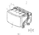
- FIG. 1 is a perspective view showing an appearance of a lidar device;
- FIG. It is a perspective view which shows the structure of a cover. It is a rear view which shows the structure of a film substrate. It is a figure which shows the adhesion
- FIG. 5 is a cross-sectional view taken along line VV of FIG. 4; 4 is a flow chart showing a part of manufacturing steps of the lidar device. It is a figure which shows an adhesion area
- FIG. 6 is a cross-sectional view corresponding to FIG. 5 when the direction connecting the first land and the second land is the direction in which the radius of curvature of the first surface is small; It is a flow chart which shows some processes among manufacturing processes of a lidar device in a modification.
- the lidar device 1 shown in FIG. 1 is an optical measurement device that measures the distance to an object by irradiating light and detecting object reflected light, which is light reflected by an object. be.
- the lidar is also written as LiDAR.
- LiDAR is an abbreviation for Light Detection and Ranging.
- the lidar device 1 is used by being mounted on a vehicle, for example, and used to detect various objects existing in front of the vehicle.
- the lidar device 1 includes a housing 2 as shown in FIG.
- the housing 2 is a resin box formed in a substantially rectangular parallelepiped shape.
- a detection module (not shown) is housed inside the housing 2 .
- the detection module includes at least a portion that emits illumination light and a portion that detects object reflected light.
- the portion irradiated with irradiation light is irradiated with light in a predetermined wavelength range in the near-infrared region as irradiation light.
- the portion irradiated with irradiation light is irradiated with light in a wavelength range of approximately 780 nm or more and 1000 nm or less.
- the forward direction is the direction of the irradiation destination of the irradiation light.
- the horizontal direction is the direction when the housing 2 is viewed from the rear rear surface. A portion of the detection module that is irradiated with the irradiation light scans the irradiation light along the left-right direction.
- the housing 2 includes a housing body 3 and a cover 4.
- the housing body 3 is a part to which the detection module is assembled.
- the cover 4 is a portion provided on the front surface of the housing 2 .
- the cover 4 includes a light transmitting member 5, a frame 6, and a shielding plate 7. As shown in FIG. 2, the cover 4 includes a light transmitting member 5, a frame 6, and a shielding plate 7. As shown in FIG. 2, the cover 4 includes a light transmitting member 5, a frame 6, and a shielding plate 7. As shown in FIG.
- the light transmitting member 5 is arranged on the front side of the cover 4 so as to face the detection module.
- the light transmission member 5 is a plate-shaped member through which the irradiation light and the object reflected light are transmitted.
- the light transmitting member 5 is made of polycarbonate, acryl, or glass, for example.
- the inner surface of the light transmitting member 5 is hereinafter referred to as a first surface 51 .
- the surface of the light transmitting member 5 opposite to the first surface 51 that is, the outer surface of the light transmitting member 5 is referred to as a second surface 52 .
- the light-transmitting member 5 has a shape in which a substantially rectangular plate-like member is curved so as to be most convex at the center in the left-right direction. Specifically, the light-transmitting member 5 is curved so as to be convex forward when viewed from above or below, and has a substantially rectangular shape when viewed from the left or right. Therefore, the first surface 51 and the second surface 52 are curved. The direction in which the radius of curvature of the first surface 51 and the second surface 52 is the minimum is the horizontal direction, and the direction of the maximum is the vertical direction.
- the light-transmitting member 5 is configured so as to hardly transmit light in the visible range and to easily transmit light in a predetermined wavelength range outside the visible range.
- the wavelength range of light in the visible region in the present disclosure has a lower limit of 360 to 400 nm and an upper limit of 760 to 780 nm.
- the predetermined wavelength range is specifically a predetermined wavelength range in the near-infrared region, and in this embodiment, a wavelength range of about 780 nm or more and 1000 nm or less.
- the light transmission member 5 is configured to have a transmittance of 10% or less for light in the visible range and a transmittance of 75% or more for light with a wavelength of approximately 780 nm or more and 1000 nm or less.
- the frame 6 is a frame-shaped member extending rearward from the outer periphery of the light transmitting member 5 .
- the shielding plate 7 is a plate-like member provided along the left-right direction so as to protrude from the first surface 51 .
- the irradiation light is transmitted through a region above the shielding plate 7 on the first surface 51 and irradiated.
- the object-reflected light is transmitted through a region of the first surface 51 below the shielding plate 7 and received.
- the film substrate 10 is a printed circuit board in which various wiring patterns are formed on a film-shaped insulating substrate.
- the film substrate 10 is attached to the first surface 51 .
- the film substrate 10 is provided with a heater wire forming a heater 11 for heating the light transmitting member 5 and a wiring pattern 12 that is a wiring pattern for the electronic component 20 .
- the electronic component 20 is a component that constitutes at least part of the circuit used to control the heater 11 .
- Electronic component 20 is attached to film substrate 10 .
- the electronic component 20 is a temperature sensor that detects the temperature of the light transmitting member 5 for temperature control of the heater 11 .
- a thermistor for example, is used as the temperature sensor.
- the electronic component 20 is arranged in an area other than the area where the heater 11 is arranged on the first surface 51 . In this embodiment, the electronic component 20 is arranged below the area where the heater 11 is arranged.
- the electronic component 20 is attached to the land 13 using an adhesive member 30.
- an adhesive member 30 As shown in FIGS. 4 and 5, the electronic component 20 is attached to the land 13 using an adhesive member 30.
- a conductive adhesive is used as the adhesive member 30 .
- the conductive adhesive contains a thermosetting resin as its component.
- the land 13 is formed at the tip of the wiring pattern 12 for mounting the electronic component 20 .
- the land 13 includes a first land 131 and a second land 132 that are not electrically connected to each other.
- the first land 131 is formed on the upper side and the second land 132 is formed on the lower side so as to face each other.
- the first land 131 and the second land 132 are formed so that the direction connecting the first land 131 and the second land 132 faces the vertical direction.
- the direction connecting the first land 131 and the second land 132 is, for example, the point of the first land 131 closest to the second land 132 and the point of the second land 132 closest to the first land 131.
- the closest point is not specified as one as in the present embodiment, the point that is the center of the portion of the first land 131 closest to the second land 132 and the point that is the center of the portion of the second land 132 that is the first land 131 It is the direction connecting the point that is the center of the part closest to .
- the electronic component 20 is attached across the first land 131 and the second land 132 so that the longitudinal direction faces the vertical direction.
- the electronic component 20 is adhered to the first land 131 and the second land 132 via the adhesive member 30 .
- the electronic component 20 is attached to the film substrate 10 and thus to the first surface 51 at two locations, the first lands 131 and the second lands 132 .
- the adhesive member 30 is applied to each of the first land 131 and the second land 132 . Specifically, the adhesive member 30 is applied so as to protrude from each of the first land 131 and the second land 132 .
- the direction orthogonal to the direction connecting the first land 131 and the second land 132 on the first surface 51 is defined as the orthogonal direction.
- the land orthogonal length CL which is the length along the orthogonal direction of the land 13, is designed to be shorter than a general land. This is to ensure that the adhesive member 30 protrudes from each of the first land 131 and the second land 132 . This makes it easier to inspect the adhesion state, which will be described later.
- the land orthogonal length CL is designed to be 1 to 1.1 times the electronic component orthogonal length CE, which is the length along the orthogonal direction of the electronic component 20 .
- the orthogonal direction is the left-right direction.
- the component attachment step S ⁇ b>101 is a step of attaching the electronic component 20 to the first land 131 and the second land 132 using the adhesive member 30 .
- the adhesive member 30 is applied to the first land 131 and the second land 132 by a predetermined application amount. When the adhesive member 30 is normally applied, the adhesive member 30 protrudes from the first land 131 and the second land 132 as shown in FIGS. 4 and 5 .
- the electronic component 20 is placed on the adhesive member 30, positioned, and pressed against the first land 131 and the second land 132. be. In this manner, the electronic component 20 is attached across the first land 131 and the second land 132 .
- the adhesion state is inspected in S102 to S105. Thereafter, the adhesive member 30 is cured in a curing step S106.
- a conductive adhesive containing a thermosetting resin is used as the adhesive member 30 . Therefore, the bonding member 30 is cured by heating the bonding member 30 in the curing step S106.
- the adhesion state inspections S102 to S105 are performed in the manufacturing process of the lidar device 1 after the component mounting step S101 and before the curing step S106. That is, in the present embodiment, the adhesion state inspections S102 to S105 are performed before the adhesive member 30 is cured.
- the adhesive state is the state of the applied adhesive member 30 .
- the state here is, for example, the size of the adhesion region R and the size of the adhesion gap D.
- the adhesion interval D is the interval between the adhesion area R of the first land 131 and the adhesion area R of the second land 132 .
- the adhesive region R is, as shown in FIG. 7, a region where the applied adhesive member 30 exists when the light transmitting member 5 is viewed from the front.
- the bonding region R includes a first bonding region R1 and a second bonding region R2.
- the first adhesion region R1 is a region protruding from the land 13.
- the second adhesion region R2 is a region that overlaps the land 13. As shown in FIG.
- Inspections S102 to S105 of the adhesion state are performed by an inspection device.
- the inspection device includes at least a light source and a camera.
- the inspection apparatus irradiates the light transmitting member 5 with transmitted light from the second surface 52, and receives reflected light, which is light reflected by the transmitted light.
- the inspection apparatus irradiates the light transmitting member 5 with transmitted light L from the light source 40, and the camera 50 receives and captures the reflected light.
- the transmitted light L is light within a wavelength range that is easily transmitted through the light transmission member 5 .
- a near-infrared light source is used as the light source 40 .
- the transmitted light L light in a wavelength range of approximately 780 nm or more and 1000 nm or less is irradiated.
- the camera 50 is a camera that is highly sensitive to light of the wavelength of the transmitted light L.
- a near-infrared camera is used as the camera 50 .
- the imaging area A of the camera 50 includes the land 13 , the adhesive member 30 and the electronic component 20 .
- the adhesive member 30 is configured to be able to reflect the transmitted light L.
- the adhesive member 30 has a reflectance of the transmitted light L of 10% or more and a transmittance of the transmitted light L of 20% or less. Thereby, the inspection apparatus can receive and image the reflected light reflected by the adhesive member 30 with the camera 50 .
- the inspection device identifies the first adhesion region R1 from the captured image that is the image captured by the camera 50.
- the captured image 60 includes the land 13, the adhesive member 30, and the electronic component 20, as shown in FIG.
- the brightness of the land 13 and the adhesive member 30 in the captured image 60 is low, and the brightness of the electronic component 20 is high.
- the inspection device binarizes the captured image 60 with a predetermined brightness, and classifies the land 13 and the adhesive member 30 from the electronic component 20 according to the level of brightness. Further, in this embodiment, the imaging area A is constant, and the size of the land 13 is known.
- the inspection apparatus detects the outer edge of the land 13 in the captured image 60, recognizes the boundary between the land 13 and the adhesive member 30, and classifies the land 13 and the adhesive member 30.
- FIG. Since the area in which the adhesive member 30 exists in the captured image 60 corresponds to the first adhesive area R1, the inspection apparatus identifies the first adhesive area R1 as described above.
- the inspection device detects the size of the adhesion region R as the adhesion state based on the first adhesion region R1 specified in S103. Then, the inspection device calculates the estimated thickness t from the size of the adhesion region R, and determines whether or not the mounting state in which the electronic component 20 is mounted is good based on the estimated thickness t.
- the estimated thickness t is the thickness of the adhesive member 30 present at a position sandwiched between the land 13 and the electronic component 20, as shown in FIG.
- the inspection device determines that the mounting state is defective when the degree of floating of the electronic component is large. It can be said that the estimated thickness t is a value representing the degree of floating of the electronic component. Therefore, when the estimated thickness t calculated as described above is equal to or greater than a predetermined thickness threshold value, the inspection apparatus determines that the degree of floating of the electronic component is large, that is, the mounting state is poor. I judge.
- the shape of the bonding area R in the state where the electronic component 20 is attached to the land 13 using the bonding member 30 can approximate an elliptical shape. Therefore, the size of the bonding region R can be approximately obtained from the distance X between the upper end portion and the lower end portion of the bonding region R and the distance Y between the left end portion and the right end portion. Specifically, by multiplying the product of the distance X and the distance Y by a predetermined constant, the size of the adhesion region R can be obtained approximately. For this reason, the distance X and the distance Y are calculated in order to detect the size of the adhesion area R. As shown in FIG.
- the inspection device uses the captured image 60 to identify the left end, right end, and upper end or lower end of the bonding area R. Then, the inspection device calculates the distance X and the distance Y from each of the identified ends.
- the inspection device obtains the half size of the distance X based on the upper end or the lower end of the adhesive region R, whichever is shown in the captured image 60, the left end, and the right end. Then, the inspection device calculates the distance X based on the half size of the distance X.
- the inspection apparatus calculates the estimated thickness t according to the formula (1) from the product of the distance X and the distance Y calculated as described above. where C is a constant.
- the estimated thickness t is the thickness of the adhesive member 30 present at a position sandwiched between the land 13 and the electronic component 20, and can be said to be a value representing the degree of floating of the electronic component. Therefore, the larger the estimated thickness t is, the farther the electronic component 20 is from the land 13 .
- the fact that the electronic component 20 is separated from the land 13 means that the pressure applied to the electronic component 20 in the component mounting step S101 was insufficient.
- the inspection device determines that the mounting state is defective.
- the inspection device may determine the attachment state by taking into consideration the bleeding amount.
- the inspection device detects the size of the adhesion gap D as the adhesion state based on the first adhesion region R1 specified in S103, and determines whether or not the adhesion state is good. .
- the inspection device needs to inspect whether the first bonding region R1 of the first land 131 and the first bonding region R1 of the second land 132 do not overlap.
- the adhesive member 30 applied to the first land 131 and the adhesive member 30 applied to the second land 132 are not connected to each other, if the distance between them is short, migration of the adhesive member 30 occurs due to aging. are more likely to occur.
- the inspection device determines that the bonding state is poor. Specifically, the inspection device detects the size of the adhesion gap D, and determines that the adhesion state is poor when the adhesion gap D is equal to or less than the gap threshold, which is a predetermined threshold.
- the inspection apparatus uses a captured image 60 to calculate the distance between the first bonding region R1 of the first land 131 and the first bonding region R1 of the second land 132. . Specifically, the inspection apparatus detects a line segment extending along the direction connecting the first land 131 and the second land 132, which is the outer edge of the first bonding region R1 between the first land 131 and the second land 132. Calculate the length of the line segment connecting them. In the present embodiment, the shortest length among the calculated lengths of the line segments is taken as the size of the adhesion gap D. FIG.
- the fact that the bonding distance D is small means that the distance between the adhesive member 30 applied to the first land 131 and the adhesive member 30 applied to the second land 132 is short.
- the length of the above line segment is 0 or close to 0 in a portion close to the overlapping portion. be a value.
- the bonding distance D is 0 or a value close to 0.
- the bonding distance D can be obtained, and the bonding distance D can be a sufficiently small value.
- the case where the adhesion interval D is equal to or less than the interval threshold includes the case where the first land 131 and the second land 132 partly overlap with each other in the first adhesion region R1.
- the inspection device detects the size of the adhesion gap D, and determines that the adhesion state is defective when the adhesion gap D is equal to or less than the gap threshold value. It is possible to determine that both the defect with the higher probability and the defect with the higher probability are defective.
- the inspection device evaluates the adhesion state by taking into consideration the amount of oozing, as in the determination of the mounting state. You can judge.
- a camera 50 having a resolution of half or less of the interval threshold is used.
- a resolution equal to or less than half the interval threshold means that the length corresponding to one pixel of the imaging device of the camera 50 in the captured image 60 is equal to or less than half the interval threshold.
- the light transmission member 5 is irradiated from the second surface 52 with the transmitted light L, which is light in a wavelength range that easily passes through the light transmission member 5, and the adhesion state is determined based on the reflected light. detected. Further, in the manufacturing process of the lidar device 1, inspections S102 to S105 of the adhesion state are performed after the component mounting step S101 of mounting the electronic component 20 on the land 13 using the adhesive member 30. FIG. In the component mounting step S ⁇ b>101 , the adhesive member 30 is applied so as to protrude from the land 13 .
- the state of the adhesive member 30 can be easily confirmed from the second surface 52 .
- the size of the adhesion region R is detected as the adhesion state. Then, an estimated thickness t is calculated from the size of the detected adhesion region R, and when the calculated estimated thickness t is equal to or greater than the thickness threshold value, it is determined that the mounting state is defective.
- the present embodiment it is possible to determine from the size of the bonding area R whether the degree of floating of the electronic component is large, that is, whether the mounting state is defective.
- the electronic component 20 is attached across the first land 131 and the second land 132 .
- the adhesive member 30 is applied so as to protrude from each of the first land 131 and the second land 132 .
- the size of the adhesion gap D is detected as the adhesion state. Then, when the adhesion distance D is equal to or less than the distance threshold value, it is determined that the adhesion state is poor.
- the present embodiment it is possible to determine from the size of the adhesion gap D whether there is a defect that causes a short circuit or a defect that increases the possibility of migration, that is, whether the bonding state is defective.
- the reflected light can be obtained as the captured image 60, so the adhesion state can be easily detected based on the reflected light.
- a camera 50 having a resolution of half or less than the interval threshold is used.
- a resolution equal to or less than half the interval threshold means that the length corresponding to one pixel of the imaging device of the camera 50 in the captured image 60 is equal to or less than half the interval threshold.
- the size of the adhesion gap D is detected using the captured image 60 captured by the camera 50, and when the detected adhesion gap D is equal to or less than the gap threshold value, the adhesion state is determined to be poor. be.
- the captured image 60 at least one pixel among the pixels of the above-described image sensor is included in the area having the length corresponding to the interval threshold value. Therefore, it is possible to detect the size of the adhesion gap D with high accuracy.
- a film substrate 10 having a heater 11 for heating the light transmitting member 5 is provided on the first surface 51 of the light transmitting member 5 .
- a land 13 is formed on the film substrate 10 .
- the electronic component 20 is attached to the land 13 formed on the film substrate 10, so that the film substrate 10 can be used as a substrate of an electric circuit for the electronic component 20. . Therefore, it is not necessary to separately provide an electric circuit board for the electronic component 20 .
- the electronic component 20 is a temperature sensor that detects the temperature of the light transmitting member 5 .
- the inspection method of the present embodiment if the degree of floating of the electronic component is large, it is determined that the mounting state is defective.
- a temperature sensor is used as the electronic component 20 , a large degree of floating of the electronic component may lead to a deterioration in the detection accuracy of the temperature of the light transmitting member 5 . Therefore, it is possible to suppress deterioration in the detection accuracy of the temperature of the light transmitting member 5 by the temperature sensor.
- the adhesive member 30 is configured so that the reflectance for the transmitted light L is 10% or more.
- the reflected light reflected by the adhesive member 30 is received by the camera 50 and captured. Therefore, according to this embodiment, the adhesive member 30 in the captured image 60 can be made clear.
- the electronic component 20 is attached to the land 13 provided on the first surface 51 of the light transmitting member 5 using the adhesive member 30 .
- the adhesive member 30 is applied so as to protrude from the land 13 .
- the adhesive member 30 protrudes from the land 13 , the state of the adhesive member 30 can be easily confirmed from the second surface 52 .
- the electronic component 20 is attached across the first land 131 and the second land 132 that are not electrically connected to each other.
- the adhesive member 30 is applied so as to protrude from each of the first land 131 and the second land 132 .
- the land orthogonal length CL is 1 to 1.1 times the electronic component orthogonal length CE.
- the adhesive member 30 in the manufacturing process of the lidar device 1, can be easily protruded from the first land 131 and the second land 132, and the electronic component 20 can be easily attached to the first land 131 and the second land 132. can do.
- the first surface 51 is curved.
- the electronic component 20 is attached across the first land 131 and the second land 132 that are not electrically connected to each other.
- the direction connecting the first land 131 and the second land 132 is the direction in which the radius of curvature of the first surface 51 is maximum.
- the first land 131 and the second land 132 are arranged such that the direction connecting the first land 131 and the second land 132 is the direction of the small curvature radius of the first surface 51, for example, the horizontal direction.
- the land 132 is formed, the first land 131 and the second land 132 are not substantially coplanar.
- the electronic component 20 when the electronic component 20 is pressed against the first land 131 and the second land 132 in the component mounting step S101, there is a possibility that sufficient pressure cannot be applied.
- the electronic component 20 may be destroyed by the pressurization. That is, in the case of such a configuration, it is difficult to pressurize the electronic component 20 and attach it to the first land 131 and the second land 132 in the component attachment step S101.
- the first land 131 and the second land 132 are formed such that the direction connecting the first land 131 and the second land 132 faces the direction in which the radius of curvature of the first surface 51 is maximum.
- the first land 131 and the second land 132 exist on substantially the same plane. Therefore, when the electronic component 20 is pressed against the first land 131 and the second land 132 in the component mounting step S101, the pressure can be sufficiently applied, and there is a possibility that the electronic component 20 may be destroyed by the pressure. low.
- the component mounting step S101 it is possible to easily attach the electronic component 20 to the first land 131 and the second land 132 by applying pressure.
- the adhesion state inspections S102 to S105 are performed before the curing step S106, that is, before the adhesive member 30 is cured.
- the timing of the adhesion state inspections S102 to S105 in the manufacturing process of the lidar device 1 is not limited to before the adhesive member 30 is cured.
- inspections S102 to S105 of the bonding state may be performed after the component mounting and curing step S201.
- the component mounting and curing step S201 differs from the component mounting and curing step S101 of the above embodiment in that it includes a step of curing the adhesive member 30 in addition to the component mounting and curing step S101. That is, the inspections S102 to S105 of the bonding state may be performed after the bonding member 30 is cured.
- the adhesive member 30 is not limited to a conductive adhesive containing a thermosetting resin.
- solder may be used as the adhesive member 30 .
- the adhesive member 30 may be cured by a method other than heating.
- inspections S102 to S105 of the adhesion state are performed by an inspection device.
- at least some steps of the inspection may be performed by an operator, for example.
- the electronic component 20 is a temperature sensor that detects the temperature of the light transmitting member 5 and is used for temperature control of the heater 11.
- the electronic component 20 may be a component other than a temperature sensor. good.
- the film substrate 10 is provided with the heater wires forming the heater 11 for heating the light transmitting member 5 and the wiring pattern 12 that is the wiring pattern for the electronic component 20. ing.
- the film substrate 10 does not necessarily have to be formed with the heater wire and the wiring pattern 12 that constitute the heater 11 .
- a film substrate 10 on which the heater wires forming the heater 11 are not formed may be used.
- the inspection device detects a line segment extending along the direction connecting the first land 131 and the second land 132, The length of the line segment connecting the outer edges of one adhesion region R1 is calculated, and the shortest length of the length of the line segment is detected as the size of the adhesion gap D.
- the method of detecting the size of the adhesion gap D is not limited to the method of the above embodiment. For example, for an arbitrary line segment that connects the outer edges of the first bonding regions R1 of the first land 131 and the second land 132, the inspection device determines the shortest length of the line segment as the bonding distance D. It may be detected as a size.
- the film substrate 10 and the electronic component 20 are provided on the first surface 51 .
- the film substrate 10 and the electronic component 20 do not necessarily have to be provided on the first surface 51 .
- the film substrate 10 and electronic component 20 may be provided on the second surface 52 .
- the inspection apparatus irradiates the light transmission member 5 with the transmitted light L from the first surface 51 in S102.
- the lidar device 1 is exemplified as an optical measurement device, but the optical measurement device is not limited to this.
- the function of one component in the above embodiment may be distributed as multiple components, or the functions of multiple components may be integrated into one component. Also, part of the configuration of the above embodiment may be omitted. Also, at least a part of the configuration of the above embodiment may be added, replaced, etc. with respect to the configuration of the other above embodiment.
- the first surface 51 corresponds to the mounting surface.
- the gap threshold value corresponds to the adhesion gap that serves as a reference for determining a defect.
Landscapes
- Physics & Mathematics (AREA)
- General Physics & Mathematics (AREA)
- Engineering & Computer Science (AREA)
- Remote Sensing (AREA)
- Radar, Positioning & Navigation (AREA)
- Electromagnetism (AREA)
- Analytical Chemistry (AREA)
- General Health & Medical Sciences (AREA)
- Immunology (AREA)
- Pathology (AREA)
- Biochemistry (AREA)
- Chemical & Material Sciences (AREA)
- Life Sciences & Earth Sciences (AREA)
- Health & Medical Sciences (AREA)
- Computer Networks & Wireless Communication (AREA)
- Length Measuring Devices By Optical Means (AREA)
Abstract
照射光の反射に基づき距離を計測する光計測装置の製造工程において、可視域外の所定の波長範囲の光を透過するように構成された光透過部材の第1の面に設けられたランドに接着部材を用いて電子部品を取り付ける部品取付工程よりも後に実施される接着状態の検査方法である。接着状態の検査方法は、前記光透過部材に前記第1の面とは反対側の第2の面から前記波長範囲内の透過光を照射して、その反射光を受光すること(S102)と、前記反射光に基づき前記接着状態を検出すること(S103~S105)と、を含む。前記部品取付工程において、前記接着部材は、前記ランドからはみ出すように塗布される。
Description
本国際出願は、2021年6月16日に日本国特許庁に出願された日本国特許出願第2021-100462号に基づく優先権を主張するものであり、日本国特許出願第2021-100462号の全内容を本国際出願に参照により援用する。
本開示は、接着状態の検査方法及び光計測装置に関する。
前方にある物体との距離を計測する光計測装置として、照射光を前方に向けて照射し、当該照射光が物体で反射した光を検出し、その物体までの距離を計測する光計測装置が知られている。光計測装置は、一般的に筐体を有する。筐体における測定方向側には、照射光及び当該照射光が物体で反射した光が透過する光透過部材が設けられる。
この種の光計測装置では、光透過部材の面に接着部材を用いて電子部品が取り付けられることがある。例えば、特許文献1には、筐体における測定方向側に送信波及び反射波を透過する透過窓が設けられ、当該透過窓の内面に設けられたランドに温度センサがはんだ付けされている測距装置が開示されている。
日本工業標準調査会、光学用語、JIS Z 8120: 2001、2001年
ところで、この種の光計測装置の製造工程では、接着部材を用いて電子部品を取り付けた後に、接着状態を検査することが必要である。検査する方法として、例えば、電子部品が取り付けられた面の側から接着部材の状態を確認する方法が考えられる。しかしながら、このような方法では、電子部品で覆われた位置に存在する接着部材の状態を確認することができない。そこで、電子部品が取り付けられた面とは反対側の面から接着部材の状態を確認する方法が考えられる。しかしながら、光透過部材は信号として用いる光以外の波長の光はノイズになるため、信号として用いる光以外の波長の光はできるだけ透過させないように構成されている。そのため、発明者の詳細な検討の結果、電子部品が取り付けられた面とは反対側の面から目視やカメラを用いて接着部材の状態を確認する場合に、大半の波長の光は遮蔽されて中身を見ることが難しいという課題が見出された。
本開示の一局面は、接着部材の状態を容易に確認するための技術を提供する。
本開示の一態様は、接着状態の検査方法である。接着状態の検査方法は、照射光の反射に基づき距離を計測する光計測装置の製造工程において、部品取付工程よりも後に実施される。部品取付工程は、可視域外の所定の波長範囲の光を透過するように構成された光透過部材の第1の面に設けられたランドに接着部材を用いて電子部品を取り付ける工程である。接着状態の検査方法は、光透過部材に第1の面とは反対側の第2の面から上述した波長範囲内の透過光を照射して、その反射光を受光することと、反射光に基づき接着状態を検出することと、を含む。部品取付工程において、接着部材は、ランドからはみ出すように塗布される。
このような構成によれば、接着部材の状態を容易に確認することができる。
本開示の別の態様は、照射光の反射に基づき距離を計測する光計測装置である。光計測装置は、光透過部材と、電子部品と、を備える。光透過部材は、可視域外の所定の波長範囲の光を透過するように構成される。電子部品は、光透過部材の一方の面である取付面に設けられたランドに接着部材を用いて取り付けられる。接着部材は、ランドからはみ出すように塗布されている。
このような構成によれば、接着部材の状態を容易に確認することができる。
以下、本開示の例示的な実施形態について図面を参照しながら説明する。
[1.構成]
[1-1.全体構成]
図1に示すライダ装置1は、光を照射し、照射した光である照射光が物体で反射した光である物体反射光を検出することで、当該物体までの距離を計測する光計測装置である。ライダはLiDARとも表記される。LiDARは、Light Detection and Rangingの略語である。ライダ装置1は、例えば車両に搭載して使用され、車両の前方に存在する様々な物体の検出に用いられる。
[1.構成]
[1-1.全体構成]
図1に示すライダ装置1は、光を照射し、照射した光である照射光が物体で反射した光である物体反射光を検出することで、当該物体までの距離を計測する光計測装置である。ライダはLiDARとも表記される。LiDARは、Light Detection and Rangingの略語である。ライダ装置1は、例えば車両に搭載して使用され、車両の前方に存在する様々な物体の検出に用いられる。
ライダ装置1は、図1に示すように、筐体2を備える。筐体2は、略直方体状に形成された樹脂製の箱体である。筐体2の内部には、図示しない検出モジュールが収納されている。検出モジュールは、照射光を照射する部分と、物体反射光を検出する部分と、を少なくとも備える。本実施形態では、照射光を照射する部分は、照射光として、近赤外域における所定の波長範囲の光を照射する。具体的には、照射光を照射する部分は、約780nm以上1000nm以下の波長範囲の光を照射する。
以下では、説明の便宜上、上下左右及び前後の方向を用いて構造を説明する。しかしながら、本開示は、使用態様などが上記の方向に限定されることはない。前方は、照射光の照射先の方向である。左右方向は、筐体2を後方背面から見たときの方向である。なお、検出モジュールにおける照射光を照射する部分は、左右方向に沿って照射光を走査する。
筐体2は、筐体本体3と、カバー4と、を備える。筐体本体3は、検出モジュールが組み付けられる部分である。カバー4は、筐体2における前面に設けられた部分である。
[1-2.カバーの構成]
図2に示すように、カバー4は、光透過部材5と、枠体6と、遮蔽板7と、を備える。
図2に示すように、カバー4は、光透過部材5と、枠体6と、遮蔽板7と、を備える。
光透過部材5は、検出モジュールに対向しカバー4における前側に配置されている。光透過部材5は、照射光及び物体反射光が透過する板状の部材である。光透過部材5は、例えば、ポリカーボネート、アクリル又はガラスにより形成されている。以下、光透過部材5の内面を、第1の面51とする。また、光透過部材5の第1の面51とは反対側の面、すなわち光透過部材5の外面を、第2の面52とする。
光透過部材5は、略長方形の板状の部材を左右方向の中央で最も凸となるように湾曲させた形状を有する。具体的には、光透過部材5は、上方又は下方から見ると前方に向けて凸となるように湾曲しており、左方又は右方から見ると略長方形状であるような形状を有する。このため、第1の面51及び第2の面52は、曲面状に形成されている。また、第1の面51及び第2の面52における曲率半径が最小である方向が左右方向であり、最大である方向が上下方向である。
光透過部材5は、可視域の光を透過しづらく、可視域外の所定の波長範囲の光を透過しやすいように構成されている。なお、本開示における可視域の光の波長範囲は、非特許文献1に基づき、下限は360~400nm、上限は760~780nmとする。所定の波長範囲は、具体的には、近赤外域における所定の波長範囲であり、本実施形態では、約780nm以上1000nm以下の波長範囲である。光透過部材5は、可視域の光の透過率が10%以下であり、約780nm以上1000nm以下の波長の光の透過率が75%以上であるように構成されている。
枠体6は、光透過部材5の外周から後方に向けて延びている、枠状の部材である。
遮蔽板7は、第1の面51から突出するように、左右方向に沿って設けられた板状の部材である。本実施形態では、照射光は、第1の面51における遮蔽板7よりも上側の領域を透過して照射される。物体反射光は、第1の面51における遮蔽板7よりも下側の領域を透過して受光される。
[1-3.フィルム基板の構成]
図3に示すように、第1の面51には、フィルム基板10と、電子部品20と、が設けられている。
図3に示すように、第1の面51には、フィルム基板10と、電子部品20と、が設けられている。
フィルム基板10は、フィルム状の絶縁基板上に各種配線パターンが形成されたプリント基板である。フィルム基板10は、第1の面51に貼り付けられている。本実施形態では、フィルム基板10には、光透過部材5を加熱するためのヒータ11を構成するヒータ線と、電子部品20への配線のパターンである配線パターン12と、が形成されている。
電子部品20は、ヒータ11の制御に用いられる回路の少なくとも一部を構成する部品である。電子部品20は、フィルム基板10に取り付けられている。本実施形態では、電子部品20は、ヒータ11の温度制御のために光透過部材5の温度を検出する温度センサである。温度センサとしては、例えば、サーミスタが用いられる。
電子部品20は、第1の面51におけるヒータ11が配置された領域以外の領域に配置されている。本実施形態では、電子部品20は、ヒータ11が配置された領域よりも下側に配置されている。
図4及び図5に示すように、電子部品20は、接着部材30を用いてランド13に取り付けられている。接着部材30としては、導電性接着剤が用いられる。本実施形態では、導電性接着剤は、その成分として熱硬化性樹脂を含有する。
ランド13は、電子部品20を取り付けるために、配線パターン12の先端に形成されている。本実施形態では、ランド13として、互いに導通していない第1ランド131と第2ランド132とを備える。第1ランド131は上側に、第2ランド132は下側に、互いに対向するように形成されている。つまり、第1ランド131及び第2ランド132は、第1ランド131と第2ランド132とを結んだ方向が上下方向を向くように形成されている。ここで、第1ランド131と第2ランド132とを結んだ方向とは、例えば、第1ランド131における第2ランド132に最も近い点と、第2ランド132における第1ランド131に最も近い点と、を結んだ方向である。本実施形態のように、当該最も近い点が1つに特定されない場合には、第1ランド131における第2ランド132に最も近い部分の中心となる点と、第2ランド132における第1ランド131に最も近い部分の中心となる点と、を結んだ方向である。電子部品20は、長手方向が上下方向を向くように、第1ランド131及び第2ランド132に跨がって取り付けられている。
電子部品20は、接着部材30を介して第1ランド131及び第2ランド132に接着されている。つまり、電子部品20は、第1ランド131及び第2ランド132の2箇所で、フィルム基板10に、ひいては第1の面51に取り付けられている。接着部材30は、第1ランド131及び第2ランド132のそれぞれに塗布されている。具体的には、接着部材30は、第1ランド131及び第2ランド132のそれぞれからはみ出すように塗布されている。
ここで、第1の面51における第1ランド131と第2ランド132とを結んだ方向に直交する方向を、直交方向とする。ランド13の直交方向に沿った長さであるランド直交長さCLは、一般的なランドと比べて短く設計されている。これは、接着部材30が第1ランド131及び第2ランド132のそれぞれから確実にはみ出すようにするためである。これにより、後述する接着状態の検査が行いやすくなる。本実施形態では、ランド直交長さCLは、電子部品20の直交方向に沿った長さである電子部品直交長さCEの1倍以上1.1倍以下に設計されている。なお、本実施形態では、直交方向は左右方向を向く。
ここで、ライダ装置1の製造工程のうち一部の工程について、図6に示すフローチャートを用いて説明する。
まず、部品取付工程S101について説明する。部品取付工程S101は、第1ランド131及び第2ランド132に接着部材30を用いて電子部品20を取り付ける工程である。部品取付工程S101において、接着部材30は、第1ランド131及び第2ランド132に、あらかじめ定められた塗布量だけ塗布される。接着部材30が正常に塗布されると、図4及び図5に示すように、接着部材30は第1ランド131及び第2ランド132のそれぞれからはみ出す。
接着部材30が第1ランド131及び第2ランド132に塗布された後、電子部品20が、接着部材30に載せられて位置決めされ、第1ランド131及び第2ランド132に押しつける方向に加圧される。このようにして、電子部品20は、第1ランド131及び第2ランド132に跨がって取り付けられる。
図6に戻り、部品取付工程S101において電子部品20が第1ランド131及び第2ランド132に取り付けられた後、S102~S105で接着状態の検査が実施される。その後、硬化工程S106で接着部材30が硬化される。上述のように、本実施形態では、接着部材30として、熱硬化性樹脂を含有する導電性接着剤が用いられる。そのため、硬化工程S106において接着部材30が加熱されることによって、接着部材30は硬化される。
[2.接着状態の検査方法]
次に、接着状態の検査方法について説明する。上述のように、接着状態の検査S102~S105は、ライダ装置1の製造工程において、部品取付工程S101よりも後、かつ、硬化工程S106よりも前に実施される。すなわち、本実施形態では、接着状態の検査S102~S105は、接着部材30の硬化前に実施される。接着状態とは、塗布された接着部材30の状態である。ここでいう状態とは、例えば、接着領域Rの大きさや、接着間隔Dの大きさである。接着間隔Dとは、第1ランド131の接着領域Rと第2ランド132の接着領域Rとの間隔である。接着領域Rとは、図7に示すように、光透過部材5を前方から平面視したときにおいて塗布された接着部材30が存在する領域である。接着領域Rは、第1接着領域R1と、第2接着領域R2と、を含む。第1接着領域R1は、ランド13からはみ出している領域である。第2接着領域R2は、ランド13に重なっている領域である。
次に、接着状態の検査方法について説明する。上述のように、接着状態の検査S102~S105は、ライダ装置1の製造工程において、部品取付工程S101よりも後、かつ、硬化工程S106よりも前に実施される。すなわち、本実施形態では、接着状態の検査S102~S105は、接着部材30の硬化前に実施される。接着状態とは、塗布された接着部材30の状態である。ここでいう状態とは、例えば、接着領域Rの大きさや、接着間隔Dの大きさである。接着間隔Dとは、第1ランド131の接着領域Rと第2ランド132の接着領域Rとの間隔である。接着領域Rとは、図7に示すように、光透過部材5を前方から平面視したときにおいて塗布された接着部材30が存在する領域である。接着領域Rは、第1接着領域R1と、第2接着領域R2と、を含む。第1接着領域R1は、ランド13からはみ出している領域である。第2接着領域R2は、ランド13に重なっている領域である。
以下では、図6に示すフローチャートを用いて、接着状態の検査方法について説明する。接着状態の検査S102~S105は、検査装置により実施される。検査装置は、光源と、カメラと、を少なくとも備える。
まず、S102で、検査装置は、光透過部材5に第2の面52から透過光を照射し、透過光が反射した光である反射光を受光する。具体的には、図8に示すように、検査装置は、光源40から光透過部材5に透過光Lを照射し、その反射光をカメラ50で受光し撮像する。透過光Lは、光透過部材5を透過しやすい波長範囲内の光である。本実施形態では、光源40として、近赤外光源が用いられる。また、透過光Lとして、約780nm以上1000nm以下の波長範囲の光が照射される。
カメラ50は、透過光Lの波長の光に対する感度が高いカメラである。本実施形態では、カメラ50として、近赤外カメラが用いられる。また、本実施形態では、カメラ50の撮像領域Aにランド13、接着部材30及び電子部品20が含まれる。
接着部材30は、透過光Lを反射可能に構成される。本実施形態では、接着部材30は、透過光Lの反射率が10%以上であり、透過光Lの透過率が20%以下である。これにより、検査装置は、接着部材30で反射した反射光をカメラ50で受光し撮像することができる。
図6に戻り、S103で、検査装置は、カメラ50により撮像された画像である撮像画像から第1接着領域R1を特定する。部品取付工程S101において接着部材30が正常に塗布された場合、図9に示すように、撮像画像60には、ランド13、接着部材30、及び、電子部品20が写っている。本実施形態では、撮像画像60におけるランド13や接着部材30の輝度は低く、電子部品20の輝度は高い。検査装置は、撮像画像60を所定の輝度で二値化し、輝度の高低から、ランド13及び接着部材30と、電子部品20と、を分類する。また、本実施形態では、撮像領域Aは一定であり、ランド13の大きさは既知である。検査装置は、このことを加味して、撮像画像60におけるランド13の外縁を検出し、ランド13と接着部材30との境界を認識して、ランド13と、接着部材30と、を分類する。撮像画像60に写っている接着部材30が存在する領域が第1接着領域R1に相当するため、上述のようにして、検査装置は、第1接着領域R1を特定する。
図6に戻り、S104で、検査装置は、S103で特定された第1接着領域R1に基づき、接着状態として接着領域Rの大きさを検出する。そして、検査装置は、接着領域Rの大きさから推定厚みtを算出し、推定厚みtに基づき、電子部品20が取り付けられている状態である取付状態が良好であるか否かを判定する。推定厚みtとは、図5に示すように、ランド13と電子部品20とに挟まれた位置に存在する接着部材30の厚みである。
電子部品20がランド13から離れている状態である電子部品浮きの程度が大きい場合、導電性の悪化や、温度の検出精度の悪化につながる可能性がある。そのため、検査装置は、電子部品浮きの程度が大きい場合に、取付状態が不良であると判定する。推定厚みtは、電子部品浮きの程度を表す値であると言える。このため、検査装置は、上述のように算出した推定厚みtが所定のしきい値である厚みしきい値以上である場合に、電子部品浮きの程度が大きい、すなわち、取付状態が不良であると判定する。
ここで、接着領域Rの大きさを検出する方法について、図9を用いて説明する。本実施形態では、電子部品20が接着部材30を用いてランド13に取り付けられている状態における接着領域Rの形状は、およそ楕円形状に近似することができる。そのため、接着領域Rの上端部と下端部との距離X及び左端部と右端部との距離Yから、接着領域Rの大きさを近似的に求めることができる。具体的には、距離Xと距離Yとの積に所定の定数を掛けることで、接着領域Rの大きさを近似的に求めることができる。このような理由で、接着領域Rの大きさを検出するために距離X及び距離Yをそれぞれ算出する。
本実施形態では、まず、検査装置は、撮像画像60を用いて、接着領域Rの左端部、右端部、及び、上端部又は下端部を特定する。そして、検査装置は、特定された各端部から、距離X及び距離Yをそれぞれ算出する。
ただし、第2接着領域R2は撮像画像60に写らないことから、接着領域Rの上端部又は下端部は撮像画像60に写らず、特定できない。したがって、撮像画像60から距離Xを直接的に算出することはできない。そのため、検査装置は、接着領域Rの上端部又は下端部のうち撮像画像60に写っている方の端部と、左端部及び右端部と、に基づき、距離Xの半分の大きさを求める。そして、検査装置は、この距離Xの半分の大きさに基づき、距離Xを算出する。
続いて、推定厚みtを算出し、推定厚みtに基づき取付状態が良好であるか否かを判定する方法について説明する。検査装置は、上述のように算出された距離Xと距離Yとの積から、(1)式に従って、推定厚みtを算出する。ここで、Cは定数である。

上述のように、推定厚みtは、ランド13と電子部品20とに挟まれた位置に存在する接着部材30の厚みであり、電子部品浮きの程度を表す値であるとも言える。このため、推定厚みtが大きいほど、電子部品20がランド13から離れていることになる。電子部品20がランド13から離れているということは、部品取付工程S101における電子部品20の加圧が不足していた、ということである。電子部品20の加圧が不足しているほど、接着部材30は広がらず、接着領域Rは小さくなる。すなわち、推定厚みtが大きいほど、接着領域Rは小さくなる、と言える。そのため、推定厚みtは、接着領域Rの大きさと反比例の関係にある。すなわち、推定厚みtは、距離Xと距離Yとの積と反比例の関係にあると言える。
そして、推定厚みtが厚みしきい値以上である場合、検査装置は、取付状態が不良であると判定する。
なお、接着部材30は、硬化するとにじみ出しが発生する。このため、本実施形態のように接着部材30の硬化前に接着状態の検査S102~S105が実施される場合、検査装置は、にじみ出し量を加味して取付状態を判定してもよい。
図6に戻り、S105で、検査装置は、S103で特定された第1接着領域R1に基づき、接着状態として接着間隔Dの大きさを検出し、接着状態が良好であるか否かを判定する。
第1ランド131に塗布されている接着部材30と第2ランド132に塗布されている接着部材30とが接続している場合には、第1ランド131及び第2ランド132は短絡する。そのため、検査装置は、第1ランド131の第1接着領域R1と第2ランド132の第1接着領域R1とが重なっていないかを検査する必要がある。ただし、第1ランド131に塗布されている接着部材30と第2ランド132に塗布されている接着部材30とが接続していなくとも、その距離が近い場合、経年変化に伴い接着部材30のマイグレーションが発生する可能性が高くなる。
そのため、検査装置は、第1ランド131の第1接着領域R1と第2ランド132の第1接着領域R1との距離が近い場合には、接着状態が不良であると判定する。具体的には、検査装置は、接着間隔Dの大きさを検出し、接着間隔Dが所定のしきい値である間隔しきい値以下である場合に、接着状態が不良であると判定する。
本実施形態では、検査装置は、図9に示すように、撮像画像60を用いて、第1ランド131の第1接着領域R1と第2ランド132の第1接着領域R1との距離を算出する。具体的には、検査装置は、第1ランド131と第2ランド132とを結んだ方向に沿って延びる線分であって、第1ランド131及び第2ランド132の第1接着領域R1の外縁同士を結ぶ線分の長さを算出する。本実施形態では、算出された当該線分の長さのうち最短の長さを、接着間隔Dの大きさとする。すなわち、接着間隔Dが小さいということは、第1ランド131に塗布されている接着部材30と第2ランド132に塗布されている接着部材30との距離が近いということである。また、第1ランド131及び第2ランド132の第1接着領域R1の一部が重なっている場合、当該重なっている部分に近い部分においては、上述の線分の長さは0又は0に近い値になる。つまり、第1ランド131及び第2ランド132の第1接着領域R1の一部が重なっている場合には、接着間隔Dは0又は0に近い値になる。
このように、第1ランド131及び第2ランド132の第1接着領域R1の一部が重なっている場合であっても、接着間隔Dは求められ、かつ、接着間隔Dは十分に小さい値をとる。すなわち、接着間隔Dが間隔しきい値以下である場合、には、第1ランド131及び第2ランド132の第1接着領域R1の一部が重なっている場合も含まれる。検査装置は、接着間隔Dの大きさを検出し、接着間隔Dが間隔しきい値以下である場合に、接着状態が不良であると判定することで、短絡する不良と、マイグレーションが発生する可能性が高くなる不良と、の両方を不良であると判定することができる。
なお、本実施形態のように接着部材30の硬化前に接着状態の検査S102~S105が実施される場合、検査装置は、取付状態の判定と同様に、にじみ出し量を加味して接着状態を判定してもよい。
また、本実施形態では、間隔しきい値の半分以下の分解能を有するカメラ50が用いられる。間隔しきい値の半分以下の分解能とは、撮像画像60におけるカメラ50の撮像素子の1画素に相当する長さが、間隔しきい値の半分以下である、ということである。
[3.効果]
以上詳述した実施形態によれば、以下の効果が得られる。
以上詳述した実施形態によれば、以下の効果が得られる。
(3a)接着状態を検査するにあたり、第1の面51の側から接着部材30の状態を確認する場合、電子部品20で覆われた位置に存在する接着部材30の状態を確認することができない。そのため、第2の面52から接着部材30の状態を確認することが考えられる。しかしながら、光透過部材5は、可視域外の所定の波長範囲の光を透過するように構成されているため、第2の面52から目視で接着部材30の状態を確認することは困難である。
本実施形態の検査方法では、光透過部材5に、第2の面52から、光透過部材5を透過しやすい波長範囲の光である透過光Lが照射され、その反射光に基づき接着状態が検出される。また、ライダ装置1の製造工程において、ランド13に接着部材30を用いて電子部品20を取り付ける部品取付工程S101よりも後に、接着状態の検査S102~S105が実施される。部品取付工程S101において、接着部材30は、ランド13からはみ出すように塗布されている。
本実施形態によれば、第2の面52から接着部材30の状態を容易に確認することができる。
(3b)本実施形態の検査方法では、接着状態として、接着領域Rの大きさが検出される。そして、検出された接着領域Rの大きさから推定厚みtが算出され、算出された推定厚みtが厚みしきい値以上である場合に、取付状態が不良であると判定される。
本実施形態によれば、接着領域Rの大きさから、電子部品浮きの程度が大きいか、すなわち、取付状態が不良であるかを判定することができる。
(3c)電子部品20は、第1ランド131と第2ランド132とに跨がって取り付けられる。接着部材30は、第1ランド131及び第2ランド132のそれぞれからはみ出すように塗布されている。本実施形態の検査方法では、接着状態として、接着間隔Dの大きさが検出される。そして、接着間隔Dが間隔しきい値以下である場合に、接着状態が不良であると判定される。
本実施形態によれば、接着間隔Dの大きさから、短絡する不良及びマイグレーションが発生する可能性が高くなる不良があるか、すなわち、接着状態が不良であるかを判定することができる。
(3d)本実施形態の検査方法では、反射光がカメラ50で受光される。そして、カメラ50による撮像画像60に基づき接着状態が検出される。
本実施形態によれば、反射光を撮像画像60として得ることができるため、反射光に基づく接着状態の検出を容易にすることができる。
(3e)本実施形態の検査方法では、間隔しきい値の半分以下の分解能を有するカメラ50が用いられる。間隔しきい値の半分以下の分解能とは、撮像画像60におけるカメラ50の撮像素子の1画素に相当する長さが、間隔しきい値の半分以下である、ということである。また、カメラ50で撮像された撮像画像60を用いて接着間隔Dの大きさが検出され、検出された接着間隔Dが間隔しきい値以下である場合に、接着状態が不良であると判定される。
本実施形態によれば、撮像画像60において、間隔しきい値に相当する長さを有する領域の中に、上述した撮像素子の画素のうち少なくとも1つの画素が必ず包含される。このため、接着間隔Dの大きさの検出を精度良くすることができる。
(3f)光透過部材5の第1の面51には、光透過部材5を加熱するためのヒータ11が形成されているフィルム基板10が設けられる。ランド13は、フィルム基板10に形成されている。
本実施形態によれば、電子部品20は、フィルム基板10に形成されているランド13に取り付けられているため、電子部品20のための電気回路の基板として、フィルム基板10を流用することができる。したがって、電子部品20のための電気回路の基板を別途設ける必要がなくなる。
(3g)電子部品20は、光透過部材5の温度を検出する温度センサである。
本実施形態の検査方法では、電子部品浮きの程度が大きい場合、取付状態が不良であると判定される。電子部品20として温度センサが用いられている場合において、電子部品浮きの程度が大きいことは、光透過部材5の温度の検出精度の悪化につながる可能性がある。したがって、温度センサによる光透過部材5の温度の検出精度が悪化することを抑制できる。
(3h)接着部材30は、透過光Lに対する反射率が10%以上であるように構成される。
接着部材30で反射した反射光は、カメラ50で受光され、撮像される。したがって、本実施形態によれば、撮像画像60における接着部材30を鮮明にすることができる。
(3i)電子部品20は、光透過部材5の第1の面51に設けられたランド13に接着部材30を用いて取り付けられている。接着部材30は、ランド13からはみ出すように塗布されている。
接着状態を検査するにあたり、第1の面51の側から接着部材30の状態を確認する場合、電子部品20で覆われた位置に存在する接着部材30の状態を確認することができない。そのため、第2の面52から接着部材30の状態を確認することが考えられる。
本実施形態によれば、接着部材30がランド13からはみ出しているため、第2の面52から接着部材30の状態を容易に確認することができる。
(3j)電子部品20は、互いに導通していない第1ランド131及び第2ランド132に跨がって取り付けられている。接着部材30は、第1ランド131及び第2ランド132のそれぞれからはみ出すように塗布されている。また、ランド直交長さCLは、電子部品直交長さCEの1倍以上1.1倍以下である。
ランド直交長さCLが短ければ短いほど、塗布された接着部材30が第1ランド131及び第2ランド132からはみ出しやすくなる。一方で、ランド直交長さCLが短すぎると、電子部品20を第1ランド131及び第2ランド132に取り付けることが困難になる。
本実施形態によれば、ライダ装置1の製造工程において、接着部材30を第1ランド131及び第2ランド132からはみ出しやすくするとともに、電子部品20を第1ランド131及び第2ランド132に取り付けやすくすることができる。
(3k)第1の面51は、曲面状に形成される。電子部品20は、互いに導通していない第1ランド131及び第2ランド132に跨がって取り付けられている。第1ランド131及び第2ランド132を結んだ方向が、第1の面51における曲率半径が最大である方向を向いている。
仮に、図10に示すように、第1ランド131及び第2ランド132を結んだ方向が第1の面51における曲率半径が小さい方向、例えば左右方向を向くように、第1ランド131及び第2ランド132が形成された場合、第1ランド131及び第2ランド132は略同一平面上に存在しない。このような構成の場合、部品取付工程S101において、電子部品20を第1ランド131及び第2ランド132に押しつける方向に加圧するとき、十分な加圧ができない可能性がある。また、加圧により電子部品20が破壊される可能性もある。すなわち、このような構成の場合、部品取付工程S101において、電子部品20を加圧して第1ランド131及び第2ランド132に取り付けることが難しい。
本実施形態のように、第1ランド131及び第2ランド132を結んだ方向が第1の面51における曲率半径が最大である方向を向くように、第1ランド131及び第2ランド132が形成されている場合、第1ランド131と第2ランド132とは略同一平面上に存在する。そのため、部品取付工程S101において、電子部品20を第1ランド131及び第2ランド132に押しつける方向に加圧するとき、十分に加圧でき、かつ、加圧により電子部品20が破壊される可能性が低い。
本実施形態によれば、部品取付工程S101において、電子部品20を加圧して第1ランド131及び第2ランド132に取り付けることを容易にすることができる。
[4.他の実施形態]
以上、本開示の実施形態について説明したが、本開示は、上記実施形態に限定されることなく、種々の形態を採り得ることは言うまでもない。
以上、本開示の実施形態について説明したが、本開示は、上記実施形態に限定されることなく、種々の形態を採り得ることは言うまでもない。
(4a)上記実施形態では、接着状態の検査S102~S105は、硬化工程S106よりも前、すなわち接着部材30の硬化前に実施される。しかし、ライダ装置1の製造工程における接着状態の検査S102~S105のタイミングは、接着部材30の硬化前に限定されるものではない。例えば、ライダ装置1の製造工程において、図11に示すように、部品取付硬化工程S201の後に、接着状態の検査S102~S105が実施されてもよい。部品取付硬化工程S201は、上記実施形態の部品取付工程S101と比較すると、部品取付工程S101に加えて、接着部材30が硬化される工程を含む点で相違する。すなわち、接着状態の検査S102~S105は、接着部材30の硬化後に実施されてもよい。
この場合、接着部材30として用いられるものは、熱硬化性樹脂を含有する導電性接着剤に限定されるものではない。例えば、接着部材30として、はんだが用いられてもよい。また、接着部材30は、加熱以外の方法によって硬化されてもよい。
(4b)上記実施形態では、接着状態の検査S102~S105は、検査装置により実施される。しかし、当該検査の少なくとも一部の工程は、例えば作業者により実施されてもよい。
(4c)上記実施形態では、電子部品20は、ヒータ11の温度制御に用いられる、光透過部材5の温度を検出する温度センサであるが、電子部品20は温度センサ以外の部品であってもよい。
(4d)上記実施形態では、フィルム基板10には、光透過部材5を加熱するためのヒータ11を構成するヒータ線と、電子部品20への配線のパターンである配線パターン12と、が形成されている。しかし、フィルム基板10には、必ずしもヒータ11を構成するヒータ線と配線パターン12とが形成されなくてもよい。例えば、ヒータ11を構成するヒータ線が形成されていないフィルム基板10が用いられてもよい。
(4e)上記実施形態では、S105で、検査装置は、第1ランド131と第2ランド132とを結んだ方向に沿って延びる線分であって、第1ランド131及び第2ランド132の第1接着領域R1の外縁同士を結ぶ線分の長さを算出し、当該線分の長さのうち最短の長さを、接着間隔Dの大きさとして検出する。しかし、接着間隔Dの大きさを検出する方法は、上記実施形態のような方法に限定されるものではない。例えば、検査装置は、第1ランド131及び第2ランド132の第1接着領域R1の外縁同士を結ぶ任意の線分について、当該線分の長さのうち最短の長さを、接着間隔Dの大きさとして検出してもよい。
(4f)上記実施形態では、フィルム基板10及び電子部品20は、第1の面51に設けられている。しかし、フィルム基板10及び電子部品20は、必ずしも第1の面51に設けられなくてもよい。例えば、フィルム基板10及び電子部品20は、第2の面52に設けられていてもよい。この場合、S102で、検査装置は、光透過部材5に第1の面51から透過光Lを照射する。
(4g)上記実施形態では、光計測装置としてライダ装置1を例示しているが、光計測装置はこれに限定されるものではない。
(4h)上記実施形態における1つの構成要素が有する機能を複数の構成要素として分散させたり、複数の構成要素が有する機能を1つの構成要素に統合したりしてもよい。また、上記実施形態の構成の一部を省略してもよい。また、上記実施形態の構成の少なくとも一部を、他の上記実施形態の構成に対して付加、置換等してもよい。
なお、上記実施形態において、第1の面51は取付面に相当する。また、間隔しきい値は、不良と判定される基準となる接着間隔に相当する。
Claims (14)
- 照射光の反射に基づき距離を計測する光計測装置の製造工程において、可視域外の所定の波長範囲の光を透過するように構成された光透過部材の第1の面に設けられたランドに接着部材を用いて電子部品を取り付ける部品取付工程よりも後に実施される接着状態の検査方法であって、
前記光透過部材に前記第1の面とは反対側の第2の面から前記波長範囲内の透過光を照射して、その反射光を受光すること(S102)と、
前記反射光に基づき前記接着状態を検出すること(S103~S105)と、
を含み、
前記部品取付工程において、前記接着部材は、前記ランドからはみ出すように塗布される、接着状態の検査方法。 - 請求項1に記載の接着状態の検査方法であって、
前記接着状態として、前記接着部材が存在する領域の大きさを検出する、接着状態の検査方法。 - 請求項1又は請求項2に記載の接着状態の検査方法であって、
前記光計測装置は、前記ランドとして、互いに導通していない第1ランドと第2ランドとを備え、
前記部品取付工程において、前記電子部品は、前記第1ランドと前記第2ランドとに跨がって取り付けられ、前記接着部材は、前記第1ランド及び前記第2ランドのそれぞれに塗布され、
前記接着状態として、前記第1ランドに塗布された前記接着部材が存在する領域と、前記第2ランドに塗布された前記接着部材が存在する領域と、の間隔である接着間隔を検出する、接着状態の検査方法。 - 請求項1乃至請求項3のいずれか1項に記載の接着状態の検査方法であって、
前記反射光をカメラで受光し、前記カメラによる撮像画像に基づき前記接着状態を検出する、接着状態の検査方法。 - 請求項3に記載の接着状態の検査方法であって、
前記反射光をカメラで受光し、前記カメラによる撮像画像に基づき前記接着状態を検出し、
前記カメラは、不良と判定される基準となる前記接着間隔の半分以下の分解能を有する、接着状態の検査方法。 - 請求項1乃至請求項5のいずれか1項に記載の接着状態の検査方法であって、
前記波長範囲は、近赤外域における所定の波長範囲である、接着状態の検査方法。 - 請求項1乃至請求項6のいずれか1項に記載の接着状態の検査方法であって、
前記第1の面には、前記光透過部材を加熱するためのヒータが形成されているフィルム基板が設けられ、
前記ランドは、前記フィルム基板に形成されている、接着状態の検査方法。 - 請求項1乃至請求項7のいずれか1項に記載の接着状態の検査方法であって、
前記電子部品は、温度センサである、接着状態の検査方法。 - 請求項1乃至請求項8のいずれか1項に記載の接着状態の検査方法であって、
前記接着部材の前記透過光に対する反射率が10%以上である、接着状態の検査方法。 - 請求項1乃至請求項9のいずれか1項に記載の接着状態の検査方法であって、
前記光計測装置の製造工程において、前記接着部材の硬化前に前記接着状態を検出する、接着状態の検査方法。 - 請求項1乃至請求項9のいずれか1項に記載の接着状態の検査方法であって、
前記光計測装置の製造工程において、前記接着部材の硬化後に前記接着状態を検出する、接着状態の検査方法。 - 照射光の反射に基づき距離を計測する光計測装置であって、
可視域外の所定の波長範囲の光を透過するように構成された光透過部材(5)と、
前記光透過部材の一方の面である取付面に設けられたランドに接着部材を用いて取り付けられた電子部品(20)と、を備え、
前記接着部材は、前記ランドからはみ出すように塗布されている、光計測装置。 - 請求項12に記載の光計測装置であって、
前記ランドとして、互いに導通していない第1ランド(131)と第2ランド(132)とを備え、
前記電子部品は、前記第1ランドと前記第2ランドとに跨がって取り付けられ、前記接着部材は、前記第1ランド及び前記第2ランドのそれぞれに塗布され、
前記ランドの直交方向の長さは、前記電子部品の前記直交方向の長さの1倍以上1.1倍以下であり、
前記直交方向は、前記第1ランドと前記第2ランドとを結んだ方向に直交する方向である、光計測装置。 - 請求項12又は請求項13に記載の光計測装置であって、
前記取付面は、曲面状に形成され、
前記ランドとして、互いに導通していない第1ランドと第2ランドとを備え、
前記電子部品は、前記第1ランドと前記第2ランドとに跨がって取り付けられ、
前記第1ランドと前記第2ランドとを結んだ方向が、前記取付面における曲率半径が最大である方向を向いている、光計測装置。
Priority Applications (1)
| Application Number | Priority Date | Filing Date | Title |
|---|---|---|---|
| JP2023529739A JPWO2022264773A1 (ja) | 2021-06-16 | 2022-05-26 |
Applications Claiming Priority (2)
| Application Number | Priority Date | Filing Date | Title |
|---|---|---|---|
| JP2021100462 | 2021-06-16 | ||
| JP2021-100462 | 2021-06-16 |
Publications (1)
| Publication Number | Publication Date |
|---|---|
| WO2022264773A1 true WO2022264773A1 (ja) | 2022-12-22 |
Family
ID=84527378
Family Applications (1)
| Application Number | Title | Priority Date | Filing Date |
|---|---|---|---|
| PCT/JP2022/021568 WO2022264773A1 (ja) | 2021-06-16 | 2022-05-26 | 接着状態の検査方法及び光計測装置 |
Country Status (2)
| Country | Link |
|---|---|
| JP (1) | JPWO2022264773A1 (ja) |
| WO (1) | WO2022264773A1 (ja) |
Citations (9)
| Publication number | Priority date | Publication date | Assignee | Title |
|---|---|---|---|---|
| JPS60171441A (ja) * | 1984-02-16 | 1985-09-04 | Shinkawa Ltd | ダイボンド接着状態の検出方法 |
| JPH0989536A (ja) * | 1995-09-20 | 1997-04-04 | Nec Corp | Bga接合部検査装置及び方法 |
| JP2001291936A (ja) * | 2000-04-04 | 2001-10-19 | Mitsubishi Electric Corp | 半導体装置 |
| JP2007048841A (ja) * | 2005-08-08 | 2007-02-22 | Moritex Corp | シリコン基板によるチップを基材にバンプ接合した構造体の検査装置 |
| JP2013069889A (ja) * | 2011-09-22 | 2013-04-18 | Nec Corp | 不良検査装置、部品実装システム、不良検査方法、プログラム |
| JP2016035398A (ja) * | 2014-08-01 | 2016-03-17 | パナソニックIpマネジメント株式会社 | 測距装置および測距方法 |
| JP2017015717A (ja) * | 2016-08-24 | 2017-01-19 | Ckd株式会社 | 半田印刷検査装置及び基板製造システム |
| JP2020003236A (ja) * | 2018-06-25 | 2020-01-09 | 株式会社リコー | 測距装置、移動体、測距方法、測距システム |
| JP2020153924A (ja) * | 2019-03-22 | 2020-09-24 | 株式会社デンソー | 測距装置 |
-
2022
- 2022-05-26 WO PCT/JP2022/021568 patent/WO2022264773A1/ja unknown
- 2022-05-26 JP JP2023529739A patent/JPWO2022264773A1/ja active Pending
Patent Citations (9)
| Publication number | Priority date | Publication date | Assignee | Title |
|---|---|---|---|---|
| JPS60171441A (ja) * | 1984-02-16 | 1985-09-04 | Shinkawa Ltd | ダイボンド接着状態の検出方法 |
| JPH0989536A (ja) * | 1995-09-20 | 1997-04-04 | Nec Corp | Bga接合部検査装置及び方法 |
| JP2001291936A (ja) * | 2000-04-04 | 2001-10-19 | Mitsubishi Electric Corp | 半導体装置 |
| JP2007048841A (ja) * | 2005-08-08 | 2007-02-22 | Moritex Corp | シリコン基板によるチップを基材にバンプ接合した構造体の検査装置 |
| JP2013069889A (ja) * | 2011-09-22 | 2013-04-18 | Nec Corp | 不良検査装置、部品実装システム、不良検査方法、プログラム |
| JP2016035398A (ja) * | 2014-08-01 | 2016-03-17 | パナソニックIpマネジメント株式会社 | 測距装置および測距方法 |
| JP2017015717A (ja) * | 2016-08-24 | 2017-01-19 | Ckd株式会社 | 半田印刷検査装置及び基板製造システム |
| JP2020003236A (ja) * | 2018-06-25 | 2020-01-09 | 株式会社リコー | 測距装置、移動体、測距方法、測距システム |
| JP2020153924A (ja) * | 2019-03-22 | 2020-09-24 | 株式会社デンソー | 測距装置 |
Also Published As
| Publication number | Publication date |
|---|---|
| JPWO2022264773A1 (ja) | 2022-12-22 |
Similar Documents
| Publication | Publication Date | Title |
|---|---|---|
| JP2012532356A (ja) | 2つの有視範囲へ同時に集束するための光学モジュール | |
| JPS6229737B2 (ja) | ||
| JP2005345383A (ja) | 表面形状の検査方法および検査装置 | |
| JP2009265412A (ja) | ステレオカメラユニット | |
| US20180356499A1 (en) | Laser ranging device, image-capturing apparatus, and terminal | |
| JP6331550B2 (ja) | 統合装置 | |
| WO2022264773A1 (ja) | 接着状態の検査方法及び光計測装置 | |
| WO2006049112A1 (ja) | 画像読み取り装置 | |
| JP4616676B2 (ja) | カラートナー付着量測定装置 | |
| US10351105B2 (en) | Illumination for detecting raindrops on a pane by means of a camera | |
| JP4205117B2 (ja) | 光学式反射型情報読み取りセンサおよび電子機器 | |
| JPH0927606A (ja) | Cog構造の固体撮像素子 | |
| JP2017116636A (ja) | トナー付着量センサ | |
| US10379064B2 (en) | Substrate inspection device and substrate manufacturing method | |
| CN115980333A (zh) | 一种荧光免疫检测方法及光学系统 | |
| WO2017104522A1 (ja) | 光導波路の検査方法およびそれを用いた光導波路の製法 | |
| JP6770830B2 (ja) | 受発光モジュール、電子機器および受発光モジュールの製造方法 | |
| JP7368265B2 (ja) | 液体センサ | |
| KR20140018465A (ko) | 반도체 패키지 검사 장치 및 그 검사 방법 | |
| JP6389977B1 (ja) | 欠陥検査装置 | |
| JP7062362B2 (ja) | 放射線検出器および放射線検出装置 | |
| JP7023605B2 (ja) | 放射線検出器および放射線検出装置 | |
| JP7294195B2 (ja) | 測距装置 | |
| CN114174831A (zh) | 测试条、监测装置和用于制造测试条的方法 | |
| JP2020159943A (ja) | 雨滴検出装置 |
Legal Events
| Date | Code | Title | Description |
|---|---|---|---|
| 121 | Ep: the epo has been informed by wipo that ep was designated in this application |
Ref document number: 22824767 Country of ref document: EP Kind code of ref document: A1 |
|
| ENP | Entry into the national phase |
Ref document number: 2023529739 Country of ref document: JP Kind code of ref document: A |
|
| NENP | Non-entry into the national phase |
Ref country code: DE |