WO2022259802A1 - 半導体装置及び電圧印加方法 - Google Patents
半導体装置及び電圧印加方法 Download PDFInfo
- Publication number
- WO2022259802A1 WO2022259802A1 PCT/JP2022/019926 JP2022019926W WO2022259802A1 WO 2022259802 A1 WO2022259802 A1 WO 2022259802A1 JP 2022019926 W JP2022019926 W JP 2022019926W WO 2022259802 A1 WO2022259802 A1 WO 2022259802A1
- Authority
- WO
- WIPO (PCT)
- Prior art keywords
- power supply
- state
- switch
- voltage
- semiconductor device
- Prior art date
- Legal status (The legal status is an assumption and is not a legal conclusion. Google has not performed a legal analysis and makes no representation as to the accuracy of the status listed.)
- Ceased
Links
Images




Classifications
-
- G—PHYSICS
- G11—INFORMATION STORAGE
- G11C—STATIC STORES
- G11C17/00—Read-only memories programmable only once; Semi-permanent stores, e.g. manually-replaceable information cards
- G11C17/14—Read-only memories programmable only once; Semi-permanent stores, e.g. manually-replaceable information cards in which contents are determined by selectively establishing, breaking or modifying connecting links by permanently altering the state of coupling elements, e.g. PROM
- G11C17/18—Auxiliary circuits, e.g. for writing into memory
-
- G—PHYSICS
- G05—CONTROLLING; REGULATING
- G05F—SYSTEMS FOR REGULATING ELECTRIC OR MAGNETIC VARIABLES
- G05F1/00—Automatic systems in which deviations of an electric quantity from one or more predetermined values are detected at the output of the system and fed back to a device within the system to restore the detected quantity to its predetermined value or values, i.e. retroactive systems
- G05F1/10—Regulating voltage or current
- G05F1/46—Regulating voltage or current wherein the variable actually regulated by the final control device is DC
- G05F1/56—Regulating voltage or current wherein the variable actually regulated by the final control device is DC using semiconductor devices in series with the load as final control devices
-
- G—PHYSICS
- G11—INFORMATION STORAGE
- G11C—STATIC STORES
- G11C5/00—Details of stores covered by group G11C11/00
- G11C5/14—Power supply arrangements, e.g. power down, chip selection or deselection, layout of wirings or power grids, or multiple supply levels
- G11C5/147—Voltage reference generators, voltage or current regulators; Internally lowered supply levels; Compensation for voltage drops
-
- H—ELECTRICITY
- H10—SEMICONDUCTOR DEVICES; ELECTRIC SOLID-STATE DEVICES NOT OTHERWISE PROVIDED FOR
- H10D—INORGANIC ELECTRIC SEMICONDUCTOR DEVICES
- H10D84/00—Integrated devices formed in or on semiconductor substrates that comprise only semiconducting layers, e.g. on Si wafers or on GaAs-on-Si wafers
Definitions
- Patent Document 1 can be cited as an example of conventional technology related to the above.
- the invention disclosed in the present specification aims to provide a semiconductor device in which a single terminal can have a plurality of functions in view of the above problems found by the inventors of the present application.
- the semiconductor device disclosed in this specification includes an internal power supply configured to generate an internal power supply voltage from an input voltage, and a first circuit block configured to operate with the internal power supply voltage. a second circuit block configured to be operated by a node voltage appearing at an internal node; and a switching section configured to switch connection destinations of the internal nodes, wherein the switching section is connected to the internal power supply. a first switch connected between a voltage application terminal and the internal node; and a second switch connected between an external terminal and the internal node, wherein the second circuit block a switch controller adapted to control each of the No.
- FIG. 1 is a diagram showing a first comparative example of a semiconductor device (an example of a circuit configuration compared with an embodiment described later).
- a semiconductor device 100 of the first comparative example has an internal power supply 110 , an analog circuit block 120 , a digital circuit block 130 and an OTP [one time programmable] memory 140 .
- the internal power supply 110 is a linear regulator that generates a predetermined internal power supply voltage VREG (eg, 1.5V) from an input voltage VIN (eg, 3.3V), and includes, for example, an output transistor 111 and a feedback control section 112. .
- VREG predetermined internal power supply voltage
- the output transistor 111 is connected between the application end of the input voltage VIN and the application end of the internal power supply voltage VREG. ) is linearly controlled.
- the output transistor 111 for example, a P-channel MOSFET [metal oxide semiconductor field effect transistor] can be suitably used.
- the analog circuit block 120 and the digital circuit block 130 each operate by being supplied with the internal power supply voltage VREG.
- the OTP memory 140 is a non-volatile semiconductor memory device to which data can be written only once.
- OTP memory 140 requires different drive voltages for operation when data is written and when data is not written (including when data is read). For example, the drive voltage required for data reading is 1.5V, which is the same voltage as internal power supply voltage VREG, but the drive voltage required for data writing is 5V. Therefore, in the semiconductor device 100 including the OTP memory 140, it is necessary to separately provide an external power supply terminal for receiving the input of the OTP power supply voltage OTP_VIN only for the data write operation that is performed only once.
- the switch control unit 250 operates by receiving the supply of the input voltage VIN, and generates the switch control signal Sctrl so that the three circuit blocks 210, 220 and 230 share the two pads PAD1 and PAD2.
- Both the circuit blocks 310 and 320 operate by receiving the supply of the input voltage VIN.
- the OTP memory 330 is a non-volatile semiconductor memory device in which data can be written only once, and the drive voltage required for operation differs between when data is written and when data is not written (including when data is read).
- the switching unit 340b operates by receiving the supply of the OTP power supply voltage OTP_VIN, and switches the connection paths between the OTP memory 330 and the switch control unit 350b and the pads PAD1 and PAD2 according to the switch control signal Sctrl2 output from the switch control unit 350b. switch.
- the switching unit 340b includes an analog switch 342 connected between the OTP memory 330/switch control unit 350b and the pad PAD1, and an analog switch 342 connected between the OTP memory 330/switch control unit 350b and the pad PAD2. 343.
- the switch control unit 350b operates by receiving the supply of the OTP power supply voltage OTP_VIN, and generates a switch control signal Sctrl2 so that the two pads PAD1 and PAD2 are shared by the circuit blocks 310 and 320 and the OTP memory 330.
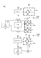
- FIG. 4 is a diagram showing a first embodiment of a semiconductor device.
- a semiconductor device 400 of the first embodiment has an internal power supply 410 , a first circuit block 420 , a second circuit block 430 and a switching section 440 .
- the internal power supply 410 is a linear regulator that generates a predetermined internal power supply voltage VREG (eg, 1.5V) from the input voltage VIN (eg, 3.3V), and includes an output transistor 411 and an operational amplifier 412, for example.
- VREG predetermined internal power supply voltage
- the output transistor 411 is connected between the application terminal of the input voltage VIN and the application terminal of the internal power supply voltage VREG, and the conductivity (and the ON resistance value) is changed according to the control signal output from the operational amplifier 412. Linearly controlled.
- the output transistor 411 for example, a P-channel MOSFET can be suitably used.
- the feedback voltage Vfb (for example, the internal power supply voltage VREG itself or its divided voltage) input to the non-inverting input terminal (+) and the reference voltage Vref input to the inverting input terminal (-) match (
- the simplest operational amplifier 412 is illustrated as the feedback control section of the internal power supply 410, but the topology of the feedback control section is arbitrary.
- an offset canceller may be introduced into the differential input stage of the operational amplifier 412 so that the input offset of the operational amplifier 412 does not have temperature dependency.
- the first circuit block 420 operates by being supplied with the internal power supply voltage VREG.
- An example of the first circuit block 420 is an analog circuit block.
- the second circuit block 430 operates by being supplied with the node voltage Vn appearing at the internal node n1.
- An example of the second circuit block 430 is a digital circuit block. Referring to this drawing, the second circuit block 430 includes an OTP memory 431 and a switch control section 432 .
- the OTP memory 431 is a nonvolatile semiconductor memory device to which data can be written only once. Note that the OTP memory 431 requires different drive voltages for operation when data is written and when data is not written (including when data is read). For example, the drive voltage required for data reading is 1.5V, which is the same voltage as internal power supply voltage VREG, but the drive voltage required for data writing is 5V.
- the second circuit block 430 includes the OTP memory 431 as an example of a load circuit that requires different drive voltages depending on the operation mode.
- the functions of the semiconductor device 400 can be switched according to data written in the OTP memory 431 . More specifically, when the semiconductor device 400 is shipped, the OTP memory 431 stores arbitrary data (for example, data "0" for a model used for a certain purpose and data "1" for a model used for another purpose). ”), the single semiconductor device 400 can be deployed as a plurality of models each adapted to a plurality of uses.
- the switching unit 440 is a circuit block configured to switch the connection destination of the internal node n1 based on switch control signals Sctrl1 and Sctrl2 output from the switch control unit 432, and includes switches SW1 and SW2 and drivers DRV1 and DRV2. including.
- the switch SW1 is connected between the application terminal of the internal power supply voltage VREG and the internal node n1, and is turned on/off based on the gate signal G1 output from the driver DRV1.
- a P-channel MOSFET is used as the switch SW1.
- the source and back gate of the switch SW1 are connected to the application end of the internal power supply voltage VREG.
- a drain of the switch SW1 is connected to the internal node n1.
- the gate of switch SW1 is connected to the output terminal of driver DRV1. Therefore, when the gate signal G1 is at the low level (GND), the switch SW1 is turned on, thereby conducting between the application end of the internal power supply voltage VREG and the internal node n1.
- the switch SW1 when the gate signal G1 is at the high level (VREG or VPAD), the switch SW1 is turned off, thereby cutting off the connection between the internal power supply voltage VREG application terminal and the internal node n1.
- the switch SW1 for example, an analog switch in which a P-channel MOSFET and an N-channel MOSFET are connected in parallel may be used.
- an N-channel MOSFET is used as the switch SW2.
- a drain of the switch SW2 is connected to the pad PAD.
- the source of switch SW2 is connected to internal node n1.
- the back gate of the switch SW2 is connected to the application terminal of the input voltage VIN.
- the gate of switch SW2 is connected to the output terminal of driver DRV2.
- the pad PAD instead of providing a dedicated pad for receiving the input of the external power supply voltage VPAD, during normal operation (including during data reading) in which data is not written to the OTP memory 431, it is used for other purposes.
- An existing pad for example, an enable pad for receiving the input of an enable signal
- a method for sharing the pad PAD will be described separately.
- the driver DRV1 operates by being supplied with the internal power supply voltage VREG or the external power supply voltage VPAD, and generates the gate signal G1 according to the switch control signal Sctrl1.
- the driver DRV2 operates by receiving the supply of the input voltage VIN or the external power supply voltage VPAD, and generates the gate signal G1 according to the switch control signal Sctrl1.
- FIG. 5 is a timing chart showing the operation sequence of the first embodiment (especially when writing data to the OTP memory 431). Voltage VREG, external power supply voltage VPAD, and node voltage Vn are depicted.
- the input voltage VIN (eg, 3.3 V) is supplied to the semiconductor device 400 from time t1 to t10, and feedback control is performed so as to match the internal power supply voltage VREG to the target value VL (eg, 1.5 V).
- VIN eg, 3.3 V
- VL target value
- the first state (1) refers to a state in which the switch SW1 is turned on and the switch SW2 is turned off.
- the second state (2) refers to a state in which the switch SW1 is turned off and the switch SW2 is turned on.
- the third state (3) refers to a state in which both the switches SW1 and SW2 are turned on.
- the external power supply voltage VPAD is set to the first voltage VM equal to or higher than the target value VL of the internal power supply voltage VREG before switching from the first state (1) to the third state (3).
- the first voltage VM is set to a voltage value equal to the output value of the internal power supply voltage VREG at time t2.
- the first voltage VM is lower than the internal power supply voltage VREG due to variations or fluctuations in the first voltage VM and the internal power supply voltage VREG, current will flow from the application end of the internal power supply voltage VREG toward the pad PAD. put away.
- the internal power supply 410 has both current source capability and current sink capability. It is also possible to use the type that has
- the switch control unit 432 sets the switching unit 440 to the second state (2) when writing data to the OTP memory 431, and the remaining period, that is, the OTP memory 431 When data is not written (including when data is read), switching unit 440 is set to the first state (1).
- the switch control unit 432 causes the switching unit 440 to go through the third state (3) in which both the switches SW1 and SW2 are turned on when transitioning between the first state (1) and the second state (2). Control. In other words, a simultaneous on section of the switches SW1 and SW2 is provided when switching the node voltage Vn between the internal power supply voltage VREG and the external power supply voltage VPAD.
- the switch control section 432 can always continue to receive the supply of the node voltage Vn, so that the switching section 440 can be controlled without any trouble even when switching between the internal power supply voltage VREG and the external power supply voltage VPAD.
- the existing pad PAD is shared without providing a dedicated pad as an external terminal for receiving the input of the external power supply voltage VPAD. That is, only when data is written to the OTP memory 431, the function as an external power supply terminal is assigned to the existing pad PAD, and when data is not written to the OTP memory 431 (including when data is read), the internal node n1 and the internal It can be short-circuited with the application terminal of the power supply voltage VREG.
- FIG. 6 is a diagram showing an example of a pad sharing method. If an existing pad is shared as the pad PAD for receiving the input of the external power supply voltage VPAD when writing data to the OTP memory 431, basically the third circuit block 450 connected to the same pad needs to withstand high voltage. becomes. Therefore, among the existing pads, those connected to a large-scale circuit block or those connected to many circuit blocks are commonly used as pads PAD for receiving the input of the external power supply voltage VPAD when writing data to the OTP memory 431. It is better to avoid
- An example of an external terminal suitable for use as the pad PAD is an enable pad to which an enable signal for controlling whether or not the semiconductor device 400 operates can be input.
- the enable pad is shared as the pad PAD
- the semiconductor device 400 can operate or not depending on the enable signal input to the pad PAD when the switching unit 440 is in the first state (1). will be switched.
- the above measure of providing the resistor R for limiting the current cannot be used when the third circuit block 450 is a circuit block that consumes a large amount of current. This is because when a large current flows through the third circuit block 450, the voltage drop across the resistor R increases and the power supply voltage of the third circuit block 450 drops.
- FIG. 7 is a diagram showing a second embodiment of the semiconductor device.
- a semiconductor device 500 of this figure has an internal power supply 510 , an analog circuit block 520 , a digital circuit block 530 , and a switching section 540 .
- the internal power supply 510 is a linear regulator that generates a predetermined internal power supply voltage VREG (eg, 1.5V) from the input voltage VIN (eg, 3.3V), and includes, for example, an output transistor 511 and a feedback control section 512. .
- VREG predetermined internal power supply voltage
- the output transistor 511 is connected between the application end of the input voltage VIN and the application end of the internal power supply voltage VREG. ) is linearly controlled.
- a P-channel MOSFET, for example, can be suitably used as the output transistor 511 .
- the analog circuit block 520 operates by being supplied with the internal power supply voltage VREG.
- the digital circuit block 530 operates by being supplied with the node voltage Vn appearing at the internal node n1.
- the digital circuit block 530 is subjected to a static power supply current measurement test (a so-called IDDQ [quiescent power supply current/quiescent current measurement] test).
- the digital circuit block 530 also functions as a switch control section that generates a switch control signal Sctrl for the switching section 540 so that the connection destination of the internal node n1 can be switched without interrupting the supply of the node voltage Vn.
- the switching unit 540 is a circuit block configured to switch the connection destination of the internal node n1 based on the switch control signal Sctrl output from the digital circuit block 530, and includes switches SW1 and SW2. Although not explicitly shown in the figure, the switching unit 540 may include the drivers DRV1 and DRV2 in FIG. 4 as components.
- the switch SW1 is connected between the application end of the internal power supply voltage VREG and the internal node n1.
- a P-channel MOSFET is used as the switch SW1 in this figure, an analog switch in which a P-channel MOSFET and an N-channel MOSFET are connected in parallel, for example, may be used.
- the switch SW2 is connected between the enable pad EN and the internal node n1.
- the enable pad EN functions as an input terminal for an enable signal when the IDDQ test is not performed, and serves as an external power supply terminal to which an external power supply voltage VPAD (for example, 2 V) is applied when the IDDQ test is performed. It is an example of an existing pad that functions as a detection terminal for static power supply current flowing.
- the digital circuit block 530 switches between the first state (1) and the second state (2) so as to go through the third state (3) in which both the switches SW1 and SW2 are turned on. 540.
- the semiconductor device 500 is configured such that the switches SW1 and SW2 can be turned on simultaneously by giving the internal power supply 510 only a current source capability. Note that the operation sequence of the second embodiment (especially when the IDDQ test is performed) is the same as in FIG.
- the existing enable pad EN is shared as an external terminal for IDDQ testing.
- the existing enable pad EN is shared as an external terminal for IDDQ testing.
- the semiconductor device disclosed in this specification includes an internal power supply configured to generate an internal power supply voltage from an input voltage, and a first circuit block configured to operate with the internal power supply voltage. a second circuit block configured to be operated by a node voltage appearing at an internal node; and a switching section configured to switch connection destinations of the internal nodes, wherein the switching section is connected to the internal power supply.
- the second circuit block may have a configuration (third configuration) including a load circuit that requires a different driving voltage depending on the operation mode.
- the load circuit is a memory that requires different drive voltages when data is written and when data is not written, and the switch control unit is configured to operate when data is not written.
- a configuration (fourth configuration) may be employed in which the switching unit is set in the first state when the data is written, and the switching unit is set in the second state when the data is written.
- the second circuit block is a digital circuit block to be subjected to a static power supply current measurement test
- the switch control unit is configured to control the static power supply.
- a configuration may be adopted in which the switching unit is set to the first state when the current measurement test is not performed, and the switching unit is set to the second state when the static power supply current measurement test is performed.
- the semiconductor device having any one of the first to sixth configurations may further include a resistor for limiting the current flowing from the pad to the third circuit block (seventh configuration).
- the semiconductor device having the seventh configuration may further include a clamper that limits the voltage applied from the pad to the third circuit block downstream of the resistor (eighth configuration).
- the voltage application method disclosed in this specification is a method of applying an external power supply voltage to the pad provided in the semiconductor device having any one of the first to ninth configurations, setting the external power supply voltage to a first voltage equal to or higher than a target value of the internal power supply voltage before switching from the first state to the third state; and after switching from the third state to the second state. raising the external power supply voltage from the first voltage to the second voltage; and lowering the external power supply voltage from the second voltage to the first voltage before switching from the second state to the third state. and stopping the application of the external power supply voltage after switching from the third state to the first state (a tenth configuration).
- semiconductor device 110 internal power supply 111 output transistor 112 feedback control unit 120 analog circuit block 130 digital circuit block 140 OTP memory 200 semiconductor device 210, 220, 230 circuit block 240 switching unit 241 to 244 analog switch 250 switch control unit 300 semiconductor device 310 , 320 circuit block 330 OTP memory 340a, 340b switching unit 341 to 344 analog switch 350a, 350b switch control unit 400 semiconductor device 410 internal power supply 411 output transistor 412 operational amplifier 420 first circuit block 430 second circuit block 431 OTP memory 432 switch control Part 440 Switching Part 450 Third Circuit Block 500 Semiconductor Device 510 Internal Power Supply 511 Output Transistor 512 Feedback Control Part 520 Analog Circuit Block 530 Digital Circuit Block 540 Switching Part DRV1, DRV2 Driver EN Enable Pad PAD1, PAD2, PAD Pad R Resistance SW1 Switch (P-channel MOSFET) SW2 Switch (N-channel MOSFET) ZD Zener diode (clamper)
Landscapes
- Engineering & Computer Science (AREA)
- Power Engineering (AREA)
- Physics & Mathematics (AREA)
- Electromagnetism (AREA)
- General Physics & Mathematics (AREA)
- Radar, Positioning & Navigation (AREA)
- Automation & Control Theory (AREA)
- Semiconductor Integrated Circuits (AREA)
Abstract
Description
図1は、半導体装置の第1比較例(後出の実施形態と対比される回路構成の一例)を示す図である。第1比較例の半導体装置100は、内部電源110と、アナログ回路ブロック120と、デジタル回路ブロック130と、OTP[one time programmable]メモリ140と、を有する。
図2は、半導体装置の第2比較例(後出の実施形態と対比される回路構成の一例)を示す図である。第2比較例の半導体装置200は、回路ブロック210、220及び230と、切替部240と、スイッチ制御部250と、を有する。
図3は、半導体装置の第3比較例(後出の実施形態と対比される回路構成の一例)を示す図である。第3比較例の半導体装置300は、回路ブロック310及び320と、OTPメモリ330と、切替部340a及び340bと、スイッチ制御部350a及び350bと、を有する。
図4は、半導体装置の第1実施形態を示す図である。第1実施形態の半導体装置400は、内部電源410と、第1回路ブロック420と、第2回路ブロック430と、切替部440と、を有する。
図7は、半導体装置の第2実施形態を示す図である。本図の半導体装置500は、内部電源510と、アナログ回路ブロック520と、デジタル回路ブロック530と、切替部540と、を有する。
以下では、上記で説明した種々の実施形態について総括的に述べる。
なお、本明細書中に開示されている種々の技術的特徴は、上記実施形態のほか、その技術的創作の主旨を逸脱しない範囲で種々の変更を加えることが可能である。すなわち、上記実施形態は、全ての点で例示であって制限的なものではないと考えられるべきであり、本発明の技術的範囲は、上記実施形態に限定されるものではなく、特許請求の範囲と均等の意味及び範囲内に属する全ての変更が含まれると理解されるべきである。
110 内部電源
111 出力トランジスタ
112 帰還制御部
120 アナログ回路ブロック
130 デジタル回路ブロック
140 OTPメモリ
200 半導体装置
210、220、230 回路ブロック
240 切替部
241~244 アナログスイッチ
250 スイッチ制御部
300 半導体装置
310、320 回路ブロック
330 OTPメモリ
340a、340b 切替部
341~344 アナログスイッチ
350a、350b スイッチ制御部
400 半導体装置
410 内部電源
411 出力トランジスタ
412 オペアンプ
420 第1回路ブロック
430 第2回路ブロック
431 OTPメモリ
432 スイッチ制御部
440 切替部
450 第3回路ブロック
500 半導体装置
510 内部電源
511 出力トランジスタ
512 帰還制御部
520 アナログ回路ブロック
530 デジタル回路ブロック
540 切替部
DRV1、DRV2 ドライバ
EN イネーブルパッド
PAD1、PAD2、PAD パッド
R 抵抗
SW1 スイッチ(Pチャネル型MOSFET)
SW2 スイッチ(Nチャネル型MOSFET)
ZD ツェナダイオード(クランパ)
Claims (10)
- 入力電圧から内部電源電圧を生成するように構成された内部電源と、
前記内部電源電圧により動作するように構成された第1回路ブロックと、
内部ノードに現れるノード電圧により動作するように構成された第2回路ブロックと、
前記内部ノードの接続先を切り替えるように構成された切替部と、
を有し、
前記切替部は、前記内部電源電圧の印加端と前記内部ノードとの間に接続された第1スイッチと、外部端子と前記内部ノードとの間に接続された第2スイッチと、を含み、
前記第2回路ブロックは、前記第1スイッチ及び前記第2スイッチをそれぞれ制御するように構成されたスイッチ制御部を含み、
前記スイッチ制御部は、前記第1スイッチがオン状態でかつ前記第2スイッチがオフ状態である第1状態と、前記第1スイッチがオフ状態でかつ前記第2スイッチがオン状態である第2状態との間で、前記切替部の動作状態を切り替える際に、前記第1スイッチ及び前記第2スイッチの双方がオン状態である第3状態を経由するように前記切替部を制御する、半導体装置。 - 前記内部電源は、前記内部電源電圧の印加端に電流を供給する能力のみを有する、請求項1に記載の半導体装置。
- 前記第2回路ブロックは、動作モードにより必要な駆動電圧が異なる負荷回路を含む、請求項1または2に記載の半導体装置。
- 前記負荷回路は、データ書込時とデータ非書込時で必要な駆動電圧が異なるメモリであり、前記スイッチ制御部は、前記データ非書込時に前記切替部を前記第1状態とし、前記データ書込時に前記切替部を前記第2状態とする、請求項3に記載の半導体装置。
- 前記第2回路ブロックは、静的電源電流測定テストの実施対象となるデジタル回路ブロックであり、前記スイッチ制御部は、前記静的電源電流測定テストの非実施時に前記切替部を前記第1状態とし、前記静的電源電流測定テストの実施時に前記切替部を前記第2状態とする、請求項1または2に記載の半導体装置。
- 前記第2スイッチはNチャネル型MOSFETである、請求項5に記載の半導体装置。
- 前記外部端子から第3回路ブロックに流れる電流を制限する抵抗をさらに有する、請求項1~6のいずれか一項に記載の半導体装置。
- 前記抵抗の下流側で前記外部端子から前記第3回路ブロックに印加される電圧を制限するクランパをさらに有する、請求項7に記載の半導体装置。
- 前記切替部が前記第1状態であるときに前記外部端子に入力されるイネーブル信号に応じて動作可否が切り替えられる、請求項1~8のいずれか一項に記載の半導体装置。
- 請求項1~9のいずれか一項に記載の半導体装置に設けられた前記外部端子に外部電源電圧を印加する電圧印加方法であって、前記第1状態から前記第3状態への切替前に前記外部電源電圧を前記内部電源電圧の目標値以上の第1電圧に設定するステップと、前記第3状態から前記第2状態への切替後に前記外部電源電圧を前記第1電圧から第2電圧に引き上げるステップと、前記第2状態から前記第3状態への切替前に前記外部電源電圧を前記第2電圧から前記第1電圧に引き下げるステップと、前記第3状態から前記第1状態への切替後に前記外部電源電圧の印加を停止するステップと、を有する、電圧印加方法。
Priority Applications (3)
| Application Number | Priority Date | Filing Date | Title |
|---|---|---|---|
| CN202280040753.8A CN117461132A (zh) | 2021-06-10 | 2022-05-11 | 半导体装置及电压施加方法 |
| JP2023527577A JPWO2022259802A1 (ja) | 2021-06-10 | 2022-05-11 | |
| US18/534,498 US20240233846A9 (en) | 2021-06-10 | 2023-12-08 | Semiconductor device and voltage application method |
Applications Claiming Priority (2)
| Application Number | Priority Date | Filing Date | Title |
|---|---|---|---|
| JP2021-097420 | 2021-06-10 | ||
| JP2021097420 | 2021-06-10 |
Related Child Applications (1)
| Application Number | Title | Priority Date | Filing Date |
|---|---|---|---|
| US18/534,498 Continuation US20240233846A9 (en) | 2021-06-10 | 2023-12-08 | Semiconductor device and voltage application method |
Publications (1)
| Publication Number | Publication Date |
|---|---|
| WO2022259802A1 true WO2022259802A1 (ja) | 2022-12-15 |
Family
ID=84424847
Family Applications (1)
| Application Number | Title | Priority Date | Filing Date |
|---|---|---|---|
| PCT/JP2022/019926 Ceased WO2022259802A1 (ja) | 2021-06-10 | 2022-05-11 | 半導体装置及び電圧印加方法 |
Country Status (4)
| Country | Link |
|---|---|
| US (1) | US20240233846A9 (ja) |
| JP (1) | JPWO2022259802A1 (ja) |
| CN (1) | CN117461132A (ja) |
| WO (1) | WO2022259802A1 (ja) |
Citations (7)
| Publication number | Priority date | Publication date | Assignee | Title |
|---|---|---|---|---|
| JPH0667740A (ja) * | 1992-08-21 | 1994-03-11 | Toshiba Corp | 半導体装置 |
| JP2007078697A (ja) * | 2006-10-23 | 2007-03-29 | Matsushita Electric Ind Co Ltd | 集積回路素子 |
| JP2008294208A (ja) * | 2007-05-24 | 2008-12-04 | Toshiba Corp | 半導体集積回路 |
| JP2010020819A (ja) * | 2008-07-09 | 2010-01-28 | Spansion Llc | 不揮発性記憶装置の制御方法、および不揮発性記憶装置 |
| JP2012243022A (ja) * | 2011-05-18 | 2012-12-10 | Toshiba Corp | 半導体装置及びこれを備えたメモリシステム |
| JP2016146009A (ja) * | 2015-02-06 | 2016-08-12 | ラピスセミコンダクタ株式会社 | 半導体装置 |
| JP2020088448A (ja) * | 2018-11-16 | 2020-06-04 | 力晶積成電子製造股▲ふん▼有限公司Powerchip Semiconductor Manufacturing Corporation | パワースイッチ制御回路とその制御方法 |
Family Cites Families (1)
| Publication number | Priority date | Publication date | Assignee | Title |
|---|---|---|---|---|
| JP5867065B2 (ja) * | 2011-12-22 | 2016-02-24 | 株式会社ソシオネクスト | 降圧型電源回路 |
-
2022
- 2022-05-11 WO PCT/JP2022/019926 patent/WO2022259802A1/ja not_active Ceased
- 2022-05-11 CN CN202280040753.8A patent/CN117461132A/zh active Pending
- 2022-05-11 JP JP2023527577A patent/JPWO2022259802A1/ja active Pending
-
2023
- 2023-12-08 US US18/534,498 patent/US20240233846A9/en active Pending
Patent Citations (7)
| Publication number | Priority date | Publication date | Assignee | Title |
|---|---|---|---|---|
| JPH0667740A (ja) * | 1992-08-21 | 1994-03-11 | Toshiba Corp | 半導体装置 |
| JP2007078697A (ja) * | 2006-10-23 | 2007-03-29 | Matsushita Electric Ind Co Ltd | 集積回路素子 |
| JP2008294208A (ja) * | 2007-05-24 | 2008-12-04 | Toshiba Corp | 半導体集積回路 |
| JP2010020819A (ja) * | 2008-07-09 | 2010-01-28 | Spansion Llc | 不揮発性記憶装置の制御方法、および不揮発性記憶装置 |
| JP2012243022A (ja) * | 2011-05-18 | 2012-12-10 | Toshiba Corp | 半導体装置及びこれを備えたメモリシステム |
| JP2016146009A (ja) * | 2015-02-06 | 2016-08-12 | ラピスセミコンダクタ株式会社 | 半導体装置 |
| JP2020088448A (ja) * | 2018-11-16 | 2020-06-04 | 力晶積成電子製造股▲ふん▼有限公司Powerchip Semiconductor Manufacturing Corporation | パワースイッチ制御回路とその制御方法 |
Also Published As
| Publication number | Publication date |
|---|---|
| US20240233846A9 (en) | 2024-07-11 |
| JPWO2022259802A1 (ja) | 2022-12-15 |
| US20240136005A1 (en) | 2024-04-25 |
| CN117461132A (zh) | 2024-01-26 |
Similar Documents
| Publication | Publication Date | Title |
|---|---|---|
| JP5376559B2 (ja) | 電源回路及び電源制御方法 | |
| US8111058B2 (en) | Circuit for generating reference voltage of semiconductor memory apparatus | |
| US7515487B2 (en) | Internal reference voltage generating circuit for reducing standby current and semiconductor memory device including the same | |
| CN108121392A (zh) | 电压调节电路 | |
| KR100548558B1 (ko) | 반도체 장치용 내부전압 발생기 | |
| JP2009003886A (ja) | 電圧レギュレータ回路 | |
| JP6702413B2 (ja) | 半導体装置 | |
| US9454165B2 (en) | Semiconductor device and current control method that controls amount of current used for voltage generation based on connection state of external capacitor | |
| TW201037974A (en) | System and method for using an integrated circuit pin as both a current limiting input and an open-drain output | |
| JP2000156097A (ja) | 電圧調整が可能な内部電源回路を有する半導体メモリ装置 | |
| US20080061749A1 (en) | Power supply step-down circuit and semiconductor device | |
| JP6781750B2 (ja) | レギュレータ回路および半導体記憶装置 | |
| WO2022259802A1 (ja) | 半導体装置及び電圧印加方法 | |
| US8922250B2 (en) | Semiconductor device and semiconductor system including the same | |
| JP2014147044A (ja) | 半導体集積回路 | |
| CN101714866A (zh) | 半导体器件和将内部电源提供给半导体器件的方法 | |
| WO2020217925A1 (ja) | 半導体集積回路装置および半導体集積回路装置の検査方法 | |
| JP2009282908A (ja) | レギュレータ | |
| KR102685617B1 (ko) | 레퍼런스 선택 회로 | |
| US20070146023A1 (en) | Reset signal generating circuit and semiconductor integrated circuit device | |
| JP3766948B2 (ja) | 電源降下回路 | |
| JPWO2022259802A5 (ja) | ||
| US7548482B2 (en) | Memory device for early stabilizing power level after deep power down mode exit | |
| KR100656426B1 (ko) | 반도체 메모리 장치의 내부 전원 생성 회로 | |
| KR100808602B1 (ko) | 내부 전원 발생기 |
Legal Events
| Date | Code | Title | Description |
|---|---|---|---|
| 121 | Ep: the epo has been informed by wipo that ep was designated in this application |
Ref document number: 22819986 Country of ref document: EP Kind code of ref document: A1 |
|
| WWE | Wipo information: entry into national phase |
Ref document number: 2023527577 Country of ref document: JP |
|
| WWE | Wipo information: entry into national phase |
Ref document number: 202280040753.8 Country of ref document: CN |
|
| NENP | Non-entry into the national phase |
Ref country code: DE |
|
| 122 | Ep: pct application non-entry in european phase |
Ref document number: 22819986 Country of ref document: EP Kind code of ref document: A1 |