WO2022255155A1 - 積層体 - Google Patents
積層体 Download PDFInfo
- Publication number
- WO2022255155A1 WO2022255155A1 PCT/JP2022/021159 JP2022021159W WO2022255155A1 WO 2022255155 A1 WO2022255155 A1 WO 2022255155A1 JP 2022021159 W JP2022021159 W JP 2022021159W WO 2022255155 A1 WO2022255155 A1 WO 2022255155A1
- Authority
- WO
- WIPO (PCT)
- Prior art keywords
- layer
- laminate
- liquid crystal
- adhesive layer
- adhesive
- Prior art date
- Legal status (The legal status is an assumption and is not a legal conclusion. Google has not performed a legal analysis and makes no representation as to the accuracy of the status listed.)
- Ceased
Links
Images

Classifications
-
- G—PHYSICS
- G02—OPTICS
- G02B—OPTICAL ELEMENTS, SYSTEMS OR APPARATUS
- G02B5/00—Optical elements other than lenses
- G02B5/30—Polarising elements
- G02B5/3016—Polarising elements involving passive liquid crystal elements
-
- H—ELECTRICITY
- H10—SEMICONDUCTOR DEVICES; ELECTRIC SOLID-STATE DEVICES NOT OTHERWISE PROVIDED FOR
- H10K—ORGANIC ELECTRIC SOLID-STATE DEVICES
- H10K59/00—Integrated devices, or assemblies of multiple devices, comprising at least one organic light-emitting element covered by group H10K50/00
- H10K59/80—Constructional details
- H10K59/8791—Arrangements for improving contrast, e.g. preventing reflection of ambient light
-
- B—PERFORMING OPERATIONS; TRANSPORTING
- B32—LAYERED PRODUCTS
- B32B—LAYERED PRODUCTS, i.e. PRODUCTS BUILT-UP OF STRATA OF FLAT OR NON-FLAT, e.g. CELLULAR OR HONEYCOMB, FORM
- B32B27/00—Layered products comprising a layer of synthetic resin
-
- B—PERFORMING OPERATIONS; TRANSPORTING
- B32—LAYERED PRODUCTS
- B32B—LAYERED PRODUCTS, i.e. PRODUCTS BUILT-UP OF STRATA OF FLAT OR NON-FLAT, e.g. CELLULAR OR HONEYCOMB, FORM
- B32B7/00—Layered products characterised by the relation between layers; Layered products characterised by the relative orientation of features between layers, or by the relative values of a measurable parameter between layers, i.e. products comprising layers having different physical, chemical or physicochemical properties; Layered products characterised by the interconnection of layers
- B32B7/02—Physical, chemical or physicochemical properties
- B32B7/023—Optical properties
-
- B—PERFORMING OPERATIONS; TRANSPORTING
- B32—LAYERED PRODUCTS
- B32B—LAYERED PRODUCTS, i.e. PRODUCTS BUILT-UP OF STRATA OF FLAT OR NON-FLAT, e.g. CELLULAR OR HONEYCOMB, FORM
- B32B7/00—Layered products characterised by the relation between layers; Layered products characterised by the relative orientation of features between layers, or by the relative values of a measurable parameter between layers, i.e. products comprising layers having different physical, chemical or physicochemical properties; Layered products characterised by the interconnection of layers
- B32B7/04—Interconnection of layers
- B32B7/12—Interconnection of layers using interposed adhesives or interposed materials with bonding properties
-
- G—PHYSICS
- G02—OPTICS
- G02B—OPTICAL ELEMENTS, SYSTEMS OR APPARATUS
- G02B1/00—Optical elements characterised by the material of which they are made; Optical coatings for optical elements
- G02B1/10—Optical coatings produced by application to, or surface treatment of, optical elements
- G02B1/14—Protective coatings, e.g. hard coatings
-
- G—PHYSICS
- G02—OPTICS
- G02B—OPTICAL ELEMENTS, SYSTEMS OR APPARATUS
- G02B5/00—Optical elements other than lenses
- G02B5/30—Polarising elements
-
- G—PHYSICS
- G02—OPTICS
- G02F—OPTICAL DEVICES OR ARRANGEMENTS FOR THE CONTROL OF LIGHT BY MODIFICATION OF THE OPTICAL PROPERTIES OF THE MEDIA OF THE ELEMENTS INVOLVED THEREIN; NON-LINEAR OPTICS; FREQUENCY-CHANGING OF LIGHT; OPTICAL LOGIC ELEMENTS; OPTICAL ANALOGUE/DIGITAL CONVERTERS
- G02F1/00—Devices or arrangements for the control of the intensity, colour, phase, polarisation or direction of light arriving from an independent light source, e.g. switching, gating or modulating; Non-linear optics
- G02F1/01—Devices or arrangements for the control of the intensity, colour, phase, polarisation or direction of light arriving from an independent light source, e.g. switching, gating or modulating; Non-linear optics for the control of the intensity, phase, polarisation or colour
- G02F1/13—Devices or arrangements for the control of the intensity, colour, phase, polarisation or direction of light arriving from an independent light source, e.g. switching, gating or modulating; Non-linear optics for the control of the intensity, phase, polarisation or colour based on liquid crystals, e.g. single liquid crystal display cells
- G02F1/133—Constructional arrangements; Operation of liquid crystal cells; Circuit arrangements
- G02F1/1333—Constructional arrangements; Manufacturing methods
- G02F1/1337—Surface-induced orientation of the liquid crystal molecules, e.g. by alignment layers
-
- G—PHYSICS
- G09—EDUCATION; CRYPTOGRAPHY; DISPLAY; ADVERTISING; SEALS
- G09F—DISPLAYING; ADVERTISING; SIGNS; LABELS OR NAME-PLATES; SEALS
- G09F9/00—Indicating arrangements for variable information in which the information is built-up on a support by selection or combination of individual elements
- G09F9/30—Indicating arrangements for variable information in which the information is built-up on a support by selection or combination of individual elements in which the desired character or characters are formed by combining individual elements
-
- H—ELECTRICITY
- H05—ELECTRIC TECHNIQUES NOT OTHERWISE PROVIDED FOR
- H05B—ELECTRIC HEATING; ELECTRIC LIGHT SOURCES NOT OTHERWISE PROVIDED FOR; CIRCUIT ARRANGEMENTS FOR ELECTRIC LIGHT SOURCES, IN GENERAL
- H05B33/00—Electroluminescent light sources
- H05B33/02—Details
-
- H—ELECTRICITY
- H10—SEMICONDUCTOR DEVICES; ELECTRIC SOLID-STATE DEVICES NOT OTHERWISE PROVIDED FOR
- H10K—ORGANIC ELECTRIC SOLID-STATE DEVICES
- H10K59/00—Integrated devices, or assemblies of multiple devices, comprising at least one organic light-emitting element covered by group H10K50/00
- H10K59/80—Constructional details
- H10K59/8793—Arrangements for polarized light emission
-
- B—PERFORMING OPERATIONS; TRANSPORTING
- B32—LAYERED PRODUCTS
- B32B—LAYERED PRODUCTS, i.e. PRODUCTS BUILT-UP OF STRATA OF FLAT OR NON-FLAT, e.g. CELLULAR OR HONEYCOMB, FORM
- B32B2307/00—Properties of the layers or laminate
- B32B2307/50—Properties of the layers or laminate having particular mechanical properties
- B32B2307/51—Elastic
-
- B—PERFORMING OPERATIONS; TRANSPORTING
- B32—LAYERED PRODUCTS
- B32B—LAYERED PRODUCTS, i.e. PRODUCTS BUILT-UP OF STRATA OF FLAT OR NON-FLAT, e.g. CELLULAR OR HONEYCOMB, FORM
- B32B2309/00—Parameters for the laminating or treatment process; Apparatus details
- B32B2309/02—Temperature
-
- H—ELECTRICITY
- H10—SEMICONDUCTOR DEVICES; ELECTRIC SOLID-STATE DEVICES NOT OTHERWISE PROVIDED FOR
- H10K—ORGANIC ELECTRIC SOLID-STATE DEVICES
- H10K59/00—Integrated devices, or assemblies of multiple devices, comprising at least one organic light-emitting element covered by group H10K50/00
- H10K59/80—Constructional details
- H10K59/87—Passivation; Containers; Encapsulations
- H10K59/871—Self-supporting sealing arrangements
- H10K59/8722—Peripheral sealing arrangements, e.g. adhesives, sealants
Definitions
- the present invention relates to laminates and image display devices.
- Patent Document 1 discloses a laminate comprising a first protective layer, a first pressure-sensitive adhesive layer, an intervening coating layer, and a second pressure-sensitive adhesive layer in this order.
- a laminate comprising a first protective layer, a first pressure-sensitive adhesive layer, an intervening coating layer, and a second pressure-sensitive adhesive layer in this order.
- a laminate that can be bent with the viewer side facing inward is used for a flexible display that can be bent with the viewer side facing inward.
- a laminate that can be bent with the viewer side surface facing outward as a laminate used in a flexible display that can be bent with the viewer side surface facing outward.
- a linear polarizing layer, a first adhesive layer, a liquid crystal coating layer, and a second adhesive layer are laminated in this order, and cracks occur when repeatedly bent with the linear polarizing layer side facing outward.
- the present invention provides the following laminate and image display device.
- a linear polarizing layer, a first adhesive layer, a liquid crystal coating layer, and a second adhesive layer are laminated in this order,
- the storage elastic modulus of the first adhesive layer at a temperature of 25 ° C. is G'1 [kPa]
- the storage elastic modulus of the second adhesive layer at a temperature of 25 ° C. is G'2 [kPa]
- the following conditions (1 ) the laminate.
- G'1 ⁇ 1000 kPa and G'2 ⁇ 1000 kPa [2]
- the laminate according to [1] wherein the linear polarizing layer includes a cured product of a composition containing a polymerizable liquid crystal compound and one or more azo dyes, and an alignment film.
- the linear polarizing layer, the first adhesive layer, the liquid crystal coating layer, and the second adhesive layer are laminated in this order, and when repeatedly bent with the linear polarizing layer side facing outward, cracks occur. It is possible to provide a laminate in which it is difficult for .
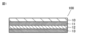
- FIG. 4 is a schematic cross-sectional view showing another example of the layer structure of the laminate according to the present invention
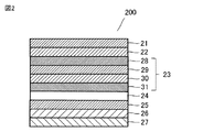
- FIG. 4 is a schematic cross-sectional view showing another example of the layer structure of the laminate according to the present invention
- It is the schematic explaining the method of a flexibility test.
- a laminate according to one aspect of the present invention includes a linear polarizing layer, a first adhesive layer, a liquid crystal coating layer, and a second adhesive layer laminated in this order, and the storage elastic modulus of the first adhesive layer at a temperature of 25 ° C. is G'1 [kPa], and the storage elastic modulus of the second adhesive layer at a temperature of 25° C. is G'2 [kPa], the following condition (1) is satisfied.
- FIG. 1 shows a schematic cross-sectional view of a laminate according to one aspect of the present invention.
- a laminate 100 shown in FIG. 1 includes a linear polarizing layer 10, a first adhesive layer 11, a liquid crystal coating layer 12, and a second adhesive layer 13 laminated in this order. Both the first adhesive layer 11 and the second adhesive layer 13 are arranged in contact with the liquid crystal coating layer 12 .
- the linear polarizing layer 10 and the first adhesive layer 11 may be arranged in contact with each other.
- the liquid crystal coating layer 12 does not include a polarizer containing a cured product of a polymerizable liquid crystal compound, which is one form of the linear polarizing layer 10 .
- the laminate 100 can further include other layers such as a protective layer, a front panel, a third adhesive layer, a bonding layer, an organic EL panel, and a touch sensor.
- the laminate 100 can be bent with the linear polarizing layer 10 side facing outward with respect to the bending axis (hereinafter also referred to as "outfold"). Being able to bend means that the laminate can be bent without causing cracks in the liquid crystal coating layer and the polarizer layer.
- Bending includes a form of bending in which a curved surface is formed at the bending portion. In the form of bending, the bending radius of the bent inner surface is not particularly limited. Bending also includes a form of refraction in which the angle of refraction of the inner surface is greater than 0° and less than 180°, and a form of folding in which the radius of curvature of the inner surface is close to zero or the angle of refraction of the inner surface is 0°. .
- the laminate of the present invention is suitable for flexible displays because it can be bent.
- the laminate 100 may have a bending radius of, for example, 4 mm, preferably 2 mm, at which cracks are unlikely to occur even when repeatedly bent in an outfold test described later.
- the number of bending times at which cracks first occur is preferably 200,000 times or more, more preferably 300,000 times or more, and further It is preferably 400,000 times or more, and particularly preferably 500,000 times or more.
- the thickness of the laminate 100 is not particularly limited because it varies depending on the functions required of the laminate and the application of the laminate. be. In this specification, the thickness of the laminate and each layer can be measured according to the thickness measurement method described in the examples below.
- the planar shape of the laminate 100 may be, for example, a square shape, preferably a square shape having long sides and short sides, more preferably a rectangle.
- the length of the long side may be, for example, 10 mm or more and 1400 mm or less, preferably 600 mm or less.
- the length of the short side is, for example, 5 mm or more and 800 mm or less, preferably 500 mm or less, and more preferably 300 mm or less.
- Each layer constituting the laminate may have rounded corners, notched ends, or perforated ends.
- the laminate 100 satisfies the above condition (1).
- the present inventors have found that by placing a liquid crystal coating layer between two relatively hard adhesive layers with a storage modulus of 1000 kPa or more at a temperature of 25° C., it is possible to repeatedly bend outfold. served.
- the storage elastic modulus at a temperature of 25° C. can be measured according to the method described in the Examples section below.
- the storage elastic modulus G′1 [kPa] of the first adhesive layer 11 at a temperature of 25° C. and the storage elastic modulus G′2 [kPa] of the second adhesive layer 13 at a temperature of 25° C. are preferably 1100 kPa or more, more preferably. is 1200 ka or more, more preferably 1300 kPa or more, and particularly preferably 1400 kPa or more.
- the storage elastic moduli at a temperature of 23° C. of the first adhesive layer 11 and the second adhesive layer 13 may be the same or different.
- the first adhesive layer 11 and the second adhesive layer 13 are formed from an adhesive composition which will be described later.
- the storage elastic modulus G′1 [kPa] of the first adhesive layer 11 at a temperature of 25° C. and the storage elastic modulus G′2 [kPa] of the second adhesive layer 13 at a temperature of 25° C. are included in the adhesive composition, for example (
- the types of monomers that make up the meth)acrylic polymer can be selected, the molecular weight of the (meth)acrylic polymer can be adjusted, and the amount of cross-linking agent added can be used to adjust the cross-linking density and thickness of the adhesive layer. or a combination of these methods.
- a pressure-sensitive adhesive having a desired storage elastic modulus can be selected and used from commercially available pressure-sensitive adhesives.
- the laminate 100 can be used, for example, in an image display device or the like.
- the image display device is not particularly limited, and examples thereof include organic electroluminescence (organic EL) display devices, inorganic electroluminescence (inorganic EL) display devices, liquid crystal display devices, and electroluminescence display devices.
- the image display device may have a touch panel function.
- the image display device can preferably be a flexible display.
- the layered product 100 can be placed in an image display device so that the linear polarizing layer 10 side is on the viewing side.
- Linear polarizing layer 10 examples include a stretched film or stretched layer to which a dichroic dye is adsorbed, a polarizer layer formed by coating and curing a dichroic dye, and the like.
- a polarizer layer formed by applying and curing a dichroic dye is preferred because there is no restriction in the bending direction compared to a stretched film or stretched layer to which a dye having anisotropic absorption is adsorbed.
- Dichroic organic dyes include, for example, azo dyes.
- azo dyes include C.I. I.
- Dichroic direct dyes composed of disazo compounds such as DIRECT RED 39, and dichroic direct dyes composed of compounds such as trisazo and tetrakisazo are included.
- the stretched film to which the dichroic dye is adsorbed is usually produced by the process of uniaxially stretching the polyvinyl alcohol resin film, and the process of dyeing the polyvinyl alcohol resin film with the dichroic dye to adsorb the dichroic dye. , a step of treating a polyvinyl alcohol-based resin film to which a dichroic dye is adsorbed with an aqueous boric acid solution, and a step of washing with water after the treatment with the aqueous boric acid solution.
- the thickness of the stretched film to which the dichroic dye is adsorbed may be, for example, 2 ⁇ m or more and 40 ⁇ m or less, may be 5 ⁇ m or more, may be 20 ⁇ m or less, further 15 ⁇ m or less, and furthermore may be 10 ⁇ m or less. .
- Polyvinyl alcohol-based resin is obtained by saponifying polyvinyl acetate-based resin.
- Polyvinyl acetate-based resins include polyvinyl acetate, which is a homopolymer of vinyl acetate, and copolymers of vinyl acetate and other monomers copolymerizable therewith.
- Other monomers copolymerizable with vinyl acetate include, for example, unsaturated carboxylic acids, olefins, vinyl ethers, unsaturated sulfonic acids, and (meth)acrylamides having an ammonium group.
- the degree of saponification of the polyvinyl alcohol resin is usually about 85 mol% or more and 100 mol% or less, preferably 98 mol% or more.
- the polyvinyl alcohol-based resin may be modified, and for example, polyvinyl formal or polyvinyl acetal modified with aldehydes may be used.
- the degree of polymerization of the polyvinyl alcohol resin is usually 1000 or more and 10000 or less, preferably 1500 or more and 5000 or less.
- the stretched layer to which the dichroic dye is adsorbed is usually formed by applying a coating liquid containing the polyvinyl alcohol resin onto the substrate film, uniaxially stretching the resulting laminated film, and uniaxially stretching the laminated film.
- the base film may be peeled off from the stretching layer to which the dichroic dye is adsorbed.
- the material and thickness of the base film may be the same as the material and thickness of the thermoplastic resin film described below.
- the polarizer layer obtained by coating and curing a dichroic dye is a composition containing a polymerizable dichroic dye having liquid crystallinity or a composition containing a polymerizable liquid crystal compound and a dichroic dye as a base material.
- a polarizer layer containing a cured product of a polymerizable liquid crystal compound, such as a layer obtained by coating and curing a film, may be mentioned.
- the substrate film may be provided with an alignment film on one surface.
- the linear polarizing layer 10 is preferably a layer containing a cured product of a composition containing a polymerizable liquid crystal compound and one or more azo dyes, and an alignment film.
- the thickness of the alignment film may be, for example, 5 nm or more and 1 ⁇ m or less.
- the linear polarizing layer may be incorporated into the laminate together with the substrate film, or may be incorporated into the laminate by peeling and removing the substrate film from the polarizer layer formed by coating and curing the dichroic dye. .
- the material and thickness of the base film may be the same as the material and thickness of the thermoplastic resin film described below.
- a hard coat layer (HC layer) may be formed on at least one surface of the base film as a protective layer, which will be described later.
- the thickness of the polarizer layer formed by applying and curing a dichroic dye is usually 10 ⁇ m or less, preferably 8 ⁇ m or less, and more preferably 5 ⁇ m or less.
- the protective layer may be placed on one side or both sides of the linear polarizing layer 10 and have the function of protecting the surface of the linear polarizing layer 10 .
- the linear polarizing layer laminated with the protective layer may be referred to as a linear polarizing plate.
- the protective layer can be an organic layer or an inorganic layer.
- the organic layer or inorganic layer may be a layer formed by coating.
- the organic layer can be a protective layer-forming composition, for example, a cured resin layer of a (meth)acrylic resin composition, an epoxy resin composition, a polyimide resin composition, or the like.
- the protective layer-forming composition may be active energy ray-curable or thermosetting.
- the inorganic layer can be formed of silicon oxide or the like, for example.
- the protective layer may be called a hard coat layer (HC layer) or an overcoat (OC) layer.
- the protective layer may be formed directly on the base film described above, or may be formed directly on the linear polarizing layer. After the protective layer is formed on the substrate film described above, the linear polarizing layer can be formed.
- the protective layer can be produced by, for example, applying an active energy ray-curable composition for forming a protective layer onto the base film and curing it by irradiating it with active energy.
- the description of the above-mentioned base film is applied to the base film.
- the protective layer can be incorporated into the laminate after the base film has been peeled off. Examples of the method of applying the protective layer-forming composition include spin coating.
- the protective layer is an inorganic layer
- the protective layer can be formed by, for example, a sputtering method, a vapor deposition method, or the like.
- the thickness of the protective layer may be, for example, 0.1 ⁇ m or more and 10 ⁇ m or less, preferably 5 ⁇ m or less.
- thermoplastic resin film that is excellent in transparency, mechanical strength, thermal stability, water barrier properties, isotropy, stretchability, etc.
- thermoplastic resins include cellulose resins such as triacetyl cellulose; polyester resins such as polyethylene terephthalate and polyethylene naphthalate; polyethersulfone resins; polysulfone resins; polycarbonate resins; Resins; polyimide resins; polyolefin resins such as polyethylene, polypropylene, and ethylene/propylene copolymers; cyclic polyolefin resins having cyclo- and norbornene structures (also referred to as norbornene-based resins); (meth)acrylic resins; polyarylate resins; and polyvinyl alcohol resins, as well as mixtures thereof.
- the two protective layers may be of the same type or of different types.
- the thickness of the thermoplastic resin film is usually 300 ⁇ m or less, preferably 200 ⁇ m or less, more preferably 100 ⁇ m or less, still more preferably 50 ⁇ m or less, and even more preferably 30 ⁇ m or less. and is usually 1 ⁇ m or more, and may be, for example, 5 ⁇ m or more or 20 ⁇ m or more.
- the protective layer is a thermoplastic resin film
- the thermoplastic resin film can be bonded to the linear polarizing layer 10 via a bonding layer, which will be described later.
- the bonding layer for bonding the thermoplastic resin film to the linear polarizing layer 10 is preferably an adhesive layer.
- a linear polarizing layer can be formed on the above protective layer.
- the laminate 100 preferably has at least one protective layer selected from the group consisting of a thermoplastic resin film and a cured resin layer on the side of the linear polarizing layer 10 opposite to the first adhesive layer 11 .
- the first adhesive layer 11 may be a layer interposed between the linear polarization layer 10 and the liquid crystal coating layer 12 to bond them.
- the second adhesive layer 13 can be a layer for bonding, for example, a touch sensor panel, an organic EL panel, or the like to the liquid crystal coating layer 12 side of the laminate 100 .
- the first adhesive layer 11 and the second adhesive layer 13 may be collectively referred to as an adhesive layer.
- the adhesive layer may be, for example, a layer composed of an adhesive or a layer obtained by subjecting this layer to some kind of treatment. Adhesives are also called pressure-sensitive adhesives. As used herein, the term "adhesive" refers to an adhesive other than a pressure-sensitive adhesive (pressure-sensitive adhesive), and is clearly distinguished from a pressure-sensitive adhesive.
- the adhesive layer may consist of one layer or two or more layers, preferably one layer.
- the adhesive layer can be formed from an adhesive composition.
- the types of adhesives used for the first adhesive layer 11 and the second adhesive layer 13 may be the same or different.
- the adhesive layer can be composed of an adhesive composition whose main component is a resin such as (meth)acrylic, rubber, urethane, ester, silicone, or polyvinyl ether. Among them, a pressure-sensitive adhesive composition using a (meth)acrylic resin as a base polymer, which is excellent in transparency, weather resistance, heat resistance, etc., is preferable.
- the adhesive composition may be active energy ray-curable or heat-curable.
- Examples of the (meth)acrylic resin (base polymer) used in the adhesive composition include butyl (meth)acrylate, ethyl (meth)acrylate, isooctyl (meth)acrylate, and 2-(meth)acrylate. Polymers or copolymers containing one or more of (meth)acrylic acid esters such as ethylhexyl as monomers are preferably used.
- the base polymer is copolymerized with a polar monomer.
- polar monomers examples include (meth)acrylic acid, 2-hydroxypropyl (meth)acrylate, hydroxyethyl (meth)acrylate, (meth)acrylamide, N,N-dimethylaminoethyl (meth)acrylate, glycidyl ( Monomers having a carboxyl group, a hydroxyl group, an amide group, an amino group, an epoxy group, etc., such as meth)acrylates, can be mentioned.
- the adhesive composition may contain only the above base polymer, but usually further contains a cross-linking agent.
- the cross-linking agent is a metal ion having a valence of 2 or more, which forms a carboxylic acid metal salt with a carboxyl group; a polyamine compound, which forms an amide bond with a carboxyl group; Examples include epoxy compounds and polyols that form ester bonds with carboxyl groups; and polyisocyanate compounds that form amide bonds with carboxyl groups. Among them, polyisocyanate compounds are preferred.
- the active energy ray-curable pressure-sensitive adhesive composition has the property of being cured by being irradiated with an active energy ray such as an ultraviolet ray or an electron beam. It is a pressure-sensitive adhesive composition that can be adhered to an adherend such as the adhesive agent, and that can be cured by irradiation with an active energy ray to adjust the adhesion force.
- the active energy ray-curable pressure-sensitive adhesive composition is preferably UV-curable.
- the active energy ray-curable pressure-sensitive adhesive composition further contains an active energy ray-polymerizable compound in addition to the base polymer and the cross-linking agent. Furthermore, if necessary, a photopolymerization initiator, a photosensitizer, and the like may be contained.
- the adhesive composition contains fine particles for imparting light scattering properties, beads (resin beads, glass beads, etc.), glass fibers, resins other than base polymers, tackifiers, fillers (metal powders and other inorganic powders). etc.), antioxidants, ultraviolet absorbers, dyes, pigments, colorants, antifoaming agents, corrosion inhibitors, antistatic agents, photopolymerization initiators, and other additives.
- the adhesive layer can be formed by applying an organic solvent-diluted solution of the adhesive composition onto a substrate and drying.
- an active energy ray-curable pressure-sensitive adhesive composition is used, a cured product having a desired degree of curing can be obtained by irradiating the formed pressure-sensitive adhesive layer with an active energy ray.
- the first adhesive layer 11 and the second adhesive layer 13 can also be selected from commercially available products so as to satisfy the above condition (1).
- the thickness of the adhesive layer is, for example, preferably 1 ⁇ m or more and 100 ⁇ m or less, more preferably 50 ⁇ m or less, and may be 20 ⁇ m or more.
- the thicknesses of the first adhesive layer 11 and the second adhesive layer 13 may be the same or different.
- the liquid crystal coating layer 12 is interposed between the first adhesive layer 11 and the second adhesive layer 13 and laminated in contact with the first adhesive layer 11 and the second adhesive layer 13 .
- the liquid crystal coating layer 12 can be a cured layer of a polymerizable liquid crystal compound.
- the liquid crystal coating layer consists of one layer or multiple layers. When the liquid crystal coating layer is composed of a plurality of layers, the layers may be laminated via a bonding layer, which will be described later, and preferably via an adhesive layer, which will be described later.
- the liquid crystal coating layer 12 can be a cured layer of a polymerizable liquid crystal compound.
- a cured layer of a polymerizable liquid crystal compound can be formed by coating a substrate film with a composition for forming a retardation layer containing a polymerizable liquid crystal compound and curing the composition.
- coating methods include a coating method and a printing method. Coating methods include bar coating, knife coating, blade coating, die coating, direct gravure coating, reverse gravure coating, roll coating, CAP coating, spin coating, spray coating, screen coating, A slit coat method, a dip coat method, etc. are mentioned.
- Examples of printing methods include offset printing, gravure printing, screen printing, inkjet printing, and the like.
- the cured layer of the polymerizable liquid crystal compound can be a retardation layer.
- the retardation layer can be composed of one layer or two or more layers.
- the retardation layer may be a positive A plate such as a ⁇ /4 plate, a ⁇ /2 plate, and a positive C plate.
- the retardation layer is preferably a ⁇ /4 plate.
- the retardation layer may be a retardation layer laminate composed of a first liquid crystal cured retardation layer and a second liquid crystal cured retardation layer. can.
- the first liquid crystal-cured retardation layer and the second liquid crystal-cured retardation layer may be laminated via a later-described bonding layer, preferably via an adhesive layer.
- the first liquid crystal cured retardation layer is preferably a ⁇ /4 plate and the second liquid crystal cured retardation layer is ⁇ /2.
- a linearly polarizing plate laminated with a retardation layer may be referred to as a circularly polarizing plate.
- the thickness of the retardation layer is, for example, 0.1 ⁇ m or more and 10 ⁇ m or less, preferably 8 ⁇ m or less, and more preferably 6 ⁇ m or less.
- the thickness of the liquid crystal coating layer 12 may be, for example, 0.1 ⁇ m or more and 10 ⁇ m or less, preferably 8 ⁇ m or less, and more preferably 6 ⁇ m or less.
- the front plate forms the outermost surface on the viewing side of the image display device, and can have a function of protecting the front surface (screen) of the image display device.
- the front plate can be what is called a window film.
- the material and thickness of the front plate are not limited as long as it is a plate-like body that can transmit light, and it may consist of only one layer or two or more layers. Examples thereof include a plate-like body made of resin (for example, a resin plate, a resin sheet, a resin film, etc.), a plate-like body made of glass (for example, a glass plate, a glass film, etc.), and a touch sensor panel described later.
- the front panel can be arranged on the viewing side of the laminate 100 .
- the laminate 100 can include a front plate on the outermost surface of the linear polarizing layer 10 opposite to the first adhesive layer 11 via a third adhesive layer, which will be described later.
- a laminate 100 having a front panel can be arranged in an image display device such that the front panel constitutes the outermost surface of the image display device.
- the thickness of the front plate may be, for example, 30 ⁇ m or more and 500 ⁇ m or less, preferably 200 ⁇ m or less, and more preferably 100 ⁇ m or less.
- the plate-like body made of resin is not limited as long as it can transmit light.
- the resin constituting the resin plate-like body such as a resin film include triacetyl cellulose, acetyl cellulose butyrate, ethylene-vinyl acetate copolymer, propionyl cellulose, butyryl cellulose, acetyl propionyl cellulose, polyester, polystyrene, Polyamide, polyetherimide, poly(meth)acrylic, polyimide, polyethersulfone, polysulfone, polyethylene, polypropylene, polymethylpentene, polyvinyl chloride, polyvinylidene chloride, polyvinyl alcohol, polyvinyl acetal, polyetherketone, polyetheretherketone , polyether sulfone, polymethyl methacrylate, polyethylene terephthalate, polybutylene terephthalate, polyethylene naphthalate, polycarbonate, and
- the front plate is preferably a film having a hard coat layer (HC layer) provided on at least one surface of the base film.
- HC layer a hard coat layer
- the base film a film made of the above resin can be used.
- the hard coat layer may be formed on one surface of the substrate film, or may be formed on both surfaces.
- the hard coat layer is, for example, a cured layer of an ultraviolet curable resin. Examples of UV curable resins include acrylic resins, silicone resins, polyester resins, urethane resins, amide resins, and epoxy resins.
- the hard coat layer may contain additives in order to improve strength. Additives are not limited and include inorganic microparticles, organic microparticles, or mixtures thereof.
- the front plate is a glass plate
- tempered glass for displays is preferably used as the glass plate.
- the thickness of the glass plate may be, for example, 50 ⁇ m or more and 1000 ⁇ m or less.
- the front plate not only has the function of protecting the front surface (screen) of the image display device described above, but also functions as a touch sensor, blue light cut function, and viewing angle adjustment. It may have a function or the like.
- the front panel preferably has a tensile elastic modulus of 4.0 GPa or more, more preferably 5.0 GPa or more at a temperature of 23° C., from the viewpoint of easily forming the laminate 100 having excellent flexibility. It is more preferably 6.0 GPa or more.
- the front plate preferably has a tensile elastic modulus of 20 GPa or less at a temperature of 23° C., more preferably 15 GPa or less, from the viewpoint of facilitating formation of a laminate having excellent flexibility.
- the tensile modulus at a temperature of 23° C. can be measured by the test method described in the Examples section below.
- the laminate 100 can be repeatedly bent in an outfold even when it has a front plate having a tensile modulus of elasticity of 6.0 GPa at a temperature of 23°C.
- the base film that constitutes the front plate may be composed of, for example, a resin film, preferably a transparent resin film.
- the resin constituting the resin film include polyolefins such as polyethylene, polypropylene, norbornene-based polymers, and cyclic olefin-based resins; polyvinyl alcohol; polyethylene terephthalate; polymethacrylic acid ester; Cellulose ester such as cellulose acetate propionate; polyethylene naphthalate; polycarbonate; polysulfone; polyethersulfone; polyetherketone; polyphenylene sulfide; Among them, cyclic olefin resins, cellulose esters and polyimides are preferred.
- the thickness of the resin film is preferably thin from the viewpoint of thinning the laminate 100, but if it is too thin, it tends to be difficult to ensure impact resistance.
- the thickness of the resin film may be, for example, 10 ⁇ m or more and 200 ⁇ m or less, preferably 15 ⁇ m or more, and more preferably 20 ⁇ m or more.
- the base film may have a hard coat layer, an antireflection layer, or an antistatic layer on at least one surface.
- the third adhesive layer can have the function of bonding the front panel to the laminate 100 .
- the third adhesive layer can be formed from an adhesive.
- the adhesive constituting the third adhesive layer may be the same as those exemplified for the adhesive composition constituting the adhesive layer, or other adhesives such as (meth)acrylic adhesive, styrene adhesive, silicone adhesive, rubber adhesive, urethane adhesive, polyester adhesive, epoxy copolymer adhesive, and the like.
- the storage elastic modulus of the third adhesive layer at a temperature of 25° C. is preferably 50 kPa or less, more preferably 45 kPa or less, and still more preferably 41 kPa or less from the viewpoint that cracks are less likely to occur in the liquid crystal coating layer when bent. be.
- a lamination layer is a layer comprised from a pressure sensitive adhesive or an adhesive agent.
- the bonding layer includes, for example, a layer for bonding the front plate and the touch sensor panel, a layer for bonding the laminate and the touch sensor panel, a layer for bonding the linear polarizing layer and the protective layer, and a first liquid crystal curing phase difference. It can be a layer or the like that joins the layer and the second liquid crystal cured retardation layer.
- the pressure-sensitive adhesive constituting the bonding layer may be the same as those exemplified for the pressure-sensitive adhesive composition constituting the above-described pressure-sensitive adhesive layer, or other pressure-sensitive adhesives such as (meth)acrylic pressure-sensitive adhesives, styrene adhesive, silicone adhesive, rubber adhesive, urethane adhesive, polyester adhesive, epoxy copolymer adhesive, and the like.
- the laminate 100 may have one bonding layer, or may have two or more bonding layers. When the laminate 100 includes a plurality of bonding layers, the plurality of bonding layers may be the same or different.
- the adhesive that constitutes the lamination layer for example, one or a combination of two or more of water-based adhesives, active energy ray-curable adhesives, pressure-sensitive adhesives, and the like can be used.
- water-based adhesives include polyvinyl alcohol-based resin aqueous solutions and water-based two-liquid type urethane-based emulsion adhesives.
- the active energy ray-curable adhesive is an adhesive that cures when irradiated with an active energy ray such as ultraviolet rays.
- an active energy ray such as ultraviolet rays.
- an active energy ray such as ultraviolet rays.
- one containing a polymerizable compound and a photopolymerization initiator, one containing a photoreactive resin examples include those containing a binder resin and a photoreactive cross-linking agent.
- Examples of the polymerizable compound include photopolymerizable monomers such as photocurable epoxy monomers, photocurable acrylic monomers, and photocurable urethane monomers, and oligomers derived from these monomers.
- Examples of the photopolymerization initiator include those containing substances that generate active species such as neutral radicals, anion radicals, and cation radicals upon irradiation with active energy rays such as ultraviolet rays.
- a pressure-sensitive adhesive layer is used as the lamination layer, it is preferably 1 ⁇ m or more, may be 5 ⁇ m or more, and is usually 200 ⁇ m or less, for example, 150 ⁇ m or less or 100 ⁇ m or less.
- the thickness of the bonding layer is preferably 0.1 ⁇ m or more, may be 0.5 ⁇ m or more, is preferably 10 ⁇ m or less, and is preferably 5 ⁇ m or less. There may be.
- the laminate 100 can include an organic EL panel on the side of the second adhesive layer 13 opposite to the liquid crystal coating layer 12 .
- the organic EL panel preferably has a tensile modulus of 4.0 GPa or more, more preferably 5.0 GPa or more, at a temperature of 23° C., from the viewpoint of facilitating formation of a laminate having excellent flexibility. It is more preferably 6.0 GPa or more.
- the organic EL panel preferably has a tensile elastic modulus of 20 GPa or less at a temperature of 23° C., more preferably 15 GPa or less, from the viewpoint of facilitating formation of a laminate having excellent flexibility.
- the laminate 100 can be outfolded and repeatedly flexed even when it includes an organic EL panel having a tensile modulus of elasticity of 6.0 GPa at a temperature of 23°C.
- the detection method of the touch sensor panel is not limited as long as it is a sensor capable of detecting a touched position, and may be a resistive film method, a capacitance method, an optical sensor method, an ultrasonic method, an electromagnetic induction coupling method, or a sensor method.
- a surface acoustic wave type touch sensor panel is exemplified.
- the capacitive touch sensor panel is preferably used in terms of low cost, high response speed, and thin film.
- the touch sensor panel may include an adhesive layer, a separation layer, a protective layer, etc. between the transparent conductive layer and the base film that supports it.
- the adhesive layer includes an adhesive layer and an adhesive layer. Examples of the base film supporting the transparent conductive layer include a base film having a transparent conductive layer deposited on one surface, a base film having a transparent conductive layer transferred via an adhesive layer, and the like.
- An example of a capacitive touch sensor panel is composed of a base film, a transparent conductive layer for position detection provided on the surface of the base film, and a touch position detection circuit.
- a capacitive touch sensor panel is composed of a base film, a transparent conductive layer for position detection provided on the surface of the base film, and a touch position detection circuit.
- the transparent conductive layer is grounded via the human body's capacitance at the touched point. be.
- a touch position sensing circuit senses the grounding of the transparent conductive layer and the touched position is detected.
- the transparent conductive layer may be a transparent conductive layer made of metal oxide such as ITO, or a metal layer made of metal such as aluminum, copper, silver, gold, or alloys thereof.
- the transparent electrode layer is formed by a coating method such as a sputtering method, a printing method, or a vapor deposition method.
- a photosensitive resist is formed on the transparent electrode layer, and then an electrode pattern layer is formed by photolithography.
- a negative type photosensitive resist or a positive type photosensitive resist is used as the photosensitive resist, and the photosensitive resist may remain or be removed after patterning.
- the electrode pattern layer can be formed by arranging a mask having an electrode pattern shape and performing sputtering.
- the separation layer can be a layer formed on a substrate such as glass to separate the transparent conductive layer formed on the separation layer from the substrate together with the separation layer.
- the separation layer is preferably an inorganic layer or an organic layer. Examples of materials for forming the inorganic layer include silicon oxide.
- a (meth)acrylic resin composition, an epoxy resin composition, a polyimide resin composition, or the like can be used as a material for forming the organic layer.
- the separation layer can be formed by coating by a known coating method and curing by thermal curing, UV curing, or a combination thereof.
- the protective layer can be provided in contact with the transparent conductive layer to protect the conductive layer.
- the protective layer includes at least one of an organic insulating film and an inorganic insulating film, and these films can be formed by coating methods such as spin coating, sputtering, and vapor deposition.
- the insulating layer can be formed from, for example, an inorganic insulating material such as silicon oxide, or a transparent organic material such as acrylic resin.
- the insulating layer can be formed by thermal curing, UV curing, thermal drying, vacuum drying, or the like after application by a known coating method.
- Base films for touch sensor panels include triacetyl cellulose, polyethylene terephthalate, cycloolefin polymer, polyethylene naphthalate, polyolefin, polycycloolefin, polycarbonate, polyethersulfone, polyarylate, polyimide, polyamide, polystyrene, and polynorbornene.
- a resin film is mentioned.
- Polyethylene terephthalate is preferably used from the viewpoint of facilitating formation of a base film having desired toughness.
- the base film of the touch sensor panel preferably has a thickness of 50 ⁇ m or less, more preferably 30 ⁇ m or less, from the viewpoint of facilitating formation of a laminate having excellent bending resistance.
- the thickness of the base film of the touch sensor panel may be, for example, 5 ⁇ m or more.
- a touch sensor panel can be manufactured, for example, as follows.
- a base film is laminated on a substrate via an adhesive layer.
- a transparent conductive layer patterned by photolithography is formed on the base film.
- the substrate and the base film are separated to obtain a touch sensor panel composed of the transparent conductive layer and the base film.
- the substrate is not particularly limited as long as it maintains flatness and has heat resistance, but is preferably a glass substrate.
- a material for forming a separation layer is first applied on a substrate to form a separation layer.
- a protective layer is formed on the separation layer by coating.
- a protective layer may be formed so that the protective layer is not formed on the portion where the pad pattern layer is formed.
- a photolithographically patterned transparent conductive layer is formed on the separation layer (or protective layer).
- An insulating layer is formed on the transparent conductive layer so as to bury the electrode pattern layer.
- a protective film is laminated on the insulating layer with a peelable adhesive, and the insulating layer and the separation layer are transferred to separate the substrate. By peeling off the peelable protective film, a touch sensor panel having insulating layer/transparent conductive layer/(protective layer)/separation layer in this order is obtained.
- the thickness of the touch sensor panel may be, for example, 5 ⁇ m or more and 2000 ⁇ m or less, or may be 5 ⁇ m or more and 100 ⁇ m or less.
- the thickness of the touch sensor panel is, for example, 0.5 ⁇ m or more and 10 ⁇ m or less, preferably 5 ⁇ m or less.
- the layer configuration of the laminate includes, for example, front panel/laminate/touch sensor panel/organic EL panel, front panel/touch sensor panel/laminate. body/organic EL panel and the like.
- the laminate 200 shown in FIG. 2 includes, from the viewing side, the front panel 21, the third adhesive layer 22, the linear polarizing plate 23, the first adhesive layer 24, the liquid crystal coating layer 25, the second adhesive layer 26, and the organic EL panel 27. They are stacked in this order.
- the linear polarizing plate 23 has a substrate film 28, an alignment film 29, a linear polarizing layer 30, and a protective layer (OC layer) 31 arranged in this order from the viewing side.
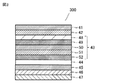
- the laminate 300 shown in FIG. 3 includes, from the viewing side, a front plate 41, a third adhesive layer 42, a linear polarizing plate 43, a first adhesive layer 44, a liquid crystal coating layer 45, a second adhesive layer 46, and an organic EL panel 47. They are stacked in this order.
- the linear polarizing plate 43 has a substrate film 48, a protective layer (HC layer) 49, an alignment film 50, a linear polarizing layer 51, and a protective layer (OC layer) 52 arranged in this order from the viewing side.
- the laminate can be produced by a method including a step of bonding the layers constituting the laminate 100 via an adhesive layer or an adhesive layer.
- a method including a step of bonding the layers constituting the laminate 100 via an adhesive layer or an adhesive layer.
- one or both of the laminating surfaces should be subjected to surface activation treatment such as corona treatment in order to improve adhesion. is preferred.
- the method for producing the linear polarizing layer includes a stretched film or stretched layer to which a dye having the above-mentioned absorption anisotropy is adsorbed. can be manufactured as described in the description.
- the linear polarizing layer When the linear polarizing layer is a film obtained by coating and curing the dye having the above-mentioned absorption anisotropy, the linear polarizing layer can be formed on the substrate via an alignment film.
- the linear polarizing layer can be formed by applying and curing a composition for forming a linear polarizing layer containing a dichroic dye and a polymerizable liquid crystal compound.
- the composition for forming a linear polarization layer preferably further contains a polymerization initiator, a leveling agent and a solvent, and further contains a photosensitizer, a polymerization inhibitor, a leveling agent and the like. It can contain more.
- the liquid crystal coating layer can be produced by applying a composition for forming a liquid crystal coating layer containing a polymerizable liquid crystal compound onto the substrate and, if present, the alignment film, and polymerizing the polymerizable liquid crystal compound.
- the liquid crystal coating layer-forming composition further contains a solvent and a polymerization initiator, and may further contain a photosensitizer, a polymerization inhibitor, a leveling agent, and the like.
- the substrate and alignment film may be incorporated into the liquid crystal coating layer, or may be peeled off from the liquid crystal coating layer and not become a component of the laminate.
- the application and drying of the composition for forming the linear polarization layer and the composition for forming the liquid crystal coating layer, and the polymerization of the polymerizable liquid crystal compound can be carried out by conventionally known coating methods, drying methods and polymerization methods.
- wire bar coating, extrusion coating, direct gravure coating, reverse gravure coating, die coating, and the like can be used as methods for applying the composition for forming a linear polarization layer and the composition for forming a liquid crystal coating layer. can be done.
- the method of polymerizing the polymerizable liquid crystal compound may be selected according to the type of polymerizable group of the polymerizable liquid crystal compound. If the polymerizable group is a photopolymerizable group, it can be polymerized by a photopolymerization method. If the polymerizable group is a thermally polymerizable group, it can be polymerized by a thermal polymerization method. In the method for producing the liquid crystal coating layer of this embodiment, a photopolymerization method is preferred. Since the photopolymerization method does not necessarily require heating the transparent base material to a high temperature, a transparent base material with low heat resistance can be used.
- the photopolymerization method is performed by irradiating visible light or ultraviolet light to a film made of a composition for forming a linearly polarized layer or a composition for forming a liquid crystal coating layer containing a polymerizable liquid crystal compound.
- Ultraviolet light is preferred because it is easy to handle.
- the adhesive layer can be prepared as an adhesive sheet.
- the pressure-sensitive adhesive sheet is prepared by dissolving or dispersing the pressure-sensitive adhesive composition in an organic solvent such as toluene or ethyl acetate to prepare a pressure-sensitive adhesive liquid, which is then applied to a release film on which a release treatment has been performed. is formed into a sheet, and another release film is further laminated on the adhesive layer.
- Each layer can be laminated by a method of laminating an adhesive sheet from which one release film has been peeled off to one layer, then peeling off the other release film, and laminating the other layer.
- Usual coating techniques using a die coater, a comma coater, a reverse roll coater, a gravure coater, a rod coater, a wire bar coater, a doctor blade coater, an air doctor coater, etc. can be used to apply the adhesive liquid onto the release film. should be adopted.
- the release film is preferably composed of a plastic film and a release layer.
- Plastic films include polyester films such as polyethylene terephthalate film, polybutylene terephthalate film and polyethylene naphthalate film, and polyolefin films such as polypropylene film.
- the release layer can be formed, for example, from a release layer-forming composition.
- the main component (resin) constituting the release layer-forming composition is not particularly limited, but examples thereof include silicone resins, alkyd resins, acrylic resins, long-chain alkyl resins, and the like.
- the thickness of the adhesive layer can be adjusted according to the coating conditions of the adhesive liquid. In order to reduce the thickness of the pressure-sensitive adhesive layer, it is effective to reduce the coating thickness.
- a laminate can be produced by cutting a long film in which a linear polarizing layer and a liquid crystal coating layer are bonded via an adhesive layer to a predetermined size.
- the laminate can also be produced by laminating a linearly polarizing layer and a liquid crystal coating layer, which have been cut to a predetermined size in advance, with an adhesive layer.
- An image display device includes the laminate described above.
- the display device is not particularly limited, and examples thereof include image display devices such as organic EL display devices, inorganic EL display devices, liquid crystal display devices, and electroluminescence display devices.
- the image display device may have a touch panel function.
- the laminate is suitable for a flexible display that can be bent or folded.
- the laminate is arranged on the viewing side of the display element of the image display device with the front panel facing outward (the side opposite to the display element side, that is, the viewing side).
- the image display device can be used as mobile devices such as smartphones and tablets, televisions, digital photo frames, electronic signboards, measuring instruments and gauges, office equipment, medical equipment, computing equipment, and the like.
- the image display device has excellent screen visibility because the distortion of the reflected image reflected on the surface of the front panel is suppressed.
- the storage modulus of the adhesive layer at a temperature of 25°C was measured by the following method.
- a plurality of adhesive layers used in Examples and Comparative Examples were laminated so as to have a thickness of 0.2 mm.
- a cylindrical body with a diameter of 8 mm was punched out from the obtained adhesive layer, and this was used as a sample for measuring the storage elastic modulus at a temperature of 25°C.
- the storage modulus (Pa) at a temperature of 25° C. was measured under the following conditions by the torsional shear method using a viscoelasticity measuring device (manufactured by Physica, MCR300) in accordance with JIS K7244-6. (Measurement condition) Normal Force FN: 1N Distortion ⁇ : 1% Frequency: 1Hz Temperature: 25°C
- the thickness of the adhesive layer was measured using a contact-type film thickness measuring device ("MS-5C” manufactured by Nikon Corporation). However, the polarizer layer and the alignment film were measured using a laser microscope ("OLS4100” manufactured by Olympus Corporation).
- the tensile modulus at a temperature of 23°C was measured as follows. A rectangular piece of 110 mm long side ⁇ 10 mm short side was cut out from a front plate or a polyimide film (a substitute equivalent to an organic EL panel) using a super cutter. Then, the upper and lower grips of a tensile tester (manufactured by Shimadzu Corporation, Autograph AG-Xplus testing machine) hold both ends of the measurement sample in the long side direction so that the distance between the grips is 5 cm, and the temperature is 23.
- a tensile tester manufactured by Shimadzu Corporation, Autograph AG-Xplus testing machine
- the measurement sample is pulled in the length direction of the measurement sample at a tensile speed of 4 mm / min, and the resulting stress - in the strain curve, from the slope of the straight line between 20 and 40 MPa, the temperature is 23 ° C. , the tensile modulus at 55% relative humidity was calculated.
- the thickness for calculating the stress was measured by the method described above.
- the jig 501 is operated in the direction of the arrow A so that the distance D becomes 4.0 mm (bending radius 2R) to bend the measurement sample 500, and then the jig 501 is bent.
- the tool 501 was operated in the direction of the arrow B to release the bending with the interval D set to 70 mm, and this series of operations was counted as one and was continuously repeated 200,000 times.
- the moving speed of the jig 501 was 1.32 m/sec, and the time required to repeat 200,000 times was 55.6 hours.
- the measurement sample was taken out from the bending tester and observed with transmitted light using an optical microscope to confirm the presence or absence of cracks. O: Cracks were generated. x: No cracks occurred.
- a polyimide film (PI film, total thickness: 40 ⁇ m, tensile modulus of elasticity 6.8 GPa) was prepared as a window film, which is a front plate.
- Linear polarizing plate A (Base film) A triacetyl cellulose (TAC) film (manufactured by Konica Minolta, Inc., thickness 25 ⁇ m) was prepared as a base film.
- TAC triacetyl cellulose
- Polymer 1 is a polymer having a photoreactive group consisting of the following structural units. GPC measurement revealed that the obtained polymer 1 had a number average molecular weight of 28200, Mw/Mn of 1.82, and a monomer content of 0.5%. A solution of polymer 1 dissolved in cyclopentanone at a concentration of 5% by mass was used as a composition for forming an alignment film.
- the polymerizable liquid crystal compound includes a polymerizable liquid crystal compound represented by formula (1-6) [hereinafter, also referred to as compound (1-6)] and a polymerizable liquid crystal compound represented by formula (1-7) [hereinafter, Also referred to as compound (1-7)] was used.
- dichroic dye As the dichroic dye, the azo dyes described in the examples of JP-A-2013-101328 represented by the following formulas (2-1a), (2-1b), and (2-3a) were used.
- composition for forming a linear polarization layer includes 75 parts by mass of compound (1-6), 25 parts by mass of compound (1-7), the above formulas (2-1a) as dichroic dyes (2-1b), (2-1b), ( 2.5 parts by mass each of the azo dyes represented by 2-3a), 2-dimethylamino-2-benzyl-1-(4-morpholinophenyl)butan-1-one (Irgacure369, manufactured by BASF Japan Co., Ltd.) as a polymerization initiator ) and 1.2 parts by mass of a polyacrylate compound (BYK-361N, manufactured by BYK-Chemie) as a leveling agent are mixed with 400 parts by mass of toluene as a solvent, and the resulting mixture is heated at 80° C. Prepared by stirring for hours.
- a polyacrylate compound BYK-361N, manufactured by BYK-Chemie
- the protective layer composition is composed of 3 parts by weight of polyvinyl alcohol resin powder (manufactured by Kuraray Co., Ltd., average degree of polymerization: 18000, trade name: KL-318) and polyamide epoxy resin (crosslinking agent, resin) per 100 parts by weight of water. Ka Chemtex Co., Ltd., trade name: SR650 (30)) was mixed with 1.5 parts by mass.
- Polarized UV treatment uses a UV irradiation device (SPOT CURE SP-7; manufactured by Ushio Inc.) is transmitted through a wire grid (UIS-27132##, manufactured by Ushio Inc.), and the integrated amount of light measured at a wavelength of 365 nm is 100 mJ/cm 2 . under certain conditions.
- the thickness of the alignment film was 100 nm.
- a composition for forming a linear polarization layer was applied onto the formed alignment film by a bar coating method, dried by heating in a drying oven at 120° C. for 1 minute, and then cooled to room temperature.
- a linearly polarized layer was formed by irradiating the dried film with ultraviolet rays at an integrated light amount of 1200 mJ/cm 2 (365 nm standard) using the above UV irradiation device.
- the thickness of the obtained linearly polarizing layer was measured with a laser microscope (OLS3000 manufactured by Olympus Corporation), it was 1.8 ⁇ m.
- OLS3000 manufactured by Olympus Corporation laser microscope
- a protective layer (OC layer) composition was applied onto the formed linear polarizing layer by a bar coating method so that the thickness after drying was 1.0 ⁇ m, and dried at a temperature of 80° C. for 3 minutes.
- a linear polarizing plate A consisting of "base film/orientation film/linear polarizing layer/protective layer (OC layer)" was obtained.
- Linear polarizing plate B (Base film) A polyethylene terephthalate (PET) film (thickness: 100 ⁇ m) was prepared as a base film.
- PET polyethylene terephthalate
- composition for protective layer 2.8 parts by weight of a dendrimer acrylate having an 18-functional acrylic group (Miramer SP1106, Miwon), 6.6 parts by weight of a urethane acrylate having a hexafunctional acrylic group (Miramer PU-620D, Miwon), and a photopolymerization initiator (Irgacure-184, BASF) 0.5 parts by weight, a leveling agent (BYK-3530, BYK) 0.1 parts by weight, and methyl ethyl ketone (MEK) 90 parts by weight, mixed with a protective layer (HC layer) composition prepared the product.
- a leveling agent BYK-3530, BYK
- MEK methyl ethyl ketone
- compositions for forming the alignment film the composition for forming the linearly polarizing layer, and the composition for forming the protective layer (OC layer), the compositions described in the section [Linearly polarizing plate A] above were used.
- a protective layer (HC layer) composition was applied to the substrate film by a bar coating method, and dried by heating in a drying oven at 80° C. for 3 minutes.
- a UV irradiation device SPOT CURE SP-7, manufactured by Ushio Inc.
- the obtained dry film was irradiated with UV light at an exposure amount of 500 mJ/cm 2 (365 nm standard) to form a protective layer (HC layer). formed.
- the thickness of the protective layer (HC layer) was measured with a laser microscope (OLS3000 manufactured by Olympus Corporation), it was 2.0 ⁇ m.
- OLS3000 manufactured by Olympus Corporation
- the protective layer (HC layer) side of the laminate composed of "base film/protective layer (HC layer)” was subjected to corona treatment once.
- the corona treatment conditions were an output of 0.3 kW and a treatment speed of 3 m/min.
- the alignment film-forming composition was applied onto the protective layer (HC layer) by a bar coating method, and dried by heating in a drying oven at 80° C. for 1 minute.
- the resulting dry film was subjected to polarized UV irradiation treatment to form a first alignment film.
- a composition for forming a linear polarization layer was applied onto the formed alignment film by a bar coating method, dried by heating in a drying oven at 120° C. for 1 minute, and then cooled to room temperature.
- a linearly polarized layer was formed by irradiating the dried film with ultraviolet rays at an integrated light amount of 1200 mJ/cm 2 (365 nm standard) using the above UV irradiation device.
- OLS3000 manufactured by Olympus Corporation When the thickness of the obtained linearly polarizing layer was measured with a laser microscope (OLS3000 manufactured by Olympus Corporation), it was 1.8 ⁇ m.
- OLS3000 manufactured by Olympus Corporation
- a protective layer (OC layer) composition was applied onto the formed polarizing layer by a bar coating method so that the thickness after drying was 1.0 ⁇ m, and dried at a temperature of 80° C. for 3 minutes.
- a laminate composed of "base film/protective layer (HC layer)/alignment film/linear polarizing layer/protective layer (OC layer)" was obtained.
- the substrate film was peeled off to obtain a linearly polarizing plate B composed of "protective layer (HC layer)/orientation film/linearly polarizing layer/protective layer (OC layer)".
- Adhesive layer A As an adhesive sheet A having an adhesive layer A, two release films (heavy separator, light separator) in which one side of a polyethylene terephthalate film (base film) with a thickness of 38 ⁇ m has been subjected to release treatment. A commercially available adhesive sheet sandwiching an acrylic adhesive layer having a thickness of 5 ⁇ m was used.
- the storage elastic modulus G′1 of the adhesive layer A obtained by removing the release film from the adhesive sheet A at a temperature of 25° C. was 1400 kPa.
- Adhesive layer B As the adhesive sheet B having the adhesive layer B, an adhesive with a thickness of 25 ⁇ m was applied to each release-treated surface of two release films (heavy separator, light separator) in which one side of the base film was subjected to release treatment.
- the storage elastic modulus G′2 of the adhesive layer B obtained by removing the release film from the adhesive sheet B at a temperature of 25° C. was 41 kPa.
- Liquid crystal coating layer (First liquid crystal cured retardation layer)
- a layer giving a retardation of ⁇ /4 was prepared, which was composed of a layer in which a nematic liquid crystal compound was cured, an alignment layer and a transparent substrate.
- the total thickness of the layer in which the nematic liquid crystal compound was cured and the alignment layer was 2 ⁇ m.
- the layer in which the nematic liquid crystal compound was cured was formed by applying a composition for forming a retardation layer containing a nematic liquid crystal compound onto the alignment layer formed on the transparent substrate and curing the composition.
- a polyethylene terephthalate substrate having a thickness of 38 ⁇ m was used as a transparent substrate, one side of which was coated with a composition for a vertical alignment layer so as to have a thickness of 3 ⁇ m, and an alignment layer was produced by irradiating polarized ultraviolet rays of 20 mJ/cm 2 . .
- a composition for the vertical alignment layer 2-phenoxyethyl acrylate, tetrahydrofurfuryl acrylate, dipentaerythritol triacrylate, and bis(2-vinyloxyethyl) ether were mixed at a ratio of 1:1:4:5. and 4% of LUCIRIN (registered trademark) TPO was added as a polymerization initiator.
- a composition for forming a retardation layer containing a photopolymerizable nematic liquid crystal (manufactured by Merck & Co., RMM28B) was applied onto the formed alignment layer by die coating.
- a liquid crystal composition methyl ethyl ketone (MEK), methyl isobutyl ketone (MIBK), and cyclohexanone (CHN) having a boiling point of 155° C. are used as solvents in a mass ratio (MEK:MIBK:CHN) of 35: A mixed solvent mixed at a ratio of 30:35 was used.
- the composition for forming a retardation layer prepared to have a solid content of 1 to 1.5 g was applied onto the orientation layer so that the coating amount was 4 to 5 g (wet).
- the retardation layer-forming composition was applied onto the alignment layer, drying was performed at a drying temperature of 75°C and a drying time of 120 seconds. After that, the liquid crystal compound was polymerized by ultraviolet (UV) irradiation to obtain a positive C layer composed of a layer in which the photopolymerizable nematic liquid crystal compound was cured, an alignment layer, and a transparent substrate. The total thickness of the layer in which the photopolymerizable nematic liquid crystal compound was cured and the alignment layer was 4 ⁇ m.
- UV ultraviolet
- the first liquid crystal cured retardation layer and the second liquid crystal cured retardation layer are bonded with an ultraviolet curing adhesive so that the surface of each liquid crystal cured retardation layer (the surface opposite to the transparent substrate) becomes the bonding surface. pasted together.
- ultraviolet rays were irradiated to cure the ultraviolet curing adhesive.
- the thickness of the cured UV-curable adhesive was 2 ⁇ m.
- Organic EL panel A polyimide film (PI film, total thickness: 75 ⁇ m, tensile modulus of elasticity 6.96 GPa) was prepared as a substitute for an organic EL panel.
- Example 1 The adhesive layer A, which was exposed by peeling off the light separator from the adhesive sheet A, was attached to the protective layer 2 side of the linear polarizing plate A to obtain a laminate A1. Both surfaces to be bonded were previously subjected to corona treatment (output: 0.3 kW, speed: 3 m/min).
- the adhesive layer A which is exposed by peeling off the heavy separator from the laminate A1, is attached to the surface of the liquid crystal coating layer from which the base film used for forming the first liquid crystal cured retardation layer is peeled off, and the laminate A2 is formed. Obtained. Both surfaces to be bonded were previously subjected to corona treatment (output: 0.3 kW, speed: 3 m/min).
- the adhesive layer A which is exposed by peeling off the light separator from another adhesive sheet A, is attached to the surface where the base film used for forming the second liquid crystal cured retardation layer is peeled from the laminate A2, and the laminate A3 was obtained. Both surfaces to be bonded were previously subjected to corona treatment (output: 0.3 kW, speed: 3 m/min).
- the third adhesive layer which was exposed by peeling off the light separator from the third adhesive sheet, was attached to the front plate to obtain a laminate A4. Both surfaces to be bonded were previously subjected to corona treatment (output: 0.3 kW, speed: 3 m/min).
- the heavy separator was peeled off from the laminate A4 and attached to the protective layer 1 side of the laminate A3 to obtain a laminate A5. Both surfaces to be bonded were previously subjected to corona treatment (output: 0.3 kW, speed: 3 m/min).
- the heavy separator of the laminate A5 was peeled off, and a substitute (polyimide film) equivalent to an organic EL panel was attached to obtain the laminate of Example 1 having the structure shown in FIG. Table 1 shows the results.
- Example 2 Comparative Examples 1 and 2> Laminates of Example 2 and Comparative Examples 1 and 2 were produced in the same manner as in Example 1, except that the linear polarizing plate and adhesive layer shown in Table 1 were used. Table 1 shows the results.
Landscapes
- Physics & Mathematics (AREA)
- General Physics & Mathematics (AREA)
- Optics & Photonics (AREA)
- Nonlinear Science (AREA)
- Crystallography & Structural Chemistry (AREA)
- Chemical & Material Sciences (AREA)
- Theoretical Computer Science (AREA)
- Engineering & Computer Science (AREA)
- Mathematical Physics (AREA)
- Spectroscopy & Molecular Physics (AREA)
- Laminated Bodies (AREA)
- Polarising Elements (AREA)
- Devices For Indicating Variable Information By Combining Individual Elements (AREA)
- Electroluminescent Light Sources (AREA)
Abstract
Description
[1] 直線偏光層と、第1粘着層と、液晶コーティング層と、第2粘着層とがこの順に積層され、
前記第1粘着層の温度25℃における貯蔵弾性率をG’1[kPa]とし、前記第2粘着層の温度25℃における貯蔵弾性率をG’2[kPa]としたとき、下記条件(1)を満たす、積層体。
(1) G’1≧1000kPaかつG’2≧1000kPa
[2] 前記直線偏光層は、重合性液晶化合物と1つまたは複数のアゾ系色素とを含む組成物の硬化物と、配向膜とを含む、[1]に記載の積層体。
[3] 前記液晶コーティング層は1層または複数層からなる、[1]または[2]に記載の積層体。
[4] 前記直線偏光層の前記第1粘着層とは反対側に熱可塑性樹脂フィルムおよび硬化樹脂層からなる群から選択される少なくとも1つの保護層を備える、[1]~[3]のいずれかに記載の積層体。
[5] 前記保護層の前記直線偏光層とは反対側に第3粘着層を介して前面板を備える、[4]に記載の積層体。
[6] 前記前面板は、温度23℃における引張弾性率が4.0GPa以上である、[5]に記載の積層体。
[7] 前記第3粘着層の温度25℃における貯蔵弾性率は50KPa以下である、[5]または[6]に記載の積層体。
[8] 前記第2粘着層の前記液晶コーティング層とは反対側に有機ELパネルを備える、[1]~[7]のいずれか1項に記載の積層体。
[9] 前記有機ELパネルは、温度23℃における引張弾性率が4.0GPa以上である、[1]~[8]のいずれかに記載の積層体。
[10] [1]~[9]のいずれかに記載の積層体を含む、画像表示装置。
本発明の一態様にかかる積層体は、直線偏光層と、第1粘着層と、液晶コーティング層と、第2粘着層とがこの順に積層され、第1粘着層の温度25℃における貯蔵弾性率をG’1[kPa]とし、第2粘着層の温度25℃における貯蔵弾性率をG’2[kPa]としたとき、下記条件(1)を満たす。
(1) G’1≧1000kPaかつG’2≧1000kPa
積層体100は、上記の条件(1)を満たす。本発明者によって、液晶コーティング層を、温度25℃における貯蔵弾性率が1000kPa以上である比較的硬い2つの粘着層の間に配置することにより、アウトフォールドで繰返しの屈曲が可能となることが見出された。温度25℃における貯蔵弾性率は、後述の実施例の欄において説明する方法に従って測定することができる。
積層体100は、例えば画像表示装置等に用いることができる。画像表示装置は特に限定されず、例えば有機エレクトロルミネッセンス(有機EL)表示装置、無機エレクトロルミネッセンス(無機EL)表示装置、液晶表示装置、電界発光表示装置等が挙げられる。画像表示装置はタッチパネル機能を有していてよい。画像表示装置は好ましくはフレキシブルディスプレイであることができる。積層体100は、直線偏光層10側が視認側となるように画像表示装置に配置されることができる。
直線偏光層10としては二色性色素を吸着させた延伸フィルムまたは延伸層、二色性色素を塗布し硬化させてなる偏光子層等が挙げられる。二色性色素を塗布し硬化させてなる偏光子層は、吸収異方性を有する色素を吸着させた延伸フィルムまたは延伸層に比べて、屈曲方向に制限がないため好ましい。
二色性色素を吸着させた延伸フィルムは、通常、ポリビニルアルコール系樹脂フィルムを一軸延伸する工程、ポリビニルアルコール系樹脂フィルムを二色性色素で染色することにより、その二色性色素を吸着させる工程、二色性色素が吸着されたポリビニルアルコール系樹脂フィルムをホウ酸水溶液で処理する工程、およびホウ酸水溶液による処理後に水洗する工程を経て製造することができる。
二色性色素を吸着させた延伸フィルムの厚みは、例えば2μm以上40μm以下であってよく、5μm以上であってもよく、20μm以下、さらには15μm以下、なおさらには10μm以下であってもよい。
必要に応じて、基材フィルムを二色性色素を吸着させた延伸層から剥離除去してもよい。基材フィルムの材料および厚みは、後述する熱可塑性樹脂フィルムの材料および厚みと同様であってよい。
二色性色素を塗布し硬化させてなる偏光子層としては、液晶性を有する重合性の二色性色素を含む組成物または重合性液晶化合物と二色性色素とを含む組成物を基材フィルムに塗布し硬化させて得られる層等の重合性液晶化合物の硬化物を含む偏光子層が挙げられる。基材フィルムは一方の面に配向膜が設けられていてもよい。直線偏光層10は、屈曲性向上の観点から好ましくは、重合性液晶化合物と1つまたは複数のアゾ系色素とを含む組成物の硬化物と、配向膜とを含む層である。配向膜の厚みは、例えば5nm以上1μm以下であってよい。
保護層は、直線偏光層10の片側または両側に配置され、直線偏光層10の表面を保護する機能を有することができる。本明細書において、保護層が積層された直線偏光層を直線偏光板ということがある。
第1粘着層11は、直線偏光層10と液晶コーティング層12との間に介在して、これらを接合する層であることができる。第2粘着層13は、積層体100の液晶コーティング層12側に例えばタッチセンサパネルや有機ELパネル等を貼合する層であることができる。以下、第1粘着層11および第2粘着層13の総称として粘着層ということがある。
液晶コーティング層12は、第1粘着層11と第2粘着層13との間に介在しており、かつ、第1粘着層11と第2粘着層13とに接して積層されている。液晶コーティング層12は、重合性液晶化合物の硬化層であることができる。液晶コーティング層は、1層または複数層からなる。液晶コーティング層が複数層からなる場合、層同士は後述する貼合層を介して積層されていてよく、好ましくは後述する接着剤層を介して積層される。
前面板は、画像表示装置の視認側の最表面を構成し、画像表示装置の前面(画面)を保護する機能を有することができる。前面板は、ウィンドウフィルムと呼ばれるものであることができる。前面板は、光を透過可能な板状体であれば、材料および厚みは限定されることはなく、また1層のみから構成されてよく、2層以上から構成されてもよい。その例としては、樹脂製の板状体(例えば樹脂板、樹脂シート、樹脂フィルム等)、ガラス製の板状体(例えばガラス板、ガラスフィルム等)、後述のタッチセンサパネルが挙げられる。積層体100が前面板を有する場合、前面板は積層体100の視認側に配置されることができる。積層体100は、直線偏光層10の第1粘着層11とは反対側の最外面に後述の第3粘着層を介して前面板を備えることができる。前面板を有する積層体100は、前面板が画像表示装置の最表面を構成するように画像表示装置に配置されることができる。
第3粘着層は、前面板を積層体100に接合する機能を有することができる。第3粘着層は、粘着剤から形成されることができる。第3粘着層を構成する粘着剤には、粘着層を構成する粘着剤組成物について例示したものと同じ剤であってもよいし、他の粘着剤、例えば(メタ)アクリル系粘着剤、スチレン系粘着剤、シリコーン系粘着剤、ゴム系粘着剤、ウレタン系粘着剤、ポリエステル系粘着剤、エポキシ系共重合体粘着剤等であってもよい。第3粘着層の温度25℃における貯蔵弾性率は、屈曲したときに液晶コーティング層にクラックが生じにくくなる観点から好ましくは50kPa以下であり、より好ましくは45kPa以下であり、さらに好ましくは41kPa以下である。
貼合層は、粘着剤または接着剤から構成される層である。貼合層は、例えば前面板とタッチセンサパネルとを貼合する層、積層体とタッチセンサパネルとを貼合する層、直線偏光層と保護層とを接合する層、第1液晶硬化位相差層と第2液晶硬化位相差層とを接合する層等であることができる。貼合層を構成する粘着剤は、上述の粘着層を構成する粘着剤組成物について例示したものと同じ剤であってもよいし、他の粘着剤、例えば(メタ)アクリル系粘着剤、スチレン系粘着剤、シリコーン系粘着剤、ゴム系粘着剤、ウレタン系粘着剤、ポリエステル系粘着剤、エポキシ系共重合体粘着剤等であってもよい。積層体100は、貼合層を1つ備えてもよいし、2以上備えてもよい。積層体100が貼合層を複数備える場合、複数の貼合層は、互いに同一であってもよいし、異なっていてもよい。
有機ELパネルは、公知の有機ELパネルを用いることができる。積層体100は、第2粘着層13の液晶コーティング層12とは反対側に有機ELパネルを備えることができる。有機ELパネルは、優れた屈曲性を有する積層体を構成し易い観点から、温度23℃における引張弾性率が、4.0GPa以上であることが好ましく、5.0GPa以上であることがより好ましく、6.0GPa以上であることがさらに好ましい。有機ELパネルは、優れた屈曲性を有する積層体を構成し易い観点から、温度23℃における引張弾性率が20GPa以下であることが好ましく、15GPa以下であることがさらに好ましい。積層体100は、温度23℃における引張弾性率が6.0GPaである有機ELパネルを備える場合でも、アウトフォールドで繰返しの屈曲が可能である。
タッチセンサパネルは、タッチされた位置を検出可能なセンサであれば、検出方式は限定されることはなく、抵抗膜方式、静電容量方式、光センサ方式、超音波方式、電磁誘導結合方式、表面弾性波方式等のタッチセンサパネルが例示される。その中でも、低コスト、早い反応速度、薄膜化の面で、静電容量方式のタッチセンサパネルが好適に用いられる。タッチセンサパネルは、透明導電層とこれを支持する基材フィルムとの間に、接着層、分離層、保護層等を備えてもよい。接着層としては、接着剤層、粘着剤層が挙げられる。透明導電層を支持する基材フィルムとして、一方の表面に透明導電層が蒸着形成されている基材フィルム、接着層を介して透明導電層が転写された基材フィルム等が挙げられる。
図2に示す積層体200は、視認側から、前面板21、第3粘着層22、直線偏光板23、第1粘着層24、液晶コーティング層25、第2粘着層26、有機ELパネル27がこの順に積層されている。直線偏光板23は、視認側から基材フィルム28、配向膜29、直線偏光層30、保護層(OC層)31がこの順に配置されている。
積層体は、粘着剤層、あるいはさらに接着剤層を介して積層体100を構成する層同士を貼合する工程を含む方法によって製造することができる。粘着剤層や接着剤層を介して層同士を貼合する場合には、密着性を高めるために、貼合面の一方または両方に対して、例えばコロナ処理等の表面活性化処理を施すことが好ましい。
本発明の別の一態様にかかる画像表示装置は、上記の積層体を含む。表示装置は特に限定されず、例えば有機EL表示装置、無機EL表示装置、液晶表示装置、電界発光表示装置等の画像表示装置が挙げられる。画像表示装置はタッチパネル機能を有していてもよい。積層体は、屈曲または折り曲げ等が可能な可撓性を有するフレキシブルディスプレイに好適である。
粘着層の温度25℃における貯蔵弾性率は、以下の方法により測定した。実施例および比較例に用いた粘着層を厚さ0.2mmになるように複数枚積層した。得られた粘着層から、直径8mmの円柱体を打ち抜き、これを温度25℃における貯蔵弾性率の測定用サンプルとした。上記サンプルについて、JIS K7244-6に準拠し、粘弾性測定装置(Physica社製、MCR300)を用いてねじりせん断法により、以下の条件で温度25℃における貯蔵弾性率(Pa)を測定した。
(測定条件)
ノーマルフォースFN:1N
歪みγ:1%
周波数:1Hz
温度:25℃
粘着層の厚みは、接触式膜厚測定装置(株式会社ニコン製「MS-5C」)を用いて測定した。ただし、偏光子層および配向膜については、レーザー顕微鏡(オリンパス株式会社製「OLS4100」)を用いて測定した。
温度23℃における引張弾性率は次のように測定した。前面板またはポリイミドフィルム(有機ELパネル相当の代用品)から長辺110mm×短辺10mmの長方形の小片をスーパーカッターを用いて切り出した。次いで、引張試験機(株式会社島津製作所製、オートグラフ AG-Xplus試験機)の上下つかみ具で、つかみ具の間隔が5cmとなるように上記測定用サンプルの長辺方向両端を挟み、温度23℃、相対湿度55%の環境下、引張速度4mm/分で測定用サンプルを測定用サンプルの長さ方向に引張り、得られる応力-ひずみ曲線における20~40MPa間の直線の傾きから、温度23℃、相対湿度55%での引張弾性率を算出した。このとき、応力を算出するための厚みは、上記に記載の方法によって測定した。
温度25℃相対湿度55%RHにおいて、次に示す手順でアウトフォールド試験を行った。
(アウトフォールド試験)
積層体から長辺110mm×短辺10mmの長方形の小片をスーパーカッターを用いて切り出した。次いで、図4(a)に示すように、個別に移動可能な二つの治具501,502を有する屈曲試験機に、測定用サンプル500を前面板側を外側にして短辺方向に平行な方向を屈曲軸として屈曲し、測定用サンプル500の長辺側の端部をそれぞれ治具501、502に粘着テープで固定し、治具501、502の間隔Dが70mmとなるように治具501、502の位置を調節した。その後、図4(b)に示すように、間隔Dが4.0mm(屈曲半径2R)となるように矢印Aの方向に治具501を稼働させて測定用サンプル500を屈曲し、その後、治具501を矢印Bの方向に稼働させて間隔Dを70mmとして屈曲を開放し、この一連の動作を1回とカウントとして、連続して20万回繰り返した。治具501の移動速度は1.32m/秒であり、20万回繰り返すのに要した時間は55.6時間であった。20万回繰り返した後、測定用サンプルを屈曲試験機から取出し、光学顕微鏡により透過光にて観察し、クラックの発生の有無を確認した。
〇:クラックの発生有り。
×:クラックの発生無し。
前面板であるウィンドウフィルムとして、ポリイミドフィルム(PIフィルム、全体の厚み:40μm、引張弾性率6.8GPa)を用意した。
基材フィルムの片面を離型処理した離型フィルム2枚(重Sp、軽Sp)のそれぞれの離型処理面を用いて、厚み50μmの第3粘着層を挟んだ市販の第3粘着剤シート(米国3M社製「CEF3501」)を用意した。第3粘着層の温度25℃における貯蔵弾性率は41kPaであった。
(基材フィルム)
基材フィルムとして、トリアセチルセルロース(TAC)フィルム(コニカミノルタ株式会社製、厚み25μm)を準備した。
ポリマー1は、以下の構造単位からなる光反応性基を有するポリマーである。

ポリマー1を濃度5質量%で、シクロペンタノンに溶解した溶液を配向膜形成用組成物として用いた。
重合性液晶化合物は、式(1-6)で表される重合性液晶化合物[以下、化合物(1-6)ともいう]と式(1-7)で表される重合性液晶化合物[以下、化合物(1-7)ともいう]とを用いた。


二色性色素には、下記式(2-1a)、(2-1b)、(2-3a)で示される特開2013-101328号公報の実施例に記載のアゾ色素を用いた。



直線偏光層形成用組成物は、化合物(1-6)75質量部、化合物(1-7)25質量部、二色性染料としての上記式(2-1a)、(2-1b)、(2-3a)で示されるアゾ色素各2.5質量部、重合開始剤としての2-ジメチルアミノ-2-ベンジル-1-(4-モルホリノフェニル)ブタン-1-オン(Irgacure369、BASFジャパン社製)6質量部、およびレベリング剤としてのポリアクリレート化合物(BYK-361N、BYK-Chemie社製)1.2質量部を、溶剤のトルエン400質量部に混合し、得られた混合物を80℃で1時間攪拌することにより調製した。
保護層用組成物は、水100質量部に対して、ポリビニルアルコール樹脂粉末(株式会社クラレ製、平均重合度18000、商品名:KL-318)3質量部と、ポリアミドエポキシ樹脂(架橋剤、住化ケムテックス株式会社製、商品名:SR650(30))1.5質量部とを混合して調製した。
基材フィルムにコロナ処理を施した。コロナ処理の条件は、出力0.3kW、処理速度3m/分とした。その後、基材フィルム上に、配向膜形成用組成物をバーコート法により塗布し、80℃の乾燥オーブン中で1分間加熱乾燥した。得られた乾燥被膜に偏光UV照射処理を施して配向膜を形成した。偏光UV処理は、UV照射装置(SPOT CURE
SP-7;ウシオ電機株式会社製)から照射される光を、ワイヤーグリッド(UIS-27132##、ウシオ電機株式会社製)を透過させて、波長365nmで測定した積算光量が100mJ/cm2である条件で行った。配向膜の厚みは100nmであった。
(基材フィルム)
基材フィルムとして、ポリエチレンテレフタレート(PET)フィルム(厚み100μm)を準備した。
18官能のアクリル基を有するデンドリマーアクリレート(Miramer SP1106、Miwon)2.8質量部と、6官能のアクリル基を有するウレタンアクリレート(Miramer PU-620D、Miwon)6.6質量部と、光重合開始剤(Irgacure-184、BASF)0.5質量部と、レベリング剤(BYK-3530、BYK)0.1質量部と、メチルエチルケトン(MEK)90質量部と混合して、保護層(HC層)用組成物を調製した。
基材フィルムに、保護層(HC層)用組成物をバーコート法により塗布し、80℃の乾燥オーブン中で3分間加熱乾燥した。得られた乾燥被膜にUV照射装置(SPOT CURE SP-7、ウシオ電機株式会社製)を用いて、露光量500mJ/cm2(365nm基準)のUV光を照射して保護層(HC層)を形成した。保護層(HC層)層の厚みをレーザー顕微鏡(オリンパス株式会社製OLS3000)により測定したところ、2.0μmであった。このようにして、「基材フィルム/保護層(HC層)」からなる積層体を得た。
粘着層Aを有する粘着剤シートAとして、厚み38μmのポリエチレンテレフタレートフィルム(基材フィルム)の片面に離形処理が施された剥離フィルム2枚(重セパレータ、軽セパレータ)のそれぞれ離型処理面で、厚み5μmのアクリル系粘着剤層を挟んだ市販の粘着剤シートを用いた。粘着剤シートAから剥離フィルムを取り除いた粘着層Aの温度25℃における貯蔵弾性率G’1は、1400kPaであった。
粘着層Bを有する粘着剤シートBとして、基材フィルムの片面に離型処理が施された2枚の離型フィルム(重セパレータ、軽セパレータ)のそれぞれの離型処理面で、厚み25μmの粘着剤層を挟んだ市販の粘着剤シート(米国3M社製「CEF3501」)を用いた。粘着シートBから剥離フィルムを取り除いた粘着層Bの温度25℃における貯蔵弾性率G’2は、41kPaであった。
(第1液晶硬化位相差層)
第1液晶硬化位相差層として、ネマチック液晶化合物が硬化した層、配向層および透明基材からなるλ/4の位相差を与える層を準備した。なお、ネマチック液晶化合物が硬化した層と、配向層との合計の厚みは2μmであった。ネマチック液晶化合物が硬化した層は、透明基材上に形成した配向層上にネマチック液晶化合物を含有する位相差層形成用組成物を塗工し、硬化させることにより形成した。
厚み38μmのポリエチレンテレフタレート基材を透明基材として用い、その片面に垂直配向層用組成物を膜厚3μmになるようにコーティングし、20mJ/cm2の偏光紫外線を照射して配向層を作製した。なお、その垂直配向層用組成物としては、2-フェノキシエチルアクリレートと、テトラヒドロフルフリルアクリレートと、ジペンタエリスリトールトリアクリレートと、ビス(2-ビニルオキシエチル)エーテルとを1:1:4:5の割合で混合し、重合開始剤としてLUCIRIN(登録商標)TPOを4%の割合で添加した混合物を用いた。
第1液晶硬化位相差層と第2液晶硬化位相差層とを、紫外線硬化型接着剤により、それぞれの液晶硬化位相差層面(透明基材とは反対側の面)が貼合面となるように貼り合わせた。次いで、紫外線を照射して紫外線硬化型接着剤を硬化させた。紫外線硬化型接着剤が硬化した後の厚みは2μmであった。このようにして、「第1液晶硬化位相差層(2μm)/接着剤層(厚み2μm)/第2液晶硬化位相差層(厚み4μm)」の層構成を有する液晶コーティング層を作製した。
有機ELパネル相当の代用品として、ポリイミドフィルム(PIフィルム、全体の厚み:75μm、引張弾性率6.96GPa)を用意した。
粘着シートAから軽セパレータを剥離して露出させた粘着層Aを、直線偏光板Aの保護層2側に貼合し、積層体A1を得た。貼合面にはあらかじめ両面コロナ処理(出力0.3kW、速度3m/分)を行った。
表1に示す直線偏光板および粘着層を用いたこと以外は実施例1と同様にして、実施例2、比較例1および2の積層体を作製した。結果を表1に示す。

第1粘着層、12,25,45 液晶コーティング層、13,26,46 第2粘着層、21,41 前面板、22,42 第3粘着層、23,43 直線偏光板、27,47
有機ELパネル、28,48 基材フィルム、49 保護層(HC層)、29,50 配向膜、31,52 保護層(OC層)、500 測定用サンプル、501,502 治具
Claims (10)
- 直線偏光層と、第1粘着層と、液晶コーティング層と、第2粘着層とがこの順に積層され、
前記第1粘着層の温度25℃における貯蔵弾性率をG’1[kPa]とし、前記第2粘着層の温度25℃における貯蔵弾性率をG’2[kPa]としたとき、下記条件(1)を満たす、積層体。
(1) G’1≧1000kPaかつG’2≧1000kPa - 前記直線偏光層は、重合性液晶化合物と1つまたは複数のアゾ系色素とを含む組成物の硬化物と、配向膜とを含む、請求項1に記載の積層体。
- 前記液晶コーティング層は1層または複数層からなる、請求項1または2に記載の積層体。
- 前記直線偏光層の前記第1粘着層とは反対側に熱可塑性樹脂フィルムおよび硬化樹脂層からなる群から選択される少なくとも1つの保護層を備える、請求項1~3のいずれか1項に記載の積層体。
- 前記保護層の前記直線偏光層とは反対側に第3粘着層を介して前面板を備える、請求項4に記載の積層体。
- 前記前面板は、温度23℃における引張弾性率が4.0GPa以上である、請求項5に記載の積層体。
- 前記第3粘着層の温度25℃における貯蔵弾性率は50KPa以下である、請求項5または6に記載の積層体。
- 前記第2粘着層の前記液晶コーティング層とは反対側に有機ELパネルを備える、請求項1~7のいずれか1項に記載の積層体。
- 前記有機ELパネルは、温度23℃における引張弾性率が4.0GPa以上である、請求項1~8のいずれか1項に記載の積層体。
- 請求項1~9のいずれか1項に記載の積層体を含む、画像表示装置。
Priority Applications (2)
| Application Number | Priority Date | Filing Date | Title |
|---|---|---|---|
| KR1020237044536A KR20240015092A (ko) | 2021-06-02 | 2022-05-23 | 적층체 |
| CN202280019217.XA CN117015728A (zh) | 2021-06-02 | 2022-05-23 | 层叠体 |
Applications Claiming Priority (2)
| Application Number | Priority Date | Filing Date | Title |
|---|---|---|---|
| JP2021-093098 | 2021-06-02 | ||
| JP2021093098A JP2022185419A (ja) | 2021-06-02 | 2021-06-02 | 積層体 |
Publications (1)
| Publication Number | Publication Date |
|---|---|
| WO2022255155A1 true WO2022255155A1 (ja) | 2022-12-08 |
Family
ID=84323141
Family Applications (1)
| Application Number | Title | Priority Date | Filing Date |
|---|---|---|---|
| PCT/JP2022/021159 Ceased WO2022255155A1 (ja) | 2021-06-02 | 2022-05-23 | 積層体 |
Country Status (5)
| Country | Link |
|---|---|
| JP (1) | JP2022185419A (ja) |
| KR (1) | KR20240015092A (ja) |
| CN (1) | CN117015728A (ja) |
| TW (1) | TW202321036A (ja) |
| WO (1) | WO2022255155A1 (ja) |
Families Citing this family (1)
| Publication number | Priority date | Publication date | Assignee | Title |
|---|---|---|---|---|
| JP7723855B1 (ja) | 2024-03-29 | 2025-08-14 | 住友化学株式会社 | 偏光積層体 |
Citations (5)
| Publication number | Priority date | Publication date | Assignee | Title |
|---|---|---|---|---|
| JP2010044211A (ja) * | 2008-08-12 | 2010-02-25 | Sumitomo Chemical Co Ltd | 偏光板及びそれを用いた画像表示装置 |
| JP2020060708A (ja) * | 2018-10-11 | 2020-04-16 | 住友化学株式会社 | 光学積層体及び表示装置 |
| US20200285093A1 (en) * | 2017-10-23 | 2020-09-10 | Samsung Sdi Co., Ltd. | Liquid crystal phase difference film, polarizing plate for light-emitting display device including same, and light-emitting display device including same |
| WO2020195540A1 (ja) * | 2019-03-26 | 2020-10-01 | 住友化学株式会社 | 積層体及び表示装置 |
| WO2021070755A1 (ja) * | 2019-10-09 | 2021-04-15 | 日東電工株式会社 | フレキシブル画像表示装置およびそれに用いる光学積層体 |
Family Cites Families (3)
| Publication number | Priority date | Publication date | Assignee | Title |
|---|---|---|---|---|
| JP5332599B2 (ja) * | 2008-07-11 | 2013-11-06 | 住友化学株式会社 | 偏光板、その製造方法及びそれを用いた複合偏光板 |
| JP5930636B2 (ja) * | 2011-09-27 | 2016-06-08 | 住友化学株式会社 | 偏光板 |
| JP7042020B2 (ja) * | 2016-08-15 | 2022-03-25 | 日東電工株式会社 | フレキシブル画像表示装置用積層体、及び、フレキシブル画像表示装置 |
-
2021
- 2021-06-02 JP JP2021093098A patent/JP2022185419A/ja active Pending
-
2022
- 2022-05-23 WO PCT/JP2022/021159 patent/WO2022255155A1/ja not_active Ceased
- 2022-05-23 KR KR1020237044536A patent/KR20240015092A/ko active Pending
- 2022-05-23 CN CN202280019217.XA patent/CN117015728A/zh active Pending
- 2022-05-30 TW TW111120081A patent/TW202321036A/zh unknown
Patent Citations (5)
| Publication number | Priority date | Publication date | Assignee | Title |
|---|---|---|---|---|
| JP2010044211A (ja) * | 2008-08-12 | 2010-02-25 | Sumitomo Chemical Co Ltd | 偏光板及びそれを用いた画像表示装置 |
| US20200285093A1 (en) * | 2017-10-23 | 2020-09-10 | Samsung Sdi Co., Ltd. | Liquid crystal phase difference film, polarizing plate for light-emitting display device including same, and light-emitting display device including same |
| JP2020060708A (ja) * | 2018-10-11 | 2020-04-16 | 住友化学株式会社 | 光学積層体及び表示装置 |
| WO2020195540A1 (ja) * | 2019-03-26 | 2020-10-01 | 住友化学株式会社 | 積層体及び表示装置 |
| WO2021070755A1 (ja) * | 2019-10-09 | 2021-04-15 | 日東電工株式会社 | フレキシブル画像表示装置およびそれに用いる光学積層体 |
Also Published As
| Publication number | Publication date |
|---|---|
| TW202321036A (zh) | 2023-06-01 |
| CN117015728A (zh) | 2023-11-07 |
| JP2022185419A (ja) | 2022-12-14 |
| KR20240015092A (ko) | 2024-02-02 |
Similar Documents
| Publication | Publication Date | Title |
|---|---|---|
| JP7194041B2 (ja) | 積層体 | |
| JP6732089B2 (ja) | フレキシブル積層体及びそれを備えた画像表示装置 | |
| KR20200081287A (ko) | 플렉시블 적층체 및 그것을 구비한 화상 표시 장치 | |
| JP2020157577A (ja) | 積層体及び表示装置 | |
| WO2020195541A1 (ja) | 積層体及び表示装置 | |
| JP7469889B2 (ja) | 光学積層体、及び表示装置の製造方法 | |
| WO2022255154A1 (ja) | 積層体 | |
| JP2022145565A (ja) | 光学積層体及び表示装置 | |
| JP2020157579A (ja) | 積層体及び表示装置 | |
| JP2022185419A (ja) | 積層体 | |
| KR20220157367A (ko) | 적층체 | |
| JP2021149087A (ja) | 積層シートおよびその製造方法 | |
| JP2021144208A (ja) | 積層シートおよびその製造方法 | |
| JP7292051B2 (ja) | フレキシブル積層体、およびそれを備えた画像表示装置 | |
| WO2021149359A1 (ja) | 光学積層体及び表示装置 | |
| JP7194042B2 (ja) | 積層体 | |
| TW202134708A (zh) | 光學積層體 | |
| WO2021182005A1 (ja) | 積層シートおよびその製造方法 | |
| WO2021166434A1 (ja) | 光学積層体およびそれを備えた表示装置 | |
| TW202128420A (zh) | 光學積層體及其製造方法 | |
| KR102345851B1 (ko) | 광학 적층체 및 표시장치 | |
| WO2021186986A1 (ja) | 積層シートおよびその製造方法 | |
| JP2023154554A (ja) | 積層体および画像表示装置 | |
| KR20210114868A (ko) | 광학 적층체 및 표시장치 |
Legal Events
| Date | Code | Title | Description |
|---|---|---|---|
| 121 | Ep: the epo has been informed by wipo that ep was designated in this application |
Ref document number: 22815905 Country of ref document: EP Kind code of ref document: A1 |
|
| WWE | Wipo information: entry into national phase |
Ref document number: 202280019217.X Country of ref document: CN |
|
| ENP | Entry into the national phase |
Ref document number: 20237044536 Country of ref document: KR Kind code of ref document: A |
|
| NENP | Non-entry into the national phase |
Ref country code: DE |
|
| 122 | Ep: pct application non-entry in european phase |
Ref document number: 22815905 Country of ref document: EP Kind code of ref document: A1 |