WO2022255121A1 - 圧電素子、液滴吐出ヘッド、強誘電体メモリ及び圧電アクチュエータ - Google Patents
圧電素子、液滴吐出ヘッド、強誘電体メモリ及び圧電アクチュエータ Download PDFInfo
- Publication number
- WO2022255121A1 WO2022255121A1 PCT/JP2022/020869 JP2022020869W WO2022255121A1 WO 2022255121 A1 WO2022255121 A1 WO 2022255121A1 JP 2022020869 W JP2022020869 W JP 2022020869W WO 2022255121 A1 WO2022255121 A1 WO 2022255121A1
- Authority
- WO
- WIPO (PCT)
- Prior art keywords
- electrode
- piezoelectric
- piezoelectric element
- film
- electrode side
- Prior art date
- Legal status (The legal status is an assumption and is not a legal conclusion. Google has not performed a legal analysis and makes no representation as to the accuracy of the status listed.)
- Ceased
Links
Images





Classifications
-
- H—ELECTRICITY
- H10—SEMICONDUCTOR DEVICES; ELECTRIC SOLID-STATE DEVICES NOT OTHERWISE PROVIDED FOR
- H10N—ELECTRIC SOLID-STATE DEVICES NOT OTHERWISE PROVIDED FOR
- H10N30/00—Piezoelectric or electrostrictive devices
- H10N30/80—Constructional details
- H10N30/87—Electrodes or interconnections, e.g. leads or terminals
-
- B—PERFORMING OPERATIONS; TRANSPORTING
- B41—PRINTING; LINING MACHINES; TYPEWRITERS; STAMPS
- B41J—TYPEWRITERS; SELECTIVE PRINTING MECHANISMS, i.e. MECHANISMS PRINTING OTHERWISE THAN FROM A FORME; CORRECTION OF TYPOGRAPHICAL ERRORS
- B41J2/00—Typewriters or selective printing mechanisms characterised by the printing or marking process for which they are designed
- B41J2/005—Typewriters or selective printing mechanisms characterised by the printing or marking process for which they are designed characterised by bringing liquid or particles selectively into contact with a printing material
- B41J2/01—Ink jet
- B41J2/135—Nozzles
- B41J2/14—Structure thereof only for on-demand ink jet heads
- B41J2/14201—Structure of print heads with piezoelectric elements
- B41J2/14233—Structure of print heads with piezoelectric elements of film type, deformed by bending and disposed on a diaphragm
-
- H—ELECTRICITY
- H10—SEMICONDUCTOR DEVICES; ELECTRIC SOLID-STATE DEVICES NOT OTHERWISE PROVIDED FOR
- H10N—ELECTRIC SOLID-STATE DEVICES NOT OTHERWISE PROVIDED FOR
- H10N30/00—Piezoelectric or electrostrictive devices
- H10N30/01—Manufacture or treatment
- H10N30/04—Treatments to modify a piezoelectric or electrostrictive property, e.g. polarisation characteristics, vibration characteristics or mode tuning
-
- H—ELECTRICITY
- H10—SEMICONDUCTOR DEVICES; ELECTRIC SOLID-STATE DEVICES NOT OTHERWISE PROVIDED FOR
- H10N—ELECTRIC SOLID-STATE DEVICES NOT OTHERWISE PROVIDED FOR
- H10N30/00—Piezoelectric or electrostrictive devices
- H10N30/704—Piezoelectric or electrostrictive devices based on piezoelectric or electrostrictive films or coatings
-
- H—ELECTRICITY
- H10—SEMICONDUCTOR DEVICES; ELECTRIC SOLID-STATE DEVICES NOT OTHERWISE PROVIDED FOR
- H10N—ELECTRIC SOLID-STATE DEVICES NOT OTHERWISE PROVIDED FOR
- H10N30/00—Piezoelectric or electrostrictive devices
- H10N30/80—Constructional details
- H10N30/85—Piezoelectric or electrostrictive active materials
- H10N30/853—Ceramic compositions
- H10N30/8548—Lead-based oxides
- H10N30/8554—Lead-zirconium titanate [PZT] based
-
- H—ELECTRICITY
- H10—SEMICONDUCTOR DEVICES; ELECTRIC SOLID-STATE DEVICES NOT OTHERWISE PROVIDED FOR
- H10N—ELECTRIC SOLID-STATE DEVICES NOT OTHERWISE PROVIDED FOR
- H10N30/00—Piezoelectric or electrostrictive devices
- H10N30/80—Constructional details
- H10N30/87—Electrodes or interconnections, e.g. leads or terminals
- H10N30/877—Conductive materials
-
- B—PERFORMING OPERATIONS; TRANSPORTING
- B41—PRINTING; LINING MACHINES; TYPEWRITERS; STAMPS
- B41J—TYPEWRITERS; SELECTIVE PRINTING MECHANISMS, i.e. MECHANISMS PRINTING OTHERWISE THAN FROM A FORME; CORRECTION OF TYPOGRAPHICAL ERRORS
- B41J2/00—Typewriters or selective printing mechanisms characterised by the printing or marking process for which they are designed
- B41J2/005—Typewriters or selective printing mechanisms characterised by the printing or marking process for which they are designed characterised by bringing liquid or particles selectively into contact with a printing material
- B41J2/01—Ink jet
- B41J2/135—Nozzles
- B41J2/14—Structure thereof only for on-demand ink jet heads
- B41J2/14201—Structure of print heads with piezoelectric elements
- B41J2/14233—Structure of print heads with piezoelectric elements of film type, deformed by bending and disposed on a diaphragm
- B41J2002/14258—Multi layer thin film type piezoelectric element
-
- H—ELECTRICITY
- H10—SEMICONDUCTOR DEVICES; ELECTRIC SOLID-STATE DEVICES NOT OTHERWISE PROVIDED FOR
- H10D—INORGANIC ELECTRIC SEMICONDUCTOR DEVICES
- H10D1/00—Resistors, capacitors or inductors
- H10D1/60—Capacitors
- H10D1/68—Capacitors having no potential barriers
- H10D1/682—Capacitors having no potential barriers having dielectrics comprising perovskite structures
Definitions
- the present invention relates to piezoelectric elements, liquid droplet ejection heads, ferroelectric memories, and piezoelectric actuators. More particularly, it relates to a piezoelectric element or the like whose piezoelectric characteristics deteriorate less with use.
- the leakage current becomes easier to flow and increases over time by applying voltage continuously or intermittently. This increase in leakage current over time is one of the causes of deterioration in piezoelectric characteristics due to use.
- the present invention has been made in view of the above-mentioned problems and circumstances, and the problem to be solved is a piezoelectric element whose piezoelectric characteristics deteriorate less with use, a droplet ejection head equipped with the piezoelectric element, and a ferroelectric memory. and to provide a piezoelectric actuator.
- the present inventors investigated the causes of the above problems and found that the first electrode, the second electrode, and the piezoelectric film positioned between the first electrode and the second electrode wherein the deterioration of the piezoelectric characteristics due to use is small by reducing the degree of deterioration due to aging under specific conditions of the Schottky barrier height between the second electrode and the piezoelectric film.
- the inventors have found that they can provide piezoelectric elements and the like, and have arrived at the present invention. That is, the above problems related to the present invention are solved by the following means.
- a piezoelectric element comprising a first electrode, a second electrode, and a piezoelectric film positioned between the first electrode and the second electrode,
- the first electrode is an electrode to which a relatively positive voltage is applied when driving
- the second electrode is an electrode to which a relatively negative voltage is applied when driven
- a piezoelectric element characterized in that, in an aging test in which an electric field of 10 V/ ⁇ m is applied at an ambient temperature of 80° C., a coefficient A obtained from the following logarithmic approximation formula is ⁇ 4.200 ⁇ 10 ⁇ 2 or more.
- ⁇ 2 A ⁇ ln(t)+B ⁇ 2 : Schottky barrier height [eV] between the second electrode and the piezoelectric film when a positive electric field of 12.68 V/ ⁇ m is applied to the first electrode t: aging time [h]
- the crystal structure of the material of the piezoelectric film is a perovskite structure, and 3.
- the material of the piezoelectric film is Pb X (Zr Y , Ti 1-Y )O 3 [0.5 ⁇ X ⁇ 1.5, 0.1 ⁇ Y ⁇ 0.9] in the entire piezoelectric film. is lead zirconate titanate represented by
- the atomic composition ratio X of lead on the first electrode side is X1
- the atomic composition ratio X of lead on the second electrode side is X2. 4.
- the piezoelectric element according to any one of items 1 to 4, wherein the value of X1/X2 is 1.04 or more.
- a dielectric film on the second electrode side is provided between the second electrode and the piezoelectric film, and 6.
- the crystal lattice volume of the material of the dielectric film on the second electrode side is smaller than the crystal lattice volume of the material of the piezoelectric film, according to any one of items 1 to 5. piezoelectric element.
- the crystal structure of the material of the dielectric film on the second electrode side is a perovskite structure, and 7.
- a first electrode side dielectric film is provided between the first electrode and the piezoelectric film, and The total thickness of the dielectric film on the second electrode side and the dielectric film on the first electrode side is equal to the dielectric film on the second electrode side, the dielectric film on the first electrode side, and the piezoelectric film.
- a Schottky barrier height ⁇ 2 between the second electrode and the piezoelectric film when a positive electric field of 12.68 V/ ⁇ m is applied to the first electrode is 0.5 eV or more.
- a droplet ejection head comprising a piezoelectric element, 11.
- a droplet discharge head, wherein the piezoelectric element is the piezoelectric element according to any one of items 1 to 10.
- a ferroelectric memory comprising a piezoelectric element, A ferroelectric memory, wherein the piezoelectric element is the piezoelectric element according to any one of items 1 to 10.
- a piezoelectric actuator comprising a piezoelectric element, A piezoelectric actuator, wherein the piezoelectric element is the piezoelectric element according to any one of items 1 to 10.
- the increase in leakage current over time causes the deterioration of piezoelectric characteristics.
- This increase in leakage current over time is caused by the continuous or intermittent application of voltage, and one possible cause of this is the decrease in Schottky barrier height.
- the present invention pays attention to the fact that the Schottky barrier height between the second electrode and the piezoelectric film decreases due to continuous or intermittent application of voltage to the piezoelectric element, thereby increasing the leakage current.
- the inventors have found that by suppressing the degree of deterioration of the Schottky barrier height due to aging within a specific range, it is possible to suppress an increase in leakage current and the resulting deterioration in piezoelectric characteristics.
- the coefficient A is an index of the degree of suppression of the decrease in Schottky barrier height.
- the coefficient A has a value of 0 or less, and the larger the value, that is, the closer the value is to 0, the smaller the degree of decrease in the Schottky barrier height.
- a piezoelectric element of the present invention is a piezoelectric element comprising a first electrode, a second electrode, and a piezoelectric film positioned between the first electrode and the second electrode, wherein the first electrode comprises: An electrode to which a relatively positive voltage is applied when driven, the second electrode is an electrode to which a relatively negative voltage is applied when driven, and an electric field at an ambient temperature of 80 ° C.
- a coefficient A obtained from the following logarithmic approximation formula in an aging test in which 10 V/ ⁇ m is applied is -4.200 ⁇ 10 ⁇ 2 or more. This feature is a technical feature common to or corresponding to the following embodiments.
- the coefficient A is preferably -1.000 ⁇ 10 -2 or more. This makes it possible to further reduce the deterioration of the piezoelectric properties that accompanies use.
- the crystal structure of the material of the piezoelectric film is a perovskite structure, and the thickness of the piezoelectric film is in the range of 0.1 to 5 ⁇ m. is preferred. As a result, the displacement generating force required for the piezoelectric element can be obtained.
- the material of the piezoelectric film is preferably lead zirconate titanate. This allows the formation of piezoelectric elements with good performance.
- the material of the piezoelectric film is Pb X (Zr Y , Ti 1-Y )O 3 [0.5 ⁇ X ⁇ 1.5, 0.1 ⁇ Y ⁇ 0 .9] and the atomic composition ratio X of lead on the first electrode side when the piezoelectric film is divided in half in the thickness direction is X1,
- the value of the ratio X1/X2 is preferably 1.04 or more. This makes it possible to further suppress the decrease in the Schottky barrier height that accompanies use.
- a dielectric film on the side of the second electrode is provided between the second electrode and the piezoelectric film, and a crystal lattice of a material of the dielectric film on the side of the second electrode is provided.
- the volume is preferably smaller than the crystal lattice volume of the material of the piezoelectric film.
- the crystal structure of the material of the dielectric film on the second electrode side is a perovskite structure, and the piezoelectric film and the dielectric film on the second electrode side are:
- the total thickness is preferably in the range of 0.1-5 ⁇ m.
- a dielectric film on the side of the first electrode is provided between the first electrode and the piezoelectric film, and the dielectric film on the side of the second electrode and the first electrode are provided.
- the total thickness of the dielectric film on the second electrode side is within a range of 5 to 15% of the total thickness of the dielectric film on the second electrode side, the dielectric film on the first electrode side, and the piezoelectric film Preferably.
- the material of the dielectric film on the second electrode side is lead lanthanum titanate. This makes it possible to suppress leakage current by forming a Schottky junction.
- the Schottky barrier height ⁇ 2 between the second electrode and the piezoelectric film when a positive electric field of 12.68 V/ ⁇ m is applied to the first electrode is It is preferably 0.5 eV or more. This makes it possible to further suppress leakage current.
- a droplet discharge head, a ferroelectric memory, and a piezoelectric actuator of the present invention are characterized by comprising the piezoelectric element of the present invention.
- a piezoelectric element of the present invention is a piezoelectric element comprising a first electrode, a second electrode, and a piezoelectric film positioned between the first electrode and the second electrode, wherein the first electrode comprises: An electrode to which a relatively positive voltage is applied when driven, the second electrode is an electrode to which a relatively negative voltage is applied when driven, and an electric field at an ambient temperature of 80 ° C.
- a coefficient A obtained from the following logarithmic approximation formula in an aging test in which 10 V/ ⁇ m is applied is -4.200 ⁇ 10 ⁇ 2 or more.
- ⁇ 2 A ⁇ ln(t)+B ⁇ 2 : Schottky barrier height [eV] between the second electrode and the piezoelectric film when a positive electric field of 12.68 V/ ⁇ m is applied to the first electrode t: aging time [h]
- FIG. 1 shows a schematic cross-sectional view of a structural example of the piezoelectric element of the present invention.
- a piezoelectric element of the present invention is characterized by comprising a first electrode 10 , a second electrode 50 , and a piezoelectric film 30 positioned between the first electrode 10 and the second electrode 50 .
- membrane 20 is provided.
- the first electrode 10 is an electrode to which a relatively positive voltage is applied when driven.
- the material of the first electrode 10 is not particularly limited, and Cr, Ni, Cu, Pt, Ir, Ti, Ir--Ti alloy, LaNiO 3 , SrRuO 3 and the like can be used.
- the thickness of the first electrode 10 is preferably in the range of 0.1-1 ⁇ m.
- the second electrode 50 is an electrode to which a relatively negative voltage is applied when driven.
- the material of the second electrode 50 is not particularly limited, and Cr, Ni, Cu, Pt, Ir, Ti, Ir—Ti alloy, LaNiO 3 , SrRuO 3 and the like can be used.
- the thickness of the second electrode 50 is preferably within the range of 0.1-5 ⁇ m.
- a "piezoelectric film” refers to a film formed of a piezoelectric material.
- the piezoelectric material that is the material of the piezoelectric film 30 according to the present invention preferably has a perovskite crystal structure.
- a “perovskite structure” refers to a crystal structure similar to perovskite (perovskite CaTiO 3 ).
- the composition of a perovskite-type crystal structure is represented by ABX3 , and in the perovskite-type crystal structure, A, B, and X exist as constituent ions of A cation, B cation, and X anion, respectively.
- the B cation-deficient perovskite compound, the A cation-deficient perovskite compound, and the X anion-deficient perovskite compound are also defined as compounds having a perovskite crystal structure.
- Lead zirconate titanate Pb(Zr,Ti) O3
- lead titanate PbTiO3
- lead zirconate PbZrO3
- lead lanthanum titanate are used as piezoelectric materials having a perovskite crystal structure.
- PT Pb, La
- barium titanate BaTiO 3
- lead zirconate titanate represented by Pb X (Zr Y ,Ti 1-Y )O 3 [0.5 ⁇ X ⁇ 1.5, 0.1 ⁇ Y ⁇ 0.9] is particularly preferable. .
- the lead zirconate titanate preferably has a non-stoichiometric composition. Specifically, when the composition is represented by Pb X (Zr Y , Ti 1-Y )O 3 [0.5 ⁇ X ⁇ 1.5, 0.1 ⁇ Y ⁇ 0.9], X>1 Preferably.
- the composition is represented by Pb X (Zr Y , Ti 1-Y )O 3 [0.5 ⁇ X ⁇ 1.5, 0.1 ⁇ Y ⁇ 0.9], and the piezoelectric film 30 is
- the value of the ratio X1/X2 is 1.04 or more. is preferable, and 1.11 or more is more preferable. This makes it possible to further suppress the decrease in the Schottky barrier height that accompanies use.
- X2 is preferably 1.2 or less, and the value of the ratio X1/X2 is preferably 1.14 or less.
- the composition of the piezoelectric film 30 can be analyzed by examining the composition in the depth direction of the piezoelectric film by alternately performing ion sputtering using Auger electron spectroscopy.
- the atomic composition ratio X of lead can be adjusted by adjusting the oxygen partial pressure of the sputtering gas when forming the piezoelectric film 30 .
- the oxygen partial pressure of the sputtering gas is set high, the atomic composition ratio X of lead can be increased, and if the oxygen partial pressure of the sputtering gas is set low, the atomic composition ratio X of lead can be reduced. can be done.
- Y is derived from the sputtering target and does not change throughout the piezoelectric film.
- the piezoelectric film 30 When the piezoelectric film 30 is divided in half in the thickness direction and the lead atomic composition ratio X is changed between the piezoelectric film on the first electrode side and the piezoelectric film on the second electrode side, the film is formed in half. Sometimes the oxygen partial pressure of the sputtering gas may be changed.
- the composition is Pb X (Zr Y , Ti 1-Y )O 3 [0.5 ⁇ X ⁇ 1.5, 0.1 ⁇ Y ⁇ 0.9].
- Y when represented by is preferably in the range of 0.50 to 0.58, particularly preferably 0.52.
- composition ratios X1 and X2 of lead are adjusted so that the value of the ratio X1/X2 is 1.04 or more, that is, so that the first electrode side increases, when a positive voltage is applied to the first electrode, , the time until lead defects diffuse to the interface of the second electrode is lengthened, so that the decrease in Schottky barrier height is suppressed.
- FIG. 2 is a schematic diagram showing changes in band alignment due to lead defect diffusion and charge injection when the piezoelectric material is PZT.
- the positively charged lead defects derived from excess lead and segregated on the first electrode side diffuse to the second electrode side due to the application of voltage, reach the interface between the second electrode and the piezoelectric body, and reach the second electrode. It lowers the Schottky barrier height between the electrode and the piezoelectric film.
- the charge injection to the interface between the first electrode and the piezoelectric film also reduces the height of the Schottky barrier between the first electrode and the piezoelectric film.
- the coercive electric field and remanent polarization changes with use.
- a positive voltage is applied to the first electrode, diffusion of lead defects toward the second electrode progresses and the internal bias becomes smaller.
- the coercive electric field shifts to the positive side, and the remnant polarization increases due to the relaxation of pinning.
- the inflection point is reached, the coercive electric field shifts to the negative side, the remanent polarization becomes smaller, and pinning progresses. This is considered to be caused by charge injection to the interface between the first electrode and the piezoelectric film.
- the thickness of the piezoelectric film 30 is preferably within the range of 0.1-5 ⁇ m, more preferably within the range of 2.0-3.5 ⁇ m. As a result, the displacement generating force required for the piezoelectric element can be obtained.
- the “dielectric film on the second electrode side” refers to a film formed of a dielectric material between the second electrode and the piezoelectric film.
- the crystal lattice volume of the material of the dielectric film 40 on the second electrode side is preferably smaller than the crystal lattice volume of the material of the piezoelectric film. This increases the bandgap and thus the Schottky barrier height at the interface.
- the crystal lattice volume can be measured by the X-ray diffraction (XRD) method. Using out-of-plane 2 ⁇ - ⁇ scanning (Out-of-plane) and in-plane 2 ⁇ - ⁇ scanning (Inplane), the crystal (001) plane spacing and (100) plane spacing are obtained as c and a, respectively. and the crystal lattice volume can be calculated by a ⁇ a ⁇ c.
- XRD X-ray diffraction
- the dielectric film 40 on the second electrode side preferably has a perovskite crystal structure.
- Piezoelectric materials having a perovskite crystal structure include lead titanate (PbTiO 3 ), lead lanthanum titanate (PLT: (Pb, La)TiO 3 ), barium titanate (BaTiO 3 ), and the like.
- PbTiO 3 lead titanate
- barium titanate BaTiO 3
- those containing lead are preferred, and lead lanthanum titanate is particularly preferred.
- a Schottky barrier can be formed at the interface with PZT due to the difference in crystal lattice capacity.
- the sum of the thickness of the piezoelectric film 30 and the thickness of the dielectric film 40 on the second electrode side is preferably within the range of 0.1 to 5 ⁇ m.
- the “dielectric film on the first electrode side” refers to a film formed of a dielectric material between the first electrode and the piezoelectric film.
- the dielectric film 20 on the first electrode side can be the same as the dielectric film 40 on the second electrode side.
- the total thickness of the dielectric film on the second electrode side and the dielectric film on the first electrode side is the total thickness of the dielectric film on the second electrode side, the dielectric film on the first electrode side, and the piezoelectric film. is preferably in the range of 5 to 15%.
- the piezoelectric element of the present invention is characterized in that, in an aging test in which an electric field of 10 V/ ⁇ m is applied at an ambient temperature of 80° C., a coefficient A obtained from the following logarithmic approximation formula is ⁇ 4.200 ⁇ 10 ⁇ 2 or more.
- ⁇ 2 A ⁇ ln(t)+B ⁇ 2 : Schottky barrier height [eV] between the second electrode and the piezoelectric film when a positive electric field of 12.68 V/ ⁇ m is applied to the first electrode t: aging time [h]
- FIG. 3 is a graph of an example to be described later. Since the change in the early stage of aging is important, the aging time t is set to 20 hours at the longest.
- the coefficient A is an index of the degree of suppression of the decrease in Schottky barrier height.
- the coefficient A is a value of 0 or less, and the larger the value, that is, the closer the value is to 0, the smaller the degree of decrease in the Schottky barrier height due to aging.
- the present invention is characterized in that the coefficient A is -4.200 ⁇ 10 -2 or more. Moreover, from the viewpoint of the effect of the present invention, it is preferably -1.000 ⁇ 10 -2 or more.
- the Schottky barrier height ⁇ 2 between the second electrode and the piezoelectric film when a positive electric field of 12.68 V/ ⁇ m is applied to the first electrode before the aging test is It is preferably 0.5 eV or more. This makes it possible to further suppress leakage current.
- the Schottky barrier height ⁇ includes the Schottky barrier height ⁇ 2 between the second electrode and the piezoelectric film and the Schottky barrier height ⁇ 1 between the first electrode and the piezoelectric film. Called S.
- a method for measuring the Schottky barrier height ⁇ S in the present invention will be described below. The measurement method is the same regardless of whether the measurement is performed independently of the aging test or the measurement in the aging test.
- the Schottky barrier height ⁇ S [eV] is obtained by measuring the leakage current density J [A/cm 2 ] at a predetermined temperature T [K] by the following method, and plotting the horizontal axis as ln (1000/T ) and the vertical axis is ln(J/T 2 ), and from the slope ⁇ , it is obtained using the following formula.
- At least four predetermined temperatures T[K] are required to create an Arrhenius plot.
- ⁇ q ⁇ S /k B ⁇ : Slope of Arrhenius plot
- ⁇ S Schottky barrier height [eV]
- q electric charge [C] k B : Boltzmann constant [J/K]
- the piezoelectric element is placed in an electric furnace, sealed, and dry air is introduced. Wait until the dew point drops below -50°C. After that, the temperature of the electric furnace is increased to adjust the ambient temperature to a predetermined temperature T[K]. Here, in order to avoid the influence of temperature fluctuations, a certain waiting time (for example, about 45 minutes until the temperature stabilizes) is provided.
- the ambient temperature is the temperature measured by a thermocouple thermometer installed near the piezoelectric element.
- the electric field is applied such that the second electrode is grounded, and when measuring the Schottky barrier height ⁇ 1 between the first electrode and the piezoelectric film, the first electrode is at a positive potential.
- the first electrode side is set to a negative potential. Leakage current density is measured, for example, with a semiconductor parameter analyzer (Agilent B1500A).
- FIG. 4 shows a droplet ejection head No. 1 of an embodiment to be described later.
- 1 is a graph obtained by plotting the measurement results of sample No. 1 with In (E) on the horizontal axis and In (J/T 2 ) on the vertical axis according to the theoretical formula of the Schottky emission current (formula (1) below). .
- This graph shows measurement results at temperatures of 40° C., 52° C., 65° C. and 80° C., and symbol E represents electric field [V/ ⁇ m].
- the electric field region where the line connecting the plotted points becomes a straight line is the electric field region where the Schottky emission current can be considered to flow predominantly. be.
- the electric field region in which the Schottky emission current can be considered to flow predominantly at any temperature is 7.714 V/ ⁇ m or more. Further, when other samples were similarly checked, a linear plot was obtained at an electric field of 12.68 V/ ⁇ m. A voltage of 68 V/ ⁇ m was adopted.
- J leakage current density [A/cm 2 ]
- A Arbitrary constant
- T Predetermined temperature [K]
- q electric charge [C]
- S Schottky barrier height [eV]
- ⁇ Permittivity [F/m]
- E electric field [V/ ⁇ m]
- k B Boltzmann constant [J/K]
- the aging test of the piezoelectric element is performed by continuously applying an electric field of 10 V/.mu.m for a predetermined time while heating the piezoelectric element so that the ambient temperature reaches 80.degree. Details of the aging test will be described below.
- the piezoelectric element is placed in an electric furnace and sealed. Dry air is put into the electric furnace, and it waits until the dew point becomes -50°C or lower. After that, the temperature of the electric furnace is increased to adjust the atmospheric temperature to 80°C. Here, in order to avoid the influence of temperature fluctuations, a certain waiting time (for example, about 45 minutes until the temperature stabilizes) is provided.
- the ambient temperature is the temperature measured by a thermocouple thermometer installed near the piezoelectric element.
- the second electrode is grounded and a positive electric field of 10 V/ ⁇ m is applied to the first electrode.
- the electric field is applied using, for example, a DC stabilized power supply (KX-100L). Aging is performed by continuously applying an electric field of 10 V/ ⁇ m while maintaining the ambient temperature at 80°C.
- the aging time t which is the elapsed time from the start of application, is set to a maximum of 20 hours.
- the Schottky barrier height ⁇ 2 between the second electrode and the piezoelectric film is measured several times during the aging to the extent that the tendency of change due to aging can be found.
- the measurement is preferably performed at least four times with different aging times t. For example, measurements are made at aging times t of 2, 5, 10 and 20 hours.
- a droplet discharge head, a ferroelectric memory, and a piezoelectric actuator according to the present invention are characterized by including the piezoelectric element of the present invention. Since the piezoelectric element of the present invention undergoes little deterioration in piezoelectric characteristics during use, a liquid droplet discharge head, ferroelectric memory, and piezoelectric actuator provided with the piezoelectric element can be used stably for a long period of time.
- the droplet discharge head, the ferroelectric memory, and the piezoelectric actuator of the present invention are not particularly limited in other configurations as long as they include the piezoelectric element of the present invention, and generally used members are used. can be configured.
- the piezoelectric element of the present invention can be used for, for example, piezoelectric microphones, vibration sensors, displacement sensors, ultrasonic detectors, oscillation circuits, resonators, ceramic filters, piezoelectric transformers, piezoelectric buzzers, ultrasonic motors, and the like. can.
- a droplet discharge head provided with the piezoelectric element of the present invention was produced, and using the droplet discharge head, the deterioration of the piezoelectric characteristics due to use was evaluated.
- interplanar spacing and crystal lattice volume of the lead lanthanum titanate of the dielectric film on the first electrode side measured by the X-ray diffraction method are as follows. (100) surface spacing a 3.95 ⁇ (001) surface spacing c 3.94 ⁇ Crystal lattice volume a ⁇ a ⁇ c 61.47 ⁇ 3
- a piezoelectric film was formed on the lead zirconate titanate (PZT: Pb 1.25 (Zr 0.0. 52 , Ti 0.48 )O 3 ) ceramic targets were used and RF magnetron sputtering was used.
- the oxygen partial pressure was increased and the lead amount was adjusted.
- the composition of the piezoelectric film on the first electrode side is represented by Pb X1 (Zr Y , Ti 1-Y )O 3 , where X1 is 1.16, Y was 0.52.
- the composition of the piezoelectric film on the second electrode side is expressed as Pb X2 (Zr Y , Ti 1-Y )O 3 , where X2 is 1.5. 08 and Y was 0.52.
- the composition of the piezoelectric film was analyzed by examining the composition in the depth direction of the piezoelectric film by alternately performing ion sputtering using Auger electron spectroscopy.
- interplanar spacing and crystal lattice volume of the lead zirconate titanate of the piezoelectric film measured by the X-ray diffraction method are as follows. (100) plane spacing a 4.09 ⁇ (001) surface spacing c 4.08 ⁇ Crystal lattice volume a ⁇ a ⁇ c 68.25 ⁇ 3
- interplanar spacing and crystal lattice volume of the lead lanthanum titanate of the dielectric film on the second electrode side measured by the X-ray diffraction method are as follows. (100) surface spacing a 3.95 ⁇ (001) surface spacing c 3.94 ⁇ Crystal lattice volume a ⁇ a ⁇ c 61.47 ⁇ 3
- a second electrode was formed on the dielectric film on the second electrode side by a sputtering method using a Cu target.
- the thickness and sputtering conditions are as follows.
- a photosensitive polyimide resin was applied onto the second electrode by spin coating and cured by baking at 230°C to form an ink blocking film of 1 ⁇ m.
- a 0.5 ⁇ m seed layer was formed on the ink blocking film by sputtering using a Ni target. Sputtering was performed for 15 minutes in argon gas at a high-frequency power of 500 W and a gas pressure of 1 Pa during sputtering.
- a pressure chamber with a height of 150 ⁇ m is formed by laminating two layers of ORDYL MP108 made by Tokyo Ohka Co., Ltd., a dry film resist with a thickness of 80 ⁇ m, and then a pressure chamber member made of Ni is deposited by Ni electroforming. formed by Next, the dry film resist layer was removed, washed and dried.
- the Si substrate was ground to a thickness of about 50 ⁇ m, and was completely removed by dry etching using SF6 .
- an OMR resist manufactured by Tokyo Ohka Co., Ltd. was applied on the first electrode, and the mask pattern was transferred by exposure and developed to form a resist mask.
- the first electrode in the region where the resist mask was not formed was removed by dry etching using a mixed gas of argon, oxygen and CHF3 . After cleaning, the resist mask was removed using a remover.
- an OMR resist manufactured by Tokyo Ohka Co., Ltd. was applied, and the mask pattern was transferred by exposure and developed to form a resist mask.
- the dielectric film and the piezoelectric film in the regions where the resist mask was not formed were removed by dry etching using a mixed gas of chlorine and bromine. After cleaning, the resist mask was removed using a remover.
- a protective film of 1 ⁇ m was formed by applying a photosensitive polyimide resin by spin coating and then patterning it. Patterning was performed by transferring a mask pattern by exposure and developing. After patterning, it was cured by baking at 210°C.
- the support substrate is heated to a temperature higher than the temperature at which the thermal peeling sheet foams, and the support substrate is removed. got 1.
- piezoelectric actuator No. An ink flow path member and a nozzle plate were adhered to the droplet ejection head No. 1 with an adhesive. got 1.
- ⁇ Droplet discharge head No. Preparation of 4> instead of forming the dielectric film on the second electrode side, the thickness of the piezoelectric film and the dielectric film on the first electrode side is set to 3.50 ⁇ m (piezoelectric film: 3.38 ⁇ m, dielectric film on the first electrode side). film: 0.12 ⁇ m), and X1 and X2 of the piezoelectric film were adjusted as shown in Table I. 1, droplet discharge head No. 4 was produced.
- the aging test method and Schottky barrier height measurement method are as described above. It should be noted that droplet ejection head No. Since the inter-electrode distance in 1 to 4 is 3.50 ⁇ m, in the aging test, the applied electric field was set to 10.00 V/ ⁇ m by setting the absolute value of the applied voltage to 35 V. Also, in the Schottky barrier height measurement, the applied electric field was set to 12.86 V/ ⁇ m by setting the absolute value of the applied voltage to 45V.
- the aging time t was set at four points of 2 hours, 5 hours, 10 hours, and 20 hours.
- the predetermined temperature T in the measurement of the Schottky barrier height ⁇ 2 at each aging time t is set to 5 points of 24 ° C, 40 ° C, 52 ° C, 65 ° C, and 80 ° C. Then, the temperature obtained by the thermocouple was adopted as the ambient temperature and used for evaluation.
- FIG. 3 shows a graph plotting each aging time t and the Schottky barrier height ⁇ 2 at that time.
- Droplet discharge head No. A factor A of 1 to 4 was derived from the logarithmic approximation described above using the Schottky barrier height ⁇ 2 at each aging time t.
- the derived coefficient A values are shown in Table I.
- the period of long-term injection was 1500 hours.
- "normal temperature” refers to the test of long-term injection at room temperature
- “high temperature” refers to the test of long-term injection at 50°C.
- a square wave was adopted as the waveform during ejection, the second electrode was grounded, and a positive voltage of 30 V was applied to the first electrode.
- the liquid droplet ejection head provided with the piezoelectric element of the present invention has high durability for long-term use. Also, from this result, it can be seen that the piezoelectric element of the present invention is less likely to deteriorate in piezoelectric characteristics during use.
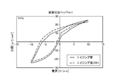
- Droplet discharge head No. FIG. 5 shows the PE characteristics of No. 1 droplet discharge head. The PE characteristics of No. 2 are shown in FIG. The electric field on the horizontal axis is positive when a positive voltage is applied to the first electrode, and the polarization on the vertical axis is positive when positive charges are accumulated in the first electrode.
- Droplet discharge head No. 7 shows changes in the coercive electric field due to aging measured in No. 1 droplet discharge head.
- FIG. 8 shows changes in the coercive electric field with aging measured in 2.
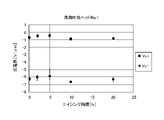
- Each coercive field was measured on three different samples, the plot represents the average, and the error bars indicate the range of variability of the values.
- Vc+ indicates the larger coercive electric field and Vc- indicates the smaller coercive electric field.
- Droplet discharge head No. 1 and droplet discharge head No. 2 the coercive electric field shifts once to the positive side and then shifts to the negative side.
- Droplet discharge head No. 1 has an inflection point in the vicinity of 5 hours, whereas droplet ejection head No. 1 has an inflection point near 5 hours. 2 has an inflection point near 2 hours.
- FIG. 9 shows changes in remanent polarization due to aging measured in No. 1 droplet ejection head.
- FIG. 10 shows the change in remanent polarization due to aging measured in 2.
- Pr+ indicates the larger remanent polarization
- Pr- indicates the smaller remanent polarization.
- Pr is a value obtained by dividing the difference between Pr+ and Pr ⁇ by 2, and this value is adopted as the remanent polarization of the sample.
- the droplet discharge head No. 1 is droplet ejection head No. 1; 2, the amount of shift in the negative direction is large.
- Droplet discharge head No. 1 the droplet ejection head No. Since head No. 2 is manufactured so that the amount of lead is generally large, the degree of segregation of internal lead defects is the same as that of droplet discharge head No. 2. 1 is larger in relative comparison. Therefore, from the correlation between the degree of segregation of lead defects and the internal bias, it is found that excess lead has a positive charge and exists in the film.
- Droplet ejection head No. 1 is the same as droplet ejection head No. 1.
- Droplet discharge head No. 2 is slower than droplet discharge head No. 2 in reaching the point of inflection. This is because 1 has a larger value of the ratio X1/X2, that is, the degree of segregation of lead defects toward the first electrode side is larger.
- the coercive electric field shifts to the negative side. This is thought to be caused by charge injection into the interface between the first electrode and the piezoelectric film, and the remanent polarization is also reduced and pinning is progressing.
- the present invention can be used for a piezoelectric element whose piezoelectric characteristics deteriorate less with use, and for a droplet discharge head, a ferroelectric memory, and a piezoelectric actuator provided with the piezoelectric element.
- First electrode 20 First electrode side dielectric film 30 Piezoelectric film 40 Second electrode side dielectric film 50 Second electrode
Landscapes
- Engineering & Computer Science (AREA)
- Chemical & Material Sciences (AREA)
- Ceramic Engineering (AREA)
- Manufacturing & Machinery (AREA)
- Particle Formation And Scattering Control In Inkjet Printers (AREA)
Priority Applications (4)
| Application Number | Priority Date | Filing Date | Title |
|---|---|---|---|
| JP2023525724A JP7803340B2 (ja) | 2021-06-03 | 2022-05-19 | 圧電素子、液滴吐出ヘッド、強誘電体メモリ及び圧電アクチュエータ |
| CN202280039712.7A CN117426156A (zh) | 2021-06-03 | 2022-05-19 | 压电元件、液滴排出头、铁电存储器以及压电致动器 |
| EP22815873.9A EP4350790A4 (en) | 2021-06-03 | 2022-05-19 | Piezoelectric element, droplet discharge head, ferroelectric memory, and piezoelectric actuator |
| US18/558,670 US20240244979A1 (en) | 2021-06-03 | 2022-05-19 | Piezoelectric element, droplet discharge head, ferroelectric memory, and piezoelectric actuator |
Applications Claiming Priority (2)
| Application Number | Priority Date | Filing Date | Title |
|---|---|---|---|
| JP2021-093593 | 2021-06-03 | ||
| JP2021093593 | 2021-06-03 |
Publications (1)
| Publication Number | Publication Date |
|---|---|
| WO2022255121A1 true WO2022255121A1 (ja) | 2022-12-08 |
Family
ID=84323254
Family Applications (1)
| Application Number | Title | Priority Date | Filing Date |
|---|---|---|---|
| PCT/JP2022/020869 Ceased WO2022255121A1 (ja) | 2021-06-03 | 2022-05-19 | 圧電素子、液滴吐出ヘッド、強誘電体メモリ及び圧電アクチュエータ |
Country Status (6)
| Country | Link |
|---|---|
| US (1) | US20240244979A1 (https=) |
| EP (1) | EP4350790A4 (https=) |
| JP (1) | JP7803340B2 (https=) |
| CN (1) | CN117426156A (https=) |
| TW (1) | TWI825732B (https=) |
| WO (1) | WO2022255121A1 (https=) |
Citations (4)
| Publication number | Priority date | Publication date | Assignee | Title |
|---|---|---|---|---|
| JP2008294345A (ja) * | 2007-05-28 | 2008-12-04 | Seiko Epson Corp | 強誘電体メモリ装置の製造方法及び強誘電体メモリ装置 |
| JP2010201830A (ja) * | 2009-03-04 | 2010-09-16 | Seiko Epson Corp | 液体噴射ヘッド及び液体噴射装置並びに圧電素子 |
| JP2012009661A (ja) * | 2010-06-25 | 2012-01-12 | Konica Minolta Holdings Inc | 圧電素子の製造方法ならびに圧電素子およびそれを用いる振動板 |
| JP2019047114A (ja) * | 2017-09-06 | 2019-03-22 | ローム株式会社 | 圧電素子 |
Family Cites Families (9)
| Publication number | Priority date | Publication date | Assignee | Title |
|---|---|---|---|---|
| JP2999703B2 (ja) * | 1995-12-20 | 2000-01-17 | 沖電気工業株式会社 | 強誘電体薄膜、その形成方法、薄膜形成用塗布液 |
| TW468253B (en) * | 1997-01-13 | 2001-12-11 | Hitachi Ltd | Semiconductor memory device |
| JP4811556B2 (ja) * | 2004-04-23 | 2011-11-09 | セイコーエプソン株式会社 | 圧電素子、液体噴射ヘッドおよび液体噴射装置 |
| JP2009071113A (ja) * | 2007-09-14 | 2009-04-02 | Fujifilm Corp | 圧電素子の駆動方法 |
| JP2010192721A (ja) * | 2009-02-19 | 2010-09-02 | Fujifilm Corp | 圧電素子とその製造方法、及び液体吐出装置 |
| JP2011061118A (ja) * | 2009-09-14 | 2011-03-24 | Seiko Epson Corp | 圧電素子、液体噴射ヘッドおよび液体噴射装置 |
| TWI407607B (zh) * | 2010-01-22 | 2013-09-01 | Hon Hai Prec Ind Co Ltd | 壓電元件及其製備方法 |
| JP6128126B2 (ja) * | 2012-08-08 | 2017-05-17 | コニカミノルタ株式会社 | 圧電素子、圧電デバイス、インクジェットヘッドおよびインクジェットプリンタ |
| CN110890456B (zh) * | 2019-12-05 | 2022-07-19 | 湖南嘉业达电子有限公司 | 一种可抑制银迁移的微孔雾化元件及其制备方法 |
-
2022
- 2022-05-19 CN CN202280039712.7A patent/CN117426156A/zh active Pending
- 2022-05-19 EP EP22815873.9A patent/EP4350790A4/en active Pending
- 2022-05-19 WO PCT/JP2022/020869 patent/WO2022255121A1/ja not_active Ceased
- 2022-05-19 JP JP2023525724A patent/JP7803340B2/ja active Active
- 2022-05-19 US US18/558,670 patent/US20240244979A1/en active Pending
- 2022-05-23 TW TW111119063A patent/TWI825732B/zh active
Patent Citations (4)
| Publication number | Priority date | Publication date | Assignee | Title |
|---|---|---|---|---|
| JP2008294345A (ja) * | 2007-05-28 | 2008-12-04 | Seiko Epson Corp | 強誘電体メモリ装置の製造方法及び強誘電体メモリ装置 |
| JP2010201830A (ja) * | 2009-03-04 | 2010-09-16 | Seiko Epson Corp | 液体噴射ヘッド及び液体噴射装置並びに圧電素子 |
| JP2012009661A (ja) * | 2010-06-25 | 2012-01-12 | Konica Minolta Holdings Inc | 圧電素子の製造方法ならびに圧電素子およびそれを用いる振動板 |
| JP2019047114A (ja) * | 2017-09-06 | 2019-03-22 | ローム株式会社 | 圧電素子 |
Non-Patent Citations (1)
| Title |
|---|
| See also references of EP4350790A4 * |
Also Published As
| Publication number | Publication date |
|---|---|
| JP7803340B2 (ja) | 2026-01-21 |
| JPWO2022255121A1 (https=) | 2022-12-08 |
| TW202312522A (zh) | 2023-03-16 |
| CN117426156A (zh) | 2024-01-19 |
| EP4350790A4 (en) | 2024-09-11 |
| US20240244979A1 (en) | 2024-07-18 |
| TWI825732B (zh) | 2023-12-11 |
| EP4350790A1 (en) | 2024-04-10 |
Similar Documents
| Publication | Publication Date | Title |
|---|---|---|
| JP5525143B2 (ja) | 圧電薄膜素子及び圧電薄膜デバイス | |
| US7215067B2 (en) | Ferroelectric thin film element, piezoelectric actuator and liquid discharge head | |
| JP5267082B2 (ja) | 圧電薄膜素子及びそれを用いたセンサ並びにアクチュエータ | |
| Fujii et al. | Preparation of (001)-oriented Pb (Zr, Ti) O/sub 3/thin films and their piezoelectric applications | |
| US20110175488A1 (en) | Piezoelectric thin film element and piezoelectric thin film device | |
| TW202106903A (zh) | 膜構造體、壓電體膜及超導體膜 | |
| JP2013168530A (ja) | ペロブスカイト機能積層膜 | |
| JP2009200469A (ja) | 圧電薄膜素子 | |
| US9620703B2 (en) | Piezoelectric thin-film element, piezoelectric sensor and vibration generator | |
| WO2020218617A1 (ja) | 強誘電性膜の製造方法、強誘電性膜、及びその用途 | |
| Fuentes-Fernandez et al. | The effect of poling conditions on the performance of piezoelectric energy harvesters fabricated by wet chemistry | |
| Zhu et al. | Enhanced ferroelectric properties of highly (100) oriented Pb (Zr 0.52 Ti 0.48) O 3 thick films prepared by chemical solution deposition | |
| Ishihama et al. | Achieving high piezoelectric performance across a wide composition range in tetragonal (Bi, Na) TiO3–BaTiO3 films for micro-electromechanical systems | |
| WO2012165110A1 (ja) | 強誘電体膜およびそれを備えた圧電素子 | |
| Zhu et al. | Piezoelectric PZT thick films on LaNiO3 buffered stainless steel foils for flexible device applications | |
| WO2022255121A1 (ja) | 圧電素子、液滴吐出ヘッド、強誘電体メモリ及び圧電アクチュエータ | |
| US8075105B2 (en) | Perovskite-type oxide film, piezoelectric thin-film device and liquid ejecting device using perovskite-type oxide film, as well as production process and evaluation method for perovskite-type oxide film | |
| EP4318619B1 (en) | Piezoelectric film, piezoelectric element and method for producing piezoelectric film | |
| JP7700802B2 (ja) | 電気機械変換素子、その製造方法及び液体吐出ヘッド | |
| WO2023042704A1 (ja) | 圧電素子、圧電アクチュエーター、液滴吐出ヘッド、液滴吐出装置、及び強誘電体メモリ | |
| Chen et al. | Growth and thickness effect of< 100>-oriented ternary 0.06 Pb (Mn1/3Nb2/3) O3-0.94 Pb (Zr0. 48Ti0. 52) O3 ferroelectric thin films on silicon substrate by RF sputtering | |
| Benoit et al. | Lead Zirconate Titanate Thin Films on Silicon-on-Sapphire Substrates | |
| Fuentes-Fernandez et al. | PAPER View Article Online View Journal| View Issue The effect of pol aUniversity of Texas at Dallas, 800 W. Cam bTexas Micro Power Inc., 7920 Beltline Rd | |
| Ibrahim et al. | Fabrication and evaluation of niobium doped lead titanate thin films | |
| Seveno et al. | Flexible Al/PZT/Al composite for piezoelectric applications |
Legal Events
| Date | Code | Title | Description |
|---|---|---|---|
| 121 | Ep: the epo has been informed by wipo that ep was designated in this application |
Ref document number: 22815873 Country of ref document: EP Kind code of ref document: A1 |
|
| WWE | Wipo information: entry into national phase |
Ref document number: 18558670 Country of ref document: US |
|
| WWE | Wipo information: entry into national phase |
Ref document number: 2023525724 Country of ref document: JP |
|
| WWE | Wipo information: entry into national phase |
Ref document number: 202280039712.7 Country of ref document: CN |
|
| WWE | Wipo information: entry into national phase |
Ref document number: 2022815873 Country of ref document: EP |
|
| NENP | Non-entry into the national phase |
Ref country code: DE |
|
| ENP | Entry into the national phase |
Ref document number: 2022815873 Country of ref document: EP Effective date: 20240103 |