WO2022254711A1 - 電力変換装置及び電源装置 - Google Patents
電力変換装置及び電源装置 Download PDFInfo
- Publication number
- WO2022254711A1 WO2022254711A1 PCT/JP2021/021424 JP2021021424W WO2022254711A1 WO 2022254711 A1 WO2022254711 A1 WO 2022254711A1 JP 2021021424 W JP2021021424 W JP 2021021424W WO 2022254711 A1 WO2022254711 A1 WO 2022254711A1
- Authority
- WO
- WIPO (PCT)
- Prior art keywords
- voltage
- circuit
- load
- conversion device
- power conversion
- Prior art date
- Legal status (The legal status is an assumption and is not a legal conclusion. Google has not performed a legal analysis and makes no representation as to the accuracy of the status listed.)
- Ceased
Links
Images


Classifications
-
- H—ELECTRICITY
- H02—GENERATION; CONVERSION OR DISTRIBUTION OF ELECTRIC POWER
- H02M—APPARATUS FOR CONVERSION BETWEEN AC AND AC, BETWEEN AC AND DC, OR BETWEEN DC AND DC, AND FOR USE WITH MAINS OR SIMILAR POWER SUPPLY SYSTEMS; CONVERSION OF DC OR AC INPUT POWER INTO SURGE OUTPUT POWER; CONTROL OR REGULATION THEREOF
- H02M1/00—Details of apparatus for conversion
- H02M1/0003—Details of control, feedback or regulation circuits
- H02M1/0009—Devices or circuits for detecting current in a converter
-
- H—ELECTRICITY
- H02—GENERATION; CONVERSION OR DISTRIBUTION OF ELECTRIC POWER
- H02M—APPARATUS FOR CONVERSION BETWEEN AC AND AC, BETWEEN AC AND DC, OR BETWEEN DC AND DC, AND FOR USE WITH MAINS OR SIMILAR POWER SUPPLY SYSTEMS; CONVERSION OF DC OR AC INPUT POWER INTO SURGE OUTPUT POWER; CONTROL OR REGULATION THEREOF
- H02M1/00—Details of apparatus for conversion
- H02M1/0048—Circuits or arrangements for reducing losses
- H02M1/0054—Transistor switching losses
- H02M1/0058—Transistor switching losses by employing soft switching techniques, i.e. commutation of transistors when applied voltage is zero or when current flow is zero
-
- H—ELECTRICITY
- H02—GENERATION; CONVERSION OR DISTRIBUTION OF ELECTRIC POWER
- H02M—APPARATUS FOR CONVERSION BETWEEN AC AND AC, BETWEEN AC AND DC, OR BETWEEN DC AND DC, AND FOR USE WITH MAINS OR SIMILAR POWER SUPPLY SYSTEMS; CONVERSION OF DC OR AC INPUT POWER INTO SURGE OUTPUT POWER; CONTROL OR REGULATION THEREOF
- H02M3/00—Conversion of DC power input into DC power output
- H02M3/22—Conversion of DC power input into DC power output with intermediate conversion into AC
- H02M3/24—Conversion of DC power input into DC power output with intermediate conversion into AC by static converters
- H02M3/28—Conversion of DC power input into DC power output with intermediate conversion into AC by static converters using discharge tubes with control electrode or semiconductor devices with control electrode to produce the intermediate AC
- H02M3/325—Conversion of DC power input into DC power output with intermediate conversion into AC by static converters using discharge tubes with control electrode or semiconductor devices with control electrode to produce the intermediate AC using devices of a triode or a transistor type requiring continuous application of a control signal
- H02M3/335—Conversion of DC power input into DC power output with intermediate conversion into AC by static converters using discharge tubes with control electrode or semiconductor devices with control electrode to produce the intermediate AC using devices of a triode or a transistor type requiring continuous application of a control signal using semiconductor devices only
- H02M3/33569—Conversion of DC power input into DC power output with intermediate conversion into AC by static converters using discharge tubes with control electrode or semiconductor devices with control electrode to produce the intermediate AC using devices of a triode or a transistor type requiring continuous application of a control signal using semiconductor devices only having several active switching elements
- H02M3/33576—Conversion of DC power input into DC power output with intermediate conversion into AC by static converters using discharge tubes with control electrode or semiconductor devices with control electrode to produce the intermediate AC using devices of a triode or a transistor type requiring continuous application of a control signal using semiconductor devices only having several active switching elements having at least one active switching element at the secondary side of an isolation transformer
- H02M3/33584—Bidirectional converters
-
- H—ELECTRICITY
- H02—GENERATION; CONVERSION OR DISTRIBUTION OF ELECTRIC POWER
- H02M—APPARATUS FOR CONVERSION BETWEEN AC AND AC, BETWEEN AC AND DC, OR BETWEEN DC AND DC, AND FOR USE WITH MAINS OR SIMILAR POWER SUPPLY SYSTEMS; CONVERSION OF DC OR AC INPUT POWER INTO SURGE OUTPUT POWER; CONTROL OR REGULATION THEREOF
- H02M7/00—Conversion of AC power input into DC power output; Conversion of DC power input into AC power output
- H02M7/42—Conversion of DC power input into AC power output without possibility of reversal
- H02M7/44—Conversion of DC power input into AC power output without possibility of reversal by static converters
- H02M7/48—Conversion of DC power input into AC power output without possibility of reversal by static converters using discharge tubes with control electrode or semiconductor devices with control electrode
- H02M7/483—Converters with outputs that each can have more than two voltages levels
- H02M7/487—Neutral point clamped inverters
-
- Y—GENERAL TAGGING OF NEW TECHNOLOGICAL DEVELOPMENTS; GENERAL TAGGING OF CROSS-SECTIONAL TECHNOLOGIES SPANNING OVER SEVERAL SECTIONS OF THE IPC; TECHNICAL SUBJECTS COVERED BY FORMER USPC CROSS-REFERENCE ART COLLECTIONS [XRACs] AND DIGESTS
- Y02—TECHNOLOGIES OR APPLICATIONS FOR MITIGATION OR ADAPTATION AGAINST CLIMATE CHANGE
- Y02B—CLIMATE CHANGE MITIGATION TECHNOLOGIES RELATED TO BUILDINGS, e.g. HOUSING, HOUSE APPLIANCES OR RELATED END-USER APPLICATIONS
- Y02B70/00—Technologies for an efficient end-user side electric power management and consumption
- Y02B70/10—Technologies improving the efficiency by using switched-mode power supplies [SMPS], i.e. efficient power electronics conversion e.g. power factor correction or reduction of losses in power supplies or efficient standby modes
Definitions
- the present disclosure relates to a power conversion device and a power supply device that convert a power supply voltage applied from a DC power supply into a DC voltage for a DC load.
- Patent Document 1 discloses a three-level DCDC converter that employs a so-called zero-voltage and zero-current switching method, in which switching is performed when the voltage and current across the switching elements are zero.
- Patent Document 1 a simple configuration in which a bidirectional switch and a capacitor for soft switching are added to the main circuit of a three-level power conversion device without using an auxiliary circuit including a high-voltage switching element and a saturation reactor, and each switching element It is disclosed that the on/off control of the can provide zero voltage and zero current switching operation. Although details will be described later, it is necessary to increase the inductance value of inductors or reactors involved in power transmission and reception in order to widen the area of soft switching.
- the present disclosure has been made in view of the above, and aims to obtain a power conversion device that enables further improvement in power conversion efficiency.
- the power conversion device is a power conversion device that converts a first DC voltage applied from a DC power supply into a second DC voltage to a load.
- a power converter includes an inverter circuit, a variable reactor, a transformer, and a converter circuit.
- the inverter circuit includes a plurality of switching elements and a snubber capacitor connected in parallel to each of the plurality of switching elements, and converts a first DC voltage into a first AC voltage.
- the variable reactor is arranged on the output side of the inverter circuit and is configured such that the inductance value can be varied.
- the transformer has a primary winding and a secondary winding that are magnetically coupled to each other, insulates the primary side from the secondary side, and converts the first AC voltage applied through the variable reactor to a second AC voltage. Convert to The converter circuit converts the second AC voltage into a second DC voltage.
- the power converter according to the present disclosure it is possible to further improve the power conversion efficiency.
- FIG. 1 is a circuit diagram showing a configuration example of a power converter according to an embodiment
- FIG. FIG. 2 is a timing chart for explaining the basic operation of the inverter circuit shown in FIG. 1; State transition diagram for explaining the basic operation of the inverter circuit shown in FIG. A diagram for explaining conditions for establishing soft switching.
- FIG. 6 is a diagram showing a configuration example of a control circuit for controlling the variable reactor shown in FIG. 5 together with the variable reactor;
- FIG. 4 is a diagram for explaining the effect of the power conversion device according to the embodiment;
- connection includes both cases in which components are directly connected to each other and cases in which components are indirectly connected to each other via other components.
- FIG. 1 is a circuit diagram showing a configuration example of a power conversion device 50 according to an embodiment.
- a power conversion device 50 according to the embodiment is a DC/DC conversion device that converts a first DC voltage, which is a power supply voltage applied from a DC power supply 1 , into a second DC voltage to a load 19 .
- the power conversion device 50 includes an inverter circuit 60, a variable reactor 20, a transformer 12, and a converter circuit 70, as shown in FIG.
- the inverter circuit 60 includes an input capacitor circuit 62 and an inverter main circuit 64 .
- Input capacitor circuit 62 holds the first DC voltage applied from DC power supply 1 .
- the inverter circuit 60 converts the first DC voltage into a first AC voltage.
- the input capacitor circuit 62 includes filter capacitors 2A and 2B.
- Filter capacitor 2A and filter capacitor 2B are connected in series.
- One end of the filter capacitor 2A is connected to the high potential line 3A, and the other end of the filter capacitor 2A is connected to the intermediate potential line 3B.
- One end of filter capacitor 2B is connected to intermediate potential line 3B, and the other end of filter capacitor 2B is connected to low potential line 3C.
- a connection point where the other end of the filter capacitor 2A and one end of the filter capacitor 2B are connected is called a "midpoint" or a "neutral point".
- the middle point of the filter capacitors 2A and 2B is generally set to zero potential.
- the inverter main circuit 64 has switching elements 7, 8, 9, and 10 (hereinafter appropriately referred to as "7 to 10") having antiparallel-connected diodes.
- An example of the switching elements 7 to 10 is the illustrated metal oxide semiconductor field effect transistor (MOSFET) with a built-in antiparallel diode.
- Antiparallel means that the anode of the diode is connected to the source of the MOSFET and the cathode of the diode is connected to the drain of the MOSFET.
- IGBT insulated gate bipolar transistor
- SiC silicon carbide
- GaN gallium nitride
- Ga2O3 gallium oxide
- diamond diamond may also be used as materials for the switching elements. If the switching element is made of a wide bandgap semiconductor material, low loss and high speed switching can be achieved.
- the inverter main circuit 64 also has snubber capacitors 7a, 8a, 9a, and 10a connected in parallel to each of the switching elements 7-10, clamp diodes 5A and 5B, and a flying capacitor 6.
- the snubber capacitors 7a, 8a, 9a, and 10a (hereinafter referred to as "7a-10a" as appropriate) are provided to suppress surges when the switching elements 7-10 interrupt the current.
- Flying capacitor 6 is provided to promote discharge of charges accumulated in snubber capacitors 7a-10a.
- the switching elements 7 and 8 are connected in series in this order to form a positive arm.
- Switching elements 9 and 10 are connected in series in this order to form a negative arm.
- the switching elements 7 to 10 are connected in series in this order to form a half bridge circuit.
- One end of the switching element 7 is connected to the high potential line 3A.
- a connection point between the other end of the switching element 7 and one end of the switching element 8 is connected to the cathode of the clamp diode 5A.
- the anode of clamp diode 5A is connected to intermediate potential line 3B.
- An AC wiring 4A is drawn out from the other end of the switching element 8, and an AC wiring 4B is drawn out from the intermediate potential line 3B.
- One end of the switching element 9 is connected to the AC wiring 4A.
- a connection point between the other end of the switching element 9 and one end of the switching element 10 is connected to the anode of the clamp diode 5B.
- the cathode of clamp diode 5B is connected to intermediate potential line 3B.
- the other end of switching element 10 is connected to low potential line 3C.
- variable reactor 20 and transformer 12 are arranged on the output side of the inverter circuit 60 .
- the variable reactor 20 is an inductance variable device configured such that the inductance value can be varied.
- the variable reactor 20 has a first terminal 20A and a second terminal 20B.
- Transformer 12 has a primary winding W1 and a secondary winding W2 that are magnetically coupled to each other.
- the primary winding W1 side is called the “primary side” and the secondary winding W2 side is called the “secondary side”.
- a transformer 12 is provided to electrically insulate the primary side and the secondary side.
- variable reactor 20 first terminal 20 A is connected to AC wiring 4 A, and second terminal 20 B is connected to one end of primary winding W 1 of transformer 12 . The other end of the primary winding W1 is connected to the AC wiring 4B. Both ends of secondary winding W 2 are connected to converter circuit 70 .
- variable reactor 20 is arranged on the AC wiring 4A in FIG. 1, the configuration is not limited to this.
- the variable reactor 20 may be arranged on the AC wiring 4B.
- the AC wiring 4B is provided with a current sensor CT1 for detecting the transformer primary current ip flowing through the primary winding W1 .
- the current sensor CT 1 may be provided on the AC wiring 4A.
- the primary current of the transformer is sometimes simply referred to as "primary current”.
- a first AC voltage is applied to the primary winding W1 of the transformer 12 via the variable reactor 20, and a second AC voltage is output from the secondary winding W2 of the transformer 12. be. That is, the transformer 12 converts the first AC voltage applied via the variable reactor 20 into the second AC voltage and outputs the second AC voltage to the converter circuit 70 .
- the converter circuit 70 includes a rectifier circuit 72 and an output filter circuit 74.
- the rectifier circuit 72 has four diodes 13, 14, 15, 16 connected in a full bridge.
- the rectifier circuit 72 rectifies the second AC voltage applied from the converter circuit 70 to generate a ripple-containing DC voltage and applies it to the output filter circuit 74 .
- the output filter circuit 74 has a smoothing reactor 17 and an output filter capacitor 18 .
- An LC filter circuit is configured by the smoothing reactor 17 and the output filter capacitor 18 .
- the output filter circuit 74 smoothes the rippled DC voltage and applies the smoothed DC voltage to the load 19 .
- a current sensor CT2 for detecting the load current i o flowing through the load 19 is provided on the output side of the output filter circuit 74 .
- the load 19 is a DC load that operates by being supplied with DC power.
- the load 19 includes an inverter that converts DC power into AC power and a device that operates on the supply of AC power from the inverter is also included in the DC load referred to here.
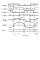
- FIG. 2 is a timing chart for explaining the basic operation of inverter circuit 60 shown in FIG.
- FIG. 3 is a state transition diagram for explaining the basic operation of inverter circuit 60 shown in FIG.
- the inductance Lk of the variable reactor 20 is assumed to be a fixed value.
- the inverter circuit 60 realizes zero voltage soft switching (ZVS) or zero current soft switching (ZVZCS) by the following operation. These ZVS and ZVZCS are collectively called "soft switching”.
- FIG. 2 shows waveforms of gate signals Q1, Q2, Q3, Q4 (hereinafter referred to as “Q1 to Q4” as appropriate), transformer primary voltage v ab , transformer primary current i p , and operation mode in order from the top. It is shown.
- Gate signals Q1-Q4 are drive signals applied to the gates of switching elements 7-10, respectively.
- the phase difference between the gate signal Q1 and the gate signal Q2 is a physical quantity called “phase shift angle” and is represented by " ⁇ " in FIG.
- the phase shift angle ⁇ determines the phase at which the transformer primary current ip rises and the magnitude of the transformer primary current ip .
- the phase shift angle ⁇ determines the phases of the gate signals Q2 to Q4 with respect to the gate signal Q1.
- the horizontal axis of FIG. 2 represents time.
- the inverter circuit 60 operates in mode 1 during the period from time t 0 to t 1 , operates in mode 2 during the period from time t 1 to t 2 , and operates in mode 2 during the period from time t 2 to t 2 . It operates in mode 3 during the period t3, operates in mode 4 during the period from time t3 to t4 , and operates in mode 5 during the period from time t4 to t5 .
- the inverter circuit 60 operates in mode 6 during the period from time t 5 to t 6 while the transformer primary current i p is negative, operates in mode 7 during the period from time t 6 to t 7 , and operates in mode 7 during the period from time t 6 to t 7 . It operates in mode 8 during the period from 7 to t 8 , in mode 9 during the period from time t 8 to t 9 , and in mode 10 during the period from time t 9 to t 10 . In this way, the inverter circuit 60 operates with one cycle period from mode 1 to mode 10 .
- FIG. 3 shows current flows in modes 1 to 6. The portions shown in bold are related to the operation of each mode. Arrows indicate the directions of currents flowing in each mode.
- the switching element 7 is turned off by ZVS.
- the snubber capacitor 10a is discharged through the switching element 8 and the flying capacitor 6, and the anti-parallel diode of the switching element 10 becomes conductive.
- the switching element 10 turns on ZVZCS after the anti-parallel connection diode of the switching element 10 becomes conductive.
- mode 4 the switching element 8 is turned off by ZVS, and the snubber capacitor 9a is discharged.
- C s1 is the capacitance of snubber capacitors 7a-10a, and it is assumed that each capacitance is equal between snubber capacitors 7a-10a.
- Vd can be considered substantially constant, and Cs1 can be considered constant.
- the transformer primary current i p is proportional to the load current i o , it can be expressed by the following equation (3) using the proportionality constant K.
- FIG. 4 shows the above equation (3) as a graph.
- FIG. 4 is a diagram for explaining conditions for establishing soft switching.
- the illustrated curve is the case where the left side and the right side in the above equation (3) are equal.
- the lower side of the curve is the hard switching region and the upper side of the curve is the soft switching region.
- the hard switching region switching loss occurs when the switching elements 7-10 are turned on or off.
- no switching loss occurs in the soft switching region. Therefore, if the current value of the load current i o corresponding to the inductance L k is i oth in the curve of FIG. 4, switching loss will occur if the load current i o is less than or equal to i oth .
- FIG. 5 is a diagram showing a detailed configuration example of variable reactor 20 according to the embodiment shown in FIG.
- the variable reactor 20, as shown in FIG. 5, includes a reactor 105 and two bidirectional switches SW1 and SW2 .
- the variable reactor 20 has gate terminals 22A and 22B in addition to the first terminal 20A and the second terminal 20B.
- Reactor 105 has one end connected to first terminal 20A and the other end connected to second terminal 20B.
- Reactor 105 has tap terminals 106 and 108 .
- the bidirectional switch SW1 has switching elements 101, 102 with anti-parallel connected diodes.
- the bidirectional switch SW2 has switching elements 103, 104 with anti-parallel connected diodes.
- the switching elements 101 and 102 are connected in anti-series so that the anodes of anti-parallel connection diodes face each other.
- Switching elements 103 and 104 are similarly configured. Note that instead of this configuration, a configuration in which the cathodes of antiparallel-connected diodes face each other may be configured to be anti-series-connected.
- bidirectional switch SW1 One end of the bidirectional switch SW1 is connected to the tap terminal 106, and the other end of the bidirectional switch SW1 is connected to the second terminal 20B.
- the common gate of bidirectional switch SW1 is connected to gate terminal 22A.
- the bidirectional switch SW1 When a gate signal is input to the gate terminal 22A, the bidirectional switch SW1 is turned on.
- the bidirectional switch SW1 When the bidirectional switch SW1 is turned on, the inductance value between the first terminal 20A and the second terminal 20B is changed from Lk3 to Lk1 .
- bidirectional switch SW2 One end of the bidirectional switch SW2 is connected to the tap terminal 108, and the other end of the bidirectional switch SW2 is connected to the second terminal 20B.
- the common gate of bidirectional switch SW2 is connected to gate terminal 22B.
- the bidirectional switch SW2 When a gate signal is input to the gate terminal 22B, the bidirectional switch SW2 is turned on.
- the bidirectional switch SW1 does not conduct and only the bidirectional switch SW2 conducts, the inductance value between the first terminal 20A and the second terminal 20B is changed from Lk3 to Lk2 .
- the relationship between L k1 , L k2 and L k3 is L k1 ⁇ L k2 ⁇ L k3 .
- FIG. 6 is a diagram showing a configuration example of a control circuit 30 for controlling the variable reactor 20 shown in FIG. 5 together with the variable reactor 20.
- the control circuit 30 comprises latch circuits 204, 205 and comparators 208, 209, 210, as shown in FIG. Latch circuits 204 and 205 each have a data input terminal D, a data output terminal Q, an inverted output terminal Q- (Q bar), and clock terminals 206 and 207, respectively. Note that the inverted output terminal Q- is not used.
- comparators 208 and 209 may be referred to as “first comparator” and the comparator 210 may be referred to as “second comparator”.
- a gate drive (GD) circuit 110 and a GD circuit 112 are present between the control circuit 30 and the variable reactor 20 .
- the output of the GD circuit 110 is input to the gate terminal 22A, and the output of the GD circuit 112 is input to the gate terminal 22B.
- the GD circuit 110 controls conduction of the bidirectional switch SW1 based on the output of the latch circuit 204.
- FIG. The GD circuit 112 controls conduction of the bidirectional switch SW2 based on the output of the latch circuit 205.
- the positive terminals of the comparators 208 and 209 receive the detected value of the load current i o from the current sensor CT2 .
- the - terminal of the comparator 209 receives the set value i o1
- the - terminal of the comparator 208 receives the set value i o2 .
- a + terminal of the comparator 210 receives the detected value of the transformer primary current i p from the current sensor CT 1 .
- a zero value, that is, "0" is input to the - terminal of the comparator 210 .
- the output of the comparator 208 is input to the data input terminal D of the latch circuit 204.
- the output of comparator 209 is input to data input terminal D of latch circuit 205 .
- the output of comparator 210 is input to clock terminal 206 of latch circuit 204 and clock terminal 207 of latch circuit 205 .
- FIG. 7 is a timing chart for explaining the operation of the control circuit 30 shown in FIG.
- FIG. 8 is a diagram for explaining the effect of the power converter 50 according to the embodiment.
- a comparator 208 compares the load current i o with the set value i o2 . When the load current i o is greater than the set value i o2 , the comparator 208 outputs a signal indicating logic “H” and the latch circuit 204 holds the signal. When the load current i o is equal to or less than the set value i o2 , the comparator 208 outputs a signal indicating logic “L” and the latch circuit 204 holds the signal. Similarly, the comparator 209 compares the load current i o with the set value i o1 .
- the comparator 209 When the load current i o is greater than the set value i o1 , the comparator 209 outputs a signal indicating logic “H” and the latch circuit 205 holds the signal. When the load current i o is equal to or less than the set value i o1 , the comparator 209 outputs a signal indicating logic “L” and the latch circuit 205 holds the signal.
- a comparator 210 compares the transformer primary current ip with a zero value. When the transformer primary current ip is greater than zero, the comparator 210 outputs a logic "H" signal which is input to the clock terminals 206 and 207 of the latch circuits 204 and 205, respectively. When the transformer primary current ip is less than zero, the comparator 210 outputs a logic "L" signal, which is input to the clock terminals 206 and 207 of the latch circuits 204 and 205, respectively.
- Latch circuits 204 and 205 hold comparison signals output from comparators 208 and 209, respectively. Latch circuits 204 and 205 output the held signals from respective data output terminals Q at the timing when the output of comparator 210 changes from logic "L” to logic "H".
- comparators 208 and 209 may be referred to as "first comparison result”
- comparator 210 may be referred to as "second comparison result”.
- FIG. 7 shows the output waveform of comparator 210 and how the value of inductance Lk of reactor 105 changes. Specifically, FIG. 7 shows how the inductance L k is changed from L k2 to L k1 .
- the value of the inductance Lk is L at the timing when the output of the comparator 210 changes from logic "L" to logic "H", that is, at the zero crossing point at which the transformer primary current ip switches from negative to positive. It is switched from k2 to L k1 .
- the output of the comparator 210 is not switched at the timing when the logic "H" changes to the logic "L".
- the soft switching region depends on the load current i o .
- the outputs of the comparators 208 and 209 are both logic "H", so the bidirectional switches SW 1 and SW 2 are conducting and the value of the inductance L k is L. becomes k1 .
- the value of Lk1 is relatively small, as shown in FIG. 8, the operation is in a region where the load current i o is larger than the set value i o2 , so switching drive in the soft switching region is possible. .
- FIG. 8 shows the inductance value of the reactor 105, i.e., i oth which is the value of the load current i o corresponding to L k3 which is the value of the inductance L k when the bidirectional switches SW 1 and SW 2 are not conducting. It is Therefore, if the load current i o is equal to or higher than i oth , switching drive in the soft switching region is possible. When the load current i o is less than i oth , the drive is in the hard switching region . The current that flows will also be smaller. Therefore, since the conduction loss of the switching elements 7-10 is small, an increase in the switching loss of the switching elements 7-10 does not pose a problem.
- the inductance value is changed at the zero cross point where the transformer primary current ip switches from negative to positive, but the present invention is not limited to this example.
- the inductance value may be changed at the zero crossing point where the transformer primary current ip switches from positive to negative.
- control circuit 30 includes a microcomputer
- the values of the set values i o1 and i o2 can be changed by recalculating the value of the constant of proportionality K in the above equation (3). Accordingly, even if the load 19 has different characteristics, it can be applied to the power converter 50 without changing the design of the control circuit 30 .
- FIG. 6 shows a configuration example in which the value of the inductance L k is changed in three stages of L k1 , L k2 , and L k3 , the configuration is not limited to this example.
- a configuration in which the value of the inductance Lk is changed in two steps, or a configuration in which the value of the inductance Lk is changed in four or more steps may be used.
- the number of tap terminals 106 and 108 provided in the reactor 105, the number of latch circuits 204 and 205 and comparators 208 and 209 in the control circuit 30, and the number of GD circuits 110 and 112 corresponding to them can be configured by changing
- the use of a saturable reactor is also conceivable.
- the saturable reactor it is difficult to maintain appropriate characteristics in consideration of the usage environment of the power conversion device 50, secular change, and the like.
- the saturable reactor has a problem that the widened soft switching region is narrow.
- the saturable reactor has problems such as an increase in size and weight, and is not easy to implement.
- the method of the embodiment can expand the soft switching region by an electrical method, so that the increase in size and weight can be suppressed.
- the values of the set values i o1 and i o2 can be changed by a processor such as a microcomputer, problems such as usage environment and aging can be resolved.
- the value of the inductance Lk is changed at the timing when the transformer primary current ip becomes zero. As a result, even with a configuration in which the inductance Lk is changed discretely, it is possible to obtain the same effect as a configuration in which the inductance Lk is changed continuously.
- the power conversion device 50 and its technology according to the embodiment can be applied to various power supply devices, but are particularly suitable for use in a power supply device that supplies power to an auxiliary load mounted on a railway vehicle.
- Auxiliary load is a name used to refer to a load other than a main motor among loads mounted on a railroad vehicle. Examples of auxiliary loads are air conditioners, interior lighting systems, door operating systems, security equipment, compressors, batteries, and control power supplies.
- a compressor is a device that produces the air source for the vehicle brakes.
- the load current i o increases during the hot summer months, when the train starts operating, or when the load factor is high, because the load on the air conditioner increases.
- the load current i o becomes smaller.
- the time during which the load current i o increases is short, and the time during which the load current i o decreases becomes long.
- the power conversion device according to the present embodiment which can reduce loss at light load, is suitable as a power supply device for railway vehicles.
- a train composed of a plurality of railroad vehicles is provided with a train information management system for managing train information.
- the train information management system can grasp the operating state of the auxiliary load based on the train information, and can control the operation of the auxiliary load. Therefore, the train information management system can recognize whether the operating state of the auxiliary load is light load or high load.
- the value of the inductance Lk in the variable reactor 20 may be changed based on the load information, which is information regarding the operating state of the auxiliary load. By doing so, the configuration of the control circuit 30 can be simplified.
- the timing of sending the signal for changing the value of the inductance Lk should be synchronized with the timing of sending the control signal to the air conditioner, for example. is required.
- variable reactor 20 When the operating state of the auxiliary load is classified into light load and high load, the variable reactor 20 may be provided with either one of the bidirectional switches SW1 and SW2 .
- variable reactor 20 configured as shown in FIG. can be used. Also, in the control circuit 30 shown in FIG. 6, the functions of the comparator 210 and the latch circuits 204 and 205 can be used.
- the control circuit 30 may be configured so that the latch circuit 204 outputs a signal to turn on the bidirectional switch SW1. Further, when the operating state of the auxiliary load is a medium load, the control circuit 30 may be configured so that the latch circuit 205 outputs a signal that turns ON only the bidirectional switch SW2 . Further, when the operating state of the auxiliary load is high load, the control circuit 30 may be configured so that neither of the two-way switches SW1 and SW2 are turned on.
- the power converter according to the embodiment includes a variable reactor arranged on the output side of the inverter circuit and having a variable inductance value.
- a variable reactor makes it possible to change the inductance value between the inverter circuit and the primary winding of the transformer based on the load current. Thereby, the further improvement of power conversion efficiency can be aimed at.
- the power converter according to the embodiment includes a control circuit that changes the inductance value of the variable reactor in two or more stages.
- the control circuit performs control to change the inductance value based on the load current flowing through the load.
- the variable reactor according to the embodiment includes a reactor having a first terminal connected to the inverter circuit and a second terminal connected to the primary winding of the transformer, and two switching elements each having an antiparallel-connected diode. are connected in reverse series to form one or more bidirectional switches. One end of each of the one or more bidirectional switches is connected to the first terminal or the second terminal, and the other end of each is connected to tap terminals of different variable reactors.
- variable reactor it is preferable to change the inductance value at the zero cross point at which the value of the transformer primary current switches from negative to positive or from positive to negative. By doing so, it is possible to reduce the influence of the change in the characteristics of the load on the inverter circuit. As a result, even with a configuration in which the inductance value is changed discretely, it is possible to obtain the same effect as a configuration in which the inductance value is changed continuously.
- control circuit includes the same number of first comparators as the number of bidirectional switches, the same number of latch circuits as the number of first comparators, and a first comparator that compares the primary current with a zero value. and a second comparator that outputs two comparison results.
- Each first comparator outputs a first comparison result of comparing the load current with a predetermined set value.
- Each latch circuit receives the first comparison result from the corresponding first comparator and the second comparison result from the second comparator.
- Each latch circuit holds the first comparison result.
- each latch circuit outputs a signal based on the first comparison result to the corresponding bidirectional switch in synchronization with the timing at which the second comparison result is input.
- the power conversion device according to the embodiment may be configured as a power supply device mounted on a railway vehicle or train.
- the power conversion device according to the embodiment can reduce loss at light load. For this reason, it can be suitably used for railway vehicles or trains that are required to improve efficiency under light loads with long operating hours while ensuring a high power supply capacity.
- the power conversion device may be configured as a power supply device mounted on a train equipped with a train information management system that manages train information.
- the power converter includes a control circuit that changes the inductance value of the variable reactor in two or more stages.
- the control circuit performs control to change the inductance value based on the load information output from the train information management system. According to the power supply device configured in this way, it is possible to obtain an effect that the configuration of the control circuit can be simplified.
- the inverter circuit 60 shown in FIG. 1 has a three-level circuit configuration, but is not limited to this.
- the inverter circuit 60 may have a two-level circuit configuration.
- the inverter circuit 60 shown in FIG. 1 has a half-bridge circuit configuration, the configuration is not limited to this.
- the inverter circuit 60 may have a single-phase bridge circuit configuration.
- the converter circuit 70 shown in FIG. 1 uses the rectifier circuit 72 in which four diodes are connected in a full bridge, it is not limited to this. Instead of the rectifier circuit 72, an AC/DC conversion circuit having at least one switching element may be used.
Landscapes
- Engineering & Computer Science (AREA)
- Power Engineering (AREA)
- Dc-Dc Converters (AREA)
Priority Applications (3)
| Application Number | Priority Date | Filing Date | Title |
|---|---|---|---|
| PCT/JP2021/021424 WO2022254711A1 (ja) | 2021-06-04 | 2021-06-04 | 電力変換装置及び電源装置 |
| JP2023525327A JP7515716B2 (ja) | 2021-06-04 | 2021-06-04 | 電力変換装置及び電源装置 |
| US18/566,341 US20240258929A1 (en) | 2021-06-04 | 2021-06-04 | Power converter and power supply apparatus |
Applications Claiming Priority (1)
| Application Number | Priority Date | Filing Date | Title |
|---|---|---|---|
| PCT/JP2021/021424 WO2022254711A1 (ja) | 2021-06-04 | 2021-06-04 | 電力変換装置及び電源装置 |
Publications (1)
| Publication Number | Publication Date |
|---|---|
| WO2022254711A1 true WO2022254711A1 (ja) | 2022-12-08 |
Family
ID=84322928
Family Applications (1)
| Application Number | Title | Priority Date | Filing Date |
|---|---|---|---|
| PCT/JP2021/021424 Ceased WO2022254711A1 (ja) | 2021-06-04 | 2021-06-04 | 電力変換装置及び電源装置 |
Country Status (3)
| Country | Link |
|---|---|
| US (1) | US20240258929A1 (https=) |
| JP (1) | JP7515716B2 (https=) |
| WO (1) | WO2022254711A1 (https=) |
Cited By (1)
| Publication number | Priority date | Publication date | Assignee | Title |
|---|---|---|---|---|
| JP7645413B1 (ja) | 2024-03-22 | 2025-03-13 | 株式会社オリジン | Dc/dcコンバータ |
Citations (3)
| Publication number | Priority date | Publication date | Assignee | Title |
|---|---|---|---|---|
| JP2013188015A (ja) * | 2012-03-08 | 2013-09-19 | Mitsubishi Electric Corp | 直流電源装置 |
| JP2018082572A (ja) * | 2016-11-17 | 2018-05-24 | 三菱電機株式会社 | 電力変換装置 |
| CN111342668A (zh) * | 2020-03-09 | 2020-06-26 | 西南交通大学 | 一种利用可变电感拓展ss结构wpt系统的软开关范围的方法 |
Family Cites Families (55)
| Publication number | Priority date | Publication date | Assignee | Title |
|---|---|---|---|---|
| US20030052658A1 (en) * | 1995-01-11 | 2003-03-20 | Baretich David F. | Method and apparatus for electronic power control |
| US6349044B1 (en) * | 1999-09-09 | 2002-02-19 | Virginia Tech Intellectual Properties, Inc. | Zero voltage zero current three level dc-dc converter |
| US6329785B1 (en) * | 2000-02-29 | 2001-12-11 | Gas Research Institute | Pulse width modulated controlled induction motor |
| JP3682773B2 (ja) * | 2000-03-23 | 2005-08-10 | Tdk株式会社 | スイッチング電源装置 |
| US20020050829A1 (en) * | 2000-08-29 | 2002-05-02 | Wilsun Xu | Thyristor linked inductor |
| US6353547B1 (en) * | 2000-08-31 | 2002-03-05 | Delta Electronics, Inc. | Three-level soft-switched converters |
| US8269141B2 (en) * | 2004-07-13 | 2012-09-18 | Lincoln Global, Inc. | Power source for electric arc welding |
| TWI268041B (en) * | 2004-09-09 | 2006-12-01 | Delta Electronics Inc | Input stage circuit of a three-level DC/DC converter |
| JP5023338B2 (ja) | 2005-03-16 | 2012-09-12 | 国立大学法人横浜国立大学 | チョッパ回路 |
| JP4723606B2 (ja) | 2007-12-26 | 2011-07-13 | 日本▲まき▼線工業株式会社 | 電源装置及び電源装置におけるタイミング制御回路 |
| JP4988925B2 (ja) * | 2009-02-06 | 2012-08-01 | 株式会社三社電機製作所 | インバータ回路 |
| JP5544745B2 (ja) * | 2009-04-16 | 2014-07-09 | サンケン電気株式会社 | 力率改善コンバータ |
| JP5434371B2 (ja) * | 2009-08-26 | 2014-03-05 | サンケン電気株式会社 | 共振型スイッチング電源装置 |
| DK2577860T3 (en) * | 2010-05-27 | 2018-10-29 | Vestas Wind Sys As | HIGH VOLTAGE POWER CONVERTER |
| EP3540927B1 (en) * | 2010-06-25 | 2020-10-14 | Hitachi, Ltd. | Dc-dc converter |
| JP5267589B2 (ja) * | 2011-02-03 | 2013-08-21 | 株式会社日本自動車部品総合研究所 | 電力変換装置 |
| US9065341B2 (en) * | 2011-02-04 | 2015-06-23 | Mitsubishi Electric Corporation | DC-DC converter |
| JP5314724B2 (ja) * | 2011-03-03 | 2013-10-16 | 株式会社日立製作所 | 直流電源装置 |
| JP2012186942A (ja) | 2011-03-07 | 2012-09-27 | Fuji Electric Co Ltd | 電源装置 |
| US9787190B2 (en) * | 2011-04-18 | 2017-10-10 | Mitsubishi Electric Corporation | Power conversion device and in-vehicle power supply device equipped with same |
| JP5762617B2 (ja) * | 2012-02-14 | 2015-08-12 | 三菱電機株式会社 | Dc/dcコンバータ |
| JP5714528B2 (ja) * | 2012-03-19 | 2015-05-07 | 株式会社豊田中央研究所 | 電力変換器および電源システム |
| US9178420B1 (en) * | 2012-08-06 | 2015-11-03 | Maxim Integrated Products, Inc. | Inductive bypass, storage and release improves buck response |
| CA2885766C (en) * | 2012-09-14 | 2019-06-11 | Queen's University At Kingston | Interleaved resonant converter |
| US20140191568A1 (en) * | 2013-01-04 | 2014-07-10 | Mojo Mobility, Inc. | System and method for powering or charging multiple receivers wirelessly with a power transmitter |
| JP6049861B2 (ja) * | 2013-03-28 | 2016-12-21 | 三菱電機株式会社 | Dc/dcコンバータ |
| US9667153B2 (en) * | 2013-05-30 | 2017-05-30 | Panasonic Intellectual Property Management Co., Ltd. | Switching power supply apparatus for generating control signal for lowering switching frequency of switching devices |
| US9871416B2 (en) * | 2013-10-31 | 2018-01-16 | Mitsubishi Electric Engineering Company, Limited | Resonant type high frequency power supply device |
| US9484821B2 (en) * | 2013-11-04 | 2016-11-01 | Futurewei Technologies, Inc. | Adjustable resonant apparatus for power converters |
| JP5977773B2 (ja) * | 2014-02-24 | 2016-08-24 | 株式会社豊田中央研究所 | 複合磁気部品の使用方法および電源システム |
| US9787114B2 (en) * | 2014-07-11 | 2017-10-10 | Samsung Electro-Mechanics Co., Ltd. | Wireless power transmitter and wireless power transmission system |
| US9831790B2 (en) * | 2014-09-17 | 2017-11-28 | Alps Electric Co., Ltd. | DC-to-DC converter |
| US9705409B2 (en) * | 2014-12-15 | 2017-07-11 | Panasonic Intellectual Property Management Co., Ltd. | Equations for an LLC converter having increased power output capabilities |
| JP6009003B2 (ja) * | 2015-01-20 | 2016-10-19 | 三菱電機株式会社 | Dc/dcコンバータ |
| KR20170002903A (ko) * | 2015-06-30 | 2017-01-09 | 엘지이노텍 주식회사 | 다중 모드 무선 전력 송신 방법 및 그를 위한 장치 |
| WO2017081971A1 (ja) * | 2015-11-11 | 2017-05-18 | 三菱電機株式会社 | 磁気部品集合体およびこの磁気部品集合体を用いた電力変換装置 |
| US9853546B2 (en) * | 2015-12-23 | 2017-12-26 | Intel Corporation | Method and apparatus for reducing overshoot and undershoot using a reconfigurable inductor for switching mode voltage |
| US10608542B2 (en) * | 2016-09-29 | 2020-03-31 | Mitsubishi Electric Corporation | Power conversion device with operation in dual-leg resonant mode or single-leg resonant mode |
| CN108736726B (zh) * | 2017-04-14 | 2021-03-19 | 台达电子工业股份有限公司 | 转换器 |
| US9954453B1 (en) * | 2017-06-27 | 2018-04-24 | Tdk Corporation | Switching power supply device and switching control circuit |
| WO2019066865A1 (en) * | 2017-09-28 | 2019-04-04 | Intel Corporation | Reconfigurable inductor |
| CN108123605B (zh) * | 2018-01-31 | 2020-06-26 | 华为技术有限公司 | 电源变换电路的控制方法以及相关电源变换电路 |
| JP6888736B2 (ja) * | 2018-03-28 | 2021-06-16 | 株式会社村田製作所 | 電圧変換器 |
| JP6734328B2 (ja) * | 2018-08-06 | 2020-08-05 | 株式会社京三製作所 | リアクトル |
| JP7018030B2 (ja) * | 2019-01-24 | 2022-02-09 | 株式会社京三製作所 | 直流パルス電源装置 |
| JP7186381B2 (ja) * | 2019-09-18 | 2022-12-09 | パナソニックIpマネジメント株式会社 | 電力変換装置 |
| US20230284354A1 (en) * | 2019-10-04 | 2023-09-07 | Versitech Limited | Current-limiting driver circuit and method |
| US10749441B1 (en) * | 2019-10-11 | 2020-08-18 | Deere & Company | Method and system for controlling a direct current to direct current converter |
| US11070136B2 (en) * | 2019-10-31 | 2021-07-20 | Deere & Company | System for controlling a direct-current-to-direct-current converter to provide electrical energy to a vehicle implement |
| KR20210127495A (ko) * | 2020-04-14 | 2021-10-22 | 엘지이노텍 주식회사 | 영 전압 스위칭 회로 및 이를 포함하는 컨버터 |
| JP7439671B2 (ja) * | 2020-07-15 | 2024-02-28 | Tdk株式会社 | スイッチング電源装置および電力供給システム |
| CN112204844B (zh) * | 2020-07-15 | 2023-12-19 | 英诺赛科(珠海)科技有限公司 | 电子电路和具有所述电子电路的半导体装置 |
| US12431788B2 (en) * | 2020-12-11 | 2025-09-30 | Panasonic Intellectual Property Management Co., Ltd. | Power converter apparatus provided with ripple cancel current generator circuit |
| US20230307918A1 (en) * | 2022-03-23 | 2023-09-28 | Enteligent Inc. | System and method for bi-directional direct current charging in electric vehicle supply equipment |
| TWI885611B (zh) * | 2023-11-29 | 2025-06-01 | 宏碁股份有限公司 | 可依負載自適應調整品質因數之諧振轉換器 |
-
2021
- 2021-06-04 US US18/566,341 patent/US20240258929A1/en active Pending
- 2021-06-04 WO PCT/JP2021/021424 patent/WO2022254711A1/ja not_active Ceased
- 2021-06-04 JP JP2023525327A patent/JP7515716B2/ja active Active
Patent Citations (3)
| Publication number | Priority date | Publication date | Assignee | Title |
|---|---|---|---|---|
| JP2013188015A (ja) * | 2012-03-08 | 2013-09-19 | Mitsubishi Electric Corp | 直流電源装置 |
| JP2018082572A (ja) * | 2016-11-17 | 2018-05-24 | 三菱電機株式会社 | 電力変換装置 |
| CN111342668A (zh) * | 2020-03-09 | 2020-06-26 | 西南交通大学 | 一种利用可变电感拓展ss结构wpt系统的软开关范围的方法 |
Cited By (2)
| Publication number | Priority date | Publication date | Assignee | Title |
|---|---|---|---|---|
| JP7645413B1 (ja) | 2024-03-22 | 2025-03-13 | 株式会社オリジン | Dc/dcコンバータ |
| JP2025145928A (ja) * | 2024-03-22 | 2025-10-03 | 株式会社オリジン | Dc/dcコンバータ |
Also Published As
| Publication number | Publication date |
|---|---|
| US20240258929A1 (en) | 2024-08-01 |
| JPWO2022254711A1 (https=) | 2022-12-08 |
| JP7515716B2 (ja) | 2024-07-12 |
Similar Documents
| Publication | Publication Date | Title |
|---|---|---|
| JP6559362B2 (ja) | 電力変換装置 | |
| US7679941B2 (en) | Power conversion system with galvanically isolated high frequency link | |
| US7768800B2 (en) | Multiphase converter apparatus and method | |
| CN103081324B (zh) | 交流-交流转换器 | |
| CN103370864B (zh) | 推挽式变换器和用于控制推挽式变换器的调制方法 | |
| US20080304296A1 (en) | DC-DC and DC-AC power conversion system | |
| CN100557934C (zh) | 一种半桥谐振变换器 | |
| CN114696625A (zh) | 一种适用于单移相控制的双有源桥电感范围确定方法 | |
| CN100405723C (zh) | 零电压开关pwm组合型三电平直流变换器 | |
| JP2016135003A (ja) | Dc/dcコンバータ | |
| CN116155122A (zh) | 单级三端口磁集成拓扑、车载充电机及其控制方法 | |
| US20170250618A1 (en) | Extremely-Sparse Parallel AC-Link Power Converter | |
| US11606025B2 (en) | Bridge rectifier operation and power factor correction circuit | |
| CN100405727C (zh) | 零电压零电流开关pwm组合型三电平直流变换器 | |
| CN212811585U (zh) | 一种能量双向流动型ac-dc变换器 | |
| JP6314734B2 (ja) | 電力変換装置 | |
| WO2022254711A1 (ja) | 電力変換装置及び電源装置 | |
| JP2002191174A (ja) | 電源装置 | |
| WO2017090118A1 (ja) | 電力変換装置および鉄道車両 | |
| CN114448285A (zh) | 三相单级隔离双向ac-dc变换器拓扑结构及其控制方法 | |
| US12525897B2 (en) | Power converter and circuit arrangement with such a power converter | |
| US12445058B2 (en) | DC/DC converter and a method for operating a DC/DC converter | |
| US12160176B2 (en) | Power converter | |
| CN109713906A (zh) | 一种谐振变换器 | |
| TWI880592B (zh) | 多相ac-dc轉換器 |
Legal Events
| Date | Code | Title | Description |
|---|---|---|---|
| 121 | Ep: the epo has been informed by wipo that ep was designated in this application |
Ref document number: 21944205 Country of ref document: EP Kind code of ref document: A1 |
|
| ENP | Entry into the national phase |
Ref document number: 2023525327 Country of ref document: JP Kind code of ref document: A |
|
| WWE | Wipo information: entry into national phase |
Ref document number: 202327081924 Country of ref document: IN Ref document number: 18566341 Country of ref document: US |
|
| NENP | Non-entry into the national phase |
Ref country code: DE |
|
| 122 | Ep: pct application non-entry in european phase |
Ref document number: 21944205 Country of ref document: EP Kind code of ref document: A1 |