WO2022239692A1 - 加速度センサ - Google Patents
加速度センサ Download PDFInfo
- Publication number
- WO2022239692A1 WO2022239692A1 PCT/JP2022/019490 JP2022019490W WO2022239692A1 WO 2022239692 A1 WO2022239692 A1 WO 2022239692A1 JP 2022019490 W JP2022019490 W JP 2022019490W WO 2022239692 A1 WO2022239692 A1 WO 2022239692A1
- Authority
- WO
- WIPO (PCT)
- Prior art keywords
- signal
- acceleration
- diagnostic
- circuit
- sensor element
- Prior art date
- Legal status (The legal status is an assumption and is not a legal conclusion. Google has not performed a legal analysis and makes no representation as to the accuracy of the status listed.)
- Ceased
Links
Images


Classifications
-
- G—PHYSICS
- G01—MEASURING; TESTING
- G01P—MEASURING LINEAR OR ANGULAR SPEED, ACCELERATION, DECELERATION, OR SHOCK; INDICATING PRESENCE, ABSENCE, OR DIRECTION, OF MOVEMENT
- G01P15/00—Measuring acceleration; Measuring deceleration; Measuring shock, i.e. sudden change of acceleration
- G01P15/02—Measuring acceleration; Measuring deceleration; Measuring shock, i.e. sudden change of acceleration by making use of inertia forces using solid seismic masses
- G01P15/08—Measuring acceleration; Measuring deceleration; Measuring shock, i.e. sudden change of acceleration by making use of inertia forces using solid seismic masses with conversion into electric or magnetic values
- G01P15/125—Measuring acceleration; Measuring deceleration; Measuring shock, i.e. sudden change of acceleration by making use of inertia forces using solid seismic masses with conversion into electric or magnetic values by capacitive pick-up
-
- G—PHYSICS
- G01—MEASURING; TESTING
- G01P—MEASURING LINEAR OR ANGULAR SPEED, ACCELERATION, DECELERATION, OR SHOCK; INDICATING PRESENCE, ABSENCE, OR DIRECTION, OF MOVEMENT
- G01P15/00—Measuring acceleration; Measuring deceleration; Measuring shock, i.e. sudden change of acceleration
- G01P15/02—Measuring acceleration; Measuring deceleration; Measuring shock, i.e. sudden change of acceleration by making use of inertia forces using solid seismic masses
- G01P15/08—Measuring acceleration; Measuring deceleration; Measuring shock, i.e. sudden change of acceleration by making use of inertia forces using solid seismic masses with conversion into electric or magnetic values
- G01P15/0802—Details
-
- G—PHYSICS
- G01—MEASURING; TESTING
- G01P—MEASURING LINEAR OR ANGULAR SPEED, ACCELERATION, DECELERATION, OR SHOCK; INDICATING PRESENCE, ABSENCE, OR DIRECTION, OF MOVEMENT
- G01P15/00—Measuring acceleration; Measuring deceleration; Measuring shock, i.e. sudden change of acceleration
- G01P15/18—Measuring acceleration; Measuring deceleration; Measuring shock, i.e. sudden change of acceleration in two or more dimensions
-
- G—PHYSICS
- G01—MEASURING; TESTING
- G01P—MEASURING LINEAR OR ANGULAR SPEED, ACCELERATION, DECELERATION, OR SHOCK; INDICATING PRESENCE, ABSENCE, OR DIRECTION, OF MOVEMENT
- G01P21/00—Testing or calibrating of apparatus or devices covered by the preceding groups
Definitions
- the present disclosure relates to acceleration sensors.
- MEMS Micro Electro Mechanical System
- capacitance-type acceleration sensors are required to have a configuration that can diagnose whether or not they are in a state where acceleration can be detected correctly. It is desired to realize such a diagnosis with a simple configuration without interrupting the acceleration detection operation.
- An object of the present disclosure is to provide an acceleration sensor that enables diagnosis with a simple configuration without interrupting the acceleration detection operation.
- An acceleration sensor includes a sensor element having a first variable capacitor and a second variable capacitor whose capacitance values change in opposite directions according to acceleration, and a sensor element for detecting the acceleration.
- a first drive signal to be detected is modulated by a second drive signal having a predetermined modulation frequency, and a signal having each component of the first drive signal and the second drive signal can be supplied to the sensor element.
- a drive circuit a detection signal generation circuit connected to the sensor element and configured to generate a detection signal corresponding to a difference in capacitance value between the first variable capacitor and the second variable capacitor;
- An acceleration signal generation circuit configured to generate an acceleration signal corresponding to the acceleration by performing low-pass processing on the signal, and a modulation component extraction by extracting a signal component of the modulation frequency in the detection signal.
- a modulation component extraction circuit configured to generate a signal.
- an acceleration sensor that enables diagnosis with a simple configuration without interrupting the acceleration detection operation.
- FIG. 1 is a configuration diagram of an acceleration sensor according to the first embodiment of the present disclosure.
- FIG. 2 is a configuration diagram of a sensor element according to the first embodiment of the present disclosure.
- FIG. 3 is a diagram showing the relationship between the detection band of the acceleration sensor and the frequencies of the first drive signal and the second drive signal, according to the first embodiment of the present disclosure.
- FIG. 4 is a diagram showing schematic waveforms of a first drive signal and a second drive signal according to the first embodiment of the present disclosure.
- FIG. 5 is a configuration diagram for explaining signal processing for outputs of sensor elements according to the first embodiment of the present disclosure.
- FIG. 6 is a diagram showing an example of waveforms of detection signals output from an A/D conversion circuit according to the first embodiment of the present disclosure.
- FIG. 7 is a diagram illustrating an example of a waveform of a detection signal output from an A/D conversion circuit according to the first embodiment of the present disclosure
- FIG. 8 is a diagram for explaining the Coulomb force generated by the second drive signal according to the first embodiment of the present disclosure.
- FIG. 9 is a diagram showing the relationship between multiple frequencies and multiple bands according to the first embodiment of the present disclosure.
- FIG. 10 is a diagram showing a waveform example of a modulated component extraction signal according to the first embodiment of the present disclosure.
- FIG. 11 is a configuration diagram of a diagnostic circuit according to Example EX1_A belonging to the first embodiment of the present disclosure.
- FIG. 12 is a configuration diagram of a diagnostic circuit according to example EX1_B belonging to the first embodiment of the present disclosure.
- FIG. 13 is a configuration diagram of an acceleration sensor according to the second embodiment of the present disclosure;
- Level refers to the level of potential, with a high level having a higher potential than a low level for any given signal or voltage of interest.
- the signal or voltage of interest strictly speaking that the signal or voltage is at a high level means that the signal or voltage is at a high level, and strictly speaking that the signal or voltage is at a low level. It means that the signal or voltage level is at low level.
- the period in which the level of the signal is high is called a high level period
- the period in which the level of the signal is low is called a low level period.
- connections between a plurality of parts forming a circuit such as arbitrary circuit elements, wirings (lines), nodes, etc., may be understood to refer to electrical connections unless otherwise specified.
- FIG. 1 shows a configuration diagram of an acceleration sensor 1 according to the first embodiment.
- the acceleration sensor 1 includes a sensor element 10, a drive circuit 20, a detection signal generation circuit 30, an acceleration signal generation circuit 40, a modulation component extraction circuit 50, a diagnostic circuit 60 and a control circuit .
- the sensor element 10 is a capacitive sensor based on MEMS (Micro Electro Mechanical System).
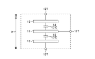
- FIG. 2 shows the configuration of the sensor element 10.
- the sensor element 10 comprises a fixed electrode 11 and movable electrodes 12 and 13 .
- Fixed electrode 11 and movable electrodes 12 and 13 form a capacitance pair consisting of variable capacitances 14 and 15 .
- a variable capacitance 14 is a capacitance formed between the fixed electrode 11 and the movable electrode 12
- a variable capacitance 15 is a capacitance formed between the fixed electrode 11 and the movable electrode 13 .
- the capacitance value of the variable capacitor 14 is referenced by the symbol "C1"
- the capacitance value of the variable capacitor 15 is referenced by the symbol "C2".
- the capacitance value may be hereinafter simply referred to as the capacitance value.
- the electrodes 11 to 13 are arranged side by side along an ⁇ -axis, which is a predetermined linear axis, and the fixed electrode 11 is positioned between the movable electrodes 12 and 13 .
- the sensor element 10 is provided with a terminal 11T connected to the fixed electrode 11, a terminal 12T connected to the movable electrode 12, and a terminal 13T connected to the movable electrode 13.
- the potentials of the electrodes 11, 12, 13 match the potentials of the terminals 11T, 12T, 13T, respectively.
- acceleration means acceleration applied to the acceleration sensor 1 and the sensor element 10 in the direction of the ⁇ -axis. Also, it is assumed that the movable electrode 12 is positioned on the positive side of the ⁇ -axis when viewed from the fixed electrode 11 and the movable electrode 13 is positioned on the negative side of the ⁇ -axis when viewed from the fixed electrode 11 .
- the capacitance values C1 and C2 have a common and predetermined reference capacitance value (although an error may exist).
- positive acceleration is applied to sensor element 10
- the distance between electrodes 11 and 12 increases while the distance between electrodes 11 and 13 decreases compared to when the acceleration is zero, resulting in a capacitance value C1 decreases from the reference capacitance value, while capacitance value C2 increases from the reference capacitance value.
- negative acceleration is applied to sensor element 10
- the distance between electrodes 11 and 12 decreases while the distance between electrodes 11 and 13 increases compared to when the acceleration is zero, resulting in a capacitance value C1 increases from the reference capacitance value, while capacitance value C2 decreases from the reference capacitance value.
- the capacitance values of the variable capacitors 14 and 15 provided in the sensor element 10 change in opposite directions according to the acceleration applied to the sensor element 10 in the ⁇ -axis direction.
- the drive circuit 20 supplies the sensor element 10 with a drive signal DRV IN for driving the sensor element 10 .
- the drive circuit 20 has a first drive signal generation circuit 21 , a second drive signal generation circuit 22 and an adder 23 .
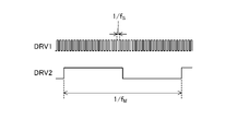
- the first drive signal generation circuit 21 generates a drive signal drv1 and outputs a drive signal DRV1 based on the drive signal drv1.
- the drive signals drv1 and DRV1 are square wave signals having a predetermined frequency f S .
- a drive signal DRV1 is generated by inputting the drive signal drv1 to a driver (buffer circuit).
- the second drive signal generation circuit 22 generates a drive signal drv2 and outputs a drive signal DRV2 based on the drive signal drv2.
- the drive signals drv2 and DRV2 are square wave signals having a predetermined frequency f M .
- a drive signal DRV2 is generated by inputting the drive signal drv2 to a driver (buffer circuit).
- Drive signals DRV1 and DRV2 are provided to adder 23 .
- the adder 23 modulates the drive signal DRV1 with the drive signal DRV2, and generates and outputs the modulated drive signal DRV1 as the drive signal DRV IN .
- the drive signal DRV IN corresponds to a signal obtained by mixing the drive signals DRV1 and DRV2, and has respective components of the drive signals DRV1 and DRV2.
- the frequency f M corresponds to the modulation frequency and may hereinafter be referred to as the modulation frequency f M .
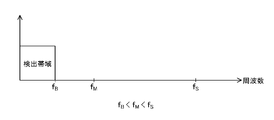
- FIG. 3 shows the relationship between the detection band of the acceleration sensor 1 and the frequencies f M and f S .
- FIG. 4 shows schematic waveforms of the drive signals DRV1 and DRV2.
- the detection band represents the frequency band of acceleration that should be detected by the acceleration sensor 1 and is determined by the specifications of the acceleration sensor 1 .
- the detection band is a band below a predetermined frequency f B .
- the acceleration sensor 1 is not required to detect acceleration at frequencies exceeding the detection band.
- Frequency f M is higher than frequency f B and frequency f S is higher than frequency f M .
- the upper limit frequency (the resonant frequency of the sensor element 10) is higher than the frequency f M and lower than the frequency f S . Therefore, the supply of the drive signal DRV1 to the sensor element 10 does not change the capacitance values C1 and C2, while the supply of the drive signal DRV2 to the sensor element 10 causes the capacitance values C1 and C2 to change.
- the drive signal DRV1 is a signal to be supplied to the sensor element 10 for detecting acceleration.
- DRV1′′ will be described as an example of the operation for detecting acceleration.
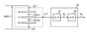
- a detection signal generation circuit 30 is provided with a C/V conversion circuit 31 and an A/D conversion circuit 32 as a configuration for generating a signal corresponding to acceleration.
- Drive signal DRV1 included in drive signal DRV IN is applied between terminals 12T and 13T.
- Terminal 11T is connected to C/V conversion circuit 31 .
- the drive signal DRV1 is a rectangular wave signal that alternately takes a high level and a low level.
- a potential higher than the voltage based on the amplitude of the drive signal DRV1 is applied to the terminal 12T when viewed from the terminal 13T.
- a higher potential is applied by a voltage based on the amplitude.
- the C/V conversion circuit 31 operates in synchronization with the drive signal DRV1, and determines the capacitance value C1 based on the voltage at the terminal 11T during the high level period of the drive signal DRV1 and the voltage at the terminal 11T during the low level period of the drive signal DRV1. and C2 to generate and output a detection signal S A according to the difference (C1-C2).
- the detection signal S A is an analog voltage signal having an analog value proportional to the difference (C1-C2) between the capacitance values C1 and C2. That is, the C/V conversion circuit 31 converts the difference (C1-C2) between the capacitance values C1 and C2 into an analog voltage signal.
- a known method can be used as a method for this conversion.
- the C/V conversion circuit 31 can be configured using a switched capacitor circuit, a sample hold circuit, and a differential amplifier circuit (none of which is shown).
- the A/D conversion circuit 32 converts the analog detection signal S A from the C/V conversion circuit 31 into a digital detection signal S D by A/D conversion (analog-digital conversion).
- A/D conversion analog-digital conversion
- the A/D conversion circuit 32 performs delta-sigma AD conversion and the sampling frequency of the A/D conversion circuit 32 is the frequency f S .
- Detected signal S D has a digital value representing the analog value of detected signal S A . That is, the detection signal S D has a digital value corresponding to the difference (C1-C2) between the capacitance values C1 and C2. More specifically, the detection signal S D has a digital value proportional to the difference (C1-C2). Therefore, the detection signal S D has a waveform corresponding to the amplitude and direction of acceleration.
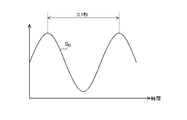
- FIG. 6 shows an overview of the waveform of the detection signal S D when the acceleration sensor 1 is given an acceleration whose magnitude changes sinusoidally at 10 Hz.
- the C/V conversion circuit 31 by operating the C/V conversion circuit 31 in synchronization with the drive signal DRV1, signals (S A , S D ) corresponding to the acceleration can be obtained.
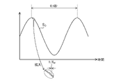
- the drive signal DRV1 is actually modulated by the drive signal DRV2. Therefore, the detection signal S D includes a signal component of the modulation frequency f M and fluctuates at the modulation frequency f M (see FIG. 7).
- the drive signal DRV2 is a rectangular wave signal that alternately takes a high level and a low level.
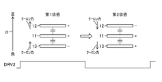
- the state of the sensor element 10 is alternately switched between the first state and the second state based on the drive signal DRV2 included in the drive signal DRV IN .
- the state of the sensor element 10 is set to the first state during the high level period of the drive signal DRV2. In the first state, each potential of the fixed electrode 11 and the movable electrode 12 increases by the amplitude of the drive signal DRV2 when viewed from the potential of the movable electrode 13 .
- the state of the sensor element 10 is set to the second state during the low level period of the drive signal DRV2.
- the potentials of the fixed electrode 11 and the movable electrode 13 are increased by the amplitude of the drive signal DRV2 when viewed from the potential of the movable electrode 12 .
- the second state is generated. , potential fluctuations of the electrodes 11 to 13 occur based on the components of the drive signal DRV1.
- the Coulomb force directed toward the positive side of the ⁇ -axis against the movable electrodes 12 and 13 based on the component of the drive signal DRV2 (repulsive force between the electrodes 11 and 12 and suction force) works.
- the Coulomb force directed toward the negative side of the ⁇ -axis against the movable electrodes 12 and 13 (attractive force between the electrodes 11 and 12 and repulsive force between the electrodes 11 and 13) is applied to the movable electrodes 12 and 13 based on the component of the drive signal DRV2. force) works.
- the detection signals S A and S D are signal components based on the Coulomb force (therefore, the modulation frequency signal component of f M ) is included.
- the acceleration signal generation circuit 40 performs predetermined low-pass processing on the detection signal S D to generate and output an acceleration signal S ACC corresponding to the acceleration.
- the acceleration signal SACC is a signal representing the amplitude and direction of acceleration.
- the acceleration signal generation circuit 40 has an LPF (low-pass filter) 41, and the LPF 41 performs the above-described low-pass processing. Since the detection signal S D is a digital signal, the LPF 41 is configured as a digital low-pass filter.
- the LPF 41 may be composed of a single-stage low-pass filter, or may be composed of a plurality of stages of low-pass filters.
- the cutoff frequency for low-pass processing by the LPF 41 is referenced by the symbol “f CO ".
- the LPF 41 passes signal components with frequencies below the cutoff frequency f CO , while attenuating signal components with frequencies higher than the cutoff frequency f CO .
- the attenuated detection signal S D is generated and output as the acceleration signal S ACC .
- the band B LPF represents the band extracted by the LPF 41 (that is, the band below the cutoff frequency f CO ).
- the cutoff frequency f CO is set to the frequency f B (see FIG. 3; eg, 100 Hz) which is the upper limit of the detection band, or is set to a frequency higher than the frequency f B by a predetermined frequency (eg, 120 Hz).
- a predetermined frequency eg, 120 Hz.
- the acceleration signal S ACC includes the signal component of the acceleration within the detection band with sufficiently high signal strength. If the specifications of the acceleration sensor 1 are satisfied, a frequency (for example, 90 Hz) lower than the frequency f B by a predetermined frequency may be set as the cutoff frequency f CO .
- the modulation frequency f M is higher than the cutoff frequency f CO , and the signal component of the modulation frequency f M in the detection signal S D is sufficiently attenuated by low-pass processing in the LPF 41 . That is, it is possible to extract the acceleration signal S ACC having only the actual acceleration component from which the modulation component has been removed.
- the modulation component extraction circuit 50 extracts the signal component of the modulation frequency f M in the detection signal S D by performing a predetermined band-pass processing on the detection signal S D , and uses the extracted signal as the modulation component extraction signal S M . Generate and output.
- the modulation component extracting circuit 50 has a BPF (band pass filter) 51, and the BPF 51 performs the band pass processing. Since the detection signal S D is a digital signal, the BPF 51 is configured as a digital bandpass filter.
- a predetermined passband is defined in the bandpass process.
- the modulation frequency f M is a frequency within the passband.
- the band B BPF represents the band extracted by the BPF 51 (that is, the pass band of the BPF 51).
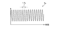
- FIG. 9 schematically shows the spectrum of the modulated component extraction signal S M .
- the BPF 51 passes signal components with frequencies within the passband and attenuates signal components with frequencies outside the passband, thereby reducing the modulation frequency f M in the detection signal S D .
- Passing signal components at frequencies within the passband may include enhancing (amplifying) signal components at frequencies within the passband.
- FIG. 10 schematically shows an example of the signal waveform of the modulated component extraction signal S M .
- the BPF 51 is designed so that the signal component of the modulation frequency f M in the modulated component extraction signal S M has a sufficiently higher signal strength than the signal component outside the passband.
- the signal components below the frequency f B and the signal components with the frequency f S have sufficiently low signal strength in the modulated component extraction signal S M (these signal components are substantially not included in the modulated component extraction signal S M ).
- the lower limit frequency of the passband should be set sufficiently higher than the frequency f B and the cutoff frequency f CO of the LPF 41
- the upper limit frequency of the passband should be set sufficiently lower than the frequency f S .
- the diagnostic circuit 60 diagnoses the state of the sensor element 10 based on the modulated component extraction signal SM, and generates and outputs a diagnostic signal S DIAG indicating the diagnostic result.
- the diagnostic signal S DIAG is a signal relating to the state of the sensor element 10 (a signal representing the state of the sensor element 10 ), more specifically, a signal representing the presence or absence of an abnormality in the sensor element 10 . In other words, the presence or absence of abnormality in the sensor element 10 is determined in the diagnosis by the diagnostic circuit 60 .
- the diagnostic signal S DIAG is a binary signal having a value of "0" or "1".
- the diagnostic signal S DIAG having a value of "1" functions as a signal indicating that the sensor element 10 is abnormal.
- a signal indicating that the sensor element 10 has an abnormality can also be expressed as a signal suggesting the possibility that the sensor element 10 has an abnormality.
- the diagnostic signal S DIAG having a value of "0" functions as a signal indicating that the sensor element 10 is normal.
- a signal indicating that the sensor element 10 is normal can also be expressed as a signal indicating that the sensor element 10 is normal.
- the control circuit 70 forms a signal processing circuit together with the drive circuit 20, the detection signal generation circuit 30, the acceleration signal generation circuit 40, the modulation component extraction circuit 50 and the diagnosis circuit 60.
- the control circuit 70 has a function of centrally controlling the operation of each part in the signal processing circuit.
- the control circuit 70 has a function of transmitting the acceleration signal S ACC itself or a signal based on the acceleration signal S ACC to an external device (not shown) connected to the acceleration sensor 1 .
- the acceleration signal S ACC may be transmitted to the external device while being updated at a constant period (for example, the period of the reciprocal of 100 Hz).
- the acceleration signal generation circuit 40 itself may transmit the acceleration signal S ACC to the external device without relying on the control circuit 70 .
- the control circuit 70 also has a function of transmitting the diagnostic signal S DIAG itself or a signal based on the diagnostic signal S DIAG to the external device.
- the diagnostic circuit 60 itself may transmit the diagnostic signal S DIAG to the external device without relying on the control circuit 70 .
- Control circuit 70 may also have other functions, which will be described later.
- the first embodiment includes the following examples EX1_A and EX1_B.
- Examples EX1_A and EX1_B detailed operation examples or configuration examples of the diagnostic circuit 60 will be described.
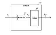
- FIG. 11 shows the internal configuration of the diagnostic circuit 60 according to the embodiment EX1_A.
- a diagnostic circuit 60 according to Example EX1_A includes an amplitude derivation unit 61 and a determination unit 65 .
- An amplitude derivation unit 61 derives the amplitude A M of the modulated component extraction signal S M .
- a determination unit 65 generates a diagnostic signal S DIAG based on the derived amplitude AM .
- the generated diagnostic signal S DIAG is output from diagnostic circuit 60 .
- the determination unit 65 generates a diagnostic signal S DIAG corresponding to whether or not the amplitude AM of the modulated component extraction signal S M deviates from a predetermined amplitude normal range.
- the determination unit 65 generates a diagnostic signal S DIAG having a value of "1" when the amplitude AM is out of the predetermined normal amplitude range, and generates a diagnostic signal S DIAG having a value of "1” when the amplitude AM is within the predetermined normal amplitude range. generates a diagnostic signal S DIAG having a value of "0". If the sensor element 10 is normal, the movable electrodes 12 and 13 should mechanically oscillate at the modulation frequency f M with proper amplitude in response to the supply of the drive signal DRV2. This is because AM is expected to fall within the normal amplitude range.
- the normal amplitude range may be a range from a predetermined lower limit amplitude A TH#L to a predetermined upper limit amplitude A TH#H (where "0 ⁇ A TH#L ⁇ A TH#H " holds true).
- a TH#L ⁇ A M ⁇ A TH#H the value of the diagnostic signal S DIAG is set to "0”
- the normal amplitude range may be a range defined only by the lower limit amplitude A TH#L .
- the diagnostic signal S DIAG is set to "0"
- the control circuit 70 latches the value and transmits a predetermined notification signal to an external device (not shown) connected to the acceleration sensor 1. (The same applies to Example EX1_B described later and other embodiments described later).
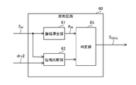
- FIG. 12 shows the internal configuration of the diagnostic circuit 60 according to the embodiment EX1_B.
- a diagnostic circuit 60 according to Example EX1_B includes an amplitude derivation unit 61 and a determination unit 65 and further includes a phase comparison unit 63 .
- the function of the amplitude derivation unit 61 is as described in the embodiment EX1_A.
- the modulated component extraction signal SM and the drive signal drv2 are input to the phase comparator 63 .
- the phase comparator 63 compares the phase of the modulated component extraction signal S M and the phase of the drive signal drv2 to derive the phase difference ⁇ between the phase of the modulated component extraction signal S M and the phase of the drive signal drv2.
- the phase difference ⁇ represents the amount of delay in the phase of the modulated component extraction signal SM with respect to the phase of the drive signal drv2 .
- the drive signal drv2 is the source signal of the drive signal DRV2 (see FIG. 1).
- the phase of the drive signal drv2 and the phase of the drive signal DRV2 are substantially the same, and here, it is considered that there is no difference between the phase of the drive signal drv2 and the phase of the drive signal DRV2.
- the phase difference ⁇ represents the phase difference between the phase of the modulated component extraction signal S M and the phase of the drive signal DRV2.
- a phase comparison between signals S M and drv2 is equivalent to a phase comparison between signals S M and DRV2.
- the determination unit 65 according to the embodiment EX1_B generates the diagnosis signal S DIAG based on the amplitude A M derived by the amplitude derivation unit 51 and the phase difference ⁇ derived by the phase comparison unit 63 .
- the generated diagnostic signal S DIAG is output from diagnostic circuit 60 .
- the determination unit 65 makes a diagnosis according to whether or not the phase difference ⁇ satisfies a predetermined phase matching condition and whether or not the amplitude AM of the modulated component extraction signal S M deviates from a predetermined amplitude normal range. Generates signal S DIAG .
- the movable electrodes 12 and 13 mechanically vibrate at the modulation frequency f M in synchronization with the drive signal DRV2 . Therefore, there should be a certain relationship between the phase of the driving signal drv2).
- the phase matching condition is determined based on this fixed relationship. The phase matching condition is satisfied when the phase difference ⁇ is within a predetermined phase matching range, and the phase matching condition is not satisfied when the phase difference ⁇ deviates from the predetermined phase matching range.
- the signal component of the acceleration will be included in the modulated component extraction signal S M .
- the sensor element 10 cannot be correctly diagnosed based on the drive signal DRV2.
- the determination unit 65 determines whether the phase difference ⁇ (relationship between two phases to be compared) satisfies a predetermined phase matching condition and the amplitude A M of the modulated component extraction signal S M is within a predetermined amplitude normal range. When deviating, it generates a diagnostic signal S DIAG having a value of "1". The determination unit 65 outputs a diagnostic signal S DIAG having a value of “0” when the phase difference ⁇ satisfies a predetermined phase matching condition and the amplitude A M of the modulated component extraction signal S M falls within a predetermined amplitude normal range. to generate
- the determination unit 65 sets the value of the diagnostic signal S DIAG to “0” regardless of the relationship between the amplitude AM and the amplitude normal range.
- the phase difference ⁇ no longer satisfies the phase matching condition.
- phase difference ⁇ (relationship between two phases to be compared) does not satisfy a predetermined phase matching condition, the control circuit 70 may change the modulation frequency f M through the control of the drive circuit 20. good. I will add an explanation for this.
- the drive circuit 20 is configured so that the modulation frequency f M can be switched between a plurality of frequencies including frequencies f M1 and f M2 (f M1 ⁇ f M2 ). No matter which one of the plurality of frequencies here is set as the modulation frequency f M , the frequency f M satisfies all the characteristics described above (thus satisfying, for example, “f B ⁇ f M ⁇ f S ”).
- the modulation frequency f M is set to the frequency f M1 . That is, the initial value of the modulation frequency f M is "f M1 ".
- the sensor element 10 is driven. This makes it possible to diagnose the sensor element 10 even when the acceleration sensor 1 is subjected to acceleration near the modulation frequency f M1 .
- the passband of the BPF 51 is switched. At this time, the width of the pass band of the BPF 51 is preferably smaller than the absolute value
- the acceleration sensor 1 may be a sensor capable of individually detecting acceleration in a plurality of mutually different axial directions.
- FIG. 13 is a configuration diagram of an acceleration sensor 1 configured as a triaxial acceleration sensor (hereinafter referred to as triaxial acceleration sensor 1).
- the three-axis acceleration sensor 1 can individually detect acceleration in the X-axis, Y-axis, and Z-axis directions. Acceleration in the X-axis, Y-axis, and Z-axis directions indicates acceleration in the X-axis, Y-axis, and Z-axis directions, respectively, applied to the three-axis acceleration sensor 1 .
- the X-axis, Y-axis and Z-axis are three axes orthogonal to each other.
- the three-axis acceleration sensor 1 has three functional blocks BL each having a sensor element 10 and a signal processing circuit SPC.
- the three functional blocks BL have the same configuration. However, of the three functional blocks BL, the ⁇ -axis (see FIG. 2) for the sensor element 10 in the first functional block BL is the X-axis, and the ⁇ -axis for the sensor element 10 in the second functional block BL is The Y-axis and the ⁇ -axis for the sensor element 10 in the third functional block BL are the Z-axis.
- the signal processing circuit SPC includes the drive circuit 20, the detection signal generation circuit 30, the acceleration signal generation circuit 40, the modulation component extraction circuit 50, the diagnosis circuit 60, and the control circuit 70 described in the first embodiment. .
- the sensor element 10 and circuits 20 to 70 operate as described in the first embodiment.
- the accelerations in the X-axis, Y-axis, and Z-axis directions can be detected separately (that is, the acceleration signal S ACC in the X-axis direction, the acceleration signal S ACC in the Y-axis direction, and the acceleration signal S ACC in the Z-axis direction can be detected. can be generated) and diagnosis of the sensor element 10 can be performed on a sensor element 10 by sensor element 10 basis.
- the signal processing circuit SPC of each functional block BL is not provided with the control circuit 70, and the three-axis acceleration sensor 1 is provided with a single control circuit (not shown) shared by the three functional blocks BL. Also good.
- a third embodiment of the present disclosure will be described.
- modification techniques, application techniques, supplementary matters, etc. applicable to the first or second embodiment will be described.
- the acceleration sensor 1 described in the third embodiment refers to the acceleration sensor 1 described in the first embodiment or the triaxial acceleration sensor 1 described in the second embodiment.
- the acceleration sensor 1 can be mounted on any device.
- the acceleration sensor 1 can be mounted on a vehicle such as an automobile.
- the external device connected to the acceleration sensor 1 is a host system (ECU (Electronic Control Unit), etc.) mounted on the vehicle.
- ECU Electronic Control Unit
- a self-diagnostic function is often required for automotive components.
- the following first and second reference examples are conceivable as implementation examples of self-diagnosis.
- self-diagnosis is performed using the Coulomb force, but the normal detection operation of acceleration is interrupted when self-diagnosis is performed. In the first reference example, normal detection operation cannot be performed during self-diagnosis.
- a sensor element dedicated to self-diagnosis is added, and self-diagnosis is performed using the sensor element dedicated to self-diagnosis.
- a total of four sensor elements are required.
- the cost increases due to the addition of the sensor element.
- the acceleration sensor 1 of the first or second embodiment can diagnose the sensor element 10 while performing a normal acceleration detection operation. Moreover, the sensor element dedicated to self-diagnosis as shown in the second reference example is unnecessary. Therefore, the diagnosis of the sensor element 10 can be performed at low cost without interrupting the normal detection operation. This diagnosis makes it possible to improve the reliability of the system including the acceleration sensor 1 .
- the AD conversion method in the A/D conversion circuit 32 may be arbitrary.
- the acceleration sensor 1 may perform each signal processing in the form of an analog signal without performing AD conversion.
- the A /D conversion circuit 32 may be removed from the detection signal generation circuit 30 of FIG.
- the LPF 41 and BPF 51 are composed of analog circuits, and an analog acceleration signal S ACC and an analog modulation component extraction signal SM are generated from the analog detection signal S A .
- Each circuit element constituting the acceleration sensor 1 is formed in the form of a semiconductor integrated circuit, and a semiconductor device is constructed by enclosing the semiconductor integrated circuit in a housing (package) made of resin.
- the semiconductor chip on which the sensor element 10 is formed and the semiconductor chip on which the other circuits (including the circuits 20 to 70) are formed may be separate, and these semiconductor chips are enclosed in a common housing.
- a semiconductor device may be configured in this manner.
- a modified configuration may be employed in which the diagnosis circuit 60 is not included in the semiconductor device.
- an external device such as a microcomputer is connected to the semiconductor device, and the diagnostic circuit 60 is provided in the external device.
- a diagnostic signal S DIAG may be generated by a diagnostic circuit 60 in the external device by inputting the modulated component extraction signal S M output from the modulated component extraction circuit 50 in the semiconductor device to the external device.
- An acceleration sensor includes a sensor element (10) having a first variable capacitor and a second variable capacitor whose capacitance values change in opposite directions according to acceleration;
- a first drive signal (DRV1) to be supplied to the sensor element for detecting acceleration is modulated by a second drive signal (DRV2) having a predetermined modulation frequency (f M ), and the first drive signal and the a drive circuit (20) configured to be able to supply a signal having each component of a second drive signal to the sensor element;
- a detection signal generation circuit (30) capable of generating detection signals (S A , S D ) corresponding to the difference in capacitance value; and an acceleration signal generation circuit (40) configured to generate an acceleration signal (S ACC ), and a modulation component extraction signal (S M ) can be generated by extracting the signal component of the modulation frequency in the detection signal.
- a modulated component extraction circuit (50) configured (first configuration).
- the sensor element can be diagnosed without interrupting the acceleration signal generation operation (normal detection operation) and without separately providing a sensor element dedicated to diagnosis (thus, at low cost).
- the modulation frequency (f M ) is lower than the frequency (f S ) of the first drive signal and lower than the cutoff frequency (f CO ) of the low-pass processing.
- a high configuration (second configuration) may also be used.
- the modulation frequency is higher than the cutoff frequency of the low-pass processing, inclusion of the modulation frequency component in the acceleration signal is suppressed. That is, the influence of the modulation by the second drive signal on the acceleration signal generation operation (normal detection operation) is suppressed. Also, the modulation frequency is set lower than the frequency of the first drive signal so that the capacitance values of the first variable capacitor and the second variable capacitor can be varied by the second drive signal.
- each capacitance value of the first variable capacitor and the second variable capacitor is modulated by supplying the component of the second drive signal to the sensor element.
- a configuration (third configuration) that varies with frequency may be used.
- the acceleration sensor according to any one of the first to third configurations, further comprising a diagnostic circuit (60) capable of generating a diagnostic signal (S DIAG ) regarding the state of the sensor element based on the modulated component extraction signal.
- a diagnostic circuit 60
- S DIAG diagnostic signal
- the diagnostic circuit may be configured to generate the diagnostic signal based on the amplitude of the modulated component extraction signal (fifth configuration).
- the diagnostic circuit is configured to generate the diagnostic signal according to whether or not the amplitude of the modulated component extraction signal deviates from a predetermined range (sixth configuration).
- the diagnostic circuit can generate, as the diagnostic signal, a signal indicating that the sensor element has an abnormality when the amplitude of the modulated component extraction signal deviates from a predetermined range. (seventh configuration).
- the diagnostic circuit is configured to generate the diagnostic signal according to the amplitude of the modulated component extraction signal and each phase of the modulated component extraction signal and the second drive signal.
- a configuration (eighth configuration) may be used.
- the diagnostic circuit satisfies a predetermined condition that the phase of the modulated component extraction signal and the phase of the second drive signal satisfy a predetermined condition, and that the amplitude of the modulated component extraction signal is a predetermined
- the configuration may be configured such that a signal indicating that there is an abnormality in the sensor element can be generated as the diagnostic signal when the sensor element is out of range.
- a control circuit configured to be able to change the modulation frequency when the relationship between the phase of the modulated component extraction signal and the phase of the second drive signal does not satisfy the predetermined condition.
- a configuration (tenth configuration) further provided may be employed.
- the modulation frequency is a certain specific frequency
- changing the modulation frequency from the specific frequency can Diagnosis can be made.
- acceleration sensor 10 sensor element 11 fixed electrode 12, 13 movable electrode 14, 15 variable capacitor 20 drive circuit 30 detection signal generation circuit 31 C/V conversion circuit 32 A/D conversion circuit 40 acceleration signal generation circuit 41 LPF 50 modulation component extraction circuit 51 BPF 60 diagnostic circuit 61 amplitude derivation unit 63 phase comparison unit 65 determination unit 70 control circuit
Landscapes
- Physics & Mathematics (AREA)
- General Physics & Mathematics (AREA)
- Pressure Sensors (AREA)
Priority Applications (2)
| Application Number | Priority Date | Filing Date | Title |
|---|---|---|---|
| JP2023520987A JPWO2022239692A1 (enExample) | 2021-05-13 | 2022-05-02 | |
| US18/498,415 US20240061011A1 (en) | 2021-05-13 | 2023-10-31 | Acceleration sensor |
Applications Claiming Priority (2)
| Application Number | Priority Date | Filing Date | Title |
|---|---|---|---|
| JP2021081427 | 2021-05-13 | ||
| JP2021-081427 | 2021-05-13 |
Related Child Applications (1)
| Application Number | Title | Priority Date | Filing Date |
|---|---|---|---|
| US18/498,415 Continuation US20240061011A1 (en) | 2021-05-13 | 2023-10-31 | Acceleration sensor |
Publications (1)
| Publication Number | Publication Date |
|---|---|
| WO2022239692A1 true WO2022239692A1 (ja) | 2022-11-17 |
Family
ID=84028308
Family Applications (1)
| Application Number | Title | Priority Date | Filing Date |
|---|---|---|---|
| PCT/JP2022/019490 Ceased WO2022239692A1 (ja) | 2021-05-13 | 2022-05-02 | 加速度センサ |
Country Status (3)
| Country | Link |
|---|---|
| US (1) | US20240061011A1 (enExample) |
| JP (1) | JPWO2022239692A1 (enExample) |
| WO (1) | WO2022239692A1 (enExample) |
Citations (4)
| Publication number | Priority date | Publication date | Assignee | Title |
|---|---|---|---|---|
| JP2008107108A (ja) * | 2006-10-23 | 2008-05-08 | Denso Corp | 容量式力学量検出装置 |
| US20090241634A1 (en) * | 2008-03-28 | 2009-10-01 | Cenk Acar | Micromachined accelerometer and method with continuous self-testing |
| JP2018159630A (ja) * | 2017-03-23 | 2018-10-11 | セイコーエプソン株式会社 | センサー素子制御装置、物理量センサー、電子機器、移動体及び物理量センサーの故障診断方法 |
| JP2019502910A (ja) * | 2015-12-15 | 2019-01-31 | パナソニック株式会社 | 加速度計センス経路自己試験 |
Family Cites Families (14)
| Publication number | Priority date | Publication date | Assignee | Title |
|---|---|---|---|---|
| JP4032681B2 (ja) * | 2001-08-27 | 2008-01-16 | 株式会社デンソー | 同期検波方法及び装置並びにセンサ信号検出装置 |
| US7287429B2 (en) * | 2004-03-25 | 2007-10-30 | Denso Corporation | Capacitive acceleration sensor system |
| JP4534741B2 (ja) * | 2004-12-10 | 2010-09-01 | 株式会社デンソー | ジャイロセンサ |
| JP4765708B2 (ja) * | 2006-03-23 | 2011-09-07 | 株式会社デンソー | 容量式物理量センサ |
| JP6531279B2 (ja) * | 2013-10-09 | 2019-06-19 | パナソニックIpマネジメント株式会社 | 加速度センサ |
| JP6311871B2 (ja) * | 2014-04-17 | 2018-04-18 | セイコーエプソン株式会社 | 物理量検出用回路、物理量検出装置、物理量計測システム、電子機器、移動体及び物理量計測データ生成方法 |
| GB2527595A (en) * | 2014-06-27 | 2015-12-30 | Atlantic Inertial Systems Ltd | Accelerometers |
| US9784644B2 (en) * | 2014-10-16 | 2017-10-10 | Tula Technology, Inc. | Engine error detection system |
| WO2016132447A1 (ja) * | 2015-02-17 | 2016-08-25 | 株式会社日立製作所 | 加速度センサ |
| WO2017009885A1 (ja) * | 2015-07-10 | 2017-01-19 | 株式会社日立製作所 | 慣性センサ |
| JP7075849B2 (ja) * | 2018-08-29 | 2022-05-26 | 株式会社日立製作所 | Mems静電容量型加速度センサ |
| EP3862757B1 (en) * | 2020-02-07 | 2024-03-27 | Atlantic Inertial Systems Limited | Methods for closed loop operation of capacitive accelerometers and such capacitive accelerometers |
| US11307218B2 (en) * | 2020-05-22 | 2022-04-19 | Invensense, Inc. | Real-time isolation of self-test and linear acceleration signals |
| US20230194564A1 (en) * | 2020-06-04 | 2023-06-22 | Panasonic Intellectual Property Management Co., Ltd. | Inertial detection circuit, inertial sensor, and inertial detection method |
-
2022
- 2022-05-02 JP JP2023520987A patent/JPWO2022239692A1/ja active Pending
- 2022-05-02 WO PCT/JP2022/019490 patent/WO2022239692A1/ja not_active Ceased
-
2023
- 2023-10-31 US US18/498,415 patent/US20240061011A1/en active Pending
Patent Citations (4)
| Publication number | Priority date | Publication date | Assignee | Title |
|---|---|---|---|---|
| JP2008107108A (ja) * | 2006-10-23 | 2008-05-08 | Denso Corp | 容量式力学量検出装置 |
| US20090241634A1 (en) * | 2008-03-28 | 2009-10-01 | Cenk Acar | Micromachined accelerometer and method with continuous self-testing |
| JP2019502910A (ja) * | 2015-12-15 | 2019-01-31 | パナソニック株式会社 | 加速度計センス経路自己試験 |
| JP2018159630A (ja) * | 2017-03-23 | 2018-10-11 | セイコーエプソン株式会社 | センサー素子制御装置、物理量センサー、電子機器、移動体及び物理量センサーの故障診断方法 |
Also Published As
| Publication number | Publication date |
|---|---|
| JPWO2022239692A1 (enExample) | 2022-11-17 |
| US20240061011A1 (en) | 2024-02-22 |
Similar Documents
| Publication | Publication Date | Title |
|---|---|---|
| JP4375579B2 (ja) | 容量式物理量検出装置 | |
| JP3861652B2 (ja) | 容量式物理量センサ | |
| CN108369246B (zh) | Mems加速度计误差的识别和补偿 | |
| JP5557354B2 (ja) | 寄生容量により誘導される誤差が減少されたセンサデバイス | |
| EP3387449B1 (en) | Accelerometer common mode self-test | |
| WO2009120753A1 (en) | Micromachined accelerometer and method with continuous self-testing | |
| JP2007178420A (ja) | 容量式物理量センサおよびその診断方法 | |
| WO2012090627A1 (ja) | センサモジュール、およびセンサシステム | |
| WO2022239692A1 (ja) | 加速度センサ | |
| JP2016095268A (ja) | 信号処理装置 | |
| EP3144640B1 (en) | Sensor arrangement and method for operation of a sensor | |
| JP2016523374A (ja) | ピックオフトランスデューサワイヤボンドビット検出 | |
| EP4163644B1 (en) | Inertial force detection circuit, inertial force sensor, and inertial force detection method | |
| JP5939136B2 (ja) | センサ装置 | |
| US8573055B2 (en) | Angular velocity sensor | |
| JP4150292B2 (ja) | 異常検出機能を持つ静電容量式センサ装置 | |
| CN108075738B (zh) | 用于多个通道的低噪声放大器 | |
| US10877064B2 (en) | Evaluation circuit for a capacitive acceleration sensor and device for detecting an acceleration | |
| EP3667332A1 (en) | Redundant sensor system with self-test of electromechanical structures | |
| JP6955831B2 (ja) | 運動センサ同相モード自己試験 | |
| JP4793012B2 (ja) | 重複角速度センサ | |
| WO2025046986A1 (ja) | ジャイロセンサ | |
| WO2025115346A1 (ja) | センサシステム | |
| JP2008256582A (ja) | 物理量センサの故障検出方法、及び物理量センサ | |
| JP2023111659A (ja) | 物理量センサーモジュールおよび物理量センサーの診断方法 |
Legal Events
| Date | Code | Title | Description |
|---|---|---|---|
| 121 | Ep: the epo has been informed by wipo that ep was designated in this application |
Ref document number: 22807394 Country of ref document: EP Kind code of ref document: A1 |
|
| WWE | Wipo information: entry into national phase |
Ref document number: 2023520987 Country of ref document: JP |
|
| NENP | Non-entry into the national phase |
Ref country code: DE |
|
| 122 | Ep: pct application non-entry in european phase |
Ref document number: 22807394 Country of ref document: EP Kind code of ref document: A1 |