WO2022239692A1 - Acceleration sensor - Google Patents
Acceleration sensor Download PDFInfo
- Publication number
- WO2022239692A1 WO2022239692A1 PCT/JP2022/019490 JP2022019490W WO2022239692A1 WO 2022239692 A1 WO2022239692 A1 WO 2022239692A1 JP 2022019490 W JP2022019490 W JP 2022019490W WO 2022239692 A1 WO2022239692 A1 WO 2022239692A1
- Authority
- WO
- WIPO (PCT)
- Prior art keywords
- signal
- acceleration
- diagnostic
- circuit
- sensor element
- Prior art date
Links
- 230000001133 acceleration Effects 0.000 title claims abstract description 155
- 238000001514 detection method Methods 0.000 claims abstract description 61
- 238000000605 extraction Methods 0.000 claims description 50
- 230000007274 generation of a signal involved in cell-cell signaling Effects 0.000 claims description 27
- 239000003990 capacitor Substances 0.000 claims description 24
- 230000008859 change Effects 0.000 claims description 10
- 230000005856 abnormality Effects 0.000 claims description 8
- 238000006243 chemical reaction Methods 0.000 description 25
- 238000003745 diagnosis Methods 0.000 description 19
- 238000010586 diagram Methods 0.000 description 15
- 239000004065 semiconductor Substances 0.000 description 10
- 238000004092 self-diagnosis Methods 0.000 description 8
- 238000009795 derivation Methods 0.000 description 6
- 238000000034 method Methods 0.000 description 6
- 230000007423 decrease Effects 0.000 description 4
- 230000002159 abnormal effect Effects 0.000 description 2
- 230000002238 attenuated effect Effects 0.000 description 2
- 239000000284 extract Substances 0.000 description 2
- 230000004044 response Effects 0.000 description 2
- 230000009471 action Effects 0.000 description 1
- 239000000470 constituent Substances 0.000 description 1
- 230000002708 enhancing effect Effects 0.000 description 1
- 230000004048 modification Effects 0.000 description 1
- 238000012986 modification Methods 0.000 description 1
- 230000008569 process Effects 0.000 description 1
- 239000011347 resin Substances 0.000 description 1
- 229920005989 resin Polymers 0.000 description 1
- 238000005070 sampling Methods 0.000 description 1
- 238000001228 spectrum Methods 0.000 description 1
Images


Classifications
-
- G—PHYSICS
- G01—MEASURING; TESTING
- G01P—MEASURING LINEAR OR ANGULAR SPEED, ACCELERATION, DECELERATION, OR SHOCK; INDICATING PRESENCE, ABSENCE, OR DIRECTION, OF MOVEMENT
- G01P15/00—Measuring acceleration; Measuring deceleration; Measuring shock, i.e. sudden change of acceleration
- G01P15/02—Measuring acceleration; Measuring deceleration; Measuring shock, i.e. sudden change of acceleration by making use of inertia forces using solid seismic masses
- G01P15/08—Measuring acceleration; Measuring deceleration; Measuring shock, i.e. sudden change of acceleration by making use of inertia forces using solid seismic masses with conversion into electric or magnetic values
- G01P15/125—Measuring acceleration; Measuring deceleration; Measuring shock, i.e. sudden change of acceleration by making use of inertia forces using solid seismic masses with conversion into electric or magnetic values by capacitive pick-up
-
- G—PHYSICS
- G01—MEASURING; TESTING
- G01P—MEASURING LINEAR OR ANGULAR SPEED, ACCELERATION, DECELERATION, OR SHOCK; INDICATING PRESENCE, ABSENCE, OR DIRECTION, OF MOVEMENT
- G01P15/00—Measuring acceleration; Measuring deceleration; Measuring shock, i.e. sudden change of acceleration
- G01P15/02—Measuring acceleration; Measuring deceleration; Measuring shock, i.e. sudden change of acceleration by making use of inertia forces using solid seismic masses
- G01P15/08—Measuring acceleration; Measuring deceleration; Measuring shock, i.e. sudden change of acceleration by making use of inertia forces using solid seismic masses with conversion into electric or magnetic values
- G01P15/0802—Details
-
- G—PHYSICS
- G01—MEASURING; TESTING
- G01P—MEASURING LINEAR OR ANGULAR SPEED, ACCELERATION, DECELERATION, OR SHOCK; INDICATING PRESENCE, ABSENCE, OR DIRECTION, OF MOVEMENT
- G01P15/00—Measuring acceleration; Measuring deceleration; Measuring shock, i.e. sudden change of acceleration
- G01P15/18—Measuring acceleration; Measuring deceleration; Measuring shock, i.e. sudden change of acceleration in two or more dimensions
-
- G—PHYSICS
- G01—MEASURING; TESTING
- G01P—MEASURING LINEAR OR ANGULAR SPEED, ACCELERATION, DECELERATION, OR SHOCK; INDICATING PRESENCE, ABSENCE, OR DIRECTION, OF MOVEMENT
- G01P21/00—Testing or calibrating of apparatus or devices covered by the preceding groups
Definitions
- the present disclosure relates to acceleration sensors.
- MEMS Micro Electro Mechanical System
- capacitance-type acceleration sensors are required to have a configuration that can diagnose whether or not they are in a state where acceleration can be detected correctly. It is desired to realize such a diagnosis with a simple configuration without interrupting the acceleration detection operation.
- An object of the present disclosure is to provide an acceleration sensor that enables diagnosis with a simple configuration without interrupting the acceleration detection operation.
- An acceleration sensor includes a sensor element having a first variable capacitor and a second variable capacitor whose capacitance values change in opposite directions according to acceleration, and a sensor element for detecting the acceleration.
- a first drive signal to be detected is modulated by a second drive signal having a predetermined modulation frequency, and a signal having each component of the first drive signal and the second drive signal can be supplied to the sensor element.
- a drive circuit a detection signal generation circuit connected to the sensor element and configured to generate a detection signal corresponding to a difference in capacitance value between the first variable capacitor and the second variable capacitor;
- An acceleration signal generation circuit configured to generate an acceleration signal corresponding to the acceleration by performing low-pass processing on the signal, and a modulation component extraction by extracting a signal component of the modulation frequency in the detection signal.
- a modulation component extraction circuit configured to generate a signal.
- an acceleration sensor that enables diagnosis with a simple configuration without interrupting the acceleration detection operation.
- FIG. 1 is a configuration diagram of an acceleration sensor according to the first embodiment of the present disclosure.
- FIG. 2 is a configuration diagram of a sensor element according to the first embodiment of the present disclosure.
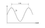
- FIG. 3 is a diagram showing the relationship between the detection band of the acceleration sensor and the frequencies of the first drive signal and the second drive signal, according to the first embodiment of the present disclosure.
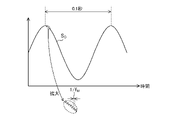
- FIG. 4 is a diagram showing schematic waveforms of a first drive signal and a second drive signal according to the first embodiment of the present disclosure.
- FIG. 5 is a configuration diagram for explaining signal processing for outputs of sensor elements according to the first embodiment of the present disclosure.
- FIG. 6 is a diagram showing an example of waveforms of detection signals output from an A/D conversion circuit according to the first embodiment of the present disclosure.
- FIG. 7 is a diagram illustrating an example of a waveform of a detection signal output from an A/D conversion circuit according to the first embodiment of the present disclosure
- FIG. 8 is a diagram for explaining the Coulomb force generated by the second drive signal according to the first embodiment of the present disclosure.
- FIG. 9 is a diagram showing the relationship between multiple frequencies and multiple bands according to the first embodiment of the present disclosure.
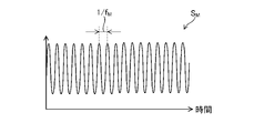
- FIG. 10 is a diagram showing a waveform example of a modulated component extraction signal according to the first embodiment of the present disclosure.
- FIG. 11 is a configuration diagram of a diagnostic circuit according to Example EX1_A belonging to the first embodiment of the present disclosure.
- FIG. 12 is a configuration diagram of a diagnostic circuit according to example EX1_B belonging to the first embodiment of the present disclosure.
- FIG. 13 is a configuration diagram of an acceleration sensor according to the second embodiment of the present disclosure;
- Level refers to the level of potential, with a high level having a higher potential than a low level for any given signal or voltage of interest.
- the signal or voltage of interest strictly speaking that the signal or voltage is at a high level means that the signal or voltage is at a high level, and strictly speaking that the signal or voltage is at a low level. It means that the signal or voltage level is at low level.
- the period in which the level of the signal is high is called a high level period
- the period in which the level of the signal is low is called a low level period.
- connections between a plurality of parts forming a circuit such as arbitrary circuit elements, wirings (lines), nodes, etc., may be understood to refer to electrical connections unless otherwise specified.
- FIG. 1 shows a configuration diagram of an acceleration sensor 1 according to the first embodiment.
- the acceleration sensor 1 includes a sensor element 10, a drive circuit 20, a detection signal generation circuit 30, an acceleration signal generation circuit 40, a modulation component extraction circuit 50, a diagnostic circuit 60 and a control circuit .
- the sensor element 10 is a capacitive sensor based on MEMS (Micro Electro Mechanical System).
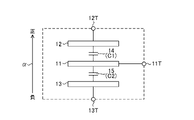
- FIG. 2 shows the configuration of the sensor element 10.
- the sensor element 10 comprises a fixed electrode 11 and movable electrodes 12 and 13 .
- Fixed electrode 11 and movable electrodes 12 and 13 form a capacitance pair consisting of variable capacitances 14 and 15 .
- a variable capacitance 14 is a capacitance formed between the fixed electrode 11 and the movable electrode 12
- a variable capacitance 15 is a capacitance formed between the fixed electrode 11 and the movable electrode 13 .
- the capacitance value of the variable capacitor 14 is referenced by the symbol "C1"
- the capacitance value of the variable capacitor 15 is referenced by the symbol "C2".
- the capacitance value may be hereinafter simply referred to as the capacitance value.
- the electrodes 11 to 13 are arranged side by side along an ⁇ -axis, which is a predetermined linear axis, and the fixed electrode 11 is positioned between the movable electrodes 12 and 13 .
- the sensor element 10 is provided with a terminal 11T connected to the fixed electrode 11, a terminal 12T connected to the movable electrode 12, and a terminal 13T connected to the movable electrode 13.
- the potentials of the electrodes 11, 12, 13 match the potentials of the terminals 11T, 12T, 13T, respectively.
- acceleration means acceleration applied to the acceleration sensor 1 and the sensor element 10 in the direction of the ⁇ -axis. Also, it is assumed that the movable electrode 12 is positioned on the positive side of the ⁇ -axis when viewed from the fixed electrode 11 and the movable electrode 13 is positioned on the negative side of the ⁇ -axis when viewed from the fixed electrode 11 .
- the capacitance values C1 and C2 have a common and predetermined reference capacitance value (although an error may exist).
- positive acceleration is applied to sensor element 10
- the distance between electrodes 11 and 12 increases while the distance between electrodes 11 and 13 decreases compared to when the acceleration is zero, resulting in a capacitance value C1 decreases from the reference capacitance value, while capacitance value C2 increases from the reference capacitance value.
- negative acceleration is applied to sensor element 10
- the distance between electrodes 11 and 12 decreases while the distance between electrodes 11 and 13 increases compared to when the acceleration is zero, resulting in a capacitance value C1 increases from the reference capacitance value, while capacitance value C2 decreases from the reference capacitance value.
- the capacitance values of the variable capacitors 14 and 15 provided in the sensor element 10 change in opposite directions according to the acceleration applied to the sensor element 10 in the ⁇ -axis direction.
- the drive circuit 20 supplies the sensor element 10 with a drive signal DRV IN for driving the sensor element 10 .
- the drive circuit 20 has a first drive signal generation circuit 21 , a second drive signal generation circuit 22 and an adder 23 .
- the first drive signal generation circuit 21 generates a drive signal drv1 and outputs a drive signal DRV1 based on the drive signal drv1.
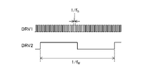
- the drive signals drv1 and DRV1 are square wave signals having a predetermined frequency f S .
- a drive signal DRV1 is generated by inputting the drive signal drv1 to a driver (buffer circuit).
- the second drive signal generation circuit 22 generates a drive signal drv2 and outputs a drive signal DRV2 based on the drive signal drv2.
- the drive signals drv2 and DRV2 are square wave signals having a predetermined frequency f M .
- a drive signal DRV2 is generated by inputting the drive signal drv2 to a driver (buffer circuit).
- Drive signals DRV1 and DRV2 are provided to adder 23 .
- the adder 23 modulates the drive signal DRV1 with the drive signal DRV2, and generates and outputs the modulated drive signal DRV1 as the drive signal DRV IN .
- the drive signal DRV IN corresponds to a signal obtained by mixing the drive signals DRV1 and DRV2, and has respective components of the drive signals DRV1 and DRV2.
- the frequency f M corresponds to the modulation frequency and may hereinafter be referred to as the modulation frequency f M .
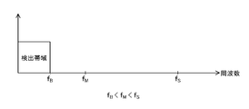
- FIG. 3 shows the relationship between the detection band of the acceleration sensor 1 and the frequencies f M and f S .
- FIG. 4 shows schematic waveforms of the drive signals DRV1 and DRV2.
- the detection band represents the frequency band of acceleration that should be detected by the acceleration sensor 1 and is determined by the specifications of the acceleration sensor 1 .
- the detection band is a band below a predetermined frequency f B .
- the acceleration sensor 1 is not required to detect acceleration at frequencies exceeding the detection band.
- Frequency f M is higher than frequency f B and frequency f S is higher than frequency f M .
- the upper limit frequency (the resonant frequency of the sensor element 10) is higher than the frequency f M and lower than the frequency f S . Therefore, the supply of the drive signal DRV1 to the sensor element 10 does not change the capacitance values C1 and C2, while the supply of the drive signal DRV2 to the sensor element 10 causes the capacitance values C1 and C2 to change.
- the drive signal DRV1 is a signal to be supplied to the sensor element 10 for detecting acceleration.
- DRV1′′ will be described as an example of the operation for detecting acceleration.
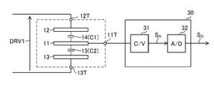
- a detection signal generation circuit 30 is provided with a C/V conversion circuit 31 and an A/D conversion circuit 32 as a configuration for generating a signal corresponding to acceleration.
- Drive signal DRV1 included in drive signal DRV IN is applied between terminals 12T and 13T.
- Terminal 11T is connected to C/V conversion circuit 31 .
- the drive signal DRV1 is a rectangular wave signal that alternately takes a high level and a low level.
- a potential higher than the voltage based on the amplitude of the drive signal DRV1 is applied to the terminal 12T when viewed from the terminal 13T.
- a higher potential is applied by a voltage based on the amplitude.
- the C/V conversion circuit 31 operates in synchronization with the drive signal DRV1, and determines the capacitance value C1 based on the voltage at the terminal 11T during the high level period of the drive signal DRV1 and the voltage at the terminal 11T during the low level period of the drive signal DRV1. and C2 to generate and output a detection signal S A according to the difference (C1-C2).
- the detection signal S A is an analog voltage signal having an analog value proportional to the difference (C1-C2) between the capacitance values C1 and C2. That is, the C/V conversion circuit 31 converts the difference (C1-C2) between the capacitance values C1 and C2 into an analog voltage signal.
- a known method can be used as a method for this conversion.
- the C/V conversion circuit 31 can be configured using a switched capacitor circuit, a sample hold circuit, and a differential amplifier circuit (none of which is shown).
- the A/D conversion circuit 32 converts the analog detection signal S A from the C/V conversion circuit 31 into a digital detection signal S D by A/D conversion (analog-digital conversion).
- A/D conversion analog-digital conversion
- the A/D conversion circuit 32 performs delta-sigma AD conversion and the sampling frequency of the A/D conversion circuit 32 is the frequency f S .
- Detected signal S D has a digital value representing the analog value of detected signal S A . That is, the detection signal S D has a digital value corresponding to the difference (C1-C2) between the capacitance values C1 and C2. More specifically, the detection signal S D has a digital value proportional to the difference (C1-C2). Therefore, the detection signal S D has a waveform corresponding to the amplitude and direction of acceleration.
- FIG. 6 shows an overview of the waveform of the detection signal S D when the acceleration sensor 1 is given an acceleration whose magnitude changes sinusoidally at 10 Hz.
- the C/V conversion circuit 31 by operating the C/V conversion circuit 31 in synchronization with the drive signal DRV1, signals (S A , S D ) corresponding to the acceleration can be obtained.
- the drive signal DRV1 is actually modulated by the drive signal DRV2. Therefore, the detection signal S D includes a signal component of the modulation frequency f M and fluctuates at the modulation frequency f M (see FIG. 7).
- the drive signal DRV2 is a rectangular wave signal that alternately takes a high level and a low level.
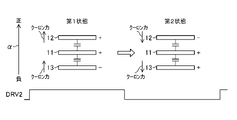
- the state of the sensor element 10 is alternately switched between the first state and the second state based on the drive signal DRV2 included in the drive signal DRV IN .
- the state of the sensor element 10 is set to the first state during the high level period of the drive signal DRV2. In the first state, each potential of the fixed electrode 11 and the movable electrode 12 increases by the amplitude of the drive signal DRV2 when viewed from the potential of the movable electrode 13 .
- the state of the sensor element 10 is set to the second state during the low level period of the drive signal DRV2.
- the potentials of the fixed electrode 11 and the movable electrode 13 are increased by the amplitude of the drive signal DRV2 when viewed from the potential of the movable electrode 12 .
- the second state is generated. , potential fluctuations of the electrodes 11 to 13 occur based on the components of the drive signal DRV1.
- the Coulomb force directed toward the positive side of the ⁇ -axis against the movable electrodes 12 and 13 based on the component of the drive signal DRV2 (repulsive force between the electrodes 11 and 12 and suction force) works.
- the Coulomb force directed toward the negative side of the ⁇ -axis against the movable electrodes 12 and 13 (attractive force between the electrodes 11 and 12 and repulsive force between the electrodes 11 and 13) is applied to the movable electrodes 12 and 13 based on the component of the drive signal DRV2. force) works.
- the detection signals S A and S D are signal components based on the Coulomb force (therefore, the modulation frequency signal component of f M ) is included.
- the acceleration signal generation circuit 40 performs predetermined low-pass processing on the detection signal S D to generate and output an acceleration signal S ACC corresponding to the acceleration.
- the acceleration signal SACC is a signal representing the amplitude and direction of acceleration.
- the acceleration signal generation circuit 40 has an LPF (low-pass filter) 41, and the LPF 41 performs the above-described low-pass processing. Since the detection signal S D is a digital signal, the LPF 41 is configured as a digital low-pass filter.
- the LPF 41 may be composed of a single-stage low-pass filter, or may be composed of a plurality of stages of low-pass filters.
- the cutoff frequency for low-pass processing by the LPF 41 is referenced by the symbol “f CO ".
- the LPF 41 passes signal components with frequencies below the cutoff frequency f CO , while attenuating signal components with frequencies higher than the cutoff frequency f CO .
- the attenuated detection signal S D is generated and output as the acceleration signal S ACC .
- the band B LPF represents the band extracted by the LPF 41 (that is, the band below the cutoff frequency f CO ).
- the cutoff frequency f CO is set to the frequency f B (see FIG. 3; eg, 100 Hz) which is the upper limit of the detection band, or is set to a frequency higher than the frequency f B by a predetermined frequency (eg, 120 Hz).
- a predetermined frequency eg, 120 Hz.
- the acceleration signal S ACC includes the signal component of the acceleration within the detection band with sufficiently high signal strength. If the specifications of the acceleration sensor 1 are satisfied, a frequency (for example, 90 Hz) lower than the frequency f B by a predetermined frequency may be set as the cutoff frequency f CO .
- the modulation frequency f M is higher than the cutoff frequency f CO , and the signal component of the modulation frequency f M in the detection signal S D is sufficiently attenuated by low-pass processing in the LPF 41 . That is, it is possible to extract the acceleration signal S ACC having only the actual acceleration component from which the modulation component has been removed.
- the modulation component extraction circuit 50 extracts the signal component of the modulation frequency f M in the detection signal S D by performing a predetermined band-pass processing on the detection signal S D , and uses the extracted signal as the modulation component extraction signal S M . Generate and output.
- the modulation component extracting circuit 50 has a BPF (band pass filter) 51, and the BPF 51 performs the band pass processing. Since the detection signal S D is a digital signal, the BPF 51 is configured as a digital bandpass filter.
- a predetermined passband is defined in the bandpass process.
- the modulation frequency f M is a frequency within the passband.
- the band B BPF represents the band extracted by the BPF 51 (that is, the pass band of the BPF 51).
- FIG. 9 schematically shows the spectrum of the modulated component extraction signal S M .
- the BPF 51 passes signal components with frequencies within the passband and attenuates signal components with frequencies outside the passband, thereby reducing the modulation frequency f M in the detection signal S D .
- Passing signal components at frequencies within the passband may include enhancing (amplifying) signal components at frequencies within the passband.
- FIG. 10 schematically shows an example of the signal waveform of the modulated component extraction signal S M .
- the BPF 51 is designed so that the signal component of the modulation frequency f M in the modulated component extraction signal S M has a sufficiently higher signal strength than the signal component outside the passband.
- the signal components below the frequency f B and the signal components with the frequency f S have sufficiently low signal strength in the modulated component extraction signal S M (these signal components are substantially not included in the modulated component extraction signal S M ).
- the lower limit frequency of the passband should be set sufficiently higher than the frequency f B and the cutoff frequency f CO of the LPF 41
- the upper limit frequency of the passband should be set sufficiently lower than the frequency f S .
- the diagnostic circuit 60 diagnoses the state of the sensor element 10 based on the modulated component extraction signal SM, and generates and outputs a diagnostic signal S DIAG indicating the diagnostic result.
- the diagnostic signal S DIAG is a signal relating to the state of the sensor element 10 (a signal representing the state of the sensor element 10 ), more specifically, a signal representing the presence or absence of an abnormality in the sensor element 10 . In other words, the presence or absence of abnormality in the sensor element 10 is determined in the diagnosis by the diagnostic circuit 60 .
- the diagnostic signal S DIAG is a binary signal having a value of "0" or "1".
- the diagnostic signal S DIAG having a value of "1" functions as a signal indicating that the sensor element 10 is abnormal.
- a signal indicating that the sensor element 10 has an abnormality can also be expressed as a signal suggesting the possibility that the sensor element 10 has an abnormality.
- the diagnostic signal S DIAG having a value of "0" functions as a signal indicating that the sensor element 10 is normal.
- a signal indicating that the sensor element 10 is normal can also be expressed as a signal indicating that the sensor element 10 is normal.
- the control circuit 70 forms a signal processing circuit together with the drive circuit 20, the detection signal generation circuit 30, the acceleration signal generation circuit 40, the modulation component extraction circuit 50 and the diagnosis circuit 60.
- the control circuit 70 has a function of centrally controlling the operation of each part in the signal processing circuit.
- the control circuit 70 has a function of transmitting the acceleration signal S ACC itself or a signal based on the acceleration signal S ACC to an external device (not shown) connected to the acceleration sensor 1 .
- the acceleration signal S ACC may be transmitted to the external device while being updated at a constant period (for example, the period of the reciprocal of 100 Hz).
- the acceleration signal generation circuit 40 itself may transmit the acceleration signal S ACC to the external device without relying on the control circuit 70 .
- the control circuit 70 also has a function of transmitting the diagnostic signal S DIAG itself or a signal based on the diagnostic signal S DIAG to the external device.
- the diagnostic circuit 60 itself may transmit the diagnostic signal S DIAG to the external device without relying on the control circuit 70 .
- Control circuit 70 may also have other functions, which will be described later.
- the first embodiment includes the following examples EX1_A and EX1_B.
- Examples EX1_A and EX1_B detailed operation examples or configuration examples of the diagnostic circuit 60 will be described.
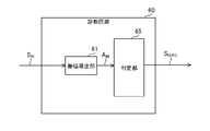
- FIG. 11 shows the internal configuration of the diagnostic circuit 60 according to the embodiment EX1_A.
- a diagnostic circuit 60 according to Example EX1_A includes an amplitude derivation unit 61 and a determination unit 65 .
- An amplitude derivation unit 61 derives the amplitude A M of the modulated component extraction signal S M .
- a determination unit 65 generates a diagnostic signal S DIAG based on the derived amplitude AM .
- the generated diagnostic signal S DIAG is output from diagnostic circuit 60 .
- the determination unit 65 generates a diagnostic signal S DIAG corresponding to whether or not the amplitude AM of the modulated component extraction signal S M deviates from a predetermined amplitude normal range.
- the determination unit 65 generates a diagnostic signal S DIAG having a value of "1" when the amplitude AM is out of the predetermined normal amplitude range, and generates a diagnostic signal S DIAG having a value of "1” when the amplitude AM is within the predetermined normal amplitude range. generates a diagnostic signal S DIAG having a value of "0". If the sensor element 10 is normal, the movable electrodes 12 and 13 should mechanically oscillate at the modulation frequency f M with proper amplitude in response to the supply of the drive signal DRV2. This is because AM is expected to fall within the normal amplitude range.
- the normal amplitude range may be a range from a predetermined lower limit amplitude A TH#L to a predetermined upper limit amplitude A TH#H (where "0 ⁇ A TH#L ⁇ A TH#H " holds true).
- a TH#L ⁇ A M ⁇ A TH#H the value of the diagnostic signal S DIAG is set to "0”
- the normal amplitude range may be a range defined only by the lower limit amplitude A TH#L .
- the diagnostic signal S DIAG is set to "0"
- the control circuit 70 latches the value and transmits a predetermined notification signal to an external device (not shown) connected to the acceleration sensor 1. (The same applies to Example EX1_B described later and other embodiments described later).
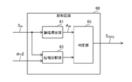
- FIG. 12 shows the internal configuration of the diagnostic circuit 60 according to the embodiment EX1_B.
- a diagnostic circuit 60 according to Example EX1_B includes an amplitude derivation unit 61 and a determination unit 65 and further includes a phase comparison unit 63 .
- the function of the amplitude derivation unit 61 is as described in the embodiment EX1_A.
- the modulated component extraction signal SM and the drive signal drv2 are input to the phase comparator 63 .
- the phase comparator 63 compares the phase of the modulated component extraction signal S M and the phase of the drive signal drv2 to derive the phase difference ⁇ between the phase of the modulated component extraction signal S M and the phase of the drive signal drv2.
- the phase difference ⁇ represents the amount of delay in the phase of the modulated component extraction signal SM with respect to the phase of the drive signal drv2 .
- the drive signal drv2 is the source signal of the drive signal DRV2 (see FIG. 1).
- the phase of the drive signal drv2 and the phase of the drive signal DRV2 are substantially the same, and here, it is considered that there is no difference between the phase of the drive signal drv2 and the phase of the drive signal DRV2.
- the phase difference ⁇ represents the phase difference between the phase of the modulated component extraction signal S M and the phase of the drive signal DRV2.
- a phase comparison between signals S M and drv2 is equivalent to a phase comparison between signals S M and DRV2.
- the determination unit 65 according to the embodiment EX1_B generates the diagnosis signal S DIAG based on the amplitude A M derived by the amplitude derivation unit 51 and the phase difference ⁇ derived by the phase comparison unit 63 .
- the generated diagnostic signal S DIAG is output from diagnostic circuit 60 .
- the determination unit 65 makes a diagnosis according to whether or not the phase difference ⁇ satisfies a predetermined phase matching condition and whether or not the amplitude AM of the modulated component extraction signal S M deviates from a predetermined amplitude normal range. Generates signal S DIAG .
- the movable electrodes 12 and 13 mechanically vibrate at the modulation frequency f M in synchronization with the drive signal DRV2 . Therefore, there should be a certain relationship between the phase of the driving signal drv2).
- the phase matching condition is determined based on this fixed relationship. The phase matching condition is satisfied when the phase difference ⁇ is within a predetermined phase matching range, and the phase matching condition is not satisfied when the phase difference ⁇ deviates from the predetermined phase matching range.
- the signal component of the acceleration will be included in the modulated component extraction signal S M .
- the sensor element 10 cannot be correctly diagnosed based on the drive signal DRV2.
- the determination unit 65 determines whether the phase difference ⁇ (relationship between two phases to be compared) satisfies a predetermined phase matching condition and the amplitude A M of the modulated component extraction signal S M is within a predetermined amplitude normal range. When deviating, it generates a diagnostic signal S DIAG having a value of "1". The determination unit 65 outputs a diagnostic signal S DIAG having a value of “0” when the phase difference ⁇ satisfies a predetermined phase matching condition and the amplitude A M of the modulated component extraction signal S M falls within a predetermined amplitude normal range. to generate
- the determination unit 65 sets the value of the diagnostic signal S DIAG to “0” regardless of the relationship between the amplitude AM and the amplitude normal range.
- the phase difference ⁇ no longer satisfies the phase matching condition.
- phase difference ⁇ (relationship between two phases to be compared) does not satisfy a predetermined phase matching condition, the control circuit 70 may change the modulation frequency f M through the control of the drive circuit 20. good. I will add an explanation for this.
- the drive circuit 20 is configured so that the modulation frequency f M can be switched between a plurality of frequencies including frequencies f M1 and f M2 (f M1 ⁇ f M2 ). No matter which one of the plurality of frequencies here is set as the modulation frequency f M , the frequency f M satisfies all the characteristics described above (thus satisfying, for example, “f B ⁇ f M ⁇ f S ”).
- the modulation frequency f M is set to the frequency f M1 . That is, the initial value of the modulation frequency f M is "f M1 ".
- the sensor element 10 is driven. This makes it possible to diagnose the sensor element 10 even when the acceleration sensor 1 is subjected to acceleration near the modulation frequency f M1 .
- the passband of the BPF 51 is switched. At this time, the width of the pass band of the BPF 51 is preferably smaller than the absolute value
- the acceleration sensor 1 may be a sensor capable of individually detecting acceleration in a plurality of mutually different axial directions.
- FIG. 13 is a configuration diagram of an acceleration sensor 1 configured as a triaxial acceleration sensor (hereinafter referred to as triaxial acceleration sensor 1).
- the three-axis acceleration sensor 1 can individually detect acceleration in the X-axis, Y-axis, and Z-axis directions. Acceleration in the X-axis, Y-axis, and Z-axis directions indicates acceleration in the X-axis, Y-axis, and Z-axis directions, respectively, applied to the three-axis acceleration sensor 1 .
- the X-axis, Y-axis and Z-axis are three axes orthogonal to each other.
- the three-axis acceleration sensor 1 has three functional blocks BL each having a sensor element 10 and a signal processing circuit SPC.
- the three functional blocks BL have the same configuration. However, of the three functional blocks BL, the ⁇ -axis (see FIG. 2) for the sensor element 10 in the first functional block BL is the X-axis, and the ⁇ -axis for the sensor element 10 in the second functional block BL is The Y-axis and the ⁇ -axis for the sensor element 10 in the third functional block BL are the Z-axis.
- the signal processing circuit SPC includes the drive circuit 20, the detection signal generation circuit 30, the acceleration signal generation circuit 40, the modulation component extraction circuit 50, the diagnosis circuit 60, and the control circuit 70 described in the first embodiment. .
- the sensor element 10 and circuits 20 to 70 operate as described in the first embodiment.
- the accelerations in the X-axis, Y-axis, and Z-axis directions can be detected separately (that is, the acceleration signal S ACC in the X-axis direction, the acceleration signal S ACC in the Y-axis direction, and the acceleration signal S ACC in the Z-axis direction can be detected. can be generated) and diagnosis of the sensor element 10 can be performed on a sensor element 10 by sensor element 10 basis.
- the signal processing circuit SPC of each functional block BL is not provided with the control circuit 70, and the three-axis acceleration sensor 1 is provided with a single control circuit (not shown) shared by the three functional blocks BL. Also good.
- a third embodiment of the present disclosure will be described.
- modification techniques, application techniques, supplementary matters, etc. applicable to the first or second embodiment will be described.
- the acceleration sensor 1 described in the third embodiment refers to the acceleration sensor 1 described in the first embodiment or the triaxial acceleration sensor 1 described in the second embodiment.
- the acceleration sensor 1 can be mounted on any device.
- the acceleration sensor 1 can be mounted on a vehicle such as an automobile.
- the external device connected to the acceleration sensor 1 is a host system (ECU (Electronic Control Unit), etc.) mounted on the vehicle.
- ECU Electronic Control Unit
- a self-diagnostic function is often required for automotive components.
- the following first and second reference examples are conceivable as implementation examples of self-diagnosis.
- self-diagnosis is performed using the Coulomb force, but the normal detection operation of acceleration is interrupted when self-diagnosis is performed. In the first reference example, normal detection operation cannot be performed during self-diagnosis.
- a sensor element dedicated to self-diagnosis is added, and self-diagnosis is performed using the sensor element dedicated to self-diagnosis.
- a total of four sensor elements are required.
- the cost increases due to the addition of the sensor element.
- the acceleration sensor 1 of the first or second embodiment can diagnose the sensor element 10 while performing a normal acceleration detection operation. Moreover, the sensor element dedicated to self-diagnosis as shown in the second reference example is unnecessary. Therefore, the diagnosis of the sensor element 10 can be performed at low cost without interrupting the normal detection operation. This diagnosis makes it possible to improve the reliability of the system including the acceleration sensor 1 .
- the AD conversion method in the A/D conversion circuit 32 may be arbitrary.
- the acceleration sensor 1 may perform each signal processing in the form of an analog signal without performing AD conversion.
- the A /D conversion circuit 32 may be removed from the detection signal generation circuit 30 of FIG.
- the LPF 41 and BPF 51 are composed of analog circuits, and an analog acceleration signal S ACC and an analog modulation component extraction signal SM are generated from the analog detection signal S A .
- Each circuit element constituting the acceleration sensor 1 is formed in the form of a semiconductor integrated circuit, and a semiconductor device is constructed by enclosing the semiconductor integrated circuit in a housing (package) made of resin.
- the semiconductor chip on which the sensor element 10 is formed and the semiconductor chip on which the other circuits (including the circuits 20 to 70) are formed may be separate, and these semiconductor chips are enclosed in a common housing.
- a semiconductor device may be configured in this manner.
- a modified configuration may be employed in which the diagnosis circuit 60 is not included in the semiconductor device.
- an external device such as a microcomputer is connected to the semiconductor device, and the diagnostic circuit 60 is provided in the external device.
- a diagnostic signal S DIAG may be generated by a diagnostic circuit 60 in the external device by inputting the modulated component extraction signal S M output from the modulated component extraction circuit 50 in the semiconductor device to the external device.
- An acceleration sensor includes a sensor element (10) having a first variable capacitor and a second variable capacitor whose capacitance values change in opposite directions according to acceleration;
- a first drive signal (DRV1) to be supplied to the sensor element for detecting acceleration is modulated by a second drive signal (DRV2) having a predetermined modulation frequency (f M ), and the first drive signal and the a drive circuit (20) configured to be able to supply a signal having each component of a second drive signal to the sensor element;
- a detection signal generation circuit (30) capable of generating detection signals (S A , S D ) corresponding to the difference in capacitance value; and an acceleration signal generation circuit (40) configured to generate an acceleration signal (S ACC ), and a modulation component extraction signal (S M ) can be generated by extracting the signal component of the modulation frequency in the detection signal.
- a modulated component extraction circuit (50) configured (first configuration).
- the sensor element can be diagnosed without interrupting the acceleration signal generation operation (normal detection operation) and without separately providing a sensor element dedicated to diagnosis (thus, at low cost).
- the modulation frequency (f M ) is lower than the frequency (f S ) of the first drive signal and lower than the cutoff frequency (f CO ) of the low-pass processing.
- a high configuration (second configuration) may also be used.
- the modulation frequency is higher than the cutoff frequency of the low-pass processing, inclusion of the modulation frequency component in the acceleration signal is suppressed. That is, the influence of the modulation by the second drive signal on the acceleration signal generation operation (normal detection operation) is suppressed. Also, the modulation frequency is set lower than the frequency of the first drive signal so that the capacitance values of the first variable capacitor and the second variable capacitor can be varied by the second drive signal.
- each capacitance value of the first variable capacitor and the second variable capacitor is modulated by supplying the component of the second drive signal to the sensor element.
- a configuration (third configuration) that varies with frequency may be used.
- the acceleration sensor according to any one of the first to third configurations, further comprising a diagnostic circuit (60) capable of generating a diagnostic signal (S DIAG ) regarding the state of the sensor element based on the modulated component extraction signal.
- a diagnostic circuit 60
- S DIAG diagnostic signal
- the diagnostic circuit may be configured to generate the diagnostic signal based on the amplitude of the modulated component extraction signal (fifth configuration).
- the diagnostic circuit is configured to generate the diagnostic signal according to whether or not the amplitude of the modulated component extraction signal deviates from a predetermined range (sixth configuration).
- the diagnostic circuit can generate, as the diagnostic signal, a signal indicating that the sensor element has an abnormality when the amplitude of the modulated component extraction signal deviates from a predetermined range. (seventh configuration).
- the diagnostic circuit is configured to generate the diagnostic signal according to the amplitude of the modulated component extraction signal and each phase of the modulated component extraction signal and the second drive signal.
- a configuration (eighth configuration) may be used.
- the diagnostic circuit satisfies a predetermined condition that the phase of the modulated component extraction signal and the phase of the second drive signal satisfy a predetermined condition, and that the amplitude of the modulated component extraction signal is a predetermined
- the configuration may be configured such that a signal indicating that there is an abnormality in the sensor element can be generated as the diagnostic signal when the sensor element is out of range.
- a control circuit configured to be able to change the modulation frequency when the relationship between the phase of the modulated component extraction signal and the phase of the second drive signal does not satisfy the predetermined condition.
- a configuration (tenth configuration) further provided may be employed.
- the modulation frequency is a certain specific frequency
- changing the modulation frequency from the specific frequency can Diagnosis can be made.
- acceleration sensor 10 sensor element 11 fixed electrode 12, 13 movable electrode 14, 15 variable capacitor 20 drive circuit 30 detection signal generation circuit 31 C/V conversion circuit 32 A/D conversion circuit 40 acceleration signal generation circuit 41 LPF 50 modulation component extraction circuit 51 BPF 60 diagnostic circuit 61 amplitude derivation unit 63 phase comparison unit 65 determination unit 70 control circuit
Abstract
A sensor element includes first and second variable capacitances having capacitance values that vary in mutually opposite directions in accordance with acceleration. A drive circuit uses a second drive signal having a predetermined modulation frequency to modulate a first drive signal that is to be supplied to the sensor element in order to detect the acceleration, and supplies a signal having each component of the first and second drive signals to the sensor element. A detection signal generating circuit generates a detection signal corresponding to a difference between the capacitance values of the first and second variable capacitances. An acceleration signal generating circuit generates an acceleration signal by subjecting the detection signal to low-pass processing. A modulation component extracting circuit generates a modulation component extracted signal by extracting the signal component having the modulation frequency from the detection signal.
Description
本開示は、加速度センサに関する。
The present disclosure relates to acceleration sensors.
加速度センサの一種として、MEMS(Micro Electro Mechanical System)による静電容量型の加速度センサがある。
As a type of acceleration sensor, there is a capacitive acceleration sensor based on MEMS (Micro Electro Mechanical System).
静電容量型の加速度センサにおいて、正しく加速度を検出できる状態にあるか否かを診断可能な構成が要求されることが多い。このような診断を、加速度の検出動作を中断することなく且つ簡素な構成で実現することが望まれる。
In many cases, capacitance-type acceleration sensors are required to have a configuration that can diagnose whether or not they are in a state where acceleration can be detected correctly. It is desired to realize such a diagnosis with a simple configuration without interrupting the acceleration detection operation.
本開示は、加速度の検出動作を中断することなく且つ簡素な構成での診断を可能とする加速度センサを提供することを目的とする。
An object of the present disclosure is to provide an acceleration sensor that enables diagnosis with a simple configuration without interrupting the acceleration detection operation.
本開示に係る加速度センサは、加速度に応じて静電容量値が互いに逆向きに変化する第1可変容量及び第2可変容量を有するセンサ素子と、前記加速度を検出するために前記センサ素子に供給すべき第1駆動信号を所定の変調周波数を有する第2駆動信号にて変調し、前記第1駆動信号及び前記第2駆動信号の各成分を有する信号を前記センサ素子に供給可能に構成された駆動回路と、前記センサ素子に接続され、前記第1可変容量及び前記第2可変容量間の静電容量値の差に応じた検出信号を生成可能に構成された検出信号生成回路と、前記検出信号に対して低域通過処理を施すことで前記加速度に応じた加速度信号を生成可能に構成された加速度信号生成回路と、前記検出信号における前記変調周波数の信号成分を抽出することで変調成分抽出信号を生成可能に構成された変調成分抽出回路と、を備える。
An acceleration sensor according to the present disclosure includes a sensor element having a first variable capacitor and a second variable capacitor whose capacitance values change in opposite directions according to acceleration, and a sensor element for detecting the acceleration. A first drive signal to be detected is modulated by a second drive signal having a predetermined modulation frequency, and a signal having each component of the first drive signal and the second drive signal can be supplied to the sensor element. a drive circuit; a detection signal generation circuit connected to the sensor element and configured to generate a detection signal corresponding to a difference in capacitance value between the first variable capacitor and the second variable capacitor; An acceleration signal generation circuit configured to generate an acceleration signal corresponding to the acceleration by performing low-pass processing on the signal, and a modulation component extraction by extracting a signal component of the modulation frequency in the detection signal. a modulation component extraction circuit configured to generate a signal.
本開示によれば、加速度の検出動作を中断することなく且つ簡素な構成での診断を可能とする加速度センサを提供することが可能となる。
According to the present disclosure, it is possible to provide an acceleration sensor that enables diagnosis with a simple configuration without interrupting the acceleration detection operation.
以下、本開示の実施形態の例を、図面を参照して具体的に説明する。参照される各図において、同一の部分には同一の符号を付し、同一の部分に関する重複する説明を原則として省略する。尚、本明細書では、記述の簡略化上、情報、信号、物理量、素子又は部位等を参照する記号又は符号を記すことによって、該記号又は符号に対応する情報、信号、物理量、素子又は部位等の名称を省略又は略記することがある。例えば、後述の“30”によって参照される検出信号生成回路は(図1参照)、検出信号生成回路30と表記されることもあるし、生成回路30又は単に回路30と略記されることもあり得るが、それらは全て同じものを指す。
Hereinafter, examples of embodiments of the present disclosure will be specifically described with reference to the drawings. In each figure referred to, the same parts are denoted by the same reference numerals, and redundant descriptions of the same parts are omitted in principle. In this specification, for simplification of description, by describing symbols or codes that refer to information, signals, physical quantities, elements or parts, etc., information, signals, physical quantities, elements or parts corresponding to the symbols or codes are used. etc. may be omitted or abbreviated. For example, the detection signal generation circuit referenced by "30" (see FIG. 1) may be referred to as detection signal generation circuit 30, or may be abbreviated as generation circuit 30 or simply circuit 30. but they all refer to the same thing.
まず、本開示の実施形態の記述にて用いられる幾つかの用語について説明を設ける。レベルとは電位のレベルを指し、任意の注目した信号又は電圧についてハイレベルはローレベルよりも高い電位を有する。任意の注目した信号又は電圧について、信号又は電圧がハイレベルにあるとは厳密には信号又は電圧のレベルがハイレベルにあることを意味し、信号又は電圧がローレベルにあるとは厳密には信号又は電圧のレベルがローレベルにあることを意味する。ハイレベル又はローレベルの信号レベルをとる任意の信号について、当該信号のレベルがハイレベルとなる期間をハイレベル期間と称し、当該信号のレベルがローレベルとなる期間をローレベル期間と称する。ハイレベル又はローレベルの電圧レベルをとる任意の電圧についても同様である。任意の回路素子、配線(ライン)、ノードなど、回路を形成する複数の部位間についての接続とは、特に記述なき限り、電気的な接続を指すと解して良い。
First, some terms used in the description of the embodiments of the present disclosure will be explained. Level refers to the level of potential, with a high level having a higher potential than a low level for any given signal or voltage of interest. For any signal or voltage of interest, strictly speaking that the signal or voltage is at a high level means that the signal or voltage is at a high level, and strictly speaking that the signal or voltage is at a low level. It means that the signal or voltage level is at low level. For any signal that takes a signal level of high level or low level, the period in which the level of the signal is high is called a high level period, and the period in which the level of the signal is low is called a low level period. The same is true for any voltage that takes a high or low voltage level. Connections between a plurality of parts forming a circuit, such as arbitrary circuit elements, wirings (lines), nodes, etc., may be understood to refer to electrical connections unless otherwise specified.
<<第1実施形態>>
本開示の第1実施形態を説明する。図1に第1実施形態に係る加速度センサ1の構成図を示す。加速度センサ1は、センサ素子10、駆動回路20、検出信号生成回路30、加速度信号生成回路40、変調成分抽出回路50、診断回路60及び制御回路70を備える。 <<First Embodiment>>
A first embodiment of the present disclosure will be described. FIG. 1 shows a configuration diagram of anacceleration sensor 1 according to the first embodiment. The acceleration sensor 1 includes a sensor element 10, a drive circuit 20, a detection signal generation circuit 30, an acceleration signal generation circuit 40, a modulation component extraction circuit 50, a diagnostic circuit 60 and a control circuit .
本開示の第1実施形態を説明する。図1に第1実施形態に係る加速度センサ1の構成図を示す。加速度センサ1は、センサ素子10、駆動回路20、検出信号生成回路30、加速度信号生成回路40、変調成分抽出回路50、診断回路60及び制御回路70を備える。 <<First Embodiment>>
A first embodiment of the present disclosure will be described. FIG. 1 shows a configuration diagram of an
センサ素子10はMEMS(Micro Electro Mechanical System)による静電容量型センサである。図2にセンサ素子10の構成を示す。センサ素子10は固定電極11並びに可動電極12及び13を備える。固定電極11並びに可動電極12及び13により、可変容量14及び15から成る容量対が形成される。可変容量14は固定電極11及び可動電極12間に形成される容量であり、可変容量15は固定電極11及び可動電極13間に形成される容量である。可変容量14の静電容量値を記号“C1”にて参照し、可変容量15の静電容量値を記号“C2”にて参照する。静電容量値を、以下、単に容量値と称することがある。電極11~13は所定の直線軸であるα軸に沿って並べて配置され、可動電極12と可動電極13との間に固定電極11が位置する。センサ素子10には、固定電極11に接続された端子11T、可動電極12に接続された端子12T、及び、可動電極13に接続された端子13Tが設けられる。電極11、12、13の電位は、夫々、端子11T、12T、13Tの電位と一致する。
The sensor element 10 is a capacitive sensor based on MEMS (Micro Electro Mechanical System). FIG. 2 shows the configuration of the sensor element 10. As shown in FIG. The sensor element 10 comprises a fixed electrode 11 and movable electrodes 12 and 13 . Fixed electrode 11 and movable electrodes 12 and 13 form a capacitance pair consisting of variable capacitances 14 and 15 . A variable capacitance 14 is a capacitance formed between the fixed electrode 11 and the movable electrode 12 , and a variable capacitance 15 is a capacitance formed between the fixed electrode 11 and the movable electrode 13 . The capacitance value of the variable capacitor 14 is referenced by the symbol "C1", and the capacitance value of the variable capacitor 15 is referenced by the symbol "C2". The capacitance value may be hereinafter simply referred to as the capacitance value. The electrodes 11 to 13 are arranged side by side along an α-axis, which is a predetermined linear axis, and the fixed electrode 11 is positioned between the movable electrodes 12 and 13 . The sensor element 10 is provided with a terminal 11T connected to the fixed electrode 11, a terminal 12T connected to the movable electrode 12, and a terminal 13T connected to the movable electrode 13. FIG. The potentials of the electrodes 11, 12, 13 match the potentials of the terminals 11T, 12T, 13T, respectively.
加速度センサ1において、固定電極11の位置は固定される一方、可動電極12及び13の各位置は加速度に応じ、固定電極11の位置を基準にα軸の方向に変動する。尚、本実施形態において、加速度とは、α軸の方向において加速度センサ1及びセンサ素子10に加わる加速度を意味する。また、固定電極11から見てα軸の正側に可動電極12が位置し、固定電極11から見てα軸の負側に可動電極13が位置しているものとする。
In the acceleration sensor 1, the position of the fixed electrode 11 is fixed, while the positions of the movable electrodes 12 and 13 change in the direction of the α-axis based on the position of the fixed electrode 11 according to the acceleration. In this embodiment, acceleration means acceleration applied to the acceleration sensor 1 and the sensor element 10 in the direction of the α-axis. Also, it is assumed that the movable electrode 12 is positioned on the positive side of the α-axis when viewed from the fixed electrode 11 and the movable electrode 13 is positioned on the negative side of the α-axis when viewed from the fixed electrode 11 .
加速度がゼロであるとき、容量値C1及びC2は共通且つ所定の基準容量値を有する(但し誤差は存在し得る)。正の加速度がセンサ素子10に加わっているとき、加速度がゼロであるときと比べて、電極11及び12間の距離が増大する一方で電極11及び13間の距離が減少し、結果、容量値C1は基準容量値より減少する一方で容量値C2は基準容量値より増大する。負の加速度がセンサ素子10に加わっているとき、加速度がゼロであるときと比べて、電極11及び12間の距離が減少する一方で電極11及び13間の距離が増大し、結果、容量値C1は基準容量値より増大する一方で容量値C2は基準容量値より減少する。このように、センサ素子10に設けられる可変容量14及び15の静電容量値は、センサ素子10に加わるα軸方向の加速度に応じて互いに逆向きに変化する。
When the acceleration is zero, the capacitance values C1 and C2 have a common and predetermined reference capacitance value (although an error may exist). When positive acceleration is applied to sensor element 10, the distance between electrodes 11 and 12 increases while the distance between electrodes 11 and 13 decreases compared to when the acceleration is zero, resulting in a capacitance value C1 decreases from the reference capacitance value, while capacitance value C2 increases from the reference capacitance value. When negative acceleration is applied to sensor element 10, the distance between electrodes 11 and 12 decreases while the distance between electrodes 11 and 13 increases compared to when the acceleration is zero, resulting in a capacitance value C1 increases from the reference capacitance value, while capacitance value C2 decreases from the reference capacitance value. Thus, the capacitance values of the variable capacitors 14 and 15 provided in the sensor element 10 change in opposite directions according to the acceleration applied to the sensor element 10 in the α-axis direction.
駆動回路20は、センサ素子10を駆動するための駆動信号DRVINをセンサ素子10に供給する。図1の構成において、駆動回路20は、第1駆動信号生成回路21、第2駆動信号生成回路22及び加算器23を有する。
The drive circuit 20 supplies the sensor element 10 with a drive signal DRV IN for driving the sensor element 10 . In the configuration of FIG. 1 , the drive circuit 20 has a first drive signal generation circuit 21 , a second drive signal generation circuit 22 and an adder 23 .
第1駆動信号生成回路21は、駆動信号drv1を生成し、駆動信号drv1に基づく駆動信号DRV1を出力する。駆動信号drv1及びDRV1は所定の周波数fSを有する矩形波信号である。駆動信号drv1をドライバ(バッファ回路)に入力することで駆動信号DRV1が生成される。第2駆動信号生成回路22は、駆動信号drv2を生成し、駆動信号drv2に基づく駆動信号DRV2を出力する。駆動信号drv2及びDRV2は所定の周波数fMを有する矩形波信号である。駆動信号drv2をドライバ(バッファ回路)に入力することで駆動信号DRV2が生成される。駆動信号DRV1及びDRV2は加算器23に与えられる。加算器23は駆動信号DRV1を駆動信号DRV2にて変調し、変調された駆動信号DRV1を駆動信号DRVINとして生成及び出力する。即ち、駆動信号DRVINは、駆動信号DRV1及びDRV2を混合した信号に相当し、駆動信号DRV1及びDRV2の各成分を有する。周波数fMは変調周波数に相当し、以下、変調周波数fMと称され得る。
The first drive signal generation circuit 21 generates a drive signal drv1 and outputs a drive signal DRV1 based on the drive signal drv1. The drive signals drv1 and DRV1 are square wave signals having a predetermined frequency f S . A drive signal DRV1 is generated by inputting the drive signal drv1 to a driver (buffer circuit). The second drive signal generation circuit 22 generates a drive signal drv2 and outputs a drive signal DRV2 based on the drive signal drv2. The drive signals drv2 and DRV2 are square wave signals having a predetermined frequency f M . A drive signal DRV2 is generated by inputting the drive signal drv2 to a driver (buffer circuit). Drive signals DRV1 and DRV2 are provided to adder 23 . The adder 23 modulates the drive signal DRV1 with the drive signal DRV2, and generates and outputs the modulated drive signal DRV1 as the drive signal DRV IN . That is, the drive signal DRV IN corresponds to a signal obtained by mixing the drive signals DRV1 and DRV2, and has respective components of the drive signals DRV1 and DRV2. The frequency f M corresponds to the modulation frequency and may hereinafter be referred to as the modulation frequency f M .
図3に加速度センサ1における検出帯域と周波数fM及びfSとの関係を示す。図4に駆動信号DRV1及びDRV2の概略波形を示す。検出帯域とは、加速度センサ1が検出すべき加速度の周波数帯域を表し、加速度センサ1の仕様にて定められる。検出帯域は所定の周波数fB以下の帯域である。検出帯域を超える周波数の加速度の検出能力は加速度センサ1に求められていない。周波数fMは周波数fBよりも高く、周波数fSは周波数fMよりも更に高い。
FIG. 3 shows the relationship between the detection band of the acceleration sensor 1 and the frequencies f M and f S . FIG. 4 shows schematic waveforms of the drive signals DRV1 and DRV2. The detection band represents the frequency band of acceleration that should be detected by the acceleration sensor 1 and is determined by the specifications of the acceleration sensor 1 . The detection band is a band below a predetermined frequency f B . The acceleration sensor 1 is not required to detect acceleration at frequencies exceeding the detection band. Frequency f M is higher than frequency f B and frequency f S is higher than frequency f M .
また、機械的な応答限界により、センサ素子10において、電極11及び12間の距離並びに電極11及び13間の距離の変動の周波数には上限がある。その上限の周波数(センサ素子10の共振周波数)は周波数fMより高く且つ周波数fSより低い。故に、センサ素子10への駆動信号DRV1の供給によっては容量値C1及びC2は変化せず、一方においてセンサ素子10への駆動信号DRV2の供給は容量値C1及びC2に変化をもたらす。
There is also an upper limit to the frequency of variation of the distance between electrodes 11 and 12 and the distance between electrodes 11 and 13 in sensor element 10 due to mechanical response limitations. The upper limit frequency (the resonant frequency of the sensor element 10) is higher than the frequency f M and lower than the frequency f S . Therefore, the supply of the drive signal DRV1 to the sensor element 10 does not change the capacitance values C1 and C2, while the supply of the drive signal DRV2 to the sensor element 10 causes the capacitance values C1 and C2 to change.
駆動信号DRV1及びDRV2の内、駆動信号DRV1は加速度を検出するためにセンサ素子10に供給されるべき信号であり、説明の便宜上、まず駆動信号DRV2の存在を無視して(即ち“DRVIN=DRV1”であると仮定して)加速度を検出するための動作の例を説明する。図5を参照する。加速度に応じた信号を生成するための構成として、検出信号生成回路30にC/V変換回路31及びA/D変換回路32が設けられる。
Of the drive signals DRV1 and DRV2 , the drive signal DRV1 is a signal to be supplied to the sensor element 10 for detecting acceleration. DRV1″) will be described as an example of the operation for detecting acceleration. Please refer to FIG. A detection signal generation circuit 30 is provided with a C/V conversion circuit 31 and an A/D conversion circuit 32 as a configuration for generating a signal corresponding to acceleration.
駆動信号DRVINに含まれる駆動信号DRV1は端子12T及び13T間に印加される。端子11TはC/V変換回路31に接続される。駆動信号DRV1はハイレベル又はローレベルを交互にとる矩形波信号である。駆動信号DRV1のハイレベル期間では端子13Tから見て端子12Tに駆動信号DRV1の振幅に基づく電圧だけ高い電位が加わり、駆動信号DRV1のローレベル期間では端子12Tから見て端子13Tに駆動信号DRV1の振幅に基づく電圧だけ高い電位が加わる。
Drive signal DRV1 included in drive signal DRV IN is applied between terminals 12T and 13T. Terminal 11T is connected to C/V conversion circuit 31 . The drive signal DRV1 is a rectangular wave signal that alternately takes a high level and a low level. During the high level period of the drive signal DRV1, a potential higher than the voltage based on the amplitude of the drive signal DRV1 is applied to the terminal 12T when viewed from the terminal 13T. A higher potential is applied by a voltage based on the amplitude.
C/V変換回路31は、駆動信号DRV1に同期して動作し、駆動信号DRV1のハイレベル期間における端子11Tの電圧と駆動信号DRV1のローレベル期間における端子11Tの電圧とに基づき、容量値C1及びC2間の差(C1-C2)に応じた検出信号SAを生成及び出力する。検出信号SAはアナログの電圧信号であって、容量値C1及びC2間の差(C1-C2)に比例するアナログ値を有する。即ち、C/V変換回路31は容量値C1及びC2間の差(C1-C2)をアナログの電圧信号に変換する。この変換の方法として公知の方法を利用できる。例えば、スイッチトキャパシタ回路、サンプルホールド回路及び差動増幅回路(何れも不図示)を用いてC/V変換回路31を構成できる。
The C/V conversion circuit 31 operates in synchronization with the drive signal DRV1, and determines the capacitance value C1 based on the voltage at the terminal 11T during the high level period of the drive signal DRV1 and the voltage at the terminal 11T during the low level period of the drive signal DRV1. and C2 to generate and output a detection signal S A according to the difference (C1-C2). The detection signal S A is an analog voltage signal having an analog value proportional to the difference (C1-C2) between the capacitance values C1 and C2. That is, the C/V conversion circuit 31 converts the difference (C1-C2) between the capacitance values C1 and C2 into an analog voltage signal. A known method can be used as a method for this conversion. For example, the C/V conversion circuit 31 can be configured using a switched capacitor circuit, a sample hold circuit, and a differential amplifier circuit (none of which is shown).
A/D変換回路32は、A/D変換(アナログ-デジタル変換)により、C/V変換回路31からのアナログの検出信号SAをデジタルの検出信号SDに変換する。ここでは、A/D変換回路32にてデルタシグマ型AD変換が行われ、A/D変換回路32のサンプリング周波数は周波数fSであるとする。
The A/D conversion circuit 32 converts the analog detection signal S A from the C/V conversion circuit 31 into a digital detection signal S D by A/D conversion (analog-digital conversion). Here, it is assumed that the A/D conversion circuit 32 performs delta-sigma AD conversion and the sampling frequency of the A/D conversion circuit 32 is the frequency f S .
検出信号SDは検出信号SAのアナログ値を表すデジタル値を有する。即ち、検出信号SDは容量値C1及びC2間の差(C1-C2)に応じたデジタル値を有する。より具体的には、検出信号SDは上記差(C1-C2)に比例するデジタル値を有する。このため、検出信号SDは加速度の振幅及び向きに応じた波形を持つ。図6に、10Hzで正弦波状に大きさが変化する加速度を加速度センサ1に与えたときにおける、検出信号SDの波形の概要を示す。
Detected signal S D has a digital value representing the analog value of detected signal S A . That is, the detection signal S D has a digital value corresponding to the difference (C1-C2) between the capacitance values C1 and C2. More specifically, the detection signal S D has a digital value proportional to the difference (C1-C2). Therefore, the detection signal S D has a waveform corresponding to the amplitude and direction of acceleration. FIG. 6 shows an overview of the waveform of the detection signal S D when the acceleration sensor 1 is given an acceleration whose magnitude changes sinusoidally at 10 Hz.
このように、駆動信号DRV1に同期してC/V変換回路31を動作させることで加速度に応じた信号(SA、SD)を得ることができる。駆動信号DRV2の存在を無視して加速度を検出するための動作を説明したが、実際には、駆動信号DRV1は駆動信号DRV2にて変調されている。このため、検出信号SDは変調周波数fMの信号成分を含み、変調周波数fMにて変動する(図7参照)。
Thus, by operating the C/V conversion circuit 31 in synchronization with the drive signal DRV1, signals (S A , S D ) corresponding to the acceleration can be obtained. Although the operation for detecting acceleration ignoring the presence of the drive signal DRV2 has been described, the drive signal DRV1 is actually modulated by the drive signal DRV2. Therefore, the detection signal S D includes a signal component of the modulation frequency f M and fluctuates at the modulation frequency f M (see FIG. 7).
図8を参照して駆動信号DRV2の作用を説明する。駆動信号DRV2はハイレベル又はローレベルを交互にとる矩形波信号である。駆動信号DRVINに含まれる駆動信号DRV2に基づきセンサ素子10の状態が交互に第1状態及び第2状態間で切り替わる。駆動信号DRV2のハイレベル期間においてセンサ素子10の状態は第1状態とされる。第1状態では、可動電極13の電位から見て固定電極11及び可動電極12の各電位が駆動信号DRV2の振幅分だけ高くなる。駆動信号DRV2のローレベル期間においてセンサ素子10の状態は第2状態とされる。第2状態では、可動電極12の電位から見て固定電極11及び可動電極13の各電位が駆動信号DRV2の振幅分だけ高くなる。但し、実際には、駆動信号DRV2のハイレベル期間において、第1状態を基準に駆動信号DRV1の成分に基づく電極11~13の電位変動が生じ、駆動信号DRV2のローレベル期間において、第2状態を基準に駆動信号DRV1の成分に基づく電極11~13の電位変動が生じる。
The action of the drive signal DRV2 will be described with reference to FIG. The drive signal DRV2 is a rectangular wave signal that alternately takes a high level and a low level. The state of the sensor element 10 is alternately switched between the first state and the second state based on the drive signal DRV2 included in the drive signal DRV IN . The state of the sensor element 10 is set to the first state during the high level period of the drive signal DRV2. In the first state, each potential of the fixed electrode 11 and the movable electrode 12 increases by the amplitude of the drive signal DRV2 when viewed from the potential of the movable electrode 13 . The state of the sensor element 10 is set to the second state during the low level period of the drive signal DRV2. In the second state, the potentials of the fixed electrode 11 and the movable electrode 13 are increased by the amplitude of the drive signal DRV2 when viewed from the potential of the movable electrode 12 . However, in practice, during the high level period of the drive signal DRV2, potential fluctuations of the electrodes 11 to 13 occur based on the components of the drive signal DRV1 with reference to the first state, and during the low level period of the drive signal DRV2, the second state is generated. , potential fluctuations of the electrodes 11 to 13 occur based on the components of the drive signal DRV1.
駆動信号DRV2のハイレベル期間では、駆動信号DRV2の成分に基づき可動電極12及び13に対してα軸の正側に向けたクーロン力(電極11及び12間の反発力と電極11及び13間の吸引力)が働く。駆動信号DRV2のローレベル期間では、駆動信号DRV2の成分に基づき可動電極12及び13に対しα軸の負側に向けたクーロン力(電極11及び12間の吸引力と電極11及び13間の反発力)が働く。つまり、駆動信号DRV2により加速度センサ1に対して変調周波数fMの加速度が加わったかのような状況を模擬することができ、検出信号SA及びSDに上記クーロン力に基づく信号成分(従って変調周波数fMの信号成分)が含まれるようになる。
During the high level period of the drive signal DRV2, the Coulomb force directed toward the positive side of the α-axis against the movable electrodes 12 and 13 based on the component of the drive signal DRV2 (repulsive force between the electrodes 11 and 12 and suction force) works. During the low level period of the drive signal DRV2, the Coulomb force directed toward the negative side of the α-axis against the movable electrodes 12 and 13 (attractive force between the electrodes 11 and 12 and repulsive force between the electrodes 11 and 13) is applied to the movable electrodes 12 and 13 based on the component of the drive signal DRV2. force) works. In other words, it is possible to simulate a situation as if the acceleration of the modulation frequency f M is applied to the acceleration sensor 1 by the drive signal DRV2, and the detection signals S A and S D are signal components based on the Coulomb force (therefore, the modulation frequency signal component of f M ) is included.
図1を再度参照し、加速度信号生成回路40は、検出信号SDに対して所定の低域通過処理を施すことで加速度に応じた加速度信号SACCを生成及び出力する。加速度信号SACCは加速度の振幅及び向きを表す信号である。加速度信号生成回路40はLPF(ローパスフィルタ)41を備え、LPF41にて上記低域通過処理が行われる。検出信号SDはデジタル信号であるので、LPF41はデジタルローパスフィルタとして構成される。LPF41は、1段のローパスフィルタにて構成されていても良いし、複数段のローパスフィルタにて構成されていても良い。
Referring to FIG. 1 again, the acceleration signal generation circuit 40 performs predetermined low-pass processing on the detection signal S D to generate and output an acceleration signal S ACC corresponding to the acceleration. The acceleration signal SACC is a signal representing the amplitude and direction of acceleration. The acceleration signal generation circuit 40 has an LPF (low-pass filter) 41, and the LPF 41 performs the above-described low-pass processing. Since the detection signal S D is a digital signal, the LPF 41 is configured as a digital low-pass filter. The LPF 41 may be composed of a single-stage low-pass filter, or may be composed of a plurality of stages of low-pass filters.
LPF41による低域通過処理の遮断周波数を記号“fCO”にて参照する。LPF41は、検出信号SDの信号成分の内、遮断周波数fCO以下の周波数の信号成分を通過させる一方、遮断周波数fCOより高い周波数の信号成分を減衰させる。当該減衰後の検出信号SDが加速度信号SACCとして生成及び出力される。
The cutoff frequency for low-pass processing by the LPF 41 is referenced by the symbol "f CO ". Of the signal components of the detection signal S D , the LPF 41 passes signal components with frequencies below the cutoff frequency f CO , while attenuating signal components with frequencies higher than the cutoff frequency f CO . The attenuated detection signal S D is generated and output as the acceleration signal S ACC .
図9において、帯域BLPFはLPF41にて抽出される帯域(即ち遮断周波数fCO以下の帯域)を表している。遮断周波数fCOは、検出帯域の上限である周波数fB(図3参照;例えば100Hz)に設定される、又は、周波数fBよりも所定周波数だけ高い周波数(例えば120Hz)に設定される。このため、加速度信号SACCには、検出帯域内の加速度の信号成分が十分に強い信号強度を持って含まれる。尚、加速度センサ1の仕様を満たすのであれば、周波数fBよりも所定周波数だけ低い周波数(例えば90Hz)を遮断周波数fCOに設定しても良い。他方、遮断周波数fCOに比べて変調周波数fMの方が高く、検出信号SDにおける変調周波数fMの信号成分は、LPF41での低域通過処理によって十分に減衰される。つまり、変調成分が除去された、実際の加速度の成分のみを有する加速度信号SACCを抽出することができる。
In FIG. 9, the band B LPF represents the band extracted by the LPF 41 (that is, the band below the cutoff frequency f CO ). The cutoff frequency f CO is set to the frequency f B (see FIG. 3; eg, 100 Hz) which is the upper limit of the detection band, or is set to a frequency higher than the frequency f B by a predetermined frequency (eg, 120 Hz). For this reason, the acceleration signal S ACC includes the signal component of the acceleration within the detection band with sufficiently high signal strength. If the specifications of the acceleration sensor 1 are satisfied, a frequency (for example, 90 Hz) lower than the frequency f B by a predetermined frequency may be set as the cutoff frequency f CO . On the other hand, the modulation frequency f M is higher than the cutoff frequency f CO , and the signal component of the modulation frequency f M in the detection signal S D is sufficiently attenuated by low-pass processing in the LPF 41 . That is, it is possible to extract the acceleration signal S ACC having only the actual acceleration component from which the modulation component has been removed.
変調成分抽出回路50は、検出信号SDに対して所定の帯域通過処理を施すことで検出信号SDにおける変調周波数fMの信号成分を抽出し、抽出した信号を変調成分抽出信号SMとして生成及び出力する。変調成分抽出回路50はBPF(バンドパスフィルタ)51を備え、BPF51にて上記帯域通過処理が行われる。検出信号SDはデジタル信号であるので、BPF51はデジタルバンドパスフィルタとして構成される。
The modulation component extraction circuit 50 extracts the signal component of the modulation frequency f M in the detection signal S D by performing a predetermined band-pass processing on the detection signal S D , and uses the extracted signal as the modulation component extraction signal S M . Generate and output. The modulation component extracting circuit 50 has a BPF (band pass filter) 51, and the BPF 51 performs the band pass processing. Since the detection signal S D is a digital signal, the BPF 51 is configured as a digital bandpass filter.
帯域通過処理において所定の通過帯域が定められる。変調周波数fMは通過帯域内の周波数である。図9において、帯域BBPFはBPF51にて抽出される帯域(即ちBPF51の通過帯域)を表している。また、図9には変調成分抽出信号SMのスペクトラムが概略的に示されている。BPF51は、検出信号SDの信号成分の内、通過帯域内の周波数の信号成分を通過させる一方で通過帯域外の周波数の信号成分を減衰させ、これによって検出信号SDにおける変調周波数fMの信号成分を抽出する。通過帯域内の周波数の信号成分の通過は、通過帯域内の周波数の信号成分の強調(増幅)を含んでいても良い。図10に変調成分抽出信号SMの信号波形の例を概略的に示す。
A predetermined passband is defined in the bandpass process. The modulation frequency f M is a frequency within the passband. In FIG. 9, the band B BPF represents the band extracted by the BPF 51 (that is, the pass band of the BPF 51). Also, FIG. 9 schematically shows the spectrum of the modulated component extraction signal S M . Of the signal components of the detection signal S D , the BPF 51 passes signal components with frequencies within the passband and attenuates signal components with frequencies outside the passband, thereby reducing the modulation frequency f M in the detection signal S D . Extract signal components. Passing signal components at frequencies within the passband may include enhancing (amplifying) signal components at frequencies within the passband. FIG. 10 schematically shows an example of the signal waveform of the modulated component extraction signal S M .
変調成分抽出信号SMにおいて、変調周波数fMの信号成分が、通過帯域外の信号成分よりも十分に高い信号強度を持つよう、BPF51が設計される。周波数fB以下の信号成分及び周波数fSの信号成分が変調成分抽出信号SMにて十分に低い信号強度を持つよう(それらの信号成分が実質的に変調成分抽出信号SMに含まれないよう)、通過帯域の下限周波数を周波数fB及びLPF41の遮断周波数fCOよりも十分に高く設定すると良く、通過帯域の上限周波数を周波数fSよりも十分に低く設定すると良い。
The BPF 51 is designed so that the signal component of the modulation frequency f M in the modulated component extraction signal S M has a sufficiently higher signal strength than the signal component outside the passband. The signal components below the frequency f B and the signal components with the frequency f S have sufficiently low signal strength in the modulated component extraction signal S M (these signal components are substantially not included in the modulated component extraction signal S M ). ), the lower limit frequency of the passband should be set sufficiently higher than the frequency f B and the cutoff frequency f CO of the LPF 41 , and the upper limit frequency of the passband should be set sufficiently lower than the frequency f S .
診断回路60は、変調成分抽出信号SMに基づきセンサ素子10の状態を診断し、診断結果を示す診断信号SDIAGを生成及び出力する。診断信号SDIAGは、センサ素子10の状態に関する信号(センサ素子10の状態を表す信号)であり、より具体的にはセンサ素子10の異常の有無を表す信号である。つまり、診断回路60の診断において、センサ素子10の異常の有無が判定される。ここでは、診断信号SDIAGが“0”又は“1”の値を有する二値化信号であるものとする。“1”の値を有する診断信号SDIAGは、センサ素子10に異常があることを示す信号として機能する。センサ素子10に異常があることを示す信号は、センサ素子10に異常のある可能性を示唆する信号と表現することもできる。“0”の値を有する診断信号SDIAGは、センサ素子10が正常であることを示す信号として機能する。センサ素子10が正常であることを示す信号は、センサ素子10に異常が無いことを示す信号と表現することもできる。
The diagnostic circuit 60 diagnoses the state of the sensor element 10 based on the modulated component extraction signal SM, and generates and outputs a diagnostic signal S DIAG indicating the diagnostic result. The diagnostic signal S DIAG is a signal relating to the state of the sensor element 10 (a signal representing the state of the sensor element 10 ), more specifically, a signal representing the presence or absence of an abnormality in the sensor element 10 . In other words, the presence or absence of abnormality in the sensor element 10 is determined in the diagnosis by the diagnostic circuit 60 . Here, it is assumed that the diagnostic signal S DIAG is a binary signal having a value of "0" or "1". The diagnostic signal S DIAG having a value of "1" functions as a signal indicating that the sensor element 10 is abnormal. A signal indicating that the sensor element 10 has an abnormality can also be expressed as a signal suggesting the possibility that the sensor element 10 has an abnormality. The diagnostic signal S DIAG having a value of "0" functions as a signal indicating that the sensor element 10 is normal. A signal indicating that the sensor element 10 is normal can also be expressed as a signal indicating that the sensor element 10 is normal.
制御回路70は、駆動回路20、検出信号生成回路30、加速度信号生成回路40、変調成分抽出回路50及び診断回路60と共に、信号処理回路を形成する。制御回路70は、信号処理回路内の各部位の動作を統括的に制御する機能を持つ。
The control circuit 70 forms a signal processing circuit together with the drive circuit 20, the detection signal generation circuit 30, the acceleration signal generation circuit 40, the modulation component extraction circuit 50 and the diagnosis circuit 60. The control circuit 70 has a function of centrally controlling the operation of each part in the signal processing circuit.
制御回路70は、加速度信号SACCそのもの又は加速度信号SACCに基づく信号を、加速度センサ1に接続された外部装置(不図示)に送信する機能を備える。加速度信号SACCは一定の周期(例えば100Hzの逆数の周期)で更新されながら上記外部装置に送信されて良い。但し、制御回路70に依ることなく、加速度信号生成回路40自体が外部装置への加速度信号SACCの送信を行っても良い。また、制御回路70は、診断信号SDIAGそのもの又は診断信号SDIAGに基づく信号を上記外部装置に送信する機能を備える。但し、制御回路70に依ることなく、診断回路60自体が外部装置への診断信号SDIAGの送信を行っても良い。制御回路70は更に他の機能を備えうるが、これについては後述される。
The control circuit 70 has a function of transmitting the acceleration signal S ACC itself or a signal based on the acceleration signal S ACC to an external device (not shown) connected to the acceleration sensor 1 . The acceleration signal S ACC may be transmitted to the external device while being updated at a constant period (for example, the period of the reciprocal of 100 Hz). However, the acceleration signal generation circuit 40 itself may transmit the acceleration signal S ACC to the external device without relying on the control circuit 70 . The control circuit 70 also has a function of transmitting the diagnostic signal S DIAG itself or a signal based on the diagnostic signal S DIAG to the external device. However, the diagnostic circuit 60 itself may transmit the diagnostic signal S DIAG to the external device without relying on the control circuit 70 . Control circuit 70 may also have other functions, which will be described later.
第1実施形態は以下の実施例EX1_A及びEX1_Bを含む。実施例EX1_A及びEX1_Bにおいて、診断回路60の詳細な動作例又は構成例を説明する。
The first embodiment includes the following examples EX1_A and EX1_B. In Examples EX1_A and EX1_B, detailed operation examples or configuration examples of the diagnostic circuit 60 will be described.
[実施例EX1_A]
実施例EX1_Aを説明する。図11に実施例EX1_Aに係る診断回路60の内部構成を示す。実施例EX1_Aに係る診断回路60は振幅導出部61及び判定部65を備える。振幅導出部61は変調成分抽出信号SMの振幅AMを導出する。判定部65は、導出された振幅AMに基づき診断信号SDIAGを生成する。生成された診断信号SDIAGは診断回路60から出力される。 [Example EX1_A]
Example EX1_A will be described. FIG. 11 shows the internal configuration of thediagnostic circuit 60 according to the embodiment EX1_A. A diagnostic circuit 60 according to Example EX1_A includes an amplitude derivation unit 61 and a determination unit 65 . An amplitude derivation unit 61 derives the amplitude A M of the modulated component extraction signal S M . A determination unit 65 generates a diagnostic signal S DIAG based on the derived amplitude AM . The generated diagnostic signal S DIAG is output from diagnostic circuit 60 .
実施例EX1_Aを説明する。図11に実施例EX1_Aに係る診断回路60の内部構成を示す。実施例EX1_Aに係る診断回路60は振幅導出部61及び判定部65を備える。振幅導出部61は変調成分抽出信号SMの振幅AMを導出する。判定部65は、導出された振幅AMに基づき診断信号SDIAGを生成する。生成された診断信号SDIAGは診断回路60から出力される。 [Example EX1_A]
Example EX1_A will be described. FIG. 11 shows the internal configuration of the
判定部65は、変調成分抽出信号SMの振幅AMが所定の振幅正常範囲を逸脱しているか否かに応じた診断信号SDIAGを生成する。判定部65は、振幅AMが所定の振幅正常範囲を逸脱している場合には“1”の値を有する診断信号SDIAGを生成し、振幅AMが所定の振幅正常範囲内に収まる場合には“0”の値を有する診断信号SDIAGを生成する。センサ素子10が正常である場合、駆動信号DRV2の供給を受けて可動電極12及び13が適正な振幅を有した状態で変調周波数fMにて機械的に振動するはずであり、この際、振幅AMが振幅正常範囲に収まることが期待されるからである。
The determination unit 65 generates a diagnostic signal S DIAG corresponding to whether or not the amplitude AM of the modulated component extraction signal S M deviates from a predetermined amplitude normal range. The determination unit 65 generates a diagnostic signal S DIAG having a value of "1" when the amplitude AM is out of the predetermined normal amplitude range, and generates a diagnostic signal S DIAG having a value of "1" when the amplitude AM is within the predetermined normal amplitude range. generates a diagnostic signal S DIAG having a value of "0". If the sensor element 10 is normal, the movable electrodes 12 and 13 should mechanically oscillate at the modulation frequency f M with proper amplitude in response to the supply of the drive signal DRV2. This is because AM is expected to fall within the normal amplitude range.
振幅正常範囲は所定の下限振幅ATH#Lから所定の上限振幅ATH#Hまでの範囲であって良い(ここで“0<ATH#L<ATH#H”が成立する)。この場合、不等式“ATH#L≦AM≦ATH#H”が成立するならば診断信号SDIAGの値は“0”とされ、不等式“AM<ATH#L”又は“ATH#H<AM” が成立するならば診断信号SDIAGの値は“1”とされる。
The normal amplitude range may be a range from a predetermined lower limit amplitude A TH#L to a predetermined upper limit amplitude A TH#H (where "0<A TH#L <A TH#H " holds true). In this case, if the inequality "A TH#L ≤ A M ≤ A TH#H " is established, the value of the diagnostic signal S DIAG is set to "0", and the inequality "A M <A TH#L " or "A TH If #H <A M ” holds true, the value of diagnostic signal S DIAG is set to “1”.
尚、振幅正常範囲は下限振幅ATH#Lのみにて規定される範囲であっても良い。この場合には、不等式“ATH#L≦AM”が成立するならば振幅AMが振幅正常範囲内に収まると判断されて診断信号SDIAGの値が“0”とされ、不等式“AM<ATH#L”が成立するならば振幅AMが振幅正常範囲を逸脱すると判断されて診断信号SDIAGの値が“1”とされる。
The normal amplitude range may be a range defined only by the lower limit amplitude A TH#L . In this case, if the inequality "A TH#L ≤ A M " holds true, it is determined that the amplitude A M falls within the amplitude normal range, the diagnostic signal S DIAG is set to "0", and the inequality "A If M <A TH#L '' holds, it is determined that the amplitude AM deviates from the normal amplitude range, and the diagnostic signal S DIAG is set to "1".
制御回路70は、“1”の値を有する診断信号SDIAGが出力された場合、その値をラッチして、所定の通知信号を加速度センサ1に接続された外部装置(不図示)に送信して良い(後述の実施例EX1_B及び後述の他の実施形態でも同様)。
When the diagnostic signal S DIAG having a value of "1" is output, the control circuit 70 latches the value and transmits a predetermined notification signal to an external device (not shown) connected to the acceleration sensor 1. (The same applies to Example EX1_B described later and other embodiments described later).
[実施例EX1_B]
実施例EX1_Bを説明する。図12に実施例EX1_Bに係る診断回路60の内部構成を示す。実施例EX1_Bに係る診断回路60は、振幅導出部61及び判定部65を備え、更に位相比較部63を備える。振幅導出部61の機能は実施例EX1_Aで述べた通りである。 [Example EX1_B]
Example EX1_B will be described. FIG. 12 shows the internal configuration of thediagnostic circuit 60 according to the embodiment EX1_B. A diagnostic circuit 60 according to Example EX1_B includes an amplitude derivation unit 61 and a determination unit 65 and further includes a phase comparison unit 63 . The function of the amplitude derivation unit 61 is as described in the embodiment EX1_A.
実施例EX1_Bを説明する。図12に実施例EX1_Bに係る診断回路60の内部構成を示す。実施例EX1_Bに係る診断回路60は、振幅導出部61及び判定部65を備え、更に位相比較部63を備える。振幅導出部61の機能は実施例EX1_Aで述べた通りである。 [Example EX1_B]
Example EX1_B will be described. FIG. 12 shows the internal configuration of the
位相比較部63には変調成分抽出信号SMと駆動信号drv2が入力される。位相比較部63は変調成分抽出信号SMの位相と駆動信号drv2の位相を比較し、変調成分抽出信号SMの位相と駆動信号drv2の位相との間の位相差Δφを導出する。ここでは、位相差Δφは、駆動信号drv2の位相から見た変調成分抽出信号SMの位相の遅れ量を表すものとする。
The modulated component extraction signal SM and the drive signal drv2 are input to the phase comparator 63 . The phase comparator 63 compares the phase of the modulated component extraction signal S M and the phase of the drive signal drv2 to derive the phase difference Δφ between the phase of the modulated component extraction signal S M and the phase of the drive signal drv2. Here, the phase difference Δφ represents the amount of delay in the phase of the modulated component extraction signal SM with respect to the phase of the drive signal drv2 .
上述したように、駆動信号drv2は駆動信号DRV2の元となる信号である(図1参照)。駆動信号drv2の位相と駆動信号DRV2の位相は実質的に同じであり、ここでは、駆動信号drv2の位相と駆動信号DRV2の位相との間に差は無いと考える。そうすると、位相差Δφは、変調成分抽出信号SMの位相と駆動信号DRV2の位相との間の位相差を表す。信号SM及びdrv2間の位相比較は信号SM及びDRV2間の位相比較と等価である。
As described above, the drive signal drv2 is the source signal of the drive signal DRV2 (see FIG. 1). The phase of the drive signal drv2 and the phase of the drive signal DRV2 are substantially the same, and here, it is considered that there is no difference between the phase of the drive signal drv2 and the phase of the drive signal DRV2. Then, the phase difference Δφ represents the phase difference between the phase of the modulated component extraction signal S M and the phase of the drive signal DRV2. A phase comparison between signals S M and drv2 is equivalent to a phase comparison between signals S M and DRV2.
実施例EX1_Bに係る判定部65は、振幅導出部51により導出された振幅AMと位相比較部63により導出された位相差Δφとに基づき診断信号SDIAGを生成する。生成された診断信号SDIAGは診断回路60から出力される。
The determination unit 65 according to the embodiment EX1_B generates the diagnosis signal S DIAG based on the amplitude A M derived by the amplitude derivation unit 51 and the phase difference Δφ derived by the phase comparison unit 63 . The generated diagnostic signal S DIAG is output from diagnostic circuit 60 .
判定部65は、位相差Δφが所定の位相適合条件を満たしているか否か、及び、変調成分抽出信号SMの振幅AMが所定の振幅正常範囲を逸脱しているか否かに応じて診断信号SDIAGを生成する。センサ素子10が正常である場合、駆動信号DRV2に同期して可動電極12及び13が変調周波数fMにて機械的に振動するため、変調成分抽出信号SMの位相と駆動信号DRV2の位相(従って駆動信号drv2の位相)との間には、一定の関係が成り立つはずである。この一定の関係に基づき上記位相適合条件が定められる。位相差φが所定の位相適合範囲内に収まるときに位相適合条件が成立し、位相差φが所定の位相適合範囲を逸脱するときに位相適合条件は不成立となる。
The determination unit 65 makes a diagnosis according to whether or not the phase difference Δφ satisfies a predetermined phase matching condition and whether or not the amplitude AM of the modulated component extraction signal S M deviates from a predetermined amplitude normal range. Generates signal S DIAG . When the sensor element 10 is normal, the movable electrodes 12 and 13 mechanically vibrate at the modulation frequency f M in synchronization with the drive signal DRV2 . Therefore, there should be a certain relationship between the phase of the driving signal drv2). The phase matching condition is determined based on this fixed relationship. The phase matching condition is satisfied when the phase difference φ is within a predetermined phase matching range, and the phase matching condition is not satisfied when the phase difference φ deviates from the predetermined phase matching range.
仮に、BPF51の通過帯域内の周波数を持った加速度が加速度センサ1に加わった場合、その加速度の信号成分が変調成分抽出信号SMに含まれるようになる。この場合においては、駆動信号DRV2に基づくセンサ素子10の診断を正しく行うことができない。
If an acceleration having a frequency within the passband of the BPF 51 is applied to the acceleration sensor 1, the signal component of the acceleration will be included in the modulated component extraction signal S M . In this case, the sensor element 10 cannot be correctly diagnosed based on the drive signal DRV2.
これを考慮し、実施例EX1_Bに係る判定部65は以下のように動作する。即ち、判定部65は、位相差Δφ(比較対象となる2つの位相間の関係)が所定の位相適合条件を満たし、且つ、変調成分抽出信号SMの振幅AMが所定の振幅正常範囲を逸脱しているときに、“1”の値を有する診断信号SDIAGを生成する。判定部65は、位相差Δφが所定の位相適合条件を満たし、且つ、変調成分抽出信号SMの振幅AMが所定の振幅正常範囲内に収まるときには“0”の値を有する診断信号SDIAGを生成する。
Considering this, the determination unit 65 according to Example EX1_B operates as follows. That is, the determination unit 65 determines whether the phase difference Δφ (relationship between two phases to be compared) satisfies a predetermined phase matching condition and the amplitude A M of the modulated component extraction signal S M is within a predetermined amplitude normal range. When deviating, it generates a diagnostic signal S DIAG having a value of "1". The determination unit 65 outputs a diagnostic signal S DIAG having a value of “0” when the phase difference Δφ satisfies a predetermined phase matching condition and the amplitude A M of the modulated component extraction signal S M falls within a predetermined amplitude normal range. to generate
また、判定部65は、位相差Δφが所定の位相適合条件を満たさない場合には、振幅AMと振幅正常範囲との関係に依らず診断信号SDIAGの値を“0”とする。BPF51の通過帯域内の周波数を持った加速度が加速度センサ1に加わった場合に、位相差Δφが位相適合条件を満たさなくなると想定される。このように、位相差φを参照することで、変調周波数fM近辺の加速度が加速度センサ1に加わったときに、誤った診断(センサ素子10が正常であるのに関わらず、センサ素子10に異常が有ると判断される診断)が成されることを回避できる。
Further, when the phase difference Δφ does not satisfy the predetermined phase matching condition, the determination unit 65 sets the value of the diagnostic signal S DIAG to “0” regardless of the relationship between the amplitude AM and the amplitude normal range. When acceleration having a frequency within the passband of the BPF 51 is applied to the acceleration sensor 1, it is assumed that the phase difference Δφ no longer satisfies the phase matching condition. By referring to the phase difference φ in this way, when acceleration near the modulation frequency f M is applied to the acceleration sensor 1, an erroneous diagnosis (irrespective of the fact that the sensor element 10 is normal, the sensor element 10 It is possible to avoid making a diagnosis that is determined to be abnormal.
位相差Δφを示す情報は制御回路70にも与えられて良い。そして、制御回路70は、位相差Δφ(比較対象となる2つの位相間の関係)が所定の位相適合条件を満たさない場合、駆動回路20の制御を通じて変調周波数fMを変更するようにしても良い。これについて説明を加える。変調周波数fMを周波数fM1及びfM2を含む複数の周波数間で切り替え可能に駆動回路20を構成しておく(fM1≠fM2)。ここにおける複数の周波数の何れが変調周波数fMに設定されたとしても、周波数fMは上述してきた全ての特性を満たす(従って、例えば“fB<fM<fS”を満たす)。
Information indicating the phase difference Δφ may also be provided to the control circuit 70 . If the phase difference Δφ (relationship between two phases to be compared) does not satisfy a predetermined phase matching condition, the control circuit 70 may change the modulation frequency f M through the control of the drive circuit 20. good. I will add an explanation for this. The drive circuit 20 is configured so that the modulation frequency f M can be switched between a plurality of frequencies including frequencies f M1 and f M2 (f M1 ≠f M2 ). No matter which one of the plurality of frequencies here is set as the modulation frequency f M , the frequency f M satisfies all the characteristics described above (thus satisfying, for example, “f B <f M <f S ”).
加速度センサ1が起動すると変調周波数fMは周波数fM1に設定される。即ち、変調周波数fMの初期値は“fM1”である。制御回路70は、“fM=fM1”の状態において位相差Δφが所定の位相適合条件を満たしているならば“fM=fM1”の状態を維持するが、“fM=fM1”の状態において位相差Δφが所定の位相適合条件を満たさないことを検知したとき、変調周波数fMを周波数fM1から周波数fM2に切り替えて、以後、“fM=fM2”の状態でセンサ素子10を駆動する。これにより、変調周波数fM1近辺の加速度が加速度センサ1に加わるケースでも、センサ素子10の診断を行うことが可能となる。
When the acceleration sensor 1 is activated, the modulation frequency f M is set to the frequency f M1 . That is, the initial value of the modulation frequency f M is "f M1 ". The control circuit 70 maintains the state of "f M =f M1 " if the phase difference Δφ satisfies a predetermined phase matching condition in the state of "f M =f M1 " . ”, the modulation frequency f M is switched from the frequency f M1 to the frequency f M2 when it is detected that the phase difference Δφ does not satisfy the predetermined phase matching condition in the state of “f M =f M2 ”. The sensor element 10 is driven. This makes it possible to diagnose the sensor element 10 even when the acceleration sensor 1 is subjected to acceleration near the modulation frequency f M1 .
制御回路70の制御の下、変調周波数fMの切り替えに連動してBPF51の通過帯域も切り替えられる。即ち、“fM=fM1”の状態においてはBPF51の通過帯域に周波数fM1が含まれるよう、“fM=fM2”の状態においてはBPF51の通過帯域に周波数fM2が含まれるよう、BPF51の通過帯域が切り替えられる。この際、BPF51の通過帯域の幅は周波数差の絶対値|fM1-fM2|よりも小さいと良い。より詳細には、“fM=fM1”の状態においてはBPF51の通過帯域に周波数fM1を含めつつ周波数fM2を含めないようにすると良く、“fM=fM2”の状態においてはBPF51の通過帯域に周波数fM2を含めつつ周波数fM1を含めないようにすると良い。“fM=fM1”の状態において周波数fM2を有する加速度が診断回路60の診断に影響を与えないようにするためであり、且つ、“fM=fM2”の状態において周波数fM1を有する加速度が診断回路60の診断に影響を与えないようにするためである。
Under the control of the control circuit 70, the pass band of the BPF 51 is also switched in conjunction with the switching of the modulation frequency f M . That is, the frequency f M1 is included in the pass band of the BPF 51 in the state of "f M = f M1 ", and the frequency f M2 is included in the pass band of the BPF 51 in the state of "f M = f M2 ". The passband of the BPF 51 is switched. At this time, the width of the pass band of the BPF 51 is preferably smaller than the absolute value |f M1 −f M2 | of the frequency difference. More specifically, in the state of "f M = f M1 ", it is preferable to include the frequency f M1 in the passband of the BPF 51 but exclude the frequency f M2 . It is preferable that the frequency f M2 is included in the pass band of , but the frequency f M1 is not included. This is to prevent the acceleration having the frequency f M2 from affecting the diagnosis of the diagnostic circuit 60 in the state of "f M =f M1 ", and the frequency f M1 in the state of "f M = f M2 ". This is to prevent the acceleration that is present from affecting the diagnosis of the diagnostic circuit 60 .
<<第2実施形態>>
本開示の第2実施形態を説明する。第1実施形態では、単一の軸方向の加速度にのみ注目したが、加速度センサ1は互いに異なる複数の軸方向の加速度を個別に検出可能なセンサであって良い。 <<Second Embodiment>>
A second embodiment of the present disclosure will be described. In the first embodiment, only acceleration in a single axial direction is focused, but theacceleration sensor 1 may be a sensor capable of individually detecting acceleration in a plurality of mutually different axial directions.
本開示の第2実施形態を説明する。第1実施形態では、単一の軸方向の加速度にのみ注目したが、加速度センサ1は互いに異なる複数の軸方向の加速度を個別に検出可能なセンサであって良い。 <<Second Embodiment>>
A second embodiment of the present disclosure will be described. In the first embodiment, only acceleration in a single axial direction is focused, but the
図13は三軸加速度センサとして構成された加速度センサ1(以下、三軸加速度センサ1と称する)の構成図である。三軸加速度センサ1は、X軸、Y軸及びZ軸方向の加速度を個別に検出可能である。X軸、Y軸、Z軸方向の加速度とは、夫々、三軸加速度センサ1に加わるX軸、Y軸、Z軸方向の加速度を指す。X軸、Y軸及びZ軸は互いに直交する3つの軸である。
FIG. 13 is a configuration diagram of an acceleration sensor 1 configured as a triaxial acceleration sensor (hereinafter referred to as triaxial acceleration sensor 1). The three-axis acceleration sensor 1 can individually detect acceleration in the X-axis, Y-axis, and Z-axis directions. Acceleration in the X-axis, Y-axis, and Z-axis directions indicates acceleration in the X-axis, Y-axis, and Z-axis directions, respectively, applied to the three-axis acceleration sensor 1 . The X-axis, Y-axis and Z-axis are three axes orthogonal to each other.
三軸加速度センサ1は、センサ素子10と信号処理回路SPCとを備えた機能ブロックBLを、3つ備える。3つの機能ブロックBLは互いに同じ構成を有する。但し、3つの機能ブロックBLの内、第1の機能ブロックBLにおけるセンサ素子10にとってのα軸(図2参照)はX軸であり、第2の機能ブロックBLにおけるセンサ素子10にとってのα軸はY軸であり、第3の機能ブロックBLにおけるセンサ素子10にとってのα軸はZ軸である。
The three-axis acceleration sensor 1 has three functional blocks BL each having a sensor element 10 and a signal processing circuit SPC. The three functional blocks BL have the same configuration. However, of the three functional blocks BL, the α-axis (see FIG. 2) for the sensor element 10 in the first functional block BL is the X-axis, and the α-axis for the sensor element 10 in the second functional block BL is The Y-axis and the α-axis for the sensor element 10 in the third functional block BL are the Z-axis.
各機能ブロックBLにおいて、信号処理回路SPCは、第1実施形態で述べた駆動回路20、検出信号生成回路30、加速度信号生成回路40、変調成分抽出回路50、診断回路60及び制御回路70を備える。各機能ブロックBLにおいて、センサ素子10及び回路20~70の動作は第1実施形態で述べた通りである。これにより、X軸、Y軸、Z軸方向の加速度を個別に検出できると共に(即ち、X軸方向の加速度信号SACC、Y軸方向の加速度信号SACC及びZ軸方向の加速度信号SACCを生成できると共に)、センサ素子10ごとにセンサ素子10の診断を行うことができる。尚、各機能ブロックBLの信号処理回路SPCに制御回路70を設けず、3つの機能ブロックBLに対して共用される単一の制御回路(不図示)を三軸加速度センサ1に設けるようにしても良い。
In each functional block BL, the signal processing circuit SPC includes the drive circuit 20, the detection signal generation circuit 30, the acceleration signal generation circuit 40, the modulation component extraction circuit 50, the diagnosis circuit 60, and the control circuit 70 described in the first embodiment. . In each functional block BL, the sensor element 10 and circuits 20 to 70 operate as described in the first embodiment. As a result, the accelerations in the X-axis, Y-axis, and Z-axis directions can be detected separately (that is, the acceleration signal S ACC in the X-axis direction, the acceleration signal S ACC in the Y-axis direction, and the acceleration signal S ACC in the Z-axis direction can be detected. can be generated) and diagnosis of the sensor element 10 can be performed on a sensor element 10 by sensor element 10 basis. The signal processing circuit SPC of each functional block BL is not provided with the control circuit 70, and the three-axis acceleration sensor 1 is provided with a single control circuit (not shown) shared by the three functional blocks BL. Also good.
<<第3実施形態>>
本開示の第3実施形態を説明する。第3実施形態では第1又は第2実施形態に適用可能な変形技術、応用技術又は補足事項等を説明する。第3実施形態で述べる加速度センサ1は、特に記述なき限り、第1実施形態で述べた加速度センサ1又は第2実施形態で述べた三軸加速度センサ1を指す。 <<Third Embodiment>>
A third embodiment of the present disclosure will be described. In the third embodiment, modification techniques, application techniques, supplementary matters, etc. applicable to the first or second embodiment will be described. Unless otherwise specified, theacceleration sensor 1 described in the third embodiment refers to the acceleration sensor 1 described in the first embodiment or the triaxial acceleration sensor 1 described in the second embodiment.
本開示の第3実施形態を説明する。第3実施形態では第1又は第2実施形態に適用可能な変形技術、応用技術又は補足事項等を説明する。第3実施形態で述べる加速度センサ1は、特に記述なき限り、第1実施形態で述べた加速度センサ1又は第2実施形態で述べた三軸加速度センサ1を指す。 <<Third Embodiment>>
A third embodiment of the present disclosure will be described. In the third embodiment, modification techniques, application techniques, supplementary matters, etc. applicable to the first or second embodiment will be described. Unless otherwise specified, the
加速度センサ1を任意の装置に搭載することができる。例えば、自動車等の車両に加速度センサ1を搭載することができ、この場合、加速度センサ1に接続される上記外部装置の例は車両に搭載された上位システム(ECU(Electronic Control Unit)など)である。車載向け部品においては自己診断機能が要望されることが多い。自己診断の実現例として以下の第1参考例及び第2参考例が考えられる。
The acceleration sensor 1 can be mounted on any device. For example, the acceleration sensor 1 can be mounted on a vehicle such as an automobile. In this case, the external device connected to the acceleration sensor 1 is a host system (ECU (Electronic Control Unit), etc.) mounted on the vehicle. be. A self-diagnostic function is often required for automotive components. The following first and second reference examples are conceivable as implementation examples of self-diagnosis.
第1参考例では、クーロン力を利用して自己診断を行うが、自己診断を行う際、加速度の通常の検出動作を中断する。第1参考例では、自己診断中は通常の検出動作を行うことができない。
In the first reference example, self-diagnosis is performed using the Coulomb force, but the normal detection operation of acceleration is interrupted when self-diagnosis is performed. In the first reference example, normal detection operation cannot be performed during self-diagnosis.
第2参考例では、自己診断専用のセンサ素子を追加し、自己診断専用のセンサ素子を用いて自己診断を行う。例えば、三軸加速度センサに第2参考例を適用する場合、計4つのセンサ素子が必要となる。第2参考例では、センサ素子の追加に伴うコスト増加が発生する。
In the second reference example, a sensor element dedicated to self-diagnosis is added, and self-diagnosis is performed using the sensor element dedicated to self-diagnosis. For example, when applying the second reference example to a triaxial acceleration sensor, a total of four sensor elements are required. In the second reference example, the cost increases due to the addition of the sensor element.
これらの参考例との対比において、第1又は第2実施形態の加速度センサ1では、加速度の通常の検出動作を行いながらセンサ素子10の診断を行うことができる。また第2参考例で示したような自己診断専用のセンサ素子は不要である。このため、通常の検出動作を中断することなく且つ低コストでセンサ素子10の診断を行うことができる。当該診断により、加速度センサ1を含むシステムの信頼性を向上させることが可能となる。
In comparison with these reference examples, the acceleration sensor 1 of the first or second embodiment can diagnose the sensor element 10 while performing a normal acceleration detection operation. Moreover, the sensor element dedicated to self-diagnosis as shown in the second reference example is unnecessary. Therefore, the diagnosis of the sensor element 10 can be performed at low cost without interrupting the normal detection operation. This diagnosis makes it possible to improve the reliability of the system including the acceleration sensor 1 .
尚、上述の実施形態において、A/D変換回路32にてデルタシグマ型AD変換が行われる例を上述したが、A/D変換回路32におけるAD変換の方式は任意であって良い。
In the above-described embodiment, the example in which the A/D conversion circuit 32 performs delta-sigma AD conversion was described above, but the AD conversion method in the A/D conversion circuit 32 may be arbitrary.
また、加速度センサ1においてAD変換を行わず、アナログ信号の形態で各信号処理を行うようにしても良い。つまり、図1の検出信号生成回路30からA/D変換回路32を削除し、アナログの検出信号SAを加速度信号生成回路40及び変調成分抽出回路50に与えるようにしても良い。この場合、LPF41及びBPF51はアナログ回路にて構成され、アナログの検出信号SAからアナログの加速度信号SACC及びアナログの変調成分抽出信号SMが生成される。
Further, the acceleration sensor 1 may perform each signal processing in the form of an analog signal without performing AD conversion. In other words, the A /D conversion circuit 32 may be removed from the detection signal generation circuit 30 of FIG. In this case, the LPF 41 and BPF 51 are composed of analog circuits, and an analog acceleration signal S ACC and an analog modulation component extraction signal SM are generated from the analog detection signal S A .
加速度センサ1を構成する各回路素子は半導体集積回路の形態で形成され、当該半導体集積回路を、樹脂にて構成された筐体(パッケージ)内に封入することで半導体装置が構成される。センサ素子10が形成される半導体チップと、それ以外の回路(回路20~70を含む)が形成される半導体チップとは、別であって良く、それらの半導体チップを共通の筐体内に封入することで半導体装置を構成して良い。
Each circuit element constituting the acceleration sensor 1 is formed in the form of a semiconductor integrated circuit, and a semiconductor device is constructed by enclosing the semiconductor integrated circuit in a housing (package) made of resin. The semiconductor chip on which the sensor element 10 is formed and the semiconductor chip on which the other circuits (including the circuits 20 to 70) are formed may be separate, and these semiconductor chips are enclosed in a common housing. A semiconductor device may be configured in this manner.
尚、上述の加速度センサ1の構成要素の内、診断回路60が上記半導体装置に含まれない変形構成が採用されても良い。当該変形構成においては、半導体装置に対してマイクロコンピュータ等から成る外部装置(ホスト装置:不図示)が接続され、当該外部装置に診断回路60が設けられる。そして、半導体装置中の変調成分抽出回路50から出力される変調成分抽出信号SMを外部装置に入力することで外部装置中の診断回路60にて診断信号SDIAGを生成すれば良い。
It should be noted that, among the components of the acceleration sensor 1 described above, a modified configuration may be employed in which the diagnosis circuit 60 is not included in the semiconductor device. In this modified configuration, an external device (host device: not shown) such as a microcomputer is connected to the semiconductor device, and the diagnostic circuit 60 is provided in the external device. A diagnostic signal S DIAG may be generated by a diagnostic circuit 60 in the external device by inputting the modulated component extraction signal S M output from the modulated component extraction circuit 50 in the semiconductor device to the external device.
任意の信号又は電圧に関して、上述の主旨を損なわない形で、それらのハイレベルとローレベルの関係は上述したものの逆とされ得る。
For any signal or voltage, their high-level and low-level relationships can be reversed to those described above without departing from the spirit of the discussion above.
本開示の実施形態は、特許請求の範囲に示された技術的思想の範囲内において、適宜、種々の変更が可能である。以上の実施形態は、あくまでも、本開示の実施形態の例であって、本開示ないし各構成要件の用語の意義は、以上の実施形態に記載されたものに制限されるものではない。上述の説明文中に示した具体的な数値は、単なる例示であって、当然の如く、それらを様々な数値に変更することができる。
The embodiments of the present disclosure can be appropriately modified in various ways within the scope of the technical ideas indicated in the claims. The above embodiments are merely examples of the embodiments of the present disclosure, and the meanings of the terms of the present disclosure and each constituent element are not limited to those described in the above embodiments. The specific numerical values given in the above description are merely examples and can of course be changed to various numerical values.
<<付記>>
上述の実施形態にて具体的構成例が示された本開示について付記を設ける。 <<Appendix>>
Additional remarks are provided for the present disclosure in which specific configuration examples are shown in the above-described embodiments.
上述の実施形態にて具体的構成例が示された本開示について付記を設ける。 <<Appendix>>
Additional remarks are provided for the present disclosure in which specific configuration examples are shown in the above-described embodiments.
本開示の一側面に係る加速度センサは(図1参照)、加速度に応じて静電容量値が互いに逆向きに変化する第1可変容量及び第2可変容量を有するセンサ素子(10)と、前記加速度を検出するために前記センサ素子に供給すべき第1駆動信号(DRV1)を所定の変調周波数(fM)を有する第2駆動信号(DRV2)にて変調し、前記第1駆動信号及び前記第2駆動信号の各成分を有する信号を前記センサ素子に供給可能に構成された駆動回路(20)と、前記センサ素子に接続され、前記第1可変容量及び前記第2可変容量間の静電容量値の差に応じた検出信号(SA、SD)を生成可能に構成された検出信号生成回路(30)と、前記検出信号に対して低域通過処理を施すことで前記加速度に応じた加速度信号(SACC)を生成可能に構成された加速度信号生成回路(40)と、前記検出信号における前記変調周波数の信号成分を抽出することで変調成分抽出信号(SM)を生成可能に構成された変調成分抽出回路(50)と、を備えた構成(第1の構成)である。
An acceleration sensor according to one aspect of the present disclosure (see FIG. 1) includes a sensor element (10) having a first variable capacitor and a second variable capacitor whose capacitance values change in opposite directions according to acceleration; A first drive signal (DRV1) to be supplied to the sensor element for detecting acceleration is modulated by a second drive signal (DRV2) having a predetermined modulation frequency (f M ), and the first drive signal and the a drive circuit (20) configured to be able to supply a signal having each component of a second drive signal to the sensor element; A detection signal generation circuit (30) capable of generating detection signals (S A , S D ) corresponding to the difference in capacitance value; and an acceleration signal generation circuit (40) configured to generate an acceleration signal (S ACC ), and a modulation component extraction signal (S M ) can be generated by extracting the signal component of the modulation frequency in the detection signal. and a modulated component extraction circuit (50) configured (first configuration).
これにより、加速度信号の生成動作(通常の検出動作)を中断することなく、且つ診断専用のセンサ素子を別途に設けることなく(従って低コストで)、センサ素子の診断を行うこととなる。
As a result, the sensor element can be diagnosed without interrupting the acceleration signal generation operation (normal detection operation) and without separately providing a sensor element dedicated to diagnosis (thus, at low cost).
第1の構成に係る加速度センサにおいて、前記変調周波数(fM)は、前記第1駆動信号の周波数(fS)よりも低く、且つ、前記低域通過処理の遮断周波数(fCO)よりも高い構成(第2の構成)であっても良い。
In the acceleration sensor according to the first configuration, the modulation frequency (f M ) is lower than the frequency (f S ) of the first drive signal and lower than the cutoff frequency (f CO ) of the low-pass processing. A high configuration (second configuration) may also be used.
変調周波数は低域通過処理の遮断周波数よりも高いため、変調周波数の成分が加速度信号に含まれることが抑制される。即ち、第2駆動信号による変調の、加速度信号の生成動作(通常の検出動作)への影響が抑制される。また、第2駆動信号にて第1可変容量及び第2可変容量の各静電容量値を変動させることを可能とすべく、第1駆動信号の周波数よりも変調周波数を低くする。
Since the modulation frequency is higher than the cutoff frequency of the low-pass processing, inclusion of the modulation frequency component in the acceleration signal is suppressed. That is, the influence of the modulation by the second drive signal on the acceleration signal generation operation (normal detection operation) is suppressed. Also, the modulation frequency is set lower than the frequency of the first drive signal so that the capacitance values of the first variable capacitor and the second variable capacitor can be varied by the second drive signal.
第1又は第2の構成に係る加速度センサにおいて、前記第2駆動信号の成分が前記センサ素子に供給されることで前記第1可変容量及び前記第2可変容量の各静電容量値が前記変調周波数にて変動する構成(第3の構成)であっても良い。
In the acceleration sensor according to the first or second configuration, each capacitance value of the first variable capacitor and the second variable capacitor is modulated by supplying the component of the second drive signal to the sensor element. A configuration (third configuration) that varies with frequency may be used.
これにより、センサ素子における各可変容量が変動可能な状態にあるかを診断することが可能となる。
This makes it possible to diagnose whether each variable capacitor in the sensor element is in a variable state.
第1~第3の構成の何れかに係る加速度センサにおいて、前記変調成分抽出信号に基づき前記センサ素子の状態に関する診断信号(SDIAG)を生成可能に構成された診断回路(60)を更に備える構成(第4の構成)であっても良い。
The acceleration sensor according to any one of the first to third configurations, further comprising a diagnostic circuit (60) capable of generating a diagnostic signal (S DIAG ) regarding the state of the sensor element based on the modulated component extraction signal. A configuration (fourth configuration) may be used.
第4の構成に係る加速度センサにおいて、前記診断回路は、前記変調成分抽出信号の振幅に基づき前記診断信号を生成可能に構成される構成(第5の構成)であっても良い。
In the acceleration sensor according to the fourth configuration, the diagnostic circuit may be configured to generate the diagnostic signal based on the amplitude of the modulated component extraction signal (fifth configuration).
これにより、センサ素子における各可変容量が変動可能な状態にあるかを反映した診断信号を生成することが可能となる。
This makes it possible to generate a diagnostic signal that reflects whether each variable capacitor in the sensor element is in a variable state.
第5の構成に係る加速度センサにおいて、前記診断回路は、前記変調成分抽出信号の振幅が所定範囲を逸脱しているか否かに応じた前記診断信号を生成可能に構成される構成(第6の構成)であっても良い。
In the acceleration sensor according to the fifth configuration, the diagnostic circuit is configured to generate the diagnostic signal according to whether or not the amplitude of the modulated component extraction signal deviates from a predetermined range (sixth configuration).
第6の構成に係る加速度センサにおいて、前記診断回路は、前記変調成分抽出信号の振幅が所定範囲を逸脱しているとき、前記センサ素子に異常があることを示す信号を前記診断信号として生成可能に構成される構成(第7の構成)であっても良い。
In the acceleration sensor according to the sixth configuration, the diagnostic circuit can generate, as the diagnostic signal, a signal indicating that the sensor element has an abnormality when the amplitude of the modulated component extraction signal deviates from a predetermined range. (seventh configuration).
第4の構成に係る加速度センサにおいて、前記診断回路は、前記変調成分抽出信号の振幅と前記変調成分抽出信号及び前記第2駆動信号の各位相とに応じた前記診断信号を生成可能に構成される構成(第8の構成)であっても良い。
In the acceleration sensor according to the fourth configuration, the diagnostic circuit is configured to generate the diagnostic signal according to the amplitude of the modulated component extraction signal and each phase of the modulated component extraction signal and the second drive signal. A configuration (eighth configuration) may be used.
これにより、センサ素子における各可変容量が変動可能な状態にあるかを反映した診断信号を生成することが可能となる。位相を参照することで、変調周波数近辺の加速度が加速度センサに加わったときに、誤った診断が成されることを抑制できる。
This makes it possible to generate a diagnostic signal that reflects whether each variable capacitor in the sensor element is in a variable state. By referring to the phase, erroneous diagnosis can be suppressed when acceleration near the modulation frequency is applied to the acceleration sensor.
第8の構成に係る加速度センサにおいて、前記診断回路は、前記変調成分抽出信号の位相と前記第2駆動信号の位相との関係が所定条件を満たし、且つ、前記変調成分抽出信号の振幅が所定範囲を逸脱しているとき、前記センサ素子に異常があることを示す信号を前記診断信号として生成可能に構成される構成(第9の構成)であっても良い。
In the acceleration sensor according to the eighth configuration, the diagnostic circuit satisfies a predetermined condition that the phase of the modulated component extraction signal and the phase of the second drive signal satisfy a predetermined condition, and that the amplitude of the modulated component extraction signal is a predetermined The configuration (ninth configuration) may be configured such that a signal indicating that there is an abnormality in the sensor element can be generated as the diagnostic signal when the sensor element is out of range.
第9の構成に係る加速度センサにおいて、前記変調成分抽出信号の位相と前記第2駆動信号の位相との関係が前記所定条件を満たさないとき、前記変調周波数を変更可能に構成された制御回路を更に備える構成(第10の構成)であっても良い。
In the acceleration sensor according to the ninth configuration, a control circuit configured to be able to change the modulation frequency when the relationship between the phase of the modulated component extraction signal and the phase of the second drive signal does not satisfy the predetermined condition. A configuration (tenth configuration) further provided may be employed.
これにより、変調周波数が或る特定の周波数であるときに、特定の周波数近辺の周波数を持つ加速度が加速度センサに加わるようなケースでも、変調周波数を特定の周波数から変更することで、センサ素子の診断を行うことが可能となる。
As a result, when the modulation frequency is a certain specific frequency, even in a case where acceleration having a frequency near the specific frequency is applied to the acceleration sensor, changing the modulation frequency from the specific frequency can Diagnosis can be made.
1 加速度センサ
10 センサ素子
11 固定電極
12、13 可動電極
14、15 可変容量
20 駆動回路
30 検出信号生成回路
31 C/V変換回路
32 A/D変換回路
40 加速度信号生成回路
41 LPF
50 変調成分抽出回路
51 BPF
60 診断回路
61 振幅導出部
63 位相比較部
65 判定部
70 制御回路 1acceleration sensor 10 sensor element 11 fixed electrode 12, 13 movable electrode 14, 15 variable capacitor 20 drive circuit 30 detection signal generation circuit 31 C/V conversion circuit 32 A/D conversion circuit 40 acceleration signal generation circuit 41 LPF
50 modulationcomponent extraction circuit 51 BPF
60diagnostic circuit 61 amplitude derivation unit 63 phase comparison unit 65 determination unit 70 control circuit
10 センサ素子
11 固定電極
12、13 可動電極
14、15 可変容量
20 駆動回路
30 検出信号生成回路
31 C/V変換回路
32 A/D変換回路
40 加速度信号生成回路
41 LPF
50 変調成分抽出回路
51 BPF
60 診断回路
61 振幅導出部
63 位相比較部
65 判定部
70 制御回路 1
50 modulation
60
Claims (10)
- 加速度に応じて静電容量値が互いに逆向きに変化する第1可変容量及び第2可変容量を有するセンサ素子と、
前記加速度を検出するために前記センサ素子に供給すべき第1駆動信号を所定の変調周波数を有する第2駆動信号にて変調し、前記第1駆動信号及び前記第2駆動信号の各成分を有する信号を前記センサ素子に供給可能に構成された駆動回路と、
前記センサ素子に接続され、前記第1可変容量及び前記第2可変容量間の静電容量値の差に応じた検出信号を生成可能に構成された検出信号生成回路と、
前記検出信号に対して低域通過処理を施すことで前記加速度に応じた加速度信号を生成可能に構成された加速度信号生成回路と、
前記検出信号における前記変調周波数の信号成分を抽出することで変調成分抽出信号を生成可能に構成された変調成分抽出回路と、を備えた、
、加速度センサ。 a sensor element having a first variable capacitor and a second variable capacitor whose capacitance values change in opposite directions according to acceleration;
A first drive signal to be supplied to the sensor element to detect the acceleration is modulated with a second drive signal having a predetermined modulation frequency, and has respective components of the first drive signal and the second drive signal. a driving circuit configured to supply a signal to the sensor element;
a detection signal generation circuit connected to the sensor element and configured to generate a detection signal corresponding to a difference in capacitance value between the first variable capacitor and the second variable capacitor;
an acceleration signal generation circuit configured to generate an acceleration signal corresponding to the acceleration by performing low-pass processing on the detection signal;
a modulation component extraction circuit configured to generate a modulation component extraction signal by extracting a signal component of the modulation frequency in the detection signal,
,Acceleration sensor. - 前記変調周波数は、前記第1駆動信号の周波数よりも低く、且つ、前記低域通過処理の遮断周波数よりも高い
、請求項1に記載の加速度センサ。 2. The acceleration sensor according to claim 1, wherein said modulation frequency is lower than the frequency of said first drive signal and higher than a cut-off frequency of said low-pass processing. - 前記第2駆動信号の成分が前記センサ素子に供給されることで前記第1可変容量及び前記第2可変容量の各静電容量値が前記変調周波数にて変動する
、請求項1又は2に記載の加速度センサ。 3. The capacitance value of each of the first variable capacitor and the second variable capacitor varies at the modulation frequency by supplying the component of the second drive signal to the sensor element. accelerometer sensor. - 前記変調成分抽出信号に基づき前記センサ素子の状態に関する診断信号を生成可能に構成された診断回路を更に備えた
、請求項1~3の何れかに記載の加速度センサ。 4. The acceleration sensor according to claim 1, further comprising a diagnostic circuit capable of generating a diagnostic signal regarding the state of said sensor element based on said modulated component extraction signal. - 前記診断回路は、前記変調成分抽出信号の振幅に基づき前記診断信号を生成可能に構成される
、請求項4に記載の加速度センサ。 5. The acceleration sensor according to claim 4, wherein said diagnostic circuit is configured to generate said diagnostic signal based on the amplitude of said modulated component extraction signal. - 前記診断回路は、前記変調成分抽出信号の振幅が所定範囲を逸脱しているか否かに応じた前記診断信号を生成可能に構成される
、請求項5に記載の加速度センサ。 6. The acceleration sensor according to claim 5, wherein said diagnostic circuit is configured to generate said diagnostic signal according to whether or not the amplitude of said modulated component extraction signal deviates from a predetermined range. - 前記診断回路は、前記変調成分抽出信号の振幅が所定範囲を逸脱しているとき、前記センサ素子に異常があることを示す信号を前記診断信号として生成可能に構成される
、請求項6に記載の加速度センサ。 7. The diagnostic circuit according to claim 6, wherein when the amplitude of said modulated component extraction signal deviates from a predetermined range, said diagnostic circuit can generate a signal indicating that said sensor element has an abnormality as said diagnostic signal. accelerometer sensor. - 前記診断回路は、前記変調成分抽出信号の振幅と前記変調成分抽出信号及び前記第2駆動信号の各位相とに応じた前記診断信号を生成可能に構成される
、請求項4に記載の加速度センサ。 5. The acceleration sensor according to claim 4, wherein said diagnostic circuit is configured to generate said diagnostic signal according to the amplitude of said modulated component extraction signal and each phase of said modulated component extracted signal and said second drive signal. . - 前記診断回路は、前記変調成分抽出信号の位相と前記第2駆動信号の位相との関係が所定条件を満たし、且つ、前記変調成分抽出信号の振幅が所定範囲を逸脱しているとき、前記センサ素子に異常があることを示す信号を前記診断信号として生成可能に構成される
、請求項8に記載の加速度センサ。 When the relationship between the phase of the modulated component extraction signal and the phase of the second drive signal satisfies a predetermined condition and the amplitude of the modulated component extraction signal deviates from a predetermined range, the diagnostic circuit detects the sensor 9. The acceleration sensor according to claim 8, configured to generate a signal indicating that an element has an abnormality as said diagnostic signal. - 前記変調成分抽出信号の位相と前記第2駆動信号の位相との関係が前記所定条件を満たさないとき、前記変調周波数を変更可能に構成された制御回路を更に備える
、請求項9に記載の加速度センサ。 10. The acceleration according to claim 9, further comprising a control circuit configured to change said modulation frequency when the relationship between the phase of said modulation component extraction signal and the phase of said second drive signal does not satisfy said predetermined condition. sensor.
Priority Applications (2)
| Application Number | Priority Date | Filing Date | Title |
|---|---|---|---|
| JP2023520987A JPWO2022239692A1 (en) | 2021-05-13 | 2022-05-02 | |
| US18/498,415 US20240061011A1 (en) | 2021-05-13 | 2023-10-31 | Acceleration sensor |
Applications Claiming Priority (2)
| Application Number | Priority Date | Filing Date | Title |
|---|---|---|---|
| JP2021-081427 | 2021-05-13 | ||
| JP2021081427 | 2021-05-13 |
Related Child Applications (1)
| Application Number | Title | Priority Date | Filing Date |
|---|---|---|---|
| US18/498,415 Continuation US20240061011A1 (en) | 2021-05-13 | 2023-10-31 | Acceleration sensor |
Publications (1)
| Publication Number | Publication Date |
|---|---|
| WO2022239692A1 true WO2022239692A1 (en) | 2022-11-17 |
Family
ID=84028308
Family Applications (1)
| Application Number | Title | Priority Date | Filing Date |
|---|---|---|---|
| PCT/JP2022/019490 WO2022239692A1 (en) | 2021-05-13 | 2022-05-02 | Acceleration sensor |
Country Status (3)
| Country | Link |
|---|---|
| US (1) | US20240061011A1 (en) |
| JP (1) | JPWO2022239692A1 (en) |
| WO (1) | WO2022239692A1 (en) |
Citations (4)
| Publication number | Priority date | Publication date | Assignee | Title |
|---|---|---|---|---|
| JP2008107108A (en) * | 2006-10-23 | 2008-05-08 | Denso Corp | Capacitive detector for mechanical quantity |
| US20090241634A1 (en) * | 2008-03-28 | 2009-10-01 | Cenk Acar | Micromachined accelerometer and method with continuous self-testing |
| JP2018159630A (en) * | 2017-03-23 | 2018-10-11 | セイコーエプソン株式会社 | Sensor element controller, physical quantity sensor, electronic apparatus, mobile entity, and method for diagnosing fault in physical quantity sensor |
| JP2019502910A (en) * | 2015-12-15 | 2019-01-31 | パナソニック株式会社 | Accelerometer sense path self test |
-
2022
- 2022-05-02 JP JP2023520987A patent/JPWO2022239692A1/ja active Pending
- 2022-05-02 WO PCT/JP2022/019490 patent/WO2022239692A1/en active Application Filing
-
2023
- 2023-10-31 US US18/498,415 patent/US20240061011A1/en active Pending
Patent Citations (4)
| Publication number | Priority date | Publication date | Assignee | Title |
|---|---|---|---|---|
| JP2008107108A (en) * | 2006-10-23 | 2008-05-08 | Denso Corp | Capacitive detector for mechanical quantity |
| US20090241634A1 (en) * | 2008-03-28 | 2009-10-01 | Cenk Acar | Micromachined accelerometer and method with continuous self-testing |
| JP2019502910A (en) * | 2015-12-15 | 2019-01-31 | パナソニック株式会社 | Accelerometer sense path self test |
| JP2018159630A (en) * | 2017-03-23 | 2018-10-11 | セイコーエプソン株式会社 | Sensor element controller, physical quantity sensor, electronic apparatus, mobile entity, and method for diagnosing fault in physical quantity sensor |
Also Published As
| Publication number | Publication date |
|---|---|
| JPWO2022239692A1 (en) | 2022-11-17 |
| US20240061011A1 (en) | 2024-02-22 |
Similar Documents
| Publication | Publication Date | Title |
|---|---|---|
| JP4375579B2 (en) | Capacitive physical quantity detector | |
| JP3861652B2 (en) | Capacitive physical quantity sensor | |
| CN108369246B (en) | Identification and compensation of MEMS accelerometer errors | |
| US8661871B2 (en) | Method for testing a microelectromechanical device, microelectromechanical device | |
| JP2007178420A (en) | Capacitive physical quantity sensor and method of its diagnosis | |
| EP3387449B1 (en) | Accelerometer common mode self-test | |
| WO2009120753A1 (en) | Micromachined accelerometer and method with continuous self-testing | |
| JP2012523565A (en) | Sensor device with reduced errors induced by parasitic capacitance | |
| WO2012090627A1 (en) | Sensor module and sensor system | |
| US8578776B2 (en) | Acceleration and angular velocity detection device | |
| JP2007285745A (en) | Angular velocity sensor | |
| WO2022239692A1 (en) | Acceleration sensor | |
| EP3144640B1 (en) | Sensor arrangement and method for operation of a sensor | |
| JP2016095268A (en) | Signal processor | |
| JP5939136B2 (en) | Sensor device | |
| US8573055B2 (en) | Angular velocity sensor | |
| JP2016523374A (en) | Pick-off transducer wire bond bit detection | |
| CN108075738B (en) | Low noise amplifier for multiple channels | |
| US10877064B2 (en) | Evaluation circuit for a capacitive acceleration sensor and device for detecting an acceleration | |
| JP4150292B2 (en) | Capacitive sensor device with abnormality detection function | |
| US20230194564A1 (en) | Inertial detection circuit, inertial sensor, and inertial detection method | |
| JP4793012B2 (en) | Overlap angular velocity sensor | |
| CN104374308A (en) | Detection circuit | |
| EP3667332A1 (en) | Redundant sensor system with self-test of electromechanical structures | |
| JP2023111659A (en) | Physical quantity sensor module and method for diagnosing physical quantity sensor |
Legal Events
| Date | Code | Title | Description |
|---|---|---|---|
| 121 | Ep: the epo has been informed by wipo that ep was designated in this application |
Ref document number: 22807394 Country of ref document: EP Kind code of ref document: A1 |
|
| WWE | Wipo information: entry into national phase |
Ref document number: 2023520987 Country of ref document: JP |
|
| NENP | Non-entry into the national phase |
Ref country code: DE |