WO2022239154A1 - パワーモジュールおよび電力変換装置 - Google Patents
パワーモジュールおよび電力変換装置 Download PDFInfo
- Publication number
- WO2022239154A1 WO2022239154A1 PCT/JP2021/018070 JP2021018070W WO2022239154A1 WO 2022239154 A1 WO2022239154 A1 WO 2022239154A1 JP 2021018070 W JP2021018070 W JP 2021018070W WO 2022239154 A1 WO2022239154 A1 WO 2022239154A1
- Authority
- WO
- WIPO (PCT)
- Prior art keywords
- frame
- power module
- heat spreader
- insulating substrate
- semiconductor element
- Prior art date
- Legal status (The legal status is an assumption and is not a legal conclusion. Google has not performed a legal analysis and makes no representation as to the accuracy of the status listed.)
- Ceased
Links
Images


Classifications
-
- H—ELECTRICITY
- H01—ELECTRIC ELEMENTS
- H01L—SEMICONDUCTOR DEVICES NOT COVERED BY CLASS H10
- H01L23/00—Details of semiconductor or other solid state devices
- H01L23/02—Containers; Seals
- H01L23/04—Containers; Seals characterised by the shape of the container or parts, e.g. caps, walls
Definitions
- the present disclosure relates to a power module and a power conversion device having a pressurizing section that pressurizes a bonding material.
- the power semiconductor elements mounted in the power module are exposed to high-temperature or high-temperature and low-temperature temperature cycles in order to switch the main current at high speed.
- each constituent member of the power module experiences a high stress load on the joints of each constituent member due to the difference in coefficient of linear expansion.
- solder joints using solder as a joint material are susceptible to cracking and deterioration.
- the present disclosure has been made to solve the above-described problems, and a power module with improved reliability is obtained by providing a pressure member between the lid and the wiring member to pressurize the joint. It is intended to
- a power module includes: a thermal diffusion part; an insulating substrate having a metal layer on the upper surface and the lower surface; the thermal diffusion part; a semiconductor element disposed above the semiconductor element and connected to the semiconductor element; a frame surrounding the insulating substrate and disposed in an outer peripheral region of the heat diffusion portion; and disposed on the upper surface side of the frame. a pressurizing portion disposed between the lid portion and the connection wiring portion to pressurize the semiconductor element through the connection wiring portion; and a fastening member for fastening the lid portion and the frame to the thermal diffusion portion. and a power module.
- the lid portion is arranged on the upper surface side of the frame
- the pressurizing portion is arranged between the lid portion and the connection wiring portion and presses the semiconductor element through the connection wiring portion
- the lid portion and a fastening member for fastening the frame body to the thermal diffusion part it is possible to pressurize the junction part that joins the semiconductor element and the metal layer on the upper surface of the insulating substrate, improving the reliability of the power module.
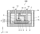
- FIG. 1 is a schematic plan view showing a power module according to Embodiment 1.
- FIG. 1 is a cross-sectional structural schematic diagram showing a power module according to Embodiment 1.
- FIG. 1 is a cross-sectional structural schematic diagram showing a power module according to Embodiment 1.
- FIG. 1 is a cross-sectional structural schematic diagram showing a power module according to Embodiment 1.
- FIG. 1 is a cross-sectional structural schematic diagram showing a power module according to Embodiment 1.
- FIG. 4 is a cross-sectional schematic diagram showing another power module in Embodiment 1.
- FIG. 4 is a cross-sectional schematic diagram showing another power module in Embodiment 1.
- FIG. 4 is a cross-sectional structural schematic diagram showing a manufacturing process of the power module in Embodiment 1;
- FIG. 4 is a cross-sectional structural schematic diagram showing a manufacturing process of the power module in Embodiment 1;
- FIG. 4 is a cross-sectional structural schematic diagram showing a manufacturing process of the power module in Embodiment 1;
- FIG. 4 is a cross-sectional structural schematic diagram showing a manufacturing process of the power module in Embodiment 1;
- FIG. 4 is a cross-sectional structural schematic diagram showing a manufacturing process of the power module in Embodiment 1;
- FIG. 4 is a cross-sectional structural schematic diagram showing a manufacturing process of the power module in Embodiment 1;
- FIG. 4 is a cross-sectional structural schematic diagram showing a manufacturing process of the power module in Embodiment 1;
- FIG. 4 is a cross-sectional structural schematic diagram showing a manufacturing process of the power module in Embodiment 1;
- FIG. 4 is a
- FIG. 4 is a schematic plan view showing a power module according to Embodiment 2;
- FIG. 10 is a cross-sectional structural schematic diagram showing a power module according to Embodiment 2;
- FIG. 10 is a cross-sectional structural schematic diagram showing a power module according to Embodiment 2;
- FIG. 11 is a schematic plan view showing a power module according to Embodiment 3;
- FIG. 11 is a cross-sectional structural schematic diagram showing a power module according to Embodiment 3;
- FIG. 11 is a cross-sectional structural schematic diagram showing a power module according to Embodiment 3;
- FIG. 11 is a schematic plan view showing a power module according to Embodiment 4;
- FIG. 11 is a cross-sectional structural schematic diagram showing a power module according to Embodiment 4;
- FIG. 11 is a schematic plan view showing a power module according to Embodiment 5;
- FIG. 11 is a cross-sectional structural schematic diagram showing a power module according to Embodiment 5;
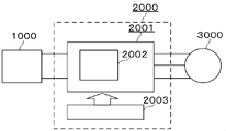
- FIG. 12 is a block diagram showing the configuration of a power conversion system to which a power conversion device according to Embodiment 6 is applied;
- FIG. 1 is a schematic plan view showing a power module according to Embodiment 1.
- FIG. FIG. 2 is a cross-sectional schematic diagram showing the power module according to Embodiment 1.
- FIG. 3 is a cross-sectional schematic diagram showing the power module according to Embodiment 1.
- FIG. 4 is a cross-sectional schematic diagram showing the power module according to Embodiment 1.
- FIG. 5 is a cross-sectional schematic diagram showing the power module according to Embodiment 1.
- FIG. FIG. 6 is a cross-sectional schematic diagram showing another power module according to Embodiment 1.
- FIG. FIG. 2 is a schematic cross-sectional view taken along the dashed-dotted line AA in FIG. FIG.
- FIG. 3 is a schematic cross-sectional view taken along dashed-dotted line BB in FIG.
- FIG. 4 is a schematic cross-sectional view taken along dashed-dotted line CC in FIG.
- FIG. 5 is a schematic cross-sectional view taken along the dashed-dotted line AA in FIG. 1 when the cooling unit 1 is attached to the power module 100.
- FIG. 6 is a schematic cross-sectional view taken along dashed-dotted line AA in FIG.
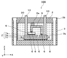
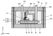
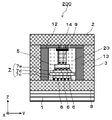
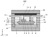
- a power module 100 includes a lid portion 2, a pressure portion 2a, a frame 3, a power semiconductor element 5 as a semiconductor element, solder 6 as a bonding material (bonding portion), and an insulating substrate 7. , a heat spreader 8 that is a heat diffusion part, wiring 9 that is a connection wiring part, bolts 4 and 11 that are fastening members, and external connection terminals 10 .
- the metal layer 7c on the lower surface side of the insulating substrate 7 is joined to the upper surface of the heat spreader 8 via the solder 6.
- the back surface of the power semiconductor element 5 is joined to the metal layer 7 a on the upper surface side of the insulating substrate 7 via solder 6 .
- Wiring 9 is joined to the surface of power semiconductor element 5 and metal layer 7 b on the upper surface side of insulating substrate 7 via solder 6 .
- External connection terminals 10 are joined to the upper surface of the metal layer 7a and the upper surface of the metal layer 7b on the upper surface side of the insulating substrate 7, respectively.
- a frame 3 surrounding the insulating substrate 7 is arranged in the outer peripheral region of the upper surface of the heat spreader 8 .
- the bottom surface of the frame 3 is joined to the top surface of the heat spreader 8 .
- a lid portion 2 is arranged on the upper surface of the frame body 3 . Between the lower surface of the lid portion 2 and the upper surface of the wiring 9, a pressurizing portion 2a for pressurizing the solder 6 that joins the power semiconductor element 5 and the metal layer 7a is arranged.
- a sealing member 20 is arranged (filled) in the interior surrounded by the heat spreader 8 and the frame 3 .
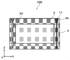
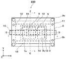
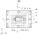
- FIG. 1 is a schematic plan view of the power module 100 viewed from the upper surface side through the cover 2 .
- a transparent member is indicated by a dotted line.
- the outermost solid line is the outer edge of the lid 2 and the outer edge (outer wall) of the frame 3.
- An inner edge (inner wall) of the frame 3 is arranged inside the outer edge of the frame 3 .
- the outer edge of the heat spreader 8 is arranged at the same position as the outer edge of the lid portion 2 (the outer edge of the frame 3).
- the outer edge of the insulating layer 7 d of the insulating substrate 7 is arranged inside the inner edge of the frame 3 .
- Metal layers 7 a and 7 b on the upper surface side of the insulating substrate 7 are arranged inside the outer edge of the insulating layer 7 d of the insulating substrate 7 .
- the power semiconductor element 5 and the external connection terminals 10 are arranged inside the outer edge of the upper surface of the metal layer 7a on the upper surface side of the insulating substrate 7 .
- Wires 9 are arranged inside the outer edges of the upper surface of the power semiconductor element 5 and the metal layer 7b on the upper surface side of the insulating substrate 7, respectively.
- the wiring 9 is located inside the outer edge of the metal layer 7a and the metal layer 7b on the upper surface side of the insulating substrate 7, straddling the gap (spaced portion) between the outer edges of the metal layer 7a and the metal layer 7b facing each other. , the metal layer 7a and the metal layer 7b.
- a pressure member 2 a is arranged on the wiring 9 above the power semiconductor element 5 inside the outer edge of the power semiconductor element 5 .
- Fastening holes 2 b for arranging bolts 4 and 11 are arranged between the outer edge and the inner edge of the frame 3 .
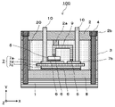
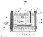
- FIG. 2 is a schematic cross-sectional view of a portion corresponding to the fastening hole 2b for fastening with the cooling section 1 of the power module 100.
- the metal layer 7c on the lower surface side of the insulating substrate 7 is joined to the upper surface of the heat spreader 8 via the solder 6.
- the back surface of the power semiconductor element 5 is joined to the metal layer 7 a on the upper surface side of the insulating substrate 7 via solder 6 .
- Wiring 9 is joined to the surface of power semiconductor element 5 and the upper surface of metal layer 7 b on the upper surface side of insulating substrate 7 via solder 6 .
- External connection terminals 10 are joined to the upper surface of the metal layer 7a and the upper surface of the metal layer 7b on the upper surface side of the insulating substrate 7, respectively.
- a frame 3 surrounding the insulating substrate 7 is arranged in the outer peripheral region of the upper surface of the heat spreader 8 .
- the lower surface of the frame 3 is joined to the upper surface of the heat spreader 8
- the lid portion 2 is arranged on the upper surface of the frame 3 .
- a pressurizing portion 2a for pressurizing the solder 6 that joins the power semiconductor element 5 and the metal layer 7a is arranged.
- a sealing member 20 is arranged inside the frame 3 .
- Fastening holes 2 b for inserting bolts 4 are arranged at corresponding portions of the frame 3 , the lid portion 2 and the heat spreader 8 .
- the fastening hole 2 b is formed through the lid portion 2 , the frame 3 and the heat spreader 8 .
- the external connection terminal 10 protrudes outside the lid portion 2 through a predetermined position of the lid portion 2 .
- FIG. 3 is a schematic cross-sectional view of a portion corresponding to the fastening hole 2b for fastening the power module 100 to the heat spreader 8.
- FIG. 3 differs from FIG. 2 in the shape of the fastening hole 2b into which the fastening member 4 is inserted.
- the bottom of the fastening hole 2 b does not penetrate the heat spreader 8 and stops inside the heat spreader 8 .
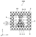
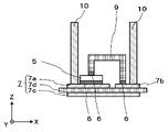
- FIG. 4 is a schematic cross-sectional view of a portion corresponding to a region where the power semiconductor element 5 of the power module 100 is pressurized by the pressurizing portion 2a.
- the back surface of the power semiconductor element 5 is bonded to the upper surface of the metal layer 7a on the upper surface side of the insulating substrate 7 via solder 6 as a bonding material.
- An electrode (not shown) is formed on the surface of the power semiconductor element 5 , and the lower surface of the wiring 9 and the electrode of the power semiconductor element 5 are joined via solder 6 .
- a pressurizing portion 2 a is arranged above the power semiconductor element 5 and on the upper surface of the wiring 9 .
- the pressurizing portion 2a is arranged so that the lower surface is in contact with the upper surface of the wiring 9 and the upper surface is in contact with the lower surface of the lid portion 2 .
- the lid portion 2 can be fastened to the heat spreader 8 using the bolts 11.
- the solder 6 that joins the power semiconductor element 5 to the metal layer 7a on the upper surface side of the insulating substrate 7 can be pressurized.
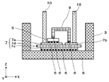
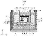
- FIG. 5 is a schematic cross-sectional view of the cooling unit 1 attached to the power module 100.
- the upper surface of cooling unit 1 is arranged so as to be in contact with the lower surface of heat spreader 8 .
- Cooling unit 1 is fastened to power module 100 with bolts 4 . If the pressurizing force applied to the solder 6 is insufficient when the bolts 11 are used for fastening, the pressurizing force can be increased when the bolts 4 are used for fastening.
- the heat spreader 8 is a plate-like bottom portion (bottom plate) of the power module 100 that includes the insulating substrate 7 and the like.
- the heat spreader 8 extends in the first direction and the second direction.
- the heat spreader 8 functions as a heat diffusion member for dissipating heat generated inside the power module 100 to the outside of the power module 100 .
- the upper surface of the heat spreader 8 is bonded to the lower surface of the metal layer 7c on the lower surface side of the insulating substrate 7 via (using) solder 6 as a bonding material.
- a copper alloy, an aluminum alloy, or the like can be used as a material for the heat spreader 8.
- the lower surface of the sealing member 20 is in contact with the outside of the bonding area with the solder 6 on the upper surface of the heat spreader 8 .
- a metal with good thermal conductivity such as copper (Cu) or aluminum (Al), or a material such as a graphite material can be used.
- the insulating substrate 7 extends in the first direction and the second direction.
- the insulating substrate 7 is a plate-like member.
- the insulating substrate 7 has an upper surface layer, an intermediate layer and a lower surface layer.
- a metal layer 7 c on the lower surface side of the insulating substrate 7 faces the upper surface of the heat spreader 8 .
- the insulating substrate 7 has an insulating layer 7d as an intermediate layer, a metal layer 7a as an upper surface layer on the upper surface side of the insulating layer 7d, and a metal layer 7c as a lower surface layer on the lower surface side of the insulating layer 7d.
- a metal layer 7 c on the lower surface side of the insulating layer 7 d is joined to the upper surface of the heat spreader 8 with solder 6 .
- the insulating substrate 7 is plate-shaped, and when the plate-shaped insulating substrate 7 is viewed from the plane (upper surface) direction, the size of the metal layer 7a on the upper surface side of the insulating layer 7d is smaller than the size of the insulating layer 7d. It's becoming The size of the metal layer 7c on the lower surface side of the insulating layer 7d is smaller than the size of the insulating layer 7d. The end of insulating layer 7d protrudes outward beyond the ends of metal layer 7a on the upper surface side of insulating layer 7d and metal layer 7c on the lower surface side of insulating layer 7d.
- the insulating layer 7d is sandwiched between the metal layer 7a on the upper surface side of the insulating layer 7d and the metal layer 7c on the lower surface side of the insulating layer 7d and the heat spreader 8, thereby suppressing creeping discharge (securing a creeping distance). It is for
- the metal layer 7a on the upper surface side of the insulating layer 7d may be divided into a plurality of parts depending on the purpose to form a circuit pattern.
- the power semiconductor element 5 and the external connection terminals 10 are arranged on the metal layer 7a.
- a wire and an external connection terminal 10 are arranged on the metal layer 7b.
- a ceramic substrate such as aluminum oxide ( Al2O3 ), aluminum nitride ( AlN) or silicon nitride ( Si3N4 ) can be used.
- a metal layer (circuit pattern plate) 7a and a metal layer (relay plate) 7b are joined to the upper surface of the insulating layer 7d by brazing or direct joining.
- a metal layer (radiating plate) 7c is joined to the lower surface of the insulating layer 7d by using a method such as brazing or direct joining.
- a method such as brazing or direct joining.
- any good electrical conductor such as Cu or Al can be used.
- a material having a two-layer structure obtained by laminating Cu and Al may be used as the metal layer 7a, the metal layer 7b, and the metal layer 7c, respectively.
- Al serves as a stress relaxation layer for bonding Cu and the insulating substrate 7, so the side closer to the insulating layer 7d is the Al layer and the far side is the Cu layer.
- the upper surface side of the insulating substrate 7 is synonymous with the upper surface side of the insulating layer 7d
- the lower surface side of the insulating substrate 7 is synonymous with the lower surface side of the insulating layer 7d.
- the power semiconductor element 5 has a structure in which electrodes (not shown) are arranged on the surface of the power semiconductor element 5 .
- the power semiconductor element 5 is bonded to the upper surface of the metal layer 7a on the upper surface side of the insulating substrate 7 via solder 6 as a bonding portion.
- silicon Si: Silicon
- silicon carbide SiC: Silicon Carbide
- gallium nitride GaN: Gallium Nitride
- the power semiconductor element 5 is a MOSFET (Metal Oxide Semiconductor Field Effect Transistor), IGBT (Insulated Gate Bipolar Transistor), FWD (Free Wheel Diode), and RC-IGBT (Reverse Conducting Power IGBT) device.
- MOSFET Metal Oxide Semiconductor Field Effect Transistor
- IGBT Insulated Gate Bipolar Transistor
- FWD Free Wheel Diode
- RC-IGBT Reverse Conducting Power IGBT
- the wiring 9 is a plate-like metal member. One end of the wiring 9 is electrically connected to the electrode of the power semiconductor element 5 on the metal layer 7 a on the upper surface side of the insulating substrate 7 . The wiring 9 has the other end electrically connected to a predetermined position of the metal layer 7b. The wiring 9 is connected to the electrodes of the power semiconductor element 5 via the solder 6 . Further, the wiring 9 is connected to the metal layer 7b through the solder 6. As shown in FIG. The wiring 9 is made of a good conductor metal with sufficient rigidity, for example, a copper plate can be used.
- the wiring 9 when Al is used as the material of the wiring 9, it can be used if the surface of the Al is configured so that it can be soldered by nickel (Ni) plating or the like. Furthermore, although both ends of the wiring 9 are joined by solder 6, they may be joined by ultrasonic joining or the like. Moreover, the wiring 9 can use a Cu ribbon material, an Al ribbon material, or the like, which can provide sufficient rigidity. The wiring 9 may be bonded to the power semiconductor element 5 or the metal layer 7b using ultrasonic bonding.
- the external connection terminal 10 is joined to a predetermined position on the metal layer 7a and a predetermined position on the metal layer 7b using ultrasonic bonding.
- the other end of the external connection terminal 10 is taken out (protrudes) from a through hole provided in the side surface of the frame 3 .
- the external connection terminal 10 can also have a structure in which an insulation bush (not shown) is inserted into the side surface of the frame 3 to ensure a long creepage insulation distance.
- the external connection terminals 10 protrude to the outside of the power module 100 from through holes provided in the side surface of the frame 3 in FIG. 2 .
- a through hole or a notch may be provided in the side surface of the frame 3 as shown in FIG.
- the external connection terminal 10 is joined to the metal layer 7a or the metal layer 7b using ultrasonic bonding, but may be joined using solder.
- the frame 3 and the lid 2 a highly rigid resin such as PPS resin (Poly Phenylene Sulfide Resin) can be used.
- the frame 3 and the lid portion 2 may be made of highly rigid metal such as Cu, Al, and stainless steel in order to increase rigidity.
- the lid portion 2 has a pressurizing portion 2a protruding toward the inside of the power module 100 of the lid portion 2 (upper surface side of the wiring 9).
- the coating amount of the resin material which is the material of the pressurizing portion 2a
- an insulator such as ceramic may be used.
- the frame 3 is a frame that surrounds the insulating substrate 7 .
- the pressurizing portion 2a may be formed integrally with the lid portion 2 or may be formed separately from the lid portion 2 .
- the shape of the lower surface side of the lid portion 2 may be the same plane as long as it is in contact with the upper surface of the frame body 3 . Further, the shape of the lower surface of the lid portion 2 may be such that it protrudes toward the heat spreader 8 inside the inner edge of the frame 3 . With such a shape, the lower surface of the lid portion 2 can be in contact with the upper surface of the pressurizing portion 2a, so that the solder 6 that joins the power semiconductor element 5 can be reliably pressurized.
- the fastening holes 2b provided in the lid portion 2 and the frame 3 may be appropriately formed according to the size (thickness) of the bolts 4 and 11 used for fastening.
- the size is not particularly limited as long as the lid portion 2, the frame body 3, the heat spreader 8 and the cooling portion 1 can be fastened together and the required pressure can be applied to the pressure portion 2a.
- the bolts 4 pass through the heat spreader 8 and fasten the lid part 2 and the frame body 3 to the cooling part 1 .
- the bolts 11 fasten the lid portion 2 and the frame body 3 to the heat spreader 8 .
- the bolts 4 and 11 are passed through (inserted into) fastening holes 2b provided in the lid portion 2 and the frame body 3 to fasten the lid portion 2 and the frame body 3 to the heat spreader 8 or the cooling portion 1 with an appropriate fastening force. .
- heat conductive grease or a graphite sheet (not shown) is interposed between the heat spreader 8 and the cooling unit 1 to reduce thermal resistance.
- the head of the bolt 4 is embedded in the lid portion 2. However, even if the head portion is protruded outside the lid portion 2 as shown in FIG. good. Common bolts can be used as the bolts 4 and 11 .
- the bonding material 6 bonds the heat spreader 8 to the insulating substrate 7 , the insulating substrate 7 to the power semiconductor element 5 , and the insulating substrate 7 to the wiring 9 .
- Tin (Sn)-based solder can be used as the solder 6 which is a joining material.
- antimony (Sb), silver (Ag), Cu, and the like are added to such Sn-based solders in order to provide stress relaxation properties, heat resistance, and fatigue resistance strength, and the composition can be arbitrarily selected.
- the solder 6 joins the members to be joined by reflowing together with the members to be joined.
- solder As a bonding material for die bonding, general solder was used as an example, but in addition to solder, TLP bonding (Transient Liquid Phase), nanoparticles such as Ag or Cu are used. There is also a sintered type joining material, which can be applied to the present disclosure, but a solder material is most suitable from the viewpoint of cost reduction and process stability.
- the sealing member 20 is filled inside the frame 3 .
- the sealing member 20 seals the insulating substrate 7 and the power semiconductor element 5 .
- epoxy resin containing filler such as silicone gel or silica can be used.
- silicone gel is used as the material of the sealing member 20, the pressurizing effect of the pressurizing portion 2a is sufficiently exhibited.
- the upper surface of the sealing member 20 can be filled inside the frame 3 within a range from the same height as the upper surface of the wiring 9 (FIG. 6) to the height contacting the lower surface of the lid 2 (FIG. 5).
- the upper surface of the sealing member 20 is higher than the upper surface of the wiring 9, by disposing a dummy member in advance in the region where the pressure member 2a is arranged and then filling the sealing member 20, It is possible to secure an arrangement area for the pressure part 2a. In this case, the wiring 9 is sealed with the sealing member 20 except for the arrangement position of the pressure member 2a. Moreover, when the upper surface of the sealing member 20 is at the same height as the upper surfaces of the wirings 9, it is desirable to secure a distance from the external connection terminals 10. FIG. If it is difficult to secure the distance between the wiring 9 and the external connection terminal 10 , the height of the upper surface of the sealing member 20 should be set to a height that covers the upper surface of the wiring 9 .
- the thickness of the sealing member 20 that covers the upper surface of the wiring 9 should be at least 100 ⁇ m.
- the thickness of the sealing member 20 covering the upper surface of the wiring 9 can be appropriately selected within a range of 100 ⁇ m or more according to the voltage of the power module used.
- the cooling part 1 is a flat metal member. Cu, Al, or the like can be used as the material of the cooling part 1 .
- the cooling unit 1 shown in FIG. 5 is displayed by simulating a top plate of a water jacket or a heat sink, and the configuration of the cooling unit 1 other than the top plate may be of any configuration.
- a heat sink is used as the cooling unit 1, not only air cooling but also water cooling or liquid cooling may be used as the cooling method.
- the difference in linear expansion coefficient between the power semiconductor element 5 and the insulating substrate 7 is small, preferably 5 ppm/K.
- the following countermeasures are taken to suppress horizontal cracking caused by cracks extending horizontally inside the solder 6 .
- the solder 6 is pressurized through the wiring 9 by the pressurizing portion 2a on the lower surface side of the lid portion 2 in order to suppress the generation of cracks due to the equibiaxial tensile-compressive deformation.
- the deformation is no longer equal biaxial tension-compression deformation, so longitudinal cracking of the solder 6 can be suppressed.
- the power module 100 is constructed using the pressurizing portion 2a in this way, the occurrence of longitudinal cracks in the solder 6 that joins the power semiconductor element 5 to the metal layer 7a on the upper surface side of the insulating substrate 7 can be suppressed. Since the heat dissipation of the power semiconductor element 5 during operation is not interrupted, the reliability of the power module 100 can be improved. Moreover, the life of the power module 100 can be extended.
- the power module can be miniaturized.
- FIG. 7 is a cross-sectional schematic diagram showing another power module according to Embodiment 1.
- FIG. FIG. 7 is a cross-sectional view of the heat spreader 8 attached to the cooling unit 1 with bolts 4.
- the heat spreader 8 does not extend to the outer edge of the frame 3, and the outer surface of the heat spreader 8 and the inner surface of the frame 3 are in contact with each other. 3c is formed.
- a corner portion 3 c of the frame 3 is a fitting portion for fitting the frame 3 and the heat spreader 8 .
- FIG 8 to 13 are cross-sectional structural schematic diagrams showing the manufacturing process of the power module according to the first embodiment.
- the main manufacturing processes of the first embodiment are roughly divided into five processes.
- the power semiconductor element 5 and the like are bonded onto the insulating substrate 7 (mounting step on the insulating substrate).
- the insulating substrate 7 to which the power semiconductor element 5 and the like are joined and the frame 3 are joined on the heat spreader 8 (mounting step on the heat spreader).
- the sealing member 20 is filled in the region surrounded by the heat spreader 8 and the frame 3 (frame resin filling step).
- the lid portion 2 is placed on the frame body 3 filled with the sealing member 20 (lid fastening step).
- the heat spreader 8 and the cooling unit 1 are fastened together (cooling unit fastening step).
- the power semiconductor element 5, the wiring 9, and the external connection terminal 10 are joined (arranged) at predetermined positions on the metal layers 7a and 7b on the upper surface side of the insulating substrate 7 (insulating substrate 7). mounting process).
- Solder 6 is used as a bonding material for bonding the power semiconductor element 5 and the wiring 9 .
- the external connection terminals 10 can be joined to the metal layers 7a and 7b on the upper surface side of the insulating substrate 7 by soldering 6 or ultrasonic joining.
- the insulating substrate 7 on which the power semiconductor elements 5 and the like are arranged is bonded (arranged) on the upper surface of the heat spreader 8 .
- the frame 3 is arranged surrounding the insulating substrate 7 in the outer peripheral region of the upper surface of the heat spreader 8 (mounting process to the heat spreader). Solder is usually used for bonding the insulating substrate 7 .
- An adhesive is usually used for bonding (bonding) the frame 3 .
- the insulating substrate 7 is placed, and the area surrounded by the frame 3 and the heat spreader 8 is filled with the sealing member 20 .
- the height of the upper surface of the sealing member 20 from the upper surface of the heat spreader 8 can be in the range from the upper surface of the wiring 9 to the upper surface of the frame 3 , in other words, the height of contact with the lower surface of the lid portion 2 .
- the sealing member 20 may be filled after disposing the pressurizing portion 2a at a predetermined position on the upper surface of the wiring 9 in advance.
- the sealing member 20 is filled so as to fill the space.
- the height of the sealing member 20 can be appropriately selected within a range from the upper surface of the wiring 9 to the lower surface of the lid portion 2 as necessary.
- FIG. 11 is a display in which the cross section AA (FIG.
- FIG. 12 shows a cross-sectional shape of a fastening hole 2b into which a bolt 4 for fastening with the cooling part 1 is inserted.
- the connection between the heat spreader 8 and the cooling unit 1, which connects the lower surface of the heat spreader 8 and the upper surface of the cooling unit 1, is performed using bolts 4 (cooling unit fastening process).
- bolts 4 cooling unit fastening process
- pressure can be applied in the direction indicated by the arrow (the direction from the pressurizing portion 2a toward the insulating substrate 7 in the Z direction).
- a thermally conductive material such as a thermal interface material (TIM) or a graphite sheet may be sandwiched between the heat spreader 8 and the cooling unit 1 to efficiently dissipate heat.
- the power module 100 including the cooling section 1 can be manufactured.
- the pressurizing portion 2a is provided between the lower surface of the lid portion 2 and the upper surface of the wiring 9, the power semiconductor element 5 is placed on the metal layer 7a on the upper surface side of the insulating substrate 7. It is possible to pressurize the solder 6 that is joined to the solder 6 and suppress the occurrence of longitudinal cracks in the solder 6 . As a result, reliability of the power module can be improved. Also, the life of the power module can be extended.
- the pressurizing portion 2a is provided between the lower surface of the lid portion 2 and the upper surface of the wiring 9, the power module can be easily manufactured.
- the pressurizing portion 2a is provided between the lower surface of the lid portion 2 and the upper surface of the wiring 9, it is possible to suppress the occurrence of longitudinal cracks in the solder 6, thereby suppressing an increase in the resistance of the power module.
- Embodiment 2 In the second embodiment, the external connection terminals 10 used in the first embodiment are exposed (protruded) from the side surface of the frame 3 to the outside of the power module, and the pressure member 2a is used as the pressure member 14.
- the heat spreader 8 is arranged so as to be in contact with not only the wiring 9 but also the external connection terminals 10 and that the heat spreader 8 has a heat spreader upper surface portion 12 and a heat spreader side surface portion 13 .
- the pressure member 14 is arranged so as to be in contact with the upper surfaces of the wirings 9 and the external connection terminals 10.
- the solder 6 that joins the power semiconductor element 5 and the metal layer 7a on the upper surface side of the insulating substrate 7 can be pressurized, and vertical cracking of the solder 6 can be suppressed.
- the heat spreader upper surface portion 12 and the heat spreader side surface portion 13 which are thermally connected to the heat spreader 8 are provided so as to be in contact with the upper surface of the external connection terminal 10 and the upper surface of the wiring 9 via the pressurizing portion 14, the power semiconductor Heat generated from the device 5 or the external connection terminals 10 can be dissipated to the heat spreader 8 and the cooling unit 1 via the heat spreader upper surface portion 12 and the heat spreader side surface portion 13. Heat can be efficiently dissipated and the cooling capacity can be improved.
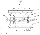
- FIG. 14 is a schematic plan view showing the power module according to Embodiment 2.
- FIG. 15 is a cross-sectional schematic diagram showing a power module according to Embodiment 2.
- FIG. 16 is a cross-sectional schematic diagram showing a power module according to Embodiment 2.
- FIG. 15 is a schematic cross-sectional view taken along dashed-dotted line DD in FIG.
- FIG. 16 is a schematic cross-sectional view taken along dashed-dotted line EE in FIG.
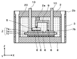
- the power module 200 includes a lid portion 2, a pressurizing portion 14, a frame 3, a power semiconductor element 5, a solder 6 as a bonding material, an insulating substrate 7, and a heat spreader 8 as a heat diffusion portion.
- the heat spreader upper surface portion 12 that is the upper surface portion of the heat spreader
- the heat spreader side surface portion 13 that is the side surface portion of the heat spreader
- the wiring 9 that is the connection wiring portion
- the bolts 4 and 11 that are fastening members
- the external connection a terminal 10 the external connection a terminal 10
- the metal layer 7c on the lower surface side of the insulating substrate 7 is joined to the upper surface of the heat spreader 8 via solder.
- the back surface of the power semiconductor element 5 is joined to the metal layer 7a on the upper surface side of the insulating substrate 7 via solder.
- Wiring 9 is joined to the surface of power semiconductor element 5 and metal layer 7b on the upper surface side of insulating substrate 7 via solder.
- External connection terminals 10 are joined to the upper surface of the metal layer 7a and the upper surface of the metal layer 7b on the upper surface side of the insulating substrate 7, respectively.
- a frame 3 surrounding the insulating substrate 7 is arranged in the outer peripheral region of the upper surface of the heat spreader 8 .
- the bottom surface of the frame 3 is joined to the top surface of the heat spreader 8 .
- a lid portion 2 is arranged on the upper surface of the frame body 3 .
- the lower surface of the lid portion 2 is in contact with the upper surface of the heat spreader upper surface portion.
- a pressure member 14 for applying pressure to the solder 6 that joins the power semiconductor element 5 and the metal layer 7a is arranged between the lower surface of the upper surface of the heat spreader and the upper surface of the wiring 9, a pressure member 14 for applying pressure to the solder 6 that joins the power semiconductor element 5 and the metal layer 7a is arranged.
- a sealing member 20 is arranged (filled) in the interior surrounded by the heat spreader 8 and the frame 3 .
- FIG. 14 is a schematic plan view of the power module 200 viewed from the upper surface side through the cover 2.
- FIG. A transparent member is indicated by a dotted line.
- the outermost solid line is the outer edge of the lid portion 2 and the outer edge (outer wall) of the frame 3 .
- An inner edge (inner wall) of the frame 3 is arranged inside the outer edge of the frame 3 .
- the outer edge of the heat spreader 8 is arranged at the same position as the outer edge of the lid portion 2 (outer edge of the frame).
- the outer edge of the insulating layer 7 d of the insulating substrate 7 is arranged inside the inner edge of the frame 3 .
- Metal layers 7 a and 7 b on the upper surface side of the insulating substrate 7 are arranged inside the outer edge of the insulating layer 7 d of the insulating substrate 7 .
- the power semiconductor element 5 and the external connection terminals 10 are arranged inside the outer edge of the upper surface of the metal layer 7 a on the upper surface side of the insulating substrate 7 .
- Wires 9 are arranged inside the outer edges of the upper surface of the power semiconductor element 5 and the metal layer 7b on the upper surface side of the insulating substrate 7, respectively.
- the wiring 9 is located inside the outer edge of the metal layer 7a and the metal layer 7b on the upper surface side of the insulating substrate 7, straddling the gap (spaced portion) between the outer edges of the metal layer 7a and the metal layer 7b facing each other. , the metal layer 7a and the metal layer 7b.
- a pressurizing portion 14 is arranged inside the inner edge of the frame 3 of the external connection terminal 10 protruding outside from the opposite side and on the upper surface of the wiring 9 .
- Fastening holes 2 b for arranging bolts 4 and 11 are arranged between the outer edge and the inner edge of the frame 3 .
- the heat spreader upper surface portion 12 is arranged so as to cover the entire inner edge of the frame 3 .
- the heat spreader side portions 13 are arranged on both sides along opposite sides of the frame 3 in the first direction.
- FIG. 15 is a schematic cross-sectional view of a portion corresponding to the external connection terminal 10 of the power module 200.
- the metal layer 7c on the lower surface side of the insulating substrate 7 is joined to the upper surface of the heat spreader 8 via the solder 6.
- the back surface of the power semiconductor element 5 is joined to the metal layer 7 a on the upper surface side of the insulating substrate 7 via solder 6 .
- Wiring 9 is joined to the surface of power semiconductor element 5 and metal layer 7 b on the upper surface side of insulating substrate 7 via solder 6 .
- External connection terminals 10 are joined to the upper surface of the metal layer 7a and the upper surface of the metal layer 7b on the upper surface side of the insulating substrate 7, respectively.
- the external connection terminals 10 protrude to the outside of the power module 200 from the side surfaces of the frame 3 facing each other.
- a region of the frame 3 where the external connection terminal 10 protrudes to the outside is provided with a hole or a notch through which the external connection terminal 10 protrudes to the outside. If the frame 3 is provided with a notch, the corresponding region of the lid 2 may have a shape that fits the notch of the frame 3 while holding the external connection terminal 10 therebetween.
- a frame 3 surrounding the insulating substrate 7 is arranged in the outer peripheral region of the upper surface of the heat spreader 8 .
- the lower surface of the frame 3 is joined to the upper surface of the heat spreader 8
- the lower surface of the lid portion 2 is arranged on the upper surface of the frame 3 .
- a pressure applying portion 14 for applying pressure to the solder 6 that joins the power semiconductor element 5 and the metal layer 7a is arranged via the heat spreader upper surface portion 12.
- a sealing member 20 is arranged inside the frame 3 .
- Fastening holes 2 b for inserting bolts 4 are arranged in the lid portion 2 corresponding to the frame 3 and the heat spreader 8 .
- the fastening hole 2 b is formed through the lid portion 2 , the frame 3 and the heat spreader 8 .
- the external connection terminal 10 protrudes outside the lid portion 2 through a predetermined position of the lid portion 2 .
- the pressurizing portion 14 and the heat spreader upper surface portion 12 extend in the first direction.
- FIG. 16 is a schematic cross-sectional view of a portion of the power module 200 corresponding to the area where the power semiconductor element 5 is pressurized by the pressurizing portion 14.
- the back surface of the power semiconductor element 5 is bonded to the upper surface of the metal layer 7a on the upper surface side of the insulating substrate 7 via solder 6 as a bonding material.
- An electrode (not shown) is formed on the surface of the power semiconductor element 5 , and the lower surface of the wiring 9 and the electrode of the power semiconductor element 5 are joined via solder 6 .
- a pressure member 14 is arranged above the power semiconductor element 5 and on the upper surface of the wiring 9 .
- the pressurizing part 14 is arranged so that its lower surface is in contact with the upper surface of the wiring 9 and its upper surface is in contact with the lower surface of the heat spreader upper surface part 12 .
- the lid portion 2 is fastened to the heat spreader 8 using the bolts 11.
- the solder 6 that joins the power semiconductor element 5 to the metal layer 7a on the upper surface side of the insulating substrate 7 can be pressurized.
- the heat spreader 8 has a heat spreader side surface portion 13 and a heat spreader top surface portion 12 surrounding the insulating substrate 7 inside the inner wall of the frame 3 .
- the upper surface of the heat spreader upper surface portion 12 is in contact with the lower surface of the lid portion 2 .
- the lower surface of the heat spreader upper surface portion 12 is in contact with the upper surface of the pressurizing portion 14 .
- the heat spreader upper surface portion 12 is supported by the heat spreader side surface portion 13 .
- the heat spreader side portions 13 face each other in the second direction of the frame 3 and are arranged along the sides of the frame 3 in the first direction.
- the insulating substrate 7 is arranged at a position sandwiched by the heat spreader side portions 13 arranged to face each other.
- the heat spreader upper surface portion 12 is supported by two heat spreader side surface portions 13 arranged at opposite positions.
- the heat spreader side surface portion 13 may be divided into a plurality of portions so that the heat spreader upper surface portion 12 can be supported on both
- the external connection terminal 10 may secure a long creepage insulation distance by inserting an insulation bush (not shown) into a projecting region projecting from the side surface of the frame 3 to the outside of the power module 200 .
- the pressurizing part 14 is in contact not only with the upper surfaces of the wirings 9 but also with the upper surfaces of the external connection terminals 10 .
- the contact area between the upper surface of the wiring 9 and the upper surface of the external connection terminal 10 although not shown, thermal grease, graphite sheet, or the like is applied to the upper surface of the wiring 9 and the external connection in order to improve contact and heat conduction. It may be inserted between the upper surface of the terminal 10 and the lower surface of the pressure member 14 .
- the heat spreader 8 has a heat spreader upper surface portion 12 and a heat spreader side surface portion 13 .
- the heat spreader upper surface portion 12 is supported by a plurality of heat spreader side surface portions 13 .
- a heat spreader upper surface portion 12 in contact with the upper surface side of the power semiconductor element 5 is thermally connected to the heat spreader 8 or the cooling portion 1 via a heat spreader side surface portion 13 . Therefore, the heat generated in the power semiconductor element 5 can be radiated not only from the metal layer 7c side on the lower surface side of the insulating substrate 7, but also from the heat spreader upper surface portion 12 side on the upper surface side of the power semiconductor element 5. Therefore, the heat generated by the power semiconductor element 5 can be cooled more effectively.
- a metal with good thermal conductivity such as Cu or Al, a graphite material, or the like can be used.
- the pressure member 14 contacts the wiring 9 and the external connection terminal 10 , it is made of an insulator similar to the insulating substrate 7 .
- the pressure member 14 can be made of a ceramic substrate such as Si 3 N 4 (silicon nitride), AlN (aluminum nitride), Al 2 O 3 (alumina), resin material, or the like.
- the heat spreader upper surface portion 12 is connected to the cooling portion 1 or the heat spreader 8 through the heat spreader side surface portion 13, so that the power semiconductor element 5 is connected through the wiring 9 or the external connection terminal 10. heat can be dissipated (cooled), and not only can the solder 6 be pressurized, but also the heat resistance can be further lowered, so the life of the power module 200 can be further extended.
- the pressurizing portion 14 is arranged so as to be in contact with the entire upper surface of the wiring 9, the entire upper surface of the wiring 9 can be pressurized. Sufficient pressure can be generated against 6.
- the external connection terminals 10 are arranged so as to protrude from the side surfaces of the frame 3 to the outside.
- the heat spreader upper surface portion 12 is supported by the respective upper surfaces of the heat spreader side surface portions 13 arranged to face each other, and is arranged in contact with the upper surface of the pressure member 14 and the lower surface of the lid portion 2 . .
- the power module 200 including the cooling section 1 can be manufactured.
- the pressure member 14 is provided between the lower surface of the heat spreader upper surface portion 12 and the upper surface of the wiring 9 and the upper surface of the external connection terminal 10, so that the power semiconductor element 5 is placed on the insulating substrate.
- the solder 6 bonded to the metal layer 7a on the upper surface side of 7 can be pressurized, and the occurrence of vertical cracks in the solder 6 can be suppressed. As a result, reliability of the power module can be improved. Also, the life of the power module can be extended.
- the heat spreader upper surface portion 12 is provided between the lower surface of the lid portion 2 and the upper surface of the pressurizing portion 14 and is connected to the heat spreader 8 via the heat spreader side surface portion 13, power is also supplied from the upper surface side of the power semiconductor element 5. Heat generated in the semiconductor element 5 or the external connection terminal 10 can be dissipated, and the heat dissipation of the power module can be improved.
- the pressurizing part 14 is arranged so as to be in contact with the entire upper surface of the wiring 9, the entire upper surface of the wiring 9 can be pressurized. Sufficient pressure can be generated against 6.
- the pressing portion 14 used in the first embodiment is arranged so as to be in contact with the entire upper surface of the wiring 9, and the heat spreader 8 has a heat spreader upper surface portion 12 and a heat spreader side surface portion 13. different. Since the pressurizing part 14 is arranged so as to be in contact with the entire upper surface of the wiring 9 in this manner, the solder 6 that joins the power semiconductor element 5 and the metal layer 7a on the upper surface side of the insulating substrate 7 can be pressurized. Vertical cracks in the solder 6 can be suppressed.
- the heat spreader upper surface portion 12 and the heat spreader side surface portion 13 connected to the heat spreader 8 are provided so as to be in contact with the upper surface of the external connection terminal 10 and the upper surface of the wiring 9 via the pressurizing portion 14, the power semiconductor element 5 or The heat generated from the external connection terminal 10 can be dissipated to the heat spreader 8 and the cooling unit 1 via the heat spreader upper surface portion 12 and the heat spreader side surface portion 13, and the heat generated in the power semiconductor element 5 and the external connection terminal 10 can be efficiently dissipated. It can dissipate heat and improve cooling capacity.
- FIG. 17 is a schematic plan view showing a power module according to Embodiment 3.
- FIG. 18 is a cross-sectional schematic diagram showing a power module according to Embodiment 3.
- FIG. 19 is a cross-sectional schematic diagram showing a power module according to Embodiment 3.
- FIG. 18 is a schematic cross-sectional view taken along dashed-dotted line FF in FIG.
- FIG. 19 is a schematic cross-sectional view along the dashed-dotted line GG in FIG.
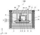
- a power module 300 includes a lid portion 2, a pressure portion 14, a frame 3, a power semiconductor element 5, a solder 6 as a bonding material, an insulating substrate 7, and a heat spreader 8 as a heat diffusion portion.
- the heat spreader upper surface portion 12 that is the upper surface portion of the heat spreader
- the heat spreader side surface portion 13 that is the side surface portion of the heat spreader
- the wiring 9 that is the connection wiring portion
- the bolts 4 and 11 that are fastening members
- the external connection a terminal 10 the external connection a terminal 10
- the metal layer 7c on the lower surface side of the insulating substrate 7 is joined to the upper surface of the heat spreader 8 via solder.
- the back surface of the power semiconductor element 5 is joined to the metal layer 7 a on the upper surface side of the insulating substrate 7 via solder 6 .
- Wiring 9 is joined to the surface of power semiconductor element 5 and metal layer 7 b on the upper surface side of insulating substrate 7 via solder 6 .
- External connection terminals 10 are joined to the upper surface of the metal layer 7a and the upper surface of the metal layer 7b on the upper surface side of the insulating substrate 7, respectively.
- a frame 3 surrounding the insulating substrate 7 is arranged in the outer peripheral region of the upper surface of the heat spreader 8 .
- the bottom surface of the frame 3 is joined to the top surface of the heat spreader 8 .
- a lid portion 2 is arranged on the upper surface of the frame body 3 .
- the lower surface of the lid portion 2 is in contact with the upper surface of the heat spreader upper surface portion 12 .
- a pressure member 14 for applying pressure to the solder 6 that joins the power semiconductor element 5 and the metal layer 7a is arranged.
- a sealing member 20 is arranged (filled) in the interior surrounded by the heat spreader 8 and the frame 3 .
- FIG. 17 is a schematic plan view of the power module 200 viewed from the upper surface side through the lid portion 2 .
- a transparent member is indicated by a dotted line.
- the outermost solid line is the outer edge of the lid 2 and the outer edge (outer wall) of the frame 3 .
- An inner edge (inner wall) of the frame 3 is arranged inside the outer edge of the frame 3 .
- the outer edge of the heat spreader 8 is arranged at the same position as the outer edge of the lid portion 2 (outer edge of the frame).
- the outer edge of the insulating layer 7 d of the insulating substrate 7 is arranged inside the inner edge of the frame 3 .
- Metal layers 7 a and 7 b on the upper surface side of the insulating substrate 7 are arranged inside the outer edge of the insulating layer 7 d of the insulating substrate 7 .
- the power semiconductor element 5 and the external connection terminals 10 are arranged inside the outer edge of the upper surface of the metal layer 7 a on the upper surface side of the insulating substrate 7 .
- Wires 9 are arranged inside the outer edges of the upper surface of the power semiconductor element 5 and the metal layer 7b on the upper surface side of the insulating substrate 7, respectively.
- the wiring 9 is located inside the outer edge of the metal layer 7a and the metal layer 7b on the upper surface side of the insulating substrate 7, straddling the gap (spaced portion) between the outer edges of the metal layer 7a and the metal layer 7b facing each other. , the metal layer 7a and the metal layer 7b.
- a pressurizing portion 14 is arranged between the external connection terminals 10 protruding from the lid portion 2 to the outside.
- a heat spreader upper surface portion 12 is arranged in a region sandwiched between the external connection terminals 10 .
- Fastening holes 2 b for arranging bolts 4 and 11 are arranged between the outer edge and the inner edge of the frame 3 .
- the heat spreader upper surface portion 12 is arranged so as to cover at least the power semiconductor element 5 from the side extending in the first direction of the frame 3 toward the opposite side.
- the heat spreader side surface portion 13 is arranged on one side along opposite sides of the frame 3 in the first direction.
- FIG. 18 is a schematic cross-sectional view of a portion corresponding to the external connection terminal 10 of the power module 300.
- FIG. 18, the metal layer 7c on the lower surface side of the insulating substrate 7 is joined to the upper surface of the heat spreader 8 via the solder 6.
- the back surface of the power semiconductor element 5 is joined to the metal layer 7 a on the upper surface side of the insulating substrate 7 via solder 6 .
- Wiring 9 is joined to the surface of power semiconductor element 5 and metal layer 7 b on the upper surface side of insulating substrate 7 via solder 6 .
- External connection terminals 10 are joined to the upper surface of the metal layer 7a and the upper surface of the metal layer 7b on the upper surface side of the insulating substrate 7, respectively.
- the external connection terminal 10 protrudes outside from the upper surface of the power module 300 through a through hole provided in the lid portion 2 .
- a frame 3 surrounding the insulating substrate 7 is arranged in the outer peripheral region of the upper surface of the heat spreader 8 .
- the lower surface of the frame 3 is joined to the upper surface of the heat spreader 8 , and the lower surface of the lid portion 2 is arranged on the upper surface of the frame 3 .
- a pressurizing part 14 for pressurizing the solder 6 that joins the power semiconductor element 5 and the metal layer 7a is arranged between the lower surface side of the lid part 2 and the upper surface of the wiring 9 with the heat spreader upper surface part 12 interposed therebetween.
- a sealing member 20 is arranged (filled) inside the frame 3 .
- Fastening holes 2 b for inserting bolts 4 are arranged in the lid portion 2 corresponding to the frame 3 and the heat spreader 8 .
- the fastening hole 2 b is formed through the lid portion 2 , the frame 3 and the heat spreader 8 .
- the external connection terminal 10 protrudes outside the lid portion 2 through a predetermined position of the lid portion 2 .
- the pressurizing portion 14 and the heat spreader upper surface portion 12 are sandwiched between the external connection terminals 10 and extend in the first direction.
- FIG. 19 is a schematic cross-sectional view of a portion of the power module 300 corresponding to the area where the power semiconductor element 5 is pressed by the pressing portion 14.
- FIG. 19 the back surface of the power semiconductor element 5 is bonded to the upper surface of the metal layer 7a on the upper surface side of the insulating substrate 7 via solder 6 as a bonding material.
- An electrode (not shown) is formed on the surface of the power semiconductor element 5 , and the lower surface of the wiring 9 and the electrode of the power semiconductor element 5 are joined via solder 6 .
- a pressure member 14 is arranged above the power semiconductor element 5 and on the upper surface of the wiring 9 .
- the pressurizing part 14 is arranged so that its lower surface is in contact with the upper surface of the wiring 9 and its upper surface is in contact with the lower surface of the heat spreader upper surface part 12 .
- the heat spreader side surface portion 13 is only on one side. Therefore, since the heat spreader top surface 12 has a cantilever shape supported by one heat spreader side surface 13, the cooling effect is reduced as compared with the second embodiment because the number of paths is reduced. However, since the heat spreader has a cantilever beam shape, the pressure (pressing force) applied to the solder 6 that joins the power semiconductor element 5 is greater than in the case of the second embodiment, and the solder 6 is applied more. Pressure can be increased.
- the heat spreader side portion 13 extending in the first direction may be divided into a plurality of portions in the first direction.
- the inside of the housing formed by the heat spreader 8, the frame 3, and the lid 2 is filled with a sealing member 20 such as a silicone gel or a resin material to prevent discharge.
- a sealing member 20 such as a silicone gel or a resin material to prevent discharge.
- a resin material that is hard after curing such as a resin material for direct potting
- the hardened resin blocks it, and the effect of pressurizing the solder 6 is reduced.
- the lid portion 2 is fastened to the heat spreader 8 using the bolts 11.
- the solder 6 that joins the power semiconductor element 5 to the metal layer 7a on the upper surface side of the insulating substrate 7 can be pressurized.
- the heat spreader upper surface portion 12 is supported by one heat spreader side surface portion 13 .
- the heat spreader side portion 13 is arranged along one of the sides of the frame 3 in the second direction. Further, they are arranged along the side portions of the frame 3 in the first direction. Since the heat spreader upper surface portion 12 is connected to the cooling portion 1 or the heat spreader 8 through the heat spreader side surface portion 13, the heat generated by the power semiconductor element 5 can be dissipated (cooled) through the wiring 9 or the external connection terminal 10. Since the structure not only pressurizes the solder 6 but also reduces the heat resistance, the life of the power module 300 can be further extended.
- the power module can be miniaturized.
- the pressure member 14 is provided between the lower surface of the heat spreader upper surface portion 12 and the upper surface of the wiring 9 and the upper surface of the external connection terminal 10, so that the power semiconductor element 5 is placed on the insulating substrate.
- the solder 6 bonded to the metal layer 7a on the upper surface side of 7 can be pressurized, and the occurrence of vertical cracks in the solder 6 can be suppressed. As a result, reliability of the power module can be improved. Also, the life of the power module can be extended.
- the heat spreader upper surface portion 12 is provided between the lower surface of the lid portion 2 and the upper surface of the pressurizing portion 14 and is connected to the heat spreader 8 via the heat spreader side surface portion 13, power is also supplied from the upper surface side of the power semiconductor element 5. Heat generated in the semiconductor element 5 or the external connection terminal 10 can be dissipated, and the heat dissipation of the power module can be improved.
- the pressurizing part 14 is arranged so as to be in contact with the entire upper surface of the wiring 9, the entire upper surface of the wiring 9 can be pressurized. Sufficient pressure can be generated against 6.
- Embodiment 4 In the fourth embodiment, the heat spreader upper surface portion 12 and the heat spreader side surface portion 13 used in the second embodiment are eliminated, and the lid portion 2 and the frame body 3 are made of the same material as the cooling portion 1. 15 and frame 16 are different. Since the pressurizing part 14 is arranged so as to be in contact with the entire upper surface of the wiring 9 in this manner, the solder 6 that joins the power semiconductor element 5 and the metal layer 7a on the upper surface side of the insulating substrate 7 can be pressurized. Vertical cracks in the solder 6 can be suppressed.
- the lid portion 15 and the frame body 16 formed of the same material as the cooling portion 1 are provided, the heat generated from the power semiconductor element 5 or the external connection terminals 10 is transferred to the outside by the cooling portion 1, the frame body 16 and the lid portion 15.
- the heat generated in the power semiconductor element 5 and the external connection terminal 10 can be efficiently radiated, and the cooling capacity can be improved. Since other points are the same as those of the second embodiment, detailed description thereof will be omitted.
- FIG. 20 is a schematic plan view showing a power module according to Embodiment 4.
- FIG. 21 is a cross-sectional schematic diagram showing a power module according to Embodiment 4.
- FIG. 21 is a schematic cross-sectional view taken along the dashed-dotted line HH in FIG. 20.
- the power module 400 includes a lid portion 15, a pressure portion 14, a frame 16, a power semiconductor element 5, a solder 6 as a bonding material, an insulating substrate 7, and a heat spreader 8 as a heat diffusion portion. , wiring 9 as a connection wiring portion, bolts 4 and 11 as fastening members, and external connection terminals 10 .
- the metal layer 7c on the lower surface side of the insulating substrate 7 is joined to the upper surface of the heat spreader 8 via solder.
- the back surface of the power semiconductor element 5 is joined to the metal layer 7 a on the upper surface side of the insulating substrate 7 via solder 6 .
- Wiring 9 is joined to the surface of power semiconductor element 5 and metal layer 7 b on the upper surface side of insulating substrate 7 via solder 6 .
- External connection terminals 10 are joined to the upper surface of the metal layer 7a and the upper surface of the metal layer 7b on the upper surface side of the insulating substrate 7, respectively.
- the inner side surface of the frame 16 surrounding the insulating substrate 7 is in contact with the outer peripheral side surface of the heat spreader 8 .
- the lower surface of frame 16 is joined to the upper surface of the outer peripheral region of cooling unit 1 .
- a lid portion 15 is arranged on the upper surface of the frame body 16 .
- the lower surface of the lid portion 15 is in contact with the upper surface of the frame 16 .
- the outer edge of the heat spreader 8 is arranged inside the outer edge of the frame 16 .
- a pressurizing portion 14 is arranged between the lower surface of the lid portion 15 and the upper surface of the wiring 9, for pressurizing the solder 6 that joins the power semiconductor element 5 and the metal layer 7a.
- a sealing member 20 is arranged (filled) in the interior surrounded by the heat spreader 8 and the frame 16 .
- FIG. 20 is a schematic plan view of the power module 400 seen from the upper surface side through the cover 2.
- FIG. A transparent member is indicated by a dotted line.
- the outermost solid line is the outer edge of the lid portion 15 and the outer edge (outer wall) of the frame body 16 .
- An inner edge (inner wall) of the frame 16 is arranged inside the outer edge of the frame 16 .
- the outer edge of the heat spreader 8 is arranged inside the outer edge of the lid portion 15 (the outer edge of the frame 16).
- the outer edge of the insulating layer 7 d of the insulating substrate 7 is arranged inside the inner edge of the frame 16 .
- Metal layers 7 a and 7 b on the upper surface side of the insulating substrate 7 are arranged inside the outer edge of the insulating layer 7 d of the insulating substrate 7 .
- the power semiconductor element 5 and the external connection terminals 10 are arranged inside the outer edge of the upper surface of the metal layer 7 a on the upper surface side of the insulating substrate 7 .
- Wires 9 are arranged inside the outer edges of the upper surface of the power semiconductor element 5 and the metal layer 7b on the upper surface side of the insulating substrate 7, respectively.
- the wiring 9 is located inside the outer edge of the metal layer 7a and the metal layer 7b on the upper surface side of the insulating substrate 7, straddling the gap (spaced portion) between the outer edges of the metal layer 7a and the metal layer 7b facing each other. , the metal layer 7a and the metal layer 7b.
- a pressurizing portion 14 is arranged inside the inner edge of the frame 3 of the external connection terminal 10 protruding outside from the opposite side and on the upper surface of the wiring 9 .
- Fastening holes 2 b for arranging bolts 4 and 11 are arranged between the outer edge and the inner edge of the frame 16 .
- FIG. 21 is a schematic cross-sectional view of a portion corresponding to the external connection terminal 10 of the power module 400.
- FIG. 21 the metal layer 7c on the lower surface side of the insulating substrate 7 is joined to the upper surface of the heat spreader 8 via the solder 6.
- the back surface of the power semiconductor element 5 is joined to the metal layer 7 a on the upper surface side of the insulating substrate 7 via solder 6 .
- Wiring 9 is joined to the surface of power semiconductor element 5 and metal layer 7 b on the upper surface side of insulating substrate 7 via solder 6 .
- External connection terminals 10 are joined to the upper surface of the metal layer 7a and the upper surface of the metal layer 7b on the upper surface side of the insulating substrate 7, respectively.
- the external connection terminals 10 protrude to the outside of the power module 400 from the side surfaces of the frame bodies 16 facing each other.
- a region of the frame 16 where the external connection terminal 10 protrudes to the outside is provided with a hole or a notch through which the external connection terminal 10 protrudes to the outside. If the frame 16 is provided with a notch, the corresponding region of the lid 15 may be shaped to fit the notch of the frame 16 while holding the external connection terminal 10 therebetween.
- a frame 16 surrounding the insulating substrate 7 is arranged in the outer peripheral region of the upper surface of the heat spreader 8 .
- the lower surface of the frame 16 is joined to the upper surface of the cooling unit 1 , and the lower surface of the lid 15 is arranged on the upper surface of the frame 16 .
- a pressurizing portion 14 for pressurizing the solder 6 that joins the power semiconductor element 5 and the metal layer 7a is arranged.
- a sealing member 20 is arranged inside the frame 16 .
- the pressurizing part 14 extends in the first direction.
- the frame 16 is arranged in the outer peripheral region of the cooling unit 1 in contact with the inner surface of the frame 16 and the outer surface of the heat spreader 8 .
- the frame 16 is provided with a corner portion 3 c including the intersection of the top surface and the side surface of the heat spreader 8 .
- a corner portion 3c of the frame 16 is a fitting portion for fitting the frame 16 and the heat spreader 8 together.
- the frame 16 and the heat spreader 8 are arranged on the upper surface of the cooling section. Therefore, the lid portion 15 and the frame body 16 are fastened to the cooling portion 1 with bolts 4 and 11 . As a result, pressure is generated in the pressurizing section 14 .
- both the bolts 4 and 11 do not necessarily have to be used to fasten the lid portion 15 and the frame body 16 to the cooling portion 1, and only the bolt 4 may be used as long as the pressure required for pressurization can be obtained.
- At least the side of the pressurizing part 14 that contacts the upper surface of the wiring 9 is made of an insulating material.
- the upper surface of the pressurizing portion 14 is in contact with the lower surface of the lid portion 15 . If the pressurizing portion 14 that contacts the lid portion 15 made of the same material as the cooling portion 1 is entirely made of a metal member, the state from the power semiconductor element 5 to the lid portion 15 is not electrically insulated. As a result, the power module no longer functions. Therefore, in order to electrically insulate the wiring 9 and the lid portion 15, an insulating member is arranged at least on the side of the pressing portion 14 that is in contact with the upper surface of the wiring 9, thereby ensuring electrical insulation. It has a structure.
- the power semiconductor element 5 is attached to the metal layer 7a on the upper surface side of the insulating substrate 7.
- the joining solder 6 can be pressurized, and the occurrence of vertical cracks in the solder 6 can be suppressed. As a result, the reliability of power module 400 can be improved. Also, the life of the power module 400 can be extended.
- lid portion 15 and the frame body 16 are made of the same material as the cooling portion 1, heat generated in the power semiconductor element 5 or the external connection terminal 10 can be dissipated from the upper surface side of the power semiconductor element 5 as well. The heat dissipation of the module 400 can be improved.
- the pressure member 14 is provided between the lower surface of the lid portion 15 and the upper surface of the wiring 9 and the upper surface of the external connection terminal 10 .
- the solder 6 bonded to the metal layer 7a on the upper surface side of the can be pressurized, and the occurrence of vertical cracks in the solder 6 can be suppressed. As a result, reliability of the power module can be improved. Also, the life of the power module can be extended.
- lid portion 15 and the frame body 16 are made of the same material as the cooling portion 1, heat generated in the power semiconductor element 5 or the external connection terminal 10 can be dissipated from the upper surface side of the power semiconductor element 5 as well. It is possible to improve the heat dissipation of the module.
- Embodiment 5 the frame 16 used in the fourth embodiment is replaced with the frame 3 in which the heat radiating portion 17 is arranged on the outer wall region (outer surface) of the region sandwiched between the fastening holes 2b of the fastening member. is different. As described above, since the heat radiating portion 17 is arranged in the outer wall region of the region sandwiched between the fastening holes 2b for arranging the fastening member of the frame 3, the heat generated from the power semiconductor element 5 or the external connection terminal 10 is dissipated from the cooling portion 1.
- Heat can be dissipated to the outside by the frame 16 and the lid portion 15, and the heat generated in the power semiconductor element 5 and the external connection terminals 10 can be efficiently dissipated and the cooling capacity can be improved. Since other points are the same as those of the fourth embodiment, detailed description thereof will be omitted.
- FIG. 22 is a schematic plan view showing a power module according to Embodiment 5.
- FIG. FIG. 23 is a cross-sectional schematic diagram showing a power module according to Embodiment 5.
- FIG. FIG. 23 is a schematic cross-sectional view along the dashed-dotted line II in FIG.
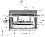
- a power module 500 includes a lid portion 15, a pressurizing portion 14, a frame body 3 having a heat radiating portion 17 in an outer wall region, a power semiconductor element 5, a solder 6 as a bonding material, and an insulating substrate 7. , a heat spreader 8 that is a heat diffusion part, wiring 9 that is a connection wiring part, bolts 4 and 11 that are fastening members, and external connection terminals 10 .
- the metal layer 7c on the lower surface side of the insulating substrate 7 is joined to the upper surface of the heat spreader 8 via solder.
- the back surface of the power semiconductor element 5 is joined to the metal layer 7 a on the upper surface side of the insulating substrate 7 via solder 6 .
- Wiring 9 is joined to the surface of power semiconductor element 5 and metal layer 7 b on the upper surface side of insulating substrate 7 via solder 6 .
- External connection terminals 10 are joined to the upper surface of the metal layer 7a and the upper surface of the metal layer 7b on the upper surface side of the insulating substrate 7, respectively.
- a frame 3 surrounding the insulating substrate 7 is arranged in the outer peripheral region of the heat spreader 8 .
- the lower surface of frame 16 is joined to the upper surface of cooling unit 1 .
- the lower surface of the lid portion 15 is in contact with the upper surface of the frame 3 .
- the outer edge of the heat spreader 8 is arranged inside the outer edge of the frame 3 .
- a lid portion 15 is arranged on the upper surface of the frame 3 .
- the lower surface of the lid portion 15 is in contact with the upper surface of the frame 16 .
- a pressurizing portion 14 is arranged for pressurizing the solder 6 that joins the power semiconductor element 5 and the metal layer 7a.
- a heat radiating portion 17 is arranged in the outer wall region sandwiched between the fastening holes 2 b of the frame 3 .
- a sealing member 20 is arranged (filled) in the interior surrounded by the heat spreader 8 and the frame 3 .
- FIG. 22 is a schematic plan view of the power module 500 seen from the upper surface side through the lid portion 15.
- FIG. A transparent member is indicated by a dotted line.
- the outermost solid line is the outer edge of the lid portion 15 and the outer edge (outer wall) of the frame 3 .
- An inner edge (inner wall) of the frame 3 is arranged inside the outer edge of the frame 16 .
- the outer edge of the heat spreader 8 is arranged inside the outer edge of the lid portion 15 (the outer edge of the frame 3).
- the outer edge of the insulating layer 7 d of the insulating substrate 7 is arranged inside the inner edge of the frame 3 .
- Metal layers 7 a and 7 b on the upper surface side of the insulating substrate 7 are arranged inside the outer edge of the insulating layer 7 d of the insulating substrate 7 .
- the power semiconductor element 5 and the external connection terminals 10 are arranged inside the outer edge of the upper surface of the metal layer 7 a on the upper surface side of the insulating substrate 7 .
- Wires 9 are arranged inside the outer edges of the upper surface of the power semiconductor element 5 and the metal layer 7b on the upper surface side of the insulating substrate 7, respectively.
- the wiring 9 is located inside the outer edge of the metal layer 7a and the metal layer 7b on the upper surface side of the insulating substrate 7, straddling the gap (spaced portion) between the outer edges of the metal layer 7a and the metal layer 7b facing each other. , the metal layer 7a and the metal layer 7b.
- a pressurizing portion 14 is arranged inside the inner edge of the frame 3 of the external connection terminal 10 projecting outward from the opposite side and on the upper surface of the wiring 9 .
- Fastening holes 2 b for arranging bolts 4 and 11 are arranged between the outer edge and the inner edge of the frame 3 .
- a plate-shaped heat radiating portion 17 is arranged in a region (outer surface) on the outer edge side sandwiched between the fastening holes 2 b of the frame 3 .
- the heat radiating portion 17 is provided with fastening holes 2b on both sides, sandwiched between the fastening holes 2b, and spaced apart from the fastening holes 2b.
- the heat dissipation portion 17 is arranged to avoid the external connection terminals 10 on the side where the external connection terminals 10 protrude to the outside.
- the bolts 11 are used to fasten the cooling unit 1 , but the bolts 11 are not necessarily required, and the bolts 4 alone may be used to fasten the cooling unit 1 .
- the heat radiating portion 17 extending in the second direction may be arranged in a region sandwiched between the bolts 4 arranged to face each other in the second direction.
- FIG. 23 is a schematic cross-sectional view of a portion corresponding to the external connection terminal 10 of the power module 500.
- FIG. 23 the metal layer 7c on the lower surface side of the insulating substrate 7 is joined to the upper surface of the heat spreader 8 via the solder 6.
- the back surface of the power semiconductor element 5 is joined to the metal layer 7 a on the upper surface side of the insulating substrate 7 via solder 6 .
- Wiring 9 is joined to the surface of power semiconductor element 5 and metal layer 7 b on the upper surface side of insulating substrate 7 via solder 6 .
- External connection terminals 10 are joined to the upper surface of the metal layer 7a and the upper surface of the metal layer 7b on the upper surface side of the insulating substrate 7, respectively.
- the external connection terminals 10 protrude to the outside of the power module 500 from the side surfaces of the frame 3 facing each other.
- a region of the frame 3 where the external connection terminal 10 protrudes to the outside is provided with a hole or a notch through which the external connection terminal 10 protrudes to the outside.
- the lid 15 may have a shape that fits the notch of the frame 3 so that the external connection terminal 10 is sandwiched in the corresponding region.
- a frame 3 surrounding the insulating substrate 7 is arranged in the outer peripheral region of the upper surface of the heat spreader 8 .
- the lower surface of the frame 3 is joined to the upper surface of the heat spreader 8 , and the lower surface of the lid portion 15 is arranged on the upper surface of the frame 3 .
- a pressurizing portion 14 for pressurizing the solder 6 that joins the power semiconductor element 5 and the metal layer 7a is arranged.
- a sealing member 20 is arranged inside the frame 3 .
- a plate-shaped heat radiating portion 17 is arranged on the outer wall of the frame 3 .
- the heat radiating portion 17 has an upper surface in contact with the lower surface of the lid portion 15 and a lower surface in contact with the upper surface of the heat spreader 8 .
- the pressurizing part 14 extends in the first direction.
- a corner portion 3c of the frame 3 is a fitting portion for fitting the frame 3 and the heat spreader 8 together.
- the frame 3 and the heat spreader 8 can be easily positioned.
- the frame 3 and the heat spreader 8 are arranged on the upper surface of the cooling section.
- the lid portion 15 and the frame body 3 are fastened to the cooling portion 1 with bolts 4 and 11 .
- pressure is generated in the pressurizing section 14 .
- both the bolts 4 and 11 do not necessarily have to be used to fasten the lid portion 15 and the frame 3 to the cooling portion 1, and only the bolt 4 may be used as long as the pressure required for pressurization can be obtained.
- the power semiconductor element 5 is attached to the metal layer 7a on the upper surface side of the insulating substrate 7.
- the joining solder 6 can be pressurized, and the occurrence of vertical cracks in the solder 6 can be suppressed. As a result, the reliability of power module 500 can be improved. Also, the life of the power module 400 can be extended.
- heat radiating portion 17 is arranged on the outer wall region of the frame 3, heat generated by the power semiconductor element 5 or the external connection terminal 10 can be dissipated from the side surface of the power module 500 while maintaining insulation from the inside of the power module 500. Heat can be dissipated, and the heat dissipation of the power module 500 can be improved.
- the pressure member 14 is provided between the lower surface of the lid portion 15 and the upper surface of the wiring 9 and the upper surface of the external connection terminal 10 .
- the solder 6 bonded to the metal layer 7a on the upper surface side of the can be pressurized, and the occurrence of vertical cracks in the solder 6 can be suppressed. As a result, reliability of the power module can be improved. Also, the life of the power module can be extended.
- heat radiating portion 17 is arranged on the outer wall region of the frame 3, heat generated by the power semiconductor element 5 or the external connection terminal 10 can be dissipated from the side surface of the power module 500 while maintaining insulation from the inside of the power module 500. Heat can be dissipated, and the heat dissipation of the power module 500 can be improved.
- Embodiment 6 a power converter to which the power modules described in the first to fifth embodiments are applied will be described.
- the present disclosure is not limited to a specific power converter, a case where the present disclosure is applied to a three-phase inverter will be described below as a sixth embodiment.
- FIG. 24 is a block diagram showing the configuration of a power conversion system to which the power converter according to this embodiment is applied.
- the power conversion system shown in FIG. 24 comprises a power supply 1000, a power conversion device 2000, and a load 3000.
- the power supply 1000 is a DC power supply and supplies DC power to the power converter 2000 .
- the power supply 1000 can be composed of various things, for example, it can be composed of a DC system, a solar battery, and a storage battery. Alternatively, it may be composed of a rectifier circuit or an AC/DC converter connected to an AC system. Also, power supply 1000 may be configured with a DC/DC converter that converts DC power output from a DC system into predetermined power.
- the power conversion device 2000 is a three-phase inverter connected between the power supply 1000 and the load 3000, converts the DC power supplied from the power supply 1000 into AC power, and supplies the AC power to the load 3000. As shown in FIG. 24, the power conversion device 2000 includes a main conversion circuit 2001 that converts DC power into AC power and outputs it, and a control circuit 2003 that outputs a control signal for controlling the main conversion circuit 2001 to the main conversion circuit 2001. and
- a load 3000 is a three-phase electric motor driven by AC power supplied from the power converter 2000 .
- the load 3000 is not limited to a specific application, but is an electric motor mounted on various electrical equipment, such as a hybrid vehicle, an electric vehicle, a railway vehicle, an elevator, or an electric motor for an air conditioner.
- the main conversion circuit 2001 includes a switching element and a freewheeling diode (not shown). By switching the switching element, DC power supplied from power supply 1000 is converted into AC power and supplied to load 3000 .
- the main conversion circuit 2001 has various specific circuit configurations, the main conversion circuit 2001 according to the present embodiment is a two-level three-phase full bridge circuit, and has six switching elements and It can consist of six freewheeling diodes in anti-parallel.
- each switching element and each freewheeling diode of the main conversion circuit 2001 is a switching element or a freewheeling diode included in the power module 2002 corresponding to the power module according to at least one of the first to fifth embodiments described above.
- the six switching elements constitute upper and lower arms connected in series for every two switching elements, and each upper and lower arm constitutes each phase (U phase, V phase, W phase) of the full bridge circuit.
- Output terminals of the upper and lower arms, that is, three output terminals of the main conversion circuit 2001 are connected to the load 3000 .
- the main conversion circuit 2001 includes a drive circuit (not shown) for driving each switching element. may be provided.
- the drive circuit generates a drive signal for driving the switching element of the main conversion circuit 2001 and supplies it to the control electrode of the switching element of the main conversion circuit 2001 .
- a drive signal for turning on the switching element and a drive signal for turning off the switching element are output to the control electrode of each switching element.
- the driving signal is a voltage signal (ON signal) equal to or higher than the threshold voltage of the switching element, and when maintaining the switching element in the OFF state, the driving signal is a voltage equal to or less than the threshold voltage of the switching element. signal (off signal).
- the control circuit 2003 controls the switching elements of the main conversion circuit 2001 so that the desired power is supplied to the load 3000 . Specifically, based on the power to be supplied to the load 3000, the time (on time) during which each switching element of the main converter circuit 2001 should be in the ON state is calculated. For example, the main conversion circuit 2001 can be controlled by PWM control that modulates the ON time of the switching element according to the voltage to be output. Then, a control command (control signal) to the drive circuit provided in the main conversion circuit 2001 so that an ON signal is output to the switching element that should be in the ON state at each time point, and an OFF signal is output to the switching element that should be in the OFF state at each time. to output The drive circuit outputs an ON signal or an OFF signal as a drive signal to the control electrode of each switching element according to this control signal.
- the power modules according to Embodiments 1 to 5 are applied as the power module 2002 forming the main conversion circuit 2001 .
- longitudinal cracks in the solder 6 that joins the power semiconductor element 5 to the insulating substrate 7 can be suppressed.
- the reliability of power converter 2000 can be improved.
- the present disclosure is not limited to this, and can be applied to various power converters.
- a two-level power conversion device is used, but a three-level or multi-level power conversion device may be used. Disclosure may apply.
- the present disclosure can be applied to a DC/DC converter or an AC/DC converter when power is supplied to a DC load or the like.
- the power conversion device to which the present disclosure is applied is not limited to the case where the above-described load is an electric motor. It can also be used, and furthermore, it can be used as a power conditioner for a photovoltaic power generation system, an electric storage system, or the like.
- Cooling part 2, 15 Lid part, 2a, 14 Pressure part, 2b Fastening hole, 3, 16 Frame, 3c Corner of frame 3, 4, 11 Bolt, 5 Power semiconductor element, 6 Solder, 7 Insulating substrate 7a, 7b, 7c Metal layer 7d Insulating layer 8 Heat spreader 9 Wiring 10 External connection terminal 12 Heat spreader top surface 13 Heat spreader side surface 17 Radiation part 20 Sealing member 100, 101, 200 , 300, 400, 500, 2002 power module, 1000 power supply, 2000 power converter, 2001 main conversion circuit, 2003 control circuit, 3000 load.
Landscapes
- Physics & Mathematics (AREA)
- Condensed Matter Physics & Semiconductors (AREA)
- General Physics & Mathematics (AREA)
- Engineering & Computer Science (AREA)
- Computer Hardware Design (AREA)
- Microelectronics & Electronic Packaging (AREA)
- Power Engineering (AREA)
- Cooling Or The Like Of Semiconductors Or Solid State Devices (AREA)
Priority Applications (2)
| Application Number | Priority Date | Filing Date | Title |
|---|---|---|---|
| JP2021557047A JPWO2022239154A1 (enExample) | 2021-05-12 | 2021-05-12 | |
| PCT/JP2021/018070 WO2022239154A1 (ja) | 2021-05-12 | 2021-05-12 | パワーモジュールおよび電力変換装置 |
Applications Claiming Priority (1)
| Application Number | Priority Date | Filing Date | Title |
|---|---|---|---|
| PCT/JP2021/018070 WO2022239154A1 (ja) | 2021-05-12 | 2021-05-12 | パワーモジュールおよび電力変換装置 |
Publications (1)
| Publication Number | Publication Date |
|---|---|
| WO2022239154A1 true WO2022239154A1 (ja) | 2022-11-17 |
Family
ID=84028034
Family Applications (1)
| Application Number | Title | Priority Date | Filing Date |
|---|---|---|---|
| PCT/JP2021/018070 Ceased WO2022239154A1 (ja) | 2021-05-12 | 2021-05-12 | パワーモジュールおよび電力変換装置 |
Country Status (2)
| Country | Link |
|---|---|
| JP (1) | JPWO2022239154A1 (enExample) |
| WO (1) | WO2022239154A1 (enExample) |
Citations (8)
| Publication number | Priority date | Publication date | Assignee | Title |
|---|---|---|---|---|
| WO2013172183A1 (ja) * | 2012-05-18 | 2013-11-21 | 三菱電機株式会社 | パワーモジュール |
| JP2014053440A (ja) * | 2012-09-07 | 2014-03-20 | Meidensha Corp | 半導体モジュール及び半導体モジュール製造方法 |
| JP2014082458A (ja) * | 2012-10-15 | 2014-05-08 | Toyota Motor Engineering & Manufacturing North America Inc | モジュール式設計態様を有するパワーモジュール及びパワーモジュール・アレイ |
| JP2014116478A (ja) * | 2012-12-11 | 2014-06-26 | Meidensha Corp | 半導体モジュール及び半導体モジュールの製造方法並びに電力変換装置 |
| JP2017220610A (ja) * | 2016-06-09 | 2017-12-14 | 株式会社村田製作所 | 半導体装置 |
| WO2018042973A1 (ja) * | 2016-09-01 | 2018-03-08 | 三菱電機株式会社 | パワーモジュールおよびその製造方法 |
| JP2018512742A (ja) * | 2015-04-13 | 2018-05-17 | アーベーベー・シュバイツ・アーゲー | パワーエレクトロニクスモジュール |
| WO2019146402A1 (ja) * | 2018-01-25 | 2019-08-01 | 三菱電機株式会社 | 電力変換装置及び電力変換装置の製造方法 |
Family Cites Families (1)
| Publication number | Priority date | Publication date | Assignee | Title |
|---|---|---|---|---|
| JP2017135183A (ja) * | 2016-01-26 | 2017-08-03 | 三菱電機株式会社 | 半導体装置 |
-
2021
- 2021-05-12 JP JP2021557047A patent/JPWO2022239154A1/ja active Pending
- 2021-05-12 WO PCT/JP2021/018070 patent/WO2022239154A1/ja not_active Ceased
Patent Citations (8)
| Publication number | Priority date | Publication date | Assignee | Title |
|---|---|---|---|---|
| WO2013172183A1 (ja) * | 2012-05-18 | 2013-11-21 | 三菱電機株式会社 | パワーモジュール |
| JP2014053440A (ja) * | 2012-09-07 | 2014-03-20 | Meidensha Corp | 半導体モジュール及び半導体モジュール製造方法 |
| JP2014082458A (ja) * | 2012-10-15 | 2014-05-08 | Toyota Motor Engineering & Manufacturing North America Inc | モジュール式設計態様を有するパワーモジュール及びパワーモジュール・アレイ |
| JP2014116478A (ja) * | 2012-12-11 | 2014-06-26 | Meidensha Corp | 半導体モジュール及び半導体モジュールの製造方法並びに電力変換装置 |
| JP2018512742A (ja) * | 2015-04-13 | 2018-05-17 | アーベーベー・シュバイツ・アーゲー | パワーエレクトロニクスモジュール |
| JP2017220610A (ja) * | 2016-06-09 | 2017-12-14 | 株式会社村田製作所 | 半導体装置 |
| WO2018042973A1 (ja) * | 2016-09-01 | 2018-03-08 | 三菱電機株式会社 | パワーモジュールおよびその製造方法 |
| WO2019146402A1 (ja) * | 2018-01-25 | 2019-08-01 | 三菱電機株式会社 | 電力変換装置及び電力変換装置の製造方法 |
Also Published As
| Publication number | Publication date |
|---|---|
| JPWO2022239154A1 (enExample) | 2022-11-17 |
Similar Documents
| Publication | Publication Date | Title |
|---|---|---|
| JP4635564B2 (ja) | 半導体装置 | |
| JP4569473B2 (ja) | 樹脂封止型パワー半導体モジュール | |
| JP6783327B2 (ja) | 半導体装置および電力変換装置 | |
| JP6945418B2 (ja) | 半導体装置および半導体装置の製造方法 | |
| JP6826665B2 (ja) | 半導体装置、半導体装置の製造方法及び電力変換装置 | |
| JP7561677B2 (ja) | 電力半導体装置、電力半導体装置の製造方法及び電力変換装置 | |
| JP6575739B1 (ja) | 半導体装置、半導体装置の製造方法および電力変換装置 | |
| US20240395678A1 (en) | Semiconductor device, method of manufacturing semiconductor device, and power conversion device | |
| JP7019024B2 (ja) | 半導体装置及び電力変換装置 | |
| CN113646876B (zh) | 功率半导体模块以及电力变换装置 | |
| JP2007012831A (ja) | パワー半導体装置 | |
| JP5899952B2 (ja) | 半導体モジュール | |
| JPWO2021001927A1 (ja) | 半導体装置、半導体装置の製造方法および電力変換装置 | |
| JP7154422B2 (ja) | 電力用半導体装置、電力用半導体装置の製造方法および電力変換装置 | |
| JP7053897B2 (ja) | 半導体装置、半導体装置の製造方法及び電力変換装置 | |
| JP7109347B2 (ja) | 半導体装置および電力変換装置 | |
| WO2022239154A1 (ja) | パワーモジュールおよび電力変換装置 | |
| JP7479771B2 (ja) | 半導体装置、半導体装置の製造方法及び電力変換装置 | |
| JP7418474B2 (ja) | 半導体装置および電力変換装置 | |
| JP2019040955A (ja) | 半導体モジュールの製造方法 | |
| JP2022029886A (ja) | 半導体装置、半導体装置の製造方法及び電力変換装置 | |
| JP7681920B2 (ja) | 半導体パッケージ及びその製造方法 | |
| JPWO2020245998A1 (ja) | 半導体装置、電力変換装置および半導体装置の製造方法 | |
| JP2007288044A (ja) | 半導体装置 | |
| JP2000174198A (ja) | モジュール型半導体装置及びこれを用いた電力変換装置 |
Legal Events
| Date | Code | Title | Description |
|---|---|---|---|
| ENP | Entry into the national phase |
Ref document number: 2021557047 Country of ref document: JP Kind code of ref document: A |
|
| 121 | Ep: the epo has been informed by wipo that ep was designated in this application |
Ref document number: 21941888 Country of ref document: EP Kind code of ref document: A1 |
|
| NENP | Non-entry into the national phase |
Ref country code: DE |
|
| 122 | Ep: pct application non-entry in european phase |
Ref document number: 21941888 Country of ref document: EP Kind code of ref document: A1 |