WO2022230887A1 - 積層光学フィルム - Google Patents
積層光学フィルム Download PDFInfo
- Publication number
- WO2022230887A1 WO2022230887A1 PCT/JP2022/018914 JP2022018914W WO2022230887A1 WO 2022230887 A1 WO2022230887 A1 WO 2022230887A1 JP 2022018914 W JP2022018914 W JP 2022018914W WO 2022230887 A1 WO2022230887 A1 WO 2022230887A1
- Authority
- WO
- WIPO (PCT)
- Prior art keywords
- optical film
- meth
- adhesive layer
- acrylate
- film
- Prior art date
- Legal status (The legal status is an assumption and is not a legal conclusion. Google has not performed a legal analysis and makes no representation as to the accuracy of the status listed.)
- Ceased
Links
Images


Classifications
-
- B—PERFORMING OPERATIONS; TRANSPORTING
- B32—LAYERED PRODUCTS
- B32B—LAYERED PRODUCTS, i.e. PRODUCTS BUILT-UP OF STRATA OF FLAT OR NON-FLAT, e.g. CELLULAR OR HONEYCOMB, FORM
- B32B27/00—Layered products comprising a layer of synthetic resin
-
- B—PERFORMING OPERATIONS; TRANSPORTING
- B32—LAYERED PRODUCTS
- B32B—LAYERED PRODUCTS, i.e. PRODUCTS BUILT-UP OF STRATA OF FLAT OR NON-FLAT, e.g. CELLULAR OR HONEYCOMB, FORM
- B32B27/00—Layered products comprising a layer of synthetic resin
- B32B27/06—Layered products comprising a layer of synthetic resin as the main or only constituent of a layer, which is next to another layer of the same or of a different material
- B32B27/08—Layered products comprising a layer of synthetic resin as the main or only constituent of a layer, which is next to another layer of the same or of a different material of synthetic resin
-
- B—PERFORMING OPERATIONS; TRANSPORTING
- B32—LAYERED PRODUCTS
- B32B—LAYERED PRODUCTS, i.e. PRODUCTS BUILT-UP OF STRATA OF FLAT OR NON-FLAT, e.g. CELLULAR OR HONEYCOMB, FORM
- B32B7/00—Layered products characterised by the relation between layers; Layered products characterised by the relative orientation of features between layers, or by the relative values of a measurable parameter between layers, i.e. products comprising layers having different physical, chemical or physicochemical properties; Layered products characterised by the interconnection of layers
- B32B7/02—Physical, chemical or physicochemical properties
- B32B7/022—Mechanical properties
-
- B—PERFORMING OPERATIONS; TRANSPORTING
- B32—LAYERED PRODUCTS
- B32B—LAYERED PRODUCTS, i.e. PRODUCTS BUILT-UP OF STRATA OF FLAT OR NON-FLAT, e.g. CELLULAR OR HONEYCOMB, FORM
- B32B7/00—Layered products characterised by the relation between layers; Layered products characterised by the relative orientation of features between layers, or by the relative values of a measurable parameter between layers, i.e. products comprising layers having different physical, chemical or physicochemical properties; Layered products characterised by the interconnection of layers
- B32B7/02—Physical, chemical or physicochemical properties
- B32B7/023—Optical properties
-
- B—PERFORMING OPERATIONS; TRANSPORTING
- B32—LAYERED PRODUCTS
- B32B—LAYERED PRODUCTS, i.e. PRODUCTS BUILT-UP OF STRATA OF FLAT OR NON-FLAT, e.g. CELLULAR OR HONEYCOMB, FORM
- B32B7/00—Layered products characterised by the relation between layers; Layered products characterised by the relative orientation of features between layers, or by the relative values of a measurable parameter between layers, i.e. products comprising layers having different physical, chemical or physicochemical properties; Layered products characterised by the interconnection of layers
- B32B7/04—Interconnection of layers
- B32B7/12—Interconnection of layers using interposed adhesives or interposed materials with bonding properties
-
- C—CHEMISTRY; METALLURGY
- C09—DYES; PAINTS; POLISHES; NATURAL RESINS; ADHESIVES; COMPOSITIONS NOT OTHERWISE PROVIDED FOR; APPLICATIONS OF MATERIALS NOT OTHERWISE PROVIDED FOR
- C09J—ADHESIVES; NON-MECHANICAL ASPECTS OF ADHESIVE PROCESSES IN GENERAL; ADHESIVE PROCESSES NOT PROVIDED FOR ELSEWHERE; USE OF MATERIALS AS ADHESIVES
- C09J201/00—Adhesives based on unspecified macromolecular compounds
-
- G—PHYSICS
- G02—OPTICS
- G02B—OPTICAL ELEMENTS, SYSTEMS OR APPARATUS
- G02B5/00—Optical elements other than lenses
- G02B5/30—Polarising elements
-
- B—PERFORMING OPERATIONS; TRANSPORTING
- B32—LAYERED PRODUCTS
- B32B—LAYERED PRODUCTS, i.e. PRODUCTS BUILT-UP OF STRATA OF FLAT OR NON-FLAT, e.g. CELLULAR OR HONEYCOMB, FORM
- B32B2307/00—Properties of the layers or laminate
- B32B2307/40—Properties of the layers or laminate having particular optical properties
- B32B2307/42—Polarizing, birefringent, filtering
Definitions
- the present invention relates to a laminated optical film.
- a display panel has a laminated structure including, for example, a pixel panel, a touch panel, and a surface protective cover.
- Various functional optical films having predetermined optical functions are also included in the laminated structure of the display panel.
- Functional optical films include, for example, polarizer films and retardation films.
- the functional optical film is incorporated in a laminated structure in the form of a laminated optical film, for example, in a state where it is bonded to another optical film such as a protective film via an adhesive.
- a laminated optical film is described, for example, in Patent Document 1 below.
- Laminated optical films for display panels that can be repeatedly folded (foldable) are strongly required to ensure bonding strength between the optical films.
- laminated optical films for foldable display panels which are used in high-temperature and high-humidity environments such as inside automobiles, excessive stress occurs in the optical film due to high temperature and high humidity, and the stress concentrates on the adhesive interface. Since peeling between the films is likely to occur, there is a particularly strong demand for ensuring the bonding strength of the adhesive layer between the optical films.
- the present invention provides a laminated optical film that is suitable for ensuring bonding strength even with a thin adhesive layer between optical films.
- the present invention is a laminated optical film comprising a first optical film, an adhesive layer, and a second optical film in order in the thickness direction, wherein the adhesive layer is bonded to the first optical film. and bonded to the second optical film, the second optical film has a boundary region containing an adhesive raw material component derived from the adhesive layer on the adhesive layer side, and
- the laminated optical film includes a laminated optical film in which the ratio of the thickness T2 of the adhesive raw material component-containing portion including the adhesive layer and the boundary region to the thickness T1 is 1.01 or more.
- the present invention [2] includes the laminated optical film according to [1] above, wherein the thickness T1 is 5 ⁇ m or less.
- the present invention [3] is the laminate according to [1] or [2] above, wherein the 90° peel strength at 25° C. of the second optical film to the first optical film is 0.8 N/15 mm or more. Includes optical film.
- the present invention [4] includes the laminated optical film according to any one of [1] to [3] above, wherein the first optical film is a polarizer film.
- the second optical film is on the side of the adhesive layer that joins the first and second optical films, and the border containing the adhesive raw material component derived from the adhesive layer. have an area. That is, the second optical film has, on the adhesive layer side, a region (boundary region) into which the adhesive raw material component from the adhesive layer permeates. In the boundary region, the constituent components of the second optical film and the adhesive raw material components are mixed.
- the ratio of the thickness T2 of the adhesive raw material component-containing portion to the thickness T1 of the adhesive layer is 1.01 or more.
- the thickness T2 of the portion (the adhesive layer and the boundary region) that contains the adhesive raw material component and participates in the adhesive function is greater than the adhesive layer thickness T1.
- These structures relating to the boundary between the second optical film and the adhesive layer and the vicinity thereof are suitable for achieving strong interaction between the second optical film and the adhesive layer and ensuring high bonding strength. Securing the bonding strength between the second optical film and the adhesive layer helps to secure the bonding strength of the adhesive layer between the first and second optical films. Therefore, this laminated optical film is suitable for securing bonding strength even with a thin adhesive layer between optical films. Securing the bonding strength between the optical films is suitable for suppressing peeling between the optical films. In addition, even in a high-temperature and high-humidity environment, the present laminated optical film is suitable for ensuring bonding strength between the optical films with a thin adhesive layer and suppressing peeling between the optical films.
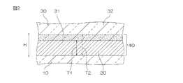
- FIG. 2 is a partially enlarged cross-sectional view of the laminated optical film shown in FIG. 1;
- FIG. 3 is a schematic cross-sectional view of another embodiment of the laminated optical film of the present invention;
- the laminated optical film of this embodiment includes a second optical film, an adhesive layer, a first optical film, an adhesive layer, and a second optical film in order in the thickness direction.
- the laminated optical film X as one embodiment of the laminated optical film of the present invention includes an optical film 10 (first optical film), an adhesive layer 20, an optical film 30 (second optical film ) are provided in order in the thickness direction H.
- the adhesive layer 20 bonds the optical films 10 and 30 together.
- the laminated optical film X has a sheet shape with a predetermined thickness and spreads in a direction orthogonal to the thickness direction H (plane direction).
- the laminated optical film X is a composite film incorporated into the laminated structure of the display panel.
- the optical film 10 is a functional optical film in this embodiment.
- Functional optical films include, for example, polarizer films and retardation films.
- a polarizer film includes, for example, a hydrophilic polymer film that has undergone a dyeing treatment with a dichroic substance and a subsequent stretching treatment.
- Dichroic substances include, for example, iodine and dichroic dyes.
- Hydrophilic polymer films include, for example, polyvinyl alcohol (PVA) films, partially formalized PVA films, and partially saponified ethylene-vinyl acetate copolymer films.
- Polarizer films also include oriented polyene films. Materials for the oriented polyene film include, for example, dehydrated PVA and dehydrochlorinated polyvinyl chloride.
- a PVA film that has undergone a dyeing treatment with iodine and a subsequent uniaxial stretching treatment is preferable because it has excellent optical properties such as polarizing properties.
- the thickness of the optical film 10 as a polarizer film is preferably 15 ⁇ m or less, more preferably 12 ⁇ m or less, even more preferably 10 ⁇ m or less, and particularly preferably 8 ⁇ m or less, from the viewpoint of thinning.
- a thin polarizer film has excellent visibility due to its small thickness unevenness, and is excellent in durability against thermal shock due to its small dimensional change due to temperature change.
- the thickness of the optical film 10 as a polarizer film is preferably 3 ⁇ m or more, more preferably 5 ⁇ m or more, from the viewpoint of strength.
- retardation films include ⁇ /2 wavelength films, ⁇ /4 wavelength films, and viewing angle compensation films.
- Materials for the retardation film include, for example, polymer films birefringent by stretching.
- Polymeric films include, for example, cellulose films and polyester films.
- Cellulose films include, for example, triacetyl cellulose films.
- Polyester films include, for example, polyethylene terephthalate films and polyethylene naphthalate films.
- the thickness of the optical film 10 as a retardation film is, for example, 20 ⁇ m or more and, for example, 150 ⁇ m or less.
- a film comprising a substrate such as a cellulose film and an orientation layer of a liquid crystal compound such as a liquid crystalline polymer on the substrate can also be preferably used.
- the adhesive layer 20 is a cured adhesive composition.
- the adhesive layer 20 bonds directly to the optical film 10 and directly bonds to the optical film 30 .
- the adhesive composition contains a curable resin. The components of the adhesive composition are specifically described below.
- the thickness T1 of the adhesive layer 20 is preferably 0.1 ⁇ m or more, more preferably 0.4 ⁇ m or more, even more preferably 0.7 ⁇ m or more, and particularly preferably 0.1 ⁇ m or more. .8 ⁇ m or more. From the viewpoint of thinning the laminated optical film X, the thickness T1 of the adhesive layer 20 is preferably 5 ⁇ m or less, more preferably 3 ⁇ m or less, still more preferably 1.5 ⁇ m or less, and particularly preferably 1 ⁇ m or less.
- the thickness T1 of the adhesive layer 20 is the length in the thickness direction H of the region having the post-curing texture (formed from the post-curing constituents) of the adhesive composition. This length can be measured in an image obtained by observation such as SEM observation. Specifically, the thickness T1 of the adhesive layer 20 can be measured by the method described later with regard to Examples.
- the first indentation elastic modulus of the adhesive layer 20 at 25° C. measured by the nanoindentation method is preferably 0.01 GPa or more, more preferably 0.03 GPa or more, still more preferably 0.05 GPa or more, and particularly preferably is 0.07 GPa or more (the first indentation elastic modulus is the indentation elastic modulus under the first measurement conditions.
- the first measurement conditions are as described later with regard to the examples, and under the first measurement conditions, the load
- the maximum indentation depth of the indenter with respect to the measurement sample during the application process is 200 nm). Such a configuration is preferable from the viewpoint of securing the bonding strength between the optical films 10 and 30 .
- the first indentation modulus is preferably 5 GPa or less, more preferably 3 GPa or less, and even more preferably 1 GPa or less.
- Such a configuration is preferable for ensuring the flexibility of the adhesive layer 20, and therefore preferable for ensuring the flexibility of the laminated optical film X.
- FIG. Methods for adjusting the indentation modulus of the adhesive layer 20 include, for example, adjusting the composition of the adhesive composition. Specifically, the adjustment of the number of functional groups of the polymerizable compound described later in the adhesive composition forming the adhesive layer 20, that is, the adjustment of the acrylic equivalent and epoxy equivalent of the polymerizable compound, is the pressing of the adhesive layer 20. It is effective as an elastic modulus adjustment method.
- the nanoindentation method is a technique for measuring various physical properties of samples on a nanometer scale.
- the nanoindentation method is performed in compliance with ISO14577.
- a process of pushing an indenter into a sample set on a stage (loading process) and then a process of withdrawing the indenter from the sample (unloading process) are performed.
- the load acting between the indenter and the sample and the relative displacement of the indenter with respect to the sample are measured (load-displacement measurement). This makes it possible to obtain a load-displacement curve. From this load-displacement curve, it is possible to obtain various physical properties of the measurement sample based on nanometer scale measurement.
- a nanoindenter (trade name “Triboindenter”, manufactured by Hysitron) can be used for the load-displacement measurement of the cross section of the adhesive layer by the nanoindentation method. Specifically, it is as described later with respect to Examples.
- the second indentation elastic modulus of the adhesive layer 20 at 25° C. measured by the nanoindentation method is preferably 0.5 GPa or more, more preferably 1 GPa or more, still more preferably 1.5 GPa or more, and particularly preferably 2 GPa.
- the second indentation elastic modulus is the indentation elastic modulus under the second measurement conditions.
- the second measurement conditions are as described later with regard to the examples.
- the The maximum indentation depth of the indenter with respect to the measurement sample is 50 nm). Such a configuration is preferable from the viewpoint of securing the bonding strength between the optical films 10 and 30 .
- the second indentation modulus is preferably 7 GPa or less, more preferably 5 GPa or less, and even more preferably 3 GPa or less.
- Such a configuration is preferable for ensuring the flexibility of the adhesive layer 20, and therefore preferable for ensuring the flexibility of the laminated optical film X.
- the optical film 30 is a transparent protective film in this embodiment.
- the transparent protective film is, for example, a flexible transparent resin film.
- Materials for the transparent protective film include, for example, polyolefin, polyester, polyamide, polyimide, polyvinyl chloride, polyvinylidene chloride, cellulose, modified cellulose, polystyrene, and polycarbonate.
- Polyolefins include, for example, cycloolefin polymers (COP), polyethylene, polypropylene, ethylene-propylene copolymers, ethylene-vinyl acetate copolymers, and ethylene-vinyl alcohol copolymers.
- COP cycloolefin polymers
- Polyesters include, for example, polyethylene terephthalate, polyethylene naphthalate, and polybutylene terephthalate.
- Polyamides include, for example, polyamide 6, polyamide 6,6, and partially aromatic polyamides. Examples of modified cellulose include triacetyl cellulose. These materials may be used alone, or two or more of them may be used in combination.
- polyolefin is preferably used, and COP is more preferably used.
- the thickness of the optical film 30 is preferably 5 ⁇ m or more, more preferably 10 ⁇ m or more, and even more preferably 20 ⁇ m or more. From the viewpoint of thinning the laminated optical film X, the thickness of the optical film 30 is preferably 100 ⁇ m or less, more preferably 70 ⁇ m or less, and even more preferably 50 ⁇ m or less.
- the optical film 30 has a boundary area 31 on the side of the adhesive layer 20 and a non-boundary area 32 on the side opposite to the adhesive layer 20, as shown in FIG.
- the boundary region 31 contains the adhesive raw material component derived from the adhesive layer 20 .
- the constituent components of the optical film 30 and the raw material components of the adhesive are mixed.
- Methods for detecting adhesive raw material components include, for example, Time-of-Flight Secondary Ion Mass Spectrometry (TOF-SIMS).
- TOF-SIMS Time-of-Flight Secondary Ion Mass Spectrometry
- the non-boundary region 32 does not contain the adhesive raw material component derived from the adhesive layer 20 .
- the non-boundary region 32 consists of constituents of the optical film 30 .
- the boundary region 31 is a region where the adhesive raw material component is detected at a detection limit value (positive/negative secondary ion intensity of 0.1 counts/second) or more in the above detection method, and the detection limit value or more is defined.
- a non-boundary region 32 is a region in which no adhesive raw material component is detected.
- the ratio of the thickness of the boundary region 31 to the thickness of the non-boundary region 32 is, for example, 0.01% or more, preferably 0.05% or more, and is, for example, 50% or less, preferably 20% or less.
- the thickness of the boundary region 31 is, for example, 0.01 ⁇ m or more, preferably 0.05 ⁇ m or more.
- the thickness of the boundary region 31 is, for example, 10 ⁇ m or less, preferably 5 ⁇ m or less.
- Methods for adjusting the thickness of the boundary region 31 include, for example, adjusting the composition of the adhesive composition.
- the boundary region 31 and the adhesive layer 20 form an adhesive raw material component-containing portion 40 .
- the ratio (T2/T1) of the thickness T2 of the adhesive raw material component-containing portion 40 to the thickness T1 of the adhesive layer 20 is , is 1.01 or more, preferably 1.05 or more, more preferably 1.1 or more, and still more preferably 1.2 or more. From the viewpoint of achieving both adhesion between the adhesive layer 20 and the optical film 30 and production stability of the laminated optical film X, the ratio (T2/T1) is preferably 1.3 or less, more preferably 1.3. It is 25 or less, more preferably 1.2 or less.
- the adhesion between the adhesive layer 20 and the optical film 30 is achieved, for example, by ensuring the thickness of the adhesive layer 20 so that when the laminated optical film X is folded, the interface between the adhesive layer 20 and the optical film 30 is This can be ensured by suppressing the occurrence of peeling due to load.
- the thickness T2 of the adhesive raw material component-containing portion 40 is larger than the thickness of the adhesive layer 20 and smaller than the total thickness of the adhesive layer 20 and the optical film 30 .
- the thickness T2 of the adhesive raw material component-containing portion 40 is, for example, 0.101 ⁇ m or more and, for example, 6.5 ⁇ m or less depending on the thickness and composition of the adhesive layer 20 and the material of the optical film 30 .
- the thickness T2 of the adhesive raw material component-containing portion 40 and the thickness of the boundary region 31 can be measured by the method described later with regard to the examples.
- the optical film 30 has the boundary region 31 on the adhesive layer 20 side of the same film.
- the constituent components of the optical film 30 and the raw material components of the adhesive are mixed.
- the ratio of the thickness T2 of the adhesive raw material component-containing portion 40 (adhesive layer 20, boundary region 31) to the thickness T1 of the adhesive layer 20 is 1.01 or more, It is preferably 1.05 or more, more preferably 1.1 or more, still more preferably 1.2 or more.
- the thickness T2 of the portion (the adhesive layer 20 and the boundary region 31) that contains the adhesive raw material components and participates in the adhesive function is greater than the thickness T1 of the adhesive layer 20.
- FIG. These configurations relating to the boundary between the optical film 30 and the adhesive layer 20 and the vicinity thereof are suitable for realizing a strong interaction between the optical film 30 and the adhesive layer 20 to ensure high bonding strength. Securing the bonding strength between the optical film 30 and the adhesive layer 20 helps to secure the bonding strength of the adhesive layer 20 between the optical films 10 and 30 . Therefore, the laminated optical film X is suitable for securing bonding strength between the optical films 10 and 30 even with a thin adhesive layer 20 .
- Securing the bonding strength between the optical films 10 and 30 is suitable for suppressing peeling between the optical films 10 and 30 .
- such a laminated optical film X ensures a bonding strength between the optical films 10 and 30 by the thin adhesive layer 20, thereby preventing peeling between the optical films 10 and 30. Suitable for suppression. Specifically, it is as shown in Examples and Comparative Examples below.
- the 90° peel strength of the optical film 30 to the optical film 10 at 25°C is preferably 0.8 N/15 mm or more, more preferably 1 N/15 mm or more, and still more preferably 1.2 N/15 mm or more. , particularly preferably 1.5 N/15 mm or more.
- the 90° peel strength is, for example, 10 N/15 mm or less.
- the 90° peel strength can be measured by the method described below with respect to the Examples.
- a method for adjusting the 90° peel strength for example, adjustment of the above ratio (T2/T1) and adjustment of the composition of the adhesive composition are exemplified.
- the ratio of the 90° peel strength (N/15mm) to the above-mentioned first indentation modulus (GPa) is preferably 5 or more, more preferably 10 or more, still more preferably 15 or more, and preferably 30 or less, It is more preferably 25 or less.
- Such a configuration is preferable for suppressing peeling between the optical films 10 and 30 when the laminated optical film X (particularly the thin laminated optical film X) is repeatedly folded.
- the ratio of the 90° peel strength (N/15mm) to the above-mentioned second indentation modulus (GPa) is preferably 0.2 or more, more preferably 0.3 or more, still more preferably 0.4 or more, and , preferably 5 or less, more preferably 3 or less, and still more preferably 2 or less.
- Such a configuration is preferable for suppressing peeling between the optical films 10 and 30 when the laminated optical film X (particularly the thin laminated optical film X) is repeatedly folded.
- the adhesive layer 20 is, for example, a cured product of an adhesive composition (active energy ray-curable composition) containing an active energy ray-curable resin.
- Active energy ray-curable compositions include, for example, electron beam-curable compositions, UV-curable compositions, and visible light-curable compositions.
- the active energy ray-curable composition is either one or both of a radically polymerizable composition and a cationic polymerizable composition.
- a radically polymerizable composition contains a radically polymerizable compound as a monomer.
- a radically polymerizable compound is a compound having a radically polymerizable functional group.
- examples of radically polymerizable functional groups include ethylenically unsaturated bond-containing groups.
- Ethylenically unsaturated bond-containing groups include, for example, (meth)acryloyl groups, vinyl groups, and allyl groups.
- a (meth)acryloyl group means an acryloyl group and/or a methacryloyl group.
- the active energy ray-curable composition preferably contains a radically polymerizable compound having a (meth)acryloyl group as a main component.
- a main component means the component with the largest mass ratio.
- the proportion of the (meth)acryloyl group-containing radically polymerizable compound in the active energy ray-curable composition is, for example, 50% by mass or more, preferably 70% by mass or more, and more preferably 80% by mass or more.
- the radically polymerizable compound includes a monofunctional radically polymerizable compound and a difunctional or higher polyfunctional radically polymerizable compound.
- Examples of monofunctional radically polymerizable compounds include (meth)acrylamide derivatives having a (meth)acrylamide group.
- (Meth)acrylamide derivatives include N-alkyl group-containing (meth)acrylamide derivatives, N-hydroxyalkyl group-containing (meth)acrylamide derivatives, N-aminoalkyl group-containing (meth)acrylamide derivatives, N-alkoxy group-containing (meth)acrylamide derivatives, ) acrylamide derivatives and N-mercaptoalkyl group-containing (meth)acrylamide derivatives.
- N-alkyl group-containing (meth)acrylamide derivatives include, for example, N-methyl(meth)acrylamide, N,N-dimethyl(meth)acrylamide, N,N-diethyl(meth)acrylamide, N-isopropyl(meth)acrylamide , N-butyl(meth)acrylamide, and N-hexyl(meth)acrylamide, preferably N,N-diethylacrylamide is used.
- N-hydroxyalkyl group-containing (meth)acrylamide derivatives include, for example, N-methylol(meth)acrylamide, N-hydroxyethyl(meth)acrylamide, and N-methylol-N-propane(meth)acrylamide, preferably is N-hydroxyethyl acrylamide.
- the (meth)acrylamide derivatives may be used alone, or two or more of them may be used in combination.
- Examples of monofunctional radically polymerizable compounds include (meth)acrylic acid derivatives having a (meth)acryloyloxy group.
- Examples of the (meth)acrylic acid derivative include (meth)acrylic acid alkyl esters and (meth)acrylic acid derivatives other than (meth)acrylic acid alkyl esters.
- the (meth)acrylic acid derivatives may be used alone, or two or more of them may be used in combination.
- (Meth)acrylic acid alkyl esters include, for example, methyl (meth)acrylate, ethyl (meth)acrylate, n-propyl (meth)acrylate, isopropyl (meth)acrylate, n-butyl (meth)acrylate, isobutyl (meth)acrylate, ) acrylate, n-pentyl (meth) acrylate, 2,2-dimethylbutyl (meth) acrylate, n-hexyl (meth) acrylate, n-octyl (meth) acrylate, 2-ethylhexyl (meth) acrylate, 4-methyl- 2-propylpentyl (meth)acrylate, and n-octadecyl (meth)acrylate.
- Examples of (meth)acrylic acid derivatives other than (meth)acrylic acid alkyl esters include (meth)acrylic acid cycloalkyl esters, (meth)acrylic acid aralkyl esters, hydroxyl group-containing (meth)acrylic acid derivatives, alkoxy group-containing ( Examples include meth)acrylic acid derivatives and phenoxy group-containing (meth)acrylic acid derivatives.
- (Meth)acrylic acid cycloalkyl esters include, for example, cyclohexyl (meth)acrylate and cyclopentyl (meth)acrylate.
- (Meth)acrylic acid aralkyl esters include, for example, benzyl (meth)acrylate and 3-phenoxybenzyl (meth)acrylate.
- hydroxyl group-containing (meth)acrylic acid derivatives include 2-hydroxyethyl (meth)acrylate, 2-hydroxypropyl (meth)acrylate, 3-hydroxypropyl (meth)acrylate, 2-hydroxybutyl (meth)acrylate, 4 -hydroxybutyl (meth)acrylate, [4-(hydroxymethyl)cyclohexyl]methyl acrylate, and 2-hydroxy-3-phenoxypropyl (meth)acrylate.
- Alkoxy group-containing (meth)acrylic acid derivatives include, for example, 2-methoxyethyl (meth)acrylate, 2-ethoxyethyl (meth)acrylate, and 3-methoxybutyl (meth)acrylate.
- Phenoxy group-containing (meth)acrylic acid derivatives include, for example, phenoxyethyl (meth)acrylate and phenoxydiethylene glycol (meth)acrylate.
- the (meth)acrylic acid derivative other than the (meth)acrylic acid alkyl ester is preferably at least one selected from the group consisting of 3-phenoxybenzyl acrylate, 2-hydroxy-3-phenoxypropyl acrylate, and phenoxydiethylene glycol acrylate. one is used.
- Carboxyl group-containing monomers are also included as monofunctional radically polymerizable compounds.
- Carboxyl group-containing monomers include, for example, (meth)acrylic acid, carboxyethyl acrylate, carboxypentyl acrylate, itaconic acid, maleic acid, fumaric acid, crotonic acid, and isocrotonic acid.
- the monofunctional radically polymerizable compound also includes a lactam-based vinyl monomer.
- Lactamic vinyl monomers include, for example, N-vinyl-2-pyrrolidone, N-vinyl- ⁇ -caprolactam, and methylvinylpyrrolidone.
- Examples of monofunctional radically polymerizable compounds include vinyl-based monomers having nitrogen-containing heterocycles.
- Such monomers include, for example, vinylpyridine, vinylpiperidone, vinylpyrimidine, vinylpiperazine, vinylpyrazine, vinylpyrrole, vinylimidazole, vinyloxazole, and vinylmorpholine.
- polyfunctional radically polymerizable compounds include tripropylene glycol di(meth)acrylate, tetraethylene glycol di(meth)acrylate, 1,6-hexanediol di(meth)acrylate, 1,9-nonanediol di(meth)acrylate.
- acrylate 1,10-decanediol diacrylate, 2-ethyl-2-butylpropanediol di(meth)acrylate, neopentyl glycol di(meth)acrylate, tricyclodecanedimethanol di(meth)acrylate, cyclic trimethylol propane formal (meth)acrylate, dioxane glycol di(meth)acrylate, trimethylolpropane tri(meth)acrylate, pentaerythritol tri(meth)acrylate, pentaerythritol tetra(meth)acrylate, dipentaerythritol penta(meth)acrylate, and dipentaerythritol hexa(meth)acrylate are used, preferably tripropylene glycol diacrylate.
- the polyfunctional radically polymerizable compounds may be used alone, or two or more of them may be used in combination.
- a polyfunctional radically polymerizable compound
- the active energy ray-curable composition When the active energy ray-curable composition is an ultraviolet curable composition or a visible light curable composition, the active energy ray curable composition contains a photopolymerization initiator.
- Photoinitiators include, for example, benzophenone compounds, benzoin ether compounds, and thioxanthone compounds.
- Benzophenone compounds include, for example, benzyl, benzophenone, benzoylbenzoic acid, and 3,3'-dimethyl-4-methoxybenzophenone.
- Benzoin ether compounds include, for example, benzoin methyl ether, benzoin ethyl ether, benzoin isopropyl ether, and benzoin butyl ether.
- Thioxanthone compounds include, for example, thioxanthone, 2-chlorothioxanthone, 2-methylthioxanthone, 2,4-dimethylthioxanthone, isopropylthioxanthone, 2,4-dichlorothioxanthone, 2,4-diethylthioxanthone, 2,4-diisopropylthioxanthone, and dodecylthioxanthone.
- a photopolymerization initiator that is highly sensitive to light of 380 nm or longer is preferably used.
- photopolymerization initiators include, for example, 2-methyl-1-(4-methylthiophenyl)-2-morpholinopropan-1-one, 2-benzyl-2-dimethylamino-1-(4-morphol linophenyl)-butanone-1,2-(dimethylamino)-2-[(4-methylphenyl)methyl]-1-[4-(4-morpholinyl)phenyl]-1-butanone, 2,4,6- trimethylbenzoyl-diphenyl-phosphine oxide, bis(2,4,6-trimethylbenzoyl)-phenylphosphine oxide, and bis( ⁇ 5-2,4-cyclopentadien-1-yl)-bis(2,6-difluoro -3-(1H-pyrrol-1-yl)-
- 2,4-diethylthioxanthone and/or 2-methyl-1-(4-methylthiophenyl)-2-morpholinopropan-1-one are preferably used.
- the content of the photopolymerization initiator in the active energy ray-curable composition is preferably 0.1 parts by mass or more, more preferably 0.05 parts by mass with respect to 100 parts by mass of the curable component (radical polymerizable compound). Above, more preferably 0.1 parts by mass or more, preferably 20 parts by mass or less, more preferably 10 parts by mass or less, and even more preferably 5 parts by mass or less.
- the composition contains a cationic polymerizable compound as a monomer.
- the cationically polymerizable compound is a compound having a cationically polymerizable functional group, and includes a monofunctional cationically polymerizable compound having one cationically polymerizable functional group and a polyfunctional cationically polymerizable compound having two or more cationically polymerizable functional groups. compounds.
- a monofunctional cationic polymerizable compound has a relatively low liquid viscosity. By adding such a monofunctional cationically polymerizable compound to the resin composition, the viscosity of the resin composition can be lowered.
- monofunctional cationically polymerizable compounds often have functional groups that exhibit various functions.
- various functions can be expressed in the resin composition and/or the cured product of the resin composition.
- the resin composition containing the polyfunctional cationically polymerizable compound by curing the resin composition containing the polyfunctional cationically polymerizable compound, a cured product having a three-dimensional crosslinked portion is obtained (the polyfunctional cationically polymerizable compound functions as a crosslinking agent). From such a point of view, it is preferable to use polyfunctional cationically polymerizable compounds.
- the amount of the polyfunctional cationically polymerizable compound relative to 100 parts by weight of the monofunctional cationically polymerizable compound is, for example, 10 parts by weight or more. It is 1000 mass parts or less.
- Cationic polymerizable functional groups include, for example, epoxy groups, oxetanyl groups, and vinyl ether groups.
- Compounds having an epoxy group include, for example, aliphatic epoxy compounds, alicyclic epoxy compounds, and aromatic epoxy compounds.
- an alicyclic epoxy compound is preferably used from the viewpoint of curability and adhesiveness of the cationic polymerizable composition.
- the alicyclic epoxy compounds include, for example, 3,4-epoxycyclohexylmethyl-3,4-epoxycyclohexanecarboxylate, or caprolactone-modified 3,4-epoxycyclohexylmethyl-3,4-epoxycyclohexanecarboxylate, Examples include trimethylcaprolactone-modified products and valerolactone-modified products.
- Examples of commercially available alicyclic epoxy compounds include Celoxide 2021, Celoxide 2021A, Celoxide 2021P, Celoxide 2081, Celoxide 2083, and Celoxide 2085 (manufactured by Daicel Chemical Industries, Ltd.), and Cyracure UVR-6105.
- Cyracure UVR-6107 Cyracure 30, and R-6110 (manufactured by Dow Chemical Japan). From the viewpoint of improving curability and reducing viscosity of the cationic polymerizable composition, it is preferable to use a compound having an oxetanyl group and/or a compound having a vinyl ether group.
- Compounds having an oxetanyl group include, for example, 3-ethyl-3-hydroxymethyloxetane, 1,4-bis[(3-ethyl-3-oxetanyl)methoxymethyl]benzene, 3-ethyl-3-(phenoxymethyl) oxetane, di[(3-ethyl-3-oxetanyl)methyl]ether, 3-ethyl-3-(2-ethylhexyloxymethyl)oxetane, and phenol novolac oxetane.
- oxetanyl group examples include, for example, Aron oxetane OXT-101, Aron oxetane OXT-121, Aron oxetane OXT-211, Aron oxetane OXT-221, and Aron oxetane OXT-212 (manufactured by Toagosei Co., Ltd.). is mentioned.
- Examples of compounds having a vinyl ether group include 2-hydroxyethyl vinyl ether, diethylene glycol monovinyl ether, 4-hydroxybutyl vinyl ether, diethylene glycol vinyl ether, triethylene glycol divinyl ether, cyclohexanedimethanol divinyl ether, cyclohexanedimethanol monovinyl ether, tricyclo.
- the active energy ray curable composition When the active energy ray-curable composition is an ultraviolet curable composition or a visible light curable composition, the active energy ray curable composition contains a photocationic polymerization initiator.
- a photocationic polymerization initiator generates cationic species or Lewis acid upon irradiation with active energy rays (visible light, ultraviolet rays, X-rays, electron beams, etc.) and initiates the polymerization reaction of the cationic polymerizable functional groups.
- the photocationic polymerization initiator includes a photoacid generator and a photobase generator, preferably a photoacid generator.
- the active energy ray-curable composition is used as a visible light-curable composition
- a cationic photopolymerization initiator that is particularly sensitive to light of 380 nm or longer.
- a photocationic polymerization initiator it is preferable to use together a photosensitizer showing maximum absorption of light having a wavelength longer than 380 nm.
- a photocationic polymerization initiator is generally a compound that exhibits maximum absorption in a wavelength region near or shorter than 300 nm. Long wavelength light can be effectively used to promote the generation of cationic species or Lewis acids from the photocationic polymerization initiator.
- photosensitizers include anthracene compounds, pyrene compounds, carbonyl compounds, organic sulfur compounds, persulfides, redox compounds, azo compounds, diazo compounds, halogen compounds, and photoreducible dyes. These may be used alone, or two or more of them may be used in combination. In particular, an anthracene compound is preferable because of its excellent photosensitizing effect.
- commercially available anthracene compounds as photosensitizers include, for example, Anthracure UVS-1331 and Anthracure UVS-1221 (manufactured by Kawasaki Kasei Co., Ltd.). The content of the photosensitizer in the composition is, for example, 0.1 to 5% by weight.
- the active energy ray-curable composition may contain an oligomer.
- Oligomers include acrylic oligomers, fluorine oligomers, and silicone oligomers, preferably acrylic oligomers.
- the addition of the oligomer to the active energy ray-curable composition is useful for adjusting the viscosity of the composition and for suppressing the shrinkage of the composition during curing. Suppression of curing shrinkage of the active energy ray-curable composition is preferable for reducing interfacial stress between the formed adhesive layer 20 and the optical films 10 and 30 . Suppression of interfacial stress is useful for securing bonding strength between the optical films 10 and 30 .
- Examples of (meth)acrylic monomers that form acrylic oligomers include (meth)acrylic acid alkyl esters having 1 to 20 carbon atoms, cycloalkyl (meth)acrylates, aralkyl (meth)acrylates, polycyclic (meth)acrylates, Examples include hydroxyl group-containing (meth)acrylic acid esters and halogen-containing (meth)acrylic acid esters.
- (Meth)acrylic acid alkyl esters for example, methyl (meth)acrylate, ethyl (meth)acrylate, n-propyl (meth)acrylate, isopropyl (meth)acrylate, 2-methyl-2-nitropropyl (meth)acrylate , n-butyl (meth)acrylate, isobutyl (meth)acrylate, S-butyl (meth)acrylate, t-butyl (meth)acrylate, n-pentyl (meth)acrylate, t-pentyl (meth)acrylate, 3-pentyl (Meth)acrylate, 2,2-dimethylbutyl (meth)acrylate, n-hexyl (meth)acrylate, cetyl (meth)acrylate, n-octyl (meth)acrylate, 2-ethylhexyl (meth)acrylate, 4-methyl- 2-propylpentyl (meth)acrylate
- Cycloalkyl (meth)acrylates include, for example, cyclohexyl (meth)acrylate and cyclopentyl (meth)acrylate.
- Aralkyl (meth)acrylates include, for example, benzyl (meth)acrylate.
- Polycyclic (meth)acrylates include, for example, 2-isobornyl (meth)acrylate, 2-norbornylmethyl (meth)acrylate, 5-norbornen-2-yl-methyl (meth)acrylate, and 3-methyl- 2-Norbornylmethyl (meth)acrylate can be mentioned.
- hydroxyl group-containing (meth)acrylic acid esters examples include hydroxyethyl (meth)acrylate, 2-hydroxypropyl (meth)acrylate, and 2,3-dihydroxypropylmethyl-butyl (meth)methacrylate.
- Halogen-containing (meth)acrylic acid esters include, for example, 2,2,2-trifluoroethyl (meth)acrylate, 2,2,2-trifluoroethylethyl (meth)acrylate, tetrafluoropropyl (meth)acrylate, hexafluoropropyl (meth)acrylate, octafluoropentyl (meth)acrylate, heptadecafluorodecyl (meth)acrylate. These (meth)acrylates may be used alone, or two or more of them may be used in combination.
- the weight average molecular weight (Mw) of the acrylic oligomer is preferably 15,000 or less, more preferably 10,000 or less, even more preferably 5,000 or less. Mw of the acrylic oligomer is preferably 500 or more, more preferably 1000 or more, and even more preferably 1500 or more.
- the content of the acrylic oligomer in the active energy ray-curable composition is preferably 2% by mass or more, more preferably 4% by mass or more, and is preferably 20% by mass or less, more preferably 15% by mass or less. .
- the active energy ray-curable composition may contain other components.
- Other ingredients include silane coupling agents, leveling agents, surfactants, plasticizers, and UV absorbers.
- the blending amount of the other component is preferably 10 parts by mass or less, more preferably 5 parts by mass or less, and still more preferably 3 parts by mass or less with respect to 100 parts by mass of the curable component. Part by mass or more.
- the viscosity of the active energy ray-curable composition at 25° C. is preferably 3 mPa ⁇ s or more, more preferably 5 mPa ⁇ s or more, and still more preferably 10 mPa ⁇ s or more, from the viewpoint of coatability in the coating step described later. and is preferably 100 mPa ⁇ s or less, more preferably 50 mPa ⁇ s or less, and still more preferably 30 mPa ⁇ s or less.
- the viscosity of the composition is a value measured with an E-type viscometer (cone plate type viscometer).
- the laminated optical film X can be produced, for example, as follows.
- an active energy ray-curable composition is applied to one side (to-be-bonded surface) of one optical film (optical film 10 or optical film 30) to form a coating film of the composition (application step).
- the surface to be bonded of the optical film may be subjected to a surface modification treatment.
- Surface modification treatments include corona treatment, plasma treatment, excimer-treatment, and flame treatment.
- Examples of coating methods in this step include reverse coaters, gravure coaters, bar reverse coaters, roll coaters, die coaters, bar coaters, and rod coaters.
- the other optical film (optical film 30 or optical film 10) is attached to one optical film via the composition coating film.
- a roll laminator can be used for lamination.
- the active energy ray-curable composition preferably contains a monomer having an SP value close to the SP value of the resin in the optical film 30 .
- the active energy ray-curable composition contains such a monomer, the monomer in contact with the surface of the optical film 30 is compatible with the surface during the process of applying and curing the active energy ray-curable composition. , the boundary region 31 is likely to be formed.
- the composition coating film between the optical films 10 and 30 is irradiated with an active energy ray to cure the coating film (active energy ray-curable composition). (hardening process).
- an adhesive layer 20 is formed between the optical films 10 and 30, and the optical films 10 and 30 are joined via the adhesive layer 20 (the adhesive layer 20 is not a pressure sensitive adhesive layer).
- the active energy ray from the optical film 30 side.
- Electron beams, ultraviolet rays, and visible rays can be used as active energy rays.
- Examples of electron beam irradiation means include an electron beam accelerator.
- Ultraviolet and visible light sources include, for example, LED lights, gallium-filled metal halide lamps, low-pressure mercury lamps, medium-pressure mercury lamps, high-pressure mercury lamps, ultra-high pressure mercury lamps, xenon lamps, halogen lamps, and gallium lamps.
- a wavelength cut filter for cutting a part of the wavelength range of ultraviolet rays and/or visible light emitted from the light source may be used as needed.
- optical films 30 may be bonded to both surfaces of the optical film 10 in the thickness direction H with adhesive layers 20 interposed therebetween.
- the laminated optical film X (laminated optical film X') shown in FIG. Prepare.
- the compositions of the active energy ray-curable compositions forming the two adhesive layers 20 may be the same or different.
- the materials of the two optical films 30 may be the same or different.
- the laminated optical film X′ can be produced, for example, by bonding the additional optical film 30 to the laminated optical film X shown in FIG. 1 via the adhesive layer 20 .
- the thickness of the adhesive layer 20 is The ratio of the thickness T2 of the adhesive raw material component-containing portion 40 to T1 (T2/T1) is 1.01 or more, preferably 1.05 or more, more preferably 1.1 or more, and still more preferably 1.2. That's it.
- Example 1 The following components were mixed at 25° C. for 1 hour at the blending amounts (solid content blending amounts) shown in Table 1 to prepare an adhesive composition (preparation step).
- the units for the amounts shown in Table 1 are relative "parts by weight”.
- Alfon 1190 (acrylic oligomer): viscosity 6000 mPa s (25 ° C.), Mw 1700, Tg -50 ° C., Toagosei BYK-UV3505 (leveling agent): modified poly having an acrylic group Dimethylsiloxane, manufactured by BYK
- the adhesive composition is coated on a long COP film (product name “Zeonor Film ZF14”, manufactured by Nippon Zeon Co., Ltd.) with a thickness of 23 ⁇ m as a transparent protective film to adhere to a thickness of 0.9 ⁇ m.
- a coating film was formed.
- an MCD coater manufactured by Fuji Kikai Co., Ltd. (cell shape: honeycomb, number of gravure roll lines: 1000 lines/inch, rotation speed: 140%/line speed) was used.
- a polarizer film (thickness: 5 ⁇ m) was bonded to the transparent protective film via an adhesive coating on the same film.
- the adhesive coating between the films was cured by irradiating the adhesive coating with ultraviolet rays through the transparent protective film.
- a gallium lamp was used for ultraviolet irradiation.
- the laminated optical film of Example 1 was produced as described above.
- the laminated optical film of Example 1 includes a polarizer film (5 ⁇ m thick), an adhesive layer, and a transparent protective film (23 ⁇ m thick) in this order in the thickness direction.
- Example 2 A laminated optical film of Example 2 was produced in the same manner as the laminated optical film of Example 1 except for the following.
- the line speed was increased by a predetermined level to shorten the time from the coating process to the curing process.
- the thickness of the coating film formed on the transparent protective film (COP film) in the coating step was set to 2.6 ⁇ m.
- the laminated optical film of Example 2 includes a polarizer film (5 ⁇ m thick), an adhesive layer, and a transparent protective film (23 ⁇ m thick) in this order in the thickness direction.
- Example 3 A laminated optical film of Example 3 was produced in the same manner as the laminated optical film of Example 1 except for the following.
- the line speed was lowered by a predetermined amount to lengthen the time from the coating process to the curing process.
- the thickness of the coating film formed on the transparent protective film (COP film) in the coating process was set to 1.2 ⁇ m.
- the laminated optical film of Example 3 includes a polarizer film (5 ⁇ m thick), an adhesive layer, and a transparent protective film (23 ⁇ m thick) in this order in the thickness direction.
- Comparative Example 1 A laminated optical film of Comparative Example 1 was produced in the same manner as the laminated optical film of Example 1 except for the following (the line speed between the coating step and the curing step was the same as in Example 1).
- an adhesive composition having the composition (components, compounding amount) shown in Table 1 was prepared.
- the monomers instead of “light acrylate POB-A” and “light acrylate P2H-A", 36 parts by mass of "light acrylate 1.9ND-A” (1,9-nonanediol diacrylate) manufactured by Kyoeisha Chemical Co., Ltd. and 12.5 parts by mass of “Light Acrylate HPP-A” (neopentyl hydroxypivalate glycol acrylic acid adduct) manufactured by Kyoeisha Chemical Co., Ltd. were used.
- the thickness of the coating film formed on the transparent protective film (COP film) in the coating process was set to 0.93 ⁇ m.
- the laminated optical film of Comparative Example 1 includes a polarizer film (5 ⁇ m thick), an adhesive layer, and a transparent protective film (23 ⁇ m thick) in this order in the thickness direction.
- the thickness T1 of the adhesive layer in each laminated optical film of Examples 1 to 3 and Comparative Example 1 was measured as follows. First, a 5 mm ⁇ 10 mm film piece (laminated optical film) was cut out from the laminated optical film. Next, the laminated optical film was cut by a cryomicrotome method. Specifically, the laminated optical film was cooled to ⁇ 30° C., cut with a hard knife in the thickness direction of the same film, and then returned to room temperature. Next, the cut surface of the laminated optical film thus formed with the cut surface was subjected to a conductive treatment with a thickness of 5 nm or less. Thus, an observation sample was obtained.
- the thickness of the adhesive layer was measured by SEM observation of the observation sample. Specifically, using a scanning electron microscope (product name "REGULUS8220", manufactured by HITACHI), a secondary electron image of the cut surface of the observation sample is observed and captured, and the thickness of the adhesive layer is measured. did. In this observation, the acceleration voltage was 3.0 kV, the current amount was 10 ⁇ A, the working distance was 8 mm, the magnification was 100,000 times, and the detection mode was Upper+Lower mode. Table 1 shows the thickness T1 ( ⁇ m) of the adhesive layer.
- the thickness T2 of the adhesive raw material component-containing portion in each of the laminated optical films of Examples 1 to 3 and Comparative Example 1 was measured as follows. First, the transparent protective film of the film piece cut out from the laminated optical film was thinned by scraping from the surface side of the transparent protective film to a predetermined depth with a microtome. A measurement sample was thus obtained. Next, the measurement sample was analyzed from the side of the transparent protective film by time-of-flight secondary ion mass spectrometry (TOF-SIMS).
- TOF-SIMS time-of-flight secondary ion mass spectrometry
- a time-of-flight secondary ion mass spectrometer (product name: TRIFT-V nanoTOF, manufactured by ULVAC-PHI) was used.
- irradiation with an etching ion beam and subsequent measurement ion beam ( In the irradiation of the etching ion beam, Ar gas cluster ions (cluster size (median value): 2500) were used, the acceleration voltage was 20 kV, and the ion beam current value was 20 kV.
- the irradiation range was 1000 ⁇ m ⁇ 1000 ⁇ m, and the irradiation time was 5 seconds.
- double-charged ions (Bi 3 ++ ) of bismuth clusters were used as primary ions for irradiation, and the acceleration voltage was 30 kV.
- the irradiation range was set to 200 ⁇ m ⁇ 200 ⁇ m in the central portion of the ion beam irradiation area for etching, and a neutralization gun was used to correct charging of the sample during analysis.This analysis was carried out at room temperature.
- the depth direction profile (depth profile) of the mass spectrum of the secondary ion (positive ion, negative ion) intensity was acquired.
- the value of C 3 H 5 + is the reference value 1 for positive ions.
- the value was converted to a value when the value of C 2 H ⁇ was taken as the reference value 1.
- the detection limit value (positive and negative secondary ion intensity 0.1 counts/sec) or more of the adhesive raw material component was detected (boundary region), and from the thickness of this boundary region and the above-mentioned thickness T1 of the adhesive layer, the adhesive raw material component
- the thickness T2 ( ⁇ m) of the containing portion was obtained, and is shown in Table 1. Table 1 also shows the ratio of the thickness T2 to the thickness T1.
- the 90° peel strength (N/15 mm) of the transparent protective film from the polarizer film was measured using a Tensilon universal tester (product name: "RTC", manufactured by A&D).
- RTC Tensilon universal tester
- the measurement temperature was 25° C.
- the peeling angle was 90°
- the peeling speed was 1000 mm/min.
- the measured 90° peel strength is shown in Table 1 as peel strength F1.
- ⁇ Indentation modulus> The elastic modulus of the adhesive layer in each of the laminated optical films of Examples 1 to 3 and Comparative Example 1 was examined by the nanoindentation method. Specifically, first, a film piece (laminated optical film) having a size of 5 mm ⁇ 10 mm was cut out from the laminated optical film. Next, the laminated optical film was cut by a cryomicrotome method. Specifically, the laminated optical film was cooled to ⁇ 30° C., cut with a hard knife in the thickness direction of the same film, and then returned to room temperature. Thus, a sample for measurement was obtained.
- Table 1 The value is shown in Table 1 as the indentation modulus M 1 (GPa) (the indentation modulus M 1 is the first indentation modulus described above). Table 1 also shows the ratio (F 1 /M 1 ) of the peel strength F 1 to the indentation modulus M 1 .
- a load-displacement measurement was performed using a nanoindenter under the same measurement conditions as the first measurement conditions (second measurement conditions) except that the maximum indentation depth was changed from 200 nm to 50 nm. Then, the obtained measurement data was processed by the dedicated analysis software (Ver. 9.4.0.1) of "TI950 Triboindenter” to calculate the indentation modulus of the adhesive layer. The value is shown in Table 1 as the indentation modulus M 2 (GPa) (the indentation modulus M 2 is the second indentation modulus described above). Table 1 also shows the ratio (F 1 /M 2 ) of the peel strength F 1 to the indentation modulus M 2 .
- a cross-linking agent product name "Coronate L", manufactured by Nippon Polyurethane
- a silane coupling agent product name "KMB-403", ⁇ - 0.075 parts by mass of glycidoxypropyltrimethoxysilane (manufactured by Shin-Etsu Chemical Co., Ltd.) was added and mixed to prepare an adhesive solution.
- the pressure-sensitive adhesive solution was applied onto the release-treated surface of the release liner to form a coating film (20 ⁇ m thick).
- This release liner is a polyethylene terephthalate film (thickness: 38 ⁇ m) that has undergone a predetermined release treatment.
- the coating film on the release liner was then dried to form an adhesive layer.
- evaluation samples were cut out from the multilayer film prepared as described above. Specifically, a rectangular sample of 25 mm ⁇ 100 mm was cut out from the laminated film so that the absorption axis direction of the polarizer film was parallel to the long side direction in the sample cut out.
- the sample was subjected to a bending test using a planar body no-load U-shaped stretching tester (manufactured by Yuasa System Equipment Co., Ltd.).
- a bending jig was attached to a range of 20 mm from the edge of the sample at each of both ends of the sample in the long side direction, and the sample was fixed to the tester (region of 60 mm in the center of the long side direction of the sample is in an unfixed state).
- the sample was placed in a constant temperature and humidity chamber under conditions of a temperature of 60°C and a relative humidity of 90%, and the bending speed It was repeatedly deformed (bent) 200,000 times at 60 rpm.
- the bent form in this test is a form in which the axial direction of the bending moment acting on the sample is orthogonal to the absorption axis direction of the polarizer film.
- the bending radius of the sample was 3 mm, and the bending angle was 180°.
- the case where peeling did not occur between the films up to 200,000 times of bending was evaluated as "excellent”.
- the case where peeling occurred at 80,000 or more and less than 200,000 was evaluated as "good", and the case where peeling occurred at less than 80,000 bending times was evaluated as "bad”.
- Table 1 shows the evaluation results.
- the laminated optical film of the present invention can be used, for example, as an element included in the laminated structure of a display panel such as a foldable display panel.
- X laminated optical film 10 optical film (first optical film) 20 adhesive layer 30 optical film (second optical film) 31 boundary region 40 adhesive raw material component-containing portion H thickness direction
Landscapes
- Physics & Mathematics (AREA)
- General Physics & Mathematics (AREA)
- Optics & Photonics (AREA)
- Engineering & Computer Science (AREA)
- Mechanical Engineering (AREA)
- Chemical & Material Sciences (AREA)
- Organic Chemistry (AREA)
- Adhesives Or Adhesive Processes (AREA)
- Laminated Bodies (AREA)
- Adhesive Tapes (AREA)
Priority Applications (3)
| Application Number | Priority Date | Filing Date | Title |
|---|---|---|---|
| CN202280022935.2A CN117042962A (zh) | 2021-04-30 | 2022-04-26 | 层叠光学膜 |
| JP2023517563A JPWO2022230887A1 (https=) | 2021-04-30 | 2022-04-26 | |
| KR1020237027592A KR20240004226A (ko) | 2021-04-30 | 2022-04-26 | 적층 광학 필름 |
Applications Claiming Priority (2)
| Application Number | Priority Date | Filing Date | Title |
|---|---|---|---|
| JP2021-077100 | 2021-04-30 | ||
| JP2021077100 | 2021-04-30 |
Publications (1)
| Publication Number | Publication Date |
|---|---|
| WO2022230887A1 true WO2022230887A1 (ja) | 2022-11-03 |
Family
ID=83848404
Family Applications (1)
| Application Number | Title | Priority Date | Filing Date |
|---|---|---|---|
| PCT/JP2022/018914 Ceased WO2022230887A1 (ja) | 2021-04-30 | 2022-04-26 | 積層光学フィルム |
Country Status (5)
| Country | Link |
|---|---|
| JP (1) | JPWO2022230887A1 (https=) |
| KR (1) | KR20240004226A (https=) |
| CN (1) | CN117042962A (https=) |
| TW (1) | TW202308843A (https=) |
| WO (1) | WO2022230887A1 (https=) |
Families Citing this family (1)
| Publication number | Priority date | Publication date | Assignee | Title |
|---|---|---|---|---|
| KR20250109442A (ko) | 2024-01-10 | 2025-07-17 | 주식회사 엘지에너지솔루션 | 배터리 팩 및 이의 동작 방법 |
Citations (6)
| Publication number | Priority date | Publication date | Assignee | Title |
|---|---|---|---|---|
| JP2015191142A (ja) * | 2014-03-28 | 2015-11-02 | 大日本印刷株式会社 | 位相差フィルム、光学フィルム、光学フィルムの製造方法 |
| JP2015200758A (ja) * | 2014-04-07 | 2015-11-12 | 日東電工株式会社 | 偏光板の製造方法 |
| WO2018056133A1 (ja) * | 2016-09-20 | 2018-03-29 | コニカミノルタ株式会社 | 偏光板及び液晶表示装置 |
| JP2020012081A (ja) * | 2018-07-20 | 2020-01-23 | ナガセケムテックス株式会社 | 光硬化性接着剤 |
| JP2020024367A (ja) * | 2018-07-25 | 2020-02-13 | 日東電工株式会社 | 偏光板およびその製造方法、ならびに画像表示装置 |
| WO2020115977A1 (ja) * | 2018-12-03 | 2020-06-11 | 日東電工株式会社 | 位相差層付偏光板およびそれを用いた画像表示装置 |
Family Cites Families (1)
| Publication number | Priority date | Publication date | Assignee | Title |
|---|---|---|---|---|
| JP7137900B2 (ja) | 2018-02-26 | 2022-09-15 | 日東電工株式会社 | 活性エネルギー線硬化型接着剤組成物、偏光フィルムおよびその製造方法、光学フィルム、ならびに画像表示装置 |
-
2022
- 2022-04-26 KR KR1020237027592A patent/KR20240004226A/ko active Pending
- 2022-04-26 JP JP2023517563A patent/JPWO2022230887A1/ja active Pending
- 2022-04-26 WO PCT/JP2022/018914 patent/WO2022230887A1/ja not_active Ceased
- 2022-04-26 CN CN202280022935.2A patent/CN117042962A/zh active Pending
- 2022-04-29 TW TW111116385A patent/TW202308843A/zh unknown
Patent Citations (6)
| Publication number | Priority date | Publication date | Assignee | Title |
|---|---|---|---|---|
| JP2015191142A (ja) * | 2014-03-28 | 2015-11-02 | 大日本印刷株式会社 | 位相差フィルム、光学フィルム、光学フィルムの製造方法 |
| JP2015200758A (ja) * | 2014-04-07 | 2015-11-12 | 日東電工株式会社 | 偏光板の製造方法 |
| WO2018056133A1 (ja) * | 2016-09-20 | 2018-03-29 | コニカミノルタ株式会社 | 偏光板及び液晶表示装置 |
| JP2020012081A (ja) * | 2018-07-20 | 2020-01-23 | ナガセケムテックス株式会社 | 光硬化性接着剤 |
| JP2020024367A (ja) * | 2018-07-25 | 2020-02-13 | 日東電工株式会社 | 偏光板およびその製造方法、ならびに画像表示装置 |
| WO2020115977A1 (ja) * | 2018-12-03 | 2020-06-11 | 日東電工株式会社 | 位相差層付偏光板およびそれを用いた画像表示装置 |
Also Published As
| Publication number | Publication date |
|---|---|
| TW202308843A (zh) | 2023-03-01 |
| JPWO2022230887A1 (https=) | 2022-11-03 |
| KR20240004226A (ko) | 2024-01-11 |
| CN117042962A (zh) | 2023-11-10 |
Similar Documents
| Publication | Publication Date | Title |
|---|---|---|
| JP6122337B2 (ja) | 偏光フィルムおよびその製造方法、光学フィルムおよび画像表示装置 | |
| KR20160048105A (ko) | 편광 필름용 경화형 접착제, 편광 필름, 광학 필름 및 화상 표시 장치 | |
| JP6841044B2 (ja) | 活性エネルギー線重合性接着剤および積層体 | |
| JP6481059B2 (ja) | 偏光フィルムおよびその製造方法、光学フィルムおよび画像表示装置 | |
| KR20190089003A (ko) | 광학 필름용 경화형 수지 조성물, 광학 필름 및 그 제조 방법 | |
| JP7417386B2 (ja) | 積層光学フィルムの製造方法 | |
| KR20210028582A (ko) | 적층 광학 필름 및 화상 표시 장치 | |
| WO2022230887A1 (ja) | 積層光学フィルム | |
| WO2022230888A1 (ja) | 積層光学フィルム | |
| JP6609075B2 (ja) | 偏光フィルムおよびその製造方法、光学フィルムおよび画像表示装置 | |
| JP7834727B2 (ja) | 積層光学フィルム | |
| KR20210028581A (ko) | 적층 광학 필름 및 화상 표시 장치 | |
| JP2017134413A (ja) | 偏光フィルムおよびその製造方法、光学フィルムおよび画像表示装置 | |
| JP7836298B2 (ja) | 積層光学フィルム | |
| JP2018092187A (ja) | 偏光フィルムおよびその製造方法、光学フィルムおよび画像表示装置 | |
| WO2022230890A1 (ja) | 積層光学フィルム | |
| KR20210028580A (ko) | 적층 광학 필름 및 화상 표시 장치 | |
| TWI917665B (zh) | 偏光薄膜及影像顯示裝置 | |
| JP7850513B2 (ja) | 積層光学フィルムおよび画像表示装置 | |
| TWI917666B (zh) | 偏光薄膜及影像顯示裝置 | |
| JP2026059299A (ja) | 光学積層体および光学積層体の製造方法 | |
| JP2026026396A (ja) | 積層光学フィルム用接着剤組成物および積層光学フィルム | |
| JP2025176046A (ja) | 積層光学フィルムの製造方法 | |
| JP2026041925A (ja) | 積層光学フィルム用接着剤組成物および積層光学フィルム | |
| WO2024247659A1 (ja) | 積層光学フィルムおよび積層光学フィルムの製造方法 |
Legal Events
| Date | Code | Title | Description |
|---|---|---|---|
| 121 | Ep: the epo has been informed by wipo that ep was designated in this application |
Ref document number: 22795800 Country of ref document: EP Kind code of ref document: A1 |
|
| ENP | Entry into the national phase |
Ref document number: 2023517563 Country of ref document: JP Kind code of ref document: A |
|
| WWE | Wipo information: entry into national phase |
Ref document number: 202280022935.2 Country of ref document: CN |
|
| NENP | Non-entry into the national phase |
Ref country code: DE |
|
| 122 | Ep: pct application non-entry in european phase |
Ref document number: 22795800 Country of ref document: EP Kind code of ref document: A1 |