WO2022230293A1 - 半導体装置 - Google Patents
半導体装置 Download PDFInfo
- Publication number
- WO2022230293A1 WO2022230293A1 PCT/JP2022/004902 JP2022004902W WO2022230293A1 WO 2022230293 A1 WO2022230293 A1 WO 2022230293A1 JP 2022004902 W JP2022004902 W JP 2022004902W WO 2022230293 A1 WO2022230293 A1 WO 2022230293A1
- Authority
- WO
- WIPO (PCT)
- Prior art keywords
- semiconductor device
- channel layer
- region
- barrier layer
- layer
- Prior art date
- Legal status (The legal status is an assumption and is not a legal conclusion. Google has not performed a legal analysis and makes no representation as to the accuracy of the status listed.)
- Ceased
Links
Images








Classifications
-
- H—ELECTRICITY
- H10—SEMICONDUCTOR DEVICES; ELECTRIC SOLID-STATE DEVICES NOT OTHERWISE PROVIDED FOR
- H10D—INORGANIC ELECTRIC SEMICONDUCTOR DEVICES
- H10D30/00—Field-effect transistors [FET]
- H10D30/40—FETs having zero-dimensional [0D], one-dimensional [1D] or two-dimensional [2D] charge carrier gas channels
- H10D30/47—FETs having zero-dimensional [0D], one-dimensional [1D] or two-dimensional [2D] charge carrier gas channels having two-dimensional [2D] charge carrier gas channels, e.g. nanoribbon FETs or high electron mobility transistors [HEMT]
- H10D30/471—High electron mobility transistors [HEMT] or high hole mobility transistors [HHMT]
- H10D30/475—High electron mobility transistors [HEMT] or high hole mobility transistors [HHMT] having wider bandgap layer formed on top of lower bandgap active layer, e.g. undoped barrier HEMTs such as i-AlGaN/GaN HEMTs
-
- H—ELECTRICITY
- H10—SEMICONDUCTOR DEVICES; ELECTRIC SOLID-STATE DEVICES NOT OTHERWISE PROVIDED FOR
- H10D—INORGANIC ELECTRIC SEMICONDUCTOR DEVICES
- H10D30/00—Field-effect transistors [FET]
- H10D30/01—Manufacture or treatment
- H10D30/015—Manufacture or treatment of FETs having heterojunction interface channels or heterojunction gate electrodes, e.g. HEMT
-
- H—ELECTRICITY
- H10—SEMICONDUCTOR DEVICES; ELECTRIC SOLID-STATE DEVICES NOT OTHERWISE PROVIDED FOR
- H10D—INORGANIC ELECTRIC SEMICONDUCTOR DEVICES
- H10D30/00—Field-effect transistors [FET]
- H10D30/01—Manufacture or treatment
- H10D30/021—Manufacture or treatment of FETs having insulated gates [IGFET]
-
- H—ELECTRICITY
- H10—SEMICONDUCTOR DEVICES; ELECTRIC SOLID-STATE DEVICES NOT OTHERWISE PROVIDED FOR
- H10D—INORGANIC ELECTRIC SEMICONDUCTOR DEVICES
- H10D30/00—Field-effect transistors [FET]
- H10D30/01—Manufacture or treatment
- H10D30/061—Manufacture or treatment of FETs having Schottky gates
-
- H—ELECTRICITY
- H10—SEMICONDUCTOR DEVICES; ELECTRIC SOLID-STATE DEVICES NOT OTHERWISE PROVIDED FOR
- H10D—INORGANIC ELECTRIC SEMICONDUCTOR DEVICES
- H10D30/00—Field-effect transistors [FET]
- H10D30/60—Insulated-gate field-effect transistors [IGFET]
-
- H—ELECTRICITY
- H10—SEMICONDUCTOR DEVICES; ELECTRIC SOLID-STATE DEVICES NOT OTHERWISE PROVIDED FOR
- H10D—INORGANIC ELECTRIC SEMICONDUCTOR DEVICES
- H10D30/00—Field-effect transistors [FET]
- H10D30/80—FETs having rectifying junction gate electrodes
- H10D30/87—FETs having Schottky gate electrodes, e.g. metal-semiconductor FETs [MESFET]
-
- H—ELECTRICITY
- H10—SEMICONDUCTOR DEVICES; ELECTRIC SOLID-STATE DEVICES NOT OTHERWISE PROVIDED FOR
- H10D—INORGANIC ELECTRIC SEMICONDUCTOR DEVICES
- H10D62/00—Semiconductor bodies, or regions thereof, of devices having potential barriers
- H10D62/10—Shapes, relative sizes or dispositions of the regions of the semiconductor bodies; Shapes of the semiconductor bodies
- H10D62/113—Isolations within a component, i.e. internal isolations
-
- H—ELECTRICITY
- H10—SEMICONDUCTOR DEVICES; ELECTRIC SOLID-STATE DEVICES NOT OTHERWISE PROVIDED FOR
- H10D—INORGANIC ELECTRIC SEMICONDUCTOR DEVICES
- H10D62/00—Semiconductor bodies, or regions thereof, of devices having potential barriers
- H10D62/10—Shapes, relative sizes or dispositions of the regions of the semiconductor bodies; Shapes of the semiconductor bodies
- H10D62/17—Semiconductor regions connected to electrodes not carrying current to be rectified, amplified or switched, e.g. channel regions
- H10D62/213—Channel regions of field-effect devices
- H10D62/221—Channel regions of field-effect devices of FETs
- H10D62/235—Channel regions of field-effect devices of FETs of IGFETs
- H10D62/299—Channel regions of field-effect devices of FETs of IGFETs having lateral doping variations
-
- H—ELECTRICITY
- H10—SEMICONDUCTOR DEVICES; ELECTRIC SOLID-STATE DEVICES NOT OTHERWISE PROVIDED FOR
- H10D—INORGANIC ELECTRIC SEMICONDUCTOR DEVICES
- H10D62/00—Semiconductor bodies, or regions thereof, of devices having potential barriers
- H10D62/80—Semiconductor bodies, or regions thereof, of devices having potential barriers characterised by the materials
- H10D62/83—Semiconductor bodies, or regions thereof, of devices having potential barriers characterised by the materials being Group IV materials, e.g. B-doped Si or undoped Ge
-
- H—ELECTRICITY
- H10—SEMICONDUCTOR DEVICES; ELECTRIC SOLID-STATE DEVICES NOT OTHERWISE PROVIDED FOR
- H10D—INORGANIC ELECTRIC SEMICONDUCTOR DEVICES
- H10D62/00—Semiconductor bodies, or regions thereof, of devices having potential barriers
- H10D62/80—Semiconductor bodies, or regions thereof, of devices having potential barriers characterised by the materials
- H10D62/85—Semiconductor bodies, or regions thereof, of devices having potential barriers characterised by the materials being Group III-V materials, e.g. GaAs
- H10D62/8503—Nitride Group III-V materials, e.g. AlN or GaN
-
- H—ELECTRICITY
- H10—SEMICONDUCTOR DEVICES; ELECTRIC SOLID-STATE DEVICES NOT OTHERWISE PROVIDED FOR
- H10D—INORGANIC ELECTRIC SEMICONDUCTOR DEVICES
- H10D64/00—Electrodes of devices having potential barriers
- H10D64/20—Electrodes characterised by their shapes, relative sizes or dispositions
-
- H—ELECTRICITY
- H10—SEMICONDUCTOR DEVICES; ELECTRIC SOLID-STATE DEVICES NOT OTHERWISE PROVIDED FOR
- H10D—INORGANIC ELECTRIC SEMICONDUCTOR DEVICES
- H10D64/00—Electrodes of devices having potential barriers
- H10D64/20—Electrodes characterised by their shapes, relative sizes or dispositions
- H10D64/23—Electrodes carrying the current to be rectified, amplified, oscillated or switched, e.g. sources, drains, anodes or cathodes
-
- H—ELECTRICITY
- H10—SEMICONDUCTOR DEVICES; ELECTRIC SOLID-STATE DEVICES NOT OTHERWISE PROVIDED FOR
- H10D—INORGANIC ELECTRIC SEMICONDUCTOR DEVICES
- H10D64/00—Electrodes of devices having potential barriers
- H10D64/20—Electrodes characterised by their shapes, relative sizes or dispositions
- H10D64/27—Electrodes not carrying the current to be rectified, amplified, oscillated or switched, e.g. gates
- H10D64/311—Gate electrodes for field-effect devices
- H10D64/411—Gate electrodes for field-effect devices for FETs
- H10D64/511—Gate electrodes for field-effect devices for FETs for IGFETs
- H10D64/512—Disposition of the gate electrodes, e.g. buried gates
- H10D64/513—Disposition of the gate electrodes, e.g. buried gates within recesses in the substrate, e.g. trench gates, groove gates or buried gates
Definitions
- the present disclosure relates to semiconductor devices.
- High-output, high-frequency semiconductor devices include, for example, power amplifiers and RF switches (see Patent Document 1, for example).
- a semiconductor device includes a channel layer and a barrier layer in this order on a substrate.
- This semiconductor device further includes a gate electrode, a source electrode and a drain electrode formed on the substrate with the channel layer and the barrier layer interposed therebetween.
- a gate electrode, a source electrode and a drain electrode extend in a first direction.
- the channel layer or barrier layer has a plurality of non-interrupting regions formed side by side with a predetermined gap in the extending direction of the gate electrode at a position facing the gate electrode. The non-conducting region prevents current from flowing through the channel layer.
- a semiconductor device includes a channel layer and a barrier layer in this order on a substrate.
- the semiconductor device further includes a plurality of gate electrodes, a plurality of source electrodes and a plurality of drain electrodes formed on the substrate via the channel layer and the barrier layer.
- Each gate electrode, each source electrode and each drain electrode extends in a first direction.
- the plurality of source electrodes and the plurality of drain electrodes are alternately arranged in a second direction crossing the first direction.
- the plurality of gate electrodes are arranged one by one between the source electrode and the drain electrode.
- the channel layer or barrier layer has a plurality of non-interrupting regions formed side by side with a predetermined gap in the extending direction of the gate electrodes at positions facing the respective gate electrodes. The non-conducting region prevents current from flowing through the channel layer.
- the channel layer or the barrier layer is formed in a position facing the gate electrode and arranged side by side with a predetermined gap in the extending direction of the gate electrode.
- a plurality of non-connected areas are provided.
- FIG. 1 is a diagram illustrating a planar configuration example of a semiconductor device according to a first embodiment of the present disclosure
- FIG. 2 is a diagram showing a cross-sectional configuration example of the semiconductor device of FIG. 1 taken along line AA
- FIG. FIG. 2 is a diagram showing a cross-sectional configuration example of the semiconductor device of FIG. 1 taken along line BB
- 2 is a diagram showing a cross-sectional configuration example of the semiconductor device of FIG. 1 taken along line CC
- FIG. It is a figure showing the example of the plane composition of the semiconductor device concerning a 2nd embodiment of this indication
- 6 is a diagram showing a cross-sectional configuration example of the semiconductor device of FIG. 5 taken along line AA
- FIG. 6 is a diagram showing a cross-sectional configuration example of the semiconductor device of FIG. 5 taken along line BB; 6 is a diagram showing a cross-sectional configuration example of the semiconductor device of FIG. 5 taken along line CC;
- FIG. FIG. 7 is a diagram showing a modified example of the cross-sectional configuration of FIG. 6;
- FIG. 9 is a diagram showing a modified example of the cross-sectional configuration of FIG. 8;
- FIG. 7 is a diagram showing a modified example of the cross-sectional configuration of FIG. 6;
- FIG. 9 is a diagram showing a modified example of the cross-sectional configuration of FIG. 8;
- FIG. 7 is a diagram showing a modified example of the cross-sectional configuration of FIG. 6;
- FIG. 9 is a diagram showing a modified example of the cross-sectional configuration of FIG. 6;
- FIG. 7 is a diagram showing a modified example of the cross-sectional configuration of FIG. 6;
- FIG. 7 is a diagram showing a
- FIG. 9 is a diagram showing a modified example of the cross-sectional configuration of FIG. 8; It is a figure showing the example of a changed completely type of the plane structure of FIG. It is a figure showing the example of a changed completely type of the cross-sectional structure of FIG.
- FIG. 4 is a diagram showing a modified example of the cross-sectional configuration of FIG. 3;
- FIG. 5 is a diagram showing a modified example of the cross-sectional configuration of FIG. 4;
- FIG. 3 is a diagram showing a modified example of the planar configuration of FIG. 2;
- FIG. 4 is a diagram showing a modified example of the cross-sectional configuration of FIG. 3;
- FIG. 5 is a diagram showing a modified example of the cross-sectional configuration of FIG.
- FIG. 23 is a diagram showing a modified example of the planar configuration of FIG. 22;
- FIG. 23 is a diagram showing a modified example of the planar configuration of FIG. 22;
- FIG. 23 is a diagram showing a modified example of the planar configuration of FIG. 22;
- 26 is a diagram showing an example of a high frequency module to which the semiconductor device of FIGS. 1 to 25 is applied;
- FIG. 26 is a diagram showing an example of a wireless communication device to which the semiconductor device of FIGS. 1 to 25 is applied;
- GaN has features such as high breakdown voltage, high temperature operation, and high saturation drift.
- a two-dimensional electron gas (2DEG) formed in a GaN-based heterojunction is characterized by high mobility and high sheet electron density. Due to these characteristics, a high electron mobility transistor (HEMT) using a GaN-based heterojunction is capable of high-speed, high-voltage operation with low resistance. Therefore, high electron mobility transistors using GaN-based heterojunctions are expected to be applied to high-output, high-frequency semiconductor devices.
- FETs for power amplifiers often employ a multi-finger structure in which a plurality of gates are arranged in parallel. If the total gate width is constant, the maximum temperature can be reduced by reducing the gate width per line and increasing the number of fingers to suppress the concentration of heat generation. Additionally, increasing the spacing between the fingers can further reduce the maximum temperature.
- FIG. 1 shows a planar configuration example of a semiconductor device 1 according to the present embodiment.
- FIG. 2 shows an example of a cross-sectional configuration of the semiconductor device 1 of FIG. 1 taken along line AA.
- FIG. 3 shows a cross-sectional configuration example of the semiconductor device 1 of FIG. 1 taken along line BB.
- FIG. 4 shows a cross-sectional configuration example of the semiconductor device 1 of FIG. 1 taken along line CC.
- the semiconductor device 1 includes a high electron mobility transistor using a heterojunction of Al 1-xy Ga x In y N (0 ⁇ x ⁇ 1, 0 ⁇ y ⁇ 1)/GaN.
- the high electron mobility transistor has, for example, a multi-finger structure in which multiple gates are arranged in parallel.
- the gate electrode 15, the source electrode 17 and the drain electrode 18 of the high electron mobility transistor extend in the first direction (horizontal direction in the plane of FIG. 1).
- the source electrode 17 and the drain electrode 18 are arranged to face each other with the gate electrode 15 interposed therebetween in a second direction (vertical direction in the plane of FIG. 1) intersecting the first direction.
- the gate electrode 15 has a gate operating portion in contact with the channel layer 11 via the gate insulating film 14 and the barrier layer 12 .
- the gate operating portion controls the current flowing through the portion of the channel layer 11 immediately below the gate operating portion.
- a plurality of impurity regions 11a are formed in the surface of the channel layer 11 on the side of the gate operating portion so as to cross the gate operating portion in the second direction (vertical direction in the plane of FIG. 1).
- a plurality of impurity regions 11a are arranged side by side in a first direction (horizontal direction in the plane of FIG. 1) at predetermined intervals.
- the impurity region 11a serves as an inactive region of the channel layer 11, which is made highly resistant by, for example, boron ion implantation.
- a region of the channel layer 11 which is directly below the gate operating portion and where the impurity region 11a is not formed is an active region.
- impurities which are non-active regions whose resistance is increased by, for example, boron ion implantation, are added to regions facing both ends of the gate electrode 15, the source electrode 17, and the drain electrode 18 in plan view.
- a region 11b may be formed.
- Impurity region 11b serves as an element isolation region. In the active region, a two-dimensional electron gas layer is created that serves as a channel.
- the multi-finger structure is realized by dividing the active region (channel region) into a plurality of regions by a plurality of impurity regions 11a. Impurity regions 11a and 11b are collectively formed in the same step in the manufacturing process, for example.
- the semiconductor device 1 includes, for example, a channel layer 11 and a barrier layer 12 in this order on a substrate 10 .
- the semiconductor device 1 further includes, for example, an insulating layer 13 on the barrier layer 12 and having an opening (hereinafter referred to as a "gate opening") at a location where the above-described gate operating portion is formed.
- the gate opening extends in a first direction (horizontal direction on the paper surface of FIG. 1).
- the semiconductor device 1 further includes, for example, a gate insulating film 14 formed in contact with the barrier layer 12 exposed at the bottom of the gate opening of the barrier layer 12 .
- the gate insulating film 14 is a conformal layer formed along the bottom and inner walls of the gate opening of the barrier layer 12 and the surface of the insulating layer 13 .
- the semiconductor device 1 further includes, for example, a gate electrode 15 formed so as to fill the gate opening of the barrier layer 12 .
- the gate electrode 15 extends in a first direction (horizontal direction in the plane of FIG. 1).
- the semiconductor device 1 includes a gate electrode 15 on a substrate 10 with a channel layer 11 and a barrier layer 12 interposed therebetween.
- a pair of openings (hereinafter referred to as openings) extending in a first direction (horizontal direction on the paper surface of FIG. 1) are provided at positions facing each other so as to sandwich the gate opening. , “source opening” and “drain opening”) are formed.
- the channel layer 11 is exposed at the bottoms of the source and drain openings.
- the semiconductor device 1 further includes, for example, a source electrode 17 making ohmic contact with the channel layer 11 exposed at the bottom of the source opening, and a drain electrode 18 making ohmic contact with the channel layer 11 exposed at the bottom of the drain opening. ing.
- the source electrode 17 and the drain electrode 18 extend in a first direction (horizontal direction on the paper surface of FIG. 1).
- the semiconductor device 1 includes a source electrode 17 and a drain electrode 18 on a substrate 10 with a channel layer 11 and a barrier layer 12 interposed therebetween.
- the surfaces of the source electrode 17 and the drain electrode 18 are covered with the insulating layer 13 .
- openings (hereinafter referred to as “extraction electrode openings") are formed in portions facing the source electrode 17 and in portions facing the drain electrode 18, respectively. .
- the source electrode 17 is exposed on the bottom surface of one extraction electrode opening.
- the drain electrode 18 is exposed at the bottom of the other extraction electrode opening.
- the semiconductor device 1 further includes, for example, an insulating layer 16 formed in contact with the surfaces of the gate electrode 15 and the gate insulating film 14 .
- the upper surface of the insulating layer 16 is a flat surface that is flatter than the surfaces of the gate electrode 15 and the gate insulating film 14 .
- the insulating layer 16 is formed with openings communicating with the extraction electrode openings.
- the semiconductor device 1 further includes, for example, lead electrode openings and lead electrodes 21 and 22 formed so as to fill the openings of the insulating layer 16 .
- the extraction electrode 21 is in contact with the source electrode 17 .
- the extraction electrode 22 is in contact with the drain electrode 18 .
- the substrate 10 is made of GaN, for example. If a buffer layer that controls the lattice constant is provided between the substrate 10 and the channel layer 11, the substrate 10 may be made of Si, SiC, sapphire, or the like, for example. In this case, the buffer layer is composed of a compound semiconductor such as AlN, AlGaN, or GaN.
- the channel layer 11 is a layer in which the channel of the high electron mobility transistor is formed.
- An active region (channel region) in the channel layer 11 is a region in which carriers are accumulated by polarization with the barrier layer 12 .
- the channel layer 11 is made of a compound semiconductor material in which carriers are easily accumulated by polarization with the barrier layer 12 . Examples of such compound semiconductor materials include GaN.
- the channel layer 11 may be made of an undoped compound semiconductor material. In this case, impurity scattering of carriers in the channel layer 11 is suppressed, and carrier movement at high mobility is realized.
- the channel layer 11 forms a two-dimensional electron gas layer that serves as a channel at the interface of the channel layer 11 in contact with the barrier layer 12 by heterojunction of the channel layer 11 and the barrier layer 12 formed of different compound semiconductor materials. .
- the barrier layer 12 is made of a compound semiconductor material in which carriers are accumulated in the channel layer 11 by polarization with the channel layer 11 .
- Examples of such compound semiconductor materials include Al 1-ab Ga InbN (0 ⁇ a ⁇ 1, 0 ⁇ b ⁇ 1).
- the barrier layer 12 may be made of an undoped compound semiconductor material. In this case, impurity scattering of carriers in the channel layer 11 is suppressed, and carrier movement at high mobility is realized.
- the insulating layer 13, the gate insulating film 14, and the insulating layer 16 are made of, for example, aluminum oxide ( Al2O3 ) , silicon oxide ( SiO2 ), or silicon nitride (SiN).
- the gate electrode 15 has, for example, a structure in which nickel (Ni) and gold (Au) are stacked in this order from the substrate 10 side.
- the source electrode 17 and the drain electrode 18 have an ohmic contact structure with the channel layer 11. For example, titanium (Ti), aluminum (Al), nickel (Ni) and gold (Au) are stacked in this order from the substrate 10 side. It is configured.
- the semiconductor device 1 when a predetermined voltage is applied to the gate electrode 15, a two-dimensional electron gas layer is generated in a portion of the channel layer 11 where the impurity region 11a is not formed. As a result, the portion of the channel layer 11 where the impurity region 11a is not formed becomes an active region (channel region). As a result, current flows from the drain electrode 18 to the source electrode 17 through the active region (channel region) of the channel layer 11 . Therefore, the portion of the channel layer 11 where the impurity region 11a is not formed operates as a normal HEMT.
- the portion of the channel layer 11 where the impurity region 11a is formed becomes a non-conducting region (a non-conducting region that inhibits current from flowing through the channel layer 11) where no current flows.
- the first direction horizontal direction in the plane of FIG. 1
- concentration of heat generated by current is suppressed, and the maximum temperature in the channel can be lowered. Therefore, deterioration of device characteristics can be suppressed.
- the concentration of heat generated by the current is suppressed without widening the channel width.
- the maximum temperature inside can be reduced.
- concentration of heat generation can be suppressed while suppressing an increase in the size of the semiconductor device 1 .
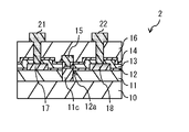
- FIG. 5 shows a planar configuration example of the semiconductor device 2 according to the present embodiment.
- FIG. 6 shows a cross-sectional configuration example of the semiconductor device 2 of FIG. 5 taken along line AA.
- FIG. 7 shows a cross-sectional configuration example of the semiconductor device 2 of FIG. 5 taken along line BB.
- FIG. 8 shows a cross-sectional configuration example of the semiconductor device 2 of FIG. 5 along line CC.
- the semiconductor device 2 is provided with a plurality of openings 12a in the barrier layer 12 in place of the impurity regions 11a, thereby providing a plurality of non-through regions in the channel layer 11 at locations facing the gate operating portion. configuration. That is, the channel layer 11 has an opening 12a penetrating through the channel layer 11 as a non-connecting region.
- the current density in the first direction (horizontal direction in FIG. 1) can be reduced as compared with the case where the non-connection region is not provided. As a result, concentration of heat generated by current is suppressed, and the maximum temperature in the channel can be lowered. Therefore, deterioration of device characteristics can be suppressed.
- the concentration of heat generated by the current is suppressed without widening the channel width.
- the maximum temperature inside can be reduced.
- concentration of heat generation can be suppressed while suppressing an increase in the size of the semiconductor device 2 .
- the gate electrode 15 may have a columnar branch portion 15a that penetrates the channel layer 11 through the opening 12a. good. At this time, the branch portion 15a is in contact with, for example, the substrate 10 and the channel layer 11 via the gate insulating film 14, and is insulated and separated from the substrate 10.
- FIG. 9 shows a modified example of the cross-sectional configuration of FIG.
- FIG. 10 shows a modified example of the cross-sectional configuration of FIG.
- At least the branch portion 15 a of the gate electrode 15 may be made of a material having a higher thermal conductivity than the channel layer 11 . This allows heat generated in the channel to propagate to the substrate 10 via the gate electrode 15 . As a result, the heat dissipation of the semiconductor device 2 is improved, so that the maximum temperature in the channel can be lowered. Therefore, deterioration of device characteristics can be suppressed.
- the semiconductor device 2 may further include a non-through portion 25 extending from the back surface of the substrate 10 to the opening 12a of the barrier layer 12, as shown in FIGS. good.
- FIG. 11 shows a modified example of the cross-sectional configuration of FIG.
- FIG. 12 shows a modified example of the cross-sectional configuration of FIG.
- the discontinuous portion 25 is formed by, for example, an insulating layer 25b formed along the inner surface of the recess extending from the back surface of the substrate 10 to the opening 12a of the barrier layer 12, and a heat propagation portion 25a formed so as to fill the recess. It is configured.
- the non-conducting portion 25 is a non-conducting region in which current does not always flow (a non-conducting region that inhibits the flow of current).
- the insulating layer 25b is made of, for example, aluminum oxide (Al 2 O 3 ), silicon oxide (SiO 2 ), or silicon nitride (SiN).
- the heat propagation part 25a may be made of a material having a thermal conductivity higher than that of the channel layer 11, for example.
- heat generated in the channel can be propagated to the substrate 10 via the non-connecting portion 25 .
- the heat dissipation of the semiconductor device 2 is improved, so that the maximum temperature in the channel can be lowered. Therefore, deterioration of device characteristics can be suppressed.
- a plurality of non-conducting regions 25 are provided in the barrier layer 12 and the channel layer 11, thereby providing a plurality of non-conducting regions in the portion of the channel layer 11 facing the gate operating portion. It has become. Even in this case, as in the case of the semiconductor device 2, the current density in the first direction (horizontal direction in FIG. 1) can be reduced compared to the case where the non-connecting region is not provided. As a result, concentration of heat generated by current is suppressed, and the maximum temperature in the channel can be lowered. Therefore, deterioration of device characteristics can be suppressed.
- the semiconductor device 2 may further include an insulating portion 11c penetrating through the channel layer 11 from the opening 12a of the barrier layer 12, as shown in FIGS. good.
- FIG. 13 shows a modified example of the cross-sectional configuration of FIG.
- FIG. 14 shows a modified example of the cross-sectional configuration of FIG.
- the insulating portion 11c is made of, for example, aluminum oxide (Al 2 O 3 ), silicon oxide (SiO 2 ), or silicon nitride (SiN).
- Al 2 O 3 aluminum oxide
- SiO 2 silicon oxide
- SiN silicon nitride
- FIG. 15 shows a planar configuration example of the semiconductor device 1 according to this modified example.
- FIG. 16 shows a cross-sectional configuration example of the semiconductor device 1 of FIG. 15 taken along line AA.
- FIG. 17 shows a cross-sectional configuration example of the semiconductor device 1 of FIG. 15 taken along line BB.
- FIG. 18 shows a cross-sectional configuration example of the semiconductor device 1 of FIG. 15 taken along line CC.
- a trench T is formed for each impurity region 11a, and each trench T penetrates the impurity region 11a, the barrier layer 12, the insulating layer 13, and the gate insulating film.
- An inner peripheral surface of each trench T is covered with an insulating layer 16 .
- a metal portion 23 made of a metal material (for example, Cu, Au, etc.) having a higher thermal conductivity than the material of the channel layer 11 is inserted into each trench T. As shown in FIG. The metal part 23 is in contact with the substrate 10 exposed at the bottom surface of the trench T. As shown in FIG. The metal part 23 is further connected to the source electrode 17 or the extraction electrode 21, for example.
- the gate electrode 15 is divided for each channel region by providing the trench T and the metal portion 23 for each impurity region 11a. That is, the gate electrode 15 is composed of a plurality of partial gate electrodes provided for each channel region. In this modification, the plurality of partial gate electrodes are connected to each other by connection wires 24 through through holes provided in the insulating layer 16 .
- the metal portion 23 is formed to penetrate each impurity region 11 a and is in contact with the substrate 10 , the source electrode 17 or the extraction electrode 21 .
- the heat generated in the channel region propagates to the substrate 10, the source electrode 17 or the extraction electrode 21 through each metal portion 23, and is exhausted to the outside. Therefore, the current density can be reduced in both the first direction (horizontal direction on the page of FIG. 1) and the second direction (vertical direction on the page of FIG. 1) compared to the case where the metal portion 23 is not provided. can.
- concentration of heat generated by current is suppressed, and the maximum temperature in the channel can be lowered. Therefore, deterioration of device characteristics can be suppressed.
- FIG. 19 shows a cross-sectional configuration example at a location corresponding to line AA in FIG.
- FIG. 20 shows a cross-sectional configuration example at a location corresponding to line BB in FIG.
- FIG. 21 shows a cross-sectional configuration example at a location corresponding to line CC in FIG.
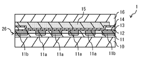
- a back barrier layer 26 is provided within the channel layer 11 .
- the back barrier layer 26 quantum confines the two-dimensional electron gas (2DEG) formed in the channel layer 11 .
- the back barrier layer 26 is made of AlGaN or the like, for example.
- the thermal conductivity of the back barrier layer 26 is low. Therefore, due to the thermal resistance at the interface of the back barrier layer 26, the heat exhaust property is deteriorated. However, since a plurality of impurity regions 11a are provided in the channel layer 11, the maximum temperature can be reduced, and performance deterioration due to heat generation can be prevented.
- FIG. 22 shows a planar configuration example of the semiconductor device 3 according to the present embodiment.
- the semiconductor device 3 corresponds to the semiconductor devices 1 and 2 provided with a plurality of high electron mobility transistors.
- each high electron mobility transistor has, for example, a multi-finger structure in which a plurality of gates are arranged in parallel. Furthermore, two high electron mobility transistors adjacent to each other share the source electrode 17 or the drain electrode 18 .
- the semiconductor device 3 has, for example, a channel layer 11 and a barrier layer 12 in this order on a substrate 10 .
- the semiconductor device 3 further includes, for example, a plurality of gate electrodes 15, a plurality of source electrodes 17 and a plurality of drain electrodes 18 on the substrate 10 with the channel layer 11 and the barrier layer 12 interposed therebetween.
- Each gate electrode 15, each source electrode 17, and each drain electrode 18 extend in a first direction (horizontal direction on the paper surface of FIG. 22).
- the plurality of source electrodes 17 and the plurality of drain electrodes 18 are alternately arranged in a second direction (vertical direction in the plane of FIG. 22) intersecting the first direction.
- the plurality of gate electrodes 15 are arranged one by one between the source electrode 17 and the drain electrode 18 .
- a plurality of impurity regions 11a are formed in parallel with predetermined gaps in the extending direction of the gate electrodes 15 at positions facing the respective gate electrodes 15 .
- the plurality of impurity regions 11a are arranged, for example, in a matrix in plan view.
- a plurality of regions (active regions (channel regions)) in which the impurity regions 11a are not formed are also arranged in a matrix in plan view.
- the plurality of impurity regions 11a may be arranged alternately in both the row direction and the column direction in plan view, as shown in FIG. 23, for example.
- the plurality of impurity regions 11a are arranged at non-positive positions with the source electrode 17 or the drain electrode 18 interposed therebetween.
- the distance between two impurity regions 11a adjacent to each other can be increased in the second direction as compared with the third embodiment.
- concentration of heat generated by current is suppressed, and the maximum temperature in the channel can be lowered. Therefore, deterioration of device characteristics can be suppressed.
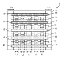
- the region in which the plurality of impurity regions 11a are formed is assumed to be ⁇ .
- the plurality of impurity regions 11a are arranged in the second direction in the central portion of the region ⁇ in the extending direction (second direction) of the source electrode 17 and the drain electrode 18.
- the width may be relatively wide in the second direction at both end portions of the region ⁇ in the second direction.
- the width in the second direction of the impurity regions 11a provided at both end portions in the second direction of the region ⁇ is defined as L1.
- L3 be the width in the second direction of the impurity region 11a provided in the center of the region ⁇ .
- L2 be the width in the second direction of the impurity region 11a provided between the impurity region 11a having the width L1 and the impurity region 11a having the width L3 in the region ⁇ .
- the widths L1, L2, and L3 satisfy the following expressions. L3>L2>L1
- the current density in the second direction can be reduced compared to the case where all the impurity regions 11a are formed with the same size.
- concentration of heat generated by current is suppressed, and the maximum temperature in the channel can be lowered. Therefore, deterioration of device characteristics can be suppressed.
- the plurality of impurity regions 11a are formed in the channel layer 11 not only directly under the gate electrode 15 but also directly under the drain electrode 18 or the source electrode 17. may also be formed.
- the plurality of high electron mobility transistors provided in the central portion in the second direction may share one impurity region 11a.
- the current density can be reduced in both the first direction and the second direction as compared with the case where all the impurity regions 11a are formed only directly under the gate electrode 15. FIG. As a result, concentration of heat generated by current is suppressed, and the maximum temperature in the channel can be lowered. Therefore, deterioration of device characteristics can be suppressed.
- the high frequency module 4 includes, for example, an edge antenna 42, a driver 43, a phase adjustment circuit 44, a switch 41, a low noise amplifier 45, a bandpass filter 46, and a power amplifier 47.
- the high-frequency module 4 is an antenna in which an edge antenna 42 formed in an array and front-end components such as a switch 41, a low-noise amplifier 45, a band-pass filter 46, and a power amplifier 47 are integrally mounted as one module. It is an integrated module. Such a high frequency module 4 can be used, for example, as a communication transceiver.
- the transistors constituting the switch 41, the low-noise amplifier 45, the power amplifier 47, and the like provided in the high-frequency module 4 are designed to increase the gain for high frequencies. , 2,3.
- FIG. 27 illustrates an example of a wireless communication device.
- This wireless communication device is, for example, a mobile phone system having multiple functions such as voice, data communication, and LAN connection.
- the wireless communication device includes, for example, an antenna ANT, an antenna switch circuit 5, a high power amplifier HPA, a radio frequency integrated circuit RFIC (Radio Frequency Integrated Circuit), a baseband section BB, an audio output section MIC, and a data output section. It includes a DT and an interface unit I/F (eg, wireless LAN (W-LAN; Wireless Local Area Network), Bluetooth (registered trademark), etc.).
- the antenna switch circuit 5 includes a high electron mobility transistor provided in the semiconductor device 1 according to one embodiment of the present disclosure and its modification.
- the high frequency integrated circuit RFIC and the baseband section BB are connected by an interface section I/F.
- the transmission signal output from the baseband unit BB is transmitted through the high frequency integrated circuit RFIC and the high power amplifier. It is output to the antenna ANT via the HPA and the antenna switch circuit 5 .
- the received signal When receiving, that is, when inputting the signal received by the antenna ANT to the receiving system of the wireless communication device, the received signal is input to the baseband unit BB via the antenna switch circuit 5 and the high frequency integrated circuit RFIC.
- the signal processed by the baseband unit BB is output from output units such as the audio output unit MIC, the data output unit DT, and the interface unit I/F.
- the present disclosure can have the following configurations.
- a channel layer and a barrier layer are provided in this order on a substrate, and a gate electrode, a source electrode and a drain electrode are formed on the substrate via the channel layer and the barrier layer and extend in a first direction,
- the channel layer or the barrier layer comprises a plurality of barrier layers which are arranged in the extending direction of the gate electrode at a position facing the gate electrode with a predetermined gap interposed therebetween and which inhibit current from flowing through the channel layer.
- the semiconductor device according to (1), wherein the non-through region is formed by ion implantation into the channel layer.
- the channel layer has an isolation region in a region facing both ends of the gate electrode, the source electrode, and the drain electrode in a plan view of the channel layer;
- the semiconductor device according to (2) wherein the non-through region and the element isolation region are collectively formed in the same process in a manufacturing process.
- the semiconductor device according to (2) or (3) further comprising a metal portion penetrating through the non-passing region and the barrier layer and connected to the source electrode.
- the barrier layer has the non-interruption region;
- the semiconductor device according to (1), wherein the barrier layer has an opening penetrating through the barrier layer as the non-passing region.
- (6) The semiconductor device according to (5), wherein the gate electrode has a branch portion penetrating the channel layer through the opening.
- the channel layer or the barrier layer inhibits the current from flowing through the channel layers formed side by side with a predetermined gap in the extending direction of the gate electrodes at positions facing the respective gate electrodes.
- a semiconductor device having a plurality of discontinuous regions.
Landscapes
- Junction Field-Effect Transistors (AREA)
Abstract
Description
1.背景
2.第1の実施の形態(半導体装置)…図1~図4
3.第2の実施の形態(半導体装置)…図5~図8
4.第2の実施の形態の変形例(半導体装置)…図9~図14
5.第1の実施の形態の変形例(半導体装置)…図15~図21
6.第3の実施の形態(半導体装置)…図22
7.第3の実施の形態の変形例(半導体装置)…図23~図25
8.適用例(高周波モジュール、無線通信装置)…図26,図27
第5世代移動体通信システム(5G)においては、ミリ波帯域の信号の使用が想定される。空間減衰の大きなミリ波帯域では、高いパワーの出力が必要となり、高出力、高周波の半導体デバイスが必要となる。高出力、高周波の半導体デバイスとしては、例えば、パワーアンプや、RFスイッチが挙げられる。
[構成]
次に、本開示の第1の実施の形態に係る半導体装置1について説明する。図1は、本実施の形態に係る半導体装置1の平面構成例を表したものである。図2は、図1の半導体装置1のA-A線での断面構成例を表したものである。図3は、図1の半導体装置1のB-B線での断面構成例を表したものである。図4は、図1の半導体装置1のC-C線での断面構成例を表したものである。
次に、半導体装置1における効果について説明する。
次に、第2の実施の形態に係る半導体装置2について説明する。図5は、本実施の形態に係る半導体装置2の平面構成例を表したものである。図6は、図5の半導体装置2のA-A線での断面構成例を表したものである。図7は、図5の半導体装置2のB-B線での断面構成例を表したものである。図8は、図5の半導体装置2のC-C線での断面構成例を表したものである。
次に、本開示の第2の実施の形態に係る半導体装置2の変形例について説明する。
上記第2の実施の形態において、例えば、図9、図10に示したように、ゲート電極15は、開口12aを介してチャネル層11を貫通する柱状の分枝部15aを有していてもよい。このとき、分枝部15aは、例えば、ゲート絶縁膜14を介して基板10やチャネル層11と接しており、基板10とは絶縁分離されている。図9は、図6の断面構成の一変形例を表したものである。図10は、図8の断面構成の一変形例を表したものである。
上記第2の実施の形態において、半導体装置2が、例えば、図11、図12に示したように、基板10の裏面から、バリア層12の開口12aに達する不通部25を更に備えていてもよい。図11は、図6の断面構成の一変形例を表したものである。図12は、図8の断面構成の一変形例を表したものである。
上記第2の実施の形態において、半導体装置2が、例えば、図13、図14に示したように、バリア層12の開口12aから、チャネル層11を貫通する絶縁部11cを更に備えていてもよい。図13は、図6の断面構成の一変形例を表したものである。図14は、図8の断面構成の一変形例を表したものである。
次に、第1の実施の形態の変形例について説明する。
次に、本開示の第3の実施の形態に係る半導体装置3について説明する。図22は、本実施の形態に係る半導体装置3の平面構成例を表したものである。
次に、本開示の第3の実施の形態に係る半導体装置3の変形例について説明する。
上記第3の実施の形態において、複数の不純物領域11aが、例えば、図23に示したように、平面視において行方向および列方向の双方において互い違いに配置されていてもよい。このとき、複数の不純物領域11aは、ソース電極17もしくはドレイン電極18を介して非正対となる位置に配置されている。このようにした場合には、上記第3の実施の形態と比べて、第2の方向において、互いに隣接する2つの不純物領域11aの距離を広げることができる。これにより、電流による発熱の集中が抑制され、チャネル中の最大温度を低下させることができる。従って、デバイス特性の劣化を抑制することができる。
上記第3の実施の形態において、複数の不純物領域11aが形成された領域をαとする。複数の不純物領域11aは、例えば、図24に示したように、領域αのうち、ソース電極17およびドレイン電極18の延在方向(第2の方向)の中央部分において、第2の方向において相対的に幅広に形成され、領域αのうち、第2の方向の両端部において、第2の方向において相対的に幅狭に形成されていてもよい。このとき、領域αの、第2の方向の両端部に設けられた不純物領域11aの、第2の方向の幅をL1とする。また、領域αの中央に設けられた不純物領域11aの、第2の方向の幅をL3とする。また、領域αのうち、幅L1の不純物領域11aと幅L3の不純物領域11aとの間に設けられた不純物領域11aの、第2の方向の幅をL2とする。このとき、幅L1,L2,L3は以下の式を満たす。
L3>L2>L1
上記変形例3-3において、第2の方向の中央部分において、複数の不純物領域11aがチャネル層11のうち、ゲート電極15の直下だけでなく、ドレイン電極18もしくはソース電極17の直下の部分にも形成されていてもよい。このとき、第2の方向の中央部分に設けられた複数の高電子移動度トランジスタは、1つの不純物領域11aを互いに共有していてもよい。このようにした場合には、全ての不純物領域11aをゲート電極15の直下だけに形成した場合と比べて、第1の方向および第2の方向の双方における電流密度を減らすことができる。その結果、電流による発熱の集中が抑制され、チャネル中の最大温度を低下させることができる。従って、デバイス特性の劣化を抑制することができる。
[適用例1]
次に、図26を参照して、本開示の各実施形態およびその変形例に係る半導体装置1、2,3が適用される高周波モジュール4について説明する。図26は、高周波モジュール4の斜視図である。
図27は、無線通信装置の一例を表したものである。この無線通信装置は、例えば、音声、データ通信、LAN接続など多機能を有する携帯電話システムである。無線通信装置は、例えば、アンテナANTと、アンテナスイッチ回路5と、高電力増幅器HPAと、高周波集積回路RFIC(Radio Frequency Integrated Circuit)と、ベースバンド部BBと、音声出力部MICと、データ出力部DTと、インタフェース部I/F(例えば、無線LAN(W-LAN;Wireless Local Area Network)、Bluetooth(登録商標)、他)とを備えている。アンテナスイッチ回路5は、本開示の一実施形態およびその変形例に係る半導体装置1に設けられた高電子移動度トランジスタを含んで構成されている。高周波集積回路RFICとベースバンド部BBとはインタフェース部I/Fにより接続されている。
(1)
基板上にチャネル層およびバリア層をこの順に備えるとともに、前記チャネル層および前記バリア層を介して前記基板上に形成され、第1の方向に延在するゲート電極、ソース電極およびドレイン電極を備え、
前記チャネル層または前記バリア層は、前記ゲート電極と対向する位置に、前記ゲート電極の延在方向に所定の間隙を介して並んで形成された、前記チャネル層に電流が流れるのを阻害する複数の不通領域を有する
半導体装置。
(2)
前記チャネル層が前記不通領域を有し、
前記不通領域は、前記チャネル層に対するイオン注入によって形成されたものである
(1)に記載の半導体装置。
(3)
前記チャネル層は、当該チャネル層のうち、平面視において、前記ゲート電極、前記ソース電極および前記ドレイン電極の両端部と対向する領域に素子分離領域を有し、
前記不通領域および前記素子分離領域は、製造過程において、同一行程で一括して形成されたものである
(2)に記載の半導体装置。
(4)
前記不通領域および前記バリア層を貫通し、前記ソース電極に接続された金属部を更に備えた
(2)または(3)に記載の半導体装置。
(5)
前記バリア層が前記不通領域を有し、
前記バリア層は、前記不通領域として、当該バリア層を貫通する開口を有する
(1)に記載の半導体装置。
(6)
前記ゲート電極は、前記開口を介して前記チャネル層を貫通する分枝部を有する
(5)に記載の半導体装置。
(7)
前記分枝部は、前記チャネル層の熱伝導率よりも高い熱伝導率の材料で構成された
(6)に記載の半導体装置。
(8)
前記基板の裏面から前記開口に達し、前記チャネル層に電流が流れるのを阻害する不通部を更に備えた
(5)に記載の半導体装置。
(9)
前記不通部は、前記チャネル層の熱伝導率よりも高い熱伝導率の材料で構成された熱伝搬部を有する
(8)に記載の半導体装置。
(10)
前記チャネル層内に、当該チャネル層に形成される二次元電子ガスに対して量子閉じ込めを行うバックバリア層を更に備えた
(1)ないし(9)のいずれか1つに記載の半導体装置。
(11)
基板上にチャネル層およびバリア層をこの順に備えるとともに、前記チャネル層および前記バリア層を介して前記基板上に形成され、第1の方向に延在する複数のゲート電極、複数のソース電極および複数のドレイン電極を備え、
前記複数のソース電極および前記複数のドレイン電極は、前記第1の方向と交差する第2の方向に交互に配置され、 前記複数のゲート電極は、前記ソース電極と前記ドレイン電極との間に1本ずつ配置され、
前記チャネル層または前記バリア層は、各前記ゲート電極と対向する位置に、前記ゲート電極の延在方向に所定の間隙を介して並んで形成された、前記チャネル層に電流が流れるのを阻害する複数の不通領域を有する
半導体装置。
(12)
前記複数の不通領域は、前記ソース電極もしくは前記ドレイン電極を介して非正対となる位置に配置されている
(11)に記載の半導体装置。
(13)
前記複数の不通領域は、当該複数の不通領域が形成された領域のうち、前記第1の方向の中央部分において、前記第1の方向において相対的に幅広に形成され、当該複数の不通領域が形成された領域のうち、前記第1の方向の両端部において、前記第1の方向において相対的に幅狭に形成されている
(11)に記載の半導体装置。
Claims (13)
- 基板上にチャネル層およびバリア層をこの順に備えるとともに、前記チャネル層および前記バリア層を介して前記基板上に形成され、第1の方向に延在するゲート電極、ソース電極およびドレイン電極を備え、
前記チャネル層または前記バリア層は、前記ゲート電極と対向する位置に、前記ゲート電極の延在方向に所定の間隙を介して並んで形成された、前記チャネル層に電流が流れるのを阻害する複数の不通領域を有する
半導体装置。 - 前記チャネル層が前記不通領域を有し、
前記不通領域は、前記チャネル層に対するイオン注入によって形成されたものである
請求項1に記載の半導体装置。 - 前記チャネル層は、当該チャネル層のうち、平面視において、前記ゲート電極、前記ソース電極および前記ドレイン電極の両端部と対向する領域に素子分離領域を有し、
前記不通領域および前記素子分離領域は、製造過程において、同一行程で一括して形成されたものである
請求項2に記載の半導体装置。 - 前記不通領域および前記バリア層を貫通し、前記ソース電極に接続された金属部を更に備えた
請求項2に記載の半導体装置。 - 前記バリア層が前記不通領域を有し、
前記バリア層は、前記不通領域として、当該バリア層を貫通する開口を有する
請求項1に記載の半導体装置。 - 前記ゲート電極は、前記開口を介して前記チャネル層を貫通する分枝部を有する
請求項5に記載の半導体装置。 - 前記分枝部は、前記チャネル層の熱伝導率よりも高い熱伝導率の材料で構成された
請求項6に記載の半導体装置。 - 前記基板の裏面から前記開口に達し、前記チャネル層に電流が流れるのを阻害する不通部を更に備えた
請求項5に記載の半導体装置。 - 前記不通部は、前記チャネル層の熱伝導率よりも高い熱伝導率の材料で構成された熱伝搬部を有する
請求項8に記載の半導体装置。 - 前記チャネル層内に、当該チャネル層に形成される二次元電子ガスに対して量子閉じ込めを行うバックバリア層を更に備えた
請求項1に記載の半導体装置。 - 基板上にチャネル層およびバリア層をこの順に備えるとともに、前記チャネル層および前記バリア層を介して前記基板上に形成され、第1の方向に延在する複数のゲート電極、複数のソース電極および複数のドレイン電極を備え、
前記複数のソース電極および前記複数のドレイン電極は、前記第1の方向と交差する第2の方向に交互に配置され、
前記複数のゲート電極は、前記ソース電極と前記ドレイン電極との間に1本ずつ配置され、
前記チャネル層または前記バリア層は、各前記ゲート電極と対向する位置に、前記ゲート電極の延在方向に所定の間隙を介して並んで形成された、前記チャネル層に電流が流れるのを阻害する複数の不通領域を有する
半導体装置。 - 前記複数の不通領域は、前記ソース電極もしくは前記ドレイン電極を介して非正対となる位置に配置されている
請求項11に記載の半導体装置。 - 前記複数の不通領域は、当該複数の不通領域が形成された領域のうち、前記第1の方向の中央部分において、前記第1の方向において相対的に幅広に形成され、当該複数の不通領域が形成された領域のうち、前記第1の方向の両端部において、前記第1の方向において相対的に幅狭に形成されている
請求項11に記載の半導体装置。
Priority Applications (3)
| Application Number | Priority Date | Filing Date | Title |
|---|---|---|---|
| US18/555,754 US20240204093A1 (en) | 2021-04-30 | 2022-02-08 | Semiconductor device |
| CN202280030133.6A CN117203776A (zh) | 2021-04-30 | 2022-02-08 | 半导体装置 |
| JP2023517066A JP7846096B2 (ja) | 2021-04-30 | 2022-02-08 | 半導体装置 |
Applications Claiming Priority (2)
| Application Number | Priority Date | Filing Date | Title |
|---|---|---|---|
| JP2021-077976 | 2021-04-30 | ||
| JP2021077976 | 2021-04-30 |
Publications (1)
| Publication Number | Publication Date |
|---|---|
| WO2022230293A1 true WO2022230293A1 (ja) | 2022-11-03 |
Family
ID=83848278
Family Applications (1)
| Application Number | Title | Priority Date | Filing Date |
|---|---|---|---|
| PCT/JP2022/004902 Ceased WO2022230293A1 (ja) | 2021-04-30 | 2022-02-08 | 半導体装置 |
Country Status (4)
| Country | Link |
|---|---|
| US (1) | US20240204093A1 (ja) |
| JP (1) | JP7846096B2 (ja) |
| CN (1) | CN117203776A (ja) |
| WO (1) | WO2022230293A1 (ja) |
Cited By (1)
| Publication number | Priority date | Publication date | Assignee | Title |
|---|---|---|---|---|
| US20240304712A1 (en) * | 2023-03-09 | 2024-09-12 | Enkris Semiconductor, Inc. | Semiconductor structure and preparation method thereof |
Families Citing this family (1)
| Publication number | Priority date | Publication date | Assignee | Title |
|---|---|---|---|---|
| CN118872067A (zh) * | 2021-12-20 | 2024-10-29 | 蒙德无线公司 | 用于rf集成电路的半导体器件 |
Citations (8)
| Publication number | Priority date | Publication date | Assignee | Title |
|---|---|---|---|---|
| JPS58134478A (ja) * | 1982-02-04 | 1983-08-10 | Sanyo Electric Co Ltd | 化合物半導体fetの製造方法 |
| JPS61260679A (ja) * | 1985-05-15 | 1986-11-18 | Fujitsu Ltd | 電界効果トランジスタ |
| JPH03191534A (ja) * | 1989-12-21 | 1991-08-21 | Nec Corp | 電界効果トランジスタおよびその製造方法 |
| JPH05114615A (ja) * | 1991-10-21 | 1993-05-07 | Rohm Co Ltd | 化合物半導体装置及びその製造方法 |
| JPH05275453A (ja) * | 1992-01-16 | 1993-10-22 | Samsung Electron Co Ltd | 接合fet及びその製造方法 |
| JPH08111519A (ja) * | 1994-08-19 | 1996-04-30 | Fujitsu Ltd | 半導体装置 |
| JP2001093914A (ja) * | 1999-09-20 | 2001-04-06 | Toshiba Corp | 半導体能動素子及び半導体集積回路 |
| JP2013182993A (ja) * | 2012-03-01 | 2013-09-12 | Toshiba Corp | 半導体装置 |
Family Cites Families (3)
| Publication number | Priority date | Publication date | Assignee | Title |
|---|---|---|---|---|
| JP2011176195A (ja) * | 2010-02-25 | 2011-09-08 | Toshiba Corp | 窒化物半導体装置 |
| JP6341679B2 (ja) * | 2014-02-06 | 2018-06-13 | ルネサスエレクトロニクス株式会社 | 半導体装置 |
| TWI736600B (zh) * | 2017-03-31 | 2021-08-21 | 聯穎光電股份有限公司 | 高電子遷移率電晶體 |
-
2022
- 2022-02-08 JP JP2023517066A patent/JP7846096B2/ja active Active
- 2022-02-08 CN CN202280030133.6A patent/CN117203776A/zh active Pending
- 2022-02-08 WO PCT/JP2022/004902 patent/WO2022230293A1/ja not_active Ceased
- 2022-02-08 US US18/555,754 patent/US20240204093A1/en active Pending
Patent Citations (8)
| Publication number | Priority date | Publication date | Assignee | Title |
|---|---|---|---|---|
| JPS58134478A (ja) * | 1982-02-04 | 1983-08-10 | Sanyo Electric Co Ltd | 化合物半導体fetの製造方法 |
| JPS61260679A (ja) * | 1985-05-15 | 1986-11-18 | Fujitsu Ltd | 電界効果トランジスタ |
| JPH03191534A (ja) * | 1989-12-21 | 1991-08-21 | Nec Corp | 電界効果トランジスタおよびその製造方法 |
| JPH05114615A (ja) * | 1991-10-21 | 1993-05-07 | Rohm Co Ltd | 化合物半導体装置及びその製造方法 |
| JPH05275453A (ja) * | 1992-01-16 | 1993-10-22 | Samsung Electron Co Ltd | 接合fet及びその製造方法 |
| JPH08111519A (ja) * | 1994-08-19 | 1996-04-30 | Fujitsu Ltd | 半導体装置 |
| JP2001093914A (ja) * | 1999-09-20 | 2001-04-06 | Toshiba Corp | 半導体能動素子及び半導体集積回路 |
| JP2013182993A (ja) * | 2012-03-01 | 2013-09-12 | Toshiba Corp | 半導体装置 |
Cited By (1)
| Publication number | Priority date | Publication date | Assignee | Title |
|---|---|---|---|---|
| US20240304712A1 (en) * | 2023-03-09 | 2024-09-12 | Enkris Semiconductor, Inc. | Semiconductor structure and preparation method thereof |
Also Published As
| Publication number | Publication date |
|---|---|
| JPWO2022230293A1 (ja) | 2022-11-03 |
| JP7846096B2 (ja) | 2026-04-14 |
| CN117203776A (zh) | 2023-12-08 |
| US20240204093A1 (en) | 2024-06-20 |
Similar Documents
| Publication | Publication Date | Title |
|---|---|---|
| JP5755671B2 (ja) | 複数のフィールドプレートを有するワイドバンドギャップトランジスタ | |
| JP7538275B2 (ja) | バイパス・ゲート式トランジスタを備える高出力mmicデバイス | |
| CN112018175B (zh) | 一种半导体器件及其制备方法、半导体封装结构 | |
| JP2012178595A (ja) | ゲート−ソースフィールドプレートを含むワイドバンドギャップトランジスタ | |
| US12347721B2 (en) | Semiconductor device and method of producing the same, and electronic device | |
| JP2021531655A (ja) | エンハンスメント・モード及びデプレッション・モード・トランジスタの両者を有するモノリシック・マイクロ波集積回路 | |
| WO2022230293A1 (ja) | 半導体装置 | |
| US20240322028A1 (en) | Semiconductor device, semiconductor module, and wireless communication apparatus | |
| JP2012182306A (ja) | Mmic用パッケージ | |
| US20240178296A1 (en) | Semiconductor device and method for manufacturing the same | |
| JP7805967B2 (ja) | 半導体装置、半導体モジュールおよび電子機器 | |
| JP2010245351A (ja) | 半導体装置 | |
| CN114175272A (zh) | 半导体装置、半导体模块和电子设备 | |
| WO2022215319A1 (ja) | 半導体装置 | |
| US20080277698A1 (en) | Field effect transistor | |
| JP2010182829A (ja) | 半導体装置 | |
| CN115692492B (zh) | 晶体管、功率放大器及电子设备 | |
| JP2010245350A (ja) | 半導体装置 | |
| CN116417503B (zh) | 一种半导体器件 | |
| WO2025140234A1 (zh) | 半导体器件 | |
| JP2025007916A (ja) | 半導体装置、半導体装置の製造方法及び電子装置 | |
| CN120224772A (zh) | 一种半导体器件及其制备方法 | |
| CN120264847A (zh) | 一种半导体器件及其制备方法 | |
| WO2024038685A1 (ja) | 半導体装置、半導体モジュール及び電子機器 | |
| CN120282519A (zh) | 一种半导体器件 |
Legal Events
| Date | Code | Title | Description |
|---|---|---|---|
| 121 | Ep: the epo has been informed by wipo that ep was designated in this application |
Ref document number: 22795216 Country of ref document: EP Kind code of ref document: A1 |
|
| WWE | Wipo information: entry into national phase |
Ref document number: 2023517066 Country of ref document: JP |
|
| WWE | Wipo information: entry into national phase |
Ref document number: 18555754 Country of ref document: US |
|
| WWE | Wipo information: entry into national phase |
Ref document number: 202280030133.6 Country of ref document: CN |
|
| NENP | Non-entry into the national phase |
Ref country code: DE |
|
| 122 | Ep: pct application non-entry in european phase |
Ref document number: 22795216 Country of ref document: EP Kind code of ref document: A1 |