WO2022220251A1 - 磁気メモリ素子 - Google Patents
磁気メモリ素子 Download PDFInfo
- Publication number
- WO2022220251A1 WO2022220251A1 PCT/JP2022/017647 JP2022017647W WO2022220251A1 WO 2022220251 A1 WO2022220251 A1 WO 2022220251A1 JP 2022017647 W JP2022017647 W JP 2022017647W WO 2022220251 A1 WO2022220251 A1 WO 2022220251A1
- Authority
- WO
- WIPO (PCT)
- Prior art keywords
- layer
- magnetic
- memory element
- magnetic memory
- antiferromagnetic
- Prior art date
- Legal status (The legal status is an assumption and is not a legal conclusion. Google has not performed a legal analysis and makes no representation as to the accuracy of the status listed.)
- Ceased
Links
Images


Classifications
-
- H—ELECTRICITY
- H10—SEMICONDUCTOR DEVICES; ELECTRIC SOLID-STATE DEVICES NOT OTHERWISE PROVIDED FOR
- H10N—ELECTRIC SOLID-STATE DEVICES NOT OTHERWISE PROVIDED FOR
- H10N50/00—Galvanomagnetic devices
- H10N50/10—Magnetoresistive devices
-
- G—PHYSICS
- G11—INFORMATION STORAGE
- G11C—STATIC STORES
- G11C11/00—Digital stores characterised by the use of particular electric or magnetic storage elements; Storage elements therefor
- G11C11/02—Digital stores characterised by the use of particular electric or magnetic storage elements; Storage elements therefor using magnetic elements
- G11C11/16—Digital stores characterised by the use of particular electric or magnetic storage elements; Storage elements therefor using magnetic elements using elements in which the storage effect is based on magnetic spin effect
- G11C11/161—Digital stores characterised by the use of particular electric or magnetic storage elements; Storage elements therefor using magnetic elements using elements in which the storage effect is based on magnetic spin effect details concerning the memory cell structure, e.g. the layers of the ferromagnetic memory cell
-
- G—PHYSICS
- G11—INFORMATION STORAGE
- G11C—STATIC STORES
- G11C11/00—Digital stores characterised by the use of particular electric or magnetic storage elements; Storage elements therefor
- G11C11/02—Digital stores characterised by the use of particular electric or magnetic storage elements; Storage elements therefor using magnetic elements
- G11C11/16—Digital stores characterised by the use of particular electric or magnetic storage elements; Storage elements therefor using magnetic elements using elements in which the storage effect is based on magnetic spin effect
- G11C11/165—Auxiliary circuits
- G11C11/1673—Reading or sensing circuits or methods
-
- G—PHYSICS
- G11—INFORMATION STORAGE
- G11C—STATIC STORES
- G11C11/00—Digital stores characterised by the use of particular electric or magnetic storage elements; Storage elements therefor
- G11C11/02—Digital stores characterised by the use of particular electric or magnetic storage elements; Storage elements therefor using magnetic elements
- G11C11/16—Digital stores characterised by the use of particular electric or magnetic storage elements; Storage elements therefor using magnetic elements using elements in which the storage effect is based on magnetic spin effect
- G11C11/165—Auxiliary circuits
- G11C11/1675—Writing or programming circuits or methods
-
- G—PHYSICS
- G11—INFORMATION STORAGE
- G11C—STATIC STORES
- G11C11/00—Digital stores characterised by the use of particular electric or magnetic storage elements; Storage elements therefor
- G11C11/18—Digital stores characterised by the use of particular electric or magnetic storage elements; Storage elements therefor using Hall-effect devices
-
- H—ELECTRICITY
- H10—SEMICONDUCTOR DEVICES; ELECTRIC SOLID-STATE DEVICES NOT OTHERWISE PROVIDED FOR
- H10B—ELECTRONIC MEMORY DEVICES
- H10B61/00—Magnetic memory devices, e.g. magnetoresistive RAM [MRAM] devices
- H10B61/20—Magnetic memory devices, e.g. magnetoresistive RAM [MRAM] devices comprising components having three or more electrodes, e.g. transistors
- H10B61/22—Magnetic memory devices, e.g. magnetoresistive RAM [MRAM] devices comprising components having three or more electrodes, e.g. transistors of the field-effect transistor [FET] type
-
- H—ELECTRICITY
- H10—SEMICONDUCTOR DEVICES; ELECTRIC SOLID-STATE DEVICES NOT OTHERWISE PROVIDED FOR
- H10N—ELECTRIC SOLID-STATE DEVICES NOT OTHERWISE PROVIDED FOR
- H10N50/00—Galvanomagnetic devices
- H10N50/01—Manufacture or treatment
-
- H—ELECTRICITY
- H10—SEMICONDUCTOR DEVICES; ELECTRIC SOLID-STATE DEVICES NOT OTHERWISE PROVIDED FOR
- H10N—ELECTRIC SOLID-STATE DEVICES NOT OTHERWISE PROVIDED FOR
- H10N50/00—Galvanomagnetic devices
- H10N50/80—Constructional details
-
- H—ELECTRICITY
- H10—SEMICONDUCTOR DEVICES; ELECTRIC SOLID-STATE DEVICES NOT OTHERWISE PROVIDED FOR
- H10N—ELECTRIC SOLID-STATE DEVICES NOT OTHERWISE PROVIDED FOR
- H10N50/00—Galvanomagnetic devices
- H10N50/80—Constructional details
- H10N50/85—Materials of the active region
-
- H—ELECTRICITY
- H10—SEMICONDUCTOR DEVICES; ELECTRIC SOLID-STATE DEVICES NOT OTHERWISE PROVIDED FOR
- H10N—ELECTRIC SOLID-STATE DEVICES NOT OTHERWISE PROVIDED FOR
- H10N52/00—Hall-effect devices
- H10N52/80—Constructional details
Definitions
- the present invention relates to magnetic memory elements.
- magnetoresistive memories that use ferromagnetic materials that can store the direction of magnetization as "0" and "1" information have been attracting attention as a representative example of nonvolatile memory.
- a magnetization reversal phenomenon using a spin current has been found as a writing method, and is being used widely.
- the magnetization reversal phenomenon that occurs when a current is passed through a multilayer film made of ferromagnetic materials and non-magnetic heavy metals (tungsten (W), platinum (Pt), etc.) is called spin-orbit torque magnetization reversal, and is a next-generation technology. It has been extensively researched.
- Non-Patent Document 1 In order to further increase the speed of the magnetoresistive memory, replacement of ferromagnetic materials with antiferromagnetic materials is under consideration (see, for example, Non-Patent Document 1).
- antiferromagnets have a spin response speed in the THz band (pico(10 ⁇ 12 ) seconds) that is two to three orders of magnitude faster than ferromagnets, and the interaction between magnetic bodies is small. This is because there is a possibility that magnetic devices such as resistive memories can be further accelerated and highly integrated.
- the present invention has been made in view of the above problems, and an object of the present invention is to enhance a read signal in a magnetic memory element using an antiferromagnetic material.
- the magnetic memory element according to the present invention comprises an antiferromagnetic layer made of a canted antiferromagnetic material having a magnetic order in which the magnetic moment is canted, and a substance different from the canted antiferromagnetic material in contact with the antiferromagnetic layer and a contact layer consisting of
- the roughness of the interface between the antiferromagnetic layer and the contact layer is 1.0 nm or less, and when a spin current flows in the contact layer, the torque generated by the spin current acts on the magnetic order of the antiferromagnetic layer, and the magnetic order can be reversed. is.
- the interface is smoothed, and spins injected from the contact layer to the antiferromagnetic layer via the interface Since the current can be increased and the magnetic properties of the antiferromagnetic layer can be kept optimal, the read signal of the magnetic memory element can be enhanced.
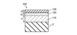
- FIG. 1 is a cross-sectional view of a conventional magnetic memory element
- FIG. 1 is a cross-sectional view of a magnetic memory device according to an embodiment of the present invention
- FIG. FIG. 4 is a cross-sectional view of a magnetic memory element according to a modification of the embodiment
- 1 is a schematic diagram showing the crystal structure and magnetic structure of Mn 3 Sn.
- FIG. 1 is a schematic diagram showing the configuration of a magnetic memory element having a Hall bar structure
- FIG. 4B is a schematic diagram for explaining a write operation in the magnetic memory element of FIG. 4A
- FIG. 4B is a schematic diagram for explaining a read operation in the magnetic memory element of FIG. 4A
- 4 is a graph showing vertical magnetic field dependence of Hall voltage for conventional Ru/Mn 3 Sn/W films. 4 is a graph showing vertical magnetic field dependence of the Hall voltage for the Mn 3 Sn/W film of the present embodiment. 4 is a graph showing write current dependence of Hall voltage for Ru/Mn 3 Sn/W films. 4 is a graph showing write current dependence of Hall voltage for Mn 3 Sn/W films. 4 is a graph showing read current dependence of Hall voltage change for a Mn 3 Sn/W film. 2 is an atomic force microscope (AFM) image of a Mn 3 Sn/W film; FIG.
- AFM atomic force microscope
- FIG. 4 is a graph showing X-ray diffraction patterns of Mn 3 Sn/Ta/Al 2 O 3 films of the present embodiment fabricated at different annealing temperatures T A ;
- FIG. Fig. 4 is AFM images of Mn3Sn /Ta/ Al2O3 films fabricated with different annealing temperatures T A ;
- TEM transmission electron microscope
- FIG. 3 is a graph showing the magnetic field dependence of the anomalous Hall conductivity of Mn 3 Sn/Ta/Al 2 O 3 films fabricated at different annealing temperatures T A ; 4 is a graph showing write current dependence of the reversal rate of magnetic order for each of a Mn 3 Sn/Ta/Al 2 O 3 film and a Ta/Mn 3 Sn/Al 2 O 3 film.
- 1 is a schematic diagram showing the configuration of a magnetic memory element of an SOT-MRAM;
- FIG. 1 is a schematic diagram showing the configuration of a magnetic memory element of an STT-MRAM;
- a multilayer film may be indicated by the material of each layer that constitutes the multilayer film.
- this multilayer film is expressed as "material a/material b/material c”.
- the thickness (nm) of each layer may be described in parentheses after the material name. For example, a layer having a thickness of ti (nm) and made of material j is expressed as "material j (ti)".
- the magnetic memory element 1 includes a substrate 2, a metal layer 10 on the substrate 2, an antiferromagnetic layer 11 on the metal layer 10, a heavy metal layer 12 on the antiferromagnetic layer 11, and an oxide on the heavy metal layer 12. a layer 13;
- the substrate 2 is made of an insulator such as Si/ SiO2 .
- the metal layer 10 is made of metal such as ruthenium (Ru).
- the antiferromagnetic layer 11 is made of an antiferromagnetic material such as Mn 3 Sn.
- the heavy metal layer 12 is made of non-magnetic heavy metal such as tantalum (Ta), tungsten (W), and platinum (Pt).
- the oxide layer 13 is a cap layer for preventing oxidation, and is made of metal oxide such as aluminum oxide (AlOx) and magnesium oxide (MgO).
- the thicknesses (nm) of the metal layer 10, the antiferromagnetic layer 11, the heavy metal layer 12, and the oxide layer 13 are expressed as t0, t1, t2, and t3, respectively.
- the temperature is maintained at a predetermined temperature (eg, 450° C.) for a predetermined time (eg, 30 minutes) and then laminating the heavy metal layer 12 and the oxide layer 13 at room temperature.
- a predetermined temperature eg, 450° C.
- a predetermined time eg, 30 minutes
- the reason why the Ru layer is provided between the substrate 2 and the Mn 3 Sn layer in the conventional magnetic memory element 1 is that if the Ru layer is not provided and the Mn 3 Sn layer is formed and then annealed, the Mn 3 Sn layer is removed. This is because the interface between the Mn 3 Sn layer and the heavy metal layer 12 becomes rough due to crystallization, which makes it difficult to drive the device.
- spin-orbit torque acts on the magnetic order of the antiferromagnetic layer 11 due to the spin Hall effect, thereby reversing the direction of the magnetic order.
- the magnetic memory element according to this embodiment does not have a Ru layer and is manufactured by an improved heat treatment process, as will be described later.
- the magnetic memory element 100 includes a substrate 2, an antiferromagnetic layer 110 made of an antiferromagnetic material laminated on the substrate 2, and an antiferromagnetic layer 110 laminated on the antiferromagnetic layer 110. and an oxide layer 130 on the heavy metal layer 120 .
- the magnetic memory element 102 shown in FIG. 2B may be employed.
- the magnetic memory element 102 has a heavy metal layer 120 , an antiferromagnetic layer 110 and an oxide layer 130 stacked in this order on the substrate 2 .
- the contact layer in contact with the antiferromagnetic layer 110 is mainly the heavy metal layer 120
- Layers may be employed. This embodiment is applicable as long as a contact layer is provided on at least one side of the antiferromagnetic layer 110 .
- Mn 3 Sn is an antiferromagnetic material having a crystal structure called a Kagome lattice based on triangles. As shown in FIG. 3, it has a structure in which Kagome lattices are stacked in the [0001] direction. Due to geometrical frustration, manganese (Mn) located at the vertices of the Kagome lattice exhibits a non-collinear ) indicates the magnetic structure.
- Mn manganese located at the vertices of the Kagome lattice exhibits a non-collinear
- Three types of six-spin units arranged on a bilayer kagome lattice form a spin order called a cluster magnetic octupole, which is indicated by a hexagon.
- This non-collinear magnetic structure can be viewed as a ferromagnetic order of clustered magnetic octupoles (thick arrow in the middle of Fig. 3). This ferromagnetic order macroscopically breaks the time-reversal symmetry.
- the cluster magnetic octupole corresponds to the Weyl points, which are topological electronic structures, and the virtual magnetic field in momentum space (equivalent to 100 to 1000 Tesla (T) in real space).
- the orientation of the poles can control the response from the Weyl point and the virtual magnetic field.
- the magnetic structure as shown in FIG. 3 has orthorhombic symmetry, with only one of the three magnetic moments of Mn located at the vertices of the triangle being parallel to the easy axis. Since the other two magnetic moments cant with respect to the easy axis, it is believed to induce a weak ferromagnetic moment.
- Such an antiferromagnet whose magnetic moment is canted and has minute magnetization is called a canted antiferromagnet.
- the crystal orientation of Mn 3 Sn plays an important role in enhancing the read signal of magnetic memory elements. For example, in measurements of the anomalous Hall effect, only grains whose magnetic ordering of the cluster magnetic octupole has a component in the perpendicular direction (perpendicular to the surface of the substrate 2) contribute to the Hall voltage.
- the Ru layer metal layer 10
- the Kagome plane of Mn 3 Sn close to the Ru layer is oriented substantially in the in-plane direction (parallel to the surface of the substrate 2). They are aligned, and the contribution to the Hall voltage is reduced.
- current flowing through the Ru layer also causes a decrease in the read voltage. Therefore, in this embodiment, as shown in FIGS. 2A and 2B, the magnetic memory elements 100 and 102 are not provided with the Ru layer, and the Mn 3 Sn layer has a crystal orientation that exhibits a higher Hall voltage.
- the Ru layer when the Ru layer is not provided, as described above, when the heavy metal layer 120 is deposited by annealing after forming the Mn 3 Sn layer (antiferromagnetic layer 110), the Mn 3 Sn layer is crystallized and Mn 3 The interface between the Sn layer and the heavy metal layer 120 becomes rough. Therefore, in the present embodiment, annealing is not performed immediately after the Mn 3 Sn layer is deposited, but annealing is performed after depositing all layers of the multilayer film.
- a case of forming Mn 3 Sn/W/AlOx on a Si/SiO 2 substrate and a case of forming Mn 3 Sn/Ta/AlOx are given as examples. to explain.
- Mn 3 Sn/W/AlOx a Mn 3 Sn layer is deposited on a Si/SiO 2 substrate at room temperature using a DC magnetron sputtering apparatus with a base pressure below 5 ⁇ 10 ⁇ 7 Pa. Then, a W layer is deposited at room temperature by a molecular beam epitaxy (MBE) apparatus under ultra-high vacuum with a base pressure of less than 2 ⁇ 10 ⁇ 8 Pa. The W layer can also be formed using a DC magnetron sputtering apparatus. An AlOx layer is then deposited at room temperature using an RF magnetron sputtering apparatus with a base pressure of less than 5 ⁇ 10 ⁇ 7 Pa. All layers are deposited without breaking vacuum. After manufacturing Mn 3 Sn/W/AlOx, the magnetic memory element 100 is manufactured by annealing at a predetermined temperature (eg, 450° C.) for a predetermined time (eg, 30 minutes).
- a predetermined temperature eg, 450° C
- Mn 3 Sn/Ta/AlOx Mn 3 Sn and Ta layers were deposited on a Si/SiO 2 substrate using a DC magnetron sputtering apparatus with a base pressure of less than 5 ⁇ 10 ⁇ 7 Pa, followed by RF magnetron sputtering. An AlOx layer is deposited using the apparatus. All layers are deposited at room temperature without breaking vacuum. After forming the Mn 3 Sn/Ta/AlOx film, annealing is performed at a predetermined temperature (eg, 500° C.) for a predetermined time (eg, 30 minutes) to fabricate the magnetic memory element 100 .
- a predetermined temperature eg, 500° C.
- a predetermined time eg, 30 minutes
- the magnetic memory element 100 is manufactured by annealing at a temperature equal to or higher than the crystallization temperature of the antiferromagnetic layer 110 after all the multilayer films including the antiferromagnetic layer 110 are formed. be done.
- a magnetic memory element 102 shown in FIG. 2B is also manufactured in a similar manner.
- the interface between the antiferromagnetic layer 110 and the contact layer in contact with the antiferromagnetic layer 110 is smoothed without providing a Ru layer, An enhancement of the readout signal can be expected.
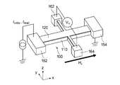
- FIG. 4A shows the configuration of a magnetic memory element 100 having a Hall bar structure.
- a sample of the magnetic memory element 100 is manufactured in a predetermined size (16 ⁇ m ⁇ 96 ⁇ m, for example).
- Electrodes 152 and 154 made of Au/Ti are arranged at both ends in the longitudinal direction (x direction) of the sample, and electrodes 162 and 164 made of Au/Ti are arranged in the lateral direction (y direction). .
- a write current I write or a read current I read flows between the electrodes 152 and 154 , and a Hall voltage VH is detected between the electrodes 162 and 164 .
- the substrate 2 and the oxide layer 130 are omitted in FIG. 4A.
- a write current I write pulse current
- a spin current is generated in the perpendicular direction (z direction) by the spin Hall effect, and SOT acts on the magnetic order of the antiferromagnetic layer 110 to reverse the magnetic order.
- SOT acts on the magnetic order of the antiferromagnetic layer 110 to reverse the magnetic order.
- the direction of the magnetic order of the antiferromagnetic layer 110 can be controlled by the direction of the write current I write .
- the magnetic order is reversed from the +z direction (“1”) to the ⁇ z direction (“0”), and when the write current I write in the ⁇ x direction is applied, the magnetic order is inverted from the -z direction (“0”) to the +z direction (“1”).
- a read current I read (direct current) is passed through the antiferromagnetic layer 110 in the x direction, as shown in FIG. 4C.
- This causes a Hall voltage VH in the y direction due to the anomalous Hall effect.
- the sign of the Hall voltage V H is determined by the z-direction component of the magnetic order of the antiferromagnetic layer 110 .
- the magnetic order of the antiferromagnetic layer 110 is oriented in the +z direction, it corresponds to "1", and when it is oriented in the -z direction, it corresponds to "0".
- the information stored by the orientation of the magnetic order of the antiferromagnetic layer 110 can be read as the Hall voltage VH by applying the read current I read .
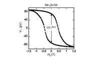
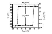
- the multilayer film of the magnetic memory element 1 used for measurement is Ru(2)/Mn 3 Sn(40)/W(5)
- the multilayer film of the magnetic memory element 100 is Mn 3 Sn(40)/W (5).
- FIGS. 5A and 5B a read current I read of 0.2 mA was applied to each of the Ru/Mn 3 Sn/W film and the Mn 3 Sn/W film under a perpendicular magnetic field Hz (perpendicular magnetic field).
- 2 shows the change in the Hall voltage VH with respect to the vertical magnetic field Hz.
- a clear hysteresis in the Hall voltage VH is observed in both samples, as shown in FIGS. 5A and 5B.
- the difference (Hall voltage change) ⁇ VH field of the Hall voltage VH at zero magnetic field in the Mn 3 Sn/W film is about 140 ⁇ V, which is about 1.0 ⁇ V higher than the Hall voltage change in the Ru/Mn 3 Sn/W film. It can be seen that it is 6 times larger.
- 2 shows the variation of the Hall voltage VH with respect to the write current I write at . Also in this case, in order to measure the Hall voltage VH , the read current I read of 0.2 mA is applied after the write current I write is applied.
- the Mn 3 Sn/W film As shown in FIG. 5D, when the write current I write is applied, a Hall voltage change ⁇ V H current of about 70 ⁇ V occurs, and the value of the read signal is higher than that in the Ru/Mn 3 Sn/W film. It can be seen that it is about three times larger. Further, from FIGS. 5B and 5D, the ratio ⁇ V H current / ⁇ V H field in the Mn 3 Sn/W film is about 0.5, so the magnetic order is reversed more than in the Ru/Mn 3 Sn/W film. It can be seen that the percentage is increasing (increasing from about 29% to about 50%). As described above, the Mn 3 Sn/W film can electrically control a larger read signal (Hall voltage) than the Ru/Mn 3 Sn/W film.
- FIG. 7 shows an AFM image of the Mn 3 Sn(40)/W(5) film with Hall bar structure.
- the root-mean-square (RMS) roughness of an AFM image is defined as Equation (1). where N is the number of pixels in the AFM image, x i is the height of the ith pixel, and x M is the average height. From the AFM image of FIG.
- the RMS roughness of the Mn 3 Sn/W film was approximately 0.5 nm, which was one order of magnitude smaller than that of the conventional Ru/Mn 3 Sn/W film. This suggests that the interface between the Mn 3 Sn layer and the W layer became smooth.
- the increase in the read signal in the magnetic memory element 100 of the Mn 3 Sn/W multilayer film is as follows : (ii) The roughness of the interface between the Mn 3 Sn layer and the W layer became 1.0 nm or less by annealing after all the layers of the multilayer film were formed, and the interface became smooth. It is believed that there is.
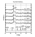
- FIG. 8 shows Mn 3 Sn(40)/Ta(40)/Ta(40) prepared on a substrate (Si/SiO 2 ) at different annealing temperatures T A (400° C., 500° C., 600° C., 650° C., 700° C.). 5) shows the X-ray diffraction pattern of the /Al 2 O 3 film.
- Figure 9 shows the results of Mn3Sn (40)/Ta( 5 )/ Al2O3 films fabricated at different annealing temperatures T A (400°C, 500°C, 600°C, 650°C, 700°C).
- TEM transmission electron microscope
- ⁇ is the resistivity of the Mn 3 Sn(40)/Ta(5) layer.
- a write current I write pulse current of 100 ms
- the Hall voltage V H is measured by applying a magnetic field followed by a read current I read of 0.2 mA (500 ms pulse current).
- the Hall voltage VH field in the Mn 3 Sn/Ta/Al 2 O 3 film under a perpendicular magnetic field Hz was also measured, and the change in the Hall voltage VH when the magnetic order of all magnetic domains in the Mn 3 Sn layer was reversed.
- FIG. 12 shows the change in the ratio V H /
- This Ta/Mn 3 Sn/Al 2 O 3 film was produced by annealing at 500° C. after depositing all the layers.
- indicates the ratio of actually reversed magnetic domains (reversal ratio) to all reversible magnetic domains.
- the Mn 3 Sn/Ta/Al 2 O 3 film and the Ta/Mn 3 Sn/Al 2 O 3 film have opposite polarities, and SOT works in opposite directions.
- the inversion ratio of both films reaches as high as about 40%.
- the difference ⁇ V H current in the Hall voltage V H when a read current I read of 0.2 mA is applied in the Mn 3 Sn/Ta/Al 2 O 3 film is about 70 ⁇ V, which is equivalent to that of the conventional magnetic memory element 1 ( (Ru/Mn 3 Sn/W film) is about three times larger than the Hall voltage change ⁇ V H current ⁇ 25 ⁇ V.
- the reaction between the Mn 3 Sn layer and the Ta layer should be small, and the interface between the Mn 3 Sn layer and the Ta layer should be small.
- a smaller roughness is preferable.
- the interface roughness is preferably 1.0 nm or less, more preferably 0.6 nm or less. In this way, by reducing the roughness of the interface and smoothing it, it is possible to increase the spin current injected into the Mn 3 Sn layer through the interface and to enhance the readout signal of the Mn 3 Sn layer. Become.
- the magnetic memory element according to this embodiment can function as a magnetic random access memory (MRAM) element.
- MRAM magnetic random access memory
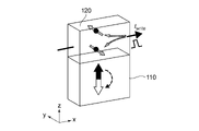
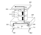
- the magnetic memory element 200 includes a magnetoresistive element 210, a heavy metal layer 220, a first terminal 231, a second terminal 232, a third terminal 233, and transistors Tr1 and Tr2.
- the heavy metal layer 220 is made of a non-magnetic heavy metal (W, Ta, etc.) exhibiting the spin Hall effect, or a chalcogenide substance such as a topological insulator.
- the magnetoresistive element 210 includes a free layer 212 in contact with the heavy metal layer 220 and capable of reversing the magnetic order, a nonmagnetic layer 214 on the free layer 212, and the nonmagnetic layer 214 in contact with the magnetic order fixed in the direction perpendicular to the plane. and a reference layer 216 .
- the free layer 212 is a canted antiferromagnetic thin film, similar to the antiferromagnetic layer 110 of FIGS. 2A and 2B.
- the nonmagnetic layer 214 is made of an insulator (for example, MgO).
- the reference layer 216 is made of ferromagnetic material (eg CoFeB).
- Magnetoresistive element 210 functions as a magnetic tunnel junction (MTJ) element.
- MTJ magnetic tunnel junction
- the first terminal 231, the second terminal 232, and the third terminal 233 are made of metal.
- a first terminal 231 is connected to the reference layer 216 , a second terminal 232 is connected to one end of the heavy metal layer 220 , and a third terminal 233 is connected to the other end of the heavy metal layer 220 .
- the first terminal 231 is connected to the ground line 240 .
- the ground line 240 is set to ground voltage. Note that the ground line 240 may be set to a reference voltage other than the ground voltage.
- the transistors Tr1 and Tr2 are, for example, N-channel metal oxide semiconductor (NMOS) transistors.
- the second terminal 232 is connected to the drain of the transistor Tr1, and the third terminal 233 is connected to the drain of the transistor Tr2.
- Gates of the transistors Tr1 and Tr2 are connected to the word line WL.
- a source of the transistor Tr1 is connected to the first bit line BL1, and a source of the transistor Tr2 is connected to the second bit line BL2.
- the magnetic memory element 200 of FIG. 13 is formed by forming a multilayer film including a heavy metal layer 220, a magnetoresistive element 210, and the like, and then annealing the multilayer film at a predetermined temperature. made by The roughness of the interface between the free layer 212 and the heavy metal layer 220 is preferably 1.0 nm or less, more preferably 0.6 nm or less.
- Data "0” and “1" are assigned to the magnetoresistive element 210 according to the resistance state. For example, when the magnetic ordering of the reference layer 216 and the magnetic ordering of the free layer 212 are in the same direction (parallel state), the magnetoresistive element 210 is in a low resistance state, and when they are in opposite directions (antiparallel state), the magnetoresistive element Since 210 is in the high resistance state, the former data can be determined as "0" and the latter data as "1".
- the word line WL is set to a high level to turn on the transistors Tr1 and Tr2, and the first bit line BL1 and the second bit line BL1 are turned on.
- One of the bit lines BL2 is set to high level and the other is set to low level.
- the write current I write flows in the in-plane direction of the heavy metal layer 220 between the first bit line BL1 and the second bit line BL2, generating a spin current, and the SOT reverses the magnetic order of the free layer 212. enabled and data can be written.
- the data to be written can be changed depending on the direction of the write current I write .
- the word line WL is set to high level to turn on the transistors Tr1 and Tr2, one bit line (second bit line BL2) is set to high level, The other bit line (first bit line BL1) is opened.
- the read current I read flows from the high-level second bit line BL2 to the third terminal 233, the heavy metal layer 220, the free layer 212, the nonmagnetic layer 214, the reference layer 216, the first terminal 231, and the ground line 240. flows.
- the resistance state of the magnetoresistive element 210 that is, the stored data can be determined.
- the read signal of the magnetic memory element 200 can be enhanced.
- FIG. 14 shows the configuration of a magnetic memory element 300 of MRAM (STT-MRAM) that reverses the magnetic order using spin transfer torque (STT).
- the magnetic memory element 300 includes a magnetoresistive element 310, a first terminal 321, a second terminal 322, and a transistor Tr.
- the magnetoresistive element 310 includes a reference layer 316 whose magnetic order is fixed in the perpendicular direction, a nonmagnetic layer 314 on the reference layer 316, and a free layer 312 in contact with the nonmagnetic layer 314 and capable of reversing the magnetic order.
- the free layer 312 is a canted antiferromagnetic thin film, similar to the antiferromagnetic layer 110 of FIGS. 2A and 2B.
- the nonmagnetic layer 314 is made of an insulator (for example, MgO).
- the reference layer 316 is made of ferromagnetic material (eg CoFeB).
- the magnetoresistive element 310 also functions as an MTJ element.
- the first terminal 321 and the second terminal 322 are made of metal.
- the free layer 312 is connected to the first terminal 321 and the reference layer 316 is connected to the second terminal 322 .
- a first terminal 321 is connected to the bit line BL, and a second terminal 322 is connected to the transistor Tr.
- the transistor Tr is, for example, an NMOS transistor.
- the transistor Tr has a drain connected to the second terminal 322, a source connected to the source line SL, and a gate connected to the word line WL.
- the magnetic memory element 300 of FIG. 14 is annealed at a predetermined temperature after depositing all layers of a multilayer film including the magnetoresistive element 310, the first terminal 321, and the like. It is made by
- the roughness of the interface between the free layer 312 and the nonmagnetic layer 314 and the roughness of the interface between the free layer 312 and the first terminal 321 are preferably 1.0 nm or less, more preferably 0.6 nm or less.
- the magnetoresistive element 310 is assigned data "0" and "1" according to the resistance state.
- the word line WL is set to a high level to turn on the transistor Tr, and a write current I write in the perpendicular direction is passed between the bit line BL and the source line SL. This allows the STT to reverse the magnetic order of the free layer 312, allowing data to be written.
- the data to be written can be changed depending on the direction of the write current I write .
- the word line WL is set to a high level to turn on the transistor Tr, and a read current I read is passed between the bit line BL and the source line SL.
- the resistance state of the magnetoresistive element 310 that is, the stored data can be determined.
- the read signal of the magnetic memory element 300 can be enhanced by smoothing the interface between the free layer 312 and the contact layer (nonmagnetic layer 314, first terminal 321).
- FIGS. 13 and 14 show an example in which the magnetoresistive elements 210 and 310 are MTJ elements, they can also function as giant magnetoresistive (GMR) elements.
- the nonmagnetic layers 214 and 314 are made of metal (conductor).
- X Sn, Ge, Ga, Rh, Pt, Ir, etc.
Landscapes
- Engineering & Computer Science (AREA)
- Computer Hardware Design (AREA)
- Manufacturing & Machinery (AREA)
- Hall/Mr Elements (AREA)
- Mram Or Spin Memory Techniques (AREA)
Priority Applications (3)
| Application Number | Priority Date | Filing Date | Title |
|---|---|---|---|
| US18/286,434 US20240194235A1 (en) | 2021-04-12 | 2022-04-12 | Magnetic memory element |
| JP2023514659A JP7710752B2 (ja) | 2021-04-12 | 2022-04-12 | 磁気メモリ素子及びその作製方法 |
| CN202280027992.XA CN117356199A (zh) | 2021-04-12 | 2022-04-12 | 磁存储元件 |
Applications Claiming Priority (2)
| Application Number | Priority Date | Filing Date | Title |
|---|---|---|---|
| US202163173579P | 2021-04-12 | 2021-04-12 | |
| US63/173,579 | 2021-04-12 |
Publications (1)
| Publication Number | Publication Date |
|---|---|
| WO2022220251A1 true WO2022220251A1 (ja) | 2022-10-20 |
Family
ID=83640695
Family Applications (1)
| Application Number | Title | Priority Date | Filing Date |
|---|---|---|---|
| PCT/JP2022/017647 Ceased WO2022220251A1 (ja) | 2021-04-12 | 2022-04-12 | 磁気メモリ素子 |
Country Status (4)
| Country | Link |
|---|---|
| US (1) | US20240194235A1 (https=) |
| JP (1) | JP7710752B2 (https=) |
| CN (1) | CN117356199A (https=) |
| WO (1) | WO2022220251A1 (https=) |
Cited By (6)
| Publication number | Priority date | Publication date | Assignee | Title |
|---|---|---|---|---|
| WO2024181562A1 (ja) * | 2023-03-01 | 2024-09-06 | TopoLogic株式会社 | 素子および素子の製造方法 |
| WO2024204298A1 (ja) * | 2023-03-28 | 2024-10-03 | 国立大学法人東京大学 | 磁気メモリ素子、磁気メモリ装置、及びフォトニックスピンレジスタ |
| WO2024253160A1 (ja) | 2023-06-09 | 2024-12-12 | Jsr株式会社 | 磁性体および絶縁体の二層膜,トンネル磁気抵抗素子,及び磁気メモリ |
| WO2025018303A1 (ja) * | 2023-07-19 | 2025-01-23 | Jsr株式会社 | 磁気トンネル接合素子の製造方法 |
| WO2025028421A1 (ja) | 2023-07-28 | 2025-02-06 | Jsr株式会社 | 反強磁性体材料,磁性体および絶縁体の二層膜,トンネル磁気抵抗素子,及び磁気メモリ |
| JP7708488B1 (ja) * | 2023-10-13 | 2025-07-15 | TopoLogic株式会社 | 磁気メモリ素子 |
Families Citing this family (1)
| Publication number | Priority date | Publication date | Assignee | Title |
|---|---|---|---|---|
| CN120949364B (zh) * | 2025-10-13 | 2026-01-23 | 中国人民解放军国防科技大学 | 一种Kagome光子晶体 |
Citations (4)
| Publication number | Priority date | Publication date | Assignee | Title |
|---|---|---|---|---|
| WO2017018391A1 (ja) * | 2015-07-24 | 2017-02-02 | 国立大学法人東京大学 | メモリ素子 |
| WO2019045055A1 (ja) * | 2017-09-04 | 2019-03-07 | Tdk株式会社 | スピン軌道トルク型磁化反転素子及び磁気メモリ |
| JP2019110326A (ja) * | 2017-03-29 | 2019-07-04 | Tdk株式会社 | 記憶素子及び磁気メモリ |
| WO2020166722A1 (ja) * | 2019-02-15 | 2020-08-20 | 国立大学法人東京大学 | スピントロニクス素子及び磁気メモリ装置 |
Family Cites Families (1)
| Publication number | Priority date | Publication date | Assignee | Title |
|---|---|---|---|---|
| JP2020017662A (ja) | 2018-07-26 | 2020-01-30 | 株式会社アルバック | 磁気記憶素子、および、磁気記憶素子の製造方法 |
-
2022
- 2022-04-12 US US18/286,434 patent/US20240194235A1/en active Pending
- 2022-04-12 WO PCT/JP2022/017647 patent/WO2022220251A1/ja not_active Ceased
- 2022-04-12 CN CN202280027992.XA patent/CN117356199A/zh active Pending
- 2022-04-12 JP JP2023514659A patent/JP7710752B2/ja active Active
Patent Citations (4)
| Publication number | Priority date | Publication date | Assignee | Title |
|---|---|---|---|---|
| WO2017018391A1 (ja) * | 2015-07-24 | 2017-02-02 | 国立大学法人東京大学 | メモリ素子 |
| JP2019110326A (ja) * | 2017-03-29 | 2019-07-04 | Tdk株式会社 | 記憶素子及び磁気メモリ |
| WO2019045055A1 (ja) * | 2017-09-04 | 2019-03-07 | Tdk株式会社 | スピン軌道トルク型磁化反転素子及び磁気メモリ |
| WO2020166722A1 (ja) * | 2019-02-15 | 2020-08-20 | 国立大学法人東京大学 | スピントロニクス素子及び磁気メモリ装置 |
Cited By (7)
| Publication number | Priority date | Publication date | Assignee | Title |
|---|---|---|---|---|
| WO2024181562A1 (ja) * | 2023-03-01 | 2024-09-06 | TopoLogic株式会社 | 素子および素子の製造方法 |
| WO2024204298A1 (ja) * | 2023-03-28 | 2024-10-03 | 国立大学法人東京大学 | 磁気メモリ素子、磁気メモリ装置、及びフォトニックスピンレジスタ |
| WO2024253160A1 (ja) | 2023-06-09 | 2024-12-12 | Jsr株式会社 | 磁性体および絶縁体の二層膜,トンネル磁気抵抗素子,及び磁気メモリ |
| KR20260008139A (ko) | 2023-06-09 | 2026-01-15 | 제이에스알 가부시키가이샤 | 자성체 및 절연체의 2층막, 터널 자기 저항 소자, 및 자기 메모리 |
| WO2025018303A1 (ja) * | 2023-07-19 | 2025-01-23 | Jsr株式会社 | 磁気トンネル接合素子の製造方法 |
| WO2025028421A1 (ja) | 2023-07-28 | 2025-02-06 | Jsr株式会社 | 反強磁性体材料,磁性体および絶縁体の二層膜,トンネル磁気抵抗素子,及び磁気メモリ |
| JP7708488B1 (ja) * | 2023-10-13 | 2025-07-15 | TopoLogic株式会社 | 磁気メモリ素子 |
Also Published As
| Publication number | Publication date |
|---|---|
| JPWO2022220251A1 (https=) | 2022-10-20 |
| CN117356199A (zh) | 2024-01-05 |
| JP7710752B2 (ja) | 2025-07-22 |
| US20240194235A1 (en) | 2024-06-13 |
Similar Documents
| Publication | Publication Date | Title |
|---|---|---|
| JP7710752B2 (ja) | 磁気メモリ素子及びその作製方法 | |
| JP6923213B2 (ja) | 磁性積層膜、磁気メモリ素子、磁気メモリ、及びその製造方法 | |
| EP2220651B1 (en) | High speed low power magnetic devices based on current induced spin-momentum transfer | |
| CN110970551B (zh) | 用于具有体积单轴磁结晶各向异性的磁性层的自旋转移力矩切换的装置和方法 | |
| EP2863434B1 (en) | High speed low power magnetic devices based on current induced spin-momentum transfer | |
| EP2118893B1 (en) | Non-volatile magnetic memory element with graded layer | |
| JP5867030B2 (ja) | 記憶素子、記憶装置 | |
| US20220149269A1 (en) | Spintronics element and magnetic memory device | |
| CN102916126B (zh) | 存储元件和存储装置 | |
| KR20220029381A (ko) | 쌍극자 결합 스핀 궤도 토크 구조 | |
| TWI509603B (zh) | Memory elements and memory devices | |
| JP5786341B2 (ja) | 記憶素子、メモリ装置 | |
| JP2013115319A (ja) | 記憶素子、記憶装置 | |
| US10840436B2 (en) | Perpendicular magnetic anisotropy interface tunnel junction devices and methods of manufacture | |
| JP7784762B2 (ja) | 磁気メモリ素子、情報処理システム、及び磁気メモリ素子の制御方法 | |
| US20250120322A1 (en) | Magnetoresistive element and magnetic memory | |
| JP5034317B2 (ja) | 記憶素子及びメモリ | |
| US20200411752A1 (en) | Methods of manufacture precessional spin current magnetic tunnel junction devices | |
| JP2013026441A (ja) | 磁壁移動型の磁気記録素子及び磁気記録方法 | |
| WO2018179961A1 (ja) | 磁気素子、磁気記憶装置及び磁気センサ | |
| WO2024204298A1 (ja) | 磁気メモリ素子、磁気メモリ装置、及びフォトニックスピンレジスタ | |
| JP2013115320A (ja) | 記憶素子、記憶装置 |
Legal Events
| Date | Code | Title | Description |
|---|---|---|---|
| 121 | Ep: the epo has been informed by wipo that ep was designated in this application |
Ref document number: 22788174 Country of ref document: EP Kind code of ref document: A1 |
|
| WWE | Wipo information: entry into national phase |
Ref document number: 2023514659 Country of ref document: JP |
|
| WWE | Wipo information: entry into national phase |
Ref document number: 202280027992.X Country of ref document: CN |
|
| NENP | Non-entry into the national phase |
Ref country code: DE |
|
| WWE | Wipo information: entry into national phase |
Ref document number: 18286434 Country of ref document: US |
|
| 122 | Ep: pct application non-entry in european phase |
Ref document number: 22788174 Country of ref document: EP Kind code of ref document: A1 |