WO2022220251A1 - Magnetic memory element - Google Patents
Magnetic memory element Download PDFInfo
- Publication number
- WO2022220251A1 WO2022220251A1 PCT/JP2022/017647 JP2022017647W WO2022220251A1 WO 2022220251 A1 WO2022220251 A1 WO 2022220251A1 JP 2022017647 W JP2022017647 W JP 2022017647W WO 2022220251 A1 WO2022220251 A1 WO 2022220251A1
- Authority
- WO
- WIPO (PCT)
- Prior art keywords
- layer
- magnetic
- memory element
- magnetic memory
- antiferromagnetic
- Prior art date
Links
- 230000005291 magnetic effect Effects 0.000 title claims abstract description 153
- 230000015654 memory Effects 0.000 title claims abstract description 77
- 230000005290 antiferromagnetic effect Effects 0.000 claims abstract description 52
- 230000005355 Hall effect Effects 0.000 claims abstract description 12
- 230000001747 exhibiting effect Effects 0.000 claims abstract description 3
- 239000002885 antiferromagnetic material Substances 0.000 claims description 13
- 239000000463 material Substances 0.000 claims description 12
- 230000002547 anomalous effect Effects 0.000 claims description 9
- 229910001385 heavy metal Inorganic materials 0.000 abstract description 34
- 239000000758 substrate Substances 0.000 abstract description 18
- 239000011572 manganese Substances 0.000 description 93
- 239000010408 film Substances 0.000 description 64
- 229910018072 Al 2 O 3 Inorganic materials 0.000 description 15
- 238000000137 annealing Methods 0.000 description 15
- TWNQGVIAIRXVLR-UHFFFAOYSA-N oxo(oxoalumanyloxy)alumane Chemical compound O=[Al]O[Al]=O TWNQGVIAIRXVLR-UHFFFAOYSA-N 0.000 description 12
- 230000008859 change Effects 0.000 description 10
- 229910052751 metal Inorganic materials 0.000 description 10
- 239000002184 metal Substances 0.000 description 10
- 238000000089 atomic force micrograph Methods 0.000 description 7
- BASFCYQUMIYNBI-UHFFFAOYSA-N platinum Chemical compound [Pt] BASFCYQUMIYNBI-UHFFFAOYSA-N 0.000 description 7
- 229910016797 Mn3Sn Inorganic materials 0.000 description 6
- 238000010586 diagram Methods 0.000 description 6
- 239000003302 ferromagnetic material Substances 0.000 description 6
- 238000005259 measurement Methods 0.000 description 6
- 229910004298 SiO 2 Inorganic materials 0.000 description 5
- 238000002441 X-ray diffraction Methods 0.000 description 5
- 239000013078 crystal Substances 0.000 description 5
- 230000005415 magnetization Effects 0.000 description 5
- 238000001755 magnetron sputter deposition Methods 0.000 description 5
- ORQBXQOJMQIAOY-UHFFFAOYSA-N nobelium Chemical compound [No] ORQBXQOJMQIAOY-UHFFFAOYSA-N 0.000 description 5
- 229910052715 tantalum Inorganic materials 0.000 description 5
- PNEYBMLMFCGWSK-UHFFFAOYSA-N aluminium oxide Inorganic materials [O-2].[O-2].[O-2].[Al+3].[Al+3] PNEYBMLMFCGWSK-UHFFFAOYSA-N 0.000 description 4
- 229910052593 corundum Inorganic materials 0.000 description 4
- 230000006870 function Effects 0.000 description 4
- 239000012212 insulator Substances 0.000 description 4
- 239000000395 magnesium oxide Substances 0.000 description 4
- CPLXHLVBOLITMK-UHFFFAOYSA-N magnesium oxide Inorganic materials [Mg]=O CPLXHLVBOLITMK-UHFFFAOYSA-N 0.000 description 4
- AXZKOIWUVFPNLO-UHFFFAOYSA-N magnesium;oxygen(2-) Chemical compound [O-2].[Mg+2] AXZKOIWUVFPNLO-UHFFFAOYSA-N 0.000 description 4
- 229910001845 yogo sapphire Inorganic materials 0.000 description 4
- 238000006243 chemical reaction Methods 0.000 description 3
- 238000000151 deposition Methods 0.000 description 3
- 230000000694 effects Effects 0.000 description 3
- 230000005294 ferromagnetic effect Effects 0.000 description 3
- 238000009499 grossing Methods 0.000 description 3
- 230000001965 increasing effect Effects 0.000 description 3
- 230000005381 magnetic domain Effects 0.000 description 3
- 230000005302 magnetic ordering Effects 0.000 description 3
- 238000000034 method Methods 0.000 description 3
- 229910052697 platinum Inorganic materials 0.000 description 3
- 230000002441 reversible effect Effects 0.000 description 3
- 229910052718 tin Inorganic materials 0.000 description 3
- 229910052721 tungsten Inorganic materials 0.000 description 3
- 229910019236 CoFeB Inorganic materials 0.000 description 2
- VYPSYNLAJGMNEJ-UHFFFAOYSA-N Silicium dioxide Chemical compound O=[Si]=O VYPSYNLAJGMNEJ-UHFFFAOYSA-N 0.000 description 2
- 230000005540 biological transmission Effects 0.000 description 2
- 238000002425 crystallisation Methods 0.000 description 2
- 230000008025 crystallization Effects 0.000 description 2
- 238000010438 heat treatment Methods 0.000 description 2
- 238000004519 manufacturing process Methods 0.000 description 2
- 229910044991 metal oxide Inorganic materials 0.000 description 2
- 150000004706 metal oxides Chemical class 0.000 description 2
- 230000004048 modification Effects 0.000 description 2
- 238000012986 modification Methods 0.000 description 2
- 230000008569 process Effects 0.000 description 2
- 230000004044 response Effects 0.000 description 2
- 239000000126 substance Substances 0.000 description 2
- 238000010408 sweeping Methods 0.000 description 2
- 239000010409 thin film Substances 0.000 description 2
- WFKWXMTUELFFGS-UHFFFAOYSA-N tungsten Chemical compound [W] WFKWXMTUELFFGS-UHFFFAOYSA-N 0.000 description 2
- 239000010937 tungsten Substances 0.000 description 2
- PWHULOQIROXLJO-UHFFFAOYSA-N Manganese Chemical compound [Mn] PWHULOQIROXLJO-UHFFFAOYSA-N 0.000 description 1
- KJTLSVCANCCWHF-UHFFFAOYSA-N Ruthenium Chemical compound [Ru] KJTLSVCANCCWHF-UHFFFAOYSA-N 0.000 description 1
- 238000003917 TEM image Methods 0.000 description 1
- 230000006399 behavior Effects 0.000 description 1
- 150000004770 chalcogenides Chemical class 0.000 description 1
- 229910052681 coesite Inorganic materials 0.000 description 1
- 150000001875 compounds Chemical class 0.000 description 1
- 239000004020 conductor Substances 0.000 description 1
- 229910052906 cristobalite Inorganic materials 0.000 description 1
- 238000005516 engineering process Methods 0.000 description 1
- 230000002708 enhancing effect Effects 0.000 description 1
- 229910052733 gallium Inorganic materials 0.000 description 1
- 229910052732 germanium Inorganic materials 0.000 description 1
- 230000003993 interaction Effects 0.000 description 1
- 229910052741 iridium Inorganic materials 0.000 description 1
- 238000010030 laminating Methods 0.000 description 1
- 229910052748 manganese Inorganic materials 0.000 description 1
- 238000001451 molecular beam epitaxy Methods 0.000 description 1
- 230000003647 oxidation Effects 0.000 description 1
- 238000007254 oxidation reaction Methods 0.000 description 1
- 229910052703 rhodium Inorganic materials 0.000 description 1
- 229910052707 ruthenium Inorganic materials 0.000 description 1
- 239000004065 semiconductor Substances 0.000 description 1
- 239000000377 silicon dioxide Substances 0.000 description 1
- 235000012239 silicon dioxide Nutrition 0.000 description 1
- 229910052682 stishovite Inorganic materials 0.000 description 1
- GUVRBAGPIYLISA-UHFFFAOYSA-N tantalum atom Chemical compound [Ta] GUVRBAGPIYLISA-UHFFFAOYSA-N 0.000 description 1
- 229910052905 tridymite Inorganic materials 0.000 description 1
Images


Classifications
-
- H—ELECTRICITY
- H01—ELECTRIC ELEMENTS
- H01L—SEMICONDUCTOR DEVICES NOT COVERED BY CLASS H10
- H01L27/00—Devices consisting of a plurality of semiconductor or other solid-state components formed in or on a common substrate
- H01L27/02—Devices consisting of a plurality of semiconductor or other solid-state components formed in or on a common substrate including semiconductor components specially adapted for rectifying, oscillating, amplifying or switching and having at least one potential-jump barrier or surface barrier; including integrated passive circuit elements with at least one potential-jump barrier or surface barrier
- H01L27/04—Devices consisting of a plurality of semiconductor or other solid-state components formed in or on a common substrate including semiconductor components specially adapted for rectifying, oscillating, amplifying or switching and having at least one potential-jump barrier or surface barrier; including integrated passive circuit elements with at least one potential-jump barrier or surface barrier the substrate being a semiconductor body
- H01L27/10—Devices consisting of a plurality of semiconductor or other solid-state components formed in or on a common substrate including semiconductor components specially adapted for rectifying, oscillating, amplifying or switching and having at least one potential-jump barrier or surface barrier; including integrated passive circuit elements with at least one potential-jump barrier or surface barrier the substrate being a semiconductor body including a plurality of individual components in a repetitive configuration
- H01L27/105—Devices consisting of a plurality of semiconductor or other solid-state components formed in or on a common substrate including semiconductor components specially adapted for rectifying, oscillating, amplifying or switching and having at least one potential-jump barrier or surface barrier; including integrated passive circuit elements with at least one potential-jump barrier or surface barrier the substrate being a semiconductor body including a plurality of individual components in a repetitive configuration including field-effect components
-
- H—ELECTRICITY
- H10—SEMICONDUCTOR DEVICES; ELECTRIC SOLID-STATE DEVICES NOT OTHERWISE PROVIDED FOR
- H10B—ELECTRONIC MEMORY DEVICES
- H10B99/00—Subject matter not provided for in other groups of this subclass
-
- H—ELECTRICITY
- H10—SEMICONDUCTOR DEVICES; ELECTRIC SOLID-STATE DEVICES NOT OTHERWISE PROVIDED FOR
- H10N—ELECTRIC SOLID-STATE DEVICES NOT OTHERWISE PROVIDED FOR
- H10N50/00—Galvanomagnetic devices
- H10N50/10—Magnetoresistive devices
-
- H—ELECTRICITY
- H10—SEMICONDUCTOR DEVICES; ELECTRIC SOLID-STATE DEVICES NOT OTHERWISE PROVIDED FOR
- H10N—ELECTRIC SOLID-STATE DEVICES NOT OTHERWISE PROVIDED FOR
- H10N50/00—Galvanomagnetic devices
- H10N50/80—Constructional details
- H10N50/85—Magnetic active materials
Definitions
- the present invention relates to magnetic memory elements.
- magnetoresistive memories that use ferromagnetic materials that can store the direction of magnetization as "0" and "1" information have been attracting attention as a representative example of nonvolatile memory.
- a magnetization reversal phenomenon using a spin current has been found as a writing method, and is being used widely.
- the magnetization reversal phenomenon that occurs when a current is passed through a multilayer film made of ferromagnetic materials and non-magnetic heavy metals (tungsten (W), platinum (Pt), etc.) is called spin-orbit torque magnetization reversal, and is a next-generation technology. It has been extensively researched.
- Non-Patent Document 1 In order to further increase the speed of the magnetoresistive memory, replacement of ferromagnetic materials with antiferromagnetic materials is under consideration (see, for example, Non-Patent Document 1).
- antiferromagnets have a spin response speed in the THz band (pico(10 ⁇ 12 ) seconds) that is two to three orders of magnitude faster than ferromagnets, and the interaction between magnetic bodies is small. This is because there is a possibility that magnetic devices such as resistive memories can be further accelerated and highly integrated.
- the present invention has been made in view of the above problems, and an object of the present invention is to enhance a read signal in a magnetic memory element using an antiferromagnetic material.
- the magnetic memory element according to the present invention comprises an antiferromagnetic layer made of a canted antiferromagnetic material having a magnetic order in which the magnetic moment is canted, and a substance different from the canted antiferromagnetic material in contact with the antiferromagnetic layer and a contact layer consisting of
- the roughness of the interface between the antiferromagnetic layer and the contact layer is 1.0 nm or less, and when a spin current flows in the contact layer, the torque generated by the spin current acts on the magnetic order of the antiferromagnetic layer, and the magnetic order can be reversed. is.
- the interface is smoothed, and spins injected from the contact layer to the antiferromagnetic layer via the interface Since the current can be increased and the magnetic properties of the antiferromagnetic layer can be kept optimal, the read signal of the magnetic memory element can be enhanced.
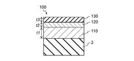
- FIG. 1 is a cross-sectional view of a conventional magnetic memory element
- FIG. 1 is a cross-sectional view of a magnetic memory device according to an embodiment of the present invention
- FIG. FIG. 4 is a cross-sectional view of a magnetic memory element according to a modification of the embodiment
- 1 is a schematic diagram showing the crystal structure and magnetic structure of Mn 3 Sn.
- FIG. 1 is a schematic diagram showing the configuration of a magnetic memory element having a Hall bar structure
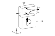
- FIG. 4B is a schematic diagram for explaining a write operation in the magnetic memory element of FIG. 4A
- FIG. 4B is a schematic diagram for explaining a read operation in the magnetic memory element of FIG. 4A
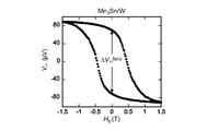
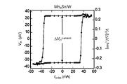
- 4 is a graph showing vertical magnetic field dependence of Hall voltage for conventional Ru/Mn 3 Sn/W films. 4 is a graph showing vertical magnetic field dependence of the Hall voltage for the Mn 3 Sn/W film of the present embodiment. 4 is a graph showing write current dependence of Hall voltage for Ru/Mn 3 Sn/W films. 4 is a graph showing write current dependence of Hall voltage for Mn 3 Sn/W films. 4 is a graph showing read current dependence of Hall voltage change for a Mn 3 Sn/W film. 2 is an atomic force microscope (AFM) image of a Mn 3 Sn/W film; FIG.
- AFM atomic force microscope
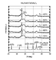
- FIG. 4 is a graph showing X-ray diffraction patterns of Mn 3 Sn/Ta/Al 2 O 3 films of the present embodiment fabricated at different annealing temperatures T A ;
- FIG. Fig. 4 is AFM images of Mn3Sn /Ta/ Al2O3 films fabricated with different annealing temperatures T A ;
- TEM transmission electron microscope
- FIG. 3 is a graph showing the magnetic field dependence of the anomalous Hall conductivity of Mn 3 Sn/Ta/Al 2 O 3 films fabricated at different annealing temperatures T A ; 4 is a graph showing write current dependence of the reversal rate of magnetic order for each of a Mn 3 Sn/Ta/Al 2 O 3 film and a Ta/Mn 3 Sn/Al 2 O 3 film.
- 1 is a schematic diagram showing the configuration of a magnetic memory element of an SOT-MRAM;
- FIG. 1 is a schematic diagram showing the configuration of a magnetic memory element of an STT-MRAM;
- a multilayer film may be indicated by the material of each layer that constitutes the multilayer film.
- this multilayer film is expressed as "material a/material b/material c”.
- the thickness (nm) of each layer may be described in parentheses after the material name. For example, a layer having a thickness of ti (nm) and made of material j is expressed as "material j (ti)".
- the magnetic memory element 1 includes a substrate 2, a metal layer 10 on the substrate 2, an antiferromagnetic layer 11 on the metal layer 10, a heavy metal layer 12 on the antiferromagnetic layer 11, and an oxide on the heavy metal layer 12. a layer 13;
- the substrate 2 is made of an insulator such as Si/ SiO2 .
- the metal layer 10 is made of metal such as ruthenium (Ru).
- the antiferromagnetic layer 11 is made of an antiferromagnetic material such as Mn 3 Sn.
- the heavy metal layer 12 is made of non-magnetic heavy metal such as tantalum (Ta), tungsten (W), and platinum (Pt).
- the oxide layer 13 is a cap layer for preventing oxidation, and is made of metal oxide such as aluminum oxide (AlOx) and magnesium oxide (MgO).
- the thicknesses (nm) of the metal layer 10, the antiferromagnetic layer 11, the heavy metal layer 12, and the oxide layer 13 are expressed as t0, t1, t2, and t3, respectively.
- the temperature is maintained at a predetermined temperature (eg, 450° C.) for a predetermined time (eg, 30 minutes) and then laminating the heavy metal layer 12 and the oxide layer 13 at room temperature.
- a predetermined temperature eg, 450° C.
- a predetermined time eg, 30 minutes
- the reason why the Ru layer is provided between the substrate 2 and the Mn 3 Sn layer in the conventional magnetic memory element 1 is that if the Ru layer is not provided and the Mn 3 Sn layer is formed and then annealed, the Mn 3 Sn layer is removed. This is because the interface between the Mn 3 Sn layer and the heavy metal layer 12 becomes rough due to crystallization, which makes it difficult to drive the device.
- spin-orbit torque acts on the magnetic order of the antiferromagnetic layer 11 due to the spin Hall effect, thereby reversing the direction of the magnetic order.
- the magnetic memory element according to this embodiment does not have a Ru layer and is manufactured by an improved heat treatment process, as will be described later.
- the magnetic memory element 100 includes a substrate 2, an antiferromagnetic layer 110 made of an antiferromagnetic material laminated on the substrate 2, and an antiferromagnetic layer 110 laminated on the antiferromagnetic layer 110. and an oxide layer 130 on the heavy metal layer 120 .
- the magnetic memory element 102 shown in FIG. 2B may be employed.
- the magnetic memory element 102 has a heavy metal layer 120 , an antiferromagnetic layer 110 and an oxide layer 130 stacked in this order on the substrate 2 .
- the contact layer in contact with the antiferromagnetic layer 110 is mainly the heavy metal layer 120
- Layers may be employed. This embodiment is applicable as long as a contact layer is provided on at least one side of the antiferromagnetic layer 110 .
- Mn 3 Sn is an antiferromagnetic material having a crystal structure called a Kagome lattice based on triangles. As shown in FIG. 3, it has a structure in which Kagome lattices are stacked in the [0001] direction. Due to geometrical frustration, manganese (Mn) located at the vertices of the Kagome lattice exhibits a non-collinear ) indicates the magnetic structure.
- Mn manganese located at the vertices of the Kagome lattice exhibits a non-collinear
- Three types of six-spin units arranged on a bilayer kagome lattice form a spin order called a cluster magnetic octupole, which is indicated by a hexagon.
- This non-collinear magnetic structure can be viewed as a ferromagnetic order of clustered magnetic octupoles (thick arrow in the middle of Fig. 3). This ferromagnetic order macroscopically breaks the time-reversal symmetry.
- the cluster magnetic octupole corresponds to the Weyl points, which are topological electronic structures, and the virtual magnetic field in momentum space (equivalent to 100 to 1000 Tesla (T) in real space).
- the orientation of the poles can control the response from the Weyl point and the virtual magnetic field.
- the magnetic structure as shown in FIG. 3 has orthorhombic symmetry, with only one of the three magnetic moments of Mn located at the vertices of the triangle being parallel to the easy axis. Since the other two magnetic moments cant with respect to the easy axis, it is believed to induce a weak ferromagnetic moment.
- Such an antiferromagnet whose magnetic moment is canted and has minute magnetization is called a canted antiferromagnet.
- the crystal orientation of Mn 3 Sn plays an important role in enhancing the read signal of magnetic memory elements. For example, in measurements of the anomalous Hall effect, only grains whose magnetic ordering of the cluster magnetic octupole has a component in the perpendicular direction (perpendicular to the surface of the substrate 2) contribute to the Hall voltage.
- the Ru layer metal layer 10
- the Kagome plane of Mn 3 Sn close to the Ru layer is oriented substantially in the in-plane direction (parallel to the surface of the substrate 2). They are aligned, and the contribution to the Hall voltage is reduced.
- current flowing through the Ru layer also causes a decrease in the read voltage. Therefore, in this embodiment, as shown in FIGS. 2A and 2B, the magnetic memory elements 100 and 102 are not provided with the Ru layer, and the Mn 3 Sn layer has a crystal orientation that exhibits a higher Hall voltage.
- the Ru layer when the Ru layer is not provided, as described above, when the heavy metal layer 120 is deposited by annealing after forming the Mn 3 Sn layer (antiferromagnetic layer 110), the Mn 3 Sn layer is crystallized and Mn 3 The interface between the Sn layer and the heavy metal layer 120 becomes rough. Therefore, in the present embodiment, annealing is not performed immediately after the Mn 3 Sn layer is deposited, but annealing is performed after depositing all layers of the multilayer film.
- a case of forming Mn 3 Sn/W/AlOx on a Si/SiO 2 substrate and a case of forming Mn 3 Sn/Ta/AlOx are given as examples. to explain.
- Mn 3 Sn/W/AlOx a Mn 3 Sn layer is deposited on a Si/SiO 2 substrate at room temperature using a DC magnetron sputtering apparatus with a base pressure below 5 ⁇ 10 ⁇ 7 Pa. Then, a W layer is deposited at room temperature by a molecular beam epitaxy (MBE) apparatus under ultra-high vacuum with a base pressure of less than 2 ⁇ 10 ⁇ 8 Pa. The W layer can also be formed using a DC magnetron sputtering apparatus. An AlOx layer is then deposited at room temperature using an RF magnetron sputtering apparatus with a base pressure of less than 5 ⁇ 10 ⁇ 7 Pa. All layers are deposited without breaking vacuum. After manufacturing Mn 3 Sn/W/AlOx, the magnetic memory element 100 is manufactured by annealing at a predetermined temperature (eg, 450° C.) for a predetermined time (eg, 30 minutes).
- a predetermined temperature eg, 450° C
- Mn 3 Sn/Ta/AlOx Mn 3 Sn and Ta layers were deposited on a Si/SiO 2 substrate using a DC magnetron sputtering apparatus with a base pressure of less than 5 ⁇ 10 ⁇ 7 Pa, followed by RF magnetron sputtering. An AlOx layer is deposited using the apparatus. All layers are deposited at room temperature without breaking vacuum. After forming the Mn 3 Sn/Ta/AlOx film, annealing is performed at a predetermined temperature (eg, 500° C.) for a predetermined time (eg, 30 minutes) to fabricate the magnetic memory element 100 .
- a predetermined temperature eg, 500° C.
- a predetermined time eg, 30 minutes
- the magnetic memory element 100 is manufactured by annealing at a temperature equal to or higher than the crystallization temperature of the antiferromagnetic layer 110 after all the multilayer films including the antiferromagnetic layer 110 are formed. be done.
- a magnetic memory element 102 shown in FIG. 2B is also manufactured in a similar manner.
- the interface between the antiferromagnetic layer 110 and the contact layer in contact with the antiferromagnetic layer 110 is smoothed without providing a Ru layer, An enhancement of the readout signal can be expected.
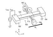
- FIG. 4A shows the configuration of a magnetic memory element 100 having a Hall bar structure.
- a sample of the magnetic memory element 100 is manufactured in a predetermined size (16 ⁇ m ⁇ 96 ⁇ m, for example).
- Electrodes 152 and 154 made of Au/Ti are arranged at both ends in the longitudinal direction (x direction) of the sample, and electrodes 162 and 164 made of Au/Ti are arranged in the lateral direction (y direction). .
- a write current I write or a read current I read flows between the electrodes 152 and 154 , and a Hall voltage VH is detected between the electrodes 162 and 164 .
- the substrate 2 and the oxide layer 130 are omitted in FIG. 4A.
- a write current I write pulse current
- a spin current is generated in the perpendicular direction (z direction) by the spin Hall effect, and SOT acts on the magnetic order of the antiferromagnetic layer 110 to reverse the magnetic order.
- SOT acts on the magnetic order of the antiferromagnetic layer 110 to reverse the magnetic order.
- the direction of the magnetic order of the antiferromagnetic layer 110 can be controlled by the direction of the write current I write .
- the magnetic order is reversed from the +z direction (“1”) to the ⁇ z direction (“0”), and when the write current I write in the ⁇ x direction is applied, the magnetic order is inverted from the -z direction (“0”) to the +z direction (“1”).
- a read current I read (direct current) is passed through the antiferromagnetic layer 110 in the x direction, as shown in FIG. 4C.
- This causes a Hall voltage VH in the y direction due to the anomalous Hall effect.
- the sign of the Hall voltage V H is determined by the z-direction component of the magnetic order of the antiferromagnetic layer 110 .
- the magnetic order of the antiferromagnetic layer 110 is oriented in the +z direction, it corresponds to "1", and when it is oriented in the -z direction, it corresponds to "0".
- the information stored by the orientation of the magnetic order of the antiferromagnetic layer 110 can be read as the Hall voltage VH by applying the read current I read .
- the multilayer film of the magnetic memory element 1 used for measurement is Ru(2)/Mn 3 Sn(40)/W(5)
- the multilayer film of the magnetic memory element 100 is Mn 3 Sn(40)/W (5).
- FIGS. 5A and 5B a read current I read of 0.2 mA was applied to each of the Ru/Mn 3 Sn/W film and the Mn 3 Sn/W film under a perpendicular magnetic field Hz (perpendicular magnetic field).
- 2 shows the change in the Hall voltage VH with respect to the vertical magnetic field Hz.
- a clear hysteresis in the Hall voltage VH is observed in both samples, as shown in FIGS. 5A and 5B.
- the difference (Hall voltage change) ⁇ VH field of the Hall voltage VH at zero magnetic field in the Mn 3 Sn/W film is about 140 ⁇ V, which is about 1.0 ⁇ V higher than the Hall voltage change in the Ru/Mn 3 Sn/W film. It can be seen that it is 6 times larger.
- 2 shows the variation of the Hall voltage VH with respect to the write current I write at . Also in this case, in order to measure the Hall voltage VH , the read current I read of 0.2 mA is applied after the write current I write is applied.
- the Mn 3 Sn/W film As shown in FIG. 5D, when the write current I write is applied, a Hall voltage change ⁇ V H current of about 70 ⁇ V occurs, and the value of the read signal is higher than that in the Ru/Mn 3 Sn/W film. It can be seen that it is about three times larger. Further, from FIGS. 5B and 5D, the ratio ⁇ V H current / ⁇ V H field in the Mn 3 Sn/W film is about 0.5, so the magnetic order is reversed more than in the Ru/Mn 3 Sn/W film. It can be seen that the percentage is increasing (increasing from about 29% to about 50%). As described above, the Mn 3 Sn/W film can electrically control a larger read signal (Hall voltage) than the Ru/Mn 3 Sn/W film.
- FIG. 7 shows an AFM image of the Mn 3 Sn(40)/W(5) film with Hall bar structure.
- the root-mean-square (RMS) roughness of an AFM image is defined as Equation (1). where N is the number of pixels in the AFM image, x i is the height of the ith pixel, and x M is the average height. From the AFM image of FIG.
- the RMS roughness of the Mn 3 Sn/W film was approximately 0.5 nm, which was one order of magnitude smaller than that of the conventional Ru/Mn 3 Sn/W film. This suggests that the interface between the Mn 3 Sn layer and the W layer became smooth.
- the increase in the read signal in the magnetic memory element 100 of the Mn 3 Sn/W multilayer film is as follows : (ii) The roughness of the interface between the Mn 3 Sn layer and the W layer became 1.0 nm or less by annealing after all the layers of the multilayer film were formed, and the interface became smooth. It is believed that there is.
- FIG. 8 shows Mn 3 Sn(40)/Ta(40)/Ta(40) prepared on a substrate (Si/SiO 2 ) at different annealing temperatures T A (400° C., 500° C., 600° C., 650° C., 700° C.). 5) shows the X-ray diffraction pattern of the /Al 2 O 3 film.
- Figure 9 shows the results of Mn3Sn (40)/Ta( 5 )/ Al2O3 films fabricated at different annealing temperatures T A (400°C, 500°C, 600°C, 650°C, 700°C).
- TEM transmission electron microscope
- ⁇ is the resistivity of the Mn 3 Sn(40)/Ta(5) layer.
- a write current I write pulse current of 100 ms
- the Hall voltage V H is measured by applying a magnetic field followed by a read current I read of 0.2 mA (500 ms pulse current).
- the Hall voltage VH field in the Mn 3 Sn/Ta/Al 2 O 3 film under a perpendicular magnetic field Hz was also measured, and the change in the Hall voltage VH when the magnetic order of all magnetic domains in the Mn 3 Sn layer was reversed.
- FIG. 12 shows the change in the ratio V H /
- This Ta/Mn 3 Sn/Al 2 O 3 film was produced by annealing at 500° C. after depositing all the layers.
- indicates the ratio of actually reversed magnetic domains (reversal ratio) to all reversible magnetic domains.
- the Mn 3 Sn/Ta/Al 2 O 3 film and the Ta/Mn 3 Sn/Al 2 O 3 film have opposite polarities, and SOT works in opposite directions.
- the inversion ratio of both films reaches as high as about 40%.
- the difference ⁇ V H current in the Hall voltage V H when a read current I read of 0.2 mA is applied in the Mn 3 Sn/Ta/Al 2 O 3 film is about 70 ⁇ V, which is equivalent to that of the conventional magnetic memory element 1 ( (Ru/Mn 3 Sn/W film) is about three times larger than the Hall voltage change ⁇ V H current ⁇ 25 ⁇ V.
- the reaction between the Mn 3 Sn layer and the Ta layer should be small, and the interface between the Mn 3 Sn layer and the Ta layer should be small.
- a smaller roughness is preferable.
- the interface roughness is preferably 1.0 nm or less, more preferably 0.6 nm or less. In this way, by reducing the roughness of the interface and smoothing it, it is possible to increase the spin current injected into the Mn 3 Sn layer through the interface and to enhance the readout signal of the Mn 3 Sn layer. Become.
- the magnetic memory element according to this embodiment can function as a magnetic random access memory (MRAM) element.
- MRAM magnetic random access memory
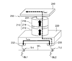
- the magnetic memory element 200 includes a magnetoresistive element 210, a heavy metal layer 220, a first terminal 231, a second terminal 232, a third terminal 233, and transistors Tr1 and Tr2.
- the heavy metal layer 220 is made of a non-magnetic heavy metal (W, Ta, etc.) exhibiting the spin Hall effect, or a chalcogenide substance such as a topological insulator.
- the magnetoresistive element 210 includes a free layer 212 in contact with the heavy metal layer 220 and capable of reversing the magnetic order, a nonmagnetic layer 214 on the free layer 212, and the nonmagnetic layer 214 in contact with the magnetic order fixed in the direction perpendicular to the plane. and a reference layer 216 .
- the free layer 212 is a canted antiferromagnetic thin film, similar to the antiferromagnetic layer 110 of FIGS. 2A and 2B.
- the nonmagnetic layer 214 is made of an insulator (for example, MgO).
- the reference layer 216 is made of ferromagnetic material (eg CoFeB).
- Magnetoresistive element 210 functions as a magnetic tunnel junction (MTJ) element.
- MTJ magnetic tunnel junction
- the first terminal 231, the second terminal 232, and the third terminal 233 are made of metal.
- a first terminal 231 is connected to the reference layer 216 , a second terminal 232 is connected to one end of the heavy metal layer 220 , and a third terminal 233 is connected to the other end of the heavy metal layer 220 .
- the first terminal 231 is connected to the ground line 240 .
- the ground line 240 is set to ground voltage. Note that the ground line 240 may be set to a reference voltage other than the ground voltage.
- the transistors Tr1 and Tr2 are, for example, N-channel metal oxide semiconductor (NMOS) transistors.
- the second terminal 232 is connected to the drain of the transistor Tr1, and the third terminal 233 is connected to the drain of the transistor Tr2.
- Gates of the transistors Tr1 and Tr2 are connected to the word line WL.
- a source of the transistor Tr1 is connected to the first bit line BL1, and a source of the transistor Tr2 is connected to the second bit line BL2.
- the magnetic memory element 200 of FIG. 13 is formed by forming a multilayer film including a heavy metal layer 220, a magnetoresistive element 210, and the like, and then annealing the multilayer film at a predetermined temperature. made by The roughness of the interface between the free layer 212 and the heavy metal layer 220 is preferably 1.0 nm or less, more preferably 0.6 nm or less.
- Data "0” and “1" are assigned to the magnetoresistive element 210 according to the resistance state. For example, when the magnetic ordering of the reference layer 216 and the magnetic ordering of the free layer 212 are in the same direction (parallel state), the magnetoresistive element 210 is in a low resistance state, and when they are in opposite directions (antiparallel state), the magnetoresistive element Since 210 is in the high resistance state, the former data can be determined as "0" and the latter data as "1".
- the word line WL is set to a high level to turn on the transistors Tr1 and Tr2, and the first bit line BL1 and the second bit line BL1 are turned on.
- One of the bit lines BL2 is set to high level and the other is set to low level.
- the write current I write flows in the in-plane direction of the heavy metal layer 220 between the first bit line BL1 and the second bit line BL2, generating a spin current, and the SOT reverses the magnetic order of the free layer 212. enabled and data can be written.
- the data to be written can be changed depending on the direction of the write current I write .
- the word line WL is set to high level to turn on the transistors Tr1 and Tr2, one bit line (second bit line BL2) is set to high level, The other bit line (first bit line BL1) is opened.
- the read current I read flows from the high-level second bit line BL2 to the third terminal 233, the heavy metal layer 220, the free layer 212, the nonmagnetic layer 214, the reference layer 216, the first terminal 231, and the ground line 240. flows.
- the resistance state of the magnetoresistive element 210 that is, the stored data can be determined.
- the read signal of the magnetic memory element 200 can be enhanced.
- FIG. 14 shows the configuration of a magnetic memory element 300 of MRAM (STT-MRAM) that reverses the magnetic order using spin transfer torque (STT).
- the magnetic memory element 300 includes a magnetoresistive element 310, a first terminal 321, a second terminal 322, and a transistor Tr.
- the magnetoresistive element 310 includes a reference layer 316 whose magnetic order is fixed in the perpendicular direction, a nonmagnetic layer 314 on the reference layer 316, and a free layer 312 in contact with the nonmagnetic layer 314 and capable of reversing the magnetic order.
- the free layer 312 is a canted antiferromagnetic thin film, similar to the antiferromagnetic layer 110 of FIGS. 2A and 2B.
- the nonmagnetic layer 314 is made of an insulator (for example, MgO).
- the reference layer 316 is made of ferromagnetic material (eg CoFeB).
- the magnetoresistive element 310 also functions as an MTJ element.
- the first terminal 321 and the second terminal 322 are made of metal.
- the free layer 312 is connected to the first terminal 321 and the reference layer 316 is connected to the second terminal 322 .
- a first terminal 321 is connected to the bit line BL, and a second terminal 322 is connected to the transistor Tr.
- the transistor Tr is, for example, an NMOS transistor.
- the transistor Tr has a drain connected to the second terminal 322, a source connected to the source line SL, and a gate connected to the word line WL.
- the magnetic memory element 300 of FIG. 14 is annealed at a predetermined temperature after depositing all layers of a multilayer film including the magnetoresistive element 310, the first terminal 321, and the like. It is made by
- the roughness of the interface between the free layer 312 and the nonmagnetic layer 314 and the roughness of the interface between the free layer 312 and the first terminal 321 are preferably 1.0 nm or less, more preferably 0.6 nm or less.
- the magnetoresistive element 310 is assigned data "0" and "1" according to the resistance state.
- the word line WL is set to a high level to turn on the transistor Tr, and a write current I write in the perpendicular direction is passed between the bit line BL and the source line SL. This allows the STT to reverse the magnetic order of the free layer 312, allowing data to be written.
- the data to be written can be changed depending on the direction of the write current I write .
- the word line WL is set to a high level to turn on the transistor Tr, and a read current I read is passed between the bit line BL and the source line SL.
- the resistance state of the magnetoresistive element 310 that is, the stored data can be determined.
- the read signal of the magnetic memory element 300 can be enhanced by smoothing the interface between the free layer 312 and the contact layer (nonmagnetic layer 314, first terminal 321).
- FIGS. 13 and 14 show an example in which the magnetoresistive elements 210 and 310 are MTJ elements, they can also function as giant magnetoresistive (GMR) elements.
- the nonmagnetic layers 214 and 314 are made of metal (conductor).
- X Sn, Ge, Ga, Rh, Pt, Ir, etc.
Abstract
Description

上述のように、磁気メモリ素子100は、多層膜の全層成膜後にアニールすることで作製される。図8に、異なるア二-リング温度TA(400℃、500℃、600℃、650℃、700℃)で基板(Si/SiO2)上に作製されたMn3Sn(40)/Ta(5)/Al2O3膜のX線回折パターンを示す。 <X-ray diffraction>
As described above, the
図9に、異なるア二-リング温度TA(400℃、500℃、600℃、650℃、700℃)で作製されたMn3Sn(40)/Ta(5)/Al2O3膜のAFM画像((a)~(e))を示す。図9より、400℃≦TA≦650℃(画像(a)~(d))のとき、RMSラフネスは、TAの上昇とともに約0.4nmから約0.6nmまでわずかに増加していることがわかる。一方、TA=700℃(画像(e))では、RMSラフネスが約1.4nmまで急激に上昇している。これは、Mn3Sn層とTa層との反応によって膜の構造が変形されたことを示唆している。 <RMS Roughness>
Figure 9 shows the results of Mn3Sn (40)/Ta( 5 )/ Al2O3 films fabricated at different annealing temperatures T A (400°C, 500°C, 600°C, 650°C, 700°C). AFM images ((a) to (e)) are shown. From FIG. 9, when 400° C.≦T A ≦650° C. (images (a) to (d)), the RMS roughness slightly increases from about 0.4 nm to about 0.6 nm as T A increases. I understand. On the other hand, at T A =700° C. (image (e)), the RMS roughness sharply increases to about 1.4 nm. This suggests that the structure of the film was deformed by the reaction between the Mn 3 Sn layer and the Ta layer.
図11に、異なるア二-リング温度TA(400℃、500℃、600℃、650℃、700℃)で作製されたMn3Sn(40)/Ta(5)/Al2O3(3)膜の異常ホール伝導度σyx= -ρH/ρ2(S/cm)の磁場依存性(グラフA~E)を示す。ここで、ρHはMn3Sn(40)/Ta(5)層のホール抵抗率 (=VH・(t1+t2))、ρはMn3Sn(40)/Ta(5)層の抵抗率である。グラフA~Eに示す全ての膜は、300Kで有限のヒステリシスが現れている。特に、TA=500℃(グラフB)では、ゼロ磁場(H=0)、300Kでのσyxは18S/cmと最大値をとっている。一方、TA=700℃(グラフE)では、ゼロ磁場、300Kでのσyxは急激に下がり、6S/cmとなっていることがわかる。 <Anomalous Hall effect>
FIG. 11 shows Mn 3 Sn(40)/Ta(5)/Al 2 O 3 (3 ) shows the magnetic field dependence (graphs A to E) of the anomalous hole conductivity σ yx =−ρ H /ρ 2 (S/cm) of the film. Here, ρH is the Hall resistivity of the Mn 3 Sn(40)/Ta(5) layer (= VH ·(t1+t2)), and ρ is the resistivity of the Mn 3 Sn(40)/Ta(5) layer. be. All films shown in graphs AE exhibit finite hysteresis at 300K. In particular, at T A =500° C. (graph B), zero magnetic field (H=0), σ yx at 300 K takes the maximum value of 18 S/cm. On the other hand, at T A =700° C. (graph E), σ yx at zero magnetic field and 300 K drops sharply to 6 S/cm.
100、102、200、300 磁気メモリ素子
110 反強磁性層
120 重金属層
130 酸化物層
152、154、162、164 電極
210、310 磁気抵抗素子
212、312 自由層
214、314 非磁性層
216、316 参照層
220 重金属層
2
Claims (7)
- 磁気モーメントがキャントした磁気秩序を有するキャントした反強磁性体からなる反強磁性層と、
前記反強磁性層に接触し、前記キャントした反強磁性体とは異なる物質からなる接触層と、を備え、
前記反強磁性層と前記接触層との界面のラフネスは1.0nm以下であり、
前記接触層にスピン流が流れると、前記スピン流によって生じるトルクが前記反強磁性層の前記磁気秩序に働き、前記磁気秩序が反転可能である、磁気メモリ素子。 an antiferromagnetic layer comprising a canted antiferromagnet having a magnetic order in which the magnetic moment is canted;
a contact layer in contact with the antiferromagnetic layer and made of a material different from the canted antiferromagnetic material;
The roughness of the interface between the antiferromagnetic layer and the contact layer is 1.0 nm or less,
A magnetic memory element, wherein when a spin current flows in the contact layer, a torque generated by the spin current acts on the magnetic order of the antiferromagnetic layer, and the magnetic order can be reversed. - 前記キャントした反強磁性体は異常ホール効果を示す、請求項1に記載の磁気メモリ素子。 The magnetic memory element according to claim 1, wherein the canted antiferromagnetic material exhibits an anomalous Hall effect.
- 前記キャントした反強磁性体はクラスター磁気八極子のスピン秩序を有する、請求項1に記載の磁気メモリ素子。 2. The magnetic memory element according to claim 1, wherein the canted antiferromagnet has a cluster magnetic octupole spin order.
- 前記反強磁性層は面直方向の前記磁気秩序を有する、請求項1に記載の磁気メモリ素子。 2. The magnetic memory element according to claim 1, wherein said antiferromagnetic layer has said magnetic order in the perpendicular direction.
- 前記界面のラフネスは0.6nm以下である、請求項1に記載の磁気メモリ素子。 2. The magnetic memory element according to claim 1, wherein the roughness of said interface is 0.6 nm or less.
- 前記接触層は、スピンホール効果を示す材料からなり、面内方向に書き込み電流が流れると前記スピン流が発生し、
前記反強磁性層では、前記スピン流によって生じたスピン軌道トルクが前記磁気秩序に働くことによって前記磁気秩序が反転可能である、請求項1~5の何れか1項に記載の磁気メモリ素子。 The contact layer is made of a material exhibiting a spin Hall effect, and when a write current flows in the in-plane direction, the spin current is generated,
6. The magnetic memory element according to claim 1, wherein in said antiferromagnetic layer, said magnetic order can be reversed by a spin-orbit torque generated by said spin current acting on said magnetic order. - 前記接触層及び前記反強磁性層に対して面直方向に書き込み電流が流れると、スピントランスファトルクによって前記反強磁性層の前記磁気秩序が反転可能である、請求項1~5の何れか1項に記載の磁気メモリ素子。
6. The magnetic order of the antiferromagnetic layer can be reversed by a spin transfer torque when a write current flows perpendicularly to the contact layer and the antiferromagnetic layer. The magnetic memory element according to the item.
Priority Applications (2)
| Application Number | Priority Date | Filing Date | Title |
|---|---|---|---|
| CN202280027992.XA CN117356199A (en) | 2021-04-12 | 2022-04-12 | Magnetic memory element |
| JP2023514659A JPWO2022220251A1 (en) | 2021-04-12 | 2022-04-12 |
Applications Claiming Priority (2)
| Application Number | Priority Date | Filing Date | Title |
|---|---|---|---|
| US202163173579P | 2021-04-12 | 2021-04-12 | |
| US63/173,579 | 2021-04-12 |
Publications (1)
| Publication Number | Publication Date |
|---|---|
| WO2022220251A1 true WO2022220251A1 (en) | 2022-10-20 |
Family
ID=83640695
Family Applications (1)
| Application Number | Title | Priority Date | Filing Date |
|---|---|---|---|
| PCT/JP2022/017647 WO2022220251A1 (en) | 2021-04-12 | 2022-04-12 | Magnetic memory element |
Country Status (3)
| Country | Link |
|---|---|
| JP (1) | JPWO2022220251A1 (en) |
| CN (1) | CN117356199A (en) |
| WO (1) | WO2022220251A1 (en) |
Citations (4)
| Publication number | Priority date | Publication date | Assignee | Title |
|---|---|---|---|---|
| WO2017018391A1 (en) * | 2015-07-24 | 2017-02-02 | 国立大学法人東京大学 | Memory element |
| WO2019045055A1 (en) * | 2017-09-04 | 2019-03-07 | Tdk株式会社 | Spin orbit torque-type magnetization switching element and magnetic memory |
| JP2019110326A (en) * | 2017-03-29 | 2019-07-04 | Tdk株式会社 | Memory element and magnetic memory |
| WO2020166722A1 (en) * | 2019-02-15 | 2020-08-20 | 国立大学法人東京大学 | Spintronics element and magnetic memory device |
-
2022
- 2022-04-12 CN CN202280027992.XA patent/CN117356199A/en active Pending
- 2022-04-12 WO PCT/JP2022/017647 patent/WO2022220251A1/en active Application Filing
- 2022-04-12 JP JP2023514659A patent/JPWO2022220251A1/ja active Pending
Patent Citations (4)
| Publication number | Priority date | Publication date | Assignee | Title |
|---|---|---|---|---|
| WO2017018391A1 (en) * | 2015-07-24 | 2017-02-02 | 国立大学法人東京大学 | Memory element |
| JP2019110326A (en) * | 2017-03-29 | 2019-07-04 | Tdk株式会社 | Memory element and magnetic memory |
| WO2019045055A1 (en) * | 2017-09-04 | 2019-03-07 | Tdk株式会社 | Spin orbit torque-type magnetization switching element and magnetic memory |
| WO2020166722A1 (en) * | 2019-02-15 | 2020-08-20 | 国立大学法人東京大学 | Spintronics element and magnetic memory device |
Also Published As
| Publication number | Publication date |
|---|---|
| CN117356199A (en) | 2024-01-05 |
| JPWO2022220251A1 (en) | 2022-10-20 |
Similar Documents
| Publication | Publication Date | Title |
|---|---|---|
| EP2220651B1 (en) | High speed low power magnetic devices based on current induced spin-momentum transfer | |
| EP2863434B1 (en) | High speed low power magnetic devices based on current induced spin-momentum transfer | |
| EP2118893B1 (en) | Non-volatile magnetic memory element with graded layer | |
| JP6923213B2 (en) | Magnetic laminated film, magnetic memory element, magnetic memory, and its manufacturing method | |
| JP5867030B2 (en) | Memory element and memory device | |
| US20170236570A1 (en) | Current induced spin-momentum transfer stack with dual insulating layers | |
| CN103151455B (en) | Memory element and memory apparatus | |
| CN106953005B (en) | Magnetic element and memory device | |
| US10439133B2 (en) | Method and system for providing a magnetic junction having a low damping hybrid free layer | |
| US20220068538A1 (en) | Dipole-coupled spin-orbit torque structure | |
| CN107946456B (en) | Magnetic tunnel junction with strong perpendicular magnetic anisotropy | |
| TWI509603B (en) | Memory elements and memory devices | |
| US20220149269A1 (en) | Spintronics element and magnetic memory device | |
| JP5786341B2 (en) | Memory element and memory device | |
| CN104662654B (en) | Memory cell, storage device and magnetic head | |
| JP2013115319A (en) | Storage element, storage device | |
| JP5034317B2 (en) | Memory element and memory | |
| WO2022220251A1 (en) | Magnetic memory element | |
| US11545620B2 (en) | Methods of manufacture precessional spin current magnetic tunnel junction devices | |
| WO2018179961A1 (en) | Magnetic element, magnetic memory device, and magnetic sensor | |
| WO2023234269A1 (en) | Magnetic memory element, information processing system, and mehod for controlling magnetic memory element | |
| JP5750725B2 (en) | Domain wall motion type magnetic recording element and magnetic recording method | |
| TW202333387A (en) | Magnetoresistive element and magnetic memory | |
| JP2013115320A (en) | Storage element, storage device |
Legal Events
| Date | Code | Title | Description |
|---|---|---|---|
| 121 | Ep: the epo has been informed by wipo that ep was designated in this application |
Ref document number: 22788174 Country of ref document: EP Kind code of ref document: A1 |
|
| WWE | Wipo information: entry into national phase |
Ref document number: 2023514659 Country of ref document: JP |
|
| NENP | Non-entry into the national phase |
Ref country code: DE |
|
| WWE | Wipo information: entry into national phase |
Ref document number: 18286434 Country of ref document: US |
|
| 122 | Ep: pct application non-entry in european phase |
Ref document number: 22788174 Country of ref document: EP Kind code of ref document: A1 |