EP2220651B1 - High speed low power magnetic devices based on current induced spin-momentum transfer - Google Patents
High speed low power magnetic devices based on current induced spin-momentum transfer Download PDFInfo
- Publication number
- EP2220651B1 EP2220651B1 EP08845901.1A EP08845901A EP2220651B1 EP 2220651 B1 EP2220651 B1 EP 2220651B1 EP 08845901 A EP08845901 A EP 08845901A EP 2220651 B1 EP2220651 B1 EP 2220651B1
- Authority
- EP
- European Patent Office
- Prior art keywords
- magnetic
- layer
- magnetic layer
- free
- magnetization
- Prior art date
- Legal status (The legal status is an assumption and is not a legal conclusion. Google has not performed a legal analysis and makes no representation as to the accuracy of the status listed.)
- Not-in-force
Links
Images


Classifications
-
- G—PHYSICS
- G11—INFORMATION STORAGE
- G11C—STATIC STORES
- G11C11/00—Digital stores characterised by the use of particular electric or magnetic storage elements; Storage elements therefor
- G11C11/02—Digital stores characterised by the use of particular electric or magnetic storage elements; Storage elements therefor using magnetic elements
- G11C11/16—Digital stores characterised by the use of particular electric or magnetic storage elements; Storage elements therefor using magnetic elements using elements in which the storage effect is based on magnetic spin effect
-
- G—PHYSICS
- G11—INFORMATION STORAGE
- G11C—STATIC STORES
- G11C11/00—Digital stores characterised by the use of particular electric or magnetic storage elements; Storage elements therefor
- G11C11/56—Digital stores characterised by the use of particular electric or magnetic storage elements; Storage elements therefor using storage elements with more than two stable states represented by steps, e.g. of voltage, current, phase, frequency
- G11C11/5607—Digital stores characterised by the use of particular electric or magnetic storage elements; Storage elements therefor using storage elements with more than two stable states represented by steps, e.g. of voltage, current, phase, frequency using magnetic storage elements
-
- G—PHYSICS
- G11—INFORMATION STORAGE
- G11C—STATIC STORES
- G11C11/00—Digital stores characterised by the use of particular electric or magnetic storage elements; Storage elements therefor
- G11C11/02—Digital stores characterised by the use of particular electric or magnetic storage elements; Storage elements therefor using magnetic elements
- G11C11/16—Digital stores characterised by the use of particular electric or magnetic storage elements; Storage elements therefor using magnetic elements using elements in which the storage effect is based on magnetic spin effect
- G11C11/161—Digital stores characterised by the use of particular electric or magnetic storage elements; Storage elements therefor using magnetic elements using elements in which the storage effect is based on magnetic spin effect details concerning the memory cell structure, e.g. the layers of the ferromagnetic memory cell
-
- G—PHYSICS
- G11—INFORMATION STORAGE
- G11C—STATIC STORES
- G11C11/00—Digital stores characterised by the use of particular electric or magnetic storage elements; Storage elements therefor
- G11C11/02—Digital stores characterised by the use of particular electric or magnetic storage elements; Storage elements therefor using magnetic elements
- G11C11/16—Digital stores characterised by the use of particular electric or magnetic storage elements; Storage elements therefor using magnetic elements using elements in which the storage effect is based on magnetic spin effect
- G11C11/165—Auxiliary circuits
- G11C11/1673—Reading or sensing circuits or methods
-
- G—PHYSICS
- G11—INFORMATION STORAGE
- G11C—STATIC STORES
- G11C11/00—Digital stores characterised by the use of particular electric or magnetic storage elements; Storage elements therefor
- G11C11/02—Digital stores characterised by the use of particular electric or magnetic storage elements; Storage elements therefor using magnetic elements
- G11C11/16—Digital stores characterised by the use of particular electric or magnetic storage elements; Storage elements therefor using magnetic elements using elements in which the storage effect is based on magnetic spin effect
- G11C11/165—Auxiliary circuits
- G11C11/1675—Writing or programming circuits or methods
-
- H—ELECTRICITY
- H10—SEMICONDUCTOR DEVICES; ELECTRIC SOLID-STATE DEVICES NOT OTHERWISE PROVIDED FOR
- H10N—ELECTRIC SOLID-STATE DEVICES NOT OTHERWISE PROVIDED FOR
- H10N50/00—Galvanomagnetic devices
- H10N50/01—Manufacture or treatment
-
- H—ELECTRICITY
- H10—SEMICONDUCTOR DEVICES; ELECTRIC SOLID-STATE DEVICES NOT OTHERWISE PROVIDED FOR
- H10N—ELECTRIC SOLID-STATE DEVICES NOT OTHERWISE PROVIDED FOR
- H10N50/00—Galvanomagnetic devices
- H10N50/10—Magnetoresistive devices
Definitions
- the present invention generally relates to magnetic devices used in memory and information processing applications, such as giant magnetoresistance (GMR) devices. More specifically, the present invention describes a high speed and low power method by which a spin polarized electrical current can be used to control and switch the direction of magnetization and helicity of a magnetic region in such a device.
- GMR giant magnetoresistance
- Magnetic devices that use a flow of spin-polarized electrons are of interest for magnetic memory and information processing applications.
- Such a device generally includes at least two ferromagnetic electrodes that are separated by a non-magnetic material, such as a metal or insulator.
- the thicknesses of the electrodes are typically in the range of 1 nm to 50 nm. If the non-magnetic material is a metal, then this type of device is known as a giant magnetoresistance or spin-valve device.
- the resistance of the device depends on the relative magnetization orientation of the magnetic electrodes, such as whether they are oriented parallel or anti-parallel (i.e., the magnetizations lie on parallel lines but point in opposite directions).
- One electrode typically has its magnetization pinned, i.e., it has a higher coercivity than the other electrode and requires larger magnetic fields or spin-polarized currents to change the orientation of its magnetization.
- the second layer is known as the free electrode and its magnetization direction can be changed relative to the former. Information can be stored in the orientation of this second layer. For example, "1" or “0” can be represented by anti-parallel alignment of the layers and "0" or “1” by parallel alignment.
- the device resistance will be different for these two states and thus the device resistance can be used to distinguish "1" from “0.”
- An important feature of such a device is that it is a non-volatile memory, since the device maintains the information even when the power is off, like a magnetic hard drive.
- the magnet electrodes can be sub-micron in lateral size and the magnetization direction can still be stable with respect to thermal fluctuations.
- MRAM magnetic random access memory
- Slonckewski's patent describes MRAM devices that use spin-momentum transfer for magnetic switching.
- the proposed devices are slow and rely on fluctuating magnetic fields and stochastic processes to initiate magnetization switching. Further, large current densities are needed to switch the devices.
- Slonckewski states “...the preferred axes of the 3 magnets F1, F2, and F3 are all “vertical” (i.e., in the same direction or orientation) as discussed above. Other orientations can serve as long as they are parallel to the same axis.”
- our device makes use of layer magnetizations that are not parallel to the same axis, to great advantage in speed, reliability, and power consumption.
- Devices are needed that exhibit high speed and reliable operation under the action of a spin-polarized current. This includes devices that operate with lower power and have lower threshold currents for switching the magnetization orientation.
- an object of the present invention is to provide a structure that is optimal for a magnetic memory or magnetic information processing device.
- the invention as defined by claim 1 provides a magnetic device including a reference magnetic layer having a fixed magnetic helicity and a fixed magnetization direction, a free magnetic layer with at least one magnetization vector having a changeable magnetization helicity, and non-magnetic layer spatially separating said free magnetic layer and said reference magnetic layer.
- the magnetization helicity of the free magnetic layer can be changed using current induced spin-momentum transfer.
- the reference layer includes an easy axis substantially perpendicular to the reference layer and a magnetic helicity substantially clockwise or counter-clockwise about the ring-shaped structure.
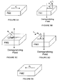
- Figure 1 shows a multilayered, pillar-shaped magnetic device comprising a pinned magnetic layer FM1 with a fixed magnetization direction and a free magnetic layer FM2 with a free magnetization direction.
- m 1 Is the magnetization vector of the pinned magnetic layer FM1
- m 2 is the magnetization vector of the free magnetic layer FM2.
- the pinned magnetic layer FM1 acts as a source of spin angular momentum.
- the pinned magnetic layer FM1 and the free magnetic layer FM2 are separated by a first non-magnetic layer N1 that spatially separates the two layers FM1 and FM2 such that their mutual magnetic interaction is minimized.
- the pillar-shaped magnetic device is typically sized in nanometers, e.g., it may be less than approximately 200 nm laterally.
- the free magnetic layer FM2 is essentially a magnetic thin film element imbedded in a pillar-shaped magnetic device with two additional layers - the pinned magnetic layer FM1 and the non-magnetic layer N1.
- the layer thicknesses are typically approximately 1 nm to 50 nm.
- These pillar-shaped magnetic devices can be fabricated in a stacked sequence of layers by many different means, including sputtering, thermal and electron-beam evaporation through a sub-micron stencil mask. These magnetic devices can also be fabricated in a stack sequence using sputtering, thermal and electron-beam evaporation to form a multilayered film followed by a subtractive nanofabrication process that removes materials to leave the pillar-shaped magnetic device on a substrate surface, such as that of a silicon of other semiconducting or insulating wafer.
- Materials for the ferromagnetic layers include (but are not limited to) Fe, Co, Ni, and alloys of these elements, such as Ni 1-x Fe x ; alloys of these ferromagnetic metals with non-magnetic metals, such as Cu, Pd, Pt, NiMnSb, at compositions in which the materials are ferromagnetically ordered at room temperature; conducting materials; and conducting magnetic oxides such as CrO 2 and Fe 3 O 4 .
- materials include (but are not limited to) Cu, Cr, Au, Ag, and Al.
- the main requirement for the non-magnetic layer is the absence of scattering of the electron spin-direction on a short length scale, which is less than about the layer thickness.
- An electric current source is connected to the pinned magnetic layer FM1 and the free magnetic layer FM2 so that an electric current I can traverse the pillar device.
- An electric current I is applied to the pillar-shaped magnetic device so that the current I flows through the various layers of the device, from the pinned magnetic layer FM1 to the first non-magnetic layer N1 to the free magnetic layer FM2.
- the applied current I results in a transfer of angular momentum from the pinned magnetic layer FM1 to the free magnetic layer FM2.
- a transfer of angular momentum from one magnetic region to another can produce a torque.
- Figures 2A-2E show steps in the method of magnetic switching using the magnetic device shown in Figure 1 and for convenience, Figures 2A-2E only show the free magnetic layer FM2 and the magnetization vector m 2 of the free magnetic layer FM2.
- Figure 2A shows the initial state of the free magnetic layer FM2 before the current I is applied.
- the torque ⁇ S per unit magnetization of the free layer is proportional to the vector triple product a 1 m ⁇ 2 ⁇ ( m ⁇ 2 ⁇ m ⁇ 1 ), where m ⁇ 2 is a unit vector in the direction of the magnetic moment of the free magnetic layer FM2 and m ⁇ 1 is a unit vector in the direction of the magnetic moment of the pinned magnetic layer FM1.
- ⁇ is the reduced Planck's constant
- g is a function of the spin-polarization P and cos( ⁇ )
- M is the magnetization density of the free layer
- e is the charge of the electron
- V is the volume of the free layer
- This torque ⁇ S which acts on the magnetic moment of the free magnetic layer FM2, causes the magnetization of the free magnetic layer FM2 to rotate out of the plane of the layer. Since the thickness of the free magnetic layer FM2 is less than the width and length dimensions of the free magnetic layer FM2, the rotation of the magnetization vector m 2 of the free magnetic layer FM2 out of the plane of the layer generates a large magnetic field, a 'demagnetizing' field, which is perpendicular to the plane of the layer.
- This demagnetizing field forces the magnetization vector m 2 of the free magnetic layer FM2 to precess, i.e., to move such that the magnetization direction rotates about the magnetic field axis.
- the demagnetizing field also determines the rate of precession. A large demagnetizing field results in an extremely high precession rate, which is an optimal condition for fast magnetic switching.
- the magnetic moment of the pinned magnetic layer FM1 is perpendicular to the plane of the free magnetic layer FM2, and the magnetic moment of the free magnetic layer FM2 is perpendicular to the axis of the pillar of thin layers and lies in the plane of the free magnetic layer FM2.
- Figure 2E shows the free magnetic layer FM2 after the magnetic switching process is completed. As shown in Figures 2A and 2E , the magnetic switching process causes the magnetization vector m 2 of the free magnetic layer FM2 to switch by reversing direction by rotating 180°.
- Figures 3A and 3B show two different forms of current input that may be applied to the magnetic device.
- the current input shown in Figure 3A is comprised of two current pulses of short duration, a first positive current pulse followed by a second negative current pulse. This form of current input results in writing a '1' or a '0'.
- the first current pulse can be negative and the second current pulse can be positive, as long as the two current pulses are of opposite polarity.
- the state of the magnetic bit will be changed from '1' to '0' or '0' to '1' (i.e., the final state will be the complement of the initial state of the bit).
- the current input shown in Figure 3A is used in the method of magnetic switching described above and shown in Figures 2A-2E . Using a current input formed of two current pulses results in a faster magnetic switching process.
- the first current pulse starts the precession of the magnetization vector m 2 of the free magnetic layer FM2.
- the second current pulse is applied to stop the precession at a desired state.
- the second current pulse is not essential to the operation of the device, but it enables higher speed switching.
- the current input shown in Figure 3B is comprised of a single positive current pulse.
- a single negative current pulse may also be applied to the magnetic device. Simulations show that many different types of current pulses switch FM2. Therefore device operation is certainly not limited to the current pulses shown in Figure 3 .
- the magnetic device described above can be incorporated into a memory cell for inclusion into arrays of memory cells to make up a magnetic memory.
- the magnetic device when implemented as a memory cell, is a multilayered, pillar-shaped device having a pinned magnetic layer FM1 with a fixed magnetization direction, a free magnetic layer FM2 with a free magnetization direction, and a read-out magnetic layer FM3 with a fixed magnetization direction.
- ⁇ right arrow over (m) ⁇ 1 is the magnetization vector of the pinned magnetic layer FM1
- ⁇ right arrow over (m) ⁇ 2 is the magnetization vector of the free magnetic layer FM2
- ⁇ right arrow over (m) ⁇ 3 is the magnetization vector of the read-out magnetic layer FM3.
- the pinned magnetic layer FM1 and the free magnetic layer FM2 are separated by a first non-magnetic layer N1 that spatially separates the two layers FM1 and FM2 such that their mutual magnetic interaction is minimized.
- the free magnetic layer FM2 and the read-out magnetic layer FM3 are separated by a second non-magnetic layer N2 that spatially separates the two layers FM2 and FM3 such that their mutual magnetic interaction is minimized.
- the pillar-shaped magnetic device is typically sized in nanometers, e.g., it may be less than approximately 200 nm.
- An electric current source is connected to the pinned magnetic layer FM1 and the read-out magnetic layer FM3 so that an electric current I can traverse the pillar device.
- a voltmeter is connected to the pinned magnetic layer FM1 and the read-out magnetic layer FM3 so that the resistance of the magnetic device can be measured to thereby read the logical contents of the memory cell.
- the magnetic switching process is used when information is written into a memory cell.
- the magnetization direction of the magnetization vector inside the memory cell is set in one of two possible orientations to code the logical values of '0' and '1'.
- This magnetic device when implemented as a memory cell, uses the method of magnetic switching described previously in order to store bits of information. Current pulses are applied to change the logical value in the magnetic device.
- the magnetic memory device described above and shown in Figure 4 stores one bit of information since the free magnetic layer FM2 has a single magnetization vector m 2 with two stable magnetic states.
- An electric current I is applied to the pillar-shaped magnetic memory device so that the current I flows through the various layers of the magnetic memory device, from the pinned magnetic layer FM1 to the read-out magnetic layer FM3.
- the applied current I results in a transfer of angular momentum from the pinned magnetic layer FM1 to the free magnetic layer FM2.
- Figures 5A-5E show steps in the method of writing information using the magnetic memory device shown in Figure 4 and for convenience, Figures 5A-5E only show the free magnetic layer FM2 and the magnetization vector m 2 of the free magnetic layer FM2.
- Figure 5A shows the initial state of the free magnetic layer FM2 before the current I is applied.
- FIGS 5B-5D applying a current I, which can be of a form as shown in Figures 3A and 3B , results in the transfer of angular momentum from the pinned magnetic layer FM1 to the free magnetic layer FM2.
- Figures 2A-2E and 5A-5E show the change in the orientation of the magnetization vector m 2 of the free magnetic layer FM2 as a result of applying the current to the magnetic device.
- Figure 6A shows a form of the current input that is applied to the magnetic memory device shown in Figure 4 .
- the current input of Figure 6A includes two current pulses of short duration, a first positive current pulse followed by a second negative current pulse, which results in writing a '1' or a '0'.
- the first current pulse can be negative and the second current pulse can be positive, as long as the two current pulses are of opposite polarity.
- the state of the magnetic bit will be changed from '1' to '0' or '0' to '1' (i.e., the final state will be the complement of the initial state of the bit).
- the first current pulse starts the precession of the magnetization vector m 2 of the free magnetic layer FM2.
- the second current pulse is applied to stop the precession at a desired state.
- the precession is stopped when 180° rotation of the magnetization vector m 2 of the free magnetic layer FM2 is achieved.
- Figure 6B shows an example of the corresponding resistance of the device as measured by the voltmeter connected to the magnetic memory device shown in Figure 4 with a small current applied, i.e., a current intensity much less than that used in the current pulses.
- the resistance increases after the current pulses of Figure 6A are applied to the device.
- the resistance At the initial state shown in Figure 5A (before the first positive current pulse), the resistance is at a constant low value.
- the resistance is at a constant high value.
- the states shown in Figures 5A and 5E correspond to a logical value of "0" in the initial state and a logical value of "1" in the final state, respectively.
- the magnetization vector m 2 of the free magnetic layer FM2 in the final state shown in Figure 5E is in the opposite direction than the magnetization vector m 2 of the free magnetic layer FM2 in the initial state shown in Figure 5A .
- the necessary amplitude of the current pulses can be estimated by numerical modeling using the equations of micromagnetics, the Landau-Lifzshitz Gilbert equations including the spin-transfer torque discussed earlier (see, for example, B. Oezyilmaz et al., Phys. Rev. Lett. 91, 067203 (2003 )).
- the Co free layer is 3 nm thick and has lateral dimensions of 60 nm by 60 nm.
- a current pulse of amplitude of 5 mA is more than sufficient to switch the layer.
- the current necessary to switch the device is reduced by decreasing the size of the Co free layer; increasing the spin-polarization of the current, for example, by using a pinned layer with a higher degree of spin-polarization; and decreasing the in-plane anisotropy or decreasing the Gilbert damping.
- a 35 psec pulse is sufficient to switch the device.
- the energy dissipation is 5 ⁇ 10 -15 J.
- This energy dissipation value can be compared to the energy needed to switch a magnetic device with a spin-polarized current when the pinned layer and the free layer magnetizations are initially aligned along the same axis. Recent experiments show that this requires a current of approximately 10 mA applied for approximately 10 ns in a device with a resistance of 5 Ohms (see, R. H. Koch et al. Phys. Rev. Lett. 92, 088302 (2004 )). The energy dissipated is thus 5 ⁇ 10 -12 J. Thus, in comparison, the power requirement for our device is quite small.
- the read-out magnetic layer FM3 is required in the simplest implementation of the magnetic memory device.
- the read-out magnetic layer FM3 has a magnetization vector m 3 with a fixed magnetization direction.
- the magnetization vector m 3 of the read-out magnetic layer FM3 can be fixed in a number of ways.
- the read-out magnetic layer FM3 can be formed thicker or of a higher anisotropic magnetic material or can be placed adjacent to an antiferromagnetic layer to use the phenomena of exchange biasing.
- the resistance of the magnetic memory device is very sensitive to the relative orientation of the magnetization vector m 2 of the free magnetic layer FM2 and the magnetization vector m 3 of read-out magnetic layer FM3.
- the resistance of the magnetic memory device is highest when the magnetization vectors m 2 and m 3 of the free magnetic layer FM2 and the read-out layer FM3, respectively, are in anti-parallel alignment.
- the resistance of the magnetic device is lowest when the magnetization vectors m 2 and m 3 of the layers FM2 and FM3, respectively, are in parallel alignment.
- a simple resistance measurement can determine the orientation of the magnetization vector m 2 of the free magnetic layer FM2.
- the fixed orientation of the magnetization vector m 3 of the read-out magnetic layer FM3 is set so that it is either in parallel or anti-parallel alignment with the magnetization vector m 2 of the free magnetic layer FM2, depending on the orientation of the magnetization vector m 2 of the free magnetic layer FM2. Since the orientation of the magnetization vector m 2 of the free magnetic layer FM2 switches so that it can be rotated 180°, the magnetization vectors m 2 and m 3 of the free magnetic layer FM2 and the read-out layer FM3, respectively, must be in either anti-parallel or parallel alignment.
- the magnetic memory device described above and shown in Figure 4 has two stable magnetic states and is able to store one bit of information.
- a magnetic memory device can be constructed to store multiple bits of information.
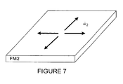
- FIG. 7 [[6]] shows an example of a free magnetic layer FM2 with four stable magnetic states.
- a magnetic memory device comprising a free magnetic layer FM2 with four stable magnetic states is able to store two bits of information.
- current pulses are applied to switch the magnetization between directions that differ by 90° instead of 180°. This can be accomplished by current pulses of a different form. For example, the current pulses can be smaller in amplitude and/or shorter in duration.
- the readout layer (FM3) is then aligned such that each of the four magnetization states has a different resistance. This requires that the readout layer magnetization not have an in-plane component that points parallel to any of the four states nor at 45° to these states.
- the operation of the magnetic device was simulated using Landau-Lifzshitz Gilbert equations including a spin-transfer torque.
- This current input comprises two current pulses similar to the current input shown in Figures 3A and 6A .
- a 16-picosecond positive current pulse is applied to the magnetic memory device to start the precession of the magnetization vector m 2 of the free magnetic layer FM2.
- a 14-picosecond negative current pulse is applied to the magnetic memory device to stop the precession of the magnetization vector m 2 of the free magnetic layer FM2 to achieve a desired state of the magnetization vector m 2 .
- the precession is stopped after achieving a 180° rotation of the magnetization vector m 2 of the free magnetic layer FM2.
- Figure 9 shows the magnetization components m X and m Y of the magnetization vector m 2 of the free magnetic layer FM2 in the x- and y-directions shown in Figures 2B and 5B .
- the magnetization components m X and m Y are measured during and after the application of the current input shown in Figure 8 .
- Figure 9 shows that the magnetization vector m 2 of the free magnetic layer FM2 reverses 180° from the initial state, which corresponds to Figure 5A , to the final state, which corresponds to Figure 5E .
- the magnetization components ( m X , m Y ) are able to switch between (-1,0) to (1,0) as shown by the present invention.
- the high speed, low power magnetic device uses energy only for read and write operations or logic operations. When not energized, the information is stored without significant loss.
- the magnetic device when implemented as a memory cell, can be used as a non-volatile memory.
- the non-volatile memory provided by the magnetic device is suitable for many applications, such as in computers and portable electronic devices.
- the high speed, low power magnetic device provides several advantages.
- the performance of the high speed, low power magnetic device compares favorably with flash memory and other types of non-volatile random access memory (RAM), such as conventional magnetic RAM (MRAM) and ferroelectric RAM (FRAM).
- RAM non-volatile random access memory
- MRAM magnetic RAM
- FRAM ferroelectric RAM
- the current-induced torques act only on the magnetic device that is energized, i.e., to which a current is applied. Therefore, when multiple magnetic devices are arranged in an array, such as in magnetic memory, the current-induced spin transfer does not produce parasitic interactions ("cross-talk") between the neighboring elements in the array, unlike in conventional magnetic memories in which magnetic switching is accomplished by using magnetic fields produced by small current-carrying wires near the magnetic elements.
- the method of magnetic switching by current induced torque is faster than current conventional methods that use magnetic fields to switch the magnetization direction of layers. Read-out and write operations can be completed in sub-nanosecond time scales.
- Conventional magnetic hard drives are very slow compared to the magnetic memory described above since the conventional hard drives have data access times of the order of milliseconds.
- the method of magnetic switching by current induced torque requires low power. This is especially advantageous for use in portable electronic devices.
- the method of magnetic switching by current induced torque is ideal for sub-micron scale devices since the lateral dimension of the magnetic device may be less than approximately 200 nm. Therefore, the device is scaled to allow the fabrication of ultra-high density memory cells so that a vast amount of information can be stored in the magnetic memory .
- the basic architecture of the high speed, low power magnetic device is straightforward, and read-out and write operations are reliable and are less sensitive to changes in temperature. Unlike conventional magnetic memory devices, the described device does not rely on stochastic (random) processes or fluctuating fields to initiate switching events.
- Multiple bits of information can be stored on each device so that even more information can be stored in the magnetic memory.
- the method of magnetic switching by current induced torque can be used for logic operations, as well as for magnetic memory devices. Since there is a threshold, which is dependent on the shape, amplitude, and period of the current pulse, for the current pulse to produce a change in magnetization, current input can be combined to produce a logic function, such as an AND gate. For example, two current pulses can be combined to produce a current pulse that traverses the device which is the sum of the two current pulses. The pulse characteristics (shape, amplitude, and period) can be chosen such that each pulse individually does not switch the device, yet the combined pulse does switch the device. Thus, this is an AND operation. A NOT operation requires simply switching the state of the device. A NOT and an AND operation can be combined to produce a NAND function, which is a universal digital logic gate (i.e., all digital logic functions can be constructed from NAND gates.)
- a magnetic device may be configured so that no net current passes through the free magnetic layer FM2 during write operations.
- FIG. 10 shows a device including current source A, current source B, and layer I2, which is a thin insulating layer made of Al2O3, for example.
- layer I2 is 0.5 to 3 nm thick and is thin enough so that electrons can traverse the layer by quantum mechanical tunneling.
- current pulses are applied with current source A to change the magnetization direction of the free magnetic layer FM2.
- current source A current flows from FM1 1 to the non-magnetic layer N1 and electron spin angular momentum is transferred to the free magnetic layer FM2 by reflection of electrons at the interface between the non-magnetic layer N1 and the free magnetic layer FM2.
- the device readout is performed using current source B. The voltage is measured when a small current from B passes between the free magnetic layer FM2 and the readout layer FM3. This voltage will depend on the relative magnetization directions of the layers FM2 and FM3 so that the magnetization direction of the free magnetic layer FM2 can be determined to read-out the device.
- This device has the advantage that the readout signal is large since the tunnel junction resistance can be large (1 Ohm to 100 kOhm). Readout signals can be in the range from 10 mV to 1 V.
- Magnetic device 1100 includes a free magnetic layer 1110, a non-magnetic layer 1120, and a reference magnetic layer 1130.
- the reference layer 1130 preferably has a fixed magnetic helicity 1135, a magnetic vector with a fixed direction at a predetermined angle, for example, perpendicular to the plane of the layer, or both a fixed magnetic helicity 1135 and a magnetic vector having a fixed direction at a predetermined angle.
- the free magnetic layer 1110 preferably has a free magnetization helicity 1115.
- the reference layer 1130 preferably acts as a source of spin angular momentum.
- the free layer 1110 and the reference layer 1130 are preferably separated by non-magnetic layer 1120.
- the reference layer 1130 is preferably magnetically harder than the free layer 1110 and preferably has a well-defined magnetic state. This property can be achieved, for example, by using a layer that is thicker than the free layer or a material having a larger magnetic anisotropy than the material of the free layer 1110, such as Cobalt, the L10 phase of FePt or FePd, or layered structures of Cobalt and Nickel. Alternatively, the desired hardness can be achieved through exchange coupling to a thin anti-ferromagnetic layer, such as IrMn or FeMn.
- the non-magnetic layer 1120 preferably conserves spin-momentum of the reference magnetic layer 1130 during spin transport across the non-magnetic layer 1120.
- the spin diffusion length of the material used in the non-magnetic layer 1120 is preferably longer than the thickness of the non-magnetic layer 1120.
- materials that satisfy the desired properties include any of the noble metals (e.g., Cu, Ag, Au).
- the non-magnetic layer may also be an insulator such as Al 2 O 3 or MgO. For a sufficiently thin insulating layer the spin transport will occur by electron tunneling so as to form a magnetic tunnel junction.
- the free magnetic layer 1110 preferably includes a soft magnetic material having a large exchange length, such as permalloy, cobalt, nickel, iron, and alloys of those materials. Additionally, alloys including non-magnetic elements, such as copper, may advantageously reduce the magnetic moment of the layers. Alternatively the free magnetic layer can include magnetic oxides such as CrO 2 or Fe 3 O 4 .
- each layer of the magnetic device 1100 is preferably ring-shaped (i.e. annular).
- An annular shape can minimize the number of edges or sharp corners that may act as magnetic nucleation sites which reduces stability by increasing the rate of reversal of magnetic helicity.
- a symmetrical ring structure is one of the preferred shapes which can be used to avoid unwanted reversal of helicity, however the present invention may employ many various forms of closed period structures which may provide similar advantages.
- the lower the rotational symmetry of the shape of the device the more likely it is that certain regions will be favored for magnetic nucleation and reversal of magnetic helicity.
- Geometries that include sharp corners provide strong nucleation sites that encourage helicity reversal and are preferably avoided.
- Ring geometries may provide very stable magnetization orientations. Additionally, the magnetization reversal mechanism of ring geometries may be weakly dependent on ring diameter beyond a critically small size (e.g., typically tens of nanometers). Thus, the size of the device may not be a critical a factor when compared with most presently used geometries. Thus, ring geometries may enable a greater range of use and decreased production costs.
- the stability of the magnetization of a ring may be the size of the ring.
- the stability of the magnetization of the ring is relatively independent of the ring size.
- the stability of the magnetization may decrease rapidly as the size of the ring decreases below the critical size.
- the magnetization may be susceptible to thermal fluctuations and the application of a destabilizing magnetic field.
- a ring-shaped magnetic device can be designed for which the magnetization of the device is generally stable under static operating conditions, but can easily be changed or reversed by applying a current pulse to the device.
- a current pulse to the device.
- the magnetic helicity can be easily reversed by applying an electrical current.
- the electrical current has the effect of providing a destabilizing field and effectively changing the value of the critical radius of the ring.
- a magnetic ring designed near the critical size is stable and does not experience unwanted reversal under normal operating conditions, but can be reversed by the application of a relatively small current.
- a magnetic ring device that has a radius greater than or equal to the critical radius can provide a very stable magnetization. Thus, if it is not a goal of a device to modify or reverse the magnetization of the device, a magnetic ring having a radius that is greater than the critical radius, can be easily employed in read only memory in a wide range of sizes greater than the critical size.
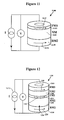
- Figure 12 illustrates a magnetic ring device 1200 employed as a magnetic memory element.
- the free magnetic layer 1210 has a magnetic helicity 1215 with at least two stable orientations - a clockwise orientation and a counter-clockwise orientation.
- the reference layer 1230 preferably has a magnetic vector having a fixed direction at predetermined angle 1236, a fixed magnetic helicity 1235, or both a fixed magnetic vector having a direction at a predetermined angle 1236 and a fixed magnetic helicity 1235.
- the predetermined angle of the fixed magnetic vector 1236 is substantially perpendicular to the plane of the reference layer 1230.
- the reference magnetic layer 1230 and the free magnetic layer 1210 are preferably separated by a non-magnetic layer 1220.
- the direction of the free magnetic layer helicity can be changed or reversed by applying an electrical pulse across the layers of magnetic device 1200 from current source 1270.
- the pulse from control current source 1270 may initiate the reversal of the free magnetic layer helicity 1215.
- the spin-momentum of the reference magnetic layer 1230 may be transferred to the free magnetic layer 1210 so as to change the magnetization and induce reversal of the free magnetic layer helicity 1215.
- An electrical pulse in one direction across the device 1200 may set the free magnetic layer helicity 1215 in a clockwise direction, and an electrical pulse in the opposite direction may set the free magnetic layer helicity 1215 in a counter-clockwise direction.
- the electrical pulse from control current source 1270 may initiate the reversal of the free magnetic layer helicity 1215. Reversal of the free magnetic layer helicity 1215 may stop when the second stable state is reached. However, a second current pulse from control current source 1270 can be used to stop the reversal of the free magnetic layer helicity 1215 more quickly.
- a reference layer 1230 having an easy axis 1236 (i.e., the energetically favorable direction of the spontaneous magnetization in a ferromagnetic material) that is substantially perpendicular to the free magnetic layer 1210 can lead to faster spin-transfer induced reversal of the free magnetic layer helicity 1215.
- a second reference layer 1263 with fixed magnetic layer helicity 1268 may be used to read-out the helicity state of the free magnetic layer.
- the fixed magnetic helicity can be achieved, for example, by using a layer that is thicker than the free layer or a material having a larger magnetic anisotropy than the material of the free layer 1210, such as Cobalt, the L10 phase of FePt or FePd, or layered structures of Cobalt and Nickel.
- the second reference 1263 layer is separated from the free magnetic layer 1210 by a non-magnetic layer 1266, which may be a thin non-magnetic metal or insulating layer. In the case of an insulating layer, the second reference layer 1263 and the free magnetic layer 1210 form a magnetic tunnel junction.
- the resistance across the device 1200 may be generally smaller than if the free magnetic layer helicity 1215 and the reference magnetic layer helicity 1235 are in opposite directions, thereby differentiating between the two stable orientations of the free magnetic layer 1210.
- FIG. 13 illustrates a magnetic ring device 1300 employed as a magnetic memory element.
- the free magnetic layer 1310 has at least two stable orientations of the free magnetic layer helicity 1315-a clockwise orientation and a counter-clockwise orientation.
- the reference layer 1330 preferably has a fixed magnetic vector 1336 having a direction at a predetermined angle, a fixed magnetic helicity 1335, or both a fixed magnetic vector 1336 having a direction at a predetermined angle 1336 and a fixed magnetic helicity 1335.
- the predetermined angle of the fixed magnetic vector 1336 is substantially perpendicular to the plane of the reference layer 1330.
- the reference magnetic layer 1330 and the free magnetic layer 1310 are preferably separated by a non-magnetic layer 1320.
- the direction of the free magnetic layer helicity can be changed or reversed by applying an electrical pulse across the layers of magnetic device 1300 from control current source 1370 through write contact 1350 and contact 1340.
- the pulse from control current source 1370 may initiate the reversal of the free magnetic layer helicity 1315.
- the spin-momentum of the reference magnetic layer 1330 may be transferred to the free magnetic layer 1310 so as to change the magnetization and induce reversal of the free magnetic layer helicity 1315.
- An electrical pulse in one direction across the device 1300 may set the free magnetic layer helicity 1315 in a clockwise direction, and an electrical pulse in the opposite direction may set the free magnetic layer helicity 1315 in a counter-clockwise direction.
- the electrical pulse from control current source 1370 may initiate the reversal of the free magnetic layer helicity 1315. Reversal of the free magnetic layer helicity 1315 may stop when the second stable state is reached. However, a second current pulse from control current source 1370 can be used to stop the reversal of the free magnetic layer helicity 1315 more quickly.
- a reference layer 1330 having an easy axis (i.e., the energetically favorable direction of the spontaneous magnetization in a ferromagnetic material) that is substantially perpendicular to the free magnetic layer 1310 can lead to faster spin-transfer induced reversal of the free magnetic layer helicity 1315.
- Layer 1320 is a spin preserving non-magnetic layer such as Cu, Ag, Au or a thin insulating layer such as Al 2 O 3 or MgO. Small asymmetry in the ring may facilitate nucleation and reversal through spin-momentum transfer. Pronounced asymmetry could reduce the magnetization stability, which is undesirable.
- the state of the free magnetic layer helicity can be determined by measuring the voltage or resistance across the device 1300. If the free magnetic layer helicity 1315 and the reference magnetic layer helicity 1335 are in the same direction (i.e., the magnetic helicities are both clockwise or both counter-clockwise), the resistance across the device 1300 may be generally smaller than if the free magnetic layer helicity 1315 and the reference magnetic layer helicity 1335 are in opposite directions.
- a write operation can be performed by control current source 1370, which provides a large current, and write contact 1350, which can be in direct contact with either the free magnetic layer 1310 or the reference magnetic layer 1330 thus having low impedance.
- the write operation circuit is completed through contact 1340 which can be placed in direct contact with either the free magnetic layer 1310 or the reference magnetic layer 1330 to complete the circuit across device 1300.
- Read contact 1360 can include a magnetic contact portion 1363 with a fixed magnetization direction or helicity 1365 and an insulator portion 1366 that separates the magnetic contact 1363 from the device 1300, thereby forming a magnetic tunnel junction with the device 1300.
- a separate readout current source 1380 can provide a smaller current across the device 1300 which is measured by voltage or resistance readout 1390.
- the thickness of the device is approximately 10 to 200 nanometers and has an outer radius of approximately 0.25 to 1 micron.
- Typical multi-element magnetic devices have strong magnetostatic interaction between the different elements. This interaction can be difficult to quantify or control, and thus results in problems increasing density and performance of the device.
- the present invention may minimize these interactions. Additionally, the device avoids the problems of magnetic field spreading which results in superior speed writing and readout along with reduction of error due to stray or poorly controlled fields.
- Magnetic tunnel junctions offer the possibility of very large magnetoresistance that can be used to read the state of a magnetic memory cell.
- a magnetic tunnel junction consists of two magnetic layers separated by a thin insulating layer.
- the insulator is sufficiently thin that electrons may traverse this layer by quantum mechanical tunneling.
- the thickness of the insulator is typically between 0.3 and 3 nm.
- a large magnetoresistance will provide a large readout signal. It has been shown experimentally that very large magnetoresistance can be achieved using magnesium oxide (MgO) insulating barriers.
- MgO magnesium oxide
- the magnetoresistance refers to the percentage change in resistance between states in which the layers are magnetized antiparallel and parallel. A magnetoresistance of greater that 400% has been achieved recently with MgO insulating layers. With an aluminum oxide insulating layer, a magnetoresistance of about 30% has been achieved. Either of these materials as well as other insulators may prove useful as the non-magnetic layers, N1 or N2..
- the pinned magnetic layer of the device includes a material with a perpendicular magnetic anisotropy.
- a perpendicular magnetic anisotropy gives a preference for the magnetization to orient perpendicular to the plane of the layer.
- Thin magnetic layers are typically magnetized in the film plane. This orientation is usually a lower energy configuration; it reduces the layer's magnetostatic energy. To orient the magnetization perpendicular to the plane the perpendicular magnetic anisotropy must be sufficiently large compared to the magnetostatic energy of the layer.
- alloys of Fe and Pt, Fe and Pd, Co and Pt, Co and Pd, Co and Au, Co and Ni can also be achieved by creating interfaces between dissimilar magnetic materials or magnetic materials and non-magnetic materials.
- An example of the former is layered structures of Co and Ni and example of the latter is layered structure of Co and Au or Co and Pt.
- An advantage of these layered materials is that they need not be crystalline; polycrystalline layers suffice.
- This layer serves to spin polarize the current.
- the materials should have good spin polarization efficiency.
- a disadvantage of using Pd or Pt is that these elements typically induce strong spin-scattering which reduces the layer spin-polarization. Large layer spin-polarization is needed for efficient device operation.
- the free layer's magnetization direction switches in response to a current pulse. It is desirable to reduce the amplitude of this current pulse to lower the power required for device operation.
- Current requirements are linked to the magnetization density, damping and magnetic anisotropy of the layers. The lower the magnetization density and magnetic anisotropy the lower the required current amplitude for switching.
- the magnetization density of a magnetic is lowered if the magnetic material is alloyed with a non-magnetic material. (Of course, this only holds in a range of alloy concentrations. Eventually the material will become non-magnetic.)
- switching current amplitude and switching time are interdependent. For example, lower magnetization density increases the time to reverse the magnetization.
Description
- This invention was made with government support under Contract Number NSF-DMR-0403630 entitled "Nanoscale Spin Transfer Devices and Materials" and Contract Numbers NSF- PHY-0351964 and NSF-PHY-0601179 entitled "Noise-Induced Escape in Multistable Systems" awarded by the National Science Foundation, and Contract Number ONR N0014-02-1-0995 entitled "Gate Controlled Ferromagnetism in Semiconductor Nanostructures" awarded by the Office of Naval Research of the Department of Defense. The government has certain rights in the invention.
- The present invention generally relates to magnetic devices used in memory and information processing applications, such as giant magnetoresistance (GMR) devices. More specifically, the present invention describes a high speed and low power method by which a spin polarized electrical current can be used to control and switch the direction of magnetization and helicity of a magnetic region in such a device.
- Magnetic devices that use a flow of spin-polarized electrons are of interest for magnetic memory and information processing applications. Such a device generally includes at least two ferromagnetic electrodes that are separated by a non-magnetic material, such as a metal or insulator. The thicknesses of the electrodes are typically in the range of 1 nm to 50 nm. If the non-magnetic material is a metal, then this type of device is known as a giant magnetoresistance or spin-valve device. The resistance of the device depends on the relative magnetization orientation of the magnetic electrodes, such as whether they are oriented parallel or anti-parallel (i.e., the magnetizations lie on parallel lines but point in opposite directions). One electrode typically has its magnetization pinned, i.e., it has a higher coercivity than the other electrode and requires larger magnetic fields or spin-polarized currents to change the orientation of its magnetization. The second layer is known as the free electrode and its magnetization direction can be changed relative to the former. Information can be stored in the orientation of this second layer. For example, "1" or "0" can be represented by anti-parallel alignment of the layers and "0" or "1" by parallel alignment. The device resistance will be different for these two states and thus the device resistance can be used to distinguish "1" from "0." An important feature of such a device is that it is a non-volatile memory, since the device maintains the information even when the power is off, like a magnetic hard drive. The magnet electrodes can be sub-micron in lateral size and the magnetization direction can still be stable with respect to thermal fluctuations.
- In conventional magnetic random access memory (MRAM) designs, magnetic fields are used to switch the magnetization direction of the free electrode. These magnetic fields are produced using current carrying wires near the magnetic electrodes. The wires must be small in cross-section because memory devices consist of dense arrays of MRAM cells. As the magnetic fields from the wires generate long-range magnetic fields (magnetic fields decay only as the inverse of the distance from the center of the wire) there will be cross-talk between elements of the arrays, and one device will experience the magnetic fields from the other devices. This cross-talk will limit the density of the memory and/or cause errors in memory operations. Further, the magnetic fields generated by such wires are limited to about 0.1 Tesla at the position of the electrodes, which leads to slow device operation. Importantly, conventional memory designs also use stochastic (random) processes or fluctuating fields to initiate the switching events, which is inherently slow and unreliable (see, for example, R. H. Koch et al., Phys. Rev. Lett. 84, 5419 (2000)).
- In
U.S. Patent No. 5,695,864 and several other publications (e.g., J. Slonckewski, Journal of Magnetism and Magnetic Materials 159, L1 (1996)), John Slonckewski described a mechanism by which a spin-polarized current can be used to directly change the magnetic orientation of a magnetic electrode. In the proposed mechanism, the spin angular momentum of the flowing electrons interacts directly with the background magnetization of a magnetic region. The moving electrons transfer a portion of their spin-angular momentum to the background magnetization and produce a torque on the magnetization in this region. This torque can alter the direction of magnetization of this region and switch its magnetization direction. Further, this interaction is local, since it only acts on regions through which the current flows. However, the proposed mechanism was purely theoretical. - Slonckewski's patent describes MRAM devices that use spin-momentum transfer for magnetic switching. However, the proposed devices are slow and rely on fluctuating magnetic fields and stochastic processes to initiate magnetization switching. Further, large current densities are needed to switch the devices. In describing the preferred embodiment of his "latch or logic gate," Slonckewski states "...the preferred axes of the 3 magnets F1, F2, and F3 are all "vertical" (i.e., in the same direction or orientation) as discussed above. Other orientations can serve as long as they are parallel to the same axis." As we describe below, our device makes use of layer magnetizations that are not parallel to the same axis, to great advantage in speed, reliability, and power consumption.
-
U.S. Patent No. 6,256,223 to Jonathan Sun also describes devices that use current-induced magnetic switching and demonstrates in experiment the operation of such devices. However, the devices proposed were unreliable, as there was little consistency with regard to device characteristics. Further, the estimated time scale for magnetic switching was 50 nsec for operation at large current densities. - Devices are needed that exhibit high speed and reliable operation under the action of a spin-polarized current. This includes devices that operate with lower power and have lower threshold currents for switching the magnetization orientation.
- Further devices that operate under the action of a spin-polarized current are disclosed in
US 2005/0041462 , in which a device has pinned, free and read-out magnetic layers and in which a current is applied to the device to induce a torque that alters the magnetic state of the device so that it can act as a magnetic memory for writing information; and inUS 6,532,164 ,US 2006/0132990 ,US 6,347,049 andUS 2006/0092696 .US 2004/0094785 discloses an MTJ structure having ring-shaped reference and free layers. - In view of the limitations associated with conventional designs of devices that use spin-momentum transfer, an object of the present invention is to provide a structure that is optimal for a magnetic memory or magnetic information processing device.
- It is another object of the present invention to produce a magnetic device that has advantages in terms of speed of operation.
- It is a further object of the present invention to produce a magnetic device that has advantages in terms of reliability.
- It is a further object of the present invention to produce a magnetic device that requires lower power to operate.
- It is a further object of the present invention to produce a magnetic device that has advantages in terms of the stability of the stored information.
- It is a further object of the present invention to produce a magnetic device that has a large read-out signal.
- The invention as defined by
claim 1 provides a magnetic device including a reference magnetic layer having a fixed magnetic helicity and a fixed magnetization direction, a free magnetic layer with at least one magnetization vector having a changeable magnetization helicity, and non-magnetic layer spatially separating said free magnetic layer and said reference magnetic layer. The magnetization helicity of the free magnetic layer can be changed using current induced spin-momentum transfer. The reference layer includes an easy axis substantially perpendicular to the reference layer and a magnetic helicity substantially clockwise or counter-clockwise about the ring-shaped structure. - The foregoing and other features of the present invention will be more readily apparent from the following detailed description and drawings of the illustrative embodiments of the invention wherein like reference numbers refer to similar elements throughout the views and in which:
-
FIG. 1 is an illustration of a magnetic device useful for understanding the present invention; -
FIGS. 2A-2E are illustrations of the free magnetic layer showing the magnetization vector and the demagnetizing field of the electronic device ofFIG. 1 during the application of pulses of current as illustrated inFIG. 3A ; -
FIG. 3A is an illustration of a current waveform that may be applied to the magnetic device; -
FIG. 3B is an illustration of an alternate current waveform that may be applied to the magnetic device; -
FIG. 4 is an illustration of a memory cell useful for understanding of the present invention; -
FIGS. 5A-5E are illustrations of the free magnetic layer showing the magnetization vector and the demagnetizing field of the memory cell ofFIG. 4 ; -
FIG. 6A is an illustration of a current waveform that may be applied to the memory cell ofFIG. 4 during a write operation; -
FIG. 6B is an illustration of a resistance measured from the memory cell during a read-out operation before and after the current pulse shown inFIG. 6A is applied; -
FIG. 7 is an illustration of the free magnetic layer of a 4-state memory cell; -
FIG. 8 is an illustration of an example of a current waveform applied to the magnetic device; -
FIG. 9 is an illustration of the magnetization components of the free magnetic layer during and after the application of the current pulse shown inFIG. 8 ; -
Figure 10 is an illustration of a memory cell in which during writing operations no net current passes through the free magnetic layer; -
Figure 11 is an illustration of an annular magnetic device ; -
Figure 12 is an illustration of an annular memory cell according to one embodiment of the present invention, and -
Figure 13 is an illustration of an annular memory cell in which separate read and write contacts are provided. - To illustrate the basic concept,
Figure 1 shows a multilayered, pillar-shaped magnetic device comprising a pinned magnetic layer FM1 with a fixed magnetization direction and a free magnetic layer FM2 with a free magnetization direction.m 1 Is the magnetization vector of the pinned magnetic layer FM1, andm 2 is the magnetization vector of the free magnetic layer FM2. The pinned magnetic layer FM1 acts as a source of spin angular momentum. - The pinned magnetic layer FM1 and the free magnetic layer FM2 are separated by a first non-magnetic layer N1 that spatially separates the two layers FM1 and FM2 such that their mutual magnetic interaction is minimized. The pillar-shaped magnetic device is typically sized in nanometers, e.g., it may be less than approximately 200 nm laterally.
- The free magnetic layer FM2 is essentially a magnetic thin film element imbedded in a pillar-shaped magnetic device with two additional layers - the pinned magnetic layer FM1 and the non-magnetic layer N1. The layer thicknesses are typically approximately 1 nm to 50 nm.
- These pillar-shaped magnetic devices can be fabricated in a stacked sequence of layers by many different means, including sputtering, thermal and electron-beam evaporation through a sub-micron stencil mask. These magnetic devices can also be fabricated in a stack sequence using sputtering, thermal and electron-beam evaporation to form a multilayered film followed by a subtractive nanofabrication process that removes materials to leave the pillar-shaped magnetic device on a substrate surface, such as that of a silicon of other semiconducting or insulating wafer.
- Materials for the ferromagnetic layers include (but are not limited to) Fe, Co, Ni, and alloys of these elements, such as Ni1-xFex; alloys of these ferromagnetic metals with non-magnetic metals, such as Cu, Pd, Pt, NiMnSb, at compositions in which the materials are ferromagnetically ordered at room temperature; conducting materials; and conducting magnetic oxides such as CrO2 and Fe3O4. For the nonmagnetic layers, materials include (but are not limited to) Cu, Cr, Au, Ag, and Al. The main requirement for the non-magnetic layer is the absence of scattering of the electron spin-direction on a short length scale, which is less than about the layer thickness.
- An electric current source is connected to the pinned magnetic layer FM1 and the free magnetic layer FM2 so that an electric current I can traverse the pillar device.
- An electric current I is applied to the pillar-shaped magnetic device so that the current I flows through the various layers of the device, from the pinned magnetic layer FM1 to the first non-magnetic layer N1 to the free magnetic layer FM2. The applied current I results in a transfer of angular momentum from the pinned magnetic layer FM1 to the free magnetic layer FM2. As stated above, a transfer of angular momentum from one magnetic region to another can produce a torque.
-
Figures 2A-2E show steps in the method of magnetic switching using the magnetic device shown inFigure 1 and for convenience,Figures 2A-2E only show the free magnetic layer FM2 and the magnetization vectorm 2 of the free magnetic layer FM2.Figure 2A shows the initial state of the free magnetic layer FM2 before the current I is applied. - As shown in
Figures 2B-2D , applying a current I, which can be of a form as shown inFigures 3A and 3B , results in the transfer of angular momentum from the pinned magnetic layer FM1 to the free magnetic layer FM2. This transfer of angular momentum from the pinned magnetic layer FM1 to the free magnetic layer FM2 produces a torqueτ S on the magnetic moment of the free magnetic layer FM2. - The torque
τ S per unit magnetization of the free layer is proportional to the vector triple product a1m̂ 2×(m̂ 2×m̂ 1), where m̂ 2 is a unit vector in the direction of the magnetic moment of the free magnetic layer FM2 and m̂ 1 is a unit vector in the direction of the magnetic moment of the pinned magnetic layer FM1. The prefactor, a1 , depends on the current I, the spin-polarization P of the current I, and the cosine of the angle between the free and pinned magnetic layers, cos(θ), such that a1=ℏIg(P,cos(θ))/(eMV). ℏ is the reduced Planck's constant, g is a function of the spin-polarization P and cos(θ), M is the magnetization density of the free layer, e is the charge of the electron, and V is the volume of the free layer (see, J. Slonczewski, Journal of Magnetism and Magnetic Materials 159, L1 (1996)). Thus, a large torqueτ S is produced when the magnetic moments of the pinned magnetic layer FM1 and the free magnetic layer FM2 are perpendicular. - This torque
τ S, which acts on the magnetic moment of the free magnetic layer FM2, causes the magnetization of the free magnetic layer FM2 to rotate out of the plane of the layer. Since the thickness of the free magnetic layer FM2 is less than the width and length dimensions of the free magnetic layer FM2, the rotation of the magnetization vectorm 2 of the free magnetic layer FM2 out of the plane of the layer generates a large magnetic field, a 'demagnetizing' field, which is perpendicular to the plane of the layer. - This demagnetizing field forces the magnetization vector
m 2 of the free magnetic layer FM2 to precess, i.e., to move such that the magnetization direction rotates about the magnetic field axis. The demagnetizing field also determines the rate of precession. A large demagnetizing field results in an extremely high precession rate, which is an optimal condition for fast magnetic switching. - Thus, in an optimal configuration of the magnetic memory device for fast magnetic switching, the magnetic moment of the pinned magnetic layer FM1 is perpendicular to the plane of the free magnetic layer FM2, and the magnetic moment of the free magnetic layer FM2 is perpendicular to the axis of the pillar of thin layers and lies in the plane of the free magnetic layer FM2.
-
Figure 2E shows the free magnetic layer FM2 after the magnetic switching process is completed. As shown inFigures 2A and2E , the magnetic switching process causes the magnetization vectorm 2 of the free magnetic layer FM2 to switch by reversing direction by rotating 180°. -
Figures 3A and 3B show two different forms of current input that may be applied to the magnetic device. The current input shown inFigure 3A is comprised of two current pulses of short duration, a first positive current pulse followed by a second negative current pulse. This form of current input results in writing a '1' or a '0'. Alternatively, the first current pulse can be negative and the second current pulse can be positive, as long as the two current pulses are of opposite polarity. In both cases, the state of the magnetic bit will be changed from '1' to '0' or '0' to '1' (i.e., the final state will be the complement of the initial state of the bit). The current input shown inFigure 3A is used in the method of magnetic switching described above and shown inFigures 2A-2E . Using a current input formed of two current pulses results in a faster magnetic switching process. - The first current pulse starts the precession of the magnetization vector
m 2 of the free magnetic layer FM2. After the completion of the first current pulse, the second current pulse is applied to stop the precession at a desired state. - The second current pulse is not essential to the operation of the device, but it enables higher speed switching. For example, the current input shown in
Figure 3B is comprised of a single positive current pulse. Alternatively, a single negative current pulse may also be applied to the magnetic device. Simulations show that many different types of current pulses switch FM2. Therefore device operation is certainly not limited to the current pulses shown inFigure 3 . - The magnetic device described above can be incorporated into a memory cell for inclusion into arrays of memory cells to make up a magnetic memory. As shown in
FIG. 4 , the magnetic device, when implemented as a memory cell, is a multilayered, pillar-shaped device having a pinned magnetic layer FM1 with a fixed magnetization direction, a free magnetic layer FM2 with a free magnetization direction, and a read-out magnetic layer FM3 with a fixed magnetization direction. {right arrow over (m)} 1 is the magnetization vector of the pinned magnetic layer FM1, {right arrow over (m)}2 is the magnetization vector of the free magnetic layer FM2, and {right arrow over (m)}3 is the magnetization vector of the read-out magnetic layer FM3. - The pinned magnetic layer FM1 and the free magnetic layer FM2 are separated by a first non-magnetic layer N1 that spatially separates the two layers FM1 and FM2 such that their mutual magnetic interaction is minimized. The free magnetic layer FM2 and the read-out magnetic layer FM3 are separated by a second non-magnetic layer N2 that spatially separates the two layers FM2 and FM3 such that their mutual magnetic interaction is minimized. The pillar-shaped magnetic device is typically sized in nanometers, e.g., it may be less than approximately 200 nm.
- An electric current source is connected to the pinned magnetic layer FM1 and the read-out magnetic layer FM3 so that an electric current I can traverse the pillar device. A voltmeter is connected to the pinned magnetic layer FM1 and the read-out magnetic layer FM3 so that the resistance of the magnetic device can be measured to thereby read the logical contents of the memory cell.
- The magnetic switching process is used when information is written into a memory cell. To store a logical bit of information in a memory cell, the magnetization direction of the magnetization vector inside the memory cell is set in one of two possible orientations to code the logical values of '0' and '1'. This magnetic device, when implemented as a memory cell, uses the method of magnetic switching described previously in order to store bits of information. Current pulses are applied to change the logical value in the magnetic device. The magnetic memory device described above and shown in
Figure 4 stores one bit of information since the free magnetic layer FM2 has a single magnetization vectorm 2 with two stable magnetic states. - An electric current I is applied to the pillar-shaped magnetic memory device so that the current I flows through the various layers of the magnetic memory device, from the pinned magnetic layer FM1 to the read-out magnetic layer FM3. The applied current I results in a transfer of angular momentum from the pinned magnetic layer FM1 to the free magnetic layer FM2.
-
Figures 5A-5E show steps in the method of writing information using the magnetic memory device shown inFigure 4 and for convenience,Figures 5A-5E only show the free magnetic layer FM2 and the magnetization vectorm 2 of the free magnetic layer FM2.Figure 5A shows the initial state of the free magnetic layer FM2 before the current I is applied. - As shown in
Figures 5B-5D , applying a current I, which can be of a form as shown inFigures 3A and 3B , results in the transfer of angular momentum from the pinned magnetic layer FM1 to the free magnetic layer FM2.Figures 2A-2E and5A-5E show the change in the orientation of the magnetization vectorm 2 of the free magnetic layer FM2 as a result of applying the current to the magnetic device. -
Figure 6A shows a form of the current input that is applied to the magnetic memory device shown inFigure 4 . The current input ofFigure 6A includes two current pulses of short duration, a first positive current pulse followed by a second negative current pulse, which results in writing a '1' or a '0'. Alternatively, the first current pulse can be negative and the second current pulse can be positive, as long as the two current pulses are of opposite polarity. In both cases, the state of the magnetic bit will be changed from '1' to '0' or '0' to '1' (i.e., the final state will be the complement of the initial state of the bit). - The first current pulse starts the precession of the magnetization vector
m 2 of the free magnetic layer FM2. After the completion of the first current pulse, the second current pulse is applied to stop the precession at a desired state. For this embodiment of the magnetic memory device of the present invention, the precession is stopped when 180° rotation of the magnetization vectorm 2 of the free magnetic layer FM2 is achieved. -
Figure 6B shows an example of the corresponding resistance of the device as measured by the voltmeter connected to the magnetic memory device shown inFigure 4 with a small current applied, i.e., a current intensity much less than that used in the current pulses. The resistance increases after the current pulses ofFigure 6A are applied to the device. At the initial state shown inFigure 5A (before the first positive current pulse), the resistance is at a constant low value. At the final state shown inFigure 5E , the resistance is at a constant high value. - Thus, the states shown in
Figures 5A and 5E correspond to a logical value of "0" in the initial state and a logical value of "1" in the final state, respectively. The magnetization vectorm 2 of the free magnetic layer FM2 in the final state shown inFigure 5E is in the opposite direction than the magnetization vectorm 2 of the free magnetic layer FM2 in the initial state shown inFigure 5A . - The necessary amplitude of the current pulses can be estimated by numerical modeling using the equations of micromagnetics, the Landau-Lifzshitz Gilbert equations including the spin-transfer torque discussed earlier (see, for example, B. Oezyilmaz et al., Phys. Rev. Lett. 91, 067203 (2003)). For a free layer comprised of Co with a magnetization density of M = 1400 emu/cm3, a Gilbert damping parameter α of 0.01, a spin-polarization of the current P of 0.4, and an in-plane uniaxial anisotropy field of 1000 kOe. (In this case, the in-plane uniaxial anisotropy constant K is K=7 × 10⁵ erg/cm3.) For the purposes of this estimation, the Co free layer is 3 nm thick and has lateral dimensions of 60 nm by 60 nm. We find that a current pulse of amplitude of 5 mA is more than sufficient to switch the layer. The current necessary to switch the device is reduced by decreasing the size of the Co free layer; increasing the spin-polarization of the current, for example, by using a pinned layer with a higher degree of spin-polarization; and decreasing the in-plane anisotropy or decreasing the Gilbert damping. For this current amplitude, a 35 psec pulse is sufficient to switch the device.
- With a device resistance of 5 Ohms, the energy dissipation is 5 × 10-15 J. This energy dissipation value can be compared to the energy needed to switch a magnetic device with a spin-polarized current when the pinned layer and the free layer magnetizations are initially aligned along the same axis. Recent experiments show that this requires a current of approximately 10 mA applied for approximately 10 ns in a device with a resistance of 5 Ohms (see, R. H. Koch et al. Phys. Rev. Lett. 92, 088302 (2004)). The energy dissipated is thus 5 × 10-12 J. Thus, in comparison, the power requirement for our device is quite small. Further, because the pulse is on only very briefly, in spite of the large current densities, 1 A/µm2, no electromigration is expected. Further, we have operated such devices at
current densities 5 times greater than this value for extended periods (approximately 1 minute) with no device damage (see, B. Oezyilmaz et al., Phys. Rev. Lett. 91, 067203 (2003)). - The read-out magnetic layer FM3 is required in the simplest implementation of the magnetic memory device. The read-out magnetic layer FM3 has a magnetization vector
m 3 with a fixed magnetization direction. The magnetization vectorm 3 of the read-out magnetic layer FM3 can be fixed in a number of ways. For example, the read-out magnetic layer FM3 can be formed thicker or of a higher anisotropic magnetic material or can be placed adjacent to an antiferromagnetic layer to use the phenomena of exchange biasing. In the phenomena of exchange biasing, the coupling between the antiferromagnetic layer and the ferromagnetic layer and the large magnetic anisotropy of the antiferromagnetic layer results in a hardening of the ferromagnetic layer so that larger magnetic fields and currents are required to change its magnetization direction. - The resistance of the magnetic memory device is very sensitive to the relative orientation of the magnetization vector
m 2 of the free magnetic layer FM2 and the magnetization vectorm 3 of read-out magnetic layer FM3. The resistance of the magnetic memory device is highest when the magnetization vectorsm 2 andm 3 of the free magnetic layer FM2 and the read-out layer FM3, respectively, are in anti-parallel alignment. The resistance of the magnetic device is lowest when the magnetization vectorsm 2 andm 3 of the layers FM2 and FM3, respectively, are in parallel alignment. Thus, a simple resistance measurement can determine the orientation of the magnetization vectorm 2 of the free magnetic layer FM2. - The fixed orientation of the magnetization vector
m 3 of the read-out magnetic layer FM3 is set so that it is either in parallel or anti-parallel alignment with the magnetization vectorm 2 of the free magnetic layer FM2, depending on the orientation of the magnetization vectorm 2 of the free magnetic layer FM2. Since the orientation of the magnetization vectorm 2 of the free magnetic layer FM2 switches so that it can be rotated 180°, the magnetization vectorsm 2 andm 3 of the free magnetic layer FM2 and the read-out layer FM3, respectively, must be in either anti-parallel or parallel alignment. - The magnetic memory device described above and shown in
Figure 4 has two stable magnetic states and is able to store one bit of information. A magnetic memory device can be constructed to store multiple bits of information.FIG. 7 [[6]] shows an example of a free magnetic layer FM2 with four stable magnetic states. A magnetic memory device comprising a free magnetic layer FM2 with four stable magnetic states is able to store two bits of information. In this embodiment, current pulses are applied to switch the magnetization between directions that differ by 90° instead of 180°. This can be accomplished by current pulses of a different form. For example, the current pulses can be smaller in amplitude and/or shorter in duration. The readout layer (FM3) is then aligned such that each of the four magnetization states has a different resistance. This requires that the readout layer magnetization not have an in-plane component that points parallel to any of the four states nor at 45° to these states. - The operation of the magnetic device was simulated using Landau-Lifzshitz Gilbert equations including a spin-transfer torque.
-
Figure 8 shows the amplitude of the current input applied to the magnetic memory device starting at an initial time t=0 and ending at t=30 picoseconds. This current input comprises two current pulses similar to the current input shown inFigures 3A and6A . - A 16-picosecond positive current pulse is applied to the magnetic memory device to start the precession of the magnetization vector
m 2 of the free magnetic layer FM2. After this 16-picosecond current pulse, a 14-picosecond negative current pulse is applied to the magnetic memory device to stop the precession of the magnetization vectorm 2 of the free magnetic layer FM2 to achieve a desired state of the magnetization vectorm 2. For magnetic memory devices, the precession is stopped after achieving a 180° rotation of the magnetization vectorm 2 of the free magnetic layer FM2. -
Figure 9 shows the magnetization components mX and mY of the magnetization vectorm 2 of the free magnetic layer FM2 in the x- and y-directions shown inFigures 2B and5B . The magnetization components mX and mY are measured during and after the application of the current input shown inFigure 8 .Figure 9 shows that the magnetization vectorm 2 of the free magnetic layer FM2 reverses 180° from the initial state, which corresponds toFigure 5A , to the final state, which corresponds toFigure 5E . The magnetization components (mX , mY ) are able to switch between (-1,0) to (1,0) as shown by the present invention. - The high speed, low power magnetic device uses energy only for read and write operations or logic operations. When not energized, the information is stored without significant loss. Thus, the magnetic device, when implemented as a memory cell, can be used as a non-volatile memory.
- The non-volatile memory provided by the magnetic device is suitable for many applications, such as in computers and portable electronic devices. In particular, the high speed, low power magnetic device provides several advantages. The performance of the high speed, low power magnetic device compares favorably with flash memory and other types of non-volatile random access memory (RAM), such as conventional magnetic RAM (MRAM) and ferroelectric RAM (FRAM).
- The current-induced torques act only on the magnetic device that is energized, i.e., to which a current is applied. Therefore, when multiple magnetic devices are arranged in an array, such as in magnetic memory, the current-induced spin transfer does not produce parasitic interactions ("cross-talk") between the neighboring elements in the array, unlike in conventional magnetic memories in which magnetic switching is accomplished by using magnetic fields produced by small current-carrying wires near the magnetic elements.
- The method of magnetic switching by current induced torque is faster than current conventional methods that use magnetic fields to switch the magnetization direction of layers. Read-out and write operations can be completed in sub-nanosecond time scales. Conventional magnetic hard drives are very slow compared to the magnetic memory described above since the conventional hard drives have data access times of the order of milliseconds.
- The method of magnetic switching by current induced torque requires low power. This is especially advantageous for use in portable electronic devices.
- The method of magnetic switching by current induced torque is ideal for sub-micron scale devices since the lateral dimension of the magnetic device may be less than approximately 200 nm. Therefore, the device is scaled to allow the fabrication of ultra-high density memory cells so that a vast amount of information can be stored in the magnetic memory .
- The basic architecture of the high speed, low power magnetic device is straightforward, and read-out and write operations are reliable and are less sensitive to changes in temperature. Unlike conventional magnetic memory devices, the described device does not rely on stochastic (random) processes or fluctuating fields to initiate switching events.
- Multiple bits of information can be stored on each device so that even more information can be stored in the magnetic memory.
- The method of magnetic switching by current induced torque can be used for logic operations, as well as for magnetic memory devices. Since there is a threshold, which is dependent on the shape, amplitude, and period of the current pulse, for the current pulse to produce a change in magnetization, current input can be combined to produce a logic function, such as an AND gate. For example, two current pulses can be combined to produce a current pulse that traverses the device which is the sum of the two current pulses. The pulse characteristics (shape, amplitude, and period) can be chosen such that each pulse individually does not switch the device, yet the combined pulse does switch the device. Thus, this is an AND operation. A NOT operation requires simply switching the state of the device. A NOT and an AND operation can be combined to produce a NAND function, which is a universal digital logic gate (i.e., all digital logic functions can be constructed from NAND gates.)
- There are several possible geometries and layer configurations . For example, a magnetic device may be configured so that no net current passes through the free magnetic layer FM2 during write operations.
FIG. 10 shows a device including current source A, current source B, and layer I2, which is a thin insulating layer made of Al2O3, for example. In this device, layer I2 is 0.5 to 3 nm thick and is thin enough so that electrons can traverse the layer by quantum mechanical tunneling. - In the device shown in
Fig. 10 , current pulses are applied with current source A to change the magnetization direction of the free magnetic layer FM2. Using current source A, current flows fromFM1 1 to the non-magnetic layer N1 and electron spin angular momentum is transferred to the free magnetic layer FM2 by reflection of electrons at the interface between the non-magnetic layer N1 and the free magnetic layer FM2. The device readout is performed using current source B. The voltage is measured when a small current from B passes between the free magnetic layer FM2 and the readout layer FM3. This voltage will depend on the relative magnetization directions of the layers FM2 and FM3 so that the magnetization direction of the free magnetic layer FM2 can be determined to read-out the device. This device has the advantage that the readout signal is large since the tunnel junction resistance can be large (1 Ohm to 100 kOhm). Readout signals can be in the range from 10 mV to 1 V. - A pillar-shaped
magnetic device 1100 having a closed periodic structure is illustrated inFigure 11 .Magnetic device 1100 includes a free magnetic layer 1110, anon-magnetic layer 1120, and a referencemagnetic layer 1130. Thereference layer 1130 preferably has a fixedmagnetic helicity 1135, a magnetic vector with a fixed direction at a predetermined angle, for example, perpendicular to the plane of the layer, or both a fixedmagnetic helicity 1135 and a magnetic vector having a fixed direction at a predetermined angle. The free magnetic layer 1110 preferably has afree magnetization helicity 1115. Thereference layer 1130 preferably acts as a source of spin angular momentum. The free layer 1110 and thereference layer 1130 are preferably separated bynon-magnetic layer 1120. - The
reference layer 1130 is preferably magnetically harder than the free layer 1110 and preferably has a well-defined magnetic state. This property can be achieved, for example, by using a layer that is thicker than the free layer or a material having a larger magnetic anisotropy than the material of the free layer 1110, such as Cobalt, the L10 phase of FePt or FePd, or layered structures of Cobalt and Nickel. Alternatively, the desired hardness can be achieved through exchange coupling to a thin anti-ferromagnetic layer, such as IrMn or FeMn. - The
non-magnetic layer 1120 preferably conserves spin-momentum of the referencemagnetic layer 1130 during spin transport across thenon-magnetic layer 1120. Thus, the spin diffusion length of the material used in thenon-magnetic layer 1120 is preferably longer than the thickness of thenon-magnetic layer 1120. Examples of materials that satisfy the desired properties include any of the noble metals (e.g., Cu, Ag, Au). The non-magnetic layer may also be an insulator such as Al2O3 or MgO. For a sufficiently thin insulating layer the spin transport will occur by electron tunneling so as to form a magnetic tunnel junction. - The free magnetic layer 1110 preferably includes a soft magnetic material having a large exchange length, such as permalloy, cobalt, nickel, iron, and alloys of those materials. Additionally, alloys including non-magnetic elements, such as copper, may advantageously reduce the magnetic moment of the layers. Alternatively the free magnetic layer can include magnetic oxides such as CrO2 or Fe3O4.
- As illustrated in
Figure 11 , each layer of themagnetic device 1100 is preferably ring-shaped (i.e. annular). An annular shape can minimize the number of edges or sharp corners that may act as magnetic nucleation sites which reduces stability by increasing the rate of reversal of magnetic helicity. A symmetrical ring structure is one of the preferred shapes which can be used to avoid unwanted reversal of helicity, however the present invention may employ many various forms of closed period structures which may provide similar advantages. The lower the rotational symmetry of the shape of the device, the more likely it is that certain regions will be favored for magnetic nucleation and reversal of magnetic helicity. Geometries that include sharp corners provide strong nucleation sites that encourage helicity reversal and are preferably avoided. - Typically devices that are known in the art result in a tradeoff between the stability of the stored information represented by the free
magnetic layer helicity 1115 and the speed and power requirements of changing the information. Typically, as the stability of the programmed helicity increases, so does the power required to change the helicity. - Ring geometries may provide very stable magnetization orientations. Additionally, the magnetization reversal mechanism of ring geometries may be weakly dependent on ring diameter beyond a critically small size (e.g., typically tens of nanometers). Thus, the size of the device may not be a critical a factor when compared with most presently used geometries. Thus, ring geometries may enable a greater range of use and decreased production costs.
- Several factors play a role in the stability of the magnetization of a ring. One factor may be the size of the ring. For a given magnetic field, there exists a critical ring radius for which a ring having a radius equal to or greater than the critical size, the stability of the magnetization of the ring is relatively independent of the ring size. The stability of the magnetization may decrease rapidly as the size of the ring decreases below the critical size. Additionally, the magnetization may be susceptible to thermal fluctuations and the application of a destabilizing magnetic field.
- Utilizing these properties, a ring-shaped magnetic device can be designed for which the magnetization of the device is generally stable under static operating conditions, but can easily be changed or reversed by applying a current pulse to the device. Specifically, for a ring device that is substantially near the critical size with no applied current, the magnetic helicity can be easily reversed by applying an electrical current. The electrical current has the effect of providing a destabilizing field and effectively changing the value of the critical radius of the ring. Thus, a magnetic ring designed near the critical size is stable and does not experience unwanted reversal under normal operating conditions, but can be reversed by the application of a relatively small current.
- A magnetic ring device that has a radius greater than or equal to the critical radius can provide a very stable magnetization. Thus, if it is not a goal of a device to modify or reverse the magnetization of the device, a magnetic ring having a radius that is greater than the critical radius, can be easily employed in read only memory in a wide range of sizes greater than the critical size.
-
Figure 12 illustrates amagnetic ring device 1200 employed as a magnetic memory element. Preferably, the freemagnetic layer 1210 has amagnetic helicity 1215 with at least two stable orientations - a clockwise orientation and a counter-clockwise orientation. Thereference layer 1230 preferably has a magnetic vector having a fixed direction atpredetermined angle 1236, a fixedmagnetic helicity 1235, or both a fixed magnetic vector having a direction at apredetermined angle 1236 and a fixedmagnetic helicity 1235. Preferably, the predetermined angle of the fixedmagnetic vector 1236 is substantially perpendicular to the plane of thereference layer 1230. The referencemagnetic layer 1230 and the freemagnetic layer 1210 are preferably separated by anon-magnetic layer 1220. - The direction of the free magnetic layer helicity can be changed or reversed by applying an electrical pulse across the layers of
magnetic device 1200 fromcurrent source 1270. The pulse from controlcurrent source 1270 may initiate the reversal of the freemagnetic layer helicity 1215. The spin-momentum of the referencemagnetic layer 1230 may be transferred to the freemagnetic layer 1210 so as to change the magnetization and induce reversal of the freemagnetic layer helicity 1215. An electrical pulse in one direction across thedevice 1200 may set the freemagnetic layer helicity 1215 in a clockwise direction, and an electrical pulse in the opposite direction may set the freemagnetic layer helicity 1215 in a counter-clockwise direction. - The electrical pulse from control
current source 1270 may initiate the reversal of the freemagnetic layer helicity 1215. Reversal of the freemagnetic layer helicity 1215 may stop when the second stable state is reached. However, a second current pulse from controlcurrent source 1270 can be used to stop the reversal of the freemagnetic layer helicity 1215 more quickly. Areference layer 1230 having an easy axis 1236 (i.e., the energetically favorable direction of the spontaneous magnetization in a ferromagnetic material) that is substantially perpendicular to the freemagnetic layer 1210 can lead to faster spin-transfer induced reversal of the freemagnetic layer helicity 1215. - A
second reference layer 1263 with fixedmagnetic layer helicity 1268 may be used to read-out the helicity state of the free magnetic layer. The fixed magnetic helicity can be achieved, for example, by using a layer that is thicker than the free layer or a material having a larger magnetic anisotropy than the material of thefree layer 1210, such as Cobalt, the L10 phase of FePt or FePd, or layered structures of Cobalt and Nickel. Thesecond reference 1263 layer is separated from the freemagnetic layer 1210 by a non-magnetic layer 1266, which may be a thin non-magnetic metal or insulating layer. In the case of an insulating layer, thesecond reference layer 1263 and the freemagnetic layer 1210 form a magnetic tunnel junction. If the freemagnetic layer helicity 1215 and the second referencemagnetic layer helicity 1268 are in the same direction (i.e., the magnetic helicities are both clockwise or both counter-clockwise), the resistance across thedevice 1200 may be generally smaller than if the freemagnetic layer helicity 1215 and the referencemagnetic layer helicity 1235 are in opposite directions, thereby differentiating between the two stable orientations of the freemagnetic layer 1210. -
FIG. 13 illustrates amagnetic ring device 1300 employed as a magnetic memory element. Preferably, the freemagnetic layer 1310 has at least two stable orientations of the free magnetic layer helicity 1315-a clockwise orientation and a counter-clockwise orientation. Thereference layer 1330 preferably has a fixedmagnetic vector 1336 having a direction at a predetermined angle, a fixedmagnetic helicity 1335, or both a fixedmagnetic vector 1336 having a direction at apredetermined angle 1336 and a fixedmagnetic helicity 1335. Preferably, the predetermined angle of the fixedmagnetic vector 1336 is substantially perpendicular to the plane of thereference layer 1330. The referencemagnetic layer 1330 and the freemagnetic layer 1310 are preferably separated by anon-magnetic layer 1320. - The direction of the free magnetic layer helicity can be changed or reversed by applying an electrical pulse across the layers of
magnetic device 1300 from controlcurrent source 1370 throughwrite contact 1350 andcontact 1340. The pulse from controlcurrent source 1370 may initiate the reversal of the freemagnetic layer helicity 1315. The spin-momentum of the referencemagnetic layer 1330 may be transferred to the freemagnetic layer 1310 so as to change the magnetization and induce reversal of the freemagnetic layer helicity 1315. An electrical pulse in one direction across thedevice 1300 may set the freemagnetic layer helicity 1315 in a clockwise direction, and an electrical pulse in the opposite direction may set the freemagnetic layer helicity 1315 in a counter-clockwise direction. - The electrical pulse from control
current source 1370 may initiate the reversal of the freemagnetic layer helicity 1315. Reversal of the freemagnetic layer helicity 1315 may stop when the second stable state is reached. However, a second current pulse from controlcurrent source 1370 can be used to stop the reversal of the freemagnetic layer helicity 1315 more quickly. - A
reference layer 1330 having an easy axis (i.e., the energetically favorable direction of the spontaneous magnetization in a ferromagnetic material) that is substantially perpendicular to the freemagnetic layer 1310 can lead to faster spin-transfer induced reversal of the freemagnetic layer helicity 1315. - Current injection need not be symmetric. Local injection of the current may be used to initiate the change in the free
magnetic layer helicity 1315. Transfer of spin angular momentum may serve to nucleate magnetization reversal with current spin-polarized by thereference layer 1330.Layer 1320 is a spin preserving non-magnetic layer such as Cu, Ag, Au or a thin insulating layer such as Al2O3 or MgO. Small asymmetry in the ring may facilitate nucleation and reversal through spin-momentum transfer. Pronounced asymmetry could reduce the magnetization stability, which is undesirable. - The state of the free magnetic layer helicity can be determined by measuring the voltage or resistance across the
device 1300. If the freemagnetic layer helicity 1315 and the referencemagnetic layer helicity 1335 are in the same direction (i.e., the magnetic helicities are both clockwise or both counter-clockwise), the resistance across thedevice 1300 may be generally smaller than if the freemagnetic layer helicity 1315 and the referencemagnetic layer helicity 1335 are in opposite directions. - Currently available magnetic memory devices typically require relatively high currents and low impedance to write information (i.e., modify the magnetic helicity of the device), whereas readout is done with smaller currents but requires a large readout signal. The ring geometry of the
magnetic device 1300 addresses these contradicting requirements by allowing the performance of the reading and writing operations in different locations on the device. A write operation can be performed by controlcurrent source 1370, which provides a large current, and writecontact 1350, which can be in direct contact with either the freemagnetic layer 1310 or the referencemagnetic layer 1330 thus having low impedance. The write operation circuit is completed throughcontact 1340 which can be placed in direct contact with either the freemagnetic layer 1310 or the referencemagnetic layer 1330 to complete the circuit acrossdevice 1300. - The read operation can be performed using a separate readout circuit. Read
contact 1360 can include amagnetic contact portion 1363 with a fixed magnetization direction orhelicity 1365 and aninsulator portion 1366 that separates themagnetic contact 1363 from thedevice 1300, thereby forming a magnetic tunnel junction with thedevice 1300. A separate readoutcurrent source 1380 can provide a smaller current across thedevice 1300 which is measured by voltage orresistance readout 1390. - Preferably, the thickness of the device is approximately 10 to 200 nanometers and has an outer radius of approximately 0.25 to 1 micron.
- Typical multi-element magnetic devices have strong magnetostatic interaction between the different elements. This interaction can be difficult to quantify or control, and thus results in problems increasing density and performance of the device. The present invention may minimize these interactions. Additionally, the device avoids the problems of magnetic field spreading which results in superior speed writing and readout along with reduction of error due to stray or poorly controlled fields.
- While there has been described what are at present considered to be an embodiment of the present invention, it will be understood that various modifications may be made thereto, and it is intended that the appended claims cover all such modifications as fall within the scope of the invention.
- Magnetic tunnel junctions offer the possibility of very large magnetoresistance that can be used to read the state of a magnetic memory cell. A magnetic tunnel junction consists of two magnetic layers separated by a thin insulating layer. The insulator is sufficiently thin that electrons may traverse this layer by quantum mechanical tunneling. The thickness of the insulator is typically between 0.3 and 3 nm.
- A large magnetoresistance will provide a large readout signal. It has been shown experimentally that very large magnetoresistance can be achieved using magnesium oxide (MgO) insulating barriers. The magnetoresistance refers to the percentage change in resistance between states in which the layers are magnetized antiparallel and parallel. A magnetoresistance of greater that 400% has been achieved recently with MgO insulating layers. With an aluminum oxide insulating layer, a magnetoresistance of about 30% has been achieved. Either of these materials as well as other insulators may prove useful as the non-magnetic layers, N1 or N2..
- Note that current must pass through the insulating layer during the switching process. An exception to this is the device represented in
Fig. 10 , in which there is a separate electrical contact to N1. This means the insulator must not be damaged in the presence of this current or, equivalently, the voltage that appears across the junction in the presence of the current. Thin insulating barriers typically support 1V/nm electric fields before damage, known as voltage breakdown. The current required to switch the junction must not produce electric fields in the junction that exceed the insulator breakdown electric field. - The pinned magnetic layer of the device includes a material with a perpendicular magnetic anisotropy. A perpendicular magnetic anisotropy gives a preference for the magnetization to orient perpendicular to the plane of the layer. Thin magnetic layers are typically magnetized in the film plane. This orientation is usually a lower energy configuration; it reduces the layer's magnetostatic energy. To orient the magnetization perpendicular to the plane the perpendicular magnetic anisotropy must be sufficiently large compared to the magnetostatic energy of the layer.
- This can be achieved with a number of different materials. For example, alloys of Fe and Pt, Fe and Pd, Co and Pt, Co and Pd, Co and Au, Co and Ni. This can also be achieved by creating interfaces between dissimilar magnetic materials or magnetic materials and non-magnetic materials. An example of the former, is layered structures of Co and Ni and example of the latter is layered structure of Co and Au or Co and Pt. An advantage of these layered materials is that they need not be crystalline; polycrystalline layers suffice.
- This layer serves to spin polarize the current. The materials should have good spin polarization efficiency. A disadvantage of using Pd or Pt is that these elements typically induce strong spin-scattering which reduces the layer spin-polarization. Large layer spin-polarization is needed for efficient device operation.
- The free layer's magnetization direction switches in response to a current pulse. It is desirable to reduce the amplitude of this current pulse to lower the power required for device operation. Current requirements are linked to the magnetization density, damping and magnetic anisotropy of the layers. The lower the magnetization density and magnetic anisotropy the lower the required current amplitude for switching. The magnetization density of a magnetic is lowered if the magnetic material is alloyed with a non-magnetic material. (Of course, this only holds in a range of alloy concentrations. Eventually the material will become non-magnetic.)
- It should be noted that the switching current amplitude and switching time are interdependent. For example, lower magnetization density increases the time to reverse the magnetization.
- It may be desirable to increase the magnetization damping of the free magnetic layer to increase the device reliability. It is the expectation that increasing the damping would increase the parameter range for switching. That is, the device would switches reproducibly between states for a greater range of current pulse amplitudes, times and current pulse shapes.
- The following references are hereby indicated: [1] S. Yuasa et al, Appled Physics Letters 89, 042505 (2006); [2] J-M. L. Beaujour , W. Chen, K. Krycka, C-C. Kao, J. Z. Sun and A. D. Kent, "Ferromagnetic resonance study of sputtered Co |Ni multilayers," The European Physical Journal B, DOI: 10.1140 (2007); and [3] ] J-M. L. Beaujour, A. D. Kent and J. Z. Sun, "Ferromagnetic resonance study of polycrystalline Fe_{1-x}V_x alloy thin films" arXiv:0710.2826 (October 2007)
Claims (10)
- A magnetic device (1200) capable at switching magnetization direction in the magnetic device, the magnetic device including a reference magnetic layer (1230) having a ring-shaped structure and with a magnetization vector having a given magnetization direction;
a free magnetic layer (1210) with at least one magnetization vector having a changeable magnetization direction;
a read-out magnetic layer (1263) with a magnetization vector having a fixed magnetization direction; the magnetic device (1200) including the reference magnetic layer (1230) having a selected fixed magnetic helicity (1235) of one of clockwise and counterclockwise about the ring-shaped structure and further having an easy axis magnetic vector (1236) perpendicular to a plane of the reference layer (1230) and to the free magnetic layer (1210) and the free magnetic layer having a reversible helicity (1215) about the ring-shaped layer; and
a plurality of non-magnetic layers (1220) spatially separating said free magnetic layer (1210) from each adjacent other layers of the magnetic device (1200), wherein at least one of said non-magnetic layers includes an insulator which has a thickness such that electrons can traverse the insulator by quantum mechanical tunneling, the magnetic device (1200) adapted to switch magnetization state of the free magnetic later (1210) in response to flow of spin-polarized current through the magnetic device thereby switching the magnetization state of the free magnetic layer (1210) by transfer of spin momentum of the reference magnetic layer (1230) to the free magnetic layer (1210). - The magnetic device of Claim 1 wherein the read-out magnetic layer (1263) is adapted to read out magnetic data from the free magnetic layer (1210).
- The magnetic device of Claim 2, wherein the second reference layer (1263) has a fixed magnetic layer helicity (1268).
- The magnetic device of Claim 3, wherein the read out magnetic layer (1263) has a thickness greater than the free magnetic layer (1210), thereby providing the fixed magnetic layer helicity.
- The magnetic device of Claim 2, wherein a non-magnetic layer (1266) separates the free magnetic layer (1210) from the read-out magnetic layer (1263) by an insulator layer, thereby forming a magnetic tunnel junction.
- The magnetic device of Claim 1, wherein the free magnetic layer (1210) includes at least two stable orientations of the helicity, each of the orientations characteristic of a different memory state and thereby enabling forming a plurality of memory states for use as a memory device.
- The magnetic device of Claim 1, wherein the reference layer (1230) easy axis is in an axis of spontaneous magnetization which is substantially perpendicular to the free magnetic layer (1210), thereby leading to faster spin-reversal of the helicity of the free magnetic layer (1210).
- The magnetic device of Claim 1, wherein each of the layers (1210...1230, 1266, 1263) has a ring geometry, thereby allowing performance of reading and writing functions in different locations of the magnetic device (1200).
- The magnetic device of Claim 8, where the writing function is performed by a control current source (1270) which is in direct contact with at least one of the free magnetic layer (1210) and the reference magnetic layer (1230).
- The magnetic device of Claim 8, where the reading function is performed by a separate readout circuit.
Applications Claiming Priority (2)
| Application Number | Priority Date | Filing Date | Title |
|---|---|---|---|
| US11/932,745 US7573737B2 (en) | 2003-08-19 | 2007-10-31 | High speed low power magnetic devices based on current induced spin-momentum transfer |
| PCT/US2008/081893 WO2009059071A2 (en) | 2007-10-31 | 2008-10-30 | High speed low power magnetic devices based on current induced spin-momentum transfer |
Publications (3)
| Publication Number | Publication Date |
|---|---|
| EP2220651A2 EP2220651A2 (en) | 2010-08-25 |
| EP2220651A4 EP2220651A4 (en) | 2010-12-08 |
| EP2220651B1 true EP2220651B1 (en) | 2013-08-21 |
Family
ID=39368956
Family Applications (1)
| Application Number | Title | Priority Date | Filing Date |
|---|---|---|---|
| EP08845901.1A Not-in-force EP2220651B1 (en) | 2007-10-31 | 2008-10-30 | High speed low power magnetic devices based on current induced spin-momentum transfer |
Country Status (8)
| Country | Link |
|---|---|
| US (1) | US7573737B2 (en) |
| EP (1) | EP2220651B1 (en) |
| JP (1) | JP5414681B2 (en) |
| KR (1) | KR20100089860A (en) |
| CN (1) | CN101896976B (en) |
| CA (1) | CA2703696A1 (en) |
| SG (1) | SG185928A1 (en) |
| WO (1) | WO2009059071A2 (en) |
Families Citing this family (118)
| Publication number | Priority date | Publication date | Assignee | Title |
|---|---|---|---|---|
| US8755222B2 (en) | 2003-08-19 | 2014-06-17 | New York University | Bipolar spin-transfer switching |
| US7911832B2 (en) * | 2003-08-19 | 2011-03-22 | New York University | High speed low power magnetic devices based on current induced spin-momentum transfer |
| US7715154B2 (en) * | 2005-04-13 | 2010-05-11 | Seagate Technology Llc | Suppression of spin momentum transfer and related torques in magnetoresistive elements |
| US8174800B2 (en) * | 2007-05-07 | 2012-05-08 | Canon Anelva Corporation | Magnetoresistive element, method of manufacturing the same, and magnetic multilayered film manufacturing apparatus |
| US7688616B2 (en) * | 2007-06-18 | 2010-03-30 | Taiwan Semicondcutor Manufacturing Company, Ltd. | Device and method of programming a magnetic memory element |
| US8100228B2 (en) * | 2007-10-12 | 2012-01-24 | D B Industries, Inc. | Portable anchorage assembly |
| US9812184B2 (en) | 2007-10-31 | 2017-11-07 | New York University | Current induced spin-momentum transfer stack with dual insulating layers |
| FR2925725B1 (en) * | 2007-12-21 | 2011-03-25 | Commissariat Energie Atomique | METHOD FOR MODELING SPIN POLARIZED CURRENT WIRE MAGNETIC TUNNEL JUNCTION |
| US7929258B2 (en) * | 2008-01-22 | 2011-04-19 | Seagate Technology Llc | Magnetic sensor including a free layer having perpendicular to the plane anisotropy |
| US8149547B2 (en) * | 2008-03-13 | 2012-04-03 | Tdk Corporation | Magnetoresistive effect element and thin-film magnetic head with the magnetoresistive effect element |
| WO2010007695A1 (en) * | 2008-07-14 | 2010-01-21 | 富士電機ホールディングス株式会社 | Spin valve element and its driving method and storage device employing them |
| US7804709B2 (en) * | 2008-07-18 | 2010-09-28 | Seagate Technology Llc | Diode assisted switching spin-transfer torque memory unit |
| US8223532B2 (en) * | 2008-08-07 | 2012-07-17 | Seagate Technology Llc | Magnetic field assisted STRAM cells |
| US8054677B2 (en) | 2008-08-07 | 2011-11-08 | Seagate Technology Llc | Magnetic memory with strain-assisted exchange coupling switch |
| US20100053822A1 (en) * | 2008-08-28 | 2010-03-04 | Seagate Technology Llc | Stram cells with ampere field assisted switching |
| US7746687B2 (en) * | 2008-09-30 | 2010-06-29 | Seagate Technology, Llc | Thermally assisted multi-bit MRAM |
| US8487390B2 (en) * | 2008-10-08 | 2013-07-16 | Seagate Technology Llc | Memory cell with stress-induced anisotropy |
| US20100091564A1 (en) * | 2008-10-10 | 2010-04-15 | Seagate Technology Llc | Magnetic stack having reduced switching current |
| US8217478B2 (en) | 2008-10-10 | 2012-07-10 | Seagate Technology Llc | Magnetic stack with oxide to reduce switching current |
| KR101178767B1 (en) * | 2008-10-30 | 2012-09-07 | 한국과학기술연구원 | Magnetic tunnel junction structure having free layer of double magnetic anisotropy |
| US8053255B2 (en) | 2009-03-03 | 2011-11-08 | Seagate Technology Llc | STRAM with compensation element and method of making the same |
| FR2944384B1 (en) * | 2009-04-09 | 2012-01-20 | Commissariat Energie Atomique | RADIOFREQUENCY OSCILLATOR WITH SPIN VALVE OR TUNNEL JUNCTION |
| US8432644B2 (en) * | 2009-06-25 | 2013-04-30 | HGST Netherlands B.V. | Spin torque oscillator sensor enhanced by magnetic anisotropy |
| US8259409B2 (en) * | 2009-06-25 | 2012-09-04 | Hitachi Global Storage Technologies Netherlands B.V. | Spin torque oscillator sensor |
| US7999337B2 (en) * | 2009-07-13 | 2011-08-16 | Seagate Technology Llc | Static magnetic field assisted resistive sense element |
| US8705213B2 (en) * | 2010-02-26 | 2014-04-22 | Seagate Technology Llc | Magnetic field detecting device with shielding layer at least partially surrounding magnetoresistive stack |
| US8604572B2 (en) | 2010-06-14 | 2013-12-10 | Regents Of The University Of Minnesota | Magnetic tunnel junction device |
| JP2012015312A (en) * | 2010-06-30 | 2012-01-19 | Sony Corp | Magnetic storage element and magnetic memory |
| CN103299370B (en) * | 2010-11-17 | 2016-01-20 | 纽约大学 | Bipolarity spin transfer switches |
| US8796794B2 (en) * | 2010-12-17 | 2014-08-05 | Intel Corporation | Write current reduction in spin transfer torque memory devices |
| CN102280574B (en) * | 2011-01-07 | 2014-04-16 | 江苏多维科技有限公司 | Thin film magnetoresistance sensing element, combination of multiple sensing elements, and electronic device coupled with combination |
| US9196332B2 (en) | 2011-02-16 | 2015-11-24 | Avalanche Technology, Inc. | Perpendicular magnetic tunnel junction (pMTJ) with in-plane magneto-static switching-enhancing layer |
| KR101195041B1 (en) | 2011-05-12 | 2012-10-31 | 고려대학교 산학협력단 | Spin-transfer-torque magnetic random access memory using current-induced self-resonant switching |
| JP5809903B2 (en) * | 2011-09-21 | 2015-11-11 | 株式会社東芝 | Nonvolatile memory device |
| WO2013090937A1 (en) * | 2011-12-16 | 2013-06-20 | Northeastern University | E-field writable non-volatile magnetic random access memory based on multiferroics |
| US8941196B2 (en) | 2012-07-10 | 2015-01-27 | New York University | Precessional reversal in orthogonal spin transfer magnetic RAM devices |
| US8773821B2 (en) * | 2012-10-05 | 2014-07-08 | Nve Corporation | Magnetoresistive-based mixed anisotropy high field sensor |
| US9082888B2 (en) | 2012-10-17 | 2015-07-14 | New York University | Inverted orthogonal spin transfer layer stack |
| US9082950B2 (en) | 2012-10-17 | 2015-07-14 | New York University | Increased magnetoresistance in an inverted orthogonal spin transfer layer stack |
| TWI622048B (en) * | 2013-03-14 | 2018-04-21 | 三星電子股份有限公司 | Dual magnetic tunneling junctions using spin-orbit interaction-based switching and memories utilizing thereof |
| US8982613B2 (en) | 2013-06-17 | 2015-03-17 | New York University | Scalable orthogonal spin transfer magnetic random access memory devices with reduced write error rates |
| US9263667B1 (en) | 2014-07-25 | 2016-02-16 | Spin Transfer Technologies, Inc. | Method for manufacturing MTJ memory device |
| US9337412B2 (en) | 2014-09-22 | 2016-05-10 | Spin Transfer Technologies, Inc. | Magnetic tunnel junction structure for MRAM device |
| US10468590B2 (en) | 2015-04-21 | 2019-11-05 | Spin Memory, Inc. | High annealing temperature perpendicular magnetic anisotropy structure for magnetic random access memory |
| US9728712B2 (en) | 2015-04-21 | 2017-08-08 | Spin Transfer Technologies, Inc. | Spin transfer torque structure for MRAM devices having a spin current injection capping layer |
| US9853206B2 (en) | 2015-06-16 | 2017-12-26 | Spin Transfer Technologies, Inc. | Precessional spin current structure for MRAM |
| US9773974B2 (en) | 2015-07-30 | 2017-09-26 | Spin Transfer Technologies, Inc. | Polishing stop layer(s) for processing arrays of semiconductor elements |
| US10163479B2 (en) | 2015-08-14 | 2018-12-25 | Spin Transfer Technologies, Inc. | Method and apparatus for bipolar memory write-verify |
| US9966901B2 (en) * | 2015-11-19 | 2018-05-08 | Samsung Electronics Co., Ltd. | Spin-torque oscillator based on easy-cone anisotropy |
| US9741926B1 (en) | 2016-01-28 | 2017-08-22 | Spin Transfer Technologies, Inc. | Memory cell having magnetic tunnel junction and thermal stability enhancement layer |
| US9734880B1 (en) * | 2016-04-01 | 2017-08-15 | Intel Corporation | Apparatuses, methods, and systems for stochastic memory circuits using magnetic tunnel junctions |
| US10628316B2 (en) | 2016-09-27 | 2020-04-21 | Spin Memory, Inc. | Memory device with a plurality of memory banks where each memory bank is associated with a corresponding memory instruction pipeline and a dynamic redundancy register |
| US10437723B2 (en) | 2016-09-27 | 2019-10-08 | Spin Memory, Inc. | Method of flushing the contents of a dynamic redundancy register to a secure storage area during a power down in a memory device |
| US10818331B2 (en) | 2016-09-27 | 2020-10-27 | Spin Memory, Inc. | Multi-chip module for MRAM devices with levels of dynamic redundancy registers |
| US11119936B2 (en) | 2016-09-27 | 2021-09-14 | Spin Memory, Inc. | Error cache system with coarse and fine segments for power optimization |
| US10546625B2 (en) | 2016-09-27 | 2020-01-28 | Spin Memory, Inc. | Method of optimizing write voltage based on error buffer occupancy |
| US11119910B2 (en) | 2016-09-27 | 2021-09-14 | Spin Memory, Inc. | Heuristics for selecting subsegments for entry in and entry out operations in an error cache system with coarse and fine grain segments |
| US10446210B2 (en) | 2016-09-27 | 2019-10-15 | Spin Memory, Inc. | Memory instruction pipeline with a pre-read stage for a write operation for reducing power consumption in a memory device that uses dynamic redundancy registers |
| US11151042B2 (en) | 2016-09-27 | 2021-10-19 | Integrated Silicon Solution, (Cayman) Inc. | Error cache segmentation for power reduction |
| US10437491B2 (en) | 2016-09-27 | 2019-10-08 | Spin Memory, Inc. | Method of processing incomplete memory operations in a memory device during a power up sequence and a power down sequence using a dynamic redundancy register |
| US10360964B2 (en) | 2016-09-27 | 2019-07-23 | Spin Memory, Inc. | Method of writing contents in memory during a power up sequence using a dynamic redundancy register in a memory device |
| US10991410B2 (en) | 2016-09-27 | 2021-04-27 | Spin Memory, Inc. | Bi-polar write scheme |
| US10366774B2 (en) | 2016-09-27 | 2019-07-30 | Spin Memory, Inc. | Device with dynamic redundancy registers |
| US10460781B2 (en) | 2016-09-27 | 2019-10-29 | Spin Memory, Inc. | Memory device with a dual Y-multiplexer structure for performing two simultaneous operations on the same row of a memory bank |
| US10672976B2 (en) | 2017-02-28 | 2020-06-02 | Spin Memory, Inc. | Precessional spin current structure with high in-plane magnetization for MRAM |
| US10665777B2 (en) | 2017-02-28 | 2020-05-26 | Spin Memory, Inc. | Precessional spin current structure with non-magnetic insertion layer for MRAM |
| CN107037382B (en) * | 2017-04-05 | 2023-05-30 | 江苏多维科技有限公司 | Pre-modulation magneto-resistance sensor |
| US10032978B1 (en) | 2017-06-27 | 2018-07-24 | Spin Transfer Technologies, Inc. | MRAM with reduced stray magnetic fields |
| US10489245B2 (en) | 2017-10-24 | 2019-11-26 | Spin Memory, Inc. | Forcing stuck bits, waterfall bits, shunt bits and low TMR bits to short during testing and using on-the-fly bit failure detection and bit redundancy remapping techniques to correct them |
| US10481976B2 (en) | 2017-10-24 | 2019-11-19 | Spin Memory, Inc. | Forcing bits as bad to widen the window between the distributions of acceptable high and low resistive bits thereby lowering the margin and increasing the speed of the sense amplifiers |
| US10656994B2 (en) | 2017-10-24 | 2020-05-19 | Spin Memory, Inc. | Over-voltage write operation of tunnel magnet-resistance (“TMR”) memory device and correcting failure bits therefrom by using on-the-fly bit failure detection and bit redundancy remapping techniques |
| US10529439B2 (en) | 2017-10-24 | 2020-01-07 | Spin Memory, Inc. | On-the-fly bit failure detection and bit redundancy remapping techniques to correct for fixed bit defects |
| US10679685B2 (en) | 2017-12-27 | 2020-06-09 | Spin Memory, Inc. | Shared bit line array architecture for magnetoresistive memory |
| US10811594B2 (en) | 2017-12-28 | 2020-10-20 | Spin Memory, Inc. | Process for hard mask development for MRAM pillar formation using photolithography |
| US10360962B1 (en) | 2017-12-28 | 2019-07-23 | Spin Memory, Inc. | Memory array with individually trimmable sense amplifiers |
| US10424726B2 (en) | 2017-12-28 | 2019-09-24 | Spin Memory, Inc. | Process for improving photoresist pillar adhesion during MRAM fabrication |
| US10395711B2 (en) | 2017-12-28 | 2019-08-27 | Spin Memory, Inc. | Perpendicular source and bit lines for an MRAM array |
| US10395712B2 (en) | 2017-12-28 | 2019-08-27 | Spin Memory, Inc. | Memory array with horizontal source line and sacrificial bitline per virtual source |
| US10516094B2 (en) | 2017-12-28 | 2019-12-24 | Spin Memory, Inc. | Process for creating dense pillars using multiple exposures for MRAM fabrication |
| US10891997B2 (en) | 2017-12-28 | 2021-01-12 | Spin Memory, Inc. | Memory array with horizontal source line and a virtual source line |
| US10840439B2 (en) | 2017-12-29 | 2020-11-17 | Spin Memory, Inc. | Magnetic tunnel junction (MTJ) fabrication methods and systems |
| US10360961B1 (en) | 2017-12-29 | 2019-07-23 | Spin Memory, Inc. | AC current pre-charge write-assist in orthogonal STT-MRAM |
| US10367139B2 (en) | 2017-12-29 | 2019-07-30 | Spin Memory, Inc. | Methods of manufacturing magnetic tunnel junction devices |
| US10236047B1 (en) | 2017-12-29 | 2019-03-19 | Spin Memory, Inc. | Shared oscillator (STNO) for MRAM array write-assist in orthogonal STT-MRAM |
| US10886330B2 (en) | 2017-12-29 | 2021-01-05 | Spin Memory, Inc. | Memory device having overlapping magnetic tunnel junctions in compliance with a reference pitch |
| US10784439B2 (en) | 2017-12-29 | 2020-09-22 | Spin Memory, Inc. | Precessional spin current magnetic tunnel junction devices and methods of manufacture |
| US10546624B2 (en) | 2017-12-29 | 2020-01-28 | Spin Memory, Inc. | Multi-port random access memory |
| US10236048B1 (en) | 2017-12-29 | 2019-03-19 | Spin Memory, Inc. | AC current write-assist in orthogonal STT-MRAM |
| US10840436B2 (en) | 2017-12-29 | 2020-11-17 | Spin Memory, Inc. | Perpendicular magnetic anisotropy interface tunnel junction devices and methods of manufacture |
| US10270027B1 (en) | 2017-12-29 | 2019-04-23 | Spin Memory, Inc. | Self-generating AC current assist in orthogonal STT-MRAM |
| US10424723B2 (en) | 2017-12-29 | 2019-09-24 | Spin Memory, Inc. | Magnetic tunnel junction devices including an optimization layer |
| US10199083B1 (en) | 2017-12-29 | 2019-02-05 | Spin Transfer Technologies, Inc. | Three-terminal MRAM with ac write-assist for low read disturb |
| US10141499B1 (en) | 2017-12-30 | 2018-11-27 | Spin Transfer Technologies, Inc. | Perpendicular magnetic tunnel junction device with offset precessional spin current layer |
| US10229724B1 (en) | 2017-12-30 | 2019-03-12 | Spin Memory, Inc. | Microwave write-assist in series-interconnected orthogonal STT-MRAM devices |
| US10319900B1 (en) | 2017-12-30 | 2019-06-11 | Spin Memory, Inc. | Perpendicular magnetic tunnel junction device with precessional spin current layer having a modulated moment density |
| US10339993B1 (en) | 2017-12-30 | 2019-07-02 | Spin Memory, Inc. | Perpendicular magnetic tunnel junction device with skyrmionic assist layers for free layer switching |
| US10255962B1 (en) | 2017-12-30 | 2019-04-09 | Spin Memory, Inc. | Microwave write-assist in orthogonal STT-MRAM |
| US10236439B1 (en) | 2017-12-30 | 2019-03-19 | Spin Memory, Inc. | Switching and stability control for perpendicular magnetic tunnel junction device |
| US10468588B2 (en) | 2018-01-05 | 2019-11-05 | Spin Memory, Inc. | Perpendicular magnetic tunnel junction device with skyrmionic enhancement layers for the precessional spin current magnetic layer |
| US10438996B2 (en) | 2018-01-08 | 2019-10-08 | Spin Memory, Inc. | Methods of fabricating magnetic tunnel junctions integrated with selectors |
| US10438995B2 (en) | 2018-01-08 | 2019-10-08 | Spin Memory, Inc. | Devices including magnetic tunnel junctions integrated with selectors |
| US10388861B1 (en) | 2018-03-08 | 2019-08-20 | Spin Memory, Inc. | Magnetic tunnel junction wafer adaptor used in magnetic annealing furnace and method of using the same |
| US10446744B2 (en) | 2018-03-08 | 2019-10-15 | Spin Memory, Inc. | Magnetic tunnel junction wafer adaptor used in magnetic annealing furnace and method of using the same |
| US20190296223A1 (en) | 2018-03-23 | 2019-09-26 | Spin Memory, Inc. | Methods of Manufacturing Three-Dimensional Arrays with Magnetic Tunnel Junction Devices Including an Annular Free Magnetic Layer and a Planar Reference Magnetic Layer |
| US11107974B2 (en) | 2018-03-23 | 2021-08-31 | Spin Memory, Inc. | Magnetic tunnel junction devices including a free magnetic trench layer and a planar reference magnetic layer |
| US11107978B2 (en) | 2018-03-23 | 2021-08-31 | Spin Memory, Inc. | Methods of manufacturing three-dimensional arrays with MTJ devices including a free magnetic trench layer and a planar reference magnetic layer |
| US10784437B2 (en) | 2018-03-23 | 2020-09-22 | Spin Memory, Inc. | Three-dimensional arrays with MTJ devices including a free magnetic trench layer and a planar reference magnetic layer |
| US10411185B1 (en) | 2018-05-30 | 2019-09-10 | Spin Memory, Inc. | Process for creating a high density magnetic tunnel junction array test platform |
| US10692569B2 (en) | 2018-07-06 | 2020-06-23 | Spin Memory, Inc. | Read-out techniques for multi-bit cells |
| US10600478B2 (en) | 2018-07-06 | 2020-03-24 | Spin Memory, Inc. | Multi-bit cell read-out techniques for MRAM cells with mixed pinned magnetization orientations |
| US10593396B2 (en) | 2018-07-06 | 2020-03-17 | Spin Memory, Inc. | Multi-bit cell read-out techniques for MRAM cells with mixed pinned magnetization orientations |
| US10559338B2 (en) | 2018-07-06 | 2020-02-11 | Spin Memory, Inc. | Multi-bit cell read-out techniques |
| US10650875B2 (en) | 2018-08-21 | 2020-05-12 | Spin Memory, Inc. | System for a wide temperature range nonvolatile memory |
| US10699761B2 (en) | 2018-09-18 | 2020-06-30 | Spin Memory, Inc. | Word line decoder memory architecture |
| US11621293B2 (en) | 2018-10-01 | 2023-04-04 | Integrated Silicon Solution, (Cayman) Inc. | Multi terminal device stack systems and methods |
| US10971680B2 (en) | 2018-10-01 | 2021-04-06 | Spin Memory, Inc. | Multi terminal device stack formation methods |
| US10580827B1 (en) | 2018-11-16 | 2020-03-03 | Spin Memory, Inc. | Adjustable stabilizer/polarizer method for MRAM with enhanced stability and efficient switching |
| US11107979B2 (en) | 2018-12-28 | 2021-08-31 | Spin Memory, Inc. | Patterned silicide structures and methods of manufacture |
Family Cites Families (75)
| Publication number | Priority date | Publication date | Assignee | Title |
|---|---|---|---|---|
| US5541868A (en) * | 1995-02-21 | 1996-07-30 | The United States Of America As Represented By The Secretary Of The Navy | Annular GMR-based memory element |
| US5629549A (en) | 1995-04-21 | 1997-05-13 | Johnson; Mark B. | Magnetic spin transistor device, logic gate & method of operation |
| US6140838A (en) | 1995-04-21 | 2000-10-31 | Johnson; Mark B. | High density and high speed magneto-electronic logic family |
| US5654566A (en) | 1995-04-21 | 1997-08-05 | Johnson; Mark B. | Magnetic spin injected field effect transistor and method of operation |
| JP3207094B2 (en) | 1995-08-21 | 2001-09-10 | 松下電器産業株式会社 | Magnetoresistance effect element and memory element |
| US5695864A (en) | 1995-09-28 | 1997-12-09 | International Business Machines Corporation | Electronic device using magnetic components |
| US6124711A (en) | 1996-01-19 | 2000-09-26 | Fujitsu Limited | Magnetic sensor using tunnel resistance to detect an external magnetic field |
| US5640343A (en) | 1996-03-18 | 1997-06-17 | International Business Machines Corporation | Magnetic memory array using magnetic tunnel junction devices in the memory cells |
| JP3447468B2 (en) * | 1996-06-17 | 2003-09-16 | シャープ株式会社 | Magnetoresistive element, method of manufacturing the same, and magnetic head using the same |
| US5966323A (en) * | 1997-12-18 | 1999-10-12 | Motorola, Inc. | Low switching field magnetoresistive tunneling junction for high density arrays |
| US6055179A (en) | 1998-05-19 | 2000-04-25 | Canon Kk | Memory device utilizing giant magnetoresistance effect |
| US6172902B1 (en) | 1998-08-12 | 2001-01-09 | Ecole Polytechnique Federale De Lausanne (Epfl) | Non-volatile magnetic random access memory |
| US6252796B1 (en) * | 1998-08-14 | 2001-06-26 | U.S. Philips Corporation | Device comprising a first and a second ferromagnetic layer separated by a non-magnetic spacer layer |
| US6016269A (en) * | 1998-09-30 | 2000-01-18 | Motorola, Inc. | Quantum random address memory with magnetic readout and/or nano-memory elements |
| JP3766565B2 (en) * | 1999-05-31 | 2006-04-12 | Tdk株式会社 | Magnetoresistive film and magnetoresistive head |
| JP3589346B2 (en) * | 1999-06-17 | 2004-11-17 | 松下電器産業株式会社 | Magnetoresistance effect element and magnetoresistance effect storage element |
| WO2001001396A1 (en) * | 1999-06-29 | 2001-01-04 | Fujitsu Limited | Magnetoresistive head and device for information reproduction |
| US6292389B1 (en) * | 1999-07-19 | 2001-09-18 | Motorola, Inc. | Magnetic element with improved field response and fabricating method thereof |
| JP3793669B2 (en) * | 1999-08-26 | 2006-07-05 | 株式会社日立グローバルストレージテクノロジーズ | Giant magnetoresistive head, thin film magnetic head, and magnetic recording / reproducing apparatus |
| KR100373473B1 (en) * | 1999-09-24 | 2003-02-25 | 가부시끼가이샤 도시바 | Magnetoresistance device, magnetoresistance head, magnetoreproducing device, and magnetic stacked body |
| US6447935B1 (en) * | 1999-11-23 | 2002-09-10 | Read-Rite Corporation | Method and system for reducing assymetry in a spin valve having a synthetic pinned layer |
| US6233172B1 (en) * | 1999-12-17 | 2001-05-15 | Motorola, Inc. | Magnetic element with dual magnetic states and fabrication method thereof |
| US6272036B1 (en) | 1999-12-20 | 2001-08-07 | The University Of Chicago | Control of magnetic direction in multi-layer ferromagnetic devices by bias voltage |
| TW504713B (en) * | 2000-04-28 | 2002-10-01 | Motorola Inc | Magnetic element with insulating veils and fabricating method thereof |
| US6385082B1 (en) | 2000-11-08 | 2002-05-07 | International Business Machines Corp. | Thermally-assisted magnetic random access memory (MRAM) |
| FR2817998B1 (en) * | 2000-12-07 | 2003-01-10 | Commissariat Energie Atomique | SPIN POLARIZATION MAGNETIC DEVICE WITH MAGNIFICATION ROTATION, MEMORY AND WRITING METHOD USING THE DEVICE |
| FR2817999B1 (en) * | 2000-12-07 | 2003-01-10 | Commissariat Energie Atomique | MAGNETIC DEVICE WITH POLARIZATION OF SPIN AND A STRIP (S) TRI-LAYER (S) AND MEMORY USING THE DEVICE |
| EP1345277A4 (en) * | 2000-12-21 | 2005-02-16 | Fujitsu Ltd | Magnetoresistive device, magnetic head, and magnetic disk player |
| US6713195B2 (en) | 2001-01-05 | 2004-03-30 | Nve Corporation | Magnetic devices using nanocomposite materials |
| JP3576111B2 (en) * | 2001-03-12 | 2004-10-13 | 株式会社東芝 | Magnetoresistance effect element |
| US6653154B2 (en) * | 2001-03-15 | 2003-11-25 | Micron Technology, Inc. | Method of forming self-aligned, trenchless mangetoresistive random-access memory (MRAM) structure with sidewall containment of MRAM structure |
| JP2002334971A (en) * | 2001-05-09 | 2002-11-22 | Nec Corp | Magnetic random access memory (mram) and operating method therefor |
| US6744086B2 (en) * | 2001-05-15 | 2004-06-01 | Nve Corporation | Current switched magnetoresistive memory cell |
| US6347049B1 (en) | 2001-07-25 | 2002-02-12 | International Business Machines Corporation | Low resistance magnetic tunnel junction device with bilayer or multilayer tunnel barrier |
| US6777730B2 (en) | 2001-08-31 | 2004-08-17 | Nve Corporation | Antiparallel magnetoresistive memory cells |
| US6773515B2 (en) * | 2002-01-16 | 2004-08-10 | Headway Technologies, Inc. | FeTa nano-oxide layer as a capping layer for enhancement of giant magnetoresistance in bottom spin valve structures |
| JP3954573B2 (en) * | 2002-04-22 | 2007-08-08 | 松下電器産業株式会社 | Magnetoresistive element, magnetic head, magnetic memory and magnetic recording apparatus using the same |
| US7005958B2 (en) * | 2002-06-14 | 2006-02-28 | Honeywell International Inc. | Dual axis magnetic sensor |
| US6714444B2 (en) * | 2002-08-06 | 2004-03-30 | Grandis, Inc. | Magnetic element utilizing spin transfer and an MRAM device using the magnetic element |
| US6888742B1 (en) * | 2002-08-28 | 2005-05-03 | Grandis, Inc. | Off-axis pinned layer magnetic element utilizing spin transfer and an MRAM device using the magnetic element |
| US6838740B2 (en) * | 2002-09-27 | 2005-01-04 | Grandis, Inc. | Thermally stable magnetic elements utilizing spin transfer and an MRAM device using the magnetic element |
| US6958927B1 (en) * | 2002-10-09 | 2005-10-25 | Grandis Inc. | Magnetic element utilizing spin-transfer and half-metals and an MRAM device using the magnetic element |
| US6956257B2 (en) * | 2002-11-18 | 2005-10-18 | Carnegie Mellon University | Magnetic memory element and memory device including same |
| US7190611B2 (en) * | 2003-01-07 | 2007-03-13 | Grandis, Inc. | Spin-transfer multilayer stack containing magnetic layers with resettable magnetization |
| US6829161B2 (en) * | 2003-01-10 | 2004-12-07 | Grandis, Inc. | Magnetostatically coupled magnetic elements utilizing spin transfer and an MRAM device using the magnetic element |
| WO2004073035A2 (en) * | 2003-02-10 | 2004-08-26 | Massachusetts Institute Of Technology | Magnetic memory elements using 360 degree domain walls |
| US6847547B2 (en) * | 2003-02-28 | 2005-01-25 | Grandis, Inc. | Magnetostatically coupled magnetic elements utilizing spin transfer and an MRAM device using the magnetic element |
| JP3546238B1 (en) * | 2003-04-23 | 2004-07-21 | 学校法人慶應義塾 | Magnetic ring unit and magnetic memory device |
| US6933155B2 (en) * | 2003-05-21 | 2005-08-23 | Grandis, Inc. | Methods for providing a sub .15 micron magnetic memory structure |
| US6980469B2 (en) * | 2003-08-19 | 2005-12-27 | New York University | High speed low power magnetic devices based on current induced spin-momentum transfer |
| US7245462B2 (en) * | 2003-08-21 | 2007-07-17 | Grandis, Inc. | Magnetoresistive element having reduced spin transfer induced noise |
| US6985385B2 (en) * | 2003-08-26 | 2006-01-10 | Grandis, Inc. | Magnetic memory element utilizing spin transfer switching and storing multiple bits |
| US7161829B2 (en) * | 2003-09-19 | 2007-01-09 | Grandis, Inc. | Current confined pass layer for magnetic elements utilizing spin-transfer and an MRAM device using such magnetic elements |
| US20050128842A1 (en) * | 2003-11-07 | 2005-06-16 | Alexander Wei | Annular magnetic nanostructures |
| US7009877B1 (en) * | 2003-11-14 | 2006-03-07 | Grandis, Inc. | Three-terminal magnetostatically coupled spin transfer-based MRAM cell |
| US7602000B2 (en) * | 2003-11-19 | 2009-10-13 | International Business Machines Corporation | Spin-current switched magnetic memory element suitable for circuit integration and method of fabricating the memory element |
| US20050136600A1 (en) * | 2003-12-22 | 2005-06-23 | Yiming Huai | Magnetic elements with ballistic magnetoresistance utilizing spin-transfer and an MRAM device using such magnetic elements |
| US6936479B2 (en) * | 2004-01-15 | 2005-08-30 | Hewlett-Packard Development Company, L.P. | Method of making toroidal MRAM cells |
| US7110287B2 (en) * | 2004-02-13 | 2006-09-19 | Grandis, Inc. | Method and system for providing heat assisted switching of a magnetic element utilizing spin transfer |
| US7203129B2 (en) * | 2004-02-16 | 2007-04-10 | Taiwan Semiconductor Manufacturing Company, Ltd. | Segmented MRAM memory array |
| US7242045B2 (en) * | 2004-02-19 | 2007-07-10 | Grandis, Inc. | Spin transfer magnetic element having low saturation magnetization free layers |
| US6967863B2 (en) * | 2004-02-25 | 2005-11-22 | Grandis, Inc. | Perpendicular magnetization magnetic element utilizing spin transfer |
| US6992359B2 (en) * | 2004-02-26 | 2006-01-31 | Grandis, Inc. | Spin transfer magnetic element with free layers having high perpendicular anisotropy and in-plane equilibrium magnetization |
| US7233039B2 (en) * | 2004-04-21 | 2007-06-19 | Grandis, Inc. | Spin transfer magnetic elements with spin depolarization layers |
| US7098494B2 (en) * | 2004-06-16 | 2006-08-29 | Grandis, Inc. | Re-configurable logic elements using heat assisted magnetic tunneling elements |
| US7576956B2 (en) * | 2004-07-26 | 2009-08-18 | Grandis Inc. | Magnetic tunnel junction having diffusion stop layer |
| JP2006080241A (en) * | 2004-09-08 | 2006-03-23 | Univ Nagoya | Solid memory device |
| US7369427B2 (en) * | 2004-09-09 | 2008-05-06 | Grandis, Inc. | Magnetic elements with spin engineered insertion layers and MRAM devices using the magnetic elements |
| JP4770144B2 (en) * | 2004-09-10 | 2011-09-14 | ソニー株式会社 | Memory element |
| JP2006093432A (en) * | 2004-09-24 | 2006-04-06 | Sony Corp | Memory element and memory |
| JP4682585B2 (en) * | 2004-11-01 | 2011-05-11 | ソニー株式会社 | Memory element and memory |
| JP4575136B2 (en) * | 2004-12-20 | 2010-11-04 | 株式会社東芝 | Magnetic recording element, magnetic recording apparatus, and information recording method |
| JPWO2006112119A1 (en) * | 2005-04-01 | 2008-12-04 | 独立行政法人科学技術振興機構 | Ferromagnetic double tunnel junction element and magnetic device |
| US20070019337A1 (en) * | 2005-07-19 | 2007-01-25 | Dmytro Apalkov | Magnetic elements having improved switching characteristics and magnetic memory devices using the magnetic elements |
| JP2007207919A (en) * | 2006-01-31 | 2007-08-16 | Toshiba Corp | Magnetoresistance effect element and magnetic memory |
-
2007
- 2007-10-31 US US11/932,745 patent/US7573737B2/en not_active Expired - Fee Related
-
2008
- 2008-10-30 WO PCT/US2008/081893 patent/WO2009059071A2/en active Application Filing
- 2008-10-30 CA CA2703696A patent/CA2703696A1/en not_active Abandoned
- 2008-10-30 SG SG2012079372A patent/SG185928A1/en unknown
- 2008-10-30 EP EP08845901.1A patent/EP2220651B1/en not_active Not-in-force
- 2008-10-30 JP JP2010531338A patent/JP5414681B2/en not_active Expired - Fee Related
- 2008-10-30 CN CN200880119942.4A patent/CN101896976B/en not_active Expired - Fee Related
- 2008-10-30 KR KR1020107011550A patent/KR20100089860A/en not_active Application Discontinuation
Also Published As
| Publication number | Publication date |
|---|---|
| JP5414681B2 (en) | 2014-02-12 |
| US7573737B2 (en) | 2009-08-11 |
| EP2220651A2 (en) | 2010-08-25 |
| SG185928A1 (en) | 2012-12-28 |
| WO2009059071A2 (en) | 2009-05-07 |
| KR20100089860A (en) | 2010-08-12 |
| CN101896976B (en) | 2014-10-15 |
| CN101896976A (en) | 2010-11-24 |
| US20080259508A2 (en) | 2008-10-23 |
| WO2009059071A3 (en) | 2009-10-22 |
| US20080112094A1 (en) | 2008-05-15 |
| EP2220651A4 (en) | 2010-12-08 |
| CA2703696A1 (en) | 2009-05-07 |
| JP2011502354A (en) | 2011-01-20 |
Similar Documents
| Publication | Publication Date | Title |
|---|---|---|
| EP2220651B1 (en) | High speed low power magnetic devices based on current induced spin-momentum transfer | |
| EP2446471B1 (en) | High speed low power magnetic devices based on current induced spin-momentum transfer | |
| US7307876B2 (en) | High speed low power annular magnetic devices based on current induced spin-momentum transfer | |
| US9449668B2 (en) | Current induced spin-momentum transfer stack with dual insulating layers | |
| US9812184B2 (en) | Current induced spin-momentum transfer stack with dual insulating layers |
Legal Events
| Date | Code | Title | Description |
|---|---|---|---|
| PUAI | Public reference made under article 153(3) epc to a published international application that has entered the european phase |
Free format text: ORIGINAL CODE: 0009012 |
|
| 17P | Request for examination filed |
Effective date: 20100527 |
|
| AK | Designated contracting states |
Kind code of ref document: A2 Designated state(s): AT BE BG CH CY CZ DE DK EE ES FI FR GB GR HR HU IE IS IT LI LT LU LV MC MT NL NO PL PT RO SE SI SK TR |
|
| AX | Request for extension of the european patent |
Extension state: AL BA MK RS |
|
| A4 | Supplementary search report drawn up and despatched |
Effective date: 20101105 |
|
| DAX | Request for extension of the european patent (deleted) | ||
| 17Q | First examination report despatched |
Effective date: 20110711 |
|
| REG | Reference to a national code |
Ref country code: DE Ref legal event code: R079 Ref document number: 602008027059 Country of ref document: DE Free format text: PREVIOUS MAIN CLASS: G11C0011150000 Ipc: G11C0011160000 |
|
| GRAP | Despatch of communication of intention to grant a patent |
Free format text: ORIGINAL CODE: EPIDOSNIGR1 |
|
| RIC1 | Information provided on ipc code assigned before grant |
Ipc: G11C 11/16 20060101AFI20130220BHEP Ipc: G11C 11/56 20060101ALI20130220BHEP |
|
| GRAS | Grant fee paid |
Free format text: ORIGINAL CODE: EPIDOSNIGR3 |
|
| GRAA | (expected) grant |
Free format text: ORIGINAL CODE: 0009210 |
|
| AK | Designated contracting states |
Kind code of ref document: B1 Designated state(s): AT BE BG CH CY CZ DE DK EE ES FI FR GB GR HR HU IE IS IT LI LT LU LV MC MT NL NO PL PT RO SE SI SK TR |
|
| REG | Reference to a national code |
Ref country code: GB Ref legal event code: FG4D |
|
| REG | Reference to a national code |
Ref country code: CH Ref legal event code: EP |
|
| REG | Reference to a national code |
Ref country code: AT Ref legal event code: REF Ref document number: 628505 Country of ref document: AT Kind code of ref document: T Effective date: 20130915 |
|
| REG | Reference to a national code |
Ref country code: IE Ref legal event code: FG4D |
|
| REG | Reference to a national code |
Ref country code: DE Ref legal event code: R096 Ref document number: 602008027059 Country of ref document: DE Effective date: 20131017 |
|
| REG | Reference to a national code |
Ref country code: NL Ref legal event code: T3 |
|
| REG | Reference to a national code |
Ref country code: AT Ref legal event code: MK05 Ref document number: 628505 Country of ref document: AT Kind code of ref document: T Effective date: 20130821 |
|
| REG | Reference to a national code |
Ref country code: LT Ref legal event code: MG4D |
|
| PG25 | Lapsed in a contracting state [announced via postgrant information from national office to epo] |
Ref country code: LT Free format text: LAPSE BECAUSE OF FAILURE TO SUBMIT A TRANSLATION OF THE DESCRIPTION OR TO PAY THE FEE WITHIN THE PRESCRIBED TIME-LIMIT Effective date: 20130821 Ref country code: CY Free format text: LAPSE BECAUSE OF FAILURE TO SUBMIT A TRANSLATION OF THE DESCRIPTION OR TO PAY THE FEE WITHIN THE PRESCRIBED TIME-LIMIT Effective date: 20130904 Ref country code: PT Free format text: LAPSE BECAUSE OF FAILURE TO SUBMIT A TRANSLATION OF THE DESCRIPTION OR TO PAY THE FEE WITHIN THE PRESCRIBED TIME-LIMIT Effective date: 20131223 Ref country code: HR Free format text: LAPSE BECAUSE OF FAILURE TO SUBMIT A TRANSLATION OF THE DESCRIPTION OR TO PAY THE FEE WITHIN THE PRESCRIBED TIME-LIMIT Effective date: 20130821 Ref country code: NO Free format text: LAPSE BECAUSE OF FAILURE TO SUBMIT A TRANSLATION OF THE DESCRIPTION OR TO PAY THE FEE WITHIN THE PRESCRIBED TIME-LIMIT Effective date: 20131121 Ref country code: SE Free format text: LAPSE BECAUSE OF FAILURE TO SUBMIT A TRANSLATION OF THE DESCRIPTION OR TO PAY THE FEE WITHIN THE PRESCRIBED TIME-LIMIT Effective date: 20130821 Ref country code: IS Free format text: LAPSE BECAUSE OF FAILURE TO SUBMIT A TRANSLATION OF THE DESCRIPTION OR TO PAY THE FEE WITHIN THE PRESCRIBED TIME-LIMIT Effective date: 20131221 Ref country code: AT Free format text: LAPSE BECAUSE OF FAILURE TO SUBMIT A TRANSLATION OF THE DESCRIPTION OR TO PAY THE FEE WITHIN THE PRESCRIBED TIME-LIMIT Effective date: 20130821 |
|
| PGFP | Annual fee paid to national office [announced via postgrant information from national office to epo] |
Ref country code: GB Payment date: 20131030 Year of fee payment: 6 |
|
| PG25 | Lapsed in a contracting state [announced via postgrant information from national office to epo] |
Ref country code: BE Free format text: LAPSE BECAUSE OF FAILURE TO SUBMIT A TRANSLATION OF THE DESCRIPTION OR TO PAY THE FEE WITHIN THE PRESCRIBED TIME-LIMIT Effective date: 20130821 Ref country code: SI Free format text: LAPSE BECAUSE OF FAILURE TO SUBMIT A TRANSLATION OF THE DESCRIPTION OR TO PAY THE FEE WITHIN THE PRESCRIBED TIME-LIMIT Effective date: 20130821 Ref country code: GR Free format text: LAPSE BECAUSE OF FAILURE TO SUBMIT A TRANSLATION OF THE DESCRIPTION OR TO PAY THE FEE WITHIN THE PRESCRIBED TIME-LIMIT Effective date: 20131122 Ref country code: PL Free format text: LAPSE BECAUSE OF FAILURE TO SUBMIT A TRANSLATION OF THE DESCRIPTION OR TO PAY THE FEE WITHIN THE PRESCRIBED TIME-LIMIT Effective date: 20130821 Ref country code: FI Free format text: LAPSE BECAUSE OF FAILURE TO SUBMIT A TRANSLATION OF THE DESCRIPTION OR TO PAY THE FEE WITHIN THE PRESCRIBED TIME-LIMIT Effective date: 20130821 Ref country code: LV Free format text: LAPSE BECAUSE OF FAILURE TO SUBMIT A TRANSLATION OF THE DESCRIPTION OR TO PAY THE FEE WITHIN THE PRESCRIBED TIME-LIMIT Effective date: 20130821 |
|
| PG25 | Lapsed in a contracting state [announced via postgrant information from national office to epo] |
Ref country code: CY Free format text: LAPSE BECAUSE OF FAILURE TO SUBMIT A TRANSLATION OF THE DESCRIPTION OR TO PAY THE FEE WITHIN THE PRESCRIBED TIME-LIMIT Effective date: 20130821 |
|
| PG25 | Lapsed in a contracting state [announced via postgrant information from national office to epo] |
Ref country code: SK Free format text: LAPSE BECAUSE OF FAILURE TO SUBMIT A TRANSLATION OF THE DESCRIPTION OR TO PAY THE FEE WITHIN THE PRESCRIBED TIME-LIMIT Effective date: 20130821 Ref country code: RO Free format text: LAPSE BECAUSE OF FAILURE TO SUBMIT A TRANSLATION OF THE DESCRIPTION OR TO PAY THE FEE WITHIN THE PRESCRIBED TIME-LIMIT Effective date: 20130821 Ref country code: DK Free format text: LAPSE BECAUSE OF FAILURE TO SUBMIT A TRANSLATION OF THE DESCRIPTION OR TO PAY THE FEE WITHIN THE PRESCRIBED TIME-LIMIT Effective date: 20130821 Ref country code: CZ Free format text: LAPSE BECAUSE OF FAILURE TO SUBMIT A TRANSLATION OF THE DESCRIPTION OR TO PAY THE FEE WITHIN THE PRESCRIBED TIME-LIMIT Effective date: 20130821 Ref country code: EE Free format text: LAPSE BECAUSE OF FAILURE TO SUBMIT A TRANSLATION OF THE DESCRIPTION OR TO PAY THE FEE WITHIN THE PRESCRIBED TIME-LIMIT Effective date: 20130821 |
|
| PG25 | Lapsed in a contracting state [announced via postgrant information from national office to epo] |
Ref country code: ES Free format text: LAPSE BECAUSE OF FAILURE TO SUBMIT A TRANSLATION OF THE DESCRIPTION OR TO PAY THE FEE WITHIN THE PRESCRIBED TIME-LIMIT Effective date: 20130821 Ref country code: IT Free format text: LAPSE BECAUSE OF FAILURE TO SUBMIT A TRANSLATION OF THE DESCRIPTION OR TO PAY THE FEE WITHIN THE PRESCRIBED TIME-LIMIT Effective date: 20130821 Ref country code: MC Free format text: LAPSE BECAUSE OF FAILURE TO SUBMIT A TRANSLATION OF THE DESCRIPTION OR TO PAY THE FEE WITHIN THE PRESCRIBED TIME-LIMIT Effective date: 20130821 |
|
| REG | Reference to a national code |
Ref country code: CH Ref legal event code: PL |
|
| PLBE | No opposition filed within time limit |
Free format text: ORIGINAL CODE: 0009261 |
|
| STAA | Information on the status of an ep patent application or granted ep patent |
Free format text: STATUS: NO OPPOSITION FILED WITHIN TIME LIMIT |
|
| 26N | No opposition filed |
Effective date: 20140522 |
|
| REG | Reference to a national code |
Ref country code: IE Ref legal event code: MM4A |
|
| PG25 | Lapsed in a contracting state [announced via postgrant information from national office to epo] |
Ref country code: LI Free format text: LAPSE BECAUSE OF NON-PAYMENT OF DUE FEES Effective date: 20131031 Ref country code: CH Free format text: LAPSE BECAUSE OF NON-PAYMENT OF DUE FEES Effective date: 20131031 |
|
| REG | Reference to a national code |
Ref country code: DE Ref legal event code: R097 Ref document number: 602008027059 Country of ref document: DE Effective date: 20140522 |
|
| PG25 | Lapsed in a contracting state [announced via postgrant information from national office to epo] |
Ref country code: IE Free format text: LAPSE BECAUSE OF NON-PAYMENT OF DUE FEES Effective date: 20131030 |
|
| GBPC | Gb: european patent ceased through non-payment of renewal fee |
Effective date: 20141030 |
|
| PG25 | Lapsed in a contracting state [announced via postgrant information from national office to epo] |
Ref country code: TR Free format text: LAPSE BECAUSE OF FAILURE TO SUBMIT A TRANSLATION OF THE DESCRIPTION OR TO PAY THE FEE WITHIN THE PRESCRIBED TIME-LIMIT Effective date: 20130821 |
|
| PG25 | Lapsed in a contracting state [announced via postgrant information from national office to epo] |
Ref country code: HU Free format text: LAPSE BECAUSE OF FAILURE TO SUBMIT A TRANSLATION OF THE DESCRIPTION OR TO PAY THE FEE WITHIN THE PRESCRIBED TIME-LIMIT; INVALID AB INITIO Effective date: 20081030 Ref country code: BG Free format text: LAPSE BECAUSE OF FAILURE TO SUBMIT A TRANSLATION OF THE DESCRIPTION OR TO PAY THE FEE WITHIN THE PRESCRIBED TIME-LIMIT Effective date: 20130821 Ref country code: LU Free format text: LAPSE BECAUSE OF NON-PAYMENT OF DUE FEES Effective date: 20131030 Ref country code: GB Free format text: LAPSE BECAUSE OF NON-PAYMENT OF DUE FEES Effective date: 20141030 |
|
| PG25 | Lapsed in a contracting state [announced via postgrant information from national office to epo] |
Ref country code: MT Free format text: LAPSE BECAUSE OF FAILURE TO SUBMIT A TRANSLATION OF THE DESCRIPTION OR TO PAY THE FEE WITHIN THE PRESCRIBED TIME-LIMIT Effective date: 20130821 |
|
| PGFP | Annual fee paid to national office [announced via postgrant information from national office to epo] |
Ref country code: NL Payment date: 20151012 Year of fee payment: 8 |
|
| REG | Reference to a national code |
Ref country code: FR Ref legal event code: PLFP Year of fee payment: 9 |
|
| REG | Reference to a national code |
Ref country code: NL Ref legal event code: MM Effective date: 20161101 |
|
| PG25 | Lapsed in a contracting state [announced via postgrant information from national office to epo] |
Ref country code: NL Free format text: LAPSE BECAUSE OF NON-PAYMENT OF DUE FEES Effective date: 20161101 |
|
| REG | Reference to a national code |
Ref country code: FR Ref legal event code: PLFP Year of fee payment: 10 |
|
| REG | Reference to a national code |
Ref country code: FR Ref legal event code: PLFP Year of fee payment: 11 |
|
| PGFP | Annual fee paid to national office [announced via postgrant information from national office to epo] |
Ref country code: DE Payment date: 20200310 Year of fee payment: 12 |
|
| PGFP | Annual fee paid to national office [announced via postgrant information from national office to epo] |
Ref country code: FR Payment date: 20200312 Year of fee payment: 12 |
|
| REG | Reference to a national code |
Ref country code: DE Ref legal event code: R119 Ref document number: 602008027059 Country of ref document: DE |
|
| PG25 | Lapsed in a contracting state [announced via postgrant information from national office to epo] |
Ref country code: DE Free format text: LAPSE BECAUSE OF NON-PAYMENT OF DUE FEES Effective date: 20210501 Ref country code: FR Free format text: LAPSE BECAUSE OF NON-PAYMENT OF DUE FEES Effective date: 20201031 |
|
| P01 | Opt-out of the competence of the unified patent court (upc) registered |
Effective date: 20230601 |