WO2022209463A1 - コイル部品及びその製造方法 - Google Patents
コイル部品及びその製造方法 Download PDFInfo
- Publication number
- WO2022209463A1 WO2022209463A1 PCT/JP2022/007592 JP2022007592W WO2022209463A1 WO 2022209463 A1 WO2022209463 A1 WO 2022209463A1 JP 2022007592 W JP2022007592 W JP 2022007592W WO 2022209463 A1 WO2022209463 A1 WO 2022209463A1
- Authority
- WO
- WIPO (PCT)
- Prior art keywords
- insulating resin
- resin layer
- layers
- spiral
- magnetic member
- Prior art date
- Legal status (The legal status is an assumption and is not a legal conclusion. Google has not performed a legal analysis and makes no representation as to the accuracy of the status listed.)
- Ceased
Links
Images








Classifications
-
- H—ELECTRICITY
- H01—ELECTRIC ELEMENTS
- H01F—MAGNETS; INDUCTANCES; TRANSFORMERS; SELECTION OF MATERIALS FOR THEIR MAGNETIC PROPERTIES
- H01F17/00—Fixed inductances of the signal type
-
- H—ELECTRICITY
- H01—ELECTRIC ELEMENTS
- H01F—MAGNETS; INDUCTANCES; TRANSFORMERS; SELECTION OF MATERIALS FOR THEIR MAGNETIC PROPERTIES
- H01F17/00—Fixed inductances of the signal type
- H01F17/04—Fixed inductances of the signal type with magnetic core
-
- H—ELECTRICITY
- H01—ELECTRIC ELEMENTS
- H01F—MAGNETS; INDUCTANCES; TRANSFORMERS; SELECTION OF MATERIALS FOR THEIR MAGNETIC PROPERTIES
- H01F27/00—Details of transformers or inductances, in general
- H01F27/02—Casings
-
- H—ELECTRICITY
- H01—ELECTRIC ELEMENTS
- H01F—MAGNETS; INDUCTANCES; TRANSFORMERS; SELECTION OF MATERIALS FOR THEIR MAGNETIC PROPERTIES
- H01F41/00—Apparatus or processes specially adapted for manufacturing or assembling magnets, inductances or transformers; Apparatus or processes specially adapted for manufacturing materials characterised by their magnetic properties
- H01F41/02—Apparatus or processes specially adapted for manufacturing or assembling magnets, inductances or transformers; Apparatus or processes specially adapted for manufacturing materials characterised by their magnetic properties for manufacturing cores, coils, or magnets
- H01F41/04—Apparatus or processes specially adapted for manufacturing or assembling magnets, inductances or transformers; Apparatus or processes specially adapted for manufacturing materials characterised by their magnetic properties for manufacturing cores, coils, or magnets for manufacturing coils
-
- H—ELECTRICITY
- H05—ELECTRIC TECHNIQUES NOT OTHERWISE PROVIDED FOR
- H05K—PRINTED CIRCUITS; CASINGS OR CONSTRUCTIONAL DETAILS OF ELECTRIC APPARATUS; MANUFACTURE OF ASSEMBLAGES OF ELECTRICAL COMPONENTS
- H05K1/00—Printed circuits
- H05K1/16—Printed circuits incorporating printed electric components, e.g. printed resistors, capacitors or inductors
Definitions
- the present invention relates to a coil component and its manufacturing method, and more particularly to a coil component having a structure in which a magnetic member is embedded in the inner diameter region of a spirally wound spiral pattern, and its manufacturing method.
- a coil component described in Patent Document 1 is known as a coil component having a structure in which spiral patterns wound in a spiral shape are laminated.
- the coil component described in Patent Document 1 has a structure in which a magnetic member is embedded in the inner diameter region of the spiral pattern, thereby increasing the inductance.
- an object of the present invention is to provide a coil component having a structure in which a magnetic member can be easily embedded in the inner diameter region of the spiral pattern, and a manufacturing method thereof.
- a coil component according to the present invention includes first and second magnetic members, and a plurality of conductor layers each including a spiral pattern disposed between the first magnetic member and the second magnetic member and wound in a spiral shape. and a plurality of insulating resin layers respectively provided between the plurality of conductor layers, and a third magnetic member embedded in the inner diameter region of the spiral pattern, wherein the plurality of insulating resin layers protrude into the inner diameter region.
- the first projecting portion of the insulating resin layer located on one end side in the coil axis direction projects more than the first projecting portion of at least one of the other insulating resin layers. Characterized by short volume.
- the first protruding portion of the insulating resin layer located on the one end side in the coil axial direction is short, it becomes easy to embed the third magnetic member in the inner diameter region from the one end side in the coil axial direction. Moreover, since more magnetic members can be embedded in the inner diameter region, it is also possible to increase the inductance.
- some of the first protrusions may have a longer protrusion amount from one end side to the other end side in the coil axial direction. Also in this case, it becomes easier to embed the third magnetic member in the inner diameter region from one end side in the coil axial direction. Moreover, since the protruding portion near the other end in the coil axial direction is relatively long, damage due to removal of the protruding portion can be minimized.
- the first protrusion of the insulating resin layer positioned on the other end side in the coil axis direction among the plurality of insulating resin layers protrudes further than the first protrusion of at least one other insulating resin layer. It doesn't matter if the quantity is short. According to this, since more magnetic members can be embedded in the inner diameter region, the inductance is further increased.
- the coil component according to the present invention further includes a fourth magnetic member located in the outer region of the spiral pattern, the plurality of insulating resin layers further having second protrusions protruding to the outer region, and the plurality of insulating resin layers Of these, the second protrusion of the insulating resin layer positioned on one end side in the coil axial direction may have a shorter protrusion amount than the second protrusion of at least one of the other insulating resin layers. According to this, when manufacturing a plurality of coil components by taking multiple pieces, it becomes easy to embed the fourth magnetic member in the outer region from the one end side in the coil axial direction. Moreover, since more magnetic members can be embedded in the outer region, it is also possible to increase the inductance.
- a method for manufacturing a coil component according to the present invention includes a step of alternately laminating a plurality of conductor layers and a plurality of insulating resin layers each including a spiral pattern wound in a spiral shape and a sacrificial pattern located in an inner diameter region of the spiral pattern; forming a space in the inner diameter region of the spiral pattern by removing the sacrificial pattern; removing a part of the protruding portion composed of a plurality of insulating resin layers protruding into the space; and embedding a magnetic member in the space. characterized by comprising
- FIG. 1 is a schematic cross-sectional view for explaining the structure of a coil component 1 according to one embodiment of the present invention.
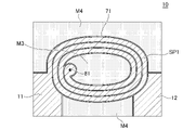
- FIG. 2 is a schematic plan view of the conductor layer 10.
- FIG. 3 is a schematic plan view of the conductor layers 20 and 40.
- FIG. FIG. 4 is a schematic plan view of the conductor layers 30 and 50.
- FIG. FIG. 5 is a schematic plan view of the conductor layer 60.
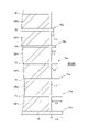
- FIG. FIG. 6 is a schematic cross-sectional view for explaining the shapes of protrusions provided on the insulating resin layers 70 to 76.
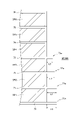
- FIG. 7 is a schematic cross-sectional view for explaining the shape of the projecting portion according to the first modification.
- FIG. 7 is a schematic cross-sectional view for explaining the shape of the projecting portion according to the first modification.
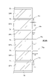
- FIG. 8 is a schematic cross-sectional view for explaining the shape of the projecting portion according to the second modification.
- FIG. 9 is a process diagram for explaining the method of manufacturing the coil component 1.
- FIG. 10A and 10B are process diagrams for explaining the method of manufacturing the coil component 1.
- FIG. 11 is a process diagram for explaining the method of manufacturing the coil component 1.
- FIG. 12A and 12B are process diagrams for explaining the method of manufacturing the coil component 1.
- FIG. 13A and 13B are process diagrams for explaining the method of manufacturing the coil component 1.
- FIG. 14A and 14B are process diagrams for explaining the method of manufacturing the coil component 1.
- FIG. 15A and 15B are process diagrams for explaining the method of manufacturing the coil component 1.
- FIG. 16A and 16B are process diagrams for explaining the manufacturing method of the coil component 1.
- FIG. 16A and 16B are process diagrams for explaining the manufacturing method of the coil component 1.
- FIG. 17A and 17B are process diagrams for explaining the method of manufacturing the coil component 1.
- FIG. 18 is a process diagram for explaining the manufacturing method of the coil component 1.
- FIG. 19A and 19B are process diagrams for explaining the method of manufacturing the coil component 1.
- FIG. 20 is a process diagram for explaining the method of manufacturing the coil component 1.
- FIG. 1 is a schematic cross-sectional view for explaining the structure of a coil component 1 according to one embodiment of the present invention.
- the coil component 1 according to the first embodiment is a surface-mounted chip component, and as shown in FIG. 1, includes magnetic members M1 to M4 and coil patterns C embedded in the magnetic members M1 to M4. Although the configuration of the coil pattern C will be described later, in this embodiment, it is composed of spiral patterns SP1 to SP6 wound in a spiral for a plurality of turns.
- the magnetic members M1 to M4 are composite members containing metal magnetic fillers such as iron (Fe) and permalloy-based materials, and resin binders. A liquid or powder epoxy resin is preferably used as the resin binder.
- the materials forming the magnetic members M1 to M4 may be the same or different.
- the magnetic member M1 is a portion that covers the coil pattern C from one side in the axial direction (upper side in FIG. 1), and the magnetic member M2 covers the coil pattern C from the other side in the axial direction (lower side in FIG. 1).
- the magnetic member M3 is a portion embedded in the inner diameter region of the coil pattern C, and the magnetic member M4 is a portion located in the outer region of the coil pattern C in the radial direction.
- the magnetic member M2 may be a magnetic substrate made of ferrite or the like.
- the insulating resin layers 70 to 76 and the conductor layers 10, 20, 30, 40, 50, 60 are alternately laminated in the axial direction.
- the planar shape of conductor layer 10 is shown in FIG. 2
- the planar shape of conductor layers 20 and 40 is shown in FIG. 3
- the planar shape of conductor layers 30 and 50 is shown in FIG. It is shown in FIG.
- the conductor layers 10, 20, 30, 40, 50, 60 have spiral patterns SP1-SP6, respectively, and the upper or lower surfaces of the spiral patterns SP1-SP6 are covered with insulating resin layers 70-76.
- the side surfaces of the spiral patterns SP1-SP6 are covered with portions of the insulating resin layers 71-76, respectively.
- the upper and lower surfaces of the spiral patterns SP1 to SP6 refer to surfaces substantially perpendicular to the coil axis
- the side surfaces of the spiral patterns SP1 to SP6 refer to surfaces substantially perpendicular to the radial direction.
- the spiral patterns SP1-SP6 constitute one coil conductor by being connected to each other through via holes formed in the insulating resin layers 71-75.
- Copper (Cu) is preferably used as the material for the conductor layers 10, 20, 30, 40, 50, and 60.
- the conductor layer 10 is the first conductor layer formed on the upper surface of the magnetic member M2 via the insulating resin layer 70, and as shown in FIG. , and two electrode patterns 11 and 12 .
- the lower surface of the spiral pattern SP1 is covered with an insulating resin layer 70, and the side and upper surfaces of the spiral pattern SP1 are covered with an insulating resin layer 71.
- the insulating resin layer 71 is interposed between the spiral pattern SP1 and the magnetic members M3 and M4.
- the electrode pattern 11 is connected to the outer peripheral end of the spiral pattern SP1.
- the electrode pattern 12 is provided independently of the spiral pattern SP1.
- the conductor layer 20 is a second conductor layer formed on the upper surface of the conductor layer 10 with an insulating resin layer 71 interposed therebetween. , and two electrode patterns 21 and 22 .
- the lower surface of the spiral pattern SP2 is covered with an insulating resin layer 71, and the side and upper surfaces of the spiral pattern SP2 are covered with an insulating resin layer 72.
- the insulating resin layer 72 is interposed between the spiral pattern SP2 and the magnetic members M3 and M4. Both the electrode patterns 21 and 22 are provided independently of the spiral pattern SP2.
- the conductor layer 30 is a third conductor layer formed on the upper surface of the conductor layer 20 with an insulating resin layer 72 interposed therebetween, and as shown in FIG. , and two electrode patterns 31 and 32 .
- the lower surface of the spiral pattern SP3 is covered with an insulating resin layer 72, and the side and upper surfaces of the spiral pattern SP3 are covered with an insulating resin layer 73.
- the insulating resin layer 73 is interposed between the spiral pattern SP3 and the magnetic members M3 and M4. Both the electrode patterns 31 and 32 are provided independently of the spiral pattern SP3.
- the conductor layer 40 is a fourth conductor layer formed on the upper surface of the conductor layer 30 with an insulating resin layer 73 interposed therebetween, and as shown in FIG. , and two electrode patterns 41 and 42 .
- the lower surface of the spiral pattern SP4 is covered with an insulating resin layer 73, and the side and upper surfaces of the spiral pattern SP4 are covered with an insulating resin layer 74.
- the insulating resin layer 74 is interposed between the spiral pattern SP4 and the magnetic members M3 and M4. Both the electrode patterns 41 and 42 are provided independently of the spiral pattern SP4.
- the conductor layer 50 is a fifth conductor layer formed on the upper surface of the conductor layer 40 with an insulating resin layer 74 interposed therebetween. , and two electrode patterns 51 and 52 .
- the lower surface of the spiral pattern SP5 is covered with an insulating resin layer 74, and the side and upper surfaces of the spiral pattern SP5 are covered with an insulating resin layer 75.
- the insulating resin layer 75 is interposed between the spiral pattern SP5 and the magnetic members M3 and M4. Both the electrode patterns 51 and 52 are provided independently of the spiral pattern SP5.
- the conductor layer 60 is a sixth conductor layer formed on the upper surface of the conductor layer 50 with an insulating resin layer 75 interposed therebetween, and as shown in FIG. It has a pattern SP6 and two electrode patterns 61 and 62 .
- the lower surface of the spiral pattern SP6 is covered with an insulating resin layer 75, and the side and upper surfaces of the spiral pattern SP6 are covered with an insulating resin layer 76.
- the insulating resin layer 76 is interposed between the spiral pattern SP6 and the magnetic members M3 and M4.
- the electrode pattern 62 is connected to the outer peripheral edge of the spiral pattern SP6.
- the electrode pattern 61 is provided independently of the spiral pattern SP6.
- the inner peripheral end of the spiral pattern SP1 and the inner peripheral end of the spiral pattern SP2 are connected via a via conductor 81 which is a part of the conductor layer 20 and provided to penetrate the insulating resin layer 71 .
- the outer peripheral end of the spiral pattern SP2 and the outer peripheral end of the spiral pattern SP3 are connected via a via conductor 82 which is a part of the conductor layer 30 and provided to penetrate the insulating resin layer 72 .
- the inner peripheral end of the spiral pattern SP3 and the inner peripheral end of the spiral pattern SP4 are connected via a via conductor 83 which is a part of the conductor layer 40 and provided to penetrate the insulating resin layer 73 .
- the outer peripheral end of the spiral pattern SP4 and the outer peripheral end of the spiral pattern SP5 are connected via a via conductor 84 which is a part of the conductor layer 50 and provided to penetrate the insulating resin layer material 74 .
- the inner peripheral end of the spiral pattern SP5 and the inner peripheral end of the spiral pattern SP6 are connected via a via conductor 85 which is a part of the conductor layer 60 and provided to penetrate the insulating resin layer 75 .
- the spiral patterns SP1 to SP6 are connected in series to form a coil conductor consisting of multiple turns.
- the electrode patterns 11, 21, 31, 41, 51, 61 are exposed from the magnetic members M1 to M4 and used as one external terminal.
- the electrode patterns 12, 22, 32, 42, 52, 62 are exposed from the magnetic members M1 to M4 and used as the other external terminals.
- the insulating resin layers 70 to 76 have protruding portions protruding to the inner diameter region and the outer region.
- the amount of protrusion in the radial direction of the protrusion is not constant between the insulating resin layers 70 to 76, and there are both long and short protrusions.
- FIG. 6 is a schematic cross-sectional view for explaining the shape of the protrusions provided on the insulating resin layers 70-76.
- the insulating resin layers 70 to 75 have projecting portions 70a to 75a projecting to the inner diameter region and the outer region, respectively.
- the projection amounts in the radial direction of the projecting portions 71a to 75a are respectively L1 to L5, L1>L2>L3>L4>L5 is.
- the insulating resin layers 71 to 75 positioned between the two conductor layers have gradually shorter protrusion amounts L1 to L5 from the lower layer to the upper layer, and the protrusion 75a of the insulating resin layer 75 has the shortest protrusion amount.
- the projecting portion 70 a of the insulating resin layer 70 positioned at the bottom layer may have a projecting amount L 0 that is approximately the same as the projecting amount L 1 of the projecting portion 71 a of the insulating resin layer 71 .
- the insulating resin layer 76 located on the uppermost layer does not have a projecting portion, but the insulating resin layer 76 may also have a projecting portion.
- the amount of protrusion of the spiral patterns SP1 to SP6 toward the inner diameter region and the amount of protrusion of the spiral patterns SP1 to SP6 toward the outer region may be the same or different.
- FIG. 7 is a schematic cross-sectional view for explaining the shape of the projecting portion according to the first modified example.
- the insulating resin layers 74 and 75 are not provided with protrusions. In this way, a portion of the insulating resin layer positioned between the two conductor layers does not need to have a protruding portion.
- FIG. 8 is a schematic cross-sectional view for explaining the shape of the projecting portion according to the second modified example.
- the projection amount L1 of the projecting portion 71a provided in the insulating resin layer 71 is shortened, and is at least shorter than the projecting amount L2 of the projecting portion 72a.
- the insulating resin layer 70 is not provided with a protruding portion.
- the projection amounts L1 to L5 gradually decrease from the lower layer to the upper layer, and the projection amount L1 of the projecting portion 71a may be shorter than the projecting amount L2 of the projecting portion 72a.
- the protrusion amounts L1 to L5 of the insulating resin layers 71 to 75 protruding to the inner diameter region and the outer region of the spiral patterns SP1 to SP6 are partially shortened. Accordingly, the volumes of the magnetic members M3 and M4 filled in the inner and outer regions are increased. This makes it possible to increase the inductance without increasing the chip size.
- FIGS. 9 to 20 are process diagrams for explaining the method of manufacturing the coil component 1 according to this embodiment.
- the process diagrams shown in FIGS. 9 to 20 show a cross section corresponding to one coil component 1, but in reality, a large number of coil components 1 are produced simultaneously using an assembly board. can do.
- a support having a metal foil 91 such as copper (Cu) provided on the surface of a base material 90 is prepared, and an insulating resin layer 70 and a seed layer S are formed on the surface of the metal foil 91 (FIG. 9).
- a resist pattern R is formed on the surface of the seed layer S (FIG. 10).
- the resist pattern R is a negative pattern of the conductor layer 10 .
- the conductor layer 10 is formed by growing the seed layer S by electroplating (FIG. 11).
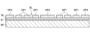
- the sacrificial pattern VP3 is formed in the inner area of the spiral pattern SP1
- the sacrificial pattern VP4 is formed in the outer area of the spiral pattern SP1.
- the seed layer S exposed in the removed portion of the resist pattern R is removed by etching (FIG. 12).
- the spiral pattern SP1 and the sacrificial patterns VP3 and VP4 are electrically separated by the spiral slit SL.
- an insulating resin layer 71 and a metal foil 92 are formed on the surface of the conductor layer 10 so as to fill the slit SL (FIG. 13).
- the insulating resin layer 71 and the metal foil 92 can be formed by a lamination method.
- the metal foil 92 is patterned to remove portions of the metal foil 92 overlapping the sacrificial patterns VP3 and VP4, and then blasting is performed using the metal foil 92 as a mask to expose the sacrificial patterns VP3 and VP4 ( Figure 14).
- openings for forming via conductors 81 are formed in insulating resin layer 71 by laser processing. The formation of the conductor layer 10 and the insulating resin layer 71 is completed by the above steps.
- a conductor layer 60 and an insulating resin layer 76 are sequentially formed (FIG. 16).
- the conductor layers 20, 30, 40, 50, and 60 also include the sacrificial pattern VP3 in the inner diameter region of the spiral patterns SP2-SP6, and the sacrificial pattern VP4 in the outer region of the spiral patterns SP2-SP6.
- the sacrificial patterns VP3 and VP4 of the conductor layer 60 located on the uppermost layer are exposed from openings provided in the insulating resin layer 76. As shown in FIG.
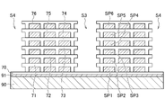
- the sacrificial patterns VP3 and VP4 are removed (FIG. 17). Since the spiral patterns SP1-SP6 are covered with the insulating resin layers 70-76, they are not etched. As a result, a space S3 is formed in the inner diameter region of the spiral patterns SP1 to SP6, and a space S4 is formed in the outer region of the spiral patterns SP1 to SP6. Part of the insulating resin layers 71 to 76 protrudes into the spaces S3 and S4. At this point, there is no substantial difference in the amount of protrusion of the insulating resin layers 71-76 into the spaces S3 and S4.
- the laser processing may be performed while the upper surface of the insulating resin layer 76 is covered with a metal foil so that the upper surface of the insulating resin layer 76 is not damaged. Alternatively, blasting may be performed instead of laser processing.
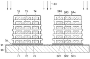
- the laser processing or blast processing conditions are set so that the portions of the insulating resin layers 70 to 76 that should not be removed are not severely damaged, thereby exposing them to the spaces S3 and S4. Alternatively, the protruding insulating resin layers 70 to 76 are partially removed.
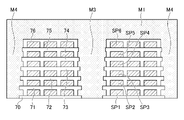
- the magnetic members M3 and M4 that fill the spaces S3 and S4 are formed, and the magnetic member M1 that covers the insulating resin layer 76 is formed (FIG. 19).
- the magnetic members M3 and M4 embedded in the spaces S3 and S4 are pushed from the upper insulating resin layer 76 side to the lower insulating resin layer 70 side, as described with reference to FIGS.
- the insulating resin layer located in the upper layer is processed so that the protruding amount becomes shorter, the work of embedding the magnetic members M3 and M4 can be efficiently performed, and the magnetic members M3 and M4 are placed in the spaces S3 and S4. Voids that do not exist are less likely to occur.
- the base material 90 and the metal foil 91 are removed (FIG. 20).
- the coil component 1 according to the present embodiment shown in FIG. 1 is completed by separating into individual pieces by dicing.
- the magnetic members M3 and M4 are exposed to the spaces S3 and S4 before the magnetic members M3 and M4 are embedded in the spaces S3 and S4.
- the magnetic members M3 and M4 can be embedded smoothly, and the spaces S3 and S4 are enlarged to increase the volume of the magnetic members M3 and M4. increases.
- the insulating resin layers 70 to 76 that are exposed or protrude into the spaces S3 and S4 are only partially removed, portions of the insulating resin layers 70 to 76 that should not be removed are greatly damaged.
- the insulating resin layers 70 to 76 that should not be removed are greatly damaged.
Landscapes
- Engineering & Computer Science (AREA)
- Power Engineering (AREA)
- Microelectronics & Electronic Packaging (AREA)
- Manufacturing & Machinery (AREA)
- Coils Or Transformers For Communication (AREA)
- Manufacturing Cores, Coils, And Magnets (AREA)
Abstract
【課題】スパイラルパターンの内径領域に磁性部材を埋め込みやすい構造を有するコイル部品を提供する。 【解決手段】コイル部品1は、磁性部材M1,M2間に配置され、それぞれスパイラル状に巻回されたスパイラルパターンSP1~SP6を含む導体層10~60と、導体層10~60間にそれぞれ設けられた絶縁樹脂層71~75と、スパイラルパターンSP1~SP6の内径領域に埋め込まれた磁性部材M3とを備える。絶縁樹脂層71~75は内径領域に突出する突出部を有する。絶縁樹脂層75の突出部は、他の少なくとも一つの絶縁樹脂層の突出部よりも突出量が短い。これにより、コイル軸方向の一端側から内径領域に磁性部材M3を埋め込みやすくなる。しかも、より多くの磁性部材M3を内径領域に埋め込むことができることから、インダクタンスを高めることも可能となる。
Description
本発明はコイル部品及びその製造方法に関し、特に、スパイラル状に巻回されたスパイラルパターンの内径領域に磁性部材が埋め込まれた構造を有するコイル部品及びその製造方法に関する。
スパイラル状に巻回されたスパイラルパターンが積層された構造を有するコイル部品としては、特許文献1に記載されたコイル部品が知られている。特許文献1に記載されたコイル部品は、スパイラルパターンの内径領域に磁性部材が埋め込まれた構造を有しており、これによりインダクタンスが高められている。
しかしながら、特許文献1に記載されたコイル部品においては、スパイラルパターンの内径領域に絶縁樹脂層の一部が突出していることから、このような突出部によって磁性部材の埋め込みが妨げられるおそれがあった。
したがって、本発明は、スパイラルパターンの内径領域に磁性部材を埋め込みやすい構造を有するコイル部品及びその製造方法を提供することを目的とする。
本発明によるコイル部品は、第1及び第2の磁性部材と、第1の磁性部材と第2の磁性部材の間に配置され、それぞれスパイラル状に巻回されたスパイラルパターンを含む複数の導体層と、複数の導体層間にそれぞれ設けられた複数の絶縁樹脂層と、スパイラルパターンの内径領域に埋め込まれた第3の磁性部材とを備え、複数の絶縁樹脂層は内径領域に突出する第1の突出部を有し、複数の絶縁樹脂層のうちコイル軸方向の一端側に位置する絶縁樹脂層の第1の突出部は、他の少なくとも一つの絶縁樹脂層の第1の突出部よりも突出量が短いことを特徴とする。
本発明によれば、コイル軸方向の一端側に位置する絶縁樹脂層の第1の突出部が短いことから、コイル軸方向の一端側から内径領域に第3の磁性部材を埋め込みやすくなる。しかも、より多くの磁性部材を内径領域に埋め込むことができることから、インダクタンスを高めることも可能となる。
本発明において、第1の突出部のいくつかは、コイル軸方向の一端側から他端側に向かって突出量が長くなっても構わない。この場合も、コイル軸方向の一端側から内径領域に第3の磁性部材を埋め込みやすくなる。しかも、コイル軸方向の他端側に近い突出部は比較的長いことから、突出部の除去に伴うダメージが最小限に抑えられる。
本発明において、複数の絶縁樹脂層のうちコイル軸方向の他端側に位置する絶縁樹脂層の第1の突出部は、他の少なくとも一つの絶縁樹脂層の第1の突出部よりも、突出量が短くても構わない。これによれば、より多くの磁性部材を内径領域に埋め込むことができることから、インダクタンスがより高められる。
本発明によるコイル部品は、スパイラルパターンの外側領域に位置する第4の磁性部材をさらに備え、複数の絶縁樹脂層は外側領域に突出する第2の突出部をさらに有し、複数の絶縁樹脂層のうちコイル軸方向の一端側に位置する絶縁樹脂層の第2の突出部は、他の少なくとも一つの絶縁樹脂層の第2の突出部よりも、突出量が短くても構わない。これによれば、複数のコイル部品を多数個取りによって作製する際に、コイル軸方向の一端側から外側領域に第4の磁性部材を埋め込みやすくなる。しかも、より多くの磁性部材を外側領域に埋め込むことができることから、インダクタンスを高めることも可能となる。
本発明によるコイル部品の製造方法は、スパイラル状に巻回されたスパイラルパターン及びスパイラルパターンの内径領域に位置する犠牲パターンを含む複数の導体層と複数の絶縁樹脂層を交互に積層する工程と、犠牲パターンを除去することによってスパイラルパターンの内径領域に空間を形成する工程と、空間に突出する複数の絶縁樹脂層からなる突出部の一部を除去する工程と、空間に磁性部材を埋め込む工程とを備えることを特徴とする。
本発明によれば、絶縁樹脂層からなる突出部の一部を除去していることから、空間に磁性部材を埋め込みやすくなる。
このように、本発明によれば、スパイラルパターンの内径領域に磁性部材を埋め込みやすい構造を有するコイル部品及びその製造方法を提供することが可能となる。
以下、添付図面を参照しながら、本発明の好ましい実施形態について詳細に説明する。
図1は、本発明の一実施形態によるコイル部品1の構造を説明するための略断面図である。
第1の実施形態によるコイル部品1は表面実装型のチップ部品であり、図1に示すように、磁性部材M1~M4と、磁性部材M1~M4に埋め込まれたコイルパターンCとを備える。コイルパターンCの構成については後述するが、本実施形態においてはスパイラル状に複数ターン巻回されたスパイラルパターンSP1~SP6からなる。
磁性部材M1~M4は、鉄(Fe)やパーマロイ系材料などからなる金属磁性体フィラーと樹脂バインダーを含む複合部材であり、コイルパターンCに電流を流すことによって生じる磁束の磁路を構成する。樹脂バインダーとしては、液状又は粉体のエポキシ樹脂を用いることが好ましい。磁性部材M1~M4を構成する材料は、互いに同じであっても構わないし、互いに異なっていても構わない。ここで、磁性部材M1はコイルパターンCを軸方向における一方側(図1に示す上側)から覆う部分であり、磁性部材M2はコイルパターンCを軸方向における他方側(図1に示す下側)から覆う部分であり、磁性部材M3はコイルパターンCの内径領域に埋め込まれた部分であり、磁性部材M4はコイルパターンCの径方向における外側領域に位置する部分である。磁性部材M2については、フェライトなどからなる磁性基板であっても構わない。
図1に示すように、絶縁樹脂層70~76と導体層10,20,30,40,50,60は、軸方向に交互に積層されている。導体層10の平面形状は図2に示され、導体層20,40の平面形状は図3に示され、導体層30,50の平面形状は図4に示され、導体層60の平面形状は図5に示されている。導体層10,20,30,40,50,60はそれぞれスパイラルパターンSP1~SP6を有しており、スパイラルパターンSP1~SP6の上面又は下面が絶縁樹脂層70~76で覆われている。スパイラルパターンSP1~SP6の側面は、それぞれ絶縁樹脂層71~76の一部で覆われている。ここで、スパイラルパターンSP1~SP6の上面及び下面とは、コイル軸に対して略垂直な面を指し、スパイラルパターンSP1~SP6の側面とは、径方向に対して略垂直な面を指す。
スパイラルパターンSP1~SP6は、絶縁樹脂層71~75に形成されたビアホールを介して互いに接続されることにより、1つのコイル導体を構成している。導体層10,20,30,40,50,60の材料としては、銅(Cu)を用いることが好ましい。絶縁樹脂層70~76のうち、少なくとも絶縁樹脂層71~75については非磁性材料が用いられる。最下層に位置する絶縁樹脂層70や、最上層に位置する絶縁樹脂層76については、磁性を有していても構わない。
導体層10は、磁性部材M2の上面に絶縁樹脂層70を介して形成された1層目の導体層であり、図2に示すように、スパイラル状に約3ターン巻回されたスパイラルパターンSP1と、2つの電極パターン11,12を有している。スパイラルパターンSP1の下面は絶縁樹脂層70で覆われ、スパイラルパターンSP1の側面及び上面は絶縁樹脂層71で覆われている。これにより、スパイラルパターンSP1と磁性部材M3,M4の間には、絶縁樹脂層71が介在する。電極パターン11は、スパイラルパターンSP1の外周端に接続されている。電極パターン12は、スパイラルパターンSP1とは独立して設けられている。
導体層20は、導体層10の上面に絶縁樹脂層71を介して形成された2層目の導体層であり、図3に示すように、スパイラル状に約3ターン巻回されたスパイラルパターンSP2と、2つの電極パターン21,22を有している。スパイラルパターンSP2の下面は絶縁樹脂層71で覆われ、スパイラルパターンSP2の側面及び上面は絶縁樹脂層72で覆われている。これにより、スパイラルパターンSP2と磁性部材M3,M4の間には、絶縁樹脂層72が介在する。電極パターン21,22は、いずれもスパイラルパターンSP2とは独立して設けられている。
導体層30は、導体層20の上面に絶縁樹脂層72を介して形成された3層目の導体層であり、図4に示すように、スパイラル状に約3ターン巻回されたスパイラルパターンSP3と、2つの電極パターン31,32を有している。スパイラルパターンSP3の下面は絶縁樹脂層72で覆われ、スパイラルパターンSP3の側面及び上面は絶縁樹脂層73で覆われている。これにより、スパイラルパターンSP3と磁性部材M3,M4の間には、絶縁樹脂層73が介在する。電極パターン31,32は、いずれもスパイラルパターンSP3とは独立して設けられている。
導体層40は、導体層30の上面に絶縁樹脂層73を介して形成された4層目の導体層であり、図3に示すように、スパイラル状に約3ターン巻回されたスパイラルパターンSP4と、2つの電極パターン41,42を有している。スパイラルパターンSP4の下面は絶縁樹脂層73で覆われ、スパイラルパターンSP4の側面及び上面は絶縁樹脂層74で覆われている。これにより、スパイラルパターンSP4と磁性部材M3,M4の間には、絶縁樹脂層74が介在する。電極パターン41,42は、いずれもスパイラルパターンSP4とは独立して設けられている。
導体層50は、導体層40の上面に絶縁樹脂層74を介して形成された5層目の導体層であり、図4に示すように、スパイラル状に約3ターン巻回されたスパイラルパターンSP5と、2つの電極パターン51,52を有している。スパイラルパターンSP5の下面は絶縁樹脂層74で覆われ、スパイラルパターンSP5の側面及び上面は絶縁樹脂層75で覆われている。これにより、スパイラルパターンSP5と磁性部材M3,M4の間には、絶縁樹脂層75が介在する。電極パターン51,52は、いずれもスパイラルパターンSP5とは独立して設けられている。
導体層60は、導体層50の上面に絶縁樹脂層75を介して形成された6層目の導体層であり、図5に示すように、スパイラル状に約2.5ターン巻回されたスパイラルパターンSP6と、2つの電極パターン61,62を有している。スパイラルパターンSP6の下面は絶縁樹脂層75で覆われ、スパイラルパターンSP6の側面及び上面は絶縁樹脂層76で覆われている。これにより、スパイラルパターンSP6と磁性部材M3,M4の間には、絶縁樹脂層76が介在する。電極パターン62は、スパイラルパターンSP6の外周端に接続されている。電極パターン61は、スパイラルパターンSP6とは独立して設けられている。
そして、スパイラルパターンSP1の内周端とスパイラルパターンSP2の内周端は、導体層20の一部であり絶縁樹脂層71を貫通して設けられたビア導体81を介して接続される。スパイラルパターンSP2の外周端とスパイラルパターンSP3の外周端は、導体層30の一部であり絶縁樹脂層72を貫通して設けられたビア導体82を介して接続される。スパイラルパターンSP3の内周端とスパイラルパターンSP4の内周端は、導体層40の一部であり絶縁樹脂層73を貫通して設けられたビア導体83を介して接続される。スパイラルパターンSP4の外周端とスパイラルパターンSP5の外周端は、導体層50の一部であり絶縁樹脂層材74を貫通して設けられたビア導体84を介して接続される。スパイラルパターンSP5の内周端とスパイラルパターンSP6の内周端は、導体層60の一部であり絶縁樹脂層75を貫通して設けられたビア導体85を介して接続される。これにより、スパイラルパターンSP1~SP6が直列に接続され、複数ターンからなるコイル導体が形成される。また、電極パターン11,21,31,41,51,61は磁性部材M1~M4から露出し、一方の外部端子として用いられる。電極パターン12,22,32,42,52,62は磁性部材M1~M4から露出し、他方の外部端子として用いられる。
図1に示すように、絶縁樹脂層70~76の少なくとも一部は、内径領域及び外側領域に突出する突出部を有している。突出部の径方向における突出量は絶縁樹脂層70~76間において一定ではなく、突出部の長さが長いものと短いものが混在している。
図6は、絶縁樹脂層70~76に設けられた突出部の形状を説明するための模式的な断面図である。
図6に示す例では、絶縁樹脂層70~75が内径領域及び外側領域に突出する突出部70a~75aをそれぞれ有している。ここで、突出部71a~75aの径方向における突出量をそれぞれL1~L5とすると、
L1>L2>L3>L4>L5
である。つまり、2つの導体層間に位置する絶縁樹脂層71~75は、下層から上層に向かって突出量L1~L5が徐々に短くなり、絶縁樹脂層75の突出部75aの突出量が最も短い。最下層に位置する絶縁樹脂層70の突出部70aの突出量L0については、絶縁樹脂層71の突出部71aの突出量L1と同程度であっても構わない。図6に示す例では、最上層に位置する絶縁樹脂層76については突出部を有していないが、絶縁樹脂層76についても突出部を有していても構わない。また、スパイラルパターンSP1~SP6の内径領域への突出量と、スパイラルパターンSP1~SP6の外側領域への突出量は、互いに同じであっても構わないし、異なっていても構わない。
L1>L2>L3>L4>L5
である。つまり、2つの導体層間に位置する絶縁樹脂層71~75は、下層から上層に向かって突出量L1~L5が徐々に短くなり、絶縁樹脂層75の突出部75aの突出量が最も短い。最下層に位置する絶縁樹脂層70の突出部70aの突出量L0については、絶縁樹脂層71の突出部71aの突出量L1と同程度であっても構わない。図6に示す例では、最上層に位置する絶縁樹脂層76については突出部を有していないが、絶縁樹脂層76についても突出部を有していても構わない。また、スパイラルパターンSP1~SP6の内径領域への突出量と、スパイラルパターンSP1~SP6の外側領域への突出量は、互いに同じであっても構わないし、異なっていても構わない。
図7は、第1の変形例による突出部の形状を説明するための模式的な断面図である。図7に示す例では、絶縁樹脂層74,75に突出部が設けられていない。このように、2つの導体層間に位置する一部の絶縁樹脂層については、突出部が存在しなくても構わない。
図8は、第2の変形例による突出部の形状を説明するための模式的な断面図である。図8に示す例では、絶縁樹脂層71に設けられた突出部71aの突出量L1が短縮されており、少なくとも突出部72aの突出量L2よりも短い。また、絶縁樹脂層70に突出部が設けられていない。このように、下層から上層に向かって突出量L1~L5が徐々に短くなる点は必須でなく、突出部71aの突出量L1については突出部72aの突出量L2よりも短くても構わない。
このように、本実施形態によるコイル部品1は、スパイラルパターンSP1~SP6の内径領域及び外側領域に突出する絶縁樹脂層71~75の突出量L1~L5の一部が短縮されていることから、その分、内径領域及び外側領域に充填される磁性部材M3,M4のボリュームが増加する。これにより、チップサイズを拡大することなくインダクタンスを高めることが可能となる。
次に、本実施形態によるコイル部品1の製造方法について説明する。
図9~図20は、本実施形態によるコイル部品1の製造方法を説明するためのプロセス図である。図9~図20に示す工程図は、1個のコイル部品1に対応する断面を示しているが、実際には、集合基板を用いて多数のコイル部品1を同時に作製することによって多数個取りすることができる。
まず、基材90の表面に銅(Cu)などの金属箔91が設けられた支持体を用意し、金属箔91の表面に絶縁樹脂層70及びシード層Sを形成する(図9)。次に、シード層Sの表面にレジストパターンRを形成する(図10)。レジストパターンRは、導体層10のネガパターンである。この状態で、電解メッキによってシード層Sを成長させることにより、導体層10を形成する(図11)。この時、スパイラルパターンSP1の内径領域には犠牲パターンVP3が形成され、スパイラルパターンSP1の外側領域には犠牲パターンVP4が形成される。
次に、レジストパターンRを剥離した後、レジストパターンRの剥離部分に露出するシード層Sをエッチングにより除去する(図12)。これにより、スパイラルパターンSP1と犠牲パターンVP3,VP4がスパイラル状のスリットSLによって電気的に分離される。次に、スリットSLを埋めるよう、導体層10の表面に絶縁樹脂層71及び金属箔92を形成する(図13)。絶縁樹脂層71及び金属箔92の形成は、ラミネート法によって行うことができる。次に、金属箔92をパターニングすることによって、犠牲パターンVP3,VP4と重なる部分の金属箔92を除去した後、金属箔92をマスクとしてブラスト加工することにより、犠牲パターンVP3,VP4を露出させる(図14)。次に、金属箔92を除去した後(図15)、レーザー加工によって絶縁樹脂層71にビア導体81(図2参照)を形成するための開口部を形成する。以上の工程により、導体層10及び絶縁樹脂層71の形成が完了する。
その後、図9~図15に示す工程を繰り返すことにより、導体層20、絶縁樹脂層72、導体層30、絶縁樹脂層73、導体層40、絶縁樹脂層74、導体層50、絶縁樹脂層75、導体層60、絶縁樹脂層76を順次形成する(図16)。導体層20,30,40,50,60においても、スパイラルパターンSP2~SP6の内径領域には犠牲パターンVP3が含まれ、スパイラルパターンSP2~SP6の外側領域には犠牲パターンVP4が含まれている。最上層に位置する導体層60の犠牲パターンVP3,VP4は、絶縁樹脂層76に設けられた開口部から露出している。
この状態でウェットエッチングを行うことにより、犠牲パターンVP3,VP4を除去する(図17)。スパイラルパターンSP1~SP6については、絶縁樹脂層70~76で覆われているため、エッチングされることはない。これにより、スパイラルパターンSP1~SP6の内径領域には空間S3が形成され、スパイラルパターンSP1~SP6の外側領域には空間S4が形成される。また、空間S3,S4には、絶縁樹脂層71~76の一部が突出する。この時点では、空間S3,S4への絶縁樹脂層71~76の突出量に実質的な差はない。
次に、空間S3,S4に露出する絶縁樹脂層70及び空間S3,S4に突出する絶縁樹脂層71~76にレーザービーム93を照射することによって、絶縁樹脂層70の露出部の一部及び絶縁樹脂層71~76の突出部の一部を除去する(図18)。この時、絶縁樹脂層76の上面がダメージを受けないよう、絶縁樹脂層76の上面を金属箔で覆った状態でレーザー加工を行っても構わない。或いは、レーザー加工の代わりにブラスト加工を行っても構わない。
この時、空間S3,S4に露出又は突出する絶縁樹脂層70~76を全て除去することが理想的であるが、空間S3,S4に露出又は突出する絶縁樹脂層70~76を全て除去するためには、長時間の加工が必要になるだけでなく、絶縁樹脂層70~76のうち除去すべきでない部分に加わるダメージが大きくなる。このため、空間S3,S4に露出又は突出する絶縁樹脂層70~76の全てを除去するのではなく、図6及び図7を用いて説明したように、上層に位置する絶縁樹脂層ほど突出量が短くなるような条件で、突出部を部分的に除去する。条件によっては、図8を用いて説明したように、下層の絶縁樹脂層71の突出量も短くなる。これは、金属箔91によって反射したレーザービーム93が絶縁樹脂層71の突出部に照射されるためである。このように、本実施形態においては、絶縁樹脂層70~76のうち除去すべきでない部分に大きなダメージが加わらないよう、レーザー加工又はブラスト加工の条件を設定することによって、空間S3,S4に露出又は突出する絶縁樹脂層70~76を部分的に除去する。
次に、空間S3,S4を埋める磁性部材M3,M4を形成するとともに、絶縁樹脂層76を覆う磁性部材M1を形成する(図19)。空間S3,S4に埋め込まれる磁性部材M3,M4は、上層に位置する絶縁樹脂層76側から下層に位置する絶縁樹脂層70側へと押し込まれるが、図6~図8を用いて説明したように、上層に位置する絶縁樹脂層ほど突出量が短くなるよう加工されていることから、磁性部材M3,M4の埋め込み作業を効率よく行うことができるとともに、空間S3,S4に磁性部材M3,M4の存在しないボイドなどが発生しにくい。次に、基材90及び金属箔91を除去する(図20)。そして、絶縁樹脂層70を覆う磁性部材M2を形成した後、ダイシングによって個片化すれば、図1に示した本実施形態によるコイル部品1が完成する。
このように、本実施形態においては、犠牲パターンVP3,VP4を除去することによって空間S3,S4を形成した後、空間S3,S4に磁性部材M3,M4を埋め込む前に、空間S3,S4に露出又は突出する絶縁樹脂層70~76の一部を除去していることから、磁性部材M3,M4の埋め込みをスムーズに行うことができるとともに、空間S3,S4の拡大によって磁性部材M3,M4のボリュームが増大する。しかも、空間S3,S4に露出又は突出する絶縁樹脂層70~76の除去を部分的な除去にとどめていることから、絶縁樹脂層70~76のうち除去すべきでない部分に大きなダメージが加わることもない。
以上、本発明の好ましい実施形態について説明したが、本発明は、上記の実施形態に限定されることなく、本発明の主旨を逸脱しない範囲で種々の変更が可能であり、それらも本発明の範囲内に包含されるものであることはいうまでもない。
1 コイル部品
10,20,30,40,50,60 導体層
11,12,21,22,31,32,41,42,51,52,61,62 電極パターン
70~76 絶縁樹脂層
70a~75a 突出部
81~85 ビア導体
90 基材
91 金属箔
92 金属箔
93 レーザービーム
C コイルパターン
M1~M4 磁性部材
R レジストパターン
S シード層
S3,S4 空間
SL スリット
SP1~SP6 スパイラルパターン
VP3,VP4 犠牲パターン
10,20,30,40,50,60 導体層
11,12,21,22,31,32,41,42,51,52,61,62 電極パターン
70~76 絶縁樹脂層
70a~75a 突出部
81~85 ビア導体
90 基材
91 金属箔
92 金属箔
93 レーザービーム
C コイルパターン
M1~M4 磁性部材
R レジストパターン
S シード層
S3,S4 空間
SL スリット
SP1~SP6 スパイラルパターン
VP3,VP4 犠牲パターン
Claims (5)
- 第1及び第2の磁性部材と、
前記第1の磁性部材と前記第2の磁性部材の間に配置され、それぞれスパイラル状に巻回されたスパイラルパターンを含む複数の導体層と、
前記複数の導体層間にそれぞれ設けられた複数の絶縁樹脂層と、
前記スパイラルパターンの内径領域に埋め込まれた第3の磁性部材と、を備え、
前記複数の絶縁樹脂層は、前記内径領域に突出する第1の突出部を有し、
前記複数の絶縁樹脂層のうちコイル軸方向の一端側に位置する絶縁樹脂層の前記第1の突出部は、他の少なくとも一つの絶縁樹脂層の前記第1の突出部よりも、突出量が短いことを特徴とするコイル部品。 - 前記第1の突出部のいくつかは、前記コイル軸方向の一端側から他端側に向かって突出量が長くなることを特徴とする請求項1に記載のコイル部品。
- 前記複数の絶縁樹脂層のうち前記コイル軸方向の他端側に位置する絶縁樹脂層の前記第1の突出部は、他の少なくとも一つの絶縁樹脂層の前記第1の突出部よりも、突出量が短いことを特徴とする請求項1又は2に記載のコイル部品。
- 前記スパイラルパターンの外側領域に位置する第4の磁性部材をさらに備え、
前記複数の絶縁樹脂層は、前記外側領域に突出する第2の突出部をさらに有し、
前記複数の絶縁樹脂層のうち前記コイル軸方向の一端側に位置する絶縁樹脂層の前記第2の突出部は、他の少なくとも一つの絶縁樹脂層の前記第2の突出部よりも、突出量が短いことを特徴とする請求項1乃至3のいずれか一項に記載のコイル部品。 - スパイラル状に巻回されたスパイラルパターン及びスパイラルパターンの内径領域に位置する犠牲パターンを含む複数の導体層と複数の絶縁樹脂層を交互に積層する工程と、
前記犠牲パターンを除去することによって、前記スパイラルパターンの内径領域に空間を形成する工程と、
前記空間に突出する前記複数の絶縁樹脂層からなる突出部の一部を除去する工程と、
前記空間に磁性部材を埋め込む工程と、を備えることを特徴とするコイル部品の製造方法。
Applications Claiming Priority (2)
| Application Number | Priority Date | Filing Date | Title |
|---|---|---|---|
| JP2021054662A JP7618476B2 (ja) | 2021-03-29 | 2021-03-29 | コイル部品及びその製造方法 |
| JP2021-054662 | 2021-03-29 |
Publications (1)
| Publication Number | Publication Date |
|---|---|
| WO2022209463A1 true WO2022209463A1 (ja) | 2022-10-06 |
Family
ID=83458842
Family Applications (1)
| Application Number | Title | Priority Date | Filing Date |
|---|---|---|---|
| PCT/JP2022/007592 Ceased WO2022209463A1 (ja) | 2021-03-29 | 2022-02-24 | コイル部品及びその製造方法 |
Country Status (2)
| Country | Link |
|---|---|
| JP (1) | JP7618476B2 (ja) |
| WO (1) | WO2022209463A1 (ja) |
Families Citing this family (2)
| Publication number | Priority date | Publication date | Assignee | Title |
|---|---|---|---|---|
| JP7548201B2 (ja) * | 2021-12-14 | 2024-09-10 | 株式会社村田製作所 | インダクタ部品およびインダクタ部品の製造方法 |
| JP7548200B2 (ja) * | 2021-12-14 | 2024-09-10 | 株式会社村田製作所 | インダクタ部品およびインダクタ部品の製造方法 |
Citations (9)
| Publication number | Priority date | Publication date | Assignee | Title |
|---|---|---|---|---|
| JPH0955316A (ja) * | 1995-08-17 | 1997-02-25 | Toshiba Corp | 平面型磁気素子およびその製造方法 |
| JP2007242800A (ja) * | 2006-03-07 | 2007-09-20 | Tdk Corp | コモンモードフィルタ |
| WO2013183452A1 (ja) * | 2012-06-08 | 2013-12-12 | 株式会社村田製作所 | 電子部品及びその製造方法 |
| US20160293318A1 (en) * | 2015-04-01 | 2016-10-06 | Samsung Electro-Mechanics Co., Ltd. | Coil component |
| JP2017017103A (ja) * | 2015-06-29 | 2017-01-19 | 株式会社村田製作所 | コイル部品 |
| JP2018182222A (ja) * | 2017-04-20 | 2018-11-15 | 株式会社村田製作所 | プリント配線基板およびスイッチングレギュレータ |
| JP2019029638A (ja) * | 2017-07-25 | 2019-02-21 | サムソン エレクトロ−メカニックス カンパニーリミテッド. | インダクタ及びその製造方法 |
| WO2019235510A1 (ja) * | 2018-06-08 | 2019-12-12 | Tdk株式会社 | コイル部品及びその製造方法 |
| JP2021068805A (ja) * | 2019-10-23 | 2021-04-30 | Tdk株式会社 | コイル部品及びその製造方法 |
-
2021
- 2021-03-29 JP JP2021054662A patent/JP7618476B2/ja active Active
-
2022
- 2022-02-24 WO PCT/JP2022/007592 patent/WO2022209463A1/ja not_active Ceased
Patent Citations (9)
| Publication number | Priority date | Publication date | Assignee | Title |
|---|---|---|---|---|
| JPH0955316A (ja) * | 1995-08-17 | 1997-02-25 | Toshiba Corp | 平面型磁気素子およびその製造方法 |
| JP2007242800A (ja) * | 2006-03-07 | 2007-09-20 | Tdk Corp | コモンモードフィルタ |
| WO2013183452A1 (ja) * | 2012-06-08 | 2013-12-12 | 株式会社村田製作所 | 電子部品及びその製造方法 |
| US20160293318A1 (en) * | 2015-04-01 | 2016-10-06 | Samsung Electro-Mechanics Co., Ltd. | Coil component |
| JP2017017103A (ja) * | 2015-06-29 | 2017-01-19 | 株式会社村田製作所 | コイル部品 |
| JP2018182222A (ja) * | 2017-04-20 | 2018-11-15 | 株式会社村田製作所 | プリント配線基板およびスイッチングレギュレータ |
| JP2019029638A (ja) * | 2017-07-25 | 2019-02-21 | サムソン エレクトロ−メカニックス カンパニーリミテッド. | インダクタ及びその製造方法 |
| WO2019235510A1 (ja) * | 2018-06-08 | 2019-12-12 | Tdk株式会社 | コイル部品及びその製造方法 |
| JP2021068805A (ja) * | 2019-10-23 | 2021-04-30 | Tdk株式会社 | コイル部品及びその製造方法 |
Also Published As
| Publication number | Publication date |
|---|---|
| JP7618476B2 (ja) | 2025-01-21 |
| JP2022152043A (ja) | 2022-10-12 |
Similar Documents
| Publication | Publication Date | Title |
|---|---|---|
| JP7557592B2 (ja) | コイル部品 | |
| JP7172113B2 (ja) | コイル部品及びその製造方法 | |
| CN115136263B (zh) | 线圈部件及其制造方法 | |
| JP7618476B2 (ja) | コイル部品及びその製造方法 | |
| US20230352233A1 (en) | Coil component and manufacturing method therefor | |
| US9287030B2 (en) | Multi gap inductor core | |
| JP2025170075A (ja) | コイル部品 | |
| JP6504632B2 (ja) | インダクタ及びその製造方法 | |
| JP7124333B2 (ja) | コイル部品及びその製造方法 | |
| JPH07201569A (ja) | 積層型電子部品及びその製造方法 | |
| JP2022152861A (ja) | インダクタ部品 | |
| CN117292913A (zh) | 线圈部件及其制造方法 | |
| JP2011198973A (ja) | 電子部品の製造方法 | |
| JP2007227730A (ja) | チップコイル | |
| JPH02256214A (ja) | チップインダクタおよびその製造方法 | |
| JP7722902B2 (ja) | コイル部品 | |
| JP7842666B2 (ja) | コイル部品 | |
| JP7572903B2 (ja) | コイル部品及びその製造方法 | |
| CN114496515B (zh) | 线圈部件及其制造方法 | |
| JP2026018948A (ja) | インダクタ | |
| JP2022130064A (ja) | コイル部品 |
Legal Events
| Date | Code | Title | Description |
|---|---|---|---|
| 121 | Ep: the epo has been informed by wipo that ep was designated in this application |
Ref document number: 22779688 Country of ref document: EP Kind code of ref document: A1 |
|
| NENP | Non-entry into the national phase |
Ref country code: DE |
|
| 122 | Ep: pct application non-entry in european phase |
Ref document number: 22779688 Country of ref document: EP Kind code of ref document: A1 |