WO2022208742A1 - 表示装置 - Google Patents
表示装置 Download PDFInfo
- Publication number
- WO2022208742A1 WO2022208742A1 PCT/JP2021/013874 JP2021013874W WO2022208742A1 WO 2022208742 A1 WO2022208742 A1 WO 2022208742A1 JP 2021013874 W JP2021013874 W JP 2021013874W WO 2022208742 A1 WO2022208742 A1 WO 2022208742A1
- Authority
- WO
- WIPO (PCT)
- Prior art keywords
- display device
- layer
- film
- light
- organic
- Prior art date
- Legal status (The legal status is an assumption and is not a legal conclusion. Google has not performed a legal analysis and makes no representation as to the accuracy of the status listed.)
- Ceased
Links
Images



Classifications
-
- H—ELECTRICITY
- H10—SEMICONDUCTOR DEVICES; ELECTRIC SOLID-STATE DEVICES NOT OTHERWISE PROVIDED FOR
- H10K—ORGANIC ELECTRIC SOLID-STATE DEVICES
- H10K59/00—Integrated devices, or assemblies of multiple devices, comprising at least one organic light-emitting element covered by group H10K50/00
-
- H—ELECTRICITY
- H10—SEMICONDUCTOR DEVICES; ELECTRIC SOLID-STATE DEVICES NOT OTHERWISE PROVIDED FOR
- H10K—ORGANIC ELECTRIC SOLID-STATE DEVICES
- H10K59/00—Integrated devices, or assemblies of multiple devices, comprising at least one organic light-emitting element covered by group H10K50/00
- H10K59/10—OLED displays
- H10K59/12—Active-matrix OLED [AMOLED] displays
- H10K59/126—Shielding, e.g. light-blocking means over the TFTs
-
- G—PHYSICS
- G09—EDUCATION; CRYPTOGRAPHY; DISPLAY; ADVERTISING; SEALS
- G09F—DISPLAYING; ADVERTISING; SIGNS; LABELS OR NAME-PLATES; SEALS
- G09F9/00—Indicating arrangements for variable information in which the information is built-up on a support by selection or combination of individual elements
- G09F9/30—Indicating arrangements for variable information in which the information is built-up on a support by selection or combination of individual elements in which the desired character or characters are formed by combining individual elements
-
- H—ELECTRICITY
- H10—SEMICONDUCTOR DEVICES; ELECTRIC SOLID-STATE DEVICES NOT OTHERWISE PROVIDED FOR
- H10K—ORGANIC ELECTRIC SOLID-STATE DEVICES
- H10K50/00—Organic light-emitting devices
-
- H—ELECTRICITY
- H10—SEMICONDUCTOR DEVICES; ELECTRIC SOLID-STATE DEVICES NOT OTHERWISE PROVIDED FOR
- H10K—ORGANIC ELECTRIC SOLID-STATE DEVICES
- H10K50/00—Organic light-emitting devices
- H10K50/80—Constructional details
- H10K50/84—Passivation; Containers; Encapsulations
- H10K50/844—Encapsulations
-
- H—ELECTRICITY
- H10—SEMICONDUCTOR DEVICES; ELECTRIC SOLID-STATE DEVICES NOT OTHERWISE PROVIDED FOR
- H10K—ORGANIC ELECTRIC SOLID-STATE DEVICES
- H10K59/00—Integrated devices, or assemblies of multiple devices, comprising at least one organic light-emitting element covered by group H10K50/00
- H10K59/80—Constructional details
- H10K59/87—Passivation; Containers; Encapsulations
- H10K59/873—Encapsulations
-
- H—ELECTRICITY
- H10—SEMICONDUCTOR DEVICES; ELECTRIC SOLID-STATE DEVICES NOT OTHERWISE PROVIDED FOR
- H10K—ORGANIC ELECTRIC SOLID-STATE DEVICES
- H10K59/00—Integrated devices, or assemblies of multiple devices, comprising at least one organic light-emitting element covered by group H10K50/00
- H10K59/10—OLED displays
- H10K59/12—Active-matrix OLED [AMOLED] displays
- H10K59/124—Insulating layers formed between TFT elements and OLED elements
Definitions
- the present invention relates to display devices.
- the organic EL element includes, for example, a first electrode provided on a flattening film of a TFT layer in which thin film transistors (hereinafter also referred to as "TFTs") are arranged, and a first electrode provided on the first electrode. and a second electrode provided on the organic EL layer.
- TFTs thin film transistors
- an island-shaped non-display area is provided inside the display area for image display in order to install electronic components such as a camera and a fingerprint sensor.
- a structure has been proposed in which a through-hole is provided to penetrate through (see, for example, Patent Document 1).
- an organic EL display device in which a through-hole is provided in a non-display area inside the display area, the peripheral edge of the through-hole is close to the display area.
- the structure is such that light from the display area can easily enter the display area.
- each sub-pixel constituting the display region is provided with a TFT for driving the organic EL element, there is a possibility that the characteristics of the TFT may deteriorate due to the incidence of light on the TFT.
- an organic EL display device having a hybrid structure in which a TFT using polysilicon and a TFT using an oxide semiconductor are provided in each sub-pixel has been proposed. has the property of being more sensitive to light than a TFT using polysilicon.
- the present invention has been made in view of this point, and its object is to suppress deterioration of TFT characteristics caused by light incident through through holes provided in a non-display area inside a display area. That's what it is.
- a display device comprises a resin substrate layer, an interlayer insulating film formed on the resin substrate layer and made of an inorganic insulating film, and a planarizing film made of an organic insulating film.
- a display device provided with a display area, and a through hole penetrating through the resin substrate layer in the non-display area in the thickness direction thereof, wherein the peripheral edge portion of the planarization film in the non-display area includes:
- a first light shielding film is provided so as to cover the side wall of the peripheral portion.
- the present invention it is possible to suppress degradation of TFT characteristics caused by light incident through through-holes provided in the non-display area inside the display area.
- FIG. 1 is a plan view showing a schematic configuration of an organic EL display device according to a first embodiment of the invention.
- FIG. 2 is a plan view of the display area of the organic EL display device according to the first embodiment of the invention.
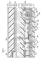
- FIG. 3 is a cross-sectional view of the display area of the organic EL display device according to the first embodiment of the invention.
- FIG. 4 is an equivalent circuit diagram showing a pixel circuit of the organic EL display device according to the first embodiment of the invention.
- FIG. 5 is a cross-sectional view showing an organic EL layer that constitutes the organic EL display device according to the first embodiment of the present invention.
- FIG. 6 is a plan view of the non-display area of the organic EL display device according to the first embodiment of the invention.
- FIG. 7 is a cross-sectional view of the non-display area of the organic EL display device along line VII-VII in FIG.
- FIG. 8 is a cross-sectional view of the non-display area in the modified example of the organic EL display device according to the first embodiment of the invention, and corresponds to FIG.
- FIG. 9 is a cross-sectional view of the non-display area of the organic EL display device according to the second embodiment of the invention, and corresponds to FIG.
- FIG. 10 is a cross-sectional view of the display area of the organic EL display device according to the third embodiment of the invention, and corresponds to FIG.
- FIG. 11 is a cross-sectional view of the non-display area of the organic EL display device according to the third embodiment of the invention, which corresponds to FIG.
- FIG. 1 is a plan view showing a schematic configuration of the organic EL display device 50a of this embodiment.
- 2 and 3 are a plan view and a cross-sectional view of the display area D of the organic EL display device 50a.
- FIG. 4 is an equivalent circuit diagram showing a pixel circuit of the organic EL display device 50a.
- FIG. 5 is a cross-sectional view showing the organic EL layer 33 forming the organic EL display device 50a.
- FIG. 6 is a plan view of the non-display area N of the organic EL display device 50a.
- 7 is a cross-sectional view of the non-display area N of the organic EL display device 50a along line VII-VII in FIG. 8 is a cross-sectional view of a non-display area N in an organic EL display device 50aa that is a modification of the organic EL display device 50a, and corresponds to FIG.
- the organic EL display device 50a includes, for example, a rectangular display area D for displaying an image, and a frame area F provided around the display area D in a frame shape.
- the rectangular display area D is exemplified, but the rectangular shape includes, for example, a shape with arc-shaped sides, a shape with arc-shaped corners, and a shape with arc-shaped corners.
- a substantially rectangular shape such as a shape with a notch is also included.
- a plurality of sub-pixels P are arranged in a matrix.
- sub-pixels P having a red light-emitting region Er for displaying red sub-pixels P having a green light-emitting region Eg for displaying green
- a sub-pixel P having a blue light-emitting region Eb for displaying blue is provided so as to be adjacent to each other.
- one pixel is configured by three adjacent sub-pixels P each having a red light emitting region Er, a green light emitting region Eg and a blue light emitting region Eb.
- FIG. 1 the display area D, as shown in FIG.
- an island-shaped non-display area N is provided.
- the thickness of the resin substrate layer 10 described later is set in order to install electronic components 60 such as a camera, a fingerprint sensor, and a face authentication sensor on the back side.
- a through hole H is provided to penetrate in the direction.
- a terminal portion T is provided so as to extend in one direction (the X direction in the drawing) at the lower end portion of the frame region F in FIG.
- the X direction in the figure can be bent at, for example, 180° (in a U shape).
- a bent portion B is provided so as to extend in one direction (the X direction in the figure).
- a substantially C-shaped trench G in plan view is provided in the flattening film 22a to be described later so as to penetrate the flattening film 22a.
- the trench G is provided in a substantially C shape so that the terminal portion T side is open in a plan view.
- the organic EL display device 50a includes a resin substrate layer 10, a TFT layer 30a provided on the resin substrate layer 10, and an organic EL device provided as a light emitting element layer on the TFT layer 30a.
- An element layer 40 and a sealing film 45 provided to cover the organic EL element layer 40 are provided.
- the resin substrate layer 10 is made of, for example, polyimide resin.
- the first concave portion Ca and each second concave portion Cb are provided in an inverse tapered shape that narrows toward the opening so as to reach the upper layer portion of the resin substrate layer 10 .
- the TFT layer 30a includes a base coat film 11 provided on the resin substrate layer 10, an initialization TFT 9a (see FIG. 4) provided in each sub-pixel P on the base coat film 11, and a compensation TFT 9a.
- a TFT 9b see FIG. 4
- a writing TFT 9c see FIG. 4
- a light emission control TFT 9f an anode discharge TFT 9g, a capacitor 9h
- the respective TFTs 9a to 9g and and a planarizing film 22a provided on the capacitor 9h As shown in FIG.
- the TFT layer 30a is provided with a plurality of gate lines 14g extending parallel to each other in the X direction in the figure. Further, as shown in FIG. 2, the TFT layer 30a is provided with a plurality of light emission control lines 14e extending parallel to each other in the X direction in the figure. Further, as shown in FIG. 2, the TFT layer 30a is provided with a plurality of second initialization power supply lines 19i extending parallel to each other in the X direction in the figure. As shown in FIG. 2, each light emission control line 14e is provided adjacent to each gate line 14g and each second initialization power supply line 19i. Further, as shown in FIG.
- the TFT layer 30a is provided with a plurality of source lines 21h extending parallel to each other in the Y direction in the figure. As shown in FIG. 2, the TFT layer 30a is provided with a plurality of power supply lines 21i extending parallel to each other in the Y direction in the figure. Each power supply line 21i is provided adjacent to each source line 21h, as shown in FIG.
- the writing TFT 9c, the driving TFT 9d, the power supply TFT 9e, and the light emission control TFT 9f are provided as first TFTs having a first semiconductor layer made of polysilicon such as LTPS (low temperature polysilicon), and have gate electrodes. , a first terminal electrode and a second terminal electrode.
- the initialization TFT 9a, the compensation TFT 9b, and the anode discharge TFT 9g are provided as second TFTs having a second semiconductor layer formed of an oxide semiconductor such as an In--Ga--Zn--O-based semiconductor.
- a third terminal electrode and a fourth terminal electrode are provided.
- the In—Ga—Zn—O-based oxide semiconductor is a ternary oxide of In (indium), Ga (gallium), and Zn (zinc), and the ratio (composition) of In, Ga, and Zn is ratio) is not particularly limited.
- In--Ga--Zn--O based semiconductors may be amorphous or crystalline.
- As the crystalline In-Ga-Zn-O-based semiconductor a crystalline In-Ga-Zn-O-based semiconductor in which the c-axis is oriented substantially perpendicular to the layer surface is preferable.
- another oxide semiconductor may be included instead of the In--Ga--Zn--O-based semiconductor.
- oxide semiconductors may include, for example, In—Sn—Zn—O-based semiconductors (eg, In 2 O 3 —SnO 2 —ZnO; InSnZnO).
- the In—Sn—Zn—O-based semiconductor is a ternary oxide of In (indium), Sn (tin), and Zn (zinc).
- oxide semiconductors include In--Al--Zn--O based semiconductors, In--Al--Sn--Zn--O based semiconductors, Zn--O based semiconductors, In--Zn--O based semiconductors, Zn--Ti-- O-based semiconductor, Cd--Ge--O-based semiconductor, Cd--Pb--O-based semiconductor, CdO (cadmium oxide), Mg--Zn--O-based semiconductor, In--Ga--Sn--O-based semiconductor, In--Ga--O-based semiconductor Semiconductors, Zr-In-Zn-O-based semiconductors, Hf-In-Zn-O-based semiconductors, Al-Ga-Zn-O-based semiconductors, Ga-Zn-O-based semiconductors, In-Ga-Zn-Sn-O-based semiconductors Semiconductors such as InGaO 3 (ZnO) 5 , magnesium zinc oxide (Mg
- the initialization TFT 9a has its gate electrode electrically connected to the previous stage (n-1 stage) gate line 14g (n-1) and its third terminal electrode. is electrically connected to the lower conductive layer 16c of the capacitor 9h and the gate electrode of the driving TFT 9d, which will be described later, and its fourth terminal electrode is electrically connected to the power supply line 21i.
- the first terminal electrodes and the second terminal electrodes of the first TFTs are indicated by circled numerals 1 and 2.
- the third terminal electrode and the fourth terminal electrode of the second TFT are indicated by circled numerals 3 and 4.
- the equivalent circuit diagram of FIG. 4 shows the pixel circuit of the n-th row and m-th column sub-pixel P, it also includes part of the pixel circuit of the (n-1)-th row and m-th column sub-pixel P.
- the power line 21i for supplying the high power voltage ELVDD also serves as the first initialization power line, but the power line 21i and the first initialization power line are provided separately.
- the present invention is not limited to this, and a voltage different from the low power supply voltage ELVSS can be applied to turn off the organic EL element 35. can be entered.
- the compensation TFT 9b has its gate electrode electrically connected to the gate line 14g(n) of its own stage (n stage) in each sub-pixel P, and its third terminal electrode is used for driving. It is electrically connected to the gate electrode of the TFT 9d, and its fourth terminal electrode is electrically connected to the first terminal electrode of the driving TFT 9d.
- the write TFT 9c has its gate electrode electrically connected to the gate line 14g(n) of its own stage (n stage), and its first terminal electrode corresponds to the gate line 14g(n).
- the second terminal electrode of the source line 21h is electrically connected to the second terminal electrode of the driving TFT 9d.
- the driving TFT 9d has its gate electrode 14b (see FIG. 3) electrically connected to the third terminal electrodes of the initialization TFT 9a and the compensation TFT 9b.
- the first terminal electrode 21e (see FIG. 3) is electrically connected to the fourth terminal electrode of the compensating TFT 9b and the second terminal electrode of the power supply TFT 9e, and the second terminal electrode 21g (see FIG. 3) is the write terminal electrode. It is electrically connected to the second terminal electrode of the embedding TFT 9c and the first terminal electrode of the light emission control TFT 9f.
- the driving TFT 9 d is configured to control the current of the organic EL element 35 . Further, as shown in FIG.
- the driving TFT 9d the first semiconductor layer 12b provided on the base coat film 11, the first gate insulating film 13 provided on the first semiconductor layer 12b, and the first gate insulating film
- a gate electrode 14b provided on the film 13, a first interlayer insulating film 15 and a second interlayer insulating film 20 provided to cover the gate electrode 14b, and a second interlayer insulating film 20 spaced apart from each other.
- a first terminal electrode 21e and a second terminal electrode 21g are provided.
- the first semiconductor layer 12b includes a first conductor region and a second conductor region provided so as to be spaced apart from each other, and a channel region defined between the first conductor region and the second conductor region.
- the first terminal electrode 21e and the second terminal electrode 21g are formed on the laminated film of the first gate insulating film 13, the first interlayer insulating film 15 and the second interlayer insulating film 20. It is electrically connected to the first conductor region and the second conductor region of the first semiconductor layer 12b through one contact hole.
- the power supply TFT 9e has its gate electrode electrically connected to the light emission control line 14e of its own stage (n stage), and its first terminal electrode connected to the power supply line 21i. and its second terminal electrode is electrically connected to the first terminal electrode of the driving TFT 9d.
- the light emission control TFT 9f has its gate electrode 14a (see FIG. 3) electrically connected to the light emission control line 14e of its own stage (n stage).
- the terminal electrode 21a (see FIG. 3) is electrically connected to the second terminal electrode of the driving TFT 9d, and the second terminal electrode 21c (see FIG. 3) is electrically connected to the first electrode 31a of the organic EL element 35 described later. It is connected to the.
- the light emission control TFT 9f includes a first semiconductor layer 12a provided on the base coat film 11, a first gate insulating film 13 provided on the first semiconductor layer 12a, and a first gate insulating film 13 provided on the first semiconductor layer 12a.
- a first terminal electrode 21a and a second terminal electrode 21b (21c) are provided as follows.
- the first semiconductor layer 12a includes a first conductor region and a second conductor region provided so as to be spaced apart from each other, and a channel region defined between the first conductor region and the second conductor region. there is 3, the first terminal electrode 21a and the second terminal electrode 21b are formed on the laminated film of the first gate insulating film 13, the first interlayer insulating film 15 and the second interlayer insulating film 20.
- the second terminal electrode 21c is formed in the contact hole formed in the laminated film of the first gate insulating film 13 and the first interlayer insulating film 15, the relay electrode 16a, and the second interlayer insulating film 20. It is electrically connected to the second conductor region of the first semiconductor layer 12a through the formed contact hole.
- the anode discharge TFT 9g has its gate electrode 19a (see FIG. 3) electrically connected to the gate line 14g(n) of its own stage (n stage).
- the third terminal electrode 21c (see FIG. 3) is electrically connected to the first electrode 31a of the organic EL element 35, and the fourth terminal electrode 21d (see FIG. 3) is electrically connected to the second initialization power line 19i. It is connected.
- the third terminal electrode 21c of the anode discharge TFT 9g is shared with the second terminal electrode 21c of the light emission control TFT 9f. Further, as shown in FIG.
- the anode discharge TFT 9g includes a second semiconductor layer 17a provided on the first interlayer insulating film 15 and a second gate insulating film 18a provided on the second semiconductor layer 17a. , a gate electrode 19a provided on a second gate insulating film 18a, a second interlayer insulating film 20 provided to cover the gate electrode 19a, and a second interlayer insulating film 20 provided on the second interlayer insulating film 20 so as to be spaced apart from each other. and a third terminal electrode 21c and a fourth terminal electrode 21d.
- the second semiconductor layer 17a is provided between the third conductor region and the fourth conductor region provided so as to be spaced apart from each other and between the third conductor region and the fourth conductor region.
- the third terminal electrode 21c is electrically connected to the third conductor region of the second semiconductor layer 17a through the contact hole formed in the second interlayer insulating film 20 and the relay electrode 16a.
- the fourth terminal electrode 21d is electrically connected to the fourth conductor region of the second semiconductor layer 17a through the contact hole formed in the second interlayer insulating film 20 and the relay electrode 16b.
- the writing TFT 9c, the driving TFT 9d, the power supply TFT 9e, and the light emission control TFT 9f are provided as the first TFTs having the first semiconductor layer made of polysilicon, and are made of an oxide semiconductor.
- the pixel circuit provided with the initialization TFT 9a, the compensation TFT 9b, and the anode discharge TFT 9g is exemplified as the second TFT having the second semiconductor layer, all the TFTs of the pixel circuit, that is, the initialization TFT 9a and the compensation TFT 9g, are provided.
- the TFT 9b, the writing TFT 9c, the driving TFT 9d, the power supply TFT 9e, the emission control TFT 9f, and the anode discharge TFT 9g may be composed of TFTs having a semiconductor layer formed of an oxide semiconductor.
- the capacitor 9h has a lower conductive layer 16c (see FIG. 3) connected to the gate electrode 14b (see FIG. 3) of the driving TFT 9d, the initializing TFT 9a, and the compensating TFT 9b.
- the upper conductive layer 19b (see FIG. 3) is electrically connected to each third terminal electrode, the third terminal electrode of the anode discharge TFT 9g, the second terminal electrode of the light emission control TFT 9f, and the first terminal electrode of the organic EL element 35. It is electrically connected to the electrode 31a. As shown in FIG.
- the capacitor 9h includes a lower conductive layer 16c made of the same material as the relay electrodes 16a and 16b and formed in the same layer, and a second gate insulating film 18b provided on the lower conductive layer 16c. , and an upper conductive layer 19b provided on the second gate insulating film 18b and made of the same material and in the same layer as the gate electrode 19a.
- the planarizing film 22a has a flat surface in the display region D, and is made of an organic insulating film such as an organic resin material such as polyimide resin or acrylic resin, or a polysiloxane-based SOG (spin on glass) material. It is
- the organic EL element layer 40 includes a plurality of first electrodes 31a provided in order corresponding to a plurality of sub-pixels P, a common edge cover 32a, a plurality of organic EL layers 33, and a common second electrode 34.
- the first electrode 31a, the organic EL layer 33 and the second electrode 34 constitute an organic EL element 35 (see FIG. 4).
- the first electrode 31a is electrically connected to the second terminal electrode 21c of the light emission control TFT 9f of each sub-pixel P through a contact hole formed in the planarizing film 22a.
- the first electrode 31 a also has a function of injecting holes into the organic EL layer 33 .
- the first electrode 31a is more preferably made of a material having a large work function in order to improve the efficiency of hole injection into the organic EL layer 33 .
- examples of materials constituting the first electrode 31a include silver (Ag), aluminum (Al), vanadium (V), cobalt (Co), nickel (Ni), tungsten (W), and gold (Au).
- the material forming the first electrode 31a may be an alloy such as astatine (At)/astatine oxide (AtO 2 ).
- the material forming the first electrode 31a is, for example, conductive oxides such as tin oxide (SnO), zinc oxide (ZnO), indium tin oxide (ITO), and indium zinc oxide (IZO). There may be.
- the first electrode 31a may be formed by laminating a plurality of layers made of the above materials.
- Compound materials having a large work function include, for example, indium tin oxide (ITO) and indium zinc oxide (IZO).
- the film thickness of the first electrode 31a is, for example, about 160 nm, preferably 150 nm or more and 300 nm or less.
- the edge cover 32a is provided in a grid pattern in common to all the sub-pixels P, and is made of, for example, an organic resin material such as polyimide resin or acrylic resin, or a polysiloxane-based SOG material.
- the organic EL layer 33 is provided as a light emitting functional layer, and as shown in FIG. and an electron injection layer 5 .
- the hole injection layer 1 is also called an anode buffer layer, and has the function of bringing the energy levels of the first electrode 31 a and the organic EL layer 33 close to each other and improving the efficiency of hole injection from the first electrode 31 a to the organic EL layer 33 .
- Examples of materials constituting the hole injection layer 1 include triazole derivatives, oxadiazole derivatives, imidazole derivatives, polyarylalkane derivatives, pyrazoline derivatives, phenylenediamine derivatives, oxazole derivatives, styrylanthracene derivatives, fluorenone derivatives, hydrazone derivatives, stilbene derivatives and the like.
- the hole transport layer 2 has a function of improving the transport efficiency of holes from the first electrode 31 a to the organic EL layer 33 .
- Examples of materials constituting the hole transport layer 2 include porphyrin derivatives, aromatic tertiary amine compounds, styrylamine derivatives, polyvinylcarbazole, poly-p-phenylene vinylene, polysilane, triazole derivatives, and oxadiazole.
- the light-emitting layer 3 In the light-emitting layer 3, holes and electrons are injected from the first electrode 31a and the second electrode 34 when a voltage is applied by the first electrode 31a and the second electrode 34, and the holes and electrons are recombined. area.
- the light-emitting layer 3 is made of a material with high light-emitting efficiency. Examples of materials constituting the light-emitting layer 3 include metal oxinoid compounds [8-hydroxyquinoline metal complex], naphthalene derivatives, anthracene derivatives, diphenylethylene derivatives, vinylacetone derivatives, triphenylamine derivatives, butadiene derivatives, and coumarin derivatives.
- the electron transport layer 4 has a function of efficiently transferring electrons to the light emitting layer 3 .
- the materials constituting the electron transport layer 4 include, for example, organic compounds such as oxadiazole derivatives, triazole derivatives, benzoquinone derivatives, naphthoquinone derivatives, anthraquinone derivatives, tetracyanoanthraquinodimethane derivatives, diphenoquinone derivatives, and fluorenone derivatives. , silole derivatives, and metal oxinoid compounds.
- the electron injection layer 5 has the function of bringing the energy levels of the second electrode 34 and the organic EL layer 33 close to each other and improving the efficiency with which electrons are injected from the second electrode 34 into the organic EL layer 33. With this function, The driving voltage of the organic EL element 35 can be lowered.
- the electron injection layer 5 is also called a cathode buffer layer.
- examples of materials constituting the electron injection layer 5 include lithium fluoride (LiF), magnesium fluoride (MgF 2 ), calcium fluoride (CaF 2 ), strontium fluoride (SrF 2 ), and barium fluoride.
- inorganic alkali compounds such as (BaF 2 ), aluminum oxide (Al 2 O 3 ), strontium oxide (SrO), and the like.
- the second electrode 34 is commonly provided for all sub-pixels P so as to cover each organic EL layer 33 and the edge cover 32a.
- the second electrode 34 also has a function of injecting electrons into the organic EL layer 33 .
- the second electrode 34 is more preferably made of a material with a small work function in order to improve the efficiency of injecting electrons into the organic EL layer 33 .
- materials constituting the second electrode 34 include silver (Ag), aluminum (Al), vanadium (V), calcium (Ca), titanium (Ti), yttrium (Y), and sodium (Na).
- the second electrode 34 is composed of, for example, magnesium (Mg)/copper (Cu), magnesium (Mg)/silver (Ag), sodium (Na)/potassium (K), astatine (At)/astatin oxide (AtO 2 ), lithium (Li)/aluminum (Al), lithium (Li)/calcium (Ca)/aluminum (Al), lithium fluoride (LiF)/calcium (Ca)/aluminum (Al), etc.
- the second electrode 34 may be formed of conductive oxides such as tin oxide (SnO), zinc oxide (ZnO), indium tin oxide (ITO), and indium zinc oxide (IZO). . Also, the second electrode 34 may be formed by laminating a plurality of layers made of the above materials.
- Examples of materials with a small work function include magnesium (Mg), lithium (Li), lithium fluoride (LiF), magnesium (Mg)/copper (Cu), magnesium (Mg)/silver (Ag), sodium (Na)/potassium (K), lithium (Li)/aluminum (Al), lithium (Li)/calcium (Ca)/aluminum (Al), lithium fluoride (LiF)/calcium (Ca)/aluminum (Al) etc.
- the sealing film 45 is provided so as to cover the second electrode 34 as shown in FIGS. and a second inorganic sealing film 43, and has a function of protecting the organic EL layer 33 of the organic EL element 35 from moisture, oxygen, and the like.
- the first inorganic sealing film 41 and the second inorganic sealing film 43 are composed of an inorganic insulating film such as a silicon nitride film, a silicon oxide film, or a silicon oxynitride film.
- the organic sealing film 42 is made of an organic resin material such as acrylic resin, epoxy resin, silicone resin, polyurea resin, parylene resin, polyimide resin, or polyamide resin.
- the organic EL display device 50a includes, as shown in FIG.
- a second outer damming wall Wb is provided in a frame shape around the outer damming wall Wa.
- the first outer damming wall Wa and the second outer damming wall Wb are formed, for example, on a lower resin layer formed in the same layer from the same material as the flattening film 22a, and on the lower resin layer. and an upper resin layer formed in the same layer from the same material as the edge cover 32a.
- the first dam wall Wa is provided so as to overlap the outer peripheral end portion of the organic sealing film 42 of the sealing film 45, and is configured to suppress the spread of the ink forming the organic sealing film 42. .
- a first frame is provided inside the trench G in a frame shape, and both end portions of the open portion of the trench G extend to the terminal portion T.
- a wiring 21j is provided.
- the first frame wiring 21j is connected to the power supply line 21i on the display area D side of the frame area F, and is configured to receive a high power supply voltage (ELVDD) at the terminal portion T.
- ELVDD high power supply voltage
- the organic EL display device 50a includes a second frame wiring 21k provided in a substantially C-shape outside the trench G in the frame region F and having both ends extending to the terminal portion T, as shown in FIG. .
- the second frame wiring 21k is electrically connected to the second electrode 34 on the display region D side of the frame region F, and configured to receive a low power supply voltage (ELVSS) at the terminal portion T. .
- ELVSS low power supply voltage
- the organic EL display device 50a includes a first light-shielding film 31b provided in a ring shape in the non-display region N so as to cover the side wall of the peripheral end portion of the planarizing film 22a.
- the first light shielding film 31b is made of the same material as the first electrode 31a and formed in the same layer, and is covered with the edge cover 32a as shown in FIG.
- a plurality of first bypass wirings 14n and a plurality of second bypass wirings 21n bypassing the through holes H are provided on the resin substrate layer 10 side of the first light shielding film 31b, as shown in FIG.
- the first detour wiring 14n and the second detour wiring 21n are the display wirings (the gate line 14g, the light emission control line 14e, the second initialization power supply line 19i, the source line 21h, the power line 21i, etc.).
- the organic EL display device 50a is provided in an annular shape in the non-display region N so as to surround the through hole H and overlap the inner peripheral edge of the organic sealing film . and an inner dam wall Wc.
- the inner dam wall Wc is provided so as to cover the first resin layer 22b formed in the same layer as the flattening film 22a and the same material.
- a second light shielding film 31c and a second resin layer 32b provided to cover the second light shielding film 31c and made of the same material as the edge cover 32a in the same layer.
- the organic EL display device 50a includes a first ring-shaped first display panel provided concentrically in the non-display area N so as to surround the through hole H outside the inner dam wall Wc. It has a recess Ca.
- the first recess Ca is formed between the first light shielding film 31b and the second light shielding film 31c so as to reach the upper layer of the resin substrate layer 10, the base coat film 11 and the first recess Ca.
- the gate insulating film 13, the first interlayer insulating film 15, and the second interlayer insulating film 20 protrude like eaves and are provided in a reverse tapered shape that narrows toward the opening (upper side in the figure).
- the organic EL layer 33 and the second electrode 34 are separated from each other on the display area D side and the through hole H side by the first concave portion Ca and the second concave portion Cb, which will be described later.
- the organic EL display device 50a in the non-display area N, includes a plurality of concentrically arranged ring-shaped electrodes so as to surround the through hole H inside the inner blocking wall Wc. It has a second recess Cb.
- the second concave portion Cb is formed between the second light shielding film 31c and the through hole H (see FIG. 6) so as to reach the upper layer portion of the resin substrate layer 10.
- the first gate insulating film 13, the first interlayer insulating film 15, and the second interlayer insulating film 20 protrude like eaves and are provided in an inverse tapered shape that narrows toward the opening (upper side in the figure).
- the organic EL display device 50a configured as described above, in each sub-pixel P, first, when the light emission control line 14e is selected and rendered inactive, the organic EL element 35 becomes non-light emitting. In the non-light-emitting state, the preceding gate line 14g(n-1) is selected, and a gate signal is input to the initialization TFT 9a via the gate line 14g(n-1), whereby the initialization TFT 9a is turned on, the high power supply voltage ELVDD of the power supply line 21i is applied to the capacitor 9h, and the driving TFT 9d is turned on. As a result, the charge in the capacitor 9h is discharged, and the voltage applied to the gate electrode of the driving TFT 9d is initialized.
- the compensation TFT 9b and the writing TFT 9c are turned on, and the source signal is transmitted through the corresponding source line 21h. is written to the capacitor 9h via the diode-connected driving TFT 9d, the anode discharge TFT 9g is turned on, and the initialization signal is applied to the organic EL element via the second initialization power supply line 19i.
- the electric charge applied to the first electrode 31a of 35 and accumulated in the first electrode 31a is reset.
- the light emission control line 14e is selected, the power supply TFT 9e and the light emission control TFT 9f are turned on, and the driving current corresponding to the voltage applied to the gate electrode of the driving TFT 9d is supplied from the power line 21i to the organic EL element 35. be done.
- the organic EL display device 50a in each sub-pixel P, the organic EL element 35 emits light with a luminance corresponding to the drive current to display an image.
- the first light shielding film 31b and the second light shielding film 31c are provided so as to surround the through hole H. The light L is blocked by the first light shielding film 31b and the second light shielding film 31c, and as shown in FIG.
- the organic EL display device 50a in which the first light shielding film 31b is provided at the peripheral edge of the planarizing film 22a is illustrated, but the inner first light shielding film 31ba is provided at the peripheral edge of the planarizing film 22a. and the organic EL display device 50aa provided with the outer first light shielding film 31bb.
- the organic EL display device 50aa in the non-display region N, as shown in FIG.
- An inner first light shielding film 31ba is provided to cover the side wall of the peripheral portion of the planarizing film 22a, and an outer first light shielding film 31bb is provided to cover the inner trench Gi.
- the organic EL display device 50aa since the inner trench Gi is formed in the planarizing film 22a, it is possible to adopt a structure in which the light L from the outside entering through the through hole H is more difficult to enter, and the flatness is improved. Intrusion of moisture into the display area D through the passivation film 22a is suppressed, and deterioration of the organic EL layer 33 of the organic EL element 35 can be suppressed.
- the manufacturing method of the organic EL display device 50a of the present embodiment includes a TFT layer forming process, an organic EL element layer forming process, a sealing film forming process, and a through hole forming process.
- ⁇ TFT layer formation process First, for example, a silicon oxide film (about 250 nm thick) and a silicon nitride film (about 100 nm thick) are sequentially formed on a resin substrate layer 10 formed on a glass substrate by plasma CVD (Chemical Vapor Deposition). A base coat film 11 is formed by film formation.
- an amorphous silicon film (about 50 nm thick) is formed by plasma CVD on the surface of the substrate on which the base coat film 11 is formed, and the amorphous silicon film is crystallized by laser annealing or the like to form a polysilicon film. is formed, the polysilicon film is patterned to form the first semiconductor layer 12a and the like.
- a silicon oxide film (approximately 100 nm) is formed by, for example, plasma CVD to form the first gate insulating film 13, and then, for example, by sputtering.
- a molybdenum film (thickness of about 100 nm) or the like is formed, the metal film is patterned to form the gate electrode 14a and the like.
- a silicon oxide film (approximately 100 nm) is formed by plasma CVD on the surface of the substrate on which the gate electrode 14a and the like are formed to form the first interlayer insulating film 15, and then, by sputtering, for example, After forming a metal film such as a molybdenum film (about 100 nm thick), the metal film is patterned to form the relay electrode 16a and the like.
- a semiconductor film such as InGaZnO 4 is formed by, for example, a sputtering method on the substrate surface on which the relay electrode 16a and the like are formed, and after annealing treatment, the semiconductor film is patterned. , to form a second semiconductor layer 17a.
- a silicon oxide film (thickness of about 300 nm) is formed by, for example, plasma CVD, and then a molybdenum film (thickness of about 100 nm) is formed by sputtering. are formed, and the laminated film is patterned to form the second gate insulating film 18a, the gate electrode 19a, and the like.
- the second interlayer insulating film 20 is formed by forming a silicon oxide film (about 150 nm) on the surface of the substrate on which the second gate insulating film 18a, the gate electrode 19a and the like are formed, by plasma CVD, for example. do.
- a titanium film (thickness of about 50 nm) and an aluminum film (thickness of about 50 nm) are formed by sputtering, for example. 400 nm in thickness), a titanium film (about 50 nm in thickness) and the like are sequentially formed to form a metal laminated film, and then the metal laminated film is patterned to form the first terminal electrode 21a, the second terminal electrode 21b, and the like. to form
- the surface of the substrate on which the first terminal electrode 21a and the second terminal electrode 21b are formed is coated with a polyimide-based photosensitive resin film (thickness of about 2 ⁇ m) by, for example, a slit coating method.
- a flattening film 22a is formed by pre-baking, exposing, developing and post-baking the film.
- the TFT layer 30a can be formed as described above.
- a first electrode 31a, an edge cover 32a, an organic EL layer 33 (hole injection layer 1, hole transport The layer 2, the light emitting layer 3, the electron transport layer 4, the electron injection layer 5) and the second electrode 34 are formed to form the organic EL element layer 40.
- FIG. Before forming the organic EL layer 33, a resist pattern having a predetermined shape is formed in the non-display region N, and the base coat film 11, the first gate insulating film 13, and the first interlayer insulating film exposed from the resist pattern are formed.
- the resin substrate layer 10 exposed from the laminated inorganic insulating film is ashed, thereby forming the first concave portion Ca and the second concave portion Cb.
- a sealing film 45 (first inorganic sealing film 41, organic sealing film 42, second inorganic sealing film 42) is formed on the organic EL element layer 40 formed in the organic EL element layer forming step using a known method.
- a membrane 43 is formed.
- the through holes H are formed by irradiating laser light while scanning it in a circular pattern.
- the organic EL display device 50a of the present embodiment can be manufactured.
- the first light shielding film 31b is formed so as to surround the through hole H and cover the side wall of the peripheral end portion of the planarizing film 22a. is provided, the external light L entering through the through hole H can be blocked by the first light shielding film 31b. This makes it difficult for the light L from the outside to enter the display area D, so that the light L from the outside can be made difficult to reach the TFTs 9a to 9g provided in each of the sub-pixels P in the display area D. FIG. Therefore, it is possible to suppress deterioration of the TFT characteristics due to the light L incident from the through hole H provided in the non-display area N inside the display area D.
- the TFTs 9a to 9g provided in each sub-pixel P in the display area D include first TFTs (a writing TFT 9c, a driving TFT 9d, a power supply TFT 9e, and a light emission control TFT 9f) using polysilicon. Since the second TFTs (the initialization TFT 9a, the compensation TFT 9b, and the anode discharge TFT 9g), which are made of an oxide semiconductor and have a property of being weak against light, are provided, the degradation of the TFT characteristics due to the light L incident from the through hole H can be prevented. In particular, it can be suppressed.
- the second light shielding film 31c is provided so as to surround the through hole H and cover the first resin layer 22b.
- the second light shielding film 31c can block external light L entering from H. This makes it difficult for the light L from the outside to enter the display area D, so that the light L from the outside can be made difficult to reach the TFTs 9a to 9g provided in each of the sub-pixels P in the display area D. FIG. Therefore, deterioration of the TFT characteristics due to the light L entering through the through holes H provided in the non-display area N inside the display area D can be further suppressed.
- the first light shielding film 31b and the second light shielding film 31c are covered with the edge cover 32a and the second resin layer 32b. 2 It is possible to suppress deterioration of the characteristics of the light shielding film 31c.
- FIG. 9 shows a second embodiment of the display device according to the invention.
- FIG. 9 is a cross-sectional view of the non-display area N of the organic EL display device 50b of the present embodiment, which corresponds to FIG. 7 described in the first embodiment.
- the same parts as in FIGS. 1 to 8 are denoted by the same reference numerals, and detailed description thereof will be omitted.
- the peripheral end surface of the base coat film 11 is flush with the peripheral end surfaces of the first gate insulating film 13, the first interlayer insulating film 15 and the second interlayer insulating film 20.
- the peripheral edge surface of the base coat film 11 is formed by the first gate insulating film 13, the first interlayer insulating film 15, and the second interlayer insulating film 20.
- An organic EL display device 50b formed to protrude from the peripheral end face is illustrated.
- the organic EL display device 50b includes a display region D in which an island-shaped non-display region N is provided, and a display region D provided around the display region D.
- a frame area F is provided.
- the organic EL display device 50b includes a resin substrate layer 10, a TFT layer 30a provided on the resin substrate layer 10, and a An organic EL element layer 40 is provided, and a sealing film 45 is provided so as to cover the organic EL element layer 40 .
- the configuration of the display region D and the frame region F in the organic EL display device 50b is substantially the same as the configuration of the display region D and the frame region F in the organic EL display device 50a of the first embodiment.
- the organic EL display device 50b covers the side walls of the peripheral end portion of the planarizing film 22a in the non-display region N, as in the organic EL display device 50a of the first embodiment.
- a first light shielding film 31b is provided in an annular shape as shown in FIG.
- the first light shielding film 31b is provided so as to cover the side walls of the peripheral portions of the first gate insulating film 13, the first interlayer insulating film 15 and the second interlayer insulating film 20. .
- an inner damming wall Wc is provided annularly so as to overlap the inner peripheral end of the .
- the inner dam wall Wc is provided so as to cover the first resin layer 22b formed in the same layer as the flattening film 22a and the same material.
- a second light shielding film 31c and a second resin layer 32b provided to cover the second light shielding film 31c and made of the same material as the edge cover 32a in the same layer.
- a base inorganic layer M is provided on the resin substrate layer 10 side of the inner dam wall Wc. As shown in FIG.
- the base inorganic layer M is laminated in order on the base coat film 11, and the base inorganic lower layer 13a formed in the same layer with the same material as the first gate insulating film 13, and the first interlayer insulating film 13a. It has a base inorganic middle layer 15a formed in the same layer with the same material as the film 15, and a base inorganic upper layer 20a formed in the same layer with the same material as the second interlayer insulating film 20.
- the second light shielding film 31c is provided so as to cover the peripheral side walls of the base inorganic layer M on the through hole H side (the right side in the drawing) and the display area D side (the left side in the drawing). It is
- the organic EL display device 50b has concentric ring-shaped electrodes in the non-display region N so as to surround the through hole H outside the inner blocking wall Wc. It has a first recess Ca provided in the.
- the first concave portion Ca is an eaves-shaped portion of the base coat film 11 that reaches the upper layer portion of the resin substrate layer 10 between the first light shielding film 31b and the second light shielding film 31c. It protrudes outward and is provided in a reverse tapered shape that narrows toward the opening (upper side in the figure).
- the organic EL display device 50b has a concentric annular display so as to surround the through hole H inside the inner blocking wall Wc in the non-display region N. It has a plurality of second recesses Cb provided in the .
- the second concave portion Cb is formed between the second light shielding film 31c and the through hole H (see FIG. 6) so as to reach the upper layer portion of the resin substrate layer 10. protrudes like an eave and is provided in an inverse tapered shape that narrows toward the opening (upper side in the figure).
- the organic EL display device 50b configured as described above, in each sub-pixel P, the organic EL element 35 emits light with a luminance corresponding to the drive current to display an image, as in the organic EL display device 50a of the first embodiment. is done. Further, in the non-display area N, the organic EL display device 50b is provided with the first light shielding film 31b and the second light shielding film 31c so as to surround the through hole H. L is shielded by the first light shielding film 31b and the second light shielding film 31c, and as shown in FIG.
- the organic EL display device 50b of the present embodiment has the first gate insulating film 13, the first interlayer insulating film 15 and the second interlayer insulating film 13 in the TFT layer forming step in the method of manufacturing the organic EL display device 50a of the first embodiment.
- the contact holes are formed in the insulating film 20, the first gate insulating film 13, the first interlayer insulating film 15 and the second interlayer insulating film 20 in the non-display area N are also partially etched. .
- the first light shielding film 31b is formed so as to surround the through hole H and cover the side wall of the peripheral end portion of the planarizing film 22a. is provided, the external light L entering through the through hole H can be blocked by the first light shielding film 31b.
- FIG. Therefore, it is possible to suppress deterioration of the TFT characteristics due to the light L incident from the through hole H provided in the non-display area N inside the display area D.
- the second light shielding film 31c is provided so as to surround the through hole H and cover the first resin layer 22b.
- the second light shielding film 31c can block external light L entering from H. This makes it difficult for the light L from the outside to enter the display area D, so that the light L from the outside can be made difficult to reach the TFTs 9a to 9g provided in each of the sub-pixels P in the display area D. FIG. Therefore, deterioration of the TFT characteristics due to the light L entering through the through holes H provided in the non-display area N inside the display area D can be further suppressed.
- the first light shielding film 31b and the second light shielding film 31c are covered with the edge cover 32a and the second resin layer 32b. 2 It is possible to suppress deterioration of the characteristics of the light shielding film 31c.
- the first light shielding film 31b covers the sidewalls of the peripheral portions of the first gate insulating film 13, the first interlayer insulating film 15 and the second interlayer insulating film 20. Since the first light shielding film 31b is provided stepwise, it is possible to improve the light shielding effect in the lateral direction by the first light shielding film 31b.
- the second light shielding film 31c is provided stepwise so as to cover the side wall of the peripheral portion of the base inorganic layer M on the through hole H side and the display area D side. Therefore, the lateral light shielding effect of the second light shielding film 31c can be improved.
- FIG. 10 is a cross-sectional view of the display area D of the organic EL display device 50c of the present embodiment, and corresponds to FIG. 3 described in the first embodiment.
- FIG. 11 is a cross-sectional view of the non-display area N of the organic EL display device 50c, which corresponds to FIG. 7 described in the first embodiment.
- the organic EL display device 50a in which the first light shielding film 31b and the second light shielding film 31c are formed in the same layer from the same material as the first electrode 31a of the organic EL element layer 40 is exemplified.
- This embodiment exemplifies an organic EL display device 50c in which the first light shielding film 23b and the second light shielding film 23c are formed in the same layer from the same material as the relay wiring layer 23a of the TFT layer 30c.
- the organic EL display device 50c includes a display region D in which an island-shaped non-display region N is provided, and a display region D provided around the display region D.
- a frame area F is provided.
- the organic EL display device 50c includes a resin substrate layer 10, a TFT layer 30c provided on the resin substrate layer 10, and an organic EL element layer 40 provided on the TFT layer 30c. , and a sealing film 45 provided to cover the organic EL element layer 40 .
- the TFT layer 30c includes a base coat film 11 provided on the resin substrate layer 10, an initialization TFT 9a (see FIG. 4) provided in each sub-pixel P on the base coat film 11, and a compensation TFT 9a.
- a TFT 9b (see FIG. 4)
- a writing TFT 9c (see FIG. 4)
- a driving TFT 9d (see FIG. 4)
- a power supply TFT 9e (see FIG.
- the relay wiring layer 23a is configured to electrically connect the second terminal electrode 21c of the light emission control TFT 9f and the first electrode 31a of the organic EL element 35. .
- the second planarization film 24 has a flat surface in the display region D, and is made of, for example, an organic resin material such as polyimide resin or acrylic resin, or an organic insulating film such as polysiloxane-based SOG material. ing.
- the TFT layer 30c includes a plurality of gate lines 14g, a plurality of light emission control lines 14e, a plurality of second initialization power supply lines 19i, and a plurality of source lines 21h, as in the TFT layer 30a of the first embodiment. and a plurality of power supply lines 21i.
- the configuration of the frame region F in the organic EL display device 50c is substantially the same as the configuration of the frame region F in the organic EL display device 50a of the first embodiment.
- the organic EL display device 50c includes a first light shielding film 23b provided in a circular shape in the non-display area N so as to cover the side wall of the peripheral end portion of the flattening film 22a.
- the first light shielding film 23b is formed in the same layer with the same material as the relay wiring layer 23a.
- the organic EL display device 50c surrounds the through hole H in the non-display region N and the organic sealing film 42 is formed, as in the organic EL display device 50a of the first embodiment.
- An inner damming wall Wc is provided annularly so as to overlap the inner peripheral end of the .
- the inner dam wall Wc is provided so as to cover the first resin layer 22b, which is formed in the same layer as the flattening film 22a and made of the same material, and the first resin layer 22b.
- a second light shielding film 23c made of the same material as the relay wiring layer 23a and formed in the same layer, and a second resin layer provided so as to cover the second light shielding film 23c and formed of the same material as the edge cover 32a in the same layer. 32b.
- a first concave portion Ca is provided concentrically and annularly so as to surround it.
- a plurality of second recesses Cb are provided concentrically and annularly so as to surround.
- the organic EL display device 50c configured as described above, in each sub-pixel P, the organic EL element 35 emits light with a luminance corresponding to the drive current to display an image, as in the organic EL display device 50a of the first embodiment. is done. Further, in the non-display area N, the organic EL display device 50c is provided with the first light shielding film 23b and the second light shielding film 23c so as to surround the through hole H. The light L is shielded by the first light shielding film 23b and the second light shielding film 23c, and as shown in FIG.
- the organic EL display device 50c of the present embodiment is formed by forming the (first) planarizing film 22a in the TFT layer forming step in the manufacturing method of the organic EL display device 50a of the first embodiment, and then performing the first planarization.
- a titanium film, an aluminum film, a titanium film, and the like are sequentially formed by, for example, a sputtering method to form a metal laminated film.
- the coating film is prebaked and exposed to light. , development and post-baking to form the second planarizing film 24 .
- the first light shielding film 23b is formed so as to surround the through hole H and cover the side wall of the peripheral end portion of the planarizing film 22a. is provided, the external light L entering through the through hole H can be blocked by the first light shielding film 23b.
- the second light shielding film 23c in the non-display area N, is provided so as to surround the through hole H and cover the first resin layer 22b.
- the second light shielding film 23c can block the external light L entering from H. This makes it difficult for the light L from the outside to enter the display area D, so that the light L from the outside can be made difficult to reach the TFTs 9a to 9g provided in each of the sub-pixels P in the display area D.
- FIG. Therefore, deterioration of the TFT characteristics due to the light L entering through the through holes H provided in the non-display area N inside the display area D can be further suppressed.
- the organic EL display device 50c of the present embodiment since the first light shielding film 23b and the second light shielding film 23c are covered with the second planarizing film 24 and the second resin layer 32b, the first light shielding film 23b and the second light shielding film 23c can be suppressed from deteriorating in characteristics.
- the organic EL display device 50c of the present embodiment since the first light shielding film 23b and the second light shielding film 23c are thicker than the first electrode 31a, the thickness of the organic EL display device 50a of the first embodiment is reduced. The light shielding effect can be improved more than the first light shielding film 31b and the second light shielding film 31c.
- the first light shielding film 31b and the second light shielding film 23b of the organic EL display device 50c of the first embodiment are formed on the first light shielding film 23b and the second light shielding film 23c of the organic EL display device 50c of the present embodiment. 31c may be overlapped with each other to further improve the light shielding effect.
- organic EL display devices 50a, 50b and 50c are illustrated in each of the above-described embodiments, the present invention may be configured by combining the constituent elements of the organic EL display devices 50a, 50b and 50c of each embodiment. good.
- an organic EL layer having a five-layer laminate structure of a hole injection layer, a hole transport layer, a light-emitting layer, an electron transport layer, and an electron injection layer was exemplified. It may have a three-layered structure of a layer-cum-hole-transporting layer, a light-emitting layer, and an electron-transporting layer-cum-electron-injecting layer.
- the organic EL display device in which the first electrode is the anode and the second electrode is the cathode was exemplified. , and can also be applied to an organic EL display device in which the second electrode is an anode.
- an organic EL display device was described as an example of a display device.
- QLED Quantum-dot light emitting diode
- the present invention is useful for flexible display devices.
Landscapes
- Engineering & Computer Science (AREA)
- Physics & Mathematics (AREA)
- Microelectronics & Electronic Packaging (AREA)
- Optics & Photonics (AREA)
- Devices For Indicating Variable Information By Combining Individual Elements (AREA)
- General Physics & Mathematics (AREA)
- Theoretical Computer Science (AREA)
- Electroluminescent Light Sources (AREA)
Priority Applications (4)
| Application Number | Priority Date | Filing Date | Title |
|---|---|---|---|
| CN202180095866.3A CN116982101B (zh) | 2021-03-31 | 2021-03-31 | 显示装置 |
| JP2023510034A JP7494383B2 (ja) | 2021-03-31 | 2021-03-31 | 表示装置 |
| US18/282,207 US20240164151A1 (en) | 2021-03-31 | 2021-03-31 | Display device |
| PCT/JP2021/013874 WO2022208742A1 (ja) | 2021-03-31 | 2021-03-31 | 表示装置 |
Applications Claiming Priority (1)
| Application Number | Priority Date | Filing Date | Title |
|---|---|---|---|
| PCT/JP2021/013874 WO2022208742A1 (ja) | 2021-03-31 | 2021-03-31 | 表示装置 |
Publications (1)
| Publication Number | Publication Date |
|---|---|
| WO2022208742A1 true WO2022208742A1 (ja) | 2022-10-06 |
Family
ID=83458230
Family Applications (1)
| Application Number | Title | Priority Date | Filing Date |
|---|---|---|---|
| PCT/JP2021/013874 Ceased WO2022208742A1 (ja) | 2021-03-31 | 2021-03-31 | 表示装置 |
Country Status (4)
| Country | Link |
|---|---|
| US (1) | US20240164151A1 (https=) |
| JP (1) | JP7494383B2 (https=) |
| CN (1) | CN116982101B (https=) |
| WO (1) | WO2022208742A1 (https=) |
Cited By (3)
| Publication number | Priority date | Publication date | Assignee | Title |
|---|---|---|---|---|
| US20230100577A1 (en) * | 2020-04-09 | 2023-03-30 | Sharp Kabushiki Kaisha | Display device and method for manufacturing same |
| WO2025074470A1 (ja) * | 2023-10-02 | 2025-04-10 | シャープディスプレイテクノロジー株式会社 | 表示装置 |
| WO2025158963A1 (ja) * | 2024-01-25 | 2025-07-31 | ソニーセミコンダクタソリューションズ株式会社 | 発光装置 |
Citations (6)
| Publication number | Priority date | Publication date | Assignee | Title |
|---|---|---|---|---|
| WO2018216545A1 (ja) * | 2017-05-22 | 2018-11-29 | シャープ株式会社 | 表示デバイス |
| JP2019075229A (ja) * | 2017-10-13 | 2019-05-16 | 株式会社ジャパンディスプレイ | 表示装置 |
| US20200212147A1 (en) * | 2018-12-28 | 2020-07-02 | Lg Display Co., Ltd. | Display Device and Method for Manufacturing the Same |
| CN111384141A (zh) * | 2020-03-24 | 2020-07-07 | 京东方科技集团股份有限公司 | Oled显示面板及其制作方法、显示装置 |
| WO2020235686A1 (ja) * | 2019-05-23 | 2020-11-26 | 株式会社ジャパンディスプレイ | 表示装置及び表示パネル |
| JP2020205402A (ja) * | 2019-06-14 | 2020-12-24 | Tianma Japan株式会社 | 薄膜デバイス |
Family Cites Families (12)
| Publication number | Priority date | Publication date | Assignee | Title |
|---|---|---|---|---|
| KR100542997B1 (ko) * | 2003-08-07 | 2006-01-20 | 삼성에스디아이 주식회사 | 평판표시장치 및 그의 제조방법 |
| JP2007123066A (ja) * | 2005-10-28 | 2007-05-17 | Seiko Epson Corp | 有機el装置 |
| JP2012255840A (ja) * | 2011-06-07 | 2012-12-27 | Japan Display West Co Ltd | 表示装置および電子機器 |
| US10209592B2 (en) * | 2015-07-09 | 2019-02-19 | Sharp Kabushiki Kaisha | Active matrix substrate, display device and display device manufacturing method |
| US20180188575A1 (en) * | 2015-07-09 | 2018-07-05 | Sharp Kabushiki Kaisha | Active matrix substrate, display device, and manufacturing method |
| JP2018146870A (ja) * | 2017-03-08 | 2018-09-20 | セイコーエプソン株式会社 | 電気光学装置及び電子機器 |
| US11800755B2 (en) * | 2018-03-30 | 2023-10-24 | Sharp Kabushiki Kaisha | Display device |
| US11963384B2 (en) * | 2019-03-26 | 2024-04-16 | Sharp Kabushiki Kaisha | Display device and method for manufacturing same |
| KR102791098B1 (ko) * | 2019-08-07 | 2025-04-08 | 삼성디스플레이 주식회사 | 디스플레이 장치 |
| JP2021034578A (ja) * | 2019-08-26 | 2021-03-01 | 株式会社ジャパンディスプレイ | 半導体装置 |
| KR102814724B1 (ko) * | 2019-09-04 | 2025-05-30 | 삼성디스플레이 주식회사 | 표시 장치 및 표시 장치의 제조 방법 |
| KR20230141195A (ko) * | 2022-03-31 | 2023-10-10 | 엘지디스플레이 주식회사 | 발광 표시 장치 |
-
2021
- 2021-03-31 CN CN202180095866.3A patent/CN116982101B/zh active Active
- 2021-03-31 WO PCT/JP2021/013874 patent/WO2022208742A1/ja not_active Ceased
- 2021-03-31 JP JP2023510034A patent/JP7494383B2/ja active Active
- 2021-03-31 US US18/282,207 patent/US20240164151A1/en active Pending
Patent Citations (6)
| Publication number | Priority date | Publication date | Assignee | Title |
|---|---|---|---|---|
| WO2018216545A1 (ja) * | 2017-05-22 | 2018-11-29 | シャープ株式会社 | 表示デバイス |
| JP2019075229A (ja) * | 2017-10-13 | 2019-05-16 | 株式会社ジャパンディスプレイ | 表示装置 |
| US20200212147A1 (en) * | 2018-12-28 | 2020-07-02 | Lg Display Co., Ltd. | Display Device and Method for Manufacturing the Same |
| WO2020235686A1 (ja) * | 2019-05-23 | 2020-11-26 | 株式会社ジャパンディスプレイ | 表示装置及び表示パネル |
| JP2020205402A (ja) * | 2019-06-14 | 2020-12-24 | Tianma Japan株式会社 | 薄膜デバイス |
| CN111384141A (zh) * | 2020-03-24 | 2020-07-07 | 京东方科技集团股份有限公司 | Oled显示面板及其制作方法、显示装置 |
Cited By (4)
| Publication number | Priority date | Publication date | Assignee | Title |
|---|---|---|---|---|
| US20230100577A1 (en) * | 2020-04-09 | 2023-03-30 | Sharp Kabushiki Kaisha | Display device and method for manufacturing same |
| US12396339B2 (en) * | 2020-04-09 | 2025-08-19 | Sharp Kabushiki Kaisha | Display device and method for manufacturing same |
| WO2025074470A1 (ja) * | 2023-10-02 | 2025-04-10 | シャープディスプレイテクノロジー株式会社 | 表示装置 |
| WO2025158963A1 (ja) * | 2024-01-25 | 2025-07-31 | ソニーセミコンダクタソリューションズ株式会社 | 発光装置 |
Also Published As
| Publication number | Publication date |
|---|---|
| CN116982101B (zh) | 2025-10-24 |
| JPWO2022208742A1 (https=) | 2022-10-06 |
| JP7494383B2 (ja) | 2024-06-03 |
| CN116982101A (zh) | 2023-10-31 |
| US20240164151A1 (en) | 2024-05-16 |
Similar Documents
| Publication | Publication Date | Title |
|---|---|---|
| WO2021161465A1 (ja) | 表示装置 | |
| JP7494383B2 (ja) | 表示装置 | |
| WO2022018799A1 (ja) | 表示装置 | |
| US12604641B2 (en) | Display device | |
| WO2021176508A1 (ja) | 表示装置 | |
| WO2020174605A1 (ja) | 表示装置及びその製造方法 | |
| US12396339B2 (en) | Display device and method for manufacturing same | |
| WO2023062696A1 (ja) | 表示装置 | |
| WO2022230060A1 (ja) | 表示装置 | |
| US20250048836A1 (en) | Display device | |
| US12610616B2 (en) | Display device and method for manufacturing same | |
| US20240365604A1 (en) | Display device | |
| WO2025169457A1 (ja) | 表示装置 | |
| WO2023126995A1 (ja) | 表示装置 | |
| WO2024176379A1 (ja) | 表示装置及びその製造方法 | |
| WO2024195051A1 (ja) | 表示装置 | |
| US20250234735A1 (en) | Display device | |
| WO2023175794A1 (ja) | 表示装置及びその製造方法 | |
| WO2025032676A1 (ja) | 表示装置 | |
| WO2023286168A1 (ja) | 表示装置 | |
| WO2023105569A1 (ja) | 表示装置 | |
| WO2023100365A1 (ja) | 表示装置 | |
| WO2024166389A1 (ja) | 表示装置 | |
| WO2023021623A1 (ja) | 表示装置及びその製造方法 | |
| WO2024105749A1 (ja) | 表示装置 |
Legal Events
| Date | Code | Title | Description |
|---|---|---|---|
| 121 | Ep: the epo has been informed by wipo that ep was designated in this application |
Ref document number: 21934908 Country of ref document: EP Kind code of ref document: A1 |
|
| WWE | Wipo information: entry into national phase |
Ref document number: 2023510034 Country of ref document: JP |
|
| WWE | Wipo information: entry into national phase |
Ref document number: 18282207 Country of ref document: US |
|
| WWE | Wipo information: entry into national phase |
Ref document number: 202180095866.3 Country of ref document: CN |
|
| NENP | Non-entry into the national phase |
Ref country code: DE |
|
| 122 | Ep: pct application non-entry in european phase |
Ref document number: 21934908 Country of ref document: EP Kind code of ref document: A1 |
|
| WWG | Wipo information: grant in national office |
Ref document number: 202180095866.3 Country of ref document: CN |