WO2022202782A1 - 有機el表示装置およびその製造方法 - Google Patents
有機el表示装置およびその製造方法 Download PDFInfo
- Publication number
- WO2022202782A1 WO2022202782A1 PCT/JP2022/013062 JP2022013062W WO2022202782A1 WO 2022202782 A1 WO2022202782 A1 WO 2022202782A1 JP 2022013062 W JP2022013062 W JP 2022013062W WO 2022202782 A1 WO2022202782 A1 WO 2022202782A1
- Authority
- WO
- WIPO (PCT)
- Prior art keywords
- organic
- layer
- group
- display device
- light
- Prior art date
- Legal status (The legal status is an assumption and is not a legal conclusion. Google has not performed a legal analysis and makes no representation as to the accuracy of the status listed.)
- Ceased
Links
Images


Classifications
-
- H—ELECTRICITY
- H10—SEMICONDUCTOR DEVICES; ELECTRIC SOLID-STATE DEVICES NOT OTHERWISE PROVIDED FOR
- H10K—ORGANIC ELECTRIC SOLID-STATE DEVICES
- H10K59/00—Integrated devices, or assemblies of multiple devices, comprising at least one organic light-emitting element covered by group H10K50/00
- H10K59/10—OLED displays
- H10K59/12—Active-matrix OLED [AMOLED] displays
- H10K59/122—Pixel-defining structures or layers, e.g. banks
-
- G—PHYSICS
- G03—PHOTOGRAPHY; CINEMATOGRAPHY; ANALOGOUS TECHNIQUES USING WAVES OTHER THAN OPTICAL WAVES; ELECTROGRAPHY; HOLOGRAPHY
- G03F—PHOTOMECHANICAL PRODUCTION OF TEXTURED OR PATTERNED SURFACES, e.g. FOR PRINTING, FOR PROCESSING OF SEMICONDUCTOR DEVICES; MATERIALS THEREFOR; ORIGINALS THEREFOR; APPARATUS SPECIALLY ADAPTED THEREFOR
- G03F7/00—Photomechanical, e.g. photolithographic, production of textured or patterned surfaces, e.g. printing surfaces; Materials therefor, e.g. comprising photoresists; Apparatus specially adapted therefor
- G03F7/004—Photosensitive materials
-
- G—PHYSICS
- G03—PHOTOGRAPHY; CINEMATOGRAPHY; ANALOGOUS TECHNIQUES USING WAVES OTHER THAN OPTICAL WAVES; ELECTROGRAPHY; HOLOGRAPHY
- G03F—PHOTOMECHANICAL PRODUCTION OF TEXTURED OR PATTERNED SURFACES, e.g. FOR PRINTING, FOR PROCESSING OF SEMICONDUCTOR DEVICES; MATERIALS THEREFOR; ORIGINALS THEREFOR; APPARATUS SPECIALLY ADAPTED THEREFOR
- G03F7/00—Photomechanical, e.g. photolithographic, production of textured or patterned surfaces, e.g. printing surfaces; Materials therefor, e.g. comprising photoresists; Apparatus specially adapted therefor
- G03F7/004—Photosensitive materials
- G03F7/038—Macromolecular compounds which are rendered insoluble or differentially wettable
-
- G—PHYSICS
- G03—PHOTOGRAPHY; CINEMATOGRAPHY; ANALOGOUS TECHNIQUES USING WAVES OTHER THAN OPTICAL WAVES; ELECTROGRAPHY; HOLOGRAPHY
- G03F—PHOTOMECHANICAL PRODUCTION OF TEXTURED OR PATTERNED SURFACES, e.g. FOR PRINTING, FOR PROCESSING OF SEMICONDUCTOR DEVICES; MATERIALS THEREFOR; ORIGINALS THEREFOR; APPARATUS SPECIALLY ADAPTED THEREFOR
- G03F7/00—Photomechanical, e.g. photolithographic, production of textured or patterned surfaces, e.g. printing surfaces; Materials therefor, e.g. comprising photoresists; Apparatus specially adapted therefor
- G03F7/004—Photosensitive materials
- G03F7/039—Macromolecular compounds which are photodegradable, e.g. positive electron resists
-
- G—PHYSICS
- G03—PHOTOGRAPHY; CINEMATOGRAPHY; ANALOGOUS TECHNIQUES USING WAVES OTHER THAN OPTICAL WAVES; ELECTROGRAPHY; HOLOGRAPHY
- G03F—PHOTOMECHANICAL PRODUCTION OF TEXTURED OR PATTERNED SURFACES, e.g. FOR PRINTING, FOR PROCESSING OF SEMICONDUCTOR DEVICES; MATERIALS THEREFOR; ORIGINALS THEREFOR; APPARATUS SPECIALLY ADAPTED THEREFOR
- G03F7/00—Photomechanical, e.g. photolithographic, production of textured or patterned surfaces, e.g. printing surfaces; Materials therefor, e.g. comprising photoresists; Apparatus specially adapted therefor
- G03F7/004—Photosensitive materials
- G03F7/09—Photosensitive materials characterised by structural details, e.g. supports, auxiliary layers
- G03F7/105—Photosensitive materials characterised by structural details, e.g. supports, auxiliary layers having substances, e.g. indicators, for forming visible images
-
- G—PHYSICS
- G09—EDUCATION; CRYPTOGRAPHY; DISPLAY; ADVERTISING; SEALS
- G09F—DISPLAYING; ADVERTISING; SIGNS; LABELS OR NAME-PLATES; SEALS
- G09F9/00—Indicating arrangements for variable information in which the information is built-up on a support by selection or combination of individual elements
- G09F9/30—Indicating arrangements for variable information in which the information is built-up on a support by selection or combination of individual elements in which the desired character or characters are formed by combining individual elements
-
- G—PHYSICS
- G09—EDUCATION; CRYPTOGRAPHY; DISPLAY; ADVERTISING; SEALS
- G09F—DISPLAYING; ADVERTISING; SIGNS; LABELS OR NAME-PLATES; SEALS
- G09F9/00—Indicating arrangements for variable information in which the information is built-up on a support by selection or combination of individual elements
- G09F9/30—Indicating arrangements for variable information in which the information is built-up on a support by selection or combination of individual elements in which the desired character or characters are formed by combining individual elements
- G09F9/301—Indicating arrangements for variable information in which the information is built-up on a support by selection or combination of individual elements in which the desired character or characters are formed by combining individual elements flexible foldable or roll-able electronic displays, e.g. thin LCD, OLED
-
- H—ELECTRICITY
- H05—ELECTRIC TECHNIQUES NOT OTHERWISE PROVIDED FOR
- H05B—ELECTRIC HEATING; ELECTRIC LIGHT SOURCES NOT OTHERWISE PROVIDED FOR; CIRCUIT ARRANGEMENTS FOR ELECTRIC LIGHT SOURCES, IN GENERAL
- H05B33/00—Electroluminescent light sources
- H05B33/02—Details
- H05B33/04—Sealing arrangements, e.g. against humidity
-
- H—ELECTRICITY
- H05—ELECTRIC TECHNIQUES NOT OTHERWISE PROVIDED FOR
- H05B—ELECTRIC HEATING; ELECTRIC LIGHT SOURCES NOT OTHERWISE PROVIDED FOR; CIRCUIT ARRANGEMENTS FOR ELECTRIC LIGHT SOURCES, IN GENERAL
- H05B33/00—Electroluminescent light sources
- H05B33/10—Apparatus or processes specially adapted to the manufacture of electroluminescent light sources
-
- H—ELECTRICITY
- H05—ELECTRIC TECHNIQUES NOT OTHERWISE PROVIDED FOR
- H05B—ELECTRIC HEATING; ELECTRIC LIGHT SOURCES NOT OTHERWISE PROVIDED FOR; CIRCUIT ARRANGEMENTS FOR ELECTRIC LIGHT SOURCES, IN GENERAL
- H05B33/00—Electroluminescent light sources
- H05B33/12—Light sources with substantially two-dimensional [2D] radiating surfaces
-
- H—ELECTRICITY
- H05—ELECTRIC TECHNIQUES NOT OTHERWISE PROVIDED FOR
- H05B—ELECTRIC HEATING; ELECTRIC LIGHT SOURCES NOT OTHERWISE PROVIDED FOR; CIRCUIT ARRANGEMENTS FOR ELECTRIC LIGHT SOURCES, IN GENERAL
- H05B33/00—Electroluminescent light sources
- H05B33/12—Light sources with substantially two-dimensional [2D] radiating surfaces
- H05B33/22—Light sources with substantially two-dimensional [2D] radiating surfaces characterised by the chemical or physical composition or the arrangement of auxiliary dielectric or reflective layers
-
- H—ELECTRICITY
- H10—SEMICONDUCTOR DEVICES; ELECTRIC SOLID-STATE DEVICES NOT OTHERWISE PROVIDED FOR
- H10K—ORGANIC ELECTRIC SOLID-STATE DEVICES
- H10K50/00—Organic light-emitting devices
- H10K50/10—OLEDs or polymer light-emitting diodes [PLED]
- H10K50/14—Carrier transporting layers
- H10K50/16—Electron transporting layers
- H10K50/165—Electron transporting layers comprising dopants
-
- H—ELECTRICITY
- H10—SEMICONDUCTOR DEVICES; ELECTRIC SOLID-STATE DEVICES NOT OTHERWISE PROVIDED FOR
- H10K—ORGANIC ELECTRIC SOLID-STATE DEVICES
- H10K59/00—Integrated devices, or assemblies of multiple devices, comprising at least one organic light-emitting element covered by group H10K50/00
- H10K59/10—OLED displays
- H10K59/12—Active-matrix OLED [AMOLED] displays
- H10K59/1201—Manufacture or treatment
-
- H—ELECTRICITY
- H10—SEMICONDUCTOR DEVICES; ELECTRIC SOLID-STATE DEVICES NOT OTHERWISE PROVIDED FOR
- H10K—ORGANIC ELECTRIC SOLID-STATE DEVICES
- H10K59/00—Integrated devices, or assemblies of multiple devices, comprising at least one organic light-emitting element covered by group H10K50/00
- H10K59/80—Constructional details
- H10K59/805—Electrodes
- H10K59/8051—Anodes
-
- H—ELECTRICITY
- H10—SEMICONDUCTOR DEVICES; ELECTRIC SOLID-STATE DEVICES NOT OTHERWISE PROVIDED FOR
- H10K—ORGANIC ELECTRIC SOLID-STATE DEVICES
- H10K59/00—Integrated devices, or assemblies of multiple devices, comprising at least one organic light-emitting element covered by group H10K50/00
- H10K59/80—Constructional details
- H10K59/805—Electrodes
- H10K59/8052—Cathodes
-
- H—ELECTRICITY
- H10—SEMICONDUCTOR DEVICES; ELECTRIC SOLID-STATE DEVICES NOT OTHERWISE PROVIDED FOR
- H10K—ORGANIC ELECTRIC SOLID-STATE DEVICES
- H10K77/00—Constructional details of devices covered by this subclass and not covered by groups H10K10/80, H10K30/80, H10K50/80 or H10K59/80
- H10K77/10—Substrates, e.g. flexible substrates
-
- H—ELECTRICITY
- H10—SEMICONDUCTOR DEVICES; ELECTRIC SOLID-STATE DEVICES NOT OTHERWISE PROVIDED FOR
- H10K—ORGANIC ELECTRIC SOLID-STATE DEVICES
- H10K77/00—Constructional details of devices covered by this subclass and not covered by groups H10K10/80, H10K30/80, H10K50/80 or H10K59/80
- H10K77/10—Substrates, e.g. flexible substrates
- H10K77/111—Flexible substrates
-
- H—ELECTRICITY
- H10—SEMICONDUCTOR DEVICES; ELECTRIC SOLID-STATE DEVICES NOT OTHERWISE PROVIDED FOR
- H10K—ORGANIC ELECTRIC SOLID-STATE DEVICES
- H10K85/00—Organic materials used in the body or electrodes of devices covered by this subclass
- H10K85/60—Organic compounds having low molecular weight
- H10K85/649—Aromatic compounds comprising a hetero atom
- H10K85/657—Polycyclic condensed heteroaromatic hydrocarbons
- H10K85/6572—Polycyclic condensed heteroaromatic hydrocarbons comprising only nitrogen in the heteroaromatic polycondensed ring system, e.g. phenanthroline or carbazole
-
- H—ELECTRICITY
- H10—SEMICONDUCTOR DEVICES; ELECTRIC SOLID-STATE DEVICES NOT OTHERWISE PROVIDED FOR
- H10K—ORGANIC ELECTRIC SOLID-STATE DEVICES
- H10K50/00—Organic light-emitting devices
- H10K50/10—OLEDs or polymer light-emitting diodes [PLED]
-
- H—ELECTRICITY
- H10—SEMICONDUCTOR DEVICES; ELECTRIC SOLID-STATE DEVICES NOT OTHERWISE PROVIDED FOR
- H10K—ORGANIC ELECTRIC SOLID-STATE DEVICES
- H10K59/00—Integrated devices, or assemblies of multiple devices, comprising at least one organic light-emitting element covered by group H10K50/00
- H10K59/80—Constructional details
- H10K59/8791—Arrangements for improving contrast, e.g. preventing reflection of ambient light
- H10K59/8792—Arrangements for improving contrast, e.g. preventing reflection of ambient light comprising light absorbing layers, e.g. black layers
Definitions
- the present invention relates to an organic EL display device having a plurality of display pixels formed in a matrix and a manufacturing method thereof.
- Organic EL display devices are attracting attention as next-generation flat panel displays.
- Organic EL refers to electroluminescence of an organic EL layer made of an organic compound provided between two electrodes.
- a display device using an organic EL light emitting element is an organic EL display device.
- Self-luminous organic EL display devices are capable of wide viewing angles, high-speed response, and high-contrast image display, and can be made thinner, lighter, and flexible by using substrates such as thin glass and plastic resin. Therefore, in recent years, research and development have been vigorously advanced.
- Flexible organic EL display devices are expected to be applied in various fields such as bendable devices that can be bent without breaking, rollable devices that can be rolled up, and foldable devices that can be folded.
- Such a flexible organic EL display device may cause peeling between the substrate and the organic EL layer due to the manufacturing process and usage method of bending and folding, and as a result, the reliability of the organic EL display device is lowered. (see, for example, Patent Document 1).
- the present invention provides an organic EL display device that is manufactured by a simple method including formation of a pixel dividing layer and spacers, and an organic EL display device that is highly reliable as a flexible display device and capable of suppressing external light reflection.
- An object of the present invention is to provide an EL display device and a manufacturing method thereof.
- the organic EL display device of the present invention is an organic EL display device comprising a substrate having a first electrode, a pixel division layer and spacers on a base material, and further comprising an organic EL layer and a second electrode, wherein the pixel division layer comprises:
- Ramax is the maximum value of the surface roughness (Ra1) and the surface roughness (Ra2) of the spacer, Ramax is 1.0 nm or more and 50 nm or less.
- a method for manufacturing an organic EL display device of the present invention is a method for manufacturing an organic EL display device having a substrate having a first electrode, a pixel dividing layer and spacers on a base material, and an organic EL layer and a second electrode.
- the organic EL display device of the present invention the organic EL display device including the formation of the pixel dividing layer and the spacer is manufactured by a simple method, the organic EL layer is not peeled off, and the diffusely reflected light from the substrate is increased. External light reflection can be suppressed.
- FIG. 1 is a schematic cross-sectional view of an organic EL display device according to the present invention
- FIG. 1 is a schematic cross-sectional view of a substrate that is an example of the present invention
- FIG. It is a schematic sectional view of Ra1 and Ra2 in the present invention.
- FIG. 4 is a schematic diagram of the taper angle of the pixel dividing layer in the present invention
- 1 is a schematic cross-sectional view of a general organic EL display device
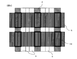
- FIG. 4A is a schematic diagram of a first electrode and a halftone photomask according to an embodiment of the present invention;
- FIG. 4 is a schematic diagram of a bending test according to an embodiment of the invention.
- 1 is a schematic diagram of an organic EL display device according to an embodiment of the present invention;
- FIG. 1 is a schematic diagram of a light-emitting device in an embodiment of the present invention;
- the organic EL display device of the present invention is an organic EL display device having a plurality of display pixels formed in a matrix.
- the emission is roughly classified into top emission and bottom emission depending on the direction in which light is extracted from the organic EL layer, but is not particularly limited.
- the organic EL display device of the present invention is an organic EL display device comprising a substrate having a first electrode, a pixel division layer and spacers on a base material, and further comprising an organic EL layer and a second electrode, wherein the pixel division layer comprises:
- Ramax is the maximum value of the surface roughness (Ra1) and the surface roughness (Ra2) of the spacer
- the organic EL display device has a Ramax of 1.0 nm or more and 50 nm or less.
- FIG. 1 shows a schematic cross-sectional view of an organic EL display device that is an example of the present invention.
- An organic EL display device has a first electrode 2 on a substrate 1 .
- a pixel dividing layer 3 is formed in a region on the substrate 1 where the first electrode 2 does not exist (hereinafter, the region on the substrate 1 where the first electrode 2 does not exist may be referred to as a first electrode gap). and spacers 4 on the pixel dividing layer.
- a unit having a first electrode, a pixel dividing layer and spacers on such a substrate is referred to as a substrate.
- the organic EL display device is obtained.
- the minimum unit of the substrate is a substrate 1, a first electrode 2, a pixel dividing layer 3, and a spacer 4, which will be described later.
- the substrate may have a configuration (for example, the configuration of FIG. 2) that further includes wiring, TFTs 7, pattern antennas, flattening layer 8, and the like.
- the wiring, TFT 7 , sensors, pattern antennas, etc., and the flattening layer 8 which serve as the base of the first electrode 2 , are all treated as a part of the base material 1 .
- FIG. 2 shows a schematic cross-sectional view of a substrate that is an example of the present invention.
- ⁇ Base material> Among the substrate 1 in FIG. 1 and the substrate 1 in FIG. 2, as the base 1a of the substrate below the TFT 7, metal, glass, resin film, etc., which are suitable for supporting the display device and transporting in the post-process are appropriately selected. can do. A resin film is preferable especially when it is necessary to have flexibility.
- soda-lime glass As the glass, soda-lime glass, alkali-free glass, or the like can be used.
- the thickness of the glass should be sufficient to maintain its mechanical strength.
- alkali-free glass is preferable because fewer ions are eluted from the glass, but soda-lime glass with a barrier coating such as SiO 2 can also be used.
- the material for the resin film it is preferable to use a resin material selected from polybenzoxazole resin, polyamideimide resin, polyimide resin, polyamide resin and poly(p-xylylene) resin because of its excellent translucency.
- the substrate may contain one of these resin materials, or may contain a combination of two or more of these resin materials.
- a solution containing a polyamic acid (partially imidized polyamic acid) resin, which is a precursor of the polyimide resin, or a soluble polyimide resin is applied to the support substrate. It can also be formed by firing.
- a gas barrier layer may be appropriately provided as a structure of the base material.
- the base material may be provided with wiring, TFT 7, flattening layer 8, and the like.
- the first electrode 2 in the present invention must be a light transmissive electrode in the case of the bottom emission type, and a light reflective electrode in the case of the top emission type.
- conductive metal oxides such as transparent tin oxide, indium oxide, and indium tin oxide (ITO), metals such as gold, silver, and chromium, and inorganic materials such as copper iodide and copper sulfide.
- Conductive substances, conductive polymers such as polythiophene, polypyrrole and polyaniline can be used, but are not particularly limited.
- the top-emission type it is preferable to use a material that exhibits high visible light reflectance and low electrical resistance at a certain thickness or more.
- Ag or an Ag alloy film containing Ag as a main component is useful because of its high reflectance.
- AgPdCu, AgTiCu, or the like having Ag as the main component can be used for the Ag alloy film, and lamination of these Ag alloy films with an oxide conductive film such as an ITO film or an IZO film provides an organic EL layer and a low contact resistance. can be realized.
- Al or an Al alloy film containing Al as a main component is also suitable as a top emission type first electrode.
- An Al—Ni alloy film containing 0.1 to 2 atomic percent of Ni is preferable because it has a reflectance as high as that of pure Al.
- reflective metal films such as molybdenum (Mo) and tungsten (W) can also be used.
- the resistance of the first electrode is not limited as long as it can supply a sufficient current for light emission of the light emitting element, but from the viewpoint of power consumption of the light emitting element, a low resistance is desirable.
- ITO with a resistance of 300 ⁇ / ⁇ or less functions as an element electrode, but it is now possible to supply ITO with a resistance of about 10 ⁇ / ⁇ , so it is particularly desirable to use a low-resistance product.
- the thickness of the first electrode can be arbitrarily selected according to the characteristics such as transmittance and resistance value, but it can be used usually between 100 and 300 nm.
- a known method can be used to form the first electrode. For example, after forming a film by a vacuum film forming method such as sputtering, patterning can be performed by an etching process using a photoresist.
- the pixel dividing layer 3 is formed in the gap of the first electrode 2 .
- a display pixel can be divided by forming a pixel division layer in the gap of the first electrode. That is, by patterning the pixel separation layer in the gap of the first electrode, the exposed portion of the first electrode is limited, and only the opening of the pixel separation layer functions as a display pixel.
- the pixel dividing layer covers the peripheral edge of the line-type or island-type first electrode, it leads to prevention of short circuits occurring at the edge of the first electrode and disconnection of the second electrode, thereby improving the reliability of the display device. can be improved.
- the pixel division layer is also formed in places other than the gaps of the first electrode, if necessary.
- Ramax is the maximum value of the surface roughness (Ra1) of the pixel division layer and the surface roughness (Ra2) of the spacer
- Ramax is 1.0 nm or more and 50 nm or less.
- the surface roughness (Ra1) of the pixel division layer is Ramax.
- both the surface roughness (Ra1) of the pixel division layer and the surface roughness (Ra2) of the spacer may be Ramax.
- the atomic force microscope (AFM) used for measuring the surface roughness in the present invention generally measures the substrate of the organic EL display device placed on a horizontal surface from vertically above, and Ra1 and Ra2 Figure 3 shows the target range of Therefore, in the present invention, the "surface roughness of the pixel division layer” means the surface of the pixel division layer that is in contact with the organic EL layer and that can be measured by AFM, that is, the surface roughness of the surface that is substantially parallel to the substrate. point to
- the anchor effect can be obtained by setting the surface roughness (Ra1) of the pixel dividing layer to 1.0 nm or more, preferably 5.0 nm or more, and more preferably 20 nm or more. Adhesion to the EL layer can be improved.
- the surface roughness (Ra1) of the pixel division layer if it is 1.0 nm or more, the anchor effect can be obtained, but the purpose is to suppress pinholes in the second electrode and defects in the sealing process described later. Therefore, it is preferable to set the thickness to 50 nm or less. Furthermore, in order to improve adhesion by increasing Ra1, it is effective to secure as large an interface as possible between the pixel division layer and the organic EL layer, and Ra1 is larger than the surface roughness Ra2 of the spacer described later. That is, when Ra1 is Ramax, the area of the interface between the pixel division layer and the organic EL layer is preferably 50% or more of the area of the interface between the substrate and the organic EL layer. This means that the pixel dividing layer is 50% or more of the surface area of the substrate.
- the forward tapered shape means the angle formed by the tangent line at the interface between the first electrode and the pixel division layer and the tangent line at the position of 50% of the maximum thickness of the pixel division layer on the surface of the tapered portion of the pixel division layer (hereinafter , this angle is sometimes referred to as the taper angle of the pixel division layer) is less than 90 degrees.
- the taper angle of the pixel division layer is preferably less than 60 degrees, more preferably less than 50 degrees, in order to obtain a highly reliable display device in which disconnection of the second electrode is suppressed.
- the substrate 1 has the first electrode 2 thereon. It has a pixel division layer 3 in the gap of the first electrode 2 and a spacer 4 on the pixel division layer.
- the pixel division layer is not limited to any known organic material or inorganic material, but the pixel division layer is a cured film of a photosensitive resin composition containing an alkali-soluble resin, since the surface roughness can be easily adjusted. is preferably included.
- the pixel division layer may be a single layer or a multilayer.
- the surface substantially parallel to the substrate whose surface roughness is to be measured is a photosensitive resin containing an alkali-soluble resin. It is preferably a cured film of the composition.
- the photosensitive resin composition preferably contains (A) an alkali-soluble resin, (B) a photosensitive agent and (C) an organic solvent, and may further contain (D) a coloring material and (E) a liquid-repellent material.
- A) an alkali-soluble resin and (B) a photosensitive agent in combination as a photosensitive resin composition pattern processing using photosensitivity becomes possible.
- C) an organic solvent a varnish state can be obtained, and coatability can be improved in some cases.
- the pixel division layer can be blackened by including (D) the coloring material in the photosensitive resin composition.
- (E) the liquid-repellent material liquid-repellency can be imparted to the pixel dividing layer.
- the photosensitive resin composition may further contain other components.
- a known method can be used for forming the pixel division layer.
- the wet coating method is preferable because a thin film can be uniformly formed on a large-sized substrate.
- wet coating methods include spin coating, slit coating, dip coating, spray coating, and printing.
- the thickness of the pixel dividing layer is usually 0.3 ⁇ m to 10 ⁇ m, but is not particularly limited as long as it is sufficient to cover the unevenness of the first electrode. Moreover, the pixel division layer requires patterning processing, and the residue of the removed portion may directly lead to defects such as short circuits and black spots. Furthermore, it is necessary to form a spacer on the pixel division layer in order to support the structure covering the second electrode in a post-process and ensure the strength of the display device.
- Alkali solubility in the present invention means that a solution obtained by dissolving a resin in ⁇ -butyrolactone (GBL) is coated on a silicon wafer and prebaked at 120° C. for 4 minutes to form a prebaked film with a film thickness of 10 ⁇ m ⁇ 0.5 ⁇ m. , The pre-baked film is immersed in a 2.38 wt% tetramethylammonium hydroxide aqueous solution at 23°C ⁇ 1°C for 1 minute and then rinsed with pure water. It means that
- the alkali-soluble resin preferably has an aromatic carboxylic acid structure from the viewpoint of improving heat resistance.
- the aromatic carboxylic acid structure refers to a carboxylic acid structure directly covalently bonded to an aromatic ring.
- the alkali-soluble resin is selected from the group consisting of acrylic resins, phenolic resins, polysiloxane resins, cardo resins, polyimide resins, polyimide precursor resins, polybenzoxazole resins, and polybenzoxazole precursor resins. It is preferable to contain more than seeds.
- the alkali-soluble resin is a polyimide resin, a polyimide precursor resin, a polybenzoxazole resin, and/or a polybenzoxazole precursor resin, since both heat resistance and chemical resistance can be achieved. It is preferable to contain. High chemical resistance is preferable because it reduces film loss when the pixel dividing layer is processed by wet etching. Moreover, the polyimide precursor resin is particularly preferred because of its small amount of outgassing under high temperature conditions. Furthermore, polyimide precursor resins having an amic acid structure are more preferable from the viewpoint of improving alkali solubility.
- the pixel division layer in the organic EL display device of the present invention preferably contains (a) silica particles having a primary particle diameter of 5 to 30 nm (hereinafter sometimes referred to as component (a)). It is more preferable that the pixel dividing layer further contains (D) a coloring material described later in addition to the component (a). In such a case, the (D) coloring material may contain (D1) an organic pigment described later. It is more preferable to contain the (b) component described later as the (D1) organic pigment.
- the component (a) preferably has a primary particle diameter of 5 to 30 nm and an aspect ratio (major axis/minor axis) of 1.0 to 1.5.
- the term "primary particle diameter” as used herein refers to the long diameter of a particle, and silica particles having a primary particle diameter of 5 to 30 nm refer to those having a primary particle diameter within the range of 5 to 30 nm.
- the term "aspect ratio (major axis/minor axis)" as used herein means a value obtained by dividing a value obtained by dividing a major axis by a minor axis in a primary particle diameter of silica particles and rounding off to the second decimal place.
- the silica particles here refer to particles having a SiO2 content of 90% by weight or more in the weight excluding water, particles made of silicon dioxide (anhydrous silicic acid), and silicon dioxide hydrate (hydrous silicic acid). and particles of quartz glass.
- the form of hydrated silicic acid is not particularly limited, and particles made of orthosilicic acid, metasilicic acid and/or metadisilicic acid also correspond to the silica particles referred to here.
- the weight excluding water means the weight of the particles minus the weight of water in the particles.
- a surface treatment agent and a coating applied as a shell to at least part of the surface of particles not containing SiO 2 as the core such as particles made of organic polymers, organic pigments or inorganic pigments Layers are defined as not silica particles by themselves, regardless of the SiO2 content, even if they contain SiO2 .
- core-shell type composite particles containing SiO 2 in the core and having a SiO 2 content of 90% by weight or more in the weight excluding water are defined as silica particles. That is, the component (a) is filled as particles in a dispersed form in the pixel division layer.
- the particle structure of component (a) is not particularly limited, and may have internal voids.
- Silica particles other than the particles made of silicon dioxide, the particles made of silicon dioxide hydrate, and the particles made of quartz glass have, for example, a SiO2 content of 90% by weight or more based on the weight excluding water.
- silica particles made of a composite oxide of silicon and metal examples include zirconium, titanium, and cerium.
- component (c) a mixture of silica particles and hafnium atoms
- the component (a) more preferably contains silica particles having a primary particle diameter of 5 to 20 nm, more preferably silica particles having a primary particle diameter of 5 to 15 nm. preferable.
- the term "primary particle size" as used herein refers to the length of the silica particles. It is more preferable to contain silica particles having an aspect ratio of 1.0 to 1.3, more preferably 1.0 to 1.2. In addition, when the aspect ratio is 1.0, it can be regarded as spherical silica particles.
- Component (a) and silica particles other than component (a) are obtained by thinly cutting the pixel division layer and the spacer layer as an observation sample, preferably by ion milling, more preferably by pretreatment by focused ion beam (FIB) processing.
- FIB focused ion beam
- the part located in the range of 0.2 to 0.8 ⁇ m in the film depth direction from the outermost layer of the pixel dividing layer or spacer layer is subjected to a transmission electron microscope-energy dispersive X-ray
- TEM-EDX Transmission electron microscopy--electron energy loss spectroscopy
- STEM-EDX scanning transmission electron microscopy--energy dispersive X-ray spectroscopy
- TEM-EDX transmission electron microscope-energy dispersive X-ray spectroscopy
- Typical values indicating the characteristics of silica particles corresponding to component (a) include the average primary particle diameter, that is, the average major diameter, rounded to the first decimal place, and the average aspect ratio. A value obtained by calculating the average value of the aspect ratios of individual silica particles corresponding to the component (a) and rounding off to the second decimal place is used.
- SiO 2 having contact with the surface of particles such as particles made of polymers, organic pigments and/or inorganic pigments is excluded from the analysis.
- the long diameter and aspect ratio of silica particles contained in the spacer layer can also be measured in a similar manner.
- the pixel dividing layer included in the organic EL display device of the present invention may further include silica particles that do not correspond to the component (a), i.e., silica particles having a primary particle diameter of less than 5 nm or more than 30 nm, and an aspect ratio (major diameter /minor diameter) of more than 1.5 may be contained.
- silica particles that do not correspond to component (a) include "ADMAFINE” (registered trademark) SO-E2, SO-E4 (both of which are manufactured by Admatec), KE-P10, KE-S10 (both of which are (manufactured by Nippon Shokubai Co., Ltd.).
- the average primary particle size of the silica particles contained in the pixel dividing layer included in the organic EL display device of the present invention is preferably 5 to 30 nm, more preferably 5 to 25 ⁇ m, from the viewpoint of suppressing luminance unevenness.
- the average aspect ratio (major axis/minor axis) is preferably 1.0 to 1.3, more preferably 1.0 to 1.2. That is, even if the pixel division layer provided in the organic EL display device of the present invention contains silica particles that do not correspond to the component (a), the average primary particle diameter of all the silica particles contained is 5 to 30 nm. is preferably Similarly, the average aspect ratio (major axis/minor axis) is preferably 1.0 to 1.3.
- silica particles as used herein includes both component (a) and silica particles not corresponding to component (a).
- the average primary particle diameter here means 0 in the film depth direction from the outermost layer of the pixel division layer under the condition of 50000 times magnification by transmission electron microscope-energy dispersive X-ray spectroscopy (TEM-EDX) as described above.
- TEM-EDX transmission electron microscope-energy dispersive X-ray spectroscopy
- 0.2 to 0.8 ⁇ m of all silica particles obtained randomly using an image analysis type particle size distribution analyzer (Mac-View, manufactured by MOUNTECH). It means the value obtained by rounding off the first decimal place of the average value of the major axis.
- the "average aspect ratio (major axis/minor axis)" as used herein refers to the average value obtained by dividing the major axis by the minor axis of each primary particle of all silica particles obtained at random in the same image. It means the value rounded off to the second decimal place.
- the silica particles having an average primary particle diameter of 5 to 30 nm refer to those having an average primary particle diameter within the range of 5 to 30 nm, and the silica particles having an average aspect ratio of 1.0 to 1.3 mean that the average It means that the aspect ratio is within the range of 1.0 to 1.3.
- the specific surface area of component (a) corresponding to the primary particle size is preferably 50 to 500 m 2 /g, more preferably 200 to 400 m 2 /g.
- the specific surface area referred to here is the specific surface area measured by the BET method using nitrogen as an adsorption gas.
- the surface of component (a) may be porous or non-porous and may have an internal surface area.
- Functional groups that the component (a) has on its surface include, for example, reaction residues of surface modifying groups containing ethylenically unsaturated double bond groups, silanol groups, alkoxysilyl groups, trialkylsilyl groups, and diphenylsilyl groups. mentioned. Above all, it is preferable to have a reactive residue of a surface modification group containing an ethylenically unsaturated double bond group in order to further reduce luminance unevenness.
- the reaction residue of the surface modifying group containing an ethylenically unsaturated double bond group means that the ethylenically unsaturated double bond group of the surface modifying group containing an ethylenically unsaturated double bond group reacts with light and/or Alternatively, it means a group remaining after radical polymerization reaction by heat.
- the component (a) contains silica particles having on the surface of the particles a reaction residue of a surface modifying group containing an ethylenically unsaturated double bond group, and a reaction of the surface modifying group containing the ethylenically unsaturated double bond group. More preferably, the residue has a structure represented by formula (3) and/or a structure represented by formula (4).
- the reaction residue of the surface modifying group containing the ethylenically unsaturated double bond group is a residue generated by a radical polymerization reaction with a compound having two or more radically polymerizable groups in the molecule, which will be described later. .
- R 17 16 represents a hydrogen atom or a methyl group.
- R 18 17 represents a divalent hydrocarbon group having 1 to 7 carbon atoms. j and k are integers and each independently represents 0 or 1; However, if j is 1, then k is 1.
- * 1 represents the bonding site with the carbon atom.
- * 2 represents a bonding site with an oxygen atom bonded to a silicon atom, which the silica particle has on the particle surface.
- R 19 18 represents an alkyl group having 1 to 3 carbon atoms.
- R 20 19 represents a hydrogen atom or a methyl group.
- R 21 20 represents an oxyalkylene group having 1 to 3 carbon atoms.
- r is an integer representing 1 to 4; * 3 represents the bonding site with the carbon atom.
- * 4 represents a bonding site with an oxygen atom bonded to a silicon atom, which the silica particle has on the particle surface.
- Component (a) having a structure represented by formula (3) is obtained by subjecting a surface modifying group derived from an organic alkoxysilane compound having an ethylenically unsaturated double bond group to dehydration condensation with a silanol group on the silica particle surface. It can be obtained by introducing a reaction and subjecting the ethylenically unsaturated double bond group contained in the surface modifying group to a radical polymerization reaction with light and/or heat.
- Organic alkoxysilane compounds having an ethylenically unsaturated double bond group include, for example, vinyltrimethoxysilane, vinyltriethoxysilane, p-styryltrimethoxysilane, p-styryltriethoxysilane, 3-methacryloxypropylmethyldimethoxy Silane, 3-methacryloxypropylmethyldiethoxysilane, 3-methacryloxypropyltrimethoxysilane, 3-methacryloxypropyltriethoxysilane, 3-acryloxypropylmethyldimethoxysilane, 3-acryloxypropylmethyldiethoxysilane, 3 -acryloxypropyltrimethoxysilane, 3-acryloxypropyltriethoxysilane, allyltrimethoxysilane, allyltriethoxysilane.
- Component (a), in which the reaction residue has a structure represented by formula (4), is a surface modifying group derived from an isocyanate compound having an ethylenically unsaturated double bond group, and a silanol group on the silica particle surface. It can be obtained by subjecting an ethylenically unsaturated double bond group contained in a surface modifying group to a radical polymerization reaction with light and/or heat.
- Isocyanate compounds having an ethylenically unsaturated double bond group include, for example, 2-methacryloyloxyethyl isocyanate, 2-acryloyloxyethyl isocyanate, and 2-(2-methacryloyloxyethyloxy)ethyl isocyanate.
- a surface modifying group derived from an organic alkoxysilane compound having an ethylenically unsaturated double bond group and a surface modifying group derived from an isocyanate compound having an ethylenically unsaturated double bond group are added to the surface of the silica particles.
- component (a) in order to improve the dispersion stability of component (a) in a negative photosensitive composition, component (a) preferably has a trialkylsilyl group, more preferably a trimethylsilyl group.
- Trimethylsilyl groups can be introduced into component (a) by converting hydrogen atoms in the surface silanol groups of silica particles into trimethylsilyl groups using a trimethylsilylating agent.
- the trimethylsilylating agent include hexamethyldisilazane and trimethylalkoxysilane, which can be introduced by deammonification reaction and dehydration condensation reaction, respectively.
- the component (a) preferably contains silica particles having sodium atoms.
- Existence forms of sodium atoms include, for example, ions (Na+) and salts with silanol groups (Si—ONa).
- the content of sodium atoms is preferably 100 to 5000 ppm by weight in component (a).
- Silica particles having sodium atoms can be synthesized by reacting sodium silicate, which is strongly alkaline as a silicon source, with a mineral acid, which is a strong acid, under alkaline conditions.
- the sodium atoms contained in the silica particles can be detected at the central portion corresponding to the intersection of the major axis and the minor axis in cross-sectional imaging of the primary particles using the aforementioned TEM-EDX.
- the content of component (a) is preferably 1 to 50% by weight, more preferably 5 to 20% by weight in terms of SiO 2 , in the pixel division layer in order to suppress luminance unevenness. From the same point of view, all silica components in the pixel division layer are preferably 1 to 50% by weight, more preferably 7 to 30% by weight in terms of SiO 2 .
- the content in terms of SiO 2 means the content calculated by excluding the weight of water in the silica particles, which varies depending on the heat history, based on the common technical knowledge of those skilled in the art.
- the pixel division layer in the organic EL display device of the present invention further contains 1 to 50 ppm by weight of (c) hafnium atoms (hereinafter sometimes referred to as the (c) component). preferably. 1 to 30 ppm by weight is more preferred.
- Component (c) is preferably contained in the pixel division layer as inorganic particles containing hafnium atoms.
- Examples of the inorganic particles containing the component (c) include hafnium oxide (HfO 2 ), a composite oxide of a metal other than hafnium and hafnium, a solid solution of an oxide of a metal other than hafnium and hafnium oxide, hafnium oxynitride, A composite oxynitride of a metal other than hafnium and hafnium, and a solid solution of an oxynitride of a metal other than hafnium and hafnium oxynitride can be mentioned.
- hafnium oxide (HfO 2 ) or a composite oxide of a metal other than hafnium and hafnium is preferable in terms of an excellent effect of reducing luminance unevenness, and a composite oxide of zirconium and hafnium (ZrO 2 —HfO 2 ) is more preferred.
- the inorganic particles containing the component (c) commercial products available in powder form can be used. (manufactured by Kojundo Chemical Laboratory Co., Ltd.). Alternatively, in the process of preparing a pigment dispersion containing component (b), which will be described later, fine particles produced by wet-grinding the surface of grinding media containing component (c) with mechanical energy are used as component (b). Component (c) may be included in the finally obtained pixel division layer by co-dispersion.
- the content of component (c) is determined by shaving a portion of the pixel division layer from the outermost layer to a depth of 0.2 to 0.8 ⁇ m and heating the ash in an electric furnace at a temperature of 800° C. or higher. It can be quantified by ICP (inductively coupled plasma) emission spectrometry using the solution obtained by heating and dissolving with dilute nitric acid after thermal decomposition with sulfuric acid, nitric acid and hydrofluoric acid as an analysis sample. can. PS3520VDDII (manufactured by Hitachi High-Tech Science) can be used as an analyzer.
- the photosensitive resin composition used in the present invention preferably contains (D) a coloring material.
- the photosensitive resin composition contains (D) the coloring material
- the pixel dividing layer contains (D) the coloring material, which is preferable because each effect described later can be obtained.
- the coloring material is a compound that absorbs light of a specific wavelength, and particularly refers to a compound that is colored by absorbing light of a visible light wavelength (380 to 780 nm).
- the cured film obtained from the photosensitive resin composition can be colored, and the light transmitted through the cured film of the photosensitive resin composition or the curing of the photosensitive resin composition A coloring property can be imparted to color the light reflected from the film in a desired color.
- the light of the wavelength absorbed by the (D) coloring material is blocked, imparting a light-shielding property. can do.
- the content of the coloring material (D) used in the present invention is preferably 1% by weight or more, more preferably 10% by weight or more, and even more preferably 15% by weight or more in the pixel dividing layer.
- the content ratio is preferably 70% by weight or less, more preferably 65% by weight or less, and even more preferably 60% by weight or less.
- (D) Coloring materials include (D1) organic pigments, (D2) inorganic pigments, and (D3) dyes that absorb light of visible light wavelengths and are colored white, red, orange, yellow, green, blue, or purple. known compounds such as Two or more of these coloring materials may be used in combination, or two or more colors may be used in combination. A combination of two or more types is preferable because the resulting pixel division layer has the effects described later.
- (D) By applying (D1) an organic pigment as a coloring material, the chemical structure change or functional group conversion function, which is a feature of the (D1) organic pigment, allows transmission or blocking of light of a desired specific wavelength, etc. Toning properties can be improved by adjusting the transmission spectrum or absorption spectrum of the cured film of the photosensitive resin composition. The details of such (D1) organic pigment will be described later.
- inorganic pigment By applying an inorganic pigment (D2) as a coloring material, the heat resistance and Weather resistance can be improved.
- inorganic pigments include zirconium nitride, zirconium oxide, titanium oxide, barium carbonate, zinc white, zinc sulfide, lead white, calcium carbonate, barium sulfate, white carbon, alumina white, silicon dioxide, kaolin clay, and talc.
- an inorganic pigment having a large specific gravity such as zirconium nitride in order to make the surface roughness (Ra1) of the pixel dividing layer 1.0 nm or more and 50 nm or less.
- Ra1 surface roughness of the pixel dividing layer 1.0 nm or more and 50 nm or less.
- Inorganic pigments have problems such as pigment aggregation, viscosity increase, and sensitivity decrease over time.
- the alkali solubility of the unexposed area and the halftone exposed area can be preferably adjusted.
- the acid equivalent of component (A) is less than 200 g/mol, for example, when obtaining a cured film of a positive photosensitive resin composition, the alkali solubility of the unexposed area increases, and the dissolution rate difference from the exposed area increases. is too small to form a desired pattern.
- the solubility of the unexposed area can be suppressed, and a pattern can be formed with less residue in the openings due to adherence of substances eluted from the unexposed area.
- the acid equivalent of the component (A) to 500 g/mol or less, it is possible to promote the dispersion stabilization of the zirconium nitride particles and obtain a photosensitive resin composition excellent in storage stability.
- (D3) Dye refers to a compound that colors an object by chemically adsorbing or strongly interacting with the surface structure of the object with a substituent such as an ionic group or a hydroxy group in the dye. It is generally soluble in solvents and the like. In addition, coloring with dyes has high coloring power and high coloring efficiency because each molecule adsorbs to an object. Examples of dyes include direct dyes, reactive dyes, sulfur dyes, vat dyes, sulfur dyes, acid dyes, metallized dyes, metallized acid dyes, basic dyes, mordant dyes, acid mordant dyes, disperse dyes, and cationic dyes. Alternatively, it can be classified as a fluorescent brightening dye.
- (D3-1) in order to make the surface roughness (Ra1) of the pixel division layer 1.0 nm or more and 50 nm or less, (D3-1) a salt-forming compound composed of an acid dye and a basic dye is contained as (D) a coloring material. preferably. (D3-1) By containing a salt-forming compound composed of an acid dye and a basic dye, deposition of the dye during development is expected in the pixel division layer corresponding to the halftone exposure area.
- a salt-forming compound composed of an acid dye and a basic dye is a compound obtained by reacting an acid dye and a basic dye. It is a chemically stable compound obtained by a chemical (salting) reaction between an acid dye whose dye ions are anionic and a basic dye whose dye ions are cationic.
- Acid dyes are compounds that have acidic substituents such as sulfo groups and carboxy groups in the dye molecule, or anionic water-soluble dyes that are salts thereof. Acid dyes include those that have an acidic substituent such as a sulfo group or a carboxy group and are classified as direct dyes. Among them, the acid dye preferably contains a xanthene-based acid dye because it can reduce residue in openings. Xanthene-based acid dyes are more effective than C.I. I. It is more preferable to contain a rhodamine-based acid dye such as Acid Red 50, 52, 289. In addition, rhodamine-based acid dyes are C.I. I. It is more preferable to contain Acid Red 52.
- a basic dye is a compound that has a basic group such as an amino group or an imino group in the molecule, or a salt thereof, and is a dye that becomes cationic in an aqueous solution.
- the basic dye preferably contains a triarylmethane-based basic dye in that it can increase the degree of blackness of the cured film.
- Triarylmethane-based basic dyes are C.I. I. Basic Blue 7 and/or C.I. I. It is more preferable to contain Basic Blue 26.
- a salt-forming compound of an acid dye and a basic dye can be synthesized by a known method. For example, when an aqueous solution of an acid dye and an aqueous solution of a basic dye are separately prepared and mixed slowly while stirring, a salt-forming compound of the acid dye and the basic dye is produced as a precipitate. By collecting this by filtration, the salt-forming compound can be obtained.
- the obtained salt-forming compound is preferably dried at about 60 to 70°C.
- the content of the salt-forming compound in the photosensitive resin composition is 10 parts by weight or more with respect to 100 parts by weight of the alkali-soluble resin (A), thereby achieving blackening and 75 parts by weight or less. By doing so, the residue in the opening can be reduced.
- the salt-forming compound within this range, the alkali solubility of the exposed area, the unexposed area, and the halftone exposed area, which will be described later, can be preferably adjusted.
- Nonionic dyes refer to dyes other than acid dyes and basic dyes that do not have an ionic structure.
- nonionic dyes examples include C.I. I. Disperse Orange 5; C.I. I. disperse thread 58;C. I. Disperse Blue 165; C.I. I. Azo nonionic dyes such as Solvent Red 18; C.I. I. Bat Blue 4; C.I. I. disperse threads 22, 60;C. I. Disperse Violet 26, 28, 31; C.I. I. Disperse Blue 14, 56, 60; C.I. I. Solvent Violet 13, 31, 36; C.I. I. Anthraquinone-based nonionic dyes such as Solvent Blue 35, 36, 45, 63, 78, 87, 97, 104, 122 and the like are included.
- an anthraquinone nonionic dye is preferable in that the blackness of the cured film can be increased.
- (D1) organic pigments used as coloring materials include phthalocyanine-based pigments, anthraquinone-based pigments, quinacridone-based pigments, pyranthrone-based pigments, dioxazine-based pigments, thioindigo-based pigments, diketopyrrolopyrrole-based pigments, and quinophthalone.
- pigments examples include metal complex pigments, lake pigments, toner pigments and fluorescent pigments.
- anthraquinone-based pigments, quinacridone-based pigments, pyranthrone-based pigments, diketopyrrolopyrrole-based pigments, benzofuranone-based pigments, perylene-based pigments, condensed azo-based pigments, and carbon black are preferred.
- the photosensitive resin composition used for forming the pixel division layer preferably contains an organic pigment in order to provide the pixel division layer with a light shielding property.
- the pixel division layer contains the organic pigment, which is preferable because the following effects can be obtained.
- organic black pigments examples include benzodifuranone-based black pigments, perylene-based black pigments, and azomethine-based black pigments.
- benzodifuranone-based black pigments examples include pigments disclosed in International Publication No. 2009/010521. Irgaphor Black (registered trademark) S0100CF and Experimental Black 582 (both manufactured by BASF) can be preferably used as commercially available benzodifuranone-based black pigments composed of the compound represented by formula (5) described later.
- perylene-based black pigments for example, C.I. I. Pigment Black 31, C.I. I. Pigment Black 32, perylenetetracarboxylic acid benzimidazole or derivatives thereof, pigments disclosed in WO 2005/078023 can be mentioned.
- Spectrasense (registered trademark) Black S0084, L0086, K0087, and K0088 can be used as commercially available products.
- azomethine-based black pigments examples include pigments disclosed in US Patent Application Publication No. 2002-121228.
- Chromo Fine Black A1103 manufactured by Dainichiseika Kogyo Co., Ltd.
- Dainichiseika Kogyo Co., Ltd. can be used.
- the mixed color organic black pigment includes (b-1) at least one organic pigment selected from an organic yellow pigment, an organic red pigment and an organic orange pigment (hereinafter sometimes referred to as the (b-1) component); b-2) containing at least one organic pigment selected from organic blue pigments and organic purple pigments (hereinafter sometimes referred to as component (b-2)), and containing components (b-1) and (b-2); ) means a pigment mixture in which the content of component (b-2) is 20% by weight or more relative to the total amount of components ).
- organic yellow pigments include C.I. I. Pigment Yellow 24, 120, 138, 139, 151, 175, 180, 185, 181, 192, 193, 194.
- organic orange pigments include C.I. I. Pigment Orange 13, 36, 43, 60, 61, 62, 64, 71, 72.
- organic red pigments include C.I. I. Pigment Red 122, 123, 149, 178, 177, 179, 180, 189, 190, 202, 209, 254, 255, 264.
- organic blue pigments include C.I. I. Pigment Blue 15, 15:1, 15:2, 15:3, 15:6, 16, 25, 56, 57, 60, 61, 64, 65, 66, 75, 79, 80.
- organic purple pigments include C.I. I. Pigment Violet 19, 23, 29, 32, 37.
- the component (b) contained in the pixel division layer in the organic EL display device of the present invention contains an organic black pigment for reducing luminance unevenness.
- the organic black pigment preferably contains a compound represented by Formula (5) or Formula (6) and/or isomers thereof.
- Component (b) contained in the pixel division layer more preferably contains a compound represented by formula (7) or an isomer thereof.
- the compounds represented by formulas (5) to (7) are synthesized by reacting 2,5-dihydroxy-1,4-benzenediacetic acid with isatin or a derivative thereof in the presence of an acidic catalyst, and converted into a pigment. can be obtained with
- R 22 1 to R 31 10 each independently represent a hydrogen atom or an alkyl group having 1 to 12 carbon atoms.
- the component corresponding to the component (b) may be finely processed by a known method such as a solvent salt milling method or an acid paste method in order to further suppress luminance unevenness.
- a solvent salt milling method or an acid paste method in order to further suppress luminance unevenness.
- the compound represented by Formula (8) or a salt thereof is allowed to coexist and adsorb to the surface of the pigment, thereby making it easier to suppress luminance unevenness in some cases.
- n and m each independently represents an integer from 0 to 2. However, n+m ⁇ 1 is satisfied.
- the component (b) contains a benzodifuranone-based black pigment
- the silica contained in the coating layer here is not part of the component (a) described above, but part of the component (b).
- the content of component (b) is preferably 1% by weight or more, more preferably 10% by weight or more, in the pixel dividing layer in order to develop high light shielding properties. It is preferably 50% by weight or less, more preferably 30% by weight or less, in order to reduce luminance unevenness.
- the content of the component (a) with respect to 100 parts by weight of the component (b) is 20% in terms of SiO 2 in order to reduce uneven brightness. ⁇ 70 parts by weight is preferred, and 30 to 50 parts by weight is more preferred. That is, in the organic EL display device of the present invention, the content of the component (a) to the component (b) in the pixel division layer is preferably 20 to 70 parts by weight in terms of SiO 2 .
- the photosensitive resin composition used in the present invention preferably contains a liquid-repellent material.
- a liquid-repellent material such as a fluorine-based polymer or a fluorine-containing compound having a silane compound can be used, but a liquid-repellent material having at least an amide group or a urethane group is preferable.
- compatibility with the alkali-soluble resin (A) described above is improved, defects such as repelling are reduced, and there is an effect of improving the thickness uniformity of the cured film. As a result, display defects of the display device are reduced.
- liquid-repellent materials examples include 2-(perfluorobutyl)ethyl (meth)acrylate and 2-(perfluorohexyl)ethyl (meth)acrylate, which are (meth)acrylate monomers having a perfluoroalkyl group.
- "Megafac (registered trademark)" RS-72-K, RS-72-A, RS-75, RS-76-E, RS-76-NS, RS-78, RS-90 manufactured by DIC Corporation ) and the like.
- epoxy group-containing (meth)acrylate monomers include glycidyl acrylate, glycidyl methacrylate, 4-hydroxybutyl acrylate glycidyl ether (4-HBAGE), 4-hydroxybutyl methallate glycidyl ether, and alicyclic epoxy groups. and methacrylates having an alicyclic epoxy group.
- the liquid-repellent material (E) having an amide group or a urethane group may be a copolymer obtained by further copolymerizing different functional group-substituted (meth)acrylic monomers.
- By copolymerizing different functional group-substituted (meth)acrylic monomers it is possible to easily balance liquid repellency and solubility.
- hydroxyl group-containing (meth)acrylates, hydroxyl group-containing (meth)acrylamides, alkoxy group-containing (meth)acrylates, blocked isocyanate group-containing (meth)acrylates, phenoxy group-containing (meth)acrylates, alkyl (meth) Examples include acrylates and vinyl group-containing compounds.
- hydroxyl group-containing (meth)acrylates examples include 2-hydroxyethyl (meth)acrylate and the like.
- hydroxyl group-containing (meth)acrylamides include N-hydroxymethylacrylamide.
- (Meth)acrylates having an alkoxy group include, for example, 3-methacryloxypropylmethyldimethoxysilane.
- Block isocyanate group-containing (meth)acrylates include, for example, 2-(0-[1′-methylpropylideneamino]carboxyamino)ethyl methacrylate (Karens MOI-BM: manufactured by Showa Denko KK; registered trademark), and the like. is mentioned.
- Phenoxy group-containing (meth)acrylates include, for example, 2-phenoxybenzyl acrylate, 3-phenoxybenzyl acrylate and the like.
- Alkyl (meth)acrylates are unsubstituted or substituted with at least one of an amino group, a monoalkylamino group, a dialkylamino group, a hydrocarbon aromatic ring, and a heterocyclic ring, or an acid anhydride is cleaved and added to a hydroxy group.
- Vinyl group-containing compounds include, for example, n-butyl vinyl ether.
- the compound contained in the liquid-repellent material (E) having an amide group or urethane group is usually a (co)polymer.
- a (co)polymer as a compound contained in the liquid-repellent material (E) can be obtained by a known polymerization method.
- the (co)polymer may be obtained, for example, by ionic polymerization such as radical polymerization or anionic polymerization. Also, it may be a random copolymer, a block copolymer, a graft (co)polymer, or an alternating copolymer.
- the radical (co)polymerization method is taken as an example.
- a predetermined amount of dimethyl (meth)acrylamide, a predetermined amount of fluorine-containing (meth)acrylate monomer, and, if necessary, a predetermined amount of epoxy group-containing (meth)acrylates, hydroxyl group-containing (meth)acrylates, hydroxyl group-containing (Meth)acrylamides, alkoxy group-containing (meth)acrylates, blocked isocyanate group-containing (meth)acrylates, phenoxy group-containing (meth)acrylates, alkyl (meth)acrylates, and vinyl group-containing compounds are added to an appropriate solvent.
- the liquid-repellent material (E) can be obtained by random copolymerization with a radical polymerization initiator inside.
- a chain transfer agent may be added during random copolymerization.
- a radical polymerization initiator for example, tert-butylperoxy-2-ethylhexanoate can be used.
- a chain transfer agent for example, dodecyl mercaptan can be used.
- solvent inert solvents, such as cyclohexanone, can be used, for example.
- the weight-average molecular weight of the liquid-repellent material (E) having an amide group or urethane group is preferably in the range of 1,500 to 50,000. By setting the molecular weight within this range, it can be more easily dissolved in the solvent used in the photosensitive resin composition. Further, by setting the molecular weight within this range, the antifoaming property of the photosensitive resin composition solution is enhanced, which is preferable.
- the liquid-repellent material (E) having an amide group or a urethane group is 0.1 to 100 parts by weight of the alkali-soluble resin (A), from the viewpoint that the obtained cured film easily exhibits sufficient liquid repellency. It is preferably at least 0.3 parts by weight, more preferably at least 0.3 parts by weight. In addition, from the viewpoint of making it difficult to cause liquid repellency in pixels and easily obtaining high durability, the amount is preferably 10 parts by weight or less, and more preferably 5 parts by weight or less.
- the spacer 4 is provided on the pixel division layer.
- the first purpose is to reduce the contact area between the substrate and the vapor deposition mask when forming the organic EL layer by providing the spacer, thereby suppressing the generation of particles during the process. As a result, it is possible to suppress the yield reduction of the panel and the deterioration of the light emitting element.
- the spacers must be patterned, and residues from the removed portions may directly lead to defects such as short circuits and black spots. Furthermore, since the shape of the edge of the spacer may cause disconnection of the second electrode, workability such as a gentle forward tapered shape is required.
- any material having the required mechanical and electrical properties can be used as the spacer without particular limitation. It is preferably a cured film of a material.
- the spacer without particular limitation. It is preferably a cured film of a material.
- Ramax is 1.0 nm or more and 50 nm or less, where Ramax is the maximum value of the surface roughness (Ra2) of the spacer. Furthermore, it is more preferable that the surface roughness (Ra2) of the spacer is Ramax. Moreover, both the surface roughness (Ra1) of the pixel division layer and the surface roughness (Ra2) of the spacer may be Ramax. Note that the surface roughness of the spacer can also be measured with an atomic force microscope (AFM) in the same manner as the pixel division layer.
- AFM atomic force microscope
- the anchor effect can be obtained by setting the surface roughness (Ra2) of the spacer to 1.0 nm or more, preferably 5.0 nm or more, more preferably 20 nm or more, so that the organic EL layer It is possible to improve the adhesion with.
- the surface roughness (Ra2) of the spacer if it is 1.0 nm or more, the anchor effect can be obtained.
- the spacers are 50% or more of the surface area of the substrate.
- Ra1 and Ra2 are as large as 1.0 nm or more, in addition to such an effect of improving adhesion, it is possible to suppress the external light reflection of the display device by increasing the diffusely reflected light of the substrate.
- two types of reflected light, regular reflected light and diffuse reflected light are generated on the substrate surface, and the total amount of reflected light is the amount of reflected light. Perceived as glare or reflection is greatly influenced by specularly reflected light. In other words, in order to maintain the display quality of the display device, it is effective to increase the diffusely reflected light of the substrate and reduce the specularly reflected light.
- the amount of diffusely reflected light on the surface of the substrate increases, and as a result, the display of the display device increases. This helps ensure quality.
- the forward tapered shape refers to a state in which the angle formed by the tangent line at the interface between the pixel dividing layer and the spacer and the tangent line at the position of 50% of the maximum thickness of the spacer on the surface of the tapered portion of the spacer is less than 90 degrees. .
- the thickness of the spacer is usually 0.3 ⁇ m to 10 ⁇ m, but is not particularly limited as long as it is sufficient to support the structure covering the contact with the vapor deposition mask and the second electrode.
- the structure of the organic EL layer 5 is not particularly limited.
- a tandem type in which a plurality of the above structures are laminated via a charge generation layer may be used.
- the charge-generating layer is also generally called an electron-withdrawing layer, connection layer, intermediate layer, intermediate electrode, intermediate conductive layer, or intermediate insulating layer, and known material configurations can be used.
- the tandem type is preferable because it can be expected to improve the emission luminance and the emission life.
- tandem type examples include (4) hole transport layer/light emitting layer/electron transport layer/charge generation layer/hole transport layer/light emitting layer/electron transport layer, and (5) hole injection layer/hole transport.
- a laminate structure including a charge generation layer between an anode and a cathode, such as transport layer/charge generation layer/hole transport layer/emissive layer/electron transport layer/charge generation layer/hole transport layer/emissive layer/electron transport layer. is mentioned.
- each of the above layers may be either a single layer or multiple layers, and may be doped.
- the electron-transporting layer and the charge-generating layer are preferably metal-doped layers, so that the electron-transporting ability and the electron-injecting ability to other adjacent layers can be improved.
- a protective layer may be further provided, and the light emission efficiency can be further improved by the optical interference effect.
- the thickness of each layer is generally selected from a range of 1 to 200 nm in consideration of the resistance value of each layer material and the effect on the efficiency of extracting EL emission.
- the hole transport layer is formed, for example, by laminating or mixing one or more hole transport materials, or by using a mixture of a hole transport material and a polymer binder. Alternatively, an inorganic salt such as iron (III) chloride may be added to the hole transport material to form the hole transport layer.
- the hole-transporting material is not particularly limited as long as it is a compound capable of forming a thin film necessary for manufacturing a light-emitting device, injecting holes from an electrode serving as an anode, and transporting holes.
- the hole-transporting layer may be a single layer or may be formed by laminating a plurality of layers.
- hole-transporting materials include 4,4′-bis(N-(3-methylphenyl)-N-phenylamino)biphenyl, 4,4′-bis(N-(1-naphthyl)-N -phenylamino)biphenyl, triphenylamine derivatives such as 4,4′,4′′-tris(3-methylphenyl(phenyl)amino)triphenylamine, bis(N-allylcarbazole), bis(N-alkylcarbazole) Heterocyclic compounds such as biscarbazole derivatives such as biscarbazole derivatives, pyrazoline derivatives, stilbene compounds, hydrazone compounds, benzofuran derivatives, thiophene derivatives, oxadiazole derivatives, phthalocyanine derivatives, and porphyrin derivatives. Polycarbonates, styrene derivatives, polythiophenes, polyanilines, polyfluorenes, polyvinyrenes
- ⁇ Light emitting layer> In the light-emitting layer, the injected electrons and holes recombine to emit light.
- a major feature of the organic EL display device is that it is possible to emit light in various colors by selecting the material that constitutes the light-emitting layer.
- the light-emitting layer is a layer that emits light when the light-emitting material is excited by the recombination energy from the collision of holes and electrons.
- the light-emitting layer may be a single layer or may be composed of a plurality of laminated layers, each of which is formed of a light-emitting material (host material and/or dopant material).
- Each light-emitting layer may be composed of either a host material or a dopant material alone, or may be composed of a combination of one or more host materials and one or more dopant materials. That is, in each light-emitting layer, only the host material or the dopant material may emit light, or both the host material and the dopant material may emit light.
- the light emitting layer is preferably composed of a combination of a host material and a dopant material.
- the dopant material may be included entirely or partially in the host material.
- the content of the dopant material in the light-emitting layer is preferably 30 parts by weight or less, more preferably 20 parts by weight or less, relative to 100 parts by weight of the host material.
- the light-emitting layer can be formed by a method of co-evaporating a host material and a dopant material, or a method of pre-mixing a host material and a dopant material and then vapor-depositing them.
- Examples of the host material constituting the light-emitting material include compounds having condensed aryl rings such as naphthalene, anthracene, phenanthrene, pyrene, chrysene, naphthacene, triphenylene, perylene, fluoranthene, fluorene, and indene. You may use 2 or more types of these.
- the host used when the emitting layer performs triplet emission (phosphorescence emission) metal chelated oxinoid compounds, dibenzofuran derivatives, dibenzothiophene derivatives, carbazole derivatives, indolocarbazole derivatives, triazine derivatives, triphenylene derivatives, etc. are suitable.
- a compound having an anthracene skeleton or a pyrene skeleton is more preferable because highly efficient light emission can be easily obtained.
- dopant materials constituting the light-emitting material include condensed ring derivatives such as anthracene and pyrene, metal complex compounds such as tris(8-quinolinolato)aluminum, bisstyryl derivatives such as bisstyryl anthracene derivatives and distyrylbenzene derivatives, tetraphenyl butadiene derivatives, dibenzofuran derivatives, carbazole derivatives, indolocarbazole derivatives, polyphenylenevinylene derivatives and the like.
- condensed ring derivatives such as anthracene and pyrene
- metal complex compounds such as tris(8-quinolinolato)aluminum
- bisstyryl derivatives such as bisstyryl anthracene derivatives and distyrylbenzene derivatives
- tetraphenyl butadiene derivatives dibenzofuran derivatives
- carbazole derivatives indolocarbazole derivatives
- a metal complex compound containing at least one metal selected from the group consisting of ) is preferred.
- the ligand that constitutes the metal complex compound can be appropriately selected from the required emission color, organic EL display device performance, and relationship with the host compound. It preferably has an aromatic heterocycle. Specific examples include tris(2-phenylpyridyl)iridium complexes, bis(2-phenylpyridyl)(acetylacetonate)iridium complexes, tetraethylporphyrin platinum complexes, and the like. You may use 2 or more types of these.
- the electron transport layer is a layer that transports electrons injected from the cathode to the light emitting layer.
- the organic EL layer of the invention preferably contains an electron transport layer.
- the electron transport layer is desired to have high electron injection efficiency and efficiently transport the injected electrons. Therefore, it is preferable that the electron-transporting layer is made of a material that has high electron affinity and electron mobility, is excellent in stability, and does not easily generate trapping impurities during manufacturing and use.
- a compound with a molecular weight of 400 or more is preferable because the film quality tends to deteriorate due to crystallization of a compound with a low molecular weight.
- the electron transport layer has a role of efficiently preventing the holes that have not recombinated from flowing from the anode to the cathode side.
- a transport layer is synonymous with a hole-blocking layer that can effectively block the movement of holes.
- the electron transport layer may be composed of a single layer or a laminate of a plurality of layers.
- Examples of electron-transporting materials that constitute the electron-transporting layer include condensed polycyclic aromatic derivatives such as naphthalene and anthracene. You may use 2 or more types of these. Among these, a compound having a heteroaryl ring structure containing electron-accepting nitrogen is preferable because the driving voltage can be further reduced and highly efficient light emission can be obtained.
- the electron-accepting nitrogen here means a nitrogen atom that forms a multiple bond with an adjacent atom. Due to the high electronegativity of nitrogen atoms, such multiple bonds have electron-accepting properties. Therefore, an aromatic heterocycle containing an electron-accepting nitrogen has a high electron affinity. An electron-transporting material containing electron-accepting nitrogen easily accepts electrons from a cathode having a high electron affinity, so that the driving voltage can be further reduced. In addition, more electrons are supplied to the light-emitting layer and the probability of recombination is increased, so that the light emission efficiency is improved.
- Heteroaryl rings containing electron-accepting nitrogen include, for example, triazine rings and pyridine rings.
- Compounds having these heteroaryl ring structures include triazole derivatives such as N-naphthyl-2,5-diphenyl-1,3,4-triazole, 2,5-bis(6′-(2′,2′′- Bipyridyl))-1,1-dimethyl-3,4-diphenylsilole and other bipyridine derivatives, 1,3-bis(4′-(2,2′:6′2′′-terpyridinyl))benzene and other terpyridine derivatives , is preferably used from the viewpoint of electron transport ability. You may use 2 or more types of these.
- a compound having a phenanthroline skeleton can also be mentioned as a substance that satisfies the conditions required for the electron transport layer.
- materials with excellent thermal stability and thin-film-forming properties are desired.
- Those having a three-dimensional structure due to steric repulsion with or adjacent substituents, or those having a plurality of linked phenanthroline skeletons are preferred.
- a compound containing a conjugated bond, a substituted or unsubstituted aromatic hydrocarbon, or a substituted or unsubstituted aromatic heterocycle in the connecting unit is more preferable.
- the electron-transporting material is not necessarily limited to one type of compound having a phenanthroline skeleton, and a plurality of the above-mentioned compounds may be mixed and used, or one or more known electron-transporting materials may be mixed with the above-mentioned compound and used.
- known electron-transporting materials include, but are not limited to, quinolinol derivative metal complexes typified by 8-hydroxyquinoline aluminum, benzoquinoline metal complexes, tropolone metal complexes, flavonol metal complexes, perylene derivatives, perinone derivatives, and naphthalene.
- coumarin derivatives, oxadiazole derivatives, aldazine derivatives, bisstyryl derivatives, pyrazine derivatives, phenanthroline derivatives, quinoline derivatives, benzimidazole derivatives, triazole derivatives, quinoxaline derivatives, benzoquinoline derivatives, etc. but are not particularly limited.
- These electron-transporting materials may be used alone, but may be used in combination with different electron-transporting materials in layers or mixed.
- Compounds having nitrogen-containing aromatic heterocycles such as phenanthroline derivatives and oligopyridine derivatives can also be used.
- a compound having a phenanthroline skeleton, which will be described later, is preferable because it exhibits excellent electron-transporting ability.
- the electron-transporting material may be used alone, but two or more of the electron-transporting materials may be mixed and used, or one or more of the other electron-transporting materials may be mixed with the electron-transporting material. I do not care.
- the electron transport layer in the present invention preferably contains a donor dopant material.
- the donor dopant material is a compound that facilitates injection of electrons from the cathode or the electron injection layer into the electron transport layer by improving the electron injection barrier and further improves the electrical conductivity of the electron transport layer.
- the donor dopant material is one or more selected from the group consisting of alkali metals, alkaline earth metals, rare earth metals, inorganic salts of these metals, and complexes of these metals and organic substances. It is preferable to contain.
- the donor dopant material is preferably a complex with an inorganic salt or an organic substance rather than a single metal, because it is easy to vapor-deposit in a vacuum and is easy to handle. A complex with an organic substance is more preferred.
- the charge generation layer generally consists of a double layer. Specifically, a pn junction type charge generation layer consisting of an n-type charge generation layer and a p-type charge generation layer can be used.
- the pn junction charge generation layer generates charges or separates the charges into holes and electrons by applying a voltage in the organic EL layer, and converts these holes and electrons into holes and electrons. It is injected into the light-emitting layer via the transport layer. Specifically, it functions as an intermediate charge generation layer for a plurality of light emitting layers included in the organic EL layer.
- the n-type charge-generating layer supplies electrons to the light-emitting layer on the anode side, and the p-type charge-generating layer supplies holes to the light-emitting layer on the cathode side. Therefore, the luminance and luminous efficiency of the organic EL layer including a plurality of luminescent layers can be further improved, the driving voltage can be lowered, and the luminous life of the organic EL layer can be further improved. For this reason, the organic EL layer in the present invention preferably contains a charge generation layer.
- the charge generation layer preferably contains a donor dopant material, and the donor dopant material includes alkali metals, alkaline earth metals, rare earth metals, inorganic salts of these metals, and It preferably contains one or more selected from the group consisting of complexes of metals and organic substances.
- the n-type charge generation layer is preferably composed of an n-type dopant material and a host material, and known materials can be used for these.
- a compound having a phenanthroline skeleton and a compound having a nitrogen-containing aromatic heterocycle such as an oligopyridine derivative can be used as the host material.
- a compound having a phenanthroline skeleton, which will be described later, is preferable because it exhibits excellent properties as a host material for the n-type charge generation layer, and these compounds may be used in combination.
- the p-type charge generation layer is preferably composed of a p-type dopant material and a host material, and known materials can be used for these materials.
- p-type dopant materials include tetrafluor-7,7,8,8-tetracyanoquinodimethane (F4-TCNQ), tetracyanoquinodimethane derivatives, radialene derivatives, iodine, FeCl 3 , FeF 3 , SbCl 5 and the like can be used.
- a preferred p-type dopant material is a radialene derivative.
- An arylamine derivative is preferred as the host material.
- the electron-transporting layer and/or the charge-generating layer preferably contain a compound having a phenanthroline skeleton represented by the following general formula (1).
- R 1 to R 8 may be the same or different and are selected from a hydrogen atom, an alkyl group, a cycloalkyl group, an alkenyl group, a cycloalkenyl group, an aryl group, a heteroaryl group and a heterocyclic group. At least one of R 1 , R 3 , R 6 and R 8 is selected from adamantyl group, norbornyl group, phenylvinyl group, ⁇ -naphthyl group, phenanthrene group and pyrenyl group.
- the electron-transporting layer and/or the charge-generating layer more preferably contain a compound having a phenanthroline skeleton represented by the following general formula (2).
- R 9 to R 16 may be the same or different, and are selected from a hydrogen atom, an alkyl group, a cycloalkyl group, an alkenyl group, a cycloalkenyl group, an aryl group, a heteroaryl group, a heterocyclic group, and X 1 . To be elected. However, at least one of R 9 to R 16 is X 1 .
- n represents a natural number from 2 to 6;
- X 1 is a single bond, or an n-valent n-valent structure derived from any of benzene, anthracene, pyridine, ethylene, thiophene, furan, methylene, carbazole, cyclohexane, spirobifluorene, triphenylamine, triptycene, and combinations thereof.
- X 1 is a single bond, or an n-valent n-valent structure derived from any of benzene, anthracene, pyridine, ethylene, thiophene, furan, methylene, carbazole, cyclohexane, spirobifluorene, triphenylamine, triptycene, and combinations thereof.
- the alkyl group includes saturated aliphatic hydrocarbon groups such as methyl group, ethyl group, n-propyl group, isopropyl group, n-butyl group, sec-butyl group and tert-butyl group. , which may or may not have substituents. Additional substituents when substituted are not particularly limited, and examples thereof include alkyl groups, halogens, aryl groups, heteroaryl groups, and the like, and this point is common to the description below. Although the number of carbon atoms in the alkyl group is not particularly limited, it is preferably in the range of 1 to 20, more preferably 1 to 8 in terms of availability and cost.
- the cycloalkyl group is, for example, a saturated alicyclic hydrocarbon group such as a cyclopropyl group, a cyclohexyl group, a norbornyl group, and an adamantyl group, which may or may not have a substituent.
- the number of carbon atoms in the alkyl group portion is not particularly limited, it is preferably in the range of 3 or more and 20 or less.
- the aralkyl group indicates an aromatic hydrocarbon group via an aliphatic hydrocarbon such as a benzyl group and a phenylethyl group, and both the aliphatic hydrocarbon and the aromatic hydrocarbon may be unsubstituted or substituted. I do not care.
- the alkenyl group means an unsaturated aliphatic hydrocarbon group containing a double bond such as a vinyl group, an allyl group, a butadienyl group, and the like, which may be unsubstituted or substituted.
- the cycloalkenyl group means an unsaturated alicyclic hydrocarbon group containing a double bond such as a cyclopentenyl group, a cyclopentadienyl group, a cyclohexene group, etc., which may be unsubstituted or substituted. .
- the alkynyl group means an unsaturated aliphatic hydrocarbon group containing a triple bond such as an acetylenyl group, which may be unsubstituted or substituted.
- the alkoxy group indicates an aliphatic hydrocarbon group via an ether bond such as a methoxy group, and the aliphatic hydrocarbon group may be unsubstituted or substituted.
- An alkylthio group is an alkoxy group in which the oxygen atom of the ether bond is substituted with a sulfur atom.
- the aryl ether group indicates an aromatic hydrocarbon group via an ether bond such as a phenoxy group, and the aromatic hydrocarbon group may be unsubstituted or substituted.
- An arylthioether group is an arylether group in which the oxygen atom of the ether bond is substituted with a sulfur atom.
- An aryl group is, for example, an aromatic hydrocarbon group such as a phenyl group, a naphthyl group, a biphenyl group, a phenanthryl group, a terphenyl group and a pyrenyl group, which may be unsubstituted or substituted.
- the heterocyclic group is, for example, a pyran ring, a piperidine ring, an aliphatic ring having a non-carbon atom in the ring such as a cyclic amide, which may or may not have a substituent. good.
- Halogen means fluorine, chlorine, bromine and iodine.
- Haloalkane, haloalkene, and haloalkyne are those in which part or all of the above-mentioned alkyl group, alkenyl group, and alkynyl group, such as a trifluoromethyl group, is substituted with the above-mentioned halogen, and the remaining portion may be unsubstituted. It does not matter if they are replaced.
- Aldehyde groups, carbonyl groups, ester groups, carbamoyl groups, and amino groups include those substituted with aliphatic hydrocarbons, alicyclic hydrocarbons, aromatic hydrocarbons, heterocyclic rings, and the like. Cyclic hydrocarbons, aromatic hydrocarbons, and heterocycles may be unsubstituted or substituted.
- a silyl group indicates a silicon compound group such as a trimethylsilyl group, which may be unsubstituted or substituted.
- a siloxanyl group indicates a silicon compound group via an ether bond such as a trimethylsiloxanyl group, which may be unsubstituted or substituted.
- a ring structure may be formed between adjacent substituents. The ring structure formed may be unsubstituted or substituted.
- the substituent itself has a three-dimensional structure, or steric repulsion with the phenanthroline skeleton or adjacent substituents brings about a three-dimensional structure. It becomes difficult to occur, and a good amorphous thin film state can be maintained.
- a substituent itself having a three-dimensional structure indicates a bulky three-dimensional structure that is not a two-dimensional planar structure, such as a t-butyl group, adamantyl group, norbornyl group, and is substituted even if unsubstituted. I don't mind.
- Substituents that produce a three-dimensional structure due to steric repulsion with the phenanthroline skeleton or adjacent substituents are ⁇ -naphthyl groups, phenanthrene groups, mesityl groups, etc., even if the substituents themselves have planar structures,
- the steric repulsion between a substituent and the phenanthroline skeleton, or between the substituent and an adjacent substituent indicates that the plane of the substituent lies in a plane different from that of the phenanthroline skeleton.
- the compound containing the phenanthroline skeleton has a higher molecular weight and a higher glass transition temperature, which also makes it difficult for crystallization to occur, making it possible to maintain a good amorphous thin film state.
- the host material for the electron-transporting layer and/or charge-generating layer is not necessarily limited to one type of compound having a phenanthroline skeleton. It may be used by mixing with a compound having a skeleton.
- known host materials include, but are not limited to, condensed ring derivatives such as previously known anthracene, phenanthrene, pyrene, perylene and chrysene, and quinolinol derivatives such as tris(8-quinolinolato)aluminum.
- Metal complexes benzoxazole derivatives, stilbene derivatives, benzthiazole derivatives, thiadiazole derivatives, thiophene derivatives, tetraphenylbutadiene derivatives, cyclopentadiene derivatives, oxadiazole derivatives, bisstyryl derivatives such as bisstyrylanthracene derivatives and distyrylbenzene derivatives, quinolinol derivatives metal complexes with different ligands, oxadiazole derivative metal complexes, benzazole derivative metal complexes, coumarin derivatives, pyrrolopyridine derivatives, perinone derivatives, thiadiazolopyridine derivatives. Phenylene derivatives, polythiophene derivatives, and the like can be used.
- a compound having a phenanthroline skeleton may be used as a dopant material, but is preferably used as a host material because it has excellent electron transport ability.
- the second electrode 6 needs to be a light-reflective electrode in the case of the bottom emission type, and a light-transmitting electrode in the case of the top emission type.
- a material that exhibits high visible light reflectance and low electrical resistance at a certain film thickness or more is preferable, and Ag or an Ag alloy film mainly containing Ag is useful because of its high reflectance.
- a MgAg alloy containing Ag as a main component, or the like can be used for the Ag alloy film.
- Al or an Al alloy film containing Al as a main component is also suitable as a second electrode for bottom emission.
- An AlCr alloy film containing Cr and an AlNi alloy film containing Ni are preferable because they have high reflectance comparable to that of pure Al and can achieve low electric resistance.
- conductive metal oxides such as transparent tin oxide, indium oxide, and indium tin oxide (ITO) can be used.
- ITO indium tin oxide
- the resistance of the second electrode is not limited as long as it can supply a sufficient current for light emission of the light emitting element, but from the viewpoint of the power consumption of the light emitting element, it is desirable that the resistance is low.
- the thickness of the electrode can be arbitrarily selected according to characteristics such as transmittance and resistance value. can.
- wirings and drive circuits such as the TFTs 7 may be provided as elements included in the substrate 1 .
- the patterned island-type first electrode 2 is often connected to the TFT 7 formed in advance as part of the substrate 1 .
- TFTs Semiconductor layers of TFTs include a-Si (amorphous silicon), p-Si (polycrystalline silicon), microcrystalline silicon, oxides represented by In--Ga--Zn--O, and p--Si and oxides.
- LTPO Low Temperature Polycrystalline Oxide
- a-Si TFTs have low mobility, which is an index of ease of movement of electrons, they require a relatively short manufacturing process and can be manufactured on large substrates, so they can be used in a wide range of small to large displays.
- p-Si TFTs have high mobility and can form driver circuits and the like on the substrate.
- the manufacturing process is longer than that of a-Si, and it is difficult to manufacture a large substrate. Therefore, it is preferably used mainly for small and medium-sized displays.
- p-Si in a p-Si TFT can generally be formed by irradiating a-Si with a laser beam as a start film to instantly melt and crystallize it.
- there is a doping step of implanting phosphorus or boron into Si which is not used in the manufacturing process of the a-Si TFT, and the threshold value of the TFT characteristics may be controlled by doping impurities into the Si film.
- TFTs can be roughly classified into bottom-gate and top-gate types from the structural aspect. It is preferable that the a-Si TFT be of the bottom gate type, and the p-Si TFT be of the top gate type.
- a drain-side electrode and a source-side electrode are connected to a semiconductor layer, and a gate electrode is provided above the semiconductor layer.
- a TFT is formed on a substrate by repeating elemental processes of thin film formation, patterning, etching, and cleaning several times. A known method can be used for forming the TFT.
- a gate electrode is arranged in the lowest layer, a semiconductor layer/insulating film is formed in an upper layer, and a source electrode and a drain electrode are formed in an upper layer.
- a straight line connecting the gate electrode, the source electrode, and the drain electrode forms an inverted triangle, which is also called an “inverted staggered structure”.
- planarization layer 8 it is preferable to use the planarization layer 8 when wiring and TFTs 7 are provided inside the substrate 1 as shown in FIG.
- the unevenness of the wiring and the TFT 7 can be covered and planarized.
- the first electrode 2 is provided on the flattening layer 8, it is preferable to connect the first electrode 2 and the wiring or the TFT 7 via a contact hole formed in the flattening layer 8.
- FIG. The flattening layer 8 is not limited to either a known organic material or an inorganic material, but preferably includes a cured film of a photosensitive resin composition from the standpoint of workability.
- the planarizing layer 8 can be applied by a wet coating method such as a spin coating method, a slit coating method, a dip coating method, a spray coating method, or a printing method, which can uniformly form a thin film on a large substrate.
- a wet coating method such as a spin coating method, a slit coating method, a dip coating method, a spray coating method, or a printing method, which can uniformly form a thin film on a large substrate.
- the photosensitive resin composition preferably contains (A) an alkali-soluble resin, (B) a photosensitive agent and (C) an organic solvent, and may further contain (D) a coloring material.
- A) an alkali-soluble resin and (B) a photosensitive agent in combination as a photosensitive resin composition pattern processing using photosensitivity becomes possible.
- C) an organic solvent by containing (C) an organic solvent, a varnish state can be obtained, and coatability can be improved in some cases.
- the flattening layer can be blackened by including (D) the coloring material in the photosensitive resin composition.
- the photosensitive resin composition may further contain other components.
- Alkali-soluble resin materials include, for example, acrylic resins, epoxy resins, polyamide resins, siloxane resins, and precursors of these resins. not. When coloring is required from the viewpoint of light shielding properties and antireflection, it is preferable to contain a coloring material as appropriate.
- ⁇ Sealing layer> After forming the second electrode, it is preferable to perform sealing with a sealing layer 9, for example, as shown in FIG. This is because the organic EL light-emitting element is said to be vulnerable to oxygen and moisture, and in order to obtain a highly reliable display device, it is preferable to perform sealing in an atmosphere containing as little oxygen and moisture as possible.
- the member used for the sealing layer 9 it is preferable to select a member having a high gas barrier property.
- gas barrier films include materials such as SiO 2 (silicon oxide), SiN (silicon nitride), and SiON (silicon oxynitride).
- a sealing layer 9 made of a resin material such as acrylic resin or silicone resin is formed on a layer formed using a material such as SiO 2 (silicon oxide), SiN (silicon nitride), or SiON (silicon oxynitride). may be provided.
- a top-emission display device it is preferably made of a light-transmissive material.
- the adhesive used when adhesion is required must also have a high gas barrier property. (manufactured by MORESCO Co., Ltd.), or a method of melting frit glass in the peripheral portion of the display device with a laser may be used.
- barium oxide, calcium oxide, and the like are known as desiccants, they are not particularly limited as long as they have high moisture adsorption performance.
- the organic EL display device of the present invention preferably further has a polarizing layer 10 as shown in FIG. 5, for example.
- a linear polarizing layer and a ⁇ /4 retardation layer are laminated to suppress reflection of light incident on the display device from the outside.
- the linear polarizing layer is not particularly limited, for example, a film obtained by dyeing a polyvinyl alcohol film with iodine and uniaxially stretching the film is often used.
- the material constituting the ⁇ /4 retardation layer is not particularly limited, a heat-resistant polyimide resin or the like is preferable.
- the organic EL display device of the present invention preferably further has an ultraviolet absorbing layer 11 as shown in FIG. 5, for example.
- an ultraviolet absorbing layer 11 As the ultraviolet absorption layer 11, a layer that absorbs light with a wavelength of 320 nm or less is preferable, a layer that absorbs light with a wavelength of 360 nm or less is more preferable, and a layer that absorbs light with a wavelength of 420 nm or less is even more preferable.
- the ultraviolet absorption layer 11 preferably has a high transmittance in a region with a wavelength of 420 nm or more. This is particularly effective when the organic EL display device of the present invention is used outdoors.
- the ultraviolet absorbing layer 11 is made of polyimide resin, polyamide resin, polyamideimide resin, polycarbonate resin, polyester resin, polyethersulfone resin, polyarylate resin, polyolefin resin, polyethylene terephthalate resin, polymethyl methacrylate resin, polysulfone resin, polyethylene resin, poly It is preferable to contain resin such as vinyl chloride resin, alicyclic olefin polymer resin, acrylic polymer resin, and cellulose ester resin. You may contain 2 or more types of these. Among these, polyimide resins and polyamide resins are more preferable.
- the ultraviolet absorption layer 11 may contain an ultraviolet absorber.
- UV absorbers include benzophenone compounds, oxybenzophenone compounds, benzotriazole compounds, salicylate compounds, salicylate compounds, acrylonitrile compounds, cyanoacrylate compounds, hindered amine compounds, triazine compounds, and nickel complex salts.
- Compounds, ultrafine particles of titanium oxide, metal complex compounds, and other known polymeric ultraviolet absorbers can be used. You may contain 2 or more types of these. Benzotriazole-based compounds and benzophenone-based compounds are preferable, and benzotriazole-based compounds are more preferable, because the UV absorber is excellent in transparency.
- polymeric ultraviolet absorbers examples include those obtained by copolymerizing a reactive ultraviolet absorber RUVA-93 manufactured by Otsuka Chemical Co., Ltd. with an acrylic monomer.
- the method for manufacturing an organic EL display device of the present invention includes a substrate having a first electrode 2, a pixel dividing layer 3, and a spacer 4 on a substrate 1, and an organic EL display device having an organic EL layer 5 and a second electrode 6. has a step of collectively processing the pixel division layer 3 and the spacer 4, and the photomask for collective processing is a halftone photomask having a light-transmitting portion, a light-shielding portion, and a semi-light-transmitting portion.
- wiring and TFTs 7 are provided on a base material that is a resin film.
- TFT formation processes such as a "gate electrode formation process”, a “gate insulating film formation process”, a “Si film formation process”, and a “source and drain electrode formation process”
- electrical connections are ensured. All the wirings for the wiring can be formed using a known method.
- the flattening layer 8 is formed by applying a slit coating method and cured by heating. At this time, a contact hole is provided for the purpose of connecting with the first electrode 2. If the material used for the planarizing layer 8 is photosensitive, photolithography is performed, and if it is non-photosensitive, a resist material is used as a mask. It can be handled by a general etching process. Thus, the base material 1 is completed.
- the first electrode 2 on the substrate films of AgPdCu and ITO are sequentially formed, and the first electrode 2 is formed by patterning.
- the pixel division layer 3 is formed in the gap of the first electrode 2, and the spacer 4 is further formed on the pixel division layer.
- the process after coating the entire surface with a photosensitive resin, openings are formed on the first electrodes by photolithography, and the openings become display pixels.
- the process of forming the spacers 4 on the pixel division layer 3 and the pixel division layer is performed by collective processing, and a photomask for collectively processing the pixel division layer 3 and the spacers 4 is provided.
- a halftone photomask having a light-transmitting portion, a light-shielding portion, and a semi-light-transmitting portion.
- a full-tone mask composed of a light-shielding portion and a light-transmitting portion is used for processing using photosensitivity.
- the transmittance between the light transmitting part 12 and the light shielding part 14 is lower than the value of the light transmitting part 12 and the transmittance is higher than the value of the light shielding part 14 .
- a photomask having a tall translucent portion 13 By exposing using a halftone photomask, it is possible to form a pattern having a step shape after development and heat curing.
- the photosensitive resin composition is of a positive type, the exposed portion irradiated with actinic rays by the translucent portion develops alkali solubility and becomes an opening, and the unexposed portion not irradiated with actinic rays by the light shielding portion.
- the halftone exposed portion irradiated with actinic rays through the semi-transparent portion corresponds to the pixel division layer 3 having a smaller thickness than the spacer 4 .
- the photosensitive resin composition is of a negative type
- the cured portion irradiated with actinic rays through the translucent portion corresponds to the spacer 4, and actinic rays are applied through the semi-translucent portion.
- the irradiated halftone exposure portion corresponds to the pixel division layer 3 .
- the transmittance of the semi-transparent portion is preferably 15 to 50% of the transmittance of the transparent portion.
- the transmittance (%THT) of the semi-light-transmitting portion is preferably 15% or more of (%TFT), more preferably 20% or more.
- the transmittance (%THT) of the semi-transparent portion is within the above range, the amount of exposure when forming a cured pattern having a stepped shape can be reduced, thereby shortening the tact time.
- the transmittance (%THT) of the translucent portion is preferably 50% or less of (%TFT), more preferably 45% or less.
- the transmittance (%THT) of the translucent portion is within the above range, the film thickness difference between the spacer 4 and the pixel division layer 3 can be sufficiently increased, thereby improving the reliability of the display device.
- the transmittance of the semi-transmissive portion is within the above range, in the patterning process of the photosensitive resin composition, the semi-transmissive portion will not be able to obtain a sufficient amount of actinic ray exposure. After the development process performed after irradiation, a difference in surface roughness between the pixel dividing layer 3 and the spacers 4 is produced.
- both Ra1 and Ra2 can be adjusted by adjusting the resin composition, such as by including a coloring material or a liquid-repellent material in the photosensitive resin composition.
- the method for manufacturing the organic EL display device of the present invention may have a cleaning step before the step of forming the organic EL layer 5, which will be described later.
- wet or dry cleaning is effective because contamination from a previous process such as photolithography often remains on the surface of the first electrode.
- Wet cleaning can be selected from immersion, ultrasonic cleaning, boiling cleaning, etc. using an organic solvent, a surfactant, water, an acid solution, an alkaline solution, or the like.
- For dry cleaning it can be selected from glow discharge treatment, plasma discharge treatment, UV/ozone treatment, and the like. Dry cleaning using an oxygen atmosphere can remove contaminants and adjust the work function.
- the manufacturing method of the organic EL display device of the present invention has a step of forming the organic EL layer 5 .
- Each layer, such as a hole transport layer, a light emitting layer, and an electron transport layer, which constitute the organic EL layer 5 can be formed by a known method, for example, a mask vapor deposition method or an inkjet method.
- the mask vapor deposition method is a method of vapor-depositing and patterning an organic compound using a vapor deposition mask.
- vapor deposition is performed by arranging a vapor deposition mask having a desired pattern as an opening on the vapor deposition source side of a substrate. mentioned.
- it is important to have a highly flat deposition mask in close contact with the substrate. can be used, for example, a technique of adhering the to the substrate.
- the generation of particles due to contact between the substrate and the vapor deposition mask leads to a decrease in panel yield and deterioration of the light emitting element, so it is preferable to minimize the spacers 4 in contact with the vapor deposition mask as much as possible.
- Etching, mechanical polishing, sandblasting, sintering, laser processing, the use of photosensitive resin, electroforming, etc. can be used as methods for manufacturing vapor deposition masks. It is preferable to use an etching method or an electroforming method, which are excellent in processing accuracy.
- the mask vapor deposition method and inkjet method become more difficult as the pattern becomes more detailed, so it is required to use the minimum necessary, such as the light emitting layer that determines the emission color.
- the minimum necessary such as the light emitting layer that determines the emission color.
- film formation over the entire surface is allowed, and the yield of the panel can be improved and the cost can be reduced.
- the manufacturing method of the organic EL display device of the present invention further has a step of forming the second electrode 6 .
- a known method can be used for the forming method, but a vacuum vapor deposition method is preferable because deterioration and damage to the underlying organic EL layer 5 can be easily avoided.
- the sealing layer 9, the polarizing layer 10, and the ultraviolet absorbing layer 11 are laminated in order.
- Each layer can be formed by a known method, and the organic EL display device shown in FIG. 5 is completed as described above.
- n 1 was used for those for which the number of tests n was not stated.
- the film thickness of the pixel division layer and the spacer in each example and comparative example was determined from the difference in level between the pixel division layer and the spacer of the patterned substrate (100 mm ⁇ 100 mm) using a surface roughness measuring instrument (Surfcom 1400D, manufactured by Tokyo Seimitsu Co., Ltd.). ) was used to measure.
- the state of taper was observed by a scanning electron microscope (SEM, S-3000N, manufactured by Hitachi High-Technologies Corporation) on a cross section obtained by cutting the patterned substrate.
- ⁇ Surface Roughness of Pixel Division Layer and Spacer> The surface roughness of the pixel dividing layer and the spacer in each example and comparative example was measured by an atomic force microscope (AFM, Dimension Icon, manufactured by Bruker) on the pixel dividing layer and the spacer of the patterned substrate (100 mm ⁇ 100 mm). Among the observed results, the arithmetic average roughness (Ra) was adopted. Observation conditions were RTESP-300 probe, tapping mode, scan size of 5 ⁇ m ⁇ , scan rate of 0.1 Hz, and 1024 sample lines.
- silica particles contained in the pixel division layer in each of the examples and comparative examples were observed by transmission electron microscope-energy dispersive X-ray spectroscopy (TEM-EDX) at a magnification of 50,000 times. It was measured using a distribution measuring machine (Mac-View, manufactured by MOUNTECH).
- TEM-EDX transmission electron microscope-energy dispersive X-ray spectroscopy
- silica particles for TEM imaging were randomly selected (test n number 30), and for each of them, the major axis, minor axis, and The aspect ratio was measured, and silica particles having a major axis (nm) of 5 to 30 nm and an aspect ratio of 1.0 to 1.5 were defined as component (a).
- component (a) silica particles having a major axis (nm) of 5 to 30 nm and an aspect ratio of 1.0 to 1.5 were defined as component (a).
- Typical values indicating the characteristics of silica particles corresponding to component (a) include the average primary particle diameter, that is, the average major diameter, rounded to the first decimal place, and the average aspect ratio. A value obtained by calculating the average value of the aspect ratios of individual silica particles corresponding to the component (a) and rounding off to the second decimal place was used.
- component (a) in each example and comparative example is shown in Table 10, with component (a) present as A and component (a) absent as B.
- Table 11 shows the cross-sectional analysis results.
- Diffuse reflection light measurement of the substrate in each example and comparative example was performed by measuring the surface of the patterned substrate (100 mm ⁇ 100 mm) on which the pixel separation layer and the spacer were formed with a spectrophotometer (CM-2600d, Konica Minolta Japan Co., Ltd.). ), and the diffuse reflectance at a wavelength of 550 nm in the SCE mode, which removes regular reflection light, was adopted. The higher the diffuse reflectance, the more the specularly reflected light can be suppressed, and the characteristics were judged to be good.
- CM-2600d Konica Minolta Japan Co., Ltd.
- ⁇ Electrical reliability test> In the electrical reliability test of the organic EL display device in each example and comparative example, a voltage of 5 V was applied between two adjacent striped first electrodes in the organic EL display device produced in each example and comparative example described later. A current value at the time of application was measured. A source meter (2400, manufactured by Keithley Instruments Co., Ltd.) was used for the measurement, and it was determined that the smaller the current value, the smaller the leakage current and the better the characteristics. The test was conducted at 20 locations (n number of tests: 20), and the average value of 10 measurements was taken, excluding five large and small measurement results.
- the emission characteristic test of the organic EL display device in each example and comparative example was performed by selecting a pair of intersecting first electrodes and second electrodes in the organic EL display device manufactured in each example and comparative example described later. Voltage and luminance were measured when a current of 10 mA/cm 2 was applied to the light-emitting element.
- a source meter (2400, manufactured by Keithley Instruments Inc.) was used for voltage measurement, and a spectral radiance meter (CS-1000, manufactured by Konica Minolta) was used for luminance measurement.
- FIG. 6 shows the design of the first electrode and the halftone photomask in each example and comparative example.
- the first electrode 2 was formed in stripes of 100 lines with a line width of 60 ⁇ m, a pitch of 100 ⁇ m, and a length of 10 mm in the center of the substrate 1 (100 mm ⁇ 100 mm). That is, the exposed portion of the substrate 1 has a width of 40 ⁇ m.
- each line width was adjusted at a pitch of 100 ⁇ m so that the light shielding portion 14 was a spacer and the semi-light-transmitting portion 13 was a pixel dividing layer.
- the line widths I and II of the negative-type halftone photomask c were adjusted so that the light-transmitting portion 12 was a spacer and the semi-light-transmitting portion 13 was a pixel dividing layer. In either case, alignment was performed as shown in FIG. 6 so that the pixel dividing layer and the spacer were arranged in the gap of the first electrode.
- the line width I corresponds to the interface between the pixel dividing layer and the organic EL layer
- the line width II corresponds to the interface between the spacer and the organic EL layer.
- KBM-403 3-glycidoxypropyltrimethoxysilane (manufactured by Shin-Etsu Chemical Co., Ltd.)
- MAP 3-aminophenol
- meta-aminophenol MBA 3-methoxy-n-butyl acetate
- MEK-ST-40 silica particle dispersion (manufactured by Nissan Chemical Industries, Ltd.).
- MEK-ST-L Silica particle dispersion (manufactured by Nissan Chemical Industries, Ltd.) in which the solvent is methyl ethyl ketone.
- Solvent species is methyl ethyl ketone MeTMS: methyltrimethoxysilane NA: 5-norbornene-2,3-dicarboxylic anhydride; nadic anhydride TMOS: tetramethoxysilane NCI-831: "Adeka Arcles" (registered trademark) NCI -831 (manufactured by ADEKA Co., Ltd.) NMP: N-methyl-2-pyrrolidone ODPA: bis(3,4-dicarboxyphenyl) ether dianhydride; oxydiphthalic dianhydride OSCAL-1421: silica particle dispersion (manufactured by Nikki Shokubai Chemical Industry Co., Ltd.).
- Solvent species is isopropyl alcohol PGME: propylene glycol monomethyl ether PGMEA: propylene glycol monomethyl ether acetate
- PhTMS phenyltrimethoxysilane S0100CF: Irgaphor Black® S0100CF SiDA: 1,3-bis(3-aminopropyl)tetramethyldisiloxane S-20000: "SOLSPERSE” (registered trademark) 20000 (polyether dispersant, manufactured by Lubrizol)
- TMSSucA 3-trimethoxysilylpropylsuccinic anhydride
- TrisP-PA 1,1-bis(4-hydroxyphenyl)-1-[4-[1-(4-hydroxyphenyl)-1-methylethyl]phenyl] Ethane (manufactured by Honshu Chemical Industry Co., Ltd.)
- a solution of ODPA 31.02 g (0.10 mol; 100 mol% relative to structural units derived from all carboxylic acids and derivatives thereof) dissolved in NMP 50.00 g was added, stirred at 20 ° C. for 1 hour, and then Stirred at 50° C. for 4 hours. After that, 15 g of xylene was added, and the mixture was stirred at 150° C. for 5 hours while azeotroping water with the xylene. After completion of the reaction, the reaction solution was poured into 3 L of water, and the deposited solid precipitate was obtained by filtration. The obtained solid was washed with water three times and then dried in a vacuum dryer at 80° C. for 24 hours to obtain a polyimide resin (PI-1). The resulting polyimide resin (PI-1) had a weight average molecular weight (Mw) of 27,000 and an acid equivalent of 350.
- Mw weight average molecular weight
- HA hydroxy group-containing diamine compound
- a solution of 5.46 g (0.050 mol; 40.0 mol% relative to the structural units derived from all amines and derivatives thereof) of MAP dissolved in 15 g of NMP was added, and Stirred for hours. After that, a solution of 23.83 g (0.20 mol) of DFA dissolved in 15 g of NMP was added. After the addition was completed, the mixture was stirred at 50°C for 3 hours. After completion of the reaction, the reaction solution was cooled to room temperature, and then poured into 3 L of water, and a solid precipitate was obtained by filtration. The obtained solid was washed with water three times and then dried in a vacuum dryer at 80° C. for 24 hours to obtain a polyimide precursor resin (PIP-1). The resulting polyimide precursor resin (PIP-1) had a weight average molecular weight (Mw) of 20,000 and an acid equivalent of 450.
- Mw weight average molecular weight
- the resulting polybenzoxazole resin (PBO-1) had a weight average molecular weight (Mw) of 25,000 and an acid equivalent of 330.
- a solution of 6.57 g of NA (0.040 mol; 33.3 mol% relative to structural units derived from all carboxylic acids and derivatives thereof) dissolved in 10 g of NMP was added and Stirred for hours. After that, the mixture was stirred at 100° C. for 2 hours in a nitrogen atmosphere. After completion of the reaction, the reaction solution was poured into 3 L of water, and the deposited solid precipitate was obtained by filtration. The obtained solid was washed with water three times and dried in a vacuum dryer at 80° C. for 24 hours to obtain a polybenzoxazole precursor resin (PBOP-1).
- the obtained polybenzoxazole precursor resin (PBOP-1) had a weight average molecular weight (Mw) of 20,000 and an acid equivalent of 330.
- the mixture was stirred at 40° C. for 30 minutes to hydrolyze the silane compound.
- a solution of 13.12 g (10 mol %) of TMSSucA dissolved in 8.48 g of PGMEA was added. After that, the bath temperature was raised to 70°C and the mixture was stirred for 1 hour, and then the bath temperature was raised to 115°C. After about 1 hour from the start of heating, the internal temperature of the solution reached 100° C., and the solution was heated and stirred for 2 hours (the internal temperature was 100 to 110° C.).
- C.I. as a basic dye was added to a separable flask. I. 9.25 g (0.018 mol) of Basic Blue 7 and 200 g of pure water were added and stirred at 60° C. for 30 minutes. C.I. I. After adding an aqueous solution prepared by dissolving 11.50 g (0.019.8 mol) of Acid Red 52 in 120 g of pure water, the mixture was stirred at 60° C. for 60 minutes. After that, the heating was stopped and the mixture was stirred and cooled to room temperature. After cooling to room temperature, the reaction solution was filtered to obtain a purple solid. This solid was dried at 60° C. for 8 hours under reduced pressure to obtain a salt forming compound d-1.
- an alkali-soluble resin solution (resin solution obtained by dissolving the above PIP-1 using PGMEA so that the solid content is 30% by weight (solid content: 30.0% by weight)) was added.
- 90.00 g of a benzodifuranone-based black pigment represented by the following structure was mixed and stirred for 20 minutes to obtain a preliminary dispersion.
- the preliminary dispersion is sent to a bead mill filled with 0.4 mm ⁇ zirconia beads (“Toreceram” (registered trademark), manufactured by Toray Industries, Inc.) at 75% by volume to carry out dispersion treatment once.
- wet media dispersion treatment was performed in a circulation system. After 30 minutes have passed, every 10 minutes of the dispersion treatment time has passed, an appropriate amount of the pigment dispersion sampled by extracting it from the discharge port of the disperser into a glass bottle container was measured by a laser diffraction/scattering method particle size distribution analyzer (UPA 150). , manufactured by Microtrac) to measure the average dispersed particle size.
- the average dispersed particle diameter at 30 minutes after sampling was 150 ⁇ 10 nm as the median diameter D50 (cumulative 50% volume average diameter), and 300 ⁇ 300 ⁇ as the median diameter D90 (cumulative 90% volume average diameter).
- a pigment dispersion having a diameter within the range of 30 nm was designated as "pigment dispersion 1".
- Pigment dispersion 2 was prepared in the same manner as in the “pigment dispersion 1” by replacing the dissolution of PIP-1 with PGMEA and using MBA.
- ZrN zirconium nitride particles
- PIP-1 polyimide precursor resin
- GBL ⁇ -butyrolactone
- the resulting preliminary dispersion was supplied to a dispersion machine (Ultra Apex Mill, manufactured by Hiroshima Metal & Machinery Co., Ltd.) equipped with a centrifugal separator filled with 75% by volume of zirconia beads of 0.05 mm diameter, and rotated at a rotation speed of 10 m / s. to obtain a pigment dispersion 3 having a solid concentration of 20% by weight and a colorant/resin (weight ratio) of 80/20.
- the composition is shown in Table 1.
- Pigment Dispersion 4 was obtained in the same manner as Pigment Dispersion 3 except that PIP-2 was used as the alkali-soluble resin.
- Pigment Dispersion Liquid 5 was obtained in the same manner as Pigment Dispersion Liquid 3 except that PIP-3 was added as the alkali-soluble resin.
- Pigment Dispersion 6 was obtained in the same manner as Pigment Dispersion 3 except that PIP-4 was used as the alkali-soluble resin.
- the preliminary stirring liquid was sent to a vertical bead mill filled in a vessel at a rate of 75% by volume, and the first wet media dispersion treatment was performed in a circulation system at a peripheral speed of 8 m/s for 3 hours.
- a filter with a diameter of 0.8 ⁇ m to prepare a pigment dispersion 1 having a solid content of 20.00% by weight.
- Table 2 shows the blending weight of each raw material.
- Solvent Blue 45 thermochromic compound f-1 (BIP-PHBZ) represented by the following structure, thermal crosslinking agent g-1 (HMOM-TPHAP) as other additives, compound h-1 (bisphenol AF) and adhesion improver i-1 (KBM-403) were added in the amounts shown in Table 3 and dissolved by stirring to prepare a positive photosensitive resin composition R-1.
- thermochromic compound f-1 BIP-PHBZ
- thermal crosslinking agent g-1 HMOM-TPHAP
- compound h-1 bisphenol AF
- adhesion improver i-1 KBM-403
- a PGMEA solution, "ADEKA ARKLS” (registered trademark) WR-301 (manufactured by ADEKA Co., Ltd.) was added, and 0.99 g of DPCA-60, a compound having two or more radically polymerizable groups, was added. It added and stirred, and the preparation liquid was obtained.
- This prepared solution and 10.50 g of Pigment Dispersion 1 sampled from the supernatant in the glass bottle were mixed and stirred for 30 minutes to obtain a negative photosensitive resin composition R-7.
- Table 4 shows the blending amounts of the raw materials.
- a negative photosensitive resin composition R-8 was prepared in the same manner as R-7, except that Pigment Dispersion Liquid 2 was used instead of Liquid 1. Table 4 shows the blending amounts of the raw materials.
- AgPdCu (100 nm) and crystalline ITO (10 nm) were formed as a first electrode in the central part of the 100 mm ⁇ 100 mm PET substrate by a vacuum sputtering method in this order. Etched in book stripes. That is, the exposed portion of the substrate has a width of 40 ⁇ m.
- a photosensitive resin composition according to each example and comparative example shown in Table 9 was applied by spin coating, and then prebaked on a hot plate at 100° C. for 2 minutes to form a film.
- This film was exposed to UV through a halftone photomask shown in Table 9, and then developed with a 2.38% TMAH aqueous solution. was dissolved, and then rinsed with pure water to obtain a pattern. After that, the substrate was cured in an oven under a nitrogen atmosphere at 250° C. for 60 minutes to obtain a substrate with a pixel division layer and a spacer pattern.
- the film thickness of the pixel division layer was set to 1.5 ⁇ m
- the film thickness of the spacer was set to 1.5 ⁇ m in all the examples and comparative examples.
- a plasma treatment apparatus SPC-100B+H, manufactured by Hitachi High-Technologies Corporation
- Table 10 shows the results of evaluating the surface roughness of the pixel dividing layer and the spacer and the diffusely reflected light of the substrate.
- an organic EL layer was formed on the entire surface of the patterned substrate by a vacuum deposition method.
- the degree of vacuum during vapor deposition was set to 1 ⁇ 10 ⁇ 3 Pa or less, and the substrate was rotated with respect to the vapor deposition source during vapor deposition.
- 10 nm of compound (HT-1) was deposited as a hole injection layer, and 50 nm of compound (HT-2) was deposited as a hole transport layer.
- a compound (GH-1) as a host material and a compound (GD-1) as a dopant material were vapor-deposited to a thickness of 40 nm as a light-emitting layer with a doping concentration of 10% by volume.
- the compound (ET-1) and LiQ were stacked at a volume ratio of 1:1 to a thickness of 40 nm.
- the hole-injection layer, hole-transport layer, light-emitting layer, and electron-transport layer so far are referred to as a first light-emitting unit.
- the film thickness referred to here is the value displayed by the crystal oscillation type film thickness monitor.
- FIG. 8 shows a schematic diagram of the organic EL display device of this embodiment
- FIG. 9 shows a schematic diagram of the light-emitting element with the organic EL layer omitted.
- Example 26 An organic EL display device was produced in the same manner as in Example 1, except that LiQ was not used in the electron transport layer of the first light-emitting unit and only the compound (ET-1) was used. Reliability, electrical reliability, and light emission characteristics were evaluated. Table 9 shows the conditions of the photosensitive resin composition and the photomask, and Table 10 shows the evaluation results.
- Example 27 An organic EL display device was produced in the same manner as in Example 1 except that LiQ was not used in the electron transport layer of the first light-emitting unit and only the compound (ET-2) was used. Reliability, electrical reliability, and light emission characteristics were evaluated. Table 9 shows the conditions of the photosensitive resin composition and the photomask, and Table 10 shows the evaluation results.
- Example 28 An organic EL display device was produced in the same manner as in Example 1, except that LiQ was not used in the electron transport layer of the first light-emitting unit and only the compound (ET-3) was used. Reliability, electrical reliability, and light emission characteristics were evaluated. Table 9 shows the conditions of the photosensitive resin composition and the photomask, and Table 10 shows the evaluation results.
- Example 29 An organic EL display device was produced in the same manner as in Example 1, except that LiQ was not used in the electron transport layer of the first light-emitting unit and only the compound (ET-4) was used. Reliability, electrical reliability, and light emission characteristics were evaluated. Table 9 shows the conditions of the photosensitive resin composition and the photomask, and Table 10 shows the evaluation results.
- an organic EL layer similar to that of the first light emitting unit was formed again to form a tandem type.
- 2 nm of LiQ was vapor-deposited as an electron injection layer.
- 20 striped second electrodes with a line width of 400 ⁇ m, a pitch of 500 ⁇ m, and a length of 10 mm were vapor-deposited with Mg and Ag at a volume ratio of 10:1 to a thickness of 10 nm so as to cross the first electrodes.
- the film thickness referred to here is the value displayed by the crystal oscillation type film thickness monitor.
- Example 31 An organic EL display device was produced in the same manner as in Example 30, except that the compound (ET-1) in the n-type charge generation layer was changed to the compound (ET-2). , electrical reliability, and light emission characteristics.
- Table 9 shows the conditions of the photosensitive resin composition and the photomask, and Table 10 shows the evaluation results.
- Example 32 An organic EL display device was produced in the same manner as in Example 30 except that the compound (ET-3) was used instead of the compound (ET-1) in the n-type charge generation layer, and the adhesion and weather resistance reliability of the organic EL display device were evaluated. , electrical reliability, and light emission characteristics.
- Table 9 shows the conditions of the photosensitive resin composition and the photomask, and Table 10 shows the evaluation results.
- Example 33 An organic EL display device was produced in the same manner as in Example 30 except that the compound (ET-4) was used instead of the compound (ET-1) in the n-type charge generation layer, and the adhesion and weather resistance reliability of the organic EL display device were evaluated. , electrical reliability, and light emission characteristics.
- Table 9 shows the conditions of the photosensitive resin composition and the photomask, and Table 10 shows the evaluation results.
Landscapes
- Engineering & Computer Science (AREA)
- Physics & Mathematics (AREA)
- General Physics & Mathematics (AREA)
- Manufacturing & Machinery (AREA)
- Microelectronics & Electronic Packaging (AREA)
- Spectroscopy & Molecular Physics (AREA)
- Theoretical Computer Science (AREA)
- Optics & Photonics (AREA)
- Architecture (AREA)
- Structural Engineering (AREA)
- Chemical & Material Sciences (AREA)
- Materials Engineering (AREA)
- Electroluminescent Light Sources (AREA)
Priority Applications (3)
| Application Number | Priority Date | Filing Date | Title |
|---|---|---|---|
| JP2022520873A JPWO2022202782A1 (https=) | 2021-03-26 | 2022-03-22 | |
| CN202280021295.3A CN116982407A (zh) | 2021-03-26 | 2022-03-22 | 有机el显示装置及其制造方法 |
| KR1020237028291A KR102960121B1 (ko) | 2021-03-26 | 2022-03-22 | 유기 el 표시 장치 및 그 제조 방법 |
Applications Claiming Priority (2)
| Application Number | Priority Date | Filing Date | Title |
|---|---|---|---|
| JP2021052862 | 2021-03-26 | ||
| JP2021-052862 | 2021-03-26 |
Publications (1)
| Publication Number | Publication Date |
|---|---|
| WO2022202782A1 true WO2022202782A1 (ja) | 2022-09-29 |
Family
ID=83397481
Family Applications (1)
| Application Number | Title | Priority Date | Filing Date |
|---|---|---|---|
| PCT/JP2022/013062 Ceased WO2022202782A1 (ja) | 2021-03-26 | 2022-03-22 | 有機el表示装置およびその製造方法 |
Country Status (4)
| Country | Link |
|---|---|
| JP (1) | JPWO2022202782A1 (https=) |
| CN (1) | CN116982407A (https=) |
| TW (1) | TW202308457A (https=) |
| WO (1) | WO2022202782A1 (https=) |
Families Citing this family (1)
| Publication number | Priority date | Publication date | Assignee | Title |
|---|---|---|---|---|
| CN118397665A (zh) * | 2024-04-08 | 2024-07-26 | 业泓科技(成都)有限公司 | 有机发光二极体显示装置和超音波指纹辨识装置 |
Citations (10)
| Publication number | Priority date | Publication date | Assignee | Title |
|---|---|---|---|---|
| JP2001267080A (ja) * | 2000-01-14 | 2001-09-28 | Toray Ind Inc | 発光素子 |
| JP2008218421A (ja) * | 1996-09-12 | 2008-09-18 | Mitsubishi Chemicals Corp | 有機電界発光素子及びその製造方法 |
| WO2012086610A1 (ja) * | 2010-12-20 | 2012-06-28 | 旭硝子株式会社 | 感光性樹脂組成物、隔壁、カラーフィルタおよび有機el素子 |
| JP2013506984A (ja) * | 2009-09-30 | 2013-02-28 | オスラム オプト セミコンダクターズ ゲゼルシャフト ミット ベシュレンクテル ハフツング | 有機電子装置およびその製造方法 |
| KR20170112304A (ko) * | 2016-03-31 | 2017-10-12 | 엘지디스플레이 주식회사 | 유기발광 표시장치 및 이의 제조방법 |
| JP6319319B2 (ja) * | 2013-11-01 | 2018-05-09 | コニカミノルタ株式会社 | 有機エレクトロルミネッセンス素子、表示装置及び照明装置 |
| KR20190053606A (ko) * | 2017-11-10 | 2019-05-20 | 주식회사 진웅산업 | 페난트롤린 화합물 및 이를 포함하는 유기발광소자 |
| US20200091257A1 (en) * | 2018-09-14 | 2020-03-19 | Boe Technology Group Co., Ltd. | Oled display panel, display apparatus and method of manufacturing oled display panel |
| WO2020120791A1 (en) * | 2018-12-14 | 2020-06-18 | Novaled Gmbh | Organic light emitting device, a method for manufacturing the same and a composition for use therein |
| US20200235172A1 (en) * | 2019-01-21 | 2020-07-23 | Samsung Display Co., Ltd. | Organic light-emitting display device and method of manufacturing the same |
-
2022
- 2022-03-22 JP JP2022520873A patent/JPWO2022202782A1/ja active Pending
- 2022-03-22 WO PCT/JP2022/013062 patent/WO2022202782A1/ja not_active Ceased
- 2022-03-22 CN CN202280021295.3A patent/CN116982407A/zh active Pending
- 2022-03-24 TW TW111111086A patent/TW202308457A/zh unknown
Patent Citations (10)
| Publication number | Priority date | Publication date | Assignee | Title |
|---|---|---|---|---|
| JP2008218421A (ja) * | 1996-09-12 | 2008-09-18 | Mitsubishi Chemicals Corp | 有機電界発光素子及びその製造方法 |
| JP2001267080A (ja) * | 2000-01-14 | 2001-09-28 | Toray Ind Inc | 発光素子 |
| JP2013506984A (ja) * | 2009-09-30 | 2013-02-28 | オスラム オプト セミコンダクターズ ゲゼルシャフト ミット ベシュレンクテル ハフツング | 有機電子装置およびその製造方法 |
| WO2012086610A1 (ja) * | 2010-12-20 | 2012-06-28 | 旭硝子株式会社 | 感光性樹脂組成物、隔壁、カラーフィルタおよび有機el素子 |
| JP6319319B2 (ja) * | 2013-11-01 | 2018-05-09 | コニカミノルタ株式会社 | 有機エレクトロルミネッセンス素子、表示装置及び照明装置 |
| KR20170112304A (ko) * | 2016-03-31 | 2017-10-12 | 엘지디스플레이 주식회사 | 유기발광 표시장치 및 이의 제조방법 |
| KR20190053606A (ko) * | 2017-11-10 | 2019-05-20 | 주식회사 진웅산업 | 페난트롤린 화합물 및 이를 포함하는 유기발광소자 |
| US20200091257A1 (en) * | 2018-09-14 | 2020-03-19 | Boe Technology Group Co., Ltd. | Oled display panel, display apparatus and method of manufacturing oled display panel |
| WO2020120791A1 (en) * | 2018-12-14 | 2020-06-18 | Novaled Gmbh | Organic light emitting device, a method for manufacturing the same and a composition for use therein |
| US20200235172A1 (en) * | 2019-01-21 | 2020-07-23 | Samsung Display Co., Ltd. | Organic light-emitting display device and method of manufacturing the same |
Also Published As
| Publication number | Publication date |
|---|---|
| KR20230162926A (ko) | 2023-11-29 |
| JPWO2022202782A1 (https=) | 2022-09-29 |
| CN116982407A (zh) | 2023-10-31 |
| TW202308457A (zh) | 2023-02-16 |
Similar Documents
| Publication | Publication Date | Title |
|---|---|---|
| TWI720276B (zh) | 有機el顯示裝置 | |
| US8541777B2 (en) | Color conversion film and multicolor-emitting, organic electroluminescent device comprising the color conversion film | |
| TWI271118B (en) | Color emission device | |
| TWI535822B (zh) | Organic electroluminescent elements and display devices | |
| TWI613273B (zh) | 有機el多色發光裝置 | |
| TW201936398A (zh) | 紅色積層基板、彩色濾光片基板、圖像顯示裝置及顯示器用基板 | |
| EP3021374B1 (en) | Transparent display devices and methods of manufacturing the same | |
| JP2016122606A (ja) | 波長変換方式発光装置並びにこれを備えた表示装置、照明装置および電子機器 | |
| JPWO2007122857A1 (ja) | 発光装置 | |
| KR102475330B1 (ko) | 유기 el 표시 장치 | |
| JPWO2011027712A1 (ja) | 有機el表示装置、カラーフィルタ基板、及び有機el表示装置の製造方法 | |
| JP6019992B2 (ja) | カラーフィルタ形成基板および表示装置 | |
| JP7310349B2 (ja) | 有機el表示装置 | |
| TW202141182A (zh) | 有機el顯示裝置及感光性樹脂組成物 | |
| WO2022202782A1 (ja) | 有機el表示装置およびその製造方法 | |
| WO2015141585A1 (ja) | オリゴアニリン誘導体、電荷輸送性ワニス及び有機エレクトロルミネッセンス素子 | |
| JP5450738B2 (ja) | 色変換膜及び該色変換膜を含む有機elデバイス | |
| KR102960121B1 (ko) | 유기 el 표시 장치 및 그 제조 방법 | |
| JP2024044445A (ja) | 有機el表示装置 | |
| CN115804246A (zh) | 有机el显示装置及其制造方法 | |
| WO2025047395A1 (ja) | 液晶ディスプレイ | |
| JP2023145369A (ja) | 画像表示装置 | |
| JP2015092561A (ja) | 電荷輸送性ワニス、電荷輸送性薄膜及び有機エレクトロルミネッセンス素子 |
Legal Events
| Date | Code | Title | Description |
|---|---|---|---|
| ENP | Entry into the national phase |
Ref document number: 2022520873 Country of ref document: JP Kind code of ref document: A |
|
| 121 | Ep: the epo has been informed by wipo that ep was designated in this application |
Ref document number: 22775565 Country of ref document: EP Kind code of ref document: A1 |
|
| WWE | Wipo information: entry into national phase |
Ref document number: 202280021295.3 Country of ref document: CN |
|
| NENP | Non-entry into the national phase |
Ref country code: DE |
|
| 122 | Ep: pct application non-entry in european phase |
Ref document number: 22775565 Country of ref document: EP Kind code of ref document: A1 |