WO2022201771A1 - 半導体レーザ - Google Patents
半導体レーザ Download PDFInfo
- Publication number
- WO2022201771A1 WO2022201771A1 PCT/JP2022/001107 JP2022001107W WO2022201771A1 WO 2022201771 A1 WO2022201771 A1 WO 2022201771A1 JP 2022001107 W JP2022001107 W JP 2022001107W WO 2022201771 A1 WO2022201771 A1 WO 2022201771A1
- Authority
- WO
- WIPO (PCT)
- Prior art keywords
- metal
- layer
- pad metal
- semiconductor laser
- insulating film
- Prior art date
- Legal status (The legal status is an assumption and is not a legal conclusion. Google has not performed a legal analysis and makes no representation as to the accuracy of the status listed.)
- Ceased
Links
Images
Classifications
-
- H—ELECTRICITY
- H01—ELECTRIC ELEMENTS
- H01S—DEVICES USING THE PROCESS OF LIGHT AMPLIFICATION BY STIMULATED EMISSION OF RADIATION [LASER] TO AMPLIFY OR GENERATE LIGHT; DEVICES USING STIMULATED EMISSION OF ELECTROMAGNETIC RADIATION IN WAVE RANGES OTHER THAN OPTICAL
- H01S5/00—Semiconductor lasers
- H01S5/30—Structure or shape of the active region; Materials used for the active region
- H01S5/32—Structure or shape of the active region; Materials used for the active region comprising PN junctions, e.g. hetero- or double- heterostructures
- H01S5/323—Structure or shape of the active region; Materials used for the active region comprising PN junctions, e.g. hetero- or double- heterostructures in AIIIBV compounds, e.g. AlGaAs-laser, InP-based laser
-
- H—ELECTRICITY
- H01—ELECTRIC ELEMENTS
- H01S—DEVICES USING THE PROCESS OF LIGHT AMPLIFICATION BY STIMULATED EMISSION OF RADIATION [LASER] TO AMPLIFY OR GENERATE LIGHT; DEVICES USING STIMULATED EMISSION OF ELECTROMAGNETIC RADIATION IN WAVE RANGES OTHER THAN OPTICAL
- H01S5/00—Semiconductor lasers
- H01S5/30—Structure or shape of the active region; Materials used for the active region
- H01S5/32—Structure or shape of the active region; Materials used for the active region comprising PN junctions, e.g. hetero- or double- heterostructures
- H01S5/323—Structure or shape of the active region; Materials used for the active region comprising PN junctions, e.g. hetero- or double- heterostructures in AIIIBV compounds, e.g. AlGaAs-laser, InP-based laser
- H01S5/32308—Structure or shape of the active region; Materials used for the active region comprising PN junctions, e.g. hetero- or double- heterostructures in AIIIBV compounds, e.g. AlGaAs-laser, InP-based laser emitting light at a wavelength less than 900 nm
- H01S5/32341—Structure or shape of the active region; Materials used for the active region comprising PN junctions, e.g. hetero- or double- heterostructures in AIIIBV compounds, e.g. AlGaAs-laser, InP-based laser emitting light at a wavelength less than 900 nm blue laser based on GaN or GaP
-
- H—ELECTRICITY
- H01—ELECTRIC ELEMENTS
- H01S—DEVICES USING THE PROCESS OF LIGHT AMPLIFICATION BY STIMULATED EMISSION OF RADIATION [LASER] TO AMPLIFY OR GENERATE LIGHT; DEVICES USING STIMULATED EMISSION OF ELECTROMAGNETIC RADIATION IN WAVE RANGES OTHER THAN OPTICAL
- H01S5/00—Semiconductor lasers
- H01S5/02—Structural details or components not essential to laser action
- H01S5/022—Mountings; Housings
- H01S5/0233—Mounting configuration of laser chips
- H01S5/0234—Up-side down mountings, e.g. Flip-chip, epi-side down mountings or junction down mountings
-
- H—ELECTRICITY
- H01—ELECTRIC ELEMENTS
- H01S—DEVICES USING THE PROCESS OF LIGHT AMPLIFICATION BY STIMULATED EMISSION OF RADIATION [LASER] TO AMPLIFY OR GENERATE LIGHT; DEVICES USING STIMULATED EMISSION OF ELECTROMAGNETIC RADIATION IN WAVE RANGES OTHER THAN OPTICAL
- H01S5/00—Semiconductor lasers
- H01S5/02—Structural details or components not essential to laser action
- H01S5/022—Mountings; Housings
- H01S5/0235—Method for mounting laser chips
- H01S5/02355—Fixing laser chips on mounts
- H01S5/0237—Fixing laser chips on mounts by soldering
-
- H—ELECTRICITY
- H01—ELECTRIC ELEMENTS
- H01S—DEVICES USING THE PROCESS OF LIGHT AMPLIFICATION BY STIMULATED EMISSION OF RADIATION [LASER] TO AMPLIFY OR GENERATE LIGHT; DEVICES USING STIMULATED EMISSION OF ELECTROMAGNETIC RADIATION IN WAVE RANGES OTHER THAN OPTICAL
- H01S5/00—Semiconductor lasers
- H01S5/04—Processes or apparatus for excitation, e.g. pumping, e.g. by electron beams
- H01S5/042—Electrical excitation ; Circuits therefor
- H01S5/0425—Electrodes, e.g. characterised by the structure
- H01S5/04252—Electrodes, e.g. characterised by the structure characterised by the material
-
- H—ELECTRICITY
- H01—ELECTRIC ELEMENTS
- H01S—DEVICES USING THE PROCESS OF LIGHT AMPLIFICATION BY STIMULATED EMISSION OF RADIATION [LASER] TO AMPLIFY OR GENERATE LIGHT; DEVICES USING STIMULATED EMISSION OF ELECTROMAGNETIC RADIATION IN WAVE RANGES OTHER THAN OPTICAL
- H01S5/00—Semiconductor lasers
- H01S5/04—Processes or apparatus for excitation, e.g. pumping, e.g. by electron beams
- H01S5/042—Electrical excitation ; Circuits therefor
- H01S5/0425—Electrodes, e.g. characterised by the structure
- H01S5/04256—Electrodes, e.g. characterised by the structure characterised by the configuration
-
- H—ELECTRICITY
- H01—ELECTRIC ELEMENTS
- H01S—DEVICES USING THE PROCESS OF LIGHT AMPLIFICATION BY STIMULATED EMISSION OF RADIATION [LASER] TO AMPLIFY OR GENERATE LIGHT; DEVICES USING STIMULATED EMISSION OF ELECTROMAGNETIC RADIATION IN WAVE RANGES OTHER THAN OPTICAL
- H01S2301/00—Functional characteristics
- H01S2301/17—Semiconductor lasers comprising special layers
-
- H—ELECTRICITY
- H01—ELECTRIC ELEMENTS
- H01S—DEVICES USING THE PROCESS OF LIGHT AMPLIFICATION BY STIMULATED EMISSION OF RADIATION [LASER] TO AMPLIFY OR GENERATE LIGHT; DEVICES USING STIMULATED EMISSION OF ELECTROMAGNETIC RADIATION IN WAVE RANGES OTHER THAN OPTICAL
- H01S2301/00—Functional characteristics
- H01S2301/17—Semiconductor lasers comprising special layers
- H01S2301/176—Specific passivation layers on surfaces other than the emission facet
-
- H—ELECTRICITY
- H01—ELECTRIC ELEMENTS
- H01S—DEVICES USING THE PROCESS OF LIGHT AMPLIFICATION BY STIMULATED EMISSION OF RADIATION [LASER] TO AMPLIFY OR GENERATE LIGHT; DEVICES USING STIMULATED EMISSION OF ELECTROMAGNETIC RADIATION IN WAVE RANGES OTHER THAN OPTICAL
- H01S5/00—Semiconductor lasers
- H01S5/04—Processes or apparatus for excitation, e.g. pumping, e.g. by electron beams
- H01S5/042—Electrical excitation ; Circuits therefor
- H01S5/0425—Electrodes, e.g. characterised by the structure
- H01S5/04252—Electrodes, e.g. characterised by the structure characterised by the material
- H01S5/04253—Electrodes, e.g. characterised by the structure characterised by the material having specific optical properties, e.g. transparent electrodes
-
- H—ELECTRICITY
- H01—ELECTRIC ELEMENTS
- H01S—DEVICES USING THE PROCESS OF LIGHT AMPLIFICATION BY STIMULATED EMISSION OF RADIATION [LASER] TO AMPLIFY OR GENERATE LIGHT; DEVICES USING STIMULATED EMISSION OF ELECTROMAGNETIC RADIATION IN WAVE RANGES OTHER THAN OPTICAL
- H01S5/00—Semiconductor lasers
- H01S5/20—Structure or shape of the semiconductor body to guide the optical wave ; Confining structures perpendicular to the optical axis, e.g. index or gain guiding, stripe geometry, broad area lasers, gain tailoring, transverse or lateral reflectors, special cladding structures, MQW barrier reflection layers
- H01S5/22—Structure or shape of the semiconductor body to guide the optical wave ; Confining structures perpendicular to the optical axis, e.g. index or gain guiding, stripe geometry, broad area lasers, gain tailoring, transverse or lateral reflectors, special cladding structures, MQW barrier reflection layers having a ridge or stripe structure
Definitions
- This technology relates to semiconductor lasers.
- Patent Document 1 proposes a semiconductor laser device using a barrier metal layer.
- Patent Document 1 may not be able to further improve reliability.
- the present technology has been developed in view of such circumstances, and the main purpose thereof is to provide a semiconductor laser capable of realizing further improvement in reliability.
- this technology is A substrate, a first cladding layer of a first conductivity type, an active layer, a second cladding layer of a second conductivity type, and a pad metal in this order, an upper portion of the pad metal opposite to the substrate side of the pad metal and a side portion of the pad metal are covered with an insulating film and a barrier metal; A semiconductor laser is provided in which the barrier metal and the bonding metal are arranged in this order on the pad metal opposite to the substrate side of the pad metal.
- the insulating film may cover a portion of the upper portion and side portions of the pad metal,
- the barrier metal may partially cover the top of the pad metal.
- the insulating film may cover a portion of the upper portion and side portions of the pad metal,
- the barrier metal may cover part of the top of the pad metal, Even if part of the insulating film covering part of the upper part of the pad metal and part of the barrier metal covering part of the upper part of the pad metal are formed in this order from the pad metal side good.
- the insulating film may cover a side portion of the pad metal,
- the barrier metal may cover the upper part of the pad metal.
- the insulating film may cover a portion of the upper portion and side portions of the pad metal,
- the barrier metal may cover part of the top of the pad metal,
- An end portion of the insulating film covering a portion of the upper portion of the pad metal may be in contact with an end portion of the barrier metal covering a portion of the upper portion of the pad metal.
- the insulating film may cover a part of the side portion of the pad metal
- the barrier metal may cover the upper portion and part of the side portion of the pad metal.
- a first guide layer may be arranged between the first cladding layer and the active layer
- a second guide layer may be arranged between the second clad layer and the active layer.
- a contact layer and a second electrode may be arranged in this order from the substrate side between the second clad layer and the pad metal, and the second electrode may be a transparent conductive film.
- the insulating film may have a laminated structure composed of at least two layers, At least one layer of the at least two layers of the insulating film may be a SiN layer.
- the barrier metal may have a laminated structure composed of at least two layers, At least one layer of the at least two layers of the barrier metal may be a Ti layer.
- the semiconductor laser according to the present technology may be a nitride semiconductor laser.
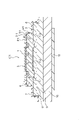
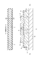
- FIG. 1 is a diagram showing a configuration example of a semiconductor laser according to a first embodiment to which the present technology is applied.
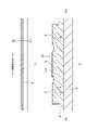
- FIG. 2 is a diagram for explaining a semiconductor laser manufacturing method according to a second embodiment to which the present technology is applied.
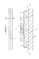
- FIG. 3 is a diagram for explaining a method of manufacturing a semiconductor laser according to a second embodiment to which the present technology is applied.
- FIG. 4 is a diagram for explaining a method of manufacturing a semiconductor laser according to a second embodiment to which the present technology is applied.
- FIG. 5 is a diagram for explaining a method of manufacturing a semiconductor laser according to a second embodiment to which the present technology is applied.
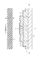
- FIG. 6 is a diagram showing a configuration example of a semiconductor laser manufactured according to the semiconductor laser manufacturing method of the second embodiment to which the present technology is applied.
- the present technology relates to semiconductor lasers.
- semiconductor lasers such as pure blue semiconductor lasers (LDs) using nitride-based compound semiconductor materials
- LDs pure blue semiconductor lasers
- a high-output semiconductor laser may saturate its output due to the influence of self-heating. Therefore, mounting is performed by junction-down mounting with good heat dissipation.
- the solder on the heat sink side may spread to the electrode of the chip due to the heat during mounting. Therefore, it is necessary to insert a barrier layer to prevent diffusion. Materials for preventing the diffusion of solder are being studied for the barrier layer. , tungsten (W), etc. may also be used.
- the present technology includes a substrate, a first cladding layer of a first conductivity type, an active layer, a second cladding layer of a second conductivity type, and a pad metal in this order. an upper portion of the pad metal opposite to the substrate and a side portion of the pad metal are covered with an insulating film and a barrier metal; A semiconductor laser can be provided in which the barrier metal and the bonding metal are arranged in this order on the pad metal.
- the second conductive type second clad layer is a p-type clad layer and the substrate is an n-type substrate.
- the first cladding layer of the first conductivity type is a p-type cladding layer
- the second cladding layer of the second conductivity type is an n-type cladding layer and the substrate is a p-type substrate.
- the substrate may be an insulating substrate (for example, a sapphire substrate).
- An insulating film covers part of the top and sides of the pad metal, and a barrier metal covers part of the top of the pad metal.
- An insulating film covers part of the top and sides of the pad metal, a barrier metal covers part of the top of the pad metal, a part of the insulating film covering part of the top of the pad metal, and the pad A portion of the barrier metal covering a portion of the upper portion of the metal is formed in this order from the pad metal side.
- An insulating film covers the sides of the pad metal and a barrier metal covers the top of the pad metal.
- An insulating film covers part of the upper part and side parts of the pad metal, a barrier metal covers part of the upper part of the pad metal, a part of the barrier metal covering part of the upper part of the pad metal, and the pad A portion of the insulating film covering a portion of the upper portion of the metal is formed in this order from the pad metal side.
- An insulating film covers part of the top and sides of the pad metal, a barrier metal covers part of the top of the pad metal, an edge of the insulating film covering part of the top of the pad metal, and the pad The ends of the barrier metal covering part of the upper portion of the metal are in contact with each other.
- the end face of the insulating film covering part of the upper part of the pad metal and the end face of the barrier metal covering part of the upper part of the pad metal may be joined.
- An insulating film covers part of the side of the pad metal, and a barrier metal covers the top and part of the side of the pad metal.
- a semiconductor laser according to the present technology includes, for example, a nitride semiconductor laser including a group III-V nitride semiconductor material such as GaN.
- a substrate constituting a nitride semiconductor laser contains a compound semiconductor, for example, a group III-V nitride semiconductor such as GaN.
- a group III-V group nitride semiconductor such as GaN.
- the “III-V group nitride semiconductor” means at least one of the group 3B elements in the short period periodic table and at least N among the group 5B elements in the short period periodic table. refers to anything that contains Examples of group III-V nitride semiconductors include gallium nitride compounds containing Ga and N.
- Gallium nitride-based compounds include, for example, GaN, AlGaN, AlGaInN, and the like.
- Group III-V nitride semiconductors may optionally contain n-type impurities of group IV or group VI elements such as Si, Ge, O and Se, or group II or group IV elements such as Mg, Zn and C. It may be doped with p-type impurities.
- a semiconductor layer constituting a nitride semiconductor laser includes, for example, a group III-V nitride semiconductor. ) is formed by an epitaxial crystal growth method such as a method.
- the semiconductor layer includes an active layer forming a light emitting region.
- the semiconductor layer has, for example, an n-type cladding layer, an active layer, a p-type cladding layer), a contact layer (for example, a p-type contact layer), and the like in order from the substrate side.
- the n-type cladding layer is made of AlGaN, for example.
- the active layer has, for example, a multiple quantum well structure in which well layers and barrier layers respectively formed of GaInN having different composition ratios are alternately laminated.
- the p-type clad layer is made of AlGaN, for example.
- the contact layer is made of GaN, for example.
- the semiconductor layer may further include layers other than the above layers (for example, a buffer layer, an n-side guide layer, a p-side guide layer, etc.).
- semiconductor lasers according to the present technology include, for example, semiconductor lasers (infrared lasers) using AlGaAs-based materials.
- the substrate is made of n-GaAs
- the n-type clad layer is made of n-AlGaAs
- the active layer is made of AlGaAs
- the p-type clad layer is made of p-AlGaAs
- the contact layer is made of GaAs. material is used.
- junction-down mounting in which the semiconductor laser light emitting portion is assembled on the side of a member such as a heat sink that has high heat dissipation properties. Junction-down mounting may cause Sn solder on the heat sink side to diffuse into the electrodes of the device, causing deterioration.
- a material having a barrier property against Sn may be selected. Even with a material having a barrier property, there is still a possibility that the diffusion cannot be prevented depending on the coverage of the stepped portion of the element.
- the top and sides of the pad metal are covered with an insulating film and a barrier metal.
- an insulating film can be formed on the sides (side surfaces) of the pad metal by a film forming method with good coverage such as sputtering, and then the barrier metal can be formed.
- the side surface of the pad metal is protected with an insulating film having poor wettability of Sn solder, and the upper surface is protected with a barrier metal to prevent diffusion.
- the insulating film may have a laminated structure including at least a SiN layer, or may be a single layer of SiN.
- the barrier metal may be composed of a layer (for example, a metal layer) containing Sn-based solder such as titanium (Ti), platinum (Pt), molybdenum (Mo), tungsten (W), and a material that is difficult to thermally diffuse.
- Sn-based solder such as titanium (Ti), platinum (Pt), molybdenum (Mo), tungsten (W), and a material that is difficult to thermally diffuse.
- a laminated structure in which layers are laminated may be used, or a single layer structure composed of one layer may be used.
- FIG. 1 is a diagram showing a configuration example of a semiconductor laser according to a first embodiment of the present technology, specifically a cross-sectional view showing a semiconductor laser 101.
- FIG. 1 is a diagram showing a configuration example of a semiconductor laser according to a first embodiment of the present technology, specifically a cross-sectional view showing a semiconductor laser 101.
- a semiconductor laser 101 includes an n-type electrode 11, a substrate (n-type GaN substrate) 10, a first conductivity type first clad layer 9 (n-type clad layer, n-type GaN layer), and an active layer 8. , a second conductive type second clad layer 7 (p-type clad layer, p-type-GaN layer (p-type-GaN layers 7-1 to 7-3)) and a contact layer (p-type contact layer in FIG. 1 The same applies hereinafter) (not shown) are stacked in this order from the bottom (from the bottom side of FIG. 1).
- the n-type electrode 11 may correspond to the first electrode.
- the transparent conductive film 5 (p-type electrode) is laminated on the contact layer (not shown) (upper side in FIG. 1), and the pad is formed on the contact layer (not shown) (transparent conductive film 5).
- a metal 4 is laminated, and a barrier metal 3 and a bonding metal 1 are laminated on the pad metal 4 in this order.
- the transparent conductive film 5 may correspond to the second electrode.
- a portion of the upper portion of the pad metal 4 (the portion indicated by the reference symbol Q1) and a side portion of the pad metal 4 (the portion indicated by the reference symbol R1) are covered with the insulating film 2, and the portion of the upper portion of the pad metal 4 is covered with the insulating film 2. (the portion indicated by the reference symbol P1) is covered with the barrier metal 3 .
- part of the insulating film 2 (insulating film 2-1) covering part of the upper part of the pad metal 4 and part of the barrier metal (barrier metal 3-1) covering part of the upper part of the pad metal 4; are formed in this order from the pad metal 4 side. That is, the barrier metal 3-1 overlaps (stacks) on the insulating film 2-1.
- the overlapping of the insulating film 2-1 and the barrier metal 3-1 has been described at the right end of the semiconductor laser 101 (right side in FIG. 1).
- part of the insulating film 2 and part of the barrier metal 3 are overlapped (stacked).
- the semiconductor laser 101 which has a laminated structure, has a convex ridge portion 20, and the ridge portion 20 extends in the direction of the resonator (in FIG. 1, from the front side to the back side of the paper surface).
- the ridge portion 20 is formed by removing part of the p-type cladding layer (p-type-GaN layer) 7 (7-1 to 7-3) and the contact layer (not shown) by etching such as RIE (Reactive Ion Etching). It is formed.
- the width of the ridge portion 20 is, for example, 0.5 ⁇ m to 100 ⁇ m, preferably 30 to 50 ⁇ m.
- Both ends (left end and right end in FIG. 1) of the semiconductor laser 101 shown in FIG. 1 are removed by etching such as RIE (Reactive Ion Etching) for element isolation.
- the etching extends in the direction of the resonator (in FIG. 1, from the front side to the back side of the paper surface), but it is not necessary to etch all the ends.
- the etching etches the p-type GaN layer 7 (7-1 to 7-3) and removes it until the n-type GaN layer 9 is reached.
- the etching depth is, for example, 0.5 ⁇ m to 5 ⁇ m, preferably 1 ⁇ m or more.
- the etching width is, for example, 1 ⁇ m to 50 ⁇ m, preferably 10 ⁇ m or more on one side.
- a pad metal 4 is laminated on the top of the ridge portion 20 . Further, an insulating film 2 (insulating film 2-1) is formed on the pad metal 4. As shown in FIG. The insulating film 2 is formed by a film forming method such as a sputtering method, which has good step coverage. Next, the insulating film 2 above the pad metal 4 is etched to ensure electrical connection. The etching pattern is smaller than that of the pad metal 4, and the insulating film 2 (insulating film 2-1) over the edge of the pad metal 4 is not etched. Therefore, the side portion (side surface) of the pad metal 4 is always covered with the insulating film 2, and the insulating film 2-1 covers even a part of the upper portion (planar portion) of the pad metal.
- a barrier metal 3 and a bonding metal 1 are formed on the insulating film 2 (insulating film 2-1).
- the pattern is smaller than the pad metal 4 and larger than the etched pattern of the insulating film 2 . Therefore, as described above, the barrier metal 3-1 is partially in contact with the flat portion of the insulating film 2-1 on the pad metal 4.
- Second Embodiment (Example 1 of Manufacturing Method of Semiconductor Laser and Example 2 of Semiconductor Laser)> A semiconductor laser manufacturing method and a semiconductor laser according to a second embodiment (semiconductor laser manufacturing method example 1 and semiconductor laser example 2) according to the present technology will be described with reference to FIGS.
- FIG. 2A and 2B are diagrams for explaining a method of manufacturing a semiconductor laser according to a second embodiment to which the present technology is applied.
- FIG. FIG. 2B is a plan view of the current confinement film 6 above the ridge Rd2 along the line A2-A'2 shown in FIG. 2A (the horizontal direction in FIG. 2A is the resonator direction). is a cross-sectional view after etching.
- the transparent conductive film 5 is formed so as to extend in the direction perpendicular to the line A2-A'2 and in the resonator direction (horizontal direction in FIG. 2A).
- an n-type clad layer (n-type-GaN layer) 9 an n-side guide layer (not shown), an active layer 8, a p-side guide layer (not shown), a p-type cladding layer (P-type-GaN layer) 7 (7-1 to 7-3), and a contact layer (not shown) are sequentially laminated. (the laminated structure shown in FIG. 2B is formed).
- etching mask layer made of, for example, SiO 2 or SiN is formed on the laminated structure by a vapor deposition method, a sputtering method, or the like. In this embodiment, for example, SiO 2 is used.
- the etching mask layer is patterned by photolithography, and the etching mask layer in the openings of the resist is removed by RIE (Reactive Ion Etching) using a fluorine-based gas or hydrofluoric acid-based wet etching.
- the p-type GaN layer 7 (7-1 to 7-3) is etched by RIE (Reactive Ion Etching) using a chlorine-based gas, and part of the laminated structure is etched until the n-type GaN layer 9 is reached. remove the part.
- RIE Reactive Ion Etching
- the etching mask layer is removed by hydrofluoric acid-based wet etching, and the transparent conductive film 5 is formed on the laminated structure by, for example, vapor deposition or sputtering.
- the transparent conductive film 5 include ITO (Indium Tin Oxide), ITiO (Indium Titanium Oxide), AZO (Al 2 O 3 —ZnO), and IGZO (InGaZnOx).
- ITO Indium Tin Oxide
- ITiO Indium Titanium Oxide
- AZO Al 2 O 3 —ZnO
- IGZO InGaZnOx
- the current confinement layer 6 is formed on the laminated structure (etching portion, ridge portion 20, etc.) by a vapor deposition method, a sputtering method, or the like.
- the current confinement layer 6 is made of, for example, SiO 2 , SiN, Al 2 O 3 or the like.
- the current confinement layer 6 is removed only from the upper portion of the ridge 20 by RIE (Reactive Ion Etching) using fluorine-based gas or wet etching using hydrofluoric acid. This enables electrical connection with the pad metal 4 formed on the ridge portion 20 .
- FIG. 3 is a diagram for explaining a semiconductor laser manufacturing method according to a second embodiment to which the present technology is applied.
- FIG. 3A is a plan view after forming a pad metal 4 ( 3A is the resonator direction)
- FIG. 3B is a cross-sectional view after the formation of the pad metal 4 along line A3-A'3 shown in FIG. 2A.
- the pad metal 4 is formed so as to extend in the direction perpendicular to the line A3-A'3 and in the direction of the resonator (horizontal direction in FIG. 3A).
- a pad metal 4 is formed on the layered structure formed in FIG.
- the pad metal is deposited by a vapor deposition method, a sputtering method, or the like, and is patterned by, for example, a lift-off method. Pattern formation may take the form of removing unnecessary portions by RIE (Reactive Ion Etching) or milling.
- the pad metal 4 is formed by laminating titanium (Ti), palladium (Pd), platinum (Pt), and gold (Au) from the laminated structure side, and is electrically connected to the upper surface of the ridge portion 20. As long as they are connected, the configuration is not necessarily limited to this.
- the film thickness of titanium (Ti) may be, for example, 2 nm or more and 100 nm or less.
- the film thickness of palladium (Pd) may be, for example, 10 nm or more and 300 nm or less.
- the film thickness of platinum (Pt) may be, for example, 10 nm or more and 300 nm or less.
- the film thickness of gold (Au) may be, for example, 300 nm or more and 3000 nm or less.
- FIGS. 4A and 4B are diagrams for explaining a method for manufacturing a semiconductor laser according to a second embodiment to which the present technology is applied.
- FIG. 4A is a plan view after forming an insulating film 2 ( 4A is the direction of the resonator), and
- FIG. 4B is a cross-sectional view taken along line A4-A'4 shown in FIG. 4A after the insulating film 2 is formed.
- FIG. 5A and 5B are diagrams for explaining a method for manufacturing a semiconductor laser according to a second embodiment to which the present technology is applied.
- FIG. 5A is a plan view after etching the insulating film 2.
- FIG. (The horizontal direction in FIG. 5A is the resonator direction.)
- FIG. 5B is a cross-sectional view after etching the insulating film 2 along line A5-A'5 shown in FIG. 5A.
- an insulating film 2 is formed to extend in a direction perpendicular to the line A4-A'4 and in the direction of the resonator (horizontal direction in FIG. 4A).
- a pad metal 4 is formed extending in the direction perpendicular to the line A5-A'5 and in the direction of the resonator (horizontal direction in FIG. 5A).
- An insulating film 2 is formed on the inner and outer peripheries of 4 .
- the insulating film 2 is formed.
- the insulating film 2 is formed on the laminated structure (entire surface of the element) formed in FIG.
- the etching pattern is smaller than the pattern of the pad metal 4, and the edges (edges) of the pad metal 4 are not etched. Therefore, all side portions (side surfaces) of the pad metal 4 are covered with the insulating film 2 .
- the etching is removed by a RIE (Reactive Ion Etching) method using a fluorine-based gas or wet etching using a hydrofluoric acid system.
- the insulating film 2 may be a SiN single layer, or may be formed by laminating a SiN layer and a layer (insulating layer) made of another material such as SiO2.
- the film thickness of the insulating film 2 may be 10 nm or more and 500 nm or less, preferably 200 nm or more.
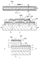
- FIG. 6 is a diagram showing a configuration example of a semiconductor laser manufactured according to the semiconductor laser manufacturing method of the second embodiment to which the present technology is applied.
- FIG. 6A shows a semiconductor laser 106 (in FIG. 6A, semiconductor laser 106A) (the horizontal direction in FIG. 6A is the cavity direction).
- 6B is manufactured by forming barrier metal 3 on top of pad metal 4 and then forming bonding metal 1 on top of barrier metal 3 according to the A6-A'6 line shown in FIG. 6A. It is also a cross-sectional view of the semiconductor laser 106 (semiconductor laser 106B in FIG. 6B).
- FIG. 6C is manufactured by forming barrier metal 3 on top of pad metal 4 and then forming bonding metal 1 on top of barrier metal 3 according to line BB' shown in FIG. 6A.
- 6A and 6B are cross-sectional views of the semiconductor laser 106 (semiconductor laser 106C in FIG. 6C), showing the laser emission end in the cavity direction.
- a bonding metal 1, a barrier metal 3 and a pad metal 4 are formed to extend in the direction perpendicular to the line A6-A'6 and in the direction of the resonator (horizontal direction in FIG. 6A).
- An insulating film 2 is formed on the inner and outer peripheries of the bonding metal 1 , the barrier metal 3 and the pad metal 4 .
- a barrier metal 3 and a bonding metal 1 are formed on the pad metal 4 in this order.
- Each of the barrier metal 3 and the bonding metal 1 is formed by a vapor deposition method, a sputtering method, or the like, and a pattern is formed by a lift-off method.
- Each metal (barrier metal 3 and bonding metal 1) may be deposited continuously or may be deposited separately. In this embodiment, film formation is performed continuously.
- the pattern is smaller than the pad metal 4 and larger than the etched pattern of the insulating film 2 . Therefore, as indicated by reference numeral Q6B in FIG. 6B, a portion of the barrier metal 3 (that is, the barrier metal 3-1) is formed on the flat portion of the insulating film 2-1 formed on the pad metal 4. It becomes the structure which contacted so that it might overlap.
- the barrier metal 3 may have a laminated structure composed of at least two layers selected from a titanium (Ti) layer, a platinum (Pt) layer, a molybdenum (Mo) layer and a tungsten (W) layer. Also, the barrier metal 3 may have a single-layer structure composed of one of a titanium (Ti) layer, a platinum (Pt) layer, a molybdenum (Mo) layer and a tungsten (W) layer. In this embodiment, it is a titanium (Ti) single layer. The film thickness of the titanium (Ti) single layer may be 100 nm or more and 500 nm or less, preferably 200 nm or more.
- the bonding metal 1 may have a laminated structure composed of at least two layers selected from a titanium (Ti) layer, a platinum (Pt) layer and a gold (Au) layer.
- a single layer may be used.
- the Au single layer forming the bonding metal 1 is formed continuously with the Ti single layer forming the barrier metal 3 .
- the thickness of the Au single layer may be 100 nm or more and 500 nm or less, preferably 300 nm or more.
- the semiconductor laser 106B includes a substrate (n-type-GaN substrate) 10, a first conductivity type first clad layer 9 (n-type clad layer, n-type-GaN layer), and a first guide layer (n-side guide layer). (not shown), an active layer 8, a second guide layer (p-side guide layer) (not shown), a second conductive type second clad layer 7 (p-type clad layer, p-type-GaN layer (p The type-GaN layers 7-1 to 7-3)) and the contact layer (the p-type contact layer in FIG. 6B; the same shall apply hereinafter) (not shown) from below (from the bottom side in FIG. 6B), They are stacked in this order.
- the transparent conductive film 5 (p-type electrode) is laminated on the contact layer (not shown), the pad metal 4 is laminated on the contact layer (not shown) (transparent conductive film 5), A barrier metal 3 and a bonding metal 1 are laminated in this order on the pad metal 4 .
- the transparent conductive film 5 may correspond to the second electrode.
- a portion of the upper portion of the pad metal 4 (portion of reference symbol Q6B) and a side portion of the pad metal 4 (portion of reference symbol R6B) are covered with the insulating film 2, and the upper portion of the pad metal 4 is covered with an insulating film 2. (The portion with reference sign P6B) is covered with a barrier metal 3. As shown in FIG.
- part of the insulating film 2 (insulating film 2-1) covering part of the upper part of the pad metal 4 and part of the barrier metal (barrier metal 3-1) covering part of the upper part of the pad metal 4; are formed in this order from the pad metal 4 side. That is, the barrier metal 3-1 overlaps (stacks) on the insulating film 2-1.
- the overlapping of the insulating film 2-1 and the barrier metal 3-1 in this manner has been described at the right end of the semiconductor laser 106B (right side in FIG. 6B). ), the insulating film 2 and the barrier metal 3 are overlapped (stacked) in a similar state.
- the semiconductor laser 106C includes a substrate (n-type-GaN free-standing substrate) 10, a first conductivity type first clad layer 9 (n-type clad layer, n-type-GaN layer), a first guide layer (n-side guide layer ) (not shown), an active layer 8, a second guide layer (p-side guide layer) (not shown), and a second conductive type second clad layer 8 (p-type clad layer, p-type GaN layer ( p-type GaN layers 7-1 to 7-3)), a contact layer (p-type contact layer in FIG.
- a transparent conductive film 5 (p-type electrode), A current confinement film 6 is laminated in this order from the bottom (from the bottom side in FIG. 6B).
- the transparent conductive film 5 may correspond to the second electrode.
- a pad metal 4 is laminated on the current confinement film 6, and a barrier metal 3 and a bonding metal 1 are laminated on the pad metal 4 in this order.
- a portion of the upper portion of the pad metal 4 (portion with reference symbol Q6C), a side portion of the pad metal 4 (portion with reference symbol R6CB), and a current confinement film extending rightward from the right edge of the pad metal 4. 6 are covered with the insulating film 2 .
- a portion of the upper portion of the pad metal 4 (the portion indicated by reference numeral P6C) is covered with the barrier metal 3. As shown in FIG.
- the pad metal 4 is covered with the insulating film 2 with good coverage, and diffusion of Sn-based solder is suppressed. Further, when Sn solder is diffused into the pad metal 4 near the laser emitting end, the laser characteristics and reliability are particularly adversely affected, but the semiconductor laser 106C can suppress this adverse effect.
- the substrate (n-type GaN self-standing substrate) 10 is polished to a film thickness suitable for cleavage, and an n-electrode (not shown) is formed by, for example, a lift-off method. As described above, the n-electrode is shown as the n-electrode 11 in FIG. Subsequently, the substrate (n-type GaN self-supporting substrate) 10 is cleaved into bars, and the exposed end faces are coated. Furthermore, the bar is cut out from the bar to form a chip, thereby manufacturing a finished product of the semiconductor laser 106 (106A to 106C).
- semiconductor laser manufacturing method example 1 and semiconductor laser example 2 semiconductor laser manufacturing method example 1 and semiconductor laser example 2 according to the present technology have been described above. , can be applied to the semiconductor laser of the first embodiment according to the present technology described above.
- this technique can also take the following structures.
- a substrate, a first cladding layer of a first conductivity type, an active layer, a second cladding layer of a second conductivity type, and a pad metal in this order, an upper portion of the pad metal opposite to the substrate side of the pad metal and a side portion of the pad metal are covered with an insulating film and a barrier metal;
- the insulating film covers a portion of the upper portion and side portions of the pad metal;
- the insulating film covers a portion of the upper portion and side portions of the pad metal; the barrier metal covers part of the top of the pad metal, A portion of an insulating film covering a portion of the upper portion of the pad metal and a portion of the barrier metal covering a portion of the upper portion of the pad metal are formed in this order from the pad metal side, [ 1].
- the insulating film covers the sides of the pad metal; The semiconductor laser according to [1], wherein the barrier metal covers the upper part of the pad metal.
- the insulating film covers a portion of the upper portion and side portions of the pad metal; the barrier metal covers part of the top of the pad metal, The semiconductor laser according to [1], wherein an edge of the insulating film covering a portion of the upper portion of the pad metal is in contact with an edge of the barrier metal covering a portion of the upper portion of the pad metal. . [6] the insulating film covers a portion of the side portion of the pad metal; The semiconductor laser according to [1], wherein the barrier metal covers the upper portion and part of the side portion of the pad metal.
- a first guide layer is arranged between the first cladding layer and the active layer,
- the insulating film has a laminated structure composed of at least two layers, The semiconductor laser according to any one of [1] to [9], wherein at least one of the at least two layers of the insulating film is a SiN layer.
- the barrier metal has a laminated structure composed of at least two layers, The semiconductor laser according to any one of [1] to [10], wherein at least one layer of the at least two layers of the barrier metal is a Ti layer.
- the semiconductor laser according to any one of [1] to [11] which is a nitride semiconductor laser.
Landscapes
- Physics & Mathematics (AREA)
- Condensed Matter Physics & Semiconductors (AREA)
- General Physics & Mathematics (AREA)
- Electromagnetism (AREA)
- Optics & Photonics (AREA)
- Geometry (AREA)
- Semiconductor Lasers (AREA)
Priority Applications (3)
| Application Number | Priority Date | Filing Date | Title |
|---|---|---|---|
| CN202280022440.XA CN116998073A (zh) | 2021-03-25 | 2022-01-14 | 半导体激光器 |
| JP2023508668A JPWO2022201771A1 (cg-RX-API-DMAC7.html) | 2021-03-25 | 2022-01-14 | |
| US18/550,808 US20240162686A1 (en) | 2021-03-25 | 2022-01-14 | Semiconductor laser |
Applications Claiming Priority (2)
| Application Number | Priority Date | Filing Date | Title |
|---|---|---|---|
| JP2021051410 | 2021-03-25 | ||
| JP2021-051410 | 2021-03-25 |
Publications (1)
| Publication Number | Publication Date |
|---|---|
| WO2022201771A1 true WO2022201771A1 (ja) | 2022-09-29 |
Family
ID=83396746
Family Applications (1)
| Application Number | Title | Priority Date | Filing Date |
|---|---|---|---|
| PCT/JP2022/001107 Ceased WO2022201771A1 (ja) | 2021-03-25 | 2022-01-14 | 半導体レーザ |
Country Status (4)
| Country | Link |
|---|---|
| US (1) | US20240162686A1 (cg-RX-API-DMAC7.html) |
| JP (1) | JPWO2022201771A1 (cg-RX-API-DMAC7.html) |
| CN (1) | CN116998073A (cg-RX-API-DMAC7.html) |
| WO (1) | WO2022201771A1 (cg-RX-API-DMAC7.html) |
Citations (7)
| Publication number | Priority date | Publication date | Assignee | Title |
|---|---|---|---|---|
| JP2000114664A (ja) * | 1998-10-06 | 2000-04-21 | Nichia Chem Ind Ltd | 窒化物半導体レーザ素子 |
| JP2006278694A (ja) * | 2005-03-29 | 2006-10-12 | Opnext Japan Inc | 光半導体装置 |
| JP2010238802A (ja) * | 2009-03-30 | 2010-10-21 | Showa Denko Kk | 半導体発光素子、電極構造、半導体発光素子の製造方法、電極構造の製造方法 |
| JP2013125886A (ja) * | 2011-12-15 | 2013-06-24 | Sony Corp | 半導体レーザ素子及び半導体レーザ素子の製造方法 |
| JP2015023175A (ja) * | 2013-07-19 | 2015-02-02 | ソニー株式会社 | 半導体発光素子および半導体発光装置 |
| US20180138663A1 (en) * | 2016-11-17 | 2018-05-17 | PlayNitride Inc. | Semiconductor laser device |
| JP2020155715A (ja) * | 2019-03-22 | 2020-09-24 | 住友電気工業株式会社 | 光半導体素子およびその製造方法 |
Family Cites Families (19)
| Publication number | Priority date | Publication date | Assignee | Title |
|---|---|---|---|---|
| KR960014732B1 (ko) * | 1992-12-22 | 1996-10-19 | 양승택 | Rwg형 반도체 레이저장치 및 제조방법 |
| US6838701B2 (en) * | 2000-02-16 | 2005-01-04 | Nichia Corporation | Nitride semiconductor laser device |
| ATE448589T1 (de) * | 2001-04-12 | 2009-11-15 | Nichia Corp | Halbleiterelement aus galliumnitridzusammensetzung |
| JP4480948B2 (ja) * | 2002-07-15 | 2010-06-16 | 日本オプネクスト株式会社 | 半導体レーザ素子及びその製造方法 |
| TWI303909B (en) * | 2002-11-25 | 2008-12-01 | Nichia Corp | Ridge waveguide semiconductor laser diode |
| JP2004335530A (ja) * | 2003-04-30 | 2004-11-25 | Mitsubishi Electric Corp | リッジ導波路型半導体レーザ |
| KR100612832B1 (ko) * | 2003-05-07 | 2006-08-18 | 삼성전자주식회사 | 고성능의 질화갈륨계 광소자 구현을 위한 니켈계 고용체를 이용한 오믹 접촉 형성을 위한 금속박막 및 그 제조방법 |
| JP4580633B2 (ja) * | 2003-11-14 | 2010-11-17 | スタンレー電気株式会社 | 半導体装置及びその製造方法 |
| US7558307B2 (en) * | 2004-02-16 | 2009-07-07 | Sharp Kabushiki Kaisha | Semiconductor laser device, semiconductor laser device manufacturing method, optical disk apparatus and optical transmission system |
| JP4956928B2 (ja) * | 2004-09-28 | 2012-06-20 | 日亜化学工業株式会社 | 半導体装置 |
| KR100631876B1 (ko) * | 2004-10-29 | 2006-10-09 | 삼성전기주식회사 | 반도체 레이저 소자의 제조 방법 |
| JP4030556B2 (ja) * | 2005-06-30 | 2008-01-09 | シャープ株式会社 | 窒化物半導体レーザ素子および窒化物半導体レーザ装置 |
| JP4352337B2 (ja) * | 2005-09-16 | 2009-10-28 | ソニー株式会社 | 半導体レーザおよび半導体レーザ装置 |
| JP2010067858A (ja) * | 2008-09-11 | 2010-03-25 | Sanyo Electric Co Ltd | 窒化物系半導体素子およびその製造方法 |
| JP2013042107A (ja) * | 2011-02-17 | 2013-02-28 | Rohm Co Ltd | 半導体レーザ素子 |
| JP2013105975A (ja) * | 2011-11-16 | 2013-05-30 | Mitsubishi Electric Corp | 光半導体装置の製造方法 |
| US10193301B2 (en) * | 2017-03-31 | 2019-01-29 | Nichia Corporation | Method of manufacturing light emitting device and light emitting device |
| DE112019000483T5 (de) * | 2018-01-23 | 2020-10-29 | Sony Semiconductor Solutions Corporation | Halbleiterlaser und elektronische vorrichtung |
| DE102021130775A1 (de) * | 2021-11-24 | 2023-05-25 | OSRAM Opto Semiconductors Gesellschaft mit beschränkter Haftung | Optoelektronisches bauelement und verfahren zum herstellen eines optoelektronischen bauelements |
-
2022
- 2022-01-14 JP JP2023508668A patent/JPWO2022201771A1/ja not_active Withdrawn
- 2022-01-14 WO PCT/JP2022/001107 patent/WO2022201771A1/ja not_active Ceased
- 2022-01-14 CN CN202280022440.XA patent/CN116998073A/zh not_active Withdrawn
- 2022-01-14 US US18/550,808 patent/US20240162686A1/en active Pending
Patent Citations (7)
| Publication number | Priority date | Publication date | Assignee | Title |
|---|---|---|---|---|
| JP2000114664A (ja) * | 1998-10-06 | 2000-04-21 | Nichia Chem Ind Ltd | 窒化物半導体レーザ素子 |
| JP2006278694A (ja) * | 2005-03-29 | 2006-10-12 | Opnext Japan Inc | 光半導体装置 |
| JP2010238802A (ja) * | 2009-03-30 | 2010-10-21 | Showa Denko Kk | 半導体発光素子、電極構造、半導体発光素子の製造方法、電極構造の製造方法 |
| JP2013125886A (ja) * | 2011-12-15 | 2013-06-24 | Sony Corp | 半導体レーザ素子及び半導体レーザ素子の製造方法 |
| JP2015023175A (ja) * | 2013-07-19 | 2015-02-02 | ソニー株式会社 | 半導体発光素子および半導体発光装置 |
| US20180138663A1 (en) * | 2016-11-17 | 2018-05-17 | PlayNitride Inc. | Semiconductor laser device |
| JP2020155715A (ja) * | 2019-03-22 | 2020-09-24 | 住友電気工業株式会社 | 光半導体素子およびその製造方法 |
Also Published As
| Publication number | Publication date |
|---|---|
| JPWO2022201771A1 (cg-RX-API-DMAC7.html) | 2022-09-29 |
| US20240162686A1 (en) | 2024-05-16 |
| CN116998073A (zh) | 2023-11-03 |
Similar Documents
| Publication | Publication Date | Title |
|---|---|---|
| JP4547933B2 (ja) | 窒化物半導体素子 | |
| JP4671617B2 (ja) | 集積型半導体レーザ素子 | |
| JP3897186B2 (ja) | 化合物半導体レーザ | |
| JP4352337B2 (ja) | 半導体レーザおよび半導体レーザ装置 | |
| JP2008141187A (ja) | 窒化物半導体レーザ装置 | |
| JP2009200478A (ja) | 半導体レーザ素子およびその製造方法 | |
| JP4909533B2 (ja) | 半導体レーザ素子及びその製造方法 | |
| JP7332623B2 (ja) | 半導体レーザ装置 | |
| WO2013089032A1 (ja) | 半導体レーザ素子及び半導体レーザ素子の製造方法 | |
| JP2009071162A (ja) | 半導体装置及び半導体装置の製造方法 | |
| JP2015167263A (ja) | 半導体レーザ素子 | |
| JP4697488B2 (ja) | マルチビーム半導体レーザ | |
| JP2009212386A (ja) | 半導体光素子の製造方法 | |
| JP2007324581A (ja) | 集積型半導体発光装置およびその製造方法 | |
| EP3493338B1 (en) | Semiconductor light-emitting element and method for manufacturing semiconductor light-emitting element | |
| JP2004281432A (ja) | 窒化物半導体素子及びその製造方法 | |
| JP5150581B2 (ja) | 発光素子、発光装置及び発光素子の製造方法 | |
| JP2005101483A (ja) | リッジ導波路型半導体レーザ | |
| JP2013102043A (ja) | 半導体レーザ素子、及び、半導体レーザ素子の作製方法 | |
| JP2007266575A (ja) | 半導体レーザ素子及び半導体レーザ装置 | |
| JP2007324582A (ja) | 集積型半導体発光装置およびその製造方法 | |
| JP2007324579A (ja) | 集積型半導体発光装置およびその製造方法 | |
| US12603478B2 (en) | Semiconductor laser and semiconductor laser device | |
| US20240162686A1 (en) | Semiconductor laser | |
| US20230335972A1 (en) | Semiconductor laser and semiconductor laser device |
Legal Events
| Date | Code | Title | Description |
|---|---|---|---|
| 121 | Ep: the epo has been informed by wipo that ep was designated in this application |
Ref document number: 22774576 Country of ref document: EP Kind code of ref document: A1 |
|
| WWE | Wipo information: entry into national phase |
Ref document number: 2023508668 Country of ref document: JP |
|
| WWE | Wipo information: entry into national phase |
Ref document number: 18550808 Country of ref document: US |
|
| WWE | Wipo information: entry into national phase |
Ref document number: 202280022440.X Country of ref document: CN |
|
| NENP | Non-entry into the national phase |
Ref country code: DE |
|
| 122 | Ep: pct application non-entry in european phase |
Ref document number: 22774576 Country of ref document: EP Kind code of ref document: A1 |