WO2022201426A1 - 半導体装置および半導体装置の製造方法 - Google Patents
半導体装置および半導体装置の製造方法 Download PDFInfo
- Publication number
- WO2022201426A1 WO2022201426A1 PCT/JP2021/012534 JP2021012534W WO2022201426A1 WO 2022201426 A1 WO2022201426 A1 WO 2022201426A1 JP 2021012534 W JP2021012534 W JP 2021012534W WO 2022201426 A1 WO2022201426 A1 WO 2022201426A1
- Authority
- WO
- WIPO (PCT)
- Prior art keywords
- metal block
- semiconductor device
- semiconductor element
- heat spreader
- heat
- Prior art date
- Legal status (The legal status is an assumption and is not a legal conclusion. Google has not performed a legal analysis and makes no representation as to the accuracy of the status listed.)
- Ceased
Links
Images






Classifications
-
- H—ELECTRICITY
- H10—SEMICONDUCTOR DEVICES; ELECTRIC SOLID-STATE DEVICES NOT OTHERWISE PROVIDED FOR
- H10W—GENERIC PACKAGES, INTERCONNECTIONS, CONNECTORS OR OTHER CONSTRUCTIONAL DETAILS OF DEVICES COVERED BY CLASS H10
- H10W40/00—Arrangements for thermal protection or thermal control
- H10W40/10—Arrangements for heating
-
- H—ELECTRICITY
- H10—SEMICONDUCTOR DEVICES; ELECTRIC SOLID-STATE DEVICES NOT OTHERWISE PROVIDED FOR
- H10W—GENERIC PACKAGES, INTERCONNECTIONS, CONNECTORS OR OTHER CONSTRUCTIONAL DETAILS OF DEVICES COVERED BY CLASS H10
- H10W40/00—Arrangements for thermal protection or thermal control
- H10W40/70—Fillings or auxiliary members in containers or in encapsulations for thermal protection or control
- H10W40/77—Auxiliary members characterised by their shape
- H10W40/778—Auxiliary members characterised by their shape in encapsulations
-
- H—ELECTRICITY
- H10—SEMICONDUCTOR DEVICES; ELECTRIC SOLID-STATE DEVICES NOT OTHERWISE PROVIDED FOR
- H10W—GENERIC PACKAGES, INTERCONNECTIONS, CONNECTORS OR OTHER CONSTRUCTIONAL DETAILS OF DEVICES COVERED BY CLASS H10
- H10W40/00—Arrangements for thermal protection or thermal control
- H10W40/20—Arrangements for cooling
- H10W40/25—Arrangements for cooling characterised by their materials
- H10W40/255—Arrangements for cooling characterised by their materials having a laminate or multilayered structure, e.g. direct bond copper [DBC] ceramic substrates
-
- H—ELECTRICITY
- H10—SEMICONDUCTOR DEVICES; ELECTRIC SOLID-STATE DEVICES NOT OTHERWISE PROVIDED FOR
- H10W—GENERIC PACKAGES, INTERCONNECTIONS, CONNECTORS OR OTHER CONSTRUCTIONAL DETAILS OF DEVICES COVERED BY CLASS H10
- H10W70/00—Package substrates; Interposers; Redistribution layers [RDL]
- H10W70/40—Leadframes
- H10W70/464—Additional interconnections in combination with leadframes
-
- H—ELECTRICITY
- H10—SEMICONDUCTOR DEVICES; ELECTRIC SOLID-STATE DEVICES NOT OTHERWISE PROVIDED FOR
- H10W—GENERIC PACKAGES, INTERCONNECTIONS, CONNECTORS OR OTHER CONSTRUCTIONAL DETAILS OF DEVICES COVERED BY CLASS H10
- H10W70/00—Package substrates; Interposers; Redistribution layers [RDL]
- H10W70/40—Leadframes
- H10W70/481—Leadframes for devices being provided for in groups H10D8/00 - H10D48/00
-
- H—ELECTRICITY
- H10—SEMICONDUCTOR DEVICES; ELECTRIC SOLID-STATE DEVICES NOT OTHERWISE PROVIDED FOR
- H10W—GENERIC PACKAGES, INTERCONNECTIONS, CONNECTORS OR OTHER CONSTRUCTIONAL DETAILS OF DEVICES COVERED BY CLASS H10
- H10W72/00—Interconnections or connectors in packages
- H10W72/071—Connecting or disconnecting
- H10W72/076—Connecting or disconnecting of strap connectors
-
- H—ELECTRICITY
- H10—SEMICONDUCTOR DEVICES; ELECTRIC SOLID-STATE DEVICES NOT OTHERWISE PROVIDED FOR
- H10W—GENERIC PACKAGES, INTERCONNECTIONS, CONNECTORS OR OTHER CONSTRUCTIONAL DETAILS OF DEVICES COVERED BY CLASS H10
- H10W72/00—Interconnections or connectors in packages
- H10W72/50—Bond wires
-
- H—ELECTRICITY
- H10—SEMICONDUCTOR DEVICES; ELECTRIC SOLID-STATE DEVICES NOT OTHERWISE PROVIDED FOR
- H10W—GENERIC PACKAGES, INTERCONNECTIONS, CONNECTORS OR OTHER CONSTRUCTIONAL DETAILS OF DEVICES COVERED BY CLASS H10
- H10W74/00—Encapsulations, e.g. protective coatings
- H10W74/01—Manufacture or treatment
-
- H—ELECTRICITY
- H10—SEMICONDUCTOR DEVICES; ELECTRIC SOLID-STATE DEVICES NOT OTHERWISE PROVIDED FOR
- H10W—GENERIC PACKAGES, INTERCONNECTIONS, CONNECTORS OR OTHER CONSTRUCTIONAL DETAILS OF DEVICES COVERED BY CLASS H10
- H10W74/00—Encapsulations, e.g. protective coatings
- H10W74/10—Encapsulations, e.g. protective coatings characterised by their shape or disposition
- H10W74/111—Encapsulations, e.g. protective coatings characterised by their shape or disposition the semiconductor body being completely enclosed
-
- H—ELECTRICITY
- H10—SEMICONDUCTOR DEVICES; ELECTRIC SOLID-STATE DEVICES NOT OTHERWISE PROVIDED FOR
- H10W—GENERIC PACKAGES, INTERCONNECTIONS, CONNECTORS OR OTHER CONSTRUCTIONAL DETAILS OF DEVICES COVERED BY CLASS H10
- H10W74/00—Encapsulations, e.g. protective coatings
- H10W74/10—Encapsulations, e.g. protective coatings characterised by their shape or disposition
- H10W74/111—Encapsulations, e.g. protective coatings characterised by their shape or disposition the semiconductor body being completely enclosed
- H10W74/114—Encapsulations, e.g. protective coatings characterised by their shape or disposition the semiconductor body being completely enclosed by a substrate and the encapsulations
-
- H—ELECTRICITY
- H10—SEMICONDUCTOR DEVICES; ELECTRIC SOLID-STATE DEVICES NOT OTHERWISE PROVIDED FOR
- H10W—GENERIC PACKAGES, INTERCONNECTIONS, CONNECTORS OR OTHER CONSTRUCTIONAL DETAILS OF DEVICES COVERED BY CLASS H10
- H10W90/00—Package configurations
-
- H—ELECTRICITY
- H10—SEMICONDUCTOR DEVICES; ELECTRIC SOLID-STATE DEVICES NOT OTHERWISE PROVIDED FOR
- H10W—GENERIC PACKAGES, INTERCONNECTIONS, CONNECTORS OR OTHER CONSTRUCTIONAL DETAILS OF DEVICES COVERED BY CLASS H10
- H10W70/00—Package substrates; Interposers; Redistribution layers [RDL]
- H10W70/40—Leadframes
- H10W70/464—Additional interconnections in combination with leadframes
- H10W70/466—Tape carriers or flat leads
-
- H—ELECTRICITY
- H10—SEMICONDUCTOR DEVICES; ELECTRIC SOLID-STATE DEVICES NOT OTHERWISE PROVIDED FOR
- H10W—GENERIC PACKAGES, INTERCONNECTIONS, CONNECTORS OR OTHER CONSTRUCTIONAL DETAILS OF DEVICES COVERED BY CLASS H10
- H10W72/00—Interconnections or connectors in packages
- H10W72/071—Connecting or disconnecting
- H10W72/076—Connecting or disconnecting of strap connectors
- H10W72/07631—Techniques
- H10W72/07636—Soldering or alloying
-
- H—ELECTRICITY
- H10—SEMICONDUCTOR DEVICES; ELECTRIC SOLID-STATE DEVICES NOT OTHERWISE PROVIDED FOR
- H10W—GENERIC PACKAGES, INTERCONNECTIONS, CONNECTORS OR OTHER CONSTRUCTIONAL DETAILS OF DEVICES COVERED BY CLASS H10
- H10W72/00—Interconnections or connectors in packages
- H10W72/60—Strap connectors, e.g. thick copper clips for grounding of power devices
- H10W72/631—Shapes of strap connectors
-
- H—ELECTRICITY
- H10—SEMICONDUCTOR DEVICES; ELECTRIC SOLID-STATE DEVICES NOT OTHERWISE PROVIDED FOR
- H10W—GENERIC PACKAGES, INTERCONNECTIONS, CONNECTORS OR OTHER CONSTRUCTIONAL DETAILS OF DEVICES COVERED BY CLASS H10
- H10W90/00—Package configurations
- H10W90/701—Package configurations characterised by the relative positions of pads or connectors relative to package parts
- H10W90/761—Package configurations characterised by the relative positions of pads or connectors relative to package parts of strap connectors
- H10W90/766—Package configurations characterised by the relative positions of pads or connectors relative to package parts of strap connectors between a chip and a stacked lead frame, conducting package substrate or heat sink
Definitions
- the present disclosure relates to a semiconductor device and a method for manufacturing a semiconductor device.
- the semiconductor device described in Patent Document 1 has a heat dissipation path from the semiconductor element to the cooling body via a heat sink block, which is a metal body bonded to the surface of the semiconductor element, and an upper heat sink bonded to the heat sink block.
- the heat dissipation path formed on the surface side of the semiconductor element is composed of parts that easily conduct heat and have a large heat capacity.
- the terminal connected to the surface electrode of the semiconductor element is preferably a thin plate from the viewpoint of workability and cost. In other words, it was difficult to achieve both high heat dissipation and low production cost.
- the present disclosure provides a low-cost semiconductor device with excellent heat dissipation.
- a semiconductor device includes a heat spreader, a semiconductor element, a metal block, terminals, and a sealing material.
- a semiconductor device includes surface electrodes.
- a semiconductor element is mounted on the upper surface of the heat spreader.
- the metal block includes a bonding surface and at least one heat dissipation surface. The bonding surface is bonded to the surface electrode of the semiconductor element. At least one heat dissipation surface is connected to the upper surface of the heat spreader via an insulating member.
- the metal block extends from the bonding surface to the at least one heat dissipation surface so as to straddle over at least one side of the semiconductor element.
- the terminal includes a first end and a second end. The first end is bonded to the metal block.
- the second end is located on the opposite side of the first end and formed connectable to an external circuit.
- the encapsulant encapsulates the heat spreader, the semiconductor element, the metal block, and the first ends of the terminals. A second end of the terminal is exposed from the encapsulant.
- a low-cost semiconductor device with excellent heat dissipation is provided.
- FIG. 1 is a plan view showing the configuration of a semiconductor device according to Embodiment 1;
- FIG. 1 is a cross-sectional view showing the configuration of a semiconductor device in Embodiment 1;
- FIG. 1 is a plan view showing the configuration of a semiconductor device according to Embodiment 1;
- FIG. 4 is a flow chart showing a method for manufacturing a semiconductor device according to Embodiment 1;
- FIG. 11 is a plan view showing the configuration of a semiconductor device according to a second embodiment;
- FIG. 10 is a cross-sectional view showing the configuration of a semiconductor device according to a second embodiment;
- FIG. 11 is a plan view showing the configuration of a semiconductor device according to a third embodiment;
- FIG. 12 is a cross-sectional view showing the configuration of a semiconductor device according to a third embodiment
- FIG. 14 is a plan view showing the configuration of a semiconductor device in Embodiment 4
- FIG. 14 is a cross-sectional view showing the configuration of a semiconductor device in Embodiment 4
- FIG. 21 is a plan view showing the configuration of a semiconductor device according to a fifth embodiment
- FIG. 14 is a cross-sectional view showing the configuration of a semiconductor device in Embodiment 5
- FIG. 21 is a plan view showing the configuration of a semiconductor device according to a sixth embodiment
- FIG. 20 is a cross-sectional view showing the configuration of a semiconductor device in Embodiment 6
- FIG. 20 is a plan view showing the configuration of a semiconductor device in Embodiment 7
- FIG. 21 is a cross-sectional view showing the configuration of a semiconductor device in Embodiment 7;
- FIG. 1 is a plan view showing the configuration of a semiconductor device 101 according to Embodiment 1.
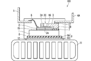
- FIG. FIG. 2 is a cross-sectional view showing the configuration of the semiconductor device 101. As shown in FIG. FIG. 2 shows a cross section along AA' shown in FIG.
- a semiconductor device 101 includes a heat spreader 1, a semiconductor element 2, a metal block 3, a first main terminal 4A, a second main terminal 4B, a signal terminal 5, a metal wire 6, an insulating member 7, a sealing material 8, and an insulating sheet 9. .
- FIG. 1 shows a state in which a sealing material 8 that covers the semiconductor element 2 and the like is seen through. The same applies to plan views shown below.
- FIG. 2 shows a state in which the semiconductor device 101 is mounted on the cooler 11 via heat dissipation grease 12 .
- hatching of the heat spreader 1 and the sealing material 8 is omitted for convenience of explanation. The same applies to the following sectional views.
- the heat spreader 1 is made of metal, for example.
- the heat spreader 1 holds the semiconductor element 2 on its upper surface via a bonding material 15 .
- the bonding material 15 is, for example, solder.
- the semiconductor element 2 is mounted on the upper surface of the heat spreader 1.
- the semiconductor element 2 is made of, for example, a semiconductor such as Si, or a so-called wide bandgap semiconductor such as SiC, GaN, or gallium oxide.
- the semiconductor element 2 is a power semiconductor element, a control IC (Integrated Circuit) for controlling the power semiconductor element, or the like.
- the semiconductor element 2 is, for example, an IGBT (Insulated Gate Bipolar Transistor), a MOSFET (Metal Oxide Semiconductor Field Effect Transistor), a Schottky barrier diode, or the like.
- the semiconductor element 2 may be an RC-IGBT (Reverse-Conducting IGBT) in which an IGBT and a freewheeling diode are formed in one semiconductor substrate.
- the semiconductor element 2 in Embodiment 1 is an IGBT.
- FIG. 3 is a plan view showing the configuration of the semiconductor element 2. As shown in FIG. The semiconductor element 2 is in a chip state and has a rectangular planar shape.
- Semiconductor element 2 includes, on its surface, surface electrode 2A, control electrode 2B and termination region 2C. A cell region (not shown) in which a plurality of IGBT cells are arranged is provided inside the termination region 2C.
- the surface electrode 2A is an electrode pad that functions as an IGBT emitter.
- Control electrode 2B includes a gate pad, an emitter sense pad, a temperature sense pad, and the like. The gate pad functions as the gate of the IGBT.
- the termination region 2C is provided around the cell region, that is, on the outer periphery of the chip. Termination region 2 ⁇ /b>C includes a guard ring that is a structure for holding the breakdown voltage of semiconductor element 2 .
- Semiconductor element 2 includes a back electrode (not shown) on its back surface. The back electrode functions as the collector of the IGBT. The back electrode is bonded to the top surface of the heat spreader 1 via a bonding material 15 . Here, the back electrode is bonded to a die pad area (not shown) provided on the top surface of the heat spreader 1 .
- the metal block 3 includes a joint surface 3A and a heat dissipation surface 3B.
- the joint surface 3A and the heat radiation surface 3B are located on the lower surface of the metal block 3.
- the bonding surface 3A is bonded to the surface electrode 2A of the semiconductor element 2 with a bonding material 16 interposed therebetween.
- the bonding material 16 is solder, for example.
- the heat dissipation surface 3B is connected to the upper surface of the heat spreader 1 via the insulating member 7. As shown in FIG. More specifically, the heat radiation surface 3B is in contact with the upper surface of the insulating member 7, and the lower surface of the insulating member 7 is in contact with the upper surface of the heat spreader 1. As shown in FIG.
- the metal block 3 extends from the bonding portion between the bonding surface 3A and the surface electrode 2A of the semiconductor element 2 to the outside of the semiconductor element 2 beyond one side of the semiconductor element 2 (the right side in FIG. 1). is bent into That is, the metal block 3 in Embodiment 1 has an L-shaped cross section and is provided so as to straddle over one side of the semiconductor element 2 .
- the metal block 3 be made of a material with high thermal conductivity and have a large heat capacity.
- the metal block 3 is preferably made of, for example, copper or an alloy containing copper. Copper or an alloy containing copper has a good bondability with solder.
- the metal block 3 made of copper or an alloy containing copper is excellent in assemblability.
- the metal block 3 is preferably made of a material having a linear expansion coefficient of 7 ppm/°C or more and 12 ppm/°C or less.
- the thickness of the metal block 3 is preferably about 2 mm, for example.
- the metal block 3 includes a through hole 3C in the joint surface 3A.
- the through hole 3 ⁇ /b>C penetrates between the upper surface and the lower surface of the metal block 3 .
- 3 C of through-holes are provided in the approximate center of 3 A of joint surfaces. In other words, the through hole 3C is provided approximately in the center of the joint between the joint surface 3A and the surface electrode 2A of the semiconductor element 2 in plan view.
- the insulating member 7 ensures the required dielectric strength against the voltage applied between the emitter and collector.
- the thickness of the insulating member 7 is preferably thin so that heat can be efficiently conducted from the metal block 3 to the heat spreader 1 . That is, the insulating member 7 should be thin as long as the withstand voltage is ensured.
- the first main terminal 4A has a plate shape.
- the first main terminal 4A includes one end and the other end opposite to the one end.
- One end of the first main terminal 4A is bonded to the upper surface of the metal block 3 with a bonding material 17 interposed therebetween.
- the bonding material 17 is solder, for example.
- the other end of the first main terminal 4A is led out of the sealing material 8 .
- the other end of the first main terminal 4A is formed so as to be connectable to an external circuit.
- the first main terminal 4A is an emitter connected to the surface electrode 2A of the semiconductor element 2 through the metal block 3. As shown in FIG.
- the first main terminal 4A has a bent portion between one end and the other end.
- the second main terminal 4B has a plate shape.
- the second main terminal 4B includes one end and the other end opposite to the one end.
- One end of the second main terminal 4B is bonded to the upper surface of the heat spreader 1 via a bonding material (bonding material 18 shown in FIG. 14).
- the bonding material 18 is solder, for example.
- the other end of the second main terminal 4B is led out of the sealing material 8 .
- the other end of the second main terminal 4B is formed so as to be connectable to an external circuit.
- the second main terminal 4B is a collector connected to the back electrode of the semiconductor element 2 through the heat spreader 1. As shown in FIG.
- the second main terminal 4B has a bent portion between one end and the other end.
- the signal terminal 5 has a plate shape.
- the signal terminal 5 includes one end and the other end positioned opposite to the one end.
- One end of signal terminal 5 is joined to control electrode 2B via metal wire 6 .
- the metal wire 6 is, for example, an aluminum wire.
- the other end of the signal terminal 5 is led out of the sealing material 8 .
- the other end of the signal terminal 5 is formed so as to be connectable to an external circuit.
- the signal terminal 5 has a bent portion between one end and the other end.
- the first main terminal 4A, the second main terminal 4B and the signal terminal 5 are preferably made of, for example, copper or an alloy containing copper.
- the first main terminal 4A, the second main terminal 4B and the signal terminal 5 are thinner than the metal block 3.
- the thicknesses of the first main terminal 4A, the second main terminal 4B, and the signal terminal 5 are preferably 1 mm or less, for example. Since the first main terminal 4A, the second main terminal 4B, and the signal terminal 5 are thinner than the metal block 3, they can be easily cut or bent in the manufacturing process of the semiconductor device 101.
- the insulating sheet 9 is attached to the lower surface of the heat spreader 1.
- the insulating sheet 9 has a configuration in which an insulating layer 9A and a copper foil 9B are integrated.
- the thickness of the insulating layer 9A is approximately 0.2 mm.
- the thickness of the copper foil 9B is approximately 0.1 mm.
- the sealing material 8 covers the heat spreader 1 , the semiconductor element 2 , the metal block 3 , one end of the first main terminal 4A, one end of the second main terminal 4B, the metal wire 6 , one end of the signal terminal 5 and the upper surface side of the insulating sheet 9 . Sealed. The lower surface of the copper foil 9B of the insulating sheet 9, the other end of the first main terminal 4A, the other end of the second main terminal 4B, and the other end of the signal terminal 5 are exposed from the sealing material 8. As shown in FIG.
- the sealing material 8 is, for example, mold resin. In an IGBT for power control, a high voltage is applied between the emitter and collector. The breakdown voltage of the IGBT is ensured by the mold resin and the guard ring of the termination region 2C.
- the cooler 11 is attached to the semiconductor device 101 via heat dissipation grease 12 .
- the heat dissipation grease 12 fills a minute space that may be created between the copper foil 9B of the insulating sheet 9 and the cooler 11 . Heat is easily conducted between the insulating sheet 9 and the cooler 11 by the heat dissipation grease 12 . Cooler 11 releases heat generated in semiconductor element 2 to the outside.
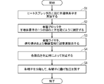
- FIG. 4 is a flow chart showing a method for manufacturing the semiconductor device 101. As shown in FIG. 4
- step S1 the semiconductor element 2 is mounted on the upper surface of the heat spreader 1 with the bonding material 15 interposed therebetween.
- the metal block 3 is placed at a predetermined position with respect to the semiconductor element 2 and the heat spreader 1.
- the joint surface 3A of the metal block 3 is positioned above the surface electrode 2A of the semiconductor element 2 . More specifically, the position of the through hole 3C of the metal block 3 is aligned with the vicinity of the center of the surface electrode 2A of the semiconductor element 2 in plan view.
- the heat radiation surface 3B of the metal block 3 is positioned above the insulating member 7 provided on the upper surface of the heat spreader 1. As shown in FIG.
- the insulating member 7 may be provided at a predetermined position on the upper surface of the heat spreader 1 in advance, or may be inserted between the metal block 3 and the heat spreader 1 in this step S2.
- a lead frame in which the first main terminal 4A, the second main terminal 4B, and the signal terminal 5 are integrated is placed on the metal block 3 and the heat spreader 1 at a predetermined position.
- a jig is used for positioning each part.
- the jig temporarily fixes the positional relationship between the metal block 3 and the semiconductor element 2, a gap is formed between the joint surface 3A of the metal block 3 and the surface electrode 2A of the semiconductor element 2. .
- the joints of the heat spreader 1, the semiconductor element 2, the metal block 3, and the lead frame are joined with a jointing material. That is, the metal block 3 is bonded to the semiconductor element 2 by the bonding material 16, the first main terminal 4A is bonded to the metal block 3 by the bonding material 17, and the second main terminal 4B is bonded to the heat spreader 1 by the bonding material 18. .
- the molten bonding material 16 is supplied from the through hole 3C.
- the bonding material 16 spreads in the gap between the bonding surface 3A and the surface electrode 2A.
- the bonding material 16 is solder, for example. Thereby, the metal block 3 is fixed so as to straddle over one side of the semiconductor element 2 .
- step S3 the metal wire 6 is ultrasonically bonded to the signal terminal 5 and the control electrode 2B. This process is a so-called wire bonding process.
- step S4 the heat spreader 1, the semiconductor element 2, the metal block 3, one end of the first main terminal 4A, one end of the second main terminal 4B, the metal wire 6, one end of the signal terminal 5, and the upper surface side of the insulating sheet 9 are molded.
- a resin pellet is set in the pot. Molten resin is extruded from the pot by a plunger into a heated mold. Resin flows into the cavity from the injection gate of the mold through runners. After that, the resin hardens, and the heat spreader 1, the semiconductor element 2, the metal block 3, one end of the first main terminal 4A, one end of the second main terminal 4B, the metal wire 6, one end of the signal terminal 5, and the upper surface of the insulating sheet 9 are exposed. , is sealed. The resin corresponds to the sealing material 8 .
- step S5 unnecessary resin hardened at the injection gate portion is cut off to form a package. Furthermore, the joint portion of the lead frame is cut, and the first main terminal 4A, the second main terminal 4B and the signal terminal 5 are separated from each other. The first main terminal 4A, the second main terminal 4B, and the signal terminal 5 are each bent into a predetermined shape. As described above, the semiconductor device 101 is completed.
- the other end of the first main terminal 4A and the other end of the second main terminal 4B are each connected to a bus bar (not shown).
- the IGBT When a voltage is applied between the gate and emitter of the IGBT from the signal terminal 5 through the gate pad, the IGBT is driven. That is, current flows from the collector-side bus bar to the second main terminal 4B, the heat spreader 1, the semiconductor element 2, the metal block 3, the first main terminal 4A, and the emitter-side bus bar in this order. At that time, heat is generated by the internal resistance of the semiconductor element 2 .
- the heat is not only emitted from the back surface of the semiconductor element 2 to the cooler 11 via the heat spreader 1, the insulating sheet 9, and the heat dissipation grease 12, but also is emitted from the front surface of the semiconductor element 2 to the metal block. 3.
- the heat is discharged to the cooler 11 through the insulating member 7, the heat spreader 1, the insulating sheet 9 and the heat dissipation grease 12.
- the metal block 3 has the function of transmitting heat and the function of storing heat, it is preferably made of a material with high thermal conductivity, and the metal block 3 preferably has a large heat capacity. Therefore, it is preferable that the metal block 3 is thick.
- the first main terminal 4 ⁇ /b>A is preferably thinner than the metal block 3 because it is cut or bent in the manufacturing process of the semiconductor device 101 .
- the integral part has a thick portion and a thin portion. That is, the part has a special and complicated shape, which increases production costs.
- the semiconductor device does not include the metal block 3, the heat generated by the semiconductor element 2 is also radiated through the first main terminal 4A having a thin plate shape, but a sufficient heat radiation effect cannot be expected.
- the metal block 3 and the first main terminal 4A in Embodiment 1 are parts different from each other.
- the semiconductor device 101 includes a metal block 3 that is thicker than the first main terminals 4A in order to increase heat capacity, and has first main terminals 4A that are thinner than the metal block 3 in order to improve workability. Therefore, both high heat dissipation and low production costs are achieved.
- Electric vehicles such as electric vehicles and hybrid vehicles are equipped with an inverter circuit.
- An inverter circuit for driving a three-phase motor has a configuration in which six semiconductor devices 101 are combined.
- the inverter circuit controls the number of revolutions of the three-phase motor and the like by PWM (Pulse Width Modulation) control.
- the motor may be temporarily locked, such as when the electric vehicle runs over a curb. At this time, a large current flows through the semiconductor element 2 .
- the amount of heat generated in the semiconductor element 2 is large, although the period during which the large current flows is short, about one second or less.
- the heat is not only emitted from the back surface of the semiconductor element 2 to the cooler 11 via the heat spreader 1, the insulating sheet 9 and the heat radiation grease 12, but also from the front surface of the semiconductor element 2.
- the heat is discharged to cooler 11 via metal block 3 , insulating member 7 , heat spreader 1 , insulating sheet 9 and heat dissipation grease 12 . Therefore, high heat dissipation is realized.
- the semiconductor device 101 includes the heat spreader 1, the semiconductor element 2, the metal block 3, the first main terminals 4A and the sealing material 8.
- the semiconductor element 2 includes a surface electrode 2A.
- a semiconductor element 2 is mounted on the upper surface of the heat spreader 1 .
- the metal block 3 includes a joint surface 3A and at least one heat dissipation surface 3B.
- the joint surface 3A is joined to the surface electrode 2A of the semiconductor element 2 .
- At least one heat dissipation surface 3B is connected to the upper surface of the heat spreader 1 via an insulating member 7. As shown in FIG.
- the metal block 3 extends from the bonding surface 3A to at least one heat dissipation surface 3B so as to straddle over at least one side of the semiconductor element 2 .
- the first main terminal 4A includes a first end and a second end. A first end is joined to the metal block 3 . The second end is located on the opposite side of the first end and formed connectable to an external circuit.
- the sealing material 8 seals the heat spreader 1, the semiconductor element 2, the metal block 3, and the first ends of the first main terminals 4A. A second end of the first main terminal 4A is exposed from the sealing material 8 .
- Such a semiconductor device 101 achieves both high heat dissipation and low production cost.
- the semiconductor device 101 is used in an inverter circuit for controlling motors of electric vehicles, electric trains, etc., or a converter circuit for regeneration.
- the metal block 3 in Embodiment 1 includes a through hole 3C in the joint surface 3A.
- the metal block 3 is made of copper or an alloy containing copper and the semiconductor element 2 is made of Si, the difference between the coefficient of linear expansion of the metal block 3 and the coefficient of linear expansion of the semiconductor element 2 is large.
- the stress caused by the temperature change is large.
- the bonding material 16 is plate-shaped solder or cream-shaped solder, the thickness of the solder changes before and after the reflow process.
- molten solder is supplied from through holes 3C of metal block 3 . Therefore, the thickness of the bonding material 16 matches the width of the gap and is controlled to a constant value. Therefore, the semiconductor device 101 having high reliability is realized.
- the metal block 3 by forming the metal block 3 from a material with a coefficient of linear expansion of 7 ppm/°C or more and 12 ppm/°C or less, the stress on the chip during heating in the bonding process or the like is reduced. Therefore, reliability of the semiconductor device 101 is improved.
- the semiconductor element 2 is formed of SiC, which has high thermal conductivity, heat dissipation is improved, so the size of the semiconductor element 2 can be reduced.
- Embodiment 2 A semiconductor device and a method for manufacturing the semiconductor device according to the second embodiment will be described.
- the same reference numerals are given to the same components as in Embodiment 1, and detailed description thereof will be omitted.
- FIG. 5 is a plan view showing the configuration of the semiconductor device 102 according to the second embodiment.
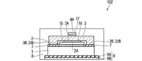
- FIG. 6 is a cross-sectional view showing the configuration of the semiconductor device 102. As shown in FIG. FIG. 6 shows a cross section at BB' shown in FIG.
- the metal block 3 includes multiple heat dissipation surfaces 3B. A plurality of heat dissipation surfaces 3 ⁇ /b>B are located on the lower surface of the metal block 3 .
- the metal block 3 includes a first heat dissipation surface 31B and a second heat dissipation surface 32B.
- the first heat dissipation surface 31B and the second heat dissipation surface 32B are connected to the upper surface of the heat spreader 1 via the insulating member 7, respectively.
- the joint surface 3A of the metal block 3 is positioned between the first heat dissipation surface 31B and the second heat dissipation surface 32B.
- the metal block 3 extends from the bonding portion between the bonding surface 3A and the surface electrode 2A of the semiconductor element 2 to the outside of the semiconductor element 2 beyond the first side of the semiconductor element 2 (upper side in FIG. 5) and downward. bent.
- the lower surface of the portion bent downward is the first heat radiation surface 31B.
- the metal block 3 extends outward from the semiconductor element 2 beyond the second side (lower side in FIG. 5) opposite to the first side of the semiconductor element 2 from the junction and bends downward. .
- the lower surface of the bent portion is the second heat dissipation surface 32B.
- the metal block 3 in the second embodiment has a U-shaped cross section and is provided so as to straddle over two sides of the semiconductor element 2 .
- the insulating member 7 is an insulating resin film formed on the upper surface of the heat spreader 1 .
- the insulating resin film is formed in a region excluding a die pad region to which the back electrode of the semiconductor element 2 is bonded and a terminal bonding region (not shown) to which the second main terminal 4B is bonded.
- the manufacturing method of the semiconductor device 102 according to the second embodiment is the same as the manufacturing method according to the first embodiment.
- the heat spreader 1 is prepared in which an insulating resin film is pre-coated in areas other than the die pad area and the terminal bonding area.
- a semiconductor element 2 is mounted on the die pad area of the heat spreader 1 .
- the solder does not flow out to the periphery of the die pad area.
- step S2 the joint surface 3A of the metal block 3 is joined to the surface electrode 2A of the semiconductor element 2, and the first heat dissipation surface 31B and the second heat dissipation surface 32B are connected to the heat spreader 1 through the insulating resin film.
- heat dissipation is improved because the metal block 3 has a plurality of heat dissipation surfaces 3B.
- the IGBT chip temperature distribution is leveled.
- the heat dissipation surface 3B of the metal block 3 is close to the upper surface of the heat spreader 1 via a thin insulating resin film, good heat dissipation can be obtained. Furthermore, since the thickness of the insulating resin film is highly uniform, uniform heat dissipation is realized in each heat dissipation surface 3B. Since it is not necessary to insert the insulating member 7 as in the first embodiment, productivity is improved.
- Embodiment 2 an example of semiconductor device 102 in which metal block 3 extends outside two sides of semiconductor element 2 is shown.
- the metal block 3 may extend outside the three sides of the semiconductor element 2 .
- the provision of the three heat dissipation surfaces 3B further improves heat dissipation.
- Embodiment 3 A semiconductor device and a method for manufacturing the semiconductor device according to the third embodiment will be described.
- the same reference numerals are given to the same components as those in Embodiment 1 or 2, and detailed description thereof will be omitted.
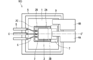
- FIG. 7 is a plan view showing the configuration of the semiconductor device 103 according to the third embodiment.
- FIG. 8 is a cross-sectional view showing the configuration of the semiconductor device 103. As shown in FIG. FIG. 8 shows a cross section along C-C' shown in FIG.
- the metal block 3 includes a recess 3D.
- the recess 3D is provided on the lower surface of the metal block 3. As shown in FIG.
- the recess 3D is recessed from the lower surface of the metal block 3 toward the upper surface with respect to the joint surface 3A.
- the recess 3D is provided outside the joint where the joint surface 3A and the surface electrode 2A of the semiconductor element 2 are joined.
- Recess 3D in the third embodiment is a groove provided above termination region 2C of semiconductor element 2, that is, above the guard ring.
- the extending direction of the groove corresponds to the extending direction of the guard ring.
- the manufacturing method of the semiconductor device 103 is the same as the manufacturing method in the first embodiment.
- step S4 when the resin is injected into the mold, the grooves of the metal block 3 improve the fluidity of the resin above the guard ring. Therefore, the generation of air bubbles is suppressed and the insulation is improved.
- Such a semiconductor device 103 prevents a decrease in breakdown voltage of the guard ring.
- Embodiment 4 A semiconductor device and a method for manufacturing the semiconductor device according to the fourth embodiment will be described.
- the same reference numerals are given to the same constituent elements as in any one of Embodiments 1 to 3, and detailed description thereof will be omitted.
- FIG. 9 is a plan view showing the configuration of the semiconductor device 104 according to the fourth embodiment.
- FIG. 10 is a cross-sectional view showing the structure of the semiconductor device 104. As shown in FIG. FIG. 10 shows a cross section along line D-D' shown in FIG.
- the metal block 3 includes a groove provided above the guard ring as the recess 3D, as in the third embodiment.
- Metal block 3 in the fourth embodiment includes hole 3E penetrating between the bottom of the groove and the upper surface of metal block 3 .
- the manufacturing method of the semiconductor device 104 is the same as the manufacturing method in the first embodiment.
- step S4 when the resin is injected into the mold, air bubbles are easily removed from the holes 3E.
- Such a semiconductor device 104 prevents a decrease in breakdown voltage of the guard ring.
- Embodiment 5 A semiconductor device and a method for manufacturing the semiconductor device according to the fifth embodiment will be described.
- the same reference numerals are given to the same components as in any one of Embodiments 1 to 4, and detailed description thereof will be omitted.
- FIG. 11 is a plan view showing the configuration of the semiconductor device 105 according to the fifth embodiment.
- FIG. 12 is a cross-sectional view showing the configuration of the semiconductor device 105. As shown in FIG. FIG. 12 shows a cross section along E-E' shown in FIG.
- the insulating member 7 between the upper surface of the heat spreader 1 and the heat radiation surface 3B of the metal block 3 is the sealing material 8. That is, the insulating member 7 is made of mold resin. In order to improve heat dissipation from the metal block 3 to the heat spreader 1, the mold resin between the heat dissipation surface 3B and the heat spreader 1 should be as thin as possible as long as the required dielectric strength is ensured.
- the manufacturing method of the semiconductor device 105 is the same as the manufacturing method in the first embodiment. However, in step S ⁇ b>2 , the metal block 3 and the like are joined with a gap formed between the upper surface of the heat spreader 1 and the heat radiation surface 3 ⁇ /b>B of the metal block 3 . In other words, the insulating member 7 does not exist between the upper surface of the heat spreader 1 and the heat radiation surface 3B of the metal block 3 after step S2 is completed. In step S4, resin is poured into the gap between the heat radiation surface 3B of the metal block 3 and the upper surface of the heat spreader 1, and the insulating member 7 is formed.
- the mold resin injected into the gap between the heat radiation surface 3B of the metal block 3 and the upper surface of the heat spreader 1 has both the insulating function between the metal block 3 and the heat spreader 1 and the heat radiation function from the metal block 3 to the heat spreader 1. come true. Since the insulating member 7 shown in the first embodiment and the insulating resin film shown in the second embodiment are not required, cost reduction is realized.
- Embodiment 6 A semiconductor device and a method for manufacturing the semiconductor device according to the sixth embodiment will be described.
- the same reference numerals are given to the same components as in any of Embodiments 1 to 5, and detailed description thereof will be omitted.
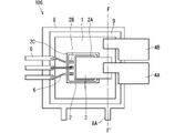
- FIG. 13 is a plan view showing the configuration of the semiconductor device 106 according to the sixth embodiment.
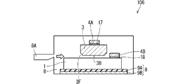
- FIG. 14 is a cross-sectional view showing the configuration of the semiconductor device 106. As shown in FIG. FIG. 14 shows a cross section along FF' shown in FIG.
- the manufacturing method of semiconductor device 106 is the same as the manufacturing method in the first embodiment.
- step S5 resin is injected from two injection gates 8A. 13 and 14 show the semiconductor device 106 before the hardened resin in the injection gate 8A is cut off.
- the metal block 3 has an inclined surface 3F at the end of the heat dissipation surface 3B.
- an injection gate 8A for injecting resin is provided laterally in the gap between the heat radiation surface 3B of the metal block 3 and the upper surface of the heat spreader 1.
- the height of the injection gate 8A approximately matches the height of the upper surface of the heat spreader 1. As shown in FIG. The resin is filled into the mold cavity through the injection gate 8A.
- the gap between the heat radiation surface 3B of the metal block 3 to the heat spreader 1 is narrow.
- resin is viscous, it is difficult to fill narrow spaces. If the gap is too narrow, the resin will not fill the gap and the collector and emitter of the IGBT will be shorted.
- the injection gate 8A is provided at approximately the same height as the upper surface of the heat spreader 1.
- FIG. The resin injected from the injection gate 8A flows along the upper surface of the heat spreader 1 and is further guided to the inclined surface 3F of the metal block 3 to efficiently fill the gap.
- a semiconductor device 106 that achieves both insulation and improved heat dissipation is realized. Even if the metal block 3 has a curved surface instead of the inclined surface 3F, the same effect can be obtained.
- Embodiment 7 A semiconductor device and a method for manufacturing the semiconductor device in Embodiment 7 will be described.
- the same reference numerals are given to the same constituent elements as in any one of Embodiments 1 to 6, and detailed description thereof will be omitted.
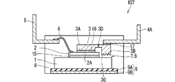
- FIG. 15 is a plan view showing the configuration of a semiconductor device 107 according to the seventh embodiment.
- FIG. 16 is a sectional view showing the configuration of the semiconductor device 107. As shown in FIG. FIG. 16 shows a cross section along GG' shown in FIG. As in the sixth embodiment, FIG. 15 shows semiconductor device 107 before the hardened resin in injection gate 8A is cut off.
- the metal block 3 includes a plurality of fine grooves 3G on the heat dissipation surface 3B.
- the extending direction of these streak-like fine grooves 3G is the direction from the injection gate 8A toward the gap between the heat radiation surface 3B of the metal block 3 and the upper surface of the heat spreader 1.
- the injection gate 8A is provided at the end where the narrow groove 3G extends. Since the resin injected from the injection gate 8A is filled along the linear narrow grooves 3G, the filling property is further improved.
Landscapes
- Cooling Or The Like Of Semiconductors Or Solid State Devices (AREA)
- Engineering & Computer Science (AREA)
- Chemical & Material Sciences (AREA)
- Materials Engineering (AREA)
- Microelectronics & Electronic Packaging (AREA)
Abstract
Description
図1は、実施の形態1における半導体装置101の構成を示す平面図である。図2は、その半導体装置101の構成を示す断面図である。図2は、図1に示されるA-A’における断面を示している。
実施の形態2における半導体装置および半導体装置の製造方法を説明する。実施の形態2において、実施の形態1と同様の構成要素には、同一の参照符号を付し、それらの詳細な説明は省略する。
実施の形態3における半導体装置および半導体装置の製造方法を説明する。実施の形態3において、実施の形態1または2と同様の構成要素には、同一の参照符号を付し、それらの詳細な説明は省略する。
実施の形態4における半導体装置および半導体装置の製造方法を説明する。実施の形態4において、実施の形態1から3のいずれかと同様の構成要素には、同一の参照符号を付し、それらの詳細な説明は省略する。
実施の形態5における半導体装置および半導体装置の製造方法を説明する。実施の形態5において、実施の形態1から4のいずれかと同様の構成要素には、同一の参照符号を付し、それらの詳細な説明は省略する。
実施の形態6における半導体装置および半導体装置の製造方法を説明する。実施の形態6において、実施の形態1から5のいずれかと同様の構成要素には、同一の参照符号を付し、それらの詳細な説明は省略する。
実施の形態7における半導体装置および半導体装置の製造方法を説明する。実施の形態7において、実施の形態1から6のいずれかと同様の構成要素には、同一の参照符号を付し、それらの詳細な説明は省略する。
Claims (16)
- ヒートスプレッダと、
表面電極を含み、前記ヒートスプレッダの上面に実装された半導体素子と、
前記半導体素子の前記表面電極に接合される接合面と、前記ヒートスプレッダの前記上面に絶縁部材を介して接続される少なくとも1つの放熱面と、を含み、前記半導体素子の少なくとも1つの辺の上方を跨ぐように前記接合面から前記少なくとも1つの放熱面に延伸する金属ブロックと、
前記金属ブロックに接合される第1端と、前記第1端とは反対側に位置し外部回路に接続可能に形成された第2端と、を含む端子と、
前記ヒートスプレッダと前記半導体素子と前記金属ブロックと前記端子の前記第1端とを封止している封止材と、を備え、
前記端子の前記第2端は、前記封止材から露出している、半導体装置。 - 前記金属ブロックは、前記接合面に貫通孔を含む、請求項1に記載の半導体装置。
- 前記絶縁部材は、前記ヒートスプレッダの前記上面に設けられた絶縁樹脂膜である、請求項1または請求項2に記載の半導体装置。
- 前記少なくとも1つの放熱面は、複数の放熱面であり、
前記接合面は、前記複数の放熱面の間に位置して、前記表面電極に接合されており、
前記金属ブロックは、前記半導体素子の複数の辺の上方を跨ぐように前記接合面から前記複数の放熱面に延伸している、請求項1から請求項3のうちいずれか一項に記載の半導体装置。 - 前記金属ブロックは、前記接合面と前記表面電極とが接合された接合部よりも外側に凹部を含み、
前記凹部は、前記接合面に対して前記金属ブロックの下面から前記上面の方向に凹んでいる、請求項1から請求項4のうちいずれか一項に記載の半導体装置。 - 前記金属ブロックは、前記凹部の底部と前記金属ブロックの前記上面との間を貫通する孔を含む、請求項5に記載の半導体装置。
- 前記金属ブロックは、線膨張係数が7ppm/℃以上、12ppm/℃以下の材料で形成される、請求項1から請求項6のうちいずれか一項に記載の半導体装置。
- 前記半導体素子は、SiCで形成されている、請求項1から請求項7のうちいずれか一項に記載の半導体装置。
- ヒートスプレッダと、
表面電極を含み、前記ヒートスプレッダの上面に実装された半導体素子と、
前記半導体素子の前記表面電極に接合される接合面と、前記ヒートスプレッダの前記上面に絶縁部材を介して接続される少なくとも1つの放熱面と、を含み、前記半導体素子の少なくとも1つの辺の上方を跨ぐように前記接合面から前記少なくとも1つの放熱面に延伸する金属ブロックと、
前記ヒートスプレッダと前記半導体素子と前記金属ブロックとを封止している封止材と、を備え、
前記絶縁部材は、前記封止材である、半導体装置。 - 前記金属ブロックは、前記放熱面に複数の細溝を含み、
前記複数の細溝の延伸方向は、一方向に揃っている、請求項9に記載の半導体装置。 - 前記金属ブロックは、前記放熱面の端部に斜面または湾曲面を有する、請求項9または請求項10に記載の半導体装置。
- 前記金属ブロックは、線膨張係数が7ppm/℃以上、12ppm/℃以下の材料で形成される、請求項9から請求項11のうちいずれか一項に記載の半導体装置。
- 前記半導体素子は、SiCで形成されている、請求項9から請求項12のうちいずれか一項に記載の半導体装置。
- ヒートスプレッダの上面に半導体素子を実装する工程と、
前記半導体素子の少なくとも1つの辺の上方を跨ぐように金属ブロックを固定する工程と、を備え、
前記金属ブロックを固定する工程は、
前記金属ブロックの接合面を前記半導体素子の表面電極に接合する工程と、
前記金属ブロックの放熱面を前記ヒートスプレッダの前記上面に絶縁部材を介して接続する工程と、を含み、
前記金属ブロックの前記放熱面を接続する工程は、
前記ヒートスプレッダと前記半導体素子と前記金属ブロックとを封止するための封止材を、前記絶縁部材として、前記金属ブロックの前記放熱面と前記ヒートスプレッダの前記上面との隙間に注入する工程を、含み、
前記封止材は、前記金属ブロックの前記放熱面と前記ヒートスプレッダの前記上面との前記隙間の横方向に設けられた注入用ゲートを介して注入される、半導体装置の製造方法。 - 前記注入用ゲートの高さは、前記ヒートスプレッダの前記上面の高さに一致している、請求項14に記載の半導体装置の製造方法。
- 前記金属ブロックは、前記放熱面に複数の細溝を含み、
前記複数の細溝の延伸方向は、前記注入用ゲートから前記隙間に向かう方向である、請求項14または請求項15に記載の半導体装置の製造方法。
Priority Applications (5)
| Application Number | Priority Date | Filing Date | Title |
|---|---|---|---|
| US18/260,282 US20240063073A1 (en) | 2021-03-25 | 2021-03-25 | Semiconductor device and method of manufacturing semiconductor device |
| PCT/JP2021/012534 WO2022201426A1 (ja) | 2021-03-25 | 2021-03-25 | 半導体装置および半導体装置の製造方法 |
| JP2023508311A JP7387059B2 (ja) | 2021-03-25 | 2021-03-25 | 半導体装置および半導体装置の製造方法 |
| DE112021007373.7T DE112021007373T5 (de) | 2021-03-25 | 2021-03-25 | Halbleitervorrichtung und Verfahren zum Herstellen einer Halbleitervorrichtung |
| CN202180096066.3A CN117043937A (zh) | 2021-03-25 | 2021-03-25 | 半导体装置以及半导体装置的制造方法 |
Applications Claiming Priority (1)
| Application Number | Priority Date | Filing Date | Title |
|---|---|---|---|
| PCT/JP2021/012534 WO2022201426A1 (ja) | 2021-03-25 | 2021-03-25 | 半導体装置および半導体装置の製造方法 |
Publications (1)
| Publication Number | Publication Date |
|---|---|
| WO2022201426A1 true WO2022201426A1 (ja) | 2022-09-29 |
Family
ID=83395420
Family Applications (1)
| Application Number | Title | Priority Date | Filing Date |
|---|---|---|---|
| PCT/JP2021/012534 Ceased WO2022201426A1 (ja) | 2021-03-25 | 2021-03-25 | 半導体装置および半導体装置の製造方法 |
Country Status (5)
| Country | Link |
|---|---|
| US (1) | US20240063073A1 (ja) |
| JP (1) | JP7387059B2 (ja) |
| CN (1) | CN117043937A (ja) |
| DE (1) | DE112021007373T5 (ja) |
| WO (1) | WO2022201426A1 (ja) |
Families Citing this family (1)
| Publication number | Priority date | Publication date | Assignee | Title |
|---|---|---|---|---|
| JP7474557B1 (ja) * | 2022-12-22 | 2024-04-25 | ヌヴォトンテクノロジージャパン株式会社 | 蓄電パック、半導体装置、および、半導体装置の製造方法 |
Citations (8)
| Publication number | Priority date | Publication date | Assignee | Title |
|---|---|---|---|---|
| JP2000058746A (ja) * | 1998-08-10 | 2000-02-25 | Toyota Motor Corp | モジュール内冷却装置 |
| JP2003258166A (ja) * | 2001-12-27 | 2003-09-12 | Denso Corp | 半導体装置 |
| JP2005286225A (ja) * | 2004-03-30 | 2005-10-13 | Toshiba Corp | インターフェイスモジュール付lsiパッケージ、lsiパッケージ及び伝送線路ヘッダー |
| JP2009124082A (ja) * | 2007-11-19 | 2009-06-04 | Mitsubishi Electric Corp | 電力用半導体装置 |
| JP2011253862A (ja) * | 2010-06-01 | 2011-12-15 | Mitsubishi Electric Corp | パワー半導体装置 |
| JP2014154613A (ja) * | 2013-02-06 | 2014-08-25 | Mitsubishi Electric Corp | 半導体装置およびその製造方法 |
| WO2017130370A1 (ja) * | 2016-01-29 | 2017-08-03 | 三菱電機株式会社 | 半導体装置 |
| WO2018047485A1 (ja) * | 2016-09-06 | 2018-03-15 | ローム株式会社 | パワーモジュールおよびインバータ装置 |
Family Cites Families (4)
| Publication number | Priority date | Publication date | Assignee | Title |
|---|---|---|---|---|
| JP3345241B2 (ja) * | 1995-11-30 | 2002-11-18 | 三菱電機株式会社 | 半導体装置 |
| WO2007141851A1 (ja) * | 2006-06-07 | 2007-12-13 | Fujitsu Limited | 半導体パッケージ及び電子装置 |
| JP2013070026A (ja) * | 2011-09-08 | 2013-04-18 | Rohm Co Ltd | 半導体装置、半導体装置の製造方法、半導体装置の実装構造、およびパワー用半導体装置 |
| JP6120704B2 (ja) * | 2013-07-03 | 2017-04-26 | 三菱電機株式会社 | 半導体装置 |
-
2021
- 2021-03-25 CN CN202180096066.3A patent/CN117043937A/zh active Pending
- 2021-03-25 JP JP2023508311A patent/JP7387059B2/ja active Active
- 2021-03-25 DE DE112021007373.7T patent/DE112021007373T5/de active Pending
- 2021-03-25 WO PCT/JP2021/012534 patent/WO2022201426A1/ja not_active Ceased
- 2021-03-25 US US18/260,282 patent/US20240063073A1/en active Pending
Patent Citations (8)
| Publication number | Priority date | Publication date | Assignee | Title |
|---|---|---|---|---|
| JP2000058746A (ja) * | 1998-08-10 | 2000-02-25 | Toyota Motor Corp | モジュール内冷却装置 |
| JP2003258166A (ja) * | 2001-12-27 | 2003-09-12 | Denso Corp | 半導体装置 |
| JP2005286225A (ja) * | 2004-03-30 | 2005-10-13 | Toshiba Corp | インターフェイスモジュール付lsiパッケージ、lsiパッケージ及び伝送線路ヘッダー |
| JP2009124082A (ja) * | 2007-11-19 | 2009-06-04 | Mitsubishi Electric Corp | 電力用半導体装置 |
| JP2011253862A (ja) * | 2010-06-01 | 2011-12-15 | Mitsubishi Electric Corp | パワー半導体装置 |
| JP2014154613A (ja) * | 2013-02-06 | 2014-08-25 | Mitsubishi Electric Corp | 半導体装置およびその製造方法 |
| WO2017130370A1 (ja) * | 2016-01-29 | 2017-08-03 | 三菱電機株式会社 | 半導体装置 |
| WO2018047485A1 (ja) * | 2016-09-06 | 2018-03-15 | ローム株式会社 | パワーモジュールおよびインバータ装置 |
Also Published As
| Publication number | Publication date |
|---|---|
| JP7387059B2 (ja) | 2023-11-27 |
| DE112021007373T5 (de) | 2024-02-15 |
| US20240063073A1 (en) | 2024-02-22 |
| CN117043937A (zh) | 2023-11-10 |
| JPWO2022201426A1 (ja) | 2022-09-29 |
Similar Documents
| Publication | Publication Date | Title |
|---|---|---|
| JP5067267B2 (ja) | 樹脂封止型半導体装置とその製造方法 | |
| US9673118B2 (en) | Power module and method of manufacturing power module | |
| KR101585306B1 (ko) | 반도체 장치 및 그 제조 방법 | |
| US8497572B2 (en) | Semiconductor module and method of manufacturing the same | |
| US8183094B2 (en) | Method of manufacturing a semiconductor device having a semiconductor chip and resin sealing portion | |
| JP6115738B2 (ja) | 半導体装置およびその製造方法 | |
| US11862542B2 (en) | Dual side cooling power module and manufacturing method of the same | |
| CN115223977B (zh) | 电力半导体装置、电力半导体装置的制造方法及电力变换装置 | |
| JP6575739B1 (ja) | 半導体装置、半導体装置の製造方法および電力変換装置 | |
| US12113002B2 (en) | Plurality of transistors attached to a heat sink with a periphery notch | |
| JP7387059B2 (ja) | 半導体装置および半導体装置の製造方法 | |
| JP7278439B1 (ja) | 半導体装置及びそれを用いた電力変換装置 | |
| JP6401444B2 (ja) | パワーモジュールおよびその製造方法 | |
| CN111834346B (zh) | 晶体管功率模块封装结构及其封装方法 | |
| JP2024138858A (ja) | 電力用半導体装置、電力変換装置、及び、電力用半導体装置の製造方法 | |
| JP7543854B2 (ja) | 半導体装置及び半導体装置の製造方法 | |
| CN116705721A (zh) | 半导体装置 | |
| JP7512659B2 (ja) | 半導体モジュール及び半導体モジュールの製造方法 | |
| US20250125207A1 (en) | Semiconductor module and manufacturing method therefor | |
| JP7422945B2 (ja) | 電力用半導体装置 | |
| US20240387443A1 (en) | Semiconductor module and method for producing semiconductor module | |
| JP2025115059A (ja) | 半導体モジュール | |
| JP2025089094A (ja) | 半導体装置、電子装置、および電子装置の製造方法 | |
| JP2004311533A (ja) | 半導体装置 |
Legal Events
| Date | Code | Title | Description |
|---|---|---|---|
| 121 | Ep: the epo has been informed by wipo that ep was designated in this application |
Ref document number: 21933035 Country of ref document: EP Kind code of ref document: A1 |
|
| ENP | Entry into the national phase |
Ref document number: 2023508311 Country of ref document: JP Kind code of ref document: A |
|
| WWE | Wipo information: entry into national phase |
Ref document number: 18260282 Country of ref document: US |
|
| WWE | Wipo information: entry into national phase |
Ref document number: 202180096066.3 Country of ref document: CN |
|
| WWE | Wipo information: entry into national phase |
Ref document number: 112021007373 Country of ref document: DE |
|
| 122 | Ep: pct application non-entry in european phase |
Ref document number: 21933035 Country of ref document: EP Kind code of ref document: A1 |