WO2022201285A1 - カセット筐体、プローバー、サーバーラックおよびストレージシステム - Google Patents
カセット筐体、プローバー、サーバーラックおよびストレージシステム Download PDFInfo
- Publication number
- WO2022201285A1 WO2022201285A1 PCT/JP2021/011858 JP2021011858W WO2022201285A1 WO 2022201285 A1 WO2022201285 A1 WO 2022201285A1 JP 2021011858 W JP2021011858 W JP 2021011858W WO 2022201285 A1 WO2022201285 A1 WO 2022201285A1
- Authority
- WO
- WIPO (PCT)
- Prior art keywords
- cassette housing
- semiconductor wafer
- heat transfer
- probe card
- cassette
- Prior art date
- Legal status (The legal status is an assumption and is not a legal conclusion. Google has not performed a legal analysis and makes no representation as to the accuracy of the status listed.)
- Ceased
Links
Images




Classifications
-
- H—ELECTRICITY
- H10—SEMICONDUCTOR DEVICES; ELECTRIC SOLID-STATE DEVICES NOT OTHERWISE PROVIDED FOR
- H10P—GENERIC PROCESSES OR APPARATUS FOR THE MANUFACTURE OR TREATMENT OF DEVICES COVERED BY CLASS H10
- H10P72/00—Handling or holding of wafers, substrates or devices during manufacture or treatment thereof
- H10P72/30—Handling or holding of wafers, substrates or devices during manufacture or treatment thereof for conveying, e.g. between different workstations
- H10P72/34—Handling or holding of wafers, substrates or devices during manufacture or treatment thereof for conveying, e.g. between different workstations the wafers being stored in a carrier, involving loading and unloading
- H10P72/3404—Storage means
-
- G—PHYSICS
- G01—MEASURING; TESTING
- G01R—MEASURING ELECTRIC VARIABLES; MEASURING MAGNETIC VARIABLES
- G01R1/00—Details of instruments or arrangements of the types included in groups G01R5/00 - G01R13/00 and G01R31/00
- G01R1/02—General constructional details
- G01R1/06—Measuring leads; Measuring probes
- G01R1/067—Measuring probes
- G01R1/06711—Probe needles; Cantilever beams; "Bump" contacts; Replaceable probe pins
- G01R1/06755—Material aspects
-
- G—PHYSICS
- G01—MEASURING; TESTING
- G01R—MEASURING ELECTRIC VARIABLES; MEASURING MAGNETIC VARIABLES
- G01R1/00—Details of instruments or arrangements of the types included in groups G01R5/00 - G01R13/00 and G01R31/00
- G01R1/02—General constructional details
- G01R1/06—Measuring leads; Measuring probes
- G01R1/067—Measuring probes
- G01R1/073—Multiple probes
- G01R1/07307—Multiple probes with individual probe elements, e.g. needles, cantilever beams or bump contacts, fixed in relation to each other, e.g. bed of nails fixture or probe card
- G01R1/07314—Multiple probes with individual probe elements, e.g. needles, cantilever beams or bump contacts, fixed in relation to each other, e.g. bed of nails fixture or probe card the body of the probe being perpendicular to test object, e.g. bed of nails or probe with bump contacts on a rigid support
-
- G—PHYSICS
- G11—INFORMATION STORAGE
- G11C—STATIC STORES
- G11C29/00—Checking stores for correct operation ; Subsequent repair; Testing stores during standby or offline operation
- G11C29/56—External testing equipment for static stores, e.g. automatic test equipment [ATE]; Interfaces therefor
- G11C29/56016—Apparatus features
-
- H—ELECTRICITY
- H10—SEMICONDUCTOR DEVICES; ELECTRIC SOLID-STATE DEVICES NOT OTHERWISE PROVIDED FOR
- H10P—GENERIC PROCESSES OR APPARATUS FOR THE MANUFACTURE OR TREATMENT OF DEVICES COVERED BY CLASS H10
- H10P72/00—Handling or holding of wafers, substrates or devices during manufacture or treatment thereof
- H10P72/04—Apparatus for manufacture or treatment
- H10P72/0431—Apparatus for thermal treatment
- H10P72/0434—Apparatus for thermal treatment mainly by convection
-
- H—ELECTRICITY
- H10—SEMICONDUCTOR DEVICES; ELECTRIC SOLID-STATE DEVICES NOT OTHERWISE PROVIDED FOR
- H10P—GENERIC PROCESSES OR APPARATUS FOR THE MANUFACTURE OR TREATMENT OF DEVICES COVERED BY CLASS H10
- H10P72/00—Handling or holding of wafers, substrates or devices during manufacture or treatment thereof
- H10P72/06—Apparatus for monitoring, sorting, marking, testing or measuring
- H10P72/0602—Temperature monitoring
-
- H—ELECTRICITY
- H10—SEMICONDUCTOR DEVICES; ELECTRIC SOLID-STATE DEVICES NOT OTHERWISE PROVIDED FOR
- H10P—GENERIC PROCESSES OR APPARATUS FOR THE MANUFACTURE OR TREATMENT OF DEVICES COVERED BY CLASS H10
- H10P72/00—Handling or holding of wafers, substrates or devices during manufacture or treatment thereof
- H10P72/10—Handling or holding of wafers, substrates or devices during manufacture or treatment thereof using carriers specially adapted therefor, e.g. front opening unified pods [FOUP]
- H10P72/19—Handling or holding of wafers, substrates or devices during manufacture or treatment thereof using carriers specially adapted therefor, e.g. front opening unified pods [FOUP] closed carriers
- H10P72/1902—Handling or holding of wafers, substrates or devices during manufacture or treatment thereof using carriers specially adapted therefor, e.g. front opening unified pods [FOUP] closed carriers specially adapted for a single substrate
-
- H—ELECTRICITY
- H10—SEMICONDUCTOR DEVICES; ELECTRIC SOLID-STATE DEVICES NOT OTHERWISE PROVIDED FOR
- H10P—GENERIC PROCESSES OR APPARATUS FOR THE MANUFACTURE OR TREATMENT OF DEVICES COVERED BY CLASS H10
- H10P72/00—Handling or holding of wafers, substrates or devices during manufacture or treatment thereof
- H10P72/30—Handling or holding of wafers, substrates or devices during manufacture or treatment thereof for conveying, e.g. between different workstations
- H10P72/32—Handling or holding of wafers, substrates or devices during manufacture or treatment thereof for conveying, e.g. between different workstations between different workstations
- H10P72/3218—Conveying cassettes, containers or carriers
-
- H—ELECTRICITY
- H10—SEMICONDUCTOR DEVICES; ELECTRIC SOLID-STATE DEVICES NOT OTHERWISE PROVIDED FOR
- H10P—GENERIC PROCESSES OR APPARATUS FOR THE MANUFACTURE OR TREATMENT OF DEVICES COVERED BY CLASS H10
- H10P72/00—Handling or holding of wafers, substrates or devices during manufacture or treatment thereof
- H10P72/30—Handling or holding of wafers, substrates or devices during manufacture or treatment thereof for conveying, e.g. between different workstations
- H10P72/34—Handling or holding of wafers, substrates or devices during manufacture or treatment thereof for conveying, e.g. between different workstations the wafers being stored in a carrier, involving loading and unloading
- H10P72/3411—Handling or holding of wafers, substrates or devices during manufacture or treatment thereof for conveying, e.g. between different workstations the wafers being stored in a carrier, involving loading and unloading involving loading and unloading of wafers
- H10P72/3412—Batch transfer of wafers
-
- H—ELECTRICITY
- H10—SEMICONDUCTOR DEVICES; ELECTRIC SOLID-STATE DEVICES NOT OTHERWISE PROVIDED FOR
- H10P—GENERIC PROCESSES OR APPARATUS FOR THE MANUFACTURE OR TREATMENT OF DEVICES COVERED BY CLASS H10
- H10P74/00—Testing or measuring during manufacture or treatment of wafers, substrates or devices
- H10P74/27—Structural arrangements therefor
- H10P74/273—Interconnections for measuring or testing, e.g. probe pads
-
- G—PHYSICS
- G01—MEASURING; TESTING
- G01R—MEASURING ELECTRIC VARIABLES; MEASURING MAGNETIC VARIABLES
- G01R31/00—Arrangements for testing electric properties; Arrangements for locating electric faults; Arrangements for electrical testing characterised by what is being tested not provided for elsewhere
- G01R31/28—Testing of electronic circuits, e.g. by signal tracer
- G01R31/2851—Testing of integrated circuits [IC]
- G01R31/2855—Environmental, reliability or burn-in testing
- G01R31/2872—Environmental, reliability or burn-in testing related to electrical or environmental aspects, e.g. temperature, humidity, vibration, nuclear radiation
- G01R31/2874—Environmental, reliability or burn-in testing related to electrical or environmental aspects, e.g. temperature, humidity, vibration, nuclear radiation related to temperature
-
- G—PHYSICS
- G11—INFORMATION STORAGE
- G11C—STATIC STORES
- G11C29/00—Checking stores for correct operation ; Subsequent repair; Testing stores during standby or offline operation
- G11C29/56—External testing equipment for static stores, e.g. automatic test equipment [ATE]; Interfaces therefor
- G11C2029/5602—Interface to device under test
-
- G—PHYSICS
- G11—INFORMATION STORAGE
- G11C—STATIC STORES
- G11C7/00—Arrangements for writing information into, or reading information out from, a digital store
- G11C7/04—Arrangements for writing information into, or reading information out from, a digital store with means for avoiding disturbances due to temperature effects
Definitions
- Embodiments of the present invention relate to cassette housings, probers, server racks and storage systems.
- a probe card is used as an inspection jig that relays electrical signals between a semiconductor wafer on which semiconductor chips are formed and an inspection device that inspects the semiconductor chips.
- a pad electrode is also formed on the semiconductor wafer.
- the probe card includes a probe card substrate and probes.
- a probe card is electrically connected to a semiconductor wafer by a prober. More specifically, the prober brings the pad electrodes of the semiconductor wafer into contact with the probes of the probe card. Thereby, the semiconductor chip of the semiconductor wafer and the probe card substrate of the probe card are electrically connected.
- One embodiment provides a cassette enclosure, prober, server rack and storage system capable of temperature conditioning for semiconductor wafers containing multiple non-volatile memory chips.
- the cassette housing includes a storage section, a probe card, and a storage section.
- the storage unit stores a semiconductor wafer including a plurality of nonvolatile memory chips.
- the probe card has probes to be brought into contact with pad electrodes provided on the semiconductor wafer.
- the accommodation portion accommodates a heat transfer liquid for cooling or raising the temperature of the semiconductor wafers stored in the storage portion.
- FIG. 1 is a block diagram showing a configuration example of a storage system according to a first embodiment
- FIG. FIG. 2 is a schematic diagram showing a temperature adjustment mechanism for a cassette housing and a prober of the storage system according to the first embodiment
- 4 is a schematic diagram showing a temperature adjustment mechanism of a server rack of the storage system according to the first embodiment
- FIG. FIG. 4 is a schematic diagram showing an example in which the probe card substrate is immersed in cooling liquid within the cassette housing of the storage system according to the first embodiment
- FIG. 4 is a schematic diagram showing an example in which the probes of the probe card and the pad electrodes of the wafer are immersed in a heat transfer fluid within the cassette housing of the storage system according to the first embodiment
- FIG. 4 is a schematic diagram showing an example in which wafers are immersed in a heat transfer liquid within the cassette housing of the storage system according to the first embodiment
- FIG. 11 is a schematic diagram showing an example of cooling or raising the temperature of a cassette housing in which wafers are stored in the storage system according to the second embodiment with a heat transfer fluid
- FIG. 11 is a schematic diagram showing a temperature adjustment mechanism included in a storage system according to a second embodiment
- FIG. FIG. 11 is a schematic diagram showing a temperature adjustment mechanism included in a storage system according to a third embodiment
- FIG. FIG. 14 is a schematic diagram showing a modified example of the temperature adjustment mechanism included in the storage system according to the third embodiment
- the first embodiment is a large-capacity storage system that uses semiconductor wafers without dicing. Also, in the first embodiment, a plurality of semiconductor wafers can be exchanged.
- FIG. 1 is a block diagram showing a configuration example of the storage system 1 according to the first embodiment.
- the storage system 1 includes a plurality of semiconductor wafers (wafers) 100 as storage.
- the storage system 1 selects a predetermined number of wafers 100 from multiple wafers 100 .
- the storage system 1 uses the selected predetermined number of wafers 100 .
- Wafer 100 includes a plurality of NAND flash memory chips (NAND chips).
- the storage system 1 also includes a plurality of cassette housings 200 .
- Cassette housing 200 incorporates probe card 210 .
- Cassette housing 200 stores wafers 100 .
- the storage system 1 has a wafer stocker 10 , a cassette stocker 20 , a prober (cassetter) 30 , a cassette transporter 40 and a server rack 50 .
- the wafer stocker 10 is a device that stores the wafers 100. Wafer stocker 10 stores a plurality of wafers 100 .
- the cassette stocker 20 is a device that stores the cassette housing 200.
- the cassette stocker 20 stores multiple cassette housings 200 .
- the plurality of cassette housings 200 stored in the cassette stocker 20 can include a mixture of cassette housings 200 containing wafers 100 and cassette housings 200 containing no wafers 100 .
- the prober 30 is a device that brings the pad electrodes 101 of the wafer 100 into contact with the probes 211 of the probe card 210 .
- the cassette transporter 40 is a device that transports the cassette housing 200 .
- the cassette transporter 40 transports the cassette housing 200 from the cassette stocker 20 to the server rack 50 .
- the cassette transporter 40 transports the cassette housing 200 from the server rack 50 to the cassette stocker 20 .
- the cassette transporter 40 transports the cassette housing 200 from the prober 30 to the server rack 50 .
- the cassette transporter 40 transports the cassette housing 200 from the server rack 50 to the prober 30 .
- the server rack 50 is a device that stores the host computer 51.
- the number of host computers 51 stored in the server rack 50 may be one or plural.
- the host computer 51 is, for example, a file server.
- the host computer 51 has a processor 52 and a storage section 53 .
- the processor 52 is a device that executes programs.
- the processor 52 executes data write processing to the wafer 100 in the cassette housing 200 or data read processing from the wafer 100 .
- the storage unit 53 is a device that stores the cassette housing 200 .
- the storage unit 53 stores a cassette housing 200 in which the wafers 100 are stored.
- the number of cassette housings 200 stored in the storage unit 53 may be one, or may be plural.
- the prober 30 has an attachment/detachment mechanism 31 .
- the attachment/detachment mechanism 31 is a device that integrates or separates the wafer 100 and the cassette housing 200 .
- the pad electrodes of the wafer 100 and the probes of the probe card in the cassette housing 200 come into contact with each other. Thereby, the NAND chips of the wafer 100 and the probe card substrate of the probe card are electrically connected.
- the wafer 100 in the cassette housing 200 stored in the server rack 50 and the wafer 100 in the cassette housing 200 stored in the cassette stocker 20 or the wafer 100 stored in the wafer stocker 10 are separated. I will explain the replacement.
- the storage system 1 replaces the wafer 100. No need.
- the storage system 1 stores the wafer 100 in the cassette housing 200 stored in the server rack 50 and the cassette stocker 20 The wafers 100 stored in the cassette housing 200 stored in , or the wafers 100 stored in the wafer stocker 10 are exchanged.
- the storage system 1 between the server rack 50 and the cassette stocker 20 the cassette housing 200 is replaced.
- the cassette housing 200 removed from the server rack 50 is, for example, the cassette housing 200 that stores the wafers 100 that have not been accessed by the processor 52 in the server rack 50 for the longest period of time.
- the storage system 1 causes the prober 30 to store the wafer 100 to which the processor 52 is to write data in the cassette housing 200 . do. Also, the storage system 1 removes from the server rack 50 the cassette housing 200 that stores the wafer 100 that has not been accessed by the processor 52 for the longest period of time in the server rack 50 . The storage system 1 moves the cassette housing 200 removed from the server rack 50 to the cassette stocker 20 . The storage system 1 also moves the cassette housing 200 in which the wafers 100 are stored from the prober 30 to the server rack 50 by the prober 30 .
- the temperature adjustment mechanism is a mechanism that cools or heats the wafer 100 .
- a temperature control mechanism is provided in the cassette housing 200 , the prober 30 and the server rack 50 .
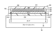
- FIG. 2 is a schematic diagram showing the temperature adjustment mechanism of the cassette housing 200 and the prober 30. As shown in FIG.
- the cassette housing 200 has an upper casing 201 and a lower casing 202 .
- the top casing 201 is a member that covers the top side of the wafer 100 .
- a probe card 201 is arranged in the upper casing 201 .
- the lower surface casing 202 is a member that covers the lower surface side of the wafer 100 .
- a storage portion 203 is provided in the inner wall portion of the lower surface casing 202 .
- a housing portion 204 is formed by fitting the upper casing 201 and the lower casing 202 together.
- the accommodation portion 204 accommodates a heat transfer liquid 300 for cooling or raising the temperature.
- Heat transfer fluid 300 is, for example, a fluorocarbon-based hydrofluoroether.
- the heat transfer liquid 300 may be liquid nitrogen.
- the housing portion 204 has an inlet and an outlet for the heat transfer fluid 300 .
- the inlet and outlet of the heat transfer fluid 300 are closed.
- the inlet and outlet of the heat transfer liquid 300 are opened.
- the prober 30 has a water supply pipe 31A, a drain pipe 31B, and a pump (fluid machine) 32 .
- the water supply pipe 31A is, for example, a hollow cylindrical member used for transporting the heat transfer medium liquid 300 from the outside of the cassette housing 200 to the inside of the cassette housing 200 .
- the drain pipe 31B is, for example, a hollow cylindrical member used for transporting the heat transfer liquid 300 from the inside of the cassette housing 200 to the outside of the cassette housing 200 .
- the pump 32 is a device that transports the heat transfer liquid 300 from one end of the water supply pipe 31A and the water discharge pipe 31B to the other end.
- the pump 32 injects the heat transfer liquid 300 into the cassette housing 200 from the water supply pipe 31A.
- the pump 32 discharges the heat transfer liquid 300 in the cassette housing 200 from the drain pipe 31B.
- the prober 30 circulates the heat transfer liquid 300 inside the cassette housing 200 .
- FIG. 3 is a schematic diagram showing the temperature adjustment mechanism of the server rack 50. As shown in FIG. FIG. 3 also shows a temperature adjusting mechanism of the cassette housing 200.
- the server rack 50 has a water supply pipe 54A, a drain pipe 54B, and a pump 55. As shown in FIG.
- the water supply pipe 54A is, for example, a hollow cylindrical member.
- the water supply pipe 54A is used for injecting the heat transfer fluid 300 into the cassette housing 200 from outside the cassette housing 200 .
- the drain pipe 54B is, for example, a hollow cylindrical member.
- the drain pipe 54B is used for discharging the heat transfer fluid 300 from the inside of the cassette housing 200 to the outside of the cassette housing 200 .
- the pump 32 is a device that transports the heat transfer liquid 300 from one end of the water supply pipe 54A and the water discharge pipe 54B to the other end.
- the server rack 50 injects the heat transfer liquid 300 into the cassette housing 200 . Also, the server rack 50 discharges the heat transfer liquid 300 from the inside of the cassette housing 200 . As a result, the server rack 50 circulates the heat transfer liquid 300 inside the cassette housing 200 .
- a cassette housing 200 containing no heat transfer liquid 300 may be carried to the server rack 50 by the cassette transporter 40 .
- the cassette housing 200 stored in the cassette stocker 20 is transported to the server rack 50 by the cassette transporter 40, the cassette housing 200 is filled with the heat transfer fluid 300.
- the server rack 50 may discharge all the heat transfer liquid 300 in the cassette housing 200 when the cassette housing 200 is removed from the server rack 50 .
- the cassette housing 200 storing the wafers 100 may be stored in the cassette stocker 20 while containing the heat transfer liquid 300 .
- the cassette housing 200 in which the wafers 100 are stored may be stored in the cassette stocker 20 without containing the heat transfer liquid 300 .
- FIG. 4 shows a first example of immersing the probe card substrate 210 of the probe card in the heat transfer liquid 300 within the cassette housing 200 .
- the probe card includes a probe card substrate 210 and probes 211 .
- the housing portion 204 is formed such that the probe card substrate 212 is immersed in the heat transfer fluid 300 .
- devices on the probe card substrate 212 can be cooled or heated by the heat transfer liquid 300 .
- FIG. 5 shows a second example in which the probes 211 of the probe card and the pad electrodes 101 of the wafer 100 are immersed in the heat transfer fluid 300 in the cassette housing 200 .
- the upper casing 201 and the lower casing 202 are fitted together to form the housing portion 204 so that the probes 211 and the pad electrodes 101 are immersed in the heat transfer fluid 300 .
- the probes 211 of the probe card 210 and the pad electrodes 101 of the wafer 100 can be cooled or heated by the heat transfer liquid 300 .
- thermo adjustment mechanism shown as the second example in FIG. 5 and the temperature adjustment mechanism shown as the first example in FIG. 4 may be combined.
- FIG. 6 shows a third example of immersing the wafer 100 in the heat transfer fluid 300 inside the cassette housing 200 .
- the upper casing 201 and the lower casing 202 are fitted together, so that the accommodation portion 204 for the heat transfer fluid 300 is formed so that the wafer 100 is immersed in the heat transfer fluid 300 .
- wafer 100 can be cooled by heat transfer liquid 300 . More specifically, the NAND chips formed on the wafer 100 can be cooled or heated by the heat transfer liquid 300 .
- the temperature adjustment mechanism shown as the third example in FIG. 6 may be combined with one or both of the temperature adjustment mechanism shown as the first example in FIG. 4 and the temperature adjustment mechanism shown as the second example in FIG.
- the storage system 1 of the first embodiment has a unique temperature control mechanism that circulates the heat transfer fluid inside the cassette housing 200. Thereby, the storage system 1 of the first embodiment can perform temperature adjustment for the wafer 100 including a plurality of NAND chips.
- the second embodiment is also a large-capacity storage system that uses a semiconductor wafer without dicing.
- the same reference numerals are used for the same components as in the first embodiment. Also, descriptions of the same components as those of the first embodiment will be omitted.
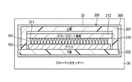
- FIG. 7 is a schematic diagram showing an example of cooling or raising the temperature of the cassette housing 200 storing the wafers 100 of the storage system 1 according to the second embodiment with the heat transfer liquid 300.
- FIG. FIG. 7 shows a state in which the cassette housing 200 storing the wafers 100 is stored in the prober 30 .
- the storage system 1 of the first embodiment circulates the heat transfer fluid 300 inside the cassette housing 200 .
- the storage system 1 of the second embodiment immerses the cassette housing 200 itself in the heat transfer liquid 300 in the prober 30 or the server rack 50 .
- the storage system 1 of the second embodiment cools or heats up the entire cassette housing 200 .
- the prober 30 has a housing portion 33 .
- the storage part 33 is a device that stores the heat transfer liquid 300 .
- the accommodating portion 33 is provided so as to seal the cassette housing 200 .
- the server rack 50 has an accommodation portion 56 .
- the storage part 56 is a device that stores the heat transfer fluid 300 .
- the accommodating portion 56 is provided so as to seal the cassette housing 200 .
- FIG. 8 is a schematic diagram showing the temperature adjustment mechanism of the storage system 1 according to the second embodiment.
- the cassette housing 200 is stored in the prober 30 .
- the prober 30 injects the heat transfer fluid 300 into the cassette housing 200 using the water supply pipe 31A, the water discharge pipe 31B, and the pump 32. Also, the prober 30 discharges the heat transfer liquid 300 from the inside of the cassette housing 200 . As a result, the prober 30 circulates the heat transfer liquid 300 inside the cassette housing 200 .
- the prober 30 injects the heat transfer fluid 300 into the housing portion 33 using the water supply pipe 31A, the water discharge pipe 31B, and the pump 32 . Also, the prober 30 discharges the heat transfer fluid 300 from the housing portion 33 . This allows the prober 30 to circulate the heat transfer fluid 300 within the prober 30 .
- the prober 30 circulates the heat transfer fluid 300 around the cassette housing 200 .
- the server rack 50 injects the heat transfer liquid 300 into the storage section 56 .
- the server rack 50 discharges the heat transfer liquid 300 from the storage section 56 .
- the server rack 50 circulates the heat transfer liquid 300 inside the server rack 50 .
- the server rack 50 circulates the heat transfer liquid 300 around the cassette housing 200 .
- An example of cooling the cassette housing 200 with the prober 30 is cooling the cassette housing 200 removed from the server rack 50 and carried.
- the wafers 100 in the cassette housing 200 removed from the server rack 50 are stored in the cassette stocker 20 while being stored in the cassette housing 200 .
- the wafers 100 in the cassette housing 200 removed from the server rack 50 are stored in the wafer stocker 10 while being removed from the cassette housing 200 .
- the temperature of the wafers 100 in the cassette housing 200 may have risen within the server rack 50 .
- the cassette housing 200 is cooled so as not to affect other wafers 100 stored at a low temperature, for example. do.
- Cooling of the cassette housing 200 in the server rack 50 is performed to suppress temperature rise of the wafer 100 due to heat generation of devices on the probe card substrate 212, for example.
- the storage system 1 of the second embodiment has a unique temperature adjustment mechanism that circulates the heat transfer liquid around the cassette housing 200. Thereby, the storage system 1 of the second embodiment can perform temperature adjustment for the wafer 100 including a plurality of NAND chips.
- the third embodiment is also a large-capacity storage system that uses semiconductor wafers without dicing.
- the same reference numerals are used for the same components as in the first embodiment and the second embodiment. Also, descriptions of the same components as in the first embodiment and the second embodiment will be omitted.
- FIG. 9 is a schematic diagram showing the temperature adjustment mechanism of the storage system 1 according to the third embodiment.
- the storage system 1 of the first and second embodiments cools or heats up with a heat transfer liquid.
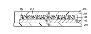
- the storage system 1 of the third embodiment brings the insulating member 213 into contact with the wafer 100 .
- the storage system 1 of the third embodiment cools or heats up by heat conduction.
- the insulating member 213 is provided on the surface of the probe card 210 arranged in the cassette housing 200 that faces the wafers 100 stored in the cassette housing 200 and on which the probes 211 are provided. A surface of the probe card 210 on which the probes 211 are provided is exposed from the inner wall portion of the upper casing 201 .
- the insulating member 212 physically contacts the wafer 100 .
- insulating member 213 is not electrically connected to wafer 100 .
- the insulating member 213 has, for example, the shape of a pin, protrusion or surface.
- the storage system 1 of the third embodiment can adjust the temperature of the wafer 100 including multiple NAND chips by heat conduction through the insulating member 212 that is not electrically connected to the wafer 100 .
- FIG. 10 is a schematic diagram showing a modified example of the temperature adjustment mechanism in the third embodiment.
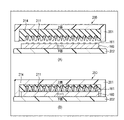
- FIG. 10 shows an example in which the insulating member 213 of FIG. 9 is provided as a cushion 214 that reduces the propagation of the shock given to the cassette housing 200 during transportation to the wafer 100, for example.
- the cushion 214 also secures the wafer 100 within the cassette housing 200 .
- FIG. 10A shows the state of the cushion 214 before the upper casing 201 and the lower casing 202 are fitted together.
- FIG. 10B shows the state of the cushion 214 after the upper casing 201 and the lower casing 202 are fitted together.
- the prober 30 When the prober 30 stores the wafer 100 in the cassette housing 200, as shown in FIG. come into physical contact with However, cushion 214 is not electrically connected to wafer 100 . Also in this modified example, the temperature of the wafer 100 including a plurality of NAND chips can be adjusted by heat conduction through the cushion 213 that is not electrically connected to the wafer 100 .
- the storage system 1 of the third embodiment brings the insulator 212 into contact with the wafer 100 inside the cassette housing 200 .
- the storage system 1 of the third embodiment has a unique temperature adjustment mechanism that cools or heats up by thermal conduction. Thereby, the storage system 1 of the third embodiment can perform temperature adjustment for the wafer 100 including multiple NAND chips.
Landscapes
- Physics & Mathematics (AREA)
- General Physics & Mathematics (AREA)
- Testing Or Measuring Of Semiconductors Or The Like (AREA)
- Container, Conveyance, Adherence, Positioning, Of Wafer (AREA)
- Memory System (AREA)
- Casings For Electric Apparatus (AREA)
- Stored Programmes (AREA)
Priority Applications (7)
| Application Number | Priority Date | Filing Date | Title |
|---|---|---|---|
| EP21932895.2A EP4276632A4 (en) | 2021-03-23 | 2021-03-23 | CASSETTE HOUSING, PROBER, SERVER RACK AND STORAGE SYSTEM |
| DE112021007357.5T DE112021007357T5 (de) | 2021-03-23 | 2021-03-23 | Kassettengehäuse, sondenvorrichtung, server-rack und lagersystem technisches gebiet |
| JP2023508202A JP7456066B2 (ja) | 2021-03-23 | 2021-03-23 | カセット筐体、プローバー、サーバーラックおよびストレージシステム |
| PCT/JP2021/011858 WO2022201285A1 (ja) | 2021-03-23 | 2021-03-23 | カセット筐体、プローバー、サーバーラックおよびストレージシステム |
| CN202180074124.2A CN116368474A (zh) | 2021-03-23 | 2021-03-23 | 晶盒壳体、探头、服务器机架以及存储系统 |
| TW110125116A TWI792396B (zh) | 2021-03-23 | 2021-07-08 | 盒筐體、探針器、伺服器機架及儲存系統 |
| US18/371,536 US20240014061A1 (en) | 2021-03-23 | 2023-09-22 | Cassette housing, prober, server rack, and storage system |
Applications Claiming Priority (1)
| Application Number | Priority Date | Filing Date | Title |
|---|---|---|---|
| PCT/JP2021/011858 WO2022201285A1 (ja) | 2021-03-23 | 2021-03-23 | カセット筐体、プローバー、サーバーラックおよびストレージシステム |
Related Child Applications (1)
| Application Number | Title | Priority Date | Filing Date |
|---|---|---|---|
| US18/371,536 Continuation US20240014061A1 (en) | 2021-03-23 | 2023-09-22 | Cassette housing, prober, server rack, and storage system |
Publications (1)
| Publication Number | Publication Date |
|---|---|
| WO2022201285A1 true WO2022201285A1 (ja) | 2022-09-29 |
Family
ID=83396431
Family Applications (1)
| Application Number | Title | Priority Date | Filing Date |
|---|---|---|---|
| PCT/JP2021/011858 Ceased WO2022201285A1 (ja) | 2021-03-23 | 2021-03-23 | カセット筐体、プローバー、サーバーラックおよびストレージシステム |
Country Status (7)
| Country | Link |
|---|---|
| US (1) | US20240014061A1 (https=) |
| EP (1) | EP4276632A4 (https=) |
| JP (1) | JP7456066B2 (https=) |
| CN (1) | CN116368474A (https=) |
| DE (1) | DE112021007357T5 (https=) |
| TW (1) | TWI792396B (https=) |
| WO (1) | WO2022201285A1 (https=) |
Citations (5)
| Publication number | Priority date | Publication date | Assignee | Title |
|---|---|---|---|---|
| US7975759B2 (en) | 2006-09-19 | 2011-07-12 | Tokyo Electron Limited | Temperature control method, temperature control apparatus and high/low temperature processing system |
| JP2016171241A (ja) * | 2015-03-13 | 2016-09-23 | 株式会社東芝 | 電子機器 |
| US10663511B2 (en) | 2017-07-20 | 2020-05-26 | Tokyo Electron Limited | Substrate mounting table and substrate inspection apparatus |
| JP2020188076A (ja) | 2019-05-10 | 2020-11-19 | 東京エレクトロン株式会社 | 載置台及び載置台の作製方法 |
| JP2020194889A (ja) * | 2019-05-28 | 2020-12-03 | 東京エレクトロン株式会社 | 搬送システム、検査システム及び検査方法 |
Family Cites Families (16)
| Publication number | Priority date | Publication date | Assignee | Title |
|---|---|---|---|---|
| US3963985A (en) * | 1974-12-12 | 1976-06-15 | International Business Machines Corporation | Probe device having probe heads and method of adjusting distances between probe heads |
| US5550482A (en) * | 1993-07-20 | 1996-08-27 | Tokyo Electron Kabushiki Kaisha | Probe device |
| JP3529581B2 (ja) * | 1997-03-14 | 2004-05-24 | 東芝マイクロエレクトロニクス株式会社 | 半導体ウェーハ及びicカード |
| US6468098B1 (en) * | 1999-08-17 | 2002-10-22 | Formfactor, Inc. | Electrical contactor especially wafer level contactor using fluid pressure |
| US20060145715A1 (en) * | 2005-01-06 | 2006-07-06 | Salmon Peter C | Wafer level test head |
| JP2007088203A (ja) * | 2005-09-22 | 2007-04-05 | Tokyo Electron Ltd | ウエハ検査装置およびウエハ検査方法、ならびにコンピュータプログラム |
| JP4744382B2 (ja) * | 2006-07-20 | 2011-08-10 | 株式会社東京精密 | プローバ及びプローブ接触方法 |
| EP1959265A1 (en) * | 2007-02-16 | 2008-08-20 | Eles Semiconductor Equipment S.P.A. | Testing integrated circuits on a wafer with a cartridge leaving exposed a surface thereof |
| JP5088167B2 (ja) * | 2008-02-22 | 2012-12-05 | 東京エレクトロン株式会社 | プローブ装置、プロービング方法及び記憶媒体 |
| JP5427536B2 (ja) * | 2009-10-01 | 2014-02-26 | 東京エレクトロン株式会社 | プローブカード |
| EP2418503B1 (en) * | 2010-07-14 | 2013-07-03 | Sensirion AG | Needle head |
| JP6289962B2 (ja) * | 2013-07-11 | 2018-03-07 | 東京エレクトロン株式会社 | プローブ装置 |
| WO2017170393A1 (ja) * | 2016-03-28 | 2017-10-05 | 株式会社東京精密 | プローバ及びプローバの操作方法 |
| KR102311459B1 (ko) * | 2017-03-14 | 2021-10-13 | 가부시키가이샤 코쿠사이 엘렉트릭 | 기판 처리 장치, 반도체 장치의 제조 방법, 및 프로그램 |
| KR20190021101A (ko) * | 2017-08-22 | 2019-03-05 | 삼성전자주식회사 | 프로브 카드, 프로브 카드를 포함한 테스트 장치, 그 프로브 카드를 이용한 테스트 방법 및 반도체 소자 제조방법 |
| WO2021095252A1 (ja) | 2019-11-15 | 2021-05-20 | キオクシア株式会社 | ストレージデバイスおよびストレージシステム |
-
2021
- 2021-03-23 DE DE112021007357.5T patent/DE112021007357T5/de active Pending
- 2021-03-23 EP EP21932895.2A patent/EP4276632A4/en active Pending
- 2021-03-23 CN CN202180074124.2A patent/CN116368474A/zh active Pending
- 2021-03-23 JP JP2023508202A patent/JP7456066B2/ja active Active
- 2021-03-23 WO PCT/JP2021/011858 patent/WO2022201285A1/ja not_active Ceased
- 2021-07-08 TW TW110125116A patent/TWI792396B/zh active
-
2023
- 2023-09-22 US US18/371,536 patent/US20240014061A1/en active Pending
Patent Citations (5)
| Publication number | Priority date | Publication date | Assignee | Title |
|---|---|---|---|---|
| US7975759B2 (en) | 2006-09-19 | 2011-07-12 | Tokyo Electron Limited | Temperature control method, temperature control apparatus and high/low temperature processing system |
| JP2016171241A (ja) * | 2015-03-13 | 2016-09-23 | 株式会社東芝 | 電子機器 |
| US10663511B2 (en) | 2017-07-20 | 2020-05-26 | Tokyo Electron Limited | Substrate mounting table and substrate inspection apparatus |
| JP2020188076A (ja) | 2019-05-10 | 2020-11-19 | 東京エレクトロン株式会社 | 載置台及び載置台の作製方法 |
| JP2020194889A (ja) * | 2019-05-28 | 2020-12-03 | 東京エレクトロン株式会社 | 搬送システム、検査システム及び検査方法 |
Non-Patent Citations (1)
| Title |
|---|
| See also references of EP4276632A4 |
Also Published As
| Publication number | Publication date |
|---|---|
| TW202237507A (zh) | 2022-10-01 |
| TWI792396B (zh) | 2023-02-11 |
| JP7456066B2 (ja) | 2024-03-26 |
| EP4276632A1 (en) | 2023-11-15 |
| JPWO2022201285A1 (https=) | 2022-09-29 |
| EP4276632A4 (en) | 2025-01-29 |
| US20240014061A1 (en) | 2024-01-11 |
| CN116368474A (zh) | 2023-06-30 |
| DE112021007357T5 (de) | 2024-03-21 |
Similar Documents
| Publication | Publication Date | Title |
|---|---|---|
| US7554349B2 (en) | Handlers for testing semiconductor devices that are capable of maintaining stable temperature in test environments | |
| JPH0587873A (ja) | 集積回路チツプのバーンイン選別方法および装置 | |
| US11121125B2 (en) | Thermal chamber for a thermal control component | |
| JP3901570B2 (ja) | 電子冷却素子を利用した半導体装置の低温試験装置 | |
| TW202332911A (zh) | 用於測試半導體積體電路晶片的液冷測試插槽 | |
| US11808803B2 (en) | Standalone thermal chamber for a temperature control component | |
| CN113302759A (zh) | 具有传热组件的双热电组件设备 | |
| KR20230115254A (ko) | 짐벌 특징부 및 향상된 열 성능을 갖는 서멀 어레이 | |
| JP3328664B2 (ja) | 多段容器の温度管理装置 | |
| JP7569495B2 (ja) | プローバの冷却システム | |
| KR102926650B1 (ko) | 지지 장치, 검사 시스템 및 지지 장치 제어 방법 | |
| CN100373167C (zh) | 用于直接冷却有源电子部件的冷却组合件 | |
| US12384624B2 (en) | Storage device and control method | |
| WO2022201285A1 (ja) | カセット筐体、プローバー、サーバーラックおよびストレージシステム | |
| JP2002280507A (ja) | 発熱素子冷却装置および発熱素子実装装置 | |
| JP4889653B2 (ja) | デバイス実装装置、テストヘッド及び電子部品試験装置 | |
| CN120233146A (zh) | 用于处理器插座的模块化低水平接触电阻测试装置 | |
| JP2003156541A (ja) | 電子デバイス検査方法 | |
| JPWO2022201285A5 (https=) | ||
| US20260118384A1 (en) | Multiple Tile Wafer Tester | |
| CN118571304B (zh) | 存储器测试装置和存储器测试方法 | |
| US12461139B2 (en) | Test device and test system for semiconductor devices | |
| CN120375904A (zh) | 用于晶圆测试的主板组件以及测试板系统 |
Legal Events
| Date | Code | Title | Description |
|---|---|---|---|
| 121 | Ep: the epo has been informed by wipo that ep was designated in this application |
Ref document number: 21932895 Country of ref document: EP Kind code of ref document: A1 |
|
| ENP | Entry into the national phase |
Ref document number: 2023508202 Country of ref document: JP Kind code of ref document: A |
|
| ENP | Entry into the national phase |
Ref document number: 2021932895 Country of ref document: EP Effective date: 20230808 |
|
| WWE | Wipo information: entry into national phase |
Ref document number: 11202305920V Country of ref document: SG |
|
| WWE | Wipo information: entry into national phase |
Ref document number: 112021007357 Country of ref document: DE |