WO2022190825A1 - タッチパネル用導電部材及びタッチパネル用導電部材の製造方法 - Google Patents
タッチパネル用導電部材及びタッチパネル用導電部材の製造方法 Download PDFInfo
- Publication number
- WO2022190825A1 WO2022190825A1 PCT/JP2022/006745 JP2022006745W WO2022190825A1 WO 2022190825 A1 WO2022190825 A1 WO 2022190825A1 JP 2022006745 W JP2022006745 W JP 2022006745W WO 2022190825 A1 WO2022190825 A1 WO 2022190825A1
- Authority
- WO
- WIPO (PCT)
- Prior art keywords
- touch panel
- transparent insulating
- conductive member
- insulating layer
- layer
- Prior art date
- Legal status (The legal status is an assumption and is not a legal conclusion. Google has not performed a legal analysis and makes no representation as to the accuracy of the status listed.)
- Ceased
Links
Images




Classifications
-
- G—PHYSICS
- G06—COMPUTING OR CALCULATING; COUNTING
- G06F—ELECTRIC DIGITAL DATA PROCESSING
- G06F3/00—Input arrangements for transferring data to be processed into a form capable of being handled by the computer; Output arrangements for transferring data from processing unit to output unit, e.g. interface arrangements
- G06F3/01—Input arrangements or combined input and output arrangements for interaction between user and computer
- G06F3/03—Arrangements for converting the position or the displacement of a member into a coded form
- G06F3/041—Digitisers, e.g. for touch screens or touch pads, characterised by the transducing means
- G06F3/044—Digitisers, e.g. for touch screens or touch pads, characterised by the transducing means by capacitive means
-
- G—PHYSICS
- G06—COMPUTING OR CALCULATING; COUNTING
- G06F—ELECTRIC DIGITAL DATA PROCESSING
- G06F3/00—Input arrangements for transferring data to be processed into a form capable of being handled by the computer; Output arrangements for transferring data from processing unit to output unit, e.g. interface arrangements
- G06F3/01—Input arrangements or combined input and output arrangements for interaction between user and computer
- G06F3/03—Arrangements for converting the position or the displacement of a member into a coded form
- G06F3/041—Digitisers, e.g. for touch screens or touch pads, characterised by the transducing means
-
- G—PHYSICS
- G06—COMPUTING OR CALCULATING; COUNTING
- G06F—ELECTRIC DIGITAL DATA PROCESSING
- G06F3/00—Input arrangements for transferring data to be processed into a form capable of being handled by the computer; Output arrangements for transferring data from processing unit to output unit, e.g. interface arrangements
- G06F3/01—Input arrangements or combined input and output arrangements for interaction between user and computer
- G06F3/03—Arrangements for converting the position or the displacement of a member into a coded form
- G06F3/041—Digitisers, e.g. for touch screens or touch pads, characterised by the transducing means
- G06F3/044—Digitisers, e.g. for touch screens or touch pads, characterised by the transducing means by capacitive means
- G06F3/0445—Digitisers, e.g. for touch screens or touch pads, characterised by the transducing means by capacitive means using two or more layers of sensing electrodes, e.g. using two layers of electrodes separated by a dielectric layer
-
- G—PHYSICS
- G06—COMPUTING OR CALCULATING; COUNTING
- G06F—ELECTRIC DIGITAL DATA PROCESSING
- G06F3/00—Input arrangements for transferring data to be processed into a form capable of being handled by the computer; Output arrangements for transferring data from processing unit to output unit, e.g. interface arrangements
- G06F3/01—Input arrangements or combined input and output arrangements for interaction between user and computer
- G06F3/03—Arrangements for converting the position or the displacement of a member into a coded form
- G06F3/041—Digitisers, e.g. for touch screens or touch pads, characterised by the transducing means
- G06F3/044—Digitisers, e.g. for touch screens or touch pads, characterised by the transducing means by capacitive means
- G06F3/0446—Digitisers, e.g. for touch screens or touch pads, characterised by the transducing means by capacitive means using a grid-like structure of electrodes in at least two directions, e.g. using row and column electrodes
-
- G—PHYSICS
- G06—COMPUTING OR CALCULATING; COUNTING
- G06F—ELECTRIC DIGITAL DATA PROCESSING
- G06F2203/00—Indexing scheme relating to G06F3/00 - G06F3/048
- G06F2203/041—Indexing scheme relating to G06F3/041 - G06F3/045
- G06F2203/04103—Manufacturing, i.e. details related to manufacturing processes specially suited for touch sensitive devices
-
- G—PHYSICS
- G06—COMPUTING OR CALCULATING; COUNTING
- G06F—ELECTRIC DIGITAL DATA PROCESSING
- G06F2203/00—Indexing scheme relating to G06F3/00 - G06F3/048
- G06F2203/041—Indexing scheme relating to G06F3/041 - G06F3/045
- G06F2203/04112—Electrode mesh in capacitive digitiser: electrode for touch sensing is formed of a mesh of very fine, normally metallic, interconnected lines that are almost invisible to see. This provides a quite large but transparent electrode surface, without need for ITO or similar transparent conductive material
Definitions
- the present invention relates to a conductive member for a touch panel used in a touch panel and a method for manufacturing the conductive member for a touch panel.
- a touch panel for input operation of A touch panel usually has a conductive member formed with a plurality of detection electrodes or the like for detecting a touch operation by a finger, a stylus pen, or the like.
- the detection electrode is made of a transparent conductive oxide such as ITO (Indium Tin Oxide), metal, or the like.
- ITO Indium Tin Oxide
- Metals have advantages over transparent conductive oxides in that they are easier to pattern, have superior flexibility, and have lower electrical resistance. For this reason, metals such as copper and silver are used in touch panels for conductive thin wires that constitute detection electrodes.
- Patent Document 1 describes a touch panel in which a transparent plastic film substrate, a light-colored layer with a thickness of 1 to 50 nm, a conductive layer made of copper, and a positive photosensitive layer with a dry thickness of 0.5 to 5 ⁇ m are laminated in this order.
- a transparent conductive film for a touch panel is described in which a conductive layer is processed into a mesh-like electrode wiring having a line width of 1 to 10 ⁇ m by a photolithography method comprising pattern exposure, development, and etching processes for a conductive laminate for a sensor.
- An object of the present invention is to provide a conductive member for a touch panel and a method for manufacturing a conductive member for a touch panel that achieves both low electrical resistance and bendability of metal thin wires.
- one aspect of the present invention provides a transparent insulating substrate, an undercoat layer disposed on the transparent insulating substrate, a first thin metal wire disposed on the undercoat layer, and a first thin metal wire disposed on the undercoat layer.
- a conductive member for a touch panel having a transparent insulating layer covering the fine metal wires, wherein the thickness of the first fine metal wires is 350 to 1000 nm, and the direction perpendicular to the direction in which the first fine metal wires extend. 10 cross-sectional images of the conductive member are obtained, and when one first metal fine wire is observed at each location, there are 6 or more locations where there is a gap between the side surface of the first metal fine wire and the transparent insulating layer. An observable conductive member for a touch panel is provided.
- a mesh pattern is formed by the first fine metal wires, and the width of the first fine metal wires is preferably 1.5 to 4.0 ⁇ m.
- a second thin metal wire is further disposed on the transparent insulating layer, and the transparent insulating layer preferably has a thickness of 1.0 to 5.0 ⁇ m.
- a mesh pattern is formed by the second fine metal wires, and the width of the second fine metal wires is preferably 1.5 to 4.0 ⁇ m.
- the first thin metal wire is preferably copper
- the second thin metal wire is preferably copper. It is preferable that the transparent insulating substrate is a substrate containing a polyester-based resin and has a thickness of 10 to 60 ⁇ m.
- One aspect of the present invention comprises: a first step of forming an undercoat layer on a transparent insulating substrate; a second step of forming a first metal fine wire on the undercoat layer; and a third step of forming an insulating layer, wherein the thickness of the first metal fine wire is 350 to 1000 nm, the undercoat layer contains a surfactant containing at least one of a fluorine atom and a silicon atom, and is surface active
- a method for producing a conductive member for a touch panel wherein the content of the agent is 0.01 to 5% by mass with respect to the total mass of the undercoat layer.
- the third step is preferably a step of applying a composition for forming a transparent insulating layer onto the first thin metal wires to form a transparent insulating layer.
- the second step preferably includes a step of forming the first thin metal wires in a mesh pattern. It is preferable to have a fourth step of forming a second fine metal wire on the transparent insulating layer.
- the fourth step preferably includes forming the second thin metal wires in a mesh pattern.
- the first thin metal wire is preferably copper
- the second thin metal wire is preferably copper.
- a conductive member for a touch panel that achieves both a reduction in the electrical resistance of the fine metal wire and a bendability.
- FIG. 2 is a schematic cross-sectional view showing a second example of an image display device having a touch panel conductive member according to an embodiment of the present invention. It is a schematic diagram which shows the electrically-conductive member for touchscreens for bendability evaluation.
- the term "transparent" means that the light transmittance is 40% or more, preferably 80% or more, and more preferably 90% or more in the visible light wavelength range of 380 to 780 nm. .
- the light transmittance is measured using “Plastics—Determination of Total Light Transmittance and Total Light Reflectance” defined in JIS (Japanese Industrial Standard) K 7375:2008.
- insulation means electrical insulation unless otherwise specified.
- the insulating substrate is a substrate having electrical insulation properties, and has an electrical resistance depending on the intended use. For example, when conductive lines are formed on both sides of an insulating substrate, the conductive lines formed on both sides are not electrically connected.
- FIG. 1 is a schematic cross-sectional view showing a first example of an image display device having a touch panel conductive member according to an embodiment of the present invention.
- the image display device 10 of the first example shown in FIG. The image display device 10 can detect that an area such as an image displayed on the image display unit 14 is touched.
- the touch panel 12 and the image display section 14 are laminated with the first transparent insulating layer 15 interposed therebetween.
- the touch panel 12 has a cover layer 16 provided on a touch panel conductive member 18 with a second transparent insulating layer 17 interposed therebetween.
- the first transparent insulating layer 15 is provided over the entire display surface 14 a of the image display section 14 .
- the touch panel conductive member 18 and the second transparent insulating layer 17 have the same size.
- the image display portion 14 is smaller than the touch panel conductive member 18, and the image display portion 14 and the first transparent insulating layer 15 have the same size.
- the first transparent insulating layer 15 is arranged on the display surface 14a side of the image display unit 14 so that a display object (not shown) displayed on the display surface 14a of the image display unit 14 can be visually recognized.
- the touch panel conductive member 18, the second transparent insulating layer 17, and the cover layer 16 are all preferably transparent.
- the cover layer 16 is called a cover glass if it is composed of glass.
- a surface 16a of the cover layer 16 is a touch surface of the image display device 10 and an operation surface.
- the image display device 10 is operated for input using the surface 16a of the cover layer 16 as an operation surface.
- the touch surface is a surface with which a finger, a stylus pen, or the like comes into contact.
- a surface 16a of the cover layer 16 serves as a visible surface of a display (not shown) displayed on the display surface 14a of the image display section 14.
- a controller 13 is provided on the rear surface 14 b of the image display section 14 .
- the touch panel conductive member 18 and the controller 13 are electrically connected by a flexible wiring member such as a flexible circuit board 19, for example.
- a decorative layer (not shown) having a light shielding function may be provided on the back surface 16b of the cover layer 16.
- the decorative layer is provided, for example, along the outer edge of the cover layer 16 when viewed from the surface 16 a side of the cover layer 16 .
- a region provided with the decorative layer is called a frame portion. Due to the decorative layer, the frame portion does not allow the underlying components such as electrode terminals and peripheral wiring of the touch panel conductive member 18 to be described later to be visible.
- the controller 13 is composed of a known device that is used to detect contact of a finger or the like on the surface 16a of the cover layer 16, which is a touch surface.
- the controller 13 detects the position where the capacitance changes in the touch panel conductive member 18 due to the touch of a finger or the like on the surface 16a of the cover layer 16, which is the touch surface.
- the capacitive touch panel includes a mutual capacitive touch panel and a self-capacitance touch panel, but is not particularly limited.
- the cover layer 16 protects the touch panel conductive member 18 .
- the structure of the cover layer 16 is not particularly limited.
- the cover layer 16 is preferably transparent so that a display (not shown) displayed on the display surface 14a of the image display unit 14 can be visually recognized.
- the cover layer 16 is made of, for example, a glass plate, chemically strengthened glass, alkali-free glass, or the like. It is preferable to appropriately select the thickness of the cover layer 16 according to each application.
- a plastic film, a plastic plate, or the like is used in addition to the glass plate.
- polyesters such as polyethylene terephthalate (PET) and polyethylene naphthalate (PEN); polyethylene (PE), polypropylene (PP), polystyrene, EVA (vinyl acetate copolymer polyethylene ) and other polyolefin resins; vinyl resins; other polycarbonate (PC) resins, polyamide resins, polyimide resins, (meth) acrylic resins, triacetyl cellulose (TAC), cycloolefin resins (COP), polyvinylidene fluoride (PVDF ), polyarylate (PAR), polyethersulfone (PES), fluorene derivatives, crystalline COP, and the like can be used.
- PET polyethylene terephthalate
- PEN polyethylene naphthalate
- PE polyethylene
- PP polypropylene
- EVA vinyl acetate copolymer polyethylene
- vinyl resins other polycarbonate (PC) resins, polyamide resins, polyimide resins, (
- (Meth)acrylic resin is a general term including acrylic resin and methacrylic resin.
- the cover layer 16 may be configured to have a polarizing plate, a circularly polarizing plate, or the like. Since the surface 16a of the cover layer 16 serves as a touch surface as described above, a hard coat layer may be provided on the surface 16a as necessary.
- the thickness of the cover layer 16 is, for example, 0.1 to 1.3 mm, preferably 0.1 to 0.7 mm.
- the configuration of the first transparent insulating layer 15 is particularly limited as long as the first transparent insulating layer 15 is transparent, has electrical insulation, and can stably fix the touch panel 12 and the image display unit 14. not a thing
- an optically transparent adhesive OCA, Optical Clear Adhesive
- an optically transparent resin OCR, Optical Clear Resin
- the first transparent insulating layer 15 may be partially hollow.
- the touch panel 12 may be provided on the display surface 14a of the image display unit 14 with a gap therebetween without providing the first transparent insulating layer 15. FIG. This gap is also called an air gap.
- the second transparent insulating layer 17 is transparent and has electrical insulating properties and can stably fix the touch panel conductive member 18 and the cover layer 16, the configuration thereof is as follows. It is not particularly limited. The same material as the first transparent insulating layer 15 can be used for the second transparent insulating layer 17 .
- the image display unit 14 has a display surface 14a for displaying a display object such as an image, and is, for example, a liquid crystal display device.
- the image display unit 14 is not limited to a liquid crystal display device, and may be an organic EL (organic electro luminescence) display device.
- the image display unit 14 can be a cathode ray tube (CRT) display, a vacuum fluorescent display (VFD), a plasma display panel (PDP), a surface field display (SED), a field emission display (FED), and an electronic Paper or the like can be used.
- the image display unit 14 is appropriately used depending on its application, but in order to make the image display device 10 thin, it is preferable to use a panel such as a liquid crystal display panel or an organic EL panel. .
- FIG. 2 is a schematic plan view showing an example of the touch panel conductive member according to the embodiment of the present invention. 2, the same components as those of the image display device 10 shown in FIG. 1 are denoted by the same reference numerals, and detailed description thereof will be omitted.
- the touch panel 12 will be described below with reference to FIGS. 1 and 2.
- FIG. The touch panel 12 has a controller 13 , a touch panel conductive member 18 , and a cover layer 16 .
- the touch panel conductive member 18 functions as a touch sensor.
- the touch panel conductive member 18 includes, for example, a transparent insulating substrate 24, an undercoat layer 25 disposed on the transparent insulating substrate 24, thin metal wires 35 (see FIG. 3) disposed on the undercoat layer 25, and thin metal wires 35. and a transparent insulating layer 27 covering the .
- a first conductive layer 11A having a plurality of first peripheral wirings 23a provided with first external connection terminals 26a is provided on the surface 25a of the undercoat layer 25, a first detection electrode layer 29A having a plurality of first detection electrodes 30, one end electrically connected to the first detection electrode 30 of the first detection electrode layer 29A, and the other end
- a first conductive layer 11A having a plurality of first peripheral wirings 23a provided with first external connection terminals 26a is provided on the surface 25a of the undercoat layer 25 .
- the flexible circuit board 19 is electrically connected to the first external connection terminal 26 a and connected to the controller 13 .
- a fine metal wire 35 is further arranged on the transparent insulating layer 27 .
- the second detection electrode 32 is composed of a fine metal wire 35 .
- a second detection electrode layer 29B having a plurality of second detection electrodes 32, one end of which is electrically connected to the second detection electrodes 32, and the other end of which is provided with a second external connection terminal 26b are provided on the transparent insulating layer 27. and a second conductive layer 11B having a plurality of second peripheral wirings 23b.
- the flexible circuit board 19 is electrically connected to the second external connection terminal 26b and connected to the controller 13. As shown in FIG.
- the second detection electrode 32 is composed of a thin metal wire 35 (see FIG. 3).
- the thin metal wire 35 forming the second detection electrode 32 is called a second thin metal wire.
- the second thin metal wires are arranged on the transparent insulating layer 27 .
- the first detection electrode 30 is referred to as the first metal thin wire
- the second detection electrode 32 is referred to as the second metal thin wire.
- the first thin metal wire and the second thin metal wire are collectively referred to as a thin metal wire 35 .
- the thin metal wire 35 includes a first thin metal wire and a second thin metal wire.
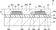
- FIG. FIG. 3 is a schematic cross-sectional view showing an example of the touch panel conductive member according to the embodiment of the present invention. 3, the same components as those of the image display device 10 shown in FIG. 1 are denoted by the same reference numerals, and detailed description thereof will be omitted.
- the touch panel conductive member 18 is a portion that functions as a touch sensor of the touch panel 12, and includes a detection portion 20 that is a detection region E1 in which a user can perform an input operation, and a peripheral region E that is positioned outside the detection region E1. 2 has a peripheral wiring portion 22 .
- the detection unit 20 has, for example, a first detection electrode layer 29A and a second detection electrode layer 29B.
- 29 A of 1st detection electrode layers and the 2nd detection electrode layer 29B are arrange
- the first detection electrode layer 29A and the second detection electrode layer 29B are electrically insulated by the transparent insulating layer 27 .
- the transparent insulating layer 27 functions as an electrical insulating layer.
- the first detection electrode layer 29A is arranged between the plurality of first detection electrodes 30 and the adjacent first detection electrodes 30, and is insulated from the first detection electrodes 30 by a plurality of first dummy electrodes. 31a.
- the plurality of first detection electrodes 30 are strip-shaped electrodes extending parallel to each other in the X direction, spaced apart in the Y direction perpendicular to the X direction, and electrically insulated from each other in the Y direction. 25 is provided on the surface 25a (see FIG. 1). In addition, the plurality of first dummy electrodes 31a are arranged between the first detection electrodes 30 and are provided on the surface 25a (see FIG. 1) of the undercoat layer 25 while being electrically insulated from the first detection electrodes 30. ing. Each of the first detection electrodes 30 is provided with a first electrode terminal 33 at at least one end in the X direction.
- the second detection electrode layer 29B has a plurality of second dummy electrodes 31b arranged between the plurality of second detection electrodes 32 and adjacent second detection electrodes 32 and insulated from the second detection electrodes 32 .
- the plurality of second detection electrodes 32 are strip-shaped electrodes extending parallel to each other in the Y direction, are spaced from each other in the X direction, and are electrically insulated from each other in the X direction on the surface 27a of the transparent insulating layer 27. (See FIG. 1).
- the plurality of second dummy electrodes 31b are arranged between the second detection electrodes 32 and provided on the surface 27a (see FIG. 1) of the transparent insulating layer 27 while being electrically insulated from the second detection electrodes 32. It is Each of the second detection electrodes 32 is provided with a second electrode terminal 34 at one end in the Y direction.
- the plurality of first detection electrodes 30 and the plurality of second detection electrodes 32 are provided orthogonally, but are electrically insulated from each other by the transparent insulating layer 27 as described above.
- the first dummy electrode 31a and the second dummy electrode 31b in the first detection electrode 30 and the second detection electrode 32 are separated from the first detection electrode 30 or the second detection electrode 32 by a disconnection portion, and are electrically It is an unconnected region. Therefore, as described above, the plurality of first detection electrodes 30 are electrically insulated from each other in the Y direction, and the plurality of second detection electrodes 32 are electrically insulated from each other in the X direction. be. As shown in FIG.
- the detection unit 20 is provided with six first detection electrodes 30 and five second detection electrodes 32, but the number is not particularly limited, and a plurality of electrodes is sufficient.
- 29 A of 1st detection electrode layers and the 2nd detection electrode layer 29B are comprised by the metal thin wire 35 (refer FIG. 3) as mentioned above.
- the first detection electrode 30 and the second detection electrode 32 are metal mesh having a mesh pattern of fine metal wires 35
- the first dummy electrode 31a and the second dummy electrode 31b are also metal mesh having a mesh pattern of fine metal wires 35.
- the electrode width of the first detection electrode 30 and the electrode width of the second detection electrode 32 are, for example, 1 to 5 mm, and the electrode pitch is 3 to 6 mm.
- the electrode width of the first detection electrodes 30 is the maximum length in the Y direction
- the electrode width of the second detection electrodes 32 is the maximum length in the X direction.
- the peripheral wiring section 22 includes peripheral wiring (first peripheral wiring 23a, second peripheral wiring 23a, second peripheral This is the area where the wiring 23b) is arranged.
- the peripheral wiring section 22 has a plurality of first peripheral wirings 23a and a plurality of second peripheral wirings 23b.
- One end of the first peripheral wiring 23a is electrically connected to the first detection electrode 30 via the first electrode terminal 33, and the other end is electrically connected to the first external connection terminal 26a.
- the second peripheral wiring 23b has one end electrically connected to the second detection electrode 32 via the second electrode terminal 34, and the other end electrically connected to the second external connection terminal 26b.
- the first electrode terminal 33 and the second electrode terminal 34 may have a solid film shape, or may have a mesh shape as disclosed in Japanese Unexamined Patent Application Publication No. 2013-127658.
- a preferable range of the widths of the first electrode terminals 33 and the second electrode terminals 34 is 1 ⁇ 3 times or more and 1.2 times or less the electrode widths of the first detection electrodes 30 and the
- the first detection electrode 30, the first dummy electrode 31a, the first electrode terminal 33, and the first peripheral wiring 23a of the first conductive layer 11A are integrally constructed from the viewpoint of electrical resistance and resistance to disconnection. It is preferable that there is one, and it is more preferable that they are made of the same metal material. In this case, the first conductive layer 11A is formed by, for example, lithography. Similarly, the second detection electrode 32, the second dummy electrode 31b, the second electrode terminal 34, and the second peripheral wiring 23b of the second conductive layer 11B are integrated from the viewpoint of electrical resistance and resistance to disconnection. It is preferable that they have the same structure, and more preferably that they are made of the same metal material. In this case, the second conductive layer 11B is formed by, for example, lithography.
- FIG. 3 is a diagram showing the touch panel conductive member 18, but a part of it is omitted, and the transparent insulating substrate 24, the undercoat layer 25, and the thin metal wires of the first detection electrodes 30 of the first detection electrode layer 29A are shown. 35 and the transparent insulating layer 27 are shown.
- the thin metal wire 35 shown in FIG. 3 is the first thin metal wire.
- cross-sectional images of the touch panel conductive member 18 in a direction perpendicular to the direction in which the metal wires 35 extend are obtained at 10 locations, and one metal wire 35 is observed at each location. Six or more places where there is a gap 37 between the side surface 35b of the fine wire 35 and the transparent insulating layer 27 are observed.
- the touch panel conductive member 18 is formed in the bending region Bf of the peripheral wiring portion 22 shown in FIG. and the second external connection terminal 26b is bent outward.
- a flexible circuit board 19 electrically connected to the first external connection terminals 26a and the second external connection terminals 26b is arranged on the rear surface 14b side of the image display section 14 opposite to the display surface 14a side.
- the first peripheral wiring 23 a existing in the bending region Bf has a gap (not shown) between the side surface (not shown) and the transparent insulating layer 27 .
- the gap of the first peripheral wiring 23a is the same as the gap 37 of the fine metal wire 35 shown in FIG.
- the first peripheral wiring 23a and the second peripheral wiring 23b can be composed of thin metal wires 35 as described later.
- the number of voids 37 is preferably 8 or more, more preferably 10 or more, in order to achieve a better balance between the reduction in electric resistance of the metal thin wire and the bendability.
- the upper limit is not particularly limited, 20 sites can be mentioned.
- the cross-sectional image is in a direction orthogonal to the direction in which the fine metal wires 35 extend, but when the fine metal wires 35 form a mesh pattern, the extending direction of the fine metal wires 35 may differ. Even if the extending direction of the metal thin wire 35 is different, the cross-sectional image of the cross section in the direction perpendicular to the extending direction of the metal thin wire 35 is acquired for each of the metal thin wires 35 to be measured.
- the porosity which is the percentage of voids, is preferably 10% to 80%, more preferably 30% to 70%, and even more preferably 40% to 70%.
- the porosity can be determined by cross-sectional observation using a scanning electron microscope (SEM) to determine whether or not there are voids on each of 20 side surfaces in total of 10 thin metal wires. That is, the ratio calculated from the number of voids present in the 20 sides is the porosity.
- the gap 37 only needs to exist in the cross-sectional image, and does not need to exist along the direction extending to the side surface 35 b of the fine metal wire 35 . Therefore, the voids 37 may exist continuously or discontinuously along the direction extending along the side surface 35 b of the fine metal wire 35 .
- a cross-sectional image of the touch panel conductive member 18 can be acquired using, for example, a scanning electron microscope (SEM).
- the gap 37 has a size of 50% or more of the thickness tc of the fine metal wire 35 .
- the void 37 exists on the side of the interface with the transparent insulating layer 27 of the thin metal wire 35 on the transparent insulating substrate 24 side.
- the void 37 is the void 37 that is in contact with the undercoat layer 25 and the side surface 35b of the fine metal wire 35 .
- the shape of the gap 37 is not particularly limited as long as it satisfies the above conditions.
- the thickness tc of the thin metal wire 35 is 350-1000 nm, preferably 600-900 nm. If the thickness tc of the metal fine wire 35 is 350 to 1000 nm, the electrical resistance of the metal fine wire 35 is small. It is more preferable that the thickness tc of the fine metal wire 35 is 600 to 900 nm, because the electrical resistance of the fine metal wire 35 is smaller. Moreover, when the thickness tc of the metal fine wire 35 is large, the voids increase and the bendability is improved. Therefore, the thickness tc of the metal fine wire 35 is preferably large.
- the width Wc of the thin metal wire 35 is preferably 1.5 to 4.0 ⁇ m, more preferably 1.5 to 3.0 ⁇ m, even more preferably 1.5 to 2.5 ⁇ m.
- the width Wc of the thin metal wire 35 is 1.5 to 4.0 ⁇ m, it becomes difficult to be visually recognized, and moiré and the like are suppressed. That is, visibility is excellent.
- the width Wc of the metal fine wire 35 is small, the gap increases and the bendability is improved, so the width Wc of the metal fine wire 35 is preferably small.
- the fine metal wires 35 constitute a mesh pattern (see FIG. 4), and the fine metal wires 35 are arranged in a mesh pattern (see FIG. 4).
- the thickness tc of the metal fine wire 35 and the width Wc of the metal fine wire 35 are measured by cutting the touch panel conductive member 18 and using a cross-sectional image of the cut cross section using a scanning electron microscope (SEM). In the cross-sectional image, the length corresponding to the thickness tc and the width Wc of the metal fine wire 35 is measured at 10 locations in the image region corresponding to the metal fine wire 35, and the average value of the measured values at the 10 locations is obtained.
- the thickness tc and the width Wc of the fine metal wire 35 are the average values of the ten measurement values described above.
- a touch panel mounted on a tablet or a notebook PC which is larger than a smartphone, detects a touch operation by contact or proximity with a finger or a stylus pen.
- a resistance a lower fine wire resistance is required.
- the wire resistance is preferably 80 ⁇ /mm or less, more preferably 60 ⁇ /mm, and particularly preferably 40 ⁇ /mm.
- the fine wire resistance of the fine metal wire described above is obtained by measuring the electrical resistance of the fine metal wire and normalizing it to the electrical resistance of 1 mm length ( ⁇ /mm). The electric resistance can be measured, for example, with a resistance meter (RM3544 manufactured by Hioki Electric Co., Ltd., HIOKI).
- the surface 35a of the fine metal wire 35 may be blackened by sulfurizing or oxidizing to form the blackened layer 38.
- FIG. The blackening layer 38 reduces the reflectance of the fine metal wires 35, for example.
- the blackening layer 38 can be composed of copper nitride, copper oxide, copper oxynitride, molybdenum oxide, AgO, Pd, carbon or other nitrides or oxides, or the like.
- the blackened layer 38 is disposed on the visible side of the metal wire 35 , ie, the surface 35 a of the metal wire 35 opposite the undercoat layer 25 . A configuration without the blackened layer 38 may be used.
- an adhesion layer (not shown) may be provided at the interface between the fine metal wires 35 and the undercoat layer 25 .
- the adhesion layer is made of copper oxide.
- the thickness ta of the transparent insulating layer 27 is preferably 1.0 to 5.0 ⁇ m. If the thickness ta of the transparent insulating layer 27 is 1.0 to 5.0 ⁇ m, both insulating properties and bendability can be achieved. Moreover, the thickness ta of the transparent insulating layer 27 is more preferably 2 to 5 ⁇ m, more preferably 2.5 to 4.5 ⁇ m. The thickness ta of the transparent insulating layer 27 is measured by cutting the touch panel conductive member 18 and using a cross-sectional image of the cut cross section using a scanning electron microscope (SEM).
- SEM scanning electron microscope
- the length corresponding to the thickness of the transparent insulating layer is measured at 10 points in the image area corresponding to the transparent insulating layer, and the average value of the measured values at 10 points is obtained.
- the thickness ta of the transparent insulating layer is the average value of the ten measurement values described above.
- the transparent insulating substrate supports the thin metal wires, and supports the first detection electrodes and the second detection electrodes composed of the thin metal wires. Also, the transparent insulating substrate supports the first peripheral wiring and the second peripheral wiring. Further, if the first detection electrode is arranged on one surface of the two surfaces of the transparent insulating substrate and the second detection electrode is arranged on the other surface, the first detection electrode and the second detection electrode are electrically connected.
- the transparent insulating substrate preferably has a thickness of 10 to 60 ⁇ m. Examples of materials for the transparent insulating substrate include transparent resin materials and transparent inorganic materials.
- transparent resin materials include acetylcellulose resins such as triacetylcellulose, polyester resins such as polyethylene terephthalate (PET) and polyethylene naphthalate (PEN), polyethylene (PE), polymethylpentene, Olefin resins such as cycloolefin polymer (COP) and cycloolefin copolymer (COC), (meth)acrylic resins such as polymethyl methacrylate, polyurethane resins, polyether sulfone, polycarbonate, polysulfone, polyether, polyether ketone , acrylonitrile, and methacrylonitrile.
- acetylcellulose resins such as triacetylcellulose
- polyester resins such as polyethylene terephthalate (PET) and polyethylene naphthalate (PEN)
- PET polyethylene
- PE polymethylpentene
- Olefin resins such as cycloolefin polymer (COP) and cycloolefin copoly
- PET is preferable because it has good adhesion to the first detection electrode, the second detection electrode, the first peripheral wiring, and the second peripheral wiring.
- transparent inorganic materials include glasses such as non-alkali glass, alkali glass, chemically strengthened glass, soda glass, potash glass, and lead glass, and translucent piezoelectric ceramics (PLZT (lead lanthanum zirconate titanate). )), quartz, fluorite and sapphire.
- the transparent insulating substrate is preferably a substrate containing a polyester-based resin.
- the total light transmittance of the transparent insulating substrate is preferably 40-100%, more preferably 85-100%. The total light transmittance is measured using, for example, "Plastics-Determination of total light transmittance and total light reflectance" defined in JIS K 7375:2008.
- the undercoat layer further improves the adhesion of the first detection electrode, the second detection electrode, the first peripheral wiring, and the second peripheral wiring.
- the undercoat layer contains a surfactant containing at least one of a fluorine atom and a silicon atom.
- the content of the surfactant in the undercoat layer is 0.01 to 5% by weight, preferably 0.04 to 1.50% by weight, based on the total weight of the undercoat layer. If the content of the surfactant in the undercoat layer is 0.01 to 5% by mass with respect to the total mass of the undercoat layer, a total of 20 side surfaces 35b Among them, the configuration can be such that there are six or more gaps 37 .
- the type of surfactant is not particularly limited, and known surfactants can be used. Specifically, at least one surfactant selected from silicone-based surfactants and fluorine-based surfactants is used. preferable. It should be noted that the surfactant is preferably an oligomer or polymer rather than a low-molecular-weight compound.
- the surfactant When a surfactant is added, the surfactant quickly migrates to the surface of the applied coating film and becomes unevenly distributed, and even after the coating film dries, the surfactant will remain unevenly distributed on the surface.
- the surface energy of the added film is lowered by the surfactant. From the viewpoint of preventing film thickness non-uniformity, repelling, and unevenness, it is preferable that the surface energy of the film is low.
- silicone-based surfactants include polymers or oligomers containing a plurality of dimethylsilyloxy units as repeating units and having substituents on terminals and/or side chains.
- a polymer or oligomer containing dimethylsilyloxy as a repeating unit may contain repeating units other than dimethylsilyloxy.
- the substituents may be the same or different, and a plurality of substituents is preferred. Examples of preferred substituents include groups including polyether groups, alkyl groups, aryl groups, aryloxy groups, aryl groups, cinnamoyl groups, oxetanyl groups, fluoroalkyl groups, polyoxyalkylene groups, and the like.
- the number average molecular weight of the silicone surfactant is not particularly limited, it is preferably 100,000 or less, more preferably 50,000 or less, even more preferably 1,000 to 30,000, and 1,000 to 20,000. is particularly preferred.
- silicone surfactants examples include X22-3710, X22-162C, X22-3701E, X22160AS and X22170DX manufactured by Shin-Etsu Chemical Co., Ltd., which are commercially available silicone surfactants having no ionizing radiation curing group.
- a fluorosurfactant has a fluoroaliphatic group and, for example, an amphiphilic group that contributes to affinity for various compositions such as coatings and molding materials when the surfactant is used as an additive. in the same molecule, and such compounds can generally be obtained by copolymerizing a monomer having a fluoroaliphatic group and a monomer having an hydrophilic group.
- monomers having hydrophilic groups to be copolymerized with monomers having fluoroaliphatic groups include poly(oxyalkylene) acrylates and poly(oxyalkylene) methacrylates.
- Preferred commercially available fluorine-based surfactants that do not have an ionizing radiation curing group include Megafac series (MCF350-5, F472, F476, F445, F444, F443, F178, F470, F475, F479, manufactured by DIC Corporation). , F477, F482, F486, TF1025, F478, F178K, F-784-F, etc.); Futagent series manufactured by Neos Co., Ltd.
- those having an ionizing radiation curing group include OPTOOL DAC manufactured by Daikin Industries, Ltd.; ), RS series (RS71, RS101, RS102, RS103, RS104, RS105, RS-56, etc.).
- a surfactant having an ionizing radiation-curable group is preferred from the viewpoint of remaining on the surface of the undercoat layer.
- the undercoat layer may contain other materials in addition to the surfactants described above.
- the undercoat layer may contain a resin (binder resin).
- the resin functions as a binder for the undercoat layer.
- the type of resin is not particularly limited, and known resins can be used. Examples of resins include polyester resins, polyether resins, (meth)acrylic resins, epoxy resins, urethane resins, alkyd resins, spiroacetal resins, polybutadiene resins, and polythiolpolyene resins, with (meth)acrylic resins being preferred.
- the content of the resin in the undercoat layer is not particularly limited, it is preferably 40 to 95% by mass, more preferably 50 to 90% by mass, even more preferably 50 to 80% by mass, based on the total mass of the undercoat layer.
- the undercoat layer may further contain inorganic particles.
- the type of inorganic particles is not particularly limited, and examples include inorganic particles containing at least one selected from the group consisting of silica, titanium oxide, zirconium oxide, and aluminum oxide.
- the particle diameter of the inorganic particles is not particularly limited, it is preferably 5 to 100 nm, more preferably 10 to 80 nm.
- the content of the inorganic particles in the undercoat layer is not particularly limited, but is preferably 5 to 60% by mass, more preferably 10 to 50% by mass, and even more preferably 10 to 45% by mass, based on the total mass of the undercoat layer.
- the method for forming the undercoat layer is not particularly limited, examples thereof include a method of applying a composition for forming an undercoat layer, as described later.
- the undercoat layer-forming composition contains the above-described surfactant. The content of the surfactant is adjusted so that the content of the surfactant in the undercoat layer is within the above range.
- the undercoat layer-forming composition may contain other materials in addition to the surfactant. Other materials include the resins and inorganic particles described above. Other materials also include solvents. Solvents include water and organic solvents.
- the composition for forming an undercoat layer may contain a monomer.
- the undercoat layer can be formed by applying an undercoat layer-forming composition containing a monomer and subjecting the coating film to curing treatment (for example, light irradiation treatment and heat treatment).
- the composition for forming an undercoat layer may further contain a polymerization initiator.
- the polymerization initiator includes known photopolymerization initiators and thermal polymerization initiators.
- the type of monomer is not particularly limited, and a monomer that can constitute the resin described above is selected. Among them, a compound having a photopolymerizable functional group is preferable as the monomer.
- the photopolymerizable functional group include polymerizable unsaturated groups (carbon-carbon unsaturated double bond groups) such as (meth)acryloyl groups, vinyl groups, styryl groups, and allyl groups. ) acryloyl groups are preferred.
- compounds having a polymerizable unsaturated group include alkylene glycol (meth)acrylic acid diesters such as neopentyl glycol acrylate, 1,6-hexanediol (meth)acrylate, and propylene glycol di(meth)acrylate; Polyoxyalkylene glycol (meth)acrylic acid diesters such as triethylene glycol di(meth)acrylate, dipropylene glycol di(meth)acrylate, polyethylene glycol di(meth)acrylate, and polypropylene glycol di(meth)acrylate; (meth)acrylic acid diesters of polyhydric alcohols such as pentaerythritol di(meth)acrylate; (Meth)acrylic diesters of ethylene oxide or propylene oxide adducts such as 2,2-bis ⁇ 4-(acryloxy-diethoxy)phenyl ⁇ propane and 2-2-bis ⁇ 4-(acryloxy-polypropoxy)phenyl ⁇ propane
- epoxy (meth)acrylates, urethane (meth)acrylates, and polyester (meth)acrylates are also preferably used as compounds having photopolymerizable functional groups.
- esters of polyhydric alcohol and (meth)acrylic acid are preferred. More preferably, it contains at least one polyfunctional monomer having 3 or more (meth)acryloyl groups in one molecule.
- esters of polyhydric alcohol and (meth)acrylic acid are preferred. More preferably, it contains at least one polyfunctional monomer having 3 or more (meth)acryloyl groups in one molecule.
- pentaerythritol tetra(meth)acrylate pentaerythritol tri(meth)acrylate, trimethylolpropane tri(meth)acrylate, EO (ethylene oxide)-modified trimethylolpropane tri(meth)acrylate, PO (propylene oxide)-modified trimethylol Propane tri(meth)acrylate, EO-modified phosphoric acid tri(meth)acrylate, trimethylolethane tri(meth)acrylate, ditrimethylolpropane tetra(meth)acrylate, dipent
- polyfunctional acrylate compounds having a (meth)acryloyl group include Nippon Kayaku Co., Ltd. KAYARADDPHA, DPHA-2C, PET-30, TMPTA, TPA-320, TPA-330, Same RP-1040, Same T-1420, Same D-310, Same DPCA-20, Same DPCA-30, Same DPCA-60, Same GPO-303, Osaka Organic Chemical Industry Co., Ltd. V#3PA, V#400, Esterified products of polyol and (meth)acrylic acid such as V#36095D, V#1000 and V#1080 can be mentioned.
- UV-1400B the same UV-1700B, the same UV-6300B, the same UV-7550B, the same UV-7600B, the same UV-7605B, the same UV-7610B, the same UV-7620EA, the same UV-7630B, the same UV-7640B , UV-6630B, UV-7000B, UV-7510B, UV-7461TE, UV-3000B, UV-3200B, UV-3210EA, UV-3310EA, UV-3310B, UV-3500BA , Same UV-3520TL, Same UV-3700B, Same UV-6100B, Same UV-6640B, Same UV-2000B, Same UV-2010B, Same UV-2250EA, Same UV-2750B (manufactured by Nippon Synthetic Chemical Co., Ltd.), UA -306H, UA-306I, UA-306T, UL-503LN (manufactured by Kyoeisha Chemical Co., Ltd.), Unidic 17-806, 17-813, V-4030, V
- the thin metal wires 35 constitute the first detection electrodes 30 (see FIG. 2) and the second detection electrodes 32 (see FIG. 2) as described above.
- the fine metal wire 35 is composed of, for example, a single piece of metal or a laminate of metals. A method for forming the thin metal wires will be described later.
- Examples of the metal contained in the thin metal wire 35 include metals or alloys such as gold (Au), silver (Ag), copper (Cu), and aluminum (Al). Among these, silver and copper are preferable, and copper is more preferable, because the thin metal wire has excellent electrical conductivity.
- the thin metal wire is not limited to a single metal, and may have a multi-layer structure.
- the thin metal wire has, for example, a structure in which a copper oxynitride layer, a copper layer, and a copper oxynitride layer are sequentially laminated, or a structure in which molybdenum (Mo), aluminum (Al), and molybdenum (Mo) are sequentially laminated, Alternatively, a structure in which molybdenum (Mo), copper (Cu), and molybdenum (Mo) are sequentially laminated can be employed.
- the first detection electrode 30 and the second detection electrode 32 are composed of the fine metal wires 35 as described above.
- the first detection electrodes 30 and the second detection electrodes 32 form, for example, a mesh pattern in which a plurality of thin metal wires 35 intersect, as shown in FIG.
- the mesh pattern composed of the fine metal wires 35 preferably has an aperture ratio of 90% or more, more preferably 95% or more, from the viewpoint of visible light transmittance. more preferred.
- the aperture ratio corresponds to the ratio of the transparent portion excluding the thin metal wires in the region provided with the conductive layer, that is, the ratio of the openings to the entire region provided with the conductive layer.
- the first peripheral wiring 23 a and the second peripheral wiring 23 b can also have the same configuration as the first detection electrode 30 and the second detection electrode 32 , and can be composed of thin metal wires 35 .
- the first peripheral wiring 23a and the second peripheral wiring 23b may have a mesh pattern in which a plurality of thin metal wires 35 intersect.
- the pattern of the mesh pattern is not particularly limited.
- Triangles such as triangles and right triangles, quadrilaterals such as squares, rectangles, rhombuses, parallelograms, and trapezoids, (regular) n-gons such as (regular) hexagons and (regular) octagons, circles, ellipses, stars, etc. Interlocking geometric figures are preferred.
- mesh of mesh pattern is intended a shape containing a plurality of openings 36 constituted by intersecting thin metal wires 35, as shown in FIG.
- the opening 36 is an open area surrounded by the fine metal wires 35 .
- the opening 36 has a diamond shape, but other shapes are possible.
- polygonal shapes eg, triangles, squares, hexagons, and random polygons
- the shape of one side may be curved, or arc-shaped, instead of linear.
- an arc shape for example, two opposing sides may be arcuately convex outward, and the other two opposing sides may be arcuately convex inward.
- the shape of each side may be a wavy line shape in which an outwardly convex circular arc and an inwardly convex circular arc are continuous.
- the shape of each side may be a sine curve.
- the mesh pattern is not particularly limited, and may be a random pattern, a regular pattern, or a regular mesh pattern in which a plurality of congruent shapes are repeatedly arranged.
- the length of one side of the rhombus that is, the length W of one side of the opening 36 is preferably 50 to 1500 ⁇ m, more preferably 150 to 800 ⁇ m, and even more preferably 200 to 600 ⁇ m from the viewpoint of visibility.
- the touch panel conductive member 18 is connected to the image display portion 14 (FIG. 1). (see FIG. 1), the display can be viewed without discomfort.
- the mesh pattern of fine metal wires can be observed and measured using an optical microscope (Digital Microscope VHX-7000 manufactured by Keyence Corporation).
- a method for forming the thin metal wire is not particularly limited.
- a method for forming the fine metal wires for example, a plating method, a printing method, a vapor deposition method, or the like can be appropriately used.
- a method for forming thin metal wires by plating will be described.
- the fine metal wire can be composed of a metal plating film formed on the undercoat layer by electroless plating on the undercoat layer. In this case, after patterning a catalyst ink containing at least metal fine particles on a base material, the base material is immersed in an electroless plating bath to form a metal plating film.
- the method for producing a metal coated base material described in JP-A-2014-159620 can be used. Also, after forming a pattern of a resin composition having a functional group capable of interacting with at least a metal catalyst precursor on a substrate, a catalyst or catalyst precursor is applied, and the substrate is immersed in an electroless plating bath. , are formed by forming a metal plating film. More specifically, the method for producing a metal coating substrate described in JP-A-2012-144761 can be applied. The pattern includes a mesh pattern.
- the plating method may be only electroless plating, or electroplating may be performed after electroless plating.
- An additive method can be used for the plating method.
- the additive method is a method of forming fine metal wires by applying plating or the like only to a portion of a transparent substrate where the fine metal wires are to be formed. From the point of view of productivity and the like, the additive method is preferable.
- a subtractive method can also be used to form the thin metal wires.
- the subtractive method is a method in which a conductive layer is formed on a transparent substrate and unnecessary portions are removed by etching such as chemical etching to form fine metal wires.
- a method for forming fine metal wires by a printing method will be described.
- a conductive paste containing conductive powder is applied to a substrate in the same pattern as the thin metal wires, and then heat treatment is performed to form the thin metal wires.
- Pattern formation using a conductive paste is performed by, for example, an inkjet method or a screen printing method.
- the conductive paste more specifically, the conductive paste described in JP-A-2011-28985 can be used.
- a method for forming thin metal wires by vapor deposition will be described. First, a film of metal such as copper is formed by vapor deposition, and fine metal wires can be formed from the metal film by photolithography. For example, fine metal wires can be formed in a mesh pattern.
- the mesh pattern is composed of thin metal wires.
- Electrolytic copper foil can be used for the metal film such as thin metal wire copper, in addition to the copper foil layer formed by vapor deposition. More specifically, the process of forming a copper wiring described in JP-A-2014-29614 can be used.
- a well-known method is mentioned as a formation method of the metal film for forming a metal fine wire.
- methods using wet processes such as coating methods, inkjet methods, coating methods, and dipping methods, vapor deposition methods such as resistance heating methods and EB (electron beam) methods, and sputtering methods and CVD (Chemical Vapor Deposition) methods.
- vapor deposition methods such as resistance heating methods and EB (electron beam) methods
- sputtering methods and CVD (Chemical Vapor Deposition) methods A method using a dry process and the like can be mentioned.
- the sputtering method is preferably applied. By etching the metal film by photolithography, thin metal wires can be formed in a desired pattern.
- Photolithography is the process of applying a resist, forming a resist film, exposing, developing and rinsing the resist film, etching the metal film, and stripping the resist film to process the metal film into a desired pattern.
- the resist can be either positive or negative resist.
- preheating or prebaking can be performed as necessary.
- a pattern mask having a desired pattern is arranged, and light having a wavelength suitable for the resist used, generally ultraviolet rays, is irradiated thereon.
- development can be performed with a developer compatible with the resist used.
- the development is stopped with a rinse liquid such as water, and the resist pattern is formed by washing.
- the resist pattern is, for example, a pattern corresponding to a mesh pattern.
- the formed resist pattern is subjected to pretreatment or post-baking as necessary, and then etching is performed to form a pattern corresponding to the resist pattern on the metal film.
- etching one that can be used as an etchant for copper, such as an aqueous solution of ferric chloride, can be appropriately selected.
- the remaining resist film is peeled off to obtain thin metal wires having a desired pattern.
- the photolithographic method is a method generally recognized by those skilled in the art, and a specific application mode thereof can be easily selected by those skilled in the art according to the intended purpose.
- the transparent insulating layer 27 is a layer that covers the first fine metal wires, and is transparent and has electrical insulating properties.
- the transparent insulating layer 27 is different from the first transparent insulating layer 15 and the second transparent insulating layer 17 described above.
- the transparent insulating layer 27 is not particularly limited as long as it can maintain electrical insulation without allowing the thin metal wires 35, which are originally in an electrically insulated state, to conduct each other when the touch panel conductive member 18 is used.
- the transparent insulating layer 27 is made of inorganic material such as silicon dioxide, silicon nitride, silicon oxynitride, and aluminum oxide.
- the transparent insulating layer 27 is made of organic material such as (meth)acrylic resin, urethane resin, and polyimide resin.
- the transparent insulating layer 27 is preferably made of an organic material, and particularly preferably a (meth)acrylic resin, in terms of ease of formation and ease of control of the film thickness.
- a composition for forming a transparent insulating layer it is preferable to use a composition for forming a transparent insulating layer as described later.
- the components contained in the composition for forming a transparent insulating layer are not particularly limited, it preferably contains a monomer.
- the monomer examples include monomers that may be contained in the undercoat layer-forming composition described above, preferably a polymerizable compound having a (meth)acryloyl group, and a polyfunctional polymerizable compound having a (meth)acryloyl group ( A polymerizable compound having two or more (meth)acryloyl groups)) is more preferred.
- the composition for forming a transparent insulating layer may contain a polymerization initiator and a solvent in addition to the above monomers. Although the content of the monomer in the composition for forming a transparent insulating layer is not particularly limited, it is preferably 40 to 95% by mass with respect to the total amount of components excluding the solvent in the composition for forming a transparent insulating layer.
- the content of the polymerization initiator in the composition for forming a transparent insulating layer is not particularly limited, but is 0.1 to 10% by mass with respect to the total amount of components excluding the solvent in the composition for forming a transparent insulating layer. preferable.
- a method for manufacturing the touch panel conductive member 18 will be described below.
- a PET substrate is used as the transparent insulating substrate.
- the undercoat layer 25 is formed on the surface 24a of the transparent insulating substrate 24 as shown in FIG.
- the undercoat layer 25 contains a surfactant containing at least one of a fluorine atom and a silicon atom as described above.
- the content of the surfactant is 0.01 to 5% by weight based on the total weight of the undercoat layer.
- a surfactant containing at least one of a fluorine atom and a silicon atom in the undercoat layer 25 the surface tension of the undercoat layer 25 is lowered, wettability is lowered when the transparent insulating layer 27 is formed, and voids are formed. considered to be easy to form.
- the method for forming the undercoat layer 25 is not particularly limited, and examples thereof include a method of applying a composition for forming an undercoat layer and, if necessary, performing a curing treatment. Examples of coating methods include spin coating, gravure coating, reverse coating, die coating, blade coating, roll coating, air knife coating, screen coating, bar coating, curtain coating, and the like. A coating method can be used. In addition, you may implement a hardening process after application
- the curing treatment includes photocuring treatment and heat treatment.
- the second step is a step of forming the first fine metal wires on the surface 25a of the undercoat layer 25. Since the first fine metal wires are formed by the method for forming the fine metal wires described above, the details thereof are as follows. Description is omitted.
- the second step preferably includes a step of forming the first fine metal wires in a mesh pattern (see FIG. 4). Since the step of forming the mesh pattern is also the same as the method of forming the fine metal wires described above, detailed description thereof will be omitted.
- a first detection electrode 30 (see FIG. 2) is formed by the first thin metal wire.
- a first detection electrode 30 (see FIG. 2) is formed on the undercoat layer 25 .
- the third step is to form a transparent insulating layer 27 covering the first thin metal wires.
- a (meth)acrylic resin is used for the transparent insulating layer 27 .
- the thickness of the transparent insulating layer 27 is preferably 1.0 to 5.0 ⁇ m.
- a method for forming the transparent insulating layer 27 is not particularly limited. A method of forming a transparent insulating layer (coating method), or a method of forming a transparent insulating layer on a temporary substrate and transferring it to the surface 25a of the undercoat layer 25 so as to cover the fine metal wires (transfer method). .
- the third step is preferably a step of applying a composition for forming a transparent insulating layer onto the first thin metal wires to form the transparent insulating layer 27 . That is, from the viewpoint of easy control of the thickness of the transparent insulating layer 27, it is preferable to use a coating method.
- the coating method for applying the composition for forming a transparent insulating layer is not particularly limited, and known methods such as gravure coater, comma coater, bar coater, knife coater, die coater or roll coater, etc. An inkjet method, a screen printing method, or the like can be used. In addition, you may implement a hardening process after application
- the curing treatment includes photocuring treatment and heat treatment.
- a fourth step of further forming a second thin metal wire on the transparent insulating layer 27 may be included. Since the second thin metal wire in the fourth step is formed by the method for forming the thin metal wire described above, detailed description thereof will be omitted. In addition, in order to form a mesh pattern (see FIG. 4) with the fine metal wires 35, the second fine metal wires may be formed in a mesh pattern (see FIG. 4) also in the fourth step.
- the second thin metal wire forms the second detection electrode 32 (see FIG. 2).
- a second sensing electrode is formed on the transparent insulating layer 27 .
- the second peripheral wiring 23b electrically connected to the second detection electrode 32 is also formed by the second fine metal wire.
- a second transparent insulating layer 17 may be formed on the second detection electrodes 32 and the second peripheral wiring 23b.
- the second transparent insulating layer 17 uses, for example, an optically transparent adhesive (OCA) and has flexibility. Since the second transparent insulating layer 17 is flexible, it is not necessary to provide the gap 37 (see FIG. 3) of the metal fine wire 35 in the second metal fine wire.
- a shield electrode may be provided on the second transparent insulating layer 17 .
- FIG. 6 is a schematic cross-sectional view showing a second example of an image display device having a touch panel conductive member according to an embodiment of the present invention. are denoted by the same reference numerals, and detailed description thereof will be omitted.
- the image display device 10a of the second example shown in FIG. The difference is that a layer 29B is provided. Undercoat layers 25 are provided on the front surface 24a and the back surface 24b of the transparent insulating substrate 24, respectively.
- a second detection electrode layer 29B is provided on the undercoat layer 25 on the front surface 24a side, and a first detection electrode layer 29A is provided on the undercoat layer 25 on the back surface 24b side.
- the transparent insulating substrate 24 electrically insulates the first detection electrode layer 29A from the second detection electrode layer 29B. That is, the first detection electrode 30 and the second detection electrode 32 are electrically insulated by the transparent insulating substrate 24 .
- a transparent insulating layer 52 is provided to cover the peripheral wiring insulating layer 50 on the first detection electrode layer 29A and the first peripheral wiring 23a.
- a transparent insulating layer 27 is provided on the undercoat layer 25 on the surface 24 a side of the transparent insulating substrate 24 to cover the second detection electrode layer 29 B, and the cover layer 16 is provided on the transparent insulating layer 27 .
- the image display unit 14 is connected to the transparent insulating layer 52 with the display surface 14a facing.
- the transparent insulating layer 52 has the same configuration as the transparent insulating layer 27 described above.
- the first fine metal wires forming the first detection electrode layer 29A and the second fine metal wires forming the second detection electrode layer 29B both have the same configuration as the fine metal wires 35 shown in FIG. In cross-sectional observation of ten metal fine wires 35, six or more gaps 37 are found among a total of twenty side faces 35b.
- the peripheral wiring insulating layer 50 is formed on the first peripheral wiring 23a for the purpose of preventing migration and corrosion of the extraction wiring.
- the peripheral wiring insulating layer 50 for example, an organic film such as (meth)acrylic resin or urethane resin is used.
- the film thickness of the peripheral wiring insulating layer 50 is preferably 1 to 30 ⁇ m.
- the present invention is basically configured as described above. As described above, the conductive member for a touch panel and the method for manufacturing the conductive member for a touch panel of the present invention have been described in detail. However, the present invention is not limited to the above-described embodiments, and various modifications or It is of course possible to make changes.
- Example 1 The touch panel electrode member of Example 1 will be described.
- a 50 ⁇ m-thick PET film (Cosmo Shine A4300, manufactured by Toyobo Co., Ltd.) having easy-adhesion layers formed on both sides was prepared.
- UCL1 shown in Table 1 below as a composition for forming an undercoat layer was applied using a spin coating method so that the dry film thickness was 1.5 ⁇ m.
- a 120 W high-pressure mercury lamp was used to irradiate the composition with ultraviolet light having a light intensity of 400 mJ for curing, thereby producing an undercoat layer (UC1).
- a copper oxide film was formed as an adhesion layer on one surface of the undercoat layer (UC1).
- the copper oxide film was formed by using copper as a target, and while introducing a mixed gas of oxygen gas (flow rate 90 sccm (standard cubic centimeter per minute)) and argon gas (flow rate 270 sccm) into the sputtering apparatus, the pressure in the deposition chamber was set to 0.0.
- the film was formed by sputtering under the conditions of 4 Pa, power density of 1.7 W/cm 2 , and temperature during film formation of 90°C.
- the film thickness of the obtained copper oxide film was 20 nm.
- 90 sccm is 152.1 ⁇ 10 ⁇ 3 Pa ⁇ m 3 /sec
- 270 sccm is 456.3 ⁇ 10 ⁇ 3 Pa ⁇ m 3 /sec.
- a copper film was formed on the formed copper oxide film.
- argon gas flow rate 270 sccm (456.3 ⁇ 10 ⁇ 3 Pa ⁇ m 3 /sec)
- the pressure in the deposition chamber was 0.4 Pa and the power density was 4.0 Pa.
- the film was formed by sputtering under conditions of 2 W/cm 2 and a temperature of 90° C. during film formation. In the laminate thus obtained, the film thickness of the copper film was 350 nm.
- MP1 regular mesh pattern
- the laminate with the resist film placed thereon was developed by immersing it in an aqueous sodium hydroxide solution with a concentration of 3%, A resist film having a pattern corresponding to the mesh pattern (MP1) was obtained.
- the copper oxide film and the copper film were simultaneously etched using a 5% ferric chloride aqueous solution to pattern the fine metal wires.
- the remaining resist film was peeled off to obtain the first fine metal wires arranged in a mesh pattern (MP1).
- the composition for forming a transparent insulating layer was applied so as to cover the first thin metal wires, thereby forming a transparent insulating layer made of an acrylic resin and having a thickness of 3.0 ⁇ m.
- the transparent insulating layer-forming composition contained 97% by mass of NK Ester A-9300 manufactured by Shin-Nakamura Chemical Co., Ltd. and 3% by mass of Irgacure 907 manufactured by IGM Resins BV.
- a copper film having a thickness of 350 nm was formed on the transparent insulating layer as described above.
- a second fine metal wire having a mesh pattern (MP2) was produced in the same manner as the first fine metal wire arranged in the mesh pattern (MP1).
- a conductive member for a touch panel was obtained.
- the rhombus lattices of the mesh pattern MP1 and the mesh pattern MP2 are shifted by 300 ⁇ m from each other, and the rhombuses of the mesh pattern MP2 are arranged so that the intersections of the diagonal lines of the rhombus lattices of the mesh pattern MP1 come to the vertices of the rhombus of the mesh pattern MP2.
- Example 1 the cross section of 10 fine metal wires was observed using a scanning electron microscope (SEM) to determine whether or not there were voids on each side surface (a total of 20 side surfaces).
- Example 1 had a porosity of 40%. That is, voids were present at 8 locations among the 20 sides. The porosity is a ratio calculated from the number of voids present in the 20 sides. Table 1 below shows the porosity and the number of voids. In addition, the voids were determined based on the criteria shown below. -standard- The size to be determined as the void is 50% or more of the height of the fine metal wire.
- the void exists on the interface side of the thin metal wire on the side of the transparent insulating substrate. The void refers to a void in contact with the undercoat layer and the side surface of the metal fine wire, and does not refer to a specific shape.
- Example 2 is the same as Example 1 except that the thickness of the fine metal wire is 600 nm and the porosity is 50%. In Example 2, voids were present in 10 of the 20 sides.
- Example 3 is the same as Example 1 except that the width of the metal fine wire is 1.5 ⁇ m, the thickness of the metal fine wire is 600 nm, and the porosity is 55% compared to Example 1. is the same as In Example 3, voids were present in 11 of the 20 sides.
- Example 4 is different from Example 1 except that the width of the metal fine wire is 1.5 ⁇ m, the thickness of the metal fine wire is 900 nm, and the porosity is 60%. is the same as In Example 4, voids were present at 12 locations out of 20 sides.
- Example 5 Compared to Example 1, Example 5 uses UCL2 in Table 1 below for the undercoat layer-forming composition, and the amount of surfactant in the undercoat layer is 1.50% by mass. It is the same as Example 1 except that the width is 3.0 ⁇ m, the thickness of the fine metal wire is 600 nm, and the porosity is 60%. In Example 5, voids were present in 12 of the 20 sides.
- Example 6 Compared to Example 1, Example 6 uses UCL2 in Table 1 below for the undercoat layer-forming composition, and the amount of surfactant in the undercoat layer is 1.50% by mass. It is the same as Example 1 except that the width is 1.5 ⁇ m, the thickness of the fine metal wire is 600 nm, and the porosity is 70%.
- Example 6 had voids in 14 of the 20 sides.
- Example 7 uses UCL2 in Table 1 below for the undercoat layer-forming composition, and the amount of surfactant in the undercoat layer is 1.50% by mass. It is the same as Example 1 except that the width is 1.5 ⁇ m, the thickness of the fine metal wire is 900 nm, and the porosity is 70%.
- Example 7 had voids in 14 of the 20 sides.
- Example 8 Compared to Example 1, Example 8 uses UCL3 in Table 1 below for the undercoat layer-forming composition, and the amount of surfactant in the undercoat layer is 0.04% by mass. It is the same as Example 1 except that the width is 3.0 ⁇ m and the porosity is 30%. In Example 8, voids were present in 6 of the 20 sides.
- Example 9 Compared to Example 1, Example 9 uses UCL3 in Table 1 below for the undercoat layer-forming composition, and the amount of surfactant in the undercoat layer is 0.04% by mass. It is the same as Example 1 except that the width is 3.0 ⁇ m, the thickness of the fine metal wire is 600 nm, and the porosity is 35%. In Example 9, voids were present at 7 locations out of 20 sides.
- Example 10 Compared to Example 1, Example 10 uses UCL5 in Table 1 below for the undercoat layer-forming composition, and the amount of surfactant in the undercoat layer is 4.02% by mass. It is the same as Example 1 except that the width is 1.5 ⁇ m, the thickness of the fine metal wire is 600 nm, and the porosity is 80%. Example 10 had voids in 16 of the 20 sides. (Example 11) Example 11 is the same as Example 1 except that the width of the metal fine wire is 5.0 ⁇ m, the thickness of the metal fine wire is 600 nm, and the porosity is 50% compared to Example 1. is the same as Example 11 had voids in 10 of the 20 sides.
- Example 12 is different from Example 1 except that the width of the metal fine wire is 1.0 ⁇ m, the thickness of the metal fine wire is 600 nm, and the porosity is 50%. is the same as Example 12 had voids in 10 of the 20 sides.
- Comparative Example 1 Compared to Example 1, Comparative Example 1 uses UCL4 in Table 1 below for the undercoat layer-forming composition, and the amount of surfactant in the undercoat layer is 0.0% by mass. It is the same as Example 1 except that the width is 5.0 ⁇ m and the porosity is 5%. In Comparative Example 1, one void was present in 20 sides.
- Comparative example 2 Compared to Example 1, Comparative Example 2 uses UCL4 in Table 1 below for the undercoat layer-forming composition, and the amount of surfactant in the undercoat layer is 0.0% by mass. It is the same as Example 1 except that the width is 3.0 ⁇ m and the porosity is 0%. Comparative Example 2 did not have voids.
- Comparative Example 3 Compared to Example 1, Comparative Example 3 uses UCL4 in Table 1 below for the undercoat layer-forming composition, and the amount of surfactant in the undercoat layer is 0.0% by mass. It is the same as Example 1 except that the width is 4.0 ⁇ m, the thickness of the fine metal wire is 600 nm, and the porosity is 15%. In Comparative Example 3, voids were present at three locations among the 20 sides.
- Comparative Example 4 Compared to Example 1, Comparative Example 4 uses UCL4 in Table 1 below for the undercoat layer-forming composition, and the amount of surfactant in the undercoat layer is 0.0% by mass.
- Comparative Example 5 It is the same as Example 1 except that the width is 1.5 ⁇ m, the thickness of the fine metal wire is 250 nm, and the porosity is 0%. Comparative Example 4 did not have voids. (Comparative Example 5) Compared to Example 1, Comparative Example 5 uses UCL2 in Table 1 below for the undercoat layer-forming composition, and the amount of surfactant in the undercoat layer is 1.50% by mass. It is the same as Example 1 except that the width is 3.0 ⁇ m, the thickness of the fine metal wire is 1100 nm, and the porosity is 65%. Comparative Example 5 had voids in 13 of the 20 sides.
- urethane acrylate is manufactured by Mitsubishi Chemical Corporation, Shikou UV7600B, solid content: 100% by mass.
- the photopolymerization initiator is Irgacure 907 solid content: 100% by mass, manufactured by IGM Resins BV.
- the surfactant is MEGAFACE RS-56 solid content: 40% by mass, manufactured by DIC Corporation.
- MIBK is methyl isobutyl ketone.
- the amount of surfactant indicates the amount in terms of solid content and can be calculated as follows.
- UCL4 does not contain surfactants.
- the electrode members for a touch panel of Examples 1 to 12 and Comparative Examples 1 to 5 were evaluated for bendability, thin wire resistance, and visibility.
- Table 2 below shows the evaluation results of bendability, fine wire resistance, and visibility. The bendability, fine wire resistance, and visibility will be described below.
- a transparent insulating film (not shown) is formed so as not to cover the extraction electrode 39c, and a rhombic mesh pattern of 600 ⁇ m on a side surrounded by second thin metal wires 39b (see FIG. 7) is formed on the transparent insulating film. is shifted 300 ⁇ m from the rhombus lattice formed by the first fine metal wires 39a to form a mesh pattern of 5 mm long and 48 mm wide, and a touch panel conductive member 40 for bendability evaluation (see FIG. 7) was created. .
- the mesh-patterned first fine metal wires 39a shown in FIG. 7 are arranged below the mesh-patterned second fine metal wires 39b.
- the first mesh-patterned fine metal wires 39a shown in FIG. 7 are bent 180 degrees at the center of the long side of the mesh-patterned region, with the second mesh-patterned fine metal wires 39b facing outward. ° Mountain folding was carried out. When folded, the mesh-patterned second thin metal wires 39b are on the outside.
- the electrical resistance between lead-out electrodes at both ends of the mesh pattern region was measured before and after bending to obtain the resistance change rate of the electrical resistance before and after bending.
- the electrical resistance was measured using a resistance meter (RM3544 manufactured by Hioki Electric Co., Ltd.).
- the bendability was evaluated according to the following evaluation criteria A to C.
- C Resistance change rate of 20% or more
- the electrical resistance of the first fine metal wire was measured and normalized ( ⁇ /mm) to the electrical resistance of 1 mm length. This was performed with ten first fine metal wires (one side forming a mesh cell), and the average value of the ten first fine metal wires was taken as the fine wire resistance.
- the electrical resistance of the first thin metal wire was measured using a resistance meter (RM3544 manufactured by Hioki Electric Co., Ltd., HIOKI).
- a touch panel electrode member was arranged on a liquid crystal display module having a liquid crystal display and a controller for controlling image display on the liquid crystal display.
- an evaluator of the visibility evaluation observes the electrode member for the touch panel arranged on the liquid crystal display module, and moire is visually recognized. Visibility was evaluated by whether or not. Twenty evaluators were used to evaluate the visibility. The evaluator evaluated the visibility based on the evaluation criteria A to D below. A: None of the 20 people recognized moire. B: Of 20 people, 1 or more and 3 or less recognized moire. C: Of 20 people, 4 or more and 9 or less recognized moire.
- D More than 10 out of 20 people recognized moire.
- the evaluation "D” is a level with practical problems, and the evaluation “C” or higher is a level with no practical problems.
- a “B” rating is a better level and an “A” rating is an excellent level.
- Reference Signs List 10 10a image display device 11A first conductive layer 11B second conductive layer 12 touch panel 13 controller 14 image display section 14a display surface 14b, 16b, 24b rear surface 15 first transparent insulating layer 16 cover layer 16a, 24a, 25a, 27a , 35a surface 17 second transparent insulating layer 18 conductive member for touch panel 19 flexible circuit board 20 detecting section 22 peripheral wiring section 23a first peripheral wiring 23b second peripheral wiring 24 transparent insulating substrate 25 undercoat layer 26a first external connection terminal 26b Second external connection terminal 27 Transparent insulating layer 29A First detection electrode layer 29B Second detection electrode layer 30 First detection electrode 31a First dummy electrode 31b Second dummy electrode 32 Second detection electrode 33 First electrode terminal 34 Second electrode Terminal 35 Thin metal wire 35b Side surface 36 Opening 37 Void 38 Blackened layer 39a First thin metal wire 39b Second thin metal wire 39c Extraction electrode 40 Touch panel conductive member for bendability evaluation 50 Peripheral wiring insulating layer 52 Transparent insulating layer Bf Bending area E 1 detection area E 2 peripheral area
Landscapes
- Engineering & Computer Science (AREA)
- General Engineering & Computer Science (AREA)
- Theoretical Computer Science (AREA)
- Human Computer Interaction (AREA)
- Physics & Mathematics (AREA)
- General Physics & Mathematics (AREA)
- Position Input By Displaying (AREA)
Abstract
Description
タッチパネルは、通常、指及びスタイラスペン等によるタッチ操作を検出するための複数の検出電極等が形成された導電部材を有する。検出電極はITO(Indium Tin Oxide:酸化インジウムスズ)等の透明導電性酸化物、又は金属等により形成される。金属は透明導電性酸化物に比べてパターニングがしやすく、屈曲性に優れ、電気抵抗値がより低い等の利点がある。このため、タッチパネルにおいて銅又は銀等の金属が、検出電極を構成する導電性細線に用いられている。
また、意匠性向上のためにディスプレイ周辺の額縁を狭くする狭額縁化のために、タッチパネルの周辺配線部を折り曲げたい要望もある。このように、タッチ操作性の向上のための電気抵抗の低抵抗化と、折り曲げ性との両立が望まれている。
透明絶縁層上に、さらに第2の金属細線が配置されており、透明絶縁層の厚みが1.0~5.0μmであることが好ましい。
第2の金属細線によりメッシュパターンが構成されており、第2の金属細線の幅が1.5~4.0μmであることが好ましい。
第1の金属細線が銅であることが好ましく、第2の金属細線が銅であることが好ましい。
透明絶縁基板がポリエステル系樹脂を含む基板であり、透明絶縁基板の厚みが10~60μmであることが好ましい。
第3の工程が透明絶縁層形成用組成物を第1の金属細線上に塗布して、透明絶縁層を形成する工程であることが好ましい。
第2の工程は第1の金属細線をメッシュパターン状に形成する工程を含むことが好ましい。
透明絶縁層上に、さらに第2の金属細線を形成する第4の工程を有することが好ましい。
第4の工程は第2の金属細線をメッシュパターン状に形成する工程を含むことが好ましい。
第1の金属細線が銅であることが好ましく、第2の金属細線が銅であることが好ましい。
なお、以下に説明する図は、本発明を説明するための例示的なものであり、以下に示す図に本発明が限定されるものではない。
なお、以下において数値範囲を示す「~」とは両側に記載された数値を含む。例えば、εが数値εα~数値εβとは、εの範囲は数値εαと数値εαを含む範囲であり、数学記号で示せばεα≦ε≦εαである。
「具体的な数値で表された角度」、「平行」、及び「直交」等の角度は、特に記載がなければ、該当する技術分野で一般的に許容される誤差範囲を含む。
光透過率は、JIS(日本産業規格) K 7375:2008に規定される「プラスチック-全光線透過率及び全光線反射率の求め方」を用いて測定されるものである。
また、絶縁とは、特に断りがなければ、電気的な絶縁を意味する。絶縁基板は、電気絶縁性を有する基板であり、使用する用途に応じた電気抵抗を有する。例えば、絶縁基板の両面に導電線が形成された場合、両面に形成された導電線同士は導通しない。
図1は本発明の実施形態のタッチパネル用導電部材を有する画像表示装置の第1の例を示す模式的断面図である。
図1に示す第1例の画像表示装置10は、タッチパネル12と、画像表示部14とを有し、画像表示部14の表示面14a側にタッチパネル12が積層されたものである。画像表示装置10は、画像表示部14に表示された画像等の領域にタッチしたことを検出することができる。
画像表示装置10では、タッチパネル12と画像表示部14とは第1の透明絶縁層15を介して積層されている。タッチパネル12は、タッチパネル用導電部材18上に第2の透明絶縁層17を介してカバー層16が設けられている。第1の透明絶縁層15は、画像表示部14の表示面14a全域に設けられている。例えば、カバー層16の表面16a側から見た場合、タッチパネル用導電部材18と第2の透明絶縁層17とは同じ大きさである。また、カバー層16の表面16a側から見た場合、画像表示部14はタッチパネル用導電部材18よりも小さく、画像表示部14と第1の透明絶縁層15とが同じ大きさである。
画像表示装置10では、画像表示部14の表示面14aに表示された表示物(図示せず)が視認できるように画像表示部14の表示面14a側に配置される第1の透明絶縁層15、タッチパネル用導電部材18、第2の透明絶縁層17及びカバー層16はいずれも透明であることが好ましい。
カバー層16の表面16aが、画像表示装置10のタッチ面であり、操作面となる。画像表示装置10は、カバー層16の表面16aを操作面として入力操作される。なお、タッチ面とは、指又はスタイラスペン等が接触する面である。カバー層16の表面16aが、画像表示部14の表示面14aに表示された表示物(図示せず)の視認面となる。
画像表示部14の裏面14bにコントローラ13が設けられている。タッチパネル用導電部材18とコントローラ13とが、例えば、フレキシブル回路基板19等の可撓性を有する配線部材で電気的に接続されている。
上述のプラスチックフィルム及びプラスチック板の原料としては、例えば、ポリエチレンテレフタレート(PET)、ポリエチレンナフタレート(PEN)等のポリエステル類;ポリエチレン(PE)、ポリプロピレン(PP)、ポリスチレン、EVA(酢酸ビニル共重合ポリエチレン)等のポリオレフィン樹脂;ビニル系樹脂;その他、ポリカーボネート(PC)樹脂、ポリアミド樹脂、ポリイミド樹脂、(メタ)アクリル樹脂、トリアセチルセルロース(TAC)、シクロオレフィン系樹脂(COP)、ポリフッ化ビニリデン(PVDF)、ポリアリレート(PAR)、ポリエーテルサルホン(PES)、フルオレン誘導体、及び、結晶性COP等を用いることができる。
なお、(メタ)アクリル樹脂とは、アクリル樹脂とメタクリル樹脂とを含む総称である。
また、カバー層16は、偏光板、又は円偏光板等を有する構成でもよい。
カバー層16の表面16aは、上述のようにタッチ面となるため、必要に応じて表面16aにハードコート層を設けてもよい。なお、カバー層16の厚みとしては、例えば、0.1~1.3mmであり、特に0.1~0.7mmが好ましい。
なお、第1の透明絶縁層15を設けることなく、画像表示部14の表示面14a上に隙間をあけてタッチパネル12を離間して設ける構成でもよい。この隙間のことをエアギャップともいう。
また、第2の透明絶縁層17は、透明であり、かつ電気絶縁性を有するものであり、かつ安定してタッチパネル用導電部材18とカバー層16とを固定することができれば、その構成は、特に限定されるものではない。第2の透明絶縁層17は第1の透明絶縁層15と同じものを用いることができる。
画像表示部14は、その用途に応じたものが適宜利用されるが、画像表示装置10の厚みを薄く構成するために、液晶表示パネル、及び有機ELパネル等のパネルの形態とすることが好ましい。
図2は本発明の実施形態のタッチパネル用導電部材の一例を示す模式的平面図である。なお、図2において、図1に示す画像表示装置10と同一構成物には、同一符号を付して、その詳細な説明は省略する。
以下、タッチパネル12について図1及び図2を用いて説明する。
タッチパネル12は、コントローラ13と、タッチパネル用導電部材18と、カバー層16とを有する。タッチパネル用導電部材18は、タッチセンサーとして機能するものである。
タッチパネル用導電部材18は、例えば、透明絶縁基板24と、透明絶縁基板24上に配置された下塗り層25と、下塗り層25上に配置された金属細線35(図3参照)と、金属細線35を被覆する透明絶縁層27とを有する。
第1検出電極30は金属細線35(図3参照)により構成される。第1検出電極30を構成する金属細線35のことを第1の金属細線という。第1の金属細線は、下塗り層25の表面25aに配置されている。
また、透明絶縁層27上に、さらに金属細線35が配置されている。第2検出電極32は金属細線35により構成される。
透明絶縁層27上に、複数の第2検出電極32を有する第2検出電極層29Bと、一端が第2検出電極32に電気的に接続され、他端に第2外部接続端子26bが設けられた複数の第2周辺配線23bとを有する第2導電層11Bを有する。第1導電層11Aと同じく、第2外部接続端子26bには、フレキシブル回路基板19が電気的に接続されて、コントローラ13と接続されている。
第2検出電極32は金属細線35(図3参照)により構成される。第2検出電極32を構成する金属細線35のことを第2の金属細線という。第2の金属細線は、透明絶縁層27上に配置されている。上述のように、第1検出電極30では、第1の金属細線といい、第2検出電極32では第2の金属細線という。第1の金属細線と第2の金属細線とをまとめて、金属細線35という。特に断りがなければ、金属細線35は、第1の金属細線と第2の金属細線とを含む。
タッチパネル用導電部材18について、図2及び図3を用いて説明する。図3は本発明の実施形態のタッチパネル用導電部材の一例を示す模式的断面図である。なお、図3において、図1に示す画像表示装置10と同一構成物には同一符号を付して、その詳細な説明は省略する。
タッチパネル用導電部材18は、タッチパネル12のタッチセンサーと機能する部位であり、使用者によって入力操作が可能な検出領域E1である検出部20と、検出領域E1の外側に位置する周辺領域E2に周辺配線部22とを有する。
検出部20は、例えば、第1検出電極層29Aと第2検出電極層29Bとを有する。第1検出電極層29Aと第2検出電極層29Bとは、透明絶縁層27を介して配置されている。第1検出電極層29Aと第2検出電極層29Bとは透明絶縁層27により電気的に絶縁される。透明絶縁層27は電気的な絶縁層として機能する。
図2に示すように、第1検出電極層29Aは、複数の第1検出電極30と隣接した第1検出電極30間に配置され、第1検出電極30と絶縁された複数の第1ダミー電極31aとを有する。
第2検出電極層29Bは、複数の第2検出電極32と隣接した第2検出電極32間に配置され、第2検出電極32と絶縁された複数の第2ダミー電極31bとを有する。複数の第2検出電極32は、互いに平行にY方向に延びる帯状の電極であり、互いにX方向に間隔をあけて、互いにX方向において電気的に絶縁された状態で透明絶縁層27の表面27a(図1参照)上に設けられている。また、複数の第2ダミー電極31bは、第2検出電極32間に配置され、第2検出電極32と電気的に絶縁された状態で透明絶縁層27の表面27a(図1参照)上に設けられている。第2検出電極32は、それぞれY方向の一方の端に第2電極端子34が設けられている。
なお、第1検出電極30及び第2検出電極32における第1ダミー電極31a及び第2ダミー電極31bは、第1検出電極30又は第2検出電極32と断線部により分断されており、電気的に接続されていない領域である。このため、上述のように、複数の第1検出電極30は互いにY方向において電気的に絶縁された状態であり、複数の第2検出電極32は互いにX方向において電気的に絶縁された状態である。図2に示すように検出部20では、第1検出電極30が6つ、第2検出電極32が5つ設けられているが、その数は特に限定されるものではなく複数あればよい。
第1検出電極層29Aと第2検出電極層29Bとは、上述のように金属細線35(図3参照)により構成される。第1検出電極30及び第2検出電極32が、金属細線35によるメッシュパターンを有する金属メッシュである場合、第1ダミー電極31a及び第2ダミー電極31bも金属細線35によるメッシュパターンを有する金属メッシュである。
第1検出電極30の電極幅及び第2検出電極32の電極幅は、例えば、1~5mmであり、電極間ピッチは3~6mmである。第1検出電極30の電極幅はY方向の最大長さであり、第2検出電極32の電極幅はX方向の最大長さである。
なお、第1電極端子33、及び第2電極端子34は、ベタ膜形状でもよく、特開2013-127658号公報に示されるようなメッシュ形状でもよい。第1電極端子33及び第2電極端子34の幅の好ましい範囲は、それぞれ第1検出電極30及び第2検出電極32の電極幅の1/3倍以上1.2倍以下である。
同じく、第2導電層11Bの第2検出電極32と第2ダミー電極31bと第2電極端子34と第2周辺配線23bとは、電気抵抗、及び断線の発生しにくさの等の観点から一体構成であることが好ましく、さらには同じ金属材料で形成することがより好ましい。この場合、第2導電層11Bは、例えば、リソグラフィ法等により形成される。
タッチパネル用導電部材18においては、金属細線35が延在する方向と直交する方向のタッチパネル用導電部材18の断面画像を10箇所取得し、各箇所で金属細線35を1つ観察した際に、金属細線35の側面35bと透明絶縁層27との間に空隙37がある箇所が6箇所以上観察される。すなわち、10本の金属細線35の断面観察において、合計20箇所の側面35bのうち、空隙37が6箇所以上ある。空隙37が6箇所以上あることにより、厚みが厚い金属細線35を折り曲げた際に、金属細線35に割れ又はひびが生じることが抑制され、折り曲げ性が向上する。
折曲げ領域Bfに存在する第1周辺配線23aは、側面(図示せず)と透明絶縁層27との間に空隙(図示せず)があることが好ましい。第1周辺配線23aの空隙は、図3に示す金属細線35の空隙37と同じである。なお、第1周辺配線23a及び第2周辺配線23bは、後述のように金属細線35で構成することができる。
なお、断面画像は、金属細線35が延在する方向と直交する方向としているが、金属細線35によりメッシュパターンが構成されている場合には、金属細線35の延在方向が異なることがある。金属細線35の延在方向が異なる場合でも、測定対象の金属細線35について、それぞれ金属細線35の延在方向と直交する方向における断面の断面画像を取得する。金属細線35をメッシュパターンとすることで、空隙37はメッシュセルの頂点近傍に形成されやすくなる。
空隙の割合である空隙率は、10%~80%が好ましく、30%~70%がより好ましく、40~70%が更に好ましい。ここで空隙率は、金属細線10本に対して、各側面、合計20側面に空隙があるか否かを、走査電子顕微鏡(SEM)を用いて断面観察することで求めることができる。即ち、20側面中に存在する空隙の個数から算出した比率が空隙率である。
また、タッチパネル用導電部材18の断面画像は、例えば、走査電子顕微鏡(SEM)を用いて取得できる。
ここで、空隙37は、金属細線35の厚みtcの50%以上のサイズを有するものである。また、空隙37は、透明絶縁基板24側の金属細線35の透明絶縁層27との界面側に存在するものである。さらには、空隙37は、下塗り層25及び金属細線35の側面35bに接しているものが空隙37である。なお、空隙37は、上述の条件を満たせば、その形状は特に限定されるものでない。
金属細線35の幅Wcが1.5~4.0μmであることが好ましく、1.5~3.0μmであることがより好ましく、1.5~2.5μmであることが更に好ましい。金属細線35の幅Wcが1.5~4.0μmであれば、視認されにくくなり、また、モアレ等の発生も抑制される。すなわち、視認性が優れる。また、金属細線35の幅Wcが細いと、空隙が多くなり、折り曲げ性が向上するため、金属細線35の幅Wcは細いことが好ましい。
指又はスタイラスペン等の操作に遅れが生じないためには、細線抵抗は80Ω/mm以下が好ましく、60Ω/mmがより好ましく、40Ω/mmであることが特に好ましい。
上述の金属細線の細線抵抗は、金属細線の電気抵抗を測定し、1mm長の電気抵抗に規格化(Ω/mm)したものである。電気抵抗は、例えば、抵抗計(日置電機株式会社HIOKI社製 RM3544)により測定できる。
また、金属細線35と下塗り層25との界面に密着層(図示せず)を設けてもよい。例えば、金属細線35が銅の場合、密着層は酸化銅で構成される。密着層を設けることにより、金属細線35と下塗り層25との密着性を向上させ、金属細線35を下塗り層25上に安定して配置できる。
透明絶縁層27の厚みtaは、タッチパネル用導電部材18を切断し、走査電子顕微鏡(SEM)を用いて切断断面の断面画像を用いて測定する。断面画像において、透明絶縁層に該当する画像領域について、透明絶縁層の厚みに相当する長さを10箇所測定し、10箇所の測定値の平均値を求める。透明絶縁層の厚みtaは、上述の10箇所の測定値の平均値である。
<透明絶縁基板>
透明絶縁基板は、金属細線を支持するものであり、第1検出電極、及び金属細線で構成される第2検出電極を支持する。また、透明絶縁基板は、第1周辺配線、及び第2周辺配線を支持する。また、透明絶縁基板の両面のうち、一方の面に第1検出電極が配置され、他方の面に第2検出電極が配置されていれば、第1検出電極と第2検出電極とを電気的に絶縁する。透明絶縁基板は、厚みが10~60μmであることが好ましい。
透明絶縁基板の材料としては、例えば、透明樹脂材料及び透明無機材料等が挙げられる。
透明無機材料としては、具体的には、例えば、無アルカリガラス、アルカリガラス、化学強化ガラス、ソーダ硝子、カリ硝子、鉛ガラス等の硝子、透光性圧電セラミックス(PLZT(チタン酸ジルコン酸ランタン鉛))等のセラミックス、石英、蛍石及びサファイア等が挙げられる。
透明絶縁基板は、ポリエステル系樹脂を含む基板であることが好ましい。
透明絶縁基板の全光線透過率は、40~100%であることが好ましく、85~100%がより好ましい。全光透過率は、例えば、JIS K 7375:2008に規定される「プラスチック-全光線透過率及び全光線反射率の求め方」を用いて測定されるものである。
下塗り層は、第1検出電極、第2検出電極、第1周辺配線、及び第2周辺配線の密着性を、より向上させるものである。下塗り層は、フッ素原子及びケイ素原子の少なくとも一方を含む界面活性剤を含む。下塗り層中の界面活性剤の含有量が、下塗り層全質量に対して、0.01~5質量%であり、0.04~1.50質量%であることが好ましい。
下塗り層の界面活性剤の含有量が、下塗り層全質量に対して0.01~5質量%であれば、上述のように10本の金属細線35の断面観察において、合計20箇所の側面35bのうち、空隙37が6箇所以上ある構成にできる。
上述の界面活性剤を含む下塗り層上に形成された金属細線を覆う透明絶縁層を形成した際に、金属細線の側面に空隙が形成されるメカニズムは定かではないが、以下の要因を想定している。下塗り層が界面活性剤を含むことにより、下塗り層の表面自由エネルギーが低下しており、透明絶縁層を形成する際に、下塗り層と金属細線との界面への透明絶縁層の濡れ広がりが不足した状態で固定化されるために空隙が形成されたと想定される。
界面活性剤の種類は特に制限されず、公知の界面活性剤を用いることができ、具体的には、シリコーン系界面活性剤及びフッ素系界面活性剤から選択される少なくとも1種の界面活性剤が好ましい。
なお、界面活性剤は、低分子化合物よりもオリゴマー又はポリマーであることが好ましい。
フルオロ脂肪族基を有するモノマーと共重合される、親媒性基を有するモノマーの代表的な例としては、ポリ(オキシアルキレン)アクリレート、及び、ポリ(オキシアルキレン)メタクリレート等が挙げられる。
下塗り層の表面に留まる観点から、電離放射線硬化基を有する界面活性剤が好ましい。
下塗り層は、樹脂(バインダー樹脂)を含んでいてもよい。樹脂は、下塗り層のバインダーとして機能する。
樹脂の種類は特に制限されず、公知の樹脂を用いることができる。樹脂としては、ポリエステル樹脂、ポリエーテル樹脂、(メタ)アクリル樹脂、エポキシ樹脂、ウレタン樹脂、アルキッド樹脂、スピロアセタール樹脂、ポリブタジエン樹脂、ポリチオールポリエン樹脂が挙げられ、(メタ)アクリル樹脂が好ましい。
下塗り層中における樹脂の含有量は特に制限されないが、下塗り層全質量に対して、40~95質量%が好ましく、50~90質量%がより好ましく、50~80質量%がさらに好ましい。
無機粒子の粒子径は特に制限されないが、5~100nmが好ましく、10~80nmがより好ましい。
下塗り層中における無機粒子の含有量は特に制限されないが、下塗り層全質量に対して、5~60質量%が好ましく、10~50質量%がより好ましく、10~45質量%がさらに好ましい。
下塗り層形成用組成物には、上述した界面活性剤が含まれる。界面活性剤の含有量は、下塗り層中における界面活性剤の含有量は上記範囲となるように調整される。
下塗り層形成用組成物は、界面活性剤以外に他の材料を含んでいてもよい。
他の材料としては、上述した樹脂及び無機粒子が挙げられる。
他の材料として、溶媒も挙げられる。溶媒としては、水及び有機溶媒が挙げられる。
また、下塗り層形成用組成物は、モノマーを含んでいてもよい。モノマーを含む下塗り層形成用組成物を塗布して、塗膜に対して硬化処理(例えば、光照射処理及び加熱処理)を施すことにより、下塗り層を形成できる。
なお、下塗り層形成用組成物は、更に重合開始剤を含んでいてもよい。重合開始剤としては、公知の光重合開始剤及び熱重合開始剤が挙げられる。
なかでも、モノマーとしては、光重合性官能基を有する化合物が好ましい。
光重合性官能基としては、(メタ)アクリロイル基、ビニル基、スチリル基、アリル基等の重合性不飽和基(炭素-炭素不飽和二重結合性基)等が挙げられ、中でも、(メタ)アクリロイル基が好ましい。
トリエチレングリコールジ(メタ)アクリレート、ジプロピレングリコールジ(メタ)アクリレート、ポリエチレングリコールジ(メタ)アクリレート、ポリプロピレングリコールジ(メタ)アクリレート等のポリオキシアルキレングリコールの(メタ)アクリル酸ジエステル類;
ペンタエリスリトールジ(メタ)アクリレート等の多価アルコールの(メタ)アクリル酸ジエステル類;
2,2-ビス{4-(アクリロキシ・ジエトキシ)フェニル}プロパン、2-2-ビス{4-(アクリロキシ・ポリプロポキシ)フェニル}プロパン等のエチレンオキシドあるいはプロピレンオキシド付加物の(メタ)アクリル酸ジエステル類;等を挙げることができる。
例えば、ペンタエリスリトールテトラ(メタ)アクリレート、ペンタエリスリトールトリ(メタ)アクリレート、トリメチロールプロパントリ(メタ)アクリレート、EO(エチレンオキサイド)変性トリメチロールプロパントリ(メタ)アクリレート、PO(プロピレンオキサイド)変性トリメチロールプロパントリ(メタ)アクリレート、EO変性リン酸トリ(メタ)アクリレート、トリメチロールエタントリ(メタ)アクリレート、ジトリメチロールプロパンテトラ(メタ)アクリレート、ジペンタエリスリトールテトラ(メタ)アクリレート、ジペンタエリスリトールペンタ(メタ)アクリレート、ジペンタエリスリトールヘキサ(メタ)アクリレート、ペンタエリスリトールヘキサ(メタ)アクリレート、カプロラクトン変性ジペンタエリスリトールトヘキサ(メタ)アクリレート、1,2,3-シクロヘキサンテトラメタクリレート、ポリウレタンポリアクリレート、ポリエステルポリアクリレート、カプロラクトン変性トリス(アクリロキシエチル)イソシアヌレート等が挙げられる。
金属細線35は、上述のように第1検出電極30(図2参照)と、第2検出電極32(図2参照)とを構成する。
金属細線35は、例えば、金属単体又は金属の積層体で構成される。金属細線の形成方法は後に説明する。
金属細線35に含まれる金属としては、例えば、金(Au)、銀(Ag)、銅(Cu)、及びアルミニウム(Al)等の金属又は合金等が挙げられる。なかでも、金属細線の導電性が優れる理由から、銀、銅であることが好ましく、銅がより好ましい。金属細線は、金属単体に限定されるものではなく、多層構造であってもよい。金属細線としては、例えば、酸窒化銅層と銅層と酸窒化銅層とが順次積層された構造、又はモリブデン(Mo)とアルミニウム(Al)とモリブデン(Mo)とが順次積層された構造、又はモリブデン(Mo)と銅(Cu)とモリブデン(Mo)とが順次積層された構造とすることができる。
第1検出電極30及び第2検出電極32は、上述のように金属細線35により構成される。第1検出電極30及び第2検出電極32により、例えば、図4に示すように複数の金属細線35が交差してなるメッシュパターンが構成される。
第1検出電極と第2検出電極において、金属細線35により構成されるメッシュパターンは、可視光透過率の点から、その開口率は90%以上であることが好ましく、95%以上であることがより好ましい。開口率とは、導電層を設けられた領域において金属細線を除いた透過性部分、すなわち、開口部が導電層を設けられた領域全体に占める割合に相当する。
なお、第1周辺配線23a及び第2周辺配線23bについても、第1検出電極30及び第2検出電極32と同じ構成とすることができ、金属細線35で構成することができる。第1周辺配線23a及び第2周辺配線23bは、複数の金属細線35が交差してなるメッシュパターンを有するものであってもよい。
メッシュパターンのメッシュとは、図5に示すように、交差する金属細線35により構成される複数の開口部36を含んでいる形状を意図する。開口部36は、金属細線35で囲まれる開口領域である。図5において、開口部36は、菱形の形状を有しているが、他の形状であってもよい。例えば、多角形状(例えば、三角形、四角形、六角形、及び、ランダムな多角形)としてもよい。また、一辺の形状を直線状の他、湾曲形状にしてもよいし、円弧状にしてもよい。円弧状とする場合は、例えば、対向する二辺については、外方に凸の円弧状とし、他の対向する二辺については、内方に凸の円弧状としてもよい。また、各辺の形状を、外方に凸の円弧と内方に凸の円弧が連続した波線形状としてもよい。もちろん、各辺の形状を、サイン曲線にしてもよい。メッシュパターンとしては、特に限定されるものでなく、ランダムなパターンでも規則的なパターンでもよく、合同な形状が複数繰り返し配置された規則的なメッシュパターンでもよい。
なお、金属細線のメッシュパターンは光学顕微鏡(株式会社キーエンス製デジタルマイクロスコープVHX-7000)を用いて観察及び測定ができる。
金属細線の形成方法は、特に限定されるものではない。金属細線の形成方法には、例えば、めっき法、印刷法及び蒸着法等が適宜利用可能である。
めっき法よる金属細線の形成方法について説明する。例えば、金属細線は、下塗り層に無電解めっきすることにより下塗り層上に形成される金属めっき膜で構成することができる。この場合、少なくとも金属微粒子を含有する触媒インクを基材上にパターン状に形成した後に、基材を無電解めっき浴に浸漬し、金属めっき膜を形成することで形成される。より具体的には、特開2014-159620号公報に記載の金属被膜基材の製造方法を利用することができる。また、少なくとも金属触媒前駆体と相互作用しうる官能基を有する樹脂組成物を基材上にパターン状に形成した後、触媒又は触媒前駆体を付与し、基材を無電解めっき浴に浸漬し、金属めっき膜を形成することで形成される。より具体的には、特開2012-144761号公報に記載の金属被膜基材の製造方法を応用することができる。パターン状には、メッシュパターンが含まれる。
アディティブ法とは、透明基板上の金属細線を形成したい部分にのみめっき処理等を施すことにより、金属細線を形成する方法である。生産性等の点から、アディティブ方法が好ましい。
金属細線の形成には、サブトラクティブ方法を用いることもできる。サブトラクティブ方法とは、透明基板上に導電層を形成して、例えば、化学エッチング処理等のエッチング処理により不要部分を除去して、金属細線を形成する方法である。
蒸着法よる金属細線の形成方法について説明する。まず、蒸着により、銅等の金属膜を形成し、フォトリソグラフィー法により、金属膜から金属細線を形成することができ、例えば、メッシュパターン状に金属細線を形成することができる。これにより、メッシュパターンが金属細線で構成される。金属細線銅等の金属膜は、蒸着による銅箔層以外にも、電解銅箔が利用可能である。より具体的には、特開2014-29614号公報に記載の銅配線を形成する工程を利用することができる。
金属膜をフォトリソグラフィー法によりエッチング加工することにより、所望のパターンに金属細線を形成できる。
透明絶縁層27は、第1の金属細線上を被覆する層であり、透明で電気絶縁性を有する。透明絶縁層27は、上述の第1の透明絶縁層15及び第2の透明絶縁層17とは異なるものである。
透明絶縁層27は、タッチパネル用導電部材18の使用時に、本来電気的に絶縁状態にある金属細線35同士を導通させることなく電気絶縁性を維持することができれば、特に限定されるものではない。透明絶縁層27は、例えば、二酸化シリコン、窒化シリコン、酸窒化シリコン、及び酸化アルミ等の無機物により形成される。また、透明絶縁層27は、例えば、(メタ)アクリル樹脂、ウレタン樹脂、及びポリイミド樹脂等の有機物により形成される。透明絶縁層27は、形成の容易さ、膜厚の制御の容易さから、有機物であることが好ましく、特に(メタ)アクリル樹脂が好ましい。
透明絶縁層を形成するためには、後述するように透明絶縁層形成用組成物を用いることが好ましい。
透明絶縁層形成用組成物に含まれる成分は特に制限されないが、モノマーを含むことが好ましい。モノマーとしては、上述した下塗り層形成用組成物に含まれていてもよいモノマーが挙げられ、(メタ)アクリロイル基を有する重合性化合物が好ましく、(メタ)アクリロイル基を有する多官能重合性化合物((メタ)アクリロイル基を2以上有する重合性化合物))がより好ましい。
透明絶縁層形成用組成物は、上記モノマー以外に、重合開始剤及び溶媒を含んでいてもよい。
透明絶縁層形成用組成物中におけるモノマーの含有量は特に制限されないが、透明絶縁層形成用組成物中の溶媒を除いた成分の合計量に対して、40~95質量%が好ましい。
透明絶縁層形成用組成物中における重合開始剤の含有量は特に制限されないが、透明絶縁層形成用組成物中の溶媒を除いた成分の合計量に対して、0.1~10質量%が好ましい。
以下、タッチパネル用導電部材18の製造方法について説明する。
透明絶縁基板上に下塗り層を形成する第1の工程と、下塗り層上に第1の金属細線を形成する第2の工程と、第1の金属細線を被覆する透明絶縁層を形成する第3の工程とを有する。
例えば、透明絶縁基板として、例えば、PET基板が用いられる。
第1の工程では、図3に示すように透明絶縁基板24の表面24aに下塗り層25を形成する。下塗り層25は、上述のようにフッ素原子及びケイ素原子の少なくとも一方を含む界面活性剤を含む。界面活性剤の含有量は下塗り層全質量に対して0.01~5質量%である。
下塗り層25にフッ素原子及びケイ素原子の少なくとも一方を含む界面活性剤を含むことにより、下塗り層25の表面張力が低くなり、透明絶縁層27を形成する際に、濡れ性が低下し、空隙を形成しやすいと考えられる。
下塗り層25の形成方法は、特に限定されるものでなく、下塗り層形成用組成物を塗布して、必要に応じて硬化処理を施す方法が挙げられる。塗布方法としては、例えば、スピンコート法、グラビアコート法、リバースコート法、ダイコート法、ブレードコート法、ロールコート法、エアナイフコート法、スクリーンコート法、バーコート法、カーテンコート法等、従来公知のコーティング方法が使用できる。
なお、塗布後、必要に応じて硬化処理を実施してもよい。硬化処理としては、光硬化処理及び加熱処理が挙げられる。
第1の金属細線により第1検出電極30(図2参照)が形成される。下塗り層25上に第1検出電極30(図2参照)が形成される。
透明絶縁層27の形成方法は、特に限定されるものでない。透明絶縁層を形成する方法(塗布法)、又は仮基板上に透明絶縁層を形成して、金属細線を被覆するように下塗り層25の表面25aに転写する方法(転写法)等が挙げられる。
第3の工程は、透明絶縁層形成用組成物を、第1の金属細線上に塗布して、透明絶縁層27を形成する工程であることが好ましい。すなわち、透明絶縁層27は、厚みの制御がしやすい観点からは、塗布法を用いることが好ましい。
透明絶縁層形成用組成物を塗布する塗布法は、特に限定されるものでなく、公知の方法、例えば、グラビアコーター、コンマコーター、バーコーター、ナイフコーター、ダイコーター若しくはロールコーター等の塗布方式、インクジェット方式、又はスクリーン印刷方式等を使用できる。
なお、塗布後、必要に応じて硬化処理を実施してもよい。硬化処理としては、光硬化処理及び加熱処理が挙げられる。
第4の工程の第2の金属細線は、上述の金属細線の形成方法により形成されるため、その詳細な説明は省略する。なお、金属細線35によりメッシュパターン(図4参照)を形成するために、第4の工程でも、第2の金属細線をメッシュパターン状(図4参照)に形成してもよい。第2の金属細線により第2検出電極32(図2参照)が形成される。透明絶縁層27上に第2検出電極が形成される。また、第4の工程では、第2の金属細線により、第2検出電極32に電気的に接続される第2周辺配線23bも形成される。
第2検出電極32及び第2周辺配線23b上に第2の透明絶縁層17を形成してもよい。第2の透明絶縁層17は、例えば、光学的に透明な粘着剤(OCA)が用いられ、柔軟性を有する。なお、第2の透明絶縁層17は柔軟性があるため、第2の金属細線に上述の金属細線35の空隙37(図3参照)を設ける必要はない。なお、第2の透明絶縁層17上にシールド電極を設けてもよい。
画像表示装置は、図1に示す画像表示装置10に限定されるものではない。以下に、画像表示装置10の他の例について説明する。
図6は本発明の実施形態のタッチパネル用導電部材を有する画像表示装置の第2の例を示す模式的断面図であり、なお、図6において、図1~図3に示す構成と同一構成物には同一符号を付して、その詳細な説明は省略する。
図6に示す第2の例の画像表示装置10aは、図1に示す画像表示装置10に比して、透明絶縁基板24の両方の面、それぞれに第1検出電極層29Aと第2検出電極層29Bとが設けられている点が異なる。透明絶縁基板24の表面24a上と裏面24b上とに、それぞれ下塗り層25が設けられている。表面24a側の下塗り層25上に第2検出電極層29Bが設けられ、裏面24b側の下塗り層25上に第1検出電極層29Aが設けられている。透明絶縁基板24により第1検出電極層29Aと第2検出電極層29Bとが電気的に絶縁される。すなわち、第1検出電極30と第2検出電極32とが、透明絶縁基板24により電気的に絶縁される。
実施例1のタッチパネル用電極部材について説明する。
まず、透明絶縁基板として、易接着層が両面に形成された厚み50μmのPETフィルム(東洋紡株式会社製、コスモシャインA4300)を準備した。
<下塗り層の形成>
PETフィルムの両面に、下塗り層形成用組成物として下記表1に示すUCL1を、乾燥膜厚1.5μmになるようにスピンコート法を用いて塗布した後、紫外線照射装置(アイグラフィックス株式会社製、120W高圧水銀灯)を用いて光強度400mJの紫外線を照射して硬化させ、下塗り層(UC1)を作製した。
次に、上述の下塗り層(UC1)の一方の面に、密着層として酸化銅膜を形成した。酸化銅膜は、銅をターゲットとして用い、酸素ガス(流量90sccm(standard cubic centimeter per minute))とアルゴンガス(流量270sccm)の混合ガスをスパッタ装置内に導入しながら、製膜室内圧力が0.4Pa、パワー密度が1.7W/cm2、製膜中の温度が90℃の条件でスパッタリング製膜を行って形成した。得られた酸化銅膜の膜厚は20nmであった。
なお、90sccmは152.1×10⁻³Pa・m3/secであり、270sccmは456.3×10-3Pa・m3/secである。
銅膜を形成した後、銅膜上に防錆処理を行い、フォトリソグラフィー法により銅膜をパターニングした。この際に、銅膜上に、ポジ型レジストを膜厚2μmとなるように塗布形成し、レジスト膜を形成した。次に、1辺600μmで65°の鋭角を有する菱形が連続した線幅5.0μmの規則的なメッシュパターン(MP1)を有するガラス製フォトマスクを用意した。
ガラス製フォトマスクをレジスト膜上に配置した状態で銅膜に対してメタルハライドランプを照射した後、レジスト膜が配置された積層体を濃度3%の水酸化ナトリウム水溶液に浸漬することで現像し、メッシュパターン(MP1)に対応するパターンを有するレジスト膜を得た。パターン形成したレジスト膜をマスクとして、酸化銅膜及び銅膜を、濃度5%の塩化第二鉄水溶液を用いて同時にエッチングして、金属細線のパターニングを行った。最後に、残ったレジスト膜を剥離して、メッシュパターン(MP1)状に配置された第1の金属細線を得た。
なお、透明絶縁層形成用組成物は、NKエステルA-9300 新中村化学工業株式会社製を97質量%、イルガキュア907 IGM Resins B.V.製を3質量%含んでいた。
次に、透明絶縁層上に、上述のようにして厚み350nmの銅膜を形成した。次に、上述のメッシュパターン(MP1)状に配置された第1の金属細線と同様の手順にて、メッシュパターン(MP2)を有する第2の金属細線を作製した。これにより、タッチパネル用導電部材を得た。
なお、メッシュパターンMP1とメッシュパターンMP2は、菱形格子が互いに300μmずつずれており、メッシュパターンMP1の菱形格子の対角線の交点にメッシュパターンMP2の菱形の頂点が来るように配置した。
なお、空隙率とは、20側面中に存在する空隙の個数から算出した比率のことである。
下記表1には空隙率及び空隙数を示す。
なお、空隙は、以下に示す基準に基づいて判断した。
-基準-
空隙と判断するサイズは、金属細線の高さの50%以上のサイズとする。
空隙は、透明絶縁基板側の金属細線の界面側に存在する。
空隙は、下塗り層と金属細線の側面とに接した空隙を指し、特定の形状を指さない。
実施例2は、実施例1に比して、金属細線の厚みが600nmである点、空隙率が50%である点以外は、実施例1と同じである。実施例2は20側面中、10箇所に空隙が存在した。
(実施例3)
実施例3は、実施例1に比して、金属細線の幅が1.5μmである点、金属細線の厚みが600nmである点、及び空隙率が55%である点以外は、実施例1と同じである。実施例3は20側面中、11箇所に空隙が存在した。
(実施例4)
実施例4は、実施例1に比して、金属細線の幅が1.5μmである点、金属細線の厚みが900nmである点、及び空隙率が60%である点以外は、実施例1と同じである。実施例4は20側面中、12箇所に空隙が存在した。
実施例5は、実施例1に比して、下塗り層形成組成物に下記表1のUCL2を用い、かつ下塗り層中の界面活性剤の量が1.50質量%である点、金属細線の幅が3.0μmである点、金属細線の厚みが600nmである点、及び空隙率が60%である点以外は、実施例1と同じである。実施例5は20側面中、12箇所に空隙が存在した。
(実施例6)
実施例6は、実施例1に比して、下塗り層形成組成物に下記表1のUCL2を用い、かつ下塗り層中の界面活性剤の量が1.50質量%である点、金属細線の幅が1.5μmである点、金属細線の厚みが600nmである点、及び空隙率が70%である点以外は、実施例1と同じである。実施例6は20側面中、14箇所に空隙が存在した。
(実施例7)
実施例7は、実施例1に比して、下塗り層形成組成物に下記表1のUCL2を用い、かつ下塗り層中の界面活性剤の量が1.50質量%である点、金属細線の幅が1.5μmである点、金属細線の厚みが900nmである点、及び空隙率が70%である点以外は、実施例1と同じである。実施例7は20側面中、14箇所に空隙が存在した。
実施例8は、実施例1に比して、下塗り層形成組成物に下記表1のUCL3を用い、かつ下塗り層中の界面活性剤の量が0.04質量%である点、金属細線の幅が3.0μmである点、及び空隙率が30%である点以外は、実施例1と同じである。実施例8は20側面中、6箇所に空隙が存在した。
(実施例9)
実施例9は、実施例1に比して、下塗り層形成組成物に下記表1のUCL3を用い、かつ下塗り層中の界面活性剤の量が0.04質量%である点、金属細線の幅が3.0μmである点、金属細線の厚みが600nmである点、及び空隙率が35%である点以外は、実施例1と同じである。実施例9は20側面中、7箇所に空隙が存在した。
実施例10は、実施例1に比して、下塗り層形成組成物に下記表1のUCL5を用い、かつ下塗り層中の界面活性剤の量が4.02質量%である点、金属細線の幅が1.5μmである点、金属細線の厚みが600nmである点、及び空隙率が80%である点以外は、実施例1と同じである。実施例10は20側面中、16箇所に空隙が存在した。
(実施例11)
実施例11は、実施例1に比して、金属細線の幅が5.0μmである点、金属細線の厚みが600nmである点、及び空隙率が50%である点以外は、実施例1と同じである。実施例11は20側面中、10箇所に空隙が存在した。
(実施例12)
実施例12は、実施例1に比して、金属細線の幅が1.0μmである点、金属細線の厚みが600nmである点、及び空隙率が50%である点以外は、実施例1と同じである。実施例12は20側面中、10箇所に空隙が存在した。
比較例1は、実施例1に比して、下塗り層形成組成物に下記表1のUCL4を用い、かつ下塗り層中の界面活性剤の量が0.0質量%である点、金属細線の幅が5.0μmである点、及び空隙率が5%である点以外は、実施例1と同じである。比較例1は20側面中、1箇所に空隙が存在した。
(比較例2)
比較例2は、実施例1に比して、下塗り層形成組成物に下記表1のUCL4を用い、かつ下塗り層中の界面活性剤の量が0.0質量%である点、金属細線の幅が3.0μmである点、及び空隙率が0%である点以外は、実施例1と同じである。比較例2は空隙が存在しなかった。
比較例3は、実施例1に比して、下塗り層形成組成物に下記表1のUCL4を用い、かつ下塗り層中の界面活性剤の量が0.0質量%である点、金属細線の幅が4.0μmである点、金属細線の厚みが600nmである点、及び空隙率が15%である点以外は、実施例1と同じである。比較例3は20側面中、3箇所に空隙が存在した。
(比較例4)
比較例4は、実施例1に比して、下塗り層形成組成物に下記表1のUCL4を用い、かつ下塗り層中の界面活性剤の量が0.0質量%である点、金属細線の幅が1.5μmである点、金属細線の厚みが250nmである点、及び空隙率が0%である点以外は、実施例1と同じである。比較例4は空隙が存在しなかった。
(比較例5)
比較例5は、実施例1に比して、下塗り層形成組成物に下記表1のUCL2を用い、かつ下塗り層中の界面活性剤の量が1.50質量%である点、金属細線の幅が3.0μmである点、金属細線の厚みが1100nmである点、及び空隙率が65%である点以外は、実施例1と同じである。比較例5は20側面中、13箇所に空隙が存在した。

光重合開始剤は、IGM Resins B.V.製、イルガキュア907 固形分:100質量%である。
界面活性剤は、DIC株式会社製、メガファック RS-56 固形分:40質量%である。
MIBKは、メチルイソブチルケトンである。
UCL1の場合、下塗り層(固形分)は、100+5+(1×0.4)=105.4である。
界面活性剤(固形分)は、1×0.4=0.4である。
UCL1の界面活性剤の量は、(0.4/105.4)×100=0.38質量%である。
同様に、UCL2の場合、下塗り層(固形分)は、100+5+(4×0.4)=106.6である。
界面活性剤(固形分)は、4×0.4=1.6である。
UCL2の界面活性剤の量は、(1.6/106.6)×100=1.50質量%である。
UCL3の場合、下塗り層(固形分)は、100+5+(0.1×0.4)=105.04である。
界面活性剤(固形分)は、0.1×0.4=0.04である。
UCL3の界面活性剤の量は、(0.04/105.04)×100=0.04質量%である。
UCL4は、界面活性剤が含まれていない。
UCL5の場合、下塗り層(固形分)は、100+5+(11×0.4)=109.4である。
界面活性剤(固形分)は、11×0.4=4.4である。
UCL5の界面活性剤の量は、(4.4/109.4)×100=4.02質量%である。
折り曲げ試験には、ユアサシステム機器株式会社製の小型卓上試験機TCDM111LHを使用した。折り曲げ直径を5mmとし、タッチパネル用導電部材を、5回折り曲げた。
なお、折り曲げ性評価には、第1の金属細線39a(図7参照)で囲まれた一辺600μmの菱形形状からなる縦5mm、横50mmのメッシュパターン領域の短辺の両端部に、第1の金属細線39aと電気的に接続する縦5mm、横1mmの取り出し電極39c(図7参照)を形成した試料を用いた。取り出し電極39cを被覆しないように透明絶縁膜(図示せず)を形成し、さらに、透明絶縁膜上に第2の金属細線39b(図7参照)で囲まれた一辺600μmの菱形形状のメッシュパターンを第1の金属細線39aで形成される菱形格子に対して300μmずらして、縦5mm、横48mmのメッシュパターンを形成し、折り曲げ性評価用のタッチパネル用導電部材40(図7参照)を作成した。
ここで、図7に示すメッシュパターン状の第1の金属細線39aは、メッシュパターン状の第2の金属細線39bの下側に配置されている。
なお、折り曲げは、図7に示すメッシュパターン状の第1の金属細線39aに対して、メッシュパターン状の第2の金属細線39bを外側にして、メッシュパターン領域の長辺の中央部にて180°山折りを実施した。折り曲げた時に、メッシュパターン状の第2の金属細線39bが外側になる。
A:抵抗変化率が10%未満
B:抵抗変化率が10%以上20%未満
C:抵抗変化率が20%以上
第1の金属細線を形成した後、かつ透明絶縁層の形成前に、第1の金属細線の電気抵抗を測定し、1mm長の電気抵抗に規格化(Ω/mm)した。これを10本の第1の金属細線(メッシュセルを構成する一辺)で実施し、10本の第1の金属細線の平均値を細線抵抗とした。第1の金属細線の電気抵抗は、抵抗計(日置電機株式会社HIOKI社製 RM3544)を用いて測定した。
液晶ディスプレイと、その液晶ディスプレイにおける画像の表示を制御するためのコントローラとを備えた液晶表示モジュール上に、タッチパネル用電極部材を配置した。次に、液晶表示モジュールにおける液晶ディスプレイの全面を緑色に点灯させた状態で、視認性の評価の評価者が液晶表示モジュール上に配置されたタッチパネル用電極部材を観察して、モアレが視認されるか否かにより視認性を評価した。なお、視認性の評価の評価者を20人とした。評価者は下記A~Dの評価基準に基づいて視認性を評価した。
A:20人中、1人もモアレを認識しなかった。
B:20人中、1人以上、3人以下がモアレを認識した。
C:20人中、4人以上、9人以下がモアレを認識した。
D:20人中、10人以上がモアレを認識した。
なお、評価「D」は、実用上問題があるレベルであり、評価「C」以上が実用上問題のないレベルである。評価「B」はより良いレベル、評価「A」は優れたレベルである。
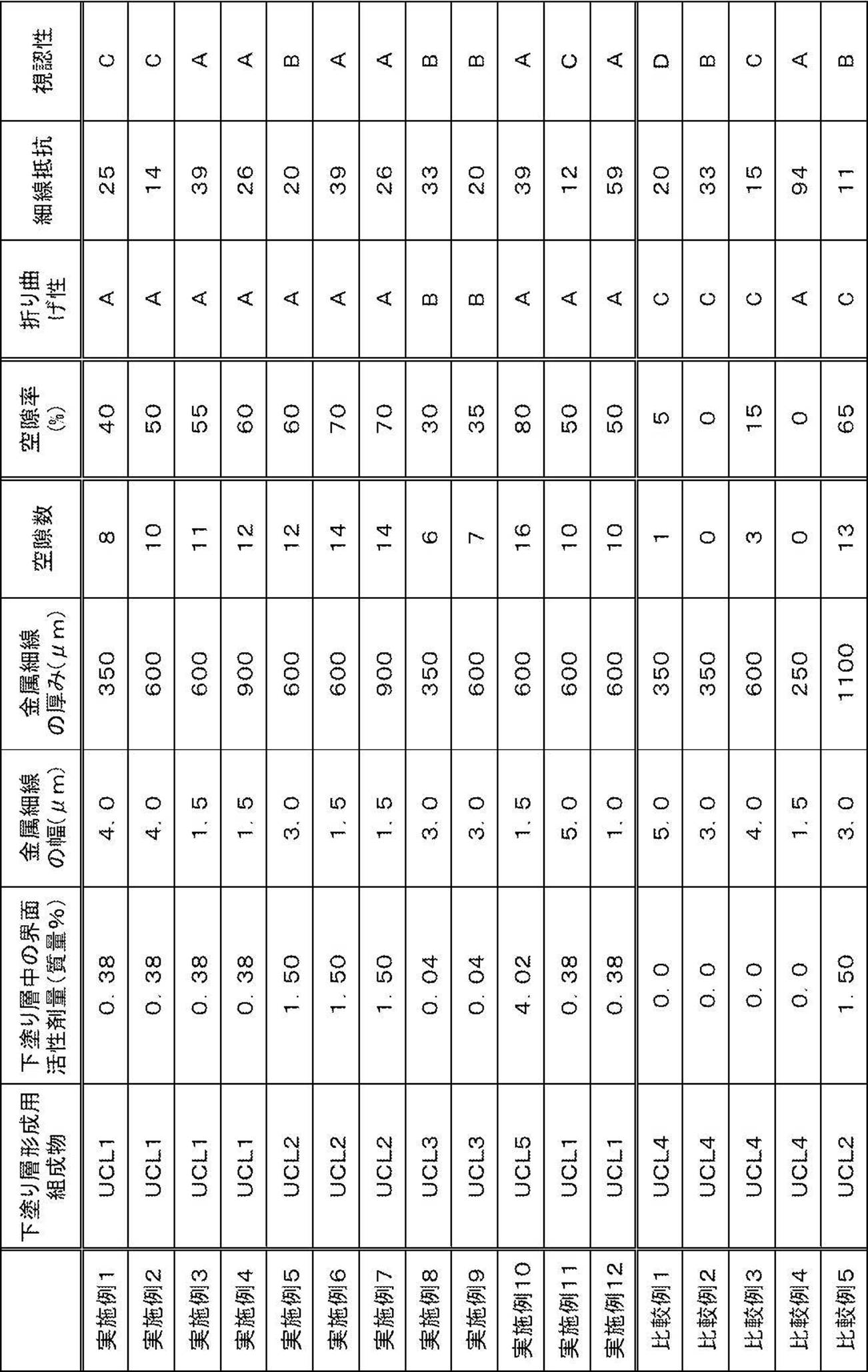
比較例1~3は空隙率が小さく、折り曲げ性が悪かった。比較例4は、金属細線の厚みが薄く線抵抗が大きかった。比較例5は、金属細線の厚みが厚く折り曲げ性が悪かった。
実施例1、2及び実施例5、8、9等の比較から、金属細線の線幅が同じ場合には、金属細線の厚みが厚い方がタッチパネル用導電部材の線抵抗が小さくなっていることがわかる。
また、実施例1~4の比較からは、金属細線の厚みが厚い方がタッチパネル用導電部材の空隙率が高くなっていることがわかる。実施例5~7の比較からは、金属細線の線幅が小さい方がタッチパネル用導電部材の空隙率が高くなっていることがわかる。また、実施例1~12の比較からは、界面活性剤の含有量が多い方がタッチパネル用導電部材の空隙率が高くなっていること、及び金属細線は細い方がタッチパネル用導電部材の視認性が良くなっていることがわかる。
11A 第1導電層
11B 第2導電層
12 タッチパネル
13 コントローラ
14 画像表示部
14a 表示面
14b、16b、24b 裏面
15 第1の透明絶縁層
16 カバー層
16a、24a、25a、27a、35a 表面
17 第2の透明絶縁層
18 タッチパネル用導電部材
19 フレキシブル回路基板
20 検出部
22 周辺配線部
23a 第1周辺配線
23b 第2周辺配線
24 透明絶縁基板
25 下塗り層
26a 第1外部接続端子
26b 第2外部接続端子
27 透明絶縁層
29A 第1検出電極層
29B 第2検出電極層
30 第1検出電極
31a 第1ダミー電極
31b 第2ダミー電極
32 第2検出電極
33 第1電極端子
34 第2電極端子
35 金属細線
35b 側面
36 開口部
37 空隙
38 黒化層
39a 第1の金属細線
39b 第2の金属細線
39c 取り出し電極
40 折り曲げ性評価用のタッチパネル用導電部材
50 周辺配線絶縁層
52 透明絶縁層
Bf 折曲げ領域
E1 検出領域
E2 周辺領域
ta、tc 厚み
Claims (14)
- 透明絶縁基板と、
透明絶縁基板上に配置された下塗り層と、
前記下塗り層上に配置された第1の金属細線と、
前記第1の金属細線を被覆する透明絶縁層とを有するタッチパネル用導電部材であって、
前記第1の金属細線の厚みが350~1000nmであり、
前記第1の金属細線が延在する方向と直交する方向の前記タッチパネル用導電部材の断面画像を10箇所取得し、各箇所で前記第1の金属細線を1つ観察した際に、前記第1の金属細線の側面と前記透明絶縁層との間に空隙がある箇所が6箇所以上観察される、タッチパネル用導電部材。 - 前記第1の金属細線によりメッシュパターンが構成されており、前記第1の金属細線の幅が1.5~4.0μmである、請求項1に記載のタッチパネル用導電部材。
- 前記透明絶縁層上に、さらに第2の金属細線が配置されており、前記透明絶縁層の厚みが1.0~5.0μmである、請求項1又は2に記載のタッチパネル用導電部材。
- 前記第2の金属細線によりメッシュパターンが構成されており、前記第2の金属細線の幅が1.5~4.0μmである、請求項3に記載のタッチパネル用導電部材。
- 前記第1の金属細線が銅である、請求項1~4のいずれか1項に記載のタッチパネル用導電部材。
- 前記第2の金属細線が銅である、請求項3又は4に記載のタッチパネル用導電部材。
- 前記透明絶縁基板がポリエステル系樹脂を含む基板であり、前記透明絶縁基板の厚みが10~60μmである、請求項1~6のいずれか1項に記載のタッチパネル用導電部材。
- 透明絶縁基板上に下塗り層を形成する第1の工程と、
前記下塗り層上に第1の金属細線を形成する第2の工程と、
前記第1の金属細線を被覆する透明絶縁層を形成する第3の工程とを有し、
前記第1の金属細線の厚みが350~1000nmであり、
前記下塗り層が、フッ素原子及びケイ素原子の少なくとも一方を含む界面活性剤を含み、前記界面活性剤の含有量が、前記下塗り層全質量に対して、0.01~5質量%である、タッチパネル用導電部材の製造方法。 - 前記第3の工程が透明絶縁層形成用組成物を前記第1の金属細線上に塗布して、前記透明絶縁層を形成する工程である、請求項8に記載のタッチパネル用導電部材の製造方法。
- 前記第2の工程は前記第1の金属細線をメッシュパターン状に形成する工程を含む、請求項8又は9に記載のタッチパネル用導電部材の製造方法。
- 前記透明絶縁層上に、さらに第2の金属細線を形成する第4の工程を有する、請求項8~10のいずれか1項に記載のタッチパネル用導電部材の製造方法。
- 前記第4の工程は前記第2の金属細線をメッシュパターン状に形成する工程を含む、請求項11に記載のタッチパネル用導電部材の製造方法。
- 前記第1の金属細線が銅である、請求項8~12のいずれか1項に記載のタッチパネル用導電部材の製造方法。
- 前記第2の金属細線が銅である、請求項11又は12に記載のタッチパネル用導電部材の製造方法。
Priority Applications (3)
| Application Number | Priority Date | Filing Date | Title |
|---|---|---|---|
| CN202280019338.4A CN116917848A (zh) | 2021-03-11 | 2022-02-18 | 触控面板用导电部件及触控面板用导电部件的制造方法 |
| JP2023505260A JPWO2022190825A1 (ja) | 2021-03-11 | 2022-02-18 | |
| US18/461,203 US20230409150A1 (en) | 2021-03-11 | 2023-09-05 | Touch panel conductive member and method for producing touch panel conductive member |
Applications Claiming Priority (2)
| Application Number | Priority Date | Filing Date | Title |
|---|---|---|---|
| JP2021-039550 | 2021-03-11 | ||
| JP2021039550 | 2021-03-11 |
Related Child Applications (1)
| Application Number | Title | Priority Date | Filing Date |
|---|---|---|---|
| US18/461,203 Continuation US20230409150A1 (en) | 2021-03-11 | 2023-09-05 | Touch panel conductive member and method for producing touch panel conductive member |
Publications (1)
| Publication Number | Publication Date |
|---|---|
| WO2022190825A1 true WO2022190825A1 (ja) | 2022-09-15 |
Family
ID=83227706
Family Applications (1)
| Application Number | Title | Priority Date | Filing Date |
|---|---|---|---|
| PCT/JP2022/006745 Ceased WO2022190825A1 (ja) | 2021-03-11 | 2022-02-18 | タッチパネル用導電部材及びタッチパネル用導電部材の製造方法 |
Country Status (4)
| Country | Link |
|---|---|
| US (1) | US20230409150A1 (ja) |
| JP (1) | JPWO2022190825A1 (ja) |
| CN (1) | CN116917848A (ja) |
| WO (1) | WO2022190825A1 (ja) |
Cited By (1)
| Publication number | Priority date | Publication date | Assignee | Title |
|---|---|---|---|---|
| JP7592927B1 (ja) | 2024-08-27 | 2024-12-02 | 日東電工株式会社 | 導電性フィルム |
Families Citing this family (1)
| Publication number | Priority date | Publication date | Assignee | Title |
|---|---|---|---|---|
| JP2024005532A (ja) * | 2022-06-30 | 2024-01-17 | 富士フイルム株式会社 | 導電性フィルム |
Citations (3)
| Publication number | Priority date | Publication date | Assignee | Title |
|---|---|---|---|---|
| WO2014034920A1 (ja) * | 2012-09-03 | 2014-03-06 | コニカミノルタ株式会社 | 透明電極およびその製造方法ならびに有機電子デバイス |
| WO2020027162A1 (ja) * | 2018-07-30 | 2020-02-06 | 旭化成株式会社 | 導電性フィルム、並びに、それを用いた導電性フィルムロール、電子ペーパー、タッチパネル、及びフラットパネルディスプレイ |
| JP2020123110A (ja) * | 2019-01-30 | 2020-08-13 | 富士フイルム株式会社 | タッチパネルおよび導電性フィルム |
Family Cites Families (4)
| Publication number | Priority date | Publication date | Assignee | Title |
|---|---|---|---|---|
| US6251470B1 (en) * | 1997-10-09 | 2001-06-26 | Micron Technology, Inc. | Methods of forming insulating materials, and methods of forming insulating materials around a conductive component |
| JP2004501503A (ja) * | 2000-03-07 | 2004-01-15 | マイクロン・テクノロジー・インコーポレーテッド | 集積回路におけるほとんど平坦な絶縁膜の形成方法 |
| KR100905828B1 (ko) * | 2007-09-17 | 2009-07-02 | 주식회사 하이닉스반도체 | 반도체 소자의 금속 배선 및 그 형성 방법 |
| JP6689451B2 (ja) * | 2017-03-30 | 2020-04-28 | 富士フイルム株式会社 | 光学フィルムならびにこれを有する画像表示装置の前面板、画像表示装置、画像表示機能付きミラ−、抵抗膜式タッチパネルおよび静電容量式タッチパネル |
-
2022
- 2022-02-18 JP JP2023505260A patent/JPWO2022190825A1/ja not_active Abandoned
- 2022-02-18 CN CN202280019338.4A patent/CN116917848A/zh active Pending
- 2022-02-18 WO PCT/JP2022/006745 patent/WO2022190825A1/ja not_active Ceased
-
2023
- 2023-09-05 US US18/461,203 patent/US20230409150A1/en not_active Abandoned
Patent Citations (3)
| Publication number | Priority date | Publication date | Assignee | Title |
|---|---|---|---|---|
| WO2014034920A1 (ja) * | 2012-09-03 | 2014-03-06 | コニカミノルタ株式会社 | 透明電極およびその製造方法ならびに有機電子デバイス |
| WO2020027162A1 (ja) * | 2018-07-30 | 2020-02-06 | 旭化成株式会社 | 導電性フィルム、並びに、それを用いた導電性フィルムロール、電子ペーパー、タッチパネル、及びフラットパネルディスプレイ |
| JP2020123110A (ja) * | 2019-01-30 | 2020-08-13 | 富士フイルム株式会社 | タッチパネルおよび導電性フィルム |
Cited By (2)
| Publication number | Priority date | Publication date | Assignee | Title |
|---|---|---|---|---|
| JP7592927B1 (ja) | 2024-08-27 | 2024-12-02 | 日東電工株式会社 | 導電性フィルム |
| JP2026042211A (ja) * | 2024-08-27 | 2026-03-11 | 日東電工株式会社 | 導電性フィルム |
Also Published As
| Publication number | Publication date |
|---|---|
| CN116917848A (zh) | 2023-10-20 |
| JPWO2022190825A1 (ja) | 2022-09-15 |
| US20230409150A1 (en) | 2023-12-21 |
Similar Documents
| Publication | Publication Date | Title |
|---|---|---|
| JP4780254B2 (ja) | 導電性基板およびその製造方法ならびにタッチパネル | |
| TWI514033B (zh) | 透明導電性積層體之製造方法 | |
| TWI466138B (zh) | Transparent conductive film, transparent conductive laminate and touch panel, and method for manufacturing transparent conductive film | |
| JP6470040B2 (ja) | 透明導電性フィルム、透明導電性フィルム積層体及びタッチパネル | |
| JP5958476B2 (ja) | 透明導電体及びタッチパネル | |
| KR101628445B1 (ko) | 투명 도전성 소자, 입력 장치 및 표시 장치 | |
| JP6070356B2 (ja) | タッチパネル用導電シートの製造方法、及びタッチパネル用導電シート | |
| WO2012005271A1 (ja) | 透明導電性フィルムおよび製造方法 | |
| JP6052330B2 (ja) | 透明導電体及びその製造方法、並びにタッチパネル | |
| US20230409150A1 (en) | Touch panel conductive member and method for producing touch panel conductive member | |
| JP6433707B2 (ja) | 透明導電性積層体およびその製造方法、透明導電性フィルムの製造方法、ならびに透明導電性フィルム巻回体の製造方法 | |
| JP5962995B2 (ja) | タッチパネル用透明導電性フィルムのベースフィルムおよびタッチパネル用透明導電性フィルム | |
| KR20140109180A (ko) | 전도성 필름 및 이의 제조 방법, 그리고 이를 포함하는 전자 장치 | |
| JP2024077918A (ja) | タッチセンサ | |
| KR20130037943A (ko) | 터치패널 및 그 제조방법 | |
| CN116324688A (zh) | 触摸面板用导电部件的制造方法及触摸面板用导电部件 | |
| TWI597742B (zh) | Transparent conductive body and touch panel | |
| JP2012216084A (ja) | 情報入力装置 | |
| KR20170081571A (ko) | 회로기판의 제조방법 | |
| CN112119331A (zh) | 防牛顿环膜以及其制造方法及用途 | |
| JP6626996B2 (ja) | 透明導電性フィルム、透明導電性フィルム積層体及びタッチパネル | |
| KR20190065187A (ko) | 광 투과성 도전 필름 및 패턴형의 도전층을 갖는 광 투과성 도전 필름의 제조 방법 | |
| KR20160006893A (ko) | 터치패널의 제조방법 | |
| JP2008250312A (ja) | 表示素子の製造方法 | |
| TWI794430B (zh) | 牛頓環防止薄膜以及其製造方法及用途 |
Legal Events
| Date | Code | Title | Description |
|---|---|---|---|
| 121 | Ep: the epo has been informed by wipo that ep was designated in this application |
Ref document number: 22766788 Country of ref document: EP Kind code of ref document: A1 |
|
| WWE | Wipo information: entry into national phase |
Ref document number: 2023505260 Country of ref document: JP |
|
| WWE | Wipo information: entry into national phase |
Ref document number: 202280019338.4 Country of ref document: CN |
|
| NENP | Non-entry into the national phase |
Ref country code: DE |
|
| 122 | Ep: pct application non-entry in european phase |
Ref document number: 22766788 Country of ref document: EP Kind code of ref document: A1 |