WO2022185803A1 - コンデンサモジュール - Google Patents
コンデンサモジュール Download PDFInfo
- Publication number
- WO2022185803A1 WO2022185803A1 PCT/JP2022/003095 JP2022003095W WO2022185803A1 WO 2022185803 A1 WO2022185803 A1 WO 2022185803A1 JP 2022003095 W JP2022003095 W JP 2022003095W WO 2022185803 A1 WO2022185803 A1 WO 2022185803A1
- Authority
- WO
- WIPO (PCT)
- Prior art keywords
- bus bar
- sealing resin
- capacitor module
- capacitor
- capacitors
- Prior art date
- Legal status (The legal status is an assumption and is not a legal conclusion. Google has not performed a legal analysis and makes no representation as to the accuracy of the status listed.)
- Ceased
Links
Images








Classifications
-
- H—ELECTRICITY
- H01—ELECTRIC ELEMENTS
- H01G—CAPACITORS; CAPACITORS, RECTIFIERS, DETECTORS, SWITCHING DEVICES, LIGHT-SENSITIVE OR TEMPERATURE-SENSITIVE DEVICES OF THE ELECTROLYTIC TYPE
- H01G2/00—Details of capacitors not covered by a single one of groups H01G4/00-H01G11/00
- H01G2/02—Mountings
-
- H—ELECTRICITY
- H01—ELECTRIC ELEMENTS
- H01G—CAPACITORS; CAPACITORS, RECTIFIERS, DETECTORS, SWITCHING DEVICES, LIGHT-SENSITIVE OR TEMPERATURE-SENSITIVE DEVICES OF THE ELECTROLYTIC TYPE
- H01G2/00—Details of capacitors not covered by a single one of groups H01G4/00-H01G11/00
- H01G2/10—Housing; Encapsulation
- H01G2/106—Fixing the capacitor in a housing
-
- H—ELECTRICITY
- H01—ELECTRIC ELEMENTS
- H01G—CAPACITORS; CAPACITORS, RECTIFIERS, DETECTORS, SWITCHING DEVICES, LIGHT-SENSITIVE OR TEMPERATURE-SENSITIVE DEVICES OF THE ELECTROLYTIC TYPE
- H01G2/00—Details of capacitors not covered by a single one of groups H01G4/00-H01G11/00
- H01G2/02—Mountings
- H01G2/04—Mountings specially adapted for mounting on a chassis
-
- H—ELECTRICITY
- H01—ELECTRIC ELEMENTS
- H01G—CAPACITORS; CAPACITORS, RECTIFIERS, DETECTORS, SWITCHING DEVICES, LIGHT-SENSITIVE OR TEMPERATURE-SENSITIVE DEVICES OF THE ELECTROLYTIC TYPE
- H01G2/00—Details of capacitors not covered by a single one of groups H01G4/00-H01G11/00
- H01G2/10—Housing; Encapsulation
-
- H—ELECTRICITY
- H01—ELECTRIC ELEMENTS
- H01G—CAPACITORS; CAPACITORS, RECTIFIERS, DETECTORS, SWITCHING DEVICES, LIGHT-SENSITIVE OR TEMPERATURE-SENSITIVE DEVICES OF THE ELECTROLYTIC TYPE
- H01G4/00—Fixed capacitors; Processes of their manufacture
- H01G4/002—Details
- H01G4/228—Terminals
-
- H—ELECTRICITY
- H01—ELECTRIC ELEMENTS
- H01G—CAPACITORS; CAPACITORS, RECTIFIERS, DETECTORS, SWITCHING DEVICES, LIGHT-SENSITIVE OR TEMPERATURE-SENSITIVE DEVICES OF THE ELECTROLYTIC TYPE
- H01G4/00—Fixed capacitors; Processes of their manufacture
- H01G4/38—Multiple capacitors, i.e. structural combinations of fixed capacitors
Definitions
- the present invention relates to capacitor modules.
- a capacitor module in which a capacitor is housed in a case and filled with sealing resin is known.
- electrodes at both ends of each capacitor are respectively connected to bus bars.
- Patent Document 1 discloses a capacitor module in which a part of a bus bar is exposed to the outside of a sealing resin in order to promote heat dissipation of the capacitor module.
- the capacitor module described in Patent Document 1 has the problem that the busbar moves within the sealing resin due to thermal shock, vibration, or the like, resulting in poor connection.
- an object of the present invention is to provide a capacitor module with improved connection reliability of bus bars.
- a capacitor module includes a case having an opening formed at a position facing the bottom surface; a sealing resin filled in the case; one or more capacitors housed in the case; a plate-shaped first bus bar connected to one electrode of the capacitor; a plate-shaped second bus bar connected to the other electrode of the capacitor; with The capacitor is placed inside the encapsulation resin,
- Each of the first bus bar and the second bus bar has a contact portion arranged inside the sealing resin and in contact with the electrode, a buried portion arranged inside the sealing resin and extending from the contact portion, and a buried portion extending from the buried portion and sealing. and an exposed portion arranged outside the stopper resin,
- the contact portion and/or the embedded portion is provided with a through hole filled with the sealing resin or a projection surrounded by the sealing resin.
- FIG. 1 is a perspective view of a capacitor module according to Embodiment 1 of the present invention
- FIG. 2 is a perspective view of the capacitor module in FIG. 1 omitting the case and sealing resin
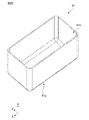
- FIG. 2 is a perspective view showing a case of the capacitor module of FIG. 1
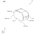
- Side view of the capacitor module of FIG. 2A 2 is a perspective view showing a capacitor included in the capacitor module of FIG. 1
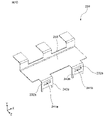
- FIG. FIG. 2A is a perspective view showing a body portion of a first bus bar of the capacitor module of FIGS. 2A and 2C
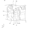
- FIG. 2B is a perspective view of the capacitor module of FIG. 2A viewed from another direction
- FIG. 4B is a perspective view showing the main body of the second bus bar of the capacitor module of FIGS. 4A and 4B;
- FIG. 4 is a partially enlarged view of a capacitor module according to a modification of the first embodiment;
- FIG. 2 is a perspective view of a capacitor module according to Embodiment 2 of the present invention;
- 7B is a perspective view showing the arrangement of capacitors inside the case of the capacitor module of FIG. 7A;
- FIG. FIG. 7B is a perspective view showing the first bus bar of the capacitor module of FIG. 7A;
- FIG. 3 is a perspective view showing a capacitor module according to Embodiment 3 of the present invention;
- FIG. 10 is a perspective view showing the first bus bar of the capacitor module of FIG. 9; Sectional view showing part of the capacitor module of FIG.
- a part of the busbar is embedded in the sealing resin, and when stress is applied to the sealing resin and the busbar due to thermal shock or vibration, the busbar is pulled out of the sealing resin. Otherwise, the connection with the capacitor may become defective, or the capacitor module may malfunction.
- a capacitor module includes a case having an opening formed at a position facing the bottom surface; a sealing resin filled in the case; one or more capacitors housed in the case; a plate-shaped first bus bar connected to one electrode of the capacitor; a plate-shaped second bus bar connected to the other electrode of the capacitor; with The capacitor is placed inside the encapsulation resin,
- Each of the first bus bar and the second bus bar has a contact portion arranged inside the sealing resin and in contact with the electrode, a buried portion arranged inside the sealing resin and extending from the contact portion, and a buried portion extending from the buried portion and sealing. and an exposed portion arranged outside the stopper resin,
- the contact portion and/or the embedded portion is provided with a through hole filled with the sealing resin or a projection surrounded by the sealing resin.
- the contact portion and/or the embedded portion may form a through hole.
- the contact portion and/or the embedded portion forming the through hole may extend in the direction from the bottom surface of the case toward the opening.
- a protrusion may be provided on the contact portion and/or the embedded portion.
- the protrusion may have a first protrusion formed by bending the end of the contact portion and/or the embedded portion.
- the protrusion may have a second protrusion formed by extending a part of the contact portion and/or the embedded portion in the width direction.
- the second protrusions can be formed in a plurality of directions, so that it is possible to further reduce the possibility of the bus bar coming off the sealing resin.
- At least one through hole or protrusion may be provided for each of the plurality of capacitors.
- FIG. 1 is a perspective view of a capacitor module 1 according to Embodiment 1 of the present invention.
- FIG. 2A is a perspective view of capacitor module 1 in FIG. 1 with case 51 and sealing resin 52 omitted.
- 2B is a perspective view showing the case 51 of the capacitor module 1 of FIG. 1.
- FIG. 2C is a side view of the capacitor module 1 of FIG. 2A.
- FIG. 2D is a perspective view showing capacitor 11 included in capacitor module 1 of FIG.
- FIG. 3 is a perspective view showing the body portion 32 of the first bus bar 31 of the capacitor module 1 of FIGS. 2A and 2C.
- FIG. 4A is a perspective view of the capacitor module 1 of FIG. 2A viewed from another direction.
- FIG. 4A is a perspective view of the capacitor module 1 of FIG. 2A viewed from another direction.
- FIG. 4B is a side view of the capacitor module 1 of FIG. 4A.
- FIG. 5 is a perspective view showing the body portion 37 of the second bus bar 36 of the capacitor module 1 of FIGS. 4A and 4B.
- the X, Y, and Z directions in the drawing indicate the horizontal direction, height direction, and vertical direction of the capacitor module 1, respectively.
- the capacitor module 1 includes a case 51, a sealing resin 52, a plurality of capacitors 11 to 18, a first busbar 31, and a second busbar 36, as shown in FIGS. 1 and 2A to 2C.
- the capacitors 11 to 18, part of the first busbar 31, and part of the second busbar 36 are accommodated in a case 51, and the inside of the case 51 is filled with a sealing resin 52.
- the case 51 has an opening 51b at a position facing the bottom surface 51a.
- capacitors 18 are arranged side by side. As shown in FIGS. 2A and 4A, in this embodiment, capacitors 11 to 14 are arranged in a row, capacitors 15 to 18 are arranged in a row, and eight capacitors are arranged in two rows in the Y direction. ing.
- the capacitors 11 to 18 are arranged such that the first electrodes 11a to 18a face each other and the second electrodes 11b to 18b face each other.
- each of the capacitors 11 to 18 and the first busbar 31 and the second busbar 36 are connected via a plurality of contact portions 35 and a plurality of contact portions 40, respectively.
- the first electrodes 11a-18a of the respective capacitors 11-18 are connected to the first bus bar 31 via the contact portions 35.
- the second electrodes 11b-18b of the respective capacitors 11-18 are connected to the second bus bar 36 via the contact portions 40.
- FIG. 1 shows that the first electrodes 11a-18a of the respective capacitors 11-18 are connected to the first bus bar 31 via the contact portions 35.
- FIG. 2C and 4B shows that the second electrodes 11b-18b of the respective capacitors 11-18 are connected to the second bus bar 36 via the contact portions 40.
- Capacitors 11-18 are film capacitors.
- the capacitors 11 to 18 are formed by winding a dielectric film on the surface of which a metal deposition film is formed and pressing the wound body of the dielectric film into a flat shape.
- Capacitors 11-18 each have a first electrode 11a-18a and a second electrode 11b-18b, as shown in FIG. 2A.
- the capacitors 11 to 18 are arranged such that the first electrodes 11a to 18a and the second electrodes 11b to 18b face each other.
- the second electrode 11b and the second electrode 12b face each other
- the second electrode 13b and the second electrode 14b face each other
- the second electrode 15b and the second electrode 16b face each other
- the second electrode 17b and the second electrode 17b face each other.
- Two electrodes 18b face each other.
- the first electrode 12a and the first electrode 13a face each other
- the first electrode 16a and the first electrode 17a face each other.
- the capacitor 11 has a side surface 11c connecting the first electrode 11a and the second electrode 11b.
- the side surface 11c includes a pair of flat portions 11d and a pair of curved portions 11e connecting the pair of flat portions 11d.
- This configuration also applies to capacitors 12-18.
- Capacitors 11 to 18 are arranged such that a pair of flat portions 11d face bottom surface 51a and opening 51b of case 51, respectively.
- dielectric films of capacitors 11-18 for example, plastic films such as polyethylene terephthalate, polypropylene, polyphenylene sulfide, or polyethylene naphthalate can be used. Moreover, Al, Zn, etc. can be used as a metal deposition film formed on the surface of a plastic film.
- the first electrodes 11a to 18a and the second electrodes 11b to 18b are formed by spraying, for example, Zn on the ends of the wound dielectric film.
- the first bus bar 31 is a plate-like conductive member connected to the first electrodes 11a-18a of the capacitors 11-18, as shown in FIGS. 2A and 3.
- FIG. In the present embodiment, first bus bar 31 is composed of body portion 32 and contact portion 35 .
- the body portion 32 has an embedded portion 33 arranged inside the sealing resin 52 and an exposed portion 34 extending from the embedded portion 33 and arranged outside the sealing resin 52 .
- a plurality of contact portions 35 are arranged inside the sealing resin 52, and each contact portion 35 contacts each of the first electrodes 11a to 18a. More specifically, one contact portion 35 contacts the first electrode 11a and the first electrode 15a. Similarly, another contact 35 contacts the first electrode 12a and the first electrode 16a, another contact 35 contacts the first electrode 13a and the first electrode 17a, and another contact 35 contacts the first electrode 13a and the first electrode 17a. It contacts the first electrode 14a and the first electrode 18a. That is, in this embodiment, the four contact portions 35 contact the first electrodes 11a-18a of the two capacitors 11-18, respectively.
- the contact portion 35 includes claws 35a (see FIGS. 2A and 2C) for connecting to the embedded portion 33, which will be described later, and claws 35b (see FIG. 2A) for connecting to the respective first electrodes 11a to 18a. have.
- the embedded portion 33 is a portion that is embedded in the sealing resin 52 when housed in the case 51 .
- three embedded portions 33 are formed in the body portion 32 .
- each embedded portion 33 is formed with a through hole 41 and a connecting portion 42 .
- the sealing resin 52 Since the inside and the periphery of the through-hole 41 are surrounded by the sealing resin 52 , it is possible to prevent the main body portion 32 (first bus bar 31 ) from coming off from the sealing resin 52 .
- the through hole 41 in the embedded portion 33 it is possible to suppress the movement and displacement of the first bus bar 31 when a load such as thermal shock or vibration is applied to the capacitor module 1 . Therefore, the contact state between the first bus bar 31 and the first electrodes 11a to 18a of the capacitors 11 to 18 can be maintained with higher accuracy, and the connection reliability of the first bus bar 31 can be improved.
- the buried portion 33 is formed extending from the exposed portion 34 in the direction (-Y direction) from the opening 51b of the case 51 toward the bottom surface 51a. Therefore, the through hole 41 is formed in a direction (Z direction) perpendicular thereto.
- the sealing resin 52 By filling the sealing resin 52 inside and around the through hole 41 formed in the Z direction, movement of the first bus bar 31 in the Y direction perpendicular to the Z direction can be suppressed.
- a connecting portion 42 is formed in the embedded portion 33 as shown in FIG.
- the connecting portion 42 is a hole formed in the embedded portion 33 in the same manner as the through hole 41 .
- a claw 35a (see FIGS. 2A and 2C) formed on the contact portion 35 is inserted into the connection portion 42, and by soldering the periphery of the connection portion 42, the body portion 32 and the contact portion 35 are electrically connected. Connected. Therefore, the first electrodes 11a to 18a of the respective capacitors 11 to 18 and the body portion 32 are electrically connected via the contact portion 35.
- the embedded portion 33 and the contact portion 35 may be connected by welding.
- the shape and number thereof are not particularly limited as long as the first electrodes 11a to 18a of the respective capacitors and the body portion 32 can be comprehensively connected.
- the exposed portion 34 is a portion that extends from the embedded portion 33 of the first bus bar 31 and is arranged outside the sealing resin 52 . As shown in FIG. 1 , the exposed portion 34 is arranged along the opening 51 b of the case 51 . By arranging the exposed portion 34 in this way, a cooling member such as a thermal pad can be arranged in the exposed portion 34 to improve the heat dissipation performance of the capacitor module 1 .
- the embedded portion 33 when connecting the contact portion 35 and the embedded portion 33 by soldering, it is desirable that the embedded portion 33 have a low heat capacity.
- a plurality of holes 43 are formed in the vicinity of the buried portion 33 in the exposed portion 34 (see FIG. 3). By providing the hole 43, the heat capacity of the embedded portion 33 can be lowered, connection can be facilitated, and productivity can be improved.
- the second bus bar 36 is a plate-like conductive member connected to the second electrodes 11b-18b of the capacitors 11-18. Note that the capacitors 14 and 18 are omitted in FIG. 4A.
- the second bus bar 36 is composed of a body portion 37 and a contact portion 40 .
- the body portion 37 has a buried portion 38 arranged inside the sealing resin 52 and an exposed portion 39 extending from the buried portion 38 and arranged outside the sealing resin 52 .
- a plurality of contact portions 40 are arranged inside the sealing resin 52, and each contact portion 40 contacts each of the second electrodes 11b to 18b. More specifically, one contact portion 40 contacts the second electrode 11b and the second electrode 15b. Similarly, another contact 40 contacts the second electrode 12b and the second electrode 16b, another contact 40 contacts the second electrode 13b and the second electrode 17b, and another contact 40 contacts the second electrode 13b and the second electrode 17b. It contacts two electrodes 14b and a second electrode 18b. That is, in this embodiment, the four contact portions 40 contact the second electrodes 11b-18b of the two capacitors 11-18, respectively.
- the contact portion 40 has a claw 40a for connecting with the embedding portion 38, which will be described later, and claws 40b for connecting to the second electrodes 11b to 18b.
- the embedded portion 38 is a portion that is embedded in the sealing resin 52 when housed in the case 51 .
- two embedded portions 38 are formed in the body portion 37 .
- a through hole 46 and a connecting portion 47 are formed in each embedded portion 38 as shown in FIG.
- the through-hole 46 is surrounded by the sealing resin 52 inside and around, it is possible to prevent the body portion 37 (second bus bar 36 ) from coming off the sealing resin 52 .
- the through hole 46 in the embedded portion 38 it is possible to suppress the movement or displacement of the second bus bar 36 when a load such as thermal shock or vibration is applied to the capacitor module 1 . Therefore, the contact state between the second bus bar 36 and the second electrodes 11b to 18b of the capacitors 11 to 18 can be maintained with higher accuracy, and the connection reliability of the second bus bar 36 can be improved.
- the buried portion 38 is formed extending from the exposed portion 39 in the direction (-Y direction) from the opening 51b of the case 51 toward the bottom surface 51a. Therefore, the through hole 46 is formed in a direction (Z direction) perpendicular thereto.
- the sealing resin 52 By filling the inside and the periphery of the through hole 46 formed in the Z direction with the sealing resin 52, movement of the second bus bar 36 in the Y direction perpendicular to the Z direction can be suppressed.
- a connecting portion 47 is formed in the embedded portion 38 as shown in FIG.
- the connecting portion 47 is a hole formed in the embedded portion 38, similar to the through hole 46.
- a claw 40a (see FIG. 4B) formed on the contact portion 40 is inserted into the connection portion 47, and the body portion 37 and the contact portion 40 are electrically connected by soldering the periphery of the connection portion 47. . Therefore, the second electrodes 11b to 18b of each capacitor and the body portion 37 are electrically connected through the contact portion 40.
- the embedded portion 38 and the contact portion 40 may be connected by welding.
- the shape and number thereof are not particularly limited as long as the second electrodes 11b to 18b of the respective capacitors and the body portion 37 can be comprehensively connected.
- the exposed portion 39 is a portion that extends from the embedded portion 38 of the second bus bar 36 and is arranged outside the sealing resin 52 . As shown in FIG. 1 , the exposed portion 39 is arranged along the opening 51 b of the case 51 . By arranging the exposed portion 39 in this manner, a cooling member such as a thermal pad, for example, can be arranged in the exposed portion 39 to improve the heat dissipation performance of the capacitor module 1 .
- the embedded portion 38 when connecting the contact portion 40 and the embedded portion 38 by soldering, it is desirable that the embedded portion 38 have a low heat capacity.
- a plurality of holes 48 are formed in the vicinity of the buried portion 38 in the exposed portion 39 . By providing the hole 48, the heat capacity of the embedded portion 38 can be lowered, connection can be facilitated, and productivity can be improved.
- portions of the first busbar 31 and the second busbar 36 that are arranged outside the case 51 are insulated by insulating paper 61 .
- Case 51 accommodates each component of capacitor module 1 .
- an opening 51b is formed at a position facing the bottom surface 51a.
- the case 51 can be made of resin such as synthetic resin.
- the case 51 can be made of synthetic resin such as polyphenylene sulfide (PPS resin) and polybutylene terephthalate (PBT resin).
- the sealing resin 52 is filled in the case 51 to seal the capacitors 11 to 18, the contact portion 35 and the embedded portion 33 of the first bus bar 31, and the contact portion 40 and the embedded portion 38 of the second bus bar 36. stop.
- the sealing resin 52 is a thermosetting resin such as an epoxy resin. Alternatively, urethane resin or the like may be used.
- the capacitor module 1 includes a case 51, a sealing resin 52, a plurality of capacitors 11-18, a first busbar 31, and a second busbar .
- the case 51 has an opening 51b at a position facing the bottom surface 51a.
- the sealing resin 52 is filled into the case 51 .
- Capacitors 11 to 18 are accommodated in case 51 and arranged inside sealing resin 52 .
- the first bus bar 31 is connected to one electrodes 11a-18a of the capacitors 11-18.
- the second bus bar 36 is connected to the other electrodes 11b-18b of the capacitors 11-18.
- Each of the first busbar 31 and the second busbar 36 has contact portions 35 , 40 , embedded portions 33 , 38 , and exposed portions 34 , 39 .
- the contact portions 35 and 40 are arranged inside the sealing resin 52 and contact the electrodes 11a-18b of the capacitors 11-18.
- the embedded portions 33 and 38 extend from the contact portions 35 and 40 and are arranged inside the sealing resin 52 .
- the exposed portions 34 and 39 extend from the embedded portions 33 and 38 and are arranged outside the sealing resin 52 .
- Buried portions 33 and 38 of first bus bar 31 and second bus bar 36 are respectively provided with through holes 41 and 46 filled with sealing resin 52 .
- the buried portions 33, 38 forming the through holes 41, 46 extend from the bottom surface 51a of the case 51 toward the opening 51b.
- the through holes 41 and 46 are formed in the direction parallel to the opening 51b of the case 51, the movement of the first busbar 31 and the second busbar 36 in the Y direction can be suppressed. Specifically, since the inside and the periphery of the through-hole 41 provided in the Z direction in the buried portion 33 of the first bus bar 31 are filled with the sealing resin 52, the direction perpendicular to the direction in which the through-hole 41 is formed is filled. Movement of the first bus bar 31 in the (Y direction) can be suppressed. Therefore, when the capacitor module 1 is subjected to thermal shock, vibration, or the like, it is possible to prevent the first bus bar 31 from coming off from the sealing resin 52 .
- the sealing resin 52 is filled inside and around the through hole 46 provided in the embedded portion 38 of the second bus bar 36 in the Z direction, the direction perpendicular to the direction in which the through hole 46 is formed (Y direction). Therefore, when the capacitor module 1 is subjected to thermal shock, vibration, or the like, it is possible to prevent the second bus bar 36 from coming off from the sealing resin 52 .
- the capacitor module 1 includes eight capacitors 11 to 18. However, the capacitor module 1 may include one or more capacitors, and the number of capacitors may vary. Not limited.
- a through-hole may be formed in at least one of the first bus bar 31 and the second bus bar 36 depending on the arrangement position of each bus bar.
- FIG. 6 is a partially enlarged view of a capacitor module according to a modification of Embodiment 1.
- protrusions 41a, 41b, and 41c may be provided in the buried portion 33a of the first bus bar 31a.
- the buried portion 33a is formed with a first protrusion 41a by bending the end portion of the buried portion 33a.
- the periphery of the first projecting portion 41a is surrounded by the sealing resin 52, and movement of the first bus bar 31a inside the sealing resin 52 can be suppressed.
- second projections 41b and 41c are formed in the buried portion 33a by partially extending the buried portion 33a in the width direction. Since the second protrusions can be formed in a plurality of directions with respect to each embedded portion 33a, it is possible to further reduce the slipping of the first bus bar 31a from the sealing resin 52 .
- the second bus bar 36 may also have a first projection and/or a second projection instead of the through hole 46 .
- FIG. 7A is a perspective view of a capacitor module 2 according to Embodiment 2 of the present invention.
- FIG. 7B is a perspective view showing the arrangement of the capacitors 111-114 inside the case 151 of the capacitor module 2 of FIG. 7A.
- FIG. 8 is a perspective view showing first bus bar 131 of capacitor module 2 of FIG. 7A.
- Embodiment 2 differs from Embodiment 1 in that the first bus bar 131 is integrally formed as shown in FIG. 7A. Also, the directions in which the respective capacitors 111 to 114 are arranged are different from those in the first embodiment.
- capacitors 111 to 114 are arranged in a case 151 having a bottom surface 151a and an opening 151b formed at a position facing the bottom surface 151a.
- the respective capacitors 111-114 are arranged such that the first electrodes 111a-114a face the opening 151b.
- a first bus bar 131 is in contact with each of the first electrodes 111a to 114a.
- Opposite electrodes (not shown) of the capacitors 111 to 114 are each in contact with a second bus bar (not shown).
- the first bus bar 131 has four contact portions 142a-142d, four embedded portions 132a-132d, and an exposed portion 133.
- Each of the contact portions 142a-142d contacts each of the first electrodes 111a-114a.
- the buried portions 132 a to 132 d and the contact portions 142 a to 142 d are extended from the respective buried portions 132 a to 132 d and arranged inside the sealing resin 152 .
- the exposed portion 133 extends from the embedded portions 132 a to 132 d and is arranged outside the sealing resin 152 .
- Through holes 141a to 141d filled with the sealing resin 152 are provided in the buried portions 132a to 132d, respectively.
- the first bus bar 131 can be formed by, for example, pressing. Since the first electrodes 111a to 114a of the respective capacitors 111 to 114 are arranged to face the opening 51b of the case 151, the first bus bar 131 and the first electrodes 111a to 114a are directly connected by soldering or welding. be able to.
- one contact portion 142a to 142d is provided for each capacitor 111 to 114, and through holes 141a to 141d are formed in each of the contact portions 142a to 142d.
- the second busbars connected to the second electrodes (not shown) of the capacitors 111 to 114 have buried portions and contact portions arranged along the bottom surface 151a of the case 151. be done.
- the second bus bar is arranged in this manner, movement of the second bus bar within case 151 is suppressed by capacitors 111 to 114 and sealing resin 152 within case 151 . Therefore, in the present embodiment, the second bus bar is not formed with through holes or projections.
- the capacitor module 2 is provided with at least one through hole 141 for each of the capacitors 111-114.
- Embodiment 3 mainly different points from Embodiment 2 will be described.
- the same reference numerals are assigned to the same or equivalent configurations as in the second embodiment.
- the description overlapping with that in the second embodiment is omitted.
- FIG. 9 is a perspective view showing a capacitor module 3 according to Embodiment 3 of the present invention.
- 10 is a perspective view showing the first bus bar 231 of the capacitor module 3 of FIG. 9.
- FIG. 11 is a cross-sectional view showing part of the capacitor module 3 of FIG.
- the third embodiment differs from the second embodiment in the orientation of capacitors 211 and 212 and the configuration of first bus bar 231 according to the orientation of capacitors 211 and 212 .
- the first bus bar 231 has contact portions 242a-242b, embedded portions 232a-232b, and an exposed portion 233, as shown in FIG.
- the contact portions 242a-242b and the buried portions 232a-232b are formed by bending the ends of the exposed portion 233. As shown in FIG.
- the contact portion 242a is in contact with the first electrode 211a of the capacitor 211, and the buried portion 232a extends from the contact portion 242a.
- a boundary between the contact portion 242a and the embedded portion 232a is indicated by a dashed line B.
- through hole 241a is formed across contact portion 242a and embedded portion 232a.
- Through hole 241a may be formed across contact portion 242a and embedded portion 232b as in the present embodiment, or may be formed in either contact portion 242a or embedded portion 232a.
- the contact portion 242b and the embedded portion 232b have the same configuration.
- the present invention is useful for capacitor modules used in various electronic devices, electrical devices, industrial devices, vehicle devices, and the like.
Landscapes
- Engineering & Computer Science (AREA)
- Power Engineering (AREA)
- Microelectronics & Electronic Packaging (AREA)
- Manufacturing & Machinery (AREA)
- Fixed Capacitors And Capacitor Manufacturing Machines (AREA)
Priority Applications (3)
| Application Number | Priority Date | Filing Date | Title |
|---|---|---|---|
| JP2023503639A JP7700840B2 (ja) | 2021-03-02 | 2022-01-27 | コンデンサモジュール |
| CN202280017305.6A CN116941002A (zh) | 2021-03-02 | 2022-01-27 | 电容器模块 |
| US18/240,654 US20230411079A1 (en) | 2021-03-02 | 2023-08-31 | Capacitor module |
Applications Claiming Priority (2)
| Application Number | Priority Date | Filing Date | Title |
|---|---|---|---|
| JP2021-032901 | 2021-03-02 | ||
| JP2021032901 | 2021-03-02 |
Related Child Applications (1)
| Application Number | Title | Priority Date | Filing Date |
|---|---|---|---|
| US18/240,654 Continuation US20230411079A1 (en) | 2021-03-02 | 2023-08-31 | Capacitor module |
Publications (1)
| Publication Number | Publication Date |
|---|---|
| WO2022185803A1 true WO2022185803A1 (ja) | 2022-09-09 |
Family
ID=83154980
Family Applications (1)
| Application Number | Title | Priority Date | Filing Date |
|---|---|---|---|
| PCT/JP2022/003095 Ceased WO2022185803A1 (ja) | 2021-03-02 | 2022-01-27 | コンデンサモジュール |
Country Status (4)
| Country | Link |
|---|---|
| US (1) | US20230411079A1 (https=) |
| JP (1) | JP7700840B2 (https=) |
| CN (1) | CN116941002A (https=) |
| WO (1) | WO2022185803A1 (https=) |
Citations (7)
| Publication number | Priority date | Publication date | Assignee | Title |
|---|---|---|---|---|
| JP2005085880A (ja) * | 2003-09-05 | 2005-03-31 | Shizuki Electric Co Inc | 電気部品 |
| JP2014116446A (ja) * | 2012-12-10 | 2014-06-26 | Panasonic Corp | ケースモールド型コンデンサ |
| WO2017146013A1 (ja) * | 2016-02-25 | 2017-08-31 | パナソニックIpマネジメント株式会社 | フィルムコンデンサ |
| WO2017204065A1 (ja) * | 2016-05-25 | 2017-11-30 | パナソニックIpマネジメント株式会社 | コンデンサ |
| JP2018037433A (ja) * | 2016-08-29 | 2018-03-08 | パナソニックIpマネジメント株式会社 | コンデンサおよびコンデンサの製造方法 |
| JP2018064051A (ja) * | 2016-10-14 | 2018-04-19 | 株式会社トーキン | 電気二重層コンデンサ |
| JP2019096713A (ja) * | 2017-11-22 | 2019-06-20 | 株式会社指月電機製作所 | コンデンサ |
Family Cites Families (5)
| Publication number | Priority date | Publication date | Assignee | Title |
|---|---|---|---|---|
| JPS611042A (ja) * | 1984-06-13 | 1986-01-07 | Toshiba Corp | 半導体装置 |
| JPS61182023U (https=) * | 1985-04-30 | 1986-11-13 | ||
| JP2009194080A (ja) * | 2008-02-13 | 2009-08-27 | Daikin Ind Ltd | コンデンサモジュール |
| JP2016092086A (ja) * | 2014-10-31 | 2016-05-23 | 日立オートモティブシステムズ株式会社 | ケース構造 |
| JP7091657B2 (ja) * | 2017-12-27 | 2022-06-28 | 株式会社デンソー | コンデンサモジュール |
-
2022
- 2022-01-27 JP JP2023503639A patent/JP7700840B2/ja active Active
- 2022-01-27 CN CN202280017305.6A patent/CN116941002A/zh active Pending
- 2022-01-27 WO PCT/JP2022/003095 patent/WO2022185803A1/ja not_active Ceased
-
2023
- 2023-08-31 US US18/240,654 patent/US20230411079A1/en active Pending
Patent Citations (7)
| Publication number | Priority date | Publication date | Assignee | Title |
|---|---|---|---|---|
| JP2005085880A (ja) * | 2003-09-05 | 2005-03-31 | Shizuki Electric Co Inc | 電気部品 |
| JP2014116446A (ja) * | 2012-12-10 | 2014-06-26 | Panasonic Corp | ケースモールド型コンデンサ |
| WO2017146013A1 (ja) * | 2016-02-25 | 2017-08-31 | パナソニックIpマネジメント株式会社 | フィルムコンデンサ |
| WO2017204065A1 (ja) * | 2016-05-25 | 2017-11-30 | パナソニックIpマネジメント株式会社 | コンデンサ |
| JP2018037433A (ja) * | 2016-08-29 | 2018-03-08 | パナソニックIpマネジメント株式会社 | コンデンサおよびコンデンサの製造方法 |
| JP2018064051A (ja) * | 2016-10-14 | 2018-04-19 | 株式会社トーキン | 電気二重層コンデンサ |
| JP2019096713A (ja) * | 2017-11-22 | 2019-06-20 | 株式会社指月電機製作所 | コンデンサ |
Also Published As
| Publication number | Publication date |
|---|---|
| US20230411079A1 (en) | 2023-12-21 |
| CN116941002A (zh) | 2023-10-24 |
| JPWO2022185803A1 (https=) | 2022-09-09 |
| JP7700840B2 (ja) | 2025-07-01 |
Similar Documents
| Publication | Publication Date | Title |
|---|---|---|
| JP5391797B2 (ja) | ケースモールド型コンデンサ | |
| US10079098B2 (en) | Case-mold-type capacitor and method for producing same | |
| JP7122657B2 (ja) | コンデンサ | |
| JP7452640B2 (ja) | コンデンサモジュール | |
| WO2012098622A1 (ja) | ケースモールド型コンデンサ | |
| JP6432792B2 (ja) | 回路構成体及び電気接続箱 | |
| CN110121922B (zh) | 电路结构体以及电气接线箱 | |
| JP6305731B2 (ja) | ケースモールド型コンデンサおよびその製造方法 | |
| US10984952B2 (en) | Capacitor | |
| JP7409491B2 (ja) | コンデンサモジュール | |
| JPWO2021220918A5 (https=) | ||
| JP4396734B2 (ja) | 表面実装型電子部品 | |
| JP4983540B2 (ja) | ケースモールド型コンデンサ | |
| WO2022185803A1 (ja) | コンデンサモジュール | |
| US12340943B2 (en) | Electronic device | |
| JP2024056186A (ja) | コンデンサ | |
| JP2017054848A (ja) | コンデンサ | |
| JP2026018323A (ja) | フィルムコンデンサ | |
| WO2023032830A1 (ja) | 電解コンデンサ及び座板 | |
| JP2024014203A (ja) | コンデンサ | |
| JP2017228744A (ja) | 電子装置 | |
| JPWO2017169956A1 (ja) | 電子部品 | |
| JPH0239405A (ja) | チップ形コンデンサの集合体 |
Legal Events
| Date | Code | Title | Description |
|---|---|---|---|
| 121 | Ep: the epo has been informed by wipo that ep was designated in this application |
Ref document number: 22762862 Country of ref document: EP Kind code of ref document: A1 |
|
| WWE | Wipo information: entry into national phase |
Ref document number: 2023503639 Country of ref document: JP |
|
| WWE | Wipo information: entry into national phase |
Ref document number: 202280017305.6 Country of ref document: CN |
|
| NENP | Non-entry into the national phase |
Ref country code: DE |
|
| 122 | Ep: pct application non-entry in european phase |
Ref document number: 22762862 Country of ref document: EP Kind code of ref document: A1 |